

Page 1

Freescale Semiconductor
80 LQFP
14 mm 14 mm
64 LQFP
10 mm 10 mm
64 QFP
14 mm 14 mm
44 LQFP
10 mm 10 mm
Data Sheet: Technical Data
MCF51JM128 ColdFire
Microcontroller
The MCF51JM128 is a member of the ColdFire family of
32-bit reduced instruction set computing (RISC)
microprocessors. This document provides an overview of the
MCF51JM128 series, focusing on its highly integrated and
diverse feature set.
The MCF51JM128 series is based on the V1 ColdFire core
and operates at processor core speeds up to 50.33 MHz. As
part of Freescale’s Controller Continuum
upgrade for designs based on the MC9S08JM60 series of 8-bit
microcontrollers.
®
, it is an ideal
Document Number: MCF51JM128
Rev. 4, 05/2012
MCF51JM128
The MCF51JM128 features the following functional units:
• V1 ColdFire core with background debug module
• Up to 128 KB of flash memory
• Up to 16 KB of static RAM (SRAM)
• Multipurpose clock generator (MCG)
• Dual-role Universal Serial Bus On-The-Go device
(USBOTG)
• Controller-area network (MSCAN)
• Cryptographic acceleration unit (CAU)
• Random number generator accelerator (RNGA)
• Analog comparators (ACMP)
• Analog-to-digital converter (ADC) with up to 12 channels
• Two Inter-integrated circuit (IIC) modules
• Two serial peripheral interfaces (SPI)
• Two serial communications interfaces (SCI)
• Carrier modulation timer (CMT)
• Eight-channel timer/pulse-width modulators (TPM)
• Real-time counter (RTC)
• 66 general-purpose input/output (GPIO) modules plus
Interrupt request input
• Eight keyboard interrupts (KBI)
• 16-bit Rapid GPIO
This document contains information on a product under development. Freescale reserves the
right to change or discontinue this product without notice.
© Freescale Semiconductor, Inc., 2008-2012. All rights reserved.
Page 2

Table of Contents
1 MCF51JM128 Family Configurations . . . . . . . . . . . . . . . . . . . .3
1.1 Device Comparison. . . . . . . . . . . . . . . . . . . . . . . . . . . . .3
1.2 Block Diagram. . . . . . . . . . . . . . . . . . . . . . . . . . . . . . . . .4
1.3 Features . . . . . . . . . . . . . . . . . . . . . . . . . . . . . . . . . . . . .5
1.4 Part Numbers . . . . . . . . . . . . . . . . . . . . . . . . . . . . . . . . .8
1.5 Pinouts and Packaging. . . . . . . . . . . . . . . . . . . . . . . . .10
2 Preliminary Electrical Characteristics . . . . . . . . . . . . . . . . . . .15
2.1 Parameter Classification . . . . . . . . . . . . . . . . . . . . . . . .15
2.2 Absolute Maximum Ratings . . . . . . . . . . . . . . . . . . . . .15
2.3 Thermal Characteristics . . . . . . . . . . . . . . . . . . . . . . . .16
2.4 Electrostatic Discharge (ESD) Protection Characteristics
. . . . . . . . . . . . . . . . . . . . . . . . . . . . . . . . . . . . . . . . . . .17
2.5 DC Characteristics . . . . . . . . . . . . . . . . . . . . . . . . . . . .18
2.6 Supply Current Characteristics. . . . . . . . . . . . . . . . . . .21
2.7 Analog Comparator (ACMP) Electricals . . . . . . . . . . . .23
2.8 ADC Characteristics . . . . . . . . . . . . . . . . . . . . . . . . . . .23
2.9 External Oscillator (XOSC) Characteristics . . . . . . . . .26
2.10 MCG Specifications . . . . . . . . . . . . . . . . . . . . . . . . . . .27
2.11 AC Characteristics . . . . . . . . . . . . . . . . . . . . . . . . . . . .28
2.12 SPI Characteristics . . . . . . . . . . . . . . . . . . . . . . . . . . . .31
2.13 Flash Specifications . . . . . . . . . . . . . . . . . . . . . . . . . . .34
2.14 USB Electricals. . . . . . . . . . . . . . . . . . . . . . . . . . . . . . .34
2.15 EMC Performance. . . . . . . . . . . . . . . . . . . . . . . . . . . . .35
3 Mechanical Outline Drawings. . . . . . . . . . . . . . . . . . . . . . . . .36
3.1 80-pin LQFP . . . . . . . . . . . . . . . . . . . . . . . . . . . . . . . . .36
3.2 64-pin LQFP . . . . . . . . . . . . . . . . . . . . . . . . . . . . . . . . .39
3.3 64-pin QFP . . . . . . . . . . . . . . . . . . . . . . . . . . . . . . . . . .42
3.4 44-pin LQFP . . . . . . . . . . . . . . . . . . . . . . . . . . . . . . . . .45
4 Revision History . . . . . . . . . . . . . . . . . . . . . . . . . . . . . . . . . . .48
List of Figures
Figure 1.MCF51JM128 Block Diagram. . . . . . . . . . . . . . . . . . . . 4
Figure 2.80-pin LQFP . . . . . . . . . . . . . . . . . . . . . . . . . . . . . . . . 10
Figure 3.64-pin QFP and LQFP . . . . . . . . . . . . . . . . . . . . . . . . 11
Figure 4.44-pin LQFP . . . . . . . . . . . . . . . . . . . . . . . . . . . . . . . . 12
Figure 5.Typical Low-side Drive (sink) characteristics – High Drive
(PTxDSn = 1) . . . . . . . . . . . . . . . . . . . . . . . . . . . . . . . 20
Figure 6.Typical Low-side Drive (sink) characteristics – Low Drive
(PTxDSn = 0) . . . . . . . . . . . . . . . . . . . . . . . . . . . . . . . 20
Figure 7.Typical High-side Drive (source) characteristics – High
Drive (PTxDSn = 1). . . . . . . . . . . . . . . . . . . . . . . . . . . 21
Figure 8.T ypical High-side Drive (source) characteristics – Low Drive
(PTxDSn = 0) . . . . . . . . . . . . . . . . . . . . . . . . . . . . . . . 21
Figure 9.ADC Input Impedance Equivalency Diagram . . . . . . . 24
Figure 10.Reset Timing . . . . . . . . . . . . . . . . . . . . . . . . . . . . . . . 29
Figure 11.IRQ/KBIPx Timing . . . . . . . . . . . . . . . . . . . . . . . . . . . 29
Figure 12.Timer External Clock. . . . . . . . . . . . . . . . . . . . . . . . . 29
Figure 13.Timer Input Capture Pulse. . . . . . . . . . . . . . . . . . . . . 30
Figure 14.SPI Master Timing (CPHA = 0) . . . . . . . . . . . . . . . . . 32
Figure 15.SPI Master Timing (CPHA = 1) . . . . . . . . . . . . . . . . . 32
Figure 16.SPI Slave Timing (CPHA = 0) . . . . . . . . . . . . . . . . . . 33
Figure 17.SPI Slave Timing (CPHA = 1) . . . . . . . . . . . . . . . . . . 33
Figure 18.80-pin LQFP Diagram - I . . . . . . . . . . . . . . . . . . . . . . 36
Figure 19.80-pin LQFP Diagram - II. . . . . . . . . . . . . . . . . . . . . . 37
Figure 20.80-pin LQFP Diagram - III . . . . . . . . . . . . . . . . . . . . . 38
Figure 21.64-pin LQFP Diagram - I . . . . . . . . . . . . . . . . . . . . . . 39
Figure 22.64-pin LQFP Diagram - II. . . . . . . . . . . . . . . . . . . . . . 40
Figure 23.64-pin LQFP Diagram - III . . . . . . . . . . . . . . . . . . . . . 41
Figure 24.64-pin QFP Diagram - I . . . . . . . . . . . . . . . . . . . . . . . 42
Figure 25.64-pin QFP Diagram - II. . . . . . . . . . . . . . . . . . . . . . . 43
Figure 26.64-pin QFP Diagram - III . . . . . . . . . . . . . . . . . . . . . . 44
Figure 27.44-pin LQFP Diagram - I . . . . . . . . . . . . . . . . . . . . . . 45
Figure 28.44-pin LQFP Diagram - II. . . . . . . . . . . . . . . . . . . . . . 46
Figure 29.44-pin LQFP Diagram - III . . . . . . . . . . . . . . . . . . . . . . 47
List of Tables
Table 1. MCF51JM128 Series Device Comparison . . . . . . . . . . 3
Table 2. MCF51JM128 Series Functional Units . . . . . . . . . . . . . 5
Table 3. Orderable Part Number Summary. . . . . . . . . . . . . . . . . 8
Table 4. Pin Assignments by Package and Pin Sharing Priority 12
Table 5. Parameter Classifications . . . . . . . . . . . . . . . . . . . . . . 15
Table 6. Absolute Maximum Ratings. . . . . . . . . . . . . . . . . . . . . 16
Table 7. Thermal Characteristics. . . . . . . . . . . . . . . . . . . . . . . . 16
Table 8. ESD and Latch-up Test Conditions . . . . . . . . . . . . . . . 17
Table 9. ESD and Latch-Up Protection Characteristics. . . . . . . 18
Table 10.DC Characteristics. . . . . . . . . . . . . . . . . . . . . . . . . . . . 18
Table 11. Supply Current Characteristics. . . . . . . . . . . . . . . . . . 21
Table 12.Analog Comparator Electrical Specifications. . . . . . . . 23
Table 13.5 Volt 12-bit ADC Operating Conditions . . . . . . . . . . . 23
T able14.5 Volt 12-bit ADC Characteristics (VREFH = VDDA, VREFL
= VSSA). . . . . . . . . . . . . . . . . . . . . . . . . . . . . . . . . . . . 24
Table 15.Oscillator Electrical Specifications (Temperature Range =
–40 to 105×C Ambient) . . . . . . . . . . . . . . . . . . . . . . . . 26
T able16.MCG Frequency Specifications (T emperature Range = –40
to 125×C Ambient) . . . . . . . . . . . . . . . . . . . . . . . . . . . 27
Table 17.Control Timing . . . . . . . . . . . . . . . . . . . . . . . . . . . . . . . 28
Table 18.TPM Input Timing . . . . . . . . . . . . . . . . . . . . . . . . . . . . 29
Table 19.MSCAN Wake-up Pulse Characteristics . . . . . . . . . . . 30
Table 20.SPI Timing. . . . . . . . . . . . . . . . . . . . . . . . . . . . . . . . . . 31
Table 21.Flash Characteristics. . . . . . . . . . . . . . . . . . . . . . . . . . 34
Table 22.Internal USB 3.3V Voltage Regulator Characteristics . 35
Table 23.Internal Revision History . . . . . . . . . . . . . . . . . . . . . . . 50
Table 24.Changes Between Revisions. . . . . . . . . . . . . . . . . . . . 51
MCF51JM128 ColdFire Microcontroller, Rev. 4
Freescale Semiconductor2
Page 3
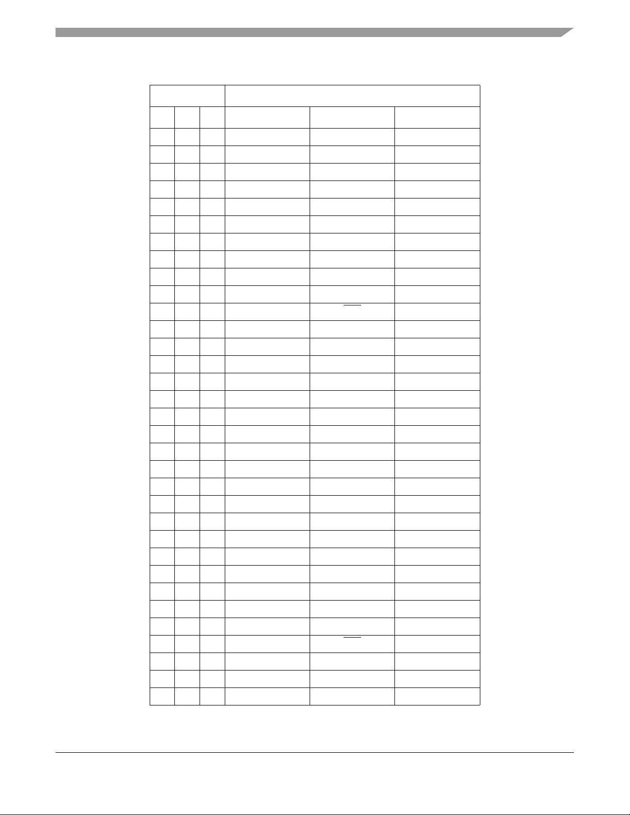
1 MCF51JM128 Family Configurations
1.1 Device Comparison
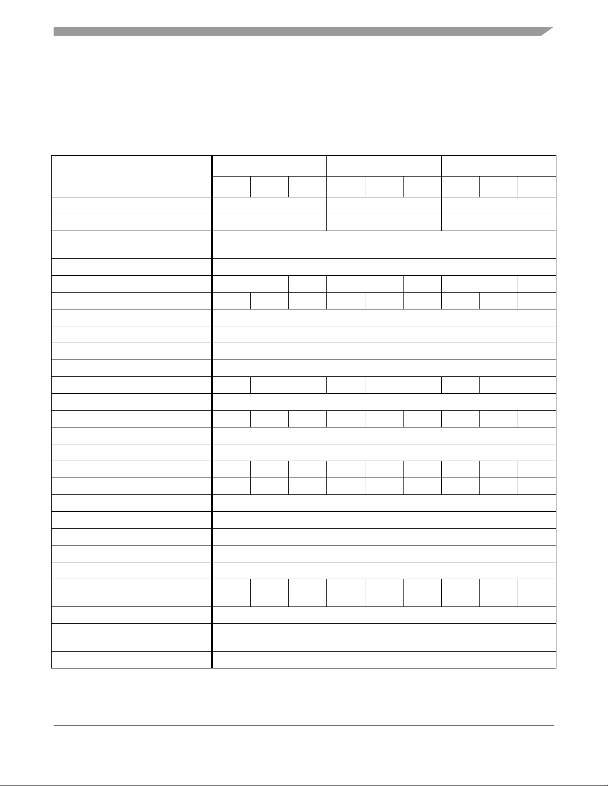
The MCF51JM128 series consists of the devices compared in Table 1.
Table 1. MCF51JM128 Series Device Comparison
MCF51JM128 Family Configurations
MCF51JM128 MCF51JM64
Feature
80-pin 64-pin 44-pin 80-pin 64-pin 44-pin 80-pin 64-pin 44-pin
Flash memory size (KB) 128 64 32
RAM size (KB) 16 16 16
V1 ColdFire core with BDM (background
debug module)
ACMP (analog comparator) Yes
ADC channels (12-bit) 12 8 12 8 12 8
CAN (controller area network) Yes Yes No Yes Yes No Yes Yes No
RNGA + CAU Yes
CMT (carrier modulator timer) Yes
COP (computer operating properly) Yes
IIC1 (inter-integrated circuit) Yes
IIC2 Yes No Yes No Yes No
IRQ (interrupt request input) Yes
KBI (keyboard interrupts) 8 8 6 8 86886
LVD (low-voltage detector) Yes
Yes
1
MCF51JM32
MCG (multipurpose clock generator) Yes
Port I/O
RGPIO (rapid general-purpose I/O) 16 6 0 16 6 0 16 6 0
RTC (real-time counter) Yes
SCI1 (serial communications interface) Yes
SCI2 Yes
SPI1 (serial peripheral interface) Yes
SPI2 Yes
TPM1 (timer/pulse-width modulator)
channels
TPM2 channels 2
USBOTG (USB On-The-G o du a l -rol e
controller)
XOSC (crystal oscillator) Yes
1
Freescale Semiconductor 3
2
Only existed on speci al pa rt number
66 51 33 66 51 33 66 51 33
664664664
Yes
MCF51JM128 ColdFire Microcontroller, Rev. 4
Page 4
MCF51JM128 Family Configurations
Port B
PTB3/SS2/ADP3
PTB4/KBIP4/ADP4
PTB5/KBIP5/ADP5
PTB2/SPSCK2/ADP2
PTB1/MOSI2/ADP1
PTB0/MISO2/ADP0
PTB6/ADP6
PTB7/ADP7
Port D
PTD3/KBIP3/ADP10
PTD4/ADP11
PTD5
PTD2/KBIP2/ACMPO
PTD1/ACMP–/ADP9
PTD0/ACMP+/ADP8
PTD6
PTD7
Port C
PTC3/TXD2
PTC4
PTC5/RXD2
PTC2/IRO
PTC1/SDA1
PTC0/SCL1
PTC6/RXCAN
PTC7
Port F
PTF3/TPM1CH5
PTF4/TPM2CH0
PTF5/TPM2CH1
PTF2/TPM1CH4
PTF1/TPM1CH3
PTF0/TPM1CH2
PTF6
PTF7/TXCAN
Port E
PTE3/TPM1CH1
PTE4/MISO1
PTE5/MOSI1
PTE2/TPM1CH0
PTE1/RXD1
PTE0/TXD1
PTE6/SPSCK1
PTE7/SS1
Port G
PTG3/KBIP7
PTG4/XTAL
PTG5/EXTAL
PTG2/KBIP6
PTG1/KBIP1
PTG0/KBIP0
PTG6
PTG7
Port H
PTH3/RGPIO9
PTH4/RGPIO10
PTH2/RGPIO8
PTH1/SCL2
PTH0/SDA2
Port J
PTJ3/RGPIO14
PTJ4/RGPIO15
PTJ2/RGPIO13
PTJ1/RGPIO12
PTJ0/RGPIO11
Port A
PTA3/RGPIO3
PTA4/RGPIO4
PTA5/RGPIO5
PTA2/RGPIO2
PTA1/RGPIO1
PTA0/RGPIO0
PTA6/RGPIO6
PTA7/RGPIO7
ADC
VREFH
VREFL
VDDAD
VSSAD
CAN
TPMCLK
TPM1
TPMCLK
SPI1
SCI1
MCG
IIC2
USB
VREG
SYSCTL
V1 ColdFire core
CMT
Port C:
IRO
Port H:
SCL2
SDA2
Port G:
EXTAL
XTAL
Port E:
RXD1
TXD1
Port E:
SS1
SPSCK1
MOSI1
MISO1
Port F:
TPM1CH5
TPM1CH4
TPM1CH3
TPM1CH2
Port E:
TPM1CH1
TPM1CH0
TPM2
Port F:
TPM2CH1
TPM2CH0
Port C:
RXCAN
Port F:
TXCAN
IIC1
Port C:
SDA1
SCL1
SCI2
Port C:
RXD2
TXD2
Port B:
ADP7
ADP6
ADP5
ADP4
ADP3
ADP2
ADP1
ADP0
Port D:
ADP11
ADP10
ADP9
ADP8
SPI2
Port B:
SS2
SPSCK2
MOSI2
MISO2
KBI
Port B:
KBIP5
KBIP4
Port D:
KBIP3
KBIP2
Port G:
KBIP7
KBIP6
KBIP1
KBIP0
RAM
RGPIO
Port J:
RGPIO15
RGPIO14
RGPIO13
RGPIO12
RGPIO11
Port H:
RGPIO10
RGPIO9
RGPIO8
Port A:
RGPIO7
RGPIO6
RGPIO5
RGPIO4
RGPIO3
RGPIO2
RGPIO1
RGPIO0
ACMP
Port D:
ACMPO
ACMP–
ACMP+
RTC
INTC
RNGA
IRQ/TPMCLK
VREFH
VREFL
VDDA
VSSA
BKGD/MS
RESET
VDD
VSS
VSS
USBDN
USBDP
VUSB33
FLASH
128 or 64 KB
16 or 8 KB
VDD
XOSC
BDM
DBG
CAU
COP
IRQ
LVD
2
Up to 16 pins on Ports A, H, and J are shared with the ColdFire Rapid GPIO module.
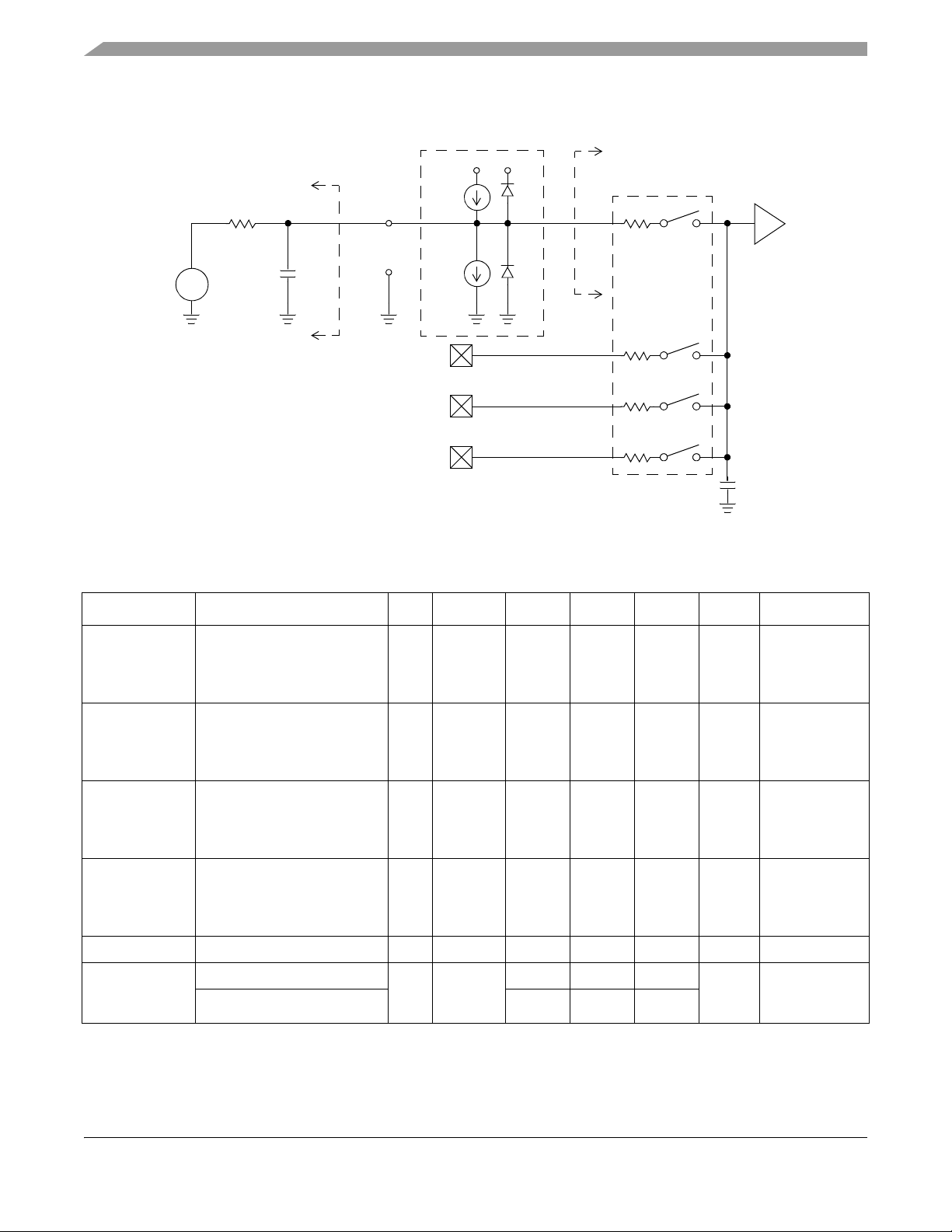
1.2 Block Diagram
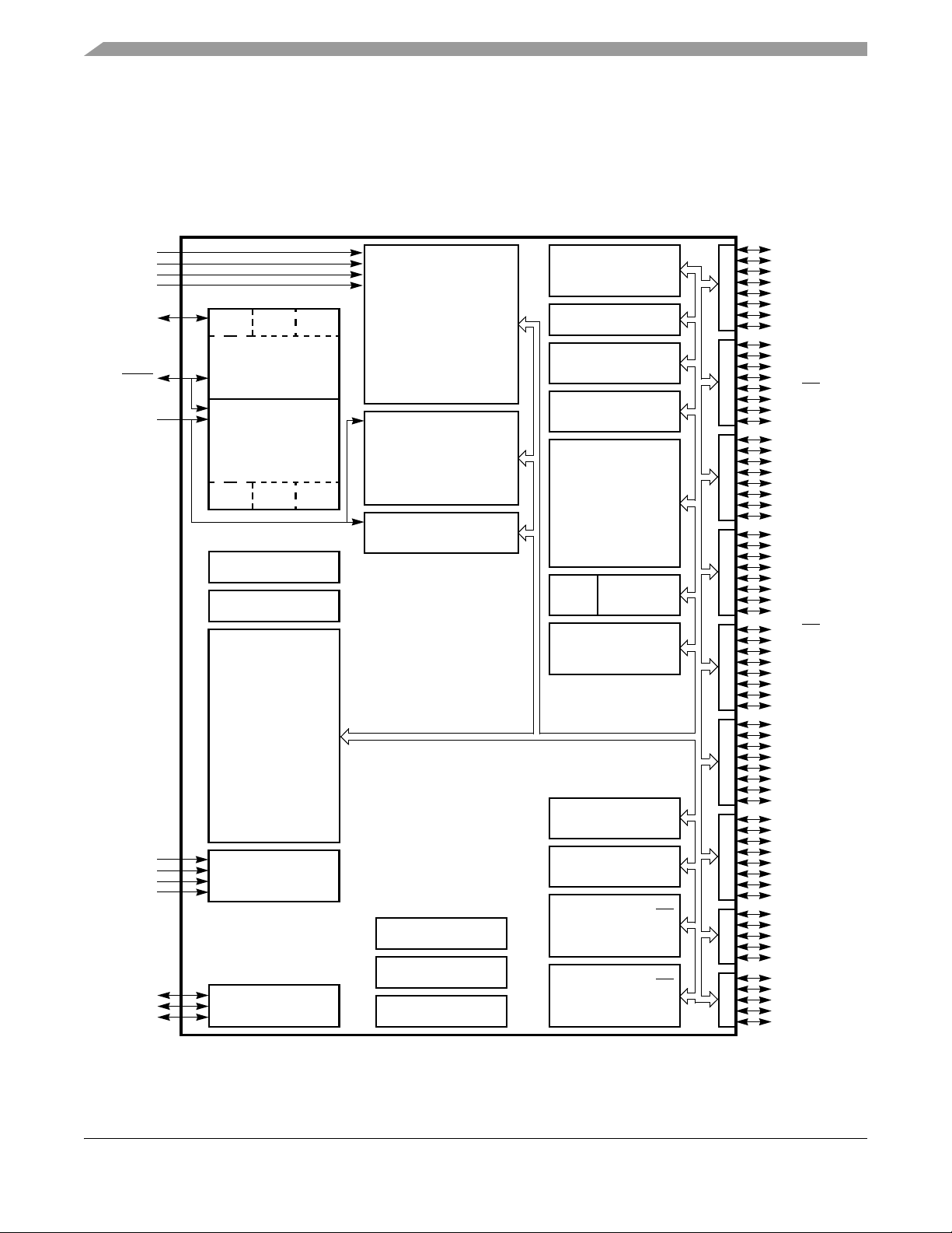
Figure 1 shows the connections between the MCF51JM128 series pins and modules.
Figure 1. MCF51JM128 Block Diagram
MCF51JM128 ColdFire Microcontroller, Rev. 4
Freescale Semiconductor4
Page 5
MCF51JM128 Family Configurations
1.3 Features
Table 2 describes the functional units of the MCF51JM128 series.
Table 2. MCF51JM128 Series Functional Units
Unit Function
CF1CORE (V1 ColdFire core) Executes programs and interrupt handlers
BDM (background debug module) Provides a single-pin debugging interface (part of the V1 ColdFire core)
DBG (debug) Provides debugging and emulation capabilities (part of the V1 ColdFire core)
SYSCTL (system control) Provides LVD, COP, external interrupt request, and so on
FLASH (flash memory) Provides storage for program code and constants
RAM (random-access memory) Provides storage for program code, constants, and variables
RGPIO (rapid general-purpose input/output) Allows I/O port access at CPU clock speeds
VREG (voltage regulator) Controls power management throughout the device
USBOTG (USB On-The-Go) Supports the USB On-The-Go dual-role controller
ADC (analog-to-digital converter) Measures analog voltages at up to 12 bits of resolution
TPM1, TPM2 (timer/pulse-width modulators) Provide a variety of timing-based features
CF1_INTC (interrupt controller) Controls and prioritizes all device interrupts
CAU (cryptographic acceleration unit) Co-processor support for DES, 3DES, AES, MD5, and SHA-1
RNGA (random number generator accelerator) 32-bit random number generator that complies with FIPS-140
RTC (real-time counter) Provides a constant-time base with optional interrupt
ACMP (analog comparator) Compares two analog inputs
CMT (carrier modulator timer) Infrared output used for the Remote Controller
IIC1, IIC2 (inter-integrated circuits) Supports the standard IIC communications protoc ol
KBI (keyboard interrupt) Provides pin interrupt capabilities
MCG (multipurpose clock generator) Provides clocking options for the device, including a phase-locked loop (PLL)
and frequency-locked loop (FLL) for multiplying slower reference clock
sources
XOSC (crystal oscillator) Supports low/high range crystals
CAN (controller area network) Supports standard CAN communications protocol
SCI1, SCI2 (serial communications interfaces) Serial communications UARTs that can support RS-232 and LIN protocols
SPI1, SPI2 (serial peripheral interfaces) Provide a 4-pin synchronous serial interface
MCF51JM128 ColdFire Microcontroller, Rev. 4
Freescale Semiconductor 5
Page 6

MCF51JM128 Family Configurations
1.3.1 Feature List
• 32-bit Version 1 ColdFire Central Processor Unit (CPU)
— Up to 50.33 MHz at 2.7 V – 5.5 V
— Performance (Dhrystone 2.1):
– 0.94 Dhrystone 2.1 MIPS per MHz when running from in tern al RAM
– 0.76 Dhrystone 2.1 MIPS per MHz when running from flash
— Implements Instruction Set Revision C (ISA_C)
— Supports up to 30 peripheral interrupt requests and seven software interrupts
• On-chip memory
— Up to 128 KB Flash memory with read/program/erase over full operating voltage and temperature range
— Up to 16 KB static random access memory (RAM)
— Security circuitry to prevent unauthorized access to RAM and flash contents
• Power-saving modes
— Two low-power stop plus wait modes
— Peripheral clock enable register can disable clocks to unused modules, thereby reducing currents; this behavior
allows clocks to remain enabled to specific perhipherals in Stop3 mode
— Very lower power real-time counter for use in run, wait, and stop modes with internal and external clock sources
• Four Clock Source Options
— Oscillator (XOSC) — Loop-control Pierce oscillator; crystal or ceramic resonator range of 31.25 kHz to 38.4 kHz
or 1 MHz to 16 MHz
— FLL/PLL controlled by internal or external reference
— Trimmable internal reference allows 0.2% resolution and 2% deviation
• System protection features
— W atchdog computer operating properly (COP) reset with option to run from dedicated 1 kHz internal clock source
or bus clock
— Low-voltage detection with reset or interrupt; selectable trip points
— Illegal opcode and illegal address detection with programmable reset or exception response
— Flash block protection
• Debug support
— Single-wire Background debug interface
— 4 Program Counters plus two address (optional data) breakpoint registers with programmable 1- or 2-level trigger
response
— 64-entry processor status and debug data trace buffer with programmable start/stop conditions
• Universal Serial Bus (USB) On-The-Go dual-role controller
— Full-speed USB device controller
– Fully compliant with USB specificatio n 1.1 and 2.0
– 16 bidirectional endpoints, with double buffering to provide the maximum throughput
– Supports control, bu lk, interrupt, and isochronous endpoints
– Supports bus-powered capabi lit y with low-power consumption
— Full-speed / low-speed host controller
– Host mode allows control, bulk, interrupt, and isochronous transfers
— OTG protocol logic
— On-chip USB transceiver
— On-chip 3.3 V USB regulator and pull-up resistors save system cost
MCF51JM128 ColdFire Microcontroller, Rev. 4
Freescale Semiconductor6
Page 7

MCF51JM128 Family Configurations
• Controller area network (MSCAN)
— Implementation of the CAN protocol — Version 2.0A/B
— Five receive buffers with FIFO storage scheme
— Three transmit buffers with internal prioritization using a “local priority” concept
— Flexible maskable identifier filter programmable as 2x32-bit, 4x16-bit, or 8x8-bit
— Programmable wakeup functionality with integrated low-pass filter
— Programmable loopback mode supports self-test operation
— Programmable bus-off recovery functionality
— Internal timer for time-stamping of received and transmitted messages
• Cryptographic acceleration unit (CAU)
— Co-processor support of DES, 3DES, AES, MD5, and SHA-1
• Random number generator accelerator (RNGA)
— 32-bit random number generator that complies with FIPS-140
• Analog-to-digital converter (ADC)
— 12-channel, 12-bit resolution
— Output formatted in 12-, 10-, or 8-bit right-justified format
— Single or continuous conversion, and selectable asynchronous hardware conversion trigger
— Operation in Stop3 mode
— Automatic compare function
— Internal temperature sensor
• Analog comparators (ACMP)
— Selectable interrupt on rising edge, falling edge, or either rising or falling edges of comparator output
— Option to compare to fixed internal bandgap reference voltage
— Option to route output to TPM module
— Operation in Stop3 mode
• Inter-integrated circuit (IIC)
— Up to 100 kbps with maximum bus loading
— Multi-master operation
— Programmable slave address
— Supports broadcast mode and 10-bit address extension
• Serial communications interfaces (SCI)
— T wo SCIs with full-duplex, non-return-to-zero (NRZ) format
— LIN master extended break generation
— LIN slave extended break detection
— Programmable 8-bit or 9-bit character length
— Wake up on active edge
• Serial peripheral interfaces (SPI)
— Two serial peripheral interfaces with full-duplex or single-wire bidirectional
— Double-buffered transmit and receive
— Programmable transmit bit rate, phase, polarity, and Slave Select output
— MSB-first or LSB-first shifting
• Timer/pulse width modulator (TPM)
— 16-bit free-running or modulo up/down count operation
— Up to eight channels, where each channel can be an input capture, output compare, or edge-aligned PWM
— One interrupt per channel plus terminal count interrupt
MCF51JM128 ColdFire Microcontroller, Rev. 4
Freescale Semiconductor 7
Page 8
MCF51JM128 Family Configurations
•RTC
— 8-bit modulus counter with binary- or decimal-based prescaler
— External clock source for precise time base, time-of-day, calendar or task scheduling functions
— Free running on-chip low power os cil lator (1 kHz) for cyclic wake-up without external components
• Carrier modulator timer (CMT)
— carrier generator, modulator, and transmitter drive the infrared out (IRO) pin
— operation in independent high/low time control, baseband, FSK, and direct IRO control modes
• Input/Output
— 66 GPIOs
— Eight keyboard interrupt pins with selectable polarity
— Hysteresis and configurable pull-up device on all input pins; configurable slew rate and drive strength on all output
pins
— 16 bits of Rapid GPIO connected to the processor’s local 32-bit platform bus with set, clear, and faster toggle
functionality
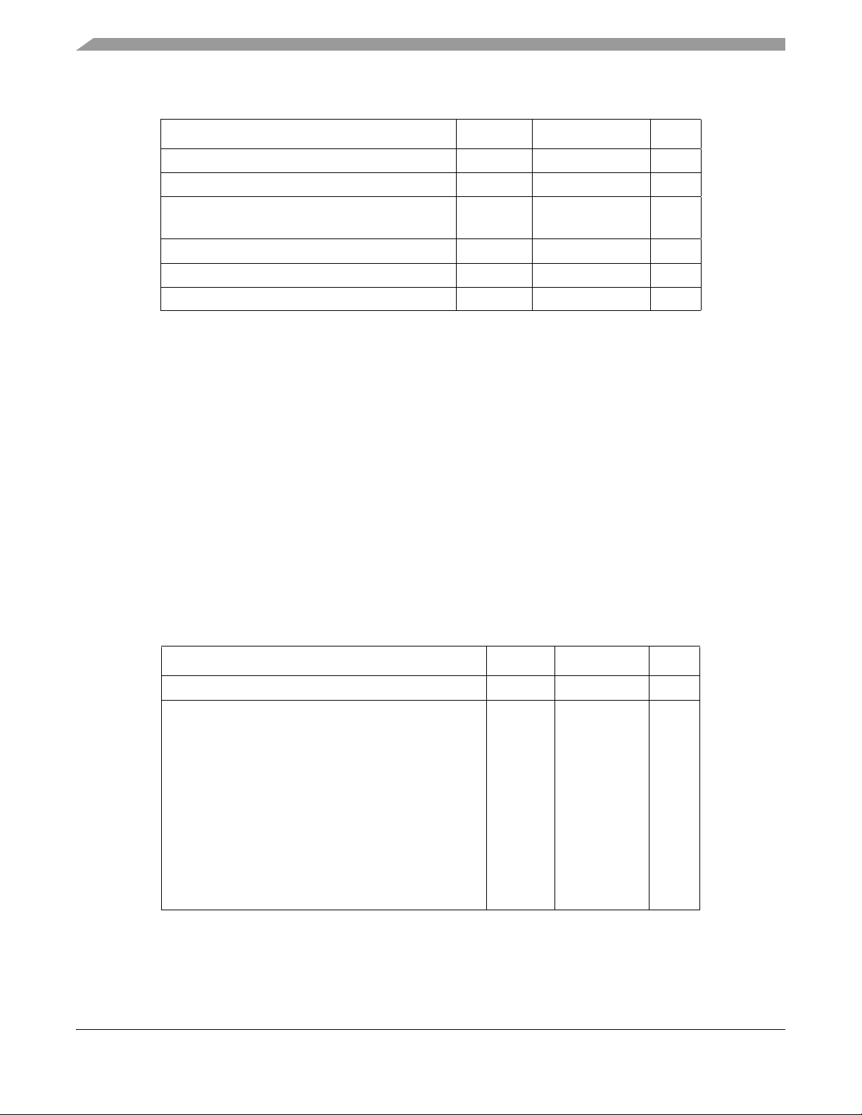
1.4 Part Numbers
Table 3. Orderable Part Number Summary
Freescale Part
Number
MCF51JM128EVLK MCF51JM128 ColdFire Microcontroller
with CAU and RNGA Enabled
MCF51JM128VLK MCF51JM128 ColdFire Microcontroller 128 / 16 80 LQFP –40 to +105 C
MCF51JM128EVLH MCF51JM128 ColdFire Microcontroller
with CAU and RNGA Enabled
MCF51JM128VLH MCF51JM128 ColdFire Microcontroller 128 / 16 64 LQFP –40 to +105 C
MCF51JM128EVQH MCF51JM128 ColdFire Microcontroller
with CAU and RNGA Enabled
MCF51JM128VQH MCF51JM128 ColdFire Microcontroller 128 / 16 64 QFP –40 to +105 C
MCF51JM128EVLD MCF51JM128 ColdFire Microcontroller
with CAU and RNGA Enabled
MCF51JM128VLD MCF51JM128 ColdFire Microcontroller 128 / 16 44 LQFP –40 to +105 C
MCF51JM64EVLK MCF51JM64 ColdFire Microcontroller
with CAU and RNGA Enabled
MCF51JM64VLK MCF51JM64 ColdFire Microcontroller 64 / 16 80 LQFP –40 to +105 C
MCF51JM64EVLH MCF51JM64 ColdFire Microcontroller
with CAU and RNGA Enabled
MCF51JM64VLH MCF51JM64 ColdFire Microcontroller 6 4 / 16 64 LQFP –40 to +105 C
Description
Flash / SRAM
(KB)
128 / 16 80 LQFP –40 to +105 C
128 / 16 64 LQFP –40 to +105 C
128 / 16 64 QFP –40 to +105 C
128 / 16 44 LQFP –40 to +105 C
64 / 16 80 LQFP –40 to +105 C
64 / 16 64 LQFP –40 to +105 C
Package Temperature
MCF51JM64EVQH MCF51JM64 ColdFire Microcontroller
with CAU and RNGA Enabled
MCF51JM64VQH MCF51JM64 ColdFire Microcontroller 64 / 16 64 QFP –40 to +105 C
MCF51JM128 ColdFire Microcontroller, Rev. 4
64 / 16 64 QFP –40 to +105 C
Freescale Semiconductor8
Page 9
MCF51JM128 Family Configurations
Table 3. Orderable Part Number Summary (continued)
MCF51JM64EVLD MCF51JM64 ColdFire Microcontroller
with CAU and RNGA Enabled
MCF51JM64VLD MCF51JM64 ColdFire Microcontroller 6 4 / 16 44 LQFP –40 to +105 C
MCF51JM32EVLK MCF51JM32 ColdFire Microcontroller
with CAU and RNGA Enabled
MCF51JM32VLK MCF51JM32 ColdFire Microcontroller 32 / 16 80 LQFP –40 to +105 C
MCF51JM32EVLH MCF51JM32 ColdFire Microcontroller
with CAU and RNGA Enabled
MCF51JM32VLH MCF51JM32 ColdFire Microcontroller 3 2 / 16 64 LQFP –40 to +105 C
MCF51JM32EVQH MCF51JM32 ColdFire Microcontroller
with CAU and RNGA Enabled
MCF51JM32VQH MCF51JM32 ColdFire Microcontroller 32 / 16 64 QFP –40 to +105 C
MCF51JM32EVLD MCF51JM32 ColdFire Microcontroller
with CAU and RNGA Enabled
MCF51JM32VLD MCF51JM32 ColdFire Microcontroller 3 2 / 16 44 LQFP –40 to +105 C
64 / 16 44 LQFP –40 to +105 C
32 / 16 80 LQFP –40 to +105 C
32 / 16 64 LQFP –40 to +105 C
32 / 16 64 QFP –40 to +105 C
32 / 16 44 LQFP –40 to +105 C
MCF51JM128 ColdFire Microcontroller, Rev. 4
Freescale Semiconductor 9
Page 10
MCF51JM128 Family Configurations
PTC4
IRQ / TPMCLK
RESET
PTF0 / TPM1CH2
PTF1 / TPM1CH3
PTF2 / TPM1CH4
PTF3 / TPM1CH5
PTF4 / TPM2CH0
PTC6 / RXCAN
PTF7 / TXCAN
PTF5 / TPM2CH1
PTF6
PTE0 / TXD1
PTE1 / RXD1
PTE2 / TPM1CH0
PTE3 / TPM1CH1
PTC7
PTH0 / SDA2
PTH1 / SCL2
PTH2 / RGPIO8
1
2
3
4
5
6
7
8
9
10
11
12
13
14
15
16
17
18
19
20
21222324252627282930313233343536373839
40
60
59
58
57
56
55
54
53
52
51
50
49
48
47
46
45
44
43
42
41
80797877767574737271706968676665646362
61
PTH3 / RGPIO9
PTH4 / RGPIO10
PTE4 / MISO1
PTE5 / MOSI1
PTE6 / SPSCK1
PTE7 / S
S1
VDD
VSS
USBDN
USBDP
VUSB33
PTG0 / KBIP0
PTG1 / KBIP1
PTA0 / RGPIO0
PTA1 / RGPIO1
PTA2 / RGPIO2
PTA3 / RGPIO3
PTA4 / RGPIO4
PTA5 / RGPIO5
PTA6 / RGPIO6
PTJ3 / RGPIO14
PTJ2 / RGPIO13
PTJ1 / RGPIO12
PTJ0 / RGPIO11
PTD2 / KBIP2 / ACMPO
VSSA
VREFL
VREFH
VDDA
PTD1 / ADP9 / ACMP–
PTD0 / ADP8 / ACMP+
PTB7 / ADP7
PTB6 / ADP6
PTB5 / KBIP5 / ADP5
PTB4 / KBIP4 / ADP4
PTB3 /
SS2 /ADP3
PTB2 / SPSCK2 / ADP2
PTB1 / MOSI2 / ADP1
PTB0 / MISO2 / ADP0
PTA7 / RGPIO7
PTC5 / RXD2
PTC3 / TXD2
PTC2 / IRO
PTC1 / SDA1
PTC0 / SCL1
PTG7
PTG6
VDD
VSS
PTG5 / EXTAL
PTG4 / XTAL
BKGD/MS
PTG3 / KBIP7
PTG2 / KBIP6
PTD7
PTD6
PTD5
PTD4 / ADP11
PTD3 / KBIP3 / ADP10
PTJ4 / RGPIO15
1.5 Pinouts and Packaging
Figure 2 shows the pinout of the 80-pin LQFP.
MCF51JM128 ColdFire Microcontroller, Rev. 4
Figure 2. 80-pin LQFP
Freescale Semiconductor10
Page 11
Figure 3 shows the pinout of the 64-pin LQFP and QFP.
PTC4
IRQ / TPMCLK
RESET
PTF0 / TPM1CH2
PTF1 / TPM1CH3
PTF2 / TPM1CH4
PTF3 / TPM1CH5
PTF4 / TPM2CH0
PTC6 / RXCAN
PTF7 / TXCAN
PTF5 / TPM2CH1
PTF6
PTE0 / TXD1
PTE1 / RXD1
PTE2 / TPM1CH0
PTE3 / TPM1CH1
1
2
3
4
5
6
7
8
9
10
11
12
13
14
15
16
171819202122232425262728293031
32
PTE4 / MISO1
PTE5 / MOSI1
PTE6 / SPSCK1
PTE7 / S
S1
VDD
VSS
USBDN
USBDP
VUSB33
PTG0 / KBIP0
PTG1 / KBIP1
PTA0 / RGPIO0
PTA1 / RGPIO1
PTA2 / RGPIO2
PTA3 / RGPIO3
PTA4 / RGPIO4
48
47
46
45
44
43
42
41
40
39
38
37
36
35
34
33
PTD2 / KBIP2 / ACMPO
VSSA
VREFL
VREFH
VDDA
PTD1 / ADP9 / ACMP–
PTD0 / ADP8 / ACMP+
PTB7 / ADP7
PTB6 / ADP6
PTB5 / KBIP5 / ADP5
PTB4 / KBIP4 / ADP4
PTB3 / S
S2 /ADP3
PTB2 / SPSCK2 / ADP2
PTB1 / MOSI2 / ADP1
PTB0 / MISO2 / ADP0
PTA5 / RGPIO5
646362616059585756555453525150
49
PTC5 / RXD2
PTC3 / TXD2
PTC2 / IRO
PTC1 / SDA1
PTC0 / SCL1
VSS
PTG5 / EXTAL
PTG4 / XTAL
BKGD/MS
PTG3 / KBIP7
PTG2 / KBIP6
PTD7
PTD6
PTD5
PTD4 / ADP11
PTD3 / KBIP3 / ADP10
MCF51JM128 Family Configurations
MCF51JM128 ColdFire Microcontroller, Rev. 4
Figure 3. 64-pin QFP and LQFP
Freescale Semiconductor 11
Page 12
MCF51JM128 Family Configurations
1
2
3
4
5
6
7
8
9
10
11
1213141516171819202122
33
32
31
30
29
28
27
26
25
24
23
4443424140393837363534
PTC4
IRQ / TPMCLK
RESET
PTF0 / TPM1CH2
PTF1 / TPM1CH3
PTF4 / TPM2CH0
PTF5 / TPM2CH1
PTE0 / TXD1
PTE1 / RXD1
PTE2 / TPM1CH0
PTE3 / TPM1CH1
PTE4 / MISO1
PTE5 / MOSI1
PTE6 / SPSCK1
PTE7 / S
S1
VDD
VSS
USBDN
USBDP
VUSB33
PTG0 / KBIP0
PTG1 / KBIP1
PTD2 / KBIP2 / ACMPO
VSSA / VREFL
VDDA / VREFH
PTD1 / ADP9 / ACMP–
PTD0 / ADP8 / ACMP+
PTB5 / KBIP5 / ADP5
PTB4 / KBIP4 / ADP4
PTB3 / S
S2 /ADP3
PTB2 / SPSCK2 / ADP2
PTB1 / MOSI2 / ADP1
PTB0 / MISO2 / ADP0
PTC5 / RXD2
PTC3 / TXD2
PTC2 / IRO
PTC1 / SDA1
PTC0 / SCL1
VSS
PTG5 / EXTAL
PTG4 / XTAL
BKGD / MS
PTG3 / KBIP7
PTG2 / KBIP6
Figure 4 shows the pinout of the 44-pin LQFP.
Table 4 shows the package pin assignments.
Table 4. Pin Assignments by Package and Pin Sharing Priority
Pin Number <-- Lowest Priority --> Highest
80 64 44 Port Pin Alt 1 Alt 2
111 PTC4 —
222 — IRQ TPMCLK
3 3 3 — RESET —
4 4 4 PTF0 TPM1CH2 —
5 5 5 PTF1 TPM1CH3 —
6 6 — PTF2 TPM1CH4 —
7 7 — PTF3 TPM1CH5 —
8 8 6 PTF4 TPM2CH0 BUSCLK_OUT
9 9 — PTC6 RXCAN —
10 10 — PTF7 TXCAN —
11 11 7 PTF5 TPM2CH1 —
12 12 — PTF6 — —
13 13 8 PTE0 TXD1 —
14 14 9 PTE1 RXD1 —
15 15 10 PTE2 TPM1CH0 —
Figure 4. 44-pin LQFP
MCF51JM128 ColdFire Microcontroller, Rev. 4
Freescale Semiconductor12
Page 13
MCF51JM128 Family Configurations
Table 4. Pin Assignments by Package and Pin Sharing Priority (continued)
Pin Number <-- Lowest Priority --> Highest
80 64 44 Port Pin Alt 1 Alt 2
16 16 11 PTE3 TPM1CH1 —
17 — — PTC7 — —
18 — — PTH0 SDA2 —
19 — — PTH1 SCL2 —
20 — — PTH2 RGPIO8 —
21 — — PTH3 RGPIO9 —
22 — — PTH4 RGPIO10 —
23 17 12 PTE4 MISO1 —
24 18 13 PTE5 MOSI1 —
25 19 14 PTE6 SPSCK1 —
26 20 15 PTE7 SS1
27 21 16 — — VDD
28 22 17 — — VSS
29 23 18 — — USBDN
30 24 19 — — USBDP
31 25 20 — — VUSB33
32 26 21 PTG0 KBIP0 USB_ALT_CLK
33 27 22 PTG1 KBIP1 —
34 28 — PTA0 RGPIO0 USB_SESSVLD
35 29 — PTA1 RGPIO1 USB_SESSEND
36 30 — PTA2 RGPIO2 USB_VBUSVLD
37 31 — PTA3 RGPIO3 USB_PULLUP(D+)
38 32 — PTA4 RGPIO4 USB_DM_DOWN
39 33 — PTA5 RGPIO5 USB_DP_DO WN
40 — — PTA6 RGPIO6 USB_ID
41 — — PTA7 RGPIO7 —
42 34 23 PTB0 MISO2 ADP0
43 35 24 PTB1 MOSI2 ADP1
—
44 36 25 PTB2 SPSCK2 ADP2
45 37 26 PTB3 SS2
46 38 27 PTB4 KBIP4 ADP4
47 39 28 PTB5 KBIP5 ADP5
48 40 — PTB6 ADP6 —
MCF51JM128 ColdFire Microcontroller, Rev. 4
Freescale Semiconductor 13
ADP3
Page 14
MCF51JM128 Family Configurations
Table 4. Pin Assignments by Package and Pin Sharing Priority (continued)
Pin Number <-- Lowest Priority --> Highest
80 64 44 Port Pin Alt 1 Alt 2
49 41 — PTB7 ADP7 —
50 42 29 PTD0 ADP8 ACMP+
51 43 30 PTD1 ADP9 ACMP–
52 44 31 — — VDDA
53 45 — — VREFH
54 46 32 — — VREFL
55 47 — — VSSA
56 48 33 PTD2 KBIP2 ACMPO
57 — — PTJ0 RGPIO11 —
58 — — PTJ1 RGPIO12 —
59 — — PTJ2 RGPIO13 —
60 — — PTJ3 RGPIO14 —
61 — — PTJ4 RGPIO15 —
62 49 — PTD3 KBIP3 ADP10
63 50 — PTD4 ADP11 —
64 51 — PTD5 — —
65 52 — PTD6 — —
66 53 — PTD7 — —
67 54 34 PTG2 KBIP6 —
68 55 35 PTG3 KBIP7 —
69 56 36 — BKGD MS
70 57 37 PTG4 XTAL
71 58 38 PTG5 EXTAL
72 59 39 — — VSS
73 — — — — VDD
74 — — PTG6 — —
75 — — PTG7 — —
76 60 40 PTC0 SCL1 —
77 61 41 PTC1 SDA1 —
78 62 42 PTC2 IRO —
79 63 43 PTC3 TXD2 —
80 64 44 PTC5 RXD2 —
MCF51JM128 ColdFire Microcontroller, Rev. 4
Freescale Semiconductor14
Page 15

Preliminary Electrical Characteristics
2 Preliminary Electrical Characteristics
This section contains electrical specification tables and reference timing diagrams for the MCF51JM128 microcontroller,
including detailed information on power considerations, DC/AC electrical characteristics, and AC timing specifications.
The electrical specifications are preliminary and are from previous designs or design simulations. These specifications may not
be fully tested or guaranteed at this early stage of the product life cycle. These specifications will, however, be met for
production silicon. Finalized specifications will be published after complete characterization and device qualifications have
been completed.
NOTE
The parameters specified in this data sheet supersede any values found in the module
specifications.
2.1 Parameter Classification
The electrical parameters shown in this supplement are guaranteed by various methods. To give the customer a better
understanding the following classification is used and the parameters are tagged accordingly in the tables where appropriate:
Table 5. Parameter Classifications
P
Those parameters are guaranteed during production testing on each individual device.
Those parameters are achieved by the design characterization by measuring a
C
statistically relevant sample size across process variations.
Those parameters are achieved by design characterization on a small sample size from
T
typical devices under typical conditions unless otherwise noted. All values shown in the
typical column are within this category.
D
Those parameters are derived mainly from simulations.
NOTE
The classification is shown in the column labeled C in the parameter tables where
appropriate.
2.2 Absolute Maximum Ratings
Absolute maximum ratings are stress ratings only, and functional operation at the maxima is not guaranteed. Stress beyond the
limits specified in Table 6 may affect device reliability or cause permanent damage to the device. For functional operating
conditions, refer to the remaining tables in this section.
This device contains circuitry protecting against damage due to high static voltage or electrical fields; however, it is advised
that normal precautions be taken to avoid application of any voltages higher than maximum-rated voltages to this
high-impedance circuit. Reliability of operation is enhanced if unused inputs are tied to an appropriate logic voltage level (for
instance, V
or VDD).
SS
MCF51JM128 ColdFire Microcontroller, Rev. 4
Freescale Semiconductor 15
Page 16
Preliminary Electrical Characteristics
Table 6. Absolute Maximum Ratings
Rating Symbol Value Unit
Supply voltage V
Input voltage V
Instantaneous maximum current Single pin limit
(applies to all port pins)1,2,
Maximum current into V
3
DD
Storage temperature T
Maximum junction temperature T
1
Input must be current limited to the value specified. To determine the value of the required
I
DD
In
I
D
DD
stg
J
current-limiting resistor, calculate resistance values f or positive (V
–0.3 to + 5.8 V
– 0.3 to VDD + 0.3 V
25 mA
120 mA
–55 to +150 C
150 C
) and negative (VSS) clamp
DD
voltages, then use the larger of the two resistance values.
2
All functional non-supply pins are internally clamped to VSS and VDD.
3
Power supply must maintain regulation within operating V
operating maximum current conditions. If positive injection current (V
range during instantaneous and
DD
> VDD) is greater than
In
IDD, the injection current may flow out of VDD and could result in external power supply going
out of regulation. Ensure external VDD load shunt current is greater than maximum injection
current. This is the greatest risk when the MCU is not consuming power. Examples: if no system
clock is present or if the clock rate is low, which would reduce overall power consumption.
2.3 Thermal Characteristics
This section provides information about operating temperature range, power dissipation, and package thermal resistance. Power
dissipation on I/O pins is usually small compared to the power dissipation in on-chip logic and it is user-determined rather than
being controlled by the MCU design. To take P
pin voltage and V
or VDD and multiply by the pin current for each I/O pin. Except in cases of unusually high pin current
SS
(heavy loads), the difference between pin voltage and V
into account in power calculations, determine the difference between actual
I/O
or VDD is small.
SS
Table 7. Thermal Characteristics
Rating Symbol Value Unit
Operating temperature range (packaged) T
Thermal resistance
A
1,2,3,4
–40 to +105 C
80-pin LQFP
1s
2s2p
52
40
64-pin LQFP
1s
2s2p
JA
65
47
C/W
64-pin QFP
1s
2s2p
54
40
44-pin LQFP
1s
2s2p
1
Junction temperature is a function of die size, on-chip power dissipation, package thermal
69
48
resistance, mounting site (board) temperature, ambient temperature, air flow, pow er dissipation
of other components on the board, and board thermal resistance.
2
Junction to Ambient Natural Convection
MCF51JM128 ColdFire Microcontroller, Rev. 4
Freescale Semiconductor16
Page 17
3
1s - Single Layer Board, one signal layer
4
2s2p - Four Layer Board, 2 signal and 2 power layers
The average chip-junction temperature (TJ) in C can be obtained from:
T
= TA + (PD JA) Eqn. 1
J
where:
= Ambient temperature, CJA = Package thermal resistance, junction-to-ambient, C/WPD = P
T
A
I
VDD, Watts — chip internal powerP
DD
For most applications, P
I/O
P
and can be neglected. An approximate relationship between PD and TJ (if P
int
= Power dissipation on input and output pins — user determined
I/O
is:
P
= K (TJ + 273C) Eqn. 2
D
Solving equations 1 and 2 for K gives:
Preliminary Electrical Characteristics
P
int
is neglected)
I/O
I/OPint
=
K = P
(TA + 273C) + JA (PD)
D
where K is a constant pertaining to the particular part. K can be determined from equation 3 by measuring P
for a known T
value of T
. Using this value of K, the values of PD and TJ can be obtained by solving equations 1 and 2 iteratively for any
A
.
A
2
(at equilibrium)
D
Eqn. 3
2.4 Electrostatic Discharge (ESD) Protection Characteristics
Although damage from static discharge is much less common on these devices than on early CMOS circuits, normal handling
precautions should be used to avoid exposure to static discharge. Qualification tests are performed to ensure that these devices
can withstand exposure to reasonable levels of static without suffering any permanent damage.
All ESD testing is in conformity with CDF-AEC-Q00 Stress Test Qualification for Automotive Grade Integrated Circuits.
(http://www.aecouncil.com/) This device was qualified to AEC-Q100 Rev E.
A device is considered to have failed if, after exposure to ESD pulses, the device no longer meets the device specification
requirements. Complete DC parametric and functional testing is performed per the applicable device specification at room
temperature followed by hot temperature, unless specified otherwise in the device specification.
Table 8. ESD and Latch-up Test Conditions
Model Description Symbol Value Unit
Series Resistance R1 1500
Human Body
Storage Capacitance C 100 pF
Number of Pulse per pin – 3
Latch-up
Freescale Semiconductor 17
Minimum input voltage limit –2.5 V
Maximum input voltage limit 7.5 V
MCF51JM128 ColdFire Microcontroller, Rev. 4
Page 18
Preliminary Electrical Characteristics
Table 9. ESD and Latch-Up Protection Characteristics
Num Rating Symbol Min Max Unit
1 Human Body Model (HBM) V
2 Charge Device Model (CDM) V
3 Latch-up Current at T
= 105CI
A
HBM
CDM
LAT
+/– 2000 — V
+/– 500 — V
+/– 100 — mA
2.5 DC Characteristics
This section includes information about power supply requirements, I/O pin characteristics, and power supply current in various
operating modes.
Table 10. DC Characteristics
—
—
—
—
—
—
—
—
—
—
—
—
—
—
—
—
—
—
—
—
1
Max Unit
—
—
—
—
V
—
—
—
—
1.5
1.5
0.8
0.8
V
1.5
1.5
0.8
0.8
100
mA
60
100
mA
60
Num C Parameter Symbol Min Typ
1 Operating voltage
2
2.7 — 5.5 V
Output high voltage — Low Drive (PTxDSn = 0)
2P
Load
Load
Load
Load
= –4 mA
= –2 mA
= –2 mA
= –1 mA
5 V, I
3 V, I
5 V, I
3 V, I
Output high voltage — High Drive (PTxDSn = 1)
5 V, I
3 V, I
5 V, I
3 V, I
= –15 mA
Load
Load
Load
Load
= –8 mA
= –8 mA
= –4 mA
V
OH
VDD – 1.5
VDD – 1.5
VDD – 0.8
– 0.8
V
DD
V
– 1.5
DD
– 1.5
V
DD
VDD – 0.8
VDD – 0.8
Output low voltage — Low Drive (PTxDSn = 0)
5 V, I
3 V, I
5 V, I
3 V, I
3P
Load
Load
Load
Load
= 4mA
= 2 mA
= 2 mA
= 1 mA
V
OL
Output low voltage — High Drive (PTxDSn = 1)
Load
Load
Load
Load
for all ports
OH
= 15 mA
= 8 mA
= 8 mA
= 4 mA
5V3VI
OHT
—
5 V, I
3 V, I
5 V, I
3 V, I
4 P Output high current — Max total I
—
5 P Output low current — Max total I
for all ports
OL
5V3VI
OLT
—
—
6 P Input high voltage; all digital inputs
V
= 5V
V
DD
= 3V
V
DD
IH
3.25
2.10
MCF51JM128 ColdFire Microcontroller, Rev. 4
—
—
—
V
—
Freescale Semiconductor18
Page 19
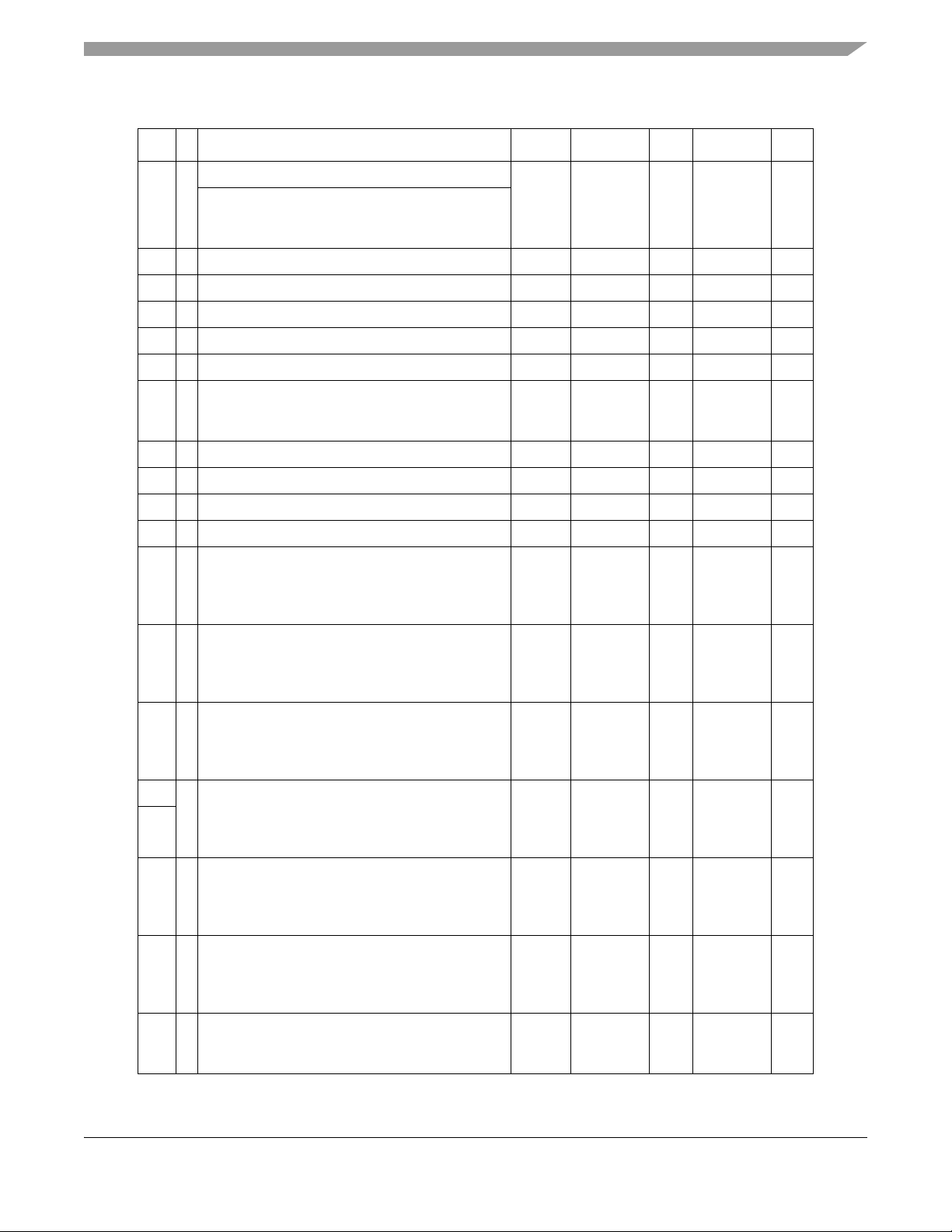
Table 10. DC Characteristics (continued)
Preliminary Electrical Characteristics
Num C Parameter Symbol Min Typ
7 P Input low voltage; all digital inputs
V
= 5V
V
DD
IL
——
VDD = 3V
8 P Input hysteresis; all digital inputs V
9 P Input leakage current; input only pins
10 P High Impedance (off-state) leakage current
11 P Internal pullup resistors
12 P Internal pulldown resistors
4
5
13 Internal pullup resistor to USBDP (to V
3
USB33
3
|IOZ|—0.11A
R
R
)
Idle
R
Transmit
14 C Input Capacitance; all non-supply pins C
15 D RAM retention voltage
6
V
16 P POR rearm voltage V
17 D POR rearm time t
V
V
18 P
19 P
Low-voltage detection threshold —
high range
Low-voltage detection threshold —
low range
V
V
V
DD
DD
DD
falling
rising
falling
VDD rising
V
20 C
Low-voltage warning threshold —
high range 1
V
DD
falling
VDD rising
0.06 x V
hys
DD
|IIn|—0.11A
PU
PD
PUPD
In
RAM
POR
POR
LVD1
LVD0
LVW3
20 45 65 k
20 45 65 k
900
1425
1300
2400
—— 8pF
—0.61.0V
0.9 1.4 2.0 V
10 — — s
3.9
4.0
2.48
2.54
4.5
4.6
4.0
4.1
2.56
2.62
4.6
4.7
1
Max Unit
1.75
V
1.05
mV
1575
k
3090
V
4.1
4.2
V
2.64
2.70
V
4.7
4.8
5 V
3 V
V
V
V
LVW2
LVW1
LVW0
V
hys
4.2
4.3
2.84
2.90
2.66
2.72
—
—
4.3
4.4
2.92
2.98
2.74
2.80
100
60
V
4.4
4.5
V
3.00
3.06
V
2.82
2.88
mV
—
—
21
22
23 C
24 T
Low-voltage warning threshold —
high range 0
P
Low-voltage warning threshold
low range 1
P
Low-voltage warning threshold —
low range 0
Low-voltage inhibit reset/recover hysteresis
V
falling
DD
rising
V
DD
falling
V
DD
VDD rising
V
falling
DD
rising
V
DD
MCF51JM128 ColdFire Microcontroller, Rev. 4
Freescale Semiconductor 19
Page 20
Preliminary Electrical Characteristics
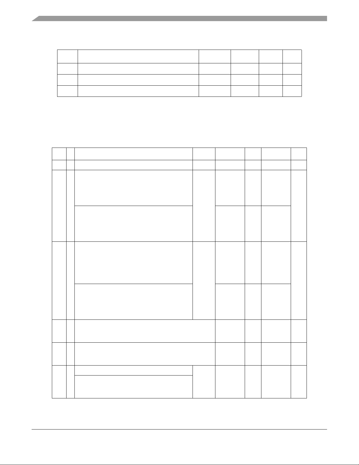
Typ i cal VOL vs. IOL AT V
DD
= 5V
0.00
0.10
0.20
0.30
0.40
0.50
0.60
0.70
0.80
0 1 2 3 4 5 6 7 8 9 10 11 12 13 14 15
I
OL
(mA)
V
OL
(v)
Hot (105°C)
Room ( 2 5 °C)
Cold (-40°C)
Typica l VOL vs. IOL AT VDD = 3V
0.00
0.20
0.40
0.60
0.80
1.00
1.20
1.40
012345678910111213
IOL (mA)
V
OL
(v)
Hot (105°C)
Room (25°C)
Cold (-40°C)
Typical VOL vs. I
OL
AT V
DD
V
0.00
0.10
0.20
0.30
0.40
0.50
0.60
0.70
0.80
0.90
012345
IOL (mA )
V
OL
(v)
H ot (105°C)
Room (25°C)
Cold (-40°C)
Typical V
OL
vs. IOL AT V
DD
= 3V
0.00
0.10
0.20
0.30
0.40
0.50
0.60
0.70
0.80
0.90
0123
IOL (mA)
V
OL
(v)
Hot (105°C)
Room (25°C)
Cold (-40°C)
1
Typical values are based on characterization data at 25C unless otherwise stated.
2
Operating voltage with USB enabled can be found in Section 2.14, “USB Electricals.”
3
Measured with V
4
Measured with V
5
Measured with V
6
This is the voltage below which the contents of RAM are not guaranteed to be maintained.
= V
In
= VSS.
In
= VDD.
In
DD
or VSS.
Figure 5. Typical Low-side Drive (sink) characteristics – High Drive (PTxDSn = 1)
Figure 6. Typical Low-side Drive (sink) characteristics – Low Drive (PTxDSn = 0)
= 5
MCF51JM128 ColdFire Microcontroller, Rev. 4
Freescale Semiconductor20
Page 21
Preliminary Electrical Characteristics
Ty pic al VDD - VOH vs. IOH AT V
DD
V
0.0
0.2
0.4
0.6
0.8
0-1-2-3-4-5-6-7-8-9-10-11-12-13-14-15
IOH (mA)
V
DD
- V
OH
(v)
Hot (105°C)
Room (25°C)
Cold (-40°C)
Typical VDD - VOH vs. IOH AT VDD=3V
0.0
0.2
0.4
0.6
0.8
1.0
1.2
0-1-2-3-4-5-6-7-8-9-10-11-12-13
IOH (mA )
V
DD
- V
OH
(v)
Hot (105°C)
Room (25°C)
Cold (-40°C)
Typical VDD - VOH vs. IOH AT V
DD
= 5V
0.0
0.2
0.4
0.6
0.8
1.0
1.2
0-1-2-3-4-5
I
OH
(mA)
V
DD
- V
OH
(v)
Hot (105°C)
Room (25°C)
Cold (-40°C)
Typical VDD - VOH vs. IOH AT VDD=3V
0.0
0.2
0.4
0.6
0.8
1.0
1.2
0-1-2-3
IOH (mA)
V
DD
- V
OH
(v)
Hot (105°C)
Room (25°C)
Cold (-40°C)
= 5
Figure 7. Typical High- side Drive (source) characteristics – High Drive (PTxDSn = 1)
Figure 8. Typical High-side Drive (source) characteristics – Low Drive (PTxDSn = 0)
2.6 Supply Current Characteristics
Num C Parameter Symbol VDD (V) Typical
1 C Run supply current
2MHz, f
2 P Run supply current
16 MHz, f
3 C Run supply current
48 MHz, f
Freescale Semiconductor 21
= 1 MHz)
Bus
Bus
Bus
Table 11. Supply Current Characteristics
3
measured at (CPU clock =
3
measured at (CPU clock =
= 8 MHz)
3
measured at (CPU clock =
= 24 MHz)
MCF51JM128 ColdFire Microcontroller, Rev. 4
RI
DD
1
Max
2
54.0 7
34.0 7
51930
318.730
54570
34470
Unit
mA
mA
mA
Page 22

Preliminary Electrical Characteristics
Table 11. Supply Current Characteristics
Num C Parameter Symbol VDD (V) Typical
3
4 C Wait mode supply current
clock = 2 MHz, f
= 1 MHz)
Bus
5 C Wait mode supply current
clock = 16 MHz, f
= 8 MHz)
Bus
6 C Wait mode supply current
clock = 48 MHz, f
= 24 MHz)
Bus
measured at (CPU
3
measured at (CPU
3
measured at (CPU
WI
DD
52.03 3
32 3
57.7312
37.712
52230
321.930
1
Max
2
7 C Stop2 mode supply current
–40 C
25 C
105C
S2I
DD
51.3533
35
–40 C
25 C
105 C
31.2533
35
8 P Stop3 mode supply current
–40 C
25 C
105 C
S3I
DD
51.4133
35
–40 C
25 C
105 C
31.3533
35
9 C Stop4 mode supply current
–40 C
25 C
105 C
S4I
DD
5 106 200 A
–40 C
25 C
396200
105 C
4
10 P RTC adder to stop2 or stop3
11 P Adder to stop3 for oscillator enabled
(ERCLKEN =1 and EREFSTEN = 1)
1
Typicals are measured at 25C.
2
Values given here are preliminary estimates prior to completing character ization.
3
All modules’ clocks are switched on, code runs from flash, in FEI mode, and there are no DC loads on port pins.
4
Most customers are expected to find that auto-wakeup from stop2 or stop3 can be used instead of the higher current wait mode.
5
Values given under the following conditions: low range operation (RANGE = 0), low power mode (HGO = 0)
, 25C
S23I
DDRTC
5
S23I
DDOSC
5300 —nA
3300 —nA
55 —A
35 —A
Unit
mA
mA
mA
A
A
A
A
A
MCF51JM128 ColdFire Microcontroller, Rev. 4
Freescale Semiconductor22
Page 23
Preliminary Electrical Characteristics
2.7 Analog Comparator (ACMP) Electricals
Table 12. Analog Comparator Electrical Specifications
Num C Rating Symbol Min Typical Max Unit
1 Supply voltage
2 Supply current (active)
3 Analog input voltage V
4 Analog input offset voltage V
5
Analog Comparator hysteresis V
6 Analog input leakage current
7 Analog Comparator initialization delay t
8
Bandgap Voltage Ref erence
Factory trimmed at V
= 3.0 V, Temp = 25CVBG1.19 1.20 1.21 V
DD
V
I
DDAC
AIN
AIO
I
ALKG
AINIT
DD
H
2.8 ADC Characteristics
Table 13. 5 Volt 12-bit ADC Operating Conditions
Characteristic Conditions Symb Min Typ
Supply voltage Absolute V
Delta to V
Ground voltage Delta to V
(VDD-V
DD
(VSS-V
SS
DDA
SSA
2
)
2
)
Ref Voltage High V
Ref Voltage Low V
Input Voltage V
Input
Capacitance
Input Resistance R
Analog Source
Resistance
12 bit mode
f
ADCK
f
ADCK
> 4MHz
< 4MHz
10 bit mode
f
> 4MHz
ADCK
< 4MHz
f
ADCK
8 bit mode (all valid f
ADC Conversion
Clock Freq.
1
Typical values assume V
High Speed (ADLPC=0) f
Low Power (ADLPC=1) 0.4 — 4.0
= 5.0V, Temp = 25C, f
DDA
)——10
ADCK
only and are not tested in production.
2
DC potential difference.
V
V
REFH
REFL
ADIN
C
ADIN
ADIN
R
ADCK
ADCK
DDA
DDA
SSA
AS
2.7 — 5.5 V
–100 0 +100 mV
–100 0 +100 mV
2.7 V
V
SSA
V
REFL
—4.55.5pF
—3 5k
—
—
—
—
0.4 — 8.0 MHz
=1.0MHz unless otherwise stated. T ypical values are f or ref erence
2.7 — 5.5 V
—2035A
VSS – 0.3 — V
20 40 mV
3.0 6.0 20.0
-- -- 1.0 A
——1.0s
1
Max Unit Comment
DDA
V
SSA
—V
V
DDA
V
SSA
REFH
V
V
V
k External to MCU
—
—
—
—
2
5
5
10
DD
V
mV
MCF51JM128 ColdFire Microcontroller, Rev. 4
Freescale Semiconductor 23
Page 24
Preliminary Electrical Characteristics
+
–
+
–
V
AS
R
AS
C
AS
V
ADIN
Z
AS
Pad
leakage
due to
input
protection
Z
ADIN
SIMPLIFIED
INPUT PIN EQUIVALENT
CIRCUIT
R
ADIN
ADC SAR
ENGINE
SIMPLIFIED
CHANNEL SELECT
CIRCUIT
INPUT PIN
R
ADIN
C
ADIN
INPUT PIN
R
ADIN
INPUT PIN
R
ADIN
Figure 9. ADC Input Impedance Equivalency Diagram
Table 14. 5 Volt 12-bit ADC Characteristics (V
Characteristic Conditions C Symb Min Typ
Supply Current
ADLPC=1
ADLSMP=1
ADCO=1
Supply Current
ADLPC=1
ADLSMP=0
ADCO=1
Supply Current
ADLPC=0
ADLSMP=1
ADCO=1
Supply Current
ADLPC=0
ADLSMP=0
ADCO=1
Supply Current Stop, Reset, Module Off I
ADC
Asynchronous
Clock Source
High Speed (ADLPC=0) T f
Low Power (ADLPC=1) 1.25 2 3.3
TI
TI
TI
PI
DDAD
DDAD
DDAD
DDAD
DDAD
ADACK
REFH
= V
DDA
1
, V
REFL
= V
SSA
)
Max Unit Comment
— 133 — A
— 218 — A
— 327 — A
—0.582 1 mA
—0.011 1 A
23.35MHzt
ADACK
1/f
ADACK
=
MCF51JM128 ColdFire Microcontroller, Rev. 4
Freescale Semiconductor24
Page 25
Preliminary Electrical Characteristics
Table 14. 5 Volt 12-bit ADC Characteristics (V
REFH
= V
DDA
Characteristic Conditions C Symb Min Typ
Conversion Time
(Including
sample time)
Short Sample (ADLSMP=0) T t
Long Sample (ADLSMP=1) — 40 —
Sample Time Short Sample (ADLSMP=0) T t
ADC
ADS
— 20 — ADCK
— 3.5 — ADCK
Long Sample (ADLSMP=1) — 23.5 —
Total Unadjusted
Error
12 bit mode T E
TUE
10 bit mode P — 1 2.5
— 3.0 — LSB
8 bit mode T — 0.5 1.0
Differential
Non-Linearity
Integral
Non-Linearity
12 bit mode T DNL — 1.75 — LSB
10 bit mode
8 bit mode
3
3
P—0.5 1.0
T—0.3 0.5
12 bit mode T INL — 1.5 — LSB
10 bit mode T — 0.5 1.0
8 bit mode T — 0.3 0.5
Zero-Scale Error 12 bit mode T E
ZS
— 1.5 — LSB2V
10 bit mode P — 0.5 1.5
, V
REFL
1
= V
) (continued)
SSA
Max Unit Comment
See Table 9 for
cycles
conversion time
variances
cycles
2
Includes
quantization
2
2
ADIN
= V
SSAD
8 bit mode T — 0.5 0.5
Full-Scale Error 12 bit mode T E
FS
10 bit mode T — 0.5 1
8 bit mode T — 0.5 0.5
Quantization
Error
12 bit mode D E
Q
10 bit mode — — 0.5
8 bit mode — — 0.5
Input Leakage
Error
12 bit mode D E
IL
10 bit mode — 0.2 2.5
8 bit mode — 0.1 1
o
Temp Sensor
CDV
25
TEMP25
Voltage
Temp Sensor
Slope
1
T ypical values assume V
o
-40
C - 25oC D m — 3.266 — mV/oC
o
C - 125oC — 3.638 —
25
= 5.0V, Temp = 2 5C, f
DDA
=1.0MHz unless otherwise stated. T ypical values are for ref erence only
ADCK
and are not tested in production.
2
1 LSB = (V
3
Monotonicity and No-Missing-Codes guaranteed in 10 bit and 8 bit modes
4
Based on input pad leakage current. Refer to pad electricals.
REFH
- V
REFL
)/2
N
— 1—LSB2V
— -1 to 0 — LSB
2
ADIN
= V
DDAD
— 1—LSB2Pad leakage4 *
R
AS
—1.396— V
MCF51JM128 ColdFire Microcontroller, Rev. 4
Freescale Semiconductor 25
Page 26

Preliminary Electrical Characteristics
2.9 External Oscillator (XOSC) Characteristics
Table 15. Oscillator Electrical Specifications (Temperature Range = –40 to 105C Ambient)
Num C Rating Symbol Min Typ
Oscillator crystal or resonator (EREFS = 1, ERCLKEN = 1)
• Low range (RANGE = 0)
1
• High range (RANGE = 1) FEE or FBE mode
• High range (RANGE = 1) PEE or PBE mode
2
3
• High range (RANGE = 1, HGO = 1) BLPE mode
• High range (RANGE = 1, HGO = 0) BLPE mode
2
Load capacitors
f
f
hi-fll
f
hi-pll
f
hi-hgo
f
hi-lp
C
C
lo
1
2
32
1
1
1
1
—
—
—
—
—
See crystal or resonator
manufacturer’s recommendation.
Feedback resistor
3
• Low range (32 kHz to 38.4 kHz)
• High range (1 MHz to 16 MHz)
R
F
10
1
Series resistor
• Low range, low gain (RANGE = 0, HGO = 0)
• Low range, high gain (RANGE = 0, HGO = 1)
—
—
—
0
100
0
4—
• High range, low gain (RANGE = 1, HGO = 0)
8MHz
4MHz
MHz
R
S
• High range, high gain (RANGE = 1, HGO = 1)
8MHz
4MHz
MHz
—
—
—
0
0
0
1
Max Unit
38.4
5
16
16
8
kHz
MHz
MHz
MHz
MHz
M
M
—
—
—
k
0
10
20
Crystal start-up time
• Low range, low gain (RANGE = 0, HGO = 0)
5T
• Low range, high gain (RANGE = 0, HGO = 1)
• High range, low gain (RANGE = 1, HG0 = 0)
• High range, high gain (RANGE = 1, HG0 = 1)
Square wave input clock frequency (EREFS = 0, ERCLKEN = 1)
6T
• FEE or FBE mode
• PEE or PBE mode
• BLPE mode
1
Data in Typical column was characterized at 5.0 V, 25C or is typical recommended value.
2
When MCG is configured for FEE or FBE mode, input clock source must be divisible using RDIV to within the range of 31.25 kHz
4
5
5
2
3
t
CSTL-LP
t
CSTL-HGO
t
CSTH-LP
t
CSTH-HGO
f
extal
—
—
—
—
0.03125
1
0
200
400
5
15
—
—
—
—
—
—
—
5
16
40
to 39.0625 kHz.
3
When MCG is configured for PEE or PBE mode, input clock source must be divisible using RDIV to within the range of 1 MHz
to 2 MHz.
4
This parameter is characterized and not tested on each device. Proper PC board-layout procedures must be followed to achieve
specifications.
5
4 MHz crystal
ms
MHz
MHz
MHz
MCF51JM128 ColdFire Microcontroller, Rev. 4
Freescale Semiconductor26
Page 27

Preliminary Electrical Characteristics
2.10 MCG Specifications
Table 16. MCG Frequency Specifications (Temperature Range = –40 to 125C Ambient)
Num C Rating Symbol Min Typical
C
DD
f
int_ft
int_ut
irefst
— 32.768 — kHz
31.25 — 39.0625 kHz
—60100s
16 — 20
f
dco_ut
— 19.92 —
f
dco_DMX32
f
dco_res_t
f
dco_res_t
f
dco_t
f
dco_t
t
fll_acquire
t
pll_acquire
C
Jitter
6
vco
f
pll_jitter_625ns
D
lock
D
unl
fll_lock
pll_lock
loc_low
— 0.1 0.2 %f
— 0.2 0.4 %f
—
–1.0
— 0.5 1%f
—— 1ms
—— 1ms
—0.020.2%f
7.0 — 55.0 MHz
—0.5665—%f
1.49 — 2.98 %
4.47 — 5.97 %
——
——
(3/5) x f
int
1P
Internal reference frequency - factory trimmed at V
= 5 V and temperature = 25
C
2 P Average internal reference frequency – untrimmed f
3 T Internal reference startup time t
P
DCO output frequency
4
range - untrimmed
2
Low range (DRS=00)
P High range (DRS=10) 48 — 60
P
DCO output frequency
5
6D
7D
8D
9D
Reference =32768Hz
and DMX32 = 1
P High range (DRS=10) — 59.77 —
Resolution of trimmed DCO output frequency at fixed
voltage and temperature (using FTRIM)
Resolution of trimmed DCO output frequency at fixed
voltage and temperature (not using FTRIM)
T otal de viation of trimmed DCO output frequency over
voltage and temperature
T otal de viation of trimmed DCO output frequency over
fixed voltage and temperature range of 0 – 70
10 D FLL acquisition time
11 D PLL acquisition time
12 D
Long term Jitter of DCO output clock (averaged over
2ms interval)
5
2
Low range (DRS=00)
3
4
13 D VCO operating frequency f
14 D Jitter of PLL output clock measured over 625 ns
15 D Lock entr y frequency tolerance
16 D Lock exit frequency tolerance
7
8
17 D Lock time — F L L t
18 D Lock time — PL L t
Loss of external clock minimum frequency – RANGE
19 D
= 0 f
1
Max Unit
MHzP Mid range (DRS=01) 32 — 40
MHzP Mid range (DRS=01) — 39.85 —
0.5
2%f
t
fll_acquire+
1075(1/fint_t
)
t
pll_acquire+
f
1075(1/
pll_r
ef)
— — kHz
dco
dco
dco
dco
dco
pll
s
s
1
Data in Typical column was characterized at 5.0 V, 25C or is typical recommended value
2
The resulting bus clock frequency should not exceed the maximum specified bus clock frequency of the device.
3
This specification applies to any time the FLL reference source or reference divider is changed, trim value changed or
changing from FLL disabled (BLPE, BLPI) to FLL enabled (FEI, FEE, FBE, FBI). If a crystal/resonator is being used as the
reference, this specification assumes it is already running.
4
This specification applies to any time the PLL VCO divider or reference divider is changed, or changing from PLL disabled
(BLPE, BLPI) to PLL enabled (PBE, PEE). If a crystal/resonator is being used as the reference, this specification assumes
it is already running.
MCF51JM128 ColdFire Microcontroller, Rev. 4
Freescale Semiconductor 27
Page 28

Preliminary Electrical Characteristics
5
Jitter is the average deviation from the programmed frequency measured over the specified interval at maximum f
BUS
Measurements are made with the device powered by filtered supplies and clocked by a stable external clock signal. Noise
injected into the FLL circuitry via VDD and VSS and variation in crystal oscillator frequency increase the C
percentage for
Jitter
a given interval.
6
625 ns represents 5 time quanta for CAN applications, under worst case conditions of 8 MHz CAN bus clock, 1 Mbps CAN
bus speed, and 8 time quanta per bit for bit time settings. 5 time quanta is the minimum time between a synchronization edge
and the sample point of a bit using 8 time quanta per bit.
7
Below D
minimum, the MCG is guaranteed to enter lock. Above D
lock
maximum, the MCG will not enter lock. But if the
lock
MCG is already in lock, then the MCG may stay in lock.
8
Below D
minimum, the MCG will not exit lock if already in lock. Above D
unl
maximum, the MCG is guaranteed to exit lock.
unl
2.11 AC Characteristics
This section describes ac timing characteristics for each peripheral system.
2.11.1 Control Timing
Table 17. Control Timing
.
Num C Parameter Symbol Min Typ
1 Bus frequency (t
2
4
5
6
Internal low-power oscillator period
External reset pulse width
(t
= 1/f
cyc
Self_reset
Reset low drive
Active background debug mode latch setup time
Active background debug mode latch hold time
IRQ pulse width
7
Asynchronous path
Synchronous path
8 KBIPx pulse width
Asynchronous path
Synchronous path
Port rise and fall time (load = 50 pF)
cyc
= 1/f
)
)f
Bus
2
2
3
2
3
4
Bus
t
LPO
t
extrst
t
rstdrv
t
MSSU
t
MSH
t
ILIH, tIHIL
t
ILIH, tIHIL
66 x t
1.5 x t
1.5 x t
dc — 24 MHz
700 1300 s
100 — ns
cyc
500 — ns
100 — ns
100
cyc
100
cyc
Slew rate control disabled (PTxSE = 0) High drive
, t
9
Slew rate control enabled (PTxSE = 1) High drive
Slew rate control disabled (PTxSE = 0) Low drive
t
Rise
Fall
—
—
Slew rate control enabled (PTxSE = 1) Low drive
1
Typical values are based on characterization data at V
2
This is the shortest pulse guaranteed to be recognized as a reset pin request. Shorter pulses are not guaranteed to override
= 5.0V, 25C unless otherwise stated.
DD
1
Max Unit
—ns
——ns
——ns
11
35
40
75
reset requests from internal sources.
3
This is the minimum pulse width guaranteed to pass through the pin synchronization circuitry. Shorter pulses may or may not
be recognized. In stop mode, the synchronizer is bypassed so shorter pulses can be recognized in that case.
4
Timing is shown with respect to 20% VDD and 80% VDD levels. Temperature range –40C to 105C.
ns
MCF51JM128 ColdFire Microcontroller, Rev. 4
Freescale Semiconductor28
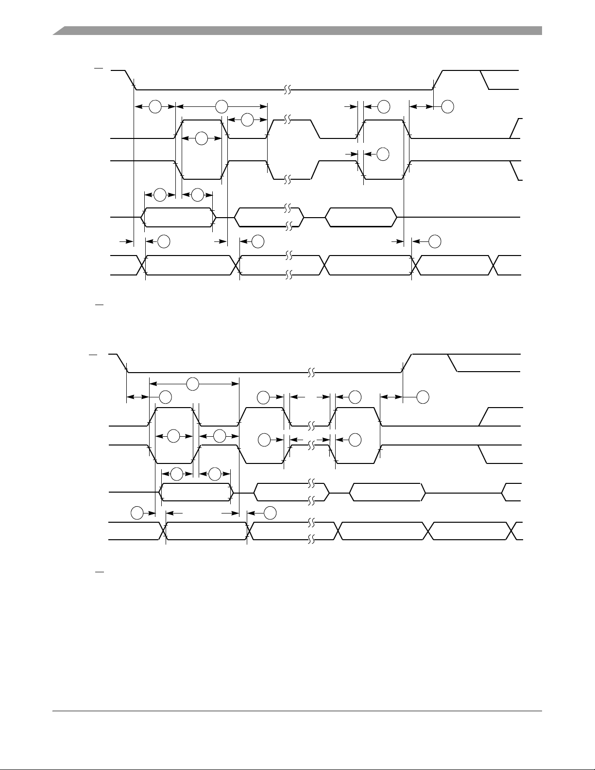
Page 29

Figure 10. Reset Timing
t
extrst
RESET PIN
t
IHIL
IRQ/KBIPx
t
ILIH
IRQ/KBIPx
t
TPMext
t
clkh
t
clkl
TPMxCLK
Figure 11. IRQ/KBIPx Timing
2.11.2 Timer/PWM (TPM) Module Timing
Preliminary Electrical Characteristics
Synchronizer circuits determine the shortest input pulses that can be recognized or the fastest clock that can be used as the
optional external source to the timer counter. These synchronizers operate from the current bus rate clock.
Table 18. TPM Input Timing
NUM C Function Symbol Min Max Unit
1—
2—
3D
4D
5D
External clock frequency
External clock period
External clock high time
External clock low time
Input capture pulse width
f
TPMext
t
TPMext
t
clkh
t
clkl
t
ICPW
dc
4—
1.5 —
1.5 —
1.5 —
f
Bus
/4
MHz
t
cyc
t
cyc
t
cyc
t
cyc
Figure 12. Timer External Clock
MCF51JM128 ColdFire Microcontroller, Rev. 4
Freescale Semiconductor 29
Page 30

Preliminary Electrical Characteristics
t
ICPW
TPMxCHn
t
ICPW
TPMxCHn
2.11.3 MSCAN
Table 19. MSCAN Wake-up Pulse Characteristics
Figure 13. Timer Input Capture Pulse
Num C Parameter Symbol Min Typ
1D
2D
1
Typical values are based on characterization data at V
MSCAN Wake-up dominant pulse filtered
MSCAN Wake-up dominant pulse pass
= 5.0V, 25C unless otherwise stated.
DD
t
WUP
t
WUP
55s
1
Max Unit
2 s
MCF51JM128 ColdFire Microcontroller, Rev. 4
Freescale Semiconductor30
Page 31

Preliminary Electrical Characteristics
2.12 SPI Characteristics
Table 20 and Figure 14 through Figure 17 describe the timing requirements for the SPI system.
Table 20. SPI Timing
No. C Function Symbol Min Max Unit
Operating frequency
—D
1D
2D
3D
4D
5D
6D
7D
Master
Slave
SPSCK period
Master
Slave
Enable lead time
Master
Slave
Enable lag time
Master
Slave
Clock (SPSCK) high or low time
Master
Slave
Data setup time (inputs)
Master
Slave
Data hold time (inputs)
Master
Slave
Slave access time
f
op
t
SPSCK
t
Lead
t
Lag
t
WSPSCK
t
SU
t
HI
t
a
f
/2048
Bus
0
2
4
12
1
12
1
t
–30
cyc
t
– 30
cyc
15
15
0
25
—1t
f
Bus
f
Bus
2048
—
—
—
—
—
1024 t
—
—
—
—
—
/2
/4
cyc
Hz
t
cyc
t
cyc
t
SPSCK
t
cyc
t
SPSCK
t
cyc
ns
ns
ns
ns
ns
ns
cyc
8D
Slave MISO disable time
t
dis
—1t
cyc
Data valid (after SPSCK edge)
9D
Master
Slave
t
v
—
—
25
25
ns
ns
Data hold time (outputs)
10 D
Master
Slave
t
HO
0
0
—
—
ns
ns
Rise time
11 D
Input
Output
t
t
RO
RI
—
—
t
cyc
– 25
25
ns
ns
Fall time
12 D
Input
Output
t
FI
t
FO
—
—
t
cyc
– 25
25
ns
ns
MCF51JM128 ColdFire Microcontroller, Rev. 4
Freescale Semiconductor 31
Page 32
Preliminary Electrical Characteristics
SPSCK
(OUTPUT)
SPSCK
(OUTPUT)
MISO
(INPUT)
MOSI
(OUTPUT)
SS
1
(OUTPUT)
MSB IN
2
BIT 6 . . . 1
LSB IN
MSB OUT
2
LSB OUT
BIT 6 . . . 1
(CPOL = 0)
(CPOL = 1)
NOTES:
2. LSBF = 0. For LSBF = 1, bit order is LSB, bit 1, ..., bit 6, MSB.
1. SS
output mode (DDS7 = 1, SSOE = 1).
1
2 3
4
5
6
9 10
11
12
4
9
SPSCK
(OUTPUT)
SPSCK
(OUTPUT)
MISO
(INPUT)
MOSI
(OUTPUT)
MSB IN
(2)
BIT 6 . . . 1
LSB IN
MASTER MSB OUT
(2)
MASTER LSB OUT
BIT 6 . . . 1
PORT DATA
(CPOL = 0)
(CPOL = 1)
PORT DATA
SS
(1)
(OUTPUT)
1. SS output mode (DDS7 = 1, SSOE = 1).
2. LSBF = 0. For LSBF = 1, bit order is LSB, bit 1, ..., bit 6, MSB.
NOTES:
2
1
12
11
3
4 4
11
12
5
6
9 10
Figure 14. SPI Master Timing (CPHA = 0)
Figure 15. SPI Master Timing (CPHA = 1)
MCF51JM128 ColdFire Microcontroller, Rev. 4
Freescale Semiconductor32
Page 33
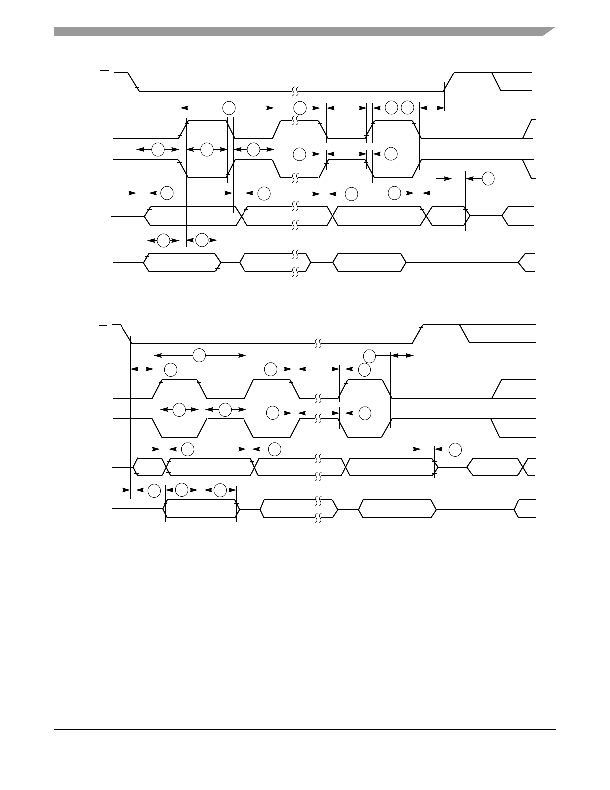
Figure 16. SPI Slave Timing (CPHA = 0)
SPSCK
(INPUT)
SPSCK
(INPUT)
MOSI
(INPUT)
MISO
(OUTPUT)
SS
(INPUT)
MSB IN
BIT 6 . . . 1
LSB IN
MSB OUT
SLAVE LSB OUT
BIT 6 . . . 1
(CPOL = 0)
(CPOL = 1)
NOTE:
SLAVE
SEE
NOTE
1. Not defined but normally MSB of character just received
1
2
3
4
5
6
7
8
9
10
11
12
4
11
12
10
SPSCK
(INPUT)
SPSCK
(INPUT)
MOSI
(INPUT)
MISO
(OUTPUT)
MSB IN
BIT 6 . . . 1
LSB IN
MSB OUT
SLAVE LSB OUT
BIT 6 . . . 1
SEE
(CPOL = 0)
(CPOL = 1)
SS
(INPUT)
NOTE:
SLAVE
NOTE
1. Not defined but normally LSB of character just received
1
2
3
4
5
6
7
8
9 10
11
12
4
11
12
Preliminary Electrical Characteristics
Freescale Semiconductor 33
Figure 17. SPI Slave Timing (CPHA = 1)
MCF51JM128 ColdFire Microcontroller, Rev. 4
Page 34
Preliminary Electrical Characteristics
2.13 Flash Specifications
This section provides details about program/erase times and program-erase endurance for the Flash memory.
Program and erase operations do not require any special power sources other than the normal V
Table 21. Flash Characteristics
DD
supply.
9
4
4000
20,000
—
100,000
1
Max Unit
t
t
t
t
—
cycles
—
Num C Characteristic Symbol Min Typ
1
2
4
5
6
7
8
9C
Supply voltage for program/erase
Supply voltage for read operation
Internal FCLK frequency
2
Internal FCLK period (1/FCLK)
Byte program time (random location)
Byte program time (burst mode)
Page erase time
Mass erase time
3
(2)
Program/erase endurance
(2)
4
TL to TH = –40C to + 105C
(2)
T = 25C
10
1
Typical values are based on characterization data at V
2
The frequency of this clock is controlled by a software setting.
3
These values are hardware state machine controlled. User code does not need to count cycles. This information
Data retention
5
V
prog/erase
V
Read
f
FCLK
t
Fcyc
t
prog
t
Burst
t
Page
t
Mass
2.7 5.5 V
2.7 5.5 V
150 200 kHz
56.67s
10,000
—
t
D_ret
= 5.0 V, 25C unless otherwise stated.
DD
15 100 — years
supplied for calculating approximate time to program and erase.
4
Typical endurance for Flash was evaluated for this product family on the 9S12Dx64. For additional information on
how Freescale Semiconductor defines typical endurance, please refer to Engineering Bulletin EB619/D, Typical
Endurance for Nonvolatile Memory.
5
Typical data retention values are based on intrinsic capability of the technology measured at high temperature and
de-rated to 25C using the Arrhenius equation. For additional information on how Freescale Semiconductor defines
typical data retention, please refer to Engineering Bulletin EB618/D, Typical Data Retention for Nonvolatile Memory .
Fcyc
Fcyc
Fcyc
Fcyc
2.14 USB Electricals
The USB electricals for the USBOTG module conform to the standards documented by the Universal Serial Bus Implementers
Forum. For the most up-to-date standards, visit http://www.usb.org.
If the Freescale USBOTG implementation requires additional or deviant electrical characteristics, this space would be used to
communicate that information.
MCF51JM128 ColdFire Microcontroller, Rev. 4
Freescale Semiconductor34
Page 35
Preliminary Electrical Characteristics
Table 22. Internal USB 3.3V Voltage Regulator Characteristics
Symbol Unit Min Typ Max
Regulator operating voltage
Vreg output
Vusb33 input with internal Vreg
disabled
VREG Quiescent Current
V
regin
V
regout
V
usb33in
I
VRQ
V 3.9 — 5.5
V33.33.6
V33.33.6
mA — 0.5 —
2.15 EMC Performance
Electromagnetic compatibility (EMC) performance is highly dependant on the environment in which the MCU resides. Board
design and layout, circuit topology choices, location and characteristics of external components as well as MCU software
operation all play a significant role in EMC performance. The system designer should consult Freescale applications notes such
as AN2321, AN1050, AN1263, AN2764, and AN1259 for advice and guidance specifically targeted at optimizing EMC
performance.
2.15.1 Radiated Emissions
Microcontroller radiated RF emissions are measured from 150 kHz to 1 GHz using the TEM/GTEM Cell method in accordance
with the IEC 61967-2 and SAE J1752/3 standards. The measurement is performed with the microcontroller installed on a
custom EMC evaluation board while running specialized EMC test software. The radiated emissions from the microcontroller
are measured in a TEM cell in two package orientations (North and East). For more detailed information concerning the
evaluation results, conditions and setup, please refer to the EMC Evaluation Report for this device.
MCF51JM128 ColdFire Microcontroller, Rev. 4
Freescale Semiconductor 35
Page 36
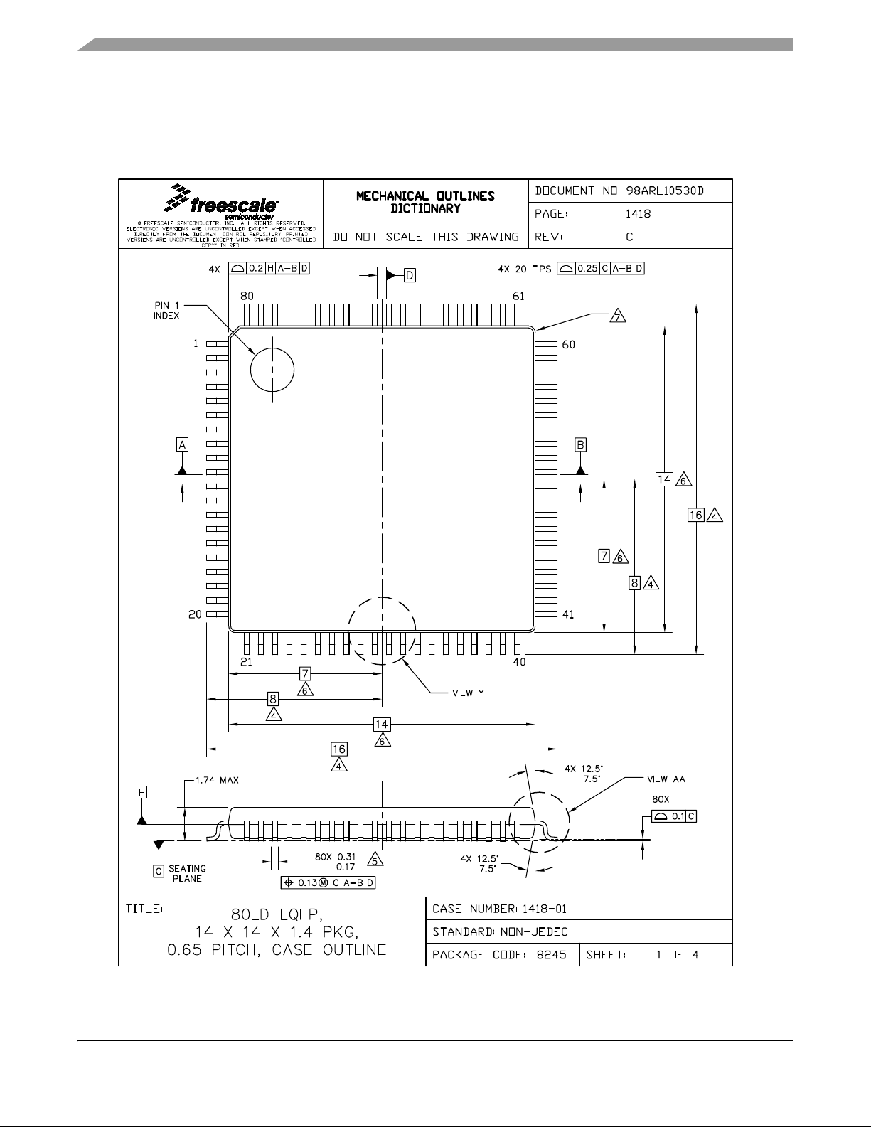
Mechanical Outline Drawings
3 Mechanical Outline Drawings
3.1 80-pin LQFP
Figure 18. 80-pin LQFP Diagram - I
MCF51JM128 ColdFire Microcontroller, Rev. 4
Freescale Semiconductor36
Page 37
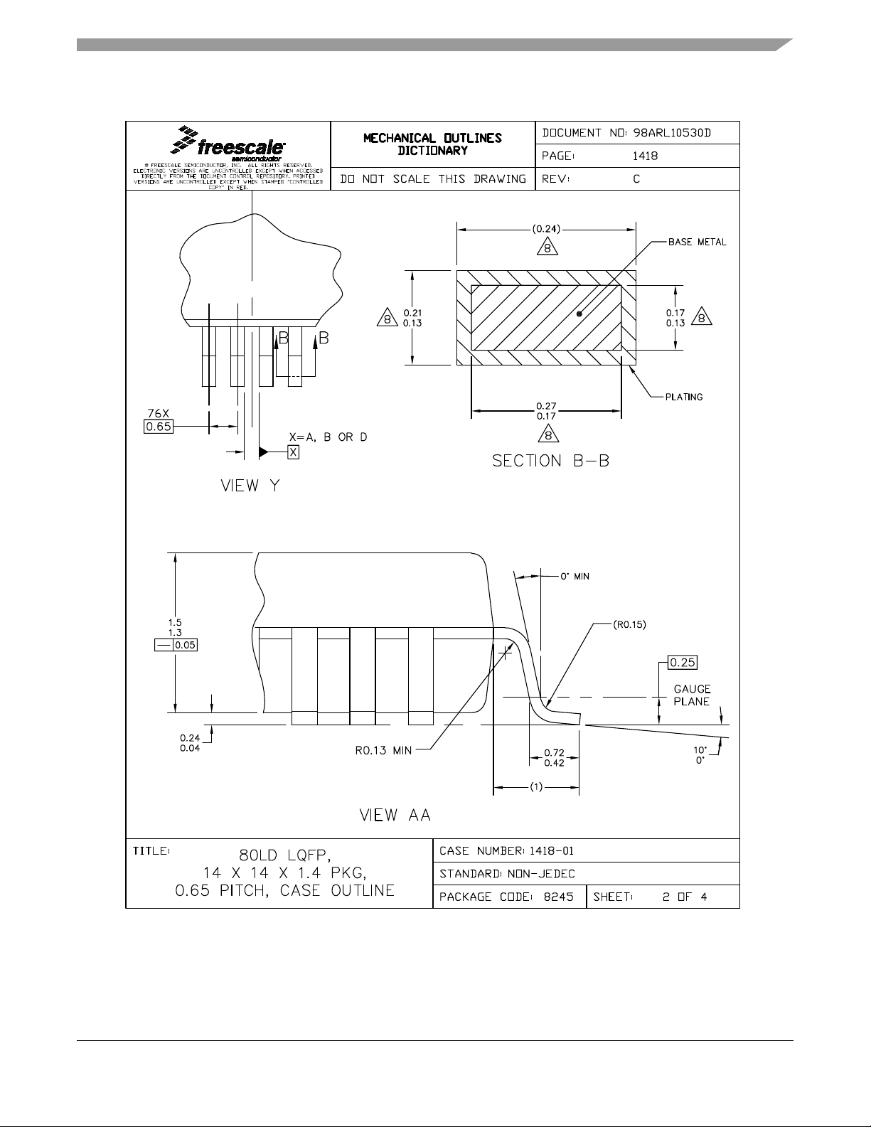
Mechanical Outline Drawings
Figure 19. 80-pin LQFP Diagram - II
MCF51JM128 ColdFire Microcontroller, Rev. 4
Freescale Semiconductor 37
Page 38
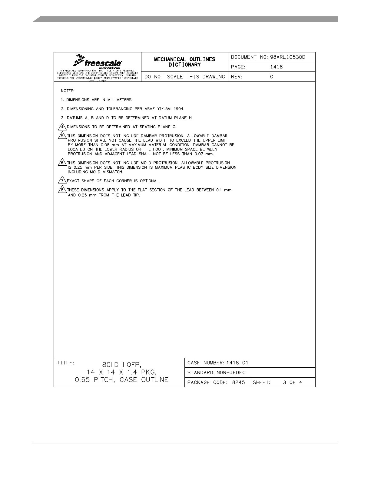
Mechanical Outline Drawings
Figure 20. 80-pin LQFP Diagram - III
MCF51JM128 ColdFire Microcontroller, Rev. 4
Freescale Semiconductor38
Page 39
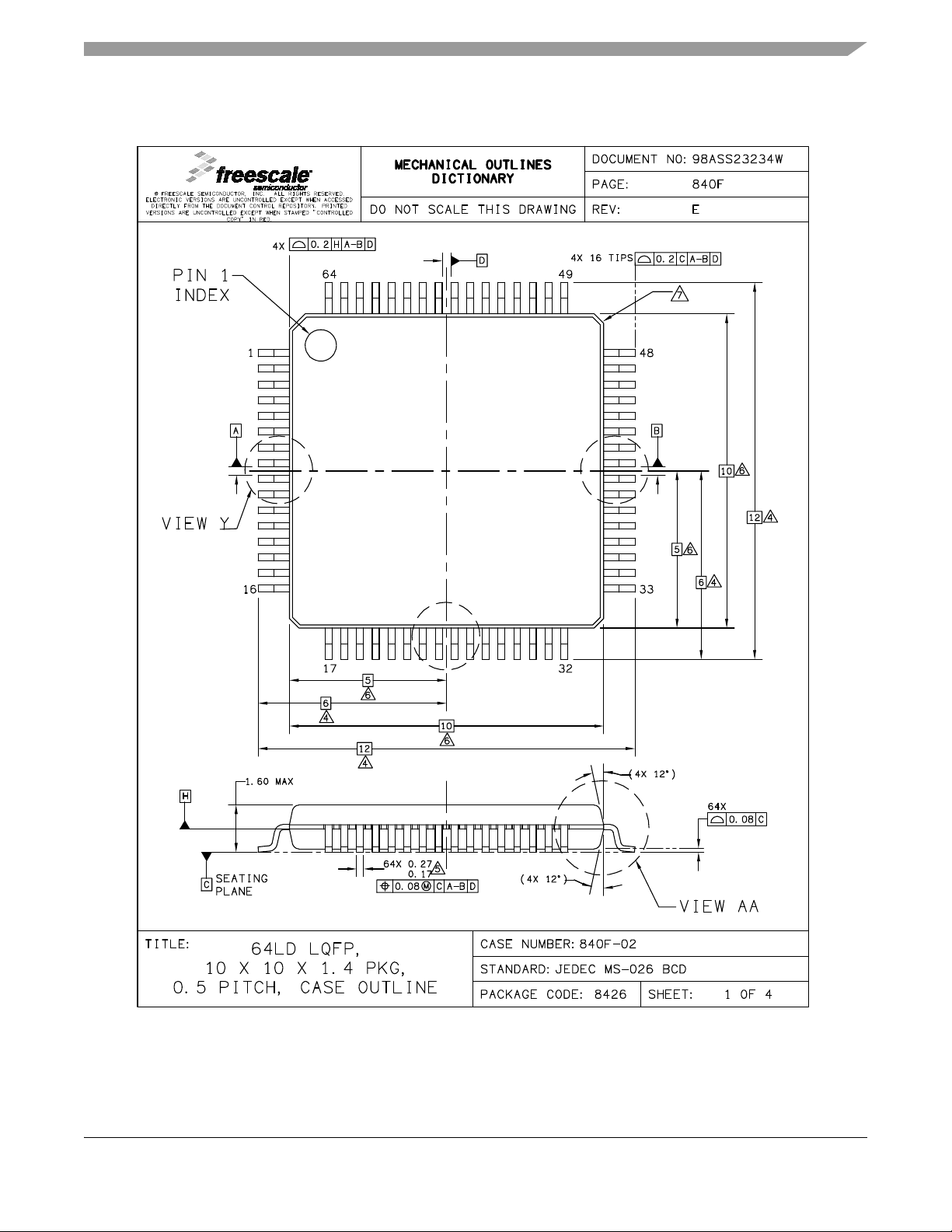
3.2 64-pin LQFP
Mechanical Outline Drawings
Figure 21. 64-pin LQFP Diagram - I
MCF51JM128 ColdFire Microcontroller, Rev. 4
Freescale Semiconductor 39
Page 40
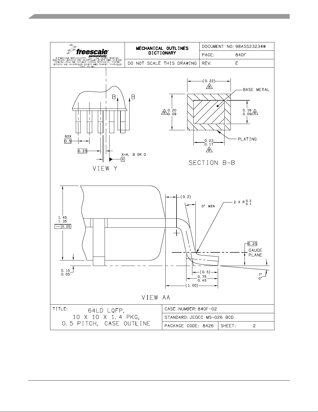
Mechanical Outline Drawings
Figure 22. 64-pin LQFP Diagram - II
MCF51JM128 ColdFire Microcontroller, Rev. 4
Freescale Semiconductor40
Page 41
Mechanical Outline Drawings
Figure 23. 64-pin LQFP Diagram - III
MCF51JM128 ColdFire Microcontroller, Rev. 4
Freescale Semiconductor 41
Page 42

Mechanical Outline Drawings
3.3 64-pin QFP
Figure 24. 64-pin QFP Diagram - I
MCF51JM128 ColdFire Microcontroller, Rev. 4
Freescale Semiconductor42
Page 43

Mechanical Outline Drawings
Figure 25. 64-pin QFP Diagram - II
MCF51JM128 ColdFire Microcontroller, Rev. 4
Freescale Semiconductor 43
Page 44

Mechanical Outline Drawings
Figure 26. 64-pin QFP Diagram - III
MCF51JM128 ColdFire Microcontroller, Rev. 4
Freescale Semiconductor44
Page 45

3.4 44-pin LQFP
Mechanical Outline Drawings
Figure 27. 44-pin LQFP Diagram - I
MCF51JM128 ColdFire Microcontroller, Rev. 4
Freescale Semiconductor 45
Page 46

Mechanical Outline Drawings
Figure 28. 44-pin LQFP Diagram - II
MCF51JM128 ColdFire Microcontroller, Rev. 4
Freescale Semiconductor46
Page 47

Mechanical Outline Drawings
Figure 29. 44-pin LQFP Diagram - III
MCF51JM128 ColdFire Microcontroller, Rev. 4
Freescale Semiconductor 47
Page 48

Revision History
4 Revision History
This section lists major changes between versions of the MCF51JM128 Data Sheet document.
Table 23. Changes Between Revisions
Revision Description
1 Updated features list
Updated the figures Typical Low-side Drive (sink) characteristics – High Drive (PTxDSn = 1), Typi cal
Low-side Drive (sink) characteristics – Low Drive (PTxDSn = 0), and Typical High-side Drive (source)
characteristics – High Drive (PTxDSn = 1)
Added the figure Typical High-side Drive (source) characteristics – Low Drive (PTxDSn = 0)
Updated the table Supply Current Characteristics
Updated the table Oscillator Electrical Specifications (Temperature Range = –40 to 105×C Ambient)
Updated the table SPI Electrical Characteristic, DC Characteristics
2 Updated the table Orderable Part Number Summary, DC Characteristics, and Supply Current
Characteristics
3 Updated the table Orderable Part Number Summary, MCG Characteristics, SPI Characteristics, and
Supply Current Characteristics
Changed V
DDAD
to V
Updated the table Device comparison
4 Added “RAM retention voltage” parameter in “DC Characteristics” table, alongwith a table note.
Added “Temp sensor voltage” parameter in “5 Volt 12-bit ADC Characteristics (V
)” table.
V
SSA
Added “ “Temp sensor slope” parameter in 5 Volt 12-bit ADC Characteristics (V
V
) table. Also, corrected unit of “Temp sensor voltage” parameter in 5 Volt 12-bit ADC
SSA
Characteristics (V
DDA
REFH
, V
= V
SSAD
DDA
to V
, V
SSA
REFL
= V
SSA
) table.
REFH
REFH
= V
= V
DDA
DDA
, V
, V
REFL
REFL
=
=
MCF51JM128 ColdFire Microcontroller, Rev. 4
Freescale Semiconductor48
Page 49

How to Reach Us:
Home Page:
www.freescale.com
Web Support:
http://www.freescale.com/support
USA/Europe or Locations Not Listed:
Freescale Semiconductor, Inc.
Technical Information Center, EL516
2100 East Elliot Road
Tempe, Arizona 85284
1-800-521-6274 or +1-480-768-2130
www.freescale.com/support
Europe, Middle East, and Africa:
Freescale Halbleiter Deutschland GmbH
Technical Information Center
Schatzbogen 7
81829 Muenchen, Germany
+44 1296 380 456 (English)
+46 8 52200080 (English)
+49 89 92103 559 (German)
+33 1 69 35 48 48 (French)
www.freescale.com/support
Japan:
Freescale Semiconductor Japan Ltd. Headquarters
ARCO Tower 15F
1-8-1, Shimo-Meguro, Meguro-ku,
Tokyo 153-0064
Japan
0120 191014 or +81 3 5437 9125
support.japan@freescale.com
Asia/Pacific:
Freescale Semiconductor China Ltd.
Exchange Building 23F
No. 118 Jianguo Road
Chaoyang District
Beijing 100022
China
+86 10 5879 8000
support.asia@freescale.com
Information in this document is provided solely to enable system and
software implementers to use F reescale Se miconductor products . There are
no express or implied copyright licenses granted hereunder to design or
fabricate any integrated circ uits or in te g rated circuits based on the
information in this document.
Freescale Semiconductor reserves the right to mak e changes without further
notice to any products herein. F reescale Semico nductor mak es no warr anty,
representation or guarantee regarding the suitability of its products for any
particular purpose, nor does Freescale Semiconductor assume any liability
arising out of the application or use of any product or circuit, an d specif ically
disclaims any and all liability, including without limitation consequential or
incidental damages. “Typical” parameters that may be provided in Freescale
Semiconductor data sheets and/or spec ifications can and d o vary in diff erent
applications and actual performance may vary over time. All operating
parameters, including “Typicals”, must be validated for each customer
application by customer’s technical experts. Freescale Semiconductor does
not convey any license under its patent rights nor the rights of others.
Freescale Semiconduct or products are not des igned, intended, or a uthorized
for use as components in systems intended for surgical implant into the bo dy ,
or other applications intended to support or sustain life, or for any other
application in which the failure of the Freescale Semiconductor product could
create a situation where personal injury or death may occur. Should Buyer
purchase or use Freescale Semiconductor products for any such unintended
or unauthorized application, Buyer shall indemnify and hold Freescale
Semiconductor and its officers, employees, subsidiaries, affiliates, and
distributors harmless against all claims, costs , damages, and exp enses, and
reasonable attorney fees arising out of, directly or indirectly, any claim of
personal injury or death associated with such unintended or unauthorized
use, even if such claim al leges th at Freescale Semiconductor wa s negli gent
regarding the design or manufacture of the part.
Freescale Semiconductor Literature Distribution Center
1-800-441-2447 or +1-303-675-2140
Fax: +1-303-675-2150
LDCForFreescaleSemiconductor@hibbertgroup.com
Freescale™ and the Freescale logo are trademarks of Freescale
Semiconductor, Inc. The described product contains a PowerPC processor
core. The Pow erPC name is a tradem ark of IBM Corp. and used under li cense.
All other product or service names are the property of their respective o wners .
© Freescale Semiconductor, Inc. 2008, 2009, 2010, 2011. All rights reserved.
MCF51JM128
Rev. 4
05/2012
 Loading...