

Page 1

MC9S12K Family
Device User Guide
Covers MC9S12KT256, MC9S12KG256,
MC9S12KG128, MC9S12KL128, MC9S12KC128,
MC9S12KG64, MC9S12KL64, MC9S12KC64
and MC9S12KG32
HCS12
Microcontrollers
9S12KT256DGV1/D
V01.09
9 SEP 2004
freescale.com
Page 2
Device User Guide — 9S12KT256DGV1/D V01.09
Revision History
Version
Number
01.00 16 JUL 02 Original Version.
01.01 22 NOV 02
01.02 15 JAN 03
01.03 13 JUN 03 Expand to a K-Family SoC Guide and include 9S12KT256.
01.04 18 JUN 03 Replace 16-channel ATD with two 8-channel ATDs for 9S12KT256.
01.05 14 NOV 03
01.06 10 FEB 04 Updated Table A-7 3.3V I/O Characteristics.
01.07 13 MAY 04
01.08 20 JUL 04
01.09 9 SEP 04
Revision
Date
Author Description of Changes
Change load cap value on VDD and VDDPLL.
Correct expanded bus timing from 20MHz to 25 MHz.
Move ATD interrupt vector from $ffd0 to $ffd2.
Change PWeh and tDSW parameter in external bus timing.
Changed to a Device User Guide and added Document number.
Updated Table A-17 Oscillator Characteristics.
Replaced XCLKS with PE7 for Clock Selection diagrams.
Added CTRL to Table 2-1 Signal Properties.
Replaced Burst programming with Row Programming in NVM
electricals.
Changed Digital logic to Internal Logic.
Added LRAE bootloader information.
Changed PWEL, PWEH, t
and t
t
P0V
Added voltage regulator characteristics.
Updated Table A-16 NVM Timing Characteristics.
Corrected A.6.1.2 Row Programming time t
Expanded K-family to include 9S12KC128, 9S12KC64, 9S12KL128
and 9S12KL64.
Updated osciilator start up time and supply current characteristics.
Added ATDCTL0 and ATDCTL1 register bits to Sec 1.7.
in the external bus timing.
P1V
DSW
, t
ACCE
, t
, t
NAD
NAV
bwpgm
, t
RWV
equation
, t
, t
LSV
NOV
,
2
Freescale Semiconductor
Page 3

Device User Guide — 9S12KT256DGV1/D V01.09
Table of Contents
Section 1 Introduction
1.1 Overview. . . . . . . . . . . . . . . . . . . . . . . . . . . . . . . . . . . . . . . . . . . . . . . . . . . . . . . . . . 15
1.2 Features . . . . . . . . . . . . . . . . . . . . . . . . . . . . . . . . . . . . . . . . . . . . . . . . . . . . . . . . . . 15
1.3 Modes of Operation . . . . . . . . . . . . . . . . . . . . . . . . . . . . . . . . . . . . . . . . . . . . . . . . . 17
1.4 MC9S12KG(L)(C)128(64)(32) Block Diagram . . . . . . . . . . . . . . . . . . . . . . . . . . . . .19
1.5 MC9S12KT(G)256 Block Diagram . . . . . . . . . . . . . . . . . . . . . . . . . . . . . . . . . . . . . . 20
1.6 Device Memory Map. . . . . . . . . . . . . . . . . . . . . . . . . . . . . . . . . . . . . . . . . . . . . . . . . 21
1.7 Detailed Register Map . . . . . . . . . . . . . . . . . . . . . . . . . . . . . . . . . . . . . . . . . . . . . . . 27
1.8 Part ID Assignments. . . . . . . . . . . . . . . . . . . . . . . . . . . . . . . . . . . . . . . . . . . . . . . . .51
Section 2 Signal Description
2.1 Device Pinout . . . . . . . . . . . . . . . . . . . . . . . . . . . . . . . . . . . . . . . . . . . . . . . . . . . . . . 53
2.2 Signal Properties Summary . . . . . . . . . . . . . . . . . . . . . . . . . . . . . . . . . . . . . . . . . . .57
2.3 Detailed Signal Descriptions. . . . . . . . . . . . . . . . . . . . . . . . . . . . . . . . . . . . . . . . . . . 60
2.3.1 EXTAL, XTAL — Oscillator Pins . . . . . . . . . . . . . . . . . . . . . . . . . . . . . . . . . . . . . 60
2.3.2 RESET — External Reset Pin . . . . . . . . . . . . . . . . . . . . . . . . . . . . . . . . . . . . . . . 60
2.3.3 TEST — Test Pin. . . . . . . . . . . . . . . . . . . . . . . . . . . . . . . . . . . . . . . . . . . . . . . . . 60
2.3.4 VREGEN — Voltage Regulator Enable Pin. . . . . . . . . . . . . . . . . . . . . . . . . . . . . 60
2.3.5 XFC — PLL Loop Filter Pin . . . . . . . . . . . . . . . . . . . . . . . . . . . . . . . . . . . . . . . . .61
2.3.6 BKGD / TAGHI / MODC — Background Debug, Tag High, and Mode Pin . . . . . 61
2.3.7 PAD[15:8] / AN[15:8] — Port AD Input Pins [15:8]. . . . . . . . . . . . . . . . . . . . . . . . 61
2.3.8 PAD[7:0] / AN[7:0] — Port AD Input Pins [7:0]. . . . . . . . . . . . . . . . . . . . . . . . . . . 61
2.3.9 PA[7:0] / ADDR[15:8] / DATA[15:8] — Port A I/O Pins . . . . . . . . . . . . . . . . . . . . 61
2.3.10 PB[7:0] / ADDR[7:0] / DATA[7:0] — Port B I/O Pins . . . . . . . . . . . . . . . . . . . . . . 62
2.3.11 PE7 / NOACC / XCLKS — Port E I/O Pin 7. . . . . . . . . . . . . . . . . . . . . . . . . . . . . 62
2.3.12 PE6 / MODB / IPIPE1 — Port E I/O Pin 6 . . . . . . . . . . . . . . . . . . . . . . . . . . . . . . 63
2.3.13 PE5 / MODA / IPIPE0 — Port E I/O Pin 5 . . . . . . . . . . . . . . . . . . . . . . . . . . . . . . 63
2.3.14 PE4 / ECLK — Port E I/O Pin 4 . . . . . . . . . . . . . . . . . . . . . . . . . . . . . . . . . . . . . . 63
2.3.15 PE3 / LSTRB / TAGLO — Port E I/O Pin 3 . . . . . . . . . . . . . . . . . . . . . . . . . . . . . 64
2.3.16 PE2 / R/W — Port E I/O Pin 2 . . . . . . . . . . . . . . . . . . . . . . . . . . . . . . . . . . . . . . . 64
2.3.17 PE1 / IRQ — Port E Input Pin 1 . . . . . . . . . . . . . . . . . . . . . . . . . . . . . . . . . . . . . . 64
2.3.18 PE0 / XIRQ — Port E Input Pin 0. . . . . . . . . . . . . . . . . . . . . . . . . . . . . . . . . . . . . 64
2.3.19 PH7 / KWH7 / SS2 — Port H I/O Pin 7 . . . . . . . . . . . . . . . . . . . . . . . . . . . . . . . . 64
Freescale Semiconductor
3
Page 4

Device User Guide — 9S12KT256DGV1/D V01.09
2.3.20 PH6 / KWH6 / SCK2 — Port H I/O Pin 6 . . . . . . . . . . . . . . . . . . . . . . . . . . . . . . .64
2.3.21 PH5 / KWH5 / MOSI2 — Port H I/O Pin 5 . . . . . . . . . . . . . . . . . . . . . . . . . . . . . . 64
2.3.22 PH4 / KWH4 / MISO2 — Port H I/O Pin 2 . . . . . . . . . . . . . . . . . . . . . . . . . . . . . . 64
2.3.23 PH3 / KWH3 / SS1 — Port H I/O Pin 3 . . . . . . . . . . . . . . . . . . . . . . . . . . . . . . . . 65
2.3.24 PH2 / KWH2 / SCK1 — Port H I/O Pin 2 . . . . . . . . . . . . . . . . . . . . . . . . . . . . . . .65
2.3.25 PH1 / KWH1 / MOSI1 — Port H I/O Pin 1 . . . . . . . . . . . . . . . . . . . . . . . . . . . . . . 65
2.3.26 PH0 / KWH0 / MISO1 — Port H I/O Pin 0 . . . . . . . . . . . . . . . . . . . . . . . . . . . . . . 65
2.3.27 PJ7 / KWJ7 / TXCAN4 / SCL — PORT J I/O Pin 7 . . . . . . . . . . . . . . . . . . . . . . . 65
2.3.28 PJ6 / KWJ6 / RXCAN4 / SDA — PORT J I/O Pin 6. . . . . . . . . . . . . . . . . . . . . . . 65
2.3.29 PJ[1:0] / KWJ[1:0] — Port J I/O Pins [1:0] . . . . . . . . . . . . . . . . . . . . . . . . . . . . . .65
2.3.30 PK7 / ECS / ROMCTL — Port K I/O Pin 7 . . . . . . . . . . . . . . . . . . . . . . . . . . . . . . 65
2.3.31 PK[5:0] / XADDR[19:14] — Port K I/O Pins [5:0] . . . . . . . . . . . . . . . . . . . . . . . . . 66
2.3.32 PM7 / TXCAN4 — Port M I/O Pin 7 . . . . . . . . . . . . . . . . . . . . . . . . . . . . . . . . . . . 66
2.3.33 PM6 / RXCAN4 — Port M I/O Pin 6. . . . . . . . . . . . . . . . . . . . . . . . . . . . . . . . . . . 66
2.3.34 PM5 / TXCAN0 / TXCAN4 / SCK0 — Port M I/O Pin 5 . . . . . . . . . . . . . . . . . . . . 66
2.3.35 PM4 / RXCAN0 / RXCAN4/ MOSI0 — Port M I/O Pin 4 . . . . . . . . . . . . . . . . . . . 66
2.3.36 PM3 / TXCAN1 / TXCAN0 / SS0 — Port M I/O Pin 3 . . . . . . . . . . . . . . . . . . . . . 67
2.3.37 PM2 / RXCAN1 / RXCAN0 / MISO0 — Port M I/O Pin 2 . . . . . . . . . . . . . . . . . . . 67
2.3.38 PM1 / TXCAN0 — Port M I/O Pin 1 . . . . . . . . . . . . . . . . . . . . . . . . . . . . . . . . . . . 67
2.3.39 PM0 / RXCAN0 — Port M I/O Pin 0. . . . . . . . . . . . . . . . . . . . . . . . . . . . . . . . . . . 67
2.3.40 PP7 / KWP7 / PWM7 / SCK2 — Port P I/O Pin 7 . . . . . . . . . . . . . . . . . . . . . . . . 67
2.3.41 PP6 / KWP6 / PWM6 / SS2 — Port P I/O Pin 6. . . . . . . . . . . . . . . . . . . . . . . . . . 67
2.3.42 PP5 / KWP5 / PWM5 / MOSI2 — Port P I/O Pin 5. . . . . . . . . . . . . . . . . . . . . . . .67
2.3.43 PP4 / KWP4 / PWM4 / MISO2 — Port P I/O Pin 4. . . . . . . . . . . . . . . . . . . . . . . .68
2.3.44 PP3 / KWP3 / PWM3 / SS1 — Port P I/O Pin 3. . . . . . . . . . . . . . . . . . . . . . . . . . 68
2.3.45 PP2 / KWP2 / PWM2 / SCK1 — Port P I/O Pin 2 . . . . . . . . . . . . . . . . . . . . . . . . 68
2.3.46 PP1 / KWP1 / PWM1 / MOSI1 — Port P I/O Pin 1. . . . . . . . . . . . . . . . . . . . . . . .68
2.3.47 PP0 / KWP0 / PWM0 / MISO1 — Port P I/O Pin 0. . . . . . . . . . . . . . . . . . . . . . . .68
2.3.48 PS7 / SS0 — Port S I/O Pin 7 . . . . . . . . . . . . . . . . . . . . . . . . . . . . . . . . . . . . . . . 68
2.3.49 PS6 / SCK0 — Port S I/O Pin 6 . . . . . . . . . . . . . . . . . . . . . . . . . . . . . . . . . . . . . . 68
2.3.50 PS5 / MOSI0 — Port S I/O Pin 5 . . . . . . . . . . . . . . . . . . . . . . . . . . . . . . . . . . . . .69
2.3.51 PS4 / MISO0 — Port S I/O Pin 4 . . . . . . . . . . . . . . . . . . . . . . . . . . . . . . . . . . . . .69
2.3.52 PS3 / TXD1 — Port S I/O Pin 3 . . . . . . . . . . . . . . . . . . . . . . . . . . . . . . . . . . . . . .69
2.3.53 PS2 / RXD1 — Port S I/O Pin 2 . . . . . . . . . . . . . . . . . . . . . . . . . . . . . . . . . . . . . . 69
2.3.54 PS1 / TXD0 — Port S I/O Pin 1 . . . . . . . . . . . . . . . . . . . . . . . . . . . . . . . . . . . . . .69
2.3.55 PS0 / RXD0 — Port S I/O Pin 0 . . . . . . . . . . . . . . . . . . . . . . . . . . . . . . . . . . . . . . 69
4
Freescale Semiconductor
Page 5

Device User Guide — 9S12KT256DGV1/D V01.09
2.3.56 PT[7:0] / IOC[7:0] — Port T I/O Pins [7:0] . . . . . . . . . . . . . . . . . . . . . . . . . . . . . . 69
2.4 Power Supply Pins . . . . . . . . . . . . . . . . . . . . . . . . . . . . . . . . . . . . . . . . . . . . . . . . . . 69
2.4.1 VDDX,VSSX — Power Supply Pins for I/O Drivers . . . . . . . . . . . . . . . . . . . . . . . 70
2.4.2 VDDR, VSSR — Power Supply Pins for I/O Drivers & for Internal Voltage Regulator
70
2.4.3 VDD1, VDD2, VSS1, VSS2 — Power Supply Pins for Internal Logic . . . . . . . . . 70
2.4.4 VDDA, VSSA — Power Supply Pins for ATD and VREG . . . . . . . . . . . . . . . . . . 70
2.4.5 VRH, VRL — ATD Reference Voltage Input Pins . . . . . . . . . . . . . . . . . . . . . . . . 70
2.4.6 VDDPLL, VSSPLL — Power Supply Pins for PLL. . . . . . . . . . . . . . . . . . . . . . . . 70
Section 3 System Clock Description
Section 4 Modes of Operation
4.1 Overview. . . . . . . . . . . . . . . . . . . . . . . . . . . . . . . . . . . . . . . . . . . . . . . . . . . . . . . . . . 72
4.2 Chip Configuration Summary . . . . . . . . . . . . . . . . . . . . . . . . . . . . . . . . . . . . . . . . . . 72
4.3 Security. . . . . . . . . . . . . . . . . . . . . . . . . . . . . . . . . . . . . . . . . . . . . . . . . . . . . . . . . . .73
4.3.1 Securing the Microcontroller . . . . . . . . . . . . . . . . . . . . . . . . . . . . . . . . . . . . . . . . 73
4.3.2 Operation of the Secured Microcontroller . . . . . . . . . . . . . . . . . . . . . . . . . . . . . . 74
4.3.3 Unsecuring the Microcontroller . . . . . . . . . . . . . . . . . . . . . . . . . . . . . . . . . . . . . . 74
4.4 Low Power Modes . . . . . . . . . . . . . . . . . . . . . . . . . . . . . . . . . . . . . . . . . . . . . . . . . . 74
4.4.1 Stop . . . . . . . . . . . . . . . . . . . . . . . . . . . . . . . . . . . . . . . . . . . . . . . . . . . . . . . . . . .74
4.4.2 Pseudo Stop. . . . . . . . . . . . . . . . . . . . . . . . . . . . . . . . . . . . . . . . . . . . . . . . . . . . . 74
4.4.3 Wait . . . . . . . . . . . . . . . . . . . . . . . . . . . . . . . . . . . . . . . . . . . . . . . . . . . . . . . . . . . 75
4.4.4 Run. . . . . . . . . . . . . . . . . . . . . . . . . . . . . . . . . . . . . . . . . . . . . . . . . . . . . . . . . . . . 75
Section 5 Resets and Interrupts
5.1 Overview. . . . . . . . . . . . . . . . . . . . . . . . . . . . . . . . . . . . . . . . . . . . . . . . . . . . . . . . . . 76
5.2 Vectors . . . . . . . . . . . . . . . . . . . . . . . . . . . . . . . . . . . . . . . . . . . . . . . . . . . . . . . . . . . 76
5.2.1 Vector Table. . . . . . . . . . . . . . . . . . . . . . . . . . . . . . . . . . . . . . . . . . . . . . . . . . . . .76
5.3 Resets . . . . . . . . . . . . . . . . . . . . . . . . . . . . . . . . . . . . . . . . . . . . . . . . . . . . . . . . . . . 78
5.3.1 Effects of Reset . . . . . . . . . . . . . . . . . . . . . . . . . . . . . . . . . . . . . . . . . . . . . . . . . .78
Section 6 HCS12 Core Block Description
6.1 CPU12 Block Description. . . . . . . . . . . . . . . . . . . . . . . . . . . . . . . . . . . . . . . . . . . . . 78
6.2 HCS12 Background Debug Module (BDM) Block Description. . . . . . . . . . . . . . . . . 78
6.3 HCS12 Debug (DBG) Block Description . . . . . . . . . . . . . . . . . . . . . . . . . . . . . . . . . 79
6.4 HCS12 Interrupt (INT) Block Description . . . . . . . . . . . . . . . . . . . . . . . . . . . . . . . . . 79
Freescale Semiconductor
5
Page 6

Device User Guide — 9S12KT256DGV1/D V01.09
6.5 HCS12 Multiplexed External Bus Interface (MEBI) Block Description . . . . . . . . . . . 79
6.6 HCS12 Module Mapping Control (MMC) Block Description. . . . . . . . . . . . . . . . . . . 79
Section 7 Analog to Digital Converter (ATD) Block Description
Section 8 Clock Reset Generator (CRG) Block Description
8.1 Device-specific information. . . . . . . . . . . . . . . . . . . . . . . . . . . . . . . . . . . . . . . . . . . . 79
Section 9 EEPROM Block Description
Section 10 Flash EEPROM Block Description
Section 11 IIC Block Description
Section 12 MSCAN Block Description
Section 13 OSC Block Description
Section 14 Port Integration Module (PIM) Block Description
Section 15 Pulse Width Modulator (PWM) Block Description
Section 16 Serial Communications Interface (SCI) Block Description
Section 17 Serial Peripheral Interface (SPI) Block Description
Section 18 Timer (TIM) Block Description
Section 19 Voltage Regulator (VREG) Block Description
19.1 Device-specific information. . . . . . . . . . . . . . . . . . . . . . . . . . . . . . . . . . . . . . . . . . . . 82
19.1.1 VDD1, VDD2, VSS1, VSS2 . . . . . . . . . . . . . . . . . . . . . . . . . . . . . . . . . . . . . . . . .82
Appendix A Electrical Characteristics
A.1 General. . . . . . . . . . . . . . . . . . . . . . . . . . . . . . . . . . . . . . . . . . . . . . . . . . . . . . . . . . . 83
A.1.1 Parameter Classification . . . . . . . . . . . . . . . . . . . . . . . . . . . . . . . . . . . . . . . . . . . 83
A.1.2 Power Supply. . . . . . . . . . . . . . . . . . . . . . . . . . . . . . . . . . . . . . . . . . . . . . . . . . . . 83
A.1.3 Pins . . . . . . . . . . . . . . . . . . . . . . . . . . . . . . . . . . . . . . . . . . . . . . . . . . . . . . . . . . . 84
A.1.4 Current Injection. . . . . . . . . . . . . . . . . . . . . . . . . . . . . . . . . . . . . . . . . . . . . . . . . . 84
6
Freescale Semiconductor
Page 7

Device User Guide — 9S12KT256DGV1/D V01.09
A.1.5 Absolute Maximum Ratings . . . . . . . . . . . . . . . . . . . . . . . . . . . . . . . . . . . . . . . . . 85
A.1.6 ESD Protection and Latch-up Immunity. . . . . . . . . . . . . . . . . . . . . . . . . . . . . . . . 86
A.1.7 Operating Conditions . . . . . . . . . . . . . . . . . . . . . . . . . . . . . . . . . . . . . . . . . . . . . . 86
A.1.8 Power Dissipation and Thermal Characteristics . . . . . . . . . . . . . . . . . . . . . . . . . 87
A.1.9 I/O Characteristics . . . . . . . . . . . . . . . . . . . . . . . . . . . . . . . . . . . . . . . . . . . . . . . . 89
A.1.10 Supply Currents . . . . . . . . . . . . . . . . . . . . . . . . . . . . . . . . . . . . . . . . . . . . . . . . . . 91
A.2 Voltage Regulator (VREG_3V3) Operating Characteristics. . . . . . . . . . . . . . . . . . . 94
A.3 Chip Power-up and LVI/LVR graphical explanation . . . . . . . . . . . . . . . . . . . . . . . . . 95
A.4 Output Loads . . . . . . . . . . . . . . . . . . . . . . . . . . . . . . . . . . . . . . . . . . . . . . . . . . . . . . 95
A.4.1 Resistive Loads . . . . . . . . . . . . . . . . . . . . . . . . . . . . . . . . . . . . . . . . . . . . . . . . . . 95
A.4.2 Capacitive Loads . . . . . . . . . . . . . . . . . . . . . . . . . . . . . . . . . . . . . . . . . . . . . . . . . 96
A.5 ATD Characteristics . . . . . . . . . . . . . . . . . . . . . . . . . . . . . . . . . . . . . . . . . . . . . . . . . 97
A.5.1 ATD Operating Characteristics . . . . . . . . . . . . . . . . . . . . . . . . . . . . . . . . . . . . . . 97
A.5.2 Factors influencing accuracy. . . . . . . . . . . . . . . . . . . . . . . . . . . . . . . . . . . . . . . . 98
A.5.3 ATD accuracy. . . . . . . . . . . . . . . . . . . . . . . . . . . . . . . . . . . . . . . . . . . . . . . . . . . . 99
A.6 NVM, Flash and EEPROM. . . . . . . . . . . . . . . . . . . . . . . . . . . . . . . . . . . . . . . . . . . 102
A.6.1 NVM timing. . . . . . . . . . . . . . . . . . . . . . . . . . . . . . . . . . . . . . . . . . . . . . . . . . . . . 102
A.6.2 NVM Reliability. . . . . . . . . . . . . . . . . . . . . . . . . . . . . . . . . . . . . . . . . . . . . . . . . . 104
A.7 Reset, Oscillator and PLL. . . . . . . . . . . . . . . . . . . . . . . . . . . . . . . . . . . . . . . . . . . . 105
A.7.1 Startup . . . . . . . . . . . . . . . . . . . . . . . . . . . . . . . . . . . . . . . . . . . . . . . . . . . . . . . . 105
A.7.2 Oscillator . . . . . . . . . . . . . . . . . . . . . . . . . . . . . . . . . . . . . . . . . . . . . . . . . . . . . . 106
A.7.3 Phase Locked Loop . . . . . . . . . . . . . . . . . . . . . . . . . . . . . . . . . . . . . . . . . . . . . . 107
A.8 MSCAN. . . . . . . . . . . . . . . . . . . . . . . . . . . . . . . . . . . . . . . . . . . . . . . . . . . . . . . . . . 111
A.9 SPI . . . . . . . . . . . . . . . . . . . . . . . . . . . . . . . . . . . . . . . . . . . . . . . . . . . . . . . . . . . . . 112
A.9.1 Master Mode . . . . . . . . . . . . . . . . . . . . . . . . . . . . . . . . . . . . . . . . . . . . . . . . . . . 112
A.9.2 Slave Mode . . . . . . . . . . . . . . . . . . . . . . . . . . . . . . . . . . . . . . . . . . . . . . . . . . . . 114
A.10 External Bus Timing . . . . . . . . . . . . . . . . . . . . . . . . . . . . . . . . . . . . . . . . . . . . . . . . 116
A.10.1 General Muxed Bus Timing . . . . . . . . . . . . . . . . . . . . . . . . . . . . . . . . . . . . . . . . 116
Appendix B Package Information
B.1 80-pin QFP package. . . . . . . . . . . . . . . . . . . . . . . . . . . . . . . . . . . . . . . . . . . . . . . . 122
B.2 100-pin LQFP package. . . . . . . . . . . . . . . . . . . . . . . . . . . . . . . . . . . . . . . . . . . . . . 123
B.3 112-pin LQFP package. . . . . . . . . . . . . . . . . . . . . . . . . . . . . . . . . . . . . . . . . . . . . . 124
Freescale Semiconductor
7
Page 8

Device User Guide — 9S12KT256DGV1/D V01.09
8
Freescale Semiconductor
Page 9

Device User Guide — 9S12KT256DGV1/D V01.09
List of Figures
Figure 0-1 Order Part number Coding . . . . . . . . . . . . . . . . . . . . . . . . . . . . . . . . . . . . . . 14
Figure 1-1 MC9S12KG(L)(C)128(64)(32) Block Diagram. . . . . . . . . . . . . . . . . . . . . . . . 19
Figure 1-2 MC9S12KT(G)256 Block Diagram. . . . . . . . . . . . . . . . . . . . . . . . . . . . . . . . . 20
Figure 1-3 MC9S12KT256 and MC9S12KG256 Memory Map. . . . . . . . . . . . . . . . . . . . 23
Figure 1-4 MC9S12KG128, MC9S12KL128 and MC9S12KC128 Memory Map . . . . . . 24
Figure 1-5 MC9S12KG64, MC9S12KL64 and MC9S12KC64 Memory Map . . . . . . . . . 25
Figure 1-6 MC9S12KG32 Memory Map . . . . . . . . . . . . . . . . . . . . . . . . . . . . . . . . . . . . . 26
Figure 2-1 Pin assignments for 112 LQFP . . . . . . . . . . . . . . . . . . . . . . . . . . . . . . . . . . . 54
Figure 2-2 Pin assignments for 100 LQFP . . . . . . . . . . . . . . . . . . . . . . . . . . . . . . . . . . . 55
Figure 2-3 Pin assignments for 80 QFP . . . . . . . . . . . . . . . . . . . . . . . . . . . . . . . . . . . . . 56
Figure 2-4 PLL Loop Filter Connections . . . . . . . . . . . . . . . . . . . . . . . . . . . . . . . . . . . . . 61
Figure 2-5 Loop Controlled Pierce Oscillator Connections (PE7=1). . . . . . . . . . . . . . . . 62
Figure 2-6 Full Swing Pierce Oscillator Connections (PE7=0) . . . . . . . . . . . . . . . . . . . . 63
Figure 2-7 External Clock Connections (PE7=0) . . . . . . . . . . . . . . . . . . . . . . . . . . . . . . 63
Figure 3-1 Clock Connections. . . . . . . . . . . . . . . . . . . . . . . . . . . . . . . . . . . . . . . . . . . . . 71
Figure A-1 Voltage Regulator - Chip Power-up and Voltage Drops (not scaled) . . . . . 95
Figure A-2 ATD Accuracy Definitions . . . . . . . . . . . . . . . . . . . . . . . . . . . . . . . . . . . . . 101
Figure A-3 Basic PLL functional diagram . . . . . . . . . . . . . . . . . . . . . . . . . . . . . . . . . . 107
Figure A-4 Jitter Definitions. . . . . . . . . . . . . . . . . . . . . . . . . . . . . . . . . . . . . . . . . . . . . 109
Figure A-5 SPI Master Timing (CPHA = 0) . . . . . . . . . . . . . . . . . . . . . . . . . . . . . . . . . 112
Figure A-6 SPI Master Timing (CPHA =1). . . . . . . . . . . . . . . . . . . . . . . . . . . . . . . . . . 113
Figure A-7 SPI Slave Timing (CPHA = 0) . . . . . . . . . . . . . . . . . . . . . . . . . . . . . . . . . . 114
Figure A-8 SPI Slave Timing (CPHA =1). . . . . . . . . . . . . . . . . . . . . . . . . . . . . . . . . . . 114
Figure A-9 General External Bus Timing. . . . . . . . . . . . . . . . . . . . . . . . . . . . . . . . . . . 117
Figure B-1 80-pin QFP Mechanical Dimensions (case no. 841B). . . . . . . . . . . . . . . . 122
Figure B-2 100-pin LQFP Mechanical Dimensions (case no. 983) . . . . . . . . . . . . . . . 123
Figure B-3 112-pin LQFP Mechanical Dimensions (case no. 987) . . . . . . . . . . . . . . . 124
Freescale Semiconductor
9
Page 10

Device User Guide — 9S12KT256DGV1/D V01.09
10
Freescale Semiconductor
Page 11

Device User Guide — 9S12KT256DGV1/D V01.09
List of Tables
Table 0-1 List of MC9S12K-Family members . . . . . . . . . . . . . . . . . . . . . . . . . . . . . . . . . 13
Table 0-2 Document References. . . . . . . . . . . . . . . . . . . . . . . . . . . . . . . . . . . . . . . . . . . 14
Table 1-1 MC9S12KT(G)256 Device Memory Map. . . . . . . . . . . . . . . . . . . . . . . . . . . . . 21
Table 1-2 MC9S12KG(L)(C)128(64)(32) Device Memory Map . . . . . . . . . . . . . . . . . . . . 22
Table 1-3 Detailed MSCAN Foreground Receive and Transmit Buffer Layout. . . . . . . . 43
Table 1-4 Assigned Part ID Numbers . . . . . . . . . . . . . . . . . . . . . . . . . . . . . . . . . . . . . . . 52
Table 1-5 Memory size registers . . . . . . . . . . . . . . . . . . . . . . . . . . . . . . . . . . . . . . . . . . . 52
Table 2-1 Signal Properties . . . . . . . . . . . . . . . . . . . . . . . . . . . . . . . . . . . . . . . . . . . . . . . 57
Table 2-2 Power and Ground. . . . . . . . . . . . . . . . . . . . . . . . . . . . . . . . . . . . . . . . . . . . . . 59
Table 2-3 Clock selection based on PE7 during reset. . . . . . . . . . . . . . . . . . . . . . . . . . . 62
Table 4-1 Mode Selection . . . . . . . . . . . . . . . . . . . . . . . . . . . . . . . . . . . . . . . . . . . . . . . . 72
Table 4-2 Clock Selection Based on PE7 . . . . . . . . . . . . . . . . . . . . . . . . . . . . . . . . . . . . 73
Table 4-3 Voltage Regulator VREGEN . . . . . . . . . . . . . . . . . . . . . . . . . . . . . . . . . . . . . . 73
Table 5-1 Interrupt Vector Locations . . . . . . . . . . . . . . . . . . . . . . . . . . . . . . . . . . . . . . . . 76
Table 5-2 Reset Summary. . . . . . . . . . . . . . . . . . . . . . . . . . . . . . . . . . . . . . . . . . . . . . . . 78
Table A-1 Absolute Maximum Ratings. . . . . . . . . . . . . . . . . . . . . . . . . . . . . . . . . . . . . . . 85
Table A-2 ESD and Latch-up Test Conditions . . . . . . . . . . . . . . . . . . . . . . . . . . . . . . . . . 86
Table A-3 ESD and Latch-Up Protection Characteristics. . . . . . . . . . . . . . . . . . . . . . . . . 86
Table A-4 Operating Conditions. . . . . . . . . . . . . . . . . . . . . . . . . . . . . . . . . . . . . . . . . . . . 87
Table A-5 Thermal Package Characteristics . . . . . . . . . . . . . . . . . . . . . . . . . . . . . . . . . . 89
Table A-6 5V I/O Characteristics . . . . . . . . . . . . . . . . . . . . . . . . . . . . . . . . . . . . . . . . . . . 90
Table A-7 3.3V I/O Characteristics. . . . . . . . . . . . . . . . . . . . . . . . . . . . . . . . . . . . . . . . . . 91
Table A-8 Supply Current Characteristics . . . . . . . . . . . . . . . . . . . . . . . . . . . . . . . . . . . . 93
Table A-9 VREG_3V3 - Operating Conditions . . . . . . . . . . . . . . . . . . . . . . . . . . . . . . . . . 94
Table A-10 Voltage Regulator - Capacitive Loads . . . . . . . . . . . . . . . . . . . . . . . . . . . . . . . 96
Table A-11 5V ATD Operating Characteristics. . . . . . . . . . . . . . . . . . . . . . . . . . . . . . . . . . 97
Table A-12 3.3V ATD Operating Characteristics . . . . . . . . . . . . . . . . . . . . . . . . . . . . . . . . 98
Table A-13 ATD Electrical Characteristics . . . . . . . . . . . . . . . . . . . . . . . . . . . . . . . . . . . . . 99
Table A-14 5V ATD Conversion Performance. . . . . . . . . . . . . . . . . . . . . . . . . . . . . . . . . . 99
Table A-15 3.3V ATD Conversion Performance. . . . . . . . . . . . . . . . . . . . . . . . . . . . . . . . 100
Table A-16 NVM Timing Characteristics . . . . . . . . . . . . . . . . . . . . . . . . . . . . . . . . . . . . . 103
Table A-17 NVM Reliability Characteristics. . . . . . . . . . . . . . . . . . . . . . . . . . . . . . . . . . . 104
Table A-18 Startup Characteristics. . . . . . . . . . . . . . . . . . . . . . . . . . . . . . . . . . . . . . . . . . 105
Freescale Semiconductor
11
Page 12

Device User Guide — 9S12KT256DGV1/D V01.09
Table A-19 Oscillator Characteristics . . . . . . . . . . . . . . . . . . . . . . . . . . . . . . . . . . . . . . . 106
Table A-20 PLL Characteristics. . . . . . . . . . . . . . . . . . . . . . . . . . . . . . . . . . . . . . . . . . . . 110
Table A-21 MSCAN Wake-up Pulse Characteristics. . . . . . . . . . . . . . . . . . . . . . . . . . . . 111
Table A-22 SPI Master Mode Timing Characteristics. . . . . . . . . . . . . . . . . . . . . . . . . . . . 113
Table A-23 SPI Slave Mode Timing Characteristics . . . . . . . . . . . . . . . . . . . . . . . . . . . . 115
Table A-24 Expanded Bus Timing Characteristics . . . . . . . . . . . . . . . . . . . . . . . . . . . . . 118
12
Freescale Semiconductor
Page 13
Device User Guide — 9S12KT256DGV1/D V01.09
Preface
The Device User Guide provides information about the MC9S12K-Family devices made up of standard
HCS12 blocks and the HCS12 processor core. This document is part of the customer documentation. A
complete set of device manuals also includes all the individual Block Guides of the implemented modules.
In a effort to reduce redundancy all module specific information is located only in the respective Block
Guide. If applicable, special implementation details of the module are given in the block description
sections of this document.
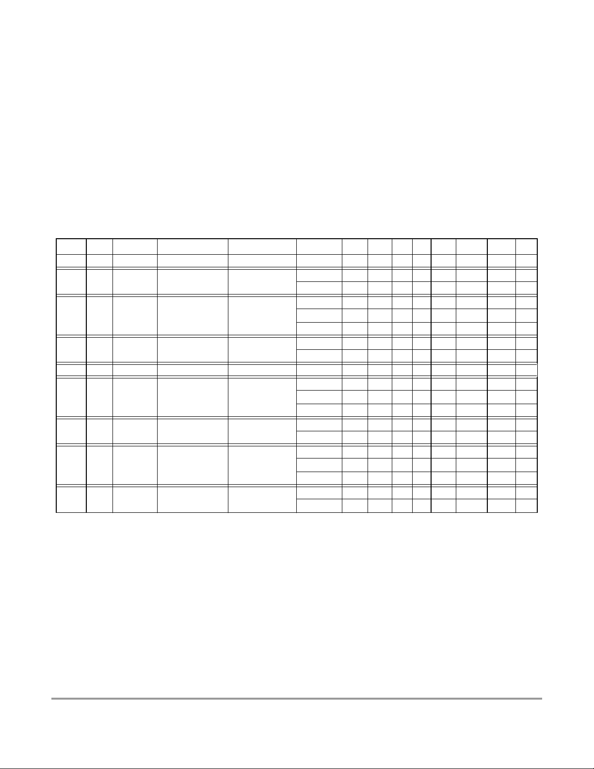
Table 0-1 shows a feature overview of the MC9S12K-Family members.
Table 0-1 List of MC9S12K-Family members
Flash RAM EEPROM Device
256K 12K 4K MC9S12KT256 C, V, M 112 LQFP 3 2 3 1 16 8 8 91
256K 12K 4K MC9S12KG256 C, V, M
128K 8K 2K MC9S12KG128 C, V, M
64K 4K 1K MC9S12KG64 C, V, M
32K 2K 1K MC9S12KG32 C, V, M 80 QFP 2 2 2 1 8 7 8 59
128K 6K 2K MC9S12KL128 C, V, M
64K 4K 1K MC9S12KL64 C, V, M
128K 6K None MC9S12KC128 C, V, M
64K 4K None MC9S12KC64 C, V, M
NOTES:
1. C: TA = 85˚C, f = 25MHz. V: TA=105˚C, f = 25MHz. M: TA= 125˚C, f = 25MHz
2. Number of channels
3. I/O is the sum of ports capable to act as digital input or output.
Temp Options
1
Package CAN SCI SPI IIC
112 LQFP 2 2 3 1 16 8 8 91
80 QFP 2 2 3 1 8 7 8 59
112 LQFP 2 2 3 1 16 8 8 91
100 LQFP 2 2 2 1 13 7 8 79
80 QFP 2 2 2 1 8 7 8 59
112 LQFP 2 2 2 1 16 8 8 91
80 QFP 2 2 2 1 8 7 8 59
112 LQFP 1 1 2 1 16 8 8 91
100 LQFP 1 1 2 1 13 7 8 79
80 QFP 1 1 2 1 8 7 8 59
112 LQFP 1 1 2 1 16 8 8 91
80 QFP 1 1 2 1 8 7 8 59
112 LQFP 1 1 2 1 16 8 8 91
100 LQFP 1 1 2 1 13 7 8 79
80 QFP 1 1 2 1 8 7 8 59
112 LQFP 1 1 2 1 16 8 8 91
80 QFP 1 1 2 1 8 7 8 59
2
A/D
PWM2TIM2I/O
3
Freescale Semiconductor
13
Page 14
Device User Guide — 9S12KT256DGV1/D V01.09
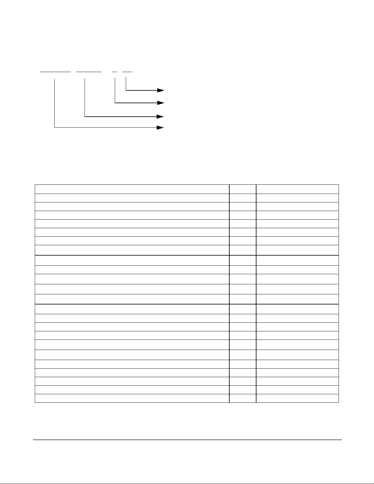
Figure 0-1 shows the part number coding based on the package and temperature options for the
MC9S12K-Family.
MC9S12 KT256 C FU
Temperature Options
C = -40˚C to 85˚C
V = -40˚C to 105˚C
Package Option
Temperature Option
Device Title
Controller Family
M = -40˚C to 125˚C
Package Options
PV = 112LQFP
PU = 100LQFP
FU = 80QFP
Figure 0-1 Order Part number Coding
Table 0-2 shows names and versions of the referenced documents throughout the Device User Guide.
Table 0-2 Document References
User Guide Version Document Order Number
CPU12 Reference Manual V02 S12CPUV2/D
HCS12 Background Debug (BDM) Block Guide V04 S12BDMV4/D
HCS12 Debug (DBG) Block Guide V01 S12DBGV1/D
HCS12 Interrupt (INT) Block Guide V01 S12INTV1/D
HCS12 Multiplexed Expanded Bus Interface (MEBI) Block Guide V03 S12MEBIV3/D
HCS12 Module Mapping Control (MMC) Block Guide V04 S12MMCV4/D
Analog to Digital Converter: 10-Bit, 16 Channels (ATD_10B16C) Block Guide V03
Analog to Digital Converter: 10-Bit, 8 Channels (ATD_10B8C) Block Guide V03
Clock and Reset Generator (CRG) Block Guide V04 S12CRGV4/D
2K Byte EEPROM (EETS2K) Block Guide V01
4K Byte EEPROM (EETS4K) Block Guide V02
128K Byte Flash with Error Code Correction (FTS128K1ECC) Block Guide V01
256K Byte Flash with Error Code Correction (FTS256K2ECC) Block Guide V01
Inter IC Bus (IIC) Block Guide V02 S12IICV2/D
Motorola Scalable CAN (MSCAN) Block Guide V02 S12MSCANV2/D
Oscillator Loop Control Pierce (OSC_LCP) Block Guide V01 S12OSCLCPV1/D
Port Integration Module
Port Integration Module
Pulse Width Modulator 8 Bit 8 Channel (PWM_8B8C) Block Guide V01 S12PWM8B6CV1/D
Serial Communications Interface (SCI) Block Guide V02 S12SCIV2/D
Serial Peripheral Interface (SPI) Block Guide V03 S12SPIV3/D
Timer: 16-Bit, 8 Channels (TIM_16B8C) Block Guide V01 S12TIM16B8CV1/D
Voltage Regulator (VREG_3V3) Block Guide V01 S12VREG3V3V1/D
NOTES:
1. Block Guide for MC9S12K-Family except MC9S12KT256 and MC9S12KG256.
2. Block Guide for MC9S12KT256 and MC9S12KG256 only.
(1)
(PIM_9KG128) Block Guide
(2)
(PIM_9KT256) Block Guide
V01 S12KG128PIMV1/D
V01 S12KT256PIMV1/D
S12ATD10B16CV3/D
S12ATD10B8CV3/D
S12EETS2KV1/D
S12EETS4KV2/D
FTS128K1ECCV1/D
FTS256K2ECCV1/D
1
2
(1)
(2)
(1)
(2)
14
Freescale Semiconductor
Page 15

Device User Guide — 9S12KT256DGV1/D V01.09
Section 1 Introduction
1.1 Overview
The MC9S12K-Family is a 112/100/80 pin 16-bit Flash-based microcontroller family targeted for high
reliability systems. Members of the MC9S12K-Family have an increased performance in reliability over
the life of the product due to a built-in Error Checking and Correction Code (ECC) in the Flash memory.
The program and erase operations automatically generate six parity bits per word making ECC transparent
to the user.
All members of the MC9S12K-Family are comprised of standard on-chip peripherals including a 16-bit
central processing unit (CPU12), up to 256K bytes of Flash EEPROM, up to 4K bytes of EEPROM, up to
12K bytes of RAM, up to two asynchronous serial communications interface (SCI), up to three serial
peripheral interface (SPI), IIC-bus, an 8-channel IC/OC timer, 16-channel or two 8-channel 10-bit
analog-to-digital converters (ADC), an 8-channel pulse-width modulator (PWM), up to three CAN 2.0 A,
B software compatible modules, 29 discrete digital I/O channels (Port A, Port B, Port E and Port K), and
20 discrete digital I/O lines with interrupt and wakeup capability. The MC9S12K-Family has full 16-bit
data paths throughout, however, the external bus can operate in an 8-bit narrow mode so single 8-bit wide
memory can be interfaced for lower cost systems. The inclusion of a PLL circuit allows power
consumption and performance to be adjusted to suit operational requirements.
1.2 Features
• HCS12 Core
– 16-bit HCS12 CPU
i. Upward compatible with M68HC11 instruction set
ii. Interrupt stacking and programmer’s model identical to M68HC11
iii. Instruction queue
iv. Enhanced indexed addressing
– MEBI (Multiplexed External Bus Interface)
– MMC (Memory Map and Interface)
– INT (Interrupt Controller)
– DBG (Debugger)
– BDM (Background Debug Mode)
• Oscillator
– 4Mhz to 16Mhz frequency range
– Pierce with amplitude loop control
– Clock monitor
Freescale Semiconductor
15
Page 16

Device User Guide — 9S12KT256DGV1/D V01.09
• Clock and Reset Generator (CRG)
– Phase-locked loop clock frequency multiplier
– Self Clock mode in absence of external clock
– COP watchdog
– Real Time interrupt (RTI)
• Memory
– 32K, 64K, 128K or 256K Byte Flash EEPROM
i. Internal program/erase voltage generation
ii. Security and Block Protect bits
iii. Hamming Error Correction Coding (ECC)
– 1K, 2K or 4K Byte EEPROM
– 2K, 4K, 6K, 8K or 12K Byte static RAM
Single-cycle misaligned word accesses without wait states
• Analog-to-Digital Converter(s) (ADC)
– One 16-channel module with 10-bit resolution except for MC9S12KT256 and MC9S12KG256
– Two 8-channel module with 10-bit resolution for MC9S12KT256 and MC9S12KG256
– External conversion trigger capability
• 8-channel Timer (TIM)
– Programmable input capture or output compare channels
– Simple PWM mode
– Counter Modulo Reset
– External Event Counting
– Gated Time Accumulation
• 8-channel Pulse Width Modulator (PWM)
– Programmable period and duty cycle per channel
– 8-bit 8-channel or 16-bit 4-channel
– Edge and center aligned PWM signals
– Emergency shutdown input
• Two or Three 1M bit per second, CAN 2.0 A, B software compatible modules
– Five receive and three transmit buffers
– Flexible identifier filter programmable as 2 x 32 bit, 4 x 16 bit or 8 x 8 bit
– Four separate interrupt channels for Rx, Tx, error and wake-up
16
Freescale Semiconductor
Page 17

Device User Guide — 9S12KT256DGV1/D V01.09
– Low-pass filter wake-up function
– Loop-back for self test operation
• Serial interfaces
– Two asynchronous serial communication interface (SCI)
– Three synchronous serial peripheral interface (SPI)
– Inter-IC Bus (IIC)
• Internal 2.5V Regulator
– Input voltage range from 3.15V to 5.5V
– Low power mode capability
– Low Voltage Reset (LVR) and Low Voltage Interrupt (LVI)
• 20 key wake up inputs
– Rising or falling edge triggered interrupt capability
– Digital filter to prevent short pulses from triggering interrupts
– Programmable pull ups and pull downs
• Operating frequency for ambient temperatures (TA -40°C to 125°C)
– 50MHz equivalent to 25MHz Bus Speed
• 112-Pin LQFP, 100-Pin LQFP, or 80-Pin QFP package
– I/O lines with 3.3V/5V input and drive capability
– 3.3V/5V A/D converter inputs
1.3 Modes of Operation
• Normal modes
– Normal Single-Chip Mode
– Normal Expanded Wide Mode
– Normal Expanded Narrow Mode
– Emulation Expanded Wide Mode
– Emulation Expanded Narrow Mode
• Special Operating Modes
– Special Single-Chip Mode with active Background Debug Mode
– Special Test Mode (Motorola use only)
– Special Peripheral Mode (Motorola use only)
• Each of the above modes of operation can be configured for three Low power submodes
Freescale Semiconductor
17
Page 18

Device User Guide — 9S12KT256DGV1/D V01.09
– Stop Mode
– Pseudo Stop Mode
– Wait Mode
• Secure operation, preventing the unauthorized read and write of the memory contents.
18
Freescale Semiconductor
Page 19

Device User Guide — 9S12KT256DGV1/D V01.09
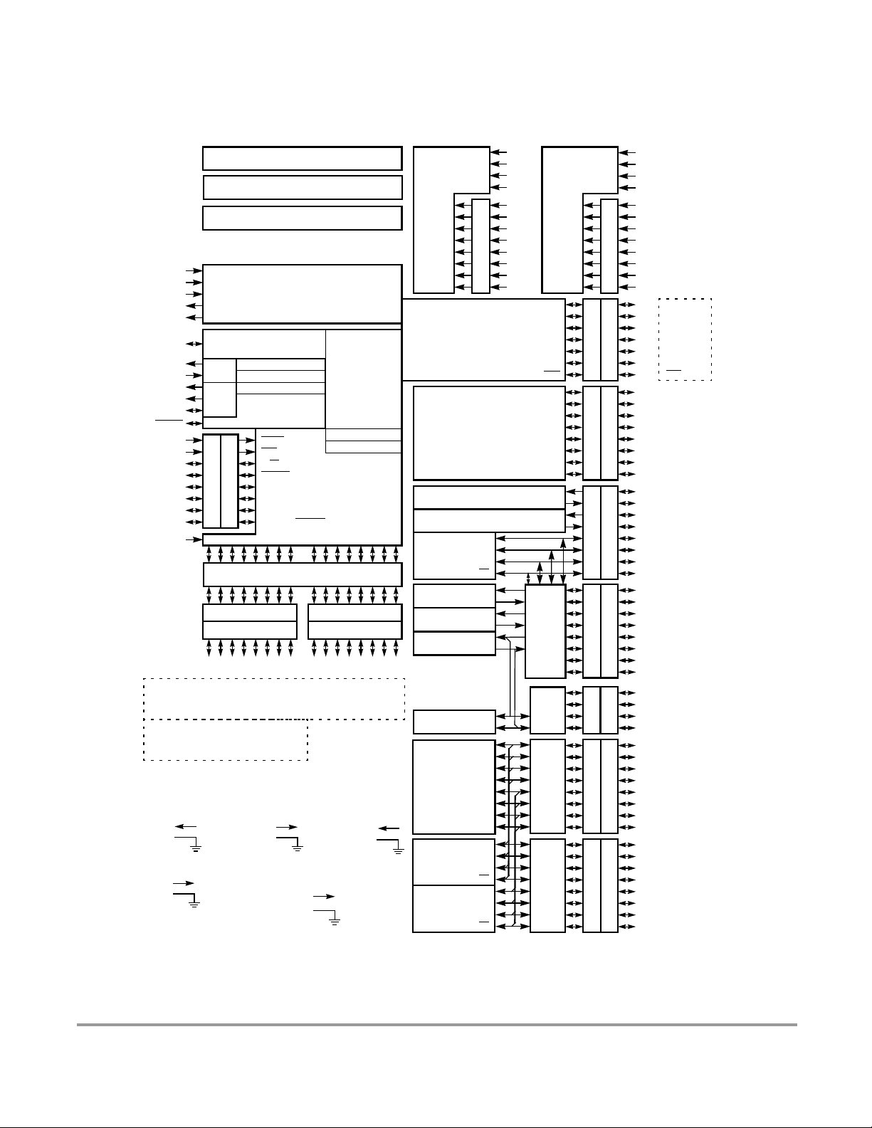
1.4 MC9S12KG(L)(C)128(64)(32) Block Diagram
VDDR
VSSR
VREGEN
VDD1,2
VSS1,2
BKGD
XTAL
EXTAL
VSSPLL
VDDPLL
XFC
RESET
PE0
PE1
PE2
PE3
PE4
PE5
PE6
PE7
TEST
Multiplexed
Wide Bus
Multiplexed
Narrow Bus
Single-wire BDM
OSC
PLL
PTE
PA7
PA6
ADDR15
ADDR14
DATA15
DATA14
DAT A7
DAT A6
Internal Logic 2.5V
V
DD1,2
V
SS1,2
Voltage Regulator 3.3V/5V
V
DDR
V
SSR
128K Byte Flash EEPROM
2K Byte EEPROM
8K Byte RAM
Voltage Regulator
Periodic Interrupt
COP Watchdog
Clock Monitor
CRG
XIRQ
IRQ
R/
W
LSTRB
ECLK
DDRE
MODA
MODB
NOACC/
XCLKS
CPU12
Breakpoints
Debugger
System
Integration
Module
(SIM)
Multiplexed Address/Data Bus
DDRA DDRB
PTA PTB
PA4
PA3
PA2
PA1
ADDR11
ADDR10
DATA11
DATA10
DAT A3
DAT A2
SSX
PA0
ADDR9
ADDR8
DAT A9
DAT A8
DAT A1
DAT A0
V
DDA
V
SSA
PB4
PB7
PB6
PB5
ADDR4
ADDR7
ADDR6
ADDR5
DAT A4
DAT A7
DAT A6
DAT A5
OSC/PLL 2.5V
V
DDPLL
V
SSPLL
PA5
ADDR12
ADDR13
DATA12
DATA13
DAT A4
DAT A5
I/O Driver 3.3V/5V
V
DDX
V
A/D Converter 3.3V/5V
Voltage Reference
PB3
PB2
ADDR3
ADDR2
DAT A3
DAT A2
PB1
PB0
ADDR1
ADDR0
DAT A1
DAT A0
ATD
AN08
AN09
AN10
AN11
AN12
AN13
AN14
AN15
PIX0
PIX1
PIX2
PIX3
PIX4
PIX5
ECS
IOC0
IOC1
IOC2
IOC3
IOC4
IOC5
IOC6
IOC7
RXD
TXD
RXD
TXD
Module to
Port Routing
KWJ0
KWJ1
KWJ6
KWJ7
KWP0
KWP1
KWP2
KWP3
KWP4
KWP5
KWP6
KWP7
KWH0
KWH1
KWH2
KWH3
KWH4
KWH5
KWH6
KWH7
PAD
PAD00
PAD01
PAD02
PAD03
PAD04
PAD05
PAD06
PAD07
AN00
AN01
AN02
AN03
AN04
AN05
AN06
AN07
PPAGE
TIM
SCI0
SCI1
MISO
MOSI
SPI0
CAN0
CAN4
IIC
PWM
SPI1
SPI2
SCK
SS
RxCAN
TxCAN PM1
RxCAN
TxCAN
SDA
SCL
PWM0
PWM1
PWM2
PWM3
PWM4
PWM5
PWM6
PWM7
MISO
MOSI
SCK
SS
MISO
MOSI
SCK
SS
VRH
VRL
VDDA
VSSA
DDRK
DDRT
DDRS
DDRM
DDRJ
DDRP
DDRH
PAD
PTK
PTT
PTS
PTM
PTJ
PTP
PTH
VRH
VRL
VDDA
VSSA
PAD08
PAD09
PAD10
PAD11
PAD12
PAD13
PAD14
PAD15
PK0
PK1
PK2
PK3
PK4
PK5
PK7
PT0
PT1
PT2
PT3
PT4
PT5
PT6
PT7
PS0
PS1
PS2
PS3
PS4
PS5
PS6
PS7
PM0
PM2
PM3
PM4
PM5
PM6
PM7
PJ0
PJ1
PJ6
PJ7
PP0
PP1
PP2
PP3
PP4
PP5
PP6
PP7
PH0
PH1
PH2
PH3
PH4
PH5
PH6
PH7
XADDR14
XADDR15
XADDR16
XADDR17
XADDR18
XADDR19
ECS
Signals shown in Bold are not available on n the 80 Pin Package
Figure 1-1 MC9S12KG(L)(C)128(64)(32) Block Diagram
Freescale Semiconductor
19
Page 20
Device User Guide — 9S12KT256DGV1/D V01.09
1.5 MC9S12KT(G)256 Block Diagram
VDDR
VSSR
VREGEN
VDD1,2
VSS1,2
BKGD
XTAL
EXTAL
VSSPLL
VDDPLL
XFC
RESET
PE0
PE1
PE2
PE3
PE4
PE5
PE6
PE7
TEST
Multiplexed
Wide Bus
Multiplexed
Narrow Bus
Single-wire BDM
OSC
PLL
PTE
PA7
PA6
ADDR15
ADDR14
DATA15
DATA14
DAT A7
DAT A6
Internal Logic 2.5V
V
DD1,2
V
SS1,2
Voltage Regulator 3.3V/5V
V
DDR
V
SSR
256K Byte Flash EEPROM
4K Byte EEPROM
12K Byte RAM
Voltage Regulator
Periodic Interrupt
COP Watchdog
Clock Monitor
CRG
XIRQ
IRQ
R/
W
LSTRB
ECLK
DDRE
MODA
MODB
NOACC/
XCLKS
CPU12
Breakpoints
Debugger
System
Integration
Module
(SIM)
Multiplexed Address/Data Bus
DDRA DDRB
PTA PTB
PA4
PA3
PA2
PA1
ADDR11
ADDR10
DATA11
DATA10
DAT A3
DAT A2
SSX
PA0
ADDR9
ADDR8
DAT A9
DAT A8
DAT A1
DAT A0
V
DDA
V
SSA
PB4
PB7
PB6
PB5
ADDR4
ADDR7
ADDR6
ADDR5
DAT A4
DAT A7
DAT A6
DAT A5
OSC/PLL 2.5V
V
DDPLL
V
SSPLL
PA5
ADDR12
ADDR13
DATA12
DATA13
DAT A4
DAT A5
I/O Driver 3.3V/5V
V
DDX
V
A/D Converter 3.3V/5V
Voltage Reference
PB3
PB2
ADDR3
ADDR2
DAT A3
DAT A2
PB1
PB0
ADDR1
ADDR0
DAT A1
DAT A0
VRH
ATD0
VRL
VDDA
VSSA
AN0
AN1
AN2
AN3
AN4
AN5
AN6
AN7
PPAGE
TIM
SCI0
SCI1
SPI0
RxCAN
CAN0
TxCAN PM1
RxCAN
CAN1
TxCAN
RxCAN
CAN4
TxCAN
IIC
PWM
SPI1
SPI2
MISO
MOSI
SCK
SS
SDA
SCL
PWM0
PWM1
PWM2
PWM3
PWM4
PWM5
PWM6
PWM7
MISO
MOSI
SCK
SS
MISO
MOSI
SCK
SS
AD0
VRH
VRL
VDDA
VSSA
PAD00
PAD01
PAD02
PAD03
PAD04
PAD05
PAD06
PAD07
ATD1
AN0
AN1
AN2
AN3
AN4
AN5
AN6
AN7
PIX0
PIX1
PIX2
PIX3
PIX4
PIX5
ECS
IOC0
IOC1
IOC2
IOC3
IOC4
IOC5
IOC6
IOC7
RXD
TXD
RXD
TXD
Module to
Port Routing
KWJ0
KWJ1
KWJ6
KWJ7
KWP0
KWP1
KWP2
KWP3
KWP4
KWP5
KWP6
KWP7
KWH0
KWH1
KWH2
KWH3
KWH4
KWH5
KWH6
KWH7
VRH
VRL
VDDA
VSSA
DDRK
DDRT
DDRS
DDRM
DDRJ
DDRP
DDRH
AD1
PTK
PTT
PTS
PTM
PTJ
PTP
PTH
VRH
VRL
VDDA
VSSA
PAD08
PAD09
PAD10
PAD11
PAD12
PAD13
PAD14
PAD15
PK0
PK1
PK2
PK3
PK4
PK5
PK7
PT0
PT1
PT2
PT3
PT4
PT5
PT6
PT7
PS0
PS1
PS2
PS3
PS4
PS5
PS6
PS7
PM0
PM2
PM3
PM4
PM5
PM6
PM7
PJ0
PJ1
PJ6
PJ7
PP0
PP1
PP2
PP3
PP4
PP5
PP6
PP7
PH0
PH1
PH2
PH3
PH4
PH5
PH6
PH7
XADDR14
XADDR15
XADDR16
XADDR17
XADDR18
XADDR19
ECS
Signals shown in Bold are not available on n the 80 Pin Package
20
Figure 1-2 MC9S12KT(G)256 Block Diagram
Freescale Semiconductor
Page 21
Device User Guide — 9S12KT256DGV1/D V01.09
1.6 Device Memory Map
Table 1-1 shows the device register map of the MC9S12KT256 and MC9S12KG256 after reset. Table
1-2 shows the device register map of the MC9S12KG128(64)(32), MC9S12KL128(64) and
MC9S12KC128(64) after reset.
Table 1-1 MC9S12KT(G)256 Device Memory Map
Address Module Size
$000 - $017 CORE (Ports A, B, E, Modes, Inits, Test) 24
$018 Reserved 1
$019 Voltage Regulator (VREG) 1
$01A - $01B Device ID register (PARTID) 2
$01C - $01F CORE (MEMSIZ, IRQ, HPRIO) 4
$020 - $02F CORE (DBG) 16
$030 - $033 CORE (PPAGE, Port K) 4
$034 - $03F Clock and Reset Generator (PLL, RTI, COP) 12
$040 - $06F Standard Timer 16-bit 8 channels (TIM) 48
$070 - $07F Reserved 16
$080 - $09F Analog to Digital Converter 10-bit 8 channels (ATD0) 32
$0A0 - $0C7 Reserved 40
$0C8 - $0CF Serial Communications Interface 0 (SCI0) 8
$0D0 - $0D7 Serial Communications Interface 1 (SCI1) 8
$0D8 - $0DF Serial Peripheral Interface 0 (SPI0) 8
$0E0 - $0E7 Inter Integrated Circuit Bus (IIC) 8
$0E8 - $0EF Reserved 8
$0F0 - $0F7 Serial Peripheral Interface 1 (SPI1) 8
$0F8 - $0FF Serial Peripheral Interface 2 (SPI2) 8
$100- $10F Flash Control Register 16
$110- $11B EEPROM Control Register 12
$11C - $11F Reserved 4
$120 - $13F Analog to Digital Converter 10-bit 8 channels (ATD1) 32
$140 - $17F Motorola Scalable Controller Area Network 0 (CAN0) 64
$180 - $1BF Motorola Scalable Controller Area Network 1 (CAN1) 64
$1C0 - $23F Reserved 128
$240 - $27F Port Integration Module (PIM) 64
$280 - $2BF Motorola Scalable Controller Area Network 4 (CAN4) 64
$2C0 - $2E7 Pulse Width Modulator 8-bit 8 channels (PWM) 40
$2E8 - $3FF Reserved 280
Freescale Semiconductor
21
Page 22
Device User Guide — 9S12KT256DGV1/D V01.09
Table 1-2 MC9S12KG(L)(C)128(64)(32) Device Memory Map
Address Module Size
$000 - $017 CORE (Ports A, B, E, Modes, Inits, Test) 24
$018 Reserved 1
$019 Voltage Regulator (VREG) 1
$01A - $01B Device ID register (PARTID) 2
$01C - $01F CORE (MEMSIZ, IRQ, HPRIO) 4
$020 - $02F CORE (DBG) 16
$030 - $033 CORE (PPAGE, Port K) 4
$034 - $03F Clock and Reset Generator (PLL, RTI, COP) 12
$040 - $06F Standard Timer 16-bit 8 channels (TIM) 48
$070 - $07F Reserved 16
$080 - $0AF Analog to Digital Converter 10-bit 16 channels (ATD) 48
$0B0 - $0C7 Reserved 24
$0C8 - $0CF Serial Communications Interface 0 (SCI0) 8
$0D0 - $0D7 Serial Communications Interface 1 (SCI1) 8
$0D8 - $0DF Serial Peripheral Interface 0 (SPI0) 8
$0E0 - $0E7 Inter Integrated Circuit Bus (IIC) 8
$0E8 - $0EF Reserved 8
$0F0 - $0F7 Serial Peripheral Interface 1 (SPI1) 8
$0F8 - $0FF Serial Peripheral Interface 2 (SPI2) 8
$100- $10F Flash Control Register 16
$110- $11B EEPROM Control Register 12
$11C - $13F Reserved 36
$140 - $17F Motorola Scalable Controller Area Network 0 (CAN0) 64
$180 - $23F Reserved 192
$240 - $27F Port Integration Module (PIM) 64
$280 - $2BF Motorola Scalable Controller Area Network 4 (CAN4) 64
$2C0 - $2E7 Pulse Width Modulator 8-bit 8 channels (PWM) 40
$2E8 - $3FF Reserved 280
22
Freescale Semiconductor
Page 23
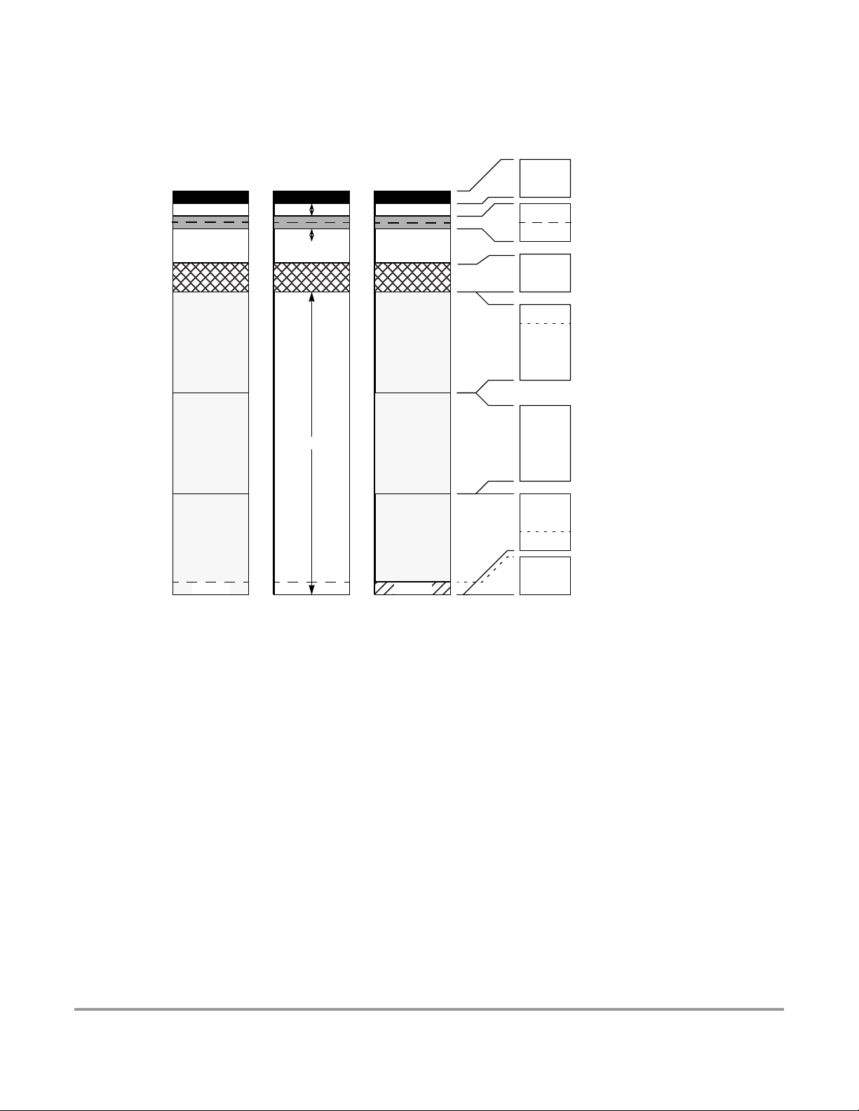
Device User Guide — 9S12KT256DGV1/D V01.09
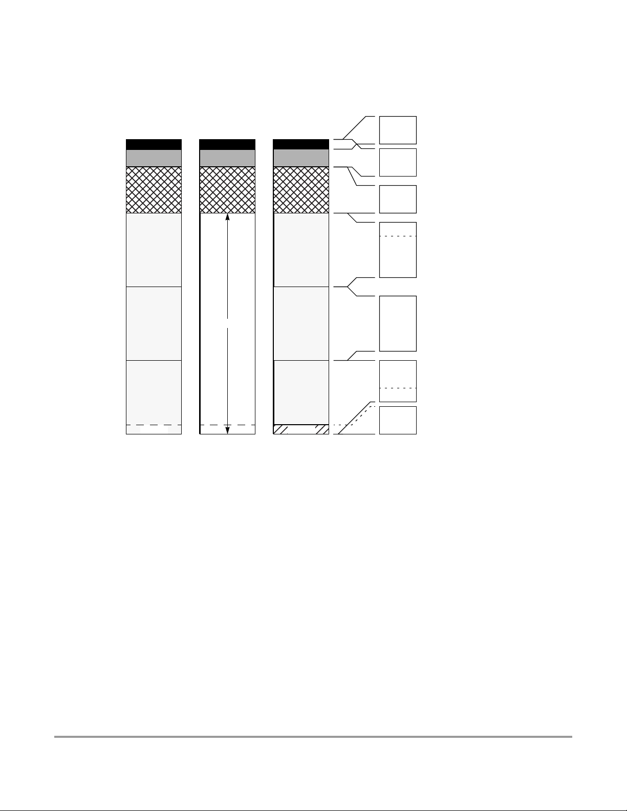
Figure 1-4 illustrates the full user configurable device memory map of MC9S12KT256 and
MC9S12KG256.
$0000
$0400
$1000
$4000
$8000
$C000
$FF00
$FFFF
NORMAL
SINGLE CHIP
EXT
VECTORSVECTORS VECTORS
EXPANDED SPECIAL
SINGLE CHIP
$0000
$03FF
$0000
$0FFF
$1000
$3FFF
$4000
$7FFF
$8000
$BFFF
$C000
$FFFF
$FF00
$FFFF
1K Register Space
Mappable to any 2K Boundary
4K Bytes EEPROM
Mappable to any 4K Boundary
12K Bytes RAM
Mappable to any 16K Boundary
and alignable to top or bottom
0.5K, 1K, 2K or 4K Protected Sector
16K Fixed Flash EEPROM
16K Page Window
sixteen * 16K Flash EEPROM Pages
16K Fixed Flash EEPROM
2K, 4K, 8K or 16K Protected Boot Sector
BDM
(If Active)
The figure shows a useful map, which is not the map out of reset. After reset the map is:
$0000 - $03FF: Register Space
$1000 - $3FFF: 12K RAM
$0000 - $0FFF: 4K EEPROM (1K hidden behind Register Space)
Figure 1-3 MC9S12KT256 and MC9S12KG256 Memory Map
Freescale Semiconductor
23
Page 24
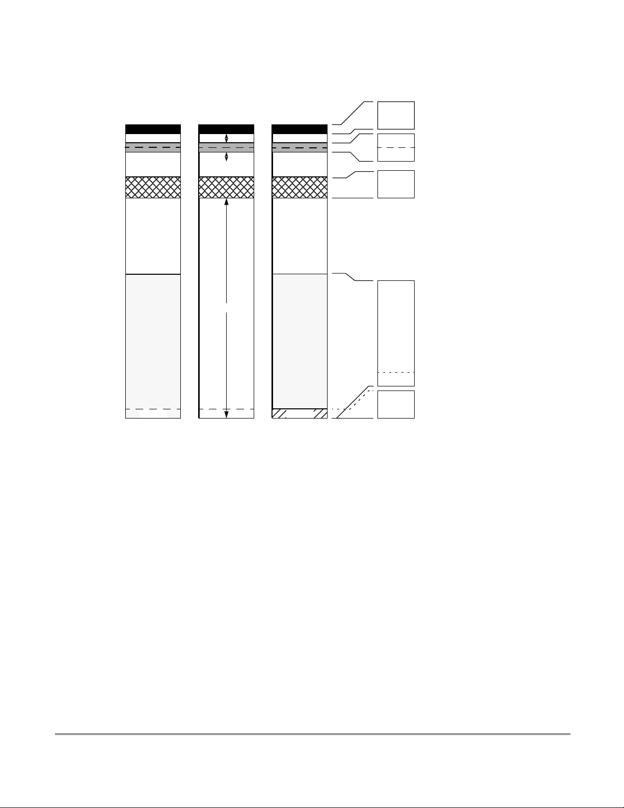
Device User Guide — 9S12KT256DGV1/D V01.09
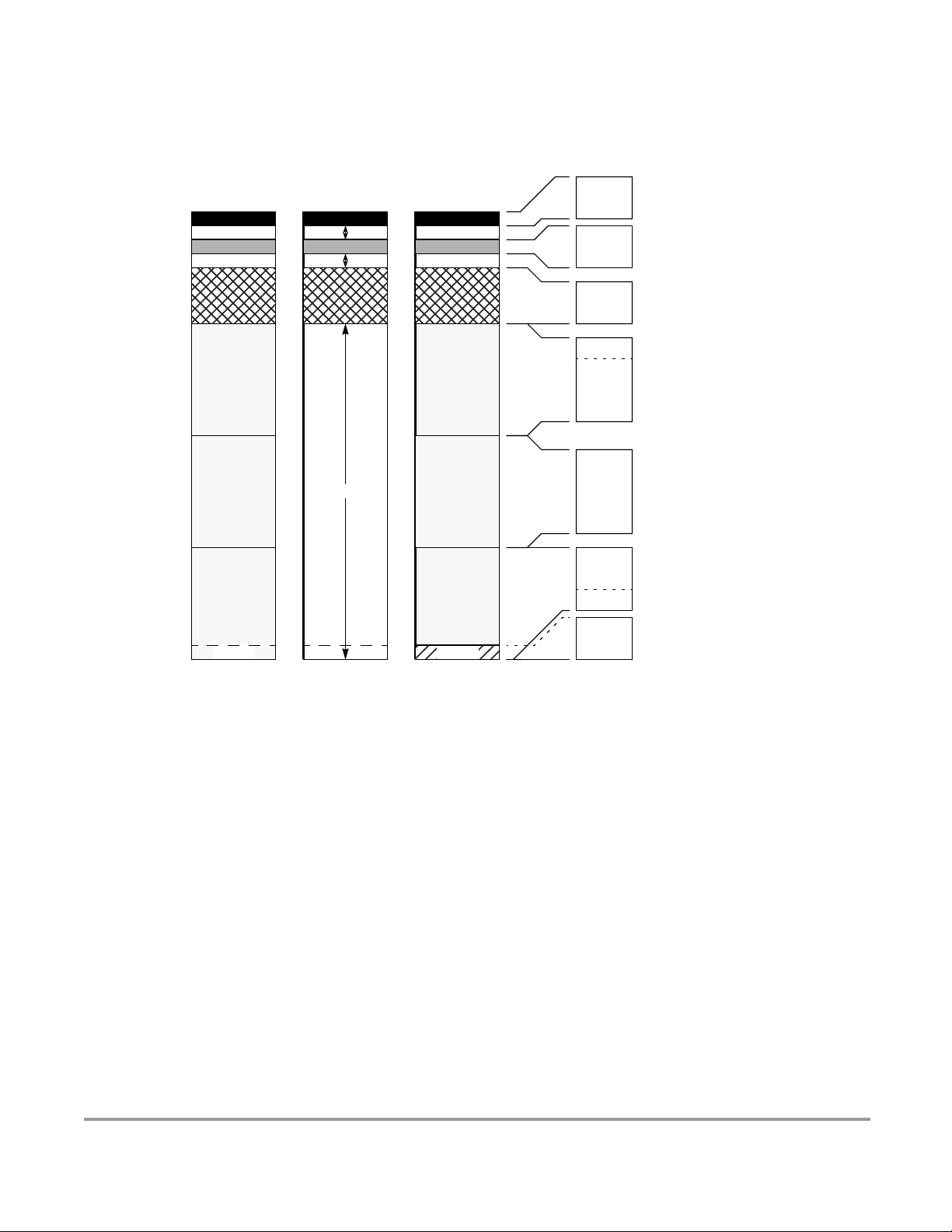
Figure 1-4 illustrates the full user configurable device memory map of MC9S12KG128, MC9S12KL128
and MC9S12KC128.
$0000
$0400
$0800
$1000
$2000
$4000
$8000
$C000
$FF00
$FFFF
NORMAL
SINGLE CHIP
EXT
VECTORSVECTORS VECTORS
EXPANDED SPECIAL
SINGLE CHIP
$0000
$03FF
$0800
$0FFF
$2000
$3FFF
$4000
$7FFF
$8000
$BFFF
$C000
$FFFF
$FF00
$FFFF
1K Register Space
Mappable to any 2K Boundary
2K Bytes EEPROM
Mappable to any 2K Boundary
8K Bytes RAM
Mappable to any 8K Boundary
0.5K, 1K, 2K or 4K Protected Sector
16K Fixed Flash EEPROM
16K Page Window
eight * 16K Flash EEPROM Pages
16K Fixed Flash EEPROM
2K, 4K, 8K or 16K Protected Boot Sector
BDM
(If Active)
The figure shows a useful map, which is not the map out of reset. After reset the map is:
$0000 - $03FF: Register Space
$0000 - $1FFF: 8K RAM (1K RAM hidden behind Register Space)
$0000 - $07FF: 2K EEPROM (not visible)
Figure 1-4 MC9S12KG128, MC9S12KL128 and MC9S12KC128 Memory Map
24
Freescale Semiconductor
Page 25
Device User Guide — 9S12KT256DGV1/D V01.09
Figure 1-5 illustrates the full user configurable device memory map of MC9S12KG64, MC9S12KL64
and MC9S12KC64.
$0000
$0400
$0800
$1000
$3000
$4000
$8000
$C000
$FF00
$FFFF
NORMAL
SINGLE CHIP
EXT
VECTORSVECTORS VECTORS
EXPANDED SPECIAL
SINGLE CHIP
$0000
$03FF
$0800
$0FFF
$3000
$3FFF
$4000
$7FFF
$8000
$BFFF
$C000
$FFFF
$FF00
$FFFF
1K Register Space
Mappable to any 2K Boundary
1K Bytes EEPROM
Mappable to any 2K Boundary
(1K mapped two times in 2K space)
4K Bytes RAM
Mappable to any 4K Boundary
0.5K, 1K, 2K or 4K Protected Sector
16K Fixed Flash EEPROM
16K Page Window
four * 16K Flash EEPROM Pages
16K Fixed Flash EEPROM
2K, 4K, 8K or 16K Protected Boot Sector
BDM
(If Active)
The figure shows a useful map, which is not the map out of reset. After reset the map is:
$0000 - $03FF: Register Space
$0000 - $0FFF: 4K RAM (1K RAM hidden behind Register Space)
$0000 - $03FF: 1K EEPROM (not visible)
Figure 1-5 MC9S12KG64, MC9S12KL64 and MC9S12KC64 Memory Map
Freescale Semiconductor
25
Page 26
Device User Guide — 9S12KT256DGV1/D V01.09
Figure 1-6 illustrates the full user configurable device memory map of MC9S12KG32.
$0000
$0400
$0800
$1000
$3800
$4000
$8000
$FF00
$FFFF
NORMAL
SINGLE CHIP
EXT
VECTORSVECTORS VECTORS
EXPANDED SPECIAL
SINGLE CHIP
$0000
$03FF
$0800
$0FFF
$3800
$3FFF
$8000
$FFFF
$FF00
$FFFF
1K Register Space
Mappable to any 2K Boundary
1K Bytes EEPROM
Mappable to any 2K Boundary
(1K mapped two times in 2K space)
2K Bytes RAM
Mappable to any 2K Boundary
32K Fixed Flash EEPROM
2K, 4K, 8K or 16K Protected Boot Sector
BDM
(If Active)
26
The figure shows a useful map, which is not the map out of reset. After reset the map is:
$0000 - $03FF: Register Space
$0000 - $07FF: 2K RAM (1K RAM hidden behind Register Space)
$0000 - $03FF: 1K EEPROM (not visible)
Figure 1-6 MC9S12KG32 Memory Map
Freescale Semiconductor
Page 27
Device User Guide — 9S12KT256DGV1/D V01.09
1.7 Detailed Register Map
The following tables show the detailed register map of the MC9S12K-Family.
$0000 - $000F MEBI map 1 of 3 (HCS12 Multiplexed External Bus Interface)
Address Name Bit 7 Bit 6 Bit 5 Bit 4 Bit 3 Bit 2 Bit 1 Bit 0
$0000 PORTA
$0001 PORTB
$0002 DDRA
$0003 DDRB
$0004 Reserved
$0005 Reserved
$0006 Reserved
$0007 Reserved
$0008 PORTE
$0009 DDRE
$000A PEAR
$000B MODE
$000C PUCR
$000D RDRIV
$000E EBICTL
$000F Reserved
Read:
Write:
Read:
Write:
Read:
Write:
Read:
Write:
Read: 0 0 0 0 0 0 0 0
Write:
Read: 0 0 0 0 0 0 0 0
Write:
Read: 0 0 0 0 0 0 0 0
Write:
Read: 0 0 0 0 0 0 0 0
Write:
Read:
Write:
Read:
Write:
Read:
Write:
Read:
Write:
Read:
Write:
Read:
Write:
Read: 0 0 0 0 0 0 0
Write:
Read: 0 0 0 0 0 0 0 0
Write:
Bit 7 6 5 4 3 2 1 Bit 0
Bit 7 6 5 4 3 2 1 Bit 0
Bit 7 6 5 4 3 2 1 Bit 0
Bit 7 6 5 4 3 2 1 Bit 0
Bit 7 6 5 4 3 2
Bit 7 6 5 4 3 Bit 2
NOACCE
MODC MODB MODA
PUPKE
RDPK
0
0 0
0 0
PIPOE NECLK LSTRE RDWE
0
PUPEE
RDPE
IVIS
0 0
0 0
0
Bit 1 Bit 0
0 0
0 0
EMK EME
PUPBE PUPAE
RDPB RDPA
ESTR
$0010 - $0014 MMC map 1 of 4 (HCS12 Module Mapping Control)
Address Name Bit 7 Bit 6 Bit 5 Bit 4 Bit 3 Bit 2 Bit 1 Bit 0
$0010 INITRM
$0011 INITRG
Freescale Semiconductor
Read:
Write:
Read: 0
Write:
RAM15 RAM14 RAM13 RAM12 RAM11
REG14 REG13 REG12 REG11
0 0
0 0 0
RAMHAL
27
Page 28
Device User Guide — 9S12KT256DGV1/D V01.09
$0010 - $0014 MMC map 1 of 4 (HCS12 Module Mapping Control)
Address Name Bit 7 Bit 6 Bit 5 Bit 4 Bit 3 Bit 2 Bit 1 Bit 0
$0012 INITEE
$0013 MISC
$0014
Reserved
Read:
Write:
Read: 0 0 0 0
Write:
Read: 0 0 0 0 0 0 0 0
Write:
EE15 EE14 EE13 EE12 EE11
EXSTR1 EXSTR0 ROMHM ROMON
0 0
$0015 - $0016 INT map 1 of 2 (HCS12 Interrupt)
Address Name Bit 7 Bit 6 Bit 5 Bit 4 Bit 3 Bit 2 Bit 1 Bit 0
$0015 ITCR
$0016 ITEST
Read: 0 0 0
Write:
Read:
Write:
INTE INTC INTA INT8 INT6 INT4 INT2 INT0
WRINT ADR3 ADR2 ADR1 ADR0
$0017 - $0017 MMC map 2 of 4 (HCS12 Module Mapping Control)
EEON
Address Name Bit 7 Bit 6 Bit 5 Bit 4 Bit 3 Bit 2 Bit 1 Bit 0
$0017 Reserved
Read: 0 0 0 0 0 0 0 0
Write:
$0018 - $0018 Miscellaneous Peripherals (Device Guide)
Address Name Bit 7 Bit 6 Bit 5 Bit 4 Bit 3 Bit 2 Bit 1 Bit 0
$0018 Reserved
Read: 0 0 0 0 0 0 0 0
Write:
$0019 - $0019 VREG3V3 (Voltage Regulator)
Address Name Bit 7 Bit 6 Bit 5 Bit 4 Bit 3 Bit 2 Bit 1 Bit 0
$0019 VREGCTRL
Read: 0 0 0 0 0 LVDS
Write:
LVIE LVIF
$001A - $001B Miscellaneous Peripherals (Device Guide)
Address Name Bit 7 Bit 6 Bit 5 Bit 4 Bit 3 Bit 2 Bit 1 Bit 0
$001A PARTIDH
$001B PARTIDL
Read: ID15 ID14 ID13 ID12 ID11 ID10 ID9 ID8
Write:
Read: ID7 ID6 ID5 ID4 ID3 ID2 ID1 ID0
Write:
28
Freescale Semiconductor
Page 29

Device User Guide — 9S12KT256DGV1/D V01.09
$001C - $001D MMC map 3 of 4 (HCS12 Module Mapping Control, Device
Guide)
Address Name Bit 7 Bit 6 Bit 5 Bit 4 Bit 3 Bit 2 Bit 1 Bit 0
$001C MEMSIZ0
$001D MEMSIZ1
Read: reg_sw0 0 eep_sw1 eep_sw0 0 ram_sw2 ram_sw1 ram_sw0
Write:
Read: rom_sw1 rom_sw0 0 0 0 0 pag_sw1 pag_sw0
Write:
$001E - $001E MEBI map 2 of 3 (HCS12 Multiplexed External Bus Interface)
Address Name Bit 7 Bit 6 Bit 5 Bit 4 Bit 3 Bit 2 Bit 1 Bit 0
$001E INTCR
Read:
Write:
IRQE IRQEN
0 0 0 0 0 0
$001F - $001F INT map 2 of 2 (HCS12 Interrupt)
Address Name Bit 7 Bit 6 Bit 5 Bit 4 Bit 3 Bit 2 Bit 1 Bit 0
$001F HPRIO
Read:
Write:
PSEL7 PSEL6 PSEL5 PSEL4 PSEL3 PSEL2 PSEL1
0
$0020 - $002F DBG (including BKP) map 1of 1 (HCS12 Debug)
Addres
s
$0020
$0021
$0022
$0023
$0024
$0025
$0026
$0027
$0028
$0029
$002A
$002B
Name Bit 7 Bit 6 Bit 5 Bit 4 Bit 3 Bit 2 Bit 1 Bit 0
DBGC1 read
-
write
DBGSC read
-
DBGTBH
-
DBGTBL read Bit 7 Bit 6 Bit 5 Bit 4 Bit 3 Bit 2 Bit 1 Bit 0
- write
DBGCNT read TBF 0 CNT
- write
DBGCCX read
- write
DBGCCH read
DBGCCL read
- write
write
read
write
write
DBGC2 read
BKPCT0
write
DBGC3 read
BKPCT1
DBGCAX
BKP0X
DBGCAH read
BKP0H write
write
read
write
DBGEN ARM TRGSEL BEGIN DBGBRK
AF BF CF 0
Bit 15 Bit 14 Bit 13 Bit 12 Bit 11 Bit 10 Bit 9 Bit 8
PAGSEL EXTCMP
Bit 15 14 13 12 11 10 9 Bit 8
Bit 7 6 5 4 3 2 1 Bit 0
BKABEN FULL BDM TAGAB BKCEN TAGC RWCEN RWC
BKAMBH BKAMBL BKBMBH BKBMBL RWAEN RWA RWBEN RWB
PAGSEL EXTCMP
Bit 15 14 13 12 11 10 9 Bit 8
0
TRG
CAPMOD
Freescale Semiconductor
29
Page 30
Device User Guide — 9S12KT256DGV1/D V01.09
$0020 - $002F DBG (including BKP) map 1of 1 (HCS12 Debug)
Addres
s
$002C
$002D
$002E
$002F
Name Bit 7 Bit 6 Bit 5 Bit 4 Bit 3 Bit 2 Bit 1 Bit 0
DBGCAL read
BKP0L write
DBGCBX read
BKP1X write
DBGCBH read
BKP1H write
DBGCBL read
BKP1L write
Bit 7 6 5 4 3 2 1 Bit 0
PAGSEL EXTCMP
Bit 15 14 13 12 11 10 9 Bit 8
Bit 7 6 5 4 3 2 1 Bit 0
$0030 - $0031 MMC map 4 of 4 (HCS12 Module Mapping Control)
Address Name Bit 7 Bit 6 Bit 5 Bit 4 Bit 3 Bit 2 Bit 1 Bit 0
$0030 PPAGE
$0031 Reserved
Read: 0 0
Write:
Read: 0 0 0 0 0 0 0 0
Write:
PIX5 PIX4 PIX3 PIX2 PIX1 PIX0
$0032 - $0033 MEBI map 3 of 3 (HCS12 Multiplexed External Bus Interface)
Address Name Bit 7 Bit 6 Bit 5 Bit 4 Bit 3 Bit 2 Bit 1 Bit 0
$0032 PORTK
$0033 DDRK
Read:
Write:
Read:
Write:
Bit 7 6 5 4 3 2 1 Bit 0
Bit 7 6 5 4 3 2 1 Bit 0
$0034 - $003F CRG (Clock and Reset Generator)
Address Name Bit 7 Bit 6 Bit 5 Bit 4 Bit 3 Bit 2 Bit 1 Bit 0
$0034 SYNR
$0035 REFDV
$0036
$0037 CRGFLG
$0038 CRGINT
$0039 CLKSEL
$003A PLLCTL
$003B RTICTL
$003C COPCTL
TEST ONLY
30
CTFLG
Read: 0 0
Write:
Read: 0 0 0 0
Write:
Read: TOUT7 TOUT6 TOUT5 TOUT4 TOUT3 TOUT2 TOUT1 TOUT0
Write:
Read:
Write:
Read:
Write:
Read:
Write:
Read:
Write:
Read: 0
Write:
Read:
Write:
RTIF PROF
RTIE
PLLSEL PSTP SYSWAI ROAWAI PLLWAI CWAI RTIWAI COPWAI
CME PLLON AUTO ACQ
WCOP RSBCK
0 0
RTR6 RTR5 RTR4 RTR3 RTR2 RTR1 RTR0
SYN5 SYN4 SYN3 SYN2 SYN1 SYN0
REFDV3 REFDV2 REFDV1 REFDV0
0
LOCKIF
LOCKIE
0 0 0
LOCK TRACK
0 0
0
PRE PCE SCME
CR2 CR1 CR0
SCMIF
SCMIE
Freescale Semiconductor
SCM
0
Page 31

Device User Guide — 9S12KT256DGV1/D V01.09
$0034 - $003F CRG (Clock and Reset Generator)
Address Name Bit 7 Bit 6 Bit 5 Bit 4 Bit 3 Bit 2 Bit 1 Bit 0
$003D
$003E
$003F ARMCOP
FORBYP
TEST ONLY
CTCTL
TEST ONLY
Read:
Write:
Read: TCTL7 TCTL6 TCTL5 TCTL4 TCLT3 TCTL2 TCTL1 TCTL0
Write:
Read: 0 0 0 0 0 0 0 0
Write: Bit 7 6 5 4 3 2 1 Bit 0
RTIBYP COPBYP
0
PLLBYP
0 0
FCM
$0040 - $006F TIM (Timer 16 Bit 8 Channels)
Address Name Bit 7 Bit 6 Bit 5 Bit 4 Bit 3 Bit 2 Bit 1 Bit 0
$0040 TIOS
$0041 CFORC
$0042 OC7M
$0043 OC7D
$0044 TCNT (hi)
$0045 TCNT (lo)
$0046 TSCR1
$0047 TTOV
$0048 TCTL1
$0049 TCTL2
$004A TCTL3
$004B TCTL4
$004C TIE
$004D TSCR2
$004E TFLG1
$004F TFLG2
$0050 TC0 (hi)
$0051 TC0 (lo)
$0052 TC1 (hi)
$0053 TC1 (lo)
Read:
Write:
Read: 0 0 0 0 0 0 0 0
Write: FOC7 FOC6 FOC5 FOC4 FOC3 FOC2 FOC1 FOC0
Read:
Write:
Read:
Write:
Read: Bit 15 14 13 12 11 10 9 Bit 8
Write:
Read: Bit 7 6 5 4 3 2 1 Bit 0
Write:
Read:
Write:
Read:
Write:
Read:
Write:
Read:
Write:
Read:
Write:
Read:
Write:
Read:
Write:
Read:
Write:
Read:
Write:
Read:
Write:
Read:
Write:
Read:
Write:
Read:
Write:
Read:
Write:
IOS7 IOS6 IOS5 IOS4 IOS3 IOS2 IOS1 IOS0
OC7M7 OC7M6 OC7M5 OC7M4 OC7M3 OC7M2 OC7M1 OC7M0
OC7D7 OC7D6 OC7D5 OC7D4 OC7D3 OC7D2 OC7D1 OC7D0
TEN TSWAI TSFRZ TFFCA
TOV7 TOV6 TOV5 TOV4 TOV3 TOV2 TOV1 TOV0
OM7 OL7 OM6 OL6 OM5 OL5 OM4 OL4
OM3 OL3 OM2 OL2 OM1 OL1 OM0 OL0
EDG7B EDG7A EDG6B EDG6A EDG5B EDG5A EDG4B EDG4A
EDG3B EDG3A EDG2B EDG2A EDG1B EDG1A EDG0B EDG0A
C7I C6I C5I C4I C3I C2I C1I C0I
TOI
C7F C6F C5F C4F C3F C2F C1F C0F
TOF
Bit 15 14 13 12 11 10 9 Bit 8
Bit 7 6 5 4 3 2 1 Bit 0
Bit 15 14 13 12 11 10 9 Bit 8
Bit 7 6 5 4 3 2 1 Bit 0
0 0 0
0 0 0 0 0 0 0
0 0 0 0
TCRE PR2 PR1 PR0
0
Freescale Semiconductor
31
Page 32

Device User Guide — 9S12KT256DGV1/D V01.09
$0040 - $006F TIM (Timer 16 Bit 8 Channels)
Address Name Bit 7 Bit 6 Bit 5 Bit 4 Bit 3 Bit 2 Bit 1 Bit 0
$0054 TC2 (hi)
$0055 TC2 (lo)
$0056 TC3 (hi)
$0057 TC3 (lo)
$0058 TC4 (hi)
$0059 TC4 (lo)
$005A TC5 (hi)
$005B TC5 (lo)
$005C TC6 (hi)
$005D TC6 (lo)
$005E TC7 (hi)
$005F TC7 (lo)
$0060 PACTL
$0061 PAFLG
$0062 PACNT (hi)
$0063 PACNT (lo)
$0064 Reserved
$0065 Reserved
$0066 Reserved
$0067 Reserved
$0068 Reserved
$0069 Reserved
$006A Reserved
$006B Reserved
$006C Reserved
Read:
Write:
Read:
Write:
Read:
Write:
Read:
Write:
Read:
Write:
Read:
Write:
Read:
Write:
Read:
Write:
Read:
Write:
Read:
Write:
Read:
Write:
Read:
Write:
Read: 0
Write:
Read: 0 0 0 0 0 0
Write:
Read:
Write:
Read:
Write:
Read: 0 0 0 0 0 0 0 0
Write:
Read: 0 0 0 0 0 0 0 0
Write:
Read: 0 0 0 0 0 0 0 0
Write:
Read: 0 0 0 0 0 0 0 0
Write:
Read: 0 0 0 0 0 0 0 0
Write:
Read: 0 0 0 0 0 0 0 0
Write:
Read: 0 0 0 0 0 0 0 0
Write:
Read: 0 0 0 0 0 0 0 0
Write:
Read: 0 0 0 0 0 0 0 0
Write:
Bit 15 14 13 12 11 10 9 Bit 8
Bit 7 6 5 4 3 2 1 Bit 0
Bit 15 14 13 12 11 10 9 Bit 8
Bit 7 6 5 4 3 2 1 Bit 0
Bit 15 14 13 12 11 10 9 Bit 8
Bit 7 6 5 4 3 2 1 Bit 0
Bit 15 14 13 12 11 10 9 Bit 8
Bit 7 6 5 4 3 2 1 Bit 0
Bit 15 14 13 12 11 10 9 Bit 8
Bit 7 6 5 4 3 2 1 Bit 0
Bit 15 14 13 12 11 10 9 Bit 8
Bit 7 6 5 4 3 2 1 Bit 0
PAEN PAMOD PEDGE CLK1 CLK0 PAOVI PAI
PAOVF PAIF
Bit 7 6 5 4 3 2 1 Bit 0
Bit 7 6 5 4 3 2 1 Bit 0
32
Freescale Semiconductor
Page 33

Device User Guide — 9S12KT256DGV1/D V01.09
$0040 - $006F TIM (Timer 16 Bit 8 Channels)
Address Name Bit 7 Bit 6 Bit 5 Bit 4 Bit 3 Bit 2 Bit 1 Bit 0
$006D Reserved
$006E Reserved
$006F Reserved
Read: 0 0 0 0 0 0 0 0
Write:
Read: 0 0 0 0 0 0 0 0
Write:
Read: 0 0 0 0 0 0 0 0
Write:
$0070 - $007F Reserved space
Address Name Bit 7 Bit 6 Bit 5 Bit 4 Bit 3 Bit 2 Bit 1 Bit 0
$0070
- $007F
Reserved
Read: 0 0 0 0 0 0 0 0
Write:
$0080 - $00AF ATD (Analog to Digital Converter 10 Bit 16 Channel)
Address Name Bit 7 Bit 6 Bit 5 Bit 4 Bit 3 Bit 2 Bit 1 Bit 0
$0080 ATDCTL0
$0081 ATDCTL1
$0082 ATDCTL2
$0083 ATDCTL3
$0084 ATDCTL4
$0085 ATDCTL5
$0086 ATDSTAT0
$0087 Reserved
$0088 ATDTEST0
$0089 ATDTEST1
$008A ATDSTAT0
$008B ATDSTAT1
$008C ATDDIEN1
$008D ATDDIEN0
$008E PORTAD1
$008F PORTAD0
Read: 0 0 0 0
Write:
Read:
ETRIGSEL
Write:
Read:
Write:
Read: 0
Write:
Read:
Write:
Read:
Write:
Read:
Write:
Read: 0 0 0 0 0 0 0 0
Write:
Read: 0 0 0 0 0 0 0 0
Write:
Read: 0 0 0 0 0 0 0
Write:
Read: CCF15 CCF14 CCF13 CCF12 CCF11 CCF10 CCF9 CCF8
Write:
Read: CCF7 CCF6 CCF5 CCF4 CCF3 CCF2 CCF1 CCF0
Write:
Read:
Write:
Read:
Write:
Read: PTAD15 PTAD14 PTAD13 PTAD12 PTAD11 PTAD10 PTAD9 PTAD8
Write:
Read: PTAD7 PTAD6 PTAD5 PTAD4 PTAD3 PTAD2 PTAD1 PTAD0
Write:
ADPU AFFC AWAI ETRIGLE ETRIGP ETRIG ASCIE
SRES8 SMP1 SMP0 PRS4 PRS3 PRS2 PRS1 PRS0
DJM DSGN SCAN MULT
SCF
IEN15 IEN14 IEN13 IEN12 IEN11 IEN10 IEN9 IEN8
IEN7 IEN6 IEN5 IEN4 IEN3 IEN2 IEN1 IEN0
0 0 0
S8C S4C S2C S1C FIFO FRZ1 FRZ0
0
ETORF FIFOR
WRAP3 WRAP2 WRAP1 WRAP0
ETRIGCH3 ETRIGCH2 ETRIGCH1 ETRIGCH0
0
0 CC2 CC1 CC0
CC CB CA
1
ASCIF
SC
Freescale Semiconductor
33
Page 34

Device User Guide — 9S12KT256DGV1/D V01.09
$0080 - $00AF ATD (Analog to Digital Converter 10 Bit 16 Channel)
Address Name Bit 7 Bit 6 Bit 5 Bit 4 Bit 3 Bit 2 Bit 1 Bit 0
$0090 ATDDR0H
$0091 ATDDR0L
$0092 ATDDR1H
$0093 ATDDR1L
$0094 ATDDR2H
$0095 ATDDR2L
$0096 ATDDR3H
$0097 ATDDR3L
$0098 ATDDR4H
$0099 ATDDR4L
$009A ATDDR5H
$009B ATDDR5L
$009C ATDDR6H
$009D ATDDR6L
$009E ATDDR7H
$009F ATDDR7L
$00A0 ATDDR8H
$00A1 ATDDR8L
$00A2 ATDDR9H
$00A3 ATDDR9L
$00A4 ATDDR10H
$00A5 ATDDR10L
$00A6 ATDDR11H
$00A7 ATDDR11L
$00A8 ATDDR12H
Read: Bit15 14 13 12 11 10 9 Bit8
Write:
Read: Bit7 Bit6 0 0 0 0 0 0
Write:
Read: Bit15 14 13 12 11 10 9 Bit8
Write:
Read: Bit7 Bit6 0 0 0 0 0 0
Write:
Read: Bit15 14 13 12 11 10 9 Bit8
Write:
Read: Bit7 Bit6 0 0 0 0 0 0
Write:
Read: Bit15 14 13 12 11 10 9 Bit8
Write:
Read: Bit7 Bit6 0 0 0 0 0 0
Write:
Read: Bit15 14 13 12 11 10 9 Bit8
Write:
Read: Bit7 Bit6 0 0 0 0 0 0
Write:
Read: Bit15 14 13 12 11 10 9 Bit8
Write:
Read: Bit7 Bit6 0 0 0 0 0 0
Write:
Read: Bit15 14 13 12 11 10 9 Bit8
Write:
Read: Bit7 Bit6 0 0 0 0 0 0
Write:
Read: Bit15 14 13 12 11 10 9 Bit8
Write:
Read: Bit7 Bit6 0 0 0 0 0 0
Write:
Read: Bit15 14 13 12 11 10 9 Bit8
Write:
Read: Bit7 Bit6 0 0 0 0 0 0
Write:
Read: Bit15 14 13 12 11 10 9 Bit8
Write:
Read: Bit7 Bit6 0 0 0 0 0 0
Write:
Read: Bit15 14 13 12 11 10 9 Bit8
Write:
Read: Bit7 Bit6 0 0 0 0 0 0
Write:
Read: Bit15 14 13 12 11 10 9 Bit8
Write:
Read: Bit7 Bit6 0 0 0 0 0 0
Write:
Read: Bit15 14 13 12 11 10 9 Bit8
Write:
1
34
Freescale Semiconductor
Page 35

Device User Guide — 9S12KT256DGV1/D V01.09
$0080 - $00AF ATD (Analog to Digital Converter 10 Bit 16 Channel)
Address Name Bit 7 Bit 6 Bit 5 Bit 4 Bit 3 Bit 2 Bit 1 Bit 0
$00A9 ATDDR12L
$00AA ATDDR13H
$00AB ATDDR13L
$00AC ATDDR14H
$00AD ATDDR14L
$00AE ATDDR15H
$00AF ATDDR15L
NOTES:
1. Registers only available on MC9S12KG128(64)(32), MC9S12KL128(64) and MC9S12KC128(64)
$00B0 - $00C7 Reserved space
Address Name Bit 7 Bit 6 Bit 5 Bit 4 Bit 3 Bit 2 Bit 1 Bit 0
$00B0
- $00C7
NOTES:
1. Reserved space for MC9S12KG128(64)(32), MC9S12KL128(64) and MC9S12KC128(64)
Reserved
Read: Bit7 Bit6 0 0 0 0 0 0
Write:
Read: Bit15 14 13 12 11 10 9 Bit8
Write:
Read: Bit7 Bit6 0 0 0 0 0 0
Write:
Read: Bit15 14 13 12 11 10 9 Bit8
Write:
Read: Bit7 Bit6 0 0 0 0 0 0
Write:
Read: Bit15 14 13 12 11 10 9 Bit8
Write:
Read: Bit7 Bit6 0 0 0 0 0 0
Write:
1
Read: 0 0 0 0 0 0 0 0
Write:
1
$0080 - $009F ATD0 (Analog to Digital Converter 10 Bit 8 Channel)
Address Name Bit 7 Bit 6 Bit 5 Bit 4 Bit 3 Bit 2 Bit 1 Bit 0
$0080 ATD0CTL0
$0081 ATD0CTL1
$0082 ATD0CTL2
$0083 ATD0CTL3
$0084 ATD0CTL4
$0085 ATD0CTL5
$0086 ATD0STAT0
$0087 Reserved
$0088 ATD0TEST0
$0089 ATD0TEST1
Read: 0 0 0 0 0
Write:
Read:
ETRIGSEL
Write:
Read:
Write:
Read: 0
Write:
Read:
Write:
Read:
Write:
Read:
Write:
Read: 0 0 0 0 0 0 0 0
Write:
Read: 0 0 0 0 0 0 0 0
Write:
Read: 0 0 0 0 0
Write:
ADPU AFFC AWAI ETRIGLE ETRIGP ETRIG ASCIE
SRES8 SMP1 SMP0 PRS4 PRS3 PRS2 PRS1 PRS0
DJM DSGN SCAN MULT
SCF
0 0 0 0
S8C S4C S2C S1C FIFO FRZ1 FRZ0
0
ETORF FIFOR
WRAP2 WRAP1 WRAP0
ETRIGCH2 ETRIGCH1 ETRIGCH0
0
0 CC2 CC1 CC0
CC CB CA
0
1
ASCIF
0
SC
Freescale Semiconductor
35
Page 36

Device User Guide — 9S12KT256DGV1/D V01.09
$0080 - $009F ATD0 (Analog to Digital Converter 10 Bit 8 Channel)
Address Name Bit 7 Bit 6 Bit 5 Bit 4 Bit 3 Bit 2 Bit 1 Bit 0
$008A Reserved
$008B ATD0STAT1
$008C Reserved
$008D ATD0DIEN
$008E Reserved
$008F PORTAD0
$0090 ATD0DR0H
$0091 ATD0DR0L
$0092 ATD0DR1H
$0093 ATD0DR1L
$0094 ATD0DR2H
$0095 ATD0DR2L
$0096 ATD0DR3H
$0097 ATD0DR3L
$0098 ATD0DR4H
$0099 ATD0DR4L
$009A ATD0DR5H
$009B ATD0DR5L
$009C ATD0DR6H
$009D ATD0DR6L
$009E ATD0DR7H
$009F ATD0DR7L
NOTES:
1. Registers only available on MC9S12KT256 and MC9S12KG256
Read: 0 0 0 0 0 0 0 0
Write:
Read: CCF7 CCF6 CCF5 CCF4 CCF3 CCF2 CCF1 CCF0
Write:
Read: 0 0 0 0 0 0 0 0
Write:
Read:
Write:
Read: 0 0 0 0 0 0 0 0
Write:
Read: PTAD7 PTAD6 PTAD5 PTAD4 PTAD3 PTAD2 PTAD1 PTAD0
Write:
Read: Bit15 14 13 12 11 10 9 Bit8
Write:
Read: Bit7 Bit6 0 0 0 0 0 0
Write:
Read: Bit15 14 13 12 11 10 9 Bit8
Write:
Read: Bit7 Bit6 0 0 0 0 0 0
Write:
Read: Bit15 14 13 12 11 10 9 Bit8
Write:
Read: Bit7 Bit6 0 0 0 0 0 0
Write:
Read: Bit15 14 13 12 11 10 9 Bit8
Write:
Read: Bit7 Bit6 0 0 0 0 0 0
Write:
Read: Bit15 14 13 12 11 10 9 Bit8
Write:
Read: Bit7 Bit6 0 0 0 0 0 0
Write:
Read: Bit15 14 13 12 11 10 9 Bit8
Write:
Read: Bit7 Bit6 0 0 0 0 0 0
Write:
Read: Bit15 14 13 12 11 10 9 Bit8
Write:
Read: Bit7 Bit6 0 0 0 0 0 0
Write:
Read: Bit15 14 13 12 11 10 9 Bit8
Write:
Read: Bit7 Bit6 0 0 0 0 0 0
Write:
IEN7 IEN6 IEN5 IEN4 IEN3 IEN2 IEN1 IEN0
1
36
Freescale Semiconductor
Page 37

Device User Guide — 9S12KT256DGV1/D V01.09
$00A0 - $00C7 Reserved space
Address Name Bit 7 Bit 6 Bit 5 Bit 4 Bit 3 Bit 2 Bit 1 Bit 0
$00A0
- $00C7
NOTES:
1. Reserved space for MC9S12KT256 and MC9S12KG256
Reserved
Read: 0 0 0 0 0 0 0 0
Write:
1
$00C8 - $00CF SCI0 (Asynchronous Serial Interface)
Address Name Bit 7 Bit 6 Bit 5 Bit 4 Bit 3 Bit 2 Bit 1 Bit 0
$00C8 SCI0BDH
$00C9 SCI0BDL
$00CA SCI0CR1
$00CB SCI0CR2
$00CC SCI0SR1
$00CD SCI0SR2
$00CE SCI0DRH
$00CF SCI0DRL
Read: 0 0 0
Write:
Read:
Write:
Read:
Write:
Read:
Write:
Read: TDRE TC RDRF IDLE OR NF FE PF
Write:
Read: 0 0 0 0 0
Write:
Read: R8
Write:
Read: R7 R6 R5 R4 R3 R2 R1 R0
Write: T7 T6 T5 T4 T3 T2 T1 T0
SBR7 SBR6 SBR5 SBR4 SBR3 SBR2 SBR1 SBR0
LOOPS SCISWAI RSRC M WAKE ILT PE PT
TIE TCIE RIE ILIE TE RE RWU SBK
T8
0 0 0 0 0 0
SBR12 SBR11 SBR10 SBR9 SBR8
BRK13 TXDIR
RAF
$00D0 - $00D7 SCI1 (Asynchronous Serial Interface)
Address Name Bit 7 Bit 6 Bit 5 Bit 4 Bit 3 Bit 2 Bit 1 Bit 0
$00D0 SCI1BDH
$00D1 SCI1BDL
$00D2 SCI1CR1
$00D3 SCI1CR2
$00D4 SCI1SR1
$00D5 SCI1SR2
$00D6 SCI1DRH
$00D7 SCI1DRL
Read: 0 0 0
Write:
Read:
Write:
Read:
Write:
Read:
Write:
Read: TDRE TC RDRF IDLE OR NF FE PF
Write:
Read: 0 0 0 0 0
Write:
Read: R8
Write:
Read: R7 R6 R5 R4 R3 R2 R1 R0
Write: T7 T6 T5 T4 T3 T2 T1 T0
SBR7 SBR6 SBR5 SBR4 SBR3 SBR2 SBR1 SBR0
LOOPS SCISWAI RSRC M WAKE ILT PE PT
TIE TCIE RIE ILIE TE RE RWU SBK
T8
0 0 0 0 0 0
SBR12 SBR11 SBR10 SBR9 SBR8
BRK13 TXDIR
RAF
Freescale Semiconductor
37
Page 38

Device User Guide — 9S12KT256DGV1/D V01.09
$00D8 - $00DF SPI0 (Serial Peripheral Interface)
Address Name Bit 7 Bit 6 Bit 5 Bit 4 Bit 3 Bit 2 Bit 1 Bit 0
$00D8 SPI0CR1
$00D9 SPI0CR2
$00DA SPI0BR
$00DB SPI0SR
$00DC Reserved
$00DD SPI0DR
$00DE Reserved
$00DF Reserved
Read:
Write:
Read: 0 0 0
Write:
Read: 0
Write:
Read: SPIF 0 SPTEF MODF 0 0 0 0
Write:
Read: 0 0 0 0 0 0 0 0
Write:
Read:
Write:
Read: 0 0 0 0 0 0 0 0
Write:
Read: 0 0 0 0 0 0 0 0
Write:
SPIE SPE SPTIE MSTR CPOL CPHA SSOE LSBFE
MODFEN BIDIROE
SPPR2 SPPR1 SPPR0
Bit7 6 5 4 3 2 1 Bit0
0
0
SPISWAI SPC0
SPR2 SPR1 SPR0
$00E0 - $00E7 IIC (Inter IC Bus)
Address Name Bit 7 Bit 6 Bit 5 Bit 4 Bit 3 Bit 2 Bit 1 Bit 0
$00E0 IBAD
$00E1 IBFD
$00E2 IBCR
$00E3 IBSR
$00E4 IBDR
$00E5 Reserved
$00E6 Reserved
$00E7 Reserved
Read:
Write:
Read:
Write:
Read:
Write: RSTA
Read: TCF IAAS IBB
Write:
Read:
Write:
Read: 0 0 0 0 0 0 0 0
Write:
Read: 0 0 0 0 0 0 0 0
Write:
Read: 0 0 0 0 0 0 0 0
Write:
ADR7 ADR6 ADR5 ADR4 ADR3 ADR2 ADR1 0
IBC7 IBC6 IBC5 IBC4 IBC3 IBC2 IBC1 IBC0
IBEN IBIE MS/SL TX/RX TXAK
IBAL
D7 D6 D5 D4 D3 D2 D1 D 0
0 SRW
0 0
IBIF
IBSWAI
RXAK
$00E8 - $00EF Reserved space
Address Name Bit 7 Bit 6 Bit 5 Bit 4 Bit 3 Bit 2 Bit 1 Bit 0
$00E8
- $00EF
Reserved
Read: 0 0 0 0 0 0 0 0
Write:
38
Freescale Semiconductor
Page 39

Device User Guide — 9S12KT256DGV1/D V01.09
$00F0 - $00F7 SPI1 (Serial Peripheral Interface)
Address Name Bit 7 Bit 6 Bit 5 Bit 4 Bit 3 Bit 2 Bit 1 Bit 0
$00F0 SPI1CR1
$00F1 SPI1CR2
$00F2 SPI1BR
$00F3 SPI1SR
$00F4 Reserved
$00F5 SPI1DR
$00F6 Reserved
$00F7 Reserved
Read:
Write:
Read: 0 0 0
Write:
Read: 0
Write:
Read: SPIF 0 SPTEF MODF 0 0 0 0
Write:
Read: 0 0 0 0 0 0 0 0
Write:
Read:
Write:
Read: 0 0 0 0 0 0 0 0
Write:
Read: 0 0 0 0 0 0 0 0
Write:
SPIE SPE SPTIE MSTR CPOL CPHA SSOE LSBFE
MODFEN BIDIROE
SPPR2 SPPR1 SPPR0
Bit7 6 5 4 3 2 1 Bit0
0
0
SPISWAI SPC0
SPR2 SPR1 SPR0
$00F8 - $00FF SPI2 (Serial Peripheral Interface)
Address Name Bit 7 Bit 6 Bit 5 Bit 4 Bit 3 Bit 2 Bit 1 Bit 0
$00F8 SPI2CR1
$00F9 SPI2CR2
$00FA SPI2BR
$00FB SPI2SR
$00FC Reserved
$00FD SPI2DR
$00FE Reserved
$00FF Reserved
Read:
Write:
Read: 0 0 0
Write:
Read: 0
Write:
Read: SPIF 0 SPTEF MODF 0 0 0 0
Write:
Read: 0 0 0 0 0 0 0 0
Write:
Read:
Write:
Read: 0 0 0 0 0 0 0 0
Write:
Read: 0 0 0 0 0 0 0 0
Write:
SPIE SPE SPTIE MSTR CPOL CPHA SSOE LSBFE
MODFEN BIDIROE
SPPR2 SPPR1 SPPR0
Bit7 6 5 4 3 2 1 Bit0
0
0
SPISWAI SPC0
SPR2 SPR1 SPR0
$0100 - $010F Flash Control Register
Address Name Bit 7 Bit 6 Bit 5 Bit 4 Bit 3 Bit 2 Bit 1 Bit 0
$0100 FCLKDIV
$0101 FSEC
$0102 FTSTMOD
$0103 FCNFG
Read: FDIVLD
Write:
Read: KEYEN RNV5 RNV4 RNV3 RNV2 SEC
Write:
Read: 0 0 0
Write:
Read:
Write:
CBEIE CCIE KEYACC
PRDIV8 FDIV5 FDIV4 FDIV3 FDIV2 FDIV1 FDIV0
WRALL
0
1
FDFD
DFDIE
0 0 0
0 0
BKSEL
(1)
Freescale Semiconductor
39
Page 40

Device User Guide — 9S12KT256DGV1/D V01.09
$0100 - $010F Flash Control Register
Address Name Bit 7 Bit 6 Bit 5 Bit 4 Bit 3 Bit 2 Bit 1 Bit 0
$0104 FPROT
$0105 FSTAT
$0106 FCMD
$0107
$0108 FADDRHI
$0109 FADDRLO
$010A FDATAHI
$010B FDATALO
$010C Reserved
$010D Reserved
$010E Reserved
$010F Reserved
NOTES:
1. Bit only available on MC9S12KT256 and MC9S12KG256.
2. Register only available on MC9S12KT256 and MC9S12KG256.
FCTL
Read:
FPOPEN
Write:
Read:
Write:
Read: 0
Write:
Read: NV7 NV6 NV5 NV4 NV3 NV2 NV1 NV0
2
Write:
Read: FADDRHI
Write:
Read: FADDRLO
Write:
Read: FDATAHI
Write:
Read: FDATALO
Write:
Read: 0 0 0 0 0 0 0 0
Write:
Read: 0 0 0 0 0 0 0 0
Write:
Read: 0 0 0 0 0 0 0 0
Write:
Read: 0 0 0 0 0 0 0 0
Write:
CBEIF
RNV6
CCIF
FPHDIS FPHS FPLDIS FPLS
PVIOL ACCERR DFDIF
CMDB
BLANK 0 0
$0110 - $011B EEPROM Control Register
Address Name Bit 7 Bit 6 Bit 5 Bit 4 Bit 3 Bit 2 Bit 1 Bit 0
$0110 ECLKDIV
$0111 Reserved
$0112
$0113 ECNFG
$0114 EPROT
$0115 ESTAT
$0116 ECMD
$0117
$0118 EADDRHI
Reserved for
Factory Test
Reserved for
Factory Test
40
Read: EDIVLD
Write:
Read: 0 0 0 0 0 0 0 0
Write:
Read: 0 0 0 0 0 0 0 0
Write:
Read:
Write:
Read:
Write:
Read:
Write:
Read: 0
Write:
Read: 0 0 0 0 0 0 0 0
Write:
Read: 0 0 0 0 0
Write:
CBEIE CCIE
EPOPEN
CBEIF
PRDIV8 EDIV5 EDIV4 EDIV3 EDIV2 EDIV1 EDIV0
0 0 0 0 0 0
NV6 NV5 NV4
CCIF
CMDB6 CMDB5
PVIOL ACCERR
0 0
EPDIS EP2 EP1 EP0
0
BLANK
CMDB2
10 9 Bit 8
0 0
0
Freescale Semiconductor
CMDB0
Page 41

Device User Guide — 9S12KT256DGV1/D V01.09
$0110 - $011B EEPROM Control Register
Address Name Bit 7 Bit 6 Bit 5 Bit 4 Bit 3 Bit 2 Bit 1 Bit 0
$0119 EADDRLO
$011A EDATAHI
$011B EDATALO
Read:
Write:
Read:
Write:
Read:
Write:
Bit 7 6 5 4 3 2 1 Bit 0
Bit 15 14 13 12 11 10 9 Bit 8
Bit 7 6 5 4 3 2 1 Bit 0
$011C - $011F Reserved space
Address Name Bit 7 Bit 6 Bit 5 Bit 4 Bit 3 Bit 2 Bit 1 Bit 0
$011C
- $011F
Reserved
Read: 0 0 0 0 0 0 0 0
Write:
$0120 - $013F ATD1 (Analog to Digital Converter 10 Bit 8 Channel)
Address Name Bit 7 Bit 6 Bit 5 Bit 4 Bit 3 Bit 2 Bit 1 Bit 0
$0120 ATD1CTL0
$0121 ATD1CTL1
$0122 ATD1CTL2
$0123 ATD1CTL3
$0124 ATD1CTL4
$0125 ATD1CTL5
$0126 ATD1STAT0
$0127 Reserved
$0128 ATD1TEST0
$0129 ATD1TEST1
$012A Reserved
$012B ATD1STAT1
$012C Reserved
$012D ATD1DIEN
$012E Reserved
$012F PORTAD1
Read: 0 0 0 0 0
Write:
Read:
ETRIGSEL
Write:
Read:
Write:
Read: 0
Write:
Read:
Write:
Read:
Write:
Read:
Write:
Read: 0 0 0 0 0 0 0 0
Write:
Read: 0 0 0 0 0 0 0 0
Write:
Read: 0 0 0 0 0
Write:
Read: 0 0 0 0 0 0 0 0
Write:
Read: CCF7 CCF6 CCF5 CCF4 CCF3 CCF2 CCF1 CCF0
Write:
Read: 0 0 0 0 0 0 0 0
Write:
Read:
Write:
Read: 0 0 0 0 0 0 0 0
Write:
Read: PTAD7 PTAD6 PTAD5 PTAD4 PTAD3 PTAD2 PTAD1 PTAD0
Write:
ADPU AFFC AWAI ETRIGLE ETRIGP ETRIG ASCIE
SRES8 SMP1 SMP0 PRS4 PRS3 PRS2 PRS1 PRS0
DJM DSGN SCAN MULT
SCF
IEN7 IEN6 IEN5 IEN4 IEN3 IEN2 IEN1 IEN0
0 0 0 0
S8C S4C S2C S1C FIFO FRZ1 FRZ0
0
ETORF FIFOR
WRAP2 WRAP1 WRAP0
ETRIGCH2 ETRIGCH1 ETRIGCH0
0
0 CC2 CC1 CC0
CC CB CA
0
1
ASCIF
0
SC
Freescale Semiconductor
41
Page 42

Device User Guide — 9S12KT256DGV1/D V01.09
$0120 - $013F ATD1 (Analog to Digital Converter 10 Bit 8 Channel)
Address Name Bit 7 Bit 6 Bit 5 Bit 4 Bit 3 Bit 2 Bit 1 Bit 0
$0130 ATD1DR0H
$0131 ATD1DR0L
$0132 ATD1DR1H
$0133 ATD1DR1L
$0134 ATD1DR2H
$0135 ATD1DR2L
$0136 ATD1DR3H
$0137 ATD1DR3L
$0138 ATD1DR4H
$0139 ATD1DR4L
$013A ATD1DR5H
$013B ATD1DR5L
$013C ATD1DR6H
$013D ATD1DR6L
$013E ATD1DR7H
$013F ATD1DR7L
NOTES:
1. Registers only available on MC9S12KT256 and MC9S12KG256. Reserved space for MC9S12KG128(64)(32),
MC9S12KL128(64) and MC9S12KC128(64).
Read: Bit15 14 13 12 11 10 9 Bit8
Write:
Read: Bit7 Bit6 0 0 0 0 0 0
Write:
Read: Bit15 14 13 12 11 10 9 Bit8
Write:
Read: Bit7 Bit6 0 0 0 0 0 0
Write:
Read: Bit15 14 13 12 11 10 9 Bit8
Write:
Read: Bit7 Bit6 0 0 0 0 0 0
Write:
Read: Bit15 14 13 12 11 10 9 Bit8
Write:
Read: Bit7 Bit6 0 0 0 0 0 0
Write:
Read: Bit15 14 13 12 11 10 9 Bit8
Write:
Read: Bit7 Bit6 0 0 0 0 0 0
Write:
Read: Bit15 14 13 12 11 10 9 Bit8
Write:
Read: Bit7 Bit6 0 0 0 0 0 0
Write:
Read: Bit15 14 13 12 11 10 9 Bit8
Write:
Read: Bit7 Bit6 0 0 0 0 0 0
Write:
Read: Bit15 14 13 12 11 10 9 Bit8
Write:
Read: Bit7 Bit6 0 0 0 0 0 0
Write:
1
$0140 - $017F CAN0 (Motorola Scalable CAN - MSCAN)
Address Name Bit 7 Bit 6 Bit 5 Bit 4 Bit 3 Bit 2 Bit 1 Bit 0
$0140 CAN0CTL0
$0141 CAN0CTL1
$0142 CAN0BTR0
$0143 CAN0BTR1
$0144 CAN0RFLG
42
Read:
Write:
Read:
Write:
Read:
Write:
Read:
Write:
Read:
Write:
RXFRM
CANE CLKSRC LOOPB LISTEN
SJW1 SJW0 BRP5 BRP4 BRP3 BRP2 BRP1 BRP0
SAMP TSEG22 TSEG21 TSEG20 TSEG13 TSEG12 TSEG11 TSEG10
WUPIF CSCIF
RXACT
CSWAI
RSTAT1 RSTAT0 TSTAT1 TSTAT0
SYNCH
TIME WUPE SLPRQ INITRQ
0
WUPM
Freescale Semiconductor
SLPAK INITAK
OVRIF RXF
Page 43

Device User Guide — 9S12KT256DGV1/D V01.09
$0140 - $017F CAN0 (Motorola Scalable CAN - MSCAN)
Address Name Bit 7 Bit 6 Bit 5 Bit 4 Bit 3 Bit 2 Bit 1 Bit 0
$0145 CAN0RIER
$0146 CAN0TFLG
$0147 CAN0TIER
$0148 CAN0TARQ
$0149 CAN0TAAK
$014A CAN0TBSEL
$014B CAN0IDAC
$014C Reserved
$014D Reserved
$014E
$014F CAN0TXERR
$0150 -
$0153
$0154 -
$0157
$0158 -
$015B
$015C -
$015F
$0160 -
$016F
$0170 -
$017F
CAN0RXERR
CAN0IDAR0 -
CAN0IDAR3
CAN0IDMR0 -
CAN0IDMR3
CAN0IDAR4 -
CAN0IDAR7
CAN0IDMR4 -
CAN0IDMR7
CAN0RXFG
CAN0TXFG
Read:
Write:
Read: 0 0 0 0 0
Write:
Read: 0 0 0 0 0
Write:
Read: 0 0 0 0 0
Write:
Read: 0 0 0 0 0 ABTAK2 ABTAK1 ABTAK0
Write:
Read: 0 0 0 0 0
Write:
Read: 0 0
Write:
Read: 0 0 0 0 0 0 0 0
Write:
Read: 0 0 0 0 0 0 0 0
Write:
Read: RXERR7 RXERR6 RXERR5 RXERR4 RXERR3 RXERR2 RXERR1 RXERR0
Write:
Read: TXERR7 TXERR6 TXERR5 TXERR4 TXERR3 TXERR2 TXERR1 TXERR0
Write:
Read:
Write:
Read:
Write:
Read:
Write:
Read:
Write:
Read: FOREGROUND RECEIVE BUFFER see (Table 1-3)
Write:
Read:
Write:
WUPIE CSCIE RSTATE1 RSTATE0 TSTATE1 TSTATE0 OVRIE RXFIE
TXE2 TXE1 TXE0
TXEIE2 TXEIE1 TXEIE0
ABTRQ2 ABTRQ1 ABTRQ0
TX2 TX1 TX0
IDAM1 IDAM0
AC7 AC6 AC5 AC4 AC3 AC2 AC1 AC0
AM7 AM6 AM5 AM4 AM3 AM2 AM1 AM0
AC7 AC6 AC5 AC4 AC3 AC2 AC1 AC0
AM7 AM6 AM5 AM4 AM3 AM2 AM1 AM0
FOREGROUND TRANSMIT BUFFER see (Table 1-3)
0 IDHIT2 IDHIT1 IDHIT0
Table 1-3 Detailed MSCAN Foreground Receive and Transmit Buffer Layout
Address Name Bit 7 Bit 6 Bit 5 Bit 4 Bit 3 Bit 2 Bit 1 Bit 0
Extended ID Read: ID28 ID27 ID26 ID25 ID24 ID23 ID22 ID21
$xxx0
$xxx1
$xxx2
$xxx3
Freescale Semiconductor
Standard ID Read: ID10 ID9 ID8 ID7 ID6 ID5 ID4 ID3
CANxRIDR0 Write:
Extended ID Read: ID20 ID19 ID18 SRR=1 IDE=1 ID17 ID16 ID15
Standard ID Read: ID2 ID1 ID0 RTR IDE=0
CANxRIDR1 Write:
Extended ID Read: ID14 ID13 ID12 ID11 ID10 ID9 ID8 ID7
Standard ID Read:
CANxRIDR2 Write:
Extended ID Read: ID6 ID5 ID4 ID3 ID2 ID1 ID0 RTR
Standard ID Read:
CANxRIDR3 Write:
43
Page 44

Device User Guide — 9S12KT256DGV1/D V01.09
Table 1-3 Detailed MSCAN Foreground Receive and Transmit Buffer Layout
Address Name Bit 7 Bit 6 Bit 5 Bit 4 Bit 3 Bit 2 Bit 1 Bit 0
$xxx4-
$xxxB
$xxxC CANRxDLR
$xxxD Reserved
$xxxE CANxRTSRH
$xxxF CANxRTSRL
$xx10
$xx10
$xx12
$xx13
$xx14$xx1B
$xx1C CANxTDLR
$xx1D CONxTTBPR
$xx1E CANxTTSRH
$xx1F CANxTTSRL
CANxRDSR0 -
CANxRDSR7
Extended ID Read:
CANxTIDR0 Write:
Standard ID Read:
Extended ID Read:
CANxTIDR1 Write:
Standard ID Read:
Extended ID Read:
CANxTIDR2 Write:
Standard ID Read:
Extended ID Read:
CANxTIDR3 Write:
Standard ID Read:
CANxTDSR0 -
CANxTDSR7
Read: DB7 DB6 DB5 DB4 DB3 DB2 DB1 DB0
Write:
Read: DLC3 DLC2 DLC1 DLC0
Write:
Read:
Write:
Read: TSR15 TSR14 TSR13 TSR12 TSR11 TSR10 TSR9 TSR8
Write:
Read: TSR7 TSR6 TSR5 TSR4 TSR3 TSR2 TSR1 TSR0
Write:
ID28 ID27 ID26 ID25 ID24 ID23 ID22 ID21
Write:
Write:
Write:
Write:
Read:
Write:
Read:
Write:
Read:
Write:
Read: TSR15 TSR14 TSR13 TSR12 TSR11 TSR10 TSR9 TSR8
Write:
Read: TSR7 TSR6 TSR5 TSR4 TSR3 TSR2 TSR1 TSR0
Write:
ID10 ID9 ID8 ID7 ID6 ID5 ID4 ID3
ID20 ID19 ID18 SRR=1 IDE=1 ID17 ID16 ID15
ID2 ID1 ID0 RTR IDE=0
ID14 ID13 ID12 ID11 ID10 ID9 ID8 ID7
ID6 ID5 ID4 ID3 ID2 ID1 ID0 RTR
DB7 DB6 DB5 DB4 DB3 DB2 DB1 DB0
DLC3 DLC2 DLC1 DLC0
PRIO7 PRIO6 PRIO5 PRIO4 PRIO3 PRIO2 PRIO1 PRIO0
$0180 - $01BF CAN1 (Motorola Scalable CAN - MSCAN)
Address Name Bit 7 Bit 6 Bit 5 Bit 4 Bit 3 Bit 2 Bit 1 Bit 0
$0180 CAN1CTL0
$0181 CAN1CTL1
$0182 CAN1BTR0
$0183 CAN1BTR1
44
Read:
Write:
Read:
Write:
Read:
Write:
Read:
Write:
RXFRM
CANE CLKSRC LOOPB LISTEN
SJW1 SJW0 BRP5 BRP4 BRP3 BRP2 BRP1 BRP0
SAMP TSEG22 TSEG21 TSEG20 TSEG13 TSEG12 TSEG11 TSEG10
RXACT
CSWAI
SYNCH
TIME WUPE SLPRQ INITRQ
0
1
WUPM
SLPAK INITAK
Freescale Semiconductor
Page 45

Device User Guide — 9S12KT256DGV1/D V01.09
$0180 - $01BF CAN1 (Motorola Scalable CAN - MSCAN)
Address Name Bit 7 Bit 6 Bit 5 Bit 4 Bit 3 Bit 2 Bit 1 Bit 0
$0184 CAN1RFLG
$0185 CAN1RIER
$0186 CAN1TFLG
$0187 CAN1TIER
$0188 CAN1TARQ
$0189 CAN1TAAK
$018A CAN1TBSEL
$018B CAN1IDAC
$018C Reserved
$018D Reserved
$018E
$018F CAN1TXERR
$0190 CAN1IDAR0
$0191 CAN1IDAR1
$0192 CAN1IDAR2
$0193 CAN1IDAR3
$0194 CAN1IDMR0
$0195 CAN1IDMR1
$0196 CAN1IDMR2
$0197 CAN1IDMR3
$0198 CAN1IDAR4
$0199 CAN1IDAR5
$019A CAN1IDAR6
$019B CAN1IDAR7
$019C CAN1IDMR4
CAN1RXERR
Read:
Write:
Read:
Write:
Read: 0 0 0 0 0
Write:
Read: 0 0 0 0 0
Write:
Read: 0 0 0 0 0
Write:
Read: 0 0 0 0 0 ABTAK2 ABTAK1 ABTAK0
Write:
Read: 0 0 0 0 0
Write:
Read: 0 0
Write:
Read: 0 0 0 0 0 0 0 0
Write:
Read: 0 0 0 0 0 0 0 0
Write:
Read: RXERR7 RXERR6 RXERR5 RXERR4 RXERR3 RXERR2 RXERR1 RXERR0
Write:
Read: TXERR7 TXERR6 TXERR5 TXERR4 TXERR3 TXERR2 TXERR1 TXERR0
Write:
Read:
Write:
Read:
Write:
Read:
Write:
Read:
Write:
Read:
Write:
Read:
Write:
Read:
Write:
Read:
Write:
Read:
Write:
Read:
Write:
Read:
Write:
Read:
Write:
Read:
Write:
WUPIF CSCIF
WUPIE CSCIE RSTATE1 RSTATE0 TSTATE1 TSTATE0 OVRIE RXFIE
AC7 AC6 AC5 AC4 AC3 AC2 AC1 AC0
AC7 AC6 AC5 AC4 AC3 AC2 AC1 AC0
AC7 AC6 AC5 AC4 AC3 AC2 AC1 AC0
AC7 AC6 AC5 AC4 AC3 AC2 AC1 AC0
AM7 AM6 AM5 AM4 AM3 AM2 AM1 AM0
AM7 AM6 AM5 AM4 AM3 AM2 AM1 AM0
AM7 AM6 AM5 AM4 AM3 AM2 AM1 AM0
AM7 AM6 AM5 AM4 AM3 AM2 AM1 AM0
AC7 AC6 AC5 AC4 AC3 AC2 AC1 AC0
AC7 AC6 AC5 AC4 AC3 AC2 AC1 AC0
AC7 AC6 AC5 AC4 AC3 AC2 AC1 AC0
AC7 AC6 AC5 AC4 AC3 AC2 AC1 AC0
AM7 AM6 AM5 AM4 AM3 AM2 AM1 AM0
RSTAT1 RSTAT0 TSTAT1 TSTAT0
IDAM1 IDAM0
0 IDHIT2 IDHIT1 IDHIT0
1
OVRIF RXF
TXE2 TXE1 TXE0
TXEIE2 TXEIE1 TXEIE0
ABTRQ2 ABTRQ1 ABTRQ0
TX2 TX1 TX0
Freescale Semiconductor
45
Page 46

Device User Guide — 9S12KT256DGV1/D V01.09
$0180 - $01BF CAN1 (Motorola Scalable CAN - MSCAN)
Address Name Bit 7 Bit 6 Bit 5 Bit 4 Bit 3 Bit 2 Bit 1 Bit 0
$019D CAN1IDMR5
$019E CAN1IDMR6
$019F CAN1IDMR7
$01A0 -
$01AF
$01B0 -
$01BF
NOTES:
1. Registers only available on MC9S12KT256. Reserved space for MC9S12KG256(128)(64)(32), MC9S12KL128(64)
CAN1RXFG
CAN1TXFG
and MC9S12KC128(64).
Read:
Write:
Read:
Write:
Read:
Write:
Read: FOREGROUND RECEIVE BUFFER see (Table 1-3)
Write:
Read:
Write:
AM7 AM6 AM5 AM4 AM3 AM2 AM1 AM0
AM7 AM6 AM5 AM4 AM3 AM2 AM1 AM0
AM7 AM6 AM5 AM4 AM3 AM2 AM1 AM0
FOREGROUND TRANSMIT BUFFER see (Table 1-3)
1
$01C0 - $023F Reserved space
Address Name Bit 7 Bit 6 Bit 5 Bit 4 Bit 3 Bit 2 Bit 1 Bit 0
$01C0
- $023F
Reserved
Read: 0 0 0 0 0 0 0 0
Write:
$0240 - $027F PIM (Port Integration Module)
Address Name Bit 7 Bit 6 Bit 5 Bit 4 Bit 3 Bit 2 Bit 1 Bit 0
$0240 PTT
$0241 PTIT
$0242 DDRT
$0243 RDRT
$0244 PERT
$0245 PPST
$0246 Reserved
$0247 Reserved
$0248 PTS
$0249 PTIS
$024A DDRS
$024B RDRS
Read:
Write:
Read: PTIT7 PTIT6 PTIT5 PTIT4 PTIT3 PTIT2 PTIT1 PTIT0
Write:
Read:
Write:
Read:
Write:
Read:
Write:
Read:
Write:
Read: 0 0 0 0 0 0 0 0
Write:
Read: 0 0 0 0 0 0 0 0
Write:
Read:
Write:
Read: PTIS7 PTIS6 PTIS5 PTIS4 PTIS3 PTIS2 PTIS1 PTIS0
Write:
Read:
Write:
Read:
Write:
PTT7 PTT6 PTT5 PTT4 PTT3 PTT2 PTT1 PTT0
DDRT7 DDRT7 DDRT5 DDRT4 DDRT3 DDRT2 DDRT1 DDRT0
RDRT7 RDRT6 RDRT5 RDRT4 RDRT3 RDRT2 RDRT1 RDRT0
PERT7 PERT6 PERT5 PERT4 PERT3 PERT2 PERT1 PERT0
PPST7 PPST6 PPST5 PPST4 PPST3 PPST2 PPST1 PPST0
PTS7 PTS6 PTS5 PTS4 PTS3 PTS2 PTS1 PTS0
DDRS7 DDRS7 DDRS5 DDRS4 DDRS3 DDRS2 DDRS1 DDRS0
RDRS7 RDRS6 RDRS5 RDRS4 RDRS3 RDRS2 RDRS1 RDRS0
46
Freescale Semiconductor
Page 47

Device User Guide — 9S12KT256DGV1/D V01.09
$0240 - $027F PIM (Port Integration Module)
Address Name Bit 7 Bit 6 Bit 5 Bit 4 Bit 3 Bit 2 Bit 1 Bit 0
$024C PERS
$024D PPSS
$024E WOMS
$024F Reserved
$0250 PTM
$0251 PTIM
$0252 DDRM
$0253 RDRM
$0254 PERM
$0255 PPSM
$0256 WOMM
$0257 MODRR
$0258 PTP
$0259 PTIP
$025A DDRP
$025B RDRP
$025C PERP
$025D PPSP
$025E PIEP
$025F PIFP
$0260 PTH
$0261 PTIH
$0262 DDRH
$0263 RDRH
$0264 PERH
Read:
Write:
Read:
Write:
Read:
Write:
Read: 0 0 0 0 0 0 0 0
Write:
Read:
Write:
Read: PTIM7 PTIM6 PTIM5 PTIM4 PTIM3 PTIM2 PTIM1 PTIM0
Write:
Read:
Write:
Read:
Write:
Read:
Write:
Read:
Write:
Read:
Write:
Read: 0
Write:
Read:
Write:
Read: PTIP7 PTIP6 PTIP5 PTIP4 PTIP3 PTIP2 PTIP1 PTIP0
Write:
Read:
Write:
Read:
Write:
Read:
Write:
Read:
Write:
Read:
Write:
Read:
Write:
Read:
Write:
Read: PTIH7 PTIH6 PTIH5 PTIH4 PTIH3 PTIH2 PTIH1 PTIH0
Write:
Read:
Write:
Read:
Write:
Read:
Write:
PERS7 PERS6 PERS5 PERS4 PERS3 PERS2 PERS1 PERS0
PPSS7 PPSS6 PPSS5 PPSS4 PPSS3 PPSS2 PPSS1 PPSS0
WOMS7 WOMS6 WOMS5 WOMS4 WOMS3 WOMS2 WOMS1 WOMS0
PTM7 PTM6 PTM5 PTM4 PTM3 PTM2 PTM1 PTM0
DDRM7 DDRM7 DDRM5 DDRM4 DDRM3 DDRM2 DDRM1 DDRM0
RDRM7 RDRM6 RDRM5 RDRM4 RDRM3 RDRM2 RDRM1 RDRM0
PERM7 PERM6 PERM5 PERM4 PERM3 PERM2 PERM1 PERM0
PPSM7 PPSM6 PPSM5 PPSM4 PPSM3 PPSM2 PPSM1 PPSM0
WOMM7 WOMM6 WOMM5 WOMM4 WOMM3 WOMM2 WOMM1 WOMM0
MODRR6 MODRR5 MODRR4 MODRR3 MODRR2 MODRR1 MODRR0
PTP7 PTP6 PTP5 PTP4 PTP3 PTP2 PTP1 PTP0
DDRP7 DDRP7 DDRP5 DDRP4 DDRP3 DDRP2 DDRP1 DDRP0
RDRP7 RDRP6 RDRP5 RDRP4 RDRP3 RDRP2 RDRP1 RDRP0
PERP7 PERP6 PERP5 PERP4 PERP3 PERP2 PERP1 PERP0
PPSP7 PPSP6 PPSP5 PPSP4 PPSP3 PPSP2 PPSP1 PPSS0
PIEP7 PIEP6 PIEP5 PIEP4 PIEP3 PIEP2 PIEP1 PIEP0
PIFP7 PIFP6 PIFP5 PIFP4 PIFP3 PIFP2 PIFP1 PIFP0
PTH7 PTH6 PTH5 PTH4 PTH3 PTH2 PTH1 PTH0
DDRH7 DDRH7 DDRH5 DDRH4 DDRH3 DDRH2 DDRH1 DDRH0
RDRH7 RDRH6 RDRH5 RDRH4 RDRH3 RDRH2 RDRH1 RDRH0
PERH7 PERH6 PERH5 PERH4 PERH3 PERH2 PERH1 PERH0
Freescale Semiconductor
47
Page 48

Device User Guide — 9S12KT256DGV1/D V01.09
$0240 - $027F PIM (Port Integration Module)
Address Name Bit 7 Bit 6 Bit 5 Bit 4 Bit 3 Bit 2 Bit 1 Bit 0
$0265 PPSH
$0266 PIEH
$0267 PIFH
$0268 PTJ
$0269 PTIJ
$026A DDRJ
$026B RDRJ
$026C PERJ
$026D PPSJ
$026E PIEJ
$026F PIFJ
$0270 -
$027F
Reserved Read:
Read:
Write:
Read:
Write:
Read:
Write:
Read:
Write:
Read: PTIJ7 PTIJ6 0 0 0 0 PTIJ1 PTIJ0
Write:
Read:
Write:
Read:
Write:
Read:
Write:
Read:
Write:
Read:
Write:
Read:
Write:
PPSH7 PPSH6 PPSH5 PPSH4 PPSH3 PPSH2 PPSH1 PPSH0
PIEH7 PIEH6 PIEH5 PIEH4 PIEH3 PIEH2 PIEH1 PIEH0
PIFH7 PIFH6 PIFH5 PIFH4 PIFH3 PIFH2 PIFH1 PIFH0
PTJ7 PTJ6
DDRJ7 DDRJ7
RDRJ7 RDRJ6
PERJ7 PERJ6
PPSJ7 PPSJ6
PIEJ7 PIEJ6
PIFJ7 PIFJ6
0 0 0 0
0 0 0 0
0 0 0 0
0 0 0 0
0 0 0 0
0 0 0 0
0 0 0 0
DDRJ1 DDRJ0
RDRJ1 RDRJ0
PERJ1 PERJ0
PPSJ1 PPSJ0
PTJ1 PTJ0
PIEJ1 PIEJ0
PIFJ1 PIFJ0
$0280 - $02BF CAN4 (Motorola Scalable CAN - MSCAN)
Address Name Bit 7 Bit 6 Bit 5 Bit 4 Bit 3 Bit 2 Bit 1 Bit 0
$0280 CAN4CTL0
$0281 CAN4CTL1
$0282 CAN4BTR0
$0283 CAN4BTR1
$0284 CAN4RFLG
$0285 CAN4RIER
$0286 CAN4TFLG
$0287 CAN4TIER
$0288 CAN4TARQ
$0289 CAN4TAAK
$028A CAN4TBSEL
Read:
Write:
Read:
Write:
Read:
Write:
Read:
Write:
Read:
Write:
Read:
Write:
Read: 0 0 0 0 0
Write:
Read: 0 0 0 0 0
Write:
Read: 0 0 0 0 0
Write:
Read: 0 0 0 0 0 ABTAK2 ABTAK1 ABTAK0
Write:
Read: 0 0 0 0 0
Write:
RXFRM
CANE CLKSRC LOOPB LISTEN
SJW1 SJW0 BRP5 BRP4 BRP3 BRP2 BRP1 BRP0
SAMP TSEG22 TSEG21 TSEG20 TSEG13 TSEG12 TSEG11 TSEG10
WUPIF CSCIF
WUPIE CSCIE RSTATE1 RSTATE0 TSTATE1 TSTATE0 OVRIE RXFIE
RXACT
CSWAI
RSTAT1 RSTAT0 TSTAT1 TSTAT0
SYNCH
TIME WUPE SLPRQ INITRQ
0
WUPM
TXE2 TXE1 TXE0
TXEIE2 TXEIE1 TXEIE0
ABTRQ2 ABTRQ1 ABTRQ0
TX2 TX1 TX0
SLPAK INITAK
OVRIF RXF
48
Freescale Semiconductor
Page 49

Device User Guide — 9S12KT256DGV1/D V01.09
$0280 - $02BF CAN4 (Motorola Scalable CAN - MSCAN)
Address Name Bit 7 Bit 6 Bit 5 Bit 4 Bit 3 Bit 2 Bit 1 Bit 0
$028B CAN4IDAC
$028C Reserved
$028D Reserved
$028E
$028F CAN4TXERR
$0290 CAN4IDAR0
$0291 CAN4IDAR1
$0292 CAN4IDAR2
$0293 CAN4IDAR3
$0294 CAN4IDMR0
$0295 CAN4IDMR1
$0296 CAN4IDMR2
$0297 CAN4IDMR3
$0298 CAN4IDAR4
$0299 CAN4IDAR5
$029A CAN4IDAR6
$029B CAN4IDAR7
$029C CAN4IDMR4
$029D CAN4IDMR5
$029E CAN4IDMR6
$029F CAN4IDMR7
$02A0 -
$02AF
$02B0 -
$02BF
CAN4RXERR
CAN4RXFG
CAN4TXFG
Read: 0 0
Write:
Read: 0 0 0 0 0 0 0 0
Write:
Read: 0 0 0 0 0 0 0 0
Write:
Read: RXERR7 RXERR6 RXERR5 RXERR4 RXERR3 RXERR2 RXERR1 RXERR0
Write:
Read: TXERR7 TXERR6 TXERR5 TXERR4 TXERR3 TXERR2 TXERR1 TXERR0
Write:
Read:
Write:
Read:
Write:
Read:
Write:
Read:
Write:
Read:
Write:
Read:
Write:
Read:
Write:
Read:
Write:
Read:
Write:
Read:
Write:
Read:
Write:
Read:
Write:
Read:
Write:
Read:
Write:
Read:
Write:
Read:
Write:
Read: FOREGROUND RECEIVE BUFFER see (Table 1-3)
Write:
Read:
Write:
AC7 AC6 AC5 AC4 AC3 AC2 AC1 AC0
AC7 AC6 AC5 AC4 AC3 AC2 AC1 AC0
AC7 AC6 AC5 AC4 AC3 AC2 AC1 AC0
AC7 AC6 AC5 AC4 AC3 AC2 AC1 AC0
AM7 AM6 AM5 AM4 AM3 AM2 AM1 AM0
AM7 AM6 AM5 AM4 AM3 AM2 AM1 AM0
AM7 AM6 AM5 AM4 AM3 AM2 AM1 AM0
AM7 AM6 AM5 AM4 AM3 AM2 AM1 AM0
AC7 AC6 AC5 AC4 AC3 AC2 AC1 AC0
AC7 AC6 AC5 AC4 AC3 AC2 AC1 AC0
AC7 AC6 AC5 AC4 AC3 AC2 AC1 AC0
AC7 AC6 AC5 AC4 AC3 AC2 AC1 AC0
AM7 AM6 AM5 AM4 AM3 AM2 AM1 AM0
AM7 AM6 AM5 AM4 AM3 AM2 AM1 AM0
AM7 AM6 AM5 AM4 AM3 AM2 AM1 AM0
AM7 AM6 AM5 AM4 AM3 AM2 AM1 AM0
IDAM1 IDAM0
FOREGROUND TRANSMIT BUFFER see (Table 1-3)
0 IDHIT2 IDHIT1 IDHIT0
Freescale Semiconductor
49
Page 50

Device User Guide — 9S12KT256DGV1/D V01.09
$02C0 - $02E7 PWM (Pulse Width Modulator 8 Bit 8 Channel)
Address Name Bit 7 Bit 6 Bit 5 Bit 4 Bit 3 Bit 2 Bit 1 Bit 0
$02C0 PWME
$02C1 PWMPOL
$02C2 PWMCLK
$02C3 PWMPRCLK
$02C4 PWMCAE
$02C5 PWMCTL
$02C6
$02C7 PWMPRSC
$02C8 PWMSCLA
$02C9 PWMSCLB
$02CA PWMSCNTA
$02CB PWMSCNTB
$02CC PWMCNT0
$02CD PWMCNT1
$02CE PWMCNT2
$02CF PWMCNT3
$02D0 PWMCNT4
$02D1 PWMCNT5
$02D2 PWMCNT6
$02D3 PWMCNT7
$02D4 PWMPER0
$02D5 PWMPER1
$02D6 PWMPER2
$02D7 PWMPER3
$02D8 PWMPER4
PWMTST
Test Only
Read:
Write:
Read:
Write:
Read:
Write:
Read: 0
Write:
Read:
Write:
Read:
Write:
Read: 0 0 0 0 0 0 0 0
Write:
Read: 0 0 0 0 0 0 0 0
Write:
Read:
Write:
Read:
Write:
Read: 0 0 0 0 0 0 0 0
Write:
Read: 0 0 0 0 0 0 0 0
Write:
Read: Bit 7 6 5 4 3 2 1 Bit 0
Write: 0 0 0 0 0 0 0 0
Read: Bit 7 6 5 4 3 2 1 Bit 0
Write: 0 0 0 0 0 0 0 0
Read: Bit 7 6 5 4 3 2 1 Bit 0
Write: 0 0 0 0 0 0 0 0
Read: Bit 7 6 5 4 3 2 1 Bit 0
Write: 0 0 0 0 0 0 0 0
Read: Bit 7 6 5 4 3 2 1 Bit 0
Write: 0 0 0 0 0 0 0 0
Read: Bit 7 6 5 4 3 2 1 Bit 0
Write: 0 0 0 0 0 0 0 0
Read: Bit 7 6 5 4 3 2 1 Bit 0
Write: 0 0 0 0 0 0 0 0
Read: Bit 7 6 5 4 3 2 1 Bit 0
Write: 0 0 0 0 0 0 0 0
Read:
Write:
Read:
Write:
Read:
Write:
Read:
Write:
Read:
Write:
PWME7 PWME6 PWME5 PWME4 PWME3 PWME2 PWME1 PWME0
PPOL7 PPOL6 PPOL5 PPOL4 PPOL3 PPOL2 PPOL1 PPOL0
PCLK7 PCLK6 PCLK5 PCLK4 PCLK3 PCLK2 PCLK1 PCLK0
PCKB2 PCKB1 PCKB0
CAE7 CAE6 CAE5 CAE4 CAE3 CAE2 CAE1 CAE0
CON67 CON45 CON23 CON01 PSWAI PFRZ
Bit 7 6 5 4 3 2 1 Bit 0
Bit 7 6 5 4 3 2 1 Bit 0
Bit 7 6 5 4 3 2 1 Bit 0
Bit 7 6 5 4 3 2 1 Bit 0
Bit 7 6 5 4 3 2 1 Bit 0
Bit 7 6 5 4 3 2 1 Bit 0
Bit 7 6 5 4 3 2 1 Bit 0
0
PCKA2 PCKA1 PCKA0
0 0
50
Freescale Semiconductor
Page 51

Device User Guide — 9S12KT256DGV1/D V01.09
$02C0 - $02E7 PWM (Pulse Width Modulator 8 Bit 8 Channel)
Address Name Bit 7 Bit 6 Bit 5 Bit 4 Bit 3 Bit 2 Bit 1 Bit 0
$02D9 PWMPER5
$02DA PWMPER6
$02DB PWMPER7
$02DC PWMDTY0
$02DD PWMDTY1
$02DE PWMDTY2
$02DF PWMDTY3
$02E0 PWMDTY4
$02E1 PWMDTY5
$02E2 PWMDTY6
$02E3 PWMDTY7
$02E4 PWMSDN
$02E5 Reserved
$02E6 Reserved
$02E7 Reserved
Read:
Write:
Read:
Write:
Read:
Write:
Read:
Write:
Read:
Write:
Read:
Write:
Read:
Write:
Read:
Write:
Read:
Write:
Read:
Write:
Read:
Write:
Read:
Write:
Read: 0 0 0 0 0 0 0 0
Write:
Read: 0 0 0 0 0 0 0 0
Write:
Read: 0 0 0 0 0 0 0 0
Write:
Bit 7 6 5 4 3 2 1 Bit 0
Bit 7 6 5 4 3 2 1 Bit 0
Bit 7 6 5 4 3 2 1 Bit 0
Bit 7 6 5 4 3 2 1 Bit 0
Bit 7 6 5 4 3 2 1 Bit 0
Bit 7 6 5 4 3 2 1 Bit 0
Bit 7 6 5 4 3 2 1 Bit 0
Bit 7 6 5 4 3 2 1 Bit 0
Bit 7 6 5 4 3 2 1 Bit 0
Bit 7 6 5 4 3 2 1 Bit 0
Bit 7 6 5 4 3 2 1 Bit 0
PWMIF PWMIE
PWMRS
TRT
PWMLVL
0
PWM7IN
PWM7INLPWM7E
NA
$02E8 - $03FF Reserved space
Address Name Bit 7 Bit 6 Bit 5 Bit 4 Bit 3 Bit 2 Bit 1 Bit 0
$02E8
- $03FF
Reserved
Read: 0 0 0 0 0 0 0 0
Write:
1.8 Part ID Assignments
The part ID is located in two 8-bit registers PARTIDH and PARTIDL (addresses $001A and $001B after
reset. The read-only value is a unique part ID for each revision of the chip.
ID Numbers shows the assigned part ID number.
Freescale Semiconductor
Table 1-4 Assigned Part
51
Page 52

Device User Guide — 9S12KT256DGV1/D V01.09
Table 1-4 Assigned Part ID Numbers
Device Mask Set Number
MC9S12KT256 0L33V $7000
MC9S12KG128 0L74N $7100
NOTES:
1. The coding is as follows:
Bit 15-12: Major family identifier
Bit 11-8: Minor family identifier
Bit 7-4: Major mask set revision number including FAB transfers
Bit 3-0: Minor - non full - mask set revision
Part ID
1
The device memory sizes are located in two 8-bit registers MEMSIZ0 and MEMSIZ1 (addresses $001C
and $001D after reset).
Table 1-5 shows the read-only values of these registers. Refer to HCS12 Module
Mapping and Control (MMC) Block Guide for further details.
Table 1-5 Memory size registers
Device Register name Value
MC9S12KT256 MEMSIZ0 $25
MC9S12KT256 MEMSIZ1 $81
MC9S12KG128 MEMSIZ0 $13
MC9S12KG128 MEMSIZ1 $80
52
Freescale Semiconductor
Page 53

Device User Guide — 9S12KT256DGV1/D V01.09
Section 2 Signal Description
2.1 Device Pinout
The MC9S12K-Family and its derivatives are available in a 112-pin low profile quad flat pack (LQFP), a
100-pin low profile quad flat pack (LQFP), and a 80-pin quad flat pack (QFP). Most pins perform two or
more functions, as described in the Signal Descriptions.
the pin assignments for different packages.
Figure 2-1, Figure 2-2 and Figure 2-3 show
Freescale Semiconductor
53
Page 54

Device User Guide — 9S12KT256DGV1/D V01.09
PP4/KWP4/PWM4/MISO2
PP5/KWP5/PWM5/MOSI2
PP6/KWP6/PWM6/SS2
PP7/KWP7/PWM7/SCK2
PK7/ECS
VDDX
VSSX
PM0/RXCAN0
PM1/TXCAN0
PM2/RXCAN1/RXCAN0/MISO0
PM3/TXCAN1/TXCAN0/SS0
PM4/RXCAN0/RXCAN4/MOSI0
PM5/TXCAN0/TXCAN4/SCK0
PJ6/KWJ6/RXCAN4/SDA
PJ7/KWJ7/TXCAN4/SCL
VREGEN
PS7/SS0
PS6/SCK0
PS5/MOSI0
PS4/MISO0
PS3/TXD1
PS2/RXD1
PS1/TXD0
PS0/RXD0
PM6/RXCAN4
PM7/TXCAN4
VSSA
VRL
SS1/PWM3/KWP3/PP3
SCK1/PWM2/KWP2/PP2
MOSI1/PWM1/KWP1/PP1
MISO1/PWM0/KWP0/PP0
XADDR17/PK3
XADDR16/PK2
XADDR15/PK1
XADDR14/PK0
IOC0/PT0
IOC1/PT1
IOC2/PT2
IOC3/PT3
VDD1
VSS1
IOC4/PT4
IOC5/PT5
IOC6/PT6
IOC7/PT7
XADDR19/PK5
XADDR18/PK4
KWJ1/PJ1
KWJ0/PJ0
MODC/TAGHI/BKGD
ADDR0/DATA0/PB0
ADDR1/DATA1/PB1
ADDR2/DATA2/PB2
ADDR3/DATA3/PB3
ADDR4/DATA4/PB4
1
112
111
110
109
108
107
106
105
104
2
3
4
5
6
7
8
9
10
11
12
13
14
15
16
17
18
19
20
21
22
23
24
25
26
27
28
293031323334353637383940414243444546474849505152535455
103
MC9S12K-Family
999897969594939291908988878685
102
101
100
112LQFP
84
VRH
83
VDDA
82
PAD15/AN15
81
PAD07/AN07
80
PAD14/AN14
79
PAD06/AN06
78
PAD13/AN13
77
PAD05/AN05
76
PAD12/AN12
75
PAD04/AN04
74
PAD11/AN11
73
PAD03/AN03
72
PAD10/AN10
71
PAD02/AN02
70
PAD09/AN09
69
PAD01/AN01
68
PAD08/AN08
67
PAD00/AN00
66
VSS2
65
VDD2
64
PA7/ADDR15/DATA15
63
PA6/ADDR14/DATA14
62
PA5/ADDR13/DATA13
61
PA4/ADDR12/DATA12
60
PA3/ADDR11/DATA11
59
PA2/ADDR10/DATA10
58
PA1/ADDR9/DATA9
57
PA0/ADDR8/DATA8
56
54
XFC
XTAL
EXTAL
VSSPLL
TEST
ADDR5/DATA5/PB5
ADDR6/DATA6/PB6
ADDR7/DATA7/PB7
SS2/KWH7/PH7
SCK2/KWH6/PH6
MOSI2/KWH5/PH5
MISO2/KWH4/PH4
MODB/IPIPE1/PE6
XCLKS/NOACC/PE7
VSSR
VDDR
RESET
ECLK/PE4
MODA/IPIPE0/PE5
VDDPLL
Signals shown in Bold are not available on the 80 Pin Package
Signals shown in Italic are only available in MC9S12KT256
Figure 2-1 Pin assignments for 112 LQFP
R/W/PE2
SS1/KWH3/PH3
SCK1/KWH2/PH2
MOSI1/KWH1/PH1
MISO1/KWH0/PH0
LSTRB/TAGLO/PE3
IRQ/PE1
XIRQ/PE0
Freescale Semiconductor
Page 55

PP4/KWP4/PWM4/MISO2
PP5/KWP5/PWM5/MOSI2
PP6/KWP6/PWM6/SS2
PP7/KWP7/PWM7/SCK2
VDDX
VSSX
PM0/RXCAN0
PM1/TXCAN0
PM2/RXCAN1/RXCAN0/MISO0
Device User Guide — 9S12KT256DGV1/D V01.09
PM4/RXCAN0/RXCAN4/MOSI0
PM5/TXCAN0/TXCAN4/SCK0
PJ6/KWJ6/RXCAN4/SDA
PJ7/KWJ7/TXCAN4/SCL
VREGEN
PM3/TXCAN1/TXCAN0/SS0
PS7/SS0
PS6/SCK0
PS5/MOSI0
PS4/MISO0
PS3/TXD1
PS2/RXD1
PS1/TXD0
PS0/RXD0
VSSA
VRL
SS1/PWM3/KWP3/PP3
SCK1/PWM2/KWP2/PP2
MOSI1/PWM1/KWP1/PP1
MISO1/PWM0/KWP0/PP0
XADDR16/PK2
XADDR15/PK1
XADDR14/PK0
IOC0/PT0
IOC1/PT1
IOC2/PT2
IOC3/PT3
VDD1
VSS1
IOC4/PT4
IOC5/PT5
IOC6/PT6
IOC7/PT7
KWJ1/PJ1
KWJ0/PJ0
MODC/TAGHI/BKGD
ADDR0/DATA0/PB0
ADDR1/DATA1/PB1
ADDR2/DATA2/PB2
ADDR3/DATA3/PB3
ADDR4/DATA4/PB4
9998979695949392919089888786858483828180797877
1
100
2
3
4
5
6
7
8
9
10
11
12
13
14
15
16
17
18
19
20
21
22
23
24
25
26272829303132333435363738394041424344454647484950
KWH5/PH5
MC9S12K-Family
100LQFP
VDDR
RESET
XFC
VSSPLL
VDDPLL
VSSR
ECLK/PE4
EXTAL
XTAL
TEST
IRQ/PE1
R/W/PE2
76
75
VRH
74
VDDA
73
PAD07/AN07
72
PAD06/AN06
71
PAD05/AN05
70
PAD12/AN12
69
PAD04/AN04
68
PAD11/AN11
67
PAD03/AN03
66
PAD10/AN10
65
PAD02/AN02
64
PAD09/AN09
63
PAD01/AN01
62
PAD08/AN08
61
PAD00/AN00
60
VSS2
59
VDD2
58
PA7/ADDR15/DATA15
57
PA6/ADDR14/DATA14
56
PA5/ADDR13/DATA13
55
PA4/ADDR12/DATA12
54
PA3/ADDR11/DATA11
53
PA2/ADDR10/DATA10
52
PA1/ADDR9/DATA9
51
PA0/ADDR8/DATA8
XIRQ/PE0
Freescale Semiconductor
SS1/KWH3/PH3
ADDR5/DATA5/PB5
ADDR6/DATA6/PB6
MODB/IPIPE1/PE6
ADDR7/DATA7/PB7
XCLKS/NOACC/PE7
MODA/IPIPE0/PE5
Signals shown in Bold are not available on the 80 Pin Package
Signals shown in Italic are only available in MC9S12KT256
SCK1/KWH2/PH2
MOSI1/KWH1/PH1
Figure 2-2 Pin assignments for 100 LQFP
MISO1/KWH0/PH0
LSTRB/TAGLO/PE3
55
Page 56

Device User Guide — 9S12KT256DGV1/D V01.09
PP4/KWP4/PWM4/MISO2
PP5/KWP5/PWM5/MOSI2
PP7/KWP7/PWM7SCK2
VDDX
VSSX
PM0/RXCAN0
PM1/TXCAN0
PM2/RXCAN1/RXCAN0/MISO0
PM3/TXCAN1/TXCAN0/SS0
PM4/RXCAN0/RXCAN4/MOSI0
PM5/TXCAN0/TXCAN4/SCK0
PJ6/KWJ6/RXCAN4/SDA
PJ7/KWJ7/TXCAN4/SCL
VREGEN
PS3/TXD1
PS2/RXD1
PS1/TXD0
PS0/RXD0
VSSA
VRL
PWM3/KWP3/PP3
PWM2/KWP2/PP2
PWM1/KWP1/PP1
PWM0/KWP0/PP0
IOC0/PT0
IOC1/PT1
IOC2/PT2
IOC3/PT3
VDD1
VSS1
IOC4/PT4
IOC5/PT5
IOC6/PT6
IOC7/PT7
MODC/TAGHI/BKGD
ADDR0/DATA0/PB0
ADDR1/DATA1/PB1
ADDR2/DATA2/PB2
ADDR3/DATA3/PB3
ADDR4/DATA4/PB4
80797877767574737271706968676665646362
1
2
3
4
5
6
7
8
9
10
11
12
13
14
15
16
17
18
19
20
21222324252627282930313233343536373839
ADDR5/DATA5/PB5
ADDR6/DATA6/PB6
ADDR7/DATA7/PB7
MC9S12K-Family
80 QFP
VSSR
VDDR
ECLK/PE4
MODA/IPIPE0/PE5
MODB/IPIPE1/PE6
XCLKS/NOACC/PE7
XFC
XTAL
TEST
RESET
Signals shown in Italic are only available in MC9S12KT256
VSSPLL
VDDPLL
EXTAL
W/PE2
IRQ/PE1
R/
LSTRB/TAGLO/PE3
61
60
VRH
59
VDDA
58
PAD07/AN07
57
PAD06/AN06
56
PAD05/AN05
55
PAD04/AN04
54
PAD03/AN03
53
PAD02/AN02
52
PAD01/AN01
51
PAD00/AN00
50
VSS2
49
VDD2
48
PA7/ADDR15/DATA15
47
PA6/ADDR14/DATA14
46
PA5/ADDR13/DATA13
45
PA4/ADDR12/DATA12
44
PA3/ADDR11/DATA11
43
PA2/ADDR10/DATA10
42
PA1/ADDR9/DATA9
41
PA0/ADDR8/DATA8
40
XIRQ/PE0
56
Figure 2-3 Pin assignments for 80 QFP
Freescale Semiconductor
Page 57

Device User Guide — 9S12KT256DGV1/D V01.09
2.2 Signal Properties Summary
(Table 2-1) summarizes the pin functionality. Signals shown in bold are not available in the 80 pin
package. (Table 2-2) summarizes the power and ground pins.
Table 2-1 Signal Properties
Internal Pull
Pin Name
Function 1
EXTAL — — — VDDPLL NA NA
XTAL — — — VDDPLL NA NA
RESET — — — VDDR None None External Reset
TEST — — — NA NA NA Test Input
VREGEN — — — VDDX NA NA Voltage Regulator Enable Input
XFC — — — VDDPLL NA NA PLL Loop Filter
BKGD TAGHI MODC — VDDR
PAD[15:8] AN[15:8]
PAD[7:0] AN[7:0]
PA[7:0]
PB[7:0]
PE7 NOACC XCLKS — VDDR PUCR Up Port E I/O, Access, Clock Select
PE6 IPIPE1 MODB — VDDR
PE5 IPIPE0 MODA — VDDR
PE4 ECLK — — VDDR PUCR Up Port E I/O, Bus Clock Output
PE3 LSTRB TAGLO — VDDR PUCR Up Port E I/O, Byte Strobe, Tag Low
PE2 R/W — — VDDR PUCR Up Port E I/O, R/W in expanded modes
PE1 IRQ — — VDDR
PE0 XIRQ — — VDDR Port E Input, Non Maskable Interrupt
PH7 KWH7 SS2 — VDDR
Pin Name
Function 2
ADDR[15:8]/
DATA[15:8]
ADDR[7:0]/
DATA[7:0]
Pin Name
Function 3
AN1[7:0]
AN0[7:0]
— — VDDR PUCR Disabled Port A I/O, Multiplexed Address/Data
— — VDDR PUCR Disabled Port B I/O, Multiplexed Address/Data
Pin Name
Function 4
1
1
Powered
by
— VDDA None None
— VDDA None None
Resistor
CTRL
Always
Up
While RESET
pin is low:
Down
While RESET
pin is low:
Down
Always Up
PERH/
PPSH
Disabled Port H I/O, Interrupt, SS of SPI2
Reset
State
Up
Description
Oscillator Pins
Background Debug, Tag High, Mode
Input
Port AD Input, Analog Inputs of ATD
in MC9S12KG128(64)(32),
MC9S12KL128(64) and
MC9S12KC128(64); Analog Inputs of
ATD1 in MC9S12KT256 and
MC9S12KG256
Port AD Input, Analog Inputs of ATD in
MC9S12KG128(64)(32),
MC9S12KL128(64) and
MC9S12KC128(64); Analog Inputs of
ATD0 in MC9S12KT256 and
MC9S12KG256
Port E I/O, Pipe Status, Mode Input
Port E I/O, Pipe Status, Mode Input
Port E Input, Maskable Interrupt
Freescale Semiconductor
57
Page 58

Device User Guide — 9S12KT256DGV1/D V01.09
Internal Pull
Pin Name
Function 1
PH6 KWH6 SCK2 — VDDR
PH5 KWH5 MOSI2 — VDDR
PH4 KWH4 MISO2 — VDDR
PH3 KWH3 SS1 — VDDR
PH2 KWH2 SCK1 — VDDR
PH1 KWH1 MOSI1 — VDDR
PH0 KWH0 MISO1 — VDDR
PJ7 KWJ7 TXCAN4 SCL VDDX
PJ6 KWJ6 RXCAN4 SDA VDDX
PJ[1:0] KWJ[1:0] — — VDDX
PK7 ECS ROMCTL — VDDX PUCR Up
PK[5:0] XADDR[19:14] — — VDDX PUCR Up Port K I/O, Extended Addresses
PM7 TXCAN4 — — VDDX
PM6 RXCAN4 — — VDDX
PM5 TXCAN0 TXCAN4 SCK0 VDDX
PM4 RXCAN0 RXCAN4 MOSI0 VDDX
PM3
PM2
PM1 TXCAN0 — — VDDX
PM0 RXCAN0 — — VDDX
PP7 KWP7 PWM7 SCK2 VDDX
PP6 KWP6 PWM6 SS2 VDDX
PP5 KWP5 PWM5 MOSI2 VDDX
PP4 KWP4 PWM4 MISO2 VDDX
Pin Name
Function 2
TXCAN1
RXCAN1
1
1
Pin Name
Function 3
TXCAN0 SS0 VDDX
RXCAN0 MISO0 VDDX
Pin Name
Function 4
Powered
by
Resistor
CTRL
PERH/
PPSH
PERH/
PPSH
PERH/
PPSH
PERH/
PPSH
PERH/
PPSH
PERH/
PPSH
PERH/
PPSH
PERJ/
PPSJ
PERJ/
PPSJ
PERJ/
PPSJ
PERM/
PPSM
PERM/
PPSM
PERM/
PPSM
PERM/
PPSM
PERM/
PPSM
PERM/
PPSM
PERM/
PPSM
PERM/
PPSM
PERP/
PPSP
PERP/
PPSP
PERP/
PPSP
PERP/
PPSP
Reset
Description
State
Disabled
Disabled
Disabled
Disabled
Disabled
Disabled
Disabled
Up
Up
Up Port J I/O, Interrupts
Disabled Port M I/O, CAN4 TX
Disabled Port M I/O, CAN4 RX
Disabled
Disabled
Disabled
Disabled
Disabled Port M I/O, CAN0 TX
Disabled Port M I/O, CAN0 RX
Disabled
Disabled
Disabled
Disabled
Port H I/O, Interrupt, SCK of SPI2
Port H I/O, Interrupt, MOSI of SPI2
Port H I/O, Interrupt, MISO of SPI2
Port H I/O, Interrupt, SS of SPI1
Port H I/O, Interrupt, SCK of SPI1
Port H I/O, Interrupt, MOSI of SPI1
Port H I/O, Interrupt, MISO of SPI1
Port J I/O, Interrupt, TX of CAN4,
SCL of IIC
Port J I/O, Interrupt, RX of CAN4,
SDA of IIC
Port K I/O, Emulation Chip Select,
ROM On Enable
Port M I/O, CAN0 TX, CAN4 TX,
SPI0 SCK
Port M I/O, CAN0 RX, CAN4 RX,
SPI0 MOSI
Port M I/O, CAN1 TX, CAN0 TX, SPI0
SS
Port M I/O, CAN1 RX, CAN0 RX, SPI0
MISO
Port P I/O, Interrupt, PWM Channel 7,
SCK of SPI2
Port P I/O, Interrupt, PWM Channel 6,
SPI2
SS
Port P I/O, Interrupt, PWM Channel 5,
SPI2 MOSI
Port P I/O, Interrupt, PWM Channel 4,
SPI2 MISO
58
Freescale Semiconductor
Page 59

Pin Name
Function 1
PP3 KWP3 PWM3 SS1 VDDX
PP2 KWP2 PWM2 SCK1 VDDX
PP1 KWP1 PWM1 MOSI1 VDDX
PP0 KWP0 PWM0 MISO1 VDDX
PS7 SS0 — — VDDX
PS6 SCK0 — — VDDX
PS5 MOSI0 — — VDDX
PS4 MISO0 — — VDDX
PS3 TXD1 — — VDDX
PS2 RXD1 — — VDDX
PS1 TXD0 — — VDDX
PS0 RXD0 — — VDDX
PT[7:0] IOC[7:0] — — VDDX
NOTES:
1. Only available on MC9S12KT256.
Pin Name
Function 2
Pin Name
Function 3
Pin Name
Function 4
Powered
by
Device User Guide — 9S12KT256DGV1/D V01.09
Internal Pull
Resistor
CTRL
PERP/
PPSP
PERP/
PPSP
PERP/
PPSP
PERP/
PPSP
PERS/
PPSS
PERS/
PPSS
PERS/
PPSS
PERS/
PPSS
PERS/
PPSS
PERS/
PPSS
PERS/
PPSS
PERS/
PPSS
Up or
Down
Reset
State
Disabled
Disabled
Disabled
Disabled
Up Port S I/O, SPI0 SS
Up Port S I/O, SPI0 SCK
Up Port S I/O, SPI0 MOSI
Up Port S I/O, SPI0 MISO
Up Port S I/O, SCI1TXD
Up Port S I/O, SCI1RXD
Up Port S I/O, SCI0 TXD
Up Port S I/O, SCI0 RXD
Disabled Port T I/O, Timer channels
Port P I/O, Interrupt, PWM Channel 3,
SPI1
Port P I/O, Interrupt, PWM Channel 2,
SPI1 SCK
Port P I/O, Interrupt, PWM Channel 1,
SPI1 MOSI
Port P I/O, Interrupt, PWM Channel 0,
SPI1 MISO
Description
SS
Mnemonic
VDD1
VDD2
VSS1
VSS2
VDDR 3.3/5.0 V
VSSR 0 V
VDDX 3.3/5.0 V
VSSX 0 V
VDDA 3.3/5.0 V Operating voltage and ground for the analog-to-digital converter and
VSSA 0 V
VRH 3.3/5.0 V Reference voltage high for the ATD converter.
VRL 0 V Reference voltage low for the ATD converter.
Freescale Semiconductor
Nominal
Voltage
2.5 V
0V
Table 2-2 Power and Ground
Description
Internal power and ground generated by internal regulator. These also
allow an external source to supply the core VDD/VSS voltages and
bypass the internal voltage regulator.
External power and ground, supply to pin drivers and internal voltage
regulator.
External power and ground, supply to pin drivers.
the reference for the internal voltage regulator, allows the supply
voltage to the A/D to be bypassed independently.
59
Page 60

Device User Guide — 9S12KT256DGV1/D V01.09
Mnemonic
VDDPLL 2.5 V Provides operating voltage and ground for the Phased-Locked Loop.
VSSPLL 0 V
Nominal
Voltage
Description
This allows the supply voltage to the PLL to be bypassed
independently. Internal power and ground generated by internal
regulator.
NOTE: All VSS pins must be connected together in the application. Because fast signal
transitions place high, short-duration current demands on the power supply, use
bypass capacitors with high-frequency characteristics and place them as close to
the MCU as possible. Bypass requirements depend on MCU pin load.
2.3 Detailed Signal Descriptions
2.3.1 EXTAL, XTAL — Oscillator Pins
EXTAL and XTAL are the crystal driver and external clock pins. On reset all the device clocks are derived
from the EXTAL input frequency. XTAL is the crystal output.
2.3.2 RESET — External Reset Pin
An active low bidirectional control signal, it acts as an input to initialize the MCU to a known start-up
state, and an output when an internal MCU function causes a reset.
2.3.3 TEST — Test Pin
This input only pin is reserved for test.
NOTE: The TEST pin must be tied to VSS in all applications.
2.3.4 VREGEN — Voltage Regulator Enable Pin
This input only pin enables or disables the on-chip voltage regulator.
60
Freescale Semiconductor
Page 61

Device User Guide — 9S12KT256DGV1/D V01.09
2.3.5 XFC — PLL Loop Filter Pin
PLL loop filter. Please ask your Motorola representative for the interactive application note to compute
PLL loop filter elements. Any current leakage on this pin must be avoided.
XFC
MCU
R
C
S
C
P
VDDPLLVDDPLL
Figure 2-4 PLL Loop Filter Connections
2.3.6 BKGD / TAGHI / MODC — Background Debug, Tag High, and Mode Pin
The BKGD/TAGHI/MODC pin is used as a pseudo-open-drain pin for the background debug
communication. In MCU expanded modes of operation when instruction tagging is on, an input low on
this pin during the falling edge of E-clock tags the high half of the instruction word being read into the
instruction queue. It is used as a MCU operating mode select pin during reset. The state of this pin is
latched to the MODC bit at the rising edge of
RESET.
2.3.7 PAD[15:8] / AN[15:8] — Port AD Input Pins [15:8]
PAD15 - PAD8 are general purpose input pins and analog inputs of the single analog to digital converter
with 16 channels on MC9S12KG128(64)(32), MC9S12KL128(64) and MC9S12KC128(64). PAD15 PAD8 are general purpose input pins and analog inputs of the analog to digital converter with 8 channels
(ATD1) on MC9S12KT256 and MC9S12KG256.
2.3.8 PAD[7:0] / AN[7:0] — Port AD Input Pins [7:0]
PAD7 - PAD0 are general purpose input pins and analog inputs of the single analog to digital converter
with 16 channels on MC9S12KG128(64)(32), MC9S12KL128(64) and MC9S12KC128(64). PAD7 PAD0 are general purpose input pins and analog inputs of the analog to digital converter with 8 channels
(ATD0) on MC9S12KT256 and MC9S12KG256.
2.3.9 PA[7:0] / ADDR[15:8] / DATA[15:8] — Port A I/O Pins
PA7-PA0 are general purpose input or output pins. In MCU expanded modes of operation, these pins are
used for the multiplexed external address and data bus.
Freescale Semiconductor
61
Page 62

Device User Guide — 9S12KT256DGV1/D V01.09
2.3.10 PB[7:0] / ADDR[7:0] / DATA[7:0] — Port B I/O Pins
PB7-PB0 are general purpose input or output pins. In MCU expanded modes of operation, these pins are
used for the multiplexed external address and data bus.
2.3.11 PE7 / NOACC / XCLKS — Port E I/O Pin 7
PE7 is a general purpose input or output pin. During MCU expanded modes of operation, the NOACC
signal, when enabled, is used to indicate that the current bus cycle is an unused or “free” cycle. This signal
will assert when the CPU is not using the bus.
The XCLKS is an input signal which controls whether a crystal in combination with the internal Loop
Controlled Pierce (low power) oscillator is used or whether Full Swing Pierce oscillator/external clock
circuitry is used. The state of this pin is latched at the rising edge of
EXTAL pin is configured for an external clock drive or Full Swing Pierce Oscillator. If input is a logic
high a Loop Controlled Pierce oscillator circuit is configured on EXTAL and XTAL. Since this pin is an
input with a pull-up device during reset, if the pin is left floating, the default configuration is a Loop
Controlled Pierce oscillator circuit on EXTAL and XTAL.
RESET. If the input is a logic low the
Table 2-3 Clock selection based on PE7 during reset
PE7 Description
1 Loop Controlled Pierce Oscillator selected
0 Full Swing Pierce Oscillator or external clock selected
EXTAL
C
7
MCU
XTAL
Crystal or
ceramic resonator
C
8
VSSPLL
Figure 2-5 Loop Controlled Pierce Oscillator Connections (PE7=1)
62
Freescale Semiconductor
Page 63

Device User Guide — 9S12KT256DGV1/D V01.09
EXTAL
C
7
MCU
XTAL
* Rs can be zero (shorted) when use with higher frequency crystals.
Refer to manufacturer’s data.
R
B
*
R
S
Crystal or
ceramic resonator
C
8
VSSPLL
Figure 2-6 Full Swing Pierce Oscillator Connections (PE7=0)
MCU
EXTAL
XTAL
not connected
CMOS-COMPATIBLE
EXTERNAL OSCILLATOR
(VDDPLL-Level)
Figure 2-7 External Clock Connections (PE7=0)
2.3.12 PE6 / MODB / IPIPE1 — Port E I/O Pin 6
PE6 is a general purpose input or output pin. It is used as a MCU operating mode select pin during reset.
The state of this pin is latched to the MODB bit at the rising edge of
RESET. This pin is shared with the
instruction queue tracking signal IPIPE1.
2.3.13 PE5 / MODA / IPIPE0 — Port E I/O Pin 5
PE5 is a general purpose input or output pin. It is used as a MCU operating mode select pin during reset.
The state of this pin is latched to the MODA bit at the rising edge of
instruction queue tracking signal IPIPE0.
RESET. This pin is shared with the
2.3.14 PE4 / ECLK — Port E I/O Pin 4
PE4 is a general purpose input or output pin. It can be configured to drive the internal bus clock ECLK.
ECLK can be used as a timing reference.
Freescale Semiconductor
63
Page 64

Device User Guide — 9S12KT256DGV1/D V01.09
2.3.15 PE3 / LSTRB / TAGLO — Port E I/O Pin 3
PE3 is a general purpose input or output pin. In MCU expanded modes of operation, LSTRB can be used
for the low-byte strobe function to indicate the type of bus access and when instruction tagging is on,
TAGLO is used to tag the low half of the instruction word being read into the instruction queue.
2.3.16 PE2 / R/W — Port E I/O Pin 2
PE2 is a general purpose input or output pin. In MCU expanded modes of operations, this pin drives the
read/write output signal for the external bus. It indicates the direction of data on the external bus.
2.3.17 PE1 / IRQ — Port E Input Pin 1
PE1 is a general purpose input pin and the maskable interrupt request input that provides a means of
applying asynchronous interrupt requests. This will wake up the MCU from STOP or WAIT mode.
2.3.18 PE0 / XIRQ — Port E Input Pin 0
PE0 is a general purpose input pin and the non-maskable interrupt request input that provides a means of
applying asynchronous interrupt requests. This will wake up the MCU from STOP or WAIT mode.
2.3.19 PH7 / KWH7 / SS2 — Port H I/O Pin 7
PH7 is a general purpose input or output pin. It can be configured to generate an interrupt causing the MCU
to exit STOP or WAIT mode. It can be configured as slave select pin
2 (SPI2).
SS of the Serial Peripheral Interface
2.3.20 PH6 / KWH6 / SCK2 — Port H I/O Pin 6
PH6 is a general purpose input or output pin. It can be configured to generate an interrupt causing the MCU
to exit STOP or WAIT mode. It can be configured as serial clock pin SCK
2 (SPI2).
of the Serial Peripheral Interface
2.3.21 PH5 / KWH5 / MOSI2 — Port H I/O Pin 5
PH5 is a general purpose input or output pin. It can be configured to generate an interrupt causing the MCU
to exit STOP or WAIT mode. It can be configured as master output (during master mode) or slave input
pin (during slave mode) MOSI
of the Serial Peripheral Interface 2 (SPI2).
2.3.22 PH4 / KWH4 / MISO2 — Port H I/O Pin 2
PH4 is a general purpose input or output pin. It can be configured to generate an interrupt causing the MCU
to exit STOP or WAIT mode. It can be configured as master input (during master mode) or slave output
(during slave mode) pin MISO
of the Serial Peripheral Interface 2 (SPI2).
64
Freescale Semiconductor
Page 65

Device User Guide — 9S12KT256DGV1/D V01.09
2.3.23 PH3 / KWH3 / SS1 — Port H I/O Pin 3
PH3 is a general purpose input or output pin. It can be configured to generate an interrupt causing the MCU
to exit STOP or WAIT mode. It can be configured as slave select pin
1 (SPI1).
SS of the Serial Peripheral Interface
2.3.24 PH2 / KWH2 / SCK1 — Port H I/O Pin 2
PH2 is a general purpose input or output pin. It can be configured to generate an interrupt causing the MCU
to exit STOP or WAIT mode. It can be configured as serial clock pin SCK
1 (SPI1).
of the Serial Peripheral Interface
2.3.25 PH1 / KWH1 / MOSI1 — Port H I/O Pin 1
PH1 is a general purpose input or output pin. It can be configured to generate an interrupt causing the MCU
to exit STOP or WAIT mode. It can be configured as master output (during master mode) or slave input
pin (during slave mode) MOSI
of the Serial Peripheral Interface 1 (SPI1).
2.3.26 PH0 / KWH0 / MISO1 — Port H I/O Pin 0
PH0 is a general purpose input or output pin. It can be configured to generate an interrupt causing the MCU
to exit STOP or WAIT mode. It can be configured as master input (during master mode) or slave output
(during slave mode) pin MISO
of the Serial Peripheral Interface 1 (SPI1).
2.3.27 PJ7 / KWJ7 / TXCAN4 / SCL — PORT J I/O Pin 7
PJ7 is a general purpose input or output pin. It can be configured to generate an interrupt causing the MCU
to exit STOP or WAIT mode. It can be configured as the transmit pin TXCAN for the Motorola Scalable
Controller Area Network controller 4 (CAN4) or the serial clock pin SCL of the IIC module.
2.3.28 PJ6 / KWJ6 / RXCAN4 / SDA — PORT J I/O Pin 6
PJ6 is a general purpose input or output pin. It can be configured to generate an interrupt causing the MCU
to exit STOP or WAIT mode. It can be configured as the receive pin RXCAN for the Motorola Scalable
Controller Area Network controller 4 (CAN4) or the serial data pin SDA of the IIC module.
2.3.29 PJ[1:0] / KWJ[1:0] — Port J I/O Pins [1:0]
PJ1 and PJ0 are general purpose input or output pins. They can be configured to generate an interrupt
causing the MCU to exit STOP or WAIT mode.
2.3.30 PK7 / ECS / ROMCTL — Port K I/O Pin 7
PK7 is a general purpose input or output pin. During MCU expanded modes of operation, this pin is used
as the emulation chip select output (
Freescale Semiconductor
ECS). During MCU expanded modes of operation, this pin is used to
65
Page 66

Device User Guide — 9S12KT256DGV1/D V01.09
enable the Flash EEPROM memory in the memory map (ROMCTL). At the rising edge of RESET, the
state of this pin is latched to the ROMON bit.For all other modes the reset state of the ROMON bit is as
follows:
special single : ROMCTL = 1
normal single : ROMCTL = 1
emulation expanded wide : ROMCTL = 0
emulation expanded narrow : ROMCTL = 0
special test : ROMCTL = 0
peripheral test : ROMCTL = 1
2.3.31 PK[5:0] / XADDR[19:14] — Port K I/O Pins [5:0]
PK5-PK0 are general purpose input or output pins. In MCU expanded modes of operation, these pins
provide the expanded address XADDR[19:14] for the external bus.
2.3.32 PM7 / TXCAN4 — Port M I/O Pin 7
PM7 is a general purpose input or output pin. It can be configured as the transmit pin TXCAN of the
Motorola Scalable Controller Area Network controllers 4 (CAN4).
2.3.33 PM6 / RXCAN4 — Port M I/O Pin 6
PM6 is a general purpose input or output pin. It can be configured as the receive pin RXCAN of the
Motorola Scalable Controller Area Network controllers 4 (CAN4).
2.3.34 PM5 / TXCAN0 / TXCAN4 / SCK0 — Port M I/O Pin 5
PM5 is a general purpose input or output pin. It can be configured as the transmit pin TXCAN of the
Motorola Scalable Controller Area Network controllers 0 or 4 (CAN0 or CAN4). It can be configured as
the serial clock pin SCK of the Serial Peripheral Interface 0 (SPI0).
2.3.35 PM4 / RXCAN0 / RXCAN4/ MOSI0 — Port M I/O Pin 4
PM4 is a general purpose input or output pin. It can be configured as the receive pin RXCAN of the
Motorola Scalable Controller Area Network controllers 0 or 4 (CAN0 or CAN4). It can be configured as
the master output (during master mode) or slave input pin (during slave mode) MOSI
Peripheral Interface 0 (SPI0).
for the Serial
66
Freescale Semiconductor
Page 67

Device User Guide — 9S12KT256DGV1/D V01.09
2.3.36 PM3 / TXCAN1 / TXCAN0 / SS0 — Port M I/O Pin 3
PM3 is a general purpose input or output pin. It can be configured as the transmit pin TXCAN of the
Motorola Scalable Controller Area Network controllers 1 or 0 (CAN1 or CAN0). It can be configured as
the slave select pin
SS of the Serial Peripheral Interface 0 (SPI0).
2.3.37 PM2 / RXCAN1 / RXCAN0 / MISO0 — Port M I/O Pin 2
PM2 is a general purpose input or output pin. It can be configured as the receive pin RXCAN of the
Motorola Scalable Controller Area Network controllers 1 or 0 (CAN1 or CAN0). It can be configured as
the master input (during master mode) or slave output pin (during slave mode) MISO
Peripheral Interface 0 (SPI0).
for the Serial
2.3.38 PM1 / TXCAN0 — Port M I/O Pin 1
PM1 is a general purpose input or output pin. It can be configured as the transmit pin TXCAN of the
Motorola Scalable Controller Area Network controller 0 (CAN0).
2.3.39 PM0 / RXCAN0 — Port M I/O Pin 0
PM0 is a general purpose input or output pin. It can be configured as the receive pin RXCAN of the
Motorola Scalable Controller Area Network controller 0 (CAN0).
2.3.40 PP7 / KWP7 / PWM7 / SCK2 — Port P I/O Pin 7
PP7 is a general purpose input or output pin. It can be configured to generate an interrupt causing the MCU
to exit STOP or WAIT mode. It can be configured as Pulse Width Modulator (PWM) channel 7 output. It
can be configured as serial clock pin SCK
of the Serial Peripheral Interface 2 (SPI2).
2.3.41 PP6 / KWP6 / PWM6 / SS2 — Port P I/O Pin 6
PP6 is a general purpose input or output pin. It can be configured to generate an interrupt causing the MCU
to exit STOP or WAIT mode. It can be configured as Pulse Width Modulator (PWM) channel 6 output. It
can be configured as slave select pin
SS of the Serial Peripheral Interface 2 (SPI2).
2.3.42 PP5 / KWP5 / PWM5 / MOSI2 — Port P I/O Pin 5
PP5 is a general purpose input or output pin. It can be configured to generate an interrupt causing the MCU
to exit STOP or WAIT mode. It can be configured as Pulse Width Modulator (PWM) channel 5 output. It
can be configured as master output (during master mode) or slave input pin (during slave mode) MOSI
the Serial Peripheral Interface 2 (SPI2).
of
Freescale Semiconductor
67
Page 68

Device User Guide — 9S12KT256DGV1/D V01.09
2.3.43 PP4 / KWP4 / PWM4 / MISO2 — Port P I/O Pin 4
PP4 is a general purpose input or output pin. It can be configured to generate an interrupt causing the MCU
to exit STOP or WAIT mode. It can be configured as Pulse Width Modulator (PWM) channel 4 output. It
can be configured as master input (during master mode) or slave output (during slave mode) pin MISO
the Serial Peripheral Interface 2 (SPI2).
of
2.3.44 PP3 / KWP3 / PWM3 / SS1 — Port P I/O Pin 3
PP3 is a general purpose input or output pin. It can be configured to generate an interrupt causing the MCU
to exit STOP or WAIT mode. It can be configured as Pulse Width Modulator (PWM) channel 3 output. It
can be configured as slave select pin
SS of the Serial Peripheral Interface 1 (SPI1).
2.3.45 PP2 / KWP2 / PWM2 / SCK1 — Port P I/O Pin 2
PP2 is a general purpose input or output pin. It can be configured to generate an interrupt causing the MCU
to exit STOP or WAIT mode. It can be configured as Pulse Width Modulator (PWM) channel 2 output. It
can be configured as serial clock pin SCK
of the Serial Peripheral Interface 1 (SPI1).
2.3.46 PP1 / KWP1 / PWM1 / MOSI1 — Port P I/O Pin 1
PP1 is a general purpose input or output pin. It can be configured to generate an interrupt causing the MCU
to exit STOP or WAIT mode. It can be configured as Pulse Width Modulator (PWM) channel 1 output. It
can be configured as master output (during master mode) or slave input pin (during slave mode) MOSI
the Serial Peripheral Interface 1 (SPI1).
of
2.3.47 PP0 / KWP0 / PWM0 / MISO1 — Port P I/O Pin 0
PP0 is a general purpose input or output pin. It can be configured to generate an interrupt causing the MCU
to exit STOP or WAIT mode. It can be configured as Pulse Width Modulator (PWM) channel 0 output. It
can be configured as master input (during master mode) or slave output (during slave mode) pin MISO
the Serial Peripheral Interface 1 (SPI1).
of
2.3.48 PS7 / SS0 — Port S I/O Pin 7
PS6 is a general purpose input or output pin. It can be configured as the slave select pin SS of the Serial
Peripheral Interface 0 (SPI0).
2.3.49 PS6 / SCK0 — Port S I/O Pin 6
PS6 is a general purpose input or output pin. It can be configured as the serial clock pin SCK of the Serial
Peripheral Interface 0 (SPI0).
68
Freescale Semiconductor
Page 69

Device User Guide — 9S12KT256DGV1/D V01.09
2.3.50 PS5 / MOSI0 — Port S I/O Pin 5
PS5 is a general purpose input or output pin. It can be configured as master output (during master mode)
or slave input pin (during slave mode) MOSI
of the Serial Peripheral Interface 0 (SPI0).
2.3.51 PS4 / MISO0 — Port S I/O Pin 4
PS4 is a general purpose input or output pin. It can be configured as master input (during master mode) or
slave output pin (during slave mode) MOSI
of the Serial Peripheral Interface 0 (SPI0).
2.3.52 PS3 / TXD1 — Port S I/O Pin 3
PS3 is a general purpose input or output pin. It can be configured as the transmit pin TXD of Serial
Communication Interface 1 (SCI1).
2.3.53 PS2 / RXD1 — Port S I/O Pin 2
PS2 is a general purpose input or output pin. It can be configured as the receive pin RXD of Serial
Communication Interface 1 (SCI1).
2.3.54 PS1 / TXD0 — Port S I/O Pin 1
PS1 is a general purpose input or output pin. It can be configured as the transmit pin TXD of Serial
Communication Interface 0 (SCI0).
2.3.55 PS0 / RXD0 — Port S I/O Pin 0
PS0 is a general purpose input or output pin. It can be configured as the receive pin RXD of Serial
Communication Interface 0 (SCI0).
2.3.56 PT[7:0] / IOC[7:0] — Port T I/O Pins [7:0]
PT7-PT0 are general purpose input or output pins. They can be configured as input capture or output
compare pins IOC7-IOC0 of the Timer (TIM).
2.4 Power Supply Pins
MC9S12K-Family power and ground pins are described below.
NOTE: All VSS pins must be connected together in the application.
Freescale Semiconductor
69
Page 70

Device User Guide — 9S12KT256DGV1/D V01.09
2.4.1 VDDX,VSSX — Power Supply Pins for I/O Drivers
External power and ground for I/O drivers. Because fast signal transitions place high, short-duration
current demands on the power supply, use bypass capacitors with high-frequency characteristics and place
them as close to the MCU as possible. Bypass requirements depend on how heavily the MCU pins are
loaded.
2.4.2 VDDR, VSSR — Power Supply Pins for I/O Drivers & for Internal Voltage
Regulator
External power and ground for I/O drivers and input to the internal voltage regulator. Because fast signal
transitions place high, short-duration current demands on the power supply, use bypass capacitors with
high-frequency characteristics and place them as close to the MCU as possible. Bypass requirements
depend on how heavily the MCU pins are loaded.
2.4.3 VDD1, VDD2, VSS1, VSS2 — Power Supply Pins for Internal Logic
Power is supplied to the MCU through VDD and VSS. Because fast signal transitions place high,
short-duration current demands on the power supply, use bypass capacitors with high-frequency
characteristics and place them as close to the MCU as possible. This 2.5V supply is derived from the
internal voltage regulator. There is no static load on those pins allowed. The internal voltage regulator is
turned off, if VREGEN is tied to ground.
NOTE: No load allowed except for bypass capacitors.
2.4.4 VDDA, VSSA — Power Supply Pins for ATD and VREG
VDDA, VSSA are the power supply and ground input pins for the voltage regulator and the analog to
digital converter. It also provides the reference for the internal voltage regulator. This allows the supply
voltage to the ATD and the reference voltage to be bypassed independently.
2.4.5 VRH, VRL — ATD Reference Voltage Input Pins
VRH and VRL are the reference voltage input pins for the analog to digital converter.
2.4.6 VDDPLL, VSSPLL — Power Supply Pins for PLL
Provides operating voltage and ground for the Oscillator and the Phased-Locked Loop. This allows the
supply voltage to the Oscillator and PLL to be bypassed independently. This 2.5V voltage is generated by
the internal voltage regulator.
NOTE: No load allowed except for bypass capacitors.
70
Freescale Semiconductor
Page 71

Device User Guide — 9S12KT256DGV1/D V01.09
Section 3 System Clock Description
The Clock and Reset Generator provides the internal clock signals for the core and all peripheral modules.
Figure 3-1 shows the clock connections from the CRG to all modules. Consult the CRG Block Guide for
details on clock generation.
HCS12 CORE
BDM
CPU
Core Clock
MEBI MMC
INT DBG
Flash
RAM
EXTAL
XTAL
OSC
CRG
Bus Clock
Oscillator Clock
Figure 3-1 Clock Connections
EEPROM
TIM
ATD
PWM
SCI0, SCI1
SPI0, SPI1, SPI2
CAN0, CAN1, CAN4
IIC
PIM
Freescale Semiconductor
71
Page 72

Device User Guide — 9S12KT256DGV1/D V01.09
Section 4 Modes of Operation
4.1 Overview
Eight possible modes determine the operating configuration of the MC9S12K-Family. Each mode has an
associated default memory map and external bus configuration controlled by a further pin.
Three low power modes exist for the device.
4.2 Chip Configuration Summary
The operating mode out of reset is determined by the states of the MODC, MODB, and MODA pins during
reset (
operating mode and provide limited mode switching during operation. The states of the MODC, MODB,
and MODA pins are latched into these bits on the rising edge of the reset signal. The ROMCTL signal
allows the setting of the ROMON bit in the MISC register thus controlling whether the internal Flash is
visible in the memory map. ROMON = 1 mean the Flash is visible in the memory map. The state of the
ROMCTL pin is latched into the ROMON bit in the MISC register on the rising edge of the reset signal.
(Table 4-1)). The MODC, MODB, and MODA bits in the MODE register show the current
Table 4-1 Mode Selection
BKGD =
MODC
0 0 0 X 1
0 0 1
0 1 0 X 0
0 1 1
1 0 0 X 1
1 0 1
1 1 0 X 1
1 1 1
PE6 =
MODB
PE5 =
MODA
PK7 =
ROMCTL
0 1
1 0
0 1
1 0
0 0
1 1
0 0
1 1
ROMON
Bit
Mode Description
Special Single Chip, BDM allowed and ACTIVE. BDM is
allowed in all other modes but a serial command is
required to make BDM active
Emulation Expanded Narrow, BDM allowed
Special Test (Expanded Wide), BDM allowed
Emulation Expanded Wide, BDM allowed
Normal Single Chip, BDM allowed
Normal Expanded Narrow, BDM allowed
Peripheral; BDM allowed b ut b us oper ations would cause
bus conflicts (must not be used)
Normal Expanded Wide, BDM allowed
For further explanation on the modes refer to the HCS12 MEBI Block Guide.
.
72
Freescale Semiconductor
Page 73

Device User Guide — 9S12KT256DGV1/D V01.09
Table 4-2 Clock Selection Based on PE7
PE7 = XCLKS Description
1 Loop Controlled Pierce Oscillator selected
0 Full Swing Pierce Oscillator or external clock selected
Table 4-3 Voltage Regulator VREGEN
VREGEN Description
1
0
Internal Voltage Regulator enabled
Internal Voltage Regulator disabled, VDD1,2 and
VDDPLL must be supplied externally with 2.5V
4.3 Security
The device will make available a security feature preventing the unauthorized read and write of the
memory contents. This feature allows:
• Protection of the contents of FLASH,
• Protection of the contents of EEPROM,
• Operation in single-chip mode,
• Operation from external memory with internal FLASH and EEPROM disabled.
The user must be reminded that part of the security must lie with the user’s code. An extreme example
would be user’s code that dumps the contents of the internal program. This code would defeat the purpose
of security. At the same time the user may also wish to put a back door in the user’s program. An example
of this is the user downloads a key through the SCI which allows access to a programming routine that
updates parameters stored in EEPROM.
4.3.1 Securing the Microcontroller
Once the user has programmed the FLASH and EEPROM (if desired), the part can be secured by
programming the security bits located in the FLASH module. These non-volatile bits will keep the part
secured through resetting the part and through powering down the part.
The security byte resides in a portion of the Flash array.
Check the Flash Block Guide for more details on the security configuration.
Freescale Semiconductor
73
Page 74

Device User Guide — 9S12KT256DGV1/D V01.09
4.3.2 Operation of the Secured Microcontroller
4.3.2.1 Normal Single Chip Mode
This will be the most common usage of the secured part. Everything will appear the same as if the part was
not secured with the exception of BDM operation. The BDM operation will be blocked.
4.3.2.2 Executing from External Memory
The user may wish to execute from external space with a secured microcontroller. This is accomplished
by resetting directly into expanded mode. The internal FLASH and EEPROM will be disabled. BDM
operations will be blocked.
4.3.3 Unsecuring the Microcontroller
In order to unsecure the microcontroller, the internal FLASH and EEPROM must be erased. This can be
done through an external program in expanded mode.
Once the user has erased the FLASH and EEPROM, the part can be reset into special single chip mode.
This invokes a program that verifies the erasure of the internal FLASH and EEPROM. Once this program
completes, the user can erase and program the FLASH security bits to the unsecured state. This is generally
done through the BDM, but the user could also change to expanded mode (by writing the mode bits
through the BDM) and jumping to an external program (again through BDM commands). Note that if the
part goes through a reset before the security bits are reprogrammed to the unsecure state, the part will be
secured again.
4.4 Low Power Modes
The microcontroller features three main low power modes. Consult the respective Block Guide for
information on the module behavior in Stop, Pseudo Stop, and Wait Mode. An important source of
information about the clock system is the Clock and Reset Generator Guide (CRG).
4.4.1 Stop
Executing the CPU STOP instruction stops all clocks and the oscillator thus putting the chip in fully static
mode. Wake up from this mode can be done via reset or external interrupts.
4.4.2 Pseudo Stop
This mode is entered by executing the CPU STOP instruction. In this mode the oscillator is still running
and the Real Time Interrupt (RTI) or Watchdog (COP) sub module can stay active. Other peripherals are
turned off. This mode consumes more current than the full STOP mode, but the wake up time from this
mode is significantly shorter.
74
Freescale Semiconductor
Page 75

Device User Guide — 9S12KT256DGV1/D V01.09
4.4.3 Wait
This mode is entered by executing the CPU WAI instruction. In this mode the CPU will not execute
instructions. The internal CPU signals (address and databus) will be fully static. All peripherals stay active.
For further power consumption the peripherals can individually turn off their local clocks.
4.4.4 Run
Although this is not a low power mode, unused peripheral modules should not be enabled in order to save
power.
Freescale Semiconductor
75
Page 76

Device User Guide — 9S12KT256DGV1/D V01.09
Section 5 Resets and Interrupts
5.1 Overview
Consult the Exception Processing section of the CPU12 Reference Manual for information on resets and
interrupts. Both local masking and CCR masking are included as listed in
be generated through external control of the RESET pin, through the clock and reset generator module
CRG or through the low voltage reset (LVR) generator of the voltage regulator module. Refer to the CRG
and VREG Block Guides for detailed information on reset generation.
5.2 Vectors
5.2.1 Vector Table
(Table 5-1) lists interrupt sources and vectors in default order of priority.
Table 5-1 Interrupt Vector Locations
Vector Address Interrupt Source
External Reset, Power On Reset or Low
$FFFE, $FFFF
$FFFC, $FFFD Clock Monitor fail reset None PLLCTL (CME, FCME) –
$FFFA, $FFFB COP failure reset None COP rate select –
$FFF8, $FFF9 Unimplemented instruction trap None None –
$FFF6, $FFF7 SWI None None –
$FFF4, $FFF5 XIRQ X-Bit None –
$FFF2, $FFF3 IRQ I-Bit IRQCR (IRQEN) $F2
$FFF0, $FFF1 Real Time Interrupt I-Bit CRGINT (RTIE) $F0
$FFEE, $FFEF Standard Timer channel 0 I-Bit TIE (C0I) $EE
$FFEC, $FFED Standard Timer channel 1 I-Bit TIE (C1I) $EC
$FFEA, $FFEB Standard Timer channel 2 I-Bit TIE (C2I) $EA
$FFE8, $FFE9 Standard Timer channel 3 I-Bit TIE (C3I) $E8
$FFE6, $FFE7 Standard Timer channel 4 I-Bit TIE (C4I) $E6
$FFE4, $FFE5 Standard Timer channel 5 I-Bit TIE (C5I) $E4
$FFE2, $FFE3 Standard Timer channel 6 I-Bit TIE (C6I) $E2
$FFE0, $FFE1 Standard Timer channel 7 I-Bit TIE (C7I) $E0
$FFDE, $FFDF Standard Timer overflow I-Bit TSCR2 (TOI) $DE
$FFDC, $FFDD Pulse accumulator overflow I-Bit PACTL (PAOVI) $DC
$FFDA, $FFDB Pulse accumulator input edge I-Bit PACTL (PAI) $DA
$FFD8, $FFD9 SPI0 I-Bit SPICR1 (SPIE, SPTIE) $D8
$FFD6, $FFD7 SCI0 I-Bit
$FFD4, $FFD5 SCI1 I-Bit
$FFD2, $FFD3 ATD0 I-Bit ATDCTL2 (ASCIE) $D2
V oltage Reset (see CRG Flags Register
to determine reset source)
CCR
Mask
None None –
(TIE, TCIE, RIE, ILIE)
(TIE, TCIE, RIE, ILIE)
Table 5-1. System resets can
Local Enable
SCICR2
SCICR2
HPRIO Value
to Elevate
$D6
$D4
76
Freescale Semiconductor
Page 77

Device User Guide — 9S12KT256DGV1/D V01.09
$FFD0, $FFD1 ATD1 I-Bit
$FFCE, $FFCF Port J I-Bit
ATDCTL2 (ASCIE)
PIEJ
(PIEJ7, PIEJ6, PIEJ1, PIEJ0)
1
$D0
$CE
$FFCC, $FFCD Port H I-Bit PIEH (PIEH7-0) $CC
$FFCA, $FFCB
$FFC8, $FFC9 I-Bit $C8
Reserved
I-Bit
Reserved
$CA
$FFC6, $FFC7 CRG PLL lock I-Bit CRGINT (LOCKIE) $C6
$FFC4, $FFC5 CRG Self Clock Mode I-Bit CRGINT (SCMIE) $C4
$FFC2, $FFC3 FLASH Double Fault Detect I-Bit FCNFG (DFDIE) $C2
$FFC0, $FFC1 IIC Bus I-Bit IBCR (IBIE) $C0
$FFBE, $FFBF SPI1 I-Bit SPICR1 (SPIE, SPTIE) $BE
$FFBC, $FFBD SPI2 I-Bit SPICR1 (SPIE, SPTIE) $BC
$FFBA, $FFBB EEPROM command I-Bit ECNFG (CCIE, CBEIE) $BA
$FFB8, $FFB9 FLASH command I-Bit FCNFG (CCIE, CBEIE) $B8
$FFB6, $FFB7 CAN0 wake-up I-Bit CAN0RIER (WUPIE) $B6
$FFB4, $FFB5 CAN0 errors I-Bit CAN0RIER (CSCIE, OVRIE) $B4
$FFB2, $FFB3 CAN0 receive I-Bit CAN0RIER (RXFIE) $B2
$FFB0, $FFB1 CAN0 transmit I-Bit CAN0TIER (TXEIE2 - TXEIE0) $B0
$FFAE, $FFAF CAN1 wake-up I-Bit
$FFAC, $FFAD CAN1 errors I-Bit
$FFAA, $FFAB CAN1 receive I-Bit
$FFA8, $FFA9 CAN1 transmit I-Bit
$FFA6, $FFA7
I-Bit
CAN1RIER (WUPIE)
CAN1RIER (CSCIE, OVRIE)
CAN1RIER (RXFIE)
CAN1TIER (TXEIE2 - TXEIE0)
1
1
1
1
$AE
$AC
$AA
$A8
$A6
$FFA4, $FFA5 I-Bit $A4
$FFA2, $FFA3 I-Bit $A2
$FFA0, $FFA1 I-Bit $A0
$FF9E, $FF9F I-Bit $9E
Reserved
Reserved
$FF9C, $FF9D I-Bit $9C
$FF9A, $FF9B I-Bit $9A
$FF98, $FF99 I-Bit $98
$FF96, $FF97 CAN4 wake-up I-Bit CAN4RIER (WUPIE) $96
$FF94, $FF95 CAN4 errors I-Bit CAN4RIER (CSCIE, OVRIE) $94
$FF92, $FF93 CAN4 receive I-Bit CAN4RIER (RXFIE) $92
$FF90, $FF91 CAN4 transmit I-Bit CAN4TIER (TXEIE2 - TXEIE0) $90
$FF8E, $FF8F Port P I-Bit PIEP (PIEP7-0) $8E
$FF8C, $FF8D PWM Emergency Shutdown I-Bit PWMSDN (PWMIE) $8C
$FF8A, $FF8B VREG Low Voltage Interrupt I-Bit CTRL0 (LVIE) $8A
$FF80 to $FF89 Reserved
NOTES:
1. Interrupt vector is only available on MC9S12KT256. Otherwise it is reserved.
Freescale Semiconductor
77
Page 78

Device User Guide — 9S12KT256DGV1/D V01.09
5.3 Resets
Resets are a subset of the interrupts featured inTable 5-1. The different sources capable of generating a
system reset are summarized in Table 5-2.
Table 5-2 Reset Summary
Reset Priority Source Vector
Power-on Reset 1 CRG Module $FFFE, $FFFF
External Reset 1 RESET pin $FFFE, $FFFF
Low Voltage Reset 1 VREG Module $FFFE, $FFFF
Clock Monitor Reset 2 CRG Module $FFFC, $FFFD
COP Watchdog Reset 3 CRG Module $FFFA, $FFFB
5.3.1 Effects of Reset
When a reset occurs, MCU registers and control bits are changed to known start-up states. Refer to the
respective module Block Guides for register reset states. Refer to the HCS12 MEBI Block Guide for mode
dependent pin configuration of port A, B and E out of reset.
Refer to the PIM Block Guide for reset configurations of all peripheral module ports.
Refer to Table 1-2(Table 1-2) for locations of the memories depending on the operating mode after reset.
The RAM array is not automatically initialized out of reset.
Section 6 HCS12 Core Block Description
6.1 CPU12 Block Description
Consult the CPU12 Reference Manual for information about the Central Processing Unit.
When the CPU12 Reference Manual refers to cycles this is equivalent to Bus Clock periods.
So 1 cycle is equivalent to 1 Bus Clock period.
6.2 HCS12 Background Debug Module (BDM) Block Description
Consult the HCS12 BDM Block Guide for information about the Background Debug Module.
When the BDM Block Guide refers to alternate clock this is equivalent to Oscillator Clock.
78
Freescale Semiconductor
Page 79

Device User Guide — 9S12KT256DGV1/D V01.09
6.3 HCS12 Debug (DBG) Block Description
Consult the HCS12 DBG Block Guide for information about the Debug module.
6.4 HCS12 Interrupt (INT) Block Description
Consult the HCS12 INT Block Guide for information about the Interrupt module.
6.5 HCS12 Multiplexed External Bus Interface (MEBI) Block Description
Consult the HCS12 MEBI Block Guide for information about the Multiplexed External Bus Interface
module.
6.6 HCS12 Module Mapping Control (MMC) Block Description
Consult the HCS12 MMC Block Guide for information about the Module Mapping Control module.
Section 7 Analog to Digital Converter (ATD) Block Description
Consult the ATD_10B16C Block Guide for further information about the A/D Converter module for the
MC9S12KG128(64)(32), MC9S12KL128(64) and MC9S12KC128(64). When the ATD_10B16C Block
Guide refers to freeze mode this is equivalent to active BDM mode.
Consult the ATD_10B8C Block Guide for further information about the A/D Converter module for the
MC9S12KT256 and MC9S12KG256. When the ATD_10B8C Block Guide refers to freeze mode this is
equivalent to active BDM mode.
Section 8 Clock Reset Generator (CRG) Block Description
Consult the CRG Block Guide for information about the Clock and Reset Generator module.
8.1 Device-specific information
The Low Voltage Reset feature uses the low voltage reset signal from the VREG module as an input to the
CRG module. When the regulator output voltage supply to the internal chip logic falls below a specified
threshold the LVR signal from the VREG module causes the CRG module to generate a reset. Consult the
VREG Block Guide for voltage level specifications.
Freescale Semiconductor
79
Page 80

Device User Guide — 9S12KT256DGV1/D V01.09
Section 9 EEPROM Block Description
Consult the EETS2K Block Guide for information about the EEPROM module for the
MC9S12KG128(64)(32), MC9S12KL128(64) and MC9S12KC128(64).
Consult the EETS4K Block Guide for information about the EEPROM module for the MC9S12KT256
and MC9S12KG256.
Section 10 Flash EEPROM Block Description
Consult the FTS128K1ECC Block Guide for information about the flash module for the
MC9S12KG128(64)(32), MC9S12KL128(64) and MC9S12KC128(64).
Consult the FTS256K2ECC Block Guide for information about the flash module for the MC9S12KT256
and MC9S12KG256.
The "S12 LRAE" is a generic Load RAM and Execute (LRAE) program which will be programmed into
the flash memory of this device during manufacture. This LRAE program will provide greater
programming flexibility to the end users by allowing the device to be programmed directly using SCI after
it is assembled on the PCB. Use of the LRAE program is at the discretion of the end user and, if not
required, it must simply be erased prior to flash programming. For more details of the S12 LRAE and its
implementation, please see the S12 LREA Application Note (AN2546/D) .
It is planned that most HC9S12 devices manufactured after Q1 of 2004 will be shipped with the S12 LRAE
programmed in the Flash . Exact details of the changeover (ie blank to programmed) for each product will
be communicated in advance via GPCN and will be traceable by the customer via datecode marking on
the device.
Please contact Motorola SPS Sales if you have any additional questions.
Section 11 IIC Block Description
Consult the IIC Block Guide for information about the Inter-IC Bus module.
Section 12 MSCAN Block Description
There are three MSCAN modules (CAN4, CAN1 and CAN0) implemented on the MC9S12KT256. There
are only two MSCAN modules (CAN4 and CAN0) implemented on the MC9S12KG128(64)(32). There
is only one MSCAN module (CAN0) implemented on the MC9S12KL128(64) and MC9S12KC128(64).
Consult the MSCAN Block Guide for information about the Motorola Scalable CAN Module.
Section 13 OSC Block Description
80
Freescale Semiconductor
Page 81

Device User Guide — 9S12KT256DGV1/D V01.09
Consult the OSC_LCP Block Guide for information about the Oscillator module.
Section 14 Port Integration Module (PIM) Block Description
Consult the PIM_9KG128 Block Guide for information about the Port Integration Module for the
MC9S12KG128(64)(32), MC9S12KL128(64) and MC9S12KC128(64).
Consult the PIM_9KT256 Block Guide for information about the Port Integration Module for the
MC9S12KT256 and MC9S12KG256.
Section 15 Pulse Width Modulator (PWM) Block Description
Consult the PWM_8B8C Block Guide for information about the Pulse Width Modulator Module. When
the PWM_8B8C Block Guide refers to freeze mode this is equivalent to active BDM mode.
Section 16 Serial Communications Interface (SCI) Block Description
There are two Serial Communications Interface modules (SCI1 and SCI0). Consult the SCI Block Guide
for information about the Serial Communications Interface module.
Section 17 Serial Peripheral Interface (SPI) Block Description
There are three Serial Peripheral Interfaces (SPI2, SPI1 and SPI0) implemented on MC9S12K-Family.
Consult the SPI Block Guide for information about each Serial Peripheral Interface module.
Section 18 Timer (TIM) Block Description
Consult the TIM_16B8C Block Guide for information about the Timer module. When the TIM_16B8C
Block Guide refers to freeze mode this is equivalent to active BDM mode.
Section 19 Voltage Regulator (VREG) Block Description
Consult the VREG_3V3 Block Guide for information about the dual output linear voltage regulator.
Freescale Semiconductor
81
Page 82

Device User Guide — 9S12KT256DGV1/D V01.09
19.1 Device-specific information
19.1.1 VDD1, VDD2, VSS1, VSS2
In all package versions, both internal VDD and VSS of the 2.5V domain are bonded out on 2 sides of the
device as two pin pairs (VDD1, VSS1 & VDD2, VSS2). VDD1 and VDD2 are connected together
internally. VSS1 and VSS2 are connected together internally. This allows systems to employ better supply
routing and further decoupling.
82
Freescale Semiconductor
Page 83

Device User Guide — 9S12KT256DGV1/D V01.09
Appendix A Electrical Characteristics
A.1 General
NOTE: The electrical characteristics given in this section are preliminary and should be
used as a guide only. Values cannot be guaranteed by Motorola and are subject to
change without notice.
This supplement contains the most accurate electrical information for the MC9S12K-Family of
microcontrollers available at the time of publication. The information should be considered
PRELIMINARY and is subject to change.
This introduction is intended to give an overview on several common topics like power supply, current
injection etc.
A.1.1 Parameter Classification
The electrical parameters shown in this supplement are guaranteed by various methods. To give the
customer a better understanding the following classification is used and the parameters are tagged
accordingly in the tables where appropriate.
NOTE: This classification is shown in the column labeled “C” in the parameter tables
where appropriate.
P:
Those parameters are guaranteed during production testing on each individual device.
C:
Those parameters are achieved by the design characterization by measuring a statistically relevant
sample size across process variations. They are regularly verified by production monitors.
T:
Those parameters are achieved by design characterization on a small sample size from typical
devices. All values shown in the typical column are within this category.
D:
Those parameters are derived mainly from simulations.
A.1.2 Power Supply
The MC9S12K-Family utilizes several pins to supply power to the I/O ports, A/D converter, oscillator,
PLL and internal logic.
The VDDA, VSSA pair supplies the A/D converter.
The VDDX, VSSX pair supplies the I/O pins
Freescale Semiconductor
83
Page 84

Device User Guide — 9S12KT256DGV1/D V01.09
The VDDR, VSSR pair supplies the internal voltage regulator.
VDD1, VSS1, VDD2 and VSS2 are the supply pins for the digital logic.
VDDPLL, VSSPLL supply the oscillator and the PLL.
VSS1 and VSS2 are internally connected by metal.
VDD1 and VDD2 are internally connected by metal.
VDDA, VDDX, VDDR as well as VSSA, VSSX, VSSR are connected by anti-parallel diodes for ESD
protection.
NOTE: In the following context VDD5 is used for either VDDA, VDDR and VDDX; VSS5
is used for either VSSA, VSSR and VSSX unless otherwise noted. IDD5 denotes the
sum of the currents flowing into the VDDA, VDDX and VDDR pins. VDD is used
for VDD1, VDD2 and VDDPLL, VSS is used for VSS1, VSS2 and VSSPLL. IDD is
used for the sum of the currents flowing into VDD1 and VDD2.
A.1.3 Pins
There are four groups of functional pins.
A.1.3.1 3.3V/5V I/O pins
Those I/O pins have a nominal level of 3.3V or 5V depending on the application operating point. This
group of pins is comprised of all port I/O pins, the analog inputs, BKGD pin and the RESET inputs.The
internal structure of all those pins is identical, however some of the functionality may be disabled. E.g. for
the analog inputs the output drivers, pull-up and pull-down resistors are disabled permanently.
A.1.3.2 Analog Reference
This group of pins is comprised of the VRH and VRL pins.
A.1.3.3 Oscillator
The pins EXTAL, XTAL dedicated to the oscillator have a nominal 2.5V level. They are supplied by
VDDPLL.
A.1.3.4 PLL
The pin XFC dedicated to the oscillator have a nominal 2.5V level. It is supplied by VDDPLL.
A.1.3.5 TEST
This pin is used for production testing only.
A.1.4 Current Injection
Power supply must maintain regulation within operating V
operating maximum current conditions. If positive injection current (V
injection current may flow out of VDD5 and could result in external power supply going out of regulation.
84
or VDD range during instantaneous and
DD5
in
> V
) is greater than I
DD5
Freescale Semiconductor
DD5
, the
Page 85

Device User Guide — 9S12KT256DGV1/D V01.09
Insure external VDD5 load will shunt current greater than maximum injection current. This will be the
greatest risk when the MCU is not consuming power; e.g. if no system clock is present, or if clock rate is
very low which would reduce overall power consumption.
A.1.5 Absolute Maximum Ratings
Absolute maximum ratings are stress ratings only. A functional operation under or outside those maxima
is not guaranteed. Stress beyond those limits may affect the reliability or cause permanent damage of the
device.
This device contains circuitry protecting against damage due to high static voltage or electrical fields;
however, it is advised that normal precautions be taken to avoid application of any voltages higher than
maximum-rated voltages to this high-impedance circuit. Reliability of operation is enhanced if unused
inputs are tied to an appropriate logic voltage level (e.g., either V
Table A-1 Absolute Maximum Ratings
Num Rating Symbol Min Max Unit
SS5
or V
DD5
).
1 I/O, Regulator and Analog Supply Voltage
2
Internal Logic Supply Voltage
3
PLL Supply Voltage
(1)
1
4 Voltage difference VDDX to VDDR and VDDA
5 Voltage difference VSSX to VSSR and VSSA
6 Digital I/O Input Voltage
7 Analog Reference
8 XFC, EXTAL, XTAL inputs
9 TEST input
Instantaneous Maximum Current
10
Single pin limit for all digital I/O pins
Instantaneous Maximum Current
11
Single pin limit for XFC, EXTAL, XTAL
Instantaneous Maximum Current
12
Single pin limit for TEST
4
2
3
13 Operating Temperature Range (packaged)
14 Operating Temperature Range (junction)
15 Storage Temperature Range
V
DD5
V
DD
V
DDPLL
∆
VDDX
∆
VSSX
V
V
RH, VRL
V
ILV
V
TEST
I
I
DL
I
DT
T
T
T
stg
-0.3 6.5 V
-0.3 3.0 V
-0.3 3.0 V
-0.3 0.3 V
-0.3 0.3 V
IN
-0.3 6.5 V
-0.3 6.5 V
-0.3 3.0 V
-0.3 10.0 V
D
-25 +25 mA
-25 +25 mA
-0.25 0 mA
A
J
– 40 125 °C
– 40 140 °C
– 65 155 °C
NOTES:
1. The device contains an internal voltage regulator to generate the logic and PLL supply out of the I/O supply.
The absolute maximum ratings apply when the device is powered from an external source.
2. All digital I/O pins are internally clamped to V
3. These pins are internally clamped to V
4. This pin is clamped low to V
SSR
SSPLL
, but not clamped high. This pin must be tied low in applications.
and V
SSX
and V
DDPLL
DDX
, V
SSR
and V
DDR
or V
SSA
and V
DDA
.
Freescale Semiconductor
85
Page 86

Device User Guide — 9S12KT256DGV1/D V01.09
A.1.6 ESD Protection and Latch-up Immunity
All ESD testing is in conformity with CDF-AEC-Q100 Stress test qualification for Automotive Grade
Integrated Circuits. During the device qualification ESD stresses were performed for the Human Body
Model (HBM), the Machine Model (MM) and the Charge Device Model.
A device will be defined as a failure if after exposure to ESD pulses the device no longer meets the device
specification. Complete DC parametric and functional testing is performed per the applicable device
specification at room temperature followed by hot temperature, unless specified otherwise in the device
specification.
Table A-2 ESD and Latch-up Test Conditions
Model Description Symbol Value Unit
Series Resistance R1 1500 Ohm
Storage Capacitance C 100 pF
Human Body
Machine
Latch-up
Number of Pulse per pin
positive
negative
Series Resistance R1 0 Ohm
Storage Capacitance C 200 pF
Number of Pulse per pin
positive
negative
Minimum input voltage limit -2.5 V
Maximum input voltage limit 7.5 V
-
-
3
3
3
3
Table A-3 ESD and Latch-Up Protection Characteristics
Num C Rating Symbol Min Max Unit
1 C Human Body Model (HBM)
2 C Machine Model (MM)
3 C Charge Device Model (CDM)
Latch-up Current at 125°C
4 C
5 C
positive
negative
Latch-up Current at 27°C
positive
negative
V
V
HBM
V
CDM
I
LAT
I
LAT
MM
2000 - V
200 - V
500 - V
+100
-100
+200
-200
- mA
- mA
A.1.7 Operating Conditions
This chapter describes the operating conditions of the device. Unless otherwise noted those conditions
apply to all the following data.
86
Freescale Semiconductor
Page 87

Device User Guide — 9S12KT256DGV1/D V01.09
NOTE: Instead of specifying ambient temperature all parameters are specified for the more
meaningful silicon junction temperature. For power dissipation calculations refer
Section A.1.8 Power Dissipation and Thermal Characteristics.
to
Table A-4 Operating Conditions
Rating Symbol Min Typ Max Unit
(2)
(2)
V
DD5
V
DD
V
DDPLL
∆
VDDX
∆
VSSX
f
osc
f
bus
T
J
2
T
A
T
J
T
A
T
J
T
A
3.15 3.3/5 5.5 V
2.35 2.5 2.75 V
2.35 2.5 2.75 V
-0.1 0 0.1 V
-0.1 0 0.1 V
0.5 - 16 MHz
0.5 - 25 MHz
-40 - 100 °C
-40 27 85 °C
-40 - 120 °C
-40 27 105 °C
-40 - 140 °C
-40 27 125 °C
I/O, Regulator and Analog Supply Voltage
Internal Logic Supply Voltage
PLL Supply Voltage
Voltage Difference VDDX to VDDA
Voltage Difference VSSX to VSSR and VSSA
Oscillator
Bus Frequency
MC9S12K-FamilyC/MC9S12KT256C
Operating Ambient Temperature Range
MC9S12K-FamilyV/MC9S12KT256V
Operating Ambient Temperature Range
MC9S12K-FamilyM/MC9S12KT256M
Operating Ambient Temperature Range
NOTES:
1. The device contains an internal voltage regulator to generate the logic and PLL supply out of the I/O supply. The
absolute maximum ratings apply when this regulator is disabled and the device is powered from an external
source.
2. Please refer to Section A.1.8 Power Dissipation and Thermal Characteristics for more details about the relation between ambient temperature TA and device junction temperature TJ.
(1)
Operating Junction Temperature Range
Operating Junction Temperature Range
Operating Junction Temperature Range
1
A.1.8 Power Dissipation and Thermal Characteristics
Power dissipation and thermal characteristics are closely related. The user must assure that the maximum
operating junction temperature is not exceeded. The average chip-junction temperature (T
obtained from:
T
T
J
A
Junction Temperature, [°C]=
Ambient Temperature, [°C]=
Freescale Semiconductor
T
T
J
A
P
D
ΘJA•()+=
) in °C can be
J
87
Page 88

Device User Guide — 9S12KT256DGV1/D V01.09
P
Θ
The total power dissipation can be calculated from:
P
Two cases with internal voltage regulator enabled and disabled must be considered:
Total Chip Power Dissipation, [W]=
D
JA
INT
1. Internal Voltage Regulator disabled
Package Thermal Resistance, [°C/W]=
P
Chip Internal Power Dissipation, [W]=
P
INT
PIO is the sum of all output currents on I/O ports associated with VDDX and VDDR.
I
⋅ I
DDVDD
P
IO
P
D
INT
DDPLLVDDPLL
R
∑
DSON
i
PIO+=
⋅ I
⋅=
+V
DDA
2
I
IO
i
⋅+=
DDA
For R
respectively
2. Internal voltage regulator enabled
I
DDR
additionally contains the current flowing into the external loads with output high.
PIO is the sum of all output currents on I/O ports associated with VDDX and VDDR.
is valid:
DSON
R
DSON
R
DSON
P
INT
is the current shown in Table A-8 and not the overall current flowing into VDDR, which
P
V
OL
------------ for outputs driven low;=
I
OL
V
------------------------------------ for outputs driven high;=
IO
–
DD5VOH
I
OH
I
⋅ I
DDRVDDR
∑
i
R
DSON
DDAVDDA
⋅+=
2
I
⋅=
IO
i
88
Freescale Semiconductor
Page 89

Device User Guide — 9S12KT256DGV1/D V01.09
Table A-5 Thermal Package Characteristics
1
Num C Rating Symbol Min Typ Max Unit
1 T
2 T
3 T Thermal Resistance QFP 80, single sided PCB
4 T
NOTES:
1. The values for thermal resistance are achieved by package simulations
2. PC Board according to EIA/JEDEC Standard 51-2
3. PC Board according to EIA/JEDEC Standard 51-7
Thermal Resistance LQFP112, single sided PCB
Thermal Resistance LQFP112, double sided PCB
with 2 internal planes
Thermal Resistance QFP 80, double sided PCB with
2 internal planes
3
2
θ
θ
θ
θ
JA
JA
JA
JA
- - 54
- - 41
- - 51
- - 41
o
C/W
o
C/W
o
C/W
o
C/W
A.1.9 I/O Characteristics
This section describes the characteristics of all 3.3V/5V I/O pins. All parameters are not always applicable,
e.g. not all pins feature pull up/down resistances.
Freescale Semiconductor
89
Page 90

Device User Guide — 9S12KT256DGV1/D V01.09
Table A-6 5V I/O Characteristics
Conditions are shown in Table A-4 unless otherwise noted
Num C Rating Symbol Min Typ Max Unit
1 P Input High Voltage
2 P Input Low Voltage
3 C Input Hysteresis
Input Leakage Current (pins in high impedance input
4 P
mode)
V
= V
in
DD5
or V
SS5
Output High Voltage (pins in output mode)
5 P
Partial Drive I
Full Drive I
OH
OH
= –10.0mA
Output Low Voltage (pins in output mode)
6 P
7 P
8 P
9 P
Partial Drive I
Full Drive I
OL
= +10.0mA
OL
Internal Pull Up Device Current,
tested at VIL Max.
Internal Pull Up Device Current,
tested at VIH Min.
Internal Pull Down Device Current,
tested at VIH Min.
= –2.0mA
= +2.0mA
V
I
I
V
V
HYS
I
V
OH
V
OL
I
PUL
PUH
PDH
0.65*V
IH
IL
DD5
V
- 0.3
SS5
-
-
V
DD5
0.35*V
+ 0.3
DD5
V
V
250 mV
in
–2.5 - 2.5 µA
V
DD5
– 0.8
- - V
- - 0.8 V
- - –130 µA
-10 - - µA
- - 130 µA
10 P
Internal Pull Down Device Current,
tested at VIL Max.
11 D Input Capacitance
1
12 T
Injection current
Single Pin limit
Total Device Limit. Sum of all injected currents
13 P
14 P
Port H, J, P Interrupt Input Pulse filtered
Port H, J, P Interrupt Input Pulse passed
2
(2)
NOTES:
1. Refer to Section A.1.4 Current Injection, for more details
2. Parameter only applies in STOP or Pseudo STOP mode.
I
PDL
C
I
ICS
I
ICP
t
pign
t
pval
10 - - µA
in
-2.5
-25
7 - pF
- 2.5
mA
25
3 µs
10 µs
90
Freescale Semiconductor
Page 91

Device User Guide — 9S12KT256DGV1/D V01.09
Table A-7 3.3V I/O Characteristics
Conditions are shown in Table A-4 unless otherwise noted
Num C Rating Symbol Min Typ Max Unit
1 P Input High Voltage
2 P Input Low Voltage
3 C Input Hysteresis
Input Leakage Current (pins in high impedance input
4 P
mode)
V
= V
in
DD5
or V
SS5
Output High Voltage (pins in output mode)
5 P
Partial Drive I
Full Drive I
OH
OH
= –4.5mA
Output Low Voltage (pins in output mode)
6 P
7 P
8 P
9 P
Partial Drive I
Full Drive I
OL
= +5.5mA
OL
Internal Pull Up Device Current,
tested at VIL Max.
Internal Pull Up Device Current,
tested at VIH Min.
Internal Pull Down Device Current,
tested at VIH Min.
= –0.75mA
= +0.9mA
V
I
I
V
V
HYS
I
V
V
I
PUL
PUH
PDH
IH
IL
in
OH
OL
0.65*V
V
SS5
DD5
- 0.3
-
-
V
DD5
0.35*V
+ 0.3
DD5
250 mV
–1 - 1 µA
V
DD5
– 0.4
- - V
- - 0.4 V
- - –60 µA
-6 - - µA
- - 60 µA
V
V
10 P
Internal Pull Down Device Current,
tested at VIL Max.
11 D Input Capacitance
1
12 T
Injection current
Single Pin limit
Total Device Limit. Sum of all injected currents
13 P
14 P
Port P, J Interrupt Input Pulse filtered
Port P, J Interrupt Input Pulse passed
2
(2)
I
PDL
C
I
ICS
I
ICP
t
PULSE
t
PULSE
6 - - µA
in
-2.5
-25
7 - pF
- 2.5
mA
25
3 µs
10 µs
NOTES:
1. Refer to Section A.1.4 Current Injection, for more details
2. Parameter only applies in STOP or Pseudo STOP mode.
A.1.10 Supply Currents
This section describes the current consumption characteristics of the device as well as the conditions for
the measurements.
Freescale Semiconductor
91
Page 92

Device User Guide — 9S12KT256DGV1/D V01.09
A.1.10.1 Measurement Conditions
All measurements are without output loads. Unless otherwise noted the currents are measured in single
chip mode, internal voltage regulator enabled and at 25MHz bus frequency using a 4MHz oscillator.
A.1.10.2 Additional Remarks
In expanded modes the currents flowing in the system are highly dependent on the load at the address, data
and control signals as well as on the duty cycle of those signals. No generally applicable numbers can be
given. A very good estimate is to take the single chip currents and add the currents due to the external
loads.
92
Freescale Semiconductor
Page 93

Device User Guide — 9S12KT256DGV1/D V01.09
Table A-8 Supply Current Characteristics
Conditions are shown in Table A-4 unless otherwise noted
Num Rating Symbol Min Typ Max Unit
Run supply currents
1
Single Chip, Internal regulator enabled
Wait Supply current
2
Pseudo Stop Current (RTI and COP enabled)
All modules enabled
only RTI enabled
1,2
1
-40°C
27°C
70°C
3
"C" Temp Option 100°C
85°C
105°C
"V" Temp Option 120°C
125°C
"M" Temp Option 140°C
Pseudo Stop Current (RTI and COP disabled)
1,2
-40°C
27°C
70°C
4
"C" Temp Option 100°C
85°C
105°C
"V" Temp Option 120°C
125°C
"M" Temp Option 140°C
Stop Current
2
-40°C
27°C
70°C
5
"C" Temp Option 100°C
85°C
105°C
"V" Temp Option 120°C
125°C
"M" Temp Option 140°C
NOTES:
1. PLL off
2. All those low power dissipation levels TJ = TA can be assumed.
I
DD5
I
DDW
I
DDPS
I
DDPS
I
DDS
90
130
155
180
250
295
470
520
1000
40
80
105
130
200
245
420
470
800
20
60
85
110
180
225
400
450
600
65
40
5
350
1200
2400
5000
200
1000
2000
5000
100
800
1800
5000
mA
mA
µA
µA
µA
Freescale Semiconductor
93
Page 94

Device User Guide — 9S12KT256DGV1/D V01.09
A.2 Voltage Regulator (VREG_3V3) Operating Characteristics
This section describes the characteristics of the on chip voltage regulator.
Table A-9 VREG_3V3 - Operating Conditions
Num C Characteristic Symbol Min Typical Max Unit
1 P Input Voltages
Regulator Current
2 P
Reduced Power Mode
Shutdown Mode
Output Voltage Core
3 P
Full Performance Mode
Reduced Power Mode
Shutdown Mode
Output Voltage PLL
4 P
Full Performance Mode
Reduced Power Mode2
Shutdown Mode
Low Voltage Interrupt
5 P
Assert Level
Deassert Level
Low Voltage Reset
5 P
Assert Level
Deassert Level
Power-on Reset
7 C
Assert Level
Deassert Level
V
VDDR,A
I
REG
V
DD
1
V
DDPLL
(1)
3
V
LVIA
V
LVID
4
V
LVRA
V
LVRD
5
V
PORA
V
PORD
3.15 — 5.5 V
—
—
2.35
1.7
—
2.35
1.7
—
4.1
4.25
2.25
—
0.97
—
20
12
2.5
2.5
—
2.5
2.5
—
4.37
4.52
—
—
---
---
50
40
2.75
2.75
—
2.75
2.75
—
4.66
4.77
—
2.55
—
2.05
µA
µA
V
V
V
V
V
V
V
V
V
V
V
V
NOTES:
1. High Impedance Output
2. Current IDDPLL = 500µA
3. Monitors V
low supply voltage.
, active only in Full Performance Mode. Indicates I/O & ADC performance degradation due to
DDA
4. Monitors VDD, active only in Full Performance Mode. V
5. Monitors VDD. Active in all modes.
NOTE: The electrical characteristics given in this section are preliminary and
should be used as a guide only. Values in this section cannot be
guaranteed by Motorola and are subject to change without notice.
94
LVRA
and V
must overlap
PORD
Freescale Semiconductor
Page 95

Device User Guide — 9S12KT256DGV1/D V01.09
A.3 Chip Power-up and LVI/LVR graphical explanation
Voltage regulator sub modules LVI (low voltage interrupt), POR (power-on reset) and LVR (low voltage
reset) handle chip power-up or drops of the supply voltage. Their function is described in
Figure A-1 Voltage Regulator - Chip Power-up and Voltage Drops (not scaled)
Figure A-1.
V
PORD
V
LVI
POR
V
V
V
V
LVID
LVIA
LVRD
LVRA
V
DDA
V
DD
t
LVI enabled LVI disabled due to LVR
LVR
A.4 Output Loads
A.4.1 Resistive Loads
The on-chip voltage regulator is intended to supply the internal logic and oscillator circuits allows no
external DC loads.
Freescale Semiconductor
95
Page 96

Device User Guide — 9S12KT256DGV1/D V01.09
A.4.2 Capacitive Loads
The capacitive loads are specified in Table A-10. Ceramic capacitors with X7R dielectricum are required.
Table A-10 Voltage Regulator - Capacitive Loads
Num Characteristic Symbol Min Typical Max Unit
1 VDD external capacitive load C
2 VDDPLL external capacitive load C
DDext
DDPLLext
200 440 12000 nF
90 220 5000 nF
96
Freescale Semiconductor
Page 97

Device User Guide — 9S12KT256DGV1/D V01.09
A.5 ATD Characteristics
This section describes the characteristics of the analog to digital converter.
A.5.1 ATD Operating Characteristics
The Table A-11 shows conditions under which the ATD operates.
The following constraints exist to obtain full-scale, full range results:
VSSA ≤ VRL ≤ VIN ≤ VRH ≤ VDDA. This constraint exists since the sample buffer amplifier can not
drive beyond the power supply levels that it ties to. If the input level goes outside of this range it will
effectively be clipped.
Table A-11 5V ATD Operating Characteristics
Conditions are shown in Table A-4 unless otherwise noted
Num C Rating Symbol Min Typ Max Unit
Reference Potential
1 D
2 C
Differential Reference Voltage
1
Low
High
VRL
VRH
VSSA
VDDA/2
VDDA/2
VDDA
VRH-VRL 4.75 5.0 5.25 V
V
V
3 D ATD Clock Frequency
ATD 10-Bit Conversion Period
4 D
ATD 8-Bit Conversion Period
5 D
6 D
7 P Reference Supply current (two ATD modules)
8 P Reference Supply current (one ATD module)
NOTES:
1. Full accuracy is not guaranteed when differential voltage is less than 4.75V
2. The minimum time assumes a final sample period of 2 ATD clocks cycles while the maximum time assumes a final sample
3. Reduced accuracy see Table A-14 and Table A-15.
Stop Recovery Time (V
period of 16 ATD clocks.
Conv, Time at 2.0MHz ATD Clock f
Conv, Time at 4.0MHz3 ATD Clock f
Conv, Time at 2.0MHz ATD Clock f
=5.0 Volts)
DDA
Clock Cycles
ATDCLK
ATDCLK
Clock Cycles
ATDCLK
(1)
2
f
ATDCLK
N
CONV10
T
CONV10
T
CONV10
N
CONV8
T
CONV8
t
SR
I
REF
I
REF
0.5 2.0 MHz
14
7
3.5
12
6
28
14
7
26
13
Cycles
µs
µs
Cycles
µs
20 µs
0.750 mA
0.375 mA
Freescale Semiconductor
97
Page 98

Device User Guide — 9S12KT256DGV1/D V01.09
Table A-12 3.3V ATD Operating Characteristics
Conditions are shown in Table A-4 unless otherwise noted; Supply Voltage 3.3V-10% <= V
Num C Rating Symbol Min Typ Max Unit
Reference Potential
1 D
2 C Differential Reference Voltage
3 D ATD Clock Frequency
ATD 10-Bit Conversion Period
4 D
ATD 8-Bit Conversion Period
5 D
6 D
7 P Reference Supply current (two ATD modules)
8 P Reference Supply current (one ATD module)
NOTES:
1. The minimum time assumes a final sample period of 2 ATD clocks cycles while the maximum time assumes a final sample
2. Reduced accuracy see Table A-14 and Table A-15.
Recovery Time (V
period of 16 ATD clocks.
Conv, Time at 2.0MHz ATD Clock f
Conv, Time at 4.0MHz2 ATD Clock f
Conv, Time at 2.0MHz ATD Clock f
=3.3 Volts)
DDA
Clock Cycles
Clock Cycles
Low
High
ATDCLK
ATDCLK
(1)
ATDCLK
1
V
RL
V
RH
VRH-V
f
ATDCLK
N
CONV10
T
CONV10
T
CONV10
N
CONV8
T
CONV8
t
REC
I
REF
I
REF
RL
V
SSA
V
/2
DDA
3.0 3.3 3.6 V
0.5 2.0 MHz
14
7
3.5
12
6
<= 3.3V+10%
DDA
V
/2
DDA
V
DDA
28
Cycles
14
7
26
Cycles
13
20 µs
0.500 mA
0.250 mA
V
V
µs
µs
µs
A.5.2 Factors influencing accuracy
Three factors - source resistance, source capacitance and current injection - have an influence on the
accuracy of the ATD.
A.5.2.1 Source Resistance:
Due to the input pin leakage current as specified in Table A-6 and Table A-7in conjunction with the
source resistance there will be a voltage drop from the signal source to the ATD input. The maximum
source resistance R
current. If device or operating conditions are less than worst case or leakage-induced error is acceptable,
larger values of source resistance are allowed.
A.5.2.2 Source capacitance
When sampling an additional internal capacitor is switched to the input. This can cause a voltage drop due
to charge sharing with the external and the pin capacitance. For a maximum sampling error of the input
voltage ≤ 1LSB, then the external filter capacitor, C
A.5.2.3 Current injection
There are two cases to consider.
specifies results in an error of less than 1/2 LSB (2.5mV) at the maximum leakage
S
≥ 1024 * (C
f
INS
- C
INN
).
98
Freescale Semiconductor
Page 99

Device User Guide — 9S12KT256DGV1/D V01.09
1. A current is injected into the channel being converted. The channel being stressed has conversion
values of $3FF ($FF in 8-bit mode) for analog inputs greater than VRH and $000 for values less
than VRL unless the current is higher than specified as disruptive conditions.
2. Current is injected into pins in the neighborhood of the channel being converted. A portion of this
current is picked up by the channel (coupling ratio K), This additional current impacts the accuracy
of the conversion depending on the source resistance.
The additional input voltage error on the converted channel can be calculated as V
I
INJ
, with I
being the sum of the currents injected into the two pins adjacent to the converted
INJ
= K * RS *
ERR
channel.
Table A-13 ATD Electrical Characteristics
Conditions are shown in Table A-4 unless otherwise noted
Num Rating Symbol Min Typ Max Unit
1 Max input Source Resistance
Total Input Capacitance
2
Non Sampling
Sampling
3 Disruptive Analog Input Current
4 Coupling Ratio positive current injection
5 Coupling Ratio negative current injection
R
S
C
INN
C
INS
I
NA
K
p
K
n
- - 1 KΩ
10
22
-2.5 2.5 mA
-4
10
-2
10
A.5.3 ATD accuracy
Table A-14 and Table A-15 specify the ATD conversion performance excluding any errors due to
current injection, input capacitance and source resistance.
Table A-14 5V ATD Conversion Performance
Conditions are shown in Table A-4 unless otherwise noted
V
= VRH - VRL = 5.12V. Resulting to one 8 bit count = 20mV and one 10 bit count = 5mV
REF
f
ATDCLK
= 2.0MHz
Num C Rating Symbol Min Typ Max Unit
1 P 10-Bit Resolution LSB 5 mV
2 P 10-Bit Differential Nonlinearity DNL –1 1 Counts
3 P 10-Bit Integral Nonlinearity INL –2.5 ±1.5 2.5 Counts
4 P
5 C
6 P 8-Bit Resolution LSB 20 mV
10-Bit Absolute Error
10-Bit Absolute Error at f
1
ATDCLK
= 4MHz
AE -3 ±2.0 3 Counts
AE ±7.0 Counts
pF
A/A
A/A
7 P 8-Bit Differential Nonlinearity DNL –0.5 0.5 Counts
8 P 8-Bit Integral Nonlinearity INL –1.0 ±0.5 1.0 Counts
9 P
8-Bit Absolute Error
(1)
AE -1.5 ±1.0 1.5 Counts
Freescale Semiconductor
99
Page 100

Device User Guide — 9S12KT256DGV1/D V01.09
NOTES:
1. These values include quantization error which is inherently 1/2 count for any A/D converter.
Table A-15 3.3V ATD Conversion Performance
Conditions are shown in Table A-4 unless otherwise noted
V
= VRH - VRL = 3.328V. Resulting to one 8 bit count = 13mV and one 10 bit count = 3.25mV
REF
f
ATDCLK
Num C Rating Symbol Min Typ Max Unit
= 2.0MHz
1 P 10-Bit Resolution LSB 3.25 mV
2 P 10-Bit Differential Nonlinearity DNL –1.5 1.5 Counts
3 P 10-Bit Integral Nonlinearity INL –3.5 ±1.5 3.5 Counts
4 P
10-Bit Absolute Error
1
AE -5 ±2.5 5 Counts
5 C
6 P 8-Bit Resolution LSB 13 mV
7 P 8-Bit Differential Nonlinearity DNL –0.5 0.5 Counts
8 P 8-Bit Integral Nonlinearity INL –1.5 ±0.1 1.5 Counts
9 P
NOTES:
1. These values include the quantization error which is inherently 1/2 count for any A/D converter.
10-Bit Absolute Error at f
8-Bit Absolute Error
(1)
ATDCLK
= 4MHz
AE ±7.0 Counts
AE -2.0 ±1.5 2.0 Counts
For the following definitions see also Figure A-2.
Differential Non-Linearity (DNL) is defined as the difference between two adjacent switching steps.
DNL i()
ViV
–
------------------------
i1–
1–=
1LSB
The Integral Non-Linearity (INL) is defined as the sum of all DNLs:
n
INL n() DNL i()
∑
i1=
V
------------------- -
V0–
n
1LSB
n–==
100
Freescale Semiconductor
 Loading...