

Page 1

MC9S12C Family
Data Sheet
Also covers
MC9S12GC Family
HCS12
Microcontrollers
MC9S12C Family
Rev. 1.15
7/2005
freescale.com
Page 2

Page 3

HCS12
Microcontrollers
MC9S12C Family
also covers
MC9S12GC Family
MC9S12C Family
Rev. 1.15
7/2005
freescale.com
Page 4

To provide the most up-to-date information, the revision of our documents on the World Wide Web will be
the most current. Your printed copy may be an earlier revision. To verify you have the latest information
available, refer to:
http://freescale.com/
A full list of family members and options is included in the appendices.
The following revision history table summarizes changes contained in this document.
This document contains information for all constituent modules, with the exception of the S12 CPU. For
S12 CPU information please refer to the CPU S12 Reference Manual.
Revision History
Date
June, 2005 01.14 New Book
July, 2005 01.15
Revision
Level
Removed 16MHz option for 128K, 96K and 64K versions
Minor corrections following review
Description
Freescale™ and the Freescale logo are trademarks of Freescale Semiconductor, Inc.
This product incorporates SuperFlash® technology licensed from SST.
© Freescale Semiconductor, Inc., 2005. All rights reserved.
MC9S12C128 Data Sheet, Rev. 1.15
4 Freescale Semiconductor
Page 5

Chapter 1 Device Overview. . . . . . . . . . . . . . . . . . . . . . . . . . . . . . . . . . . . .19
Chapter 2 Port Integration Module (PIM9C32) . . . . . . . . . . . . . . . . . . . . .75
Chapter 3 Module Mapping Control (MMCV4) . . . . . . . . . . . . . . . . . . . .111
Chapter 4 Multiplexed External Bus Interface (MEBIV3) . . . . . . . . . . . .131
Chapter 5 Interrupt (INTV1) . . . . . . . . . . . . . . . . . . . . . . . . . . . . . . . . . . .161
Chapter 6 Background Debug Module (BDMV4) . . . . . . . . . . . . . . . . . .169
Chapter 7 Debug Module (DBGV1) . . . . . . . . . . . . . . . . . . . . . . . . . . . . .195
Chapter 8 Analog-to-Digital Converter (ATD10B8CV2) . . . . . . . . . . . . .229
Chapter 9 Clocks and Reset Generator (CRGV4) . . . . . . . . . . . . . . . . . .255
Chapter 10 128 Kbyte Flash Module (S12FTS128K1V2). . . . . . . . . . . . . .291
Chapter 11 Freescale’s Scalable Controller Area Network (MSCANV2) 325
Chapter 12 Oscillator (OSCV2) . . . . . . . . . . . . . . . . . . . . . . . . . . . . . . . . .379
Chapter 13 Pulse-Width Modulator (PWM8B6CV1) . . . . . . . . . . . . . . . . .383
Chapter 14 Serial Communications Interface (S12SCIV2) . . . . . . . . . . . .419
Chapter 15 Serial Peripheral Interface (SPIV3) . . . . . . . . . . . . . . . . . . . . .449
Chapter 16 Timer Module (TIM16B8CV1) . . . . . . . . . . . . . . . . . . . . . . . . .471
Chapter 17 Dual Output Voltage Regulator (VREG3V3V2) . . . . . . . . . . .497
Appendix A Electrical Characteristics. . . . . . . . . . . . . . . . . . . . . . . . . . . . .505
Appendix B Emulation Information . . . . . . . . . . . . . . . . . . . . . . . . . . . . . . .537
Appendix C Package Information . . . . . . . . . . . . . . . . . . . . . . . . . . . . . . . .539
Appendix D Derivative Differences . . . . . . . . . . . . . . . . . . . . . . . . . . . . . . .543
Appendix E Ordering Information . . . . . . . . . . . . . . . . . . . . . . . . . . . . . . . .544
MC9S12C128 Data Sheet, Rev. 1.15
Freescale Semiconductor 5
Page 6

MC9S12C128 Data Sheet, Rev. 1.15
6 Freescale Semiconductor
Page 7

Chapter 1Device Overview
1.1 Introduction . . . . . . . . . . . . . . . . . . . . . . . . . . . . . . . . . . . . . . . . . . . . . . . . . . . . . . . . . . . . . . . . . . 19
1.1.1 Features . . . . . . . . . . . . . . . . . . . . . . . . . . . . . . . . . . . . . . . . . . . . . . . . . . . . . . . . . . . . . . 19
1.1.2 Modes of Operation . . . . . . . . . . . . . . . . . . . . . . . . . . . . . . . . . . . . . . . . . . . . . . . . . . . . .21
1.1.3 Block Diagram . . . . . . . . . . . . . . . . . . . . . . . . . . . . . . . . . . . . . . . . . . . . . . . . . . . . . . . . . 22
1.2 Memory Map and Registers . . . . . . . . . . . . . . . . . . . . . . . . . . . . . . . . . . . . . . . . . . . . . . . . . . . . . . 23
1.2.1 Device Memory Map . . . . . . . . . . . . . . . . . . . . . . . . . . . . . . . . . . . . . . . . . . . . . . . . . . . . 23
1.2.2 Detailed Register Map . . . . . . . . . . . . . . . . . . . . . . . . . . . . . . . . . . . . . . . . . . . . . . . . . . . 29
1.2.3 Part ID Assignments . . . . . . . . . . . . . . . . . . . . . . . . . . . . . . . . . . . . . . . . . . . . . . . . . . . .47
1.3 Signal Description . . . . . . . . . . . . . . . . . . . . . . . . . . . . . . . . . . . . . . . . . . . . . . . . . . . . . . . . . . . . . 48
1.3.1 Device Pinouts . . . . . . . . . . . . . . . . . . . . . . . . . . . . . . . . . . . . . . . . . . . . . . . . . . . . . . . . . 48
1.3.2 Signal Properties Summary . . . . . . . . . . . . . . . . . . . . . . . . . . . . . . . . . . . . . . . . . . . . . . . 51
1.3.3 Pin Initialization for 48- and 52-Pin LQFP Bond Out Versions . . . . . . . . . . . . . . . . . . . 52
1.3.4 Detailed Signal Descriptions . . . . . . . . . . . . . . . . . . . . . . . . . . . . . . . . . . . . . . . . . . . . . . 53
1.3.5 Power Supply Pins . . . . . . . . . . . . . . . . . . . . . . . . . . . . . . . . . . . . . . . . . . . . . . . . . . . . . .58
1.4 System Clock Description . . . . . . . . . . . . . . . . . . . . . . . . . . . . . . . . . . . . . . . . . . . . . . . . . . . . . . . 60
1.5 Modes of Operation . . . . . . . . . . . . . . . . . . . . . . . . . . . . . . . . . . . . . . . . . . . . . . . . . . . . . . . . . . . . 60
1.5.1 Chip Configuration Summary . . . . . . . . . . . . . . . . . . . . . . . . . . . . . . . . . . . . . . . . . . . . . 60
1.5.2 Security . . . . . . . . . . . . . . . . . . . . . . . . . . . . . . . . . . . . . . . . . . . . . . . . . . . . . . . . . . . . . . 61
1.5.3 Low-Power Modes . . . . . . . . . . . . . . . . . . . . . . . . . . . . . . . . . . . . . . . . . . . . . . . . . . . . . . 62
1.6 Resets and Interrupts . . . . . . . . . . . . . . . . . . . . . . . . . . . . . . . . . . . . . . . . . . . . . . . . . . . . . . . . . . . 63
1.6.1 Vectors . . . . . . . . . . . . . . . . . . . . . . . . . . . . . . . . . . . . . . . . . . . . . . . . . . . . . . . . . . . . . . . 63
1.6.2 Resets . . . . . . . . . . . . . . . . . . . . . . . . . . . . . . . . . . . . . . . . . . . . . . . . . . . . . . . . . . . . . . . . 65
1.7 Device Specific Information and Module Dependencies . . . . . . . . . . . . . . . . . . . . . . . . . . . . . . . . 65
1.7.1 PPAGE . . . . . . . . . . . . . . . . . . . . . . . . . . . . . . . . . . . . . . . . . . . . . . . . . . . . . . . . . . . . . . . 65
1.7.2 BDM Alternate Clock . . . . . . . . . . . . . . . . . . . . . . . . . . . . . . . . . . . . . . . . . . . . . . . . . . . 66
1.7.3 Extended Address Range Emulation Implications . . . . . . . . . . . . . . . . . . . . . . . . . . . . . 66
1.7.4 VREGEN . . . . . . . . . . . . . . . . . . . . . . . . . . . . . . . . . . . . . . . . . . . . . . . . . . . . . . . . . . . . . 67
1.7.5 V
DD1
, V
1.7.6 Clock Reset Generator And VREG Interface . . . . . . . . . . . . . . . . . . . . . . . . . . . . . . . . . 67
1.7.7 Analog-to-Digital Converter . . . . . . . . . . . . . . . . . . . . . . . . . . . . . . . . . . . . . . . . . . . . . . 67
1.7.8 MODRR Register Port T And Port P Mapping . . . . . . . . . . . . . . . . . . . . . . . . . . . . . . . . 67
1.7.9 Port AD Dependency On PIM And ATD Registers . . . . . . . . . . . . . . . . . . . . . . . . . . . . . 67
1.8 Recommended Printed Circuit Board Layout . . . . . . . . . . . . . . . . . . . . . . . . . . . . . . . . . . . . . . . . 68
DD2
, V
SS1
, V
SS2 . . . . . . . . . . . . . . . . . . . . . . . . . . . . . . . . . . . . . . . . . . . . . . . . . . . . . . . . . . . . . . 67
Chapter 2
Port Integration Module (PIM9C32) Block Description
2.1 Introduction . . . . . . . . . . . . . . . . . . . . . . . . . . . . . . . . . . . . . . . . . . . . . . . . . . . . . . . . . . . . . . . . . . 75
2.1.1 Features . . . . . . . . . . . . . . . . . . . . . . . . . . . . . . . . . . . . . . . . . . . . . . . . . . . . . . . . . . . . . . 75
2.1.2 Block Diagram . . . . . . . . . . . . . . . . . . . . . . . . . . . . . . . . . . . . . . . . . . . . . . . . . . . . . . . . . 76
MC9S12C128 Data Sheet, Rev. 1.15
Freescale Semiconductor 7
Page 8

2.2 Signal Description . . . . . . . . . . . . . . . . . . . . . . . . . . . . . . . . . . . . . . . . . . . . . . . . . . . . . . . . . . . . . 77
2.3 Memory Map and Registers . . . . . . . . . . . . . . . . . . . . . . . . . . . . . . . . . . . . . . . . . . . . . . . . . . . . . . 78
2.3.1 Module Memory Map . . . . . . . . . . . . . . . . . . . . . . . . . . . . . . . . . . . . . . . . . . . . . . . . . . . 78
2.3.2 Register Descriptions . . . . . . . . . . . . . . . . . . . . . . . . . . . . . . . . . . . . . . . . . . . . . . . . . . . .81
2.4 Functional Description . . . . . . . . . . . . . . . . . . . . . . . . . . . . . . . . . . . . . . . . . . . . . . . . . . . . . . . . . 105
2.4.1 Registers . . . . . . . . . . . . . . . . . . . . . . . . . . . . . . . . . . . . . . . . . . . . . . . . . . . . . . . . . . . . . 105
2.4.2 Port Descriptions . . . . . . . . . . . . . . . . . . . . . . . . . . . . . . . . . . . . . . . . . . . . . . . . . . . . . . 106
2.4.3 Port A, B, E and BKGD Pin . . . . . . . . . . . . . . . . . . . . . . . . . . . . . . . . . . . . . . . . . . . . . 108
2.4.4 External Pin Descriptions . . . . . . . . . . . . . . . . . . . . . . . . . . . . . . . . . . . . . . . . . . . . . . . 108
2.4.5 Low Power Options . . . . . . . . . . . . . . . . . . . . . . . . . . . . . . . . . . . . . . . . . . . . . . . . . . . . 108
2.5 Initialization Information . . . . . . . . . . . . . . . . . . . . . . . . . . . . . . . . . . . . . . . . . . . . . . . . . . . . . . . 108
2.5.1 Reset Initialization . . . . . . . . . . . . . . . . . . . . . . . . . . . . . . . . . . . . . . . . . . . . . . . . . . . . . 108
2.6 Interrupts . . . . . . . . . . . . . . . . . . . . . . . . . . . . . . . . . . . . . . . . . . . . . . . . . . . . . . . . . . . . . . . . . . . 109
2.6.1 Interrupt Sources . . . . . . . . . . . . . . . . . . . . . . . . . . . . . . . . . . . . . . . . . . . . . . . . . . . . . . 109
2.6.2 Recovery from STOP . . . . . . . . . . . . . . . . . . . . . . . . . . . . . . . . . . . . . . . . . . . . . . . . . . . 109
2.7 Application Information . . . . . . . . . . . . . . . . . . . . . . . . . . . . . . . . . . . . . . . . . . . . . . . . . . . . . . . . 109
Chapter 3
Module Mapping Control (MMCV4) Block Description
3.1 Introduction . . . . . . . . . . . . . . . . . . . . . . . . . . . . . . . . . . . . . . . . . . . . . . . . . . . . . . . . . . . . . . . . . 111
3.1.1 Features . . . . . . . . . . . . . . . . . . . . . . . . . . . . . . . . . . . . . . . . . . . . . . . . . . . . . . . . . . . . . 112
3.1.2 Modes of Operation . . . . . . . . . . . . . . . . . . . . . . . . . . . . . . . . . . . . . . . . . . . . . . . . . . . . 112
3.2 External Signal Description . . . . . . . . . . . . . . . . . . . . . . . . . . . . . . . . . . . . . . . . . . . . . . . . . . . . . 112
3.3 Memory Map and Register Definition . . . . . . . . . . . . . . . . . . . . . . . . . . . . . . . . . . . . . . . . . . . . . 112
3.3.1 Module Memory Map . . . . . . . . . . . . . . . . . . . . . . . . . . . . . . . . . . . . . . . . . . . . . . . . . . 112
3.3.2 Register Descriptions . . . . . . . . . . . . . . . . . . . . . . . . . . . . . . . . . . . . . . . . . . . . . . . . . . . 114
3.4 Functional Description . . . . . . . . . . . . . . . . . . . . . . . . . . . . . . . . . . . . . . . . . . . . . . . . . . . . . . . . . 124
3.4.1 Bus Control . . . . . . . . . . . . . . . . . . . . . . . . . . . . . . . . . . . . . . . . . . . . . . . . . . . . . . . . . . 124
3.4.2 Address Decoding . . . . . . . . . . . . . . . . . . . . . . . . . . . . . . . . . . . . . . . . . . . . . . . . . . . . . 124
3.4.3 Memory Expansion . . . . . . . . . . . . . . . . . . . . . . . . . . . . . . . . . . . . . . . . . . . . . . . . . . . . 126
Chapter 4
Multiplexed External Bus Interface (MEBIV3)
Block Description
4.1 Introduction . . . . . . . . . . . . . . . . . . . . . . . . . . . . . . . . . . . . . . . . . . . . . . . . . . . . . . . . . . . . . . . . . 131
4.1.1 Features . . . . . . . . . . . . . . . . . . . . . . . . . . . . . . . . . . . . . . . . . . . . . . . . . . . . . . . . . . . . . 131
4.1.2 Modes of Operation . . . . . . . . . . . . . . . . . . . . . . . . . . . . . . . . . . . . . . . . . . . . . . . . . . . . 133
4.2 External Signal Description . . . . . . . . . . . . . . . . . . . . . . . . . . . . . . . . . . . . . . . . . . . . . . . . . . . . . 133
4.3 Memory Map and Register Definition . . . . . . . . . . . . . . . . . . . . . . . . . . . . . . . . . . . . . . . . . . . . . 136
4.3.1 Module Memory Map . . . . . . . . . . . . . . . . . . . . . . . . . . . . . . . . . . . . . . . . . . . . . . . . . . 136
4.3.2 Register Descriptions . . . . . . . . . . . . . . . . . . . . . . . . . . . . . . . . . . . . . . . . . . . . . . . . . . . 137
4.4 Functional Description . . . . . . . . . . . . . . . . . . . . . . . . . . . . . . . . . . . . . . . . . . . . . . . . . . . . . . . . . 153
4.4.1 Detecting Access Type from External Signals . . . . . . . . . . . . . . . . . . . . . . . . . . . . . . . . 153
4.4.2 Stretched Bus Cycles . . . . . . . . . . . . . . . . . . . . . . . . . . . . . . . . . . . . . . . . . . . . . . . . . . . 154
MC9S12C128 Data Sheet, Rev. 1.15
8 Freescale Semiconductor
Page 9

4.4.3 Modes of Operation . . . . . . . . . . . . . . . . . . . . . . . . . . . . . . . . . . . . . . . . . . . . . . . . . . . . 154
4.4.4 Internal Visibility . . . . . . . . . . . . . . . . . . . . . . . . . . . . . . . . . . . . . . . . . . . . . . . . . . . . . . 159
4.4.5 Low-Power Options . . . . . . . . . . . . . . . . . . . . . . . . . . . . . . . . . . . . . . . . . . . . . . . . . . . . 159
Chapter 5
Interrupt (INTV1) Block Description
5.1 Introduction . . . . . . . . . . . . . . . . . . . . . . . . . . . . . . . . . . . . . . . . . . . . . . . . . . . . . . . . . . . . . . . . . 161
5.1.1 Features . . . . . . . . . . . . . . . . . . . . . . . . . . . . . . . . . . . . . . . . . . . . . . . . . . . . . . . . . . . . . 162
5.1.2 Modes of Operation . . . . . . . . . . . . . . . . . . . . . . . . . . . . . . . . . . . . . . . . . . . . . . . . . . . . 162
5.2 External Signal Description . . . . . . . . . . . . . . . . . . . . . . . . . . . . . . . . . . . . . . . . . . . . . . . . . . . . . 163
5.3 Memory Map and Register Definition . . . . . . . . . . . . . . . . . . . . . . . . . . . . . . . . . . . . . . . . . . . . . 163
5.3.1 Module Memory Map . . . . . . . . . . . . . . . . . . . . . . . . . . . . . . . . . . . . . . . . . . . . . . . . . . 163
5.3.2 Register Descriptions . . . . . . . . . . . . . . . . . . . . . . . . . . . . . . . . . . . . . . . . . . . . . . . . . . . 163
5.4 Functional Description . . . . . . . . . . . . . . . . . . . . . . . . . . . . . . . . . . . . . . . . . . . . . . . . . . . . . . . . . 165
5.4.1 Low-Power Modes . . . . . . . . . . . . . . . . . . . . . . . . . . . . . . . . . . . . . . . . . . . . . . . . . . . . . 166
5.5 Resets . . . . . . . . . . . . . . . . . . . . . . . . . . . . . . . . . . . . . . . . . . . . . . . . . . . . . . . . . . . . . . . . . . . . . . 166
5.6 Interrupts . . . . . . . . . . . . . . . . . . . . . . . . . . . . . . . . . . . . . . . . . . . . . . . . . . . . . . . . . . . . . . . . . . . 166
5.6.1 Interrupt Registers . . . . . . . . . . . . . . . . . . . . . . . . . . . . . . . . . . . . . . . . . . . . . . . . . . . . . 166
5.6.2 Highest Priority I-Bit Maskable Interrupt . . . . . . . . . . . . . . . . . . . . . . . . . . . . . . . . . . . 166
5.6.3 Interrupt Priority Decoder . . . . . . . . . . . . . . . . . . . . . . . . . . . . . . . . . . . . . . . . . . . . . . . 167
5.7 Exception Priority . . . . . . . . . . . . . . . . . . . . . . . . . . . . . . . . . . . . . . . . . . . . . . . . . . . . . . . . . . . . 167
Chapter 6
Background Debug Module (BDMV4) Block Description
6.1 Introduction . . . . . . . . . . . . . . . . . . . . . . . . . . . . . . . . . . . . . . . . . . . . . . . . . . . . . . . . . . . . . . . . . 169
6.1.1 Features . . . . . . . . . . . . . . . . . . . . . . . . . . . . . . . . . . . . . . . . . . . . . . . . . . . . . . . . . . . . . 169
6.1.2 Modes of Operation . . . . . . . . . . . . . . . . . . . . . . . . . . . . . . . . . . . . . . . . . . . . . . . . . . . . 170
6.2 External Signal Description . . . . . . . . . . . . . . . . . . . . . . . . . . . . . . . . . . . . . . . . . . . . . . . . . . . . . 170
6.2.1 BKGD — Background Interface Pin . . . . . . . . . . . . . . . . . . . . . . . . . . . . . . . . . . . . . . . 171
6.2.2
6.2.3
6.3 Memory Map and Register Definition . . . . . . . . . . . . . . . . . . . . . . . . . . . . . . . . . . . . . . . . . . . . . 172
6.3.1 Module Memory Map . . . . . . . . . . . . . . . . . . . . . . . . . . . . . . . . . . . . . . . . . . . . . . . . . . 172
6.3.2 Register Descriptions . . . . . . . . . . . . . . . . . . . . . . . . . . . . . . . . . . . . . . . . . . . . . . . . . . . 173
6.4 Functional Description . . . . . . . . . . . . . . . . . . . . . . . . . . . . . . . . . . . . . . . . . . . . . . . . . . . . . . . . . 178
6.4.1 Security . . . . . . . . . . . . . . . . . . . . . . . . . . . . . . . . . . . . . . . . . . . . . . . . . . . . . . . . . . . . . 178
6.4.2 Enabling and Activating BDM . . . . . . . . . . . . . . . . . . . . . . . . . . . . . . . . . . . . . . . . . . . 178
6.4.3 BDM Hardware Commands . . . . . . . . . . . . . . . . . . . . . . . . . . . . . . . . . . . . . . . . . . . . . 179
6.4.4 Standard BDM Firmware Commands . . . . . . . . . . . . . . . . . . . . . . . . . . . . . . . . . . . . . . 180
6.4.5 BDM Command Structure . . . . . . . . . . . . . . . . . . . . . . . . . . . . . . . . . . . . . . . . . . . . . . . 181
6.4.6 BDM Serial Interface . . . . . . . . . . . . . . . . . . . . . . . . . . . . . . . . . . . . . . . . . . . . . . . . . . . 183
6.4.7 Serial Interface Hardware Handshake Protocol . . . . . . . . . . . . . . . . . . . . . . . . . . . . . . . 186
6.4.8 Hardware Handshake Abort Procedure . . . . . . . . . . . . . . . . . . . . . . . . . . . . . . . . . . . . . 188
6.4.9 SYNC — Request Timed Reference Pulse . . . . . . . . . . . . . . . . . . . . . . . . . . . . . . . . . . 191
TAGHI — High Byte Instruction Tagging Pin . . . . . . . . . . . . . . . . . . . . . . . . . . . . . . . 171
TAGLO — Low Byte Instruction Tagging Pin . . . . . . . . . . . . . . . . . . . . . . . . . . . . . . . 171
MC9S12C128 Data Sheet, Rev. 1.15
Freescale Semiconductor 9
Page 10

6.4.10 Instruction Tracing . . . . . . . . . . . . . . . . . . . . . . . . . . . . . . . . . . . . . . . . . . . . . . . . . . . . . 191
6.4.11 Instruction Tagging . . . . . . . . . . . . . . . . . . . . . . . . . . . . . . . . . . . . . . . . . . . . . . . . . . . . 192
6.4.12 Serial Communication Time-Out . . . . . . . . . . . . . . . . . . . . . . . . . . . . . . . . . . . . . . . . . . 192
6.4.13 Operation in Wait Mode . . . . . . . . . . . . . . . . . . . . . . . . . . . . . . . . . . . . . . . . . . . . . . . . . 193
6.4.14 Operation in Stop Mode . . . . . . . . . . . . . . . . . . . . . . . . . . . . . . . . . . . . . . . . . . . . . . . . . 193
Chapter 7
Debug Module (DBGV1) Block Description
7.1 Introduction . . . . . . . . . . . . . . . . . . . . . . . . . . . . . . . . . . . . . . . . . . . . . . . . . . . . . . . . . . . . . . . . . 195
7.1.1 Features . . . . . . . . . . . . . . . . . . . . . . . . . . . . . . . . . . . . . . . . . . . . . . . . . . . . . . . . . . . . . 195
7.1.2 Modes of Operation . . . . . . . . . . . . . . . . . . . . . . . . . . . . . . . . . . . . . . . . . . . . . . . . . . . . 197
7.1.3 Block Diagram . . . . . . . . . . . . . . . . . . . . . . . . . . . . . . . . . . . . . . . . . . . . . . . . . . . . . . . . 197
7.2 External Signal Description . . . . . . . . . . . . . . . . . . . . . . . . . . . . . . . . . . . . . . . . . . . . . . . . . . . . . 199
7.3 Memory Map and Register Definition . . . . . . . . . . . . . . . . . . . . . . . . . . . . . . . . . . . . . . . . . . . . . 200
7.3.1 Module Memory Map . . . . . . . . . . . . . . . . . . . . . . . . . . . . . . . . . . . . . . . . . . . . . . . . . . 200
7.3.2 Register Descriptions . . . . . . . . . . . . . . . . . . . . . . . . . . . . . . . . . . . . . . . . . . . . . . . . . . . 200
7.4 Functional Description . . . . . . . . . . . . . . . . . . . . . . . . . . . . . . . . . . . . . . . . . . . . . . . . . . . . . . . . . 216
7.4.1 DBG Operating in BKP Mode . . . . . . . . . . . . . . . . . . . . . . . . . . . . . . . . . . . . . . . . . . . . 216
7.4.2 DBG Operating in DBG Mode . . . . . . . . . . . . . . . . . . . . . . . . . . . . . . . . . . . . . . . . . . . 218
7.4.3 Breakpoints . . . . . . . . . . . . . . . . . . . . . . . . . . . . . . . . . . . . . . . . . . . . . . . . . . . . . . . . . . 225
7.5 Resets . . . . . . . . . . . . . . . . . . . . . . . . . . . . . . . . . . . . . . . . . . . . . . . . . . . . . . . . . . . . . . . . . . . . . . 226
7.6 Interrupts . . . . . . . . . . . . . . . . . . . . . . . . . . . . . . . . . . . . . . . . . . . . . . . . . . . . . . . . . . . . . . . . . . . 226
Chapter 8
Analog-to-Digital Converter (ATD10B8CV2)
Block Description
8.1 Introduction . . . . . . . . . . . . . . . . . . . . . . . . . . . . . . . . . . . . . . . . . . . . . . . . . . . . . . . . . . . . . . . . . 229
8.1.1 Features . . . . . . . . . . . . . . . . . . . . . . . . . . . . . . . . . . . . . . . . . . . . . . . . . . . . . . . . . . . . . 229
8.1.2 Modes of Operation . . . . . . . . . . . . . . . . . . . . . . . . . . . . . . . . . . . . . . . . . . . . . . . . . . . . 229
8.1.3 Block Diagram . . . . . . . . . . . . . . . . . . . . . . . . . . . . . . . . . . . . . . . . . . . . . . . . . . . . . . . . 230
8.2 Signal Description . . . . . . . . . . . . . . . . . . . . . . . . . . . . . . . . . . . . . . . . . . . . . . . . . . . . . . . . . . . . 231
8.2.1 AN7 / ETRIG / PAD7 . . . . . . . . . . . . . . . . . . . . . . . . . . . . . . . . . . . . . . . . . . . . . . . . . . 231
8.2.2 AN6 / PAD6 . . . . . . . . . . . . . . . . . . . . . . . . . . . . . . . . . . . . . . . . . . . . . . . . . . . . . . . . . . 231
8.2.3 AN5 / PAD5 . . . . . . . . . . . . . . . . . . . . . . . . . . . . . . . . . . . . . . . . . . . . . . . . . . . . . . . . . . 231
8.2.4 AN4 / PAD4 . . . . . . . . . . . . . . . . . . . . . . . . . . . . . . . . . . . . . . . . . . . . . . . . . . . . . . . . . . 231
8.2.5 AN3 / PAD3 . . . . . . . . . . . . . . . . . . . . . . . . . . . . . . . . . . . . . . . . . . . . . . . . . . . . . . . . . . 231
8.2.6 AN2 / PAD2 . . . . . . . . . . . . . . . . . . . . . . . . . . . . . . . . . . . . . . . . . . . . . . . . . . . . . . . . . . 231
8.2.7 AN1 / PAD1 . . . . . . . . . . . . . . . . . . . . . . . . . . . . . . . . . . . . . . . . . . . . . . . . . . . . . . . . . . 231
8.2.8 AN0 / PAD0 . . . . . . . . . . . . . . . . . . . . . . . . . . . . . . . . . . . . . . . . . . . . . . . . . . . . . . . . . . 231
8.2.9 V
8.2.10 V
8.3 Memory Map and Registers . . . . . . . . . . . . . . . . . . . . . . . . . . . . . . . . . . . . . . . . . . . . . . . . . . . . . 232
8.3.1 Module Memory Map . . . . . . . . . . . . . . . . . . . . . . . . . . . . . . . . . . . . . . . . . . . . . . . . . . 232
8.3.2 Register Descriptions . . . . . . . . . . . . . . . . . . . . . . . . . . . . . . . . . . . . . . . . . . . . . . . . . . . 236
, V
RH
RL . . . . . . . . . . . . . . . . . . . . . . . . . . . . . . . . . . . . . . . . . . . . . . . . . . . . . . . . . . . . . . . . . . . . . . . . . . . . 231
, V
DDA
SSA . . . . . . . . . . . . . . . . . . . . . . . . . . . . . . . . . . . . . . . . . . . . . . . . . . . . . . . . . . . . . . . . . . . . . . . . . 231
MC9S12C128 Data Sheet, Rev. 1.15
10 Freescale Semiconductor
Page 11

8.4 Functional Description . . . . . . . . . . . . . . . . . . . . . . . . . . . . . . . . . . . . . . . . . . . . . . . . . . . . . . . . . 251
8.4.1 Analog Sub-block . . . . . . . . . . . . . . . . . . . . . . . . . . . . . . . . . . . . . . . . . . . . . . . . . . . . . 251
8.4.2 Digital Sub-block . . . . . . . . . . . . . . . . . . . . . . . . . . . . . . . . . . . . . . . . . . . . . . . . . . . . . . 252
8.5 Resets . . . . . . . . . . . . . . . . . . . . . . . . . . . . . . . . . . . . . . . . . . . . . . . . . . . . . . . . . . . . . . . . . . . . . . 253
8.6 Interrupts . . . . . . . . . . . . . . . . . . . . . . . . . . . . . . . . . . . . . . . . . . . . . . . . . . . . . . . . . . . . . . . . . . . 253
Chapter 9
Clocks and Reset Generator (CRGV4) Block Description
9.1 Introduction . . . . . . . . . . . . . . . . . . . . . . . . . . . . . . . . . . . . . . . . . . . . . . . . . . . . . . . . . . . . . . . . . 255
9.1.1 Features . . . . . . . . . . . . . . . . . . . . . . . . . . . . . . . . . . . . . . . . . . . . . . . . . . . . . . . . . . . . . 255
9.1.2 Modes of Operation . . . . . . . . . . . . . . . . . . . . . . . . . . . . . . . . . . . . . . . . . . . . . . . . . . . . 256
9.1.3 Block Diagram . . . . . . . . . . . . . . . . . . . . . . . . . . . . . . . . . . . . . . . . . . . . . . . . . . . . . . . . 256
9.2 External Signal Description . . . . . . . . . . . . . . . . . . . . . . . . . . . . . . . . . . . . . . . . . . . . . . . . . . . . . 257
9.2.1 V
DDPLL
, V
SSPLL
9.2.2 XFC — PLL Loop Filter Pin . . . . . . . . . . . . . . . . . . . . . . . . . . . . . . . . . . . . . . . . . . . . . 257
9.2.3
RESET — Reset Pin . . . . . . . . . . . . . . . . . . . . . . . . . . . . . . . . . . . . . . . . . . . . . . . . . . . 258
9.3 Memory Map and Register Definition . . . . . . . . . . . . . . . . . . . . . . . . . . . . . . . . . . . . . . . . . . . . . 258
9.3.1 Module Memory Map . . . . . . . . . . . . . . . . . . . . . . . . . . . . . . . . . . . . . . . . . . . . . . . . . . 258
9.3.2 Register Descriptions . . . . . . . . . . . . . . . . . . . . . . . . . . . . . . . . . . . . . . . . . . . . . . . . . . . 259
9.4 Functional Description . . . . . . . . . . . . . . . . . . . . . . . . . . . . . . . . . . . . . . . . . . . . . . . . . . . . . . . . . 270
9.4.1 Phase Locked Loop (PLL) . . . . . . . . . . . . . . . . . . . . . . . . . . . . . . . . . . . . . . . . . . . . . . . 270
9.4.2 System Clocks Generator . . . . . . . . . . . . . . . . . . . . . . . . . . . . . . . . . . . . . . . . . . . . . . . . 273
9.4.3 Clock Monitor (CM) . . . . . . . . . . . . . . . . . . . . . . . . . . . . . . . . . . . . . . . . . . . . . . . . . . . 274
9.4.4 Clock Quality Checker . . . . . . . . . . . . . . . . . . . . . . . . . . . . . . . . . . . . . . . . . . . . . . . . . . 274
9.4.5 Computer Operating Properly Watchdog (COP) . . . . . . . . . . . . . . . . . . . . . . . . . . . . . . 276
9.4.6 Real-Time Interrupt (RTI) . . . . . . . . . . . . . . . . . . . . . . . . . . . . . . . . . . . . . . . . . . . . . . . 276
9.4.7 Modes of Operation . . . . . . . . . . . . . . . . . . . . . . . . . . . . . . . . . . . . . . . . . . . . . . . . . . . . 277
9.4.8 Low-Power Operation in Run Mode . . . . . . . . . . . . . . . . . . . . . . . . . . . . . . . . . . . . . . . 278
9.4.9 Low-Power Operation in Wait Mode . . . . . . . . . . . . . . . . . . . . . . . . . . . . . . . . . . . . . . . 278
9.4.10 Low-Power Operation in Stop Mode . . . . . . . . . . . . . . . . . . . . . . . . . . . . . . . . . . . . . . . 282
9.5 Resets . . . . . . . . . . . . . . . . . . . . . . . . . . . . . . . . . . . . . . . . . . . . . . . . . . . . . . . . . . . . . . . . . . . . . . 286
9.5.1 Clock Monitor Reset . . . . . . . . . . . . . . . . . . . . . . . . . . . . . . . . . . . . . . . . . . . . . . . . . . . 288
9.5.2 Computer Operating Properly Watchdog (COP) Reset . . . . . . . . . . . . . . . . . . . . . . . . . 288
9.5.3 Power-On Reset, Low Voltage Reset . . . . . . . . . . . . . . . . . . . . . . . . . . . . . . . . . . . . . . . 289
9.6 Interrupts . . . . . . . . . . . . . . . . . . . . . . . . . . . . . . . . . . . . . . . . . . . . . . . . . . . . . . . . . . . . . . . . . . . 290
9.6.1 Real-Time Interrupt . . . . . . . . . . . . . . . . . . . . . . . . . . . . . . . . . . . . . . . . . . . . . . . . . . . . 290
9.6.2 PLL Lock Interrupt . . . . . . . . . . . . . . . . . . . . . . . . . . . . . . . . . . . . . . . . . . . . . . . . . . . . 290
9.6.3 Self-Clock Mode Interrupt . . . . . . . . . . . . . . . . . . . . . . . . . . . . . . . . . . . . . . . . . . . . . . . 290
— PLL Operating Voltage, PLL Ground . . . . . . . . . . . . . . . . . . . . . . 257
Chapter 10
128 Kbyte Flash Module (S12FTS128K1V2)
10.1 Introduction . . . . . . . . . . . . . . . . . . . . . . . . . . . . . . . . . . . . . . . . . . . . . . . . . . . . . . . . . . . . . . . . . 291
10.1.1 Glossary . . . . . . . . . . . . . . . . . . . . . . . . . . . . . . . . . . . . . . . . . . . . . . . . . . . . . . . . . . . . . 291
10.1.2 Features . . . . . . . . . . . . . . . . . . . . . . . . . . . . . . . . . . . . . . . . . . . . . . . . . . . . . . . . . . . . . 291
MC9S12C128 Data Sheet, Rev. 1.15
Freescale Semiconductor 11
Page 12

10.1.3 Modes of Operation . . . . . . . . . . . . . . . . . . . . . . . . . . . . . . . . . . . . . . . . . . . . . . . . . . . . 292
10.1.4 Block Diagram . . . . . . . . . . . . . . . . . . . . . . . . . . . . . . . . . . . . . . . . . . . . . . . . . . . . . . . . 292
10.2 External Signal Description . . . . . . . . . . . . . . . . . . . . . . . . . . . . . . . . . . . . . . . . . . . . . . . . . . . . . 292
10.3 Memory Map and Registers . . . . . . . . . . . . . . . . . . . . . . . . . . . . . . . . . . . . . . . . . . . . . . . . . . . . . 293
10.3.1 Module Memory Map . . . . . . . . . . . . . . . . . . . . . . . . . . . . . . . . . . . . . . . . . . . . . . . . . . 293
10.3.2 Register Descriptions . . . . . . . . . . . . . . . . . . . . . . . . . . . . . . . . . . . . . . . . . . . . . . . . . . . 296
10.4 Functional Description . . . . . . . . . . . . . . . . . . . . . . . . . . . . . . . . . . . . . . . . . . . . . . . . . . . . . . . . . 308
10.4.1 Flash Command Operations . . . . . . . . . . . . . . . . . . . . . . . . . . . . . . . . . . . . . . . . . . . . . . 308
10.4.2 Operating Modes . . . . . . . . . . . . . . . . . . . . . . . . . . . . . . . . . . . . . . . . . . . . . . . . . . . . . . 322
10.4.3 Flash Module Security . . . . . . . . . . . . . . . . . . . . . . . . . . . . . . . . . . . . . . . . . . . . . . . . . . 322
10.4.4 Flash Reset Sequence . . . . . . . . . . . . . . . . . . . . . . . . . . . . . . . . . . . . . . . . . . . . . . . . . . . 324
10.4.5 Interrupts . . . . . . . . . . . . . . . . . . . . . . . . . . . . . . . . . . . . . . . . . . . . . . . . . . . . . . . . . . . . 324
Chapter 11
Freescale’s Scalable Controller Area Network (MSCANV2) Block Description
11.1 Introduction . . . . . . . . . . . . . . . . . . . . . . . . . . . . . . . . . . . . . . . . . . . . . . . . . . . . . . . . . . . . . . . . . 325
11.1.1 Block Diagram . . . . . . . . . . . . . . . . . . . . . . . . . . . . . . . . . . . . . . . . . . . . . . . . . . . . . . . . 326
11.1.2 Features . . . . . . . . . . . . . . . . . . . . . . . . . . . . . . . . . . . . . . . . . . . . . . . . . . . . . . . . . . . . . 326
11.1.3 Modes of Operation . . . . . . . . . . . . . . . . . . . . . . . . . . . . . . . . . . . . . . . . . . . . . . . . . . . . 327
11.2 External Signal Description . . . . . . . . . . . . . . . . . . . . . . . . . . . . . . . . . . . . . . . . . . . . . . . . . . . . . 327
11.2.1 RXCAN — CAN Receiver Input Pin . . . . . . . . . . . . . . . . . . . . . . . . . . . . . . . . . . . . . . 327
11.2.2 TXCAN — CAN Transmitter Output Pin . . . . . . . . . . . . . . . . . . . . . . . . . . . . . . . . . . 327
11.2.3 CAN System . . . . . . . . . . . . . . . . . . . . . . . . . . . . . . . . . . . . . . . . . . . . . . . . . . . . . . . . . 327
11.3 Memory Map and Register Definition . . . . . . . . . . . . . . . . . . . . . . . . . . . . . . . . . . . . . . . . . . . . . 328
11.3.1 Module Memory Map . . . . . . . . . . . . . . . . . . . . . . . . . . . . . . . . . . . . . . . . . . . . . . . . . . 328
11.3.2 Register Descriptions . . . . . . . . . . . . . . . . . . . . . . . . . . . . . . . . . . . . . . . . . . . . . . . . . . . 330
11.3.3 Programmer’s Model of Message Storage . . . . . . . . . . . . . . . . . . . . . . . . . . . . . . . . . . . 351
11.4 Functional Description . . . . . . . . . . . . . . . . . . . . . . . . . . . . . . . . . . . . . . . . . . . . . . . . . . . . . . . . . 360
11.4.1 General . . . . . . . . . . . . . . . . . . . . . . . . . . . . . . . . . . . . . . . . . . . . . . . . . . . . . . . . . . . . . . 360
11.4.2 Message Storage . . . . . . . . . . . . . . . . . . . . . . . . . . . . . . . . . . . . . . . . . . . . . . . . . . . . . . 361
11.4.3 Identifier Acceptance Filter . . . . . . . . . . . . . . . . . . . . . . . . . . . . . . . . . . . . . . . . . . . . . . 364
11.4.4 Timer Link . . . . . . . . . . . . . . . . . . . . . . . . . . . . . . . . . . . . . . . . . . . . . . . . . . . . . . . . . . . 370
11.4.5 Modes of Operation . . . . . . . . . . . . . . . . . . . . . . . . . . . . . . . . . . . . . . . . . . . . . . . . . . . . 371
11.4.6 Low-Power Options . . . . . . . . . . . . . . . . . . . . . . . . . . . . . . . . . . . . . . . . . . . . . . . . . . . . 371
11.4.7 Reset Initialization . . . . . . . . . . . . . . . . . . . . . . . . . . . . . . . . . . . . . . . . . . . . . . . . . . . . . 376
11.4.8 Interrupts . . . . . . . . . . . . . . . . . . . . . . . . . . . . . . . . . . . . . . . . . . . . . . . . . . . . . . . . . . . . 376
11.5 Initialization/Application Information . . . . . . . . . . . . . . . . . . . . . . . . . . . . . . . . . . . . . . . . . . . . . 378
11.5.1 MSCAN initialization . . . . . . . . . . . . . . . . . . . . . . . . . . . . . . . . . . . . . . . . . . . . . . . . . . 378
Chapter 12
Oscillator (OSCV2) Block Description
12.1 Introduction . . . . . . . . . . . . . . . . . . . . . . . . . . . . . . . . . . . . . . . . . . . . . . . . . . . . . . . . . . . . . . . . . 379
12.1.1 Features . . . . . . . . . . . . . . . . . . . . . . . . . . . . . . . . . . . . . . . . . . . . . . . . . . . . . . . . . . . . . 379
12.1.2 Modes of Operation . . . . . . . . . . . . . . . . . . . . . . . . . . . . . . . . . . . . . . . . . . . . . . . . . . . . 379
MC9S12C128 Data Sheet, Rev. 1.15
12 Freescale Semiconductor
Page 13

12.2 External Signal Description . . . . . . . . . . . . . . . . . . . . . . . . . . . . . . . . . . . . . . . . . . . . . . . . . . . . . 380
12.2.1 V
DDPLL
and V
SSPLL
— PLL Operating Voltage, PLL Ground . . . . . . . . . . . . . . . . . . . 380
12.2.2 EXTAL and XTAL — Clock/Crystal Source Pins . . . . . . . . . . . . . . . . . . . . . . . . . . . . . 380
12.2.3 XCLKS — Colpitts/Pierce Oscillator Selection Signal . . . . . . . . . . . . . . . . . . . . . . . . . 381
12.3 Memory Map and Register Definition . . . . . . . . . . . . . . . . . . . . . . . . . . . . . . . . . . . . . . . . . . . . . 382
12.4 Functional Description . . . . . . . . . . . . . . . . . . . . . . . . . . . . . . . . . . . . . . . . . . . . . . . . . . . . . . . . . 382
12.4.1 Amplitude Limitation Control (ALC) . . . . . . . . . . . . . . . . . . . . . . . . . . . . . . . . . . . . . . 382
12.4.2 Clock Monitor (CM) . . . . . . . . . . . . . . . . . . . . . . . . . . . . . . . . . . . . . . . . . . . . . . . . . . . 382
12.5 Interrupts . . . . . . . . . . . . . . . . . . . . . . . . . . . . . . . . . . . . . . . . . . . . . . . . . . . . . . . . . . . . . . . . . . . 382
Chapter 13
Pulse-Width Modulator (PWM8B6CV1) Block Description
13.1 Introduction . . . . . . . . . . . . . . . . . . . . . . . . . . . . . . . . . . . . . . . . . . . . . . . . . . . . . . . . . . . . . . . . . 383
13.1.1 Features . . . . . . . . . . . . . . . . . . . . . . . . . . . . . . . . . . . . . . . . . . . . . . . . . . . . . . . . . . . . . 383
13.1.2 Modes of Operation . . . . . . . . . . . . . . . . . . . . . . . . . . . . . . . . . . . . . . . . . . . . . . . . . . . . 383
13.1.3 Block Diagram . . . . . . . . . . . . . . . . . . . . . . . . . . . . . . . . . . . . . . . . . . . . . . . . . . . . . . . . 384
13.2 External Signal Description . . . . . . . . . . . . . . . . . . . . . . . . . . . . . . . . . . . . . . . . . . . . . . . . . . . . . 384
13.2.1 PWM5 — Pulse Width Modulator Channel 5 Pin . . . . . . . . . . . . . . . . . . . . . . . . . . . . . 384
13.2.2 PWM4 — Pulse Width Modulator Channel 4 Pin . . . . . . . . . . . . . . . . . . . . . . . . . . . . . 384
13.2.3 PWM3 — Pulse Width Modulator Channel 3 Pin . . . . . . . . . . . . . . . . . . . . . . . . . . . . . 384
13.2.4 PWM2 — Pulse Width Modulator Channel 2 Pin . . . . . . . . . . . . . . . . . . . . . . . . . . . . . 385
13.2.5 PWM1 — Pulse Width Modulator Channel 1 Pin . . . . . . . . . . . . . . . . . . . . . . . . . . . . . 385
13.2.6 PWM0 — Pulse Width Modulator Channel 0 Pin . . . . . . . . . . . . . . . . . . . . . . . . . . . . . 385
13.3 Memory Map and Register Definition . . . . . . . . . . . . . . . . . . . . . . . . . . . . . . . . . . . . . . . . . . . . . 385
13.3.1 Module Memory Map . . . . . . . . . . . . . . . . . . . . . . . . . . . . . . . . . . . . . . . . . . . . . . . . . . 385
13.3.2 Register Descriptions . . . . . . . . . . . . . . . . . . . . . . . . . . . . . . . . . . . . . . . . . . . . . . . . . . . 387
13.4 Functional Description . . . . . . . . . . . . . . . . . . . . . . . . . . . . . . . . . . . . . . . . . . . . . . . . . . . . . . . . . 407
13.4.1 PWM Clock Select . . . . . . . . . . . . . . . . . . . . . . . . . . . . . . . . . . . . . . . . . . . . . . . . . . . . . 407
13.4.2 PWM Channel Timers . . . . . . . . . . . . . . . . . . . . . . . . . . . . . . . . . . . . . . . . . . . . . . . . . . 410
13.5 Resets . . . . . . . . . . . . . . . . . . . . . . . . . . . . . . . . . . . . . . . . . . . . . . . . . . . . . . . . . . . . . . . . . . . . . . 417
13.6 Interrupts . . . . . . . . . . . . . . . . . . . . . . . . . . . . . . . . . . . . . . . . . . . . . . . . . . . . . . . . . . . . . . . . . . . 417
Chapter 14
Serial Communications Interface (S12SCIV2)
Block Description
14.1 Introduction . . . . . . . . . . . . . . . . . . . . . . . . . . . . . . . . . . . . . . . . . . . . . . . . . . . . . . . . . . . . . . . . . 419
14.1.1 Glossary . . . . . . . . . . . . . . . . . . . . . . . . . . . . . . . . . . . . . . . . . . . . . . . . . . . . . . . . . . . . . 419
14.1.2 Features . . . . . . . . . . . . . . . . . . . . . . . . . . . . . . . . . . . . . . . . . . . . . . . . . . . . . . . . . . . . . 419
14.1.3 Modes of Operation . . . . . . . . . . . . . . . . . . . . . . . . . . . . . . . . . . . . . . . . . . . . . . . . . . . . 420
14.1.4 Block Diagram . . . . . . . . . . . . . . . . . . . . . . . . . . . . . . . . . . . . . . . . . . . . . . . . . . . . . . . . 421
14.2 External Signal Description . . . . . . . . . . . . . . . . . . . . . . . . . . . . . . . . . . . . . . . . . . . . . . . . . . . . . 421
14.2.1 TXD-SCI Transmit Pin . . . . . . . . . . . . . . . . . . . . . . . . . . . . . . . . . . . . . . . . . . . . . . . . . 421
14.2.2 RXD-SCI Receive Pin . . . . . . . . . . . . . . . . . . . . . . . . . . . . . . . . . . . . . . . . . . . . . . . . . . 421
14.3 Memory Map and Registers . . . . . . . . . . . . . . . . . . . . . . . . . . . . . . . . . . . . . . . . . . . . . . . . . . . . . 422
MC9S12C128 Data Sheet, Rev. 1.15
Freescale Semiconductor 13
Page 14

14.3.1 Module Memory Map . . . . . . . . . . . . . . . . . . . . . . . . . . . . . . . . . . . . . . . . . . . . . . . . . . 422
14.3.2 Register Descriptions . . . . . . . . . . . . . . . . . . . . . . . . . . . . . . . . . . . . . . . . . . . . . . . . . . . 422
14.4 Functional Description . . . . . . . . . . . . . . . . . . . . . . . . . . . . . . . . . . . . . . . . . . . . . . . . . . . . . . . . . 430
14.4.1 Data Format . . . . . . . . . . . . . . . . . . . . . . . . . . . . . . . . . . . . . . . . . . . . . . . . . . . . . . . . . . 431
14.4.2 Baud Rate Generation . . . . . . . . . . . . . . . . . . . . . . . . . . . . . . . . . . . . . . . . . . . . . . . . . . 432
14.4.3 Transmitter . . . . . . . . . . . . . . . . . . . . . . . . . . . . . . . . . . . . . . . . . . . . . . . . . . . . . . . . . . . 433
14.4.4 Receiver . . . . . . . . . . . . . . . . . . . . . . . . . . . . . . . . . . . . . . . . . . . . . . . . . . . . . . . . . . . . . 436
14.4.5 Single-Wire Operation . . . . . . . . . . . . . . . . . . . . . . . . . . . . . . . . . . . . . . . . . . . . . . . . . . 445
14.4.6 Loop Operation . . . . . . . . . . . . . . . . . . . . . . . . . . . . . . . . . . . . . . . . . . . . . . . . . . . . . . . 445
14.5 Initialization Information . . . . . . . . . . . . . . . . . . . . . . . . . . . . . . . . . . . . . . . . . . . . . . . . . . . . . . . 445
14.5.1 Reset Initialization . . . . . . . . . . . . . . . . . . . . . . . . . . . . . . . . . . . . . . . . . . . . . . . . . . . . . 445
14.5.2 Interrupt Operation . . . . . . . . . . . . . . . . . . . . . . . . . . . . . . . . . . . . . . . . . . . . . . . . . . . . . 446
14.5.3 Recovery from Wait Mode . . . . . . . . . . . . . . . . . . . . . . . . . . . . . . . . . . . . . . . . . . . . . . . 447
Chapter 15
Serial Peripheral Interface (SPIV3) Block Description
15.1 Introduction . . . . . . . . . . . . . . . . . . . . . . . . . . . . . . . . . . . . . . . . . . . . . . . . . . . . . . . . . . . . . . . . . 449
15.1.1 Features . . . . . . . . . . . . . . . . . . . . . . . . . . . . . . . . . . . . . . . . . . . . . . . . . . . . . . . . . . . . . 449
15.1.2 Modes of Operation . . . . . . . . . . . . . . . . . . . . . . . . . . . . . . . . . . . . . . . . . . . . . . . . . . . . 449
15.1.3 Block Diagram . . . . . . . . . . . . . . . . . . . . . . . . . . . . . . . . . . . . . . . . . . . . . . . . . . . . . . . . 450
15.2 External Signal Description . . . . . . . . . . . . . . . . . . . . . . . . . . . . . . . . . . . . . . . . . . . . . . . . . . . . . 450
15.2.1 MOSI — Master Out/Slave In Pin . . . . . . . . . . . . . . . . . . . . . . . . . . . . . . . . . . . . . . . . . 450
15.2.2 MISO — Master In/Slave Out Pin . . . . . . . . . . . . . . . . . . . . . . . . . . . . . . . . . . . . . . . . . 451
15.2.3
15.2.4 SCK — Serial Clock Pin . . . . . . . . . . . . . . . . . . . . . . . . . . . . . . . . . . . . . . . . . . . . . . . . 451
15.3 Memory Map and Register Definition . . . . . . . . . . . . . . . . . . . . . . . . . . . . . . . . . . . . . . . . . . . . . 451
15.3.1 Module Memory Map . . . . . . . . . . . . . . . . . . . . . . . . . . . . . . . . . . . . . . . . . . . . . . . . . . 451
15.3.2 Register Descriptions . . . . . . . . . . . . . . . . . . . . . . . . . . . . . . . . . . . . . . . . . . . . . . . . . . . 452
15.4 Functional Description . . . . . . . . . . . . . . . . . . . . . . . . . . . . . . . . . . . . . . . . . . . . . . . . . . . . . . . . . 459
15.4.1 Master Mode . . . . . . . . . . . . . . . . . . . . . . . . . . . . . . . . . . . . . . . . . . . . . . . . . . . . . . . . . 460
15.4.2 Slave Mode . . . . . . . . . . . . . . . . . . . . . . . . . . . . . . . . . . . . . . . . . . . . . . . . . . . . . . . . . . 461
15.4.3 Transmission Formats . . . . . . . . . . . . . . . . . . . . . . . . . . . . . . . . . . . . . . . . . . . . . . . . . . 462
15.4.4 SPI Baud Rate Generation . . . . . . . . . . . . . . . . . . . . . . . . . . . . . . . . . . . . . . . . . . . . . . . 465
15.4.5 Special Features . . . . . . . . . . . . . . . . . . . . . . . . . . . . . . . . . . . . . . . . . . . . . . . . . . . . . . . 466
15.4.6 Error Conditions . . . . . . . . . . . . . . . . . . . . . . . . . . . . . . . . . . . . . . . . . . . . . . . . . . . . . . . 467
15.4.7 Operation in Run Mode . . . . . . . . . . . . . . . . . . . . . . . . . . . . . . . . . . . . . . . . . . . . . . . . . 468
15.4.8 Operation in Wait Mode . . . . . . . . . . . . . . . . . . . . . . . . . . . . . . . . . . . . . . . . . . . . . . . . . 468
15.4.9 Operation in Stop Mode . . . . . . . . . . . . . . . . . . . . . . . . . . . . . . . . . . . . . . . . . . . . . . . . . 468
15.5 Reset . . . . . . . . . . . . . . . . . . . . . . . . . . . . . . . . . . . . . . . . . . . . . . . . . . . . . . . . . . . . . . . . . . . . . . . 469
15.6 Interrupts . . . . . . . . . . . . . . . . . . . . . . . . . . . . . . . . . . . . . . . . . . . . . . . . . . . . . . . . . . . . . . . . . . . 469
15.6.1 MODF . . . . . . . . . . . . . . . . . . . . . . . . . . . . . . . . . . . . . . . . . . . . . . . . . . . . . . . . . . . . . . 469
15.6.2 SPIF . . . . . . . . . . . . . . . . . . . . . . . . . . . . . . . . . . . . . . . . . . . . . . . . . . . . . . . . . . . . . . . . 469
15.6.3 SPTEF . . . . . . . . . . . . . . . . . . . . . . . . . . . . . . . . . . . . . . . . . . . . . . . . . . . . . . . . . . . . . . 469
SS — Slave Select Pin . . . . . . . . . . . . . . . . . . . . . . . . . . . . . . . . . . . . . . . . . . . . . . . . . 451
MC9S12C128 Data Sheet, Rev. 1.15
14 Freescale Semiconductor
Page 15

Chapter 16
Timer Module (TIM16B8CV1) Block Description
16.1 Introduction . . . . . . . . . . . . . . . . . . . . . . . . . . . . . . . . . . . . . . . . . . . . . . . . . . . . . . . . . . . . . . . . . 471
16.1.1 Features . . . . . . . . . . . . . . . . . . . . . . . . . . . . . . . . . . . . . . . . . . . . . . . . . . . . . . . . . . . . . 471
16.1.2 Modes of Operation . . . . . . . . . . . . . . . . . . . . . . . . . . . . . . . . . . . . . . . . . . . . . . . . . . . . 471
16.1.3 Block Diagrams . . . . . . . . . . . . . . . . . . . . . . . . . . . . . . . . . . . . . . . . . . . . . . . . . . . . . . . 472
16.2 External Signal Description . . . . . . . . . . . . . . . . . . . . . . . . . . . . . . . . . . . . . . . . . . . . . . . . . . . . . 474
16.2.1 IOC7 — Input Capture and Output Compare Channel 7 Pin . . . . . . . . . . . . . . . . . . . . 474
16.2.2 IOC6 — Input Capture and Output Compare Channel 6 Pin . . . . . . . . . . . . . . . . . . . . 474
16.2.3 IOC5 — Input Capture and Output Compare Channel 5 Pin . . . . . . . . . . . . . . . . . . . . 474
16.2.4 IOC4 — Input Capture and Output Compare Channel 4 Pin . . . . . . . . . . . . . . . . . . . . 474
16.2.5 IOC3 — Input Capture and Output Compare Channel 3 Pin . . . . . . . . . . . . . . . . . . . . 474
16.2.6 IOC2 — Input Capture and Output Compare Channel 2 Pin . . . . . . . . . . . . . . . . . . . . 475
16.2.7 IOC1 — Input Capture and Output Compare Channel 1 Pin . . . . . . . . . . . . . . . . . . . . 475
16.2.8 IOC0 — Input Capture and Output Compare Channel 0 Pin . . . . . . . . . . . . . . . . . . . . 475
16.3 Memory Map and Register Definition . . . . . . . . . . . . . . . . . . . . . . . . . . . . . . . . . . . . . . . . . . . . . 475
16.3.1 Module Memory Map . . . . . . . . . . . . . . . . . . . . . . . . . . . . . . . . . . . . . . . . . . . . . . . . . . 475
16.3.2 Register Descriptions . . . . . . . . . . . . . . . . . . . . . . . . . . . . . . . . . . . . . . . . . . . . . . . . . . . 477
16.4 Functional Description . . . . . . . . . . . . . . . . . . . . . . . . . . . . . . . . . . . . . . . . . . . . . . . . . . . . . . . . . 491
16.4.1 Prescaler . . . . . . . . . . . . . . . . . . . . . . . . . . . . . . . . . . . . . . . . . . . . . . . . . . . . . . . . . . . . . 492
16.4.2 Input Capture . . . . . . . . . . . . . . . . . . . . . . . . . . . . . . . . . . . . . . . . . . . . . . . . . . . . . . . . . 493
16.4.3 Output Compare . . . . . . . . . . . . . . . . . . . . . . . . . . . . . . . . . . . . . . . . . . . . . . . . . . . . . . . 493
16.4.4 Pulse Accumulator . . . . . . . . . . . . . . . . . . . . . . . . . . . . . . . . . . . . . . . . . . . . . . . . . . . . . 493
16.4.5 Event Counter Mode . . . . . . . . . . . . . . . . . . . . . . . . . . . . . . . . . . . . . . . . . . . . . . . . . . . 494
16.4.6 Gated Time Accumulation Mode . . . . . . . . . . . . . . . . . . . . . . . . . . . . . . . . . . . . . . . . . . 494
16.5 Resets . . . . . . . . . . . . . . . . . . . . . . . . . . . . . . . . . . . . . . . . . . . . . . . . . . . . . . . . . . . . . . . . . . . . . . 494
16.6 Interrupts . . . . . . . . . . . . . . . . . . . . . . . . . . . . . . . . . . . . . . . . . . . . . . . . . . . . . . . . . . . . . . . . . . . 494
16.6.1 Channel [7:0] Interrupt (C[7:0]F) . . . . . . . . . . . . . . . . . . . . . . . . . . . . . . . . . . . . . . . . . 495
16.6.2 Pulse Accumulator Input Interrupt (PAOVI) . . . . . . . . . . . . . . . . . . . . . . . . . . . . . . . . . 495
16.6.3 Pulse Accumulator Overflow Interrupt (PAOVF) . . . . . . . . . . . . . . . . . . . . . . . . . . . . . 495
16.6.4 Timer Overflow Interrupt (TOF) . . . . . . . . . . . . . . . . . . . . . . . . . . . . . . . . . . . . . . . . . . 495
Chapter 17
Dual Output Voltage Regulator (VREG3V3V2)
Block Description
17.1 Introduction . . . . . . . . . . . . . . . . . . . . . . . . . . . . . . . . . . . . . . . . . . . . . . . . . . . . . . . . . . . . . . . . . 497
17.1.1 Features . . . . . . . . . . . . . . . . . . . . . . . . . . . . . . . . . . . . . . . . . . . . . . . . . . . . . . . . . . . . . 497
17.1.2 Modes of Operation . . . . . . . . . . . . . . . . . . . . . . . . . . . . . . . . . . . . . . . . . . . . . . . . . . . . 497
17.1.3 Block Diagram . . . . . . . . . . . . . . . . . . . . . . . . . . . . . . . . . . . . . . . . . . . . . . . . . . . . . . . . 498
17.2 External Signal Description . . . . . . . . . . . . . . . . . . . . . . . . . . . . . . . . . . . . . . . . . . . . . . . . . . . . . 499
17.2.1 V
17.2.2 V
17.2.3 V
17.2.4 V
Freescale Semiconductor 15
, V
DDR
, V
DDA
, VSS — Regulator Output1 (Core Logic) . . . . . . . . . . . . . . . . . . . . . . . . . . . . . . . 500
DD
DDPLL
— Regulator Power Input . . . . . . . . . . . . . . . . . . . . . . . . . . . . . . . . . . . . . 499
SSR
— Regulator Reference Supply . . . . . . . . . . . . . . . . . . . . . . . . . . . . . . . . 499
SSA
, V
— Regulator Output2 (PLL) . . . . . . . . . . . . . . . . . . . . . . . . . . . . . . . 500
SSPLL
MC9S12C128 Data Sheet, Rev. 1.15
Page 16

17.2.5 V
REGEN
— Optional Regulator Enable . . . . . . . . . . . . . . . . . . . . . . . . . . . . . . . . . . . . . 500
17.3 Memory Map and Register Definition . . . . . . . . . . . . . . . . . . . . . . . . . . . . . . . . . . . . . . . . . . . . . 500
17.3.1 Module Memory Map . . . . . . . . . . . . . . . . . . . . . . . . . . . . . . . . . . . . . . . . . . . . . . . . . . 500
17.3.2 Register Descriptions . . . . . . . . . . . . . . . . . . . . . . . . . . . . . . . . . . . . . . . . . . . . . . . . . . . 501
17.4 Functional Description . . . . . . . . . . . . . . . . . . . . . . . . . . . . . . . . . . . . . . . . . . . . . . . . . . . . . . . . . 501
17.4.1 REG — Regulator Core . . . . . . . . . . . . . . . . . . . . . . . . . . . . . . . . . . . . . . . . . . . . . . . . . 502
17.4.2 Full-Performance Mode . . . . . . . . . . . . . . . . . . . . . . . . . . . . . . . . . . . . . . . . . . . . . . . . . 502
17.4.3 Reduced-Power Mode . . . . . . . . . . . . . . . . . . . . . . . . . . . . . . . . . . . . . . . . . . . . . . . . . . 502
17.4.4 LVD — Low-Voltage Detect . . . . . . . . . . . . . . . . . . . . . . . . . . . . . . . . . . . . . . . . . . . . . 502
17.4.5 POR — Power-On Reset . . . . . . . . . . . . . . . . . . . . . . . . . . . . . . . . . . . . . . . . . . . . . . . . 502
17.4.6 LVR — Low-Voltage Reset . . . . . . . . . . . . . . . . . . . . . . . . . . . . . . . . . . . . . . . . . . . . . . 502
17.4.7 CTRL — Regulator Control . . . . . . . . . . . . . . . . . . . . . . . . . . . . . . . . . . . . . . . . . . . . . 502
17.5 Resets . . . . . . . . . . . . . . . . . . . . . . . . . . . . . . . . . . . . . . . . . . . . . . . . . . . . . . . . . . . . . . . . . . . . . . 503
17.5.1 Power-On Reset . . . . . . . . . . . . . . . . . . . . . . . . . . . . . . . . . . . . . . . . . . . . . . . . . . . . . . . 503
17.5.2 Low-Voltage Reset . . . . . . . . . . . . . . . . . . . . . . . . . . . . . . . . . . . . . . . . . . . . . . . . . . . . . 503
17.6 Interrupts . . . . . . . . . . . . . . . . . . . . . . . . . . . . . . . . . . . . . . . . . . . . . . . . . . . . . . . . . . . . . . . . . . . 503
17.6.1 LVI — Low-Voltage Interrupt . . . . . . . . . . . . . . . . . . . . . . . . . . . . . . . . . . . . . . . . . . . . 503
Appendix A
Electrical Characteristics
A.1 General . . . . . . . . . . . . . . . . . . . . . . . . . . . . . . . . . . . . . . . . . . . . . . . . . . . . . . . . . . . . . . . . . . . . . 505
A.1.1 Parameter Classification . . . . . . . . . . . . . . . . . . . . . . . . . . . . . . . . . . . . . . . . . . . . . . . . . 505
A.1.2 Power Supply . . . . . . . . . . . . . . . . . . . . . . . . . . . . . . . . . . . . . . . . . . . . . . . . . . . . . . . . . 505
A.1.3 Pins . . . . . . . . . . . . . . . . . . . . . . . . . . . . . . . . . . . . . . . . . . . . . . . . . . . . . . . . . . . . . . . . . 506
A.1.4 Current Injection. . . . . . . . . . . . . . . . . . . . . . . . . . . . . . . . . . . . . . . . . . . . . . . . . . . . . . . 506
A.1.5 Absolute Maximum Ratings. . . . . . . . . . . . . . . . . . . . . . . . . . . . . . . . . . . . . . . . . . . . . . 507
A.1.6 ESD Protection and Latch-up Immunity. . . . . . . . . . . . . . . . . . . . . . . . . . . . . . . . . . . . . 508
A.1.7 Operating Conditions . . . . . . . . . . . . . . . . . . . . . . . . . . . . . . . . . . . . . . . . . . . . . . . . . . . 509
A.1.8 Power Dissipation and Thermal Characteristics. . . . . . . . . . . . . . . . . . . . . . . . . . . . . . . 510
A.1.9 I/O Characteristics . . . . . . . . . . . . . . . . . . . . . . . . . . . . . . . . . . . . . . . . . . . . . . . . . . . . . 512
A.1.10 Supply Currents . . . . . . . . . . . . . . . . . . . . . . . . . . . . . . . . . . . . . . . . . . . . . . . . . . . . . . . 513
A.2 ATD Characteristics . . . . . . . . . . . . . . . . . . . . . . . . . . . . . . . . . . . . . . . . . . . . . . . . . . . . . . . . . . . 516
A.2.1 ATD Operating Characteristics In 5V Range. . . . . . . . . . . . . . . . . . . . . . . . . . . . . . . . . 516
A.2.2 ATD Operating Characteristics In 3.3V Range . . . . . . . . . . . . . . . . . . . . . . . . . . . . . . . 517
A.2.3 Factors Influencing Accuracy . . . . . . . . . . . . . . . . . . . . . . . . . . . . . . . . . . . . . . . . . . . . 517
A.2.4 ATD Accuracy (5V Range) . . . . . . . . . . . . . . . . . . . . . . . . . . . . . . . . . . . . . . . . . . . . . . 518
A.2.5 ATD Accuracy (3.3V Range). . . . . . . . . . . . . . . . . . . . . . . . . . . . . . . . . . . . . . . . . . . . . 519
A.3 MSCAN. . . . . . . . . . . . . . . . . . . . . . . . . . . . . . . . . . . . . . . . . . . . . . . . . . . . . . . . . . . . . . . . . . . . . 521
A.4 Reset, Oscillator and PLL . . . . . . . . . . . . . . . . . . . . . . . . . . . . . . . . . . . . . . . . . . . . . . . . . . . . . . . 521
A.4.1 Startup. . . . . . . . . . . . . . . . . . . . . . . . . . . . . . . . . . . . . . . . . . . . . . . . . . . . . . . . . . . . . . . 521
A.4.2 Oscillator. . . . . . . . . . . . . . . . . . . . . . . . . . . . . . . . . . . . . . . . . . . . . . . . . . . . . . . . . . . . . 522
A.4.3 Phase Locked Loop. . . . . . . . . . . . . . . . . . . . . . . . . . . . . . . . . . . . . . . . . . . . . . . . . . . . . 524
A.5 NVM, Flash, and EEPROM . . . . . . . . . . . . . . . . . . . . . . . . . . . . . . . . . . . . . . . . . . . . . . . . . . . . . 527
A.5.1 NVM Timing . . . . . . . . . . . . . . . . . . . . . . . . . . . . . . . . . . . . . . . . . . . . . . . . . . . . . . . . . 527
A.5.2 NVM Reliability . . . . . . . . . . . . . . . . . . . . . . . . . . . . . . . . . . . . . . . . . . . . . . . . . . . . . . . 530
MC9S12C128 Data Sheet, Rev. 1.15
16 Freescale Semiconductor
Page 17

A.6 SPI. . . . . . . . . . . . . . . . . . . . . . . . . . . . . . . . . . . . . . . . . . . . . . . . . . . . . . . . . . . . . . . . . . . . . . . . . 531
A.6.1 Master Mode. . . . . . . . . . . . . . . . . . . . . . . . . . . . . . . . . . . . . . . . . . . . . . . . . . . . . . . . . . 531
A.6.2 Slave Mode . . . . . . . . . . . . . . . . . . . . . . . . . . . . . . . . . . . . . . . . . . . . . . . . . . . . . . . . . . . 533
A.7 Voltage Regulator . . . . . . . . . . . . . . . . . . . . . . . . . . . . . . . . . . . . . . . . . . . . . . . . . . . . . . . . . . . . . 535
A.7.1 Voltage Regulator Operating Conditions . . . . . . . . . . . . . . . . . . . . . . . . . . . . . . . . . . . . 535
A.7.2 Chip Power-up and LVI/LVR Graphical Explanation . . . . . . . . . . . . . . . . . . . . . . . . . . 535
A.7.3 Output Loads. . . . . . . . . . . . . . . . . . . . . . . . . . . . . . . . . . . . . . . . . . . . . . . . . . . . . . . . . . 536
Appendix B
Emulation Information
B.1 General . . . . . . . . . . . . . . . . . . . . . . . . . . . . . . . . . . . . . . . . . . . . . . . . . . . . . . . . . . . . . . . . . . . . . 537
B.1.1 PK[2:0] / XADDR[16:14]. . . . . . . . . . . . . . . . . . . . . . . . . . . . . . . . . . . . . . . . . . . . . . . . 538
Appendix C
Package Information
C.1 General . . . . . . . . . . . . . . . . . . . . . . . . . . . . . . . . . . . . . . . . . . . . . . . . . . . . . . . . . . . . . . . . . . . . . 539
C.1.1 80-Pin QFP Package . . . . . . . . . . . . . . . . . . . . . . . . . . . . . . . . . . . . . . . . . . . . . . . . . . . . 540
C.1.2 52-Pin LQFP Package. . . . . . . . . . . . . . . . . . . . . . . . . . . . . . . . . . . . . . . . . . . . . . . . . . . 541
C.1.3 48-Pin LQFP Package. . . . . . . . . . . . . . . . . . . . . . . . . . . . . . . . . . . . . . . . . . . . . . . . . . . 542
Appendix D
Derivative Differences
Appendix E
Ordering Information
MC9S12C128 Data Sheet, Rev. 1.15
Freescale Semiconductor 17
Page 18

MC9S12C128 Data Sheet, Rev. 1.15
18 Freescale Semiconductor
Page 19

Chapter 1 Device Overview
1.1 Introduction
The MC9S12C-Family and the MC9S12GC Family are 48/52/80 pin Flash-based industrial/automotive
network control MCU families, which deliver the power and flexibility of the 16-bit core (CPU12) family
to a whole new range of cost and space sensitive, general purpose industrial and automotive network
applications. All MC9S12C-Family and MC9S12GC Family members are comprised of standard on-chip
peripherals including a 16-bit central processing unit (CPU12), up to 128K bytes of Flash EEPROM, up
to 4K bytes of RAM, an asynchronous serial communications interface (SCI), a serial peripheral interface
(SPI), an 8-channel 16-bit timer module (TIM), a 6-channel 8-bit pulse width modulator (PWM), an 8channel, 10-bit analog-to-digital converter (ADC). The MC9S12C-Family members also feature a CAN
2.0 A, B software compatible module (MSCAN12). All family members feature full 16-bit data paths
throughout. The inclusion of a PLL circuit allows power consumption and performance to be adjusted to
suit operational requirements. In addition to the I/O ports availablein each module, up to 10dedicated I/O
port bits are available with wake-up capability from stop or wait mode. The devices are available in 48-,
52-, and 80-pin QFP packages, with the 80-pin version pin compatible to the HCS12 A, B, and D Family
derivatives.
1.1.1 Features
• 16-bit HCS12 core:
— HCS12 CPU
– Upward compatible with M68HC11 instruction set
– Interrupt stacking and programmer’s model identical to M68HC11
– Instruction queue
– Enhanced indexed addressing
— MMC (memory map and interface)
— INT (interrupt control)
— BDM (background debug mode)
— DBG12 (enhanced debug12 module, including breakpoints and change-of-flow trace buffer)
— MEBI (multiplexed expansion bus interface) available only in 80-pin package version
• Wake-up interrupt inputs:
— Up to 12 port bits available for wake up interrupt function with digital filtering
MC9S12C128 Data Sheet, Rev. 1.15
Freescale Semiconductor 19
Page 20

Chapter 1 Device Overview
• Memory options:
— 16K or 32Kbyte Flash EEPROM (erasable in 512-byte sectors)
64K, 96K, or 128Kbyte Flash EEPROM (erasable in 1024-byte sectors)
— 1K, 2K, or 4K Byte RAM
• Analog-to-digital converters:
— One 8-channel module with 10-bit resolution
— External conversion trigger capability
• Available on MC9S12C Family:
— One 1M bit per second, CAN 2.0 A, B software compatible module
— Five receive and three transmit buffers
— Flexible identifier filter programmable as 2 x 32 bit, 4 x 16 bit, or 8 x 8 bit
— Four separate interrupt channels for Rx, Tx, error, and wake-up
— Low-pass filter wake-up function
— Loop-back for self test operation
• Timer module (TIM):
— 8-channel timer
— Each channel configurable as either input capture or output compare
— Simple PWM mode
— Modulo reset of timer counter
— 16-bit pulse accumulator
— External event counting
— Gated time accumulation
• PWM module:
— Programmable period and duty cycle
— 8-bit 6-channel or 16-bit 3-channel
— Separate control for each pulse width and duty cycle
— Center-aligned or left-aligned outputs
— Programmable clock select logic with a wide range of frequencies
— Fast emergency shutdown input
• Serial interfaces:
— One asynchronous serial communications interface (SCI)
— One synchronous serial peripheral interface (SPI)
• CRG (clock reset generator module)
— Windowed COP watchdog
— Real time interrupt
— Clock monitor
— Pierce or low current Colpitts oscillator
— Phase-locked loop clock frequency multiplier
— Limp home mode in absence of external clock
— Low power 0.5MHz to 16MHz crystal oscillator reference clock
MC9S12C128 Data Sheet, Rev. 1.15
20 Freescale Semiconductor
Page 21

• Operating frequency:
— 32MHz equivalent to 16MHz bus speed for single chip
— 32MHz equivalent to 16MHz bus speed in expanded bus modes
— Option of 9S12C Family: 50MHz equivalent to 25MHz bus speed
— All 9S12GC Family members allow a 50MHz operating frequency.
• Internal 2.5V regulator:
— Supports an input voltage range from 2.97V to 5.5V
— Low power mode capability
— Includes low voltage reset (LVR) circuitry
— Includes low voltage interrupt (LVI) circuitry
• 48-pin LQFP, 52-pin LQFP, or 80-pin QFP package:
— Up to 58 I/O lines with 5V input and drive capability (80-pin package)
— Up to 2 dedicated 5V input only lines (IRQ, XIRQ)
— 5V 8 A/D converter inputs and 5V I/O
• Development support:
— Single-wire background debug™ mode (BDM)
— On-chip hardware breakpoints
— Enhanced DBG12 debug features
Chapter 1 Device Overview
1.1.2 Modes of Operation
User modes (expanded modes are only available in the 80-pin package version).
• Normal and emulation operating modes:
— Normal single-chip mode
— Normal expanded wide mode
— Normal expanded narrow mode
— Emulation expanded wide mode
— Emulation expanded narrow mode
• Special operating modes:
— Special single-chip mode with active background debug mode
— Special test mode (Freescale use only)
— Special peripheral mode (Freescale use only)
• Low power modes:
— Stop mode
— Pseudo stop mode
— Wait mode
MC9S12C128 Data Sheet, Rev. 1.15
Freescale Semiconductor 21
Page 22
Chapter 1 Device Overview
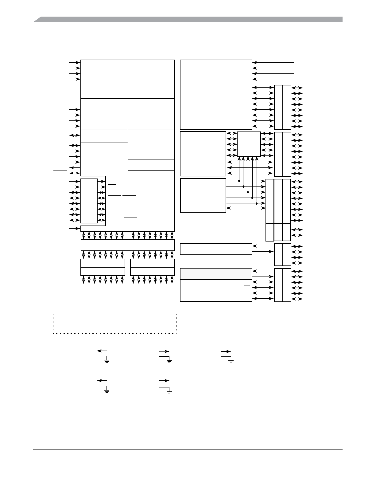
1.1.3 Block Diagram
V
V
V
BKGD
V
DDPLL
V
SSPLL
EXTAL
XTAL
RESET
TEST/V
V
V
V
V
V
XFC
PE0
PE1
PE2
PE3
PE4
PE5
PE6
PE7
SSR
DDR
DDX
SSX
DD2
SS2
DD1
SS1
V
DDA
V
SSA
V
RH
Voltage Regulator
V
RL
AN0
ATD
16K, 32K, 64K, 96K, 128K Byte Flash
AN1
AN2
AN3
AN4
AN5
AN6
AN7
MUX
MODC
PLL
PTE
1K, 2K, 4K Byte RAM
Background
Debug12 Module
Clock and
Reset
Generation
Module
XIRQ
IRQ
R/W
LSTRB/TAGLO
ECLK
DDRE
MODA/IPIPE0
HCS12
CPU
COP Watchdog
Clock Monitor
Periodic Interrupt
System
Integration
Module
(SIM)
Timer
Module
PWM
Module
IOC0
IOC1
IOC2
IOC3
IOC4
IOC5
IOC6
IOC7
PW0
PW1
PW2
PW3
PW4
PW5
MODB/IPIPE1
NOACC/XCLKS
PP
Keypad Interrupt
Key Int
Multiplexed Address/Data Bus
DDRA DDRB
PTA PTB
SCI
MSCAN is not available on the
9S12GC Family Members
MSCAN
RXD
TXD
RXCAN
TXCAN
MISO
PA4
PA3
PA 2
PA 1
PA7
PA6
PA5
PA 0
PB7
PB6
PB5
PB4
PB3
PB2
PB1
PB0
SPI
SS
MOSI
SCK
PTAD
DDRAD
PTT
DDRT
PTP
DDRP
PTJ
DDRJ
PTS
DDRS
PTM
DDRM
V
DDA
V
SSA
V
RH
V
RL
PAD0
PAD1
PAD2
PAD3
PAD4
PAD5
PAD6
PAD7
PT0
PT1
PT2
PT3
PT4
PT5
PT6
PT7
PP0
PP1
PP2
PP3
PP4
PP5
PP6
PP7
PJ6
PJ7
PS0
PS1
PS2
PS3
PM0
PM1
PM2
PM3
PM4
PM5
ADDR12
ADDR11
ADDR10
ADDR9
ADDR8
DATA11
DATA1 0
DATA9
DATA8
ADDR7
ADDR6
ADDR5
DATA4
DATA7
DATA6
DATA5
I/O Driver 5V
V
DDX
V
SSX
ADDR4
ADDR3
DATA3
ADDR2
ADDR1
DATA2
DATA1
ADDR0
Signals shown in Bold are not available on the 52 or 48 Pin Package
DATA0
Signals shown in Bold Italic are available in the 52, but not the 48 Pin Package
Voltage Regulator 5V & I/O
V
DDR
V
SSR
A/D Converter 5V
V
DDA
V
SSA
VRL is bonded internally to V
for 52- and 48-Pin packages
SSA
Multiplexed
Wide Bus
ADDR15
ADDR14
ADDR13
DATA12
DATA15
DATA14
DATA13
Internal Logic 2.5V
V
DD1,2
V
SS1,2
PLL 2.5V
V
DDPLL
V
SSPLL
Figure 1-1. MC9S12C-Family Block Diagram
MC9S12C128 Data Sheet, Rev. 1.15
22 Freescale Semiconductor
Page 23

Chapter 1 Device Overview
1.2 Memory Map and Registers
1.2.1 Device Memory Map
Table 1-1 shows the deviceregister map after reset. Figure 1-2through Figure 1-6 illustrate the full device
memory map.
Table 1-1. Device Register Map Overview
Address Module Size
0x0000–0x0017 Core (ports A, B, E, modes, inits, test) 24
0x0018 Reserved 1
0x0019 Voltage regulator (VREG) 1
0x001A–0x001B Device ID register 2
0x001C–0x001F Core (MEMSIZ, IRQ, HPRIO) 4
0x0020–0x002F Core (DBG) 16
0x0030–0x0033 Core (PPAGE
0x0034–0x003F Clock and reset generator (CRG) 12
0x0040–0x006F Standard timer module (TIM) 48
0x0070–0x007F Reserved 16
0x0080–0x009F Analog-to-digital converter (ATD) 32
0x00A0–0x00C7 Reserved 40
0x00C8–0x00CF Serial communications interface (SCI) 8
0x00D0–0x00D7 Reserved 8
0x00D8–0x00DF Serial peripheral interface (SPI) 8
0x00E0–0x00FF Pulse width modulator (PWM) 32
0x0100–0x010F Flash control register 16
0x0110–0x013F Reserved 48
0x0140–0x017F Scalable controller area network (MSCAN)
0x0180–0x023F Reserved 192
0x0240–0x027F Port integration module (PIM) 64
0x0280–0x03FF Reserved 384
1. External memory paging is not supported on this device (Section 1.7.1, “PPAGE”).
2. Not available on MC9S12GC Family devices
(1)
)
(2)
4
64
MC9S12C128 Data Sheet, Rev. 1.15
Freescale Semiconductor 23
Page 24
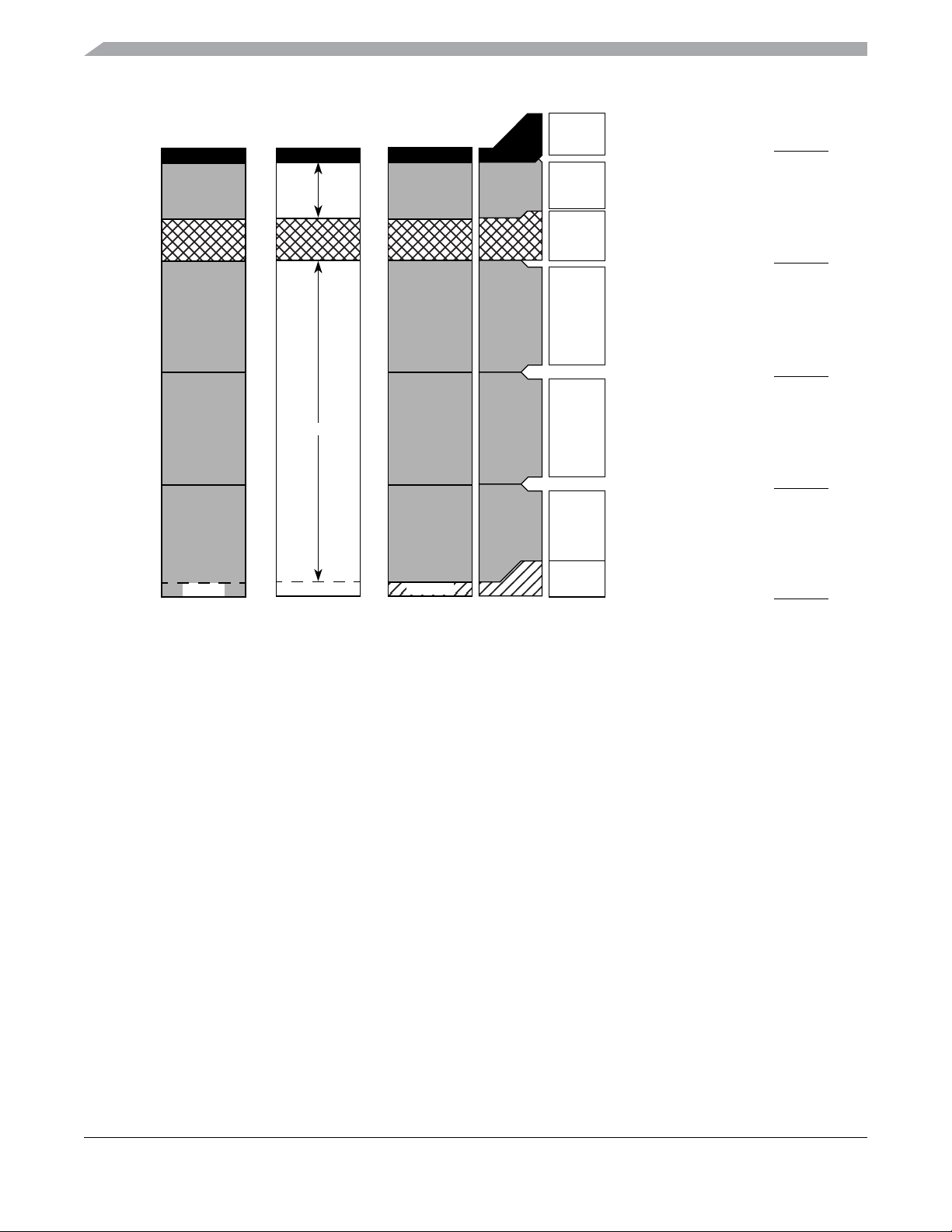
Chapter 1 Device Overview
0x0000
0x0400
0x3000
0x4000
0x8000
EXT
0xC000
0xFF00
0xFFFF
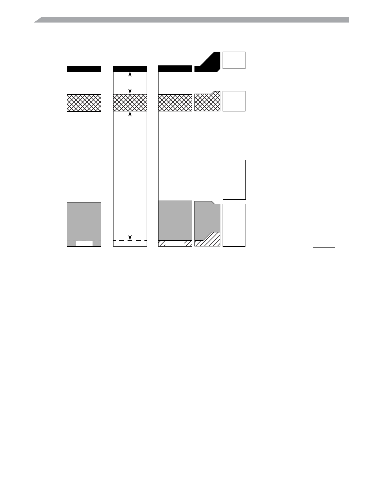
The figure shows a useful map, which is not the map out of reset. After reset the map is:
0x0000–0x03FF: Register Space
0x0000–0x0FFF: 4K RAM (only 3K visible 0x0400–0x0FFF)
Flash erase sector size is 1024 bytes
VECTORS
NORMAL
SINGLE CHIP
VECTORS
EXPANDED SPECIAL
VECTORS
SINGLE CHIP
Figure 1-2. MC9S12C128 and MC9S12GC128 User Configurable Memory Map
0x0000
0x03FF
0x0000
0x3FFF
0x3000
0x3FFF
0x4000
0x7FFF
0x8000
0xBFFF
0xC000
0xFFFF
0xFF00
0xFFFF
1K Register Space
Mappable to any 2K Boundary
16K Fixed Flash EEPROM
4K Bytes RAM
Mappable to any 4K Boundary
16K Fixed Flash EEPROM
16K Page Window
8 * 16K Flash EEPROM Pages
16K Fixed Flash EEPROM
BDM
(If Active)
PAGE MAP
0x003D
0x003E
PPAGE
0x003F
MC9S12C128 Data Sheet, Rev. 1.15
24 Freescale Semiconductor
Page 25

Chapter 1 Device Overview
0x0000
0x0400
0x3000
0x4000
0x8000
EXT
0xC000
0xFF00
0xFFFF
The figure shows a useful map, which is not the map out of reset. After reset the map is:
Flash erase sector size is 1024 bytes
VECTORS
NORMAL
SINGLE CHIP
0x0000–0x03FF: Register Space
0x0000–0x0FFF: 4K RAM (only 3K visible 0x0400–0x0FFF)
VECTORS
EXPANDED SPECIAL
VECTORS
SINGLE CHIP
Figure 1-3. MC9S12C96 and MC9S12GC96 User Configurable Memory Map
0x0000
0x03FF
0x0000
0x3FFF
0x3000
0x3FFF
0x4000
0x7FFF
0x8000
0xBFFF
0xC000
0xFFFF
0xFF00
0xFFFF
1K Register Space
Mappable to any 2K Boundary
16K Fixed Flash EEPROM
4K Bytes RAM
Mappable to any 4K Boundary
16K Fixed Flash EEPROM
16K Page Window
6 * 16K Flash EEPROM Pages
16K Fixed Flash EEPROM
BDM
(If Active)
PAGE MAP
0x003D
0x003E
PPAGE
0x003F
MC9S12C128 Data Sheet, Rev. 1.15
Freescale Semiconductor 25
Page 26
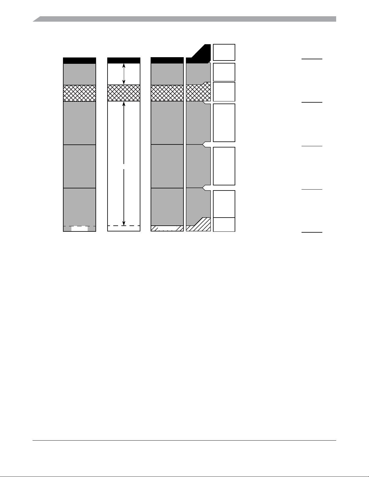
Chapter 1 Device Overview
0x0000
0x0400
0x3000
0x4000
0x8000
EXT
0xC000
0xFF00
0xFFFF
The figure shows a useful map, which is not the map out of reset. After reset the map is:
Flash erase sector size is 1024 Bytes
VECTORS
NORMAL
SINGLE CHIP
0x0000–0x03FF: Register space
0x0000–0x0FFF: 4K RAM (only 3K visible 0x0400–0x0FFF)
VECTORS
EXPANDED SPECIAL
VECTORS
SINGLE CHIP
0x0000
0x03FF
0x0000
0x3FFF
0x3000
0x3FFF
0x4000
0x7FFF
0x8000
0xBFFF
0xC000
0xFFFF
0xFF00
0xFFFF
1K Register Space
Mappable to any 2K Boundary
16K Fixed Flash EEPROM
4K Bytes RAM
Mappable to any 4K Boundary
16K Fixed Flash EEPROM
16K Page Window
4 * 16K Flash EEPROM Pages
16K Fixed Flash EEPROM
BDM
(If Active)
PAGE MAP
0x003D
0x003E
PPAGE
0x003F
Figure 1-4. MC9S12C64 and MC9S12GC64 User Configurable Memory Map
MC9S12C128 Data Sheet, Rev. 1.15
26 Freescale Semiconductor
Page 27
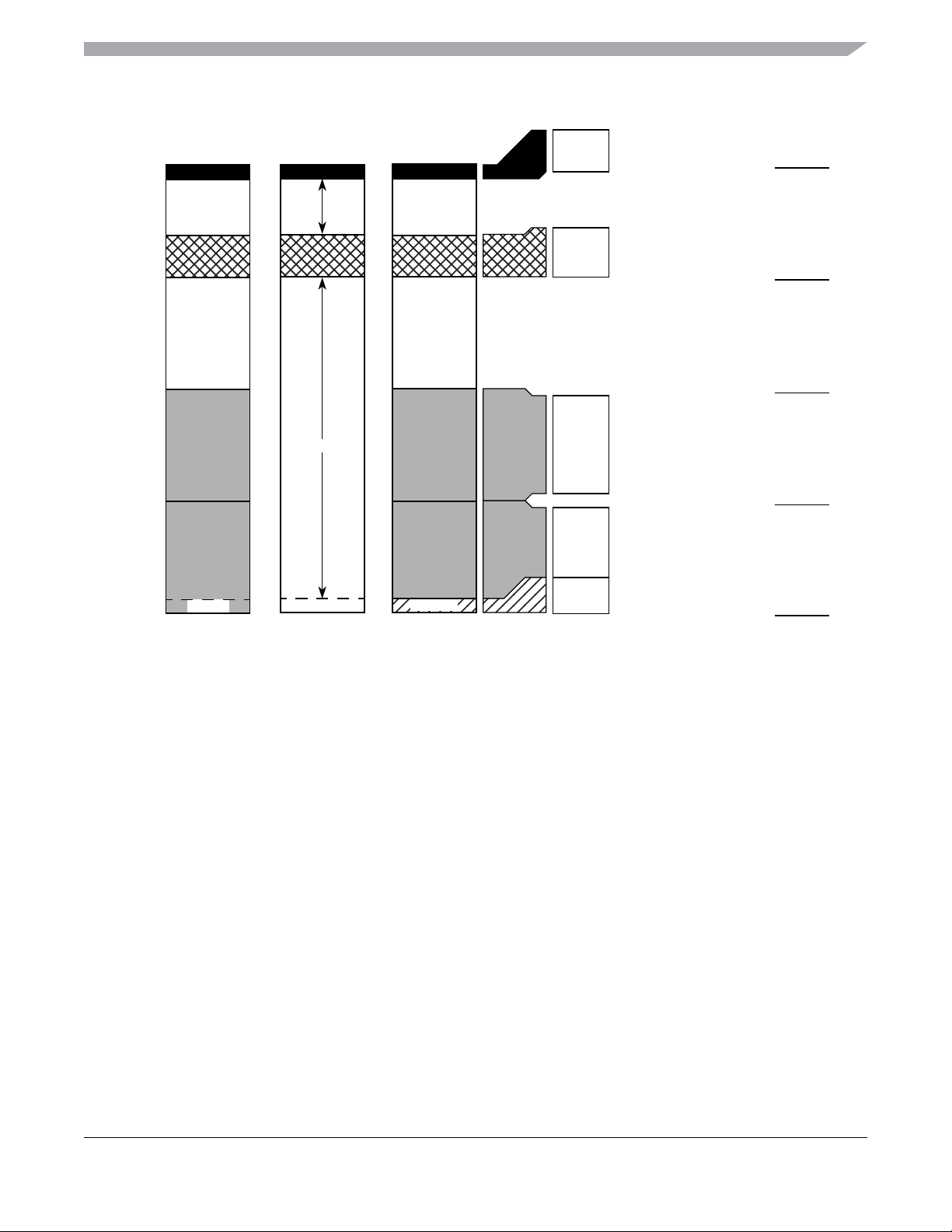
Chapter 1 Device Overview
0x0000
0x0400
0x3800
0x4000
0x8000
0xC000
0xFF00
0xFFFF
VECTORS
NORMAL
SINGLE CHIP
EXT
VECTORS
EXPANDED SPECIAL
VECTORS
SINGLE CHIP
0x0000
0x03FF
0x3800
0x3FFF
0x8000
0xBFFF
0xC000
0xFFFF
0xFF00
0xFFFF
1K Register Space
Mappable to any 2K Boundary
2K Bytes RAM
Mappable to any 2K Boundary
16K Page Window
2 * 16K Flash EEPROM Pages
16K Fixed Flash EEPROM
BDM
(If Active)
PAGE MAP
0x003E
PPAGE
0x003F
The figure shows a useful map, which is not the map out of reset. After reset the map is:
0x0000–0x03FF: Register space
0x0800–0x0FFF: 2K RAM
Flash erase sector size is 512 bytes
The flash page 0x003E is visible at 0x4000–0x7FFF in the memory map if ROMHM = 0.
In the figure ROMHM = 1 removing page 0x003E from 0x4000–0x7FFF.
Figure 1-5. MC9S12C32 and MC9S12GC32 User Configurable Memory Map
MC9S12C128 Data Sheet, Rev. 1.15
Freescale Semiconductor 27
Page 28
Chapter 1 Device Overview
0x0000
0x0400
0x3C00
0x4000
0x8000
EXT
0xC000
0xFF00
0xFFFF
The figure shows a useful map, which is not the map out of reset. After reset the map is:
VECTORS
NORMAL
SINGLE CHIP
0x0000–0x03FF: Register Space
0x0C00–0x0FFF: 1K RAM
VECTORS
EXPANDED SPECIAL
VECTORS
SINGLE CHIP
0x0000
0x03FF
0x3C00
0x3FFF
0x8000
0xBFFF
0xC000
0xFFFF
0xFF00
0xFFFF
1K Register Space
Mappable to any 2K Boundary
1K Bytes RAM
Mappable to any 2K Boundary
16K Page Window
16K Fixed Flash EEPROM
BDM
(If Active)
PAGE MAP
PPAGE
0x003F
The 16K flash array page 0x003F is also visible in the PPAGE window when PPAGE register contents are odd.
Flash Erase Sector Size is 512 Bytes
Figure 1-6. MC9S12GC16 User Configurable Memory Map
MC9S12C128 Data Sheet, Rev. 1.15
28 Freescale Semiconductor
Page 29

Chapter 1 Device Overview
1.2.2 Detailed Register Map
The detailed register map of the MC9S12C Family
is listed in address order below.
0x0000–0x000F MEBI Map 1 of 3 (HCS12 Multiplexed External Bus Interface)
Address Name Bit 7 Bit 6 Bit 5 Bit 4 Bit 3 Bit 2 Bit 1 Bit 0
0x0000 PORTA
0x0001 PORTB
0x0002 DDRA
0x0003 DDRB
0x0004 Reserved
0x0005 Reserved
0x0006 Reserved
0x0007 Reserved
0x0008 PORTE
0x0009 DDRE
0x000A PEAR
0x000B MODE
0x000C PUCR
0x000D RDRIV
0x000E EBICTL
0x000F Reserved
Read:
Write:
Read:
Write:
Read:
Write:
Read:
Write:
Read: 0 0 0 0 0 0 0 0
Write:
Read: 0 0 0 0 0 0 0 0
Write:
Read: 0 0 0 0 0 0 0 0
Write:
Read: 0 0 0 0 0 0 0 0
Write:
Read:
Write:
Read:
Write:
Read:
Write:
Read:
Write:
Read:
Write:
Read:
Write:
Read: 0 0 0 0 0 0 0
Write:
Read: 0 0 0 0 0 0 0 0
Write:
Bit 7 6 5 4 3 2 1 Bit 0
Bit 7 6 5 4 3 2 1 Bit 0
Bit 7 6 5 4 3 2 1 Bit 0
Bit 7 6 5 4 3 2 1 Bit 0
Bit 7 6 5 4 3 2
Bit 7 6 5 4 3 Bit 2
NOACCE
MODC MODB MODA
PUPKE
RDPK
0
00
00
PIPOE NECLK LSTRE RDWE
PUPEE
RDPE
0
IVIS
00
00
0
Bit 1 Bit 0
00
00
EMK EME
PUPBE PUPAE
RDPB RDPA
ESTR
MC9S12C128 Data Sheet, Rev. 1.15
Freescale Semiconductor 29
Page 30
Chapter 1 Device Overview
0x0010–0x0014 MMC Map 1 of 4 (HCS12 Module Mapping Control)
Address Name Bit 7 Bit 6 Bit 5 Bit 4 Bit 3 Bit 2 Bit 1 Bit 0
0x0010 INITRM
0x0011 INITRG
0x0012 INITEE
0x0013 MISC
0x0014 Reserved
Read:
Write:
Read: 0
Write:
Read:
Write:
Read: 0 0 0 0
Write:
Read: 0 0 0 0 0 0 0 0
Write:
RAM15 RAM14 RAM13 RAM12 RAM11
REG14 REG13 REG12 REG11
EE15 EE14 EE13 EE12 EE11
EXSTR1 EXSTR0 ROMHM ROMON
00
000
00
RAMHAL
EEON
0x0015–0x0016 INT Map 1 of 2 (HCS12 Interrupt)
Address Name Bit 7 Bit 6 Bit 5 Bit 4 Bit 3 Bit 2 Bit 1 Bit 0
0x0015 ITCR
0x0016 ITEST
Read: 0 0 0
Write:
Read:
Write:
INTE INTC INTA INT8 INT6 INT4 INT2 INT0
WRINT ADR3 ADR2 ADR1 ADR0
0x0017–0x0017 MMC Map 2 of 4 (HCS12 Module Mapping Control)
Address Name Bit 7 Bit 6 Bit 5 Bit 4 Bit 3 Bit 2 Bit 1 Bit 0
0x0017 Reserved
Read: 0 0 0 0 0 0 0 0
Write:
0x0018–0x0018 Miscellaneous Peripherals (Device User Guide)
Address Name Bit 7 Bit 6 Bit 5 Bit 4 Bit 3 Bit 2 Bit 1 Bit 0
0x0018 Reserved
Read: 0 0 0 0 0 0 0 0
Write:
0x0019–0x0019 VREG3V3 (Voltage Regulator)
Address Name Bit 7 Bit 6 Bit 5 Bit 4 Bit 3 Bit 2 Bit 1 Bit 0
$0019 VREGCTRL
Read: 0 0 0 0 0 LVDS
Write:
LVIE LVIF
MC9S12C128 Data Sheet, Rev. 1.15
30 Freescale Semiconductor
Page 31

Chapter 1 Device Overview
0x001A–0x001B Miscellaneous Peripherals (Device User Guide)
Address Name Bit 7 Bit 6 Bit 5 Bit 4 Bit 3 Bit 2 Bit 1 Bit 0
0x001A PARTIDH
0x001B PARTIDL
Read: ID15 ID14 ID13 ID12 ID11 ID10 ID9 ID8
Write:
Read: ID7 ID6 ID5 ID4 ID3 ID2 ID1 ID0
Write:
0x001C–0x001D MMC Map 3 of 4 (HCS12 Module Mapping Control, Device User Guide)
Address Name Bit 7 Bit 6 Bit 5 Bit 4 Bit 3 Bit 2 Bit 1 Bit 0
0x001C MEMSIZ0
0x001D MEMSIZ1
Read:
Write:
Read:
Write:
reg_sw0 0 eep_sw1 eep_sw0 0 ram_sw2 ram_sw1 ram_sw0
rom_sw1 rom_sw0 0 0 0 0 pag_sw1 pag_sw0
0x001E–0x001E MEBI Map 2 of 3 (HCS12 Multiplexed External Bus Interface)
Address Name Bit 7 Bit 6 Bit 5 Bit 4 Bit 3 Bit 2 Bit 1 Bit 0
0x001E INTCR
Read:
Write:
IRQE IRQEN
000000
0x001F–0x001F INT Map 2 of 2 (HCS12 Interrupt)
Address Name Bit 7 Bit 6 Bit 5 Bit 4 Bit 3 Bit 2 Bit 1 Bit 0
0x001F HPRIO
Read:
Write:
PSEL7 PSEL6 PSEL5 PSEL4 PSEL3 PSEL2 PSEL1
0x0020–0x002F DBG (Including BKP) Map 1 of 1 (HCS12 Debug)
Address Name Bit 7 Bit 6 Bit 5 Bit 4 Bit 3 Bit 2 Bit 1 Bit 0
0x0020 DBGC1
0x0021 DBGSC
0x0022 DBGTBH
0x0023 DBGTBL
0x0024 DBGCNT
0x0025 DBGCCX
Read:
Write:
Read: AF BF CF 0
Write:
Read: Bit 15 Bit 14 Bit 13 Bit 12 Bit 11 Bit 10 Bit 9 Bit 8
Write:
Read: Bit 7 Bit 6 Bit 5 Bit 4 Bit 3 Bit 2 Bit 1 Bit 0
Write:
Read: TBF 0 CNT
Write:
Read:
Write:
DBGEN ARM TRGSEL BEGIN DBGBRK
PAGSEL EXTCMP
0
TRG
CAPMOD
0
MC9S12C128 Data Sheet, Rev. 1.15
Freescale Semiconductor 31
Page 32

Chapter 1 Device Overview
0x0020–0x002F DBG (Including BKP) Map 1 of 1 (HCS12 Debug) (continued)
Address Name Bit 7 Bit 6 Bit 5 Bit 4 Bit 3 Bit 2 Bit 1 Bit 0
0x0026 DBGCCH
0x0027 DBGCCL
0x0028
0x0029
0x002A
0x002B
0x002C
0x002D
0x002E
0x002F
DBGC2 Read:
BKPCT0 Write:
DBGC3 Read:
BKPCT1 Write:
DBGCAX Read:
BKP0X Write:
DBGCAH Read:
BKP0H Write:
DBGCAL Read:
BKP0L Write:
DBGCBX Read:
BKP1X Write:
DBGCBH Read:
BKP1H Write:
DBGCBL Read:
BKP1L Write:
Read:
Write:
Read:
Write:
Bit 15 14 13 12 11 10 9 Bit 8
Bit 7 6 5 4 3 2 1 Bit 0
BKABEN FULL BDM TAGAB BKCEN TAGC RWCEN RWC
BKAMBH BKAMBL BKBMBH BKBMBL RWAEN RWA RWBEN RWB
PAGSEL EXTCMP
Bit 15 14 13 12 11 10 9 Bit 8
Bit 7 6 5 4 3 2 1 Bit 0
PAGSEL EXTCMP
Bit 15 14 13 12 11 10 9 Bit 8
Bit 7 6 5 4 3 2 1 Bit 0
0x0030–0x0031 MMC Map 4 of 4 (HCS12 Module Mapping Control)
Address Name Bit 7 Bit 6 Bit 5 Bit 4 Bit 3 Bit 2 Bit 1 Bit 0
0x0030 PPAGE
0x0031 Reserved
Read: 0 0
Write:
Read: 0 0 0 0 0 0 0 0
Write:
PIX5 PIX4 PIX3 PIX2 PIX1 PIX0
0x0032–0x0033 MEBI Map 3 of 3 (HCS12 Multiplexed External Bus Interface)
Address Name Bit 7 Bit 6 Bit 5 Bit 4 Bit 3 Bit 2 Bit 1 Bit 0
Read:
0x0032 PORTK
0x0033 DDRK
1. Only applicable in special emulation-only bond outs, for emulation of extended memory map.
(1)
1
Write:
Read:
Write:
Bit 7 6 5 4 3 2 1 Bit 0
Bit 7 6 5 4 3 2 1 Bit 0
MC9S12C128 Data Sheet, Rev. 1.15
32 Freescale Semiconductor
Page 33

Chapter 1 Device Overview
0x0034–0x003F CRG (Clock and Reset Generator)
Address Name Bit 7 Bit 6 Bit 5 Bit 4 Bit 3 Bit 2 Bit 1 Bit 0
0x0034 SYNR
0x0035 REFDV
0x0036
0x0037 CRGFLG
0x0038 CRGINT
0x0039 CLKSEL
0x003A PLLCTL
0x003B RTICTL
0x003C COPCTL
0x003D
0x003E
0x003F ARMCOP
CTFLG
TEST ONLY
FORBYP
TEST ONLY
CTCTL
TEST ONLY
Read: 0 0
Write:
Read: 0 0 0 0
Write:
Read: TOUT7 TOUT6 TOUT5 TOUT4 TOUT3 TOUT2 TOUT1 TOUT0
Write:
Read:
Write:
Read:
Write:
Read:
Write:
Read:
Write:
Read: 0
Write:
Read:
Write:
Read:
Write:
Read: TCTL7 TCTL6 TCTL5 TCTL4 TCLT3 TCTL2 TCTL1 TCTL0
Write:
Read: 0 0 0 0 0 0 0 0
Write: Bit 7 6 5 4 3 2 1 Bit 0
RTIF PROF
RTIE
PLLSEL PSTP SYSWAI ROAWAI PLLWAI CWAI RTIWAI COPWAI
CME PLLON AUTO ACQ
WCOP RSBCK
RTIBYP COPBYP
00
RTR6 RTR5 RTR4 RTR3 RTR2 RTR1 RTR0
SYN5 SYN4 SYN3 SYN2 SYN1 SYN0
REFDV3 REFDV2 REFDV1 REFDV0
0
000
0
LOCKIF
LOCKIE
PLLBYP
LOCK TRACK
00
0
00
PRE PCE SCME
CR2 CR1 CR0
SCMIF
SCMIE
FCM
SCM
0
0
0x0040–0x006F TIM (Sheet 1 of 3)
Address Name Bit 7 Bit 6 Bit 5 Bit 4 Bit 3 Bit 2 Bit 1 Bit 0
0x0040 TIOS
0x0041 CFORC
0x0042 OC7M
0x0043 OC7D
0x0044 TCNT (hi)
0x0045 TCNT (lo)
0x0046 TSCR1
0x0047 TTOV
Freescale Semiconductor 33
Read:
Write:
Read: 0 0 0 0 0 0 0 0
Write: FOC7 FOC6 FOC5 FOC4 FOC3 FOC2 FOC1 FOC0
Read:
Write:
Read:
Write:
Read: Bit 15 14 13 12 11 10 9 Bit 8
Write:
Read: Bit 7 6 5 4 3 2 1 Bit 0
Write:
Read:
Write:
Read:
Write:
IOS7 IOS6 IOS5 IOS4 IOS3 IOS2 IOS1 IOS0
OC7M7 OC7M6 OC7M5 OC7M4 OC7M3 OC7M2 OC7M1 OC7M0
OC7D7 OC7D6 OC7D5 OC7D4 OC7D3 OC7D2 OC7D1 OC7D0
TEN TSWAI TSFRZ TFFCA
TOV7 TOV6 TOV5 TOV4 TOV3 TOV2 TOV1 TOV0
MC9S12C128 Data Sheet, Rev. 1.15
0000
Page 34

Chapter 1 Device Overview
0x0040–0x006F TIM (Sheet 2 of 3)
Address Name Bit 7 Bit 6 Bit 5 Bit 4 Bit 3 Bit 2 Bit 1 Bit 0
0x0048 TCTL1
0x0049 TCTL2
0x004A TCTL3
0x004B TCTL4
0x004C TIE
0x004D TSCR2
0x004E TFLG1
0x004F TFLG2
0x0050 TC0 (hi)
0x0051 TC0 (lo)
0x0052 TC1 (hi)
0x0053 TC1 (lo)
0x0054 TC2 (hi)
0x0055 TC2 (lo)
0x0056 TC3 (hi)
0x0057 TC3 (lo)
0x0058 TC4 (hi)
0x0059 TC4 (lo)
0x005A TC5 (hi)
0x005B TC5 (lo)
0x005C TC6 (hi)
0x005D TC6 (lo)
0x005E TC7 (hi)
Read:
Write:
Read:
Write:
Read:
Write:
Read:
Write:
Read:
Write:
Read:
Write:
Read:
Write:
Read:
Write:
Read:
Write:
Read:
Write:
Read:
Write:
Read:
Write:
Read:
Write:
Read:
Write:
Read:
Write:
Read:
Write:
Read:
Write:
Read:
Write:
Read:
Write:
Read:
Write:
Read:
Write:
Read:
Write:
Read:
Write:
OM7 OL7 OM6 OL6 OM5 OL5 OM4 OL4
OM3 OL3 OM2 OL2 OM1 OL1 OM0 OL0
EDG7B EDG7A EDG6B EDG6A EDG5B EDG5A EDG4B EDG4A
EDG3B EDG3A EDG2B EDG2A EDG1B EDG1A EDG0B EDG0A
C7I C6I C5I C4I C3I C2I C1I C0I
TOI
C7F C6F C5F C4F C3F C2F C1F C0F
TOF
Bit 15 14 13 12 11 10 9 Bit 8
Bit 7 6 5 4 3 2 1 Bit 0
Bit 15 14 13 12 11 10 9 Bit 8
Bit 7 6 5 4 3 2 1 Bit 0
Bit 15 14 13 12 11 10 9 Bit 8
Bit 7 6 5 4 3 2 1 Bit 0
Bit 15 14 13 12 11 10 9 Bit 8
Bit 7 6 5 4 3 2 1 Bit 0
Bit 15 14 13 12 11 10 9 Bit 8
Bit 7 6 5 4 3 2 1 Bit 0
Bit 15 14 13 12 11 10 9 Bit 8
Bit 7 6 5 4 3 2 1 Bit 0
Bit 15 14 13 12 11 10 9 Bit 8
Bit 7 6 5 4 3 2 1 Bit 0
Bit 15 14 13 12 11 10 9 Bit 8
000
0000000
TCRE PR2 PR1 PR0
MC9S12C128 Data Sheet, Rev. 1.15
34 Freescale Semiconductor
Page 35

Chapter 1 Device Overview
0x0040–0x006F TIM (Sheet 3 of 3)
Address Name Bit 7 Bit 6 Bit 5 Bit 4 Bit 3 Bit 2 Bit 1 Bit 0
0x005F TC7 (lo)
0x0060 PACTL
0x0061 PAFLG
0x0062 PACNT (hi)
0x0063 PACNT (lo)
0x0064 Reserved
0x0065 Reserved
0x0066 Reserved
0x0067 Reserved
0x0068 Reserved
0x0069 Reserved
0x006A Reserved
0x006B Reserved
0x006C Reserved
0x006D Reserved
0x006E Reserved
0x006F Reserved
Read:
Write:
Read: 0
Write:
Read: 0 0 0 0 0 0
Write:
Read:
Write:
Read:
Write:
Read: 0 0 0 0 0 0 0 0
Write:
Read: 0 0 0 0 0 0 0 0
Write:
Read: 0 0 0 0 0 0 0 0
Write:
Read: 0 0 0 0 0 0 0 0
Write:
Read: 0 0 0 0 0 0 0 0
Write:
Read: 0 0 0 0 0 0 0 0
Write:
Read: 0 0 0 0 0 0 0 0
Write:
Read: 0 0 0 0 0 0 0 0
Write:
Read: 0 0 0 0 0 0 0 0
Write:
Read: 0 0 0 0 0 0 0 0
Write:
Read: 0 0 0 0 0 0 0 0
Write:
Read: 0 0 0 0 0 0 0 0
Write:
Bit 7 6 5 4 3 2 1 Bit 0
PAEN PAMOD PEDGE CLK1 CLK0 PAOVI PAI
PAOVF PAIF
Bit 15 14 13 12 11 10 9 Bit 8
Bit 7 6 5 4 3 2 1 Bit 0
0x0070–0x007F Reserved
Address Name Bit 7 Bit 6 Bit 5 Bit 4 Bit 3 Bit 2 Bit 1 Bit 0
0x0070–
0x007F
Freescale Semiconductor 35
Reserved
Read: 0 0 0 0 0 0 0 0
Write:
MC9S12C128 Data Sheet, Rev. 1.15
Page 36

Chapter 1 Device Overview
0x0080–0x009F ATD (Analog-to-Digital Converter 10 Bit 8 Channel)
Address Name Bit 7 Bit 6 Bit 5 Bit 4 Bit 3 Bit 2 Bit 1 Bit 0
0x0080 ATDCTL0
0x0081 ATDCTL1
0x0082 ATDCTL2
0x0083 ATDCTL3
0x0084 ATDCTL4
0x0085 ATDCTL5
0x0086 ATDSTAT0
0x0087 Reserved
0x0088 ATDTEST0
0x0089 ATDTEST1
0x008A Reserved
0x008B ATDSTAT1
0x008C Reserved
0x008D ATDDIEN
0x008E Reserved
0x008F PORTAD
0x0090 ATDDR0H
0x0091 ATDDR0L
0x0092 ATDDR1H
0x0093 ATDDR1L
0x0094 ATDDR2H
0x0095 ATDDR2L
Read: 0 0 0 0 0 0 0 0
Write:
Read: 0 0 0 0 0 0 0 0
Write:
Read:
Write:
Read: 0
Write:
Read:
Write:
Read:
Write:
Read:
Write:
Read: 0 0 0 0 0 0 0 0
Write:
Read: 0 0 0 0 0 0 0 0
Write:
Read: 0 0 0 0 0 0 0
Write:
Read: 0 0 0 0 0 0 0 0
Write:
Read: CCF7 CCF6 CCF5 CCF4 CCF3 CCF2 CCF1 CCF0
Write:
Read: 0 0 0 0 0 0 0 0
Write:
Read:
Write:
Read: 0 0 0 0 0 0 0 0
Write:
Read: Bit7 6 5 4 3 2 1 BIT 0
Write:
Read: Bit15 14 13 12 11 10 9 Bit8
Write:
Read: Bit7 Bit6 0 0 0 0 0 0
Write:
Read: Bit15 14 13 12 11 10 9 Bit8
Write:
Read: Bit7 Bit6 0 0 0 0 0 0
Write:
Read: Bit15 14 13 12 11 10 9 Bit8
Write:
Read: Bit7 Bit6 0 0 0 0 0 0
Write:
ADPU AFFC AWAI ETRIGLE ETRIGP ETRIG ASCIE
S8C S4C S2C S1C FIFO FRZ1 FRZ0
SRES8 SMP1 SMP0 PRS4 PRS3 PRS2 PRS1 PRS0
DJM DSGN SCAN MULT
SCF
Bit 7 6 5 4 3 2 1 Bit 0
0
ETORF FIFOR
0
0 CC2 CC1 CC0
CC CB CA
ASCIF
SC
MC9S12C128 Data Sheet, Rev. 1.15
36 Freescale Semiconductor
Page 37

Chapter 1 Device Overview
0x0080–0x009F ATD (Analog-to-Digital Converter 10 Bit 8 Channel) (continued)
Address Name Bit 7 Bit 6 Bit 5 Bit 4 Bit 3 Bit 2 Bit 1 Bit 0
0x0096 ATDDR3H
0x0097 ATDDR3L
0x0098 ATDDR4H
0x0099 ATDDR4L
0x009A ATDDR5H
0x009B ATDDR5L
0x009C ATDDR6H
0x009D ATDDR6L
0x009E ATDDR7H
0x009F ATDDR7L
Read: Bit15 14 13 12 11 10 9 Bit8
Write:
Read: Bit7 Bit6 0 0 0 0 0 0
Write:
Read: Bit15 14 13 12 11 10 9 Bit8
Write:
Read: Bit7 Bit6 0 0 0 0 0 0
Write:
Read: Bit15 14 13 12 11 10 9 Bit8
Write:
Read: Bit7 Bit6 0 0 0 0 0 0
Write:
Read: Bit15 14 13 12 11 10 9 Bit8
Write:
Read: Bit7 Bit6 0 0 0 0 0 0
Write:
Read: Bit15 14 13 12 11 10 9 Bit8
Write:
Read: Bit7 Bit6 0 0 0 0 0 0
Write:
0x00A0–0x00C7 Reserved
Address Name Bit 7 Bit 6 Bit 5 Bit 4 Bit 3 Bit 2 Bit 1 Bit 0
0x00A0–
0x00C7
Reserved
Read: 0 0 0 0 0 0 0 0
Write:
0x00C8–0x00CF SCI (Asynchronous Serial Interface)
Address Name Bit 7 Bit 6 Bit 5 Bit 4 Bit 3 Bit 2 Bit 1 Bit 0
0x00C8 SCIBDH
0x00C9 SCIBDL
0x00CA SCICR1
0x00CB SCICR2
0x00CC SCISR1
Read: 0 0 0
Write:
Read:
Write:
Read:
Write:
Read:
Write:
Read: TDRE TC RDRF IDLE OR NF FE PF
Write:
SBR7 SBR6 SBR5 SBR4 SBR3 SBR2 SBR1 SBR0
LOOPS SCISWAI RSRC M WAKE ILT PE PT
TIE TCIE RIE ILIE TE RE RWU SBK
SBR12 SBR11 SBR10 SBR9 SBR8
MC9S12C128 Data Sheet, Rev. 1.15
Freescale Semiconductor 37
Page 38

Chapter 1 Device Overview
0x00C8–0x00CF SCI (Asynchronous Serial Interface) (continued)
Address Name Bit 7 Bit 6 Bit 5 Bit 4 Bit 3 Bit 2 Bit 1 Bit 0
0x00CD SCISR2
0x00CE SCIDRH
0x00CF SCIDRL
Read: 0 0 0 0 0
Write:
Read: R8
Write:
Read: R7 R6 R5 R4 R3 R2 R1 R0
Write: T7 T6 T5 T4 T3 T2 T1 T0
T8
000000
BRK13 TXDIR
RAF
0x00D0–0x00D7 Reserved
Address Name Bit 7 Bit 6 Bit 5 Bit 4 Bit 3 Bit 2 Bit 1 Bit 0
0x00D0–
0x00D7
Reserved
Read: 0 0 0 0 0 0 0 0
Write:
0x00D8–0x00DF SPI (Serial Peripheral Interface)
Address Name Bit 7 Bit 6 Bit 5 Bit 4 Bit 3 Bit 2 Bit 1 Bit 0
0x00D8 SPICR1
0x00D9 SPICR2
0x00DA SPIBR
0x00DB SPISR
0x00DC Reserved
0x00DD SPIDR
0x00DE Reserved
0x00DF Reserved
Read:
Write:
Read: 0 0 0
Write:
Read: 0
Write:
Read: SPIF 0 SPTEF MODF 0 0 0 0
Write:
Read: 0 0 0 0 0 0 0 0
Write:
Read:
Write:
Read: 0 0 0 0 0 0 0 0
Write:
Read: 0 0 0 0 0 0 0 0
Write:
SPIE SPE SPTIE MSTR CPOL CPHA SSOE LSBFE
MODFEN BIDIROE
SPPR2 SPPR1 SPPR0
Bit7 6 5 4 3 2 1 Bit0
0
0
SPR2 SPR1 SPR0
SPISWAI SPC0
MC9S12C128 Data Sheet, Rev. 1.15
38 Freescale Semiconductor
Page 39

Chapter 1 Device Overview
0x00E0–0x00FF PWM (Pulse Width Modulator)
Address Name Bit 7 Bit 6 Bit 5 Bit 4 Bit 3 Bit 2 Bit 1 Bit 0
$00E0 PWME
$00E1 PWMPOL
$00E2 PWMCLK
$00E3 PWMPRCLK
$00E4 PWMCAE
$00E5 PWMCTL
$00E6
$00E7 PWMPRSC
$00E8 PWMSCLA
$00E9 PWMSCLB
$00EA PWMSCNTA
$00EB PWMSCNTB
$00EC PWMCNT0
$00ED PWMCNT1
$00EE PWMCNT2
$00EF PWMCNT3
$00F0 PWMCNT4
$00F1 PWMCNT5
$00F2 PWMPER0
$00F3 PWMPER1
$00F4 PWMPER2
$00F5 PWMPER3
PWMTST
Test Only
Read: 0 0
Write:
Read: 0 0
Write:
Read: 0 0
Write:
Read: 0
Write:
Read: 0 0
Write:
Read: 0
Write:
Read: 0 0 0 0 0 0 0 0
Write:
Read: 0 0 0 0 0 0 0 0
Write:
Read:
Write:
Read:
Write:
Read: 0 0 0 0 0 0 0 0
Write:
Read: 0 0 0 0 0 0 0 0
Write:
Read: Bit 7 6 5 4 3 2 1 Bit 0
Write: 0 0 0 0 0 0 0 0
Read: Bit 7 6 5 4 3 2 1 Bit 0
Write: 0 0 0 0 0 0 0 0
Read: Bit 7 6 5 4 3 2 1 Bit 0
Write: 0 0 0 0 0 0 0 0
Read: Bit 7 6 5 4 3 2 1 Bit 0
Write: 0 0 0 0 0 0 0 0
Read: Bit 7 6 5 4 3 2 1 Bit 0
Write: 0 0 0 0 0 0 0 0
Read: Bit 7 6 5 4 3 2 1 Bit 0
Write: 0 0 0 0 0 0 0 0
Read:
Write:
Read:
Write:
Read:
Write:
Read:
Write:
Bit 7 6 5 4 3 2 1 Bit 0
Bit 7 6 5 4 3 2 1 Bit 0
Bit 7 6 5 4 3 2 1 Bit 0
Bit 7 6 5 4 3 2 1 Bit 0
Bit 7 6 5 4 3 2 1 Bit 0
Bit 7 6 5 4 3 2 1 Bit 0
PCKB2 PCKB1 PCKB0
CON45 CON23 CON01 PSWAI PFRZ
PWME5 PWME4 PWME3 PWME2 PWME1 PWME0
PPOL5 PPOL4 PPOL3 PPOL2 PPOL1 PPOL0
PCLK5 PCLK4 PCLK3 PCLK2 PCLK1 PCLK0
0
CAE5 CAE4 CAE3 CAE2 CAE1 CAE0
PCKA2 PCKA1 PCKA0
00
MC9S12C128 Data Sheet, Rev. 1.15
Freescale Semiconductor 39
Page 40

Chapter 1 Device Overview
0x00E0–0x00FF PWM (Pulse Width Modulator) (continued)
Address Name Bit 7 Bit 6 Bit 5 Bit 4 Bit 3 Bit 2 Bit 1 Bit 0
$00F6 PWMPER4
$00F7 PWMPER5
$00F8 PWMDTY0
$00F9 PWMDTY1
$00FA PWMDTY2
$00FB PWMDTY3
$00FC PWMDTY4
$00FD PWMDTY5
$00FE Reserved
$00FF Reserved
Read:
Write:
Read:
Write:
Read:
Write:
Read:
Write:
Read:
Write:
Read:
Write:
Read:
Write:
Read:
Write:
Read:
Write: PWMRSTRT
Read: 0 0 0 0 0 0 0 0
Write:
Bit 7 6 5 4 3 2 1 Bit 0
Bit 7 6 5 4 3 2 1 Bit 0
Bit 7 6 5 4 3 2 1 Bit 0
Bit 7 6 5 4 3 2 1 Bit 0
Bit 7 6 5 4 3 2 1 Bit 0
Bit 7 6 5 4 3 2 1 Bit 0
Bit 7 6 5 4 3 2 1 Bit 0
Bit 7 6 5 4 3 2 1 Bit 0
PWMIF PWMIE
0
PWMLVL
0 PWM5IN
PWM5INL PWM5ENA
0x0100–0x010F Flash Control Register
Address Name Bit 7 Bit 6 Bit 5 Bit 4 Bit 3 Bit 2 Bit 1 Bit 0
0x0100 FCLKDIV
0x0101 FSEC
0x0102 FTSTMOD
0x0103 FCNFG
0x0104 FPROT
0x0105 FSTAT
0x0106 FCMD
0x0107
0x0108
0x0109
Reserved for
Factory Test
Reserved for
Factory Test
Reserved for
Factory Test
Read: FDIVLD
Write:
Read: KEYEN1 KEYEN0 NV5 NV4 NV3 NV2 SEC1 SEC0
Write:
Read:
Write:
Read:
Write:
Read:
Write:
Read:
Write:
Read: 0
Write:
Read: 0 0 0 0 0 0 0 0
Write:
Read: 0 0 0 0 0 0 0 0
Write:
Read: 0 0 0 0 0 0 0 0
Write:
0 0 0 WRALL
CBEIE CCIE KEYACC
FPOPEN NV6 FPHDIS FPHS1 FPHS0 FPLDIS FPLS1 FPLS0
CBEIF
PRDIV8 FDIV5 FDIV4 FDIV3 FDIV2 FDIV1 FDIV0
000
CCIF
CMDB6 CMDB5
PVIOL ACCERR
000
0
00
BLANK
CMDB2
BKSEL1 BKSEL0
00
0
CMDB0
0
MC9S12C128 Data Sheet, Rev. 1.15
40 Freescale Semiconductor
Page 41

Chapter 1 Device Overview
0x0100–0x010F Flash Control Register (continued)
Address Name Bit 7 Bit 6 Bit 5 Bit 4 Bit 3 Bit 2 Bit 1 Bit 0
0x010A
0x010B
0x010C Reserved
0x010D Reserved
0x010E Reserved
0x010F Reserved
Reserved for
Factory Test
Reserved for
Factory Test
Read: 0 0 0 0 0 0 0 0
Write:
Read: 0 0 0 0 0 0 0 0
Write:
Read: 0 0 0 0 0 0 0 0
Write:
Read: 0 0 0 0 0 0 0 0
Write:
Read: 0 0 0 0 0 0 0 0
Write:
Read: 0 0 0 0 0 0 0 0
Write:
0x0110–0x013F Reserved
Address Name Bit 7 Bit 6 Bit 5 Bit 4 Bit 3 Bit 2 Bit 1 Bit 0
0x0110–
0x003F
Reserved
Read: 0 0 0 0 0 0 0 0
Write:
0x0140–0x017F CAN (Scalable Controller Area Network — MSCAN)
Address Name Bit 7 Bit 6 Bit 5 Bit 4 Bit 3 Bit 2 Bit 1 Bit 0
0x0140 CANCTL0
0x0141 CANCTL1
0x0142 CANBTR0
0x0143 CANBTR1
0x0144 CANRFLG
0x0145 CANRIER
0x0146 CANTFLG
0x0147 CANTIER
0x0148 CANTARQ
0x0149 CANTAAK
Read:
Write:
Read:
Write:
Read:
Write:
Read:
Write:
Read:
Write:
Read:
Write:
Read: 0 0 0 0 0
Write:
Read: 0 0 0 0 0
Write:
Read: 0 0 0 0 0
Write:
Read: 0 0 0 0 0 ABTAK2 ABTAK1 ABTAK0
Write:
RXFRM
CANE CLKSRC LOOPB LISTEN
SJW1 SJW0 BRP5 BRP4 BRP3 BRP2 BRP1 BRP0
SAMP TSEG22 TSEG21 TSEG20 TSEG13 TSEG12 TSEG11 TSEG10
WUPIF CSCIF
WUPIE CSCIE RSTATE1 RSTATE0 TSTATE1 TSTATE0 OVRIE RXFIE
RXACT
CSWAI
RSTAT1 RSTAT0 TSTAT1 TSTAT0
SYNCH
TIME WUPE SLPRQ INITRQ
0
(1)
WUPM
TXE2 TXE1 TXE0
TXEIE2 TXEIE1 TXEIE0
ABTRQ2 ABTRQ1 ABTRQ0
SLPAK INITAK
OVRIF RXF
MC9S12C128 Data Sheet, Rev. 1.15
Freescale Semiconductor 41
Page 42

Chapter 1 Device Overview
0x0140–0x017F CAN (Scalable Controller Area Network — MSCAN)
Address Name Bit 7 Bit 6 Bit 5 Bit 4 Bit 3 Bit 2 Bit 1 Bit 0
0x014A CANTBSEL
0x014B CANIDAC
0x014C Reserved
0x014D Reserved
0x014E CANRXERR
0x014F CANTXERR
0x0150–
0x0153
0x0154–
0x0157
0x0158–
0x015B
0x015C–
0x015F
0x0160–
0x016F
0x0170–
0x017F
1. Not available on the MC9S12GC Family members. Those memory locations should not be accessed.
CANIDAR0 -
CANIDAR3
CANIDMR0 -
CANIDMR3
CANIDAR4 -
CANIDAR7
CANIDMR4 -
CANIDMR7
CANRXFG
CANTXFG
Read: 0 0 0 0 0
Write:
Read: 0 0
Write:
Read: 0 0 0 0 0 0 0 0
Write:
Read: 0 0 0 0 0 0 0 0
Write:
Read: RXERR7 RXERR6 RXERR5 RXERR4 RXERR3 RXERR2 RXERR1 RXERR0
Write:
Read: TXERR7 TXERR6 TXERR5 TXERR4 TXERR3 TXERR2 TXERR1 TXERR0
Write:
Read:
Write:
Read:
Write:
Read:
Write:
Read:
Write:
Read: FOREGROUND RECEIVE BUFFER see Table1-2
Write:
Read:
Write:
AC7 AC6 AC5 AC4 AC3 AC2 AC1 AC0
AM7 AM6 AM5 AM4 AM3 AM2 AM1 AM0
AC7 AC6 AC5 AC4 AC3 AC2 AC1 AC0
AM7 AM6 AM5 AM4 AM3 AM2 AM1 AM0
IDAM1 IDAM0
FOREGROUND TRANSMIT BUFFER see Table1-2
0 IDHIT2 IDHIT1 IDHIT0
(1)
(continued)
TX2 TX1 TX0
Table 1-2. Detailed MSCAN Foreground Receive and Transmit Buffer Layout
Address Name Bit 7 Bit 6 Bit 5 Bit 4 Bit 3 Bit 2 Bit 1 Bit 0
Extended ID Read: ID28 ID27 ID26 ID25 ID24 ID23 ID22 ID21
0xXXX0
0xXXX1
0xXXX2
0xXXX3
0xXXX4–
0xXXXB
0xXXXC CANRxDLR
42 Freescale Semiconductor
Standard ID Read: ID10 ID9 ID8 ID7 ID6 ID5 ID4 ID3
CANxRIDR0 Write:
Extended ID Read: ID20 ID19 ID18 SRR=1 IDE=1 ID17 ID16 ID15
Standard ID Read: ID2 ID1 ID0 RTR IDE=0
CANxRIDR1 Write:
Extended ID Read: ID14 ID13 ID12 ID11 ID10 ID9 ID8 ID7
Standard ID Read:
CANxRIDR2 Write:
Extended ID Read: ID6 ID5 ID4 ID3 ID2 ID1 ID0 RTR
Standard ID Read:
CANxRIDR3 Write:
CANxRDSR0–
CANxRDSR7
Read: DB7 DB6 DB5 DB4 DB3 DB2 DB1 DB0
Write:
Read:
Write:
MC9S12C128 Data Sheet, Rev. 1.15
DLC3 DLC2 DLC1 DLC0
Page 43

Chapter 1 Device Overview
Table 1-2. Detailed MSCAN Foreground Receive and Transmit Buffer Layout (continued)
Address Name Bit 7 Bit 6 Bit 5 Bit 4 Bit 3 Bit 2 Bit 1 Bit 0
0xXXXD Reserved
0xXXXE CANxRTSRH
0xXXXF CANxRTSRL
Extended ID Read:
0xxx10
0xxx11
0xxx12
0xxx13
0xxx14–
0xxx1B
0xxx1C CANxTDLR
0xxx1D CONxTTBPR
0xxx1E CANxTTSRH
0xxx1F CANxTTSRL
CANxTIDR0 Write:
Standard ID
Extended ID Read:
CANxTIDR1 Write:
Standard ID
Extended ID Read:
CANxTIDR2 Write:
Standard ID
Extended ID Read:
CANxTIDR3 Write:
Standard ID
CANxTDSR0–
CANxTDSR7
Read:
Write:
Read: TSR15 TSR14 TSR13 TSR12 TSR11 TSR10 TSR9 TSR8
Write:
Read: TSR7 TSR6 TSR5 TSR4 TSR3 TSR2 TSR1 TSR0
Write:
ID28 ID27 ID26 ID25 ID24 ID23 ID22 ID21
Read:
Write:
Read:
Write:
Read:
Write:
Read:
Write:
Read:
Write:
Read:
Write:
Read:
Write:
Read: TSR15 TSR14 TSR13 TSR12 TSR11 TSR10 TSR9 TSR8
Write:
Read: TSR7 TSR6 TSR5 TSR4 TSR3 TSR2 TSR1 TSR0
Write:
ID10 ID9 ID8 ID7 ID6 ID5 ID4 ID3
ID20 ID19 ID18 SRR=1 IDE=1 ID17 ID16 ID15
ID2 ID1 ID0 RTR IDE=0
ID14 ID13 ID12 ID11 ID10 ID9 ID8 ID7
ID6 ID5 ID4 ID3 ID2 ID1 ID0 RTR
DB7 DB6 DB5 DB4 DB3 DB2 DB1 DB0
DLC3 DLC2 DLC1 DLC0
PRIO7 PRIO6 PRIO5 PRIO4 PRIO3 PRIO2 PRIO1 PRIO0
0x0180–0x023F Reserved
Address Name Bit 7 Bit 6 Bit 5 Bit 4 Bit 3 Bit 2 Bit 1 Bit 0
0x0180–
0x023F
Freescale Semiconductor 43
Reserved
Read: 0 0 0 0 0 0 0 0
Write:
MC9S12C128 Data Sheet, Rev. 1.15
Page 44
Chapter 1 Device Overview
0x0240–0x027F PIM (Port Interface Module) (Sheet 1 of 3)
Address Name Bit 7 Bit 6 Bit 5 Bit 4 Bit 3 Bit 2 Bit 1 Bit 0
0x0240 PTT
0x0241 PTIT
0x0242 DDRT
0x0243 RDRT
0x0244 PERT
0x0245 PPST
0x0246 Reserved
0x0247 MODRR
0x0248 PTS
0x0249 PTIS
0x024A DDRS
0x024B RDRS
0x024C PERS
0x024D PPSS
0x024E WOMS
0x024F Reserved
0x0250 PTM
0x0251 PTIM
0x0252 DDRM
0x0253 RDRM
0x0254 PERM
0x0255 PPSM
Read:
Write:
Read: PTIT7 PTIT6 PTIT5 PTIT4 PTIT3 PTIT2 PTIT1 PTIT0
Write:
Read:
Write:
Read:
Write:
Read:
Write:
Read:
Write:
Read: 0 0 0 0 0 0 0 0
Write:
Read: 0 0 0
Write:
Read: 0 0 0 0
Write:
Read: 0 0 0 0 PTIS3 PTIS2 PTIS1 PTIS0
Write:
Read: 0 0 0 0
Write:
Read: 0 0 0 0
Write:
Read: 0 0 0 0
Write:
Read: 0 0 0 0
Write:
Read: 0 0 0 0
Write:
Read: 0 0 0 0 0 0 0 0
Write:
Read: 0 0
Write:
Read: 0 0 PTIM5 PTIM4 PTIM3 PTIM2 PTIM1 PTIM0
Write:
Read: 0 0
Write:
Read: 0 0
Write:
Read: 0 0
Write:
Read: 0 0
Write:
PTT7 PTT6 PTT5 PTT4 PTT3 PTT2 PTT1 PTT0
DDRT7 DDRT7 DDRT5 DDRT4 DDRT3 DDRT2 DDRT1 DDRT0
RDRT7 RDRT6 RDRT5 RDRT4 RDRT3 RDRT2 RDRT1 RDRT0
PERT7 PERT6 PERT5 PERT4 PERT3 PERT2 PERT1 PERT0
PPST7 PPST6 PPST5 PPST4 PPST3 PPST2 PPST1 PPST0
MODRR4 MODRR3 MODRR2 MODRR1 MODRR0
PTS3 PTS2 PTS1 PTS0
DDRS3 DDRS2 DDRS1 DDRS0
RDRS3 RDRS2 RDRS1 RDRS0
PERS3 PERS2 PERS1 PERS0
PPSS3 PPSS2 PPSS1 PPSS0
WOMS3 WOMS2 WOMS1 WOMS0
PTM5 PTM4 PTM3 PTM2 PTM1 PTM0
DDRM5 DDRM4 DDRM3 DDRM2 DDRM1 DDRM0
RDRM5 RDRM4 RDRM3 RDRM2 RDRM1 RDRM0
PERM5 PERM4 PERM3 PERM2 PERM1 PERM0
PPSM5 PPSM4 PPSM3 PPSM2 PPSM1 PPSM0
MC9S12C128 Data Sheet, Rev. 1.15
44 Freescale Semiconductor
Page 45

Chapter 1 Device Overview
0x0240–0x027F PIM (Port Interface Module) (Sheet 2 of 3)
Address Name Bit 7 Bit 6 Bit 5 Bit 4 Bit 3 Bit 2 Bit 1 Bit 0
0x0256 WOMM
0x0257 Reserved
0x0258 PTP
0x0259 PTIP
0x025A DDRP
0x025B RDRP
0x025C PERP
0x025D PPSP
0x025E PIEP
0x025F PIFP
0x0260 Reserved
0x0261 Reserved
0x0262 Reserved
0x0263 Reserved
0x0264 Reserved
0x0265 Reserved
0x0266 Reserved
0x0267 Reserved
0x0268 PTJ
0x0269 PTIJ
0x026A DDRJ
0x026B RDRJ
0x026C PERJ
Read: 0 0
Write:
Read: 0 0 0 0 0 0 0 0
Write:
Read:
Write:
Read: PTIP7 PTIP6 PTIP5 PTIP4 PTIP3 PTIP2 PTIP1 PTIP0
Write:
Read:
Write:
Read:
Write:
Read:
Write:
Read:
Write:
Read:
Write:
Read:
Write:
Read: 0 0 0 0 0 0 0 0
Write:
Read: 0 0 0 0 0 0 0 0
Write:
Read: 0 0 0 0 0 0 0 0
Write:
Read: 0 0 0 0 0 0 0 0
Write:
Read: 0 0 0 0 0 0 0 0
Write:
Read: 0 0 0 0 0 0 0 0
Write:
Read: 0 0 0 0 0 0 0 0
Write:
Read: 0 0 0 0 0 0 0 0
Write:
Read:
Write:
Read: PTIJ7 PTIJ6 0 0 0 0 0 0
Write:
Read:
Write:
Read:
Write:
Read:
Write:
PTP7 PTP6 PTP5 PTP4 PTP3 PTP2 PTP1 PTP0
DDRP7 DDRP7 DDRP5 DDRP4 DDRP3 DDRP2 DDRP1 DDRP0
RDRP7 RDRP6 RDRP5 RDRP4 RDRP3 RDRP2 RDRP1 RDRP0
PERP7 PERP6 PERP5 PERP4 PERP3 PERP2 PERP1 PERP0
PPSP7 PPSP6 PPSP5 PPSP4 PPSP3 PPSP2 PPSP1 PPSS0
PIEP7 PIEP6 PIEP5 PIEP4 PIEP3 PIEP2 PIEP1 PIEP0
PIFP7 PIFP6 PIFP5 PIFP4 PIFP3 PIFP2 PIFP1 PIFP0
PTJ7 PTJ6
DDRJ7 DDRJ7
RDRJ7 RDRJ6
PERJ7 PERJ6
WOMM5 WOMM4 WOMM3 WOMM2 WOMM1 WOMM0
000000
000000
000000
000000
MC9S12C128 Data Sheet, Rev. 1.15
Freescale Semiconductor 45
Page 46
Chapter 1 Device Overview
0x0240–0x027F PIM (Port Interface Module) (Sheet 3 of 3)
Address Name Bit 7 Bit 6 Bit 5 Bit 4 Bit 3 Bit 2 Bit 1 Bit 0
0x026D PPSJ
0x026E PIEJ
0x026F PIFJ
0x0270 PTAD
0x0271 PTIAD
0x0272 DDRAD
0x0273 RDRAD
0x0274 PERAD
0x0275 PPSAD
0x0276-
0x027F
Reserved
Read:
Write:
Read:
Write:
Read:
Write:
Read:
Write:
Read: PTIAD7 PTIAD6 PTIAD5 PTIAD4 PTIAD3 PTIAD2 PTIAD1 PTIJ7
Write:
Read:
Write:
Read:
Write:
Read:
Write:
Read:
Write:
Read: 0 0 0 0 0 0 0 0
Write:
PPSJ7 PPSJ6
PIEJ7 PIEJ6
PIFJ7 PIFJ6
PTAD7 PTAD6 PTAD5 PTAD4 PTAD3 PTAD2 PTAD1 PTAD0
DDRAD7 DDRAD6 DDRAD5 DDRAD4 DDRAD3 DDRAD2 DDRAD1 DDRAD0
RDRAD7 RDRAD6 RDRAD5 RDRAD4 RDRAD3 RDRAD2 RDRAD1 RDRAD0
PERAD7 PERAD6 PERAD5 PERAD4 PERAD3 PERAD2 PERAD1 PERAD0
PPSAD7 PPSAD6 PPSAD5 PPSAD4 PPSAD3 PPSAD2 PPSAD1 PPSAD0
000000
000000
000000
0x0280–0x03FF Reserved Space
Address Name Bit 7 Bit 6 Bit 5 Bit 4 Bit 3 Bit 2 Bit 1 Bit 0
0x0280–
0x2FF
0x0300
–0x03FF
Reserved
Unimplemented
Read: 0 0 0 0 0 0 0 0
Write:
Read: 0 0 0 0 0 0 0 0
Write:
MC9S12C128 Data Sheet, Rev. 1.15
46 Freescale Semiconductor
Page 47

Chapter 1 Device Overview
1.2.3 Part ID Assignments
The partID is located intwo 8-bit registersPARTIDH and PARTIDL (addresses0x001A and ox001B after
reset). The read-only value is a unique part ID for each revision of the chip. Table 1-3 shows the assigned
part ID numbers for production mask sets.
Table 1-3. Assigned Part ID Numbers
Device Mask Set Number Part ID
MC9S12C32 1L45J $3300
MC9S12C32 2L45J $3302
MC9S12C32 0M34C $3310
MC9S12C64 2L09S $3102
MC9S12C96 2L09S $3102
MC9S12C128 2L09S $3102
MC9S12GC16 2L45J $3302
MC9S12GC32 2L45J $3302
MC9S12GC32 0M34C $3310
MC9S12GC64 2L09S $3102
MC9S12GC96 2L09S $3102
MC9S12GC128 2L09S $3102
1. The coding is as follows:
Bit 15–12: Major family identifier
Bit 11–8: Minor family identifier
Bit 7–4: Major mask set revision number including FAB transfers
Bit 3–0: Minor — non full — mask set revision
(1)
The device memory sizes are located in two 8-bit registers MEMSIZ0 and MEMSIZ1 (addresses 0x001C
and 0x001D after reset). Table 1-4 showsthe read-only values of theseregisters. Refer to Module Mapping
and Control (MMC) Block Guide for further details.
Table 1-4. Memory Size Registers
Device Register Name Value
MC9S12GC16
MC9S12C32, MC9S12GC32
MC9S12C64, MC9S12GC64
MC9S12C96,MC9S12GC96
MC9S12C128, MC9S12GC128
MEMSIZ0 $00
MEMSIZ1 $80
MEMSIZ0 $00
MEMSIZ1 $80
MEMSIZ0 $01
MEMSIZ1 $C0
MEMSIZ0 $01
MEMSIZ1 $C0
MEMSIZ0 $01
MEMSIZ1 $C0
MC9S12C128 Data Sheet, Rev. 1.15
Freescale Semiconductor 47
Page 48

Chapter 1 Device Overview
5
4
3
2
0
L
1.3 Signal Description
1.3.1 Device Pinouts
PP4/KWP4/PW4
PP5/KWP5/PW5
DDXVSSX
PP7/KWP7
V
SS
PM0/RXCAN
PM1/TXCAN
PM2/MISO
PM3/
PM4/MOSI
PM5/SCK
PJ6/KWJ6
PJ7/KWJ7
PP6/KWP6/ROMCT
PS3
PS2
PS1/TXD
PS0/RXD
SSAVRL
V
PW3/KWP3/PP3
PW2/KWP2/PP2
PW1/KWP1/PP1
PW0/KWP0/PP0
PW0/IOC0/PT0
PW1/IOC1/PT1
PW2/IOC2/PT2
PW3/IOC3/PT3
V
DD1
V
PW4/IOC4/PT4
MODC/TAGHI/BKGD
ADDR0/DATA0/PB0
ADDR1/DATA1/PB1
ADDR2/DATA2/PB2
ADDR3/DATA3/PB3
ADDR4/DATA4/PB4
SS1
IOC5/PT5
IOC6/PT6
IOC7/PT7
80797877767574737271706968676665646362
1
2
3
4
5
6
7
8
9
10
11
12
13
14
15
16
17
18
19
20
21222324252627282930313233343536373839
ADDR5/DATA5/PB5
ADDR6/DATA6/PB6
ADDR7/DATA7/PB7
MC9S12C-Family
MC9S12GC Family
ECLK/PE4
MODA/IPIPE0/PE5
MODB/IPIPE1/PE6
XCLKS/NOACC/PE7
V
SSR
V
DDR
DDPLL
V
RESET
XFC
SSPLL
V
EXTAL
PP
XTAL
TEST/V
W/PE2
IRQ/PE1
R/
LSTRB/TAGLO/PE3
61
60
V
RH
59
V
DDA
58
PAD07/AN07
57
PAD06/AN06
56
PAD05/AN05
55
PAD04/AN04
54
PAD03/AN03
53
PAD02/AN02
52
PAD01/AN01
51
PAD00/AN00
50
V
SS2
49
V
DD2
48
PA7/ADDR15/DATA1
47
PA6/ADDR14/DATA1
46
PA5/ADDR13/DATA1
45
PA4/ADDR12/DATA1
44
PA3/ADDR11/DATA11
43
PA2/ADDR10/DATA1
42
PA1/ADDR9/DATA9
41
PA0/ADDR8/DATA8
40
XIRQ/PE0
Signals shown in Bold are not available on the 52- or 48-pin package
Signals shown in Bold Italic are available in the 52-pin, but not the 48-pin package
Figure 1-7. Pin Assignments in 80-Pin QFP
MC9S12C128 Data Sheet, Rev. 1.15
48 Freescale Semiconductor
Page 49

Chapter 1 Device Overview
PW3/KWP3/PP3
PW0/IOC0/PT0
PW1/IOC1/PT1
PW2/IOC2/PT2
PW3/IOC3/PT3
V
DD1
V
SS1
PW4/IOC4/PT4
IOC5/PT5
IOC6/PT6
IOC7/PT7
MODC/BKGD
PB4
PP4/KWP4/PW4
PP5/KWP5/PW5
52
1
2
3
4
5
6
7
8
9
10
11
12
13
14
ECLK/PE4
XCLKS/PE7
51
15
DDXVSSX
V
50
49
MC9S12C-Family
MC9S12GC Family
16
17
SSR
DDR
V
V
PM0/RXCAN
PM1/TXCAN
PM2/MISO
48
47
46
18
19
20
XFC
DDPLL
V
RESET
PM3/SS
45
21
SSPLL
V
PM4/MOSI
PM5/SCK
44
43
22
23
XTAL
EXTAL
PS1/TXD
PS0/RXD
42
41
24
25
PP
IRQ/PE1
TEST/V
SSA
V
40
39
38
37
36
35
34
33
32
31
30
29
28
27
26
XIRQ/PE0
V
RH
V
DDA
PAD07/AN07
PAD06/AN06
PAD05/AN05
PAD04/AN04
PAD03/AN03
PAD02/AN02
PAD01/AN01
PAD00/AN00
PA 2
PA 1
PA 0
* Signals shown in Bold italic are not available on the 48-pin package
Figure 1-8. Pin Assignments in 52-Pin LQFP
MC9S12C128 Data Sheet, Rev. 1.15
Freescale Semiconductor 49
Page 50

Chapter 1 Device Overview
PW0/IOC0/PT0
PW1/IOC1/PT1
PW2/IOC2/PT2
PW3/IOC3/PT3
V
DD1
V
SS1
PW4/IOC4/PT4
IOC5/PT5
IOC6/PT6
IOC7/PT7
MODC/BKGD
PB4
PP5/KWP5/PW5
V
48
1
47
2
3
4
5
6
7
8
9
10
11
12
13
14
ECLK/PE4
XCLKS/PE7
DDXVSSX
46
15
SSR
V
PM0/RXCAN
PM1/TXCAN
PM2/MISO
PM3/SS
45
44
43
42
MC9S12C-Family
MC9S12GC Family
16
17
18
19
DDR
V
RESET
DDPLL
V
XFC
PM4/MOSI
PM5/SCK
41
40
20
21
SSPLL
EXTAL
V
PS1/TXD
PS0/RXD
39
38
22
23
PP
XTAL
TEST/V
SSA
V
37
36
35
34
33
32
31
30
29
28
27
26
25
24
IRQ/PE1
V
RH
V
DDA
PAD07/AN07
PAD06/AN06
PAD05/AN05
PAD04/AN04
PAD03/AN03
PAD02/AN02
PAD01/AN01
PAD00/AN00
PA 0
XIRQ/PE0
Figure 1-9. Pin Assignments in 48-Pin LQFP
MC9S12C128 Data Sheet, Rev. 1.15
50 Freescale Semiconductor
Page 51
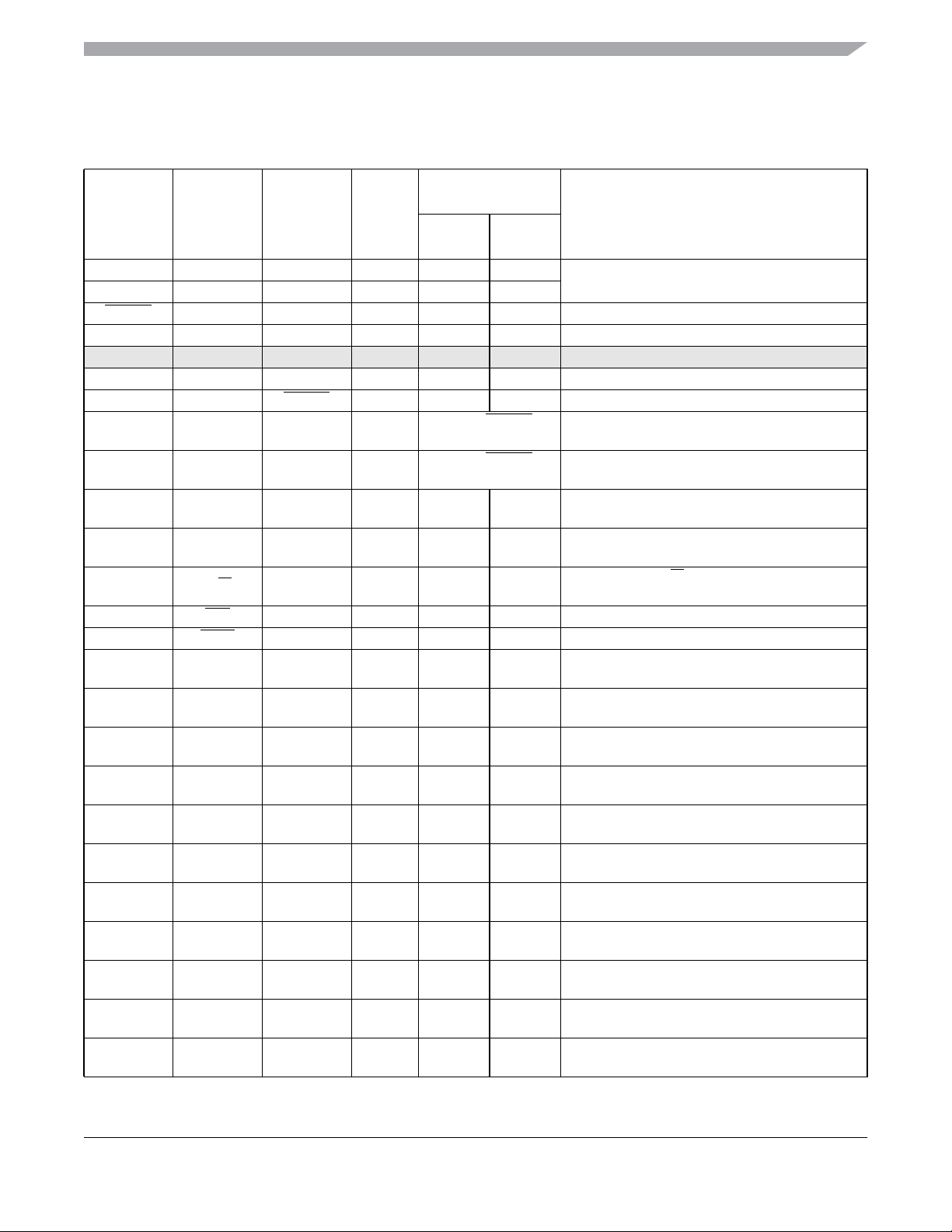
1.3.2 Signal Properties Summary
Table 1-5. Signal Properties
Pin Name
Function 1
EXTAL — — V
XTAL — — V
RESET — — V
XFC — — V
TEST V
BKGD MODC TAGHI V
PE7 NOACC
PE6 IPIPE1 MODB V
PE5 IPIPE0 MODA V
PE4 ECLK — V
PE3 LSTRB TAGLO V
PE2 R/
PE1
PE0
PA[7:3]
PA[2:1]
PA[0]
PB[7:5]
PB[4]
PB[3:0]
PAD[7:0] AN[7:0] — V
PP[7] KWP[7] — V
PP[6] KWP[6] ROMCTL V
PP[5] KWP[5] PW5 V
PP[4:3] KWP[4:3] PW[4:3] V
Pin Name
Function 2
PP
Pin Name
Function 3
— V
Domain
XCLKS V
W—V
IRQ — V
XIRQ — V
ADDR[15:1/
DATA[15:1]
ADDR[10:9/
DATA[10:9]
ADDR[8]/
DATA[8]
ADDR[7:5]/
DATA[7:5]
ADDR[4]/
DATA[4]
ADDR[3:0]/
DATA[3:0]
—V
—V
—V
—V
—V
—V
Power
DDPLL
DDPLL
DDX
DDPLL
SSX
DDX
DDX
DDX
DDX
DDX
DDX
DDX
DDX
DDX
DDX
DDX
DDX
DDX
DDX
DDX
DDA
DDX
DDX
DDX
DDX
CTRL
NA NA Oscillator pins
NA NA
None None External reset pin
NA NA PLL loop filter pin
NA NA Test pin only
Up Up Background debug, mode pin, tag signal high
PUCR Up Port E I/O pin, access, clock select
pin is low: Down
pin is low: Down
PUCR
PUCR
PUCR
PUCR Up Port E input, external interrupt pin
PUCR Up Port E input, non-maskable interrupt pin
PUCR Disabled
PUCR Disabled
PUCR Disabled
PUCR Disabled
PUCR Disabled
PUCR Disabled
PERAD/P
PSAD
PERP/
PPSP
PERP/
PPSP
PERP/
PPSP
PERP/
PPSP
Internal Pull
Resistor
Reset
State
While RESET
While RESET
Mode
Dep
Mode
Dep
Mode
Dep
Disabled
Disabled
Disabled
Disabled
Disabled
Chapter 1 Device Overview
Description
Port E I/O pin and pipe status
Port E I/O pin and pipe status
Port E I/O pin, bus clock output
(1)
Port E I/O pin, low strobe, tag signal low
1
Port E I/O pin, R/W in expanded modes
1
Port A I/O pin and multiplexed address/data
Port A I/O pin and multiplexed address/data
Port A I/O pin and multiplexed address/data
Port B I/O pin and multiplexed address/data
Port B I/O pin and multiplexed address/data
Port B I/O pin and multiplexed address/data
Port AD I/O pins and ATD inputs
Port P I/O pins and keypad wake-up
Port P I/O pins, keypad wake-up, and ROMON
enable.
Port P I/O pin, keypad wake-up, PW5 output
Port P I/O pin, keypad wake-up, PWM output
MC9S12C128 Data Sheet, Rev. 1.15
Freescale Semiconductor 51
Page 52

Chapter 1 Device Overview
Table 1-5. Signal Properties (continued)
Internal Pull
Pin Name
Function 1
PP[2:0] KWP[2:0] PW[2:0] V
PJ[7:6] KWJ[7:6] — V
PM5 SCK — V
PM4 MOSI — V
PM3 SS — V
PM2 MISO — V
PM1 TXCAN — V
PM0 RXCAN — V
PS[3:2] — — V
PS1 TXD — V
PS0 RXD — V
PT[7:5] IOC[7:5] — V
PT[4:0] IOC[4:0] PW[4:0] V
1. The Port E output buffer enable signal control at reset is determined by the PEAR register and is mode dependent. For
example, in special test mode RDWE= LSTRE = 1 which enables the PE[3:2] output buffersand disables the pull-ups. Refer
to S12_MEBI user guide for PEAR register details.
2. CAN functionality is not available on the MC9S12GC Family members.
Pin Name
Function 2
Pin Name
Function 3
Power
Domain
DDX
DDX
DDX
DDX
DDX
DDX
DDX
DDX
DDX
DDX
DDX
DDX
DDX
Resistor
CTRL
PERP/
PPSP
PERJ/
PPSJ
PERM/
PPSM
PERM/
PPSM
PERM/
PPSM
PERM/
PPSM
PERM/
PPSM
PERM/
PPSM
PERS/
PPSS
PERS/
PPSS
PERS/
PPSS
PERT/
PPST
PERT/
PPST
Reset
State
Disabled
Disabled
Up
Up
Up
Up
Up
Up
Up
Up
Up
Disabled
Disabled
Description
Port P I/O pins, keypad wake-up, PWM outputs
Port J I/O pins and keypad wake-up
Port M I/O pin and SPI SCK signal
Port M I/O pin and SPI MOSI signal
Port M I/O pin and SPI SS signal
Port M I/O pin and SPI MISO signal
Port M I/O pin and CAN transmit signal
Port M I/O pin and CAN receive signal
Port S I/O pins
Port S I/O pin and SCI transmit signal
Port S I/O pin and SCI receive signal
Port T I/O pins shared with timer (TIM)
Port T I/O pins shared with timer and PWM
(2)
2
1.3.3 Pin Initialization for 48- and 52-Pin LQFP Bond Out Versions
Not Bonded Pins:
If the port pins are not bonded out in the chosen package the user should initialize the registers to
be inputs with enabled pull resistance to avoid excess current consumption. This applies to the
following pins:
(48LQFP): Port A[7:1], Port B[7:5], Port B[3:0], PortE[6,5,3,2], Port P[7:6], PortP[4:0], Port
J[7:6], PortS[3:2]
(52LQFP): Port A[7:3], Port B[7:5], Port B[3:0], PortE[6,5,3,2], Port P[7:6], PortP[2:0], Port
J[7:6], PortS[3:2]
MC9S12C128 Data Sheet, Rev. 1.15
52 Freescale Semiconductor
Page 53

Chapter 1 Device Overview
1.3.4 Detailed Signal Descriptions
1.3.4.1 EXTAL, XTAL — Oscillator Pins
EXTAL and XTAL are the crystal driver and external clock pins. On reset all the deviceclocks are derived
from the EXTAL input frequency. XTAL is the crystal output.
1.3.4.2 RESET — External Reset Pin
RESET is an activelow bidirectional control signal that acts as an input to initialize the MCU to a known
start-up state. It also acts as an open-drain output to indicate that an internal failure has been detected in
either the clock monitor or COP watchdog circuit. External circuitry connected to the
not include a largecapacitance that would interfere with the ability of this signal to rise to a validlogic one
within 32 ECLK cycles after the low drive is released. Upon detection of any reset, an internal circuit
drives the
RESET pin low and a clocked reset sequence controls when the MCU can begin normal
processing.
1.3.4.3 TEST / VPP — Test Pin
This pin is reserved for test and must be tied to VSS in all applications.
RESET pin should
1.3.4.4 XFC — PLL Loop Filter Pin
Dedicated pin used to create the PLL loop filter. See CRG BUG for more detailed information.PLL loop
filter. Please ask your Freescale representative for the interactive application note to compute PLL loop
filter elements. Any current leakage on this pin must be avoided.
XFC
R
0
MCU
Figure 1-10. PLL Loop Filter Connections
V
DDPLL
C
S
V
DDPLL
C
P
1.3.4.5 BKGD / TAGHI / MODC — Background Debug, Tag High, and Mode Pin
The BKGD / TAGHI / MODC pin is used as a pseudo-open-drain pin for the background debug
communication. In MCU expanded modes of operation when instruction tagging is on, an input low on
this pin during the falling edge of E-clock tags the high half of the instruction word being read into the
instruction queue. It is also used as a MCU operating mode select pin at the rising edge during reset, when
the state of this pin is latched to the MODC bit.
MC9S12C128 Data Sheet, Rev. 1.15
Freescale Semiconductor 53
Page 54

Chapter 1 Device Overview
1.3.4.6 PA[7:0] / ADDR[15:8] / DATA[15:8] — Port A I/O Pins
PA7–PA0 are general purpose input or output pins,. In MCU expanded modes of operation, these pins are
used for the multiplexedexternal address and data bus.PA[7:1]pins arenot availablein the 48-pinpackage
version. PA[7:3] are not available in the 52-pin package version.
1.3.4.7 PB[7:0] / ADDR[7:0] / DATA[7:0] — Port B I/O Pins
PB7–PB0 are general purpose input or output pins. In MCU expanded modes of operation, these pins are
used for the multiplexed external address and data bus. PB[7:5] and PB[3:0] pins are not available in the
48-pin nor 52-pin package version.
1.3.4.8 PE7 / NOACC / XCLKS — Port E I/O Pin 7
PE7 is a general purpose input or output pin. During MCU expanded modes of operation, the NOACC
signal, when enabled, is used to indicate that the current buscycle is an unused or “free” cycle. This signal
will assert when the CPU is not using the bus.The
crystal in combination with the internal Colpitts (low power) oscillator is used or whether Pierce
oscillator/external clock circuitry is used. The state of this pin is latched at the rising edge of
the input is a logic low the EXTAL pin is configured for an external clock drive or a Pierce oscillator. If
input is a logic high a Colpitts oscillator circuit is configured on EXTAL and XTAL. Since this pin is an
input with a pull-up device during reset, if the pin is left floating, the default configuration is a Colpitts
oscillator circuit on EXTAL and XTAL.
XCLKS is an input signal which controls whether a
RESET. If
EXTAL
1
CDC
MCU
XTAL
1. Due to the nature of a translated ground Colpitts oscillator a DC voltage
bias is applied to the crystal. Please contact the crystal manufacturer for
crystal DC.
C
1
C
2
V
SSPLL
Crystal or
Ceramic Resonator
Figure 1-11. Colpitts Oscillator Connections (PE7 = 1)
EXTAL
C
1
MCU
XTAL
1. RS can be zero (shorted) when used with higher frequency crystals,
refer to manufacturer’s data.
R
B
1
R
S
Crystal or
Ceramic Resonator
C
2
V
SSPLL
Figure 1-12. Pierce Oscillator Connections (PE7 = 0)
MC9S12C128 Data Sheet, Rev. 1.15
54 Freescale Semiconductor
Page 55

Chapter 1 Device Overview
EXTAL
MCU
XTAL
Figure 1-13. External Clock Connections (PE7 = 0)
Not Connected
CMOS Compatible
External Oscillator
(V
Level)
DDPLL
1.3.4.9 PE6 / MODB / IPIPE1 — Port E I/O Pin 6
PE6 is a general purpose input or output pin. It is used as a MCU operating mode select pin during reset.
The state of this pin is latched to the MODB bit at the rising edge of
RESET. This pin is shared with the
instruction queue tracking signal IPIPE1. This pin is an input with a pull-down devicewhich is only active
RESET is low. PE[6] is not available in the 48- / 52-pin package versions.
when
1.3.4.10 PE5 / MODA / IPIPE0 — Port E I/O Pin 5
PE5 is a general purpose input or output pin. It is used as a MCU operating mode select pin during reset.
The state of this pin is latched to the MODA bit at the rising edge of
instruction queue tracking signal IPIPE0. This pin is an input with a pull-down devicewhich is only active
RESET is low. This pin is not available in the 48- / 52-pin package versions.
when
RESET. This pin is shared with the
1.3.4.11 PE4 / ECLK— Port E I/O Pin [4] / E-Clock Output
ECLK is the output connection for the internal bus clock. It is used to demultiplex the address and data in
expanded modes and is used as a timing reference. ECLK frequency is equal to 1/2 the crystal frequency
out of reset. The ECLK pin is initially configured as ECLK output with stretch in all expanded modes. The
E clock output function depends upon the settings of the NECLK bit in the PEAR register, the IVIS bit in
the MODE register and the ESTR bit in the EBICTL register. All clocks, including the E clock, are halted
when the MCU is in stop mode. It is possible to configure the MCU to interface to slowexternal memory.
ECLK can be stretched for such accesses. Reference the MISC register (EXSTR[1:0] bits) for more
information. In normal expanded narrow mode, the E clock is available for use in external select decode
logic or as a constant speed clock for use in the external application system. AlternativelyPE4 can be used
as a general purpose input or output pin.
1.3.4.12 PE3 / LSTRB — Port E I/O Pin [3] / Low-Byte Strobe (LSTRB)
In all modes this pin can be used as a general-purpose I/O and is an input with an active pull-up out of
reset. Ifthe strobe function is required, it should be enabled by settingthe LSTRE bit in the PEAR register.
This signal is used in write operations. Therefore external low byte writes will not be possible until this
function is enabled. This pin is also used as
LSTRB function. This pin is not available in the 48- / 52-pin package versions.
the
TAGLO in special expanded modes and is multiplexed with
MC9S12C128 Data Sheet, Rev. 1.15
Freescale Semiconductor 55
Page 56

Chapter 1 Device Overview
1.3.4.13 PE2 / R/W — Port E I/O Pin [2] / Read/Write
In all modes this pin can be used as a general-purpose I/O and is an input with an active pull-up out of
reset. If the read/write function is required it should be enabled by setting the RDWE bit in the PEAR
register. External writes will not be possible until enabled. This pin is not available in the 48- / 52-pin
package versions.
1.3.4.14 PE1 / IRQ — Port E Input Pin [1] / Maskable Interrupt Pin
The IRQ input provides a means of applying asynchronous interrupt requests to the MCU. Either falling
edge-sensitive triggering or level-sensitive triggering is program selectable (INTCR register).
IRQ is
always enabled and configured to level-sensitive triggering out of reset. It can be disabled by clearing
IRQEN bit (INTCR register). When the MCU is reset the
IRQ function is masked in the condition code
register. This pin is always an input and can always be read. There is an active pull-up on this pin while in
reset and immediately out of reset. The pull-up can be turned off by clearing PUPEE in the PUCR register.
1.3.4.15 PE0 / XIRQ — Port E input Pin [0] / Non Maskable Interrupt Pin
The XIRQ input provides a means of requesting a non-maskable interrupt after reset initialization. During
reset, the X bit in the condition code register (CCR) is set and any interrupt is masked until MCU software
enables it. Because the
network. This pin is always an input and can always be read. There is an active pull-up on this pin while
in reset and immediately out of reset. The pull-up can be turned off by clearing PUPEE in the PUCR
register.
XIRQ input is level sensitive, it can be connected to a multiple-source wired-OR
1.3.4.16 PAD[7:0] / AN[7:0] — Port AD I/O Pins [7:0]
PAD7–PAD0 are general purpose I/O pins and also analog inputs for the analog to digital converter. In
order to use a PAD pin as a standard input, the corresponding ATDDIEN register bit must be set. These
bits are cleared out of reset to configure the PAD pins for A/D operation.
When the A/D converter is active in multi-channel mode, port inputs are scanned and converted
irrespective of Port AD configuration. Thus Port AD pins that are configured as digital inputs or digital
outputs are also converted in the A/D conversion sequence.
1.3.4.17 PP[7] / KWP[7] — Port P I/O Pin [7]
PP7 is a general purpose input or output pin, shared with the keypad interrupt function. When configured
as an input, it can generate interrupts causing the MCU to exit stop or wait mode. This pin is not available
in the 48- / 52-pin package versions.
1.3.4.18 PP[6] / KWP[6]/ROMCTL — Port P I/O Pin [6]
PP6 is a general purpose input or output pin, shared with the keypad interrupt function. When configured
as an input, it can generate interrupts causing the MCU to exit stop or wait mode. This pin is not available
in the 48- / 52-pin package versions. During MCU expanded modes of operation, this pin is used to enable
MC9S12C128 Data Sheet, Rev. 1.15
56 Freescale Semiconductor
Page 57

Chapter 1 Device Overview
the Flash EEPROM memory in the memory map (ROMCTL). At the rising edge of RESET, the state of
this pin is latched to the ROMON bit.
• PP6 = 1 in emulation modes equates to ROMON = 0 (ROM space externally mapped)
• PP6 = 0 in expanded modes equates to ROMON = 0 (ROM space externally mapped)
1.3.4.19 PP[5:0] / KWP[5:0] / PW[5:0] — Port P I/O Pins [5:0]
PP[5:0] are general purpose input or output pins, shared with the keypad interrupt function. When
configured as inputs, they can generate interrupts causing the MCU to exit stop or wait mode.
PP[5:0] are also shared with the PWM output signals, PW[5:0]. Pins PP[2:0] are only available in the 80pin package version. Pins PP[4:3] are not available in the 48-pin package version.
1.3.4.20 PJ[7:6] / KWJ[7:6] — Port J I/O Pins [7:6]
PJ[7:6] are general purpose input or output pins, shared with the keypad interrupt function. When
configured as inputs, they can generate interrupts causing the MCU to exit stop or wait mode. These pins
are not available in the 48-pin package version nor in the 52-pin package version.
1.3.4.21 PM5 / SCK — Port M I/O Pin 5
PM5 is a general purpose input or output pin and also the serial clock pin SCK for the serial peripheral
interface (SPI).
1.3.4.22 PM4 / MOSI — Port M I/O Pin 4
PM4 is a general purpose input or output pin and also the master output (during master mode) or slave
input (during slave mode) pin for the serial peripheral interface (SPI).
1.3.4.23 PM3 / SS — Port M I/O Pin 3
PM3 is a general purpose input or output pin and also the slave select pin SS for the serial peripheral
interface (SPI).
1.3.4.24 PM2 / MISO — Port M I/O Pin 2
PM2 is a general purpose input or output pin and also the master input (during master mode) or slave
output (during slave mode) pin for the serial peripheral interface (SPI).
1.3.4.25 PM1 / TXCAN — Port M I/O Pin 1
PM1 is a general purpose input or output pin and the transmit pin, TXCAN, of the CAN module if
available.
1.3.4.26 PM0 / RXCAN — Port M I/O Pin 0
PM0 is a general purpose input or output pinand the receivepin, RXCAN, of the CAN module if available.
MC9S12C128 Data Sheet, Rev. 1.15
Freescale Semiconductor 57
Page 58

Chapter 1 Device Overview
1.3.4.27 PS[3:2] — Port S I/O Pins [3:2]
PS3 and PS2 are general purpose input or output pins. These pins are not available in the 48- / 52-pin
package versions.
1.3.4.28 PS1 / TXD — Port S I/O Pin 1
PS1 is a general purpose input or output pin and the transmit pin, TXD, of serial communication interface
(SCI).
1.3.4.29 PS0 / RXD — Port S I/O Pin 0
PS0 is a general purpose input or output pin and the receive pin, RXD, of serial communication interface
(SCI).
1.3.4.30 PPT[7:5] / IOC[7:5] — Port T I/O Pins [7:5]
PT7–PT5 are general purpose input or output pins. They can also be configured as the timer system input
capture or output compare pins IOC7-IOC5.
1.3.4.31 PT[4:0] / IOC[4:0] / PW[4:0]— Port T I/O Pins [4:0]
PT4–PT0 are general purpose input or output pins. They can also be configured as the timer system input
capture or output compare pins IOC[n] or as the PWM outputs PW[n].
1.3.5 Power Supply Pins
1.3.5.1 V
DDX,VSSX
External powerand ground for I/O drivers.Bypass requirements depend on how heavily the MCUpins are
loaded.
1.3.5.2 V
DDR
, V
Voltage Regulator
External power and ground for the internal voltage regulator. Connecting V
internal voltage regulator.
1.3.5.3 V
Poweris supplied to theMCU through VDDand VSS. This2.5V supply is derivedfrom the internalvoltage
regulator.There isno static loadon those pins allowed.The internal voltageregulatoris turned off,if V
is tied to ground.
DD1
, V
— Power and Ground Pins for I/O Drivers
— Power and Ground Pins for I/O Drivers and for Internal
SSR
to ground disables the
DDR
DD2
, V
SS1
, V
— Internal Logic Power Pins
SS2
DDR
MC9S12C128 Data Sheet, Rev. 1.15
58 Freescale Semiconductor
Page 59

Chapter 1 Device Overview
1.3.5.4 V
V
DDA,VSSA
are the powersupply and ground input pins for the voltage regulator reference and the analog
DDA
, V
— Power Supply Pins for ATD and VREG
SSA
to digital converter.
1.3.5.5 VRH, VRL — ATD Reference Voltage Input Pins
VRH and VRL are the reference voltage input pins for the analog to digital converter.
1.3.5.6 V
DDPLL
Provides operating voltage and ground for the oscillator and the phased-locked loop. This allows the
supply voltage to the oscillator and PLL to be bypassed independently. This 2.5V voltage is generated by
the internal voltage regulator.
Mnemonic
V
, V
DD1
DD2
V
, V
SS1
SS2
V
DDR
V
SSR
V
DDX
V
SSX
V
DDA
V
SSA
V
RH
V
RL
V
DDPLL
V
SSPLL
Nominal
Voltage (V)
, V
SSPLL
— Power Supply Pins for PLL
Table 1-6. Power and Ground Connection Summary
Description
2.5 Internal power and ground generated by internal regulator. These also allow an external source
0
5.0 External power and ground, supply to internal voltage regulator.
0
5.0 External power and ground, supply to pin drivers.
0
5.0 Operating voltage and ground for the analog-to-digital converters and the reference for the
0
5.0 Reference voltage low for the ATD converter.
0
2.5 Providesoperatingvoltage and groundforthe phased-locked loop. This allowsthe supply voltage
0
to supply the core V
In the 48 and 52 LQFP packages V
internal voltage regulator, allows the supply voltage to the A/D to be bypassed independently.
In the 48 and 52 LQFP packages V
to the PLL to be bypassed independently. Internal power and ground generated by internal
regulator.
voltages and bypass the internal voltage regulator.
DD/VSS
and V
DD2
is bonded to V
RL
are not available.
SS2
.
SSA
NOTE
All V
pins must be connected together in the application. Because fast
SS
signal transitions place high, short-duration current demands on the power
supply, use bypass capacitors with high-frequency characteristics and place
them as close to the MCU as possible. Bypass requirements depend on
MCU pin load.
MC9S12C128 Data Sheet, Rev. 1.15
Freescale Semiconductor 59
Page 60
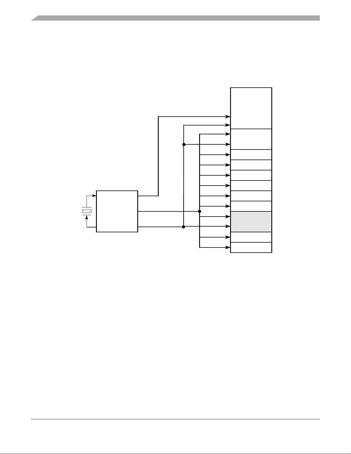
Chapter 1 Device Overview
1.4 System Clock Description
The clock and reset generator provides the internal clock signals for the core and all peripheral modules.
Figure 1-14 shows the clock connections from the CRG to all modules. Consult the CRG Block User
Guide for details on clock generation.
EXTAL
XTAL
CRG
Core Clock
Bus Clock
Oscillator Clock
Figure 1-14. Clock Connections
S12_CORE
Flash
RAM
TIM
ATD
PIM
SCI
SPI
MSCAN
Not on 9S12GC
VREG
TPM
1.5 Modes of Operation
Eight possible modes determine the device operating configuration. Each mode has an associated default
memory map and external bus configuration controlled by a further pin.
Three low power modes exist for the device.
1.5.1 Chip Configuration Summary
The operating mode out ofreset is determined bythe states ofthe MODC, MODB, andMODA pins during
reset. The MODC, MODB, and MODA bits in the MODE register show the current operating mode and
provide limited mode switching during operation. The states of the MODC, MODB, and MODA pins are
latched into these bits on the rising edge of the reset signal. The ROMCTL signal allows the setting of the
ROMONbit in the MISC register thus controlling whether the internal Flash is visible in the memory map.
ROMON = 1 mean the Flash is visible in the memory map. The state of the ROMCTL pin is latched into
the ROMON bit in the MISC register on the rising edge of the reset signal.
MC9S12C128 Data Sheet, Rev. 1.15
60 Freescale Semiconductor
Page 61

Table 1-7. Mode Selection
Chapter 1 Device Overview
BKGD =
MODC
000 X 1
001
0 1 0 X 0 Special Test (Expanded Wide), BDM allowed
011
1 0 0 X 1 Normal Single Chip, BDM allowed
101
110 X 1
111
PE6 =
MODB
PE5 =
MODA
PP6 =
ROMCTL
0 1 Emulation Expanded Narrow, BDM allowed
10
0 1 Emulation Expanded Wide, BDM allowed
10
0 0 Normal Expanded Narrow, BDM allowed
11
0 0 Normal Expanded Wide, BDM allowed
11
ROMON
Bit
Mode Description
Special Single Chip, BDM allowed and ACTIVE. BDM is allowed in
all other modes but a serial command is required to make BDM
active.
Peripheral; BDM allowed but bus operations would cause bus
conflicts (must not be used)
For further explanation on the modes refer to the S12_MEBI block guide.
Table 1-8. Clock Selection Based on PE7
PE7 = XCLKS Description
1 Colpitts Oscillator selected
0 Pierce Oscillator/external clock selected
1.5.2 Security
The device will make available a security feature preventing the unauthorized read and write of the
memory contents. This feature allows:
• Protection of the contents of FLASH,
• Operation in single-chip mode,
• Operation from external memory with internal FLASH disabled.
The user must be reminded that part of the security must lie with the user’s code. An extreme example
would be user’scode that dumps the contents of the internal program. This code would defeat the purpose
of security. At the same time the user may also wish to put a back door in the user’sprogram. An example
of this is the user downloads a key through the SCI which allows access to a programming routine that
updates parameters.
1.5.2.1 Securing the Microcontroller
Once the user has programmed the FLASH, the part can be secured by programming the security bits
located in the FLASH module. These non-volatile bits will keep the part secured through resetting the part
and through powering down the part.
MC9S12C128 Data Sheet, Rev. 1.15
Freescale Semiconductor 61
Page 62

Chapter 1 Device Overview
The security byte resides in a portion of the Flash array.
Check the Flash Block User Guide for more details on the security configuration.
1.5.2.2 Operation of the Secured Microcontroller
1.5.2.2.1 Normal Single Chip Mode
This will bethe most common usage of the secured part.Everything will appear the same as if the part was
not secured with the exception of BDM operation. The BDM operation will be blocked.
1.5.2.2.2 Executing from External Memory
The user may wish to execute from external space with a secured microcontroller. This is accomplished
by resetting directly into expanded mode. The internal FLASH will be disabled. BDM operations will be
blocked.
1.5.2.3 Unsecuring the Microcontroller
In order to unsecure the microcontroller, the internal FLASH must be erased. This can be done through an
externalprogram in expanded mode or via a sequence of BDM commands. Unsecuring is also possible via
the Backdoor Key Access. Refer to Flash Block Guide for details.
Once the user has erased the FLASH, the part can be reset into special single chip mode. This invokes a
program that verifies the erasure of the internal FLASH. Once this program completes, the user can erase
and program the FLASH security bits to the unsecured state. This is generally done through the BDM, but
the user could also change to expanded mode (by writing the mode bits through the BDM) and jumping to
an external program (again through BDM commands). Note that if the part goes through a reset before the
security bits are reprogrammed to the unsecure state, the part will be secured again.
1.5.3 Low-Power Modes
The microcontroller features three main low power modes. Consult the respective Block User Guide for
information on the module behavior in stop, pseudo stop, and wait mode. An important source of
information about the clock system is the Clock and Reset Generator User Guide (CRG).
1.5.3.1 Stop
Executing the CPU STOP instruction stops all clocks and the oscillator thus putting the chip in fully static
mode. Wake up from this mode can be done via reset or external interrupts.
1.5.3.2 Pseudo Stop
This mode is entered by executing the CPU STOP instruction. In this mode the oscillator is still running
and the real time interrupt (RTI) or watchdog (COP) sub module can stay active. Other peripherals are
turned off.This mode consumes more current than thefull stop mode, butthe wakeup time from thismode
is significantly shorter.
MC9S12C128 Data Sheet, Rev. 1.15
62 Freescale Semiconductor
Page 63

Chapter 1 Device Overview
1.5.3.3 Wait
This mode is entered by executing the CPU WAI instruction. In this mode the CPU will not execute
instructions. The internal CPU signals (address and data bus) will be fully static. All peripherals stay
active.For further power consumption reduction the peripherals can individuallyturn off theirlocal clocks.
1.5.3.4 Run
Although this is not a low-power mode, unused peripheral modules should not be enabled in order to save
power.
1.6 Resets and Interrupts
Consult the Exception Processing section of the CPU12 Reference Manual for information.
1.6.1 Vectors
Table 1-9 lists interrupt sources and vectors in default order of priority.
Table 1-9. Interrupt Vector Locations
Vector Address Interrupt Source
External reset, power on reset,
0xFFFE, 0xFFFF
0xFFFC, 0xFFFD Clock monitor fail reset None COPCTL (CME, FCME) —
0xFFFA, 0xFFFB COP failure reset None COP rate select —
0xFFF8, 0xFFF9 Unimplemented instruction trap None None —
0xFFF6, 0xFFF7 SWI None None —
0xFFF4, 0xFFF5 XIRQ X-Bit None —
0xFFF2, 0xFFF3 IRQ I bit INTCR (IRQEN) 0x00F2
0xFFF0, 0xFFF1 Real time Interrupt I bit CRGINT (RTIE) 0x00F0
0xFFEE, 0xFFEF Standard timer channel 0 I bit TIE (C0I) 0x00EE
0xFFEC, 0xFFED Standard timer channel 1 I bit TIE (C1I) 0x00EC
0xFFEA, 0xFFEB Standard timer channel 2 I bit TIE (C2I) 0x00EA
0xFFE8, 0xFFE9 Standard timer channel 3 I bit TIE (C3I) 0x00E8
0xFFE6, 0xFFE7 Standard timer channel 4 I bit TIE (C4I) 0x00E6
0xFFE4, 0xFFE5 Standard timer channel 5 I bit TIE (C5I) 0x00E4
(see CRG flags register to determine
or low voltage reset
reset source)
CCR
Mask
None None —
Local Enable
HPRIO Value
to Elevate
0xFFE2, 0xFFE3 Standard timer channel 6 I bit TIE (C6I) 0x00E2
0xFFE0, 0xFFE1 Standard timer channel 7 I bit TIE (C7I) 0x00E0
0xFFDE, 0xFFDF Standard timer overflow I bit TMSK2 (TOI) 0x00DE
0xFFDC, 0xFFDD Pulse accumulator A overflow I bit PACTL (PAOVI) 0x00DC
MC9S12C128 Data Sheet, Rev. 1.15
Freescale Semiconductor 63
Page 64

Chapter 1 Device Overview
Table 1-9. Interrupt Vector Locations (continued)
Vector Address Interrupt Source
CCR
Mask
Local Enable
HPRIO Value
to Elevate
0xFFDA, 0xFFDB Pulse accumulator input edge I bit PACTL (PAI) 0x00DA
0xFFD8, 0xFFD9 SPI I bit SPICR1 (SPIE, SPTIE) 0x00D8
0xFFD6, 0xFFD7 SCI I bit
0xFFD4, 0xFFD5
Reserved
SCICR2
(TIE, TCIE, RIE, ILIE)
0x00D6
0xFFD2, 0xFFD3 ATD I bit ATDCTL2 (ASCIE) 0x00D2
0xFFD0, 0xFFD1
Reserved
0xFFCE, 0xFFCF Port J I bit PIEP (PIEP7-6) 0x00CE
0xFFCC, 0xFFCD
0xFFCA, 0xFFCB
0xFFC8, 0xFFC9
Reserved
Reserved
Reserved
0xFFC6, 0xFFC7 CRG PLL lock I bit PLLCR (LOCKIE) 0x00C6
0xFFC4, 0xFFC5 CRG self clock mode I bit PLLCR (SCMIE) 0x00C4
0xFFBA to 0xFFC3
Reserved
0xFFB8, 0xFFB9 FLASH I bit FCNFG (CCIE, CBEIE) 0x00B8
0xFFB6, 0xFFB7
0xFFB4, 0xFFB5
0xFFB2, 0xFFB3
0xFFB0, 0xFFB1
0xFF90 to 0xFFAF
CAN wake-up
CAN errors
CAN receive
CAN transmit
(1)
1
1
1
I bit CANRIER (WUPIE) 0x00B6
I bit CANRIER (CSCIE, OVRIE) 0x00B4
I bit CANRIER (RXFIE) 0x00B2
I bit CANTIER (TXEIE[2:0]) 0x00B0
Reserved
0xFF8E, 0xFF8F Port P I bit PIEP (PIEP7-0) 0x008E
0xFF8C, 0xFF8D PWM emergency shutdown I bit PWMSDN(PWMIE) 0x008C
0xFF8A, 0xFF8B VREG LVI I bit CTRL0 (LVIE) 0x008A
0xFF80 to 0xFF89
Reserved
1. Not available on MC9S12GC Family members
MC9S12C128 Data Sheet, Rev. 1.15
64 Freescale Semiconductor
Page 65

Chapter 1 Device Overview
1.6.2 Resets
Resets are a subset of the interrupts featured in Table 1-9. The different sources capable of generating a
system reset are summarized in Table 1-10. When a reset occurs, MCU registers and control bits are
changed to known start-up states. Refer to the respective module Block User Guides for register reset
states.
1.6.2.1 Reset Summary Table
Table 1-10. Reset Summary
Reset Priority Source Vector
Power-on Reset 1 CRG module 0xFFFE, 0xFFFF
External Reset 1
Low Voltage Reset 1 VREG module 0xFFFE, 0xFFFF
Clock Monitor Reset 2 CRG module 0xFFFC, 0xFFFD
COP Watchdog Reset 3 CRG module 0xFFFA, 0xFFFB
1.6.2.2 Effects of Reset
When a reset occurs, MCU registers and control bits are changed to known start-up states. Refer to the
respective module Block User Guides for register reset states. Refer to the HCS12 Multiplexed External
Bus Interface (MEBI) Block Guide for mode dependent pin configuration of port A, B and E out of reset.
RESET pin 0xFFFE, 0xFFFF
Refer to the PIM Block User Guide for reset configurations of all peripheral module ports.
Refer to Figure 1-2to Figure 1-6footnotes for locations of the memoriesdepending on theoperating mode
after reset.
The RAM array is not automatically initialized out of reset.
NOTE
For devices assembled in 48-pin or 52-pin LQFP packages all non-bonded
out pins should be configured as outputs after reset in order to avoid current
drawn from floating inputs. Refer to Table 1-5 for affected pins.
1.7 Device Specific Information and Module Dependencies
1.7.1 PPAGE
External paging is not supported on these devices. In order to access the 16K flash blocks in the address
range 0x8000–0xBFFF the PPAGE register must be loaded with the corresponding value for this range.
Refer to Table 1-11 for device specific page mapping.
For all devices Flash Page 3F is visible in the 0xC000–0xFFFF range if ROMON is set. For all devices
(except MC9S12GC16) Page 3E is also visible in the 0x4000–0x7FFF range if ROMHM is cleared and
ROMON is set. For all devices apart from MC9S12C32 Flash Page 3D is visible in the 0x0000–0x3FFF
range if ROMON is set...
MC9S12C128 Data Sheet, Rev. 1.15
Freescale Semiconductor 65
Page 66

Chapter 1 Device Overview
Table 1-11. Device Specific Flash PAGE Mapping
Device PAGE PAGE Visible with PPAGE Contents
MC9S12GC16 3F $01,$03,$05,$07,$09......$35,$37,$39,$3B,$3D,$3F
MC9S12C32
MC9S12GC32
MC9S12C64
MC9S12GC64
MC9S12C96
MC9S12GC96
MC9S12C128
MC9S12GC128
3E $00,$02,$04,$06,$08,$0A,$0C,$0E,$10,$12......$2C,$2E,$30,$32,$34,$36,$38,$3A,$3C,$3E
3F $01,$03,$05,$07,$09,$0B,$0D,$0F,$11,$13.....$2D,$2F,$31,$33,$35,$37,$39,$3B,$3D,$3F
3C $04,$0C,$14,$1C,$24,$2C,$34,$3C
3D $05,$0D,$15,$1D,$25,$2D,$35,$3D
3E $06,$0E,$16,$1E,$26,$2E,$36,$3E
3F $07,$0F,$17,$1F,$27,$2F,$37,$3F
3A $02,$0A,$12,$1A,$22,$2A,$32,$3A
3B $03,$0B,$13,$1B,$23,$2B,$33,$3B
3C $04,$0C,$14,$1C,$24,$2C,$34,$3C
3D $05,$0D,$15,$1D,$25,$2D,$35,$3D
3E $06,$0E,$16,$1E,$26,$2E,$36,$3E
3F $07,$0F,$17,$1F,$27,$2F,$37,$3F
38 $00,$08,$10,$18,$20,$28,$30,$38
39 $01,$09,$11,$19,$21,$29,$31,$39
3A $02,$0A,$12,$1A,$22,$2A,$32,$3A
3B $03,$0B,$13,$1B,$23,$2B,$33,$3B
3C $04,$0C,$14,$1C,$24,$2C,$34,$3C
3D $05,$0D,$15,$1D,$25,$2D,$35,$3D
3E $06,$0E,$16,$1E,$26,$2E,$36,$3E
3F $07,$0F,$17,$1F,$27,$2F,$37,$3F
1.7.2 BDM Alternate Clock
The BDM section reference to alternate clock is equivalent to the oscillator clock.
1.7.3 Extended Address Range Emulation Implications
In order to emulate the MC9S12GC or MC9S12C-Familydevices, external addressing of a 128K memory
map is required. This is provided in a 112 LQFP package version which includes the 3 necessary extra
external address bus signals via PortK[2:0]. This package version is for emulation only and not provided
as a general production package.
The reset state of DDRK is 0x0000, configuring the pins as inputs.
The reset state of PUPKE in the PUCR register is “1” enabling the internal Port K pullups.
In this reset state the pull-ups provide a defined state and prevent a floating input, thereby preventing
unnecessary current flow at the input stage.
To prevent unnecessary current flow in production package options, the states of DDRK and PUPKE
should not be changed by software.
MC9S12C128 Data Sheet, Rev. 1.15
66 Freescale Semiconductor
Page 67

1.7.4 VREGEN
Chapter 1 Device Overview
The VREGEN input mentioned in the VREG section is device internal, connected internally to V
1.7.5 V
DD1
, V
DD2
, V
SS1
, V
SS2
DDR
.
In the 80-pin QFP package versions, both internal VDDand VSSof the 2.5V domain are bonded out on 2
sides of the device as two pin pairs (V
internally. V
SS1
and V
are connected together internally. The extra pin pair enables systems using the
SS2
DD1,VSS1
&V
DD2,VSS2
). V
DD1
and V
are connected together
DD2
80-pin package to employ better supply routing and further decoupling.
1.7.6 Clock Reset Generator And VREG Interface
The low voltage reset feature uses the low voltage reset signal from the VREG module as an input to the
CRG module. When the regulator output voltage supply to the internal chip logic falls below a specified
threshold the LVR signal from the VREG module causes the CRG module to generate a reset.
NOTE
If thevoltage regulator isshut down by connecting V
to groundthen the
DDR
LVRF flag in the CRG flags register (CRGFLG) is undefined.
1.7.7 Analog-to-Digital Converter
In the 48- and 52-pin package versions, the VRL pad is bonded internally to the V
SSA
pin.
1.7.8 MODRR Register Port T And Port P Mapping
The MODRR register within the PIM allows for mapping of PWM channels to port T in the absence of
port P pins for the low pin count packages. For the 80QFP package option it is recommended not to use
MODRR since this is intended to support PWM channel availability in low pin count packages. Note that
when mapping PWM channels to port T in an 80QFP option, the associated PWM channels are then
mapped to both port P and port T.
1.7.9 Port AD Dependency On PIM And ATD Registers
The port AD pins interface to the PIM module. However, the port pin digital state can be read from either
the PORTAD register in the ATD register map or from the PTAD register in the PIM register map.
In order to read a digital pin value from PORTAD the corresponding ATDDIEN bit must be set. If the
corresponding ATDDIEN bit is cleared then the pin is configured as an analog input and the PORTAD bit
reads back as "1".
In order to read a digital pin value from PTAD, the corresponding DDRAD bit must be cleared, to
configure the pin as an input.
Furthermore in order to use a port AD pin as an analog input, the corresponding DDRAD bit must be
cleared to configure the pin as an input
MC9S12C128 Data Sheet, Rev. 1.15
Freescale Semiconductor 67
Page 68

Chapter 1 Device Overview
1.8 Recommended Printed Circuit Board Layout
The PCB must be carefully laid out to ensure proper operation of the voltage regulator as well as of the
MCU itself. The following rules must be observed:
• Every supply pair must be decoupled by a ceramic capacitor connected as near as possible to the
corresponding pins (C1–C6).
• Central point of the ground star should be the V
• Use low ohmic low inductance connections between V
•V
must be directly connected to V
SSPLL
• Keep traces of V
, EXTAL, and XTAL as short as possible and occupied board area for C7,
SSPLL
SSR
.
C8, C11, and Q1 as small as possible.
• Do not place other signals or supplies underneath area occupied by C7, C8, C10, and Q1 and the
connection area to the MCU.
• Central power input should be fed in at the V
Table 1-12. Recommended Component Values
Component Purpose Type Value
C1 V
C2 V
C3 V
C4 V
C5 V
C6 V
C7 OSC load capacitor
C8 OSC load capacitor
DD2
filter capacitor Ceramic X7R 220nF, 470nF
DD1
filter capacitor (80 QFP only) Ceramic X7R 220nF
filter capacitor Ceramic X7R 100nF
DDA
filter capacitor X7R/tantalum >=100nF
DDR
filter capacitor Ceramic X7R 100nF
DDPLL
filter capacitor X7R/tantalum >=100nF
DDX
pin.
SSR
DDA/VSSA
SS1
, V
SS2
, and V
SSR
.
pins.
See PLL specification chapter
(1)
C9 PLL loop filter capacitor
C10 PLL loop filter capacitor
C11 DC cutoff capacitor
R1 PLL loop filter resistor See PLL Specification chapter
R2 / R
B
R3 / R
S
Q1 Quartz — —
1. In 48LQFP and 52LQFP package versions, V
V
.
DD1
68 Freescale Semiconductor
PLL loop filter resistor
PLL loop filter resistor
is not available. Thus 470nF must be connected to
DD2
MC9S12C128 Data Sheet, Rev. 1.15
See PLL specification chapter
Colpitts mode only, if recommended by
quartz manufacturer
Pierce mode only
Page 69

Chapter 1 Device Overview
C1
C6
DDX
V
V
DD1
V
SS1
V
SSR
V
SSX
V
SSA
C3
V
DDA
C4
V
DDR
C5
C11
C8
C7
Q1
C9
C10
V
SSPLL
V
R1
DDPLL
Note: Oscillator in Colpitts mode.
Figure 1-15. Recommended PCB Layout (48 LQFP)
MC9S12C128 Data Sheet, Rev. 1.15
Freescale Semiconductor 69
Page 70
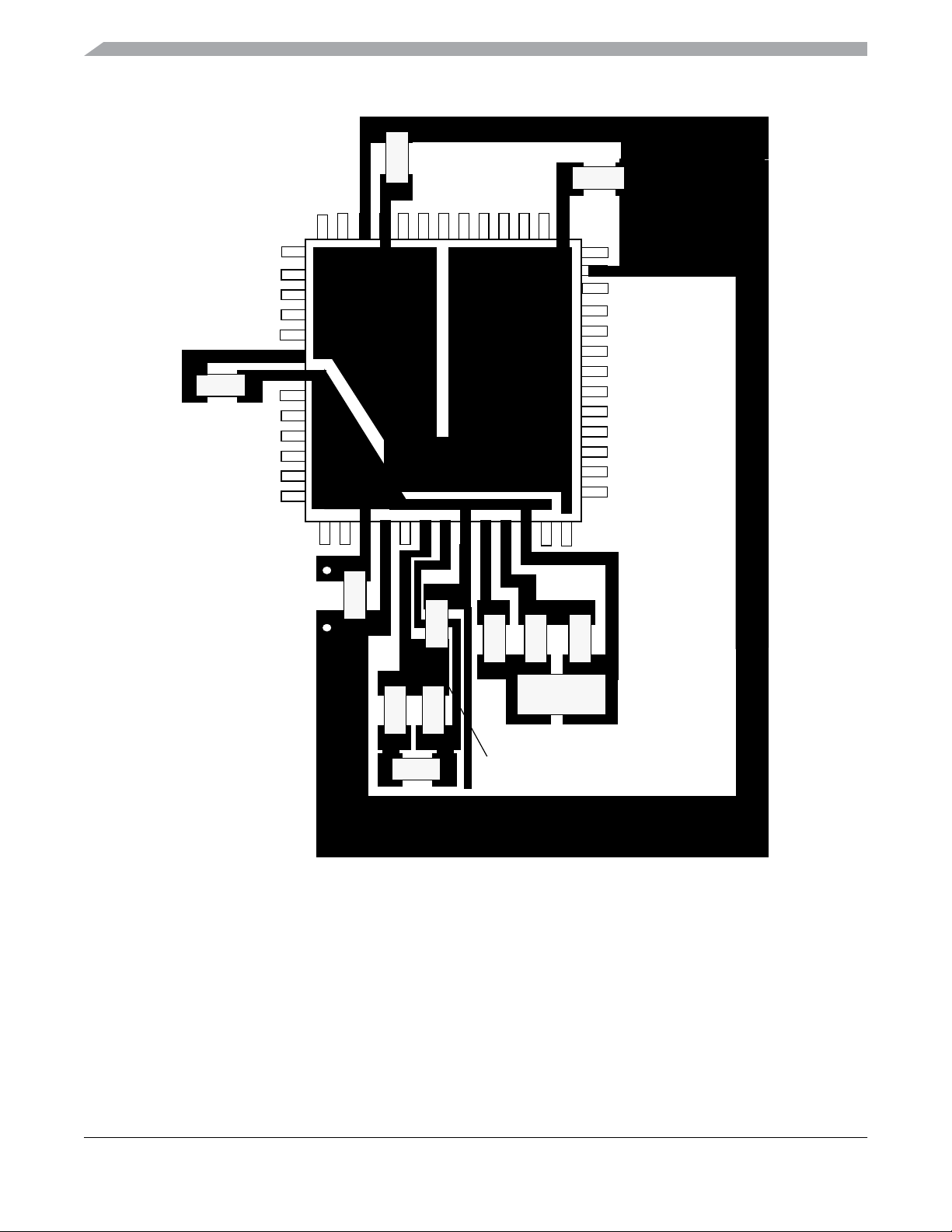
Chapter 1 Device Overview
C1
V
V
DD1
SS1
V
V
SSR
DDR
DDX
V
C4
C6
V
SSX
C5
V
C11
SSA
C8
C3
C7
V
DDA
Note: Oscillator in Colpitts mode.
Figure 1-16. Recommended PCB Layout (52 LQFP)
MC9S12C128 Data Sheet, Rev. 1.15
C9
R1
C10
V
SSPLL
V
DDPLL
Q1
70 Freescale Semiconductor
Page 71

C1
V
V
DD1
SS1
DDX
V
C6
V
SSX
V
SSA
C3
Chapter 1 Device Overview
V
DDA
V
SS2
C2
V
DD2
V
SSR
V
DDR
Note: Oscillator in Colpitts mode.
Figure 1-17. Recommended PCB Layout (80 QFP)
C4
C9
R1
C5
C10
C11
V
SSPLL
V
DDPLL
C8
Q1
C7
MC9S12C128 Data Sheet, Rev. 1.15
Freescale Semiconductor 71
Page 72

Chapter 1 Device Overview
C1
V
V
DD1
SS1
V
V
SSR
DDR
DDX
V
C4
C6
V
SSX
C5
R2
V
SSA
Q1
R3
C3
V
DDA
C9
R1
C10
C8
VSSPLL
V
DDPLL
C7
Figure 1-18. Recommended PCB Layout for 48 LQFP Pierce Oscillator
MC9S12C128 Data Sheet, Rev. 1.15
72 Freescale Semiconductor
Page 73

C1
Chapter 1 Device Overview
C6
DDX
V
V
DD1
V
SS1
V
SSX
V
SSA
C3
V
DDA
V
V
SSR
DDR
C4
C9
R1
C5
C10
V
R2
Q1
C8
VSSPLL
DDPLL
R3
C7
Figure 1-19. Recommended PCB Layout for 52 LQFP Pierce Oscillator
MC9S12C128 Data Sheet, Rev. 1.15
Freescale Semiconductor 73
Page 74

Chapter 1 Device Overview
V
DD1
C1
V
SS1
DDX
V
C6
V
SSX
V
SSA
C3
V
DDA
V
SS2
C2
V
DD2
V
V
V
SSR
DDR
C4
C5
R3
R2
SSPLL
Q1
C9
R1
C10
C8
VSSPLL
V
DDPLL
C7
Figure 1-20. Recommended PCB Layout for 80QFP Pierce Oscillator
MC9S12C128 Data Sheet, Rev. 1.15
74 Freescale Semiconductor
Page 75

Chapter 2 Port Integration Module (PIM9C32) Block Description
2.1 Introduction
The Port Integration Module establishes the interface between the peripheral modules and the I/O pins for
all ports.
This chapter covers:
• Port A, B, and E related to the core logic and the multiplexed bus interface
• Port T connected to the TIM module (PWM module can be routed to port T as well)
• Port S connected to the SCI module
• Port M associated to the MSCAN and SPI module
• Port P connected to the PWM module, external interrupt sources available
• Port J pins can be used as external interrupt sources and standard I/O’s
The following I/O pin configurations can be selected:
• Available on all I/O pins:
— Input/output selection
— Drive strength reduction
— Enable and select of pull resistors
• Available on all Port P and Port J pins:
— Interrupt enable and status flags
The implementation of the Port Integration Module is device dependent.
2.1.1 Features
A standard port has the following minimum features:
• Input/output selection
• 5-V output drive with two selectable drive strength
• 5-V digital and analog input
• Input with selectable pull-up or pull-down device
Optional features:
• Open drain for wired-OR connections
• Interrupt inputs with glitch filtering
MC9S12C128 Data Sheet, Rev. 1.15
Freescale Semiconductor 75
Page 76

Chapter 2 Port Integration Module (PIM9C32) Block Description
2.1.2 Block Diagram
Figure 2-1 is a block diagram of the PIM.
Port Integration Module
PJ6
PJ7
PAD0
PAD1
PAD2
PAD3
PAD4
PAD5
PAD6
PAD7
Port J
A/D
IRQ Logic
AN0
AN1
AN2
AN3
AN4
AN5
AN6
AN7
ATD
CAN
SPI
SCI
IOC0
IOC1
IOC2
IOC3
TIM
IOC4
IOC5
IOC6
IOC7
PWM0
PWM1
PWM2
PWM3
PWM
PWM4
PWM5
RXD
TXD
RXCAN
TXCAN
MISO
MOSI
SCK
SS
MUX
Port T
Port P
Interrupt Logic
Port S
Port M
PT0
PT1
PT2
PT3
PT4
PT5
PT6
PT7
PP0
PP1
PP2
PP3
PP4
PP5
PP6
PP7
PS0
PS1
PS2
PS3
PM0
PM1
PM2
PM3
PM4
PM5
PB0
PB1
PB2
PB3
PB4
PB5
PB6
PB7
PA0
PA1
PA2
PA3
PA4
PA5
PA6
PA7
ADDR0/DATA0
ADDR1/DATA1
ADDR2/DATA2
ADDR3/DATA3
ADDR4/DATA4
Port B
Port A
ADDR5/DATA5
ADDR6/DATA6
ADDR7/DATA7
CORE
ADDR8/DATA8
ADDR9/DATA9
ADDR10/DATA10
ADDR11/DATA11
ADDR12/DATA12
ADDR13/DATA13
ADDR14/DATA14
ADDR15/DATA15
BKGD/MODC/
LSTRB/TAGLO
IPIPE0/MODA
IPIPE1/MODB
NOACC/
TAGHI
XIRQ
IRQ
R/W
ECLK
XCLKS
Port E
BKGD
PE0
PE1
PE2
PE3
PE4
PE5
PE6
PE7
Figure 2-1. PIM Block Diagram
MC9S12C128 Data Sheet, Rev. 1.15
76 Freescale Semiconductor
Page 77

Chapter 2 Port Integration Module (PIM9C32) Block Description
2.2 Signal Description
This section lists and describes the signals that do connect off-chip.
Table 2-1 shows all pins and their functions that are controlled by the PIM module. If there is more than
one function associated to a pin, the priority is indicated by the position in the table from top (highest
priority) to down (lowest priority).
Table 2-1. Pin Functions and Priorities
Port Pin Name Pin Function Description
Port T PT[7:0] PWM[4:0] PWM outputs (only available if enabled in MODRR register) GPIO
IOC[7:0] Standard timer channels 7 to 0
GPIO General-purpose I/O
Port S PS3 GPIO General-purpose I/O
PS2 GPIO General purpose I/O
PS1 TXD Serial communication interface transmit pin
GPIO General-purpose I/O
PS0 RXD Serial communication interface receive pin
GPIO General-purpose I/O
Port M PM5 SCK SPI clock
PM4 MOSI SPI transmit pin
PM3 SS SPI slave select line
PM2 MISO SPI receive pin
PM1 TXCAN MSCAN transmit pin
PM0 RXCAN MSCAN receive pin
Port P PP[7:0] PWM[5:0] PWM outputs
GPIO[7:0] General purpose I/O with interrupt
PP[6] ROMON ROMON input signal
Port J PJ[7:6] GPIO General purpose I/O with interrupt
Port AD PAD[7:0] ATD[7:0] ATD analog inputs
GPIO[7:0] General purpose I/O
Port A PA[7:0] ADDR[15:8]/
DATA[15:8]/
GPIO
Port B PB[7:0] ADDR[7:0]/
DATA[7:0]/
GPIO
Refer to MEBI Block Guide.
Refer to MEBI Block Guide.
Pin Function
after Reset
MC9S12C128 Data Sheet, Rev. 1.15
Freescale Semiconductor 77
Page 78

Chapter 2 Port Integration Module (PIM9C32) Block Description
Table 2-1. Pin Functions and Priorities (continued)
Port Pin Name Pin Function Description
NOACC/
PE7
PE6
PE5
Port E
PE4 ECLK/GPIO
PE3
PE2
PE1 IRQ/GPI
PE0
XCLKS/
GPIO
IPIPE1/
MODB/
GPIO
IPIPE0/
MODA/
GPIO
LSTRB/
TAGLO/
GPIO
R/W/
GPIO
XIRQ/GPI
Refer to MEBI Block Guide.
2.3 Memory Map and Registers
Pin Function
after Reset
This section provides a detailed description of all registers.
2.3.1 Module Memory Map
Figure 2-2 shows the register map of the Port Integration Module.
Address Name Bit 7 654321Bit 0
R
PTT7 PTT6 PTT5 PTT4 PTT3 PTT2 PTT1 PTT0
0x0000 PTT
0x0001 PTIT
0x0002 DDRT
0x0003 RDRT
0x0004 PERT
0x0005 PPST
W
TIM IOC7 IOC6 IOC5 IOC4 IOC3 IOC2 IOC1 IOC0
PWM
R PTIT7 PTIT6 PTIT5 PTIT4 PTIT3 PTIT2 PTIT1 PTIT0
W
R
DDRT7 DDRT6 DDRT5 DDRT4 DDRT3 DDRT2 DDRT1 DDRT0
W
R
RDRT7 RDRT6 RDRT5 RDRT4 RDRT3 RDRT2 RDRT1 RDRT0
W
R
PERT7 PERT6 PERT5 PERT4 PERT3 PERT2 PERT1 PERT0
W
R
PPST7 PPST6 PPST5 PPST4 PPST3 PPST2 PPST1 PPST0
W
= Unimplemented or Reserved
PWM4 PWM3 PWM2 PWM1 PWM0
Figure 2-2. Quick Reference to PIM Registers (Sheet 1 of 3)
MC9S12C128 Data Sheet, Rev. 1.15
78 Freescale Semiconductor
Page 79
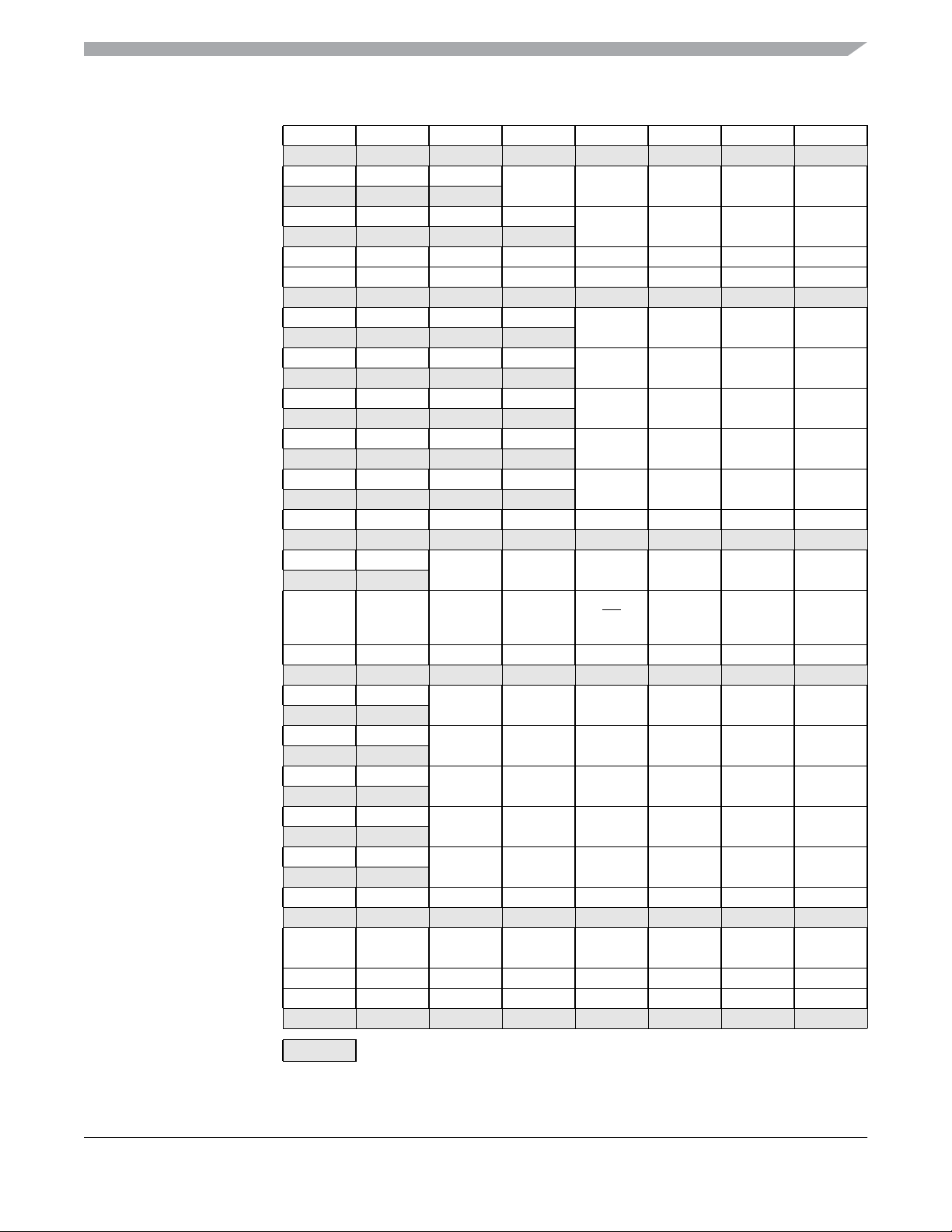
Chapter 2 Port Integration Module (PIM9C32) Block Description
Address Name Bit 7 654321Bit 0
0x0006 Reserved
0x0007 MODRR
0x0008 PTS
0x0009 PTIS
0x000A DDRS
0x000B RDRS
0x000C PERS
0x000D PPSS
0x000E WOMS
0x000F Reserved
0x0010 PTM
0x0011 PTIM
0x0012 DDRM
0x0013 RDRM
0x0014 PERM
0x0015 PPSM
0x0016 WOMM
0x0017 Reserved
0x0018 PTP
0x0019 PTIP
R00000000
W
R000
W
R0000
W
SCI——————TXDRXD
R0000PTIS3 PTIS2 PTIS1 PTIS0
W
R0000
W
R0000
W
R0000
W
R0000
W
R0000
W
R00000000
W
R0 0
W
MSCAN
/
— — SCK MOSI
SPI
R 0 0 PTIM5 PTIM4 PTIM3 PTIM2 PTIM1 PTIM0
W
R0 0
W
R0 0
W
R0 0
W
R0 0
W
R0 0
W
R00000000
W
R
PTP7 PTP6 PTP5 PTP4 PTP3 PTP2 PTP1 PTP0
W
PWM — — PWM5 PWM4 PWM3 PWM2 PWM1 PWM0
R PTIP7 PTIP6 PTIP5 PTIP4 PTIP3 PTIP2 PTIP1 PTIP0
W
PTM5 PTM4 PTM3 PTM2 PTM1 PTM0
DDRM5 DDRM4 DDRM3 DDRM2 DDRM1 DDRM0
RDRM5 RDRM4 RDRM3 RDRM2 RDRM1 RDRM0
PERM5 PERM4 PERM3 PERM2 PERM1 PERM0
PPSM5 PPSM4 PPSM3 PPSM2 PPSM1 PPSM0
WOMM5 WOMM4 WOMM3 WOMM2 WOMM1 WOMM0
MODRR4 MODRR3 MODRR2 MODRR1 MODRR0
PTS3 PTS2 PTS1 PTS0
DDRS3 DDRS2 DDRS1 DDRS0
RDRS3 RDRS2 RDRS1 RDRS0
PERS3 PERS2 PERS1 PERS0
PPSS3 PPSS2 PPSS1 PPSS0
WOMS3 WOMS2 WOMS1 WOMS0
SS MISO TXCAN RXCAN
= Unimplemented or Reserved
Figure 2-2. Quick Reference to PIM Registers (Sheet 2 of 3)
MC9S12C128 Data Sheet, Rev. 1.15
Freescale Semiconductor 79
Page 80

Chapter 2 Port Integration Module (PIM9C32) Block Description
Address Name Bit 7 654321Bit 0
0x001A DDRP
0x001B RDRP
0x001C PERP
0x001D PPSP
0x001E PIEP
0x001F PIFP
0x0020–
0x0027
0x0028 PTJ
0x0029 PTIJ
0x002A DDRJ
0x002B RDRJ
0x002C PERJ
0x002D PPSJ
0x002E PIEJ
0x002F PIFJ
0x0030 PTAD
0x0031 PTIAD
0x0032 DDRAD
0x0033 RDRAD
0x0034 PERAD
0x0035 PPSAD
0x0036–
0x003F
Reserved
Reserved
R
DDRP7 DDRP6 DDRP5 DDRP4 DDRP3 DDRP2 DDRP1 DDRP0
W
R
RDRP7 RDRP6 RDRP5 RDRP4 RDRP3 RDRP2 RDRP1 RDRP0
W
R
PERP7 PERP6 PERP5 PERP4 PERP3 PERP2 PERP1 PERP0
W
R
PPSP7 PPSP6 PPSP5 PPSP4 PPSP3 PPSP2 PPSP1 PPSP0
W
R
PIEP7 PIEP6 PIEP5 PIEP4 PIEP3 PIEP2 PIEP1 PIEP0
W
R
PIFP7 PIFP6 PIFP5 PIFP4 PIFP3 PIFP2 PIFP1 PIFP0
W
R00000000
W
R
PTJ7 PTJ6
W
R PTIJ7 PTIJ6 000000
W
R
DDRJ7 DDRJ6
W
R
RDRJ7 RDRJ6
W
R
PERJ7 PERJ6
W
R
PPSJ7 PPSJ6
W
R
PIEJ7 PIEJ6
W
R
PIFJ7 PIFJ6
W
R
PTAD7 PTAD6 PTAD5 PTAD4 PTAD3 PTAD2 PTAD1 PTAD0
W
R PTIAD7 PTIAD6 PTIAD5 PTIAD4 PTIAD3 PTIAD2 PTIAD1 PTIAD0
W
R
DDRAD7 DDRAD6 DDRAD5 DDRAD4 DDRAD3 DDRAD2 DDRAD1 DDRAD0
W
R
RDRAD7 RDRAD6 RDRAD5 RDRAD4 RDRAD3 RDRAD2 RDRAD1 RDRAD0
W
R
PERAD7 PERAD6 PERAD5 PERAD4 PERAD3 PERAD2 PERAD1 PERAD0
W
R
PPSAD7 PPSAD6 PPSAD5 PPSAD4 PPSAD3 PPSAD2 PPSAD1 PPSAD0
W
R00000000
W
000000
000000
000000
000000
000000
000000
000000
= Unimplemented or Reserved
Figure 2-2. Quick Reference to PIM Registers (Sheet 3 of 3)
MC9S12C128 Data Sheet, Rev. 1.15
80 Freescale Semiconductor
Page 81

Chapter 2 Port Integration Module (PIM9C32) Block Description
2.3.2 Register Descriptions
Table 2-2 summarizes the effect on the various configuration bits — data direction (DDR), input/output
level (I/O), reduced drive (RDR), pull enable (PE), pull select (PS), and interrupt enable (IE) for the ports.
The configuration bit PS is used for two purposes:
1. Configure the sensitive interrupt edge (rising or falling), if interrupt is enabled.
2. Select either a pull-up or pull-down device if PE is active.
Table 2-2. Pin Configuration Summary
DDR IO RDR PE PS IE
0 X X 0 X 0 Input Disabled Disabled
0 X X 1 0 0 Input Pull up Disabled
0 X X 1 1 0 Input Pull down Disabled
0 X X 0 0 1 Input Disabled Falling edge
0 X X 0 1 1 Input Disabled Rising edge
0 X X 1 0 1 Input Pull up Falling edge
0 X X 1 1 1 Input Pull down rising edge
1 0 0 X X 0 Output, full drive to 0 Disabled Disabled
1 1 0 X X 0 Output, full drive to 1 Disabled Disabled
1 0 1 X X 0 Output, reduced drive to 0 Disabled Disabled
1 1 1 X X 0 Output, reduced drive to 1 Disabled Disabled
1 0 0 X 0 1 Output, full drive to 0 Disabled Falling edge
1 1 0 X 1 1 Output, full drive to 1 Disabled Rising edge
1 0 1 X 0 1 Output, reduced drive to 0 Disabled Falling edge
1 1 1 X 1 1 Output, reduced drive to 1 Disabled Rising edge
1. Applicable only on ports P and J.
(1)
Function Pull Device Interrupt
NOTE
Allbits of allregisters inthis moduleare completely synchronous to internal
clocks during a register read.
MC9S12C128 Data Sheet, Rev. 1.15
Freescale Semiconductor 81
Page 82

Chapter 2 Port Integration Module (PIM9C32) Block Description
2.3.2.1 Port T Registers
2.3.2.1.1 Port T I/O Register (PTT)
Module Base + 0x0000
76543210
R
PTT7 PTT6 PTT5 PTT4 PTT3 PTT2 PTT1 PTT0
W
TIM IOC7 IOC6 IOC5 IOC4 IOC3 IOC2 IOC1 IOC0
PWM PWM4 PWM3 PWM2 PWM1 PWM0
Reset 0 0 0 00000
= Unimplemented or Reserved
Figure 2-3. Port T I/O Register (PTT)
Read: Anytime.
Write: Anytime.
If the data direction bits of the associated I/O pins are set to 1, a read returns the value of the port register,
otherwise the value at the pins is read.
If a TIM-channel is defined as output, the related port T is assigned to IOC function.
In addition to the possible timer functionality of port T pins PWM channels [4:0] can be routed to port
T[4:0]. For this the Module Routing Register (MODRR) needs to be configured.
Table 2-3. Port T[4:0] Pin Functionality Configurations
MODRR[x] PWME[x]
0 0 0 General Purpose I/O
0 0 1 Timer
0 1 0 General Purpose I/O
0 1 1 Timer
1 0 0 General Purpose I/O
1 0 1 Timer
1 1 0 PWM
1 1 1 PWM
1. All fields in the that are not shaded are standard use cases.
2. TIMEN[x] means that the timer is enabled (TSCR1[7]), the related channel is
configured for output compare function (TIOS[x] or special output on a timer
overflowevent— configurable in TTOV[x])and the timer outputis routed to the
port pin (TCTL1/TCTL2).
TIMEN[x]
(2)
Port T[x] Output
(1)
MC9S12C128 Data Sheet, Rev. 1.15
82 Freescale Semiconductor
Page 83

Chapter 2 Port Integration Module (PIM9C32) Block Description
2.3.2.1.2 Port T Input Register (PTIT)
Module Base + 0x0001
76543210
R PTIT7 PTIT6 PTIT5 PTIT4 PTIT3 PTIT2 PTIT1 PTIT0
W
Reset — — ——————
= Unimplemented or Reserved
Figure 2-4. Port T Input Register (PTIT)
Read: Anytime.
Write: Never, writes to this register have no effect.
Table 2-4. PTIT Field Descriptions
Field Description
7–0
PTIT[7:0]
Port T Input Register — This register always reads back the status of the associated pins. This can also be
used to detect overload or short circuit conditions on output pins.
2.3.2.1.3 Port T Data Direction Register (DDRT)
Module Base + 0x0002
76543210
R
DDRT7 DDRT6 DDRT5 DDRT4 DDRT3 DDRT2 DDRT1 DDRT0
W
Reset 0 0 0 00000
Figure 2-5. Port T Data Direction Register (DDRT)
Read: Anytime.
Write: Anytime.
Table 2-5. DDRT Field Descriptions
Field Description
7–0
DDRT[7:0]
Data Direction Port T — This register configures each port T pin as either input or output.
The standard TIM / PWM modules forcesthe I/Ostate tobe anoutput foreach standard TIM / PWM module port
associated with an enabled output compare. In these cases the data direction bits will not change.
The DDRT bits revert to controlling the I/O direction of a pin when the associated timer output compare is
disabled.
The timer input capture always monitors the state of the pin.
0 Associated pin is configured as input.
1 Associated pin is configured as output.
Note: Due to internalsynchronization circuits,it can takeup to 2 bus cycles until the correct value is read on PTT
or PTIT registers, when changing the DDRT register.
MC9S12C128 Data Sheet, Rev. 1.15
Freescale Semiconductor 83
Page 84

Chapter 2 Port Integration Module (PIM9C32) Block Description
2.3.2.1.4 Port T Reduced Drive Register (RDRT)
Module Base + 0x0003
76543210
R
RDRT7 RDRT6 RDRT5 RDRT4 RDRT3 RDRT2 RDRT1 RDRT0
W
Reset 0 0 0 00000
Figure 2-6. Port T Reduced Drive Register (RDRT)
Read: Anytime.
Write: Anytime.
Table 2-6. RDRT Field Descriptions
Field Description
7–0
RDRT[7:0]
Reduced Drive Port T — This register configures the drive strength of each port T output pin as either full or
reduced. If the port is used as input this bit is ignored.
0 Full drive strength at output.
1 Associated pin drives at about 1/3 of the full drive strength.
2.3.2.1.5 Port T Pull Device Enable Register (PERT)
Module Base + 0x0004
76543210
R
PERT7 PERT6 PERT5 PERT4 PERT3 PERT2 PERT1 PERT0
W
Reset 0 0 0 00000
Figure 2-7. Port T Pull Device Enable Register (PERT)
Read: Anytime.
Write: Anytime.
Table 2-7. PERT Field Descriptions
Field Description
7–0
PERT[7:0]
Pull Device Enable — This register configures whether a pull-up or a pull-down device is activated, if the port
is used as input. This bit has no effect if the port is used as output. Out of reset no pull device is enabled.
0 Pull-up or pull-down device is disabled.
1 Either a pull-up or pull-down device is enabled.
MC9S12C128 Data Sheet, Rev. 1.15
84 Freescale Semiconductor
Page 85

Chapter 2 Port Integration Module (PIM9C32) Block Description
2.3.2.1.6 Port T Polarity Select Register (PTTST)
Module Base + 0x0005
76543210
R
PPST7 PPST6 PPST5 PPST4 PPST3 PPST2 PPST1 PPST0
W
Reset 0 0 0 00000
Figure 2-8. Port T Polarity Select Register (PPST)
Read: Anytime.
Write: Anytime.
Table 2-8. PPST Field Descriptions
Field Description
7–0
PPST[7:0]
Pull Select Port T — This register selects whether a pull-down or a pull-up device is connected to the pin.
0 A pull-up device is connected to the associated port T pin, if enabled by the associated bit in register PERT
and if the port is used as input.
1 A pull-down deviceis connectedto the associated port Tpin, if enabled by the associated bit in register PERT
and if the port is used as input.
2.3.2.1.7 Port T Module Routing Register (MODRR)
Module Base + 0x0007
76543210
R000
W
Reset — — — 00000
= Unimplemented or Reserved
MODRR4 MODRR3 MODRR2 MODRR1 MODRR0
Figure 2-9. Port T Module Routing Register (MODRR)
Read: Anytime.
Write: Anytime.
Table 2-9. MODRR Field Descriptions
Field Description
4–0
MODRR[4:0]
Freescale Semiconductor 85
Module Routing Register Port T — This register selects the module connected to port T.
0 Associated pin is connected to TIM module
1 Associated pin is connected to PWM module
MC9S12C128 Data Sheet, Rev. 1.15
Page 86

Chapter 2 Port Integration Module (PIM9C32) Block Description
2.3.2.2 Port S Registers
2.3.2.2.1 Port S I/O Register (PTS)
Module Base + 0x0008
76543210
R0000
W
SCI——————TXDRXD
Reset 0 0 0 00000
= Unimplemented or Reserved
Figure 2-10. Port S I/O Register (PTS)
Read: Anytime.
Write: Anytime.
If the data direction bits of the associated I/O pins are set to 1, a read returns the value of the port register,
otherwise the value at the pins is read.
PTS3 PTS2 PTS1 PTS0
The SCI port associated with transmit pin 1 is configured as output if the transmitter is enabled and the
SCI pin associated with receive pin 0 is configured as input if the receiver is enabled. Please refer to SCI
Block User Guide for details.
2.3.2.2.2 Port S Input Register (PTIS)
Module Base + 0x0009
76543210
R 0 0 0 0 PTIS3 PTIS2 PTIS1 PTIS0
W
Reset 0 0 0 00000
= Unimplemented or Reserved
Figure 2-11. Port S Input Register (PTIS)
Read: Anytime.
Write: Never, writes to this register have no effect.
Table 2-10. PTIS Field Descriptions
Field Description
3–0
PTIS[3:0]
86 Freescale Semiconductor
Port S Input Register — This register always reads back the status of the associated pins. This also can be
used to detect overload or short circuit conditions on output pins.
MC9S12C128 Data Sheet, Rev. 1.15
Page 87

Chapter 2 Port Integration Module (PIM9C32) Block Description
2.3.2.2.3 Port S Data Direction Register (DDRS)
Module Base + 0x000A
76543210
R0000
W
Reset 0 0 0 00000
= Unimplemented or Reserved
DDRS3 DDRS2 DDRS1 DDRS0
Figure 2-12. Port S Data Direction Register (DDRS)
Read: Anytime.
Write: Anytime.
Table 2-11. DDRS Field Descriptions
Field Description
3–0
DDRS[3:0]
Direction Register Port S — This register configures each port S pin as either input or output.
If the associated SCI transmit or receive channel is enabled this register has no effect on the pins. The pin is
forcedto be an output if the SCI transmitchannel is enabled, it is forced to be an input if the SCI receive channel
is enabled.
The DDRS bits revert to controlling the I/O direction of a pin when the associated channel is disabled.
0 Associated pin is configured as input.
1 Associated pin is configured as output.
Note: Due to internalsynchronization circuits, itcan take upto 2bus cycles untilthe correct valueis read on PTS
or PTIS registers, when changing the DDRS register.
MC9S12C128 Data Sheet, Rev. 1.15
Freescale Semiconductor 87
Page 88

Chapter 2 Port Integration Module (PIM9C32) Block Description
2.3.2.2.4 Port S Reduced Drive Register (RDRS)
Module Base + 0x000B
76543210
R0000
W
Reset 0 0 0 00000
= Unimplemented or Reserved
RDRS3 RDRS2 RDRS1 RDRS0
Figure 2-13. Port S Reduced Drive Register (RDRS)
Read: Anytime.
Write: Anytime.
Table 2-12. RDRS Field Descriptions
Field Description
3–0
RDRS[3:0]
Reduced Drive Port S — This register configures the drive strength of each port S output pin as either full or
reduced. If the port is used as input this bit is ignored.
0 Full drive strength at output.
1 Associated pin drives at about 1/3 of the full drive strength.
2.3.2.2.5 Port S Pull Device Enable Register (PERS)
Module Base + 0x000C
76543210
R0000
W
Reset 0 0 0 01111
= Unimplemented or Reserved
PERS3 PERS2 PERS1 PERS0
Figure 2-14. Port S Pull Device Enable Register (PERS)
Read: Anytime.
Write: Anytime.
Table 2-13. PERS Field Descriptions
Field Description
3–0
PERS[3:0]
88 Freescale Semiconductor
Reduced Drive PortS — This register configureswhether apull-up or a pull-down deviceis activated, if the port
is used as input or as output in wired-or (open drain) mode. This bit has no effect if the port is used as push-pull
output. Out of reset a pull-up device is enabled.
0 Pull-up or pull-down device is disabled.
1 Either a pull-up or pull-down device is enabled.
MC9S12C128 Data Sheet, Rev. 1.15
Page 89

Chapter 2 Port Integration Module (PIM9C32) Block Description
2.3.2.2.6 Port S Polarity Select Register (PPSS)
Module Base + 0x000D
76543210
R0000
W
Reset 0 0 0 00000
= Unimplemented or Reserved
PPSS3 PPSS2 PPSS1 PPSS0
Figure 2-15. Port S Polarity Select Register (PPSS)
Read: Anytime.
Write: Anytime.
Table 2-14. PPSS Field Descriptions
Field Description
3–0
PPSS[3:0]
Pull Select Port S — This register selects whether a pull-down or a pull-up device is connected to the pin.
0 A pull-up device is connected to the associated port S pin, if enabled by the associated bit in register PERS
and if the port is used as input or as wired-or output.
1 A pull-down deviceis connected to the associatedport S pin, if enabled bythe associated bit in registerPERS
and if the port is used as input.
2.3.2.2.7 Port S Wired-OR Mode Register (WOMS)
Module Base + 0x000E
76543210
R0000
W
Reset 0 0 0 00000
= Unimplemented or Reserved
WOMS3 WOMS2 WOMS1 WOMS0
Figure 2-16. Port S Wired-Or Mode Register (WOMS)
Read: Anytime.
Write: Anytime.
Table 2-15. WOMS Field Descriptions
Field Description
3–0
WOMS[3:0]
Freescale Semiconductor 89
Wired-OR Mode Port S — This register configures the output pins as wired-or. If enabled the output is driven
active low only (open-drain). A logic level of “1” is not driven. This bit has no influence on pins used as inputs.
0 Output buffers operate as push-pull outputs.
1 Output buffers operate as open-drain outputs.
MC9S12C128 Data Sheet, Rev. 1.15
Page 90

Chapter 2 Port Integration Module (PIM9C32) Block Description
2.3.2.3 Port M Registers
2.3.2.3.1 Port M I/O Register (PTM)
Module Base + 0x0010
76543210
R0 0
W
PTM5 PTM4 PTM3 PTM2 PTM1 PTM0
MSCAN/
SPI
Reset 0 0 0 00000
— — SCK MOSI
= Unimplemented or Reserved
SS MISO TXCAN RXCAN
Figure 2-17. Port M I/O Register (PTM)
Read: Anytime.
Write: Anytime.
If the data direction bits of the associated I/O pins are set to 1, a read returns the value of the port register,
otherwise the value at the pins is read.
The SPI pin configurations (PM[5:2]) is determined by several status bits in the SPI module. Please refer
to the SPI Block User Guide for details.
2.3.2.3.2 Port M Input Register (PTIM)
Module Base + 0x0011
76543210
R 0 0 PTIM5 PTIM4 PTIM3 PTIM2 PTIM1 PTIM0
W
Reset — — ——————
= Unimplemented or Reserved
Figure 2-18. Port M Input Register (PTIM)
Read: Anytime.
Write: Never, writes to this register have no effect.
Table 2-16. PTIM Field Descriptions
Field Description
5–0
PTIM[5:0]
90 Freescale Semiconductor
Port M Input Register — This register always reads back the status of the associated pins. This also can be
used to detect overload or short circuit conditions on output pins.
MC9S12C128 Data Sheet, Rev. 1.15
Page 91

Chapter 2 Port Integration Module (PIM9C32) Block Description
2.3.2.3.3 Port M Data Direction Register (DDRM)
Module Base + 0x0012
76543210
R0 0
W
Reset — — 0 00000
= Unimplemented or Reserved
DDRM5 DDRM4 DDRM3 DDRM2 DDRM1 DDRM0
Figure 2-19. Port M Data Direction Register (DDRM)
Read: Anytime.
Write: Anytime.
Table 2-17. DDRM Field Descriptions
Field Description
5–0
DDRM[5:0]
Data Direction Port M — This register configures each port S pin as either input or output
If SPI or MSCAN is enabled, the SPI and MSCAN modules determines thepin directions.Please referto the SPI
and MSCAN Block User Guides for details.
If the associated SCI or MSCAN transmitor receivechannels are enabled,this registerhas noeffect on the pins.
Thepins are forcedto beoutputsif the SCI orMSCAN transmit channels areenabled,theyare forced to be inputs
if the SCI or MSCAN receive channels are enabled.
The DDRS bits revert to controlling the I/O direction of a pin when the associated channel is disabled.
0 Associated pin is configured as input.
1 Associated pin is configured as output.
Note: Due tointernal synchronizationcircuits, it cantakeup to 2bus cycles until thecorrect value isread on PTM
or PTIM registers, when changing the DDRM register.
MC9S12C128 Data Sheet, Rev. 1.15
Freescale Semiconductor 91
Page 92

Chapter 2 Port Integration Module (PIM9C32) Block Description
2.3.2.3.4 Port M Reduced Drive Register (RDRM)
Module Base + 0x0013
76543210
R0 0
W
Reset 0 0 0 00000
= Unimplemented or Reserved
RDRM5 RDRM4 RDRM3 RDRM2 RDRM1 RDRM0
Figure 2-20. Port M Reduced Drive Register (RDRM)
Read: Anytime.
Write: Anytime.
Table 2-18. RDRM Field Descriptions
Field Description
5–0
RDRM[5:0]
Reduced Drive Port M — This register configures the drive strength of each port M output pin as either full or
reduced. If the port is used as input this bit is ignored.
0 Full drive strength at output.
1 Associated pin drives at about 1/3 of the full drive strength.
2.3.2.3.5 Port M Pull Device Enable Register (PERM)
Module Base + 0x0014
76543210
R0 0
W
Reset 0 0 1 11111
= Unimplemented or Reserved
PERM5 PERM4 PERM3 PERM2 PERM1 PERM0
Figure 2-21. Port M Pull Device Enable Register (PERM)
Read: Anytime.
Write: Anytime.
Table 2-19. PERM Field Descriptions
Field Description
5–0
PERM[5:0]
92 Freescale Semiconductor
Pull Device Enable Port M — This register configures whether a pull-up or a pull-down device is activated, if
the port is used as input or as output in wired-or (open drain) mode. This bit has no effect if the port is used as
push-pull output. Out of reset a pull-up device is enabled.
0 Pull-up or pull-down device is disabled.
1 Either a pull-up or pull-down device is enabled.
MC9S12C128 Data Sheet, Rev. 1.15
Page 93

Chapter 2 Port Integration Module (PIM9C32) Block Description
2.3.2.3.6 Port M Polarity Select Register (PPSM)
Module Base + 0x0015
76543210
R0 0
W
Reset 0 0 0 00000
= Unimplemented or Reserved
PPSM5 PPSM4 PPSM3 PPSM2 PPSM1 PPSM0
Figure 2-22. Port M Polarity Select Register (PPSM)
Read: Anytime.
Write: Anytime.
Table 2-20. PPSM Field Descriptions
Field Description
5–0
PPSM[5:0]
Polarity Select Port M — This register selects whether a pull-down or a pull-up device is connected to the pin.
0 A pull-up device is connected to the associated port M pin, if enabled by the associated bit in register PERM
and if the port is used as input or as wired-or output.
1 A pull-down device is connectedto the associated port M pin,if enabled by the associatedbit in registerPERM
and if the port is used as input.
2.3.2.3.7 Port M Wired-OR Mode Register (WOMM)
Module Base + 0x0016
76543210
R0 0
W
Reset 0 0 0 00000
= Unimplemented or Reserved
WOMM5 WOMM4 WOMM3 WOMM2 WOMM1 WOMM0
Figure 2-23. Port M Wired-OR Mode Register (WOMM)
Read: Anytime.
Write: Anytime.
Table 2-21. WOMM Field Descriptions
Field Description
5–0
WOMM[5:0]
Freescale Semiconductor 93
Wired-OR Mode Port M — This register configures the output pins as wired-or. If enabled the output is driven
active low only (open-drain). A logic level of “1” is not driven. This bit has no influence on pins used as inputs.
0 Output buffers operate as push-pull outputs.
1 Output buffers operate as open-drain outputs.
MC9S12C128 Data Sheet, Rev. 1.15
Page 94

Chapter 2 Port Integration Module (PIM9C32) Block Description
2.3.2.4 Port P Registers
2.3.2.4.1 Port P I/O Register (PTP)
Module Base + 0x0018
76543210
R
PTP7 PTP6 PTP5 PTP4 PTP3 PTP2 PTP1 PTP0
W
PWM — — PWM5 PWM4 PWM3 PWM2 PWM1 PWM0
Reset 0 0 0 00000
Figure 2-24. Port P I/O Register (PTP)
Read: Anytime.
Write: Anytime.
If the data direction bits of the associated I/O pins are set to 1, a read returns the value of the port register,
otherwise the value at the pins is read.
2.3.2.4.2 Port P Input Register (PTIP)
Module Base + 0x0019
76543210
R PTIP7 PTIP6 PTIP5 PTIP4 PTIP3 PTIP2 PTIP1 PTIP0
W
Reset — — ——————
= Unimplemented or Reserved
Figure 2-25. Port P Input Register (PTIP)
Read: Anytime.
Write: Never, writes to this register have no effect.
This register always reads back the status of the associated pins. This can be also used to detect overload
or short circuit conditions on output pins.
MC9S12C128 Data Sheet, Rev. 1.15
94 Freescale Semiconductor
Page 95

Chapter 2 Port Integration Module (PIM9C32) Block Description
2.3.2.4.3 Port P Data Direction Register (DDRP)
Module Base + 0x001A
76543210
R
DDRP7 DDRP6 DDRP5 DDRP4 DDRP3 DDRP2 DDRP1 DDRP0
W
Reset 0 0 0 00000
Figure 2-26. Port P Data Direction Register (DDRP)
Read: Anytime.
Write: Anytime.
Table 2-22. DDRP Field Descriptions
Field Description
7–0
DDRP[7:0]
Data Direction Port P — This register configures each port P pin as either input or output.
0 Associated pin is configured as input.
1 Associated pin is configured as output.
Note: Due to internalsynchronization circuits, itcan take upto 2bus cycles untilthe correct valueis read on PTP
or PTIP registers, when changing the DDRP register.
2.3.2.4.4 Port P Reduced Drive Register (RDRP)
Module Base + 0x001B
76543210
R
RDRP7 RDRP6 RDRP5 RDRP4 RDRP3 RDRP2 RDRP1 RDRP0
W
Reset 0 0 0 00000
Figure 2-27. Port P Reduced Drive Register (RDRP)
Read: Anytime.
Write: Anytime.
Table 2-23. RDRP Field Descriptions
Field Description
7–0
RDRP[7:0]
Freescale Semiconductor 95
Reduced Drive Port P — This register configures the drive strength of each port P output pin as either full or
reduced. If the port is used as input this bit is ignored.
0 Full drive strength at output.
1 Associated pin drives at about 1/3 of the full drive strength.
MC9S12C128 Data Sheet, Rev. 1.15
Page 96

Chapter 2 Port Integration Module (PIM9C32) Block Description
2.3.2.4.5 Port P Pull Device Enable Register (PERP)
Module Base + 0x001C
76543210
R
PERP7 PERP6 PERP5 PERP4 PERP3 PERP2 PERP1 PERP0
W
Reset 0 0 0 00000
Figure 2-28. Port P Pull Device Enable Register (PERP)
Read: Anytime.
Write: Anytime.
Table 2-24. PERP Field Descriptions
Field Description
7–0
PERP[7:0]
Pull Device Enable Port P — Thisregister configureswhether a pull-up or a pull-down device is activated, if the
port is used as input. This bit has no effect if the port is used as output. Out of reset no pull device is enabled.
0 Pull-up or pull-down device is disabled.
1 Either a pull-up or pull-down device is enabled.
2.3.2.4.6 Port P Polarity Select Register (PPSP)
Module Base + 0x001D
76543210
R
PPSP7 PPSP6 PPSP5 PPSP4 PPSP3 PPSP2 PPSP1 PPSP0
W
Reset 0 0 0 00000
Figure 2-29. Port P Polarity Select Register (PPSP)
Read: Anytime.
Write: Anytime.
Table 2-25. PPSP Field Descriptions
Field Description
7–0
PPSP[7:0]
Pull Select Port P — This register serves a dual purpose by selecting the polarity of the active interrupt edge
as well as selecting a pull-up or pull-down device if enabled.
0 Falling edge on the associated port P pin sets the associated flag bit in the PIFP register.A pull-up device is
connected to theassociated port P pin,if enabled bytheassociated bit in register PERPand if the portis used
as input.
1 Rising edge on the associated port P pin sets the associated flag bit in the PIFP register.A pull-down device
is connected to the associated port P pin, if enabled by the associated bit in register PERP and if the port is
used as input.
MC9S12C128 Data Sheet, Rev. 1.15
96 Freescale Semiconductor
Page 97

Chapter 2 Port Integration Module (PIM9C32) Block Description
2.3.2.4.7 Port P Interrupt Enable Register (PIEP)
Module Base + 0x001E
76543210
R
PIEP7 PIEP6 PIEP5 PIEP4 PIEP3 PIEP2 PIEP1 PIEP0
W
Reset 0 0 0 00000
Figure 2-30. Port P Interrupt Enable Register (PIEP)
Read: Anytime.
Write: Anytime.
Table 2-26. PIEP Field Descriptions
Field Description
7–0
PIEP[7:0]
Pull Select Port P — This register disables or enables on a per pin basis the edge sensitive external interrupt
associated with port P.
0 Interrupt is disabled (interrupt flag masked).
1 Interrupt is enabled.
2.3.2.4.8 Port P Interrupt Flag Register (PIFP)
Module Base + 0x001F
76543210
R
PIFP7 PIFP6 PIFP5 PIFP4 PIFP3 PIFP2 PIFP1 PIFP0
W
Reset 0 0 0 00000
Figure 2-31. Port P Interrupt Flag Register (PIFP)
Read: Anytime.
Write: Anytime.
Table 2-27. PIFP Field Descriptions
Field Description
7–0
PIFP[7:0]
Interrupt Flags Port P — Each flag is set by an active edge on the associated input pin. This could be a rising
or a falling edge based on the state of the PPSP register. To clear this flag, write a “1” to the corresponding bit
in the PIFP register. Writing a “0” has no effect.
0 No active edge pending.
Writing a “0” has no effect.
1 Active edge on the associated bit has occurred (an interrupt will occur if the associated enable bit is set).
Writing a “1” clears the associated flag.
MC9S12C128 Data Sheet, Rev. 1.15
Freescale Semiconductor 97
Page 98

Chapter 2 Port Integration Module (PIM9C32) Block Description
2.3.2.5 Port J Registers
2.3.2.5.1 Port J I/O Register (PTJ)
Module Base + 0x0028
76543210
R
PTJ7 PTJ6
W
Reset 0 0 ——————
= Unimplemented or Reserved
Read: Anytime.
Write: Anytime.
If the data direction bits of the associated I/O pins are set to 1, a read returns the value of the port register,
otherwise the value at the pins is read.
000000
Figure 2-32. Port J I/O Register (PTJ)
2.3.2.5.2 Port J Input Register (PTIJ)
Module Base + 0x0029
76543210
R PTIJ7 PTIJ6 0 00000
W
Reset 0 0 ——————
= Unimplemented or Reserved
Figure 2-33. Port J Input Register (PTIJ)
Read: Anytime.
Write: Never, writes to this register have no effect.
This register always reads back the status of the associated pins. This can be used to detect overload or
short circuit conditions on output pins.
MC9S12C128 Data Sheet, Rev. 1.15
98 Freescale Semiconductor
Page 99

Chapter 2 Port Integration Module (PIM9C32) Block Description
2.3.2.5.3 Port J Data Direction Register (DDRJ)
Module Base + 0x002A
76543210
R
DDRJ7 DDRJ6
W
Reset 0 0 ——————
= Unimplemented or Reserved
000000
Figure 2-34. Port J Data Direction Register (DDRJ)
Read: Anytime.
Write: Anytime.
Table 2-28. DDRJ Field Descriptions
Field Description
7–6
DDRJ[7:6]
Data Direction Port J — This register configures port pins J[7:6] as either input or output.
DDRJ[7:6] — Data Direction Port J
0 Associated pin is configured as input.
1 Associated pin is configured as output.
Note: Due to internal synchronization circuits,it cantake up to 2 buscycles untilthe correctvalue is read on PTJ
or PTIJ registers, when changing the DDRJ register.
2.3.2.5.4 Port J Reduced Drive Register (RDRJ)
Module Base + 0x002B
76543210
R
RDRJ7 RDRJ6
W
Reset 0 0 ——————
= Unimplemented or Reserved
000000
Figure 2-35. Port J Reduced Drive Register (RDRJ)
Read: Anytime.
Write: Anytime.
Table 2-29. RDRJ Field Descriptions
Field Description
7–6
RDRJ[7:6]
Freescale Semiconductor 99
Reduced Drive Port J — This register configures the drive strength of each port J output pin as either full or
reduced. If the port is used as input this bit is ignored.
0 Full drive strength at output.
1 Associated pin drives at about 1/3 of the full drive strength.
MC9S12C128 Data Sheet, Rev. 1.15
Page 100

Chapter 2 Port Integration Module (PIM9C32) Block Description
2.3.2.5.5 Port J Pull Device Enable Register (PERJ)
Module Base + 0x002C
76543210
R
PERJ7 PERJ6
W
Reset 0 0 ——————
= Unimplemented or Reserved
000000
Figure 2-36. Port J Pull Device Enable Register (PERJ)
Read: Anytime.
Write: Anytime.
Table 2-30. PERJ Field Descriptions
Field Description
7–6
PERJ[7:6]
Reduced Drive Port J —This registerconfigures whethera pull-upor apull-down device isactivated, if the port
is used as input or as wired-or output. This bit has no effect if the port is used as push-pull output.
0 Pull-up or pull-down device is disabled.
1 Either a pull-up or pull-down device is enabled.
2.3.2.5.6 Port J Polarity Select Register (PPSJ)
Module Base + 0x002D
76543210
R
PPSJ7 PPSJ6
W
Reset 0 0 ——————
= Unimplemented or Reserved
000000
Figure 2-37. Port J Polarity Select Register (PPSJ)
Read: Anytime.
Write: Anytime.
Table 2-31. PPSJ Field Descriptions
Field Description
7–6
PPSJ[7:6]
100 Freescale Semiconductor
Reduced Drive Port J —This register servesa dual purposeby selecting the polarity of the activeinterrupt edge
as well as selecting a pull-up or pull-down device if enabled.
0 Falling edge on the associated port J pin sets the associated flag bit in the PIFJ register.
A pull-up device is connected to the associated port J pin, if enabled by the associated bit in register PERJ
and if the port is used as general purpose input.
1 Rising edge on the associated port J pin sets the associated flag bit in the PIFJ register.
A pull-down device is connected to the associated port J pin, if enabled bythe associated bit in register PERJ
and if the port is used as input.
MC9S12C128 Data Sheet, Rev. 1.15
 Loading...