


MC9S12E128
MC9S12E64
MC9S12E32
Data Sheet
HCS12
Microcontrollers
MC9S12E128V1
Rev. 1.07
10/2005
freescale.com


MC9S12E128 Data Sheet
covers
MC9S12E64 & MC9S12E32
MC9S12E128V1
Rev. 1.07
10/2005

To provide the most up-to-date information, the revision of our documents on the World Wide Web will be
the most current. Your printed copy may be an earlier revision. To verify you have the latest information
available, refer to:
http://freescale.com/
The following revision history table summarizes changes contained in this document.
Revision History
Date
October 10, 2005 01.07 New Data Sheet
Revision
Level
Description
Freescale™ and the Freescale logo are trademarks of Freescale Semiconductor, Inc.
This product incorporates SuperFlash® technology licensed from SST.
© Freescale Semiconductor, Inc., 2005. All rights reserved.
MC9S12E128 Data Sheet, Rev. 1.07
4 Freescale Semiconductor

Chapter 1 MC9S12E128 Device Overview (MC9S12E128DGV1) . . . . . . .21
Chapter 2 128 Kbyte Flash Module (FTS128K1V1) . . . . . . . . . . . . . . . . . .85
Chapter 3 Port Integration Module (PIM9E128V1). . . . . . . . . . . . . . . . . .119
Chapter 4 Clocks and Reset Generator (CRGV4) . . . . . . . . . . . . . . . . . .165
Chapter 5 Oscillator (OSCV2) . . . . . . . . . . . . . . . . . . . . . . . . . . . . . . . . . .201
Chapter 6 Analog-to-Digital Converter (ATD10B16CV2) . . . . . . . . . . . .205
Chapter 7 Digital-to-Analog Converter (DAC8B1CV1) . . . . . . . . . . . . . .237
Chapter 8 Serial Communication Interface (SCIV3) . . . . . . . . . . . . . . . .245
Chapter 9 Serial Peripheral Interface (SPIV3) . . . . . . . . . . . . . . . . . . . . .277
Chapter 10 Inter-Integrated Circuit (IICV2) . . . . . . . . . . . . . . . . . . . . . . . .299
Chapter 11 Pulse Width Modulator w/ Fault Protection (PMF15B6CV2).323
Chapter 12 Pulse-Width Modulator (PWM8B6CV1). . . . . . . . . . . . . . . . . .381
Chapter 13 Timer Module (TIM16B4CV1). . . . . . . . . . . . . . . . . . . . . . . . . .415
Chapter 14 Dual Output Voltage Regulator (VREG3V3V2). . . . . . . . . . . .439
Chapter 15 Background Debug Module (BDMV4). . . . . . . . . . . . . . . . . . .447
Chapter 16 Debug Module (DBGV1). . . . . . . . . . . . . . . . . . . . . . . . . . . . . .473
Chapter 17 Interrupt (INTV1). . . . . . . . . . . . . . . . . . . . . . . . . . . . . . . . . . . .505
Chapter 18 Multiplexed External Bus Interface (MEBIV3) . . . . . . . . . . . .513
Chapter 19 Module Mapping Control (MMCV4). . . . . . . . . . . . . . . . . . . . .543
Appendix A Electrical Characteristics. . . . . . . . . . . . . . . . . . . . . . . . . . . . .563
Appendix B Package Information . . . . . . . . . . . . . . . . . . . . . . . . . . . . . . . .599
Appendix C Ordering Information . . . . . . . . . . . . . . . . . . . . . . . . . . . . . . . .602
MC9S12E128 Data Sheet, Rev. 1.07
Freescale Semiconductor 5

MC9S12E128 Data Sheet, Rev. 1.07
6 Freescale Semiconductor

Chapter 1
MC9S12E128 Device Overview (MC9S12E128DGV1)
1.1 Introduction . . . . . . . . . . . . . . . . . . . . . . . . . . . . . . . . . . . . . . . . . . . . . . . . . . . . . . . . . . . . . . . . . . 21
1.1.1 Features . . . . . . . . . . . . . . . . . . . . . . . . . . . . . . . . . . . . . . . . . . . . . . . . . . . . . . . . . . . . . . 21
1.1.2 Modes of Operation . . . . . . . . . . . . . . . . . . . . . . . . . . . . . . . . . . . . . . . . . . . . . . . . . . . . .23
1.1.3 Block Diagram . . . . . . . . . . . . . . . . . . . . . . . . . . . . . . . . . . . . . . . . . . . . . . . . . . . . . . . . . 24
1.2 Device Memory Map . . . . . . . . . . . . . . . . . . . . . . . . . . . . . . . . . . . . . . . . . . . . . . . . . . . . . . . . . . . 25
1.2.1 Detailed Register Map . . . . . . . . . . . . . . . . . . . . . . . . . . . . . . . . . . . . . . . . . . . . . . . . . . . 29
1.2.2 Part ID Assignments . . . . . . . . . . . . . . . . . . . . . . . . . . . . . . . . . . . . . . . . . . . . . . . . . . . .58
1.3 Signal Description . . . . . . . . . . . . . . . . . . . . . . . . . . . . . . . . . . . . . . . . . . . . . . . . . . . . . . . . . . . . . 59
1.3.1 Device Pinout . . . . . . . . . . . . . . . . . . . . . . . . . . . . . . . . . . . . . . . . . . . . . . . . . . . . . . . . . . 59
1.3.2 Signal Properties Summary . . . . . . . . . . . . . . . . . . . . . . . . . . . . . . . . . . . . . . . . . . . . . . . 62
1.4 Detailed Signal Descriptions . . . . . . . . . . . . . . . . . . . . . . . . . . . . . . . . . . . . . . . . . . . . . . . . . . . . . 64
1.4.1 EXTAL, XTAL — Oscillator Pins . . . . . . . . . . . . . . . . . . . . . . . . . . . . . . . . . . . . . . . . . . 64
1.4.2 RESET — External Reset Pin . . . . . . . . . . . . . . . . . . . . . . . . . . . . . . . . . . . . . . . . . . . . . 64
1.4.3 TEST — Test Pin . . . . . . . . . . . . . . . . . . . . . . . . . . . . . . . . . . . . . . . . . . . . . . . . . . . . . .64
1.4.4 XFC — PLL Loop Filter Pin . . . . . . . . . . . . . . . . . . . . . . . . . . . . . . . . . . . . . . . . . . . . . . 64
1.4.5 BKGD / TAGHI / MODC — Background Debug, Tag High & Mode Pin . . . . . . . . . . . 64
1.4.6 PA[7:0] / ADDR[15:8] / DATA[15:8] — Port A I/O Pins . . . . . . . . . . . . . . . . . . . . . . . . 64
1.4.7 PB[7:0] / ADDR[7:0] / DATA[7:0] — Port B I/O Pins . . . . . . . . . . . . . . . . . . . . . . . . . . 64
1.4.8 PE7 / NOACC / XCLKS — Port E I/O Pin 7 . . . . . . . . . . . . . . . . . . . . . . . . . . . . . . . . . 65
1.4.9 PE6 / MODB / IPIPE1 — Port E I/O Pin 6 . . . . . . . . . . . . . . . . . . . . . . . . . . . . . . . . . . . 65
1.4.10 PE5 / MODA / IPIPE0 — Port E I/O Pin 5 . . . . . . . . . . . . . . . . . . . . . . . . . . . . . . . . . . . 66
1.4.11 PE4 / ECLK— Port E I/O Pin 4 / E-Clock Output . . . . . . . . . . . . . . . . . . . . . . . . . . . . . 66
1.4.12 PE3 / LSTRB / TAGLO — Port E I/O Pin 3 / Low-Byte Strobe (LSTRB) . . . . . . . . . . . 66
1.4.13 PE2 / R/W — Port E I/O Pin 2 / Read/Write . . . . . . . . . . . . . . . . . . . . . . . . . . . . . . . . . . 66
1.4.14 PE1 / IRQ — Port E input Pin 1 / Maskable Interrupt Pin . . . . . . . . . . . . . . . . . . . . . . . 66
1.4.15 PE0 / XIRQ — Port E input Pin 0 / Non Maskable Interrupt Pin . . . . . . . . . . . . . . . . . . 67
1.4.16 PK7 / ECS / ROMCTL — Port K I/O Pin 7 . . . . . . . . . . . . . . . . . . . . . . . . . . . . . . . . . . 67
1.4.17 PK6 / XCS — Port K I/O Pin 6 . . . . . . . . . . . . . . . . . . . . . . . . . . . . . . . . . . . . . . . . . . . 67
1.4.18 PK[5:0] / XADDR[19:14] — Port K I/O Pins [5:0] . . . . . . . . . . . . . . . . . . . . . . . . . . . . 67
1.4.19 PAD[15:0] / AN[15:0] / KWAD[15:0] — Port AD I/O Pins [15:0] . . . . . . . . . . . . . . . . 67
1.4.20 PM7 / SCL — Port M I/O Pin 7 . . . . . . . . . . . . . . . . . . . . . . . . . . . . . . . . . . . . . . . . . . . 68
1.4.21 PM6 / SDA — Port M I/O Pin 6 . . . . . . . . . . . . . . . . . . . . . . . . . . . . . . . . . . . . . . . . . . . 68
1.4.22 PM5 / TXD2 — Port M I/O Pin 5 . . . . . . . . . . . . . . . . . . . . . . . . . . . . . . . . . . . . . . . . . . 68
1.4.23 PM4 / RXD2 — Port M I/O Pin 4 . . . . . . . . . . . . . . . . . . . . . . . . . . . . . . . . . . . . . . . . . . 68
1.4.24 PM3 — Port M I/O Pin 3 . . . . . . . . . . . . . . . . . . . . . . . . . . . . . . . . . . . . . . . . . . . . . . . . 68
1.4.25 PM1 / DAO1 — Port M I/O Pin 1 . . . . . . . . . . . . . . . . . . . . . . . . . . . . . . . . . . . . . . . . . . 68
1.4.26 PM0 / DAO2 — Port M I/O Pin 0 . . . . . . . . . . . . . . . . . . . . . . . . . . . . . . . . . . . . . . . . . . 69
1.4.27 PP[5:0] / PW0[5:0] — Port P I/O Pins [5:0] . . . . . . . . . . . . . . . . . . . . . . . . . . . . . . . . . . 69
MC9S12E128 Data Sheet, Rev. 1.07
Freescale Semiconductor 7

1.4.28 PQ[6:4] / IS[2:0] — Port Q I/O Pins [6:4] . . . . . . . . . . . . . . . . . . . . . . . . . . . . . . . . . . . . 69
1.4.29 PQ[3:0] / FAULT[3:0] — Port Q I/O Pins [3:0] . . . . . . . . . . . . . . . . . . . . . . . . . . . . . . . 69
1.4.30 PS7 / SS — Port S I/O Pin 7 . . . . . . . . . . . . . . . . . . . . . . . . . . . . . . . . . . . . . . . . . . . . . . 69
1.4.31 PS6 / SCK — Port S I/O Pin 6 . . . . . . . . . . . . . . . . . . . . . . . . . . . . . . . . . . . . . . . . . . . . . 70
1.4.32 PS5 / MOSI — Port S I/O Pin 5 . . . . . . . . . . . . . . . . . . . . . . . . . . . . . . . . . . . . . . . . . . . 70
1.4.33 PS4 / MISO — Port S I/O Pin 4 . . . . . . . . . . . . . . . . . . . . . . . . . . . . . . . . . . . . . . . . . . . 70
1.4.34 PS3 / TXD1 — Port S I/O Pin 3 . . . . . . . . . . . . . . . . . . . . . . . . . . . . . . . . . . . . . . . . . . . 70
1.4.35 PS2 / RXD1 — Port S I/O Pin 2 . . . . . . . . . . . . . . . . . . . . . . . . . . . . . . . . . . . . . . . . . . . 70
1.4.36 PS1 / TXD0 — Port S I/O Pin 1 . . . . . . . . . . . . . . . . . . . . . . . . . . . . . . . . . . . . . . . . . . . 70
1.4.37 PS0 / RXD0 — Port S I/O Pin 0 . . . . . . . . . . . . . . . . . . . . . . . . . . . . . . . . . . . . . . . . . . . 71
1.4.38 PT[7:4] / IOC1[7:4]— Port T I/O Pins [7:4] . . . . . . . . . . . . . . . . . . . . . . . . . . . . . . . . . . 71
1.4.39 PT[3:0] / IOC0[7:4]— Port T I/O Pins [3:0] . . . . . . . . . . . . . . . . . . . . . . . . . . . . . . . . . . 71
1.4.40 PU[7:6] — Port U I/O Pins [7:6] . . . . . . . . . . . . . . . . . . . . . . . . . . . . . . . . . . . . . . . . . . . 71
1.4.41 PU[5:4] / PW1[5:4] — Port U I/O Pins [5:4] . . . . . . . . . . . . . . . . . . . . . . . . . . . . . . . . . 71
1.4.42 PU[3:0] / IOC2[7:4]/PW1[3:0] — Port U I/O Pins [3:0] . . . . . . . . . . . . . . . . . . . . . . . . 71
1.4.43 VDDX,VSSX — Power & Ground Pins for I/O Drivers . . . . . . . . . . . . . . . . . . . . . . . . . 72
1.4.44 VDDR, VSSR — Power Supply Pins for I/O Drivers & for Internal Voltage Regulator 72
1.4.45 VDD1, VDD2, VSS1, VSS2 — Power Supply Pins for Internal Logic . . . . . . . . . . . . . 72
1.4.46 VDDA, VSSA — Power Supply Pins for ATD and VREG . . . . . . . . . . . . . . . . . . . . . . 72
1.4.47 VRH, VRL — ATD Reference Voltage Input Pins . . . . . . . . . . . . . . . . . . . . . . . . . . . . . 72
1.4.48 VDDPLL, VSSPLL — Power Supply Pins for PLL . . . . . . . . . . . . . . . . . . . . . . . . . . . . 72
1.5 System Clock Description . . . . . . . . . . . . . . . . . . . . . . . . . . . . . . . . . . . . . . . . . . . . . . . . . . . . . . . 74
1.6 Modes of Operation . . . . . . . . . . . . . . . . . . . . . . . . . . . . . . . . . . . . . . . . . . . . . . . . . . . . . . . . . . . . 75
1.6.1 Overview . . . . . . . . . . . . . . . . . . . . . . . . . . . . . . . . . . . . . . . . . . . . . . . . . . . . . . . . . . . . . 75
1.6.2 Chip Configuration Summary . . . . . . . . . . . . . . . . . . . . . . . . . . . . . . . . . . . . . . . . . . . . . 75
1.7 Security . . . . . . . . . . . . . . . . . . . . . . . . . . . . . . . . . . . . . . . . . . . . . . . . . . . . . . . . . . . . . . . . . . . . . . 76
1.7.1 Securing the Microcontroller . . . . . . . . . . . . . . . . . . . . . . . . . . . . . . . . . . . . . . . . . . . . . . 76
1.7.2 Operation of the Secured Microcontroller . . . . . . . . . . . . . . . . . . . . . . . . . . . . . . . . . . . . 76
1.7.3 Unsecuring the Microcontroller . . . . . . . . . . . . . . . . . . . . . . . . . . . . . . . . . . . . . . . . . . . . 76
1.8 Low Power Modes . . . . . . . . . . . . . . . . . . . . . . . . . . . . . . . . . . . . . . . . . . . . . . . . . . . . . . . . . . . . . 77
1.8.1 Stop . . . . . . . . . . . . . . . . . . . . . . . . . . . . . . . . . . . . . . . . . . . . . . . . . . . . . . . . . . . . . . . . . 77
1.8.2 Pseudo Stop . . . . . . . . . . . . . . . . . . . . . . . . . . . . . . . . . . . . . . . . . . . . . . . . . . . . . . . . . . . 77
1.8.3 Wait . . . . . . . . . . . . . . . . . . . . . . . . . . . . . . . . . . . . . . . . . . . . . . . . . . . . . . . . . . . . . . . . . 77
1.8.4 Run . . . . . . . . . . . . . . . . . . . . . . . . . . . . . . . . . . . . . . . . . . . . . . . . . . . . . . . . . . . . . . . . . . 77
1.9 Resets and Interrupts . . . . . . . . . . . . . . . . . . . . . . . . . . . . . . . . . . . . . . . . . . . . . . . . . . . . . . . . . . . 77
1.9.1 Vectors . . . . . . . . . . . . . . . . . . . . . . . . . . . . . . . . . . . . . . . . . . . . . . . . . . . . . . . . . . . . . . . 77
1.9.2 Resets . . . . . . . . . . . . . . . . . . . . . . . . . . . . . . . . . . . . . . . . . . . . . . . . . . . . . . . . . . . . . . . . 79
1.10 Recommended Printed Circuit Board Layout . . . . . . . . . . . . . . . . . . . . . . . . . . . . . . . . . . . . . . . . 81
MC9S12E128 Data Sheet, Rev. 1.07
8 Freescale Semiconductor

Chapter 2
128 Kbyte Flash Module (FTS128K1V1)
2.1 Introduction . . . . . . . . . . . . . . . . . . . . . . . . . . . . . . . . . . . . . . . . . . . . . . . . . . . . . . . . . . . . . . . . . . 85
2.1.1 Glossary . . . . . . . . . . . . . . . . . . . . . . . . . . . . . . . . . . . . . . . . . . . . . . . . . . . . . . . . . . . . . . 85
2.1.2 Features . . . . . . . . . . . . . . . . . . . . . . . . . . . . . . . . . . . . . . . . . . . . . . . . . . . . . . . . . . . . . . 85
2.1.3 Modes of Operation . . . . . . . . . . . . . . . . . . . . . . . . . . . . . . . . . . . . . . . . . . . . . . . . . . . . .86
2.1.4 Block Diagram . . . . . . . . . . . . . . . . . . . . . . . . . . . . . . . . . . . . . . . . . . . . . . . . . . . . . . . . . 86
2.2 External Signal Description . . . . . . . . . . . . . . . . . . . . . . . . . . . . . . . . . . . . . . . . . . . . . . . . . . . . . . 86
2.3 Memory Map and Registers . . . . . . . . . . . . . . . . . . . . . . . . . . . . . . . . . . . . . . . . . . . . . . . . . . . . . . 87
2.3.1 Module Memory Map . . . . . . . . . . . . . . . . . . . . . . . . . . . . . . . . . . . . . . . . . . . . . . . . . . . 87
2.3.2 Register Descriptions . . . . . . . . . . . . . . . . . . . . . . . . . . . . . . . . . . . . . . . . . . . . . . . . . . . .90
2.4 Functional Description . . . . . . . . . . . . . . . . . . . . . . . . . . . . . . . . . . . . . . . . . . . . . . . . . . . . . . . . . 102
2.4.1 Flash Command Operations . . . . . . . . . . . . . . . . . . . . . . . . . . . . . . . . . . . . . . . . . . . . . . 102
2.4.2 Operating Modes . . . . . . . . . . . . . . . . . . . . . . . . . . . . . . . . . . . . . . . . . . . . . . . . . . . . . . 116
2.4.3 Flash Module Security . . . . . . . . . . . . . . . . . . . . . . . . . . . . . . . . . . . . . . . . . . . . . . . . . . 116
2.4.4 Flash Reset Sequence . . . . . . . . . . . . . . . . . . . . . . . . . . . . . . . . . . . . . . . . . . . . . . . . . . . 118
2.4.5 Interrupts . . . . . . . . . . . . . . . . . . . . . . . . . . . . . . . . . . . . . . . . . . . . . . . . . . . . . . . . . . . . 118
Chapter 3
Port Integration Module (PIM9E128V1)
3.1 lntroduction . . . . . . . . . . . . . . . . . . . . . . . . . . . . . . . . . . . . . . . . . . . . . . . . . . . . . . . . . . . . . . . . . 119
3.1.1 Features . . . . . . . . . . . . . . . . . . . . . . . . . . . . . . . . . . . . . . . . . . . . . . . . . . . . . . . . . . . . . 119
3.1.2 Block Diagram . . . . . . . . . . . . . . . . . . . . . . . . . . . . . . . . . . . . . . . . . . . . . . . . . . . . . . . . 120
3.2 External Signal Description . . . . . . . . . . . . . . . . . . . . . . . . . . . . . . . . . . . . . . . . . . . . . . . . . . . . . 121
3.3 Memory Map and Register Definition . . . . . . . . . . . . . . . . . . . . . . . . . . . . . . . . . . . . . . . . . . . . . 127
3.3.1 Port AD . . . . . . . . . . . . . . . . . . . . . . . . . . . . . . . . . . . . . . . . . . . . . . . . . . . . . . . . . . . . . 128
3.3.2 Port M . . . . . . . . . . . . . . . . . . . . . . . . . . . . . . . . . . . . . . . . . . . . . . . . . . . . . . . . . . . . . . 137
3.3.3 Port P . . . . . . . . . . . . . . . . . . . . . . . . . . . . . . . . . . . . . . . . . . . . . . . . . . . . . . . . . . . . . . . 142
3.3.4 Port Q . . . . . . . . . . . . . . . . . . . . . . . . . . . . . . . . . . . . . . . . . . . . . . . . . . . . . . . . . . . . . . . 145
3.3.5 Port S . . . . . . . . . . . . . . . . . . . . . . . . . . . . . . . . . . . . . . . . . . . . . . . . . . . . . . . . . . . . . . . 148
3.3.6 Port T . . . . . . . . . . . . . . . . . . . . . . . . . . . . . . . . . . . . . . . . . . . . . . . . . . . . . . . . . . . . . . . 152
3.3.7 Port U . . . . . . . . . . . . . . . . . . . . . . . . . . . . . . . . . . . . . . . . . . . . . . . . . . . . . . . . . . . . . . . 155
3.4 Functional Description . . . . . . . . . . . . . . . . . . . . . . . . . . . . . . . . . . . . . . . . . . . . . . . . . . . . . . . . . 159
3.4.1 I/O Register . . . . . . . . . . . . . . . . . . . . . . . . . . . . . . . . . . . . . . . . . . . . . . . . . . . . . . . . . . 159
3.4.2 Input Register . . . . . . . . . . . . . . . . . . . . . . . . . . . . . . . . . . . . . . . . . . . . . . . . . . . . . . . . . 159
3.4.3 Data Direction Register . . . . . . . . . . . . . . . . . . . . . . . . . . . . . . . . . . . . . . . . . . . . . . . . . 159
3.4.4 Reduced Drive Register . . . . . . . . . . . . . . . . . . . . . . . . . . . . . . . . . . . . . . . . . . . . . . . . . 160
3.4.5 Pull Device Enable Register . . . . . . . . . . . . . . . . . . . . . . . . . . . . . . . . . . . . . . . . . . . . . 160
3.4.6 Polarity Select Register . . . . . . . . . . . . . . . . . . . . . . . . . . . . . . . . . . . . . . . . . . . . . . . . . 161
3.4.7 Pin Configuration Summary . . . . . . . . . . . . . . . . . . . . . . . . . . . . . . . . . . . . . . . . . . . . . 161
3.5 Resets . . . . . . . . . . . . . . . . . . . . . . . . . . . . . . . . . . . . . . . . . . . . . . . . . . . . . . . . . . . . . . . . . . . . . . 162
3.5.1 Reset Initialization . . . . . . . . . . . . . . . . . . . . . . . . . . . . . . . . . . . . . . . . . . . . . . . . . . . . . 162
3.6 Interrupts . . . . . . . . . . . . . . . . . . . . . . . . . . . . . . . . . . . . . . . . . . . . . . . . . . . . . . . . . . . . . . . . . . . 163
3.6.1 General . . . . . . . . . . . . . . . . . . . . . . . . . . . . . . . . . . . . . . . . . . . . . . . . . . . . . . . . . . . . . . 163
MC9S12E128 Data Sheet, Rev. 1.07
Freescale Semiconductor 9

3.6.2 Interrupt Sources . . . . . . . . . . . . . . . . . . . . . . . . . . . . . . . . . . . . . . . . . . . . . . . . . . . . . . 164
3.6.3 Operation in Stop Mode . . . . . . . . . . . . . . . . . . . . . . . . . . . . . . . . . . . . . . . . . . . . . . . . . 164
Chapter 4
Clocks and Reset Generator (CRGV4)
4.1 Introduction . . . . . . . . . . . . . . . . . . . . . . . . . . . . . . . . . . . . . . . . . . . . . . . . . . . . . . . . . . . . . . . . . 165
4.1.1 Features . . . . . . . . . . . . . . . . . . . . . . . . . . . . . . . . . . . . . . . . . . . . . . . . . . . . . . . . . . . . . 165
4.1.2 Modes of Operation . . . . . . . . . . . . . . . . . . . . . . . . . . . . . . . . . . . . . . . . . . . . . . . . . . . . 166
4.1.3 Block Diagram . . . . . . . . . . . . . . . . . . . . . . . . . . . . . . . . . . . . . . . . . . . . . . . . . . . . . . . . 166
4.2 External Signal Description . . . . . . . . . . . . . . . . . . . . . . . . . . . . . . . . . . . . . . . . . . . . . . . . . . . . . 167
4.2.1 V
DDPLL
, V
SSPLL
4.2.2 XFC — PLL Loop Filter Pin . . . . . . . . . . . . . . . . . . . . . . . . . . . . . . . . . . . . . . . . . . . . . 167
4.2.3
RESET — Reset Pin . . . . . . . . . . . . . . . . . . . . . . . . . . . . . . . . . . . . . . . . . . . . . . . . . . . 168
4.3 Memory Map and Register Definition . . . . . . . . . . . . . . . . . . . . . . . . . . . . . . . . . . . . . . . . . . . . . 168
4.3.1 Module Memory Map . . . . . . . . . . . . . . . . . . . . . . . . . . . . . . . . . . . . . . . . . . . . . . . . . . 168
4.3.2 Register Descriptions . . . . . . . . . . . . . . . . . . . . . . . . . . . . . . . . . . . . . . . . . . . . . . . . . . . 169
4.4 Functional Description . . . . . . . . . . . . . . . . . . . . . . . . . . . . . . . . . . . . . . . . . . . . . . . . . . . . . . . . . 180
4.4.1 Phase Locked Loop (PLL) . . . . . . . . . . . . . . . . . . . . . . . . . . . . . . . . . . . . . . . . . . . . . . . 180
4.4.2 System Clocks Generator . . . . . . . . . . . . . . . . . . . . . . . . . . . . . . . . . . . . . . . . . . . . . . . . 183
4.4.3 Clock Monitor (CM) . . . . . . . . . . . . . . . . . . . . . . . . . . . . . . . . . . . . . . . . . . . . . . . . . . . 184
4.4.4 Clock Quality Checker . . . . . . . . . . . . . . . . . . . . . . . . . . . . . . . . . . . . . . . . . . . . . . . . . . 184
4.4.5 Computer Operating Properly Watchdog (COP) . . . . . . . . . . . . . . . . . . . . . . . . . . . . . . 186
4.4.6 Real-Time Interrupt (RTI) . . . . . . . . . . . . . . . . . . . . . . . . . . . . . . . . . . . . . . . . . . . . . . . 187
4.4.7 Modes of Operation . . . . . . . . . . . . . . . . . . . . . . . . . . . . . . . . . . . . . . . . . . . . . . . . . . . . 187
4.4.8 Low-Power Operation in Run Mode . . . . . . . . . . . . . . . . . . . . . . . . . . . . . . . . . . . . . . . 188
4.4.9 Low-Power Operation in Wait Mode . . . . . . . . . . . . . . . . . . . . . . . . . . . . . . . . . . . . . . . 188
4.4.10 Low-Power Operation in Stop Mode . . . . . . . . . . . . . . . . . . . . . . . . . . . . . . . . . . . . . . . 192
4.5 Resets . . . . . . . . . . . . . . . . . . . . . . . . . . . . . . . . . . . . . . . . . . . . . . . . . . . . . . . . . . . . . . . . . . . . . . 196
4.5.1 Clock Monitor Reset . . . . . . . . . . . . . . . . . . . . . . . . . . . . . . . . . . . . . . . . . . . . . . . . . . . 198
4.5.2 Computer Operating Properly Watchdog (COP) Reset . . . . . . . . . . . . . . . . . . . . . . . . . 198
4.5.3 Power-On Reset, Low Voltage Reset . . . . . . . . . . . . . . . . . . . . . . . . . . . . . . . . . . . . . . . 199
4.6 Interrupts . . . . . . . . . . . . . . . . . . . . . . . . . . . . . . . . . . . . . . . . . . . . . . . . . . . . . . . . . . . . . . . . . . . 200
4.6.1 Real-Time Interrupt . . . . . . . . . . . . . . . . . . . . . . . . . . . . . . . . . . . . . . . . . . . . . . . . . . . . 200
4.6.2 PLL Lock Interrupt . . . . . . . . . . . . . . . . . . . . . . . . . . . . . . . . . . . . . . . . . . . . . . . . . . . . 200
4.6.3 Self-Clock Mode Interrupt . . . . . . . . . . . . . . . . . . . . . . . . . . . . . . . . . . . . . . . . . . . . . . . 200
— PLL Operating Voltage, PLL Ground . . . . . . . . . . . . . . . . . . . . . . 167
MC9S12E128 Data Sheet, Rev. 1.07
10 Freescale Semiconductor

Chapter 5
Oscillator (OSCV2)
5.1 Introduction . . . . . . . . . . . . . . . . . . . . . . . . . . . . . . . . . . . . . . . . . . . . . . . . . . . . . . . . . . . . . . . . . 201
5.1.1 Features . . . . . . . . . . . . . . . . . . . . . . . . . . . . . . . . . . . . . . . . . . . . . . . . . . . . . . . . . . . . . 201
5.1.2 Modes of Operation . . . . . . . . . . . . . . . . . . . . . . . . . . . . . . . . . . . . . . . . . . . . . . . . . . . . 201
5.2 External Signal Description . . . . . . . . . . . . . . . . . . . . . . . . . . . . . . . . . . . . . . . . . . . . . . . . . . . . . 202
5.2.1 V
DDPLL
and V
SSPLL
— PLL Operating Voltage, PLL Ground . . . . . . . . . . . . . . . . . . . 202
5.2.2 EXTAL and XTAL — Clock/Crystal Source Pins . . . . . . . . . . . . . . . . . . . . . . . . . . . . . 202
5.2.3 XCLKS — Colpitts/Pierce Oscillator Selection Signal . . . . . . . . . . . . . . . . . . . . . . . . . 203
5.3 Memory Map and Register Definition . . . . . . . . . . . . . . . . . . . . . . . . . . . . . . . . . . . . . . . . . . . . . 204
5.4 Functional Description . . . . . . . . . . . . . . . . . . . . . . . . . . . . . . . . . . . . . . . . . . . . . . . . . . . . . . . . . 204
5.4.1 Amplitude Limitation Control (ALC) . . . . . . . . . . . . . . . . . . . . . . . . . . . . . . . . . . . . . . 204
5.4.2 Clock Monitor (CM) . . . . . . . . . . . . . . . . . . . . . . . . . . . . . . . . . . . . . . . . . . . . . . . . . . . 204
5.5 Interrupts . . . . . . . . . . . . . . . . . . . . . . . . . . . . . . . . . . . . . . . . . . . . . . . . . . . . . . . . . . . . . . . . . . . 204
Chapter 6
Analog-to-Digital Converter (ATD10B16CV2)
6.1 Introduction . . . . . . . . . . . . . . . . . . . . . . . . . . . . . . . . . . . . . . . . . . . . . . . . . . . . . . . . . . . . . . . . . 205
6.1.1 Features . . . . . . . . . . . . . . . . . . . . . . . . . . . . . . . . . . . . . . . . . . . . . . . . . . . . . . . . . . . . . 205
6.1.2 Modes of Operation . . . . . . . . . . . . . . . . . . . . . . . . . . . . . . . . . . . . . . . . . . . . . . . . . . . . 205
6.1.3 Block Diagram . . . . . . . . . . . . . . . . . . . . . . . . . . . . . . . . . . . . . . . . . . . . . . . . . . . . . . . . 205
6.2 External Signal Description . . . . . . . . . . . . . . . . . . . . . . . . . . . . . . . . . . . . . . . . . . . . . . . . . . . . . 207
6.2.1 AN15/ETRIG — Analog Input Channel 15 / External trigger Pin . . . . . . . . . . . . . . . . 207
6.2.2 ANx (x = 14, 13, 12, 11, 10, 9, 8, 7, 6, 5, 4, 3, 2, 1, 0) — Analog Input Channel x Pins . .
207
6.2.3 V
6.2.4 V
6.3 Memory Map and Register Definition . . . . . . . . . . . . . . . . . . . . . . . . . . . . . . . . . . . . . . . . . . . . . 207
6.3.1 Module Memory Map . . . . . . . . . . . . . . . . . . . . . . . . . . . . . . . . . . . . . . . . . . . . . . . . . . 207
6.3.2 Register Descriptions . . . . . . . . . . . . . . . . . . . . . . . . . . . . . . . . . . . . . . . . . . . . . . . . . . . 209
6.4 Functional Description . . . . . . . . . . . . . . . . . . . . . . . . . . . . . . . . . . . . . . . . . . . . . . . . . . . . . . . . . 230
6.4.1 Analog Sub-block . . . . . . . . . . . . . . . . . . . . . . . . . . . . . . . . . . . . . . . . . . . . . . . . . . . . . 230
6.4.2 Digital Sub-Block . . . . . . . . . . . . . . . . . . . . . . . . . . . . . . . . . . . . . . . . . . . . . . . . . . . . . 231
6.4.3 Operation in Low Power Modes . . . . . . . . . . . . . . . . . . . . . . . . . . . . . . . . . . . . . . . . . . 232
6.5 Resets . . . . . . . . . . . . . . . . . . . . . . . . . . . . . . . . . . . . . . . . . . . . . . . . . . . . . . . . . . . . . . . . . . . . . . 233
6.6 Interrupts . . . . . . . . . . . . . . . . . . . . . . . . . . . . . . . . . . . . . . . . . . . . . . . . . . . . . . . . . . . . . . . . . . . 233
, VRL — High Reference Voltage Pin, Low Reference Voltage Pin . . . . . . . . . . . . 207
RH
DDA
, V
— Analog Circuitry Power Supply Pins . . . . . . . . . . . . . . . . . . . . . . . . . 207
SSA
MC9S12E128 Data Sheet, Rev. 1.07
Freescale Semiconductor 11

Chapter 7
Digital-to-Analog Converter (DAC8B1CV1)
7.1 Introduction . . . . . . . . . . . . . . . . . . . . . . . . . . . . . . . . . . . . . . . . . . . . . . . . . . . . . . . . . . . . . . . . . 237
7.1.1 Features . . . . . . . . . . . . . . . . . . . . . . . . . . . . . . . . . . . . . . . . . . . . . . . . . . . . . . . . . . . . . 237
7.1.2 Modes of Operation . . . . . . . . . . . . . . . . . . . . . . . . . . . . . . . . . . . . . . . . . . . . . . . . . . . . 237
7.1.3 Block Diagram . . . . . . . . . . . . . . . . . . . . . . . . . . . . . . . . . . . . . . . . . . . . . . . . . . . . . . . . 237
7.2 External Signal Description . . . . . . . . . . . . . . . . . . . . . . . . . . . . . . . . . . . . . . . . . . . . . . . . . . . . . 238
7.2.1 DAO — DAC Channel Output . . . . . . . . . . . . . . . . . . . . . . . . . . . . . . . . . . . . . . . . . . . . 239
7.2.2 V
7.2.3 V
7.2.4 V
7.2.5 V
— DAC Power Supply . . . . . . . . . . . . . . . . . . . . . . . . . . . . . . . . . . . . . . . . . . . . 239
DDA
— DAC Ground Supply . . . . . . . . . . . . . . . . . . . . . . . . . . . . . . . . . . . . . . . . . . . . 239
SSA
— DAC Reference Supply . . . . . . . . . . . . . . . . . . . . . . . . . . . . . . . . . . . . . . . . . . 239
REF
— DAC Reference Ground Supply . . . . . . . . . . . . . . . . . . . . . . . . . . . . . . . . . . . . 239
RL
7.3 Memory Map and Registers . . . . . . . . . . . . . . . . . . . . . . . . . . . . . . . . . . . . . . . . . . . . . . . . . . . . . 239
7.3.1 Module Memory Map . . . . . . . . . . . . . . . . . . . . . . . . . . . . . . . . . . . . . . . . . . . . . . . . . . 239
7.3.2 Register Descriptions . . . . . . . . . . . . . . . . . . . . . . . . . . . . . . . . . . . . . . . . . . . . . . . . . . . 240
7.4 Functional Description . . . . . . . . . . . . . . . . . . . . . . . . . . . . . . . . . . . . . . . . . . . . . . . . . . . . . . . . . 243
7.4.1 Functional Description . . . . . . . . . . . . . . . . . . . . . . . . . . . . . . . . . . . . . . . . . . . . . . . . . . 243
7.5 Resets . . . . . . . . . . . . . . . . . . . . . . . . . . . . . . . . . . . . . . . . . . . . . . . . . . . . . . . . . . . . . . . . . . . . . . 244
7.5.1 General . . . . . . . . . . . . . . . . . . . . . . . . . . . . . . . . . . . . . . . . . . . . . . . . . . . . . . . . . . . . . . 244
Chapter 8
Serial Communication Interface (SCIV3)
8.1 Introduction . . . . . . . . . . . . . . . . . . . . . . . . . . . . . . . . . . . . . . . . . . . . . . . . . . . . . . . . . . . . . . . . . 245
8.1.1 Glossary . . . . . . . . . . . . . . . . . . . . . . . . . . . . . . . . . . . . . . . . . . . . . . . . . . . . . . . . . . . . . 245
8.1.2 Features . . . . . . . . . . . . . . . . . . . . . . . . . . . . . . . . . . . . . . . . . . . . . . . . . . . . . . . . . . . . . 245
8.1.3 Modes of Operation . . . . . . . . . . . . . . . . . . . . . . . . . . . . . . . . . . . . . . . . . . . . . . . . . . . . 246
8.1.4 Block Diagram . . . . . . . . . . . . . . . . . . . . . . . . . . . . . . . . . . . . . . . . . . . . . . . . . . . . . . . . 247
8.2 External Signal Description . . . . . . . . . . . . . . . . . . . . . . . . . . . . . . . . . . . . . . . . . . . . . . . . . . . . . 248
8.2.1 TXD — SCI Transmit Pin . . . . . . . . . . . . . . . . . . . . . . . . . . . . . . . . . . . . . . . . . . . . . . . 248
8.2.2 RXD — SCI Receive Pin . . . . . . . . . . . . . . . . . . . . . . . . . . . . . . . . . . . . . . . . . . . . . . . . 248
8.3 Memory Map and Register Definition . . . . . . . . . . . . . . . . . . . . . . . . . . . . . . . . . . . . . . . . . . . . . 248
8.3.1 Module Memory Map . . . . . . . . . . . . . . . . . . . . . . . . . . . . . . . . . . . . . . . . . . . . . . . . . . 248
8.3.2 Register Descriptions . . . . . . . . . . . . . . . . . . . . . . . . . . . . . . . . . . . . . . . . . . . . . . . . . . . 248
8.4 Functional Description . . . . . . . . . . . . . . . . . . . . . . . . . . . . . . . . . . . . . . . . . . . . . . . . . . . . . . . . . 258
8.4.1 Infrared Interface Submodule . . . . . . . . . . . . . . . . . . . . . . . . . . . . . . . . . . . . . . . . . . . . 259
8.4.2 Data Format . . . . . . . . . . . . . . . . . . . . . . . . . . . . . . . . . . . . . . . . . . . . . . . . . . . . . . . . . . 259
8.4.3 Baud Rate Generation . . . . . . . . . . . . . . . . . . . . . . . . . . . . . . . . . . . . . . . . . . . . . . . . . . 261
8.4.4 Transmitter . . . . . . . . . . . . . . . . . . . . . . . . . . . . . . . . . . . . . . . . . . . . . . . . . . . . . . . . . . . 262
8.4.5 Receiver . . . . . . . . . . . . . . . . . . . . . . . . . . . . . . . . . . . . . . . . . . . . . . . . . . . . . . . . . . . . . 265
8.4.6 Single-Wire Operation . . . . . . . . . . . . . . . . . . . . . . . . . . . . . . . . . . . . . . . . . . . . . . . . . . 273
8.4.7 Loop Operation . . . . . . . . . . . . . . . . . . . . . . . . . . . . . . . . . . . . . . . . . . . . . . . . . . . . . . . 274
8.5 Interrupts . . . . . . . . . . . . . . . . . . . . . . . . . . . . . . . . . . . . . . . . . . . . . . . . . . . . . . . . . . . . . . . . . . . 274
8.5.1 Description of Interrupt Operation . . . . . . . . . . . . . . . . . . . . . . . . . . . . . . . . . . . . . . . . . 274
8.5.2 Recovery from Wait Mode . . . . . . . . . . . . . . . . . . . . . . . . . . . . . . . . . . . . . . . . . . . . . . . 275
MC9S12E128 Data Sheet, Rev. 1.07
12 Freescale Semiconductor

Chapter 9
Serial Peripheral Interface (SPIV3)
9.1 Introduction . . . . . . . . . . . . . . . . . . . . . . . . . . . . . . . . . . . . . . . . . . . . . . . . . . . . . . . . . . . . . . . . . 277
9.1.1 Features . . . . . . . . . . . . . . . . . . . . . . . . . . . . . . . . . . . . . . . . . . . . . . . . . . . . . . . . . . . . . 277
9.1.2 Modes of Operation . . . . . . . . . . . . . . . . . . . . . . . . . . . . . . . . . . . . . . . . . . . . . . . . . . . . 277
9.1.3 Block Diagram . . . . . . . . . . . . . . . . . . . . . . . . . . . . . . . . . . . . . . . . . . . . . . . . . . . . . . . . 278
9.2 External Signal Description . . . . . . . . . . . . . . . . . . . . . . . . . . . . . . . . . . . . . . . . . . . . . . . . . . . . . 278
9.2.1 MOSI — Master Out/Slave In Pin . . . . . . . . . . . . . . . . . . . . . . . . . . . . . . . . . . . . . . . . . 278
9.2.2 MISO — Master In/Slave Out Pin . . . . . . . . . . . . . . . . . . . . . . . . . . . . . . . . . . . . . . . . . 279
9.2.3
9.2.4 SCK — Serial Clock Pin . . . . . . . . . . . . . . . . . . . . . . . . . . . . . . . . . . . . . . . . . . . . . . . . 279
9.3 Memory Map and Register Definition . . . . . . . . . . . . . . . . . . . . . . . . . . . . . . . . . . . . . . . . . . . . . 279
9.3.1 Module Memory Map . . . . . . . . . . . . . . . . . . . . . . . . . . . . . . . . . . . . . . . . . . . . . . . . . . 279
9.3.2 Register Descriptions . . . . . . . . . . . . . . . . . . . . . . . . . . . . . . . . . . . . . . . . . . . . . . . . . . . 280
9.4 Functional Description . . . . . . . . . . . . . . . . . . . . . . . . . . . . . . . . . . . . . . . . . . . . . . . . . . . . . . . . . 287
9.4.1 Master Mode . . . . . . . . . . . . . . . . . . . . . . . . . . . . . . . . . . . . . . . . . . . . . . . . . . . . . . . . . 288
9.4.2 Slave Mode . . . . . . . . . . . . . . . . . . . . . . . . . . . . . . . . . . . . . . . . . . . . . . . . . . . . . . . . . . 289
9.4.3 Transmission Formats . . . . . . . . . . . . . . . . . . . . . . . . . . . . . . . . . . . . . . . . . . . . . . . . . . 290
9.4.4 SPI Baud Rate Generation . . . . . . . . . . . . . . . . . . . . . . . . . . . . . . . . . . . . . . . . . . . . . . . 293
9.4.5 Special Features . . . . . . . . . . . . . . . . . . . . . . . . . . . . . . . . . . . . . . . . . . . . . . . . . . . . . . . 294
9.4.6 Error Conditions . . . . . . . . . . . . . . . . . . . . . . . . . . . . . . . . . . . . . . . . . . . . . . . . . . . . . . . 295
9.4.7 Operation in Run Mode . . . . . . . . . . . . . . . . . . . . . . . . . . . . . . . . . . . . . . . . . . . . . . . . . 296
9.4.8 Operation in Wait Mode . . . . . . . . . . . . . . . . . . . . . . . . . . . . . . . . . . . . . . . . . . . . . . . . . 296
9.4.9 Operation in Stop Mode . . . . . . . . . . . . . . . . . . . . . . . . . . . . . . . . . . . . . . . . . . . . . . . . . 296
9.5 Reset . . . . . . . . . . . . . . . . . . . . . . . . . . . . . . . . . . . . . . . . . . . . . . . . . . . . . . . . . . . . . . . . . . . . . . . 297
9.6 Interrupts . . . . . . . . . . . . . . . . . . . . . . . . . . . . . . . . . . . . . . . . . . . . . . . . . . . . . . . . . . . . . . . . . . . 297
9.6.1 MODF . . . . . . . . . . . . . . . . . . . . . . . . . . . . . . . . . . . . . . . . . . . . . . . . . . . . . . . . . . . . . . 297
9.6.2 SPIF . . . . . . . . . . . . . . . . . . . . . . . . . . . . . . . . . . . . . . . . . . . . . . . . . . . . . . . . . . . . . . . . 297
9.6.3 SPTEF . . . . . . . . . . . . . . . . . . . . . . . . . . . . . . . . . . . . . . . . . . . . . . . . . . . . . . . . . . . . . . 297
SS — Slave Select Pin . . . . . . . . . . . . . . . . . . . . . . . . . . . . . . . . . . . . . . . . . . . . . . . . . 279
Chapter 10
Inter-Integrated Circuit (IICV2)
10.1 Introduction . . . . . . . . . . . . . . . . . . . . . . . . . . . . . . . . . . . . . . . . . . . . . . . . . . . . . . . . . . . . . . . . . 299
10.1.1 Features . . . . . . . . . . . . . . . . . . . . . . . . . . . . . . . . . . . . . . . . . . . . . . . . . . . . . . . . . . . . . 299
10.1.2 Modes of Operation . . . . . . . . . . . . . . . . . . . . . . . . . . . . . . . . . . . . . . . . . . . . . . . . . . . . 300
10.1.3 Block Diagram . . . . . . . . . . . . . . . . . . . . . . . . . . . . . . . . . . . . . . . . . . . . . . . . . . . . . . . . 300
10.2 External Signal Description . . . . . . . . . . . . . . . . . . . . . . . . . . . . . . . . . . . . . . . . . . . . . . . . . . . . . 301
10.2.1 IIC_SCL — Serial Clock Line Pin . . . . . . . . . . . . . . . . . . . . . . . . . . . . . . . . . . . . . . . . 301
10.2.2 IIC_SDA — Serial Data Line Pin . . . . . . . . . . . . . . . . . . . . . . . . . . . . . . . . . . . . . . . . . 301
10.3 Memory Map and Register Definition . . . . . . . . . . . . . . . . . . . . . . . . . . . . . . . . . . . . . . . . . . . . . 301
10.3.1 Module Memory Map . . . . . . . . . . . . . . . . . . . . . . . . . . . . . . . . . . . . . . . . . . . . . . . . . . 301
10.3.2 Register Descriptions . . . . . . . . . . . . . . . . . . . . . . . . . . . . . . . . . . . . . . . . . . . . . . . . . . . 302
10.4 Functional Description . . . . . . . . . . . . . . . . . . . . . . . . . . . . . . . . . . . . . . . . . . . . . . . . . . . . . . . . . 313
10.4.1 I-Bus Protocol . . . . . . . . . . . . . . . . . . . . . . . . . . . . . . . . . . . . . . . . . . . . . . . . . . . . . . . . 313
MC9S12E128 Data Sheet, Rev. 1.07
Freescale Semiconductor 13

10.4.2 Operation in Run Mode . . . . . . . . . . . . . . . . . . . . . . . . . . . . . . . . . . . . . . . . . . . . . . . . . 316
10.4.3 Operation in Wait Mode . . . . . . . . . . . . . . . . . . . . . . . . . . . . . . . . . . . . . . . . . . . . . . . . . 316
10.4.4 Operation in Stop Mode . . . . . . . . . . . . . . . . . . . . . . . . . . . . . . . . . . . . . . . . . . . . . . . . . 316
10.5 Resets . . . . . . . . . . . . . . . . . . . . . . . . . . . . . . . . . . . . . . . . . . . . . . . . . . . . . . . . . . . . . . . . . . . . . . 317
10.6 Interrupts . . . . . . . . . . . . . . . . . . . . . . . . . . . . . . . . . . . . . . . . . . . . . . . . . . . . . . . . . . . . . . . . . . . 317
10.7 Initialization/Application Information . . . . . . . . . . . . . . . . . . . . . . . . . . . . . . . . . . . . . . . . . . . . . 317
10.7.1 IIC Programming Examples . . . . . . . . . . . . . . . . . . . . . . . . . . . . . . . . . . . . . . . . . . . . . 317
Chapter 11
Pulse Width Modulator with Fault Protection (PMF15B6CV2)
11.1 Introduction . . . . . . . . . . . . . . . . . . . . . . . . . . . . . . . . . . . . . . . . . . . . . . . . . . . . . . . . . . . . . . . . . 323
11.1.1 Features . . . . . . . . . . . . . . . . . . . . . . . . . . . . . . . . . . . . . . . . . . . . . . . . . . . . . . . . . . . . . 323
11.1.2 Modes of Operation . . . . . . . . . . . . . . . . . . . . . . . . . . . . . . . . . . . . . . . . . . . . . . . . . . . . 324
11.1.3 Block Diagrams . . . . . . . . . . . . . . . . . . . . . . . . . . . . . . . . . . . . . . . . . . . . . . . . . . . . . . . 324
11.2 External Signal Description . . . . . . . . . . . . . . . . . . . . . . . . . . . . . . . . . . . . . . . . . . . . . . . . . . . . . 326
11.2.1 PWM0–PWM5 Pins . . . . . . . . . . . . . . . . . . . . . . . . . . . . . . . . . . . . . . . . . . . . . . . . . . . 326
11.2.2 FAULT0–FAULT3 Pins . . . . . . . . . . . . . . . . . . . . . . . . . . . . . . . . . . . . . . . . . . . . . . . . . 326
11.2.3 IS0–IS2 Pins . . . . . . . . . . . . . . . . . . . . . . . . . . . . . . . . . . . . . . . . . . . . . . . . . . . . . . . . . 326
11.3 Memory Map and Registers . . . . . . . . . . . . . . . . . . . . . . . . . . . . . . . . . . . . . . . . . . . . . . . . . . . . . 327
11.3.1 Module Memory Map . . . . . . . . . . . . . . . . . . . . . . . . . . . . . . . . . . . . . . . . . . . . . . . . . . 327
11.3.2 Register Descriptions . . . . . . . . . . . . . . . . . . . . . . . . . . . . . . . . . . . . . . . . . . . . . . . . . . . 330
11.4 Functional Description . . . . . . . . . . . . . . . . . . . . . . . . . . . . . . . . . . . . . . . . . . . . . . . . . . . . . . . . . 357
11.4.1 Block Diagram . . . . . . . . . . . . . . . . . . . . . . . . . . . . . . . . . . . . . . . . . . . . . . . . . . . . . . . . 357
11.4.2 Prescaler . . . . . . . . . . . . . . . . . . . . . . . . . . . . . . . . . . . . . . . . . . . . . . . . . . . . . . . . . . . . . 357
11.4.3 PWM Generator . . . . . . . . . . . . . . . . . . . . . . . . . . . . . . . . . . . . . . . . . . . . . . . . . . . . . . . 357
11.4.4 Independent or Complementary Channel Operation . . . . . . . . . . . . . . . . . . . . . . . . . . . 361
11.4.5 Deadtime Generators . . . . . . . . . . . . . . . . . . . . . . . . . . . . . . . . . . . . . . . . . . . . . . . . . . . 362
11.4.6 Software Output Control . . . . . . . . . . . . . . . . . . . . . . . . . . . . . . . . . . . . . . . . . . . . . . . . 370
11.4.7 PWM Generator Loading . . . . . . . . . . . . . . . . . . . . . . . . . . . . . . . . . . . . . . . . . . . . . . . . 373
11.4.8 Fault Protection . . . . . . . . . . . . . . . . . . . . . . . . . . . . . . . . . . . . . . . . . . . . . . . . . . . . . . . 377
11.5 Resets . . . . . . . . . . . . . . . . . . . . . . . . . . . . . . . . . . . . . . . . . . . . . . . . . . . . . . . . . . . . . . . . . . . . . . 379
11.6 Clocks . . . . . . . . . . . . . . . . . . . . . . . . . . . . . . . . . . . . . . . . . . . . . . . . . . . . . . . . . . . . . . . . . . . . . . 379
11.7 Interrupts . . . . . . . . . . . . . . . . . . . . . . . . . . . . . . . . . . . . . . . . . . . . . . . . . . . . . . . . . . . . . . . . . . . 380
Chapter 12
Pulse-Width Modulator (PWM8B6CV1)
12.1 Introduction . . . . . . . . . . . . . . . . . . . . . . . . . . . . . . . . . . . . . . . . . . . . . . . . . . . . . . . . . . . . . . . . . 381
12.1.1 Features . . . . . . . . . . . . . . . . . . . . . . . . . . . . . . . . . . . . . . . . . . . . . . . . . . . . . . . . . . . . . 381
12.1.2 Modes of Operation . . . . . . . . . . . . . . . . . . . . . . . . . . . . . . . . . . . . . . . . . . . . . . . . . . . . 381
12.1.3 Block Diagram . . . . . . . . . . . . . . . . . . . . . . . . . . . . . . . . . . . . . . . . . . . . . . . . . . . . . . . . 382
12.2 External Signal Description . . . . . . . . . . . . . . . . . . . . . . . . . . . . . . . . . . . . . . . . . . . . . . . . . . . . . 382
12.2.1 PWM5 — Pulse Width Modulator Channel 5 Pin . . . . . . . . . . . . . . . . . . . . . . . . . . . . . 382
12.2.2 PWM4 — Pulse Width Modulator Channel 4 Pin . . . . . . . . . . . . . . . . . . . . . . . . . . . . . 382
12.2.3 PWM3 — Pulse Width Modulator Channel 3 Pin . . . . . . . . . . . . . . . . . . . . . . . . . . . . . 382
MC9S12E128 Data Sheet, Rev. 1.07
14 Freescale Semiconductor

12.2.4 PWM2 — Pulse Width Modulator Channel 2 Pin . . . . . . . . . . . . . . . . . . . . . . . . . . . . . 383
12.2.5 PWM1 — Pulse Width Modulator Channel 1 Pin . . . . . . . . . . . . . . . . . . . . . . . . . . . . . 383
12.2.6 PWM0 — Pulse Width Modulator Channel 0 Pin . . . . . . . . . . . . . . . . . . . . . . . . . . . . . 383
12.3 Memory Map and Register Definition . . . . . . . . . . . . . . . . . . . . . . . . . . . . . . . . . . . . . . . . . . . . . 383
12.3.1 Module Memory Map . . . . . . . . . . . . . . . . . . . . . . . . . . . . . . . . . . . . . . . . . . . . . . . . . . 383
12.3.2 Register Descriptions . . . . . . . . . . . . . . . . . . . . . . . . . . . . . . . . . . . . . . . . . . . . . . . . . . . 385
12.4 Functional Description . . . . . . . . . . . . . . . . . . . . . . . . . . . . . . . . . . . . . . . . . . . . . . . . . . . . . . . . . 403
12.4.1 PWM Clock Select . . . . . . . . . . . . . . . . . . . . . . . . . . . . . . . . . . . . . . . . . . . . . . . . . . . . . 403
12.4.2 PWM Channel Timers . . . . . . . . . . . . . . . . . . . . . . . . . . . . . . . . . . . . . . . . . . . . . . . . . . 406
12.5 Resets . . . . . . . . . . . . . . . . . . . . . . . . . . . . . . . . . . . . . . . . . . . . . . . . . . . . . . . . . . . . . . . . . . . . . . 413
12.6 Interrupts . . . . . . . . . . . . . . . . . . . . . . . . . . . . . . . . . . . . . . . . . . . . . . . . . . . . . . . . . . . . . . . . . . . 413
Chapter 13
Timer Module (TIM16B4CV1)
13.1 Introduction . . . . . . . . . . . . . . . . . . . . . . . . . . . . . . . . . . . . . . . . . . . . . . . . . . . . . . . . . . . . . . . . . 415
13.1.1 Features . . . . . . . . . . . . . . . . . . . . . . . . . . . . . . . . . . . . . . . . . . . . . . . . . . . . . . . . . . . . . 415
13.1.2 Modes of Operation . . . . . . . . . . . . . . . . . . . . . . . . . . . . . . . . . . . . . . . . . . . . . . . . . . . . 415
13.1.3 Block Diagrams . . . . . . . . . . . . . . . . . . . . . . . . . . . . . . . . . . . . . . . . . . . . . . . . . . . . . . . 416
13.2 External Signal Description . . . . . . . . . . . . . . . . . . . . . . . . . . . . . . . . . . . . . . . . . . . . . . . . . . . . . 418
13.2.1 IOC7 — Input Capture and Output Compare Channel 7 Pin . . . . . . . . . . . . . . . . . . . . 418
13.2.2 IOC6 — Input Capture and Output Compare Channel 6 Pin . . . . . . . . . . . . . . . . . . . . 418
13.2.3 IOC5 — Input Capture and Output Compare Channel 5 Pin . . . . . . . . . . . . . . . . . . . . 418
13.2.4 IOC4 — Input Capture and Output Compare Channel 4 Pin . . . . . . . . . . . . . . . . . . . . 418
13.3 Memory Map and Register Definition . . . . . . . . . . . . . . . . . . . . . . . . . . . . . . . . . . . . . . . . . . . . . 419
13.3.1 Module Memory Map . . . . . . . . . . . . . . . . . . . . . . . . . . . . . . . . . . . . . . . . . . . . . . . . . . 419
13.3.2 Register Descriptions . . . . . . . . . . . . . . . . . . . . . . . . . . . . . . . . . . . . . . . . . . . . . . . . . . . 420
13.4 Functional Description . . . . . . . . . . . . . . . . . . . . . . . . . . . . . . . . . . . . . . . . . . . . . . . . . . . . . . . . . 435
13.4.1 Prescaler . . . . . . . . . . . . . . . . . . . . . . . . . . . . . . . . . . . . . . . . . . . . . . . . . . . . . . . . . . . . . 436
13.4.2 Input Capture . . . . . . . . . . . . . . . . . . . . . . . . . . . . . . . . . . . . . . . . . . . . . . . . . . . . . . . . . 436
13.4.3 Output Compare . . . . . . . . . . . . . . . . . . . . . . . . . . . . . . . . . . . . . . . . . . . . . . . . . . . . . . . 436
13.4.4 Pulse Accumulator . . . . . . . . . . . . . . . . . . . . . . . . . . . . . . . . . . . . . . . . . . . . . . . . . . . . . 436
13.4.5 Event Counter Mode . . . . . . . . . . . . . . . . . . . . . . . . . . . . . . . . . . . . . . . . . . . . . . . . . . . 437
13.4.6 Gated Time Accumulation Mode . . . . . . . . . . . . . . . . . . . . . . . . . . . . . . . . . . . . . . . . . . 437
13.5 Resets . . . . . . . . . . . . . . . . . . . . . . . . . . . . . . . . . . . . . . . . . . . . . . . . . . . . . . . . . . . . . . . . . . . . . . 437
13.6 Interrupts . . . . . . . . . . . . . . . . . . . . . . . . . . . . . . . . . . . . . . . . . . . . . . . . . . . . . . . . . . . . . . . . . . . 438
13.6.1 Channel [7:4] Interrupt (C[7:4]F) . . . . . . . . . . . . . . . . . . . . . . . . . . . . . . . . . . . . . . . . . 438
13.6.2 Pulse Accumulator Input Interrupt (PAOVI) . . . . . . . . . . . . . . . . . . . . . . . . . . . . . . . . . 438
13.6.3 Pulse Accumulator Overflow Interrupt (PAOVF) . . . . . . . . . . . . . . . . . . . . . . . . . . . . . 438
13.6.4 Timer Overflow Interrupt (TOF) . . . . . . . . . . . . . . . . . . . . . . . . . . . . . . . . . . . . . . . . . . 438
MC9S12E128 Data Sheet, Rev. 1.07
Freescale Semiconductor 15

Chapter 14
Dual Output Voltage Regulator (VREG3V3V2)
14.1 Introduction . . . . . . . . . . . . . . . . . . . . . . . . . . . . . . . . . . . . . . . . . . . . . . . . . . . . . . . . . . . . . . . . . 439
14.1.1 Features . . . . . . . . . . . . . . . . . . . . . . . . . . . . . . . . . . . . . . . . . . . . . . . . . . . . . . . . . . . . . 439
14.1.2 Modes of Operation . . . . . . . . . . . . . . . . . . . . . . . . . . . . . . . . . . . . . . . . . . . . . . . . . . . . 439
14.1.3 Block Diagram . . . . . . . . . . . . . . . . . . . . . . . . . . . . . . . . . . . . . . . . . . . . . . . . . . . . . . . . 440
14.2 External Signal Description . . . . . . . . . . . . . . . . . . . . . . . . . . . . . . . . . . . . . . . . . . . . . . . . . . . . . 441
14.2.1 V
14.2.2 V
14.2.3 V
14.2.4 V
14.2.5 V
14.3 Memory Map and Register Definition . . . . . . . . . . . . . . . . . . . . . . . . . . . . . . . . . . . . . . . . . . . . . 442
14.3.1 Module Memory Map . . . . . . . . . . . . . . . . . . . . . . . . . . . . . . . . . . . . . . . . . . . . . . . . . . 442
14.3.2 Register Descriptions . . . . . . . . . . . . . . . . . . . . . . . . . . . . . . . . . . . . . . . . . . . . . . . . . . . 443
14.4 Functional Description . . . . . . . . . . . . . . . . . . . . . . . . . . . . . . . . . . . . . . . . . . . . . . . . . . . . . . . . . 443
14.4.1 REG — Regulator Core . . . . . . . . . . . . . . . . . . . . . . . . . . . . . . . . . . . . . . . . . . . . . . . . . 443
14.4.2 Full-Performance Mode . . . . . . . . . . . . . . . . . . . . . . . . . . . . . . . . . . . . . . . . . . . . . . . . . 444
14.4.3 Reduced-Power Mode . . . . . . . . . . . . . . . . . . . . . . . . . . . . . . . . . . . . . . . . . . . . . . . . . . 444
14.4.4 LVD — Low-Voltage Detect . . . . . . . . . . . . . . . . . . . . . . . . . . . . . . . . . . . . . . . . . . . . . 444
14.4.5 POR — Power-On Reset . . . . . . . . . . . . . . . . . . . . . . . . . . . . . . . . . . . . . . . . . . . . . . . . 444
14.4.6 LVR — Low-Voltage Reset . . . . . . . . . . . . . . . . . . . . . . . . . . . . . . . . . . . . . . . . . . . . . . 444
14.4.7 CTRL — Regulator Control . . . . . . . . . . . . . . . . . . . . . . . . . . . . . . . . . . . . . . . . . . . . . 444
14.5 Resets . . . . . . . . . . . . . . . . . . . . . . . . . . . . . . . . . . . . . . . . . . . . . . . . . . . . . . . . . . . . . . . . . . . . . . 445
14.5.1 Power-On Reset . . . . . . . . . . . . . . . . . . . . . . . . . . . . . . . . . . . . . . . . . . . . . . . . . . . . . . . 445
14.5.2 Low-Voltage Reset . . . . . . . . . . . . . . . . . . . . . . . . . . . . . . . . . . . . . . . . . . . . . . . . . . . . . 445
14.6 Interrupts . . . . . . . . . . . . . . . . . . . . . . . . . . . . . . . . . . . . . . . . . . . . . . . . . . . . . . . . . . . . . . . . . . . 445
14.6.1 LVI — Low-Voltage Interrupt . . . . . . . . . . . . . . . . . . . . . . . . . . . . . . . . . . . . . . . . . . . . 445
— Regulator Power Input . . . . . . . . . . . . . . . . . . . . . . . . . . . . . . . . . . . . . . . . . . 441
DDR
, V
DDA
, VSS — Regulator Output1 (Core Logic) . . . . . . . . . . . . . . . . . . . . . . . . . . . . . . . 442
DD
DDPLL
REGEN
— Regulator Reference Supply . . . . . . . . . . . . . . . . . . . . . . . . . . . . . . . . 441
SSA
, V
— Regulator Output2 (PLL) . . . . . . . . . . . . . . . . . . . . . . . . . . . . . . . 442
SSPLL
— Optional Regulator Enable . . . . . . . . . . . . . . . . . . . . . . . . . . . . . . . . . . . . . 442
Chapter 15
Background Debug Module (BDMV4)
15.1 Introduction . . . . . . . . . . . . . . . . . . . . . . . . . . . . . . . . . . . . . . . . . . . . . . . . . . . . . . . . . . . . . . . . . 447
15.1.1 Features . . . . . . . . . . . . . . . . . . . . . . . . . . . . . . . . . . . . . . . . . . . . . . . . . . . . . . . . . . . . . 447
15.1.2 Modes of Operation . . . . . . . . . . . . . . . . . . . . . . . . . . . . . . . . . . . . . . . . . . . . . . . . . . . . 448
15.2 External Signal Description . . . . . . . . . . . . . . . . . . . . . . . . . . . . . . . . . . . . . . . . . . . . . . . . . . . . . 448
15.2.1 BKGD — Background Interface Pin . . . . . . . . . . . . . . . . . . . . . . . . . . . . . . . . . . . . . . . 449
15.2.2
15.2.3
15.3 Memory Map and Register Definition . . . . . . . . . . . . . . . . . . . . . . . . . . . . . . . . . . . . . . . . . . . . . 450
15.3.1 Module Memory Map . . . . . . . . . . . . . . . . . . . . . . . . . . . . . . . . . . . . . . . . . . . . . . . . . . 450
15.3.2 Register Descriptions . . . . . . . . . . . . . . . . . . . . . . . . . . . . . . . . . . . . . . . . . . . . . . . . . . . 451
15.4 Functional Description . . . . . . . . . . . . . . . . . . . . . . . . . . . . . . . . . . . . . . . . . . . . . . . . . . . . . . . . . 456
15.4.1 Security . . . . . . . . . . . . . . . . . . . . . . . . . . . . . . . . . . . . . . . . . . . . . . . . . . . . . . . . . . . . . 456
15.4.2 Enabling and Activating BDM . . . . . . . . . . . . . . . . . . . . . . . . . . . . . . . . . . . . . . . . . . . 456
16 Freescale Semiconductor
TAGHI — High Byte Instruction Tagging Pin . . . . . . . . . . . . . . . . . . . . . . . . . . . . . . . 449
TAGLO — Low Byte Instruction Tagging Pin . . . . . . . . . . . . . . . . . . . . . . . . . . . . . . . 449
MC9S12E128 Data Sheet, Rev. 1.07

15.4.3 BDM Hardware Commands . . . . . . . . . . . . . . . . . . . . . . . . . . . . . . . . . . . . . . . . . . . . . 457
15.4.4 Standard BDM Firmware Commands . . . . . . . . . . . . . . . . . . . . . . . . . . . . . . . . . . . . . . 458
15.4.5 BDM Command Structure . . . . . . . . . . . . . . . . . . . . . . . . . . . . . . . . . . . . . . . . . . . . . . . 459
15.4.6 BDM Serial Interface . . . . . . . . . . . . . . . . . . . . . . . . . . . . . . . . . . . . . . . . . . . . . . . . . . . 461
15.4.7 Serial Interface Hardware Handshake Protocol . . . . . . . . . . . . . . . . . . . . . . . . . . . . . . . 464
15.4.8 Hardware Handshake Abort Procedure . . . . . . . . . . . . . . . . . . . . . . . . . . . . . . . . . . . . . 466
15.4.9 SYNC — Request Timed Reference Pulse . . . . . . . . . . . . . . . . . . . . . . . . . . . . . . . . . . 469
15.4.10Instruction Tracing . . . . . . . . . . . . . . . . . . . . . . . . . . . . . . . . . . . . . . . . . . . . . . . . . . . . . 469
15.4.11Instruction Tagging . . . . . . . . . . . . . . . . . . . . . . . . . . . . . . . . . . . . . . . . . . . . . . . . . . . . 470
15.4.12Serial Communication Time-Out . . . . . . . . . . . . . . . . . . . . . . . . . . . . . . . . . . . . . . . . . . 470
15.4.13Operation in Wait Mode . . . . . . . . . . . . . . . . . . . . . . . . . . . . . . . . . . . . . . . . . . . . . . . . . 471
15.4.14Operation in Stop Mode . . . . . . . . . . . . . . . . . . . . . . . . . . . . . . . . . . . . . . . . . . . . . . . . . 471
Chapter 16
Debug Module (DBGV1)
16.1 Introduction . . . . . . . . . . . . . . . . . . . . . . . . . . . . . . . . . . . . . . . . . . . . . . . . . . . . . . . . . . . . . . . . . 473
16.1.1 Features . . . . . . . . . . . . . . . . . . . . . . . . . . . . . . . . . . . . . . . . . . . . . . . . . . . . . . . . . . . . . 473
16.1.2 Modes of Operation . . . . . . . . . . . . . . . . . . . . . . . . . . . . . . . . . . . . . . . . . . . . . . . . . . . . 475
16.1.3 Block Diagram . . . . . . . . . . . . . . . . . . . . . . . . . . . . . . . . . . . . . . . . . . . . . . . . . . . . . . . . 475
16.2 External Signal Description . . . . . . . . . . . . . . . . . . . . . . . . . . . . . . . . . . . . . . . . . . . . . . . . . . . . . 477
16.3 Memory Map and Register Definition . . . . . . . . . . . . . . . . . . . . . . . . . . . . . . . . . . . . . . . . . . . . . 478
16.3.1 Module Memory Map . . . . . . . . . . . . . . . . . . . . . . . . . . . . . . . . . . . . . . . . . . . . . . . . . . 478
16.3.2 Register Descriptions . . . . . . . . . . . . . . . . . . . . . . . . . . . . . . . . . . . . . . . . . . . . . . . . . . . 478
16.4 Functional Description . . . . . . . . . . . . . . . . . . . . . . . . . . . . . . . . . . . . . . . . . . . . . . . . . . . . . . . . . 493
16.4.1 DBG Operating in BKP Mode . . . . . . . . . . . . . . . . . . . . . . . . . . . . . . . . . . . . . . . . . . . . 493
16.4.2 DBG Operating in DBG Mode . . . . . . . . . . . . . . . . . . . . . . . . . . . . . . . . . . . . . . . . . . . 495
16.4.3 Breakpoints . . . . . . . . . . . . . . . . . . . . . . . . . . . . . . . . . . . . . . . . . . . . . . . . . . . . . . . . . . 502
16.5 Resets . . . . . . . . . . . . . . . . . . . . . . . . . . . . . . . . . . . . . . . . . . . . . . . . . . . . . . . . . . . . . . . . . . . . . . 503
16.6 Interrupts . . . . . . . . . . . . . . . . . . . . . . . . . . . . . . . . . . . . . . . . . . . . . . . . . . . . . . . . . . . . . . . . . . . 503
Chapter 17
Interrupt (INTV1)
17.1 Introduction . . . . . . . . . . . . . . . . . . . . . . . . . . . . . . . . . . . . . . . . . . . . . . . . . . . . . . . . . . . . . . . . . 505
17.1.1 Features . . . . . . . . . . . . . . . . . . . . . . . . . . . . . . . . . . . . . . . . . . . . . . . . . . . . . . . . . . . . . 506
17.1.2 Modes of Operation . . . . . . . . . . . . . . . . . . . . . . . . . . . . . . . . . . . . . . . . . . . . . . . . . . . . 506
17.2 External Signal Description . . . . . . . . . . . . . . . . . . . . . . . . . . . . . . . . . . . . . . . . . . . . . . . . . . . . . 507
17.3 Memory Map and Register Definition . . . . . . . . . . . . . . . . . . . . . . . . . . . . . . . . . . . . . . . . . . . . . 507
17.3.1 Module Memory Map . . . . . . . . . . . . . . . . . . . . . . . . . . . . . . . . . . . . . . . . . . . . . . . . . . 507
17.3.2 Register Descriptions . . . . . . . . . . . . . . . . . . . . . . . . . . . . . . . . . . . . . . . . . . . . . . . . . . . 507
17.4 Functional Description . . . . . . . . . . . . . . . . . . . . . . . . . . . . . . . . . . . . . . . . . . . . . . . . . . . . . . . . . 509
17.4.1 Low-Power Modes . . . . . . . . . . . . . . . . . . . . . . . . . . . . . . . . . . . . . . . . . . . . . . . . . . . . . 509
17.5 Resets . . . . . . . . . . . . . . . . . . . . . . . . . . . . . . . . . . . . . . . . . . . . . . . . . . . . . . . . . . . . . . . . . . . . . . 510
17.6 Interrupts . . . . . . . . . . . . . . . . . . . . . . . . . . . . . . . . . . . . . . . . . . . . . . . . . . . . . . . . . . . . . . . . . . . 510
17.6.1 Interrupt Registers . . . . . . . . . . . . . . . . . . . . . . . . . . . . . . . . . . . . . . . . . . . . . . . . . . . . . 510
MC9S12E128 Data Sheet, Rev. 1.07
Freescale Semiconductor 17

17.6.2 Highest Priority I-Bit Maskable Interrupt . . . . . . . . . . . . . . . . . . . . . . . . . . . . . . . . . . . 510
17.6.3 Interrupt Priority Decoder . . . . . . . . . . . . . . . . . . . . . . . . . . . . . . . . . . . . . . . . . . . . . . . 510
17.7 Exception Priority . . . . . . . . . . . . . . . . . . . . . . . . . . . . . . . . . . . . . . . . . . . . . . . . . . . . . . . . . . . . 511
Chapter 18
Multiplexed External Bus Interface (MEBIV3)
18.1 Introduction . . . . . . . . . . . . . . . . . . . . . . . . . . . . . . . . . . . . . . . . . . . . . . . . . . . . . . . . . . . . . . . . . 513
18.1.1 Features . . . . . . . . . . . . . . . . . . . . . . . . . . . . . . . . . . . . . . . . . . . . . . . . . . . . . . . . . . . . . 513
18.1.2 Modes of Operation . . . . . . . . . . . . . . . . . . . . . . . . . . . . . . . . . . . . . . . . . . . . . . . . . . . . 515
18.2 External Signal Description . . . . . . . . . . . . . . . . . . . . . . . . . . . . . . . . . . . . . . . . . . . . . . . . . . . . . 516
18.3 Memory Map and Register Definition . . . . . . . . . . . . . . . . . . . . . . . . . . . . . . . . . . . . . . . . . . . . . 518
18.3.1 Module Memory Map . . . . . . . . . . . . . . . . . . . . . . . . . . . . . . . . . . . . . . . . . . . . . . . . . . 518
18.3.2 Register Descriptions . . . . . . . . . . . . . . . . . . . . . . . . . . . . . . . . . . . . . . . . . . . . . . . . . . . 519
18.4 Functional Description . . . . . . . . . . . . . . . . . . . . . . . . . . . . . . . . . . . . . . . . . . . . . . . . . . . . . . . . . 536
18.4.1 Detecting Access Type from External Signals . . . . . . . . . . . . . . . . . . . . . . . . . . . . . . . . 536
18.4.2 Stretched Bus Cycles . . . . . . . . . . . . . . . . . . . . . . . . . . . . . . . . . . . . . . . . . . . . . . . . . . . 536
18.4.3 Modes of Operation . . . . . . . . . . . . . . . . . . . . . . . . . . . . . . . . . . . . . . . . . . . . . . . . . . . . 537
18.4.4 Internal Visibility . . . . . . . . . . . . . . . . . . . . . . . . . . . . . . . . . . . . . . . . . . . . . . . . . . . . . . 541
18.4.5 Low-Power Options . . . . . . . . . . . . . . . . . . . . . . . . . . . . . . . . . . . . . . . . . . . . . . . . . . . . 542
Chapter 19
Module Mapping Control (MMCV4)
19.1 Introduction . . . . . . . . . . . . . . . . . . . . . . . . . . . . . . . . . . . . . . . . . . . . . . . . . . . . . . . . . . . . . . . . . 543
19.1.1 Features . . . . . . . . . . . . . . . . . . . . . . . . . . . . . . . . . . . . . . . . . . . . . . . . . . . . . . . . . . . . . 544
19.1.2 Modes of Operation . . . . . . . . . . . . . . . . . . . . . . . . . . . . . . . . . . . . . . . . . . . . . . . . . . . . 544
19.2 External Signal Description . . . . . . . . . . . . . . . . . . . . . . . . . . . . . . . . . . . . . . . . . . . . . . . . . . . . . 544
19.3 Memory Map and Register Definition . . . . . . . . . . . . . . . . . . . . . . . . . . . . . . . . . . . . . . . . . . . . . 544
19.3.1 Module Memory Map . . . . . . . . . . . . . . . . . . . . . . . . . . . . . . . . . . . . . . . . . . . . . . . . . . 544
19.3.2 Register Descriptions . . . . . . . . . . . . . . . . . . . . . . . . . . . . . . . . . . . . . . . . . . . . . . . . . . . 546
19.4 Functional Description . . . . . . . . . . . . . . . . . . . . . . . . . . . . . . . . . . . . . . . . . . . . . . . . . . . . . . . . . 555
19.4.1 Bus Control . . . . . . . . . . . . . . . . . . . . . . . . . . . . . . . . . . . . . . . . . . . . . . . . . . . . . . . . . . 555
19.4.2 Address Decoding . . . . . . . . . . . . . . . . . . . . . . . . . . . . . . . . . . . . . . . . . . . . . . . . . . . . . 556
19.4.3 Memory Expansion . . . . . . . . . . . . . . . . . . . . . . . . . . . . . . . . . . . . . . . . . . . . . . . . . . . . 557
MC9S12E128 Data Sheet, Rev. 1.07
18 Freescale Semiconductor

Appendix A
Electrical Characteristics
A.1 General . . . . . . . . . . . . . . . . . . . . . . . . . . . . . . . . . . . . . . . . . . . . . . . . . . . . . . . . . . . . . . . . . . . . . 563
A.1.1 Parameter Classification . . . . . . . . . . . . . . . . . . . . . . . . . . . . . . . . . . . . . . . . . . . . . . . . . 563
A.1.2 Power Supply . . . . . . . . . . . . . . . . . . . . . . . . . . . . . . . . . . . . . . . . . . . . . . . . . . . . . . . . . 563
A.1.3 Pins . . . . . . . . . . . . . . . . . . . . . . . . . . . . . . . . . . . . . . . . . . . . . . . . . . . . . . . . . . . . . . . . . 564
A.1.4 Current Injection. . . . . . . . . . . . . . . . . . . . . . . . . . . . . . . . . . . . . . . . . . . . . . . . . . . . . . . 564
A.1.5 Absolute Maximum Ratings. . . . . . . . . . . . . . . . . . . . . . . . . . . . . . . . . . . . . . . . . . . . . . 565
A.1.6 ESD Protection and Latch-up Immunity. . . . . . . . . . . . . . . . . . . . . . . . . . . . . . . . . . . . . 566
A.1.7 Operating Conditions . . . . . . . . . . . . . . . . . . . . . . . . . . . . . . . . . . . . . . . . . . . . . . . . . . . 567
A.1.8 Power Dissipation and Thermal Characteristics. . . . . . . . . . . . . . . . . . . . . . . . . . . . . . . 567
A.1.9 I/O Characteristics . . . . . . . . . . . . . . . . . . . . . . . . . . . . . . . . . . . . . . . . . . . . . . . . . . . . . 569
A.1.10 Supply Currents . . . . . . . . . . . . . . . . . . . . . . . . . . . . . . . . . . . . . . . . . . . . . . . . . . . . . . . 570
A.2 Voltage Regulator . . . . . . . . . . . . . . . . . . . . . . . . . . . . . . . . . . . . . . . . . . . . . . . . . . . . . . . . . . . . . 572
A.2.1 Chip Power-up and LVI/LVR Graphical Explanation . . . . . . . . . . . . . . . . . . . . . . . . . . 573
A.2.2 Output Loads. . . . . . . . . . . . . . . . . . . . . . . . . . . . . . . . . . . . . . . . . . . . . . . . . . . . . . . . . . 573
A.3 Startup, Oscillator and PLL. . . . . . . . . . . . . . . . . . . . . . . . . . . . . . . . . . . . . . . . . . . . . . . . . . . . . . 574
A.3.1 Startup. . . . . . . . . . . . . . . . . . . . . . . . . . . . . . . . . . . . . . . . . . . . . . . . . . . . . . . . . . . . . . . 574
A.3.2 Oscillator. . . . . . . . . . . . . . . . . . . . . . . . . . . . . . . . . . . . . . . . . . . . . . . . . . . . . . . . . . . . . 576
A.3.3 Phase Locked Loop. . . . . . . . . . . . . . . . . . . . . . . . . . . . . . . . . . . . . . . . . . . . . . . . . . . . . 577
A.4 Flash NVM . . . . . . . . . . . . . . . . . . . . . . . . . . . . . . . . . . . . . . . . . . . . . . . . . . . . . . . . . . . . . . . . . . 581
A.4.1 NVM Timing . . . . . . . . . . . . . . . . . . . . . . . . . . . . . . . . . . . . . . . . . . . . . . . . . . . . . . . . . 581
A.4.2 NVM Reliability . . . . . . . . . . . . . . . . . . . . . . . . . . . . . . . . . . . . . . . . . . . . . . . . . . . . . . . 583
A.5 SPI Characteristics . . . . . . . . . . . . . . . . . . . . . . . . . . . . . . . . . . . . . . . . . . . . . . . . . . . . . . . . . . . . 585
A.5.1 Master Mode. . . . . . . . . . . . . . . . . . . . . . . . . . . . . . . . . . . . . . . . . . . . . . . . . . . . . . . . . . 585
A.5.2 Slave Mode . . . . . . . . . . . . . . . . . . . . . . . . . . . . . . . . . . . . . . . . . . . . . . . . . . . . . . . . . . . 587
A.6 ATD Characteristics . . . . . . . . . . . . . . . . . . . . . . . . . . . . . . . . . . . . . . . . . . . . . . . . . . . . . . . . . . . 589
A.6.1 ATD Operating Characteristics — 5V Range . . . . . . . . . . . . . . . . . . . . . . . . . . . . . . . . 589
A.6.2 ATD Operating Characteristics — 3.3V Range . . . . . . . . . . . . . . . . . . . . . . . . . . . . . . . 590
A.6.3 Factors Influencing Accuracy . . . . . . . . . . . . . . . . . . . . . . . . . . . . . . . . . . . . . . . . . . . . 590
A.6.4 ATD Accuracy — 5V Range . . . . . . . . . . . . . . . . . . . . . . . . . . . . . . . . . . . . . . . . . . . . . 592
A.6.5 ATD Accuracy — 3.3V Range. . . . . . . . . . . . . . . . . . . . . . . . . . . . . . . . . . . . . . . . . . . . 592
A.7 DAC Characteristics . . . . . . . . . . . . . . . . . . . . . . . . . . . . . . . . . . . . . . . . . . . . . . . . . . . . . . . . . . . 595
A.7.1 DAC Operating Characteristics . . . . . . . . . . . . . . . . . . . . . . . . . . . . . . . . . . . . . . . . . . . 595
A.8 External Bus Timing . . . . . . . . . . . . . . . . . . . . . . . . . . . . . . . . . . . . . . . . . . . . . . . . . . . . . . . . . . . 595
Appendix B
Package Information
B.1 64-Pin QFN Package. . . . . . . . . . . . . . . . . . . . . . . . . . . . . . . . . . . . . . . . . . . . . . . . . . . . . . . . . . . 599
B.2 80-Pin QFP Package . . . . . . . . . . . . . . . . . . . . . . . . . . . . . . . . . . . . . . . . . . . . . . . . . . . . . . . . . . . 600
B.3 112-Pin LQFP Package . . . . . . . . . . . . . . . . . . . . . . . . . . . . . . . . . . . . . . . . . . . . . . . . . . . . . . . . . 601
Appendix C
Ordering Information
MC9S12E128 Data Sheet, Rev. 1.07
Freescale Semiconductor 19

MC9S12E128 Data Sheet, Rev. 1.07
20 Freescale Semiconductor

Chapter 1 MC9S12E128 Device Overview (MC9S12E128DGV1)
1.1 Introduction
The MC9S12E128 is a 112/80/64 pin low cost general purpose MCU comprised of standard on-chip
peripherals including a 16-bit central processing unit (HCS12 CPU), up to 128K bytes of Flash EEPROM,
up to 8K bytes of RAM, three asynchronous serial communications interface modules (SCI), a serial
peripheral interface (SPI), an Inter-IC Bus (IIC), three 4-channel 16-bit timer modules (TIM), a 6-channel
15-bit Pulse Modulator with Fault protection module (PMF), a 6-channel 8-bit Pulse Width Modulator
(PWM), a 16-channel 10-bit analog-to-digital converter (ADC), and two 1-channel 8-bit digital-to-analog
converters (DAC). The MC9S12E128 has full 16-bit data paths throughout. The inclusion of a PLL circuit
allows power consumption and performance to be adjusted to suit operational requirements. In addition to
the I/O ports available on each module, 16 dedicated I/O port bits are available with Wake-Up capability
from STOP or WAIT mode. Furthermore, an on chip bandgap based voltage regulator (VREG) generates
the internal digital supply voltage of 2.5V (VDD) from a 3.135V to 5.5V external supply range.
1.1.1 Features
• 16-bit HCS12 CORE
— HCS12 CPU
– i. Upward compatible with M68HC11 instruction set
– ii. Interrupt stacking and programmer’s model identical to M68HC11
– iii. Instruction queue
– iv. Enhanced indexed addressing
— Module Mapping Control (MMC)
— Interrupt control (INT)
— Background Debug Module (BDM)
— Debugger (DBG12) including breakpoints and change-of-flow trace buffer
— Multiplexed External Bus Interface (MEBI)
• Wake-Up interrupt inputs
— Up to 16 port bits available for wake up interrupt function with digital filtering
• Memory Options
— 32K, 64K or 128K Byte Flash EEPROM
— 2K, 4K or 8K Byte RAM
MC9S12E128 Data Sheet, Rev. 1.07
Freescale Semiconductor 21

Chapter 1 MC9S12E128 Device Overview (MC9S12E128DGV1)
• Two 1-channel Digital-to-Analog Converters (DAC)
— 8-bit resolution
• Analog-to-Digital Converter (ADC)
— 16-channel module with 10-bit resolution
— External conversion trigger capability
• Three 4-channel Timers (TIM)
— Programmable input capture or output compare channels
— Simple PWM mode
— Counter modulo reset
— External event counting
— Gated time accumulation
• 6 PWM channels (PWM)
— Programmable period and duty cycle
— 8-bit 6-channel or 16-bit 3-channel
— Separate control for each pulse width and duty cycle
— Center-aligned or left-aligned outputs
— Programmable clock select logic with a wide range of frequencies
— Fast emergency shutdown input
• 6-channel Pulse width Modulator with Fault protection (PMF)
— Three independent 15-bit counters with synchronous mode
— Complementary channel operation
— Edge and center aligned PWM signals
— Programmable dead time insertion
— Integral reload rates from 1 to 16
— Four fault protection shut down input pins
— Three current sense input pins
• Serial interfaces
— Three asynchronous serial communication interfaces (SCI)
— Synchronous serial peripheral interface (SPI)
— Inter-IC Bus (IIC)
• Clock and Reset Generator (CRG)
— Windowed COP watchdog
— Real Time interrupt
— Clock Monitor
— Pierce or low current Colpitts oscillator
— Phase-locked loop clock frequency multiplier
— Self Clock mode in absence of external clock
— Low power 0.5 to 16Mhz crystal oscillator reference clock
MC9S12E128 Data Sheet, Rev. 1.07
22 Freescale Semiconductor

• Operating frequency
— 50MHz equivalent to 25MHz Bus Speed
• Internal 2.5V Regulator
— Input voltage range from 3.135V to 5.5V
— Low power mode capability
— Includes low voltage reset (LVR) circuitry
— Includes low voltage interrupt (LVI) circuitry
• 112-Pin LQFP or 80-Pin QFP or 64-Pin QFN package
— Up to 90 I/O lines with 5V input and drive capability (112 pin package)
— Up to two dedicated 5V input only lines (IRQ and XIRQ)
— Sixteen 3.3V/5V A/D converter inputs
• Development Support.
— Single-wire background debug
TM
mode
— On-chip hardware breakpoints
— Enhanced debug features
1.1.2 Modes of Operation
Chapter 1 MC9S12E128 Device Overview (MC9S12E128DGV1)
User modes (Expanded modes are only available in the 112-pin package version)
• Normal modes
— Normal Single-Chip Mode
— Normal Expanded Wide Mode
— Normal Expanded Narrow Mode
— Emulation Expanded Wide Mode
— Emulation Expanded Narrow Mode
• Special Operating Modes
— Special Single-Chip Mode with active Background Debug Mode
— Special Test Mode (Freescale use only)
— Special Peripheral Mode (Freescale use only)
• Low power modes
— Stop Mode
— Pseudo Stop Mode
— Wait Mode
MC9S12E128 Data Sheet, Rev. 1.07
Freescale Semiconductor 23
Chapter 1 MC9S12E128 Device Overview (MC9S12E128DGV1)
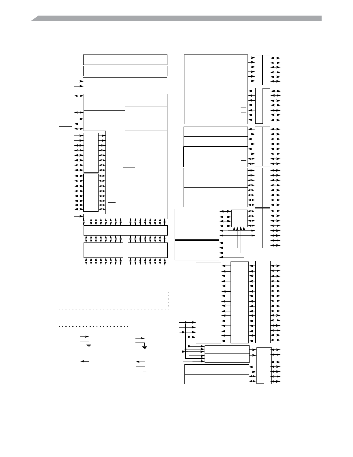
1.1.3 Block Diagram
32K / 64K / 128K Byte Flash EEPROM
2k / 4K / 8K Byte RAM
VDDR
VSSR
BKGD
XFC
EXTAL
XTAL
RESET
PE0
PE1
PE2
PE3
PE4
PE5
PE6
PE7
PK0
PK1
PK2
PK3
PK4
PK5
PK6
PK7
TEST
Multiplexed
Wide Bus
Multiplexed
Narrow Bus
Voltage Regulator 3.3V/5V
VDDR
VSSR
PLL 2.5V
VDDPLL
VSSPLL
Signals shown in Bold are not available on the 80 Pin Package
MODC/TAGHI
Single-wire Background
Debug Module
CRG
PTE
PTK
PA7
PA6
ADDR15
ADDR14
DATA15
DATA14
DATA7
DATA6
Voltage Regulator
CPU12
Periodic Interrupt
Clock and
Reset
Generation
XIRQ
IRQ
W
R/
LSTRB/TAGLO
ECLK
DDRE
MODA/IPIPE0
MODB/IPIPE1
NOACC/
XADDR14
XADDR15
XADDR16
XADDR17
XADDR18
DDRK
XADDR19
XCS
ECS
Multiplexed Address/Data Bus
DDRA DDRB
PTA PTB
PA4
PA3
PA2
PA5
ADDR12
ADDR11
ADDR10
ADDR13
DATA12
DATA11
DATA10
DATA13
DATA4
DATA3
DATA2
DATA5
Internal Logic 2.5V
COP Watchdog
Clock Monitor
Debugger(DBG12)
Breakpoints
System
Integration
Module
XCLKS
PA1
PA0
PB7
PB6
PB5
ADDR9
ADDR8
ADDR7
ADDR6
ADDR5
DATA9
DATA8
DATA7
DATA6
DATA5
DATA1
DATA0
I/O Driver 3.3V/5V
VDDX
VSSX
VDD1,2
VSS1,2
(SIM)
PB4
PB3
PB2
ADDR4
ADDR3
ADDR2
DATA4
DATA3
DATA2
ADC/DAC 3.3V/5V
Voltage Reference
Figure 1-1. MC9S12E128 Block Diagram
PB1
PB0
ADDR1
ADDR0
DATA1
DATA0
VDDA
VSSA
VRH
VRL
PWM
TIM2
PMF
SCI0
SCI1
SPI
SCI2
IIC
TIM0
TIM1
ADC
PW10
PW11
PW12
PW13
PW14
PW15
IOC24
IOC25
IOC26
IOC27
AN0
AN1
AN2
AN3
AN4
AN5
AN6
AN7
AN8
AN9
AN10
AN11
AN12
AN13
AN14
AN15
DAC0
DAC1
PW00
PW01
PW02
PW03
PW04
PW05
FAULT0
FAULT1
FAU LT2
FAULT3
IS0
IS1
IS2
RXD0
TXD0
RXD1
TXD1
MISO
MOSI
SCK
SS
IOC04
IOC05
IOC06
IOC07
IOC14
IOC15
IOC16
IOC17
MUX
KWAD0
KWAD1
KWAD2
KWAD3
KWAD4
KWAD5
KWAD6
KWAD7
KWAD8
KWAD9
KWAD10
KWAD11
KWAD12
KWAD13
KWAD14
KWAD15
DAO0
DAO1
RXD2
TXD2
SDA
SCL
PTP
DDRP
PTQ
DDRQ
PTS
DDRS
PTT
DDRT
PTU
DDRU
PAD
DDRAD
PTM
DDRM
PP0
PP1
PP2
PP3
PP4
PP5
PQ0
PQ1
PQ2
PQ3
PQ4
PQ5
PQ6
PS0
PS1
PS2
PS3
PS4
PS5
PS6
PS7
PT0
PT1
PT2
PT3
PT4
PT5
PT6
PT7
PU0
PU1
PU2
PU3
PU4
PU5
PU6
PU7
PAD0
PAD1
PAD2
PAD3
PAD4
PAD5
PAD6
PAD7
PAD8
PAD9
PAD10
PAD11
PAD12
PAD13
PAD14
PAD15
PM0
PM1
PM3
PM4
PM5
PM6
PM7
MC9S12E128 Data Sheet, Rev. 1.07
24 Freescale Semiconductor

Chapter 1 MC9S12E128 Device Overview (MC9S12E128DGV1)
1.2 Device Memory Map
Table 1-1 shows the device register map of the MC9S12E128 after reset. Figure 1-2, Figure 1-3 and
Figure 1-4 illustrate the device memory map with Flash and RAM.
Table 1-1. Device Register Map Overview
Address Module Size
0x0000–0x0017 CORE (Ports A, B, E, Modes, Inits, Test) 24
0x0018 Reserved 1
0x0019 Voltage Regulator (VREG) 1
0x001A–0x001B Device ID register (PARTID) 2
0x001C–0x001F CORE (MEMSIZ, IRQ, HPRIO) 4
0x0020–0x002F CORE (DBG) 16
0x0030–0x0033 CORE (PPAGE, Port K) 4
0x0034–0x003F Clock and Reset Generator (PLL, RTI, COP) 12
0x0040–0x006F Standard Timer 16-bit 4 channels (TIM0) 48
0x0070–0x007F Reserved 16
0x0080–0x00AF Analog to Digital Converter 10-bit 16 channels (ATD) 48
0x00B0–0x00C7 Reserved 24
0x00C8–0x00CF Serial Communications Interface 0 (SCI0) 8
0x00D0–0x00D7 Serial Communications Interface 1 (SCI1) 8
0x00D8–0x00DF Serial Peripheral Interface (SPI) 8
0x00E0–0x00E7 Inter IC Bus 8
0x00E8–0x00EF Serial Communications Interface 2 (SCI2) 8
0x00F0–0x00F3 Digital to Analog Converter 8-bit 1-channel (DAC0) 4
0x00F4–0x00F7 Digital to Analog Converter 8-bit 1-channel (DAC1) 4
0x00F8–0x00FF Reserved 8
0x0100- 0x010F Flash Control Register 16
0x0110–0x013F Reserved 48
0x0140–0x016F Standard Timer 16-bit 4 channels (TIM1) 48
0x0170–0x017F Reserved 16
0x0180–0x01AF Standard Timer 16-bit 4 channels (TIM2) 48
0x01B0–0x01DF Reserved 48
0x01E0–0x01FF Pulse Width Modulator 8-bit 6 channels (PWM) 32
0x0200–0x023F Pulse Width Modulator with Fault 15-bit 6 channels (PMF) 64
0x0240–0x027F Port Integration Module (PIM) 64
0x0280–0x03FF Reserved 384
MC9S12E128 Data Sheet, Rev. 1.07
Freescale Semiconductor 25

Chapter 1 MC9S12E128 Device Overview (MC9S12E128DGV1)
$0000
$0400
$2000
$4000
$8000
$C000
$FF00
$FFFF
VECTORS
NORMAL
SINGLE CHIP
EXT
VECTORS
EXPANDED SPECIAL
VECTORS
SINGLE CHIP
$0000
$03FF
$2000
$3FFF
$4000
$7FFF
$8000
$BFFF
$C000
$FFFF
$FF00
$FFFF
1K Register Space
Mappable to any 2K Boundary
8K Bytes RAM
Mappable to any 8K Boundary
0.5K, 1K, 2K or 4K Protected Sector
16K Fixed Flash EEPROM
16K Page Window
eight * 16K Flash EEPROM Pages
16K Fixed Flash EEPROM
2K, 4K, 8K or 16K Protected Boot Sector
BDM
(If Active)
The figure shows a useful map, which is not the map out of reset. After reset the map is:
$0000–$03FF: Register Space
$0000–$1FFF: 8K RAM (only 7K RAM visible $0400–$1FFF)
Figure 1-2. MC9S12E128 User Configurable Memory Map
MC9S12E128 Data Sheet, Rev. 1.07
26 Freescale Semiconductor
Chapter 1 MC9S12E128 Device Overview (MC9S12E128DGV1)
$0000
$0400
$3000
$4000
$8000
$C000
$FF00
$FFFF
VECTORS
NORMAL
SINGLE CHIP
EXT
VECTORS
EXPANDED SPECIAL
VECTORS
SINGLE CHIP
$0000
$03FF
$3000
$3FFF
$4000
$7FFF
$8000
$BFFF
$C000
$FFFF
$FF00
$FFFF
1K Register Space
Mappable to any 2K Boundary
4K Bytes RAM
Mappable to any 4K Boundary
0.5K, 1K, 2K or 4K Protected Sector
16K Fixed Flash EEPROM
16K Page Window
four * 16K Flash EEPROM Pages
16K Fixed Flash EEPROM
2K, 4K, 8K or 16K Protected Boot Sector
BDM
(If Active)
The figure shows a useful map, which is not the map out of reset. After reset the map is:
$0000–$03FF: Register Space
$0000–$0FFF: 4K RAM (only 3K RAM visible $0400–$0FFF)
Figure 1-3. MC9S12E64 User Configurable Memory Map
MC9S12E128 Data Sheet, Rev. 1.07
Freescale Semiconductor 27
Chapter 1 MC9S12E128 Device Overview (MC9S12E128DGV1)
$0000
$0400
$3000
$4000
$8000
$C000
$FF00
$FFFF
VECTORS
NORMAL
SINGLE CHIP
EXT
VECTORS
EXPANDED SPECIAL
VECTORS
SINGLE CHIP
$0000
$03FF
$3700
$3FFF
$4000
$7FFF
$8000
$BFFF
$C000
$FFFF
$FF00
$FFFF
1K Register Space
Mappable to any 2K Boundary
2K Bytes RAM
Mappable to any 2K Boundary
0.5K, 1K, 2K or 4K Protected Sector
16K Fixed Flash EEPROM
16K Page Window
two * 16K Flash EEPROM Pages
16K Fixed Flash EEPROM
2K, 4K, 8K or 16K Protected Boot Sector
BDM
(If Active)
The figure shows a useful map, which is not the map out of reset. After reset the map is:
$0000–$03FF: Register Space
$0000–$07FF: 2K RAM (only 1K RAM visible $0400–$07FF)
Figure 1-4. MC9S12E32 User Configurable Memory Map
MC9S12E128 Data Sheet, Rev. 1.07
28 Freescale Semiconductor
Chapter 1 MC9S12E128 Device Overview (MC9S12E128DGV1)
1.2.1 Detailed Register Map
0x0000 – 0x000F MEBI Map 1 of 3 (HCS12 Multiplexed External Bus Interface)
Address Name Bit 7 Bit 6 Bit 5 Bit 4 Bit 3 Bit 2 Bit 1 Bit 0
0x0000 PORTA
0x0001 PORTB
0x0002 DDRA
0x0003 DDRB
0x0004 Reserved
0x0005 Reserved
0x0006 Reserved
0x0007 Reserved
0x0008 PORTE
0x0009 DDRE
0x000A PEAR
0x000B MODE
0x000C PUCR
0x000D RDRIV
0x000E EBICTL
0x000F Reserved
R
Bit 7 6 5 4 3 2 1 Bit 0
W
R
Bit 7 6 5 4 3 2 1 Bit 0
W
R
Bit 7 6 5 4 3 2 1 Bit 0
W
R
Bit 7 6 5 4 3 2 1 Bit 0
W
R00000000
W
R00000000
W
R00000000
W
R00000000
W
R
Bit 7 6 5 4 3 2
W
R
Bit 7 6 5 4 3 Bit 2
W
R
NOACCE
W
R
MODC MODB MODA
W
R
PUPKE
W
R
RDPK
W
R0000000
W
R00000000
W
0
00
00
PIPOE NECLK LSTRE RDWE
PUPEE
RDPE
0
IVIS
00
00
0
Bit 1 Bit 0
00
00
EMK EME
PUPBE PUPAE
RDPB RDPA
ESTR
MC9S12E128 Data Sheet, Rev. 1.07
Freescale Semiconductor 29
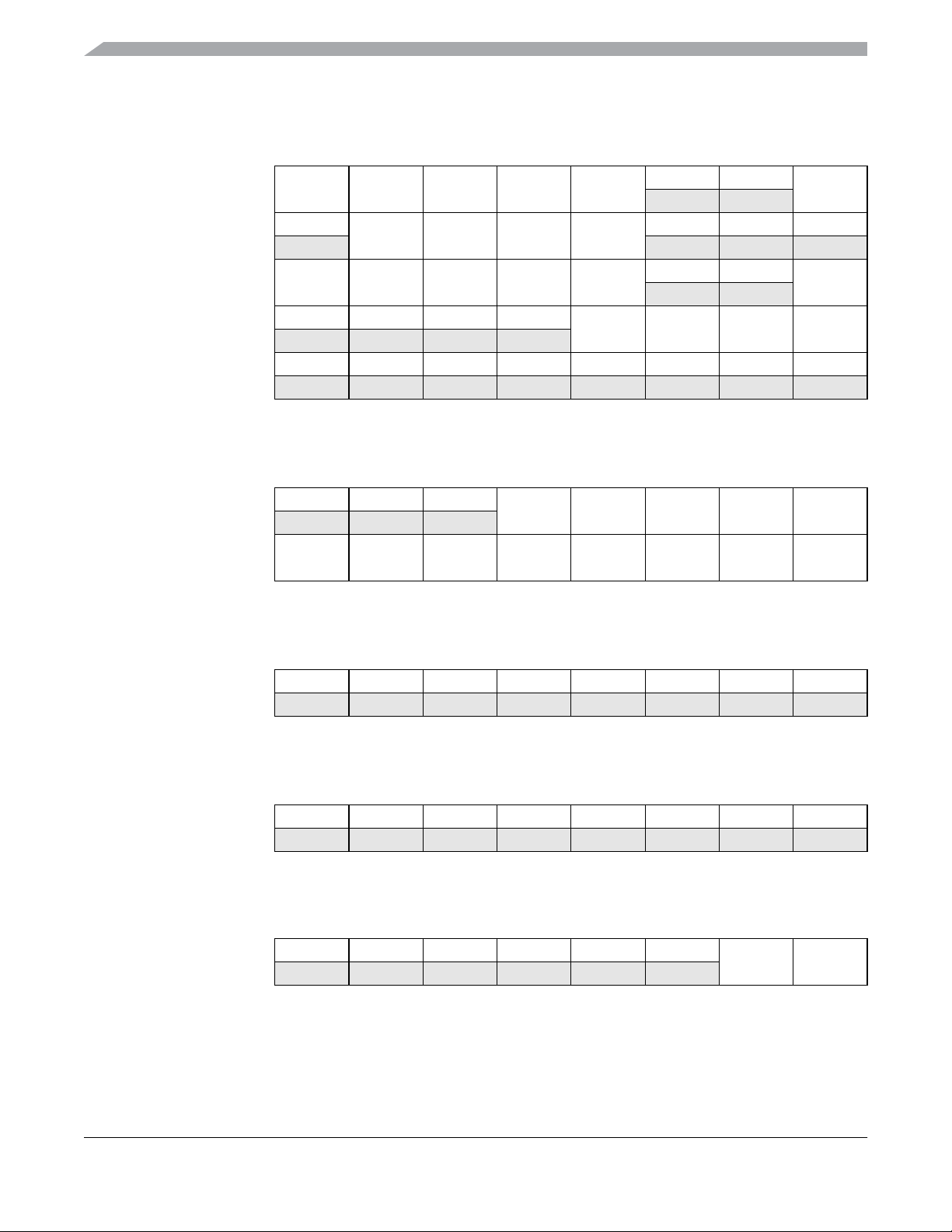
Chapter 1 MC9S12E128 Device Overview (MC9S12E128DGV1)
0x0010 – 0x0014 MMC Map 1 of 4 (HCS12 Module Mapping Control)
Address Name Bit 7 Bit 6 Bit 5 Bit 4 Bit 3 Bit 2 Bit 1 Bit 0
0x0010 INITRM
0x0011 INITRG
0x0012 INITEE
0x0013 MISC
0x0014 MTST0
R
RAM15 RAM14 RAM13 RAM12 RAM11
W
R0
W
R
EE15 EE14 EE13 EE12 EE11
W
R0 0 0 0
W
R Bit 7 6 5 4 3 2 1 Bit 0
W
REG14 REG13 REG12 REG11
EXSTR1 EXSTR0 ROMHM ROMON
00
000
00
RAMHAL
EEON
0x0015 – 0x0016 INT Map 1 of 2 (HCS12 Interrupt)
Address Name Bit 7 Bit 6 Bit 5 Bit 4 Bit 3 Bit 2 Bit 1 Bit 0
0x0015 ITCR
0x0016 ITEST
R0 0 0
W
R
INTE INTC INTA INT8 INT6 INT4 INT2 INT0
W
WRINT ADR3 ADR2 ADR1 ADR0
0x0017 – 0x0017MMC Map 2 of 4 (HCS12 Module Mapping Control)
Address Name Bit 7 Bit 6 Bit 5 Bit 4 Bit 3 Bit 2 Bit 1 Bit 0
0x0017 MTST1
R Bit 7 6 5 4 3 2 1 Bit 0
W
0x0018 – 0x0018 Miscellaneous Peripherals (Device User Guide)
Address Name Bit 7 Bit 6 Bit 5 Bit 4 Bit 3 Bit 2 Bit 1 Bit 0
0x0018 Reserved
R00000000
W
0x0019 – 0x0019 VREG3V3 (Voltage Regulator)
Address Name Bit 7 Bit 6 Bit 5 Bit 4 Bit 3 Bit 2 Bit 1 Bit 0
0x0019 VREGCTRL
R 0 0 0 0 0 LVDS
W
LVIE LVIF
MC9S12E128 Data Sheet, Rev. 1.07
30 Freescale Semiconductor

Chapter 1 MC9S12E128 Device Overview (MC9S12E128DGV1)
0x001A – 0x001B Miscellaneous Peripherals (Device User Guide)
Address Name Bit 7 Bit 6 Bit 5 Bit 4 Bit 3 Bit 2 Bit 1 Bit 0
0x001A PARTIDH
0x001B PARTIDL
R ID15 ID14 ID13 ID12 ID11 ID10 ID9 ID8
W
R ID7 ID6 ID5 ID4 ID3 ID2 ID1 ID0
W
0x001C – 0x001D MMC Map 3 of 4 (HCS12 Module Mapping Control, Device User Guide)
Address Name Bit 7 Bit 6 Bit 5 Bit 4 Bit 3 Bit 2 Bit 1 Bit 0
0x001C MEMSIZ0
0x001D MEMSIZ1
R reg_sw0 0 eep_sw1 eep_sw0 0 ram_sw2 ram_sw1 ram_sw0
W
R rom_sw1 rom_sw0 0 0 0 0 pag_sw1 pag_sw0
W
0x001E – 0x001E MEBI Map 2 of 3 (HCS12 Multiplexed External Bus Interface)
Address Name Bit 7 Bit 6 Bit 5 Bit 4 Bit 3 Bit 2 Bit 1 Bit 0
0x001E INTCR
R
IRQE IRQEN
W
000000
0x001F – 0x001F INT Map 2 of 2 (HCS12 Interrupt)
Address Name Bit 7 Bit 6 Bit 5 Bit 4 Bit 3 Bit 2 Bit 1 Bit 0
0x001F HPRIO
R
PSEL7 PSEL6 PSEL5 PSEL4 PSEL3 PSEL2 PSEL1
W
0x0020 – 0x002F DBG (Including BKP) Map 1 of 1 (HCS12 Debug)
Address Name Bit 7 Bit 6 Bit 5 Bit 4 Bit 3 Bit 2 Bit 1 Bit 0
0x0020
0x0021
0x0022
0x0023
0x0024
0x0025
DBGC1 R
—W
DBGSC R AF BF CF 0
—W
DBGTBH R Bit 15 Bit 14 Bit 13 Bit 12 Bit 11 Bit 10 Bit 9 Bit 8
—W
DBGTBL R Bit 7 Bit 6 Bit 5 Bit 4 Bit 3 Bit 2 Bit 1 Bit 0
—W
DBGCNT R TBF 0 CNT
—W
DBGCCX R
—W
DBGEN ARM TRGSEL BEGIN DBGBRK
PAGSEL EXTCMP
0
TRG
CAPMOD
0
MC9S12E128 Data Sheet, Rev. 1.07
Freescale Semiconductor 31

Chapter 1 MC9S12E128 Device Overview (MC9S12E128DGV1)
0x0020 – 0x002F DBG (Including BKP) Map 1 of 1 (HCS12 Debug) (continued)
Address Name Bit 7 Bit 6 Bit 5 Bit 4 Bit 3 Bit 2 Bit 1 Bit 0
0x0026
0x0027
0x0028
0x0029
0x002A
0x002B
0x002C
0x002D
0x002E
0x002F
DBGCCH R
—W
DBGCCL R
—W
DBGC2 R
BKPCT0 W
DBGC3 R
BKPCT1 W
DBGCAX R
BKP0X W
DBGCAH R
BKP0H W
DBGCAL R
BKP0L W
DBGCBX R
BKP1X W
DBGCBH R
BKP1H W
DBGCBL R
BKP1L W
Bit 15 14 13 12 11 10 9 Bit 8
Bit 7 6 5 4 3 2 1 Bit 0
BKABEN FULL BDM TAGAB BKCEN TAGC RWCEN RWC
BKAMBH BKAMBL BKBMBH BKBMBL RWAEN RWA RWBEN RWB
PAGSEL EXTCMP
Bit 15 14 13 12 11 10 9 Bit 8
Bit 7 6 5 4 3 2 1 Bit 0
PAGSEL EXTCMP
Bit 15 14 13 12 11 10 9 Bit 8
Bit 7 6 5 4 3 2 1 Bit 0
0x0030 – 0x0031 MMC Map 4 of 4 (HCS12 Module Mapping Control)
Address Name Bit 7 Bit 6 Bit 5 Bit 4 Bit 3 Bit 2 Bit 1 Bit 0
0x0030 PPAGE
0x0031 Reserved
R0 0
W
R00000000
W
PIX5 PIX4 PIX3 PIX2 PIX1 PIX0
0x0032 – 0x0033 MEBI Map 3 of 3 (HCS12 Multiplexed External Bus Interface)
Address Name Bit 7 Bit 6 Bit 5 Bit 4 Bit 3 Bit 2 Bit 1 Bit 0
0x0032 PORTK
0x0033 DDRK
R
ECS XCS XAB19 XAB18 XAB17 XAB16 XAB15 XAB14
W
R
Bit 7 6 5 4 3 2 1 Bit 0
W
MC9S12E128 Data Sheet, Rev. 1.07
32 Freescale Semiconductor

Chapter 1 MC9S12E128 Device Overview (MC9S12E128DGV1)
0x0034 – 0x003F CRG (Clock and Reset Generator)
Address Name Bit 7 Bit 6 Bit 5 Bit 4 Bit 3 Bit 2 Bit 1 Bit 0
0x0034 SYNR
0x0035 REFDV
0x0036
0x0037 CRGFLG
0x0038 CRGINT
0x0039 CLKSEL
0x003A PLLCTL
0x003B RTICTL
0x003C COPCTL
0x003D
0x003E
0x003F ARMCOP
CTFLG
TEST ONLY
FORBYP
TEST ONLY
CTCTL
TEST ONLY
R0 0
W
R0 0 0 0
W
R TOUT7 TOUT6 TOUT5 TOUT4 TOUT3 TOUT2 TOUT1 TOUT0
W
R
RTIF PROF
W
R
RTIE
W
R
PLLSEL PSTP SYSWAI ROAWAI PLLWAI CWAI RTIWAI COPWAI
W
R
CME PLLON AUTO ACQ
W
R0
W
R
WCOP RSBCK
W
R
RTIBYP COPBYP
W
R TCTL7 TCTL6 TCTL5 TCTL4 TCLT3 TCTL2 TCTL1 TCTL0
W
R00000000
W Bit 7 6 5 4 3 2 1 Bit 0
00
RTR6 RTR5 RTR4 RTR3 RTR2 RTR1 RTR0
SYN5 SYN4 SYN3 SYN2 SYN1 SYN0
REFDV3 REFDV2 REFDV1 REFDV0
0
000
0
LOCKIF
LOCKIE
PLLBYP
LOCK TRACK
00
0
00
PRE PCE SCME
CR2 CR1 CR0
SCMIF
SCMIE
FCM
SCM
0
0
0x0040 – 0x006F TIM0 (Timer 16 Bit 4 Channels) (Sheet 1 of 4)
Address Name Bit 7 Bit 6 Bit 5 Bit 4 Bit 3 Bit 2 Bit 1 Bit 0
0x0040 TIOS
0x0041 CFORC
0x0042 OC7M
0x0043 OC7D
0x0044 TCNT (hi)
0x0045 TCNT (lo)
Freescale Semiconductor 33
R
IOS7 IOS6 IOS5 IOS4
W
R00000000
W FOC7 FOC6 FOC5 FOC4
R
OC7M7 OC7M6 OC7M5 OC7M4
W
R
OC7D7 OC7D6 OC7D5 OC7D4
W
R Bit 15 14 13 12 11 10 9 Bit 8
W
R Bit 7 6 5 4 3 2 1 Bit 0
W
MC9S12E128 Data Sheet, Rev. 1.07
0000
0000
0000

Chapter 1 MC9S12E128 Device Overview (MC9S12E128DGV1)
0x0040 – 0x006F TIM0 (Timer 16 Bit 4 Channels) (Sheet 2 of 4)
Address Name Bit 7 Bit 6 Bit 5 Bit 4 Bit 3 Bit 2 Bit 1 Bit 0
0x0046 TSCR1
0x0047 TTOV
0x0048 TCTL1
0x0049 Reserved
0x004A TCTL3
0x004B Reserved
0x004C TIE
0x004D TSCR2
0x004E TFLG1
0x004F TFLG2
0x0050 Reserved
0x0051 Reserved
0x0052 Reserved
0x0053 Reserved
0x0054 Reserved
0x0055 Reserved
0x0056 Reserved
0x0057 Reserved
0x0058 TC4 (hi)
R
TEN TSWAI TSFRZ TFFCA
W
R
TOV7 TOV6 TOV5 TOV4
W
R
OM7 OL7 OM6 OL6 OM5 OL5 OM4 OL4
W
R00000000
W
R
EDG7B EDG7A EDG6B EDG6A EDG5B EDG5A EDG4B EDG4A
W
R00000000
W
R
C7I C6I C5I C4I
W
R
TOI
W
R
C7F C6F C5F C4F
W
R
TOF
W
R00000000
W
R00000000
W
R00000000
W
R00000000
W
R00000000
W
R00000000
W
R00000000
W
R00000000
W
R
Bit 15 14 13 12 11 10 9 Bit 8
W
000
0000000
0000
0000
0000
TCRE PR2 PR1 PR0
0000
MC9S12E128 Data Sheet, Rev. 1.07
34 Freescale Semiconductor

Chapter 1 MC9S12E128 Device Overview (MC9S12E128DGV1)
0x0040 – 0x006F TIM0 (Timer 16 Bit 4 Channels) (Sheet 3 of 4)
Address Name Bit 7 Bit 6 Bit 5 Bit 4 Bit 3 Bit 2 Bit 1 Bit 0
0x0059 TC4 (lo)
0x005A TC5 (hi)
0x005B TC5 (lo)
0x005C TC6 (hi)
0x005D TC6 (lo)
0x005E TC7 (hi)
0x005F TC7 (lo)
0x0060 PACTL
0x0061 PAFLG
0x0062 PACNT (hi)
0x0063 PACNT (lo)
0x0064 Reserved
0x0065 Reserved
0x0066 Reserved
0x0067 Reserved
0x0068 Reserved
0x0069 Reserved
0x006A Reserved
0x006B Reserved
R
Bit 7 6 5 4 3 2 1 Bit 0
W
R
Bit 15 14 13 12 11 10 9 Bit 8
W
R
Bit 7 6 5 4 3 2 1 Bit 0
W
R
Bit 15 14 13 12 11 10 9 Bit 8
W
R
Bit 7 6 5 4 3 2 1 Bit 0
W
R
Bit 15 14 13 12 11 10 9 Bit 8
W
R
Bit 7 6 5 4 3 2 1 Bit 0
W
R0
W
R0 0 0 0 0 0
W
R
Bit 15 14 13 12 11 10 9 Bit 8
W
R
Bit 7 6 5 4 3 2 1 Bit 0
W
R00000000
W
R00000000
W
R00000000
W
R00000000
W
R00000000
W
R00000000
W
R00000000
W
R00000000
W
PAEN PAMOD PEDGE CLK1 CLK0 PAOVI PAI
PAOVF PAIF
MC9S12E128 Data Sheet, Rev. 1.07
Freescale Semiconductor 35

Chapter 1 MC9S12E128 Device Overview (MC9S12E128DGV1)
0x0040 – 0x006F TIM0 (Timer 16 Bit 4 Channels) (Sheet 4 of 4)
Address Name Bit 7 Bit 6 Bit 5 Bit 4 Bit 3 Bit 2 Bit 1 Bit 0
0x006C Reserved
0x006D Reserved
0x006E Reserved
0x006F Reserved
R00000000
W
R00000000
W
R00000000
W
R00000000
W
0x0070 – 0x007F Reserved
Address Name Bit 7 Bit 6 Bit 5 Bit 4 Bit 3 Bit 2 Bit 1 Bit 0
0x0070–
0x007F
Reserved
R00000000
W
0x0080 – 0x00AF ATD (Analog to Digital Converter 10 Bit 16 Channel) (Sheet 1 of 3)
Address Name Bit 7 Bit 6 Bit 5 Bit 4 Bit 3 Bit 2 Bit 1 Bit 0
0x0080 ATDCTL0
0x0081 ATDCTL1
0x0082 ATDCTL2
0x0083 ATDCTL3
0x0084 ATDCTL4
0x0085 ATDCTL5
0x0086 ATDSTAT0
0x0087 Reserved
0x0088 ATDTEST0
0x0089 ATDTEST1
0x008A ATDSTAT0
R0 0 0 0
W
R
ETRIGSEL
W
R
ADPU AFFC AWAI ETRIGLE ETRIGP ETRIG ASCIE
W
R0
W
R
SRES8 SMP1 SMP0 PRS4 PRS3 PRS2 PRS1 PRS0
W
R
DJM DSGN SCAN MULT
W
R
SCF
W
000
2
S8C S4C S2C S1C FIFO FRZ1 FRZ0
0
ETORF FIFOR
WRAP3
ETRIGCH3
R00000000
W
R00000000
W
R0000000
W
R CCF15 CCF14 CCF13 CCF12 CCF11 CCF10 CCF9 CCF8
W
1
WRAP21WRAP11WRAP0
2
ETRIGCH22ETRIGCH12ETRIGCH0
ASCIF
0
CC CB CA
0 CC2 CC1 CC0
SC
1
2
MC9S12E128 Data Sheet, Rev. 1.07
36 Freescale Semiconductor

Chapter 1 MC9S12E128 Device Overview (MC9S12E128DGV1)
0x0080 – 0x00AF ATD (Analog to Digital Converter 10 Bit 16 Channel) (Sheet 2 of 3)
Address Name Bit 7 Bit 6 Bit 5 Bit 4 Bit 3 Bit 2 Bit 1 Bit 0
0x008B ATDSTAT1
0x008C ATDDIEN0
0x008D ATDDIEN1
0x008E PORTAD0
0x008F PORTAD1
0x0090 ATDDR0H
0x0091 ATDDR0L
0x0092 ATDDR1H
0x0093 ATDDR1L
0x0094 ATDDR2H
0x0095 ATDDR2L
0x0096 ATDDR3H
0x0097 ATDDR3L
0x0098 ATDDR4H
0x0099 ATDDR4L
0x009A ATDDR5H
0x009B ATDDR5L
0x009C ATDDR6H
0x009D ATDDR6L
R CCF7 CCF6 CCF5 CCF4 CCF3 CCF2 CCF1 CCF0
W
R
IEN15 IEN14 IEN13 IEN12 IEN11 IEN10 IEN9 IEN8
W
R
IEN7 IEN6 IEN5 IEN4 IEN3 IEN2 IEN1 IEN0
W
R PTAD15 PTAD14 PTAD13 PTAD12 PTAD11 PTAD10 PTAD9 PTAD8
W
R PTAD7 PTAD6 PTAD5 PTAD4 PTAD3 PTAD2 PTAD1 PTAD0
W
R Bit15 14 13 12 11 10 9 Bit8
W
R Bit7 Bit6 0 0 0 0 0 0
W
R Bit15 14 13 12 11 10 9 Bit8
W
R Bit7 Bit6 0 0 0 0 0 0
W
R Bit15 14 13 12 11 10 9 Bit8
W
R Bit7 Bit6 0 0 0 0 0 0
W
R Bit15 14 13 12 11 10 9 Bit8
W
R Bit7 Bit6 0 0 0 0 0 0
W
R Bit15 14 13 12 11 10 9 Bit8
W
R Bit7 Bit6 0 0 0 0 0 0
W
R Bit15 14 13 12 11 10 9 Bit8
W
R Bit7 Bit6 0 0 0 0 0 0
W
R Bit15 14 13 12 11 10 9 Bit8
W
R Bit7 Bit6 0 0 0 0 0 0
W
MC9S12E128 Data Sheet, Rev. 1.07
Freescale Semiconductor 37

Chapter 1 MC9S12E128 Device Overview (MC9S12E128DGV1)
0x0080 – 0x00AF ATD (Analog to Digital Converter 10 Bit 16 Channel) (Sheet 3 of 3)
Address Name Bit 7 Bit 6 Bit 5 Bit 4 Bit 3 Bit 2 Bit 1 Bit 0
0x009E ATDDR7H
0x009F ATDDR7L
0x00A0 ATDDR8H
0x00A1 ATDDR8L
0x00A2 ATDDR9H
0x00A3 ATDDR9L
0x00A4 ATDDR10H
0x00A5 ATDDR10L
0x00A6 ATDDR11H
0x00A7 ATDDR11L
0x00A8 ATDDR12H
0x00A9 ATDDR12L
0x00AA ATDDR13H
0x00AB ATDDR13L
0x00AC ATDDR14H
0x00AD ATDDR14L
0x00AE ATDDR15H
0x00AF ATDDR15L
1
WRAP0–3 bits are available in version V04 of ATD10B16C
2
ETRIGSEL and ETRIGCH0–3 bits are available in version V04 of ATD10B16C
R Bit15 14 13 12 11 10 9 Bit8
W
R Bit7 Bit6 0 0 0 0 0 0
W
R Bit15 14 13 12 11 10 9 Bit8
W
R Bit7 Bit6 0 0 0 0 0 0
W
R Bit15 14 13 12 11 10 9 Bit8
W
R Bit7 Bit6 0 0 0 0 0 0
W
R Bit15 14 13 12 11 10 9 Bit8
W
R Bit7 Bit6 0 0 0 0 0 0
W
R Bit15 14 13 12 11 10 9 Bit8
W
R Bit7 Bit6 0 0 0 0 0 0
W
R Bit15 14 13 12 11 10 9 Bit8
W
R Bit7 Bit6 0 0 0 0 0 0
W
R Bit15 14 13 12 11 10 9 Bit8
W
R Bit7 Bit6 0 0 0 0 0 0
W
R Bit15 14 13 12 11 10 9 Bit8
W
R Bit7 Bit6 0 0 0 0 0 0
W
R Bit15 14 13 12 11 10 9 Bit8
W
R Bit7 Bit6 0 0 0 0 0 0
W
MC9S12E128 Data Sheet, Rev. 1.07
38 Freescale Semiconductor

Chapter 1 MC9S12E128 Device Overview (MC9S12E128DGV1)
0x00B0 – 0x00C7 Reserved
Address Name Bit 7 Bit 6 Bit 5 Bit 4 Bit 3 Bit 2 Bit 1 Bit 0
0x00B0–
0x00C7
Reserved
R00000000
W
0x00C8 – 0x00CF SCI0 (Asynchronous Serial Interface)
Address Name Bit 7 Bit 6 Bit 5 Bit 4 Bit 3 Bit 2 Bit 1 Bit 0
0x00C8 SCIBDH
0x00C9 SCIBDL
0x00CA SCICR1
0x00CB SCICR2
0x00CC SCISR1
0x00CD SCISR2
0x00CE SCIDRH
0x00CF SCIDRL
1
TXPOL and RXPOL bits are available in version V04 of SCI
R
IREN TNP1 TNP0 SBR12 SBR11 SBR10 SBR9 SBR8
W
R
SBR7 SBR6 SBR5 SBR4 SBR3 SBR2 SBR1 SBR0
W
R
LOOPS SCISWAI RSRC M WAKE ILT PE PT
W
R
TIE TCIE RIE ILIE TE RE RWU SBK
W
R TDRE TC RDRF IDLE OR NF FE PF
W
R0 0 0
W
RR8
W
RR7R6R5R4R3R2R1R0
WT7T6T5T4T3T2T1T0
T8
000000
TXPOL
1
RXPOL
1
BRK13 TXDIR
RAF
0x00D0 – 0x00D7 SCI1 (Asynchronous Serial Interface)
Address Name Bit 7 Bit 6 Bit 5 Bit 4 Bit 3 Bit 2 Bit 1 Bit 0
0x00D0 SCIBDH
0x00D1 SCIBDL
0x00D2 SCICR1
0x00D3 SCICR2
0x00D4 SCISR1
Freescale Semiconductor 39
R
IREN TNP1 TNP0 SBR12 SBR11 SBR10 SBR9 SBR8
W
R
SBR7 SBR6 SBR5 SBR4 SBR3 SBR2 SBR1 SBR0
W
R
LOOPS SCISWAI RSRC M WAKE ILT PE PT
W
R
TIE TCIE RIE ILIE TE RE RWU SBK
W
R TDRE TC RDRF IDLE OR NF FE PF
W
MC9S12E128 Data Sheet, Rev. 1.07

Chapter 1 MC9S12E128 Device Overview (MC9S12E128DGV1)
0x00D0 – 0x00D7 SCI1 (Asynchronous Serial Interface) (continued)
Address Name Bit 7 Bit 6 Bit 5 Bit 4 Bit 3 Bit 2 Bit 1 Bit 0
0x00D5 SCISR2
0x00D6 SCIDRH
0x00D7 SCIDRL
1
TXPOL and RXPOL are available in version V04 of SCI
R0 0 0
W
RR8
W
RR7R6R5R4R3R2R1R0
WT7T6T5T4T3T2T1T0
T8
1
TXPOL
000000
RXPOL
1
BRK13 TXDIR
RAF
0x00D8 – 0x00DF SPI (Serial Peripheral Interface)
Address Name Bit 7 Bit 6 Bit 5 Bit 4 Bit 3 Bit 2 Bit 1 Bit 0
0x00D8 SPICR1
0x00D9 SPICR2
0x00DA SPIBR
0x00DB SPISR
0x00DC Reserved
0x00DD SPIDR
0x00DE Reserved
0x00DF Reserved
R
SPIE SPE SPTIE MSTR CPOL CPHA SSOE LSBFE
W
R0 0 0
W
R0
W
R SPIF 0 SPTEF MODF 0 0 0 0
W
R00000000
W
R
Bit7 6 5 4 3 2 1 Bit0
W
R00000000
W
R00000000
W
SPPR2 SPPR1 SPPR0
MODFEN BIDIROE
0
0
SPR2 SPR1 SPR0
SPISWAI SPC0
0x00E0 – 0x00E7 IIC (Inter-IC Bus)
Address Name Bit 7 Bit 6 Bit 5 Bit 4 Bit 3 Bit 2 Bit 1 Bit 0
0x00E0 IBAD
0x00E1 IBFD
0x00E2 IBCR
0x00E3 IBSR
40 Freescale Semiconductor
R
ADR7 ADR6 ADR5 ADR4 ADR3 ADR2 ADR1
W
R
IBC7 IBC6 IBC5 IBC4 IBC3 IBC2 IBC1 IBC0
W
R
IBEN IBIE MS/
W RSTA
R TCF IAAS IBB
W
MC9S12E128 Data Sheet, Rev. 1.07
SL Tx/Rx TXAK
IBAL
0SRW
00
IBIF
0
IBSWAI
RXAK

Chapter 1 MC9S12E128 Device Overview (MC9S12E128DGV1)
0x00E0 – 0x00E7 IIC (Inter-IC Bus) (continued)
Address Name Bit 7 Bit 6 Bit 5 Bit 4 Bit 3 Bit 2 Bit 1 Bit 0
0x00E4 IBDR
0x00E5 Reserved
0x00E6 Reserved
0x00E7 Reserved
R
D7 D6 D5 D4 D3 D2 D1 D0
W
R00000000
W
R00000000
W
R00000000
W
0x00E8 – 0x00EF SCI2 (Asynchronous Serial Interface)
Address Name Bit 7 Bit 6 Bit 5 Bit 4 Bit 3 Bit 2 Bit 1 Bit 0
0x00E8 SCIBDH
0x00E9 SCIBDL
0x00EA SCICR1
0x00EB SCICR2
0x00EC SCISR1
0x00ED SCISR2
0x00EE SCIDRH
0x00EF SCIDRL
1
TXPOL and RXPOL are available in version V04 of SCI
R
IREN TNP1 TNP0 SBR12 SBR11 SBR10 SBR9 SBR8
W
R
SBR7 SBR6 SBR5 SBR4 SBR3 SBR2 SBR1 SBR0
W
R
LOOPS SCISWAI RSRC M WAKE ILT PE PT
W
R
TIE TCIE RIE ILIE TE RE RWU SBK
W
R TDRE TC RDRF IDLE OR NF FE PF
W
R0 0 0
W
RR8
W
T8
000000
TXPOL
1
RXPOL
1
BRK13 TXDIR
RAF
RR7R6R5R4R3R2R1R0
WT7T6T5T4T3T2T1T0
MC9S12E128 Data Sheet, Rev. 1.07
Freescale Semiconductor 41

Chapter 1 MC9S12E128 Device Overview (MC9S12E128DGV1)
0x00F0 – 0x00F3 DAC0 (Digital-to-Analog Converter)
Address Name Bit 7 Bit 6 Bit 5 Bit 4 Bit 3 Bit 2 Bit 1 Bit 0
0x00F0 DACC0
0x00F1 DACC1
0x00F2 DACD
0x00F3 DACD
R
DACE
W
R00000000
W
R
BIT7 BIT6 BIT5 BIT4 BIT3 BIT2 BIT1 BIT0
W
R
BIT7 BIT6 BIT5 BIT4 BIT3 BIT2 BIT1 BIT0
W
DACTE 0 0
DJM DSGN DACWAI DACOE
0x00F4 – 0x00F7 DAC1 (Digital-to-Analog Converter)
Address Name Bit 7 Bit 6 Bit 5 Bit 4 Bit 3 Bit 2 Bit 1 Bit 0
0x00F4 DACC0
0x00F5 DACC1
0x00F6 DACD
0x00F7 DACD
R
DACE
W
R00000000
W
R
BIT7 BIT6 BIT5 BIT4 BIT3 BIT2 BIT1 BIT0
W
R
BIT7 BIT6 BIT5 BIT4 BIT3 BIT2 BIT1 BIT0
W
DACTE 0 0
DJM DSGN DACWAI DACOE
0x00F8 – 0x00FF Reserved
Address Name Bit 7 Bit 6 Bit 5 Bit 4 Bit 3 Bit 2 Bit 1 Bit 0
0x00F8–
0x00FF
Reserved
R00000000
W
0x0100 – 0x010F Flash Control Register
Address Name Bit 7 Bit 6 Bit 5 Bit 4 Bit 3 Bit 2 Bit 1 Bit 0
0x0100 FCLKDIV
0x0101 FSEC
0x0102
0x0103 FCNFG
0x0104 FPROT
Reserved for
Factory Test
R FDIVLD
W
R KEYEN1 NV6 NV5 NV4 NV3 NV2 SEC1 SEC0
W
R00000000
W
R
CBEIE CCIE KEYACC
W
R
FPOPEN NV6 FPHDIS FPHS1 FPHS0 FPLDIS FPLS1 FPLS0
W
PRDIV8 FDIV5 FDIV4 FDIV3 FDIV2 FDIV1 FDIV0
00000
MC9S12E128 Data Sheet, Rev. 1.07
42 Freescale Semiconductor

Chapter 1 MC9S12E128 Device Overview (MC9S12E128DGV1)
0x0100 – 0x010F Flash Control Register (continued)
Address Name Bit 7 Bit 6 Bit 5 Bit 4 Bit 3 Bit 2 Bit 1 Bit 0
0x0105 FSTAT
0x0106 FCMD
0x0107
0x0108
0x0109
0x010A
0x010B
0x010C Reserved
0x010D Reserved
0x010E Reserved
0x010F Reserved
Reserved for
Factory Test
Reserved for
Factory Test
Reserved for
Factory Test
Reserved for
Factory Test
Reserved for
Factory Test
R
CBEIF
W
R0
W
R00000000
W
R00000000
W
R00000000
W
R00000000
W
R00000000
W
R00000000
W
R00000000
W
R00000000
W
R00000000
W
CCIF
CMDB6 CMDB5
PVIOL ACCERR
0
00
BLANK
CMDB2
00
0
CMDB0
0x0110 – 0x013F Reserved
Address Name Bit 7 Bit 6 Bit 5 Bit 4 Bit 3 Bit 2 Bit 1 Bit 0
0x0110–
0x013F
Reserved
R00000000
W
0x0140 – 0x016F TIM1 (Timer 16 Bit 4 Channels) (Sheet 1 of 4)
Address Name Bit 7 Bit 6 Bit 5 Bit 4 Bit 3 Bit 2 Bit 1 Bit 0
0x0140 TIOS
0x0141 CFORC
0x0142 OC7M
0x0143 OC7D
Freescale Semiconductor 43
R
IOS7 IOS6 IOS5 IOS4
W
R00000000
W FOC7 FOC6 FOC5 FOC4
R
OC7M7 OC7M6 OC7M5 OC7M4
W
R
OC7D7 OC7D6 OC7D5 OC7D4
W
MC9S12E128 Data Sheet, Rev. 1.07
0000
0000
0000

Chapter 1 MC9S12E128 Device Overview (MC9S12E128DGV1)
0x0140 – 0x016F TIM1 (Timer 16 Bit 4 Channels) (Sheet 2 of 4)
Address Name Bit 7 Bit 6 Bit 5 Bit 4 Bit 3 Bit 2 Bit 1 Bit 0
0x0144 TCNT (hi)
0x0145 TCNT (lo)
0x0146 TSCR1
0x0147 TTOV
0x0148 TCTL1
0x0149 Reserved
0x014A TCTL3
0x014B Reserved
0x014C TIE
0x014D TSCR2
0x014E TFLG1
0x014F TFLG2
0x0150 Reserved
0x0151 Reserved
0x0152 Reserved
0x0153 Reserved
0x0154 Reserved
0x0155 Reserved
0x0156 Reserved
R Bit 15 14 13 12 11 10 9 Bit 8
W
R Bit 7 6 5 4 3 2 1 Bit 0
W
R
TEN TSWAI TSFRZ TFFCA
W
R
TOV7 TOV6 TOV5 TOV4
W
R
OM7 OL7 OM6 OL6 OM5 OL5 OM4 OL4
W
R00000000
W
R
EDG7B EDG7A EDG6B EDG6A EDG5B EDG5A EDG4B EDG4A
W
R00000000
W
R
C7I C6I C5I C4I
W
R
TOI
W
R
C7F C6F C5F C4F
W
R
TOF
W
R00000000
W
R00000000
W
R00000000
W
R00000000
W
R00000000
W
R00000000
W
R00000000
W
000
0000000
0000
0000
0000
TCRE PR2 PR1 PR0
0000
MC9S12E128 Data Sheet, Rev. 1.07
44 Freescale Semiconductor

Chapter 1 MC9S12E128 Device Overview (MC9S12E128DGV1)
0x0140 – 0x016F TIM1 (Timer 16 Bit 4 Channels) (Sheet 3 of 4)
Address Name Bit 7 Bit 6 Bit 5 Bit 4 Bit 3 Bit 2 Bit 1 Bit 0
0x0157 Reserved
0x0158 TC4 (hi)
0x0159 TC4 (lo)
0x015A TC5 (hi)
0x015B TC5 (lo)
0x015C TC6 (hi)
0x015D TC6 (lo)
0x015E TC7 (hi)
0x015F TC7 (lo)
0x0160 PACTL
0x0161 PAFLG
0x0162 PACNT (hi)
0x0163 PACNT (lo)
0x0164 Reserved
0x0165 Reserved
0x0166 Reserved
0x0167 Reserved
0x0168 Reserved
0x0169 Reserved
R00000000
W
R
Bit 15 14 13 12 11 10 9 Bit 8
W
R
Bit 7 6 5 4 3 2 1 Bit 0
W
R
Bit 15 14 13 12 11 10 9 Bit 8
W
R
Bit 7 6 5 4 3 2 1 Bit 0
W
R
Bit 15 14 13 12 11 10 9 Bit 8
W
R
Bit 7 6 5 4 3 2 1 Bit 0
W
R
Bit 15 14 13 12 11 10 9 Bit 8
W
R
Bit 7 6 5 4 3 2 1 Bit 0
W
R0
W
R0 0 0 0 0 0
W
R
Bit 15 14 13 12 11 10 9 Bit 8
W
R
Bit 7 6 5 4 3 2 1 Bit 0
W
R00000000
W
R00000000
W
R00000000
W
R00000000
W
R00000000
W
R00000000
W
PAEN PAMOD PEDGE CLK1 CLK0 PAOVI PAI
PAOVF PAIF
MC9S12E128 Data Sheet, Rev. 1.07
Freescale Semiconductor 45

Chapter 1 MC9S12E128 Device Overview (MC9S12E128DGV1)
0x0140 – 0x016F TIM1 (Timer 16 Bit 4 Channels) (Sheet 4 of 4)
Address Name Bit 7 Bit 6 Bit 5 Bit 4 Bit 3 Bit 2 Bit 1 Bit 0
0x016A Reserved
0x016B Reserved
0x016C Reserved
0x016D Reserved
0x016E Reserved
0x016F Reserved
R00000000
W
R00000000
W
R00000000
W
R00000000
W
R00000000
W
R00000000
W
0x0170 – 0x017F Reserved
Address Name Bit 7 Bit 6 Bit 5 Bit 4 Bit 3 Bit 2 Bit 1 Bit 0
0x0110–
0x013F
Reserved
R00000000
W
0x0180 – 0x01AF TIM2 (Timer 16 Bit 4 Channels) (Sheet 1 of 3)
Address Name Bit 7 Bit 6 Bit 5 Bit 4 Bit 3 Bit 2 Bit 1 Bit 0
0x0180 TIOS
0x0181 CFORC
0x0182 OC7M
0x0183 OC7D
0x0184 TCNT (hi)
0x0185 TCNT (lo)
0x0186 TSCR1
0x0187 TTOV
0x0188 TCTL1
R
IOS7 IOS6 IOS5 IOS4
W
R00000000
W FOC7 FOC6 FOC5 FOC4
R
OC7M7 OC7M6 OC7M5 OC7M4
W
R
OC7D7 OC7D6 OC7D5 OC7D4
W
R Bit 15 14 13 12 11 10 9 Bit 8
W
R Bit 7 6 5 4 3 2 1 Bit 0
W
R
TEN TSWAI TSFRZ TFFCA
W
R
TOV7 TOV6 TOV5 TOV4
W
R
OM7 OL7 OM6 OL6 OM5 OL5 OM4 OL4
W
0000
0000
0000
0000
0000
MC9S12E128 Data Sheet, Rev. 1.07
46 Freescale Semiconductor

Chapter 1 MC9S12E128 Device Overview (MC9S12E128DGV1)
0x0180 – 0x01AF TIM2 (Timer 16 Bit 4 Channels) (Sheet 2 of 3)
Address Name Bit 7 Bit 6 Bit 5 Bit 4 Bit 3 Bit 2 Bit 1 Bit 0
0x0189 Reserved
0x018A TCTL3
0x018B Reserved
0x018C TIE
0x018D TSCR2
0x018E TFLG1
0x018F TFLG2
0x0190 Reserved
0x0191 Reserved
0x0192 Reserved
0x0193 Reserved
0x0194 Reserved
0x0195 Reserved
0x0196 Reserved
0x0197 Reserved
0x0198 TC4 (hi)
0x0199 TC4 (lo)
0x015A TC5 (hi)
0x019B TC5 (lo)
0x019C TC6 (hi)
R00000000
W
R
EDG7B EDG7A EDG6B EDG6A EDG5B EDG5A EDG4B EDG4A
W
R00000000
W
R
C7I C6I C5I C4I
W
R
TOI
W
R
C7F C6F C5F C4F
W
R
TOF
W
R00000000
W
R00000000
W
R00000000
W
R00000000
W
R00000000
W
R00000000
W
R00000000
W
R00000000
W
R
Bit 15 14 13 12 11 10 9 Bit 8
W
R
Bit 7 6 5 4 3 2 1 Bit 0
W
R
Bit 15 14 13 12 11 10 9 Bit 8
W
R
Bit 7 6 5 4 3 2 1 Bit 0
W
R
Bit 15 14 13 12 11 10 9 Bit 8
W
000
0000000
0000
TCRE PR2 PR1 PR0
0000
MC9S12E128 Data Sheet, Rev. 1.07
Freescale Semiconductor 47

Chapter 1 MC9S12E128 Device Overview (MC9S12E128DGV1)
0x0180 – 0x01AF TIM2 (Timer 16 Bit 4 Channels) (Sheet 3 of 3)
Address Name Bit 7 Bit 6 Bit 5 Bit 4 Bit 3 Bit 2 Bit 1 Bit 0
0x019D TC6 (lo)
0x019E TC7 (hi)
0x019F TC7 (lo)
0x01A0 PACTL
0x01A1 PAFLG
0x01A2 PACNT (hi)
0x01A3 PACNT (lo)
0x01A4 Reserved
0x01A5 Reserved
0x01A6 Reserved
0x01A7 Reserved
0x01A8 Reserved
0x01A9 Reserved
0x01AA Reserved
0x01AB Reserved
0x01AC Reserved
0x01AD Reserved
0x01AE Reserved
0x01AF Reserved
R
Bit 7 6 5 4 3 2 1 Bit 0
W
R
Bit 15 14 13 12 11 10 9 Bit 8
W
R
Bit 7 6 5 4 3 2 1 Bit 0
W
R0
W
R0 0 0 0 0 0
W
R
Bit 15 14 13 12 11 10 9 Bit 8
W
R
Bit 7 6 5 4 3 2 1 Bit 0
W
R00000000
W
R00000000
W
R00000000
W
R00000000
W
R00000000
W
R00000000
W
R00000000
W
R00000000
W
R00000000
W
R00000000
W
R00000000
W
R00000000
W
PAEN PAMOD PEDGE CLK1 CLK0 PAOVI PAI
PAOVF PAIF
MC9S12E128 Data Sheet, Rev. 1.07
48 Freescale Semiconductor

Chapter 1 MC9S12E128 Device Overview (MC9S12E128DGV1)
0x01B0 – 0x01DF Reserved
Address Name Bit 7 Bit 6 Bit 5 Bit 4 Bit 3 Bit 2 Bit 1 Bit 0
0x01B0–
0x01DF
Reserved
R00000000
W
0x01E0 – 0x01FF PWM (Pulse Width Modulator)
Address Name Bit 7 Bit 6 Bit 5 Bit 4 Bit 3 Bit 2 Bit 1 Bit 0
0x01E0 PWME
0x01E1 PWMPOL
0x01E2 PWMCLK
0x01E3 PWMPRCLK
0x01E4 PWMCAE
0x01E5 PWMCTL
0x01E6
0x01E7 PWMPRSC
0x01E8 PWMSCLA
0x01E9 PWMSCLB
0x01EA PWMSCNTA
0x01EB PWMSCNTB
0x01EC PWMCNT0
0x01ED PWMCNT1
0x01EE PWMCNT2
0x01EF PWMCNT3
PWMTST
Test Only
R0 0
W
R0 0
W
R0 0
W
R0
W
R0 0
W
R0
W
R00000000
W
R00000000
W
R
Bit 7 6 5 4 3 2 1 Bit 0
W
R
Bit 7 6 5 4 3 2 1 Bit 0
W
R00000000
W
R00000000
W
R Bit 7 6 5 4 3 2 1 Bit 0
W00000000
R Bit 7 6 5 4 3 2 1 Bit 0
W00000000
R Bit 7 6 5 4 3 2 1 Bit 0
W00000000
R Bit 7 6 5 4 3 2 1 Bit 0
W00000000
PCKB2 PCKB1 PCKB0
CON45 CON23 CON01 PSWAI PFRZ
PWME5 PWME4 PWME3 PWME2 PWME1 PWME0
PPOL5 PPOL4 PPOL3 PPOL2 PPOL1 PPOL0
PCLK5 PCLK4 PCLK3 PCLK2 PCLK1 PCLK0
0
CAE5 CAE4 CAE3 CAE2 CAE1 CAE0
PCKA2 PCKA1 PCKA0
00
MC9S12E128 Data Sheet, Rev. 1.07
Freescale Semiconductor 49

Chapter 1 MC9S12E128 Device Overview (MC9S12E128DGV1)
0x01E0 – 0x01FF PWM (Pulse Width Modulator) (continued)
Address Name Bit 7 Bit 6 Bit 5 Bit 4 Bit 3 Bit 2 Bit 1 Bit 0
0x01F0 PWMCNT4
0x01F1 PWMCNT5
0x01F2 PWMPER0
0x01F3 PWMPER1
0x01F4 PWMPER2
0x01F5 PWMPER3
0x01F6 PWMPER4
0x01F7 PWMPER5
0x01F8 PWMDTY0
0x01F9 PWMDTY1
0x01FA PWMDTY2
0x01FB PWMDTY3
0x01FC PWMDTY4
0x01FD PWMDTY5
0x01FE PWMSDN
0x01FF Reserved
R Bit 7 6 5 4 3 2 1 Bit 0
W00000000
R Bit 7 6 5 4 3 2 1 Bit 0
W00000000
R
Bit 7 6 5 4 3 2 1 Bit 0
W
R
Bit 7 6 5 4 3 2 1 Bit 0
W
R
Bit 7 6 5 4 3 2 1 Bit 0
W
R
Bit 7 6 5 4 3 2 1 Bit 0
W
R
Bit 7 6 5 4 3 2 1 Bit 0
W
R
Bit 7 6 5 4 3 2 1 Bit 0
W
R
Bit 7 6 5 4 3 2 1 Bit 0
W
R
Bit 7 6 5 4 3 2 1 Bit 0
W
R
Bit 7 6 5 4 3 2 1 Bit 0
W
R
Bit 7 6 5 4 3 2 1 Bit 0
W
R
Bit 7 6 5 4 3 2 1 Bit 0
W
R
Bit 7 6 5 4 3 2 1 Bit 0
W
R
PWMIF PWMIE
W
R00000000
W
0
PWMRSTRT
PWMLVL
0 PWM5IN
PWM5INL PWM5ENA
MC9S12E128 Data Sheet, Rev. 1.07
50 Freescale Semiconductor

Chapter 1 MC9S12E128 Device Overview (MC9S12E128DGV1)
0x0200 – 0x023F PMF (Pulse width Modulator with Fault protection) (Sheet 1 of 4)
Address Name Bit 7 Bit 6 Bit 5 Bit 4 Bit 3 Bit 2 Bit 1 Bit 0
0x0200 PMFCFG0
0x0201 PMFCFG1
0x0202 PMFCFG2
0x0203 PMFCFG3
0x0204 PMFFCTL
0x0205
0x0206 PMFFSTA
0x0207 PMFQSMP
0x0208 PMFDMPA
0x0209 PMFDMPB
0x020A PMFDMPC
0x020B Reserved
0x020C PMFOUTC
0x020D PMFOUTB
0x020E PMFDTMS
0x020F PMFCCTL
0x0210 PMFVAL0
0x0211 PMFVAL0
0x0212 PMFVAL1
PMFFPIN
R
WP MTG EDGEC EDGEB EDGEA INDEPC INDEPB INDEPA
W
R
ENHA
W
R0 0
W
R
PMFWAI PMFFRZ
W
R
FMODE3 FIE3 FMODE2 FIE2 FMODE1 FIE1 FMODE0 FIE0
W
R0
W
R0
W
R
W
R
W
R
W
R
W
R00000000
W
R0 0
W
R0 0
W
R 0 0 DT5 DT4 DT3 DT2 DT1 DT0
W
R0 0
W
R
W
R
W
R
W
QSMP3 QSMP2 QSMP1 QSMP0
DMP13 DMP12 DMP11 DMP10 DMP03 DMP02 DMP01 DMP00
DMP33 DMP32 DMP31 DMP30 DMP23 DMP22 DMP21 DMP20
DMP53 DMP52 DMP51 DMP50 DMP43 DMP42 DMP41 DMP40
Bit 15 14 13 12 11 10 9 Bit 8
Bit 7 6 5 4 3 2 1 Bit 0
Bit 15 14 13 12 11 10 9 Bit 8
0
FPINE3
FFLAG3
BOTNEGC TOPNEGC BOTNEGB TOPNEGB BOTNEGA TOPNEGA
MSK5 MSK4 MSK3 MSK2 MSK1 MSK0
0
0
0
OUTCTL5 OUTCTL4 OUTCTL3 OUTCTL2 OUTCTL1 OUTCTL0
OUT5 OUT4 OUT3 OUT2 OUT1 OUT0
ISENS
VLMODE SWAPC SWAPB SWAPA
FPINE2
FFLAG2
0
0
0
FPINE1
FFLAG1
IPOLC IPOLB IPOLA
0
0
FPINE0
FFLAG0
MC9S12E128 Data Sheet, Rev. 1.07
Freescale Semiconductor 51

Chapter 1 MC9S12E128 Device Overview (MC9S12E128DGV1)
0x0200 – 0x023F PMF (Pulse width Modulator with Fault protection) (Sheet 2 of 4)
Address Name Bit 7 Bit 6 Bit 5 Bit 4 Bit 3 Bit 2 Bit 1 Bit 0
0x0213 PMFVAL1
0x0214 PMFVAL2
0x0215 PMFVAL2
0x0216 PMFVAL3
0x0217 PMFVAL3
0x0218 PMFVAL4
0x0219 PMFVAL4
0x021A PMFVAL5
0x021B PMFVAL5
0x021C Reserved
0x021D Reserved
0x021E Reserved
0x021F Reserved
0x0220 PMFENCA
0x0221 PMFFQCA
0x0222 PMFCNTA
0x0223 PMFCNTA
0x0224 PMFMODA
0x0225 PMFMODA
R
Bit 7 6 5 4 3 2 1 Bit 0
W
R
Bit 15 14 13 12 11 10 9 Bit 8
W
R
Bit 7 6 5 4 3 2 1 Bit 0
W
R
Bit 15 14 13 12 11 10 9 Bit 8
W
R
Bit 7 6 5 4 3 2 1 Bit 0
W
R
Bit 15 14 13 12 11 10 9 Bit 8
W
R
Bit 7 6 5 4 3 2 1 Bit 0
W
R
Bit 15 14 13 12 11 10 9 Bit 8
W
R
Bit 7 6 5 4 3 2 1 Bit 0
W
R00000000
W
R00000000
W
R00000000
W
R00000000
W
R
PWMENA
W
R
W
R0
W
R
Bit 7 6 5 4 3 2 1 Bit 0
W
R0
W
R
Bit 7 6 5 4 3 2 1 Bit 0
W
00000
LDFQA HALFA PRSCA PWMRFA
Bit 14 13 12 11 10 9 Bit 8
Bit 14 13 12 11 10 9 Bit 8
LDOKA PWMRIEA
MC9S12E128 Data Sheet, Rev. 1.07
52 Freescale Semiconductor

Chapter 1 MC9S12E128 Device Overview (MC9S12E128DGV1)
0x0200 – 0x023F PMF (Pulse width Modulator with Fault protection) (Sheet 3 of 4)
Address Name Bit 7 Bit 6 Bit 5 Bit 4 Bit 3 Bit 2 Bit 1 Bit 0
0x0226 PMFDTMA
0x0227 PMFDTMA
0x0228 PMFENCB
0x0229 PMFFQCB
0x022A PMFCNTB
0x022B PMFCNTB
0x022C PMFMODB
0x022D PMFMODB
0x022E PMFDTMB
0x022F PMFDTMB
0x0230 PMFENCC
0x0231 PMFFQCC
0x0232 PMFCNTC
0x0233 PMFCNTC
0x0234 PMFMODC
0x0235 PMFMODC
0x0236 PMFDTMC
0x0237 PMFDTMC
0x0238 Reserved
R0 0 0 0
W
R
Bit 7 6 5 4 3 2 1 Bit 0
W
R
PWMENB
W
R
W
R0
W
R
Bit 7 6 5 4 3 2 1 Bit 0
W
R0
W
R
Bit 7 6 5 4 3 2 1 Bit 0
W
R0 0 0 0
W
R
Bit 7 6 5 4 3 2 1 Bit 0
W
R
PWMENC
W
R
W
R0
W
R
Bit 7 6 5 4 3 2 1 Bit 0
W
R0
W
R
Bit 7 6 5 4 3 2 1 Bit 0
W
R0 0 0 0
W
R
Bit 7 6 5 4 3 2 1 Bit 0
W
R00000000
W
00000
LDFQB HALFB PRSCB PWMRFB
Bit 14 13 12 11 10 9 Bit 8
Bit 14 13 12 11 10 9 Bit 8
00000
LDFQC HALFC PRSCC PWMRFC
Bit 14 13 12 11 10 9 Bit 8
Bit 14 13 12 11 10 9 Bit 8
Bit 11 10 9 Bit 8
LDOKB PWMRIEB
Bit 11 10 9 Bit 8
LDOKC PWMRIEC
Bit 11 10 9 Bit 8
MC9S12E128 Data Sheet, Rev. 1.07
Freescale Semiconductor 53

Chapter 1 MC9S12E128 Device Overview (MC9S12E128DGV1)
0x0200 – 0x023F PMF (Pulse width Modulator with Fault protection) (Sheet 4 of 4)
Address Name Bit 7 Bit 6 Bit 5 Bit 4 Bit 3 Bit 2 Bit 1 Bit 0
0x0239 Reserved
0x023A Reserved
0x023B Reserved
0x023C Reserved
0x023D Reserved
0x023E Reserved
0x023F Reserved
R00000000
W
R00000000
W
R00000000
W
R00000000
W
R00000000
W
R00000000
W
R00000000
W
0x0240 – 0x027F PIM (Port Interface Module) (Sheet 1 of 4)
Address Name Bit 7 Bit 6 Bit 5 Bit 4 Bit 3 Bit 2 Bit 1 Bit 0
0x0240 PTT
0x0241 PTIT
0x0242 DDRT
0x0243 RDRT
0x0244 PERT
0x0245 PPST
0x0246 Reserved
0x0247 Reserved
0x0248 PTS
0x0249 PTIS
R
PTT7 PTT6 PTT5 PTT4 PTT3 PTT2 PTT1 PTT0
W
R PTIT7 PTIT6 PTIT5 PTIT4 PTIT3 PTIT2 PTIT1 PTIT0
W
R
DDRT7 DDRT7 DDRT5 DDRT4 DDRT3 DDRT2 DDRT1 DDRT0
W
R
RDRT7 RDRT6 RDRT5 RDRT4 RDRT3 RDRT2 RDRT1 RDRT0
W
R
PERT7 PERT6 PERT5 PERT4 PERT3 PERT2 PERT1 PERT0
W
R
PPST7 PPST6 PPST5 PPST4 PPST3 PPST2 PPST1 PPST0
W
R00000000
W
R00000000
W
R
PTS7 PTS6 PTS5 PTS4 PTS3 PTS2 PTS1 PTS0
W
R PTIS7 PTIS6 PTIS5 PTIS4 PTIS3 PTIS2 PTIS1 PTIS0
W
MC9S12E128 Data Sheet, Rev. 1.07
54 Freescale Semiconductor

Chapter 1 MC9S12E128 Device Overview (MC9S12E128DGV1)
0x0240 – 0x027F PIM (Port Interface Module) (Sheet 2 of 4)
Address Name Bit 7 Bit 6 Bit 5 Bit 4 Bit 3 Bit 2 Bit 1 Bit 0
0x024A DDRS
0x024B RDRS
0x024C PERS
0x024D PPSS
0x024E WOMS
0x024F Reserved
0x0250 PTM
0x0251 PTIM
0x0252 DDRM
0x0253 RDRM
0x0254 PERM
0x0255 PPSM
0x0256 WOMM
0x0257 Reserved
0x0258 PTP
0x0259 PTIP
0x025A DDRP
0x025B RDRP
0x025C PERP
R
DDRS7 DDRS6 DDRS5 DDRS4 DDRS3 DDRS2 DDRS1 DDRS0
W
R
RDRS7 RDRS6 RDRS5 RDRS4 RDRS3 RDRS2 RDRS1 RDRS0
W
R
PERS7 PERS6 PERS5 PERS4 PERS3 PERS2 PERS1 PERS0
W
R
PPSS7 PPSS6 PPSS5 PPSS4 PPSS3 PPSS2 PPSS1 PPSS0
W
R
WOMS7 WOMS6 WOMS5 WOMS4 WOMS3 WOMS2 WOMS1 WOMS0
W
R00000000
W
R
PTM7 PTM6 PTM5 PTM4 PTM3
W
R PTIM7 PTIM6 PTIM5 PTIM4 PTIM3 0 PTIM1 PTIM0
W
R
DDRM7 DDRM6 DDRM5 DDRM4 DDRM3
W
R
RDRM7 RDRM6 RDRM5 RDRM4 RDRM3
W
R
PERM7 PERM6 PERM5 PERM4 PERM3
W
R
PPSM7 PPSM6 PPSM5 PPSM4 PPSM3
W
R
WOMM7 WOMM6 WOMM5 WOMM4
W
R00000000
W
R0 0
W
R 0 0 PTIP5 PTIP4 PTIP3 PTIP2 PTIP1 PTIP0
W
R0 0
W
R0 0
W
R0 0
W
PTP5 PTP4 PTP3 PTP2 PTP1 PTP0
DDRP5 DDRP4 DDRP3 DDRP2 DDRP1 DDRP0
RDRP5 RDRP4 RDRP3 RDRP2 RDRP1 RDRP0
PERP5 PERP4 PERP3 PERP2 PERP1 PERP0
0000
0
0
0
0
0
PTM1 PTM0
DDRM1 DDRM0
RDRM1 RDRM0
PERM1 PERM0
PPSM1 PPSM0
MC9S12E128 Data Sheet, Rev. 1.07
Freescale Semiconductor 55

Chapter 1 MC9S12E128 Device Overview (MC9S12E128DGV1)
0x0240 – 0x027F PIM (Port Interface Module) (Sheet 3 of 4)
Address Name Bit 7 Bit 6 Bit 5 Bit 4 Bit 3 Bit 2 Bit 1 Bit 0
0x025D PPSP
0x025E Reserved
0x025F Reserved
0x0260 PTQ
0x0261 PTIQ
0x0262 DDRQ
0x0263 RDRQ
0x0264 PERQ
0x0265 PPSQ
0x0266 Reserved
0x0267 Reserved
0x0268 PTU
0x0269 PTIU
0x026A DDRU
0x026B RDRU
0x026C PERU
0x026D PPSU
0x026E MODRR
0x026F Reserved
R0 0
W
R00000000
W
R00000000
W
R0
W
R 0 PTIQ6 PTIQ5 PTIQ4 PTIQ3 PTIQ2 PTIQ1 PTIQ0
W
R0
W
R0
W
R0
W
R0
W
R00000000
W
R00000000
W
R
PTU7 PTU6 PTU5 PTU4 PTU3 PTU2 PTU1 PTU0
W
R PTIU7 PTIU6 PTIU5 PTIU4 PTIU3 PTIU2 PTIU1 PTIU0
W
R
DDRU7 DDRU6 DDRU5 DDRU4 DDRU3 DDRU2 DDRU1 DDRU0
W
R
RDRU7 RDRU6 RDRU5 RDRU4 RDRU3 RDRU2 RDRU1 RDRU0
W
R
PERU7 PERU6 PERU5 PERU4 PERU3 PERU2 PERU1 PERU0
W
R
PPSU7 PPSU6 PPSU5 PPSU4 PPSU3 PPSU2 PPSU1 PPSU0
W
R0 0 0 0
W
R00000000
W
PTQ6 PTQ5 PTQ4 PTQ3 PTQ2 PTQ1 PTQ0
DDRQ6 DDRQ5 DDRQ4 DDRQ3 DDRQ2 DDRQ1 DDRQ0
RDRQ6 RDRQ5 RDRQ4 RDRQ3 RDRQ2 RDRQ1 RDRQ0
PERQ6 PERQ5 PERQ4 PERQ3 PERQ2 PERQ1 PERQ0
PPSQ6 PPSQ5 PPSQ4 PPSQ3 PPSQ2 PPSQ1 PPSQ0
PPSP5 PPSP4 PPSP3 PPSP2 PPSP1 PPSP0
MODRR3 MODRR2 MODRR1 MODRR0
MC9S12E128 Data Sheet, Rev. 1.07
56 Freescale Semiconductor

Chapter 1 MC9S12E128 Device Overview (MC9S12E128DGV1)
0x0240 – 0x027F PIM (Port Interface Module) (Sheet 4 of 4)
Address Name Bit 7 Bit 6 Bit 5 Bit 4 Bit 3 Bit 2 Bit 1 Bit 0
0x0270 PTAD(H)
0x0271 PTAD(L)
0x0272 PTIAD(H)
0x0273 PTIAD(L)
0x0274 DDRAD(H)
0x0275 DDRAD(L)
0x0276 RDRAD(H)
0x0277 RDRAD(L)
0x0278 PERAD(H)
0x0279 PERAD(L)
0x027A PPSAD(H)
0x027B PPSAD(L)
0x027C PIEAD(H)
0x027D PIEAD(L)
0x027E PIFAD(H)
0x027F PIFAD(L)
R
PTAD15 PTAD14 PTAD13 PTAD12 PTAD11 PTAD10 PTAD9 PTAD8
W
R
PTAD7 PTAD6 PTAD5 PTAD4 PTAD3 PTAD2 PTAD1 PTAD0
W
R PTIAD15 PTIAD14 PTIAD13 PTIAD12 PTIAD11 PTIAD10 PTIAD9 PTIAD8
W
R PTIAD7 PTIAD6 PTIAD5 PTIAD4 PTIAD3 PTIAD2 PTIAD1 PTIAD0
W
R
DDRAD15 DDRAD14 DDRAD13 DDRAD12 DDRAD11 DDRAD10 DDRAD9 DDRAD8
W
R
DDRAD7 DDRAD6 DDRAD5 DDRAD4 DDRAD3 DDRAD2 DDRAD1 DDRAD0
W
R
RDRAD15 RDRAD14 RDRAD13 RDRAD12 RDRAD11 RDRAD10 RDRAD9 RDRAD8
W
R
RDRAD7 RDRAD6 RDRAD5 RDRAD4 RDRAD3 RDRAD2 RDRAD1 RDRAD0
W
R
PERAD15 PERAD14 PERAD13 PERAD12 PERAD11 PERAD10 PERAD9 PERAD8
W
R
PERAD7 PERAD6 PERAD5 PERAD4 PERAD3 PERAD2 PERAD1 PERAD0
W
R
PPSAD15 PPSAD14 PPSAD13 PPSAD12 PPSAD11 PPSAD10 PPSAD9 PPSAD8
W
R
PPSAD7 PPSAD6 PPSAD5 PPSAD4 PPSAD3 PPSAD2 PPSAD1 PPSAD0
W
R
PIEAD15 PIEAD14 PIEAD13 PIEAD12 PIEAD11 PIEAD10 PIEAD9 PIEAD8
W
R
PIEAD7 PIEAD6 PIEAD5 PIEAD4 PIEAD3 PIEAD2 PIEAD1 PIEAD0
W
R
PIFAD15 PIFAD14 PIFAD13 PIFAD12 PIFAD11 PIFAD10 PIFAD9 PIFAD8
W
R
PIFAD7 PIFAD6 PIFAD5 PIFAD4 PIFAD3 PIFAD2 PIFAD1 PIFAD0
W
0x0280 – 0x03FF Reserved Space
Address Name Bit 7 Bit 6 Bit 5 Bit 4 Bit 3 Bit 2 Bit 1 Bit 0
0x0280–
0x2FF
0x0300–
0x03FF
Freescale Semiconductor 57
Reserved
Unimplemented
R00000000
W
R00000000
W
MC9S12E128 Data Sheet, Rev. 1.07

Chapter 1 MC9S12E128 Device Overview (MC9S12E128DGV1)
1.2.2 Part ID Assignments
The part ID is located in two 8-bit registers PARTIDH and PARTIDL (addresses 0x001A and 0x001B after
reset. The read-only value is a unique part ID for each revision of the chip. Table 1-2 shows the assigned
part ID numbers.
Table 1-2. Assigned Part ID Numbers
Device Mask Set Number Part ID
MC9S12E128 2L15P 0x5102
1
The coding is as follows:
Bit 15–12: Major family identifier
Bit 11–8: Minor family identifier
Bit 7–4: Major mask set revision number including FAB transfers
Bit 3–0: Minor — non full — mask set revision
1
The device memory sizes are located in two 8-bit registers MEMSIZ0 and MEMSIZ1 (addresses 0x001C
and 0x001D after reset). Table 1-3 shows the read-only values of these registers. Refer to HCS12 Module
Mapping Control (MMC) block description chapter for further details.
Table 1-3. Memory Size Registers
Device Register name Value
MC9S12E128 MEMSIZ0 0x03
MC9S12E128 MEMSIZ1 0x80
MC9S12E128 Data Sheet, Rev. 1.07
58 Freescale Semiconductor

1.3 Signal Description
1.3.1 Device Pinout
PP0/PW00
PP1/PW01
PP2/PW02
PP3/PW03
PP4/PW04
PP5/PW05
PK6/XCS
PK5/XADDR19
PK7/ECS/ROMCTL
PK4/XADDR18
VDD1
VSS1
PK3/XADDR17
PK2/XADDR16
Chapter 1 MC9S12E128 Device Overview (MC9S12E128DGV1)
PK1/XADDR15
PK0/XADDR14
PM1/DA1
PM0/DA0
PAD15/AN15/KWAD15
PAD14/AN14/KWAD14
PAD13/AN13/KWAD13
PAD12/AN12/KWAD12
PAD11/AN11/KWAD11
PAD10/AN10/KWAD10
PAD09/AN09/KWAD09
PAD08/AN08/KWAD08
VSSA
VRL
PM3
RXD2/PM4
TXD2/PM5
SDA/PM6
SCL/PM7
FAULT0/PQ0
FAULT1/PQ1
FAULT2/PQ2
FAULT3/PQ3
ADDR0/DATA0/PB0
ADDR1/DATA1/PB1
ADDR2/DATA2/PB2
ADDR3/DATA3/PB3
ADDR4/DATA4/PB4
ADDR5/DATA5/PB5
ADDR6/DATA6/PB6
ADDR7/DATA7/PB7
MODC/
VDDX
VSSX
IS0/PQ4
IS1/PQ5
IS2/PQ6
TAGHI/BKGD
IOC04/PT0
IOC05/PT1
IOC06/PT2
IOC07/PT3
IOC14/PT4
112
111
110
109
108
107
106
105
104
1
2
3
4
5
6
7
8
9
10
11
12
13
14
15
16
17
18
19
20
21
22
23
24
25
26
27
28
293031323334353637383940414243444546474849505152535455
103
MC9S12E128
999897969594939291908988878685
102
101
100
112LQFP
84
VRH
83
VDDA
82
PAD07/AN07/KWAD07
81
PAD06/AN06/KWAD06
80
PAD05/AN05/KWAD05
79
PAD04/AN04/KWAD04
78
PAD03/AN03/KWAD03
77
PAD02/AN02/KWAD02
76
PAD01/AN01/KWAD01
75
PAD00/AN00/KWAD00
74
PA7/ADDR15/DATA15
73
PA6/ADDR14/DATA14
72
PA5/ADDR13/DATA13
71
PA4/ADDR12/DATA12
70
VSS2
69
VDD2
68
PA3/ADDR11/DATA11
67
PA2/ADDR10/DATA10
66
PA1/ADDR9/DATA9
65
PA0/ADDR8/DATA8
64
PS7/SS
63
PS6/SCK
62
PS5/MOSI
61
PS4/MISO
60
PS3/TXD1
59
PS2/RXD1
58
PS1/TXD0
57
PS0/RXD0
56
PU6
VSSR
VDDR
PW14/PU4
IOC15/PT5
IOC16/PT6
IOC17/PT7
Signals shown in Bold are not available on the 80-pin package
PW15/PU5
PW10/IOC24/PU0
PW11/IOC25/PU1
ECLK/PE4
MODA/IPIPE0/PE5
MODB/IPIPE1/PE6
XCLKS/NOACC/PE7
RESET
VDDPLL
XFC
VSSPLL
EXTAL
XTAL
TEST
PU7
IRQ/PE1
R/W/PE2
XIRQ/PE0
PW13/IOC27PU3
PW12/IOC26/PU2
LSTRB/TAGLO/PE3
Figure 1-5. Pin Assignments for 112-LQFP
MC9S12E128 Data Sheet, Rev. 1.07
Freescale Semiconductor 59

Chapter 1 MC9S12E128 Device Overview (MC9S12E128DGV1)
PP0/PW00
PP1/PW01
PP2/PW02
PP3/PW03
PP4/PW04
PP5/PW05
VDD1
VSS1
PM1/DA1
PM0/DA0
PAD15/AN15/KWAD15
PAD14/AN14/KWAD14
PAD13/AN13/KWAD13
PAD12/AN12/KWAD12
PAD11/AN11/KWAD11
PAD10/AN10/KWAD10
PAD09/AN09/KWAD09
PAD08/AN08/KWAD08
VSSA
VRL
PM3
RXD2/PM4
TXD2/PM5
SDA/PM6
SCL/PM7
FAULT0/PQ0
FAULT1/PQ1
FAULT2/PQ2
FAULT3/PQ3
VDDX
VSSX
IS0/PQ4
IS1/PQ5
IS2/PQ6
MODC/TAGHI/BKGD
IOC04/PT0
IOC05/PT1
IOC06/PT2
IOC07/PT3
IOC14/PT4
80797877767574737271706968676665646362
1
2
3
4
5
6
7
8
9
10
11
12
13
14
15
16
17
18
19
20
21222324252627282930313233343536373839
IOC15/PT5
IOC16/PT6
IOC17/PT7
PW10/IOC24/PU0
MC9S12E128
80 QFP
VSSR
VDDR
RESET
ECLK/PE4
PW11/IOC25/PU1
XCLKS/NOACC/PE7
XFC
VSSPLL
VDDPLL
EXTAL
XTAL
TEST
61
VRH
60
VDDA
59
PAD07/AN07/KWAD07
58
PAD06/AN06/KWAD06
57
PAD05/AN05/KWAD05
56
PAD04/AN04/KWAD04
55
PAD03/AN03/KWAD03
54
PAD02/AN02/KWAD02
53
PAD01/AN01/KWAD01
52
PAD00/AN00/KWAD00
51
VSS2
50
VDD2
49
PS7/SS
48
PS6/SCK
47
PS5/MOSI
46
PS4/MISO
45
PS3/TXD1
44
PS2/RXD1
43
PS1/TXD0
42
PS0/RXD0
41
40
IRQ/PE1
XIRQ/PE0
PW12/IOC26/PU2
PW13/IOC27/PU3
Signals shown in Bold are not available on the 64-pin package
Figure 1-6. Pin Assignments for 80-QFP
MC9S12E128 Data Sheet, Rev. 1.07
60 Freescale Semiconductor

PP0/PW00
PP1/PW01
PP2/PW02
PP3/PW03
PP4/PW04
PP5/PW05
VDD1
VSS1
PM1/DA1
Chapter 1 MC9S12E128 Device Overview (MC9S12E128DGV1)
PM0/DA0
PAD15/AN15/KWAD15
PAD13/AN13/KWAD13
PAD12/AN12/KWAD12
PAD08/AN08/KWAD08
VSSA
VRL
PM4
PM5
SDA/PM6
SCL/PM7
FAULT0/PQ0
FAULT1/PQ1
FAULT2/PQ2
FAULT3/PQ3
VDDX
VSSX
MODC/BKGD
IOC04/PT0
IOC05/PT1
IOC06/PT2
IOC07/PT3
IOC14/PT4
646362616059585756555453525150
1
2
3
4
5
6
7
8
9
10
11
12
13
14
15
16
171819202122232425262728293031
IOC15/PT5
IOC16/PT6
MC9S12E128
VSSR
ECLK/PE4
IOC17/PT7
XCLKS/PE7
64 QFN
VDDR
RESET
VDDPLL
XFC
VSSPLL
EXTAL
XTAL
TEST
IRQ/PE1
49
48
47
46
45
44
43
42
41
40
39
38
37
36
35
34
33
32
XIRQ/PE0
Figure 1-7. Pin Assignments for 64-QFN
VRH
VDDA
PAD06/AN06/KWAD06
PAD04/AN04/KWAD04
PAD02/AN02/KWAD02
PAD00/AN00/KWAD00
VSS2
VDD2
PS7/SS
PS6/SCK
PS5/MOSI
PS4/MISO
PS3/TXD1
PS2/RXD1
PS1/TXD0
PS0/RXD0
MC9S12E128 Data Sheet, Rev. 1.07
Freescale Semiconductor 61

Chapter 1 MC9S12E128 Device Overview (MC9S12E128DGV1)
1.3.2 Signal Properties Summary
Table 1-4. Signal Properties
Pin Name
Function 1
EXTAL — — VDDPLL NA NA Oscillator pins
XTAL — — VDDPLL NA NA
XFC — — VDDPLL NA NA PLL loop filter pin
RESET — — VDDX None None External reset pin
BKGD MODC TAGHI VDDX Up Up Background debug, mode pin, tag signal
TEST VPP — NA NA NA Test pin only
PAD[15,13,
12,8,6,4,2,0]
PAD[14,11,
10,9,7,5,3,1]
PA[7:0] ADDR[15:8]/
PB[7:0] ADDR[7:0]/
PE7 NOACC XCLKS VDDX Input Input Port E I/O pin, access, clock select
PE6 IPIPE1 MODB VDDX While
PE5 IPIPE0 MODA VDDX While
PE4 ECLK — VDDX PUCR Mode Dep
PE3
PE2 R/
PE1 IRQ — VDDX PUCR Up Port E input, external interrupt pin
PE0 XIRQ — VDDX PUCR Up Port E input, non-maskable interrupt pin
PK[7] ECS ROMCTL VDDX PUCR Up Port K I/O Pin, Emulation Chip Select
PK[6] XCS — VDDX PUCR Up Port K I/O Pin, External Chip Select
PK[5:0] XADDR[19:14] — VDDX PUCR Up Port K I/O Pins, Extended Addresses
PM7 SCL — VDDX PERM/
PM6 SDA — VDDX PERM/
PM5 TXD2 — VDDX PERM/
PM4 RXD2 — VDDX PERM/
PM3 — — VDDX PERM/
PM1 DAO1 — VDDX PERM/
Pin Name
Function 2
AN[15,13,
12,8,6,4,2,0]
AN[14,11,
10,9,7,5,3,1]
DATA[15:8]
DATA[7:0]
LSTRB TAGLO VDDX PUCR Mode Dep1Port E I/O pin, low strobe, tag signal
W — VDDX PUCR Mode Dep1Port E I/O pin, R/W in expanded modes
Pin Name
Function 3
KWAD[15,13,
12,8,6,4,2,0]
KWAD[14,11,
10,9,7,5,3,1]
— VDDX PUCR Disabled Port A I/O pin, multiplexed
— VDDX PUCR Disabled Port B I/O pin, multiplexed
Power
Domain
VDDX PERAD/
VDDX PERAD/
Internal Pull Resistor
CTRL Reset State
Disabled Port AD I/O Pins, ATD inputs, keypad
PPSAD
Disabled Port AD I/O Pins, ATD inputs, keypad
PPSAD
RESET is low:
Down
RESET is low:
Down
Up Port M I/O Pin, IIC SCL signal
PPSM
Up Port M I/O Pin, IIC SDA signal
PPSM
Up Port M I/O Pin, SCI2 transmit signal
PPSM
Up Port M I/O Pin, SCI2 receive signal
PPSM
Disabled Port M I/O Pin
PPSM
Disabled Port M I/O Pin, DAC1 output
PPSM
Description
high
Wake-up
Wake-up
address/data
address/data
Port E I/O pin, pipe status, mode
selection
Port E I/O pin, pipe status, mode
selection
1
Port E I/O pin, bus clock output
low
MC9S12E128 Data Sheet, Rev. 1.07
62 Freescale Semiconductor

Chapter 1 MC9S12E128 Device Overview (MC9S12E128DGV1)
Table 1-4. Signal Properties
Pin Name
Function 1
PM0 DAO0 — VDDX PERM/
PP[5:0] PW0[5:0] — VDDX PERP/
PQ[6:4]
PQ[3:0] FAULT[3:0] — VDDX PERQ/
PS7 SS — VDDX PERS/
PS6 SCK — VDDX PERS/
PS5 MOSI — VDDX PERS/
PS4 MISO — VDDX PERS/
PS3 TXD1 — VDDX PERS/
PS2 RXD1 — VDDX PERS/
PS1 TXD0 — VDDX PERS/
PS0 RXD0 — VDDX PERS/
PT[7:4] IOC1[7:4] — VDDX PERT/
PT[3:0] IOC0[7:4] — VDDX PERT/
PU[7:6] — — VDDX PERU/
PU[5:4] PW1[5:4] — VDDX PERU/
PU[3:0] IOC2[7:4] PW1[3:0] VDDX PERU/
1
The Port E output buffer enable signal control at reset is determined by the PEAR register and is mode dependent. For
example, in special test mode RDWE = LSTRE = 1 which enables the PE[3:2] output buffers and disables the pull-ups. Refer
to the S12 MEBI block description chapter for PEAR register details.
Pin Name
Function 2
IS[6:4] — VDDX PERQ/
Pin Name
Function 3
Power
Domain
Internal Pull Resistor
CTRL Reset State
Disabled Port M I/O Pin, DAC0 output
PPSM
Disabled Port P I/O Pins, PWM output
PPSP
Disabled Port Q I/O Pins, IS[6:4] input
PPSQ
Disabled Port Q I/O Pins, Fault[3:0] input
PPSQ
Up Port S I/O Pin, SPI SS signal
PPSS
Up Port S I/O Pin, SPI SCK signal
PPSS
Up Port S I/O Pin, SPI MOSI signal
PPSS
Up Port S I/O Pin, SPI MISO signal
PPSS
Up Port S I/O Pin, SCI1 transmit signal
PPSS
Up Port S I/O Pin, SCI1 receive signal
PPSS
Up Port S I/O Pin, SCI0 transmit signal
PPSS
Up Port S I/O Pin, SCI0 receive signal
PPSS
Disabled Port T I/O Pins, timer (TIM1)
PPST
Disabled Port T I/O Pins, timer (TIM0)
PPST
Disabled Port U I/O Pins
PPSU
Disabled Port U I/O Pins, PWM outputs
PPSU
Disabled Port U I/O Pins, timer (TIM2), PWM
PPSU
Description
outputs
NOTE
Signals shown in bold are not available in the 112-pin package.
Signals shown in italic are not available in the 80-pin package.
If the port pins are not bonded out in the chosen package the user should initialize the registers to be inputs
with enabled pull resistance to avoid excess current consumption. This applies to the following pins:
(80QFP): Port A[7:0], Port B[7:0], Port E[6,5,3,2], Port K[7:0], Port U[7:4]
(64QFN): Port U[3:0], Port Q[6:4], Port M[3], Port AD[14,11,10,9,7,5,3,1]
MC9S12E128 Data Sheet, Rev. 1.07
Freescale Semiconductor 63

Chapter 1 MC9S12E128 Device Overview (MC9S12E128DGV1)
1.4 Detailed Signal Descriptions
1.4.1 EXTAL, XTAL — Oscillator Pins
EXTAL and XTAL are the external clock and crystal driver pins. On reset all the device clocks are derived
from the EXTAL input frequency. XTAL is the crystal output.
1.4.2 RESET — External Reset Pin
RESET is an active low bidirectional control signal that acts as an input to initialize the MCU to a known
start-up state. It also acts as an open-drain output to indicate that an internal failure has been detected in
either the clock monitor or COP watchdog circuit. External circuitry connected to the RESET pin should
not include a large capacitance that would interfere with the ability of this signal to rise to a valid logic one
within 32 ECLK cycles after the low drive is released. Upon detection of any reset, an internal circuit
drives the RESET pin low and a clocked reset sequence controls when the MCU can begin normal
processing.
1.4.3 TEST — Test Pin
The TEST pin is reserved for test and must be tied to VSS in all applications.
1.4.4 XFC — PLL Loop Filter Pin
Dedicated pin used to create the PLL loop filter. See the CRG block description chapter for more detailed
information.
1.4.5 BKGD / TAGHI / MODC — Background Debug, Tag High & Mode Pin
The BKGD / TAGHI / MODC pin is used as a pseudo-open-drain pin for the background debug
communication. It is used as a MCU operating mode select pin during reset. The state of this pin is latched
to the MODC bit at the rising edge of RESET. In MCU expanded modes of operation, when instruction
tagging is on, an input low on this pin during the falling edge of E-clock tags the high half of the instruction
word being read into the instruction queue. This pin always has an internal pull up.
1.4.6 PA[7:0] / ADDR[15:8] / DATA[15:8] — Port A I/O Pins
PA[7:0] are general purpose input or output pins. In MCU expanded modes of operation, these pins are
used for the multiplexed external address and data bus. PA[7:0] pins are not available in the 80 pin package
version.
1.4.7 PB[7:0] / ADDR[7:0] / DATA[7:0] — Port B I/O Pins
PB[7:0] are general purpose input or output pins. In MCU expanded modes of operation, these pins are
used for the multiplexed external address and data bus. PB[7:0] pins are not available in the 80 pin package
version.
MC9S12E128 Data Sheet, Rev. 1.07
64 Freescale Semiconductor

Chapter 1 MC9S12E128 Device Overview (MC9S12E128DGV1)
1.4.8 PE7 / NOACC / XCLKS — Port E I/O Pin 7
PE7 is a general purpose input or output pin. During MCU expanded modes of operation, the NOACC
signal, when enabled, is used to indicate that the current bus cycle is an unused or “free cycle”. This signal
will assert when the CPU is not using the bus. The
crystal in combination with the internal Colpitts (low power) oscillator is used or whether Pierce
oscillator/external clock circuitry is used. The state of this pin is latched at the rising edge of
the input is a logic low the EXTAL pin is configured for an external clock drive or a Pierce Oscillator. If
the input is a logic high a Colpitts oscillator circuit is configured on EXTAL and XTAL. Since this pin is
an input with a pull-up device during reset, if the pin is left floating, the default configuration is a Colpitts
oscillator circuit on EXTAL and XTAL.
EXTAL
1
CDC
MCU
XTAL
XCLKS is an input signal which controls whether a
RESET. If
C1
C2
Crystal or
ceramic resonator
VSSPLL
1. Due to the nature of a translated ground Colpitts oscillator a DC voltage bias is
applied to the crystal. Please contact the crystal manufacturer for crystal DC
Figure 1-8. Colpitts Oscillator Connections (PE7 = 1)
EXTAL
C1
MCU
XTAL
1. Rs can be zero (shorted) when use with higher frequency crystals.
Refer to manufacturer’s data.
RS
RB
1
Crystal or
ceramic resonator
C2
VSSPLL
Figure 1-9. Pierce Oscillator Connections (PE7 = 0)
1.4.9 PE6 / MODB / IPIPE1 — Port E I/O Pin 6
PE6 is a general purpose input or output pin. It is used as a MCU operating mode select pin during reset.
The state of this pin is latched to the MODB bit at the rising edge of RESET. This pin is shared with the
instruction queue tracking signal IPIPE1. This pin is an input with a pull-down device which is only active
when RESET is low. PE6 is not available in the 80 pin package version.
MC9S12E128 Data Sheet, Rev. 1.07
Freescale Semiconductor 65

Chapter 1 MC9S12E128 Device Overview (MC9S12E128DGV1)
1.4.10 PE5 / MODA / IPIPE0 — Port E I/O Pin 5
PE5 is a general purpose input or output pin. It is used as a MCU operating mode select pin during reset.
The state of this pin is latched to the MODA bit at the rising edge of RESET. This pin is shared with the
instruction queue tracking signal IPIPE0. This pin is an input with a pull-down device which is only active
when RESET is low. PE5 is not available in the 80-pin package version.
1.4.11 PE4 / ECLK— Port E I/O Pin 4 / E-Clock Output
PE4 is a general purpose input or output pin. In Normal Single Chip mode PE4 is configured with an active
pull-up while in reset and immediately out of reset. The pullup can be turned off by clearing PUPEE in the
PUCR register. In all modes except Normal Single Chip Mode, the PE4 pin is initially configured as the
output connection for the internal bus clock (ECLK). ECLK is used as a timing reference and to
demultiplex the address and data in expanded modes. The ECLK frequency is equal to 1/2 the crystal
frequency out of reset. The ECLK output function depends upon the settings of the NECLK bit in the
PEAR register, the IVIS bit in the MODE register and the ESTR bit in the EBICTL register. All clocks,
including the ECLK, are halted when the MCU is in STOP mode. It is possible to configure the MCU to
interface to slow external memory. ECLK can be stretched for such accesses. The PE4 pin is initially
configured as ECLK output with stretch in all expanded modes. Reference the MISC register (EXSTR[1:0]
bits) for more information. In normal expanded narrow mode, the ECLK is available for use in external
select decode logic or as a constant speed clock for use in the external application system.
1.4.12 PE3 / LSTRB / TAGLO — Port E I/O Pin 3 / Low-Byte Strobe (LSTRB)
PE3 can be used as a general-purpose I/O in all modes and is an input with an active pull-up out of reset.
The pullup can be turned off by clearing PUPEE in the PUCR register. PE3 can also be configured as a
Low-Byte Strobe (
not be possible until this function is enabled.
register. In Expanded Wide and Emulation Narrow modes, and when BDM tagging is enabled, the
function is multiplexed with the
falling edge of ECLK will tag the low byte of an instruction word being read into the instruction queue.
PE3 is not available in the 80 pin package version.
LSTRB). The LSTRB signal is used in write operations, so external low byte writes will
LSTRB can be enabled by setting the LSTRE bit in the PEAR
LSTRB
TAGLO function. When enabled a logic zero on the TAGLO pin at the
1.4.13 PE2 / R/W — Port E I/O Pin 2 / Read/Write
PE2 can be used as a general-purpose I/O in all modes and is configured an input with an active pull-up
out of reset. The pullup can be turned off by clearing PUPEE in the PUCR register. If the read/
function is required it should be enabled by setting the RDWE bit in the PEAR register. External writes
will not be possible until the read/
package version.
write function is enabled. The PE2 pin is not available in the 80 pin
write
1.4.14 PE1 / IRQ — Port E input Pin 1 / Maskable Interrupt Pin
PE1 is always an input and can always be read. The PE1 pin is also the IRQ input used for requesting an
asynchronous interrupt to the MCU. During reset, the I bit in the condition code register (CCR) is set and
IRQ interrupt is masked until software enables it by clearing the I bit. The IRQ is software
any
MC9S12E128 Data Sheet, Rev. 1.07
66 Freescale Semiconductor

Chapter 1 MC9S12E128 Device Overview (MC9S12E128DGV1)
programmable to either falling edge-sensitive triggering or level-sensitive triggering based on the setting
of the IRQE bit in the IRQCR register. The
triggering out of reset. It can be disabled by clearing IRQEN bit in the IRQCR register. There is an active
pull-up on this pin while in reset and immediately out of reset. The pullup can be turned off by clearing
PUPEE in the PUCR register.
IRQ is always enabled and configured to level-sensitive
1.4.15 PE0 / XIRQ — Port E input Pin 0 / Non Maskable Interrupt Pin
PE0 is always an input and can always be read. The PE0 pin is also the XIRQ input for requesting a
nonmaskable asynchronous interrupt to the MCU. During reset, the X bit in the condition code register
(CCR) is set and any
Because the
network. There is an active pull-up on this pin while in reset and immediately out of reset. The pullup can
be turned off by clearing PUPEE in the PUCR register.
XIRQ input is level sensitive triggered, it can be connected to a multiple-source wired-OR
XIRQ interrupt is masked until MCU software enables it by clearing the X bit.
1.4.16 PK7 / ECS / ROMCTL — Port K I/O Pin 7
PK7 is a general purpose input or output pin. During MCU expanded modes of operation, when the EMK
bit in the MODE register is set to 1, this pin is used as the emulation chip select output (
modes the PK7 pin can be used to determine the reset state of the ROMON bit in the MISC register. At the
rising edge of
this pin while in reset and immediately out of reset. The pullup can be turned off by clearing PUPKE in
the PUCR register. Refer to the HCS12 MEBI block description chapter for further details. PK7 is not
available in the 80 pin package version.
RESET, the state of the PK7 pin is latched to the ROMON bit. There is an active pull-up on
ECS). In expanded
1.4.17 PK6 / XCS — Port K I/O Pin 6
PK6 is a general purpose input or output pin. During MCU expanded modes of operation, when the EMK
bit in the MODE register is set to 1, this pin is used as an external chip select signal for most external
accesses that are not selected by ECS. There is an active pull-up on this pin while in reset and immediately
out of reset. The pullup can be turned off by clearing PUPKE in the PUCR register. Refer to the HCS12
MEBI block description chapter for further details. PK6 is not available in the 80 pin package version.
1.4.18 PK[5:0] / XADDR[19:14] — Port K I/O Pins [5:0]
PK[5:0] are general purpose input or output pins. In MCU expanded modes of operation, when the EMK
bit in the MODE register is set to 1, PK[5:0] provide the expanded address XADDR[19:14] for the external
bus. There are active pull-ups on PK[5:0] pins while in reset and immediately out of reset. The pullup can
be turned off by clearing PUPKE in the PUCR register. Refer to the HCS12 MEBI block description
chapter for further details. PK[5:0] are not available in the 80 pin package version.
1.4.19 PAD[15:0] / AN[15:0] / KWAD[15:0] — Port AD I/O Pins [15:0]
PAD[15:0] are the analog inputs for the analog to digital converter (ADC). They can also be configured as
general purpose digital input or output pin. When enabled as digital inputs or outputs, the PAD[15:0] can
MC9S12E128 Data Sheet, Rev. 1.07
Freescale Semiconductor 67

Chapter 1 MC9S12E128 Device Overview (MC9S12E128DGV1)
also be configured as Keypad Wake-up pins (KWU) and generate interrupts causing the MCU to exit STOP
or WAIT mode. Consult the Port Integration Module (PIM) PIM_9E128 block description chapter and the
ATD_10B16C block description chapter for information about pin configurations.
1.4.20 PM7 / SCL — Port M I/O Pin 7
PM7 is a general purpose input or output pin. When the IIC module is enabled it becomes the serial clock
line (SCL) for the IIC module (IIC). While in reset and immediately out of reset the PM7 pin is configured
as a high impedance input pin. Consult the Port Integration Module (PIM) PIM_9E128 block description
chapter and the IIC block description chapter for information about pin configurations.
1.4.21 PM6 / SDA — Port M I/O Pin 6
PM6 is a general purpose input or output pin. When the IIC module is enabled it becomes the Serial Data
Line (SDL) for the IIC module (IIC). While in reset and immediately out of reset the PM6 pin is configured
as a high impedance input pin. Consult the Port Integration Module (PIM) PIM_9E128 block description
chapter and the IIC block description chapter for information about pin configurations.
1.4.22 PM5 / TXD2 — Port M I/O Pin 5
PM5 is a general purpose input or output. When the Serial Communications Interface 2 (SCI2) transmitter
is enabled the PM5 pin is configured as the transmit pin TXD2 of SCI2. While in reset and immediately
out of reset the PM5 pin is configured as a high impedance input pin. Consult the Port Integration Module
(PIM) PIM_9E128 block description chapter and the SCI block description chapter for information about
pin configurations.
1.4.23 PM4 / RXD2 — Port M I/O Pin 4
PM4 is a general purpose input or output. When the Serial Communications Interface 2 (SCI2) receiver is
enabled the PM4 pin is configured as the receive pin RXD2 of SCI2. While in reset and immediately out
of reset the PM4 pin is configured as a high impedance input pin. Consult the Port Integration Module
(PIM) PIM_9E128 block description chapter and the SCI block description chapter for information about
pin configurations.
1.4.24 PM3 — Port M I/O Pin 3
PM3 is a general purpose input or output pin. While in reset and immediately out of reset the PM3 pin is
configured as a high impedance input pin. Consult the Port Integration Module (PIM) PIM_9E128 block
description chapter for information about pin configurations.
1.4.25 PM1 / DAO1 — Port M I/O Pin 1
PM1 is a general purpose input or output pin. When the Digital to Analog module 1 (DAC1) is enabled the
PM1 pin is configured as the analog output DA01 of DAC1. While in reset and immediately out of reset
the PM1 pin is configured as a high impedance input pin. Consult the Port Integration Module (PIM)
MC9S12E128 Data Sheet, Rev. 1.07
68 Freescale Semiconductor

Chapter 1 MC9S12E128 Device Overview (MC9S12E128DGV1)
PIM_9E128 block description chapter and the DAC_8B1C block description chapter for information about
pin configurations.
1.4.26 PM0 / DAO2 — Port M I/O Pin 0
PM0 is a general purpose input or output pin. When the Digital to Analog module 2 (DAC2) is enabled the
PM0 pin is configured as the analog output DA02 of DAC2. While in reset and immediately out of reset
the PM0 pin is configured as a high impedance input pin. Consult the Port Integration Module (PIM)
PIM_9E128 block description chapter and the DAC_8B1C block description chapter for information about
pin configurations.
1.4.27 PP[5:0] / PW0[5:0] — Port P I/O Pins [5:0]
PP[5:0] are general purpose input or output pins. When the Pulse width Modulator with Fault protection
(PMF) is enabled the PP[5:0] output pins, as a whole or as pairs, can be configured as PW0[5:0] outputs.
While in reset and immediately out of reset the PP[5:0] pins are configured as a high impedance input pins.
Consult the Port Integration Module (PIM) PIM_9E128 block description chapter and the PMF_15B6C
block description chapter for information about pin configurations.
1.4.28 PQ[6:4] / IS[2:0] — Port Q I/O Pins [6:4]
PQ[6:4] are general purpose input or output pins. When enabled in the Pulse width Modulator with Fault
protection module (PMF), the PQ[6:4] pins become the current status input pins,
pulse width correction. While in reset and immediately out of reset PP[5:0] pins are configured as a high
impedance input pins. Consult the Port Integration Module (PIM) PIM_9E128 block description chapter
and the PMF_15B6C block description chapter for information about pin configurations.
IS[2:0], for top/bottom
1.4.29 PQ[3:0] / FAULT[3:0] — Port Q I/O Pins [3:0]
PQ[3:0] are general purpose input or output pins. When enabled in the Pulse width Modulator with Fault
protection module (PMF), the PQ[3:0] pins become the Fault protection inputs pins, FAULT[3:0], of the
PMF. While in reset and immediately out of reset the PQ[3:0] pins are configured as a high impedance
input pins. Consult the Port Integration Module (PIM) PIM_9E128 block description chapter and the
PMF_15B6C block description chapter for information about pin configurations.
1.4.30 PS7 / SS — Port S I/O Pin 7
PS7 is a general purpose input or output. When the Serial Peripheral Interface (SPI) is enabled PS7
becomes the slave select pin
a high impedance input pin. Consult the Port Integration Module (PIM) PIM_9E128 block description
chapter and the SPI block description chapter for information about pin configurations.
SS. While in reset and immediately out of reset the PS7 pin is configured as
MC9S12E128 Data Sheet, Rev. 1.07
Freescale Semiconductor 69

Chapter 1 MC9S12E128 Device Overview (MC9S12E128DGV1)
1.4.31 PS6 / SCK — Port S I/O Pin 6
PS6 is a general purpose input or output pin. When the Serial Peripheral Interface (SPI) is enabled PS6
becomes the serial clock pin, SCK. While in reset and immediately out of reset the PS6 pin is configured
as a high impedance input pin. Consult the Port Integration Module (PIM) PIM_9E128 block description
chapter and the SPI block description chapter for information about pin configurations.
1.4.32 PS5 / MOSI — Port S I/O Pin 5
PS5 is a general purpose input or output pin. When the Serial Peripheral Interface (SPI) is enabled PS5 is
the master output (during master mode) or slave input (during slave mode) pin. While in reset and
immediately out of reset the PS5 pin is configured as a high impedance input pin Consult the Port
Integration Module (PIM) PIM_9E128 block description chapter and the SPI block description chapter for
information about pin configurations.
1.4.33 PS4 / MISO — Port S I/O Pin 4
PS4 is a general purpose input or output pin. When the Serial Peripheral Interface (SPI) is enabled PS4 is
the master input (during master mode) or slave output (during slave mode) pin. While in reset and
immediately out of reset the PS4 pin is configured as a high impedance input pin. Consult the Port
Integration Module (PIM) PIM_9E128 block description chapter and the SPI block description chapter for
information about pin configurations.
1.4.34 PS3 / TXD1 — Port S I/O Pin 3
PS3 is a general purpose input or output. When the Serial Communications Interface 1 (SCI1) transmitter
is enabled the PS3 pin is configured as the transmit pin, TXD1, of SCI1. While in reset and immediately
out of reset the PS3 pin is configured as a high impedance input pin. Consult the Port Integration Module
(PIM) PIM_9E128 block description chapter and the SCI block description chapter for information about
pin configurations.
1.4.35 PS2 / RXD1 — Port S I/O Pin 2
PS2 is a general purpose input or output. When the Serial Communications Interface 1 (SCI1) receiver is
enabled the PS2 pin is configured as the receive pin RXD1 of SCI1. While in reset and immediately out of
reset the PS2 pin is configured as a high impedance input pin. Consult the Port Integration Module (PIM)
PIM_9E128 block description chapter and the SCI block description chapter for information about pin
configurations.
1.4.36 PS1 / TXD0 — Port S I/O Pin 1
PS1 is a general purpose input or output. When the Serial Communications Interface 0 (SCI0) transmitter
is enabled the PS1 pin is configured as the transmit pin, TXD0, of SCI0. While in reset and immediately
out of reset the PS1 pin is configured as a high impedance input pin. Consult the Port Integration Module
(PIM) PIM_9E128 block description chapter and the SCI block description chapter for information about
pin configurations.
MC9S12E128 Data Sheet, Rev. 1.07
70 Freescale Semiconductor

Chapter 1 MC9S12E128 Device Overview (MC9S12E128DGV1)
1.4.37 PS0 / RXD0 — Port S I/O Pin 0
PS0 is a general purpose input or output. When the Serial Communications Interface 0 (SCI0) receiver is
enabled the PS0 pin is configured as the receive pin RXD0 of SCI0. While in reset and immediately out of
reset the PS0 pin is configured as a high impedance input pin. Consult the Port Integration Module (PIM)
PIM_9E128 block description chapter and the SCI block description chapter for information about pin
configurations.
1.4.38 PT[7:4] / IOC1[7:4]— Port T I/O Pins [7:4]
PT[7:4] are general purpose input or output pins. When the Timer system 1 (TIM1) is enabled they can
also be configured as the TIM1 input capture or output compare pins IOC1[7-4]. While in reset and
immediately out of reset the PT[7:4] pins are configured as a high impedance input pins. Consult the Port
Integration Module (PIM) PIM_9E128 block description chapter and the TIM_16B4C block description
chapter for information about pin configurations.
1.4.39 PT[3:0] / IOC0[7:4]— Port T I/O Pins [3:0]
PT[3:0] are general purpose input or output pins. When the Timer system 0 (TIM0) is enabled they can
also be configured as the TIM0 input capture or output compare pins IOC0[7-4]. While in reset and
immediately out of reset the PT[3:0] pins are configured as a high impedance input pins. Consult the Port
Integration Module (PIM) PIM_9E128 block description chapter and the TIM_16B4C block description
chapter for information about pin configurations.
1.4.40 PU[7:6] — Port U I/O Pins [7:6]
PU[7:6] are general purpose input or output pins. While in reset and immediately out of reset the PU[7:6]
pins are configured as a high impedance input pins. Consult the Port Integration Module (PIM)
PIM_9E128 for information about pin configurations. PU[7:6] are not available in the 80 pin package
version.
1.4.41 PU[5:4] / PW1[5:4] — Port U I/O Pins [5:4]
PU[5:4] are general purpose input or output pins. When the Pulse Width Modulator (PWM) is enabled the
PU[5:4] output pins, individually or as a pair, can be configured as PW1[5:4] outputs. While in reset and
immediately out of reset the PU[5:4] pins are configured as a high impedance input pins. Consult the Port
Integration Module (PIM) PIM_9E128 block description chapter and the PWM_8B6C block description
chapter for information about pin configurations. PU[5:4] are not available in the 80 pin package version.
1.4.42 PU[3:0] / IOC2[7:4]/PW1[3:0] — Port U I/O Pins [3:0]
PU[3:0] are general purpose input or output pins. When the Timer system 2 (TIM2) is enabled they can
also be configured as the TIM2 input capture or output compare pins IOC2[7-4]. When the Pulse Width
Modulator (PWM) is enabled the PU[3:0] output pins, individually or as a pair, can be configured as
PW1[3:0] outputs. The MODRR register in the Port Integration Module determines if the TIM2 or PWM
function is selected. While in reset and immediately out of reset the PU[3:0] pins are configured as a high
MC9S12E128 Data Sheet, Rev. 1.07
Freescale Semiconductor 71

Chapter 1 MC9S12E128 Device Overview (MC9S12E128DGV1)
impedance input pins. Consult the Port Integration Module (PIM) PIM_9E128 block description chapter,
TIM_16B4C block description chapter, and the PWM_8B6C block description chapter for information
about pin configurations.
1.4.43 VDDX,VSSX — Power & Ground Pins for I/O Drivers
External power and ground for I/O drivers. Bypass requirements depend on how heavily the MCU pins are
loaded.
1.4.44 VDDR, VSSR — Power Supply Pins for I/O Drivers & for Internal
Voltage Regulator
External power and ground for I/O drivers and input to the internal voltage regulator. Bypass requirements
depend on how heavily the MCU pins are loaded.
1.4.45 VDD1, VDD2, VSS1, VSS2 — Power Supply Pins for Internal Logic
Power is supplied to the MCU through VDD and VSS. This 2.5V supply is derived from the internal
voltage regulator. There is no static load on those pins allowed. The internal voltage regulator is turned off,
if VDDR is tied to ground.
1.4.46 VDDA, VSSA — Power Supply Pins for ATD and VREG
VDDA, VSSA are the power supply and ground input pins for the voltage regulator and the analog to
digital converter.
1.4.47 VRH, VRL — ATD Reference Voltage Input Pins
VRH and VRL are the reference voltage input pins for the analog to digital converter.
1.4.48 VDDPLL, VSSPLL — Power Supply Pins for PLL
Provides operating voltage and ground for the Oscillator and the Phased-Locked Loop. This allows the
supply voltage to the Oscillator and PLL to be bypassed independently. This 2.5V voltage is generated by
the internal voltage regulator.
MC9S12E128 Data Sheet, Rev. 1.07
72 Freescale Semiconductor

Chapter 1 MC9S12E128 Device Overview (MC9S12E128DGV1)
Table 1-5. MC9S12E128 Power and Ground Connection Summary
Mnemonic
VDD1, VDD2 2.5 V Internal power and ground generated by internal regulator. These also allow an external
VSS1, VSS2 0V
VDDR 3.3/5.0 V External power and ground, supply to internal voltage regulator.
VSSR 0 V
VDDX 3.3/5.0 V External power and ground, supply to pin drivers.
VSSX 0 V
VDDA 3.3/5.0 V Operating voltage and ground for the analog-to-digital converter, the reference for the
VSSA 0 V
VRH 3.3/5.0 V Reference voltage high for the ATD converter, and DAC.
VRL 0 V Reference voltage low for the ATD converter.
VDDPLL 2.5 V Provides operating voltage and ground for the Phased-Locked Loop. This allows the
VSSPLL 0 V
Nominal
Voltage
Description
source to supply the core VDD/VSS voltages and bypass the internal voltage regulator.
To disable voltage regulator attach V
internal voltage regulator and the digital-to-analog converters, allowsthe supply voltageto
the A/D to be bypassed independently.
supply voltage to the PLL to be bypassed independently. Internal power and ground
generated by internal regulator.
DDR
to V
SSR
.
NOTE
All VSS pins must be connected together in the application. Because fast
signal transitions place high, short-duration current demands on the power
supply, use bypass capacitors with high-frequency characteristics and place
them as close to the MCU as possible. Bypass requirements depend on
MCU pin load.
MC9S12E128 Data Sheet, Rev. 1.07
Freescale Semiconductor 73

Chapter 1 MC9S12E128 Device Overview (MC9S12E128DGV1)
1.5 System Clock Description
The Clock and Reset Generator provides the internal clock signals for the core and all peripheral modules.
Figure 1-10 shows the clock connections from the CRG to all modules. Consult the CRG block description
chapter for details on clock generation.
HCS12 CORE
BDM
CPU
Core Clock
MEBI MMC
INT DBG
Flash
RAM
ATD
DAC
EXTAL
XTAL
OSC
CRG
Bus Clock
Oscillator Clock
Figure 1-10. Clock Connections
Table 1-6. Clock Selection Based on PE7
PE7 = XCLKS Description
1 Colpitts Oscillator selected
0 Pierce Oscillator/external clock selected
IIC
PIM
PMF
PWM
SCI0, SCI1, SCI2
SPI
TIM0, TIM1, TIM2
VREG
MC9S12E128 Data Sheet, Rev. 1.07
74 Freescale Semiconductor

Chapter 1 MC9S12E128 Device Overview (MC9S12E128DGV1)
1.6 Modes of Operation
1.6.1 Overview
Eight possible modes determine the operating configuration of the MC9S12E128. Each mode has an
associated default memory map and external bus configuration controlled by a further pin.
Three low power modes exist for the device.
1.6.2 Chip Configuration Summary
The operating mode out of reset is determined by the states of the MODC, MODB, and MODA pins during
reset. The MODC, MODB, and MODA bits in the MODE register show the current operating mode and
provide limited mode switching during operation. The states of the MODC, MODB, and MODA pins are
latched into these bits on the rising edge of the reset signal. The ROMCTL signal allows the setting of the
ROMON bit in the MISC register thus controlling whether the internal Flash is visible in the memory map.
ROMON = 1 mean the Flash is visible in the memory map. The state of the ROMCTL pin is latched into
the ROMON bit in the MISC register on the rising edge of the reset signal.
Table 1-7. Mode Selection
BKGD =
MODC
0 0 0 X 1 Special Single Chip, BDM allowed and ACTIVE. BDM is
00101Emulation Expanded Narrow, BDM allowed
0 1 0 X 0 Special Test (Expanded Wide), BDM allowed
01101Emulation Expanded Wide, BDM allowed
1 0 0 X 1 Normal Single Chip, BDM allowed
10100Normal Expanded Narrow, BDM allowed
1 1 0 X 1 Peripheral;BDM allowed but bus operations would cause
11100Normal Expanded Wide, BDM allowed
PE6 =
MODB
PE5 =
MODA
PK7 =
ROMCTL
10
10
11
11
ROMON
Bit
Mode Description
allowed in all other modes but a serial command is
required to make BDM active.
bus conflicts (must not be used)
For further explanation on the modes refer to the HCS12 MEBI block description chapter.
Table 1-8. Clock Selection Based on PE7
PE7 = XCLKS
1 Colpitts Oscillator selected
0 Pierce Oscillator/external clock selected
MC9S12E128 Data Sheet, Rev. 1.07
Freescale Semiconductor 75
Description

Chapter 1 MC9S12E128 Device Overview (MC9S12E128DGV1)
1.7 Security
The device will make available a security feature preventing the unauthorized read and write of the
memory contents. This feature allows:
• Protection of the contents of FLASH,
• Operation in single-chip mode,
• Operation from external memory with internal FLASH disabled.
The user must be reminded that part of the security must lie with the user’s code. An extreme example
would be user’s code that dumps the contents of the internal program. This code would defeat the purpose
of security. At the same time the user may also wish to put a back door in the user’s program. An example
of this is the user downloads a key through the SCI which allows access to a programming routine that
updates parameters.
1.7.1 Securing the Microcontroller
Once the user has programmed the FLASH, the part can be secured by programming the security bits
located in the FLASH module. These non-volatile bits will keep the part secured through resetting the part
and through powering down the part.
The security byte resides in a portion of the Flash array.
Check the Flash block description chapter for more details on the security configuration.
1.7.2 Operation of the Secured Microcontroller
1.7.2.1 Normal Single Chip Mode
This will be the most common usage of the secured part. Everything will appear the same as if the part was
not secured with the exception of BDM operation. The BDM operation will be blocked.
1.7.2.2 Executing from External Memory
The user may wish to execute from external space with a secured microcontroller. This is accomplished
by resetting directly into expanded mode. The internal FLASH will be disabled. BDM operations will be
blocked.
1.7.3 Unsecuring the Microcontroller
In order to unsecure the microcontroller, the internal FLASH must be erased. This can be done through an
external program in expanded mode.
Once the user has erased the FLASH, the part can be reset into special single chip mode. This invokes a
program that verifies the erasure of the internal FLASH. Once this program completes, the user can erase
and program the FLASH security bits to the unsecured state. This is generally done through the BDM, but
the user could also change to expanded mode (by writing the mode bits through the BDM) and jumping to
MC9S12E128 Data Sheet, Rev. 1.07
76 Freescale Semiconductor

Chapter 1 MC9S12E128 Device Overview (MC9S12E128DGV1)
an external program (again through BDM commands). Note that if the part goes through a reset before the
security bits are reprogrammed to the unsecure state, the part will be secured again.
1.8 Low Power Modes
The microcontroller features three main low power modes. Consult the respective block description
chapter for information on the module behavior in Stop, Pseudo Stop, and Wait Mode. An important source
of information about the clock system is the Clock and Reset Generator (CRG) block description chapter.
1.8.1 Stop
Executing the CPU STOP instruction stops all clocks and the oscillator thus putting the chip in fully static
mode. Wake up from this mode can be done via reset or external interrupts.
1.8.2 Pseudo Stop
This mode is entered by executing the CPU STOP instruction. In this mode the oscillator is still running
and the Real Time Interrupt (RTI) or Watchdog (COP) sub module can stay active. Other peripherals are
turned off. This mode consumes more current than the full STOP mode, but the wake up time from this
mode is significantly shorter.
1.8.3 Wait
This mode is entered by executing the CPU WAI instruction. In this mode the CPU will not execute
instructions. The internal CPU signals (address and data bus) will be fully static. All peripherals stay
active. For further power consumption the peripherals can individually turn off their local clocks.
1.8.4 Run
Although this is not a low power mode, unused peripheral modules should not be enabled in order to save
power.
1.9 Resets and Interrupts
Consult the Exception Processing section of the CPU12 Reference Manual for information on resets and
interrupts. System resets can be generated through external control of the
and reset generator module CRG or through the low voltage reset (LVR) generator of the voltage regulator
module. Refer to the CRG and VREG block description chapters for detailed information on reset
generation.
1.9.1 Vectors
Table 1-9 lists interrupt sources and vectors in default order of priority.
RESET pin, through the clock
MC9S12E128 Data Sheet, Rev. 1.07
Freescale Semiconductor 77

Chapter 1 MC9S12E128 Device Overview (MC9S12E128DGV1)
Table 1-9. Interrupt Vector Locations
Vector Address Interrupt Source
0xFFFE, 0xFFFF External Reset, Power On Reset or Low
Voltage Reset (see CRG Flags Register to
determine reset source)
0xFFFC, 0xFFFD Clock Monitor fail reset None COPCTL (CME, FCME) –
0xFFFA, 0xFFFB COP failure reset None COP rate select –
0xFFF8, 0xFFF9 Unimplemented instruction trap None None –
0xFFF6, 0xFFF7 SWI None None –
0xFFF4, 0xFFF5 XIRQ X-Bit None –
0xFFF2, 0xFFF3 IRQ I-Bit INTCR (IRQEN) 0xF2
0xFFF0, 0xFFF1 Real Time Interrupt I-Bit CRGINT (RTIE) 0xF0
0xFFE8 to 0xFFEF
0xFFE6, 0xFFE7 Standard Timer 0 channel 4 I-Bit TIE (C4I) 0xE6
0xFFE4, 0xFFE5 Standard Timer 0 channel 5 I-Bit TIE (C5I) 0xE4
0xFFE2, 0xFFE3 Standard Timer 0 channel 6 I-Bit TIE (C6I) 0xE2
0xFFE0, 0xFFE1 Standard Timer 0 channel 7 I-Bit TIE (C7I) 0xE0
0xFFDE, 0xFFDF Standard Timer overflow I-Bit TSCR2 (TOI) 0xDE
0xFFDC, 0xFFDD Pulse accumulator overflow I-Bit PACTL(PAOVI) 0xDC
0xFFDA, 0xFFDB Pulse accumulator input edge I-Bit PACTL (PAI) 0xDA
0xFFD8, 0xFFD9 SPI I-Bit SPICR1 (SPIE, SPTIE) 0xD8
0xFFD6, 0xFFD7 SCI0 I-Bit SCICR2
0xFFD4, 0xFFD5 SCI1 I-Bit SCICR2
0xFFD2, 0xFFD3 SCI2 I-Bit SCICR2
0xFFD0, 0xFFD1 ATD I-Bit ATDCTL2 (ASCIE) 0xD0
0xFFCE, 0xFFCF Port AD (KWU) I-Bit PTADIF (PTADIE) 0xCE
0xFFC8 to 0xFFCD
0xFFC6, 0xFFC7 CRG PLL lock I-Bit PLLCR (LOCKIE) 0xC6
0xFFC4, 0xFFC5 CRG Self Clock Mode I-Bit PLLCR (SCMIE) 0xC4
0xFFC2, 0xFFC3
0xFFC0, 0xFFC1 IIC Bus I-Bit IBCR (IBIE) 0xC0
0xFFBA to 0xFFBF
0xFFB8, 0xFFB9 FLASH I-Bit FCNFG (CCIE, CBEIE) 0xB8
0xFFB6, 0xFFB7 Standard Timer 1 channel 4 I-Bit TIE (C4I) 0xB6
0xFFB4, 0xFFB5 Standard Timer 1 channel 5 I-Bit TIE (C5I) 0xB4
0xFFB2, 0xFFB3 Standard Timer 1 channel 6 I-Bit TIE (C6I) 0xB2
0xFFB0, 0xFFB1 Standard Timer 1 channel 7 I-Bit TIE (C7I) 0xB0
0xFFAE, 0xFFAF Standard Timer 1 overflow I-Bit TSCR2 (TOI) 0xAE
CCR
Mask
None None –
Reserved
Reserved
Reserved
Reserved
Local Enable
(TIE, TCIE, RIE, ILIE)
(TIE, TCIE, RIE, ILIE)
(TIE, TCIE, RIE, ILIE)
HPRIO Value
to Elevate
0xD6
0xD4
0xD2
MC9S12E128 Data Sheet, Rev. 1.07
78 Freescale Semiconductor

Chapter 1 MC9S12E128 Device Overview (MC9S12E128DGV1)
Table 1-9. Interrupt Vector Locations (continued)
Vector Address Interrupt Source
0xFFAC, 0xFFAD Standard Timer 1 Pulse accumulator
overflow
0xFFAA, 0xFFAB StandardTimer 1 Pulse accumulator input
edge
0xFFA8, 0xFFA9
0xFFA6, 0xFFA7 Standard Timer 2 channel 4 I-Bit TIE (C4I) 0xA6
0xFFA4, 0xFFA5 Standard Timer 2 channel 5 I-Bit TIE (C5I) 0xA4
0xFFA2, 0xFFA3 Standard Timer 2 channel 6 I-Bit TIE (C6I) 0xA2
0xFFA0, 0xFFA1 Standard Timer 2 channel 7 I-Bit TIE (C7I) 0xA0
0xFF9E, 0xFF9F Standard Timer overflow I-Bit TSCR2 (TOI) 0x9E
0xFF9C, 0xFF9D Standard Timer 2 Pulse accumulator
overflow
0xFF9A, 0xFF9B Standard Timer 2 Pulse accumulator input
edge
0xFF98, 0xFF99 PMF Generator A Reload I-Bit PMFENCA (PWMRIEA) 0x98
0xFF96, 0xFF97 PMF Generator B Reload I-Bit PMFENCB (PWMRIEB) 0x96
0xFF94, 0xFF95 PMF Generator C Reload I-Bit PMFENCC (PWMRIEC) 0x94
0xFF92, 0xFF93 PMF Fault 0 I-Bit PMFFCTL (FIE0) 0x92
0xFF90, 0xFF91 PMF Fault 1 I-Bit PMFFCTL (FIE1) 0x90
0xFF8E, 0xFF8F PMF Fault 2 I-Bit PMFFCTL (FIE2) 0x8E
0xFF8C, 0xFF8D PMF Fault 3 I-Bit PMFFCTL (FIE3) 0x8C
0xFF8A, 0xFF8B VREG LVI I-Bit CTRL0 (LVIE) 0x8A
0xFF88, 0xFF89 PWM Emergency Shutdown I-Bit PWMSDN(PWMIE) 0x88
0xFF80 to 0xFF87
CCR
Mask
I-Bit PACTL (PAOVI) 0xAC
I-Bit PACTL (PAI) 0xAA
Reserved
I-Bit PACTL (PAOVI) 0x9C
I-Bit PACTL (PAI) 0x9A
Reserved
Local Enable
HPRIO Value
to Elevate
1.9.2 Resets
Resets are a subset of the interrupts featured in Table 1-9. The different sources capable of generating a
system reset are summarized in Table 1-10.
1.9.2.1 Reset Summary Table
Table 1-10. Reset Summary
Reset Priority Source Vector
Power-on Reset 1 CRG Module 0xFFFE, 0xFFFF
External Reset 1 RESET pin 0xFFFE, 0xFFFF
Low Voltage Reset 1 VREG Module 0xFFFE, 0xFFFF
Clock Monitor Reset 2 CRG Module 0xFFFC, 0xFFFD
COP Watchdog Reset 3 CRG Module 0xFFFA, 0xFFFB
MC9S12E128 Data Sheet, Rev. 1.07
Freescale Semiconductor 79

Chapter 1 MC9S12E128 Device Overview (MC9S12E128DGV1)
1.9.2.2 Effects of Reset
When a reset occurs, MCU registers and control bits are changed to known start-up states. Refer to the
respective module block description chapters for register reset states. Refer to the HCS12 MEBI block
description chapter for mode dependent pin configuration of port A, B and E out of reset.
Refer to the PIM block description chapter for reset configurations of all peripheral module ports.
Refer to Table 1-1 for locations of the memories depending on the operating mode after reset.
The RAM array is not automatically initialized out of reset.
MC9S12E128 Data Sheet, Rev. 1.07
80 Freescale Semiconductor

Chapter 1 MC9S12E128 Device Overview (MC9S12E128DGV1)
1.10 Recommended Printed Circuit Board Layout
The Printed Circuit Board (PCB) must be carefully laid out to ensure proper operation of the voltage
regulator as well as the MCU itself. The following rules must be observed:
• Every supply pair must be decoupled by a ceramic capacitor connected as near as possible to the
corresponding pins (C1–C6).
• Central point of the ground star should be the VSSR pin.
• Use low ohmic low inductance connections between VSS1, VSS2 and VSSR.
• VSSPLL must be directly connected to VSSR.
• Keep traces of VSSPLL, EXTAL and XTAL as short as possible and occupied board area for C7,
C8, C11 and Q1 as small as possible.
• Do not place other signals or supplies underneath area occupied by C7, C8, C10 and Q1 and the
connection area to the MCU.
• Central power input should be fed in at the VDDA/VSSA pins.
Table 1-11. Recommended Decoupling Capacitor Choice
Component Purpose Type Value
C1 VDD1 filter cap Ceramic X7R 100–220nF
C2 VDD2 filter cap (80 QFP only) Ceramic X7R 100–220nF
C3 VDDA filter cap Ceramic X7R 100nF
C4 VDDR filter cap X7R/tantalum >=100nF
C5 VDDPLL filter cap Ceramic X7R 100nF
C6 VDDX filter cap X7R/tantalum >=100nF
C7 OSC load cap
C8 OSC load cap
C9 PLL loop filter cap
C10 PLL loop filter cap
C11 DC cutoff cap
R1 PLL loop filter res
Q1 Quartz
See PLL specification chapter
MC9S12E128 Data Sheet, Rev. 1.07
Freescale Semiconductor 81

Chapter 1 MC9S12E128 Device Overview (MC9S12E128DGV1)
NOTE: Oscillator in Colpitts mode.
VDD1
C1
VSS1
VSSA
C3
VDDA
C6
VDDX
VSSX
VSSR
VDDR
C4
C9
R1
C5
C10
C8
C11
VSSPLL
VDDPLL
VSS2
C2
VDD2
C7
Q1
Figure 1-11. Recommended PCB Layout (112-LQFP)
MC9S12E128 Data Sheet, Rev. 1.07
82 Freescale Semiconductor

Chapter 1 MC9S12E128 Device Overview (MC9S12E128DGV1)
NOTE: Oscillator in Colpitts mode.
VDD1
C1
VSS1
VSSA
C3
VDDA
C6
VDDX
VSSX
VSSR
VDDR
C4
C9
R1
C5
C10
C11
VSSPLL
VDDPLL
C8
VSS2
C2
VDD2
C7
Q1
Figure 1-12. Recommended PCB Layout (80-QFP)
MC9S12E128 Data Sheet, Rev. 1.07
Freescale Semiconductor 83

Chapter 1 MC9S12E128 Device Overview (MC9S12E128DGV1)
NOTE: Oscillator in Colpitts mode.
VDD1
VDDX
C6
VSSX
C1
VSSA
C3
VSS1
VDDA
VSS2
C2
VDD2
VSSR
VDDR
C4
C9
R1
C5
C10
C11
VSSPLL
VDDPLL
C8
C7
Q1
Figure 1-13. Recommended PCB Layout (64-QFN)
MC9S12E128 Data Sheet, Rev. 1.07
84 Freescale Semiconductor

Chapter 2 128 Kbyte Flash Module (FTS128K1V1)
2.1 Introduction
The FTS128K1 module implements a 128 Kbyte Flash (nonvolatile) memory. The Flash memory contains
one array of 128 Kbytes organized as 1024 rows of 128 bytes with an erase sector size of eight rows (1024
bytes). The Flash array may be read as either bytes, aligned words, or misaligned words. Read access time
is one bus cycle for byte and aligned word, and two bus cycles for misaligned words.
The Flash array is ideal for program and data storage for single-supply applications allowing for field
reprogramming without requiring external voltage sources for program or erase. Program and erase
functions are controlled by a command driven interface. The Flash module supports both mass erase and
sector erase. An erased bit reads 1 and a programmed bit reads 0. The high voltage required to program
and erase is generated internally. It is not possible to read from a Flash array while it is being erased or
programmed.
CAUTION
A Flash word must be in the erased state before being programmed.
Cumulative programming of bits within a Flash word is not allowed.
2.1.1 Glossary
Command Write Sequence — A three-step MCU instruction sequence to program, erase, or erase verify
the Flash array memory.
2.1.2 Features
• 128 Kbytes of Flash memory comprised of one 128 Kbyte array divided into 128 sectors of 1024
bytes
• Automated program and erase algorithm
• Interrupts on Flash command completion and command buffer empty
• Fast sector erase and word program operation
• 2-stage command pipeline for faster multi-word program times
• Flexible protection scheme to prevent accidental program or erase
• Single power supply for Flash program and erase operations
• Security feature to prevent unauthorized access to the Flash array memory
MC9S12E128 Data Sheet, Rev. 1.07
Freescale Semiconductor 85

Chapter 2 128 Kbyte Flash Module (FTS128K1V1)
2.1.3 Modes of Operation
See Section 2.4.2, “Operating Modes” for a description of the Flash module operating modes. For program
and erase operations, refer to Section 2.4.1, “Flash Command Operations”.
2.1.4 Block Diagram
Figure 2-1 shows a block diagram of the FTS128K1 module.
FTS128K1
Flash
Command
Complete
Interrupt
Command
Buffer Empty
Interrupt
Interface
Command Pipeline
cmd2
addr2
data2
Registers
cmd1
addr1
data1
Flash Array
64K * 16 Bits
sector 0
sector 1
Protection
Security
Oscillator
Clock
Clock
Divider
Figure 2-1. FTS128K1 Block Diagram
FCLK
2.2 External Signal Description
The FTS128K1 module contains no signals that connect off-chip.
MC9S12E128 Data Sheet, Rev. 1.07
sector 127
86 Freescale Semiconductor

Chapter 2 128 Kbyte Flash Module (FTS128K1V1)
2.3 Memory Map and Registers
This section describes the FTS128K1 memory map and registers.
2.3.1 Module Memory Map
The FTS128K1 memory map is shown in Figure 2-2. The HCS12 architecture places the Flash array
addresses between 0x4000 and 0xFFFF, which corresponds to three 16 Kbyte pages. The content of the
HCS12 Core PPAGE register is used to map the logical middle page ranging from address 0x8000 to
0xBFFF to any physical 16K byte page in the Flash array memory.
2.3.2.5) can be set to globally protect the entire Flash array. Three separate areas, one starting from the
Flash array starting address (called lower) towards higher addresses, one growing downward from the
Flash array end address (called higher), and the remaining addresses, can be activated for protection. The
Flash array addresses covered by these protectable regions are shown in Figure 2-2. The higher address
area is mainly targeted to hold the boot loader code since it covers the vector space. The lower address area
can be used for EEPROM emulation in an MCU without an EEPROM module since it can be left
unprotected while the remaining addresses are protected from program or erase. Default protection
settings as well as security information that allows the MCU to restrict access to the Flash module are
stored in the Flash configuration field described in Table 2-1.
1
The FPROT register (see Section
Table 2-1. Flash Configuration Field
Flash Address
0xFF00–0xFF07 8 Backdoor Key to unlock security
0xFF08–0xFF0C 5 Reserved
0xFF0D 1 Flash Protection byte
0xFF0E 1 Reserved
0xFF0F 1 Flash Security/Options byte
Size
(bytes)
Refer to Section 2.3.2.5, “Flash Protection Register (FPROT)”
Refer to Section 2.3.2.2, “Flash Security Register (FSEC)”
Description
1. By placing 0x3E/0x3F in the HCS12 Core PPAGE register, the bottom/top fixed16 Kbyte pages can be seen twice in the MCU
memory map.
MC9S12E128 Data Sheet, Rev. 1.07
Freescale Semiconductor 87

Chapter 2 128 Kbyte Flash Module (FTS128K1V1)
MODULE BASE + 0x0000
MODULE BASE + 0x000F
Flash Registers
16 bytes
FLASH_START = 0x4000
0x4400
0x4800
0x5000
0x6000
0x8000
0xC000
0x3E
16K PAGED
MEMORY
Flash Protected Low Sectors
1, 2, 4, 8 Kbytes
Flash Array
0x38 0x39 0x3A 0x3B
0x3C 0x3D 003E 0x3F
0xE000
0xF000
0xF800
FLASH_END = 0xFFFF
Note: 0x38–0x3F correspond to the PPAGE register content
0x3F
Flash Protected High Sectors
2, 4, 8, 16 Kbytes
0xFF00–0xFF0F (Flash Configuration Field)
Figure 2-2. Flash Memory Map
MC9S12E128 Data Sheet, Rev. 1.07
88 Freescale Semiconductor

Chapter 2 128 Kbyte Flash Module (FTS128K1V1)
Table 2-2. Flash Array Memory Map Summary
MCU Address
Range
0x0000–0x3FFF
2
PPAGE
Unpaged
Protectable
Low Range
Protectable
High Range
Array Relative
Address
N.A. N.A. 0x14000–0x17FFF
1
(0x3D)
0x4000–0x7FFF Unpaged
(0x3E)
0x4000–0x43FF N.A. 0x18000–0x1BFFF
0x4000–0x47FF
0x4000–0x4FFF
0x4000–0x5FFF
0x8000–0xBFFF 0x38 N.A. N.A. 0x00000–0x03FFF
0x39 N.A. N.A. 0x04000–0x07FFF
0x3A N.A. N.A. 0x08000–0x0BFFF
0x3B N.A. N.A. 0x0C000–0x0FFFF
0x3C N.A. N.A. 0x10000–0x13FFF
0x3D N.A. N.A. 0x14000–0x17FFF
0x3E 0x8000–0x83FF N.A. 0x18000–0x1BFFF
0x8000–0x87FF
0x8000–0x8FFF
0x8000–0x9FFF
0xC000–0xFFFF Unpaged
1
Inside Flash block.
2
If allowed by MCU.
0x3F N.A. 0xB800–0xBFFF 0x1C000–0x1FFFF
0xB000–0xBFFF
0xA000–0xBFFF
0x8000–0xBFFF
N.A. 0xF800–0xFFFF 0x1C000–0x1FFFF
(0x3F)
0xF000–0xFFFF
0xE000–0xFFFF
0xC000–0xFFFF
MC9S12E128 Data Sheet, Rev. 1.07
Freescale Semiconductor 89

Chapter 2 128 Kbyte Flash Module (FTS128K1V1)
2.3.2 Register Descriptions
The Flash module contains a set of 16 control and status registers located between module base + 0x0000
and 0x000F. A summary of the Flash module registers is given in Figure 2-3. Detailed descriptions of each
register bit are provided.
Register
Name
0x0000
FCLKDIV
0x0001
FSEC
0x0002
RESERVED1
0x0003
FCNFG
0x0004
FPROT
0x0005
FSTAT
0x0006
FCMD
0x0007
RESERVED2
0x0008
FADDRHI
0x0009
FADDRLO
0x000A
FDATAHI
1
0x000B
FDATALO
0x000C
RESERVED3
0x000D
RESERVED4
0x000E
RESERVED5
0x000F
RESERVED6
Bit 7 6 5 4 3 2 1 Bit 0
R FDIVLD
W
PRDIV8 FDIV5 FDIV4 FDIV3 FDIV2 FDIV1 FDIV0
R KEYEN1 KEYEN0 NV5 NV4 NV3 NV2 SEC1 SEC0
W
R00000000
1
W
R
CBEIE CCIE KEYACC
W
R
FPOPEN NV6 FPHDIS FPHS1 FPHS0 FPLDIS FPLS1 FPLS0
W
R
CBEIF
W
R0
W
CCIF
PVIOL ACCERR
CMDB6 CMDB5
00000
0 BLANK
00
CMDB2
FAIL
0
DONE
CMDB0
R00000000
1
W
R
1
W
R
1
W
R
W
R
1
W
FABHI
FABLO
FDHI
FDLO
R00000000
1
W
R00000000
1
W
R00000000
1
W
R00000000
1
W
= Unimplemented or Reserved
Figure 2-3. Flash Register Summary
1
Intended for factory test purposes only.
MC9S12E128 Data Sheet, Rev. 1.07
90 Freescale Semiconductor

Chapter 2 128 Kbyte Flash Module (FTS128K1V1)
2.3.2.1 Flash Clock Divider Register (FCLKDIV)
The FCLKDIV register is used to control timed events in program and erase algorithms.
Module Base + 0x0000
76543210
R FDIVLD
W
Reset 00000000
All bits in the FCLKDIV register are readable, bits 6–0 are write once and bit 7 is not writable.
Field Description
PRDIV8 FDIV5 FDIV4 FDIV3 FDIV2 FDIV1 FDIV0
= Unimplemented or Reserved
Figure 2-4. Flash Clock Divider Register (FCLKDIV)
Table 2-3. FCLKDIV Field Descriptions
7
FDIVLD
6
PRDIV8
5–0
FDIV[5:0]
Clock Divider Loaded
0 FCLKDIV register has not been written
1 FCLKDIV register has been written to since the last reset
Enable Prescalar by 8
0 The oscillator clock is directly fed into the Flash clock divider
1 The oscillator clock is divided by 8 before feeding into the Flash clock divider
Clock Divider Bits — The combination of PRDIV8 and FDIV[5:0] must divide the oscillator clock down to a
frequency of 150 kHz – 200 kHz. The maximum divide ratio is 512. Refer to Section 2.4.1.1, “Writing the
FCLKDIV Register” for more information.
2.3.2.2 Flash Security Register (FSEC)
The FSEC register holds all bits associated with the security of the MCU and Flash module.
Module Base + 0x0001
76543210
R KEYEN1 KEYEN0 NV5 NV4 NV3 NV2 SEC1 SEC0
W
Reset F F FFFFFF
= Unimplemented or Reserved
Figure 2-5. Flash Security Register (FSEC)
All bits in the FSEC register are readable but not writable.
The FSEC register is loaded from the Flash configuration field at 0xFF0F during the reset sequence,
indicated by F in Figure 2-5.
MC9S12E128 Data Sheet, Rev. 1.07
Freescale Semiconductor 91

Chapter 2 128 Kbyte Flash Module (FTS128K1V1)
Table 2-4. FSEC Field Descriptions
Field Description
7–6
KEYEN[1:0]
5–2
NV[5:2]
1–0
SEC[1:0]
Backdoor Key Security Enable Bits — The KEYEN[1:0] bits define the enabling of the backdoor key access
to the Flash module as shown in Table 2-5.
Nonvolatile Flag Bits — The NV[5:2] bits are available to the user as nonvolatile flags.
Flash Security Bits —The SEC[1:0] bitsdefine the securitystate of the MCUas shown in Table 2-6. Ifthe Flash
module is unsecured using backdoor key access, the SEC[1:0] bits are forced to 1:0.
Table 2-5. Flash KEYEN States
KEYEN[1:0] Status of Backdoor Key Access
00 DISABLED
1
01
10 ENABLED
11 DISABLED
1
Preferred KEYEN state to disable Backdoor Key Access.
DISABLED
Table 2-6. Flash Security States
SEC[1:0] Status of Security
00 Secured
1
01
10 Unsecured
11 Secured
1
Preferred SEC state to set MCU to secured state.
Secured
The security function in the Flash module is described in Section 2.4.3, “Flash Module Security”.
2.3.2.3 RESERVED1
This register is reserved for factory testing and is not accessible to the user.
Module Base + 0x0002
76543210
R00000000
W
Reset 00000000
= Unimplemented or Reserved
Figure 2-6. RESERVED1
All bits read 0 and are not writable.
MC9S12E128 Data Sheet, Rev. 1.07
92 Freescale Semiconductor

Chapter 2 128 Kbyte Flash Module (FTS128K1V1)
2.3.2.4 Flash Configuration Register (FCNFG)
The FCNFG register enables the Flash interrupts and gates the security backdoor key writes.
Module Base + 0x0003
76543210
R
CBEIE CCIE KEYACC
W
Reset 00000000
= Unimplemented or Reserved
Figure 2-7. Flash Configuration Register (FCNFG)
CBEIE, CCIE, and KEYACC are readable and writable while remaining bits read 0 and are not writable.
KEYACC is only writable if the KEYEN bit in the FSEC register is set to the enabled state (see Section
2.3.2.2).
Table 2-7. FCNFG Field Descriptions
Field Description
00000
7
CBEIE
6
CCIE
5
KEYACC
Command Buffer Empty Interrupt Enable — The CBEIE bit enables the interrupts in case of an empty
command buffer in the Flash module.
0 Command Buffer Empty interrupts disabled
1 An interrupt will be requested whenever the CBEIF flag is set (see Section 2.3.2.6)
Command Complete Interrupt Enable — The CCIE bit enables the interrupts in case of all commands being
completed in the Flash module.
0 Command Complete interrupts disabled
1 An interrupt will be requested whenever the CCIF flag is set (see Section 2.3.2.6)
Enable Security Key Writing.
0 Flash writes are interpreted as the start of a command write sequence
1 Writes to the Flash array are interpreted as a backdoor key while reads of the Flash array return invalid data
2.3.2.5 Flash Protection Register (FPROT)
The FPROT register defines which Flash sectors are protected against program or erase.
Module Base + 0x0004
76543210
R
FPOPEN NV6 FPHDIS FPHS1 FPHS0 FPLDIS FPLS1 FPLS0
W
Reset F F FFFFFF
Figure 2-8. Flash Protection Register (FPROT)
The FPROT register is readable in normal and special modes. FPOPEN can only be written from a 1 to a 0.
FPLS[1:0] can be written anytime until FPLDIS is cleared. FPHS[1:0] can be written anytime until
MC9S12E128 Data Sheet, Rev. 1.07
Freescale Semiconductor 93

Chapter 2 128 Kbyte Flash Module (FTS128K1V1)
FPHDIS is cleared. The FPROT register is loaded from Flash address 0xFF0D during the reset sequence,
indicated by F in Figure 2-8.
To change the Flash protection that will be loaded on reset, the upper sector of the Flash array must be
unprotected, then the Flash protection byte located at Flash address 0xFF0D must be written to.
A protected Flash sector is disabled by FPHDIS and FPLDIS while the size of the protected sector is
defined by FPHS[1:0] and FPLS[1:0] in the FPROT register.
Trying to alter any of the protected areas will result in a protect violation error and the PVIOL flag will be
set in the FSTAT register (see Section 2.3.2.6). A mass erase of the whole Flash array is only possible when
protection is fully disabled by setting the FPOPEN, FPLDIS, and FPHDIS bits. An attempt to mass erase
a Flash array while protection is enabled will set the PVIOL flag in the FSTAT register.
Table 2-8. FPROT Field Descriptions
Field Description
7
FPOPEN
6
NV6
5
FPHDIS
4–3
FPHS[1:0]
2
FPLDIS
1–0
FPLS[1:0]
Protection Function for Program or Erase — It is possible using the FPOPEN bit to either select address
ranges to be protected using FPHDIS, FPLDIS, FPHS[1:0] and FPLS[1:0] or to select the same ranges to be
unprotected. When FPOPEN is set, FPxDIS enables the ranges to be protected, whereby clearing FPxDIS
enables protection for the range specified by the corresponding FPxS[1:0] bits. When FPOPEN is cleared,
FPxDIS defines unprotected ranges as specified by the corresponding FPxS[1:0] bits. In this case, setting
FPxDIS enables protection. Thus the effective polarity of the FPxDIS bits is swapped by the FPOPEN bit as
shown in Table 2-9. This function allows the main part of the Flash arrayto be protected while a small range can
remain unprotected for EEPROM emulation.
0 The FPHDIS and FPLDIS bits define Flash address ranges to be unprotected
1 The FPHDIS and FPLDIS bits define Flash address ranges to be protected
Nonvolatile Flag Bit — The NV6 bit should remain in the erased state for future enhancements.
Flash Protection Higher Address Range Disable — The FPHDIS bit determines whether there is a
protected/unprotected area in the higher space of the Flash address map.
0 Protection/unprotection enabled
1 Protection/unprotection disabled
Flash Protection Higher Address Size — The FPHS[1:0] bits determine the size of the protected/unprotected
sector as shown in Table 2-10. The FPHS[1:0] bits can only be written to while the FPHDIS bit is set.
Flash Protection Lower Address Range Disable — The FPLDIS bit determines whether there is a
protected/unprotected sector in the lower space of the Flash address map.
0 Protection/unprotection enabled
1 Protection/unprotection disabled
Flash Protection Lower Address Size — The FPLS[1:0] bits determine the size of the protected/unprotected
sector as shown in Table 2-11. The FPLS[1:0] bits can only be written to while the FPLDIS bit is set.
MC9S12E128 Data Sheet, Rev. 1.07
94 Freescale Semiconductor

Chapter 2 128 Kbyte Flash Module (FTS128K1V1)
Table 2-9. Flash Protection Function
FPOPEN FPHDIS FPHS[1] FPHS[0] FPLDIS FPLS[1] FPLS[0] Function
1 1 x x 1 x x No protection
1 1 x x 0 x x Protect low range
1 0 x x 1 x x Protect high range
1 0 x x 0 x x Protect high and low ranges
0 1 x x 1 x x Full Flash array protected
0 0 x x 1 x x Unprotected high range
0 1 x x 0 x x Unprotected low range
0 0 x x 0 x x Unprotected high and low ranges
1
For range sizes refer to Table 2-10 and Table 2-11 or .
Table 2-10. Flash Protection Higher Address Range
FPHS[1:0] Address Range Range Size
00 0xF800–0xFFFF 2 Kbytes
01 0xF000–0xFFFF 4 Kbytes
10 0xE000–0xFFFF 8 Kbytes
11 0xC000–0xFFFF 16 Kbytes
1
Table 2-11. Flash Protection Lower Address Range
FPLS[1:0] Address Range Range Size
00 0x4000–0x43FF 1 Kbyte
01 0x4000–0x47FF 2 Kbytes
10 0x4000–0x4FFF 4 Kbytes
11 0x4000–0x5FFF 8 Kbytes
Figure 2-9 illustrates all possible protection scenarios. Although the protection scheme is loaded from the
Flash array after reset, it is allowed to change in normal modes. This protection scheme can be used by
applications requiring re-programming in single chip mode while providing as much protection as possible
if no re-programming is required.
MC9S12E128 Data Sheet, Rev. 1.07
Freescale Semiconductor 95

Chapter 2 128 Kbyte Flash Module (FTS128K1V1)
Scenario
0xFFFF
Scenario
0xFFFF
FPHDIS = 1
FPLDIS = 1
7 6 5 4
FPOPEN = 1
3 2 1 0
FPOPEN = 0
FPHDIS = 1
FPLDIS = 0
FPHDIS = 0
FPLDIS = 1
FPHDIS = 0
FPLDIS = 0
FPLS[1:0]
FPHS[1:0]
FPLS[1:0]
FPHS[1:0]
Protected Flash
Figure 2-9. Flash Protection Scenarios
2.3.2.5.1 Flash Protection Restrictions
The general guideline is that protection can only be added, not removed. All valid transitions between
Flash protection scenarios are specified in Table 2-12. Any attempt to write an invalid scenario to the
FPROT register will be ignored and the FPROT register will remain unchanged. The contents of the
FPROT register reflect the active protection scenario.
Table 2-12. Flash Protection Scenario Transitions
From
Protection
Scenario
0 XXXX
1XX
2XX
3X
4XX
5 XXXX
01234567
To Protection Scenario
1
MC9S12E128 Data Sheet, Rev. 1.07
96 Freescale Semiconductor

Chapter 2 128 Kbyte Flash Module (FTS128K1V1)
Table 2-12. Flash Protection Scenario Transitions
From
Protection
Scenario
6XXXX
7 XXXXXXXX
1
Allowed transitions marked with X.
01234567
To Protection Scenario
1
2.3.2.6 Flash Status Register (FSTAT)
The FSTAT register defines the status of the Flash command controller and the results of command
execution.
Module Base + 0x0005
76543210
R
CBEIF
W
Reset 11000001
CCIF
PVIOL ACCERR
= Unimplemented or Reserved
Figure 2-10. Flash Status Register (FSTAT)
0 BLANK
FAIL
DONE
In normal modes, bits CBEIF, PVIOL, and ACCERR are readable and writable, bits CCIF and BLANK
are readable and not writable, remaining bits, including FAIL and DONE, read 0 and are not writable. In
special modes, FAIL is readable and writable while DONE is readable but not writable. FAIL must be clear
in special modes when starting a command write sequence.
Table 2-13. FSTAT Field Descriptions
Field Description
7
CBEIF
6
CCIF
Command Buffer Empty Interrupt Flag — The CBEIF flag indicates that the address, data and command
buffers are empty so that a new command write sequence can be started. The CBEIF flag is cleared by writing
a 1 to CBEIF. Writing a 0 to the CBEIF flag has no effect on CBEIF. Writing a 0 to CBEIF after writing an aligned
word to the Flash address space but before CBEIF is cleared will abort a command write sequence and cause
the ACCERR flag in the FSTAT register to be set. Writing a 0 to CBEIF outside of a command write sequence
will not set the ACCERR flag. The CBEIF flag is used together with the CBEIE bit in the FCNFG register to
generate an interrupt request (see Figure 2-26).
0 Buffers are full
1 Buffers are ready to accept a new command
Command Complete Interrupt Flag — TheCCIF flag indicates that thereare no more commands pending.The
CCIF flag is cleared when CBEIF is clear and sets automatically upon completion of all active and pending
commands. The CCIF flag does not set when an active commands completes and a pending command is
fetchedfrom the command buffer. Writing to the CCIF flag has no effect. The CCIF flag is used together with the
CCIE bit in the FCNFG register to generate an interrupt request (see Figure 2-26).
0 Command in progress
1 All commands are completed
MC9S12E128 Data Sheet, Rev. 1.07
Freescale Semiconductor 97

Chapter 2 128 Kbyte Flash Module (FTS128K1V1)
Table 2-13. FSTAT Field Descriptions
Field Description
5
PVIOL
4
ACCERR
2
BLANK
1
FAIL
0
DONE
Protection Violation — The PVIOL flag indicates an attempt was made to program or erase an address in a
protected Flash array memory area. The PVIOL flag is cleared by writing a 1 to PVIOL. Writing a 0 to the PVIOL
flag has no effect on PVIOL. While PVIOL is set, it is not possible to launch another command.
0 No protection violation detected
1 Protection violation has occurred
Access Error — The ACCERR flag indicates an illegal access to the Flash array caused by either a violation of
the command write sequence, issuing an illegal command (illegal combination of the CMDBx bits in the FCMD
register) or the executionof aCPU STOP instruction whilea command isexecuting(CCIF=0). The ACCERR flag
is cleared by writing a 1 to ACCERR. Writinga 0 to the ACCERR flag has no effecton ACCERR. While ACCERR
is set, it is not possible to launch another command.
0 No access error detected
1 Access error has occurred
Flash Array Has Been Verified as Erased — The BLANK flag indicates that an erase verify command has
checked the Flash array and found it to be erased. The BLANK flag is cleared by hardware when CBEIF is
cleared as part of a new valid command write sequence. Writing to the BLANK flag has no effect on BLANK.
0 If an erase verify command has been requested, and the CCIF flag is set, then a 0 in BLANK indicates the
array is not erased
1 Flash array verifies as erased
Flag Indicating a Failed Flash Operation — In special modes, the FAILflag will set if the eraseverify operation
fails(Flash arrayverified as not erased). Writinga 0tothe FAILflag has no effecton FAIL.TheFAILflag is cleared
by writing a 1 to FAIL. While FAIL is set, it is not possible to launch another command.
0 Flash operation completed without error
1 Flash operation failed
Flag Indicating a Failed Operation is not Active — In special modes, the DONE flag will clear if a program,
erase, or erase verify operation is active.
0 Flash operation is active
1 Flash operation is not active
2.3.2.7 Flash Command Register (FCMD)
The FCMD register defines the Flash commands.
Module Base + 0x0006
76543210
R0
CMDB6 CMDB5
W
Reset 00000000
= Unimplemented or Reserved
Figure 2-11. Flash Command Register (FCMD)
Bits CMDB6, CMDB5, CMDB2, and CMDB0 are readable and writable during a command write
sequence while bits 7, 4, 3, and 1 read 0 and are not writable.
MC9S12E128 Data Sheet, Rev. 1.07
98 Freescale Semiconductor
00
CMDB2
0
CMDB0

Table 2-14. FCMD Field Descriptions
Field Description
Chapter 2 128 Kbyte Flash Module (FTS128K1V1)
6, 5, 2, 0
CMDB[6:5]
ValidFlash commands are shown in Table 2-15. An attempt to execute any command other than those listed in
Table 2-15 will set the ACCERR bit in the FSTAT register (see Section 2.3.2.6).
CMDB[2]
CMDB[0]
Table 2-15. Valid Flash Command List
CMDB NVM Command
0x05 Erase verify
0x20 Word program
0x40 Sector erase
0x41 Mass erase
2.3.2.8 RESERVED2
This register is reserved for factory testing and is not accessible to the user.
Module Base + 0x0007
76543210
R00000000
W
Reset 00000000
= Unimplemented or Reserved
Figure 2-12. RESERVED2
All bits read 0 and are not writable.
2.3.2.9 Flash Address Register (FADDR)
FADDRHI and FADDRLO are the Flash address registers.
\
Module Base + 0x0008
76543210
R
W
Reset 00000000
Figure 2-13. Flash Address High Register (FADDRHI)
\
\
FABHI
MC9S12E128 Data Sheet, Rev. 1.07
Freescale Semiconductor 99

Chapter 2 128 Kbyte Flash Module (FTS128K1V1)
Module Base + 0x0009
76543210
R
W
Reset 00000000
FABLO
Figure 2-14. Flash Address Low Register (FADDRLO)
In normal modes, all FABHI and FABLO bits read 0 and are not writable. In special modes, the FABHI
and FABLO bits are readable and writable. For sector erase, the MCU address bits [9:0] are ignored. For
mass erase, any address within the Flash array is valid to start the command.
2.3.2.10 Flash Data Register (FDATA)
FDATAHI and FDATALO are the Flash data registers.
Module Base + 0x000A
76543210
R
W
FDHI
Reset 00000000
Figure 2-15. Flash Data High Register (FDATAHI)
Module Base + 0x000B
76543210
R
W
Reset 00000000
FDLO
Figure 2-16. Flash Data Low Register (FDATALO)
In normal modes, all FDATAHI and FDATALO bits read 0 and are not writable. In special modes, all
FDATAHI and FDATALO bits are readable and writable when writing to an address within the Flash
address range.
2.3.2.11 RESERVED3
This register is reserved for factory testing and is not accessible to the user.
MC9S12E128 Data Sheet, Rev. 1.07
100 Freescale Semiconductor
 Loading...