

Page 1

MC9S12DJ64
Device User Guide
V01.17
Covers also
MC9S12D64, MC9S12A64
DOCUMENT NUMBER
9S12DJ64DGV1/D
Original Release Date: 19 Nov. 2001
Revised: 21 May 2004
Motorola, Inc.
Motorola reserves the right to make changes without further notice to any products herein to improve reliability, function or
design. Motorola does not assume any liability arising out of the application or use of any product or circuit described herein;
neither does it convey any license under its patent rights nor the rights of others. Motorola products are not designed, intended,
or authorized for use as components in systems intended for surgical implant into the body, or other applications intended to
support or sustain life, or for any other application in which the failure of the Motorola product could create a situation where
personal injury or death may occur. Should Buyer purchase or use Motorola products for any such unintended or unauthorized
application,Buyershallindemnify andhold Motorolaand itsofficers, employees,subsidiaries, affiliates,and distributorsharmless
against all claims, costs, damages, and expenses, and reasonable attorney fees arising out of, directly or indirectly, any claim of
personal injury or death associated with such unintended or unauthorized use, even if such claim alleges that Motorola was
negligent regarding the design or manufacture of the part.
1
Page 2

Revision History
Version
Number
V01.00
V01.01
V01.02
V01.03
V01.04
V01.05
Revision
Date
16 NOV
2001
18 FEB
2002
6 MAR
2002
4 June
2002
4 July
2002
30 July
2002
Effective
Date
19 NOV
2001
18 FEB
2002
6 MAR
2002
4 June
2002
4 July
2002
30 July
2002
Author Description of Changes
Initial version based on MC9SDP256-2.09 Version.
In table 7 I/O Characteristics" of the electrical characteristics
replaced tPULSEwith tpign andtpval inlines "Port ...Interrupt Input
Pulse filtered" and "Port ... Interrupt Input Pulse passed"
respectively.
Table "Oscillator Characteristics":removed "Oscillator start-up time
from POR or STOP" row
Table "5V I/O Characteristics": Updated
Partial Drive IOH = +–2mA and Full Drive IOH = –10mA
Table "ATD Operating Characteristics": Distinguish I
ATD blocks on
Table "ATD Electrical Characteristics": Update C
Table "Operating Conditions": Changed V
(min)
Removed Document number except from Cover Sheet
Updated Table "Document References"
Table "5V I/O Characteristics" : Corrected Input Capacitance to 6pF
Section: "Device Pinout" (112-pin and 80-pin): added in diagrams
RXCAN0 to PJ6 and TXCAN0 to PJ7
Table "PLL Characteristics": Updated parameters K
Figure "Basic PLL functional diagram": Inserted XFC pin in diagram
Enhanced section "XFC Component Selection"
Added to SectionsATD,ECT and PWM: freeze mode = active BDM
mode
Added 1L86D to Table "Assigned Part ID numbers"
Corrected MEMSIZ1 value in Table "Memory size registers"
Subsection "Device Memory Map: Removed Flash mapping from
$0000 to $3FFF.
Table "Signal Properties": Added column "Internal Pull Resistor".
Preface Table "Document References": Changed to full naming for
each block.
Table "Interrupt Vector Locations", Column "Local Enable":
Corrected several register and bit names.
Figure "Recommended PCB Layout for 80QFP: Corrected
VREGEN pin position
Thermal values for junction to board and package
BGND pin pull-up
Part Order Information
Global Register Table
Chip Configuration Summary
Modified mode of Operations chapter
Section "Printed Circuit Board Layout Proposals": added Pierce
Oscillator examples for 112LQFP and 80QFP
DD
and V
REF
to 22 pF
INS
DDPLL
1
for 1 and 2
to 2.35 V
and f
1
Page 3

MC9S12DJ64 Device User Guide — V01.17
Version
Number
V01.06
V01.07
V01.08
V01.09
V01.10
V01.11
V01.12
V01.13
V01.14
Revision
Date
20 Aug.
2002
20 Sept.
2002
25 Sept.
2002
10 Oct.
2002
8 Nov.
2002
24 Jan.
2003
31 Mar.
2003
20 May
2003
10 June
2003
Effective
Date
20 Aug.
2002
20 Sept.
2002
25 Sept.
2002
10 Oct.
2002
8 Nov.
2002
24 Jan.
2003
31 Mar.
2003
20 May
2003
10 June
2003
Author Description of Changes
NVM electricals updated
Subsection "Detailed Register Map: Address corrections
Preface, Table "Document references": added OSC User Guide
New section "Oscillator (OSC) Block Description"
Electrical Characteristics:
-> Section "General": removed preliminary disclaimer
->Table "Supply Current Characteristics":
changed max Run IDD from 65mA to 50mA
changes max Wait IDD from 40mA to 30mA
changed max Stop IDD from 50uA to 100uA
Section HCS12 Core Block Description: mentioned alternate clock
of BDM to be equivalent to oscillator clock
Table "5V I/O Characteristics": Corrected Input Leakage Current to
+/- 1 uA
Section "Part ID assignment": Located on start of next page for
better readability
Added MC9S12A64 derivative to cover sheet and "Derivative
Differences" Table
Corrected in footnote of Table "PLL Characteristics": f
Renamed "Preface" section to "Derivative Differences and
Document references". Added details for derivatives missing CAN0
and/or BDLC
Table"ESD and Latch-upTest Conditions":changed pulse numbers
from 3 to 1
Table "ESD and Latch-Up Protection Characteristics": changed
parameter classification from C to T
Table "5V I/O Characteristics": removed foot note from "Input
Leakage Current"
Table " Supply Current Characteristics": updated Stop and Pseudo
Stop currents
Subsection "Detailed Register Map": Corrected several entries
Subsection "Unsecuring the Microcontroller": Added more details
Table "Operating Conditions": improved footnote 1 wording, applied
footnote 1 to PLL Supply Voltage.
Tables "SPI Master/Slave Mode Timing Characteristics: Corrected
Operating Frequency
Appendix ’NVM, Flash and EEPROM’: Replaced ’burst
programming’ by ’row programming
Table "Operating Conditions": corrected minimum bus frequency to
0.25MHz
Section "Feature List": ECT features changed to "Four pulse
accumulators ..."
Replaced references to HCS12 Core Guide by the individual
HCS12 Block guides
Table "Signal Properties" corrected pull resistor reset state for PE7
and PE4-PE2.
Table "Absolute Maximum Ratings" corrected footnote on clamp of
TEST pin.
Added cycle definition to "CPU 12 Block Description".
Added register reset values to MMC and MEBI block descriptions.
Diagram "Clock Connections": Connect Bus Clock to HCS12 Core
OSC
= 4MHz
3
Page 4

MC9S12DJ64 Device User Guide — V01.17
Version
Number
V01.15
V01.16
V01.17
Revision
Date
22 July
2003
24 Feb.
2004
21 May
2004
Effective
Date
22 July
2003
24 Feb.
2004
21 May
2004
Author Description of Changes
Mentioned "S12 LRAE" bootloader in Flash section
Section Document References: corrected S12 CPU document
reference
Added 3L86D maskset with corresponding Part ID
Table Oscillator Characteristics: Added more details for EXTAL pin
Added 4L86D maskset with corresponding Part ID
Table "MC9S12DJ64 Memory Mapout of Reset": corrected$1000 $3fff memory in single chip modes to "unimplemented".
4
Page 5

MC9S12DJ64 Device User Guide — V01.17
Table of Contents
Section 1 Introduction
1.1 Overview. . . . . . . . . . . . . . . . . . . . . . . . . . . . . . . . . . . . . . . . . . . . . . . . . . . . . . . . . . . . .19
1.2 Features . . . . . . . . . . . . . . . . . . . . . . . . . . . . . . . . . . . . . . . . . . . . . . . . . . . . . . . . . . . . .19
1.3 Modes of Operation . . . . . . . . . . . . . . . . . . . . . . . . . . . . . . . . . . . . . . . . . . . . . . . . . . . .21
1.4 Block Diagram . . . . . . . . . . . . . . . . . . . . . . . . . . . . . . . . . . . . . . . . . . . . . . . . . . . . . . . .22
1.5 Device Memory Map. . . . . . . . . . . . . . . . . . . . . . . . . . . . . . . . . . . . . . . . . . . . . . . . . . . .25
1.5.1 Detailed Register Map . . . . . . . . . . . . . . . . . . . . . . . . . . . . . . . . . . . . . . . . . . . . . . . .28
1.6 Part ID Assignments. . . . . . . . . . . . . . . . . . . . . . . . . . . . . . . . . . . . . . . . . . . . . . . . . . . .47
Section 2 Signal Description
2.1 Device Pinout . . . . . . . . . . . . . . . . . . . . . . . . . . . . . . . . . . . . . . . . . . . . . . . . . . . . . . . . .49
2.2 Signal Properties Summary . . . . . . . . . . . . . . . . . . . . . . . . . . . . . . . . . . . . . . . . . . . . . .51
2.3 Detailed Signal Descriptions. . . . . . . . . . . . . . . . . . . . . . . . . . . . . . . . . . . . . . . . . . . . . .54
2.3.1 EXTAL, XTAL — Oscillator Pins . . . . . . . . . . . . . . . . . . . . . . . . . . . . . . . . . . . . . . . .54
2.3.2 RESET — External Reset Pin . . . . . . . . . . . . . . . . . . . . . . . . . . . . . . . . . . . . . . . . . .54
2.3.3 TEST — Test Pin. . . . . . . . . . . . . . . . . . . . . . . . . . . . . . . . . . . . . . . . . . . . . . . . . . . .54
2.3.4 VREGEN — Voltage Regulator Enable Pin. . . . . . . . . . . . . . . . . . . . . . . . . . . . . . . .54
2.3.5 XFC — PLL Loop Filter Pin . . . . . . . . . . . . . . . . . . . . . . . . . . . . . . . . . . . . . . . . . . . .54
2.3.6 BKGD / TAGHI / MODC — Background Debug, Tag High, and Mode Pin . . . . . . . .54
2.3.7 PAD15 / AN15 / ETRIG1 — Port AD Input Pin of ATD1 . . . . . . . . . . . . . . . . . . . . . .55
2.3.8 PAD[14:08] / AN[14:08] — Port AD Input Pins ATD1 . . . . . . . . . . . . . . . . . . . . . . . .55
2.3.9 PAD07 / AN07 / ETRIG0 — Port AD Input Pin of ATD0 . . . . . . . . . . . . . . . . . . . . . .55
2.3.10 PAD[06:00] / AN[06:00] — Port AD Input Pins of ATD0 . . . . . . . . . . . . . . . . . . . . . .55
2.3.11 PA[7:0] / ADDR[15:8] / DATA[15:8] — Port A I/O Pins . . . . . . . . . . . . . . . . . . . . . . .55
2.3.12 PB[7:0] / ADDR[7:0] / DATA[7:0] — Port B I/O Pins . . . . . . . . . . . . . . . . . . . . . . . . .55
2.3.13 PE7 / NOACC / XCLKS — Port E I/O Pin 7. . . . . . . . . . . . . . . . . . . . . . . . . . . . . . . .55
2.3.14 PE6 / MODB / IPIPE1 — Port E I/O Pin 6 . . . . . . . . . . . . . . . . . . . . . . . . . . . . . . . . .57
2.3.15 PE5 / MODA / IPIPE0 — Port E I/O Pin 5 . . . . . . . . . . . . . . . . . . . . . . . . . . . . . . . . .57
2.3.16 PE4 / ECLK — Port E I/O Pin 4 . . . . . . . . . . . . . . . . . . . . . . . . . . . . . . . . . . . . . . . . .57
2.3.17 PE3 / LSTRB / TAGLO — Port E I/O Pin 3 . . . . . . . . . . . . . . . . . . . . . . . . . . . . . . . .57
2.3.18 PE2 / R/W — Port E I/O Pin 2 . . . . . . . . . . . . . . . . . . . . . . . . . . . . . . . . . . . . . . . . . .57
2.3.19 PE1 / IRQ — Port E Input Pin 1. . . . . . . . . . . . . . . . . . . . . . . . . . . . . . . . . . . . . . . . .57
2.3.20 PE0 / XIRQ — Port E Input Pin 0. . . . . . . . . . . . . . . . . . . . . . . . . . . . . . . . . . . . . . . .57
5
Page 6

MC9S12DJ64 Device User Guide — V01.17
2.3.21 PH7 / KWH7 — Port H I/O Pin 7 . . . . . . . . . . . . . . . . . . . . . . . . . . . . . . . . . . . . . . . .57
2.3.22 PH6 / KWH6 — Port H I/O Pin 6 . . . . . . . . . . . . . . . . . . . . . . . . . . . . . . . . . . . . . . . .58
2.3.23 PH5 / KWH5 — Port H I/O Pin 5 . . . . . . . . . . . . . . . . . . . . . . . . . . . . . . . . . . . . . . . .58
2.3.24 PH4 / KWH4 — Port H I/O Pin 2 . . . . . . . . . . . . . . . . . . . . . . . . . . . . . . . . . . . . . . . .58
2.3.25 PH3 / KWH3 — Port H I/O Pin 3 . . . . . . . . . . . . . . . . . . . . . . . . . . . . . . . . . . . . . . . .58
2.3.26 PH2 / KWH2 — Port H I/O Pin 2 . . . . . . . . . . . . . . . . . . . . . . . . . . . . . . . . . . . . . . . .58
2.3.27 PH1 / KWH1 — Port H I/O Pin 1 . . . . . . . . . . . . . . . . . . . . . . . . . . . . . . . . . . . . . . . .58
2.3.28 PH0 / KWH0 — Port H I/O Pin 0 . . . . . . . . . . . . . . . . . . . . . . . . . . . . . . . . . . . . . . . .58
2.3.29 PJ7 / KWJ7 / SCL / TXCAN0 — PORT J I/O Pin 7 . . . . . . . . . . . . . . . . . . . . . . . . . .58
2.3.30 PJ6 / KWJ6 / SDA / RXCAN0 — PORT J I/O Pin 6. . . . . . . . . . . . . . . . . . . . . . . . . .59
2.3.31 PJ[1:0] / KWJ[1:0] — Port J I/O Pins [1:0] . . . . . . . . . . . . . . . . . . . . . . . . . . . . . . . . .59
2.3.32 PK7 / ECS / ROMCTL — Port K I/O Pin 7. . . . . . . . . . . . . . . . . . . . . . . . . . . . . . . . .59
2.3.33 PK[5:0] / XADDR[19:14] — Port K I/O Pins [5:0] . . . . . . . . . . . . . . . . . . . . . . . . . . . .59
2.3.34 PM7 — Port M I/O Pin 7. . . . . . . . . . . . . . . . . . . . . . . . . . . . . . . . . . . . . . . . . . . . . . .59
2.3.35 PM6 — Port M I/O Pin 6. . . . . . . . . . . . . . . . . . . . . . . . . . . . . . . . . . . . . . . . . . . . . . .59
2.3.36 PM5 / TXCAN0 / SCK0 — Port M I/O Pin 5. . . . . . . . . . . . . . . . . . . . . . . . . . . . . . . .59
2.3.37 PM4 / RXCAN0 / MOSI0 — Port M I/O Pin 4. . . . . . . . . . . . . . . . . . . . . . . . . . . . . . .59
2.3.38 PM3 / TXCAN0 / SS0 — Port M I/O Pin 3 . . . . . . . . . . . . . . . . . . . . . . . . . . . . . . . . .60
2.3.39 PM2 / RXCAN0 / MISO0 — Port M I/O Pin 2. . . . . . . . . . . . . . . . . . . . . . . . . . . . . . .60
2.3.40 PM1 / TXCAN0 / TXB — Port M I/O Pin 1 . . . . . . . . . . . . . . . . . . . . . . . . . . . . . . . . .60
2.3.41 PM0 / RXCAN0 / RXB — Port M I/O Pin 0. . . . . . . . . . . . . . . . . . . . . . . . . . . . . . . . .60
2.3.42 PP7 / KWP7 / PWM7 — Port P I/O Pin 7. . . . . . . . . . . . . . . . . . . . . . . . . . . . . . . . . .60
2.3.43 PP6 / KWP6 / PWM6 — Port P I/O Pin 6. . . . . . . . . . . . . . . . . . . . . . . . . . . . . . . . . .60
2.3.44 PP5 / KWP5 / PWM5 — Port P I/O Pin 5. . . . . . . . . . . . . . . . . . . . . . . . . . . . . . . . . .60
2.3.45 PP4 / KWP4 / PWM4 — Port P I/O Pin 4. . . . . . . . . . . . . . . . . . . . . . . . . . . . . . . . . .60
2.3.46 PP3 / KWP3 / PWM3 — Port P I/O Pin 3. . . . . . . . . . . . . . . . . . . . . . . . . . . . . . . . . .61
2.3.47 PP2 / KWP2 / PWM2 — Port P I/O Pin 2. . . . . . . . . . . . . . . . . . . . . . . . . . . . . . . . . .61
2.3.48 PP1 / KWP1 / PWM1 — Port P I/O Pin 1. . . . . . . . . . . . . . . . . . . . . . . . . . . . . . . . . .61
2.3.49 PP0 / KWP0 / PWM0 — Port P I/O Pin 0. . . . . . . . . . . . . . . . . . . . . . . . . . . . . . . . . .61
2.3.50 PS7 / SS0 — Port S I/O Pin 7 . . . . . . . . . . . . . . . . . . . . . . . . . . . . . . . . . . . . . . . . . .61
2.3.51 PS6 / SCK0 — Port S I/O Pin 6 . . . . . . . . . . . . . . . . . . . . . . . . . . . . . . . . . . . . . . . . .61
2.3.52 PS5 / MOSI0 — Port S I/O Pin 5 . . . . . . . . . . . . . . . . . . . . . . . . . . . . . . . . . . . . . . . .61
2.3.53 PS4 / MISO0 — Port S I/O Pin 4 . . . . . . . . . . . . . . . . . . . . . . . . . . . . . . . . . . . . . . . .61
2.3.54 PS3 / TXD1 — Port S I/O Pin 3 . . . . . . . . . . . . . . . . . . . . . . . . . . . . . . . . . . . . . . . . .61
2.3.55 PS2 / RXD1 — Port S I/O Pin 2. . . . . . . . . . . . . . . . . . . . . . . . . . . . . . . . . . . . . . . . .62
2.3.56 PS1 / TXD0 — Port S I/O Pin 1 . . . . . . . . . . . . . . . . . . . . . . . . . . . . . . . . . . . . . . . . .62
6
Page 7

MC9S12DJ64 Device User Guide — V01.17
2.3.57 PS0 / RXD0 — Port S I/O Pin 0. . . . . . . . . . . . . . . . . . . . . . . . . . . . . . . . . . . . . . . . .62
2.3.58 PT[7:0] / IOC[7:0] — Port T I/O Pins [7:0] . . . . . . . . . . . . . . . . . . . . . . . . . . . . . . . . .62
2.4 Power Supply Pins . . . . . . . . . . . . . . . . . . . . . . . . . . . . . . . . . . . . . . . . . . . . . . . . . . . . .62
2.4.1 VDDX, VSSX — Power & Ground Pins for I/O Drivers . . . . . . . . . . . . . . . . . . . . . . .63
2.4.2 VDDR, VSSR — Power & Ground Pins for I/O Drivers & for Internal Voltage Regulator
63
2.4.3 VDD1, VDD2, VSS1, VSS2 — Internal Logic Power Supply Pins. . . . . . . . . . . . . . .63
2.4.4 VDDA, VSSA — Power Supply Pins for ATD0/ATD1 and VREG . . . . . . . . . . . . . . .63
2.4.5 VRH, VRL — ATD Reference Voltage Input Pins . . . . . . . . . . . . . . . . . . . . . . . . . . .64
2.4.6 VDDPLL, VSSPLL — Power Supply Pins for PLL. . . . . . . . . . . . . . . . . . . . . . . . . . .64
2.4.7 VREGEN — On Chip Voltage Regulator Enable. . . . . . . . . . . . . . . . . . . . . . . . . . . .64
Section 3 System Clock Description
3.1 Overview. . . . . . . . . . . . . . . . . . . . . . . . . . . . . . . . . . . . . . . . . . . . . . . . . . . . . . . . . . . . .65
Section 4 Modes of Operation
4.1 Overview. . . . . . . . . . . . . . . . . . . . . . . . . . . . . . . . . . . . . . . . . . . . . . . . . . . . . . . . . . . . .67
4.2 Chip Configuration Summary . . . . . . . . . . . . . . . . . . . . . . . . . . . . . . . . . . . . . . . . . . . . .67
4.3 Security. . . . . . . . . . . . . . . . . . . . . . . . . . . . . . . . . . . . . . . . . . . . . . . . . . . . . . . . . . . . . .68
4.3.1 Securing the Microcontroller . . . . . . . . . . . . . . . . . . . . . . . . . . . . . . . . . . . . . . . . . . .68
4.3.2 Operation of the Secured Microcontroller . . . . . . . . . . . . . . . . . . . . . . . . . . . . . . . . .68
4.3.3 Unsecuring the Microcontroller . . . . . . . . . . . . . . . . . . . . . . . . . . . . . . . . . . . . . . . . .69
4.4 Low Power Modes . . . . . . . . . . . . . . . . . . . . . . . . . . . . . . . . . . . . . . . . . . . . . . . . . . . . .69
4.4.1 Stop . . . . . . . . . . . . . . . . . . . . . . . . . . . . . . . . . . . . . . . . . . . . . . . . . . . . . . . . . . . . . .69
4.4.2 Pseudo Stop. . . . . . . . . . . . . . . . . . . . . . . . . . . . . . . . . . . . . . . . . . . . . . . . . . . . . . . .69
4.4.3 Wait . . . . . . . . . . . . . . . . . . . . . . . . . . . . . . . . . . . . . . . . . . . . . . . . . . . . . . . . . . . . . .69
4.4.4 Run. . . . . . . . . . . . . . . . . . . . . . . . . . . . . . . . . . . . . . . . . . . . . . . . . . . . . . . . . . . . . . .70
Section 5 Resets and Interrupts
5.1 Overview. . . . . . . . . . . . . . . . . . . . . . . . . . . . . . . . . . . . . . . . . . . . . . . . . . . . . . . . . . . . .71
5.2 Vectors . . . . . . . . . . . . . . . . . . . . . . . . . . . . . . . . . . . . . . . . . . . . . . . . . . . . . . . . . . . . . .71
5.2.1 Vector Table. . . . . . . . . . . . . . . . . . . . . . . . . . . . . . . . . . . . . . . . . . . . . . . . . . . . . . . .71
5.3 Effects of Reset . . . . . . . . . . . . . . . . . . . . . . . . . . . . . . . . . . . . . . . . . . . . . . . . . . . . . . .72
5.3.1 I/O pins. . . . . . . . . . . . . . . . . . . . . . . . . . . . . . . . . . . . . . . . . . . . . . . . . . . . . . . . . . . .72
5.3.2 Memory . . . . . . . . . . . . . . . . . . . . . . . . . . . . . . . . . . . . . . . . . . . . . . . . . . . . . . . . . . .73
Section 6 HCS12 Core Block Description
7
Page 8

MC9S12DJ64 Device User Guide — V01.17
6.1 CPU12 Block Description. . . . . . . . . . . . . . . . . . . . . . . . . . . . . . . . . . . . . . . . . . . . . . . .75
6.1.1 Device-specific information . . . . . . . . . . . . . . . . . . . . . . . . . . . . . . . . . . . . . . . . . . . .75
6.2 HCS12 Module Mapping Control (MMC) Block Description. . . . . . . . . . . . . . . . . . . . . .75
6.2.1 Device-specific information . . . . . . . . . . . . . . . . . . . . . . . . . . . . . . . . . . . . . . . . . . . .75
6.3 HCS12 Multiplexed External Bus Interface (MEBI) Block Description . . . . . . . . . . . . . .75
6.3.1 Device-specific information . . . . . . . . . . . . . . . . . . . . . . . . . . . . . . . . . . . . . . . . . . . .75
6.4 HCS12 Interrupt (INT) Block Description . . . . . . . . . . . . . . . . . . . . . . . . . . . . . . . . . . . .76
6.5 HCS12 Background Debug (BDM) Block Description . . . . . . . . . . . . . . . . . . . . . . . . . .76
6.5.1 Device-specific information . . . . . . . . . . . . . . . . . . . . . . . . . . . . . . . . . . . . . . . . . . . .76
6.6 HCS12 Breakpoint (BKP) Block Description . . . . . . . . . . . . . . . . . . . . . . . . . . . . . . . . .76
Section 7 Clock and Reset Generator (CRG) Block Description
7.1 Device-specific information. . . . . . . . . . . . . . . . . . . . . . . . . . . . . . . . . . . . . . . . . . . . . . .76
Section 8 Oscillator (OSC) Block Description
8.1 Device-specific information. . . . . . . . . . . . . . . . . . . . . . . . . . . . . . . . . . . . . . . . . . . . . . .76
Section 9 Enhanced Capture Timer (ECT) Block Description
Section 10 Analog to Digital Converter (ATD) Block Description
Section 11 Inter-IC Bus (IIC) Block Description
Section 12 Serial Communications Interface (SCI) Block Description
Section 13 Serial Peripheral Interface (SPI) Block Description
Section 14 J1850 (BDLC) Block Description
Section 15 Pulse Width Modulator (PWM) Block Description
Section 16 Flash EEPROM 64K Block Description
Section 17 EEPROM 1K Block Description
Section 18 RAM Block Description
Section 19 MSCAN Block Description
8
Page 9

MC9S12DJ64 Device User Guide — V01.17
Section 20 Port Integration Module (PIM) Block Description
Section 21 Voltage Regulator (VREG) Block Description
Section 22 Printed Circuit Board Layout Proposals
Appendix A Electrical Characteristics
A.1 General. . . . . . . . . . . . . . . . . . . . . . . . . . . . . . . . . . . . . . . . . . . . . . . . . . . . . . . . . . . . . .85
A.1.1 Parameter Classification . . . . . . . . . . . . . . . . . . . . . . . . . . . . . . . . . . . . . . . . . . . . . .85
A.1.2 Power Supply. . . . . . . . . . . . . . . . . . . . . . . . . . . . . . . . . . . . . . . . . . . . . . . . . . . . . . .85
A.1.3 Pins . . . . . . . . . . . . . . . . . . . . . . . . . . . . . . . . . . . . . . . . . . . . . . . . . . . . . . . . . . . . . .86
A.1.4 Current Injection. . . . . . . . . . . . . . . . . . . . . . . . . . . . . . . . . . . . . . . . . . . . . . . . . . . . .86
A.1.5 Absolute Maximum Ratings . . . . . . . . . . . . . . . . . . . . . . . . . . . . . . . . . . . . . . . . . . . .87
A.1.6 ESD Protection and Latch-up Immunity. . . . . . . . . . . . . . . . . . . . . . . . . . . . . . . . . . .88
A.1.7 Operating Conditions . . . . . . . . . . . . . . . . . . . . . . . . . . . . . . . . . . . . . . . . . . . . . . . . .88
A.1.8 Power Dissipation and Thermal Characteristics . . . . . . . . . . . . . . . . . . . . . . . . . . . .89
A.1.9 I/O Characteristics . . . . . . . . . . . . . . . . . . . . . . . . . . . . . . . . . . . . . . . . . . . . . . . . . . .91
A.1.10 Supply Currents . . . . . . . . . . . . . . . . . . . . . . . . . . . . . . . . . . . . . . . . . . . . . . . . . . . . .92
A.2 ATD Characteristics . . . . . . . . . . . . . . . . . . . . . . . . . . . . . . . . . . . . . . . . . . . . . . . . . . . .95
A.2.1 ATD Operating Characteristics . . . . . . . . . . . . . . . . . . . . . . . . . . . . . . . . . . . . . . . . .95
A.2.2 Factors influencing accuracy . . . . . . . . . . . . . . . . . . . . . . . . . . . . . . . . . . . . . . . . . . .95
A.2.3 ATD accuracy. . . . . . . . . . . . . . . . . . . . . . . . . . . . . . . . . . . . . . . . . . . . . . . . . . . . . . .97
A.3 NVM, Flash and EEPROM. . . . . . . . . . . . . . . . . . . . . . . . . . . . . . . . . . . . . . . . . . . . . . .99
A.3.1 NVM timing. . . . . . . . . . . . . . . . . . . . . . . . . . . . . . . . . . . . . . . . . . . . . . . . . . . . . . . . .99
A.3.2 NVM Reliability. . . . . . . . . . . . . . . . . . . . . . . . . . . . . . . . . . . . . . . . . . . . . . . . . . . . .101
A.4 Voltage Regulator. . . . . . . . . . . . . . . . . . . . . . . . . . . . . . . . . . . . . . . . . . . . . . . . . . . . .103
A.5 Reset, Oscillator and PLL. . . . . . . . . . . . . . . . . . . . . . . . . . . . . . . . . . . . . . . . . . . . . . .105
A.5.1 Startup . . . . . . . . . . . . . . . . . . . . . . . . . . . . . . . . . . . . . . . . . . . . . . . . . . . . . . . . . . .105
A.5.2 Oscillator . . . . . . . . . . . . . . . . . . . . . . . . . . . . . . . . . . . . . . . . . . . . . . . . . . . . . . . . .106
A.5.3 Phase Locked Loop . . . . . . . . . . . . . . . . . . . . . . . . . . . . . . . . . . . . . . . . . . . . . . . . .107
A.6 MSCAN. . . . . . . . . . . . . . . . . . . . . . . . . . . . . . . . . . . . . . . . . . . . . . . . . . . . . . . . . . . . .111
A.7 SPI . . . . . . . . . . . . . . . . . . . . . . . . . . . . . . . . . . . . . . . . . . . . . . . . . . . . . . . . . . . . . . . .113
A.7.1 Master Mode . . . . . . . . . . . . . . . . . . . . . . . . . . . . . . . . . . . . . . . . . . . . . . . . . . . . . .113
A.7.2 Slave Mode . . . . . . . . . . . . . . . . . . . . . . . . . . . . . . . . . . . . . . . . . . . . . . . . . . . . . . .115
A.8 External Bus Timing . . . . . . . . . . . . . . . . . . . . . . . . . . . . . . . . . . . . . . . . . . . . . . . . . . .117
A.8.1 General Muxed Bus Timing . . . . . . . . . . . . . . . . . . . . . . . . . . . . . . . . . . . . . . . . . . .117
9
Page 10

MC9S12DJ64 Device User Guide — V01.17
Appendix B Package Information
B.1 General. . . . . . . . . . . . . . . . . . . . . . . . . . . . . . . . . . . . . . . . . . . . . . . . . . . . . . . . . . . . .121
B.2 112-pin LQFP package. . . . . . . . . . . . . . . . . . . . . . . . . . . . . . . . . . . . . . . . . . . . . . . . .122
B.3 80-pin QFP package. . . . . . . . . . . . . . . . . . . . . . . . . . . . . . . . . . . . . . . . . . . . . . . . . . .123
10
Page 11

MC9S12DJ64 Device User Guide — V01.17
List of Figures
Figure 0-1 Order Partnumber Example. . . . . . . . . . . . . . . . . . . . . . . . . . . . . . . . . . . . . . . . .15
Figure 1-1 MC9S12DJ64 Block Diagram . . . . . . . . . . . . . . . . . . . . . . . . . . . . . . . . . . . . . . .23
Figure 1-2 MC9S12DJ64 Memory Map out of Reset . . . . . . . . . . . . . . . . . . . . . . . . . . . . . .27
Figure 2-1 Pin Assignments in 112-pin LQFP for MC9S12DJ64 . . . . . . . . . . . . . . . . . . . . .50
Figure 2-2 Pin Assignments in 80-pin QFP for MC9S12DJ64 . . . . . . . . . . . . . . . . . . . . . . .51
Figure 2-3 PLL Loop Filter Connections . . . . . . . . . . . . . . . . . . . . . . . . . . . . . . . . . . . . . . . .54
Figure 2-4 Colpitts Oscillator Connections (PE7=1) . . . . . . . . . . . . . . . . . . . . . . . . . . . . . . .56
Figure 2-5 Pierce Oscillator Connections (PE7=0) . . . . . . . . . . . . . . . . . . . . . . . . . . . . . . . .56
Figure 2-6 External Clock Connections (PE7=0) . . . . . . . . . . . . . . . . . . . . . . . . . . . . . . . . .56
Figure 3-1 Clock Connections. . . . . . . . . . . . . . . . . . . . . . . . . . . . . . . . . . . . . . . . . . . . . . . .65
Figure 22-1 Recommended PCB Layout 112LQFP Colpitts Oscillator. . . . . . . . . . . . . . . . . .80
Figure 22-2 Recommended PCB Layout for 80QFP Colpitts Oscillator . . . . . . . . . . . . . . . . .81
Figure 22-3 Recommended PCB Layout for 112LQFP Pierce Oscillator . . . . . . . . . . . . . . . .82
Figure 22-4 Recommended PCB Layout for 80QFP Pierce Oscillator . . . . . . . . . . . . . . . . . .83
Figure A-1 ATD Accuracy Definitions . . . . . . . . . . . . . . . . . . . . . . . . . . . . . . . . . . . . . . . . . 98
Figure A-2 Basic PLL functional diagram . . . . . . . . . . . . . . . . . . . . . . . . . . . . . . . . . . . . . 107
Figure A-3 Jitter Definitions. . . . . . . . . . . . . . . . . . . . . . . . . . . . . . . . . . . . . . . . . . . . . . . . 109
Figure A-4 Maximum bus clock jitter approximation . . . . . . . . . . . . . . . . . . . . . . . . . . . . . 109
Figure A-5 SPI Master Timing (CPHA = 0) . . . . . . . . . . . . . . . . . . . . . . . . . . . . . . . . . . . . 113
Figure A-6 SPI Master Timing (CPHA =1). . . . . . . . . . . . . . . . . . . . . . . . . . . . . . . . . . . . . 114
Figure A-7 SPI Slave Timing (CPHA = 0) . . . . . . . . . . . . . . . . . . . . . . . . . . . . . . . . . . . . . 115
Figure A-8 SPI Slave Timing (CPHA =1). . . . . . . . . . . . . . . . . . . . . . . . . . . . . . . . . . . . . . 115
Figure A-9 General External Bus Timing. . . . . . . . . . . . . . . . . . . . . . . . . . . . . . . . . . . . . . 118
Figure B-1 112-pin LQFP mechanical dimensions (case no. 987) . . . . . . . . . . . . . . . . . . 122
Figure B-2 80-pin QFP Mechanical Dimensions (case no. 841B). . . . . . . . . . . . . . . . . . . 123
11
Page 12

MC9S12DJ64 Device User Guide — V01.17
12
Page 13

MC9S12DJ64 Device User Guide — V01.17
List of Tables
Table 0-1 Derivative Differences . . . . . . . . . . . . . . . . . . . . . . . . . . . . . . . . . . . . . . . . . . . . . .15
Table 0-2 Document References. . . . . . . . . . . . . . . . . . . . . . . . . . . . . . . . . . . . . . . . . . . . . .17
Table 1-1 Device Memory Map . . . . . . . . . . . . . . . . . . . . . . . . . . . . . . . . . . . . . . . . . . . . . . .25
$0000 - $000F MEBI map 1 of 3 (HCS12 Multiplexed External Bus Interface) ................28
$0010 - $0014 MMC map 1 of 4 (HCS12 Module Mapping Control) ...............................28
$0015 - $0016 INT map 1 of 2 (HCS12 Interrupt) ............................................................29
$0017 - $0019 Reserved ..................................................................................................29
$001A - $001B Device ID Register (Table 1-3) ................................................................29
$001C - $001D MMC map 3 of 4 (HCS12 Module Mapping Control, Table 1-4) ..............29
$001E - $001E MEBI map 2 of 3 (HCS12 Multiplexed External Bus Interface) ................29
$001F - $001F INT map 2 of 2 (HCS12 Interrupt) ............................................................29
$0020 - $0027 Reserved ..................................................................................................29
$0028 - $002F BKP (HCS12 Breakpoint) .........................................................................30
$0030 - $0031 MMC map 4 of 4 (HCS12 Module Mapping Control) ...............................30
$0032 - $0033 MEBI map 3 of 3 (HCS12 Multiplexed External Bus Interface) ................30
$0034 - $003F CRG (Clock and Reset Generator) ..........................................................30
$0040 - $007F ECT (Enhanced Capture Timer 16 Bit 8 Channels) .................................31
$0080 - $009F ATD0 (Analog to Digital Converter 10 Bit 8 Channel) ..............................34
$00A0 - $00C7 PWM (Pulse Width Modulator 8 Bit 8 Channel) .......................................35
$00C8 - $00CF SCI0 (Asynchronous Serial Interface) ......................................................37
$00D0 - $00D7 SCI1 (Asynchronous Serial Interface) ......................................................37
$00D8 - $00DF SPI0 (Serial Peripheral Interface) ............................................................37
$00E0 - $00E7 IIC (Inter IC Bus) ......................................................................................38
$00E8 - $00EF BDLC (Bytelevel Data Link Controller J1850) ..........................................38
$00F0 - $00FF Reserved ..................................................................................................39
$0100 - $010F Flash Control Register (fts64k) ................................................................39
$0110 - $011B EEPROM Control Register (eets1k) ........................................................39
$011C - $011F Reserved for RAM Control Register ........................................................40
$0120 - $013F ATD1 (Analog to Digital Converter 10 Bit 8 Channel) ..............................40
$0140 - $017F CAN0 (Motorola Scalable CAN - MSCAN) ..............................................41
Table 1-2 Detailed MSCAN Foreground Receive and Transmit Buffer Layout . . . . . . . . . . .42
$0180 - $023F Reserved ..................................................................................................43
$0240 - $027F PIM (Port Integration Module) ..................................................................44
13
Page 14

MC9S12DJ64 Device User Guide — V01.17
$0280 - $03FF Reserved ..................................................................................................46
Table 1-3 Assigned Part ID Numbers . . . . . . . . . . . . . . . . . . . . . . . . . . . . . . . . . . . . . . . . . .47
Table 1-4 Memory size registers . . . . . . . . . . . . . . . . . . . . . . . . . . . . . . . . . . . . . . . . . . . . . .47
Table 2-1 Signal Properties . . . . . . . . . . . . . . . . . . . . . . . . . . . . . . . . . . . . . . . . . . . . . . . . . .52
Table 2-2 MC9S12DJ64 Power and Ground Connection Summary . . . . . . . . . . . . . . . . . . .62
Table 4-1 Mode Selection . . . . . . . . . . . . . . . . . . . . . . . . . . . . . . . . . . . . . . . . . . . . . . . . . . .67
Table 4-2 Clock Selection Based on PE7 . . . . . . . . . . . . . . . . . . . . . . . . . . . . . . . . . . . . . . .67
Table 4-3 Voltage Regulator VREGEN . . . . . . . . . . . . . . . . . . . . . . . . . . . . . . . . . . . . . . . . .68
Table 5-1 Interrupt Vector Locations . . . . . . . . . . . . . . . . . . . . . . . . . . . . . . . . . . . . . . . . . . .71
Table 22-1 Suggested External Component Values . . . . . . . . . . . . . . . . . . . . . . . . . . . . . . . .79
Table A-1 Absolute Maximum Ratings. . . . . . . . . . . . . . . . . . . . . . . . . . . . . . . . . . . . . . . . . .87
Table A-2 ESD and Latch-up Test Conditions . . . . . . . . . . . . . . . . . . . . . . . . . . . . . . . . . . . .88
Table A-3 ESD and Latch-Up Protection Characteristics. . . . . . . . . . . . . . . . . . . . . . . . . . . .88
Table A-4 Operating Conditions. . . . . . . . . . . . . . . . . . . . . . . . . . . . . . . . . . . . . . . . . . . . . . .89
Table A-5 Thermal Package Characteristics . . . . . . . . . . . . . . . . . . . . . . . . . . . . . . . . . . . . .91
Table A-6 5V I/O Characteristics . . . . . . . . . . . . . . . . . . . . . . . . . . . . . . . . . . . . . . . . . . . . . .92
Table A-7 Supply Current Characteristics . . . . . . . . . . . . . . . . . . . . . . . . . . . . . . . . . . . . . . .93
Table A-8 ATD Operating Characteristics . . . . . . . . . . . . . . . . . . . . . . . . . . . . . . . . . . . . . . .95
Table A-9 ATD Electrical Characteristics . . . . . . . . . . . . . . . . . . . . . . . . . . . . . . . . . . . . . . . .96
Table A-10 ATD Conversion Performance . . . . . . . . . . . . . . . . . . . . . . . . . . . . . . . . . . . . . . .97
Table A-11 NVM Timing Characteristics . . . . . . . . . . . . . . . . . . . . . . . . . . . . . . . . . . . . . . . .100
Table A-12 NVM Reliability Characteristics. . . . . . . . . . . . . . . . . . . . . . . . . . . . . . . . . . . . . .101
Table A-13 Voltage Regulator Recommended Load Capacitances . . . . . . . . . . . . . . . . . . .103
Table A-14 Startup Characteristics. . . . . . . . . . . . . . . . . . . . . . . . . . . . . . . . . . . . . . . . . . . . .105
Table A-15 Oscillator Characteristics . . . . . . . . . . . . . . . . . . . . . . . . . . . . . . . . . . . . . . . . . . .106
Table A-16 PLL Characteristics . . . . . . . . . . . . . . . . . . . . . . . . . . . . . . . . . . . . . . . . . . . . . . .110
Table A-17 MSCAN Wake-up Pulse Characteristics. . . . . . . . . . . . . . . . . . . . . . . . . . . . . . .111
Table A-18 SPI Master Mode Timing Characteristics. . . . . . . . . . . . . . . . . . . . . . . . . . . . . . .114
Table A-19 SPI Slave Mode Timing Characteristics . . . . . . . . . . . . . . . . . . . . . . . . . . . . . . .116
Table A-20 Expanded Bus Timing Characteristics. . . . . . . . . . . . . . . . . . . . . . . . . . . . . . . . .119
14
Page 15
MC9S12DJ64 Device User Guide — V01.17
Derivative Differences and Document References
Derivative Differences
Table 0-1 shows the availability of peripheral modules on the various derivatives. For details about the
compatibility within the MC9S12D-Family refer also to engineering bulletin EB386.
Table 0-1 Derivative Differences
Generic device MC9S12DJ64 MC9S12D64 MC9S12A64
CAN0 1 1 0
J1850/BDLC 1 0 0
Packages 112LQFP, 80QFP 112LQFP, 80QFP 112LQFP, 80QFP
Mask Set L86D L86D L86D
Temp Options M, V, C M, V, C C
Package Codes PV, FU PV, FU PV, FU
Note
An errata exists
contact Sales office
An errata exists
contact Sales office
An errata exists
contact Sales office
MC9S12 DJ64 C FU
Package Option
Temperature Option
Device Title
Controller Family
Figure 0-1 Order Partnumber Example
The following items should be considered when using a derivative.
• Registers
– Do not write or read CAN0 registers (after reset: address range $0140 - $017F), if using a
derivative without CAN0 (see Table 0-1).
– Do not write or read BDLC registers (after reset: address range $00E8 - $00EF), if using a
derivative without BDLC (see Table 0-1).
• Interrupts
– Fill the four CAN0 interrupt vectors ($FFB0 - $FFB7) according to your coding policies for
unused interrupts, if using a derivative without CAN0 (see Table 0-1).
Temperature Options
C = -40˚C to 85˚C
V = -40˚C to 105˚C
M = -40˚C to 125˚C
Package Options
FU = 80QFP
PV = 112LQFP
– Fill the BDLC interrupt vector ($FFC2, $FFC3) according to your coding policies for unused
interrupts, if using a derivative without BDLC (see Table 0-1).
• Ports
15
Page 16

MC9S12DJ64 Device User Guide — V01.17
– The CAN0 pin functionality (TXCAN0, RXCAN0) is not available on port PJ7, PJ6, PM5,
PM4, PM3, PM2, PM1 and PM0, if using a derivative without CAN0 (see Table 0-1).
– The BDLC pin functionality (TXB, RXB) is not available on port PM1 and PM0, if using a
derivative without BDLC (see Table 0-1).
– Do not write MODRR1 and MODRR0 Bit of Module Routing Register (PIM_9DJ64 Block
User Guide), if using a derivative without CAN0 (see Table 0-1).
• Pins not available in 80 pin QFP package
– Port H
In order to avoid floating nodes the ports should be either configured as outputs by setting the
data direction register (DDRH at Base+$0262) to $FF, or enabling the pull resistors by writing
a $FF to the pull enable register (PERH at Base+$0264).
– Port J[1:0]
PortJpull-up resistors areenabled out ofreseton all fourpins(7:6 and1:0).Therefore care must
be taken not to disable the pull enables on PJ[1:0] by clearing the bits PERJ1 and PERJ0 at
Base+$026C.
– Port K
Port K pull-up resistors are enabled out of reset, i.e. Bit 7 = PUKE = 1 in the register PUCR at
Base+$000C. Therefor care must be taken not to clear this bit.
– Port M[7:6]
PM7:6 must be configured as outputs or their pull resistors must be enabled to avoid floating
inputs.
– Port P6
PP6 must be configured as output or its pull resistor must be enabled to avoid a floating input.
– Port S[7:4]
PS7:4 must be configured as outputs or their pull resistors must be enabled to avoid floating
inputs.
– PAD[15:8] (ATD1 channels)
Out ofresetthe ATD1 is disabledpreventingcurrent flows in the pins.Donot modify the ATD1
registers!
Document References
The Device User Guide providesinformationabouttheMC9S12DJ64 device made up of standard HCS12
blocks and the HCS12 processor core.
This document is part of the customer documentation. A complete set of device manuals also includes all
the individual Block Guides of the implemented modules. In a effort to reduce redundancy all module
specific information is located only in the respective Block Guide. If applicable, special implementation
details of the module are given in the block description sections of this document.
See Table 0-2 for names and versions of the referenced documents throughout the Device User Guide.
16
Page 17
MC9S12DJ64 Device User Guide — V01.17
Table 0-2 Document References
User Guide
HCS12 CPU Reference Manual V02 S12CPUV2/D
HCS12 Module Mapping Control (MMC) Block Guide V04 S12MMCV4/D
HCS12 Multiplexed External Bus Interface (MEBI) Block Guide V03 S12MEBIV3/D
HCS12 Interrupt (INT) Block Guide V01 S12INTV1/D
HCS12 Background Debug (BDM) Block Guide V04 S12BDMV4/D
HCS12 Breakpoint (BKP) Block Guide V01 S12BKPV1/D
Clock and Reset Generator (CRG) Block User Guide V04 S12CRGV4/D
Oscillator (OSC) Block User Guide V02 S12OSCV2/D
Enhanced Capture Timer 16 Bit 8 Channel (ECT_16B8C) Block User Guide V01 S12ECT16B8CV1/D
Analog to Digital Converter 10 Bit 8 Channel (ATD_10B8C) Block User Guide V02 S12ATD10B8CV2/D
Inter IC Bus (IIC) Block User Guide V02 S12IICV2/D
Asynchronous Serial Interface (SCI) Block User Guide V02 S12SCIV2/D
Serial Peripheral Interface (SPI) Block User Guide V02 S12SPIV2/D
Pulse Width Modulator 8 Bit 8 Channel (PWM_8B8C) Block User Guide V01 S12PWM8B8CV1/D
64K Byte Flash (FTS64K) Block User Guide V01 S12FTS64KV1/D
1K Byte EEPROM (EETS1K) Block User Guide V01 S12EETS1KV1/D
Byte Level Data Link Controller -J1850 (BDLC) Block User Guide V01 S12BDLCV1/D
Motorola Scalable CAN (MSCAN) Block User Guide V02 S12MSCANV2/D
Voltage Regulator (VREG) Block User Guide V01 S12VREGV1/D
Port Integration Module (PIM_9DJ64) Block User Guide V01 S12PIM9DJ64V1/D
Versi
on
Document Order Number
17
Page 18

MC9S12DJ64 Device User Guide — V01.17
18
Page 19

MC9S12DJ64 Device User Guide — V01.17
Section 1 Introduction
1.1 Overview
The MC9S12DJ64 microcontroller unit (MCU) is a 16-bit device composed of standard on-chip
peripherals including a 16-bit central processing unit (HCS12 CPU), 64K bytes of Flash EEPROM, 4K
bytes of RAM, 1K bytes of EEPROM, two asynchronous serial communications interfaces (SCI), one
serial peripheral interfaces (SPI), an 8-channel IC/OC enhanced capture timer, two 8-channel, 10-bit
analog-to-digital converters(ADC),an 8-channel pulse-width modulator(PWM),a digital Byte Data Link
Controller (BDLC), 29 discrete digital I/O channels (Port A, Port B, Port K and Port E), 20 discrete digital
I/O lines with interrupt and wakeup capability, a CAN 2.0 A, B software compatible modules
(MSCAN12), and an Inter-IC Bus. The MC9S12DJ64 has full 16-bit datapaths throughout. However, the
external bus can operate in an 8-bit narrow mode so single 8-bit wide memory can be interfaced for lower
cost systems. The inclusion of a PLL circuit allows power consumption and performance to be adjusted to
suit operational requirements.
1.2 Features
• HCS12 Core
– 16-bit HCS12 CPU
i. Upward compatible with M68HC11 instruction set
ii. Interrupt stacking and programmer’s model identical to M68HC11
iii.Instruction queue
iv.Enhanced indexed addressing
– MEBI (Multiplexed External Bus Interface)
– MMC (Module Mapping Control)
– INT (Interrupt control)
– BKP (Breakpoints)
– BDM (Background Debug Mode)
• CRG (low current Colpitts or Pierce oscillator, PLL, reset, clocks, COP watchdog, real time
interrupt, clock monitor)
• 8-bit and 4-bit ports with interrupt functionality
– Digital filtering
– Programmable rising or falling edge trigger
• Memory
– 64K Flash EEPROM
– 1K byte EEPROM
19
Page 20

MC9S12DJ64 Device User Guide — V01.17
– 4K byte RAM
• Two 8-channel Analog-to-Digital Converters
– 10-bit resolution
– External conversion trigger capability
• 1M bit per second, CAN 2.0 A, B software compatible module
– Five receive and three transmit buffers
– Flexible identifier filter programmable as 2 x 32 bit, 4 x 16 bit or 8 x 8 bit
– Four separate interrupt channels for Rx, Tx, error and wake-up
– Low-pass filter wake-up function
– Loop-back for self test operation
• Enhanced Capture Timer
– 16-bit main counter with 7-bit prescaler
– 8 programmable input capture or output compare channels
– Four 8-bit or two 16-bit pulse accumulators
• 8 PWM channels
– Programmable period and duty cycle
– 8-bit 8-channel or 16-bit 4-channel
– Separate control for each pulse width and duty cycle
– Center-aligned or left-aligned outputs
– Programmable clock select logic with a wide range of frequencies
– Fast emergency shutdown input
– Usable as interrupt inputs
• Serial interfaces
– Two asynchronous Serial Communications Interfaces (SCI)
– Synchronous Serial Peripheral Interface (SPI)
• Byte Data Link Controller (BDLC)
– SAE J1850 Class B Data Communications Network Interface Compatible and ISO Compatible
for Low-Speed (<125 Kbps) Serial Data Communications in Automotive Applications
• Inter-IC Bus (IIC)
– Compatible with I2C Bus standard
– Multi-master operation
– Software programmable for one of 256 different serial clock frequencies
• 112-Pin LQFP or 80 QFP package
20
Page 21

– I/O lines with 5V input and drive capability
– 5V A/D converter inputs
– Operation at 50MHz equivalent to 25MHz Bus Speed
– Development support
– Single-wire background debug™ mode (BDM)
– On-chip hardware breakpoints
1.3 Modes of Operation
User modes
• Normal and Emulation Operating Modes
– Normal Single-Chip Mode
– Normal Expanded Wide Mode
– Normal Expanded Narrow Mode
MC9S12DJ64 Device User Guide — V01.17
– Emulation Expanded Wide Mode
– Emulation Expanded Narrow Mode
• Special Operating Modes
– Special Single-Chip Mode with active Background Debug Mode
– Special Test Mode (Motorola use only)
– Special Peripheral Mode (Motorola use only)
Low power modes
• Stop Mode
• Pseudo Stop Mode
• Wait Mode
21
Page 22

MC9S12DJ64 Device User Guide — V01.17
1.4 Block Diagram
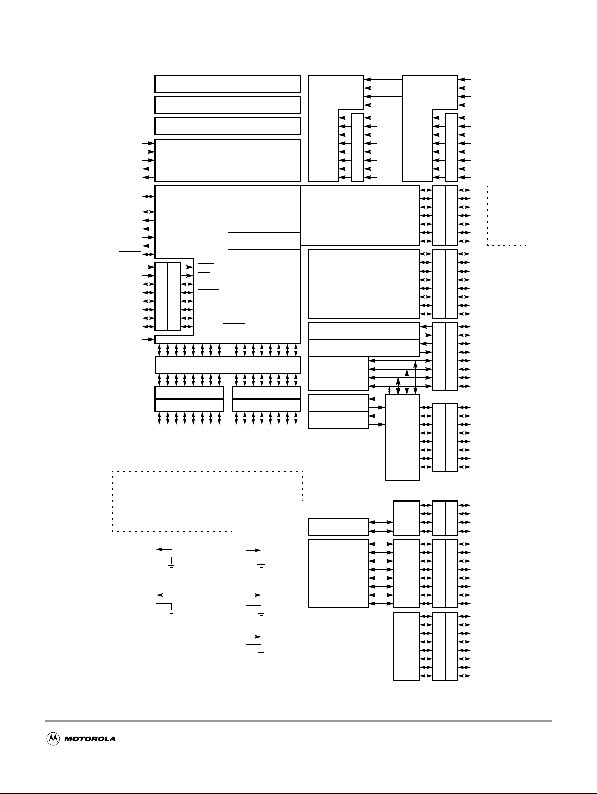
Figure 1-1 shows a block diagram of the MC9S12DJ64 device.
22
Page 23
MC9S12DJ64 Device User Guide — V01.17
Figure 1-1 MC9S12DJ64 Block Diagram
VDDR
VSSR
VREGEN
VDD1,2
VSS1,2
BKGD
XFC
VDDPLL
VSSPLL
EXTAL
XTAL
RESET
PE0
PE1
PE2
PE3
PE4
PE5
PE6
PE7
TEST
Multiplexed
Wide Bus
Multiplexed
Narrow Bus
Internal Logic 2.5V
VDD1,2
VSS1,2
PLL 2.5V
VDDPLL
VSSPLL
64K Byte Flash EEPROM
4K Byte RAM
1K Byte EEPROM
Voltage Regulator
Single-wire Background
Debug Module
Clock and
Reset
PLL
Generation
Module
XIRQ
IRQ
W
R/
LSTRB
DDRE
ECLK
MODA
MODB
NOACC/
XCLKS
PTE
Multiplexed Address/Data Bus
DDRA DDRB
PTA PTB
PA4
PA3
PA2
PA1
ADDR11
ADDR10
ADDR9
DATA11
DATA10
DATA9
DATA3
DATA2
DATA1
PA0
ADDR8
DATA8
DATA0
PA7
PA6
PA5
ADDR15
ADDR14
ADDR13
DATA15
DATA14
DATA13
DATA7
DATA6
DATA5
ADDR12
DATA12
DATA4
I/O Driver 5V
VDDX
VSSX
A/D Converter 5V &
Voltage Regulator Reference
VDDA
VSSA
Voltage Regulator 5V & I/O
VDDR
VSSR
CPU12
Periodic Interrupt
COP Watchdog
Clock Monitor
Breakpoints
System
Integration
PB4
PB3
PB5
ADDR4
ADDR5
DATA4
DATA5
PB2
ADDR3
ADDR2
DATA3
DATA2
PB7
PB6
ADDR7
ADDR6
DATA7
DATA6
PB1
PB0
ADDR1
ADDR0
DATA1
DATA0
AN0
AN1
AN2
AN3
AN4
AN5
AN6
AN7
VRH
VRL
VDDA
VSSA
AD0
ATD0
PPAGE
Enhanced Capture
Timer
SCI0
SCI1
MISO
MOSI
SPI0
BDLC
(J1850)
CAN0
IIC
PWM
SCK
SS
RXB
TXB
RXCAN
TXCAN
SDA
SCL
PWM0
PWM1
PWM2
PWM3
PWM4
PWM5
PWM6
PWM7
ATD1
PAD00
PAD01
PAD02
PAD03
PAD04
PAD05
PAD06
PAD07
AN0
AN1
AN2
AN3
AN4
AN5
AN6
AN7
PIX0
PIX1
PIX2
PIX3
PIX4
PIX5
ECS
IOC0
IOC1
IOC2
IOC3
IOC4
IOC5
IOC6
IOC7
RXD
TXD
RXD
TXD
Module to Port Routing
KWJ0
KWJ1
KWJ6
KWJ7
KWP0
KWP1
KWP2
KWP3
KWP4
KWP5
KWP6
KWP7
KWH0
KWH1
KWH2
KWH3
KWH4
KWH5
KWH6
KWH7
VRH
VRL
VDDA
VSSA
DDRK
DDRT
DDRS
DDRM
DDRJ
DDRP
DDRH
AD1
PTK
PTT
PTS
PTM
PTJ
PTP
PTH
VRH
VRL
VDDA
VSSA
PAD08
PAD09
PAD10
PAD11
PAD12
PAD13
PAD14
PAD15
PK0
PK1
PK2
PK3
PK4
PK5
PK7
PT0
PT1
PT2
PT3
PT4
PT5
PT6
PT7
PS0
PS1
PS2
PS3
PS4
PS5
PS6
PS7
PM0
PM1
PM2
PM3
PM4
PM5
PM6
PM7
PJ0
PJ1
PJ6
PJ7
PP0
PP1
PP2
PP3
PP4
PP5
PP6
PP7
PH0
PH1
PH2
PH3
PH4
PH5
PH6
PH7
XADDR14
XADDR15
XADDR16
XADDR17
XADDR18
XADDR19
ECS
Signals shown in Bold are not available on the 80 Pin Package
23
Page 24

MC9S12DJ64 Device User Guide — V01.17
24
Page 25
MC9S12DJ64 Device User Guide — V01.17
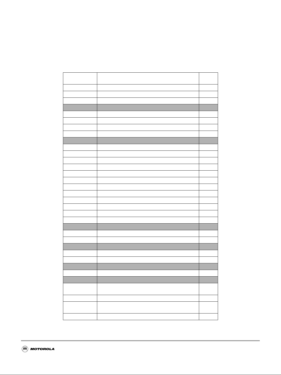
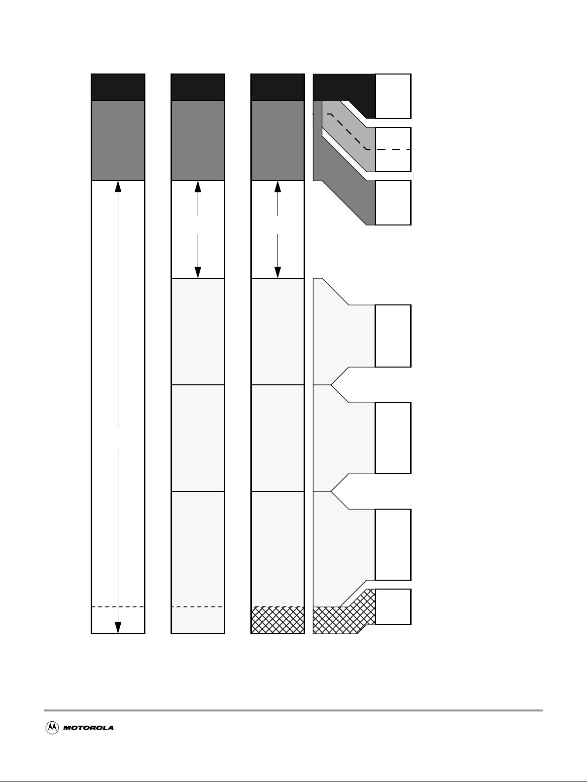
1.5 Device Memory Map
Table 1-1 and Figure 1-2 show the device memory map of the MC9S12DJ64 after reset. The 1K
EEPROM is mapped twice in a 2K address space. Note that after reset the bottom 1k of the EEPROM
($0000 - $03FF) are hidden by the register space, and the 1K $0400 - $07FF is hidden by the RAM.
Table 1-1 Device Memory Map
Address Module
$0000 - $000F HCS12 Multiplexed External Bus Interface 16
$0010 - $0014 HCS12 Module Mapping Control 5
$0015 - $0016 HCS12 Interrupt 2
$0017 - $0019 Reserved 3
$001A - $001B Device ID register (PARTID) 2
$001C - $001D HCS12 Module Mapping Control 2
$001E HCS12 Multiplexed External Bus Interface 1
$001F HCS12 Interrupt 1
$0020 - $0027 Reserved 8
$0028 - $002F HCS12 Breakpoint Module 8
$0030 - $0031 HCS12 Module Mapping Control 2
$0032 - $0033 HCS12 Multiplexed External Bus Interface 2
$0034 - $003F Clock and Reset Generator (PLL, RTI, COP) 12
$0040 - $007F Enhanced Capture Timer 16-bit 8 channels 64
$0080 - $009F Analog to Digital Converter 10-bit 8 channels (ATD0) 32
$00A0 - $00C7 Pulse Width Modulator 8-bit 8 channels (PWM) 40
$00C8 - $00CF Serial Communications Interface 0 (SCI0) 8
$00D0 - $00D7 Serial Communications Interface 0 (SCI1) 8
$00D8 - $00DF Serial Peripheral Interface (SPI0) 8
$00E0 - $00E7 Inter IC Bus 8
$00E8 - $00EF Byte Data Link Controller (BDLC) 8
$00F0 - $00FF Reserved 16
$0100- $010F Flash Control Register 16
$0110 - $011B EEPROM Control Register 12
$011C - $011F Reserved 4
$0120 - $013F Analog to Digital Converter 10-bit 8 channels (ATD1) 32
$0140 - $017F Motorola Scalable Can (CAN0) 64
$0180 - $023F Reserved 192
$0240 - $027F Port Integration Module (PIM) 64
$0280 - $03FF Reserved 384
$0000 - $07FF
$0000 - $0FFF RAM array 4096
$4000 - $7FFF
$8000 - $BFFF Flash EEPROM Page Window 16384
EEPROM array 1k Array mapped twice in the
address space
Fixed Flash EEPROM array
incl. 0.5K, 1K, 2K or 4K Protected Sector at start
Size
(Bytes)
2048
16384
25
Page 26

MC9S12DJ64 Device User Guide — V01.17
Table 1-1 Device Memory Map
Address Module
Fixed Flash EEPROM array
$C000 - $FFFF
incl. 0.5K, 1K, 2K or 4K Protected Sector at end
and 256 bytes of Vector Space at $FF80 - $FFFF
Size
(Bytes)
16384
26
Page 27
MC9S12DJ64 Device User Guide — V01.17
Figure 1-2 MC9S12DJ64 Memory Map out of Reset
$0000
$0400
$0800
$1000
$4000
Unimplemented Unimplemented
$0000
$03FF
$0000
$07FF
$0000
$0FFF
$4000
$7FFF
REGISTERS
(Mappable to any 2K
Boundary within the
first 32K)
1K Bytes EEPROM
(Mappable to any 2K
Boundary; 1K mapped two
times in the 2K address
space)
4K Bytes RAM
(Mappable to any 4K
Boundary)
16K Fixed Flash
Page $3E = 62
(This is dependant on the
state of the ROMHM bit)
$8000
$C000
$FF00
$FFFF
EXTERN
VECTORS
EXPANDED
VECTORS
NORMAL
SINGLE CHIP
VECTORS
SPECIAL
SINGLE CHIP
$8000
16K Page Window
4 x 16K Flash EEPROM
pages
$BFFF
$C000
16K Fixed Flash
Page $3F = 63
$FFFF
$FF00
BDM
(if active)
$FFFF
27
Page 28
MC9S12DJ64 Device User Guide — V01.17
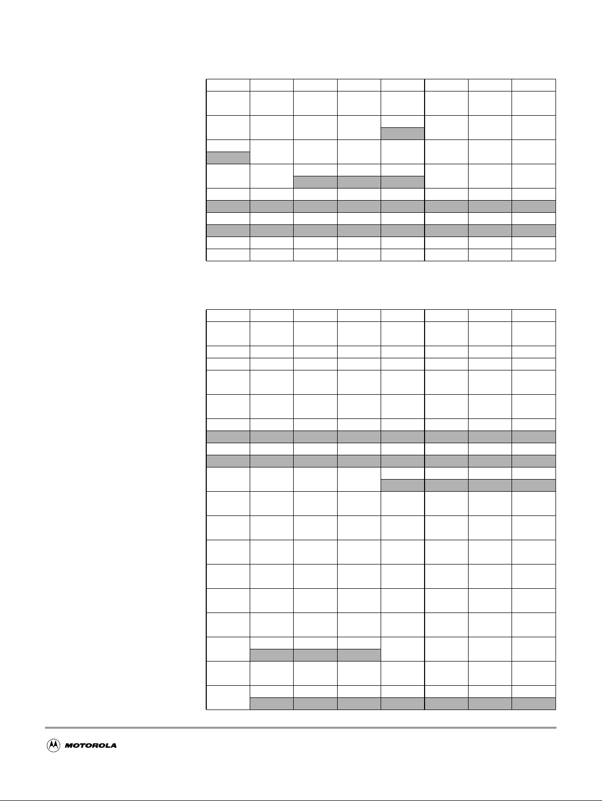
1.5.1 Detailed Register Map
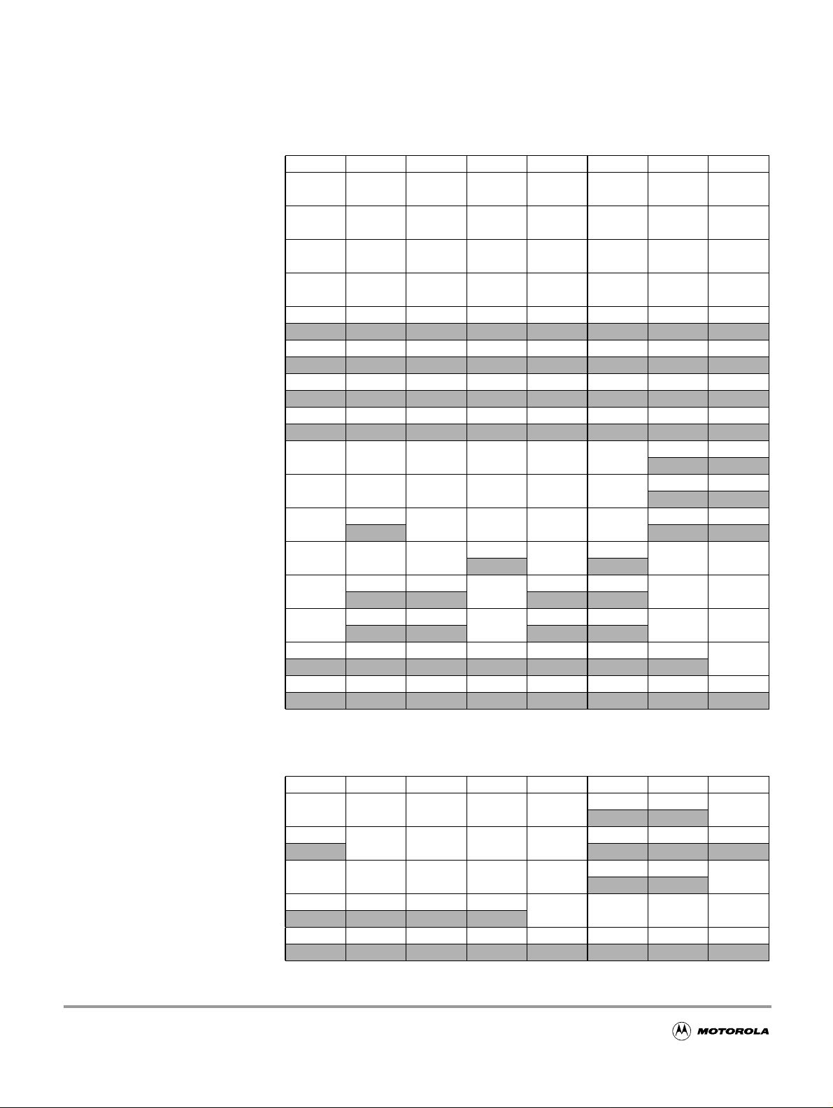
$0000 - $000F MEBI map 1 of 3 (HCS12 Multiplexed External Bus Interface)
Address Name Bit 7 Bit 6 Bit 5 Bit 4 Bit 3 Bit 2 Bit 1 Bit 0
$0000 PORTA
$0001 PORTB
$0002 DDRA
$0003 DDRB
$0004 Reserved
$0005 Reserved
$0006 Reserved
$0007 Reserved
$0008 PORTE
$0009 DDRE
$000A PEAR
$000B MODE
$000C PUCR
$000D RDRIV
$000E EBICTL
$000F Reserved
Read:
Write:
Read:
Write:
Read:
Write:
Read:
Write:
Read: 00000000
Write:
Read: 00000000
Write:
Read: 00000000
Write:
Read: 00000000
Write:
Read:
Write:
Read:
Write:
Read:
Write:
Read:
Write:
Read:
Write:
Read:
Write:
Read: 0000000
Write:
Read: 00000000
Write:
Bit 7 654321Bit 0
Bit 7 654321Bit 0
Bit 7 654321Bit 0
Bit 7 654321Bit 0
Bit 7 65432
Bit 7 6543Bit 2
NOACCE
MODC MODB MODA
PUPKE
RDPK
0
00
00
PIPOE NECLK LSTRE RDWE
PUPEE
RDPE
0
IVIS
00
00
0
Bit 1 Bit 0
00
00
EMK EME
PUPBE PUPAE
RDPB RDPA
ESTR
$0010 - $0014 MMC map 1 of 4 (HCS12 Module Mapping Control)
Address Name Bit 7 Bit 6 Bit 5 Bit 4 Bit 3 Bit 2 Bit 1 Bit 0
$0010 INITRM
$0011 INITRG
$0012 INITEE
$0013 MISC
$0014 Reserved
28
Read:
Write:
Read: 0
Write:
Read:
Write:
Read: 0000
Write:
Read: 00000000
Write:
RAM15 RAM14 RAM13 RAM12 RAM11
REG14 REG13 REG12 REG11
EE15 EE14 EE13 EE12 EE11
EXSTR1 EXSTR0 ROMHM ROMON
00
000
00
RAMHAL
EEON
Page 29
MC9S12DJ64 Device User Guide — V01.17
$0015 - $0016 INT map 1 of 2 (HCS12 Interrupt)
Address Name Bit 7 Bit 6 Bit 5 Bit 4 Bit 3 Bit 2 Bit 1 Bit 0
$0015 ITCR
$0016 ITEST
Read: 0 0 0
Write:
Read:
Write:
INTE INTC INTA INT8 INT6 INT4 INT2 INT0
WRINT ADR3 ADR2 ADR1 ADR0
$0017 - $0019 Reserved
Address Name Bit 7 Bit 6 Bit 5 Bit 4 Bit 3 Bit 2 Bit 1 Bit 0
$0017 -
$0019
Reserved
Read: 00000000
Write:
$001A - $001B Device ID Register (Table 1-3)
Address Name Bit 7 Bit 6 Bit 5 Bit 4 Bit 3 Bit 2 Bit 1 Bit 0
$001A PARTIDH
$001B PARTIDL
Read: ID15 ID14 ID13 ID12 ID11 ID10 ID9 ID8
Write:
Read: ID7 ID6 ID5 ID4 ID3 ID2 ID1 ID0
Write:
$001C - $001D MMC map 3 of 4 (HCS12 Module Mapping Control, Table 1-4)
Address Name Bit 7 Bit 6 Bit 5 Bit 4 Bit 3 Bit 2 Bit 1 Bit 0
$001C MEMSIZ0
$001D MEMSIZ1
Read: reg_sw0 0 eep_sw1 eep_sw0 0 ram_sw2 ram_sw1 ram_sw0
Write:
Read: rom_sw1 rom_sw0 0000pag_sw1 pag_sw0
Write:
$001E - $001E MEBI map 2 of 3 (HCS12 Multiplexed External Bus Interface)
Address Name Bit 7 Bit 6 Bit 5 Bit 4 Bit 3 Bit 2 Bit 1 Bit 0
$001E INTCR
Read:
Write:
IRQE IRQEN
000000
$001F - $001F INT map 2 of 2 (HCS12 Interrupt)
Address Name Bit 7 Bit 6 Bit 5 Bit 4 Bit 3 Bit 2 Bit 1 Bit 0
$001F HPRIO
Read:
Write:
PSEL7 PSEL6 PSEL5 PSEL4 PSEL3 PSEL2 PSEL1
0
$0020 - $0027 Reserved
Address Name Bit 7 Bit 6 Bit 5 Bit 4 Bit 3 Bit 2 Bit 1 Bit 0
$0020 -
$0027
Reserved
Read: 00000000
Write:
29
Page 30
MC9S12DJ64 Device User Guide — V01.17
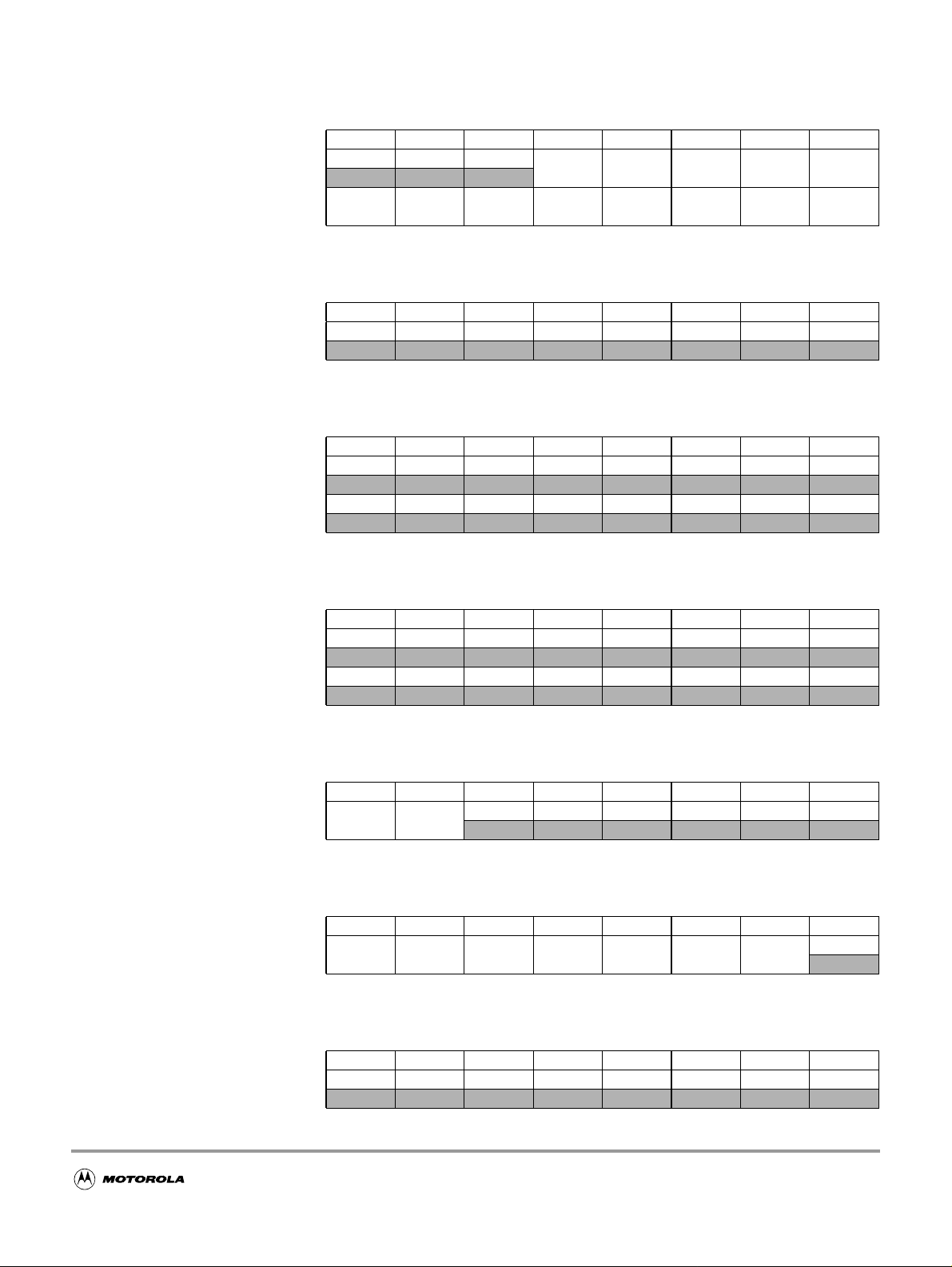
$0028 - $002F BKP (HCS12 Breakpoint)
Address Name Bit 7 Bit 6 Bit 5 Bit 4 Bit 3 Bit 2 Bit 1 Bit 0
$0028 BKPCT0
$0029 BKPCT1
$002A BKP0X
$002B BKP0H
$002C BKP0L
$002D BKP1X
$002E BKP1H
$002F BKP1L
Read:
Write:
Read:
Write:
Read: 0 0
Write:
Read:
Write:
Read:
Write:
Read: 0 0
Write:
Read:
Write:
Read:
Write:
BKEN BKFULL BKBDM BKTAG
BK0MBH BK0MBL BK1MBH BK1MBL BK0RWE BK0RW BK1RWE BK1RW
BK0V5 BK0V4 BK0V3 BK0V2 BK0V1 BK0V0
Bit 15 14 13 12 11 10 9 Bit 8
Bit 7 654321Bit 0
BK1V5 BK1V4 BK1V3 BK1V2 BK1V1 BK1V0
Bit 15 14 13 12 11 10 9 Bit 8
Bit 7 654321Bit 0
0000
$0030 - $0031 MMC map 4 of 4 (HCS12 Module Mapping Control)
Address Name Bit 7 Bit 6 Bit 5 Bit 4 Bit 3 Bit 2 Bit 1 Bit 0
$0030 PPAGE
$0031 Reserved
Read: 0 0
Write:
Read: 00000000
Write:
PIX5 PIX4 PIX3 PIX2 PIX1 PIX0
$0032 - $0033 MEBI map 3 of 3 (HCS12 Multiplexed External Bus Interface)
Address Name Bit 7 Bit 6 Bit 5 Bit 4 Bit 3 Bit 2 Bit 1 Bit 0
$0032 PORTK
$0033 DDRK
Read:
Write:
Read:
Write:
Bit 7 654321Bit 0
Bit 7 654321Bit 0
$0034 - $003F CRG (Clock and Reset Generator)
Address Name Bit 7 Bit 6 Bit 5 Bit 4 Bit 3 Bit 2 Bit 1 Bit 0
$0034 SYNR
$0035 REFDV
$0036
$0037 CRGFLG
$0038 CRGINT
CTFLG
TEST ONLY
Read: 0 0
Write:
Read: 0000
Write:
Read: 00000000
Write:
Read:
Write:
Read:
Write:
RTIF PORF
RTIE
00
SYN5 SYN4 SYN3 SYN2 SYN1 SYN0
REFDV3 REFDV2 REFDV1 REFDV0
0
LOCKIF
LOCKIE
LOCK TRACK
00
SCMIF
SCMIE
SCM
0
30
Page 31
MC9S12DJ64 Device User Guide — V01.17
$0034 - $003F CRG (Clock and Reset Generator)
Address Name Bit 7 Bit 6 Bit 5 Bit 4 Bit 3 Bit 2 Bit 1 Bit 0
$0039 CLKSEL
$003A PLLCTL
$003B RTICTL
$003C COPCTL
$003D
$003E
$003F ARMCOP
FORBYP
TEST ONLY
CTCTL
TEST ONLY
Read:
Write:
Read:
Write:
Read: 0
Write:
Read:
Write:
Read: 00000000
Write:
Read: 00000000
Write:
Read: 00000000
Write: Bit 7 654321Bit 0
PLLSEL PSTP SYSWAI ROAWAI PLLWAI CWAI RTIWAI COPWAI
CME PLLON AUTO ACQ
RTR6 RTR5 RTR4 RTR3 RTR2 RTR1 RTR0
WCOP RSBCK
000
0
PRE PCE SCME
CR2 CR1 CR0
$0040 - $007F ECT (Enhanced Capture Timer 16 Bit 8 Channels)
Address Name Bit 7 Bit 6 Bit 5 Bit 4 Bit 3 Bit 2 Bit 1 Bit 0
$0040 TIOS
$0041 CFORC
$0042 OC7M
$0043 OC7D
$0044 TCNT (hi)
$0045 TCNT (lo)
$0046 TSCR1
$0047 TTOV
$0048 TCTL1
$0049 TCTL2
$004A TCTL3
$004B TCTL4
$004C TIE
$004D TSCR2
$004E TFLG1
$004F TFLG2
Read:
Write:
Read: 00000000
Write: FOC7 FOC6 FOC5 FOC4 FOC3 FOC2 FOC1 FOC0
Read:
Write:
Read:
Write:
Read: Bit 15 14 13 12 11 10 9 Bit 8
Write:
Read: Bit 7 654321Bit 0
Write:
Read:
Write:
Read:
Write:
Read:
Write:
Read:
Write:
Read:
Write:
Read:
Write:
Read:
Write:
Read:
Write:
Read:
Write:
Read:
Write:
IOS7 IOS6 IOS5 IOS4 IOS3 IOS2 IOS1 IOS0
OC7M7 OC7M6 OC7M5 OC7M4 OC7M3 OC7M2 OC7M1 OC7M0
OC7D7 OC7D6 OC7D5 OC7D4 OC7D3 OC7D2 OC7D1 OC7D0
TEN TSWAI TSFRZ TFFCA
TOV7 TOV6 TOV5 TOV4 TOV3 TOV2 TOV1 TOV0
OM7 OL7 OM6 OL6 OM5 OL5 OM4 OL4
OM3 OL3 OM2 OL2 OM1 OL1 OM0 OL0
EDG7B EDG7A EDG6B EDG6A EDG5B EDG5A EDG4B EDG4A
EDG3B EDG3A EDG2B EDG2A EDG1B EDG1A EDG0B EDG0A
C7I C6I C5I C4I C3I C2I C1I C0I
TOI
C7F C6F C5F C4F C3F C2F C1F C0F
TOF
000
0000000
0000
TCRE PR2 PR1 PR0
31
Page 32

MC9S12DJ64 Device User Guide — V01.17
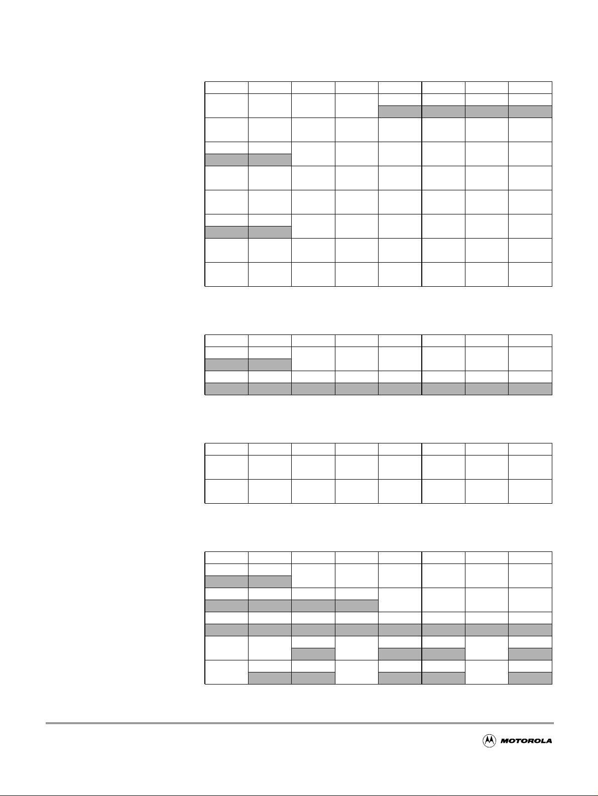
$0040 - $007F ECT (Enhanced Capture Timer 16 Bit 8 Channels)
Address Name Bit 7 Bit 6 Bit 5 Bit 4 Bit 3 Bit 2 Bit 1 Bit 0
$0050 TC0 (hi)
$0051 TC0 (lo)
$0052 TC1 (hi)
$0053 TC1 (lo)
$0054 TC2 (hi)
$0055 TC2 (lo)
$0056 TC3 (hi)
$0057 TC3 (lo)
$0058 TC4 (hi)
$0059 TC4 (lo)
$005A TC5 (hi)
$005B TC5 (lo)
$005C TC6 (hi)
$005D TC6 (lo)
$005E TC7 (hi)
$005F TC7 (lo)
$0060 PACTL
$0061 PAFLG
$0062 PACN3 (hi)
$0063 PACN2 (lo)
$0064 PACN1 (hi)
$0065 PACN0 (lo)
$0066 MCCTL
$0067 MCFLG
$0068 ICPAR
Read:
Write:
Read:
Write:
Read:
Write:
Read:
Write:
Read:
Write:
Read:
Write:
Read:
Write:
Read:
Write:
Read:
Write:
Read:
Write:
Read:
Write:
Read:
Write:
Read:
Write:
Read:
Write:
Read:
Write:
Read:
Write:
Read: 0
Write:
Read: 000000
Write:
Read:
Write:
Read:
Write:
Read:
Write:
Read:
Write:
Read:
Write: ICLAT FLMC
Read:
Write:
Read: 0000
Write:
Bit 15 14 13 12 11 10 9 Bit 8
Bit 7 654321Bit 0
Bit 15 14 13 12 11 10 9 Bit 8
Bit 7 654321Bit 0
Bit 15 14 13 12 11 10 9 Bit 8
Bit 7 654321Bit 0
Bit 15 14 13 12 11 10 9 Bit 8
Bit 7 654321Bit 0
Bit 15 14 13 12 11 10 9 Bit 8
Bit 7 654321Bit 0
Bit 15 14 13 12 11 10 9 Bit 8
Bit 7 654321Bit 0
Bit 15 14 13 12 11 10 9 Bit 8
Bit 7 654321Bit 0
Bit 15 14 13 12 11 10 9 Bit 8
Bit 7 654321Bit 0
PAEN PAMOD PEDGE CLK1 CLK0 PAOVI PAI
PAOVF PAIF
Bit 7 654321Bit 0
Bit 7 654321Bit 0
Bit 7 654321Bit 0
Bit 7 654321Bit 0
MCZI MODMC RDMCL
MCZF
0 0 0 POLF3 POLF2 POLF1 POLF0
00
PA3EN PA2EN PA1EN PA0EN
MCEN MCPR1 MCPR0
32
Page 33

MC9S12DJ64 Device User Guide — V01.17
$0040 - $007F ECT (Enhanced Capture Timer 16 Bit 8 Channels)
Address Name Bit 7 Bit 6 Bit 5 Bit 4 Bit 3 Bit 2 Bit 1 Bit 0
$0069 DLYCT
$006A ICOVW
$006B ICSYS
$006C Reserved
$006D
$006E Reserved
$006F Reserved
$0070 PBCTL
$0071 PBFLG
$0072 PA3H
$0073 PA2H
$0074 PA1H
$0075 PA0H
$0076 MCCNT (hi)
$0077 MCCNT (lo)
$0078 TC0H (hi)
$0079 TC0H (lo)
$007A TC1H (hi)
$007B TC1H (lo)
$007C TC2H (hi)
$007D TC2H (lo)
$007E TC3H (hi)
$007F TC3H (lo)
TIMTST
Test Only
Read: 000000
Write:
Read:
Write:
Read:
Write:
Read:
Write:
Read: 000000
Write:
Read:
Write:
Read:
Write:
Read: 0
Write:
Read: 000000
Write:
Read: Bit 7 654321Bit 0
Write:
Read: Bit 7 654321Bit 0
Write:
Read: Bit 7 654321Bit 0
Write:
Read: Bit 7 654321Bit 0
Write:
Read:
Write:
Read:
Write:
Read: Bit 15 14 13 12 11 10 9 Bit 8
Write:
Read: Bit 7 654321Bit 0
Write:
Read: Bit 15 14 13 12 11 10 9 Bit 8
Write:
Read: Bit 7 654321Bit 0
Write:
Read: Bit 15 14 13 12 11 10 9 Bit 8
Write:
Read: Bit 7 654321Bit 0
Write:
Read: Bit 15 14 13 12 11 10 9 Bit 8
Write:
Read: Bit 7 654321Bit 0
Write:
NOVW7 NOVW6 NOVW5 NOVW4 NOVW3 NOVW2 NOVW1 NOVW0
SH37 SH26 SH15 SH04 TFMOD PACMX BUFEN LATQ
PBEN
Bit 15 14 13 12 11 10 9 Bit 8
Bit 7 654321Bit 0
0000
DLY1 DLY0
TCBYP
PBOVI
PBOVF
0
0
0
33
Page 34

MC9S12DJ64 Device User Guide — V01.17
$0080 - $009F ATD0 (Analog to Digital Converter 10 Bit 8 Channel)
Address Name Bit 7 Bit 6 Bit 5 Bit 4 Bit 3 Bit 2 Bit 1 Bit 0
$0080 ATD0CTL0
$0081 ATD0CTL1
$0082 ATD0CTL2
$0083 ATD0CTL3
$0084 ATD0CTL4
$0085 ATD0CTL5
$0086 ATD0STAT0
$0087 Reserved
$0088 ATD0TEST0
$0089 ATD0TEST1
$008A Reserved
$008B ATD0STAT1
$008C Reserved
$008D ATD0DIEN
$008E Reserved
$008F PORTAD0
$0090 ATD0DR0H
$0091 ATD0DR0L
$0092 ATD0DR1H
$0093 ATD0DR1L
$0094 ATD0DR2H
$0095 ATD0DR2L
$0096 ATD0DR3H
$0097 ATD0DR3L
$0098 ATD0DR4H
Read: 00000000
Write:
Read: 00000000
Write:
Read:
Write:
Read: 0
Write:
Read:
Write:
Read:
Write:
Read:
Write:
Read: 00000000
Write:
Read: 00000000
Write:
Read: 0000000
Write:
Read: 00000000
Write:
Read: CCF7 CCF6 CCF5 CCF4 CCF3 CCF2 CCF1 CCF0
Write:
Read: 00000000
Write:
Read:
Write:
Read: 00000000
Write:
Read: Bit7 654321BIT 0
Write:
Read: Bit15 14 13 12 11 10 9 Bit8
Write:
Read: Bit7 Bit6 000000
Write:
Read: Bit15 14 13 12 11 10 9 Bit8
Write:
Read: Bit7 Bit6 000000
Write:
Read: Bit15 14 13 12 11 10 9 Bit8
Write:
Read: Bit7 Bit6 000000
Write:
Read: Bit15 14 13 12 11 10 9 Bit8
Write:
Read: Bit7 Bit6 000000
Write:
Read: Bit15 14 13 12 11 10 9 Bit8
Write:
ADPU AFFC AWAI ETRIGLE ETRIGP ETRIG ASCIE
S8C S4C S2C S1C FIFO FRZ1 FRZ0
SRES8 SMP1 SMP0 PRS4 PRS3 PRS2 PRS1 PRS0
DJM DSGN SCAN MULT
SCF
Bit 7 654321Bit 0
0
ETORF FIFOR
0
0 CC2 CC1 CC0
CC CB CA
ASCIF
SC
34
Page 35

MC9S12DJ64 Device User Guide — V01.17
$0080 - $009F ATD0 (Analog to Digital Converter 10 Bit 8 Channel)
Address Name Bit 7 Bit 6 Bit 5 Bit 4 Bit 3 Bit 2 Bit 1 Bit 0
$0099 ATD0DR4L
$009A ATD0DR5H
$009B ATD0DR5L
$009C ATD0DR6H
$009D ATD0DR6L
$009E ATD0DR7H
$009F ATD0DR7L
Read: Bit7 Bit6 000000
Write:
Read: Bit15 14 13 12 11 10 9 Bit8
Write:
Read: Bit7 Bit6 000000
Write:
Read: Bit15 14 13 12 11 10 9 Bit8
Write:
Read: Bit7 Bit6 000000
Write:
Read: Bit15 14 13 12 11 10 9 Bit8
Write:
Read: Bit7 Bit6 000000
Write:
$00A0 - $00C7 PWM (Pulse Width Modulator 8 Bit 8 Channel)
Address Name Bit 7 Bit 6 Bit 5 Bit 4 Bit 3 Bit 2 Bit 1 Bit 0
$00A0 PWME
$00A1 PWMPOL
$00A2 PWMCLK
$00A3 PWMPRCLK
$00A4 PWMCAE
$00A5 PWMCTL
$00A6
$00A7
$00A8 PWMSCLA
$00A9 PWMSCLB
$00AA
$00AB
$00AC PWMCNT0
$00AD PWMCNT1
$00AE PWMCNT2
$00AF PWMCNT3
PWMTST
Test Only
PWMPRSC
Test Only
PWMSCNTA
Test Only
PWMSCNTB
Test Only
Read:
Write:
Read:
Write:
Read:
Write:
Read: 0
Write:
Read:
Write:
Read:
Write:
Read: 00000000
Write:
Read: 00000000
Write:
Read:
Write:
Read:
Write:
Read: 00000000
Write:
Read: 00000000
Write:
Read: Bit 7 6 5 4 3 2 1 Bit 0
Write: 00000000
Read: Bit 7 6 5 4 3 2 1 Bit 0
Write: 00000000
Read: Bit 7 6 5 4 3 2 1 Bit 0
Write: 00000000
Read: Bit 7 6 5 4 3 2 1 Bit 0
Write: 00000000
PWME7 PWME6 PWME5 PWME4 PWME3 PWME2 PWME1 PWME0
PPOL7 PPOL6 PPOL5 PPOL4 PPOL3 PPOL2 PPOL1 PPOL0
PCLK7 PCLK6 PCLK5 PCLK4 PCLK3 PCLK2 PCLK1 PCLK0
PCKB2 PCKB1 PCKB0
CAE7 CAE6 CAE5 CAE4 CAE3 CAE2 CAE1 CAE0
CON67 CON45 CON23 CON01 PSWAI PFRZ
Bit 7 6 5 4 3 2 1 Bit 0
Bit 7 6 5 4 3 2 1 Bit 0
0
PCKA2 PCKA1 PCKA0
00
35
Page 36

MC9S12DJ64 Device User Guide — V01.17
$00A0 - $00C7 PWM (Pulse Width Modulator 8 Bit 8 Channel)
Address Name Bit 7 Bit 6 Bit 5 Bit 4 Bit 3 Bit 2 Bit 1 Bit 0
$00B0 PWMCNT4
$00B1 PWMCNT5
$00B2 PWMCNT6
$00B3 PWMCNT7
$00B4 PWMPER0
$00B5 PWMPER1
$00B6 PWMPER2
$00B7 PWMPER3
$00B8 PWMPER4
$00B9 PWMPER5
$00BA PWMPER6
$00BB PWMPER7
$00BC PWMDTY0
$00BD PWMDTY1
$00BE PWMDTY2
$00BF PWMDTY3
$00C0 PWMDTY4
$00C1 PWMDTY5
$00C2 PWMDTY6
$00C3 PWMDTY7
$00C4 PWMSDN
$00C5 Reserved
$00C6 Reserved
$00C7 Reserved
Read: Bit 7 6 5 4 3 2 1 Bit 0
Write: 00000000
Read: Bit 7 6 5 4 3 2 1 Bit 0
Write: 00000000
Read: Bit 7 6 5 4 3 2 1 Bit 0
Write: 00000000
Read: Bit 7 6 5 4 3 2 1 Bit 0
Write: 00000000
Read:
Write:
Read:
Write:
Read:
Write:
Read:
Write:
Read:
Write:
Read:
Write:
Read:
Write:
Read:
Write:
Read:
Write:
Read:
Write:
Read:
Write:
Read:
Write:
Read:
Write:
Read:
Write:
Read:
Write:
Read:
Write:
Read:
Write:
Read: 00000000
Write:
Read: 00000000
Write:
Read: 00000000
Write:
Bit 7 6 5 4 3 2 1 Bit 0
Bit 7 6 5 4 3 2 1 Bit 0
Bit 7 6 5 4 3 2 1 Bit 0
Bit 7 6 5 4 3 2 1 Bit 0
Bit 7 6 5 4 3 2 1 Bit 0
Bit 7 6 5 4 3 2 1 Bit 0
Bit 7 6 5 4 3 2 1 Bit 0
Bit 7 6 5 4 3 2 1 Bit 0
Bit 7 6 5 4 3 2 1 Bit 0
Bit 7 6 5 4 3 2 1 Bit 0
Bit 7 6 5 4 3 2 1 Bit 0
Bit 7 6 5 4 3 2 1 Bit 0
Bit 7 6 5 4 3 2 1 Bit 0
Bit 7 6 5 4 3 2 1 Bit 0
Bit 7 6 5 4 3 2 1 Bit 0
Bit 7 6 5 4 3 2 1 Bit 0
PWMIF PWMIE
PWMRSTRT
PWMLVL
0 PWM7IN
PWM7INL PWM7ENA
36
Page 37

MC9S12DJ64 Device User Guide — V01.17
$00C8 - $00CF SCI0 (Asynchronous Serial Interface)
Address Name Bit 7 Bit 6 Bit 5 Bit 4 Bit 3 Bit 2 Bit 1 Bit 0
$00C8 SCI0BDH
$00C9 SCI0BDL
$00CA SCI0CR1
$00CB SCI0CR2
$00CC SCI0SR1
$00CD SCI0SR2
$00CE SCI0DRH
$00CF SCI0DRL
Read: 0 0 0
Write:
Read:
Write:
Read:
Write:
Read:
Write:
Read: TDRE TC RDRF IDLE OR NF FE PF
Write:
Read: 00000
Write:
Read: R8
Write:
Read: R7 R6 R5 R4 R3 R2 R1 R0
Write: T7 T6 T5 T4 T3 T2 T1 T0
SBR7 SBR6 SBR5 SBR4 SBR3 SBR2 SBR1 SBR0
LOOPS SCISWAI RSRC M WAKE ILT PE PT
TIE TCIE RIE ILIE TE RE RWU SBK
T8
000000
SBR12 SBR11 SBR10 SBR9 SBR8
BRK13 TXDIR
RAF
$00D0 - $00D7 SCI1 (Asynchronous Serial Interface)
Address Name Bit 7 Bit 6 Bit 5 Bit 4 Bit 3 Bit 2 Bit 1 Bit 0
$00D0 SCI1BDH
$00D1 SCI1BDL
$00D2 SCI1CR1
$00D3 SCI1CR2
$00D4 SCI1SR1
$00D5 SCI1SR2
$00D6 SCI1DRH
$00D7 SCI1DRL
Read: 0 0 0
Write:
Read:
Write:
Read:
Write:
Read:
Write:
Read: TDRE TC RDRF IDLE OR NF FE PF
Write:
Read: 00000
Write:
Read: R8
Write:
Read: R7 R6 R5 R4 R3 R2 R1 R0
Write: T7 T6 T5 T4 T3 T2 T1 T0
SBR7 SBR6 SBR5 SBR4 SBR3 SBR2 SBR1 SBR0
LOOPS SCISWAI RSRC M WAKE ILT PE PT
TIE TCIE RIE ILIE TE RE RWU SBK
T8
000000
SBR12 SBR11 SBR10 SBR9 SBR8
BRK13 TXDIR
RAF
$00D8 - $00DF SPI0 (Serial Peripheral Interface)
Address Name Bit 7 Bit 6 Bit 5 Bit 4 Bit 3 Bit 2 Bit 1 Bit 0
$00D8 SPI0CR1
$00D9 SPI0CR2
$00DA SPI0BR
$00DB SPI0SR
Read:
Write:
Read: 0 0 0
Write:
Read: 0
Write:
Read: SPIF 0 SPTEF MODF 0000
Write:
SPIE SPE SPTIE MSTR CPOL CPHA SSOE LSBFE
MODFEN BIDIROE
SPPR2 SPPR1 SPPR0
0
0
SPISWAI SPC0
SPR2 SPR1 SPR0
37
Page 38

MC9S12DJ64 Device User Guide — V01.17
$00D8 - $00DF SPI0 (Serial Peripheral Interface)
Address Name Bit 7 Bit 6 Bit 5 Bit 4 Bit 3 Bit 2 Bit 1 Bit 0
$00DC Reserved
$00DD SPI0DR
$00DE Reserved
$00DF Reserved
Read: 00000000
Write:
Read:
Write:
Read: 00000000
Write:
Read: 00000000
Write:
Bit7 654321Bit0
$00E0 - $00E7 IIC (Inter IC Bus)
Address Name Bit 7 Bit 6 Bit 5 Bit 4 Bit 3 Bit 2 Bit 1 Bit 0
$00E0 IBAD
$00E1 IBFD
$00E2 IBCR
$00E3 IBSR
$00E4 IBDR
$00E5 Reserved
$00E6 Reserved
$00E7 Reserved
Read:
Write:
Read:
Write:
Read:
Write: RSTA
Read: TCF IAAS IBB
Write:
Read:
Write:
Read: 0 0 0 0 0 0 0 0
Write:
Read: 00000000
Write:
Read: 00000000
Write:
ADR7 ADR6 ADR5 ADR4 ADR3 ADR2 ADR1 0
IBC7 IBC6 IBC5 IBC4 IBC3 IBC2 IBC1 IBC0
IBEN IBIE MS/
D7 D6 D5 D4 D3 D2 D1 D 0
SL TX/RX TXAK
IBAL
0SRW
00
IBIF
IBSWAI
RXAK
$00E8 - $00EF BDLC (Bytelevel Data Link Controller J1850)
Address Name Bit 7 Bit 6 Bit 5 Bit 4 Bit 3 Bit 2 Bit 1 Bit 0
$00E8 DLCBCR1
$00E9 DLCBSVR
$00EA DLCBCR2
$00EB DLCBDR
$00EC DLCBARD
$00ED DLCBRSR
$00EE DLCSCR
$00EF DLCBSTAT
38
Read:
Write:
Read: 0 0 I3 I2 I1 I0 0 0
Write:
Read:
Write:
Read:
Write:
Read: 0
Write:
Read:
Write:
Read:
Write:
Read:
Write:
IMSG CLKS
SMRST DLOOP RX4XE NBFS TEOD TSIFR TMIFR1 TMIFR0
D7 D6 D5 D4 D3 D2 D1 D0
RXPOL
0 0
0 0 0
0 0 0 0 0 0 0 IDLE
0000
00
R5 R4 R3 R2 R1 R0
BDLCE
BO3 BO2 BO1 BO0
0 0 0 0
IE WCM
Page 39
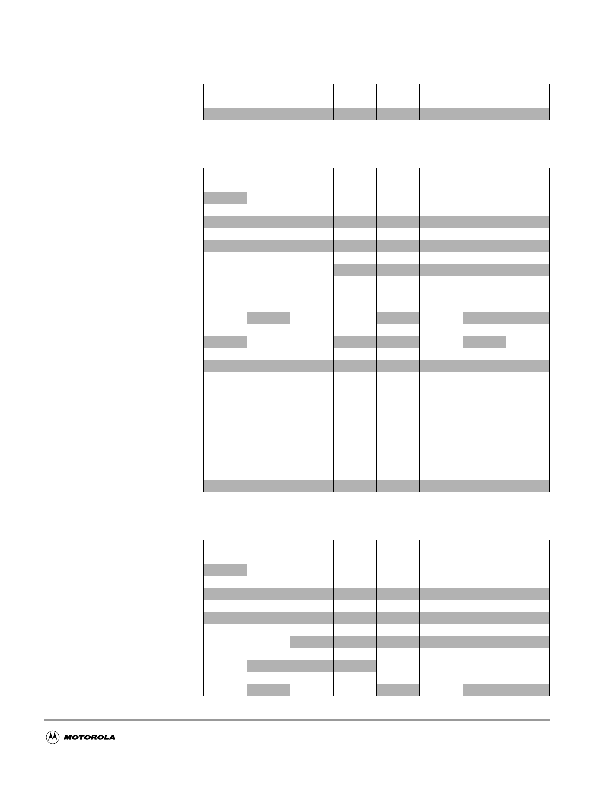
MC9S12DJ64 Device User Guide — V01.17
$00F0 - $00FF Reserved
Address Name Bit 7 Bit 6 Bit 5 Bit 4 Bit 3 Bit 2 Bit 1 Bit 0
$00F0 -
$00FF
Reserved
Read: 00000000
Write:
$0100 - $010F Flash Control Register (fts64k)
Address Name Bit 7 Bit 6 Bit 5 Bit 4 Bit 3 Bit 2 Bit 1 Bit 0
$0100 FCLKDIV
$0101 FSEC
$0102 Reserved
$0103 FCNFG
$0104 FPROT
$0105 FSTAT
$0106 FCMD
$0107 Reserved
$0108 FADDRHI
$0109 FADDRLO
$010A FDATAHI
$010B FDATALO
$010C -
$010F
Reserved
Read: FDIVLD
Write:
Read: KEYEN NV6 NV5 NV4 NV3 NV2 SEC1 SEC0
Write:
Read: 00000000
Write:
Read:
Write:
Read:
Write:
Read:
Write:
Read: 0
Write:
Read: 00000000
Write:
Read:
Write:
Read:
Write:
Read:
Write:
Read:
Write:
Read: 00000000
Write:
CBEIE CCIE KEYACC
FPOPEN NV6 FPHDIS FPHS1 FPHS0 FPLDIS FPLS1 FPLS0
CBEIF
Bit 14 Bit 14 13 12 11 10 9 Bit 8
Bit 7 654321Bit 0
Bit 15 14 13 12 11 10 9 Bit 8
Bit 7 654321Bit 0
PRDIV8 FDIV5 FDIV4 FDIV3 FDIV2 FDIV1 FDIV0
00000
CCIF
CMDB6 CMDB5
PVIOL ACCERR
00
0
BLANK
CMDB2
00
0
CMDB0
$0110 - $011B EEPROM Control Register (eets1k)
Address Name Bit 7 Bit 6 Bit 5 Bit 4 Bit 3 Bit 2 Bit 1 Bit 0
$0110 ECLKDIV
$0111 Reserved
$0112 Reserved
$0113 ECNFG
$0114 EPROT
$0115 ESTAT
Read: EDIVLD
Write:
Read: 00000000
Write:
Read: 00000000
Write:
Read:
Write:
Read:
Write:
Read:
Write:
CBEIE CCIE
EPOPEN
CBEIF
PRDIV8 EDIV5 EDIV4 EDIV3 EDIV2 EDIV1 EDIV0
000000
NV6 NV5 NV4
CCIF
PVIOL ACCERR
EPDIS EP2 EP1 EP0
0
BLANK
00
39
Page 40

MC9S12DJ64 Device User Guide — V01.17
$0110 - $011B EEPROM Control Register (eets1k)
Address Name Bit 7 Bit 6 Bit 5 Bit 4 Bit 3 Bit 2 Bit 1 Bit 0
$0116 ECMD
$0117
$0118 EADDRHI
$0119 EADDRLO
$011A EDATAHI
$011B EDATALO
Reserved for
Factory Test
Read: 0
Write:
Read: 00000000
Write:
Read: 0000000
Write:
Read:
Write:
Read:
Write:
Read:
Write:
Bit 7 654321Bit 0
Bit 15 14 13 12 11 10 9 Bit 8
Bit 7 654321Bit 0
CMDB6 CMDB5
00
CMDB2
$011C - $011F Reserved for RAM Control Register
Address Name Bit 7 Bit 6 Bit 5 Bit 4 Bit 3 Bit 2 Bit 1 Bit 0
$011C -
$011F
Reserved
Read: 00000000
Write:
0
CMDB0
Bit 8
$0120 - $013F ATD1 (Analog to Digital Converter 10 Bit 8 Channel)
Address Name Bit 7 Bit 6 Bit 5 Bit 4 Bit 3 Bit 2 Bit 1 Bit 0
$0120 ATD1CTL0
$0121 ATD1CTL1
$0122 ATD1CTL2
$0123 ATD1CTL3
$0124 ATD1CTL4
$0125 ATD1CTL5
$0126 ATD1STAT0
$0127 Reserved
$0128 ATD1TEST0
$0129 ATD1TEST1
$012A Reserved
$012B ATD1STAT1
$012C Reserved
Read: 00000000
Write:
Read: 00000000
Write:
Read:
Write:
Read: 0
Write:
Read:
Write:
Read:
Write:
Read: SCF 0 ETORF FIFOR 0 CC2 CC1 CC0
Write:
Read: 00000000
Write:
Read: 00000000
Write:
Read: 00000
Write:
Read: 00000000
Write:
Read: CCF7 CCF6 CCF5 CCF4 CCF3 CCF2 CCF1 CCF0
Write:
Read: 00000000
Write:
ADPU AFFC AWAI ETRIGLE ETRIGP ETRIG ASCIE
S8C S4C S2C S1C FIFO FRZ1 FRZ0
SRES8 SMP1 SMP0 PRS4 PRS3 PRS2 PRS1 PRS0
DJM DSGN SCAN MULT
0
CC CB CA
0
0
ASCIF
SC
40
Page 41
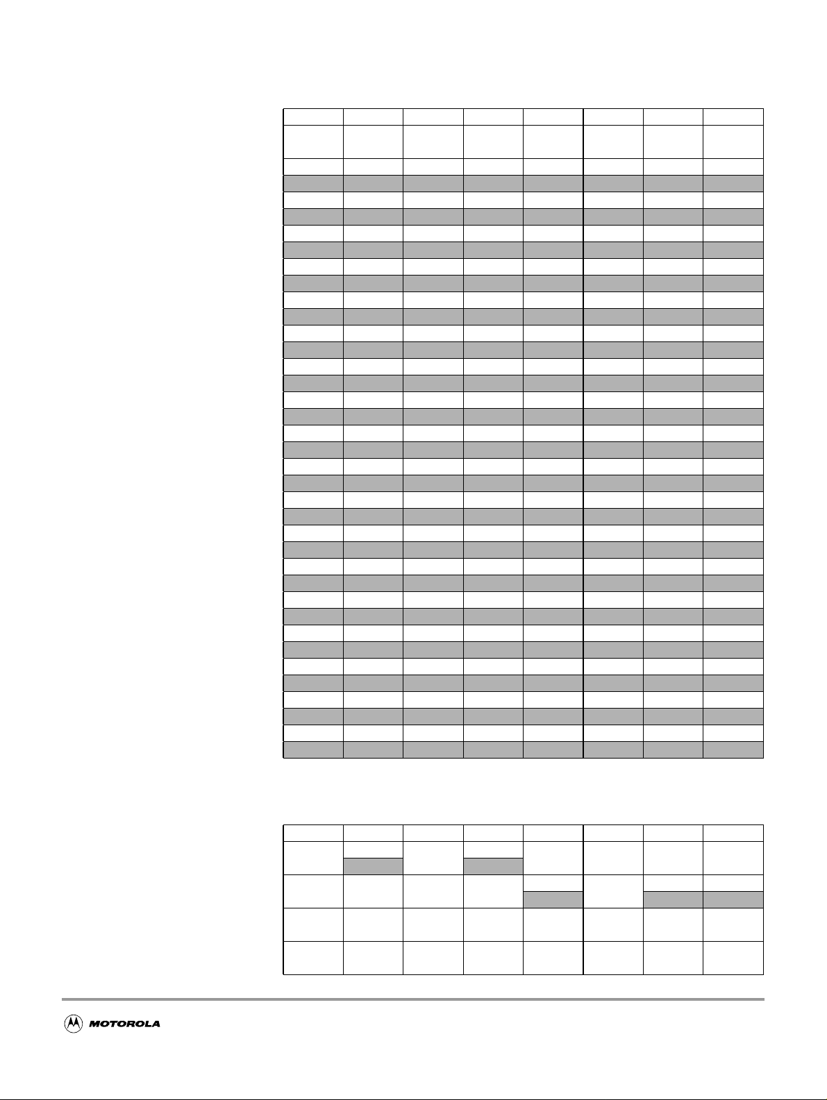
MC9S12DJ64 Device User Guide — V01.17
$0120 - $013F ATD1 (Analog to Digital Converter 10 Bit 8 Channel)
Address Name Bit 7 Bit 6 Bit 5 Bit 4 Bit 3 Bit 2 Bit 1 Bit 0
$012D ATD1DIEN
$012E Reserved
$012F PORTAD1
$0130 ATD1DR0H
$0131 ATD1DR0L
$0132 ATD1DR1H
$0133 ATD1DR1L
$0134 ATD1DR2H
$0135 ATD1DR2L
$0136 ATD1DR3H
$0137 ATD1DR3L
$0138 ATD1DR4H
$0139 ATD1DR4L
$013A ATD1DR5H
$013B ATD1DR5L
$013C ATD1DR6H
$013D ATD1DR6L
$013E ATD1DR7H
$013F ATD1DR7L
Read:
Write:
Read: 00000000
Write:
Read: Bit7 654321BIT 0
Write:
Read: Bit15 14 13 12 11 10 9 Bit8
Write:
Read: Bit7 Bit6 000000
Write:
Read: Bit15 14 13 12 11 10 9 Bit8
Write:
Read: Bit7 Bit6 000000
Write:
Read: Bit15 14 13 12 11 10 9 Bit8
Write:
Read: Bit7 Bit6 000000
Write:
Read: Bit15 14 13 12 11 10 9 Bit8
Write:
Read: Bit7 Bit6 000000
Write:
Read: Bit15 14 13 12 11 10 9 Bit8
Write:
Read: Bit7 Bit6 000000
Write:
Read: Bit15 14 13 12 11 10 9 Bit8
Write:
Read: Bit7 Bit6 000000
Write:
Read: Bit15 14 13 12 11 10 9 Bit8
Write:
Read: Bit7 Bit6 000000
Write:
Read: Bit15 14 13 12 11 10 9 Bit8
Write:
Read: Bit7 Bit6 000000
Write:
Bit 7 654321Bit 0
$0140 - $017F CAN0 (Motorola Scalable CAN - MSCAN)
Address Name Bit 7 Bit 6 Bit 5 Bit 4 Bit 3 Bit 2 Bit 1 Bit 0
$0140 CAN0CTL0
$0141 CAN0CTL1
$0142 CAN0BTR0
$0143 CAN0BTR1
Read:
Write:
Read:
Write:
Read:
Write:
Read:
Write:
RXFRM
CANE CLKSRC LOOPB LISTEN
SJW1 SJW0 BRP5 BRP4 BRP3 BRP2 BRP1 BRP0
SAMP TSEG22 TSEG21 TSEG20 TSEG13 TSEG12 TSEG11 TSEG10
RXACT
CSWAI
SYNCH
TIME WUPE SLPRQ INITRQ
0
WUPM
SLPAK INITAK
41
Page 42
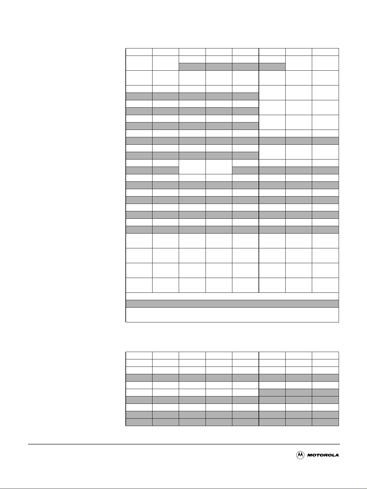
MC9S12DJ64 Device User Guide — V01.17
$0140 - $017F CAN0 (Motorola Scalable CAN - MSCAN)
Address Name Bit 7 Bit 6 Bit 5 Bit 4 Bit 3 Bit 2 Bit 1 Bit 0
$0144 CAN0RFLG
$0145 CAN0RIER
$0146 CAN0TFLG
$0147 CAN0TIER
$0148 CAN0TARQ
$0149 CAN0TAAK
$014A CAN0TBSEL
$014B CAN0IDAC
$014C Reserved
$014D Reserved
$014E CAN0RXERR
$014F CAN0TXERR
$0150 -
$0153
$0154 -
$0157
$0158 -
$015B
$015C -
$015F
$0160 -
$016F
$0170 -
$017F
CAN0IDAR0 -
CAN0IDAR3
CAN0IDMR0 -
CAN0IDMR3
CAN0IDAR4 -
CAN0IDAR7
CAN0IDMR4 -
CAN0IDMR7
CAN0RXFG
CAN0TXFG
Read:
Write:
Read:
Write:
Read: 00000
Write:
Read: 00000
Write:
Read: 00000
Write:
Read: 00000ABTAK2ABTAK1ABTAK0
Write:
Read: 00000
Write:
Read: 0 0
Write:
Read: 00000000
Write:
Read: 00000000
Write:
Read: RXERR7 RXERR6 RXERR5 RXERR4 RXERR3 RXERR2 RXERR1 RXERR0
Write:
Read: TXERR7 TXERR6 TXERR5 TXERR4 TXERR3 TXERR2 TXERR1 TXERR0
Write:
Read:
Write:
Read:
Write:
Read:
Write:
Read:
Write:
Read: FOREGROUND RECEIVE BUFFER see Table 1-2
Write:
Read:
Write:
WUPIF CSCIF
WUPIE CSCIE RSTATE1 RSTATE0 TSTATE1 TSTATE0 OVRIE RXFIE
AC7 AC6 AC5 AC4 AC3 AC2 AC1 AC0
AM7 AM6 AM5 AM4 AM3 AM2 AM1 AM0
AC7 AC6 AC5 AC4 AC3 AC2 AC1 AC0
AM7 AM6 AM5 AM4 AM3 AM2 AM1 AM0
RSTAT1 RSTAT0 TSTAT1 TSTAT0
TXE2 TXE1 TXE0
TXEIE2 TXEIE1 TXEIE0
ABTRQ2 ABTRQ1 ABTRQ0
TX2 TX1 TX0
IDAM1 IDAM0
FOREGROUND TRANSMIT BUFFER see Table 1-2
0 IDHIT2 IDHIT1 IDHIT0
OVRIF RXF
Table 1-2 Detailed MSCAN Foreground Receive and Transmit Buffer Layout
Address Name Bit 7 Bit 6 Bit 5 Bit 4 Bit 3 Bit 2 Bit 1 Bit 0
Extended ID Read: ID28 ID27 ID26 ID25 ID24 ID23 ID22 ID21
$0160
$0161
$0162
42
Standard ID Read: ID10 ID9 ID8 ID7 ID6 ID5 ID4 ID3
CAN0RIDR0 Write:
Extended ID Read: ID20 ID19 ID18 SRR=1 IDE=1 ID17 ID16 ID15
Standard ID Read: ID2 ID1 ID0 RTR IDE=0
CAN0RIDR1 Write:
Extended ID Read: ID14 ID13 ID12 ID11 ID10 ID9 ID8 ID7
Standard ID Read:
CAN0RIDR2 Write:
Page 43
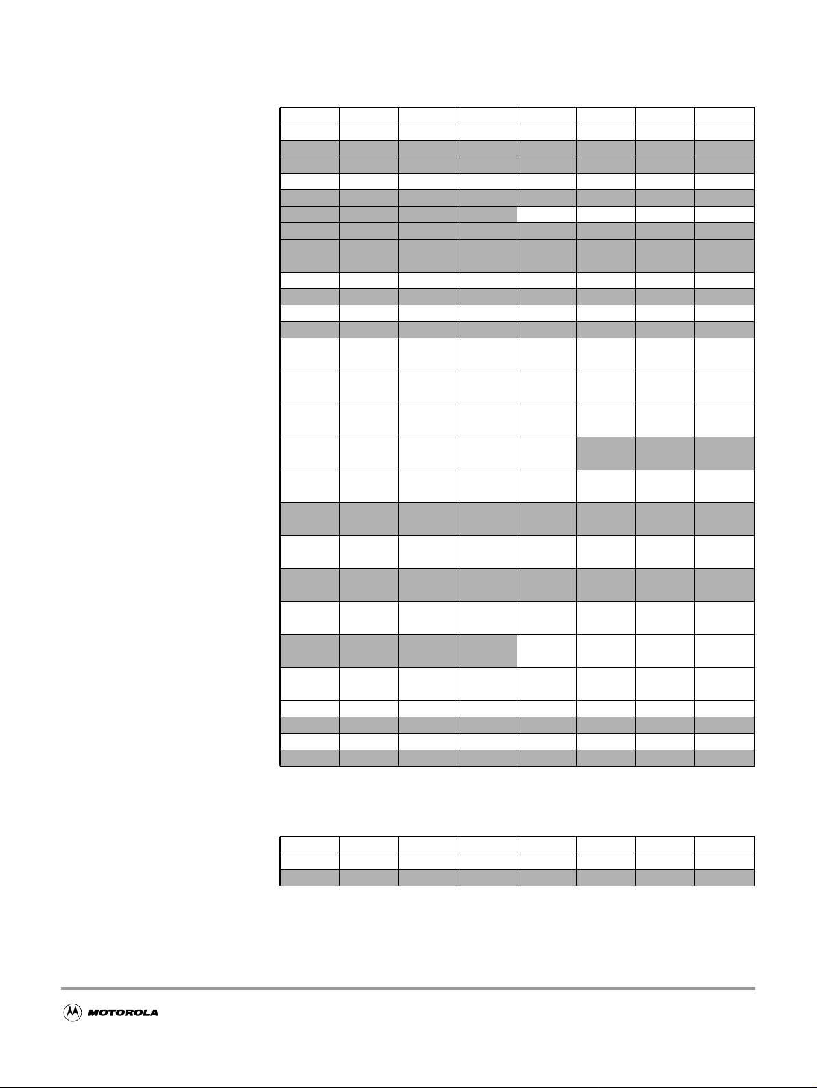
MC9S12DJ64 Device User Guide — V01.17
Table 1-2 Detailed MSCAN Foreground Receive and Transmit Buffer Layout
Address Name Bit 7 Bit 6 Bit 5 Bit 4 Bit 3 Bit 2 Bit 1 Bit 0
Extended ID Read: ID6 ID5 ID4 ID3 ID2 ID1 ID0 RTR
$0163
$0164$016B
$016C CAN0RDLR
$016D Reserved
$016E CAN0RTSRH
$016F CAN0RTSRL
$0170
$0171
$0172
$0173
$0174$017B
$017C CAN0TDLR
$017D CAN0TTBPR
$017E CAN0TTSRH
$017F CAN0TTSRL
Standard ID Read:
CAN0RIDR3 Write:
CAN0RDSR0 -
CAN0RDSR7
Extended ID Read:
CAN0TIDR0 Write:
Standard ID Read:
Extended ID Read:
CAN0TIDR1 Write:
Standard ID Read:
Extended ID Read:
CAN0TIDR2 Write:
Standard ID Read:
Extended ID Read:
CAN0TIDR3 Write:
Standard ID Read:
CAN0TDSR0 -
CAN0TDSR7
Read: DB7 DB6 DB5 DB4 DB3 DB2 DB1 DB0
Write:
Read:
Write:
Read:
Write:
Read: TSR15 TSR14 TSR13 TSR12 TSR11 TSR10 TSR9 TSR8
Write:
Read: TSR7 TSR6 TSR5 TSR4 TSR3 TSR2 TSR1 TSR0
Write:
Write:
Write:
Write:
Write:
Read:
Write:
Read:
Write:
Read:
Write:
Read: TSR15 TSR14 TSR13 TSR12 TSR11 TSR10 TSR9 TSR8
Write:
Read: TSR7 TSR6 TSR5 TSR4 TSR3 TSR2 TSR1 TSR0
Write:
DLC3 DLC2 DLC1 DLC0
ID28 ID27 ID26 ID25 ID24 ID23 ID22 ID21
ID10 ID9 ID8 ID7 ID6 ID5 ID4 ID3
ID20 ID19 ID18 SRR=1 IDE=1 ID17 ID16 ID15
ID2 ID1 ID0 RTR IDE=0
ID14 ID13 ID12 ID11 ID10 ID9 ID8 ID7
ID6 ID5 ID4 ID3 ID2 ID1 ID0 RTR
DB7 DB6 DB5 DB4 DB3 DB2 DB1 DB0
DLC3 DLC2 DLC1 DLC0
PRIO7 PRIO6 PRIO5 PRIO4 PRIO3 PRIO2 PRIO1 PRIO0
$0180 - $023F Reserved
Address Name Bit 7 Bit 6 Bit 5 Bit 4 Bit 3 Bit 2 Bit 1 Bit 0
$0180 -
$023F
Reserved
Read: 00000000
Write:
43
Page 44

MC9S12DJ64 Device User Guide — V01.17
$0240 - $027F PIM (Port Integration Module)
Address Name Bit 7 Bit 6 Bit 5 Bit 4 Bit 3 Bit 2 Bit 1 Bit 0
$0240 PTT
$0241 PTIT
$0242 DDRT
$0243 RDRT
$0244 PERT
$0245 PPST
$0246 Reserved
$0247 Reserved
$0248 PTS
$0249 PTIS
$024A DDRS
$024B RDRS
$024C PERS
$024D PPSS
$024E WOMS
$024F Reserved
$0250 PTM
$0251 PTIM
$0252 DDRM
$0253 RDRM
$0254 PERM
$0255 PPSM
$0256 WOMM
$0257 MODRR
$0258 PTP
Read:
Write:
Read: PTIT7 PTIT6 PTIT5 PTIT4 PTIT3 PTIT2 PTIT1 PTIT0
Write:
Read:
Write:
Read:
Write:
Read:
Write:
Read:
Write:
Read: 00000000
Write:
Read: 00000000
Write:
Read:
Write:
Read: PTIS7 PTIS6 PTIS5 PTIS4 PTIS3 PTIS2 PTIS1 PTIS0
Write:
Read:
Write:
Read:
Write:
Read:
Write:
Read:
Write:
Read:
Write:
Read: 00000000
Write:
Read:
Write:
Read: PTIM7 PTIM6 PTIM5 PTIM4 PTIM3 PTIM2 PTIM1 PTIM0
Write:
Read:
Write:
Read:
Write:
Read:
Write:
Read:
Write:
Read:
Write:
Read: 0 0 0
Write:
Read:
Write:
PTT7 PTT6 PTT5 PTT4 PTT3 PTT2 PTT1 PTT0
DDRT7 DDRT7 DDRT5 DDRT4 DDRT3 DDRT2 DDRT1 DDRT0
RDRT7 RDRT6 RDRT5 RDRT4 RDRT3 RDRT2 RDRT1 RDRT0
PERT7 PERT6 PERT5 PERT4 PERT3 PERT2 PERT1 PERT0
PPST7 PPST6 PPST5 PPST4 PPST3 PPST2 PPST1 PPST0
PTS7 PTS6 PTS5 PTS4 PTS3 PTS2 PTS1 PTS0
DDRS7 DDRS7 DDRS5 DDRS4 DDRS3 DDRS2 DDRS1 DDRS0
RDRS7 RDRS6 RDRS5 RDRS4 RDRS3 RDRS2 RDRS1 RDRS0
PERS7 PERS6 PERS5 PERS4 PERS3 PERS2 PERS1 PERS0
PPSS7 PPSS6 PPSS5 PPSS4 PPSS3 PPSS2 PPSS1 PPSS0
WOMS7 WOMS6 WOMS5 WOMS4 WOMS3 WOMS2 WOMS1 WOMS0
PTM7 PTM6 PTM5 PTM4 PTM3 PTM2 PTM1 PTM0
DDRM7 DDRM7 DDRM5 DDRM4 DDRM3 DDRM2 DDRM1 DDRM0
RDRM7 RDRM6 RDRM5 RDRM4 RDRM3 RDRM2 RDRM1 RDRM0
PERM7 PERM6 PERM5 PERM4 PERM3 PERM2 PERM1 PERM0
PPSM7 PPSM6 PPSM5 PPSM4 PPSM3 PPSM2 PPSM1 PPSM0
WOMM7 WOMM6 WOMM5 WOMM4 WOMM3 WOMM2 WOMM1 WOMM0
MODRR4
PTP7 PTP6 PTP5 PTP4 PTP3 PTP2 PTP1 PTP0
00
MODRR1 MODRR0
44
Page 45

MC9S12DJ64 Device User Guide — V01.17
$0240 - $027F PIM (Port Integration Module)
Address Name Bit 7 Bit 6 Bit 5 Bit 4 Bit 3 Bit 2 Bit 1 Bit 0
$0259 PTIP
$025A DDRP
$025B RDRP
$025C PERP
$025D PPSP
$025E PIEP
$025F PIFP
$0260 PTH
$0261 PTIH
$0262 DDRH
$0263 RDRH
$0264 PERH
$0265 PPSH
$0266 PIEH
$0267 PIFH
$0268 PTJ
$0269 PTIJ
$026A DDRJ
$026B RDRJ
$026C PERJ
$026D PPSJ
$026E PIEJ
$026F PIFJ
$0270 -
$027F
Reserved
Read: PTIP7 PTIP6 PTIP5 PTIP4 PTIP3 PTIP2 PTIP1 PTIP0
Write:
Read:
Write:
Read:
Write:
Read:
Write:
Read:
Write:
Read:
Write:
Read:
Write:
Read:
Write:
Read: PTIH7 PTIH6 PTIH5 PTIH4 PTIH3 PTIH2 PTIH1 PTIH0
Write:
Read:
Write:
Read:
Write:
Read:
Write:
Read:
Write:
Read:
Write:
Read:
Write:
Read:
Write:
Read: PTIJ7 PTIJ6 0000PTIJ1 PTIJ0
Write:
Read:
Write:
Read:
Write:
Read:
Write:
Read:
Write:
Read:
Write:
Read:
Write:
Read: 00000000
Write:
DDRP7 DDRP7 DDRP5 DDRP4 DDRP3 DDRP2 DDRP1 DDRP0
RDRP7 RDRP6 RDRP5 RDRP4 RDRP3 RDRP2 RDRP1 RDRP0
PERP7 PERP6 PERP5 PERP4 PERP3 PERP2 PERP1 PERP0
PPSP7 PPSP6 PPSP5 PPSP4 PPSP3 PPSP2 PPSP1 PPSS0
PIEP7 PIEP6 PIEP5 PIEP4 PIEP3 PIEP2 PIEP1 PIEP0
PIFP7 PIFP6 PIFP5 PIFP4 PIFP3 PIFP2 PIFP1 PIFP0
PTH7 PTH6 PTH5 PTH4 PTH3 PTH2 PTH1 PTH0
DDRH7 DDRH7 DDRH5 DDRH4 DDRH3 DDRH2 DDRH1 DDRH0
RDRH7 RDRH6 RDRH5 RDRH4 RDRH3 RDRH2 RDRH1 RDRH0
PERH7 PERH6 PERH5 PERH4 PERH3 PERH2 PERH1 PERH0
PPSH7 PPSH6 PPSH5 PPSH4 PPSH3 PPSH2 PPSH1 PPSH0
PIEH7 PIEH6 PIEH5 PIEH4 PIEH3 PIEH2 PIEH1 PIEH0
PIFH7 PIFH6 PIFH5 PIFH4 PIFH3 PIFH2 PIFH1 PIFH0
PTJ7 PTJ6
DDRJ7 DDRJ7
RDRJ7 RDRJ6
PERJ7 PERJ6
PPSJ7 PPSJ6
PIEJ7 PIEJ6
PIFJ7 PIFJ6
0000
0000
0000
0000
0000
0000
0000
PTJ1 PTJ0
DDRJ1 DDRJ0
RDRJ1 RDRJ0
PERJ1 PERJ0
PPSJ1 PPSJ0
PIEJ1 PIEJ0
PIFJ1 PIFJ0
45
Page 46

MC9S12DJ64 Device User Guide — V01.17
$0280 - $03FF Reserved
Address Name Bit 7 Bit 6 Bit 5 Bit 4 Bit 3 Bit 2 Bit 1 Bit 0
$0280 -
$03FF
Reserved
Read: 00000000
Write:
46
Page 47

MC9S12DJ64 Device User Guide — V01.17
1.6 Part ID Assignments
The part ID is located in two 8-bit registers PARTIDH and PARTIDL (addresses $001A and $001B after
reset). The read-only value is a uniquepartIDforeachrevision of the chip. Table 1-3showstheassigned
part ID number.
Table 1-3 Assigned Part ID Numbers
Device Mask Set Number
MC9S12DJ64 0L86D $0200
MC9S12DJ64 1L86D $0201
MC9S12DJ64 2L86D
MC9S12DJ64 3L86D $0203
MC9S12DJ64 4L86D $0204
NOTES:
1. The coding is as follows:
Bit 15-12: Major family identifier
Bit 11-8: Minor family identifier
Bit 7-4: Major mask set revision number including FAB transfers
Bit 3-0: Minor - non full - mask set revision
2. 1L86D is identical to 2L86D except improved ESD performance on 2L86D
Part ID
$0201
1
2
The device memory sizes are located in two 8-bit registers MEMSIZ0 and MEMSIZ1 (addresses $001C
and $001D after reset). Table 1-4 shows the read-only values of these registers. Refer to HCS12 Module
Mapping Control (MMC) Block Guide for further details.
Table 1-4 Memory size registers
Register name Value
MEMSIZ0 $11
MEMSIZ1 $80
47
Page 48

MC9S12DJ64 Device User Guide — V01.17
48
Page 49

MC9S12DJ64 Device User Guide — V01.17
Section 2 Signal Description
This section describes signals that connect off-chip. It includes a pinout diagram, a table of signal
properties, and detailed discussion of signals. It is built from the signal description sections of the Block
Guides of the individual IP blocks on the device.
2.1 Device Pinout
The MC9S12DJ64 is available in a 112-pin low profile quad flat pack (LQFP) and in a 80-pin quad flat
pack (QFP). Most pins perform two or more functions, as described in the Signal Descriptions. Figure
2-1 and Figure 2-2 show the pin assignments.
49
Page 50
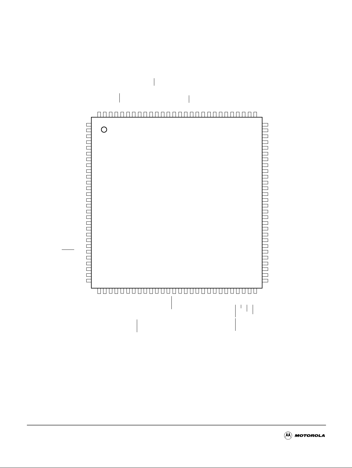
MC9S12DJ64 Device User Guide — V01.17
PP4/KWP4/PWM4
PP5/KWP5/PWM5
PP6/KWP6/PWM6
PP7/KWP7/PWM7
PK7/ECS/ROMCTL
VDDX
VSSX
PM0/RXCAN0/RXB
PM4/RXCAN0/MOSI
PM5/TXCAN0/SCK0
PJ6/KWJ6/SDA/RXCAN0
PM1/TXCAN0/TXB
PM2/RXCAN0/MISO0
PM3/TXCAN0/SS0
PJ7/KWJ7/SCL/TXCAN0
VREGEN
PS7/SS0
PS6/SCK0
PS5/MOSI0
PS4/MISO0
PS3/TXD1
PS2/RXD1
PS1/TXD0
PS0/RXD0
PM6
PM7
VSSA
VRL
PWM3/KWP3/PP3
PWM2/KWP2/PP2
PWM1/KWP1/PP1
PWM0/KWP0/PP0
XADDR17/PK3
XADDR16/PK2
XADDR15/PK1
XADDR14/PK0
IOC0/PT0
IOC1/PT1
IOC2/PT2
IOC3/PT3
VDD1
VSS1
IOC4/PT4
IOC5/PT5
IOC6/PT6
IOC7/PT7
XADDR19/PK5
XADDR18/PK4
KWJ1/PJ1
KWJ0/PJ0
MODC/TAGHI/BKGD
ADDR0/DATA0/PB0
ADDR1/DATA1/PB1
ADDR2/DATA2/PB2
ADDR3/DATA3/PB3
ADDR4/DATA4/PB4
112
111
110
109
108
107
106
105
104
1
2
3
4
5
6
7
8
9
10
11
12
13
14
15
16
17
18
19
20
21
22
23
24
25
26
27
28
293031323334353637383940414243444546474849505152535455
103
999897969594939291908988878685
102
101
100
MC9S12DJ64
112LQFP
84
VRH
83
VDDA
82
PAD15/AN15/ETRIG1
81
PAD07/AN07/ETRIG0
80
PAD14/AN14
79
PAD06/AN06
78
PAD13/AN13
77
PAD05/AN05
76
PAD12/AN12
75
PAD04/AN04
74
PAD11/AN11
73
PAD03/AN03
72
PAD10/AN10
71
PAD02/AN02
70
PAD09/AN09
69
PAD01/AN01
68
PAD08/AN08
67
PAD00/AN00
66
VSS2
65
VDD2
64
PA7/ADDR15/DATA15
63
PA6/ADDR14/DATA14
62
PA5/ADDR13/DATA13
61
PA4/ADDR12/DATA12
60
PA3/ADDR11/DATA11
59
PA2/ADDR10/DATA10
58
PA1/ADDR9/DATA9
57
PA0/ADDR8/DATA8
56
50
XFC
XTAL
EXTAL
VSSPLL
TEST
KWH3/PH3
KWH2/PH2
R/W/PE2
KWH1/PH1
KWH0/PH0
LSTRB/TAGLO/PE3
IRQ/PE1
XIRQ/PE0
ADDR5/DATA5/PB5
ADDR6/DATA6/PB6
KWH7/PH7
KWH6/PH6
ADDR7/DATA7/PB7
KWH5/PH5
KWH4/PH4
MODB/IPIPE1/PE6
XCLKS/NOACC/PE7
VSSR
VDDR
RESET
ECLK/PE4
MODA/IPIPE0/PE5
VDDPLL
Signals shown in Bold are not available on the 80 Pin Package
Figure 2-1 Pin Assignments in 112-pin LQFP for MC9S12DJ64
Page 51
PP4/KWP4/PWM4
PP5/KWP5/PWM5
PP7/KWP7/PWM7
VDDX
VSSX
PM0/RXCAN0/RXB
PM4/RXCAN0/MOSI0
PM5/TXCAN0/SCK0
PJ6/KWJ6/SDA/RXCAN0
PM1/TXCAN0/TXB
PM2/RXCAN0/MISO0
PM3/TXCAN0/SS0
PJ7/KWJ7/SCL/TXCAN0
MC9S12DJ64 Device User Guide — V01.17
VREGEN
PS3/TXD1
PS2/RXD1
PS1/TXD0
PS0/RXD0
VSSA
VRL
PWM3/KWP3/PP3
PWM2/KWP2/PP2
PWM1/KWP1/PP1
PWM0/KWP0/PP0
IOC0/PT0
IOC1/PT1
IOC2/PT2
IOC3/PT3
VDD1
VSS1
IOC4/PT4
IOC5/PT5
IOC6/PT6
MODC/
IOC7/PT7
TAGHI/BKGD
ADDR0/DATA0/PB0
ADDR1/DATA1/PB1
ADDR2/DATA2/PB2
ADDR3/DATA3/PB3
ADDR4/DATA4/PB4
80797877767574737271706968676665646362
1
2
3
4
5
6
7
8
9
10
11
12
13
14
15
16
17
18
19
20
21222324252627282930313233343536373839
ADDR5/DATA5/PB5
ADDR6/DATA6/PB6
ADDR7/DATA7/PB7
XCLKS/NOACC/PE7
MC9S12DJ64
80 QFP
VSSR
VDDR
RESET
ECLK/PE4
MODA/IPIPE0/PE5
MODB/IPIPE1/PE6
VDDPLL
XFC
VSSPLL
EXTAL
XTAL
TEST
IRQ/PE1
R/W/PE2
LSTRB/TAGLO/PE3
61
60
VRH
59
VDDA
58
PAD07/AN07/ETRIG0
57
PAD06/AN06
56
PAD05/AN05
55
PAD04/AN04
54
PAD03/AN03
53
PAD02/AN02
52
PAD01/AN01
51
PAD00/AN00
50
VSS2
49
VDD2
48
PA7/ADDR15/DATA15
47
PA6/ADDR14/DATA14
46
PA5/ADDR13/DATA13
45
PA4/ADDR12/DATA12
44
PA3/ADDR11/DATA11
43
PA2/ADDR10/DATA10
42
PA1/ADDR9/DATA9
41
PA0/ADDR8/DATA8
40
XIRQ/PE0
Figure 2-2 Pin Assignments in 80-pin QFP for MC9S12DJ64
2.2 Signal Properties Summary
Table 2-1 summarizes the pin functionality. Signals shown in bold are not available in the 80 pin
package.
51
Page 52

MC9S12DJ64 Device User Guide — V01.17
Table 2-1 Signal Properties
Internal Pull
Pin Name
Function1
EXTAL — — —
XTAL — — —
RESET — — — VDDR External Reset
TEST — — — N.A. Test Input
VREGEN — — — VDDX Voltage Regulator Enable Input
XFC — — — VDDPLL PLL Loop Filter
BKGD
PAD15 AN15 ETRIG1 —
PAD[14:08] AN[14:08] — —
PAD07 AN07 ETRIG0 —
PAD[06:00] AN[06:00] — —
PA[7:0]
PB[7:0]
PE7 NOACC
PE6 IPIPE1 MODB — While
PE5 IPIPE0 MODA — Port E I/O, Pipe Status, Mode Input
PE4 ECLK — —
PE3
PE2 R/
PE1
PE0
PH7 KWH7 ——
PH6 KWH6 —— Port H I/O, Interrupt
PH5 KWH5 —— Port H I/O, Interrupt
PH4 KWH4 —— Port H I/O, Interrupt
PH3 KWH3 —— Port H I/O, Interrupt
PH2 KWH2 —— Port H I/O, Interrupt
PH1 KWH1 —— Port H I/O, Interrupt
PH0 KWH0 —— Port H I/O, Interrupt
Pin Name
Function2
TAGHI MODC — VDDR
ADDR[15:8]/
DATA[15:8]
ADDR[7:0]/
DATA[7:0]
LSTRB TAGLO — Port E I/O, Byte Strobe, Tag Low
W — — Port E I/O, R/W in expanded modes
IRQ — —
XIRQ — — Port E Input, Non Maskable Interrupt
Pin Name
Function3
——
——
XCLKS —
Pin Name
Function4
Powered
by
VDDPLL
VDDA None None
VDDR
Resistor
CTRL
None None
Always
Up
PUCR/
PUPAE
PUCR/
PUPBE
PUCR/
PUPEE
PUCR/
PUPEE
PERH/
PPSH
Reset
State
Disabled
Mode
depen-
dant
RESET pin is
low:
Down
Mode
depen-
dant
Disabled
Up
Up
Description
Oscillator Pins
Background Debug, Tag High, Mode
Input
Port AD Input, Analog Input AN7 of
ATD1, External Trigger Input of
ATD1
Port AD Inputs, Analog Inputs
AN[6:0] of ATD1
Port AD Input, Analog Input AN7 of
ATD0, External Trigger Input of ATD0
Port AD Inputs, Analog Inputs AN[6:0]
of ATD0
Port A I/O, Multiplexed Address/Data
Port B I/O, Multiplexed Address/Data
Port E I/O, Access, Clock Select
1
Port E I/O, Pipe Status, Mode Input
Port E I/O, Bus Clock Output
1
Port E Input, Maskable Interrupt
Port H I/O, Interrupt
52
Page 53

MC9S12DJ64 Device User Guide — V01.17
Internal Pull
Pin Name
Function1
PJ7 KWJ7 SCL TXCAN0
PJ6 KWJ6 SDA RXCAN0
PJ[1:0] KWJ[1:0] — — Port J I/O, Interrupts
PK7
PK[5:0] XADDR[19:14] — — Port K I/O, Extended Addresses
PM7 — — —
PM6 — — — Port M I/O
PM5 TXCAN0 SCK — Port M I/O, TX of CAN0, SCK of SPI0
PM4 RXCAN0 MOSI — Port M I/O, RX of CAN0, MOSI of SPI0
PM3 TXCAN0
PM2 RXCAN0 MISO0 — Port M I/O,RX of CAN0, MISO of SPI0
PM1 TXCAN0 TXB — Port M I/O, TX of CAN0, RX of BDLC
PM0 RXCAN0 RXB — Port M I/O, RX of CAN0, RX of BDLC
PP7 KWP7 PWM7 —
PP6 KWP6 PWM6 — Port P I/O,Interrupt, PWM Channel 6
PP5 KWP5 PWM5 — Port P I/O, Interrupt, PWM Channel 5
PP4 KWP4 PWM4 — Port P I/O, Interrupt, PWM Channel 4
PP3 KWP3 PWM3 — Port P I/O, Interrupt, PWM Channel 3
PP2 KWP2 PWM2 — Port P I/O, Interrupt, PWM Channel 2
PP1 KWP1 PWM1 — Port P I/O, Interrupt, PWM Channel 1
PP0 KWP0 PWM0 — Port P I/O, Interrupt, PWM Channel 0
PS7
PS6 SCK0 — — Port S I/O, SCK of SPI0
PS5 MOSI0 — — Port S I/O, MOSI of SPI0
PS4 MISO0 — — Port S I/O, MISO of SPI0
PS3 TXD1 — — Port S I/O, TXD of SCI1
PS2 RXD1 — — Port S I/O, RXD of SCI1
PS1 TXD0 — — Port S I/O, TXD of SCI0
PS0 RXD0 — — Port S I/O, RXD of SCI0
PT[7:0] IOC[7:0] — —
NOTES:
1. Refer to PEAR register description in HCS12 Multiplexed External Bus Interface (MEBI) Block Guide
Pin Name
Function2
ECS ROMCTL —
SS0 — —
Pin Name
Function3
SS0 — Port M I/O, TX of CAN0, SS of SPI0
Pin Name
Function4
Powered
by
VDDX
VDDX
Resistor
CTRL
PERJ/
PPSJ
PUCR/
PUPKE
PERM/
PPSM
PERP/
PPSP
PERS/
PPSS
PERT/
PPST
Reset
State
Port J I/O, Interrupt, SCL of IIC, TX of
CAN0
Up
Up
Disabled
Up
Disabled Port T I/O, Timer channels
Port J I/O, Interrupt, SDA of IIC, RX of
CAN0
Port K I/O, Emulation Chip Select,
ROM On Enable
Port M I/O
Port P I/O, Interrupt, Channel 7 of
PWM
Port S I/O, SS of SPI0
Description
53
Page 54

MC9S12DJ64 Device User Guide — V01.17
2.3 Detailed Signal Descriptions
2.3.1 EXTAL, XTAL — Oscillator Pins
EXTAL andXTALare the crystal driver and externalclockpins.On reset all the deviceclocksarederived
from the EXTAL input frequency. XTAL is the crystal output.
2.3.2 RESET — External Reset Pin
An active low bidirectional control signal, it acts as an input to initialize the MCU to a known start-up
state, and an output when an internal MCU function causes a reset.
2.3.3 TEST — Test Pin
This input only pin is reserved for test.
NOTE:
The TEST pin must be tied to VSS in all applications.
2.3.4 VREGEN — Voltage Regulator Enable Pin
This input only pin enables or disables the on-chip voltage regulator.
2.3.5 XFC — PLL Loop Filter Pin
PLL loop filter. Please ask your Motorola representative for the interactive application note to compute
PLL loop filter elements. Any current leakage on this pin must be avoided.
XFC
R
MCU
0
C
S
C
P
VDDPLLVDDPLL
Figure 2-3 PLL Loop Filter Connections
2.3.6 BKGD / TAGHI / MODC — Background Debug, Tag High, and Mode Pin
The BKGD/TAGHI/MODC pin is used as a pseudo-open-drain pin for the background debug
communication. In MCU expanded modes of operation when instruction tagging is on, an input low on
this pin during the falling edge of E-clock tags the high half of the instruction word being read into the
54
Page 55

MC9S12DJ64 Device User Guide — V01.17
instruction queue. It is used as a MCU operating mode select pin during reset. The state of this pin is
latched to the MODC bit at the rising edge of
RESET. This pin has a permanently enabled pull-up device.
2.3.7 PAD15 / AN15 / ETRIG1 — Port AD Input Pin of ATD1
PAD15 is a general purpose input pin and analog input AN7 of the analog to digital converter ATD1. It
can act as an external trigger input for the ATD1.
2.3.8 PAD[14:08] / AN[14:08] — Port AD Input Pins ATD1
PAD14 - PAD08 are general purpose input pins and analog inputs AN[6:0] of the analog to digital
converter ATD1.
2.3.9 PAD07 / AN07 / ETRIG0 — Port AD Input Pin of ATD0
PAD07 is a general purpose input pin and analog input AN0 of the analog to digital converter ATD0. It
can act as an external trigger input for the ATD0.
2.3.10 PAD[06:00] / AN[06:00] — Port AD Input Pins of ATD0
PAD06 - PAD00 are general purpose input pins and analog inputs AN[6:0] of the analog to digital
converter ATD0.
2.3.11 PA[7:0] / ADDR[15:8] / DATA[15:8] — Port A I/O Pins
PA7-PA0 are general purpose input or output pins. In MCU expanded modes of operation, these pins are
used for the multiplexed external address and data bus.
2.3.12 PB[7:0] / ADDR[7:0] / DATA[7:0] — Port B I/O Pins
PB7-PB0 are general purpose input or output pins. In MCU expanded modes of operation, these pins are
used for the multiplexed external address and data bus.
2.3.13 PE7 / NOACC / XCLKS — Port E I/O Pin 7
PE7 is a general purpose input or output pin. During MCU expanded modes of operation, the NOACC
signal, when enabled, is used to indicate that the current bus cycle is an unused or “free” cycle. This signal
will assert when the CPU is not using the bus.
XCLKS is an input signal which controls whether a crystal in combination with the internal Colpitts
The
(low power) oscillator isusedorwhether Pierce oscillator/external clock circuitry is used. The state of this
pin is latched at the rising edge of
external clock drive or a Pierce Oscillator.If input is a logic high a Colpitts oscillator circuit is configured
on EXTAL and XTAL. Since this pin is an input with a pull-up device during reset, if the pin is left
floating, the default configuration is a Colpitts oscillator circuit on EXTAL and XTAL.
RESET. If the input is a logic low the EXTAL pin is configured for an
55
Page 56

MC9S12DJ64 Device User Guide — V01.17
EXTAL
MCU
XTAL
* Due to the nature of a translated ground Colpitts oscillator a
DC voltage bias is applied to the crystal
Please contact the crystal manufacturer for crystal DC
bias conditions and recommended capacitor value C
Figure 2-4 Colpitts Oscillator Connections (PE7=1)
CDC*
C
1
Crystal or
ceramic resonator
C
2
VSSPLL
.
DC
EXTAL
C
3
MCU
XTAL
R
B
*
R
S
Crystal or
ceramic resonator
C
4
VSSPLL
* Rs can be zero (shorted) when used with higher frequency crystals.
Refer to manufacturer’s data.
Figure 2-5 Pierce Oscillator Connections (PE7=0)
MCU
EXTAL
XTAL
not connected
CMOS-COMPATIBLE
EXTERNAL OSCILLATO
(V
DDPLL
-Level)
R
56
Figure 2-6 External Clock Connections (PE7=0)
Page 57

MC9S12DJ64 Device User Guide — V01.17
2.3.14 PE6 / MODB / IPIPE1 — Port E I/O Pin 6
PE6 is a general purpose input or output pin. It is used as a MCU operating mode select pin during reset.
The state of this pin is latched to the MODB bit at the rising edge of
instruction queue tracking signalIPIPE1.Thispin is an input with a pull-down device which is only active
RESET is low.
when
RESET. This pin is shared with the
2.3.15 PE5 / MODA / IPIPE0 — Port E I/O Pin 5
PE5 is a general purpose input or output pin. It is used as a MCU operating mode select pin during reset.
The state of this pin is latched to the MODA bit at the rising edge of
instruction queue tracking signalIPIPE0.Thispin is an input with a pull-down device which is only active
RESET is low.
when
RESET. This pin is shared with the
2.3.16 PE4 / ECLK — Port E I/O Pin 4
PE4 is a general purpose input or output pin. It can be configured to drive the internal bus clock ECLK.
ECLK can be used as a timing reference.
2.3.17 PE3 / LSTRB / TAGLO — Port E I/O Pin 3
PE3 is a general purpose input or output pin. In MCU expanded modes of operation, LSTRB can be used
for the low-byte strobe function to indicate the type of bus access and when instruction tagging is on,
TAGLO is used to tag the low half of the instruction word being read into the instruction queue.
2.3.18 PE2 / R/W—Port E I/O Pin 2
PE2 is a general purpose input or output pin. In MCU expanded modes of operations, this pin drives the
read/write output signal for the external bus. It indicates the direction of data on the external bus.
2.3.19 PE1 / IRQ — Port E Input Pin 1
PE1 is a general purpose input pin and the maskable interrupt request input that provides a means of
applying asynchronous interrupt requests. This will wake up the MCU from STOP or WAIT mode.
2.3.20 PE0 / XIRQ — Port E Input Pin 0
PE0 is a general purpose input pin and the non-maskable interrupt request input that provides a means of
applying asynchronous interrupt requests. This will wake up the MCU from STOP or WAIT mode.
2.3.21 PH7 / KWH7 — Port H I/O Pin 7
PH7isa general purpose inputor output pin. Itcan be configured togeneratean interrupt causingtheMCU
to exit STOP or WAIT mode.
57
Page 58

MC9S12DJ64 Device User Guide — V01.17
2.3.22 PH6 / KWH6 — Port H I/O Pin 6
PH6isa general purpose inputor output pin. Itcan be configured togeneratean interrupt causingtheMCU
to exit STOP or WAIT mode.
2.3.23 PH5 / KWH5 — Port H I/O Pin 5
PH5isa general purpose inputor output pin. Itcan be configured togeneratean interrupt causingtheMCU
to exit STOP or WAIT mode.
2.3.24 PH4 / KWH4 — Port H I/O Pin 2
PH4isa general purpose inputor output pin. Itcan be configured togeneratean interrupt causingtheMCU
to exit STOP or WAIT mode.
2.3.25 PH3 / KWH3 — Port H I/O Pin 3
PH3isa general purpose inputor output pin. Itcan be configured togeneratean interrupt causingtheMCU
to exit STOP or WAIT mode.
2.3.26 PH2 / KWH2 — Port H I/O Pin 2
PH2isa general purpose inputor output pin. Itcan be configured togeneratean interrupt causingtheMCU
to exit STOP or WAIT mode.
2.3.27 PH1 / KWH1 — Port H I/O Pin 1
PH1isa general purpose inputor output pin. Itcan be configured togeneratean interrupt causingtheMCU
to exit STOP or WAIT mode.
2.3.28 PH0 / KWH0 — Port H I/O Pin 0
PH0isa general purpose inputor output pin. Itcan be configured togeneratean interrupt causingtheMCU
to exit STOP or WAIT mode.
2.3.29 PJ7 / KWJ7 / SCL / TXCAN0 — PORT J I/O Pin 7
PJ7 is a generalpurposeinputoroutput pin. It can be configured to generate an interrupt causing theMCU
to exit STOP or WAIT mode. It can be configured as the serial clock pin SCL of the IIC module. It can be
configured as the transmit pin TXCAN of the Motorola Scalable Controller Area Network controller 0
(CAN0).
58
Page 59

MC9S12DJ64 Device User Guide — V01.17
2.3.30 PJ6 / KWJ6 / SDA / RXCAN0 — PORT J I/O Pin 6
PJ6 is a generalpurposeinputoroutput pin. It can be configured to generate an interrupt causing theMCU
to exit STOP or WAIT mode. It can be configured as the serial data pin SDA of the IIC module. It can be
configured as the receive pin RXCAN of the Motorola Scalable Controller Area Network controller 0
(CAN0).
2.3.31 PJ[1:0] / KWJ[1:0] — Port J I/O Pins [1:0]
PJ1 and PJ0 are general purpose input or output pins. They can be configured to generate an interrupt
causing the MCU to exit STOP or WAIT mode.
2.3.32 PK7 / ECS / ROMCTL — Port K I/O Pin 7
PK7 is a general purpose input or output pin. During MCU expanded modes of operation, this pin is used
as the emulation chip select output (
enable the Flash EEPROM memory in the memory map (ROMCTL). At the rising edge of
stateofthis pin islatchedto the ROMONbit. For a completelist of modesreferto 4.2 ChipConfiguration
Summary.
ECS). During MCU expanded modes of operation, this pin is used to
RESET, the
2.3.33 PK[5:0] / XADDR[19:14] — Port K I/O Pins [5:0]
PK5-PK0 are general purpose input or output pins. In MCU expanded modes of operation, these pins
provide the expanded address XADDR[19:14] for the external bus.
2.3.34 PM7 — Port M I/O Pin 7
PM7 is a general purpose input or output pin.
2.3.35 PM6 — Port M I/O Pin 6
PM6 is a general purpose input or output pin.
2.3.36 PM5 / TXCAN0 / SCK0 — Port M I/O Pin 5
PM5 is a general purpose input or output pin. It can be configured as the transmit pin TXCAN of the
Motorola Scalable Controller Area Network controller 0 (CAN0). It can be configured as the serial clock
pin SCK of the Serial Peripheral Interface 0 (SPI0).
2.3.37 PM4 / RXCAN0 / MOSI0 — Port M I/O Pin 4
PM4 is a general purpose input or output pin. It can be configured as the receive pin RXCAN of the
MotorolaScalableController Area Networkcontroller0 (CAN0). Itcan be configuredasthe master output
(during master mode) or slave input pin (during slave mode) MOSI
(SPI0).
for the Serial Peripheral Interface 0
59
Page 60

MC9S12DJ64 Device User Guide — V01.17
2.3.38 PM3 / TXCAN0 / SS0 — Port M I/O Pin 3
PM3 is a general purpose input or output pin. It can be configured as the transmit pin TXCAN of the
Motorola Scalable Controller Area Network controller 0 (CAN0). It can be configured as the slave select
SS of the Serial Peripheral Interface 0 (SPI0).
pin
2.3.39 PM2 / RXCAN0 / MISO0 — Port M I/O Pin 2
PM2 is a general purpose input or output pin. It can be configured as the receive pin RXCAN of the
Motorola Scalable Controller Area Network controller 0 (CAN0). It can be configured asthemaster input
(during master mode) or slave output pin (during slave mode) MISO
(SPI0).
for the Serial Peripheral Interface 0
2.3.40 PM1 / TXCAN0 / TXB — Port M I/O Pin 1
PM1 is a general purpose input or output pin. It can be configured as the transmit pin TXCAN of the
Motorola Scalable Controller Area Network controller 0 (CAN0). It can be configured as the transmit pin
TXB of the BDLC.
2.3.41 PM0 / RXCAN0 / RXB — Port M I/O Pin 0
PM0 is a general purpose input or output pin. It can be configured as the receive pin RXCAN of the
Motorola Scalable Controller Area Network controller 0 (CAN0). It can be configured as the receive pin
RXB of the BDLC.
2.3.42 PP7 / KWP7 / PWM7 — Port P I/O Pin 7
PP7 isageneral purpose input or outputpin.It can be configured to generateaninterrupt causing the MCU
to exit STOP or WAIT mode. It can be configured as Pulse Width Modulator (PWM) channel 7 output.
2.3.43 PP6 / KWP6 / PWM6 — Port P I/O Pin 6
PP6 isageneral purpose input or outputpin.It can be configured to generateaninterrupt causing the MCU
to exit STOP or WAIT mode. It can be configured as Pulse Width Modulator (PWM) channel 6 output.
2.3.44 PP5 / KWP5 / PWM5 — Port P I/O Pin 5
PP5 isageneral purpose input or outputpin.It can be configured to generateaninterrupt causing the MCU
to exit STOP or WAIT mode. It can be configured as Pulse Width Modulator (PWM) channel 5 output.
2.3.45 PP4 / KWP4 / PWM4 — Port P I/O Pin 4
PP4 isageneral purpose input or outputpin.It can be configured to generateaninterrupt causing the MCU
to exit STOP or WAIT mode. It can be configured as Pulse Width Modulator (PWM) channel 4 output.
60
Page 61

MC9S12DJ64 Device User Guide — V01.17
2.3.46 PP3 / KWP3 / PWM3 — Port P I/O Pin 3
PP3 isageneral purpose input or outputpin.It can be configured to generateaninterrupt causing the MCU
to exit STOP or WAIT mode. It can be configured as Pulse Width Modulator (PWM) channel 3 output.
2.3.47 PP2 / KWP2 / PWM2 — Port P I/O Pin 2
PP2 isageneral purpose input or outputpin.It can be configured to generateaninterrupt causing the MCU
to exit STOP or WAIT mode. It can be configured as Pulse Width Modulator (PWM) channel 2 output.
2.3.48 PP1 / KWP1 / PWM1 — Port P I/O Pin 1
PP1 isageneral purpose input or outputpin.It can be configured to generateaninterrupt causing the MCU
to exit STOP or WAIT mode. It can be configured as Pulse Width Modulator (PWM) channel 1 output.
2.3.49 PP0 / KWP0 / PWM0 — Port P I/O Pin 0
PP0 isageneral purpose input or outputpin.It can be configured to generateaninterrupt causing the MCU
to exit STOP or WAIT mode. It can be configured as Pulse Width Modulator (PWM) channel 0 output.
2.3.50 PS7 / SS0 — Port S I/O Pin 7
PS6 is a general purpose input or output pin. It can be configured as the slave select pin SS of the Serial
Peripheral Interface 0 (SPI0).
2.3.51 PS6 / SCK0 — Port S I/O Pin 6
PS6 is a general purpose input or output pin. It can be configured as the serial clock pin SCK of the Serial
Peripheral Interface 0 (SPI0).
2.3.52 PS5 / MOSI0 — Port S I/O Pin 5
PS5 is a general purpose input or output pin. It can be configured as master output (during master mode)
or slave input pin (during slave mode) MOSI of the Serial Peripheral Interface 0 (SPI0).
2.3.53 PS4 / MISO0 — Port S I/O Pin 4
PS4 is a general purpose input or output pin. It can be configured as master input (during master mode) or
slave output pin (during slave mode) MOSI of the Serial Peripheral Interface 0 (SPI0).
2.3.54 PS3 / TXD1 — Port S I/O Pin 3
PS3 is a general purpose input or output pin. It can be configured as the transmit pin TXD of Serial
Communication Interface 1 (SCI1).
61
Page 62
MC9S12DJ64 Device User Guide — V01.17
2.3.55 PS2 / RXD1 — Port S I/O Pin 2
PS2 is a general purpose input or output pin. It can be configured as the receive pin RXD of Serial
Communication Interface 1 (SCI1).
2.3.56 PS1 / TXD0 — Port S I/O Pin 1
PS1 is a general purpose input or output pin. It can be configured as the transmit pin TXD of Serial
Communication Interface 0 (SCI0).
2.3.57 PS0 / RXD0 — Port S I/O Pin 0
PS0 is a general purpose input or output pin. It can be configured as the receive pin RXD of Serial
Communication Interface 0 (SCI0).
2.3.58 PT[7:0] / IOC[7:0] — Port T I/O Pins [7:0]
PT7-PT0 are general purpose input or output pins. They can be configured as input capture or output
compare pins IOC7-IOC0 of the Enhanced Capture Timer (ECT).
2.4 Power Supply Pins
MC9S12DJ64 power and ground pins are described below.
NOTE:
Mnemonic
VDD1, 2 13, 65 2.5V
VSS1, 2 14, 66 0V
VDDR 41 5.0V
VSSR 40 0V
VDDX 107 5.0V
VSSX 106 0V
VDDA 83 5.0V Operating voltage and ground for the analog-to-digital
VSSA 86 0V
VRL 85 0V
VRH 84 5.0V
All VSS pins must be connected together in the application.
Table 2-2 MC9S12DJ64 Power and Ground Connection Summary
Pin Number
112-pin QFP
Nominal
Voltage
Internal power and ground generated by internal regulator
External power and ground, supply to pin drivers and internal
voltage regulator.
External power and ground, supply to pin drivers.
converters and the reference for the internal voltageregulator,
allows the supply voltage to the A/D to be bypassed
independently.
Reference voltages for the analog-to-digital converter.
Description
62
Page 63

MC9S12DJ64 Device User Guide — V01.17
Mnemonic
Pin Number
112-pin QFP
VDDPLL 43 2.5V Provides operating voltage and ground for the Phased-Locked
VSSPLL 45 0V
VREGEN 97 5.0V Internal Voltage Regulator enable/disable
Nominal
Voltage
Description
Loop. This allows the supply voltage to the PLL to be
bypassed independently. Internal power and ground
generated by internal regulator.
2.4.1 VDDX, VSSX — Power & Ground Pins for I/O Drivers
External power and ground for I/O drivers. Because fast signal transitions place high, short-duration
current demandsonthepower supply, use bypass capacitors withhigh-frequencycharacteristics and place
them as close to the MCU as possible. Bypass requirements depend on how heavily the MCU pins are
loaded.
VDDX and VSSX are the supplies for Ports J, K, M, P, T and S.
2.4.2 VDDR, VSSR — Power & Ground Pins for I/O Drivers & for Internal Voltage Regulator
External power and ground for I/O drivers and input to the internal voltage regulator. Because fast signal
transitions place high, short-duration current demands on the power supply, use bypass capacitors with
high-frequency characteristics and place them as close to the MCU as possible. Bypass requirements
depend on how heavily the MCU pins are loaded.
VDDR and VSSR are the supplies for Ports A, B, E and H.
2.4.3 VDD1, VDD2, VSS1, VSS2 — Internal Logic Power Supply Pins
Power is supplied to the MCU through VDD and VSS. Because fast signal transitions place high,
short-duration current demands on the power supply, use bypass capacitors with high-frequency
characteristics and place them as close to the MCU as possible. This 2.5V supply is derived from the
internal voltage regulator. There is no static load on those pins allowed. The internal voltage regulator is
turned off, if VREGEN is tied to ground.
NOTE:
No load allowed except for bypass capacitors.
2.4.4 VDDA, VSSA — Power Supply Pins for ATD0/ATD1 and VREG
VDDA, VSSA are the power supply and ground input pins for the voltage regulator and the two analog to
digital converters. It also provides the reference for the internal voltage regulator. This allows the supply
voltage to ATD0/ATD1 and the reference voltage to be bypassed independently.
63
Page 64

MC9S12DJ64 Device User Guide — V01.17
2.4.5 VRH, VRL — ATD Reference Voltage Input Pins
VRH and VRL are the reference voltage input pins for the analog to digital converter.
2.4.6 VDDPLL, VSSPLL — Power Supply Pins for PLL
Provides operating voltage and ground for the Oscillator and the Phased-Locked Loop. This allows the
supply voltage to the Oscillator and PLL to be bypassed independently.This 2.5V voltage is generated by
the internal voltage regulator.
NOTE:
No load allowed except for bypass capacitors.
2.4.7 VREGEN — On Chip Voltage Regulator Enable
Enables the internal 5V to 2.5V voltage regulator. If this pin is tied low, VDD1,2 and VDDPLL must be
supplied externally.
64
Page 65

MC9S12DJ64 Device User Guide — V01.17
Section 3 System Clock Description
3.1 Overview
The Clock and Reset Generator provides the internal clock signals for the HCS12 Core and all peripheral
modules. Figure 3-1 shows the clock connections from the CRG to all modules.
Consult the CRG Block User Guide and OSC Block User Guide for details on clock generation.
HCS12 CORE
BDM
CPU
Core Clock
MEBI MMC
INT BKP
Flash
RAM
EXTAL
XTAL
OSC
CRG
Bus Clock
Oscillator Clock
Figure 3-1 Clock Connections
EEPROM
ECT
ATD0, 1
PWM
SCI0, SCI1
SPI0
CAN0
IIC
BDLC
PIM
65
Page 66

MC9S12DJ64 Device User Guide — V01.17
66
Page 67

MC9S12DJ64 Device User Guide — V01.17
Section 4 Modes of Operation
4.1 Overview
Eight possible modes determine the operating configuration of the MC9S12DJ64. Each mode has an
associated default memory map and external bus configuration.
Three low power modes exist for the device.
4.2 Chip Configuration Summary
The operatingmode out of resetisdetermined by the statesof the MODC, MODB,andMODA pins during
reset (Table4-1).TheMODC,MODB, and MODA bits intheMODE register show the currentoperating
modeandprovide limited modeswitchingduring operation. Thestates of theMODC,MODB, and MODA
pinsarelatched into thesebitson the risingedge of theresetsignal. The ROMCTLsignalallows the setting
of the ROMON bit in the MISC register thus controlling whether the internal Flash is visible in the
memory map. ROMON = 1 mean the Flash is visible in the memory map. The state of the ROMCTL pin
is latched into the ROMON bit in the MISC register on the rising edge of the reset signal.
Table 4-1 Mode Selection
BKGD =
MODC
000X1
001
0 1 0 X 0 Special Test (Expanded Wide), BDM allowed
011
1 0 0 X 1 Normal Single Chip, BDM allowed
101
110X1
111
PE6 =
MODB
PE5 =
MODA
PK7 =
ROMCTL
01
10
01
10
00
11
00
11
ROMON
Bit
Mode Description
Special Single Chip, BDM allowed and ACTIVE. BDM is
allowed in all other modes but a serial command is
required to make BDM active.
Emulation Expanded Narrow, BDM allowed
Emulation Expanded Wide, BDM allowed
Normal Expanded Narrow, BDM allowed
Peripheral; BDM allowed but bus operations would cause
bus conflicts (must not be used)
Normal Expanded Wide, BDM allowed
For further explanation on the modes refer to the HCS12 Multiplexed External Bus Interface Block Guide.
Table 4-2 Clock Selection Based on PE7
PE7 = XCLKS Description
1 Colpitts Oscillator selected
67
Page 68

MC9S12DJ64 Device User Guide — V01.17
Table 4-2 Clock Selection Based on PE7
PE7 = XCLKS Description
0 Pierce Oscillator/external clock selected
Table 4-3 Voltage Regulator VREGEN
VREGEN Description
1 Internal Voltage Regulator enabled
0
Internal Voltage Regulator disabled, VDD1,2 and
VDDPLL must be supplied externally with 2.5V
4.3 Security
The device will make available a security feature preventing the unauthorized read and write of the
memory contents. This feature allows:
• Protection of the contents of FLASH,
• Protection of the contents of EEPROM,
• Operation in single-chip mode,
• Operation from external memory with internal FLASH and EEPROM disabled.
The user must be reminded that part of the security must lie with the user’s code. An extreme example
would be user’s code that dumps the contents of theinternalprogram. This code would defeat the purpose
of security. At the same time the user may also wish to put a back door in the user’s program. An example
of this is the user downloads a key through the SCI which allows access to a programming routine that
updates parameters stored in EEPROM.
4.3.1 Securing the Microcontroller
Once the user has programmed the FLASH and EEPROM (if desired), the part can be secured by
programming the security bits located in the FLASH module. These non-volatile bits will keep the part
secured through resetting the part and through powering down the part.
The security byte resides in a portion of the Flash array.
Check the Flash Block User Guide for more details on the security configuration.
4.3.2 Operation of the Secured Microcontroller
4.3.2.1 Normal Single Chip Mode
This will bethemostcommon usage of the secured part. Everything will appear thesameasif the part was
not secured with the exception of BDM operation. The BDM operation will be blocked.
68
Page 69

MC9S12DJ64 Device User Guide — V01.17
4.3.2.2 Executing from External Memory
The user may wish to execute from external space with a secured microcontroller. This is accomplished
by resetting directly into expanded mode. The internal FLASH and EEPROM will be disabled. BDM
operations will be blocked.
4.3.3 Unsecuring the Microcontroller
In order to unsecure the microcontroller, the internal FLASH and EEPROM must be erased. This can be
done through an external program in expanded mode or via a sequence of BDM commands. Unsecuring
is also possible via the Backdoor Key Access. Refer to Flash Block Guide for details.
Once the user has erased the FLASH and EEPROM, the part can be reset into special single chip mode.
This invokes a program that verifies the erasure of the internal FLASH and EEPROM. Once this program
completes,theuser can eraseandprogram the FLASHsecurity bits totheunsecured state. Thisisgenerally
done through the BDM, but the user could also change to expanded mode (by writing the mode bits
through the BDM) and jumping to an external program (again through BDM commands). Note that if the
part goes through a reset before the security bits are reprogrammed to the unsecure state, the part will be
secured again.
4.4 Low Power Modes
The microcontroller features three main low power modes. Consult the respective Block User Guide for
information on the module behavior in Stop, Pseudo Stop, and Wait Mode. An important source of
information about the clock system is the Clock and Reset Generator User Guide (CRG).
4.4.1 Stop
Executing the CPU STOP instruction stops all clocks andthe oscillator thus putting the chip in fully static
mode. Wake up from this mode can be done via reset or external interrupts.
4.4.2 Pseudo Stop
This mode is entered by executing the CPU STOP instruction. In this mode the oscillator is still running
and the Real Time Interrupt (RTI) or Watchdog (COP) sub module can stay active. Other peripherals are
turned off. This mode consumes more current than the full STOP mode, but the wake up time from this
mode is significantly shorter.
4.4.3 Wait
This mode is entered by executing the CPU WAI instruction. In this mode the CPU will not execute
instructions. The internal CPU signals (address and data bus) will be fully static. All peripherals stay
active. For further power consumption the peripherals can individually turn off their local clocks.
69
Page 70

MC9S12DJ64 Device User Guide — V01.17
4.4.4 Run
Although this is not a low power mode, unused peripheral modules should not be enabled in order to save
power.
70
Page 71

MC9S12DJ64 Device User Guide — V01.17
Section 5 Resets and Interrupts
5.1 Overview
Consult the Exception Processing section of the CPU12 Reference Manual for information on resets and
interrupts.
5.2 Vectors
5.2.1 Vector Table
Table 5-1 lists interrupt sources and vectors in default order of priority.
Table 5-1 Interrupt Vector Locations
Vector Address Interrupt Source
$FFFE, $FFFF Reset None None –
$FFFC, $FFFD Clock Monitor fail reset None PLLCTL (CME, SCME) –
$FFFA, $FFFB COP failure reset None COP rate select –
$FFF8, $FFF9 Unimplemented instruction trap None None –
$FFF6, $FFF7 SWI None None –
$FFF4, $FFF5 XIRQ X-Bit None –
$FFF2, $FFF3 IRQ I-Bit IRQCR (IRQEN) $F2
$FFF0, $FFF1 Real Time Interrupt I-Bit CRGINT (RTIE) $F0
$FFEE, $FFEF Enhanced Capture Timer channel 0 I-Bit TIE (C0I) $EE
$FFEC, $FFED Enhanced Capture Timer channel 1 I-Bit TIE (C1I) $EC
$FFEA, $FFEB Enhanced Capture Timer channel 2 I-Bit TIE (C2I) $EA
$FFE8, $FFE9 Enhanced Capture Timer channel 3 I-Bit TIE (C3I) $E8
$FFE6, $FFE7 Enhanced Capture Timer channel 4 I-Bit TIE (C4I) $E6
$FFE4, $FFE5 Enhanced Capture Timer channel 5 I-Bit TIE (C5I) $E4
$FFE2, $FFE3 Enhanced Capture Timer channel 6 I-Bit TIE (C6I) $E2
$FFE0, $FFE1 Enhanced Capture Timer channel 7 I-Bit TIE (C7I) $E0
$FFDE, $FFDF Enhanced Capture Timer overflow I-Bit TSRC2 (TOI) $DE
$FFDC, $FFDD Pulse accumulator A overflow I-Bit PACTL (PAOVI) $DC
$FFDA, $FFDB Pulse accumulator input edge I-Bit PACTL (PAI) $DA
$FFD8, $FFD9 SPI0 I-Bit SPICR1 (SPIE, SPTIE) $D8
$FFD6, $FFD7 SCI0 I-Bit
$FFD4, $FFD5 SCI1 I-Bit
$FFD2, $FFD3 ATD0 I-Bit ATDCTL2 (ASCIE) $D2
$FFD0, $FFD1 ATD1 I-Bit ATDCTL2 (ASCIE) $D0
$FFCE, $FFCF Port J I-Bit
$FFCC, $FFCD Port H I-Bit PIEH (PIEH7-0) $CC
CCR
Mask
Local Enable
SCICR2
(TIE, TCIE, RIE, ILIE)
SCICR2
(TIE, TCIE, RIE, ILIE)
PIEJ
(PIEJ7, PIEJ6, PIEJ1, PIEJ0)
HPRIO Value
to Elevate
$D6
$D4
$CE
71
Page 72

MC9S12DJ64 Device User Guide — V01.17
$FFCA, $FFCB Modulus Down Counter underflow I-Bit MCCTL (MCZI) $CA
$FFC8, $FFC9 Pulse Accumulator B Overflow I-Bit PBCTL (PBOVI) $C8
$FFC6, $FFC7 CRG PLL lock I-Bit CRGINT (LOCKIE) $C6
$FFC4, $FFC5 CRG Self Clock Mode I-Bit CRGINT (SCMIE) $C4
$FFC2, $FFC3 BDLC I-Bit DLCBCR1 (IE) $C2
$FFC0, $FFC1 IIC Bus I-Bit IBCR (IBIE) $C0
$FFBE, $FFBF
$FFBC, $FFBD I-Bit $BC
$FFBA, $FFBB EEPROM I-Bit ECNFG (CCIE, CBEIE) $BA
$FFB8, $FFB9 FLASH I-Bit FCNFG (CCIE, CBEIE) $B8
$FFB6, $FFB7 CAN0 wake-up I-Bit CANRIER (WUPIE) $B6
$FFB4, $FFB5 CAN0 errors I-Bit CANRIER (CSCIE, OVRIE) $B4
$FFB2, $FFB3 CAN0 receive I-Bit CANRIER (RXFIE) $B2
$FFB0, $FFB1 CAN0 transmit I-Bit CANTIER (TXEIE2-TXEIE0) $B0
$FFAE, $FFAF
$FFAC, $FFAD I-Bit $AC
$FFAA, $FFAB I-Bit $AA
$FFA8, $FFA9 I-Bit $A8
$FFA6, $FFA7 I-Bit $A6
$FFA4, $FFA5 I-Bit $A4
$FFA2, $FFA3 I-Bit $A2
$FFA0, $FFA1 I-Bit $A0
$FF9E, $FF9F I-Bit $9E
$FF9C, $FF9D I-Bit $9C
$FF9A, $FF9B I-Bit $9A
$FF98, $FF99 I-Bit $98
$FF96, $FF97 I-Bit $96
$FF94, $FF95 I-Bit $94
$FF92, $FF93 I-Bit $92
$FF90, $FF91 I-Bit $90
$FF8E, $FF8F Port P I-Bit PIEP (PIEP7-0) $8E
$FF8C, $FF8D PWM Emergency Shutdown I-Bit PWMSDN (PWMIE) $8C
$FF80 to
$FF8B
Reserved
Reserved
I-Bit
I-Bit
Reserved
Reserved
Reserved
$BE
$AE
5.3 Effects of Reset
When a reset occurs, MCU registers and control bits are changed to known start-up states. Refer to the
respective module Block User Guides for register reset states.
5.3.1 I/O pins
Refer to the HCS12 Multiplexed External Bus Interface (MEBI) Block Guide for mode dependent pin
configuration of port A, B, E and K out of reset.
Refer to the PIM Block User Guide for reset configurations of all peripheral module ports.
72
Page 73

MC9S12DJ64 Device User Guide — V01.17
NOTE:
For devices assembled in 80-pin QFP packages all non-bonded out pins should be
configured as outputs after reset in order to avoid current drawn from floating
inputs. Refer to
Table 2-1
for affected pins.
5.3.2 Memory
Refer to Table 1-1 for locations of the memories depending on the operating mode after reset.
The RAM array is not automatically initialized out of reset.
73
Page 74

MC9S12DJ64 Device User Guide — V01.17
74
Page 75

MC9S12DJ64 Device User Guide — V01.17
Section 6 HCS12 Core Block Description
6.1 CPU12 Block Description
Consult the CPU12 Reference Manual for information on the CPU.
6.1.1 Device-specific information
When the CPU12 Reference Manual refers to cycles this is equivalent to Bus Clock periods.
So 1 cycle is equivalent to 1 Bus Clock period.
6.2 HCS12 Module Mapping Control (MMC) Block Description
Consult the MMC Block Guide for information on the HCS12 Module Mapping Control module.
6.2.1 Device-specific information
• INITEE
– Reset state: $01
– Bits EE11-EE15 are "Write once in Normal and Emulation modes and write anytime in Special
modes".
• PPAGE
– Reset state: $00
– Register is "Write anytime in all modes"
• MEMSIZ0
– Reset state: $11
• MEMSIZ1
– Reset state: $80
6.3 HCS12 Multiplexed External Bus Interface (MEBI) Block Description
Consult the MEBI Block Guide for information on HCS12 Multiplexed External Bus Interface module.
6.3.1 Device-specific information
• PUCR
– Reset state: $90
75
Page 76

MC9S12DJ64 Device User Guide — V01.17
6.4 HCS12 Interrupt (INT) Block Description
Consult the INT Block Guide for information on the HCS12 Interrupt module.
6.5 HCS12 Background Debug (BDM) Block Description
Consult the BDM Block Guide for information on the HCS12 Background Debug module.
6.5.1 Device-specific information
When the BDM Block Guide refers to alternate clock this is equivalent to Oscillator Clock.
6.6 HCS12 Breakpoint (BKP) Block Description
Consult the BKP Block Guide for information on the HCS12 Breakpoint module.
Section 7 Clock and Reset Generator (CRG) Block Description
Consult the CRG Block User Guide for information about the Clock and Reset Generator module.
7.1 Device-specific information
The Low Voltage Reset feature of the CRG is not available on this device.
Section 8 Oscillator (OSC) Block Description
Consult the OSC Block User Guide for information about the Oscillator module.
8.1 Device-specific information
The XCLKS input signal is active low (see 2.3.13 PE7 / NOACC / XCLKS — Port E I/O Pin 7).
Section 9 Enhanced Capture Timer (ECT) Block Description
Consult the ECT_16B8C Block User Guide for information about the Enhanced Capture Timer module.
When the ECT_16B8C Block User Guide refers to freeze mode this is equivalent to active BDM mode.
76
Page 77

MC9S12DJ64 Device User Guide — V01.17
Section 10 Analog to Digital Converter (ATD) Block Description
There are two Analog to Digital Converters (ATD1 and ATD0) implemented on the MC9S12DJ64.
Consult the ATD_10B8C Block User Guide for information about each Analog to Digital Converter
module. When the ATD_10B8C Block User Guide refers to freeze mode this is equivalent to active BDM
mode.
Section 11 Inter-IC Bus (IIC) Block Description
Consult the IIC Block User Guide for information about the Inter-IC Bus module.
Section 12 Serial Communications Interface (SCI) Block Description
There are two Serial Communications Interfaces (SCI1 and SCI0) implemented on the MC9S12DJ64
device. Consult the SCI Block User Guide for information about each Serial Communications Interface
module.
Section 13 Serial Peripheral Interface (SPI) Block Description
Consult the SPI Block User Guide for information about each Serial Peripheral Interface module.
Section 14 J1850 (BDLC) Block Description
Consult the BDLC Block User Guide for information about the J1850 module.
Section 15 Pulse Width Modulator (PWM) Block Description
Consult the PWM_8B8C Block User Guide for information about the Pulse Width Modulator module.
When the PWM_8B8C Block User Guide refers to freeze mode this is equivalent to active BDM mode.
Section 16 Flash EEPROM 64K Block Description
77
Page 78

MC9S12DJ64 Device User Guide — V01.17
Consult the FTS64K Block User Guide for information about the flash module.
The "S12 LRAE" is a generic Load RAM and Execute (LRAE) program which will be programmed into
the flash memory of this device during manufacture. This LRAE program will provide greater
programming flexibility to the end users by allowing the device to be programmed directly using CAN or
SCI after it is assembled on the PCB. Use of the LRAE program is at the discretion of the end user and,
if not required, it must simply be erased prior to flash programming. For more details of the S12 LRAE
and its implementation, please see the S12 LREA Application Note (AN2546/D).
It isplanned that most HC9S12devicesmanufactured after Q1 of2004 will be shippedwiththe S12 LRAE
programmed in the Flash . Exact details of the changeover (ieblank to programmed) for each product will
be communicated in advance via GPCN and will be traceable by the customer via datecode marking on
the device.
Please contact Motorola SPS Sales if you have any additional questions.
Section 17 EEPROM 1K Block Description
Consult the EETS1K Block User Guide for information about the EEPROM module.
Section 18 RAM Block Description
This module supports single-cycle misaligned word accesses.
Section 19 MSCAN Block Description
Consult the MSCAN Block User Guide for information about the Motorola Scalable CAN Module.
Section 20 Port Integration Module (PIM) Block Description
Consult the PIM_9DJ64 Block User Guide for information about the Port Integration Module.
Section 21 Voltage Regulator (VREG) Block Description
Consult the VREG Block User Guide for information about the dual output linear voltage regulator.
Section 22 Printed Circuit Board Layout Proposals
78
Page 79
MC9S12DJ64 Device User Guide — V01.17
Table 22-1 Suggested External Component Values
Component Purpose Type Value
C1 VDD1 filter cap ceramic X7R 100 .. 220nF
C2 VDD2 filter cap ceramic X7R 100 .. 220nF
C3 VDDA filter cap ceramic X7R 100nF
C4 VDDR filter cap X7R/tantalum >=100nF
C5 VDDPLL filter cap ceramic X7R 100nF
C6 VDDX filter cap X7R/tantalum >=100nF
C7 OSC load cap
C8 OSC load cap
C9 / C
S
C10 / C
P
C11 / C
DC
R1 PLL loop filter res See PLL specification chapter
R2 / R
B
R3 / R
S
Q1 Quartz
PLL loop filter cap
PLL loop filter cap
DC cutoff cap
PLL loop filter res
PLL loop filter res
See PLL specification chapter
Colpitts mode only, if recommended by
quartz manufacturer
Pierce mode only
The PCB must be carefully laid out to ensure proper operation of the voltage regulator as well as of the
MCU itself. The following rules must be observed:
• Every supply pair must be decoupled by a ceramic capacitor connected as near as possible to the
corresponding pins(C1 - C6).
• Central point of the ground star should be the VSSR pin.
• Use low ohmic low inductance connections between VSS1, VSS2 and VSSR.
• VSSPLL must be directly connected to VSSR.
• Keep traces of VSSPLL, EXTAL and XTAL as short as possible and occupied board area for C7,
C8, C11 and Q1 as small as possible.
• Do not place other signals or supplies underneath area occupied by C7, C8, C10 and Q1 and the
connection area to the MCU.
• Central power input should be fed in at the VDDA/VSSA pins.
79
Page 80

MC9S12DJ64 Device User Guide — V01.17
Figure 22-1 Recommended PCB Layout 112LQFP Colpitts Oscillator
C1
VDD1
VSS1
VDDX
C6
VSSX
VREGEN
VSSA
C3
VDDA
VSS2
C2
VDD2
80
VSSR
VDDR
C4
C9
R1
C5
C10
C11
VSSPLL
VDDPLL
C8
C7
Q1
Page 81
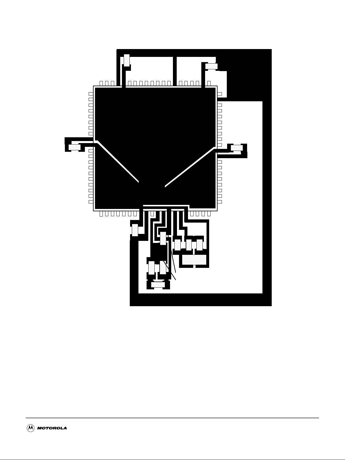
MC9S12DJ64 Device User Guide — V01.17
Figure 22-2 Recommended PCB Layout for 80QFP Colpitts Oscillator
VDDX
C6
VSSX
VDD1
C1
VSS1
VREGEN
VSSA
C3
VDDA
VSS2
C2
VDD2
VSSR
VDDR
C4
C9
R1
C5
C10
C8
C11
VSSPLL
VDDPLL
C7
Q1
81
Page 82

MC9S12DJ64 Device User Guide — V01.17
Figure 22-3 Recommended PCB Layout for 112LQFP Pierce Oscillator
C1
VDD1
VSS1
VDDX
C6
VSSX
VREGEN
VSSA
C3
VDDA
VSS2
C2
VDD2
VSSR
VDDR
VDDPLL
C4
C9
R1
C5
C10
C8
R2
Q1
R3
VSSPLL
C7
82
Page 83

MC9S12DJ64 Device User Guide — V01.17
Figure 22-4 Recommended PCB Layout for 80QFP Pierce Oscillator
VDDX
C6
VSSX
VDD1
C1
VSS1
VREGEN
VSSA
C3
VDDA
VSS2
C2
VDD2
VSSR
VDDR
C4
C9
R1
C5
C10
R2
Q1
C8
VSSPLL
VDDPLL
VSSPLL
R3
C7
83
Page 84

MC9S12DJ64 Device User Guide — V01.17
84
Page 85

MC9S12DJ64 Device User Guide — V01.17
Appendix A Electrical Characteristics
A.1 General
This introduction is intended to give an overview on several common topics like power supply, current
injection etc.
A.1.1 Parameter Classification
The electrical parameters shown in this supplement are guaranteed by various methods. To give the
customer a better understanding the following classification is used and the parameters are tagged
accordingly in the tables where appropriate.
NOTE:
P:
Those parameters are guaranteed during production testing on each individual device.
C:
Those parameters are achieved by the design characterization by measuring a statistically relevant
sample size across process variations.
T:
Those parameters are achieved by design characterization on a small sample size from typical devices
under typical conditions unless otherwise noted. All values shown in the typical column are within
this category.
D:
Those parameters are derived mainly from simulations.
This classification is shown in the column labeled “C” in the parameter tables
where appropriate.
A.1.2 Power Supply
The MC9S12DJ64 utilizes several pins to supply power to the I/O ports, A/D converter, oscillator, PLL
and internal logic.
The VDDA, VSSA pairsuppliestheA/D converter and the resistor ladder of the internal voltage regulator.
The VDDX, VSSX, VDDR and VSSR pairs supply the I/O pins, VDDR supplies also the internal voltage
regulator.
VDD1, VSS1, VDD2 and VSS2 are the supply pins for the digital logic, VDDPLL, VSSPLL supply the
oscillator and the PLL.
VSS1 and VSS2 are internally connected by metal.
85
Page 86

MC9S12DJ64 Device User Guide — V01.17
VDDA, VDDX, VDDR as well as VSSA, VSSX, VSSR are connected by anti-parallel diodes for ESD
protection.
NOTE:
In the following context VDD5 is used for either VDDA, VDDR and VDDX; VSS5
is used for either VSSA, VSSR and VSSX unless otherwise noted.
IDD5 denotes the sum of the currents flowing into the VDDA, VDDX and VDDR
pins.
VDD is used for VDD1, VDD2 and VDDPLL, VSS is used for VSS1, VSS2 and
VSSPLL.
IDD is used for the sum of the currents flowing into VDD1 and VDD2.
A.1.3 Pins
There are four groups of functional pins.
A.1.3.1 5V I/O pins
Those I/O pins have a nominal level of 5V. This class of pins is comprised of all port I/O pins, the analog
inputs, BKGD and the RESET pins.The internal structure of all those pins is identical, however some of
the functionality may be disabled. E.g. for the analog inputs the output drivers, pull-up and pull-down
resistors are disabled permanently.
A.1.3.2 Analog Reference
This group is made up by the VRH and VRL pins.
A.1.3.3 Oscillator
The pins XFC, EXTAL, XTAL dedicated to the oscillator have a nominal 2.5V level. They are supplied
by VDDPLL.
A.1.3.4 TEST
This pin is used for production testing only.
A.1.3.5 VREGEN
This pin is used to enable the on chip voltage regulator.
A.1.4 Current Injection
Power supply must maintain regulation within operating V
operating maximum current conditions. If positive injection current (V
injection current may flowoutofVDD5and could result in external power supply going out of regulation.
Ensure external VDD5 load will shunt current greater than maximum injection current. This will be the
greatest risk when the MCU is not consuming power; e.g. if no system clock is present, or if clock rate is
very low which would reduce overall power consumption.
or VDD range during instantaneous and
DD5
in
>V
) is greater than I
DD5
DD5
, the
86
Page 87

MC9S12DJ64 Device User Guide — V01.17
A.1.5 Absolute Maximum Ratings
Absolute maximum ratings are stress ratings only. A functional operation under or outside those maxima
is not guaranteed. Stress beyond those limits may affect the reliability or cause permanent damage of the
device.
This device contains circuitry protecting against damage due to high static voltage or electrical fields;
however, it is advised that normal precautions be taken to avoid application of any voltages higher than
maximum-rated voltages to this high-impedance circuit. Reliability of operation is enhanced if unused
inputs are tied to an appropriate logic voltage level (e.g., either V
SS5
or V
DD5
).
Table A-1 Absolute Maximum Ratings
1
Num Rating Symbol Min Max Unit
1 I/O, Regulator and Analog Supply Voltage
2
Digital Logic Supply Voltage
3
PLL Supply Voltage
2
2
4 Voltage difference VDDX to VDDR and VDDA
5 Voltage difference VSSX to VSSR and VSSA
6 Digital I/O Input Voltage
7 Analog Reference
8 XFC, EXTAL, XTAL inputs
9 TEST input
Instantaneous Maximum Current
10
Single pin limit for all digital I/O pins
Instantaneous Maximum Current
11
Single pin limit for XFC, EXTAL, XTAL
Instantaneous Maximum Current
12
Single pin limit for TEST
5
3
4
13 Storage Temperature Range
NOTES:
1. Beyond absolute maximum ratings device might be damaged.
2. The device contains an internal voltage regulator to generatethe logic and PLL supply out of the I/O supply.
The absolute maximum ratings apply when the device is powered from an external source.
3. All digital I/O pins are internally clamped to V
4. Those pins are internally clamped to V
5. This pin is clamped low to V
SSR
SSPLL
, but not clamped high. This pin must be tied low in applications.
and V
SSX
and V
DDX
DDPLL
V
DD5
V
DD
V
DDPLL
∆
VDDX
∆
VSSX
V
IN
V
RH,VRL
V
ILV
V
TEST
I
D
I
DL
I
DT
T
stg
, V
and V
SSR
.
-0.3 6.0 V
-0.3 3.0 V
-0.3 3.0 V
-0.3 0.3 V
-0.3 0.3 V
-0.3 6.0 V
-0.3 6.0 V
-0.3 3.0 V
-0.3 10.0 V
-25 +25 mA
-25 +25 mA
-0.25 0 mA
– 65 155 °C
DDR
or V
SSA
and V
DDA
.
87
Page 88

MC9S12DJ64 Device User Guide — V01.17
A.1.6 ESD Protection and Latch-up Immunity
All ESD testing is in conformity with CDF-AEC-Q100 Stress test qualification for Automotive Grade
Integrated Circuits. During the device qualification ESD stresses were performed for the Human Body
Model (HBM), the Machine Model (MM) and the Charge Device Model.
A device will be defined as a failure if after exposure to ESD pulses the device no longer meets the device
specification. Complete DC parametric and functional testing is performed per the applicable device
specification at room temperature followed by hot temperature, unless specified otherwise in the device
specification.
Table A-2 ESD and Latch-up Test Conditions
Model Description Symbol Value Unit
Series Resistance R1 1500 Ohm
Storage Capacitance C 100 pF
Human Body
Number of Pulse per pin
positive
negative
Series Resistance R1 0 Ohm
-
1
1
Storage Capacitance C 200 pF
Machine
Latch-up
Number of Pulse per pin
positive
negative
Minimum input voltage limit -2.5 V
Maximum input voltage limit 7.5 V
-
3
3
Table A-3 ESD and Latch-Up Protection Characteristics
Num C Rating Symbol Min Max Unit
1 T Human Body Model (HBM)
2 T Machine Model (MM)
3 T Charge Device Model (CDM)
Latch-up Current at TA = 125°C
4T
5T
positive
negative
Latch-up Current at T
positive
negative
= 27°C
A
V
V
V
HBM
MM
CDM
I
LAT
I
LAT
2000 - V
200 - V
500 - V
+100
-100
+200
-200
-mA
-mA
A.1.7 Operating Conditions
This chapter describes the operating conditions of the device. Unless otherwise noted those conditions
apply to all the following data.
88
Page 89

MC9S12DJ64 Device User Guide — V01.17
NOTE:
Please refer to the temperature rating of the device (C, V, M) with regards to the
ambient temperature T
and the junction temperature TJ. For power dissipation
A
calculations refer to Section A.1.8 Power Dissipation and Thermal
Characteristics.
Table A-4 Operating Conditions
Rating Symbol Min Typ Max Unit
I/O, Regulator and Analog Supply Voltage
Digital Logic Supply Voltage
PLL Supply Voltage
Voltage Difference VDDX to VDDR and VDDA
Voltage Difference VSSX to VSSR and VSSA
Oscillator
Bus Frequency
MC9S12DJ64C
Operating Ambient Temperature Range
MC9S12DJ64V
1
Operating Junction Temperature Range
1
V
DD5
V
DD
V
DDPLL
∆
VDDX
∆
VSSX
f
osc
f
bus
T
J
3
T
A
4.5 5 5.25 V
2.35 2.5 2.75 V
2.35 2.5 2.75 V
-0.1 0 0.1 V
-0.1 0 0.1 V
0.5 - 16 MHz
2
0.25
-40 - 100 °C
-40 27 85 °C
- 25 MHz
Operating Junction Temperature Range
Operating Ambient Temperature Range
MC9S12DJ64M
Operating Junction Temperature Range
Operating Ambient Temperature Range
NOTES:
1. The device contains an internal voltage regulator to generate the logic and PLL supply out of the I/O supply. The
given operating rangeapplies when this regulator isdisabled and the device ispowered from an external source.
2. Some blocks e.g. ATD (conversion) and NVMs (program/erase) require higher bus frequencies for proper operation.
3. Please refer to Section A.1.8 Power Dissipation and Thermal Characteristics for more details about the relation between ambient temperature T
and device junction temperature TJ.
A
T
J
3
T
A
T
J
3
T
A
-40 - 120 °C
-40 27 105 °C
-40 - 140 °C
-40 27 125 °C
A.1.8 Power Dissipation and Thermal Characteristics
Power dissipation and thermal characteristics are closely related. The user must assure that the maximum
operating junction temperature is not exceeded. The average chip-junction temperature (T
obtained from:
T
T
J
A
P
D
ΘJA•()+=
)in°C can be
J
T
Junction Temperature, [°C]=
J
89
Page 90

MC9S12DJ64 Device User Guide — V01.17
T
P
Θ
The total power dissipation can be calculated from:
P
Two cases with internal voltage regulator enabled and disabled must be considered:
Ambient Temperature, [°C]=
A
Total Chip Power Dissipation, [W]=
D
JA
INT
1. Internal Voltage Regulator disabled
Package Thermal Resistance, [°C/W]=
Chip Internal Power Dissipation, [W]=
P
INT
I
⋅ I
DDVDD
P
P
IO
P
D
INT
DDPLLVDDPLL
R
∑
DSON
i
PIO+=
⋅ I
⋅=
+V
2
I
IO
i
DDA
⋅+=
DDA
P
is the sum of all output currents on I/O ports associated with VDDX and VDDR.
IO
For R
respectively
2. Internal voltage regulator enabled
is the current shown in Table A-7 and not the overall current flowing into VDDR, which
I
DDR
additionally contains the current flowing into the external loads with output high.
PIO is the sum of all output currents on I/O ports associated with VDDX and VDDR.
DSON
is valid:
R
DSON
R
DSON
P
INT
V
OL
------------ for outputs driven low;=
I
OL
P
V
------------------------------------ for outputs driven high;=
IO
–
DD5VOH
I
OH
I
DDRVDDR
⋅ I
∑
i
R
DSON
⋅+=
DDAVDDA
2
I
⋅=
IO
i
90
Page 91
MC9S12DJ64 Device User Guide — V01.17
Table A-5 Thermal Package Characteristics
1
Num C Rating Symbol Min Typ Max Unit
1T
2T
Thermal Resistance LQFP112, single sided PCB
Thermal Resistance LQFP112, double sided PCB
with 2 internal planes
3
3 T Junction to Board LQFP112
4 T Junction to Case LQFP112
5 T Junction to Package Top LQFP112
6 T Thermal Resistance QFP 80, single sided PCB
7T
Thermal Resistance QFP 80, doublesided PCB with
2 internal planes
8 T Junction to Board QFP80
9 T Junction to Case QFP80
10 T Junction to Package Top QFP80
2
θ
JA
θ
JA
θ
JB
θ
JC
Ψ
JT
θ
JA
θ
JA
θ
JB
θ
JC
Ψ
JT
NOTES:
1. The values for thermal resistance are achieved by package simulations
2. PC Board according to EIA/JEDEC Standard 51-3
3. PC Board according to EIA/JEDEC Standard 51-7
––54
––41
––31
––11
––2
––51
––41
––27
––14
––3
o
C/W
o
C/W
o
C/W
o
C/W
o
C/W
o
C/W
o
C/W
o
C/W
o
C/W
o
C/W
A.1.9 I/O Characteristics
This section describes the characteristics of all 5V I/O pins. All parameters are not always applicable, e.g.
not all pins feature pull up/down resistances.
91
Page 92

MC9S12DJ64 Device User Guide — V01.17
Table A-6 5V I/O Characteristics
Conditions are shown in Table A-4 unless otherwise noted
Num C Rating Symbol Min Typ Max Unit
1 P Input High Voltage
2 P Input Low Voltage
3 C Input Hysteresis
Input Leakage Current (pins in high impedance input
4P
mode)
V
= V
in
DD5
or V
SS5
Output High Voltage (pins in output mode)
5P
Partial Drive IOH= –2mA
Full Drive IOH= –10mA
Output Low Voltage (pins in output mode)
6P
Partial Drive IOL= +2mA
Full Drive IOL= +10mA
7P
8C
9P
10 C
Internal Pull Up Device Current,
tested at V
Max.
IL
Internal Pull Up Device Current,
tested at V
IH
Min.
Internal Pull Down Device Current,
tested at V
IH
Min.
Internal Pull Down Device Current,
tested at V
Max.
IL
11 D Input Capacitance
1
12 T
Injection current
Single Pin limit
Total Device Limit. Sum of all injected currents
13 P
14 P
Port H, J, P Interrupt Input Pulse filtered
Port H, J, P Interrupt Input Pulse passed
2
2
NOTES:
1. Refer to Section A.1.4 Current Injection, for more details
2. Parameter only applies in STOP or Pseudo STOP mode.
V
V
V
V
V
I
I
PUH
I
PDH
I
C
I
I
t
t
IH
IL
HYS
I
in
OH
OL
PUL
PDL
in
ICS
ICP
pign
pval
0.65*V
V
SS5
DD5
- 0.3
-
-
V
DD5
0.35*V
+ 0.3
DD5
250 mV
–1 - 1 µA
V
DD5
– 0.8
--V
- - 0.8 V
- - –130 µA
-10 - - µA
- - 130 µA
10 - - µA
6-pF
-2.5
-25
- 2.5
25
3 µs
10 µs
V
V
mA
A.1.10 Supply Currents
This section describes the current consumption characteristics of the device as well as the conditions for
the measurements.
92
Page 93

MC9S12DJ64 Device User Guide — V01.17
A.1.10.1 Measurement Conditions
All measurements are without output loads. Unless otherwise noted the currents are measured in single
chip mode, internal voltage regulator enabled and at 25MHz bus frequency using a 4MHz oscillator in
Colpitts mode. Production testing is performed using a square wave signal at the EXTAL input.
A.1.10.2 Additional Remarks
In expanded modesthecurrents flowing in the system are highly dependentonthe load at the address, data
and control signals as well as on the duty cycle of those signals. No generally applicable numbers can be
given. A very good estimate is to take the single chip currents and add the currents due to the external
loads.
Table A-7 Supply Current Characteristics
Conditions are shown in Table A-4 unless otherwise noted
Num C Rating Symbol Min Typ Max Unit
1P
2P
3
4
5
Run supply currents
Wait Supply current
P
Pseudo Stop Current (RTI and COP disabled)
C
P
C
C
P
C
P
C
P
Pseudo Stop Current (RTI and COP enabled)
C
C
C
C
C
C
C
Stop Current
C
P
C
C
P
C
P
C
P
Single Chip, Internal regulator enabled
All modules enabled, PLL on
only RTI enabled
1, 2
-40°C
27°C
70°C
85°C
"C" Temp Option 100°C
105°C
"V" Temp Option 120°C
125°C
"M" Temp Option 140°C
1, 2
-40°C
27°C
70°C
85°C
105°C
125°C
140°C
2
-40°C
27°C
70°C
85°C
"C" Temp Option 100°C
105°C
"V" Temp Option 120°C
125°C
"M" Temp Option 140°C
I
DD5
I
DDW
1
370
400
450
I
DDPS
I
DDPS
I
DDS
550
600
650
800
850
1200
570
600
650
750
850
1200
1500
12
25
100
130
160
200
350
400
600
50
30
5
500
1600
2100
5000
100
1200
1700
5000
mA
mA
µA
µA
µA
93
Page 94

MC9S12DJ64 Device User Guide — V01.17
NOTES:
1. PLL off
2. At those low power dissipation levels T
= TA can be assumed
J
94
Page 95
MC9S12DJ64 Device User Guide — V01.17
A.2 ATD Characteristics
This section describes the characteristics of the analog to digital converter.
A.2.1 ATD Operating Characteristics
The Table A-8 shows conditions under which the ATD operates.
The following constraints exist to obtain full-scale, full range results:
V
≤ VRL≤ VIN≤ VRH≤ V
SSA
beyond the power supply levels that it ties to. If the input level goes outside of this range it will effectively
be clipped.
Table A-8 ATD Operating Characteristics
Conditions are shown in Table A-4 unless otherwise noted
Num C Rating Symbol Min Typ Max Unit
Reference Potential
1D
2C
3 D ATD Clock Frequency
4D
5D
6D
7 P Reference Supply current 2 ATD blocks on
8 P Reference Supply current 1 ATD block on
NOTES:
1. Full accuracy is not guaranteed when differential voltage is less than 4.50V
2. The minimumtime assumes a final sample periodof 2 ATD clocks cycles whilethe maximum time assumes a finalsample
Differential Reference Voltage
ATD 10-Bit Conversion Period
Conv, Time at 2.0MHz ATD Clock f
ATD 8-Bit Conversion Period
Conv, Time at 2.0MHz ATD Clock f
Recovery Time (V
period of 16 ATD clocks.
=5.0 Volts)
DDA
. This constraint exists since the sample buffer amplifier can not drive
DDA
Low
High
1
Clock Cycles
ATDCLK
Clock Cycles
ATDCLK
2
2
V
RL
V
RH
VRH-V
f
ATDCLK
N
CONV10
T
CONV10
N
CONV8
T
CONV8
t
REC
I
REF
I
REF
RL
V
V
DDA
SSA
/2
V
DDA
V
DDA
/2
4.50 5.00 5.25 V
0.5 2.0 MHz
14
7
12
6
28
14
26
13
20 µs
0.750 mA
0.375 mA
V
V
Cycles
µs
Cycles
µs
A.2.2 Factors influencing accuracy
Three factors - source resistance, source capacitance and current injection - have an influence on the
accuracy of the ATD.
A.2.2.1 Source Resistance:
Due to the input pin leakage current as specified in Table A-6 in conjunction with the source resistance
there will be a voltage drop from the signal source to the ATD input. The maximum source resistance R
S
95
Page 96

MC9S12DJ64 Device User Guide — V01.17
specifies results in an error of less than 1/2 LSB (2.5mV) at the maximum leakage current. If device or
operatingconditionsare less thanworstcase or leakage-inducederror is acceptable,largervalues of source
resistance is allowed.
A.2.2.2 Source Capacitance
When sampling an additional internal capacitor is switched to the input. This can cause a voltage drop due
to charge sharing with the external and the pin capacitance. For a maximum sampling error of the input
voltage ≤ 1LSB, then the external filter capacitor, C
≥ 1024 * (C
f
INS
- C
INN
).
A.2.2.3 Current Injection
There are two cases to consider.
1. A current is injected into the channel being converted. The channel being stressed has conversion
values of$3FF($FF in 8-bit mode) for analoginputsgreater than V
unless the current is higher than specified as disruptive condition.
V
RL
and $000forvalues less than
RH
2. Current is injected into pins in the neighborhood of the channel being converted. A portion of this
current is picked up by the channel (coupling ratio K), This additional current impacts the accuracy
of the conversion depending on the source resistance.
The additional input voltage error on the converted channel can be calculated as V
I
INJ
, with I
being the sum of the currents injected into the two pins adjacent to the converted
INJ
=K*RS*
ERR
channel.
Table A-9 ATD Electrical Characteristics
Conditions are shown in Table A-4 unless otherwise noted
Num C Rating Symbol Min Typ Max Unit
1 C Max input Source Resistance
Total Input Capacitance
2T
3 C Disruptive Analog Input Current
4 C Coupling Ratio positive current injection
5 C Coupling Ratio negative current injection
Non Sampling
Sampling
R
S
C
INN
C
INS
I
NA
K
p
K
n
--1KΩ
10
22
-2.5 2.5 mA
-4
10
-2
10
pF
A/A
A/A
96
Page 97

MC9S12DJ64 Device User Guide — V01.17
A.2.3 ATD accuracy
Table A-10 specifies the ATD conversion performance excluding any errors due to current injection,
input capacitance and source resistance.
Table A-10 ATD Conversion Performance
Conditions are shown in Table A-4 unless otherwise noted
V
= VRH - VRL = 5.12V. Resulting to one 8 bit count = 20mV and one 10 bit count = 5mV
REF
f
ATDCLK
Num C Rating Symbol Min Typ Max Unit
= 2.0MHz
1 P 10-Bit Resolution LSB 5 mV
2 P 10-Bit Differential Nonlinearity DNL –1 1 Counts
3 P 10-Bit Integral Nonlinearity INL –2.5 ±1.5 2.5 Counts
4P
5 P 8-Bit Resolution LSB 20 mV
6 P 8-Bit Differential Nonlinearity DNL –0.5 0.5 Counts
7 P 8-Bit Integral Nonlinearity INL –1.0 ±0.5 1.0 Counts
8P
10-Bit Absolute Error
8-Bit Absolute Error
1
1
AE -3 ±2.0 3 Counts
AE -1.5 ±1.0 1.5 Counts
NOTES:
1. These values include the quantization error which is inherently 1/2 count for any A/D converter.
For the following definitions see also Figure A-1.
Differential Non-Linearity (DNL) is defined as the difference between two adjacent switching steps.
V
–
V
i
DNL i()
------------------------
i1–
1–=
1LSB
The Integral Non-Linearity (INL) is defined as the sum of all DNLs:
n
INL n() DNL i()
∑
i1=
V
------------------- -
V0–
n
1LSB
n–==
97
Page 98

MC9S12DJ64 Device User Guide — V01.17
DNL
$3FF
$3FE
$3FD
$3FC
$3FB
$3FA
$3F9
$3F8
$3F7
$3F6
$3F5
$3F4
$3F3
V
i-1
LSB
10-Bit Absolute Error Boundary
V
i
8-Bit Absolute Error Boundary
$FF
$FE
$FD
9
8
10-Bit Resolution
7
6
5
4
3
2
1
0
5
10 15 20 25 30 35 40 5085 5090 5095 5100 5105 5110 5115 51205065 5070 5075 50805060
NOTE: Figure A-1
Ideal Transfer Curve
10-Bit Transfer Curve
8-Bit Transfer Curve
45
5055
Figure A-1 ATD Accuracy Definitions
shows only definitions, for specification values refer to
Table A-10
2
8-Bit Resolution
1
Vin
mV
.
98
Page 99

A.3 NVM, Flash and EEPROM
MC9S12DJ64 Device User Guide — V01.17
NOTE:
Unless otherwise noted the abbreviation NVM (Non Volatile Memory) is used for
both Flash and EEPROM.
A.3.1 NVM timing
The time base for all NVM program or erase operations is derived from the oscillator. A minimum
oscillator frequency f
do not have any means to monitor the frequency and will not prevent program or erase operation at
frequencies above or below the specified minimum. Attempting to program or erase the NVM modules at
a lower frequency a full program or erase transition is not assured.
The Flash and EEPROM program and erase operations are timed using a clock derived fromtheoscillator
using the FCLKDIV and ECLKDIV registers respectively. Thefrequency of this clock must be set within
the limits specified as f
The minimum program and erase times shown in Table A-11 are calculated for maximum f
maximum f
A.3.1.1 Single Word Programming
. The maximum times are calculated for minimum f
bus
NVMOSC
NVMOP
is required for performing program or erase operations. The NVM modules
.
and
NVMOP
and a f
of 2MHz.
bus
NVMOP
The programming time for single word programming is dependant on the bus frequency as a well as on
the frequency f
A.3.1.2 Row Programming
This applies onlytothe Flash where up to 32 wordsinarow can be programmed consecutively by keeping
the command pipeline filled. The time to program a consecutive word can be calculated as:
The time to program a whole row is:
Row programming is more than 2 times faster than single word programming.
A.3.1.3 Sector Erase
NVMOP
and can be calculated according to the following formula.
t
swpgm
t
bwpgm
t
brpgm
9
⋅ 25
--------------------f
NVMOP
1
4
⋅ 9
--------------------f
NVMOP
1
t
swpgm
31 t
⋅+=
1
⋅+=
---------f
bus
1
⋅+=
---------f
bus
bwpgm
Erasing a 512 byte Flash sector or a 4 byte EEPROM sector takes:
99
Page 100
MC9S12DJ64 Device User Guide — V01.17
t
era
The setup time can be ignored for this operation.
A.3.1.4 Mass Erase
Erasing a NVM block takes:
4000
⋅≈
--------------------f
NVMOP
1
1
t
mass
The setup time can be ignored for this operation.
A.3.1.5 Blank Check
The time it takes to perform a blank check on the Flash or EEPROM is dependant on the location of the
first non-blank word starting at relative address zero. Ittakes one bus cycle per word to verify plus a setup
of the command.
t
check
Table A-11 NVM Timing Characteristics
20000
location t
⋅≈
--------------------f
NVMOP
cyc
10 t
⋅+⋅≈
cyc
Conditions are shown in Table A-4 unless otherwise noted
Num C Rating Symbol Min Typ Max Unit
1 D External Oscillator Clock
2 D Bus frequency for Programming or Erase Operations
3 D Operating Frequency
4 P Single Word Programming Time
5D
6D
7 P Sector Erase Time
8 P Mass Erase Time
9 D Blank Check Time Flash per block
10 D Blank Check Time EEPROM per block
NOTES:
1. Restrictions for oscillator in crystal mode apply!
2.Minimum Programmingtimes areachieved undermaximum NVMoperating frequencyf
3. Maximum Erase and Programming times are achieved under particular combinations of f
4. Burst Programming operations are not applicable to EEPROM
5. Minimum Erase times are achieved under maximum NVM operating frequency f
6. Minimum time, if first word in the array is not blank
7. Maximum time to complete check on an erased block
Flash Burst Programming consecutive word
Flash Burst Programming Time for 32 Words
f
.
bus
Refer to formulae in Sections A.3.1.1 - A.3.1.4 for guidance.
4
4
f
NVMOSC
f
NVMBUS
f
NVMOP
t
swpgm
t
bwpgm
t
brpgm
t
era
t
mass
t
check
t
check
0.5
1 MHz
150 200 kHz
2
46
2
20.4
2
678.4
5
20
5
100
6
11
6
11
NVMOP
NVMOP
andmaximum busfrequency
and bus frequency f
NVMOP
.
50
74.5
31
1035.5
26.7
133
32778
2058
1
3
MHz
3
3
3
7
µs
µs
3
µs
ms
ms
7
t
cyc
t
cyc
.
bus
100
 Loading...