

Datasheet MC9S08RC8, MC9S08RC16, MC9S08RC32, MC9S08RC60, MC9S08RD8 Datasheet (Freescale)
...
查询MC9S08RC16供应商
MC9S08RC8/16/32/60
MC9S08RD8/16/32/60
MC9S08RE8/16/32/60
MC9S08RG32/60
Data Sheet
HCS08
Microcontrollers
MC9S08RG60/D
Rev 1.10
08/2004
freescale.com


MC9S08RG60 Data Sheet
Covers: MC9S08RC8/16/32/60
MC9S08RD8/16/32/60
MC9S08RE8/16/32/60
MC9S08RG32/60
MC9S08RG60/D
Rev 1.10
08/2004

Revision History
To provide the most up-to-date information, the revision of our documents on the World Wide Web will
be the most current. Your printed copy may be an earlier revision. To verify you have the latest information
available, refer to:
http://freescale.com
The following revision history table summarizes changes contained in this document.
Version
Number
1.07 2/4/2004 Initial external release.
1.08 4/22/2004 Changes to Table C-6 in electricals section.
1.09 7/7/2004
1.10 8/11/2004
Revision
Date
Description of Changes
Added Table C-4; changes to Table C-6; changed to Freescale
format
Removed BRK bit 13 and TXINV, which are not available on this
module version; fixed typo in Figure 13-2; corrected the SPTEF
description in section 12.3
This product contains SuperFlash® technology licensed from SST.
Freescale™ and the Freescale logo are trademarks of Freescale Semiconductor, Inc.
© Freescale Semiconductor, Inc., 2004. All rights reserved.

SoC Guide — MC9S08RG60/D Rev 1.10
List of Chapters
Chapter 1 Introduction . . . . . . . . . . . . . . . . . . . . . . . . . . . . . . . . . . . . . . . . . . .15
Chapter 2 Pins and Connections . . . . . . . . . . . . . . . . . . . . . . . . . . . . . . . . . . .19
Chapter 3 Modes of Operation . . . . . . . . . . . . . . . . . . . . . . . . . . . . . . . . . . . . .29
Chapter 4 Memory . . . . . . . . . . . . . . . . . . . . . . . . . . . . . . . . . . . . . . . . . . . . . . .35
Chapter 5 Resets, Interrupts, and System Configuration . . . . . . . . . . . . . . .57
Chapter 6 Central Processor Unit (CPU) . . . . . . . . . . . . . . . . . . . . . . . . . . . . .73
Chapter 7 Carrier Modulator Timer (CMT) Module . . . . . . . . . . . . . . . . . . . . .93
Chapter 8 Parallel Input/Output . . . . . . . . . . . . . . . . . . . . . . . . . . . . . . . . . . . 111
Chapter 9 Keyboard Interrupt (KBI) Module . . . . . . . . . . . . . . . . . . . . . . . . .121
Chapter 10 Timer/PWM Module (TPM) Module . . . . . . . . . . . . . . . . . . . . . . .127
Chapter 11 Serial Communications Interface (SCI) Module . . . . . . . . . . . .143
Chapter 12 Serial Peripheral Interface (SPI) Module . . . . . . . . . . . . . . . . . .161
Chapter 13 Analog Comparator (ACMP) Module . . . . . . . . . . . . . . . . . . . . .177
Chapter 14 Development Support . . . . . . . . . . . . . . . . . . . . . . . . . . . . . . . . . 183
Appendix C Electrical Characteristics. . . . . . . . . . . . . . . . . . . . . . . . . . . . . . 207
Appendix D Ordering Information and Mechanical Drawings . . . . . . . . . .223
Freescale Semiconductor
5MC9S08RC/RD/RE/RG

List of Chapters
MC9S08RC/RD/RE/RG6
Freescale Semiconductor

SoC Guide — MC9S08RG60/D Rev 1.10
Contents
Chapter 1 Introduction
1.1 Overview. . . . . . . . . . . . . . . . . . . . . . . . . . . . . . . . . . . . . . . . . . . . . . . . . . . . . . . . . . 15
1.2 Features . . . . . . . . . . . . . . . . . . . . . . . . . . . . . . . . . . . . . . . . . . . . . . . . . . . . . . . . . . 15
1.2.1 Standard Features of the HCS08 Family . . . . . . . . . . . . . . . . . . . . . . . . . . . . . . . 15
1.2.2 Features of MC9S08RC/RD/RE/RG Series of MCUs . . . . . . . . . . . . . . . . . . . . . 15
1.2.3 Devices in the MC9S08RC/RD/RE/RG Series. . . . . . . . . . . . . . . . . . . . . . . . . . . 16
1.3 MCU Block Diagram. . . . . . . . . . . . . . . . . . . . . . . . . . . . . . . . . . . . . . . . . . . . . . . . . 17
1.4 System Clock Distribution. . . . . . . . . . . . . . . . . . . . . . . . . . . . . . . . . . . . . . . . . . . . . 18
Chapter 2 Pins and Connections
2.1 Introduction. . . . . . . . . . . . . . . . . . . . . . . . . . . . . . . . . . . . . . . . . . . . . . . . . . . . . . . . 19
2.2 Device Pin Assignment. . . . . . . . . . . . . . . . . . . . . . . . . . . . . . . . . . . . . . . . . . . . . . . 19
2.3 Recommended System Connections . . . . . . . . . . . . . . . . . . . . . . . . . . . . . . . . . . . . 21
2.3.1 Power . . . . . . . . . . . . . . . . . . . . . . . . . . . . . . . . . . . . . . . . . . . . . . . . . . . . . . . . . . 23
2.3.2 Oscillator . . . . . . . . . . . . . . . . . . . . . . . . . . . . . . . . . . . . . . . . . . . . . . . . . . . . . . . 23
2.3.3 PTD1/RESET . . . . . . . . . . . . . . . . . . . . . . . . . . . . . . . . . . . . . . . . . . . . . . . . . . . . 23
2.3.4 Background/Mode Select (PTD0/BKGD/MS). . . . . . . . . . . . . . . . . . . . . . . . . . . . 24
2.3.5 IRO Pin Description . . . . . . . . . . . . . . . . . . . . . . . . . . . . . . . . . . . . . . . . . . . . . . . 24
2.3.6 General-Purpose I/O and Peripheral Ports . . . . . . . . . . . . . . . . . . . . . . . . . . . . . 24
2.3.7 Signal Properties Summary . . . . . . . . . . . . . . . . . . . . . . . . . . . . . . . . . . . . . . . . . 26
Chapter 3 Modes of Operation
3.1 Introduction. . . . . . . . . . . . . . . . . . . . . . . . . . . . . . . . . . . . . . . . . . . . . . . . . . . . . . . . 29
3.2 Features . . . . . . . . . . . . . . . . . . . . . . . . . . . . . . . . . . . . . . . . . . . . . . . . . . . . . . . . . . 29
3.3 Run Mode. . . . . . . . . . . . . . . . . . . . . . . . . . . . . . . . . . . . . . . . . . . . . . . . . . . . . . . . . 29
3.4 Active Background Mode . . . . . . . . . . . . . . . . . . . . . . . . . . . . . . . . . . . . . . . . . . . . . 29
3.5 Wait Mode . . . . . . . . . . . . . . . . . . . . . . . . . . . . . . . . . . . . . . . . . . . . . . . . . . . . . . . . 30
3.6 Stop Modes . . . . . . . . . . . . . . . . . . . . . . . . . . . . . . . . . . . . . . . . . . . . . . . . . . . . . . . 31
3.6.1 Stop1 Mode . . . . . . . . . . . . . . . . . . . . . . . . . . . . . . . . . . . . . . . . . . . . . . . . . . . . . 31
3.6.2 Stop2 Mode . . . . . . . . . . . . . . . . . . . . . . . . . . . . . . . . . . . . . . . . . . . . . . . . . . . . . 31
3.6.3 Stop3 Mode . . . . . . . . . . . . . . . . . . . . . . . . . . . . . . . . . . . . . . . . . . . . . . . . . . . . . 32
3.6.4 Active BDM Enabled in Stop Mode . . . . . . . . . . . . . . . . . . . . . . . . . . . . . . . . . . . 33
3.6.5 LVD Reset Enabled in Stop Mode . . . . . . . . . . . . . . . . . . . . . . . . . . . . . . . . . . . . 33
3.6.6 On-Chip Peripheral Modules in Stop Mode . . . . . . . . . . . . . . . . . . . . . . . . . . . . . 33
Freescale Semiconductor
7MC9S08RC/RD/RE/RG

Contents
Chapter 4 Memory
4.1 MC9S08RC/RD/RE/RG Memory Map . . . . . . . . . . . . . . . . . . . . . . . . . . . . . . . . . . . 35
4.1.1 Reset and Interrupt Vector Assignments . . . . . . . . . . . . . . . . . . . . . . . . . . . . . . . 36
4.2 Register Addresses and Bit Assignments . . . . . . . . . . . . . . . . . . . . . . . . . . . . . . . . 37
4.3 RAM . . . . . . . . . . . . . . . . . . . . . . . . . . . . . . . . . . . . . . . . . . . . . . . . . . . . . . . . . . . . .41
4.4 FLASH . . . . . . . . . . . . . . . . . . . . . . . . . . . . . . . . . . . . . . . . . . . . . . . . . . . . . . . . . . . 42
4.4.1 Features . . . . . . . . . . . . . . . . . . . . . . . . . . . . . . . . . . . . . . . . . . . . . . . . . . . . . . . . 42
4.4.2 Program and Erase Times . . . . . . . . . . . . . . . . . . . . . . . . . . . . . . . . . . . . . . . . . . 42
4.4.3 Program and Erase Command Execution . . . . . . . . . . . . . . . . . . . . . . . . . . . . . . 43
4.4.4 Burst Program Execution . . . . . . . . . . . . . . . . . . . . . . . . . . . . . . . . . . . . . . . . . . . 45
4.4.5 Access Errors. . . . . . . . . . . . . . . . . . . . . . . . . . . . . . . . . . . . . . . . . . . . . . . . . . . . 47
4.4.6 FLASH Block Protection. . . . . . . . . . . . . . . . . . . . . . . . . . . . . . . . . . . . . . . . . . . . 47
4.4.7 Vector Redirection . . . . . . . . . . . . . . . . . . . . . . . . . . . . . . . . . . . . . . . . . . . . . . . . 48
4.5 Security. . . . . . . . . . . . . . . . . . . . . . . . . . . . . . . . . . . . . . . . . . . . . . . . . . . . . . . . . . .48
4.6 FLASH Registers and Control Bits . . . . . . . . . . . . . . . . . . . . . . . . . . . . . . . . . . . . . . 49
4.6.1 FLASH Clock Divider Register (FCDIV). . . . . . . . . . . . . . . . . . . . . . . . . . . . . . . . 50
4.6.2 FLASH Options Register (FOPT and NVOPT) . . . . . . . . . . . . . . . . . . . . . . . . . . 51
4.6.3 FLASH Configuration Register (FCNFG) . . . . . . . . . . . . . . . . . . . . . . . . . . . . . . . 52
4.6.4 FLASH Protection Register (FPROT and NVPROT) . . . . . . . . . . . . . . . . . . . . . . 52
4.6.5 FLASH Status Register (FSTAT) . . . . . . . . . . . . . . . . . . . . . . . . . . . . . . . . . . . . . 54
4.6.6 FLASH Command Register (FCMD) . . . . . . . . . . . . . . . . . . . . . . . . . . . . . . . . . . 55
Chapter 5 Resets, Interrupts, and System Configuration
5.1 Introduction. . . . . . . . . . . . . . . . . . . . . . . . . . . . . . . . . . . . . . . . . . . . . . . . . . . . . . . . 57
5.2 Features . . . . . . . . . . . . . . . . . . . . . . . . . . . . . . . . . . . . . . . . . . . . . . . . . . . . . . . . . . 57
5.3 MCU Reset. . . . . . . . . . . . . . . . . . . . . . . . . . . . . . . . . . . . . . . . . . . . . . . . . . . . . . . . 58
5.4 Computer Operating Properly (COP) Watchdog . . . . . . . . . . . . . . . . . . . . . . . . . . . 58
5.5 Interrupts . . . . . . . . . . . . . . . . . . . . . . . . . . . . . . . . . . . . . . . . . . . . . . . . . . . . . . . . . 59
5.5.1 Interrupt Stack Frame . . . . . . . . . . . . . . . . . . . . . . . . . . . . . . . . . . . . . . . . . . . . . 60
5.5.2 External Interrupt Request (IRQ) Pin . . . . . . . . . . . . . . . . . . . . . . . . . . . . . . . . . . 61
5.5.3 Interrupt Vectors, Sources, and Local Masks . . . . . . . . . . . . . . . . . . . . . . . . . . . 61
5.6 Low-Voltage Detect (LVD) System. . . . . . . . . . . . . . . . . . . . . . . . . . . . . . . . . . . . . . 62
5.6.1 Power-On Reset Operation . . . . . . . . . . . . . . . . . . . . . . . . . . . . . . . . . . . . . . . . . 63
5.6.2 LVD Reset Operation . . . . . . . . . . . . . . . . . . . . . . . . . . . . . . . . . . . . . . . . . . . . . . 63
5.6.3 LVD Interrupt and Safe State Operation . . . . . . . . . . . . . . . . . . . . . . . . . . . . . . . 63
5.6.4 Low-Voltage Warning (LVW) . . . . . . . . . . . . . . . . . . . . . . . . . . . . . . . . . . . . . . . . 63
MC9S08RC/RD/RE/RG8
Freescale Semiconductor

SoC Guide — MC9S08RG60/D Rev 1.10
5.7 Real-Time Interrupt (RTI) . . . . . . . . . . . . . . . . . . . . . . . . . . . . . . . . . . . . . . . . . . . . . 64
5.8 Reset, Interrupt, and System Control Registers and Control Bits . . . . . . . . . . . . . . 64
5.8.1 Interrupt Pin Request Status and Control Register (IRQSC) . . . . . . . . . . . . . . . . 64
5.8.2 System Reset Status Register (SRS) . . . . . . . . . . . . . . . . . . . . . . . . . . . . . . . . . 65
5.8.3 System Background Debug Force Reset Register (SBDFR). . . . . . . . . . . . . . . . 67
5.8.4 System Options Register (SOPT) . . . . . . . . . . . . . . . . . . . . . . . . . . . . . . . . . . . . 67
5.8.5 System Device Identification Register (SDIDH, SDIDL) . . . . . . . . . . . . . . . . . . . 69
5.8.6 System Real-Time Interrupt Status and Control Register (SRTISC) . . . . . . . . . . 69
5.8.7 System Power Management Status and Control 1 Register (SPMSC1) . . . . . . . 71
5.8.8 System Power Management Status and Control 2 Register (SPMSC2) . . . . . . . 72
Chapter 6 Central Processor Unit (CPU)
6.1 Introduction. . . . . . . . . . . . . . . . . . . . . . . . . . . . . . . . . . . . . . . . . . . . . . . . . . . . . . . . 73
6.2 Features . . . . . . . . . . . . . . . . . . . . . . . . . . . . . . . . . . . . . . . . . . . . . . . . . . . . . . . . . . 74
6.3 Programmer’s Model and CPU Registers . . . . . . . . . . . . . . . . . . . . . . . . . . . . . . . . 74
6.3.1 Accumulator (A) . . . . . . . . . . . . . . . . . . . . . . . . . . . . . . . . . . . . . . . . . . . . . . . . . . 75
6.3.2 Index Register (H:X). . . . . . . . . . . . . . . . . . . . . . . . . . . . . . . . . . . . . . . . . . . . . . . 75
6.3.3 Stack Pointer (SP) . . . . . . . . . . . . . . . . . . . . . . . . . . . . . . . . . . . . . . . . . . . . . . . . 76
6.3.4 Program Counter (PC) . . . . . . . . . . . . . . . . . . . . . . . . . . . . . . . . . . . . . . . . . . . . . 76
6.3.5 Condition Code Register (CCR). . . . . . . . . . . . . . . . . . . . . . . . . . . . . . . . . . . . . . 76
6.4 Addressing Modes . . . . . . . . . . . . . . . . . . . . . . . . . . . . . . . . . . . . . . . . . . . . . . . . . . 78
6.4.1 Inherent Addressing Mode (INH) . . . . . . . . . . . . . . . . . . . . . . . . . . . . . . . . . . . . . 78
6.4.2 Relative Addressing Mode (REL). . . . . . . . . . . . . . . . . . . . . . . . . . . . . . . . . . . . . 78
6.4.3 Immediate Addressing Mode (IMM) . . . . . . . . . . . . . . . . . . . . . . . . . . . . . . . . . . . 78
6.4.4 Direct Addressing Mode (DIR) . . . . . . . . . . . . . . . . . . . . . . . . . . . . . . . . . . . . . . . 78
6.4.5 Extended Addressing Mode (EXT). . . . . . . . . . . . . . . . . . . . . . . . . . . . . . . . . . . . 79
6.4.6 Indexed Addressing Mode . . . . . . . . . . . . . . . . . . . . . . . . . . . . . . . . . . . . . . . . . . 79
6.5 Special Operations . . . . . . . . . . . . . . . . . . . . . . . . . . . . . . . . . . . . . . . . . . . . . . . . . . 80
6.5.1 Reset Sequence. . . . . . . . . . . . . . . . . . . . . . . . . . . . . . . . . . . . . . . . . . . . . . . . . . 80
6.5.2 Interrupt Sequence. . . . . . . . . . . . . . . . . . . . . . . . . . . . . . . . . . . . . . . . . . . . . . . . 80
6.5.3 Wait Mode Operation . . . . . . . . . . . . . . . . . . . . . . . . . . . . . . . . . . . . . . . . . . . . . . 81
6.5.4 Stop Mode Operation . . . . . . . . . . . . . . . . . . . . . . . . . . . . . . . . . . . . . . . . . . . . . . 81
6.5.5 BGND Instruction . . . . . . . . . . . . . . . . . . . . . . . . . . . . . . . . . . . . . . . . . . . . . . . . . 82
6.6 HCS08 Instruction Set Summary . . . . . . . . . . . . . . . . . . . . . . . . . . . . . . . . . . . . . . . 82
Freescale Semiconductor
9MC9S08RC/RD/RE/RG

Contents
Chapter 7 Carrier Modulator Timer (CMT) Module
7.1 Introduction. . . . . . . . . . . . . . . . . . . . . . . . . . . . . . . . . . . . . . . . . . . . . . . . . . . . . . . . 93
7.2 Features . . . . . . . . . . . . . . . . . . . . . . . . . . . . . . . . . . . . . . . . . . . . . . . . . . . . . . . . . . 94
7.3 CMT Block Diagram . . . . . . . . . . . . . . . . . . . . . . . . . . . . . . . . . . . . . . . . . . . . . . . . . 94
7.4 Pin Description . . . . . . . . . . . . . . . . . . . . . . . . . . . . . . . . . . . . . . . . . . . . . . . . . . . . . 95
7.5 Functional Description . . . . . . . . . . . . . . . . . . . . . . . . . . . . . . . . . . . . . . . . . . . . . . . 95
7.5.1 Carrier Generator . . . . . . . . . . . . . . . . . . . . . . . . . . . . . . . . . . . . . . . . . . . . . . . . . 96
7.5.2 Modulator . . . . . . . . . . . . . . . . . . . . . . . . . . . . . . . . . . . . . . . . . . . . . . . . . . . . . . . 98
7.5.3 Extended Space Operation . . . . . . . . . . . . . . . . . . . . . . . . . . . . . . . . . . . . . . . . 101
7.5.4 Transmitter . . . . . . . . . . . . . . . . . . . . . . . . . . . . . . . . . . . . . . . . . . . . . . . . . . . . . 102
7.5.5 CMT Interrupts . . . . . . . . . . . . . . . . . . . . . . . . . . . . . . . . . . . . . . . . . . . . . . . . . . 103
7.5.6 Wait Mode Operation . . . . . . . . . . . . . . . . . . . . . . . . . . . . . . . . . . . . . . . . . . . . . 103
7.5.7 Stop Mode Operation . . . . . . . . . . . . . . . . . . . . . . . . . . . . . . . . . . . . . . . . . . . . . 103
7.5.8 Background Mode Operation . . . . . . . . . . . . . . . . . . . . . . . . . . . . . . . . . . . . . . . 104
7.6 CMT Registers and Control Bits . . . . . . . . . . . . . . . . . . . . . . . . . . . . . . . . . . . . . . . 104
7.6.1 Carrier Generator Data Registers (CMTCGH1, CMTCGL1, CMTCGH2, and CMTCGL2)
104
7.6.2 CMT Output Control Register (CMTOC) . . . . . . . . . . . . . . . . . . . . . . . . . . . . . . 106
7.6.3 CMT Modulator Status and Control Register (CMTMSC) . . . . . . . . . . . . . . . . . 107
7.6.4 CMT Modulator Data Registers (CMTCMD1, CMTCMD2, CMTCMD3, and CMTCMD4)
109
Chapter 8 Parallel Input/Output
8.1 Introduction. . . . . . . . . . . . . . . . . . . . . . . . . . . . . . . . . . . . . . . . . . . . . . . . . . . . . . . 111
8.2 Features . . . . . . . . . . . . . . . . . . . . . . . . . . . . . . . . . . . . . . . . . . . . . . . . . . . . . . . . . 111
8.3 Pin Descriptions . . . . . . . . . . . . . . . . . . . . . . . . . . . . . . . . . . . . . . . . . . . . . . . . . . . 111
8.3.1 Port A . . . . . . . . . . . . . . . . . . . . . . . . . . . . . . . . . . . . . . . . . . . . . . . . . . . . . . . . . 112
8.3.2 Port B . . . . . . . . . . . . . . . . . . . . . . . . . . . . . . . . . . . . . . . . . . . . . . . . . . . . . . . . . 112
8.3.3 Port C . . . . . . . . . . . . . . . . . . . . . . . . . . . . . . . . . . . . . . . . . . . . . . . . . . . . . . . . . 113
8.3.4 Port D . . . . . . . . . . . . . . . . . . . . . . . . . . . . . . . . . . . . . . . . . . . . . . . . . . . . . . . . . 113
8.3.5 Port E . . . . . . . . . . . . . . . . . . . . . . . . . . . . . . . . . . . . . . . . . . . . . . . . . . . . . . . . . 114
8.4 Parallel I/O Controls . . . . . . . . . . . . . . . . . . . . . . . . . . . . . . . . . . . . . . . . . . . . . . . . 114
8.4.1 Data Direction Control . . . . . . . . . . . . . . . . . . . . . . . . . . . . . . . . . . . . . . . . . . . . 114
8.4.2 Internal Pullup Control . . . . . . . . . . . . . . . . . . . . . . . . . . . . . . . . . . . . . . . . . . . . 115
8.5 Stop Modes . . . . . . . . . . . . . . . . . . . . . . . . . . . . . . . . . . . . . . . . . . . . . . . . . . . . . . 115
8.6 Parallel I/O Registers and Control Bits . . . . . . . . . . . . . . . . . . . . . . . . . . . . . . . . . . 115
MC9S08RC/RD/RE/RG10
Freescale Semiconductor

SoC Guide — MC9S08RG60/D Rev 1.10
8.6.1 Port A Registers (PTAD, PTAPE, and PTADD) . . . . . . . . . . . . . . . . . . . . . . . . . 115
8.6.2 Port B Registers (PTBD, PTBPE, and PTBDD) . . . . . . . . . . . . . . . . . . . . . . . . . 117
8.6.3 Port C Registers (PTCD, PTCPE, and PTCDD) . . . . . . . . . . . . . . . . . . . . . . . . 118
8.6.4 Port D Registers (PTDD, PTDPE, and PTDDD) . . . . . . . . . . . . . . . . . . . . . . . . 119
8.6.5 Port E Registers (PTED, PTEPE, and PTEDD) . . . . . . . . . . . . . . . . . . . . . . . . . 120
Chapter 9 Keyboard Interrupt (KBI) Module
9.1 Introduction. . . . . . . . . . . . . . . . . . . . . . . . . . . . . . . . . . . . . . . . . . . . . . . . . . . . . . . 121
9.2 KBI Block Diagram . . . . . . . . . . . . . . . . . . . . . . . . . . . . . . . . . . . . . . . . . . . . . . . . . 123
9.3 Keyboard Interrupt (KBI) Module . . . . . . . . . . . . . . . . . . . . . . . . . . . . . . . . . . . . . . 123
9.3.1 Pin Enables . . . . . . . . . . . . . . . . . . . . . . . . . . . . . . . . . . . . . . . . . . . . . . . . . . . . 123
9.3.2 Edge and Level Sensitivity . . . . . . . . . . . . . . . . . . . . . . . . . . . . . . . . . . . . . . . . . 123
9.3.3 KBI Interrupt Controls. . . . . . . . . . . . . . . . . . . . . . . . . . . . . . . . . . . . . . . . . . . . . 124
9.4 KBI Registers and Control Bits. . . . . . . . . . . . . . . . . . . . . . . . . . . . . . . . . . . . . . . . 124
9.4.1 KBI x Status and Control Register (KBIxSC) . . . . . . . . . . . . . . . . . . . . . . . . . . . 124
9.4.2 KBI x Pin Enable Register (KBIxPE) . . . . . . . . . . . . . . . . . . . . . . . . . . . . . . . . . 126
Chapter 10 Timer/PWM Module (TPM) Module
10.1 Introduction. . . . . . . . . . . . . . . . . . . . . . . . . . . . . . . . . . . . . . . . . . . . . . . . . . . . . . . 127
10.2 Features . . . . . . . . . . . . . . . . . . . . . . . . . . . . . . . . . . . . . . . . . . . . . . . . . . . . . . . . . 127
10.3 TPM Block Diagram . . . . . . . . . . . . . . . . . . . . . . . . . . . . . . . . . . . . . . . . . . . . . . . . 129
10.4 Pin Descriptions . . . . . . . . . . . . . . . . . . . . . . . . . . . . . . . . . . . . . . . . . . . . . . . . . . . 130
10.4.1 External TPM Clock Sources . . . . . . . . . . . . . . . . . . . . . . . . . . . . . . . . . . . . . . . 130
10.4.2 TPM1CHn — TPM1 Channel n I/O Pins . . . . . . . . . . . . . . . . . . . . . . . . . . . . . . 130
10.5 Functional Description . . . . . . . . . . . . . . . . . . . . . . . . . . . . . . . . . . . . . . . . . . . . . . 130
10.5.1 Counter . . . . . . . . . . . . . . . . . . . . . . . . . . . . . . . . . . . . . . . . . . . . . . . . . . . . . . . 131
10.5.2 Channel Mode Selection . . . . . . . . . . . . . . . . . . . . . . . . . . . . . . . . . . . . . . . . . . 132
10.5.3 Center-Aligned PWM Mode . . . . . . . . . . . . . . . . . . . . . . . . . . . . . . . . . . . . . . . . 133
10.6 TPM Interrupts . . . . . . . . . . . . . . . . . . . . . . . . . . . . . . . . . . . . . . . . . . . . . . . . . . . . 135
10.6.1 Clearing Timer Interrupt Flags . . . . . . . . . . . . . . . . . . . . . . . . . . . . . . . . . . . . . . 135
10.6.2 Timer Overflow Interrupt Description . . . . . . . . . . . . . . . . . . . . . . . . . . . . . . . . . 135
10.6.3 Channel Event Interrupt Description . . . . . . . . . . . . . . . . . . . . . . . . . . . . . . . . . 135
10.6.4 PWM End-of-Duty-Cycle Events . . . . . . . . . . . . . . . . . . . . . . . . . . . . . . . . . . . . 136
10.7 TPM Registers and Control Bits . . . . . . . . . . . . . . . . . . . . . . . . . . . . . . . . . . . . . . . 136
10.7.1 Timer x Status and Control Register (TPM1SC) . . . . . . . . . . . . . . . . . . . . . . . . 136
10.7.2 Timer x Counter Registers (TPM1CNTH:TPM1CNTL) . . . . . . . . . . . . . . . . . . . 138
Freescale Semiconductor
11MC9S08RC/RD/RE/RG

Contents
10.7.3 Timer x Counter Modulo Registers (TPM1MODH:TPM1MODL) . . . . . . . . . . . . 139
10.7.4 Timer x Channel n Status and Control Register (TPM1CnSC) . . . . . . . . . . . . . 140
10.7.5 Timer x Channel Value Registers (TPM1CnVH:TPM1CnVL) . . . . . . . . . . . . . . 142
Chapter 11 Serial Communications Interface (SCI) Module
11.1 Features . . . . . . . . . . . . . . . . . . . . . . . . . . . . . . . . . . . . . . . . . . . . . . . . . . . . . . . . . 144
11.2 SCI System Description . . . . . . . . . . . . . . . . . . . . . . . . . . . . . . . . . . . . . . . . . . . . . 144
11.3 Baud Rate Generation . . . . . . . . . . . . . . . . . . . . . . . . . . . . . . . . . . . . . . . . . . . . . . 144
11.4 Transmitter Functional Description. . . . . . . . . . . . . . . . . . . . . . . . . . . . . . . . . . . . . 145
11.4.1 Transmitter Block Diagram. . . . . . . . . . . . . . . . . . . . . . . . . . . . . . . . . . . . . . . . . 145
11.4.2 Send Break and Queued Idle. . . . . . . . . . . . . . . . . . . . . . . . . . . . . . . . . . . . . . . 147
11.5 Receiver Functional Description. . . . . . . . . . . . . . . . . . . . . . . . . . . . . . . . . . . . . . . 147
11.5.1 Receiver Block Diagram. . . . . . . . . . . . . . . . . . . . . . . . . . . . . . . . . . . . . . . . . . . 147
11.5.2 Data Sampling Technique . . . . . . . . . . . . . . . . . . . . . . . . . . . . . . . . . . . . . . . . . 149
11.5.3 Receiver Wakeup Operation . . . . . . . . . . . . . . . . . . . . . . . . . . . . . . . . . . . . . . . 150
11.6 Interrupts and Status Flags . . . . . . . . . . . . . . . . . . . . . . . . . . . . . . . . . . . . . . . . . . 150
11.7 Additional SCI Functions . . . . . . . . . . . . . . . . . . . . . . . . . . . . . . . . . . . . . . . . . . . . 151
11.7.1 8- and 9-Bit Data Modes . . . . . . . . . . . . . . . . . . . . . . . . . . . . . . . . . . . . . . . . . . 151
11.8 Stop Mode Operation . . . . . . . . . . . . . . . . . . . . . . . . . . . . . . . . . . . . . . . . . . . . . . . 152
11.8.1 Loop Mode . . . . . . . . . . . . . . . . . . . . . . . . . . . . . . . . . . . . . . . . . . . . . . . . . . . . . 152
11.8.2 Single-Wire Operation . . . . . . . . . . . . . . . . . . . . . . . . . . . . . . . . . . . . . . . . . . . . 152
11.9 SCI Registers and Control Bits. . . . . . . . . . . . . . . . . . . . . . . . . . . . . . . . . . . . . . . . 152
11.9.1 SCI Baud Rate Registers (SCI1BDH, SCI1BHL) . . . . . . . . . . . . . . . . . . . . . . . . 153
11.9.2 SCI Control Register 1 (SCI1C1) . . . . . . . . . . . . . . . . . . . . . . . . . . . . . . . . . . . . 153
11.9.3 SCI Control Register 2 (SCI1C2) . . . . . . . . . . . . . . . . . . . . . . . . . . . . . . . . . . . . 155
11.9.4 SCI Status Register 1 (SCI1S1). . . . . . . . . . . . . . . . . . . . . . . . . . . . . . . . . . . . . 156
11.9.5 SCI Status Register 2 (SCI1S2). . . . . . . . . . . . . . . . . . . . . . . . . . . . . . . . . . . . . 158
11.9.6 SCI Control Register 3 (SCI1C3) . . . . . . . . . . . . . . . . . . . . . . . . . . . . . . . . . . . . 159
11.9.7 SCI Data Register (SCI1D) . . . . . . . . . . . . . . . . . . . . . . . . . . . . . . . . . . . . . . . . 160
Chapter 12 Serial Peripheral Interface (SPI) Module
12.1 Features . . . . . . . . . . . . . . . . . . . . . . . . . . . . . . . . . . . . . . . . . . . . . . . . . . . . . . . . . 162
12.2 Block Diagrams . . . . . . . . . . . . . . . . . . . . . . . . . . . . . . . . . . . . . . . . . . . . . . . . . . . 162
12.2.1 SPI System Block Diagram . . . . . . . . . . . . . . . . . . . . . . . . . . . . . . . . . . . . . . . . 162
12.2.2 SPI Module Block Diagram . . . . . . . . . . . . . . . . . . . . . . . . . . . . . . . . . . . . . . . . 163
12.2.3 SPI Baud Rate Generation. . . . . . . . . . . . . . . . . . . . . . . . . . . . . . . . . . . . . . . . . 165
MC9S08RC/RD/RE/RG12
Freescale Semiconductor

SoC Guide — MC9S08RG60/D Rev 1.10
12.3 Functional Description . . . . . . . . . . . . . . . . . . . . . . . . . . . . . . . . . . . . . . . . . . . . . . 165
12.3.1 SPI Clock Formats . . . . . . . . . . . . . . . . . . . . . . . . . . . . . . . . . . . . . . . . . . . . . . . 166
12.3.2 SPI Pin Controls. . . . . . . . . . . . . . . . . . . . . . . . . . . . . . . . . . . . . . . . . . . . . . . . . 168
12.3.3 SPI Interrupts . . . . . . . . . . . . . . . . . . . . . . . . . . . . . . . . . . . . . . . . . . . . . . . . . . . 169
12.3.4 Mode Fault Detection . . . . . . . . . . . . . . . . . . . . . . . . . . . . . . . . . . . . . . . . . . . . . 169
12.4 SPI Registers and Control Bits. . . . . . . . . . . . . . . . . . . . . . . . . . . . . . . . . . . . . . . . 170
12.4.1 SPI Control Register 1 (SPI1C1) . . . . . . . . . . . . . . . . . . . . . . . . . . . . . . . . . . . . 170
12.4.2 SPI Control Register 2 (SPI1C2) . . . . . . . . . . . . . . . . . . . . . . . . . . . . . . . . . . . . 172
12.4.3 SPI Baud Rate Register (SPI1BR). . . . . . . . . . . . . . . . . . . . . . . . . . . . . . . . . . . 173
12.4.4 SPI Status Register (SPI1S) . . . . . . . . . . . . . . . . . . . . . . . . . . . . . . . . . . . . . . . 174
12.4.5 SPI Data Register (SPI1D). . . . . . . . . . . . . . . . . . . . . . . . . . . . . . . . . . . . . . . . . 175
Chapter 13 Analog Comparator (ACMP) Module
13.1 Features . . . . . . . . . . . . . . . . . . . . . . . . . . . . . . . . . . . . . . . . . . . . . . . . . . . . . . . . . 178
13.2 Block Diagram . . . . . . . . . . . . . . . . . . . . . . . . . . . . . . . . . . . . . . . . . . . . . . . . . . . . 178
13.3 Pin Description . . . . . . . . . . . . . . . . . . . . . . . . . . . . . . . . . . . . . . . . . . . . . . . . . . . . 178
13.4 Functional Description . . . . . . . . . . . . . . . . . . . . . . . . . . . . . . . . . . . . . . . . . . . . . . 179
13.4.1 Interrupts . . . . . . . . . . . . . . . . . . . . . . . . . . . . . . . . . . . . . . . . . . . . . . . . . . . . . . 179
13.4.2 Wait Mode Operation . . . . . . . . . . . . . . . . . . . . . . . . . . . . . . . . . . . . . . . . . . . . . 179
13.4.3 Stop Mode Operation . . . . . . . . . . . . . . . . . . . . . . . . . . . . . . . . . . . . . . . . . . . . . 179
13.4.4 Background Mode Operation . . . . . . . . . . . . . . . . . . . . . . . . . . . . . . . . . . . . . . . 179
13.5 ACMP Status and Control Register (ACMP1SC) . . . . . . . . . . . . . . . . . . . . . . . . . . 180
Chapter 14 Development Support
14.1 Introduction. . . . . . . . . . . . . . . . . . . . . . . . . . . . . . . . . . . . . . . . . . . . . . . . . . . . . . . 183
14.2 Features . . . . . . . . . . . . . . . . . . . . . . . . . . . . . . . . . . . . . . . . . . . . . . . . . . . . . . . . . 184
14.3 Background Debug Controller (BDC) . . . . . . . . . . . . . . . . . . . . . . . . . . . . . . . . . . . 185
14.3.1 BKGD Pin Description . . . . . . . . . . . . . . . . . . . . . . . . . . . . . . . . . . . . . . . . . . . . 185
14.3.2 Communication Details . . . . . . . . . . . . . . . . . . . . . . . . . . . . . . . . . . . . . . . . . . . 186
14.3.3 BDC Commands . . . . . . . . . . . . . . . . . . . . . . . . . . . . . . . . . . . . . . . . . . . . . . . . 190
14.3.4 BDC Hardware Breakpoint. . . . . . . . . . . . . . . . . . . . . . . . . . . . . . . . . . . . . . . . . 192
14.4 On-Chip Debug System (DBG) . . . . . . . . . . . . . . . . . . . . . . . . . . . . . . . . . . . . . . . 193
14.4.1 Comparators A and B. . . . . . . . . . . . . . . . . . . . . . . . . . . . . . . . . . . . . . . . . . . . . 193
14.4.2 Bus Capture Information and FIFO Operation . . . . . . . . . . . . . . . . . . . . . . . . . . 194
14.4.3 Change-of-Flow Information. . . . . . . . . . . . . . . . . . . . . . . . . . . . . . . . . . . . . . . . 194
14.4.4 Tag vs. Force Breakpoints and Triggers . . . . . . . . . . . . . . . . . . . . . . . . . . . . . . 195
Freescale Semiconductor
13MC9S08RC/RD/RE/RG

Contents
14.4.5 Trigger Modes . . . . . . . . . . . . . . . . . . . . . . . . . . . . . . . . . . . . . . . . . . . . . . . . . . 195
14.4.6 Hardware Breakpoints . . . . . . . . . . . . . . . . . . . . . . . . . . . . . . . . . . . . . . . . . . . . 197
14.5 Registers and Control Bits . . . . . . . . . . . . . . . . . . . . . . . . . . . . . . . . . . . . . . . . . . . 197
14.5.1 BDC Registers and Control Bits. . . . . . . . . . . . . . . . . . . . . . . . . . . . . . . . . . . . . 197
14.5.2 System Background Debug Force Reset Register (SBDFR). . . . . . . . . . . . . . . 199
14.5.3 DBG Registers and Control Bits. . . . . . . . . . . . . . . . . . . . . . . . . . . . . . . . . . . . . 200
Appendix C Electrical Characteristics
C.1 Introduction. . . . . . . . . . . . . . . . . . . . . . . . . . . . . . . . . . . . . . . . . . . . . . . . . . . . . . . 207
C.2 Absolute Maximum Ratings . . . . . . . . . . . . . . . . . . . . . . . . . . . . . . . . . . . . . . . . . . 207
C.3 Thermal Characteristics . . . . . . . . . . . . . . . . . . . . . . . . . . . . . . . . . . . . . . . . . . . . . 208
C.4 Electrostatic Discharge (ESD) Protection Characteristics . . . . . . . . . . . . . . . . . . . 209
C.5 DC Characteristics . . . . . . . . . . . . . . . . . . . . . . . . . . . . . . . . . . . . . . . . . . . . . . . . . 209
C.6 Supply Current Characteristics. . . . . . . . . . . . . . . . . . . . . . . . . . . . . . . . . . . . . . . . 213
C.7 Analog Comparator (ACMP) Electricals . . . . . . . . . . . . . . . . . . . . . . . . . . . . . . . . . 214
C.8 Oscillator Characteristics . . . . . . . . . . . . . . . . . . . . . . . . . . . . . . . . . . . . . . . . . . . . 214
C.9 AC Characteristics . . . . . . . . . . . . . . . . . . . . . . . . . . . . . . . . . . . . . . . . . . . . . . . . . 215
C.9.1 Control Timing . . . . . . . . . . . . . . . . . . . . . . . . . . . . . . . . . . . . . . . . . . . . . . . . . . 215
C.9.2 Timer/PWM (TPM) Module Timing . . . . . . . . . . . . . . . . . . . . . . . . . . . . . . . . . . 216
C.9.3 SPI Timing . . . . . . . . . . . . . . . . . . . . . . . . . . . . . . . . . . . . . . . . . . . . . . . . . . . . . 217
C.10 FLASH Specifications. . . . . . . . . . . . . . . . . . . . . . . . . . . . . . . . . . . . . . . . . . . . . . . 221
Appendix D Ordering Information and Mechanical Drawings
D.1 Ordering Information. . . . . . . . . . . . . . . . . . . . . . . . . . . . . . . . . . . . . . . . . . . . . . . . 223
D.2 Mechanical Drawings . . . . . . . . . . . . . . . . . . . . . . . . . . . . . . . . . . . . . . . . . . . . . . . 224
D.2.1 28-Pin SOIC Package Drawing . . . . . . . . . . . . . . . . . . . . . . . . . . . . . . . . . . . . . 225
D.2.2 28-Pin PDIP Package Drawing . . . . . . . . . . . . . . . . . . . . . . . . . . . . . . . . . . . . . 226
D.2.3 32-Pin LQFP Package Drawing . . . . . . . . . . . . . . . . . . . . . . . . . . . . . . . . . . . . . 227
D.2.4 44-Pin LQFP Package Drawing . . . . . . . . . . . . . . . . . . . . . . . . . . . . . . . . . . . . . 228
MC9S08RC/RD/RE/RG14
Freescale Semiconductor

SoC Guide — MC9S08RG60/D Rev 1.10
Chapter 1 Introduction
1.1 Overview
The MC9S08RC/RD/RE/RG are members of the low-cost, high-performance HCS08 Family of 8-bit
microcontroller units (MCUs). All MCUs in this family use the enhanced HCS08 core and are available
with a variety of modules, memory sizes, memory types, and package types.
1.2 Features
Features have been organized to reflect:
• Standard features of the HCS08 Family
• Additional features of the MC9S08RC/RD/RE/RG MCU
1.2.1 Standard Features of the HCS08 Family
• HCS08 CPU (central processor unit)
• HC08 instruction set with added BGND instruction
• Background debugging system (see also the Development Support section)
• Breakpoint capability to allow single breakpoint setting during in-circuit debugging (plus two more
breakpoints in on-chip debug module)
• Debug module containing two comparators and nine trigger modes. Eight deep FIFO for storing
change-of-flow addresses and event-only data. Debug module supports both tag and force
breakpoints.
• Support for up to 32 interrupt/reset sources
• Power-saving modes: wait plus three stops
• System protection features:
– Optional computer operating properly (COP) reset
– Low-voltage detection with reset or interrupt
– Illegal opcode detection with reset
– Illegal address detection with reset (some devices don’t have illegal addresses)
1.2.2 Features of MC9S08RC/RD/RE/RG Series of MCUs
• 8 MHz internal bus frequency
• On-chip in-circuit programmable FLASH memory with block protection and security option (see
Table 1-1 for device specific information)
• On-chip random-access memory (RAM) (see Table 1-1 for device specific information)
Freescale Semiconductor
15MC9S08RC/RD/RE/RG

Introduction
• Low power oscillator capable of operating from crystal or resonator from 1 to 16 MHz
• On-chip analog comparator with internal reference (ACMP1) see Table 1-1
– Full rail-to-rail supply operation
– Option to compare to a fixed internal bandgap reference voltage
• Serial communications interface module (SCI1) — see Table 1-1
• Serial peripheral interface module (SPI1) — see Table 1-1
• 2-channel, 16-bit timer/pulse-width modulator (TPM1) module with selectable input capture,
output compare, and edge-aligned or center-aligned PWM capability on each channel.
• Keyboard interrupt ports (KBI1, KBI2)
– Providing 12 keyboard interrupts
– Eight with falling-edge/low-level plus four with selectable polarity
• Carrier modulator timer (CMT) with dedicated infrared output (IRO) pin
– Drives IRO pin for remote control communications
– Can be disconnected from IRO pin and used as output compare timer
– IRO output pin has high-current sink capability
• Eight high-current pins (limited by maximum package dissipation)
• Software selectable pullups on ports when used as input. Selection is on an individual port bit basis.
During output mode, pullups are disengaged.
• 39 general-purpose input/output (I/O) pins, depending on package selection
• Four packages available
– 28-pin plastic dual in-line package (PDIP)
– 28-pin small outline integrated circuit (SOIC)
– 32-pin low-profile quad flat package (LQFP)
– 44-pin low-profile quad flat package (LQFP)
1.2.3 Devices in the MC9S08RC/RD/RE/RG Series
Table 1-1 below lists the devices available in the MC9S08RC/RD/RE/RG series and summarizes the
differences in functions and configuration between them.
Table 1-1 Devices in the MC9S08RC/RD/RE/RG Series
Device FLASH
9S08RG32/60 32K/60K 2K/2K Yes Yes Yes
9S08RE8/16/32/60 8/16K/32K/60K 1K/1K/2K/2K Yes Yes No
9S08RD8/16/32/60 8/16K/32K/60K 1K/1K/2K/2K No Yes No
9S08RC8/16/32/60 8/16K/32K/60K 1K/1K/2K/2K Yes No No
NOTES:
1. 3S08RC/RD/RE8/16 ROM MCU devices have 512 bytes RAM instead of 1K bytes.
2. Only available in 32- or 44-pin LQFP packages.
RAM
(1)
ACMP
(2)
SCI SPI
MC9S08RC/RD/RE/RG16
Freescale Semiconductor
SoC Guide — MC9S08RG60/D Rev 1.10
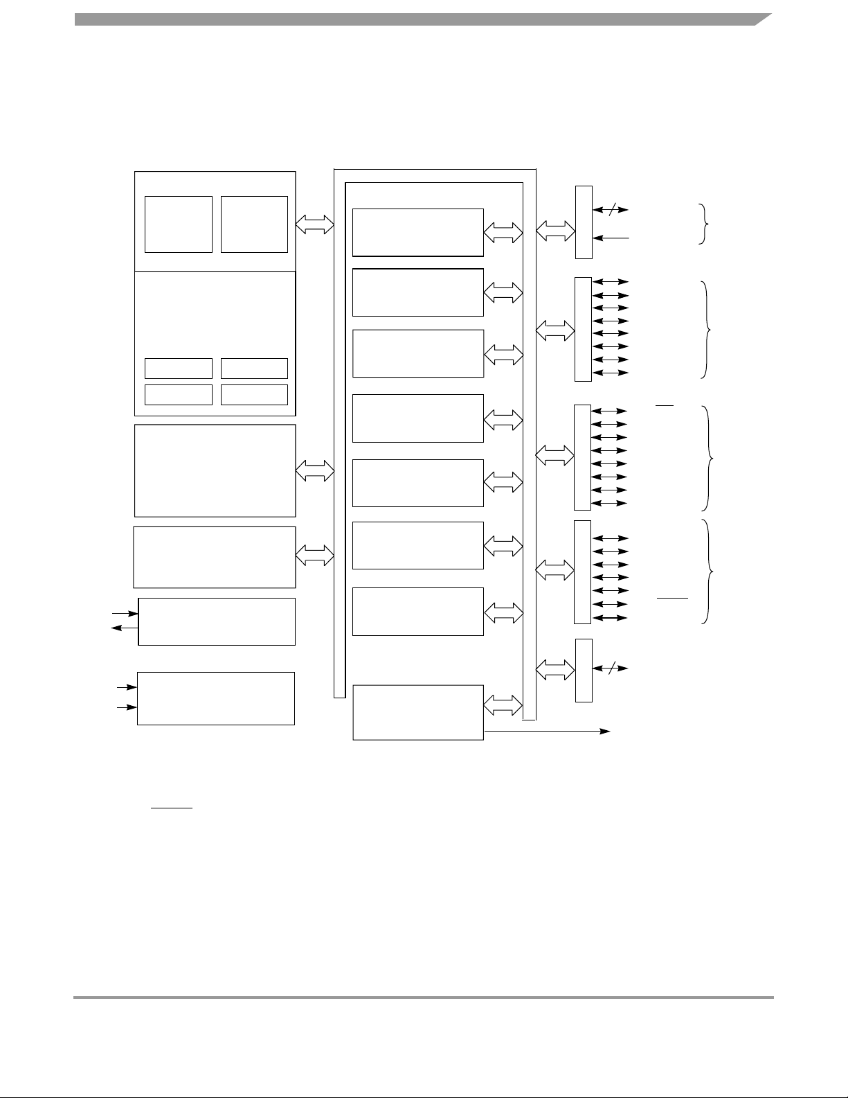
1.3 MCU Block Diagram
This block diagram shows the structure of the MC9S08RC/RD/RE/RG MCUs.
EXTAL
XTAL
HCS08 CORE
BDC
HCS08 SYSTEM CONTROL
RESETS AND INTERRUPTS
MODES OF OPERATION
POWER MANAGEMENT
RTI
IRQ LVD
USER FLASH
(RC/RD/RE/RG60 = 63,364 BYTES)
(RC/RD/RE/RG32 = 32,768 BYTES)
(RC/RD/RE16 = 16,384 BYTES)
(RC/RD/RE8 = 8192 BYTES)
USER RAM
(RC/RD/RE/RG32/60 = 2048 BYTES)
(RC/RD/RE8/16 = 1024 BYTES)
LOW-POWER OSCILLATOR
CPU
COP
INTERNAL BUS
DEBUG
MODULE (DBG)
8-BIT KEYBOARD
INTERRUPT MODULE (KBI1)
4-BIT KEYBOARD
INTERRUPT MODULE (KBI2)
SERIAL COMMUNICATIONS
INTERFACE MODULE (SCI1)
ANALOG COMPARATOR
MODULE (ACMP1)
2-CHANNEL TIMER/PWM
MODULE (TPM1)
SERIAL PERIPHERAL
INTERFACE MODULE (SPI1)
PORT A
PORT B
PORT C
PORT D
7
PTA7/KBI1P7–
PTA1/KBI1P1
PTA0/KBI1P0
PTB7/TPM1CH1
PTE6
PTB5
PTB4
PTB3
PTB2
PTB1/RxD1
PTB0/TxD1
PTC7/
PTC6/SPSCK1
PTC5/MISO1
PTC4/MOSI1
PTC3/KBI2P3
PTC2/KBI2P2
PTC1/KBI2P1
PTC0/KBI2P0
PTD6/TPM1CH0
PTD5/ACMP1+
PTD4/ACMP1–
PTD3
PTD2/IRQ
PTD1/
PTD0/BKGD/MS
NOTES1, 2, 6
NOTES 1, 5
SS1
NOTE 1
NOTES
1, 3, 4
RESET
8
V
DD
V
SS
VOLTAGE
REGULATOR
CARRIER MODULATOR
TIMER MODULE (CMT)
PORT E
PTE7–
IRO NOTE 5
NOTES:
1. Port pins are software configurable with pullup device if input port
2. PTA0 does not have a clamp diode to V
3. IRQ pin contains software configurable pullup/pulldown device if IRQ enabled (IRQPE = 1)
4. The
RESET pin contains integrated pullup device enabled if reset enabled (RSTPE = 1)
. PTA0 should not be driven above VDD.
DD
5. High current drive
6. Pins PTA[7:0] contain both pullup and pulldown devices. Pulldown available when KBI enabled (KBI1Pn = 1).
Figure 1-1 MC9S08RC/RD/RE/RG Block Diagram
Freescale Semiconductor
PTE0
NOTE 1
17MC9S08RC/RD/RE/RG
Introduction
Table 1-2 lists the functional versions of the on-chip modules.
Table 1-2 Block Versions
Module Version
Analog Comparator (ACMP) 1
Carrier Modulator Transmitter (CMT) 1
Keyboard Interrupt (KBI) 1
Serial Communications Interface (SCI) 1
Serial Peripheral Interface (SPI) 3
Timer Pulse-Width Modulator (TPM) 1
Central Processing Unit (CPU) 2
Debug Module (DBG) 1
FLASH 1
System Control 2
1.4 System Clock Distribution
SYSTEM
CONTROL
LOGIC
RTI
BUSCLK
OSC
RTI
OSC
OSCOUT*
CPU
* OSCOUT is the alternate BDC clock source for the MC9S08RC/RD/RE/RG.
RTICLKS
÷2
Figure 1-2 System Clock Distribution Diagram
BDC
TPM
ACMP
CMT
SCI
RAM FLASH
SPI
FLASH has frequency
requirements for program
and erase operation.
See Appendix A.
Figure 1-2 shows a simplified clock connection diagram for the MCU. The CPU operates at the input
frequency of the oscillator. The bus clock frequency is half of the oscillator frequency and is used by all
of the internal circuits with the exception of the CPU and RTI. The RTI can use either the oscillator input
or the internal RTI oscillator as its clock source.
MC9S08RC/RD/RE/RG18
Freescale Semiconductor

SoC Guide — MC9S08RG60/D Rev 1.10
Chapter 2 Pins and Connections
2.1 Introduction
This section describes signals that connect to package pins. It includes a pinout diagram, a table of signal
properties, and detailed discussion of signals.
2.2 Device Pin Assignment
PTA3/KBI1P3
PTE5
38
18
PTE4
37
19
36
20
PTA1/KBI1P1
PTA2/KBI1P2
34
35
32
31
30
29
28
27
26
25
24
21
22
PTA0/KBI1P0
33
PTD6/TPM1CH0
PTD5/ACMP1+
PTD4/ACMP1–
EXTAL
XTAL
PTD3
PTD2/IRQ
PTD1/RESET
PTD0/BKGD/MS
PTC7/SS1
23
PTB0/TxD1
PTB1/RxD1
PTB2
PTB3
PTB4
V
V
IRO
PTB5
PTB6
PTB7/TPM1CH1
PTA7/KBI1P7
PTA6/KBI1P6
PTA5/KBI1P5
44
43
1
2
3
4
5
6
DD
7
SS
8
9
10
11
12
42
13
14
PTE7
PTA4/KBI1P4
41
40
15
16
PTE6
39
17
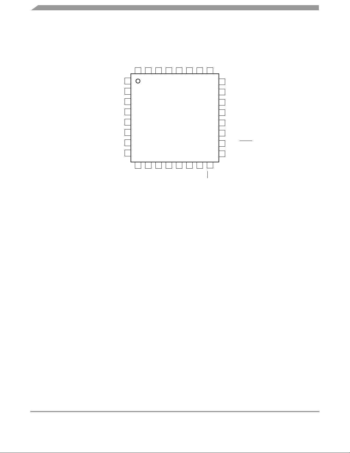
Figure 2-1 MC9S08RC/RD/RE/RG in 44-Pin LQFP Package
Freescale Semiconductor
PTC1/KBI2P1
PTC0/KBI2P0
PTC2/KBI2P2
PTC3/KBI2P3
PTE0
PTE1
PTE2
PTE3
PTC4/MOSI1
PTC5/MISO1
PTC6/SPSCK1
19MC9S08RC/RD/RE/RG
Pins and Connections
PTA0/KBI1P0
PTA1/KBI1P1
25
26
24
23
22
21
20
19
18
17
15
16
PTC7/SS1
PTC6/SPSCK1
PTD6/TPM1CH0
PTD5/ACMP1+
PTD4/ACMP1–
EXTAL
XTAL
PTD2/IRQ
PTD1/RESET
PTD0/BKGD/MS
PTB0/TxD1
PTB1/RxD1
PTB2
V
V
IRO
PTB6
PTB7/TPM1CH1
PTA7/KBI1P7
PTA6/KBI1P6
PTA5/KBI1P5
PTA4/KBI1P4
PTA3/KBI1P3
PTA2/KBI1P2
32
27
28
29
30
2
3
4
5
6
7
8
9
PTC0/KBI2P0
31
10
11
PTC1/KBI2P1
PTC2/KBI2P2
12
13
PTC4/MISO1
PTC3/KBI2P3
14
PTC5/MISO1
1
DD
SS
Figure 2-2 MC9S08RC/RD/RE/RG in 32-Pin LQFP Package
MC9S08RC/RD/RE/RG20
Freescale Semiconductor

SoC Guide — MC9S08RG60/D Rev 1.10
PTA5/KBI1P5
PTA6/KBI1P6
PTA7/KBI1P7
PTB0/TxD1
PTB1/RxD1
PTB2
V
V
IRO
PTB7/TPM1CH1
PTC0/KBI2P0
PTC1/KBI2P1
PTC2/KBI2P2
PTC3/KBI2P3
1
2
3
4
5
6
7
DD
8
SS
9
10
11
12
13
14
28
27
26
25
24
23
22
21
20
19
18
17
16
15
PTA4/KBI1P4
PTA3/KBI1P3
PTA2/KBI1P2
PTA1/KBI1P1
PTA0/KBI1P0
PTD6/TPM1CH0
EXTAL
XTAL
PTD1/RESET
PTD0/BKGD/MS
PTC7/SS1
PTC6/SPSCK1
PTC5/MISO1
PTC4/MOSI1
Figure 2-3 MC9S08RC/RD/RE/RG in 28-Pin SOIC Package and 28-Pin PDIP Package
2.3 Recommended System Connections
Figure 2-4 shows pin connections that are common to almost all MC9S08RC/RD/RE/RG application
systems. A more detailed discussion of system connections follows.
Freescale Semiconductor
21MC9S08RC/RD/RE/RG
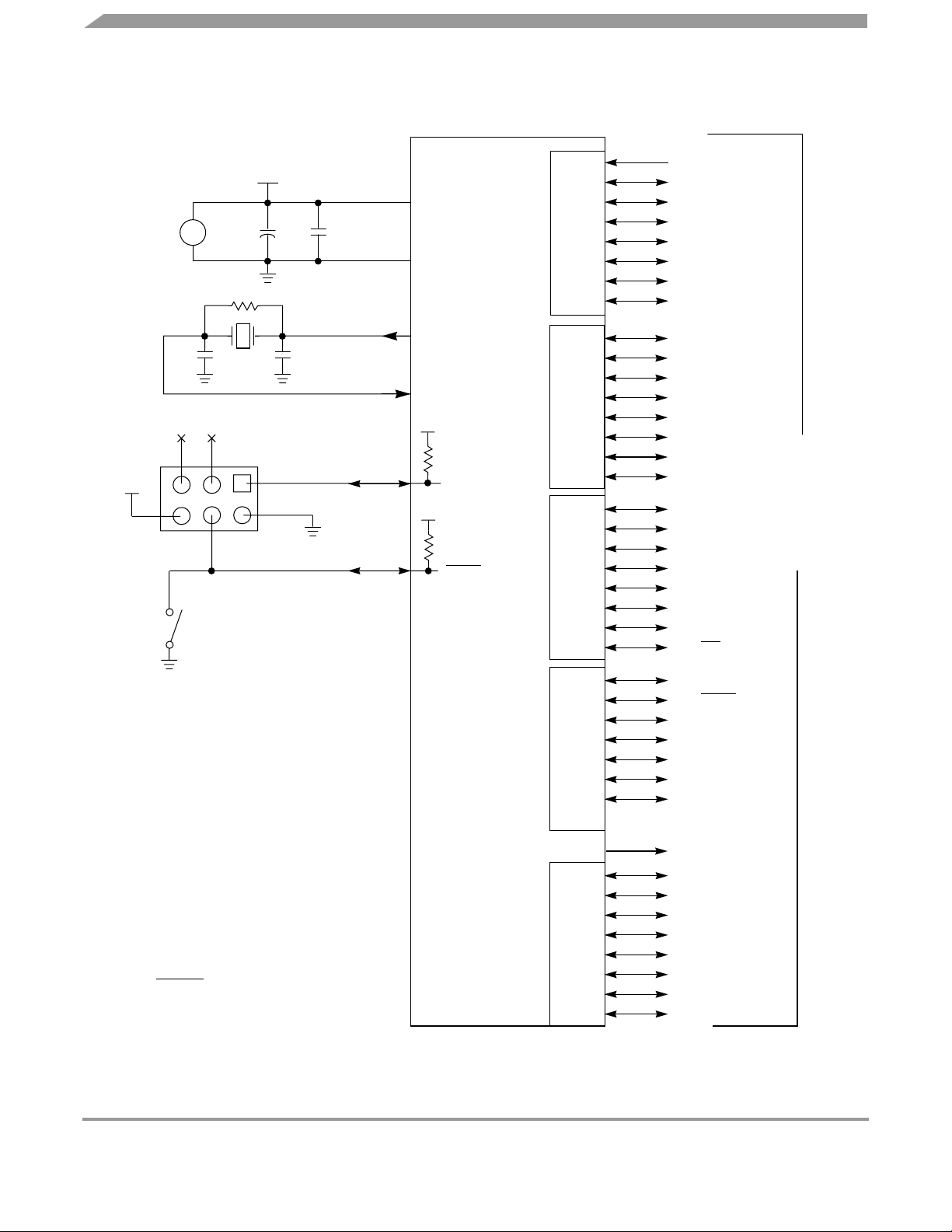
Pins and Connections
MC9S08RC/RD/RE/RG
SYSTEM
POWER
C2
BACKGROUND HEADER
V
DD
+
3 V
OPTIONAL
MANUAL
RESET
C
BLK
10 µF
X1
V
DD
V
DD
+
R
F
1
C1
C
BY
0.1 µF
V
SS
XTAL
EXTAL
BKGD/MS
NOTE 1
RESET
NOTE 2
PORT
A
PORT
B
PORT
C
PTA0/KBI1P0
PTA1/KBI1P1
PTA2/KBI1P2
PTA3/KBI1P3
PTA4/KBI1P4
PTA5/KBI1P5
PTA6/KBI1P6
PTA7/KBI1P7
PTB0/TxD1
PTB1/RxD1
PTB2
PTB3
PTB4
PTB5
PTB6
PTB7/TPM1CH1
PTC0/KBI2P0
PTC1/KBI2P1
PTC2/KBI2P2
PTC3/KBI2P3
PTC4/MOSI1
PTC5/MISO1
PTC6/SPSCK1
PTC7/SS1
I/O AND
PERIPHERAL
INTERFACE TO
APPLICATION
SYSTEM
NOTES:
1. BKGD/MS is the
same pin as PTD0.
2.
RESET is the
same pin as PTD1.
PORT
D
PORT
E
Figure 2-4 Basic System Connections
PTD0/BKGD/MS
PTD1/
RESET
PTD2/IRQ
PTD3
PTD4/ACMP1–
PTD5/ACMP1+
PTD6/TPM1CH0
IRO
PTE0
PTE1
PTE2
PTE3
PTE4
PTE5
PTE6
PTE7
MC9S08RC/RD/RE/RG22
Freescale Semiconductor

SoC Guide — MC9S08RG60/D Rev 1.10
2.3.1 Power
VDD and VSS are the primary power supply pins for the MCU. This voltage source supplies power to all
I/O buffer circuitry and to an internal voltage regulator. The internal voltage regulator provides a regulated
lower-voltage source to the CPU and other internal circuitry of the MCU.
Typically, application systems have two separate capacitors across the power pins. In this case, there
should be a bulk electrolytic capacitor, such as a 10-µF tantalum capacitor, to provide bulk charge storage
for the overall system and a 0.1-µF ceramic bypass capacitor located as near to the MCU power pins as
practical to suppress high-frequency noise.
2.3.2 Oscillator
The oscillator in the MC9S08RC/RD/RE/RG is a traditional Pierce oscillator that can accommodate a
crystal or ceramic resonator in the range of 1 MHz to 16 MHz.
Refer to Figure 2-4 for the following discussion. RFshould be a low-inductance resistor such as a carbon
composition resistor. Wire-wound resistors, and some metal film resistors, have too much inductance. C1
and C2 normally should be high-quality ceramic capacitors specifically designed for high-frequency
applications.
is used to provide a bias path to keep the EXTAL input in its linear range during crystal startup and its
R
F
value is not generally critical. Typical systems use 1 MΩ. Higher values are sensitive to humidity and
lower values reduce gain and (in extreme cases) could prevent startup.
C1 and C2 are typically in the 5-pF to 25-pF range and are chosen to match the requirements of a specific
crystal or resonator. Be sure to take into account printed circuit board (PCB) capacitance and MCU pin
capacitance when sizing C1 and C2. The crystal manufacturer typically specifies a load capacitance that
is the series combination of C1 and C2, which are usually the same size. As a first-order approximation,
use 5 pF as an estimate of combined pin and PCB capacitance for each oscillator pin (EXTAL and XTAL).
2.3.3 PTD1/RESET
The external pin reset function is shared with an output-only port function on the PTD1/RESET pin. The
reset function is enabled when RSTPE in SOPT is set. RSTPE is set following any reset of the MCU and
must be cleared in order to use this pin as an output-only port.
Whenever any reset is initiated (whether from an external signal or from an internal system), the reset pin
is driven low for about 34 cycles of f
Self_reset
later. If reset was caused by an internal source such as low-voltage reset or watchdog timeout, the circuitry
expects the reset pin sample to return a logic 1. If the pin is still low at this sample point, the reset is
assumed to be from an external source. The reset circuitry decodes the cause of reset and records it by
setting a corresponding bit in the system control reset status register (SRS).
, released, and sampled again about 38 cycles of f
Self_reset
Never connect any significant capacitance to the reset pin because that would interfere with the circuit and
sequence that detects the source of reset. If an external capacitance prevents the reset pin from rising to a
valid logic 1 before the reset sample point, all resets will appear to be external resets.
Freescale Semiconductor
23MC9S08RC/RD/RE/RG

Pins and Connections
2.3.4 Background/Mode Select (PTD0/BKGD/MS)
The background/mode select function is shared with an output-only port function on the PTD0/BKDG/MS
pin. While in reset, the pin functions as a mode select pin. Immediately after reset rises, the pin functions
as the background pin and can be used for background debug communication. While functioning as a
background/mode select pin, this pin has an internal pullup device enabled. To use as an output-only port,
BKGDPE in SOPT must be cleared.
If nothing is connected to this pin, the MCU will enter normal operating mode at the rising edge of reset.
If a debug system is connected to the 6-pin standard background debug header, it can hold BKGD/MS low
during the rising edge of reset, which forces the MCU to active background mode.
The BKGD pin is used primarily for background debug controller (BDC) communications using a custom
protocol that uses 16 clock cycles of the target MCU’s BDC clock per bit time. The target MCU’s BDC
clock could be as fast as the bus clock rate, so there should never be any significant capacitance connected
to the BKGD/MS pin that could interfere with background serial communications.
Although the BKGD pin is a pseudo open-drain pin, the background debug communication protocol
provides brief, actively driven, high speedup pulses to ensure fast rise times. Small capacitances from
cables and the absolute value of the internal pullup device play almost no role in determining rise and fall
times on the BKGD pin.
2.3.5 IRO Pin Description
The IRO pin is the output of the CMT. See Carrier Modulator Timer (CMT) Module for a detailed
description of this pin function.
2.3.6 General-Purpose I/O and Peripheral Ports
The remaining pins are shared among general-purpose I/O and on-chip peripheral functions such as timers
and serial I/O systems. (Not all pins are available in all packages. See Table 2-2.) Immediately after reset,
all 37 of these pins are configured as high-impedance general-purpose inputs with internal pullup devices
disabled.
NOTE: To avoid extra current drain from floating input pins, the reset initialization routine
in the application program should either enable on-chip pullup devices or change
the direction of unused pins to outputs so the pins do not float.
For information about controlling these pins as general-purpose I/O pins, see the Parallel Input/Output
section. For information about how and when on-chip peripheral systems use these pins, refer to the
appropriate section from Table 2-1.
MC9S08RC/RD/RE/RG24
Freescale Semiconductor

SoC Guide — MC9S08RG60/D Rev 1.10
Table 2-1 Pin Sharing References
Port Pins
PTA7–PTA0 KBI1P7–KBI1P0 Keyboard Interrupt (KBI) Module
PTB7 TPM1CH1 Timer/PWM Module (TPM) Module
PTB6–PTB2 — Parallel Input/Output
PTB1
PTB0
PTC7
PTC6
PTC5
PTC4
PTC3–PTC0 KBI2P3–KBI2P0 Keyboard Interrupt (KBI) Module
PTD6 TPM1CH0 Timer/PWM Module (TPM) Module
PTD5
PTD4
PTD2 IRQ
PTD0 BKGD/MS
Alternate
Function
RxD1
TxD1
SS1
SPSCK1
MISO1
MOSI1
ACMP1+
ACMP1–
RESET
Reference
Serial Communications Interface (SCI) Module
Serial Peripheral Interface (SPI) Module
Analog Comparator (ACMP) Module
Resets, Interrupts, and System ConfigurationPTD1
(1)
PTE7–PTE0 — Parallel Input/Output
NOTES:
1. See this section for information about modules that share these pins.
When an on-chip peripheral system is controlling a pin, data direction control bits still determine what is
read from port data registers even though the peripheral module controls the pin direction by controlling
the enable for the pin’s output buffer. See the Parallel Input/Output section for more details.
Pullup enable bits for each input pin control whether on-chip pullup devices are enabled whenever the pin
is acting as an input even if it is being controlled by an on-chip peripheral module. When the PTA7–PTA4
pins are controlled by the KBI module and are configured for rising-edge/high-level sensitivity, the pullup
enable control bits enable pulldown devices rather than pullup devices. Similarly, when PTD2 is
configured as the IRQ input and is set to detect rising edges, the pullup enable control bit enables a
pulldown device rather than a pullup device.
Freescale Semiconductor
25MC9S08RC/RD/RE/RG

Pins and Connections
2.3.7 Signal Properties Summary
Table 2-2 summarizes I/O pin characteristics. These characteristics are determined by the way the
common pin interfaces are hardwired to internal circuits.
Table 2-2 Signal Properties
Pin
Name
V
DD
V
SS
XTAL O — — Crystal oscillator output
EXTAL I — — Crystal oscillator input
IRO O Y — Infrared output
PTA0/KBI1P0 I N SWC
PTA1/KBI1P1 I/O N SWC
PTA2/KBI1P2 I/O N SWC
PTA3/KBI1P3 I/O N SWC
PTA4/KBI1P4 I/O N SWC
PTA5/KBI1P5 I/O N SWC
PTA6/KBI1P6 I/O N SWC
PTA7/KBI1P7 I/O N SWC
PTB0/TxD1 I/O Y SWC
PTB1/RxD1 I/O Y SWC
PTB2 I/O Y SWC
PTB3 I/O Y SWC Available only in 44-LQFP package
PTB4 I/O Y SWC Available only in 44-LQFP package
PTB5 I/O Y SWC Available only in 44-LQFP package
PTB6 I/O Y SWC Available only in 32- or 44-LQFP packages
PTB7/TPM1CH1 I/O Y SWC
PTC0/KBI2P0 I/O N SWC
PTC1/KBI2P1 I/O N SWC
PTC2/KBI2P2 I/O N SWC
PTC3/KBI2P3 I/O N SWC
PTC4/MOSI1 I/O N SWC
PTC5/MISO1 I/O N SWC
PTC6/SPSCK1 I/O N SWC
SS1 I/O N SWC
PTC7/
PTD0/BKGD/MS I/O N
PTD1/
RESET I/O N
PTD2/IRQ I/O N
PTD3 I/O N SWC Available only in 44-LQFP package
PTD4/ACMP1– I/O N SWC Available only in 32- or 44-LQFP packages
PTD5/ACMP1+ I/O N SWC Available only in 32- or 44-LQFP packages
Dir
(1)
High
Current Pin
——
——
Pullup
SWC
SWC
SWC
(2)
PTA0 does not have a clamp diode to V
driven above V
(3)
Output-only when configured as PTD0 pin. Pullup enabled.
(3)
Output-only when configured as PTD1 pin.
(4)
Available only in 32- or 44-LQFP packages
DD
.
Comments
. PTA0 should not be
DD
MC9S08RC/RD/RE/RG26
Freescale Semiconductor
SoC Guide — MC9S08RG60/D Rev 1.10
Table 2-2 Signal Properties (Continued)
Pin
Name
PTD6/TPM1CH0 I/O N SWC
PTE0 I/O N SWC Available only in 44-LQFP package
PTE1 I/O N SWC Available only in 44-LQFP package
PTE2 I/O N SWC Available only in 44-LQFP package
PTE3 I/O N SWC Available only in 44-LQFP package
PTE4 I/O N SWC Available only in 44-LQFP package
PTE5 I/O N SWC Available only in 44-LQFP package
PTE6 I/O N SWC Available only in 44-LQFP package
PTE7 I/O N SWC Available only in 44-LQFP package
NOTES:
1. Unless otherwise indicated, all digital inputs have input hysteresis.
2. SWC is software-controlled pullup resistor, the register is associated with the respective port.
3. When these pins are configured as
4. When configured for the IRQ function, this pin will have a pullup device enabled when the IRQ is set for falling edge
detection and a pulldown device enabled when the IRQ is set for rising edge detection.
Dir
(1)
High
Current Pin
Pullup
RESET or BKGD/MS pullup device is enabled.
(2)
Comments
Freescale Semiconductor
27MC9S08RC/RD/RE/RG

Pins and Connections
MC9S08RC/RD/RE/RG28
Freescale Semiconductor

SoC Guide — MC9S08RG60/D Rev 1.10
Chapter 3 Modes of Operation
3.1 Introduction
The operating modes of the MC9S08RC/RD/RE/RG are described in this section. Entry into each mode,
exit from each mode, and functionality while in each of the modes are described.
3.2 Features
• Active background mode for code development
• Wait mode:
– CPU shuts down to conserve power
– System clocks running
– Full voltage regulation maintained
• Stop modes:
– System clocks stopped; voltage regulator in standby
– Stop1 — Full power down of internal circuits for maximum power savings
– Stop2 — Partial power down of internal circuits, RAM remains operational
– Stop3 — All internal circuits powered for fast recovery
3.3 Run Mode
This is the normal operating mode for the MC9S08RC/RD/RE/RG. This mode is selected when the
BKGD/MS pin is high at the rising edge of reset. In this mode, the CPU executes code from internal
memory with execution beginning at the address fetched from memory at $FFFE:$FFFF after reset.
3.4 Active Background Mode
The active background mode functions are managed through the background debug controller (BDC) in
the HCS08 core. The BDC, together with the on-chip debug module (DBG), provide the means for
analyzing MCU operation during software development.
Active background mode is entered in any of five ways:
• When the BKGD/MS pin is low at the rising edge of reset
• When a BACKGROUND command is received through the BKGD pin
• When a BGND instruction is executed
• When encountering a BDC breakpoint
• When encountering a DBG breakpoint
Freescale Semiconductor
29MC9S08RC/RD/RE/RG

Modes of Operation
After active background mode is entered, the CPU is held in a suspended state waiting for serial
background commands rather than executing instructions from the user’s application program.
Background commands are of two types:
• Non-intrusive commands, defined as commands that can be issued while the user program is
running. Non-intrusive commands can be issued through the BKGD pin while the MCU is in run
mode; non-intrusive commands can also be executed when the MCU is in the active background
mode. Non-intrusive commands include:
– Memory access commands
– Memory-access-with-status commands
– BDC register access commands
– BACKGROUND command
• Active background commands, which can only be executed while the MCU is in active background
mode, include commands to:
– Read or write CPU registers
– Trace one user program instruction at a time
– Leave active background mode to return to the user’s application program (GO)
The active background mode is used to program a bootloader or user application program into the FLASH
program memory before the MCU is operated in run mode for the first time. When the
MC9S08RC/RD/RE/RG is shipped from the Freescale Semiconductor factory, the FLASH program
memory is usually erased so there is no program that could be executed in run mode until the FLASH
memory is initially programmed. The active background mode can also be used to erase and reprogram
the FLASH memory after it has been previously programmed.
For additional information about the active background mode, refer to the Development Support section.
3.5 Wait Mode
Wait mode is entered by executing a WAIT instruction. Upon execution of the WAIT instruction, the CPU
enters a low-power state in which it is not clocked. The I bit in CCR is cleared when the CPU enters the
wait mode, enabling interrupts. When an interrupt request occurs, the CPU exits the wait mode and
resumes processing, beginning with the stacking operations leading to the interrupt service routine.
Only the BACKGROUND command and memory-access-with-status commands are available when the
MCU is in wait mode. The memory-access-with-status commands do not allow memory access, but they
report an error indicating that the MCU is in either stop or wait mode. The BACKGROUND command
can be used to wake the MCU from wait mode and enter active background mode.
MC9S08RC/RD/RE/RG30
Freescale Semiconductor

SoC Guide — MC9S08RG60/D Rev 1.10
3.6 Stop Modes
One of three stop modes is entered upon execution of a STOP instruction when the STOPE bit in the
system option register is set. In all stop modes, all internal clocks are halted. If the STOPE bit is not set
when the CPU executes a STOP instruction, the MCU will not enter any of the stop modes and an illegal
opcode reset is forced. The stop modes are selected by setting the appropriate bits in SPMSC2.
Table 3-1 summarizes the behavior of the MCU in each of the stop modes.
Table 3-1 Stop Mode Behavior
CPU, Digital
Mode PDC PPDC
Stop1 1 0 Off Off Off Standby Standby Reset Off
Peripherals,
FLASH
RAM OSC ACMP Regulator I/O Pins RTI
Stop2 1 1 Off Standby Off Standby Standby
Stop3 0
Don’t
care
Standby Standby Off Standby Standby
States
held
States
held
Optionally on
Optionally on
3.6.1 Stop1 Mode
Stop1 mode provides the lowest possible standby power consumption by causing the internal circuitry of
the MCU to be powered down. To enter stop1, the user must execute a STOP instruction with the PDC bit
in SPMSC2 set and the PPDC bit clear. Stop1 can be entered only if the LVD reset is disabled
(LVDRE = 0).
When the MCU is in stop1 mode, all internal circuits that are powered from the voltage regulator are
turned off. The voltage regulator is in a low-power standby state, as are the OSC and ACMP.
Exit from stop1 is done by asserting any of the wakeup pins on the MCU:
have been enabled. IRQ and KBI pins are always active-low when used as wakeup pins in stop1 regardless
of how they were configured before entering stop1.
Upon wakeup from stop1 mode, the MCU will start up as from a power-on reset (POR). The CPU will
take the reset vector.
RESET, IRQ, or KBI, which
3.6.2 Stop2 Mode
Stop2 mode provides very low standby power consumption and maintains the contents of RAM and the
current state of all of the I/O pins. To select entry into stop2 upon execution of a STOP instruction, the
user must execute a STOP instruction with the PPDC and PDC bits in SPMSC2 set. Stop2 can be entered
only if LVDRE = 0.
Before entering stop2 mode, the user must save the contents of the I/O port registers, as well as any other
memory-mapped registers that they want to restore after exit of stop2, to locations in RAM. Upon exit
from stop2, these values can be restored by user software.
Freescale Semiconductor
31MC9S08RC/RD/RE/RG

Modes of Operation
When the MCU is in stop2 mode, all internal circuits that are powered from the voltage regulator are
turned off, except for the RAM. The voltage regulator is in a low-power standby state, as is the ACMP.
Upon entry into stop2, the states of the I/O pins are latched. The states are held while in stop2 mode and
after exiting stop2 mode until a 1 is written to PPDACK in SPMSC2.
Exit from stop2 is done by asserting any of the wakeup pins:
RESET, IRQ, or KBI that have been enabled,
or through the real-time interrupt. IRQ and KBI pins are always active-low when used as wakeup pins in
stop2 regardless of how they were configured before entering stop2.
Upon wakeup from stop2 mode, the MCU will start up as from a power-on reset (POR) except pin states
remain latched. The CPU will take the reset vector. The system and all peripherals will be in their default
reset states and must be initialized.
After waking up from stop2, the PPDF bit in SPMSC2 is set. This flag may be used to direct user code to
go to a stop2 recovery routine. PPDF remains set and the I/O pin states remain latched until a 1 is written
to PPDACK in SPMSC2.
For pins that were configured as general-purpose I/O, the user must copy the contents of the I/O port
registers, which have been saved in RAM, back to the port registers before writing to the PPDACK bit. If
the port registers are not restored from RAM before writing to PPDACK, then the register bits will be in
their reset states when the I/O pin latches are opened and the I/O pins will switch to their reset states.
For pins that were configured as peripheral I/O, the user must reconfigure the peripheral module that
interfaces to the pin before writing to the PPDACK bit. If the peripheral module is not enabled before
writing to PPDACK, the pins will be controlled by their associated port control registers when the I/O
latches are opened.
3.6.3 Stop3 Mode
Upon entering stop3 mode, all of the clocks in the MCU, including the oscillator itself, are halted. The
OSC is turned off, the ACMP is disabled, and the voltage regulator is put in standby. The states of all of
the internal registers and logic, as well as the RAM content, are maintained. The I/O pin states are not
latched at the pin as in stop2. Instead they are maintained by virtue of the states of the internal logic driving
the pins being maintained.
Exit from stop3 is done by asserting
RESET, any asynchronous interrupt pin that has been enabled, or
through the real-time interrupt. The asynchronous interrupt pins are the IRQ or KBI pins.
If stop3 is exited by means of the RESET pin, then the MCU will be reset and operation will resume after
taking the reset vector. Exit by means of an asynchronous interrupt or the real-time interrupt will result in
the MCU taking the appropriate interrupt vector.
A separate self-clocked source (≈1 kHz) for the real-time interrupt allows a wakeup from stop2 or stop3
mode with no external components. When RTIS2:RTIS1:RTIS0 = 0:0:0, the real-time interrupt function
and this 1-kHz source are disabled. Power consumption is lower when the 1-kHz source is disabled, but
in that case the real-time interrupt cannot wake the MCU from stop.
MC9S08RC/RD/RE/RG32
Freescale Semiconductor

SoC Guide — MC9S08RG60/D Rev 1.10
3.6.4 Active BDM Enabled in Stop Mode
Entry into the active background mode from run mode is enabled if the ENBDM bit in BDCSCR is set.
This register is described in the Development Support section of this data sheet. If ENBDM is set when
the CPU executes a STOP instruction, the system clocks to the background debug logic remain active
when the MCU enters stop mode so background debug communication is still possible. In addition, the
voltage regulator does not enter its low-power standby state but maintains full internal regulation. The
MCU cannot enter either stop1 mode or stop2 mode if ENBDM is set.
Most background commands are not available in stop mode. The memory-access-with-status commands
do not allow memory access, but they report an error indicating that the MCU is in either stop or wait
mode. The BACKGROUND command can be used to wake the MCU from stop and enter active
background mode if the ENBDM bit is set. After active background mode is entered, all background
commands are available. Table 3-2 summarizes the behavior of the MCU in stop when entry into the active
background mode is enabled.
Table 3-2 BDM Enabled Stop Mode Behavior
CPU, Digital
Mode PDC PPDC
Peripherals,
FLASH
RAM OSC ACMP Regulator I/O Pins RTI
Stop3
Don’t
care
Don’t
care
Standby Standby On Standby On
States
held
Optionally on
3.6.5 LVD Reset Enabled in Stop Mode
The LVD system is capable of generating either an interrupt or a reset when the supply voltage drops
below the LVD voltage. If the LVD reset is enabled in stop by setting the LVDRE bit in SPMSC1 when
the CPU executes a STOP instruction, then the voltage regulator remains active during stop mode. If the
user attempts to enter either stop1 or stop2 with the LVD reset enabled (LVDRE = 1) the MCU will instead
enter stop3. Table 3-3 summarizes the behavior of the MCU in stop when LVD reset is enabled.
Table 3-3 LVD Enabled Stop Mode Behavior
CPU, Digital
Mode PDC PPDC
Stop3
Don’t
care
Don’t
care
Peripherals,
FLASH
Standby Standby On Standby On
RAM OSC ACMP Regulator I/O Pins RTI
States
held
Optionally on
3.6.6 On-Chip Peripheral Modules in Stop Mode
When the MCU enters any stop mode, system clocks to the internal peripheral modules are stopped. Even
in the exception case (ENBDM = 1), where clocks are kept alive to the background debug logic, clocks to
the peripheral systems are halted to reduce power consumption.
Freescale Semiconductor
33MC9S08RC/RD/RE/RG

Modes of Operation
I/O Pins
• All I/O pin states remain unchanged when the MCU enters stop3 mode.
• If the MCU is configured to go into stop2 mode, all I/O pin states are latched before entering stop.
Pin states remain latched until the PPDACK bit is written.
• If the MCU is configured to go into stop1 mode, all I/O pins are forced to their default reset state
upon entry into stop.
Memory
• All RAM and register contents are preserved while the MCU is in stop3 mode.
• All registers will be reset upon wakeup from stop2, but the contents of RAM are preserved. The
user may save any memory-mapped register data into RAM before entering stop2 and restore the
data upon exit from stop2.
• All registers will be reset upon wakeup from stop1 and the contents of RAM are not preserved. The
MCU must be initialized as upon reset. The contents of the FLASH memory are non-volatile and
are preserved in any of the stop modes.
OSC — In any of the stop modes, the OSC stops running.
TPM — When the MCU enters stop mode, the clock to the TPM module stops. The modules halt
operation. If the MCU is configured to go into stop2 or stop1 mode, the TPM module will be reset upon
wakeup from stop and must be reinitialized.
ACMP — When the MCU enters any stop mode, the ACMP will enter a low-power standby state
. No
compare operation will occur while in stop. If the MCU is configured to go into stop2 or stop1 mode, the
ACMP will be reset upon wakeup from stop and must be reinitialized.
KBI — During stop3, the KBI pins that are enabled continue to function as interrupt sources. During stop1
or stop2, enabled KBI pins function as wakeup inputs. When functioning as a wakeup, a KBI pin is always
active low regardless of how it was configured before entering stop1 or stop2.
SCI — When the MCU enters stop mode, the clock to the SCI module stops. The module halts operation.
If the MCU is configured to go into stop2 or stop1 mode, the SCI module will be reset upon wakeup from
stop and must be reinitialized.
SPI — When the MCU enters stop mode, the clock to the SPI module stops. The module halts operation.
If the MCU is configured to go into stop2 or stop1 mode, the SPI module will be reset upon wakeup from
stop and must be reinitialized.
CMT — When the MCU enters stop mode, the clock to the CMT module stops. The module halts
operation. If the MCU is configured to go into stop2 or stop1 mode, the CMT module will be reset upon
wakeup from stop and must be reinitialized.
Voltage Regulator — The voltage regulator enters a low-power standby state when the MCU enters any
of the stop modes unless the LVD reset function is enabled or BDM is enabled.
MC9S08RC/RD/RE/RG34
Freescale Semiconductor

SoC Guide — MC9S08RG60/D Rev 1.10
Chapter 4 Memory
4.1 MC9S08RC/RD/RE/RG Memory Map
As shown in Figure 4-1, on-chip memory in the MC9S08RC/RD/RE/RG series of MCUs consists of
RAM, FLASH program memory for nonvolatile data storage, and I/O and control/status registers. The
registers are divided into three groups:
• Direct-page registers ($0000 through $0045 for 32K and 60K parts, and $0000 through $003F for
16K and 8K parts)
• High-page registers ($1800 through $182B)
• Nonvolatile registers ($FFB0 through $FFBF)
$0000
DIRECT PAGE REGISTERS
$0045
$0046
$0845
$0846
$17FF
$1800
$182B
$182C
$FFFF
2048 BYTES
4026 BYTES
HIGH PAGE REGISTERS
59348 BYTES
MC9S08RC/RD/RE/RG60
RAM
FLASH
FLASH
DIRECT PAGE REGISTERS
RAM
2048 BYTES
UNIMPLEMENTED
4026 BYTES
HIGH PAGE REGISTERS
UNIMPLEMENTED
26580 BYTES
FLASH
32768 BYTES
MC9S08RC/RD/RE/RG32
$0000
$0045
$0046
$0845
$0846
$17FF
$1800
$182B
$182C
$8000
DIRECT PAGE REGISTERS
RAM
1024 BYTES
UNIMPLEMENTED
5056 BYTES
HIGH PAGE REGISTERS
UNIMPLEMENTED
42964 BYTES
FLASH
16384 BYTES
MC9S08RC/RD/RE16
(1)
$0000
$003F
$0040
$043F
$0440
$17FF
$1800
$182B
$182C
$BFFF
$C000
$FFFF
DIRECT PAGE REGISTERS
RAM
1024 BYTES
UNIMPLEMENTED
5056 BYTES
HIGH PAGE REGISTERS
UNIMPLEMENTED
51156 BYTES
FLASH
8192 BYTES
MC9S08RC/RD/RE8
(1)
$0000
$003F
$0040
$043F
$0440
$17FF
$1800
$182B
$182C
$DFFF
$E000
$FFFF
NOTE:
1. MC3S08RC/RD/RE16/8 ROM MCU devices have 512 bytes of RAM instead of 1K bytes.
Freescale Semiconductor
Figure 4-1 MC9S08RC/RD/RE/RG Memory Map
35MC9S08RC/RD/RE/RG

Memory
4.1.1 Reset and Interrupt Vector Assignments
Table 4-1 shows address assignments for reset and interrupt vectors. The vector names shown in this table
are the labels used in the Freescale-provided equate file for the MC9S08RC/RD/RE/RG. For more details
about resets, interrupts, interrupt priority, and local interrupt mask controls, refer to the Resets, Interrupts,
and System Configuration section.
Table 4-1 Reset and Interrupt Vectors
Vector
Numbe
r
16
through
31
15 $FFE0:FFE1
14 $FFE2:FFE3 RTI Vrti
13 $FFE4:FFE5 KBI2 Vkeyboard2
12 $FFE6:FFE7 KBI1 Vkeyboard1
11 $FFE8:FFE9
10 $FFEA:FFEB CMT Vcmt
9 $FFEC:FFED
8 $FFEE:FFEF
7 $FFF0:FFF1
6 $FFF2:FFF3 TPM Overflow Vtpm1ovf
5 $FFF4:FFF5 TPM Channel 1 Vtpm1ch1
4 $FFF6:FFF7 TPM Channel 0 Vtpm1ch0
3 $FFF8:FFF9 IRQ Virq
2 $FFFA:FFFB Low Voltage Detect Vlvd
1 $FFFC:FFFD SWI Vswi
0 $FFFE:FFFF Reset Vreset
NOTES:
1. The SPI module is not included on the MC9S08RC/RD/RE devices. This vector location is unused for those
devices.
2. The analog comparator (ACMP) module is not included on the MC9S08RD devices. This vector location is unused
for those devices.
3. The SCI module is not included on the MC9S08RC devices. This vector location is unused for those devices.
Address
(High/Low)
$FFC0:FFC1
$FFDE:FFDF
Vector Vector Name
Unused Vector Space
(available for user program)
(1)
SPI
(2)
ACMP
SCI Transmit
SCI Receive
SCI Error
(3)
(3)
(3)
Vspi1
Vacmp1
Vsci1tx
Vsci1rx
Vsci1err
MC9S08RC/RD/RE/RG36
Freescale Semiconductor

SoC Guide — MC9S08RG60/D Rev 1.10
4.2 Register Addresses and Bit Assignments
The registers in the MC9S08RC/RD/RE/RG are divided into these three groups:
• Direct-page registers are located within the first 256 locations in the memory map, so they are
accessible with efficient direct addressing mode instructions.
• High-page registers are used much less often, so they are located above $1800 in the memory map.
This leaves more room in the direct page for more frequently used registers and variables.
• The nonvolatile register area consists of a block of 16 locations in FLASH memory at
$FFB0–$FFBF.
Nonvolatile register locations include:
– Three values that are loaded into working registers at reset
– An 8-byte backdoor comparison key that optionally allows a user to gain controlled access to
secure memory
Because the nonvolatile register locations are FLASH memory, they must be erased and
programmed like other FLASH memory locations.
Direct-page registers can be accessed with efficient direct addressing mode instructions. Bit manipulation
instructions can be used to access any bit in any direct-page register. Table 4-2 is a summary of all
user-accessible direct-page registers and control bits.
The direct page registers in Table 4-2 can use the more efficient direct addressing mode, which requires
only the lower byte of the address. Because of this, the lower byte of the address in column one is shown
in bold text. In Table 4-3 and Table 4-4, the whole address in column one is shown in bold. In Table 4-2,
Table 4-3, and Table 4-4, the register names in column two are shown in bold to set them apart from the
bit names to the right. Cells that are not associated with named bits are shaded. A shaded cell with a 0
indicates this unused bit always reads as a 0. Shaded cells with dashes indicate unused or reserved bit
locations that could read as 1s or 0s.
Freescale Semiconductor
37MC9S08RC/RD/RE/RG
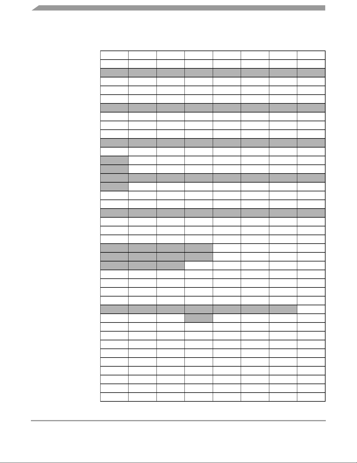
Memory
Table 4-2 Direct-Page Register Summary
Address Register Name Bit 7 654321Bit 0
$0000 PTAD PTAD7 PTAD6 PTAD5 PTAD4 PTAD3 PTAD2 PTAD1 PTAD0
$0001 PTAPE PTAPE7 PTAPE6 PTAPE5 PTAPE4 PTAPE3 PTAPE2 PTAPE1 PTAPE0
$0002 Reserved — — — — — — — —
$0003 PTADD PTADD7 PTADD6 PTADD5 PTADD4 PTADD3 PTADD2 PTADD1 PTADD0
$0004 PTBD PTBD7 PTBD6 PTBD5 PTBD4 PTBD3 PTBD2 PTBD1 PTBD0
$0005 PTBPE PTBPE7 PTBPE6 PTBPE5 PTBPE4 PTBPE3 PTBPE2 PTBPE1 PTBPE0
$0006 Reserved — — — — — — — —
$0007 PTBDD PTBDD7 PTBDD6 PTBDD5 PTBDD4 PTBDD3 PTBDD2 PTBDD1 PTBDD0
$0008 PTCD PTCD7 PTCD6 PTCD5 PTCD4 PTCD3 PTCD2 PTCD1 PTCD0
$0009 PTCPE PTCPE7 PTCPE6 PTCPE5 PTCPE4 PTCPE3 PTCPE2 PTCPE1 PTCPE0
$000A Reserved — — — — — — — —
$000B PTCDD PTCDD7 PTCDD6 PTCDD5 PTCDD4 PTCDD3 PTCDD2 PTCDD1 PTCDD0
$000C PTDD 0 PTDD6 PTDD5 PTDD4 PTDD3 PTDD2 PTDD1 PTDD0
$000D PTDPE 0 PTDPE6 PTDPE5 PTDPE4 PTDPE3 PTDPE2 PTDPE1 PTDPE0
$000E Reserved — — — — — — — —
$000F PTDDD 0 PTDDD6 PTDDD5 PTDDD4 PTDDD3 PTDDD2 PTDDD1 PTDDD0
$0010 PTED PTED7 PTED6 PTED5 PTED4 PTED3 PTED2 PTED1 PTED0
$0011 PTEPE PTEPE7 PTEPE6 PTEPE5 PTEPE4 PTEPE3 PTEPE2 PTEPE1 PTEPE0
$0012 Reserved — — — — — — — —
$0013 PTEDD PTEDD7 PTEDD6 PTEDD5 PTEDD4 PTEDD3 PTEDD2 PTEDD1 PTEDD0
$0014 KBI1SC KBEDG7 KBEDG6 KBEDG5 KBEDG4 KBF KBACK KBIE KBIMOD
$0015 KBI1PE KBIPE7 KBIPE6 KBIPE5 KBIPE4 KBIPE3 KBIPE2 KBIPE1 KBIPE0
$0016 KBI2SC 0 0 0 0 KBF KBACK KBIE KBIMOD
$0017 KBI2PE 0 0 0 0 KBIPE3 KBIPE2 KBIPE1 KBIPE0
(1)
(1)
(1)
(1)
(1)
(1)
(1)
(1)
0 0 0 SBR12 SBR11 SBR10 SBR9 SBR8
SBR7 SBR6 SBR5 SBR4 SBR3 SBR2 SBR1 SBR0
LOOPS SCISWAI RSRC M WAKE ILT PE PT
TIE TCIE RIE ILIE TE RE RWU SBK
TDRE TC RDRF IDLE OR NF FE PF
0 0 0 0 0 0 0 RAF
R8 T8 TXDIR 0 ORIE NEIE FEIE PEIE
R7/T7 R6/T6 R5/T5 R4/T4 R3/T3 R2/T2 R1/T1 R0/T0
$0018 SCI1BDH
$0019 SCI1BDL
$001A SCI1C1
$001B SCI1C2
$001C SCI1S1
$001D SCI1S2
$001E SCI1C3
$001F SCI1D
$0020 CMTCGH1 PH7 PH6 PH5 PH4 PH3 PH2 PH1 PH0
$0021 CMTCGL1 PL7 PL6 PL5 PL4 PL3 PL2 PL1 PL0
$0022 CMTCGH2 SH7 SH6 SH5 SH4 SH3 SH2 SH1 SH0
$0023 CMTCGL2 SL7 SL6 SL5 SL4 SL3 SL2 SL1 SL0
$0024 CMTOC IROL CMTPOL IROPEN 00000
$0025 CMTMSC EOCF CMTDIV1 CMTDIV0 EXSPC BASE FSK EOCIE MCGEN
$0026 CMTCMD1 MB15 MB14 MB13 MB12 MB11 MB10 MB9 MB8
$0027 CMTCMD2 MB7 MB6 MB5 MB4 MB3 MB2 MB1 MB0
MC9S08RC/RD/RE/RG38
Freescale Semiconductor

SoC Guide — MC9S08RG60/D Rev 1.10
Table 4-2 Direct-Page Register Summary (Continued)
Address Register Name Bit 7 654321Bit 0
$0028 CMTCMD3 SB15 SB14 SB13 SB12 SB11 SB10 SB9 SB8
$0029 CMTCMD4 SB7 SB6 SB5 SB4 SB3 SB2 SB1 SB0
$002A IRQSC 0 0 IRQEDG IRQPE IRQF IRQACK IRQIE IRQMOD
(3)
(3)
(3)
(3)
(3)
(2)
ACME ACBGS ACF ACIE ACO — ACMOD1 ACMOD0
—
—
—
—
—
—
—
—
—
—
—
—
—
—
—
—
—
—
—
—
—
—
—
—
—
—
—
—
—
—
SPIE SPE SPTIE MSTR CPOL CPHA SSOE LSBFE
0 0 0 MODFEN BIDIROE 0 SPISWAI SPC0
0 SPPR2 SPPR1 SPPR0 0 SPR2 SPR1 SPR0
SPRF 0 SPTEF MODF 0 0 0 0
Bit 7 654321Bit 0
$002B ACMP1SC
$002C–
Reserved —
$002F
$0030 TPM1SC TOF TOIE CPWMS CLKSB CLKSA PS2 PS1 PS0
$0031 TPM1CNTH Bit 15 14 13 12 11 10 9 Bit 8
$0032 TPM1CNTL Bit 7 654321Bit 0
$0033 TPM1MODH Bit 15 14 13 12 11 10 9 Bit 8
$0034 TPM1MODL Bit 7 654321Bit 0
$0035 TPM1C0SC CH0F CH0IE MS0B MS0A ELS0B ELS0A 0 0
$0036 TPM1C0VH Bit 15 14 13 12 11 10 9 Bit 8
$0037 TPM1C0VL Bit 7 654321Bit 0
$0038 TPM1C1SC CH1F CH1IE MS1B MS1A ELS1B ELS1A 0 0
$0039 TPM1C1VH Bit 15 14 13 12 11 10 9 Bit 8
$003A TPM1C1VL Bit 7 654321Bit 0
$003B–
Reserved —
$003F
$0040 SPI1C1
$0041 SPI1C2
$0042 SPI1BR
$0043 SPI1S
$0044 Reserved — — — — — — — —
$0045 SPI1D
NOTES:
1. The SCI module is not included on the MC9S08RC devices. This is a reserved location for those devices.
2. The analog comparator (ACMP) module is not included on the MC9S08RD devices. This is a reserved location for those
devices.
3. The SPI module is not included on the MC9S08RC/RD/RE devices. These are reserved locations on the 32K and 60K
versions of these devices. The address range $0040–$004F are RAM locations on the 16K and 8K devices. There are
no MC9S08RG8/16 devices.
Freescale Semiconductor
39MC9S08RC/RD/RE/RG

Memory
High-page registers, shown in Table 4-3, are accessed much less often than other I/O and control registers
so they have been located outside the direct addressable memory space, starting at $1800.
Table 4-3 High-Page Register Summary
Address Register Name Bit 7 654321Bit 0
—
—
—
—
—
—
—
—
(1)
0 LVD 0
—
—
—
—
—
—
—
—
—
—
—
—
—
—
—
—
—
—
—
—
—
—
—
—
$1800 SRS POR PIN COP ILOP ILAD
$1801 SBDFR 0 0 0 0 0 0 0 BDFR
$1802 SOPT COPE COPT STOPE — 0 0 BKGDPE RSTPE
$1803–
$1804
$1805 Reserved 0 0 0 0 0 0 0 0
$1806 SDIDH REV3 REV2 REV1 REV0 ID11 ID10 ID9 ID8
$1807 SDIDL ID7 ID6 ID5 ID4 ID3 ID2 ID1 ID0
$1808 SRTISC RTIF RTIACK RTICLKS RTIE 0 RTIS2 RTIS1 RTIS0
$1809 SPMSC1 LVDF LVDACK LVDIE SAFE LVDRE — — —
$180A SPMSC2 LVWF LVWACK 0 0 PPDF PPDACK PDC PPDC
$180B–
$180F
$1810 DBGCAH Bit 15 14 13 12 11 10 9 Bit 8
$1811 DBGCAL Bit 7 654321Bit 0
$1812 DBGCBH Bit 15 14 13 12 11 10 9 Bit 8
$1813 DBGCBL Bit 7 654321Bit 0
$1814 DBGFH Bit 15 14 13 12 11 10 9 Bit 8
$1815 DBGFL Bit 7 654321Bit 0
$1816 DBGC DBGEN ARM TAG BRKEN RWA RWAEN RWB RWBEN
$1817 DBGT TRGSEL BEGIN 0 0 TRG3 TRG2 TRG1 TRG0
$1818 DBGS AF BF ARMF 0 CNT3 CNT2 CNT1 CNT0
$1819–
$181F
$1820 FCDIV DIVLD PRDIV8 DIV5 DIV4 DIV3 DIV2 DIV1 DIV0
$1821 FOPT KEYEN FNORED 0 0 0 0 SEC01 SEC00
$1822 Reserved — — — — — — — —
$1823 FCNFG 0 0 KEYACC 0 0 0 0 0
$1824 FPROT FPOPEN FPDIS FPS2 FPS1 FPS0 0 0 0
$1825 FSTAT FCBEF FCCF FPVIOL FACCERR 0 FBLANK 0 0
$1826 FCMD FCMD7 FCMD6 FCMD5 FCMD4 FCMD3 FCMD2 FCMD1 FCMD0
$1827–
$182B
NOTES:
1. The ILAD bit is only present on 16K and 8K versions of the devices.
Reserved
Reserved
Reserved
Reserved
—
—
—
—
—
—
—
—
—
—
—
—
—
—
—
—
—
—
—
—
—
—
—
—
—
—
—
—
—
—
—
—
MC9S08RC/RD/RE/RG40
Freescale Semiconductor

SoC Guide — MC9S08RG60/D Rev 1.10
Nonvolatile FLASH registers, shown in Table 4-4, are located in the FLASH memory. These registers
include an 8-byte backdoor key that optionally can be used to gain access to secure memory resources.
During reset events, the contents of NVPROT and NVOPT in the nonvolatile register area of the FLASH
memory are transferred into corresponding FPROT and FOPT working registers in the high-page registers
to control security and block protection options.
Table 4-4 Nonvolatile Register Summary
Address Register Name Bit 7 654321Bit 0
$FFB0–
$FFB7
$FFB8–
$FFBC
$FFBD NVPROT FPOPEN FPDIS FPS2 FPS1 FPS0 0 0 0
$FFBE Reserved — — — — — — — —
$FFBF NVOPT KEYEN FNORED 0 0 0 0 SEC01 SEC00
NVBACKKEY
Reserved —
—
—
—
—
—
8-Byte Comparison Key
—
—
—
—
—
—
—
—
—
—
Provided the key enable (KEYEN) bit is 1, the 8-byte comparison key can be used to temporarily
disengage memory security. This key mechanism can be accessed only through user code running in
secure memory. (A security key cannot be entered directly through background debug commands.) This
security key can be disabled completely by programming the KEYEN bit to 0. If the security key is
disabled, the only way to disengage security is by mass erasing the FLASH if needed (normally through
the background debug interface) and verifying that FLASH is blank. To avoid returning to secure mode
after the next reset, program the security bits (SEC01:SEC00) to the unsecured state (1:0).
4.3 RAM
The MC9S08RC/RD/RE/RG includes static RAM. The locations in RAM below $0100 can be accessed
using the more efficient direct addressing mode, and any single bit in this area can be accessed with the
bit-manipulation instructions (BCLR, BSET, BRCLR, and BRSET). Locating the most frequently
accessed program variables in this area of RAM is preferred.
The RAM retains data when the MCU is in low-power wait, stop2, or stop3 mode. At power-on or after
wakeup from stop1, the contents of RAM are uninitialized. RAM data is unaffected by any reset provided
that the supply voltage does not drop below the minimum value for RAM retention.
For compatibility with older M68HC05 MCUs, the HCS08 resets the stack pointer to $00FF. In the
MC9S08RC/RD/RE/RG, it is usually best to reinitialize the stack pointer to the top of the RAM so the
direct page RAM can be used for frequently accessed RAM variables and bit-addressable program
variables. Include the following 2-instruction sequence in your reset initialization routine (where RamLast
is equated to the highest address of the RAM in the Freescale-provided equate file).
LDHX #RamLast+1 ;point one past RAM
TXS ;SP<-(H:X-1)
Freescale Semiconductor
41MC9S08RC/RD/RE/RG

Memory
When security is enabled, the RAM is considered a secure memory resource and is not accessible through
BDM or through code executing from non-secure memory. See 4.5 Security for a detailed description of
the security feature.
4.4 FLASH
The FLASH memory is intended primarily for program storage. In-circuit programming allows the
operating program to be loaded into the FLASH memory after final assembly of the application product.
It is possible to program the entire array through the single-wire background debug interface. Because no
special voltages are needed for FLASH erase and programming operations, in-application programming
is also possible through other software-controlled communication paths. For a more detailed discussion of
in-circuit and in-application programming, refer to the HCS08 Family Reference Manual, Volume I,
Freescale Semiconductor document order number HCS08RMv1/D.
4.4.1 Features
Features of the FLASH memory include:
• FLASH Size
– MC9S08RC/RD/RE/RG60 — 63374 bytes (124 pages of 512 bytes each)
– MC9S08RC/RD/RE/RG32 — 32768 bytes (64 pages of 512 bytes each)
– MC9S08RC/RD/RE16 — 16384 bytes (32 pages of 512 bytes each)
– MC9S08RC/RD/RE8 — 8192 bytes (16 pages of 512 bytes each)
• Single power supply program and erase
• Command interface for fast program and erase operation
• Up to 100,000 program/erase cycles at typical voltage and temperature
• Flexible block protection
• Security feature for FLASH and RAM
• Auto power-down for low-frequency read accesses
4.4.2 Program and Erase Times
Before any program or erase command can be accepted, the FLASH clock divider register (FCDIV) must
be written to set the internal clock for the FLASH module to a frequency (f
200 kHz (see 4.6.1 FLASH Clock Divider Register (FCDIV)). This register can be written only once, so
normally this write is done during reset initialization. FCDIV cannot be written if the access error flag,
FACCERR in FSTAT, is set. The user must ensure that FACCERR is not set before writing to the FCDIV
register. One period of the resulting clock (1/f
) is used by the command processor to time program
FCLK
and erase pulses. An integer number of these timing pulses are used by the command processor to complete
a program or erase command.
) between 150 kHz and
FCLK
MC9S08RC/RD/RE/RG42
Freescale Semiconductor

SoC Guide — MC9S08RG60/D Rev 1.10
Table 4-5 shows program and erase times. The bus clock frequency and FCDIV determine the frequency
of FCLK (f
). The time for one cycle of FCLK is t
FCLK
of cycles of FCLK and as an absolute time for the case where t
FCLK
= 1/f
FCLK
. The times are shown as a number
FCLK
=5µs. Program and erase times
shown include overhead for the command state machine and enabling and disabling of program and erase
voltages.
Table 4-5 Program and Erase Times
Parameter Cycles of FCLK Time if FCLK = 200 kHz
Byte program 9 45 µs
Byte program (burst) 4
Page erase 4000 20 ms
Mass erase 20,000 100 ms
NOTES:
1. Excluding start/end overhead
20 µs
(1)
4.4.3 Program and Erase Command Execution
The steps for executing any of the commands are listed below. The FCDIV register must be initialized and
any error flags cleared before beginning command execution. The command execution steps are:
1. Write a data value to an address in the FLASH array. The address and data information from this
write is latched into the FLASH interface. This write is a required first step in any command
sequence. For erase and blank check commands, the value of the data is not important. For page
erase commands, the address may be any address in the 512-byte page of FLASH to be erased. For
mass erase and blank check commands, the address can be any address in the FLASH memory.
Whole pages of 512 bytes are the smallest block of FLASH that may be erased. In the 60K version,
there are two instances where the size of a block that is accessible to the user is less than 512 bytes:
the first page following RAM, and the first page following the high page registers. These pages are
overlapped by the RAM and high page registers respectively.
2. Write the command code for the desired command to FCMD. The five valid commands are blank
check ($05), byte program ($20), burst program ($25), page erase ($40), and mass erase ($41). The
command code is latched into the command buffer.
3. Write a 1 to the FCBEF bit in FSTAT to clear FCBEF and launch the command (including its
address and data information).
A partial command sequence can be aborted manually by writing a 0 to FCBEF any time after the write to
the memory array and before writing the 1 that clears FCBEF and launches the complete command.
Aborting a command in this way sets the FACCERR access error flag, which must be cleared before
starting a new command.
Freescale Semiconductor
43MC9S08RC/RD/RE/RG

Memory
A strictly monitored procedure must be adhered to, or the command will not be accepted. This minimizes
the possibility of any unintended changes to the FLASH memory contents. The command complete flag
(FCCF) indicates when a command is complete. The command sequence must be completed by clearing
FCBEF to launch the command. Figure 4-2 is a flowchart for executing all of the commands except for
burst programming. The FCDIV register must be initialized before using any FLASH commands. This
must be done only once following a reset.
START
FACCERR ?
CLEAR ERROR
WRITE TO FCDIV
WRITE TO FLASH
TO BUFFER ADDRESS AND DATA
WRITE COMMAND TO FCMD
WRITE 1 TO FCBEF
TO LAUNCH COMMAND
AND CLEAR FCBEF
FPVIO OR
FACCERR ?
0
FCCF ?
(1)
(2)
NO
1
DONE
0
(1)
Only required once
after reset.
(2)
Wait at least four cycles before
checking FCBEF or FCCF.
YES
ERROR EXIT
Figure 4-2 FLASH Program and Erase Flowchart
MC9S08RC/RD/RE/RG44
Freescale Semiconductor

SoC Guide — MC9S08RG60/D Rev 1.10
4.4.4 Burst Program Execution
The burst program command is used to program sequential bytes of data in less time than would be
required using the standard program command. This is possible because the high voltage to the FLASH
array does not need to be disabled between program operations. Ordinarily, when a program or erase
command is issued, an internal charge pump associated with the FLASH memory must be enabled to
supply high voltage to the array. Upon completion of the command, the charge pump is turned off. When
a burst program command is issued, the charge pump is enabled and remains enabled after completion of
the burst program operation if the following two conditions are met:
• The new burst program command has been queued before the current program operation completes.
• The next sequential address selects a byte on the same physical row as the current byte being
programmed. A row of FLASH memory consists of 64 bytes. A byte within a row is selected by
addresses A5 through A0. A new row begins when addresses A5 through A0 are all zero.
The first byte of a series of sequential bytes being programmed in burst mode will take the same amount
of time to program as a byte programmed in standard mode. Subsequent bytes will program in the burst
program time provided that the conditions above are met. In the case where the next sequential address is
the beginning of a new row, the program time for that byte will be the standard time instead of the burst
time. This is because the high voltage to the array must be disabled and then enabled again. If a new burst
command has not been queued before the current command completes, then the charge pump will be
disabled and high voltage removed from the array.
Freescale Semiconductor
45MC9S08RC/RD/RE/RG
Memory
START
FACCERR ?
CLEAR ERROR
WRITE TO FCDIV
FCBEF ?
WRITE TO FLASH
TO BUFFER ADDRESS AND DATA
WRITE COMMAND TO FCMD
WRITE 1 TO FCBEF
TO LAUNCH COMMAND
AND CLEAR FCBEF
FPVIO OR
FACCERR ?
YES
NEW BURST COMMAND ?
NO
NO
0
1
(1)
1
(2)
(1)
Only required once
after reset.
0
(2)
Wait at least four cycles before
checking FCBEF or FCCF.
YES
ERROR EXIT
0
FCCF ?
1
DONE
Figure 4-3 FLASH Burst Program Flowchart
MC9S08RC/RD/RE/RG46
Freescale Semiconductor

SoC Guide — MC9S08RG60/D Rev 1.10
4.4.5 Access Errors
An access error occurs whenever the command execution protocol is violated.
Any of the following specific actions will cause the access error flag (FACCERR) in FSTAT to be set.
FACCERR must be cleared by writing a 1 to FACCERR in FSTAT before any command can be
processed:
• Writing to a FLASH address before the internal FLASH clock frequency has been set by writing to
the FCDIV register
• Writing to a FLASH address while FCBEF is not set (A new command cannot be started until the
command buffer is empty.)
• Writing a second time to a FLASH address before launching the previous command (There is only
one write to FLASH for every command.)
• Writing a second time to FCMD before launching the previous command (There is only one write
to FCMD for every command.)
• Writing to any FLASH control register other than FCMD after writing to a FLASH address
• Writing any command code other than the five allowed codes ($05, $20, $25, $40, or $41) to FCMD
• Accessing (read or write) any FLASH control register other than the write to FSTAT (to clear
FCBEF and launch the command) after writing the command to FCMD
• The MCU enters stop mode while a program or erase command is in progress (The command is
aborted.)
• Writing the byte program, burst program, or page erase command code ($20, $25, or $40) with a
background debug command while the MCU is secured (The background debug controller can only
do blank check and mass erase commands when the MCU is secure.)
• Writing 0 to FCBEF to cancel a partial command
4.4.6 FLASH Block Protection
Block protection prevents program or erase changes for FLASH memory locations in a designated address
range. Mass erase is disabled when any block of FLASH is protected. The MC9S08RC/RD/RE/RG allows
a block of memory at the end of FLASH, and/or the entire FLASH memory to be block protected. A
disable control bit and a 3-bit control field, for each of the blocks, allows the user to independently set the
size of these blocks. A separate control bit allows block protection of the entire FLASH memory array. All
seven of these control bits are located in the FPROT register (see 4.6.4 FLASH Protection Register
(FPROT and NVPROT)).
At reset, the high-page register (FPROT) is loaded with the contents of the NVPROT location that is in
the nonvolatile register block of the FLASH memory. The value in FPROT cannot be changed directly
from application software so a runaway program cannot alter the block protection settings. If the last
512 bytes of FLASH (which includes the NVPROT register) is protected, the application program cannot
alter the block protection settings (intentionally or unintentionally). The FPROT control bits can be written
by background debug commands to allow a way to erase a protected FLASH memory.
Freescale Semiconductor
47MC9S08RC/RD/RE/RG

Memory
One use for block protection is to block protect an area of FLASH memory for a bootloader program. This
bootloader program then can be used to erase the rest of the FLASH memory and reprogram it. Because
the bootloader is protected, it remains intact even if MCU power is lost during an erase and reprogram
operation.
4.4.7 Vector Redirection
Whenever any block protection is enabled, the reset and interrupt vectors will be protected. For this reason,
a mechanism for redirecting vector reads is provided. Vector redirection allows users to modify interrupt
vector information without unprotecting bootloader and reset vector space. For redirection to occur, at
least some portion but not all of the FLASH memory must be block protected by programming the
NVPROT register located at address $FFBD. All of the interrupt vectors (memory locations
$FFC0–$FFFD) are redirected, while the reset vector ($FFFE:FFFF) is not.
For example, if 512 bytes of FLASH are protected, the protected address region is from $FE00 through
$FFFF. The interrupt vectors ($FFC0–$FFFD) are redirected to the locations $FDC0–$FDFD. Now, if an
SPI interrupt is taken for instance, the values in the locations $FDE0:FDE1 are used for the vector instead
of the values in the locations $FFE0:FFE1. This allows the user to reprogram the unprotected portion of
the FLASH with new program code including new interrupt vector values while leaving the protected area,
which includes the default vector locations, unchanged.
4.5 Security
The MC9S08RC/RD/RE/RG includes circuitry to prevent unauthorized access to the contents of FLASH
and RAM memory. When security is engaged, FLASH and RAM are considered secure resources.
Direct-page registers, high-page registers, and the background debug controller are considered unsecured
resources. Programs executing within secure memory have normal access to any MCU memory locations
and resources. Attempts to access a secure memory location with a program executing from an unsecured
memory space or through the background debug interface are blocked (writes are ignored and reads return
all 0s).
Security is engaged or disengaged based on the state of two nonvolatile register bits (SEC01:SEC00) in
the FOPT register. During reset, the contents of the nonvolatile location NVOPT are copied from FLASH
into the working FOPT register in high-page register space. A user engages security by programming the
NVOPT location, which can be done at the same time the FLASH memory is programmed. The 1:0 state
disengages security while the other three combinations engage security. Notice the erased state (1:1)
makes the MCU secure. During development, whenever the FLASH is erased, it is good practice to
immediately program the SEC00 bit to 0 in NVOPT so SEC01:SEC00 = 1:0. This would allow the MCU
to remain unsecured after a subsequent reset.
The on-chip debug module cannot be enabled while the MCU is secure. The separate background debug
controller can still be used for background memory access commands, but the MCU cannot enter active
background mode except by holding BKGD/MS low at the rising edge of reset.
A user can choose to allow or disallow a security unlocking mechanism through an 8-byte backdoor
security key. If the nonvolatile KEYEN bit in NVOPT/FOPT is 0, the backdoor key is disabled and there
MC9S08RC/RD/RE/RG48
Freescale Semiconductor

SoC Guide — MC9S08RG60/D Rev 1.10
is no way to disengage security without completely erasing all FLASH locations. If KEYEN is 1, a secure
user program can temporarily disengage security by:
1. Writing 1 to KEYACC in the FCNFG register. This makes the FLASH module interpret writes to
the backdoor comparison key locations (NVBACKKEY through NVBACKKEY+7) as values to
be compared against the key rather than as the first step in a FLASH program or erase command.
2. Writing the user-entered key values to the NVBACKKEY through NVBACKKEY+7 locations.
These writes must be done in order starting with the value for NVBACKKEY and ending with
NVBACKKEY+7. STHX must not be used for these writes because these writes cannot be done on
adjacent bus cycles. User software normally would get the key codes from outside the MCU system
through a communication interface such as a serial I/O.
3. Writing 0 to KEYACC in the FCNFG register. If the 8-byte key that was just written matches the
key stored in the FLASH locations, SEC01:SEC00 are automatically changed to 1:0 and security
will be disengaged until the next reset.
The security key can be written only from RAM, so it cannot be entered through background commands
without the cooperation of a secure user program. The FLASH memory cannot be accessed by read
operations while KEYACC is set.
The backdoor comparison key (NVBACKKEY through NVBACKKEY+7) is located in FLASH memory
locations in the nonvolatile register space so users can program these locations exactly as they would
program any other FLASH memory location. The nonvolatile registers are in the same 512-byte block of
FLASH as the reset and interrupt vectors, so block protecting that space also block protects the backdoor
comparison key. Block protects cannot be changed from user application programs, so if the vector space
is block protected, the backdoor security key mechanism cannot permanently change the block protect,
security settings, or the backdoor key.
Security can always be disengaged through the background debug interface by performing these steps:
1. Disable any block protections by writing FPROT. FPROT can be written only with background
debug commands, not from application software.
2. Mass erase FLASH if necessary.
3. Blank check FLASH. Provided FLASH is completely erased, security is disengaged until the next
reset.
To avoid returning to secure mode after the next reset, program NVOPT so SEC01:SEC00 = 1:0.
4.6 FLASH Registers and Control Bits
The FLASH module has nine 8-bit registers in the high-page register space, three locations in the
nonvolatile register space in FLASH memory that are copied into three corresponding high-page control
registers at reset. There is also an 8-byte comparison key in FLASH memory. Refer to Table 4-3 and Table
4-4 for the absolute address assignments for all FLASH registers. This section refers to registers and
control bits only by their names. A Freescale-provided equate or header file normally is used to translate
these names into the appropriate absolute addresses.
Freescale Semiconductor
49MC9S08RC/RD/RE/RG

Memory
4.6.1 FLASH Clock Divider Register (FCDIV)
Bit 7 of this register is a read-only status flag. Bits 6 through 0 may be read at any time but can be written
only one time. Before any erase or programming operations are possible, write to this register to set the
frequency of the clock for the nonvolatile memory system within acceptable limits.
Bit 7 6 54321Bit 0
Read: DIVLD
PRDIV8 DIV5 DIV4 DIV3 DIV2 DIV1 DIV0
Write:
Reset: 0 0 000000
= Unimplemented or Reserved
Figure 4-4 FLASH Clock Divider Register (FCDIV)
DIVLD — Divisor Loaded Status Flag
When set, this read-only status flag indicates that the FCDIV register has been written since reset.
Reset clears this bit and the first write to this register causes this bit to become set regardless of the
data written.
1 = FCDIV has been written since reset; erase and program operations enabled for FLASH.
0 = FCDIV has not been written since reset; erase and program operations disabled for FLASH.
PRDIV8 — Prescale (Divide) FLASH Clock by 8
1 = Clock input to the FLASH clock divider is the bus rate clock divided by 8.
0 = Clock input to the FLASH clock divider is the bus rate clock.
DIV5:DIV0 — Divisor for FLASH Clock Divider
The FLASH clock divider divides the bus rate clock (or the bus rate clock divided by 8 if PRDIV8 = 1)
by the value in the 6-bit DIV5:DIV0 field plus one. The resulting frequency of the internal FLASH
clock must fall within the range of 200 kHz to 150 kHz for proper FLASH operations. Program/erase
timing pulses are one cycle of this internal FLASH clock, which corresponds to a range of 5 µs to
6.7 µs. The automated programming logic uses an integer number of these pulses to complete an erase
or program operation.
Equation 1 if PRDIV8 = 0 — f
Equation 2 if PRDIV8 = 1 — f
FCLK
FCLK
= f
= f
÷ ([DIV5:DIV0] + 1)
Bus
÷ (8 × ([DIV5:DIV0] + 1))
Bus
Table 4-6 shows the appropriate values for PRDIV8 and DIV5:DIV0 for selected bus frequencies.
MC9S08RC/RD/RE/RG50
Freescale Semiconductor

SoC Guide — MC9S08RG60/D Rev 1.10
Table 4-6 FLASH Clock Divider Settings
f
Bus
8 MHz 0 39 200 kHz 5 µs
4 MHz 0 19 200 kHz 5 µs
2 MHz 0 9 200 kHz 5 µs
1 MHz 0 4 200 kHz 5 µs
200 kHz 0 0 200 kHz 5 µs
150 kHz 0 0 150 kHz 6.7 µs
PRDIV8
(Binary)
DIV5:DIV0
(Decimal)
f
FCLK
Program/Erase Timing Pulse
(5 µs Min, 6.7 µs Max)
4.6.2 FLASH Options Register (FOPT and NVOPT)
During reset, the contents of the nonvolatile location NVOPT are copied from FLASH into FOPT. Bits 5
through 2 are not used and always read 0. This register may be read at any time, but writes have no meaning
or effect. To change the value in this register, erase and reprogram the NVOPT location in FLASH
memory as usual and then issue a new MCU reset.
Bit 7 6 54321Bit 0
Read: KEYEN FNORED 0000SEC01 SEC00
Write:
Reset: This register is loaded from nonvolatile location NVOPT during reset.
= Unimplemented or Reserved
Figure 4-5 FLASH Options Register (FOPT)
KEYEN — Backdoor Key Mechanism Enable
When this bit is 0, the backdoor key mechanism cannot be used to disengage security. The backdoor
key mechanism is accessible only from user (secured) firmware. BDM commands cannot be used to
write key comparison values that would unlock the backdoor key. For more detailed information about
the backdoor key mechanism, refer to 4.5 Security.
1 = If user firmware writes an 8-byte value that matches the nonvolatile backdoor key
(NVBACKKEY through NVBACKKEY+7 in that order), security is temporarily disengaged
until the next MCU reset.
0 = No backdoor key access allowed.
FNORED — Vector Redirection Disable
When this bit is 1, then vector redirection is disabled.
1 = Vector redirection disabled.
0 = Vector redirection enabled.
Freescale Semiconductor
51MC9S08RC/RD/RE/RG

Memory
SEC01:SEC00 — Security State Code
This 2-bit field determines the security state of the MCU as shown in Table 4-7. When the MCU is
secure, the contents of RAM and FLASH memory cannot be accessed by instructions from any
unsecured source including the background debug interface. For more detailed information about
security, refer to 4.5 Security.
Table 4-7 Security States
SEC01:SEC00 Description
0:0 secure
0:1 secure
1:0 unsecured
1:1 secure
SEC01:SEC00 changes to 1:0 after successful backdoor key entry or a successful blank check of FLASH.
4.6.3 FLASH Configuration Register (FCNFG)
Bits 7 through 5 may be read or written at any time. Bits 4 through 0 always read 0 and cannot be written.
Bit 7 6 54321Bit 0
Read: 0 0
KEYACC
Write:
Reset: 0 0 000000
= Unimplemented or Reserved
00000
Figure 4-6 FLASH Configuration Register (FCNFG)
KEYACC — Enable Writing of Access Key
This bit enables writing of the backdoor comparison key. For more detailed information about the
backdoor key mechanism, refer to 4.5 Security.
1 = Writes to NVBACKKEY ($FFB0–$FFB7) are interpreted as comparison key writes.
Reads of the FLASH return invalid data.
0 = Writes to $FFB0–$FFB7 are interpreted as the start of a FLASH programming or erase
command.
4.6.4 FLASH Protection Register (FPROT and NVPROT)
During reset, the contents of the nonvolatile location NVPROT is copied from FLASH into FPROT. Bits
0, 1, and 2 are not used and each always reads as 0. This register may be read at any time, but user program
writes have no meaning or effect. Background debug commands can write to FPROT at $1824.
MC9S08RC/RD/RE/RG52
Freescale Semiconductor

Bit 7 6 54321Bit 0
Read: FPOPEN FPDIS FPS2 FPS1 FPS0 000
Write:
(1)
(1)
(1) (1) (1)
Reset: This register is loaded from nonvolatile location NVPROT during reset.
= Unimplemented or Reserved
NOTES:
1. Background commands can be used to change the contents of these bits in FPROT.
Figure 4-7 FLASH Protection Register (FPROT)
FPOPEN — Open Unprotected FLASH for Program/Erase
1 = Any FLASH location, not otherwise block protected or secured, may be erased or programmed.
0 = Entire FLASH memory is block protected (no program or erase allowed).
FPDIS — FLASH Protection Disable
1 = No FLASH block is protected.
0 = FLASH block specified by FPS2:FPS0 is block protected (program and erase not allowed).
SoC Guide — MC9S08RG60/D Rev 1.10
FPS2:FPS1:FPS0 — FLASH Protect Size Selects
When FPDIS = 0, this 3-bit field determines the size of a protected block of FLASH locations at the
high address end of the FLASH (see Table 4-8). Protected FLASH locations cannot be erased or
programmed.
Table 4-8 High Address Protected Block for 32K and 60K Versions
FPS2:FPS1:FPS0 Protected Address Range Protected Block Size
0:0:0 $FE00–$FFFF 512 bytes
0:0:1 $FC00–$FFFF 1 Kbytes $FBC0–$FBFD
0:1:0 $F800–$FFFF 2 Kbytes $F7C0–$F7FD
0:1:1 $F000–$FFFF 4 Kbytes $EFC0–$EFFD
1:0:0 $E000–$FFFF 8 Kbytes $DFC0–$DFFD
1:0:1 $C000–$FFFF 16 Kbytes $BFC0–$BFFD
(3)
1:1:0
(3)
1:1:1
NOTES:
1. No redirection if FPOPEN = 0, or FNORED = 1.
2. Reset vector is not redirected.
3. Use for 60K version only. When protecting all of 32K version memory, use FPOPEN = 0.
$8000–$FFFF 32 Kbytes $7FC0–$7FFD
$8000–$FFFF 32 Kbytes $7FC0–$7FFD
Redirected Vectors
$FDC0–$FDFD
(1)
(2)
Freescale Semiconductor
53MC9S08RC/RD/RE/RG

Memory
Table 4-9 High Address Protected Block for 8K and 16K Version
FPS2:FPS1:FPS0 Protected Address Range Protected Block Size
0:0:0 $FE00–$FFFF 512 bytes
0:0:1 $FC00–$FFFF 1 Kbytes $FBC0–$FBFD
0:1:0 $F800–$FFFF 2 Kbytes $F7C0–$F7FD
0:1:1 $F000–$FFFF 4 Kbytes $EFC0–$EFFD
(3)
1:0:0
(3)
1:0:1
(3)
1:1:0
(3)
1:1:1
NOTES:
1. No redirection if FPOPEN = 0, or FNORED = 1.
2. Reset vector is not redirected.
3. Use for 60K version only. When protecting all of 32K version memory, use FPOPEN = 0.
$E000–$FFFF 8 Kbytes $DFC0–$DFFD
$E000–$FFFF 8 Kbytes $DFC0–$DFFD
$E000–$FFFF 8 Kbytes $DFC0–$DFFD
$E000–$FFFF 8 Kbytes $DFC0–$DFFD
Redirected Vectors
$FDC0–$FDFD
(1)
(2)
4.6.5 FLASH Status Register (FSTAT)
Bits 3, 1, and 0 always read 0 and writes have no meaning or effect. The remaining five bits are status bits
that can be read at any time. Writes to these bits have special meanings that are discussed in the bit
descriptions.
Bit 7 6 54321Bit 0
Read:
FCBEF
FCCF
0 FBLANK 00
FPVIOL FACCERR
Write:
Reset: 1 1 000000
= Unimplemented or Reserved
Figure 4-8 FLASH Status Register (FSTAT)
FCBEF — FLASH Command Buffer Empty Flag
The FCBEF bit is used to launch commands. It also indicates that the command buffer is empty so that
a new command sequence can be executed when performing burst programming. The FCBEF bit is
cleared by writing a 1 to it or when a burst program command is transferred to the array for
programming. Only burst program commands can be buffered.
1 = A new burst program command may be written to the command buffer.
0 = Command buffer is full (not ready for additional commands).
MC9S08RC/RD/RE/RG54
Freescale Semiconductor

SoC Guide — MC9S08RG60/D Rev 1.10
FCCF — FLASH Command Complete Flag
FCCF is set automatically when the command buffer is empty and no command is being processed.
FCCF is cleared automatically when a new command is started (by writing 1 to FCBEF to register a
command). Writing to FCCF has no meaning or effect.
1 = All commands complete
0 = Command in progress
FPVIOL — Protection Violation Flag
FPVIOL is set automatically when FCBEF is cleared to register a command that attempts to erase or
program a location in a protected block (the erroneous command is ignored). FPVIOL is cleared by
writing a 1 to FPVIOL.
1 = An attempt was made to erase or program a protected location.
0 = No protection violation.
FACCERR — Access Error Flag
FACCERR is set automatically when the proper command sequence is not followed exactly (the
erroneous command is ignored), if a program or erase operation is attempted before the FCDIV register
has been initialized, or if the MCU enters stop while a command was in progress. For a more detailed
discussion of the exact actions that are considered access errors, see 4.4.5 Access Errors. FACCERR
is cleared by writing a 1 to FACCERR. Writing a 0 to FACCERR has no meaning or effect.
1 = An access error has occurred.
0 = No access error.
FBLANK — FLASH Verified as All Blank (erased) Flag
FBLANK is set automatically at the conclusion of a blank check command if the entire FLASH array
was verified to be erased. FBLANK is cleared by clearing FCBEF to write a new valid command.
Writing to FBLANK has no meaning or effect.
1 = After a blank check command is completed and FCCF = 1, FBLANK = 1 indicates the FLASH
array is completely erased (all $FF).
0 = After a blank check command is completed and FCCF = 1, FBLANK = 0 indicates the FLASH
array is not completely erased.
4.6.6 FLASH Command Register (FCMD)
Only four command codes are recognized in normal user modes as shown in Table 4-10. Refer to
4.4.3 Program and Erase Command Execution for a detailed discussion of FLASH programming and erase
operations.
Bit 7 6 54321Bit 0
Read: 0 0 000000
Write: FCMD7 FCMD6 FCMD5 FCMD4 FCMD3 FCMD2 FCMD1 FCMD0
Reset: 0 0 000000
Freescale Semiconductor
Figure 4-9 FLASH Command Register (FCMD)
55MC9S08RC/RD/RE/RG

Memory
Table 4-10 FLASH Commands
Command FCMD Equate File Label
Blank check $05 mBlank
Byte program $20 mByteProg
Byte program – burst mode $25 mBurstProg
Page erase (512 bytes/page) $40 mPageErase
Mass erase (all FLASH) $41 mMassErase
All other command codes are illegal and generate an access error.
It is not necessary to perform a blank check command after a mass erase operation. Only blank check is
required as part of the security unlocking mechanism.
MC9S08RC/RD/RE/RG56
Freescale Semiconductor

SoC Guide — MC9S08RG60/D Rev 1.10
Chapter 5 Resets, Interrupts, and System Configuration
5.1 Introduction
This section discusses basic reset and interrupt mechanisms and the various sources of reset and interrupts
in the MC9S08RC/RD/RE/RG. Some interrupt sources from peripheral modules are discussed in greater
detail within other sections of this data sheet. This section gathers basic information about all reset and
interrupt sources in one place for easy reference. A few reset and interrupt sources, including the computer
operating properly (COP) watchdog and real-time interrupt (RTI), are not part of on-chip peripheral
systems having their own sections but are part of the system control logic.
5.2 Features
Reset and interrupt features include:
• Multiple sources of reset for flexible system configuration and reliable operation:
– Power-on detection (POR)
– Low voltage detection (LVD) with enable
– External reset pin with enable (
– COP watchdog with enable and two timeout choices
– Illegal opcode
– Illegal address (on 16K and 8K devices)
– Serial command from a background debug host
• Reset status register (SRS) to indicate source of most recent reset; flag to indicate stop2 (partial
power down) mode recovery (PPDF)
• Separate interrupt vectors for each module (reduces polling overhead) (see Table 5-1)
RESET)
Freescale Semiconductor
57MC9S08RC/RD/RE/RG

Resets, Interrupts, and System Configuration
5.3 MCU Reset
Resetting the MCU provides a way to start processing from a known set of initial conditions. During reset,
most control and status registers are forced to initial values and the program counter is loaded from the
reset vector ($FFFE:$FFFF). On-chip peripheral modules are disabled and I/O pins are initially configured
as general-purpose high-impedance inputs with pullup devices disabled. The I bit in the condition code
register (CCR) is set to block maskable interrupts until the user program has a chance to initialize the stack
pointer (SP) and system control settings. SP is forced to $00FF at reset.
The MC9S08RC/RD/RE/RG has six sources for reset:
• Power-on reset (POR)
• Low-voltage detect (LVD)
• Computer operating properly (COP) timer
• Illegal opcode detect
• Illegal address (16K and 8K devices only)
• Background debug forced reset
• The reset pin (
RESET)
Each of these sources, with the exception of the background debug forced reset, has an associated bit in
the system reset status register. Whenever the MCU enters reset, the reset pin is driven low for 34 internal
bus cycles where the internal bus frequency is one-half the OSC frequency. After the 34 cycles are
completed, the pin is released and will be pulled up by the internal pullup resistor, unless it is held low
externally. After the pin is released, it is sampled after another 38 cycles to determine whether the reset
pin is the cause of the MCU reset.
5.4 Computer Operating Properly (COP) Watchdog
The COP watchdog is intended to force a system reset when the application software fails to execute as
expected. To prevent a system reset from the COP timer (when it is enabled), application software must
reset the COP timer periodically. If the application program gets lost and fails to reset the COP before it
times out, a system reset is generated to force the system back to a known starting point. The COP
watchdog is enabled by the COPE bit in SOPT (see 5.8.4 System Options Register (SOPT) for additional
information). The COP timer is reset by writing any value to the address of SRS. This write does not affect
the data in the read-only SRS. Instead, the act of writing to this address is decoded and sends a reset signal
to the COP timer.
After any reset, the COP timer is enabled. This provides a reliable way to detect code that is not executing
as intended. If the COP watchdog is not used in an application, it can be disabled by clearing the COPE
bit in the write-once SOPT register. Also, the COPT bit can be used to choose one of two timeout periods
18
or 220cycles of the bus rate clock). Even if the application will use the reset default settings in COPE
(2
and COPT, the user must write to write-once SOPT during reset initialization to lock in the settings. That
way, they cannot be changed accidentally if the application program gets lost.
MC9S08RC/RD/RE/RG58
Freescale Semiconductor

SoC Guide — MC9S08RG60/D Rev 1.10
The write to SRS that services (clears) the COP timer must not be placed in an interrupt service routine
(ISR) because the ISR could continue to be executed periodically even if the main application program
fails.
When the MCU is in active background mode, the COP timer is temporarily disabled.
5.5 Interrupts
Interrupts provide a way to save the current CPU status and registers, execute an interrupt service routine
(ISR), and then restore the CPU status so processing resumes where it was before the interrupt. Other than
the software interrupt (SWI), which is a program instruction, interrupts are caused by hardware events
such as an edge on the IRQ pin or a timer-overflow event. The debug module can also generate an SWI
under certain circumstances.
If an event occurs in an enabled interrupt source, an associated read-only status flag will become set. The
CPU will not respond until and unless the local interrupt enable is a logic 1 to enable the interrupt. The I
bit in the CCR is logic 0 to allow interrupts. The global interrupt mask (I bit) in the CCR is initially set
after reset, which masks (prevents) all maskable interrupt sources. The user program initializes the stack
pointer and performs other system setup before clearing the I bit to allow the CPU to respond to interrupts.
When the CPU receives a qualified interrupt request, it completes the current instruction before responding
to the interrupt. The interrupt sequence uses the same cycle-by-cycle sequence as the SWI instruction and
consists of:
• Saving the CPU registers on the stack
• Setting the I bit in the CCR to mask further interrupts
• Fetching the interrupt vector for the highest-priority interrupt that is currently pending
• Filling the instruction queue with the first three bytes of program information starting from the
address fetched from the interrupt vector locations
While the CPU is responding to the interrupt, the I bit is automatically set to avoid the possibility of
another interrupt interrupting the ISR itself (this is called nesting of interrupts). Normally, the I bit is
restored to 0 when the CCR is restored from the value stacked on entry to the ISR. In rare cases, the I bit
may be cleared inside an ISR (after clearing the status flag that generated the interrupt) so that other
interrupts can be serviced without waiting for the first service routine to finish. This practice is not
recommended for anyone other than the most experienced programmers because it can lead to subtle
program errors that are difficult to debug.
The interrupt service routine ends with a return-from-interrupt (RTI) instruction that restores the CCR, A,
X, and PC registers to their pre-interrupt values by reading the previously saved information off the stack.
NOTE: For compatibility with the M68HC08 Family, the H register is not automatically
saved and restored. It is good programming practice to push H onto the stack at the
start of the interrupt service routine (ISR) and restore it just before the RTI that is
used to return from the ISR.
If two or more interrupts are pending when the I bit is cleared, the highest priority source is serviced first
(see Table 5-1).
Freescale Semiconductor
59MC9S08RC/RD/RE/RG
Resets, Interrupts, and System Configuration
5.5.1 Interrupt Stack Frame
Figure 5-1 shows the contents and organization of a stack frame. Before the interrupt, the stack pointer
(SP) points at the next available byte location on the stack. The current values of CPU registers are stored
on the stack starting with the low-order byte of the program counter (PCL) and ending with the CCR. After
stacking, the SP points at the next available location on the stack, which is the address that is one less than
the address where the CCR was saved. The PC value that is stacked is the address of the instruction in the
main program that would have executed next if the interrupt had not occurred.
TOWARD LOWER ADDRESSES
UNSTACKING
ORDER
5
4
3
2
1
STACKING
ORDER
70
1
2
3
4
5
CONDITION CODE REGISTER
ACCUMULATOR
INDEX REGISTER (LOW BYTE X)
PROGRAM COUNTER HIGH
PROGRAM COUNTER LOW
TOWARD HIGHER ADDRESSES
* High byte (H) of index register is not automatically stacked.
*
SP AFTER
INTERRUPT STACKING
SP BEFORE
THE INTERRUPT
Figure 5-1 Interrupt Stack Frame
When an RTI instruction is executed, these values are recovered from the stack in reverse order. As part
of the RTI sequence, the CPU fills the instruction pipeline by reading three bytes of program information,
starting from the PC address just recovered from the stack.
The status flag causing the interrupt must be acknowledged (cleared) before returning from the ISR.
Typically, the flag must be cleared at the beginning of the ISR so that if another interrupt is generated by
this same source, it will be registered so it can be serviced after completion of the current ISR.
MC9S08RC/RD/RE/RG60
Freescale Semiconductor

SoC Guide — MC9S08RG60/D Rev 1.10
5.5.2 External Interrupt Request (IRQ) Pin
External interrupts are managed by the IRQSC status and control register. When the IRQ function is
enabled, synchronous logic monitors the pin for edge-only or edge-and-level events. When the MCU is in
stop mode and system clocks are shut down, a separate asynchronous path is used so the IRQ (if enabled)
can wake the MCU.
5.5.2.1 Pin Configuration Options
The IRQ pin enable (IRQPE) control bit in the IRQSC register must be 1 in order for the IRQ pin to act as
the interrupt request (IRQ) input. When the pin is configured as an IRQ input, the user can choose the
polarity of edges or levels detected (IRQEDG), whether the pin detects edges-only or edges and levels
(IRQMOD), and whether an event causes an interrupt or merely sets the IRQF flag (which can be polled
by software).
When the IRQ pin is configured to detect rising edges, an optional pulldown resistor is available rather
than a pullup resistor. BIH and BIL instructions may be used to detect the level on the IRQ pin when the
pin is configured to act as the IRQ input.
5.5.2.2 Edge and Level Sensitivity
The IRQMOD control bit reconfigures the detection logic so it detects edge events and pin levels. In this
edge detection mode, the IRQF status flag becomes set when an edge is detected (when the IRQ pin
changes from the deasserted to the asserted level), but the flag is continuously set (and cannot be cleared)
as long as the IRQ pin remains at the asserted level.
5.5.3 Interrupt Vectors, Sources, and Local Masks
Table 5-1 provides a summary of all interrupt sources. Higher-priority sources are located towards the
bottom of the table. The high-order byte of the address for the interrupt service routine is located at the
first address in the vector address column, and the low-order byte of the address for the interrupt service
routine is located at the next higher address.
When an interrupt condition occurs, an associated flag bit becomes set. If the associated local interrupt
enable is 1, an interrupt request is sent to the CPU. Within the CPU, if the global interrupt mask (I bit in
the CCR) is 0, the CPU will finish the current instruction; stack the PCL, PCH, X, A, and CCR CPU
registers; set the I bit; and then fetch the interrupt vector for the highest priority pending interrupt.
Processing then continues in the interrupt service routine.
Freescale Semiconductor
61MC9S08RC/RD/RE/RG
Resets, Interrupts, and System Configuration
Table 5-1 Vector Summary
Vector
Priority
Lower
Higher
NOTES:
1. The SPI module is not included on the MC9S08RC/RD/RE devices. This vector location is unused for those devices.
2. The analog comparator (ACMP) module is not included on the MC9S08RD devices. This vector location is unused for
3. The SCI module is not included on the MC9S08RC devices. This vector location is unused for those devices.
Vector
Number
16
through
31
15 $FFE0/FFE1 Vspi1
14 $FFE2/FFE3 Vrti
13 $FFE4/FFE5 Vkeyboard2 KBI2 KBF KBIE Keyboard 2 pins
12 $FFE6/FFE7 Vkeyboard1 KBI1 KBF KBIE Keyboard 1 pins
11 $FFE8/FFE9 Vacmp1
10 $FFEA/FFEB Vcmt CMT EOCF EOCIE CMT
9 $FFEC/FFED Vsci1tx
8 $FFEE/FFEF Vsci1rx
7 $FFF0/FFF1 Vsci1err
6 $FFF2/FFF3 Vtpm1ovf TPM TOF TOIE TPM overflow
5 $FFF4/FFF5 Vtpm1ch1 TPM CH1F CH1IE TPM channel 1
4 $FFF6/FFF7 Vtpm1ch0 TPM CH0F CH0IE TPM channel 0
3 $FFF8/FFF9 Virq IRQ IRQF IRQIE IRQ pin
2 $FFFA/FFFB Vlvd
1 $FFFC/FFFD Vswi Core
0 $FFFE/FFFF Vreset
those devices.
Address
(High/Low)
$FFC0/FFC1
through
$FFDE/FFDF
Vector Name Module Source Enable Description
Unused Vector Space
(available for user program)
(1)
SPI
System
control
ACMP
(3)
SCI
(3)
SCI
(3)
SCI
System
control
System
control
(2)
Instruction
RESET pin
Illegal opcode
Illegal address
SPIF
MODF
SPTEF
RTIF RTIE Real-time interrupt
ACF ACIE ACMP compare
TDRE
TC
IDLE
RDRF
OR
NF
FE
PF
LVDF LVDIE Low-voltage detect
SWI
COP
LV D
SPIE
SPIE
SPTIE
TIE
TCIE
ILIE
RIE
ORIE
NFIE
FEIE
PFIE
— Software interrupt
COPE
LVDRE
RSTPE
—
—
Low-voltage detect
SPI
SCI transmit
SCI receive
SCI error
Watchdog timer
External pin
Illegal opcode
Illegal address
5.6 Low-Voltage Detect (LVD) System
The MC9S08RC/RD/RE/RG includes a system to protect against low-voltage conditions in order to
protect memory contents and control MCU system states during supply voltage variations. The system is
comprised of a power-on reset (POR) circuit, an LVD circuit with flag bits for warning and detection, and
a mechanism for entering a system safe state following an LVD interrupt. The LVD circuit can be
configured to generate an interrupt or a reset when low supply voltage has been detected.
MC9S08RC/RD/RE/RG62
Freescale Semiconductor

5.6.1 Power-On Reset Operation
SoC Guide — MC9S08RG60/D Rev 1.10
When power is initially applied to the MCU, or when the supply voltage drops below the V
POR
level, the
POR circuit will cause a reset condition. As the supply voltage rises, the LVD circuit will hold the chip in
reset until the supply has risen above the V
level. Both the POR bit and the LVD bit in SRS are set
LVD
following a POR.
5.6.2 LVD Reset Operation
The LVD can be configured to generate a reset upon detection of a low voltage condition. This is done by
setting LVDRE to 1. LVDRE is a write-once bit that is set following a POR and is unaffected by other
resets. When LVDRE = 1, setting the SAFE bit has no effect. After an LVD reset has occurred, the LVD
system will hold the MCU in reset until the supply voltage is above the V
level. The LVD bit in the
LVD
SRS register is set following either an LVD reset or POR.
5.6.3 LVD Interrupt and Safe State Operation
When the voltage on the supply pin VDDdrops below V
operation (LVDIE is set and LVDRE is clear), an LVD interrupt will occur. The LVD trip point is set
above the minimum voltage at which the MCU can reliably operate, but the supply voltage may still be
dropping. It is recommended that the user place the MCU in the safe state as soon as possible following a
LVD interrupt. For systems where the supply voltage may drop so rapidly that the MCU may not have
time to service the LVD interrupt and enter the safe state, it is recommended that the LVD be configured
to generate a reset. The safe state is entered by executing a STOP instruction with the SAFE bit in the
system power management status and control 1 (SPMSC1) register set while in a low voltage condition
(LVDF = 1).
and the LVD circuit is configured for interrupt
LVD
After the LVD interrupt has occurred, the user may configure the system to block all interrupts, resets, or
wakeups by writing a 1 to the SAFE bit. While SAFE =1 and V
and wakeups are blocked. After V
is above V
DD
REARM
, the SAFE bit is ignored (the SAFE bit will still
is below V
DD
REARM
all interrupts, resets,
read a logic 1). After setting the SAFE bit, the MCU must be put into either the stop3 or stop2 mode before
the supply voltage drops below the minimum operating voltage of the MCU. The supply voltage may now
drop to a level just above the POR trip point and then restored to a level above V
REARM
and the MCU state
(in the case of stop3) and RAM contents will be preserved. When the supply voltage has been restored,
interrupts, resets, and wakeups are then unblocked. When the MCU has recovered from stop mode, the
SAFE bit should be cleared.
5.6.4 Low-Voltage Warning (LVW)
The LVD system has a low-voltage warning flag to indicate to the user that the supply voltage is
approaching, but is still above, the low-voltage detect voltage. The LVW does not have an interrupt
associated with it. However, the FLASH memory cannot be reliably programmed or erased below the
V
(SPMSC2) register must be checked before initiating any FLASH program or erase operation.
level, so the status of the LVWF bit in the system power management status and control 2
LVW
Freescale Semiconductor
63MC9S08RC/RD/RE/RG

Resets, Interrupts, and System Configuration
5.7 Real-Time Interrupt (RTI)
The real-time interrupt (RTI) function can be used to generate periodic interrupts based on a divide of the
external oscillator or an internal 1-kHz clock source. It can also be used to wake the MCU from stop2 or
stop3 mode when using the internal 1-kHz clock source.
The SRTISC register includes a read-only status flag, a write-only acknowledge bit, and a 3-bit control
value (RTIS2:RTIS1:RTIS0) used to disable the clock source to the real-time interrupt or select one of
seven wakeup delays between 8 ms and 1.024 seconds. The 1-kHz clock source and therefore the periodic
rates have a tolerance of about ±30 percent. The RTI has a local interrupt enable, RTIE, to allow masking
of the real-time interrupt. It can be disabled by writing 0:0:0 to RTIS2:RTIS1:RTIS0 so the clock source
is disabled and no interrupts will be generated. See 5.8.6 System Real-Time Interrupt Status and Control
Register (SRTISC) for detailed information about this register.
5.8 Reset, Interrupt, and System Control Registers and Control Bits
One 8-bit register in the direct page register space and five 8-bit registers in the high-page register space
are related to reset and interrupt systems.
Refer to the direct-page register summary in the Memory section of this data sheet for the absolute address
assignments for all registers. This section refers to registers and control bits only by their names. A
Freescale-provided equate or header file is used to translate these names into the appropriate absolute
addresses.
Some control bits in the SOPT and SPMSC2 registers are related to modes of operation. Although brief
descriptions of these bits are provided here, the related functions are discussed in greater detail in Modes
of Operation.
5.8.1 Interrupt Pin Request Status and Control Register (IRQSC)
This direct page register includes two unimplemented bits that always read 0, four read/write bits, one
read-only status bit, and one write-only bit. These bits are used to configure the IRQ function, report status,
and acknowledge IRQ events.
Bit 7 654321Bit 0
Read: 0 0
IRQEDG IRQPE
Write: IRQACK
Reset: 00000000
IRQF 0
IRQIE IRQMOD
= Unimplemented or Reserved
Figure 5-2 Interrupt Request Status and Control Register (IRQSC)
MC9S08RC/RD/RE/RG64
Freescale Semiconductor

SoC Guide — MC9S08RG60/D Rev 1.10
IRQEDG — Interrupt Request (IRQ) Edge Select
This read/write control bit is used to select the polarity of edges or levels on the IRQ pin that cause
IRQF to be set. The IRQMOD control bit determines whether the IRQ pin is sensitive to both edges
and levels or only edges. When the IRQ pin is enabled as the IRQ input and is configured to detect
rising edges, the optional pullup resistor is reconfigured as an optional pulldown resistor.
1 = IRQ is rising edge or rising edge/high-level sensitive.
0 = IRQ is falling edge or falling edge/low-level sensitive.
IRQPE — IRQ Pin Enable
This read/write control bit enables the IRQ pin function. When this bit is set the IRQ pin can be used
as an interrupt request. Also, when this bit is set, either an internal pull-up or an internal pull-down
resistor is enabled depending on the state of the IRQMOD bit.
1 = IRQ pin function is enabled.
0 = IRQ pin function is disabled.
IRQF — IRQ Flag
This read-only status bit indicates when an interrupt request event has occurred.
1 = IRQ event detected.
0 = No IRQ request.
IRQACK — IRQ Acknowledge
This write-only bit is used to acknowledge interrupt request events (write 1 to clear IRQF). Writing 0
has no meaning or effect. Reads always return logic 0. If edge-and-level detection is selected
(IRQMOD = 1), IRQF cannot be cleared while the IRQ pin remains at its asserted level.
IRQIE — IRQ Interrupt Enable
This read/write control bit determines whether IRQ events generate a hardware interrupt request.
1 = Hardware interrupt requested whenever IRQF = 1.
0 = Hardware interrupt requests from IRQF disabled (use polling).
IRQMOD — IRQ Detection Mode
This read/write control bit selects either edge-only detection or edge-and-level detection. The
IRQEDG control bit determines the polarity of edges and levels that are detected as interrupt request
events. See 5.5.2.2 Edge and Level Sensitivity for more details.
1 = IRQ event on falling edges and low levels or on rising edges and high levels.
0 = IRQ event on falling edges or rising edges only.
5.8.2 System Reset Status Register (SRS)
This register includes seven read-only status flags to indicate the source of the most recent reset. When a
debug host forces reset by writing 1 to BDFR in the SBDFR register, none of the status bits in SRS will
be set. Writing any value to this register address clears the COP watchdog timer without affecting the
contents of this register. The reset state of these bits depends on what caused the MCU to reset.
Freescale Semiconductor
65MC9S08RC/RD/RE/RG

Resets, Interrupts, and System Configuration
Bit 7 6 54321Bit 0
Read: POR PIN COP ILOP ILAD
(1)
0 LVD 0
Write:
Power-on reset: 1 0 000010
Low-voltage reset: U 0 000010
Any other reset: 0
U = Unaffected by reset
NOTES:
1. The ILAD bit is only present in 16K and 8K versions of the devices.
2. Any of these reset sources that are active at the time of reset will cause the corresponding bit(s) to be set;
bits corresponding to sources that are not active at the time of reset will be cleared.
Writing any value to SRS address clears COP watchdog timer.
(2)
(2) (2) (2)
000
Figure 5-3 System Reset Status (SRS)
POR — Power-On Reset
Reset was caused by the power-on detection logic. Because the internal supply voltage was ramping
up at the time, the low-voltage reset (LVR) status bit is also set to indicate that the reset occurred while
the internal supply was below the LVR threshold.
1 = POR caused reset.
0 = Reset not caused by POR.
PIN — External Reset Pin
Reset was caused by an active-low level on the external reset pin.
1 = Reset came from external reset pin.
0 = Reset not caused by external reset pin.
COP — Computer Operating Properly (COP) Watchdog
Reset was caused by the COP watchdog timer timing out. This reset source may be blocked by
COPE = 0.
1 = Reset caused by COP timeout.
0 = Reset not caused by COP timeout.
ILOP — Illegal Opcode
Reset was caused by an attempt to execute an unimplemented or illegal opcode. The STOP instruction
is considered illegal if stop is disabled by STOPE = 0 in the SOPT register. The BGND instruction is
considered illegal if active background mode is disabled by ENBDM = 0 in the BDCSC register.
1 = Reset caused by an illegal opcode.
0 = Reset not caused by an illegal opcode.
ILAD — Illegal Address Access
Reset was caused by an attempt to access a designated illegal address.
1 = Reset caused by an illegal address access
0 = Reset not caused by an illegal address access
MC9S08RC/RD/RE/RG66
Freescale Semiconductor

SoC Guide — MC9S08RG60/D Rev 1.10
Illegal address areas only exist in the 16K and 8K versions and are defined as:
• $0440–$17FF — Gap from end of RAM to start of high-page registers
• $1834–$BFFF — Gap from end of high-page registers to start of FLASH memory
Unused and reserved locations in register areas are not considered designated illegal addresses and do
not trigger illegal address resets.
LVD — Low Voltage Detect
If the LVDRE bit is set and the supply drops below the LVD trip voltage, an LVD reset occurs. This
bit is also set by POR.
1 = Reset caused by LVD trip or POR
0 = Reset not caused by LVD trip or POR
5.8.3 System Background Debug Force Reset Register (SBDFR)
This register contains a single write-only control bit. A serial background command such as
WRITE_BYTE must be used to write to SBDFR. Attempts to write this register from a user program are
ignored. Reads always return $00.
Bit 7 654321Bit 0
Read: 00000000
Write: BDFR
Reset: 00000000
= Unimplemented or Reserved
NOTES:
1. BDFR is writable only through serial background debug commands, not from user programs.
(1)
Figure 5-4 System Background Debug Force Reset Register (SBDFR)
BDFR — Background Debug Force Reset
A serial background command such as WRITE_BYTE may be used to allow an external debug host
to force a target system reset. Writing logic 1 to this bit forces an MCU reset. This bit cannot be written
from a user program.
5.8.4 System Options Register (SOPT)
This register may be read at any time. Bits 3 and 2 are unimplemented and always read 0. This is a
write-once register so only the first write after reset is honored. Any subsequent attempt to write to SOPT
(intentionally or unintentionally) is ignored to avoid accidental changes to these sensitive settings. SOPT
must be written during the user’s reset initialization program to set the desired controls even if the desired
settings are the same as the reset settings.
Freescale Semiconductor
67MC9S08RC/RD/RE/RG

Resets, Interrupts, and System Configuration
Bit 7 654321Bit 0
Read:
COPE COPT STOPE
Write:
Reset: 11010011
= Unimplemented or Reserved
00
BKGDPE RSTPE
Figure 5-5 System Options Register (SOPT)
COPE — COP Watchdog Enable
This write-once bit defaults to 1 after reset.
1 = COP watchdog timer enabled (force reset on timeout).
0 = COP watchdog timer disabled.
COPT — COP Watchdog Timeout
This write-once bit defaults to 1 after reset.
20
1 = Long timeout period selected (2
0 = Short timeout period selected (2
cycles of BUSCLK).
18
cycles of BUSCLK).
STOPE — Stop Mode Enable
This write-once bit defaults to 0 after reset, which disables stop mode. If stop mode is disabled and a
user program attempts to execute a STOP instruction, an illegal opcode reset is forced.
1 = Stop mode enabled.
0 = Stop mode disabled.
BKGDPE — Background Debug Mode Pin Enable
The BKGDPE bit enables the PTD0/BKGD/MS pin to function as BKGD/MS. When the bit is clear,
the pin will function as PTD0, which is an output only general purpose I/O. This pin always defaults
to BKGD/MS function after any reset.
1 = BKGD pin enabled.
0 = BKGD pin disabled.
RSTPE —
The RSTPE bit enables the PTD1/
RESET Pin Enable
RESET pin to function as RESET. When the bit is clear, the pin will
function as PTD1, which is an output only general purpose I/O. This pin always defaults to
function after any reset.
RESET pin enabled
1 =
RESET pin disabled
0 =
RESET
MC9S08RC/RD/RE/RG68
Freescale Semiconductor

SoC Guide — MC9S08RG60/D Rev 1.10
5.8.5 System Device Identification Register (SDIDH, SDIDL)
This read-only register is included so host development systems can identify the HCS08 derivative and
revision number. This allows the development software to recognize where specific memory blocks,
registers, and control bits are located in a target MCU.
Bit 7 6 5 4321Bit 0
Read: REV3 REV2 REV1 REV0 ID11 ID10 ID9 ID8
Reset: 0
Read: ID7 ID6 ID5 ID4 ID3 ID2 ID1 ID0
Reset, 8/16K: 0 0 0 00011
Reset, 32/60K: 0 0 0 00100
NOTES:
1. The revision number that is hard coded into these bits reflects the current silicon revision level.
(1)
(1)
0
= Unimplemented or Reserved
(1)
0
(1)
0
0000
Figure 5-6 System Device Identification Register (SDIDH, SDIDL)
REV[3:0] — Revision Number
The high-order 4 bits of address $1806 are hard coded to reflect the current mask set revision number
(0–F).
ID[11:0] — Part Identification Number
Each derivative in the HCS08 Family has a unique identification number. The
MC9S08RC/RD/RE/RG32/60 is hard coded to the value $004 and the MC9S08RC/RD/RE8/16 is hard
coded to the value $003.
5.8.6 System Real-Time Interrupt Status and Control Register (SRTISC)
This register contains one read-only status flag, one write-only acknowledge bit, three read/write delay
selects, and three unimplemented bits, which always read 0.
Bit 7 6 5 4321Bit 0
Read:
Write:
RTIF 0
RTICLKS RTIE
RTIACK
0
RTIS2 RTIS1 RTIS0
Reset: 0 0 0 00000
Figure 5-7 System RTI Status and Control Register (SRTISC)
Freescale Semiconductor
= Unimplemented or Reserved
69MC9S08RC/RD/RE/RG

Resets, Interrupts, and System Configuration
RTIF — Real-Time Interrupt Flag
This read-only status bit indicates the periodic wakeup timer has timed out.
1 = Periodic wakeup timer timed out.
0 = Periodic wakeup timer not timed out.
RTIACK — Real-Time Interrupt Acknowledge
This write-only bit is used to acknowledge real-time interrupt request (write 1 to clear RTIF). Writing
0 has no meaning or effect. Reads always return logic 0.
RTICLKS — Real-Time Interrupt Clock Select
This read/write bit selects the clock source for the real-time interrupt.
1 = Real-time interrupt request clock source is external clock.
0 = Real-time interrupt request clock source is internal 1-kHz oscillator.
RTIE — Real-Time Interrupt Enable
This read-write bit enables real-time interrupts.
1 = Real-time interrupts enabled.
0 = Real-time interrupts disabled.
RTIS2:RTIS1:RTIS0 — Real-Time Interrupt Delay Selects
These read/write bits select the wakeup delay for the RTI. The clock source for the real-time interrupt
is a self-clocked source that oscillates at about 1 kHz and is independent of other MCU clock sources.
Using an external clock source, the delays will be crystal frequency divided by the value in
RTIS2:RTIS1:RTIS0.
Table 5-2 Real-Time Interrupt Frequency
RTIS2:RTIS1:RTIS0
0:0:0 Disable periodic wakeup timer Disable periodic wakeup timer
0:0:1 8 ms divide by 256
0:1:0 32 ms divide by 1024
0:1:1 64 ms divide by 2048
1:0:0 128 ms divide by 4096
1:0:1 256 ms divide by 8192
1:1:0 512 ms divide by 16384
1:1:1 1.024 s divide by 32768
NOTES:
1. Normal values are shown in this column based on f
on these values.
1-kHz Clock Source Delay
(1)
= 1 kHz. See Table C-9 Control Timing f
RTI
Using External Clock Source Delay
(crystal frequency)
for the tolerance
RTI
MC9S08RC/RD/RE/RG70
Freescale Semiconductor

SoC Guide — MC9S08RG60/D Rev 1.10
5.8.7 System Power Management Status and Control 1 Register (SPMSC1)
Bit 7 6 54321Bit 0
Read: LVDF 0
Write:
Power-on reset: 0 0 001000
Any other reset: 0 0 0 0 U 0 0 0
NOTES:
1. This bit can be written only one time after reset. Additional writes are ignored.
LVDACK
= Unimplemented or Reserved U = Unaffected by reset
LVDIE SAFE
(1)
LVDRE
(1)
000
Figure 5-8 System Power Management Status and Control 1 Register (SPMSC1)
LVDF — Low-Voltage Detect Flag
Provided LVDE = 1, this read-only status bit indicates a low-voltage detect error.
LVDACK — Low-Voltage Detect Acknowledge
This write-only bit is used to acknowledge low voltage detection errors (write 1 to clear LVDF). Reads
always return logic 0.
LVDIE — Low-Voltage Detect Interrupt Enable
This read/write bit enables hardware interrupt requests for LVDF.
1 = Request a hardware interrupt when LVDF = 1.
0 = Hardware interrupt disabled (use polling).
SAFE — SAFE System from interrupts
This read/write bit enables hardware to block interrupts and resets from waking the MCU from stop
mode while the supply voltage V
is below the V
DD
REARM
voltage. For a more detailed description see
section 5.6.3 LVD Interrupt and Safe State Operation.
1 = Interrupts and resets are blocked while supply voltage is below re-arm voltage
0 = Enable pending interrupts and resets
LVDRE — Low-Voltage Detect Reset Enable
This bit enables the LVD reset function. This bit can be written only once after a reset and additional
writes have no meaning or effect. It is set following a POR and is unaffected by any other resets,
including an LVD reset.
1 = Force an MCU reset when LVDF = 1.
0 = LVDF does not generate hardware resets.
Freescale Semiconductor
71MC9S08RC/RD/RE/RG

Resets, Interrupts, and System Configuration
5.8.8 System Power Management Status and Control 2 Register (SPMSC2)
This register is used to report the status of the low voltage warning function, and to configure the stop
mode behavior of the MCU.
Bit 7 6 54321Bit 0
Read: LVWF 000PPDF 0
PDC PPDC
Write: LVWACK PPDACK
(1)
Reset:
NOTES:
1. LVWF will be set in the case when V
below V
LVW
.
0
0
= Unimplemented or Reserved U = Unaffected by reset
Supply
Figure 5-9 System Power Management Status and Control 2 Register (SPMSC2)
LVWF — Low-Voltage Warning Flag
The LVWF bit indicates the low voltage warning status.
1 = Low voltage warning is present or was present.
0 = Low voltage warning not present.
00
transitions below the trip point or after reset and V
0000
Supply
is already
LVWACK — Low-Voltage Warning Acknowledge
The LVWF bit indicates the low voltage warning status.
Writing a logic 1 to LVWACK clears LVWF to a logic 0 if a low voltage warning is not present.
PPDF — Partial Power Down Flag
The PPDF bit indicates that the MCU has exited the stop2 mode.
1 = Stop2 mode recovery.
0 = Not stop2 mode recovery.
PPDACK — Partial Power Down Acknowledge
Writing a logic 1 to PPDACK clears the PPDF bit.
PDC — Power Down Control
The write-once PDC bit controls entry into the power down (stop2 and stop1) modes.
1 = Power down modes are enabled.
0 = Power down modes are disabled.
PPDC — Partial Power Down Control
The write-once PPDC bit controls which power down mode, stop1 or stop2, is selected.
1 = Stop2, partial power down, mode enabled if PDC set.
0 = Stop1, full power down, mode enabled if PDC set.
MC9S08RC/RD/RE/RG72
Freescale Semiconductor

SoC Guide — MC9S08RG60/D Rev 1.10
Chapter 6 Central Processor Unit (CPU)
6.1 Introduction
This section provides summary information about the registers, addressing modes, and instruction set of
the CPU of the HCS08 Family. For a more detailed discussion, refer to the HCS08 Family Reference
Manual, Freescale Semiconductor document order number HCS08RMv1/D.
The HCS08 CPU is fully source- and object-code-compatible with the M68HC08 CPU. Several
instructions and enhanced addressing modes were added to improve C compiler efficiency and to support
a new background debug system that replaces the monitor mode of earlier M68HC08 microcontrollers
(MCU).
Freescale Semiconductor
73MC9S08RC/RD/RE/RG

Central Processor Unit (CPU)
6.2 Features
Features of the HCS08 CPU include:
• Object code fully upward-compatible with M68HC05 and M68HC08 Families
• All registers and memory are mapped to a single 64-Kbyte address space
• 16-bit stack pointer (any size stack anywhere in 64-Kbyte address space)
• 16-bit index register (H:X) with powerful indexed addressing modes
• 8-bit accumulator (A)
• Many instructions treat X as a second general-purpose 8-bit register
• Seven addressing modes:
– Inherent — Operands in internal registers
– Relative — 8-bit signed offset to branch destination
– Immediate — Operand in next object code byte(s)
– Direct — Operand in memory at $0000–$00FF
– Extended — Operand anywhere in 64-Kbyte address space
– Indexed relative to H:X — Five submodes including auto increment
– Indexed relative to SP — Improves C efficiency dramatically
• Memory-to-memory data move instructions with four address mode combinations
• Overflow, half-carry, negative, zero, and carry condition codes support conditional branching on
the results of signed, unsigned, and binary-coded decimal (BCD) operations
• Efficient bit manipulation instructions
• Fast 8-bit by 8-bit multiply and 16-bit by 8-bit divide instructions
• STOP and WAIT instructions to invoke low-power operating modes
6.3 Programmer’s Model and CPU Registers
Figure 6-1 shows the five CPU registers. CPU registers are not part of the memory map.
MC9S08RC/RD/RE/RG74
Freescale Semiconductor

SoC Guide — MC9S08RG60/D Rev 1.10
H X
15
15
CONDITION CODE REGISTER
6.3.1 Accumulator (A)
7
ACCUMULATOR
16-BIT INDEX REGISTER H:X
INDEX REGISTER (LOW)INDEX REGISTER (HIGH)
87
STACK POINTER
PROGRAM COUNTER
70
Figure 6-1 CPU Registers
0
A
0
SP
0
PC
CCRCV11H I NZ
CARRY
ZERO
NEGATIVE
INTERRUPT MASK
HALF-CARRY (FROM BIT 3)
TWO’S COMPLEMENT OVERFLOW
The A accumulator is a general-purpose 8-bit register. One operand input to the arithmetic logic unit
(ALU) is connected to the accumulator and the ALU results are often stored into the A accumulator after
arithmetic and logical operations. The accumulator can be loaded from memory using various addressing
modes to specify the address where the loaded data comes from, or the contents of A can be stored to
memory using various addressing modes to specify the address where data from A will be stored.
Reset has no effect on the contents of the A accumulator.
6.3.2 Index Register (H:X)
This 16-bit register is actually two separate 8-bit registers (H and X), which often work together as a 16-bit
address pointer where H holds the upper byte of an address and X holds the lower byte of the address. All
indexed addressing mode instructions use the full 16-bit value in H:X as an index reference pointer;
however, for compatibility with the earlier M68HC05 Family, some instructions operate only on the
low-order 8-bit half (X).
Many instructions treat X as a second general-purpose 8-bit register that can be used to hold 8-bit data
values. X can be cleared, incremented, decremented, complemented, negated, shifted, or rotated. Transfer
instructions allow data to be transferred from A or transferred to A where arithmetic and logical operations
can then be performed.
For compatibility with the earlier M68HC05 Family, H is forced to $00 during reset. Reset has no effect
on the contents of X.
Freescale Semiconductor
75MC9S08RC/RD/RE/RG

Central Processor Unit (CPU)
6.3.3 Stack Pointer (SP)
This 16-bit address pointer register points at the next available location on the automatic last-in-first-out
(LIFO) stack. The stack may be located anywhere in the 64-Kbyte address space that has RAM and can
be any size up to the amount of available RAM. The stack is used to automatically save the return address
for subroutine calls, the return address and CPU registers during interrupts, and for local variables. The
AIS (add immediate to stack pointer) instruction adds an 8-bit signed immediate value to SP. This is most
often used to allocate or deallocate space for local variables on the stack.
SP is forced to $00FF at reset for compatibility with the earlier M68HC05 Family. HCS08 programs
normally change the value in SP to the address of the last location (highest address) in on-chip RAM
during reset initialization to free up direct page RAM (from the end of the on-chip registers to $00FF).
The RSP (reset stack pointer) instruction was included for compatibility with the M68HC05 Family and
is seldom used in new HCS08 programs because it only affects the low-order half of the stack pointer.
6.3.4 Program Counter (PC)
The program counter is a 16-bit register that contains the address of the next instruction or operand to be
fetched.
During normal program execution, the program counter automatically increments to the next sequential
memory location every time an instruction or operand is fetched. Jump, branch, interrupt, and return
operations load the program counter with an address other than that of the next sequential location. This
is called a change-of-flow.
During reset, the program counter is loaded with the reset vector that is located at $FFFE and $FFFF. The
vector stored there is the address of the first instruction that will be executed after exiting the reset state.
6.3.5 Condition Code Register (CCR)
The 8-bit condition code register contains the interrupt mask (I) and five flags that indicate the results of
the instruction just executed. Bits 6 and 5 are set permanently to logic 1. The following paragraphs
describe the functions of the condition code bits in general terms. For a more detailed explanation of how
each instruction sets the CCR bits, refer to the HCS08 Family Reference Manual, volume 1,
Freescale Semiconductor document order number HCS08RMv1/D.
70
CONDITION CODE REGISTER
CCR
CV11H I NZ
CARRY
ZERO
NEGATIVE
INTERRUPT MASK
HALF-CARRY (FROM BIT 3)
TWO’S COMPLEMENT OVERFLOW
Figure 6-2 Condition Code Register
MC9S08RC/RD/RE/RG76
Freescale Semiconductor

SoC Guide — MC9S08RG60/D Rev 1.10
V — Two’s Complement Overflow Flag
The CPU sets the overflow flag when a two’s complement overflow occurs. The signed branch
instructions BGT, BGE, BLE, and BLT use the overflow flag.
1 = Overflow
0 = No overflow
H — Half-Carry Flag
The CPU sets the half-carry flag when a carry occurs between accumulator bits 3 and 4 during an
add-without-carry (ADD) or add-with-carry (ADC) operation. The half-carry flag is required for
binary-coded decimal (BCD) arithmetic operations. The DAA instruction uses the states of the H and
C condition code bits to automatically add a correction value to the result from a previous ADD or
ADC on BCD operands to correct the result to a valid BCD value.
1 = Carry between bits 3 and 4
0 = No carry between bits 3 and 4
I — Interrupt Mask Bit
When the interrupt mask is set, all maskable CPU interrupts are disabled. CPU interrupts are enabled
when the interrupt mask is cleared. When a CPU interrupt occurs, the interrupt mask is set
automatically after the CPU registers are saved on the stack, but before the first instruction of the
interrupt service routine is executed.
1 = Interrupts disabled
0 = Interrupts enabled
Interrupts are not recognized at the instruction boundary after any instruction that clears I (CLI or
TAP). This ensures that the next instruction after a CLI or TAP will always be executed without the
possibility of an intervening interrupt, provided I was set.
N — Negative Flag
The CPU sets the negative flag when an arithmetic operation, logic operation, or data manipulation
produces a negative result, setting bit 7 of the result. Simply loading or storing an 8-bit or 16-bit value
causes N to be set if the most significant bit of the loaded or stored value was 1.
1 = Negative result
0 = Non-negative result
Z — Zero Flag
The CPU sets the zero flag when an arithmetic operation, logic operation, or data manipulation
produces a result of $00 or $0000. Simply loading or storing an 8-bit or 16-bit value causes Z to be set
if the loaded or stored value was all 0s.
1 = Zero result
0 = Non-zero result
C — Carry/Borrow Flag
The CPU sets the carry/borrow flag when an addition operation produces a carry out of bit 7 of the
accumulator or when a subtraction operation requires a borrow. Some instructions — such as bit test
and branch, shift, and rotate — also clear or set the carry/borrow flag.
1 = Carry out of bit 7
0 = No carry out of bit 7
Freescale Semiconductor
77MC9S08RC/RD/RE/RG

Central Processor Unit (CPU)
6.4 Addressing Modes
Addressing modes define the way the CPU accesses operands and data. In the HCS08, all memory, status
and control registers, and input/output (I/O) ports share a single 64-Kbyte linear address space so a 16-bit
binary address can uniquely identify any memory location. This arrangement means that the same
instructions that access variables in RAM can also be used to access I/O and control registers or
nonvolatile program space.
Some instructions use more than one addressing mode. For instance, move instructions use one addressing
mode to specify the source operand and a second addressing mode to specify the destination address.
Instructions such as BRCLR, BRSET, CBEQ, and DBNZ use one addressing mode to specify the location
of an operand for a test and then use relative addressing mode to specify the branch destination address
when the tested condition is true. For BRCLR, BRSET, CBEQ, and DBNZ, the addressing mode listed in
the instruction set tables is the addressing mode needed to access the operand to be tested, and relative
addressing mode is implied for the branch destination.
6.4.1 Inherent Addressing Mode (INH)
In this addressing mode, operands needed to complete the instruction (if any) are located within CPU
registers so the CPU does not need to access memory to get any operands.
6.4.2 Relative Addressing Mode (REL)
Relative addressing mode is used to specify the destination location for branch instructions. A signed 8-bit
offset value is located in the memory location immediately following the opcode. During execution, if the
branch condition is true, the signed offset is sign-extended to a 16-bit value and is added to the current
contents of the program counter, which causes program execution to continue at the branch destination
address.
6.4.3 Immediate Addressing Mode (IMM)
In immediate addressing mode, the operand needed to complete the instruction is included in the object
code immediately following the instruction opcode in memory. In the case of a 16-bit immediate operand,
the high-order byte is located in the next memory location after the opcode, and the low-order byte is
located in the next memory location after that.
6.4.4 Direct Addressing Mode (DIR)
In direct addressing mode, the instruction includes the low-order eight bits of an address in the direct page
($0000–$00FF). During execution a 16-bit address is formed by concatenating an implied $00 for the
high-order half of the address and the direct address from the instruction to get the 16-bit address where
the desired operand is located. This is faster and more memory efficient than specifying a complete 16-bit
address for the operand.
MC9S08RC/RD/RE/RG78
Freescale Semiconductor

SoC Guide — MC9S08RG60/D Rev 1.10
6.4.5 Extended Addressing Mode (EXT)
In extended addressing mode, the full 16-bit address of the operand is located in the next two bytes of
program memory after the opcode (high byte first).
6.4.6 Indexed Addressing Mode
Indexed addressing mode has seven variations including five that use the 16-bit H:X index register pair
and two that use the stack pointer as the base reference.
6.4.6.1 Indexed, No Offset (IX)
This variation of indexed addressing uses the 16-bit value in the H:X index register pair as the address of
the operand needed to complete the instruction.
6.4.6.2 Indexed, No Offset with Post Increment (IX+)
This variation of indexed addressing uses the 16-bit value in the H:X index register pair as the address of
the operand needed to complete the instruction. The index register pair is then incremented
(H:X = H:X + $0001) after the operand has been fetched. This addressing mode is only used for MOV and
CBEQ instructions.
6.4.6.3 Indexed, 8-Bit Offset (IX1)
This variation of indexed addressing uses the 16-bit value in the H:X index register pair plus an unsigned
8-bit offset included in the instruction as the address of the operand needed to complete the instruction.
6.4.6.4 Indexed, 8-Bit Offset with Post Increment (IX1+)
This variation of indexed addressing uses the 16-bit value in the H:X index register pair plus an unsigned
8-bit offset included in the instruction as the address of the operand needed to complete the instruction.
The index register pair is then incremented (H:X = H:X + $0001) after the operand has been fetched. This
addressing mode is used only for the CBEQ instruction.
6.4.6.5 Indexed, 16-Bit Offset (IX2)
This variation of indexed addressing uses the 16-bit value in the H:X index register pair plus a 16-bit offset
included in the instruction as the address of the operand needed to complete the instruction.
6.4.6.6 SP-Relative, 8-Bit Offset (SP1)
This variation of indexed addressing uses the 16-bit value in the stack pointer (SP) plus an unsigned 8-bit
offset included in the instruction as the address of the operand needed to complete the instruction.
6.4.6.7 SP-Relative, 16-Bit Offset (SP2)
This variation of indexed addressing uses the 16-bit value in the stack pointer (SP) plus a 16-bit offset
included in the instruction as the address of the operand needed to complete the instruction.
Freescale Semiconductor
79MC9S08RC/RD/RE/RG

Central Processor Unit (CPU)
6.5 Special Operations
The CPU performs a few special operations that are similar to instructions but do not have opcodes like
other CPU instructions. In addition, a few instructions such as STOP and WAIT directly affect other MCU
circuitry. This section provides additional information about these operations.
6.5.1 Reset Sequence
Reset can be caused by a power-on-reset (POR) event, internal conditions such as the COP (computer
operating properly) watchdog, or by assertion of an external active-low reset pin. When a reset event
occurs, the CPU immediately stops whatever it is doing (the MCU does not wait for an instruction
boundary before responding to a reset event). For a more detailed discussion about how the MCU
recognizes resets and determines the source, refer to the Resets, Interrupts, and System Configuration
section.
The reset event is considered concluded when the sequence to determine whether the reset came from an
internal source is done and when the reset pin is no longer asserted. At the conclusion of a reset event, the
CPU performs a 6-cycle sequence to fetch the reset vector from $FFFE and $FFFF and to fill the
instruction queue in preparation for execution of the first program instruction.
6.5.2 Interrupt Sequence
When an interrupt is requested, the CPU completes the current instruction before responding to the
interrupt. At this point, the program counter is pointing at the start of the next instruction, which is where
the CPU should return after servicing the interrupt. The CPU responds to an interrupt by performing the
same sequence of operations as for a software interrupt (SWI) instruction, except the address used for the
vector fetch is determined by the highest priority interrupt that is pending when the interrupt sequence
started.
The CPU sequence for an interrupt is:
1. Store the contents of PCL, PCH, X, A, and CCR on the stack, in that order.
2. Set the I bit in the CCR.
3. Fetch the high-order half of the interrupt vector.
4. Fetch the low-order half of the interrupt vector.
5. Delay for one free bus cycle.
6. Fetch three bytes of program information starting at the address indicated by the interrupt vector to
fill the instruction queue in preparation for execution of the first instruction in the interrupt service
routine.
After the CCR contents are pushed onto the stack, the I bit in the CCR is set to prevent other interrupts
while in the interrupt service routine. Although it is possible to clear the I bit with an instruction in the
interrupt service routine, this would allow nesting of interrupts (which is not recommended because it
leads to programs that are difficult to debug and maintain).
MC9S08RC/RD/RE/RG80
Freescale Semiconductor

SoC Guide — MC9S08RG60/D Rev 1.10
For compatibility with the earlier M68HC05 MCUs, the high-order half of the H:X index register pair (H)
is not saved on the stack as part of the interrupt sequence. The user must use a PSHH instruction at the
beginning of the service routine to save H and then use a PULH instruction just before the RTI that ends
the interrupt service routine. It is not necessary to save H if you are certain that the interrupt service routine
does not use any instructions or auto-increment addressing modes that might change the value of H.
The software interrupt (SWI) instruction is like a hardware interrupt except that it is not masked by the
global I bit in the CCR and it is associated with an instruction opcode within the program so it is not
asynchronous to program execution.
6.5.3 Wait Mode Operation
The WAIT instruction enables interrupts by clearing the I bit in the CCR. It then halts the clocks to the
CPU to reduce overall power consumption while the CPU is waiting for the interrupt or reset event that
will wake the CPU from wait mode. When an interrupt or reset event occurs, the CPU clocks will resume
and the interrupt or reset event will be processed normally.
If a serial BACKGROUND command is issued to the MCU through the background debug interface while
the CPU is in wait mode, CPU clocks will resume and the CPU will enter active background mode where
other serial background commands can be processed. This ensures that a host development system can still
gain access to a target MCU even if it is in wait mode.
6.5.4 Stop Mode Operation
Usually, all system clocks, including the crystal oscillator (when used), are halted during stop mode to
minimize power consumption. In such systems, external circuitry is needed to control the time spent in
stop mode and to issue a signal to wake up the target MCU when it is time to resume processing. Unlike
the earlier M68HC05 and M68HC08 MCUs, the HCS08 can be configured to keep a minimum set of
clocks running in stop mode. This optionally allows an internal periodic signal to wake the target MCU
from stop mode.
When a host debug system is connected to the background debug pin (BKGD) and the ENBDM control
bit has been set by a serial command through the background interface (or because the MCU was reset into
active background mode), the oscillator is forced to remain active when the MCU enters stop mode. In this
case, if a serial BACKGROUND command is issued to the MCU through the background debug interface
while the CPU is in stop mode, CPU clocks will resume and the CPU will enter active background mode
where other serial background commands can be processed. This ensures that a host development system
can still gain access to a target MCU even if it is in stop mode.
Recovery from stop mode depends on the particular HCS08 and whether the oscillator was stopped in stop
mode. Refer to Modes of Operation for more details.
Freescale Semiconductor
81MC9S08RC/RD/RE/RG

Central Processor Unit (CPU)
6.5.5 BGND Instruction
The BGND instruction is new to the HCS08 compared to the M68HC08. BGND would not be used in
normal user programs because it forces the CPU to stop processing user instructions and enter the active
background mode. The only way to resume execution of the user program is through reset or by a host
debug system issuing a GO, TRACE1, or TAGGO serial command through the background debug
interface.
Software-based breakpoints can be set by replacing an opcode at the desired breakpoint address with the
BGND opcode. When the program reaches this breakpoint address, the CPU is forced to active
background mode rather than continuing the user program.
6.6 HCS08 Instruction Set Summary
Instruction Set Summary Nomenclature
The nomenclature listed here is used in the instruction descriptions in Table 6-1.
Operators
( ) = Contents of register or memory location shown inside parentheses
← = Is loaded with (read: “gets”)
& = Boolean AND
| = Boolean OR
⊕ = Boolean exclusive-OR
× = Multiply
÷ = Divide
: = Concatenate
+ = Add
– = Negate (two’s complement)
CPU registers
A = Accumulator
CCR = Condition code register
H = Index register, higher order (most significant) 8 bits
X = Index register, lower order (least significant) 8 bits
PC = Program counter
PCH = Program counter, higher order (most significant) 8 bits
PCL = Program counter, lower order (least significant) 8 bits
SP = Stack pointer
MC9S08RC/RD/RE/RG82
Freescale Semiconductor

SoC Guide — MC9S08RG60/D Rev 1.10
Memory and addressing
M=A memory location or absolute data, depending on addressing mode
M:M + $0001= A 16-bit value in two consecutive memory locations. The higher-order (most
significant) 8 bits are located at the address of M, and the lower-order (least
significant) 8 bits are located at the next higher sequential address.
Condition code register (CCR) bits
V = Two’s complement overflow indicator, bit 7
H = Half carry, bit 4
I = Interrupt mask, bit 3
N = Negative indicator, bit 2
Z = Zero indicator, bit 1
C = Carry/borrow, bit 0 (carry out of bit 7)
CCR activity notation
– = Bit not affected
0 = Bit forced to 0
1 = Bit forced to 1
= Bit set or cleared according to results of operation
U = Undefined after the operation
Machine coding notation
dd = Low-order 8 bits of a direct address $0000–$00FF (high byte assumed to be
$00)
ee = Upper 8 bits of 16-bit offset
ff = Lower 8 bits of 16-bit offset or 8-bit offset
ii = One byte of immediate data
jj = High-order byte of a 16-bit immediate data value
kk = Low-order byte of a 16-bit immediate data value
hh = High-order byte of 16-bit extended address
ll = Low-order byte of 16-bit extended address
rr = Relative offset
Freescale Semiconductor
83MC9S08RC/RD/RE/RG

Central Processor Unit (CPU)
Source form
Everything in the source forms columns, except expressions in italic characters, is literal information that
must appear in the assembly source file exactly as shown. The initial 3- to 5-letter mnemonic is always a
literal expression. All commas, pound signs (#), parentheses, and plus signs (+) are literal characters.
n — Any label or expression that evaluates to a single integer in the range 0–7
opr8i — Any label or expression that evaluates to an 8-bit immediate value
opr16i — Any label or expression that evaluates to a 16-bit immediate value
opr8a — Any label or expression that evaluates to an 8-bit value. The instruction treats
this 8-bit value as the low order 8 bits of an address in the direct page of the
64-Kbyte address space ($00xx).
opr16a — Any label or expression that evaluates to a 16-bit value. The instruction treats
this value as an address in the 64-Kbyte address space.
oprx8 — Any label or expression that evaluates to an unsigned 8-bit value, used for
indexed addressing
oprx16 — Any label or expression that evaluates to a 16-bit value. Because the HCS08
has a 16-bit address bus, this can be either a signed or an unsigned value.
rel — Any label or expression that refers to an address that is within –128 to +127
locations from the next address after the last byte of object code for the current
instruction. The assembler will calculate the 8-bit signed offset and include it in
the object code for this instruction.
Address modes
INH = Inherent (no operands)
IMM = 8-bit or 16-bit immediate
DIR = 8-bit direct
EXT = 16-bit extended
IX = 16-bit indexed no offset
IX+ = 16-bit indexed no offset, post increment (CBEQ and MOV only)
IX1 = 16-bit indexed with 8-bit offset from H:X
IX1+ = 16-bit indexed with 8-bit offset, post increment
(CBEQ only)
IX2 = 16-bit indexed with 16-bit offset from H:X
REL = 8-bit relative offset
SP1 = Stack pointer with 8-bit offset
SP2 = Stack pointer with 16-bit offset
MC9S08RC/RD/RE/RG84
Freescale Semiconductor

SoC Guide — MC9S08RG60/D Rev 1.10
Table 6-1 HCS08 Instruction Set Summary (Sheet 1 of 6)
Effect
on CCR
Source
Form
ADC #opr8i
ADC opr8a
ADC opr16a
ADC oprx16,X
ADC oprx8,X
ADC ,X
ADC oprx16,SP
ADC oprx8,SP
ADD #opr8i
ADD opr8a
ADD opr16a
ADD oprx16,X
ADD oprx8,X
ADD ,X
ADD oprx16,SP
ADD oprx8,SP
AIS #opr8i
AIX #opr8i
AND #opr8i
AND opr8a
AND opr16a
AND oprx16,X
AND oprx8,X
AND ,X
AND oprx16,SP
AND oprx8,SP
ASL opr8a
ASLA
ASLX
ASL oprx8,X
ASL ,X
ASL oprx8,SP
ASR opr8a
ASRA
ASRX
ASR oprx8,X
ASR ,X
ASR oprx8,SP
BCC rel Branch if Carry Bit Clear Branch if (C) = 0 – – – – – – REL 24 rr 3
BCLR n,opr8a Clear Bit n in Memory Mn ← 0 ––––––
BCS rel
BEQ rel Branch if Equal Branch if (Z) = 1 – – – – – – REL 27 rr 3
BGE rel
BGND
BGT rel
BHCC rel
Operation Description
VH I NZC
Add with Carry A ← (A) + (M) + (C) –
Add without Carry A ← (A) + (M) –
Add Immediate Value
(Signed) to Stack Pointer
Add Immediate Value
(Signed) to Index
Register (H:X)
Logical AND A ← (A) & (M) 0 – – –
Arithmetic Shift Left
(Same as LSL)
Arithmetic Shift Right – –
Branch if Carry Bit Set
(Same as BLO)
Branch if Greater Than or
Equal To
(Signed Operands)
Enter Active Background
if ENBDM = 1
Branch if Greater Than
(Signed Operands)
Branch if Half Carry Bit
Clear
M is sign extended to a 16-bit value
M is sign extended to a 16-bit value
Commands Until GO, TRACE1, or
SP ← (SP) + (M)
H:X ← (H:X) + (M)
C
b7
b7
Branch if (C) = 1 – – – – – – REL 25 rr 3
Branch if (N ⊕ V) = 0 – – – – – – REL 90 rr 3
Waits For and Processes BDM
TAGGO
Branch if (Z) | (N ⊕ V) = 0 – – – – – – REL 92 rr 3
Branch if (H) = 0 – – – – – – REL 28 rr 3
0
b0
C
b0
– – – – – – IMM A7 ii 2
– – – – – – IMM AF ii 2
––
– – – – – – INH 82 5+
Address
IMM
DIR
EXT
IX2
IX1
IX
SP2
SP1
IMM
DIR
EXT
IX2
IX1
IX
SP2
SP1
IMM
DIR
EXT
IX2
IX1
IX
SP2
SP1
DIR
INH
INH
IX1
IX
SP1
DIR
INH
INH
IX1
IX
SP1
DIR (b0)
DIR (b1)
DIR (b2)
DIR (b3)
DIR (b4)
DIR (b5)
DIR (b6)
DIR (b7)
Mode
Opcode
A9
B9
C9
D9
E9
F9
9ED9
9EE9
AB
BB
CB
DB
EB
FB
9EDB
9EEB
A4
B4
C4
D4
E4
F4
9ED4
9EE4
38
48
58
68
78
9E68
37
47
57
67
77
9E67
11
13
15
17
19
1B
1D
1F
Operand
ii
dd
hh ll
ee ff
ff
ee ff
ff
ii
dd
hh ll
ee ff
ff
ee ff
ff
ii
dd
hh ll
ee ff
ff
ee ff
ff
dd
ff
ff
dd
ff
ff
dd
dd
dd
dd
dd
dd
dd
dd
(1)
Bus Cycles
2
3
4
4
3
3
5
4
2
3
4
4
3
3
5
4
2
3
4
4
3
3
5
4
5
1
1
5
4
6
5
1
1
5
4
6
5
5
5
5
5
5
5
5
Freescale Semiconductor
85MC9S08RC/RD/RE/RG

Central Processor Unit (CPU)
Table 6-1 HCS08 Instruction Set Summary (Sheet 2 of 6)
Effect
on CCR
Source
Form
BHCS rel
BHI rel Branch if Higher Branch if (C) | (Z) = 0 – – – – – – REL 22 rr 3
BHS rel
BIH rel Branch if IRQ Pin High Branch if IRQ pin = 1 – – – – – – REL 2F rr 3
BIL rel Branch if IRQ Pin Low Branch if IRQ pin = 0 – – – – – – REL 2E rr 3
BIT #opr8i
BIT opr8a
BIT opr16a
BIT oprx16,X
BIT oprx8,X
BIT ,X
BIT oprx16,SP
BIT oprx8,SP
BLE rel
BLO rel
BLS rel Branch if Lower or Same Branch if (C) | (Z) = 1 – – – – – – REL 23 rr 3
BLT rel
BMC rel
BMI rel Branch if Minus Branch if (N) = 1 – – – – – – REL 2B rr 3
BMS rel
BNE rel Branch if Not Equal Branch if (Z) = 0 – – – – – – REL 26 rr 3
BPL rel Branch if Plus Branch if (N) = 0 – – – – – – REL 2A rr 3
BRA rel Branch Always No Test – – – – – – REL 20 rr 3
BRCLR n,opr8a,rel
BRN rel Branch Never Uses 3 Bus Cycles – – – – – – REL 21 rr 3
BRSET n,opr8a,rel
BSET n,opr8a Set Bit n in Memory Mn ← 1 ––––––
BSR rel Branch to Subroutine
Operation Description
Branch if Half Carry Bit
Set
Branch if Higher or Same
(Same as BCC)
Bit Test
Branch if Less Than
or Equal To
(Signed Operands)
Branch if Lower
(Same as BCS)
Branch if Less Than
(Signed Operands)
Branch if Interrupt Mask
Clear
Branch if Interrupt Mask
Set
Branch if Bit n in Memory
Clear
Branch if Bit n in Memory
Set
(CCR Updated but Operands
Branch if (Z) | (N ⊕ V) = 1 – – – – – – REL 93 rr 3
Branch if (N ⊕ V ) = 1 – – – – – – REL 91 rr 3
Branch if (Mn) = 0 – – – – –
Branch if (Mn) = 1 – – – – –
PC ← (PC) + $0002
push (PCL); SP ← (SP) – $0001
push (PCH); SP ← (SP) – $0001
VH I NZC
Branch if (H) = 1 – – – – – – REL 29 rr 3
Branch if (C) = 0 – – – – – – REL 24 rr 3
(A) & (M)
0–– –
Not Changed)
Branch if (C) = 1 – – – – – – REL 25 rr 3
Branch if (I) = 0 – – – – – – REL 2C rr 3
Branch if (I) = 1 – – – – – – REL 2D rr 3
– – – – – – REL AD rr 5
PC ← (PC) + rel
Address
IMM
DIR
EXT
IX2
IX1
IX
SP2
SP1
DIR (b0)
DIR (b1)
DIR (b2)
DIR (b3)
DIR (b4)
DIR (b5)
DIR (b6)
DIR (b7)
DIR (b0)
DIR (b1)
DIR (b2)
DIR (b3)
DIR (b4)
DIR (b5)
DIR (b6)
DIR (b7)
DIR (b0)
DIR (b1)
DIR (b2)
DIR (b3)
DIR (b4)
DIR (b5)
DIR (b6)
DIR (b7)
Mode
Opcode
A5
B5
C5
D5
E5
F5
9ED5
9EE5
01
03
05
07
09
0B
0D
0F
00
02
04
06
08
0A
0C
0E
10
12
14
16
18
1A
1C
1E
Operand
ii
dd
hh ll
ee ff
ff
ee ff
ff
dd rr
dd rr
dd rr
dd rr
dd rr
dd rr
dd rr
dd rr
dd rr
dd rr
dd rr
dd rr
dd rr
dd rr
dd rr
dd rr
dd
dd
dd
dd
dd
dd
dd
dd
(1)
Bus Cycles
2
3
4
4
3
3
5
4
5
5
5
5
5
5
5
5
5
5
5
5
5
5
5
5
5
5
5
5
5
5
5
5
MC9S08RC/RD/RE/RG86
Freescale Semiconductor

SoC Guide — MC9S08RG60/D Rev 1.10
Table 6-1 HCS08 Instruction Set Summary (Sheet 3 of 6)
Effect
on CCR
Source
Form
CBEQ opr8a,rel
CBEQA #opr8i,rel
CBEQX #opr8i,rel
CBEQ oprx8,X+,rel
CBEQ ,X+,rel
CBEQ oprx8,SP,rel
CLC Clear Carry Bit C ← 0 – – – – – 0 INH 98 1
CLI Clear Interrupt Mask Bit I ← 0 – – 0 – – – INH 9A 1
CLR opr8a
CLRA
CLRX
CLRH
CLR oprx8,X
CLR ,X
CLR oprx8,SP
CMP #opr8i
CMP opr8a
CMP opr16a
CMP oprx16,X
CMP oprx8,X
CMP ,X
CMP oprx16,SP
CMP oprx8,SP
COM opr8a
COMA
COMX
COM oprx8,X
COM ,X
COM oprx8,SP
CPHX opr16a
CPHX #opr16i
CPHX opr8a
CPHX oprx8,SP
CPX #opr8i
CPX opr8a
CPX opr16a
CPX oprx16,X
CPX oprx8,X
CPX ,X
CPX oprx16,SP
CPX oprx8,SP
DAA
DBNZ opr8a,rel
DBNZA rel
DBNZX rel
DBNZ oprx8,X,rel
DBNZ ,X,rel
DBNZ oprx8,SP,rel
DEC opr8a
DECA
DECX
DEC oprx8,X
DEC ,X
DEC oprx8,SP
DIV Divide
Operation Description
Branch if (A) = (M)
Compare and Branch if
Equal
Clear
Compare Accumulator
with Memory
Complement
(One’s Complement)
Compare Index Register
(H:X) with Memory
Compare X (Index
Register Low) with
Memory
Decimal Adjust
Accumulator After ADD or
ADC of BCD Values
Decrement and Branch if
Not Zero
Decrement
Branch if (A) = (M)
Branch if (X) = (M)
Branch if (A) = (M)
Branch if (A) = (M)
Branch if (A) = (M)
(CCR Updated But Operands Not
M ← (M)= $FF – (M)
A ← (A) = $FF – (A)
X ← (X) = $FF – (X)
M ← (M) = $FF – (M)
M ← (M) = $FF – (M)
M ← (M) = $FF – (M)
(H:X) – (M:M + $0001)
(CCR Updated But Operands Not
(CCR Updated But Operands Not
Decrement A, X, or M
Branch if (result) ≠ 0
DBNZX Affects X Not H
M ← $00
A ← $00
X ← $00
H ← $00
M ← $00
M ← $00
M ← $00
(A) – (M)
Changed)
Changed)
(X) – (M)
Changed)
(A)
10
M ← (M) – $01
A ← (A) – $01
X ← (X) – $01
M ← (M) – $01
M ← (M) – $01
M ← (M) – $01
A ← (H:A)÷(X)
H ← Remainder
DIR
IMM
IMM
IX1+
IX+
SP1
DIR
INH
INH
INH
IX1
IX
SP1
IMM
DIR
EXT
IX2
IX1
IX
SP2
SP1
DIR
INH
INH
IX1
IX
SP1
EXT
IMM
DIR
SP1
IMM
DIR
EXT
IX2
IX1
IX
SP2
SP1
DIR
INH
INH
IX1
IX
SP1
DIR
INH
INH
IX1
IX
SP1
Mode
Address
Opcode
31
41
51
61
71
9E61
3F
4F
5F
8C
6F
7F
9E6F
A1
B1
C1
D1
E1
F1
9ED1
9EE1
33
43
53
63
73
9E63
3E
65
75
9EF3
A3
B3
C3
D3
E3
F3
9ED3
9EE3
3B
4B
5B
6B
7B
9E6B
3A
4A
5A
6A
7A
9E6A
Operand
dd rr
ii rr
ii rr
ff rr
rr
ff rr
dd
ff
ff
ii
dd
hh ll
ee ff
ff
ee ff
ff
dd
ff
ff
hh ll
jj kk
dd
ff
ii
dd
hh ll
ee ff
ff
ee ff
ff
dd rr
rr
rr
ff rr
rr
ff rr
dd
ff
ff
VH I NZC
––––––
0––01–
––
0–– 1
––
––
U – – INH 72 1
––––––
–– –
– – – – INH 52 6
(1)
Bus Cycles
5
4
4
5
5
6
5
1
1
1
5
4
6
2
3
4
4
3
3
5
4
5
1
1
5
4
6
6
3
5
6
2
3
4
4
3
3
5
4
7
4
4
7
6
8
5
1
1
5
4
6
Freescale Semiconductor
87MC9S08RC/RD/RE/RG

Central Processor Unit (CPU)
Table 6-1 HCS08 Instruction Set Summary (Sheet 4 of 6)
Effect
on CCR
Source
Form
EOR #opr8i
EOR opr8a
EOR opr16a
EOR oprx16,X
EOR oprx8,X
EOR ,X
EOR oprx16,SP
EOR oprx8,SP
INC opr8a
INCA
INCX
INC oprx8,X
INC ,X
INC oprx8,SP
JMP opr8a
JMP opr16a
JMP oprx16,X
JMP oprx8,X
JMP ,X
JSR opr8a
JSR opr16a
JSR oprx16,X
JSR oprx8,X
JSR ,X
LDA #opr8i
LDA opr8a
LDA opr16a
LDA oprx16,X
LDA oprx8,X
LDA ,X
LDA oprx16,SP
LDA oprx8,SP
LDHX #opr16i
LDHX opr8a
LDHX opr16a
LDHX ,X
LDHX oprx16,X
LDHX oprx8,X
LDHX oprx8,SP
LDX #opr8i
LDX opr8a
LDX opr16a
LDX oprx16,X
LDX oprx8,X
LDX ,X
LDX oprx16,SP
LDX oprx8,SP
LSL opr8a
LSLA
LSLX
LSL oprx8,X
LSL ,X
LSL oprx8,SP
LSR opr8a
LSRA
LSRX
LSR oprx8,X
LSR ,X
LSR oprx8,SP
MOV opr8a,opr8a
MOV opr8a,X+
MOV #opr8i,opr8a
MOV ,X+,opr8a
MUL Unsigned multiply X:A ← (X) × (A) – 0 –––0 INH 42 5
Operation Description
VH I NZC
Exclusive OR
Memory with
Accumulator
Increment
Jump PC ← Jump Address – – – – – –
PC ← (PC) + n (n = 1, 2, or 3)
Jump to Subroutine
Load Accumulator from
Memory
Load Index Register (H:X)
from Memory
Load X (Index Register
Low) from Memory
Logical Shift Left
(Same as ASL)
Logical Shift Right ––0
Move
Push (PCL); SP ← (SP) – $0001
Push (PCH); SP ← (SP) – $0001
A ← (A ⊕ M) 0 – – –
M ← (M) + $01
A ← (A) + $01
X ← (X) + $01
M ← (M) + $01
M ← (M) + $01
M ← (M) + $01
PC ← Unconditional Address
A ← (M) 0 – – –
H:X ← (M:M + $0001) 0 –– –
X ← (M) 0 –– –
C
b7
b7
(M)
destination
H:X ← (H:X) + $0001 in
IX+/DIR and DIR/IX+ Modes
← (M)
0
b0
C0
b0
source
–– –
––––––
––
0 –– –
Address
IMM
DIR
EXT
IX2
IX1
IX
SP2
SP1
DIR
INH
INH
IX1
IX
SP1
DIR
EXT
IX2
IX1
IX
DIR
EXT
IX2
IX1
IX
IMM
DIR
EXT
IX2
IX1
IX
SP2
SP1
IMM
DIR
EXT
IX
IX2
IX1
SP1
IMM
DIR
EXT
IX2
IX1
IX
SP2
SP1
DIR
INH
INH
IX1
IX
SP1
DIR
INH
INH
IX1
IX
SP1
DIR/DIR
DIR/IX+
IMM/DIR
IX+/DIR
Mode
Opcode
A8
B8
C8
D8
E8
F8
9ED8
9EE8
3C
4C
5C
6C
7C
9E6C
BC
CC
DC
EC
FC
BD
CD
DD
ED
FD
A6
B6
C6
D6
E6
F6
9ED6
9EE6
45
55
32
9EAE
9EBE
9ECE
9EFE
AE
BE
CE
DE
EE
FE
9EDE
9EEE
38
48
58
68
78
9E68
34
44
54
64
74
9E64
4E
5E
6E
7E
Operand
ii
dd
hh ll
ee ff
ff
ee ff
ff
dd
ff
ff
dd
hh ll
ee ff
ff
dd
hh ll
ee ff
ff
ii
dd
hh ll
ee ff
ff
ee ff
ff
jj kk
dd
hh ll
ee ff
ff
ff
ii
dd
hh ll
ee ff
ff
ee ff
ff
dd
ff
ff
dd
ff
ff
dd dd
dd
ii dd
dd
(1)
Bus Cycles
2
3
4
4
3
3
5
4
5
1
1
5
4
6
3
4
4
3
3
5
6
6
5
5
2
3
4
4
3
3
5
4
3
4
5
5
6
5
5
2
3
4
4
3
3
5
4
5
1
1
5
4
6
5
1
1
5
4
6
5
5
4
5
MC9S08RC/RD/RE/RG88
Freescale Semiconductor

SoC Guide — MC9S08RG60/D Rev 1.10
Table 6-1 HCS08 Instruction Set Summary (Sheet 5 of 6)
Effect
on CCR
Source
Form
NEG opr8a
NEGA
NEGX
NEG oprx8,X
NEG ,X
NEG oprx8,SP
NOP No Operation Uses 1 Bus Cycle ––––––INH 9D 1
NSA
ORA #opr8i
ORA opr8a
ORA opr16a
ORA oprx16,X
ORA oprx8,X
ORA ,X
ORA oprx16,SP
ORA oprx8,SP
PSHA
PSHH
PSHX
PULA
PULH
PULX
ROL opr8a
ROLA
ROLX
ROL oprx8,X
ROL ,X
ROL oprx8,SP
ROR opr8a
RORA
RORX
ROR oprx8,X
ROR ,X
ROR oprx8,SP
RSP Reset Stack Pointer
RTI Return from Interrupt
RTS Return from Subroutine
SBC #opr8i
SBC opr8a
SBC opr16a
SBC oprx16,X
SBC oprx8,X
SBC ,X
SBC oprx16,SP
SBC oprx8,SP
SEC Set Carry Bit C ← 1 –––––1 INH 99 1
SEI Set Interrupt Mask Bit I ← 1 ––1 –––INH 9B 1
Operation Description
VH I NZC
M ← – (M) = $00 – (M)
Negate
(Two’s Complement)
Nibble Swap
Accumulator
Inclusive OR Accumulator
and Memory
Push Accumulator onto
Stack
Push H (Index Register
High) onto Stack
Push X (Index Register
Low) onto Stack
Pull Accumulator from
Stack
Pull H (Index Register
High) from Stack
Pull X (Index Register
Low) from Stack
Rotate Left through Carry ––
Rotate Right through
Carry
Subtract with Carry A ← (A) – (M) – (C) ––
A ← – (A) = $00 – (A)
X ← – (X) = $00 – (X)
M ← – (M) = $00 – (M)
M ← – (M) = $00 – (M)
M ← – (M) = $00 – (M)
A ← (A[3:0]:A[7:4]) ––––––INH 62 1
A ← (A) | (M) 0 –– –
Push (A); SP ← (SP) – $0001 ––––––INH 87 2
Push (H); SP ← (SP) – $0001 ––––––INH 8B 2
Push (X); SP ← (SP) – $0001 ––––––INH 89 2
SP ← (SP + $0001); Pull (A) ––––––INH 86 3
SP ← (SP + $0001); Pull (H) ––––––INH 8A 3
SP ← (SP + $0001); Pull (X) ––––––INH 88 3
C
b7
b7
SP ← $FF
(High Byte Not Affected)
SP ← (SP) + $0001; Pull (CCR)
SP ← (SP) + $0001; Pull (A)
SP ← (SP) + $0001; Pull (X)
SP ← (SP) + $0001; Pull (PCH)
SP ← (SP) + $0001; Pull (PCL)
SP ← SP + $0001; Pull (PCH)
SP ← SP + $0001; Pull (PCL)
b0
C
b0
––
––
––––––INH 9C 1
––––––INH 81 6
Mode
Address
DIR
INH
INH
IX1
IX
SP1
IMM
DIR
EXT
IX2
IX1
IX
SP2
SP1
DIR
INH
INH
IX1
IX
SP1
DIR
INH
INH
IX1
IX
SP1
INH 80 9
IMM
DIR
EXT
IX2
IX1
IX
SP2
SP1
Opcode
30
40
50
60
70
9E60
AA
BA
CA
DA
EA
FA
9EDA
9EEA
39
49
59
69
79
9E69
36
46
56
66
76
9E66
A2
B2
C2
D2
E2
F2
9ED2
9EE2
Operand
dd
ff
ff
ii
dd
hh ll
ee ff
ff
ee ff
ff
dd
ff
ff
dd
ff
ff
ii
dd
hh ll
ee ff
ff
ee ff
ff
(1)
Bus Cycles
5
1
1
5
4
6
2
3
4
4
3
3
5
4
5
1
1
5
4
6
5
1
1
5
4
6
2
3
4
4
3
3
5
4
Freescale Semiconductor
89MC9S08RC/RD/RE/RG

Central Processor Unit (CPU)
Table 6-1 HCS08 Instruction Set Summary (Sheet 6 of 6)
Effect
on CCR
Source
Form
STA opr8a
STA opr16a
STA oprx16,X
STA oprx8,X
STA ,X
STA oprx16,SP
STA oprx8,SP
STHX opr8a
STHX opr16a
STHX oprx8,SP
STOP
STX opr8a
STX opr16a
STX oprx16,X
STX oprx8,X
STX ,X
STX oprx16,SP
STX oprx8,SP
SUB #opr8i
SUB opr8a
SUB opr16a
SUB oprx16,X
SUB oprx8,X
SUB ,X
SUB oprx16,SP
SUB oprx8,SP
SWI Software Interrupt
TAP
TAX
TPA
TST opr8a
TSTA
TSTX
TST oprx8,X
TST ,X
TST oprx8,SP
TSX Transfer SP to Index Reg. H:X ← (SP) + $0001 ––––––INH 95 2
TXA
TXS Transfer Index Reg. to SP SP ← (H:X) – $0001 ––––––INH 94 2
WAIT
Operation Description
VH I NZC
Store Accumulator in
Memory
Store H:X (Index Reg.) (M:M + $0001) ← (H:X) 0 –– –
Enable Interrupts:
Stop Processing
Refer to MCU
Documentation
Store X (Low 8 Bits of
Index Register)
in Memory
Subtract A ← (A) – (M) ––
Transfer Accumulator to
CCR
Transfer Accumulator to
X (Index Register Low)
Transfer CCR to
Accumulator
Test for Negative or Zero
Transfer X (Index Reg.
Low) to Accumulator
Enable Interrupts; Wait
for Interrupt
I bit ← 0; Stop Processing ––0 –––INH 8E 2+
Push (PCL); SP ← (SP) – $0001
Push (PCH); SP ← (SP) – $0001
Push (X); SP ← (SP) – $0001
Push (A); SP ← (SP) – $0001
Push (CCR); SP ← (SP) – $0001
PCH ← Interrupt Vector High Byte
PCL ← Interrupt Vector Low Byte
M ← (A) 0 –– –
M ← (X) 0 –– –
PC ← (PC) + $0001
––1 –––INH 83 11
I ← 1;
CCR ← (A) INH 84 1
X ← (A) ––––––INH 97 1
A ← (CCR) ––––––INH 85 1
(M) – $00
(A) – $00
(X) – $00
(M) – $00
(M) – $00
(M) – $00
A ← (X) ––––––INH 9F 1
I bit ← 0; Halt CPU ––0 –––INH 8F 2+
0 –– –
DIR
EXT
IX2
IX1
IX
SP2
SP1
DIR
EXT
SP1
DIR
EXT
IX2
IX1
IX
SP2
SP1
IMM
DIR
EXT
IX2
IX1
IX
SP2
SP1
DIR
INH
INH
IX1
IX
SP1
Mode
Address
Opcode
B7
C7
D7
E7
F7
9ED7
9EE7
35
96
9EFF
BF
CF
DF
EF
FF
9EDF
9EEF
A0
B0
C0
D0
E0
F0
9ED0
9EE0
3D
4D
5D
6D
7D
9E6D
Operand
dd
hh ll
ee ff
ff
ee ff
ff
dd
hh ll
ff
dd
hh ll
ee ff
ff
ee ff
ff
ii
dd
hh ll
ee ff
ff
ee ff
ff
dd
ff
ff
NOTES:
1. Bus clock frequency is one-half of the CPU clock frequency.
(1)
Bus Cycles
3
4
4
3
2
5
4
4
5
5
3
4
4
3
2
5
4
2
3
4
4
3
3
5
4
4
1
1
4
3
5
MC9S08RC/RD/RE/RG90
Freescale Semiconductor

SoC Guide — MC9S08RG60/D Rev 1.10
Table 6-2 Opcode Map (Sheet 1 of 2)
Bit-Manipulation Branch Read-Modify-Write Control Register/Memory
00 5
BRSET0
3 DIR
01 5
BRCLR0
3 DIR
02 5
BRSET1
3 DIR
03 5
BRCLR1
3 DIR
04 5
BRSET2
3 DIR
05 5
BRCLR2
3 DIR
06 5
BRSET3
3 DIR
07 5
BRCLR3
3 DIR
08 5
BRSET4
3 DIR
09 5
BRCLR4
3 DIR
0A 5
BRSET5
3 DIR
0B 5
BRCLR5
3 DIR
0C 5
BRSET6
3 DIR
0D 5
BRCLR6
3 DIR
0E 5
BRSET7
3 DIR
0F 5
BRCLR7
3 DIR
INH Inherent REL Relative SP1 Stack Pointer, 8-Bit Offset
IMM Immediate IX Indexed, No Offset SP2 Stack Pointer, 16-Bit Offset
DIR Direct IX1 Indexed, 8-Bit Offset IX+ Indexed, No Offset with
EXT Extended IX2 Indexed, 16-Bit Offset Post Increment
DD DIR to DIR IMD IMM to DIR IX1+ Indexed, 1-Byte Offset with
IX+D IX+ to DIR DIX+ DIR to IX+ Post Increment
10 5
BSET0
2 DIR
11 5
BCLR0
2 DIR
12 5
BSET1
2 DIR
13 5
BCLR1
2 DIR
14 5
BSET2
2 DIR
15 5
BCLR2
2 DIR
16 5
BSET3
2 DIR
17 5
BCLR3
2 DIR
18 5
BSET4
2 DIR
19 5
BCLR4
2 DIR
1A 5
BSET5
2 DIR
1B 5
BCLR5
2 DIR
1C 5
BSET6
2 DIR
1D 5
BCLR6
2 DIR
1E 5
BSET7
2 DIR
1F 5
BCLR7
2 DIR
20 3
BRA
2 REL
21 3
BRN
2 REL
22 3
BHI
2 REL
23 3
BLS
2 REL
24 3
BCC
2 REL
25 3
BCS
2 REL
26 3
BNE
2 REL
27 3
BEQ
2 REL
28 3
BHCC
2 REL
29 3
BHCS
2 REL
2A 3
BPL
2 REL
2B 3
BMI
2 REL
2C 3
BMC
2 REL
2D 3
BMS
2 REL
2E 3
BIL
2 REL
2F 3
BIH
2 REL
30 5
NEG
2 DIR
31 5
CBEQ
3 DIR
32 5
LDHX
3 EXT
33 5
COM
2 DIR
34 5
LSR
2 DIR
35 4
STHX
2 DIR
36 5
ROR
2 DIR
37 5
ASR
2 DIR
38 5
LSL
2 DIR
39 5
ROL
2 DIR
3A 5
DEC
2 DIR
3B 7
DBNZ
3 DIR
3C 5
INC
2 DIR
3D 4
TST
2 DIR
3E 6
CPHX
3 EXT
3F 5
CLR
2 DIR
40 1
1 INH
41 4
CBEQA
3 IMM
42 5
1 INH
43 1
1 INH
44 1
1 INH
45 3
3 IMM
46 1
1 INH
47 1
1 INH
48 1
1 INH
49 1
1 INH
4A 1
1 INH
4B 4
2 INH
4C 1
1 INH
4D 1
1 INH
4E 5
3DD
4F 1
1 INH
NEGA
MUL
COMA
LSRA
LDHX
RORA
ASRA
LSLA
ROLA
DECA
DBNZA
INCA
TSTA
MOV
CLRA
50 1
1 INH
51 4
3 IMM
52 6
1 INH
53 1
1 INH
54 1
1 INH
55 4
2 DIR
56 1
1 INH
57 1
1 INH
58 1
1 INH
59 1
1 INH
5A 1
1 INH
5B 4
2 INH
5C 1
1 INH
5D 1
1 INH
5E 5
2 DIX+
5F 1
1 INH
NEGX
CBEQX
DIV
COMX
LSRX
LDHX
RORX
ASRX
LSLX
ROLX
DECX
DBNZX
INCX
TSTX
MOV
CLRX
60 5
NEG
2 IX1
61 5
CBEQ
3 IX1+
62 1
NSA
1 INH
63 5
COM
2 IX1
64 5
LSR
2 IX1
65 3
CPHX
3 IMM
66 5
ROR
2 IX1
67 5
ASR
2 IX1
68 5
LSL
2 IX1
69 5
ROL
2 IX1
6A 5
DEC
2 IX1
6B 7
DBNZ
3 IX1
6C 5
INC
2 IX1
6D 4
TST
2 IX1
6E 4
MOV
3 IMD
6F 5
CLR
2 IX1
70 4
1IX
71 5
2 IX+
72 1
1 INH
73 4
1IX
74 4
1IX
75 5
2 DIR
76 4
1IX
77 4
1IX
78 4
1IX
79 4
1IX
7A 4
1IX
7B 6
2IX
7C 4
1IX
7D 3
1IX
7E 5
2 IX+D
7F 4
1IX
NEG
CBEQ
DAA
COM
LSR
CPHX
ROR
ASR
LSL
ROL
DEC
DBNZ
INC
TST
MOV
CLR
80 9
1 INH
81 6
1 INH
82 5+
1 INH
83 11
1 INH
84 1
1 INH
85 1
1 INH
86 3
1 INH
87 2
1 INH
88 3
1 INH
89 2
1 INH
8A 3
1 INH
8B 2
1 INH
8C 1
1 INH
8E 2+
1 INH
8F 2+
1 INH
RTI
RTS
BGND
SWI
TA P
TPA
PULA
PSHA
PULX
PSHX
PULH
PSHH
CLRH
STOP
WAIT
90 3
BGE
2 REL
91 3
BLT
2 REL
92 3
BGT
2 REL
93 3
BLE
2 REL
94 2
TXS
1 INH
95 2
TSX
1 INH
96 5
STHX
3 EXT
97 1
TA X
1 INH
98 1
CLC
1 INH
99 1
SEC
1 INH
9A 1
CLI
1 INH
9B 1
SEI
1 INH
9C 1
RSP
1 INH
9D 1
NOP
1 INH
9E
Page 2
9F 1
TXA
1 INH
A0 2
SUB
2 IMM
A1 2
CMP
2 IMM
A2 2
SBC
2 IMM
A3 2
CPX
2 IMM
A4 2
AND
2 IMM
A5 2
BIT
2 IMM
A6 2
LDA
2 IMM
A7 2
AIS
2 IMM
A8 2
EOR
2 IMM
A9 2
ADC
2 IMM
AA 2
ORA
2 IMM
AB 2
ADD
2 IMM
AD 5
BSR
2 REL
AE 2
LDX
2 IMM
AF 2
AIX
2 IMM
Hexadecimal
Number of Bytes
B0 3
SUB
2 DIR
B1 3
CMP
2 DIR
B2 3
SBC
2 DIR
B3 3
CPX
2 DIR
B4 3
AND
2 DIR
B5 3
BIT
2 DIR
B6 3
LDA
2 DIR
B7 3
STA
2 DIR
B8 3
EOR
2 DIR
B9 3
ADC
2 DIR
BA 3
ORA
2 DIR
BB 3
ADD
2 DIR
BC 3
JMP
2 DIR
BD 5
JSR
2 DIR
BE 3
LDX
2 DIR
BF 3
STX
2 DIR
Opcode in
C0 4
SUB
3 EXT
C1 4
CMP
3 EXT
C2 4
SBC
3 EXT
C3 4
CPX
3 EXT
C4 4
AND
3 EXT
C5 4
BIT
3 EXT
C6 4
LDA
3 EXT
C7 4
STA
3 EXT
C8 4
EOR
3 EXT
C9 4
ADC
3 EXT
CA 4
ORA
3 EXT
CB 4
ADD
3 EXT
CC 4
JMP
3 EXT
CD 6
JSR
3 EXT
CE 4
LDX
3 EXT
CF 4
STX
3 EXT
F0 3
SUB
1IX
D0 4
3 IX2
D1 4
3 IX2
D2 4
3 IX2
D3 4
3 IX2
D4 4
3 IX2
D5 4
3 IX2
D6 4
3 IX2
D7 4
3 IX2
D8 4
3 IX2
D9 4
3 IX2
DA 4
3 IX2
DB 4
3 IX2
DC 4
3 IX2
DD 6
3 IX2
DE 4
3 IX2
DF 4
3 IX2
HCS08 Cycles
Instruction Mnemonic
Addressing Mode
SUB
CMP
SBC
CPX
AND
BIT
LDA
STA
EOR
ADC
ORA
ADD
JMP
JSR
LDX
STX
E0 3
SUB
2 IX1
E1 3
CMP
2 IX1
E2 3
SBC
2 IX1
E3 3
CPX
2 IX1
E4 3
AND
2 IX1
E5 3
BIT
2 IX1
E6 3
LDA
2 IX1
E7 3
STA
2 IX1
E8 3
EOR
2 IX1
E9 3
ADC
2 IX1
EA 3
ORA
2 IX1
EB 3
ADD
2 IX1
EC 3
JMP
2 IX1
ED 5
JSR
2 IX1
EE 3
LDX
2 IX1
EF 3
STX
2 IX1
F0 3
SUB
1IX
F1 3
CMP
1IX
F2 3
SBC
1IX
F3 3
CPX
1IX
F4 3
AND
1IX
F5 3
BIT
1IX
F6 3
LDA
1IX
F7 2
STA
1IX
F8 3
EOR
1IX
F9 3
ADC
1IX
FA 3
ORA
1IX
FB 3
ADD
1IX
FC 3
JMP
1IX
FD 5
JSR
1IX
FE 3
LDX
1IX
FF 2
STX
1IX
Freescale Semiconductor
91MC9S08RC/RD/RE/RG

Central Processor Unit (CPU)
Table 6-2 Opcode Map (Sheet 2 of 2)
Bit-Manipulation Branch Read-Modify-Write Control Register/Memory
INH Inherent REL Relative SP1 Stack Pointer, 8-Bit Offset
IMM Immediate IX Indexed, No Offset SP2 Stack Pointer, 16-Bit Offset
DIR Direct IX1 Indexed, 8-Bit Offset IX+ Indexed, No Offset with
EXT Extended IX2 Indexed, 16-Bit Offset Post Increment
DD DIR to DIR IMD IMM to DIR IX1+ Indexed, 1-Byte Offset with
IX+D IX+ to DIR DIX+ DIR to IX+ Post Increment
Note: All Sheet 2 Opcodes are Preceded by the Page 2 Prebyte (9E)
9E60 6
NEG
3 SP1
9E61 6
CBEQ
4 SP1
9E63 6
COM
3 SP1
9E64 6
LSR
3 SP1
9E66 6
ROR
3 SP1
9E67 6
ASR
3 SP1
9E68 6
LSL
3 SP1
9E69 6
ROL
3 SP1
9E6A 6
DEC
3 SP1
9E6B 8
DBNZ
4 SP1
9E6C 6
INC
3 SP1
9E6D 5
TST
3 SP1
9E6F 6
CLR
3 SP1
9EAE 5
2IX
Prebyte (9E) and Opcode in
9EBE 6
LDHX
4 IX2
Hexadecimal
Number of Bytes
LDHX
9ECE 5
LDHX
3 IX1
9E60 6
NEG
3 SP1
SUB
CMP
SBC
CPX
AND
BIT
LDA
STA
EOR
ADC
ORA
ADD
LDX
STX
9EE0 4
SUB
3 SP1
9EE1 4
CMP
3 SP1
9EE2 4
SBC
3 SP1
9EE3 4
CPX
3 SP1
9EE4 4
AND
3 SP1
9EE5 4
BIT
3 SP1
9EE6 4
LDA
3 SP1
9EE7 4
STA
3 SP1
9EE8 4
EOR
3 SP1
9EE9 4
ADC
3 SP1
9EEA 4
ORA
3 SP1
9EEB 4
ADD
3 SP1
9EEE 4
LDX
3 SP1
9EEF 4
STX
3 SP1
9ED0 5
4 SP2
9ED1 5
4 SP2
9ED2 5
4 SP2
9ED3 5
4 SP2
9ED4 5
4 SP2
9ED5 5
4 SP2
9ED6 5
4 SP2
9ED7 5
4 SP2
9ED8 5
4 SP2
9ED9 5
4 SP2
9EDA 5
4 SP2
9EDB 5
4 SP2
9EDE 5
4 SP2
9EDF 5
4 SP2
HCS08 Cycles
Instruction Mnemonic
Addressing Mode
9EF3 6
CPHX
3 SP1
9EFE 5
LDHX
3 SP1
9EFF 5
STHX
3 SP1
MC9S08RC/RD/RE/RG92
Freescale Semiconductor
SoC Guide — MC9S08RG60/D Rev 1.10
Chapter 7 Carrier Modulator Timer (CMT) Module
7.1 Introduction
EXTAL
XTAL
HCS08 CORE
BDC
HCS08 SYSTEM CONTROL
RESETS AND INTERRUPTS
MODES OF OPERATION
POWER MANAGEMENT
RTI
IRQ LVD
USER FLASH
(RC/RD/RE/RG60 = 63,364 BYTES)
(RC/RD/RE/RG32 = 32,768 BYTES)
(RC/RD/RE16 = 16,384 BYTES)
(RC/RD/RE8 = 8192 BYTES)
USER RAM
(RC/RD/RE/RG32/60 = 2048 BYTES)
(RC/RD/RE8/16 = 1024 BYTES)
LOW-POWER OSCILLATOR
CPU
COP
INTERNAL BUS
DEBUG
MODULE (DBG)
8-BIT KEYBOARD
INTERRUPT MODULE (KBI1)
4-BIT KEYBOARD
INTERRUPT MODULE (KBI2)
SERIAL COMMUNICATIONS
INTERFACE MODULE (SCI1)
ANALOG COMPARATOR
MODULE (ACMP1)
2-CHANNEL TIMER/PWM
MODULE (TPM1)
SERIAL PERIPHERAL
INTERFACE MODULE (SPI1)
PORT A
PORT B
PORT C
PORT D
7
PTA7/KBI1P7–
PTA1/KBI1P1
PTA0/KBI1P0
PTB7/TPM1CH1
PTE6
PTB5
PTB4
PTB3
PTB2
PTB1/RxD1
PTB0/TxD1
PTC7/
PTC6/SPSCK1
PTC5/MISO1
PTC4/MOSI1
PTC3/KBI2P3
PTC2/KBI2P2
PTC1/KBI2P1
PTC0/KBI2P0
PTD6/TPM1CH0
PTD5/ACMP1+
PTD4/ACMP1–
PTD3
PTD2/IRQ
PTD1/
PTD0/BKGD/MS
NOTES1, 2, 6
NOTES 1, 5
SS1
NOTE 1
NOTES
1, 3, 4
RESET
8
V
DD
V
SS
VOLTAGE
REGULATOR
CARRIER MODULATOR
TIMER MODULE (CMT)
PORT E
PTE7–
IRO NOTE 5
NOTES:
1. Port pins are software configurable with pullup device if input port
2. PTA0 does not have a clamp diode to V
3. IRQ pin contains software configurable pullup/pulldown device if IRQ enabled (IRQPE = 1)
4. The
RESET pin contains integrated pullup device enabled if reset enabled (RSTPE = 1)
. PTA0 should not be driven above VDD.
DD
5. High current drive.
6. Pins PTA[7:0] contain both pullup and pulldown devices. Pulldown available when KBI enabled (KBI1Pn = 1).
Figure 7-1 MC9S08RC/RD/RE/RG Block Diagram
Freescale Semiconductor
PTE0
NOTE 1
93MC9S08RC/RD/RE/RG
Carrier Modulator Transmitter (CMT) Module
7.2 Features
The CMT consists of a carrier generator, modulator, and transmitter that drives the infrared out (IRO) pin.
The features of this module include:
• Four modes of operation
– Time with independent control of high and low times
– Baseband
– Frequency shift key (FSK)
– Direct software control of IRO pin
• Extended space operation in time, baseband, and FSK modes
• Selectable input clock divide: 1, 2, 4, or 8
• Interrupt on end of cycle
– Ability to disable IRO pin and use as timer interrupt
7.3 CMT Block Diagram
BUS CLOCK
PRIMARY/SECONDARY SELECT
MODULATOR
EOC INT EN
MIREQ
OUT
CMTCMD REGS
IIREQ
TRANSMITTER
OUTPUT
CMTPOL
MCGEN
CLOCK
CONTROL
CMTCLK
CMTDIV
CARRIER
GENERATOR
CMTCG REGS
CARRIER
OUT (f
CG
FSK
)
MODULATOR
EOC FLAG
EXSPC
BASE
CMT REGISTERS
AND BUS INTERFACE
INTERNAL BUS
Figure 7-2 Carrier Modulator Transmitter Module Block Diagram
IROPEN
IRO
PIN
IROL
MC9S08RC/RD/RE/RG94
Freescale Semiconductor

SoC Guide — MC9S08RG60/D Rev 1.10
7.4 Pin Description
The IRO pin is the only pin associated with the CMT. The pin is driven by the transmitter output when the
MCGEN bit in the CMTMSC register and the IROPEN bit in the CMTOC register are set. If the MCGEN
bit is clear and the IROPEN bit is set, the pin is driven by the IROL bit in the CMTOC register. This
enables user software to directly control the state of the IRO pin by writing to the IROL bit. If the IROPEN
bit is clear, the pin is disabled and is not driven by the CMT module. This is so the CMT can be configured
as a modulo timer for generating periodic interrupts without causing pin activity.
7.5 Functional Description
The CMT module consists of a carrier generator, a modulator, a transmitter output, and control registers.
The block diagram is shown in Figure 7-2. When operating in time mode, the user independently defines
the high and low times of the carrier signal to determine both period and duty cycle. The carrier generator
resolution is 125 ns when operating with an 8 MHz internal bus frequency and the CMTDIV1 and
CMTDIV0 bits in the CMTMSC register are both equal to 0. The carrier generator can generate signals
with periods between 250 ns (4 MHz) and 127.5 µs (7.84 kHz) in steps of 125 ns. See Table 7-1.
Table 7-1 Clock Divide
Bus
Clock
(MHz)
8 0:0 0.125 0.25 1.0
8 0:1 0.25 0.5 2.0
8 1:0 0.5 1.0 4.0
8 1:1 1.0 2.0 8.0
CMTDIV1:CMTDIV0
Carrier
Generator
Resolution
(µs)
Min Carrier
Generator
Period
(µs)
Min
Modulator
Period
(µs)
The possible duty cycle options will depend upon the number of counts required to complete the carrier
period. For example, a 1.6 MHz signal has a period of 625 ns and will therefore require 5 × 125 ns counts
to generate. These counts may be split between high and low times, so the duty cycles available will be
20 percent (one high, four low), 40 percent (two high, three low), 60 percent (three high, two low) and
80 percent (four high, one low).
For lower frequency signals with larger periods, higher resolution (as a percentage of the total period) duty
cycles are possible.
When the BASE bit in the CMT modulator status and control register (CMTMSC) is set, the carrier output
) to the modulator is held high continuously to allow for the generation of baseband protocols.
(f
CG
A third mode allows the carrier generator to alternate between two sets of high and low times. When
operating in FSK mode, the generator will toggle between the two sets when instructed by the modulator,
allowing the user to dynamically switch between two carrier frequencies without CPU intervention.
Freescale Semiconductor
95MC9S08RC/RD/RE/RG

Carrier Modulator Transmitter (CMT) Module
The modulator provides a simple method to control protocol timing. The modulator has a minimum
resolution of 1.0 µs with an 8 MHz internal bus clock. It can count bus clocks (to provide real-time control)
or it can count carrier clocks (for self-clocked protocols). See 7.5.2 Modulator for more details.
The transmitter output block controls the state of the infrared out pin (IRO). The modulator output is gated
on to the IRO pin when the modulator/carrier generator is enabled.
A summary of the possible modes is shown in Table 7-2.
Table 7-2 CMT Modes of Operation
Mode
Time 1 0 0 0
Baseband 1 1 x 0
FSK 1 0 1 0
Extended
Space
IRO Latch 0 x x x IROL bit controls state of IRO pin.
NOTES:
1. To prevent spurious operation, initialize all data and control registers before beginning a transmission (MCGEN=1).
2. These bits are not double buffered and should not be changed during a transmission (while MCGEN=1).
MCGEN
Bit
1xx1
(1)
BASE
(2)
Bit
FSK
Bit
(2)
EXSPC
Bit
Comment
controlled by primary high and low registers.
f
CG
transmitted to IRO pin when modulator gate is open.
f
CG
is always high. IRO pin high when modulator gate is open.
f
CG
f
control alternates between primary high/low registers and
CG
secondary high/low registers.
transmitted to IRO pin when modulator gate is open.
f
CG
Setting the EXSPC bit causes subsequent modulator cycles
to be spaces (modulator out not asserted) for the duration of
the modulator period (mark and space times).
7.5.1 Carrier Generator
The carrier signal is generated by counting a register-selected number of input clocks (125 ns for an 8 MHz
bus) for both the carrier high time and the carrier low time. The period is determined by the total number
of clocks counted. The duty cycle is determined by the ratio of high time clocks to total clocks counted.
The high and low time values are user programmable and are held in two registers.
An alternate set of high/low count values is held in another set of registers to allow the generation of dual
frequency FSK (frequency shift keying) protocols without CPU intervention.
NOTE: Only non-zero data values are allowed. The carrier generator will not work if any
of the count values are equal to zero.
The MCGEN bit in the CMTMSC register must be set and the BASE bit must be cleared to enable carrier
generator clocks. When the BASE bit is set, the carrier output to the modulator is held high continuously.
The block diagram is shown in Figure 7-3.
MC9S08RC/RD/RE/RG96
Freescale Semiconductor

CMTCLK
MCGEN
CARRIER OUT (f
BASE
FSK
CG
SoC Guide — MC9S08RG60/D Rev 1.10
CMTCGH2
CMTCGH1
=?
CLK
8-BIT UP COUNTER
CLR
CLOCK AND OUTPUT CONTROL
)
=?
CMTCGL1
CMTCGL2
Figure 7-3 Carrier Generator Block Diagram
PRIMARY/
SECONDARY
SELECT
The high/low time counter is an 8-bit up counter. After each increment, the contents of the counter are
compared with the appropriate high or low count value register. When the compare value is reached, the
counter is reset to a value of $01, and the compare is redirected to the other count value register.
Assuming that the high time count compare register is currently active, a valid compare will cause the
carrier output to be driven low. The counter will continue to increment (starting at reset value of $01).
When the value stored in the selected low count value register is reached, the counter will again be reset
and the carrier output will be driven high.
The cycle repeats, automatically generating a periodic signal that is directed to the modulator. The lowest
frequency (maximum period) and highest frequency (minimum period) that can be generated are defined
as:
f
min
f
max
= f
= f
CMTCLK
CMTCLK
÷ (2 x 1) Hz
÷ (2 x (28 – 1)) Hz
In the general case, the carrier generator output frequency is:
f
CG
= f
CMTCLK
÷ (Highcount + Lowcount) Hz
Where: 0 < Highcount < 256 and
0 < Lowcount < 256
Freescale Semiconductor
97MC9S08RC/RD/RE/RG

Carrier Modulator Transmitter (CMT) Module
The duty cycle of the carrier signal is controlled by varying the ratio of high time to low + high time. As
the input clock period is fixed, the duty cycle resolution will be proportional to the number of counts
required to generate the desired carrier period.
Duty Cycle
Highcount
----------------------------------------------------------------=
Highcount Lowcount+
7.5.2 Modulator
The modulator has three main modes of operation:
• Gate the carrier onto the modulator output (time mode)
• Control the logic level of the modulator output (baseband mode)
• Count carrier periods and instruct the carrier generator to alternate between two carrier frequencies
whenever a modulation period (mark + space counts) expires (FSK mode)
The modulator includes a 17-bit down counter with underflow detection. The counter is loaded from the
16-bit modulation mark period buffer registers, CMTCMD1 and CMTCMD2. The most significant bit is
loaded with a logic zero and serves as a sign bit. When the counter holds a positive value, the modulator
gate is open and the carrier signal is driven to the transmitter block.
When the counter underflows, the modulator gate is closed and a 16-bit comparator is enabled that
compares the logical complement of the value of the down-counter with the contents of the modulation
space period register (which has been loaded from the registers CMTCMD3 and CMTCMD4).
When a match is obtained the cycle repeats by opening the modulator gate, reloading the counter with the
contents of CMTCMD1 and CMTCMD2, and reloading the modulation space period register with the
contents of CMTCMD3 and CMTCMD4.
If the contents of the modulation space period register are all zeroes, the match will be immediate and no
space period will be generated (for instance, for FSK protocols that require successive bursts of different
frequencies).
The MCGEN bit in the CMTMSC register must be set to enable the modulator timer.
MC9S08RC/RD/RE/RG98
Freescale Semiconductor

SoC Guide — MC9S08RG60/D Rev 1.10
0
MS BIT
16 BITS
CMTCMD1:CMTCMD2
17-BIT DOWN COUNTER *
16
COUNTER
=?
16
SPACE PERIOD REGISTER *
CMTCMD3:CMTCMD4
16 BITS
* DENOTES HIDDEN REGISTER
LOAD
MODE
÷ 8
CLOCK CONTROL
.
SYSTEM CONTROL
FSK
MODULATOR GATE
EXSPC
BASE
EOCIE
.
EOC FLAG SET
MODULE INTERRUPT REQUEST
PRIMARY/SECONDARY SELECT
CMTCLOCK
CARRIER OUT (f
)
CG
MODULATOR
OUT
Figure 7-4 Modulator Block Diagram
7.5.2.1 Time Mode
When the modulator operates in time mode (MCGEN bit is set, BASE bit is clear, and FSK bit is clear),
the modulation mark period consists of an integer number of CMTCLK ÷ 8 clock periods. The modulation
space period consists of zero or an integer number of CMTCLK ÷ 8 clock periods. With an 8 MHz bus and
CMTDIV1:CMTDIV0 = 00, the modulator resolution is 1 µs and has a maximum mark and space period
of about 65.535 ms each. See Figure 7-5 for an example of the time mode and baseband mode outputs.
The mark and space time equations for time and baseband mode are:
= (CMTCMD1:CMTCMD2 + 1) ÷ (f
t
mark
= CMTCMD3:CMTCMD4 ÷ (f
t
space
CMTCLK
CMTCLK
÷ 8)
÷ 8)
where CMTCMD1:CMTCMD2 and CMTCMD3:CMTCMD4 are the decimal values of the concatenated
registers.
Freescale Semiconductor
99MC9S08RC/RD/RE/RG

Carrier Modulator Transmitter (CMT) Module
CMTCLK ÷ 8
CARRIER OUT
MODULATOR GATE
IRO PIN (TIME MODE)
(BASEBAND MODE)
(fCG)
MARK SPACE MARK
IRO PIN
Figure 7-5 Example CMT Output in Time and Baseband Modes
7.5.2.2 Baseband Mode
Baseband mode (MCGEN bit is set and BASE bit is set) is a derivative of time mode, where the mark and
space period is based on (CMTCLK ÷ 8) counts. The mark and space calculations are the same as in time
mode. In this mode the modulator output will be at a logic 1 for the duration of the mark period and at a
logic 0 for the duration of a space period. See Figure 7-5 for an example of the output for both baseband
and time modes. In the example, the carrier out frequency (f
) is generated with a high count of $01 and
CG
a low count of $02, which results in a divide of 3 of CMTCLK with a 33 percent duty cycle. The modulator
down-counter was loaded with the value $0003 and the space period register with $0002.
NOTE: The waveforms in Figure 7-5 and Figure 7-6 are for the purpose of conceptual
illustration and are not meant to represent precise timing relationships between the
signals shown.
7.5.2.3 FSK Mode
When the modulator operates in FSK mode (MCGEN bit is set, FSK bit is set, and BASE bit is clear), the
modulation mark and space periods consist of an integer number of carrier clocks (space period can be 0).
When the mark period expires, the space period is transparently started (as in time mode). The carrier
generator toggles between primary and secondary data register values whenever the modulator space
period expires.
MC9S08RC/RD/RE/RG100
Freescale Semiconductor
 Loading...