


MC9S08AW60
MC9S08AW48
MC9S08AW32
MC9S08AW16
Advance Information Data Sheet
HCS08
Microcontrollers
MC9S08AW60
Rev.1.0
1/2006
freescale.com


MC9S08AW60/48/32/16 Features
8-Bit HCS08 Central Processor Unit (CPU)
• 40-MHz HCS08 CPU (central processor unit)
• 20-MHz internal bus frequency
• HC08 instruction set with added BGND
instruction
• Single-wire background debug mode interface
• Breakpoint capability to allow single breakpoint
setting during in-circuit debugging (plus two
more breakpoints in on-chip debug module)
• On-chip real-time in-circuit emulation (ICE) with
two comparators (plus one in BDM), nine
trigger modes, and on-chip bus capture buffer.
Typically shows approximately 50 instructions
before or after the trigger point.
• Support for up to 32 interrupt/reset sources
Memory Options
• Up to 60 KB of on-chip in-circuit programmable
FLASH memory with block protection and
security options
• Up to 2 KB of on-chip RAM
Clock Source Options
• Clock source options include crystal, resonator,
external clock, or internally generated clock
with precision NVM trimming
System Protection
• Optional computer operating properly (COP)
reset
• Low-voltage detection with reset or interrupt
• Illegal opcode detection with reset
• Illegal address detection with reset (some
devices don’t have illegal addresses)
Power-Saving Modes
• Wait plus two stops
• IIC — Inter-integrated circuit bus module to
operate at up to 100 kbps with maximum bus
loading; capable of higher baudrates with
reduced loading
• Timers — One 2-channel and one 6-channel
16-bit timer/pulse-width modulator (TPM)
module: Selectable input capture, output
compare, and edge-aligned PWM capability on
each channel. Each timer module may be
configured for buffered, centered PWM
(CPWM) on all channels
• KBI — 8-pin keyboard interrupt module
Input/Output
• Up to 54 general-purpose input/output (I/O)
pins
• Software selectable pullups on ports when
used as inputs
• Software selectable slew rate control on ports
when used as outputs
• Software selectable drive strength on ports
when used as outputs
• Master reset pin and power-on reset (POR)
• Internal pullup on RESET, IRQ, and BKGD/MS
pins to reduce customer system cost
Package Options:
MC9S08AW60/48/32
• 64-pin quad flat package (QFP)
• 64-pin low-profile quad flat package (LQFP)
• 48-pin low-profile quad flat package (QFN)
• 44-pin low-profile quad flat package (LQFP)
MC9S08AW16
• 48-pin low-profile quad flat package (QFN)
• 44-pin low-profile quad flat package (LQFP)
Peripherals
• ADC — 16-channel, 10-bit analog-to-digital
converter with automatic compare function
• SCI — Two serial communications interface
modules with optional 13-bit break
• SPI — Serial peripheral interface module

MC9S08AW60 Data Sheet, Rev.1.0
4 Freescale Semiconductor

MC9S08AW60
Advance Information Data Sheet
Covers MC9S08AW60
MC9S08AW48
MC9S08AW32
MC9S08AW16
MC9S08AW60
Rev.1.0
1/2006
This document contains information on a new product. Specifications and information herein are
subject to change without notice.

Revision History
To provide the most up-to-date information, the revision of our documents on the World Wide Web will be
the most current. Your printed copy may be an earlier revision. To verify you have the latest information
available, refer to:
http://freescale.com/
The following revision history table summarizes changes contained in this document. For your
convenience, the page number designators have been linked to the appropriate location.
Revision
Number
1.0 1/30/2006 Initial external release.
Revision
Date
Description of Changes
This product incorporates SuperFlash® technology licensed from SST.
Freescale™ and the Freescale logo are trademarks of Freescale Semiconductor, Inc.
© Freescale Semiconductor, Inc., 2006. All rights reserved.

Chapters
Chapter 1 Introduction......................................................................................19
Chapter 2 Pins and Connections.....................................................................23
Chapter 3 Modes of Operation.........................................................................33
Chapter 4 Memory.............................................................................................39
Chapter 5 Resets, Interrupts, and System Configuration ............................. 63
Chapter 6 Parallel Input/Output ....................................................................... 79
Chapter 7 Central Processor Unit (S08CPUV2)............................................107
Chapter 8 Internal Clock Generator (S08ICGV4) .......................................... 127
Chapter 9 Keyboard Interrupt (S08KBIV1)....................................................155
Chapter 10 Timer/PWM (S08TPMV2) ............................................................... 163
Chapter 11 Serial Communications Interface (S08SCIV2).............................179
Chapter 12 Serial Peripheral Interface (S08SPIV3) ........................................ 197
Chapter 13 Inter-Integrated Circuit (S08IICV1) ............................................... 215
Chapter 14 Analog-to-Digital Converter (S08ADC10V1)................................ 231
Chapter 15 Development Support ................................................................... 257
Appendix A Electrical Characteristics and Timing Specifications ............... 279
Appendix B Ordering Information and Mechanical Drawings.......................305
MC9S08AW60 Data Sheet, Rev.1.0
Freescale Semiconductor 7


Chapter 1
Introduction
1.1 Overview .........................................................................................................................................19
1.2 MCU Block Diagrams .....................................................................................................................19
1.3 System Clock Distribution ..............................................................................................................21
Chapter 2
Pins and Connections
2.1 Introduction .....................................................................................................................................23
2.2 Device Pin Assignment ...................................................................................................................24
2.3 Recommended System Connections ...............................................................................................26
2.3.1 Power (V
, 2 x VSS, V
DD
DDAD
, V
) .........................................................................28
SSAD
2.3.2 Oscillator (XTAL, EXTAL) ............................................................................................28
2.3.3
RESET ............................................................................................................................28
2.3.4 Background/Mode Select (BKGD/MS) .........................................................................29
2.3.5 ADC Reference Pins (V
REFH
, V
) ...........................................................................29
REFL
2.3.6 External Interrupt Pin (IRQ) ...........................................................................................29
2.3.7 General-Purpose I/O and Peripheral Ports .....................................................................30
Chapter 3
Modes of Operation
3.1 Introduction .....................................................................................................................................33
3.2 Features ...........................................................................................................................................33
3.3 Run Mode ........................................................................................................................................33
3.4 Active Background Mode ................................................................................................................33
3.5 Wait Mode .......................................................................................................................................34
3.6 Stop Modes ......................................................................................................................................34
3.6.1 Stop2 Mode ....................................................................................................................35
3.6.2 Stop3 Mode ....................................................................................................................36
3.6.3 Active BDM Enabled in Stop Mode ...............................................................................36
3.6.4 LVD Enabled in Stop Mode ...........................................................................................37
3.6.5 On-Chip Peripheral Modules in Stop Modes .................................................................37
Chapter 4
Memory
4.1 MC9S08AW60/48/32/16 Memory Map ..........................................................................................39
4.1.1 Reset and Interrupt Vector Assignments ........................................................................42
4.2 Register Addresses and Bit Assignments ........................................................................................43
4.3 RAM ................................................................................................................................................49
4.4 FLASH ............................................................................................................................................49
4.4.1 Features ...........................................................................................................................50
MC9S08AW60 Data Sheet, Rev.1.0
Freescale Semiconductor 9

4.4.2 Program and Erase Times ...............................................................................................50
4.4.3 Program and Erase Command Execution .......................................................................51
4.4.4 Burst Program Execution ...............................................................................................52
4.4.5 Access Errors ..................................................................................................................54
4.4.6 FLASH Block Protection ...............................................................................................54
4.4.7 Vector Redirection ..........................................................................................................55
4.5 Security ............................................................................................................................................55
4.6 FLASH Registers and Control Bits .................................................................................................57
4.6.1 FLASH Clock Divider Register (FCDIV) ......................................................................57
4.6.2 FLASH Options Register (FOPT and NVOPT) .............................................................58
4.6.3 FLASH Configuration Register (FCNFG) .....................................................................59
4.6.4 FLASH Protection Register (FPROT and NVPROT) ....................................................60
4.6.5 FLASH Status Register (FSTAT) ...................................................................................60
4.6.6 FLASH Command Register (FCMD) ............................................................................62
Chapter 5
Resets, Interrupts, and System Configuration
5.1 Introduction .....................................................................................................................................63
5.2 Features ...........................................................................................................................................63
5.3 MCU Reset ......................................................................................................................................63
5.4 Computer Operating Properly (COP) Watchdog .............................................................................64
5.5 Interrupts .........................................................................................................................................64
5.5.1 Interrupt Stack Frame .....................................................................................................65
5.5.2 External Interrupt Request (IRQ) Pin .............................................................................66
5.5.3 Interrupt Vectors, Sources, and Local Masks .................................................................67
5.6 Low-Voltage Detect (LVD) System ................................................................................................69
5.6.1 Power-On Reset Operation .............................................................................................69
5.6.2 LVD Reset Operation .....................................................................................................69
5.6.3 LVD Interrupt Operation ................................................................................................69
5.6.4 Low-Voltage Warning (LVW) ........................................................................................69
5.7 Real-Time Interrupt (RTI) ...............................................................................................................69
5.8 MCLK Output .................................................................................................................................70
5.9 Reset, Interrupt, and System Control Registers and Control Bits ...................................................70
5.9.1 Interrupt Pin Request Status and Control Register (IRQSC) .........................................71
5.9.2 System Reset Status Register (SRS) ...............................................................................72
5.9.3 System Background Debug Force Reset Register (SBDFR) ..........................................73
5.9.4 System Options Register (SOPT) ...................................................................................73
5.9.5 System MCLK Control Register (SMCLK) ...................................................................74
5.9.6 System Device Identification Register (SDIDH, SDIDL) ..............................................75
5.9.7 System Real-Time Interrupt Status and Control Register (SRTISC) .............................76
5.9.8 System Power Management Status and Control 1 Register (SPMSC1) .........................77
5.9.9 System Power Management Status and Control 2 Register (SPMSC2) .........................78
MC9S08AW60 Data Sheet, Rev.1.0
10 Freescale Semiconductor

Chapter 6
Parallel Input/Output
6.1 Introduction .....................................................................................................................................79
6.2 Features ...........................................................................................................................................79
6.3 Pin Descriptions ..............................................................................................................................80
6.3.1 Port A ..............................................................................................................................80
6.3.2 Port B ..............................................................................................................................80
6.3.3 Port C ..............................................................................................................................81
6.3.4 Port D ..............................................................................................................................81
6.3.5 Port E ..............................................................................................................................82
6.3.6 Port F ..............................................................................................................................83
6.3.7 Port G ..............................................................................................................................83
6.4 Parallel I/O Control .........................................................................................................................84
6.5 Pin Control ......................................................................................................................................85
6.5.1 Internal Pullup Enable ....................................................................................................85
6.5.2 Output Slew Rate Control Enable ..................................................................................85
6.5.3 Output Drive Strength Select ..........................................................................................85
6.6 Pin Behavior in Stop Modes ............................................................................................................86
6.7 Parallel I/O and Pin Control Registers ............................................................................................86
6.7.1 Port A I/O Registers (PTAD and PTADD) .....................................................................86
6.7.2 Port A Pin Control Registers (PTAPE, PTASE, PTADS) ..............................................87
6.7.3 Port B I/O Registers (PTBD and PTBDD) .....................................................................89
6.7.4 Port B Pin Control Registers (PTBPE, PTBSE, PTBDS) ..............................................90
6.7.5 Port C I/O Registers (PTCD and PTCDD) .....................................................................92
6.7.6 Port C Pin Control Registers (PTCPE, PTCSE, PTCDS) ..............................................93
6.7.7 Port D I/O Registers (PTDD and PTDDD) ....................................................................95
6.7.8 Port D Pin Control Registers (PTDPE, PTDSE, PTDDS) .............................................96
6.7.9 Port E I/O Registers (PTED and PTEDD) ......................................................................98
6.7.10 Port E Pin Control Registers (PTEPE, PTESE, PTEDS) ...............................................99
6.7.11 Port F I/O Registers (PTFD and PTFDD) ....................................................................101
6.7.12 Port F Pin Control Registers (PTFPE, PTFSE, PTFDS) ..............................................102
6.7.13 Port G I/O Registers (PTGD and PTGDD) ..................................................................104
6.7.14 Port G Pin Control Registers (PTGPE, PTGSE, PTGDS) ...........................................105
Chapter 7
Central Processor Unit (S08CPUV2)
7.1 Introduction ...................................................................................................................................107
7.1.1 Features .........................................................................................................................107
7.2 Programmer’s Model and CPU Registers .....................................................................................108
7.2.1 Accumulator (A) ...........................................................................................................108
7.2.2 Index Register (H:X) ....................................................................................................108
7.2.3 Stack Pointer (SP) .........................................................................................................109
7.2.4 Program Counter (PC) ..................................................................................................109
7.2.5 Condition Code Register (CCR) ...................................................................................109
MC9S08AW60 Data Sheet, Rev.1.0
Freescale Semiconductor 11

7.3 Addressing Modes .........................................................................................................................110
7.3.1 Inherent Addressing Mode (INH) ................................................................................111
7.3.2 Relative Addressing Mode (REL) ................................................................................111
7.3.3 Immediate Addressing Mode (IMM) ...........................................................................111
7.3.4 Direct Addressing Mode (DIR) ....................................................................................111
7.3.5 Extended Addressing Mode (EXT) ..............................................................................111
7.3.6 Indexed Addressing Mode ............................................................................................111
7.4 Special Operations .........................................................................................................................112
7.4.1 Reset Sequence .............................................................................................................113
7.4.2 Interrupt Sequence ........................................................................................................113
7.4.3 Wait Mode Operation ...................................................................................................114
7.4.4 Stop Mode Operation ...................................................................................................114
7.4.5 BGND Instruction ........................................................................................................114
7.5 HCS08 Instruction Set Summary ..................................................................................................115
Chapter 8
Internal Clock Generator (S08ICGV4)
8.1 Introduction ...................................................................................................................................129
8.1.1 Features .........................................................................................................................130
8.1.2 Modes of Operation ......................................................................................................130
8.2 External Signal Description ..........................................................................................................131
8.2.1 EXTAL — External Reference Clock / Oscillator Input ..............................................131
8.2.2 XTAL — Oscillator Output ..........................................................................................131
8.2.3 External Clock Connections .........................................................................................131
8.2.4 External Crystal/Resonator Connections ......................................................................132
8.3 Register Definition ........................................................................................................................132
8.3.1 ICG Control Register 1 (ICGC1) .................................................................................133
8.3.2 ICG Control Register 2 (ICGC2) .................................................................................135
8.3.3 ICG Status Register 1 (ICGS1) ....................................................................................136
8.3.4 ICG Status Register 2 (ICGS2) ....................................................................................137
8.3.5 ICG Filter Registers (ICGFLTU, ICGFLTL) ...............................................................137
8.3.6 ICG Trim Register (ICGTRM) .....................................................................................138
8.4 Functional Description ..................................................................................................................138
8.4.1 Off Mode (Off) .............................................................................................................139
8.4.2 Self-Clocked Mode (SCM) ...........................................................................................139
8.4.3 FLL Engaged, Internal Clock (FEI) Mode ...................................................................140
8.4.4 FLL Engaged Internal Unlocked ..................................................................................141
8.4.5 FLL Engaged Internal Locked ......................................................................................141
8.4.6 FLL Bypassed, External Clock (FBE) Mode ...............................................................141
8.4.7 FLL Engaged, External Clock (FEE) Mode .................................................................141
8.4.8 FLL Lock and Loss-of-Lock Detection ........................................................................142
8.4.9 FLL Loss-of-Clock Detection ......................................................................................143
8.4.10 Clock Mode Requirements ...........................................................................................144
8.4.11 Fixed Frequency Clock .................................................................................................145
8.4.12 High Gain Oscillator .....................................................................................................145
MC9S08AW60 Data Sheet, Rev.1.0
12 Freescale Semiconductor

8.5 Initialization/Application Information ..........................................................................................145
8.5.1 Introduction ..................................................................................................................145
8.5.2 Example #1: External Crystal = 32 kHz, Bus Frequency = 4.19 MHz ........................147
8.5.3 Example #2: External Crystal = 4 MHz, Bus Frequency = 20 MHz ............................149
8.5.4 Example #3: No External Crystal Connection, 5.4 MHz Bus Frequency ....................151
8.5.5 Example #4: Internal Clock Generator Trim ................................................................153
Chapter 9
Keyboard Interrupt (S08KBIV1)
9.1 Introduction ...................................................................................................................................155
9.2 Keyboard Pin Sharing ....................................................................................................................155
9.3 Features .........................................................................................................................................156
9.3.1 KBI Block Diagram ......................................................................................................158
9.4 Register Definition ........................................................................................................................158
9.4.1 KBI Status and Control Register (KBI1SC) .................................................................159
9.4.2 KBI Pin Enable Register (KBI1PE) .............................................................................160
9.5 Functional Description ..................................................................................................................160
9.5.1 Pin Enables ...................................................................................................................160
9.5.2 Edge and Level Sensitivity ...........................................................................................160
9.5.3 KBI Interrupt Controls .................................................................................................161
Chapter 10
Timer/PWM (S08TPMV2)
10.1 Introduction ...................................................................................................................................163
10.2 Features .........................................................................................................................................163
10.2.1 Block Diagram ..............................................................................................................165
10.3 External Signal Description ..........................................................................................................166
10.3.1 External TPM Clock Sources .......................................................................................166
10.3.2 TPMxCHn — TPMx Channel n I/O Pins .....................................................................166
10.4 Register Definition ........................................................................................................................166
10.4.1 Timer x Status and Control Register (TPMxSC) ..........................................................167
10.4.2 Timer x Counter Registers (TPMxCNTH:TPMxCNTL) .............................................168
10.4.3 Timer x Counter Modulo Registers (TPMxMODH:TPMxMODL) .............................169
10.4.4 Timer x Channel n Status and Control Register (TPMxCnSC) ....................................170
10.4.5 Timer x Channel Value Registers (TPMxCnVH:TPMxCnVL) ....................................171
10.5 Functional Description ..................................................................................................................172
10.5.1 Counter .........................................................................................................................172
10.5.2 Channel Mode Selection ...............................................................................................173
10.5.3 Center-Aligned PWM Mode ........................................................................................175
10.6 TPM Interrupts ..............................................................................................................................176
10.6.1 Clearing Timer Interrupt Flags .....................................................................................176
10.6.2 Timer Overflow Interrupt Description ..........................................................................176
10.6.3 Channel Event Interrupt Description ............................................................................177
10.6.4 PWM End-of-Duty-Cycle Events .................................................................................177
MC9S08AW60 Data Sheet, Rev.1.0
Freescale Semiconductor 13

Chapter 11
Serial Communications Interface (S08SCIV2)
11.1 Introduction ...................................................................................................................................179
11.1.1 Features .........................................................................................................................181
11.1.2 Modes of Operation ......................................................................................................181
11.1.3 Block Diagram ..............................................................................................................182
11.2 Register Definition ........................................................................................................................184
11.2.1 SCI Baud Rate Registers (SCIxBDH, SCIxBHL) ........................................................184
11.2.2 SCI Control Register 1 (SCIxC1) .................................................................................185
11.2.3 SCI Control Register 2 (SCIxC2) .................................................................................186
11.2.4 SCI Status Register 1 (SCIxS1) ....................................................................................187
11.2.5 SCI Status Register 2 (SCIxS2) ....................................................................................189
11.2.6 SCI Control Register 3 (SCIxC3) .................................................................................189
11.2.7 SCI Data Register (SCIxD) ..........................................................................................190
11.3 Functional Description ..................................................................................................................191
11.3.1 Baud Rate Generation ...................................................................................................191
11.3.2 Transmitter Functional Description ..............................................................................191
11.3.3 Receiver Functional Description ..................................................................................193
11.3.4 Interrupts and Status Flags ...........................................................................................194
11.4 Additional SCI Functions ..............................................................................................................195
11.4.1 8- and 9-Bit Data Modes ..............................................................................................195
11.4.2 Stop Mode Operation ...................................................................................................196
11.4.3 Loop Mode ...................................................................................................................196
11.4.4 Single-Wire Operation ..................................................................................................196
Chapter 12
Serial Peripheral Interface (S08SPIV3)
12.1 Introduction ...................................................................................................................................199
12.1.1 Features .........................................................................................................................200
12.1.2 Block Diagrams ............................................................................................................200
12.1.3 SPI Baud Rate Generation ............................................................................................202
12.2 External Signal Description ..........................................................................................................203
12.2.1 SPSCK — SPI Serial Clock .........................................................................................203
12.2.2 MOSI — Master Data Out, Slave Data In ....................................................................203
12.2.3 MISO — Master Data In, Slave Data Out ....................................................................203
12.2.4
12.3 Register Definition ........................................................................................................................204
12.3.1 SPI Control Register 1 (SPI1C1) ..................................................................................204
12.3.2 SPI Control Register 2 (SPI1C2) ..................................................................................205
12.3.3 SPI Baud Rate Register (SPI1BR) ...............................................................................206
12.3.4 SPI Status Register (SPI1S) ..........................................................................................207
12.3.5 SPI Data Register (SPI1D) ...........................................................................................208
12.4 Functional Description ..................................................................................................................208
12.4.1 SPI Clock Formats ........................................................................................................209
12.4.2 SPI Interrupts ................................................................................................................211
SS — Slave Select ........................................................................................................203
MC9S08AW60 Data Sheet, Rev.1.0
14 Freescale Semiconductor

12.4.3 Mode Fault Detection ...................................................................................................212
12.5 Initialization/Application Information ..........................................................................................212
12.5.1 SPI Module Initialization Example ..............................................................................212
Chapter 13
Inter-Integrated Circuit (S08IICV1)
13.1 Introduction ...................................................................................................................................215
13.1.1 Features .........................................................................................................................217
13.1.2 Modes of Operation ......................................................................................................217
13.1.3 Block Diagram ..............................................................................................................218
13.2 External Signal Description ..........................................................................................................218
13.2.1 SCL — Serial Clock Line .............................................................................................218
13.2.2 SDA — Serial Data Line ..............................................................................................218
13.3 Register Definition ........................................................................................................................218
13.3.1 IIC Address Register (IIC1A) .......................................................................................219
13.3.2 IIC Frequency Divider Register (IIC1F) ......................................................................219
13.3.3 IIC Control Register (IIC1C) ........................................................................................222
13.3.4 IIC Status Register (IIC1S) ..........................................................................................223
13.3.5 IIC Data I/O Register (IIC1D) ......................................................................................224
13.4 Functional Description ..................................................................................................................225
13.4.1 IIC Protocol ..................................................................................................................225
13.5 Resets ............................................................................................................................................228
13.6 Interrupts .......................................................................................................................................228
13.6.1 Byte Transfer Interrupt .................................................................................................229
13.6.2 Address Detect Interrupt ...............................................................................................229
13.6.3 Arbitration Lost Interrupt .............................................................................................229
Chapter 14
Analog-to-Digital Converter (S08ADC10V1)
14.1 Overview .......................................................................................................................................231
14.2 Channel Assignments ....................................................................................................................231
14.2.1 Alternate Clock .............................................................................................................232
14.2.2 Hardware Trigger ..........................................................................................................232
14.2.3 Features .........................................................................................................................234
14.2.4 Block Diagram ..............................................................................................................234
14.3 External Signal Description ..........................................................................................................235
14.3.1 Analog Power (V
14.3.2 Analog Ground (V
14.3.3 Voltage Reference High (V
14.3.4 Voltage Reference Low (V
14.3.5 Analog Channel Inputs (ADx) ......................................................................................236
14.4 Register Definition ........................................................................................................................236
14.4.1 Status and Control Register 1 (ADC1SC1) ..................................................................236
14.4.2 Status and Control Register 2 (ADC1SC2) ..................................................................238
14.4.3 Data Result High Register (ADC1RH) ........................................................................239
) ................................................................................................236
DDAD
) ..............................................................................................236
SSAD
) .................................................................................236
REFH
) ..................................................................................236
REFL
MC9S08AW60 Data Sheet, Rev.1.0
Freescale Semiconductor 15

14.4.4 Data Result Low Register (ADC1RL) ..........................................................................239
14.4.5 Compare Value High Register (ADC1CVH) ................................................................240
14.4.6 Compare Value Low Register (ADC1CVL) .................................................................240
14.4.7 Configuration Register (ADC1CFG) ............................................................................240
14.4.8 Pin Control 1 Register (APCTL1) ................................................................................242
14.4.9 Pin Control 2 Register (APCTL2) ................................................................................243
14.4.10 Pin Control 3 Register (APCTL3) ................................................................................244
14.5 Functional Description ..................................................................................................................245
14.5.1 Clock Select and Divide Control ..................................................................................245
14.5.2 Input Select and Pin Control .........................................................................................246
14.5.3 Hardware Trigger ..........................................................................................................246
14.5.4 Conversion Control .......................................................................................................246
14.5.5 Automatic Compare Function ......................................................................................249
14.5.6 MCU Wait Mode Operation .........................................................................................249
14.5.7 MCU Stop3 Mode Operation .......................................................................................249
14.5.8 MCU Stop1 and Stop2 Mode Operation ......................................................................250
14.6 Initialization Information ..............................................................................................................250
14.6.1 ADC Module Initialization Example ...........................................................................250
14.7 Application Information ................................................................................................................252
14.7.1 External Pins and Routing ............................................................................................252
14.7.2 Sources of Error ............................................................................................................254
Chapter 15
Development Support
15.1 Introduction ...................................................................................................................................257
15.1.1 Features .........................................................................................................................257
15.2 Background Debug Controller (BDC) ..........................................................................................258
15.2.1 BKGD Pin Description .................................................................................................258
15.2.2 Communication Details ................................................................................................259
15.2.3 BDC Commands ...........................................................................................................263
15.2.4 BDC Hardware Breakpoint ..........................................................................................265
15.3 On-Chip Debug System (DBG) ....................................................................................................266
15.3.1 Comparators A and B ...................................................................................................266
15.3.2 Bus Capture Information and FIFO Operation .............................................................266
15.3.3 Change-of-Flow Information ........................................................................................267
15.3.4 Tag vs. Force Breakpoints and Triggers .......................................................................267
15.3.5 Trigger Modes ..............................................................................................................268
15.3.6 Hardware Breakpoints ..................................................................................................270
15.4 Register Definition ........................................................................................................................270
15.4.1 BDC Registers and Control Bits ...................................................................................270
15.4.2 System Background Debug Force Reset Register (SBDFR) ........................................272
15.4.3 DBG Registers and Control Bits ..................................................................................273
MC9S08AW60 Data Sheet, Rev.1.0
16 Freescale Semiconductor

Appendix A
Electrical Characteristics and Timing Specifications
A.1 Introduction ....................................................................................................................................279
A.2 Parameter Classification.................................................................................................................279
A.3 Absolute Maximum Ratings...........................................................................................................279
A.4 Thermal Characteristics..................................................................................................................281
A.5 ESD Protection and Latch-Up Immunity .......................................................................................282
A.6 DC Characteristics..........................................................................................................................283
A.7 Supply Current Characteristics.......................................................................................................287
A.8 ADC Characteristics.......................................................................................................................289
A.9 Internal Clock Generation Module Characteristics........................................................................292
A.9.1 ICG Frequency Specifications.......................................................................................293
A.10 AC Characteristics..........................................................................................................................295
A.10.1 Control Timing..............................................................................................................295
A.10.2 Timer/PWM (TPM) Module Timing.............................................................................296
A.11 SPI Characteristics .........................................................................................................................298
A.12 FLASH Specifications....................................................................................................................301
A.13 EMC Performance..........................................................................................................................302
A.13.1 Radiated Emissions .......................................................................................................302
A.13.2 Conducted Transient Susceptibility...............................................................................302
Appendix B
Ordering Information and Mechanical Drawings
B.1 Ordering Information .....................................................................................................................305
B.2 Orderable Part Numbering System ................................................................................................305
B.3 Mechanical Drawings.....................................................................................................................305
MC9S08AW60 Data Sheet, Rev.1.0
Freescale Semiconductor 17

MC9S08AW60 Data Sheet, Rev.1.0
18 Freescale Semiconductor
Chapter 1 Introduction
1.1 Overview
The MC9S08AW60, MC9S08AW48, MC9S08AW32, and MC9S08AW16 are members of the low-cost,
high-performance HCS08 Family of 8-bit microcontroller units (MCUs). All MCUs in the family use the
enhanced HCS08 core and are available with a variety of modules, memory sizes, memory types, and
package types. Refer to Table 1-1 for memory sizes and package types.
Table 1-2 summarizes the peripheral availability per package type for the devices available in the
MC9S08AW60/48/32/16 series.
Table 1-1. Devices in the MC9S08AW60/48/32/16 Series
Device FLASH RAM Package
MC9S08AW60 63,280
MC9S08AW48 49,152
MC9S08AW32 32,768
MC9S08AW16 16,384 1024
Table 1-2. Peripherals Available per Package Type
2048
Package Options
64 QFP
64 LQFP
48 QFN
44 LQFP
Feature 64-pin 48-pin 44-pin
ADC 16-ch 8-ch 8-ch
IIC yes yes yes
IRQ yes yes yes
KBI1 8 7 6
SCI1 yes yes yes
SCI2 yes yes yes
SPI1 yes yes yes
TPM1 6-ch 4-ch 4-ch
TPM1CLK yes no no
TPM2 2-ch 2-ch 2-ch
TPM2CLK yes no no
I/O pins 54 38 34
1.2 MCU Block Diagrams
The block diagram shows the structure of the MC9S08AW60/48/32/16 MCU.
MC9S08AW60 Data Sheet, Rev.1.0
Freescale Semiconductor 19
Chapter 1 Introduction
BKGD/MS
RESET
IRQ
V
DDAD
V
SSAD
V
REFL
V
REFH
V
DD
V
SS
NOTES:
HCS08 CORE
BDC
HCS08 SYSTEM CONTROL
RESETS AND INTERRUPTS
MODES OF OPERATION
POWER MANAGEMENT
RTI COP
IRQ LVD
USER FLASH
(AW60 = 63,280 BYTES)
(AW48 = 49,152 BYTES)
(AW32 = 32,768 BYTES)
(AW16 = 16,384 BYTES)
USER RAM
AW60/48/32 = 2048 BYTES
AW16 = 1024 BYTES
INTERNAL CLOCK
GENERATOR (ICG)
LOW-POWER OSCILLATOR
VOLTAGE
REGULATOR
CPU
DEBUG
MODULE (DBG)
SERIAL COMMUNICATIONS
INTERFACE MODULE (SCI2)
IIC MODULE (IIC1)
10-BIT
ANALOG-TO-DIGITAL
CONVERTER (ADC1)
SERIAL PERIPHERAL
INTERFACE MODULE (SPI1)
6-CHANNEL TIMER/PWM
MODULE (TPM1)
SERIAL COMMUNICATIONS
INTERFACE MODULE (SCI1)
2-CHANNEL TIMER/PWM
MODULE (TPM2)
8-BIT KEYBOARD
INTERRUPT MODULE (KBI1)
RxD2
TxD2
SDA1
SCL1
AD1P7–AD1P0
8
AD1P15–AD1P8
SPSCK1
MOSI1
MISO1
SS1
TPM1CLK
TPM1CH5–
TPM1CH0
RxD1
TxD1
TPM2CLK
TPM2CH1–TPM2CH0
KBI1P7–KBI1P5
KBI1P4–KBI1P0
EXTAL
XTAL
1. Port pins are software configurable with pullup device if input port.
2. Pin contains software configurable pullup/pulldown device if IRQ is enabled
(IRQPE = 1). Pulldown is enabled if rising edge detect is selected (IRQEDG = 1)
3. IRQ does not have a clamp diode to V
4. Pin contains integrated pullup device.
. IRQ should not be driven above VDD.
DD
5. Pins PTD7, PTD3, PTD2, and PTG4 contain both pullup and pulldown devices.
Pulldown enabled when KBI is enabled (KBIPEn = 1) and rising edge is selected
(KBEDGn = 1).
8
PTA7– PTA0
PORT A
8
PTB7/AD1P7–
PORT B
PORT C
8
PORT D
6
2
3
5
PORT E
PORT F
PORT G
PTB0/AD1P0
PTC6
PTC5/RxD2
PTC4
PTC3/TxD2
PTC2/MCLK
PTC1/SDA1
PTC0/SCL1
PTD7/AD1P15/KBI1P7
PTD6/AD1P14/TPM1CLK
PTD5/AD1P13
PTD4/AD1P12/TPM2CLK
PTD3/AD1P11/KBI1P6
PTD2/AD1P10/KBI1P5
PTD1/AD1P9
PTD0/AD1P8
PTE7/SPSCK1
PTE6/MOSI1
PTE5/MISO1
PTE4/SS1
PTE3/TPM1CH1
PTE2/TPM1CH0
PTE1/RxD1
PTE0/TxD1
PTF7
PTF6
PTF5/TPM2CH1
PTF4/TPM2CH0
PTF3/TPM1CH5
PTF2/TPM1CH4
PTF1/TPM1CH3
PTF0/TPM1CH2
PTG6/EXTAL
PTG5/XTAL
PTG4/KBI1P4
PTG3/KBI1P3
PTG2/KBI1P2
PTG1/KBI1P1
PTG0/KBI1P0
Figure 1-1. MC9S08AW60/48/32/16 Block Diagram
MC9S08AW60 Data Sheet, Rev.1.0
20 Freescale Semiconductor
Table 1-3 lists the functional versions of the on-chip modules.
Table 1-3. Versions of On-Chip Modules
Module Version
Analog-to-Digital Converter (ADC) 1
Internal Clock Generator (ICG) 4
Inter-Integrated Circuit (IIC) 1
Keyboard Interrupt (KBI) 1
Serial Communications Interface (SCI) 2
Serial Peripheral Interface (SPI) 3
Timer Pulse-Width Modulator (TPM) 2
Central Processing Unit (CPU) 2
Debug Module (DBG) 2
1.3 System Clock Distribution
Chapter 1 Introduction
ICG
ICGERCLK
FFE
SYSTEM
CONTROL
LOGIC
RTI
TPM1 TPM2 IIC1 SCI1 SCI2 SPI1
÷2
FIXED FREQ CLOCK (XCLK)
ICGOUT
ICGLCLK*
* ICGLCLK is the alternate BDC clock source for the MC9S08AW60/48/32/16.
÷2
CPU
BUSCLK
BDC
Figure 1-2. System Clock Distribution Diagram
ADC1
ADC has min and max
frequency requirements.
See Chapter 14,
“Analog-to-Digital Converter
(S08ADC10V1) and
Appendix A, “Electrical
Characteristics and Timing
Specifications
RAM FLASH
FLASH has frequency
requirements for program
and erase operation.
See Appendix A, “Electrical
Characteristics and Timing
Specifications.
MC9S08AW60 Data Sheet, Rev.1.0
Freescale Semiconductor 21

Chapter 1 Introduction
Some of the modules inside the MCU have clock source choices. Figure 1-2 shows a simplified clock
connection diagram. The ICG supplies the clock sources:
• ICGOUT is an output of the ICG module. It is one of the following:
— The external crystal oscillator
— An external clock source
— The output of the digitally-controlled oscillator (DCO) in the frequency-locked loop
sub-module
— Control bits inside the ICG determine which source is connected.
• FFE is a control signal generated inside the ICG. If the frequency of ICGOUT > 4 × the frequency
of ICGERCLK, this signal is a logic 1 and the fixed-frequency clock will be ICGERCLK/2.
Otherwise the fixed-frequency clock will be BUSCLK.
• ICGLCLK — Development tools can select this internal self-clocked source (~ 8 MHz) to speed
up BDC communications in systems where the bus clock is slow.
• ICGERCLK — External reference clock can be selected as the real-time interrupt clock source.
Can also be used as the ALTCLK input to the ADC module.
MC9S08AW60 Data Sheet, Rev.1.0
22 Freescale Semiconductor

Chapter 2 Pins and Connections
2.1 Introduction
This chapter describes signals that connect to package pins. It includes a pinout diagram, a table of signal
properties, and detailed discussion of signals.
MC9S08AW60 Data Sheet, Rev.1.0
Freescale Semiconductor 23
Chapter 2 Pins and Connections
2.2 Device Pin Assignment
PTC4
IRQ
RESET
PTF0/TPM1CH2
PTF1/TPM1CH3
PTF2/TPM1CH4
PTF3/TPM1CH5
PTF4/TPM2CH0
PTC6
PTF7
PTF5/TPM2CH1
PTF6
PTE0/TxD1
PTE1/RxD1
PTE2/TPM1CH0
1
PTC5/RxD2
64
2
3
4
5
6
7
8
9
10
11
12
13
14
15
PTC3/TxD2
PTC2/MCLK
63 62 61
PTC1/SDA1
PTC0/SCL1
59
60
SS
PTG6/EXTAL
V
57
58
64-Pin QFP
64-Pin LQFP
PTG5/XTAL
BKGD/MS
56
REFL
V
REFH
V
PTD6/TPM1CLK/AD1P14
PTD7/KBI1P7/AD1P15
PTD5/AD1P13
PTD4/TPM2CLK/AD1P12
PTG4/KBI1P4
49
505152535455
47
46
45
44
43
42
41
40
39
38
37
36
35
34
PTG3/KBI1P3
48
PTD3/KBI1P6/AD1P11
PTD2/KBI1P5/AD1P10
V
SSAD
V
DDAD
PTD1/AD1P9
PTD0/AD1P8
PTB7/AD1P7
PTB6/AD1P6
PTB5/AD1P5
PTB4/AD1P4
PTB3/AD1P3
PTB2/AD1P2
PTB1/AD1P1
PTB0/AD1P0
PTE3/TPM1CH1
16
17
18
PTE4/SS1
19
20 21 22
PTE6/MOSI1
PTE5/MISO1
PTE7/SPSCK1
23
DD
SS
V
V
PTG1/KBI1P1
PTG0/KBI1P0
27
26
PTA024PTA125PTA2
PTG2/KBI1P2
28 29 30 31
PTA4
PTA3
32
PTA5
PTA6
PTA7
33
Figure 2-1. MC9S08AW60/48/32/16 in 64-Pin QFP/LQFP Package
MC9S08AW60 Data Sheet, Rev.1.0
24 Freescale Semiconductor

PTC4
IRQ
RESET
PTF0/TPM1CH2
PTF1/TPM1CH3
PTF4/TPM2CH0
PTF5/TPM2CH1
PTF6
PTE0/TxD1
PTE1/RxD1
PTE2/TPM1CH0
PTE3/TPM1CH1
1
2
3
4
5
6
7
8
9
10
11
12
PTC5/RxD2
PTC3/TxD2
47
48
14
13
PTE4/SS1
PTE5/MISO1
PTC1/SDA1
PTC2/MCLK
46
45
15
16
PTE6/MOSI1
PTE7/SPSCK1
SS
PTG6/EXTAL
V
PTC0/SCL1
44
43
42
48-Pin QFN
17
18
19
SS
DD
V
V
PTG0/KBI1P0
PTG5/XTAL
BKGD/MS
41
40
20
21
PTG2/KBI1P2
PTG1/KBI1P1
22
PTA0
REFL
V
39
V
38
23
PTA1
REFH
Chapter 2 Pins and Connections
PTG4/KB1IP4
37
PTG3/KBI1P3
36
PTD3/KBI1P6/AD1P11
35
PTD2/KBI1P5/AD1P10
34
V
33
SSAD
V
32
DDAD
PTD1/AD1P9
31
PTD0/AD1P8
30
PTB3/AD1P3
29
PTB2/AD1P2
28
27
PTB1/AD1P1
PTB0/AD1P0
26
PTA7
25
24
PTA2
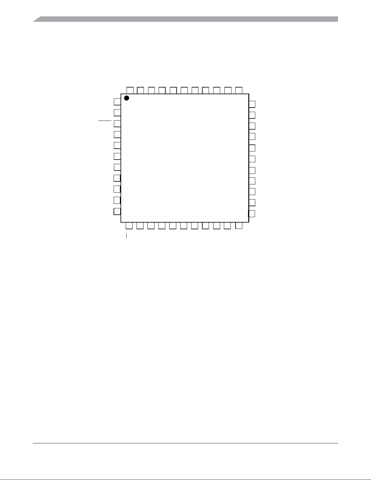
Figure 2-2. MC9S08AW60/48/32/16 in 48-Pin QFN Package
MC9S08AW60 Data Sheet, Rev.1.0
Freescale Semiconductor 25
Chapter 2 Pins and Connections
PTC4
IRQ
RESET
PTF0/TPM1CH2
PTF1/TPM1CH3
PTF4/TPM2CH0
PTF5/TPM2CH1
PTE0/TxD1
PTE1/RxD1
PTE2/TPM1CH0
PTE3/TPM1CH1
11
1
PTC5/RxD2
44
2
3
4
5
6
7
8
9
10
12
PTE4/SS1
PTC3/TxD2
PTC2/MCLK
43 42 41
14
13
PTE6/MOSI1
PTE5/MISO1
PTC0/SCL1
PTC1/SDA1
40
44-Pin LQFP
15 16 17
SS
V
PTE7/SPSCK1
SS
V
39
DD
V
PTG6/EXTAL
PTG5/XTAL
37
38
18
PTG1/KBI1P1
PTG0/KBI1P0
REFL
BKGD/MS
V
35
36
20 21
PTA019PTA1
PTG2/KBI1P2
REFH
V
34
PTG3/KBI1P3
33
32
PTD3/KBI1P6/AD1P11
PTD2/KBI1P5/AD1P10
31
V
30
29
28
27
26
25
24
22
SSAD
V
DDAD
PTD1/AD1P9
PTD0/AD1P8
PTB3/AD1P3
PTB2/AD1P2
PTB1/AD1P1
PTB0/AD1P0
23
Figure 2-3. MC9S08AW60/48/32/16 in 44-Pin LQFP Package
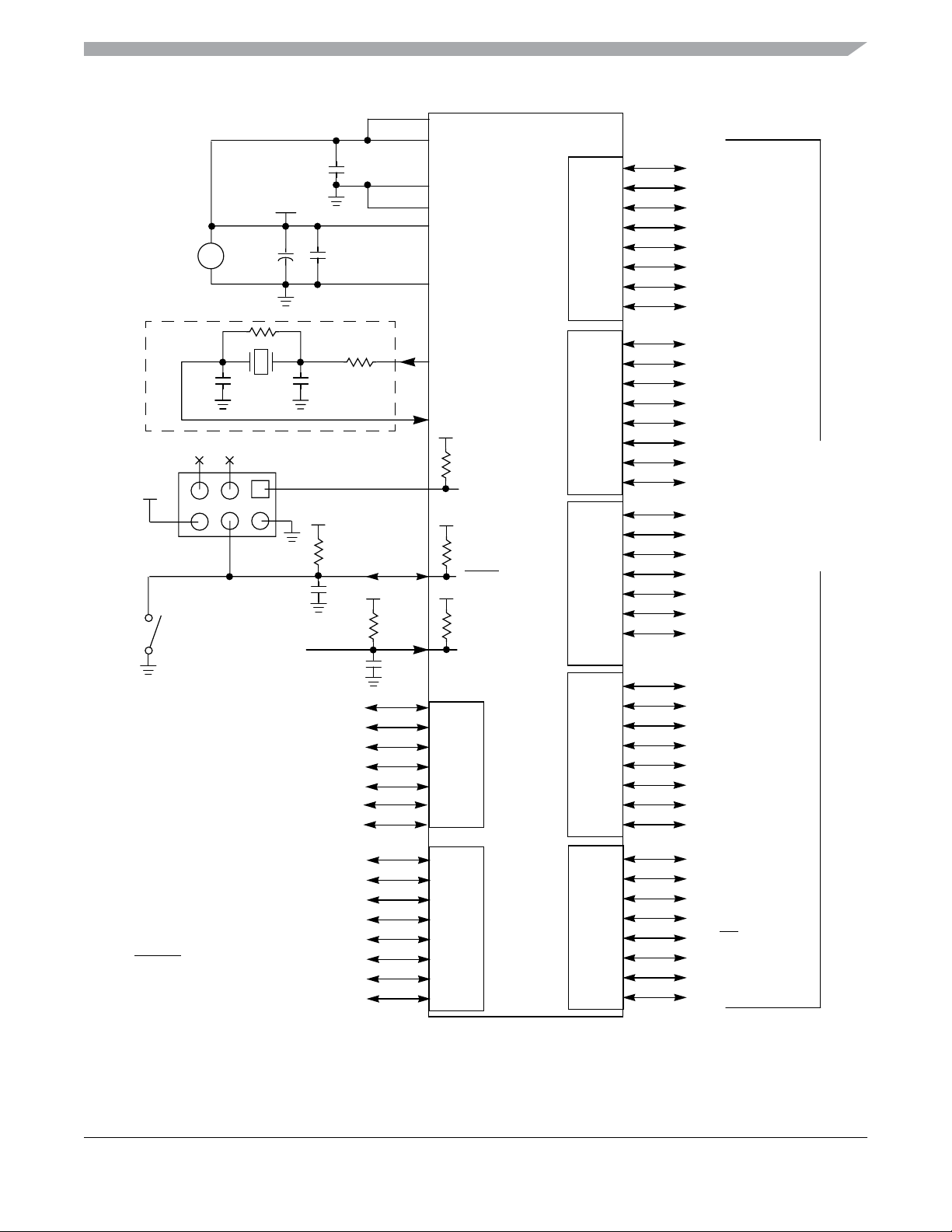
2.3 Recommended System Connections
Figure 2-4 shows pin connections that are common to almost all MC9S08AW60/48/32/16 application
systems.
MC9S08AW60 Data Sheet, Rev.1.0
26 Freescale Semiconductor
SYSTEM
POWER
5 V
Chapter 2 Pins and Connections
V
REFH
DDAD
SSAD
REFL
DD
MC9S08AW60
PORT
A
PTA0
PTA1
PTA2
PTA3
PTA4
PTA5
PTA6
C
BYAD
0.1 µF
V
V
DD
+
C
BLK
10 µF
+
C
BY
0.1 µF
V
V
V
VSS(x2)
PTA7
V
DD
NOTES:
1. Not required if
using the internal
clock option.
2. These are the
same pins as
PTG5 and PTG6
3. RC filters on
RESET and IRQ
are recommended
for EMC-sensitive
applications.
NOTE 1
C1
X1
BACKGROUND HEADER
OPTIONAL
MANUAL
RESET
ASYNCHRONOUS
INTERRUPT
INPUT
R
F
C2
1
V
DD
4.7 kΩ–10 kΩ
0.1 µF
PTG0/KBI1P0
PTG1/KBI1P1
PTG2/KBI1P2
PTG3/KBI1P3
PTG4/KBI1P4
PTG5/XTAL
PTG6/EXTAL
PTF0/TPM1CH2
PTF1/TPM1CH3
PTF2/TPM1CH4
PTF3/TPM1CH5
PTF4/TPM2CH0
PTF5/TPM2CH1
PTF6
PTF7
R
S
XTAL
NOTE 2
EXTAL
NOTE 2
PORT
B
PTB0/AD1P0
PTB1/AD1P1
PTB2/AD1P2
PTB3/AD1P3
PTB4/AD1P4
PTB5/AD1P5
I/O AND
PERIPHERAL
INTERFACE TO
APPLICATION
SYSTEM
V
DD
4.7 kΩ–
10 kΩ
BKGD/MS
RESET
NOTE 3
PORT
C
PTB6/AD1P6
PTB7/AD1P7
PTC0/SCL1
PTC1/SDA1
PTC2/MCLK
PTC3/TxD2
PTC4
PTC5/RxD2
PTC6
IRQ
0.1 µF
NOTE 3
PTD0/AD1P8
PTD1/AD1P9
PTD2/AD1P10/KBI1P5
PORT
G
PORT
D
PTD3/AD1P11/KBI1P6
PTD4/AD1P12/TPM2CLK
PTD5/AD1P13
PTD6/AD1P14/TPM1CLK
PTD7/AD1P15/KBI1P7
PTE0/TxD1
PTE1/RxD1
PTE2/TPM1CH0
PORT
F
PORT
E
PTE3/TPM1CH1
PTE4/
SS1
PTE5/MISO1
PTE6/MOSI1
PTE7/SPSCK1
Figure 2-4. Basic System Connections
MC9S08AW60 Data Sheet, Rev.1.0
Freescale Semiconductor 27

Chapter 2 Pins and Connections
2.3.1 Power (VDD, 2 x VSS, V
DDAD
, V
SSAD
)
VDD and VSS are the primary power supply pins for the MCU. This voltage source supplies power to all
I/O buffer circuitry and to an internal voltage regulator. The internal voltage regulator provides regulated
lower-voltage source to the CPU and other internal circuitry of the MCU.
Typically, application systems have two separate capacitors across the power pins. In this case, there
should be a bulk electrolytic capacitor, such as a 10-µF tantalum capacitor, to provide bulk charge storage
for the overall system and a 0.1-µF ceramic bypass capacitor located as near to the paired V
DD
and V
SS
power pins as practical to suppress high-frequency noise. The MC9S08AW60 has a second VSSpin. This
pin should be connected to the system ground plane or to the primary V
pin through a low-impedance
SS
connection.
V
DDAD
and V
are the analog power supply pins for the MCU. This voltage source supplies power to
SSAD
the ADC module. A 0.1-µF ceramic bypass capacitor should be located as near to the analog power pins
as practical to suppress high-frequency noise.
2.3.2 Oscillator (XTAL, EXTAL)
Out of reset the MCU uses an internally generated clock (self-clocked mode — f
Self_reset
about 8-MHz crystal rate. This frequency source is used during reset startup and can be enabled as the
clock source for stop recovery to avoid the need for a long crystal startup delay. This MCU also contains
a trimmable internal clock generator (ICG) module that can be used to run the MCU. For more information
on the ICG, see the Chapter 8, “Internal Clock Generator (S08ICGV4).”
) equivalent to
The oscillator in this MCU is a Pierce oscillator that can accommodate a crystal or ceramic resonator in
either of two frequency ranges selected by the RANGE bit in the ICGC1 register. Rather than a crystal or
ceramic resonator, an external oscillator can be connected to the EXTAL input pin.
Refer to Figure 2-4 for the following discussion. R
(when used) and RF should be low-inductance
S
resistors such as carbon composition resistors. Wire-wound resistors, and some metal film resistors, have
too much inductance. C1 and C2 normally should be high-quality ceramic capacitors that are specifically
designed for high-frequency applications.
is used to provide a bias path to keep the EXTAL input in its linear range during crystal startup and its
R
F
value is not generally critical. Typical systems use 1 MΩ to 10 MΩ. Higher values are sensitive to humidity
and lower values reduce gain and (in extreme cases) could prevent startup.
C1 and C2 are typically in the 5-pF to 25-pF range and are chosen to match the requirements of a specific
crystal or resonator. Be sure to take into account printed circuit board (PCB) capacitance and MCU pin
capacitance when sizing C1 and C2. The crystal manufacturer typically specifies a load capacitance which
is the series combination of C1 and C2 which are usually the same size. As a first-order approximation,
use 10 pF as an estimate of combined pin and PCB capacitance for each oscillator pin (EXTAL and
XTAL).
2.3.3 RESET
RESET is a dedicated pin with a pullup device built in. It has input hysteresis, a high current output driver,
and no output slew rate control. Internal power-on reset and low-voltage reset circuitry typically make
MC9S08AW60 Data Sheet, Rev.1.0
28 Freescale Semiconductor

Chapter 2 Pins and Connections
external reset circuitry unnecessary. This pin is normally connected to the standard 6-pin background
debug connector so a development system can directly reset the MCU system. If desired, a manual external
reset can be added by supplying a simple switch to ground (pull reset pin low to force a reset).
Whenever any reset is initiated (whether from an external signal or from an internal system), the reset pin
is driven low for approximately 34 bus cycles, released, and sampled again approximately 38 bus cycles
later. If reset was caused by an internal source such as low-voltage reset or watchdog timeout, the circuitry
expects the reset pin sample to return a logic 1. The reset circuitry decodes the cause of reset and records
it by setting a corresponding bit in the system control reset status register (SRS).
In EMC-sensitive applications, an external RC filter is recommended on the reset pin. See Figure 2-4 for
an example.
2.3.4 Background/Mode Select (BKGD/MS)
While in reset, the BKGD/MS pin functions as a mode select pin. Immediately after reset rises the pin
functions as the background pin and can be used for background debug communication. While functioning
as a background/mode select pin, the pin includes an internal pullup device, input hysteresis, a standard
output driver, and no output slew rate control.
If nothing is connected to this pin, the MCU will enter normal operating mode at the rising edge of reset.
If a debug system is connected to the 6-pin standard background debug header, it can hold BKGD/MS low
during the rising edge of reset which forces the MCU to active background mode.
The BKGD pin is used primarily for background debug controller (BDC) communications using a custom
protocol that uses 16 clock cycles of the target MCU’s BDC clock per bit time. The target MCU’s BDC
clock could be as fast as the bus clock rate, so there should never be any significant capacitance connected
to the BKGD/MS pin that could interfere with background serial communications.
Although the BKGD pin is a pseudo open-drain pin, the background debug communication protocol
provides brief, actively driven, high speedup pulses to ensure fast rise times. Small capacitances from
cables and the absolute value of the internal pullup device play almost no role in determining rise and fall
times on the BKGD pin.
2.3.5 ADC Reference Pins (V
The V
REFH
and V
pins are the voltage reference high and voltage reference low inputs respectively
REFL
REFH
, V
REFL
)
for the ADC module.
2.3.6 External Interrupt Pin (IRQ)
The IRQ pin is the input source for the IRQ interrupt and is also the input for the BIH and BIL instructions.
If the IRQ function is not enabled, this pin does not perform any function.
When IRQ is configured as the IRQ input and is set to detect rising edges, a pulldown device rather than
a pullup device is enabled.
In EMC-sensitive applications, an external RC filter is recommended on the IRQ pin. See Figure 2-4 for
an example.
MC9S08AW60 Data Sheet, Rev.1.0
Freescale Semiconductor 29

Chapter 2 Pins and Connections
2.3.7 General-Purpose I/O and Peripheral Ports
The remaining pins are shared among general-purpose I/O and on-chip peripheral functions such as timers
and serial I/O systems. Immediately after reset, all of these pins are configured as high-impedance
general-purpose inputs with internal pullup devices disabled.
NOTE
To avoid extra current drain from floating input pins, the reset initialization
routine in the application program should either enable on-chip pullup
devices or change the direction of unused pins to outputs so the pins do not
float.
For information about controlling these pins as general-purpose I/O pins, see Chapter 6, “Parallel
Input/Output.” For information about how and when on-chip peripheral systems use these pins, refer to the
appropriate chapter from Table 2-1.
Table 2-1. Pin Sharing Priority
Lowest <- Pin Function Priority -> Highest
Port Pins Alternate Function Alternate Function
PTB7–PTB0 AD1P7–AD1P0 Chapter 14, “Analog-to-Digital Converter (S08ADC10V1)”
PTC5, PTC3 RxD2–TxD2 Chapter 11, “Serial Communications Interface (S08SCIV2)”
PTC2 MCLK Chapter 5, “Resets, Interrupts, and System Configuration”
PTC1–PTC0 SCL1–SDA1 Chapter 13, “Inter-Integrated Circuit (S08IICV1)”
PTD7 KBI1P7 AD1P15 Chapter 14, “Analog-to-Digital Converter (S08ADC10V1)”
Chapter 9, “Keyboard Interrupt (S08KBIV1)”
PTD6 TPM1CLK AD1P14 Chapter 14, “Analog-to-Digital Converter (S08ADC10V1)”
Chapter 10, “Timer/PWM (S08TPMV2)”
PTD5 AD1P13 AD1P13 Chapter 14, “Analog-to-Digital Converter (S08ADC10V1)”
PTD4 TPM2CLK AD1P12 Chapter 14, “Analog-to-Digital Converter (S08ADC10V1)”
Chapter 10, “Timer/PWM (S08TPMV2)”
PTD3–PTD2 KBI1P6–KBI1P5 AD1P11–AD1P10 Chapter 14, “Analog-to-Digital Converter (S08ADC10V1)”
Chapter 9, “Keyboard Interrupt (S08KBIV1)”
PTD1–PTD0 AD1P9–AD1P8 Chapter 14, “Analog-to-Digital Converter (S08ADC10V1)”
PTE7
PTE6
PTE5
PTE4
PTE3–PTE2 TPM1CH1–
PTE1–PTE0 RxD1–TxD1 Chapter 11, “Serial Communications Interface (S08SCIV2)”
PTF5–PTF4 TPM2CH1–
PTF3–PTF0 TPM1CH5–
PTG4–PTG0 KBI1P4–KBI1P0 Chapter 9, “Keyboard Interrupt (S08KBIV1)”
PTG6–PTG5 EXTAL–XTAL Chapter 8, “Internal Clock Generator (S08ICGV4)”
1
See the listed chapter for information about modules that share these pins.
SPSCK1
MOSI1
MISO1
SS1
TPM1CH0
TPM2CH0
TPM1CH2
Chapter 12, “Serial Peripheral Interface (S08SPIV3)”
Chapter 10, “Timer/PWM (S08TPMV2)”
Chapter 10, “Timer/PWM (S08TPMV2)”
Chapter 10, “Timer/PWM (S08TPMV2)”
Reference
1
MC9S08AW60 Data Sheet, Rev.1.0
30 Freescale Semiconductor

Chapter 2 Pins and Connections
When an on-chip peripheral system is controlling a pin, data direction control bits still determine what is
read from port data registers even though the peripheral module controls the pin direction by controlling
the enable for the pin’s output buffer. See the Chapter 6, “Parallel Input/Output” chapter for more details.
Pullup enable bits for each input pin control whether on-chip pullup devices are enabled whenever the pin
is acting as an input even if it is being controlled by an on-chip peripheral module. When the PTD7, PTD3,
PTD2, and PTG4 pins are controlled by the KBI module and are configured for rising-edge/high-level
sensitivity, the pullup enable control bits enable pulldown devices rather than pullup devices.
NOTE
When an alternative function is first enabled it is possible to get a spurious
edge to the module, user software should clear out any associated flags
before interrupts are enabled. Table 2-1 illustrates the priority if multiple
modules are enabled. The highest priority module will have control over the
pin. Selecting a higher priority pin function with a lower priority function
already enabled can cause spurious edges to the lower priority module. It is
recommended that all modules that share a pin be disabled before enabling
another module.
MC9S08AW60 Data Sheet, Rev.1.0
Freescale Semiconductor 31

Chapter 2 Pins and Connections
MC9S08AW60 Data Sheet, Rev.1.0
32 Freescale Semiconductor

Chapter 3 Modes of Operation
3.1 Introduction
The operating modes of the MC9S08AW60/48/32/16 are described in this chapter. Entry into each mode,
exit from each mode, and functionality while in each of the modes are described.
3.2 Features
• Active background mode for code development
• Wait mode:
— CPU shuts down to conserve power
— System clocks running
— Full voltage regulation maintained
• Stop modes:
— System clocks stopped; voltage regulator in standby
— Stop2 — Partial power down of internal circuits, RAM contents retained
— Stop3 — All internal circuits powered for fast recovery
3.3 Run Mode
This is the normal operating mode for the MC9S08AW60/48/32/16. This mode is selected when the
BKGD/MS pin is high at the rising edge of reset. In this mode, the CPU executes code from internal
memory with execution beginning at the address fetched from memory at $FFFE:$FFFF after reset.
3.4 Active Background Mode
The active background mode functions are managed through the background debug controller (BDC) in
the HCS08 core. The BDC, together with the on-chip debug module (DBG), provide the means for
analyzing MCU operation during software development.
Active background mode is entered in any of five ways:
• When the BKGD/MS pin is low at the rising edge of reset
• When a BACKGROUND command is received through the BKGD pin
• When a BGND instruction is executed
• When encountering a BDC breakpoint
• When encountering a DBG breakpoint
MC9S08AW60 Data Sheet, Rev.1.0
Freescale Semiconductor 33

Chapter 3 Modes of Operation
After entering active background mode, the CPU is held in a suspended state waiting for serial background
commands rather than executing instructions from the user’s application program.
Background commands are of two types:
• Non-intrusive commands, defined as commands that can be issued while the user program is
running. Non-intrusive commands can be issued through the BKGD pin while the MCU is in run
mode; non-intrusive commands can also be executed when the MCU is in the active background
mode. Non-intrusive commands include:
— Memory access commands
— Memory-access-with-status commands
— BDC register access commands
— The BACKGROUND command
• Active background commands, which can only be executed while the MCU is in active background
mode. Active background commands include commands to:
— Read or write CPU registers
— Trace one user program instruction at a time
— Leave active background mode to return to the user’s application program (GO)
The active background mode is used to program a bootloader or user application program into the FLASH
program memory before the MCU is operated in run mode for the first time. When the
MC9S08AW60/48/32/16 is shipped from the Freescale Semiconductor factory, the FLASH program
memory is erased by default unless specifically noted so there is no program that could be executed in run
mode until the FLASH memory is initially programmed. The active background mode can also be used to
erase and reprogram the FLASH memory after it has been previously programmed.
For additional information about the active background mode, refer to Chapter 15, “Development
Support.”
3.5 Wait Mode
Wait mode is entered by executing a WAIT instruction. Upon execution of the WAIT instruction, the CPU
enters a low-power state in which it is not clocked. The I bit in CCR is cleared when the CPU enters the
wait mode, enabling interrupts. When an interrupt request occurs, the CPU exits the wait mode and
resumes processing, beginning with the stacking operations leading to the interrupt service routine.
While the MCU is in wait mode, there are some restrictions on which background debug commands can
be used. Only the BACKGROUND command and memory-access-with-status commands are available
when the MCU is in wait mode. The memory-access-with-status commands do not allow memory access,
but they report an error indicating that the MCU is in either stop or wait mode. The BACKGROUND
command can be used to wake the MCU from wait mode and enter active background mode.
3.6 Stop Modes
One of two stop modes is entered upon execution of a STOP instruction when the STOPE bit in the system
option register is set. In both stop modes, all internal clocks are halted. If the STOPE bit is not set when
MC9S08AW60 Data Sheet, Rev.1.0
34 Freescale Semiconductor

Chapter 3 Modes of Operation
the CPU executes a STOP instruction, the MCU will not enter either of the stop modes and an illegal
opcode reset is forced. The stop modes are selected by setting the appropriate bits in SPMSC2.
HCS08 devices that are designed for low voltage operation (1.8V to 3.6V) also include stop1 mode. The
MC9S08AW60/48/32/16 family of devices does not include stop1 mode.
Table 3-1 summarizes the behavior of the MCU in each of the stop modes.
Table 3-1. Stop Mode Behavior
CPU, Digital
Mode PPDC
Peripherals,
FLASH
RAM ICG ADC1 Regulator I/O Pins RTI
Stop2 1 Off Standby Off Disabled Standby States
1
Stop3 0 Standby Standby Off
1
Crystal oscillator can be configured to run in stop3. Please see the ICG registers.
Optionally on Standby States
held
held
Optionally on
Optionally on
3.6.1 Stop2 Mode
The stop2 mode provides very low standby power consumption and maintains the contents of RAM and
the current state of all of the I/O pins. To enter stop2, the user must execute a STOP instruction with stop2
selected (PPDC = 1) and stop mode enabled (STOPE = 1). In addition, the LVD must not be enabled to
operate in stop (LVDSE = 0 or LVDE = 0). If the LVD is enabled in stop, then the MCU enters stop3 upon
the execution of the STOP instruction regardless of the state of PPDC.
Before entering stop2 mode, the user must save the contents of the I/O port registers, as well as any other
memory-mapped registers which they want to restore after exit of stop2, to locations in RAM. Upon exit
of stop2, these values can be restored by user software before pin latches are opened.
When the MCU is in stop2 mode, all internal circuits that are powered from the voltage regulator are turned
off, except for the RAM. The voltage regulator is in a low-power standby state, as is the ADC. Upon entry
into stop2, the states of the I/O pins are latched. The states are held while in stop2 mode and after exiting
stop2 mode until a logic 1 is written to PPDACK in SPMSC2.
Exit from stop2 is done by asserting either of the wake-up pins:
RESET or IRQ, or by an RTI interrupt.
IRQ is always an active low input when the MCU is in stop2, regardless of how it was configured before
entering stop2.
NOTE
Although this IRQ pin is automatically configured as active low input, the
pullup associated with the IRQ pin is not automatically enabled. Therefore,
if an external pullup is not used, the internal pullup must be enabled by
setting IRQPE in IRQSC.
Upon wake-up from stop2 mode, the MCU will start up as from a power-on reset (POR) except pin states
remain latched. The CPU will take the reset vector. The system and all peripherals will be in their default
reset states and must be initialized.
MC9S08AW60 Data Sheet, Rev.1.0
Freescale Semiconductor 35

Chapter 3 Modes of Operation
After waking up from stop2, the PPDF bit in SPMSC2 is set. This flag may be used to direct user code to
go to a stop2 recovery routine. PPDF remains set and the I/O pin states remain latched until a logic 1 is
written to PPDACK in SPMSC2.
To maintain I/O state for pins that were configured as general-purpose I/O, the user must restore the
contents of the I/O port registers, which have been saved in RAM, to the port registers before writing to
the PPDACK bit. If the port registers are not restored from RAM before writing to PPDACK, then the
register bits will assume their reset states when the I/O pin latches are opened and the I/O pins will switch
to their reset states.
For pins that were configured as peripheral I/O, the user must reconfigure the peripheral module that
interfaces to the pin before writing to the PPDACK bit. If the peripheral module is not enabled before
writing to PPDACK, the pins will be controlled by their associated port control registers when the I/O
latches are opened.
3.6.2 Stop3 Mode
Stop3 mode is entered by executing a STOP instruction under the conditions as shown in Table 3-1. The
states of all of the internal registers and logic, RAM contents, and I/O pin states are maintained.
Stop3 can be exited by asserting
RESET, or by an interrupt from one of the following sources: the real-time
interrupt (RTI), LVD, ADC, IRQ, or the KBI.
If stop3 is exited by means of the
RESET pin, then the MCU is reset and operation will resume after taking
the reset vector. Exit by means of one of the internal interrupt sources results in the MCU taking the
appropriate interrupt vector.
3.6.3 Active BDM Enabled in Stop Mode
Entry into the active background mode from run mode is enabled if the ENBDM bit in BDCSCR is set.
This register is described in Chapter 15, “Development Support” of this data sheet. If ENBDM is set when
the CPU executes a STOP instruction, the system clocks to the background debug logic remain active when
the MCU enters stop mode so background debug communication is still possible. In addition, the voltage
regulator does not enter its low-power standby state but maintains full internal regulation. If the user
attempts to enter stop2 with ENBDM set, the MCU will instead enter stop3.
Most background commands are not available in stop mode. The memory-access-with-status commands
do not allow memory access, but they report an error indicating that the MCU is in either stop or wait
mode. The BACKGROUND command can be used to wake the MCU from stop and enter active
background mode if the ENBDM bit is set. After entering background debug mode, all background
commands are available. Table 3-2 summarizes the behavior of the MCU in stop when entry into the
background debug mode is enabled.
MC9S08AW60 Data Sheet, Rev.1.0
36 Freescale Semiconductor

Mode PPDC
Table 3-2. BDM Enabled Stop Mode Behavior
CPU, Digital
Peripherals,
FLASH
Chapter 3 Modes of Operation
RAM ICG ADC1 Regulator I/O Pins RTI
Stop3 0 Standby Standby Active Optionally on Active States
held
Optionally on
3.6.4 LVD Enabled in Stop Mode
The LVD system is capable of generating either an interrupt or a reset when the supply voltage drops below
the LVD voltage. If the LVD is enabled in stop by setting the LVDE and the LVDSE bits, then the voltage
regulator remains active during stop mode. If the user attempts to enter stop2 with the LVD enabled for
stop, the MCU will instead enter stop3. Table 3-3 summarizes the behavior of the MCU in stop when the
LVD is enabled.
Table 3-3. LVD Enabled Stop Mode Behavior
CPU, Digital
Mode PPDC
Stop3 0 Standby Standby Off
1
Crystal oscillator can be configured to run in stop3. Please see the ICG registers.
Peripherals,
FLASH
RAM ICG ADC1 Regulator I/O Pins RTI
1
Optionally on Active States
held
Optionally on
3.6.5 On-Chip Peripheral Modules in Stop Modes
When the MCU enters any stop mode, system clocks to the internal peripheral modules are stopped. Even
in the exception case (ENBDM = 1), where clocks to the background debug logic continue to operate,
clocks to the peripheral systems are halted to reduce power consumption. Refer to Section 3.6.1, “Stop2
Mode,” and Section 3.6.2, “Stop3 Mode,” for specific information on system behavior in stop modes.
Table 3-4. Stop Mode Behavior
Mode
Peripheral
Stop2 Stop3
CPU Off Standby
RAM Standby Standby
FLASH Off Standby
Parallel Port Registers Off Standby
ADC1 Off Optionally On
ICG Off Optionally On
IIC Off Standby
MC9S08AW60 Data Sheet, Rev.1.0
1
2
Freescale Semiconductor 37

Chapter 3 Modes of Operation
KBI Off Optionally On
RTI Optionally On
SCI Off Standby
SPI Off Standby
TPM Off Standby
Voltage Regulator Standby Standby
I/O Pins States Held States Held
1
Requires the asynchronous ADC clock and LVD to be enabled, else in
standby.
2
OSCSTEN set in ICSC1, else in standby. For high frequency range (RANGE
in ICSC2 set) requires the LVD to also be enabled in stop3.
3
During stop3, KBI pins that are enabled continue to function as interrupt
sources that are capable of waking the MCU from stop3.
4
This RTI can be enabled to run in stop2 or stop3 with the internal RTI clock
source (RTICLKS = 0, in SRTISC). The RTI also can be enabled to run in
stop3 with the external clock source (RTICLKS = 1 and OSCSTEN = 1).
Table 3-4. Stop Mode Behavior (continued)
Mode
Peripheral
Stop2 Stop3
4
Optionally On
3
4
MC9S08AW60 Data Sheet, Rev.1.0
38 Freescale Semiconductor

Chapter 4 Memory
4.1 MC9S08AW60/48/32/16 Memory Map
Figure 4-1 shows the memory map for the MC9S08AW60 and MC9S08AW48 MCUs. Figure 4-2 shows
the memory map for the MC9S08AW32 and MC9S08AW16 MCUs. On-chip memory in the
MC9S08AW60/48/32/16 series of MCUs consists of RAM, FLASH program memory for nonvolatile data
storage, plus I/O and control/status registers. The registers are divided into three groups:
• Direct-page registers ($0000 through $006F)
• High-page registers ($1800 through $185F)
• Nonvolatile registers ($FFB0 through $FFBF)
MC9S08AW60 Data Sheet, Rev.1.0
Freescale Semiconductor 39

Chapter 4 Memory
$0000
$006F
$0070
$086F
$0870
$17FF
$1800
$185F
$1860
DIRECT PAGE REGISTERS
RAM
2048 BYTES
FLASH
3984 BYTES
HIGH PAGE REGISTERS
FLASH
59,296 BYTES
$0000
$006F
$0070
$086F
$0870
$17FF
$1800
$185F
$1860
$3FFF
$4000
DIRECT PAGE REGISTERS
RAM
2048 BYTES
RESERVED
3984 BYTES
HIGH PAGE REGISTERS
RESERVED
10,144 BYTES
FLASH
49,152 BYTES
$FFFF
MC9S08AW60
$FFFF
MC9S08AW48
Figure 4-1. MC9S08AW60 and MC9S08AW48 Memory Map
MC9S08AW60 Data Sheet, Rev.1.0
40 Freescale Semiconductor

Chapter 4 Memory
$0000
$006F
$0070
$086F
$0870
$17FF
$1800
$185F
$1860
$7FFF
$8000
DIRECT PAGE REGISTERS
RAM
2048 BYTES
RESERVED
3984 BYTES
HIGH PAGE REGISTERS
RESERVED
26,528 BYTES
FLASH
32,768 BYTES
$0000
$006F
$0070
$046F
$0470
$17FF
$1800
$185F
$1860
$BFFF
$C000
DIRECT PAGE REGISTERS
RAM
1024 BYTES
RESERVED
5008 BYTES
HIGH PAGE REGISTERS
RESERVED
42,912 BYTES
FLASH
16,384 BYTES
$FFFF
$FFFF
MC9S08AW32
MC9S08AW16
Figure 4-2. MC9S08AW32 and MC9S08AW16 Memory Map
MC9S08AW60 Data Sheet, Rev.1.0
Freescale Semiconductor 41

Chapter 4 Memory
4.1.1 Reset and Interrupt Vector Assignments
Figure 4-1 shows address assignments for reset and interrupt vectors. The vector names shown in this table
are the labels used in the Freescale-provided equate file for the MC9S08AW60/48/32/16. For more details
about resets, interrupts, interrupt priority, and local interrupt mask controls, refer to Chapter 5, “Resets,
Interrupts, and System Configuration.”
Table 4-1. Reset and Interrupt Vectors
Address
(High/Low)
$FFC0:FFC1
$FFCA:FFCB
$FFCC:FFCD RTI Vrti
$FFCE:FFCF IIC1 Viic1
$FFD0:FFD1 ADC1 Conversion Vadc1
$FFD2:FFD3 KBI1 Vkeyboard1
$FFD4:FFD5 SCI2 Transmit Vsci2tx
$FFD6:FFD7 SCI2 Receive Vsci2rx
$FFD8:FFD9 SCI2 Error Vsci2err
$FFDA:FFDB SCI1 Transmit Vsci1tx
$FFDC:FFDD SCI1 Receive Vsci1rx
$FFDE:FFDF SCI1 Error Vsci1err
$FFE0:FFE1 SPI1 Vspi1
$FFE2:FFE3 TPM2 Overflow Vtpm2ovf
$FFE4:FFE5 TPM2 Channel 1 Vtpm2ch1
$FFE6:FFE7 TPM2 Channel 0 Vtpm2ch0
$FFE8:FFE9 TPM1 Overflow Vtpm1ovf
$FFEA:FFEB TPM1 Channel 5 Vtpm1ch5
$FFEC:FFED TPM1 Channel 4 Vtpm1ch4
$FFEE:FFEF TPM1 Channel 3 Vtpm1ch3
$FFF0:FFF1 TPM1 Channel 2 Vtpm1ch2
$FFF2:FFF3 TPM1 Channel 1 Vtpm1ch1
$FFF4:FFF5 TPM1 Channel 0 Vtpm1ch0
$FFF6:FFF7 ICG Vicg
$FFF8:FFF9 Low Voltage Detect Vlvd
$FFFA:FFFB IRQ Virq
$FFFC:FFFD SWI Vswi
$FFFE:FFFF Reset Vreset
Unused Vector Space
(available for user program)
Vector Vector Name
MC9S08AW60 Data Sheet, Rev.1.0
42 Freescale Semiconductor

Chapter 4 Memory
4.2 Register Addresses and Bit Assignments
The registers in the MC9S08AW60/48/32/16 are divided into these three groups:
• Direct-page registers are located in the first 112 locations in the memory map, so they are
accessible with efficient direct addressing mode instructions.
• High-page registers are used much less often, so they are located above $1800 in the memory map.
This leaves more room in the direct page for more frequently used registers and variables.
• The nonvolatile register area consists of a block of 16 locations in FLASH memory at
$FFB0–$FFBF.
Nonvolatile register locations include:
— Three values which are loaded into working registers at reset
— An 8-byte backdoor comparison key which optionally allows a user to gain controlled access
to secure memory
Because the nonvolatile register locations are FLASH memory, they must be erased and
programmed like other FLASH memory locations.
Direct-page registers can be accessed with efficient direct addressing mode instructions. Bit manipulation
instructions can be used to access any bit in any direct-page register. Table 4-2 is a summary of all
user-accessible direct-page registers and control bits.
The direct page registers in Table 4-2 can use the more efficient direct addressing mode which only
requires the lower byte of the address. Because of this, the lower byte of the address in column one is
shown in bold text. In Table 4-3 and Table 4-4 the whole address in column one is shown in bold. In
Table 4-2, Table 4-3, and Table 4-4, the register names in column two are shown in bold to set them apart
from the bit names to the right. Cells that are not associated with named bits are shaded. A shaded cell with
a 0 indicates this unused bit always reads as a 0. Shaded cells with dashes indicate unused or reserved bit
locations that could read as 1s or 0s.
MC9S08AW60 Data Sheet, Rev.1.0
Freescale Semiconductor 43

Chapter 4 Memory
Table 4-2. Direct-Page Register Summary (Sheet 1 of 3)
Address Register Name Bit 7 654321Bit 0
$0000 PTAD
$0001 PTADD
$0002 PTBD
$0003 PTBDD
$0004 PTCD
$0005 PTCDD
$0006 PTDD
$0007 PTDDD
$0008 PTED
$0009 PTEDD
$000A PTFD
$000B PTFDD
$000C PTGD
$000D PTGDD
$000E–
$000F
Reserved
$0010 ADC1SC1
$0011 ADC1SC2
$0012 ADC1RH
$0013 ADC1RL
$0014 ADC1CVH
$0015 ADC1CVL
$0016 ADC1CFG
$0017 APCTL1
$0018 APCTL2
$0019 APCTL3
$001A–
$001B
Reserved
$001C IRQSC
$001D Reserved
$001E KBISC
$001F KBIPE
$0020 TPM1SC
$0021 TPM1CNTH
$0022 TPM1CNTL
$0023 TPM1MODH
$0024 TPM1MODL
$0025 TPM1C0SC
$0026 TPM1C0VH
$0027 TPM1C0VL
PTAD7 PTAD6 PTAD5 PTAD4 PTAD3 PTAD2 PTAD1 PTAD0
PTADD7 PTADD6 PTADD5 PTADD4 PTADD3 PTADD2 PTADD1 PTADD0
PTBD7 PTBD6 PTBD5 PTBD4 PTBD3 PTBD2 PTBD1 PTBD0
PTBDD7 PTBDD6 PTBDD5 PTBDD4 PTBDD3 PTBDD2 PTBDD1 PTBDD0
0 PTCD6 PTCD5 PTCD4 PTCD3 PTCD2 PTCD1 PTCD0
0 PTCDD6 PTCDD5 PTCDD4 PTCDD3 PTCDD2 PTCDD1 PTCDD0
PTDD7 PTDD6 PTDD5 PTDD4 PTDD3 PTDD2 PTDD1 PTDD0
PTDDD7 PTDDD6 PTDDD5 PTDDD4 PTDDD3 PTDDD2 PTDDD1 PTDDD0
PTED7 PTED6 PTED5 PTED4 PTED3 PTED2 PTED1 PTED0
PTEDD7 PTEDD6 PTEDD5 PTEDD4 PTEDD3 PTEDD2 PTEDD1 PTEDD0
PTFD7 PTFD6 PTFD5 PTFD4 PTFD3 PTFD2 PTFD1 PTFD0
PTFDD7 PTFDD6 PTFDD5 PTFDD4 PTFDD3 PTFDD2 PTFDD1 PTFDD0
0 PTGD6 PTGD5 PTGD4 PTGD3 PTGD2 PTGD1 PTGD0
0 PTGDD6 PTGDD5 PTGDD4 PTGDD3 PTGDD2 PTGDD1 PTGDD0
—
—
COCO AIEN ADCO ADCH
ADACT ADTRG ACFE ACFGT 0 0 R R
0 0 0 0 0 0 ADR9 ADR8
ADR7 ADR6 ADR5 ADR4 ADR3 ADR2 ADR1 ADR0
0 0 0 0 0 0 ADCV9 ADCV8
ADCV7 ADCV6 ADCV5 ADCV4 ADCV3 ADCV2 ADCV1 ADCV0
ADLPC ADIV ADLSMP MODE ADICLK
ADPC7 ADPC6 ADPC5 ADPC4 ADPC3 ADPC2 ADPC1 ADPC0
ADPC15 ADPC14 ADPC13 ADPC12 ADPC11 ADPC10 ADPC9 ADPC8
ADPC23 ADPC22 ADPC21 ADPC20 ADPC19 ADPC18 ADPC17 ADPC16
—
—
0 0 IRQEDG IRQPE IRQF IRQACK IRQIE IRQMOD
— — — — — — — —
KBEDG7 KBEDG6 KBEDG5 KBEDG4 KBF KBACK KBIE KBIMOD
KBIPE7 KBIPE6 KBIPE5 KBIPE4 KBIPE3 KBIPE2 KBIPE1 KBIPE0
TOF TOIE CPWMS CLKSB CLKSA PS2 PS1 PS0
Bit 15 14 13 12 11 10 9 Bit 8
Bit 7 654321Bit 0
Bit 15 14 13 12 11 10 9 Bit 8
Bit 7 654321Bit 0
CH0F CH0IE MS0B MS0A ELS0B ELS0A 0 0
Bit 15 14 13 12 11 10 9 Bit 8
Bit 7 654321Bit 0
—
—
—
—
—
—
—
—
—
—
—
—
—
—
—
—
—
—
—
—
—
—
—
—
—
—
—
—
MC9S08AW60 Data Sheet, Rev.1.0
44 Freescale Semiconductor

Chapter 4 Memory
Table 4-2. Direct-Page Register Summary (Sheet 2 of 3)
Address Register Name Bit 7 654321Bit 0
$0028 TPM1C1SC
$0029 TPM1C1VH
$002A TPM1C1VL
$002B TPM1C2SC
$002C TPM1C2VH
$002D TPM1C2VL
$002E TPM1C3SC
$002F TPM1C3VH
$0030 TPM1C3VL
$0031 TPM1C4SC
$0032 TPM1C4VH
$0033 TPM1C4VL
$0034 TPM1C5SC
$0035 TPM1C5VH
$0036 TPM1C5VL
$0037 Reserved
$0038 SCI1BDH
$0039 SCI1BDL
$003A SCI1C1
$003B SCI1C2
$003C SCI1S1
$003D SCI1S2
$003E SCI1C3
$003F SCI1D
$0040 SCI2BDH
$0041 SCI2BDL
$0042 SCI2C1
$0043 SCI2C2
$0044 SCI2S1
$0045 SCI2S2
$0046 SCI2C3
$0047 SCI2D
$0048 ICGC1
$0049 ICGC2
$004A ICGS1
$004B ICGS2
$004C ICGFLTU
$004D ICGFLTL
$004E ICGTRM
$004F Reserved
CH1F CH1IE MS1B MS1A ELS1B ELS1A 0 0
Bit 15 14 13 12 11 10 9 Bit 8
Bit 7 654321Bit 0
CH2F CH2IE MS2B MS2A ELS2B ELS2A 0 0
Bit 15 14 13 12 11 10 9 Bit 8
Bit 7 654321Bit 0
CH3F CH3IE MS3B MS3A ELS3B ELS3A 0 0
Bit 15 14 13 12 11 10 9 Bit 8
Bit 7 654321Bit 0
CH4F CH4IE MS4B MS4A ELS4B ELS4A 0 0
Bit 15 14 13 12 11 10 9 Bit 8
Bit 7 654321Bit 0
CH5F CH5IE MS5B MS5A ELS5B ELS5A 0 0
Bit 15 14 13 12 11 10 9 Bit 8
Bit 7 654321Bit 0
— — — — — — — —
0 0 0 SBR12 SBR11 SBR10 SBR9 SBR8
SBR7 SBR6 SBR5 SBR4 SBR3 SBR2 SBR1 SBR0
LOOPS SCISWAI RSRC M WAKE ILT PE PT
TIE TCIE RIE ILIE TE RE RWU SBK
TDRE TC RDRF IDLE OR NF FE PF
0 0 0 0 0 BRK13 0 RAF
R8 T8 TXDIR TXINV ORIE NEIE FEIE PEIE
Bit 7 654321Bit 0
0 0 0 SBR12 SBR11 SBR10 SBR9 SBR8
SBR7 SBR6 SBR5 SBR4 SBR3 SBR2 SBR1 SBR0
LOOPS SCISWAI RSRC M WAKE ILT PE PT
TIE TCIE RIE ILIE TE RE RWU SBK
TDRE TC RDRF IDLE OR NF FE PF
0 0 0 0 0 BRK13 0 RAF
R8 T8 TXDIR TXINV ORIE NEIE FEIE PEIE
Bit 7 654321Bit 0
HGO RANGE REFS CLKS OSCSTEN LOCD 0
LOLRE MFD LOCRE RFD
CLKST REFST LOLS LOCK LOCS ERCS ICGIF
0 0 0 0 0 0 0 DCOS
0 0 0 0FLT
FLT
TRIM
— — — — — — — —
MC9S08AW60 Data Sheet, Rev.1.0
Freescale Semiconductor 45

Chapter 4 Memory
Table 4-2. Direct-Page Register Summary (Sheet 3 of 3)
Address Register Name Bit 7 654321Bit 0
$0050 SPI1C1
$0051 SPI1C2
$0052 SPI1BR
$0053 SPI1S
$0054 Reserved
$0055 SPI1D
$0056–
$0057
Reserved
$0058 IIC1A
$0059 IIC1F
$005A IIC1C
$005B IIC1S
$005C IIC1D
$005D–
$005F
Reserved
$0060 TPM2SC
$0061 TPM2CNTH
$0062 TPM2CNTL
$0063 TPM2MODH
$0064 TPM2MODL
$0065 TPM2C0SC
$0066 TPM2C0VH
$0067 TPM2C0VL
$0068 TPM2C1SC
$0069 TPM2C1VH
$006A TPM2C1VL
$006B–
$006F
Reserved
SPIE SPE SPTIE MSTR CPOL CPHA SSOE LSBFE
0 0 0 MODFEN BIDIROE 0 SPISWAI SPC0
0 SPPR2 SPPR1 SPPR0 0 SPR2 SPR1 SPR0
SPRF 0 SPTEF MODF 0 0 0 0
0 0 0 0 0 0 0 0
Bit 7 654321Bit 0
—
—
MULT ICR
IICEN IICIE MST TX TXAK RSTA 0 0
TCF IAAS BUSY ARBL 0 SRW IICIF RXAK
—
—
TOF TOIE CPWMS CLKSB CLKSA PS2 PS1 PS0
Bit 15 14 13 12 11 10 9 Bit 8
Bit 7 654321Bit 0
Bit 15 14 13 12 11 10 9 Bit 8
Bit 7 654321Bit 0
CH0F CH0IE MS0B MS0A ELS0B ELS0A 0 0
Bit 15 14 13 12 11 10 9 Bit 8
Bit 7 654321Bit 0
CH1F CH1IE MS1B MS1A ELS1B ELS1A 0 0
Bit 15 14 13 12 11 10 9 Bit 8
Bit 7 654321Bit 0
—
—
—
—
—
—
—
—
—
—
—
—
—
—
—
—
ADDR 0
DATA
—
—
—
—
—
—
—
—
—
—
—
—
—
—
—
—
—
—
—
—
—
—
—
—
—
—
—
—
MC9S08AW60 Data Sheet, Rev.1.0
46 Freescale Semiconductor

Chapter 4 Memory
High-page registers, shown in Table 4-3, are accessed much less often than other I/O and control registers
so they have been located outside the direct addressable memory space, starting at $1800.
Table 4-3. High-Page Register Summary (Sheet 1 of 2)
Address Register Name Bit 7 654321Bit 0
$1800 SRS
$1801 SBDFR
$1802 SOPT
$1803 SMCLK
$1804 –
$1805
Reserved
$1806 SDIDH
$1807 SDIDL
$1808 SRTISC
$1809 SPMSC1
$180A SPMSC2
$180B–
$180F
Reserved
$1810 DBGCAH
$1811 DBGCAL
$1812 DBGCBH
$1813 DBGCBL
$1814 DBGFH
$1815 DBGFL
$1816 DBGC
$1817 DBGT
$1818 DBGS
$1819–
$181F
Reserved
$1820 FCDIV
$1821 FOPT
$1822 Reserved
$1823 FCNFG
$1824 FPROT
$1825 FSTAT
$1826 FCMD
$1827–
$183F
Reserved
$1840 PTAPE
$1841 PTASE
$1842 PTADS
$1843 Reserved
$1844 PTBPE
$1845 PTBSE
POR PIN COP ILOP 0 ICG LVD 0
0 0 0 0 0 0 0 BDFR
COPE COPT STOPE — 0 0 — —
0 0 0 MPE 0 MCSEL
—
—
REV3 REV2 REV1 REV0 ID11 ID10 ID9 ID8
ID7 ID6 ID5 ID4 ID3 ID2 ID1 ID0
RTIF RTIACK RTICLKS RTIE 0 RTIS2 RTIS1 RTIS0
LVDF LVDACK LVDIE LVDRE LVDSE LVDE 0
LVWF LVWACK LVDV LVWV PPDF PPDACK — PPDC
—
—
Bit 15 14 13 12 11 10 9 Bit 8
Bit 7 654321Bit 0
Bit 15 14 13 12 11 10 9 Bit 8
Bit 7 654321Bit 0
Bit 15 14 13 12 11 10 9 Bit 8
Bit 7 654321Bit 0
DBGEN ARM TAG BRKEN RWA RWAEN RWB RWBEN
TRGSEL BEGIN 0 0 TRG3 TRG2 TRG1 TRG0
AF BF ARMF 0 CNT3 CNT2 CNT1 CNT0
—
—
DIVLD PRDIV8 DIV5 DIV4 DIV3 DIV2 DIV1 DIV0
KEYEN FNORED 0 0 0 0 SEC01 SEC00
— — — — — — — —
0 0 KEYACC 0 0 0 0 0
FPS7 FPS6 FPS5 FPS4 FPS3 FPS2 FPS1 FPDIS
FCBEF FCCF FPVIOL FACCERR 0 FBLANK 0 0
FCMD7 FCMD6 FCMD5 FCMD4 FCMD3 FCMD2 FCMD1 FCMD0
—
—
PTAPE7 PTAPE6 PTAPE5 PTAPE4 PTAPE3 PTAPE2 PTAPE1 PTAPE0
PTASE7 PTASE6 PTASE5 PTASE4 PTASE3 PTASE2 PTASE1 PTASE0
PTADS7 PTADS6 PTADS5 PTADS4 PTADS3 PTADS2 PTADS1 PTADS0
— — — — — — — —
PTBPE7 PTBPE6 PTBPE5 PTBPE4 PTBPE3 PTBPE2 PTBPE1 PTBPE0
PTBSE7 PTBSE6 PTBSE5 PTBSE4 PTBSE3 PTBSE2 PTBSE1 PTBSE0
—
—
—
—
—
—
—
—
—
—
—
—
—
—
—
—
—
—
—
—
—
—
—
—
—
—
—
—
—
—
—
—
—
—
—
—
—
—
—
—
—
—
—
—
—
—
—
—
—
—
1
BGBE
—
—
—
—
—
—
MC9S08AW60 Data Sheet, Rev.1.0
Freescale Semiconductor 47
Chapter 4 Memory
Table 4-3. High-Page Register Summary (Sheet 2 of 2)
Address Register Name Bit 7 654321Bit 0
$1846 PTBDS
$1847 Reserved
$1848 PTCPE
$1849 PTCSE
$184A PTCDS
$184B Reserved
$184C PTDPE
$184D PTDSE
$184E PTDDS
$184F Reserved
$1850 PTEPE
$1851 PTESE
$1852 PTEDS
$1853 Reserved
$1854 PTFPE
$1855 PTFSE
$1856 PTFDS
$1857 Reserved
$1858 PTGPE
$1859 PTGSE
$185A PTGDS
$185B–
$185F
1
This reserved bit must always be written to 0.
Reserved
PTBDS7 PTBDS6 PTBDS5 PTBDS4 PTBDS3 PTBDS2 PTBDS1 PTBDS0
— — — — — — — —
0 PTCPE6 PTCPE5 PTCPE4 PTCPE3 PTCPE2 PTCPE1 PTCPE0
0 PTCSE6 PTCSE5 PTCSE4 PTCSE3 PTCSE2 PTCSE1 PTCSE0
0 PTCDS6 PTCDS5 PTCDS4 PTCDS3 PTCDS2 PTCDS1 PTCDS0
— — — — — — — —
PTDPE7 PTDPE6 PTDPE5 PTDPE4 PTDPE3 PTDPE2 PTDPE1 PTDPE0
PTDSE7 PTDSE6 PTDSE5 PTDSE4 PTDSE3 PTDSE2 PTDSE1 PTDSE0
PTDDS7 PTDDS6 PTDDS5 PTDDS4 PTDDS3 PTDDS2 PTDDS1 PTDDS0
— — — — — — — —
PTEPE7 PTEPE6 PTEPE5 PTEPE4 PTEPE3 PTEPE2 PTEPE1 PTEPE0
PTESE7 PTESE6 PTESE5 PTESE4 PTESE3 PTESE2 PTESE1 PTESE0
PTEDS7 PTEDS6 PTEDS5 PTEDS4 PTEDS3 PTEDS2 PTEDS1 PTEDS0
— — — — — — — —
PTFPE7 PTFPE6 PTFPE5 PTFPE4 PTFPE3 PTFPE2 PTFPE1 PTFPE0
PTFSE7 PTFSE6 PTFSE5 PTFSE4 PTFSE3 PTFSE2 PTFSE1 PTFSE0
PTFDS7 PTFDS6 PTFDS5 PTFDS4 PTFDS3 PTFDS2 PTFDS1 PTFDS0
— — — — — — — —
0 PTGPE6 PTGPE5 PTGPE4 PTGPE3 PTGPE2 PTGPE1 PTGPE0
0 PTGSE6 PTGSE5 PTGSE4 PTGSE3 PTGSE2 PTGSE1 PTGSE0
0 PTGDS6 PTGDS5 PTGDS4 PTGDS3 PTGDS2 PTGDS1 PTGDS0
—
—
—
—
—
—
—
—
—
—
—
—
—
—
—
—
Nonvolatile FLASH registers, shown in Table 4-4, are located in the FLASH memory. These registers
include an 8-byte backdoor key which optionally can be used to gain access to secure memory resources.
During reset events, the contents of NVPROT and NVOPT in the nonvolatile register area of the FLASH
memory are transferred into corresponding FPROT and FOPT working registers in the high-page registers
to control security and block protection options.
Table 4-4. Nonvolatile Register Summary
Address Register Name Bit 7 654321Bit 0
$FFB0 –
$FFB7
$FFB8 –
$FFBC
$FFBD NVPROT
$FFBE Reserved
$FFBF NVOPT
1
This location can be used to store the factory trim value for the ICG.
48 Freescale Semiconductor
NVBACKKEY
Reserved
1
8-Byte Comparison Key
—
—
FPS7 FPS6 FPS5 FPS4 FPS3 FPS2 FPS1 FPDIS
— — — — — — — —
KEYEN FNORED 0 0 0 0 SEC01 SEC00
—
—
MC9S08AW60 Data Sheet, Rev.1.0
—
—
—
—
—
—
—
—
—
—
—
—

Chapter 4 Memory
Provided the key enable (KEYEN) bit is 1, the 8-byte comparison key can be used to temporarily
disengage memory security. This key mechanism can be accessed only through user code running in secure
memory. (A security key cannot be entered directly through background debug commands.) This security
key can be disabled completely by programming the KEYEN bit to 0. If the security key is disabled, the
only way to disengage security is by mass erasing the FLASH if needed (normally through the background
debug interface) and verifying that FLASH is blank. To avoid returning to secure mode after the next reset,
program the security bits (SEC01:SEC00) to the unsecured state (1:0).
4.3 RAM
The MC9S08AW60/48/32/16 includes static RAM. The locations in RAM below $0100 can be accessed
using the more efficient direct addressing mode, and any single bit in this area can be accessed with the bit
manipulation instructions (BCLR, BSET, BRCLR, and BRSET). Locating the most frequently accessed
program variables in this area of RAM is preferred.
The RAM retains data when the MCU is in low-power wait, stop2, or stop3 mode. At power-on, the
contents of RAM are uninitialized. RAM data is unaffected by any reset provided that the supply voltage
does not drop below the minimum value for RAM retention.
For compatibility with older M68HC05 MCUs, the HCS08 resets the stack pointer to $00FF. In the
MC9S08AW60/48/32/16, it is usually best to re-initialize the stack pointer to the top of the RAM so the
direct page RAM can be used for frequently accessed RAM variables and bit-addressable program
variables. Include the following 2-instruction sequence in your reset initialization routine (where RamLast
is equated to the highest address of the RAM in the Freescale-provided equate file).
LDHX #RamLast+1 ;point one past RAM
TXS ;SP<-(H:X-1)
When security is enabled, the RAM is considered a secure memory resource and is not accessible through
BDM or through code executing from non-secure memory. See Section 4.5, “Security” for a detailed
description of the security feature.
4.4 FLASH
The FLASH memory is intended primarily for program storage. In-circuit programming allows the
operating program to be loaded into the FLASH memory after final assembly of the application product.
It is possible to program the entire array through the single-wire background debug interface. Because no
special voltages are needed for FLASH erase and programming operations, in-application programming
is also possible through other software-controlled communication paths. For a more detailed discussion of
in-circuit and in-application programming, refer to the HCS08 Family Reference Manual, Volume I,
Freescale Semiconductor document order number HCS08RMv1/D.
MC9S08AW60 Data Sheet, Rev.1.0
Freescale Semiconductor 49

Chapter 4 Memory
4.4.1 Features
Features of the FLASH memory include:
• FLASH Size
— MC9S08AW60 — 63280 bytes (124 pages of 512 bytes each)
— MC9S08AW48 — 49152 bytes (96 pages of 512 bytes each)
— MC9S08AW32 — 32768 bytes (64 pages of 512 bytes each)
• Single power supply program and erase
• Command interface for fast program and erase operation
• Up to 100,000 program/erase cycles at typical voltage and temperature
• Flexible block protection
• Security feature for FLASH and RAM
• Auto power-down for low-frequency read accesses
4.4.2 Program and Erase Times
Before any program or erase command can be accepted, the FLASH clock divider register (FCDIV) must
be written to set the internal clock for the FLASH module to a frequency (f
200 kHz (see Section 4.6.1, “FLASH Clock Divider Register (FCDIV)”). This register can be written only
once, so normally this write is done during reset initialization. FCDIV cannot be written if the access error
flag, FACCERR in FSTAT, is set. The user must ensure that FACCERR is not set before writing to the
FCDIV register. One period of the resulting clock (1/f
) is used by the command processor to time
FCLK
program and erase pulses. An integer number of these timing pulses are used by the command processor
to complete a program or erase command.
) between 150 kHz and
FCLK
Table 4-5 shows program and erase times. The bus clock frequency and FCDIV determine the frequency
of FCLK (f
). The time for one cycle of FCLK is t
FCLK
of cycles of FCLK and as an absolute time for the case where t
FCLK
= 1/f
FCLK
. The times are shown as a number
FCLK
=5µs. Program and erase times
shown include overhead for the command state machine and enabling and disabling of program and erase
voltages.
Table 4-5. Program and Erase Times
Parameter Cycles of FCLK Time if FCLK = 200 kHz
Byte program 9 45 µs
Byte program (burst) 4 20 µs
Page erase 4000 20 ms
Mass erase 20,000 100 ms
1
Excluding start/end overhead
2
Because the page and mass erase times can be longer than the COP watchdog timeout, the
COP should be serviced during any software erase routine.
MC9S08AW60 Data Sheet, Rev.1.0
1
2
2
50 Freescale Semiconductor

Chapter 4 Memory
4.4.3 Program and Erase Command Execution
The steps for executing any of the commands are listed below. The FCDIV register must be initialized and
any error flags cleared before beginning command execution. The command execution steps are:
1. Write a data value to an address in the FLASH array. The address and data information from this
write is latched into the FLASH interface. This write is a required first step in any command
sequence. For erase and blank check commands, the value of the data is not important. For page
erase commands, the address may be any address in the 512-byte page of FLASH to be erased. For
mass erase and blank check commands, the address can be any address in the FLASH memory.
Whole pages of 512 bytes are the smallest block of FLASH that may be erased. In the 60K version,
there are two instances where the size of a block that is accessible to the user is less than 512 bytes:
the first page following RAM, and the first page following the high page registers. These pages are
overlapped by the RAM and high page registers respectively.
NOTE
Do not program any byte in the FLASH more than once after a successful
erase operation. Reprogramming bits to a byte which is already
programmed is not allowed without first erasing the page in which the byte
resides or mass erasing the entire FLASH memory. Programming without
first erasing may disturb data stored in the FLASH.
2. Write the command code for the desired command to FCMD. The five valid commands are blank
check ($05), byte program ($20), burst program ($25), page erase ($40), and mass erase ($41).
The command code is latched into the command buffer.
3. Write a 1 to the FCBEF bit in FSTAT to clear FCBEF and launch the command (including its
address and data information).
A partial command sequence can be aborted manually by writing a 0 to FCBEF any time after the write to
the memory array and before writing the 1 that clears FCBEF and launches the complete command.
Aborting a command in this way sets the FACCERR access error flag which must be cleared before
starting a new command.
A strictly monitored procedure must be obeyed or the command will not be accepted. This minimizes the
possibility of any unintended changes to the FLASH memory contents. The command complete flag
(FCCF) indicates when a command is complete. The command sequence must be completed by clearing
FCBEF to launch the command. Figure 4-3 is a flowchart for executing all of the commands except for
burst programming. The FCDIV register must be initialized before using any FLASH commands. This
only must be done once following a reset.
MC9S08AW60 Data Sheet, Rev.1.0
Freescale Semiconductor 51
Chapter 4 Memory
FLASH PROGRAM AND
ERASE FLOW
WRITE TO FCDIV
FACCERR ?
CLEAR ERROR
WRITE TO FLASH
TO BUFFER ADDRESS AND DATA
WRITE COMMAND TO FCMD
WRITE 1 TO FCBEF
TO LAUNCH COMMAND
AND CLEAR FCBEF
FPVIOL OR
FACCERR ?
(Note 1)
START
1
(Note 2)
NO
Note 1: Required only once after reset.
0
Note 2: Wait at least four bus cycles
before checking FCBEF or FCCF.
YES
ERROR EXIT
0
FCCF ?
1
DONE
Figure 4-3. FLASH Program and Erase Flowchart
4.4.4 Burst Program Execution
The burst program command is used to program sequential bytes of data in less time than would be
required using the standard program command. This is possible because the high voltage to the FLASH
array does not need to be disabled between program operations. Ordinarily, when a program or erase
command is issued, an internal charge pump associated with the FLASH memory must be enabled to
supply high voltage to the array. Upon completion of the command, the charge pump is turned off. When
a burst program command is issued, the charge pump is enabled and then remains enabled after completion
of the burst program operation if these two conditions are met:
• The next burst program command has been queued before the current program operation has
completed.
• The next sequential address selects a byte on the same physical row as the current byte being
programmed. A row of FLASH memory consists of 64 bytes. A byte within a row is selected by
addresses A5 through A0. A new row begins when addresses A5 through A0 are all zero.
MC9S08AW60 Data Sheet, Rev.1.0
52 Freescale Semiconductor

Chapter 4 Memory
The first byte of a series of sequential bytes being programmed in burst mode will take the same amount
of time to program as a byte programmed in standard mode. Subsequent bytes will program in the burst
program time provided that the conditions above are met. In the case the next sequential address is the
beginning of a new row, the program time for that byte will be the standard time instead of the burst time.
This is because the high voltage to the array must be disabled and then enabled again. If a new burst
command has not been queued before the current command completes, then the charge pump will be
disabled and high voltage removed from the array.
FLASH BURST
PROGRAM FLOW
WRITE TO FCDIV
FACCERR ?
CLEAR ERROR
FCBEF ?
WRITE TO FLASH
TO BUFFER ADDRESS AND DATA
WRITE COMMAND ($25) TO FCMD
WRITE 1 TO FCBEF
TO LAUNCH COMMAND
AND CLEAR FCBEF
(Note 1)
START
1
1
(Note 2)
Note 1: Required only once after reset.
0
0
Note 2: Wait at least four bus cycles before
checking FCBEF or FCCF.
FPVIO OR
FACCERR ?
YES
NEW BURST COMMAND ?
0
NO
NO
FCCF ?
1
DONE
YES
ERROR EXIT
Figure 4-4. FLASH Burst Program Flowchart
MC9S08AW60 Data Sheet, Rev.1.0
Freescale Semiconductor 53

Chapter 4 Memory
4.4.5 Access Errors
An access error occurs whenever the command execution protocol is violated.
Any of the following specific actions will cause the access error flag (FACCERR) in FSTAT to be set.
FACCERR must be cleared by writing a 1 to FACCERR in FSTAT before any command can be processed.
• Writing to a FLASH address before the internal FLASH clock frequency has been set by writing
to the FCDIV register
• Writing to a FLASH address while FCBEF is not set (A new command cannot be started until the
command buffer is empty.)
• Writing a second time to a FLASH address before launching the previous command (There is only
one write to FLASH for every command.)
• Writing a second time to FCMD before launching the previous command (There is only one write
to FCMD for every command.)
• Writing to any FLASH control register other than FCMD after writing to a FLASH address
• Writing any command code other than the five allowed codes ($05, $20, $25, $40, or $41) to
FCMD
• Accessing (read or write) any FLASH control register other than the write to FSTAT (to clear
FCBEF and launch the command) after writing the command to FCMD.
• The MCU enters stop mode while a program or erase command is in progress (The command is
aborted.)
• Writing the byte program, burst program, or page erase command code ($20, $25, or $40) with a
background debug command while the MCU is secured (The background debug controller can
only do blank check and mass erase commands when the MCU is secure.)
• Writing 0 to FCBEF to cancel a partial command
4.4.6 FLASH Block Protection
The block protection feature prevents the protected region of FLASH from program or erase changes.
Block protection is controlled through the FLASH Protection Register (FPROT). When enabled, block
protection begins at any 512 byte boundary below the last address of FLASH, $FFFF. (see Section 4.6.4,
“FLASH Protection Register (FPROT and NVPROT)”).
After exit from reset, FPROT is loaded with the contents of the NVPROT location which is in the
nonvolatile register block of the FLASH memory. FPROT cannot be changed directly from application
software so a runaway program cannot alter the block protection settings. Since NVPROT is within the last
512 bytes of FLASH, if any amount of memory is protected, NVPROT is itself protected and cannot be
altered (intentionally or unintentionally) by the application software. FPROT can be written through
background debug commands which allows a way to erase and reprogram a protected FLASH memory.
The block protection mechanism is illustrated below. The FPS bits are used as the upper bits of the last
address of unprotected memory. This address is formed by concatenating FPS7:FPS1 with logic 1 bits as
shown. For example, in order to protect the last 8192 bytes of memory (addresses $E000 through $FFFF),
the FPS bits must be set to 1101 111 which results in the value $DFFF as the last address of unprotected
memory. In addition to programming the FPS bits to the appropriate value, FPDIS (bit 0 of NVPROT) must
MC9S08AW60 Data Sheet, Rev.1.0
54 Freescale Semiconductor

Chapter 4 Memory
be programmed to logic 0 to enable block protection. Therefore the value $DE must be programmed into
NVPROT to protect addresses $E000 through $FFFF.
FPS7 FPS6 FPS5 FPS4 FPS3 FPS2 FPS1
A15 A14 A13 A12 A11 A10 A9 A81A7 A6 A5 A4 A3 A2 A1 A0
Figure 4-5. Block Protection Mechanism
11111111
One use for block protection is to block protect an area of FLASH memory for a bootloader program. This
bootloader program then can be used to erase the rest of the FLASH memory and reprogram it. Because
the bootloader is protected, it remains intact even if MCU power is lost in the middle of an erase and
reprogram operation.
4.4.7 Vector Redirection
Whenever any block protection is enabled, the reset and interrupt vectors will be protected. Vector
redirection allows users to modify interrupt vector information without unprotecting bootloader and reset
vector space. Vector redirection is enabled by programming the FNORED bit in the NVOPT register
located at address $FFBF to zero. For redirection to occur, at least some portion but not all of the FLASH
memory must be block protected by programming the NVPROT register located at address $FFBD. All of
the interrupt vectors (memory locations $FFC0–$FFFD) are redirected, though the reset vector
($FFFE:FFFF) is not.
For example, if 512 bytes of FLASH are protected, the protected address region is from $FE00 through
$FFFF. The interrupt vectors ($FFC0–$FFFD) are redirected to the locations $FDC0–$FDFD. Now, if an
SPI interrupt is taken for instance, the values in the locations $FDE0:FDE1 are used for the vector instead
of the values in the locations $FFE0:FFE1. This allows the user to reprogram the unprotected portion of
the FLASH with new program code including new interrupt vector values while leaving the protected area,
which includes the default vector locations, unchanged.
4.5 Security
The MC9S08AW60/48/32/16 includes circuitry to prevent unauthorized access to the contents of FLASH
and RAM memory. When security is engaged, FLASH and RAM are considered secure resources.
Direct-page registers, high-page registers, and the background debug controller are considered unsecured
resources. Programs executing within secure memory have normal access to any MCU memory locations
and resources. Attempts to access a secure memory location with a program executing from an unsecured
memory space or through the background debug interface are blocked (writes are ignored and reads return
all 0s).
Security is engaged or disengaged based on the state of two nonvolatile register bits (SEC01:SEC00) in
the FOPT register. During reset, the contents of the nonvolatile location NVOPT are copied from FLASH
into the working FOPT register in high-page register space. A user engages security by programming the
NVOPT location which can be done at the same time the FLASH memory is programmed. The 1:0 state
disengages security and the other three combinations engage security. Notice the erased state (1:1) makes
MC9S08AW60 Data Sheet, Rev.1.0
Freescale Semiconductor 55

Chapter 4 Memory
the MCU secure. During development, whenever the FLASH is erased, it is good practice to immediately
program the SEC00 bit to 0 in NVOPT so SEC01:SEC00 = 1:0. This would allow the MCU to remain
unsecured after a subsequent reset.
The on-chip debug module cannot be enabled while the MCU is secure. The separate background debug
controller can still be used for background memory access commands, but the MCU cannot enter active
background mode except by holding BKGD/MS low at the rising edge of reset.
A user can choose to allow or disallow a security unlocking mechanism through an 8-byte backdoor
security key. If the nonvolatile KEYEN bit in NVOPT/FOPT is 0, the backdoor key is disabled and there
is no way to disengage security without completely erasing all FLASH locations. If KEYEN is 1, a secure
user program can temporarily disengage security by:
1. Writing 1 to KEYACC in the FCNFG register. This makes the FLASH module interpret writes to
the backdoor comparison key locations (NVBACKKEY through NVBACKKEY+7) as values to
be compared against the key rather than as the first step in a FLASH program or erase command.
2. Writing the user-entered key values to the NVBACKKEY through NVBACKKEY+7 locations.
These writes must be done in order starting with the value for NVBACKKEY and ending with
NVBACKKEY+7. STHX should not be used for these writes because these writes cannot be done
on adjacent bus cycles. User software normally would get the key codes from outside the MCU
system through a communication interface such as a serial I/O.
3. Writing 0 to KEYACC in the FCNFG register. If the 8-byte key that was just written matches the
key stored in the FLASH locations, SEC01:SEC00 are automatically changed to 1:0 and security
will be disengaged until the next reset.
The security key can be written only from secure memory (either RAM or FLASH), so it cannot be entered
through background commands without the cooperation of a secure user program.
The backdoor comparison key (NVBACKKEY through NVBACKKEY+7) is located in FLASH memory
locations in the nonvolatile register space so users can program these locations exactly as they would
program any other FLASH memory location. The nonvolatile registers are in the same 512-byte block of
FLASH as the reset and interrupt vectors, so block protecting that space also block protects the backdoor
comparison key. Block protects cannot be changed from user application programs, so if the vector space
is block protected, the backdoor security key mechanism cannot permanently change the block protect,
security settings, or the backdoor key.
Security can always be disengaged through the background debug interface by taking these steps:
1. Disable any block protections by writing FPROT. FPROT can be written only with background
debug commands, not from application software.
2. Mass erase FLASH if necessary.
3. Blank check FLASH. Provided FLASH is completely erased, security is disengaged until the next
reset.
To avoid returning to secure mode after the next reset, program NVOPT so SEC01:SEC00 = 1:0.
MC9S08AW60 Data Sheet, Rev.1.0
56 Freescale Semiconductor

Chapter 4 Memory
4.6 FLASH Registers and Control Bits
The FLASH module has nine 8-bit registers in the high-page register space, three locations in the
nonvolatile register space in FLASH memory which are copied into three corresponding high-page control
registers at reset. There is also an 8-byte comparison key in FLASH memory. Refer to Table 4-3 and
Table 4-4 for the absolute address assignments for all FLASH registers. This section refers to registers and
control bits only by their names. A Freescale-provided equate or header file normally is used to translate
these names into the appropriate absolute addresses.
4.6.1 FLASH Clock Divider Register (FCDIV)
Bit 7 of this register is a read-only status flag. Bits 6 through 0 may be read at any time but can be written
only one time. Before any erase or programming operations are possible, write to this register to set the
frequency of the clock for the nonvolatile memory system within acceptable limits.
76543210
R DIVLD
W
Reset 00000000
PRDIV8 DIV5 DIV4 DIV3 DIV2 DIV1 DIV0
= Unimplemented or Reserved
Figure 4-6. FLASH Clock Divider Register (FCDIV)
Table 4-6. FCDIV Register Field Descriptions
Field Description
7
DIVLD
6
PRDIV8
5:0
DIV[5:0]
Divisor Loaded Status Flag — When set, this read-only status flag indicates that the FCDIV register has been
written since reset. Reset clears this bit and the first write to this register causes this bit to become set regardless
of the data written.
0 FCDIV has not been written since reset; erase and program operations disabled for FLASH.
1 FCDIV has been written since reset; erase and program operations enabled for FLASH.
Prescale (Divide) FLASH Clock by 8
0 Clock input to the FLASH clock divider is the bus rate clock.
1 Clock input to the FLASH clock divider is the bus rate clock divided by 8.
Divisor for FLASH Clock Divider — The FLASH clock divider divides the bus rate clock (or the bus rate clock
divided by 8 if PRDIV8 = 1) by the value in the 6-bit DIV5:DIV0 field plus one. The resulting frequency of the
internal FLASH clock must fall within the range of 200 kHz to 150 kHz for proper FLASH operations.
Program/Erase timing pulses are one cycle of this internal FLASH clock which corresponds to a range of 5 µsto
6.7 µs. The automated programming logic uses an integer number of these pulses to complete an erase or
program operation. See Equation 4-1, Equation 4-2, and Table 4-6.
if PRDIV8 = 0 — f
if PRDIV8 = 1 — f
FCLK
FCLK
= f
= f
÷ ([DIV5:DIV0] + 1) Eqn. 4-1
Bus
÷ (8 × ([DIV5:DIV0] + 1)) Eqn. 4-2
Bus
Table 4-7 shows the appropriate values for PRDIV8 and DIV5:DIV0 for selected bus frequencies.
MC9S08AW60 Data Sheet, Rev.1.0
Freescale Semiconductor 57
Chapter 4 Memory
Table 4-7. FLASH Clock Divider Settings
f
Bus
20 MHz 1 12 192.3 kHz 5.2 µs
10 MHz 0 49 200 kHz 5 µs
8 MHz 0 39 200 kHz 5 µs
4 MHz 0 19 200 kHz 5 µs
2 MHz 0 9 200 kHz 5 µs
1 MHz 0 4 200 kHz 5 µs
200 kHz 0 0 200 kHz 5 µs
150 kHz 0 0 150 kHz 6.7 µs
PRDIV8
(Binary)
DIV5:DIV0
(Decimal)
f
FCLK
Program/Erase Timing Pulse
(5 µs Min, 6.7 µs Max)
4.6.2 FLASH Options Register (FOPT and NVOPT)
During reset, the contents of the nonvolatile location NVOPT are copied from FLASH into FOPT. Bits 5
through 2 are not used and always read 0. This register may be read at any time, but writes have no meaning
or effect. To change the value in this register, erase and reprogram the NVOPT location in FLASH memory
as usual and then issue a new MCU reset.
76543210
R KEYEN FNORED 0000SEC01 SEC00
W
Reset This register is loaded from nonvolatile location NVOPT during reset.
= Unimplemented or Reserved
Figure 4-7. FLASH Options Register (FOPT)
Table 4-8. FOPT Register Field Descriptions
Field Description
7
KEYEN
6
FNORED
1:0
SEC0[1:0]
Backdoor Key Mechanism Enable — When this bit is 0, the backdoor key mechanism cannot be used to
disengage security. The backdoor key mechanism is accessible only from user (secured) firmware. BDM
commands cannot be used to write key comparison values that would unlock the backdoor key. For more detailed
information about the backdoor key mechanism, refer to Section 4.5, “Security.”
0 No backdoor key access allowed.
1 If user firmware writes an 8-byte value that matches the nonvolatile backdoor key (NVBACKKEY through
NVBACKKEY+7 in that order), security is temporarily disengaged until the next MCU reset.
Vector Redirection Disable — When this bit is 1, then vector redirection is disabled.
0 Vector redirection enabled.
1 Vector redirection disabled.
Security State Code — This 2-bit field determines the security state of the MCU as shown in Table 4-9. When
the MCU is secure, the contents of RAM and FLASH memory cannot be accessed by instructions from any
unsecured source including the background debug interface. For more detailed information about security, refer
to Section 4.5, “Security.”
MC9S08AW60 Data Sheet, Rev.1.0
58 Freescale Semiconductor
Chapter 4 Memory
Table 4-9. Security States
SEC01:SEC00 Description
0:0 secure
0:1 secure
1:0 unsecured
1:1 secure
SEC01:SEC00 changes to 1:0 after successful backdoor key entry or a successful blank check of FLASH.
4.6.3 FLASH Configuration Register (FCNFG)
Bits 7 through 5 may be read or written at any time. Bits 4 through 0 always read 0 and cannot be written.
76543210
R0 0
KEYACC
W
Reset 00000000
= Unimplemented or Reserved
00000
Figure 4-8. FLASH Configuration Register (FCNFG)
Table 4-10. FCNFG Register Field Descriptions
Field Description
5
KEYACC
Enable Writing of Access Key — This bit enables writing of the backdoor comparison key. For more detailed
information about the backdoor key mechanism, refer to Section 4.5, “Security.”
0 Writes to $FFB0–$FFB7 are interpreted as the start of a FLASH programming or erase command.
1 Writes to NVBACKKEY ($FFB0–$FFB7) are interpreted as comparison key writes.
MC9S08AW60 Data Sheet, Rev.1.0
Freescale Semiconductor 59

Chapter 4 Memory
4.6.4 FLASH Protection Register (FPROT and NVPROT)
During reset, the contents of the nonvolatile location NVPROT is copied from FLASH into FPROT. Bits
0, 1, and 2 are not used and each always reads as 0. This register may be read at any time, but user program
writes have no meaning or effect. Background debug commands can write to FPROT.
76543210
R FPS7 FPS6 FPS5 FPS4 FPS3 FPS2 FPS1 FPDIS
W
Reset This register is loaded from nonvolatile location NVPROT during reset.
1
Background commands can be used to change the contents of these bits in FPROT.
Field Description
(1)
(1) (1) (1) (1) (1) (1) (1)
Figure 4-9. FLASH Protection Register (FPROT)
Table 4-11. FPROT Register Field Descriptions
7:1
FPS[7:1]
0
FPDIS
FLASH Protect Select Bits — When FPDIS = 0, this 7-bit field determines the ending address of unprotected
FLASH locations at the high address end of the FLASH. Protected FLASH locations cannot be erased or
programmed.
FLASH Protection Disable
0 FLASH block specified by FPS[7:1] is block protected (program and erase not allowed).
1 No FLASH block is protected.
4.6.5 FLASH Status Register (FSTAT)
Bits 3, 1, and 0 always read 0 and writes have no meaning or effect. The remaining five bits are status bits
that can be read at any time. Writes to these bits have special meanings that are discussed in the bit
descriptions.
76543210
R
FCBEF
W
Reset 11000000
FCCF
FPVIOL FACCERR
= Unimplemented or Reserved
Figure 4-10. FLASH Status Register (FSTAT)
0 FBLANK 0 0
MC9S08AW60 Data Sheet, Rev.1.0
60 Freescale Semiconductor

Table 4-12. FSTAT Register Field Descriptions
Field Description
Chapter 4 Memory
7
FCBEF
6
FCCF
5
FPVIOL
4
FACCERR
2
FBLANK
FLASH Command Buffer Empty Flag — The FCBEF bit is used to launch commands. It also indicates that the
command buffer is empty so that a new command sequence can be executed when performing burst
programming. The FCBEF bit is cleared by writing a one to it or when a burst program command is transferred
to the array for programming. Only burst program commands can be buffered.
0 Command buffer is full (not ready for additional commands).
1 A new burst program command may be written to the command buffer.
FLASH Command Complete Flag — FCCF is set automatically when the command buffer is empty and no
command is being processed. FCCF is cleared automatically when a new command is started (by writing 1 to
FCBEF to register a command). Writing to FCCF has no meaning or effect.
0 Command in progress
1 All commands complete
Protection Violation Flag — FPVIOL is set automatically when FCBEF is cleared to register a command that
attempts to erase or program a location in a protected block (the erroneous command is ignored). FPVIOL is
cleared by writing a 1 to FPVIOL.
0 No protection violation.
1 An attempt was made to erase or program a protected location.
Access Error Flag — FACCERR is set automatically when the proper command sequence is not obeyed exactly
(the erroneous command is ignored), if a program or erase operation is attempted before the FCDIV register has
been initialized, or if the MCU enters stop while a command was in progress. For a more detailed discussion of
the exact actions that are considered access errors, see Section 4.4.5, “Access Errors.” FACCERR is cleared by
writing a 1 to FACCERR. Writing a 0 to FACCERR has no meaning or effect.
0 No access error.
1 An access error has occurred.
FLASH Verified as All Blank (erased) Flag — FBLANK is set automatically at the conclusion of a blank check
command if the entire FLASH array was verified to be erased. FBLANK is cleared by clearing FCBEF to write a
new valid command. Writing to FBLANK has no meaning or effect.
0 After a blank check command is completed and FCCF = 1, FBLANK = 0 indicates the FLASH array is not
completely erased.
1 After a blank check command is completed and FCCF = 1, FBLANK = 1 indicates the FLASH array is
completely erased (all $FF).
MC9S08AW60 Data Sheet, Rev.1.0
Freescale Semiconductor 61
Chapter 4 Memory
4.6.6 FLASH Command Register (FCMD)
Only five command codes are recognized in normal user modes as shown in Table 4-14. Refer to
Section 4.4.3, “Program and Erase Command Execution” for a detailed discussion of FLASH
programming and erase operations.
76543210
R
W
Reset 00000000
Field Description
FCMD[7:0] FLASH Command Bits — See Table 4-14
00000000
FCMD7 FCMD6 FCMD5 FCMD4 FCMD3 FCMD2 FCMD1 FCMD0
Figure 4-11. FLASH Command Register (FCMD)
Table 4-13. FCMD Register Field Descriptions
Table 4-14. FLASH Commands
Command FCMD Equate File Label
Blank check $05 mBlank
Byte program $20 mByteProg
Byte program — burst mode $25 mBurstProg
Page erase (512 bytes/page) $40 mPageErase
Mass erase (all FLASH) $41 mMassErase
All other command codes are illegal and generate an access error.
It is not necessary to perform a blank check command after a mass erase operation. Only blank check is
required as part of the security unlocking mechanism.
MC9S08AW60 Data Sheet, Rev.1.0
62 Freescale Semiconductor

Chapter 5
Resets, Interrupts, and System Configuration
5.1 Introduction
This chapter discusses basic reset and interrupt mechanisms and the various sources of reset and interrupts
in the MC9S08AW60/48/32/16. Some interrupt sources from peripheral modules are discussed in greater
detail within other chapters of this data manual. This chapter gathers basic information about all reset and
interrupt sources in one place for easy reference. A few reset and interrupt sources, including the computer
operating properly (COP) watchdog and real-time interrupt (RTI), are not part of on-chip peripheral
systems with their own sections but are part of the system control logic.
5.2 Features
Reset and interrupt features include:
• Multiple sources of reset for flexible system configuration and reliable operation:
— Power-on detection (POR)
— Low voltage detection (LVD) with enable
— External
— COP watchdog with enable and two timeout choices
RESET pin
— Illegal opcode
— Serial command from a background debug host
• Reset status register (SRS) to indicate source of most recent reset
• Separate interrupt vectors for each module (reduces polling overhead) (see Table 5-10)
5.3 MCU Reset
Resetting the MCU provides a way to start processing from a known set of initial conditions. During reset,
most control and status registers are forced to initial values and the program counter is loaded from the
reset vector ($FFFE:$FFFF). On-chip peripheral modules are disabled and I/O pins are initially configured
as general-purpose high-impedance inputs with pullup devices disabled. The I bit in the condition code
register (CCR) is set to block maskable interrupts so the user program has a chance to initialize the stack
pointer (SP) and system control settings. SP is forced to $00FF at reset.
The MC9S08AW60/48/32/16 has seven sources for reset:
• Power-on reset (POR)
• Low-voltage detect (LVD)
• Computer operating properly (COP) timer
MC9S08AW60 Data Sheet, Rev.1.0
Freescale Semiconductor 63

Chapter 5 Resets, Interrupts, and System Configuration
• Illegal opcode detect
• Background debug forced reset
• The reset pin (
RESET)
• Clock generator loss of lock and loss of clock reset
Each of these sources, with the exception of the background debug forced reset, has an associated bit in
the system reset status register. Whenever the MCU enters reset, the internal clock generator (ICG) module
switches to self-clocked mode with the frequency of f
Self_reset
selected. The reset pin is driven low for 34
bus cycles where the internal bus frequency is half the ICG frequency. After the 34 bus cycles are
completed, the pin is released and will be pulled up by the internal pullup resistor, unless it is held low
externally. After the pin is released, it is sampled after another 38 bus cycles to determine whether the reset
pin is the cause of the MCU reset.
5.4 Computer Operating Properly (COP) Watchdog
The COP watchdog is intended to force a system reset when the application software fails to execute as
expected. To prevent a system reset from the COP timer (when it is enabled), application software must
reset the COP timer periodically. If the application program gets lost and fails to reset the COP before it
times out, a system reset is generated to force the system back to a known starting point. The COP
watchdog is enabled by the COPE bit in SOPT (see Section 5.9.4, “System Options Register (SOPT)” for
additional information). The COP timer is reset by writing any value to the address of SRS. This write does
not affect the data in the read-only SRS. Instead, the act of writing to this address is decoded and sends a
reset signal to the COP timer.
After any reset, the COP timer is enabled. This provides a reliable way to detect code that is not executing
as intended. If the COP watchdog is not used in an application, it can be disabled by clearing the COPE
bit in the write-once SOPT register. Also, the COPT bit can be used to choose one of two timeout periods
18
or 213cycles of the bus rate clock). Even if the application will use the reset default settings in COPE
(2
and COPT, the user should write to write-once SOPT during reset initialization to lock in the settings. That
way, they cannot be changed accidentally if the application program gets lost.
The write to SRS that services (clears) the COP timer should not be placed in an interrupt service routine
(ISR) because the ISR could continue to be executed periodically even if the main application program
fails.
When the MCU is in active background mode, the COP timer is temporarily disabled.
5.5 Interrupts
Interrupts provide a way to save the current CPU status and registers, execute an interrupt service routine
(ISR), and then restore the CPU status so processing resumes where it left off before the interrupt. Other
than the software interrupt (SWI), which is a program instruction, interrupts are caused by hardware events
such as an edge on the IRQ pin or a timer-overflow event. The debug module can also generate an SWI
under certain circumstances.
If an event occurs in an enabled interrupt source, an associated read-only status flag will become set. The
CPU will not respond until and unless the local interrupt enable is a logic 1 to enable the interrupt. The
MC9S08AW60 Data Sheet, Rev.1.0
64 Freescale Semiconductor

Chapter 5 Resets, Interrupts, and System Configuration
I bit in the CCR is 0 to allow interrupts. The global interrupt mask (I bit) in the CCR is initially set after
reset which masks (prevents) all maskable interrupt sources. The user program initializes the stack pointer
and performs other system setup before clearing the I bit to allow the CPU to respond to interrupts.
When the CPU receives a qualified interrupt request, it completes the current instruction before responding
to the interrupt. The interrupt sequence obeys the same cycle-by-cycle sequence as the SWI instruction and
consists of:
• Saving the CPU registers on the stack
• Setting the I bit in the CCR to mask further interrupts
• Fetching the interrupt vector for the highest-priority interrupt that is currently pending
• Filling the instruction queue with the first three bytes of program information starting from the
address fetched from the interrupt vector locations
While the CPU is responding to the interrupt, the I bit is automatically set to avoid the possibility of another
interrupt interrupting the ISR itself (this is called nesting of interrupts). Normally, the I bit is restored to 0
when the CCR is restored from the value stacked on entry to the ISR. In rare cases, the I bit may be cleared
inside an ISR (after clearing the status flag that generated the interrupt) so that other interrupts can be
serviced without waiting for the first service routine to finish. This practice is not recommended for anyone
other than the most experienced programmers because it can lead to subtle program errors that are difficult
to debug.
The interrupt service routine ends with a return-from-interrupt (RTI) instruction which restores the CCR,
A, X, and PC registers to their pre-interrupt values by reading the previously saved information off the
stack.
NOTE
For compatibility with the M68HC08, the H register is not automatically
saved and restored. It is good programming practice to push H onto the stack
at the start of the interrupt service routine (ISR) and restore it immediately
before the RTI that is used to return from the ISR.
When two or more interrupts are pending when the I bit is cleared, the highest priority source is serviced
first (see Table 5-1).
5.5.1 Interrupt Stack Frame
Figure 5-1 shows the contents and organization of a stack frame. Before the interrupt, the stack pointer
(SP) points at the next available byte location on the stack. The current values of CPU registers are stored
on the stack starting with the low-order byte of the program counter (PCL) and ending with the CCR. After
stacking, the SP points at the next available location on the stack which is the address that is one less than
the address where the CCR was saved. The PC value that is stacked is the address of the instruction in the
main program that would have executed next if the interrupt had not occurred.
MC9S08AW60 Data Sheet, Rev.1.0
Freescale Semiconductor 65
Chapter 5 Resets, Interrupts, and System Configuration
UNSTACKING
ORDER
5
4
3
2
1
STACKING
ORDER
70
1
2
3
4
5
CONDITION CODE REGISTER
ACCUMULATOR
INDEX REGISTER (LOW BYTE X)
PROGRAM COUNTER HIGH
PROGRAM COUNTER LOW
* High byte (H) of index register is not automatically stacked.
TOWARD LOWER ADDRESSES
SP AFTER
INTERRUPT STACKING
*
SP BEFORE
THE INTERRUPT
TOWARD HIGHER ADDRESSES
Figure 5-1. Interrupt Stack Frame
When an RTI instruction is executed, these values are recovered from the stack in reverse order. As part of
the RTI sequence, the CPU fills the instruction pipeline by reading three bytes of program information,
starting from the PC address recovered from the stack.
The status flag causing the interrupt must be acknowledged (cleared) before returning from the ISR.
Typically, the flag should be cleared at the beginning of the ISR so that if another interrupt is generated by
this same source, it will be registered so it can be serviced after completion of the current ISR.
5.5.2 External Interrupt Request (IRQ) Pin
External interrupts are managed by the IRQSC status and control register. When the IRQ function is
enabled, synchronous logic monitors the pin for edge-only or edge-and-level events. When the MCU is in
stop mode and system clocks are shut down, a separate asynchronous path is used so the IRQ (if enabled)
can wake the MCU.
5.5.2.1 Pin Configuration Options
The IRQ pin enable (IRQPE) control bit in the IRQSC register must be 1 in order for the IRQ pin to act as
the interrupt request (IRQ) input. As an IRQ input, the user can choose the polarity of edges or levels
detected (IRQEDG), whether the pin detects edges-only or edges and levels (IRQMOD), and whether an
event causes an interrupt or only sets the IRQF flag which can be polled by software.
When the IRQ pin is configured to detect rising edges, an optional pulldown resistor is available rather than
a pullup resistor. BIH and BIL instructions may be used to detect the level on the IRQ pin when the pin is
configured to act as the IRQ input.
MC9S08AW60 Data Sheet, Rev.1.0
66 Freescale Semiconductor

Chapter 5 Resets, Interrupts, and System Configuration
NOTE
The voltage measured on the pulled up IRQ pin may be as low as
– 0.7 V. The internal gates connected to this pin are pulled all the way
V
DD
to V
measurement of V
. All other pins with enabled pullup resistors will have an unloaded
DD
.
DD
5.5.2.2 Edge and Level Sensitivity
The IRQMOD control bit reconfigures the detection logic so it detects edge events and pin levels. In this
edge detection mode, the IRQF status flag becomes set when an edge is detected (when the IRQ pin
changes from the deasserted to the asserted level), but the flag is continuously set (and cannot be cleared)
as long as the IRQ pin remains at the asserted level.
5.5.3 Interrupt Vectors, Sources, and Local Masks
Table 5-1 provides a summary of all interrupt sources. Higher-priority sources are located toward the
bottom of the table. The high-order byte of the address for the interrupt service routine is located at the
first address in the vector address column, and the low-order byte of the address for the interrupt service
routine is located at the next higher address.
When an interrupt condition occurs, an associated flag bit becomes set. If the associated local interrupt
enable is 1, an interrupt request is sent to the CPU. Within the CPU, if the global interrupt mask (I bit in
the CCR) is 0, the CPU will finish the current instruction, stack the PCL, PCH, X, A, and CCR CPU
registers, set the I bit, and then fetch the interrupt vector for the highest priority pending interrupt.
Processing then continues in the interrupt service routine.
MC9S08AW60 Data Sheet, Rev.1.0
Freescale Semiconductor 67

Chapter 5 Resets, Interrupts, and System Configuration
Table 5-1. Vector Summary
Vector
Priority
Lower
Higher
Vector
Number
26
through
31
25 $FFCC/FFCD Vrti System
24 $FFCE/FFCF Viic1 IIC1 IICIF IICIE IIC1
23 $FFD0/FFD1 Vadc1 ADC1 COCO AIEN ADC1
22 $FFD2/FFD3 Vkeyboard 1 KBI1 KBF KBIE KBI1 pins
21 $FFD4/FFD5 Vsci2tx SCI2 TDRE
20 $FFD6/FFD7 Vsci2rx SCI2 IDLE
19 $FFD8/FFD9 Vsci2err SCI2 OR
18 $FFDA/FFDB Vsci1tx SCI1 TDRE
17 $FFDC/FFDD Vsci1rx SCI1 IDLE
16 $FFDE/FFDF Vsci1err SCI1 OR
15 $FFE0/FFE1 Vspi1 SPI1 SPIF
14 $FFE2/FFE3 Vtpm2ovf TPM2 TOF TOIE TPM2 overflow
13 $FFE4/FFE5 Vtpm2ch1 TPM2 CH1F CH1IE TPM2 channel 1
12 $FFE6/FFE7 Vtpm2ch0 TPM2 CH0F CH0IE TPM2 channel 0
11 $FFE8/FFE9 Vtpm1ovf TPM1 TOF TOIE TPM1 overflow
10 $FFEA/FFEB Vtpm1ch5 TPM1 CH5F CH5IE TPM1 channel 5
9 $FFEC/FFED Vtpm1ch4 TPM1 CH4F CH4IE TPM1 channel 4
8 $FFEE/FFEF Vtpm1ch3 TPM1 CH3F CH3IE TPM1 channel 3
7 $FFF0/FFF1 Vtpm1ch2 TPM1 CH2F CH2IE TPM1 channel 2
6 $FFF2/FFF3 Vtpm1ch1 TPM1 CH1F CH1IE TPM1 channel 1
5 $FFF4/FFF5 Vtpm1ch0 TPM1 CH0F CH0IE TPM1 channel 0
4 $FFF6/FFF7 Vicg ICG ICGIF
3 $FFF8/FFF9 Vlvd System
2 $FFFA/FFFB Virq IRQ IRQF IRQIE IRQ pin
1 $FFFC/FFFD Vswi Core SWI
0 $FFFE/FFFF Vreset System
Address
(High/Low)
$FFC0/FFC1
through
$FFCA/FFCB
Vector Name Module Source Enable Description
Unused Vector Space
(available for user program)
RTIF RTIE Real-time interrupt
control
control
control
TIE
TC
RDRF
NF
FE
PF
TC
RDRF
NF
FE
PF
MODF
SPTEF
(LOLS/LOCS)
LVDF LVDIE Low-voltage detect
Instruction
COP
LV D
RESET pin
Illegal opcode
TCIE
ILIE
RIE
ORIE
NFIE
FEIE
PFIE
TIE
TCIE
ILIE
RIE
ORIE
NFIE
FEIE
PFIE
SPIE
SPIE
SPTIE
LOLRE/LOCRE ICG
— Software interrupt
COPE
LVDRE
—
—
SCI2 transmit
SCI2 receive
SCI2 error
SCI1 transmit
SCI1 receive
SCI1 error
SPI1
Watchdog timer
Low-voltage detect
External pin
Illegal opcode
MC9S08AW60 Data Sheet, Rev.1.0
68 Freescale Semiconductor

Chapter 5 Resets, Interrupts, and System Configuration
5.6 Low-Voltage Detect (LVD) System
The MC9S08AW60/48/32/16 includes a system to protect against low voltage conditions in order to
protect memory contents and control MCU system states during supply voltage variations. The system is
comprised of a power-on reset (POR) circuit and an LVD circuit with a user selectable trip voltage, either
high (V
LVDH
) or low (V
voltage is selected by LVDV in SPMSC2. The LVD is disabled upon entering any of the stop modes unless
the LVDSE bit is set. If LVDSE and LVDE are both set, then the MCU cannot enter stop2, and the current
consumption in stop3 with the LVD enabled will be greater.
5.6.1 Power-On Reset Operation
). The LVD circuit is enabled when LVDE in SPMSC1 is high and the trip
LVDL
When power is initially applied to the MCU, or when the supply voltage drops below the V
POR
level, the
POR circuit will cause a reset condition. As the supply voltage rises, the LVD circuit will hold the chip in
reset until the supply has risen above the V
level. Both the POR bit and the LVD bit in SRS are set
LVDL
following a POR.
5.6.2 LVD Reset Operation
The LVD can be configured to generate a reset upon detection of a low voltage condition by setting
LVDRE to 1. After an LVD reset has occurred, the LVD system will hold the MCU in reset until the supply
voltage has risen above the level determined by LVDV. The LVD bit in the SRS register is set following
either an LVD reset or POR.
5.6.3 LVD Interrupt Operation
When a low voltage condition is detected and the LVD circuit is configured for interrupt operation (LVDE
set, LVDIE set, and LVDRE clear), then LVDF will be set and an LVD interrupt will occur.
5.6.4 Low-Voltage Warning (LVW)
The LVD system has a low voltage warning flag to indicate to the user that the supply voltage is
approaching, but is still above, the LVD voltage. The LVW does not have an interrupt associated with it.
There are two user selectable trip voltages for the LVW, one high (V
voltage is selected by LVWV in SPMSC2.
) and one low (V
LVWH
LVWL
). The trip
5.7 Real-Time Interrupt (RTI)
The real-time interrupt function can be used to generate periodic interrupts. The RTI can accept two
sources of clocks, the 1-kHz internal clock or an external clock if available. The 1-kHz internal clock
source is completely independent of any bus clock source and is used only by the RTI module and, on some
MCUs, the COP watchdog. To use an external clock source, it must be available and active. The RTICLKS
bit in SRTISC is used to select the RTI clock source.
MC9S08AW60 Data Sheet, Rev.1.0
Freescale Semiconductor 69

Chapter 5 Resets, Interrupts, and System Configuration
Either RTI clock source can be used when the MCU is in run, wait or stop3 mode. When using the external
oscillator in stop3, it must be enabled in stop (OSCSTEN = 1) and configured for low bandwidth operation
(RANGE = 0). Only the internal 1-kHz clock source can be selected to wake the MCU from stop2 mode.
The SRTISC register includes a read-only status flag, a write-only acknowledge bit, and a 3-bit control
value (RTIS2:RTIS1:RTIS0) used to disable the clock source to the real-time interrupt or select one of
seven wakeup periods. The RTI has a local interrupt enable, RTIE, to allow masking of the real-time
interrupt. The RTI can be disabled by writing each bit of RTIS to zeroes, and no interrupts will be
generated. See Section 5.9.7, “System Real-Time Interrupt Status and Control Register (SRTISC),” for
detailed information about this register.
5.8 MCLK Output
The PTC2 pin is shared with the MCLK clock output. Setting the pin enable bit, MPE, causes the PTC2
pin to output a divided version of the internal MCU bus clock. The divide ratio is determined by the
MCSEL bits. When MPE is set, the PTC2 pin is forced to operate as an output pin regardless of the state
of the port data direction control bit for the pin. If the MCSEL bits are all 0s, the pin is driven low. The
slew rate and drive strength for the pin are controlled by PTCSE2 and PTCDS2, respectively. The
maximum clock output frequency is limited if slew rate control is enabled, see Appendix A, “Electrical
Characteristics and Timing Specifications,” for pin rise and fall times with slew rate enabled.
5.9 Reset, Interrupt, and System Control Registers and Control Bits
One 8-bit register in the direct page register space and eight 8-bit registers in the high-page register space
are related to reset and interrupt systems.
Refer to the direct-page register summary in Chapter 4, “Memory,” of this data sheet for the absolute
address assignments for all registers. This section refers to registers and control bits only by their names.
A Freescale-provided equate or header file is used to translate these names into the appropriate absolute
addresses.
Some control bits in the SOPT and SPMSC2 registers are related to modes of operation. Although brief
descriptions of these bits are provided here, the related functions are discussed in greater detail in
Chapter 3, “Modes of Operation.”
MC9S08AW60 Data Sheet, Rev.1.0
70 Freescale Semiconductor

Chapter 5 Resets, Interrupts, and System Configuration
5.9.1 Interrupt Pin Request Status and Control Register (IRQSC)
This direct page register includes two unimplemented bits which always read 0, four read/write bits, one
read-only status bit, and one write-only bit. These bits are used to configure the IRQ function, report status,
and acknowledge IRQ events.
76543210
R0 0
IRQEDG IRQPE
W IRQACK
Reset 00000000
= Unimplemented or Reserved
Figure 5-2. Interrupt Request Status and Control Register (IRQSC)
Table 5-2. IRQSC Register Field Descriptions
Field Description
IRQF 0
IRQIE IRQMOD
5
IRQEDG
4
IRQPE
3
IRQF
2
IRQACK
1
IRQIE
0
IRQMOD
Interrupt Request (IRQ) Edge Select — This read/write control bit is used to select the polarity of edges or
levels on the IRQ pin that cause IRQF to be set. The IRQMOD control bit determines whether the IRQ pin is
sensitive to both edges and levels or only edges. When the IRQ pin is enabled as the IRQ input and is configured
to detect rising edges, the optional pullup resistor is re-configured as an optional pulldown resistor.
0 IRQ is falling edge or falling edge/low-level sensitive.
1 IRQ is rising edge or rising edge/high-level sensitive.
IRQ Pin Enable — This read/write control bit enables the IRQ pin function. When this bit is set the IRQ pin can
be used as an interrupt request. Also, when this bit is set, either an internal pull-up or an internal pull-down
resistor is enabled depending on the state of the IRQMOD bit.
0 IRQ pin function is disabled.
1 IRQ pin function is enabled.
IRQ Flag — This read-only status bit indicates when an interrupt request event has occurred.
0 No IRQ request.
1 IRQ event detected.
IRQ Acknowledge — This write-only bit is used to acknowledge interrupt request events (write 1 to clear IRQF).
Writing 0 has no meaning or effect. Reads always return logic 0. If edge-and-level detection is selected
(IRQMOD = 1), IRQF cannot be cleared while the IRQ pin remains at its asserted level.
IRQ Interrupt Enable — This read/write control bit determines whether IRQ events generate a hardware
interrupt request.
0 Hardware interrupt requests from IRQF disabled (use polling).
1 Hardware interrupt requested whenever IRQF = 1.
IRQ Detection Mode — This read/write control bit selects either edge-only detection or edge-and-level
detection. The IRQEDG control bit determines the polarity of edges and levels that are detected as interrupt
request events. See Section 5.5.2.2, “Edge and Level Sensitivity” for more details.
0 IRQ event on falling edges or rising edges only.
1 IRQ event on falling edges and low levels or on rising edges and high levels.
MC9S08AW60 Data Sheet, Rev.1.0
Freescale Semiconductor 71

Chapter 5 Resets, Interrupts, and System Configuration
5.9.2 System Reset Status Register (SRS)
This register includes seven read-only status flags to indicate the source of the most recent reset. When a
debug host forces reset by writing 1 to BDFR in the SBDFR register, none of the status bits in SRS will be
set. Writing any value to this register address clears the COP watchdog timer without affecting the contents
of this register. The reset state of these bits depends on what caused the MCU to reset.
76543210
R POR PIN COP ILOP 0 ICG LVD 0
W Writing any value to SIMRS address clears COP watchdog timer.
POR10000010
LVR:
Any other
U0000010
0
(1)
(1) (1)
0
(1)
00
reset:
U = Unaffected by reset
1
Any of these reset sources that are active at the time of reset will cause the corresponding bit(s) to be set; bits corresponding
to sources that are not active at the time of reset will be cleared.
Figure 5-3. System Reset Status (SRS)
Table 5-3. SRS Register Field Descriptions
Field Description
7
POR
6
PIN
5
COP
Power-On Reset — Reset was caused by the power-on detection logic. Because the internal supply voltage was
ramping up at the time, the low-voltage reset (LVR) status bit is also set to indicate that the reset occurred while
the internal supply was below the LVR threshold.
0 Reset not caused by POR.
1 POR caused reset.
External Reset Pin — Reset was caused by an active-low level on the external reset pin.
0 Reset not caused by external reset pin.
1 Reset came from external reset pin.
Computer Operating Properly (COP) Watchdog — Reset was caused by the COP watchdog timer timing out.
This reset source may be blocked by COPE = 0.
0 Reset not caused by COP timeout.
1 Reset caused by COP timeout.
4
ILOP
72 Freescale Semiconductor
Illegal Opcode — Reset was caused by an attempt to execute an unimplemented or illegal opcode. The STOP
instruction is considered illegal if stop is disabled by STOPE = 0 in the SOPT register. The BGND instruction is
considered illegal if active background mode is disabled by ENBDM = 0 in the BDCSC register.
0 Reset not caused by an illegal opcode.
1 Reset caused by an illegal opcode.
MC9S08AW60 Data Sheet, Rev.1.0

Chapter 5 Resets, Interrupts, and System Configuration
Table 5-3. SRS Register Field Descriptions (continued)
Field Description
2
ICG
1
LV D
Internal Clock Generation Module Reset — Reset was caused by an ICG module reset.
0 Reset not caused by ICG module.
1 Reset caused by ICG module.
Low Voltage Detect — If the LVDRE and LVDSE bits are set and the supply drops below the LVD trip voltage,
an LVD reset will occur. This bit is also set by POR.
0 Reset not caused by LVD trip or POR.
1 Reset caused by LVD trip or POR.
5.9.3 System Background Debug Force Reset Register (SBDFR)
This register contains a single write-only control bit. A serial background command such as
WRITE_BYTE must be used to write to SBDFR. Attempts to write this register from a user program are
ignored. Reads always return $00.
76543210
R00000000
W BDFR
Reset 00000000
= Unimplemented or Reserved
1
BDFR is writable only through serial background debug commands, not from user programs.
1
Figure 5-4. System Background Debug Force Reset Register (SBDFR)
Table 5-4. SBDFR Register Field Descriptions
Field Description
0
BDFR
Background Debug Force Reset — A serial background command such as WRITE_BYTE may be used to
allow an external debug host to force a target system reset. Writing logic 1 to this bit forces an MCU reset. This
bit cannot be written from a user program.
5.9.4 System Options Register (SOPT)
This register may be read at any time. Bits 3 and 2 are unimplemented and always read 0. This is a
write-once register so only the first write after reset is honored. Any subsequent attempt to write to SOPT
(intentionally or unintentionally) is ignored to avoid accidental changes to these sensitive settings. SOPT
should be written during the user’s reset initialization program to set the desired controls even if the desired
settings are the same as the reset settings.
MC9S08AW60 Data Sheet, Rev.1.0
Freescale Semiconductor 73
Chapter 5 Resets, Interrupts, and System Configuration
76543210
R
COPE COPT STOPE
W
Reset 11010011
= Unimplemented or Reserved
00
Figure 5-5. System Options Register (SOPT)
Table 5-5. SOPT Register Field Descriptions
Field Description
7
COPE
6
COPT
5
STOPE
COP Watchdog Enable — This write-once bit defaults to 1 after reset.
0 COP watchdog timer disabled.
1 COP watchdog timer enabled (force reset on timeout).
COP Watchdog Timeout — This write-once bit defaults to 1 after reset.
0 Short timeout period selected (2
1 Long timeout period selected (2
Stop Mode Enable — This write-once bit defaults to 0 after reset, which disables stop mode. If stop mode is
disabled and a user program attempts to execute a STOP instruction, an illegal opcode reset is forced.
0 Stop mode disabled.
1 Stop mode enabled.
13
cycles of BUSCLK).
18
cycles of BUSCLK).
5.9.5 System MCLK Control Register (SMCLK)
This register is used to control the MCLK clock output.
76543210
R000
MPE
W
Reset 00000000
= Unimplemented or Reserved
Figure 5-6. System MCLK Control Register (SMCLK)
0
MCSEL
Table 5-6. SMCLK Register Field Descriptions
Field Description
4
MPE
2:0
MCSEL
MCLK Pin Enable — This bit is used to enable the MCLK function.
0 MCLK output disabled.
1 MCLK output enabled on PTC2 pin.
MCLK Divide Select — These bits are used to select the divide ratio for the MCLK output according to the
formula below when the MCSEL bits are not equal to all zeroes. In the case that the MCSEL bits are all zero and
MPE is set, the pin is driven low. See Equation 5-1.
MCLK frequency = Bus Clock frequency ÷ (2 * MCSEL) Eqn. 5-1
MC9S08AW60 Data Sheet, Rev.1.0
74 Freescale Semiconductor
Chapter 5 Resets, Interrupts, and System Configuration
5.9.6 System Device Identification Register (SDIDH, SDIDL)
This read-only register is included so host development systems can identify the HCS08 derivative. This
allows the development software to recognize where specific memory blocks, registers, and control bits
are located in a target MCU.
76543210
R ID11 ID10 ID9 ID8
W
Reset
————
0000
= Unimplemented or Reserved
Figure 5-7. System Device Identification Register — High (SDIDH)
Table 5-7. SDIDH Register Field Descriptions
Field Description
7:4
Reserved
3:0
ID[11:8]
W
Reset 00001000
Bits 7:4 are reserved. Reading these bits will result in an indeterminate value; writes have no effect.
Part Identification Number — Each derivative in the HCS08 Family has a unique identification number. The
MC9S08AW60/48/32/16 is hard coded to the value $008. See also ID bits in Table 5-8.
76543210
R ID7 ID6 ID5 ID4 ID3 ID2 ID1 ID0
= Unimplemented or Reserved
Figure 5-8. System Device Identification Register — Low (SDIDL)
Table 5-8. SDIDL Register Field Descriptions
Field Description
7:0
ID[7:0]
Freescale Semiconductor 75
Part Identification Number — Each derivative in the HCS08 Family has a unique identification number. The
MC9S08AW60/48/32/16 is hard coded to the value $008. See also ID bits in Table 5-7.
MC9S08AW60 Data Sheet, Rev.1.0

Chapter 5 Resets, Interrupts, and System Configuration
5.9.7 System Real-Time Interrupt Status and Control Register (SRTISC)
This register contains one read-only status flag, one write-only acknowledge bit, three read/write delay
selects, and three unimplemented bits, which always read 0.
76543210
R RTIF 0
W
Reset 00000000
RTIACK
= Unimplemented or Reserved
RTICLKS RTIE
Figure 5-9. System RTI Status and Control Register (SRTISC)
Table 5-9. SRTISC Register Field Descriptions
Field Description
0
RTIS2 RTIS1 RTIS0
7
RTIF
6
RTIACK
5
RTICLKS
4
RTIE
2:0
RTIS[2:0]
Real-Time Interrupt Flag — This read-only status bit indicates the periodic wakeup timer has timed out.
0 Periodic wakeup timer not timed out.
1 Periodic wakeup timer timed out.
Real-Time Interrupt Acknowledge — This write-only bit is used to acknowledge real-time interrupt request
(write 1 to clear RTIF). Writing 0 has no meaning or effect. Reads always return logic 0.
Real-Time Interrupt Clock Select — This read/write bit selects the clock source for the real-time interrupt.
0 Real-time interrupt request clock source is internal 1-kHz oscillator.
1 Real-time interrupt request clock source is external clock.
Real-Time Interrupt Enable — This read-write bit enables real-time interrupts.
0 Real-time interrupts disabled.
1 Real-time interrupts enabled.
Real-Time Interrupt Delay Selects — These read/write bits select the wakeup delay for the RTI. The clock
source for the real-time interrupt is a self-clocked source which oscillates at about 1 kHz, is independent of other
MCU clock sources. Using external clock source the delays will be crystal frequency divided by value in
RTIS2:RTIS1:RTIS0. See Table 5-10.
Table 5-10. Real-Time Interrupt Frequency
RTIS2:RTIS1:RTIS0 1-kHz Clock Source Delay
0:0:0 Disable periodic wakeup timer Disable periodic wakeup timer
0:0:1 8 ms divide by 256
0:1:0 32 ms divide by 1024
0:1:1 64 ms divide by 2048
1:0:0 128 ms divide by 4096
1:0:1 256 ms divide by 8192
1:1:0 512 ms divide by 16384
1:1:1 1.024 s divide by 32768
1
Normal values are shown in this column based on f
Specifications,” f
for the tolerance on these values.
RTI
RTI
1
= 1 kHz. See Appendix A, “Electrical Characteristics and Timing
Using External Clock Source Delay
(Crystal Frequency)
MC9S08AW60 Data Sheet, Rev.1.0
76 Freescale Semiconductor

Chapter 5 Resets, Interrupts, and System Configuration
5.9.8 System Power Management Status and Control 1 Register (SPMSC1)
7654321
R LVDF 0
LVDIE LVDRE
(2)
LVDSE
(2)
LVDE
(2)
1
0
BGBE
W LV DAC K
Reset 00011100
= Unimplemented or Reserved
1
Bit 1 is a reserved bit that must always be written to 0.
2
This bit can be written only one time after reset. Additional writes are ignored.
Figure 5-10. System Power Management Status and Control 1 Register (SPMSC1)
Table 5-11. SPMSC1 Register Field Descriptions
Field Description
7
LVDF
6
LV DAC K
5
LVDIE
Low-Voltage Detect Flag — Provided LVDE = 1, this read-only status bit indicates a low-voltage detect event.
Low-Voltage Detect Acknowledge — This write-only bit is used to acknowledge low voltage detection errors
(write 1 to clear LVDF). Reads always return 0.
Low-Voltage Detect Interrupt Enable — This read/write bit enables hardware interrupt requests for LVDF.
0 Hardware interrupt disabled (use polling).
1 Request a hardware interrupt when LVDF = 1.
4
LVDRE
3
LVDSE
2
LVDE
1
BGBE
Low-Voltage Detect Reset Enable — This read/write bit enables LVDF events to generate a hardware reset
(provided LVDE = 1).
0 LVDF does not generate hardware resets.
1 Force an MCU reset when LVDF = 1.
Low-Voltage Detect Stop Enable — Provided LVDE = 1, this read/write bit determines whether the low-voltage
detect function operates when the MCU is in stop mode.
0 Low-voltage detect disabled during stop mode.
1 Low-voltage detect enabled during stop mode.
Low-Voltage Detect Enable — This read/write bit enables low-voltage detect logic and qualifies the operation
of other bits in this register.
0 LVD logic disabled.
1 LVD logic enabled.
Bandgap Buffer Enable — The BGBE bit is used to enable an internal buffer for the bandgap voltage reference
for use by the ADC module on one of its internal channels.
0 Bandgap buffer disabled.
1 Bandgap buffer enabled.
MC9S08AW60 Data Sheet, Rev.1.0
Freescale Semiconductor 77
Chapter 5 Resets, Interrupts, and System Configuration
5.9.9 System Power Management Status and Control 2 Register (SPMSC2)
This register is used to report the status of the low voltage warning function, and to configure the stop mode
behavior of the MCU.
76543210
R LVWF 0
LVDV LVWV
W
Power-on
(2)
0
LV WAC K PPDACK
0000000
reset:
LVD
0
0UU0000
(2)
reset:
Any other
0
0UU0000
(2)
reset:
= Unimplemented or Reserved U = Unaffected by reset
1
This bit can be written only one time after reset. Additional writes are ignored.
2
LVWF will be set in the case when V
transitions below the trip point or after reset and V
Supply
PPDF 0
is already below V
Supply
PPDC
LV W
1
.
Figure 5-11. System Power Management Status and Control 2 Register (SPMSC2)
Table 5-12. SPMSC2 Register Field Descriptions
Field Description
7
LVWF
6
LV WAC K
5
LV DV
4
LVWV
3
PPDF
2
PPDACK
0
PPDC
Low-Voltage Warning Flag — The LVWF bit indicates the low voltage warning status.
0 Low voltage warning not present.
1 Low voltage warning is present or was present.
Low-Voltage Warning Acknowledge — The LVWACK bit is the low-voltage warning acknowledge.
Writing a 1 to LVWACK clears LVWF to a 0 if a low voltage warning is not present.
Low-Voltage Detect Voltage Select — The LVDV bit selects the LVD trip point voltage (V
0 Low trip point selected (V
1 High trip point selected (V
LV D
LV D
= V
= V
LVDL
LVDH
).
).
Low-Voltage Warning Voltage Select — The LVWV bit selects the LVW trip point voltage (V
0 Low trip point selected (V
1 High trip point selected (V
LV W
LV W
= V
= V
LVWL
LVWH
).
).
Partial Power Down Flag — The PPDF bit indicates that the MCU has exited the stop2 mode.
0 Not stop2 mode recovery.
1 Stop2 mode recovery.
Partial Power Down Acknowledge — Writing a 1 to PPDACK clears the PPDF bit.
Partial Power Down Control — The write-once PPDC bit controls whether stop2 or stop3 mode is selected.
0 Stop3 mode enabled.
1 Stop2, partial power down, mode enabled.
LV D
).
LV W
).
MC9S08AW60 Data Sheet, Rev.1.0
78 Freescale Semiconductor
Chapter 6 Parallel Input/Output
6.1 Introduction
This chapter explains software controls related to parallel input/output (I/O). The MC9S08AW60 has
seven I/O ports which include a total of 54 general-purpose I/O pins. See Chapter 2, “Pins and
Connections” for more information about the logic and hardware aspects of these pins.
Many of these pins are shared with on-chip peripherals such as timer systems, communication systems, or
keyboard interrupts. When these other modules are not controlling the port pins, they revert to
general-purpose I/O control.
NOTE
Not all general-purpose I/O pins are available on all packages. To avoid
extra current drain from floating input pins, the user’s reset initialization
routine in the application program should either enable on-chip pullup
devices or change the direction of unconnected pins to outputs so the pins
do not float.
Table 6-1. KBI and Parallel I/O Interaction
PTxPEn
(Pull Enable)
1
x = Don’t care
000 x
1 0 0 x enabled disabled
x 1 0 x disabled disabled
1 x 1 0 enabled disabled
1 x 1 1 disabled enabled
0 x 1 x disabled disabled
PTxDDn
(Data Direction)
KBIPEn
(KBI Pin Enable)
KBEDGn
(KBI Edge Select)
1
Pullup Pulldown
disabled disabled
6.2 Features
Parallel I/O and Pin Control features, depending on package choice, include:
• A total of 54 general-purpose I/O pins in seven ports
• Hysteresis input buffers
• Software-controlled pullups on each input pin
MC9S08AW60 Data Sheet, Rev.1.0
Freescale Semiconductor 79

Chapter 6 Parallel Input/Output
• Software-controlled slew rate output buffers
• Eight port A pins
• Eight port B pins shared with ADC1
• Seven port C pins shared with SCI2, IIC1, and MCLK
• Eight port D pins shared with ADC1, KBI1, and TPM1 and TPM2 external clock inputs
• Eight port E pins shared with SCI1, TPM1, and SPI1
• Eight port F pins shared with TPM1 and TPM2
• Seven port G pins shared with XTAL, EXTAL, and KBI1
6.3 Pin Descriptions
The MC9S08AW60/48/32/16 has a total of 54 parallel I/O pins in seven ports (PTA–PTG). Not all pins are
bonded out in all packages. Consult the pin assignment in Chapter 2, “Pins and Connections,” for available
parallel I/O pins. All of these pins are available for general-purpose I/O when they are not used by other
on-chip peripheral systems.
After reset, the shared peripheral functions are disabled so that the pins are controlled by the parallel I/O.
All of the parallel I/O are configured as inputs (PTxDDn = 0). The pin control functions for each pin are
configured as follows: slew rate control enabled (PTxSEn = 1), low drive strength selected (PTxDSn = 0),
and internal pullups disabled (PTxPEn = 0).
The following paragraphs discuss each port and the software controls that determine each pin’s use.
6.3.1 Port A
Port A Bit 7 654321Bit 0
MCU Pin: PTA7 PTA6 PTA5 PTA4 PTA3 PTA2 PTA1 PTA0
Figure 6-1. Port A Pin Names
Port A pins are general-purpose I/O pins. Parallel I/O function is controlled by the port A data (PTAD) and
data direction (PTADD) registers which are located in page zero register space. The pin control registers,
pullup enable (PTAPE), slew rate control (PTASE), and drive strength select (PTADS) are located in the
high page registers. Refer to Section 6.4, “Parallel I/O Control” for more information about
general-purpose I/O control and Section 6.5, “Pin Control” for more information about pin control.
6.3.2 Port B
Port B Bit 7 654321Bit 0
MCU Pin:
PTB7/
AD1P7
PTB6/
AD1P6
Figure 6-2. Port B Pin Names
PTB5/
AD1P5
PTB4/
AD1P4
PTB3/
AD1P3
PTB2/
AD1P2
PTB1/
AD1P1
PTB0/
AD1P0
MC9S08AW60 Data Sheet, Rev.1.0
80 Freescale Semiconductor

Chapter 6 Parallel Input/Output
Port B pins are general-purpose I/O pins. Parallel I/O function is controlled by the port B data (PTBD) and
data direction (PTBDD) registers which are located in page zero register space. The pin control registers,
pullup enable (PTBPE), slew rate control (PTBSE), and drive strength select (PTBDS) are located in the
high page registers. Refer to Section 6.4, “Parallel I/O Control” for more information about
general-purpose I/O control and Section 6.5, “Pin Control” for more information about pin control.
Port B general-purpose I/O are shared with the ADC. Any pin enabled as an ADC input will have the
general-purpose I/O function disabled. Refer to Chapter 14, “Analog-to-Digital Converter
(S08ADC10V1)” for more information about using port B as analog inputs.
6.3.3 Port C
Port C Bit 7 653321Bit 0
MCU Pin: PTC6
Figure 6-3. Port C Pin Names
PTC5/
RxD2
PTC4
PTC3/
TxD2
PTC2/
MCLK
PTC1/
SDA1
PTC0/
SCL1
Port C pins are general-purpose I/O pins. Parallel I/O function is controlled by the port C data (PTCD) and
data direction (PTCDD) registers which are located in page zero register space. The pin control registers,
pullup enable (PTCPE), slew rate control (PTCSE), and drive strength select (PTCDS) are located in the
high page registers. Refer to Section 6.4, “Parallel I/O Control” for more information about
general-purpose I/O control and Section 6.5, “Pin Control” for more information about pin control.
Port C general-purpose I/O is shared with SCI2, IIC, and MCLK. When any of these shared functions is
enabled, the direction, input or output, is controlled by the shared function and not by the data direction
register of the parallel I/O port. Also, for pins which are configured as outputs by the shared function, the
output data is controlled by the shared function and not by the port data register.
Refer to Chapter 11, “Serial Communications Interface (S08SCIV2)” for more information about using
port C pins as SCI pins.
Refer to Chapter 13, “Inter-Integrated Circuit (S08IICV1)” for more information about using port C pins
as IIC pins.
Refer to Chapter 5, “Resets, Interrupts, and System Configuration” for more information about using
PTC2 as the MCLK pin.
6.3.4 Port D
Port D Bit 7 654321Bit 0
PTD7/
MCU Pin:
AD1P15/
KBI1P7
Port D pins are general-purpose I/O pins. Parallel I/O function is controlled by the port D data (PTDD) and
data direction (PTDDD) registers which are located in page zero register space. The pin control registers,
Freescale Semiconductor 81
PTD6/
AD1P14/
TPM1CLK
Figure 6-4. Port D Pin Names
MC9S08AW60 Data Sheet, Rev.1.0
PTD5/
AD1P13/
PTD4/
AD1P12/
TPM2CLK
PTD3/
AD1P11/
KBI1P6
PTD2/
AD1P10/
KBI1P5
PTD1/
AD1P9
PTD0/
AD1P8

Chapter 6 Parallel Input/Output
pullup enable (PTDPE), slew rate control (PTDSE), and drive strength select (PTDDS) are located in the
high page registers. Refer to Section 6.4, “Parallel I/O Control” for more information about
general-purpose I/O control and Section 6.5, “Pin Control” for more information about pin control.
Port D general-purpose I/O are shared with the ADC, KBI, and TPM1 and TPM2 external clock inputs.
When any of these shared functions is enabled, the direction, input or output, is controlled by the shared
function and not by the data direction register of the parallel I/O port. When a pin is shared with both the
ADC and a digital peripheral function, the ADC has higher priority. For example, in the case that both the
ADC and the KBI are configured to use PTD7 then the pin is controlled by the ADC module.
Refer to Chapter 10, “Timer/PWM (S08TPMV2)” for more information about using port D pins as TPM
external clock inputs.
Refer to Chapter 14, “Analog-to-Digital Converter (S08ADC10V1)” for more information about using
port D pins as analog inputs.
Refer to Chapter 9, “Keyboard Interrupt (S08KBIV1)” for more information about using port D pins as
keyboard inputs.
6.3.5 Port E
Port E Bit 7 654321Bit 0
MCU Pin:
PTE7/
SPSCK1
PTE6/
MOSI1
Figure 6-5. Port E Pin Names
PTE5/
MISO1
PTE4/
SS1
PTE3/
TPM1CH1
PTE2/
TPM1CH0
PTE1/
RxD1
PTE0/
TxD1
Port E pins are general-purpose I/O pins. Parallel I/O function is controlled by the port E data (PTED) and
data direction (PTEDD) registers which are located in page zero register space. The pin control registers,
pullup enable (PTEPE), slew rate control (PTESE), and drive strength select (PTEDS) are located in the
high page registers. Refer to Section 6.4, “Parallel I/O Control” for more information about
general-purpose I/O control and Section 6.5, “Pin Control” for more information about pin control.
Port E general-purpose I/O is shared with SCI1, SPI, and TPM1 timer channels. When any of these shared
functions is enabled, the direction, input or output, is controlled by the shared function and not by the data
direction register of the parallel I/O port. Also, for pins which are configured as outputs by the shared
function, the output data is controlled by the shared function and not by the port data register.
Refer to Chapter 11, “Serial Communications Interface (S08SCIV2)” for more information about using
port E pins as SCI pins.
Refer to Chapter 12, “Serial Peripheral Interface (S08SPIV3)” for more information about using port E
pins as SPI pins.
Refer to Chapter 10, “Timer/PWM (S08TPMV2)” for more information about using port E pins as TPM
channel pins.
MC9S08AW60 Data Sheet, Rev.1.0
82 Freescale Semiconductor

Chapter 6 Parallel Input/Output
6.3.6 Port F
Port F Bit 7 654321Bit 0
MCU Pin: PTF7 PTF6
PTF5/
TPM2CH1
Figure 6-6. Port F Pin Names
PTF4/
TPM2CH0
PTF3/
TPM1CH5
PTF2/
TPM1CH4
PTF1/
TPM1CH3
PTF0/
TPM1CH2
Port F pins are general-purpose I/O pins. Parallel I/O function is controlled by the port F data (PTFD) and
data direction (PTFDD) registers which are located in page zero register space. The pin control registers,
pullup enable (PTFPE), slew rate control (PTFSE), and drive strength select (PTFDS) are located in the
high page registers. Refer to Section 6.4, “Parallel I/O Control” for more information about
general-purpose I/O control and Section 6.5, “Pin Control” for more information about pin control.
Port F general-purpose I/O is shared with TPM1 and TPM2 timer channels. When any of these shared
functions is enabled, the direction, input or output, is controlled by the shared function and not by the data
direction register of the parallel I/O port. Also, for pins which are configured as outputs by the shared
function, the output data is controlled by the shared function and not by the port data register.
Refer to Chapter 10, “Timer/PWM (S08TPMV2)” for more information about using port F pins as TPM
channel pins.
6.3.7 Port G
Port G Bit 7 654321Bit 0
MCU Pin:
PTG6/
EXTAL
PTG5/
XTAL
PTG4/
KBI1P4
PTG3/
KBI1P3
PTG2/
KBI1P2
PTG1/
KBI1P1
PTG0/
KBI1P0
Figure 6-7. Port G Pin Names
Port G pins are general-purpose I/O pins. Parallel I/O function is controlled by the port G data (PTGD) and
data direction (PTGDD) registers which are located in page zero register space. The pin control registers,
pullup enable (PTGPE), slew rate control (PTGSE), and drive strength select (PTGDS) are located in the
high page registers. Refer to Section 6.4, “Parallel I/O Control” for more information about
general-purpose I/O control and Section 6.5, “Pin Control” for more information about pin control.
Port G general-purpose I/O is shared with KBI, XTAL, and EXTAL. When a pin is enabled as a KBI input,
the pin functions as an input regardless of the state of the associated PTG data direction register bit. When
the external oscillator is enabled, PTG5 and PTG6 function as oscillator pins. In this case the associated
parallel I/O and pin control registers have no control of the pins.
Refer to Chapter 8, “Internal Clock Generator (S08ICGV4)” for more information about using port G pins
as XTAL and EXTAL pins.
Refer to Chapter 9, “Keyboard Interrupt (S08KBIV1)” for more information about using port G pins as
keyboard inputs.
MC9S08AW60 Data Sheet, Rev.1.0
Freescale Semiconductor 83

Chapter 6 Parallel Input/Output
6.4 Parallel I/O Control
Reading and writing of parallel I/O is done through the port data registers. The direction, input or output,
is controlled through the port data direction registers. The parallel I/O port function for an individual pin
is illustrated in the block diagram below.
PTxDDn
QD
PTxDn
QD
Output Enable
Output Data
1
Port Read
Data
Input Data
BUSCLK
0
Figure 6-8. Parallel I/O Block Diagram
Synchronizer
The data direction control bits determine whether the pin output driver is enabled, and they control what
is read for port data register reads. Each port pin has a data direction register bit. When PTxDDn = 0, the
corresponding pin is an input and reads of PTxD return the pin value. When PTxDDn = 1, the
corresponding pin is an output and reads of PTxD return the last value written to the port data register.
When a peripheral module or system function is in control of a port pin, the data direction register bit still
controls what is returned for reads of the port data register, even though the peripheral system has
overriding control of the actual pin direction.
When a shared analog function is enabled for a pin, all digital pin functions are disabled. A read of the port
data register returns a value of 0 for any bits which have shared analog functions enabled. In general,
whenever a pin is shared with both an alternate digital function and an analog function, the analog function
has priority such that if both the digital and analog functions are enabled, the analog function controls the
pin.
It is a good programming practice to write to the port data register before changing the direction of a port
pin to become an output. This ensures that the pin will not be driven momentarily with an old data value
that happened to be in the port data register.
MC9S08AW60 Data Sheet, Rev.1.0
84 Freescale Semiconductor

Chapter 6 Parallel Input/Output
6.5 Pin Control
The pin control registers are located in the high page register block of the memory. These registers are used
to control pullups, slew rate, and drive strength for the I/O pins. The pin control registers operate
independently of the parallel I/O registers.
6.5.1 Internal Pullup Enable
An internal pullup device can be enabled for each port pin by setting the corresponding bit in one of the
pullup enable registers (PTxPEn). The pullup device is disabled if the pin is configured as an output by the
parallel I/O control logic or any shared peripheral function regardless of the state of the corresponding
pullup enable register bit. The pullup device is also disabled if the pin is controlled by an analog function.
6.5.2 Output Slew Rate Control Enable
Slew rate control can be enabled for each port pin by setting the corresponding bit in one of the slew rate
control registers (PTxSEn). When enabled, slew control limits the rate at which an output can transition in
order to reduce EMC emissions. Slew rate control has no effect on pins which are configured as inputs.
6.5.3 Output Drive Strength Select
An output pin can be selected to have high output drive strength by setting the corresponding bit in one of
the drive strength select registers (PTxDSn). When high drive is selected a pin is capable of sourcing and
sinking greater current. Even though every I/O pin can be selected as high drive, the user must ensure that
the total current source and sink limits for the chip are not exceeded. Drive strength selection is intended
to affect the DC behavior of I/O pins. However, the AC behavior is also affected. High drive allows a pin
to drive a greater load with the same switching speed as a low drive enabled pin into a smaller load.
Because of this the EMC emissions may be affected by enabling pins as high drive.
MC9S08AW60 Data Sheet, Rev.1.0
Freescale Semiconductor 85

Chapter 6 Parallel Input/Output
6.6 Pin Behavior in Stop Modes
Depending on the stop mode, I/O functions differently as the result of executing a STOP instruction. An
explanation of I/O behavior for the various stop modes follows:
• Stop2 mode is a partial power-down mode, whereby I/O latches are maintained in their state as
before the STOP instruction was executed. CPU register status and the state of I/O registers should
be saved in RAM before the STOP instruction is executed to place the MCU in stop2 mode. Upon
recovery from stop2 mode, before accessing any I/O, the user should examine the state of the PPDF
bit in the SPMSC2 register. If the PPDF bit is 0, I/O must be initialized as if a power on reset had
occurred. If the PPDF bit is 1, I/O data previously stored in RAM, before the STOP instruction was
executed, peripherals may require being initialized and restored to their pre-stop condition. The
user must then write a 1 to the PPDACK bit in the SPMSC2 register. Access to I/O is now permitted
again in the user’s application program.
• In stop3 mode, all I/O is maintained because internal logic circuity stays powered up. Upon
recovery, normal I/O function is available to the user.
6.7 Parallel I/O and Pin Control Registers
This section provides information about the registers associated with the parallel I/O ports and pin control
functions. These parallel I/O registers are located in page zero of the memory map and the pin control
registers are located in the high page register section of memory.
Refer to tables in Chapter 4, “Memory,” for the absolute address assignments for all parallel I/O and pin
control registers. This section refers to registers and control bits only by their names. A Freescale-provided
equate or header file normally is used to translate these names into the appropriate absolute addresses.
6.7.1 Port A I/O Registers (PTAD and PTADD)
Port A parallel I/O function is controlled by the registers listed below.
76543210
R
PTAD7 PTAD6 PTAD5 PTAD4 PTAD3 PTAD2 PTAD1 PTAD0
W
Reset 00000000
Figure 6-9. Port A Data Register (PTAD)
Table 6-2. PTAD Register Field Descriptions
Field Description
7:0
PTAD[7:0]
Port A Data Register Bits — For port A pins that are inputs, reads return the logic level on the pin. For port A
pins that are configured as outputs, reads return the last value written to this register.
Writes are latched into all bits of this register. For port A pins that are configured as outputs, the logic level is
driven out the corresponding MCU pin.
Reset forces PTAD to all 0s, but these 0s are not driven out the corresponding pins because reset also configures
all port pins as high-impedance inputs with pullups disabled.
MC9S08AW60 Data Sheet, Rev.1.0
86 Freescale Semiconductor

Chapter 6 Parallel Input/Output
76543210
R
PTADD7 PTADD6 PTADD5 PTADD4 PTADD3 PTADD2 PTADD1 PTADD0
W
Reset 00000000
Figure 6-10. Data Direction for Port A Register (PTADD)
Table 6-3. PTADD Register Field Descriptions
Field Description
7:0
PTADD[7:0]
Data Direction for Port A Bits — These read/write bits control the direction of port A pins and what is read for
PTAD reads.
0 Input (output driver disabled) and reads return the pin value.
1 Output driver enabled for port A bit n and PTAD reads return the contents of PTADn.
6.7.2 Port A Pin Control Registers (PTAPE, PTASE, PTADS)
In addition to the I/O control, port A pins are controlled by the registers listed below.
76543210
R
PTAPE7 PTAPE6 PTAPE5 PTAPE4 PTAPE3 PTAPE2 PTAPE1 PTAPE0
W
Reset 00000000
Figure 6-11. Internal Pullup Enable for Port A (PTAPE)
Table 6-4. PTADD Register Field Descriptions
Field Description
[7:0]
PTAPE[7:0]
Internal Pullup Enable for Port A Bits — Each of these control bits determines if the internal pullup device is
enabled for the associated PTA pin. For port A pins that are configured as outputs, these bits have no effect and
the internal pullup devices are disabled.
0 Internal pullup device disabled for port A bit n.
1 Internal pullup device enabled for port A bit n.
MC9S08AW60 Data Sheet, Rev.1.0
Freescale Semiconductor 87

Chapter 6 Parallel Input/Output
76543210
R
PTASE7 PTASE6 PTASE5 PTASE4 PTASE3 PTASE2 PTASE1 PTASE0
W
Reset 11111111
Figure 6-12. Output Slew Rate Control Enable for Port A (PTASE)
Table 6-5. PTASE Register Field Descriptions
Field Description
7:0
PTASE[7:0]
Output Slew Rate Control Enable for Port A Bits — Each of these control bits determine whether output slew
rate control is enabled for the associated PTA pin. For port A pins that are configured as inputs, these bits have
no effect.
0 Output slew rate control disabled for port A bit n.
1 Output slew rate control enabled for port A bit n.
76543210
R
PTADS7 PTADS6 PTADS5 PTADS4 PTADS3 PTADS2 PTADS1 PTADS0
W
Reset 00000000
Figure 6-13. Output Drive Strength Selection for Port A (PTASE)
Table 6-6. PTASE Register Field Descriptions
Field Description
7:0
PTADS[7:0]
Output Drive Strength Selection for Port A Bits — Each of these control bits selects between low and high
output drive for the associated PTA pin.
0 Low output drive enabled for port A bit n.
1 High output drive enabled for port A bit n.
MC9S08AW60 Data Sheet, Rev.1.0
88 Freescale Semiconductor

Chapter 6 Parallel Input/Output
6.7.3 Port B I/O Registers (PTBD and PTBDD)
Port B parallel I/O function is controlled by the registers listed below.
76543210
R
PTBD7 PTBD6 PTBD5 PTBD4 PTBD3 PTBD2 PTBD1 PTBD0
W
Reset 00000000
Figure 6-14. Port B Data Register (PTBD)
Table 6-7. PTBD Register Field Descriptions
Field Description
7:0
PTBD[7:0]
W
Reset 00000000
Port B Data Register Bits — For port B pins that are inputs, reads return the logic level on the pin. For port B
pins that are configured as outputs, reads return the last value written to this register.
Writes are latched into all bits of this register. For port B pins that are configured as outputs, the logic level is
driven out the corresponding MCU pin.
Reset forces PTBD to all 0s, but these 0s are not driven out the corresponding pins because reset also configures
all port pins as high-impedance inputs with pullups disabled.
76543210
R
PTBDD7 PTBDD6 PTBDD5 PTBDD4 PTBDD3 PTBDD2 PTBDD1 PTBDD0
Figure 6-15. Data Direction for Port B (PTBDD)
Table 6-8. PTBDD Register Field Descriptions
Field Description
7:0
PTBDD[7:0]
Data Direction for Port B Bits — These read/write bits control the direction of port B pins and what is read for
PTBD reads.
0 Input (output driver disabled) and reads return the pin value.
1 Output driver enabled for port B bit n and PTBD reads return the contents of PTBDn.
MC9S08AW60 Data Sheet, Rev.1.0
Freescale Semiconductor 89

Chapter 6 Parallel Input/Output
6.7.4 Port B Pin Control Registers (PTBPE, PTBSE, PTBDS)
In addition to the I/O control, port B pins are controlled by the registers listed below.
76543210
R
PTBPE7 PTBPE6 PTBPE5 PTBPE4 PTBPE3 PTBPE2 PTBPE1 PTBPE0
W
Reset 00000000
Figure 6-16. Internal Pullup Enable for Port B (PTBPE)
Table 6-9. PTBPE Register Field Descriptions
Field Description
7:0
PTBPE[7:0]
W
Reset 11111111
Internal Pullup Enable for Port B Bits — Each of these control bits determines if the internal pullup device is
enabled for the associated PTB pin. For port B pins that are configured as outputs, these bits have no effect and
the internal pullup devices are disabled.
0 Internal pullup device disabled for port B bit n.
1 Internal pullup device enabled for port B bit n.
76543210
R
PTBSE7 PTBSE6 PTBSE5 PTBSE4 PTBSE3 PTBSE2 PTBSE1 PTBSE0
Figure 6-17. Output Slew Rate Control Enable (PTBSE)
Table 6-10. PTBSE Register Field Descriptions
Field Description
7:0
PTBSE[7:0]
Output Slew Rate Control Enable for Port B Bits— Each of these control bits determine whether output slew
rate control is enabled for the associated PTB pin. For port B pins that are configured as inputs, these bits have
no effect.
0 Output slew rate control disabled for port B bit n.
1 Output slew rate control enabled for port B bit n.
MC9S08AW60 Data Sheet, Rev.1.0
90 Freescale Semiconductor

Chapter 6 Parallel Input/Output
76543210
R
PTBDS7 PTBDS6 PTBDS5 PTBDS4 PTBDS3 PTBDS2 PTBDS1 PTBDS0
W
Reset
00000000
Figure 6-18. Output Drive Strength Selection for Port B (PTBDS)
Table 6-11. PTBDS Register Field Descriptions
Field Description
7:0
PTBDS[7:0]
Output Drive Strength Selection for Port B Bits — Each of these control bits selects between low and high
output drive for the associated PTB pin.
0 Low output drive enabled for port B bit n.
1 High output drive enabled for port B bit n.
MC9S08AW60 Data Sheet, Rev.1.0
Freescale Semiconductor 91

Chapter 6 Parallel Input/Output
6.7.5 Port C I/O Registers (PTCD and PTCDD)
Port C parallel I/O function is controlled by the registers listed below.
76543210
R
W
Reset 00000000
Field Description
PTCD6 PTCD5 PTCD4 PTCD3 PTCD2 PTCD1 PTCD0
Figure 6-19. Port C Data Register (PTCD)
Table 6-12. PTCD Register Field Descriptions
6:0
PTCD[6:0]
W
Reset 00000000
Port C Data Register Bits — For port C pins that are inputs, reads return the logic level on the pin. For port C
pins that are configured as outputs, reads return the last value written to this register.
Writes are latched into all bits of this register. For port C pins that are configured as outputs, the logic level is
driven out the corresponding MCU pin.
Reset forces PTCD to all 0s, but these 0s are not driven out the corresponding pins because reset also
configures all port pins as high-impedance inputs with pullups disabled.
76543210
R
PTCDD6 PTCDD5 PTCDD4 PTCDD3 PTCDD2 PTCDD1 PTCDD0
Figure 6-20. Data Direction for Port C (PTCDD)
Table 6-13. PTCDD Register Field Descriptions
Field Description
6:0
PTCDD[6:0]
Data Direction for Port C Bits — These read/write bits control the direction of port C pins and what is read for
PTCD reads.
0 Input (output driver disabled) and reads return the pin value.
1 Output driver enabled for port C bit n and PTCD reads return the contents of PTCDn.
MC9S08AW60 Data Sheet, Rev.1.0
92 Freescale Semiconductor

Chapter 6 Parallel Input/Output
6.7.6 Port C Pin Control Registers (PTCPE, PTCSE, PTCDS)
In addition to the I/O control, port C pins are controlled by the registers listed below.
76543210
R
W
Reset 00000000
Field Description
PTCPE6 PTCPE5 PTCPE4 PTCPE3 PTCPE2 PTCPE1 PTCPE0
Figure 6-21. Internal Pullup Enable for Port C (PTCPE)
Table 6-14. PTCPE Register Field Descriptions
6:0
PTCPE[6:0]
W
Reset 01111111
Internal Pullup Enable for Port C Bits — Each of these control bits determines if the internal pullup device is
enabled for the associated PTC pin. For port C pins that are configured as outputs, these bits have no effect and
the internal pullup devices are disabled.
0 Internal pullup device disabled for port C bit n.
1 Internal pullup device enabled for port C bit n.
76543210
R
PTCSE6 PTCSE5 PTCSE4 PTCSE3 PTCSE2 PTCSE1 PTCSE0
Figure 6-22. Output Slew Rate Control Enable for Port C (PTCSE)
Table 6-15. PTCSE Register Field Descriptions
Field Description
6:0
PTCSE[6:0]
Output Slew Rate Control Enable for Port C Bits — Each of these control bits determine whether output slew
rate control is enabled for the associated PTC pin. For port C pins that are configured as inputs, these bits have
no effect.
0 Output slew rate control disabled for port C bit n.
1 Output slew rate control enabled for port C bit n.
MC9S08AW60 Data Sheet, Rev.1.0
Freescale Semiconductor 93

Chapter 6 Parallel Input/Output
76543210
R
PTCDS6 PTCDS5 PTCDS4 PTCDS3 PTCDS2 PTCDS1 PTCDS0
W
Reset 00000000
Figure 6-23. Output Drive Strength Selection for Port C (PTCDS)
Table 6-16. PTCDS Register Field Descriptions
Field Description
6:0
PTCDS[6:0]
Output Drive Strength Selection for Port C Bits — Each of these control bits selects between low and high
output drive for the associated PTC pin.
0 Low output drive enabled for port C bit n.
1 High output drive enabled for port C bit n.
MC9S08AW60 Data Sheet, Rev.1.0
94 Freescale Semiconductor

Chapter 6 Parallel Input/Output
6.7.7 Port D I/O Registers (PTDD and PTDDD)
Port D parallel I/O function is controlled by the registers listed below.
76543210
R
PTDD7 PTDD6 PTDD5 PTDD4 PTDD3 PTDD2 PTDD1 PTDD0
W
Reset 00000000
Figure 6-24. Port D Data Register (PTDD)
Table 6-17. PTDD Register Field Descriptions
Field Description
7:0
PTDD[7:0]
W
Reset 00000000
Port D Data Register Bits — For port D pins that are inputs, reads return the logic level on the pin. For port D
pins that are configured as outputs, reads return the last value written to this register.
Writes are latched into all bits of this register. For port D pins that are configured as outputs, the logic level is
driven out the corresponding MCU pin.
Reset forces PTDD to all 0s, but these 0s are not driven out the corresponding pins because reset also
configures all port pins as high-impedance inputs with pullups disabled.
76543210
R
PTDDD7 PTDDD6 PTDDD5 PTDDD4 PTDDD3 PTDDD2 PTDDD1 PTDDD0
Figure 6-25. Data Direction for Port D (PTDDD)
Table 6-18. PTDDD Register Field Descriptions
Field Description
7:0
PTDDD[7:0]
Data Direction for Port D Bits — These read/write bits control the direction of port D pins and what is read for
PTDD reads.
0 Input (output driver disabled) and reads return the pin value.
1 Output driver enabled for port D bit n and PTDD reads return the contents of PTDDn.
MC9S08AW60 Data Sheet, Rev.1.0
Freescale Semiconductor 95

Chapter 6 Parallel Input/Output
6.7.8 Port D Pin Control Registers (PTDPE, PTDSE, PTDDS)
In addition to the I/O control, port D pins are controlled by the registers listed below.
76543210
R
PTDPE7 PTDPE6 PTDPE5 PTDPE4 PTDPE3 PTDPE2 PTDPE1 PTDPE0
W
Reset 00000000
Figure 6-26. Internal Pullup Enable for Port D (PTDPE)
Table 6-19. PTDPE Register Field Descriptions
Field Description
7:0
PTDPE[7:0]
W
Reset 11111111
Internal Pullup Enable for Port D Bits — Each of these control bits determines if the internal pullup device is
enabled for the associated PTD pin. For port D pins that are configured as outputs, these bits have no effect and
the internal pullup devices are disabled.
0 Internal pullup device disabled for port D bit n.
1 Internal pullup device enabled for port D bit n.
76543210
R
PTDSE7 PTDSE6 PTDSE5 PTDSE4 PTDSE3 PTDSE2 PTDSE1 PTDSE0
Figure 6-27. Output Slew Rate Control Enable for Port D (PTDSE)
Table 6-20. PTDSE Register Field Descriptions
Field Description
7:0
PTDSE[7:0]
Output Slew Rate Control Enable for Port D Bits — Each of these control bits determine whether output slew
rate control is enabled for the associated PTD pin. For port D pins that are configured as inputs, these bits have
no effect.
0 Output slew rate control disabled for port D bit n.
1 Output slew rate control enabled for port D bit n.
MC9S08AW60 Data Sheet, Rev.1.0
96 Freescale Semiconductor

Chapter 6 Parallel Input/Output
76543210
R
PTDDS7 PTDDS6 PTDDS5 PTDDS4 PTDDS3 PTDDS2 PTDDS1 PTDDS0
W
Reset 00000000
Figure 6-28. Output Drive Strength Selection for Port D (PTDDS)
Table 6-21. PTDDS Register Field Descriptions
Field Description
7:0
PTDDS[7:0]
Output Drive Strength Selection for Port D Bits — Each of these control bits selects between low and high
output drive for the associated PTD pin.
0 Low output drive enabled for port D bit n.
1 High output drive enabled for port D bit n.
MC9S08AW60 Data Sheet, Rev.1.0
Freescale Semiconductor 97

Chapter 6 Parallel Input/Output
6.7.9 Port E I/O Registers (PTED and PTEDD)
Port E parallel I/O function is controlled by the registers listed below.
76543210
R
PTED7 PTED6 PTED5 PTED4 PTED3 PTED2 PTED1 PTED0
W
Reset 00000000
Figure 6-29. Port E Data Register (PTED)
Table 6-22. PTED Register Field Descriptions
Field Description
7:0
PTED[7:0]
W
Reset 00000000
Port E Data Register Bits — For port E pins that are inputs, reads return the logic level on the pin. For port E
pins that are configured as outputs, reads return the last value written to this register.
Writes are latched into all bits of this register. For port E pins that are configured as outputs, the logic level is
driven out the corresponding MCU pin.
Reset forces PTED to all 0s, but these 0s are not driven out the corresponding pins because reset also configures
all port pins as high-impedance inputs with pullups disabled.
76543210
R
PTEDD7 PTEDD6 PTEDD5 PTEDD4 PTEDD3 PTEDD2 PTEDD1 PTEDD0
Figure 6-30. Data Direction for Port E (PTEDD)
Table 6-23. PTEDD Register Field Descriptions
Field Description
7:0
PTEDD[7:0]
Data Direction for Port E Bits — These read/write bits control the direction of port E pins and what is read for
PTED reads.
0 Input (output driver disabled) and reads return the pin value.
1 Output driver enabled for port E bit n and PTED reads return the contents of PTEDn.
MC9S08AW60 Data Sheet, Rev.1.0
98 Freescale Semiconductor

Chapter 6 Parallel Input/Output
6.7.10 Port E Pin Control Registers (PTEPE, PTESE, PTEDS)
In addition to the I/O control, port E pins are controlled by the registers listed below.
76543210
R
PTEPE7 PTEPE6 PTEPE5 PTEPE4 PTEPE3 PTEPE2 PTEPE1 PTEPE0
W
Reset 00000000
Figure 6-31. Internal Pullup Enable for Port E (PTEPE)
Table 6-24. PTEPE Register Field Descriptions
Field Description
7:0
PTEPE[7:0]
W
Reset 11111111
Internal Pullup Enable for Port E Bits— Each of these control bits determines if the internal pullup device is
enabled for the associated PTE pin. For port E pins that are configured as outputs, these bits have no effect and
the internal pullup devices are disabled.
0 Internal pullup device disabled for port E bit n.
1 Internal pullup device enabled for port E bit n.
76543210
R
PTESE7 PTESE6 PTESE5 PTESE4 PTESE3 PTESE2 PTESE1 PTESE0
Figure 6-32. Output Slew Rate Control Enable for Port E (PTESE)
Table 6-25. PTESE Register Field Descriptions
Field Description
7:0
PTESE[7:0]
Output Slew Rate Control Enable for Port E Bits — Each of these control bits determine whether output slew
rate control is enabled for the associated PTE pin. For port E pins that are configured as inputs, these bits have
no effect.
0 Output slew rate control disabled for port E bit n.
1 Output slew rate control enabled for port E bit n.
MC9S08AW60 Data Sheet, Rev.1.0
Freescale Semiconductor 99

Chapter 6 Parallel Input/Output
76543210
R
PTEDS7 PTEDS6 PTEDS5 PTEDS4 PTEDS3 PTEDS2 PTEDS1 PTEDS0
W
Reset 00000000
Figure 6-33. Output Drive Strength Selection for Port E (PTEDS)
Table 6-26. PTEDS Register Field Descriptions
Field Description
7:0
PTEDS[7:0]
Output Drive Strength Selection for Port E Bits — Each of these control bits selects between low and high
output drive for the associated PTE pin.
0 Low output drive enabled for port E bit n.
1 High output drive enabled for port E bit n.
MC9S08AW60 Data Sheet, Rev.1.0
100 Freescale Semiconductor
 Loading...