

Page 1

Freescale Semiconductor
Product Preview
MC9328MX21/D
Rev. 1.1, 09/29/2004
MC9328MX21
Package Information
MC9328MX21
1 Introduction
Freescale’s i.MX family of microprocessors has
demonstrated leadership in the portable handheld
market. Building on the success of the MX (Media
Extensions) series, the i.MX21 (MC9328MX21)
provides a leap in performance with an ARM926EJ-S™
microprocessor core that provides native security and
accelerated Java support in addition to highly integrated
system functions. The i.MX products specifically
address the needs of the smartphone and portable
product markets with their intelligent integrated
peripherals, advanced processor core, and power
management capabilities.
(MAPBGA–289)
Ordering Information: See Table 1 on page 4
Contents
1 Introduction . . . . . . . . . . . . . . . . . . . . . . . . . . . . . .1
2 Signal Descriptions. . . . . . . . . . . . . . . . . . . . . . . .5
3 Specifications . . . . . . . . . . . . . . . . . . . . . . . . . . .15
4 Package Information. . . . . . . . . . . . . . . . . . . . .102
5 Document Revision History . . . . . . . . . . . . . . .105
The i.MX21 features the advanced and power-efficient
ARM926EJ-S core operating at speeds up to 266 MHz
and is part of a growing family of Smart Speed products
that offer high performance processing optimized for
lowest power consumption. On-chip modules such as a
video accelerator module, LCD controller, USB On-TheGo, CMOS sensor interface, and two synchronous serial
interfaces offer designers a rich suite of peripherals that
can enhance any product seeking to provide a rich
This document contains information on a product under development. Freescale reserves the right to change or discontinue this
product without notice.
© Freescale Semiconductor, Inc., 2004. All rights reserved.
Page 2
Introduction
multimedia experience. In addition, the i.MX21 provides optional hardware enabled security features
including high assurance boot mode, unique processor IDs, secret key support, secure RAM, and a security
monitor. These optional features enable secure e-commerce, digital rights management (DRM),
information encryption, and secure software downloads.
For cost sensitive applications, the NAND Flash controller allows the use of low-cost NAND Flash
devices to be used as primary or secondary non-volatile storage. The on-chip error correction code (ECC)
and parity checking circuitry of the NAND Flash controller frees the CPU for other tasks. WLAN,
Bluetooth and expansion options are provided through PCMCIA/CF, USB, and MMC/SD host controllers.
The i.MX21 is packaged in a 289-pin MAPBGA.
i.MX21
Figure 1. i.MX21 Functional Block Diagram
MC9328MX21 Product Preview, Rev. 1.1
2 Freescale Semiconductor
Page 3

Introduction
1.1 Conventions
This document uses the following conventions:
• OVERBAR
• Logic level one is a voltage that corresponds to Boolean true (1) state.
• Logic level zero is a voltage that corresponds to Boolean false (0) state.
•To set a bit or bits means to establish logic level one.
•To clear a bit or bits means to establish logic level zero.
•A signal is an electronic construct whose state conveys or changes in state convey information.
•A pin is an external physical connection. The same pin can be used to connect a number of signals.
• Asserted means that a discrete signal is in active logic state.
— Active low signals change from logic level one to logic level zero.
— Active high signals change from logic level zero to logic level one.
• Negated means that an asserted discrete signal changes logic state.
— Active low signals change from logic level zero to logic level one.
— Active high signals change from logic level one to logic level zero.
• LSB means least significant bit or bits, and MSB means most significant bit or bits. References to low and
high bytes or words are spelled out.
• Numbers preceded by a percent sign (%) are binary. Numbers preceded by a dollar sign ($) or 0x are
hexadecimal.
is used to indicate a signal that is active when pulled low: for example, RESET.
1.2 Target Applications
The i.MX21 is targeted for advanced information appliances, smart phones, Web browsers, digital MP3 audio
players, handheld computers based on the popular Palm OS platform, and messaging applications.
1.3 Reference Documentation
The following documents are required for a complete description of the i.MX21 and are necessary to design
properly with the device. Especially for those not familiar with the ARM926EJ-S processor or previous
DragonBall products, the following documents are helpful when used in conjunction with this manual.
ARM Architecture Reference Manual (ARM Ltd., order number ARM DDI 0100)
ARM7TDMI Data Sheet (ARM Ltd., order number ARM DDI 0029)
ARM920T Technical Reference Manual (ARM Ltd., order number ARM DDI 0151C)
MC9328MX21 Product Brief (order number MC9328MX21P/D)
MC9328MX21 Reference Manual (order number MC9328MX21RM/D)
MC9328MX1 Product Brief (order number MC9328MX1P/D)
MC9328MX1 Data Sheet (order number MC9328MX1/D)
MC9328MX1 Reference Manual (order number MC9328MX1RM/D)
The Freescale manuals are available on the Freescale Semiconductor Web site at http://www.freescale.com. These
documents may be downloaded directly from the Freescale Web site, or printed versions may be ordered. The
ARM Ltd. documentation is available from http://www.arm.com.
MC9328MX21 Product Preview, Rev. 1.1
Freescale Semiconductor 3
Page 4
Introduction
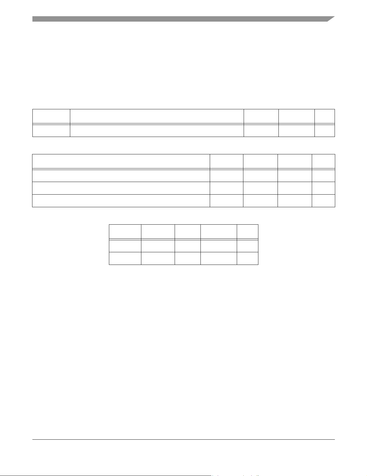
1.4 Ordering Information
Table 1 provides ordering information for the i.MX21.
Table 1. i.MX21 Ordering Information
Marking Package Size Package Type Operating range
MC9328MX21VG 289-lead MAPBGA
0.65mm, 14mm x 14mm
MC9328MX21VK 289-lead MAPBGA
0.65mm, 14mm x 14mm
MC9328MX21VH 289-lead MAPBGA
0.8mm, 17mm x 17mm
MC9328MX21VM 289-lead MAPBGA
0.8mm, 17mm x 17mm
MC9328MX21DVG 289-lead MAPBGA
0.65mm, 14mm x 14mm
MC9328MX21DVK 289-lead MAPBGA
0.65mm, 14mm x 14mm
MC9328MX21DVH 289-lead MAPBGA
0.8mm, 17mm x 17mm
MC9328MX21DVM 289-lead MAPBGA
0.8mm, 17mm x 17mm
MC9328MX21CVG 289-lead MAPBGA
0.65mm, 14mm x 14mm
MC9328MX21CVK 289-lead MAPBGA
0.65mm, 14mm x 14mm
MC9328MX21CVH 289-lead MAPBGA
0.8mm, 17mm x 17mm
Lead
Lead-free
Lead
Lead-free
Lead
Lead-free
Lead
Lead-free
Lead
Lead-free
Lead
°C–70°C
0
°C–70°C
0
0°C–70°C
0°C–70°C
°C–70°C
-30
-30°C–70°C
-30°C–70°C
°C–70°C
-30
-40°C–85°C
-40°C–85°C
°C–85°C
-40
MC9328MX21CVM 289-lead MAPBGA
0.8mm, 17mm x 17mm
Lead-free
-40°C–85°C
1.5 Features
The i.MX21 boasts a robust array of features that can support a wide variety of applications. Below is a brief
description of i.MX21 features.
• ARM926EJ-S Core Complex
• enhanced Multimedia Accelerator (eMMA)
• Optional Security System
• Display and Video Modules
— LCD Controller (LCDC)
— Smart LCD Controller (SLCDC)
— CMOS Sensor Interface (CSI)
• Bus Master Interface (BMI)
MC9328MX21 Product Preview, Rev. 1.1
4 Freescale Semiconductor
Page 5

Signal Descriptions
• Wireless Connectivity
— Fast Infra-Red Interface (Fast IR)
• Wired Connectivity
— USB On-The-Go (USBOTG) Controller
— Four Universal Asynchronous Receiver/Transmitters (UART1, UART2, UART3, and UART4)
— Two Configurable Serial Peripheral Interfaces (CSPI1 and CSPI2) for High Speed Data Transfer
— Inter-IC (I
— Two Synchronous Serial Interfaces (SSI) with Inter-IC Sound (I
2
C) Bus Module
2
S)
— Digital Audio Mux
— One-Wire Controller
— Keypad Interface
• Memory Expansion and I/O Card Support
— Two Multimedia Card and Secure Digital (MMC/SD) Host Controller Modules
• Memory Interface
— External Interface Module (EIM)
— SDRAM Controller (SDRAMC)
— NAND Flash Controller (NFC)
— PCMCIA/CF Interface
• Standard System Resources
— Clock Generation Module (CGM) and Power Control Module
— Three General-Purpose 32-Bit Counters/Timers
— Watchdog Timer
— Real-Time Clock/Sampling Timer (RTC)
— Pulse-Width Modulator (PWM) Module
— Direct Memory Access Controller (DMAC)
— General-Purpose I/O (GPIO) Ports
— Debug Capability
2 Signal Descriptions
This section identifies and describes the i.MX21 signals and their pin assignments. The i.MX21 signals are listed in
Table 2.
Table 2. i.MX21 Signal Descriptions
Signal Name Function/Notes
External Bus/Chip Select (EIM)
A [25:0] Address bus signals
D [31:0] Data bus signals
EB0 MSB Byte Strobe—Active low external enable byte signal that controls D [31:24], shared with
SDRAM DQM0.
EB1 Byte Strobe—Active low external enable byte signal that controls D [23:16], shared with SDRAM
DQM1.
MC9328MX21 Product Preview, Rev. 1.1
Freescale Semiconductor 5
Page 6
Signal Descriptions
Table 2. i.MX21 Signal Descriptions (Continued)
Signal Name Function/Notes
EB2 Byte Strobe—Active low external enable byte signal that controls D [15:8], shared with SDRAM
DQM2 and PCMCIA PC_REG
EB3 LSB Byte Strobe—Active low external enable byte signal that controls D [7:0], shared with SDRAM
DQM3 and PCMCIA PC_IORD.
OE Memory Output Enable—Active low output enables external data bus, shared with PCMCIA
PC_IOWR
CS [5:0] Chip Select—The chip select signals CS [3:2] are multiplexed with CSD [1:0] and are selected by
the Function Multiplexing Control Register (FMCR) in the System Control chapter. By default CSD
[1:0] is selected. DTACK is multiplexed with CS4.
ECB Active low input signal sent by flash device to the EIM whenever the flash device must terminate an
on-going burst sequence and initiate a new (long first access) burst sequence.
LBA Active low signal sent by flash device causing the external burst device to latch the starting burst
address.
BCLK Clock signal sent to external synchronous memories (such as burst flash) during burst mode.
RW RW signal—Indicates whether external access is a read (high) or write (low) cycle. This signal is
also shared with the PCMCIA PC_WE.
.
.
DTACK DTACK signal—External input data acknowledge signal, multiplexed with CS4.
Bootstrap
BOOT [3:0] System Boot Mode Select—The operational system boot mode of the i.MX21 upon system reset is
determined by the settings of these pins.
SDRAM Controller
SDBA [4:0] SDRAM non-interleave mode bank address signals. These signals are multiplexed with address
signals A[20:16].
SDIBA [3:0] SDRAM interleave addressing mode bank address signals. These signals are multiplexed with
address signals A[24:21].
MA [11:0] SDRAM address signals. MA[9:0] are multiplexed with address signals A[10:1].
DQM [3:0] SDRAM data qualifier mask multiplexed with EB[3:0]. DQM3 corresponds to D[31:24], DQM2
corresponds to D[23:16], DQM1 corresponds to D[15:8], and DQM0 corresponds to D[7:0].
CSD0 SDRAM Chip Select signal. This signal is multiplexed with the CS2 signal. This signal is selectable
by programming the Function Multiplexing Control Register in the System Control chapter.
CSD1 SDRAM Chip Select signal. This signal is multiplexed with the CS3 signal. This signal is selectable
by programming the Function Multiplexing Control Register in the System Control chapter.
RAS SDRAM Row Address Select signal
CAS SDRAM Column Address Select signal
SDWE SDRAM Write Enable signal
SDCKE0 SDRAM Clock Enable 0
SDCKE1 SDRAM Clock Enable 1
SDCLK SDRAM Clock
MC9328MX21 Product Preview, Rev. 1.1
6 Freescale Semiconductor
Page 7
Signal Descriptions
Table 2. i.MX21 Signal Descriptions (Continued)
Signal Name Function/Notes
Clocks and Resets
EXTAL26M Crystal input (26MHz), or a 16 MHz to 32 MHz oscillator (or square-wave) input when internal
oscillator circuit is shut down.
XTAL26M Oscillator output to external crystal
EXTAL32K 32 kHz crystal input
XTAL32K Oscillator output to 32 kHz crystal
CLKO Clock Out signal selected from internal clock signals. Please refer to clock controller for internal
clock selection.
EXT_48M This is a special factory test signal. To ensure proper operation, connect this signal to ground.
EXT_266M This is a special factory test signal. To ensure proper operation, connect this signal to ground.
RESET_IN Master Reset—External active low Schmitt trigger input signal. When this signal goes active, all
modules (except the reset module, SDRAMC module, and the clock control module) are reset.
RESET_OUT Reset Out—Internal active low output signal from the Watchdog Timer module and is asserted
from the following sources: Power-on reset, External reset (RESET_IN
), and Watchdog time-out.
POR Power On Reset—Active low Schmitt trigger input signal. The POR signal is normally generated by
an external RC circuit designed to detect a power-up event.
CLKMODE[1:0] These are special factory test signals. To ensure proper operation, leave these signals as no
connects.
OSC26M_TEST This is a special factory test signal. To ensure proper operation, leave this signal as a no connect.
TEST_WB[2:0] These are special factory test signals. However, these signals are also multiplexed with GPIO
PORT E as well as alternate keypad signals. If not utilizing these signals for GPIO functionality or
for it’s other multiplexed function, then configure as GPIO input with pull up enabled, and leave as
a no connect.
TEST_WB[4:3] These are special factory test signals. To ensure proper operation, leave these signals as no
connects.
WKGD Battery indicator input used to qualify the walk-up process. Also multiplexed with TIN.
JTAG
TRST Test Reset Pin—External active low signal used to asynchronously initialize the JTAG controller.
TDO Serial Output for test instructions and data. Changes on the falling edge of TCK.
TDI Serial Input for test instructions and data. Sampled on the rising edge of TCK.
TCK Test Clock to synchronize test logic and control register access through the JTAG port.
TMS Test Mode Select to sequence the JTAG test controller’s state machine. Sampled on the rising
edge of TCK.
JTAG_CTRL JTAG Controller select signal—JTAG_CTRL is sampled during the rising edge of TRST. Must be
pulled to logic high for proper JTAG interface to debugger. Pulling JTAG_CRTL low is for internal
test purposes only.
RTCK JTAG Return Clock used to enhance stability of JTAG debug interface devices. This signal is
multiplexed with OWIRE, hence utilizing OWIRE will render RTCK unusable and vice versa.
MC9328MX21 Product Preview, Rev. 1.1
Freescale Semiconductor 7
Page 8
Signal Descriptions
Table 2. i.MX21 Signal Descriptions (Continued)
Signal Name Function/Notes
CMOS Sensor Interface
CSI_D [7:0] Sensor port data
CSI_MCLK Sensor port master clock
CSI_VSYNC Sensor port vertical sync
CSI_HSYNC Sensor port horizontal sync
CSI_PIXCLK Sensor port data latch clock
LCD Controller
LD [17:0] LCD Data Bus—All LCD signals are driven low after reset and when LCD is off. LD[15:0] signals
are multiplexed with SLCDC1_DAT[15:0] from SLCDC1 and BMI_D[15:0]. LD[17] signal is
multiplexed with BMI_WRITE
and EXT_DMAGRANT signals.
of BMI. LD[16] signal is multiplexed with BMI_READ_REQ of BMI
FLM_VSYNC
(or simply referred
to as VSYNC)
LP_HSYNC (or simply
referred to as HSYNC)
LSCLK Shift Clock. This signal is multiplexed with the BMI_CLK_CS from BMI.
OE_ACD Alternate Crystal Direction/Output Enable.
CONTRAST This signal is used to control the LCD bias voltage as contrast control. This signal is multiplexed
SPL_SPR Sampling start signal for left and right scanning. This signal is multiplexed with the SLCDC1_CLK.
PS Control signal output for source driver (Sharp panel dedicated signal). This signal is multiplexed
CLS Start signal output for gate driver. This signal is invert version of PS (Sharp panel dedicated
REV Signal for common electrode driving signal preparation (Sharp panel dedicated signal). This signal
SLCDC1_CLK SLCDC Clock output signal. This signal is multiplexed and available at 2 alternate locations. These
SLCDC1_CS SLCDC Chip Select output signal. This signal is multiplexed and available at 2 alternate signal
Frame Sync or Vsync—This signal also serves as the clock signal output for gate
driver (dedicated signal SPS for Sharp panel HR-TFT). This signal is multiplexed with
BMI_RXF_FULL and BMI_WAIT
Line Pulse or HSync
with the BMI_READ from BMI.
with the SLCDC1_CS.
signal). This signal is multiplexed with the SLCDC1_RS.
is multiplexed with SLCDC1_D0.
Smart LCD Controller
are SPL_SPR and SD2_CLK signals of LCDC and SD2, respectively.
locations. These are PS and SD2_CMD signals of LCDC and SD2, respectively.
of the BMI.
SLCDC1_RS SLCDC Register Select output signal. This signal is multiplexed and available at 2 alternate signal
locations. These are CLS and SD2_D3 signals of LCDC and SD2, respectively.
SLCDC1_D0 SLCDC serial data output signal. This signal is multiplexed and available at 2 alternate signal
locations. These are and REV and SD2_D2 signals of LCDC and SD2, respectively. This signal is
inactive when a parallel data interface is used.
MC9328MX21 Product Preview, Rev. 1.1
8 Freescale Semiconductor
Page 9
Signal Descriptions
Table 2. i.MX21 Signal Descriptions (Continued)
Signal Name Function/Notes
SLCDC1_DAT[15:0] SLCDC Data output signals for connection to a parallel SLCD panel interface. These signals are
multiplexed with LD[15:0] while an alternate 8-bit SLCD muxing is available on LD[15:8]. Further
alternate muxing of these signals are available on some of the USB OTG and USBH1 signals.
SLCDC2_CLK SLCDC Clock input signal for pass through to SLCD device. This signal is multiplexed with
SSI3_CLK signal from SSI3.
SLCDC2_CS SLCDC Chip Select input signal for pass through to SLCD device. This signal is multiplexed with
SSI3_TXD signal from SSI3.
SLCDC2_RS SLCDC Register Select input signal for pass through to SLCD device. This signal is multiplexed
with SSI3_RXD signal from SSI3.
SLCDC2_D0 SLCD Data input signal for pass through to SLCD device. This signal is multiplexed with SSI3_FS
signal from SSI3.
Bus Master Interface (BMI)
BMI_D[15:0] BMI bidirectional data bus. Bus width is programmable between 8-bit or 16-bit.These signals are
multiplexed with LD[15:0] and SLCDC_DAT[15:0].
BMI_CLK_CS BMI bidirectional clock or chip select signal.This signal is multiplexed with LSCLK of LCDC.
BMI_WRITE BMI bidirectional signal to indicate read or write access. This is an input signal when the BMI is a
slave and an output signal when BMI is the master of the interface. BMI_WRITE is asserted for
write and negated for read.This signal is muxed with LD[17] of LCDC.
BMI_READ BMI output signal to enable data read from external slave device. This signal is not used and
driven high when BMI is slave.This signal is multiplexed with CONTRAST signal of LCDC.
BMI_READ_REQ BMI Read request output signal to external bus master. This signal is active when the data in the
TXFIFO is larger or equal to the data transfer size of a single external BMI access.This signal is
muxed with LD[16] of LCDC.
BMI_RXF_FULL BMI Receive FIFO full active high output signal to reflect if the RxFIFO reaches water mark
value.This signal is muxed with VSYNC of the LCDC.
BMI_WAIT BMI Wait—Active low signal to wait for data ready (read cycle) or accepted (write_cycle). Also
multiplexed with VSYNC.
External DMA
EXT_DMAREQ External DMA Request input signal. This signal is multiplexed with CSPI1_RDY.
EXT_DMAGRANT External DMA Grant output signal. This signal is multiplexed with LD[16].
NAND Flash Controller
NF_CLE NAND Flash Command Latch Enable output signal. This signal is multiplexed with PC_POE of
PCMCIA.
NF_CE NAND Flash Chip Enable output signal. This signal is multiplexed with PC_CE1 of PCMCIA.
NF_WP NAND Flash Write Protect output signal. This signal is multiplexed with PC_CE2 of PCMCIA.
NF_ALE NAND Flash Address Latch Enable output signal. This signal is multiplexed with PC_OE of
PCMCIA.
NF_RE NAND Flash Read Enable output signal. This signal is multiplexed with PC_RW of PCMCIA.
MC9328MX21 Product Preview, Rev. 1.1
Freescale Semiconductor 9
Page 10
Signal Descriptions
Table 2. i.MX21 Signal Descriptions (Continued)
Signal Name Function/Notes
NF_WE NAND Flash Write Enable output signal. This signal is multiplexed with and PC_BVD2 of PCMCIA.
NF_RB NAND Flash Ready Busy input signal. This signal is multiplexed with PC_RST of PCMCIA.
NF_IO[15:0] NAND Flash Data input and output signals. NF_IO[15:7] signals are multiplexed with A[25:21] and
A[15:13]. NF_IO[7:0] signals are multiplexed with several PCMCIA signals.
PCMCIA Controller
PC_A[25:0] PCMCIA Address signals. These signals are multiplexed with A[25:0].
PC_D[15:0] PCMCIA Data input and output signals. These signals are multiplexed with D[15:0].
PC_CD1 PCMCIA Card Detect1 input signal. This signal is multiplexed with NFIO[7] signal of NF.
PC_CD2 PCMCIA Card Detect2 input signal. This signal is multiplexed with NFIO[6] signal of NF.
PC_WAIT PCMCIA Wait input signal to extend current access This signal is multiplexed with NFIO[5] signal
of NF.
PC_READY PCMCIA Ready input signal to indicate card is ready for access. This signal is multiplexed with
NFIO[4] signal of NF.
PC_RST PCMCIA Reset output signal. This signal is multiplexed with NFRB signal of NF.
PC_OE PCMCIA Memory Read Enable output signal asserted during common or attribute memory read
cycles. This signal is multiplexed with NFALE signal of NF.
PC_WE PCMCIA Memory Write Enable output signal asserted during common or attribute memory cycles.
This signal is shared with RW of the EIM.
PC_VS1 PCMCIA Voltage Sense1 input signal. This signal is multiplexed with NFIO[2] signal of NF
PC_VS2 PCMCIA Voltage Sense2 input signal. This signal is multiplexed with NFIO[1] signal of NF
PC_BVD1 PCMCIA Battery Voltage Detect1 input signal. This signal is multiplexed with NFIO[0] signal of NF
PC_BVD2 PCMCIA Battery Voltage Detect2 input signal. This signal is multiplexed with NF_WE signal of NF
PC_SPKOUT PCMCIA Speaker Out output signal. This signal is multiplexed with PWMO signal.
PC_REG PCMCIA Register Select output signal. This signal is shared with EB2 of EIM.
PC_CE1 PCMCIA Card Enable1 output signal. This signal is multiplexed with NFCE signal of NF.
PC_CE2 PCMCIA Card Enable2 output signal. This signal is multiplexed with NFWP signal of NF.
PC_IORD PCMCIA IO Read output signal. This signal is shared with EB3 of EIM.
PC_IOWR PCMCIA IO Write output signal. This signal is shared with OE signal of EIM.
PC_WP PCMCIA Write Protect input signal. This signal is multiplexed with NFIO[3] signal of NF.
PC_POE PCMCIA Output Enable signal to enable voltage translation buffers and transceivers. This signal is
multiplexed with NFCLE signal of NF.
PC_RW PCMCIA Read Write output signal to control external transceiver direction. Asserted high for read
access and negated low for write access. This signal is multiplexed with NFRE
signal of NF.
PC_PWRON PCMCIA input signal to indicate that the card power has been applied and stabilized.
MC9328MX21 Product Preview, Rev. 1.1
10 Freescale Semiconductor
Page 11
Signal Descriptions
Table 2. i.MX21 Signal Descriptions (Continued)
Signal Name Function/Notes
CSPI
CSPI1_MOSI Master Out/Slave In signal
CSPI1_MISO Master In/Slave Out signal
CSPI1_SS[2:0] Slave Select (Selectable polarity) signal. CSPI1_SS2 is also multiplexed with USBG_RXDAT.
CSPI1_SCLK Serial Clock signal
CSPI1_RDY Serial Data Ready signal. Also multiplexed with EXT_DMAREQ.
CSPI2_MOSI Master Out/Slave In signal. This signal is multiplexed with USBH2_TXDP signal of USB OTG.
CSPI2_MISO Master In/Slave Out signal. This signal is multiplexed with USBH2_TXDM signal of USB OTG.
CSPI2_SS[2:0] Slave Select (Selectable polarity) signals. These signals are multiplexed with USBH2_FS,
USBH2_RXDP and USBH2_RXDM signal of USB OTG
CSPI2_SCLK Serial Clock signal. This signal is multiplexed with USBH2_OE signal of USB OTG
CSPI3_MOSI Master Out/Slave In signal. This signal is multiplexed with SD1_CMD.
CSPI3_MISO Master In/Slave Out signal. This signal is multiplexed with SD1_D0.
CSPI3_SS Slave Select (Selectable polarity) signal multiplexed with SD1_D3.
CSPI3_SCLK Serial Clock signal. This signal is multiplexed with SD1_CLK.
General Purpose Timers
TIN Timer Input Capture or Timer Input Clock—The signal on this input is applied to all 3 timers
simultaneously. This signal is muxed with the Walk-up Guard Mode WKGD
Clock, and Reset Controller module.
TOUT1 (or simply TOUT) Timer Output signal from General Purpose Timer1 (GPT1). This signal is multiplexed with
SSI1_MCLK and SSI2_MCLK signal of SSI1 and SSI2. The pin name of this signal is simply
TOUT.
TOUT2 Timer Output signal from General Purpose Timer1 (GPT2). This signal is multiplexed with PWMO.
TOUT3 Timer Output signal from General Purpose Timer1 (GPT3). This signal is multiplexed with PWMO.
USB On-The-Go
USB_BYP USB Bypass input active low signal.
USB_PWR USB Power output signal
USB_OC USB Over current input signal
USBG_RXDP USB OTG Receive Data Plus input signal. This signal is muxed with SLCDC1_DAT15.
USBG_RXDM USB OTG Receive Data Minus input signal. This signal is muxed with SLCDC1_DAT14.
USBG_TXDP USB OTG Transmit Data Plus output signal. This signal is muxed with SLCDC1_DAT13.
signal in the PLL,
USBG_TXDM USB OTG Transmit Data Minus output signal. This signal is muxed with SLCDC1_DAT12.
USBG_RXDAT USB OTG Transceiver differential data receive signal. Multiplexed with CSPI1_SS2.
USBG_OE USB OTG Output Enable signal. This signal is muxed with SLCDC1_DAT11.
MC9328MX21 Product Preview, Rev. 1.1
Freescale Semiconductor 11
Page 12

Signal Descriptions
Table 2. i.MX21 Signal Descriptions (Continued)
Signal Name Function/Notes
USBG_ON USB OTG Transceiver ON output signal. This signal is muxed with SLCDC1_DAT9.
USBG_FS USB OTG Full Speed output signal. This signal is multiplexed with external transceiver
USBG_TXR_INT
USBH1_RXDP USB Host1 Receive Data Plus input signal. This signal is multiplexed with UART4_RXD and
SLCDC1_DAT6. It also provides an alternative multiplex for UART4_RTS, where this signal is
selectable by programming the Function Multiplexing Control Register in the System Control
chapter.
USBH1_RXDM USB Host1 Receive Data Minus input signal. This signal is muxed with SLCDC1_DAT5. It also
provides an alternative multiplex for UART4_CTS.
USBH1_TXDP USB Host1 Transmit Data Plus output signal. This signal is multiplexed with UART4_CTS and
SLCDC1_DAT4. It also provides an alternative multiplex for UART4_RXD, where this signal is
selectable by programming the Function Multiplexing Control Register in the System Control
chapter.
USBH1_TXDM USB Host1 Transmit Data Minus output signal. This signal is multiplexed with UART4_TXD and
SLCDC1_DAT3.
USBH1_RXDAT USB Host1 Transceiver differential data receive signal. Multiplexed with USBH1_FS.
signal of USB OTG. This signal is muxed with SLCDC1_DAT10.
USBH1_OE USB Host1 Output Enable signal. This signal is muxed with SLCDC1_DAT2.
USBH1_FS USB Host1 Full Speed output signal. This signal is multiplexed with UART4_RTS and
SLCDC1_DAT1 and USBH1_RXDAT.
USBH_ON USB Host transceiver ON output signal. This signal is muxed with SLCDC1_DAT0.
USBH2_RXDP USB Host2 Receive Data Plus input signal. This signal is multiplexed with CSPI2_SS[1] of CSPI2.
USBH2_RXDM USB Host2 Receive Data Minus input signal. This signal is multiplexed with CSPI2_SS[2] of
CSPI2.
USBH2_TXDP USB Host2 Transmit Data Plus output signal. This signal is multiplexed with CSPI2_MOSI of
CSPI2.
USBH2_TXDM USB Host2 Transmit Data Minus output signal. This signal is multiplexed with CSPI2_MISO of
CSPI2.
USBH2_OE USB Host2 Output Enable signal. This signal is multiplexed with CSPI2_SCLK of CSPI2.
USBH2_FS USB Host2 Full Speed output signal. This signal is multiplexed with CSPI2_SS[0] of CSPI2.
USBG_SCL USB OTG I2C Clock Output signal. This signal is multiplexed with SLCDC1_DAT8.
USBG_SDA USB OTG I2C Data Input/Output signal. This signal is multiplexed with SLCDC1_DAT7.
USBG_TXR_INT USB OTG transceiver Interrupt input. Multiplexed with USBG_FS.
Secure Digital Interface
SD1_CMD SD Command bidirectional signal—If the system designer does not want to make use of the
internal pull-up, via the Pull-up enable register, a 4.7K–69K external pull up resistor must be
added. This signal is multiplexed with CSPI3_MOSI.
SD1_CLK SD Output Clock. This signal is multiplexed with CSPI3_SCLK.
MC9328MX21 Product Preview, Rev. 1.1
12 Freescale Semiconductor
Page 13
Signal Descriptions
Table 2. i.MX21 Signal Descriptions (Continued)
Signal Name Function/Notes
SD1_D[3:0] SD Data bidirectional signals—If the system designer does not want to make use of the internal
pull-up, via the Pull-up enable register, a 50 K–69K external pull up resistor must be added.
SD1_D[3] is muxed with CSPI3_SS while SD1_D[0] is muxed with CSPI3_MISO.
SD2_CMD SD Command bidirectional signal. This signal is multiplexed with SLCDC1_CS signal from
SLCDC1.
SD2_CLK SD Output Clock signal. This signal is multiplexed with SLCDC1_CLK signal from SLCDC1.
SD2_D[3:0] SD Data bidirectional signals. SD2_D[3:2] are which are multiplexed with SLCDC1_RS and
SLCDC_D0 signals from SLCDC1.
UARTs – IrDA/Auto-Bauding
UART1_RXD Receive Data input signal
UART1_TXD Transmit Data output signal
UART1_RTS Request to Send input signal
UART1_CTS Clear to Send output signal
UART2_RXD Receive Data input signal. This signal is multiplexed with KP_ROW6 signal from KPP.
UART2_TXD Transmit Data output signal. This signal is multiplexed with KP_COL6 signal from KPP.
UART2_RTS Request to Send input signal. This signal is multiplexed with KP_ROW7 signal from KPP.
UART2_CTS Clear to Send output signal. This signal is multiplexed with KP_COL7 signal from KPP.
UART3_RXD Receive Data input signal. This signal is multiplexed with IR_RXD from FIRI.
UART3_TXD Transmit Data output signal. This signal is multiplexed with IR_TXD from FIRI.
UART3_RTS Request to Send input signal
UART3_CTS Clear to Send output signal
UART4_RXD Receive Data input signal which is multiplexed with USBH1_RXDP and USBH1_TXDP.
UART4_TXD Transmit Data output signal which is multiplexed with USBH1_TXDM.
UART4_RTS Request to Send input signal which is multiplexed with USBH1_FS and USBH1_RXDP.
UART4_CTS Clear to Send output signal which is multiplexed with USBH1_TXDP and USBH1_RXDM.
Serial Audio Port – SSI (configurable to I2S protocol and AC97)
SSI1_CLK Serial clock signal which is output in master or input in slave
SSI1_TXD Transmit serial data
SSI1_RXD Receive serial data
SSI1_FS Frame Sync signal which is output in master and input in slave
SSI1_MCLK SSI1 master clock. Multiplexed with TOUT.
SSI2_CLK Serial clock signal which is output in master or input in slave.
SSI2_TXD Transmit serial data signal
SSI2_RXD Receive serial data
MC9328MX21 Product Preview, Rev. 1.1
Freescale Semiconductor 13
Page 14
Signal Descriptions
Table 2. i.MX21 Signal Descriptions (Continued)
Signal Name Function/Notes
SSI2_FS Frame Sync signal which is output in master and input in slave.
SSI2_MCLK SSI2 master clock. Multiplexed with TOUT.
SSI3_CLK Serial clock signal which is output in master or input in slave. This signal is multiplexed with
SLCDC2_CLK
SSI3_TXD Transmit serial data signal which is multiplexed with SLCDC2_CS
SSI3_RXD Receive serial data which is multiplexed with SLCDC2_RS
SSI3_FS Frame Sync signal which is output in master and input in slave. This signal is multiplexed with
SLCDC2_D0.
SAP_CLK Serial clock signal which is output in master or input in slave.
SAP_TXD Transmit serial data
SAP_RXD Receive serial data
SAP_FS Frame Sync signal which is output in master and input in slave.
I2C
I2C_CLK I2C Clock
I2C_DATA I2C Data
1-Wire
OWIRE One wire input and output signal. This signal is multiplexed with JTAG RTCK.
PWM
PWMO PWM Output. This signal is multiplexed with PC_SPKOUT of PCMCIA, as well as TOUT2 and
TOUT3 of the General Purpose Timer module.
Keypad
KP_COL[7:0] Keypad Column selection signals. KP_COL[7:6] are multiplexed with UART2_CTS and
UART2_TXD respectively. Alternatively, KP_COL6 is also available on the internal factory test
signal TEST_WB2. The Function Multiplexing Control Register in the System Control chapter must
be used in conjunction with programming the GPIO multiplexing (to select the alternate signal
multiplexing) to choose which signal KP_COL6 is available.
KP_ROW[7:0] Keypad Row selection signals. KP_ROW[7:6] are multiplexed with UART2_RTS and UART2_RXD
signals respectively. Alternatively, KP_ROW7 and KP_ROW6 are available on the internal factory
test signals TEST_WB0 and TEST_WB1 respectively. The Function Multiplexing Control Register
in the System Control chapter must be used in conjunction with programming the GPIO
multiplexing (to select the alternate signal multiplexing) to choose which signals KP_ROW6 and
KP_ROW7 are available.
Noisy Supply Pins
NVDD Noisy Supply for the I/O pins. There are six (6) I/O voltage rings, NVDD1 through NVDD6.
NVSS Noisy Ground for the I/O pins
MC9328MX21 Product Preview, Rev. 1.1
14 Freescale Semiconductor
Page 15
Table 2. i.MX21 Signal Descriptions (Continued)
Signal Name Function/Notes
Supply Pins – Analog Modules
Specifications
VDDA
(formally AVDD)
QVSS (internally
connected to AVSS)
QVDD Power supply pins for silicon internal circuitry
QVSS Quiet GND pins for silicon internal circuitry
QVDDX Power supply pin for the ARM core, connect directly to QVDD
Supply for analog blocks
Quiet GND for analog blocks (QVSS and AVSS are synonymous)
Internal Power Supply
3 Specifications
This section contains the electrical specifications and timing diagrams for the i.MX21 processor.
3.1 Maximum Ratings
Table 3 provides information on maximum ratings.
Table 3. Maximum Ratings
Rating Symbol Minimum Maximum Unit
Supply voltage V
Maximum operating temperature range of i.MX21 T
Storage temperature Test -55 150 °C
dd
A
-0.3 3.3 V
- 40 / -30 / 0 70 / 85 °C
3.2 Recommended Operating Range
Table 4 provides the recommended operating ranges for the supply voltages. The i.MX21 processor has multiple
pairs of VDD and VSS power supply and return pins. QVDD, QVDDx, and QVSS pins are used for internal logic.
All other VDD and VSS pins are for the I/O pads voltage supply, and each pair of VDD and VSS provides power
to the enclosed I/O pads. This design allows different peripheral supply voltage levels in a system.
Because AVDD pins are supply voltages to the analog pads, it is recommended to isolate and noise-filter the
AVDD pins from other VDD pins.
For more information about I/O pads grouping per VDD, please refer to Table 4 on page 15.
Table 4. Recommended Operating Range
Rating Symbol Minimum Maximum Unit
I/O supply voltage NVDD 2, 3, 4, 5, 6 2.70 3.30 V
I/O supply voltage NVDD 1 1.70 3.30 V
MC9328MX21 Product Preview, Rev. 1.1
Freescale Semiconductor 15
Page 16
Specifications
Table 4. Recommended Operating Range (Continued)
Rating Symbol Minimum Maximum Unit
Internal supply voltage (Core = 266 MHz) QVDD, QVDDx 1.45 1.65 V
Analog supply voltage AVDD 1.70 3.30 V
3.3 DC Electrical Characteristics
Table 5 contains both maximum and minimum DC characteristics of the i.MX21.
Table 5. Maximum and Minimum DC Characteristics
Number
or Symbol
Iop Full running operating current
QVDD & QVDDx=1.65V, NVDD1=1.8V, NVDD2-
Parameter Minimum Typical Maximum Unit
– 120mA
–mA
(QVDD+QVDDx),
6 & AVDD=3.1V,
Full run: Core=266MHz, System=133MHz,
Doze: Core=266MHz, System=53MHz,
8mA
(NVDD1)
MPEG4 Playback (QVGA) from MMC/SD card,
30fps, 44.1kHz audio)
6.6mA
(NVDD2-6+AVDD)
Sidd Standby current (QVDD, QVDDx= 1.55V) – 360 – µA
V
IH
V
IL
V
OH
V
OL
V
it+
V
V
hys
I
IL
I
IH
I
OH
Input high voltage 0.7NVDD – NVDD V
Input low voltage 0 – 0.3NVDD V
Output high voltage 0.8NVDD – – V
Output low voltage – – 0.2NVDD V
Positive input threshold voltage, Vi=V
Negative input threshold voltage, Vi=V
it-
Hysteresis (V
− V
it+
it-)=Vih
Input low leakage current
= GND, no pull-up or pull-down)
(V
IN
Input high leakage current
(V
IN=VDD
, no pull-up or pull-down)
Output high current
VO = VOH
ih
il
– – 2.15 V
0.75 – – V
–0.3 ––
–– ±1µA
–– ±1µA
––Slow Pad: -6
Fast Pad: -5
mA
I
I
C
OL
OZ
C
Output low current
VO = VOL
Output leakage current
(V
out=VDD
Input capacitance – – 5 pF
i
Output capacitance – – 5 pF
o
, output is tri-stated)
Slow Pad: 6
––mA
Fast Pad: 5
–– ±5µA
MC9328MX21 Product Preview, Rev. 1.1
16 Freescale Semiconductor
Page 17
Specifications
3.4 AC Electrical Characteristics
The AC characteristics consist of output delays, input setup and hold times, and signal skew times. All
signals are specified relative to an appropriate edge of other signals. All timing specifications are specified
at a system operating frequency from 0 MHz to 133 MHz (core operating frequency 266 MHz) with an
operating supply voltage from V
DD min
to V
DD max
timing is measured at 30 pF loading.
Table 6. Tri-State Signal Timing
Pin Parameter Minimum Maximum Unit
TRISTATE Time from TRISTATE activate until I/O becomes Hi-Z – 20.8 ns
Table 7. 32k/26M Oscillator Signal Timing
Parameter Minimum RMS Maximum Unit
EXTAL32k input jitter (peak to peak) for both System PLL and MCUPLL – 5 20 ns
EXTAL32k input jitter (peak to peak) for MCUPLL only – 5 100 ns
EXTAL32k startup time 800 – – ms
under an operating temperature from TL to TH. All
Table 8. CLKO Rise/Fall Time (at 30pF Loaded)
Best Case Typical Worst Case Units
Rise Time 0.80 1.00 1.40 ns
Fall Time 0.74 1.08 1.67 ns
MC9328MX21 Product Preview, Rev. 1.1
Freescale Semiconductor 17
Page 18

Specifications
3.5 DPLL Timing Specifications
Parameters of the DPLL are given in Table 9. In this table, T
predivider and T
is the output double clock period.
dck
is a reference clock period after the
ref
Table 9. DPLL Specifications
Parameter Test Conditions Minimum Typical Maximum Unit
Reference clock frequency range Vcc = 1.5V 16 – 320 MHz
Pre-divider output clock frequency
range
Double clock frequency range Vcc = 1.5V 160 – 560 MHz
Pre-divider factor (PD) – 1 – 16 –
Total multiplication factor (MF) Includes both integer
MF integer part – 5 – 15 –
MF numerator Should be less than the denominator 0 – 1022 –
MF denominator – 1 – 1023 –
Frequency lock-in time after
full reset
Vcc = 1.5V 16 – 32 MHz
5–15–
and fractional parts
FOL mode for non-integer MF
(does not include pre-multi lock-in time)
350 400 450 T
ref
Frequency lock-in time after
partial reset
Phase lock-in time after
full reset
Phase lock-in time after
partial reset
Frequency jitter (p-p) – – 0.02 0.03 2•T
Phase jitter (p-p) Integer MF, FPL mode, Vcc=1.5V – 1.0 1.5 ns
Power dissipation FOL mode, integer MF,
FOL mode for non-integer MF (does not
include pre-multi lock-in time)
FPL mode and integer MF (does not
include pre-multi lock-in time)
FPL mode and integer MF (does not
include pre-multi lock-in time)
= 560 MHz, Vcc = 1.5V
f
dck
220 280 330 T
480 530 580 T
360 410 460 T
–1.5–mW
(Avg)
ref
ref
ref
dck
MC9328MX21 Product Preview, Rev. 1.1
18 Freescale Semiconductor
Page 19
Specifications
3.6 Reset Module
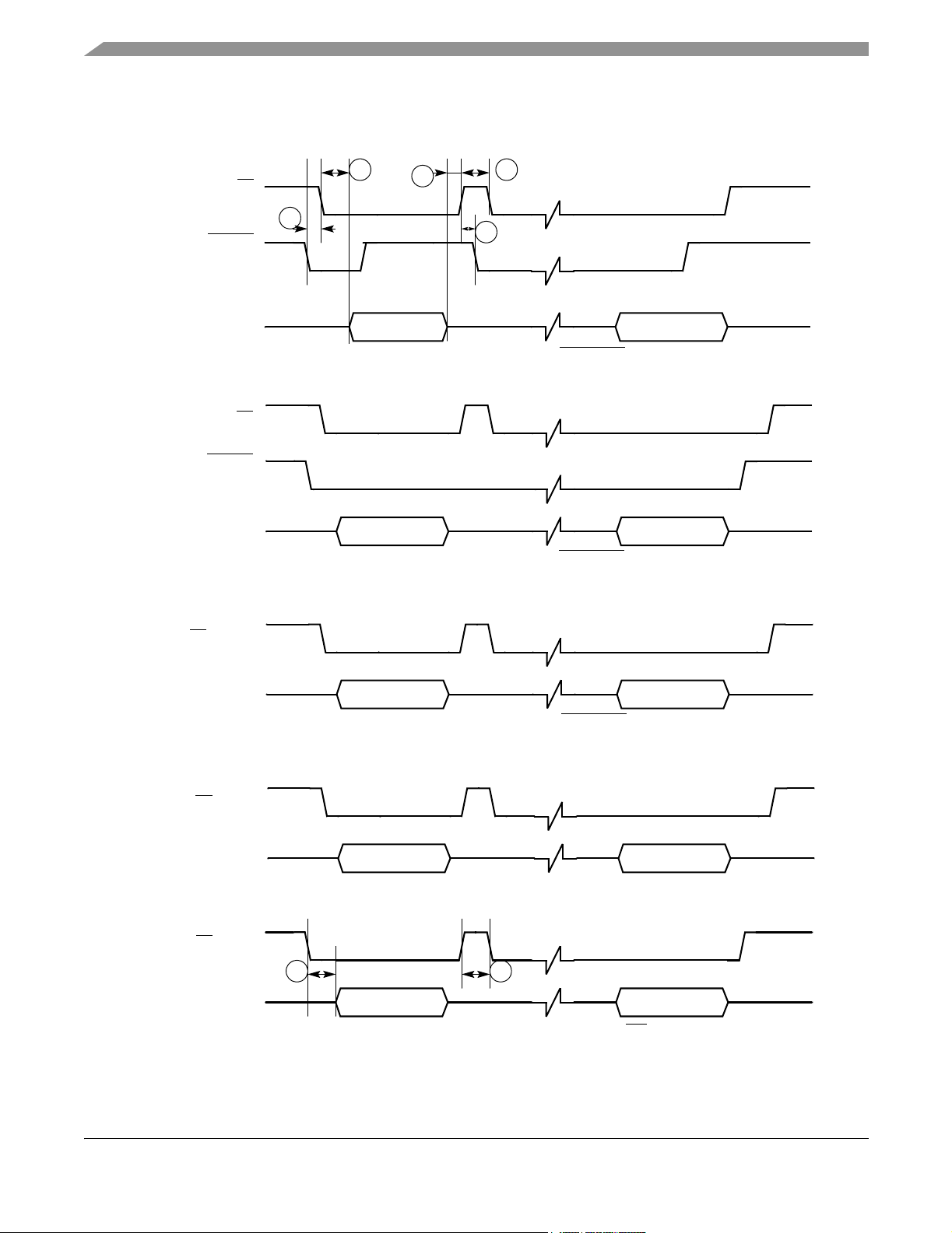
The timing relationships of the Reset module with the POR and RESET_IN are shown in Figure 2 and
Figure 3 on page 20. Be aware that NVDD must ramp up to at least 1.7V for NVDD1 and 2.7V for
NVDD2-6 before QVDD is powered up to prevent forward biasing.
POR
RESET_POR
RESET_DRAM
HRESET
RESET_OUT
CLK32
HCLK
1
Can be adjusted depending on the crystal
start-up time 32KHz or 32.768KHz
Figure 2. Timing Relationship with POR
2
Exact 300ms
3
7 cycles @ CLK32
4
14 cycles @ CLK32
MC9328MX21 Product Preview, Rev. 1.1
Freescale Semiconductor 19
Page 20
Specifications
RESET_IN
5
Ref
No.
HRESET
RESET_OUT
CLK32
HCLK
6
Figure 3. Timing Relationship with RESET_IN
Table 10. Reset Module Timing Parameter Table
1.8V +/- 0.10V 3.0V +/- 0.30V
Parameter
Min Max Min Max
14 cycles @ CLK32
4
Unit
1 Width of input POWER_ON_RESET 800 – 800 – ms
2 Width of internal POWER_ON_RESET
300 300 300 300 ms
(CLK32 at 32 KHz)
3 7K to 32K-cycle stretcher for SDRAM reset 7 7 7 7 Cycles of
CLK32
4 14K to 32K-cycle stretcher for internal system reset
HRESERT
and output reset at pin RESET_OUT
5 Width of external hard-reset RESET_IN
14 14 14 14 Cycles of
CLK32
4 – 4 – Cycles of
CLK32
6 4K to 32K-cycle qualifier 4 4 4 4 Cycles of
CLK32
MC9328MX21 Product Preview, Rev. 1.1
20 Freescale Semiconductor
Page 21
Specifications
3.7 External DMA Request and Grant
The External DMA request is an active low signal to be used by devices external to i.MX21 processor to request
the DMAC for data transfer.
After assertion of External DMA request the DMA burst will start when the channel on which the External request
is the source (as per the RSSR settings) becomes the current highest priority channel. The external device using the
External DMA request should keep its request asserted until it is serviced by the DMAC. One External DMA
request will initiate one DMA burst.
The output External Grant signal from the DMAC is an active-low signal.When the following conditions are true,
the External DMA Grant signal is asserted with the initiation of the DMA burst.
• The DMA channel for which the DMA burst is ongoing has request source as external DMA Request (as
per source select register setting).
• REN and CEN bit of this channel are set.
• External DMA Request is asserted.
After the grant is asserted, the External DMA request will not be sampled until completion of the DMA burst. As
the external request is synchronized, the request synchronization will not be done during this period. The priority of
the external request becomes low for the next consecutive burst, if another DMA request signal is asserted.
Worst case—that is, the smallest burst (1 byte read/write) timing diagrams are shown in Figure 4 and Figure 5 on
page 21. Minimum and maximum timings for the External request and External grant signals are present in
Table 11 on page 22.
Figure 4 shows the minimum time for which the External Grant signal remains asserted when an External DMA
request is de-asserted immediately after sensing grant signal active.
Ext_DMAReq
Ext_DMAGrant
t
min_assert
Figure 4. Assertion of DMA External Grant Signal
Figure 5 shows the safe maximum time for which External DMA request can be kept asserted, after sensing grant
signal active such that a new burst is not initiated.
Ext_DMAReq
Ext_DMAGrant
t
max_req_assert
Data read from
External device
Data written to
External device
t
max_read
t
max_write
NOTE: Assuming in worst case the data is read/written from/to External device as per the above waveform.
Figure 5. Safe Maximum Timings for External Request De-Assertion
MC9328MX21 Product Preview, Rev. 1.1
Freescale Semiconductor 21
Page 22
Specifications
Table 11. DMA External Request and Grant Timing Parameter Table
3.0 V
Parameter Description
WCS BCS WCS BCS
t
min_assert
t
max_req_assert
t
max_read
t
max_write
Minimum assertion time of
External Grant signal
Maximum External request
assertion time after assertion of
Grant signal
Maximum External request
assertion time after first read
completion
Maximum External request
assertion time after completion of
first write
8 hclk + 8.6 8 hclk + 2.74 8 hclk + 7.17 8 hclk + 3.25 ns
9 hclk - 20.66 9 hclk - 6.7 9 hclk - 17.96 9 hclk - 8.16 ns
8 hclk - 6.21 8 hclk - 0.77 8 hclk - 5.84 8 hclk - 0.66 ns
3 hclk - 15.87 3 hclk - 8.83 3 hclk - 15.9 3 hclk - 9.12 ns
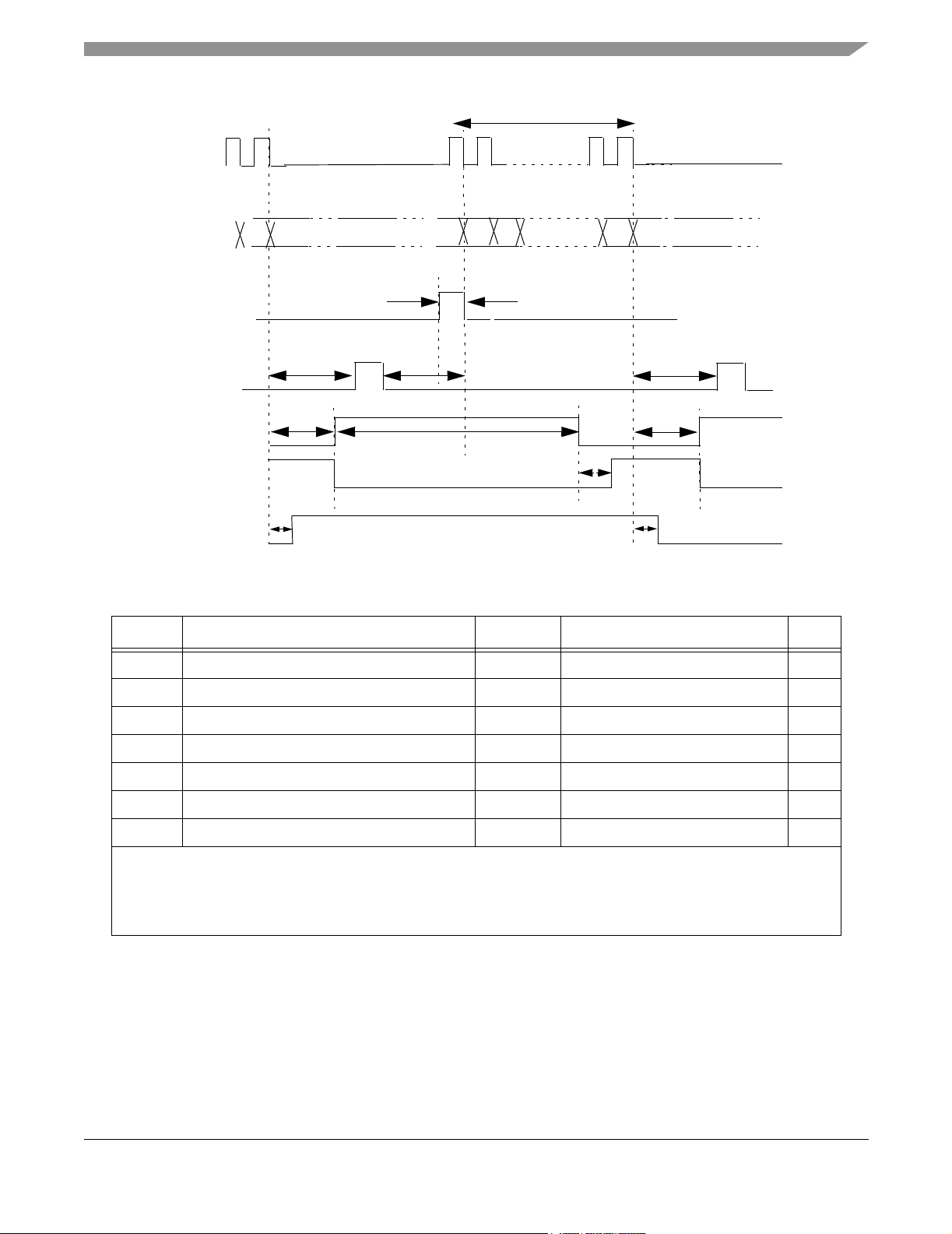
3.8 BMI Interface Timing Diagram
3.8.1 Connecting BMI to ATI MMD Devices
3.8.1.1 ATI MMD Devices Drive the BMI_CLK/CS
1.8 V
Unit
In this mode MMD_MODE_SEL bit is set and MMD_CLKOUT bit is cleared. BMI_WRITE and
BMI_CLK/CS are input signals to BMI driving by ATI MMD chip set. Output signal BMI_READ_REQ
can be used as interrupt signal to inform MMD that data is ready in BMI TxFIFO for read access. MMD
can write data to BMI RxFIFO anytime as CPU or DMA can move data out from RxFIFO much faster
than the BMI interface. Overflow interrupt is generated if RxFIFO overflow is detected. Once this
happens, the new coming data is ignored.
3.8.1.1.1 MMD Read BMI Timing
Figure 6 shows the MMD read BMI timing when the MMD drives clock.
On each rising edge of BMI_CLK/CS BMI checks the BMI_WRITE
logic level to determine if the current
cycle is a read cycle. It puts data into the data bus and enables the data out on the rising edge of BMI_CLK/
CS if BMI_WRITE is logic high. The BMI_READ_REQ is negated one hclk cycle after the BMI_CLK/
CS rising edge of last data read. The MMD cannot issues read command when BMI_READ_REQ is low
(no data in TxFIFO).
MC9328MX21 Product Preview, Rev. 1.1
22 Freescale Semiconductor
Page 23
BMI_CLK/CS
Specifications
1T
BMI_READ_REQ
BMI_D[15:0]
BMI_WRITE
Clock period 1T 33.3 – – ns
write
read_req hold time Trh 6 – 24 ns
transfer data setup time Tds 6 – 14 ns
transfer data hold time Tdh 6 - 14 ns
Tdh
Tds
TxD1 TxD2 Last TxD
Ts
Trh
Figure 6. MMD (ATI) Drives Clock, MMD Read BMI Timing
(MMD_MODE_SEL=1, MASTER_MODE_SEL=0,MMD_CLKOUT=0)
Table 12. MMD Read BMI Timing Table when MMD Drives Clock
Item Symbol Minimum Typical Maximum Unit
setup time Ts 11 – – ns
Note: All the timings assume that the hclk is running at 133 MHz.
Note: The MIN period of the 1T is assumed that MMD latch data at falling edge.
Note: If the MMD latch data at next rising edge, the ideally max clock can be as much as double, but because the BMI data pads
are slow pads and it max frequency can only up to 18Mhz, the max clock frequency can only up to 36 MHz.
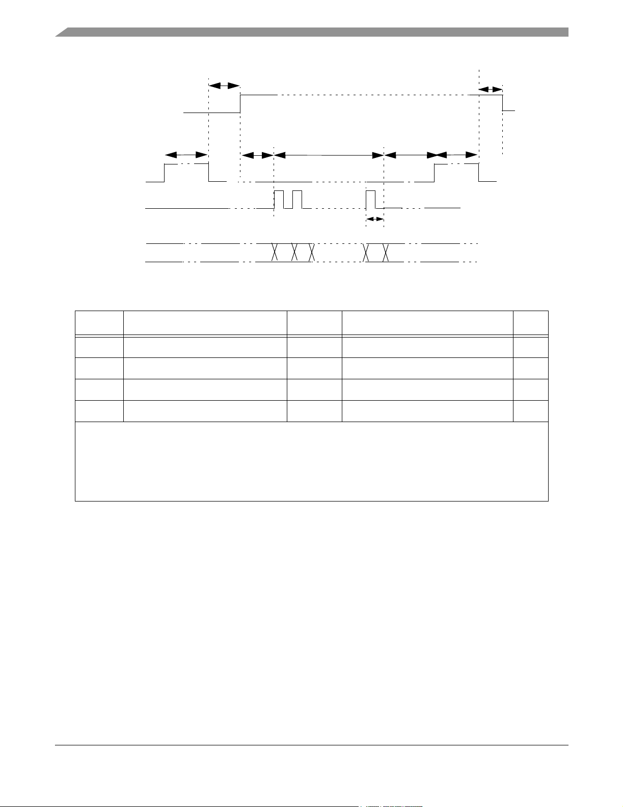
3.8.1.1.2 MMD Write BMI Timing
Figure 7 on page 24 shows the MMD write BMI timing when MMD drives clock. On each falling edge of
BMI_CLK/CS BMI checks the BMI_WRITE logic level to determine if the current cycle is a write cycle.
If the BMI_ WRITE is logic low, it latches data into the RxFIFO on each falling edge of BMI_CLK/CS
signal.
MC9328MX21 Product Preview, Rev. 1.1
Freescale Semiconductor 23
Page 24
Specifications
BMI_CLK/CS
BMI_READ_REQ
BMI_D[15:0]
BMI_WRITE
Ts
Figure 7. MMD (ATI) Drives Clock, MMD Write BMI Timing
(MMD_MODE_SEL=1, MASTER_MODE_SEL=0, MMD_CLKOUT=0)
Table 13. MMD Write BMI Timing
Item Symbol Minimum Typical Maximum Unit
write
setup time Ts 11 – – ns
write
hold time Th 0 – – ns
receive data setup time Tds 5 – – ns
Note: All timings assume that the hclk is running at 133 MHz.
Note: At this mode, the maximum frequency of the BMI_CLK/CS can be up to 36 MHz (doubles as maximum data pad speed).
RxD1 RxD2 Last RxD
Tds
Can be asserted any timeCan be asserted any time
Th
3.8.1.2 BMI Drives the BMI_CLK/CS
In this mode MMD_MODE_SEL and MMD_CLKOUT are both set. The software must know which
mode it is now (READ or WRITE). When the BMI_WRITE is high, BMI drives BMI_CLK/CS out if the
TxFIFO is not emptied. When BMI_WRITE is low, user can write a 1 to READ bit of control register1 to
issue a write cycle (MMD write BMI).
3.8.1.3 MMD Read BMI Timing
Figure 13 on page 29 shows the MMD read BMI timing when BMI drives the BMI_CLK/CS. When the
BMI_WRITE is high, the BMI drives BMI_CLK/CS out if data is written to TxFIFO (BMI_READ_REQ
become high), BMI puts data into data bus and enable data out on the rising edge of BMI_CLK/CS. The
MMD devices can latch the data on each falling edge of BMI_CLK/CS.
It is recommended that the MMD do not change the BMI_WRITE signal from high to low when the
BMI_READ_REQ is asserted. If user writes data to the TxFIFO when the BMI_WRITE is low, the BMI
will drive BMI_CLK/CS out once the BMI_WRITE
is changed from low to high.
MC9328MX21 Product Preview, Rev. 1.1
24 Freescale Semiconductor
Page 25
BMI_CLK/CS
Specifications
1T
BMI_READ_REQ
BMI_D[15:0]
BMI_WRITE
Tds
Tdh
TxD1 TxD2 Last TxD
DMA or CPU write data to TxFIFO
Trh
Figure 8. BMI Drives Clock, MMD Read BMI Timing
(MASTER_MODE_SEL=0, MMD_MODE_SEL=1, MMD_CLKOUT=1)
Table 14. MMD Read BMI Timing Table when BMI Drives Clock
Item Symbol MIN TYP MAX Unit
transfer data setup time Tds 2 – 8 ns
transfer data hold time Tdh 2 – 8 ns
read_req hold time Trh 2 – 18 ns
Note: In this mode, the max frequency of the BMI_CLK/CS can be up to 36Mhz(double as max data pad speed).
Note: The BMI_CLK/CS can only be divided by 2,4,8,16 from HCLK.
3.8.1.4 MMD Write BMI Timing
Figure on page 26 shows the MMD write BMI timing when BMI drives BMI_CLK/CS.
When the BMI_WRITE signal is asserted, the BMI can write a 1 to READ bit of control register to issue
a WRITE cycle. This bit is cleared automatically when the WRITE operation is completed. In a WRITE
burst the MMD will write COUNT+1 data to the BMI. The user can issue another WRITE operation if the
MMD still has data to write after the first operation completed.
The BMI can latch the data either at falling edge or the next rising edge of the BMI_CLK/CS according to
the DATA_LATCH bit. When the DATA_LATCH bit is set, the BMI latch data at the next rising edge and
latch the last data using the internal clock.
BMI_WRITE signal can not be negated when the WRITE operation is proceeding.
MC9328MX21 Product Preview, Rev. 1.1
Freescale Semiconductor 25
Page 26
Specifications
BMI_CLK/CS
Total has COUNT+1 clocks in one burst
BMI_READ_REQ
BMI_D[15:0]
BMI_WRITE
RxD1
Tds1
A 1 is written to READ bit of control register
RxD2
Can be asserted any timeCan be asserted any time
Last RxD
Tds2
Figure 9. BMI Drives Clock, MMD Write BMI Timing
(MASTER_MODE_SEL=0, MMD_MODE_SEL=1, MMD_CLKOUT=1)
Table 15. MMD Write BMI Timing Table when BMI Drives Clock
Item Symbol Minimum Typical Maximum Unit
receive data setup time1 Tds1 14 – – ns
receive data setup time2 Tds2 14 – – ns
Note: The BMI_CLK/CS can only be up to 30Mhz if BMI latch data at the falling edge and can be up to 36Mhz (double as max
data pad speed) if BMI latch data at the next rising edge.
Note: Tds1 is the receive data setup time when BMI latch data at the falling edge.
Note: Tds2 is the receive data setup time when BMI latch data at the next rising edge.
3.8.2 Connecting BMI to External Bus Master Devices
In this mode both MASTER_SEL bit and MMD_MODE_SEL bit are cleared and the MMD_CLKOUT
bit is no useful. BMI_WRITE and BMI_CLK/CS are input signals driving by the external bus master. The
Output signal BMI_READ_REQ can be used as an interrupt signal to inform external bus master that data
is ready in the BMI TxFIFO for a read access. The external bus master can write data to the BMI RxFIFO
anytime since the CPU or DMA can move data out from RxFIFO much faster than the BMI interface. An
overflow interrupt is generated if RxFIFO overflow is detected. Once this happens, the new coming data
is ignored.
Each falling edge of BMI_CLK/CS will determine if the current cycle is read or write cycle. It drives data
and enables data out if BMI_WRITE
CS is logic low and BMI_WRITE is logic high.
Each rising edge of BMI_CLK/CS will determine if data should be latched to RxFIFO from the data bus.
is logic high. The D_EN signal remains active only while BMI_CLK/
MC9328MX21 Product Preview, Rev. 1.1
26 Freescale Semiconductor
Page 27
BMI_CLK/CS
Specifications
BMI_READ_REQ
BMI_D[15:0]
BMI_WRITE
Ts
Ttds
Read
BMI
Ttdh
RxDTxD Last TxD
Ts
Write
BMI
Trdh
Th
Trh
Read
BMI
Figure 10. Memory Interface Slave Mode, External Bus Master Read/Write to BMI Timing
(MMD_MODE_SEL=0, MASTER_MODE_SEL=0)
Table 16. External Bus Master Read/Write to BMI Timing Table
Item Symbol Minimum Typical Maximum Unit
write
setup time Ts 11 – – ns
write
hold time Th 0 – – ns
receive data hold time Trdh 3 – – ns
transfer data setup time Ttds 6 – 14 ns
transfer data hold time Ttdh 6 – 14 ns
read_req hold time Trh 6 – 24 ns
Note: All the timings are assumed that the hclk is running at 133 MHz.
3.8.3 Connecting BMI to External Bus Slave Devices
In this mode the BMI_WRITE, BMI_READ and BMI_CLK/CS are output signals driving by the BMI
module. The output signal BMI_READ_REQ is still driving active-in on a write cycle, but it can be
ignored in this case. Instead, it is used to trigger internal logic to generate the read or write signals. Data
write cycles are continuously generated when TxFIFO is not emptied.
To issue a read cycle, the user can write a value of 1 to the READ bit of control register. This bit is cleared
automatically when the read operation is completed. A read cycle reads COUNT+1 data from the external
bus slave. The user can write a 1 to the READ bit while there is still data in the TxFIFO, but the read cycle
will not start until all data in the TxFIFO is emptied. If the read cycle begins, the write operation also
cannot begin until this read cycle complete.
In this master mode operation, Int_Clk is derived from HCLK through an integer divider DIV of BMI
control register and it is used to control the read/write cycle timing by generate WRITE
signals.
and CLK/CS
MC9328MX21 Product Preview, Rev. 1.1
Freescale Semiconductor 27
Page 28
Specifications
3.8.3.1 Memory Interface Master Mode Without WAIT Signal
The WAIT control bit (BMICTLR1[29]) is used in this mode. When this bit is cleared (default), the
BMI_WAIT signal is ignored and the CS cycle is terminated by Wait State (WS) control bits. Figure 11
shows the BMI timing when the WAIT bit is cleared.
(reference only)
Int_Clk
Int_write
(reference only)
BMI_CLK/CS
BMI_READ_REQ
BMI_D[15:0]
BMI_WRITE
BMI_READ
1+ws 1+ws
TxD1 TxD2
BMI write BMI write BMI write
DMA or CPU write data to TxFIFO
On the next Int_Clk BMI issues a write cycle
BMI_READ_REQ is still logic high, BMI issues next write cycle
Last TxD
A 1 is written to READ bit of control reg1
1+ws 1+ws
RxD1 RxD2
Tdh
Figure 11. Memory Interface Master Mode, BMI Read/Write to External Slave Device Timing without Wait
Signal (MMD_MODE_SEL=0, MASTER_MODE_SEL=1)
3.8.3.2 Memory Interface Master Mode with WAIT Signal
When the WAIT control bit is set, the BMI_WAIT signal is used and the CS cycle is terminated upon
sampling a logic high BMI_WAIT
When the BMI_WRITE is asserted, the BMI will detect the BMI_WAIT signal on every falling edge of
the Int_Clk. When it detected the high level of the BMI_WAIT, the BMI_WRITE will be negated after
1+WS Int_Clk period. If the BMI_WAIT is always high or already high before BMI_WRITE is asserted,
this timing will same as without WAIT
Int_Clk period.
28 Freescale Semiconductor
signal. Figure 12 shows the BMI write timing when the WAIT bit is set.
signal. So the BMI_WRITE will be asserted at least for 1+WS
MC9328MX21 Product Preview, Rev. 1.1
Page 29
Specifications
1+ws 1+ws
(reference only)
Int_Clk
BMI_CLK/CS
BMI_D[15:0]
TXD_a TXD_b
BMI_READ
BMI_WRITE
BMI_WAIT
Figure 12. Memory Interface Master Mode, BMI Write to External Slave Device Timing with Wait Signal
(MMD_MODE_SEL=0, MASTER_MODE_SEL=1,WAIT=1)
Figure 13 shows the BMI read timing when the WAIT bit is set. As write timing, when the BMI_READ is
asserted, the BMI will detect the BMI_WAIT signal on every falling edge of the Int_Clk. When it detected
the high level of the BMI_WAIT, the BMI_READ will be negated after 1+WS Int_Clk period. If the
BMI_WAIT is always high or already high before BMI_READ is asserted, this timing will same as
without WAIT signal. So the BMI_READ will be asserted at least for 1+WS Int_Clk period.
1+ws 1+ws
Int_Clk
(reference only)
BMI_CLK/CS
BMI_D[15:0]
BMI_WRITE
BMI_READ
BMI_WAIT
RXD_a RXD_b
Figure 13. Memory Interface Master Mode, BMI Read to External Slave Device Timing with Wait Signal
(MMD_MODE_SEL=0, MASTER_MODE_SEL=1,WAIT=1)
3.9 SPI Timing Diagrams
To use the internal transmit (TX) and receive (RX) data FIFOs when the SPI 1 module is configured as a
master, two control signals are used for data transfer rate control: the SS
signal (input). The SPI 1 Sample Period Control Register (PERIODREG1) and the SPI 2 Sample Period
Control Register (PERIODREG2) can also be programmed to a fixed data transfer rate for either SPI 1 or
SPI 2. When the SPI 1 module is configured as a slave, the user can configure the SPI 1 Control Register
(CONTROLREG1) to match the external SPI master’s timing. In this configuration, SS becomes an input
signal (output) and the SPI_RDY
MC9328MX21 Product Preview, Rev. 1.1
Freescale Semiconductor 29
Page 30
Specifications
signal, and is used to latch data into or load data out to the internal data shift registers, as well as to
increment the data FIFO.
.
SS
2
3
5
SPIRDY
SCLK, MOSI, MISO
Figure 14. Master SPI Timing Diagram Using SPI_RDY Edge Trigger
SS
SPIRDY
SCLK, MOSI, MISO
Figure 15. Master SPI Timing Diagram Using SPI_RDY
(output)
SS
1
4
Level Trigger
SCLK, MOSI, MISO
Figure 16. Master SPI Timing Diagram Ignore SPI_RDY
SS (input)
SCLK, MOSI, MISO
Figure 17. Slave SPI Timing Diagram FIFO Advanced by BIT COUNT
SS
(input)
SCLK, MOSI, MISO
Figure 18. Slave SPI Timing Diagram FIFO Advanced by SS
Level Trigger
6 7
Rising Edge
MC9328MX21 Product Preview, Rev. 1.1
30 Freescale Semiconductor
Page 31

Table 17. Timing Parameter Table for Figure 14 through Figure 18
Specifications
Ref
No.
1 SPI_RDY to SS output low 2T
2SS output low to first SCLK edge 3·Tsclk
3 Last SCLK edge to SS
4SS
5SS
6SS
7SS
1. T = CSPI system clock period (PERCLK2).
2. Tsclk = Period of SCLK.
3. WAIT = Number of bit clocks (SCLK) or 32.768 KHz clocks per Sample Period Control
Register.
output high to SPI_RDY low 0 – ns
output pulse width Tsclk + WAIT
input low to first SCLK edge T – ns
input pulse width T – ns
Parameter Minimum Maximum Unit
1
2
output high 2·Tsclk – ns
3
–ns
–ns
–ns
3.10 LCD Controller
This section includes timing diagrams for the LCD controller. For detailed timing diagrams of the LCD
controller with various display configurations, refer to the LCD controller chapter of the i.MX21 Reference
Manual.
T1
LSCLK
LD[17:0]
T2
T3
Figure 19. SCLK to LD Timing Diagram
Table 18. LCDC SCLK Timing Parameter Table
3.0 +/- 0.3V
Symbol Parameter
T1 SCLK period 23 2000 ns
T2 Pixel data setup time 11 – ns
T3 Pixel data up time 11 – ns
The pixel clock is equal to LCDC_CLK / (PCD + 1).
When it is in CSTN, TFT or monochrome mode with bus width = 1, SCLK is equal to the pixel clock.
When it is in monochrome with other bus width settings, SCLK is equal to the pixel clock divided by bus width.
The polarity of SCLK and LD can also be programmed.
Maximum frequency of SCLK is HCLK / 3 for TFT and CSTN, otherwise LD output will be incorrect.
Minimum Maximum
Unit
MC9328MX21 Product Preview, Rev. 1.1
Freescale Semiconductor 31
Page 32
Specifications
VSYN
HSYN
OE
LD[17:0]
HSYN
LD[15:0]
SCLK
OE
Non-display region
T1
T2
Line Y
T5 T7
T6
T3
(0,1)
T4
XMAX
(0,2)
Display region
Line 1 Line Y
(0,X-1)
Figure 20. 4/8/12/16/18 Bit/Pixel TFT Color Mode Panel Timing
Table 19. 4/8/12/16/18 Bit/Pixel TFT Color Mode Panel Timing
Symbol Description Minimum Value Unit
T1 End of OE to beginning of VSYN T5+T6+T7-1 (VWAIT1·T2)+T5+T6+T7-1 Ts
T2 HSYN period – XMAX+T5+T6+T7 Ts
T3 VSYN pulse width T2 VWIDTH·T2 Ts
T4 End of VSYN to beginning of OE 1 (VWAIT2·T2)+1 Ts
T5 HSYN pulse width 1 HWIDTH+1 Ts
T6 End of HSYN to beginning to OE 3 HWAIT2+3 Ts
T7 End of OE to beginning of HSYN 1 HWAIT1+1 Ts
Note:
• Ts is the SCLK period.
• VSYN, HSYN and OE can be programmed as active high or active low. In Figure 20, all 3 signals are active low.
• SCLK can be programmed to be deactivated during the VSYN pulse or the OE deasserted period. In Figure 20, SCLK is
always active.
• XMAX is defined in number of pixels in one line.
MC9328MX21 Product Preview, Rev. 1.1
32 Freescale Semiconductor
Page 33
SCLK
Specifications
XMAX
T1
T5
D1
D2
D320
T2
T4
T6
T7
LD
SPL_SPR
HSYN
CLS
PS
REV
D320
T7
T4
T2
T3
Figure 21. Sharp TFT Panel Timing
Table 20. Sharp TFT Panel Timing
Symbol Description Minimum Value Unit
T1 SPL/SPR pulse width – 1 Ts
T2 End of LD of line to beginning of HSYN 1 HWAIT1+1 Ts
T3 End of HSYN to beginning of LD of line 4 HWAIT2 + 4 Ts
T4 CLS rise delay from end of LD of line 3 CLS_RISE_DELAY+1 Ts
T5 CLS pulse width 1 CLS_HI_WIDTH+1 Ts
T6 PS rise delay from CLS negation 0 PS_RISE_DELAY Ts
T7 REV toggle delay from last LD of line 1 REV_TOGGLE_DELAY+1 Ts
Note:
• Falling of SPL/SPR aligns with first LD of line.
• Falling of PS aligns with rising edge of CLS.
• REV toggles in every HSYN period.
MC9328MX21 Product Preview, Rev. 1.1
Freescale Semiconductor 33
Page 34
Specifications
VSYN
HSYN
SCLK
LD[15:0]
T2
T1
T3
XMAX
Ts
T4
T2
T1
Figure 22. Non-TFT Mode Panel Timing
Table 21. Non-TFT Mode Panel Timing
Symbol Description Minimum Value Unit
T1 HSYN to VSYN delay 2 HWAIT2+2 Tpix
T2 HSYN pulse width 1 HWIDTH+1 Tpix
T3 VSYN to SCLK – 0
T4 SCLK to HSYN 1 HWAIT1+1 Tpix
Note:
• Ts is the SCLK period while Tpix is the pixel clock period.
• VSYN, HSYN and SCLK can be programmed as active high or active low. In Figure 67 on page 83, all these 3
signals are active high.
• When it is in CSTN mode or monochrome mode with bus width = 1, T3 = Tpix = Ts.
• When it is in monochrome mode with bus width = 2, 4, and 8, T3 = 1, 2 and 4 Tpix respectively.
≤ T3 ≤ Ts –
MC9328MX21 Product Preview, Rev. 1.1
34 Freescale Semiconductor
Page 35
3.11 Smart LCD Controller
Specifications
LCD_CS
LCD_CLK (LCD_DATA[6])
SDATA (LCD_DATA[7])
RS
LCD_CS
LCD_CLK (LCD_DATA[6])
SDATA (LCD_DATA[7])
RS
LCD_CS
T2
MSB
RS=0 ≥ command data, RS=1≥ display data
SCKPOL = 1, CSPOL = 0
T2
MSB
RS=0 ≥ command data, RS=1≥ display data
SCKPOL = 0, CSPOL = 0
T2
T1
T1
T1
T4
T4
T6
T6
T5
T5
T3
T7
LSB
T3
T7
LSB
T3
LCD_CLK (LCD_DATA[6])
SDATA (LCD_DATA[7])
RS
LCD_CS
LCD_CLK (LCD_DATA[6])
SDATA (LCD_DATA[7])
RS
T4
MSB
T6
RS=0 ≥ command data, RS=1≥ display data
SCKPOL = 1, CSPOL = 1
T2
T1
T4
MSB
T6
RS=0 ≥ command data, RS=1≥ display data
SCKPOL = 0, CSPOL = 1
Figure 23. SLCDC Serial Transfer Timing
T5
T5
T7
LSB
T3
T7
LSB
MC9328MX21 Product Preview, Rev. 1.1
Freescale Semiconductor 35
Page 36
Specifications
Symbol Description Minimum Maximum Unit
T1 Pixel clock period 42 962 ns
T2 Chip select setup time 5 – ns
T3 Chip select hold time 5 – ns
T4 Data setup time 5 – ns
T4 Data hold time 5 – ns
T6 Register select setup time 5 – ns
T7 Register select hold time 5 – ns
Table 22. SLCDC Serial Transfer Timing
LCD_CLK
T5T4
LCD_RS
T1
LCD_CS
LCD_DATA[15:0]
LCD_CLK
LCD_RS
LCD_CS
LCD_DATA[15:0]
T2
command data
CSPOL=0
T4
T2
command data
CSPOL=1
T3
display data
T5
T1
T3
display data
Figure 24. SLCDC Parallel Transfers Timing
MC9328MX21 Product Preview, Rev. 1.1
36 Freescale Semiconductor
Page 37
Specifications
Table 23. SLCDC Parallel Transfers Timing
Symbol Description Minimum Maximum Unit
T1 Pixel clock period 23 962 ns
T2 Data setup time 5 – ns
T3 Data hold time 5 – ns
T4 Register select setup time 5 – ns
T5 Register select hold time 5 – ns
3.12 Multimedia Card/Secure Digital Host Controller
The DMA interface block controls all data routing between the external data bus (DMA access), internal
MMC/SD module data bus, and internal system FIFO access through a dedicated state machine that
monitors the status of FIFO content (empty or full), FIFO address, and byte/block counters for the MMC/
SD module (inner system) and the application (user programming).
Bus Clock
5a
CMD_DAT Input
CMD_DAT Output
Valid Data
Figure 25. Chip-Select Read Cycle Timing Diagram
Table 24. SDHC Bus Timing Parameter Table
Ref
No.
1 CLK frequency at Data transfer Mode (PP)
2 CLK frequency at Identification Mode
3a Clock high time
1
Parameter
2
—10/30 cards 6/33 – 10/50 – ns
3a
3b
1 2
4b
4a
5b
Valid Data
7
Valid DataValid Data
6a
6b
1.8V +/- 0.10V 3.0V +/- 0.30V
Unit
Min Max Min Max
1
—10/30 cards 0 25/5 0 25/5 MHz
0 400 0 400 KHz
3b Clock low time
4a Clock fall time
4b Clock rise time
1
—10/30 cards 15/75 – 10/50 – ns
1
—10/30 cards – 10/50 (5.00)
1
—10/30 cards – 14/67 (6.67)
3
– 10/50 ns
3
– 10/50 ns
MC9328MX21 Product Preview, Rev. 1.1
Freescale Semiconductor 37
Page 38
Specifications
Table 24. SDHC Bus Timing Parameter Table (Continued)
Ref
No.
5a Input hold time3—10/30 cards 5.7/5.7 – 5/5 – ns
5b Input setup time
6a Output hold time
6b Output setup time
7 Output delay time
1. C
≤ 100 pF / 250 pF (10/30 cards)
L
≤ 250 pF (21 cards)
2. C
L
3. C
≤ 25 pF (1 card)
L
Parameter
3
—10/30 cards 5.7/5.7 – 5/5 – ns
3
—10/30 cards 5.7/5.7 – 5/5 – ns
3
—10/30 cards 5.7/5.7 – 5/5 – ns
3
1.8V +/- 0.10V 3.0V +/- 0.30V
Unit
Min Max Min Max
0 16 0 14 ns
3.12.1 Command Response Timing on MMC/SD Bus
The card identification and card operation conditions timing are processed in open-drain mode. The card
response to the host command starts after exactly NID clock cycles. For the card address assignment,
SET_RCA is also processed in the open-drain mode. The minimum delay between the host command and
card response is NCR clock cycles as illustrated in Figure 26. The symbols for Figure 26 through
Figure 30 are defined in Table 25.
Table 25. State Signal Parameters for Figure 26 through Figure 30
Card Active Host Active
Symbol Definition Symbol Definition
Z High impedance state S Start bit (0)
D Data bits T Transmitter bit
(Host = 1, Card = 0)
* Repetition P One-cycle pull-up (1)
CRC Cyclic redundancy check bits (7 bits) E End bit (1)
MC9328MX21 Product Preview, Rev. 1.1
38 Freescale Semiconductor
Page 39
Host Command
N
cycles
ID
Specifications
CID/OCR
CMD
CMD
Content
S T E Z Z S T
Host Command
Content
S T E Z Z S T
CRC
CRC
******
N
CR
******
cycles
Content
Identification Timing
CID/OCR
Content
SET_RCA Timing
Z Z
Z Z
Z
Z
Figure 26. Timing Diagrams at Identification Mode
After a card receives its RCA, it switches to data transfer mode. As shown on the first diagram in Figure 27
on page 39, SD_CMD lines in this mode are driven with push-pull drivers. The command is followed by
a period of two Z bits (allowing time for direction switching on the bus) and then by P bits pushed up by
the responding card. The other two diagrams show the separating periods NRC and NCC.
N
cycles
CR
Host Command
CMD
Content
S T E Z Z P P S T
Response
CRC
Command response timing (data transfer mode)
N
RC
******
cycles
Response
Content
Host Command
CRC
E Z Z
Z
CMD
CMD
Content
S T E Z Z S T
Host Command
Content
S T E Z Z S T
CRC
Timing response end to next CMD start (data transfer mode)
CRC
******
N
cycles
CC
******
Timing of command sequences (all modes)
Content
Host Command
Content
CRC
CRC
E Z Z
E Z Z
Z
Z
Figure 27. Timing Diagrams at Data Transfer Mode
Figure 28 on page 40 shows basic read operation timing. In a read operation, the sequence starts with a
single block read command (which specifies the start address in the argument field). The response is sent
on the SD_CMD lines as usual. Data transmission from the card starts after the access time delay NAC,
beginning from the last bit of the read command. If the system is in multiple block read mode, the card
sends a continuous flow of data blocks with distance N
until the card sees a stop transmission command.
AC
The data stops two clock cycles after the end bit of the stop command.
MC9328MX21 Product Preview, Rev. 1.1
Freescale Semiconductor 39
Page 40
Specifications
Host Command
N
CR
cycles
Response
CMD
DAT
Host Command
CMD
DAT
Content
S T E Z Z P P S T
Z****Z
CMD
Content
S T E Z Z P P S T
N
CRC
Z Z P P S D
Host Command
Content
S T E Z Z P P S T
Z****Z
cycles
CR
******
******
NAC cycles
CRC
Z Z P P S D
NAC cycles
CRC
******
******
Response
Content
D D D P
Read Data
N
cycles
CR
******
CRC
*****
Content
D D D
Read Data
Timing of single block read
E Z
N
Response
Content
CRC
E Z
*****
*****
AC
cycles
P S DD DD
Timing of multiple block read
CRC
E Z
*****
Read Data
NST
DAT
D D DD DD D D Z
*****
Valid Read Data
ZZE
Timing of stop command
(CMD12, data transfer mode)
*****
Figure 28. Timing Diagrams at Data Read
Figure 29 on page 41 shows the basic write operation timing. As with the read operation, after the card
response, the data transfer starts after NWR cycles. The data is suffixed with CRC check bits to allow the
card to check for transmission errors. The card sends back the CRC check result as a CC status token on
the data line. If there was a transmission error, the card sends a negative CRC status (101); otherwise, a
positive CRC status (010) is returned. The card expects a continuous flow of data blocks if it is configured
to multiple block mode, with the flow terminated by a stop transmission command.
MC9328MX21 Product Preview, Rev. 1.1
40 Freescale Semiconductor
Page 41
Specifications
P P P
Response
******
E Z Z P
CRC
Content
L*L
Status
E Z Z S E S E Z
CRC
Content
Z Z Z P P S
X X X X X X X ZX XXE Z ZP P S
X X X X X X
CRC
Content
Z Z Z
Busy
CRC status
Write Data
cycles
N
WR
******
L*L
Status
E Z Z S E S E Z
CRC
Content
X X X X X X
E Z Z X X X X X X XX X X Z
CRC
Content
Busy
CRC status
Write Data
cycles
WR
N
Status
X X X X X X
E Z Z X X Z P P S
CRC
Content
Z Z P P S
DAT
CRC status
Write Data
cycles
N
WR
Timing of the multiple block write command
cycles
N
CR
Host Command
******
E Z Z P P S T
CRC
Content
S T
CMD
Z****Z
DAT
Z****Z
DAT
Timing of the block write command
E Z Z P P P P
CMD
E Z Z S E Z P P S
CRC
Content
Z Z P P S
DAT
Figure 29. Timing Diagrams at Data Write
The stop transmission command may occur when the card is in different states. Figure 30 shows the
different scenarios on the bus.
MC9328MX21 Product Preview, Rev. 1.1
Freescale Semiconductor 41
Page 42

Specifications
E
CRC
Content
Host Command
S T
Z
E Z Z
CRC
Stop transmission during data transfer
from the host.
Stop transmission during CRC status transfer
from the card.
Stop transmission received after last data block.
Card becomes busy programming.
Stop transmission received after last data block.
Card becomes busy programming.
Card Response
cycles
CR
N
Host Command
Content
******
CRC
Content
S T E Z Z P P S T
CMD
******
D DD DD D Z Z Z ZD D DD DD DE Z Z SL Z Z Z Z Z Z Z Z ZZ Z Z Z Z Z Z Z Z Z Z Z ZE
DAT
******
Busy (Card is programming)
E
CRC
Write Data
D DD DD D Z Z Z ZD Z Z S Z Z S L Z Z Z Z Z Z Z Z ZZ Z Z Z Z Z Z Z Z Z Z Z ZE
DAT
******
S L Z Z Z Z Z Z Z Z Z Z Z Z ZZ Z Z Z Z Z Z Z Z Z Z Z ZE
DAT
******
Z Z Z Z Z Z Z Z Z ZZ Z Z Z Z Z Z Z Z Z S L Z Z Z Z Z Z Z Z ZZ Z Z Z Z Z Z Z Z Z Z Z ZE
DAT
Figure 30. Stop Transmission During Different Scenarios
Table 26. Timing Values for Figure 26 through Figure 30
Parameter Symbol Minimum Maximum Unit
MMC/SD bus clock, CLK (All values are referred to minimum (VIH) and maximum (VIL)
Command response cycle NCR 2 64 Clock cycles
Identification response cycle NID 5 5 Clock cycles
MC9328MX21 Product Preview, Rev. 1.1
42 Freescale Semiconductor
Page 43

Specifications
Table 26. Timing Values for Figure 26 through Figure 30 (Continued)
Parameter Symbol Minimum Maximum Unit
Access time delay cycle NAC 2 TAAC + NSAC Clock cycles
Command read cycle NRC 8 – Clock cycles
Command-command cycle NCC 8 – Clock cycles
Command write cycle NWR 2 – Clock cycles
Stop transmission cycle NST 2 2 Clock cycles
TAAC: Data read access time -1 defined in CSD register bit[119:112]
NSAC: Data read access time -2 in CLK cycles (NSAC·100) defined in CSD register bit[111:104]
3.12.2 SDIO-IRQ and ReadWait Service Handling
In SDIO, there is a 1-bit or 4-bit interrupt response from the SDIO peripheral card. In 1-bit mode, the
interrupt response is simply that the SD_DAT[1] line is held low. The SD_DAT[1] line is not used as data
in this mode. The memory controller generates an interrupt according to this low and the system interrupt
continues until the source is removed (SD_DAT[1] returns to its high level).
In 4-bit mode, the interrupt is less simple. The interrupt triggers at a particular period called the Interrupt
Peri od during the data access, and the controller must sample SD_DAT[1] during this short period to
determine the IRQ status of the attached card. The interrupt period only happens at the boundary of each
block (512 bytes).
CMD
DAT[1]
For 4-bit
DAT[1]
For 1-bit
Content
S T E Z Z P E Z Z
Interrupt Period IRQ IRQ
CRC
Response
S Z Z
Block Data
ES
L H
Interrupt Period
******
Block Data
Z Z
ES
Figure 31. SDIO IRQ Timing Diagram
ReadWait is another feature in SDIO that allows the user to submit commands during the data transfer. In
this mode, the block temporarily pauses the data transfer operation counter and related status, yet keeps
the clock running, and allows the user to submit commands as normal. After all commands are submitted,
the user can switch back to the data transfer operation and all counter and status values are resumed as
access continues.
MC9328MX21 Product Preview, Rev. 1.1
Freescale Semiconductor 43
Page 44

Specifications
CMD
DAT[1]
For 4-bit
DAT[2]
For 4-bit
******
Block Data
Block Data
ES
Z Z L H ES
E Z ZS
L L L L L L L L L L L L L L L L L L L L L H Z S
CMD52
P S T E Z Z
CRC
Z
******
Block Data
Block Data
E
Figure 32. SDIO ReadWait Timing Diagram
3.13 NAND-Flash Controller Interface
The timing diagrams Figure 33 through Figure 36shows the timing of the NAND Flash controller.
Table 27 on page 46 provides the relative timing requirement for the different signals of NFC at the
i.MX21 module level.
NFCLE
tCLS
tCS
NFCE
tWP
tCLH
tCH
NFWE
NFALE
NFIO7:0
tALS tALH
tDS
command
tDH
Figure 33. Command Latch Cycle Timing
MC9328MX21 Product Preview, Rev. 1.1
44 Freescale Semiconductor
Page 45

Specifications
NFCLE
NFCE
NFWE
NFALE
NFIO7:0
NFCLE
NFCE
tCLS
tCS
tWP
tALS
tDS
Address
tCH
tWC
tWH
tALH
tDH
Figure 34. Address Latch Cycle Timing
tCLS
tCS
NFWE
NFALE
NFIO15:0
tWC
tWP
tALS
tDS
Data to NF
tWH
tALH
tDH
Figure 35. Input Data Latch Cycle Timing
MC9328MX21 Product Preview, Rev. 1.1
Freescale Semiconductor 45
Page 46

Specifications
NFCLE
NFCE
NFRE
NFALE
tREA
tRC
tREH
tRP
tRHZ
NFIO15:0
tRR
NFCE
Data from NF
Figure 36. Output Data Latch Cycle Timing
Note: The data shown in Figure 36 is generated using the NAND Flash device and sampled with IPP_FLASH_CLK.
Table 27. Timing Characteristics
Number
1tCLS0 –
2tCLH10 –
3tCS0 –
4tCH10 –
5tWP25 –
6tALS0 –
7tALH10 –
8tDS20 –
9tDH10 –
Timing
Parameter
Minimum Maximum
10 tWC 45 –
11 tWH 15 –
12 tAR 10 –
13 tCLR 10 –
14 tRR 20 –
15 tRP 25 –
16 tWB – 100
MC9328MX21 Product Preview, Rev. 1.1
46 Freescale Semiconductor
Page 47

Table 27. Timing Characteristics (Continued)
Specifications
Number
17 tRC 50 –
18 tCEA – 45
19 tREA – 30
20 tRHZ – 30
21 tCHZ – 20
22 tOH 15 –
23 tREH 15 –
24 tIR 0 –
25 tWHR 60 –
Timing
Parameter
Minimum Maximum
3.14 Pulse-Width Modulator
The PWM can be programmed to select one of two clock signals as its source frequency. The selected
clock signal is passed through a divider and a prescaler before being input to the counter. The output is
available at the pulse-width modulator output (PWMO) external pin.
2a
System Clock
1
3b
PWM Output
Table 28. PWM Output Timing Parameter Table
Ref
No.
1 System CLK frequency
2a Clock high time
2b Clock low time
3a Clock fall time
3b Clock rise time
Parameter
1
12.29 – 12.29 – ns
1
9.91–9.91–ns
1
1
2b
3a
4a
4b
Figure 37. PWM Output Timing Diagram
1.8V +/- 0.10V 3.0V +/- 0.30V
Unit
Minimum Maximum Minimum Maximum
1
045045MHz
–0.5–0.5ns
–0.5–0.5ns
MC9328MX21 Product Preview, Rev. 1.1
Freescale Semiconductor 47
Page 48
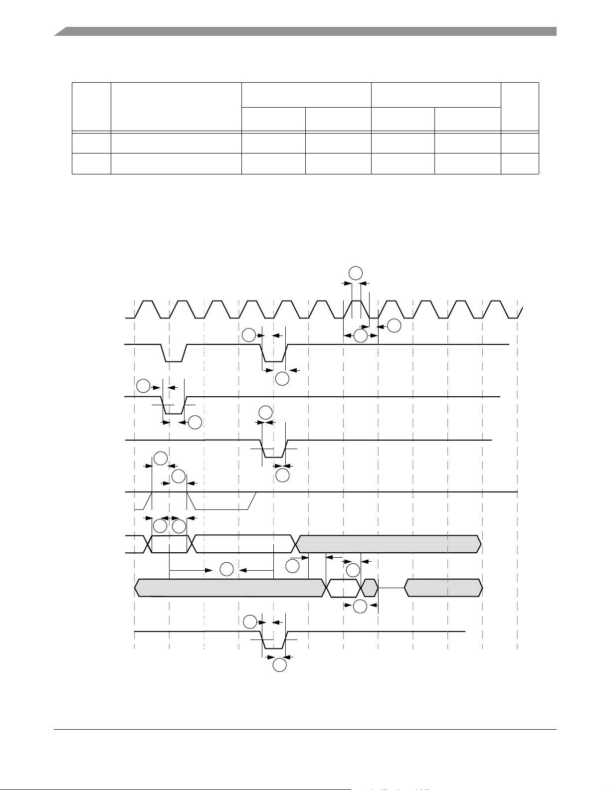
Specifications
Table 28. PWM Output Timing Parameter Table (Continued)
Ref
No.
4a Output delay time
4b Output setup time
1. CL of PWMO = 30 pF
Parameter
1
1
1.8V +/- 0.10V 3.0V +/- 0.30V
Unit
Minimum Maximum Minimum Maximum
9.37–3.61–ns
8.71–3.03–ns
3.15 SDRAM Memory Controller
The following figures (Figure 38 through Figure 41 on page 52) and their associated tables specify the
timings related to the SDRAMC module in the i.MX21.
1
SDCLK
2
CS
RAS
3S
3S
3
3H
CAS
WE
ADDR
DQ
DQM
3S
3H
4S
4H
ROW/BA
3S
3S
3H
3H
5
6
Data
7
Note: CKE is high during the read/write cycle.
3H
COL/BA
8
Figure 38. SDRAM Read Cycle Timing Diagram
MC9328MX21 Product Preview, Rev. 1.1
48 Freescale Semiconductor
Page 49
Table 29. SDRAM Timing Parameter Table
Specifications
Ref
No.
Parameter
Minimum Maximum Minimum Maximum
1.8V 3.0V +/-10%
Unit
1 SDRAM clock high-level width 3.00 – 4 – ns
2 SDRAM clock low-level width
3.00 – 4 – ns
3 SDRAM clock cycle time 11.1 – 7.5 – ns
3S CS, RAS, CAS, WE, DQM setup time 4.78 – 3 – ns
3H CS, RAS, CAS, WE, DQM hold time 3.03 – 2 – ns
4S Address setup time 3.67 – 3 – ns
4H Address hold time 2.95 – 2 – ns
5 SDRAM access time (CL = 3) –
5 SDRAM access time (CL = 2) –
5.4
6.0
–
–
5.4
6.0
5 SDRAM access time (CL = 1) – – – – ns
6 Data out hold time
7 Data out high-impedance time (CL = 3) –
3.0
–
1
t
HZ
3.0
–
–ns
1
t
HZ
ns
ns
ns
7 Data out high-impedance time (CL = 2) –
1
t
HZ
–
1
t
HZ
7 Data out high-impedance time (CL = 1) – – – – ns
8 Active to read/write command period (RC = 1)
t
RCD
2
–
t
RCD
2
–ns
1. tHZ = SDRAM data out high-impedance time, external SDRAM memory device dependent parameter.
2. t
= SDRAM clock cycle time. The t
RCD
setting can be found in the i.MX21 reference manual.
RCD
ns
MC9328MX21 Product Preview, Rev. 1.1
Freescale Semiconductor 49
Page 50
Specifications
SDCLK
CS
RAS
CAS
WE
3
1
2
6
ADDR
DQ
DQM
4
/ BA
5 7
ROW/BA
COL/BA
8
DATA
9
Figure 39. SDRAM Write Cycle Timing Diagram
Table 30. SDRAM Write Timing Parameter Table
Ref
No.
Parameter
Minimum Maximum Minimum Maximum
1 SDRAM clock high-level width 3.00 – 4 – ns
2 SDRAM clock low-level width
3 SDRAM clock cycle time 11.1 – 7.5 – ns
1.8V 3.0V +/-10%
3.00 – 4 – ns
Unit
4 Address setup time 3.67 – 3 – ns
5 Address hold time 2.95 – 2 – ns
6 Precharge cycle period
1
7 Active to read/write command delay t
t
RP
RCD
2
2
–t
–t
RP
RCD
2
2
–ns
–ns
8 Data setup time 3.41 – 2 – ns
MC9328MX21 Product Preview, Rev. 1.1
50 Freescale Semiconductor
Page 51
Table 30. SDRAM Write Timing Parameter Table (Continued)
Specifications
Ref
No.
Parameter
Minimum Maximum Minimum Maximum
1.8V 3.0V +/-10%
9 Data hold time 2.45 – 2 – ns
1. Precharge cycle timing is included in the write timing diagram.
2. tRP and t
SDCLK
CS
RAS
= SDRAM clock cycle time. These settings can be found in the i.MX21 reference manual.
RCD
3
1 2
6
CAS
7
7
Unit
WE
ADDR
DQ
DQM
4
BA
5
ROW/BA
Figure 40. SDRAM Refresh Timing Diagram
Table 31. SDRAM Refresh Timing Parameter Table
Ref
No.
Parameter
Minimum Maximum Minimum Maximum
1 SDRAM clock high-level width 3.00 – 4 – ns
2 SDRAM clock low-level width
1.8V 3.0V +/-10%
3.00 – 4 – ns
Unit
3 SDRAM clock cycle time 11.1 – 7.5 – ns
MC9328MX21 Product Preview, Rev. 1.1
Freescale Semiconductor 51
Page 52
Specifications
Table 31. SDRAM Refresh Timing Parameter Table (Continued)
Ref
No.
Parameter
Minimum Maximum Minimum Maximum
1.8V 3.0V +/-10%
4 Address setup time 3.67 – 3 – ns
5 Address hold time 2.95 – 2 – ns
6 Precharge cycle period t
7 Auto precharge command period t
1. t
and tRC = SDRAM clock cycle time. These settings can be found in the i.MX21 reference manual.
RP
SDCLK
CS
RAS
RP
RC
1
1
–t
–t
RP
RC
1
1
–ns
–ns
Unit
CAS
WE
ADDR
DQ
DQM
CKE
BA
Figure 41. SDRAM Self-Refresh Cycle Timing Diagram
3.16 Synchronous Serial Interface
The transmit and receive sections of the SSI can be synchronous or asynchronous. In synchronous mode,
the transmitter and the receiver use a common clock and frame synchronization signal. In asynchronous
MC9328MX21 Product Preview, Rev. 1.1
52 Freescale Semiconductor
Page 53

Specifications
mode, the transmitter and receiver each have their own clock and frame synchronization signals.
Continuous or gated clock mode can be selected. In continuous mode, the clock runs continuously. In gated
clock mode, the clock functions only during transmission. The internal and external clock timing diagrams
are shown in Figure 42 through Figure 45 on page 54.
Normal or network mode can also be selected. In normal mode, the SSI functions with one data word of
I/O per frame. In network mode, a frame can contain between 2 and 32 data words. Network mode is
typically used in star or ring-time division multiplex networks with other processors or codecs, allowing
interface to time division multiplexed networks without additional logic. Use of the gated clock is not
allowed in network mode. These distinctions result in the basic operating modes that allow the SSI to
communicate with a wide variety of devices.
The SSI can be connected to 4 set of ports, SAP, SSI1, SSI2 and SSI3.
1
CK Output
FS (bl) Output
FS (wl) Output
STXD Output
SRXD Input
Note: SRXD input in synchronous mode only.
Figure 42. SSI Transmitter Internal Clock Timing Diagram
CK Output
FS (bl) Output
2
1
3
4
6
12
10
31
5
7
11
32
8
9
FS (wl) Output
13
14
SRXD Input
Figure 43. SSI Receiver Internal Clock Timing Diagram
MC9328MX21 Product Preview, Rev. 1.1
Freescale Semiconductor 53
Page 54
Specifications
15
16
CK Input
18
FS (bl) Input
FS (wl) Input
STXD Output
SRXD Input
Note: SRXD Input in Synchronous mode only
Figure 44. SSI Transmitter External Clock Timing Diagram
15
16
CK Input
17
17
22
26
20
33
24
28
27
34
19
FS (bl) Input
FS (wl) Input
23
21
25
30
29
SRXD Input
Figure 45. SSI Receiver External Clock Timing Diagram
Table 32. SSI to SAP Ports Timing Parameter Table
Ref
No.
Parameter
Internal Clock Operation
1
1 (Tx/Rx) CK clock period
90.91 – 90.91 – ns
2 (Tx) CK high to FS (bl) high -3.30 -1.16 -2.98 -1.10 ns
3 (Rx) CK high to FS (bl) high -3.93 -1.34 -4.18 -1.43 ns
1.8V +/- 0.10V 3.0V +/- 0.30V
Minimum Maximum Minimum Maximum
1
(SAP Ports)
Unit
MC9328MX21 Product Preview, Rev. 1.1
54 Freescale Semiconductor
Page 55
Table 32. SSI to SAP Ports Timing Parameter Table (Continued)
Specifications
Ref
No.
Parameter
1.8V +/- 0.10V 3.0V +/- 0.30V
Unit
Minimum Maximum Minimum Maximum
4 (Tx) CK high to FS (bl) low -3.30 -1.16 -2.98 -1.10 ns
5 (Rx) CK high to FS (bl) low -3.93 -1.34 -4.18 -1.43 ns
6 (Tx) CK high to FS (wl) high -3.30 -1.16 -2.98 -1.10 ns
7 (Rx) CK high to FS (wl) high -3.93 -1.34 -4.18 -1.43 ns
8 (Tx) CK high to FS (wl) low -3.30 -1.16 -2.98 -1.10 ns
9 (Rx) CK high to FS (wl) low -3.93 -1.34 -4.18 -1.43 ns
10 (Tx) CK high to STXD valid from high impedance -2.44 -0.60 -2.65 -0.98 ns
11a (Tx) CK high to STXD high -2.44 -0.60 -2.65 -0.98 ns
11b (Tx) CK high to STXD low -2.44 -0.60 -2.65 -0.98 ns
12 (Tx) CK high to STXD high impedance -2.67 -0.99 -2.65 -0.98 ns
13 SRXD setup time before (Rx) CK low 23.68 – 22.09 – ns
14 SRXD hold time after (Rx) CK low 0 – 0 – ns
External Clock Operation (SAP Ports)
15 (Tx/Rx) CK clock period
1
90.91 – 90.91 – ns
16 (Tx/Rx) CK clock high period 36.36 – 36.36 – ns
17 (Tx/Rx) CK clock low period 36.36 – 36.36 – ns
18 (Tx) CK high to FS (bl) high 10.24 19.50 7.16 8.65 ns
19 (Rx) CK high to FS (bl) high 10.89 21.27 7.63 9.12 ns
20 (Tx) CK high to FS (bl) low 10.24 19.50 7.16 8.65 ns
21 (Rx) CK high to FS (bl) low 10.89 21.27 7.63 9.12 ns
22 (Tx) CK high to FS (wl) high 10.24 19.50 7.16 8.65 ns
23 (Rx) CK high to FS (wl) high 10.89 21.27 7.63 9.12 ns
24 (Tx) CK high to FS (wl) low 10.24 19.50 7.16 8.65 ns
25 (Rx) CK high to FS (wl) low 10.89 21.27 7.63 9.12 ns
26 (Tx) CK high to STXD valid from high impedance 12.08 19.36 7.71 9.20 ns
27a (Tx) CK high to STXD high 10.80 19.36 7.71 9.20 ns
MC9328MX21 Product Preview, Rev. 1.1
Freescale Semiconductor 55
Page 56
Specifications
Table 32. SSI to SAP Ports Timing Parameter Table (Continued)
Ref
No.
Parameter
1.8V +/- 0.10V 3.0V +/- 0.30V
Unit
Minimum Maximum Minimum Maximum
27b (Tx) CK high to STXD low 10.80 19.36 7.71 9.20 ns
28 (Tx) CK high to STXD high impedance 12.08 19.36 7.71 9.20 ns
29 SRXD setup time before (Rx) CK low 0.37 – 0.42 – ns
30 SRXD hole time after (Rx) CK low 0 – 0 – ns
Synchronous Internal Clock Operation (SAP Ports)
31 SRXD setup before (Tx) CK falling 23.00 – 21.41 – ns
32 SRXD hold after (Tx) CK falling 0 – 0 – ns
Synchronous External Clock Operation (SAP Ports)
33 SRXD setup before (Tx) CK falling 1.20 – 0.88 – ns
34 SRXD hold after (Tx) CK falling 0 – 0 – ns
1. All the timings for the SSI are given for a non-inverted serial clock polarity (TSCKP/RSCKP = 0) and a non-inverted frame sync
(TFSI/RFSI = 0). If the polarity of the clock and/or the frame sync have been inverted, all the timing remains valid by inverting
the clock signal STCK/SRCK and/or the frame sync STFS/SRFS shown in the tables and in the figures.
Table 33. SSI to SSI1 Ports Timing Parameter Table
Ref
No.
Parameter
Internal Clock Operation
1
1 (Tx/Rx) CK clock period
90.91 – 90.91 – ns
2 (Tx) CK high to FS (bl) high -0.68 -0.15 -0.68 -0.15 ns
3 (Rx) CK high to FS (bl) high -0.96 -0.27 -0.96 -0.27 ns
4 (Tx) CK high to FS (bl) low -0.68 -0.15 -0.68 -0.15 ns
5 (Rx) CK high to FS (bl) low -0.96 -0.27 -0.96 -0.27 ns
6 (Tx) CK high to FS (wl) high -0.68 -0.15 -0.68 -0.15 ns
7 (Rx) CK high to FS (wl) high -0.96 -0.27 -0.96 -0.27 ns
8 (Tx) CK high to FS (wl) low -0.68 -0.15 -0.68 -0.15 ns
9 (Rx) CK high to FS (wl) low -0.96 -0.27 -0.96 -0.27 ns
1.8V +/- 0.10V 3.0V +/- 0.30V
Minimum Maximum Minimum Maximum
1
(SSI1 Ports)
Unit
MC9328MX21 Product Preview, Rev. 1.1
56 Freescale Semiconductor
Page 57
Table 33. SSI to SSI1 Ports Timing Parameter Table (Continued)
Specifications
Ref
No.
Parameter
1.8V +/- 0.10V 3.0V +/- 0.30V
Unit
Minimum Maximum Minimum Maximum
10 (Tx) CK high to STXD valid from high impedance -1.68 -0.36 -1.68 -0.36 ns
11a (Tx) CK high to STXD high -1.68 -0.36 -1.68 -0.36 ns
11b (Tx) CK high to STXD low -1.68 -0.36 -1.68 -0.36 ns
12 (Tx) CK high to STXD high impedance -1.58 -0.31 -1.58 -0.31 ns
13 SRXD setup time before (Rx) CK low 20.41 – 20.41 – ns
14 SRXD hold time after (Rx) CK low 0 – 0 – ns
External Clock Operation (SSI1 Ports)
15 (Tx/Rx) CK clock period
1
90.91 – 90.91 – ns
16 (Tx/Rx) CK clock high period 36.36 – 36.36 – ns
17 (Tx/Rx) CK clock low period 36.36 – 36.36 – ns
18 (Tx) CK high to FS (bl) high 10.22 17.63 8.82 16.24 ns
19 (Rx) CK high to FS (bl) high 10.79 19.67 9.39 18.28 ns
20 (Tx) CK high to FS (bl) low 10.22 17.63 8.82 16.24 ns
21 (Rx) CK high to FS (bl) low 10.79 19.67 9.39 18.28 ns
22 (Tx) CK high to FS (wl) high 10.22 17.63 8.82 16.24 ns
23 (Rx) CK high to FS (wl) high 10.79 19.67 9.39 18.28 ns
24 (Tx) CK high to FS (wl) low 10.22 17.63 8.82 16.24 ns
25 (Rx) CK high to FS (wl) low 10.79 19.67 9.39 18.28 ns
26 (Tx) CK high to STXD valid from high impedance 10.05 15.75 8.66 14.36 ns
27a (Tx) CK high to STXD high 10.00 15.63 8.61 14.24 ns
27b (Tx) CK high to STXD low 10.00 15.63 8.61 14.24 ns
28 (Tx) CK high to STXD high impedance 10.05 15.75 8.66 14.36 ns
29 SRXD setup time before (Rx) CK low 0.78 – 0.47 – ns
30 SRXD hole time after (Rx) CK low 0 – 0 – ns
Synchronous Internal Clock Operation (SSI1 Ports)
31 SRXD setup before (Tx) CK falling 19.90 – 19.90 – ns
MC9328MX21 Product Preview, Rev. 1.1
Freescale Semiconductor 57
Page 58

Specifications
Table 33. SSI to SSI1 Ports Timing Parameter Table (Continued)
Ref
No.
32 SRXD hold after (Tx) CK falling 0 – 0 – ns
33 SRXD setup before (Tx) CK falling 2.59 – 2.28 – ns
34 SRXD hold after (Tx) CK falling 0 – 0 – ns
1. All the timings for the SSI are given for a non-inverted serial clock polarity (TSCKP/RSCKP = 0) and a non-inverted frame sync
(TFSI/RFSI = 0). If the polarity of the clock and/or the frame sync have been inverted, all the timing remains valid by inverting
the clock signal STCK/SRCK and/or the frame sync STFS/SRFS shown in the tables and in the figures.
Parameter
Synchronous External Clock Operation (SSI1 Ports)
1.8V +/- 0.10V 3.0V +/- 0.30V
Unit
Minimum Maximum Minimum Maximum
Table 34. SSI to SSI2 Ports Timing Parameter Table
Ref
No.
1 (Tx/Rx) CK clock period
Parameter
Internal Clock Operation1 (SSI2 Ports)
1
90.91 – 90.91 – ns
1.8V +/- 0.10V 3.0V +/- 0.30V
Unit
Minimum Maximum Minimum Maximum
2 (Tx) CK high to FS (bl) high 0.01 0.15 0.01 0.15 ns
3 (Rx) CK high to FS (bl) high -0.21 0.05 -0.21 0.05 ns
4 (Tx) CK high to FS (bl) low 0.01 0.15 0.01 0.15 ns
5 (Rx) CK high to FS (bl) low -0.21 0.05 -0.21 0.05 ns
6 (Tx) CK high to FS (wl) high 0.01 0.15 0.01 0.15 ns
7 (Rx) CK high to FS (wl) high -0.21 0.05 -0.21 0.05 ns
8 (Tx) CK high to FS (wl) low 0.01 0.15 0.01 0.15 ns
9 (Rx) CK high to FS (wl) low -0.21 0.05 -0.21 0.05 ns
10 (Tx) CK high to STXD valid from high impedance 0.34 0.72 0.34 0.72 ns
11a (Tx) CK high to STXD high 0.34 0.72 0.34 0.72 ns
11b (Tx) CK high to STXD low 0.34 0.72 0.34 0.72 ns
12 (Tx) CK high to STXD high impedance 0.34 0.48 0.34 0.48 ns
13 SRXD setup time before (Rx) CK low 21.50 – 21.50 – ns
14SRXD hold time after (Rx) CK low 0–0–ns
MC9328MX21 Product Preview, Rev. 1.1
58 Freescale Semiconductor
Page 59

Table 34. SSI to SSI2 Ports Timing Parameter Table (Continued)
Specifications
Ref
No.
15 (Tx/Rx) CK clock period1 90.91 – 90.91 – ns
16 (Tx/Rx) CK clock high period 36.36 – 36.36 – ns
17 (Tx/Rx) CK clock low period 36.36 – 36.36 – ns
18 (Tx) CK high to FS (bl) high 10.40 17.37 8.67 15.88 ns
19 (Rx) CK high to FS (bl) high 11.00 19.70 9.28 18.21 ns
20 (Tx) CK high to FS (bl) low 10.40 17.37 8.67 15.88 ns
21 (Rx) CK high to FS (bl) low 11.00 19.70 9.28 18.21 ns
22 (Tx) CK high to FS (wl) high 10.40 17.37 8.67 15.88 ns
23 (Rx) CK high to FS (wl) high 11.00 19.70 9.28 18.21 ns
24 (Tx) CK high to FS (wl) low 10.40 17.37 8.67 15.88 ns
25 (Rx) CK high to FS (wl) low 11.00 19.70 9.28 18.21 ns
Parameter
External Clock Operation (SSI2 Ports)
1.8V +/- 0.10V 3.0V +/- 0.30V
Unit
Minimum Maximum Minimum Maximum
26 (Tx) CK high to STXD valid from high impedance 9.59 17.08 7.86 15.59 ns
27a (Tx) CK high to STXD high 9.59 17.08 7.86 15.59 ns
27b (Tx) CK high to STXD low 9.59 17.08 7.86 15.59 ns
28 (Tx) CK high to STXD high impedance 9.59 16.84 7.86 15.35 ns
29 SRXD setup time before (Rx) CK low 2.52 – 2.52 – ns
30 SRXD hole time after (Rx) CK low 0 – 0 – ns
Synchronous Internal Clock Operation (SSI2 Ports)
31 SRXD setup before (Tx) CK falling 20.78 – 20.78 – ns
32SRXD hold after (Tx) CK falling 0–0–ns
Synchronous External Clock Operation (SSI2 Ports)
33 SRXD setup before (Tx) CK falling 4.42 – 4.42 – ns
34SRXD hold after (Tx) CK falling 0–0–ns
1. All the timings for the SSI are given for a non-inverted serial clock polarity (TSCKP/RSCKP = 0) and a non-inverted frame sync
(TFSI/RFSI = 0). If the polarity of the clock and/or the frame sync have been inverted, all the timing remains valid by inverting
the clock signal STCK/SRCK and/or the frame sync STFS/SRFS shown in the tables and in the figures.
MC9328MX21 Product Preview, Rev. 1.1
Freescale Semiconductor 59
Page 60

Specifications
Table 35. SSI to SSI3 Ports Timing Parameter Table
Ref
No.
1 (Tx/Rx) CK clock period
Parameter
Internal Clock Operation
1
90.91 – 90.91 – ns
1.8V +/- 0.10V 3.0V +/- 0.30V
Minimum Maximum Minimum Maximum
1
(SSI3 Ports)
Unit
2 (Tx) CK high to FS (bl) high -2.09 -0.66 -2.09 -0.66 ns
3 (Rx) CK high to FS (bl) high -2.74 -0.84 -2.74 -0.84 ns
4 (Tx) CK high to FS (bl) low -2.09 -0.66 -2.09 -0.66 ns
5 (Rx) CK high to FS (bl) low -2.74 -0.84 -2.74 -0.84 ns
6 (Tx) CK high to FS (wl) high -2.09 -0.66 -2.09 -0.66 ns
7 (Rx) CK high to FS (wl) high -2.74 -0.84 -2.74 -0.84 ns
8 (Tx) CK high to FS (wl) low -2.09 -0.66 -2.09 -0.66 ns
9 (Rx) CK high to FS (wl) low -2.74 -0.84 -2.74 -0.84 ns
10 (Tx) CK high to STXD valid from high impedance -1.73 -0.26 -1.73 -0.26 ns
11a (Tx) CK high to STXD high -2.87 -0.80 -2.87 -0.80 ns
11b (Tx) CK high to STXD low -2.87 -0.80 -2.87 -0.80 ns
12 (Tx) CK high to STXD high impedance -1.73 -0.26 -1.73 -0.26 ns
13 SRXD setup time before (Rx) CK low 22.77 – 22.77 – ns
14 SRXD hold time after (Rx) CK low 0 – 0 – ns
External Clock Operation (SSI3 Ports)
15 (Tx/Rx) CK clock period
1
90.91 – 90.91 – ns
16 (Tx/Rx) CK clock high period 36.36 – 36.36 – ns
17 (Tx/Rx) CK clock low period 36.36 – 36.36 – ns
18 (Tx) CK high to FS (bl) high 9.62 17.10 7.90 15.61 ns
19 (Rx) CK high to FS (bl) high 10.30 19.54 8.58 18.05 ns
20 (Tx) CK high to FS (bl) low 9.62 17.10 7.90 15.61 ns
21 (Rx) CK high to FS (bl) low 10.30 19.54 8.58 18.05 ns
22 (Tx) CK high to FS (wl) high 9.62 17.10 7.90 15.61 ns
23 (Rx) CK high to FS (wl) high 10.30 19.54 8.58 18.05 ns
MC9328MX21 Product Preview, Rev. 1.1
60 Freescale Semiconductor
Page 61

Table 35. SSI to SSI3 Ports Timing Parameter Table (Continued)
Specifications
Ref
No.
24 (Tx) CK high to FS (wl) low 9.62 17.10 7.90 15.61 ns
25 (Rx) CK high to FS (wl) low 10.30 19.54 8.58 18.05 ns
26 (Tx) CK high to STXD valid from high impedance 9.02 16.46 7.29 14.97 ns
27a (Tx) CK high to STXD high 8.48 15.32 6.75 13.83 ns
27b (Tx) CK high to STXD low 8.48 15.32 6.75 13.83 ns
28 (Tx) CK high to STXD high impedance 9.02 16.46 7.29 14.97 ns
29 SRXD setup time before (Rx) CK low 1.49 – 1.49 – ns
30 SRXD hole time after (Rx) CK low 0 – 0 – ns
31 SRXD setup before (Tx) CK falling 21.99 – 21.99 – ns
32 SRXD hold after (Tx) CK falling 0 – 0 – ns
Parameter
Synchronous Internal Clock Operation (SSI3 Ports)
Synchronous External Clock Operation (SSI3 Ports)
1.8V +/- 0.10V 3.0V +/- 0.30V
Unit
Minimum Maximum Minimum Maximum
33 SRXD setup before (Tx) CK falling 3.80 – 3.80 – ns
34 SRXD hold after (Tx) CK falling 0 – 0 – ns
1. All the timings for the SSI are given for a non-inverted serial clock polarity (TSCKP/RSCKP = 0) and a non-inverted frame sync
(TFSI/RFSI = 0). If the polarity of the clock and/or the frame sync have been inverted, all the timing remains valid by inverting
the clock signal STCK/SRCK and/or the frame sync STFS/SRFS shown in the tables and in the figures.
3.17 1-Wire Interface Timing
3.17.1 Reset Sequence with Reset Pulse Presence Pulse
To begin any communications with the DS2502, it is required that an initialization procedure be issued. A
reset pulse must be generated and then a presence pulse must be detected. The minimum reset pulse length
is 480 us. The bus master (one-wire) will generate this pulse, then after the DS2502 detects a rising edge
on the one-wire bus, it will wait 15-60 us before it will transmit back a presence pulse. The presence pulse
will exist for 60-240 us.
The timing diagram for this sequence is shown in Figure 46.
MC9328MX21 Product Preview, Rev. 1.1
Freescale Semiconductor 61
Page 62

Specifications
Reset and Presence Pulses
Set RPP
511 us
one-wire
BUS
DS2502
waits
15-60us
68us
DS2502 Tx
“presence pulse”
60-240us
One-Wire samples (set PST)
AutoClear RPP
Control Bit
512us
Figure 46. 1-Wire Initialization
The reset pulse begins the initialization sequence and it is initiated when the RPP control register bit is set.
When the presence pulse is detected, this bit will be cleared. The presence pulse is used by the bus master
to determine if at least one DS2502 is connected. Software will determine if more than one DS2502 exists.
The one-wire will sample for the DS2502 presence pulse. The presence pulse is latched in the one-wire
control register PST. When the PST bit is set to a one, it means that a DS2502 is present; if the bit is set to
a zero, then no device was found.
3.17.2 Write 0
The Write 0 function simply writes a zero bit to the DS2502. The sequence takes 117 us. The one-wire bus
is held low for 100us.
AutoClear WR0
17us
one-wire
BUS
Set WR0
Write 0 Slot 128us
100us
Figure 47. Write 0 Timing
The Write 0 pulse sequence is initiated when the WR0 control bit register is set. When the write is
complete, the WR0 register will be auto cleared.
3.17.3 Write 1/Read Data
The Write 1 and Read timing is identical. The time slot is first driven low. According to the DS2502
documentation, the DS2502 has a delay circuit which is used to synchronize the DS2502 with the bus
master (one-wire). This delay circuit is triggered by the falling edge of the data line and is used to decide
when the DS2502 should sample the line. In the case of a write 1 or read 1, after a delay, a 1 will be
transmitted / received. When a read 0 slot is issued, the delay circuit will hold the data line low to override
the 1 generated by the bus master (one-wire).
For the Write 1 or Read, the control register WR1/RD is set and auto-cleared when the sequence has been
completed. After a Read, the control register RDST bit is set to the value of the read.
MC9328MX21 Product Preview, Rev. 1.1
62 Freescale Semiconductor
Page 63

Specifications
R
R
Read Timing
one-wire
BUS
Set WR1/RD
Write “1” Slot 117us
5us
Auto Clear WR1/
Figure 48. Write 1 Timing
Set WR1/RD Auto Clear WR1/RD Set WR1/RD Auto Clear WR1/
5us
13us
Read “0” Slot 117us
60us
One-Wire samples
(set RDST)
5us
Read “1” Slot 117us
One-Wire samples
13us
(set RDST)
Figure 49. Read Timing
The precision of the generated clock is very important to get a proper behavior of the one-wire module.
This module is based on a state machine which undertakes actions at defined times.
Table 36. System Timing Requirements
Times
Val ues
(Microsec)
RSTL 511 480 – 31 0.0645
PST 68 60 75 7 0.1
RSTH 512 480 – 32 0.0645
LOW0 100 60 120 20 0.2
LOWR 5 1 15 4 0.8
READ_sample 13 – 15 2 0.15
Minimum
(Microsec)
Maximum
(microsec)
Absolute
Precision
Relative
Precision
The most stringent constraint is 0.0645 as a relative time imprecision.
The time relative precision is directly derived from the frequency of the derivative clock (f):
Time relative precision = 1/f -1 = divider/clock (MHz) - 1
The Table 37 gathers relative time precision for different main clock frequencies.
MC9328MX21 Product Preview, Rev. 1.1
Freescale Semiconductor 63
Page 64

Specifications
Table 37. System Clock Requirements
Main Clock Frequency (MHz) 13 16.8 19.44
Clock divide ratio 13 17 19
Generated frequency (MHz) 1 0.9882 1.023
Relative time imprecision 0 0.0117 0.023
This shows that the user should take care of the main clock frequency when using the one-wire module. If
the main clock is an exact integer multiple of 1 MHz, then the generated frequency will be exactly 1 MHz.
NOTE:
A main clock frequency below 10 MHz might cause a misbehavior of the module.
3.18 USB On-The-Go
Four types of data transfer modes exist for the USB module: control transfers, bulk transfers, isochronous
transfers and interrupt transfers. From the perspective of the USB module, the interrupt transfer type is
identical to the bulk data transfer mode, and no additional hardware is supplied to support it. This section
covers the transfer modes and how they work from the ground up.
Data moves across the USB in packets. Groups of packets are combined to form data transfers. The same
packet transfer mechanism applies to bulk, interrupt, and control transfers. Isochronous data is also moved
in the form of packets, but because isochronous pipes are given a fixed portion of the USB bandwidth at
all times, there is no end-of-transfer.
MC9328MX21 Product Preview, Rev. 1.1
64 Freescale Semiconductor
Page 65
USB_ON
(Output)
1
t
OEB_TXDP
t
TXDM_OEB
USB_OE
(Output)
6
t
PERIOD
USB_TXDP
(Output)
USB_TXDM
(Output)
t
OEB_TXDM
2
t
FEOPT
5
USB_VP
(Input)
USB_VM
(Input)
Figure 50. USB Timing Diagram for Data Transfer to USB Transceiver (TX)
4
3
t
TXDP_OEB
Specifications
Ref
No.
1t
OEB
2t
OEB
3t
TXDP_
4t
TXDM_
5t
FEOPT
6t
PERIOD
Table 38. USB Timing Parameter Table for Data Transfer to USB Transceiver (TX)
3.0 +/- 0.3V
Parameter
Minimum Maximum
; USBD_OE active to USBD_TXDP low 83.14 83.47 ns
_TXDP
; USBD_OE active to USBD_TXDM high 81.55 81.98 ns
_TXDM
; USBD_TXDP high to USBD_OE deactivated 83.54 83.8 ns
OEB
; USBD_TXDM low to USBD_OE deactivated (includes SE0) 248.9 249.13 ns
OEB
; SE0 interval of EOP 160 175 ns
; Data transfer rate 11.97 12.03 Mb/s
Unit
MC9328MX21 Product Preview, Rev. 1.1
Freescale Semiconductor 65
Page 66
Specifications
USB_TXDP
USB_TXDM
USB_RXDP
USB_RXDM
USB_ON
(Output)
USB_OE
(Output)
(Output)
(Output)
(Input)
(Input)
t
FEOPR
1
Figure 51. USB Timing Diagram for Data Transfer from USB Transceiver (RX)
Table 39. USB Timing Parameter Table for Data Transfer from USB Transceiver (RX)
3.0 +/- 0.3V
Ref No. Parameter
Unit
Minimum Maximum
1t
; Receiver SE0 interval of EOP 82 – ns
FEOPR
The USBOTG I2C communication protocol consists of six components: START, Data Source/Recipient,
Data Direction, Slave Acknowledge, Data, Data Acknowledge, and STOP.
USBG_SDA
5
USBG_SCL
1
Figure 52. USB Timing Diagram for Data Transfer from USB Transceiver (I2C)
3
2
4
6
MC9328MX21 Product Preview, Rev. 1.1
66 Freescale Semiconductor
Page 67
Specifications
Table 40. USB Timing Parameter Table for Data Transfer from USB Transceiver (I2C)
1.8 +/- 0.10V
Ref No. Parameter
Minimum Maximum
1 Hold time (repeated) START condition 188 – ns
Unit
2 Data hold time
3 Data setup time 88 – ns
4 HIGH period of the SCL clock 500 – ns
5 LOW period of the SCL clock 500 – ns
6 Setup time for STOP condition 185 – ns
0 188 ns
3.19 External Interface Module (EIM)
The External Interface Module (EIM) handles the interface to devices external to the i.MX21, including
generation of chip-selects for external peripherals and memory. The timing diagram for the EIM is shown
in Figure 53, and Table 41 on page 68 defines the parameters of signals.
MC9328MX21 Product Preview, Rev. 1.1
Freescale Semiconductor 67
Page 68
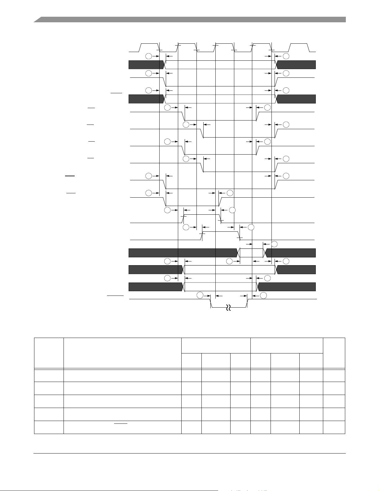
Specifications
(HCLK) Bus Clock
Address
Chip-select
Read (Write
1a 1b
2a 2b
3b3a
)
(rising edge)
OE
(falling edge)
OE
EB
(rising edge)
EB
(falling edge)
LBA
(negated falling edge)
LBA
(negated rising edge)
Burst Clock (rising edge)
Burst Clock (falling edge)
Read Data
Write Data (negated falling)
Write Data (negated rising)
DTACK
4a 4b
4c 4d
5a 5b
5c 5d
6a
6a
7a 7b
7c
9a
9a
10a
8a
6b
6c
7d
8b
9b
9c
10a
Figure 53. EIM Bus Timing Diagram
Table 41. EIM Bus Timing Parameters
1.8V +/- 0.1V 3.0V +/- 0.3V
Ref No. Parameter
Min Typical Max Min Typical Max
1a Clock fall to address valid 3.97 6.02 9.89 3.83 5.89 9.79 ns
1b Clock fall to address invalid 3.93 6.00 9.86 3.81 5.86 9.76 ns
2a Clock fall to chip-select valid 3.47 5.59 8.62 3.30 5.09 8.45 ns
2b Clock fall to chip-select invalid 3.39 5.09 8.27 3.15 4.85 8.03 ns
3a Clock fall to Read (Write
) Valid 3.51 5.56 8.79 3.39 5.39 8.51 ns
MC9328MX21 Product Preview, Rev. 1.1
68 Freescale Semiconductor
Unit
Page 69
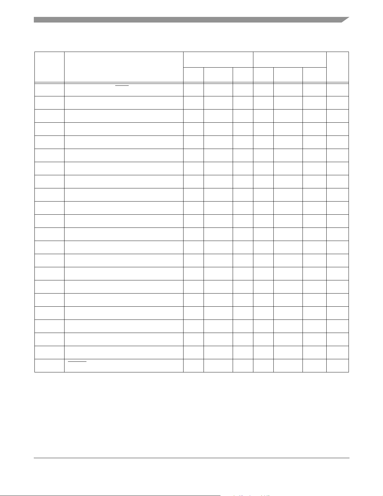
Specifications
Table 41. EIM Bus Timing Parameters (Continued)
1.8V +/- 0.1V 3.0V +/- 0.3V
Ref No. Parameter
Min Typical Max Min Typical Max
3b Clock fall to Read (Write) Invalid 3.59 5.37 9.14 3.36 5.20 8.50 ns
Unit
4a Clock
4b Clock
4c Clock
4d Clock
5a Clock
5b Clock
5c Clock
5d Clock
6a Clock
6b Clock
6c Clock
7a Clock
7b Clock
7c Clock
1
rise to Output Enable Valid 3.62 5.49 8.98 3.46 5.33 9.02 ns
1
rise to Output Enable Invalid 3.70 5.61 9.26 3.46 5.37 8.81 ns
1
fall to Output Enable Valid 3.60 5.48 8.77 3.44 5.30 8.88 ns
1
fall to Output Enable Invalid 3.69 5.62 9.12 3.42 5.36 8.60 ns
1
rise to Enable Bytes Valid 3.69 5.46 8.71 3.46 5.25 8.54 ns
1
rise to Enable Bytes Invalid 4.64 5.47 8.70 3.46 5.25 8.54 ns
1
fall to Enable Bytes Valid 3.52 5.06 8.39 3.41 5.18 8.36 ns
1
fall to Enable Bytes Invalid 3.50 5.05 8.27 3.41 5.18 8.36 ns
1
fall to Load Burst Address Valid 3.65 5.28 8.69 3.30 5.23 8.81 ns
1
fall to Load Burst Address Invalid 3.65 5.67 9.36 3.41 5.43 9.13 ns
1
rise to Load Burst Address Invalid 3.66 5.69 9.48 3.33 5.47 9.25 ns
1
rise to Burst Clock rise 3.50 5.22 8.42 3.26 4.99 8.19 ns
1
rise to Burst Clock fall 3.49 5.19 8.30 3.31 5.03 8.17 ns
1
fall to Burst Clock rise 3.50 5.22 8.39 3.26 4.98 8.15 ns
7d Clock
1
fall to Burst Clock fall 3.49 5.19 8.29 3.31 5.02 8.12 ns
8a Read Data setup time 4.54 – – 4.54 – – ns
8b Read Data hold time 0.5 – – 0.5 – – ns
9a Clock
9b Clock
9c Clock
10a DTACK
1
rise to Write Data Valid 4.13 5.86 9.16 3.95 6.36 10.31 ns
1
fall to Write Data Invalid 4.10 5.79 9.15 4.04 6.27 9.16 ns
1
rise to Write Data Invalid 4.02 5.81 9.37 4.22 5.29 9.24 ns
setup time 2.65 4.63 8.40 2.64 4.61 8.41 ns
1. Clock refers to the system clock signal, HCLK, generated from the System DPLL
3.19.1 EIM External Bus Timing Diagrams
The following timing diagrams show the timing of accesses to memory or a peripheral.
MC9328MX21 Product Preview, Rev. 1.1
Freescale Semiconductor 69
Page 70
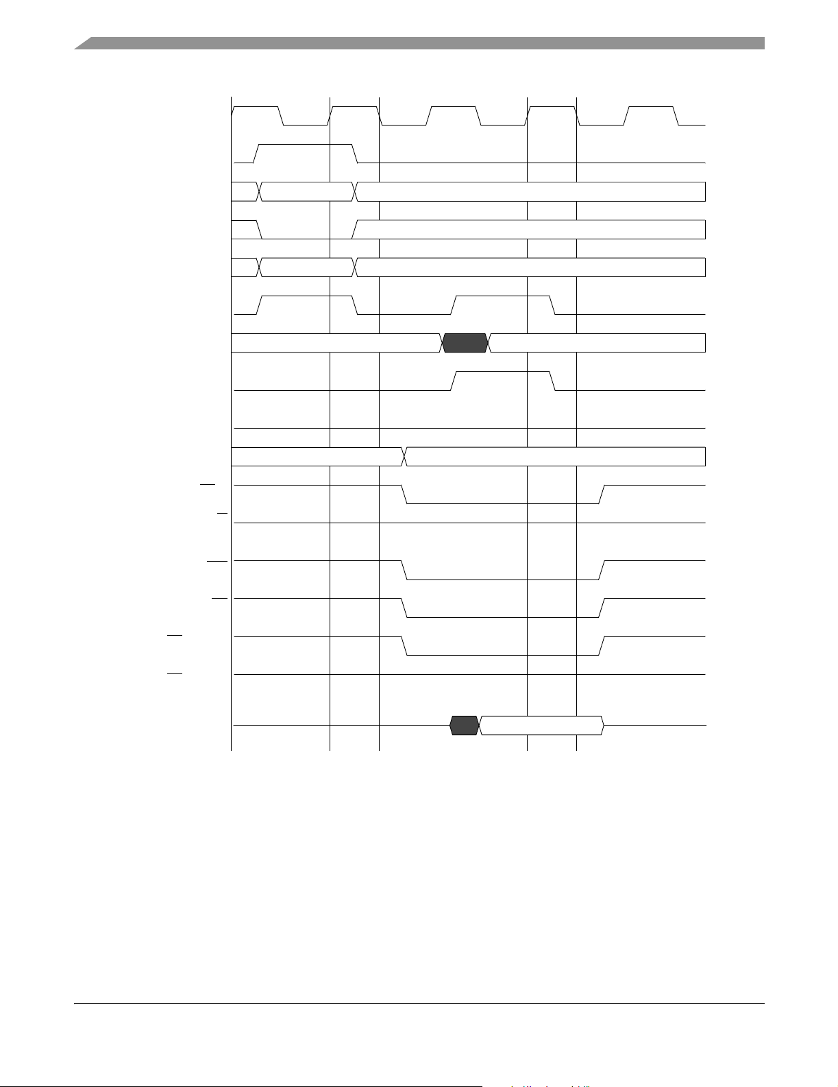
Specifications
hselm_weim_cs[0]
hclk
htrans
hwrite
haddr
hready
weim_hrdata
weim_hready
BCLK
A[24:0]
[0]
CS
R/W
LBA
Seq/Nonseq
Read
V1
Last Valid Data
Last Valid Address
V1
V1
Read
OE
EB (EBC=0)
(EBC=1)
EB
DATA_IN
V1
Figure 54. WSC = 1, A.HALF/E.HALF
MC9328MX21 Product Preview, Rev. 1.1
70 Freescale Semiconductor
Page 71
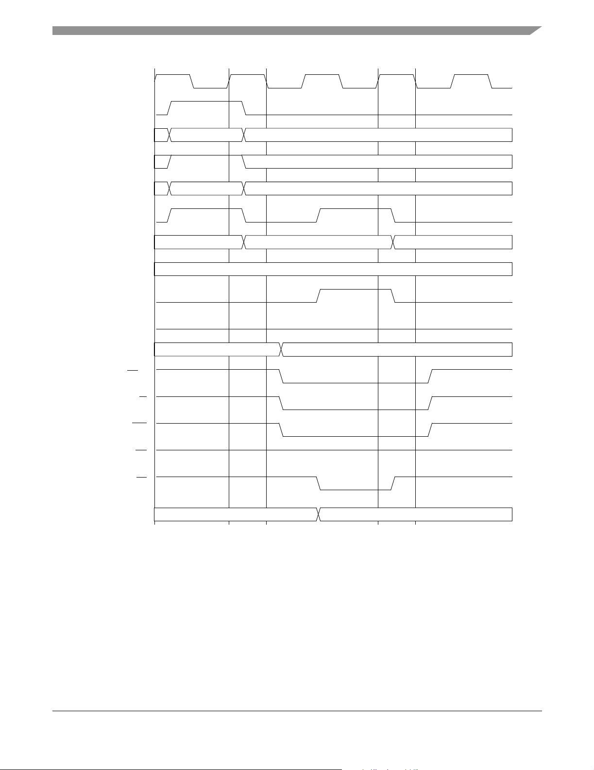
hclk
hselm_weim_cs[0]
Specifications
htrans
hwrite
haddr
hready
hwdata
weim_hrdata
weim_hready
BCLK
A[24:0]
[0]
CS
R/W
Nonseq
Write
V1
Last Valid Data
Last Valid Address
Write Data (V1) Unknown
Last Valid Data
V1
Write
LBA
OE
EB
D[31:0]
Last Valid Data Write Data (V1)
Figure 55. WSC = 1, WEA = 1, WEN = 1, A.HALF/E.HALF
MC9328MX21 Product Preview, Rev. 1.1
Freescale Semiconductor 71
Page 72
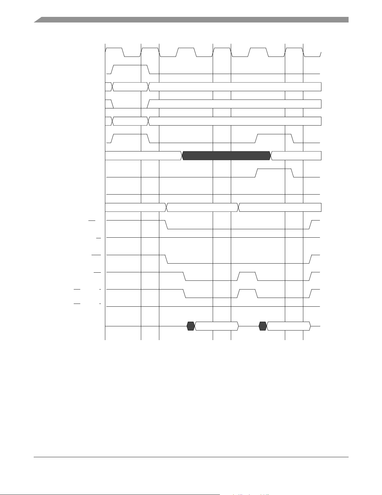
Specifications
hselm_weim_cs[0]
hclk
htrans
hwrite
haddr
hready
weim_hrdata
weim_hready
BCLK
A[24:0]
[0]
CS
R/W
LBA
Nonseq
Read
V1
Last Valid Data
Address V1
Read
V1 Word
Address V1 + 2Last Valid Addr
OE
EB
(EBC=0)
EB (EBC=1)
DATA_IN
1/2 Half Word 2/2 Half Word
Figure 56. WSC = 1, OEA = 1, A.WORD/E.HALF
MC9328MX21 Product Preview, Rev. 1.1
72 Freescale Semiconductor
Page 73
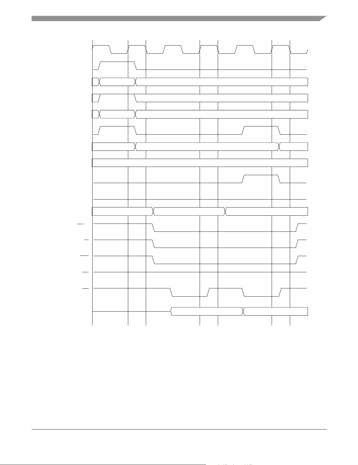
hclk
hselm_weim_cs[0]
Specifications
htrans
hwrite
haddr
hready
hwdata
weim_hrdata
weim_hready
BCLK
A[24:0]
[0]
CS
R/W
Nonseq
Write
V1
Last Valid Data
Write Data (V1 Word)
Last Valid Data
Address V1
Address V1 + 2Last Valid Addr
Write
LBA
OE
EB
D[31:0]
1/2 Half Word 2/2 Half Word
Figure 57. WSC = 1, WEA = 1, WEN = 1, A.WORD/E.HALF
MC9328MX21 Product Preview, Rev. 1.1
Freescale Semiconductor 73
Page 74

Specifications
hselm_weim_cs[3]
hclk
htrans
hwrite
haddr
hready
weim_hrdata
weim_hready
BCLK
A[24:0]
[3]
CS
R/W
LBA
Nonseq
Read
V1
Last Valid Data
Address V1
Read
V1 Word
Address V1 + 2Last Valid Addr
OE
EB (EBC=0)
(EBC=1)
EB
DATA_IN
1/2 Half Word 2/2 Half Word
Figure 58. WSC = 3, OEA = 2, A.WORD/E.HALF
MC9328MX21 Product Preview, Rev. 1.1
74 Freescale Semiconductor
Page 75

hclk
hselm_weim_cs[3]
Specifications
htrans
hwrite
haddr
hready
hwdata
weim_hrdata
weim_hready
BCLK
A[24:0]
[3]
CS
R/W
Nonseq
Write
V1
Last Valid
Data
Write Data (V1 Word)
Address V1
Write
Last Valid Data
Address V1 + 2Last Valid Addr
LBA
OE
EB
D[31:0]
Last Valid Data
1/2 Half Word 2/2 Half Word
Figure 59. WSC = 3, WEA = 1, WEN = 3, A.WORD/E.HALF
MC9328MX21 Product Preview, Rev. 1.1
Freescale Semiconductor 75
Page 76

Specifications
hselm_weim_cs[2]
hclk
htrans
hwrite
haddr
hready
weim_hrdata
weim_hready
BCLK
A[24:0]
[2]
CS
R/W
LBA
Nonseq
Read
V1
Last Valid Data
Address V1
Read
V1 Word
Address V1 + 2Last Valid Addr
EB
(EBC=0)
EB
(EBC=1)
DATA_IN
OE
1/2 Half Word 2/2 Half Word
Figure 60. WSC = 3, OEA = 4, A.WORD/E.HALF
MC9328MX21 Product Preview, Rev. 1.1
76 Freescale Semiconductor
Page 77

hclk
hselm_weim_cs[2]
Specifications
htrans
hwrite
haddr
hready
hwdata
weim_hrdata
weim_hready
BCLK
A[24:0]
[2]
CS
R/W
Nonseq
Write
V1
Last Valid
Data
Address V1
Write
Write Data (V1 Word)
Last Valid Data
Address V1 + 2Last Valid Addr
LBA
OE
EB
D[31:0]
Last Valid Data
1/2 Half Word 2/2 Half Word
Figure 61. WSC = 3, WEA = 2, WEN = 3, A.WORD/E.HALF
MC9328MX21 Product Preview, Rev. 1.1
Freescale Semiconductor 77
Page 78

Specifications
hselm_weim_cs[2]
hclk
htrans
hwrite
haddr
hready
weim_hrdata
weim_hready
BCLK
A[24:0]
[2]
CS
R/W
LBA
Nonseq
Read
V1
Last Valid Data
Address V1
Read
V1 Word
Address V1 + 2Last Valid Addr
(EBC=0)
EB
(EBC=1)
EB
DATA_IN
OE
1/2 Half Word 2/2 Half Word
Figure 62. WSC = 3, OEN = 2, A.WORD/E.HALF
MC9328MX21 Product Preview, Rev. 1.1
78 Freescale Semiconductor
Page 79

hclk
hselm_weim_cs[2]
Specifications
htrans
hwrite
haddr
hready
weim_hrdata
weim_hready
BCLK
A[24:0]
[2]
CS
R/W
LBA
Nonseq
Read
V1
Last Valid Data
Address V1
Read
V1 Word
Address V1 + 2Last Valid Addr
EB
(EBC=0)
EB
(EBC=1)
DATA_IN
OE
1/2 Half Word 2/2 Half Word
Figure 63. WSC = 3, OEA = 2, OEN = 2, A.WORD/E.HALF
MC9328MX21 Product Preview, Rev. 1.1
Freescale Semiconductor 79
Page 80
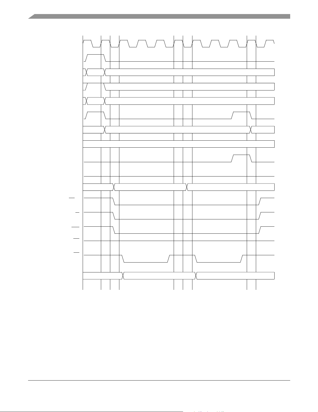
Specifications
hselm_weim_cs[2]
hclk
htrans
hwrite
haddr
hready
hwdata
weim_hrdata
weim_hready
BCLK
A[24:0]
[2]
CS
R/W
Nonseq
Write
V1
Last Valid
Data
Address V1
Write Data (V1 Word)
Last Valid Data
Write
Unknown
Address V1 + 2Last Valid Addr
LBA
OE
EB
D[31:0]
Last Valid Data
1/2 Half Word 2/2 Half Word
Figure 64. WSC = 2, WWS = 1, WEA = 1, WEN = 2, A.WORD/E.HALF
MC9328MX21 Product Preview, Rev. 1.1
80 Freescale Semiconductor
Page 81
hclk
hselm_weim_cs[2]
Specifications
htrans
hwrite
haddr
hready
hwdata
weim_hrdata
weim_hready
BCLK
A[24:0]
[2]
CS
R/W
Nonseq
Write
V1
Last Valid
Data
Write Data (V1 Word)
Last Valid Data
Address V1
Unknown
Address V1 + 2Last Valid Addr
Write
LBA
OE
EB
D[31:0]
Last Valid Data
1/2 Half Word 2/2 Half Word
Figure 65. WSC = 1, WWS = 2, WEA = 1, WEN = 2, A.WORD/E.HALF
MC9328MX21 Product Preview, Rev. 1.1
Freescale Semiconductor 81
Page 82

Specifications
hselm_weim_cs[2]
hclk
htrans
hwrite
haddr
hready
hwdata
weim_hrdata
weim_hready
BCLK
A[24:0]
[2]
CS
R/W
Nonseq
Read
V1
Last Valid Data
Last Valid Data Read Data
Read
Nonseq
Write
V8
Write Data
Address V1
Address V8Last Valid Addr
Write
EB
(EBC=0)
(EBC=1)
EB
DATA_IN
LBA
OE
Read Data
D[31:0]
Last Valid Data Write Data
Figure 66. WSC = 2, WWS = 2, WEA = 1, WEN = 2, A.HALF/E.HALF
MC9328MX21 Product Preview, Rev. 1.1
82 Freescale Semiconductor
Page 83
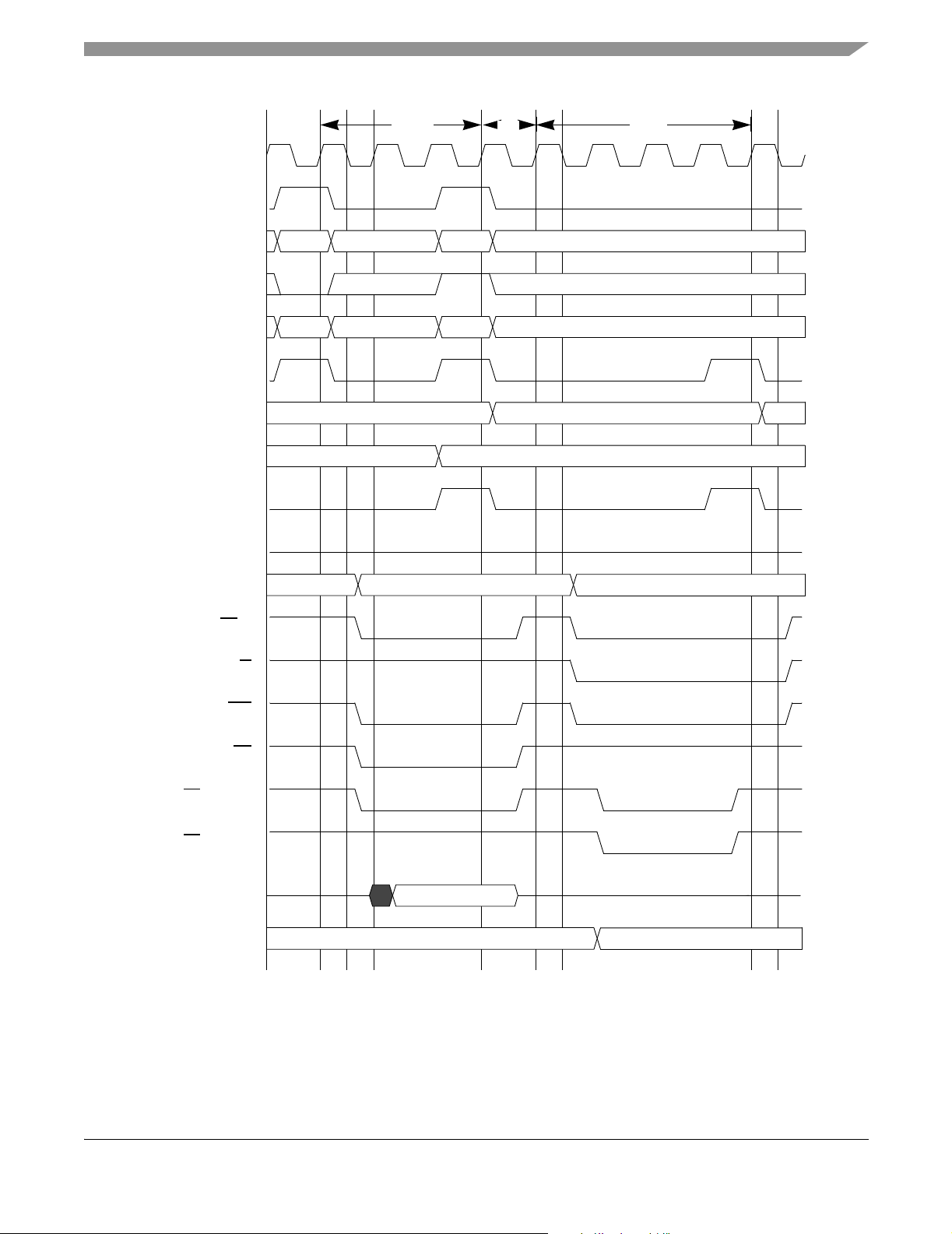
hclk
hselm_weim_cs[2]
Specifications
Read WriteIdle
htrans
hwrite
haddr
hready
hwdata
weim_hrdata
weim_hready
BCLK
A[24:0]
[2]
CS
R/W
Nonseq
Read
V1
Last Valid Data
Last Valid Data
Read
Nonseq
Write
V8
Write Data
Read Data
Address V1 Address V8Last Valid Addr
Write
LBA
OE
EB
(EBC=0)
(EBC=1)
EB
DATA_IN
D[31:0]
Read Data
Last Valid Data Write Data
Figure 67. WSC = 2, WWS = 1, WEA = 1, WEN = 2, EDC = 1, A.HALF/E.HALF
MC9328MX21 Product Preview, Rev. 1.1
Freescale Semiconductor 83
Page 84

Specifications
hselm_weim_cs[4]
hclk
htrans
hwrite
haddr
hready
hwdata
weim_hrdata
weim_hready
BCLK
A[24:0]
[3:0]
CS
R/W
Nonseq
Write
V1
Last Valid
Data
Write Data (Word)
Last Valid Data
Address V1 Address V1 + 2Last Valid Addr
Write
LBA
OE
EB
D[31:0]
Last Valid Data
Write Data (1/2 Half Word) Write Data (2/2 Half Word)
Figure 68. WSC = 2, CSA = 1, WWS = 1, A.WORD/E.HALF
MC9328MX21 Product Preview, Rev. 1.1
84 Freescale Semiconductor
Page 85
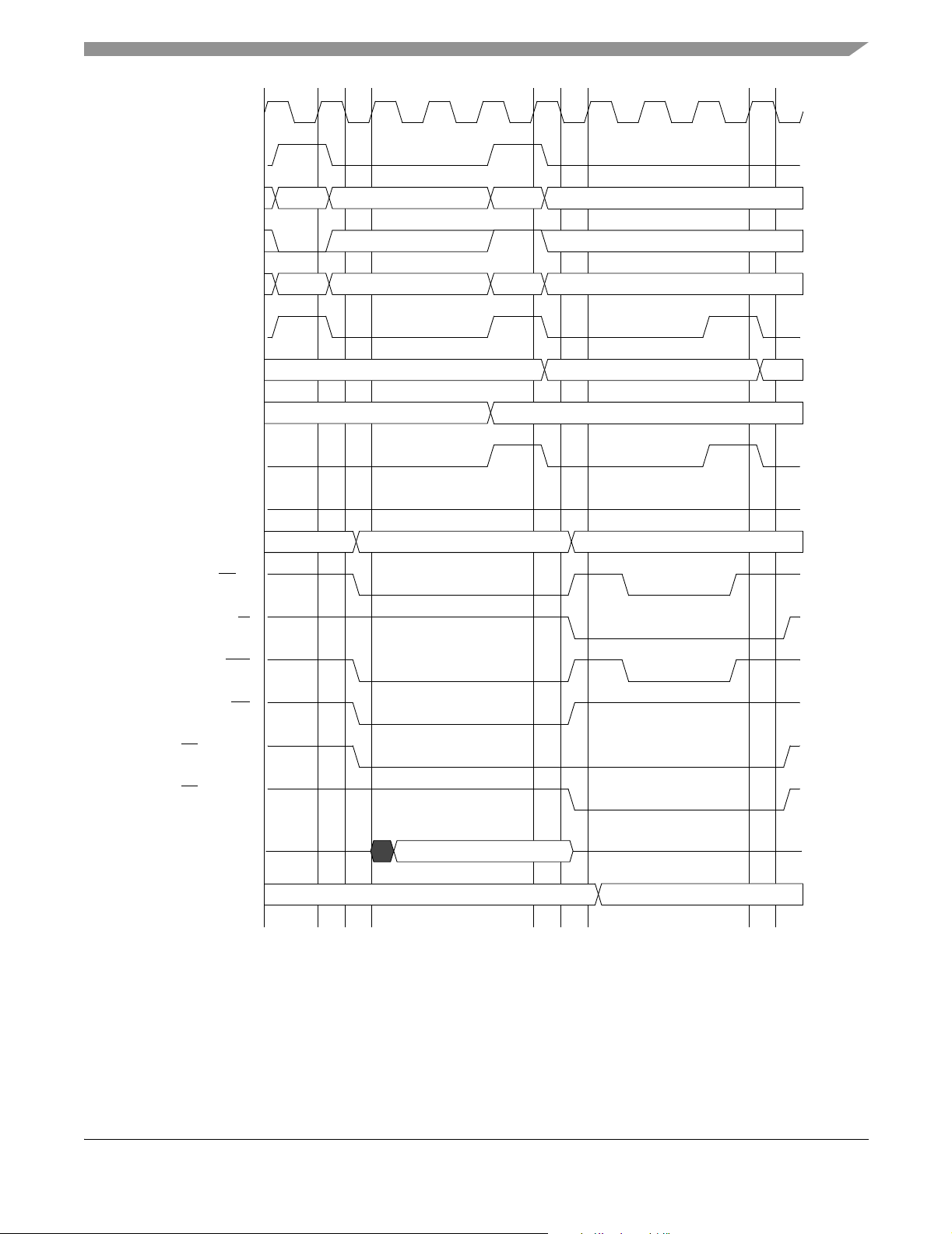
hclk
hselm_weim_cs[4]
Specifications
htrans
hwrite
haddr
hready
hwdata
weim_hrdata
weim_hready
BCLK
A[24:0]
[4]
CS
R/W
Nonseq
Read
V1
Nonseq
Write
V8
Last Valid Data
Last Valid Data Read Data
Address V1 Address V8Last Valid Addr
Read
Write Data
Write
EB
(EBC=0)
(EBC=1)
EB
DATA_IN
LBA
OE
D[31:0]
Read Data
Write DataLast Valid Data
Figure 69. WSC = 3, CSA = 1, A.HALF/E.HALF
MC9328MX21 Product Preview, Rev. 1.1
Freescale Semiconductor 85
Page 86
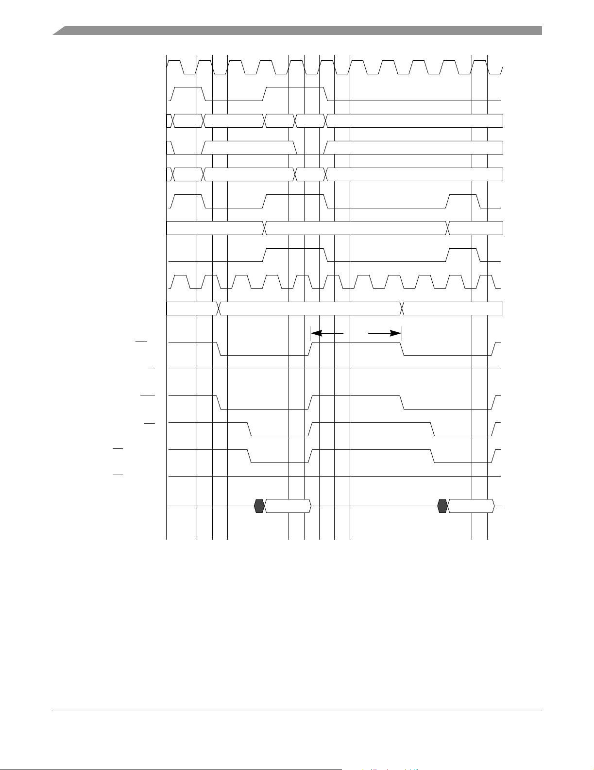
Specifications
hselm_weim_cs[4]
hclk
htrans
hwrite
haddr
hready
weim_hrdata
weim_hready
BCLK
A[24:0]
[4]
CS
R/W
Nonseq
Read
V1
Last Valid Data
Last Valid Addr
Read
Idle
Seq
Read
V2
Address V1
Read Data (V1)
CNC
Read Data (V2)
Address V2
EB
(EBC=0)
(EBC=1)
EB
DATA_IN
LBA
OE
Read Data
(V1)
Figure 70. WSC = 2, OEA = 2, CNC = 3, BCM = 1, A.HALF/E.HALF
Read Data
(V2)
MC9328MX21 Product Preview, Rev. 1.1
86 Freescale Semiconductor
Page 87
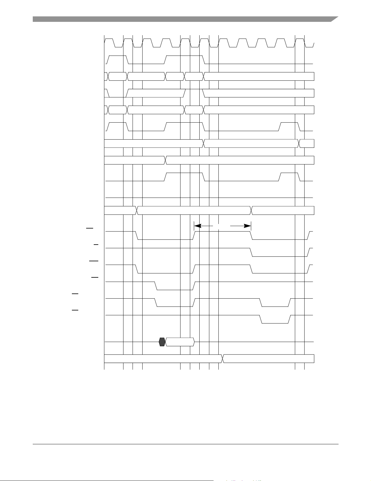
hclk
hselm_weim_cs[4]
Specifications
htrans
hwrite
haddr
hready
hwdata
weim_hrdata
weim_hready
BCLK
A[24:0]
[4]
CS
R/W
Nonseq
Read
V1
Last Valid Data
Last Valid Addr
Last Valid Data
Read
Nonseq
Idle
Write
V8
Write Data
Read Data
Address V1 Address V8
CNC
Write
LBA
OE
EB
(EBC=0)
(EBC=1)
EB
DATA_IN
D[31:0]
Last Valid Data Write Data
Read Data
Figure 71. WSC = 2, OEA = 2, WEA = 1, WEN = 2, CNC = 3, A.HALF/E.HALF
MC9328MX21 Product Preview, Rev. 1.1
Freescale Semiconductor 87
Page 88
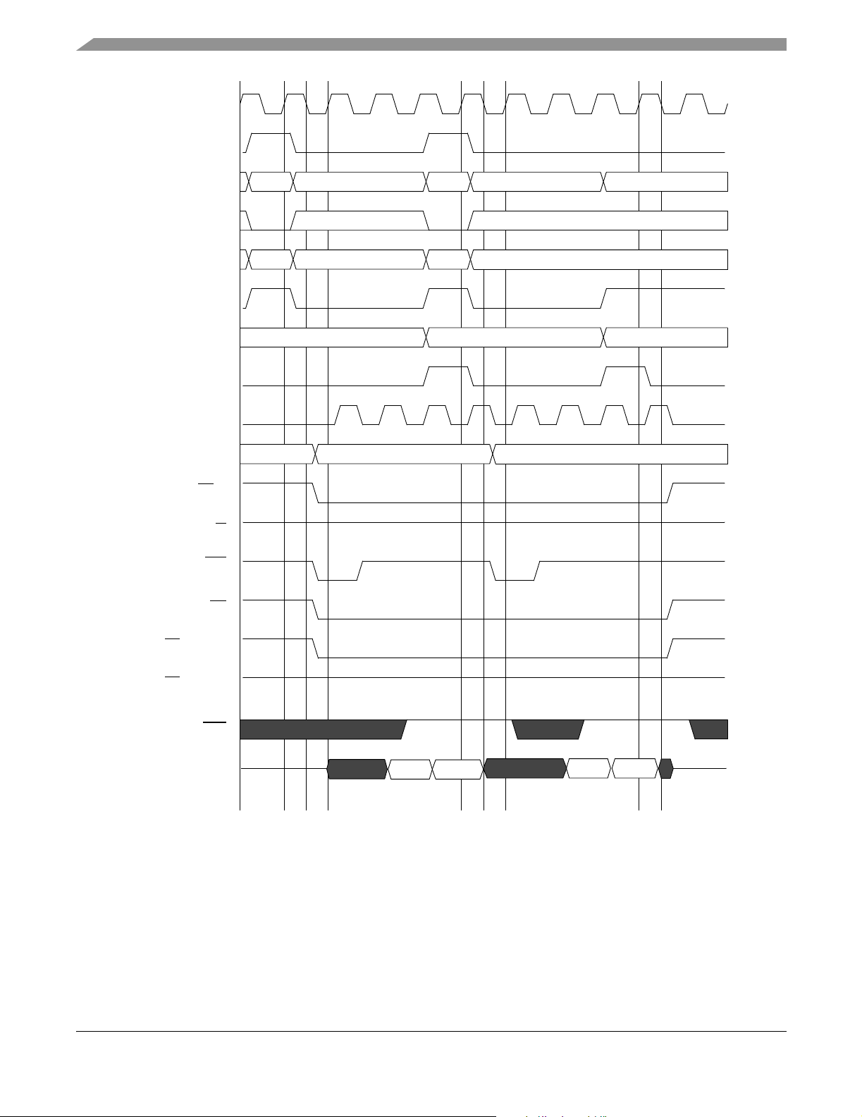
Specifications
hselm_weim_cs[2]
hclk
htrans
hwrite
haddr
hready
weim_hrdata
weim_hready
BCLK
A[24:0]
[2]
CS
R/W
LBA
Nonseq Nonseq
Read Read
V1 V5
Address V1Last Valid Addr Address V5
Read
Idle
EB
(EBC=0)
(EBC=1)
EB
DATA_IN
OE
ECB
V1 Word V2 Word
V5 Word
Figure 72. WSC = 3, SYNC = 1, A.HALF/E.HALF
V6 Word
MC9328MX21 Product Preview, Rev. 1.1
88 Freescale Semiconductor
Page 89
hclk
hselm_weim_cs[2]
Specifications
htrans
hwrite
haddr
hready
weim_hrdata
weim_hready
BCLK
A[24:0]
[2]
CS
R/W
LBA
Nonseq
Read
V1
Last Valid Data V1 Word V2 Word V3 Word V4 Word
Seq
Read Read Read
V2 V3 V4
Seq Seq
Address V1Last Valid Addr
Read
Idle
(EBC=0)
EB
(EBC=1)
EB
DATA_IN
OE
ECB
V1 Word V2 Word V3 Word V4 Word
Figure 73. WSC = 2, SYNC = 1, DOL = [1/0], A.WORD/E.WORD
MC9328MX21 Product Preview, Rev. 1.1
Freescale Semiconductor 89
Page 90

Specifications
hselm_weim_cs[2]
hclk
htrans
hwrite
haddr
hready
weim_hrdata
weim_hready
BCLK
A[24:0]
[2]
CS
R/W
LBA
Nonseq
Read
V1
Seq
Read
V2
Last Valid Data V1 Word V2 Word
Last Valid Addr
Address V1
Address V2
Read
Idle
EB
(EBC=0)
(EBC=1)
EB
DATA_IN
OE
ECB
V1 1/2 V1 2/2 V2 1/2 V2 2/2
Figure 74. WSC = 2, SYNC = 1, DOL = [1/0], A.WORD/E.HALF
MC9328MX21 Product Preview, Rev. 1.1
90 Freescale Semiconductor
Page 91
hclk
hselm_weim_cs[2]
Specifications
htrans
hwrite
haddr
hready
weim_hrdata
weim_hready
BCLK
A[24:0]
[2]
CS
R/W
LBA
Non
seq
Read
V1
Last Valid
Addr
Seq
Idle
Read
V2
Last Valid Data V1 Word V2 Word
Address V1
Read
OE
(EBC=0)
EB
(EBC=1)
EB
ECB
DATA_IN
V1 1/2 V1 2/2 V2 1/2 V2 2/2
Figure 75. WSC = 7, OEA = 8, SYNC = 1, DOL = 1, BCD = 1, BCS = 2, A.WORD/E.HALF
MC9328MX21 Product Preview, Rev. 1.1
Freescale Semiconductor 91
Page 92

Specifications
hselm_weim_cs[2]
hclk
htrans
hwrite
haddr
hready
weim_hrdata
weim_hready
BCLK
A[24:0]
[2]
CS
R/W
LBA
Non
seq
Read
V1
Last Valid
Addr
Seq
Read
V2
Last Valid Data V1 Word V2 Word
Address V1
Read
Idle
OE
EB
(EBC=0)
(EBC=1)
EB
ECB
DATA_IN
V1 1/2 V1 2/2 V2 1/2 V2 2/2
Figure 76. WSC = 7, OEA = 8, SYNC = 1, DOL = 1, BCD = 1, BCS = 1, A.WORD/E.HALF
3.20 DTACK Mode Memory Access Timing Diagrams
When enabled, the DTACK input signal is used to externally terminate a data transfer. For DTACK
enabled operations, a bus time-out monitor generates a bus error when an external bus cycle is not
terminated by the DTACK
internal system clock driven from the PLL module. For a 133 MHz HCLK setting, this time equates to
7.7 µs. Refer to the Section 3.5, “DPLL Timing Specifications,” on page 18 for more information on how
to generate different HCLK frequencies.
input signal after 1024 HCLK clock cycles have elapsed, where HCLK is the
MC9328MX21 Product Preview, Rev. 1.1
92 Freescale Semiconductor
Page 93

Specifications
There are two modes of operation for the DTACK input signal: rising edge detection or level sensitive
detection with a programmable insensitivity time. DTACK
is only used during external asynchronous data
transfers, thus the SYNC bit in the chip select control registers must be cleared.
During edge detection mode, the EIM will terminate an external data transfer following the detection of the
DTACK
is used for devices that follow the PCMCIA standard. Note that DTACK
only be used for CS
signal’s rising edge, so long as it occurs within the 1024 HCLK cycle time. Edge detection mode
rising edge detection mode can
[5] operations. To configure CS[5] for DTACK rising edge detection, the following
bits must be programmed in the Chip Select 5 Control Register and EIM Configuration Register:
• WSC bit field set to 0x3F and CSA (or CSN) set to 1 or greater in the Chip Select 5 Control Register
• AGE bit set in the EIM Configuration Register
Other bits such as DSZ, OEA, OEN, and so on, may be set according to system and timing requirements of
the external device. The requirement of setting CSA or CSN is required to allow the EIM to wait for the
rising edge of DTACK
during back-to-back external transfers, such as during DMA transfers or an internal
32-bit access through an external 16-bit data port.
During level sensitive detection, the EIM will first hold off sampling the DTACK
signal for at least 2
HCLK cycles, and up to 5 HCLK cycles as programmed by the DCT bits in the Chip Select Control
Register. After this insensitivity time, the EIM will sample DTACK
and if it detects that DTACK is logic
high, it will continue the data transfer at the programmed number of wait states. However, if the EIM
detects that DTACK
is logic low, it will wait until DTACK goes to logic high to continue the access, so
long as this occurs within the 1024 HCLK cycle time. If at anytime during an external data transfer
DTACK
goes to logic low, the EIM will wait until DTACK returns to logic high to resume the data
transfer. Level detection is often used for asynchronous devices such graphic controller chips. Level
detection may be used with any chip select except CS[4] as it is multiplexed with the DTACK
configure a chip select for DTACK
level sensitive detection, the following bits must be programmed in the
signal. To
Chip Select Control Register and EIM Configuration Register:
• EW bit set, WSC set to > 1, and CSN set to < 3 in the Chip Select Control Register
• BCD/DCT set to desired “insensitivity time” in the Chip Select Control Register. The “insensitivity
time” is dictated by the external device’s timing requirements.
• AGE bit cleared in the EIM Configuration Register
Other bits such as DSZ, OEA, OEN, and so on, may be set according to system and timing requirements of
the external device.
The waveforms in the following section provide examples of the DTACK
signal operation.
MC9328MX21 Product Preview, Rev. 1.1
Freescale Semiconductor 93
Page 94

Specifications
3.20.1 DTACK Example Waveforms: Internal ARM AHB Word Accesses to Word-Width (32-bit) Memory
HCLK
Internal Signal
BCLK
ADDR
CS[5]
RW
LBA
OE
EB (EBC=0)
EB
(EBC=1)
DTACK
DATA_IN
Last Valid
Addr
V1
Read
V1 Data
Figure 77. DTACK Edge Triggered Read Access, WSC=3F, OEA=8, OEN=5, AGE=1.
MC9328MX21 Product Preview, Rev. 1.1
94 Freescale Semiconductor
Page 95

HCLK
BCLK
Specifications
ADDR
Internal Signal
[0]
CS
RW
LBA
OE
EB (EBC=0)
EB
(EBC=1)
DTACK
DATA_IN
Last Valid Addr
Address V1
DCT
V1+4
Read
V1 Word V1+4 Word
V1+8
V1+8 Word
Figure 78. DTACK Level Sensitive Sequential Read Accesses, WSC=2, EW=1, DCT=1, AGE=0
(Example of DTACK
staying high)
MC9328MX21 Product Preview, Rev. 1.1
Freescale Semiconductor 95
Page 96
Specifications
HCLK
BCLK
ADDR
Last Valid Addr
Address V1
V1+4 V1+8
Internal Signal
CS
[0]
RW
LBA
OE
EB
DTACK
DATA_OUT
RWA
Write
DCT
V1 Word
RWN
V1+4 Word V1+8
Figure 79. DTACK Level Sensitive Sequential Write Accesses, WSC=2, EW=1, RWA=1, RWN=1,
DCT=1, AGE=0 (Example of DTACK
Asserting)
MC9328MX21 Product Preview, Rev. 1.1
96 Freescale Semiconductor
Page 97
Specifications
3.21 I2C Module
The I2C communication protocol consists of seven elements: START, Data Source/Recipient, Data
Direction, Slave Acknowledge, Data, Data Acknowledge, and STOP.
SDA
5
SCL
1
Figure 80. Definition of Bus Timing for I2C
Table 42. I2C Bus Timing Parameter Table
Ref
No.
SCL Clock Frequency 0 100 0 100 kHz
1 Hold time (repeated) START condition 114.8 – 111.1 – ns
2 Data hold time
3 Data setup time 3.1 – 1.76 – ns
4 HIGH period of the SCL clock 69.7 – 68.3 – ns
5 LOW period of the SCL clock 336.4 – 335.1 – ns
6 Setup time for STOP condition 110.5 – 111.1 – ns
Parameter
3
2
Minimum Maximum Minimum Maximum
4
6
1.8V +/- 0.10V 3.0V +/- 0.30V
0 69.7 0 72.3 ns
Unit
3.22 CMOS Sensor Interface
The CSI module consists of a control register to configure the interface timing, a control register
for statistic data generation, a status register, interface logic, a 32 × 32 image data receive FIFO,
and a 16 × 32 statistic data FIFO.
3.22.1 Gated Clock Mode
Figure 81 shows the timing diagram when the CMOS sensor output data is configured for negative
edge and the CSI is programmed to received data on the positive edge. Figure 82 on page 98 shows
the timing diagram when the CMOS sensor output data is configured for positive edge and the CSI
is programmed to received data in negative edge. The parameters for the timing diagrams are listed
in Table 43 on page 98. The formula for calculating the pixel clock rise and fall time is located in
Section 3.22.3, “Calculation of Pixel Clock Rise/Fall Time,” on page 101.
MC9328MX21 Product Preview, Rev. 1.1
Freescale Semiconductor 97
Page 98
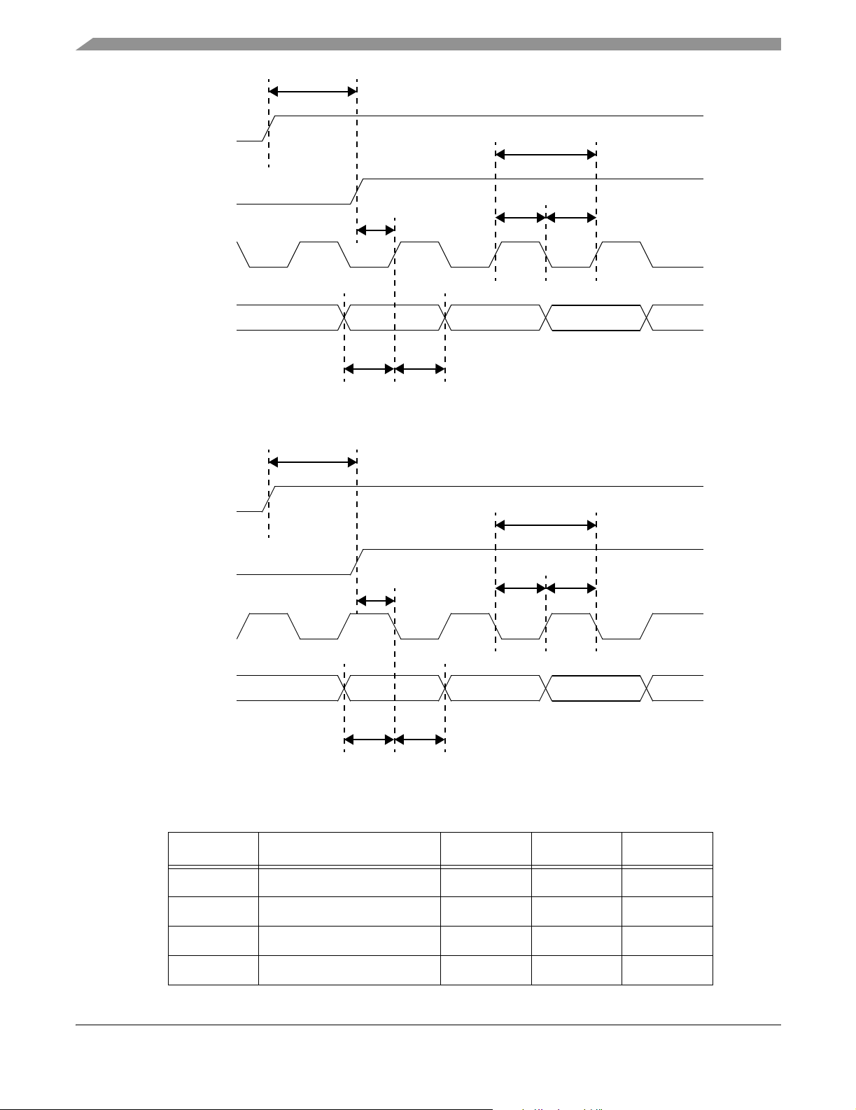
Specifications
1
VSYNC
HSYNC
PIXCLK
DATA[7:0]
VSYNC
7
2
Valid Data
3
Valid Data Valid Data
4
65
Figure 81. Sensor Output Data on Pixel Clock Falling Edge
CSI Latches Data on Pixel Clock Rising Edge
1
7
HSYNC
PIXCLK
DATA[7:0]
2
Valid Data
3
Valid Data Valid Data
4
65
Figure 82. Sensor Output Data on Pixel Clock Rising Edge
CSI Latches Data on Pixel Clock Falling Edge
Table 43. Gated Clock Mode Timing Parameters
Number Parameter Minimum Maximum Unit
1 csi_vsync to csi_hsync 9 * T
HCLK
2 csi_hsync to csi_pixclk 3
3 csi_d setup time 1 – ns
4 csi_d hold time 1 – ns
–ns
(T
/2) - 3 ns
P
MC9328MX21 Product Preview, Rev. 1.1
98 Freescale Semiconductor
Page 99

Table 43. Gated Clock Mode Timing Parameters
Number Parameter Minimum Maximum Unit
Specifications
5 csi_pixclk high time T
6 csi_pixclk low time T
7 csi_pixclk frequency 0 HCLK / 2 MHz
HCLK = AHB System Clock
= Period for HCLK
T
HCLK
TP = Period of CSI_PIXCLK
HCLK
HCLK
–ns
–ns
The limitation on pixel clock rise time/fall time is not specified. It should be calculated from the
hold time and setup time based on the following assumptions:
Rising-edge latch data
max rise time allowed = (positive duty cycle - hold time)
max fall time allowed = (negative duty cycle - setup time)
In most of case, duty cycle is 50 / 50, therefore
max rise time = (period / 2 - hold time)
max fall time = (period / 2 - setup time)
For example: Given pixel clock period = 10ns, duty cycle = 50 / 50, hold time = 1ns, setup time =
1ns.
positive duty cycle = 10 / 2 = 5ns
≥ max rise time allowed = 5 - 1 = 4ns
negative duty cycle = 10 / 2 = 5ns
≥ max fall time allowed = 5 - 1 = 4ns
Falling-edge latch data
max fall time allowed = (negative duty cycle - hold time)
max rise time allowed = (positive duty cycle - setup time)
3.22.2 Non-Gated Clock Mode
Figure 83 shows the timing diagram when the CMOS sensor output data is configured for negative
edge and the CSI is programmed to received data on the positive edge. Figure 84 on page 100
shows the timing diagram when the CMOS sensor output data is configured for positive edge and
the CSI is programmed to received data in negative edge. The parameters for the timing diagrams
are listed in Table 44 on page 100. The formula for calculating the pixel clock rise and fall time is
located in Section 3.22.3, “Calculation of Pixel Clock Rise/Fall Time,” on page 101.
MC9328MX21 Product Preview, Rev. 1.1
Freescale Semiconductor 99
Page 100
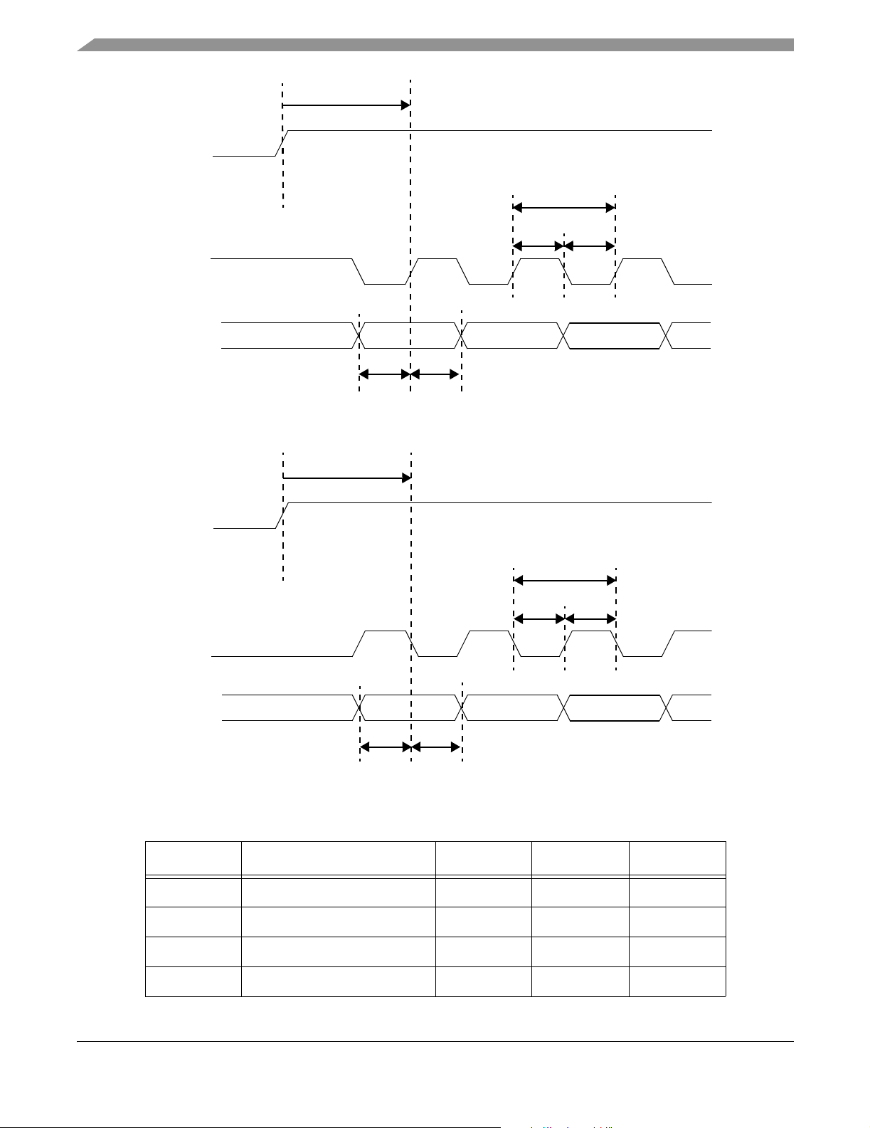
Specifications
1
VSYNC
6
PIXCLK
DATA[7:0]
VSYNC
5
Valid Data
Valid Data
23
4
Valid Data
Figure 83. Sensor Output Data on Pixel Clock Falling Edge
CSI Latches Data on Pixel Clock Rising Edge
1
6
5
4
PIXCLK
DATA[7:0]
Valid Data
2
Valid Data
3
Valid Data
Figure 84. Sensor Output Data on Pixel Clock Rising Edge
CSI Latches Data on Pixel Clock Falling Edge
Table 44. Non-Gated Clock Mode Parameters
Number Parameter Minimum Maximum Unit
1 csi_vsync to csi_pixclk 9 * T
HCLK
2 csi_d setup time 1 – ns
3 csi_d hold time 1 – ns
4 csi_pixclk high time T
HCLK
MC9328MX21 Product Preview, Rev. 1.1
100 Freescale Semiconductor
–ns
–ns
 Loading...