

Datasheet MC68HC908QY4, MC68HC908QY2, MC68HC908QT2, MC68HC908QY1, MC68HC908QT1 Datasheet (Freescale)

查询MC68HC908QY1CDTE供应商
MC68HC908QY4
MC68HC908QT4
MC68HC908QY2
MC68HC908QT2
MC68HC908QY1
MC68HC908QT1
Data Sheet
M68HC08
Microcontrollers
MC68HC908QY4/D
Rev. 5
07/2005
freescale.com


MC68HC908QY4
MC68HC908QT4
MC68HC908QY2
MC68HC908QT2
MC68HC908QY1
MC68HC908QT1
Data Sheet
To provide the most up-to-date information, the revision of our documents on the World Wide Web will be
the most current. Your printed copy may be an earlier revision. To verify you have the latest information
available, refer to:
http://freescale.com/
Freescale™ and the Freescale logo are trademarks of Freescale Semiconductor, Inc.
This product incorporates SuperFlash® technology licensed from SST.
© Freescale Semiconductor, Inc., 2005. All rights reserved.
MC68HC908QY/QT Family Data Sheet, Rev. 5
Freescale Semiconductor 3

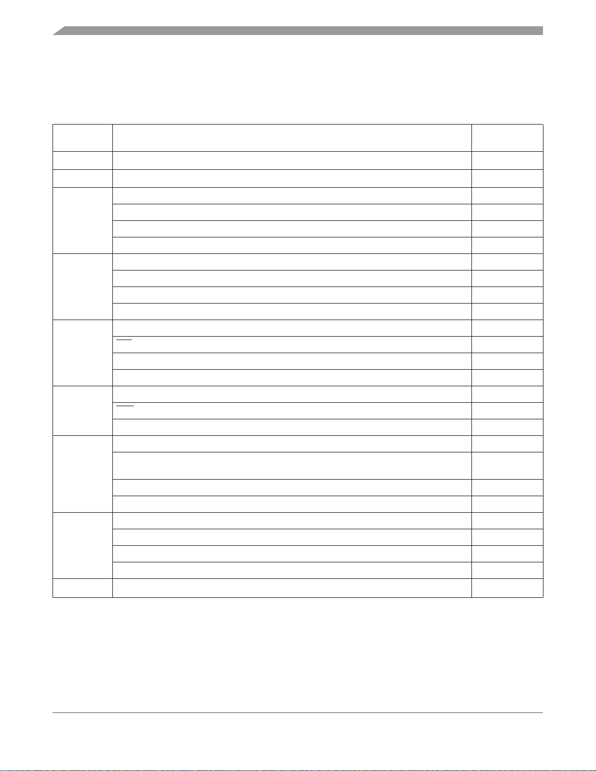
Revision History
The following revision history table summarizes changes contained in this document. For your
convenience, the page number designators have been linked to the appropriate location.
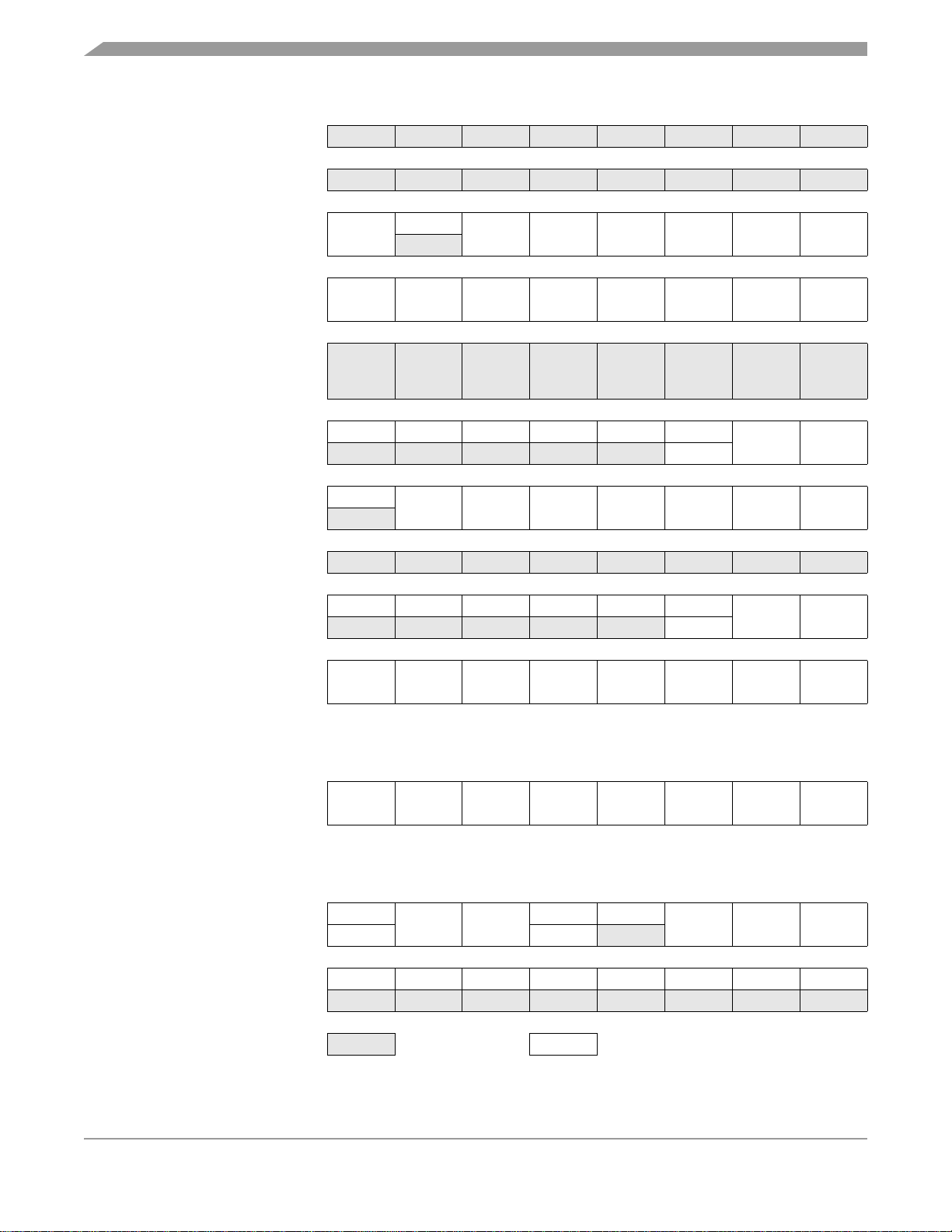
Revision History (Sheet 1 of 3)
Date
September,
2002
December,
2002
January,
2003
Revision
Level
N/A Initial release N/A
1.2 Features — Added 8-pin dual flat no lead (DFN) packages to features list. 19
Figure 1-2. MCU Pin Assignments — Figure updated to include DFN packages. 21
Figure 2-1. Memory Map — Clarified illegal address and unimplemented
memory.
Figure 2-2. Control, Status, and Data Registers — Corrected bit definitions for
Port A Data Register (PTA) and Data Direction Register A (DDRA).
Table 13-3. Interrupt Sources — Corrected vector addresses for keyboard
interrupt and ADC conversion complete interrupt.
Chapter 13 System Integration Module (SIM) — Removed reference to break
status register as it is duplicated in break module.
11.3.1 Internal Oscillator and 11.3.1.1 Internal Oscillator Trimming — Clarified
oscillator trim option ordering information and what to expect with untrimmed
device.
Figure 11-5. Oscillator Trim Register (OSCTRIM) — Bit 1 designation corrected. 98
Figure 15-13. Monitor Mode Circuit (Internal Clock, No High Voltage) —
0.1
0.2 4.2 Features — Corrected third bulleted item. 49
Diagram updated for clarity.
Figure 12-1. I/O Port Register Summary — Corrected bit definitions for PTA7,
DDRA7, and DDRA6.
Figure 12-2. Port A Data Register (PTA) — Corrected bit definition for PTA7. 100
Figure 12-3. Data Direction Register A (DDRA) — Corrected bit definitions for
DDRA7 and DDRA6.
Figure 12-6. Port B Data Register (PTB) — Corrected bit definition for PTB1 103
Chapter 9 Keyboard Interrupt Module (KBI) — Section reworked after deletion
of auto wakeup for clarity.
Chapter 4 Auto Wakeup Module (AWU) — New section added for clarity. 49
Figure 10-1. LVI Module Block Diagram — Corrected LVI stop representation. 87
Chapter 16 Electrical Specifications — Extensive changes made to electrical
specifications.
17.5 8-Pin Dual Flat No Lead (DFN) Package (Case #1452) — Added case
outline drawing for DFN package.
Chapter 17 Ordering Information and Mechanical Specifications — Added
ordering information for DFN package.
Description
Page
Number(s)
27
27
118
113
92
150
99
101
83
169
177
185
MC68HC908QY/QT Family Data Sheet, Rev. 5
4 Freescale Semiconductor
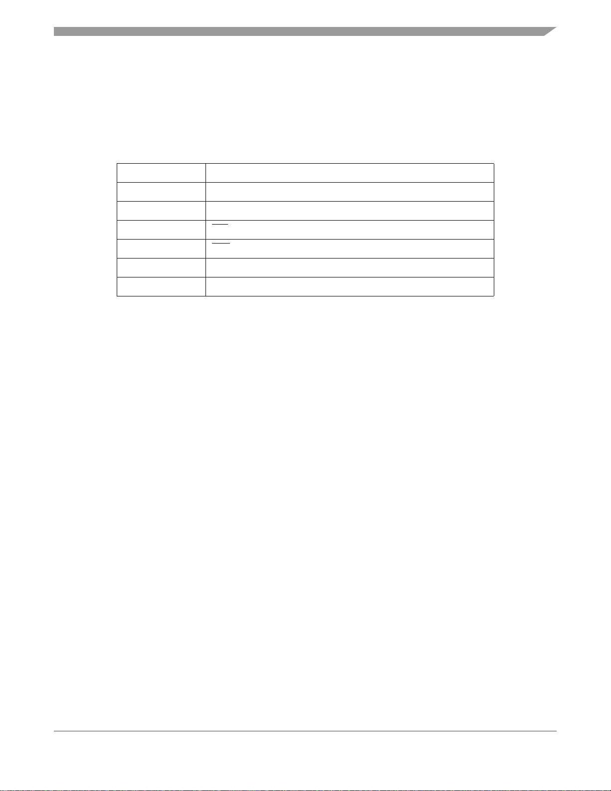
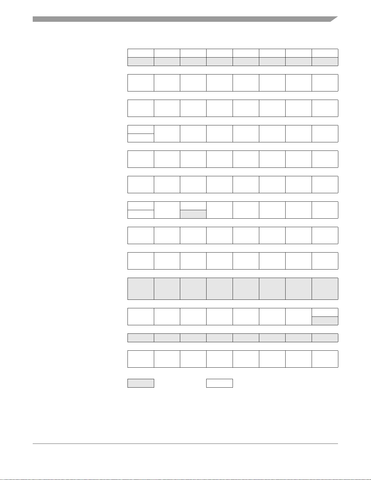
Revision History (Sheet 2 of 3)
Date
August,
2003
October,
2003
January,
2004
Revision
Level
1.0
2.0
3.0
Description
Reformatted to meet latest M68HC08 documentation standards N/A
Figure 1-1. Block Diagram — Diagram redrawn to include keyboard interrupt
module and TCLK pin designator.
Figure 1-2. MCU Pin Assignments — Added TCLK pin designator. 21
Table 1-2. Pin Functions — Added TCLK pin description. 22
Table 1-3. Function Priority in Shared Pins — Revised table for clarity and to
add TCLK.
Figure 2-1. Memory Map — Corrected names for the IRQ status and control
register (INTSCR) bits 3–0.
3.7.3 ADC Input Clock Register — Clarified bit description for the ADC clock
prescaler bits.
4.3 Functional Description — Updated periodic wakeup request values. 51
Figure 6-1. COP Block Diagram — Reworked for clarity 59
Chapter 8 External Interrupt (IRQ) — Corrected bit names for MODE, IRQF,
ACK, and IMASK
Chapter 14 Timer Interface Module (TIM) — Added TCLK function. 131–139
15.3 Monitor Module (MON) — Updated with additional data. 147
Chapter 16 Electrical Specifications — Updated with additional data. 169–173
Figure 2-2. Control, Status, and Data Registers — Deleted unimplemented
areas from $FFB0–$FFBD and $FFC2–$FFCF as they are actually available.
Also corrected $FFBF designation from unimplemented to reserved.
Figure 6-1. COP Block Diagram — Reworked for clarity 59
6.3.2 STOP Instruction — Added subsection 60
13.4.2 Active Resets from Internal Sources — Reworked notes for clarity. 111
Table 13-2. Reset Recovery Timing — Replaced previous table with new
information.
Chapter 14 Timer Interface Module (TIM) — Updated with additional data. 131
Figure 15-3. Break I/O Register Summary — Corrected bit designators for the
BRKAR register
15.3 Monitor Module (MON) — Clarified seventh bullet. 147
Table 17-1. MC Order Numbers — Corrected temperature and package
designators.
Figure 2-2. Control, Status, and Data Registers — Corrected reset state for the
FLASH Block Protect Register at address location $FFBE and the Internal
Oscillator Trim Value at $FFC0.
Figure 2-5. FLASH Block Protect Register (FLBPR) — Restated reset state for
clarity.
Page
Number(s)
20
23
26
47
77–79
27
112
143
175
32
38
MC68HC908QY/QT Family Data Sheet, Rev. 5
Freescale Semiconductor 5
Revision History
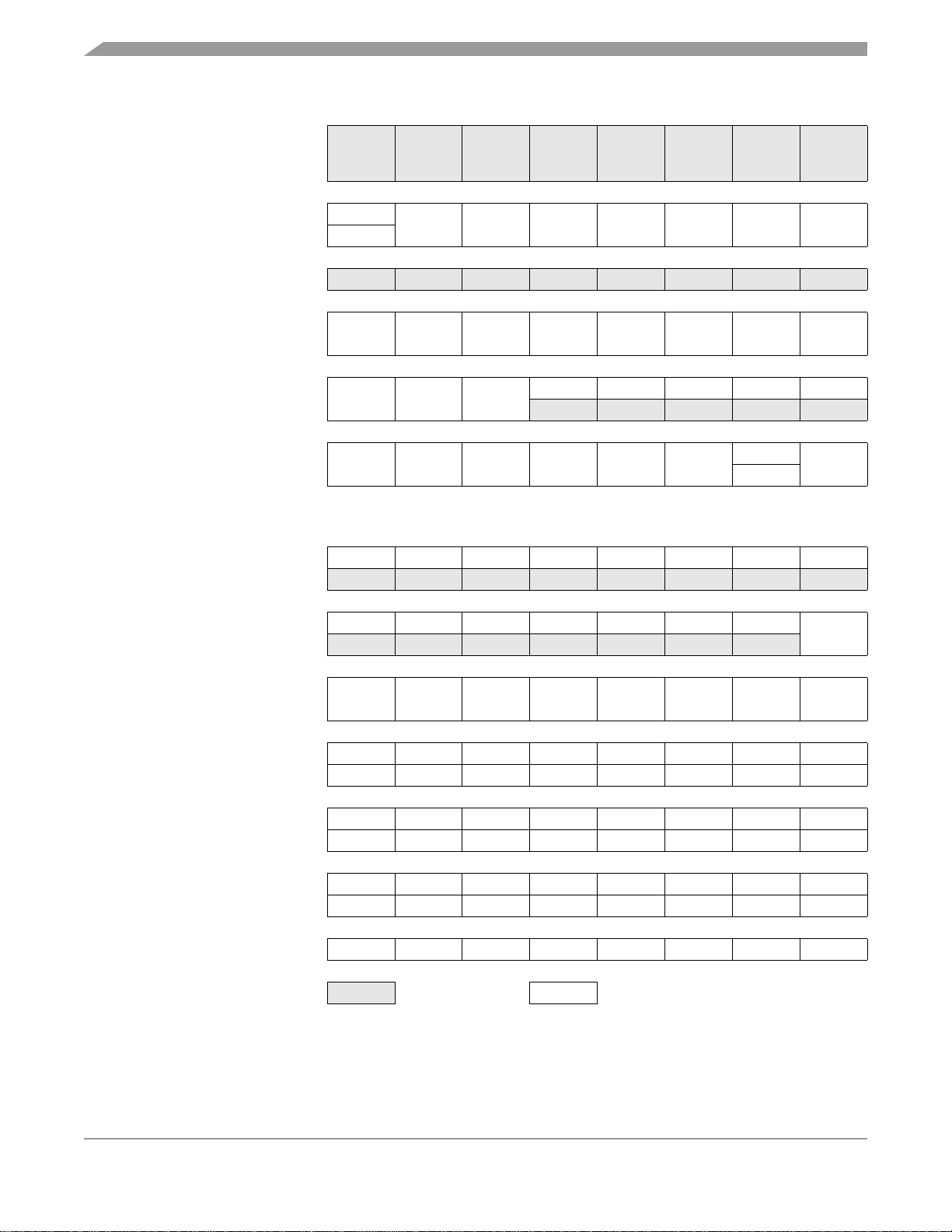
Revision History (Sheet 3 of 3)
Date
November,
2004
July,
2005
Revision
Level
4.0
5.0
Description
Reformatted to meet current documentation standards Throughout
6.3.1 BUSCLKX4 — Clarified description of BUSCLKX4 58
Chapter 7 Central Processor Unit (CPU) — In 7.7 Instruction Set Summary:
Reworked definitions for STOP instruction
Added WAIT instruction
13.8.1 SIM Reset Status Register — Clarified SRSR flag setting 117
14.9.1 TIM Status and Control Register — Added information to TSTOP note 127
16.8 5-V Oscillator Characteristics — Added values for deviation from trimmed
inernal oscillator
16.12 3-V Oscillator Characteristics — Added values for deviation from trimmed
inernal oscillator
Figure 5-2. Configuration Register 1 (CONFIG1) — Clarified bit definitions for
COPRS.
Chapter 8 External Interrupt (IRQ) — Reworked for clarification. 73
11.3.4 RC Oscillator — Improved RC oscillator wording. 93
12.1 Introduction — Added note pertaining to non-bonded port pins. 97
17.3 Package Dimensions — Updated package information. 165
Page
Number(s)
70
71
155
158
54
MC68HC908QY/QT Family Data Sheet, Rev. 5
6 Freescale Semiconductor

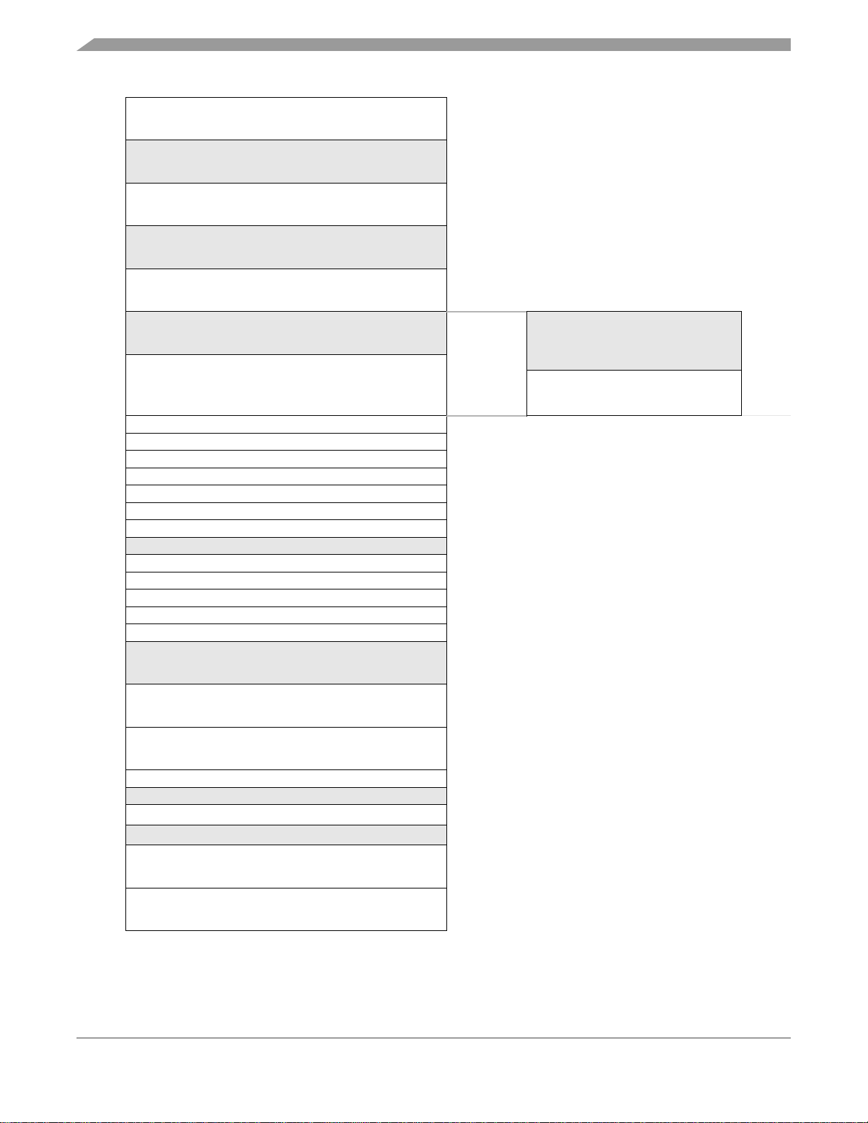
List of Chapters
Chapter 1 General Description. . . . . . . . . . . . . . . . . . . . . . . . . . . . . . . . . . . . . . . . . . . . . . . . 17
Chapter 2 Memory. . . . . . . . . . . . . . . . . . . . . . . . . . . . . . . . . . . . . . . . . . . . . . . . . . . . . . . . . .25
Chapter 3 Analog-to-Digital Converter (ADC). . . . . . . . . . . . . . . . . . . . . . . . . . . . . . . . . . . . 41
Chapter 4 Auto Wakeup Module (AWU) . . . . . . . . . . . . . . . . . . . . . . . . . . . . . . . . . . . . . . . .49
Chapter 5 Configuration Register (CONFIG) . . . . . . . . . . . . . . . . . . . . . . . . . . . . . . . . . . . .53
Chapter 6 Computer Operating Properly (COP) . . . . . . . . . . . . . . . . . . . . . . . . . . . . . . . . . .57
Chapter 7 Central Processor Unit (CPU). . . . . . . . . . . . . . . . . . . . . . . . . . . . . . . . . . . . . . . .61
Chapter 8 External Interrupt (IRQ). . . . . . . . . . . . . . . . . . . . . . . . . . . . . . . . . . . . . . . . . . . . .73
Chapter 9 Keyboard Interrupt Module (KBI) . . . . . . . . . . . . . . . . . . . . . . . . . . . . . . . . . . . . .79
Chapter 10 Low-Voltage Inhibit (LVI). . . . . . . . . . . . . . . . . . . . . . . . . . . . . . . . . . . . . . . . . . . 85
Chapter 11 Oscillator Module (OSC) . . . . . . . . . . . . . . . . . . . . . . . . . . . . . . . . . . . . . . . . . . .89
Chapter 12 Input/Output Ports (PORTS) . . . . . . . . . . . . . . . . . . . . . . . . . . . . . . . . . . . . . . . .97
Chapter 13 System Integration Module (SIM). . . . . . . . . . . . . . . . . . . . . . . . . . . . . . . . . . .103
Chapter 14 Timer Interface Module (TIM) . . . . . . . . . . . . . . . . . . . . . . . . . . . . . . . . . . . . . .119
Chapter 15 Development Support . . . . . . . . . . . . . . . . . . . . . . . . . . . . . . . . . . . . . . . . . . . .133
Chapter 16 Electrical Specifications . . . . . . . . . . . . . . . . . . . . . . . . . . . . . . . . . . . . . . . . . .149
Chapter 17 Ordering Information and Mechanical Specifications . . . . . . . . . . . . . . . . . .165
MC68HC908QY/QT Family Data Sheet, Rev. 5
Freescale Semiconductor 7

List of Chapters
MC68HC908QY/QT Family Data Sheet, Rev. 5
8 Freescale Semiconductor

Table of Contents
Chapter 1
General Description
1.1 Introduction . . . . . . . . . . . . . . . . . . . . . . . . . . . . . . . . . . . . . . . . . . . . . . . . . . . . . . . . . . . . . . . . 17
1.2 Features. . . . . . . . . . . . . . . . . . . . . . . . . . . . . . . . . . . . . . . . . . . . . . . . . . . . . . . . . . . . . . . . . . . 17
1.3 MCU Block Diagram . . . . . . . . . . . . . . . . . . . . . . . . . . . . . . . . . . . . . . . . . . . . . . . . . . . . . . . . . 19
1.4 Pin Assignments . . . . . . . . . . . . . . . . . . . . . . . . . . . . . . . . . . . . . . . . . . . . . . . . . . . . . . . . . . . . 19
1.5 Pin Functions . . . . . . . . . . . . . . . . . . . . . . . . . . . . . . . . . . . . . . . . . . . . . . . . . . . . . . . . . . . . . . . 22
1.6 Pin Function Priority. . . . . . . . . . . . . . . . . . . . . . . . . . . . . . . . . . . . . . . . . . . . . . . . . . . . . . . . . . 23
Chapter 2
Memory
2.1 Introduction . . . . . . . . . . . . . . . . . . . . . . . . . . . . . . . . . . . . . . . . . . . . . . . . . . . . . . . . . . . . . . . . 25
2.2 Unimplemented Memory Locations . . . . . . . . . . . . . . . . . . . . . . . . . . . . . . . . . . . . . . . . . . . . . . 25
2.3 Reserved Memory Locations . . . . . . . . . . . . . . . . . . . . . . . . . . . . . . . . . . . . . . . . . . . . . . . . . . . 25
2.4 Input/Output (I/O) Section . . . . . . . . . . . . . . . . . . . . . . . . . . . . . . . . . . . . . . . . . . . . . . . . . . . . . 27
2.5 Random-Access Memory (RAM) . . . . . . . . . . . . . . . . . . . . . . . . . . . . . . . . . . . . . . . . . . . . . . . . 32
2.6 FLASH Memory (FLASH) . . . . . . . . . . . . . . . . . . . . . . . . . . . . . . . . . . . . . . . . . . . . . . . . . . . . . 33
2.6.1 FLASH Control Register. . . . . . . . . . . . . . . . . . . . . . . . . . . . . . . . . . . . . . . . . . . . . . . . . . . . 33
2.6.2 FLASH Page Erase Operation. . . . . . . . . . . . . . . . . . . . . . . . . . . . . . . . . . . . . . . . . . . . . . . 34
2.6.3 FLASH Mass Erase Operation. . . . . . . . . . . . . . . . . . . . . . . . . . . . . . . . . . . . . . . . . . . . . . . 35
2.6.4 FLASH Program Operation . . . . . . . . . . . . . . . . . . . . . . . . . . . . . . . . . . . . . . . . . . . . . . . . . 35
2.6.5 FLASH Protection . . . . . . . . . . . . . . . . . . . . . . . . . . . . . . . . . . . . . . . . . . . . . . . . . . . . . . . . 36
2.6.6 FLASH Block Protect Register . . . . . . . . . . . . . . . . . . . . . . . . . . . . . . . . . . . . . . . . . . . . . . . 38
2.6.7 Wait Mode . . . . . . . . . . . . . . . . . . . . . . . . . . . . . . . . . . . . . . . . . . . . . . . . . . . . . . . . . . . . . . 39
2.6.8 Stop Mode . . . . . . . . . . . . . . . . . . . . . . . . . . . . . . . . . . . . . . . . . . . . . . . . . . . . . . . . . . . . . . 39
Chapter 3
Analog-to-Digital Converter (ADC)
3.1 Introduction . . . . . . . . . . . . . . . . . . . . . . . . . . . . . . . . . . . . . . . . . . . . . . . . . . . . . . . . . . . . . . . . 41
3.2 Features. . . . . . . . . . . . . . . . . . . . . . . . . . . . . . . . . . . . . . . . . . . . . . . . . . . . . . . . . . . . . . . . . . . 41
3.3 Functional Description . . . . . . . . . . . . . . . . . . . . . . . . . . . . . . . . . . . . . . . . . . . . . . . . . . . . . . . . 41
3.3.1 ADC Port I/O Pins . . . . . . . . . . . . . . . . . . . . . . . . . . . . . . . . . . . . . . . . . . . . . . . . . . . . . . . . 41
3.3.2 Voltage Conversion . . . . . . . . . . . . . . . . . . . . . . . . . . . . . . . . . . . . . . . . . . . . . . . . . . . . . . . 44
3.3.3 Conversion Time . . . . . . . . . . . . . . . . . . . . . . . . . . . . . . . . . . . . . . . . . . . . . . . . . . . . . . . . . 44
3.3.4 Continuous Conversion . . . . . . . . . . . . . . . . . . . . . . . . . . . . . . . . . . . . . . . . . . . . . . . . . . . . 44
3.3.5 Accuracy and Precision . . . . . . . . . . . . . . . . . . . . . . . . . . . . . . . . . . . . . . . . . . . . . . . . . . . . 44
3.4 Interrupts . . . . . . . . . . . . . . . . . . . . . . . . . . . . . . . . . . . . . . . . . . . . . . . . . . . . . . . . . . . . . . . . . . 44
3.5 Low-Power Modes . . . . . . . . . . . . . . . . . . . . . . . . . . . . . . . . . . . . . . . . . . . . . . . . . . . . . . . . . . . 44
3.5.1 Wait Mode . . . . . . . . . . . . . . . . . . . . . . . . . . . . . . . . . . . . . . . . . . . . . . . . . . . . . . . . . . . . . . 44
3.5.2 Stop Mode . . . . . . . . . . . . . . . . . . . . . . . . . . . . . . . . . . . . . . . . . . . . . . . . . . . . . . . . . . . . . . 45
MC68HC908QY/QT Family Data Sheet, Rev. 5
Freescale Semiconductor 9

Table of Contents
3.6 Input/Output Signals . . . . . . . . . . . . . . . . . . . . . . . . . . . . . . . . . . . . . . . . . . . . . . . . . . . . . . . . . 45
3.7 Input/Output Registers . . . . . . . . . . . . . . . . . . . . . . . . . . . . . . . . . . . . . . . . . . . . . . . . . . . . . . . . 45
3.7.1 ADC Status and Control Register . . . . . . . . . . . . . . . . . . . . . . . . . . . . . . . . . . . . . . . . . . . . 45
3.7.2 ADC Data Register. . . . . . . . . . . . . . . . . . . . . . . . . . . . . . . . . . . . . . . . . . . . . . . . . . . . . . . . 47
3.7.3 ADC Input Clock Register . . . . . . . . . . . . . . . . . . . . . . . . . . . . . . . . . . . . . . . . . . . . . . . . . . 47
Chapter 4
Auto Wakeup Module (AWU)
4.1 Introduction . . . . . . . . . . . . . . . . . . . . . . . . . . . . . . . . . . . . . . . . . . . . . . . . . . . . . . . . . . . . . . . . 49
4.2 Features. . . . . . . . . . . . . . . . . . . . . . . . . . . . . . . . . . . . . . . . . . . . . . . . . . . . . . . . . . . . . . . . . . . 49
4.3 Functional Description . . . . . . . . . . . . . . . . . . . . . . . . . . . . . . . . . . . . . . . . . . . . . . . . . . . . . . . . 49
4.4 Wait Mode . . . . . . . . . . . . . . . . . . . . . . . . . . . . . . . . . . . . . . . . . . . . . . . . . . . . . . . . . . . . . . . . . 50
4.5 Stop Mode . . . . . . . . . . . . . . . . . . . . . . . . . . . . . . . . . . . . . . . . . . . . . . . . . . . . . . . . . . . . . . . . . 50
4.6 Input/Output Registers . . . . . . . . . . . . . . . . . . . . . . . . . . . . . . . . . . . . . . . . . . . . . . . . . . . . . . . . 51
4.6.1 Port A I/O Register. . . . . . . . . . . . . . . . . . . . . . . . . . . . . . . . . . . . . . . . . . . . . . . . . . . . . . . . 51
4.6.2 Keyboard Status and Control Register. . . . . . . . . . . . . . . . . . . . . . . . . . . . . . . . . . . . . . . . . 51
4.6.3 Keyboard Interrupt Enable Register. . . . . . . . . . . . . . . . . . . . . . . . . . . . . . . . . . . . . . . . . . . 52
Chapter 5
Configuration Register (CONFIG)
5.1 Introduction . . . . . . . . . . . . . . . . . . . . . . . . . . . . . . . . . . . . . . . . . . . . . . . . . . . . . . . . . . . . . . . . 53
5.2 Functional Description . . . . . . . . . . . . . . . . . . . . . . . . . . . . . . . . . . . . . . . . . . . . . . . . . . . . . . . . 53
Chapter 6
Computer Operating Properly (COP)
6.1 Introduction . . . . . . . . . . . . . . . . . . . . . . . . . . . . . . . . . . . . . . . . . . . . . . . . . . . . . . . . . . . . . . . . 57
6.2 Functional Description . . . . . . . . . . . . . . . . . . . . . . . . . . . . . . . . . . . . . . . . . . . . . . . . . . . . . . . . 57
6.3 I/O Signals . . . . . . . . . . . . . . . . . . . . . . . . . . . . . . . . . . . . . . . . . . . . . . . . . . . . . . . . . . . . . . . . . 58
6.3.1 BUSCLKX4 . . . . . . . . . . . . . . . . . . . . . . . . . . . . . . . . . . . . . . . . . . . . . . . . . . . . . . . . . . . . . 58
6.3.2 STOP Instruction . . . . . . . . . . . . . . . . . . . . . . . . . . . . . . . . . . . . . . . . . . . . . . . . . . . . . . . . . 58
6.3.3 COPCTL Write . . . . . . . . . . . . . . . . . . . . . . . . . . . . . . . . . . . . . . . . . . . . . . . . . . . . . . . . . . . 58
6.3.4 Power-On Reset. . . . . . . . . . . . . . . . . . . . . . . . . . . . . . . . . . . . . . . . . . . . . . . . . . . . . . . . . . 58
6.3.5 Internal Reset. . . . . . . . . . . . . . . . . . . . . . . . . . . . . . . . . . . . . . . . . . . . . . . . . . . . . . . . . . . . 58
6.3.6 COPD (COP Disable). . . . . . . . . . . . . . . . . . . . . . . . . . . . . . . . . . . . . . . . . . . . . . . . . . . . . . 58
6.3.7 COPRS (COP Rate Select) . . . . . . . . . . . . . . . . . . . . . . . . . . . . . . . . . . . . . . . . . . . . . . . . . 59
6.4 COP Control Register . . . . . . . . . . . . . . . . . . . . . . . . . . . . . . . . . . . . . . . . . . . . . . . . . . . . . . . . 59
6.5 Interrupts . . . . . . . . . . . . . . . . . . . . . . . . . . . . . . . . . . . . . . . . . . . . . . . . . . . . . . . . . . . . . . . . . . 59
6.6 Monitor Mode . . . . . . . . . . . . . . . . . . . . . . . . . . . . . . . . . . . . . . . . . . . . . . . . . . . . . . . . . . . . . . . 59
6.7 Low-Power Modes . . . . . . . . . . . . . . . . . . . . . . . . . . . . . . . . . . . . . . . . . . . . . . . . . . . . . . . . . . . 59
6.7.1 Wait Mode . . . . . . . . . . . . . . . . . . . . . . . . . . . . . . . . . . . . . . . . . . . . . . . . . . . . . . . . . . . . . . 59
6.7.2 Stop Mode . . . . . . . . . . . . . . . . . . . . . . . . . . . . . . . . . . . . . . . . . . . . . . . . . . . . . . . . . . . . . . 59
6.8 COP Module During Break Mode . . . . . . . . . . . . . . . . . . . . . . . . . . . . . . . . . . . . . . . . . . . . . . . 59
MC68HC908QY/QT Family Data Sheet, Rev. 5
10 Freescale Semiconductor

Chapter 7
Central Processor Unit (CPU)
7.1 Introduction . . . . . . . . . . . . . . . . . . . . . . . . . . . . . . . . . . . . . . . . . . . . . . . . . . . . . . . . . . . . . . . . 61
7.2 Features. . . . . . . . . . . . . . . . . . . . . . . . . . . . . . . . . . . . . . . . . . . . . . . . . . . . . . . . . . . . . . . . . . . 61
7.3 CPU Registers . . . . . . . . . . . . . . . . . . . . . . . . . . . . . . . . . . . . . . . . . . . . . . . . . . . . . . . . . . . . . . 61
7.3.1 Accumulator . . . . . . . . . . . . . . . . . . . . . . . . . . . . . . . . . . . . . . . . . . . . . . . . . . . . . . . . . . . . . 62
7.3.2 Index Register . . . . . . . . . . . . . . . . . . . . . . . . . . . . . . . . . . . . . . . . . . . . . . . . . . . . . . . . . . . 62
7.3.3 Stack Pointer . . . . . . . . . . . . . . . . . . . . . . . . . . . . . . . . . . . . . . . . . . . . . . . . . . . . . . . . . . . . 63
7.3.4 Program Counter . . . . . . . . . . . . . . . . . . . . . . . . . . . . . . . . . . . . . . . . . . . . . . . . . . . . . . . . . 63
7.3.5 Condition Code Register . . . . . . . . . . . . . . . . . . . . . . . . . . . . . . . . . . . . . . . . . . . . . . . . . . . 64
7.4 Arithmetic/Logic Unit (ALU) . . . . . . . . . . . . . . . . . . . . . . . . . . . . . . . . . . . . . . . . . . . . . . . . . . . . 65
7.5 Low-Power Modes . . . . . . . . . . . . . . . . . . . . . . . . . . . . . . . . . . . . . . . . . . . . . . . . . . . . . . . . . . . 65
7.5.1 Wait Mode . . . . . . . . . . . . . . . . . . . . . . . . . . . . . . . . . . . . . . . . . . . . . . . . . . . . . . . . . . . . . . 65
7.5.2 Stop Mode . . . . . . . . . . . . . . . . . . . . . . . . . . . . . . . . . . . . . . . . . . . . . . . . . . . . . . . . . . . . . . 65
7.6 CPU During Break Interrupts . . . . . . . . . . . . . . . . . . . . . . . . . . . . . . . . . . . . . . . . . . . . . . . . . . . 65
7.7 Instruction Set Summary . . . . . . . . . . . . . . . . . . . . . . . . . . . . . . . . . . . . . . . . . . . . . . . . . . . . . . 66
7.8 Opcode Map . . . . . . . . . . . . . . . . . . . . . . . . . . . . . . . . . . . . . . . . . . . . . . . . . . . . . . . . . . . . . . . 71
Chapter 8
External Interrupt (IRQ)
8.1 Introduction . . . . . . . . . . . . . . . . . . . . . . . . . . . . . . . . . . . . . . . . . . . . . . . . . . . . . . . . . . . . . . . . 73
8.2 Features. . . . . . . . . . . . . . . . . . . . . . . . . . . . . . . . . . . . . . . . . . . . . . . . . . . . . . . . . . . . . . . . . . . 73
8.3 Functional Description . . . . . . . . . . . . . . . . . . . . . . . . . . . . . . . . . . . . . . . . . . . . . . . . . . . . . . . . 73
8.3.1 MODE = 1 . . . . . . . . . . . . . . . . . . . . . . . . . . . . . . . . . . . . . . . . . . . . . . . . . . . . . . . . . . . . . . 75
8.3.2 MODE = 0 . . . . . . . . . . . . . . . . . . . . . . . . . . . . . . . . . . . . . . . . . . . . . . . . . . . . . . . . . . . . . . 75
8.4 Interrupts . . . . . . . . . . . . . . . . . . . . . . . . . . . . . . . . . . . . . . . . . . . . . . . . . . . . . . . . . . . . . . . . . . 76
8.5 Low-Power Modes . . . . . . . . . . . . . . . . . . . . . . . . . . . . . . . . . . . . . . . . . . . . . . . . . . . . . . . . . . . 76
8.5.1 Wait Mode . . . . . . . . . . . . . . . . . . . . . . . . . . . . . . . . . . . . . . . . . . . . . . . . . . . . . . . . . . . . . . 76
8.5.2 Stop Mode . . . . . . . . . . . . . . . . . . . . . . . . . . . . . . . . . . . . . . . . . . . . . . . . . . . . . . . . . . . . . . 76
8.6 IRQ Module During Break Interrupts . . . . . . . . . . . . . . . . . . . . . . . . . . . . . . . . . . . . . . . . . . . . . 76
8.7 I/O Signals . . . . . . . . . . . . . . . . . . . . . . . . . . . . . . . . . . . . . . . . . . . . . . . . . . . . . . . . . . . . . . . . . 76
8.7.1 IRQ Input Pins (IRQ
8.8 Registers . . . . . . . . . . . . . . . . . . . . . . . . . . . . . . . . . . . . . . . . . . . . . . . . . . . . . . . . . . . . . . . . . . 77
) . . . . . . . . . . . . . . . . . . . . . . . . . . . . . . . . . . . . . . . . . . . . . . . . . . . . . . 77
Chapter 9
Keyboard Interrupt Module (KBI)
9.1 Introduction . . . . . . . . . . . . . . . . . . . . . . . . . . . . . . . . . . . . . . . . . . . . . . . . . . . . . . . . . . . . . . . . 79
9.2 Features. . . . . . . . . . . . . . . . . . . . . . . . . . . . . . . . . . . . . . . . . . . . . . . . . . . . . . . . . . . . . . . . . . . 79
9.3 Functional Description . . . . . . . . . . . . . . . . . . . . . . . . . . . . . . . . . . . . . . . . . . . . . . . . . . . . . . . . 79
9.3.1 Keyboard Operation. . . . . . . . . . . . . . . . . . . . . . . . . . . . . . . . . . . . . . . . . . . . . . . . . . . . . . . 79
9.3.2 Keyboard Initialization . . . . . . . . . . . . . . . . . . . . . . . . . . . . . . . . . . . . . . . . . . . . . . . . . . . . . 82
9.4 Wait Mode . . . . . . . . . . . . . . . . . . . . . . . . . . . . . . . . . . . . . . . . . . . . . . . . . . . . . . . . . . . . . . . . . 82
9.5 Stop Mode . . . . . . . . . . . . . . . . . . . . . . . . . . . . . . . . . . . . . . . . . . . . . . . . . . . . . . . . . . . . . . . . . 82
9.6 Keyboard Module During Break Interrupts. . . . . . . . . . . . . . . . . . . . . . . . . . . . . . . . . . . . . . . . . 82
MC68HC908QY/QT Family Data Sheet, Rev. 5
Freescale Semiconductor 11

Table of Contents
9.7 Input/Output Registers . . . . . . . . . . . . . . . . . . . . . . . . . . . . . . . . . . . . . . . . . . . . . . . . . . . . . . . . 83
9.7.1 Keyboard Status and Control Register. . . . . . . . . . . . . . . . . . . . . . . . . . . . . . . . . . . . . . . . . 83
9.7.2 Keyboard Interrupt Enable Register. . . . . . . . . . . . . . . . . . . . . . . . . . . . . . . . . . . . . . . . . . . 84
Chapter 10
Low-Voltage Inhibit (LVI)
10.1 Introduction . . . . . . . . . . . . . . . . . . . . . . . . . . . . . . . . . . . . . . . . . . . . . . . . . . . . . . . . . . . . . . . . 85
10.2 Features. . . . . . . . . . . . . . . . . . . . . . . . . . . . . . . . . . . . . . . . . . . . . . . . . . . . . . . . . . . . . . . . . . . 85
10.3 Functional Description . . . . . . . . . . . . . . . . . . . . . . . . . . . . . . . . . . . . . . . . . . . . . . . . . . . . . . . . 85
10.3.1 Polled LVI Operation . . . . . . . . . . . . . . . . . . . . . . . . . . . . . . . . . . . . . . . . . . . . . . . . . . . . . . 86
10.3.2 Forced Reset Operation. . . . . . . . . . . . . . . . . . . . . . . . . . . . . . . . . . . . . . . . . . . . . . . . . . . . 86
10.3.3 Voltage Hysteresis Protection . . . . . . . . . . . . . . . . . . . . . . . . . . . . . . . . . . . . . . . . . . . . . . . 86
10.3.4 LVI Trip Selection. . . . . . . . . . . . . . . . . . . . . . . . . . . . . . . . . . . . . . . . . . . . . . . . . . . . . . . . . 86
10.4 LVI Status Register . . . . . . . . . . . . . . . . . . . . . . . . . . . . . . . . . . . . . . . . . . . . . . . . . . . . . . . . . . 87
10.5 LVI Interrupts . . . . . . . . . . . . . . . . . . . . . . . . . . . . . . . . . . . . . . . . . . . . . . . . . . . . . . . . . . . . . . . 87
10.6 Low-Power Modes . . . . . . . . . . . . . . . . . . . . . . . . . . . . . . . . . . . . . . . . . . . . . . . . . . . . . . . . . . . 87
10.6.1 Wait Mode . . . . . . . . . . . . . . . . . . . . . . . . . . . . . . . . . . . . . . . . . . . . . . . . . . . . . . . . . . . . . . 87
10.6.2 Stop Mode . . . . . . . . . . . . . . . . . . . . . . . . . . . . . . . . . . . . . . . . . . . . . . . . . . . . . . . . . . . . . . 87
Chapter 11
Oscillator Module (OSC)
11.1 Introduction . . . . . . . . . . . . . . . . . . . . . . . . . . . . . . . . . . . . . . . . . . . . . . . . . . . . . . . . . . . . . . . . 89
11.2 Features. . . . . . . . . . . . . . . . . . . . . . . . . . . . . . . . . . . . . . . . . . . . . . . . . . . . . . . . . . . . . . . . . . . 89
11.3 Functional Description . . . . . . . . . . . . . . . . . . . . . . . . . . . . . . . . . . . . . . . . . . . . . . . . . . . . . . . . 89
11.3.1 Internal Oscillator . . . . . . . . . . . . . . . . . . . . . . . . . . . . . . . . . . . . . . . . . . . . . . . . . . . . . . . . . 90
11.3.1.1 Internal Oscillator Trimming . . . . . . . . . . . . . . . . . . . . . . . . . . . . . . . . . . . . . . . . . . . . . . . 91
11.3.1.2 Internal to External Clock Switching . . . . . . . . . . . . . . . . . . . . . . . . . . . . . . . . . . . . . . . . . 91
11.3.2 External Oscillator . . . . . . . . . . . . . . . . . . . . . . . . . . . . . . . . . . . . . . . . . . . . . . . . . . . . . . . . 91
11.3.3 XTAL Oscillator . . . . . . . . . . . . . . . . . . . . . . . . . . . . . . . . . . . . . . . . . . . . . . . . . . . . . . . . . . 92
11.3.4 RC Oscillator . . . . . . . . . . . . . . . . . . . . . . . . . . . . . . . . . . . . . . . . . . . . . . . . . . . . . . . . . . . . 93
11.4 Oscillator Module Signals . . . . . . . . . . . . . . . . . . . . . . . . . . . . . . . . . . . . . . . . . . . . . . . . . . . . . 93
11.4.1 Crystal Amplifier Input Pin (OSC1). . . . . . . . . . . . . . . . . . . . . . . . . . . . . . . . . . . . . . . . . . . . 93
11.4.2 Crystal Amplifier Output Pin (OSC2/PTA4/BUSCLKX4) . . . . . . . . . . . . . . . . . . . . . . . . . . . 94
11.4.3 Oscillator Enable Signal (SIMOSCEN) . . . . . . . . . . . . . . . . . . . . . . . . . . . . . . . . . . . . . . . . 94
11.4.4 XTAL Oscillator Clock (XTALCLK). . . . . . . . . . . . . . . . . . . . . . . . . . . . . . . . . . . . . . . . . . . . 94
11.4.5 RC Oscillator Clock (RCCLK) . . . . . . . . . . . . . . . . . . . . . . . . . . . . . . . . . . . . . . . . . . . . . . . 94
11.4.6 Internal Oscillator Clock (INTCLK). . . . . . . . . . . . . . . . . . . . . . . . . . . . . . . . . . . . . . . . . . . . 94
11.4.7 Oscillator Out 2 (BUSCLKX4) . . . . . . . . . . . . . . . . . . . . . . . . . . . . . . . . . . . . . . . . . . . . . . . 94
11.4.8 Oscillator Out (BUSCLKX2) . . . . . . . . . . . . . . . . . . . . . . . . . . . . . . . . . . . . . . . . . . . . . . . . . 94
11.5 Low Power Modes . . . . . . . . . . . . . . . . . . . . . . . . . . . . . . . . . . . . . . . . . . . . . . . . . . . . . . . . . . . 95
11.5.1 Wait Mode . . . . . . . . . . . . . . . . . . . . . . . . . . . . . . . . . . . . . . . . . . . . . . . . . . . . . . . . . . . . . . 95
11.5.2 Stop Mode . . . . . . . . . . . . . . . . . . . . . . . . . . . . . . . . . . . . . . . . . . . . . . . . . . . . . . . . . . . . . . 95
11.6 Oscillator During Break Mode . . . . . . . . . . . . . . . . . . . . . . . . . . . . . . . . . . . . . . . . . . . . . . . . . . 95
11.7 CONFIG2 Options . . . . . . . . . . . . . . . . . . . . . . . . . . . . . . . . . . . . . . . . . . . . . . . . . . . . . . . . . . . 95
11.8 Input/Output (I/O) Registers. . . . . . . . . . . . . . . . . . . . . . . . . . . . . . . . . . . . . . . . . . . . . . . . . . . . 95
11.8.1 Oscillator Status Register. . . . . . . . . . . . . . . . . . . . . . . . . . . . . . . . . . . . . . . . . . . . . . . . . . . 96
11.8.2 Oscillator Trim Register (OSCTRIM) . . . . . . . . . . . . . . . . . . . . . . . . . . . . . . . . . . . . . . . . . . 96
MC68HC908QY/QT Family Data Sheet, Rev. 5
12 Freescale Semiconductor

Chapter 12
Input/Output Ports (PORTS)
12.1 Introduction . . . . . . . . . . . . . . . . . . . . . . . . . . . . . . . . . . . . . . . . . . . . . . . . . . . . . . . . . . . . . . . . 97
12.2 Port A . . . . . . . . . . . . . . . . . . . . . . . . . . . . . . . . . . . . . . . . . . . . . . . . . . . . . . . . . . . . . . . . . . . . . 97
12.2.1 Port A Data Register . . . . . . . . . . . . . . . . . . . . . . . . . . . . . . . . . . . . . . . . . . . . . . . . . . . . . . 98
12.2.2 Data Direction Register A. . . . . . . . . . . . . . . . . . . . . . . . . . . . . . . . . . . . . . . . . . . . . . . . . . . 98
12.2.3 Port A Input Pullup Enable Register. . . . . . . . . . . . . . . . . . . . . . . . . . . . . . . . . . . . . . . . . . . 99
12.3 Port B . . . . . . . . . . . . . . . . . . . . . . . . . . . . . . . . . . . . . . . . . . . . . . . . . . . . . . . . . . . . . . . . . . . . 100
12.3.1 Port B Data Register . . . . . . . . . . . . . . . . . . . . . . . . . . . . . . . . . . . . . . . . . . . . . . . . . . . . . 100
12.3.2 Data Direction Register B. . . . . . . . . . . . . . . . . . . . . . . . . . . . . . . . . . . . . . . . . . . . . . . . . . 101
12.3.3 Port B Input Pullup Enable Register. . . . . . . . . . . . . . . . . . . . . . . . . . . . . . . . . . . . . . . . . . 102
Chapter 13
System Integration Module (SIM)
13.1 Introduction . . . . . . . . . . . . . . . . . . . . . . . . . . . . . . . . . . . . . . . . . . . . . . . . . . . . . . . . . . . . . . . 103
13.2 RST
13.3 SIM Bus Clock Control and Generation . . . . . . . . . . . . . . . . . . . . . . . . . . . . . . . . . . . . . . . . . . 104
13.3.1 Bus Timing . . . . . . . . . . . . . . . . . . . . . . . . . . . . . . . . . . . . . . . . . . . . . . . . . . . . . . . . . . . . . 105
13.3.2 Clock Start-Up from POR. . . . . . . . . . . . . . . . . . . . . . . . . . . . . . . . . . . . . . . . . . . . . . . . . . 105
13.3.3 Clocks in Stop Mode and Wait Mode. . . . . . . . . . . . . . . . . . . . . . . . . . . . . . . . . . . . . . . . . 105
13.4 Reset and System Initialization . . . . . . . . . . . . . . . . . . . . . . . . . . . . . . . . . . . . . . . . . . . . . . . . 105
13.4.1 External Pin Reset . . . . . . . . . . . . . . . . . . . . . . . . . . . . . . . . . . . . . . . . . . . . . . . . . . . . . . . 106
13.4.2 Active Resets from Internal Sources . . . . . . . . . . . . . . . . . . . . . . . . . . . . . . . . . . . . . . . . . 106
13.4.2.1 Power-On Reset . . . . . . . . . . . . . . . . . . . . . . . . . . . . . . . . . . . . . . . . . . . . . . . . . . . . . . . 107
13.4.2.2 Computer Operating Properly (COP) Reset . . . . . . . . . . . . . . . . . . . . . . . . . . . . . . . . . . 108
13.4.2.3 Illegal Opcode Reset . . . . . . . . . . . . . . . . . . . . . . . . . . . . . . . . . . . . . . . . . . . . . . . . . . . 108
13.4.2.4 Illegal Address Reset . . . . . . . . . . . . . . . . . . . . . . . . . . . . . . . . . . . . . . . . . . . . . . . . . . . 108
13.4.2.5 Low-Voltage Inhibit (LVI) Reset . . . . . . . . . . . . . . . . . . . . . . . . . . . . . . . . . . . . . . . . . . . 108
13.5 SIM Counter. . . . . . . . . . . . . . . . . . . . . . . . . . . . . . . . . . . . . . . . . . . . . . . . . . . . . . . . . . . . . . . 108
13.5.1 SIM Counter During Power-On Reset . . . . . . . . . . . . . . . . . . . . . . . . . . . . . . . . . . . . . . . . 108
13.5.2 SIM Counter During Stop Mode Recovery. . . . . . . . . . . . . . . . . . . . . . . . . . . . . . . . . . . . . 109
13.5.3 SIM Counter and Reset States . . . . . . . . . . . . . . . . . . . . . . . . . . . . . . . . . . . . . . . . . . . . . 109
13.6 Exception Control. . . . . . . . . . . . . . . . . . . . . . . . . . . . . . . . . . . . . . . . . . . . . . . . . . . . . . . . . . . 109
13.6.1 Interrupts . . . . . . . . . . . . . . . . . . . . . . . . . . . . . . . . . . . . . . . . . . . . . . . . . . . . . . . . . . . . . . 109
13.6.1.1 Hardware Interrupts . . . . . . . . . . . . . . . . . . . . . . . . . . . . . . . . . . . . . . . . . . . . . . . . . . . . 111
13.6.1.2 SWI Instruction . . . . . . . . . . . . . . . . . . . . . . . . . . . . . . . . . . . . . . . . . . . . . . . . . . . . . . . . 112
13.6.2 Interrupt Status Registers . . . . . . . . . . . . . . . . . . . . . . . . . . . . . . . . . . . . . . . . . . . . . . . . . 112
13.6.2.1 Interrupt Status Register 1 . . . . . . . . . . . . . . . . . . . . . . . . . . . . . . . . . . . . . . . . . . . . . . . 113
13.6.2.2 Interrupt Status Register 2 . . . . . . . . . . . . . . . . . . . . . . . . . . . . . . . . . . . . . . . . . . . . . . . 113
13.6.2.3 Interrupt Status Register 3 . . . . . . . . . . . . . . . . . . . . . . . . . . . . . . . . . . . . . . . . . . . . . . . 113
13.6.3 Reset . . . . . . . . . . . . . . . . . . . . . . . . . . . . . . . . . . . . . . . . . . . . . . . . . . . . . . . . . . . . . . . . . 114
13.6.4 Break Interrupts . . . . . . . . . . . . . . . . . . . . . . . . . . . . . . . . . . . . . . . . . . . . . . . . . . . . . . . . . 114
13.6.5 Status Flag Protection in Break Mode . . . . . . . . . . . . . . . . . . . . . . . . . . . . . . . . . . . . . . . . 114
13.7 Low-Power Modes . . . . . . . . . . . . . . . . . . . . . . . . . . . . . . . . . . . . . . . . . . . . . . . . . . . . . . . . . . 114
13.7.1 Wait Mode . . . . . . . . . . . . . . . . . . . . . . . . . . . . . . . . . . . . . . . . . . . . . . . . . . . . . . . . . . . . . 114
13.7.2 Stop Mode . . . . . . . . . . . . . . . . . . . . . . . . . . . . . . . . . . . . . . . . . . . . . . . . . . . . . . . . . . . . . 115
and IRQ Pins Initialization . . . . . . . . . . . . . . . . . . . . . . . . . . . . . . . . . . . . . . . . . . . . . . . . 104
MC68HC908QY/QT Family Data Sheet, Rev. 5
Freescale Semiconductor 13

Table of Contents
13.8 SIM Registers . . . . . . . . . . . . . . . . . . . . . . . . . . . . . . . . . . . . . . . . . . . . . . . . . . . . . . . . . . . . . 116
13.8.1 SIM Reset Status Register. . . . . . . . . . . . . . . . . . . . . . . . . . . . . . . . . . . . . . . . . . . . . . . . . 117
13.8.2 Break Flag Control Register. . . . . . . . . . . . . . . . . . . . . . . . . . . . . . . . . . . . . . . . . . . . . . . . 118
Chapter 14
Timer Interface Module (TIM)
14.1 Introduction . . . . . . . . . . . . . . . . . . . . . . . . . . . . . . . . . . . . . . . . . . . . . . . . . . . . . . . . . . . . . . . 119
14.2 Features. . . . . . . . . . . . . . . . . . . . . . . . . . . . . . . . . . . . . . . . . . . . . . . . . . . . . . . . . . . . . . . . . . 119
14.3 Pin Name Conventions . . . . . . . . . . . . . . . . . . . . . . . . . . . . . . . . . . . . . . . . . . . . . . . . . . . . . . 119
14.4 Functional Description . . . . . . . . . . . . . . . . . . . . . . . . . . . . . . . . . . . . . . . . . . . . . . . . . . . . . . . 121
14.4.1 TIM Counter Prescaler. . . . . . . . . . . . . . . . . . . . . . . . . . . . . . . . . . . . . . . . . . . . . . . . . . . . 122
14.4.2 Input Capture . . . . . . . . . . . . . . . . . . . . . . . . . . . . . . . . . . . . . . . . . . . . . . . . . . . . . . . . . . . 122
14.4.3 Output Compare. . . . . . . . . . . . . . . . . . . . . . . . . . . . . . . . . . . . . . . . . . . . . . . . . . . . . . . . . 122
14.4.3.1 Unbuffered Output Compare . . . . . . . . . . . . . . . . . . . . . . . . . . . . . . . . . . . . . . . . . . . . . 122
14.4.3.2 Buffered Output Compare . . . . . . . . . . . . . . . . . . . . . . . . . . . . . . . . . . . . . . . . . . . . . . . 122
14.4.4 Pulse Width Modulation (PWM) . . . . . . . . . . . . . . . . . . . . . . . . . . . . . . . . . . . . . . . . . . . . . 123
14.4.4.1 Unbuffered PWM Signal Generation . . . . . . . . . . . . . . . . . . . . . . . . . . . . . . . . . . . . . . . 124
14.4.4.2 Buffered PWM Signal Generation . . . . . . . . . . . . . . . . . . . . . . . . . . . . . . . . . . . . . . . . . 124
14.4.4.3 PWM Initialization . . . . . . . . . . . . . . . . . . . . . . . . . . . . . . . . . . . . . . . . . . . . . . . . . . . . . . 125
14.5 Interrupts . . . . . . . . . . . . . . . . . . . . . . . . . . . . . . . . . . . . . . . . . . . . . . . . . . . . . . . . . . . . . . . . . 125
14.6 Wait Mode . . . . . . . . . . . . . . . . . . . . . . . . . . . . . . . . . . . . . . . . . . . . . . . . . . . . . . . . . . . . . . . . 126
14.7 TIM During Break Interrupts. . . . . . . . . . . . . . . . . . . . . . . . . . . . . . . . . . . . . . . . . . . . . . . . . . . 126
14.8 Input/Output Signals . . . . . . . . . . . . . . . . . . . . . . . . . . . . . . . . . . . . . . . . . . . . . . . . . . . . . . . . 126
14.8.1 TIM Clock Pin (PTA2/TCLK) . . . . . . . . . . . . . . . . . . . . . . . . . . . . . . . . . . . . . . . . . . . . . . . 126
14.8.2 TIM Channel I/O Pins (PTA0/TCH0 and PTA1/TCH1). . . . . . . . . . . . . . . . . . . . . . . . . . . . 126
14.9 Input/Output Registers . . . . . . . . . . . . . . . . . . . . . . . . . . . . . . . . . . . . . . . . . . . . . . . . . . . . . . . 126
14.9.1 TIM Status and Control Register . . . . . . . . . . . . . . . . . . . . . . . . . . . . . . . . . . . . . . . . . . . . 127
14.9.2 TIM Counter Registers . . . . . . . . . . . . . . . . . . . . . . . . . . . . . . . . . . . . . . . . . . . . . . . . . . . 128
14.9.3 TIM Counter Modulo Registers . . . . . . . . . . . . . . . . . . . . . . . . . . . . . . . . . . . . . . . . . . . . . 129
14.9.4 TIM Channel Status and Control Registers . . . . . . . . . . . . . . . . . . . . . . . . . . . . . . . . . . . . 129
14.9.5 TIM Channel Registers . . . . . . . . . . . . . . . . . . . . . . . . . . . . . . . . . . . . . . . . . . . . . . . . . . . 132
Chapter 15
Development Support
15.1 Introduction . . . . . . . . . . . . . . . . . . . . . . . . . . . . . . . . . . . . . . . . . . . . . . . . . . . . . . . . . . . . . . . 133
15.2 Break Module (BRK) . . . . . . . . . . . . . . . . . . . . . . . . . . . . . . . . . . . . . . . . . . . . . . . . . . . . . . . . 133
15.2.1 Functional Description . . . . . . . . . . . . . . . . . . . . . . . . . . . . . . . . . . . . . . . . . . . . . . . . . . . . 133
15.2.1.1 Flag Protection During Break Interrupts . . . . . . . . . . . . . . . . . . . . . . . . . . . . . . . . . . . . . 135
15.2.1.2 TIM During Break Interrupts . . . . . . . . . . . . . . . . . . . . . . . . . . . . . . . . . . . . . . . . . . . . . . 135
15.2.1.3 COP During Break Interrupts . . . . . . . . . . . . . . . . . . . . . . . . . . . . . . . . . . . . . . . . . . . . . 135
15.2.2 Break Module Registers. . . . . . . . . . . . . . . . . . . . . . . . . . . . . . . . . . . . . . . . . . . . . . . . . . . 135
15.2.2.1 Break Status and Control Register . . . . . . . . . . . . . . . . . . . . . . . . . . . . . . . . . . . . . . . . . 136
15.2.2.2 Break Address Registers . . . . . . . . . . . . . . . . . . . . . . . . . . . . . . . . . . . . . . . . . . . . . . . . 136
15.2.2.3 Break Auxiliary Register . . . . . . . . . . . . . . . . . . . . . . . . . . . . . . . . . . . . . . . . . . . . . . . . . 137
15.2.2.4 Break Status Register. . . . . . . . . . . . . . . . . . . . . . . . . . . . . . . . . . . . . . . . . . . . . . . . . . . 137
15.2.2.5 Break Flag Control Register . . . . . . . . . . . . . . . . . . . . . . . . . . . . . . . . . . . . . . . . . . . . . 138
15.2.3 Low-Power Modes . . . . . . . . . . . . . . . . . . . . . . . . . . . . . . . . . . . . . . . . . . . . . . . . . . . . . . . 138
MC68HC908QY/QT Family Data Sheet, Rev. 5
14 Freescale Semiconductor

15.3 Monitor Module (MON) . . . . . . . . . . . . . . . . . . . . . . . . . . . . . . . . . . . . . . . . . . . . . . . . . . . . . . 138
15.3.1 Functional Description . . . . . . . . . . . . . . . . . . . . . . . . . . . . . . . . . . . . . . . . . . . . . . . . . . . . 139
15.3.1.1 Normal Monitor Mode . . . . . . . . . . . . . . . . . . . . . . . . . . . . . . . . . . . . . . . . . . . . . . . . . . . 142
15.3.1.2 Forced Monitor Mode . . . . . . . . . . . . . . . . . . . . . . . . . . . . . . . . . . . . . . . . . . . . . . . . . . . 143
15.3.1.3 Monitor Vectors . . . . . . . . . . . . . . . . . . . . . . . . . . . . . . . . . . . . . . . . . . . . . . . . . . . . . . . 143
15.3.1.4 Data Format . . . . . . . . . . . . . . . . . . . . . . . . . . . . . . . . . . . . . . . . . . . . . . . . . . . . . . . . . . 144
15.3.1.5 Break Signal . . . . . . . . . . . . . . . . . . . . . . . . . . . . . . . . . . . . . . . . . . . . . . . . . . . . . . . . . . 144
15.3.1.6 Baud Rate. . . . . . . . . . . . . . . . . . . . . . . . . . . . . . . . . . . . . . . . . . . . . . . . . . . . . . . . . . . . 144
15.3.1.7 Commands . . . . . . . . . . . . . . . . . . . . . . . . . . . . . . . . . . . . . . . . . . . . . . . . . . . . . . . . . . . 144
15.3.2 Security . . . . . . . . . . . . . . . . . . . . . . . . . . . . . . . . . . . . . . . . . . . . . . . . . . . . . . . . . . . . . . . 148
Chapter 16
Electrical Specifications
16.1 Introduction . . . . . . . . . . . . . . . . . . . . . . . . . . . . . . . . . . . . . . . . . . . . . . . . . . . . . . . . . . . . . . . 149
16.2 Absolute Maximum Ratings . . . . . . . . . . . . . . . . . . . . . . . . . . . . . . . . . . . . . . . . . . . . . . . . . . . 149
16.3 Functional Operating Range . . . . . . . . . . . . . . . . . . . . . . . . . . . . . . . . . . . . . . . . . . . . . . . . . . 150
16.4 Thermal Characteristics . . . . . . . . . . . . . . . . . . . . . . . . . . . . . . . . . . . . . . . . . . . . . . . . . . . . . . 150
16.5 5-V DC Electrical Characteristics. . . . . . . . . . . . . . . . . . . . . . . . . . . . . . . . . . . . . . . . . . . . . . . 151
16.6 Typical 5-V Output Drive Characteristics . . . . . . . . . . . . . . . . . . . . . . . . . . . . . . . . . . . . . . . . . 152
16.7 5-V Control Timing . . . . . . . . . . . . . . . . . . . . . . . . . . . . . . . . . . . . . . . . . . . . . . . . . . . . . . . . . . 153
16.8 5-V Oscillator Characteristics. . . . . . . . . . . . . . . . . . . . . . . . . . . . . . . . . . . . . . . . . . . . . . . . . . 154
16.9 3-V DC Electrical Characteristics. . . . . . . . . . . . . . . . . . . . . . . . . . . . . . . . . . . . . . . . . . . . . . . 155
16.10 Typical 3.0-V Output Drive Characteristics . . . . . . . . . . . . . . . . . . . . . . . . . . . . . . . . . . . . . . . 156
16.11 3-V Control Timing . . . . . . . . . . . . . . . . . . . . . . . . . . . . . . . . . . . . . . . . . . . . . . . . . . . . . . . . . . 157
16.12 3-V Oscillator Characteristics. . . . . . . . . . . . . . . . . . . . . . . . . . . . . . . . . . . . . . . . . . . . . . . . . . 158
16.13 Supply Current Characteristics . . . . . . . . . . . . . . . . . . . . . . . . . . . . . . . . . . . . . . . . . . . . . . . . 159
16.14 Analog-to-Digital Converter Characteristics. . . . . . . . . . . . . . . . . . . . . . . . . . . . . . . . . . . . . . . 161
16.15 Timer Interface Module Characteristics . . . . . . . . . . . . . . . . . . . . . . . . . . . . . . . . . . . . . . . . . . 162
16.16 Memory Characteristics . . . . . . . . . . . . . . . . . . . . . . . . . . . . . . . . . . . . . . . . . . . . . . . . . . . . . . 163
Chapter 17
Ordering Information and Mechanical Specifications
17.1 Introduction . . . . . . . . . . . . . . . . . . . . . . . . . . . . . . . . . . . . . . . . . . . . . . . . . . . . . . . . . . . . . . . 165
17.2 MC Order Numbers . . . . . . . . . . . . . . . . . . . . . . . . . . . . . . . . . . . . . . . . . . . . . . . . . . . . . . . . . 165
17.3 Package Dimensions . . . . . . . . . . . . . . . . . . . . . . . . . . . . . . . . . . . . . . . . . . . . . . . . . . . . . . . . 165
MC68HC908QY/QT Family Data Sheet, Rev. 5
Freescale Semiconductor 15

Table of Contents
MC68HC908QY/QT Family Data Sheet, Rev. 5
16 Freescale Semiconductor

Chapter 1
General Description
1.1 Introduction
The MC68HC908QY4 is a member of the low-cost, high-performance M68HC08 Family of 8-bit
microcontroller units (MCUs). The M68HC08 Family is a Complex Instruction Set Computer (CISC) with
a Von Neumann architecture. All MCUs in the family use the enhanced M68HC08 central processor unit
(CPU08) and are available with a variety of modules, memory sizes and types, and package types.
0.4
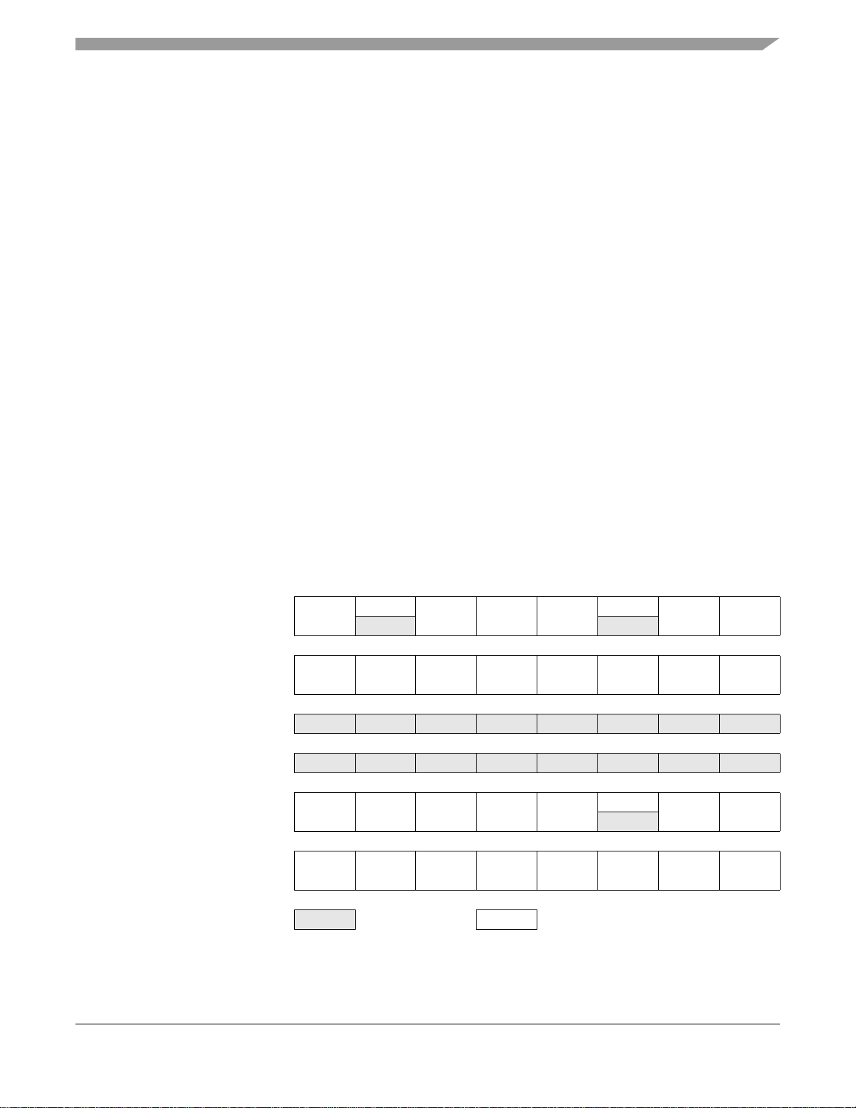
Table 1-1. Summary of Device Variations
Device
MC68HC908QT1 1536 bytes — 8 pins
MC68HC908QT2 1536 bytes 4 ch, 8 bit 8 pins
MC68HC908QT4 4096 bytes 4 ch, 8 bit 8 pins
MC68HC908QY1 1536 bytes — 16 pins
MC68HC908QY2 1536 bytes 4 ch, 8 bit 16 pins
MC68HC908QY4 4096 bytes 4 ch, 8 bit 16 pins
FLASH
Memory Size
Analog-to-Digital
Converter
1.2 Features
Features include:
• High-performance M68HC08 CPU core
• Fully upward-compatible object code with M68HC05 Family
• 5-V and 3-V operating voltages (V
• 8-MHz internal bus operation at 5 V, 4-MHz at 3 V
• Trimmable internal oscillator
– 3.2 MHz internal bus operation
– 8-bit trim capability allows 0.4% accuracy
– ± 25% untrimmed
• Auto wakeup from STOP capability
• Configuration (CONFIG) register for MCU configuration options, including:
– Low-voltage inhibit (LVI) trip point
• In-system FLASH programming
• FLASH security
(2)
DD
)
(1)
Pin
Count
1. The oscillator frequency is guaranteed to ±5% over temperature and voltage range after trimming.
2. No security feature is absolutely secure. However, Freescale’s strategy is to make reading or copying the FLASH difficult for
unauthorized users.
MC68HC908QY/QT Family Data Sheet, Rev. 5
Freescale Semiconductor 17

General Description
• On-chip in-application programmable FLASH memory (with internal program/erase voltage
generation)
– MC68HC908QY4 and MC68HC908QT4 — 4096 bytes
– MC68HC908QY2, MC68HC908QY1, MC68HC908QT2, and MC68HC908QT1 — 1536 bytes
• 128 bytes of on-chip random-access memory (RAM)
• 2-channel, 16-bit timer interface module (TIM)
• 4-channel, 8-bit analog-to-digital converter (ADC) on MC68HC908QY2, MC68HC908QY4,
MC68HC908QT2, and MC68HC908QT4
• 5 or 13 bidirectional input/output (I/O) lines and one input only:
– Six shared with keyboard interrupt function and ADC
– Two shared with timer channels
– One shared with external interrupt (IRQ)
– Eight extra I/O lines on 16-pin package only
– High current sink/source capability on all port pins
– Selectable pullups on all ports, selectable on an individual bit basis
– Three-state ability on all port pins
• 6-bit keyboard interrupt with wakeup feature (KBI)
• Low-voltage inhibit (LVI) module features:
– Software selectable trip point in CONFIG register
• System protection features:
– Computer operating properly (COP) watchdog
– Low-voltage detection with reset
– Illegal opcode detection with reset
– Illegal address detection with reset
• External asynchronous interrupt pin with internal pullup (IRQ
) shared with general-purpose input
pin
• Master asynchronous reset pin (RST
) shared with general-purpose input/output (I/O) pin
• Power-on reset
• Internal pullups on IRQ
and RST to reduce external components
• Memory mapped I/O registers
• Power saving stop and wait modes
• MC68HC908QY4, MC68HC908QY2, and MC68HC908QY1 are available in these packages:
– 16-pin plastic dual in-line package (PDIP)
– 16-pin small outline integrated circuit (SOIC) package
– 16-pin thin shrink small outline package (TSSOP)
• MC68HC908QT4, MC68HC908QT2, and MC68HC908QT1 are available in these packages:
– 8-pin PDIP
– 8-pin SOIC
– 8-pin dual flat no lead (DFN) package
MC68HC908QY/QT Family Data Sheet, Rev. 5
18 Freescale Semiconductor

MCU Block Diagram
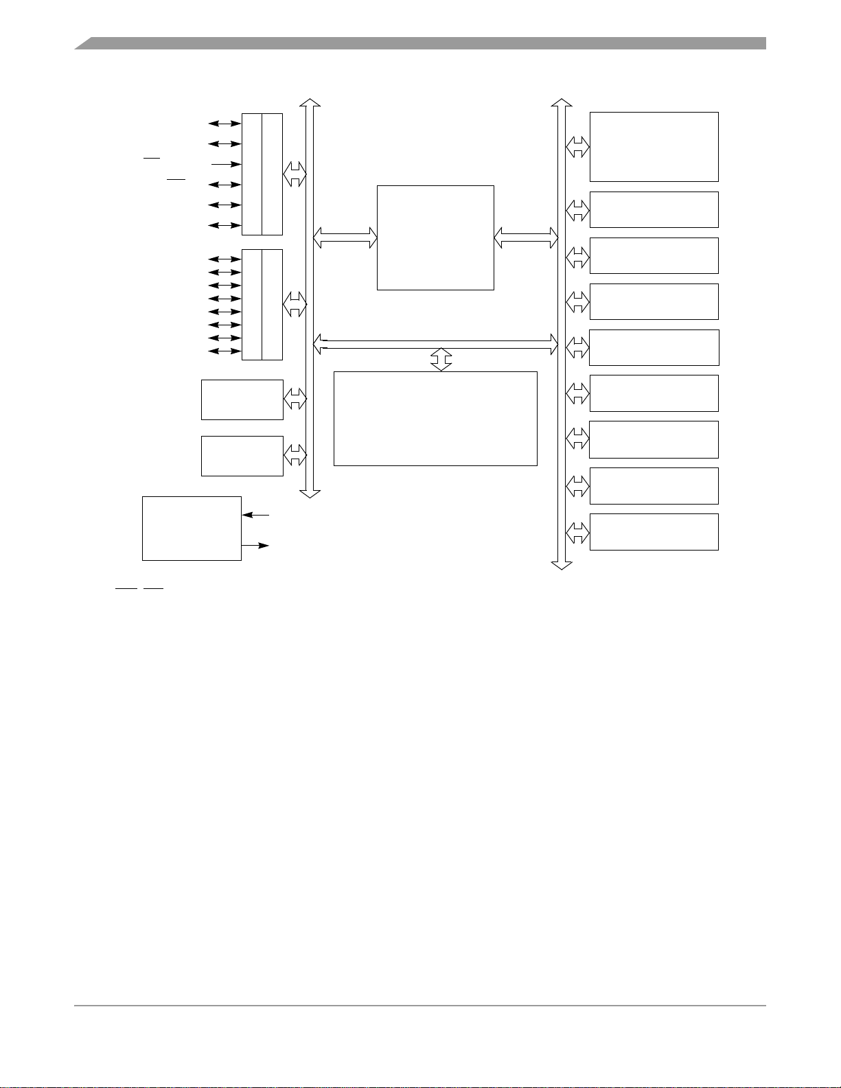
Features of the CPU08 include the following:
• Enhanced HC05 programming model
• Extensive loop control functions
• 16 addressing modes (eight more than the HC05)
• 16-bit index register and stack pointer
• Memory-to-memory data transfers
• Fast 8 × 8 multiply instruction
• Fast 16/8 divide instruction
• Binary-coded decimal (BCD) instructions
• Optimization for controller applications
• Efficient C language support
1.3 MCU Block Diagram
Figure 1-1 shows the structure of the MC68HC908QY4.
1.4 Pin Assignments
The MC68HC908QT4, MC68HC908QT2, and MC68HC908QT1 are available in 8-pin packages and the
MC68HC908QY4, MC68HC908QY2, and MC68HC908QY1 in 16-pin packages. Figure 1-2 shows the pin
assignment for these packages.
MC68HC908QY/QT Family Data Sheet, Rev. 5
Freescale Semiconductor 19
General Description
PTA0/AD0/TCH0/KBI0
PTA1/AD1/TCH1/KBI1
PTA2/IRQ
/KBI2/TCLK
PTA3/RST
PTA4/OSC2/AD2/KBI4
PTA5/OSC1/AD3/KBI5
/KBI3
PTB0
PTB1
PTB2
PTB3
PTB4
PTB5
PTB6
PTB7
POWER SUPPLY
PTA
PTB
8-BIT ADC
128 BYTES RAM
DDRA
DDRB
V
DD
V
SS
M68HC08 CPU
MC68HC908QY4 AND MC68HC908QT4
4096 BYTES
MC68HC908QY2, MC68HC908QY1,
MC68HC908QT2, AND MC68HC908QT1:
1536 BYTES
USER FLASH
CLOCK
GENERATOR
(OSCILLATOR)
SYSTEM INTEGRATION
MODULE
SINGLE INTERRUPT
MODULE
BREAK
MODULE
POWER-ON RESET
MODULE
KEYBOARD INTERRUPT
MODULE
16-BIT TIMER
MODULE
COP
MODULE
MONITOR ROM
RST, IRQ: Pins have internal (about 30K Ohms) pull up
PTA[0:5]: High current sink and source capability
PTA[0:5]: Pins have programmable keyboard interrupt and pull up
PTB[0:7]: Not available on 8-pin devices – MC68HC908QT1, MC68HC908QT2, and MC68HC908QT4 (see note in
12.1 Introduction)
ADC: Not available on the MC68HC908QY1 and MC68HC908QT1
Figure 1-1. Block Diagram
MC68HC908QY/QT Family Data Sheet, Rev. 5
20 Freescale Semiconductor
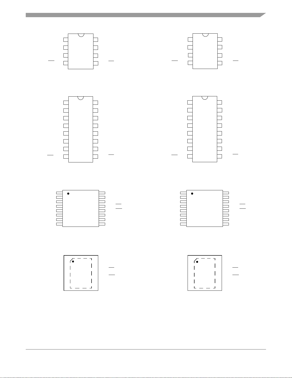
Pin Assignments
V
PTA5/OSC1/KBI5
PTA4/OSC2/KBI4
PTA3/RST
/KBI3
V
PTB7
PTB6
PTA5/OSC1/KBI5
PTA4/OSC2/KBI4
PTB5
PTB4
PTA3/RST
/KBI3
DD
1
2
3
4
8
7
6
5
8-PIN ASSIGNMENT
MC68HC908QT1 PDIP/SOIC
1
DD
2
3
4
5
6
7
8
16
15
14
13
12
11
10
9
16-PIN ASSIGNMENT
MC68HC908QY1 PDIP/SOIC
V
SS
PTA0/TCH0/KBI0
PTA1/TCH1/KBI1
PTA2/IRQ/KBI2/TCLK
V
SS
PTB0
PTB1
PTA0/TCH0/KBI0
PTA1/TCH1/KBI1
PTB2
PTB3
PTA2/IRQ
/KBI2/TCLK
V
PTA5/OSC1/AD3/KBI5
PTA4/OSC2/AD2/KBI4
PTA3/RST
/KBI3
1
DD
2
3
4
8-PIN ASSIGNMENT
MC68HC908QT2 AND MC68HC908QT4 PDIP/SOIC
V
PTB7
PTB6
PTA5/OSC1/AD3/KBI5
PTA4/OSC2/AD2/KBI4
PTB5
PTB4
PTA3/RST
/KBI3
1
DD
2
3
4
5
6
7
8
16-PIN ASSIGNMENT
MC68HC908QY2 AND MC68HC908QY4 PDIP/SOIC
V
SS
8
PTA0/AD0/TCH0/KBI0
7
6
PTA1/AD1/TCH1/KBI1
PTA2/IRQ/KBI2/TCLK
5
V
16
SS
15
PTB0
14
PTB1
PTA0/AD0/TCH0/KBI0
13
PTA1/AD1/TCH1/KBI1
12
11
PTB2
10
PTB3
PTA2/IRQ
9
/KBI2/TCLK
PTA0/TCH0/KBI0
PTB1
PTB0
V
V
PTB7
PTB6
PTA5/OSC1/KBI5
PTA0/TCH0/KBI0
PTA5/OSC1/KB15
1
2
3
4
SS
5
DD
6
7
8
16-PIN ASSIGNMENT
MC68HC908QY1 TSSOP
1
2
V
SS
V
3
DD
4
8-PIN ASSIGNMENT
MC68HC908QT1 DFN
PTA1/TCH1/KBI1
16
PTB2
15
PTB3
14
PTA2/IRQ
13
PTA3/RST
12
11
PTB4
10
PTB5
9
PTA4/OSC2/KBI4
8
PTA1/TCH1/KBI1
7
PTA2/IRQ/KBI2/TCLK
6
PTA3/RST
PTA4/OSC2/KBI4
5
/KBI2/TCLK
/KBI3
/KBI3
PTA0/AD0/TCH0/KBI0
PTA5/OSC1/AD3/KBI5
PTA0/AD0/TCH0/KBI0
PTA5//OSC1/AD3/KB15
Figure 1-2. MCU Pin Assignments
PTB1
PTB0
V
V
PTB7
PTB6
1
2
3
4
SS
5
DD
6
7
8
PTA1/AD1/TCH1/KBI1
16
PTB2
15
PTB3
14
PTA2/IRQ
13
PTA3/RST
12
11
PTB4
10
PTB5
9
PTA4/OSC2/AD2/KBI4
16-PIN ASSIGNMENT
MC68HC908QY2 AND MC68HC908QY4 TSSOP
1
V
2
SS
V
3
DD
4
8
PTA1/AD1/TCH1/KBI1
7
PTA2/IRQ/KBI2/TCLK
6
PTA3/RST
PTA4/OSC2/AD2/KBI4
5
8-PIN ASSIGNMENT
MC68HC908QT2 AND MC68HC908QT4 DFN
/KBI2/TCLK
/KBI3
/KBI3
MC68HC908QY/QT Family Data Sheet, Rev. 5
Freescale Semiconductor 21
General Description
1.5 Pin Functions
Table 1-2 provides a description of the pin functions.
Table 1-2. Pin Functions
Pin
Name
V
DD
V
SS
PTA0
PTA1
PTA2
PTA3
Description Input/Output
Power supply Power
Power supply ground Power
PTA0 — General purpose I/O port Input/Output
AD0 — A/D channel 0 input Input
TCH0 — Timer Channel 0 I/O Input/Output
KBI0 — Keyboard interrupt input 0 Input
PTA1 — General purpose I/O port Input/Output
AD1 — A/D channel 1 input Input
TCH1 — Timer Channel 1 I/O Input/Output
KBI1 — Keyboard interrupt input 1 Input
PTA2 — General purpose input-only port Input
— External interrupt with programmable pullup and Schmitt trigger input Input
IRQ
KBI2 — Keyboard interrupt input 2 Input
TCLK — Timer clock input Input
PTA3 — General purpose I/O port Input/Output
RST — Reset input, active low with internal pullup and Schmitt trigger Input
KBI3 — Keyboard interrupt input 3 Input
PTA4 — General purpose I/O port Input/Output
OSC2 —XTAL oscillator output (XTAL option only)
PTA4
PTA5
PTB[0:7]
1. The PTB pins are not available on the 8-pin packages (see note in 12.1 Introduction).
22 Freescale Semiconductor
RC or internal oscillator output (OSC2EN = 1 in PTAPUE register)
AD2 — A/D channel 2 input Input
KBI4 — Keyboard interrupt input 4 Input
PTA5 — General purpose I/O port Input/Output
OSC1 — XTAL, RC, or external oscillator input Input
AD3 — A/D channel 3 input Input
KBI5 — Keyboard interrupt input 5 Input
(1)
8 general-purpose I/O ports Input/Output
MC68HC908QY/QT Family Data Sheet, Rev. 5
Output
Output
Pin Function Priority
1.6 Pin Function Priority
Table 1-3 is meant to resolve the priority if multiple functions are enabled on a single pin.
NOTE
Upon reset all pins come up as input ports regardless of the priority table.
Table 1-3. Function Priority in Shared Pins
Pin Name Highest-to-Lowest Priority Sequence
PTA0 AD0 → TCH0 → KBI0 → PTA0
PTA1 AD1 →TCH1 → KBI1 → PTA1
PTA2 IRQ
PTA3 RST
PTA4 OSC2 → AD2 → KBI4 → PTA4
PTA5 OSC1 → AD3 → KBI5 → PTA5
→ KBI2 → TCLK → PTA2
→ KBI3 → PTA3
MC68HC908QY/QT Family Data Sheet, Rev. 5
Freescale Semiconductor 23

General Description
MC68HC908QY/QT Family Data Sheet, Rev. 5
24 Freescale Semiconductor

Chapter 2
Memory
2.1 Introduction
The central processor unit (CPU08) can address 64 Kbytes of memory space. The memory map, shown
in Figure 2-1, includes:
• 4096 bytes of user FLASH for MC68HC908QT4 and MC68HC908QY4
• 1536 bytes of user FLASH for MC68HC908QT2, MC68HC908QT1, MC68HC908QY2, and
MC68HC908QY1
• 128 bytes of random access memory (RAM)
• 48 bytes of user-defined vectors, located in FLASH
• 416 bytes of monitor read-only memory (ROM)
• 1536 bytes of FLASH program and erase routines, located in ROM
2.2 Unimplemented Memory Locations
Accessing an unimplemented location can have unpredictable effects on MCU operation. In Figure 2-1
and in register figures in this document, unimplemented locations are shaded.
2.3 Reserved Memory Locations
Accessing a reserved location can have unpredictable effects on MCU operation. In Figure 2-1 and in
register figures in this document, reserved locations are marked with the word Reserved or with the
letter R.
MC68HC908QY/QT Family Data Sheet, Rev. 5
Freescale Semiconductor 25
Memory
$0000
↓
$003F
$0040
↓
$007F
$0080
↓
$00FF
$0100
↓
$27FF
$2800
↓
$2DFF
$2E00
↓
$EDFF
$EE00
↓
$FDFF
$FE00 BREAK STATUS REGISTER (BSR)
$FE01 RESET STATUS REGISTER (SRSR)
$FE02 BREAK AUXILIARY REGISTER (BRKAR)
$FE03 BREAK FLAG CONTROL REGISTER (BFCR)
$FE04 INTERRUPT STATUS REGISTER 1 (INT1)
$FE05 INTERRUPT STATUS REGISTER 2 (INT2)
$FE06 INTERRUPT STATUS REGISTER 3 (INT3)
$FE07
$FE08
$FE09 BREAK ADDRESS HIGH REGISTER (BRKH)
$FE0A BREAK ADDRESS LOW REGISTER (BRKL)
$FE0B BREAK STATUS AND CONTROL REGISTER (BRKSCR)
$FE0C LVISR
$FE0D
↓
$FE0F
$FE10
↓
$FFAF
$FFB0
↓
$FFBD
$FFBE FLASH BLOCK PROTECT REGISTER (FLBPR)
$FFBF
$FFC0 INTERNAL OSCILLATOR TRIM VALUE
$FFC1
$FFC2
↓
$FFCF
$FFD0
↓
$FFFF
RESERVED FOR FLASH TEST CONTROL REGISTER (FLTCR)
MC68HC908QT4 AND MC68HC908QY4
FLASH CONTROL REGISTER (FLCR)
I/O REGISTERS
64 BYTES
RESERVED
64 BYTES
128 BYTES
UNIMPLEMENTED
9984 BYTES
AUXILIARY ROM
1536 BYTES
UNIMPLEMENTED
49152 BYTES
FLASH MEMORY
4096 BYTES
RESERVED FOR FLASH TEST
MONITOR ROM 416 BYTES
14 BYTES
RESERVED FLASH
RESERVED FLASH
14 BYTES
USER VECTORS
48 BYTES
(1)
RAM
(1)
(1)
3 BYTES
FLASH
FLASH
Note 1.
Attempts to execute code from addresses in this
range will generate an illegal address reset.
UNIMPLEMENTED
51712 BYTES
FLASH MEMORY
1536 BYTES
MC68HC908QT1, MC68HC908QT2,
MC68HC908QY1, and MC68HC908QY2
Memory Map
$2E00
↓
$F7FF
$F800
↓
$FDFF
Figure 2-1. Memory Map
MC68HC908QY/QT Family Data Sheet, Rev. 5
26 Freescale Semiconductor
Input/Output (I/O) Section
2.4 Input/Output (I/O) Section
Addresses $0000–$003F, shown in Figure 2-2, contain most of the control, status, and data registers.
Additional I/O registers have these addresses:
• $FE00 — Break status register, BSR
• $FE01 — Reset status register, SRSR
• $FE02 — Break auxiliary register, BRKAR
• $FE03 — Break flag control register, BFCR
• $FE04 — Interrupt status register 1, INT1
• $FE05 — Interrupt status register 2, INT2
• $FE06 — Interrupt status register 3, INT3
•$FE07 — Reserved
• $FE08 — FLASH control register, FLCR
• $FE09 — Break address register high, BRKH
• $FE0A — Break address register low, BRKL
• $FE0B — Break status and control register, BRKSCR
• $FE0C — LVI status register, LVISR
•$FE0D — Reserved
• $FFBE — FLASH block protect register, FLBPR
• $FFC0 — Internal OSC trim value — Optional
• $FFFF — COP control register, COPCTL
Addr.Register Name Bit 7654321Bit 0
Port A Data Register
$0000
Port B Data Register
$0001
$0002 Unimplemented
$0003 Unimplemented
Data Direction Register A
$0004
Data Direction Register B
$0005
(PTA)
See page 98.
(PTB)
See page 100.
(DDRA)
See page 98.
(DDRB)
See page 101.
Read:
Write:
Reset: Unaffected by reset
Read:
Write:
Reset: Unaffected by reset
Read:
Write:
Reset:00000000
Read:
Write:
Reset:00000000
R
PTB7 PTB6 PTB5 PTB4 PTB3 PTB2 PTB1 PTB0
R R DDRA5 DDRA4 DDRA3
DDRB7 DDRB6 DDRB5 DDRB4 DDRB3 DDRB2 DDRB1 DDRB0
AWUL
= Unimplemented R = Reserved U = Unaffected
PTA5 PTA4 PTA3
PTA2
0
DDRA1 DDRA0
PTA1 PTA0
Figure 2-2. Control, Status, and Data Registers (Sheet 1 of 5)
MC68HC908QY/QT Family Data Sheet, Rev. 5
Freescale Semiconductor 27
Memory
Addr.Register Name Bit 7654321Bit 0
$0006
Unimplemented
↓
$000A
Unimplemented
Port A Input Pullup Enable
$000B
Register (PTAPUE)
See page 99.
Port B Input Pullup Enable
$000C
Register (PTBPUE)
See page 102.
$000D
↓
Unimplemented
$0019
Keyboard Status and
$001A
Control Register (KBSCR)
See page 83.
Keyboard Interrupt
$001B
Enable Register (KBIER)
See page 84.
$001C Unimplemented
IRQ Status and Control
$001D
Register (INTSCR)
See page 77.
Configuration Register 2
$001E
(CONFIG2)
See page 53.
Read:
Write:
OSC2EN
0
PTAPUE5 PTAPUE4 PTAPUE3 PTAPUE2 PTAPUE1 PTAPUE0
Reset:00000000
Read:
PTBPUE7 PTBPUE6 PTBPUE5 PTBPUE4 PTBPUE3 PTBPUE2 PTBPUE1 PTBPUE0
Write:
Reset:00000000
Read: 0 0 0 0 KEYF 0
Write: ACKK
IMASKK MODEK
Reset:00000000
Read: 0
Write:
AWUIE KBIE5 KBIE4 KBIE3 KBIE2 KBIE1 KBIE0
Reset:00000000
Read: 0 0 0 0 IRQF 0
Write: ACK
IMASK MODE
Reset:00000000
Read:
(1)
Reset:00000000
IRQPUD IRQEN R OSCOPT1 OSCOPT0 R R RSTEN
Write:
(2)
1. One-time writable register after each reset.
2. RSTEN reset to 0 by a power-on reset (POR) only.
Read:
(1)
Write:
COPRS LVISTOP LVIRSTD LVIPWRD LVI5OR3 SSREC STOP COPD
Reset:00000
(2)
000
$001F
Configuration Register 1
(CONFIG1)
See page 54.
1. One-time writable register after each reset.
2. LVI5OR3 reset to 0 by a power-on reset (POR) only.
$0020
$0021
TIM Status and Control
Register (TSC)
See page 127.
TIM Counter Register High
(TCNTH)
See page 128.
Read: TOF
Write: 0 TRST
TOIE TSTOP
Reset:00100000
Read: Bit 15 Bit 14 Bit 13 Bit 12 Bit 11 Bit 10 Bit 9 Bit 8
Write:
Reset:00000000
00
PS2 PS1 PS0
= Unimplemented R = Reserved U = Unaffected
Figure 2-2. Control, Status, and Data Registers (Sheet 2 of 5)
MC68HC908QY/QT Family Data Sheet, Rev. 5
28 Freescale Semiconductor
Input/Output (I/O) Section
Addr.Register Name Bit 7654321Bit 0
Read: Bit 7 Bit 6 Bit 5 Bit 4 Bit 3 Bit 2 Bit 1 Bit 0
Write:
Reset:00000000
Read:
Write:
Reset:11111111
Read:
Write:
Reset:11111111
Read: CH0F
Write: 0
Reset:00000000
Read:
Write:
Reset: Indeterminate after reset
Read:
Write:
Reset: Indeterminate after reset
Read: CH1F
Write: 0
Reset:00000000
Read:
Write:
Reset: Indeterminate after reset
Read:
Write:
Reset: Indeterminate after reset
Bit 15 Bit 14 Bit 13 Bit 12 Bit 11 Bit 10 Bit 9 Bit 8
Bit 7 Bit 6 Bit 5 Bit 4 Bit 3 Bit 2 Bit 1 Bit 0
CH0IE MS0B MS0A ELS0B ELS0A TOV0 CH0MAX
Bit 15 Bit 14 Bit 13 Bit 12 Bit 11 Bit 10 Bit 9 Bit 8
Bit 7 Bit 6 Bit 5 Bit 4 Bit 3 Bit 2 Bit 1 Bit 0
CH1IE
Bit 15 Bit 14 Bit 13 Bit 12 Bit 11 Bit 10 Bit 9 Bit 8
Bit 7 Bit 6 Bit 5 Bit 4 Bit 3 Bit 2 Bit 1 Bit 0
0
MS1A ELS1B ELS1A TOV1 CH1MAX
$0022
$0023
$0024
$0025
$0026
$0027
$0028
$0029
$002A
$002B
↓
$0035
TIM Counter Register Low
(TCNTL)
See page 128.
TIM Counter Modulo
Register High (TMODH)
See page 129.
TIM Counter Modulo
Register Low (TMODL)
See page 129.
TIM Channel 0 Status and
Control Register (TSC0)
See page 130.
TIM Channel 0
Register High (TCH0H)
See page 132.
TIM Channel 0
Register Low (TCH0L)
See page 132.
TIM Channel 1 Status and
Control Register (TSC1)
See page 130.
TIM Channel 1
Register High (TCH1H)
See page 132.
TIM Channel 1
Register Low (TCH1L)
See page 132.
Unimplemented
Oscillator Status Register
$0036
$0037 Unimplemented Read:
Oscillator Trim Register
$0038
(OSCSTAT)
See page 96.
(OSCTRIM)
See page 96.
Read:
Write:
Reset:00000000
Read:
Write:
Reset:10000000
RRRRRRECGON
TRIM7 TRIM6 TRIM5 TRIM4 TRIM3 TRIM2 TRIM1 TRIM0
= Unimplemented R = Reserved U = Unaffected
ECGST
Figure 2-2. Control, Status, and Data Registers (Sheet 3 of 5)
MC68HC908QY/QT Family Data Sheet, Rev. 5
Freescale Semiconductor 29
Memory
Addr.Register Name Bit 7654321Bit 0
$0039
↓
$003B
Unimplemented
ADC Status and Control
$003C
$003D Unimplemented
$003E
$003F
$FE00
$FE01
$FE02
$FE03
$FE04
$FE05
$FE06
$FE07 Reserved RRRRRRRR
Register (ADSCR)
See page 45.
ADC Data Register
(ADR)
See page 47.
ADC Input Clock Register
(ADICLK)
See page 47.
Break Status Register
(BSR)
See page 137.
SIM Reset Status Register
(SRSR)
See page 117.
Break Auxiliary
Register (BRKAR)
See page 137.
Break Flag Control
Register (BFCR)
See page 138.
Interrupt Status Register 1
(INT1)
See page 77.
Interrupt Status Register 2
(INT2)
See page 77.
Interrupt Status Register 3
(INT3)
See page 77.
Read: COCO
Write: R
Reset:00011111
Read:
Write:
Reset: Indeterminate after reset
Read:
Write:
Reset:00000000
Read:
Write: See note 1
Reset: 0
Read: POR PIN COP ILOP ILAD MODRST LVI 0
Write:
POR:10000000
Read:0000000
Write:
Reset:00000000
Read:
Write:
Reset: 0
Read: 0 IF5 IF4 IF3 0 IF1 0 0
Write:RRRRRRRR
Reset:00000000
Read:IF140000000
Write:RRRRRRRR
Reset:00000000
Read:0000000IF15
Write:RRRRRRRR
Reset:00000000
Bit 7 Bit 6 Bit 5 Bit 4 Bit 3 Bit 2 Bit 1 Bit 0
ADIV2 ADIV1 ADIV0
RRRRRR
1. Writing a 0 clears SBSW.
BCFERRRRRRR
AIEN ADCO CH4 CH3 CH2 CH1 CH0
00000
SBSW
R
BDCOP
= Unimplemented R = Reserved U = Unaffected
Figure 2-2. Control, Status, and Data Registers (Sheet 4 of 5)
MC68HC908QY/QT Family Data Sheet, Rev. 5
30 Freescale Semiconductor

Input/Output (I/O) Section
Addr.Register Name Bit 7654321Bit 0
Read: 0 0 0 0
Write:
Reset:00000000
Read:
Write:
Reset:00000000
Read:
Write:
Reset:00000000
Read:
Write:
Reset:00000000
Read:LVIOUT000000R
Write:
Reset:00000000
Bit 15 Bit 14 Bit 13 Bit 12 Bit 11 Bit 10 Bit 9 Bit 8
Bit 7 Bit 6 Bit 5 Bit 4 Bit 3 Bit 2 Bit 1 Bit 0
BRKE BRKA
000000
HVEN MASS ERASE PGM
$FE08
$FE09
$FE0A
$FE0B
$FE0C
$FE0D
↓
$FE0F
FLASH Control Register
(FLCR)
See page 33.
Break Address High
Register (BRKH)
See page 136.
Break Address low
Register (BRKL)
See page 136.
Break Status and Control
Register (BRKSCR)
See page 136.
LVI Status Register
(LVISR)
See page 87.
Reserved for FLASH Test RRRRRRRR
FLASH Block Protect
$FFBE
$FFBF Reserved RRRRRRRR
$FFC0
$FFC1 Reserved RRRRRRRR
$FFFF
Register (FLBPR)
See page 38.
Internal Oscillator Trim
Value (Optional)
COP Control Register
(COPCTL)
See page 59.
Read:
Write:
Reset: Unaffected by reset
Read:
Write:
Reset: Unaffected by reset
Read: LOW BYTE OF RESET VECTOR
Write: WRITING CLEARS COP COUNTER (ANY VALUE)
Reset: Unaffected by reset
BPR7 BPR6 BPR5 BPR4 BPR3 BPR2 BPR1 BPR0
TRIM7 TRIM6 TRIM5 TRIM4 TRIM3 TRIM2 TRIM1 TRIM0
= Unimplemented R = Reserved U = Unaffected
Figure 2-2. Control, Status, and Data Registers (Sheet 5 of 5)
MC68HC908QY/QT Family Data Sheet, Rev. 5
Freescale Semiconductor 31

Memory
Table 2-1. Vector Addresses
Vector Priority Vector Address Vector
Lowest
Highest
IF15
IF14
IF13
↓
IF6
IF5
IF4
IF3
IF2 — Not used
IF1
—
—
$FFDE ADC conversion complete vector (high)
$FFDF ADC conversion complete vector (low)
$FFE0 Keyboard vector (high)
$FFE1 Keyboard vector (low)
— Not used
$FFF2 TIM overflow vector (high)
$FFF3 TIM overflow vector (low)
$FFF4 TIM Channel 1 vector (high)
$FFF5 TIM Channel 1 vector (low)
$FFF6 TIM Channel 0 vector (high)
$FFF7 TIM Channel 0 vector (low)
$FFFA IRQ
$FFFB IRQ
$FFFC SWI vector (high)
$FFFD SWI vector (low)
$FFFE Reset vector (high)
$FFFF Reset vector (low)
.
vector (high)
vector (low)
2.5 Random-Access Memory (RAM)
Addresses $0080–$00FF are RAM locations. The location of the stack RAM is programmable. The 16-bit
stack pointer allows the stack to be anywhere in the 64-Kbyte memory space.
NOTE
For correct operation, the stack pointer must point only to RAM locations.
Before processing an interrupt, the central processor unit (CPU) uses five bytes of the stack to save the
contents of the CPU registers.
NOTE
For M6805, M146805, and M68HC05 compatibility, the H register is not
stacked.
During a subroutine call, the CPU uses two bytes of the stack to store the return address. The stack
pointer decrements during pushes and increments during pulls.
NOTE
Be careful when using nested subroutines. The CPU may overwrite data in
the RAM during a subroutine or during the interrupt stacking operation.
MC68HC908QY/QT Family Data Sheet, Rev. 5
32 Freescale Semiconductor

FLASH Memory (FLASH)
2.6 FLASH Memory (FLASH)
This subsection describes the operation of the embedded FLASH memory. The FLASH memory can be
read, programmed, and erased from a single external supply. The program and erase operations are
enabled through the use of an internal charge pump.
The FLASH memory consists of an array of 4096 or 1536 bytes with an additional 48 bytes for user
vectors. The minimum size of FLASH memory that can be erased is 64 bytes; and the maximum size of
FLASH memory that can be programmed in a program cycle is 32 bytes (a row). Program and erase
operations are facilitated through control bits in the FLASH control register (FLCR). Details for these
operations appear later in this section. The address ranges for the user memory and vectors are:
• $EE00 – $FDFF; user memory, 4096 bytes: MC68HC908QY4 and MC68HC908QT4
• $F800 – $FDFF; user memory, 1536 bytes: MC68HC908QY2, MC68HC908QT2,
MC68HC908QY1 and MC68HC908QT1
• $FFD0 – $FFFF; user interrupt vectors, 48 bytes.
NOTE
An erased bit reads as a 1 and a programmed bit reads as a 0.
A security feature prevents viewing of the FLASH contents.
2.6.1 FLASH Control Register
(1)
The FLASH control register (FLCR) controls FLASH program and erase operations.
Address: $FE08
Bit 7654321Bit 0
Read:0000
Write:
Reset:00000000
= Unimplemented
HVEN MASS ERASE PGM
Figure 2-3. FLASH Control Register (FLCR)
HVEN — High Voltage Enable Bit
This read/write bit enables high voltage from the charge pump to the memory for either program or
erase operation. It can only be set if either PGM =1 or ERASE = 1 and the proper sequence for
program or erase is followed.
1 = High voltage enabled to array and charge pump on
0 = High voltage disabled to array and charge pump off
MASS — Mass Erase Control Bit
This read/write bit configures the memory for mass erase operation.
1 = Mass erase operation selected
0 = Mass erase operation unselected
1. No security feature is absolutely secure. However, Freescale’s strategy is to make reading or copying the FLASH difficult
for unauthorized users.
MC68HC908QY/QT Family Data Sheet, Rev. 5
Freescale Semiconductor 33

Memory
ERASE — Erase Control Bit
This read/write bit configures the memory for erase operation. ERASE is interlocked with the PGM bit
such that both bits cannot be equal to 1 or set to 1 at the same time.
1 = Erase operation selected
0 = Erase operation unselected
PGM — Program Control Bit
This read/write bit configures the memory for program operation. PGM is interlocked with the ERASE
bit such that both bits cannot be equal to 1 or set to 1 at the same time.
1 = Program operation selected
0 = Program operation unselected
2.6.2 FLASH Page Erase Operation
Use the following procedure to erase a page of FLASH memory. A page consists of 64 consecutive bytes
starting from addresses $XX00, $XX40, $XX80, or $XXC0. The 48-byte user interrupt vectors area also
forms a page. Any FLASH memory page can be erased alone.
1. Set the ERASE bit and clear the MASS bit in the FLASH control register.
2. Read the FLASH block protect register.
3. Write any data to any FLASH location within the address range of the block to be erased.
4. Wait for a time, t
5. Set the HVEN bit.
6. Wait for a time, t
7. Clear the ERASE bit.
8. Wait for a time, t
9. Clear the HVEN bit.
10. After time, t
RCV
Programming and erasing of FLASH locations cannot be performed by
code being executed from the FLASH memory. While these operations
must be performed in the order as shown, but other unrelated operations
may occur between the steps.
(minimum 10 µs).
NVS
(minimum 1 ms or 4 ms).
Erase
(minimum 5 µs).
NVH
(typical 1 µs), the memory can be accessed in read mode again.
NOTE
CAUTION
A page erase of the vector page will erase the internal oscillator trim value
at $FFC0.
In applications that require more than 1000 program/erase cycles, use the 4 ms page erase specification
to get improved long-term reliability. Any application can use this 4 ms page erase specification. However,
in applications where a FLASH location will be erased and reprogrammed less than 1000 times, and
speed is important, use the 1 ms page erase specification to get a shorter cycle time.
MC68HC908QY/QT Family Data Sheet, Rev. 5
34 Freescale Semiconductor

2.6.3 FLASH Mass Erase Operation
Use the following procedure to erase the entire FLASH memory to read as a 1:
1. Set both the ERASE bit and the MASS bit in the FLASH control register.
2. Read the FLASH block protect register.
3. Write any data to any FLASH address
4. Wait for a time, t
(minimum 10 µs).
NVS
5. Set the HVEN bit.
6. Wait for a time, t
(minimum 4 ms).
MErase
7. Clear the ERASE and MASS bits.
Mass erase is disabled whenever any block is protected (FLBPR does not
equal $FF).
(1)
within the FLASH memory address range.
NOTE
FLASH Memory (FLASH)
8. Wait for a time, t
(minimum 100 µs).
NVHL
9. Clear the HVEN bit.
10. After time, t
(typical 1 µs), the memory can be accessed in read mode again.
RCV
NOTE
Programming and erasing of FLASH locations cannot be performed by
code being executed from the FLASH memory. While these operations
must be performed in the order as shown, but other unrelated operations
may occur between the steps.
CAUTION
A mass erase will erase the internal oscillator trim value at $FFC0.
2.6.4 FLASH Program Operation
Programming of the FLASH memory is done on a row basis. A row consists of 32 consecutive bytes
starting from addresses $XX00, $XX20, $XX40, $XX60, $XX80, $XXA0, $XXC0, or $XXE0. Use the
following step-by-step procedure to program a row of FLASH memory
Figure 2-4 shows a flowchart of the programming algorithm.
NOTE
Only bytes which are currently $FF may be programmed.
1. Set the PGM bit. This configures the memory for program operation and enables the latching of
address and data for programming.
2. Read the FLASH block protect register.
3. Write any data to any FLASH location within the address range desired.
4. Wait for a time, t
5. Set the HVEN bit.
6. Wait for a time, t
7. Write data to the FLASH address being programmed
(minimum 10 µs).
NVS
(minimum 5 µs).
PGS
(2)
.
1. When in monitor mode, with security sequence failed (see 15.3.2 Security), write to the FLASH block protect register
instead of any FLASH address.
2. The time between each FLASH address change, or the time between the last FLASH address programmed to clearing
PGM bit, must not exceed the maximum programming time, t
MC68HC908QY/QT Family Data Sheet, Rev. 5
Freescale Semiconductor 35
PROG
maximum.

Memory
8. Wait for time, t
(minimum 30 µs).
PROG
9. Repeat step 7 and 8 until all desired bytes within the row are programmed.
10. Clear the PGM bit
11. Wait for time, t
(1)
.
(minimum 5 µs).
NVH
12. Clear the HVEN bit.
13. After time, t
(typical 1 µs), the memory can be accessed in read mode again.
RCV
NOTE
The COP register at location $FFFF should not be written between
steps 5–12, when the HVEN bit is set. Since this register is located at a
valid FLASH address, unpredictable behavior may occur if this location is
written while HVEN is set.
This program sequence is repeated throughout the memory until all data is programmed.
NOTE
Programming and erasing of FLASH locations cannot be performed by
code being executed from the FLASH memory. While these operations
must be performed in the order shown, other unrelated operations may
occur between the steps. Do not exceed t
maximum, see 16.16
PROG
Memory Characteristics.
2.6.5 FLASH Protection
Due to the ability of the on-board charge pump to erase and program the FLASH memory in the target
application, provision is made to protect blocks of memory from unintentional erase or program operations
due to system malfunction. This protection is done by use of a FLASH block protect register (FLBPR).
The FLBPR determines the range of the FLASH memory which is to be protected. The range of the
protected area starts from a location defined by FLBPR and ends to the bottom of the FLASH memory
($FFFF). When the memory is protected, the HVEN bit cannot be set in either ERASE or PROGRAM
operations.
NOTE
In performing a program or erase operation, the FLASH block protect
register must be read after setting the PGM or ERASE bit and before
asserting the HVEN bit.
When the FLBPR is programmed with all 0 s, the entire memory is protected from being programmed and
erased. When all the bits are erased (all 1’s), the entire memory is accessible for program and erase.
When bits within the FLBPR are programmed, they lock a block of memory. The address ranges are
shown in 2.6.6 FLASH Block Protect Register. Once the FLBPR is programmed with a value other than
$FF, any erase or program of the FLBPR or the protected block of FLASH memory is prohibited. Mass
erase is disabled whenever any block is protected (FLBPR does not equal $FF). The FLBPR itself can be
erased or programmed only with an external voltage, V
, present on the IRQ pin. This voltage also
TST
allows entry from reset into the monitor mode.
MC68HC908QY/QT Family Data Sheet, Rev. 5
36 Freescale Semiconductor

FLASH Memory (FLASH)
Algorithm for Programming
a Row (32 Bytes) of FLASH Memory
1
2
READ THE FLASH BLOCK PROTECT REGISTER
3
WRITE ANY DATA TO ANY FLASH ADDRESS
WITHIN THE ROW ADDRESS RANGE DESIRED
4
5
6
7
WRITE DATA TO THE FLASH ADDRESS
8
SET PGM BIT
WAIT FOR A TIME, t
SET HVEN BIT
WAIT FOR A TIME, t
TO BE PROGRAMMED
WAIT FOR A TIME, t
PROG
NVS
PGS
9
NOTES:
The time between each FLASH address change (step 7 to step 7),
or the time between the last FLASH address programmed
to clearing PGM bit (step 7 to step 10)
must not exceed the maximum programming
PROG
max.
time, t
This row program algorithm assumes the row/s
to be programmed are initially erased.
Figure 2-4. FLASH Programming Flowchart
COMPLETED
PROGRAMMING
THIS ROW?
N
Y
10
11
12
13
CLEAR PGM BIT
WAIT FOR A TIME, t
CLEAR HVEN BIT
WAIT FOR A TIME, t
END OF PROGRAMMING
NVH
RCV
MC68HC908QY/QT Family Data Sheet, Rev. 5
Freescale Semiconductor 37

Memory
2.6.6 FLASH Block Protect Register
The FLASH block protect register is implemented as a byte within the FLASH memory, and therefore can
only be written during a programming sequence of the FLASH memory. The value in this register
determines the starting address of the protected range within the FLASH memory.
Address: $FFBE
Bit 7654321Bit 0
Read:
Write:
Reset: Unaffected by reset. Initial value from factory is 1.
Write to this register is by a programming sequence to the FLASH memory.
BPR[7:0] — FLASH Protection Register Bits [7:0]
These eight bits in FLBPR represent bits [13:6] of a 16-bit memory address. Bits [15:14] are 1s and
bits [5:0] are 0s.
The resultant 16-bit address is used for specifying the start address of the FLASH memory for block
protection. The FLASH is protected from this start address to the end of FLASH memory, at $FFFF.
With this mechanism, the protect start address can be XX00, XX40, XX80, or XXC0 within the FLASH
memory. See Figure 2-6 and Table 2-2.
BPR7 BPR6 BPR5 BPR4 BPR3 BPR2 BPR1 BPR0
Figure 2-5. FLASH Block Protect Register (FLBPR)
16-BIT MEMORY ADDRESS
START ADDRESS OF
FLASH BLOCK PROTECT
FLBPR VALUE
Figure 2-6. FLASH Block Protect Start Address
Table 2-2. Examples of Protect Start Address
BPR[7:0] Start of Address of Protect Range
$00–$B8 The entire FLASH memory is protected.
$B9 (1011 1001) $EE40 (1110 1110 0100 0000)
$BA (1011 1010) $EE80 (1110 1110 1000 0000)
$BB (1011 1011) $EEC0 (1110 1110 1100 0000)
$BC (1011 1100) $EF00 (1110 1111 0000 0000)
and so on...
$DE (1101 1110)$F780 (1111 0111 1000 0000)
$DF (1101 1111)$F7C0 (1111 0111 1100 0000)
$FE (1111 1110)
$FF The entire FLASH memory is not protected.
$FF80 (1111 1111 1000 0000)
FLBPR, OSCTRIM, and vectors are protected
0
00011
0
0
MC68HC908QY/QT Family Data Sheet, Rev. 5
38 Freescale Semiconductor

FLASH Memory (FLASH)
2.6.7 Wait Mode
Putting the MCU into wait mode while the FLASH is in read mode does not affect the operation of the
FLASH memory directly, but there will not be any memory activity since the CPU is inactive.
The WAIT instruction should not be executed while performing a program or erase operation on the
FLASH, or the operation will discontinue and the FLASH will be on standby mode.
2.6.8 Stop Mode
Putting the MCU into stop mode while the FLASH is in read mode does not affect the operation of the
FLASH memory directly, but there will not be any memory activity since the CPU is inactive.
The STOP instruction should not be executed while performing a program or erase operation on the
FLASH, or the operation will discontinue and the FLASH will be on standby mode
NOTE
Standby mode is the power-saving mode of the FLASH module in which all
internal control signals to the FLASH are inactive and the current
consumption of the FLASH is at a minimum.
MC68HC908QY/QT Family Data Sheet, Rev. 5
Freescale Semiconductor 39

Memory
MC68HC908QY/QT Family Data Sheet, Rev. 5
40 Freescale Semiconductor

Chapter 3
Analog-to-Digital Converter (ADC)
3.1 Introduction
This section describes the analog-to-digital converter (ADC). The ADC is an 8-bit, 4-channel analog-todigital converter. The ADC module is only available on the MC68HC908QY2, MC68HC908QT2,
MC68HC908QY4, and MC68HC908QT4.
3.2 Features
Features of the ADC module include:
• 4 channels with multiplexed input
• Linear successive approximation with monotonicity
• 8-bit resolution
• Single or continuous conversion
• Conversion complete flag or conversion complete interrupt
• Selectable ADC clock frequency
3.3 Functional Description
Four ADC channels are available for sampling external sources at pins PTA0, PTA1, PTA4, and PTA5.
An analog multiplexer allows the single ADC converter to select one of the four ADC channels as an ADC
voltage input (ADCVIN). ADCVIN is converted by the successive approximation register-based counters.
The ADC resolution is eight bits. When the conversion is completed, ADC puts the result in the ADC data
register and sets a flag or generates an interrupt.
Figure 3-2 shows a block diagram of the ADC.
3.3.1 ADC Port I/O Pins
PTA0, PTA1, PTA4, and PTA5 are general-purpose I/O pins that are shared with the ADC channels. The
channel select bits (ADC status and control register (ADSCR), $003C), define which ADC channel/port
pin will be used as the input signal. The ADC overrides the port I/O logic by forcing that pin as input to the
ADC. The remaining ADC channels/port pins are controlled by the port I/O logic and can be used as
general-purpose I/O. Writes to the port register or data direction register (DDR) will not have any affect
on the port pin that is selected by the ADC. Read of a port pin which is in use by the ADC will return a 0
if the corresponding DDR bit is at 0. If the DDR bit is at 1, the value in the port data latch is read.
MC68HC908QY/QT Family Data Sheet, Rev. 5
Freescale Semiconductor 41
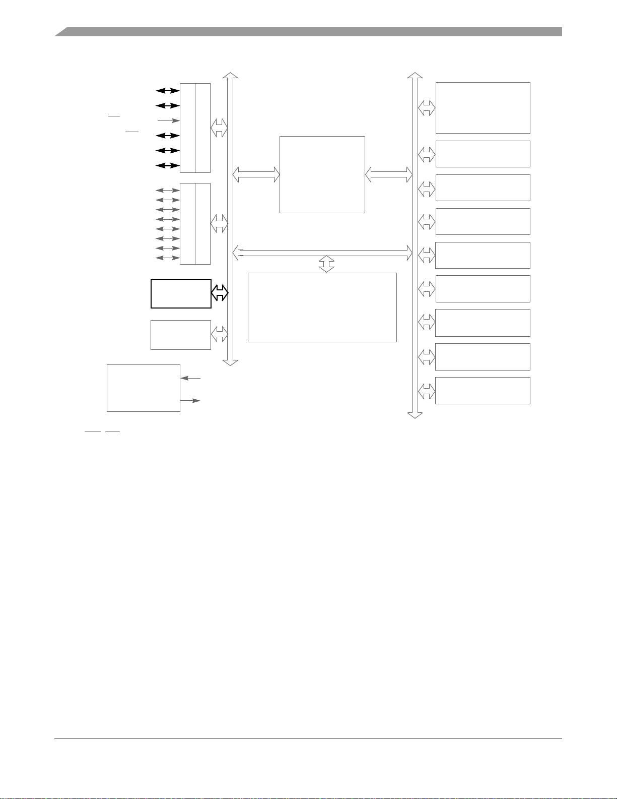
Analog-to-Digital Converter (ADC)
PTA0/AD0/TCH0/KBI0
PTA1/AD1/TCH1/KBI1
PTA2/IRQ
/KBI2/TCLK
PTA3/RST
PTA4/OSC2/AD2/KBI4
PTA5/OSC1/AD3/KBI5
/KBI3
PTB0
PTB1
PTB2
PTB3
PTB4
PTB5
PTB6
PTB7
POWER SUPPLY
PTA
PTB
8-BIT ADC
128 BYTES RAM
DDRA
DDRB
V
DD
V
SS
M68HC08 CPU
MC68HC908QY4 AND MC68HC908QT4
4096 BYTES
MC68HC908QY2, MC68HC908QY1,
MC68HC908QT2, AND MC68HC908QT1:
1536 BYTES
USER FLASH
CLOCK
GENERATOR
(OSCILLATOR)
SYSTEM INTEGRATION
MODULE
SINGLE INTERRUPT
MODULE
BREAK
MODULE
POWER-ON RESET
MODULE
KEYBOARD INTERRUPT
MODULE
16-BIT TIMER
MODULE
COP
MODULE
MONITOR ROM
RST, IRQ: Pins have internal (about 30K Ohms) pull up
PTA[0:5]: High current sink and source capability
PTA[0:5]: Pins have programmable keyboard interrupt and pull up
PTB[0:7]: Not available on 8-pin devices – MC68HC908QT1, MC68HC908QT2, and MC68HC908QT4 (see note in
12.1 Introduction)
ADC: Not available on the MC68HC908QY1 and MC68HC908QT1
Figure 3-1. Block Diagram Highlighting ADC Block and Pins
MC68HC908QY/QT Family Data Sheet, Rev. 5
42 Freescale Semiconductor

INTERNAL
DATA BUS
Functional Description
READ DDRA
WRITE DDRA
WRITE PTA
READ PTA
INTERRUPT
LOGIC
AIEN COCO
CONVERSION
COMPLETE
RESET
ADC DATA REGISTER
ADC
DDRAx
PTAx
ADC CLOCK
ADC VOLTAGE IN
ADCVIN
DISABLE
DISABLE
ADC CHANNEL x
CHANNEL
SELECT
(1 OF 4 CHANNELS)
ADCx
CH[4:0]
BUS CLOCK
CLOCK
GENERATOR
ADIV[2:0]
Figure 3-2. ADC Block Diagram
MC68HC908QY/QT Family Data Sheet, Rev. 5
Freescale Semiconductor 43

Analog-to-Digital Converter (ADC)
3.3.2 Voltage Conversion
When the input voltage to the ADC equals VDD, the ADC converts the signal to $FF (full scale). If the input
voltage equals V
the ADC converts it to $00. Input voltages between VDD and V
SS,
linear conversion. All other input voltages will result in $FF if greater than V
and $00 if less than VSS.
DD
are a straight-line
SS
NOTE
Input voltage should not exceed the analog supply voltages.
3.3.3 Conversion Time
Sixteen ADC internal clocks are required to perform one conversion. The ADC starts a conversion on the
first rising edge of the ADC internal clock immediately following a write to the ADSCR. If the ADC internal
clock is selected to run at 1 MHz, then one conversion will take 16 µs to complete. With a 1-MHz ADC
internal clock the maximum sample rate is 62.5 kHz.
Conversion Time =
Number of Bus Cycles = Conversion Time × Bus Frequency
16 ADC Clock Cycles
ADC Clock Frequency
3.3.4 Continuous Conversion
In the continuous conversion mode (ADCO = 1), the ADC continuously converts the selected channel
filling the ADC data register (ADR) with new data after each conversion. Data from the previous
conversion will be overwritten whether that data has been read or not. Conversions will continue until the
ADCO bit is cleared. The COCO bit (ADSCR, $003C) is set after each conversion and will stay set until
the next read of the ADC data register.
When a conversion is in process and the ADSCR is written, the current conversion data should be
discarded to prevent an incorrect reading.
3.3.5 Accuracy and Precision
The conversion process is monotonic and has no missing codes.
3.4 Interrupts
When the AIEN bit is set, the ADC module is capable of generating a central processor unit (CPU)
interrupt after each ADC conversion. A CPU interrupt is generated if the COCO bit is at 0. The COCO bit
is not used as a conversion complete flag when interrupts are enabled.
3.5 Low-Power Modes
The following subsections describe the ADC in low-power modes.
3.5.1 Wait Mode
The ADC continues normal operation during wait mode. Any enabled CPU interrupt request from the ADC
can bring the microcontroller unit (MCU) out of wait mode. If the ADC is not required to bring the MCU out
of wait mode, power down the ADC by setting the CH[4:0] bits in ADSCR to 1s before executing the WAIT
instruction.
MC68HC908QY/QT Family Data Sheet, Rev. 5
44 Freescale Semiconductor

Input/Output Signals
3.5.2 Stop Mode
The ADC module is inactive after the execution of a STOP instruction. Any pending conversion is aborted.
ADC conversions resume when the MCU exits stop mode. Allow one conversion cycle to stabilize the
analog circuitry before using ADC data after exiting stop mode.
3.6 Input/Output Signals
The ADC module has four channels that are shared with I/O port A.
ADC voltage in (ADCVIN) is the input voltage signal from one of the four ADC channels to the ADC
module.
3.7 Input/Output Registers
These I/O registers control and monitor ADC operation:
• ADC status and control register (ADSCR)
• ADC data register (ADR)
• ADC clock register (ADICLK)
3.7.1 ADC Status and Control Register
The following paragraphs describe the function of the ADC status and control register (ADSCR). When a
conversion is in process and the ADSCR is written, the current conversion data should be discarded to
prevent an incorrect reading.
Address: $003C
Bit 7654321Bit 0
Read: COCO
Write: R
Reset:00011111
R= Reserved
AIEN ADCO CH4 CH3 CH2 CH1 CH0
Figure 3-3. ADC Status and Control Register (ADSCR)
COCO — Conversions Complete Bit
In non-interrupt mode (AIEN = 0), COCO is a read-only bit that is set at the end of each conversion.
COCO will stay set until cleared by a read of the ADC data register. Reset clears this bit.
In interrupt mode (AIEN = 1), COCO is a read-only bit that is not set at the end of a conversion. It
always reads as a 0.
1 = Conversion completed (AIEN = 0)
0 = Conversion not completed (AIEN = 0) or CPU interrupt enabled (AIEN = 1)
NOTE
The write function of the COCO bit is reserved. When writing to the ADSCR
register, always have a 0 in the COCO bit position.
MC68HC908QY/QT Family Data Sheet, Rev. 5
Freescale Semiconductor 45

Analog-to-Digital Converter (ADC)
AIEN — ADC Interrupt Enable Bit
When this bit is set, an interrupt is generated at the end of an ADC conversion. The interrupt signal is
cleared when ADR is read or ADSCR is written. Reset clears the AIEN bit.
1 = ADC interrupt enabled
0 = ADC interrupt disabled
ADCO — ADC Continuous Conversion Bit
When set, the ADC will convert samples continuously and update ADR at the end of each conversion.
Only one conversion is allowed when this bit is cleared. Reset clears the ADCO bit.
1 = Continuous ADC conversion
0 = One ADC conversion
CH[4:0] — ADC Channel Select Bits
CH4, CH3, CH2, CH1, and CH0 form a 5-bit field which is used to select one of the four ADC channels.
The five select bits are detailed in Table 3-1. Care should be taken when using a port pin as both an
analog and a digital input simultaneously to prevent switching noise from corrupting the analog signal.
The ADC subsystem is turned off when the channel select bits are all set to 1. This feature allows for
reduced power consumption for the MCU when the ADC is not used. Reset sets all of these bits to 1.
NOTE
Recovery from the disabled state requires one conversion cycle to stabilize.
Table 3-1. MUX Channel Select
CH4 CH3 CH2 CH1 CH0
00000 ADC0 PTA0
00001 ADC1 PTA1
00010 ADC2 PTA4
00011 ADC3 PTA5
00100 —
↓↓↓↓↓ —
11010 —
11011 — Reserved
11
11
11
111 1 1—ADC power off
1. If any unused channels are selected, the resulting ADC conversion will be
unknown.
2. The voltage levels supplied from internal reference nodes, as specified in the
table, are used to verify the operation of the ADC converter both in production test and for user applications.
1 0 0 — Unused
1 0 1—
1 1 0—
ADC
Channel
Input Select
V
V
DDA
SSA
(1)
(2)
(2)
Unused
MC68HC908QY/QT Family Data Sheet, Rev. 5
46 Freescale Semiconductor
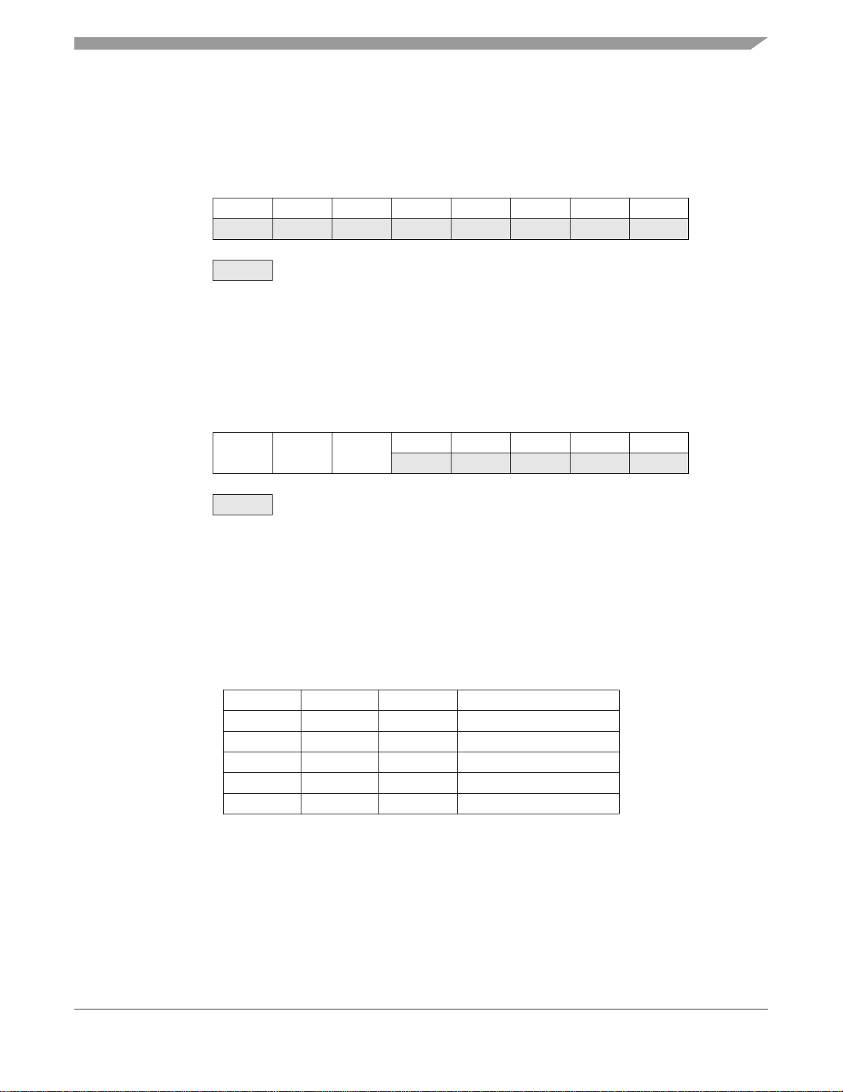
Input/Output Registers
3.7.2 ADC Data Register
One 8-bit result register is provided. This register is updated each time an ADC conversion completes.
Address: $003E
Bit 7654321Bit 0
Read: AD7 AD6 AD5 AD4 AD3 AD2 AD1 AD0
Write:
Reset: Indeterminate after reset
= Unimplemented
Figure 3-4. ADC Data Register (ADR)
3.7.3 ADC Input Clock Register
This register selects the clock frequency for the ADC.
Address: $003F
Bit 7654321Bit 0
Read:
Write:
Reset:00000000
ADIV2 ADIV1 ADIV0
= Unimplemented
00000
Figure 3-5. ADC Input Clock Register (ADICLK)
ADIV2–ADIV0 — ADC Clock Prescaler Bits
ADIV2, ADIV1, and ADIV0 form a 3-bit field which selects the divide ratio used by the ADC to generate
the internal ADC clock. Table 3-2 shows the available clock configurations. The ADC clock frequency
should be set between f
ADIC(MIN)
and f
ADIC(MAX)
. The analog input level should remain stable for the
entire conversion time (maximum = 17 ADC clock cycles).
Table 3-2. ADC Clock Divide Ratio
ADIV2 ADIV1 ADIV0 ADC Clock Rate
0 0 0 Bus clock ÷ 1
0 0 1 Bus clock ÷ 2
0 1 0 Bus clock ÷ 4
0 1 1 Bus clock ÷ 8
1 X X Bus clock ÷ 16
X = don’t care
MC68HC908QY/QT Family Data Sheet, Rev. 5
Freescale Semiconductor 47

Analog-to-Digital Converter (ADC)
MC68HC908QY/QT Family Data Sheet, Rev. 5
48 Freescale Semiconductor

Chapter 4
Auto Wakeup Module (AWU)
4.1 Introduction
This section describes the auto wakeup module (AWU). The AWU generates a periodic interrupt during
stop mode to wake the part up without requiring an external signal. Figure 4-1 is a block diagram of the
AWU.
4.2 Features
Features of the auto wakeup module include:
• One internal interrupt with separate interrupt enable bit, sharing the same keyboard interrupt vector
and keyboard interrupt mask bit
• Exit from low-power stop mode without external signals
• Selectable timeout periods
• Dedicated low-power internal oscillator separate from the main system clock sources
4.3 Functional Description
The function of the auto wakeup logic is to generate periodic wakeup requests to bring the microcontroller
unit (MCU) out of stop mode. The wakeup requests are treated as regular keyboard interrupt requests,
with the difference that instead of a pin, the interrupt signal is generated by an internal logic.
Writing the AWUIE bit in the keyboard interrupt enable register enables or disables the auto wakeup
interrupt input (see Figure 4-1). A logic 1 applied to the AWUIREQ input with auto wakeup interrupt
request enabled, latches an auto wakeup interrupt request.
Auto wakeup latch, AWUL, can be read directly from the bit 6 position of port A data register (PTA). This
is a read-only bit which is occupying an empty bit position on PTA. No PTA associated registers, such as
PTA6 data direction or PTA6 pullup exist for this bit.
Entering stop mode will enable the auto wakeup generation logic. An internal RC oscillator (exclusive for
the auto wakeup feature) drives the wakeup request generator. Once the overflow count is reached in the
generator counter, a wakeup request, AWUIREQ, is latched and sent to the KBI logic. See Figure 4-1.
Wakeup interrupt requests will only be serviced if the associated interrupt enable bit, AWUIE, in KBIER
is set. The AWU shares the keyboard interrupt vector.
The overflow count can be selected from two options defined by the COPRS bit in CONFIG1. This bit was
“borrowed” from the computer operating properly (COP) using the fact that the COP feature is idle (no
MCU clock available) in stop mode. The typical values of the periodic wakeup request are (at room
temperature):
• COPRS = 0: 650 ms @ 5 V, 875 ms @ 3 V
• COPRS = 1: 16 ms @ 5 V, 22 ms @ 3 V
MC68HC908QY/QT Family Data Sheet, Rev. 5
Freescale Semiconductor 49
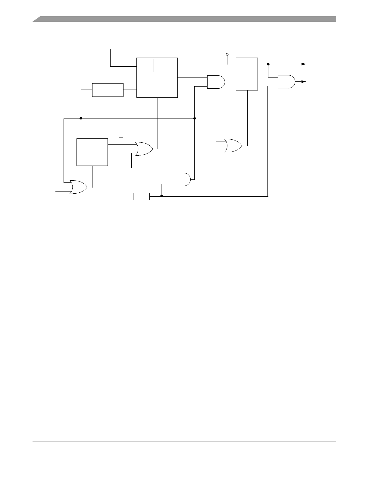
Auto Wakeup Module (AWU)
(CGMXCLK)
BUSCLKX4
RESET
COPRS (FROM CONFIG1)
INT RC OSC
EN 32 kHz
CLRLOGIC
CLEAR
CLK
RST
RESET
AUTOWUGE N
SHORT
CLK
AWUI E
1 = DIV 2
0 = DIV 2
OVERFLOW
RST
ISTOP
9
14
RESET
ACKK
V
DD
D
Q
E
R
Figure 4-1. Auto Wakeup Interrupt Request Generation Logic
TO PTA READ, BIT 6
AWUL
AWUIREQ
TO KBI INTERRUPT LOGIC (SEE
Figure 9-2. Keyboard Interrupt
Block Diagram)
The auto wakeup RC oscillator is highly dependent on operating voltage and temperature. This feature is
not recommended for use as a time-keeping function.
The wakeup request is latched to allow the interrupt source identification. The latched value, AWUL, can
be read directly from the bit 6 position of PTA data register. This is a read-only bit which is occupying an
empty bit position on PTA. No PTA associated registers, such as PTA6 data, PTA6 direction, and PTA6
pullup exist for this bit. The latch can be cleared by writing to the ACKK bit in the KBSCR register. Reset
also clears the latch. AWUIE bit in KBI interrupt enable register (see Figure 4-1) has no effect on AWUL
reading.
The AWU oscillator and counters are inactive in normal operating mode and become active only upon
entering stop mode.
4.4 Wait Mode
The AWU module remains inactive in wait mode.
4.5 Stop Mode
When the AWU module is enabled (AWUIE = 1 in the keyboard interrupt enable register) it is activated
automatically upon entering stop mode. Clearing the IMASKK bit in the keyboard status and control
register enables keyboard interrupt requests to bring the MCU out of stop mode. The AWU counters start
from ‘0’ each time stop mode is entered.
MC68HC908QY/QT Family Data Sheet, Rev. 5
50 Freescale Semiconductor

Input/Output Registers
4.6 Input/Output Registers
The AWU shares registers with the keyboard interrupt (KBI) module and the port A I/O module. The
following I/O registers control and monitor operation of the AWU:
• Port A data register (PTA)
• Keyboard interrupt status and control register (KBSCR)
• Keyboard interrupt enable register (KBIER)
4.6.1 Port A I/O Register
The port A data register (PTA) contains a data latch for the state of the AWU interrupt request, in addition
to the data latches for port A.
Address: $0000
Bit 7654321Bit 0
Read: 0 AWUL
Write:
Reset: 0 0 Unaffected by reset
= Unimplemented
PTA5 PTA4 PTA3
Figure 4-2. Port A Data Register (PTA)
PTA2
PTA1 PTA0
AWUL — Auto Wakeup Latch
This is a read-only bit which has the value of the auto wakeup interrupt request latch. The wakeup
request signal is generated internally. There is no PTA6 port or any of the associated bits such as
PTA6 data direction or pullup bits.
1 = Auto wakeup interrupt request is pending
0 = Auto wakeup interrupt request is not pending
NOTE
PTA5–PTA0 bits are not used in conjuction with the auto wakeup feature.
To see a description of these bits, see 12.2.1 Port A Data Register.
4.6.2 Keyboard Status and Control Register
The keyboard status and control register (KBSCR):
• Flags keyboard/auto wakeup interrupt requests
• Acknowledges keyboard/auto wakeup interrupt requests
• Masks keyboard/auto wakeup interrupt requests
Address: $001A
Bit 7654321Bit 0
Read:0000KEYF0
Write: ACKK
Reset:00000000
= Unimplemented
IMASKK MODEK
Figure 4-3. Keyboard Status and Control Register (KBSCR)
MC68HC908QY/QT Family Data Sheet, Rev. 5
Freescale Semiconductor 51

Auto Wakeup Module (AWU)
Bits 7–4 — Not used
These read-only bits always read as 0s.
KEYF — Keyboard Flag Bit
This read-only bit is set when a keyboard interrupt is pending on port A or auto wakeup. Reset clears
the KEYF bit.
1 = Keyboard/auto wakeup interrupt pending
0 = No keyboard/auto wakeup interrupt pending
ACKK — Keyboard Acknowledge Bit
Writing a 1 to this write-only bit clears the keyboard/auto wakeup interrupt request on port A and auto
wakeup logic. ACKK always reads as 0.Reset clears ACKK.
IMASKK— Keyboard Interrupt Mask Bit
Writing a 1 to this read/write bit prevents the output of the keyboard interrupt mask from generating
interrupt requests on port A or auto wakeup. Reset clears the IMASKK bit.
1 = Keyboard/auto wakeup interrupt requests masked
0 = Keyboard/auto wakeup interrupt requests not masked
NOTE
MODEK is not used in conjuction with the auto wakeup feature. To see a
description of this bit, see 9.7.1 Keyboard Status and Control Register.
4.6.3 Keyboard Interrupt Enable Register
The keyboard interrupt enable register (KBIER) enables or disables the auto wakeup to operate as a
keyboard/auto wakeup interrupt input.
Address: $001B
Bit 7654321Bit 0
Read: 0
Write:
Reset:00000000
Figure 4-4. Keyboard Interrupt Enable Register (KBIER)
AWUIE — Auto Wakeup Interrupt Enable Bit
This read/write bit enables the auto wakeup interrupt input to latch interrupt requests. Reset clears
AWUIE.
1 = Auto wakeup enabled as interrupt input
0 = Auto wakeup not enabled as interrupt input
KBIE5–KBIE0 bits are not used in conjuction with the auto wakeup feature.
To see a description of these bits, see 9.7.2 Keyboard Interrupt Enable
Register.
AWUIE KBIE5 KBIE4 KBIE3 KBIE2 KBIE1 KBIE0
= Unimplemented
NOTE
MC68HC908QY/QT Family Data Sheet, Rev. 5
52 Freescale Semiconductor

Chapter 5
Configuration Register (CONFIG)
5.1 Introduction
This section describes the configuration registers (CONFIG1 and CONFIG2). The configuration registers
enable or disable the following options:
• Stop mode recovery time (32 × BUSCLKX4 cycles or
4096 × BUSCLKX4 cycles)
•STOP instruction
• Computer operating properly module (COP)
• COP reset period (COPRS): 8176 × BUSCLKX4 or 262,128 × BUSCLKX4
• Low-voltage inhibit (LVI) enable and trip voltage selection
• OSC option selection
•IRQ
•RST
• Auto wakeup timeout period
5.2 Functional Description
pin
pin
The configuration registers are used in the initialization of various options. The configuration registers can
be written once after each reset. Most of the configuration register bits are cleared during reset. Since the
various options affect the operation of the microcontroller unit (MCU) it is recommended that this register
be written immediately after reset. The configuration registers are located at $001E and $001F, and may
be read at anytime.
NOTE
The CONFIG registers are one-time writable by the user after each reset.
Upon a reset, the CONFIG registers default to predetermined settings as
shown in Figure 5-1 and Figure 5-2.
Address:
$001E
Bit 7654 321Bit 0
Read:
Write:
Reset:000 0 0 00U
IRQPUD IRQEN R OSCOPT1 OSCOPT0 R R RSTEN
POR:000 0 0 000
= Reserved U = Unaffected
R
Figure 5-1. Configuration Register 2 (CONFIG2)
MC68HC908QY/QT Family Data Sheet, Rev. 5
Freescale Semiconductor 53

Configuration Register (CONFIG)
IRQPUD — IRQ Pin Pullup Control Bit
1 = Internal pullup is disconnected
0 = Internal pullup is connected between IRQ
pin and V
DD
IRQEN — IRQ Pin Function Selection Bit
1 = Interrupt request function active in pin
0 = Interrupt request function inactive in pin
OSCOPT1 and OSCOPT0 — Selection Bits for Oscillator Option
(0, 0) Internal oscillator
(0, 1) External oscillator
(1, 0) External RC oscillator
(1, 1) External XTAL oscillator
RSTEN — RST
Pin Function Selection
1 = Reset function active in pin
0 = Reset function inactive in pin
NOTE
The RSTEN bit is cleared by a power-on reset (POR) only. Other resets will
leave this bit unaffected.
Address:
$001F
Bit 7 6 5 4 3 2 1 Bit 0
Read:
Write:
Reset:0000U000
POR:00000000
COPRS LVISTOP LVIRSTD LVIPWRD LVI5OR3 SSREC STOP COPD
U = Unaffected
Figure 5-2. Configuration Register 1 (CONFIG1)
COPRS (Out of STOP Mode) — COP Reset Period Selection Bit
1 = COP reset short cycle = 8176 × BUSCLKX4
0 = COP reset long cycle = 262,128 × BUSCLKX4
COPRS (In STOP Mode) — Auto Wakeup Period Selection Bit
1 = Auto wakeup short cycle = 512 × INTRCOSC
0 = Auto wakeup long cycle = 16,384 × INTRCOSC
LVISTOP — LVI Enable in Stop Mode Bit
When the LVIPWRD bit is clear, setting the LVISTOP bit enables the LVI to operate during stop mode.
Reset clears LVISTOP.
1 = LVI enabled during stop mode
0 = LVI disabled during stop mode
LVIRSTD — LVI Reset Disable Bit
LVIRSTD disables the reset signal from the LVI module.
1 = LVI module resets disabled
0 = LVI module resets enabled
MC68HC908QY/QT Family Data Sheet, Rev. 5
54 Freescale Semiconductor

Functional Description
LVIPWRD — LVI Power Disable Bit
LVIPWRD disables the LVI module.
1 = LVI module power disabled
0 = LVI module power enabled
LVI5OR3 — LVI 5-V or 3-V Operating Mode Bit
LVI5OR3 selects the voltage operating mode of the LVI module. The voltage mode selected for the
LVI should match the operating V
for the LVI’s voltage trip points for each of the modes.
DD
1 = LVI operates in 5-V mode
0 = LVI operates in 3-V mode
NOTE
The LVI5OR3 bit is cleared by a power-on reset (POR) only. Other resets
will leave this bit unaffected.
SSREC — Short Stop Recovery Bit
SSREC enables the CPU to exit stop mode with a delay of 32 BUSCLKX4 cycles instead of a 4096
BUSCLKX4 cycle delay.
1 = Stop mode recovery after 32 BUSCLKX4 cycles
0 = Stop mode recovery after 4096 BUSCLKX4 cycles
NOTE
Exiting stop mode by an LVI reset will result in the long stop recovery.
The system stabilization time for power-on reset and long stop recovery (both 4096 BUSCLKX4
cycles) gives a delay longer than the LVI enable time for these startup scenarios. There is no period
where the MCU is not protected from a low-power condition. However, when using the short stop
recovery configuration option, the 32 BUSCLKX4 delay must be greater than the LVI’s turn on time to
avoid a period in startup where the LVI is not protecting the MCU.
STOP — STOP Instruction Enable Bit
STOP enables the STOP instruction.
1 = STOP instruction enabled
0 = STOP instruction treated as illegal opcode
COPD — COP Disable Bit
COPD disables the COP module.
1 = COP module disabled
0 = COP module enabled
MC68HC908QY/QT Family Data Sheet, Rev. 5
Freescale Semiconductor 55

Configuration Register (CONFIG)
MC68HC908QY/QT Family Data Sheet, Rev. 5
56 Freescale Semiconductor

Chapter 6
Computer Operating Properly (COP)
6.1 Introduction
The computer operating properly (COP) module contains a free-running counter that generates a reset if
allowed to overflow. The COP module helps software recover from runaway code. Prevent a COP reset
by clearing the COP counter periodically. The COP module can be disabled through the COPD bit in the
configuration 1 (CONFIG1) register.
6.2 Functional Description
BUSCLKX4
STOP INSTRUCTION
INTERNAL RESET SOURCES
COPCTL WRITE
COPEN (FROM SIM)
COP DISABLE (COPD FROM CONFIG1)
RESET
COPCTL WRITE
COP RATE SELECT
(COPRS FROM CONFIG1)
12-BIT SIM COUNTER
CLEAR ALL STAGES
COP CLOCK
CLEAR STAGES 5–12
6-BIT COP COUNTER
CLEAR
COP COUNTER
Figure 6-1. COP Block Diagram
RESET CIRCUIT
RESET STATUS REGISTER
COP TIMEOUT
MC68HC908QY/QT Family Data Sheet, Rev. 5
Freescale Semiconductor 57

Computer Operating Properly (COP)
The COP counter is a free-running 6-bit counter preceded by the 12-bit system integration module (SIM)
counter. If not cleared by software, the COP counter overflows and generates an asynchronous reset after
262,128 or 8176 BUSCLKX4 cycles; depending on the state of the COP rate select bit, COPRS, in
configuration register 1. With a 262,128 BUSCLKX4 cycle overflow option, the internal 12.8-MHz
oscillator gives a COP timeout period of 20.48 ms. Writing any value to location $FFFF before an overflow
occurs prevents a COP reset by clearing the COP counter and stages 12–5 of the SIM counter.
NOTE
Service the COP immediately after reset and before entering or after exiting
stop mode to guarantee the maximum time before the first COP counter
overflow.
A COP reset pulls the RST
cycles and sets the COP bit in the reset status register (RSR). See 13.8.1 SIM Reset Status Register.
Place COP clearing instructions in the main program and not in an interrupt
subroutine. Such an interrupt subroutine could keep the COP from
generating a reset even while the main program is not working properly.
pin low (if the RSTEN bit is set in the CONFIG1 register) for 32 × BUSCLKX4
NOTE
6.3 I/O Signals
The following paragraphs describe the signals shown in Figure 6-1.
6.3.1 BUSCLKX4
BUSCLKX4 is the oscillator output signal. BUSCLKX4 frequency is equal to the internal oscillator
frequency, the crystal frequency, or the RC-oscillator frequency.
6.3.2 STOP Instruction
The STOP instruction clears the SIM counter.
6.3.3 COPCTL Write
Writing any value to the COP control register (COPCTL) (see 6.4 COP Control Register) clears the COP
counter and clears stages 12–5 of the SIM counter. Reading the COP control register returns the low byte
of the reset vector.
6.3.4 Power-On Reset
The power-on reset (POR) circuit in the SIM clears the SIM counter 4096 × BUSCLKX4 cycles after
power up.
6.3.5 Internal Reset
An internal reset clears the SIM counter and the COP counter.
6.3.6 COPD (COP Disable)
The COPD signal reflects the state of the COP disable bit (COPD) in the configuration register 1
(CONFIG1). See Chapter 5 Configuration Register (CONFIG).
MC68HC908QY/QT Family Data Sheet, Rev. 5
58 Freescale Semiconductor

COP Control Register
6.3.7 COPRS (COP Rate Select)
The COPRS signal reflects the state of the COP rate select bit (COPRS) in the configuration register 1
(CONFIG1). See Chapter 5 Configuration Register (CONFIG).
6.4 COP Control Register
The COP control register (COPCTL) is located at address $FFFF and overlaps the reset vector. Writing
any value to $FFFF clears the COP counter and starts a new timeout period. Reading location $FFFF
returns the low byte of the reset vector.
Address: $FFFF
Bit 7654321Bit 0
Read: LOW BYTE OF RESET VECTOR
Write: CLEAR COP COUNTER
Reset: Unaffected by reset
Figure 6-2. COP Control Register (COPCTL)
6.5 Interrupts
The COP does not generate CPU interrupt requests.
6.6 Monitor Mode
The COP is disabled in monitor mode when V
is present on the IRQ pin.
TST
6.7 Low-Power Modes
The WAIT and STOP instructions put the MCU in low power-consumption standby modes.
6.7.1 Wait Mode
The COP continues to operate during wait mode. To prevent a COP reset during wait mode, periodically
clear the COP counter.
6.7.2 Stop Mode
Stop mode turns off the BUSCLKX4 input to the COP and clears the SIM counter. Service the COP
immediately before entering or after exiting stop mode to ensure a full COP timeout period after entering
or exiting stop mode.
6.8 COP Module During Break Mode
The COP is disabled during a break interrupt with monitor mode when BDCOP bit is set in break auxiliary
register (BRKAR).
MC68HC908QY/QT Family Data Sheet, Rev. 5
Freescale Semiconductor 59

Computer Operating Properly (COP)
MC68HC908QY/QT Family Data Sheet, Rev. 5
60 Freescale Semiconductor

Chapter 7
Central Processor Unit (CPU)
7.1 Introduction
The M68HC08 CPU (central processor unit) is an enhanced and fully object-code-compatible version of
the M68HC05 CPU. The CPU08 Reference Manual (document order number CPU08RM/AD) contains a
description of the CPU instruction set, addressing modes, and architecture.
7.2 Features
Features of the CPU include:
• Object code fully upward-compatible with M68HC05 Family
• 16-bit stack pointer with stack manipulation instructions
• 16-bit index register with x-register manipulation instructions
• 8-MHz CPU internal bus frequency
• 64-Kbyte program/data memory space
• 16 addressing modes
• Memory-to-memory data moves without using accumulator
• Fast 8-bit by 8-bit multiply and 16-bit by 8-bit divide instructions
• Enhanced binary-coded decimal (BCD) data handling
• Modular architecture with expandable internal bus definition for extension of addressing range
beyond 64 Kbytes
• Low-power stop and wait modes
7.3 CPU Registers
Figure 7-1 shows the five CPU registers. CPU registers are not part of the memory map.
MC68HC908QY/QT Family Data Sheet, Rev. 5
Freescale Semiconductor 61

Central Processor Unit (CPU)
7
15
H X
15
15
70
V11H I NZC
0
ACCUMULATOR (A)
0
INDEX REGISTER (H:X)
0
STACK POINTER (SP)
0
PROGRAM COUNTER (PC)
CONDITION CODE REGISTER (CCR)
CARRY/BORROW FLAG
ZERO FLAG
NEGATIVE FLAG
INTERRUPT MASK
HALF-CARRY FLAG
TWO’S COMPLEMENT OVERFLOW FLAG
Figure 7-1. CPU Registers
7.3.1 Accumulator
The accumulator is a general-purpose 8-bit register. The CPU uses the accumulator to hold operands and
the results of arithmetic/logic operations.
Bit 7654321Bit 0
Read:
Write:
Reset: Unaffected by reset
Figure 7-2. Accumulator (A)
7.3.2 Index Register
The 16-bit index register allows indexed addressing of a 64-Kbyte memory space. H is the upper byte of
the index register, and X is the lower byte. H:X is the concatenated 16-bit index register.
In the indexed addressing modes, the CPU uses the contents of the index register to determine the
conditional address of the operand.
The index register can serve also as a temporary data storage location.
Bit
151413121110987654321
Read:
Write:
Reset:00000000XXXXXXXX
X = Indeterminate
Figure 7-3. Index Register (H:X)
Bit
0
MC68HC908QY/QT Family Data Sheet, Rev. 5
62 Freescale Semiconductor

CPU Registers
7.3.3 Stack Pointer
The stack pointer is a 16-bit register that contains the address of the next location on the stack. During a
reset, the stack pointer is preset to $00FF. The reset stack pointer (RSP) instruction sets the least
significant byte to $FF and does not affect the most significant byte. The stack pointer decrements as data
is pushed onto the stack and increments as data is pulled from the stack.
In the stack pointer 8-bit offset and 16-bit offset addressing modes, the stack pointer can function as an
index register to access data on the stack. The CPU uses the contents of the stack pointer to determine
the conditional address of the operand.
Bit
151413121110987654321
Read:
Write:
Reset:0000000011111111
Bit
0
Figure 7-4. Stack Pointer (SP)
NOTE
The location of the stack is arbitrary and may be relocated anywhere in
random-access memory (RAM). Moving the SP out of page 0 ($0000 to
$00FF) frees direct address (page 0) space. For correct operation, the
stack pointer must point only to RAM locations.
7.3.4 Program Counter
The program counter is a 16-bit register that contains the address of the next instruction or operand to be
fetched.
Normally, the program counter automatically increments to the next sequential memory location every
time an instruction or operand is fetched. Jump, branch, and interrupt operations load the program
counter with an address other than that of the next sequential location.
During reset, the program counter is loaded with the reset vector address located at $FFFE and $FFFF.
The vector address is the address of the first instruction to be executed after exiting the reset state.
Bit
151413121110987654321
Read:
Write:
Reset: Loaded with vector from $FFFE and $FFFF
Bit
0
Figure 7-5. Program Counter (PC)
MC68HC908QY/QT Family Data Sheet, Rev. 5
Freescale Semiconductor 63

Central Processor Unit (CPU)
7.3.5 Condition Code Register
The 8-bit condition code register contains the interrupt mask and five flags that indicate the results of the
instruction just executed. Bits 6 and 5 are set permanently to 1. The following paragraphs describe the
functions of the condition code register.
Bit 7654321Bit 0
Read:
Write:
Reset:X11X1XXX
V — Overflow Flag
The CPU sets the overflow flag when a two's complement overflow occurs. The signed branch
instructions BGT, BGE, BLE, and BLT use the overflow flag.
1 = Overflow
0 = No overflow
H — Half-Carry Flag
The CPU sets the half-carry flag when a carry occurs between accumulator bits 3 and 4 during an
add-without-carry (ADD) or add-with-carry (ADC) operation. The half-carry flag is required for
binary-coded decimal (BCD) arithmetic operations. The DAA instruction uses the states of the H and
C flags to determine the appropriate correction factor.
1 = Carry between bits 3 and 4
0 = No carry between bits 3 and 4
V11H I NZC
X = Indeterminate
Figure 7-6. Condition Code Register (CCR)
I — Interrupt Mask
When the interrupt mask is set, all maskable CPU interrupts are disabled. CPU interrupts are enabled
when the interrupt mask is cleared. When a CPU interrupt occurs, the interrupt mask is set
automatically after the CPU registers are saved on the stack, but before the interrupt vector is fetched.
1 = Interrupts disabled
0 = Interrupts enabled
NOTE
To maintain M6805 Family compatibility, the upper byte of the index
register (H) is not stacked automatically. If the interrupt service routine
modifies H, then the user must stack and unstack H using the PSHH and
PULH instructions.
After the I bit is cleared, the highest-priority interrupt request is serviced first.
A return-from-interrupt (RTI) instruction pulls the CPU registers from the stack and restores the
interrupt mask from the stack. After any reset, the interrupt mask is set and can be cleared only by the
clear interrupt mask software instruction (CLI).
N — Negative Flag
The CPU sets the negative flag when an arithmetic operation, logic operation, or data manipulation
produces a negative result, setting bit 7 of the result.
1 = Negative result
0 = Non-negative result
MC68HC908QY/QT Family Data Sheet, Rev. 5
64 Freescale Semiconductor

Arithmetic/Logic Unit (ALU)
Z — Zero Flag
The CPU sets the zero flag when an arithmetic operation, logic operation, or data manipulation
produces a result of $00.
1 = Zero result
0 = Non-zero result
C — Carry/Borrow Flag
The CPU sets the carry/borrow flag when an addition operation produces a carry out of bit 7 of the
accumulator or when a subtraction operation requires a borrow. Some instructions — such as bit test
and branch, shift, and rotate — also clear or set the carry/borrow flag.
1 = Carry out of bit 7
0 = No carry out of bit 7
7.4 Arithmetic/Logic Unit (ALU)
The ALU performs the arithmetic and logic operations defined by the instruction set.
Refer to the CPU08 Reference Manual (document order number CPU08RM/AD) for a description of the
instructions and addressing modes and more detail about the architecture of the CPU.
7.5 Low-Power Modes
The WAIT and STOP instructions put the MCU in low power-consumption standby modes.
7.5.1 Wait Mode
The WAIT instruction:
• Clears the interrupt mask (I bit) in the condition code register, enabling interrupts. After exit from
wait mode by interrupt, the I bit remains clear. After exit by reset, the I bit is set.
• Disables the CPU clock
7.5.2 Stop Mode
The STOP instruction:
• Clears the interrupt mask (I bit) in the condition code register, enabling external interrupts. After
exit from stop mode by external interrupt, the I bit remains clear. After exit by reset, the I bit is set.
• Disables the CPU clock
After exiting stop mode, the CPU clock begins running after the oscillator stabilization delay.
7.6 CPU During Break Interrupts
If a break module is present on the MCU, the CPU starts a break interrupt by:
• Loading the instruction register with the SWI instruction
• Loading the program counter with $FFFC:$FFFD or with $FEFC:$FEFD in monitor mode
The break interrupt begins after completion of the CPU instruction in progress. If the break address
register match occurs on the last cycle of a CPU instruction, the break interrupt begins immediately.
A return-from-interrupt instruction (RTI) in the break routine ends the break interrupt and returns the MCU
to normal operation if the break interrupt has been deasserted.
MC68HC908QY/QT Family Data Sheet, Rev. 5
Freescale Semiconductor 65

Central Processor Unit (CPU)
7.7 Instruction Set Summary
Table 7-1 provides a summary of the M68HC08 instruction set.
Table 7-1. Instruction Set Summary (Sheet 1 of 6)
Effect
Source
Form
ADC #opr
ADC opr
ADC opr
ADC opr,X
ADC opr,X
ADC ,X
ADC opr,SP
ADC opr,SP
ADD #opr
ADD opr
ADD opr
ADD opr,X
ADD opr,X
ADD ,X
ADD opr,SP
ADD opr,SP
AIS #
opr Add Immediate Value (Signed) to SP
AIX #opr Add Immediate Value (Signed) to H:X
AND #opr
AND opr
AND opr
AND opr,X
AND opr,X
AND ,X
AND opr,SP
AND opr,SP
ASL opr
ASLA
ASLX
ASL opr,X
ASL ,X
ASL opr,SP
ASR opr
ASRA
ASRX
ASR opr,X
ASR opr,X
ASR opr,SP
BCC rel Branch if Carry Bit Clear PC ← (PC) + 2 + rel ? (C) = 0 ––––––REL 24 rr 3
BCLR n, opr Clear Bit n in M Mn ← 0 ––––––
BCS rel Branch if Carry Bit Set (Same as BLO) PC ← (PC) + 2 + rel ? (C) = 1 ––––––REL 25 rr 3
BEQ rel Branch if Equal PC ← (PC) + 2 + rel ? (Z) = 1 ––––––REL 27 rr 3
BGE opr
BGT opr
BHCC rel Branch if Half Carry Bit Clear PC ← (PC) + 2 + rel ? (H) = 0 ––––––REL 28 rr 3
BHCS rel Branch if Half Carry Bit Set PC ← (PC) + 2 + rel ? (H) = 1 ––––––REL 29 rr 3
BHI rel Branch if Higher PC ← (PC) + 2 + rel ? (C) | (Z) = 0 ––––––REL 22 rr 3
Add with Carry A ← (A) + (M) + (C) –
Add without Carry A ← (A) + (M) –
Logical AND A ← (A) & (M) 0 – – –
Arithmetic Shift Left
(Same as LSL)
Arithmetic Shift Right ––
Branch if Greater Than or Equal To
(Signed Operands)
Branch if Greater Than (Signed
Operands)
Operation Description
SP ← (SP) + (16
H:X ← (H:X) + (16
C
b7
b7
PC ← (PC) + 2 + rel ? (N
PC ← (PC) + 2 + rel ? (Z) | (N
« M)
« M)
0
b0
C
b0
⊕ V) = 0
⊕ V) = 0
on CCR
VH I NZC
––––––IMM A7 ii 2
––––––IMM AF ii 2
––
––––––REL 90 rr 3
––––––REL 92 rr 3
Address
Mode
IMM
DIR
EXT
IX2
IX1
IX
SP1
SP2
IMM
DIR
EXT
IX2
IX1
IX
SP1
SP2
IMM
DIR
EXT
IX2
IX1
IX
SP1
SP2
DIR
INH
INH
IX1
IX
SP1
DIR
INH
INH
IX1
IX
SP1
DIR (b0)
DIR (b1)
DIR (b2)
DIR (b3)
DIR (b4)
DIR (b5)
DIR (b6)
DIR (b7)
Opcode
A9
B9
C9
D9
E9
F9
9EE9
9ED9
AB
BB
CB
DB
EB
FB
9EEB
9EDB
A4
B4
C4
D4
E4
F4
9EE4
9ED4
38
48
58
68
78
9E68
37
47
57
67
77
9E67
11
13
15
17
19
1B
1D
1F
ii
dd
hh ll
ee ff
ff
ff
ee ff
ii
dd
hh ll
ee ff
ff
ff
ee ff
ii
dd
hh ll
ee ff
ff
ff
ee ff
dd
ff
ff
dd
ff
ff
dd
dd
dd
dd
dd
dd
dd
dd
Operand
Cycles
2
3
4
4
3
2
4
5
2
3
4
4
3
2
4
5
2
3
4
4
3
2
4
5
4
1
1
4
3
5
4
1
1
4
3
5
4
4
4
4
4
4
4
4
MC68HC908QY/QT Family Data Sheet, Rev. 5
66 Freescale Semiconductor

Instruction Set Summary
Table 7-1. Instruction Set Summary (Sheet 2 of 6)
Effect
Source
Form
BHS rel
BIH rel Branch if IRQ
BIL rel Branch if IRQ
BIT #opr
BIT opr
BIT opr
BIT opr,X
BIT opr,X
BIT ,X
BIT opr,SP
BIT opr,SP
BLE opr
BLO rel Branch if Lower (Same as BCS) PC ← (PC) + 2 + rel ? (C) = 1 ––––––REL 25 rr 3
BLS rel Branch if Lower or Same PC ← (PC) + 2 + rel ? (C) | (Z) = 1 ––––––REL 23 rr 3
BLT opr Branch if Less Than (Signed Operands)
BMC rel Branch if Interrupt Mask Clear PC ← (PC) + 2 + rel ? (I) = 0 ––––––REL 2C rr 3
BMI rel Branch if Minus PC ← (PC) + 2 + rel ? (N) = 1 ––––––REL 2B rr 3
BMS rel Branch if Interrupt Mask Set PC ← (PC) + 2 + rel ? (I) = 1 ––––––REL 2D rr 3
BNE rel Branch if Not Equal PC ← (PC) + 2 + rel ? (Z) = 0 ––––––REL 26 rr 3
BPL rel Branch if Plus PC ← (PC) + 2 + rel ? (N) = 0 ––––––REL 2A rr 3
BRA rel Branch Always PC ← (PC) + 2 + rel ––––––REL 20 rr 3
BRCLR n,opr,rel Branch if Bit n in M Clear PC ← (PC) + 3 + rel ? (Mn) = 0 –––––
BRN rel Branch Never PC ← (PC) + 2 ––––––REL 21 rr 3
BRSET n,opr,rel Branch if Bit n in M Set PC ← (PC) + 3 +
BSET n,opr Set Bit n in M Mn ← 1 ––––––
BSR rel Branch to Subroutine
CBEQ opr,rel
CBEQA #opr,rel
CBEQX #opr,rel
CBEQ opr,X+,rel
CBEQ X+,rel
CBEQ opr,SP,rel
CLC Clear Carry Bit C ← 0 –––––0INH 98 1
CLI Clear Interrupt Mask I ← 0 ––0–––INH 9A 2
Branch if Higher or Same
(Same as BCC)
Bit Test (A) & (M) 0 – – –
Branch if Less Than or Equal To
(Signed Operands)
Compare and Branch if Equal
Operation Description
PC ← (PC) + 2 + rel ? (C) = 0 ––––––REL 24 rr 3
Pin High PC ← (PC) + 2 + rel ? IRQ = 1 ––––––REL 2F rr 3
Pin Low PC ← (PC) + 2 + rel ? IRQ = 0 ––––––REL 2E rr 3
PC ← (PC) + 2 + rel ? (Z) | (N
PC ← (PC) + 2 + rel ? (N
rel ? (Mn) = 1 –––––
PC ← (PC) + 2; push (PCL)
SP ← (SP) – 1; push (PCH)
SP ← (SP) – 1
PC ← (PC) + rel
PC ← (PC) + 3 + rel ? (A) – (M) = $00
PC ← (PC) + 3 + rel ? (A) – (M) = $00
PC ← (PC) + 3 + rel ? (X) – (M) = $00
PC ← (PC) + 3 + rel ? (A) – (M) = $00
PC ← (PC) + 2 + rel ? (A) – (M) = $00
PC ← (PC) + 4 + rel ? (A) – (M) = $00
⊕ V) = 1
⊕ V) =1
on CCR
VH I NZC
––––––REL 93 rr 3
––––––REL 91 rr 3
––––––REL AD rr 4
––––––
Address
Mode
IMM
DIR
EXT
IX2
IX1
IX
SP1
SP2
DIR (b0)
DIR (b1)
DIR (b2)
DIR (b3)
DIR (b4)
DIR (b5)
DIR (b6)
DIR (b7)
DIR (b0)
DIR (b1)
DIR (b2)
DIR (b3)
DIR (b4)
DIR (b5)
DIR (b6)
DIR (b7)
DIR (b0)
DIR (b1)
DIR (b2)
DIR (b3)
DIR (b4)
DIR (b5)
DIR (b6)
DIR (b7)
DIR
IMM
IMM
IX1+
IX+
SP1
A5
B5
C5
D5
E5
F5
9EE5
9ED5
01
03
05
07
09
0B
0D
0F
00
02
04
06
08
0A
0C
0E
10
12
14
16
18
1A
1C
1E
31
41
51
61
71
9E61
Opcode
ii
dd
hh ll
ee ff
ff
ff
ee ff
dd rr
dd rr
dd rr
dd rr
dd rr
dd rr
dd rr
dd rr
dd rr
dd rr
dd rr
dd rr
dd rr
dd rr
dd rr
dd rr
dd
dd
dd
dd
dd
dd
dd
dd
dd rr
ii rr
ii rr
ff rr
rr
ff rr
Operand
2
3
4
4
3
2
4
5
5
5
5
5
5
5
5
5
5
5
5
5
5
5
5
5
4
4
4
4
4
4
4
4
5
4
4
5
4
6
Cycles
MC68HC908QY/QT Family Data Sheet, Rev. 5
Freescale Semiconductor 67
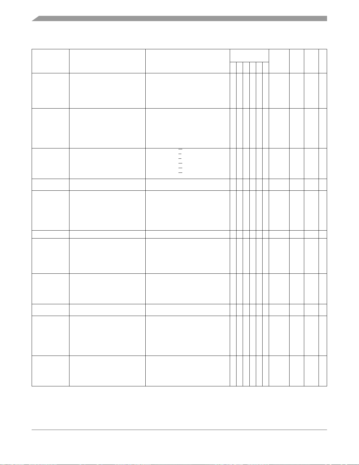
Central Processor Unit (CPU)
Source
Form
CLR opr
CLRA
CLRX
CLRH
CLR opr,X
CLR ,X
CLR opr,SP
CMP #opr
CMP opr
CMP opr
CMP opr,X
CMP opr,X
CMP ,X
CMP opr,SP
CMP opr,SP
COM
opr
COMA
COMX
COM opr,X
COM ,X
COM opr,SP
CPHX #opr
CPHX opr
CPX #opr
CPX opr
CPX opr
CPX ,X
CPX opr,X
CPX opr,X
CPX opr,SP
CPX opr,SP
DAA Decimal Adjust A
DBNZ opr,rel
DBNZA rel
DBNZX rel
DBNZ opr,X,rel
DBNZ X,rel
DBNZ opr,SP,rel
DEC opr
DECA
DECX
DEC opr,X
DEC ,X
DEC opr,SP
DIV Divide
EOR #opr
EOR opr
EOR opr
EOR opr,X
EOR opr,X
EOR ,X
EOR opr,SP
EOR opr,SP
INC opr
INCA
INCX
INC opr,X
INC ,X
INC opr,SP
Clear
Compare A with M (A) – (M) ––
Complement (One’s Complement)
Compare H:X with M (H:X) – (M:M + 1) ––
Compare X with M (X) – (M) ––
Decrement and Branch if Not Zero
Decrement
Exclusive OR M with A
Increment
Operation Description
Table 7-1. Instruction Set Summary (Sheet 3 of 6)
Effect
on CCR
VH I NZC
M ← $00
A ← $00
X ← $00
H ← $00
M ← $00
M ← $00
M ← $00
M ← (M
) = $FF – (M)
A ← (A
) = $FF – (M)
X ← (X) = $FF – (M)
M ← (M
) = $FF – (M)
M ← (M) = $FF – (M)
M ← (M) = $FF – (M)
(A)
10
A ← (A) – 1 or M ← (M) – 1 or X ← (X) – 1
PC ← (PC) + 3 + rel ? (result) ≠ 0
PC ← (PC) + 2 + rel ? (result) ≠ 0
PC ← (PC) + 2 + rel ? (result) ≠ 0
PC ← (PC) + 3 + rel ? (result) ≠ 0
PC ← (PC) + 2 + rel ? (result) ≠ 0
PC ← (PC) + 4 + rel ? (result) ≠ 0
M
← (M) – 1
A ← (A) – 1
X ← (X) – 1
M ← (M) – 1
M ← (M) – 1
M ← (M) – 1
A ← (H:A)/(X)
H ← Remainder
A ← (A
⊕ M)
M ← (M) + 1
A ← (A) + 1
X ← (X) + 1
M ← (M) + 1
M ← (M) + 1
M ← (M) + 1
0––01–
0––1
U–– INH 72 2
––––––
–––
––––INH 52 7
0–––
–––
DIR
INH
INH
INH
IX1
IX
SP1
IMM
DIR
EXT
IX2
IX1
IX
SP1
SP2
DIR
INH
INH
IX1
IX
SP1
IMM
DIR
IMM
DIR
EXT
IX2
IX1
IX
SP1
SP2
DIR
INH
INH
IX1
IX
SP1
DIR
INH
INH
IX1
IX
SP1
IMM
DIR
EXT
IX2
IX1
IX
SP1
SP2
DIR
INH
INH
IX1
IX
SP1
Address
Mode
Opcode
Operand
3F
dd
4F
5F
8C
6F
ff
7F
9E6F
ff
ii
A1
dd
B1
hh ll
C1
ee ff
D1
ff
E1
F1
ff
9EE1
ee ff
9ED1
33
dd
43
53
63
ff
73
9E63
ff
6575ii ii+1dd3
A3
ii
B3
dd
C3
hh ll
D3
ee ff
E3
ff
F3
9EE3
ff
9ED3
ee ff
3B
dd rr
4B
rr
5B
rr
6B
ff rr
7B
rr
9E6B
ff rr
3A
dd
4A
5A
6A
ff
7A
9E6A
ff
A8
ii
B8
dd
C8
hh ll
D8
ee ff
E8
ff
F8
9EE8
ff
9ED8
ee ff
3C
dd
4C
5C
6C
ff
7C
9E6C
ff
Cycles
3
1
1
1
3
2
4
2
3
4
4
3
2
4
5
4
1
1
4
3
5
4
2
3
4
4
3
2
4
5
5
3
3
5
4
6
4
1
1
4
3
5
2
3
4
4
3
2
4
5
4
1
1
4
3
5
MC68HC908QY/QT Family Data Sheet, Rev. 5
68 Freescale Semiconductor

Instruction Set Summary
Table 7-1. Instruction Set Summary (Sheet 4 of 6)
Effect
Source
Form
JMP opr
JMP opr
JMP opr,X
JMP opr,X
JMP ,X
JSR opr
JSR opr
JSR opr,X
JSR opr,X
JSR ,X
LDA #opr
LDA opr
LDA opr
LDA opr,X
LDA opr,X
LDA ,X
LDA opr,SP
LDA opr,SP
LDHX #opr
LDHX opr
LDX #opr
LDX opr
LDX opr
LDX opr,X
LDX opr,X
LDX ,X
LDX opr,SP
LDX opr,SP
LSL opr
LSLA
LSLX
LSL opr,X
LSL ,X
LSL opr,SP
LSR opr
LSRA
LSRX
LSR opr,X
LSR ,X
LSR opr,SP
MOV opr,opr
MOV opr,X+
MOV #opr,opr
MOV X+,opr
MUL Unsigned multiply X:A ← (X) × (A) –0–––0INH 42 5
NEG opr
NEGA
NEGX
NEG opr,X
NEG ,X
NEG opr,SP
NOP No Operation None ––––––INH 9D 1
NSA Nibble Swap A A ← (A[3:0]:A[7:4]) ––––––INH 62 3
ORA #opr
ORA opr
ORA opr
ORA opr,X
ORA opr,X
ORA ,X
ORA opr,SP
ORA opr,SP
PSHA Push A onto Stack Push (A); SP ← (SP) – 1 ––––––INH 87 2
PSHH Push H onto Stack Push (H); SP ← (SP) – 1 ––––––INH 8B 2
PSHX Push X onto Stack Push (X); SP ← (SP) – 1 ––––––INH 89 2
Jump PC ← Jump Address ––––––
Jump to Subroutine
Load A from M A ← (M) 0–––
Load H:X from M H:X ← (M:M + 1) 0–––
Load X from M X ← (M) 0–––
Logical Shift Left
(Same as ASL)
Logical Shift Right ––0
Move
Negate (Two’s Complement)
Inclusive OR A and M A ← (A) | (M) 0 – – –
Operation Description
PC ← (PC) + n (n = 1, 2, or 3)
Push (PCL); SP ← (SP) – 1
Push (PCH); SP ← (SP) – 1
PC ← Unconditional Address
C
b7
b7
(M)
Destination
H:X ← (H:X) + 1 (IX+D, DIX+)
M ← –(M) = $00 – (M)
A ← –(A) = $00 – (A)
X ← –(X) = $00 – (X)
M ← –(M) = $00 – (M)
M ← –(M) = $00 – (M)
← (M)
0
b0
C0
b0
Source
on CCR
VH I NZC
––––––
––
0–––
––
DIR
EXT
IX2
IX1
IX
DIR
EXT
IX2
IX1
IX
IMM
DIR
EXT
IX2
IX1
IX
SP1
SP2
IMM
DIR
IMM
DIR
EXT
IX2
IX1
IX
SP1
SP2
DIR
INH
INH
IX1
IX
SP1
DIR
INH
INH
IX1
IX
SP1
DD
DIX+
IMD
IX+D
DIR
INH
INH
IX1
IX
SP1
IMM
DIR
EXT
IX2
IX1
IX
SP1
SP2
Address
Mode
Opcode
Operand
BC
dd
CC
hh ll
DC
ee ff
EC
ff
FC
BD
dd
CD
hh ll
DD
ee ff
ED
ff
FD
A6
ii
B6
dd
C6
hh ll
D6
ee ff
E6
ff
F6
9EE6
ff
9ED6
ee ff
4555ii jjdd3
AE
ii
BE
dd
CE
hh ll
DE
ee ff
EE
ff
FE
9EEE
ff
9EDE
ee ff
38
dd
48
58
68
ff
78
9E68
ff
34
dd
44
54
64
ff
74
9E64
ff
4E
dd dd
5E
dd
6E
ii dd
7E
dd
30
dd
40
50
60
ff
70
9E60
ff
AA
ii
BA
dd
hh ll
CA
ee ff
DA
ff
EA
FA
ff
9EEA
ee ff
9EDA
2
3
4
3
2
4
5
6
5
4
2
3
4
4
3
2
4
5
4
2
3
4
4
3
2
4
5
4
1
1
4
3
5
4
1
1
4
3
5
5
4
4
4
4
1
1
4
3
5
2
3
4
4
3
2
4
5
Cycles
MC68HC908QY/QT Family Data Sheet, Rev. 5
Freescale Semiconductor 69

Central Processor Unit (CPU)
Table 7-1. Instruction Set Summary (Sheet 5 of 6)
Effect
Source
Form
PULA Pull A from Stack SP ← (SP + 1); Pull (A) ––––––INH 86 2
PULH Pull H from Stack SP ← (SP + 1); Pull (H) ––––––INH 8A 2
PULX Pull X from Stack SP ← (SP + 1); Pull (X) ––––––INH 88 2
ROL opr
ROLA
ROLX
ROL opr,X
ROL ,X
ROL opr,SP
ROR opr
RORA
RORX
ROR opr,X
ROR ,X
ROR opr,SP
RSP Reset Stack Pointer SP ← $FF ––––––INH 9C 1
RTI Return from Interrupt
RTS Return from Subroutine
SBC #opr
SBC opr
SBC opr
SBC opr,X
SBC opr,X
SBC ,X
SBC opr,SP
SBC opr,SP
SEC Set Carry Bit C ← 1 –––––1INH 99 1
SEI Set Interrupt Mask I ← 1 ––1–––INH 9B 2
STA opr
STA opr
STA opr,X
STA opr,X
STA ,X
STA opr,SP
STA opr,SP
STHX opr Store H:X in M (M:M + 1) ← (H:X) 0 – – – DIR 35 dd 4
STOP
STX opr
STX opr
STX opr,X
STX opr,X
STX ,X
STX opr,SP
STX opr,SP
SUB #opr
SUB opr
SUB opr
SUB opr,X
SUB opr,X
SUB ,X
SUB opr,SP
SUB opr,SP
Rotate Left through Carry ––
Rotate Right through Carry ––
Subtract with Carry A ← (A) – (M) – (C) ––
Store A in M M ← (A) 0–––
Enable Interrupts, Stop Processing,
Refer to MCU Documentation
Store X in M M ← (X) 0–––
Subtract A ← (A) – (M) ––
Operation Description
C
b7
b7
SP ← (SP) + 1; Pull (CCR)
SP ← (SP) + 1; Pull (A)
SP ← (SP) + 1; Pull (X)
SP ←
(SP) + 1; Pull (PCH)
SP ← (SP) + 1; Pull (PCL)
SP ← SP + 1; Pull (PCH)
SP ← SP + 1; Pull (PCL)
I ← 0; Stop Processing ––0–––INH 8E 1
b0
b0
C
on CCR
VH I NZC
INH 80 7
––––––INH 81 4
DIR
INH
INH
IX1
IX
SP1
DIR
INH
INH
IX1
IX
SP1
IMM
DIR
EXT
IX2
IX1
IX
SP1
SP2
DIR
EXT
IX2
IX1
IX
SP1
SP2
DIR
EXT
IX2
IX1
IX
SP1
SP2
IMM
DIR
EXT
IX2
IX1
IX
SP1
SP2
Address
Mode
9E69
9E66
9EE2
9ED2
9EE7
9ED7
9EEF
9EDF
9EE0
9ED0
39
49
59
69
79
36
46
56
66
76
A2
B2
C2
D2
E2
F2
B7
C7
D7
E7
F7
BF
CF
DF
EF
FF
A0
B0
C0
D0
E0
F0
Opcode
dd
ff
ff
dd
ff
ff
ii
dd
hh ll
ee ff
ff
ff
ee ff
dd
hh ll
ee ff
ff
ff
ee ff
dd
hh ll
ee ff
ff
ff
ee ff
ii
dd
hh ll
ee ff
ff
ff
ee ff
Operand
Cycles
4
1
1
4
3
5
4
1
1
4
3
5
2
3
4
4
3
2
4
5
3
4
4
3
2
4
5
3
4
4
3
2
4
5
2
3
4
4
3
2
4
5
MC68HC908QY/QT Family Data Sheet, Rev. 5
70 Freescale Semiconductor
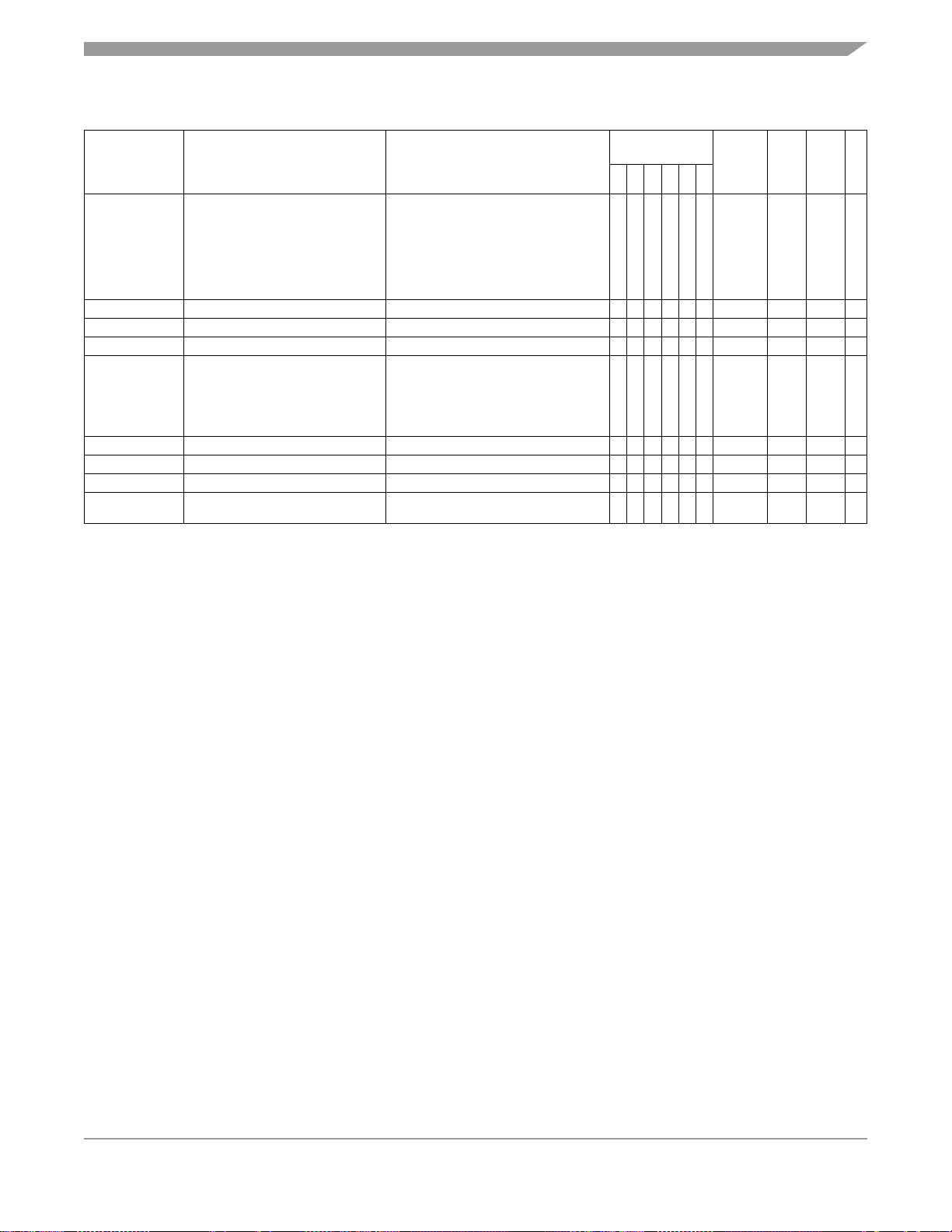
Opcode Map
Table 7-1. Instruction Set Summary (Sheet 6 of 6)
Effect
Source
Form
SWI Software Interrupt
TAP Transfer A to CCR CCR ← (A) INH 84 2
TAX Transfer A to X X ← (A) ––––––INH 97 1
TPA Transfer CCR to A A ← (CCR) ––––––INH 85 1
TST opr
TSTA
TSTX
TST opr,X
TST ,X
TST opr,SP
TSX Transfer SP to H:X H:X ← (SP) + 1 ––––––INH 95 2
TXA Transfer X to A A ← (X) ––––––INH 9F 1
TXS Transfer H:X to SP (SP) ← (H:X) – 1 ––––––INH 94 2
WAIT Enable Interrupts; Wait for Interrupt
A Accumulator n Any bit
C Carry/borrow bit opr Operand (one or two bytes)
CCR Condition code register PC Program counter
dd Direct address of operand PCH Program counter high byte
dd rr Direct address of operand and relative offset of branch instruction PCL Program counter low byte
DD Direct to direct addressing mode REL Relative addressing mode
DIR Direct addressing mode rel Relative program counter offset byte
DIX+ Direct to indexed with post increment addressing mode rr Relative program counter offset byte
ee ff High and low bytes of offset in indexed, 16-bit offset addressing SP1 Stack pointer, 8-bit offset addressing mode
EXT Extended addressing mode SP2 Stack pointer 16-bit offset addressing mode
ff Offset byte in indexed, 8-bit offset addressing SP Stack pointer
H Half-carry bit U Undefined
H Index register high byte V Overflow bit
hh ll High and low bytes of operand address in extended addressing X Index register low byte
I Interrupt mask Z Zero bit
ii Immediate operand byte & Logical AND
IMD Immediate source to direct destination addressing mode | Logical OR
IMM Immediate addressing mode
INH Inherent addressing mode ( ) Contents of
IX Indexed, no offset addressing mode –( ) Negation (two’s complement)
IX+ Indexed, no offset, post increment addressing mode # Immediate value
IX+D Indexed with post increment to direct addressing mode
IX1 Indexed, 8-bit offset addressing mode ← Loaded with
IX1+ Indexed, 8-bit offset, post increment addressing mode ? If
IX2 Indexed, 16-bit offset addressing mode : Concatenated with
M Memory location Set or cleared
N Negative bit — Not affected
Test for Negative or Zero (A) – $00 or (X) – $00 or (M) – $00 0 – – –
Operation Description
PC ← (PC) + 1; Push (PCL)
SP ← (SP) – 1; Push (PCH)
SP ← (SP) – 1; Push (X)
SP ← (SP) – 1; Push (A)
SP ← (SP) – 1; Push (CCR)
SP ← (SP) – 1; I ← 1
PCH ← Interrupt Vector High Byte
PCL ← Interrupt Vector Low Byte
I bit ← 0; Inhibit CPU clocking
until interrupted
⊕ Logical EXCLUSIVE OR
« Sign extend
on CCR
VH I NZC
––1–––INH 83 9
––0–––INH 8F 1
DIR
INH
INH
IX1
IX
SP1
Address
Mode
9E6D
3D
4D
5D
6D
7D
Opcode
dd
ff
ff
Operand
3
1
1
3
2
4
Cycles
7.8 Opcode Map
See Table 7-2.
MC68HC908QY/QT Family Data Sheet, Rev. 5
Freescale Semiconductor 71

Central Processor Unit (CPU)
2
SUB
1IX
4
SUB
3 SP1
3
SUB
2IX1
5
SUB
4 SP2
4
SUB
3IX2
4
SUB
3EXT
3
SUB
2DIR
2
SUB
2IMM
3
BGE
2REL
7
RTI
1INH
3
NEG
1IX
5
NEG
4
1
1
4
3
4
3 SP1
NEG
2IX1
NEGX
1INH
NEGA
1INH
NEG
2DIR
BRA
2REL
BSET0
2DIR
Table 7-2. Opcode Map
2
4
3
5
4
4
3
2
3
4
4
6
5
4
4
5
3
4
CMP
1IX
CMP
3 SP1
CMP
2IX1
CMP
4 SP2
CMP
3IX2
CMP
3EXT
CMP
2DIR
CMP
2IMM
BLT
2REL
RTS
1INH
CBEQ
2IX+
CBEQ
4 SP1
CBEQ
3IX1+
CBEQX
3IMM
CBEQA
3IMM
CBEQ
3DIR
BRN
2REL
BCLR0
2DIR
2
4
3
5
4
4
3
2
3
2
3
7
5
3
4
SBC
SBC
SBC
SBC
SBC
SBC
SBC
SBC
BGT
DAA
NSA
DIV
MUL
BHI
BSET1
1IX
3 SP1
2IX1
4 SP2
3IX2
3EXT
2DIR
2IMM
2REL
1INH
1INH
1INH
1INH
2REL
2DIR
2
CPX
4
CPX
3
CPX
5
CPX
4
CPX
4
CPX
3
CPX
2
CPX
3
BLE
9
SWI
3
COM
5
COM
4
COM
1
COMX
1
COMA
4
COM
3
BLS
4
BCLR1
1IX
3 SP1
2IX1
4 SP2
3IX2
3EXT
2DIR
2IMM
2REL
1INH
1IX
3 SP1
2IX1
1INH
1INH
2DIR
2REL
2DIR
2
4
3
5
4
4
3
2
2
2
3
5
4
1
1
4
3
4
AND
1IX
AND
3 SP1
AND
2IX1
AND
4 SP2
AND
3IX2
AND
3EXT
AND
2DIR
AND
2IMM
TXS
1INH
TA P
1INH
LSR
1IX
LSR
3 SP1
LSR
2IX1
LSRX
1INH
LSRA
1INH
LSR
2DIR
BCC
2REL
BSET2
2DIR
2
4
3
5
4
4
3
2
2
1
4
3
4
3
4
3
4
BIT
1IX
BIT
3 SP1
BIT
2IX1
BIT
4 SP2
BIT
3IX2
BIT
3EXT
BIT
2DIR
BIT
2IMM
TSX
1INH
TPA
1INH
CPHX
2DIR
CPHX
3IMM
LDHX
2DIR
LDHX
3IMM
STHX
2DIR
BCS
2REL
BCLR2
2DIR
2
4
3
5
4
4
3
2
2
3
5
4
1
1
4
3
4
LDA
1IX
LDA
3 SP1
LDA
2IX1
LDA
4 SP2
LDA
3IX2
LDA
3EXT
LDA
2DIR
LDA
2IMM
PULA
1INH
ROR
1IX
ROR
3 SP1
ROR
2IX1
RORX
1INH
RORA
1INH
ROR
2DIR
BNE
2REL
BSET3
2DIR
2
4
3
5
4
4
3
2
1
2
3
5
4
1
1
4
3
4
STA
1IX
STA
3 SP1
STA
2IX1
STA
4 SP2
STA
3IX2
STA
3EXT
STA
2DIR
AIS
2IMM
TA X
1INH
PSHA
1INH
ASR
1IX
ASR
3 SP1
ASR
2IX1
ASRX
1INH
ASRA
1INH
ASR
2DIR
BEQ
2REL
BCLR3
2DIR
2
4
3
5
4
4
3
2
1
2
3
5
4
1
1
4
3
4
EOR
1IX
EOR
3 SP1
EOR
2IX1
EOR
4 SP2
EOR
3IX2
EOR
3EXT
EOR
2DIR
EOR
2IMM
CLC
1INH
PULX
1INH
LSL
1IX
LSL
3 SP1
LSL
2IX1
LSLX
1INH
LSLA
1INH
LSL
2DIR
BHCC
2REL
BSET4
2DIR
2
ADC
4
ADC
3
ADC
5
ADC
4
ADC
4
ADC
3
ADC
2
ADC
1
SEC
2
PSHX
3
ROL
5
ROL
4
ROL
1
ROLX
1
ROLA
4
ROL
3
BHCS
4
BCLR4
1IX
3 SP1
2IX1
4 SP2
3IX2
3EXT
2DIR
2IMM
1INH
1INH
1IX
3 SP1
2IX1
1INH
1INH
2DIR
2REL
2DIR
2
4
3
5
4
4
3
2
2
2
3
5
4
1
1
4
3
4
ORA
1IX
ORA
3 SP1
ORA
2IX1
ORA
4 SP2
ORA
3IX2
ORA
3EXT
ORA
2DIR
ORA
2IMM
CLI
1INH
PULH
1INH
DEC
1IX
DEC
3 SP1
DEC
2IX1
DECX
1INH
DECA
1INH
DEC
2DIR
BPL
2REL
BSET5
2DIR
2
ADD
4
ADD
3
ADD
5
ADD
4
ADD
4
ADD
3
ADD
2
ADD
2
SEI
2
PSHH
4
DBNZ
6
DBNZ
5
DBNZ
3
DBNZX
3
DBNZA
5
DBNZ
3
BMI
4
BCLR5
1IX
3 SP1
2IX1
4 SP2
3IX2
3EXT
2DIR
2IMM
1INH
1INH
2IX
4 SP1
3IX1
2INH
2INH
3DIR
2REL
2DIR
2
3
4
3
2
1
1
3
5
4
1
1
4
3
4
JMP
1IX
JMP
2IX1
JMP
3IX2
JMP
3EXT
JMP
2DIR
RSP
1INH
CLRH
1INH
INC
1IX
INC
3 SP1
INC
2IX1
INCX
1INH
INCA
1INH
INC
2DIR
BMC
2REL
BSET6
2DIR
4
5
6
5
4
4
1
2
4
3
1
1
3
3
4
JSR
1IX
JSR
2IX1
JSR
3IX2
JSR
3EXT
JSR
2DIR
BSR
2REL
NOP
1INH
TST
1IX
TST
3 SP1
TST
2IX1
TSTX
1INH
TSTA
1INH
TST
2DIR
BMS
2REL
BCLR6
2DIR
2
2
STX
LDX
4
LDX
3
LDX
5
LDX
4
LDX
4
LDX
3
LDX
2
LDX
1
STOP
4
MOV
4
MOV
4
MOV
5
MOV
3
BIL
4
BSET7
1IX
3 SP1
2IX1
4 SP2
3IX2
3EXT
2DIR
2IMM
*
1INH
2IX+D
3IMD
2DIX+
3DD
2REL
2DIR
4
3
5
4
4
3
2
1
1
2
4
3
1
1
3
3
4
1IX
STX
3 SP1
STX
2IX1
STX
4 SP2
STX
3IX2
STX
3EXT
STX
2DIR
AIX
2IMM
TXA
1INH
WAIT
1INH
CLR
1IX
CLR
3 SP1
CLR
2IX1
CLRX
1INH
CLRA
1INH
CLR
2DIR
BIH
2REL
BCLR7
2DIR
MSB
0 High Byte of Opcode in Hexadecimal
LSB
Cycles
Opcode Mnemonic
Number of Bytes / Addressing Mode
5
BRSET0
3DIR
Low Byte of Opcode in Hexadecimal 0
5
BRCLR0
1
3DIR
5
BRSET1
3DIR
2
5
0 1 2 3 4 5 6 9E6 7 8 9 A B C D 9ED E 9EE F
DIR DIR REL DIR INH INH IX1 SP1 IX INH INH IMM DIR EXT IX2 SP2 IX1 SP1 IX
Bit Manipulation Branch Read-Modify-Write Control Register/Memory
MSB
BRSET0
3DIR
0
LSB
5
5
BRSET2
3DIR
BRCLR1
3DIR
4
3
5
5
BRSET3
3DIR
BRCLR2
3DIR
6
5
5
5
BRSET4
3DIR
BRCLR3
3DIR
8
7
5
BRSET5
A
3DIR
5
5
5
BRSET6
BRCLR5
3DIR
3DIR
BRCLR6
3DIR
B
C
D
5
BRCLR4
3DIR
9
5
5
BRSET7
BRCLR7
3DIR
3DIR
F
E
INH Inherent REL Relative SP1 Stack Pointer, 8-Bit Offset
IMM Immediate IX Indexed, No Offset SP2 Stack Pointer, 16-Bit Offset
DIR Direct IX1 Indexed, 8-Bit Offset IX+ Indexed, No Offset with
EXT Extended IX2 Indexed, 16-Bit Offset Post Increment
DD Direct-Direct IMD Immediate-Direct IX1+ Indexed, 1-Byte Offset with
IX+D Indexed-Direct DIX+ Direct-Indexed Post Increment
*Pre-byte for stack pointer indexed instructions
MC68HC908QY/QT Family Data Sheet, Rev. 5
72 Freescale Semiconductor

Chapter 8
External Interrupt (IRQ)
8.1 Introduction
The IRQ pin (external interrupt), shared with PTA2 (general purpose input) and keyboard interrupt (KBI),
provides a maskable interrupt input
8.2 Features
Features of the IRQ module include the following:
• External interrupt pin, IRQ
•IRQ interrupt control bits
• Programmable edge-only or edge and level interrupt sensitivity
• Automatic interrupt acknowledge
• Selectable internal pullup resistor
8.3 Functional Description
IRQ pin functionality is enabled by setting configuration register 2 (CONFIG2) IRQEN bit accordingly. A
zero disables the IRQ function and PTA2 will assume the other shared functionalities. A one enables the
IRQ function.
A low level applied to the external interrupt request (IRQ
Figure 8-2 shows the structure of the IRQ module.
Interrupt signals on the IRQ
following actions occurs:
• IRQ vector fetch — An IRQ vector fetch automatically generates an interrupt acknowledge signal
that clears the IRQ latch.
• Software clear — Software can clear the IRQ latch by writing a 1 to the ACK bit in the interrupt
status and control register (INTSCR).
• Reset — A reset automatically clears the IRQ latch.
The external interrupt pin is falling-edge-triggered out of reset and is software-configurable to be either
falling-edge or falling-edge and low-level triggered. The MODE bit in INTSCR controls the triggering
sensitivity of the IRQ
pin.
pin are latched into the IRQ latch. The IRQ latch remains set until one of the
) pin can latch a CPU interrupt request.
MC68HC908QY/QT Family Data Sheet, Rev. 5
Freescale Semiconductor 73

External Interrupt (IRQ)
PTA0/AD0/TCH0/KBI0
PTA1/AD1/TCH1/KBI1
PTA2/IRQ
PTA4/OSC2/AD2/KBI4
PTA5/OSC1/AD3/KBI5
/KBI2/TCLK
PTA3/RST
/KBI3
PTB0
PTB1
PTB2
PTB3
PTB4
PTB5
PTB6
PTB7
POWER SUPPLY
PTA
PTB
8-BIT ADC
128 BYTES RAM
DDRA
DDRB
V
DD
V
SS
M68HC08 CPU
MC68HC908QY4 AND MC68HC908QT4
4096 BYTES
MC68HC908QY2, MC68HC908QY1,
MC68HC908QT2, AND MC68HC908QT1:
1536 BYTES
USER FLASH
CLOCK
GENERATOR
(OSCILLATOR)
SYSTEM INTEGRATION
MODULE
SINGLE INTERRUPT
MODULE
BREAK
MODULE
POWER-ON RESET
MODULE
KEYBOARD INTERRUPT
MODULE
16-BIT TIMER
MODULE
COP
MODULE
MONITOR ROM
RST, IRQ: Pins have internal (about 30K Ohms) pull up
PTA[0:5]: High current sink and source capability
PTA[0:5]: Pins have programmable keyboard interrupt and pull up
PTB[0:7]: Not available on 8-pin devices – MC68HC908QT1, MC68HC908QT2, and MC68HC908QT4 (see note in
12.1 Introduction)
ADC: Not available on the MC68HC908QY1 and MC68HC908QT1
Figure 8-1. Block Diagram Highlighting IRQ Block and Pins
When set, the IMASK bit in INTSCR masks the IRQ
interrupt request. A latched interrupt request is not
presented to the interrupt priority logic unless IMASK is clear.
NOTE
The interrupt mask (I) in the condition code register (CCR) masks all
interrupt requests, including the IRQ
A falling edge on the IRQ
pin can latch an interrupt request into the IRQ latch. An IRQ vector fetch,
interrupt request.
software clear, or reset clears the IRQ latch.
MC68HC908QY/QT Family Data Sheet, Rev. 5
74 Freescale Semiconductor

INTERNAL ADDRESS BUS
IRQPUD
IRQ
ACK
RESET
VECTOR
FETCH
DECODER
V
DD
INTERNAL
PULLUP
DEVICE
V
DD
CLR
DQ
CK
LATCH
MODE
IRQ
IMASK
SYNCHRO-
NIZER
HIGH
VOLTAGE
DETECT
Figure 8-2. IRQ Module Block Diagram
Functional Description
TO CPU FOR
BIL/BIH
INSTRUCTIONS
IRQF
IRQ
INTERRUPT
REQUEST
TO MODE
SELECT
LOGIC
8.3.1 MODE = 1
If the MODE bit is set, the IRQ pin is both falling edge sensitive and low level sensitive. With MODE set,
both of the following actions must occur to clear the IRQ
• Return of the IRQ
pin to a high level. As long as the IRQ pin is low, the IRQ request remains active.
interrupt request:
• IRQ vector fetch or software clear. An IRQ vector fetch generates an interrupt acknowledge signal
to clear the IRQ latch. Software generates the interrupt acknowledge signal by writing a 1 to ACK
in INTSCR. The ACK bit is useful in applications that poll the IRQ
pin and require software to clear
the IRQ latch. Writing to ACK prior to leaving an interrupt service routine can also prevent spurious
interrupts due to noise. Setting ACK does not affect subsequent transitions on the IRQ
pin. A falling
edge that occurs after writing to ACK latches another interrupt request. If the IRQ mask bit, IMASK,
is clear, the CPU loads the program counter with the IRQ vector address.
The IRQ vector fetch or software clear and the return of the IRQ
The interrupt request remains pending as long as the IRQ
pin to a high level may occur in any order.
pin is low. A reset will clear the IRQ latch and
the MODE control bit, thereby clearing the interrupt even if the pin stays low.
Use the BIH or BIL instruction to read the logic level on the IRQ
pin.
8.3.2 MODE = 0
If the MODE bit is clear, the IRQ pin is falling edge sensitive only. With MODE clear, an IRQ vector fetch
or software clear immediately clears the IRQ latch.
The IRQF bit in INTSCR can be read to check for pending interrupts. The IRQF bit is not affected by
IMASK, which makes it useful in applications where polling is preferred.
NOTE
When using the level-sensitive interrupt trigger, avoid false IRQ interrupts
by masking interrupt requests in the interrupt routine.
MC68HC908QY/QT Family Data Sheet, Rev. 5
Freescale Semiconductor 75

External Interrupt (IRQ)
8.4 Interrupts
The following IRQ source can generate interrupt requests:
• Interrupt flag (IRQF) — The IRQF bit is set when the IRQ
The IRQ interrupt mask bit, IMASK, is used to enable or disable IRQ interrupt requests.
pin is asserted based on the IRQ mode.
8.5 Low-Power Modes
The WAIT and STOP instructions put the MCU in low power-consumption standby modes.
8.5.1 Wait Mode
The IRQ module remains active in wait mode. Clearing IMASK in INTSCR enables IRQ interrupt requests
to bring the MCU out of wait mode.
8.5.2 Stop Mode
The IRQ module remains active in stop mode. Clearing IMASK in INTSCR enables IRQ interrupt requests
to bring the MCU out of stop mode.
8.6 IRQ Module During Break Interrupts
The system integration module (SIM) controls whether status bits in other modules can be cleared during
the break state. The BCFE bit in the break flag control register (BFCR) enables software to clear status
bits during the break state. See Chapter 13 System Integration Module (SIM).
To allow software to clear status bits during a break interrupt, write a 1 to the BCFE bit. If a status bit is
cleared during the break state, it remains cleared when the MCU exits the break state.
To protect status bits during the break state, write a 0 to BCFE. With BCFE cleared (its default state),
software can read and write registers during the break state without affecting status bits. Some status bits
have a two-step read/write clearing procedure. If software does the first step on such a bit before the
break, the bit cannot change during the break state as long as BCFE is cleared. After the break, doing the
second step clears the status bit.
8.7 I/O Signals
The IRQ module shares its pin with the keyboard interrupt, input/output ports, and timer interface
modules.
NOTE
When the IRQ
instructions can be used to read the logic level on the IRQ
function is disabled, these instructions will behave as if the IRQ
logic 1, regardless of the actual level on the pin. Conversely, when the IRQ
function is enabled, bit 2 of the port A data register will always read a 0.
function is enabled in the CONFIG2 register, the BIH and BIL
pin. If the IRQ
pin is a
When using the level-sensitive interrupt trigger, avoid false interrupts by
masking interrupt requests in the interrupt routine. An internal pullup
resistor to V
the IRQPUD bit in the CONFIG2 register ($001E).
76 Freescale Semiconductor
is connected to the IRQ pin; this can be disabled by setting
DD
MC68HC908QY/QT Family Data Sheet, Rev. 5

Registers
8.7.1 IRQ Input Pins (IRQ)
The IRQ pin provides a maskable external interrupt source. The IRQ pin contains an internal pullup
device.
8.8 Registers
The IRQ status and control register (INTSCR) controls and monitors operation of the IRQ module. See
Chapter 5 Configuration Register (CONFIG).
The INTSCR has the following functions:
• Shows the state of the IRQ flag
• Clears the IRQ latch
• Masks the IRQ interrupt request
• Controls triggering sensitivity of the IRQ
Address: $001D
Bit 7654321Bit 0
Read:0000IRQF0
Write: ACK
Reset:00000000
= Unimplemented
interrupt pin
IMASK MODE
Figure 8-3. IRQ Status and Control Register (INTSCR)
IRQF — IRQ Flag
This read-only status bit is set when the IRQ interrupt is pending.
1 = IRQ
0 = IRQ
interrupt pending
interrupt not pending
ACK — IRQ Interrupt Request Acknowledge Bit
Writing a 1 to this write-only bit clears the IRQ latch. ACK always reads as 0.
IMASK — IRQ Interrupt Mask Bit
Writing a 1 to this read/write bit disables the IRQ interrupt request.
1 = IRQ interrupt request disabled
0 = IRQ interrupt request enabled
MODE — IRQ Edge/Level Select Bit
This read/write bit controls the triggering sensitivity of the IRQ
1 = IRQ
0 = IRQ
interrupt request on falling edges and low levels
interrupt request on falling edges only
pin.
MC68HC908QY/QT Family Data Sheet, Rev. 5
Freescale Semiconductor 77

External Interrupt (IRQ)
MC68HC908QY/QT Family Data Sheet, Rev. 5
78 Freescale Semiconductor

Chapter 9
Keyboard Interrupt Module (KBI)
9.1 Introduction
The keyboard interrupt module (KBI) provides six independently maskable external interrupts, which are
accessible via the PTA0–PTA5 pins.
9.2 Features
Features of the keyboard interrupt module include:
• Six keyboard interrupt pins with separate keyboard interrupt enable bits and one keyboard interrupt
mask
• Software configurable pullup device if input pin is configured as input port bit
• Programmable edge-only or edge and level interrupt sensitivity
• Exit from low-power modes
9.3 Functional Description
The keyboard interrupt module controls the enabling/disabling of interrupt functions on the six port A pins.
These six pins can be enabled/disabled independently of each other. Refer to Figure 9-2.
9.3.1 Keyboard Operation
Writing to the KBIE0–KBIE5 bits in the keyboard interrupt enable register (KBIER) independently enables
or disables each port A pin as a keyboard interrupt pin. Enabling a keyboard interrupt pin in port A also
enables its internal pullup device irrespective of PTAPUEx bits in the port A input pullup enable register
(see 12.2.3 Port A Input Pullup Enable Register). A logic 0 applied to an enabled keyboard interrupt pin
latches a keyboard interrupt request.
A keyboard interrupt is latched when one or more keyboard interrupt inputs goes low after all were high.
The MODEK bit in the keyboard status and control register controls the triggering mode of the keyboard
interrupt.
• If the keyboard interrupt is edge-sensitive only, a falling edge on a keyboard interrupt input does
not latch an interrupt request if another keyboard pin is already low. To prevent losing an interrupt
request on one input because another input is still low, software can disable the latter input while
it is low.
• If the keyboard interrupt is falling edge and low-level sensitive, an interrupt request is present as
long as any keyboard interrupt input is low.
MC68HC908QY/QT Family Data Sheet, Rev. 5
Freescale Semiconductor 79

Keyboard Interrupt Module (KBI)
PTA0/AD0/TCH0/KBI0
PTA1/AD1/TCH1/KBI1
PTA2/IRQ
/KBI2/TCLK
PTA3/RST
PTA4/OSC2/AD2/KBI4
PTA5/OSC1/AD3/KBI5
/KBI3
PTB0
PTB1
PTB2
PTB3
PTB4
PTB5
PTB6
PTB7
POWER SUPPLY
PTA
PTB
8-BIT ADC
128 BYTES RAM
DDRA
DDRB
V
DD
V
SS
M68HC08 CPU
MC68HC908QY4 AND MC68HC908QT4
4096 BYTES
MC68HC908QY2, MC68HC908QY1,
MC68HC908QT2, AND MC68HC908QT1:
1536 BYTES
USER FLASH
CLOCK
GENERATOR
(OSCILLATOR)
SYSTEM INTEGRATION
MODULE
SINGLE INTERRUPT
MODULE
BREAK
MODULE
POWER-ON RESET
MODULE
KEYBOARD INTERRUPT
MODULE
16-BIT TIMER
MODULE
COP
MODULE
MONITOR ROM
RST, IRQ: Pins have internal (about 30K Ohms) pull up
PTA[0:5]: High current sink and source capability
PTA[0:5]: Pins have programmable keyboard interrupt and pull up
PTB[0:7]: Not available on 8-pin devices – MC68HC908QT1, MC68HC908QT2, and MC68HC908QT4 (see note in
12.1 Introduction)
ADC: Not available on the MC68HC908QY1 and MC68HC908QT1
Figure 9-1. Block Diagram Highlighting KBI Block and Pins
MC68HC908QY/QT Family Data Sheet, Rev. 5
80 Freescale Semiconductor

KBI0
KBIE0
TO PULLUP ENABLE
KBI5
KBIE5
TO PULLUP ENABLE
Functional Description
INTERNAL BUS
VECTOR FETCH
DECODER
ACKK
V
DD
.
.
CLR
DQ
CK
.
KEYBOARD
INTERRUPT FF
MODEK
RESET
SYNCHRONIZER
IMASKK
KEYF
KEYBOARD
INTERRUPT
REQUEST
AWUIREQ
(1)
1. For AWUGEN logic refer to Figure 4-1. Auto Wakeup Interrupt Request Generation Logic.
Figure 9-2. Keyboard Interrupt Block Diagram
If the MODEK bit is set, the keyboard interrupt inputs are both falling edge and low-level sensitive, and
both of the following actions must occur to clear a keyboard interrupt request:
• Vector fetch or software clear — A vector fetch generates an interrupt acknowledge signal to clear
the interrupt request. Software may generate the interrupt acknowledge signal by writing a 1 to the
ACKK bit in the keyboard status and control register (KBSCR). The ACKK bit is useful in
applications that poll the keyboard interrupt inputs and require software to clear the keyboard
interrupt request. Writing to the ACKK bit prior to leaving an interrupt service routine can also
prevent spurious interrupts due to noise. Setting ACKK does not affect subsequent transitions on
the keyboard interrupt inputs. A falling edge that occurs after writing to the ACKK bit latches
another interrupt request. If the keyboard interrupt mask bit, IMASKK, is clear, the central
processor unit (CPU) loads the program counter with the vector address at locations $FFE0 and
$FFE1.
• Return of all enabled keyboard interrupt inputs to logic 1 — As long as any enabled keyboard
interrupt pin is at logic 0, the keyboard interrupt remains set. The auto wakeup interrupt input,
AWUIREQ, will be cleared only by writing to ACKK bit in KBSCR or reset.
The vector fetch or software clear and the return of all enabled keyboard interrupt pins to logic 1 may occur
in any order.
If the MODEK bit is clear, the keyboard interrupt pin is falling-edge sensitive only. With MODEK clear, a
vector fetch or software clear immediately clears the keyboard interrupt request.
Reset clears the keyboard interrupt request and the MODEK bit, clearing the interrupt request even if a
keyboard interrupt input stays at logic 0.
The keyboard flag bit (KEYF) in the keyboard status and control register can be used to see if a pending
interrupt exists. The KEYF bit is not affected by the keyboard interrupt mask bit (IMASKK) which makes
it useful in applications where polling is preferred.
MC68HC908QY/QT Family Data Sheet, Rev. 5
Freescale Semiconductor 81

Keyboard Interrupt Module (KBI)
To determine the logic level on a keyboard interrupt pin, use the data direction register to configure the
pin as an input and then read the data register.
NOTE
Setting a keyboard interrupt enable bit (KBIEx) forces the corresponding
keyboard interrupt pin to be an input, overriding the data direction register.
However, the data direction register bit must be a 0 for software to read the
pin.
9.3.2 Keyboard Initialization
When a keyboard interrupt pin is enabled, it takes time for the internal pullup to reach a logic 1. Therefore
a false interrupt can occur as soon as the pin is enabled.
To prevent a false interrupt on keyboard initialization:
1. Mask keyboard interrupts by setting the IMASKK bit in the keyboard status and control register.
2. Enable the KBI pins by setting the appropriate KBIEx bits in the keyboard interrupt enable register.
3. Write to the ACKK bit in the keyboard status and control register to clear any false interrupts.
4. Clear the IMASKK bit.
An interrupt signal on an edge-triggered pin can be acknowledged immediately after enabling the pin. An
interrupt signal on an edge- and level-triggered interrupt pin must be acknowledged after a delay that
depends on the external load.
Another way to avoid a false interrupt:
1. Configure the keyboard pins as outputs by setting the appropriate DDRA bits in the data direction
register A.
2. Write 1s to the appropriate port A data register bits.
3. Enable the KBI pins by setting the appropriate KBIEx bits in the keyboard interrupt enable register.
9.4 Wait Mode
The keyboard module remains active in wait mode. Clearing the IMASKK bit in the keyboard status and
control register enables keyboard interrupt requests to bring the MCU out of wait mode.
9.5 Stop Mode
The keyboard module remains active in stop mode. Clearing the IMASKK bit in the keyboard status and
control register enables keyboard interrupt requests to bring the MCU out of stop mode.
9.6 Keyboard Module During Break Interrupts
The system integration module (SIM) controls whether the keyboard interrupt latch can be cleared during
the break state. The BCFE bit in the break flag control register (BFCR) enables software to clear status
bits during the break state.
To allow software to clear the keyboard interrupt latch during a break interrupt, write a 1 to the BCFE bit.
If a latch is cleared during the break state, it remains cleared when the MCU exits the break state.
MC68HC908QY/QT Family Data Sheet, Rev. 5
82 Freescale Semiconductor

Input/Output Registers
To protect the latch during the break state, write a 0 to the BCFE bit. With BCFE at 0 (its default state),
writing to the keyboard acknowledge bit (ACKK) in the keyboard status and control register during the
break state has no effect.
9.7 Input/Output Registers
The following I/O registers control and monitor operation of the keyboard interrupt module:
• Keyboard interrupt status and control register (KBSCR)
• Keyboard interrupt enable register (KBIER)
9.7.1 Keyboard Status and Control Register
The keyboard status and control register (KBSCR):
• Flags keyboard interrupt requests
• Acknowledges keyboard interrupt requests
• Masks keyboard interrupt requests
• Controls keyboard interrupt triggering sensitivity
Address: $001A
Bit 7654321Bit 0
Read:0000KEYF0
Write: ACKK
Reset:00000000
= Unimplemented
IMASKK MODEK
Figure 9-3. Keyboard Status and Control Register (KBSCR)
Bits 7–4 — Not used
These read-only bits always read as 0s.
KEYF — Keyboard Flag Bit
This read-only bit is set when a keyboard interrupt is pending on port A or auto wakeup. Reset clears
the KEYF bit.
1 = Keyboard interrupt pending
0 = No keyboard interrupt pending
ACKK — Keyboard Acknowledge Bit
Writing a 1 to this write-only bit clears the keyboard interrupt request on port A and auto wakeup logic.
ACKK always reads as 0. Reset clears ACKK.
IMASKK— Keyboard Interrupt Mask Bit
Writing a 1 to this read/write bit prevents the output of the keyboard interrupt mask from generating
interrupt requests on port A or auto wakeup. Reset clears the IMASKK bit.
1 = Keyboard interrupt requests masked
0 = Keyboard interrupt requests not masked
MODEK — Keyboard Triggering Sensitivity Bit
This read/write bit controls the triggering sensitivity of the keyboard interrupt pins on port A and auto
wakeup. Reset clears MODEK.
1 = Keyboard interrupt requests on falling edges and low levels
0 = Keyboard interrupt requests on falling edges only
MC68HC908QY/QT Family Data Sheet, Rev. 5
Freescale Semiconductor 83

Keyboard Interrupt Module (KBI)
9.7.2 Keyboard Interrupt Enable Register
The port A keyboard interrupt enable register (KBIER) enables or disables each port A pin or auto wakeup
to operate as a keyboard interrupt input.
Address: $001B
Bit 7654321Bit 0
Read: 0
Write:
Reset:00000000
Figure 9-4. Keyboard Interrupt Enable Register (KBIER)
KBIE5–KBIE0 — Port A Keyboard Interrupt Enable Bits
Each of these read/write bits enables the corresponding keyboard interrupt pin on port A to latch
interrupt requests. Reset clears the keyboard interrupt enable register.
1 = KBIx pin enabled as keyboard interrupt pin
0 = KBIx pin not enabled as keyboard interrupt pin
AWUIE bit is not used in conjunction with the keyboard interrupt feature. To
see a description of this bit, see Chapter 4 Auto Wakeup Module (AWU).
AWUIE KBIE5 KBIE4 KBIE3 KBIE2 KBIE1 KBIE0
= Unimplemented
NOTE
MC68HC908QY/QT Family Data Sheet, Rev. 5
84 Freescale Semiconductor

Chapter 10
Low-Voltage Inhibit (LVI)
10.1 Introduction
This section describes the low-voltage inhibit (LVI) module, which monitors the voltage on the VDD pin
and can force a reset when the V
10.2 Features
Features of the LVI module include:
• Programmable LVI reset
• Programmable power consumption
• Selectable LVI trip voltage
• Programmable stop mode operation
10.3 Functional Description
Figure 10-1 shows the structure of the LVI module. LVISTOP, LVIPWRD, LVI5OR3, and LVIRSTD are
user selectable options found in the configuration register (CONFIG1). See Chapter 5 Configuration
Register (CONFIG).
voltage falls below the LVI trip falling voltage, V
DD
TRIPF
.
V
DD
STOP INSTRUCTION
LVISTOP
FROM CONFIG
FROM CONFIG
LVIRSTD
LVIPWRD
FROM CONFIG
V
LOW V
DD
DETECTOR
LVI5OR3
FROM CONFIG
> LVITRIP = 0
DD
≤ LVITRIP = 1
V
DD
LVIOUT
LVI RESET
Figure 10-1. LVI Module Block Diagram
The LVI is enabled out of reset. The LVI module contains a bandgap reference circuit and comparator.
Clearing the LVI power disable bit, LVIPWRD, enables the LVI to monitor V
reset disable bit, LVIRSTD, enables the LVI module to generate a reset when V
MC68HC908QY/QT Family Data Sheet, Rev. 5
voltage. Clearing the LVI
DD
falls below a voltage,
DD
Freescale Semiconductor 85

Low-Voltage Inhibit (LVI)
V
Setting the LVI 5-V or 3-V trip point bit, LVI5OR3, enables the trip point voltage, V
for 5-V operation. Clearing the LVI5OR3 bit enables the trip point voltage, V
. Setting the LVI enable in stop mode bit, LVISTOP, enables the LVI to operate in stop mode.
TRIPF
, to be configured
TRIPF
, to be configured for 3-V
TRIPF
operation. The actual trip thresholds are specified in 16.5 5-V DC Electrical Characteristics and 16.9 3-V
DC Electrical Characteristics.
NOTE
After a power-on reset, the LVI’s default mode of operation is 3 volts. If a
5-V system is used, the user must set the LVI5OR3 bit to raise the trip point
to 5-V operation.
If the user requires 5-V mode and sets the LVI5OR3 bit after power-on reset
while the V
supply is not above the V
DD
for 5-V mode, the
TRIPR
microcontroller unit (MCU) will immediately go into reset. The next time the
LVI releases the reset, the supply will be above the V
Once an LVI reset occurs, the MCU remains in reset until V
rises above a voltage, V
DD
for 5-V mode.
TRIPR
TRIPR
, which
causes the MCU to exit reset. See Chapter 13 System Integration Module (SIM) for the reset recovery
sequence.
The output of the comparator controls the state of the LVIOUT flag in the LVI status register (LVISR) and
can be used for polling LVI operation when the LVI reset is disabled.
10.3.1 Polled LVI Operation
In applications that can operate at VDD levels below the V
level, software can monitor VDD by polling
TRIPF
the LVIOUT bit. In the configuration register, the LVIPWRD bit must be cleared to enable the LVI module,
and the LVIRSTD bit must be at set to disable LVI resets.
10.3.2 Forced Reset Operation
In applications that require VDD to remain above the V
module to reset the MCU when V
falls below the V
DD
TRIPF
LVIPWRD and LVIRSTD bits must be cleared to enable the LVI module and to enable LVI resets.
level, enabling LVI resets allows the LVI
TRIPF
level. In the configuration register, the
10.3.3 Voltage Hysteresis Protection
Once the LVI has triggered (by having VDD fall below V
V
rises above the rising trip point voltage, V
DD
continually entering and exiting reset if V
V
TRIPF
by the hysteresis voltage, V
HYS
.
is approximately equal to V
DD
. This prevents a condition in which the MCU is
TRIPR
), the LVI will maintain a reset condition until
TRIPF
TRIPF
. V
is greater than
TRIPR
10.3.4 LVI Trip Selection
The LVI5OR3 bit in the configuration register selects whether the LVI is configured for 5-V or 3-V
protection.
NOTE
The microcontroller is guaranteed to operate at a minimum supply voltage.
The trip point (V
See 16.5 5-V DC Electrical Characteristics and 16.9 3-V DC Electrical
Characteristics for the actual trip point voltages.
TRIPF
[5 V] or V
[3 V]) may be lower than this.
TRIPF
MC68HC908QY/QT Family Data Sheet, Rev. 5
86 Freescale Semiconductor
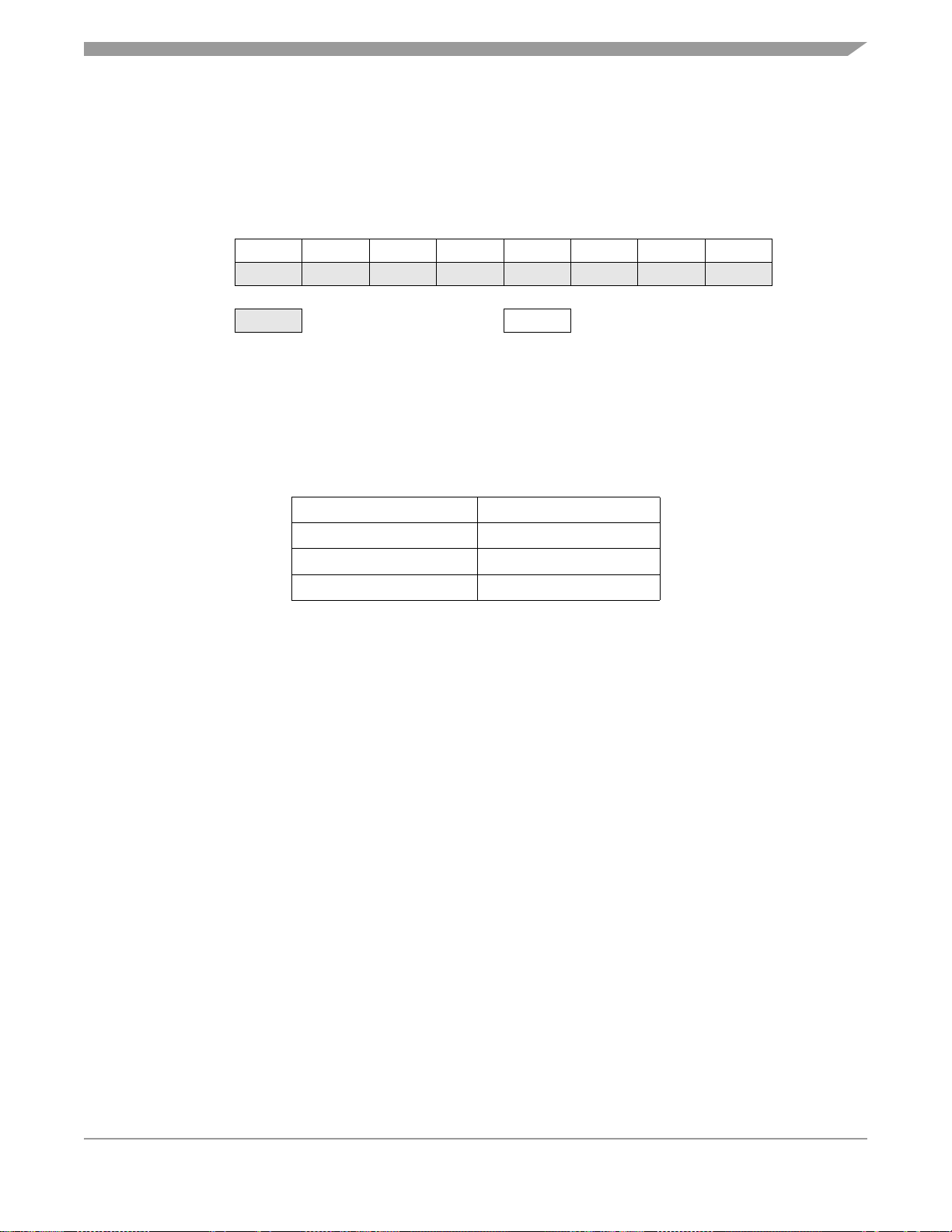
10.4 LVI Status Register
LVI Status Register
The LVI status register (LVISR) indicates if the VDD voltage was detected below the V
LVI resets have been disabled
Address: $FE0C
Bit 7654321Bit 0
Read:LVIOUT000000R
Write:
Reset:00000000
.
= Unimplemented R = Reserved
TRIPF
Figure 10-2. LVI Status Register (LVISR)
LVIOUT — LVI Output Bit
This read-only flag becomes set when the V
when V
voltage rises above V
DD
. The difference in these threshold levels results in a hysteresis
TRIPR
voltage falls below the V
DD
trip voltage and is cleared
TRIPF
that prevents oscillation into and out of reset (see Table 10-1). Reset clears the LVIOUT bit.
Table 10-1. LVIOUT Bit Indication
V
TRIPF
V
V
> V
DD
VDD < V
< VDD < V
DD
TRIPR
TRIPF
TRIPR
LVIOUT
0
1
Previous value
level while
10.5 LVI Interrupts
The LVI module does not generate interrupt requests.
10.6 Low-Power Modes
The STOP and WAIT instructions put the MCU in low power-consumption standby modes.
10.6.1 Wait Mode
If enabled, the LVI module remains active in wait mode. If enabled to generate resets, the LVI module can
generate a reset and bring the MCU out of wait mode.
10.6.2 Stop Mode
When the LVIPWRD bit in the configuration register is cleared and the LVISTOP bit in the configuration
register is set, the LVI module remains active in stop mode. If enabled to generate resets, the LVI module
can generate a reset and bring the MCU out of stop mode.
MC68HC908QY/QT Family Data Sheet, Rev. 5
Freescale Semiconductor 87

Low-Voltage Inhibit (LVI)
MC68HC908QY/QT Family Data Sheet, Rev. 5
88 Freescale Semiconductor

Chapter 11
Oscillator Module (OSC)
11.1 Introduction
The oscillator module is used to provide a stable clock source for the microcontroller system and bus. The
oscillator module generates two output clocks, BUSCLKX2 and BUSCLKX4. The BUSCLKX4 clock is
used by the system integration module (SIM) and the computer operating properly module (COP). The
BUSCLKX2 clock is divided by two in the SIM to be used as the bus clock for the microcontroller.
Therefore the bus frequency will be one fourth of the BUSCLKX4 frequency.
11.2 Features
The oscillator has these four clock source options available:
1. Internal oscillator: An internally generated, fixed frequency clock, trimmable to ±5%.This is the
default option out of reset.
2. External oscillator: An external clock that can be driven directly into OSC1.
3. External RC: A built-in oscillator module (RC oscillator) that requires an external R connection only.
The capacitor is internal to the chip.
4. External crystal: A built-in oscillator module (XTAL oscillator) that requires an external crystal or
ceramic-resonator.
11.3 Functional Description
The oscillator contains these major subsystems:
• Internal oscillator circuit
• Internal or external clock switch control
• External clock circuit
• External crystal circuit
• External RC clock circuit
MC68HC908QY/QT Family Data Sheet, Rev. 5
Freescale Semiconductor 89

Oscillator Module (OSC)
PTA0/AD0/TCH0/KBI0
PTA1/AD1/TCH1/KBI1
PTA2/IRQ
/KBI2/TCLK
PTA3/RST
PTA4/OSC2/AD2/KBI4
PTA5/OSC1/AD3/KBI5
/KBI3
PTB0
PTB1
PTB2
PTB3
PTB4
PTB5
PTB6
PTB7
POWER SUPPLY
PTA
PTB
8-BIT ADC
128 BYTES RAM
DDRA
DDRB
V
DD
V
SS
M68HC08 CPU
MC68HC908QY4 AND MC68HC908QT4
4096 BYTES
MC68HC908QY2, MC68HC908QY1,
MC68HC908QT2, AND MC68HC908QT1:
1536 BYTES
USER FLASH
CLOCK
GENERATOR
(OSCILLATOR)
SYSTEM INTEGRATION
MODULE
SINGLE INTERRUPT
MODULE
BREAK
MODULE
POWER-ON RESET
MODULE
KEYBOARD INTERRUPT
MODULE
16-BIT TIMER
MODULE
COP
MODULE
MONITOR ROM
RST, IRQ: Pins have internal (about 30K Ohms) pull up
PTA[0:5]: High current sink and source capability
PTA[0:5]: Pins have programmable keyboard interrupt and pull up
PTB[0:7]: Not available on 8-pin devices – MC68HC908QT1, MC68HC908QT2, and MC68HC908QT4 (see note in
12.1 Introduction)
ADC: Not available on the MC68HC908QY1 and MC68HC908QT1
Figure 11-1. Block Diagram Highlighting OSC Block and Pins
11.3.1 Internal Oscillator
The internal oscillator circuit is designed for use with no external components to provide a clock source
with tolerance less than ±25% untrimmed.An 8-bit trimming register allows adjustment to a tolerance of
less than ±5%.
The internal oscillator will generate a clock of 12.8 MHz typical (INTCLK) resulting in a bus speed (internal
clock ÷ 4) of 3.2 MHz. 3.2 MHz came from the maximum bus speed guaranteed at 3 V which is 4
MHz.Since the internal oscillator will have a ±25% tolerance (pre-trim), then the +25% case should not
allow a frequency higher than 4 MHz:
3.2 MHz + 25% = 4 MHz
Figure 11-3 shows how BUSCLKX4 is derived from INTCLK and, like the RC oscillator, OSC2 can output
BUSCLKX4 by setting OSC2EN in PTAPUE register. See Chapter 12 Input/Output Ports (PORTS)
MC68HC908QY/QT Family Data Sheet, Rev. 5
90 Freescale Semiconductor

Functional Description
11.3.1.1 Internal Oscillator Trimming
The 8-bit trimming register, OSCTRIM, allows a clock period adjust of +127 and –128 steps. Increasing
OSCTRIM value increases the clock period. Trimming allows the internal clock frequency to be set to
12.8 MHz ± 5%.
All devices are programmed with a trim value in a reserved FLASH location, $FFC0. This value can be
copied from the FLASH to the OSCTRIM register ($0038) during reset initialization.
Reset loads OSCTRIM with a default value of $80.
WARNING
Bulk FLASH erasure will set location $FFC0 to $FF and the factory
programmed value will be lost.
11.3.1.2 Internal to External Clock Switching
When external clock source (external OSC, RC, or XTAL) is desired, the user must perform the following
steps:
1. For external crystal circuits only, OSCOPT[1:0] = 1:1: To help precharge an external crystal
oscillator, set PTA4 (OSC2) as an output and drive high for several cycles. This may help the
crystal circuit start more robustly.
2. Set CONFIG2 bits OSCOPT[1:0] according to . The oscillator module control logic will then set
OSC1 as an external clock input and, if the external crystal option is selected, OSC2 will also be
set as the clock output.
3. Create a software delay to wait the stabilization time needed for the selected clock source (crystal,
resonator, RC) as recommended by the component manufacturer. A good rule of thumb for crystal
oscillators is to wait 4096 cycles of the crystal frequency, i.e., for a 4-MHz crystal, wait
approximately 1 msec.
4. After the manufacturer’s recommended delay has elapsed, the ECGON bit in the OSC status
register (OSCSTAT) needs to be set by the user software.
5. After ECGON set is detected, the OSC module checks for oscillator activity by waiting two external
clock rising edges.
6. The OSC module then switches to the external clock. Logic provides a glitch free transition.
7. The OSC module first sets the ECGST bit in the OSCSTAT register and then stops the internal
oscillator.
NOTE
Once transition to the external clock is done, the internal oscillator will only
be reactivated with reset. No post-switch clock monitor feature is
implemented (clock does not switch back to internal if external clock dies).
11.3.2 External Oscillator
The external clock option is designed for use when a clock signal is available in the application to provide
a clock source to the microcontroller. The OSC1 pin is enabled as an input by the oscillator module. The
clock signal is used directly to create BUSCLKX4 and also divided by two to create BUSCLKX2.
In this configuration, the OSC2 pin cannot output BUSCLKX4.So the OSC2EN bit in the port A pullup
enable register will be clear to enable PTA4 I/O functions on the pin
MC68HC908QY/QT Family Data Sheet, Rev. 5
Freescale Semiconductor 91
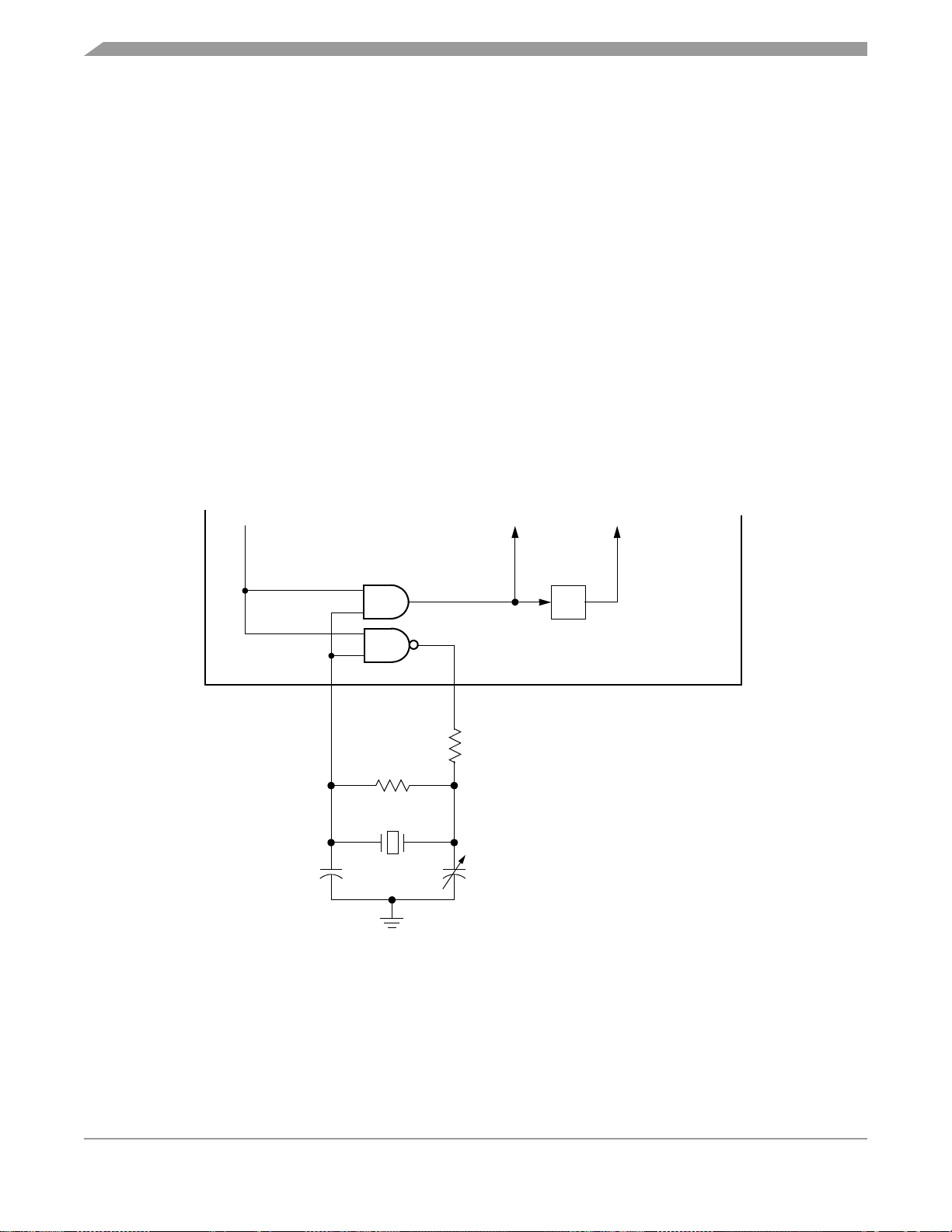
Oscillator Module (OSC)
11.3.3 XTAL Oscillator
The XTAL oscillator circuit is designed for use with an external crystal or ceramic resonator to provide an
accurate clock source. In this configuration, the OSC2 pin is dedicated to the external crystal circuit. The
OSC2EN bit in the port A pullup enable register has no effect when this clock mode is selected.
In its typical configuration, the XTAL oscillator is connected in a Pierce oscillator configuration, as shown
in Figure 11-2. This figure shows only the logical representation of the internal components and may not
represent actual circuitry. The oscillator configuration uses five components:
•Crystal, X
• Fixed capacitor, C
• Tuning capacitor, C2 (can also be a fixed capacitor)
• Feedback resistor, R
• Series resistor, RS (optional)
1
1
B
NOTE
The series resistor (R
) is included in the diagram to follow strict Pierce
S
oscillator guidelines and may not be required for all ranges of operation,
especially with high frequency crystals. Refer to the crystal manufacturer’s
data for more information.
FROM SIM
BUSCLKX2BUSCLKX4
XTALCLK
SIMOSCEN
MCU
OSC2OSC1
(1)
R
R
B
X
1
C
1
Note 1.
can be zero (shorted) when used with higher-frequency crystals. Refer to manufacturer’s
R
S
data. See Chapter 16 Electrical Specifications for component value recommendations.
S
C
2
TO SIMTO SIM
÷ 2
Figure 11-2. XTAL Oscillator External Connections
MC68HC908QY/QT Family Data Sheet, Rev. 5
92 Freescale Semiconductor

11.3.4 RC Oscillator
Oscillator Module Signals
The RC oscillator circuit is designed for use with an external resistor (R
) to provide a clock source with
EXT
a tolerance within 25% of the expected frequency. See Figure 11-3.
The capacitor (C) for the RC oscillator is internal to the MCU. The R
1%
or less to minimize its effect on the frequency.
value must have a tolerance of
EXT
In this configuration, the OSC2 pin can be left in the reset state as PTA4. Or, the OSC2EN bit in the port
A pullup enable register can be set to enable the OSC2 output function on the pin. Enabling the OSC2
output slightly increases the external RC oscillator frequency, f
SIMOSCEN
MCU
EXTERNAL RC
EN
OSCILLATOR
INTCLK
RCCLK
0
1
1
0
RCCLK
OSCRCOPT
TO SIM
.
PTA4
I/O
TO SIMFROM SIM
BUSCLKX2BUSCLKX4
÷ 2
PTA4
OSC2EN
OSC1
PTA4/BUSCLKX4 (OSC2)
V
DD
R
EXT
See Chapter 16 Electrical Specifications for component value requirements.
Figure 11-3. RC Oscillator External Connections
11.4 Oscillator Module Signals
The following paragraphs describe the signals that are inputs to and outputs from the oscillator module.
11.4.1 Crystal Amplifier Input Pin (OSC1)
The OSC1 pin is either an input to the crystal oscillator amplifier, an input to the RC oscillator circuit, or
an external clock source.
For the internal oscillator configuration, the OSC1 pin can assume other functions according to Table 1-3.
Function Priority in Shared Pins.
MC68HC908QY/QT Family Data Sheet, Rev. 5
Freescale Semiconductor 93

Oscillator Module (OSC)
11.4.2 Crystal Amplifier Output Pin (OSC2/PTA4/BUSCLKX4)
For the XTAL oscillator device, the OSC2 pin is the crystal oscillator inverting amplifier output.
For the external clock option, the OSC2 pin is dedicated to the PTA4 I/O function. The OSC2EN bit has
no effect.
For the internal oscillator or RC oscillator options, the OSC2 pin can assume other functions according to
Table 1-3. Function Priority in Shared Pins, or the output of the oscillator clock (BUSCLKX4).
Table 11-1. OSC2 Pin Function
Option OSC2 Pin Function
XTAL oscillator Inverting OSC1
External clock PTA4 I/O
Internal oscillator
or
RC oscillator
Controlled by OSC2EN bit in PTAPUE register
OSC2EN = 0: PTA4 I/O
OSC2EN = 1: BUSCLKX4 output
11.4.3 Oscillator Enable Signal (SIMOSCEN)
The SIMOSCEN signal comes from the system integration module (SIM) and enables/disables either the
XTAL oscillator circuit, the RC oscillator, or the internal oscillator.
11.4.4 XTAL Oscillator Clock (XTALCLK)
XTALCLK is the XTAL oscillator output signal. It runs at the full speed of the crystal (f
directly from the crystal oscillator circuit. Figure 11-2 shows only the logical relation of XTALCLK to OSC1
and OSC2 and may not represent the actual circuitry. The duty cycle of XTALCLK is unknown and may
depend on the crystal and other external factors. Also, the frequency and amplitude of XTALCLK can be
unstable at start up.
) and comes
XCLK
11.4.5 RC Oscillator Clock (RCCLK)
RCCLK is the RC oscillator output signal. Its frequency is directly proportional to the time constant of
external R and internal C. Figure 11-3 shows only the logical relation of RCCLK to OSC1 and may not
represent the actual circuitry.
11.4.6 Internal Oscillator Clock (INTCLK)
INTCLK is the internal oscillator output signal. Its nominal frequency is fixed to 12.8 MHz, but it can be
also trimmed using the oscillator trimming feature of the OSCTRIM register (see 11.3.1.1 Internal
Oscillator Trimming).
11.4.7 Oscillator Out 2 (BUSCLKX4)
BUSCLKX4 is the same as the input clock (XTALCLK, RCCLK, or INTCLK). This signal is driven to the
SIM module and is used to determine the COP cycles.
11.4.8 Oscillator Out (BUSCLKX2)
The frequency of this signal is equal to half of the BUSCLKX4, this signal is driven to the SIM for
generation of the bus clocks used by the CPU and other modules on the MCU. BUSCLKX2 will be divided
MC68HC908QY/QT Family Data Sheet, Rev. 5
94 Freescale Semiconductor

Low Power Modes
again in the SIM and results in the internal bus frequency being one fourth of either the XTALCLK,
RCCLK, or INTCLK frequency.
11.5 Low Power Modes
The WAIT and STOP instructions put the MCU in low-power consumption standby modes.
11.5.1 Wait Mode
The WAIT instruction has no effect on the oscillator logic. BUSCLKX2 and BUSCLKX4 continue to drive
to the SIM module.
11.5.2 Stop Mode
The STOP instruction disables either the XTALCLK, the RCCLK, or INTCLK output, hence BUSCLKX2
and BUSCLKX4.
11.6 Oscillator During Break Mode
The oscillator continues to drive BUSCLKX2 and BUSCLKX4 when the device enters the break state.
11.7 CONFIG2 Options
Two CONFIG2 register options affect the operation of the oscillator module: OSCOPT1 and OSCOPT0.
All CONFIG2 register bits will have a default configuration. Refer to Chapter 5 Configuration Register
(CONFIG) for more information on how the CONFIG2 register is used.
Table 11-2 shows how the OSCOPT bits are used to select the oscillator clock source.
.
Table 11-2. Oscillator Modes
OSCOPT1 OSCOPT0 Oscillator Modes
0 0 Internal oscillator
0 1 External oscillator
10External RC
1 1 External crystal
11.8 Input/Output (I/O) Registers
The oscillator module contains these two registers:
1. Oscillator status register (OSCSTAT)
2. Oscillator trim register (OSCTRIM)
MC68HC908QY/QT Family Data Sheet, Rev. 5
Freescale Semiconductor 95

Oscillator Module (OSC)
11.8.1 Oscillator Status Register
The oscillator status register (OSCSTAT) contains the bits for switching from internal to external clock
sources.
Address:
$0036
Bit 7654321Bit 0
Read:
Write:
Reset:00000000
RRRRRRECGON
R
=Reserved
= Unimplemented
ECGST
Figure 11-4. Oscillator Status Register (OSCSTAT)
ECGON — External Clock Generator On Bit
This read/write bit enables external clock generator, so that the switching process can be initiated. This
bit is forced low during reset. This bit is ignored in monitor mode with the internal oscillator bypassed,
PTM or CTM mode.
1 = External clock generator enabled
0 = External clock generator disabled
ECGST — External Clock Status Bit
This read-only bit indicates whether or not an external clock source is engaged to drive the system
clock.
1 = An external clock source engaged
0 = An external clock source disengaged
11.8.2 Oscillator Trim Register (OSCTRIM)
Address:
$0038
Bit 7654321Bit 0
Read:
Write:
Reset:10000000
TRIM7 TRIM6 TRIM5 TRIM4 TRIM3 TRIM2 TRIM1 TRIM0
Figure 11-5. Oscillator Trim Register (OSCTRIM)
TRIM7–TRIM0 — Internal Oscillator Trim Factor Bits
These read/write bits change the size of the internal capacitor used by the internal oscillator. By
measuring the period of the internal clock and adjusting this factor accordingly, the frequency of the
internal clock can be fine tuned. Increasing (decreasing) this factor by one increases (decreases) the
period by approximately 0.2% of the untrimmed period (the period for TRIM = $80). The trimmed
frequency is guaranteed not to vary by more than ±5% over the full specified range of temperature and
voltage. The reset value is $80, which sets the frequency to 12.8 MHz (3.2 MHz bus speed) ±25%.
MC68HC908QY/QT Family Data Sheet, Rev. 5
96 Freescale Semiconductor

Chapter 12
Input/Output Ports (PORTS)
12.1 Introduction
The MC68HC908QT1, MC68HC908QT2, and MC68HC908QT4 have five bidirectional input-output (I/O)
pins and one input only pin. The MC68HC908QY1, MC68HC908QY2, and MC68HC908QY4 have
thirteen bidirectional pins and one input only pin. All I/O pins are programmable as inputs or outputs.
NOTE
Connect any unused I/O pins to an appropriate logic level, either V
Although the I/O ports do not require termination for proper operation,
termination reduces excess current consumption and the possibility of
electrostatic damage.
8-pin devices have non-bonded pins. These pins should be configured
either as outputs driving low or high, or as inputs with internal pullups
enabled. Configuring these non-bonded pins in this manner will prevent any
excess current consumption caused by floating inputs.
12.2 Port A
or VSS.
DD
Port A is a 6-bit special function port that shares all six of its pins with the keyboard interrupt (KBI) module
(see Chapter 9 Keyboard Interrupt Module (KBI)). Each port A pin also has a software configurable pullup
device if the corresponding port pin is configured as an input port.
NOTE
PTA2 is input only.
When the IRQ
(CONFIG2), bit 2 of the port A data register (PTA) will always read a 0. In
this case, the BIH and BIL instructions can be used to read the logic level
on the PTA2 pin. When the IRQ
behave as if the PTA2 pin is a logic 1. However, reading bit 2 of PTA will
read the actual logic level on the pin.
function is enabled in the configuration register 2
function is disabled, these instructions will
MC68HC908QY/QT Family Data Sheet, Rev. 5
Freescale Semiconductor 97

Input/Output Ports (PORTS)
12.2.1 Port A Data Register
The port A data register (PTA) contains a data latch for each of the six port A pins.
Address:
Additional Functions:
$0000
Bit 76 5 4 3 2 1Bit 0
Read:
Write:
Reset: Unaffected by reset
R
R = Reserved
AWUL
PTA5 PTA4 PTA3
KBI5 KBI4 KBI3 KBI2 KBI1 KBI0
= Unimplemented
PTA2
PTA1 PTA0
Figure 12-1. Port A Data Register (PTA)
PTA[5:0] — Port A Data Bits
These read/write bits are software programmable. Data direction of each port A pin is under the control
of the corresponding bit in data direction register A. Reset has no effect on port A data.
AWUL — Auto Wakeup Latch Data Bit
This is a read-only bit which has the value of the auto wakeup interrupt request latch. The wakeup
request signal is generated internally (see Chapter 4 Auto Wakeup Module (AWU)). There is no PTA6
port nor any of the associated bits such as PTA6 data register, pullup enable or direction.
KBI[5:0] — Port A Keyboard Interrupts
The keyboard interrupt enable bits, KBIE5–KBIE0, in the keyboard interrupt control enable register
(KBIER) enable the port A pins as external interrupt pins (see Chapter 9 Keyboard Interrupt Module
(KBI)).
12.2.2 Data Direction Register A
Data direction register A (DDRA) determines whether each port A pin is an input or an output. Writing a 1
to a DDRA bit enables the output buffer for the corresponding port A pin; a 0 disables the output buffer.
Address:
DDRA[5:0] — Data Direction Register A Bits
These read/write bits control port A data direction. Reset clears DDRA[5:0], configuring all port A pins
as inputs.
1 = Corresponding port A pin configured as output
0 = Corresponding port A pin configured as input
Avoid glitches on port A pins by writing to the port A data register before
changing data direction register A bits from 0 to 1.
$0004
Bit 7654321Bit 0
Read:
Write:
Reset:00000000
R R DDRA5 DDRA4 DDRA3
R= Reserved
= Unimplemented
0
DDRA1 DDRA0
Figure 12-2. Data Direction Register A (DDRA)
NOTE
MC68HC908QY/QT Family Data Sheet, Rev. 5
98 Freescale Semiconductor

Figure 12-3 shows the port A I/O logic.
READ DDRA ($0004)
WRITE DDRA ($0004)
RESET
Port A
PTAPUEx
DDRAx
30 k
WRITE PTA ($0000)
PTAx
INTERNAL DATA BUS
READ PTA ($0000)
TO KEYBOARD INTERRUPT CIRCUIT
PTAx
Figure 12-3. Port A I/O Circuit
NOTE
Figure 12-3 does not apply to PTA2
When DDRAx is a 1, reading address $0000 reads the PTAx data latch. When DDRAx is a 0, reading
address $0000 reads the voltage level on the pin. The data latch can always be written, regardless of the
state of its data direction bit.
12.2.3 Port A Input Pullup Enable Register
The port A input pullup enable register (PTAPUE) contains a software configurable pullup device for each
if the six port A pins. Each bit is individually configurable and requires the corresponding data direction
register, DDRAx, to be configured as input. Each pullup device is automatically and dynamically disabled
when its corresponding DDRAx bit is configured as output.
Address:
$000B
Bit 7654321Bit 0
Read:
OSC2EN PTAPUE5 PTAPUE4 PTAPUE3 PTAPUE2 PTAPUE1 PTAPUE0
Write:
Reset:00000000
= Unimplemented
Figure 12-4. Port A Input Pullup Enable Register (PTAPUE)
OSC2EN — Enable PTA4 on OSC2 Pin
This read/write bit configures the OSC2 pin function when internal oscillator or RC oscillator option is
selected. This bit has no effect for the XTAL or external oscillator options.
1 = OSC2 pin outputs the internal or RC oscillator clock (BUSCLKX4)
0 = OSC2 pin configured for PTA4 I/O, having all the interrupt and pullup functions
MC68HC908QY/QT Family Data Sheet, Rev. 5
Freescale Semiconductor 99

Input/Output Ports (PORTS)
PTAPUE[5:0] — Port A Input Pullup Enable Bits
These read/write bits are software programmable to enable pullup devices on port A pins.
1 = Corresponding port A pin configured to have internal pull if its DDRA bit is set to 0
0 = Pullup device is disconnected on the corresponding port A pin regardless of the state of its
DDRA bit
Table 12-1 summarizes the operation of the port A pins.
Table 12-1. Port A Pin Functions
PTAPUE
Bit
10
00X
X 1 X Output DDRA5–DDRA0 PTA5–PTA0
1. X = don’t care
2. I/O pin pulled to VDD by internal pullup.
3. Writing affects data register, but does not affect input.
4. Hi-Z = high impedance
5. Output does not apply to PTA2
DDRA
Bit
PTA
Bit
(1)
X
I/O Pin
Mode
Input, V
Input, Hi-Z
DD
(2)
(4)
Accesses to DDRA Accesses to PTA
Read/Write Read Write
DDRA5–DDRA0 Pin
DDRA5–DDRA0 Pin
PTA5–PTA0
PTA5–PTA0
PTA5–PTA0
12.3 Port B
Port B is an 8-bit general purpose I/O port. Port B is only available on the MC68HC908QY1,
MC68HC908QY2, and MC68HC908QY4.
12.3.1 Port B Data Register
The port B data register (PTB) contains a data latch for each of the eight port B pins.
Address:
$0001
Bit 7654321Bit 0
Read:
Write:
Reset: Unaffected by reset
PTB7 PTB6 PTB5 PTB4 PTB3 PTB2 PTB1 PTB0
(3)
(3)
(5)
Figure 12-5. Port B Data Register (PTB)
PTB[7:0] — Port B Data Bits
These read/write bits are software programmable. Data direction of each port B pin is under the control
of the corresponding bit in data direction register B. Reset has no effect on port B data.
MC68HC908QY/QT Family Data Sheet, Rev. 5
100 Freescale Semiconductor
 Loading...