


M68HC08
Microcontrollers
freescale.com
查询MC908QC16CDRE供应商
MC68HC908QC16
MC68HC908QC8
MC68HC908QC4
Data Sheet
MC68HC908QC16
Rev. 3
04/2007


MC68HC908QC16
MC68HC908QC8
MC68HC908QC4
Data Sheet
To provide the most up-to-date information, the revision of our documents on the World Wide Web will be
the most current. Your printed copy may be an earlier revision. To verify you have the latest information
available, refer to:
http://www.freescale.com
Freescale™ and the Freescale logo are trademarks of Freescale Semiconductor, Inc.
This product incorporates SuperFlash® technology licensed from SST.
© Freescale Semiconductor, Inc., 2007. All rights reserved.
MC68HC908QC16 • MC68HC908QC8 • MC68HC908QC4 Data Sheet, Rev. 3
Freescale Semiconductor 3

Revision History
The following revision history table summarizes changes contained in this document. For your
convenience, the page number designators have been linked to the appropriate location.
Revision History
Date
April, 2006 1.0 Initial release N/A
May, 2006 1.1
October, 2006 2.0
Revision
Level
Description
19.5 5-V DC Electrical Characteristics — Updated values 237
19.8 3.3-V DC Electrical Characteristics — Updated values 240
19.11 Oscillator Characteristics — Updated values 243
Figure 19-9. Typical 5-Volt Run Current versus Bus Frequency (25°C) and
Figure 19-10. Typical 3.3-Volt Run Current versus Bus Frequency (25°C) —
added
1.7 Unused Pin Termination — Added new section 24
11.2 Unused Pin Termination — Replaced note with new section 107
19.5 5-V DC Electrical Characteristics — New values for:
DC injection current
Low-voltage inhibit reset, trip rising voltage
19.8 3.3-V DC Electrical Characteristics — New values for:
DC injection current
Low-voltage inhibit reset, trip rising voltage
19.12 Supply Current Characteristics — New values for stop mode supply
currents at –40 to 125°C
20.3 Package Dimensions — Updated package dimension drawing for the
28-lead TSSOP.
Number(s)
Page
247
237
240
246
261
April, 2007 3.0
Table 1-2. Pin Functions — Added note 22
Figure 2-2. Control, Status, and Data Registers — Corrected Port C Data
Register bit PTC3
Chapter 3 Analog-to-Digital Converter (ADC10) Module — Renamed ADCSC
register to ADSCR to be consistent with development tools
Chapter 4 Configuration Registers (CONFIG1 and CONFIG2) — Changed
CGMXCLK to BUSCLKX4 60
11.3 Port A — Added information to first paragraph of note 107
11.3.1 Port A Data Register — Corrected bit designations for the first entry
under Figure 11-1. Port A Data Register (PTA).
11.5 Port C — Added note and corrected address location designation in last
paragraph
Chapter 13 Enhanced Serial Communications Interface (ESCI) Module —
Changed SCIBDSRC to ESCIBDSRC and CGMXCLK to BUSCLKX4
13.9.3 Bit Time Measurement — Corrected first sentence of listing number 1 150
Figure 18-18. Monitor Mode Entry Timing — Changed CGMXCLK to
BUSCLKX4
MC68HC908QC16 • MC68HC908QC8 • MC68HC908QC4 Data Sheet, Rev. 3
27
45
108
112
113
123
234
4 Freescale Semiconductor

List of Sections
Chapter 1 General Description. . . . . . . . . . . . . . . . . . . . . . . . . . . . . . . . . . . . . . . . . . . . . . . . 17
Chapter 2 Memory. . . . . . . . . . . . . . . . . . . . . . . . . . . . . . . . . . . . . . . . . . . . . . . . . . . . . . . . . .25
Chapter 3 Analog-to-Digital Converter (ADC10) Module . . . . . . . . . . . . . . . . . . . . . . . . . . . 45
Chapter 4 Configuration Registers (CONFIG1 and CONFIG2) . . . . . . . . . . . . . . . . . . . . . .59
Chapter 5 Computer Operating Properly (COP) . . . . . . . . . . . . . . . . . . . . . . . . . . . . . . . . . .63
Chapter 6 Central Processor Unit (CPU). . . . . . . . . . . . . . . . . . . . . . . . . . . . . . . . . . . . . . . .67
Chapter 7 External Interrupt (IRQ). . . . . . . . . . . . . . . . . . . . . . . . . . . . . . . . . . . . . . . . . . . . .79
Chapter 8 Keyboard Interrupt Module (KBI) . . . . . . . . . . . . . . . . . . . . . . . . . . . . . . . . . . . . .85
Chapter 9 Low-Voltage Inhibit (LVI). . . . . . . . . . . . . . . . . . . . . . . . . . . . . . . . . . . . . . . . . . . . 93
Chapter 10 Oscillator Mode (OSC). . . . . . . . . . . . . . . . . . . . . . . . . . . . . . . . . . . . . . . . . . . . .97
Chapter 11 Input/Output Ports (PORTS) . . . . . . . . . . . . . . . . . . . . . . . . . . . . . . . . . . . . . . .107
Chapter 12 Periodic Wakeup Module (PWU) . . . . . . . . . . . . . . . . . . . . . . . . . . . . . . . . . . .117
Chapter 13 Enhanced Serial Communications Interface (ESCI) Module . . . . . . . . . . . . .123
Chapter 14 System Integration Module (SIM). . . . . . . . . . . . . . . . . . . . . . . . . . . . . . . . . . .153
Chapter 15 Serial Peripheral Interface (SPI) Module . . . . . . . . . . . . . . . . . . . . . . . . . . . . .169
Chapter 16 Timer Interface Module (TIM1) . . . . . . . . . . . . . . . . . . . . . . . . . . . . . . . . . . . . . 189
Chapter 17 Timer Interface Module (TIM2) . . . . . . . . . . . . . . . . . . . . . . . . . . . . . . . . . . . . . 205
Chapter 18 Development Support . . . . . . . . . . . . . . . . . . . . . . . . . . . . . . . . . . . . . . . . . . . .219
Chapter 19 Electrical Specifications . . . . . . . . . . . . . . . . . . . . . . . . . . . . . . . . . . . . . . . . . .235
Chapter 20 Ordering Information and Mechanical Specifications . . . . . . . . . . . . . . . . . .257
MC68HC908QC16 • MC68HC908QC8 • MC68HC908QC4 Data Sheet, Rev. 3
Freescale Semiconductor 5

List of Sections
MC68HC908QC16 • MC68HC908QC8 • MC68HC908QC4 Data Sheet, Rev. 3
6 Freescale Semiconductor

Table of Contents
Chapter 1
General Description
1.1 Introduction . . . . . . . . . . . . . . . . . . . . . . . . . . . . . . . . . . . . . . . . . . . . . . . . . . . . . . . . . . . . . . . . 17
1.2 Features. . . . . . . . . . . . . . . . . . . . . . . . . . . . . . . . . . . . . . . . . . . . . . . . . . . . . . . . . . . . . . . . . . . 17
1.3 MCU Block Diagram . . . . . . . . . . . . . . . . . . . . . . . . . . . . . . . . . . . . . . . . . . . . . . . . . . . . . . . . . 19
1.4 Pin Assignments . . . . . . . . . . . . . . . . . . . . . . . . . . . . . . . . . . . . . . . . . . . . . . . . . . . . . . . . . . . . 19
1.5 Pin Functions . . . . . . . . . . . . . . . . . . . . . . . . . . . . . . . . . . . . . . . . . . . . . . . . . . . . . . . . . . . . . . . 19
1.6 Pin Function Priority. . . . . . . . . . . . . . . . . . . . . . . . . . . . . . . . . . . . . . . . . . . . . . . . . . . . . . . . . . 24
1.7 Unused Pin Termination . . . . . . . . . . . . . . . . . . . . . . . . . . . . . . . . . . . . . . . . . . . . . . . . . . . . . . 24
Chapter 2
Memory
2.1 Introduction . . . . . . . . . . . . . . . . . . . . . . . . . . . . . . . . . . . . . . . . . . . . . . . . . . . . . . . . . . . . . . . . 25
2.2 Unimplemented Memory Locations . . . . . . . . . . . . . . . . . . . . . . . . . . . . . . . . . . . . . . . . . . . . . . 25
2.3 Reserved Memory Locations . . . . . . . . . . . . . . . . . . . . . . . . . . . . . . . . . . . . . . . . . . . . . . . . . . . 25
2.4 Direct Page Registers . . . . . . . . . . . . . . . . . . . . . . . . . . . . . . . . . . . . . . . . . . . . . . . . . . . . . . . . 25
2.5 Random-Access Memory (RAM) . . . . . . . . . . . . . . . . . . . . . . . . . . . . . . . . . . . . . . . . . . . . . . . . 35
2.6 FLASH Memory (FLASH) . . . . . . . . . . . . . . . . . . . . . . . . . . . . . . . . . . . . . . . . . . . . . . . . . . . . . 36
2.6.1 FLASH Control Register. . . . . . . . . . . . . . . . . . . . . . . . . . . . . . . . . . . . . . . . . . . . . . . . . . . . 36
2.6.2 FLASH Page Erase Operation. . . . . . . . . . . . . . . . . . . . . . . . . . . . . . . . . . . . . . . . . . . . . . . 37
2.6.3 FLASH Mass Erase Operation. . . . . . . . . . . . . . . . . . . . . . . . . . . . . . . . . . . . . . . . . . . . . . . 38
2.6.4 FLASH Program Operation . . . . . . . . . . . . . . . . . . . . . . . . . . . . . . . . . . . . . . . . . . . . . . . . . 39
2.6.5 FLASH Protection . . . . . . . . . . . . . . . . . . . . . . . . . . . . . . . . . . . . . . . . . . . . . . . . . . . . . . . . 41
2.6.6 FLASH Block Protect Register . . . . . . . . . . . . . . . . . . . . . . . . . . . . . . . . . . . . . . . . . . . . . . . 41
2.6.7 EEPROM Memory Emulation Using FLASH Memory . . . . . . . . . . . . . . . . . . . . . . . . . . . . . 42
Chapter 3
Analog-to-Digital Converter (ADC10) Module
3.1 Introduction . . . . . . . . . . . . . . . . . . . . . . . . . . . . . . . . . . . . . . . . . . . . . . . . . . . . . . . . . . . . . . . . 45
3.2 Features. . . . . . . . . . . . . . . . . . . . . . . . . . . . . . . . . . . . . . . . . . . . . . . . . . . . . . . . . . . . . . . . . . . 45
3.3 Functional Description . . . . . . . . . . . . . . . . . . . . . . . . . . . . . . . . . . . . . . . . . . . . . . . . . . . . . . . . 45
3.3.1 Clock Select and Divide Circuit . . . . . . . . . . . . . . . . . . . . . . . . . . . . . . . . . . . . . . . . . . . . . . 47
3.3.2 Input Select and Pin Control . . . . . . . . . . . . . . . . . . . . . . . . . . . . . . . . . . . . . . . . . . . . . . . . 48
3.3.3 Conversion Control . . . . . . . . . . . . . . . . . . . . . . . . . . . . . . . . . . . . . . . . . . . . . . . . . . . . . . . 48
3.3.3.1 Initiating Conversions . . . . . . . . . . . . . . . . . . . . . . . . . . . . . . . . . . . . . . . . . . . . . . . . . . . . 48
3.3.3.2 Completing Conversions . . . . . . . . . . . . . . . . . . . . . . . . . . . . . . . . . . . . . . . . . . . . . . . . . 48
3.3.3.3 Aborting Conversions . . . . . . . . . . . . . . . . . . . . . . . . . . . . . . . . . . . . . . . . . . . . . . . . . . . . 48
3.3.3.4 Total Conversion Time . . . . . . . . . . . . . . . . . . . . . . . . . . . . . . . . . . . . . . . . . . . . . . . . . . . 49
3.3.4 Sources of Error . . . . . . . . . . . . . . . . . . . . . . . . . . . . . . . . . . . . . . . . . . . . . . . . . . . . . . . . . . 50
3.3.4.1 Sampling Error . . . . . . . . . . . . . . . . . . . . . . . . . . . . . . . . . . . . . . . . . . . . . . . . . . . . . . . . . 50
3.3.4.2 Pin Leakage Error. . . . . . . . . . . . . . . . . . . . . . . . . . . . . . . . . . . . . . . . . . . . . . . . . . . . . . . 50
3.3.4.3 Noise-Induced Errors . . . . . . . . . . . . . . . . . . . . . . . . . . . . . . . . . . . . . . . . . . . . . . . . . . . . 50
MC68HC908QC16 • MC68HC908QC8 • MC68HC908QC4 Data Sheet, Rev. 3
Freescale Semiconductor 7

Table of Contents
3.3.4.4 Code Width and Quantization Error . . . . . . . . . . . . . . . . . . . . . . . . . . . . . . . . . . . . . . . . . 51
3.3.4.5 Linearity Errors . . . . . . . . . . . . . . . . . . . . . . . . . . . . . . . . . . . . . . . . . . . . . . . . . . . . . . . . . 51
3.3.4.6 Code Jitter, Non-Monotonicity and Missing Codes. . . . . . . . . . . . . . . . . . . . . . . . . . . . . . 51
3.4 Interrupts . . . . . . . . . . . . . . . . . . . . . . . . . . . . . . . . . . . . . . . . . . . . . . . . . . . . . . . . . . . . . . . . . . 52
3.5 Low-Power Modes . . . . . . . . . . . . . . . . . . . . . . . . . . . . . . . . . . . . . . . . . . . . . . . . . . . . . . . . . . . 52
3.5.1 Wait Mode . . . . . . . . . . . . . . . . . . . . . . . . . . . . . . . . . . . . . . . . . . . . . . . . . . . . . . . . . . . . . . 52
3.5.2 Stop Mode . . . . . . . . . . . . . . . . . . . . . . . . . . . . . . . . . . . . . . . . . . . . . . . . . . . . . . . . . . . . . . 52
3.6 ADC10 During Break Interrupts . . . . . . . . . . . . . . . . . . . . . . . . . . . . . . . . . . . . . . . . . . . . . . . . . 52
3.7 I/O Signals . . . . . . . . . . . . . . . . . . . . . . . . . . . . . . . . . . . . . . . . . . . . . . . . . . . . . . . . . . . . . . . . . 53
3.7.1 ADC10 Analog Power Pin (V
3.7.2 ADC10 Analog Ground Pin (V
3.7.3 ADC10 Voltage Reference High Pin (V
3.7.4 ADC10 Voltage Reference Low Pin (V
) . . . . . . . . . . . . . . . . . . . . . . . . . . . . . . . . . . . . . . . . . . . . 53
DDA
). . . . . . . . . . . . . . . . . . . . . . . . . . . . . . . . . . . . . . . . . . . . 53
SSA
). . . . . . . . . . . . . . . . . . . . . . . . . . . . . . . . . . . . 53
REFH
) . . . . . . . . . . . . . . . . . . . . . . . . . . . . . . . . . . . . 53
REFL
3.7.5 ADC10 Channel Pins (ADn). . . . . . . . . . . . . . . . . . . . . . . . . . . . . . . . . . . . . . . . . . . . . . . . . 54
3.8 Registers . . . . . . . . . . . . . . . . . . . . . . . . . . . . . . . . . . . . . . . . . . . . . . . . . . . . . . . . . . . . . . . . . . 54
3.8.1 ADC10 Status and Control Register . . . . . . . . . . . . . . . . . . . . . . . . . . . . . . . . . . . . . . . . . . 54
3.8.2 ADC10 Result High Register (ADRH) . . . . . . . . . . . . . . . . . . . . . . . . . . . . . . . . . . . . . . . . . 56
3.8.3 ADC10 Result Low Register (ADRL) . . . . . . . . . . . . . . . . . . . . . . . . . . . . . . . . . . . . . . . . . . 56
3.8.4 ADC10 Clock Register (ADCLK) . . . . . . . . . . . . . . . . . . . . . . . . . . . . . . . . . . . . . . . . . . . . . 56
Chapter 4
Configuration Registers (CONFIG1 and CONFIG2)
4.1 Introduction . . . . . . . . . . . . . . . . . . . . . . . . . . . . . . . . . . . . . . . . . . . . . . . . . . . . . . . . . . . . . . . . 59
4.2 Functional Description . . . . . . . . . . . . . . . . . . . . . . . . . . . . . . . . . . . . . . . . . . . . . . . . . . . . . . . . 59
Chapter 5
Computer Operating Properly (COP)
5.1 Introduction . . . . . . . . . . . . . . . . . . . . . . . . . . . . . . . . . . . . . . . . . . . . . . . . . . . . . . . . . . . . . . . . 63
5.2 Functional Description . . . . . . . . . . . . . . . . . . . . . . . . . . . . . . . . . . . . . . . . . . . . . . . . . . . . . . . . 63
5.3 I/O Signals . . . . . . . . . . . . . . . . . . . . . . . . . . . . . . . . . . . . . . . . . . . . . . . . . . . . . . . . . . . . . . . . . 64
5.3.1 BUSCLKX4 . . . . . . . . . . . . . . . . . . . . . . . . . . . . . . . . . . . . . . . . . . . . . . . . . . . . . . . . . . . . . 64
5.3.2 STOP Instruction . . . . . . . . . . . . . . . . . . . . . . . . . . . . . . . . . . . . . . . . . . . . . . . . . . . . . . . . . 64
5.3.3 COPCTL Write . . . . . . . . . . . . . . . . . . . . . . . . . . . . . . . . . . . . . . . . . . . . . . . . . . . . . . . . . . . 64
5.3.4 Power-On Reset. . . . . . . . . . . . . . . . . . . . . . . . . . . . . . . . . . . . . . . . . . . . . . . . . . . . . . . . . . 64
5.3.5 Internal Reset. . . . . . . . . . . . . . . . . . . . . . . . . . . . . . . . . . . . . . . . . . . . . . . . . . . . . . . . . . . . 64
5.3.6 COPD (COP Disable). . . . . . . . . . . . . . . . . . . . . . . . . . . . . . . . . . . . . . . . . . . . . . . . . . . . . . 64
5.3.7 COPRS (COP Rate Select) . . . . . . . . . . . . . . . . . . . . . . . . . . . . . . . . . . . . . . . . . . . . . . . . . 65
5.4 COP Control Register . . . . . . . . . . . . . . . . . . . . . . . . . . . . . . . . . . . . . . . . . . . . . . . . . . . . . . . . 65
5.5 Interrupts . . . . . . . . . . . . . . . . . . . . . . . . . . . . . . . . . . . . . . . . . . . . . . . . . . . . . . . . . . . . . . . . . . 65
5.6 Monitor Mode . . . . . . . . . . . . . . . . . . . . . . . . . . . . . . . . . . . . . . . . . . . . . . . . . . . . . . . . . . . . . . . 65
5.7 Low-Power Modes . . . . . . . . . . . . . . . . . . . . . . . . . . . . . . . . . . . . . . . . . . . . . . . . . . . . . . . . . . . 65
5.7.1 Wait Mode . . . . . . . . . . . . . . . . . . . . . . . . . . . . . . . . . . . . . . . . . . . . . . . . . . . . . . . . . . . . . . 65
5.7.2 Stop Mode . . . . . . . . . . . . . . . . . . . . . . . . . . . . . . . . . . . . . . . . . . . . . . . . . . . . . . . . . . . . . . 65
5.8 COP Module During Break Mode . . . . . . . . . . . . . . . . . . . . . . . . . . . . . . . . . . . . . . . . . . . . . . . 65
MC68HC908QC16 • MC68HC908QC8 • MC68HC908QC4 Data Sheet, Rev. 3
8 Freescale Semiconductor

Chapter 6
Central Processor Unit (CPU)
6.1 Introduction . . . . . . . . . . . . . . . . . . . . . . . . . . . . . . . . . . . . . . . . . . . . . . . . . . . . . . . . . . . . . . . . 67
6.2 Features. . . . . . . . . . . . . . . . . . . . . . . . . . . . . . . . . . . . . . . . . . . . . . . . . . . . . . . . . . . . . . . . . . . 67
6.3 CPU Registers . . . . . . . . . . . . . . . . . . . . . . . . . . . . . . . . . . . . . . . . . . . . . . . . . . . . . . . . . . . . . . 67
6.3.1 Accumulator . . . . . . . . . . . . . . . . . . . . . . . . . . . . . . . . . . . . . . . . . . . . . . . . . . . . . . . . . . . . . 68
6.3.2 Index Register . . . . . . . . . . . . . . . . . . . . . . . . . . . . . . . . . . . . . . . . . . . . . . . . . . . . . . . . . . . 68
6.3.3 Stack Pointer . . . . . . . . . . . . . . . . . . . . . . . . . . . . . . . . . . . . . . . . . . . . . . . . . . . . . . . . . . . . 69
6.3.4 Program Counter . . . . . . . . . . . . . . . . . . . . . . . . . . . . . . . . . . . . . . . . . . . . . . . . . . . . . . . . . 69
6.3.5 Condition Code Register . . . . . . . . . . . . . . . . . . . . . . . . . . . . . . . . . . . . . . . . . . . . . . . . . . . 70
6.4 Arithmetic/Logic Unit (ALU) . . . . . . . . . . . . . . . . . . . . . . . . . . . . . . . . . . . . . . . . . . . . . . . . . . . . 71
6.5 Low-Power Modes . . . . . . . . . . . . . . . . . . . . . . . . . . . . . . . . . . . . . . . . . . . . . . . . . . . . . . . . . . . 71
6.5.1 Wait Mode . . . . . . . . . . . . . . . . . . . . . . . . . . . . . . . . . . . . . . . . . . . . . . . . . . . . . . . . . . . . . . 71
6.5.2 Stop Mode . . . . . . . . . . . . . . . . . . . . . . . . . . . . . . . . . . . . . . . . . . . . . . . . . . . . . . . . . . . . . . 71
6.6 CPU During Break Interrupts . . . . . . . . . . . . . . . . . . . . . . . . . . . . . . . . . . . . . . . . . . . . . . . . . . . 71
6.7 Instruction Set Summary . . . . . . . . . . . . . . . . . . . . . . . . . . . . . . . . . . . . . . . . . . . . . . . . . . . . . . 72
6.8 Opcode Map . . . . . . . . . . . . . . . . . . . . . . . . . . . . . . . . . . . . . . . . . . . . . . . . . . . . . . . . . . . . . . . 77
Chapter 7
External Interrupt (IRQ)
7.1 Introduction . . . . . . . . . . . . . . . . . . . . . . . . . . . . . . . . . . . . . . . . . . . . . . . . . . . . . . . . . . . . . . . . 79
7.2 Features. . . . . . . . . . . . . . . . . . . . . . . . . . . . . . . . . . . . . . . . . . . . . . . . . . . . . . . . . . . . . . . . . . . 79
7.3 Functional Description . . . . . . . . . . . . . . . . . . . . . . . . . . . . . . . . . . . . . . . . . . . . . . . . . . . . . . . . 79
7.3.1 MODE = 1 . . . . . . . . . . . . . . . . . . . . . . . . . . . . . . . . . . . . . . . . . . . . . . . . . . . . . . . . . . . . . . 81
7.3.2 MODE = 0 . . . . . . . . . . . . . . . . . . . . . . . . . . . . . . . . . . . . . . . . . . . . . . . . . . . . . . . . . . . . . . 82
7.4 Interrupts . . . . . . . . . . . . . . . . . . . . . . . . . . . . . . . . . . . . . . . . . . . . . . . . . . . . . . . . . . . . . . . . . . 82
7.5 Low-Power Modes . . . . . . . . . . . . . . . . . . . . . . . . . . . . . . . . . . . . . . . . . . . . . . . . . . . . . . . . . . . 82
7.5.1 Wait Mode . . . . . . . . . . . . . . . . . . . . . . . . . . . . . . . . . . . . . . . . . . . . . . . . . . . . . . . . . . . . . . 82
7.5.2 Stop Mode . . . . . . . . . . . . . . . . . . . . . . . . . . . . . . . . . . . . . . . . . . . . . . . . . . . . . . . . . . . . . . 82
7.6 IRQ Module During Break Interrupts . . . . . . . . . . . . . . . . . . . . . . . . . . . . . . . . . . . . . . . . . . . . . 82
7.7 I/O Signals . . . . . . . . . . . . . . . . . . . . . . . . . . . . . . . . . . . . . . . . . . . . . . . . . . . . . . . . . . . . . . . . . 83
7.7.1 IRQ Input Pins (IRQ
7.8 Registers . . . . . . . . . . . . . . . . . . . . . . . . . . . . . . . . . . . . . . . . . . . . . . . . . . . . . . . . . . . . . . . . . . 83
) . . . . . . . . . . . . . . . . . . . . . . . . . . . . . . . . . . . . . . . . . . . . . . . . . . . . . . 83
Chapter 8
Keyboard Interrupt Module (KBI)
8.1 Introduction . . . . . . . . . . . . . . . . . . . . . . . . . . . . . . . . . . . . . . . . . . . . . . . . . . . . . . . . . . . . . . . . 85
8.2 Features. . . . . . . . . . . . . . . . . . . . . . . . . . . . . . . . . . . . . . . . . . . . . . . . . . . . . . . . . . . . . . . . . . . 85
8.3 Functional Description . . . . . . . . . . . . . . . . . . . . . . . . . . . . . . . . . . . . . . . . . . . . . . . . . . . . . . . . 85
8.3.1 Keyboard Operation. . . . . . . . . . . . . . . . . . . . . . . . . . . . . . . . . . . . . . . . . . . . . . . . . . . . . . . 87
8.3.1.1 MODEK = 1 . . . . . . . . . . . . . . . . . . . . . . . . . . . . . . . . . . . . . . . . . . . . . . . . . . . . . . . . . . . 87
8.3.1.2 MODEK = 0 . . . . . . . . . . . . . . . . . . . . . . . . . . . . . . . . . . . . . . . . . . . . . . . . . . . . . . . . . . . 87
8.3.2 Keyboard Initialization . . . . . . . . . . . . . . . . . . . . . . . . . . . . . . . . . . . . . . . . . . . . . . . . . . . . . 88
8.4 Interrupts . . . . . . . . . . . . . . . . . . . . . . . . . . . . . . . . . . . . . . . . . . . . . . . . . . . . . . . . . . . . . . . . . . 88
8.5 Low-Power Modes . . . . . . . . . . . . . . . . . . . . . . . . . . . . . . . . . . . . . . . . . . . . . . . . . . . . . . . . . . . 88
8.5.1 Wait Mode . . . . . . . . . . . . . . . . . . . . . . . . . . . . . . . . . . . . . . . . . . . . . . . . . . . . . . . . . . . . . . 88
8.5.2 Stop Mode . . . . . . . . . . . . . . . . . . . . . . . . . . . . . . . . . . . . . . . . . . . . . . . . . . . . . . . . . . . . . . 88
8.6 KBI During Break Interrupts . . . . . . . . . . . . . . . . . . . . . . . . . . . . . . . . . . . . . . . . . . . . . . . . . . . . 89
MC68HC908QC16 • MC68HC908QC8 • MC68HC908QC4 Data Sheet, Rev. 3
Freescale Semiconductor 9

Table of Contents
8.7 I/O Signals . . . . . . . . . . . . . . . . . . . . . . . . . . . . . . . . . . . . . . . . . . . . . . . . . . . . . . . . . . . . . . . . . 89
8.7.1 KBI Input Pins (KBI7:KBI0) . . . . . . . . . . . . . . . . . . . . . . . . . . . . . . . . . . . . . . . . . . . . . . . . . 89
8.8 Registers . . . . . . . . . . . . . . . . . . . . . . . . . . . . . . . . . . . . . . . . . . . . . . . . . . . . . . . . . . . . . . . . . . 89
8.8.1 Keyboard Status and Control Register (KBSCR). . . . . . . . . . . . . . . . . . . . . . . . . . . . . . . . . 89
8.8.2 Keyboard Interrupt Enable Register (KBIER). . . . . . . . . . . . . . . . . . . . . . . . . . . . . . . . . . . . 90
8.8.3 Keyboard Interrupt Polarity Register (KBIPR) . . . . . . . . . . . . . . . . . . . . . . . . . . . . . . . . . . . 91
Chapter 9
Low-Voltage Inhibit (LVI)
9.1 Introduction . . . . . . . . . . . . . . . . . . . . . . . . . . . . . . . . . . . . . . . . . . . . . . . . . . . . . . . . . . . . . . . . 93
9.2 Features. . . . . . . . . . . . . . . . . . . . . . . . . . . . . . . . . . . . . . . . . . . . . . . . . . . . . . . . . . . . . . . . . . . 93
9.3 Functional Description . . . . . . . . . . . . . . . . . . . . . . . . . . . . . . . . . . . . . . . . . . . . . . . . . . . . . . . . 93
9.3.1 Polled LVI Operation . . . . . . . . . . . . . . . . . . . . . . . . . . . . . . . . . . . . . . . . . . . . . . . . . . . . . . 94
9.3.2 Forced Reset Operation. . . . . . . . . . . . . . . . . . . . . . . . . . . . . . . . . . . . . . . . . . . . . . . . . . . . 94
9.3.3 LVI Hysteresis . . . . . . . . . . . . . . . . . . . . . . . . . . . . . . . . . . . . . . . . . . . . . . . . . . . . . . . . . . . 94
9.3.4 LVI Trip Selection. . . . . . . . . . . . . . . . . . . . . . . . . . . . . . . . . . . . . . . . . . . . . . . . . . . . . . . . . 94
9.4 LVI Interrupts . . . . . . . . . . . . . . . . . . . . . . . . . . . . . . . . . . . . . . . . . . . . . . . . . . . . . . . . . . . . . . . 95
9.5 Low-Power Modes . . . . . . . . . . . . . . . . . . . . . . . . . . . . . . . . . . . . . . . . . . . . . . . . . . . . . . . . . . . 95
9.5.1 Wait Mode . . . . . . . . . . . . . . . . . . . . . . . . . . . . . . . . . . . . . . . . . . . . . . . . . . . . . . . . . . . . . . 95
9.5.2 Stop Mode . . . . . . . . . . . . . . . . . . . . . . . . . . . . . . . . . . . . . . . . . . . . . . . . . . . . . . . . . . . . . . 95
9.6 Registers . . . . . . . . . . . . . . . . . . . . . . . . . . . . . . . . . . . . . . . . . . . . . . . . . . . . . . . . . . . . . . . . . . 95
Chapter 10
Oscillator Mode (OSC)
10.1 Introduction . . . . . . . . . . . . . . . . . . . . . . . . . . . . . . . . . . . . . . . . . . . . . . . . . . . . . . . . . . . . . . . . 97
10.2 Features. . . . . . . . . . . . . . . . . . . . . . . . . . . . . . . . . . . . . . . . . . . . . . . . . . . . . . . . . . . . . . . . . . . 97
10.3 Functional Description . . . . . . . . . . . . . . . . . . . . . . . . . . . . . . . . . . . . . . . . . . . . . . . . . . . . . . . . 97
10.3.1 Internal Signal Definitions . . . . . . . . . . . . . . . . . . . . . . . . . . . . . . . . . . . . . . . . . . . . . . . . . . 97
10.3.1.1 Oscillator Enable Signal (SIMOSCEN). . . . . . . . . . . . . . . . . . . . . . . . . . . . . . . . . . . . . . . 97
10.3.1.2 XTAL Oscillator Clock (XTALCLK) . . . . . . . . . . . . . . . . . . . . . . . . . . . . . . . . . . . . . . . . . . 99
10.3.1.3 RC Oscillator Clock (RCCLK). . . . . . . . . . . . . . . . . . . . . . . . . . . . . . . . . . . . . . . . . . . . . . 99
10.3.1.4 Internal Oscillator Clock (INTCLK) . . . . . . . . . . . . . . . . . . . . . . . . . . . . . . . . . . . . . . . . . . 99
10.3.1.5 Bus Clock Times 4 (BUSCLKX4) . . . . . . . . . . . . . . . . . . . . . . . . . . . . . . . . . . . . . . . . . . . 99
10.3.1.6 Bus Clock Times 2 (BUSCLKX2) . . . . . . . . . . . . . . . . . . . . . . . . . . . . . . . . . . . . . . . . . . . 99
10.3.2 Internal Oscillator . . . . . . . . . . . . . . . . . . . . . . . . . . . . . . . . . . . . . . . . . . . . . . . . . . . . . . . . . 99
10.3.2.1 Internal Oscillator Trimming . . . . . . . . . . . . . . . . . . . . . . . . . . . . . . . . . . . . . . . . . . . . . . . 99
10.3.2.2 Internal to External Clock Switching. . . . . . . . . . . . . . . . . . . . . . . . . . . . . . . . . . . . . . . . 100
10.3.2.3 External to Internal Clock Switching. . . . . . . . . . . . . . . . . . . . . . . . . . . . . . . . . . . . . . . . 100
10.3.3 External Oscillator . . . . . . . . . . . . . . . . . . . . . . . . . . . . . . . . . . . . . . . . . . . . . . . . . . . . . . . 100
10.3.4 XTAL Oscillator . . . . . . . . . . . . . . . . . . . . . . . . . . . . . . . . . . . . . . . . . . . . . . . . . . . . . . . . . 100
10.3.5 RC Oscillator . . . . . . . . . . . . . . . . . . . . . . . . . . . . . . . . . . . . . . . . . . . . . . . . . . . . . . . . . . . 101
10.4 Interrupts . . . . . . . . . . . . . . . . . . . . . . . . . . . . . . . . . . . . . . . . . . . . . . . . . . . . . . . . . . . . . . . . . 102
10.5 Low-Power Modes . . . . . . . . . . . . . . . . . . . . . . . . . . . . . . . . . . . . . . . . . . . . . . . . . . . . . . . . . . 102
10.5.1 Wait Mode . . . . . . . . . . . . . . . . . . . . . . . . . . . . . . . . . . . . . . . . . . . . . . . . . . . . . . . . . . . . . 102
10.5.2 Stop Mode . . . . . . . . . . . . . . . . . . . . . . . . . . . . . . . . . . . . . . . . . . . . . . . . . . . . . . . . . . . . . 102
10.6 OSC During Break Interrupts . . . . . . . . . . . . . . . . . . . . . . . . . . . . . . . . . . . . . . . . . . . . . . . . . . 102
10.7 I/O Signals . . . . . . . . . . . . . . . . . . . . . . . . . . . . . . . . . . . . . . . . . . . . . . . . . . . . . . . . . . . . . . . . 103
10.7.1 Oscillator Input Pin (OSC1) . . . . . . . . . . . . . . . . . . . . . . . . . . . . . . . . . . . . . . . . . . . . . . . . 103
10.7.2 Oscillator Output Pin (OSC2) . . . . . . . . . . . . . . . . . . . . . . . . . . . . . . . . . . . . . . . . . . . . . . . 103
MC68HC908QC16 • MC68HC908QC8 • MC68HC908QC4 Data Sheet, Rev. 3
10 Freescale Semiconductor

10.8 Registers . . . . . . . . . . . . . . . . . . . . . . . . . . . . . . . . . . . . . . . . . . . . . . . . . . . . . . . . . . . . . . . . . 103
10.8.1 Oscillator Status and Control Register . . . . . . . . . . . . . . . . . . . . . . . . . . . . . . . . . . . . . . . . 103
10.8.2 Oscillator Trim Register (OSCTRIM) . . . . . . . . . . . . . . . . . . . . . . . . . . . . . . . . . . . . . . . . . 105
Chapter 11
Input/Output Ports (PORTS)
11.1 Introduction . . . . . . . . . . . . . . . . . . . . . . . . . . . . . . . . . . . . . . . . . . . . . . . . . . . . . . . . . . . . . . . 107
11.2 Unused Pin Termination . . . . . . . . . . . . . . . . . . . . . . . . . . . . . . . . . . . . . . . . . . . . . . . . . . . . . 107
11.3 Port A . . . . . . . . . . . . . . . . . . . . . . . . . . . . . . . . . . . . . . . . . . . . . . . . . . . . . . . . . . . . . . . . . . . . 107
11.3.1 Port A Data Register . . . . . . . . . . . . . . . . . . . . . . . . . . . . . . . . . . . . . . . . . . . . . . . . . . . . . 108
11.3.2 Data Direction Register A. . . . . . . . . . . . . . . . . . . . . . . . . . . . . . . . . . . . . . . . . . . . . . . . . . 108
11.3.3 Port A Input Pullup Enable Register. . . . . . . . . . . . . . . . . . . . . . . . . . . . . . . . . . . . . . . . . . 109
11.4 Port B . . . . . . . . . . . . . . . . . . . . . . . . . . . . . . . . . . . . . . . . . . . . . . . . . . . . . . . . . . . . . . . . . . . . 110
11.4.1 Port B Data Register . . . . . . . . . . . . . . . . . . . . . . . . . . . . . . . . . . . . . . . . . . . . . . . . . . . . . 110
11.4.2 Data Direction Register B. . . . . . . . . . . . . . . . . . . . . . . . . . . . . . . . . . . . . . . . . . . . . . . . . . 110
11.4.3 Port B Input Pullup Enable Register. . . . . . . . . . . . . . . . . . . . . . . . . . . . . . . . . . . . . . . . . . 111
11.5 Port C. . . . . . . . . . . . . . . . . . . . . . . . . . . . . . . . . . . . . . . . . . . . . . . . . . . . . . . . . . . . . . . . . . . . 112
11.5.1 Port C Data Register . . . . . . . . . . . . . . . . . . . . . . . . . . . . . . . . . . . . . . . . . . . . . . . . . . . . . 112
11.5.2 Data Direction Register C . . . . . . . . . . . . . . . . . . . . . . . . . . . . . . . . . . . . . . . . . . . . . . . . . 113
11.5.3 Port C Input Pullup Enable Register . . . . . . . . . . . . . . . . . . . . . . . . . . . . . . . . . . . . . . . . . 114
11.6 Port D. . . . . . . . . . . . . . . . . . . . . . . . . . . . . . . . . . . . . . . . . . . . . . . . . . . . . . . . . . . . . . . . . . . . 114
11.6.1 Port D Data Register . . . . . . . . . . . . . . . . . . . . . . . . . . . . . . . . . . . . . . . . . . . . . . . . . . . . . 114
11.6.2 Data Direction Register D . . . . . . . . . . . . . . . . . . . . . . . . . . . . . . . . . . . . . . . . . . . . . . . . . 115
11.6.3 Port D Input Pullup Enable Register . . . . . . . . . . . . . . . . . . . . . . . . . . . . . . . . . . . . . . . . . 116
Chapter 12
Periodic Wakeup Module (PWU)
12.1 Introduction . . . . . . . . . . . . . . . . . . . . . . . . . . . . . . . . . . . . . . . . . . . . . . . . . . . . . . . . . . . . . . . 117
12.2 Features. . . . . . . . . . . . . . . . . . . . . . . . . . . . . . . . . . . . . . . . . . . . . . . . . . . . . . . . . . . . . . . . . . 117
12.3 Functional Description . . . . . . . . . . . . . . . . . . . . . . . . . . . . . . . . . . . . . . . . . . . . . . . . . . . . . . . 117
12.4 Interrupts . . . . . . . . . . . . . . . . . . . . . . . . . . . . . . . . . . . . . . . . . . . . . . . . . . . . . . . . . . . . . . . . . 118
12.5 Low-Power Modes . . . . . . . . . . . . . . . . . . . . . . . . . . . . . . . . . . . . . . . . . . . . . . . . . . . . . . . . . . 118
12.5.1 Wait Mode . . . . . . . . . . . . . . . . . . . . . . . . . . . . . . . . . . . . . . . . . . . . . . . . . . . . . . . . . . . . . 118
12.5.2 Stop Mode . . . . . . . . . . . . . . . . . . . . . . . . . . . . . . . . . . . . . . . . . . . . . . . . . . . . . . . . . . . . . 119
12.6 PWU During Break Interrupts . . . . . . . . . . . . . . . . . . . . . . . . . . . . . . . . . . . . . . . . . . . . . . . . . 119
12.7 I/O Signals . . . . . . . . . . . . . . . . . . . . . . . . . . . . . . . . . . . . . . . . . . . . . . . . . . . . . . . . . . . . . . . . 119
12.8 Registers . . . . . . . . . . . . . . . . . . . . . . . . . . . . . . . . . . . . . . . . . . . . . . . . . . . . . . . . . . . . . . . . . 119
12.8.1 Periodic Wakeup Status and Control Register. . . . . . . . . . . . . . . . . . . . . . . . . . . . . . . . . . 119
12.8.2 Periodic Wakeup Prescaler Register . . . . . . . . . . . . . . . . . . . . . . . . . . . . . . . . . . . . . . . . . 120
12.8.3 Periodic Wakeup Modulo Register. . . . . . . . . . . . . . . . . . . . . . . . . . . . . . . . . . . . . . . . . . . 121
Chapter 13
Enhanced Serial Communications Interface (ESCI) Module
13.1 Introduction . . . . . . . . . . . . . . . . . . . . . . . . . . . . . . . . . . . . . . . . . . . . . . . . . . . . . . . . . . . . . . . 123
13.2 Features. . . . . . . . . . . . . . . . . . . . . . . . . . . . . . . . . . . . . . . . . . . . . . . . . . . . . . . . . . . . . . . . . . 123
13.3 Functional Description . . . . . . . . . . . . . . . . . . . . . . . . . . . . . . . . . . . . . . . . . . . . . . . . . . . . . . . 125
13.3.1 Data Format . . . . . . . . . . . . . . . . . . . . . . . . . . . . . . . . . . . . . . . . . . . . . . . . . . . . . . . . . . . . 126
13.3.2 Transmitter . . . . . . . . . . . . . . . . . . . . . . . . . . . . . . . . . . . . . . . . . . . . . . . . . . . . . . . . . . . . . 126
13.3.2.1 Character Length . . . . . . . . . . . . . . . . . . . . . . . . . . . . . . . . . . . . . . . . . . . . . . . . . . . . . . 126
MC68HC908QC16 • MC68HC908QC8 • MC68HC908QC4 Data Sheet, Rev. 3
Freescale Semiconductor 11

Table of Contents
13.3.2.2 Character Transmission . . . . . . . . . . . . . . . . . . . . . . . . . . . . . . . . . . . . . . . . . . . . . . . . . 126
13.3.2.3 Break Characters . . . . . . . . . . . . . . . . . . . . . . . . . . . . . . . . . . . . . . . . . . . . . . . . . . . . . . 127
13.3.2.4 Idle Characters . . . . . . . . . . . . . . . . . . . . . . . . . . . . . . . . . . . . . . . . . . . . . . . . . . . . . . . . 128
13.3.2.5 Inversion of Transmitted Output . . . . . . . . . . . . . . . . . . . . . . . . . . . . . . . . . . . . . . . . . . . 128
13.3.3 Receiver . . . . . . . . . . . . . . . . . . . . . . . . . . . . . . . . . . . . . . . . . . . . . . . . . . . . . . . . . . . . . . . 128
13.3.3.1 Character Length . . . . . . . . . . . . . . . . . . . . . . . . . . . . . . . . . . . . . . . . . . . . . . . . . . . . . . 128
13.3.3.2 Character Reception. . . . . . . . . . . . . . . . . . . . . . . . . . . . . . . . . . . . . . . . . . . . . . . . . . . . 128
13.3.3.3 Data Sampling . . . . . . . . . . . . . . . . . . . . . . . . . . . . . . . . . . . . . . . . . . . . . . . . . . . . . . . . 130
13.3.3.4 Framing Errors . . . . . . . . . . . . . . . . . . . . . . . . . . . . . . . . . . . . . . . . . . . . . . . . . . . . . . . . 131
13.3.3.5 Baud Rate Tolerance . . . . . . . . . . . . . . . . . . . . . . . . . . . . . . . . . . . . . . . . . . . . . . . . . . . 131
13.3.3.6 Receiver Wakeup . . . . . . . . . . . . . . . . . . . . . . . . . . . . . . . . . . . . . . . . . . . . . . . . . . . . . . 133
13.4 Interrupts . . . . . . . . . . . . . . . . . . . . . . . . . . . . . . . . . . . . . . . . . . . . . . . . . . . . . . . . . . . . . . . . . 134
13.4.1 Transmitter Interrupts. . . . . . . . . . . . . . . . . . . . . . . . . . . . . . . . . . . . . . . . . . . . . . . . . . . . . 134
13.4.2 Receiver Interrupts. . . . . . . . . . . . . . . . . . . . . . . . . . . . . . . . . . . . . . . . . . . . . . . . . . . . . . . 134
13.4.3 Error Interrupts . . . . . . . . . . . . . . . . . . . . . . . . . . . . . . . . . . . . . . . . . . . . . . . . . . . . . . . . . . 134
13.5 Low-Power Modes . . . . . . . . . . . . . . . . . . . . . . . . . . . . . . . . . . . . . . . . . . . . . . . . . . . . . . . . . . 135
13.5.1 Wait Mode . . . . . . . . . . . . . . . . . . . . . . . . . . . . . . . . . . . . . . . . . . . . . . . . . . . . . . . . . . . . . 135
13.5.2 Stop Mode . . . . . . . . . . . . . . . . . . . . . . . . . . . . . . . . . . . . . . . . . . . . . . . . . . . . . . . . . . . . . 135
13.6 ESCI During Break Interrupts . . . . . . . . . . . . . . . . . . . . . . . . . . . . . . . . . . . . . . . . . . . . . . . . . 135
13.7 I/O Signals . . . . . . . . . . . . . . . . . . . . . . . . . . . . . . . . . . . . . . . . . . . . . . . . . . . . . . . . . . . . . . . . 135
13.7.1 ESCI Transmit Data (TxD) . . . . . . . . . . . . . . . . . . . . . . . . . . . . . . . . . . . . . . . . . . . . . . . . . 135
13.7.2 ESCI Receive Data (RxD) . . . . . . . . . . . . . . . . . . . . . . . . . . . . . . . . . . . . . . . . . . . . . . . . . 136
13.8 Registers . . . . . . . . . . . . . . . . . . . . . . . . . . . . . . . . . . . . . . . . . . . . . . . . . . . . . . . . . . . . . . . . . 136
13.8.1 ESCI Control Register 1. . . . . . . . . . . . . . . . . . . . . . . . . . . . . . . . . . . . . . . . . . . . . . . . . . . 136
13.8.2 ESCI Control Register 2. . . . . . . . . . . . . . . . . . . . . . . . . . . . . . . . . . . . . . . . . . . . . . . . . . . 138
13.8.3 ESCI Control Register 3. . . . . . . . . . . . . . . . . . . . . . . . . . . . . . . . . . . . . . . . . . . . . . . . . . . 140
13.8.4 ESCI Status Register 1 . . . . . . . . . . . . . . . . . . . . . . . . . . . . . . . . . . . . . . . . . . . . . . . . . . . 141
13.8.5 ESCI Status Register 2 . . . . . . . . . . . . . . . . . . . . . . . . . . . . . . . . . . . . . . . . . . . . . . . . . . . 143
13.8.6 ESCI Data Register . . . . . . . . . . . . . . . . . . . . . . . . . . . . . . . . . . . . . . . . . . . . . . . . . . . . . . 144
13.8.7 ESCI Baud Rate Register . . . . . . . . . . . . . . . . . . . . . . . . . . . . . . . . . . . . . . . . . . . . . . . . . 144
13.8.8 ESCI Prescaler Register . . . . . . . . . . . . . . . . . . . . . . . . . . . . . . . . . . . . . . . . . . . . . . . . . . 145
13.9 ESCI Arbiter . . . . . . . . . . . . . . . . . . . . . . . . . . . . . . . . . . . . . . . . . . . . . . . . . . . . . . . . . . . . . . . 149
13.9.1 ESCI Arbiter Control Register . . . . . . . . . . . . . . . . . . . . . . . . . . . . . . . . . . . . . . . . . . . . . . 149
13.9.2 ESCI Arbiter Data Register . . . . . . . . . . . . . . . . . . . . . . . . . . . . . . . . . . . . . . . . . . . . . . . . 150
13.9.3 Bit Time Measurement . . . . . . . . . . . . . . . . . . . . . . . . . . . . . . . . . . . . . . . . . . . . . . . . . . . . 150
13.9.4 Arbitration Mode. . . . . . . . . . . . . . . . . . . . . . . . . . . . . . . . . . . . . . . . . . . . . . . . . . . . . . . . . 151
Chapter 14
System Integration Module (SIM)
14.1 Introduction . . . . . . . . . . . . . . . . . . . . . . . . . . . . . . . . . . . . . . . . . . . . . . . . . . . . . . . . . . . . . . . 153
14.2 RST
14.3 SIM Bus Clock Control and Generation . . . . . . . . . . . . . . . . . . . . . . . . . . . . . . . . . . . . . . . . . . 153
14.3.1 Bus Timing . . . . . . . . . . . . . . . . . . . . . . . . . . . . . . . . . . . . . . . . . . . . . . . . . . . . . . . . . . . . . 155
14.3.2 Clock Start-Up from POR. . . . . . . . . . . . . . . . . . . . . . . . . . . . . . . . . . . . . . . . . . . . . . . . . . 155
14.3.3 Clocks in Stop Mode and Wait Mode. . . . . . . . . . . . . . . . . . . . . . . . . . . . . . . . . . . . . . . . . 155
14.4 Reset and System Initialization . . . . . . . . . . . . . . . . . . . . . . . . . . . . . . . . . . . . . . . . . . . . . . . . 155
14.4.1 External Pin Reset . . . . . . . . . . . . . . . . . . . . . . . . . . . . . . . . . . . . . . . . . . . . . . . . . . . . . . . 155
12 Freescale Semiconductor
and IRQ Pins Initialization . . . . . . . . . . . . . . . . . . . . . . . . . . . . . . . . . . . . . . . . . . . . . . . . 153
MC68HC908QC16 • MC68HC908QC8 • MC68HC908QC4 Data Sheet, Rev. 3

14.4.2 Active Resets from Internal Sources . . . . . . . . . . . . . . . . . . . . . . . . . . . . . . . . . . . . . . . . . 156
14.4.2.1 Power-On Reset. . . . . . . . . . . . . . . . . . . . . . . . . . . . . . . . . . . . . . . . . . . . . . . . . . . . . . . 157
14.4.2.2 Computer Operating Properly (COP) Reset. . . . . . . . . . . . . . . . . . . . . . . . . . . . . . . . . . 157
14.4.2.3 Illegal Opcode Reset . . . . . . . . . . . . . . . . . . . . . . . . . . . . . . . . . . . . . . . . . . . . . . . . . . . 158
14.4.2.4 Illegal Address Reset . . . . . . . . . . . . . . . . . . . . . . . . . . . . . . . . . . . . . . . . . . . . . . . . . . . 158
14.4.2.5 Low-Voltage Inhibit (LVI) Reset . . . . . . . . . . . . . . . . . . . . . . . . . . . . . . . . . . . . . . . . . . . 158
14.5 SIM Counter. . . . . . . . . . . . . . . . . . . . . . . . . . . . . . . . . . . . . . . . . . . . . . . . . . . . . . . . . . . . . . . 158
14.5.1 SIM Counter During Power-On Reset . . . . . . . . . . . . . . . . . . . . . . . . . . . . . . . . . . . . . . . . 158
14.5.2 SIM Counter During Stop Mode Recovery. . . . . . . . . . . . . . . . . . . . . . . . . . . . . . . . . . . . . 158
14.5.3 SIM Counter and Reset States . . . . . . . . . . . . . . . . . . . . . . . . . . . . . . . . . . . . . . . . . . . . . 159
14.6 Exception Control. . . . . . . . . . . . . . . . . . . . . . . . . . . . . . . . . . . . . . . . . . . . . . . . . . . . . . . . . . . 159
14.6.1 Interrupts . . . . . . . . . . . . . . . . . . . . . . . . . . . . . . . . . . . . . . . . . . . . . . . . . . . . . . . . . . . . . . 159
14.6.1.1 Hardware Interrupts . . . . . . . . . . . . . . . . . . . . . . . . . . . . . . . . . . . . . . . . . . . . . . . . . . . . 159
14.6.1.2 SWI Instruction . . . . . . . . . . . . . . . . . . . . . . . . . . . . . . . . . . . . . . . . . . . . . . . . . . . . . . . . 162
14.6.2 Interrupt Status Registers . . . . . . . . . . . . . . . . . . . . . . . . . . . . . . . . . . . . . . . . . . . . . . . . . 162
14.6.2.1 Interrupt Status Register 1 . . . . . . . . . . . . . . . . . . . . . . . . . . . . . . . . . . . . . . . . . . . . . . . 163
14.6.2.2 Interrupt Status Register 2 . . . . . . . . . . . . . . . . . . . . . . . . . . . . . . . . . . . . . . . . . . . . . . . 163
14.6.2.3 Interrupt Status Register 3 . . . . . . . . . . . . . . . . . . . . . . . . . . . . . . . . . . . . . . . . . . . . . . . 163
14.6.3 Reset . . . . . . . . . . . . . . . . . . . . . . . . . . . . . . . . . . . . . . . . . . . . . . . . . . . . . . . . . . . . . . . . . 163
14.6.4 Break Interrupts . . . . . . . . . . . . . . . . . . . . . . . . . . . . . . . . . . . . . . . . . . . . . . . . . . . . . . . . . 164
14.6.5 Status Flag Protection in Break Mode . . . . . . . . . . . . . . . . . . . . . . . . . . . . . . . . . . . . . . . . 164
14.7 Low-Power Modes . . . . . . . . . . . . . . . . . . . . . . . . . . . . . . . . . . . . . . . . . . . . . . . . . . . . . . . . . . 164
14.7.1 Wait Mode . . . . . . . . . . . . . . . . . . . . . . . . . . . . . . . . . . . . . . . . . . . . . . . . . . . . . . . . . . . . . 164
14.7.2 Stop Mode . . . . . . . . . . . . . . . . . . . . . . . . . . . . . . . . . . . . . . . . . . . . . . . . . . . . . . . . . . . . . 165
14.8 SIM Registers . . . . . . . . . . . . . . . . . . . . . . . . . . . . . . . . . . . . . . . . . . . . . . . . . . . . . . . . . . . . . 166
14.8.1 SIM Reset Status Register. . . . . . . . . . . . . . . . . . . . . . . . . . . . . . . . . . . . . . . . . . . . . . . . . 167
14.8.2 Break Flag Control Register. . . . . . . . . . . . . . . . . . . . . . . . . . . . . . . . . . . . . . . . . . . . . . . . 168
Chapter 15
Serial Peripheral Interface (SPI) Module
15.1 Introduction . . . . . . . . . . . . . . . . . . . . . . . . . . . . . . . . . . . . . . . . . . . . . . . . . . . . . . . . . . . . . . . 169
15.2 Features. . . . . . . . . . . . . . . . . . . . . . . . . . . . . . . . . . . . . . . . . . . . . . . . . . . . . . . . . . . . . . . . . . 169
15.3 Functional Description . . . . . . . . . . . . . . . . . . . . . . . . . . . . . . . . . . . . . . . . . . . . . . . . . . . . . . . 169
15.3.1 Master Mode . . . . . . . . . . . . . . . . . . . . . . . . . . . . . . . . . . . . . . . . . . . . . . . . . . . . . . . . . . . 172
15.3.2 Slave Mode . . . . . . . . . . . . . . . . . . . . . . . . . . . . . . . . . . . . . . . . . . . . . . . . . . . . . . . . . . . . 172
15.3.3 Transmission Formats . . . . . . . . . . . . . . . . . . . . . . . . . . . . . . . . . . . . . . . . . . . . . . . . . . . . 173
15.3.3.1 Clock Phase and Polarity Controls. . . . . . . . . . . . . . . . . . . . . . . . . . . . . . . . . . . . . . . . . 173
15.3.3.2 Transmission Format When CPHA = 0 . . . . . . . . . . . . . . . . . . . . . . . . . . . . . . . . . . . . . 173
15.3.3.3 Transmission Format When CPHA = 1 . . . . . . . . . . . . . . . . . . . . . . . . . . . . . . . . . . . . . 174
15.3.3.4 Transmission Initiation Latency . . . . . . . . . . . . . . . . . . . . . . . . . . . . . . . . . . . . . . . . . . . 175
15.3.4 Queuing Transmission Data. . . . . . . . . . . . . . . . . . . . . . . . . . . . . . . . . . . . . . . . . . . . . . . . 177
15.3.5 Resetting the SPI . . . . . . . . . . . . . . . . . . . . . . . . . . . . . . . . . . . . . . . . . . . . . . . . . . . . . . . . 178
15.3.6 Error Conditions . . . . . . . . . . . . . . . . . . . . . . . . . . . . . . . . . . . . . . . . . . . . . . . . . . . . . . . . . 178
15.3.6.1 Overflow Error . . . . . . . . . . . . . . . . . . . . . . . . . . . . . . . . . . . . . . . . . . . . . . . . . . . . . . . . 178
15.3.6.2 Mode Fault Error. . . . . . . . . . . . . . . . . . . . . . . . . . . . . . . . . . . . . . . . . . . . . . . . . . . . . . . 180
15.4 Interrupts . . . . . . . . . . . . . . . . . . . . . . . . . . . . . . . . . . . . . . . . . . . . . . . . . . . . . . . . . . . . . . . . . 181
15.5 Low-Power Modes . . . . . . . . . . . . . . . . . . . . . . . . . . . . . . . . . . . . . . . . . . . . . . . . . . . . . . . . . . 182
15.5.1 Wait Mode . . . . . . . . . . . . . . . . . . . . . . . . . . . . . . . . . . . . . . . . . . . . . . . . . . . . . . . . . . . . . 182
15.5.2 Stop Mode . . . . . . . . . . . . . . . . . . . . . . . . . . . . . . . . . . . . . . . . . . . . . . . . . . . . . . . . . . . . . 182
MC68HC908QC16 • MC68HC908QC8 • MC68HC908QC4 Data Sheet, Rev. 3
Freescale Semiconductor 13

Table of Contents
15.6 SPI During Break Interrupts . . . . . . . . . . . . . . . . . . . . . . . . . . . . . . . . . . . . . . . . . . . . . . . . . . . 182
15.7 I/O Signals . . . . . . . . . . . . . . . . . . . . . . . . . . . . . . . . . . . . . . . . . . . . . . . . . . . . . . . . . . . . . . . . 183
15.7.1 MISO (Master In/Slave Out). . . . . . . . . . . . . . . . . . . . . . . . . . . . . . . . . . . . . . . . . . . . . . . . 183
15.7.2 MOSI (Master Out/Slave In). . . . . . . . . . . . . . . . . . . . . . . . . . . . . . . . . . . . . . . . . . . . . . . . 183
15.7.3 SPSCK (Serial Clock) . . . . . . . . . . . . . . . . . . . . . . . . . . . . . . . . . . . . . . . . . . . . . . . . . . . . 183
15.7.4 SS
(Slave Select) . . . . . . . . . . . . . . . . . . . . . . . . . . . . . . . . . . . . . . . . . . . . . . . . . . . . . . . . 183
15.8 Registers . . . . . . . . . . . . . . . . . . . . . . . . . . . . . . . . . . . . . . . . . . . . . . . . . . . . . . . . . . . . . . . . . 184
15.8.1 SPI Control Register . . . . . . . . . . . . . . . . . . . . . . . . . . . . . . . . . . . . . . . . . . . . . . . . . . . . . 184
15.8.2 SPI Status and Control Register . . . . . . . . . . . . . . . . . . . . . . . . . . . . . . . . . . . . . . . . . . . . 186
15.8.3 SPI Data Register . . . . . . . . . . . . . . . . . . . . . . . . . . . . . . . . . . . . . . . . . . . . . . . . . . . . . . . 188
Chapter 16
Timer Interface Module (TIM1)
16.1 Introduction . . . . . . . . . . . . . . . . . . . . . . . . . . . . . . . . . . . . . . . . . . . . . . . . . . . . . . . . . . . . . . . 189
16.2 Features. . . . . . . . . . . . . . . . . . . . . . . . . . . . . . . . . . . . . . . . . . . . . . . . . . . . . . . . . . . . . . . . . . 189
16.3 Functional Description . . . . . . . . . . . . . . . . . . . . . . . . . . . . . . . . . . . . . . . . . . . . . . . . . . . . . . . 189
16.3.1 TIM1 Counter Prescaler . . . . . . . . . . . . . . . . . . . . . . . . . . . . . . . . . . . . . . . . . . . . . . . . . . . 192
16.3.2 Input Capture . . . . . . . . . . . . . . . . . . . . . . . . . . . . . . . . . . . . . . . . . . . . . . . . . . . . . . . . . . . 192
16.3.3 Output Compare. . . . . . . . . . . . . . . . . . . . . . . . . . . . . . . . . . . . . . . . . . . . . . . . . . . . . . . . . 192
16.3.3.1 Unbuffered Output Compare . . . . . . . . . . . . . . . . . . . . . . . . . . . . . . . . . . . . . . . . . . . . . 192
16.3.3.2 Buffered Output Compare . . . . . . . . . . . . . . . . . . . . . . . . . . . . . . . . . . . . . . . . . . . . . . . 192
16.3.4 Pulse Width Modulation (PWM) . . . . . . . . . . . . . . . . . . . . . . . . . . . . . . . . . . . . . . . . . . . . . 193
16.3.4.1 Unbuffered PWM Signal Generation . . . . . . . . . . . . . . . . . . . . . . . . . . . . . . . . . . . . . . . 194
16.3.4.2 Buffered PWM Signal Generation . . . . . . . . . . . . . . . . . . . . . . . . . . . . . . . . . . . . . . . . . 194
16.3.4.3 PWM Initialization. . . . . . . . . . . . . . . . . . . . . . . . . . . . . . . . . . . . . . . . . . . . . . . . . . . . . . 195
16.4 Interrupts . . . . . . . . . . . . . . . . . . . . . . . . . . . . . . . . . . . . . . . . . . . . . . . . . . . . . . . . . . . . . . . . . 196
16.5 Low-Power Modes . . . . . . . . . . . . . . . . . . . . . . . . . . . . . . . . . . . . . . . . . . . . . . . . . . . . . . . . . . 196
16.5.1 Wait Mode . . . . . . . . . . . . . . . . . . . . . . . . . . . . . . . . . . . . . . . . . . . . . . . . . . . . . . . . . . . . . 196
16.5.2 Stop Mode . . . . . . . . . . . . . . . . . . . . . . . . . . . . . . . . . . . . . . . . . . . . . . . . . . . . . . . . . . . . . 196
16.6 TIM1 During Break Interrupts. . . . . . . . . . . . . . . . . . . . . . . . . . . . . . . . . . . . . . . . . . . . . . . . . . 197
16.7 I/O Signals . . . . . . . . . . . . . . . . . . . . . . . . . . . . . . . . . . . . . . . . . . . . . . . . . . . . . . . . . . . . . . . . 197
16.7.1 TIM1 Channel I/O Pins (T1CH3:T1CH0) . . . . . . . . . . . . . . . . . . . . . . . . . . . . . . . . . . . . . . 197
16.7.2 TIM1 Clock Pin (T1CLK) . . . . . . . . . . . . . . . . . . . . . . . . . . . . . . . . . . . . . . . . . . . . . . . . . . 197
16.8 Registers . . . . . . . . . . . . . . . . . . . . . . . . . . . . . . . . . . . . . . . . . . . . . . . . . . . . . . . . . . . . . . . . . 197
16.8.1 TIM1 Status and Control Register . . . . . . . . . . . . . . . . . . . . . . . . . . . . . . . . . . . . . . . . . . . 197
16.8.2 TIM1 Counter Registers . . . . . . . . . . . . . . . . . . . . . . . . . . . . . . . . . . . . . . . . . . . . . . . . . . 199
16.8.3 TIM1 Counter Modulo Registers . . . . . . . . . . . . . . . . . . . . . . . . . . . . . . . . . . . . . . . . . . . . 200
16.8.4 TIM1 Channel Status and Control Registers . . . . . . . . . . . . . . . . . . . . . . . . . . . . . . . . . . . 200
16.8.5 TIM1 Channel Registers . . . . . . . . . . . . . . . . . . . . . . . . . . . . . . . . . . . . . . . . . . . . . . . . . . 204
Chapter 17
Timer Interface Module (TIM2)
17.1 Introduction . . . . . . . . . . . . . . . . . . . . . . . . . . . . . . . . . . . . . . . . . . . . . . . . . . . . . . . . . . . . . . . 205
17.2 Features. . . . . . . . . . . . . . . . . . . . . . . . . . . . . . . . . . . . . . . . . . . . . . . . . . . . . . . . . . . . . . . . . . 205
17.3 Functional Description . . . . . . . . . . . . . . . . . . . . . . . . . . . . . . . . . . . . . . . . . . . . . . . . . . . . . . . 205
17.3.1 TIM2 Counter Prescaler . . . . . . . . . . . . . . . . . . . . . . . . . . . . . . . . . . . . . . . . . . . . . . . . . . . 205
17.3.2 Input Capture . . . . . . . . . . . . . . . . . . . . . . . . . . . . . . . . . . . . . . . . . . . . . . . . . . . . . . . . . . . 207
MC68HC908QC16 • MC68HC908QC8 • MC68HC908QC4 Data Sheet, Rev. 3
14 Freescale Semiconductor

17.3.3 Output Compare. . . . . . . . . . . . . . . . . . . . . . . . . . . . . . . . . . . . . . . . . . . . . . . . . . . . . . . . . 207
17.3.3.1 Unbuffered Output Compare . . . . . . . . . . . . . . . . . . . . . . . . . . . . . . . . . . . . . . . . . . . . . 207
17.3.3.2 Buffered Output Compare . . . . . . . . . . . . . . . . . . . . . . . . . . . . . . . . . . . . . . . . . . . . . . . 208
17.3.4 Pulse Width Modulation (PWM) . . . . . . . . . . . . . . . . . . . . . . . . . . . . . . . . . . . . . . . . . . . . . 208
17.3.4.1 Unbuffered PWM Signal Generation . . . . . . . . . . . . . . . . . . . . . . . . . . . . . . . . . . . . . . . 209
17.3.4.2 Buffered PWM Signal Generation . . . . . . . . . . . . . . . . . . . . . . . . . . . . . . . . . . . . . . . . . 210
17.3.4.3 PWM Initialization. . . . . . . . . . . . . . . . . . . . . . . . . . . . . . . . . . . . . . . . . . . . . . . . . . . . . . 210
17.4 Interrupts . . . . . . . . . . . . . . . . . . . . . . . . . . . . . . . . . . . . . . . . . . . . . . . . . . . . . . . . . . . . . . . . . 211
17.5 Low-Power Modes . . . . . . . . . . . . . . . . . . . . . . . . . . . . . . . . . . . . . . . . . . . . . . . . . . . . . . . . . . 211
17.5.1 Wait Mode . . . . . . . . . . . . . . . . . . . . . . . . . . . . . . . . . . . . . . . . . . . . . . . . . . . . . . . . . . . . . 211
17.5.2 Stop Mode . . . . . . . . . . . . . . . . . . . . . . . . . . . . . . . . . . . . . . . . . . . . . . . . . . . . . . . . . . . . . 211
17.6 TIM2 During Break Interrupts. . . . . . . . . . . . . . . . . . . . . . . . . . . . . . . . . . . . . . . . . . . . . . . . . . 211
17.7 I/O Signals . . . . . . . . . . . . . . . . . . . . . . . . . . . . . . . . . . . . . . . . . . . . . . . . . . . . . . . . . . . . . . . . 212
17.7.1 TIM2 Channel I/O Pins (T2CH1:T2CH0) . . . . . . . . . . . . . . . . . . . . . . . . . . . . . . . . . . . . . . 212
17.7.2 TIM2 Clock Pin (T2CLK) . . . . . . . . . . . . . . . . . . . . . . . . . . . . . . . . . . . . . . . . . . . . . . . . . . 212
17.8 Registers . . . . . . . . . . . . . . . . . . . . . . . . . . . . . . . . . . . . . . . . . . . . . . . . . . . . . . . . . . . . . . . . . 212
17.8.1 TIM2 Status and Control Register . . . . . . . . . . . . . . . . . . . . . . . . . . . . . . . . . . . . . . . . . . . 212
17.8.2 TIM2 Counter Registers . . . . . . . . . . . . . . . . . . . . . . . . . . . . . . . . . . . . . . . . . . . . . . . . . . 214
17.8.3 TIM2 Counter Modulo Registers . . . . . . . . . . . . . . . . . . . . . . . . . . . . . . . . . . . . . . . . . . . . 215
17.8.4 TIM2 Channel Status and Control Registers . . . . . . . . . . . . . . . . . . . . . . . . . . . . . . . . . . . 215
17.8.5 TIM2 Channel Registers . . . . . . . . . . . . . . . . . . . . . . . . . . . . . . . . . . . . . . . . . . . . . . . . . . 218
Chapter 18
Development Support
18.1 Introduction . . . . . . . . . . . . . . . . . . . . . . . . . . . . . . . . . . . . . . . . . . . . . . . . . . . . . . . . . . . . . . . 219
18.2 Break Module (BRK) . . . . . . . . . . . . . . . . . . . . . . . . . . . . . . . . . . . . . . . . . . . . . . . . . . . . . . . . 219
18.2.1 Functional Description . . . . . . . . . . . . . . . . . . . . . . . . . . . . . . . . . . . . . . . . . . . . . . . . . . . . 219
18.2.1.1 Flag Protection During Break Interrupts . . . . . . . . . . . . . . . . . . . . . . . . . . . . . . . . . . . . . 221
18.2.1.2 TIM1 During Break Interrupts . . . . . . . . . . . . . . . . . . . . . . . . . . . . . . . . . . . . . . . . . . . . . 221
18.2.1.3 COP During Break Interrupts . . . . . . . . . . . . . . . . . . . . . . . . . . . . . . . . . . . . . . . . . . . . . 221
18.2.2 Break Module Registers. . . . . . . . . . . . . . . . . . . . . . . . . . . . . . . . . . . . . . . . . . . . . . . . . . . 222
18.2.2.1 Break Status and Control Register . . . . . . . . . . . . . . . . . . . . . . . . . . . . . . . . . . . . . . . . . 222
18.2.2.2 Break Address Registers . . . . . . . . . . . . . . . . . . . . . . . . . . . . . . . . . . . . . . . . . . . . . . . . 222
18.2.2.3 Break Auxiliary Register . . . . . . . . . . . . . . . . . . . . . . . . . . . . . . . . . . . . . . . . . . . . . . . . . 223
18.2.2.4 Break Status Register. . . . . . . . . . . . . . . . . . . . . . . . . . . . . . . . . . . . . . . . . . . . . . . . . . . 223
18.2.2.5 Break Flag Control Register . . . . . . . . . . . . . . . . . . . . . . . . . . . . . . . . . . . . . . . . . . . . . 223
18.2.3 Low-Power Modes . . . . . . . . . . . . . . . . . . . . . . . . . . . . . . . . . . . . . . . . . . . . . . . . . . . . . . . 224
18.3 Monitor Module (MON) . . . . . . . . . . . . . . . . . . . . . . . . . . . . . . . . . . . . . . . . . . . . . . . . . . . . . . 224
18.3.1 Functional Description . . . . . . . . . . . . . . . . . . . . . . . . . . . . . . . . . . . . . . . . . . . . . . . . . . . . 224
18.3.1.1 Normal Monitor Mode. . . . . . . . . . . . . . . . . . . . . . . . . . . . . . . . . . . . . . . . . . . . . . . . . . . 228
18.3.1.2 Forced Monitor Mode . . . . . . . . . . . . . . . . . . . . . . . . . . . . . . . . . . . . . . . . . . . . . . . . . . . 229
18.3.1.3 Monitor Vectors . . . . . . . . . . . . . . . . . . . . . . . . . . . . . . . . . . . . . . . . . . . . . . . . . . . . . . . 229
18.3.1.4 Data Format . . . . . . . . . . . . . . . . . . . . . . . . . . . . . . . . . . . . . . . . . . . . . . . . . . . . . . . . . . 230
18.3.1.5 Break Signal . . . . . . . . . . . . . . . . . . . . . . . . . . . . . . . . . . . . . . . . . . . . . . . . . . . . . . . . . . 230
18.3.1.6 Baud Rate. . . . . . . . . . . . . . . . . . . . . . . . . . . . . . . . . . . . . . . . . . . . . . . . . . . . . . . . . . . . 230
18.3.1.7 Commands . . . . . . . . . . . . . . . . . . . . . . . . . . . . . . . . . . . . . . . . . . . . . . . . . . . . . . . . . . . 230
18.3.2 Security . . . . . . . . . . . . . . . . . . . . . . . . . . . . . . . . . . . . . . . . . . . . . . . . . . . . . . . . . . . . . . . 234
MC68HC908QC16 • MC68HC908QC8 • MC68HC908QC4 Data Sheet, Rev. 3
Freescale Semiconductor 15

Table of Contents
Chapter 19
Electrical Specifications
19.1 Introduction . . . . . . . . . . . . . . . . . . . . . . . . . . . . . . . . . . . . . . . . . . . . . . . . . . . . . . . . . . . . . . . 235
19.2 Absolute Maximum Ratings . . . . . . . . . . . . . . . . . . . . . . . . . . . . . . . . . . . . . . . . . . . . . . . . . . . 235
19.3 Functional Operating Range . . . . . . . . . . . . . . . . . . . . . . . . . . . . . . . . . . . . . . . . . . . . . . . . . . 236
19.4 Thermal Characteristics . . . . . . . . . . . . . . . . . . . . . . . . . . . . . . . . . . . . . . . . . . . . . . . . . . . . . . 236
19.5 5-V DC Electrical Characteristics. . . . . . . . . . . . . . . . . . . . . . . . . . . . . . . . . . . . . . . . . . . . . . . 237
19.6 Typical 5-V Output Drive Characteristics . . . . . . . . . . . . . . . . . . . . . . . . . . . . . . . . . . . . . . . . . 239
19.7 5-V Control Timing . . . . . . . . . . . . . . . . . . . . . . . . . . . . . . . . . . . . . . . . . . . . . . . . . . . . . . . . . . 240
19.8 3.3-V DC Electrical Characteristics . . . . . . . . . . . . . . . . . . . . . . . . . . . . . . . . . . . . . . . . . . . . . 240
19.9 Typical 3.3-V Output Drive Characteristics . . . . . . . . . . . . . . . . . . . . . . . . . . . . . . . . . . . . . . . 242
19.10 3.3-V Control Timing . . . . . . . . . . . . . . . . . . . . . . . . . . . . . . . . . . . . . . . . . . . . . . . . . . . . . . . . 243
19.11 Oscillator Characteristics . . . . . . . . . . . . . . . . . . . . . . . . . . . . . . . . . . . . . . . . . . . . . . . . . . . . . 243
19.12 Supply Current Characteristics . . . . . . . . . . . . . . . . . . . . . . . . . . . . . . . . . . . . . . . . . . . . . . . . 246
19.13 ADC10 Characteristics. . . . . . . . . . . . . . . . . . . . . . . . . . . . . . . . . . . . . . . . . . . . . . . . . . . . . . . 248
19.14 5.0-Volt SPI Characteristics . . . . . . . . . . . . . . . . . . . . . . . . . . . . . . . . . . . . . . . . . . . . . . . . . . . 250
19.15 3.3-Volt SPI Characteristics . . . . . . . . . . . . . . . . . . . . . . . . . . . . . . . . . . . . . . . . . . . . . . . . . . . 251
19.16 Timer Interface Module Characteristics . . . . . . . . . . . . . . . . . . . . . . . . . . . . . . . . . . . . . . . . . . 254
19.17 Memory Characteristics . . . . . . . . . . . . . . . . . . . . . . . . . . . . . . . . . . . . . . . . . . . . . . . . . . . . . . 255
Chapter 20
Ordering Information and Mechanical Specifications
20.1 Introduction . . . . . . . . . . . . . . . . . . . . . . . . . . . . . . . . . . . . . . . . . . . . . . . . . . . . . . . . . . . . . . . 257
20.2 MC Order Numbers . . . . . . . . . . . . . . . . . . . . . . . . . . . . . . . . . . . . . . . . . . . . . . . . . . . . . . . . . 257
20.3 Package Dimensions . . . . . . . . . . . . . . . . . . . . . . . . . . . . . . . . . . . . . . . . . . . . . . . . . . . . . . . . 257
MC68HC908QC16 • MC68HC908QC8 • MC68HC908QC4 Data Sheet, Rev. 3
16 Freescale Semiconductor

Chapter 1
General Description
1.1 Introduction
The MC68HC908QC16, MC68HC908QC8, and MC68HC908QC4 are members of the low-cost,
high-performance M68HC08 Family of 8-bit microcontroller units (MCUs). All MCUs in the family use the
enhanced M68HC08 central processor unit (CPU08) and are available with a variety of modules, memory
sizes and types, and package types.
0.4
Table 1-1. Summary of Device Variations
Device
MC68HC908QC16 16 Kbytes 512 bytes 16, 20, 28 pins
MC68HC908QC8 8 Kbytes 384 bytes 16, 20, 28 pins
MC68HC908QC4 4 Kbytes 384 bytes 16, 20, 28 pins
FLASH
Memory Size
RAM Pin Count
1.2 Features
Features include:
• High-performance M68HC08 CPU core
• Fully upward-compatible object code with M68HC05 Family
(1)
DD
)
• 5.0-V and 3.3-V operating voltages (V
• 8-MHz internal bus operation at 5 V, 4-MHz at 3.3 V
• Trimmable internal oscillator
– Software selectable 1 MHz, 2 MHz, 3.2 MHz, or 6.4 MHz internal bus operation
– 8-bit trim capability
– ± 25% untrimmed
– Trimmable to approximately 0.4%
• Software selectable crystal oscillator range, 32–100 kHz, 1–8 MHz, and 8–32 MHz
• Software configurable input clock from either internal or external source
• Auto wakeup from STOP capability using dedicated internal 32-kHz RC or bus clock source
• FLASH security
(2)
• On-chip in-application programmable FLASH memory (with internal program/erase voltage
generation)
1. See 19.11 Oscillator Characteristics for internal oscillator specifications
2. No security feature is absolutely secure. However, Freescale’s strategy is to make reading or copying the FLASH difficult for
unauthorized users.
MC68HC908QC16 • MC68HC908QC8 • MC68HC908QC4 Data Sheet, Rev. 3
Freescale Semiconductor 17

General Description
• Enhanced serial communications interface (ESCI) module
• Serial peripheral interface (SPI) module
• 4-channel, 16-bit timer interface (TIM1) module
• 2-channel, 16-bit timer interface (TIM2) module
• 10-channel, 10-bit analog-to-digital converter (ADC) with internal bandgap reference channel
(ADC10)
• Up to 24 bidirectional input/output (I/O) lines and two input only:
– Six shared with keyboard interrupt function
– Ten shared with ADC
– Four shared with TIM1
– Two shared with TIM2
– Two shared with ESCI
– Four shared with SPI
– One input only shared with external interrupt (IRQ)
– High current sink/source capability on all port pins
– Selectable pullups on all ports, selectable on an individual bit basis
– Three-state ability on all port pins
• 6-bit keyboard interrupt with wakeup feature (KBI)
– Programmable for rising/falling edge or high/low level detection
• Low-voltage inhibit (LVI) module features:
– Software selectable trip point in CONFIG register
• System protection features:
– Computer operating properly (COP) watchdog
– Low-voltage detection with reset
– Illegal opcode detection with reset
– Illegal address detection with reset
• External asynchronous interrupt pin with internal pullup (IRQ
) shared with general-purpose input
pin
• Master asynchronous reset pin with internal pullup (RST
) shared with general-purpose input/output
(I/O) pin
• Memory mapped I/O registers
• Power saving stop and wait modes
• MC68HC908QC16, MC68HC908QC8, and MC68HC908QC4 are available in these packages:
– 28-pin small outline integrated circuit package (SOIC)
– 28-pin thin shrink small outline package (TSSOP)
– 20-pin SOIC
– 20-pin TSSOP
– 16-pin SOIC
– 16-pin TSSOP
MC68HC908QC16 • MC68HC908QC8 • MC68HC908QC4 Data Sheet, Rev. 3
18 Freescale Semiconductor

MCU Block Diagram
Features of the CPU08 include the following:
• Enhanced HC05 programming model
• Extensive loop control functions
• 16 addressing modes (eight more than the HC05)
• 16-bit index register and stack pointer
• Memory-to-memory data transfers
• Fast 8 × 8 multiply instruction
• Fast 16/8 divide instruction
• Binary-coded decimal (BCD) instructions
• Optimization for controller applications
• Efficient C language support
1.3 MCU Block Diagram
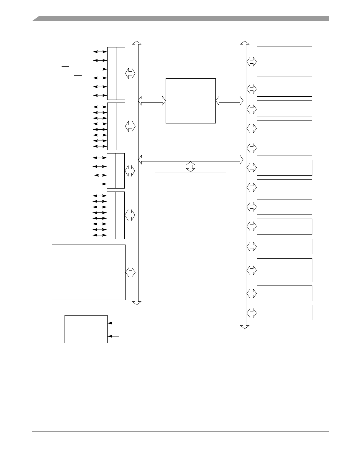
Figure 1-1 shows the structure of the MC68HC908QC16, MC68HC908QC8, and MC68HC908QC4.
1.4 Pin Assignments
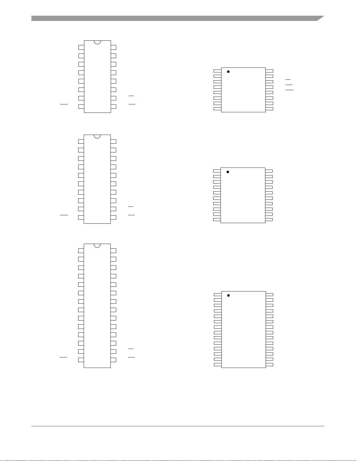
The MC68HC908QC16, MC68HC908QC8, and MC68HC908QC4 are available in 16-pin, 20-pin, and
28-pin packages. Figure 1-2 shows the pin assignment for these packages.
1.5 Pin Functions
Table 1-2 provides a description of the pin functions.
MC68HC908QC16 • MC68HC908QC8 • MC68HC908QC4 Data Sheet, Rev. 3
Freescale Semiconductor 19
General Description
All port pins can be configured with internal pullup
PTC not available on 16-pin devices (see note in 11.1 Introduction)
PTD not available on 16-pin or 20-pin devices (see note in 11.1 Introduction)
PTA0/T1CH0/AD0/KBI0
PTA1/T1CH1/AD1/KBI1
PTA2/IRQ
/KBI2/T1CLK
PTA3/RST
/KBI3
PTA4/OSC2/AD2/KBI4
PTA5/OSC1/AD3/KBI5
4-CHANNEL 16-BIT
TIMER MODULE
KEYBOARD INTERRUPT
MODULE
SINGLE INTERRUPT
MODULE
PERIODIC WAKEUP
LOW-VOLTAGE
INHIBIT
COP
MODULE
10-CHANNEL
10-BIT ADC
ENHANCED SERIAL
PTB0/SPSCK/AD4
PTB
DDRB
M68HC08 CPU
PTA
DDRA
PTB1/MOSI/T2CH1/AD5
PTB2/MISO/T2CH0/AD6
PTB3/SS
/T2CLK/AD7
PTB4/RxD/T2CH0/AD8
PTB5/TxD/T2CH1/AD9
PTB6/T1CH2
PTB7/T1CH3
POWER SUPPLY
V
DD
V
SS
CLOCK
GENERATOR
COMMUNICATIONS
INTERFACE MODULE
MODULE
SERIAL PERIPHERAL
INTERFACE
16,384 BYTES
MC68HC908QC16
8192 BYTES
MC68HC908QC8
512 BYTES
MC68HC908QC16
384 BYTES
MC68HC908QC8
BREAK
MODULE
MONITOR ROM
2-CHANNEL 16-BIT
TIMER MODULE
PTC0
PTC1
PTC2
PTC3
PTC
DDRC
PTD0
PTD
DDRD
PTD1
PTD2
PTD3
PTD4
PTD5
PTD6
PTD7
MC68HC908QC4
USER RAM
USER FLASH
4096 BYTES
384 BYTES
MC68HC908QC4
Figure 1-1. Block Diagram
MC68HC908QC16 • MC68HC908QC8 • MC68HC908QC4 Data Sheet, Rev. 3
20 Freescale Semiconductor
Pin Functions
1
2
3
4
5
6
7
8
16-PIN ASSIGNMENT
MC68HC908QCxx SOIC
16
15
14
13
12
11
10
9
1
2
3
4
5
6
7
8
20-PIN ASSIGNMENT
MC68HC908QCxx SOIC
20
19
18
17
16
15
14
13
9
10
12
11
V
DD
PTB7/T1CH3
PTB6/T1CH2
PTA5/OSC1/AD3/KBI5
PTA4/OSC2/AD2/KBI4
PTB5/TxD/T2CH1/AD9
PTB4/RxD/T2CH0/AD8
PTA3/RST/KBI3 PTA2/IRQ/KBI2/T1CLK
PTB3/SS/T2CLK/AD7
PTB2/MISO/T2CH0/AD6
PTA1/T1CH1/AD1/KBI1
PTA0/T1CH0/AD0/KBI0
PTB1/MOSI/T2CH1/AD5
PTB0/SPSCK/AD4
V
SS
V
DD
PTB7/T1CH3
PTB6/T1CH2
PTA5/OSC1/AD3/KBI5
PTA4/OSC2/AD2/KBI4
PTC1
PTC0
PTB5/TxD/T2CH1/AD9
PTB4/RxD/T2CH0/AD8
PTA3/RST/KBI3
PTB2/MISO/T2CH0/AD6
PTA1/T1CH1/AD1/KBI1
PTC3
PTC2
PTA0/T1CH0/AD0/KBI0
PTB1/MOSI/T2CH1/AD5
PTB0/SPSCK/AD4
V
SS
PTA2/IRQ/KBI2/T1CLK
PTB3/SS/T2CLK/AD7
16-PIN ASSIGNMENT
MC68HC908QCxx TSSOP
PTA0/T1CH0/AD0/KBI0
PTB1/MOSI/T2CH1/AD5
PTB0/SPSCK/AD4
V
SS
V
DD
PTB7/T1CH3
PTB6/T1CH2
PTA5/OSC1/AD3/KBI5
PTA1/T1CH1/AD1/KBI1
PTB2/MISO/T2CH0/AD6
PTB3/SS/T2CLK/AD7
PTA2/IRQ/KBI2/T1CLK
PTA3/RST/KBI3
PTB4/RxD/T2CH0/AD8
PTB5/TxD/T2CH1/AD9
PTA4/OSC2/AD2/KBI4
PTC2
PTA0/T1CH0/AD0/KBI0
PTB1/MOSI/T2CH1/AD5
PTB0/SPSCK/AD4
V
SS
V
DD
PTB7/T1CH3
PTB6/T1CH2 PTB5/TxD/T2CH1/AD9
PTB4/RxD/T2CH0/AD8
PTA3/RST/KBI3
PTA2/IRQ/KBI2/T1CLK
PTB3/SS/T2CLK/AD7
PTB2/MISO/T2CH0/AD6
PTA1/T1CH1/AD1/KBI1
PTC3
PTA5/OSC1/AD3/KBI5
PTA4/OSC2/AD2/KBI4 PTC1
PTC0
1
2
3
4
5
6
7
8
16
15
14
13
12
11
10
9
20-PIN ASSIGNMENT
MC68HC908QCxx TSSOP
1
2
3
4
5
6
7
8
20
19
18
17
16
15
14
13
9
10
12
11
PTD5
PTD4
PTC2
PTA0/T1CH0/AD0/KBI0
PTB1/MOSI/T2CH1/AD5
PTB0/SPSCK/AD4
V
SS
V
DD
PTA3/RST/KBI3
PTA2/IRQ/KBI2/T1CLK
PTB3/SS/T2CLK/AD7
PTB2/MISO/T2CH0/AD6
PTA1/T1CH1/AD1/KBI1
PTC3
PTD7
PTD6
PTB7/T1CH3
PTB6/T1CH2 PTB5/TxD/T2CH1/AD9
PTB4/RxD/T2CH0/AD8
28-PIN ASSIGNMENT
MC68HC908QCxx TSSOP
1
2
3
4
5
6
7
8
28
27
26
25
24
23
22
21
9
10
20
19
11
12
18
17
13
14
16
15
PTD0
PTC0
PTD2
PTD1
PTA5/OSC1/AD3/KBI5
PTA4/OSC2/AD2/KBI4
PTC1
PTD3
1
2
3
4
5
6
7
8
28-PIN ASSIGNMENT
MC68HC908QCxx SOIC
28
27
26
25
24
23
22
21
9
10
20
19
11
12
18
17
13
14
16
15
PTD6
PTD5
PTD4
PTC2
PTA0/T1CH0/AD0/KBI0
PTB1/MOSI/T2CH1/AD5
PTB0/SPSCK/AD4
V
SS
PTC3
PTD7
V
DD
PTB7/T1CH3
PTB6/T1CH2
PTA5/OSC1/AD3/KBI5
PTA4/OSC2/AD2/KBI4
PTC1
PTD3
PTD2
PTD1
PTD0
PTB2/MISO/T2CH0/AD6
PTA1/T1CH1/AD1/KBI1
PTA2/IRQ/KBI2/T1CLK
PTB3/SS/T2CLK/AD7
PTC0
PTB5/TxD/T2CH1/AD9
PTB4/RxD/T2CH0/AD8
PTA3/RST/KBI3
NOTE: T2CH0 and T2CH1 can be repositioned using TIM2POS in CONFIG2.
Figure 1-2. MC68HC908QC16, MC68HC908QC8, and MC68HC908QC4 Pin Assignments
MC68HC908QC16 • MC68HC908QC8 • MC68HC908QC4 Data Sheet, Rev. 3
Freescale Semiconductor 21

General Description
Table 1-2. Pin Functions
Pin Name Description Input/Output
V
V
PTA0
PTA1
PTA2
PTA3
PTA4
PTA5
PTB0
PTB1
DD
SS
(1)
Power supply Power
Power supply ground Power
PTA0 — General purpose I/O port Input/Output
T1CH0 — Timer Channel 0 I/O Input/Output
AD0 — A/D channel 0 input Input
KBI0 — Keyboard interrupt input 0 Input
PTA1 — General purpose I/O port Input/Output
T1CH1 — Timer Channel 1 I/O Input/Output
AD1 — A/D channel 1 input Input
KBI1 — Keyboard interrupt input 1 Input
PTA2 — General purpose input-only port Input
IRQ — External interrupt with programmable pullup and Schmitt trigger input Input
KBI2 — Keyboard interrupt input 2 Input
T1CLK — TIM1 timer clock input Input
PTA3 — General purpose I/O port Input/Output
RST
— Reset input, active low with internal pullup and Schmitt trigger Input
KBI3 — Keyboard interrupt input 3 Input
PTA4 — General purpose I/O port Input/Output
OSC2 —XTAL oscillator output (XTAL option only)
RC or internal oscillator output (OSC2EN = 1 in PTAPUE register)
Output
Output
AD2 — A/D channel 2 input Input
KBI4 — Keyboard interrupt input 4 Input
PTA5 — General purpose I/O port Input/Output
OSC1 — XTAL, RC, or external oscillator input Input
AD3 — A/D channel 3 input Input
KBI5 — Keyboard interrupt input 5 Input
PTB0 — General-purpose I/O port Input/Output
SPSCK— SPI serial clock Input/Output
AD4 — A/D channel 4 input Input
PTB1 — General-purpose I/O port Input/Output
MOSI — SPI data transmitted Input/Output
T2CH1
(2)
— TIM2 channel 1
Input/Output
AD5 — A/D channel 5 input Input
— Continued on next page
MC68HC908QC16 • MC68HC908QC8 • MC68HC908QC4 Data Sheet, Rev. 3
22 Freescale Semiconductor

Pin Functions
Table 1-2. Pin Functions (Continued)
Pin Name Description Input/Output
PTB2 — General-purpose I/O port Input/Output
PTB2
PTB3
PTB4
PTB5
PTB6
PTB7
PTC0–PTC2
(1, 3)
PTC3
PTD0–PTD7
MISO — SPI data received Input/Output
T2CH0
(2)
— TIM2 channel 0
Input/Output
AD6 — A/D channel 6 input Input
PTB3 — General-purpose I/O port Input/Output
SS
— SPI slave select Input
T2CLK — TIM2 timer clock input Input
AD7 — A/D channel 7 input Input
PTB4 — General-purpose I/O port Input/Output
RxD — ESCI receive data I/O Input
T2CH0
(2)
— TIM2 channel 0
Input/Output
AD8 — A/D channel 8 input Input
PTB5 — General-purpose I/O port Input/Output
TxD — ESCI transport data I/O Output
T2CH1
(2)
— TIM2 channel 1
Input/Output
AD9 — A/D channel 9 input Input
PTB6 — General-purpose I/O port Input/Output
T1CH2 — Timer channel 2 I/O Input/Output
PTB7 — General-purpose I/O port Input/Output
T1CH3 — Timer channel 3 I/O Input/Output
(3)
General-purpose I/O port Input/Output
General-purpose input port Input
(4)
General-purpose I/O port Input/Output
1. PTA2 and PTC3 pins have high voltage detectors to enter special modes.
2. T2CH0 and T2CH1 can be repositioned using TIM2POS in CONFIG2.
3. Pins not available on 16-pin devices (see note in 11.1 Introduction).
4. Pins not available on 16-pin or 20-pin devices (see note in 11.1 Introduction).
MC68HC908QC16 • MC68HC908QC8 • MC68HC908QC4 Data Sheet, Rev. 3
Freescale Semiconductor 23
General Description
1.6 Pin Function Priority
Table 1-3 is meant to resolve the priority if multiple functions are enabled on a single pin.
NOTE
Upon reset all pins come up as input ports regardless of the priority table.
Table 1-3. Function Priority in Shared Pins
Pin Name Highest-to-Lowest Priority Sequence
(1)
PTA0
(1)
PTA1
PTA2 IRQ → T1CLK → KBI2 → PTA2
PTA3 RST
(1)
PTA4
(1)
PTA5
(1)
PTB0
(1)
PTB1
(1)
PTB2
(1)
PTB3
(1)
PTB4
(1)
PTB5
PTB6 T1CH2 → PTB6
PTB7 T1CH3 → PTB7
PTCx PTCx
PTDx PTDx
1. When a pin is to be used as an ADC pin, the I/O port function should be left as
an input and all other shared modules should be disabled. The ADC does not
override additional modules using the pin.
2. T2CH0 and T2CH1 can be repositioned using TIM2POS in CONFIG2
(see Figure 2-2. Control, Status, and Data Registers).
AD0 → T1CH0 → KBI0 → PTA0
AD1 → T1CH1 → KBI1 → PTA1
→ KBI3 → PTA3
OSC2 → AD2 → KBI4 → PTA4
OSC1 → AD3 → KBI5 → PTA5
AD4 → SPSCK → PTB0
AD5 → MOSI → T2CH1
AD6 → MISO → T2CH0
AD7 → SS → T2CLK → PTB3
AD8 → RxD → T2CH0
AD9 → TxD → T2CH1
(2)
→ PTB1
(2)
→ PTB2
(2)
→ PTB4
(2)
→ PTB5
1.7 Unused Pin Termination
Input pins and I/O port pins that are not used in the application must be terminated. This prevents excess
current caused by floating inputs, and enhances immunity during noise or transient events. Termination
methods include:
1. Configuring unused pins as outputs and driving high or low;
2. Configuring unused pins as inputs and enabling internal pull-ups;
3. Configuring unused pins as inputs and using external pull-up or pull-down resistors.
Never connect unused pins directly to V
Since some general-purpose I/O pins are not available on all packages, these pins must be terminated
as well. Either method 1 or 2 above are appropriate.
MC68HC908QC16 • MC68HC908QC8 • MC68HC908QC4 Data Sheet, Rev. 3
24 Freescale Semiconductor
or VSS.
DD

Chapter 2
Memory
2.1 Introduction
The central processor unit (CPU08) can address 64 Kbytes of memory space. The memory map is shown
in Figure 2-1.
2.2 Unimplemented Memory Locations
Executing code from an unimplemented location will cause an illegal address reset. In Figure 2-1,
unimplemented locations are shaded.
2.3 Reserved Memory Locations
Accessing a reserved location can have unpredictable effects on MCU operation. In Figure 2-1, reserved
locations are marked with the word reserved or with the letter R.
2.4 Direct Page Registers
Figure 2-2 shows the memory mapped registers. Registers with addresses between $0000 and $00FF
are considered direct page registers and all instructions including those with direct page addressing
modes can access them. Registers between $0100 and $FFFF require non-direct page addressing
modes. See Chapter 6 Central Processor Unit (CPU) for more information on addressing modes.
MC68HC908QC16 • MC68HC908QC8 • MC68HC908QC4 Data Sheet, Rev. 3
Freescale Semiconductor 25
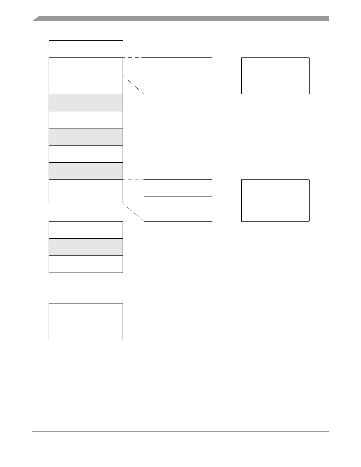
Memory
$0000
↓
$003F
$0040
↓
$023F
$0240
↓
$024F
$0250
↓
$27FF
$2800
↓
$2A1F
$2A20
↓
$2F7D
$2F7E
↓
$2FFF
$3000
↓
$BDFF
$BE00
↓
$FDFF
$FE00
↓
$FE1F
$FE20
↓
$FF7D
$FF7E
↓
$FFAF
$FFB0
↓
$FFBD
$FFBE
DIRECT PAGE REGISTERS
64 BYTES
RAM
512 BYTES
REGISTERS
16 BYTES
UNIMPLEMENTED
9648 BYTES
AUXILIARY ROM
544 BYTES
UNIMPLEMENTED
1374 BYTES
AUXILIARY ROM
130 BYTES
UNIMPLEMENTED
36,352 BYTES
FLASH MEMORY
16,384 BYTES
MISCELLANEOUS REGISTERS
32 BYTES
MONITOR ROM
350 BYTES
UNIMPLEMENTED
50 BYTES
FLASH
14 BYTES
RAM
384 BYTES
RESERVED
128 BYTES
RESERVED
8192 BYTES
FLASH MEMORY
8192 BYTES
$0040
↓
$01BF
$01C0
↓
$023F
$BE00
↓
$DDFF
$DE00
↓
$FDFF
RAM
384 BYTES
RESERVED
128 BYTES
RESERVED
12,288 BYTES
FLASH MEMORY
4096 BYTES
$0040
↓
$01BF
$01C0
↓
$023F
$BE00
↓
$EDFF
$EE00
↓
$FDFF
↓
$FFC1
$FFC2
↓
$FFCF
$FFD0
↓
$FFFF
MISCELLANEOUS REGISTERS
FLASH
14 BYTES
USER VECTORS
48 BYTES
MC68HC908QC16 Memory Map MC68HC908QC8 Memory Map MC68HC908QC4 Memory Map
Figure 2-1. Memory Map
MC68HC908QC16 • MC68HC908QC8 • MC68HC908QC4 Data Sheet, Rev. 3
26 Freescale Semiconductor
Direct Page Registers
Addr.Register Name Bit 7654321Bit 0
Port A Data Register
$0000
Port B Data Register
$0001
Port C Data Register
$0002
Port D Data Register
$0003
Data Direction Register A
$0004
Data Direction Register B
$0005
Data Direction Register C
$0006
Data Direction Register D
$0007
$0008 Reserved
(PTA)
See page 108.
(PTB)
See page 110.
(PTC)
See page 112.
(PTD)
See page 114.
(DDRA)
See page 108.
(DDRB)
See page 110.
(DDRC)
See page 113.
(DDRD)
See page 115.
Read: 0 R
Write:
Reset: Unaffected by reset
Read:
Write:
Reset: Unaffected by reset
Read: 0 0 0 0 PTC3
Write:
Reset: Unaffected by reset
Read:
Write:
Reset: Unaffected by reset
Read: 0 0
Write:
Reset:00000000
Read:
Write:
Reset:00000000
Read: 0 0 0 0 0
Write:
Reset:00000000
Read:
Write:
Reset:00000000
PTB7 PTB6 PTB5 PTB4 PTB3 PTB2 PTB1 PTB0
PTD7 PTD6 PTD5 PTD4 PTD3 PTD2 PTD1 PTD0
DDRB7 DDRB6 DDRB5 DDRB4 DDRB3 DDRB2 DDRB1 DDRB0
DDRD7 DDRD6 DDRD5 DDRD4 DDRD3 DDRD2 DDRD1 DDRD0
0
PTA5 PTA4 PTA3
DDRA5 DDRA4 DDRA3
PTA2
PTC2 PTC1 PTC0
0
DDRC2 DDRC1 DDRC0
PTA1 PTA0
DDRA1 DDRA0
Read: 0 0 0 0
Write:
Reset:00000000
Read:
PTDPUE7 PTDPUE6 PTDPUE5 PTDPUE4 PTDPUE3 PTDPUE2 PTDPUE1 PTDPUE0
Write:
Reset:00000000
Read:
OSC2EN
Write:
Reset:00000000
Read:
PTBPUE7 PTBPUE6 PTBPUE5 PTBPUE4 PTBPUE3 PTBPUE2 PTBPUE1 PTBPUE0
Write:
Reset:00000000
0
PTAPUE5 PTAPUE4 PTAPUE3 PTAPUE2 PTAPUE1 PTAPUE0
= Unimplemented R = Reserved U = Unaffected
PTCPUE3 PTCPUE2 PTCPUE1 PTCPUE0
$0009
$000A
$000B
$000C
Port C Input Pullup Enable
Register (PTCPUE)
See page 114.
Port D Input Pullup Enable
Register (PTDPUE)
See page 116.
Port A Input Pullup Enable
Register (PTAPUE)
See page 109.
Port B Input Pullup Enable
Register (PTBPUE)
See page 111.
Figure 2-2. Control, Status, and Data Registers (Sheet 1 of 8)
MC68HC908QC16 • MC68HC908QC8 • MC68HC908QC4 Data Sheet, Rev. 3
Freescale Semiconductor 27
Memory
Addr.Register Name Bit 7654321Bit 0
Read:
Write:
Reset:00101000
Read: SPRF
Write:
Reset:00001000
Read:R7R6R5R4R3R2R1R0
Write: T7 T6 T5 T4 T3 T2 T1 T0
Reset: Unaffected by reset
Read:
Write:
Reset:00000000
Read:
Write:
Reset:00000000
Read: R8
Write:
Reset:U0000000
Read: SCTE TC SCRF IDLE OR NF FE PE
Write:
Reset:11000000
Read:000000BKFRPF
Write:
Reset:00000000
Read:R7R6R5R4R3R2R1R0
Write: T7 T6 T5 T4 T3 T2 T1 T0
Reset: Unaffected by reset
Read:
Write:
Reset:00000000
Read:
Write:
Reset:00000000
Read:
Write:
Reset:00000000
SPRIE R SPMSTR CPOL CPHA SPWOM SPE SPTIE
ERRIE
LOOPS ENSCI TXINV M WAKE ILTY PEN PTY
SCTIE TCIE SCRIE ILIE TE RE RWU SBK
T8 R R ORIE NEIE FEIE PEIE
LINT LINR SCP1 SCP0 R SCR2 SCR1 SCR0
PDS2 PDS1 PDS0 PSSB4 PSSB3 PSSB2 PSSB1 PSSB0
AM1 R AM0 ACLK
= Unimplemented R = Reserved U = Unaffected
OVRF MODF SPTE
AFIN ARUN AROVFL ARD8
MODFEN SPR1 SPR0
$000D
$000E
$000F
$0010
$0011
$0012
$0013
$0014
$0015
$0016
$0017
$0018
SPI Control Register
(SPCR)
See page 185.
SPI Status and Control
Register (SPSCR)
See page 186.
SPI Data Register
(SPDR)
See page 188.
ESCI Control Register 1
(SCC1)
See page 136.
ESCI Control Register 2
(SCC2)
See page 138.
ESCI Control Register 3
(SCC3)
See page 141.
ESCI Status Register 1
(SCS1)
See page 141.
ESCI Status Register 2
(SCS2)
See page 143.
ESCI Data Register
(SCDR)
See page 144.
ESCI Baud Rate Register
(SCBR)
See page 144.
ESCI Prescaler Register
(SCPSC)
See page 146.
ESCI Arbiter Control
Register (SCIACTL)
See page 149.
Figure 2-2. Control, Status, and Data Registers (Sheet 2 of 8)
MC68HC908QC16 • MC68HC908QC8 • MC68HC908QC4 Data Sheet, Rev. 3
28 Freescale Semiconductor
Direct Page Registers
Addr.Register Name Bit 7654321Bit 0
Read: ARD7 ARD6 ARD5 ARD4 ARD3 ARD2 ARD1 ARD0
Write:
Reset:00000000
Read: 0 0 0 0 KEYF 0
Write: ACKK
IMASKK MODEK
Reset:00000000
Read: 0
Write:
R KBIE5 KBIE4 KBIE3 KBIE2 KBIE1 KBIE0
Reset:00000000
Read: 0 0
Write:
KBIP5 KBIP4 KBIP3 KBIP2 KBIP1 KBIP0
Reset:00000000
Read: 0 0 0 0 IRQF 0
Write:
ACK
IMASK MODE
Reset:00000000
Read:
(1)
IRQPUD IRQEN
Write:
Reset:00000000
00
TIM2POS ESCIBDSRC
OSCENIN-
STOP
RSTEN
(2)
$0019
$001A
$001B
$001C
$001D
$001E
ESCI Arbiter Data Register
(SCIADAT)
See page 150.
Keyboard Status and
Control Register (KBSCR)
See page 90.
Keyboard Interrupt
Enable Register (KBIER)
See page 90.
Keyboard Interrupt Polarity
Register (KBIPR)
See page 91.
IRQ Status and Control
Register (INTSCR)
See page 83.
Configuration Register 2
(CONFIG2)
See page 59.
1. One-time writable register after each reset.
2. RSTEN reset to 0 by a power-on reset (POR) only.
Configuration Register 1
$001F
TIM1 Status and Control
$0020
TIM1 Counter Register
$0021
TIM1 Counter Register Low
$0022
TIM1 Counter Modulo
$0023
Register High (T1MODH)
(CONFIG1)
See page 60.
Read:
(1)
Write:
COPRS LVISTOP LVIRSTD
Reset:00000
LVIPWRD
LVITRIP SSREC STOP COPD
(2)
1. One-time writable register after each reset.
2. LVI5OR3 reset to 0 by a power-on reset (POR) only.
Register (T1SC)
See page 198.
Read: TOF
Write: 0 TRST
TOIE TSTOP
Reset:00100000
00
Read: Bit 15 Bit 14 Bit 13 Bit 12 Bit 11 Bit 10 Bit 9 Bit 8
High (T1CNTH)
See page 199.
Write:
Reset:00000000
Read: Bit 7 Bit 6 Bit 5 Bit 4 Bit 3 Bit 2 Bit 1 Bit 0
(T1CNTL)
See page 199.
See page 200.
Write:
Reset:00000000
Read:
Write:
Bit 15 Bit 14 Bit 13 Bit 12 Bit 11 Bit 10 Bit 9 Bit 8
Reset:11111111
= Unimplemented R = Reserved U = Unaffected
Figure 2-2. Control, Status, and Data Registers (Sheet 3 of 8)
000
PS2 PS1 PS0
MC68HC908QC16 • MC68HC908QC8 • MC68HC908QC4 Data Sheet, Rev. 3
Freescale Semiconductor 29
Memory
Addr.Register Name Bit 7654321Bit 0
TIM1 Counter Modulo
$0024
$0025
$0026
$0027
$0028
$0029
$002A
$002B
↓
$002F
Register Low (T1MODL)
TIM1 Channel 0 Status and
Control Register (T1SC0)
Register High (T1CH0H)
Register Low (T1CH0L)
TIM1 Channel 1 Status and
Control Register (T1SC1)
Register High (T1CH1H)
Register Low (T1CH1L)
See page 200.
See page 201.
TIM1 Channel 0
See page 204.
TIM1 Channel 0
See page 204.
See page 198.
TIM1 Channel 1
See page 204.
TIM1 Channel 1
See page 204.
Reserved
Read:
Write:
Reset:11111111
Read: CH0F
Write: 0
Reset:00000000
Read:
Write:
Reset: Indeterminate after reset
Read:
Write:
Reset: Indeterminate after reset
Read: CH1F
Write: 0
Reset:00000000
Read:
Write:
Reset: Indeterminate after reset
Read:
Write:
Reset: Indeterminate after reset
Bit 7 Bit 6 Bit 5 Bit 4 Bit 3 Bit 2 Bit 1 Bit 0
CH0IE MS0B MS0A ELS0B ELS0A TOV0 CH0MAX
Bit 15 Bit 14 Bit 13 Bit 12 Bit 11 Bit 10 Bit 9 Bit 8
Bit 7 Bit 6 Bit 5 Bit 4 Bit 3 Bit 2 Bit 1 Bit 0
CH1IE
Bit 15 Bit 14 Bit 13 Bit 12 Bit 11 Bit 10 Bit 9 Bit 8
Bit 7 Bit 6 Bit 5 Bit 4 Bit 3 Bit 2 Bit 1 Bit 0
0
MS1A ELS1B ELS1A TOV1 CH1MAX
TIM1 Channel 2 Status and
$0030
$0031
$0032
$0033
Control Register (T1SC2)
Register High (T1CH2H)
Register Low (T1CH2L)
TIM1 Channel 3 Status and
Control Register (T1SC3)
See page 201.
TIM1 Channel 2
See page 204.
TIM1 Channel 2
See page 204.
See page 201.
Read: CH2F
Write: 0
Reset:00000000
Read:
Write:
Reset: Indeterminate after reset
Read:
Write:
Reset: Indeterminate after reset
Read: CH3F
Write: 0
Reset:00000000
Bit 15 Bit 14 Bit 13 Bit 12 Bit 11 Bit 10 Bit 9 Bit 8
Bit 7 Bit 6 Bit 5 Bit 4 Bit 3 Bit 2 Bit 1 Bit 0
CH2IE
CH3IE
= Unimplemented R = Reserved U = Unaffected
0
0
MS2A ELS2B ELS2A TOV2 CH2MAX
MS3A ELS3B ELS3A TOV3 CH3MAX
Figure 2-2. Control, Status, and Data Registers (Sheet 4 of 8)
MC68HC908QC16 • MC68HC908QC8 • MC68HC908QC4 Data Sheet, Rev. 3
30 Freescale Semiconductor

Direct Page Registers
Addr.Register Name Bit 7654321Bit 0
Read:
Write:
Reset: Indeterminate after reset
Read:
Write:
Reset: Indeterminate after reset
Read:
Write:
Reset:00000000
Bit 15 Bit 14 Bit 13 Bit 12 Bit 11 Bit 10 Bit 9 Bit 8
Bit 7 Bit 6 Bit 5 Bit 4 Bit 3 Bit 2 Bit 1 Bit 0
OSCOPT1 OSCOPT0 ICFS1 ICFS0 ECFS1 ECFS0 ECGON
ECGST
$0034
$0035
$0036
$0037
TIM1 Channel 3
Register High (T1CH3H)
See page 204.
TIM1 Channel 3
Register Low (T1CH3L)
See page 204.
Oscillator Status and
Control Register (OSCSC)
See page 104.
Reserved
Oscillator Trim Register
$0038
$0039
↓
$003B
ADC10 Status and Control
$003C
ADC10 Data Register High
$003D
ADC10 Data Register Low
$003E
ADC10 Clock Register
$003F
TIM2 Status and Control
$0240
TIM2 Counter Register High
$0241
(OSCTRIM)
See page 105.
Reserved
Register (ADSCR)
See page 54.
(ADRH)
See page 56.
(ADRL)
See page 56.
(ADCLK)
See page 56.
Register (T2SC)
See page 213.
(T2CNTH)
See page 214.
Read:
Write:
Reset:10000000
Read: COCO
Write:
Reset:00011111
Read:000000AD9AD8
Write:RRRRRRRR
Reset:00000000
Read: AD7 AD6 AD5 AD4 AD3 AD2 AD1 AD0
Write:RRRRRRRR
Reset:00000000
Read:
Write:
Reset:00000000
Read: TOF
Write: 0 TRST
Reset:00100000
Read: Bit 15 Bit 14 Bit 13 Bit 12 Bit 11 Bit 10 Bit 9 Bit 8
Write:
Reset:00000000
TRIM7 TRIM6 TRIM5 TRIM4 TRIM3 TRIM2 TRIM1 TRIM0
AIEN ADCO ADCH4 ADCH3 ADCH2 ADCH1 ADCH0
ADLPC ADIV1 ADIV0 ADICLK MODE1 MODE0 ADLSMP ADACKEN
TOIE TSTOP
= Unimplemented R = Reserved U = Unaffected
00
PS2 PS1 PS0
Figure 2-2. Control, Status, and Data Registers (Sheet 5 of 8)
MC68HC908QC16 • MC68HC908QC8 • MC68HC908QC4 Data Sheet, Rev. 3
Freescale Semiconductor 31

Memory
Addr.Register Name Bit 7654321Bit 0
TIM2 Counter Register Low
$0242
TIM2 Counter Modulo
$0243
$0244
$0245
$0246
$0247
$0248
$0249
$024A
$024B
Register High (T2MODH)
TIM2 Counter Modulo
Register Low (T2MODL)
TIM2 Channel 0 Status and
Control Register (T2SC0)
TIM2 Channel 0 Register
TIM2 Channel 0 Register
TIM2 Channel 1 Status and
Control Register (T2SC1)
TIM2 Channel 1 Register
TIM2 Channel 1 Register
(T2CNTL)
See page 214.
See page 215.
See page 215.
See page 215.
High (T2CH0H)
See page 218.
Low (T2CH0L)
See page 218.
See page 215.
High (T2CH1H)
See page 218.
Low (T2CH1L)
See page 218.
Reserved
Read: Bit 7 Bit 6 Bit 5 Bit 4 Bit 3 Bit 2 Bit 1 Bit 0
Write:
Reset:00000000
Read:
Write:
Reset:11111111
Read:
Write:
Reset:11111111
Read: CH0F
Write: 0
Reset:00000000
Read:
Write:
Reset: Indeterminate after reset
Read:
Write:
Reset: Indeterminate after reset
Read: CH1F
Write: 0
Reset:00000000
Read:
Write:
Reset: Indeterminate after reset
Read:
Write:
Reset: Indeterminate after reset
Bit 15 Bit 14 Bit 13 Bit 12 Bit 11 Bit 10 Bit 9 Bit 8
Bit 7 Bit 6 Bit 5 Bit 4 Bit 3 Bit 2 Bit 1 Bit 0
CH0IE MS0B MS0A ELS0B ELS0A TOV0 CH0MAX
Bit 15 Bit 14 Bit 13 Bit 12 Bit 11 Bit 10 Bit 9 Bit 8
Bit 7 Bit 6 Bit 5 Bit 4 Bit 3 Bit 2 Bit 1 Bit 0
CH1IE
Bit 15 Bit 14 Bit 13 Bit 12 Bit 11 Bit 10 Bit 9 Bit 8
Bit 7 Bit 6 Bit 5 Bit 4 Bit 3 Bit 2 Bit 1 Bit 0
0
MS1A ELS1B ELS1A TOV1 CH1MAX
$024C
$024D
$024E
Periodic Wakeup Status
and Control Register
(PWUSC)
See page 119.
Periodic Wakeup Prescaler
Register (PWUP)
See page 120.
Periodic Wakeup Modulo
Register (PWUMOD)
See page 121.
Read: 0 0
Write:
Reset:00000000
Read: 0 0 0 0
Write:
Reset:00000000
Read:
Write:
Reset:00000000
Bit 7 Bit 6 Bit 5 Bit 4 Bit 3 Bit 2 Bit 1 Bit 0
= Unimplemented R = Reserved U = Unaffected
PWUON
PWUCLK-
SEL
PWUF 0
PWUACK
PS3 PS2 PS1 PS0
PWUIE SMODE
Figure 2-2. Control, Status, and Data Registers (Sheet 6 of 8)
MC68HC908QC16 • MC68HC908QC8 • MC68HC908QC4 Data Sheet, Rev. 3
32 Freescale Semiconductor

Direct Page Registers
Addr.Register Name Bit 7654321Bit 0
$024F
Reserved
Break Status Register
$FE00
SIM Reset Status Register
$FE01
Break Auxiliary Register
$FE02
Break Flag Control Register
$FE03
Interrupt Status Register 1
$FE04
Interrupt Status Register 2
$FE05
Interrupt Status Register 3
$FE06
$FE07
(BSR)
See page 223.
(SRSR)
See page 167.
(BRKAR)
See page 223.
(BFCR)
See page 223.
(INT1)
See page 163.
(INT2)
See page 163.
(INT3)
See page 163.
Reserved
Read:
Write: 0
Reset: 0
Read: POR PIN COP ILOP ILAD MODRST LVI 0
Write:
POR:10000000
Read:0000000
Write:
Reset:00000000
Read:
Write:
Reset: 0
Read: IF6 IF5 IF4 IF3 IF2 IF1 0 0
Write:RRRRRRRR
Reset:00000000
Read: IF14 IF13 IF12 IF11 IF10 IF9 IF8 IF7
Write:RRRRRRRR
Reset:00000000
Read: IF22 IF21 IF20 IF19 IF18 IF17 IF16 IF15
Write:RRRRRRRR
Reset:00000000
RRRRRR
BCFERRRRRRR
SBSW
R
BDCOP
Read: 0 0 0 0
Write:
Reset:00000000
Read:
Write:
Reset:00000000
Read:
Write:
Reset:00000000
Read:
Write:
Reset:00000000
Bit 15 Bit 14 Bit 13 Bit 12 Bit 11 Bit 10 Bit 9 Bit 8
Bit 7 Bit 6 Bit 5 Bit 4 Bit 3 Bit 2 Bit 1 Bit 0
BRKE BRKA
= Unimplemented R = Reserved U = Unaffected
000000
HVEN MASS ERASE PGM
$FE08
$FE09
$FE0A
$FE0B
FLASH Control Register
(FLCR)
See page 36.
Break Address High
Register (BRKH)
See page 222.
Break Address low
Register (BRKL)
See page 222.
Break Status and Control
Register (BRKSCR)
See page 223.
Figure 2-2. Control, Status, and Data Registers (Sheet 7 of 8)
MC68HC908QC16 • MC68HC908QC8 • MC68HC908QC4 Data Sheet, Rev. 3
Freescale Semiconductor 33

Memory
Addr.Register Name Bit 7654321Bit 0
Read:LVIOUT000000R
Write:
Reset:00000000
$FE0C
$FE0D
↓
$FE0F
LVI Status Register
(LVISR)
See page 95.
Reserved
$FFBE
$FFBF
$FFC0
$FFC1
$FFFF
FLASH Block Protect
Register (FLBPR)
See page 41.
Internal Oscillator
Trim Value
COP Control Register
(COPCTL)
See page 65.
Figure 2-2. Control, Status, and Data Registers (Sheet 8 of 8)
Read:
Write:
Reset: Unaffected by reset
Read:
Write:
Reset: FLASH location with factory programmed trim value.
Read: LOW BYTE OF RESET VECTOR
Write: WRITING CLEARS COP COUNTER (ANY VALUE)
Reset: Unaffected by reset
BPR7 BPR6 BPR5 BPR4 BPR3 BPR2 BPR1 BPR0
TRIM7 TRIM6 TRIM5 TRIM4 TRIM3 TRIM2 TRIM1 TRIM0
= Unimplemented R = Reserved U = Unaffected
MC68HC908QC16 • MC68HC908QC8 • MC68HC908QC4 Data Sheet, Rev. 3
34 Freescale Semiconductor

Random-Access Memory (RAM)
Table 2-1. Vector Addresses
Vector Priority Vector Address Vector
Lowest
Highest
IF22-
IF20
IF19 $FFD6,7 PWU vector
IF18 $FFD8,9 TIM2 overflow vector
IF17 $FFDA,B TIM2 channel 1 vector
IF16 $FFDC,D TIM2 channel 0 vector
IF15 $FFDE,F ADC conversion complete vector
IF14 $FFE0,1 Keyboard vector
IF13 $FFE2,3 SPI transmit vector
IF12 $FFE4,5 SPI receive vector
IF11 $FFE6,7 ESCI transmit vector
IF10 $FFE8,9 ESCI receive vector
IF9 $FFEA,B ESCI error vector
IF8 — Not used
IF7 $FFEE,F TIM1 Channel 3 vector
IF6 $FFF0,1 TIM1 Channel 2 vector
IF5 $FFF2,3 TIM1 overflow vector
IF4 $FFF4,5 TIM1 Channel 1 vector
IF3 $FFF6,7 TIM1 Channel 0 vector
IF2 — Not used
IF1 $FFFA,B IRQ
— $FFFC,D SWI vector
— $FFFE,F Reset vector
$FFD0-
$FFD5
.
Unused vectors (available for user program)
vector
2.5 Random-Access Memory (RAM)
This MCU includes static RAM. The locations in RAM below $0100 can be accessed using the more
efficient direct addressing mode, and any single bit in this area can be accessed with the bit manipulation
instructions (BCLR, BSET, BRCLR, and BRSET). Locating the most frequently accessed program
variables in this area of RAM is preferred.
The RAM retains data when the MCU is in low-power wait or stop mode. At power-on, the contents of
RAM are uninitialized. RAM data is unaffected by any reset provided that the supply voltage does not drop
below the minimum value for RAM retention.
For compatibility with older M68HC05 MCUs, the HC08 resets the stack pointer to $00FF. In the devices
that have RAM above $00FF, it is usually best to reinitialize the stack pointer to the top of the RAM so the
direct page RAM can be used for frequently accessed RAM variables and bit-addressable program
variables. Include the following 2-instruction sequence in your reset initialization routine (where RamLast
is equated to the highest address of the RAM).
LDHX #RamLast+1 ;point one past RAM
TXS ;SP<-(H:X-1)
MC68HC908QC16 • MC68HC908QC8 • MC68HC908QC4 Data Sheet, Rev. 3
Freescale Semiconductor 35

Memory
2.6 FLASH Memory (FLASH)
The FLASH memory is intended primarily for program storage. In-circuit programming allows the
operating program to be loaded into the FLASH memory after final assembly of the application product.
It is possible to program the entire array through the single-wire monitor mode interface. Because no
special voltages are needed for FLASH erase and programming operations, in-application programming
is also possible through other software-controlled communication paths.
This subsection describes the operation of the embedded FLASH memory. The FLASH memory can be
read, programmed, and erased from the internal V
enabled through the use of an internal charge pump.
The minimum size of FLASH memory that can be erased is 64 bytes; and the maximum size of FLASH
memory that can be programmed in a program cycle is 32 bytes (a row). Program and erase operations
are facilitated through control bits in the FLASH control register (FLCR). Details for these operations
appear later in this section.
An erased bit reads as a 1 and a programmed bit reads as a 0. A security
feature prevents viewing of the FLASH contents.
2.6.1 FLASH Control Register
supply. The program and erase operations are
DD
NOTE
(1)
The FLASH control register (FLCR) controls FLASH program and erase operations.
Bit 7654321Bit 0
Read:0000
Write:
Reset:00000000
= Unimplemented
HVEN MASS ERASE PGM
Figure 2-3. FLASH Control Register (FLCR)
HVEN — High Voltage Enable Bit
This read/write bit enables high voltage from the charge pump to the memory for either program or
erase operation. It can only be set if either PGM =1 or ERASE = 1 and the proper sequence for
program or erase is followed.
1 = High voltage enabled to array and charge pump on
0 = High voltage disabled to array and charge pump off
MASS — Mass Erase Control Bit
This read/write bit configures the memory for mass erase operation.
1 = Mass erase operation selected
0 = Mass erase operation unselected
ERASE — Erase Control Bit
This read/write bit configures the memory for erase operation. ERASE is interlocked with the PGM bit
such that both bits cannot be equal to 1 or set to 1 at the same time.
1 = Erase operation selected
0 = Erase operation unselected
1. No security feature is absolutely secure. However, Freescale’s strategy is to make reading or copying the FLASH difficult
for unauthorized users.
MC68HC908QC16 • MC68HC908QC8 • MC68HC908QC4 Data Sheet, Rev. 3
36 Freescale Semiconductor

FLASH Memory (FLASH)
PGM — Program Control Bit
This read/write bit configures the memory for program operation. PGM is interlocked with the ERASE
bit such that both bits cannot be equal to 1 or set to 1 at the same time.
1 = Program operation selected
0 = Program operation unselected
2.6.2 FLASH Page Erase Operation
Use the following procedure to erase a page of FLASH memory. A page consists of 64 consecutive bytes
starting from addresses $XX00, $XX40, $XX80, or $XXC0. The 48-byte user interrupt vectors area also
forms a page. Any FLASH memory page can be erased alone.
1. Set the ERASE bit and clear the MASS bit in the FLASH control register.
2. Read the FLASH block protect register.
3. Write any data to any FLASH location within the address range of the block to be erased.
4. Wait for a time, t
5. Set the HVEN bit.
6. Wait for a time, t
7. Clear the ERASE bit.
8. Wait for a time, t
9. Clear the HVEN bit.
10. After time, t
RCV,
.
NVS
.
Erase
.
NVH
the memory can be accessed in read mode again.
NOTE
Programming and erasing of FLASH locations cannot be performed by
code being executed from the FLASH memory. While these operations
must be performed in the order as shown, other unrelated operations may
occur between the steps.
NOTE
A page erase of the vector page will erase the internal oscillator trim value
at $FFC0.
MC68HC908QC16 • MC68HC908QC8 • MC68HC908QC4 Data Sheet, Rev. 3
Freescale Semiconductor 37

Memory
2.6.3 FLASH Mass Erase Operation
Use the following procedure to erase the entire FLASH memory to read as a 1:
1. Set both the ERASE bit and the MASS bit in the FLASH control register.
2. Read the FLASH block protect register.
3. Write any data to any FLASH address
4. Wait for a time, t
NVS
.
5. Set the HVEN bit.
6. Wait for a time, t
MErase
.
7. Clear the ERASE and MASS bits.
Mass erase is disabled whenever any block is protected (FLBPR does not
equal $FF).
(1)
within the FLASH memory address range.
NOTE
8. Wait for a time, t
9. Clear the HVEN bit.
10. After time, t
RCV,
Programming and erasing of FLASH locations cannot be performed by
code being executed from the FLASH memory. While these operations
must be performed in the order as shown, other unrelated operations may
occur between the steps.
A mass erase will erase the internal oscillator trim value at $FFC0.
.
NVHL
the memory can be accessed in read mode again.
NOTE
CAUTION
1. When in monitor mode, with security sequence failed (see 18.3.2 Security), write to the FLASH block protect register instead of any FLASH address.
MC68HC908QC16 • MC68HC908QC8 • MC68HC908QC4 Data Sheet, Rev. 3
38 Freescale Semiconductor

FLASH Memory (FLASH)
2.6.4 FLASH Program Operation
Programming of the FLASH memory is done on a row basis. A row consists of 32 consecutive bytes
starting from addresses $XX00, $XX20, $XX40, $XX60, $XX80, $XXA0, $XXC0, or $XXE0. Use the
following step-by-step procedure to program a row of FLASH memory
Figure 2-4 shows a flowchart of the programming algorithm.
NOTE
Do not program any byte in the FLASH more than once after a successful
erase operation. Reprogramming bits to a byte which is already
programmed is not allowed without first erasing the page in which the byte
resides or mass erasing the entire FLASH memory. Programming without
first erasing may disturb data stored in the FLASH.
1. Set the PGM bit. This configures the memory for program operation and enables the latching of
address and data for programming.
2. Read the FLASH block protect register.
3. Write any data to any FLASH location within the address range desired.
4. Wait for a time, t
5. Set the HVEN bit.
6. Wait for a time, t
7. Write data to the FLASH address being programmed
8. Wait for time, t
9. Repeat step 7 and 8 until all desired bytes within the row are programmed.
10. Clear the PGM bit
11. Wait for time, t
12. Clear the HVEN bit.
13. After time, t
RCV
This program sequence is repeated throughout the memory until all data is programmed.
.
NVS
.
PGS
PROG
NVH
(1)
.
.
.
(1)
.
, the memory can be accessed in read mode again.
NOTE
Programming and erasing of FLASH locations cannot be performed by
code being executed from the FLASH memory. While these operations
must be performed in the order shown, other unrelated operations may
occur between the steps. Do not exceed t
maximum, see 19.17
PROG
Memory Characteristics.
1. The time between each FLASH address change, or the time between the last FLASH address programmed to clearing
PGM bit, must not exceed the maximum programming time, t
MC68HC908QC16 • MC68HC908QC8 • MC68HC908QC4 Data Sheet, Rev. 3
Freescale Semiconductor 39
PROG
maximum.

Memory
SET HVEN BIT
WRITE ANY DATA TO ANY FLASH ADDRESS
WITHIN THE ROW ADDRESS RANGE DESIRED
WAIT FOR A TIME, t
NVS
SET PGM BIT
WAIT FOR A TIME, t
PGS
WRITE DATA TO THE FLASH ADDRESS
TO BE PROGRAMMED
WAIT FOR A TIME, t
PROG
CLEAR PGM BIT
WAIT FOR A TIME, t
NVH
CLEAR HVEN BIT
WAIT FOR A TIME, t
RCV
COMPLETED
PROGRAMMING
THIS ROW?
Y
N
END OF PROGRAMMING
The time between each FLASH address change (step 7 to step 7 loop),
must not exceed the maximum programming
time, t
PROG
max.
or the time between the last FLASH address programmed
to clearing PGM bit (step 7 to step 10)
NOTES:
1
3
4
5
6
7
8
10
11
12
13
Algorithm for Programming
a Row (32 Bytes) of FLASH Memory
This row program algorithm assumes the row/s
to be programmed are initially erased.
9
READ THE FLASH BLOCK PROTECT REGISTER
2
Figure 2-4. FLASH Programming Flowchart
40 Freescale Semiconductor
MC68HC908QC16 • MC68HC908QC8 • MC68HC908QC4 Data Sheet, Rev. 3

FLASH Memory (FLASH)
2.6.5 FLASH Protection
Due to the ability of the on-board charge pump to erase and program the FLASH memory in the target
application, provision is made to protect blocks of memory from unintentional erase or program operations
due to system malfunction. This protection is done by use of a FLASH block protect register (FLBPR).
The FLBPR determines the range of the FLASH memory which is to be protected. The range of the
protected area starts from a location defined by FLBPR and ends to the bottom of the FLASH memory
($FFFF). When the memory is protected, the HVEN bit cannot be set in either ERASE or PROGRAM
operations.
NOTE
In performing a program or erase operation, the FLASH block protect
register must be read after setting the PGM or ERASE bit and before
asserting the HVEN bit.
When the FLBPR is programmed with all 0 s, the entire memory is protected from being programmed and
erased. When all the bits are erased (all 1’s), the entire memory is accessible for program and erase.
When bits within the FLBPR are programmed, they lock a block of memory. The address ranges are
shown in 2.6.6 FLASH Block Protect Register. Once the FLBPR is programmed with a value other than
$FF, any erase or program of the FLBPR or the protected block of FLASH memory is prohibited. Mass
erase is disabled whenever any block is protected (FLBPR does not equal $FF). The FLBPR itself can be
erased or programmed only with an external voltage, V
allows entry from reset into the monitor mode.
, present on the IRQ pin. This voltage also
TST
2.6.6 FLASH Block Protect Register
The FLASH block protect register is implemented as a byte within the FLASH memory, and therefore can
only be written during a programming sequence of the FLASH memory. The value in this register
determines the starting address of the protected range within the FLASH memory.
Bit 7654321Bit 0
Read:
Write:
Reset: Unaffected by reset. Initial value from factory is 1.
Write to this register is by a programming sequence to the FLASH memory.
BPR[7:0] — FLASH Protection Register Bits [7:0]
These eight bits in FLBPR represent bits [13:6] of a 16-bit memory address. Bits [15:14] are 1s and
bits [5:0] are 0s.
The resultant 16-bit address is used for specifying the start address of the FLASH memory for block
protection. The FLASH is protected from this start address to the end of FLASH memory, at $FFFF.
With this mechanism, the protect start address can be $XX00, $XX40, $XX80, or $XXC0 within the
FLASH memory. See Figure 2-6 and Table 2-2.
BPR7 BPR6 BPR5 BPR4 BPR3 BPR2 BPR1 BPR0
Figure 2-5. FLASH Block Protect Register (FLBPR)
MC68HC908QC16 • MC68HC908QC8 • MC68HC908QC4 Data Sheet, Rev. 3
Freescale Semiconductor 41

Memory
0
0
00011
FLBPR VALUE
START ADDRESS OF
16-BIT MEMORY ADDRESS
FLASH BLOCK PROTECT
0
Figure 2-6. FLASH Block Protect Start Address
Table 2-2. Examples of Protect Start Address
BPR[7:0]
(2)
$00
$01 (0000 0001) $C040 (1100 0000 0100 0000)
$02 (0000 0010) $C080 (1100 0000 1000 0000)
$03 (0000 0011) $C0C0 (1100 0000 1100 0000)
and so on...
$FD (1111 1101)$FF40 (1111 1111 0100 0000)
$FE (1111 1110)$FF80 (1111 1111 1000 0000)
$FF The entire FLASH memory is not protected.
1. The end address of the protected range is always $FFFF.
2. $BE00–$BFFF is always protected unless the entire FLASH memory is unprotected, BPR[7:0] = $FF.
Start of Address of Protect Range
The entire FLASH memory is protected.
(1)
2.6.7 EEPROM Memory Emulation Using FLASH Memory
In some applications, the user may want to repeatedly store and read a set of data from an area of
nonvolatile memory. This is easily implemented in EEPROM memory because single byte erase is
allowed in EEPROM.
When using FLASH memory, the minimum erase size is a page. However, the FLASH can be used as
EEPROM memory. This technique is called “EEPROM emulation”.
The basic concept of EEPROM emulation using FLASH is that a page is continuously programmed with
a new data set without erasing the previously programmed locations. Once the whole page is completely
programmed or the page does not have enough bytes to program a new data set, the user software
automatically erases the page and then programs a new data set in the erased page.
In EEPROM emulation when data is read from the page, the user software must find the latest data set
in the page since the previous data still remains in the same page. There are many ways to monitor the
page erase timing and the latest data set. One example is unprogrammed FLASH bytes are detected by
checking programmed bytes (non-$FF value) in a page. In this way, the end of the data set will contain
unprogrammed data ($FF value).
A couple of application notes, describing how to emulate EEPROM using FLASH, are available on our
web site. Titles and order numbers for these application notes are given at the end of this subsection.
42 Freescale Semiconductor
MC68HC908QC16 • MC68HC908QC8 • MC68HC908QC4 Data Sheet, Rev. 3

FLASH Memory (FLASH)
For EEPROM emulation software to work successfully, the following items must be taken care of in the
user software:
1. Each FLASH byte in a page must be programmed only one time until the page is erased.
2. A page must be erased before the FLASH cumulative program HV period (t
maximum t
. tHV is defined as the cumulative high-voltage programming time to the same row
HV
) is beyond the
HV
before the next erase. For more detailed information, refer to 19.17 Memory Characteristics.
3. FLASH row erase and program cycles should not exceed 10,000 cycles, respectively.
The above EEPROM emulation software can be easily developed by using the on-chip FLASH routines
implemented in the MCU. These routines are located in the ROM memory and support FLASH program
and erase operations. Proper utilization of the on-chip FLASH routines guarantee conformance to the
FLASH specifications.
In the on-chip FLASH programming routine called PRGRNGE, the high-voltage programming time is
enabled for less than 125 μs when programming a single byte at any operating bus frequency between
1.0 MHz and 8.4 MHz. Therefore, even when a row is programmed by 32 separate single-byte
programming operations, t
is less than the maximum tHV. Hence, item 2 listed above is already taken
HV
care of by using this routine.
A page erased operation is provided in the FLASH erase routine called ERARNGE.
Application note AN2635 (On-Chip FLASH Programming Routines) describes how to use these routines.
The following application notes, available at www.freescale.com, describe how EERPOM emulation is
implemented using FLASH:
AN2183 — Using FLASH as EEPROM on the MC68HC908GP32
AN2346 — EEPROM Emulation Using FLASH in MC68HC908QY/QT MCUs
AN2690 — Low Frequency EEPROM Emulation on the MC68HC908QY4
An EEPROM emulation driver, available at www.freescale.com, has been developed and qualified:
AN3040 — M68HC08 EEPROM Emulation Driver
MC68HC908QC16 • MC68HC908QC8 • MC68HC908QC4 Data Sheet, Rev. 3
Freescale Semiconductor 43

Memory
MC68HC908QC16 • MC68HC908QC8 • MC68HC908QC4 Data Sheet, Rev. 3
44 Freescale Semiconductor

Chapter 3
Analog-to-Digital Converter (ADC10) Module
3.1 Introduction
This section describes the 10-bit successive approximation analog-to-digital converter (ADC10).
The ADC10 module shares its pins with general-purpose input/output (I/O) port pins. See Figure 3-1 for
port location of these shared pins. The ADC10 on this MCU uses V
pins. This MCU uses BUSCLKX4 as its alternate clock source for the ADC. This MCU does not have a
hardware conversion trigger.
3.2 Features
Features of the ADC10 module include:
• Linear successive approximation algorithm with 10-bit resolution
• Output formatted in 10- or 8-bit right-justified format
• Single or continuous conversion (automatic power-down in single conversion mode)
• Configurable sample time and conversion speed (to save power)
• Conversion complete flag and interrupt
• Input clock selectable from up to three sources
• Operation in wait and stop modes for lower noise operation
• Selectable asynchronous hardware conversion trigger
and VSS as its supply and reference
DD
3.3 Functional Description
The ADC10 uses successive approximation to convert the input sample taken from ADVIN to a digital
representation. The approximation is taken and then rounded to the nearest 10- or 8-bit value to provide
greater accuracy and to provide a more robust mechanism for achieving the ideal code-transition voltage.
Figure 3-2 shows a block diagram of the ADC10
MC68HC908QC16 • MC68HC908QC8 • MC68HC908QC4 Data Sheet, Rev. 3
Freescale Semiconductor 45

Analog-to-Digital Converter (ADC10) Module
All port pins can be configured with internal pullup
PTC not available on 16-pin devices (see note in 11.1 Introduction)
PTD not available on 16-pin or 20-pin devices (see note in 11.1 Introduction)
PTA0/T1CH0/AD0/KBI0
PTA1/T1CH1/AD1/KBI1
PTA2/IRQ
/KBI2/T1CLK
PTA3/RST
/KBI3
PTA4/OSC2/AD2/KBI4
PTA5/OSC1/AD3/KBI5
4-CHANNEL 16-BIT
TIMER MODULE
KEYBOARD INTERRUPT
MODULE
SINGLE INTERRUPT
MODULE
PERIODIC WAKEUP
LOW-VOLTAGE
INHIBIT
COP
MODULE
10-CHANNEL
10-BIT ADC
ENHANCED SERIAL
PTB0/SPSCK/AD4
PTB
DDRB
M68HC08 CPU
PTA
DDRA
PTB1/MOSI/T2CH1/AD5
PTB2/MISO/T2CH0/AD6
PTB3/SS
/T2CLK/AD7
PTB4/RxD/T2CH0/AD8
PTB5/TxD/T2CH1/AD9
PTB6/T1CH2
PTB7/T1CH3
POWER SUPPLY
V
DD
V
SS
CLOCK
GENERATOR
COMMUNICATIONS
INTERFACE MODULE
MODULE
SERIAL PERIPHERAL
INTERFACE
16,384 BYTES
MC68HC908QC16
8192 BYTES
MC68HC908QC8
512 BYTES
MC68HC908QC16
384 BYTES
MC68HC908QC8
BREAK
MODULE
MONITOR ROM
2-CHANNEL 16-BIT
TIMER MODULE
PTC0
PTC1
PTC2
PTC3
PTC
DDRC
PTD0
PTD
DDRD
PTD1
PTD2
PTD3
PTD4
PTD5
PTD6
PTD7
MC68HC908QC4
USER RAM
USER FLASH
4096 BYTES
384 BYTES
MC68HC908QC4
Figure 3-1. Block Diagram Highlighting ADC10 Block and Pins
MC68HC908QC16 • MC68HC908QC8 • MC68HC908QC4 Data Sheet, Rev. 3
46 Freescale Semiconductor

Functional Description
AD0
• • •
ADn
V
REFH
V
REFL
ADVIN
ADCH
CONTROL SEQUENCER
INITIALIZE
SAMPLE
CONVERT
TRANSFER
ABORT
ADCK
BUS CLOCK
ALTERNATE CLOCK SOURCE
ADICLK
ADIV
ACLK
ADCO
ADSCR
ADLSMP
ADLPC
MODE
COMPLETE
DATA REGISTERS ADRH:ADRL
SAR CONVERTER
AIEN
COCO
INTERRUPT
AIEN
COCO
1
2
1 2
MCU STOP
ADHWT
ADCLK
ACLKEN
ASYNC
CLOCK
GENERATOR
CLOCK
DIVIDE
Figure 3-2. ADC10 Block Diagram
The ADC10 can perform an analog-to-digital conversion on one of the software selectable channels. The
output of the input multiplexer (ADVIN) is converted by a successive approximation algorithm into a 10-bit
digital result. When the conversion is completed, the result is placed in the data registers (ADRH and
ADRL). In 8-bit mode, the result is rounded to 8 bits and placed in ADRL. The conversion complete flag
is then set and an interrupt request is generated if AIEN has been set.
3.3.1 Clock Select and Divide Circuit
The clock select and divide circuit selects one of three clock sources and divides it by a configurable value
to generate the input clock to the converter (ADCK). The clock can be selected from one of the following
sources:
• The asynchronous clock source (ACLK) — This clock source is generated from a dedicated clock
source which is enabled when the ADC10 is converting and the clock source is selected by setting
ACLKEN. When ADLPC is clear, this clock operates from 1–2 MHz; when ADLPC is set, it operates
at 0.5–1 MHz. This clock is not disabled in STOP and allows conversions in stop mode for lower
noise operation.
• Alternate Clock Source — This clock source is equal to the external oscillator clock or four times
the bus clock. The alternate clock source is MCU specific, see 3.1 Introduction to determine source
and availability of this clock source option. This clock is selected when ADICLK and ACLKEN are
both clear.
• The bus clock — This clock source is equal to the bus frequency. This clock is selected when
ADICLK is set and ACLKEN is clear.
Whichever clock is selected, its frequency must fall within the acceptable frequency range for ADCK. If
the available clocks are too slow, the ADC10 will not perform according to specifications. If the available
MC68HC908QC16 • MC68HC908QC8 • MC68HC908QC4 Data Sheet, Rev. 3
Freescale Semiconductor 47

Analog-to-Digital Converter (ADC10) Module
clocks are too fast, then the clock must be divided to the appropriate frequency. This divider is specified
by ADIV[1:0] and can be divide-by 1, 2, 4, or 8.
3.3.2 Input Select and Pin Control
Only one analog input may be used for conversion at any given time. The channel select bits in ADSCR
are used to select the input signal for conversion.
3.3.3 Conversion Control
Conversions can be performed in either 10-bit mode or 8-bit mode as determined by the MODE bits.
Conversions can be initiated by either a software or hardware trigger. In addition, the ADC10 module can
be configured for low power operation, long sample time, and continuous conversion.
3.3.3.1 Initiating Conversions
A conversion is initiated:
• Following a write to ADSCR (with ADCH bits not all 1s) if software triggered operation is selected.
• Following a hardware trigger event if hardware triggered operation is selected.
• Following the transfer of the result to the data registers when continuous conversion is enabled.
If continuous conversions are enabled a new conversion is automatically initiated after the completion of
the current conversion. In software triggered operation, continuous conversions begin after ADSCR is
written and continue until aborted. In hardware triggered operation, continuous conversions begin after a
hardware trigger event and continue until aborted.
3.3.3.2 Completing Conversions
A conversion is completed when the result of the conversion is transferred into the data result registers,
ADRH and ADRL. This is indicated by the setting of COCO. An interrupt request is generated if AIEN is
set at the time that COCO is set.
A blocking mechanism prevents a new result from overwriting previous data in ADRH and ADRL if the
previous data is in the process of being read while in 10-bit mode (ADRH has been read but ADRL has
not). In this case the data transfer is blocked, COCO is not set, and the new result is lost. When a data
transfer is blocked, another conversion is initiated regardless of the state of ADCO (single or continuous
conversions enabled). If single conversions are enabled, this could result in several discarded
conversions and excess power consumption. To avoid this issue, the data registers must not be read after
initiating a single conversion until the conversion completes.
3.3.3.3 Aborting Conversions
Any conversion in progress will be aborted when:
• A write to ADSCR occurs (the current conversion will be aborted and a new conversion will be
initiated, if ADCH are not all 1s).
• A write to ADCLK occurs.
• The MCU is reset.
• The MCU enters stop mode with ACLK not enabled.
MC68HC908QC16 • MC68HC908QC8 • MC68HC908QC4 Data Sheet, Rev. 3
48 Freescale Semiconductor

Functional Description
21 ADCK cycles
Conversion time =
16 MHz/8
Number of bus cycles = 11.25 μs x 4 MHz = 45 cycles
3 bus cycles
4 MHz
+
= 11.25 μs
When a conversion is aborted, the contents of the data registers, ADRH and ADRL, are not altered but
continue to be the values transferred after the completion of the last successful conversion. In the case
that the conversion was aborted by a reset, ADRH and ADRL return to their reset states.
Upon reset or when a conversion is otherwise aborted, the ADC10 module will enter a low power, inactive
state. In this state, all internal clocks and references are disabled. This state is entered asynchronously
and immediately upon aborting of a conversion.
3.3.3.4 Total Conversion Time
The total conversion time depends on many factors such as sample time, bus frequency, whether
ACLKEN is set, and synchronization time. The total conversion time is summarized in Table 3-1.
Table 3-1. Total Conversion Time versus Control Conditions
Conversion Mode ACLKEN Maximum Conversion Time
8-Bit Mode (short sample — ADLSMP = 0):
Single or 1st continuous
Single or 1st continuous
Subsequent continuous (f
8-Bit Mode (long sample — ADLSMP = 1):
Single or 1st continuous
Single or 1st continuous
Subsequent continuous (f
10-Bit Mode (short sample — ADLSMP = 0):
Single or 1st continuous
Single or 1st continuous
Subsequent continuous (f
10-Bit Mode (long sample — ADLSMP = 1):
Single or 1st continuous
Single or 1st continuous
Subsequent continuous (f
Bus
Bus
Bus
Bus
≥ f
≥ f
≥ f
≥ f
ADCK
ADCK
ADCK
ADCK
)
)
)
)
0
1
X
0
1
X
0
1
X
0
1
X
18 ADCK + 3 bus clock
18 ADCK + 3 bus clock + 5 μs
16 ADCK
38 ADCK + 3 bus clock
38 ADCK + 3 bus clock + 5 μs
36 ADCK
21 ADCK + 3 bus clock
21 ADCK + 3 bus clock + 5 μs
19 ADCK
41 ADCK + 3 bus clock
41 ADCK + 3 bus clock + 5 μs
39 ADCK
The maximum total conversion time for a single conversion or the first conversion in continuous
conversion mode is determined by the clock source chosen and the divide ratio selected. The clock
source is selectable by ADICLK and ACLKEN, and the divide ratio is specified by ADIV. For example, if
the alternative clock source is 16 MHz and is selected as the input clock source, the input clock
divide-by-8 ratio is selected and the bus frequency is 4 MHz, then the conversion time for a single 10-bit
conversion is:
NOTE
The ADCK frequency must be between f
minimum and f
ADCK
ADCK
maximum to meet A/D specifications.
MC68HC908QC16 • MC68HC908QC8 • MC68HC908QC4 Data Sheet, Rev. 3
Freescale Semiconductor 49

Analog-to-Digital Converter (ADC10) Module
3.3.4 Sources of Error
Several sources of error exist for ADC conversions. These are discussed in the following sections.
3.3.4.1 Sampling Error
For proper conversions, the input must be sampled long enough to achieve the proper accuracy. Given
the maximum input resistance of approximately 15 kΩ and input capacitance of approximately 10 pF,
sampling to within 1/4
cycles / 2 MHz maximum ADCK frequency) provided the resistance of the external analog source (R
is kept below 10 kΩ. Higher source resistances or higher-accuracy sampling is possible by setting
ADLSMP (to increase the sample window to 23.5 cycles) or decreasing ADCK frequency to increase
sample time.
3.3.4.2 Pin Leakage Error
LSB (at 10-bit resolution) can be achieved within the minimum sample window (3.5
AS
)
Leakage on the I/O pins can cause conversion error if the external analog source resistance (R
If this error cannot be tolerated by the application, keep R
LSB leakage error (at 10-bit resolution).
1/4
lower than V
AS
ADVIN
/ (4096*I
Leak
) is high.
AS
) for less than
3.3.4.3 Noise-Induced Errors
System noise which occurs during the sample or conversion process can affect the accuracy of the
conversion. The ADC10 accuracy numbers are guaranteed as specified only if the following conditions
are met:
• There is a 0.1μF low-ESR capacitor from V
• There is a 0.1μF low-ESR capacitor from V
REFH
DDA
to V
to V
(if available).
REFL
(if available).
SSA
• If inductive isolation is used from the primary supply, an additional 1μF capacitor is placed from
V
DDA
•V
SSA
to V
and V
(if available).
SSA
(if available) is connected to VSS at a quiet point in the ground plane.
REFL
• The MCU is placed in wait mode immediately after initiating the conversion (next instruction after
write to ADSCR).
• There is no I/O switching, input or output, on the MCU during the conversion.
There are some situations where external system activity causes radiated or conducted noise emissions
or excessive V
noise is coupled into the ADC10. In these cases, or when the MCU cannot be placed
DD
in wait or I/O activity cannot be halted, the following recommendations may reduce the effect of noise on
the accuracy:
• Place a 0.01 μF capacitor on the selected input channel to V
REFL
or V
(if available). This will
SSA
improve noise issues but will affect sample rate based on the external analog source resistance.
• Operate the ADC10 in stop mode by setting ACLKEN, selecting the channel in ADSCR, and
executing a STOP instruction. This will reduce V
noise but will increase effective conversion time
DD
due to stop recovery.
• Average the input by converting the output many times in succession and dividing the sum of the
results. Four samples are required to eliminate the effect of a 1
LSB, one-time error.
• Reduce the effect of synchronous noise by operating off the asynchronous clock (ACLKEN=1) and
averaging. Noise that is synchronous to the ADCK cannot be averaged out.
MC68HC908QC16 • MC68HC908QC8 • MC68HC908QC4 Data Sheet, Rev. 3
50 Freescale Semiconductor

Functional Description
3.3.4.4 Code Width and Quantization Error
The ADC10 quantizes the ideal straight-line transfer function into 1024 steps (in 10-bit mode). Each step
ideally has the same height (1 code) and width. The width is defined as the delta between the transition
points from one code to the next. The ideal code width for an N bit converter (in this case N can be 8 or
10), defined as 1
LSB, is:
1
LSB = (V
REFH–VREFL
) / 2
N
Because of this quantization, there is an inherent quantization error. Because the converter performs a
conversion and then rounds to 8 or 10 bits, the code will transition when the voltage is at the midpoint
between the points where the straight line transfer function is exactly represented by the actual transfer
function. Therefore, the quantization error will be ± 1/2
however, the code width of the first ($000) conversion is only 1/2
or $3FF) is 1.5
LSB.
LSB in 8- or 10-bit mode. As a consequence,
LSB and the code width of the last ($FF
3.3.4.5 Linearity Errors
The ADC10 may also exhibit non-linearity of several forms. Every effort has been made to reduce these
errors but the user should be aware of them because they affect overall accuracy. These errors are:
• Zero-Scale Error (E
the actual code width of the first conversion and the ideal code width (1/2
) (sometimes called offset) — This error is defined as the difference between
ZS
LSB). Note, if the first
conversion is $001, then the difference between the actual $001 code width and its ideal (1
used.
• Full-Scale Error (E
the last conversion and the ideal code width (1.5
difference between the actual $3FE code width and its ideal (1
) — This error is defined as the difference between the actual code width of
FS
LSB). Note, if the last conversion is $3FE, then the
LSB) is used.
• Differential Non-Linearity (DNL) — This error is defined as the worst-case difference between the
actual code width and the ideal code width for all conversions.
• Integral Non-Linearity (INL) — This error is defined as the highest-value the (absolute value of the)
running sum of DNL achieves. More simply, this is the worst-case difference of the actual transition
voltage to a given code and its corresponding ideal transition voltage, for all codes.
• Total Unadjusted Error (TUE) — This error is defined as the difference between the actual transfer
function and the ideal straight-line transfer function, and therefore includes all forms of error.
3.3.4.6 Code Jitter, Non-Monotonicity and Missing Codes
Analog-to-digital converters are susceptible to three special forms of error. These are code jitter,
non-monotonicity, and missing codes.
• Code jitter is when, at certain points, a given input voltage converts to one of two values when
sampled repeatedly. Ideally, when the input voltage is infinitesimally smaller than the transition
voltage, the converter yields the lower code (and vice-versa). However, even very small amounts
of system noise can cause the converter to be indeterminate (between two codes) for a range of
input voltages around the transition voltage. This range is normally around ±1/2
LSB but will
increase with noise.
• Non-monotonicity is defined as when, except for code jitter, the converter converts to a lower code
for a higher input voltage.
• Missing codes are those which are never converted for any input value. In 8-bit or 10-bit mode, the
ADC10 is guaranteed to be monotonic and to have no missing codes.
LSB) is
MC68HC908QC16 • MC68HC908QC8 • MC68HC908QC4 Data Sheet, Rev. 3
Freescale Semiconductor 51

Analog-to-Digital Converter (ADC10) Module
3.4 Interrupts
When AIEN is set, the ADC10 is capable of generating an interrupt request after each conversion. An
interrupt request is generated when the conversion completes (indicated by COCO being set). COCO will
set at the end of a conversion regardless of the state of AIEN.
3.5 Low-Power Modes
The WAIT and STOP instructions put the MCU in low power-consumption standby modes.
3.5.1 Wait Mode
The ADC10 will continue the conversion process and will generate an interrupt request following a
conversion if AIEN is set. If the ADC10 is not required in wait mode, power down the ADC by setting the
channel select bits (ADCH[4:0]) to all 1s to enter a low power state before executing the WAIT instruction.
3.5.2 Stop Mode
If ACLKEN is clear, executing a STOP instruction will abort the current conversion and place the ADC10
in a low-power state. Upon return from stop mode, a write to ADSCR is required to resume conversions,
and the result stored in ADRH and ADRL will represent the last completed conversion until the new
conversion completes.
If ACLKEN is set, the ADC10 continues normal operation during stop mode. The ADC10 will continue the
conversion process and will generate an interrupt following a conversion if AIEN is set. If the ADC10 is
not required to bring the MCU out of stop mode, ensure that the ADC10 is not in continuous conversion
mode by clearing ADCO in the ADC10 status and control register before executing the STOP instruction.
In single conversion mode the ADC10 automatically enters a low-power state when the conversion is
complete. It is not necessary to set the channel select bits (ADCH[4:0]) to all 1s to enter a low-power state.
If ACLKEN is set, a conversion can be initiated while in stop using the external hardware trigger
ADEXTCO when in external convert mode. The ADC10 will operate in a low-power mode until the trigger
is asserted, at which point it will perform a conversion and assert the interrupt when complete (if AIEN is
set).
3.6 ADC10 During Break Interrupts
The system integration module (SIM) controls whether status bits in other modules can be cleared during
the break state. BCFE in the break flag control register (BFCR) enables software to clear status bits during
the break state. See BFCR in the SIM section of this data sheet.
To allow software to clear status bits during a break interrupt, write a 1 to BCFE. If a status bit is cleared
during the break state, it remains cleared when the MCU exits the break state.
To protect status bits during the break state, write a 0 to BCFE. With BCFE cleared (its default state),
software can read and write registers during the break state without affecting status bits. Some status bits
have a two-step read/write clearing procedure. If software does the first step on such a bit before the
break, the bit cannot change during the break state as long as BCFE is cleared. After the break, doing the
second step clears the status bit.
MC68HC908QC16 • MC68HC908QC8 • MC68HC908QC4 Data Sheet, Rev. 3
52 Freescale Semiconductor

I/O Signals
3.7 I/O Signals
The ADC10 module shares its pins with general-purpose input/output (I/O) port pins. See Figure 3-1 for
port location of these shared pins. The ADC10 on this MCU uses V
pins. This MCU does not have an external trigger source.
and VSS as its supply and reference
DD
3.7.1 ADC10 Analog Power Pin (V
The ADC10 analog portion uses V
to V
. If externally available, connect the V
DD
may be necessary to ensure clean V
DDA
DDA
)
DDA
as its power pin. In some packages, V
pin to the same voltage potential as VDD. External filtering
DDA
for good results.
is connected internally
DDA
NOTE
If externally available, route V
carefully for maximum noise immunity
DDA
and place bypass capacitors as near as possible to the package.
3.7.2 ADC10 Analog Ground Pin (V
The ADC10 analog portion uses V
to V
. If externally available, connect the V
SS
as its ground pin. In some packages, V
SSA
SSA
)
SSA
pin to the same voltage potential as VSS.
SSA
is connected internally
In cases where separate power supplies are used for analog and digital power, the ground connection
between these supplies should be at the V
these supplies if possible. The V
pin makes a good single point ground location.
SSA
3.7.3 ADC10 Voltage Reference High Pin (V
V
V
potential as V
the V
is the power supply for setting the high-reference voltage for the converter. In some packages,
REFH
is connected internally to V
REFH
, or may be driven by an external source that is between the minimum V
DDA
potential (V
DDA
REFH
must never exceed V
. If externally available, V
DDA
pin. This should be the only ground connection between
SSA
)
REFH
may be connected to the same
REFH
spec and
DDA
).
DDA
NOTE
Route V
carefully for maximum noise immunity and place bypass
REFH
capacitors as near as possible to the package.
AC current in the form of current spikes required to supply charge to the capacitor array at each
successive approximation step is drawn through the V
REFH
and V
loop. The best external component
REFL
to meet this current demand is a 0.1 μF capacitor with good high frequency characteristics. This capacitor
is connected between V
REFH
and V
and must be placed as close as possible to the package pins.
REFL
Resistance in the path is not recommended because the current will cause a voltage drop which could
result in conversion errors. Inductance in this path must be minimum (parasitic only).
3.7.4 ADC10 Voltage Reference Low Pin (V
V
is the power supply for setting the low-reference voltage for the converter. In some packages,
REFL
is connected internally to V
V
REFL
potential as V
. There will be a brief current associated with V
SSA
charging. If externally available, connect the V
. If externally available, connect the V
SSA
REFL
)
REFL
REFL
when the sampling capacitor is
REFL
pin to the same potential as V
pin to the same voltage
at the single point
SSA
ground location.
MC68HC908QC16 • MC68HC908QC8 • MC68HC908QC4 Data Sheet, Rev. 3
Freescale Semiconductor 53

Analog-to-Digital Converter (ADC10) Module
3.7.5 ADC10 Channel Pins (ADn)
The ADC10 has multiple input channels. Empirical data shows that capacitors on the analog inputs
improve performance in the presence of noise or when the source impedance is high. 0.01 μF capacitors
with good high-frequency characteristics are sufficient. These capacitors are not necessary in all cases,
but when used they must be placed as close as possible to the package pins and be referenced to V
SSA
3.8 Registers
These registers control and monitor operation of the ADC10:
• ADC10 status and control register, ADSCR
• ADC10 data registers, ADRH and ADRL
• ADC10 clock register, ADCLK
3.8.1 ADC10 Status and Control Register
This section describes the function of the ADC10 status and control register (ADSCR). Writing ADSCR
aborts the current conversion and initiates a new conversion (if the ADCH[4:0] bits are equal to a value
other than all 1s).
.
Bit 7654321Bit 0
Read: COCO
Write:
Reset:00011111
AIEN ADCO ADCH4 ADCH3 ADCH2 ADCH1 ADCH0
= Unimplemented
Figure 3-3. ADC10 Status and Control Register (ADSCR)
COCO — Conversion Complete Bit
COCO is a read-only bit which is set each time a conversion is completed. This bit is cleared whenever
the status and control register is written or whenever the data register (low) is read.
1 = Conversion completed
0 = Conversion not completed
AIEN — ADC10 Interrupt Enable Bit
When this bit is set, an interrupt is generated at the end of a conversion. The interrupt signal is cleared
when the data register is read or the status/control register is written.
1 = ADC10 interrupt enabled
0 = ADC10 interrupt disabled
ADCO — ADC10 Continuous Conversion Bit
When this bit is set, the ADC10 will begin to convert samples continuously (continuous conversion
mode) and update the result registers at the end of each conversion, provided ADCH[4:0] do not
decode to all 1s. The ADC10 will continue to convert until the MCU enters reset, the MCU enters stop
mode (if ACLKEN is clear), ADCLK is written, or until ADSCR is written again. If stop is entered (with
ACLKEN low), continuous conversions will cease and can be restarted only with a write to ADSCR.
Any write to ADSCR with ADCO set and the ADCH bits not all 1s will abort the current conversion and
begin continuous conversions.
MC68HC908QC16 • MC68HC908QC8 • MC68HC908QC4 Data Sheet, Rev. 3
54 Freescale Semiconductor

Registers
If the bus frequency is less than the ADCK frequency, precise sample time for continuous conversions
cannot be guaranteed in short-sample mode (ADLSMP = 0). If the bus frequency is less than 1/11th
of the ADCK frequency, precise sample time for continuous conversions cannot be guaranteed in
long-sample mode (ADLSMP = 1).
When clear, the ADC10 will perform a single conversion (single conversion mode) each time ADSCR
is written (assuming ADCH[4:0] do not decode all 1s).
1 = Continuous conversion following a write to ADSCR
0 = One conversion following a write to ADSCR
ADCH[4:0] — Channel Select Bits
The ADCH[4:0] bits form a 5-bit field that is used to select one of the input channels. The input
channels are detailed in Table 3-2. The successive approximation converter subsystem is turned off
when the channel select bits are all set to 1. This feature allows explicit disabling of the ADC10 and
isolation of the input channel from the I/O pad. Terminating continuous conversion mode this way will
prevent an additional, single conversion from being performed. It is not necessary to set the channel
select bits to all 1s to place the ADC10 in a low-power state, however, because the module is
automatically placed in a low-power state when a conversion completes.
Table 3-2. Input Channel Select
ADCH4 ADCH3 ADCH2 ADCH1 ADCH0
00000 AD0
00001 AD1
00010 AD2
00011 AD3
00100 AD4
00101 AD5
00110 AD6
00111 AD7
01000 Unused
Continuing through Unused
10111 Unused
11000 AD8
11001 AD9
11010BANDGAP REF
11011 Reserved
11100 Reserved
11101 V
11110 V
11111Low-power state
1. If any unused or reserved channels are selected, the resulting conversion will
be unknown.
2. Requires LVI to be powered (LVIPWRD =0, in CONFIG1)
Input Select
(1)
(2)
REFH
REFL
MC68HC908QC16 • MC68HC908QC8 • MC68HC908QC4 Data Sheet, Rev. 3
Freescale Semiconductor 55

Analog-to-Digital Converter (ADC10) Module
3.8.2 ADC10 Result High Register (ADRH)
This register holds the MSBs of the result and is updated each time a conversion completes. All other bits
read as 0s. Reading ADRH prevents the ADC10 from transferring subsequent conversion results into the
result registers until ADRL is read. If ADRL is not read until the after next conversion is completed, then
the intermediate conversion result will be lost. In 8-bit mode, this register contains no interlocking with
ADRL.
Bit 7654321Bit 0
Read:00000000
Write:
Reset:00000000
= Unimplemented
Figure 3-4. ADC10 Data Register High (ADRH), 8-Bit Mode
Bit 7654321Bit 0
Read:000000AD9AD8
Write:
Reset:00000000
= Unimplemented
Figure 3-5. ADC10 Data Register High (ADRH), 10-Bit Mode
3.8.3 ADC10 Result Low Register (ADRL)
This register holds the LSBs of the result. This register is updated each time a conversion completes.
Reading ADRH prevents the ADC10 from transferring subsequent conversion results into the result
registers until ADRL is read. If ADRL is not read until the after next conversion is completed, then the
intermediate conversion result will be lost. In 8-bit mode, there is no interlocking with ADRH.
Bit 7654321Bit 0
Read: AD7 AD6 AD5 AD4 AD3 AD2 AD1 AD0
Write:
Reset:00000000
= Unimplemented
Figure 3-6. ADC10 Data Register Low (ADRL)
3.8.4 ADC10 Clock Register (ADCLK)
This register selects the clock frequency for the ADC10 and the modes of operation.
Bit 7654321Bit 0
Read:
Write:
Reset:00000000
ADLPC ADIV1 ADIV0 ADICLK MODE1 MODE0 ADLSMP ACLKEN
Figure 3-7. ADC10 Clock Register (ADCLK)
MC68HC908QC16 • MC68HC908QC8 • MC68HC908QC4 Data Sheet, Rev. 3
56 Freescale Semiconductor

Registers
ADLPC — ADC10 Low-Power Configuration Bit
ADLPC controls the speed and power configuration of the successive approximation converter. This
is used to optimize power consumption when higher sample rates are not required.
1 = Low-power configuration: The power is reduced at the expense of maximum clock speed.
0 = High-speed configuration
ADIV[1:0] — ADC10 Clock Divider Bits
ADIV1 and ADIV0 select the divide ratio used by the ADC10 to generate the internal clock ADCK.
Table 3-3 shows the available clock configurations.
Table 3-3. ADC10 Clock Divide Ratio
ADIV1 ADIV0 Divide Ratio (ADIV) Clock Rate
0 0 1 Input clock ÷ 1
0 1 2 Input clock ÷ 2
1 0 4 Input clock ÷ 4
1 1 8 Input clock ÷ 8
ADICLK — Input Clock Select Bit
If ACLKEN is clear, ADICLK selects either the bus clock or an alternate clock source as the input clock
source to generate the internal clock ADCK. If the alternate clock source is less than the minimum
clock speed, use the internally-generated bus clock as the clock source. As long as the internal clock
ADCK, which is equal to the selected input clock divided by ADIV, is at a frequency (f
ADCK
) between
the minimum and maximum clock speeds (considering ALPC), correct operation can be guaranteed.
1 = The internal bus clock is selected as the input clock source
0 = The alternate clock source is selected
MODE[1:0] — 10- or 8-Bit or Hardware Triggered Mode Selection
These bits select 10- or 8-bit operation. The successive approximation converter generates a result
that is rounded to 8- or 10-bit value based on the mode selection. This rounding process sets the
transfer function to transition at the midpoint between the ideal code voltages, causing a quantization
error of ± 1/2
LSB.
Reset returns 8-bit mode.
00 = 8-bit, right-justified, ADSCR software triggered mode enabled
01 = 10-bit, right-justified, ADSCR software triggered mode enabled
10 = Reserved
11 = 10-bit, right-justified, hardware triggered mode enabled
ADLSMP — Long Sample Time Configuration
This bit configures the sample time of the ADC10 to either 3.5 or 23.5 ADCK clock cycles. This adjusts
the sample period to allow higher impedance inputs to be accurately sampled or to maximize
conversion speed for lower impedance inputs. Longer sample times can also be used to lower overall
power consumption in continuous conversion mode if high conversion rates are not required.
1 = Long sample time (23.5 cycles)
0 = Short sample time (3.5 cycles)
MC68HC908QC16 • MC68HC908QC8 • MC68HC908QC4 Data Sheet, Rev. 3
Freescale Semiconductor 57

Analog-to-Digital Converter (ADC10) Module
ACLKEN — Asynchronous Clock Source Enable
This bit enables the asynchronous clock source as the input clock to generate the internal clock ADCK,
and allows operation in stop mode. The asynchronous clock source will operate between 1 MHz and
2 MHz if ADLPC is clear, and between 0.5 MHz and 1 MHz if ADLPC is set.
1 = The asynchronous clock is selected as the input clock source (the clock generator is only
enabled during the conversion)
0 = ADICLK specifies the input clock source and conversions will not continue in stop mode
MC68HC908QC16 • MC68HC908QC8 • MC68HC908QC4 Data Sheet, Rev. 3
58 Freescale Semiconductor

Chapter 4
Configuration Registers (CONFIG1 and CONFIG2)
4.1 Introduction
This section describes the configuration registers (CONFIG1 and CONFIG2). The configuration registers
enable or disable the following options:
• Stop mode recovery time (32 × BUSCLKX4 cycles or 4096 × BUSCLKX4 cycles)
•STOP instruction
• Computer operating properly module (COP)
• COP reset period (COPRS): 8176 × BUSCLKX4 or 262,128 × BUSCLKX4
• Low-voltage inhibit (LVI) enable and trip voltage selection
• Allow clock source to remain enabled in STOP
• Enable IRQ
• Disable IRQ
• Enable RST
• Clock source selection for the enhanced serial communication interface (ESCI) module
• Reposition TIM2 timer channels
4.2 Functional Description
pin
pin pullup device
pin
The configuration registers are used in the initialization of various options. The configuration registers can
be written once after each reset. Most of the configuration register bits are cleared during reset. Since the
various options affect the operation of the microcontroller unit (MCU) it is recommended that this register
be written immediately after reset. The configuration registers are located at $001E and $001F, and may
be read at anytime.
NOTE
The CONFIG registers are one-time writable by the user after each reset.
Upon a reset, the CONFIG registers default to predetermined settings as
shown in Figure 4-1 and Figure 4-2.
Bit 7 6 5 4 3 2 1 Bit 0
Read:
IRQPUD IRQEN
Write:
Reset:000 0 0 0 0U
POR:000 0 0 0 00
= Unimplemented U = Unaffected
00
TIM2POS ESCIBDSRC
OSCENIN
STOP
RSTEN
Figure 4-1. Configuration Register 2 (CONFIG2)
MC68HC908QC16 • MC68HC908QC8 • MC68HC908QC4 Data Sheet, Rev. 3
Freescale Semiconductor 59

Configuration Registers (CONFIG1 and CONFIG2)
IRQPUD — IRQ Pin Pullup Control Bit
1 = Internal pullup is disconnected
0 = Internal pullup is connected between IRQ
pin and V
DD
IRQEN — IRQ Pin Function Selection Bit
1 = Interrupt request function active in pin
0 = Interrupt request function inactive in pin
TIM2POS — TIM2 Position Bit
TIM2POS is used to reposition the timer channels for TIM2 to a different pair of pins. This allows the
user to free up one of the communication ports based on application needs.
1 = TIM2 timer channel pins share PTB4 and PTB5
0 = TIM2 timer channel pins share PTB1 and PTB2
ESCIBDSRC — ESCI Baud Rate Clock Source Bit
ESCIBDSRC controls the clock source used for the ESCI. The setting of the bit affects the frequency
at which the ESCI operates.
1 = Internal data bus clock used as clock source for ESCI
0 = BUSCLKX4 used as clock source for ESCI
OSCENINSTOP— Oscillator Enable in Stop Mode Bit
OSCENINSTOP, when set, will allow the clock source to continue to generate clocks in stop mode.
This function can be used to keep the periodic wakeup running while the rest of the microcontroller
stops. When clear, the clock source is disabled when the microcontroller enters stop mode.
1 = Oscillator enabled to operate during stop mode
0 = Oscillator disabled during stop mode
RSTEN — RST
Pin Function Selection
1 = Reset function active in pin
0 = Reset function inactive in pin
The RSTEN bit is cleared by a power-on reset (POR) only. Other resets will
leave this bit unaffected.
Bit 7 6 5 4 3 2 1 Bit 0
Read:
Write:
Reset:0000U000
COPRS LVISTOP LVIRSTD LVIPWRD LVITRIP SSREC STOP COPD
POR:00000000
U = Unaffected
Figure 4-2. Configuration Register 1 (CONFIG1)
COPRS — COP Reset Period Selection Bit
1 = COP reset short cycle = 8176 × BUSCLKX4
0 = COP reset long cycle = 262,128 × BUSCLKX4
NOTE
MC68HC908QC16 • MC68HC908QC8 • MC68HC908QC4 Data Sheet, Rev. 3
60 Freescale Semiconductor

Functional Description
LVISTOP — LVI Enable in Stop Mode Bit
When the LVIPWRD bit is clear, setting the LVISTOP bit enables the LVI to operate during stop mode.
Reset clears LVISTOP.
1 = LVI enabled during stop mode
0 = LVI disabled during stop mode
LVIRSTD — LVI Reset Disable Bit
LVIRSTD disables the reset signal from the LVI module.
1 = LVI module resets disabled
0 = LVI module resets enabled
LVIPWRD — LVI Power Disable Bit
LVIPWRD disables the LVI module.
1 = LVI module power disabled
0 = LVI module power enabled
LVITRIP — LVI Trip Point Selection Bit
LVITRIP selects the voltage operating mode of the LVI module. The voltage mode selected for the LVI
should match the operating V
for the LVI’s voltage trip points for each of the modes.
DD
1 = LVI operates for a 5-V protection
0 = LVI operates for a 3.3-V protection
NOTE
The LVITRIP bit is cleared by a power-on reset (POR) only. Other resets
will leave this bit unaffected.
SSREC — Short Stop Recovery Bit
SSREC enables the CPU to exit stop mode with a delay of 32 BUSCLKX4 cycles instead of a 4096
BUSCLKX4 cycle delay.
1 = Stop mode recovery after 32 BUSCLKX4 cycles
0 = Stop mode recovery after 4096 BUSCLKX4 cycles
NOTE
Exiting stop mode by an LVI reset will result in the long stop recovery.
When using the LVI during normal operation but disabling during stop mode, the LVI will have an
enable time of t
. The system stabilization time for power-on reset and long stop recovery (both 4096
EN
BUSCLKX4 cycles) gives a delay longer than the LVI enable time for these startup scenarios. There
is no period where the MCU is not protected from a low-power condition. However, when using the
short stop recovery configuration option, the 32 BUSCLKX4 delay must be greater than the LVI’s turn
on time to avoid a period in startup where the LVI is not protecting the MCU.
STOP — STOP Instruction Enable Bit
STOP enables the STOP instruction.
1 = STOP instruction enabled
0 = STOP instruction treated as illegal opcode
COPD — COP Disable Bit
COPD disables the COP module.
1 = COP module disabled
0 = COP module enabled
MC68HC908QC16 • MC68HC908QC8 • MC68HC908QC4 Data Sheet, Rev. 3
Freescale Semiconductor 61

Configuration Registers (CONFIG1 and CONFIG2)
MC68HC908QC16 • MC68HC908QC8 • MC68HC908QC4 Data Sheet, Rev. 3
62 Freescale Semiconductor

Chapter 5
1. See Chapter 14 System Integration Module (SIM) for more details.
COPCTL WRITE
BUSCLKX4
STOP INSTRUCTION
SIM RESET CIRCUIT
RESET STATUS REGISTER
INTERNAL RESET SOURCES
(1)
SIM MODULE
CLEAR STAGES 5–12
12-BIT SIM COUNTER
CLEAR ALL STAGES
COPD (FROM CONFIG1)
RESET
COPCTL WRITE
CLEAR
COP MODULE
COPEN (FROM SIM)
COP CLOCK
COP TIMEOUT
COP RATE SELECT
(COPRS FROM CONFIG1)
6-BIT COP COUNTER
COP COUNTER
Computer Operating Properly (COP)
5.1 Introduction
The computer operating properly (COP) module contains a free-running counter that generates a reset if
allowed to overflow. The COP module helps software recover from runaway code. Prevent a COP reset
by clearing the COP counter periodically. The COP module can be disabled through the COPD bit in the
configuration 1 (CONFIG1) register.
5.2 Functional Description
Freescale Semiconductor 63
MC68HC908QC16 • MC68HC908QC8 • MC68HC908QC4 Data Sheet, Rev. 3
Figure 5-1. COP Block Diagram

Computer Operating Properly (COP)
The COP counter is a free-running 6-bit counter preceded by the 12-bit system integration module (SIM)
counter. If not cleared by software, the COP counter overflows and generates an asynchronous reset after
262,128 or 8176 BUSCLKX4 cycles; depending on the state of the COP rate select bit, COPRS, in
configuration register 1. With a 262,128 BUSCLKX4 cycle overflow option, the internal 12.8-MHz
oscillator gives a COP timeout period of 20.48 ms. Writing any value to location $FFFF before an overflow
occurs prevents a COP reset by clearing the COP counter and stages 12–5 of the SIM counter.
NOTE
Service the COP immediately after reset and before entering or after exiting
stop mode to guarantee the maximum time before the first COP counter
overflow.
A COP reset pulls the RST
cycles and sets the COP bit in the reset status register (RSR). See 14.8.1 SIM Reset Status Register.
Place COP clearing instructions in the main program and not in an interrupt
subroutine. Such an interrupt subroutine could keep the COP from
generating a reset even while the main program is not working properly.
pin low (if the RSTEN bit is set in the CONFIG1 register) for 32 × BUSCLKX4
NOTE
5.3 I/O Signals
The following paragraphs describe the signals shown in Figure 5-1.
5.3.1 BUSCLKX4
BUSCLKX4 is the oscillator output signal. BUSCLKX4 frequency is equal to the crystal frequency, internal
oscillator frequency, or the RC-oscillator frequency.
5.3.2 STOP Instruction
The STOP instruction clears the SIM counter.
5.3.3 COPCTL Write
Writing any value to the COP control register (COPCTL) (see 5.4 COP Control Register) clears the COP
counter and clears stages 12–5 of the SIM counter. Reading the COP control register returns the low byte
of the reset vector.
5.3.4 Power-On Reset
The power-on reset (POR) circuit in the SIM clears the SIM counter 4096 × BUSCLKX4 cycles after power
up.
5.3.5 Internal Reset
An internal reset clears the SIM counter and the COP counter.
5.3.6 COPD (COP Disable)
The COPD signal reflects the state of the COP disable bit (COPD) in the configuration register (CONFIG).
See Chapter 4 Configuration Registers (CONFIG1 and CONFIG2).
MC68HC908QC16 • MC68HC908QC8 • MC68HC908QC4 Data Sheet, Rev. 3
64 Freescale Semiconductor

COP Control Register
5.3.7 COPRS (COP Rate Select)
The COPRS signal reflects the state of the COP rate select bit (COPRS) in the configuration register 1
(CONFIG1). See Chapter 4 Configuration Registers (CONFIG1 and CONFIG2).
5.4 COP Control Register
The COP control register (COPCTL) is located at address $FFFF and overlaps the reset vector. Writing
any value to $FFFF clears the COP counter and starts a new timeout period. Reading location $FFFF
returns the low byte of the reset vector.
Bit 7654321Bit 0
Read: LOW BYTE OF RESET VECTOR
Write: CLEAR COP COUNTER
Reset: Unaffected by reset
Figure 5-2. COP Control Register (COPCTL)
5.5 Interrupts
The COP does not generate CPU interrupt requests.
5.6 Monitor Mode
The COP is disabled in monitor mode when V
is present on the IRQ pin.
TST
5.7 Low-Power Modes
The WAIT and STOP instructions put the MCU in low power-consumption standby modes.
5.7.1 Wait Mode
The COP continues to operate during wait mode. To prevent a COP reset during wait mode, periodically
clear the COP counter.
5.7.2 Stop Mode
Stop mode turns off the BUSCLKX4 input to the COP and clears the SIM counter. Service the COP
immediately before entering or after exiting stop mode to ensure a full COP timeout period after entering
or exiting stop mode.
5.8 COP Module During Break Mode
The COP is disabled during a break interrupt with monitor mode when BDCOP bit is set in break auxiliary
register (BRKAR).
MC68HC908QC16 • MC68HC908QC8 • MC68HC908QC4 Data Sheet, Rev. 3
Freescale Semiconductor 65

Computer Operating Properly (COP)
MC68HC908QC16 • MC68HC908QC8 • MC68HC908QC4 Data Sheet, Rev. 3
66 Freescale Semiconductor

Chapter 6
Central Processor Unit (CPU)
6.1 Introduction
The M68HC08 CPU (central processor unit) is an enhanced and fully object-code-compatible version of
the M68HC05 CPU. The CPU08 Reference Manual (document order number CPU08RM/AD) contains a
description of the CPU instruction set, addressing modes, and architecture.
6.2 Features
Features of the CPU include:
• Object code fully upward-compatible with M68HC05 Family
• 16-bit stack pointer with stack manipulation instructions
• 16-bit index register with x-register manipulation instructions
• 8-MHz CPU internal bus frequency
• 64-Kbyte program/data memory space
• 16 addressing modes
• Memory-to-memory data moves without using accumulator
• Fast 8-bit by 8-bit multiply and 16-bit by 8-bit divide instructions
• Enhanced binary-coded decimal (BCD) data handling
• Modular architecture with expandable internal bus definition for extension of addressing range
beyond 64 Kbytes
• Low-power stop and wait modes
6.3 CPU Registers
Figure 6-1 shows the five CPU registers. CPU registers are not part of the memory map.
MC68HC908QC16 • MC68HC908QC8 • MC68HC908QC4 Data Sheet, Rev. 3
Freescale Semiconductor 67

Central Processor Unit (CPU)
ACCUMULATOR (A)
INDEX REGISTER (H:X)
STACK POINTER (SP)
PROGRAM COUNTER (PC)
CONDITION CODE REGISTER (CCR)
CARRY/BORROW FLAG
ZERO FLAG
NEGATIVE FLAG
INTERRUPT MASK
HALF-CARRY FLAG
TWO’S COMPLEMENT OVERFLOW FLAG
V11HINZC
H X
0
0
0
0
7
15
15
15
70
6.3.1 Accumulator
Figure 6-1. CPU Registers
The accumulator is a general-purpose 8-bit register. The CPU uses the accumulator to hold operands and
the results of arithmetic/logic operations.
Bit 7654321Bit 0
Read:
Write:
Reset: Unaffected by reset
Figure 6-2. Accumulator (A)
6.3.2 Index Register
The 16-bit index register allows indexed addressing of a 64-Kbyte memory space. H is the upper byte of
the index register, and X is the lower byte. H:X is the concatenated 16-bit index register.
In the indexed addressing modes, the CPU uses the contents of the index register to determine the
conditional address of the operand.
The index register can serve also as a temporary data storage location.
Bit
151413121110987654321
Read:
Write:
Reset:00000000XXXXXXXX
X = Indeterminate
Figure 6-3. Index Register (H:X)
Bit
0
MC68HC908QC16 • MC68HC908QC8 • MC68HC908QC4 Data Sheet, Rev. 3
68 Freescale Semiconductor

CPU Registers
6.3.3 Stack Pointer
The stack pointer is a 16-bit register that contains the address of the next location on the stack. During a
reset, the stack pointer is preset to $00FF. The reset stack pointer (RSP) instruction sets the least
significant byte to $FF and does not affect the most significant byte. The stack pointer decrements as data
is pushed onto the stack and increments as data is pulled from the stack.
In the stack pointer 8-bit offset and 16-bit offset addressing modes, the stack pointer can function as an
index register to access data on the stack. The CPU uses the contents of the stack pointer to determine
the conditional address of the operand.
Bit
151413121110987654321
Read:
Write:
Reset:0000000011111111
Bit
0
Figure 6-4. Stack Pointer (SP)
NOTE
The location of the stack is arbitrary and may be relocated anywhere in
random-access memory (RAM). Moving the SP out of page 0 ($0000 to
$00FF) frees direct address (page 0) space. For correct operation, the
stack pointer must point only to RAM locations.
6.3.4 Program Counter
The program counter is a 16-bit register that contains the address of the next instruction or operand to be
fetched.
Normally, the program counter automatically increments to the next sequential memory location every
time an instruction or operand is fetched. Jump, branch, and interrupt operations load the program
counter with an address other than that of the next sequential location.
During reset, the program counter is loaded with the reset vector address located at $FFFE and $FFFF.
The vector address is the address of the first instruction to be executed after exiting the reset state.
Bit
151413121110987654321
Read:
Write:
Reset: Loaded with vector from $FFFE and $FFFF
Bit
0
Figure 6-5. Program Counter (PC)
MC68HC908QC16 • MC68HC908QC8 • MC68HC908QC4 Data Sheet, Rev. 3
Freescale Semiconductor 69

Central Processor Unit (CPU)
6.3.5 Condition Code Register
The 8-bit condition code register contains the interrupt mask and five flags that indicate the results of the
instruction just executed. Bits 6 and 5 are set permanently to 1. The following paragraphs describe the
functions of the condition code register.
Bit 7654321Bit 0
Read:
Write:
Reset:X11X1XXX
V — Overflow Flag
The CPU sets the overflow flag when a two's complement overflow occurs. The signed branch
instructions BGT, BGE, BLE, and BLT use the overflow flag.
1 = Overflow
0 = No overflow
H — Half-Carry Flag
The CPU sets the half-carry flag when a carry occurs between accumulator bits 3 and 4 during an
add-without-carry (ADD) or add-with-carry (ADC) operation. The half-carry flag is required for
binary-coded decimal (BCD) arithmetic operations. The DAA instruction uses the states of the H and
C flags to determine the appropriate correction factor.
1 = Carry between bits 3 and 4
0 = No carry between bits 3 and 4
V11HI NZC
X = Indeterminate
Figure 6-6. Condition Code Register (CCR)
I — Interrupt Mask
When the interrupt mask is set, all maskable CPU interrupts are disabled. CPU interrupts are enabled
when the interrupt mask is cleared. When a CPU interrupt occurs, the interrupt mask is set
automatically after the CPU registers are saved on the stack, but before the interrupt vector is fetched.
1 = Interrupts disabled
0 = Interrupts enabled
NOTE
To maintain M6805 Family compatibility, the upper byte of the index
register (H) is not stacked automatically. If the interrupt service routine
modifies H, then the user must stack and unstack H using the PSHH and
PULH instructions.
After the I bit is cleared, the highest-priority interrupt request is serviced first.
A return-from-interrupt (RTI) instruction pulls the CPU registers from the stack and restores the
interrupt mask from the stack. After any reset, the interrupt mask is set and can be cleared only by the
clear interrupt mask software instruction (CLI).
N — Negative Flag
The CPU sets the negative flag when an arithmetic operation, logic operation, or data manipulation
produces a negative result, setting bit 7 of the result.
1 = Negative result
0 = Non-negative result
MC68HC908QC16 • MC68HC908QC8 • MC68HC908QC4 Data Sheet, Rev. 3
70 Freescale Semiconductor

Arithmetic/Logic Unit (ALU)
Z — Zero Flag
The CPU sets the zero flag when an arithmetic operation, logic operation, or data manipulation
produces a result of $00.
1 = Zero result
0 = Non-zero result
C — Carry/Borrow Flag
The CPU sets the carry/borrow flag when an addition operation produces a carry out of bit 7 of the
accumulator or when a subtraction operation requires a borrow. Some instructions — such as bit test
and branch, shift, and rotate — also clear or set the carry/borrow flag.
1 = Carry out of bit 7
0 = No carry out of bit 7
6.4 Arithmetic/Logic Unit (ALU)
The ALU performs the arithmetic and logic operations defined by the instruction set.
Refer to the CPU08 Reference Manual (document order number CPU08RM/AD) for a description of the
instructions and addressing modes and more detail about the architecture of the CPU.
6.5 Low-Power Modes
The WAIT and STOP instructions put the MCU in low power-consumption standby modes.
6.5.1 Wait Mode
The WAIT instruction:
• Clears the interrupt mask (I bit) in the condition code register, enabling interrupts. After exit from
wait mode by interrupt, the I bit remains clear. After exit by reset, the I bit is set.
• Disables the CPU clock
6.5.2 Stop Mode
The STOP instruction:
• Clears the interrupt mask (I bit) in the condition code register, enabling external interrupts. After
exit from stop mode by external interrupt, the I bit remains clear. After exit by reset, the I bit is set.
• Disables the CPU clock
After exiting stop mode, the CPU clock begins running after the oscillator stabilization delay.
6.6 CPU During Break Interrupts
If a break module is present on the MCU, the CPU starts a break interrupt by:
• Loading the instruction register with the SWI instruction
• Loading the program counter with $FFFC:$FFFD or with $FEFC:$FEFD in monitor mode
The break interrupt begins after completion of the CPU instruction in progress. If the break address
register match occurs on the last cycle of a CPU instruction, the break interrupt begins immediately.
A return-from-interrupt instruction (RTI) in the break routine ends the break interrupt and returns the MCU
to normal operation if the break interrupt has been deasserted.
MC68HC908QC16 • MC68HC908QC8 • MC68HC908QC4 Data Sheet, Rev. 3
Freescale Semiconductor 71

Central Processor Unit (CPU)
C
b0
b7
0
b0
b7
C
6.7 Instruction Set Summary
Table 6-1 provides a summary of the M68HC08 instruction set.
Table 6-1. Instruction Set Summary (Sheet 1 of 6)
Effect
Source
Form
ADC #opr
ADC opr
ADC opr
ADC opr,X
ADC opr,X
ADC ,X
ADC opr,SP
ADC opr,SP
ADD #opr
ADD opr
ADD opr
ADD opr,X
ADD opr,X
ADD ,X
ADD opr,SP
ADD opr,SP
AIS #
opr Add Immediate Value (Signed) to SP
AIX #opr Add Immediate Value (Signed) to H:X
AND #opr
AND opr
AND opr
AND opr,X
AND opr,X
AND ,X
AND opr,SP
AND opr,SP
ASL opr
ASLA
ASLX
ASL opr,X
ASL ,X
ASL opr,SP
ASR opr
ASRA
ASRX
ASR opr,X
ASR opr,X
ASR opr,SP
BCC rel Branch if Carry Bit Clear PC ← (PC) + 2 + rel ? (C) = 0 ––––––REL 24 rr 3
BCLR n, opr Clear Bit n in M Mn ← 0 ––––––
BCS rel Branch if Carry Bit Set (Same as BLO) PC ← (PC) + 2 + rel ? (C) = 1 ––––––REL 25 rr 3
BEQ rel Branch if Equal PC ← (PC) + 2 + rel ? (Z) = 1 ––––––REL 27 rr 3
BGE opr
BGT opr
BHCC rel Branch if Half Carry Bit Clear PC ← (PC) + 2 + rel ? (H) = 0 ––––––REL 28 rr 3
BHCS rel Branch if Half Carry Bit Set PC ← (PC) + 2 + rel ? (H) = 1 ––––––REL 29 rr 3
BHI rel Branch if Higher PC ← (PC) + 2 + rel ? (C) | (Z) = 0 ––––––REL 22 rr 3
Add with Carry A ← (A) + (M) + (C) –
Add without Carry A ← (A) + (M) –
Logical AND A ← (A) & (M) 0 – – –
Arithmetic Shift Left
(Same as LSL)
Arithmetic Shift Right ––
Branch if Greater Than or Equal To
(Signed Operands)
Branch if Greater Than (Signed
Operands)
Operation Description
SP ← (SP) + (16
H:X ← (H:X) + (16
PC ← (PC) + 2 + rel ? (N
PC ← (PC) + 2 + rel ? (Z) | (N
« M)
« M)
⊕ V) = 0
⊕ V) = 0
on CCR
VH I NZC
––––––IMM A7 ii 2
––––––IMM AF ii 2
––
––––––REL 90 rr 3
––––––REL 92 rr 3
Address
Mode
IMM
DIR
EXT
IX2
IX1
IX
SP1
SP2
IMM
DIR
EXT
IX2
IX1
IX
SP1
SP2
IMM
DIR
EXT
IX2
IX1
IX
SP1
SP2
DIR
INH
INH
IX1
IX
SP1
DIR
INH
INH
IX1
IX
SP1
DIR (b0)
DIR (b1)
DIR (b2)
DIR (b3)
DIR (b4)
DIR (b5)
DIR (b6)
DIR (b7)
A9
B9
C9
D9
E9
F9
9EE9
9ED9
AB
BB
CB
DB
EB
FB
9EEB
9EDB
A4
B4
C4
D4
E4
F4
9EE4
9ED4
38
48
58
68
78
9E68
37
47
57
67
77
9E67
11
13
15
17
19
1B
1D
1F
Opcode
ii
dd
hh ll
ee ff
ff
ff
ee ff
ii
dd
hh ll
ee ff
ff
ff
ee ff
ii
dd
hh ll
ee ff
ff
ff
ee ff
dd
ff
ff
dd
ff
ff
dd
dd
dd
dd
dd
dd
dd
dd
Operand
Cycles
2
3
4
4
3
2
4
5
2
3
4
4
3
2
4
5
2
3
4
4
3
2
4
5
4
1
1
4
3
5
4
1
1
4
3
5
4
4
4
4
4
4
4
4
MC68HC908QC16 • MC68HC908QC8 • MC68HC908QC4 Data Sheet, Rev. 3
72 Freescale Semiconductor

Instruction Set Summary
Table 6-1. Instruction Set Summary (Sheet 2 of 6)
Effect
Source
Form
BHS rel
BIH rel Branch if IRQ
BIL rel Branch if IRQ
BIT #opr
BIT opr
BIT opr
BIT opr,X
BIT opr,X
BIT ,X
BIT opr,SP
BIT opr,SP
BLE opr
BLO rel Branch if Lower (Same as BCS) PC ← (PC) + 2 + rel ? (C) = 1 ––––––REL 25 rr 3
BLS rel Branch if Lower or Same PC ← (PC) + 2 + rel ? (C) | (Z) = 1 ––––––REL 23 rr 3
BLT opr Branch if Less Than (Signed Operands)
BMC rel Branch if Interrupt Mask Clear PC ← (PC) + 2 + rel ? (I) = 0 ––––––REL 2C rr 3
BMI rel Branch if Minus PC ← (PC) + 2 + rel ? (N) = 1 ––––––REL 2B rr 3
BMS rel Branch if Interrupt Mask Set PC ← (PC) + 2 + rel ? (I) = 1 ––––––REL 2D rr 3
BNE rel Branch if Not Equal PC ← (PC) + 2 + rel ? (Z) = 0 ––––––REL 26 rr 3
BPL rel Branch if Plus PC ← (PC) + 2 + rel ? (N) = 0 ––––––REL 2A rr 3
BRA rel Branch Always PC ← (PC) + 2 + rel ––––––REL 20 rr 3
BRCLR n,opr,rel Branch if Bit n in M Clear PC ← (PC) + 3 + rel ? (Mn) = 0 –––––
BRN rel Branch Never PC ← (PC) + 2 ––––––REL 21 rr 3
BRSET n,opr,rel Branch if Bit n in M Set PC ← (PC) + 3 +
BSET n,opr Set Bit n in M Mn ← 1 ––––––
BSR rel Branch to Subroutine
CBEQ opr,rel
CBEQA #opr,rel
CBEQX #opr,rel
CBEQ opr,X+,rel
CBEQ X+,rel
CBEQ opr,SP,rel
CLC Clear Carry Bit C ← 0 –––––0INH 98 1
CLI Clear Interrupt Mask I ← 0 ––0–––INH 9A 2
Branch if Higher or Same
(Same as BCC)
Bit Test (A) & (M) 0 – – –
Branch if Less Than or Equal To
(Signed Operands)
Compare and Branch if Equal
Operation Description
PC ← (PC) + 2 + rel ? (C) = 0 ––––––REL 24 rr 3
Pin High PC ← (PC) + 2 + rel ? IRQ = 1 ––––––REL 2F rr 3
Pin Low PC ← (PC) + 2 + rel ? IRQ = 0 ––––––REL 2E rr 3
PC ← (PC) + 2 + rel ? (Z) | (N
PC ← (PC) + 2 + rel ? (N
rel ? (Mn) = 1 –––––
PC ← (PC) + 2; push (PCL)
SP ← (SP) – 1; push (PCH)
SP ← (SP) – 1
PC ← (PC) + rel
PC ← (PC) + 3 + rel ? (A) – (M) = $00
PC ← (PC) + 3 + rel ? (A) – (M) = $00
PC ← (PC) + 3 + rel ? (X) – (M) = $00
PC ← (PC) + 3 + rel ? (A) – (M) = $00
PC ← (PC) + 2 + rel ? (A) – (M) = $00
PC ← (PC) + 4 + rel ? (A) – (M) = $00
⊕ V) = 1
⊕ V) =1
on CCR
VH I NZC
––––––REL 93 rr 3
––––––REL 91 rr 3
––––––REL AD rr 4
––––––
Address
Mode
IMM
DIR
EXT
IX2
IX1
IX
SP1
SP2
DIR (b0)
DIR (b1)
DIR (b2)
DIR (b3)
DIR (b4)
DIR (b5)
DIR (b6)
DIR (b7)
DIR (b0)
DIR (b1)
DIR (b2)
DIR (b3)
DIR (b4)
DIR (b5)
DIR (b6)
DIR (b7)
DIR (b0)
DIR (b1)
DIR (b2)
DIR (b3)
DIR (b4)
DIR (b5)
DIR (b6)
DIR (b7)
DIR
IMM
IMM
IX1+
IX+
SP1
A5
B5
C5
D5
E5
F5
9EE5
9ED5
01
03
05
07
09
0B
0D
0F
00
02
04
06
08
0A
0C
0E
10
12
14
16
18
1A
1C
1E
31
41
51
61
71
9E61
Opcode
ii
dd
hh ll
ee ff
ff
ff
ee ff
dd rr
dd rr
dd rr
dd rr
dd rr
dd rr
dd rr
dd rr
dd rr
dd rr
dd rr
dd rr
dd rr
dd rr
dd rr
dd rr
dd
dd
dd
dd
dd
dd
dd
dd
dd rr
ii rr
ii rr
ff rr
rr
ff rr
Operand
2
3
4
4
3
2
4
5
5
5
5
5
5
5
5
5
5
5
5
5
5
5
5
5
4
4
4
4
4
4
4
4
5
4
4
5
4
6
Cycles
MC68HC908QC16 • MC68HC908QC8 • MC68HC908QC4 Data Sheet, Rev. 3
Freescale Semiconductor 73

Central Processor Unit (CPU)
Source
Form
CLR opr
CLRA
CLRX
CLRH
CLR opr,X
CLR ,X
CLR opr,SP
CMP #opr
CMP opr
CMP opr
CMP opr,X
CMP opr,X
CMP ,X
CMP opr,SP
CMP opr,SP
COM
opr
COMA
COMX
COM opr,X
COM ,X
COM opr,SP
CPHX #opr
CPHX opr
CPX #opr
CPX opr
CPX opr
CPX ,X
CPX opr,X
CPX opr,X
CPX opr,SP
CPX opr,SP
DAA Decimal Adjust A
DBNZ opr,rel
DBNZA rel
DBNZX rel
DBNZ opr,X,rel
DBNZ X,rel
DBNZ opr,SP,rel
DEC opr
DECA
DECX
DEC opr,X
DEC ,X
DEC opr,SP
DIV Divide
EOR #opr
EOR opr
EOR opr
EOR opr,X
EOR opr,X
EOR ,X
EOR opr,SP
EOR opr,SP
INC opr
INCA
INCX
INC opr,X
INC ,X
INC opr,SP
Clear
Compare A with M (A) – (M) ––
Complement (One’s Complement)
Compare H:X with M (H:X) – (M:M + 1) ––
Compare X with M (X) – (M) ––
Decrement and Branch if Not Zero
Decrement
Exclusive OR M with A
Increment
Operation Description
Table 6-1. Instruction Set Summary (Sheet 3 of 6)
Effect
on CCR
VH I NZC
M ← $00
A ← $00
X ← $00
H ← $00
M ← $00
M ← $00
M ← $00
M ← (M
) = $FF – (M)
A ← (A
) = $FF – (M)
X ← (X) = $FF – (M)
M ← (M
) = $FF – (M)
M ← (M) = $FF – (M)
M ← (M) = $FF – (M)
(A)
10
A ← (A) – 1 or M ← (M) – 1 or X ← (X) – 1
PC ← (PC) + 3 + rel ? (result) ≠ 0
PC ← (PC) + 2 + rel ? (result) ≠ 0
PC ← (PC) + 2 + rel ? (result) ≠ 0
PC ← (PC) + 3 + rel ? (result) ≠ 0
PC ← (PC) + 2 + rel ? (result) ≠ 0
PC ← (PC) + 4 + rel ? (result) ≠ 0
M
← (M) – 1
A ← (A) – 1
X ← (X) – 1
M ← (M) – 1
M ← (M) – 1
M ← (M) – 1
A ← (H:A)/(X)
H ← Remainder
A ← (A
⊕ M)
M ← (M) + 1
A ← (A) + 1
X ← (X) + 1
M ← (M) + 1
M ← (M) + 1
M ← (M) + 1
0––01–
0––1
U–– INH 72 2
––––––
–––
––––INH 52 7
0–––
–––
DIR
INH
INH
INH
IX1
IX
SP1
IMM
DIR
EXT
IX2
IX1
IX
SP1
SP2
DIR
INH
INH
IX1
IX
SP1
IMM
DIR
IMM
DIR
EXT
IX2
IX1
IX
SP1
SP2
DIR
INH
INH
IX1
IX
SP1
DIR
INH
INH
IX1
IX
SP1
IMM
DIR
EXT
IX2
IX1
IX
SP1
SP2
DIR
INH
INH
IX1
IX
SP1
Address
Mode
Opcode
Operand
3F
dd
4F
5F
8C
6F
ff
7F
9E6F
ff
ii
A1
dd
B1
hh ll
C1
ee ff
D1
ff
E1
F1
ff
9EE1
ee ff
9ED1
33
dd
43
53
63
ff
73
9E63
ff
6575ii ii+1dd3
A3
ii
B3
dd
C3
hh ll
D3
ee ff
E3
ff
F3
9EE3
ff
9ED3
ee ff
3B
dd rr
4B
rr
5B
rr
6B
ff rr
7B
rr
9E6B
ff rr
3A
dd
4A
5A
6A
ff
7A
9E6A
ff
A8
ii
B8
dd
C8
hh ll
D8
ee ff
E8
ff
F8
9EE8
ff
9ED8
ee ff
3C
dd
4C
5C
6C
ff
7C
9E6C
ff
Cycles
3
1
1
1
3
2
4
2
3
4
4
3
2
4
5
4
1
1
4
3
5
4
2
3
4
4
3
2
4
5
5
3
3
5
4
6
4
1
1
4
3
5
2
3
4
4
3
2
4
5
4
1
1
4
3
5
MC68HC908QC16 • MC68HC908QC8 • MC68HC908QC4 Data Sheet, Rev. 3
74 Freescale Semiconductor

Instruction Set Summary
C
b0
b7
0
b0
b7
C0
Table 6-1. Instruction Set Summary (Sheet 4 of 6)
Effect
Source
Form
JMP opr
JMP opr
JMP opr,X
JMP opr,X
JMP ,X
JSR opr
JSR opr
JSR opr,X
JSR opr,X
JSR ,X
LDA #opr
LDA opr
LDA opr
LDA opr,X
LDA opr,X
LDA ,X
LDA opr,SP
LDA opr,SP
LDHX #opr
LDHX opr
LDX #opr
LDX opr
LDX opr
LDX opr,X
LDX opr,X
LDX ,X
LDX opr,SP
LDX opr,SP
LSL opr
LSLA
LSLX
LSL opr,X
LSL ,X
LSL opr,SP
LSR opr
LSRA
LSRX
LSR opr,X
LSR ,X
LSR opr,SP
MOV opr,opr
MOV opr,X+
MOV #opr,opr
MOV X+,opr
MUL Unsigned multiply X:A ← (X) × (A) –0–––0INH 42 5
NEG opr
NEGA
NEGX
NEG opr,X
NEG ,X
NEG opr,SP
NOP No Operation None ––––––INH 9D 1
NSA Nibble Swap A A ← (A[3:0]:A[7:4]) ––––––INH 62 3
ORA #opr
ORA opr
ORA opr
ORA opr,X
ORA opr,X
ORA ,X
ORA opr,SP
ORA opr,SP
PSHA Push A onto Stack Push (A); SP ← (SP) – 1 ––––––INH 87 2
PSHH Push H onto Stack Push (H); SP ← (SP) – 1 ––––––INH 8B 2
PSHX Push X onto Stack Push (X); SP ← (SP) – 1 ––––––INH 89 2
Jump PC ← Jump Address ––––––
Jump to Subroutine
Load A from M A ← (M) 0–––
Load H:X from M H:X ← (M:M + 1) 0–––
Load X from M X ← (M) 0–––
Logical Shift Left
(Same as ASL)
Logical Shift Right ––0
Move
Negate (Two’s Complement)
Inclusive OR A and M A ← (A) | (M) 0 – – –
Operation Description
PC ← (PC) + n (n = 1, 2, or 3)
Push (PCL); SP ← (SP) – 1
Push (PCH); SP ← (SP) – 1
PC ← Unconditional Address
(M)
Destination
H:X ← (H:X) + 1 (IX+D, DIX+)
M ← –(M) = $00 – (M)
A ← –(A) = $00 – (A)
X ← –(X) = $00 – (X)
M ← –(M) = $00 – (M)
M ← –(M) = $00 – (M)
← (M)
Source
on CCR
VH I NZC
––––––
––
0–––
––
DIR
EXT
IX2
IX1
IX
DIR
EXT
IX2
IX1
IX
IMM
DIR
EXT
IX2
IX1
IX
SP1
SP2
IMM
DIR
IMM
DIR
EXT
IX2
IX1
IX
SP1
SP2
DIR
INH
INH
IX1
IX
SP1
DIR
INH
INH
IX1
IX
SP1
DD
DIX+
IMD
IX+D
DIR
INH
INH
IX1
IX
SP1
IMM
DIR
EXT
IX2
IX1
IX
SP1
SP2
Address
Mode
Opcode
Operand
BC
dd
CC
hh ll
DC
ee ff
EC
ff
FC
BD
dd
CD
hh ll
DD
ee ff
ED
ff
FD
A6
ii
B6
dd
C6
hh ll
D6
ee ff
E6
ff
F6
9EE6
ff
9ED6
ee ff
4555ii jjdd3
AE
ii
BE
dd
CE
hh ll
DE
ee ff
EE
ff
FE
9EEE
ff
9EDE
ee ff
38
dd
48
58
68
ff
78
9E68
ff
34
dd
44
54
64
ff
74
9E64
ff
4E
dd dd
5E
dd
6E
ii dd
7E
dd
30
dd
40
50
60
ff
70
9E60
ff
AA
ii
BA
dd
hh ll
CA
ee ff
DA
ff
EA
FA
ff
9EEA
ee ff
9EDA
2
3
4
3
2
4
5
6
5
4
2
3
4
4
3
2
4
5
4
2
3
4
4
3
2
4
5
4
1
1
4
3
5
4
1
1
4
3
5
5
4
4
4
4
1
1
4
3
5
2
3
4
4
3
2
4
5
Cycles
MC68HC908QC16 • MC68HC908QC8 • MC68HC908QC4 Data Sheet, Rev. 3
Freescale Semiconductor 75

Central Processor Unit (CPU)
C
b0
b7
b0
b7
C
Table 6-1. Instruction Set Summary (Sheet 5 of 6)
Effect
Source
Form
PULA Pull A from Stack SP ← (SP + 1); Pull (A) ––––––INH 86 2
PULH Pull H from Stack SP ← (SP + 1); Pull (H) ––––––INH 8A 2
PULX Pull X from Stack SP ← (SP + 1); Pull (X) ––––––INH 88 2
ROL opr
ROLA
ROLX
ROL opr,X
ROL ,X
ROL opr,SP
ROR opr
RORA
RORX
ROR opr,X
ROR ,X
ROR opr,SP
RSP Reset Stack Pointer SP ← $FF ––––––INH 9C 1
RTI Return from Interrupt
RTS Return from Subroutine
SBC #opr
SBC opr
SBC opr
SBC opr,X
SBC opr,X
SBC ,X
SBC opr,SP
SBC opr,SP
SEC Set Carry Bit C ← 1 –––––1INH 99 1
SEI Set Interrupt Mask I ← 1 ––1–––INH 9B 2
STA opr
STA opr
STA opr,X
STA opr,X
STA ,X
STA opr,SP
STA opr,SP
STHX opr Store H:X in M (M:M + 1) ← (H:X) 0 – – – DIR 35 dd 4
STOP
STX opr
STX opr
STX opr,X
STX opr,X
STX ,X
STX opr,SP
STX opr,SP
SUB #opr
SUB opr
SUB opr
SUB opr,X
SUB opr,X
SUB ,X
SUB opr,SP
SUB opr,SP
Rotate Left through Carry ––
Rotate Right through Carry ––
Subtract with Carry A ← (A) – (M) – (C) ––
Store A in M M ← (A) 0–––
Enable Interrupts, Stop Processing,
Refer to MCU Documentation
Store X in M M ← (X) 0–––
Subtract A ← (A) – (M) ––
Operation Description
SP ← (SP) + 1; Pull (CCR)
SP ← (SP) + 1; Pull (A)
SP ← (SP) + 1; Pull (X)
SP ←
(SP) + 1; Pull (PCH)
SP ← (SP) + 1; Pull (PCL)
SP ← SP + 1; Pull (PCH)
SP ← SP + 1; Pull (PCL)
I ← 0; Stop Processing ––0–––INH 8E 1
on CCR
VH I NZC
INH 80 7
––––––INH 81 4
DIR
INH
INH
IX1
IX
SP1
DIR
INH
INH
IX1
IX
SP1
IMM
DIR
EXT
IX2
IX1
IX
SP1
SP2
DIR
EXT
IX2
IX1
IX
SP1
SP2
DIR
EXT
IX2
IX1
IX
SP1
SP2
IMM
DIR
EXT
IX2
IX1
IX
SP1
SP2
Address
Mode
9E69
9E66
9EE2
9ED2
9EE7
9ED7
9EEF
9EDF
9EE0
9ED0
39
49
59
69
79
36
46
56
66
76
A2
B2
C2
D2
E2
F2
B7
C7
D7
E7
F7
BF
CF
DF
EF
FF
A0
B0
C0
D0
E0
F0
Opcode
dd
ff
ff
dd
ff
ff
ii
dd
hh ll
ee ff
ff
ff
ee ff
dd
hh ll
ee ff
ff
ff
ee ff
dd
hh ll
ee ff
ff
ff
ee ff
ii
dd
hh ll
ee ff
ff
ff
ee ff
Operand
Cycles
4
1
1
4
3
5
4
1
1
4
3
5
2
3
4
4
3
2
4
5
3
4
4
3
2
4
5
3
4
4
3
2
4
5
2
3
4
4
3
2
4
5
MC68HC908QC16 • MC68HC908QC8 • MC68HC908QC4 Data Sheet, Rev. 3
76 Freescale Semiconductor

Opcode Map
Table 6-1. Instruction Set Summary (Sheet 6 of 6)
Effect
Source
Form
SWI Software Interrupt
TAP Transfer A to CCR CCR ← (A) INH 84 2
TAX Transfer A to X X ← (A) ––––––INH 97 1
TPA Transfer CCR to A A ← (CCR) ––––––INH 85 1
TST opr
TSTA
TSTX
TST opr,X
TST ,X
TST opr,SP
TSX Transfer SP to H:X H:X ← (SP) + 1 ––––––INH 95 2
TXA Transfer X to A A ← (X) ––––––INH 9F 1
TXS Transfer H:X to SP (SP) ← (H:X) – 1 ––––––INH 94 2
WAIT Enable Interrupts; Wait for Interrupt
A Accumulator n Any bit
C Carry/borrow bit opr Operand (one or two bytes)
CCR Condition code register PC Program counter
dd Direct address of operand PCH Program counter high byte
dd rr Direct address of operand and relative offset of branch instruction PCL Program counter low byte
DD Direct to direct addressing mode REL Relative addressing mode
DIR Direct addressing mode rel Relative program counter offset byte
DIX+ Direct to indexed with post increment addressing mode rr Relative program counter offset byte
ee ff High and low bytes of offset in indexed, 16-bit offset addressing SP1 Stack pointer, 8-bit offset addressing mode
EXT Extended addressing mode SP2 Stack pointer 16-bit offset addressing mode
ff Offset byte in indexed, 8-bit offset addressing SP Stack pointer
H Half-carry bit U Undefined
H Index register high byte V Overflow bit
hh ll High and low bytes of operand address in extended addressing X Index register low byte
I Interrupt mask Z Zero bit
ii Immediate operand byte & Logical AND
IMD Immediate source to direct destination addressing mode | Logical OR
IMM Immediate addressing mode
INH Inherent addressing mode ( ) Contents of
IX Indexed, no offset addressing mode –( ) Negation (two’s complement)
IX+ Indexed, no offset, post increment addressing mode # Immediate value
IX+D Indexed with post increment to direct addressing mode
IX1 Indexed, 8-bit offset addressing mode ← Loaded with
IX1+ Indexed, 8-bit offset, post increment addressing mode ? If
IX2 Indexed, 16-bit offset addressing mode : Concatenated with
M Memory location Set or cleared
N Negative bit — Not affected
Test for Negative or Zero (A) – $00 or (X) – $00 or (M) – $00 0 – – –
Operation Description
PC ← (PC) + 1; Push (PCL)
SP ← (SP) – 1; Push (PCH)
SP ← (SP) – 1; Push (X)
SP ← (SP) – 1; Push (A)
SP ← (SP) – 1; Push (CCR)
SP ← (SP) – 1; I ← 1
PCH ← Interrupt Vector High Byte
PCL ← Interrupt Vector Low Byte
I bit ← 0; Inhibit CPU clocking
until interrupted
⊕ Logical EXCLUSIVE OR
« Sign extend
on CCR
VH I NZC
––1–––INH 83 9
––0–––INH 8F 1
DIR
INH
INH
IX1
IX
SP1
Address
Mode
9E6D
3D
4D
5D
6D
7D
Opcode
dd
ff
ff
Operand
3
1
1
3
2
4
Cycles
6.8 Opcode Map
See Table 6-2.
MC68HC908QC16 • MC68HC908QC8 • MC68HC908QC4 Data Sheet, Rev. 3
Freescale Semiconductor 77

Central Processor Unit (CPU)
MSB
LSB
MSB
LSB
2
SUB
1IX
4
SUB
3 SP1
3
SUB
2IX1
5
SUB
4 SP2
4
SUB
3IX2
4
SUB
3EXT
3
SUB
2DIR
2
SUB
2IMM
3
BGE
2REL
7
RTI
1INH
3
NEG
1IX
5
NEG
4
1
1
4
3
4
3 SP1
NEG
2IX1
NEGX
1INH
NEGA
1INH
NEG
2DIR
BRA
2REL
BSET0
2DIR
Table 6-2. Opcode Map
2
CMP
4
CMP
3
CMP
5
CMP
4
CMP
4
CMP
3
CMP
2
CMP
3
BLT
4
RTS
4
CBEQ
6
CBEQ
5
CBEQ
4
CBEQX
4
CBEQA
5
CBEQ
3
BRN
4
BCLR0
2
1IX
4
3 SP1
3
2IX1
5
4 SP2
4
3IX2
4
3EXT
3
2DIR
2
2IMM
3
2REL
1INH
2
2IX+
4 SP1
3
3IX1+
7
3IMM
5
3IMM
3DIR
3
2REL
4
2DIR
SBC
1IX
SBC
3 SP1
SBC
2IX1
SBC
4 SP2
SBC
3IX2
SBC
3EXT
SBC
2DIR
SBC
2IMM
BGT
2REL
DAA
1INH
NSA
1INH
DIV
1INH
MUL
1INH
BHI
2REL
BSET1
2DIR
2
CPX
4
CPX
3
CPX
5
CPX
4
CPX
4
CPX
3
CPX
2
CPX
3
BLE
9
SWI
3
COM
5
COM
4
COM
1
COMX
1
COMA
4
COM
3
BLS
4
BCLR1
1IX
3 SP1
2IX1
4 SP2
3IX2
3EXT
2DIR
2IMM
2REL
1INH
1IX
3 SP1
2IX1
1INH
1INH
2DIR
2REL
2DIR
2
4
3
5
4
4
3
2
2
2
3
5
4
1
1
4
3
4
AND
1IX
AND
3 SP1
AND
2IX1
AND
4 SP2
AND
3IX2
AND
3EXT
AND
2DIR
AND
2IMM
TXS
1INH
TA P
1INH
LSR
1IX
LSR
3 SP1
LSR
2IX1
LSRX
1INH
LSRA
1INH
LSR
2DIR
BCC
2REL
BSET2
2DIR
2
BIT
4
BIT
3
BIT
5
BIT
4
BIT
4
BIT
3
BIT
2
BIT
2
TSX
1
TPA
4
CPHX
3
CPHX
4
LDHX
3
LDHX
4
STHX
3
BCS
4
BCLR2
1IX
3 SP1
2IX1
4 SP2
3IX2
3EXT
2DIR
2IMM
1INH
1INH
2DIR
3IMM
2DIR
3IMM
2DIR
2REL
2DIR
2
4
3
5
4
4
3
2
2
3
5
4
1
1
4
3
4
LDA
1IX
LDA
3 SP1
LDA
2IX1
LDA
4 SP2
LDA
3IX2
LDA
3EXT
LDA
2DIR
LDA
2IMM
PULA
1INH
ROR
1IX
ROR
3 SP1
ROR
2IX1
RORX
1INH
RORA
1INH
ROR
2DIR
BNE
2REL
BSET3
2DIR
2
4
3
5
4
4
3
2
1
2
3
5
4
1
1
4
3
4
STA
1IX
STA
3 SP1
STA
2IX1
STA
4 SP2
STA
3IX2
STA
3EXT
STA
2DIR
AIS
2IMM
TA X
1INH
PSHA
1INH
ASR
1IX
ASR
3 SP1
ASR
2IX1
ASRX
1INH
ASRA
1INH
ASR
2DIR
BEQ
2REL
BCLR3
2DIR
2
4
3
5
4
4
3
2
1
2
3
5
4
1
1
4
3
4
EOR
1IX
EOR
3 SP1
EOR
2IX1
EOR
4 SP2
EOR
3IX2
EOR
3EXT
EOR
2DIR
EOR
2IMM
CLC
1INH
PULX
1INH
LSL
1IX
LSL
3 SP1
LSL
2IX1
LSLX
1INH
LSLA
1INH
LSL
2DIR
BHCC
2REL
BSET4
2DIR
2
ADC
4
ADC
3
ADC
5
ADC
4
ADC
4
ADC
3
ADC
2
ADC
1
SEC
2
PSHX
3
ROL
5
ROL
4
ROL
1
ROLX
1
ROLA
4
ROL
3
BHCS
4
BCLR4
1IX
3 SP1
2IX1
4 SP2
3IX2
3EXT
2DIR
2IMM
1INH
1INH
1IX
3 SP1
2IX1
1INH
1INH
2DIR
2REL
2DIR
2
4
3
5
4
4
3
2
2
2
3
5
4
1
1
4
3
4
ORA
1IX
ORA
3 SP1
ORA
2IX1
ORA
4 SP2
ORA
3IX2
ORA
3EXT
ORA
2DIR
ORA
2IMM
CLI
1INH
PULH
1INH
DEC
1IX
DEC
3 SP1
DEC
2IX1
DECX
1INH
DECA
1INH
DEC
2DIR
BPL
2REL
BSET5
2DIR
2
ADD
4
ADD
3
ADD
5
ADD
4
ADD
4
ADD
3
ADD
2
ADD
2
SEI
2
PSHH
4
DBNZ
6
DBNZ
5
DBNZ
3
DBNZX
3
DBNZA
5
DBNZ
3
BMI
4
BCLR5
1IX
3 SP1
2IX1
4 SP2
3IX2
3EXT
2DIR
2IMM
1INH
1INH
2IX
4 SP1
3IX1
2INH
2INH
3DIR
2REL
2DIR
2
3
4
3
2
1
1
3
5
4
1
1
4
3
4
JMP
1IX
JMP
2IX1
JMP
3IX2
JMP
3EXT
JMP
2DIR
RSP
1INH
CLRH
1INH
INC
1IX
INC
3 SP1
INC
2IX1
INCX
1INH
INCA
1INH
INC
2DIR
BMC
2REL
BSET6
2DIR
4
JSR
5
JSR
6
JSR
5
JSR
4
JSR
4
BSR
1
NOP
2
TST
4
TST
3
TST
1
TSTX
1
TSTA
3
TST
3
BMS
4
BCLR6
1IX
2IX1
3IX2
3EXT
2DIR
2REL
1INH
1IX
3 SP1
2IX1
1INH
1INH
2DIR
2REL
2DIR
2
2
4
3
5
4
4
3
2
1
4
4
4
5
3
4
LDX
LDX
LDX
LDX
LDX
LDX
LDX
LDX
*
STOP
MOV
MOV
MOV
MOV
BIL
BSET7
1IX
3 SP1
2IX1
4 SP2
3IX2
3EXT
2DIR
2IMM
1INH
2IX+D
3IMD
2DIX+
3DD
2REL
2DIR
STX
4
STX
3
STX
5
STX
4
STX
4
STX
3
STX
2
AIX
1
TXA
1
WAIT
2
CLR
4
CLR
3
CLR
1
CLRX
1
CLRA
3
CLR
3
BIH
4
BCLR7
1IX
3 SP1
2IX1
4 SP2
3IX2
3EXT
2DIR
2IMM
1INH
1INH
1IX
3 SP1
2IX1
1INH
1INH
2DIR
2REL
2DIR
0 High Byte of Opcode in Hexadecimal
Cycles
Opcode Mnemonic
Number of Bytes / Addressing Mode
5
BRSET0
3DIR
Low Byte of Opcode in Hexadecimal 0
5
5
0 1 2 3 4 5 6 9E6 7 8 9 A B C D 9ED E 9EE F
DIR DIR REL DIR INH INH IX1 SP1 IX INH INH IMM DIR EXT IX2 SP2 IX1 SP1 IX
Bit Manipulation Branch Read-Modify-Write Control Register/Memory
BRSET0
0
3DIR
5
BRSET1
BRCLR0
3DIR
3DIR
1
2
5
5
BRSET2
3DIR
BRCLR1
3DIR
4
3
5
5
BRSET3
3DIR
BRCLR2
3DIR
6
5
5
5
BRSET4
3DIR
BRCLR3
3DIR
8
7
5
BRSET5
A
3DIR
5
5
5
BRSET6
BRCLR5
3DIR
3DIR
BRCLR6
3DIR
B
C
D
5
BRCLR4
3DIR
9
5
5
BRSET7
BRCLR7
3DIR
3DIR
F
E
INH Inherent REL Relative SP1 Stack Pointer, 8-Bit Offset
IMM Immediate IX Indexed, No Offset SP2 Stack Pointer, 16-Bit Offset
DIR Direct IX1 Indexed, 8-Bit Offset IX+ Indexed, No Offset with
EXT Extended IX2 Indexed, 16-Bit Offset Post Increment
DD Direct-Direct IMD Immediate-Direct IX1+ Indexed, 1-Byte Offset with
IX+D Indexed-Direct DIX+ Direct-Indexed Post Increment
*Pre-byte for stack pointer indexed instructions
MC68HC908QC16 • MC68HC908QC8 • MC68HC908QC4 Data Sheet, Rev. 3
78 Freescale Semiconductor

Chapter 7
External Interrupt (IRQ)
7.1 Introduction
The IRQ (external interrupt) module provides a maskable interrupt input.
functionality is enabled by setting configuration register 2 (CONFIG2) IRQEN bit accordingly. A zero
IRQ
disables the IRQ function and IRQ
function. See Chapter 4 Configuration Registers (CONFIG1 and CONFIG2) for more information on
enabling the IRQ pin.
The IRQ pin shares its pin with general-purpose input/output (I/O) port pins. See Figure 7-1 for port
location of this shared pin.
7.2 Features
Features of the IRQ module include:
• A dedicated external interrupt pin IRQ
• IRQ interrupt control bits
• Programmable edge-only or edge and level interrupt sensitivity
• Automatic interrupt acknowledge
• Internal pullup device
will assume the other shared functionalities. A one enables the IRQ
7.3 Functional Description
A low level applied to the external interrupt request (IRQ) pin can latch a CPU interrupt request. Figure 7-2
shows the structure of the IRQ module.
Interrupt signals on the IRQ
following actions occurs:
• IRQ vector fetch. An IRQ vector fetch automatically generates an interrupt acknowledge signal that
clears the latch that caused the vector fetch.
• Software clear. Software can clear the IRQ latch by writing a 1 to the ACK bit in the interrupt status
and control register (INTSCR).
• Reset. A reset automatically clears the IRQ latch.
The external IRQ
edge or falling edge and low level sensitive. The MODE bit in INTSCR controls the triggering sensitivity
of the IRQ
pin.
pin is falling edge sensitive out of reset and is software-configurable to be either falling
MC68HC908QC16 • MC68HC908QC8 • MC68HC908QC4 Data Sheet, Rev. 3
pin are latched into the IRQ latch. The IRQ latch remains set until one of the
Freescale Semiconductor 79

External Interrupt (IRQ)
All port pins can be configured with internal pullup
PTC not available on 16-pin devices (see note in 11.1 Introduction)
PTD not available on 16-pin or 20-pin devices (see note in 11.1 Introduction)
PTA0/T1CH0/AD0/KBI0
PTA1/T1CH1/AD1/KBI1
PTA2/IRQ
/KBI2/T1CLK
PTA3/RST/KBI3
PTA4/OSC2/AD2/KBI4
PTA5/OSC1/AD3/KBI5
4-CHANNEL 16-BIT
TIMER MODULE
KEYBOARD INTERRUPT
MODULE
SINGLE INTERRUPT
MODULE
PERIODIC WAKEUP
LOW-VOLTAGE
INHIBIT
COP
MODULE
10-CHANNEL
10-BIT ADC
ENHANCED SERIAL
PTB0/SPSCK/AD4
PTB
DDRB
M68HC08 CPU
PTA
DDRA
PTB1/MOSI/T2CH1/AD5
PTB2/MISO/T2CH0/AD6
PTB3/SS
/T2CLK/AD7
PTB4/RxD/T2CH0/AD8
PTB5/TxD/T2CH1/AD9
PTB6/T1CH2
PTB7/T1CH3
POWER SUPPLY
V
DD
V
SS
CLOCK
GENERATOR
COMMUNICATIONS
INTERFACE MODULE
MODULE
SERIAL PERIPHERAL
INTERFACE
16,384 BYTES
MC68HC908QC16
8192 BYTES
MC68HC908QC8
512 BYTES
MC68HC908QC16
384 BYTES
MC68HC908QC8
BREAK
MODULE
MONITOR ROM
2-CHANNEL 16-BIT
TIMER MODULE
PTC0
PTC1
PTC2
PTC3
PTC
DDRC
PTD0
PTD
DDRD
PTD1
PTD2
PTD3
PTD4
PTD5
PTD6
PTD7
MC68HC908QC4
USER RAM
USER FLASH
4096 BYTES
384 BYTES
MC68HC908QC4
Figure 7-1. Block Diagram Highlighting IRQ Block and Pin
MC68HC908QC16 • MC68HC908QC8 • MC68HC908QC4 Data Sheet, Rev. 3
80 Freescale Semiconductor

Functional Description
IMASK
DQ
CK
CLR
IRQ
HIGH
INTERRUPT
TO MODE
SELECT
LOGIC
REQUEST
V
DD
MODE
VOLTAGE
DETECT
IRQF
TO CPU FOR
BIL/BIH
INSTRUCTIONS
INTERNAL ADDRESS BUS
RESET
V
DD
INTERNAL
PULLUP
DEVICE
ACK
IRQ
SYNCHRONIZER
IRQ VECTOR
FETCH
DECODER
IRQ LATCH
When set, the IMASK bit in INTSCR masks the IRQ interrupt request. A latched interrupt request is not
presented to the interrupt priority logic unless IMASK is clear.
NOTE
The interrupt mask (I) in the condition code register (CCR) masks all
interrupt requests, including the IRQ
interrupt request.
A falling edge on the IRQ
pin can latch an interrupt request into the IRQ latch. An IRQ vector fetch,
software clear, or reset clears the IRQ latch.
Figure 7-2. IRQ Module Block Diagram
7.3.1 MODE = 1
If the MODE bit is set, the IRQ pin is both falling edge sensitive and low level sensitive. With MODE set,
both of the following actions must occur to clear the IRQ
• Return of the IRQ
• IRQ vector fetch or software clear. An IRQ vector fetch generates an interrupt acknowledge signal
The IRQ vector fetch or software clear and the return of the IRQ
The interrupt request remains pending as long as the IRQ
the MODE control bit, thereby clearing the interrupt even if the pin stays low.
Use the BIH or BIL instruction to read the logic level on the IRQ
Freescale Semiconductor 81
interrupt request:
pin to a high level. As long as the IRQ pin is low, the IRQ request remains active.
to clear the IRQ latch. Software generates the interrupt acknowledge signal by writing a 1 to ACK
in INTSCR. The ACK bit is useful in applications that poll the IRQ
the IRQ latch. Writing to ACK prior to leaving an interrupt service routine can also prevent spurious
interrupts due to noise. Setting ACK does not affect subsequent transitions on the IRQ
edge that occurs after writing to ACK latches another interrupt request. If the IRQ mask bit, IMASK,
is clear, the CPU loads the program counter with the IRQ vector address.
MC68HC908QC16 • MC68HC908QC8 • MC68HC908QC4 Data Sheet, Rev. 3
pin to a high level may occur in any order.
pin is low. A reset will clear the IRQ latch and
pin.
pin and require software to clear
pin. A falling

External Interrupt (IRQ)
7.3.2 MODE = 0
If the MODE bit is clear, the IRQ pin is falling edge sensitive only. With MODE clear, an IRQ vector fetch
or software clear immediately clears the IRQ latch.
The IRQF bit in INTSCR can be read to check for pending interrupts. The IRQF bit is not affected by
IMASK, which makes it useful in applications where polling is preferred.
NOTE
When using the level-sensitive interrupt trigger, avoid false IRQ interrupts
by masking interrupt requests in the interrupt routine.
7.4 Interrupts
The following IRQ source can generate interrupt requests:
• Interrupt flag (IRQF) — The IRQF bit is set when the IRQ
The IRQ interrupt mask bit, IMASK, is used to enable or disable IRQ interrupt requests.
pin is asserted based on the IRQ mode.
7.5 Low-Power Modes
The WAIT and STOP instructions put the MCU in low power-consumption standby modes.
7.5.1 Wait Mode
The IRQ module remains active in wait mode. Clearing IMASK in INTSCR enables IRQ interrupt requests
to bring the MCU out of wait mode.
7.5.2 Stop Mode
The IRQ module remains active in stop mode. Clearing IMASK in INTSCR enables IRQ interrupt requests
to bring the MCU out of stop mode.
7.6 IRQ Module During Break Interrupts
The system integration module (SIM) controls whether status bits in other modules can be cleared during
the break state. The BCFE bit in the break flag control register (BFCR) enables software to clear status
bits during the break state. See BFCR in the SIM section of this data sheet.
To allow software to clear status bits during a break interrupt, write a 1 to BCFE. If a status bit is cleared
during the break state, it remains cleared when the MCU exits the break state.
To protect status bits during the break state, write a 0 to BCFE. With BCFE cleared (its default state),
software can read and write registers during the break state without affecting status bits. Some status bits
have a two-step read/write clearing procedure. If software does the first step on such a bit before the
break, the bit cannot change during the break state as long as BCFE is cleared. After the break, doing the
second step clears the status bit.
MC68HC908QC16 • MC68HC908QC8 • MC68HC908QC4 Data Sheet, Rev. 3
82 Freescale Semiconductor

I/O Signals
7.7 I/O Signals
The IRQ module does not share its pin with any module on this MCU.
7.7.1 IRQ Input Pins (IRQ)
The IRQ pin provides a maskable external interrupt source. The IRQ pin contains an internal pullup
device.
7.8 Registers
The IRQ status and control register (INTSCR) controls and monitors operation of the IRQ module. The
INTSCR:
• Shows the state of the IRQ flag
• Clears the IRQ latch
• Masks the IRQ interrupt request
• Controls triggering sensitivity of the IRQ
Bit 7654321Bit 0
Read:0000IRQF0
Write:
Reset:00000000
= Unimplemented
interrupt pin
ACK
IMASK MODE
Figure 7-3. IRQ Status and Control Register (INTSCR)
IRQF — IRQ Flag Bit
This read-only status bit is set when the IRQ interrupt is pending.
1 = IRQ
0 = IRQ
interrupt pending
interrupt not pending
ACK — IRQ Interrupt Request Acknowledge Bit
Writing a 1 to this write-only bit clears the IRQ latch. ACK always reads 0.
IMASK — IRQ Interrupt Mask Bit
Writing a 1 to this read/write bit disables the IRQ interrupt request.
1 = IRQ interrupt request disabled
0 = IRQ interrupt request enabled
MODE — IRQ Edge/Level Select Bit
This read/write bit controls the triggering sensitivity of the IRQ
1 = IRQ
0 = IRQ
interrupt request on falling edges and low levels
interrupt request on falling edges only
pin.
MC68HC908QC16 • MC68HC908QC8 • MC68HC908QC4 Data Sheet, Rev. 3
Freescale Semiconductor 83

External Interrupt (IRQ)
MC68HC908QC16 • MC68HC908QC8 • MC68HC908QC4 Data Sheet, Rev. 3
84 Freescale Semiconductor

Chapter 8
KBI LATCH
KEYBOARD
INTERRUPT
REQUEST
ACKK
INTERNAL BUS
RESET
KBIE0
KBI0
0
1
S
KBIP0
KBIEx
KBIx
0
1
S
KBIPx
DQ
CK
CLR
V
DD
MODEK
IMASKK
SYNCHRONIZER
KEYF
TO PULLUP/
TO PULLUP/
PULLDOWN ENABLE
PULLDOWN ENABLE
VECTOR FETCH
DECODER
Keyboard Interrupt Module (KBI)
8.1 Introduction
The keyboard interrupt module (KBI) provides independently maskable external interrupts. The KBI
shares its pins with general-purpose input/output (I/O) port pins. See Figure 8-2 for port location of these
shared pins.
8.2 Features
Features of the keyboard interrupt module include:
• Keyboard interrupt pins with separate keyboard interrupt enable bits and one keyboard interrupt
mask
• Programmable edge-only or edge and level interrupt sensitivity
• Edge sensitivity programmable for rising or falling edge
• Level sensitivity programmable for high or low level
• Pullup or pulldown device automatically enabled based on the polarity of edge or level detect
• Exit from low-power modes
8.3 Functional Description
The keyboard interrupt module controls the enabling/disabling of interrupt functions on the KBI pins.
These pins can be enabled/disabled independently of each other.
Figure 8-1. Keyboard Interrupt Block Diagram
Freescale Semiconductor 85
MC68HC908QC16 • MC68HC908QC8 • MC68HC908QC4 Data Sheet, Rev. 3

Keyboard Interrupt Module (KBI)
All port pins can be configured with internal pullup
PTC not available on 16-pin devices (see note in 11.1 Introduction)
PTD not available on 16-pin or 20-pin devices (see note in 11.1 Introduction)
PTA0/T1CH0/AD0/KBI0
PTA1/T1CH1/AD1/KBI1
PTA2/IRQ
/KBI2/T1CLK
PTA3/RST
/KBI3
PTA4/OSC2/AD2/KBI4
PTA5/OSC1/AD3/KBI5
4-CHANNEL 16-BIT
TIMER MODULE
KEYBOARD INTERRUPT
MODULE
SINGLE INTERRUPT
MODULE
PERIODIC WAKEUP
LOW-VOLTAGE
INHIBIT
COP
MODULE
10-CHANNEL
10-BIT ADC
ENHANCED SERIAL
PTB0/SPSCK/AD4
PTB
DDRB
M68HC08 CPU
PTA
DDRA
PTB1/MOSI/T2CH1/AD5
PTB2/MISO/T2CH0/AD6
PTB3/SS
/T2CLK/AD7
PTB4/RxD/T2CH0/AD8
PTB5/TxD/T2CH1/AD9
PTB6/T1CH2
PTB7/T1CH3
POWER SUPPLY
V
DD
V
SS
CLOCK
GENERATOR
COMMUNICATIONS
INTERFACE MODULE
MODULE
SERIAL PERIPHERAL
INTERFACE
16,384 BYTES
MC68HC908QC16
8192 BYTES
MC68HC908QC8
512 BYTES
MC68HC908QC16
384 BYTES
MC68HC908QC8
BREAK
MODULE
MONITOR ROM
2-CHANNEL 16-BIT
TIMER MODULE
PTC0
PTC1
PTC2
PTC3
PTC
DDRC
PTD0
PTD
DDRD
PTD1
PTD2
PTD3
PTD4
PTD5
PTD6
PTD7
MC68HC908QC4
USER RAM
USER FLASH
4096 BYTES
384 BYTES
MC68HC908QC4
Figure 8-2. Block Diagram Highlighting KBI Block and Pins
MC68HC908QC16 • MC68HC908QC8 • MC68HC908QC4 Data Sheet, Rev. 3
86 Freescale Semiconductor

Functional Description
8.3.1 Keyboard Operation
Writing to the KBIEx bits in the keyboard interrupt enable register (KBIER) independently enables or
disables each KBI pin. The polarity of the keyboard interrupt is controlled using the KBIPx bits in the
keyboard interrupt polarity register (KBIPR). Edge-only or edge and level sensitivity is controlled using the
MODEK bit in the keyboard status and control register (KBISCR).
Enabling a keyboard interrupt pin also enables its internal pullup or pulldown device based on the polarity
enabled. On falling edge or low level detection, a pullup device is configured. On rising edge or high level
detection, a pulldown device is configured.
The keyboard interrupt latch is set when one or more enabled keyboard interrupt inputs are asserted.
• If the keyboard interrupt sensitivity is edge-only, for KBIPx = 0, a falling (for KBIPx = 1, a rising) edge
on a keyboard interrupt input does not latch an interrupt request if another enabled keyboard pin is
already asserted. To prevent losing an interrupt request on one input because another input remains
asserted, software can disable the latter input while it is asserted.
• If the keyboard interrupt is edge and level sensitive, an interrupt request is present as long as any
enabled keyboard interrupt input is asserted.
8.3.1.1 MODEK = 1
If the MODEK bit is set, the keyboard interrupt inputs are both edge and level sensitive. The KBIPx bit will
determine whether a edge sensitive pin detects rising or falling edges and on level sensitive pins whether
the pin detects low or high levels. With MODEK set, both of the following actions must occur to clear a
keyboard interrupt request:
• Return of all enabled keyboard interrupt inputs to a deasserted level. As long as any enabled
keyboard interrupt pin is asserted, the keyboard interrupt remains active.
• Vector fetch or software clear. A KBI vector fetch generates an interrupt acknowledge signal to clear
the KBI latch. Software generates the interrupt acknowledge signal by writing a 1 to ACKK in KBSCR.
The ACKK bit is useful in applications that poll the keyboard interrupt inputs and require software to
clear the KBI latch. Writing to ACKK prior to leaving an interrupt service routine can also prevent
spurious interrupts due to noise. Setting ACKK does not affect subsequent transitions on the
keyboard interrupt inputs. An edge detect that occurs after writing to ACKK latches another interrupt
request. If the keyboard interrupt mask bit, IMASKK, is clear, the CPU loads the program counter with
the KBI vector address.
The KBI vector fetch or software clear and the return of all enabled keyboard interrupt pins to a deasserted
level may occur in any order.
Reset clears the keyboard interrupt request and the MODEK bit, clearing the interrupt request even if a
keyboard interrupt input stays asserted.
8.3.1.2 MODEK = 0
If the MODEK bit is clear, the keyboard interrupt inputs are edge sensitive. The KBIPx bit will determine
whether an edge sensitive pin detects rising or falling edges. A KBI vector fetch or software clear
immediately clears the KBI latch.
MC68HC908QC16 • MC68HC908QC8 • MC68HC908QC4 Data Sheet, Rev. 3
Freescale Semiconductor 87

Keyboard Interrupt Module (KBI)
The keyboard flag bit (KEYF) in KBSCR can be read to check for pending interrupts. The KEYF bit is not
affected by IMASKK, which makes it useful in applications where polling is preferred.
NOTE
Setting a keyboard interrupt enable bit (KBIEx) forces the corresponding
keyboard interrupt pin to be an input, overriding the data direction register.
However, the data direction register bit must be a 0 for software to read the
pin.
8.3.2 Keyboard Initialization
When a keyboard interrupt pin is enabled, it takes time for the internal pullup or pulldown device to pull
the pin to its deasserted level. Therefore a false interrupt can occur as soon as the pin is enabled.
To prevent a false interrupt on keyboard initialization:
1. Mask keyboard interrupts by setting IMASKK in KBSCR.
2. Enable the KBI polarity by setting the appropriate KBIPx bits in KBIPR.
3. Enable the KBI pins by setting the appropriate KBIEx bits in KBIER.
4. Write to ACKK in KBSCR to clear any false interrupts.
5. Clear IMASKK.
An interrupt signal on an edge sensitive pin can be acknowledged immediately after enabling the pin. An
interrupt signal on an edge and level sensitive pin must be acknowledged after a delay that depends on
the external load.
8.4 Interrupts
The following KBI source can generate interrupt requests:
• Keyboard flag (KEYF) — The KEYF bit is set when any enabled KBI pin is asserted based on the KBI
mode and pin polarity. The keyboard interrupt mask bit, IMASKK, is used to enable or disable KBI
interrupt requests.
8.5 Low-Power Modes
The WAIT and STOP instructions put the MCU in low power-consumption standby modes.
8.5.1 Wait Mode
The KBI module remains active in wait mode. Clearing IMASKK in KBSCR enables keyboard interrupt
requests to bring the MCU out of wait mode.
8.5.2 Stop Mode
The KBI module remains active in stop mode. Clearing IMASKK in KBSCR enables keyboard interrupt
requests to bring the MCU out of stop mode.
MC68HC908QC16 • MC68HC908QC8 • MC68HC908QC4 Data Sheet, Rev. 3
88 Freescale Semiconductor

KBI During Break Interrupts
8.6 KBI During Break Interrupts
The system integration module (SIM) controls whether status bits in other modules can be cleared during
the break state. The BCFE bit in the break flag control register (BFCR) enables software to clear status
bits during the break state. See BFCR in the SIM section of this data sheet.
To allow software to clear status bits during a break interrupt, write a 1 to BCFE. If a status bit is cleared
during the break state, it remains cleared when the MCU exits the break state.
To protect status bits during the break state, write a 0 to BCFE. With BCFE cleared (its default state),
software can read and write registers during the break state without affecting status bits. Some status bits
have a two-step read/write clearing procedure. If software does the first step on such a bit before the
break, the bit cannot change during the break state as long as BCFE is cleared. After the break, doing the
second step clears the status bit.
8.7 I/O Signals
The KBI module can share its pins with the general-purpose I/O pins. See Figure 8-2 for the port pins that
are shared.
8.7.1 KBI Input Pins (KBI7:KBI0)
Each KBI pin is independently programmable as an external interrupt source. KBI pin polarity can be
controlled independently. Each KBI pin when enabled will automatically configure the appropriate
pullup/pulldown device based on polarity.
8.8 Registers
The following registers control and monitor operation of the KBI module:
• KBSCR (keyboard interrupt status and control register)
• KBIER (keyboard interrupt enable register)
• KBIPR (keyboard interrupt polarity register)
8.8.1 Keyboard Status and Control Register (KBSCR)
Features of the KBSCR:
• Flags keyboard interrupt requests
• Acknowledges keyboard interrupt requests
• Masks keyboard interrupt requests
• Controls keyboard interrupt triggering sensitivity
MC68HC908QC16 • MC68HC908QC8 • MC68HC908QC4 Data Sheet, Rev. 3
Freescale Semiconductor 89

Keyboard Interrupt Module (KBI)
Bit 7654321Bit 0
Read:0000KEYF 0
Write:
Reset:00000000
= Unimplemented
ACKK
IMASKK MODEK
Figure 8-3. Keyboard Status and Control Register (KBSCR)
KEYF — Keyboard Flag Bit
This read-only bit is set when a keyboard interrupt is pending.
1 = Keyboard interrupt pending
0 = No keyboard interrupt pending
ACKK — Keyboard Acknowledge Bit
Writing a 1 to this write-only bit clears the KBI request. ACKK always reads 0.
IMASKK— Keyboard Interrupt Mask Bit
Writing a 1 to this read/write bit prevents the output of the KBI latch from generating interrupt requests.
1 = Keyboard interrupt requests disabled
0 = Keyboard interrupt requests enabled
MODEK — Keyboard Triggering Sensitivity Bit
This read/write bit controls the triggering sensitivity of the keyboard interrupt pins.
1 = Keyboard interrupt requests on edge and level
0 = Keyboard interrupt requests on edge only
8.8.2 Keyboard Interrupt Enable Register (KBIER)
KBIER enables or disables each keyboard interrupt pin.
Bit 7654321Bit 0
Read: 0
Write:
Reset:00000000
Figure 8-4. Keyboard Interrupt Enable Register (KBIER)
KBIE5–KBIE0 — Keyboard Interrupt Enable Bits
Each of these read/write bits enables the corresponding keyboard interrupt pin to latch KBI interrupt
requests.
1 = KBIx pin enabled as keyboard interrupt pin
0 = KBIx pin not enabled as keyboard interrupt pin
R — Reserved bit
This reserved bit should always be written to a 0 and will read 0.
R KBIE5 KBIE4 KBIE3 KBIE2 KBIE1 KBIE0
= Unimplemented
MC68HC908QC16 • MC68HC908QC8 • MC68HC908QC4 Data Sheet, Rev. 3
90 Freescale Semiconductor

Registers
8.8.3 Keyboard Interrupt Polarity Register (KBIPR)
KBIPR determines the polarity of the enabled keyboard interrupt pin and enables the appropriate pullup
or pulldown device.
Bit 7654321Bit 0
Read: 0 0
Write:
Reset:00000000
= Unimplemented
Figure 8-5. Keyboard Interrupt Polarity Register (KBIPR)
KBIP5–KBIP0 — Keyboard Interrupt Polarity Bits
Each of these read/write bits enables the polarity of the keyboard interrupt detection.
1 = Keyboard polarity is high level and/or rising edge
0 = Keyboard polarity is low level and/or falling edge
KBIP5 KBIP4 KBIP3 KBIP2 KBIP1 KBIP0
MC68HC908QC16 • MC68HC908QC8 • MC68HC908QC4 Data Sheet, Rev. 3
Freescale Semiconductor 91

Keyboard Interrupt Module (KBI)
MC68HC908QC16 • MC68HC908QC8 • MC68HC908QC4 Data Sheet, Rev. 3
92 Freescale Semiconductor

Chapter 9
LOW V
DD
DETECTOR
LVIPWRD
STOP INSTRUCTION
LVISTOP
LVI RESET
LVIOUT
0 IF V
DD
> V
TRIPR
1 IF V
DD
≤ V
TRIPF
FROM CONFIGURATION REGISTER
V
DD
LVIRSTD
LVITRIP
FROM CONFIGURATION REGISTER
FROM CONFIGURATION REGISTER
FROM CONFIGURATION REGISTER
Low-Voltage Inhibit (LVI)
9.1 Introduction
The low-voltage inhibit (LVI) module is provided as a system protection mechanism to prevent the MCU
from operating below a certain operating supply voltage level. The module has several configuration
options to allow functionality to be tailored to different system level demands.
The configuration registers (see Chapter 4 Configuration Registers (CONFIG1 and CONFIG2)) contain
control bits for this module.
9.2 Features
Features of the LVI module include:
• Programmable LVI reset
• Selectable LVI trip voltage
• Programmable stop mode operation
9.3 Functional Description
Figure 9-1 shows the structure of the LVI module. LVISTOP, LVIPWRD, LVITRIP, and LVIRSTD are user
selectable options found in the configuration register.
Figure 9-1. LVI Module Block Diagram
Freescale Semiconductor 93
MC68HC908QC16 • MC68HC908QC8 • MC68HC908QC4 Data Sheet, Rev. 3

Low-Voltage Inhibit (LVI)
The LVI module contains a bandgap reference circuit and comparator. When the LVITRIP bit is cleared,
the default state at power-on reset, V
is configured for the lower VDD operating range. The actual
TRIPF
trip points are specified in 19.5 5-V DC Electrical Characteristics and 19.8 3.3-V DC Electrical
Characteristics.
Because the default LVI trip point after power-on reset is configured for low voltage operation, a system
requiring high voltage LVI operation must set the LVITRIP bit during system initialization. V
above the LVI trip rising voltage, V
, for the high voltage operating range or the MCU will immediately
TRIPR
must be
DD
go into LVI reset.
After an LVI reset occurs, the MCU remains in reset until V
rises above V
DD
. See Chapter 14 System
TRIPR
Integration Module (SIM) for the reset recovery sequence.
The output of the comparator controls the state of the LVIOUT flag in the LVI status register (LVISR) and
can be used for polling LVI operation when the LVI reset is disabled.
The LVI is enabled out of reset. The following bits located in the configuration register can alter the default
conditions.
• Setting the LVI power disable bit, LVIPWRD, disables the LVI.
• Setting the LVI reset disable bit, LVIRSTD, prevents the LVI module from generating a reset.
• Setting the LVI enable in stop mode bit, LVISTOP, enables the LVI to operate in stop mode.
• Setting the LVI trip point bit, LVITRIP, configures the trip point voltage (V
) for the higher VDD
TRIPF
operating range.
9.3.1 Polled LVI Operation
In applications that can operate at VDD levels below the V
the LVIOUT bit. In the configuration register, LVIPWRD must be cleared to enable the LVI module, and
LVIRSTD must be set to disable LVI resets.
level, software can monitor VDD by polling
TRIPF
9.3.2 Forced Reset Operation
In applications that require VDD to remain above the V
module to reset the MCU when V
falls below the V
DD
TRIPF
and LVIRSTD must be cleared to enable the LVI module and to enable LVI resets.
level, enabling LVI resets allows the LVI
TRIPF
level. In the configuration register, LVIPWRD
9.3.3 LVI Hysteresis
The LVI has hysteresis to maintain a stable operating condition. After the LVI has triggered (by having
V
fall below V
DD
V
. This prevents a condition in which the MCU is continually entering and exiting reset if VDD is
TRIPR
approximately equal to V
), the MCU will remain in reset until VDD rises above the rising trip point voltage,
TRIPF
TRIPF
. V
is greater than V
TRIPR
by the typical hysteresis voltage, V
TRIPF
HYS
.
9.3.4 LVI Trip Selection
LVITRIP in the configuration register selects the LVI protection range. The default setting out of reset is
for the low voltage range. Because LVITRIP is in a write-once configuration register, the protection range
cannot be changed after initialization.
NOTE
The MCU is guaranteed to operate at a minimum supply voltage. The trip
point (V
section for the actual trip point voltages.
MC68HC908QC16 • MC68HC908QC8 • MC68HC908QC4 Data Sheet, Rev. 3
94 Freescale Semiconductor
) may be lower than this. See the Electrical Characteristics
TRIPF

LVI Interrupts
9.4 LVI Interrupts
The LVI module does not generate interrupt requests.
9.5 Low-Power Modes
The STOP and WAIT instructions put the MCU in low power-consumption standby modes.
9.5.1 Wait Mode
If enabled, the LVI module remains active in wait mode. If enabled to generate resets, the LVI module can
generate a reset and bring the MCU out of wait mode.
9.5.2 Stop Mode
If the LVIPWRD bit in the configuration register is cleared and the LVISTOP bit in the configuration
register is set, the LVI module remains active. If enabled to generate resets, the LVI module can generate
a reset and bring the MCU out of stop mode.
9.6 Registers
The LVI status register (LVISR) contains a status bit that is useful when the LVI is enabled and LVI reset
is disabled.
Bit 76 5 4 3 2 1Bit 0
Read:LVIOUT000000R
Write:
Reset:00000000
= Unimplemented R = Reserved
Figure 9-2. LVI Status Register (LVISR)
LVIOUT — LVI Output Bit
This read-only flag becomes set when the V
when V
voltage rises above V
DD
TRIPR
Table 9-1. LVIOUT Bit Indication
V
> V
DD
VDD < V
< VDD < V
V
TRIPF
MC68HC908QC16 • MC68HC908QC8 • MC68HC908QC4 Data Sheet, Rev. 3
voltage falls below the V
DD
. (See Table 9-1.)
V
DD
TRIPR
TRIPF
TRIPR
LVIOUT
0
1
Previous value
trip voltage and is cleared
TRIPF
Freescale Semiconductor 95

Low-Voltage Inhibit (LVI)
MC68HC908QC16 • MC68HC908QC8 • MC68HC908QC4 Data Sheet, Rev. 3
96 Freescale Semiconductor

Chapter 10
Oscillator Mode (OSC)
10.1 Introduction
The oscillator (OSC) module is used to provide a stable clock source for the MCU system and bus.
The OSC shares its pins with general-purpose input/output (I/O) port pins. See Figure 10-1 for port
location of these shared pins. The OSC2EN bit is located in the port A pull enable register (PTAPUEN)
on this MCU. See Chapter 11 Input/Output Ports (PORTS) for information on PTAPUEN register.
10.2 Features
The bus clock frequency is one fourth of any of these clock source options:
1. Internal oscillator: An internally generated, fixed frequency clock, trimmable to ± 0.4%. There are
four choices for the internal oscillator, 25.6 MHz, 12.8 MHz, 8 MHz, or 4 MHz. The 4-MHz internal
oscillator is the default option out of reset.
2. External oscillator: An external clock that can be driven directly into OSC1.
3. External RC: A built-in oscillator module (RC oscillator) that requires an external R connection only.
The capacitor is internal to the chip.
4. External crystal: A built-in XTAL oscillator that requires an external crystal or ceramic-resonator.
There are three crystal frequency ranges supported, 8–32 MHz, 1–8 MHz, and 32–100 kHz.
10.3 Functional Description
The oscillator contains these major subsystems:
• Internal oscillator circuit
• Internal or external clock switch control
• External clock circuit
• External crystal circuit
• External RC clock circuit
10.3.1 Internal Signal Definitions
The following signals and clocks are used in the functional description and figures of the OSC module.
10.3.1.1 Oscillator Enable Signal (SIMOSCEN)
The SIMOSCEN signal comes from the system integration module (SIM) and disables the XTAL oscillator
circuit, the RC oscillator, or the internal oscillator in stop mode. OSCENINSTOP in the configuration
register can be used to override this signal.
MC68HC908QC16 • MC68HC908QC8 • MC68HC908QC4 Data Sheet, Rev. 3
Freescale Semiconductor 97

Oscillator Mode (OSC)
All port pins can be configured with internal pullup
PTC not available on 16-pin devices (see note in 11.1 Introduction)
PTD not available on 16-pin or 20-pin devices (see note in 11.1 Introduction)
PTA0/T1CH0/AD0/KBI0
PTA1/T1CH1/AD1/KBI1
PTA2/IRQ
/KBI2/T1CLK
PTA3/RST
/KBI3
PTA4/OSC2/AD2/KBI4
PTA5/OSC1/AD3/KBI5
4-CHANNEL 16-BIT
TIMER MODULE
KEYBOARD INTERRUPT
MODULE
SINGLE INTERRUPT
MODULE
PERIODIC WAKEUP
LOW-VOLTAGE
INHIBIT
COP
MODULE
10-CHANNEL
10-BIT ADC
ENHANCED SERIAL
PTB0/SPSCK/AD4
PTB
DDRB
M68HC08 CPU
PTA
DDRA
PTB1/MOSI/T2CH1/AD5
PTB2/MISO/T2CH0/AD6
PTB3/SS
/T2CLK/AD7
PTB4/RxD/T2CH0/AD8
PTB5/TxD/T2CH1/AD9
PTB6/T1CH2
PTB7/T1CH3
POWER SUPPLY
V
DD
V
SS
CLOCK
GENERATOR
COMMUNICATIONS
INTERFACE MODULE
MODULE
SERIAL PERIPHERAL
INTERFACE
16,384 BYTES
MC68HC908QC16
8192 BYTES
MC68HC908QC8
512 BYTES
MC68HC908QC16
384 BYTES
MC68HC908QC8
BREAK
MODULE
MONITOR ROM
2-CHANNEL 16-BIT
TIMER MODULE
PTC0
PTC1
PTC2
PTC3
PTC
DDRC
PTD0
PTD
DDRD
PTD1
PTD2
PTD3
PTD4
PTD5
PTD6
PTD7
MC68HC908QC4
USER RAM
USER FLASH
4096 BYTES
384 BYTES
MC68HC908QC4
Figure 10-1. Block Diagram Highlighting OSC Block and Pins
MC68HC908QC16 • MC68HC908QC8 • MC68HC908QC4 Data Sheet, Rev. 3
98 Freescale Semiconductor

10.3.1.2 XTAL Oscillator Clock (XTALCLK)
Functional Description
XTALCLK is the XTAL oscillator output signal. It runs at the full speed of the crystal (f
) and comes
XCLK
directly from the crystal oscillator circuit. Figure 10-2 shows only the logical relation of XTALCLK to OSC1
and OSC2 and may not represent the actual circuitry. The duty cycle of XTALCLK is unknown and may
depend on the crystal and other external factors. The frequency of XTALCLK can be unstable at start up.
10.3.1.3 RC Oscillator Clock (RCCLK)
RCCLK is the RC oscillator output signal. Its frequency is directly proportional to the time constant of the
external R (R
) and internal C. Figure 10-3 shows only the logical relation of RCCLK to OSC1 and may
EXT
not represent the actual circuitry.
10.3.1.4 Internal Oscillator Clock (INTCLK)
INTCLK is the internal oscillator output signal. INTCLK is software selectable to be nominally 25.6 MHz,
12.8 MHz, 8.0 MHz, or 4.0 MHz. INTCLK can be digitally adjusted using the oscillator trimming feature of
the OSCTRIM register (see 10.3.2.1 Internal Oscillator Trimming).
10.3.1.5 Bus Clock Times 4 (BUSCLKX4)
BUSCLKX4 is the same frequency as the input clock (XTALCLK, RCCLK, or INTCLK). This signal is
driven to the SIM module and is used during recovery from reset and stop and is the clock source for the
COP module.
10.3.1.6 Bus Clock Times 2 (BUSCLKX2)
The frequency of this signal is equal to half of the BUSCLKX4. This signal is driven to the SIM for
generation of the bus clocks used by the CPU and other modules on the MCU. BUSCLKX2 will be divided
by two in the SIM. The internal bus frequency is one fourth of the XTALCLK, RCCLK, or INTCLK
frequency.
10.3.2 Internal Oscillator
The internal oscillator circuit is designed for use with no external components to provide a clock source
with a tolerance of less than ±25% untrimmed. An 8-bit register (OSCTRIM) allows the digital adjustment
to a tolerance of ACC
The internal oscillator is capable of generating clocks of 25.6 MHz, 12.8 MHz, 8.0 MHz, or 4.0 MHz
(INTCLK) resulting in a bus frequency (INTCLK divided by 4) of 6.4 MHz, 3.2 MHz, 2.0 MHz, or 1.0 MHz
respectively. The bus clock is software selectable and defaults to the 1.0-MHz bus out of reset. Users can
increase the bus frequency based on the voltage range of their application.
Figure 10-3 shows how BUSCLKX4 is derived from INTCLK and OSC2 can output BUSCLKX4 by setting
OSC2EN.
10.3.2.1 Internal Oscillator Trimming
OSCTRIM allows a clock period adjustment of +127 and –128 steps. Increasing the OSCTRIM value
increases the clock period, which decreases the clock frequency. Trimming allows the internal clock
frequency to be fine tuned to the target frequency.
. See the oscillator characteristics in the Electrical section of this data sheet.
INT
All devices are factory programmed with a trim value that is stored in FLASH memory at location $FFC0.
This trim value is not automatically loaded into OSCTRIM register. User software must copy the trim value
MC68HC908QC16 • MC68HC908QC8 • MC68HC908QC4 Data Sheet, Rev. 3
Freescale Semiconductor 99

Oscillator Mode (OSC)
from $FFC0 into OSCTRIM if needed. The factory trim value provides the accuracy required for
communication using force monitor mode. Trimming the device in the user application board will provide
the most accurate trim value. See Oscillator Characteristics in the Electrical Chapter of this data book for
additional information on factory trim.
10.3.2.2 Internal to External Clock Switching
When external clock source (external OSC, RC, or XTAL) is desired, the user must perform the following
steps:
1. For external crystal circuits only, configure OSCOPT[1:0] to external crystal. To help precharge an
external crystal oscillator, momentarily configure OSC2 as an output and drive it high for several
cycles. This can help the crystal circuit start more robustly.
2. Configure OSCOPT[1:0] and ECFS[1:0] according to 10.8.1 Oscillator Status and Control Register.
The oscillator module control logic will then enable OSC1 as an external clock input and, if the
external crystal option is selected, OSC2 will also be enabled as the clock output. If RC oscillator
option is selected, enabling the OSC2 output may change the bus frequency.
3. Create a software delay to provide the stabilization time required for the selected clock source
(crystal, resonator, RC). A good rule of thumb for crystal oscillators is to wait 4096 cycles of the
crystal frequency; i.e., for a 4-MHz crystal, wait approximately 1 ms.
4. After the stabilization delay has elapsed, set ECGON.
After ECGON set is detected, the OSC module checks for oscillator activity by waiting two external clock
rising edges. The OSC module then switches to the external clock. Logic provides a coherent transition.
The OSC module first sets ECGST and then stops the internal oscillator.
10.3.2.3 External to Internal Clock Switching
After following the procedures to switch to an external clock source, it is possible to go back to the internal
source. By clearing the OSCOPT[1:0] bits and clearing the ECGON bit, the external circuit will be
disengaged. The bus clock will be derived from the selected internal clock source based on the ICFS[1:0]
bits.
10.3.3 External Oscillator
The external oscillator option is designed for use when a clock signal is available in the application to
provide a clock source to the MCU. The OSC1 pin is enabled as an input by the oscillator module. The
clock signal is used directly to create BUSCLKX4 and also divided by two to create BUSCLKX2.
In this configuration, the OSC2 pin cannot output BUSCLKX4. The OSC2EN bit will be forced clear to
enable alternative functions on the pin.
10.3.4 XTAL Oscillator
The XTAL oscillator circuit is designed for use with an external crystal or ceramic resonator to provide an
accurate clock source. In this configuration, the OSC2 pin is dedicated to the external crystal circuit. The
OSC2EN bit has no effect when this clock mode is selected.
In its typical configuration, the XTAL oscillator is connected in a Pierce oscillator configuration, as shown
in Figure 10-2. This figure shows only the logical representation of the internal components and may not
represent actual circuitry.
MC68HC908QC16 • MC68HC908QC8 • MC68HC908QC4 Data Sheet, Rev. 3
100 Freescale Semiconductor
 Loading...