


MC68HC908LD64
Data Sheet
M68HC08
Microcontrollers
MC68HC908LD64
Rev. 3.0
07/2004
freescale.com


MC68HC908LD64
Data Sheet
To provide the most up-to-date information, the revision of our
documents on the World Wide Web will be the most current. Your printed
copy may be an earlier revision. To verify you have the latest information
available, refer to:
http://www.freescale.com
The following revision history table summarizes changes contained in
this document. For your convenience, the page number designators
have been linked to the appropriate location.
Freescale and the Freescale logo are trademarks of Freescale Semiconductor, Inc.
This product incorporates SuperFlash® technology licensed from SST. © Freescale Semiconductor, Inc., 2004
MC68HC908LD64 — Rev. 3.0 Data Sheet
Freescale Semiconductor 3
Revision History
Revision History
Date
July 2004 3
Revision
Level
Description
Figure 13-2 . ADC Block Diagram — Removed incorrect
ADICLK input to clock generator in block diagram.
18.7.1 OSD Control Register (OSDCR) — Corrected HALFCLK
bit definitions.
18.7.2 OSD Status Register (OSDSR) — Corrected WRDY bit
description.
18.7.3 OSD Data Registers (OSDDRH:OSDDRL) — Corrected
OSDD[15:0] bits description.
18.8.3.5 Frame Control Registers — Corrected OSD_EN bit
location.
Section 11. Timer Interface Module (TIM) — Corrected timer
discrepancies throughout.
Section 16. DDC12AB Interface — Changed the prefix "D" to
"DDC" in DDC12AB register name abbreviations throughout.
Page
Number(s)
179
278
278
279
288
149
235
Data Sheet MC68HC908LD64 — Rev. 3.0
4 Freescale Semiconductor

Data Sheet — MC68HC908LD64
Section 1. General Description . . . . . . . . . . . . . . . . . . . . 31
Section 2. Memory Map . . . . . . . . . . . . . . . . . . . . . . . . . . 41
Section 3. Random-Access Memory (RAM) . . . . . . . . . . 61
Section 4. FLASH Memory . . . . . . . . . . . . . . . . . . . . . . . .63
Section 5. Configuration Register (CONFIG) . . . . . . . . .75
Section 6. Central Processor Unit (CPU) . . . . . . . . . . . . 77
Section 7. Oscillator (OSC) . . . . . . . . . . . . . . . . . . . . . . .95
Section 8. Clock Generator Module (CGM). . . . . . . . . . .99
Section 9. System Integration Module (SIM) . . . . . . . .113
Section 10. Monitor ROM (MON) . . . . . . . . . . . . . . . . . . 137
Section 11. Timer Interface Module (TIM) . . . . . . . . . . .149
List of Sections
Section 12. Pulse Width Modulator (PWM) . . . . . . . . . . 171
Section 13. Analog-to-Digital Converter (ADC) . . . . . .177
Section 14. Universal Serial Bus Module (USB). . . . . . 187
Section 15. Multi-Master IIC Interface (MMIIC) . . . . . . .221
Section 16. DDC12AB Interface . . . . . . . . . . . . . . . . . . . 235
Section 17. Sync Processor . . . . . . . . . . . . . . . . . . . . . .251
Section 18. On-Screen Display (OSD) . . . . . . . . . . . . . .271
Section 19. Input/Output (I/O) Ports . . . . . . . . . . . . . . . 293
Section 20. External Interrupt (IRQ) . . . . . . . . . . . . . . .315
Section 21. Keyboard Interrupt Module (KBI). . . . . . . . 321
Section 22. Computer Operating Properly (COP) . . . .329
Section 23. Break Module (BRK) . . . . . . . . . . . . . . . . . .335
Section 24. Electrical Specifications. . . . . . . . . . . . . . . 343
Section 25. Mechanical Specifications . . . . . . . . . . . . .357
Section 26. Ordering Information . . . . . . . . . . . . . . . . . 359
MC68HC908LD64 — Rev. 3.0 Data Sheet
Freescale Semiconductor List of Sections 5

List of Sections
Data Sheet MC68HC908LD64 — Rev. 3.0
6 List of Sections Freescale Semiconductor

Data Sheet — MC68HC908LD64
1.1 Contents . . . . . . . . . . . . . . . . . . . . . . . . . . . . . . . . . . . . . . . . . .31
1.2 Introduction. . . . . . . . . . . . . . . . . . . . . . . . . . . . . . . . . . . . . . . .31
1.3 Features . . . . . . . . . . . . . . . . . . . . . . . . . . . . . . . . . . . . . . . . . .32
1.4 MCU Block Diagram . . . . . . . . . . . . . . . . . . . . . . . . . . . . . . . . .34
1.5 Pin Assignments. . . . . . . . . . . . . . . . . . . . . . . . . . . . . . . . . . . .36
1.6 Pin Functions . . . . . . . . . . . . . . . . . . . . . . . . . . . . . . . . . . . . . .37
Table of Contents
Section 1. General Description
Section 2. Memory Map
2.1 Contents . . . . . . . . . . . . . . . . . . . . . . . . . . . . . . . . . . . . . . . . . .41
2.2 Introduction. . . . . . . . . . . . . . . . . . . . . . . . . . . . . . . . . . . . . . . .41
2.3 Unimplemented Memory Locations . . . . . . . . . . . . . . . . . . . . .41
2.4 Reserved Memory Locations . . . . . . . . . . . . . . . . . . . . . . . . . .42
2.5 Input/Output (I/O) Section. . . . . . . . . . . . . . . . . . . . . . . . . . . . .42
Section 3. Random-Access Memory (RAM)
3.1 Contents . . . . . . . . . . . . . . . . . . . . . . . . . . . . . . . . . . . . . . . . . .61
3.2 Introduction. . . . . . . . . . . . . . . . . . . . . . . . . . . . . . . . . . . . . . . .61
3.3 Functional Description . . . . . . . . . . . . . . . . . . . . . . . . . . . . . . .61
Section 4. FLASH Memory
4.1 Contents . . . . . . . . . . . . . . . . . . . . . . . . . . . . . . . . . . . . . . . . . .63
4.2 Introduction. . . . . . . . . . . . . . . . . . . . . . . . . . . . . . . . . . . . . . . .64
MC68HC908LD64 — Rev. 3.0 Data Sheet
Freescale Semiconductor Table of Contents 7

Table of Contents
4.3 Functional Description . . . . . . . . . . . . . . . . . . . . . . . . . . . . . . .64
4.4 FLASH Control Registers . . . . . . . . . . . . . . . . . . . . . . . . . . . . .66
4.4.1 OSD FLASH Even High Byte Write Buffer (OSDEHBUF) . . 67
4.5 FLASH Block Erase Operation . . . . . . . . . . . . . . . . . . . . . . . . .68
4.6 FLASH Mass Erase Operation . . . . . . . . . . . . . . . . . . . . . . . . .69
4.7 FLASH Program Operation. . . . . . . . . . . . . . . . . . . . . . . . . . . .70
4.8 FLASH Block Protection . . . . . . . . . . . . . . . . . . . . . . . . . . . . . .72
4.8.1 FLASH Block Protect Registers . . . . . . . . . . . . . . . . . . . . . .72
Section 5. Configuration Register (CONFIG)
5.1 Contents . . . . . . . . . . . . . . . . . . . . . . . . . . . . . . . . . . . . . . . . . .75
5.2 Introduction. . . . . . . . . . . . . . . . . . . . . . . . . . . . . . . . . . . . . . . .75
5.3 Functional Description . . . . . . . . . . . . . . . . . . . . . . . . . . . . . . .75
5.4 Configuration Register . . . . . . . . . . . . . . . . . . . . . . . . . . . . . . .76
Section 6. Central Processor Unit (CPU)
6.1 Contents . . . . . . . . . . . . . . . . . . . . . . . . . . . . . . . . . . . . . . . . . .77
6.2 Introduction. . . . . . . . . . . . . . . . . . . . . . . . . . . . . . . . . . . . . . . .78
6.3 Features . . . . . . . . . . . . . . . . . . . . . . . . . . . . . . . . . . . . . . . . . .78
6.4 CPU Registers . . . . . . . . . . . . . . . . . . . . . . . . . . . . . . . . . . . . .79
6.4.1 Accumulator . . . . . . . . . . . . . . . . . . . . . . . . . . . . . . . . . . . . .79
6.4.2 Index Register . . . . . . . . . . . . . . . . . . . . . . . . . . . . . . . . . . .80
6.4.3 Stack Pointer . . . . . . . . . . . . . . . . . . . . . . . . . . . . . . . . . . . . 80
6.4.4 Program Counter . . . . . . . . . . . . . . . . . . . . . . . . . . . . . . . . .81
6.4.5 Condition Code Register . . . . . . . . . . . . . . . . . . . . . . . . . . . 82
6.5 Arithmetic/Logic Unit (ALU) . . . . . . . . . . . . . . . . . . . . . . . . . . .84
6.6 Low-Power Modes . . . . . . . . . . . . . . . . . . . . . . . . . . . . . . . . . .84
6.6.1 Wait Mode . . . . . . . . . . . . . . . . . . . . . . . . . . . . . . . . . . . . . .84
6.6.2 Stop Mode . . . . . . . . . . . . . . . . . . . . . . . . . . . . . . . . . . . . . .85
6.7 CPU During Break Interrupts . . . . . . . . . . . . . . . . . . . . . . . . . .85
Data Sheet MC68HC908LD64 — Rev. 3.0
8 Table of Contents Freescale Semiconductor

Table of Contents
6.8 Instruction Set Summary . . . . . . . . . . . . . . . . . . . . . . . . . . . . .85
6.9 Opcode Map . . . . . . . . . . . . . . . . . . . . . . . . . . . . . . . . . . . . . . . 85
Section 7. Oscillator (OSC)
7.1 Contents . . . . . . . . . . . . . . . . . . . . . . . . . . . . . . . . . . . . . . . . . .95
7.2 Introduction. . . . . . . . . . . . . . . . . . . . . . . . . . . . . . . . . . . . . . . .95
7.3 Oscillator External Connections . . . . . . . . . . . . . . . . . . . . . . . .96
7.4 I/O Signals . . . . . . . . . . . . . . . . . . . . . . . . . . . . . . . . . . . . . . . . 97
7.4.1 Crystal Amplifier Input Pin (OSC1). . . . . . . . . . . . . . . . . . . . 97
7.4.2 Crystal Amplifier Output Pin (OSC2) . . . . . . . . . . . . . . . . . . 97
7.4.3 Oscillator Enable Signal (SIMOSCEN). . . . . . . . . . . . . . . . . 97
7.4.4 External Clock Source (OSCXCLK) . . . . . . . . . . . . . . . . . . . 97
7.4.5 Oscillator Out (OSCOUT). . . . . . . . . . . . . . . . . . . . . . . . . . . 97
7.5 Low Power Modes . . . . . . . . . . . . . . . . . . . . . . . . . . . . . . . . . .98
7.5.1 Wait Mode . . . . . . . . . . . . . . . . . . . . . . . . . . . . . . . . . . . . . .98
7.5.2 Stop Mode . . . . . . . . . . . . . . . . . . . . . . . . . . . . . . . . . . . . . .98
7.6 Oscillator During Break Mode. . . . . . . . . . . . . . . . . . . . . . . . . .98
Section 8. Clock Generator Module (CGM)
8.1 Contents . . . . . . . . . . . . . . . . . . . . . . . . . . . . . . . . . . . . . . . . . .99
8.2 Introduction. . . . . . . . . . . . . . . . . . . . . . . . . . . . . . . . . . . . . . .100
8.3 Features . . . . . . . . . . . . . . . . . . . . . . . . . . . . . . . . . . . . . . . . .100
8.4 Functional Description . . . . . . . . . . . . . . . . . . . . . . . . . . . . . .100
8.4.1 Crystal Oscillator Circuit . . . . . . . . . . . . . . . . . . . . . . . . . . . 103
8.5 CGM I/O Signals. . . . . . . . . . . . . . . . . . . . . . . . . . . . . . . . . . .103
8.5.1 External Filter Capacitor Pin (CGMXFC) . . . . . . . . . . . . . . 103
8.5.2 PLL Analog Power Pin (VDDA) . . . . . . . . . . . . . . . . . . . . . 103
8.5.3 PLL Analog Ground Pin (VSSA). . . . . . . . . . . . . . . . . . . . . 103
8.5.4 Crystal Output Frequency Signal (OSCXCLK). . . . . . . . . . 104
8.5.5 Crystal Reference Frequency Signal (OSCRCLK). . . . . . . 104
8.5.6 CGM Base Clock Output (DCLK1) . . . . . . . . . . . . . . . . . . .104
8.5.7 CGM CPU Interrupt (CGMINT) . . . . . . . . . . . . . . . . . . . . .104
MC68HC908LD64 — Rev. 3.0 Data Sheet
Freescale Semiconductor Table of Contents 9

Table of Contents
8.6 CGM I/O Registers . . . . . . . . . . . . . . . . . . . . . . . . . . . . . . . . .104
8.6.1 PLL Control Register (PCTL) . . . . . . . . . . . . . . . . . . . . . . .105
8.6.2 PLL Bandwidth Control Register (PBWC) . . . . . . . . . . . . . 106
8.6.3 PLL Programming Register (PPG) . . . . . . . . . . . . . . . . . . . 108
8.6.4 H & V Sync Output Control Register (HVOCR) . . . . . . . . . 110
8.7 Interrupts. . . . . . . . . . . . . . . . . . . . . . . . . . . . . . . . . . . . . . . . .111
8.8 Low-Power Modes . . . . . . . . . . . . . . . . . . . . . . . . . . . . . . . . .111
8.8.1 Wait Mode . . . . . . . . . . . . . . . . . . . . . . . . . . . . . . . . . . . . .111
8.8.2 Stop Mode . . . . . . . . . . . . . . . . . . . . . . . . . . . . . . . . . . . . .112
8.9 CGM During Break Interrupts . . . . . . . . . . . . . . . . . . . . . . . . .112
Section 9. System Integration Module (SIM)
9.1 Contents . . . . . . . . . . . . . . . . . . . . . . . . . . . . . . . . . . . . . . . . .113
9.2 Introduction. . . . . . . . . . . . . . . . . . . . . . . . . . . . . . . . . . . . . . .114
9.3 SIM Bus Clock Control and Generation . . . . . . . . . . . . . . . . .117
9.3.1 Bus Timing . . . . . . . . . . . . . . . . . . . . . . . . . . . . . . . . . . . . .117
9.3.2 Clock Start-Up from POR . . . . . . . . . . . . . . . . . . . . . . . . . . 117
9.3.3 Clocks in Stop Mode and Wait Mode . . . . . . . . . . . . . . . . .117
9.4 Reset and System Initialization. . . . . . . . . . . . . . . . . . . . . . . .118
9.4.1 External Pin Reset . . . . . . . . . . . . . . . . . . . . . . . . . . . . . . . 118
9.4.2 Active Resets from Internal Sources . . . . . . . . . . . . . . . . . 119
9.4.2.1 Power-On Reset . . . . . . . . . . . . . . . . . . . . . . . . . . . . . .120
9.4.2.2 Computer Operating Properly (COP) Reset. . . . . . . . . .121
9.4.2.3 Low-Voltage Inhibit Reset . . . . . . . . . . . . . . . . . . . . . . . 121
9.4.2.4 Illegal Opcode Reset . . . . . . . . . . . . . . . . . . . . . . . . . . . 121
9.4.2.5 Illegal Address Reset . . . . . . . . . . . . . . . . . . . . . . . . . . . 122
9.5 SIM Counter . . . . . . . . . . . . . . . . . . . . . . . . . . . . . . . . . . . . . .122
9.5.1 SIM Counter During Power-On Reset . . . . . . . . . . . . . . . . 122
9.5.2 SIM Counter During Stop Mode Recovery . . . . . . . . . . . . . 122
9.5.3 SIM Counter and Reset States. . . . . . . . . . . . . . . . . . . . . .123
9.6 Exception Control . . . . . . . . . . . . . . . . . . . . . . . . . . . . . . . . . .123
9.6.1 Interrupts . . . . . . . . . . . . . . . . . . . . . . . . . . . . . . . . . . . . . . 124
9.6.1.1 Hardware Interrupts . . . . . . . . . . . . . . . . . . . . . . . . . . . . 126
Data Sheet MC68HC908LD64 — Rev. 3.0
10 Table of Contents Freescale Semiconductor

Table of Contents
9.6.1.2 SWI Instruction. . . . . . . . . . . . . . . . . . . . . . . . . . . . . . . . 127
9.6.2 Interrupt Status Registers. . . . . . . . . . . . . . . . . . . . . . . . . . 127
9.6.2.1 Interrupt Status Register 1 . . . . . . . . . . . . . . . . . . . . . . . 129
9.6.2.2 Interrupt Status Register 2 . . . . . . . . . . . . . . . . . . . . . . . 129
9.6.3 Reset . . . . . . . . . . . . . . . . . . . . . . . . . . . . . . . . . . . . . . . . . 130
9.6.4 Break Interrupts . . . . . . . . . . . . . . . . . . . . . . . . . . . . . . . . .130
9.6.5 Status Flag Protection in Break Mode . . . . . . . . . . . . . . . . 130
9.7 Low-Power Modes . . . . . . . . . . . . . . . . . . . . . . . . . . . . . . . . .131
9.7.1 Wait Mode . . . . . . . . . . . . . . . . . . . . . . . . . . . . . . . . . . . . .131
9.7.2 Stop Mode . . . . . . . . . . . . . . . . . . . . . . . . . . . . . . . . . . . . .132
9.8 SIM Registers . . . . . . . . . . . . . . . . . . . . . . . . . . . . . . . . . . . . .134
9.8.1 SIM Break Status Register (SBSR) . . . . . . . . . . . . . . . . . .134
9.8.2 SIM Reset Status Register (SRSR) . . . . . . . . . . . . . . . . . .135
9.8.3 SIM Break Flag Control Register (SBFCR) . . . . . . . . . . . . 136
Section 10. Monitor ROM (MON)
10.1 Contents . . . . . . . . . . . . . . . . . . . . . . . . . . . . . . . . . . . . . . . . .137
10.2 Introduction. . . . . . . . . . . . . . . . . . . . . . . . . . . . . . . . . . . . . . .137
10.3 Features . . . . . . . . . . . . . . . . . . . . . . . . . . . . . . . . . . . . . . . . .138
10.4 Functional Description . . . . . . . . . . . . . . . . . . . . . . . . . . . . . .138
10.4.1 Entering Monitor Mode . . . . . . . . . . . . . . . . . . . . . . . . . . . .140
10.4.2 Data Format . . . . . . . . . . . . . . . . . . . . . . . . . . . . . . . . . . . .142
10.4.3 Echoing . . . . . . . . . . . . . . . . . . . . . . . . . . . . . . . . . . . . . . .143
10.4.4 Break Signal . . . . . . . . . . . . . . . . . . . . . . . . . . . . . . . . . . . .143
10.4.5 Commands . . . . . . . . . . . . . . . . . . . . . . . . . . . . . . . . . . . . .144
10.4.6 Baud Rate . . . . . . . . . . . . . . . . . . . . . . . . . . . . . . . . . . . . .147
Section 11. Timer Interface Module (TIM)
11.1 Contents . . . . . . . . . . . . . . . . . . . . . . . . . . . . . . . . . . . . . . . . .149
11.2 Introduction. . . . . . . . . . . . . . . . . . . . . . . . . . . . . . . . . . . . . . .150
11.3 Features . . . . . . . . . . . . . . . . . . . . . . . . . . . . . . . . . . . . . . . . .150
11.4 Pin Name Conventions. . . . . . . . . . . . . . . . . . . . . . . . . . . . . .150
MC68HC908LD64 — Rev. 3.0 Data Sheet
Freescale Semiconductor Table of Contents 11

Table of Contents
11.5 Functional Description . . . . . . . . . . . . . . . . . . . . . . . . . . . . . .151
11.5.1 TIM Counter Prescaler . . . . . . . . . . . . . . . . . . . . . . . . . . . . 153
11.5.2 Input Capture . . . . . . . . . . . . . . . . . . . . . . . . . . . . . . . . . . .153
11.5.3 Output Compare. . . . . . . . . . . . . . . . . . . . . . . . . . . . . . . . .153
11.5.3.1 Unbuffered Output Compare . . . . . . . . . . . . . . . . . . . . .154
11.5.3.2 Buffered Output Compare . . . . . . . . . . . . . . . . . . . . . . . 155
11.5.4 Pulse Width Modulation (PWM) . . . . . . . . . . . . . . . . . . . . .155
11.5.4.1 Unbuffered PWM Signal Generation . . . . . . . . . . . . . . .156
11.5.4.2 Buffered PWM Signal Generation . . . . . . . . . . . . . . . . . 157
11.5.4.3 PWM Initialization . . . . . . . . . . . . . . . . . . . . . . . . . . . . .158
11.6 Interrupts. . . . . . . . . . . . . . . . . . . . . . . . . . . . . . . . . . . . . . . . .159
11.7 Low-Power Modes . . . . . . . . . . . . . . . . . . . . . . . . . . . . . . . . .159
11.7.1 Wait Mode . . . . . . . . . . . . . . . . . . . . . . . . . . . . . . . . . . . . .159
11.7.2 Stop Mode . . . . . . . . . . . . . . . . . . . . . . . . . . . . . . . . . . . . .160
11.8 TIM During Break Interrupts . . . . . . . . . . . . . . . . . . . . . . . . . .160
11.9 I/O Signals . . . . . . . . . . . . . . . . . . . . . . . . . . . . . . . . . . . . . . . 160
11.10 I/O Registers. . . . . . . . . . . . . . . . . . . . . . . . . . . . . . . . . . . . . . 161
11.10.1 TIM Status and Control Register (TSC) . . . . . . . . . . . . . . .161
11.10.2 TIM Counter Registers (TCNTH:TCNTL) . . . . . . . . . . . . . . 163
11.10.3 TIM Counter Modulo Registers (TMODH:TMODL) . . . . . . 164
11.10.4 TIM Channel Status and Control Registers (TSC0:TSC1) . 165
11.10.5 TIM Channel Registers (TCH0H/L:TCH1H/L) . . . . . . . . . .168
Section 12. Pulse Width Modulator (PWM)
12.1 Contents . . . . . . . . . . . . . . . . . . . . . . . . . . . . . . . . . . . . . . . . .171
12.2 Introduction. . . . . . . . . . . . . . . . . . . . . . . . . . . . . . . . . . . . . . .171
12.3 Functional Description . . . . . . . . . . . . . . . . . . . . . . . . . . . . . .171
12.4 PWM Registers. . . . . . . . . . . . . . . . . . . . . . . . . . . . . . . . . . . .173
12.4.1 PWM Data Registers 0 to 7 (0PWM–7PWM). . . . . . . . . . . 173
12.4.2 PWM Control Register (PWMCR) . . . . . . . . . . . . . . . . . . . 174
Data Sheet MC68HC908LD64 — Rev. 3.0
12 Table of Contents Freescale Semiconductor

Table of Contents
Section 13. Analog-to-Digital Converter (ADC)
13.1 Contents . . . . . . . . . . . . . . . . . . . . . . . . . . . . . . . . . . . . . . . . .177
13.2 Introduction. . . . . . . . . . . . . . . . . . . . . . . . . . . . . . . . . . . . . . .178
13.3 Features . . . . . . . . . . . . . . . . . . . . . . . . . . . . . . . . . . . . . . . . .178
13.4 Functional Description . . . . . . . . . . . . . . . . . . . . . . . . . . . . . .179
13.4.1 ADC Port I/O Pins . . . . . . . . . . . . . . . . . . . . . . . . . . . . . . .180
13.4.2 Voltage Conversion . . . . . . . . . . . . . . . . . . . . . . . . . . . . . .180
13.4.3 Conversion Time . . . . . . . . . . . . . . . . . . . . . . . . . . . . . . . . 180
13.4.4 Continuous Conversion . . . . . . . . . . . . . . . . . . . . . . . . . . . 181
13.4.5 Accuracy and Precision . . . . . . . . . . . . . . . . . . . . . . . . . . . 181
13.5 Interrupts. . . . . . . . . . . . . . . . . . . . . . . . . . . . . . . . . . . . . . . . .181
13.6 Low-Power Modes . . . . . . . . . . . . . . . . . . . . . . . . . . . . . . . . .181
13.6.1 Wait Mode . . . . . . . . . . . . . . . . . . . . . . . . . . . . . . . . . . . . .181
13.6.2 Stop Mode . . . . . . . . . . . . . . . . . . . . . . . . . . . . . . . . . . . . .182
13.7 I/O Signals . . . . . . . . . . . . . . . . . . . . . . . . . . . . . . . . . . . . . . . 182
13.7.1 ADC Analog Power Pin (VDDA). . . . . . . . . . . . . . . . . . . . . 182
13.7.2 ADC Analog Ground Pin (VSSA) . . . . . . . . . . . . . . . . . . . .182
13.7.3 ADC Voltage Reference High Pin (VRH) . . . . . . . . . . . . . .182
13.7.4 ADC Voltage Reference Low Pin (VRL). . . . . . . . . . . . . . . 182
13.7.5 ADC Voltage In (ADCVIN) . . . . . . . . . . . . . . . . . . . . . . . . . 182
13.8 I/O Registers. . . . . . . . . . . . . . . . . . . . . . . . . . . . . . . . . . . . . .183
13.8.1 ADC Status and Control Register. . . . . . . . . . . . . . . . . . . . 183
13.8.2 ADC Data Register. . . . . . . . . . . . . . . . . . . . . . . . . . . . . . . 185
13.8.3 ADC Input Clock Register . . . . . . . . . . . . . . . . . . . . . . . . .185
Section 14. Universal Serial Bus Module (USB)
14.1 Contents . . . . . . . . . . . . . . . . . . . . . . . . . . . . . . . . . . . . . . . . .187
14.2 Introduction. . . . . . . . . . . . . . . . . . . . . . . . . . . . . . . . . . . . . . .188
14.3 Features . . . . . . . . . . . . . . . . . . . . . . . . . . . . . . . . . . . . . . . . .188
14.4 I/O Pins. . . . . . . . . . . . . . . . . . . . . . . . . . . . . . . . . . . . . . . . . .189
14.5 Overview. . . . . . . . . . . . . . . . . . . . . . . . . . . . . . . . . . . . . . . . .192
MC68HC908LD64 — Rev. 3.0 Data Sheet
Freescale Semiconductor Table of Contents 13

Table of Contents
14.6 Hub Function I/O Registers . . . . . . . . . . . . . . . . . . . . . . . . . .194
14.6.1 USB Hub Root Port Control Register (HRPCR) . . . . . . . . . 194
14.6.2 USB Hub Downstream Port Control Registers
(HDP1CR–HDP4CR) . . . . . . . . . . . . . . . . . . . . . . . . . .195
14.6.3 USB SIE Timing Interrupt Register (SIETIR) . . . . . . . . . . . 198
14.6.4 USB SIE Timing Status Register (SIETSR) . . . . . . . . . . . .200
14.6.5 USB Hub Address Register (HADDR) . . . . . . . . . . . . . . . . 202
14.6.6 USB Hub Interrupt Register 0 (HIR0) . . . . . . . . . . . . . . . . . 203
14.6.7 USB Hub Control Register 0 (HCR0) . . . . . . . . . . . . . . . . . 205
14.6.8 USB Hub Endpoint 1 Control and Data Register (HCDR) . 206
14.6.9 USB Hub Status Register (HSR) . . . . . . . . . . . . . . . . . . . . 208
14.6.10 USB Hub Endpoint 0 Data Registers (HE0D0–HE0D7). . . 209
14.7 Embedded Device Function I/O Registers . . . . . . . . . . . . . . . 209
14.7.1 USB Embedded Device Address Register (DADDR). . . . . 210
14.7.2 USB Embedded Device Interrupt Register 0 (DIR0) . . . . . 210
14.7.3 USB Embedded Device Interrupt Register 1 (DIR1) . . . . . 212
14.7.4 USB Embedded Device Control Register 0 (DCR0) . . . . .213
14.7.5 USB Embedded Device Control Register 1 (DCR1) . . . . .215
14.7.6 USB Embedded Device Control Register 2 (DCR2) . . . . .216
14.7.7 USB Embedded Device Status Register (DSR) . . . . . . . . . 217
14.7.8 USB Embedded Device Endpoint 0 Data Registers
(DE0D0–DE0D7). . . . . . . . . . . . . . . . . . . . . . . . . . . . . . 219
14.7.9 USB Embedded Device Endpoint 1/2 Data Registers
(DE1D0–DE1D7). . . . . . . . . . . . . . . . . . . . . . . . . . . . . . 219
Section 15. Multi-Master IIC Interface (MMIIC)
15.1 Contents . . . . . . . . . . . . . . . . . . . . . . . . . . . . . . . . . . . . . . . . .221
15.2 Introduction. . . . . . . . . . . . . . . . . . . . . . . . . . . . . . . . . . . . . . .221
15.3 Features . . . . . . . . . . . . . . . . . . . . . . . . . . . . . . . . . . . . . . . . .222
15.4 I/O Pins. . . . . . . . . . . . . . . . . . . . . . . . . . . . . . . . . . . . . . . . . .222
15.5 Multi-Master IIC Registers . . . . . . . . . . . . . . . . . . . . . . . . . . .223
15.5.1 Multi-Master IIC Address Register (MMADR) . . . . . . . . . .224
15.5.2 Multi-Master IIC Control Register (MMCR) . . . . . . . . . . . .225
15.5.3 Multi-Master IIC Master Control Register (MIMCR) . . . . . .226
15.5.4 Multi-Master IIC Status Register (MMSR) . . . . . . . . . . . . . 228
Data Sheet MC68HC908LD64 — Rev. 3.0
14 Table of Contents Freescale Semiconductor

Table of Contents
15.5.5 Multi-Master IIC Data Transmit Register (MMDTR) . . . . . . 230
15.5.6 Multi-Master IIC Data Receive Register (MMDRR) . . . . . . 231
15.6 Programming Considerations . . . . . . . . . . . . . . . . . . . . . . . . .232
Section 16. DDC12AB Interface
16.1 Contents . . . . . . . . . . . . . . . . . . . . . . . . . . . . . . . . . . . . . . . . .235
16.2 Introduction. . . . . . . . . . . . . . . . . . . . . . . . . . . . . . . . . . . . . . .235
16.3 Features . . . . . . . . . . . . . . . . . . . . . . . . . . . . . . . . . . . . . . . . .236
16.4 I/O Pins. . . . . . . . . . . . . . . . . . . . . . . . . . . . . . . . . . . . . . . . . .236
16.5 DDC Protocols . . . . . . . . . . . . . . . . . . . . . . . . . . . . . . . . . . . .238
16.6 DDC Registers . . . . . . . . . . . . . . . . . . . . . . . . . . . . . . . . . . . .238
16.6.1 DDC Address Register (DDCADR) . . . . . . . . . . . . . . . . . . 238
16.6.2 DDC2 Address Register (DDC2ADR) . . . . . . . . . . . . . . . . 239
16.6.3 DDC Control Register (DDCCR) . . . . . . . . . . . . . . . . . . . . 240
16.6.4 DDC Master Control Register (DDCMCR) . . . . . . . . . . . . . 241
16.6.5 DDC Status Register (DDCSR) . . . . . . . . . . . . . . . . . . . . . 244
16.6.6 DDC Data Transmit Register (DDCDTR) . . . . . . . . . . . . . . 246
16.6.7 DDC Data Receive Register (DDCDRR) . . . . . . . . . . . . . .247
16.7 Programming Considerations . . . . . . . . . . . . . . . . . . . . . . . . .248
Section 17. Sync Processor
17.1 Contents . . . . . . . . . . . . . . . . . . . . . . . . . . . . . . . . . . . . . . . . .251
17.2 Introduction. . . . . . . . . . . . . . . . . . . . . . . . . . . . . . . . . . . . . . .252
17.3 Features . . . . . . . . . . . . . . . . . . . . . . . . . . . . . . . . . . . . . . . . .252
17.4 I/O Pins. . . . . . . . . . . . . . . . . . . . . . . . . . . . . . . . . . . . . . . . . .253
17.5 Functional Blocks . . . . . . . . . . . . . . . . . . . . . . . . . . . . . . . . . .255
17.5.1 Polarity Detection . . . . . . . . . . . . . . . . . . . . . . . . . . . . . . . .256
17.5.1.1 Hsync Polarity Detection . . . . . . . . . . . . . . . . . . . . . . . . 256
17.5.1.2 Vsync Polarity Detection . . . . . . . . . . . . . . . . . . . . . . . . 256
17.5.1.3 Composite Sync Polarity Detection . . . . . . . . . . . . . . . . 256
17.5.2 Sync Signal Counters. . . . . . . . . . . . . . . . . . . . . . . . . . . . .257
MC68HC908LD64 — Rev. 3.0 Data Sheet
Freescale Semiconductor Table of Contents 15

Table of Contents
17.5.3 Polarity Controlled HOUT and VOUT Outputs . . . . . . . . . .257
17.5.4 Clamp Pulse Output . . . . . . . . . . . . . . . . . . . . . . . . . . . . . .258
17.5.5 Low Vertical Frequency Detect . . . . . . . . . . . . . . . . . . . . .259
17.6 Sync Processor I/O Registers. . . . . . . . . . . . . . . . . . . . . . . . .259
17.6.1 Sync Processor Control & Status Register (SPCSR). . . . . 259
17.6.2 Sync Processor Input/Output Control Register (SPIOCR) .261
17.6.3 Vertical Frequency Registers (VFRs). . . . . . . . . . . . . . . . . 263
17.6.4 Hsync Frequency Registers (HFRs). . . . . . . . . . . . . . . . . . 265
17.6.5 Sync Processor Control Register 1 (SPCR1). . . . . . . . . . .267
17.6.6 H & V Sync Output Control Register (HVOCR) . . . . . . . . . 268
17.7 System Operation. . . . . . . . . . . . . . . . . . . . . . . . . . . . . . . . . .269
Section 18. On-Screen Display (OSD)
18.1 Contents . . . . . . . . . . . . . . . . . . . . . . . . . . . . . . . . . . . . . . . . .271
18.2 Introduction. . . . . . . . . . . . . . . . . . . . . . . . . . . . . . . . . . . . . . .272
18.3 Features . . . . . . . . . . . . . . . . . . . . . . . . . . . . . . . . . . . . . . . . .272
18.4 System Overview . . . . . . . . . . . . . . . . . . . . . . . . . . . . . . . . . .273
18.5 OSD FLASH Font Memory Map . . . . . . . . . . . . . . . . . . . . . . .275
18.6 OSD Screen Memory Map . . . . . . . . . . . . . . . . . . . . . . . . . . .276
18.7 OSD Module I/O Registers . . . . . . . . . . . . . . . . . . . . . . . . . . .277
18.7.1 OSD Control Register (OSDCR) . . . . . . . . . . . . . . . . . . . . 277
18.7.2 OSD Status Register (OSDSR) . . . . . . . . . . . . . . . . . . . . . 278
18.7.3 OSD Data Registers (OSDDRH:OSDDRL) . . . . . . . . . . . . 279
18.7.4 OSD Row Address Register (OSDRAR) . . . . . . . . . . . . . . 280
18.7.5 OSD Column Address Register (OSDCAR). . . . . . . . . . . . 280
18.7.6 OSD FLASH Even High Byte Write Buffer (OSDEHBUF) . 281
18.8 OSD Registers . . . . . . . . . . . . . . . . . . . . . . . . . . . . . . . . . . . .282
18.8.1 OSD Display Registers (Attribute and Code Registers) . . . 282
18.8.2 Row Attribute Registers . . . . . . . . . . . . . . . . . . . . . . . . . . . 283
18.8.3 Control, Window, and Pattern Registers . . . . . . . . . . . . . . 283
18.8.3.1 Window Registers 1, 2, 3, 4 . . . . . . . . . . . . . . . . . . . . . .284
18.8.3.2 Vertical Delay Control Register . . . . . . . . . . . . . . . . . . . 285
18.8.3.3 Horizontal Delay Control Register . . . . . . . . . . . . . . . . . 286
Data Sheet MC68HC908LD64 — Rev. 3.0
16 Table of Contents Freescale Semiconductor

Table of Contents
18.8.3.4 Character Height Control Register. . . . . . . . . . . . . . . . . 286
18.8.3.5 Frame Control Registers . . . . . . . . . . . . . . . . . . . . . . . . 288
Section 19. Input/Output (I/O) Ports
19.1 Contents . . . . . . . . . . . . . . . . . . . . . . . . . . . . . . . . . . . . . . . . .293
19.2 Introduction. . . . . . . . . . . . . . . . . . . . . . . . . . . . . . . . . . . . . . .294
19.3 Port A . . . . . . . . . . . . . . . . . . . . . . . . . . . . . . . . . . . . . . . . . . .297
19.3.1 Port A Data Register . . . . . . . . . . . . . . . . . . . . . . . . . . . . .297
19.3.2 Data Direction Register A . . . . . . . . . . . . . . . . . . . . . . . . . 298
19.3.3 Port A Options . . . . . . . . . . . . . . . . . . . . . . . . . . . . . . . . . .299
19.4 Port B . . . . . . . . . . . . . . . . . . . . . . . . . . . . . . . . . . . . . . . . . . .300
19.4.1 Port B Data Register . . . . . . . . . . . . . . . . . . . . . . . . . . . . .300
19.4.2 Data Direction Register B . . . . . . . . . . . . . . . . . . . . . . . . . 301
19.4.3 Port B Options . . . . . . . . . . . . . . . . . . . . . . . . . . . . . . . . . .302
19.5 Port C . . . . . . . . . . . . . . . . . . . . . . . . . . . . . . . . . . . . . . . . . . .303
19.5.1 Port C Data Register . . . . . . . . . . . . . . . . . . . . . . . . . . . . .303
19.5.2 Data Direction Register C . . . . . . . . . . . . . . . . . . . . . . . . . 304
19.5.3 Port C Options . . . . . . . . . . . . . . . . . . . . . . . . . . . . . . . . . . 305
19.6 Port D . . . . . . . . . . . . . . . . . . . . . . . . . . . . . . . . . . . . . . . . . . .306
19.6.1 Port D Data Register . . . . . . . . . . . . . . . . . . . . . . . . . . . . .306
19.6.2 Data Direction Register D. . . . . . . . . . . . . . . . . . . . . . . . . . 307
19.6.3 Port D Options . . . . . . . . . . . . . . . . . . . . . . . . . . . . . . . . . . 309
19.7 Port E . . . . . . . . . . . . . . . . . . . . . . . . . . . . . . . . . . . . . . . . . . .311
19.7.1 Port E Data Register . . . . . . . . . . . . . . . . . . . . . . . . . . . . .311
19.7.2 Data Direction Register E. . . . . . . . . . . . . . . . . . . . . . . . . . 312
19.7.3 Port E Options . . . . . . . . . . . . . . . . . . . . . . . . . . . . . . . . . .313
Section 20. External Interrupt (IRQ)
20.1 Contents . . . . . . . . . . . . . . . . . . . . . . . . . . . . . . . . . . . . . . . . .315
20.2 Introduction. . . . . . . . . . . . . . . . . . . . . . . . . . . . . . . . . . . . . . .315
20.3 Features . . . . . . . . . . . . . . . . . . . . . . . . . . . . . . . . . . . . . . . . .315
20.4 Functional Description . . . . . . . . . . . . . . . . . . . . . . . . . . . . . .316
MC68HC908LD64 — Rev. 3.0 Data Sheet
Freescale Semiconductor Table of Contents 17

Table of Contents
20.4.1 IRQ Pin. . . . . . . . . . . . . . . . . . . . . . . . . . . . . . . . . . . . . . . .318
20.5 IRQ Status and Control Register (INTSCR) . . . . . . . . . . . . . .319
20.6 IRQ Module During Break Interrupts . . . . . . . . . . . . . . . . . . .320
Section 21. Keyboard Interrupt Module (KBI)
21.1 Contents . . . . . . . . . . . . . . . . . . . . . . . . . . . . . . . . . . . . . . . . .321
21.2 Introduction. . . . . . . . . . . . . . . . . . . . . . . . . . . . . . . . . . . . . . .321
21.3 Features . . . . . . . . . . . . . . . . . . . . . . . . . . . . . . . . . . . . . . . . .322
21.4 I/O Pins. . . . . . . . . . . . . . . . . . . . . . . . . . . . . . . . . . . . . . . . . .322
21.5 Functional Description . . . . . . . . . . . . . . . . . . . . . . . . . . . . . .323
21.6 Keyboard Initialization. . . . . . . . . . . . . . . . . . . . . . . . . . . . . . .325
21.7 I/O Registers. . . . . . . . . . . . . . . . . . . . . . . . . . . . . . . . . . . . . .325
21.7.1 Keyboard Status and Control Register. . . . . . . . . . . . . . . . 326
21.7.2 Keyboard Interrupt Enable Register . . . . . . . . . . . . . . . . . .327
21.8 Low-Power Modes . . . . . . . . . . . . . . . . . . . . . . . . . . . . . . . . .327
21.8.1 Wait Mode . . . . . . . . . . . . . . . . . . . . . . . . . . . . . . . . . . . . .327
21.8.2 Stop Mode . . . . . . . . . . . . . . . . . . . . . . . . . . . . . . . . . . . . .327
21.9 Keyboard Module During Break Interrupts . . . . . . . . . . . . . . .328
Section 22. Computer Operating Properly (COP)
22.1 Contents . . . . . . . . . . . . . . . . . . . . . . . . . . . . . . . . . . . . . . . . .329
22.2 Introduction. . . . . . . . . . . . . . . . . . . . . . . . . . . . . . . . . . . . . . .329
22.3 Functional Description . . . . . . . . . . . . . . . . . . . . . . . . . . . . . .330
22.4 I/O Signals . . . . . . . . . . . . . . . . . . . . . . . . . . . . . . . . . . . . . . . 331
22.4.1 OSCXCLK . . . . . . . . . . . . . . . . . . . . . . . . . . . . . . . . . . . . .331
22.4.2 STOP Instruction . . . . . . . . . . . . . . . . . . . . . . . . . . . . . . . . 331
22.4.3 COPCTL Write . . . . . . . . . . . . . . . . . . . . . . . . . . . . . . . . . .331
22.4.4 Power-On Reset. . . . . . . . . . . . . . . . . . . . . . . . . . . . . . . . . 331
22.4.5 Internal Reset . . . . . . . . . . . . . . . . . . . . . . . . . . . . . . . . . . . 332
22.4.6 Reset Vector Fetch. . . . . . . . . . . . . . . . . . . . . . . . . . . . . . .332
Data Sheet MC68HC908LD64 — Rev. 3.0
18 Table of Contents Freescale Semiconductor

Table of Contents
22.4.7 COPD (COP Disable). . . . . . . . . . . . . . . . . . . . . . . . . . . . . 332
22.4.8 COPRS (COP Rate Select) . . . . . . . . . . . . . . . . . . . . . . . . 332
22.5 COP Control Register. . . . . . . . . . . . . . . . . . . . . . . . . . . . . . .333
22.6 Interrupts. . . . . . . . . . . . . . . . . . . . . . . . . . . . . . . . . . . . . . . . .333
22.7 Monitor Mode . . . . . . . . . . . . . . . . . . . . . . . . . . . . . . . . . . . . .333
22.8 Low-Power Modes . . . . . . . . . . . . . . . . . . . . . . . . . . . . . . . . .333
22.8.1 Wait Mode . . . . . . . . . . . . . . . . . . . . . . . . . . . . . . . . . . . . .334
22.8.2 Stop Mode . . . . . . . . . . . . . . . . . . . . . . . . . . . . . . . . . . . . .334
22.9 COP Module During Break Mode . . . . . . . . . . . . . . . . . . . . . .334
Section 23. Break Module (BRK)
23.1 Contents . . . . . . . . . . . . . . . . . . . . . . . . . . . . . . . . . . . . . . . . .335
23.2 Introduction. . . . . . . . . . . . . . . . . . . . . . . . . . . . . . . . . . . . . . .335
23.3 Features . . . . . . . . . . . . . . . . . . . . . . . . . . . . . . . . . . . . . . . . .336
23.4 Functional Description . . . . . . . . . . . . . . . . . . . . . . . . . . . . . .336
23.4.1 Flag Protection During Break Interrupts . . . . . . . . . . . . . . . 338
23.4.2 CPU During Break Interrupts . . . . . . . . . . . . . . . . . . . . . . . 338
23.4.3 TIM During Break Interrupts . . . . . . . . . . . . . . . . . . . . . . . . 338
23.4.4 COP During Break Interrupts . . . . . . . . . . . . . . . . . . . . . . .338
23.5 Low-Power Modes . . . . . . . . . . . . . . . . . . . . . . . . . . . . . . . . .338
23.5.1 Wait Mode . . . . . . . . . . . . . . . . . . . . . . . . . . . . . . . . . . . . .338
23.5.2 Stop Mode . . . . . . . . . . . . . . . . . . . . . . . . . . . . . . . . . . . . .339
23.6 Break Module Registers . . . . . . . . . . . . . . . . . . . . . . . . . . . . .339
23.6.1 Break Status and Control Register. . . . . . . . . . . . . . . . . . . 339
23.6.2 Break Address Registers . . . . . . . . . . . . . . . . . . . . . . . . . . 340
23.6.3 SIM Break Status Register . . . . . . . . . . . . . . . . . . . . . . . . .340
23.6.4 SIM Break Flag Control Register . . . . . . . . . . . . . . . . . . . . 342
Section 24. Electrical Specifications
24.1 Contents . . . . . . . . . . . . . . . . . . . . . . . . . . . . . . . . . . . . . . . . .343
24.2 Introduction. . . . . . . . . . . . . . . . . . . . . . . . . . . . . . . . . . . . . . .344
MC68HC908LD64 — Rev. 3.0 Data Sheet
Freescale Semiconductor Table of Contents 19

Table of Contents
24.3 Absolute Maximum Ratings . . . . . . . . . . . . . . . . . . . . . . . . . .344
24.4 Functional Operating Range. . . . . . . . . . . . . . . . . . . . . . . . . .345
24.5 Thermal Characteristics . . . . . . . . . . . . . . . . . . . . . . . . . . . . .345
24.6 DC Electrical Characteristics . . . . . . . . . . . . . . . . . . . . . . . . .346
24.7 Control Timing . . . . . . . . . . . . . . . . . . . . . . . . . . . . . . . . . . . .347
24.8 TImer Interface Module Characteristics . . . . . . . . . . . . . . . . .347
24.9 Oscillator Characteristics . . . . . . . . . . . . . . . . . . . . . . . . . . . .347
24.10 ADC Electrical Characteristics . . . . . . . . . . . . . . . . . . . . . . . . 348
24.11 Sync Processor Timing. . . . . . . . . . . . . . . . . . . . . . . . . . . . . . 349
24.12 USB DC Electrical Characteristics . . . . . . . . . . . . . . . . . . . . . 349
24.12.1 USB Low Speed Source Electrical Characteristics . . . . . . 350
24.12.2 USB High Speed Source Electrical Characteristics . . . . . .351
24.12.3 HUB Repeater Electrical Characteristics . . . . . . . . . . . . . . 352
24.12.4 USB Signaling Levels. . . . . . . . . . . . . . . . . . . . . . . . . . . . . 353
24.13 DDC12AB/MMIIC Timing . . . . . . . . . . . . . . . . . . . . . . . . . . . . 354
24.13.1 DDC12AB/MMIIC Interface Input Signal Timing . . . . . . . .354
24.13.2 DDC12AB/MMIIC Interface Output Signal Timing . . . . . . . 354
24.14 FLASH Memory Characteristics . . . . . . . . . . . . . . . . . . . . . . .355
Section 25. Mechanical Specifications
25.1 Contents . . . . . . . . . . . . . . . . . . . . . . . . . . . . . . . . . . . . . . . . .357
25.2 Introduction. . . . . . . . . . . . . . . . . . . . . . . . . . . . . . . . . . . . . . .357
25.3 64-Pin Plastic Quad Flat Pack (QFP) . . . . . . . . . . . . . . . . . . .358
Section 26. Ordering Information
26.1 Contents . . . . . . . . . . . . . . . . . . . . . . . . . . . . . . . . . . . . . . . . .359
26.2 Introduction. . . . . . . . . . . . . . . . . . . . . . . . . . . . . . . . . . . . . . .359
26.3 MC Order Numbers . . . . . . . . . . . . . . . . . . . . . . . . . . . . . . . .359
Data Sheet MC68HC908LD64 — Rev. 3.0
20 Table of Contents Freescale Semiconductor

Data Sheet — MC68HC908LD64
Figure Title Page
1-1 MC68HC908LD64 MCU Block Diagram. . . . . . . . . . . . . . . . . .35
1-2 64-Pin QFP Pin Assignment . . . . . . . . . . . . . . . . . . . . . . . . . . . 36
2-1 Memory Map. . . . . . . . . . . . . . . . . . . . . . . . . . . . . . . . . . . . . . .43
2-2 Control, Status, and Data Registers . . . . . . . . . . . . . . . . . . . . .45
4-1 FLASH I/O Register Summary . . . . . . . . . . . . . . . . . . . . . . . . .64
4-2 47,616-byte FLASH Control Register (FLCR) . . . . . . . . . . . . .66
4-3 13K-byte FLASH Control Register (FLCR1). . . . . . . . . . . . . . .66
4-4 OSD FLASH Even High Byte Write Buffer (OSDEHBUF) . . . .67
4-5 FLASH Programming Flowchart. . . . . . . . . . . . . . . . . . . . . . . .71
4-6 47,616-byte FLASH Block Protect Register (FLBPR). . . . . . . .72
4-7 13K-byte FLASH Block Protect Register 1 (FLBPR1) . . . . . . .72
4-8 FLASH Block Protect Start Address . . . . . . . . . . . . . . . . . . . . .73
List of Figures
5-1 Configuration Register (CONFIG). . . . . . . . . . . . . . . . . . . . . . .76
6-1 CPU Registers . . . . . . . . . . . . . . . . . . . . . . . . . . . . . . . . . . . . .79
6-2 Accumulator (A) . . . . . . . . . . . . . . . . . . . . . . . . . . . . . . . . . . . .79
6-3 Index Register (H:X) . . . . . . . . . . . . . . . . . . . . . . . . . . . . . . . . .80
6-4 Stack Pointer (SP) . . . . . . . . . . . . . . . . . . . . . . . . . . . . . . . . . .80
6-5 Program Counter (PC) . . . . . . . . . . . . . . . . . . . . . . . . . . . . . . .81
6-6 Condition Code Register (CCR) . . . . . . . . . . . . . . . . . . . . . . . .82
7-1 Oscillator External Connections . . . . . . . . . . . . . . . . . . . . . . . .96
8-1 CGM Block Diagram. . . . . . . . . . . . . . . . . . . . . . . . . . . . . . . .101
8-2 CGM I/O Register Summary. . . . . . . . . . . . . . . . . . . . . . . . . .102
8-3 PLL Control Register (PCTL) . . . . . . . . . . . . . . . . . . . . . . . . . 105
8-4 PLL Bandwidth Control Register (PBWC) . . . . . . . . . . . . . . .107
MC68HC908LD64 — Rev. 3.0 Data Sheet
Freescale Semiconductor List of Figures 21

List of Figures
Figure Title Page
8-5 PLL Programming Register (PPG) . . . . . . . . . . . . . . . . . . . . .108
8-6 H&V Sync Output Control Register (HVOCR) . . . . . . . . . . . .110
9-1 SIM Block Diagram. . . . . . . . . . . . . . . . . . . . . . . . . . . . . . . . .115
9-2 SIM I/O Register Summary. . . . . . . . . . . . . . . . . . . . . . . . . . .116
9-3 OSC Clock Signals . . . . . . . . . . . . . . . . . . . . . . . . . . . . . . . . .117
9-4 External Reset Timing . . . . . . . . . . . . . . . . . . . . . . . . . . . . . .119
9-5 Internal Reset Timing . . . . . . . . . . . . . . . . . . . . . . . . . . . . . . .119
9-6 Sources of Internal Reset . . . . . . . . . . . . . . . . . . . . . . . . . . . .119
9-7 POR Recovery . . . . . . . . . . . . . . . . . . . . . . . . . . . . . . . . . . . .120
9-8 Interrupt Entry. . . . . . . . . . . . . . . . . . . . . . . . . . . . . . . . . . . . . 124
9-9 Interrupt Recovery . . . . . . . . . . . . . . . . . . . . . . . . . . . . . . . . .124
9-10 Interrupt Processing . . . . . . . . . . . . . . . . . . . . . . . . . . . . . . . .125
9-11 Interrupt Recognition Example . . . . . . . . . . . . . . . . . . . . . . . .126
9-12 Interrupt Status Register 1 (INT1). . . . . . . . . . . . . . . . . . . . . .129
9-13 Interrupt Status Register 2 (INT2). . . . . . . . . . . . . . . . . . . . . .129
9-14 Wait Mode Entry Timing . . . . . . . . . . . . . . . . . . . . . . . . . . . . .131
9-15 Wait Recovery from Interrupt or Break . . . . . . . . . . . . . . . . . .132
9-16 Wait Recovery from Internal Reset. . . . . . . . . . . . . . . . . . . . .132
9-17 Stop Mode Entry Timing . . . . . . . . . . . . . . . . . . . . . . . . . . . . .133
9-18 Stop Mode Recovery from Interrupt or Break . . . . . . . . . . . . .133
9-19 SIM Break Status Register (SBSR) . . . . . . . . . . . . . . . . . . . .134
9-20 SIM Reset Status Register (SRSR) . . . . . . . . . . . . . . . . . . . .135
9-21 SIM Break Flag Control Register (SBFCR) . . . . . . . . . . . . . .136
10-1 Monitor Mode Circuit. . . . . . . . . . . . . . . . . . . . . . . . . . . . . . . .139
10-2 Monitor Data Format. . . . . . . . . . . . . . . . . . . . . . . . . . . . . . . .143
10-3 Sample Monitor Waveforms . . . . . . . . . . . . . . . . . . . . . . . . . .143
10-4 Read Transaction . . . . . . . . . . . . . . . . . . . . . . . . . . . . . . . . . .143
10-5 Break Transaction. . . . . . . . . . . . . . . . . . . . . . . . . . . . . . . . . .144
11-1 TIM Block Diagram . . . . . . . . . . . . . . . . . . . . . . . . . . . . . . . . .151
11-2 PWM Period and Pulse Width . . . . . . . . . . . . . . . . . . . . . . . .156
11-3 TIM Status and Control Register (TSC) . . . . . . . . . . . . . . . . .161
11-4 TIM Counter Registers (TCNTH:TCNTL) . . . . . . . . . . . . . . . .163
11-5 TIM Counter Modulo Registers (TMODH:TMODL). . . . . . . . .164
Data Sheet MC68HC908LD64 — Rev. 3.0
22 List of Figures Freescale Semiconductor

List of Figures
Figure Title Page
11-6 TIM Channel Status and Control Registers (TSC0:TSC1) . . .165
11-7 CHxMAX Latency . . . . . . . . . . . . . . . . . . . . . . . . . . . . . . . . . .168
11-8 TIM Channel Registers (TCH0H/L:TCH1H/L). . . . . . . . . . . . .169
12-1 PWM I/O Register Summary . . . . . . . . . . . . . . . . . . . . . . . . .172
12-2 PWM Data Registers 0 to 7 (0PWM–7PWM) . . . . . . . . . . . . .173
12-3 PWM Control Register (PWMCR). . . . . . . . . . . . . . . . . . . . . .174
12-4 8-Bit PWM Output Waveforms . . . . . . . . . . . . . . . . . . . . . . . .175
13-1 ADC I/O Register Summary . . . . . . . . . . . . . . . . . . . . . . . . . .178
13-2 ADC Block Diagram . . . . . . . . . . . . . . . . . . . . . . . . . . . . . . . .179
13-3 ADC Status and Control Register (ADSCR) . . . . . . . . . . . . . .183
13-4 ADC Data Register (ADR) . . . . . . . . . . . . . . . . . . . . . . . . . . .185
13-5 ADC Input Clock Register (ADICLK) . . . . . . . . . . . . . . . . . . .185
14-1 USB I/O Register Summary . . . . . . . . . . . . . . . . . . . . . . . . . .190
14-2 USB Module Block Diagram . . . . . . . . . . . . . . . . . . . . . . . . . .193
14-3 USB Hub Root Port Control Register (HRPCR) . . . . . . . . . . .194
14-4 USB Hub Downstream Port Control Registers
(HDP1CR–HDP4CR). . . . . . . . . . . . . . . . . . . . . . . . . . . . . 195
14-5 USB SIE Timing Interrupt Register (SIETIR) . . . . . . . . . . . . .198
14-6 USB SIE Timing Status Register (SIETSR) . . . . . . . . . . . . . . 200
14-7 USB Hub Address Register (HADDR) . . . . . . . . . . . . . . . . . .202
14-8 USB Hub Interrupt Register 0 (HIR0) . . . . . . . . . . . . . . . . . . .203
14-9 USB Hub Control Register 0 (HCR0) . . . . . . . . . . . . . . . . . . .205
14-10 USB Hub Endpoint 1 Control and Data Register (HCDR) . . . 206
14-11 USB Hub Status Register (HSR) . . . . . . . . . . . . . . . . . . . . . . 208
14-12 USB Hub Endpoint 0 Data Registers (HE0D0–HE0D7) . . . . . 209
14-13 USB Embedded Device Address Register (DADDR) . . . . . . . 210
14-14 USB Embedded Device Interrupt Register 0 (DIR0). . . . . . . .210
14-15 USB Embedded Device Interrupt Register 1 (DIR1). . . . . . . .212
14-16 USB Embedded Device Control Register 0 (DCR0). . . . . . . . 213
14-17 USB Embedded Device Control Register 1 (DCR1). . . . . . . . 215
14-18 USB Embedded Device Control Register 2 (DCR2). . . . . . . . 216
14-19 USB Embedded Device Status Register (DSR) . . . . . . . . . . . 217
14-20 USB Embedded Device Endpoint 0 Data Registers
(DE0D0–DE0D7) . . . . . . . . . . . . . . . . . . . . . . . . . . . . . . . .219
MC68HC908LD64 — Rev. 3.0 Data Sheet
Freescale Semiconductor List of Figures 23

List of Figures
Figure Title Page
14-21 USB Embedded Device Endpoint 1/2 Data Registers
(DE1D0–DE1D7) . . . . . . . . . . . . . . . . . . . . . . . . . . . . . . . .219
15-1 MMIIC I/O Register Summary. . . . . . . . . . . . . . . . . . . . . . . . .223
15-2 Multi-Master IIC Address Register (MMADR). . . . . . . . . . . . .224
15-3 Multi-Master IIC Control Register (MMCR). . . . . . . . . . . . . . .225
15-4 Multi-Master IIC Master Control Register (MIMCR) . . . . . . . . 226
15-5 Multi-Master IIC Status Register (MMSR) . . . . . . . . . . . . . . .228
15-6 Multi-Master IIC Data Transmit Register (MMDTR) . . . . . . . . 230
15-7 Multi-Master IIC Data Receive Register (MMDRR) . . . . . . . .231
15-8 Data Transfer Sequences for Master/Slave
Transmit/Receive Modes . . . . . . . . . . . . . . . . . . . . . . . . . .233
16-1 DDC I/O Register Summary . . . . . . . . . . . . . . . . . . . . . . . . . .237
16-2 DDC Address Register (DDCADR). . . . . . . . . . . . . . . . . . . . .238
16-3 DDC2 Address Register (DDC2ADR). . . . . . . . . . . . . . . . . . .239
16-4 DDC Control Register (DDCCR). . . . . . . . . . . . . . . . . . . . . . .240
16-5 DDC Master Control Register (DDCMCR) . . . . . . . . . . . . . . .241
16-6 DDC Status Register (DDCSR) . . . . . . . . . . . . . . . . . . . . . . .244
16-7 DDC Data Transmit Register (DDCDTR) . . . . . . . . . . . . . . . .246
16-8 DDC Data Receive Register (DDCDRR) . . . . . . . . . . . . . . . . 247
16-9 Data Transfer Sequences for Master/Slave
Transmit/Receive Modes . . . . . . . . . . . . . . . . . . . . . . . . . .249
17-1 Sync Processor I/O Register Summary . . . . . . . . . . . . . . . . .254
17-2 Sync Processor Block Diagram . . . . . . . . . . . . . . . . . . . . . . .255
17-3 Clamp Pulse Output Timing . . . . . . . . . . . . . . . . . . . . . . . . . .258
17-4 Sync Processor Control & Status Register (SPCSR) . . . . . . .259
17-5 Sync Processor Input/Output Control Register (SPIOCR) . . .261
17-6 Vertical Frequency High Register. . . . . . . . . . . . . . . . . . . . . .263
17-7 Vertical Frequency Low Register . . . . . . . . . . . . . . . . . . . . . .263
17-8 Hsync Frequency High Register. . . . . . . . . . . . . . . . . . . . . . .265
17-9 Hsync Frequency Low Register . . . . . . . . . . . . . . . . . . . . . . .265
17-10 Sync Processor Control Register 1 (SPCR1) . . . . . . . . . . . . . 267
17-11 H&V Sync Output Control Register (HVOCR) . . . . . . . . . . . . 268
Data Sheet MC68HC908LD64 — Rev. 3.0
24 List of Figures Freescale Semiconductor

List of Figures
Figure Title Page
18-1 On-Screen Display I/O Register Summary. . . . . . . . . . . . . . .273
18-2 OSD Block Diagram . . . . . . . . . . . . . . . . . . . . . . . . . . . . . . . .274
18-3 Memory Map of OSD FLASH Fonts . . . . . . . . . . . . . . . . . . . .275
18-4 Memory Map of OSD Registers . . . . . . . . . . . . . . . . . . . . . . .276
18-5 OSD Control Register (OSDCR). . . . . . . . . . . . . . . . . . . . . . .277
18-6 OSD Status Register (OSDSR) . . . . . . . . . . . . . . . . . . . . . . .278
18-7 OSD Data Register High (OSDDRH) . . . . . . . . . . . . . . . . . . .279
18-8 OSD Data Register Low (OSDDRL) . . . . . . . . . . . . . . . . . . . .279
18-9 OSD Row Address Register (OSDRAR) . . . . . . . . . . . . . . . .280
18-10 OSD Column Address Register (OSDCAR) . . . . . . . . . . . . . . 280
18-11 OSD FLASH Even High Byte Write Buffer (OSDEHBUF) . . . 281
18-12 OSD Font Even Byte Buffer . . . . . . . . . . . . . . . . . . . . . . . . . . 281
18-13 Character Font Matrix Height Expansion by CH[3:0] . . . . . . . 287
18-14 Display Character Height . . . . . . . . . . . . . . . . . . . . . . . . . . . . 287
19-1 Port I/O Register Summary. . . . . . . . . . . . . . . . . . . . . . . . . . .294
19-2 Port A Data Register (PTA) . . . . . . . . . . . . . . . . . . . . . . . . . . 297
19-3 Data Direction Register A (DDRA) . . . . . . . . . . . . . . . . . . . . .298
19-4 Port A I/O Circuit. . . . . . . . . . . . . . . . . . . . . . . . . . . . . . . . . . .298
19-5 Keyboard Interrupt Enable Register (KIER) . . . . . . . . . . . . . .299
19-6 Port B Data Register (PTB) . . . . . . . . . . . . . . . . . . . . . . . . . . 300
19-7 Data Direction Register B (DDRB) . . . . . . . . . . . . . . . . . . . . .301
19-8 Port B I/O Circuit. . . . . . . . . . . . . . . . . . . . . . . . . . . . . . . . . . .301
19-9 PWM Control Register (PWMCR). . . . . . . . . . . . . . . . . . . . . .302
19-10 Port C Data Register (PTC) . . . . . . . . . . . . . . . . . . . . . . . . . . 303
19-11 Data Direction Register C (DDRC) . . . . . . . . . . . . . . . . . . . . . 304
19-12 Port C I/O Circuit. . . . . . . . . . . . . . . . . . . . . . . . . . . . . . . . . . .305
19-13 Port D Data Register (PTD) . . . . . . . . . . . . . . . . . . . . . . . . . . 306
19-14 Data Direction Register D (DDRD) . . . . . . . . . . . . . . . . . . . . . 307
19-15 Port D I/O Circuit. . . . . . . . . . . . . . . . . . . . . . . . . . . . . . . . . . .308
19-16 Port D Control Register (PDCR). . . . . . . . . . . . . . . . . . . . . . . 309
19-17 Port E Data Register (PTE) . . . . . . . . . . . . . . . . . . . . . . . . . .311
19-18 Data Direction Register E (DDRE) . . . . . . . . . . . . . . . . . . . . .312
19-19 Port E I/O Circuit. . . . . . . . . . . . . . . . . . . . . . . . . . . . . . . . . . . 312
19-20 Port E Control Register (PECR) . . . . . . . . . . . . . . . . . . . . . . . 313
MC68HC908LD64 — Rev. 3.0 Data Sheet
Freescale Semiconductor List of Figures 25

List of Figures
Figure Title Page
20-1 IRQ Module Block Diagram . . . . . . . . . . . . . . . . . . . . . . . . . .317
20-2 IRQ I/O Register Summary. . . . . . . . . . . . . . . . . . . . . . . . . . .317
20-3 IRQ Status and Control Register (INTSCR) . . . . . . . . . . . . . .319
21-1 KBI I/O Register Summary . . . . . . . . . . . . . . . . . . . . . . . . . . .322
21-2 Keyboard Interrupt Module Block Diagram. . . . . . . . . . . . . . .323
21-3 Keyboard Status and Control Register (KBSCR) . . . . . . . . . .326
21-4 Keyboard Interrupt Enable Register (KBIER) . . . . . . . . . . . . .327
22-1 COP Block Diagram . . . . . . . . . . . . . . . . . . . . . . . . . . . . . . . .330
22-2 Configuration Register (CONFIG). . . . . . . . . . . . . . . . . . . . . .332
22-3 COP Control Register (COPCTL). . . . . . . . . . . . . . . . . . . . . .333
23-1 Break Module Block Diagram . . . . . . . . . . . . . . . . . . . . . . . . .337
23-2 Break Module I/O Register Summary. . . . . . . . . . . . . . . . . . .337
23-3 Break Status and Control Register (BRKSCR). . . . . . . . . . . .339
23-4 Break Address Register High (BRKH) . . . . . . . . . . . . . . . . . .340
23-5 Break Address Register Low (BRKL) . . . . . . . . . . . . . . . . . . .340
23-6 SIM Break Status Register (SBSR) . . . . . . . . . . . . . . . . . . . . 341
23-7 SIM Break Flag Control Register (SBFCR) . . . . . . . . . . . . . .342
24-1 MMIIC Signal Timings. . . . . . . . . . . . . . . . . . . . . . . . . . . . . . .354
25-1 64-Pin QFP (Case #840B) . . . . . . . . . . . . . . . . . . . . . . . . . . .358
Data Sheet MC68HC908LD64 — Rev. 3.0
26 List of Figures Freescale Semiconductor

Data Sheet — MC68HC908LD64
Table Title Page
1-1 Pin Functions . . . . . . . . . . . . . . . . . . . . . . . . . . . . . . . . . . . . . .37
2-1 Vector Addresses . . . . . . . . . . . . . . . . . . . . . . . . . . . . . . . . . . . 60
4-1 FLASH Memory Array Summary . . . . . . . . . . . . . . . . . . . . . . .65
6-1 Instruction Set Summary . . . . . . . . . . . . . . . . . . . . . . . . . . . . .86
6-2 Opcode Map . . . . . . . . . . . . . . . . . . . . . . . . . . . . . . . . . . . . . . . 94
8-1 Free-Running HSOUT, VSOUT, DE, and DCLK Settings . . .102
8-2 VCO Frequency Multiplier (N) Selection. . . . . . . . . . . . . . . . . 109
List of Tables
9-1 Signal Name Conventions . . . . . . . . . . . . . . . . . . . . . . . . . . .116
9-2 PIN Bit Set Timing . . . . . . . . . . . . . . . . . . . . . . . . . . . . . . . . .118
9-3 Interrupt Sources . . . . . . . . . . . . . . . . . . . . . . . . . . . . . . . . . .128
9-4 SIM Registers Summary. . . . . . . . . . . . . . . . . . . . . . . . . . . . .134
10-1 Monitor Mode Signal Requirements and Options . . . . . . . . . .141
10-2 Mode Differences . . . . . . . . . . . . . . . . . . . . . . . . . . . . . . . . . .142
10-3 READ (Read Memory) Command . . . . . . . . . . . . . . . . . . . . .144
10-4 WRITE (Write Memory) Command. . . . . . . . . . . . . . . . . . . . .145
10-5 IREAD (Indexed Read) Command . . . . . . . . . . . . . . . . . . . . .145
10-6 IWRITE (Indexed Write) Command . . . . . . . . . . . . . . . . . . . .146
10-7 READSP (Read Stack Pointer) Command . . . . . . . . . . . . . . . 146
10-8 RUN (Run User Program) Command . . . . . . . . . . . . . . . . . . .147
10-9 Monitor Baud Rate Selection . . . . . . . . . . . . . . . . . . . . . . . . .147
11-1 Pin Name Conventions. . . . . . . . . . . . . . . . . . . . . . . . . . . . . .150
11-2 Prescaler Selection. . . . . . . . . . . . . . . . . . . . . . . . . . . . . . . . .163
11-3 Mode, Edge, and Level Selection. . . . . . . . . . . . . . . . . . . . . .167
MC68HC908LD64 — Rev. 3.0 Data Sheet
Freescale Semiconductor List of Tables 27

List of Tables
Table Title Page
12-1 PWM Channels and Port I/O pins. . . . . . . . . . . . . . . . . . . . . .174
13-1 MUX Channel Select . . . . . . . . . . . . . . . . . . . . . . . . . . . . . . .184
13-2 ADC Clock Divide Ratio . . . . . . . . . . . . . . . . . . . . . . . . . . . . .186
14-1 USB I/O Pins. . . . . . . . . . . . . . . . . . . . . . . . . . . . . . . . . . . . . .190
15-1 Pin Name Conventions. . . . . . . . . . . . . . . . . . . . . . . . . . . . . .222
15-2 Baud Rate Select . . . . . . . . . . . . . . . . . . . . . . . . . . . . . . . . . .228
16-1 Pin Name Conventions. . . . . . . . . . . . . . . . . . . . . . . . . . . . . .236
16-2 Baud Rate Select . . . . . . . . . . . . . . . . . . . . . . . . . . . . . . . . . .243
17-1 Pin Name Conventions. . . . . . . . . . . . . . . . . . . . . . . . . . . . . .253
17-2 Sync Output Control . . . . . . . . . . . . . . . . . . . . . . . . . . . . . . . .257
17-3 Sync Output Polarity . . . . . . . . . . . . . . . . . . . . . . . . . . . . . . . .258
17-4 ATPOL, VINVO, and HINVO setting. . . . . . . . . . . . . . . . . . . .261
17-5 Sample Vertical Frame Frequencies . . . . . . . . . . . . . . . . . . .264
17-6 Clamp Pulse Width . . . . . . . . . . . . . . . . . . . . . . . . . . . . . . . . .265
17-7 HSYNC Polarity Detection Pulse Width . . . . . . . . . . . . . . . . . 267
17-8 ATPOL, VINVO, and HINVO setting. . . . . . . . . . . . . . . . . . . .268
17-9 Free-Running HSOUT, VSOUT, DE, and DCLK Settings . . .269
18-1 Shadow Width Setting . . . . . . . . . . . . . . . . . . . . . . . . . . . . . .289
18-2 Shadow Width Setting . . . . . . . . . . . . . . . . . . . . . . . . . . . . . .290
19-1 Port Control Register Bits Summary. . . . . . . . . . . . . . . . . . . .296
19-2 Port A Pin Functions. . . . . . . . . . . . . . . . . . . . . . . . . . . . . . . .299
19-3 Port B Pin Functions. . . . . . . . . . . . . . . . . . . . . . . . . . . . . . . .302
19-4 Port C Pin Functions. . . . . . . . . . . . . . . . . . . . . . . . . . . . . . . .305
19-5 Port D Pin Functions. . . . . . . . . . . . . . . . . . . . . . . . . . . . . . . .308
19-6 Port E Pin Functions. . . . . . . . . . . . . . . . . . . . . . . . . . . . . . . .313
21-1 Pin Name Conventions. . . . . . . . . . . . . . . . . . . . . . . . . . . . . .322
24-1 Absolute Maximum Ratings . . . . . . . . . . . . . . . . . . . . . . . . . .344
Data Sheet MC68HC908LD64 — Rev. 3.0
28 List of Tables Freescale Semiconductor

List of Tables
Table Title Page
24-2 Operating Range . . . . . . . . . . . . . . . . . . . . . . . . . . . . . . . . . .345
24-3 Thermal Characteristics . . . . . . . . . . . . . . . . . . . . . . . . . . . . .345
24-4 DC Electrical Characteristics . . . . . . . . . . . . . . . . . . . . . . . . .346
24-5 Control Timing . . . . . . . . . . . . . . . . . . . . . . . . . . . . . . . . . . . .347
24-6 TIM Characteristics. . . . . . . . . . . . . . . . . . . . . . . . . . . . . . . . .347
24-7 Oscillator Characteristics . . . . . . . . . . . . . . . . . . . . . . . . . . . .347
24-8 ADC Electrical Characteristics . . . . . . . . . . . . . . . . . . . . . . . .348
24-9 Sync Processor Timing. . . . . . . . . . . . . . . . . . . . . . . . . . . . . .349
24-10 USB DC Electrical Characteristics . . . . . . . . . . . . . . . . . . . . . 349
24-11 USB Low Speed Source Electrical Characteristics. . . . . . . . .350
24-12 USB High Speed Source Electrical Characteristics . . . . . . . . 351
24-13 HUB Repeater Electrical Characteristics . . . . . . . . . . . . . . . . 352
24-14 USB Signaling Levels . . . . . . . . . . . . . . . . . . . . . . . . . . . . . . .353
24-15 DDC12AB/MMIIC Interface Input Signal Timing. . . . . . . . . . . 354
24-16 DDC12AB/MMIIC Interface Output Signal Timing . . . . . . . . . 354
24-17 FLASH Memory Electrical Characteristics . . . . . . . . . . . . . . . 355
26-1 MC Order Numbers . . . . . . . . . . . . . . . . . . . . . . . . . . . . . . . .359
MC68HC908LD64 — Rev. 3.0 Data Sheet
Freescale Semiconductor List of Tables 29

List of Tables
Data Sheet MC68HC908LD64 — Rev. 3.0
30 List of Tables Freescale Semiconductor

Data Sheet — MC68HC908LD64
1.1 Contents
1.2 Introduction. . . . . . . . . . . . . . . . . . . . . . . . . . . . . . . . . . . . . . . .31
1.3 Features . . . . . . . . . . . . . . . . . . . . . . . . . . . . . . . . . . . . . . . . . .32
1.4 MCU Block Diagram . . . . . . . . . . . . . . . . . . . . . . . . . . . . . . . . .34
1.5 Pin Assignments . . . . . . . . . . . . . . . . . . . . . . . . . . . . . . . . . . . .36
1.6 Pin Functions . . . . . . . . . . . . . . . . . . . . . . . . . . . . . . . . . . . . . .37
1.2 Introduction
The MC68HC908LD64 is a member of the low-cost, high-performance
M68HC08 Family of 8-bit microcontroller units (MCUs). The M68HC08
Family is based on the customer-specified integrated circuit (CSIC)
design strategy. All MCUs in the family use the enhanced M68HC08
central processor unit (CPU08) and are available with a variety of
modules, memory sizes and types, and package types.
Section 1. General Description
With special modules such as the sync processor, on-screen display
module, analog-to-digital converter, pulse modulator module, DDC12AB
interface, multi-master IIC interface, and universal serial bus interface,
the MC68HC908LD64 is designed specifically for use in digital monitor
systems.
MC68HC908LD64 — Rev. 3.0 Data Sheet
Freescale Semiconductor General Description 31

General Description
1.3 Features
Features of the MC68HC908LD64 MCU include the following:
• High-performance M68HC08 architecture
• Fully upward-compatible object code with M6805, M146805, and
M68HC05 families
• Low-power design; fully static with stop and wait modes
• 3.3V operating voltage
• 6MHz internal bus frequency; with 24MHz external crystal
• 60,928 bytes of on-chip FLASH memory with security1 feature
• 2,048 bytes of on-chip random access memory (RAM)
• 39 general-purpose input/output (I/O) pins, including:
– 38 shared-function I/O pins
– 8-bit keyboard interrupt port
• 2-channel, 16-bit timer interface module (TIM) with selectable
input capture, output compare, and PWM capability on one
channel
• 6-channel, 8-bit analog-to-digital converter (ADC)
• 8-channel, 8-bit pulse width modulator (PWM)
• Sync signal processor with the following features:
– Horizontal and vertical frequency counters
– Low vertical frequency indicator (40.7Hz)
– Polarity controlled Hsync and Vsync outputs from separate
sync or composite sync inputs
– Internal generated free-running Hsync, Vsync, DE, and DCLK
– CLAMP pulse output to the external pre-amp chip
• On screen display (OSD) and full screen pattern display
1. No security feature is absolutely secure. However, Freescale’s strategy is to make reading or
copying the FLASH difficult for unauthorized users.
Data Sheet MC68HC908LD64 — Rev. 3.0
32 General Description Freescale Semiconductor

General Description
Features
• Full Universal Serial Bus (USB) specification 1.1, composite hub
with embedded functions, including:
– One 12MHz upstream port
– Four 12MHz/1.5MHz downstream ports
– One hub control endpoint with 8-byte transmit buffer and
8-byte receive buffer
– One hub interrupt endpoint with 1-byte transmit buffer
– One device control endpoint with 8-byte transmit buffer and
8-byte receive buffer
– Two device interrupt endpoints with shared 8-byte transmit
buffer
• DDC12AB1 module with the following:
– DDC1 hardware
– Multi-master IIC2 hardware for DDC2AB; with dual address
• Additional multi-master IIC module
• In-system programming capability using USB or DDC12AB
communication, or standard serial link on PTA0 pin
• System protection features:
– Optional computer operating properly (COP) reset
– Illegal opcode detection with reset
– Illegal address detection with reset
• Master reset pin (with internal pull-up) and power-on reset
•IRQ interrupt pin with internal pull-up and schmitt-trigger input
• 64-pin quad flat pack (QFP) package
1. DDC is a VESA bus standard.
2. IIC is a proprietary Philips interface bus.
MC68HC908LD64 — Rev. 3.0 Data Sheet
Freescale Semiconductor General Description 33

General Description
Features of the CPU08 include the following:
• Enhanced HC05 programming model
• Extensive loop control functions
• 16 addressing modes (eight more than the HC05)
• 16-bit index register and stack pointer
• Memory-to-memory data transfers
• Fast 8 × 8 multiply instruction
• Fast 16/8 divide instruction
• Binary-coded decimal (BCD) instructions
• Optimization for controller applications
• Third party C language support
1.4 MCU Block Diagram
Figure 1-1 shows the structure of the MC68HC908LD64.
Data Sheet MC68HC908LD64 — Rev. 3.0
34 General Description Freescale Semiconductor

M68HC08 CPU
General Description
MCU Block Diagram
INTERNAL BUS
CPU
REGISTERS
CONTROL AND STATUS REGISTERS — 80 BYTES
USER FLASH — 60,928 BYTES
USER RAM — 2,048 BYTES
MONITOR ROM — 1,024+ 464 BYTES
USER FLASH VECTOR SPACE — 32 BYTES
OSC1
OSC2
CGMXFC
RST
IRQ
PHSYNC††
PVSYNC††
PCLK††
OSDR
OSDG
OSDB
FBKG
VDD1
VSS1
VDD2
VSS2
VDDA
VSSA
VRH
VRL
ARITHMETIC/LOGIC
UNIT (ALU)
CLOCK GENERATOR MODULE
24-MHz OSCILLATOR
PHASE-LOCKED LOOP
SYSTEM INTEGRATION
MODULE
EXTERNAL IRQ
MODULE
COMPUTER OPERATING
PROPERLY MODULE
POWER-ON RESET
MODULE
ON-SCREEN DISPLAY
MODULE
POWER
ADC REFERENCE
KEYBOARD INTERRUPT
MODULE
PULSE WIDTH MODULATOR
MODULE
MONITOR
MODULE
8-BIT ANALOG-TO-DIGITAL
CONVERTER MODULE
FREE-RUN PANEL TIMING
MODULE
SYNC PROCESSOR
MODULE
2-CHANNEL TIMER INTERFACE
MODULE
MULTI-MASTER IIC
INTERFACE MODULE
DDC12AB INTERFACE
MODULE
MONITOR MODE ENTRY
MODULE
SECURITY
MODULE
UNIVERSAL SERIAL BUS
INTERFACE MODULE
AND
HUB CONTROLLER
† Pin is +5V open-drain
†† Pin is +5V input
DS PORT 4
DS PORT 3
DS PORT 2
DS PORT 1
US PORT
DDRA
DDRB
DDRC
DDRD
DDRE
PORTA
PORTB
PORTC
PORTD
PORTE
PTA7/KBI7
:
PTA0/KBI0
PTB7/PWM7
:
PTB0/PWM0
PTC6
PTC5/ADC5
:
PTC0/ADC0
HSYNC††
VSYNC††
CLAMP/TCH0
PTD7/IICSDA†
PTD6/IICSCL†
PTD5/DDCSDA†
PTD4/DDCSCL†
PTD3/HOUT
PTD2/VOUT
PTD1/DE
PTD0/DCLK
PTE7/DMINUS4
PTE6/DPLUS4
PTE5/DMINUS3
PTE4/DPLUS3
PTE3/DMINUS2
PTE2/DPLUS2
PTE1/DMINUS1
PTE0/DPLUS1
DMINUS0
DPLUS0
Figure 1-1. MC68HC908LD64 MCU Block Diagram
MC68HC908LD64 — Rev. 3.0 Data Sheet
Freescale Semiconductor General Description 35

General Description
1.5 Pin Assignments
IRQ
RST
VRH
VRL
PTC0/ADC0
PTC1/ADC1
PTC2/ADC2
PTC3/ADC3
PTC4/ADC4
VSS2
PTC5/ADC5
PTC6
PTA7/KBI7
PTA6/KBI6
PTA5/KBI5
PTA4/KBI4
64
63
62
61
60
59
58
57
56
55
54
53
52
16
1
2
3
4
5
6
7
8
9
10
11
12
13
14
15
18
19
20
21
22
23
24
25
26
27
28
17
VDDA
OSC1
OSC2
VSSA
VDD1
DPLUS0
DMINUS0
PTE0/DPLUS1
PTE1/DMINUS1
PTE2/DPLUS2
PTE3/DMINUS2
PTE4/DPLUS3
PTE5/DMINUS3
PTE6/DPLUS4
PTE7/DMINUS4
CGMXFC
29
51
30
50
31
47
46
45
44
43
42
41
40
39
38
37
36
35
34
49
48
33
32
PTA3/KBI3
PTA2/KBI2
PTA1/KBI1
PTA0/KBI0
VDD2
PTB7/PWM7
PTB6/PWM6
PTB5/PWM5
PTB4/PWM4
PTB3/PWM3
PTB2/PWM2
PTB1/PWM1
PTB0/PWM0
PTD7IICSDA
PTD6/IICSCL
PTD5/DDCSDA
VSS1
CLAMP/TCH0
VSYNC
HSYNC
PVSYNC
PHSYNC
PCLK
OSDG
OSDB
OSDR
FBKG
PTD1/DE
PTD0/DCLK
PTD2/VOUT
PTD3/HOUT
PTD4/DDCSCL
Figure 1-2. 64-Pin QFP Pin Assignment
Data Sheet MC68HC908LD64 — Rev. 3.0
36 General Description Freescale Semiconductor

1.6 Pin Functions
General Description
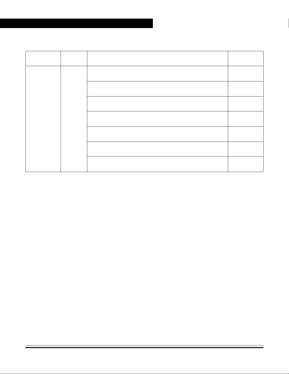
Description of the pin functions are provided in Table 1-1.
Table 1-1. Pin Functions
PIN NAME PIN DESCRIPTION
VDD1, VDD2 Power supply input to the MCU.
VSS1, VSS2 Power supply ground.
VDDA Power supply input for analog circuits.
VSSA Power supply ground for analog circuits.
Crystal connections to the on-chip oscillator.
OSC1, OSC2
An external clock can be connected directly to
OSC1; with OSC2 floating.
See Section 7. Oscillator (OSC).
Pin Functions
RST
IRQ
CGMXFC
VSYNC
HSYNC
PTA7/KBI7–PTA0/KBI0
External reset pin; active low; with internal pull-up
and schmitt trigger input. It is driven low when any
internal reset source is asserted.
See Section 9. System Integration Module
(SIM).
External IRQ pin; with schmitt trigger input and
internal pull-up. This pin is also used for mode
entry selection.
See Section 20. External Interrupt (IRQ) and
Section 9. System Integration Module (SIM).
External filter capacitor connection for the CGM
module.
See Section 8. Clock Generator Module (CGM).
Vsync input to the sync processor.
This pin is rated at +5V.
See Section 17. Sync Processor.
Hsync input to the sync processor.
This pin is rated at +5V.
See Section 17. Sync Processor.
These are shared function, bidirectional I/O port
pins. Each pin contains a pull-up device to VDD
when it is configured as an external keyboard
interrupt pin.
See Section 19. Input/Output (I/O) Ports and
Section 21. Keyboard Interrupt Module (KBI).
MC68HC908LD64 — Rev. 3.0 Data Sheet
Freescale Semiconductor General Description 37

General Description
Table 1-1. Pin Functions (Continued)
PIN NAME PIN DESCRIPTION
PTB7/PWM7–PTB0/PWM0
VRH High voltage reference input to ADC module.
VRL Low voltage reference input to ADC module.
These are shared-function, bidirectional I/O port
pins. Each pin can be configured as a standard I/O
pin or a PWM output channel.
See Section 19. Input/Output (I/O) Ports and
Section 12. Pulse Width Modulator (PWM).
PTC6
PTC5/ADC5–PTC0/ADC0
PTD7/IICSDA
PTD6/IICSCL
PTD5/DDCSDA
This pin is a standard bidirectional I/O pin.
See Section 19. Input/Output (I/O) Ports.
These are shared-function, bidirectional I/O port
pins. Each pin can be configured as a standard I/O
pin or an ADC input channel.
See Section 19. Input/Output (I/O) Ports and
Section 13. Analog-to-Digital Converter (ADC).
This is a shared-function pin. It can be configured
as a standard I/O pin or the data line of the multimaster IIC module. This pin is +5V open-drain
when configured as output.
See Section 19. Input/Output (I/O) Ports and
Section 15. Multi-Master IIC Interface (MMIIC).
This is a shared function pin. It can be configured
as a standard I/O pin or the clock line of the multimaster IIC module. This pin is +5V open-drain
when configured as output.
See Section 19. Input/Output (I/O) Ports and
Section 15. Multi-Master IIC Interface (MMIIC).
This is a shared function pin. It can be configured
as a standard I/O pin or the data line of the
DDC12AB module. This pin is +5V open-drain
when configured as output.
See Section 19. Input/Output (I/O) Ports and
Section 16. DDC12AB Interface.
This is a shared function pin. It can be configured
as a standard I/O pin or the clock line of the
PTD4/DDCSCL
Data Sheet MC68HC908LD64 — Rev. 3.0
38 General Description Freescale Semiconductor
DDC12AB module. This pin is +5V open-drain
when configured as output.
See Section 19. Input/Output (I/O) Ports and
Section 16. DDC12AB Interface.

General Description
Table 1-1. Pin Functions (Continued)
PIN NAME PIN DESCRIPTION
Pin Functions
PTD3/HOUT
PTD2/VOUT
PTD1/DE
PTD0/DCLK
CLAMP/TCH0
PVSYNC
PHSYNC
PCLK
OSDR
OSDG
OSDB
These are shared function, bidirectional I/O port
pins. These pins can be configured as standard
I/O pins or free-run timing output signals.
See Section 19. Input/Output (I/O) Ports and
Section 17. Sync Processor.
This is shared function pins. This TIM channel 0
I/O pin can be configured as the Sync processor
CLAMP output pin.
See Section 11. Timer Interface Module (TIM)
and Section 17. Sync Processor.
Vsync input to the On-Screen Display module.
This pin is rated at +5V.
See Section 18. On-Screen Display (OSD).
Hsync input to the On-Screen Display module.
This pin is rated at +5V.
See Section 18. On-Screen Display (OSD).
Pixel clock input to the On-Screen Display module.
This pin is rated at +5V.
See Section 18. On-Screen Display (OSD).
R, G, and B output of the On-Screen Display
module.
See Section 18. On-Screen Display (OSD).
Pixel-enable output of the On-Screen Display
FBKG
PTE7/DMINUS4
PTE6/DPLUS4
PTE5/DMINUS3
PTE4/4DPLUS3
PTE3/DMINUS2
PTE2/DPLUS2
PTE1/DMINUS1
PTE0/DPLUS1
DPLUS0
DMINUS0
module.
See Section 18. On-Screen Display (OSD).
These are shared function, bidirectional I/O port
pins. These pins can be configured as standard
I/O pins or downstream data pins of USB module.
See Section 19. Input/Output (I/O) Ports and
Section 14. Universal Serial Bus Module (USB).
Data pins of USB module upstream port.
See Section 14. Universal Serial Bus Module
(USB).
NOTE: Any unused inputs and I/O ports should be tied to an appropriate logic level
(either V
require termination, termination is recommended to reduce the possibility of
static damage.
MC68HC908LD64 — Rev. 3.0 Data Sheet
or VSS). Although the I/O ports of the MC68HC908LD64 do not
DD
Freescale Semiconductor General Description 39

General Description
Data Sheet MC68HC908LD64 — Rev. 3.0
40 General Description Freescale Semiconductor

Data Sheet — MC68HC908LD64
2.1 Contents
2.2 Introduction. . . . . . . . . . . . . . . . . . . . . . . . . . . . . . . . . . . . . . . .41
2.3 Unimplemented Memory Locations . . . . . . . . . . . . . . . . . . . . .41
2.4 Reserved Memory Locations . . . . . . . . . . . . . . . . . . . . . . . . . .42
2.5 Input/Output (I/O) Section. . . . . . . . . . . . . . . . . . . . . . . . . . . . .42
2.2 Introduction
The CPU08 can address 64K-bytes of memory space. The memory
map, shown in Figure 2-1, includes:
Section 2. Memory Map
• 60,928 bytes of FLASH memory
• 2,048 bytes of random-access memory (RAM)
• 32 bytes of user-defined vectors
• 1,024 + 464 bytes of monitor ROM
2.3 Unimplemented Memory Locations
Accessing an unimplemented location can cause an illegal address
reset if illegal address resets are enabled. In the memory map
(Figure 2-1) and in register figures in this document, unimplemented
locations are shaded.
MC68HC908LD64 — Rev. 3.0 Data Sheet
Freescale Semiconductor Memory Map 41

Memory Map
2.4 Reserved Memory Locations
Accessing a reserved location can have unpredictable effects on MCU
operation. In the Figure 2-1 and in register figures in this document,
reserved locations are marked with the word Reserved or with the
letter R.
2.5 Input/Output (I/O) Section
Most of the control, status, and data registers are in the zero page area
of $0000–$007F. Additional I/O registers have these addresses:
• $FE00; SIM break status register, SBSR
• $FE01; SIM reset status register, SRSR
• $FE02; Reserved
• $FE03; SIM break flag control register, SBFCR
• $FE04; Interrupt status register 1, INT1
• $FE05; Interrupt status register 2, INT2
• $FE06; Reserved
• $FE07; 47,616 bytes FLASH control register, FLCR
• $FE08; 47,616 bytes FLASH block protect register, FLBPR
• $FE09; Reserved
• $FE0A; 13K-bytes FLASH control register, FLCR1
• $FE0B; 13K-bytes FLASH block protect register, FLBPR1
• $FE0C; Break address register high, BRKH
• $FE0D; Break address register low, BRKL
• $FE0E; Break status and control register, BRKSCR
• $FE0F; Reserved
• $FFFF; COP control register, COPCTL
Data registers are shown in Figure 2-2. Table 2-1 is a list of vector
locations.
Data Sheet MC68HC908LD64 — Rev. 3.0
42 Memory Map Freescale Semiconductor

$0000
↓
$007F
$0080
↓
$047F
$0480
↓
$07FF
$0800
↓
$0BFF
Memory Map
Input/Output (I/O) Section
I/O Registers
128 Bytes
RAM
1,024 Bytes
Unimplemented
896 Bytes
OSD RAM
1,024 Bytes
$0C00
↓
$0FFF
$1000
↓
$3FFF
$4000
↓
$F9FF
$FA00
↓
$FDFF
$FE00 SIM Break Status Register (SBSR)
$FE01 SIM Reset Status Register (SRSR)
$FE02 Reserved
FLASH Memory
1,024 Bytes
(8 × 128-Byte Blocks)
OSD FLASH Memory
12,288 Bytes
(24 × 512-Byte Blocks)
FLASH Memory
47,616 Bytes
(93 × 512-Byte Blocks)
Monitor ROM
1,024 Bytes
$FE03 SIM Break Flag Control Register (SBFCR)
$FE04 Interrupt Status Register 1 (INT1)
Figure 2-1. Memory Map
MC68HC908LD64 — Rev. 3.0 Data Sheet
Freescale Semiconductor Memory Map 43

Memory Map
$FE05 Interrupt Status Register 2 (INT2)
$FE06 Reserved
$FE07 47,616 bytes FLASH Control Register (FLCR)
$FE08 47,616 bytes FLASH Block Protect Register (FLBPR)
$FE09 Reserved
$FE0A 13K-bytes FLASH Control Register (FLCR1)
$FE0B 13K-bytes FLASH Block Protect Register (FLBPR1)
$FE0C Break Address Register High (BRKH)
$FE0D Break Address Register Low (BRKL)
$FE0E Break Status and Control Register (BRKSCR)
$FE0F Reserved
$FE10
↓
$FFDF
Monitor ROM
464 Bytes
$FFE0
↓
$FFFF
FLASH Vectors
32 Bytes
Figure 2-1. Memory Map (Continued)
Data Sheet MC68HC908LD64 — Rev. 3.0
44 Memory Map Freescale Semiconductor

Memory Map
Input/Output (I/O) Section
Addr.Register Name Bit 7654321Bit 0
$0000
$0001
$0002
$0003
$0004
$0005
$0006
$0007
$0008
$0009
Port A Data Register
Port B Data Register
Port C Data Register
Port D Data Register
Data Direction Register A
Data Direction Register B
Data Direction Register C
Data Direction Register D
Port E Data Register
Data Direction Register E
(PTA)
(PTB)
(PTC)
(PTD)
(DDRA)
(DDRB)
(DDRC)
(DDRD)
(PTE)
(DDRE)
Read:
Write:
Reset: Unaffected by reset
Read:
Write:
Reset: Unaffected by reset
Read: 0
Write:
Reset: Unaffected by reset
Read:
Write:
Reset: Unaffected by reset
Read:
Write:
Reset:00000000
Read:
Write:
Reset:00000000
Read: 0
Write:
Reset:00000000
Read:
Write:
Reset:00000000
Read:
Write:
Reset: Unaffected by reset
Read:
Write:
Reset:00000000
PTA7 PTA6 PTA5 PTA4 PTA3 PTA2 PTA1 PTA0
PTB7 PTB6 PTB5 PTB4 PTB3 PTB2 PTB1 PTB0
PTC6 PTC5 PTC4 PTC3 PTC2 PTC1 PTC0
PTD7 PTD6 PTD5 PTD4 PTD3 PTD2 PTD1 PTD0
DDRA7 DDRA6 DDRA5 DDRA4 DDRA3 DDRA2 DDRA1 DDRA0
DDRB7 DDRB6 DDRB5 DDRB4 DDRB3 DDRB2 DDRB1 DDRB0
DDRC6 DDRC5 DDRC4 DDRC3 DDRC2 DDRC1 DDRC0
DDRD7 DDRD6 DDRD5 DDRD4 DDRD3 DDRD2 DDRD1 DDRD0
PTE7 PTE6 PTE5 PTE4 PTE3 PTE2 PTE1 PTE0
DDRE7 DDRE6 DDRE5 DDRE4 DDRE3 DDRE2 DDRE1 DDRE0
U = Unaffected X = Indeterminate
= Unimplemented R = Reserved
Figure 2-2. Control, Status, and Data Registers (Sheet 1 of 15)
MC68HC908LD64 — Rev. 3.0 Data Sheet
Freescale Semiconductor Memory Map 45

Memory Map
Addr.Register Name Bit 7654321Bit 0
TIM Status and Control
$000A
$000B Unimplemented
TIM Counter Register High
$000C
TIM Counter Register Low
$000D
TIM Counter Modulo
$000E
$000F
$0010
$0011
TIM Counter Modulo
TIM Channel 0
Status and Control
TIM Channel 0
Register
(TSC)
(TCNTH)
(TCNTL)
Register High
(TMODH)
Register Low
(TMODL)
Register
(TSC0)
Register High
(TCH0H)
Read: TOF
TOIE TSTOP
Write: 0 TRST
Reset:00100000
Read:
Write:
Reset:00000000
Read: Bit15 Bit14 Bit13 Bit12 Bit11 Bit10 Bit9 Bit8
Write:
Reset:00000000
Read: Bit7 Bit6 Bit5 Bit4 Bit3 Bit2 Bit1 Bit0
Write:
Reset:00000000
Read:
Bit15 Bit14 Bit13 Bit12 Bit11 Bit10 Bit9 Bit8
Write:
Reset:11111111
Read:
Bit7 Bit6 Bit5 Bit4 Bit3 Bit2 Bit1 Bit0
Write:
Reset:11111111
Read: CH0F
CH0IE MS0B MS0A ELS0B ELS0A TOV0 CH0MAX
Write: 0
Reset:00000000
Read:
Bit15 Bit14 Bit13 Bit12 Bit11 Bit10 Bit9 Bit8
Write:
Reset: Indeterminate after reset
00
PS2 PS1 PS0
Read:
Write:
Reset: Indeterminate after reset
Read: CH1F
Write: 0
Reset:00000000
Bit7 Bit6 Bit5 Bit4 Bit3 Bit2 Bit1 Bit0
CH1IE
0
MS1A ELS1B ELS1A TOV1 CH1MAX
= Unimplemented R = Reserved
$0012
$0013
TIM Channel 0
Register Low
(TCH0L)
TIM Channel 1
Status and Control
Register
(TSC1)
U = Unaffected X = Indeterminate
Figure 2-2. Control, Status, and Data Registers (Sheet 2 of 15)
Data Sheet MC68HC908LD64 — Rev. 3.0
46 Memory Map Freescale Semiconductor

Memory Map
Input/Output (I/O) Section
Addr.Register Name Bit 7654321Bit 0
Read:
Write:
Reset: Indeterminate after reset
Read:
Write:
Reset: Indeterminate after reset
Read:
Write:
Reset:00000000
Read:
Write:
Reset:10100000
Read:
Write:
Reset:00000000
Read: RXIF TXIF MATCH SRW RXAK SCLIF TXBE RXBF
Write: 0 0
Reset:00001010
Read:
Write:
Reset:11111111
Read: DRD7 DRD6 DRD5 DRD4 DRD3 DRD2 DRD1 DRD0
Write:
Reset:00000000
Bit15 Bit14 Bit13 Bit12 Bit11 Bit10 Bit9 Bit8
Bit7 Bit6 Bit5 Bit4 Bit3 Bit2 Bit1 Bit0
ALIF NAKIF BB MAST MRW BR2 BR1 BR0
DAD7 DAD6 DAD5 DAD4 DAD3 DAD2 DAD1 EXTAD
DEN DIEN
DTD7 DTD6 DTD5 DTD4 DTD3 DTD2 DTD1 DTD0
00
TXAK SCLIEN DDC1EN
0
0
$0014
$0015
$0016
$0017
$0018
$0019
$001A
$001B
TIM Channel 1
Register High
(TCH1H)
TIM Channel 1
Register Low
(TCH1L)
DDC Master Control
Register
(DDCMCR)
DDC Address Register
(DDCADR)
DDC Control Register
(DDCCR)
DDC Status Register
(DDCSR)
DDC Data Transmit
Register
(DDCDTR)
DDC Data Receive
Register
(DDCDRR)
$001C
$001D Unimplemented
DDC2 Address Register
(DDC2ADR)
U = Unaffected X = Indeterminate
Read:
D2AD7 D2AD6 D2AD5 D2AD4 D2AD3 D2AD2 D2AD1
Write:
Reset:00000000
Read:
Write:
Reset:
= Unimplemented R = Reserved
0
Figure 2-2. Control, Status, and Data Registers (Sheet 3 of 15)
MC68HC908LD64 — Rev. 3.0 Data Sheet
Freescale Semiconductor Memory Map 47

Memory Map
Addr.Register Name Bit 7654321Bit 0
IRQ Status and Control
$001E
$001F
† One-time writable register after each reset.
$0020
$0021
$0022
Configuration Register
USB Embedded Device
Endpoint 0 Data Reg. 0
USB Embedded Device
Endpoint 0 Data Reg. 1
USB Embedded Device
Endpoint 0 Data Reg. 2
Register
(INTSCR)
(CONFIG)
(DE0D0)
(DE0D1)
(DE0D2)
USB Embedded Device
$0023
$0024
Endpoint 0 Data Reg. 3
(DE0D3)
USB Embedded Device
Endpoint 0 Data Reg. 4
(DE0D4)
Read: 0000IRQF0
Write:
Reset:00000000
Read: 0000
Write:
†
Reset:00000000
Read: DE0R07 DE0R06 DE0R05 DE0R04 DE0R03 DE0R02 DE0R01 DE0R00
Write: DE0T07 DE0T06 DE0T05 DE0T04 DE0T03 DE0T02 DE0T01 DE0T00
Reset: Indeterminate after reset
Read: DE0R17 DE0R16 DE0R15 DE0R14 DE0R13 DE0R12 DE0R11 DE0R10
Write: DE0T17 DE0T16 DE0T15 DE0T14 DE0T13 DE0T12 DE0T11 DE0T10
Reset: Indeterminate after reset
Read: DE0R27 DE0R26 DE0R25 DE0R24 DE0R23 DE0R22 DE0R21 DE0R20
Write: DE0T27 DE0T26 DE0T25 DE0T24 DE0T23 DE0T22 DE0T21 DE0T20
Reset: Indeterminate after reset
Read: DE0R37 DE0R36 DE0R35 DE0R34 DE0R33 DE0R32 DE0R31 DE0R30
Write: DE0T37 DE0T36 DE0T35 DE0T34 DE0T33 DE0T32 DE0T31 DE0T30
Reset: Indeterminate after reset
Read: DE0R47 DE0R46 DE0R45 DE0R44 DE0R43 DE0R42 DE0R41 DE0R40
Write: DE0T47 DE0T46 DE0T45 DE0T44 DE0T43 DE0T42 DE0T41 DE0T40
Reset: Indeterminate after reset
SSREC COPRS STOP COPD
ACK
IMASK MODE
Read: DE0R57 DE0R56 DE0R55 DE0R54 DE0R53 DE0R52 DE0R51 DE0R50
Write: DE0T57 DE0T56 DE0T55 DE0T54 DE0T53 DE0T52 DE0T51 DE0T50
Reset: Indeterminate after reset
Read: DE0R67 DE0R66 DE0R65 DE0R64 DE0R63 DE0R62 DE0R61 DE0R60
Write: DE0T67 DE0T66 DE0T65 DE0T64 DE0T63 DE0T62 DE0T61 DE0T60
Reset: Indeterminate after reset
Read: DE0R77 DE0R76 DE0R75 DE0R74 DE0R73 DE0R72 DE0R71 DE0R70
Write: DE0T77 DE0T76 DE0T75 DE0T74 DE0T73 DE0T72 DE0T71 DE0T70
Reset: Indeterminate after reset
= Unimplemented R = Reserved
$0025
$0026
$0027
USB Embedded Device
Endpoint 0 Data Reg. 5
(DE0D5)
USB Embedded Device
Endpoint 0 Data Reg. 6
(DE0D6)
USB Embedded Device
Endpoint 0 Data Reg. 7
(DE0D7)
U = Unaffected X = Indeterminate
Figure 2-2. Control, Status, and Data Registers (Sheet 4 of 15)
Data Sheet MC68HC908LD64 — Rev. 3.0
48 Memory Map Freescale Semiconductor

Memory Map
Input/Output (I/O) Section
Addr.Register Name Bit 7654321Bit 0
Read:
Write: DE1T07 DE1T06 DE1T05 DE1T04 DE1T03 DE1T02 DE1T01 DE1T00
Reset: Indeterminate after reset
Read:
Write: DE1T17 DE1T16 DE1T15 DE1T14 DE1T13 DE1T12 DE1T11 DE1T10
Reset: Indeterminate after reset
Read:
Write: DE1T27 DE1T26 DE1T25 DE1T24 DE1T23 DE1T22 DE1T21 DE1T20
Reset: Indeterminate after reset
Read:
Write: DE1T37 DE1T36 DE1T35 DE1T34 DE1T33 DE1T32 DE1T31 DE1T30
Reset: Indeterminate after reset
Read:
Write: DE1T47 DE1T46 DE1T45 DE1T44 DE1T43 DE1T42 DE1T41 DE1T40
Reset: Indeterminate after reset
Read:
Write: DE1T57 DE1T56 DE1T55 DE1T54 DE1T53 DE1T52 DE1T51 DE1T50
Reset: Indeterminate after reset
Read:
Write: DE1T67 DE1T66 DE1T65 DE1T64 DE1T63 DE1T62 DE1T61 DE1T60
Reset: Indeterminate after reset
Read:
Write: DE1T77 DE1T76 DE1T75 DE1T74 DE1T73 DE1T72 DE1T71 DE1T70
Reset: Indeterminate after reset
Read: HE0R07 HE0R06 HE0R05 HE0R04 HE0R03 HE0R02 HE0R01 HE0R00
Write: HE0T07 HE0T06 HE0T05 HE0T04 HE0T03 HE0T02 HE0T01 HE0T00
Reset: Indeterminate after reset
Read: HE0R17 HE0R16 HE0R15 HE0R14 HE0R13 HE0R12 HE0R11 HE0R10
Write: HE0T17 HE0T16 HE0T15 HE0T14 HE0T13 HE0T12 HE0T11 HE0T10
Reset: Indeterminate after reset
$0028
$0029
$002A
$002B
$002C
$002D
$002E
$002F
$0030
$0031
USB Embedded Device
Endpoint 1/2 Data Reg. 0
(DE1D0)
USB Embedded Device
Endpoint 1/2 Data Reg. 1
(DE1D1)
USB Embedded Device
Endpoint 1/2 Data Reg. 2
(DE1D2)
USB Embedded Device
Endpoint 1/2 Data Reg. 3
(DE1D3)
USB Embedded Device
Endpoint 1/2 Data Reg. 4
(DE1D4)
USB Embedded Device
Endpoint 1/2 Data Reg. 5
(DE1D5)
USB Embedded Device
Endpoint 1/2 Data Reg. 6
(DE1D6)
USB Embedded Device
Endpoint 1/2 Data Reg. 7
(DE1D7)
USB HUB Endpoint 0
Data Register 0
(HE0D0)
USB HUB Endpoint 0
Data Register 1
(HE0D1)
U = Unaffected X = Indeterminate
= Unimplemented R = Reserved
Figure 2-2. Control, Status, and Data Registers (Sheet 5 of 15)
MC68HC908LD64 — Rev. 3.0 Data Sheet
Freescale Semiconductor Memory Map 49

Memory Map
Addr.Register Name Bit 7654321Bit 0
USB HUB Endpoint 0
$0032
$0033
$0034
$0035
$0036
$0037
$0038
$0039
$003A
ADC Status and Control
$003B
Data Register 2
(HE0D2)
USB HUB Endpoint 0
Data Register 3
(HE0D3)
USB HUB Endpoint 0
Data Register 4
(HE0D4)
USB HUB Endpoint 0
Data Register 5
(HE0D5)
USB HUB Endpoint 0
Data Register 6
(HE0D6)
USB HUB Endpoint 0
Data Register 7
(HE0D7)
PLL Control Register
(PCTL)
PLL Bandwidth Control
Register
(PBWC)
PLL Programming
Register
Register
(ADSCR)
Read: HE0R27 HE0R26 HE0R25 HE0R24 HE0R23 HE0R22 HE0R21 HE0R20
Write: HE0T27 HE0T26 HE0T25 HE0T24 HE0T23 HE0T22 HE0T21 HE0T20
Reset: Indeterminate after reset
Read: HE0R37 HE0R36 HE0R35 HE0R34 HE0R33 HE0R32 HE0R31 HE0R30
Write: HE0T37 HE0T36 HE0T35 HE0T34 HE0T33 HE0T32 HE0T31 HE0T30
Reset: Indeterminate after reset
Read: HE0R47 HE0R46 HE0R45 HE0R44 HE0R43 HE0R42 HE0R41 HE0R40
Write: HE0T47 HE0T46 HE0T45 HE0T44 HE0T43 HE0T42 HE0T41 HE0T40
Reset: Indeterminate after reset
Read: HE0R57 HE0R56 HE0R55 HE0R54 HE0R53 HE0R52 HE0R51 HE0R50
Write: HE0T57 HE0T56 HE0T55 HE0T54 HE0T53 HE0T52 HE0T51 HE0T50
Reset: Indeterminate after reset
Read: HE0R67 HE0R66 HE0R65 HE0R64 HE0R63 HE0R62 HE0R61 HE0R60
Write: HE0T67 HE0T66 HE0T65 HE0T64 HE0T63 HE0T62 HE0T61 HE0T60
Reset: Indeterminate after reset
Read: HE0R77 HE0R76 HE0R75 HE0R74 HE0R73 HE0R72 HE0R71 HE0R70
Write: HE0T77 HE0T76 HE0T75 HE0T74 HE0T73 HE0T72 HE0T71 HE0T70
Reset: Indeterminate after reset
Read:
Write:
Reset:00101111
Read:
Write:
Reset:00000000
Read:
Write:
(PPG)
Reset:01100110
Read: COCO
Write:
Reset:00011111
PLLIE
AUTO
MUL7 MUL6 MUL5 MUL4 VRS7 VRS6 VRS5 VRS4
PLLF
LOCK
AIEN ADCO ADCH4 ADCH3 ADCH2 ADCH1 ADCH0
PLLON BCS
ACQ
XLD
1111
0000
U = Unaffected X = Indeterminate
= Unimplemented R = Reserved
Figure 2-2. Control, Status, and Data Registers (Sheet 6 of 15)
Data Sheet MC68HC908LD64 — Rev. 3.0
50 Memory Map Freescale Semiconductor

Memory Map
Input/Output (I/O) Section
Addr.Register Name Bit 7654321Bit 0
Read: AD7 AD6 AD5 AD4 AD3 AD2 AD1 AD0
$003C
$003D
$003E Unimplemented
$003F
$0040
$0041
$0042
$0043
$0044
$0045
ADC Data Register
(ADR)
ADC Input Clock Register
(ADICLK)
H & V Sync Output Control
Register
(HVOCR)
Sync Processor Control
and Status Register
(SPCSR)
Vertical Frequency High
Register
(VFHR)
Vertical Frequency Low
Register
(VFLR)
Hsync Frequency High
Register
(HFHR)
Hsync Frequency Low
Register
(HFLR)
Sync Processor I/O Control
Register
(SPIOCR)
Write:
Reset: Indeterminate after reset
Read:
Write:
Reset:00000000
Read:
Write:
Reset:
Read:
Write:
Reset: 00 00
Read:
Write: 0
Reset:00000000
Read: VOF 0 0 VF12 VF11 VF10 VF9 VF8
Write:
Reset:00000000
Read: VF7 VF6 VF5 VF4 VF3 VF2 VF1 VF0
Write:
Reset:00000000
Read: HFH7 HFH6 HFH5 HFH4 HFH3 HFH2 HFH1 HFH0
Write:
Reset:00000000
Read: HOVER 0 0 HFL4 HFL3 HFL2 HFL1 HFL0
Write:
Reset:00000000
Read: VSYNCS HSYNCS
Write:
Reset:000 00
ADIV2 ADIV1 ADIV0
VSIF
VSIE VEDGE
CPW1 CPW0
COINV R R R BPOR SOUT
00000
DCLKPH1 DCLKPH0 R HVOCR1 HVOCR0
VPOL HPOL
COMP VINVO HINVO
U = Unaffected X = Indeterminate
= Unimplemented R = Reserved
Figure 2-2. Control, Status, and Data Registers (Sheet 7 of 15)
MC68HC908LD64 — Rev. 3.0 Data Sheet
Freescale Semiconductor Memory Map 51

Memory Map
Addr.Register Name Bit 7654321Bit 0
Sync Processor Control
$0046
USB Embedded Device
$0047
USB Embedded Device
$0048
USB Embedded Device
$0049
$004A
$004B
$004C
$004D
$004E
$004F
Interrupt Register 0
USB Embedded Device
Interrupt Register 1
USB Embedded Device
USB Embedded Device
USB Embedded Device
Keyboard Status and
Keyboard Interrupt Enable
Register 1
(SPCR1)
Control Register 2
(DCR2)
Address Register
(DADDR)
(DIR0)
(DIR1)
Control Register 0
(DCR0)
Control Register 1
(DCR1)
Status Register
Control Register
(KBSCR)
Register
(KBIER)
Read:
Write: 0
Reset:0000 00
Read: 0000
Write:
Reset:00000000
Read:
Write:
Reset:00000000
Read: TXD0F RXD0F 0 0
Write:
Reset:00000000
Read: TXD1F 0 0 0
Write:
Reset:00000000
Read:
Write:
Reset:00000000
Read:
Write:
Reset:00000000
Read: DRSEQ DSETUP DTX1ST 0 RP0SIZ3 RP0SIZ2 RP0SIZ1 RP0SIZ0
Write:
(DSR)
Reset:00000000
Read: 0000KEYF 0
Write:
Reset:00000000
Read:
Write:
Reset:00000000
LVSIE
DEVEN DADD6 DADD5 DADD4 DADD3 DADD2 DADD1 DADD0
T0SEQ DSTALL0 TX0E RX0E TP0SIZ3 TP0SIZ2 TP0SIZ1 TP0SIZ0
T1SEQ ENDADD TX1E
KBIE7 KBIE6 KBIE5 KBIE4 KBIE3 KBIE2 KBIE1 KBIE0
LVSIF
HPS1 HPS0 R R ATPOL FSHF
ENABLE2 ENABLE1 DSTALL2 DSTALL1
00
TXD0IE RXD0IE
TXD0FR RXD0FR
000
TXD1IE
TXD1FR
0
TP1SIZ3 TP1SIZ2 TP1SIZ1 TP1SIZ0
DTX1STR
IMASKK MODEK
ACKK
U = Unaffected X = Indeterminate
= Unimplemented R = Reserved
Figure 2-2. Control, Status, and Data Registers (Sheet 8 of 15)
Data Sheet MC68HC908LD64 — Rev. 3.0
52 Memory Map Freescale Semiconductor

Memory Map
Input/Output (I/O) Section
Addr.Register Name Bit 7654321Bit 0
Read:
$0050 Unimplemented
USB HUB Downstream
$0051
$0052
$0053
$0054
$0055 Unimplemented
$0056
$0057
$0058
* RSTF and USBEN are reset by a power-on reset (POR) only.
Port 1 Control Register
(HDP1CR)
USB HUB Downstream
Port 2 Control Register
(HDP2CR)
USB HUB Downstream
Port 3 Control Register
(HDP3CR)
USB HUB Downstream
Port 4 Control Register
(HDP4CR)
USB SIE Timing Interrupt
Register
(SIETIR)
USB SIE Timing Status
Register
(SIETSR)
USB HUB Address
Register
(HADDR)
Write:
Reset:
Read:
Write:
Reset:000000XX
Read:
Write:
Reset:000000XX
Read:
Write:
Reset:000000XX
Read:
Write:
Reset:000000XX
Read:
Write:
Reset:
Read: SOFF EOF2F EOPF TRANF
Write:
Reset:00000000
Read: RSTF 0 LOCKF 00000
Write:
Reset:0*0000000
Read:
Write:
Reset:0*0000000
PEN1 LOWSP1 RST1 RESUM1 SUSP1
PEN2 LOWSP2 RST2 RESUM2 SUSP2
PEN3 LOWSP3 RST3 RESUM3 SUSP3
PEN4 LOWSP4 RST4 RESUM4 SUSP4
SOFIE EOF2IE EOPIE TRANIE
RSTFR LOCKFR SOFFR EOF2FR EOPFR TRANFR
USBEN ADD6 ADD5 ADD4 ADD3 ADD2 ADD1 ADD0
0D1+D1–
0D2+D2–
0D3+D3–
0D4+D4–
$0059
USB HUB Interrupt
Register 0
(HIR0)
U = Unaffected X = Indeterminate
Read: TXDF RXDF 0 0
Write:
Reset:00000000
TXDIE RXDIE
= Unimplemented R = Reserved
00
TXDFR RXDFR
Figure 2-2. Control, Status, and Data Registers (Sheet 9 of 15)
MC68HC908LD64 — Rev. 3.0 Data Sheet
Freescale Semiconductor Memory Map 53

Memory Map
Addr.Register Name Bit 7654321Bit 0
Read:
$005A Unimplemented
USB HUB Control
$005B
USB HUB Endpoint 1
$005C
$005D
$005E
Control and Data Register
USB HUB Status Register
USB HUB Root Port
Control Register
$005F Unimplemented
Register 0
(HCR0)
(HCDR)
(HRPCR)
Reset:
Reset:
Read:
Write:
Reset:00000000
Read:
Write:
Reset:00000000
Read: RSEQ SETUP TX1ST 0 RPSIZ3 RPSIZ2 RPSIZ1 RPSIZ0
Write:
(HSR)
Reset:XXX0XXXX
Read: 0 0 0
Write:
Reset:000000XX
Read:
Write:
TSEQ STALL0 TXE RXE TPSIZ3 TPSIZ2 TPSIZ1 TPSIZ0
STALL1 PNEW PCHG5 PCHG4 PCHG3 PCHG2 PCHG1 PCHG0
TX1STR
0D0+D0–
RESUM0 SUSPND
$0060
$0061
$0062
$0063
OSD Control Register
(OSDCR)
OSD Status Register
(OSDSR)
OSD Data Register Low
(OSDDRL)
OSD Data Register High
(OSDDRH)
U = Unaffected X = Indeterminate
Figure 2-2. Control, Status, and Data Registers (Sheet 10 of 15)
Reset:
Read:
OSDMEN R OSDRST CLKINV CLKPH1 CLKPH0 HALFCLK OSDIEN
Write:
Reset:0 000000
Read: WRDY
Write:
Reset: 1 0
Read:
OSDD7 OSDD6 OSDD5 OSDD4 OSDD3 OSDD2 OSDD1 OSDD0
Write:
Reset: Unaffected by reset
Read:
OSDD15 OSDD14 OSDD13 OSDD12 OSDD11 OSDD10 OSDD9 OSDD8
Write:
Reset: Unaffected by reset
= Unimplemented R = Reserved
DENDIF
Data Sheet MC68HC908LD64 — Rev. 3.0
54 Memory Map Freescale Semiconductor

Memory Map
Input/Output (I/O) Section
Addr.Register Name Bit 7654321Bit 0
OSD Row Address
$0064
OSD Column Address
$0065
OSD FLASH Even
$0066
$0067 Unimplemented
$0068
$0069
$006A
$006B
$006C
$006D
High Byte Write Buffer
Master Control Register
Multi-Master IIC Address
Multi-Master IIC Control
Register
(OSDRAR)
Register
(OSDCAR)
(OSDEHBUF)
Port E Control
Register
(PECR)
Port D Control
Register
(PDCR)
Multi-Master IIC
(MIMCR)
Register
(MMADR)
Register
(MMCR)
Multi-Master IIC
Status Register
(MMSR)
Read:
Write:
Reset: 0000
Read:
Write:
Reset: 00000
Read:
Write:
Reset: Unaffected by reset
Read:
Write:
Reset:
Read:
Write:
Reset: 0000
Read:
Write:
Reset:00000000
Read: MMALIF MMNAKIF MMBB
Write: 0 0
Reset:00000000
Read:
Write:
Reset:10100000
Read:
Write:
Reset:00000000
Read: MMRXIF MMTXIF MMATCH MMSRW MMRXAK 0 MMTXBE MMRXBF
Write: 0 0
Reset:00001010
DOT15 DOT14 DOT13 DOT12 DOT11 DOT10 DOT9 DOT8
IICDATE IICSCLE DDCDATE DDCSCLE HOUTE VOUTE DEE DCLKE
MMAD7 MMAD6 MMAD5 MMAD4 MMAD3 MMAD2 MMAD1 MMEXTAD
00
MMEN MMIEN
COLA4 COLA3 COLA2 COLA1 COLA0
R USBDS4E USBDS3E USBDS2E USBDS1E
MMAST MMRW MMBR2 MMBR1 MMBR0
ROWA3 ROWA2 ROWA1 ROWA0
000
MMTXAK
U = Unaffected X = Indeterminate
= Unimplemented R = Reserved
Figure 2-2. Control, Status, and Data Registers (Sheet 11 of 15)
MC68HC908LD64 — Rev. 3.0 Data Sheet
Freescale Semiconductor Memory Map 55

Memory Map
Addr.Register Name Bit 7654321Bit 0
Read:
MMTD7 MMTD6 MMTD5 MMTD4 MMTD3 MMTD2 MMTD1 MMTD0
Write:
Reset:11111111
Read: MMRD7 MMRD6 MMRD5 MMRD4 MMRD3 MMRD2 MMRD1 MMRD0
Write:
Reset:00000000
$006E
$006F
Multi-Master IIC
Data Transmit Register
(MMDTR)
Multi-Master IIC
Data Receive Register
(MMDRR)
Read:
$0070
$0071
$0072
$0073
$0074
$0075
PWM0 Data Register
(0PWM)
PWM1 Data Register
(1PWM)
PWM2 Data Register
(2PWM)
PWM3 Data Register
(3PWM)
PWM4 Data Register
(4PWM)
PWM5 Data Register
(5PWM)
Write:
Reset:00000000
Read:
Write:
Reset:00000000
Read:
Write:
Reset:00000000
Read:
Write:
Reset:00000000
Read:
Write:
Reset:00000000
Read:
Write:
Reset:00000000
0PWM4 0PWM3 0PWM2 0PWM1 0PWM0 0BRM2 0BRM1 0BRM0
1PWM4 1PWM3 1PWM2 1PWM1 1PWM0 1BRM2 1BRM1 1BRM0
2PWM4 2PWM3 2PWM2 2PWM1 2PWM0 2BRM2 2BRM1 2BRM0
3PWM4 3PWM3 3PWM2 3PWM1 3PWM0 3BRM2 3BRM1 3BRM0
4PWM4 4PWM3 4PWM2 4PWM1 4PWM0 4BRM2 4BRM1 4BRM0
5PWM4 5PWM3 5PWM2 5PWM1 5PWM0 5BRM2 5BRM1 5BRM0
$0076
$0077
Read:
PWM6 Data Register
(6PWM)
PWM7 Data Register
(7PWM)
U = Unaffected X = Indeterminate
Write:
Reset:00000000
Read:
Write:
Reset:00000000
6PWM4 6PWM3 6PWM2 6PWM1 6PWM0 6BRM2 6BRM1 6BRM0
7PWM4 7PWM3 7PWM2 7PWM1 7PWM0 7BRM2 7BRM1 7BRM0
= Unimplemented R = Reserved
Figure 2-2. Control, Status, and Data Registers (Sheet 12 of 15)
Data Sheet MC68HC908LD64 — Rev. 3.0
56 Memory Map Freescale Semiconductor

Memory Map
Input/Output (I/O) Section
Addr.Register Name Bit 7654321Bit 0
Read:
$0078
$0079 Unimplemented
$007A Unimplemented
$007B Unimplemented
$007C Unimplemented
PWM Control Register
(PWMCR)
Reset:00000000
Reset:
Reset:
Reset:
PWM7E PWM6E PWM5E PWM4E PWM3E PWM2E PWM1E PWM0E
Write:
Read:
Write:
Read:
Write:
Read:
Write:
Read:
Write:
$007D Unimplemented
$007E Unimplemented
$007F Unimplemented
SIM Break Status Register
$FE00
Note: Writing a logic 0 clears SBSW.
(SBSR)
U = Unaffected X = Indeterminate
Reset:
Read:
Write:
Reset:
Read:
Write:
Reset:
Read:
Write:
Reset:
Read:
RRRRRR
Write: Note
Reset: 0
= Unimplemented R = Reserved
SBSW
R
Figure 2-2. Control, Status, and Data Registers (Sheet 13 of 15)
MC68HC908LD64 — Rev. 3.0 Data Sheet
Freescale Semiconductor Memory Map 57

Memory Map
Addr.Register Name Bit 7654321Bit 0
Read: POR PIN COP ILOP ILAD USB 0 0
SIM Reset Status Register
$FE01
$FE02 Reserved
SIM Break Flag Control
$FE03
Interrupt Status Register 1
$FE04
Interrupt Status Register 2
$FE05
$FE06 Reserved
(SRSR)
Register
(SBFCR)
Write:
POR:10000000
Read:
Write:
Reset:
Read:
Write:
Reset: 0
Read: IF6 IF5 IF4 IF3 IF2 IF1 0 0
Write:RRRRRRRR
(INT1)
Reset:00000000
Read: IF14 IF13 IF12 IF11 IF10 IF9 IF8 IF7
Write:RRRRRRRR
(INT2)
Reset:00000000
Read:
Write:
RRRRRRRR
BCFERRRRRRR
RRRRRRRR
47,616 Bytes FLASH
$FE07
$FE08
$FE09 Reserved
$FE0A
Control Register
(FLCR)
47,616 Bytes FLASH
Block Protect Register
(FLBPR)
13K-Bytes FLASH
Control Register
(FLCR1)
U = Unaffected X = Indeterminate
Figure 2-2. Control, Status, and Data Registers (Sheet 14 of 15)
Reset:
Read: 0000
Write:
Reset:00000000
Read:
BPR7 BPR6 BPR5 BPR4 BPR3 BPR2 BPR1
Write:
Reset:00000000
Read:
RRRRRRRR
Write:
Reset:
Read: 0000
Write:
Reset:00000000
= Unimplemented R = Reserved
HVEN MASS ERASE PGM
0
HVEN1 MASS1 ERASE1 PGM1
Data Sheet MC68HC908LD64 — Rev. 3.0
58 Memory Map Freescale Semiconductor

Memory Map
Input/Output (I/O) Section
Addr.Register Name Bit 7654321Bit 0
$FE0B
$FE0C
$FE0D
$FE0E
13K-Bytes FLASH
Block Protect Register
(FLBPR1)
Break Address High
Register (BRKH)
Break Address Low
Register (BRKL)
Break Status and Control
Register
(BRKSCR)
Read:
Write:
Reset:00000000
Read:
Write:
Reset:00000000
Read:
Write:
Reset:00000000
Read:
Write:
Reset:00000000
BPR17 BPR16 BPR15 BPR14 BPR13 BPR12 BPR11
Bit 15 14 13 12 11 10 9 Bit 8
Bit 7654321Bit 0
000000
BRKE BRKA
0
$FFFF
Read: Low byte of reset vector
COP Control Register
(COPCTL)
U = Unaffected X = Indeterminate
Write: Writing clears COP counter (any value)
Reset: Unaffected by reset
= Unimplemented R = Reserved
Figure 2-2. Control, Status, and Data Registers (Sheet 15 of 15)
MC68HC908LD64 — Rev. 3.0 Data Sheet
Freescale Semiconductor Memory Map 59

Memory Map
Table 2-1. Vector Addresses
.
Vector Priority Vector Address Vector
Lowest
IF14
IF13
IF12
IF11
IF10
IF9
IF8
IF7
IF6
IF5
IF4
IF3
IF2
IF1
—
Highest $FFFF Reset Vector (Low)
—
$FFE0 CGM PLL Interrupt Vector (High)
$FFE1 CGM PLL Interrupt Vector (Low)
$FFE2 Keyboard Interrupt Vector (High)
$FFE3 Keyboard Interrupt Vector (Low)
$FFE4 ADC Interrupt Vector (High)
$FFE5 ADC Interrupt Vector (Low)
$FFE6 OSD Interrupt Vector (High)
$FFE7 OSD Interrupt Vector (Low)
$FFE8 MMIIC Vector (High)
$FFE9 MMIIC Vector (Low)
$FFEA Sync Processor Vector (High)
$FFEB Sync Processor Vector (Low)
$FFEC TIM Overflow Vector (High)
$FFED TIM Overflow Vector (Low)
$FFEE TIM Channel 1 Vector (High)
$FFEF TIM Channel 1 Vector (Low)
$FFF0 TIM Channel 0 Vector (High)
$FFF1 TIM Channel 0 Vector (Low)
$FFF2 DDC12AB Vector (High)
$FFF3 DDC12AB Vector (Low)
$FFF4 USB Device Interrupt Vector (High)
$FFF5 USB Device Interrupt Vector (Low)
$FFF6 USB HUB Interrupt Vector (High)
$FFF7 USB HUB Interrupt Vector (Low)
$FFF8 USB Vector (High)
$FFF9 USB Vector (Low)
$FFFA IRQ Vector (High)
$FFFB IRQ Vector (Low)
$FFFC SWI Vector (High)
$FFFD SWI Vector (Low)
$FFFE Reset Vector (High)
Data Sheet MC68HC908LD64 — Rev. 3.0
60 Memory Map Freescale Semiconductor

Data Sheet — MC68HC908LD64
Section 3. Random-Access Memory (RAM)
3.1 Contents
3.2 Introduction. . . . . . . . . . . . . . . . . . . . . . . . . . . . . . . . . . . . . . . .61
3.3 Functional Description . . . . . . . . . . . . . . . . . . . . . . . . . . . . . . .61
3.2 Introduction
This section describes the 2,048 bytes of RAM (random-access
memory).
3.3 Functional Description
The RAM is divided into two blocks. Addresses $0080 through $047F
are locations for general use. Addresses $0800 through $0BFF are
locations for the OSD display RAM (see 18.6 OSD Screen Memory
Map). The location of the stack RAM is programmable. The 16-bit stack
pointer allows the stack to be anywhere in the 64-Kbyte memory space.
NOTE: For correct operation, the stack pointer must point only to RAM
locations.
Within page zero are 128 bytes of RAM. Because the location of the
stack RAM is programmable, all page zero RAM locations can be used
for I/O control and user data or code. When the stack pointer is moved
from its reset location at $00FF out of page zero, direct addressing mode
instructions can efficiently access all page zero RAM locations. Page
zero RAM, therefore, provides ideal locations for frequently accessed
global variables.
Before processing an interrupt, the CPU uses five bytes of the stack to
save the contents of the CPU registers.
MC68HC908LD64 — Rev. 3.0 Data Sheet
Freescale Semiconductor Random-Access Memory (RAM) 61

Random-Access Memory (RAM)
NOTE: For M6805 compatibility, the H register is not stacked.
During a subroutine call, the CPU uses two bytes of the stack to store
the return address. The stack pointer decrements during pushes and
increments during pulls.
NOTE: Be careful when using nested subroutines. The CPU may overwrite data
in the RAM during a subroutine or during the interrupt stacking
operation.
Data Sheet MC68HC908LD64 — Rev. 3.0
62 Random-Access Memory (RAM) Freescale Semiconductor

Data Sheet — MC68HC908LD64
4.1 Contents
4.2 Introduction. . . . . . . . . . . . . . . . . . . . . . . . . . . . . . . . . . . . . . . .64
4.3 Functional Description . . . . . . . . . . . . . . . . . . . . . . . . . . . . . . .64
4.4 FLASH Control Registers . . . . . . . . . . . . . . . . . . . . . . . . . . . . .66
4.4.1 OSD FLASH Even High Byte Write Buffer (OSDEHBUF) . . 67
4.5 FLASH Block Erase Operation . . . . . . . . . . . . . . . . . . . . . . . . .68
4.6 FLASH Mass Erase Operation . . . . . . . . . . . . . . . . . . . . . . . . .69
4.7 FLASH Program Operation. . . . . . . . . . . . . . . . . . . . . . . . . . . .70
Section 4. FLASH Memory
4.8 FLASH Block Protection . . . . . . . . . . . . . . . . . . . . . . . . . . . . . .72
4.8.1 FLASH Block Protect Registers . . . . . . . . . . . . . . . . . . . . . .72
MC68HC908LD64 — Rev. 3.0 Data Sheet
Freescale Semiconductor FLASH Memory 63

FLASH Memory
4.2 Introduction
This section describes the operation of the embedded FLASH memory.
This memory can be read, programmed, and erased from a single
external supply. The program and erase operations are enabled through
the use of an internal charge pump.
Addr.Register Name Bit 7654321Bit 0
47,616 Bytes FLASH
$FE07
$FE08
$FE0A
$FE0B
$0066
Control Register
(FLCR)
47,616 Bytes FLASH
Block Protect Register
(FLBPR)
13K-Bytes FLASH
Control Register
(FLCR1)
13K-Bytes FLASH
Block Protect Register
(FLBPR1)
OSD FLASH Even
High Byte Write Buffer
(OSDEHBUF)
Read: 0000
HVEN MASS ERASE PGM
Write:
Reset:00000000
Read:
BPR7 BPR6 BPR5 BPR4 BPR3 BPR2 BPR1
Write:
Reset:00000000
Read: 0000
HVEN1 MASS1 ERASE1 PGM1
Write:
Reset:00000000
Read:
BPR17 BPR16 BPR15 BPR14 BPR13 BPR12 BPR11
Write:
Reset:00000000
Read:
DOT15 DOT14 DOT13 DOT12 DOT11 DOT10 DOT9 DOT8
Write:
Reset: Unaffected by reset
0
0
Figure 4-1. FLASH I/O Register Summary
4.3 Functional Description
The MC68HC908LD64 FLASH memory contains two arrays:
• 13,312-byte array
• 47,616-byte array
An additional 32 bytes of FLASH user vectors, $FFE0–$FFFF, are in the
same array as the 47,616-byte. The size, address range, and memory
usage of the arrays are summarized in Table 4-1.
NOTE: An erased bit reads as logic 1 and a programmed bit reads as logic 0.
Data Sheet MC68HC908LD64 — Rev. 3.0
64 FLASH Memory Freescale Semiconductor

FLASH Memory
Functional Description
Table 4-1. FLASH Memory Array Summary
13,312 Array 47,616 Array
Bytes 1,024 12,288 47,616 32
Address range $0C00–$0FFF $1000–$3FFF $4000–$F9FF $FFE0–$FFFF
Minimum erase size 128 bytes 512 bytes 512 bytes
Usage
Programming Size
Related Control registers
User data or
program
Double bytes in a 64-byte
programming routine
FLCR1 at $FE0A
FLBPR1 at $FE0B
OSDEHBUF at $0066
OSD fonts User program User vectors
Each FLASH array is programmed and erased through control bits in
their respective memory mapped FLASH control registers, FLCR and
FLCR1.
The 13K-bytes array is programmed in double bytes. Programming an
odd address ($xxxx+1) location automatically programs the content in
the OSD FLASH even high byte write buffer (OSDEHBUF) to the even
address ($xxxx) location.
Programming tools are available from Freescale. Contact your local
Freescale representative for more information.
32 bytes by mass
erase only
Single bytes in a 64-byte
programming routine
FLCR at $FE07
FLBPR at $FE08
NOTE: A security feature prevents viewing of the FLASH contents.
1. No security feature is absolutely secure. However, Freescale’s strategy is to make reading or
copying the FLASH difficult for unauthorized users.
MC68HC908LD64 — Rev. 3.0 Data Sheet
Freescale Semiconductor FLASH Memory 65
1

FLASH Memory
4.4 FLASH Control Registers
The two FLASH control registers control FLASH program and erase
operations.
This register controls the 47,616-byte array:
Address: $FE07
Bit 7654321Bit 0
Read: 0000
Write:
Reset:00000000
= Unimplemented
HVEN MASS ERASE PGM
Figure 4-2. 47,616-byte FLASH Control Register (FLCR)
This register controls the 13K-byte array:
Address: $FE0A
Read: 0000
Write:
Reset:00000000
Bit 7654321Bit 0
HVEN1 MASS1 ERASE1 PGM1
= Unimplemented
Figure 4-3. 13K-byte FLASH Control Register (FLCR1)
FLCR1 is used with the OSD FLASH even high byte write buffer
(OSDEHBUF) in programming operations. See 4.4.1 OSD FLASH Even
High Byte Write Buffer (OSDEHBUF).
The following are bit definitions for FLCR and FLCR1.
HVEN — High-Voltage Enable Bit
This read/write bit enables the charge pump to drive high voltages for
program and erase operations in the array. HVEN can only be set if
either PGM = 1 or ERASE = 1 and the proper sequence for program
or erase is followed.
1 = High voltage enabled to array and charge pump on
0 = High voltage disabled to array and charge pump off
Data Sheet MC68HC908LD64 — Rev. 3.0
66 FLASH Memory Freescale Semiconductor

FLASH Memory
FLASH Control Registers
MASS — Mass Erase Control Bit
This read/write bit configures the memory for mass erase operation or
block erase operation when the ERASE bit is set.
1 = Mass Erase operation selected
0 = Mass Erase operation not selected
ERASE — Erase Control Bit
This read/write bit configures the memory for erase operation. ERASE
is interlocked with the PGM bit such that both bits cannot be equal to
1 or set to 1 at the same time.
1 = Erase operation selected
0 = Erase operation not selected
PGM — Program Control Bit
This read/write bit configures the memory for program operation.
PGM is interlocked with the ERASE bit such that both bits cannot be
equal to 1 or set to 1 at the same time.
1 = Program operation selected
0 = Program operation not selected
4.4.1 OSD FLASH Even High Byte Write Buffer (OSDEHBUF)
Address: $0066
Bit 76543210
Read:
DOT15 DOT14 DOT13 DOT12 DOT11 DOT10 DOT9 DOT8
Write:
Reset: Unaffected by reset
Figure 4-4. OSD FLASH Even High Byte Write Buffer (OSDEHBUF)
DOT[15:8] — OSD FLASH Even High Byte Buffer
These bits define the byte to be programmed to an even address
location of the 13K-bytes array. The contents of this register will be
automatically programmed to the even address ($xxxx) location when
the odd address ($xxxx+1) is programmed. Reset has no effect on these
bits. See 18.5 OSD FLASH Font Memory Map for OSD font memory
map.
MC68HC908LD64 — Rev. 3.0 Data Sheet
Freescale Semiconductor FLASH Memory 67

FLASH Memory
4.5 FLASH Block Erase Operation
The minimum erase size for the FLASH memory is one block, and is
carried out by the block erase operation. For memory $0C00–$0FFF, a
block consists of 128 consecutive bytes starting from addresses $xx00
or $xx80. For memory $1000–$3FFF and $4000–$F9FF, a block
consists of 512 consecutive bytes starting from addresses $x000,
$x200, $x400, $x600, $x800, $xA00, $xC00, or $xE00.
NOTE: The 32-byte user vectors, $FFE0–$FFFF, cannot be erased by the block
erase operation because of security reasons. Mass erase is required to
erase this block.
Use the following procedure to erase a block of FLASH memory:
1. Set the ERASE bit, and clear the MASS bit in the FLASH control
register.
2. Write any data to any FLASH address within the block address
range desired.
3. Wait for a time, t
(min. 5µs)
nvs
4. Set the HVEN bit.
5. Wait for a time, t
(min. 10ms)
Erase
6. Clear the ERASE bit.
7. Wait for a time, t
(min. 5µs)
nvh
8. Clear the HVEN bit.
9. After a time, t
(min. 1µs), the memory can be accessed again in
rcv
read mode.
NOTE: Programming and erasing of FLASH locations cannot be performed by
code being executed from the same FLASH array that is being
programmed or erased. While these operations must be performed in
the order as shown, but other unrelated operations may occur between
the steps.
Data Sheet MC68HC908LD64 — Rev. 3.0
68 FLASH Memory Freescale Semiconductor

4.6 FLASH Mass Erase Operation
A mass erase operation erases an entire array of FLASH memory. The
MC68HC908LD64 contains two FLASH memory arrays, therefore, two
mass erase operations are required to erase all FLASH memory in the
device. Mass erasing the 13K-byte array, erases all FLASH memory
from $0800 to $3FFF. Mass erasing the 47,616-byte array, erases all
FLASH memory from $4000 to $FFFF.
Use the following procedure to erase an entire FLASH memory array:
1. Set both the ERASE bit, and the MASS bit in the FLASH control
register.
2. Write any data to any FLASH address within the FLASH memory
address range.
FLASH Memory
FLASH Mass Erase Operation
3. Wait for a time, t
nvs
(5µs).
4. Set the HVEN bit.
5. Wait for a time, t
ERASE
(10ms).
6. Clear the ERASE bit.
7. Wait for a time, t
(100µs).
nvhl
8. Clear the HVEN bit.
9. After time, t
(1µs), the memory can be accessed again in read
rcv
mode.
NOTE: Programming and erasing of FLASH locations cannot be performed by
code being executed from the same FLASH array that is being
programmed or erased. While these operations must be performed in
the order as shown, but other unrelated operations may occur between
the steps.
MC68HC908LD64 — Rev. 3.0 Data Sheet
Freescale Semiconductor FLASH Memory 69

FLASH Memory
4.7 FLASH Program Operation
Programming of the FLASH memory is done on a row basis. A row
consists of 64 consecutive bytes starting from addresses $XX00,
$XX40, $XX80, and $XXC0. Use this step-by-step procedure to program
a row of FLASH memory (Figure 4-5 is a flowchart representation):
NOTE: In order to avoid program disturbs, the row must be erased before any
byte on that row is programmed.
1. Set the PGM bit. This configures the memory for program
operation and enables the latching of address and data for
programming.
2. Write any data to any FLASH address within the row address
range desired.
3. Wait for a time, t
(min. 5µs).
nvs
4. Set the HVEN bit.
5. Wait for a time, t
(min. 10µs).
pgs
6. For 47,616-byte array: Write data to the FLASH address to be
programmed.
For 13K-byte array: Write even address data to OSDEHBUF
then write odd address data to the odd
FLASH address to be programmed.
7. Wait for time, t
(min. 20µs).
PROG
8. Repeat step 6 and 7 until all the bytes within the row are
programmed.
9. Clear the PGM bit.
10. Wait for time, t
(min. 5µs).
nvh
11. Clear the HVEN bit.
12. After time, t
(min 1µs), the memory can be accessed in read
rcv
mode again.
This program sequence is repeated throughout the memory until all data
is programmed.
NOTE: Programming and erasing of FLASH locations cannot be performed by
code being executed from the same FLASH array that is being
programmed or erased. While these operations must be performed in
the order shown, other unrelated operations may occur between the
steps. Do not exceed t
Characteristics.
Data Sheet MC68HC908LD64 — Rev. 3.0
70 FLASH Memory Freescale Semiconductor
maximum. See 24.14 FLASH Memory
PROG

FLASH Memory
FLASH Program Operation
Algorithm for programming
a row (64 bytes) of FLASH memory
6
For 47,616 bytes array
Write data to the FLASH address
to be programmed
1
2
Write any data to any FLASH address
Set PGM bit
within the row address range desired
3
4
5
Wait for a time, t
Set HVEN bit
Wait for a time, t
nvs
pgs
For 13K-bytes array
Write even byte to OSD FLASH Even
High Byte Write Buffer at $0066.
Write odd byte to the FLASH address
to be programmed.
7
Wait for a time, t
Completed
programming
this row?
NOTE:
The time between each FLASH address change (step 6 to step 6), or
the time between the last FLASH address programmed
to clearing PGM bit (step 6 to step 9)
must not exceed the maximum programming
PROG
max.
time, t
This row program algorithm assumes the row/s
to be programmed are initially erased.
prog
Y
N
9
10
11
12
Clear PGM bit
Wait for a time, t
Clear HVEN bit
Wait for a time, t
nvh
rcv
End of Programming
Figure 4-5. FLASH Programming Flowchart
MC68HC908LD64 — Rev. 3.0 Data Sheet
Freescale Semiconductor FLASH Memory 71

FLASH Memory
4.8 FLASH Block Protection
Due to the ability of the on-board charge pump to erase and program the
FLASH memory in the target application, provision is made for protecting
blocks of memory from unintentional erase or program operations due to
system malfunction. This protection is done by use of a FLASH Block
Protect Register for each array (FLBPR and FLBPR1). The block protect
register determines the range of the FLASH memory which is to be
protected. The range of the protected area starts from a location defined
by block protect register and ends at the bottom of the FLASH memory
array ($FFFF and $3FFF). When the memory is protected, the HVEN bit
cannot be set in either ERASE or PROGRAM operations.
4.8.1 FLASH Block Protect Registers
Each FLASH block protect register is implemented as an 7-bit I/O
register. The BPR bit content of the register determines the starting
location of the protected range within the FLASH memory.
This register controls the 47,616-byte array:
Address: $FE08
Bit 7654321Bit 0
Read:
BPR7 BPR6 BPR5 BPR4 BPR3 BPR2 BPR1
Write:
Reset:00000000
0
Figure 4-6. 47,616-byte FLASH Block Protect Register (FLBPR)
This register controls the 13K-byte array:
Address: $FE0B
Bit 7654321Bit 0
Read:
BPR17 BPR16 BPR15 BPR14 BPR13 BPR12 BPR11
Write:
Reset:00000000
0
Figure 4-7. 13K-byte FLASH Block Protect Register 1 (FLBPR1)
Data Sheet MC68HC908LD64 — Rev. 3.0
72 FLASH Memory Freescale Semiconductor

FLASH Memory
FLASH Block Protection
BPR[7:1] — FLASH Block Protect Bits
These seven bits represent bits [15:9] of a 16-bit memory address.
Bits [8:0] are logic 0s.
The resultant 16-bit address is used for specifying the start address
of the FLASH memory for block protection. The FLASH is protected
from this start address to the end of FLASH memory, at $FFFF.
BPR1[7:1] — FLASH Block Protect Bits
These seven bits represent bits [15:9] of a 16-bit memory address.
Bits [8:0] are logic 0s.
The resultant 16-bit address is used for specifying the start address
of the FLASH memory for block protection. The FLASH is protected
from this start address to the end of FLASH memory, at $3FFF.
16-bit memory address
Start address of FLASH block protect 000000000
BPR[7:1] 0
Figure 4-8. FLASH Block Protect Start Address
Examples of block protection for 47,616-byte FLASH memory array:
BPR[7:0] FLASH Memory Protected Range
$40 The entire 47,616 bytes of FLASH memory is protected.
$42 (0100 0010) $4200 (0100 0010 0000 0000) to $FFFF
$44 (0100 0100) $4400 (0100 0100 0000 0000) to $FFFF
and so on...
$F8 (1111 1000)$F800 (1111 1000 0000 0000) to $FFFF
$FA $FFE0 to $FFFF (FLASH Vectors)
$FC $FFE0 to $FFFF (FLASH Vectors)
$FE $FFE0 to $FFFF (FLASH Vectors)
$00–3E The entire 47,616 bytes FLASH memory is not protected.
MC68HC908LD64 — Rev. 3.0 Data Sheet
Freescale Semiconductor FLASH Memory 73

FLASH Memory
Examples of block protection for 13K-byte FLASH memory array:
BPR1[7:0] FLASH Memory Protected Range
$0C The entire 13K-byte FLASH memory is protected.
$0E (0000 1110) $0E00 (0000 1110 0000 0000) to $3FFF
$10 (0001 0000) $1000 (0001 0000 0000 0000) to $3FFF
and so on...
$38 (0011 1000) $3800 (0011 1000 0000 0000) to $3FFF
$3A (0011 1010) $3A00 (0011 1010 0000 0000) to $3FFF
$3C (0011 1100) $3C00 (0011 1100 0000 0000) to $3FFF
$3E (0011 1110) $3E00 (0011 1110 0000 0000) to $3FFF
$00–$0B or $40–$FE The entire 13K-byte FLASH memory is not protected.
Data Sheet MC68HC908LD64 — Rev. 3.0
74 FLASH Memory Freescale Semiconductor

Data Sheet — MC68HC908LD64
Section 5. Configuration Register (CONFIG)
5.1 Contents
5.2 Introduction. . . . . . . . . . . . . . . . . . . . . . . . . . . . . . . . . . . . . . . .75
5.3 Functional Description . . . . . . . . . . . . . . . . . . . . . . . . . . . . . . .75
5.4 Configuration Register . . . . . . . . . . . . . . . . . . . . . . . . . . . . . . .76
5.2 Introduction
This section describes the configuration register, CONFIG. The
configuration register enables or disables these options:
• Stop mode recovery time (32 OSCXCLK cycles or 4096
OSCXCLK cycles)
• COP timeout period (218 – 24 or 213 – 24 OSCXCLK cycles)
• STOP instruction
• Computer operating properly module (COP)
5.3 Functional Description
The configuration register is used in the initialization of various options.
The configuration register can be written once after each reset. All of the
configuration register bits are cleared during reset. Since the various
options affect the operation of the MCU, it is recommended that this
register be written immediately after reset. The configuration register is
located at $001F. The configuration register may be read at anytime.
MC68HC908LD64 — Rev. 3.0 Data Sheet
Freescale Semiconductor Configuration Register (CONFIG) 75

Configuration Register (CONFIG)
5.4 Configuration Register
Address: $001F
Bit 7654321Bit 0
Read: 0 0 0 0
Write:
Reset:00000000
= Unimplemented
Figure 5-1. Configuration Register (CONFIG)
SSREC — Short Stop Recovery Bit
SSREC enables the CPU to exit stop mode with a delay of 32
OSCXCLK cycles instead of a 4096 OSCXCLK cycle delay.
1 = Stop mode recovery after 32 OSCXCLK cycles
0 = Stop mode recovery after 4096 OSCXCLK cycles
SSREC COPRS STOP COPD
NOTE: Exiting stop mode by pulling reset will result in the long stop recovery.
If using an external crystal oscillator, do not set the SSREC bit.
COPRS — COP Rate Select Bit
COPRS selects the COP timeout period. Reset clears COPRS. (See
Section 22. Computer Operating Properly (COP).)
1 = COP timeout period = 213 – 24 OSCXCLK cycles
0 = COP timeout period = 218 – 24 OSCXCLK cycles
STOP — STOP Instruction Enable Bit
STOP enables the STOP instruction.
1 = STOP instruction enabled
0 = STOP instruction treated as illegal opcode
COPD — COP Disable Bit
COPD disables the COP module. (See Section 22. Computer
Operating Properly (COP).)
1 = COP module disabled
0 = COP module enabled
Data Sheet MC68HC908LD64 — Rev. 3.0
76 Configuration Register (CONFIG) Freescale Semiconductor

Data Sheet — MC68HC908LD64
Section 6. Central Processor Unit (CPU)
6.1 Contents
6.2 Introduction. . . . . . . . . . . . . . . . . . . . . . . . . . . . . . . . . . . . . . . .78
6.3 Features . . . . . . . . . . . . . . . . . . . . . . . . . . . . . . . . . . . . . . . . . .78
6.4 CPU Registers . . . . . . . . . . . . . . . . . . . . . . . . . . . . . . . . . . . . .79
6.4.1 Accumulator . . . . . . . . . . . . . . . . . . . . . . . . . . . . . . . . . . . . .79
6.4.2 Index Register . . . . . . . . . . . . . . . . . . . . . . . . . . . . . . . . . . .80
6.4.3 Stack Pointer . . . . . . . . . . . . . . . . . . . . . . . . . . . . . . . . . . . . 80
6.4.4 Program Counter . . . . . . . . . . . . . . . . . . . . . . . . . . . . . . . . .81
6.4.5 Condition Code Register . . . . . . . . . . . . . . . . . . . . . . . . . . . 82
6.5 Arithmetic/Logic Unit (ALU) . . . . . . . . . . . . . . . . . . . . . . . . . . .84
6.6 Low-Power Modes . . . . . . . . . . . . . . . . . . . . . . . . . . . . . . . . . .84
6.6.1 Wait Mode . . . . . . . . . . . . . . . . . . . . . . . . . . . . . . . . . . . . . .84
6.6.2 Stop Mode . . . . . . . . . . . . . . . . . . . . . . . . . . . . . . . . . . . . . .85
6.7 CPU During Break Interrupts . . . . . . . . . . . . . . . . . . . . . . . . . .85
6.8 Instruction Set Summary . . . . . . . . . . . . . . . . . . . . . . . . . . . . .85
6.9 Opcode Map . . . . . . . . . . . . . . . . . . . . . . . . . . . . . . . . . . . . . . .85
MC68HC908LD64 — Rev. 3.0 Data Sheet
Freescale Semiconductor Central Processor Unit (CPU) 77

Central Processor Unit (CPU)
6.2 Introduction
The M68HC08 CPU (central processor unit) is an enhanced and fully
object-code-compatible version of the M68HC05 CPU. The CPU08
Reference Manual (Freescale document order number CPU08RM/AD)
contains a description of the CPU instruction set, addressing modes,
and architecture.
6.3 Features
Feature of the CPU include:
• Object code fully upward-compatible with M68HC05 Family
• 16-bit stack pointer with stack manipulation instructions
• 16-Bit index register with X-register manipulation instructions
• 6-MHz CPU internal bus frequency
• 64-Kbyte program/data memory space
• 16 addressing modes
• Memory-to-memory data moves without using accumulator
• Fast 8-bit by 8-bit multiply and 16-bit by 8-bit divide instructions
• Enhanced binary-coded decimal (BCD) data handling
• Modular architecture with expandable internal bus definition for
extension of addressing range beyond 64-Kbytes
• Low-power stop and wait modes
Data Sheet MC68HC908LD64 — Rev. 3.0
78 Central Processor Unit (CPU) Freescale Semiconductor

6.4 CPU Registers
Central Processor Unit (CPU)
CPU Registers
Figure 6-1 shows the five CPU registers. CPU registers are not part of
the memory map.
6.4.1 Accumulator
7
15
H X
15
15
70
V11H I NZC
0
ACCUMULATOR (A)
0
INDEX REGISTER (H:X)
0
STACK POINTER (SP)
0
PROGRAM COUNTER (PC)
CONDITION CODE REGISTER (CCR)
CARRY/BORROW FLAG
ZERO FLAG
NEGATIVE FLAG
INTERRUPT MASK
HALF-CARRY FLAG
TWO’S COMPLEMENT OVERFLOW FLAG
Figure 6-1. CPU Registers
The accumulator is a general-purpose 8-bit register. The CPU uses the
accumulator to hold operands and the results of arithmetic/logic
operations.
Bit 7654321Bit 0
Read:
Write:
Reset: Unaffected by reset
Figure 6-2. Accumulator (A)
MC68HC908LD64 — Rev. 3.0 Data Sheet
Freescale Semiconductor Central Processor Unit (CPU) 79

Central Processor Unit (CPU)
6.4.2 Index Register
The 16-bit index register allows indexed addressing of a 64K-byte
memory space. H is the upper byte of the index register, and X is the
lower byte. H:X is the concatenated 16-bit index register.
In the indexed addressing modes, the CPU uses the contents of the
index register to determine the conditional address of the operand.
The index register can serve also as a temporary data storage location.
6.4.3 Stack Pointer
Bit
1413121110987654321
15
Read:
Write:
Reset:00000000XXXXXXXX
X = Indeterminate
Bit
0
Figure 6-3. Index Register (H:X)
The stack pointer is a 16-bit register that contains the address of the next
location on the stack. During a reset, the stack pointer is preset to
$00FF. The reset stack pointer (RSP) instruction sets the least
significant byte to $FF and does not affect the most significant byte. The
stack pointer decrements as data is pushed onto the stack and
increments as data is pulled from the stack.
In the stack pointer 8-bit offset and 16-bit offset addressing modes, the
stack pointer can function as an index register to access data on the
stack. The CPU uses the contents of the stack pointer to determine the
conditional address of the operand.
Bit
1413121110987654321
15
Read:
Write:
Reset:0000000011111111
Bit
0
Figure 6-4. Stack Pointer (SP)
Data Sheet MC68HC908LD64 — Rev. 3.0
80 Central Processor Unit (CPU) Freescale Semiconductor

NOTE: The location of the stack is arbitrary and may be relocated anywhere in
6.4.4 Program Counter
Central Processor Unit (CPU)
CPU Registers
RAM. Moving the SP out of page 0 ($0000 to $00FF) frees direct
address (page 0) space. For correct operation, the stack pointer must
point only to RAM locations.
The program counter is a 16-bit register that contains the address of the
next instruction or operand to be fetched.
Normally, the program counter automatically increments to the next
sequential memory location every time an instruction or operand is
fetched. Jump, branch, and interrupt operations load the program
counter with an address other than that of the next sequential location.
During reset, the program counter is loaded with the reset vector
address located at $FFFE and $FFFF. The vector address is the
address of the first instruction to be executed after exiting the reset state.
Bit
1413121110987654321
15
Read:
Write:
Reset: Loaded with Vector from $FFFE and $FFFF
Figure 6-5. Program Counter (PC)
Bit
0
MC68HC908LD64 — Rev. 3.0 Data Sheet
Freescale Semiconductor Central Processor Unit (CPU) 81

Central Processor Unit (CPU)
6.4.5 Condition Code Register
The 8-bit condition code register contains the interrupt mask and five
flags that indicate the results of the instruction just executed. Bits 6 and
5 are set permanently to logic 1. The following paragraphs describe the
functions of the condition code register.
Bit 7654321Bit 0
Read:
Write:
Reset:
V11H I NZC
X1 1X1XXX
X = Indeterminate
Figure 6-6. Condition Code Register (CCR)
V — Overflow Flag
The CPU sets the overflow flag when a two's complement overflow
occurs. The signed branch instructions BGT, BGE, BLE, and BLT use
the overflow flag.
1 = Overflow
0 = No overflow
H — Half-Carry Flag
The CPU sets the half-carry flag when a carry occurs between
accumulator bits 3 and 4 during an add-without-carry (ADD) or addwith-carry (ADC) operation. The half-carry flag is required for binarycoded decimal (BCD) arithmetic operations. The DAA instruction
uses the states of the H and C flags to determine the appropriate
correction factor.
1 = Carry between bits 3 and 4
0 = No carry between bits 3 and 4
Data Sheet MC68HC908LD64 — Rev. 3.0
82 Central Processor Unit (CPU) Freescale Semiconductor

Central Processor Unit (CPU)
CPU Registers
I — Interrupt Mask
When the interrupt mask is set, all maskable CPU interrupts are
disabled. CPU interrupts are enabled when the interrupt mask is
cleared. When a CPU interrupt occurs, the interrupt mask is set
automatically after the CPU registers are saved on the stack, but
before the interrupt vector is fetched.
1 = Interrupts disabled
0 = Interrupts enabled
NOTE: To maintain M6805 Family compatibility, the upper byte of the index
register (H) is not stacked automatically. If the interrupt service routine
modifies H, then the user must stack and unstack H using the PSHH and
PULH instructions.
After the I bit is cleared, the highest-priority interrupt request is
serviced first.
A return-from-interrupt (RTI) instruction pulls the CPU registers from
the stack and restores the interrupt mask from the stack. After any
reset, the interrupt mask is set and can be cleared only by the clear
interrupt mask software instruction (CLI).
N — Negative Flag
The CPU sets the negative flag when an arithmetic operation, logic
operation, or data manipulation produces a negative result, setting
bit 7 of the result.
1 = Negative result
0 = Non-negative result
Z — Zero Flag
The CPU sets the zero flag when an arithmetic operation, logic
operation, or data manipulation produces a result of $00.
1 = Zero result
0 = Non-zero result
MC68HC908LD64 — Rev. 3.0 Data Sheet
Freescale Semiconductor Central Processor Unit (CPU) 83

Central Processor Unit (CPU)
C — Carry/Borrow Flag
The CPU sets the carry/borrow flag when an addition operation
produces a carry out of bit 7 of the accumulator or when a subtraction
operation requires a borrow. Some instructions — such as bit test and
branch, shift, and rotate — also clear or set the carry/borrow flag.
1 = Carry out of bit 7
0 = No carry out of bit 7
6.5 Arithmetic/Logic Unit (ALU)
The ALU performs the arithmetic and logic operations defined by the
instruction set.
Refer to the CPU08 Reference Manual (Freescale document order
number CPU08RM/AD) for a description of the instructions and
addressing modes and more detail about the architecture of the CPU.
6.6 Low-Power Modes
6.6.1 Wait Mode
The WAIT and STOP instructions put the MCU in low power-consumption
standby modes.
The WAIT instruction:
• Clears the interrupt mask (I bit) in the condition code register,
enabling interrupts. After exit from wait mode by interrupt, the I bit
remains clear. After exit by reset, the I bit is set.
• Disables the CPU clock.
Data Sheet MC68HC908LD64 — Rev. 3.0
84 Central Processor Unit (CPU) Freescale Semiconductor

6.6.2 Stop Mode
The STOP instruction:
• Clears the interrupt mask (I bit) in the condition code register,
enabling external interrupts. After exit from stop mode by external
interrupt, the I bit remains clear. After exit by reset, the I bit is set.
• Disables the CPU clock.
After exiting stop mode, the CPU clock begins running after the oscillator
stabilization delay.
6.7 CPU During Break Interrupts
If the break module is enabled, a break interrupt causes the CPU to
execute the software interrupt instruction (SWI) at the completion of the
current CPU instruction. (See Section 23. Break Module (BRK).) The
program counter vectors to $FFFC–$FFFD ($FEFC–$FEFD in monitor
mode).
Central Processor Unit (CPU)
CPU During Break Interrupts
A return-from-interrupt instruction (RTI) in the break routine ends the
break interrupt and returns the MCU to normal operation if the break
interrupt has been deasserted.
6.8 Instruction Set Summary
Table 6-1 provides a summary of the M68HC08 instruction set.
6.9 Opcode Map
The opcode map is provided in Table 6-2.
MC68HC908LD64 — Rev. 3.0 Data Sheet
Freescale Semiconductor Central Processor Unit (CPU) 85

Central Processor Unit (CPU)
Table 6-1. Instruction Set Summary (Sheet 1 of 8)
Effect on
Source
Form
ADC #opr
ADC opr
ADC opr
ADC opr,X
ADC opr,X
ADC ,X
ADC opr,SP
ADC opr,SP
ADD #opr
ADD opr
ADD opr
ADD opr,X
ADD opr,X
ADD ,X
ADD opr,SP
ADD opr,SP
AIS #opr Add Immediate Value (Signed) to SP SP ← (SP) + (16 « M) ––––––IMM A7 ii 2
Add with Carry A ← (A) + (M) + (C) RR– RRR
Add without Carry A ← (A) + (M) RR– RRR
Operation Description
CCR
VH I NZC
IMM
DIR
EXT
IX2
IX1
IX
SP1
SP2
IMM
DIR
EXT
IX2
IX1
IX
SP1
SP2
Address
Mode
Opcode
A9
B9
C9
D9
E9
F9
9EE9
9ED9
AB
BB
CB
DB
EB
FB
9EEB
9EDB
Operand
ii
dd
hh ll
ee ff
ff
ff
ee ff
ii
dd
hh ll
ee ff
ff
ff
ee ff
Cycles
2
3
4
4
3
2
4
5
2
3
4
4
3
2
4
5
AIX #opr Add Immediate Value (Signed) to H:X H:X ← (H:X) + (16 « M) ––––––IMM AF ii 2
AND #opr
AND opr
AND opr
AND opr,X
AND opr,X
AND ,X
AND opr,SP
AND opr,SP
ASL opr
ASLA
ASLX
ASL opr,X
ASL ,X
ASL opr,SP
ASR opr
ASRA
ASRX
ASR opr,X
ASR opr,X
ASR opr,SP
BCC rel Branch if Carry Bit Clear PC ← (PC) + 2 + rel ? (C) = 0 – – – – – – REL 24 rr 3
BCLR n, opr Clear Bit n in M Mn ← 0 ––––––
Logical AND A ← (A) & (M) 0 – – RR–
Arithmetic Shift Left
(Same as LSL)
Arithmetic Shift Right R ––RRR
C
b7
b7
0
b0
C
b0
R ––RRR
IMM
DIR
EXT
IX2
IX1
IX
SP1
SP2
DIR
INH
INH
IX1
IX
SP1
DIR
INH
INH
IX1
IX
SP1
DIR (b0)
DIR (b1)
DIR (b2)
DIR (b3)
DIR (b4)
DIR (b5)
DIR (b6)
DIR (b7)
A4
B4
C4
D4
E4
F4
9EE4
9ED4
38
48
58
68
78
9E68
37
47
57
67
77
9E67
11
13
15
17
19
1B
1D
1F
ii
dd
hh ll
ee ff
ff
ff
ee ff
dd
ff
ff
dd
ff
ff
dd
dd
dd
dd
dd
dd
dd
dd
2
3
4
4
3
2
4
5
4
1
1
4
3
5
4
1
1
4
3
5
4
4
4
4
4
4
4
4
Data Sheet MC68HC908LD64 — Rev. 3.0
86 Central Processor Unit (CPU) Freescale Semiconductor

Central Processor Unit (CPU)
Opcode Map
Table 6-1. Instruction Set Summary (Sheet 2 of 8)
Effect on
Source
Form
BCS rel Branch if Carry Bit Set (Same as BLO) PC ← (PC) + 2 + rel ? (C) = 1 ––––––REL 25 rr 3
BEQ rel Branch if Equal PC ← (PC) + 2 + rel ? (Z) = 1 ––––––REL 27 rr 3
Operation Description
CCR
VH I NZC
Address
Mode
Opcode
Operand
Cycles
BGE opr
BGT opr
BHCC rel Branch if Half Carry Bit Clear PC ← (PC) + 2 + rel ? (H) = 0 ––––––REL 28 rr 3
BHCS rel Branch if Half Carry Bit Set PC ← (PC) + 2 + rel ? (H) = 1 ––––––REL 29 rr 3
BHI rel Branch if Higher PC ← (PC) + 2 + rel ? (C) | (Z) = 0 – – – – – – REL 22 rr 3
BHS rel
BIH rel Branch if IRQ
BIL rel Branch if IRQ
BIT #opr
BIT opr
BIT opr
BIT opr,X
BIT opr,X
BIT ,X
BIT opr,SP
BIT opr,SP
BLE opr
BLO rel Branch if Lower (Same as BCS) PC ← (PC) + 2 + rel ? (C) = 1 ––––––REL 25 rr 3
BLS rel Branch if Lower or Same PC ← (PC) + 2 + rel ? (C) | (Z) = 1 – – – – – – REL 23 rr 3
BLT opr Branch if Less Than (Signed Operands) P C ← (PC) + 2 + rel ? (N ⊕ V) =1 ––––––REL 91 rr 3
Branch if Greater Than or Equal To
(Signed Operands)
Branch if Greater Than (Signed
Operands)
Branch if Higher or Same
(Same as BCC)
Pin High PC ← (PC) + 2 + rel ? IRQ = 1 ––––––REL 2F rr 3
Pin Low PC ← (PC) + 2 + rel ? IRQ = 0 ––––––REL 2E rr 3
Bit Test (A) & (M) 0 – – RR –
Branch if Less Than or Equal To
(Signed Operands)
PC ← (PC) + 2 + rel ? (N ⊕ V) = 0 ––––––REL 90 rr 3
PC ← (PC) + 2 + rel ? (Z) | (N ⊕ V) = 0
PC ← (PC) + 2 + rel ? (C) = 0 ––––––REL 24 rr 3
PC ← (PC) + 2 + rel ? (Z) | (N ⊕ V) = 1
––––––REL 92 rr 3
ii
IMM
DIR
EXT
IX2
IX1
IX
SP1
SP2
––––––REL 93 rr 3
A5
B5
C5
D5
E5
F5
9EE5
9ED5
dd
hh ll
ee ff
ff
ff
ee ff
2
3
4
4
3
2
4
5
BMC rel Branch if Interrupt Mask Clear PC ← (PC) + 2 + rel ? (I) = 0 ––––––REL 2C rr 3
BMI rel Branch if Minus PC ← (PC) + 2 + rel ? (N) = 1 ––––––REL 2B rr 3
BMS rel Branch if Interrupt Mask Set PC ← (PC) + 2 + rel ? (I) = 1 ––––––REL 2D rr 3
BNE rel Branch if Not Equal PC ← (PC) + 2 + rel ? (Z) = 0 ––––––REL 26 rr 3
BPL rel Branch if Plus PC ← (PC) + 2 + rel ? (N) = 0 ––––––REL 2A rr 3
BRA rel Branch Always PC ← (PC) + 2 + rel ––––––REL 20 rr 3
MC68HC908LD64 — Rev. 3.0 Data Sheet
Freescale Semiconductor Central Processor Unit (CPU) 87

Central Processor Unit (CPU)
Table 6-1. Instruction Set Summary (Sheet 3 of 8)
Effect on
Source
Form
BRCLR n,opr,rel Branch if Bit n in M Clear PC ← (PC) + 3 + rel ? (Mn) = 0 –––––R
BRN rel Branch Never PC ← (PC) + 2 ––––––REL 21 rr 3
BRSET n,opr,rel Branch if Bit n in M Set PC ← (PC) + 3 + rel ? (Mn) = 1 –––––R
Operation Description
CCR
VH I NZC
Address
Mode
DIR (b0)
DIR (b1)
DIR (b2)
DIR (b3)
DIR (b4)
DIR (b5)
DIR (b6)
DIR (b7)
DIR (b0)
DIR (b1)
DIR (b2)
DIR (b3)
DIR (b4)
DIR (b5)
DIR (b6)
DIR (b7)
01
03
05
07
09
0B
0D
0F
00
02
04
06
08
0A
0C
0E
Opcode
Operand
dd rr
dd rr
dd rr
dd rr
dd rr
dd rr
dd rr
dd rr
dd rr
dd rr
dd rr
dd rr
dd rr
dd rr
dd rr
dd rr
Cycles
5
5
5
5
5
5
5
5
5
5
5
5
5
5
5
5
DIR (b0)
DIR (b1)
BSET n,opr Set Bit n in M Mn ← 1 ––––––
PC ← (PC) + 2; push (PCL)
BSR rel Branch to Subroutine
CBEQ opr,rel
CBEQA #opr,rel
CBEQX #opr,rel
CBEQ opr,X+,rel
CBEQ X+,rel
CBEQ opr,SP,rel
CLC Clear Carry Bit C ← 0 –––––0INH 98 1
CLI Clear Interrupt Mask I ← 0 ––0–––INH 9A 2
CLR opr
CLRA
CLRX
CLRH
CLR opr,X
CLR ,X
CLR opr,SP
Compare and Branch if Equal
Clear
SP ← (SP) – 1; push (PCH)
SP ← (SP) – 1
PC ← (PC) + rel
PC ← (PC) + 3 + rel ? (A) – (M) = $00
PC ← (PC) + 3 + rel ? (A) – (M) = $00
PC ← (PC) + 3 + rel ? (X) – (M) = $00
PC ← (PC) + 3 + rel ? (A) – (M) = $00
PC ← (PC) + 2 + rel ? (A) – (M) = $00
PC ← (PC) + 4 + rel ? (A) – (M) = $00
M ← $00
A ← $00
X ← $00
H ← $00
M ← $00
M ← $00
M ← $00
––––––REL AD rr 4
––––––
0––01–
DIR (b2)
DIR (b3)
DIR (b4)
DIR (b5)
DIR (b6)
DIR (b7)
DIR
IMM
IMM
IX1+
IX+
SP1
DIR
INH
INH
INH
IX1
IX
SP1
10
12
14
16
18
1A
1C
1E
31
41
51
61
71
9E61
3F
4F
5F
8C
6F
7F
9E6F
dd
dd
dd
dd
dd
dd
dd
dd
dd rr
ii rr
ii rr
ff rr
rr
ff rr
dd
ff
ff
4
4
4
4
4
4
4
4
5
4
4
5
4
6
3
1
1
1
3
2
4
Data Sheet MC68HC908LD64 — Rev. 3.0
88 Central Processor Unit (CPU) Freescale Semiconductor

Source
Form
CMP #opr
CMP opr
CMP opr
CMP opr,X
CMP opr,X
CMP ,X
CMP opr,SP
CMP opr,SP
COM opr
COMA
COMX
COM opr,X
COM ,X
COM opr,SP
Central Processor Unit (CPU)
Table 6-1. Instruction Set Summary (Sheet 4 of 8)
Effect on
Operation Description
Compare A with M (A) – (M) R ––RRR
M ← (M
) = $FF – (M)
A ← (A
) = $FF – (M)
X ← (X
Complement (One’s Complement)
M ← (M
M ← (M
M ← (M
) = $FF – (M)
) = $FF – (M)
) = $FF – (M)
) = $FF – (M)
CCR
VH I NZC
0––RR1
IMM
DIR
EXT
IX2
IX1
IX
SP1
SP2
DIR
INH
INH
IX1
IX
SP1
Opcode Map
Address
Mode
Opcode
A1
B1
C1
D1
E1
F1
9EE1
9ED1
33
43
53
63
73
9E63
ii
dd
hh ll
ee ff
ff
ff
ee ff
dd
ff
ff
Operand
Cycles
2
3
4
4
3
2
4
5
4
1
1
4
3
5
CPHX #opr
CPHX opr
CPX #opr
CPX opr
CPX opr
CPX ,X
CPX opr,X
CPX opr,X
CPX opr,SP
CPX opr,SP
DAA Decimal Adjust A (A)
DBNZ opr,rel
DBNZA rel
DBNZX rel
DBNZ opr,X,rel
DBNZ X,rel
DBNZ opr,SP,rel
DEC opr
DECA
DECX
DEC opr,X
DEC ,X
DEC opr,SP
DIV Divide
EOR #opr
EOR opr
EOR opr
EOR opr,X
EOR opr,X
EOR ,X
EOR opr,SP
EOR opr,SP
Compare H:X with M (H:X) – (M:M + 1) R ––RRR
Compare X with M (X) – (M) R ––RRR
A ← (A) – 1 or M ← (M) – 1 or X ← (X) – 1
PC ← (PC) + 3 + rel ? (result) ≠ 0
PC ← (PC) + 2 + rel ? (result) ≠ 0
Decrement and Branch if Not Zero
Decrement
Exclusive OR M with A A ← (A ⊕ M) 0––RR–
PC ← (PC) + 2 + rel ? (result) ≠ 0
PC ← (PC) + 3 + rel ? (result) ≠ 0
PC ← (PC) + 2 + rel ? (result) ≠ 0
PC ← (PC) + 4 + rel ? (result) ≠ 0
M ← (M) – 1
A ← (A) – 1
X ← (X) – 1
M ← (M) – 1
M ← (M) – 1
M ← (M) – 1
A ← (H:A)/(X)
H ← Remainder
IMM
DIR
IMM
DIR
EXT
IX2
IX1
IX
SP1
SP2
10
U–– RRRINH 72 2
DIR
INH
––––––
R ––RR–
––––RRINH 52 7
INH
IX1
IX
SP1
DIR
INH
INH
IX1
IX
SP1
IMM
DIR
EXT
IX2
IX1
IX
SP1
SP2
6575ii ii+1dd3
ii
A3
dd
B3
hh ll
C3
ee ff
D3
ff
E3
F3
ff
9EE3
ee ff
9ED3
dd rr
3B
rr
4B
rr
5B
ff rr
6B
rr
7B
ff rr
9E6B
dd
3A
4A
5A
ff
6A
7A
9E6A
ff
ii
A8
dd
B8
hh ll
C8
ee ff
D8
ff
E8
F8
ff
9EE8
ee ff
9ED8
4
2
3
4
4
3
2
4
5
5
3
3
5
4
6
4
1
1
4
3
5
2
3
4
4
3
2
4
5
MC68HC908LD64 — Rev. 3.0 Data Sheet
Freescale Semiconductor Central Processor Unit (CPU) 89

Central Processor Unit (CPU)
Table 6-1. Instruction Set Summary (Sheet 5 of 8)
Source
Form
INC opr
INCA
INCX
INC opr,X
INC ,X
INC opr,SP
JMP opr
JMP opr
JMP opr,X
JMP opr,X
JMP ,X
Increment
Jump PC ← Jump Address ––––––
Operation Description
M ← (M) + 1
A ← (A) + 1
X ← (X) + 1
M ← (M) + 1
M ← (M) + 1
M ← (M) + 1
Effect on
CCR
VH I NZC
R ––RR–
DIR
INH
INH
IX1
IX
SP1
DIR
EXT
IX2
IX1
IX
Address
Mode
Opcode
3C
4C
5C
6C
7C
9E6C
BC
CC
DC
EC
FC
dd
ff
ff
dd
hh ll
ee ff
ff
Operand
Cycles
4
1
1
4
3
5
2
3
4
3
2
JSR opr
JSR opr
JSR opr,X
JSR opr,X
JSR ,X
LDA #opr
LDA opr
LDA opr
LDA opr,X
LDA opr,X
LDA ,X
LDA opr,SP
LDA opr,SP
LDHX #opr
LDHX opr
LDX #opr
LDX opr
LDX opr
LDX opr,X
LDX opr,X
LDX ,X
LDX opr,SP
LDX opr,SP
LSL opr
LSLA
LSLX
LSL opr,X
LSL ,X
LSL opr,SP
PC ← (PC) + n (n = 1, 2, or 3)
Jump to Subroutine
Load A from M A ← (M) 0––RR–
Load H:X from M H:X ← (M:M + 1) 0––RR–
Load X from M X ← (M) 0––RR–
Logical Shift Left
(Same as ASL)
Push (PCL); SP ← (SP) – 1
Push (PCH); SP ← (SP) – 1
PC ← Unconditional Address
C
b7
0
b0
––––––
R ––RRR
DIR
EXT
IX2
IX1
IX
IMM
DIR
EXT
IX2
IX1
IX
SP1
SP2
IMM
DIR
IMM
DIR
EXT
IX2
IX1
IX
SP1
SP2
DIR
INH
INH
IX1
IX
SP1
dd
BD
hh ll
CD
ee ff
DD
ff
ED
FD
ii
A6
dd
B6
hh ll
C6
ee ff
D6
ff
E6
F6
ff
9EE6
ee ff
9ED6
4555ii jjdd3
ii
AE
dd
BE
hh ll
CE
ee ff
DE
ff
EE
FE
ff
9EEE
ee ff
9EDE
dd
38
48
58
ff
68
78
9E68
ff
4
5
6
5
4
2
3
4
4
3
2
4
5
4
2
3
4
4
3
2
4
5
4
1
1
4
3
5
LSR opr
LSRA
LSRX
LSR opr,X
LSR ,X
LSR opr,SP
Logical Shift Right R ––0RR
b7
C0
b0
DIR
INH
INH
IX1
IX
SP1
34
44
54
64
74
9E64
dd
ff
ff
4
1
1
4
3
5
Data Sheet MC68HC908LD64 — Rev. 3.0
90 Central Processor Unit (CPU) Freescale Semiconductor

Central Processor Unit (CPU)
Opcode Map
Table 6-1. Instruction Set Summary (Sheet 6 of 8)
Effect on
Source
Form
MOV opr,opr
MOV opr,X+
MOV #opr,opr
MOV X+,opr
MUL Unsigned multiply X:A ← (X) × (A) –0–––0INH 42 5
NEG opr
NEGA
NEGX
NEG opr,X
NEG ,X
NEG opr,SP
NOP No Operation None – – – – – – INH 9D 1
NSA Nibble Swap A A ← (A[3:0]:A[7:4]) – – – – – – INH 62 3
ORA #opr
ORA opr
ORA opr
ORA opr,X
ORA opr,X
ORA ,X
ORA opr,SP
ORA opr,SP
PSHA Push A onto Stack Push (A); SP ← (SP) – 1 ––––––INH 87 2
Move
Negate (Two’s Complement)
Inclusive OR A and M A ← (A) | (M) 0 – – RR
Operation Description
(M)
Destination
H:X ← (H:X) + 1 (IX+D, DIX+)
M ← –(M) = $00 – (M)
A ← –(A) = $00 – (A)
X ← –(X) = $00 – (X)
M ← –(M) = $00 – (M)
M ← –(M) = $00 – (M)
← (M)
Source
CCR
VH I NZC
0––RR–
R ––RRR
–
DD
DIX+
IMD
IX+D
DIR
INH
INH
IX1
IX
SP1
IMM
DIR
EXT
IX2
IX1
IX
SP1
SP2
Address
Mode
Opcode
4E
5E
6E
7E
30
40
50
60
70
9E60
AA
BA
CA
DA
EA
FA
9EEA
9EDA
dd dd
dd
ii dd
dd
dd
ff
ff
ii
dd
hh ll
ee ff
ff
ff
ee ff
Operand
5
4
4
4
4
1
1
4
3
5
2
3
4
4
3
2
4
5
Cycles
PSHH Push H onto Stack Push (H); SP ← (SP) – 1 ––––––INH 8B 2
PSHX Push X onto Stack Push (X); SP ← (SP) – 1 ––––––INH 89 2
PULA Pull A from Stack SP ← (SP + 1); Pull (A) ––––––INH 86 2
PULH Pull H from Stack SP ← (SP + 1); Pull (H) ––––––INH 8A 2
PULX Pull X from Stack SP ← (SP + 1); Pull (X) ––––––INH 88 2
dd
ff
ff
dd
ff
ff
4
1
1
4
3
5
4
1
1
4
3
5
ROL opr
ROLA
ROLX
ROL opr,X
ROL ,X
ROL opr,SP
ROR opr
RORA
RORX
ROR opr,X
ROR ,X
ROR opr,SP
RSP Reset Stack Pointer SP ← $FF ––––––INH 9C 1
Rotate Left through Carry R ––RRR
Rotate Right through Carry R ––RRR
C
b7
b7
b0
C
b0
DIR
INH
INH
IX1
IX
SP1
DIR
INH
INH
IX1
IX
SP1
39
49
59
69
79
9E69
36
46
56
66
76
9E66
MC68HC908LD64 — Rev. 3.0 Data Sheet
Freescale Semiconductor Central Processor Unit (CPU) 91

Central Processor Unit (CPU)
Table 6-1. Instruction Set Summary (Sheet 7 of 8)
Effect on
Source
Form
RTI Return from Interrupt
RTS Return from Subroutine
SBC #opr
SBC opr
SBC opr
SBC opr,X
SBC opr,X
SBC ,X
SBC opr,SP
SBC opr,SP
SEC Set Carry Bit C ← 1 –––––1INH 99 1
Subtract with Carry A ← (A) – (M) – (C) R ––RRR
Operation Description
SP ← (SP) + 1; Pull (CCR)
SP ← (SP) + 1; Pull (A)
SP ← (SP) + 1; Pull (X)
SP ← (SP) + 1; Pull (PCH)
SP ← (SP) + 1; Pull (PCL)
SP ← SP + 1; Pull (PCH)
SP ← SP + 1; Pull (PCL)
CCR
VH I NZC
RRRRRRINH 80 7
––––––INH 81 4
IMM
DIR
EXT
IX2
IX1
IX
SP1
SP2
Address
Mode
Opcode
A2
B2
C2
D2
E2
F2
9EE2
9ED2
Operand
ii
dd
hh ll
ee ff
ff
ff
ee ff
Cycles
2
3
4
4
3
2
4
5
SEI Set Interrupt Mask I ← 1 ––1–––INH 9B 2
STA opr
STA opr
STA opr,X
STA opr,X
STA ,X
STA opr,SP
STA opr,SP
STHX opr Store H:X in M (M:M + 1) ← (H:X) 0 – – RR– DIR 35 dd 4
STOP Enable IRQ
STX opr
STX opr
STX opr,X
STX opr,X
STX ,X
STX opr,SP
STX opr,SP
SUB #opr
SUB opr
SUB opr
SUB opr,X
SUB opr,X
SUB ,X
SUB opr,SP
SUB opr,SP
Store A in M M ← (A) 0––RR–
Pin; Stop Oscillator I ← 0; Stop Oscillator – – 0 – – – INH 8E 1
Store X in M M ← (X) 0––RR–
Subtract A ← (A) – (M) R ––RRR
DIR
EXT
IX2
IX1
IX
SP1
SP2
DIR
EXT
IX2
IX1
IX
SP1
SP2
IMM
DIR
EXT
IX2
IX1
IX
SP1
SP2
B7
C7
D7
E7
F7
9EE7
9ED7
BF
CF
DF
EF
FF
9EEF
9EDF
A0
B0
C0
D0
E0
F0
9EE0
9ED0
dd
hh ll
ee ff
ff
ff
ee ff
dd
hh ll
ee ff
ff
ff
ee ff
ii
dd
hh ll
ee ff
ff
ff
ee ff
3
4
4
3
2
4
5
3
4
4
3
2
4
5
2
3
4
4
3
2
4
5
Data Sheet MC68HC908LD64 — Rev. 3.0
92 Central Processor Unit (CPU) Freescale Semiconductor

Central Processor Unit (CPU)
Opcode Map
Table 6-1. Instruction Set Summary (Sheet 8 of 8)
Effect on
Source
Form
SWI Software Interrupt
TAP Transfer A to CCR CCR ← (A) RRRRRRINH 84 2
TAX Transfer A to X X ← (A) ––––––INH 97 1
TPA Transfer CCR to A A ← (CCR) – – – – – – INH 85 1
TST opr
TSTA
TSTX
TST opr,X
TST ,X
TST opr,SP
TSX Transfer SP to H:X H:X ← (SP) + 1 ––––––INH 95 2
TXA Transfer X to A A ← (X) ––––––INH 9F 1
TXS Transfer H:X to SP (SP) ← (H:X) – 1 ––––––INH 94 2
A Accumulator n Any bit
C Carry/borrow bit opr Operand (one or two bytes)
CCR Condition code register PC Program counter
dd Direct address of operand PCH Program counter high byte
dd rr Direct address of operand and relative offset of branch instruction PCL Program counter low byte
DD Direct to direct addressing mode REL Relative addressing mode
DIR Direct addressing mode rel Relative program counter offset byte
DIX+ Direct to indexed with post increment addressing mode rr Relative program counter offset byte
ee ff High and low bytes of offset in indexed, 16-bit offset addressing SP1 Stack pointer, 8-bit offset addressing mode
EXT Extended addressing mode SP2 Stack pointer 16-bit offset addressing mode
ff Offset byte in indexed, 8-bit offset addressing SP Stack pointer
H Half-carry bit U Undefined
H Index register high byte V Overflow bit
hh ll High and low bytes of operand address in extended addressing X Index register low byte
I Interrupt mask Z Zero bit
ii Immediate operand byte & Logical AND
IMD Immediate source to direct destination addressing mode | Logical OR
IMM Immediate addressing mode
INH Inherent addressing mode ( ) Contents of
IX Indexed, no offset addressing mode –( ) Negation (two’s complement)
IX+ Indexed, no offset, post increment addressing mode # Immediate value
IX+D Indexed with post increment to direct addressing mode
IX1 Indexed, 8-bit offset addressing mode ← Loaded with
IX1+ Indexed, 8-bit offset, post increment addressing mode ? If
IX2 Indexed, 16-bit offset addressing mode : Concatenated with
M Memory location R Set or cleared
N Negative bit — Not affected
Test for Negative or Zero (A) – $00 or (X) – $00 or (M) – $00 0 – – RR–
Operation Description
PC ← (PC) + 1; Push (PCL)
SP ← (SP) – 1; Push (PCH)
SP ← (SP) – 1; Push (X)
SP ← (SP) – 1; Push (A)
SP ← (SP) – 1; Push (CCR)
SP ← (SP) – 1; I ← 1
PCH ← Interrupt Vector High Byte
PCL ← Interrupt Vector Low Byte
⊕ Logical EXCLUSIVE OR
« Sign extend
CCR
VH I NZC
––1–––INH 83 9
DIR
INH
INH
IX1
IX
SP1
Address
Mode
Opcode
3D
4D
5D
6D
7D
9E6D
dd
ff
ff
Operand
3
1
1
3
2
4
Cycles
MC68HC908LD64 — Rev. 3.0 Data Sheet
Freescale Semiconductor Central Processor Unit (CPU) 93

Data Sheet MC68HC908LD64 — Rev. 3.0
94 Central Processor Unit (CPU) Freescale Semiconductor
Central Processor Unit (CPU)
Table 6-2. Opcode Map
Bit Manipulation Branch Read-Modify-Write Control Register/Memory
DIR DIR REL DIR INH INH IX1 SP1 IX INH INH IMM DIR EXT IX2 SP2 IX1 SP1 IX
MSB
LSB
05BRSET0
15BRCLR0
25BRSET1
35BRCLR1
45BRSET2
55BRCLR2
65BRSET3
75BRCLR3
85BRSET4
95BRCLR4
A5BRSET5
B5BRCLR5
C5BRSET6
D5BRCLR6
E5BRSET7
F5BRCLR7
01234569E6789ABCD9EDE9EEF
3DIR
3DIR
3DIR
3DIR
3DIR
3DIR
3DIR
3DIR
3DIR
3DIR
3DIR
3DIR
3DIR
3DIR
3DIR
3DIR
4
BSET0
2DIR
4
BCLR0
2DIR
4
BSET1
2DIR
4
BCLR1
2DIR
4
BSET2
2DIR
4
BCLR2
2DIR
4
BSET3
2DIR
4
BCLR3
2DIR
4
BSET4
2DIR
4
BCLR4
2DIR
4
BSET5
2DIR
4
BCLR5
2DIR
4
BSET6
2DIR
4
BCLR6
2DIR
4
BSET7
2DIR
4
BCLR7
2DIR
3
BRA
2REL
3
BRN
2REL
3
BHI
2REL
3
BLS
2REL
3
BCC
2REL
3
BCS
2REL
3
BNE
2REL
3
BEQ
2REL
3
BHCC
2REL
3
BHCS
2REL
3
BPL
2REL
3
BMI
2REL
3
BMC
2REL
3
BMS
2REL
3
BIL
2REL
3
BIH
2REL
4
NEG
2DIR
5
CBEQ
3DIR
4
COM
2DIR
4
LSR
2DIR
4
STHX
2DIR
4
ROR
2DIR
4
ASR
2DIR
4
LSL
2DIR
4
ROL
2DIR
4
DEC
2DIR
5
DBNZ
3DIR
4
INC
2DIR
3
TST
2DIR
3
CLR
2DIR
1
NEGA
1INH
4
CBEQA
3IMM
5
MUL
1INH
1
COMA
1INH
1
LSRA
1INH
3
LDHX
3IMM
1
RORA
1INH
1
ASRA
1INH
1
LSLA
1INH
1
ROLA
1INH
1
DECA
1INH
3
DBNZA
2INH
1
INCA
1INH
1
TSTA
1INH
5
MOV
3DD
1
CLRA
1INH
1
NEGX
1INH
4
CBEQX
3IMM
7
DIV
1INH
1
COMX
1INH
1
LSRX
1INH
4
LDHX
2DIR
1
RORX
1INH
1
ASRX
1INH
1
LSLX
1INH
1
ROLX
1INH
1
DECX
1INH
3
DBNZX
2INH
1
INCX
1INH
1
TSTX
1INH
4
MOV
2DIX+
1
CLRX
1INH
4
NEG
2IX1
3IX1+
1INH
2IX1
2IX1
3IMM
2IX1
2IX1
2IX1
2IX1
2IX1
3IX1
2IX1
2IX1
3IMD
2IX1
CBEQ
NSA
COM
LSR
CPHX
ROR
ASR
LSL
ROL
DEC
DBNZ
INC
TST
MOV
CLR
3SP1
5
4SP1
3
4
3SP1
4
3SP1
3
4
3SP1
4
3SP1
4
3SP1
4
3SP1
4
3SP1
5
4SP1
4
3SP1
3
3SP1
4
3
3SP1
5
NEG
6
CBEQ
5
COM
5
LSR
ROR
5
ASR
5
LSL
5
ROL
5
DEC
6
DBNZ
5
INC
4
TST
4
CLR
NEG
1IX
CBEQ
2IX+
DAA
1INH
COM
1IX
LSR
1IX
CPHX
2DIR
5
ROR
1IX
ASR
1IX
LSL
1IX
ROL
1IX
DEC
1IX
DBNZ
2IX
INC
1IX
TST
1IX
MOV
2IX+D
CLR
1IX
3
4
2
3
3
4
3
3
3
3
3
4
3
2
4
2
7
RTI
1INH
4
RTS
1INH
9
SWI
1INH
2
TA P
1INH
1
TPA
1INH
2
PULA
1INH
2
PSHA
1INH
2
PULX
1INH
2
PSHX
1INH
2
PULH
1INH
2
PSHH
1INH
1
CLRH
1INH
1
STOP
1INH
1
WAIT
1INH
3
BGE
2REL
3
BLT
2REL
3
BGT
2REL
3
BLE
2REL
2
TXS
1INH
2
TSX
1INH
1
TA X
1INH
1
CLC
1INH
1
SEC
1INH
2
CLI
1INH
2
SEI
1INH
1
RSP
1INH
1
NOP
1INH
*
1
TXA
1INH
2
SUB
2IMM
2
CMP
2IMM
2
SBC
2IMM
2
CPX
2IMM
2
AND
2IMM
2
BIT
2IMM
2
LDA
2IMM
2
AIS
2IMM
2
EOR
2IMM
2
ADC
2IMM
2
ORA
2IMM
2
ADD
2IMM
4
BSR
2REL
2
LDX
2IMM
2
AIX
2IMM
3
SUB
2DIR
3
CMP
2DIR
3
SBC
2DIR
3
CPX
2DIR
3
AND
2DIR
3
BIT
2DIR
3
LDA
2DIR
3
STA
2DIR
3
EOR
2DIR
3
ADC
2DIR
3
ORA
2DIR
3
ADD
2DIR
2
JMP
2DIR
4
JSR
2DIR
3
LDX
2DIR
3
STX
2DIR
4
SUB
3EXT
4
CMP
3EXT
4
SBC
3EXT
4
CPX
3EXT
4
AND
3EXT
4
BIT
3EXT
4
LDA
3EXT
4
STA
3EXT
4
EOR
3EXT
4
ADC
3EXT
4
ORA
3EXT
4
ADD
3EXT
3
JMP
3EXT
5
JSR
3EXT
4
LDX
3EXT
4
STX
3EXT
4
SUB
3IX2
4
CMP
3IX2
4
SBC
3IX2
4
CPX
3IX2
4
AND
3IX2
4
BIT
3IX2
4
LDA
3IX2
4
STA
3IX2
4
EOR
3IX2
4
ADC
3IX2
4
ORA
3IX2
4
ADD
3IX2
4
JMP
3IX2
6
JSR
3IX2
4
LDX
3IX2
4
STX
3IX2
5
SUB
4SP2
5
CMP
4SP2
5
SBC
4SP2
5
CPX
4SP2
5
AND
4SP2
5
BIT
4SP2
5
LDA
4SP2
5
STA
4SP2
5
EOR
4SP2
5
ADC
4SP2
5
ORA
4SP2
5
ADD
4SP2
5
LDX
4SP2
5
STX
4SP2
3
SUB
2IX1
3
CMP
2IX1
3
SBC
2IX1
3
CPX
2IX1
3
AND
2IX1
3
BIT
2IX1
3
LDA
2IX1
3
STA
2IX1
3
EOR
2IX1
3
ADC
2IX1
3
ORA
2IX1
3
ADD
2IX1
3
JMP
2IX1
5
JSR
2IX1
3
LDX
2IX1
3
STX
2IX1
4
SUB
3SP1
4
CMP
3SP1
4
SBC
3SP1
4
CPX
3SP1
4
AND
3SP1
4
BIT
3SP1
4
LDA
3SP1
4
STA
3SP1
4
EOR
3SP1
4
ADC
3SP1
4
ORA
3SP1
4
ADD
3SP1
4
LDX
3SP1
4
STX
3SP1
SUB
1IX
CMP
1IX
SBC
1IX
CPX
1IX
AND
1IX
BIT
1IX
LDA
1IX
STA
1IX
EOR
1IX
ADC
1IX
ORA
1IX
ADD
1IX
JMP
1IX
JSR
1IX
LDX
1IX
STX
1IX
2
2
2
2
2
2
2
2
2
2
2
2
2
4
2
2
INH Inherent REL Relative SP1 Stack Pointer, 8-Bit Offset
IMM Immediate IX Indexed, No Offset SP2 Stack Pointer, 16-Bit Offset
DIR Direct IX1 Indexed, 8-Bit Offset IX+ Indexed, No Offset with
EXT Extended IX2 Indexed, 16-Bit Offset Post Increment
DD Direct-Direct IMD Immediate-Direct IX1+ Indexed, 1-Byte Offset with
IX+D Indexed-Direct DIX+ Direct-Indexed Post Increment
*Pre-byte for stack pointer indexed instructions
MSB
LSB
Low Byte of Opcode in Hexadecimal 05BRSET0
0 High Byte of Opcode in Hexadecimal
3DIR
Cycles
Opcode Mnemonic
Number of Bytes / Addressing Mode

Data Sheet — MC68HC908LD64
7.1 Contents
7.2 Introduction. . . . . . . . . . . . . . . . . . . . . . . . . . . . . . . . . . . . . . . .95
7.3 Oscillator External Connections . . . . . . . . . . . . . . . . . . . . . . . .96
7.4 I/O Signals . . . . . . . . . . . . . . . . . . . . . . . . . . . . . . . . . . . . . . . . 97
7.4.1 Crystal Amplifier Input Pin (OSC1). . . . . . . . . . . . . . . . . . . . 97
7.4.2 Crystal Amplifier Output Pin (OSC2) . . . . . . . . . . . . . . . . . . 97
7.4.3 Oscillator Enable Signal (SIMOSCEN). . . . . . . . . . . . . . . . . 97
7.4.4 External Clock Source (OSCXCLK) . . . . . . . . . . . . . . . . . . . 97
7.4.5 Oscillator Out (OSCOUT). . . . . . . . . . . . . . . . . . . . . . . . . . . 97
Section 7. Oscillator (OSC)
7.2 Introduction
7.5 Low Power Modes . . . . . . . . . . . . . . . . . . . . . . . . . . . . . . . . . .98
7.5.1 Wait Mode . . . . . . . . . . . . . . . . . . . . . . . . . . . . . . . . . . . . . .98
7.5.2 Stop Mode . . . . . . . . . . . . . . . . . . . . . . . . . . . . . . . . . . . . . .98
7.6 Oscillator During Break Mode. . . . . . . . . . . . . . . . . . . . . . . . . .98
The oscillator circuit is designed for use with crystals or ceramic
resonators. The oscillator circuit generates the crystal clock signal,
OSCXCLK, at the frequency of the crystal. This signal is divided by two
before being passed on to the SIM for bus clock generation. Figure 7-1
shows the structure of the oscillator. The oscillator requires various
external components.
The MC68HC908LD64 operates from a nominal 24MHz crystal or
external clock, providing an 8MHz internal bus clock. The 24MHz clock
is required for various modules, such as the CGM and USB.
MC68HC908LD64 — Rev. 3.0 Data Sheet
Freescale Semiconductor Oscillator (OSC) 95

Oscillator (OSC)
7.3 Oscillator External Connections
In its typical configuration, the oscillator requires five external
components. The crystal oscillator is normally connected in a Pierce
oscillator configuration, as shown in Figure 7-1. This figure shows only
the logical representation of the internal components and may not
represent actual circuitry. The oscillator configuration uses five
components:
• Crystal, X1 (nominally 24MHz)
• Fixed capacitor, C
1
• Tuning capacitor, C2 (can also be a fixed capacitor)
• Feedback resistor, R
B
• Series resistor, RS (not required for 24MHz crystal)
The series resistor (RS) is included in the diagram to follow strict Pierce
oscillator guidelines and may not be required for all ranges of operation,
especially with high frequency crystals. Refer to the crystal
manufacturer’s data for more information.
From
SIM
OSCXCLK
SIMOSCEN
MCU
OSC1 OSC2
To SIM
÷ 2
To SIM
OSCOUT
RS*
R
B
*RS can be zero (shorted) when used with
X
1
24MHz
C
1
higher-frequency crystals. Refer to manufacturer’s data.
C
2
Figure 7-1. Oscillator External Connections
Data Sheet MC68HC908LD64 — Rev. 3.0
96 Oscillator (OSC) Freescale Semiconductor

7.4 I/O Signals
The following paragraphs describe the oscillator I/O signals.
7.4.1 Crystal Amplifier Input Pin (OSC1)
The OSC1 pin is an input to the crystal oscillator amplifier.
An externally generated clock also can feed the OSC1 pin of the crystal
oscillator circuit. Connect the external clock to the OSC1 pin and let the
OSC2 pin float.
7.4.2 Crystal Amplifier Output Pin (OSC2)
The OSC2 pin is the output of the crystal oscillator inverting amplifier.
Oscillator (OSC)
I/O Signals
7.4.3 Oscillator Enable Signal (SIMOSCEN)
The SIMOSCEN signal comes from the SIM and enables the oscillator.
7.4.4 External Clock Source (OSCXCLK)
OSCXCLK is the crystal oscillator output signal. It runs at the full speed
of the crystal (f
) and comes directly from the crystal oscillator circuit.
XCLK
Figure 7-1 shows only the logical relation of OSCXCLK to OSC1 and
OSC2 and may not represent the actual circuitry. The duty cycle of
OSCXCLK is unknown and may depend on the crystal and other
external factors. Also, the frequency and amplitude of OSCXCLK can be
unstable at start-up.
7.4.5 Oscillator Out (OSCOUT)
The clock driven to the SIM is the crystal frequency divided by two. This
signal is driven to the SIM for generation of the bus clocks used by the
CPU and other modules on the MCU. OSCOUT will be divided again in
the SIM and results in the internal bus frequency being one fourth of the
OSCXCLK frequency.
MC68HC908LD64 — Rev. 3.0 Data Sheet
Freescale Semiconductor Oscillator (OSC) 97

Oscillator (OSC)
7.5 Low Power Modes
The WAIT and STOP instructions put the MCU in low-powerconsumption standby modes.
7.5.1 Wait Mode
The WAIT instruction has no effect on the oscillator logic. OSCXCLK
continues to drive to the SIM module.
7.5.2 Stop Mode
The STOP instruction disables the OSCXCLK output.
7.6 Oscillator During Break Mode
The oscillator continues drive OSCXCLK when the chip enters the break
state.
Data Sheet MC68HC908LD64 — Rev. 3.0
98 Oscillator (OSC) Freescale Semiconductor

Data Sheet — MC68HC908LD64
Section 8. Clock Generator Module (CGM)
8.1 Contents
8.2 Introduction. . . . . . . . . . . . . . . . . . . . . . . . . . . . . . . . . . . . . . .100
8.3 Features . . . . . . . . . . . . . . . . . . . . . . . . . . . . . . . . . . . . . . . . .100
8.4 Functional Description . . . . . . . . . . . . . . . . . . . . . . . . . . . . . .100
8.4.1 Crystal Oscillator Circuit . . . . . . . . . . . . . . . . . . . . . . . . . . . 103
8.5 CGM I/O Signals. . . . . . . . . . . . . . . . . . . . . . . . . . . . . . . . . . .103
8.5.1 External Filter Capacitor Pin (CGMXFC) . . . . . . . . . . . . . . 103
8.5.2 PLL Analog Power Pin (VDDA) . . . . . . . . . . . . . . . . . . . . . 103
8.5.3 PLL Analog Ground Pin (VSSA). . . . . . . . . . . . . . . . . . . . . 103
8.5.4 Crystal Output Frequency Signal (OSCXCLK). . . . . . . . . . 104
8.5.5 Crystal Reference Frequency Signal (OSCRCLK). . . . . . . 104
8.5.6 CGM Base Clock Output (DCLK1) . . . . . . . . . . . . . . . . . . .104
8.5.7 CGM CPU Interrupt (CGMINT) . . . . . . . . . . . . . . . . . . . . .104
8.6 CGM I/O Registers . . . . . . . . . . . . . . . . . . . . . . . . . . . . . . . . .104
8.6.1 PLL Control Register (PCTL) . . . . . . . . . . . . . . . . . . . . . . .105
8.6.2 PLL Bandwidth Control Register (PBWC) . . . . . . . . . . . . . 106
8.6.3 PLL Programming Register (PPG) . . . . . . . . . . . . . . . . . . . 108
8.6.4 H & V Sync Output Control Register (HVOCR) . . . . . . . . . 110
8.7 Interrupts. . . . . . . . . . . . . . . . . . . . . . . . . . . . . . . . . . . . . . . . .111
8.8 Low-Power Modes . . . . . . . . . . . . . . . . . . . . . . . . . . . . . . . . .111
8.8.1 Wait Mode . . . . . . . . . . . . . . . . . . . . . . . . . . . . . . . . . . . . .111
8.8.2 Stop Mode . . . . . . . . . . . . . . . . . . . . . . . . . . . . . . . . . . . . .112
8.9 CGM During Break Interrupts . . . . . . . . . . . . . . . . . . . . . . . . .112
MC68HC908LD64 — Rev. 3.0 Data Sheet
Freescale Semiconductor Clock Generator Module (CGM) 99

Clock Generator Module (CGM)
8.2 Introduction
This section describes the clock generator module (CGM). Using the
crystal reference clock from the oscillator module, the CGM generates
the display base clock, DCLK1, for the sync processor module. The
CGM is able to generate a frequency up to 108MHz from a 24MHz
reference clock.
8.3 Features
Features of the CGM include the following:
• Phase-locked loop with output frequency in integer multiples of the
crystal reference
• Programmable hardware voltage-controlled oscillator (VCO) for
low-jitter operation
8.4 Functional Description
The CGM consists of three major sub-modules:
• Automatic bandwidth control mode for low-jitter operation
• Automatic frequency lock detector
• CPU interrupt on entry or exit from locked condition
• Crystal oscillator circuit which generates the buffered constant
crystal frequency clock, OSCRCLK. (See Section 7. Oscillator
(OSC).)
• Phase-locked loop (PLL) which generates the programmable
VCO frequency clock CGMVCLK.
• Base clock selector circuit; this software-controlled circuit selects
either OSCXCLK divided by two or the VCO clock CGMVCLK
divided by two, as the base clock DCLK1. The sync processor
derives other display clocks from DCLK1.
Data Sheet MC68HC908LD64 — Rev. 3.0
100 Clock Generator Module (CGM) Freescale Semiconductor
 Loading...