

Page 1

查询MC68HC908LB8供应商
MC68HC908LB8
Data Sheet
M68HC08
Microcontrollers
MC68HC908LB8
Rev. 1
8/2005
freescale.com
Page 2

Page 3

MC68HC908LB8
Data Sheet
To provide the most up-to-date information, the revision of our documents on the World Wide Web will be
the most current. Your printed copy may be an earlier revision. To verify you have the latest information
available, refer to:
http://www.freescale.com
The following revision history table summarizes changes contained in this document. For your
convenience, the page number designators have been linked to the appropriate location.
Revision History
Date
1/2005 0 First release N/A
8/2005 1 Section 4.7 Application Information added.
Revision
Level
Description
Minor changes to the second and third paragraphs in the note in Section
10.4.9 Deadtime Insertion.
Page
Number(s)
56
101
MC68HC908LB8 Data Sheet, Rev. 1
Freescale Semiconductor 3
Page 4

MC68HC908LB8 Data Sheet, Rev. 1
4 Freescale Semiconductor
Page 5

List of Sections
Chapter 1 General Description . . . . . . . . . . . . . . . . . . . . . . . . . . . . . . . . . . . . . . . . . . . . .17
Chapter 2 Memory. . . . . . . . . . . . . . . . . . . . . . . . . . . . . . . . . . . . . . . . . . . . . . . . . . . . . . . . 25
Chapter 3 Analog-to-Digital Converter (ADC). . . . . . . . . . . . . . . . . . . . . . . . . . . . . . . . . .45
Chapter 4 Op Amp/Comparator Module . . . . . . . . . . . . . . . . . . . . . . . . . . . . . . . . . . . . . . 53
Chapter 5 Configuration Register (CONFIG) . . . . . . . . . . . . . . . . . . . . . . . . . . . . . . . . . .59
Chapter 6 Computer Operating Properly (COP) Module . . . . . . . . . . . . . . . . . . . . . . . . .63
Chapter 7 Central Processor Unit (CPU). . . . . . . . . . . . . . . . . . . . . . . . . . . . . . . . . . . . . .67
Chapter 8 External Interrupt (IRQ). . . . . . . . . . . . . . . . . . . . . . . . . . . . . . . . . . . . . . . . . . . 81
Chapter 9 Keyboard Interrupt Module (KBI) . . . . . . . . . . . . . . . . . . . . . . . . . . . . . . . . . . . 85
Chapter 10 High Resolution PWM (HRP) . . . . . . . . . . . . . . . . . . . . . . . . . . . . . . . . . . . . . .91
Chapter 11 Low-Power Modes . . . . . . . . . . . . . . . . . . . . . . . . . . . . . . . . . . . . . . . . . . . . . .113
Chapter 12 Low-Voltage Inhibit (LVI) . . . . . . . . . . . . . . . . . . . . . . . . . . . . . . . . . . . . . . . .119
Chapter 13 Oscillator Module (OSC) . . . . . . . . . . . . . . . . . . . . . . . . . . . . . . . . . . . . . . . . .123
Chapter 14 Input/Output (I/O) Ports. . . . . . . . . . . . . . . . . . . . . . . . . . . . . . . . . . . . . . . . . .133
Chapter 15 Pulse Width Modulator with Fault Input (PWM) . . . . . . . . . . . . . . . . . . . . . .141
Chapter 16 Resets and Interrupts . . . . . . . . . . . . . . . . . . . . . . . . . . . . . . . . . . . . . . . . . . . 163
Chapter 17 System Integration Module (SIM). . . . . . . . . . . . . . . . . . . . . . . . . . . . . . . . . .171
Chapter 18 Timer Interface Module (TIM) . . . . . . . . . . . . . . . . . . . . . . . . . . . . . . . . . . . . .187
Chapter 19 Development Support . . . . . . . . . . . . . . . . . . . . . . . . . . . . . . . . . . . . . . . . . . .203
Chapter 20 Electrical Specifications . . . . . . . . . . . . . . . . . . . . . . . . . . . . . . . . . . . . . . . . .221
Chapter 21 Ordering Information and Mechanical Specifications . . . . . . . . . . . . . . . . .231
MC68HC908LB8 Data Sheet, Rev. 1
Freescale Semiconductor 5
Page 6

MC68HC908LB8 Data Sheet
6 Freescale Semiconductor
Page 7

Table of Contents
Chapter 1
General Description
1.1 Introduction . . . . . . . . . . . . . . . . . . . . . . . . . . . . . . . . . . . . . . . . . . . . . . . . . . . . . . . . . . . . . . . . 17
1.2 Features. . . . . . . . . . . . . . . . . . . . . . . . . . . . . . . . . . . . . . . . . . . . . . . . . . . . . . . . . . . . . . . . . . . 17
1.2.1 Standard Features of the MC68HC908LB8 . . . . . . . . . . . . . . . . . . . . . . . . . . . . . . . . . . . . . 17
1.2.2 Features of the CPU08 . . . . . . . . . . . . . . . . . . . . . . . . . . . . . . . . . . . . . . . . . . . . . . . . . . . . 19
1.3 MCU Block Diagram . . . . . . . . . . . . . . . . . . . . . . . . . . . . . . . . . . . . . . . . . . . . . . . . . . . . . . . . . 19
1.4 Pin Assignments . . . . . . . . . . . . . . . . . . . . . . . . . . . . . . . . . . . . . . . . . . . . . . . . . . . . . . . . . . . . 20
1.5 Pin Functions . . . . . . . . . . . . . . . . . . . . . . . . . . . . . . . . . . . . . . . . . . . . . . . . . . . . . . . . . . . . . . . 21
1.6 Pin Function Priority. . . . . . . . . . . . . . . . . . . . . . . . . . . . . . . . . . . . . . . . . . . . . . . . . . . . . . . . . . 22
1.7 System Clock Distribution . . . . . . . . . . . . . . . . . . . . . . . . . . . . . . . . . . . . . . . . . . . . . . . . . . . . . 24
Chapter 2
Memory
2.1 Introduction . . . . . . . . . . . . . . . . . . . . . . . . . . . . . . . . . . . . . . . . . . . . . . . . . . . . . . . . . . . . . . . . 25
2.2 Unimplemented Memory Locations . . . . . . . . . . . . . . . . . . . . . . . . . . . . . . . . . . . . . . . . . . . . . . 25
2.3 Reserved Memory Locations . . . . . . . . . . . . . . . . . . . . . . . . . . . . . . . . . . . . . . . . . . . . . . . . . . . 25
2.4 Register Section. . . . . . . . . . . . . . . . . . . . . . . . . . . . . . . . . . . . . . . . . . . . . . . . . . . . . . . . . . . . . 25
2.5 Random-Access Memory (RAM) . . . . . . . . . . . . . . . . . . . . . . . . . . . . . . . . . . . . . . . . . . . . . . . . 35
2.6 FLASH Memory (FLASH) . . . . . . . . . . . . . . . . . . . . . . . . . . . . . . . . . . . . . . . . . . . . . . . . . . . . . 36
2.6.1 FLASH Control Register. . . . . . . . . . . . . . . . . . . . . . . . . . . . . . . . . . . . . . . . . . . . . . . . . . . . 37
2.6.2 FLASH Page Erase Operation . . . . . . . . . . . . . . . . . . . . . . . . . . . . . . . . . . . . . . . . . . . . . . . 37
2.6.3 FLASH Mass Erase Operation. . . . . . . . . . . . . . . . . . . . . . . . . . . . . . . . . . . . . . . . . . . . . . . 38
2.6.4 FLASH Program/Read Operation . . . . . . . . . . . . . . . . . . . . . . . . . . . . . . . . . . . . . . . . . . . . 39
2.6.5 FLASH Block Protection. . . . . . . . . . . . . . . . . . . . . . . . . . . . . . . . . . . . . . . . . . . . . . . . . . . . 40
2.6.6 FLASH Block Protect Register . . . . . . . . . . . . . . . . . . . . . . . . . . . . . . . . . . . . . . . . . . . . . . . 42
2.6.7 Wait Mode . . . . . . . . . . . . . . . . . . . . . . . . . . . . . . . . . . . . . . . . . . . . . . . . . . . . . . . . . . . . . . 43
2.6.8 Stop Mode . . . . . . . . . . . . . . . . . . . . . . . . . . . . . . . . . . . . . . . . . . . . . . . . . . . . . . . . . . . . . . 43
Chapter 3
Analog-to-Digital Converter (ADC)
3.1 Introduction . . . . . . . . . . . . . . . . . . . . . . . . . . . . . . . . . . . . . . . . . . . . . . . . . . . . . . . . . . . . . . . . 45
3.2 Features. . . . . . . . . . . . . . . . . . . . . . . . . . . . . . . . . . . . . . . . . . . . . . . . . . . . . . . . . . . . . . . . . . . 46
3.3 Functional Description . . . . . . . . . . . . . . . . . . . . . . . . . . . . . . . . . . . . . . . . . . . . . . . . . . . . . . . . 46
3.3.1 ADC Port I/O Pins . . . . . . . . . . . . . . . . . . . . . . . . . . . . . . . . . . . . . . . . . . . . . . . . . . . . . . . . 46
3.3.2 Voltage Conversion . . . . . . . . . . . . . . . . . . . . . . . . . . . . . . . . . . . . . . . . . . . . . . . . . . . . . . . 47
3.3.3 Conversion Time . . . . . . . . . . . . . . . . . . . . . . . . . . . . . . . . . . . . . . . . . . . . . . . . . . . . . . . . . 47
3.3.4 Conversion . . . . . . . . . . . . . . . . . . . . . . . . . . . . . . . . . . . . . . . . . . . . . . . . . . . . . . . . . . . . . . 47
3.3.5 Accuracy and Precision . . . . . . . . . . . . . . . . . . . . . . . . . . . . . . . . . . . . . . . . . . . . . . . . . . . . 47
3.4 Monotonicity. . . . . . . . . . . . . . . . . . . . . . . . . . . . . . . . . . . . . . . . . . . . . . . . . . . . . . . . . . . . . . . . 47
MC68HC908LB8 Data Sheet, Rev. 1
Freescale Semiconductor 7
Page 8

3.5 Interrupts . . . . . . . . . . . . . . . . . . . . . . . . . . . . . . . . . . . . . . . . . . . . . . . . . . . . . . . . . . . . . . . . . . 47
3.6 Low-Power Modes . . . . . . . . . . . . . . . . . . . . . . . . . . . . . . . . . . . . . . . . . . . . . . . . . . . . . . . . . . . 48
3.6.1 Wait Mode . . . . . . . . . . . . . . . . . . . . . . . . . . . . . . . . . . . . . . . . . . . . . . . . . . . . . . . . . . . . . . 48
3.6.2 Stop Mode . . . . . . . . . . . . . . . . . . . . . . . . . . . . . . . . . . . . . . . . . . . . . . . . . . . . . . . . . . . . . . 48
3.7 I/O Signals . . . . . . . . . . . . . . . . . . . . . . . . . . . . . . . . . . . . . . . . . . . . . . . . . . . . . . . . . . . . . . . . . 48
3.8 I/O Registers . . . . . . . . . . . . . . . . . . . . . . . . . . . . . . . . . . . . . . . . . . . . . . . . . . . . . . . . . . . . . . . 48
3.8.1 ADC Status and Control Register . . . . . . . . . . . . . . . . . . . . . . . . . . . . . . . . . . . . . . . . . . . . 48
3.8.2 ADC Data Register. . . . . . . . . . . . . . . . . . . . . . . . . . . . . . . . . . . . . . . . . . . . . . . . . . . . . . . . 50
3.8.3 ADC Clock Register . . . . . . . . . . . . . . . . . . . . . . . . . . . . . . . . . . . . . . . . . . . . . . . . . . . . . . . 50
Chapter 4
Op Amp/Comparator Module
4.1 Introduction . . . . . . . . . . . . . . . . . . . . . . . . . . . . . . . . . . . . . . . . . . . . . . . . . . . . . . . . . . . . . . . . 53
4.2 Features. . . . . . . . . . . . . . . . . . . . . . . . . . . . . . . . . . . . . . . . . . . . . . . . . . . . . . . . . . . . . . . . . . . 53
4.3 Pin Name Conventions . . . . . . . . . . . . . . . . . . . . . . . . . . . . . . . . . . . . . . . . . . . . . . . . . . . . . . . 53
4.4 Functional Description . . . . . . . . . . . . . . . . . . . . . . . . . . . . . . . . . . . . . . . . . . . . . . . . . . . . . . . . 54
4.5 Low Power Modes . . . . . . . . . . . . . . . . . . . . . . . . . . . . . . . . . . . . . . . . . . . . . . . . . . . . . . . . . . . 55
4.5.1 Wait Mode . . . . . . . . . . . . . . . . . . . . . . . . . . . . . . . . . . . . . . . . . . . . . . . . . . . . . . . . . . . . . . 55
4.5.2 Stop Mode . . . . . . . . . . . . . . . . . . . . . . . . . . . . . . . . . . . . . . . . . . . . . . . . . . . . . . . . . . . . . . 55
4.6 Op Amp/Comparator Control Register. . . . . . . . . . . . . . . . . . . . . . . . . . . . . . . . . . . . . . . . . . . . 55
4.7 Application Information . . . . . . . . . . . . . . . . . . . . . . . . . . . . . . . . . . . . . . . . . . . . . . . . . . . . . . . 56
Chapter 5
Configuration Register (CONFIG)
5.1 Introduction . . . . . . . . . . . . . . . . . . . . . . . . . . . . . . . . . . . . . . . . . . . . . . . . . . . . . . . . . . . . . . . . 59
5.2 Functional Description . . . . . . . . . . . . . . . . . . . . . . . . . . . . . . . . . . . . . . . . . . . . . . . . . . . . . . . . 59
Chapter 6
Computer Operating Properly (COP) Module
6.1 Introduction . . . . . . . . . . . . . . . . . . . . . . . . . . . . . . . . . . . . . . . . . . . . . . . . . . . . . . . . . . . . . . . . 63
6.2 Functional Description . . . . . . . . . . . . . . . . . . . . . . . . . . . . . . . . . . . . . . . . . . . . . . . . . . . . . . . . 63
6.3 I/O Signals . . . . . . . . . . . . . . . . . . . . . . . . . . . . . . . . . . . . . . . . . . . . . . . . . . . . . . . . . . . . . . . . . 64
6.3.1 BUSCLKX4 . . . . . . . . . . . . . . . . . . . . . . . . . . . . . . . . . . . . . . . . . . . . . . . . . . . . . . . . . . . . . 64
6.3.2 COPCTL Write . . . . . . . . . . . . . . . . . . . . . . . . . . . . . . . . . . . . . . . . . . . . . . . . . . . . . . . . . . . 64
6.3.3 Power-On Reset. . . . . . . . . . . . . . . . . . . . . . . . . . . . . . . . . . . . . . . . . . . . . . . . . . . . . . . . . . 64
6.3.4 Internal Reset. . . . . . . . . . . . . . . . . . . . . . . . . . . . . . . . . . . . . . . . . . . . . . . . . . . . . . . . . . . . 64
6.3.5 Reset Vector Fetch . . . . . . . . . . . . . . . . . . . . . . . . . . . . . . . . . . . . . . . . . . . . . . . . . . . . . . . 64
6.3.6 COPD (COP Disable). . . . . . . . . . . . . . . . . . . . . . . . . . . . . . . . . . . . . . . . . . . . . . . . . . . . . . 65
6.3.7 COPRS (COP Rate Select) . . . . . . . . . . . . . . . . . . . . . . . . . . . . . . . . . . . . . . . . . . . . . . . . . 65
6.4 COP Control Register . . . . . . . . . . . . . . . . . . . . . . . . . . . . . . . . . . . . . . . . . . . . . . . . . . . . . . . . 65
6.5 Interrupts . . . . . . . . . . . . . . . . . . . . . . . . . . . . . . . . . . . . . . . . . . . . . . . . . . . . . . . . . . . . . . . . . . 65
6.6 Monitor Mode . . . . . . . . . . . . . . . . . . . . . . . . . . . . . . . . . . . . . . . . . . . . . . . . . . . . . . . . . . . . . . . 65
6.7 Low-Power Modes . . . . . . . . . . . . . . . . . . . . . . . . . . . . . . . . . . . . . . . . . . . . . . . . . . . . . . . . . . . 65
6.7.1 Wait Mode . . . . . . . . . . . . . . . . . . . . . . . . . . . . . . . . . . . . . . . . . . . . . . . . . . . . . . . . . . . . . . 65
6.7.2 Stop Mode . . . . . . . . . . . . . . . . . . . . . . . . . . . . . . . . . . . . . . . . . . . . . . . . . . . . . . . . . . . . . . 65
MC68HC908LB8 Data Sheet
8 Freescale Semiconductor
Page 9

Chapter 7
Central Processor Unit (CPU)
7.1 Introduction . . . . . . . . . . . . . . . . . . . . . . . . . . . . . . . . . . . . . . . . . . . . . . . . . . . . . . . . . . . . . . . . 67
7.2 Features. . . . . . . . . . . . . . . . . . . . . . . . . . . . . . . . . . . . . . . . . . . . . . . . . . . . . . . . . . . . . . . . . . . 67
7.3 CPU Registers . . . . . . . . . . . . . . . . . . . . . . . . . . . . . . . . . . . . . . . . . . . . . . . . . . . . . . . . . . . . . . 67
7.3.1 Accumulator . . . . . . . . . . . . . . . . . . . . . . . . . . . . . . . . . . . . . . . . . . . . . . . . . . . . . . . . . . . . . 68
7.3.2 Index Register . . . . . . . . . . . . . . . . . . . . . . . . . . . . . . . . . . . . . . . . . . . . . . . . . . . . . . . . . . . 68
7.3.3 Stack Pointer . . . . . . . . . . . . . . . . . . . . . . . . . . . . . . . . . . . . . . . . . . . . . . . . . . . . . . . . . . . . 69
7.3.4 Program Counter . . . . . . . . . . . . . . . . . . . . . . . . . . . . . . . . . . . . . . . . . . . . . . . . . . . . . . . . . 69
7.3.5 Condition Code Register . . . . . . . . . . . . . . . . . . . . . . . . . . . . . . . . . . . . . . . . . . . . . . . . . . . 69
7.4 Arithmetic/Logic Unit (ALU) . . . . . . . . . . . . . . . . . . . . . . . . . . . . . . . . . . . . . . . . . . . . . . . . . . . . 71
7.5 Low-Power Modes . . . . . . . . . . . . . . . . . . . . . . . . . . . . . . . . . . . . . . . . . . . . . . . . . . . . . . . . . . . 71
7.5.1 Wait Mode . . . . . . . . . . . . . . . . . . . . . . . . . . . . . . . . . . . . . . . . . . . . . . . . . . . . . . . . . . . . . . 71
7.5.2 Stop Mode . . . . . . . . . . . . . . . . . . . . . . . . . . . . . . . . . . . . . . . . . . . . . . . . . . . . . . . . . . . . . . 71
7.6 CPU During Break Interrupts . . . . . . . . . . . . . . . . . . . . . . . . . . . . . . . . . . . . . . . . . . . . . . . . . . . 71
7.7 Instruction Set Summary . . . . . . . . . . . . . . . . . . . . . . . . . . . . . . . . . . . . . . . . . . . . . . . . . . . . . . 72
7.8 Opcode Map . . . . . . . . . . . . . . . . . . . . . . . . . . . . . . . . . . . . . . . . . . . . . . . . . . . . . . . . . . . . . . . 78
Chapter 8
External Interrupt (IRQ)
8.1 Introduction . . . . . . . . . . . . . . . . . . . . . . . . . . . . . . . . . . . . . . . . . . . . . . . . . . . . . . . . . . . . . . . . 81
8.2 Features. . . . . . . . . . . . . . . . . . . . . . . . . . . . . . . . . . . . . . . . . . . . . . . . . . . . . . . . . . . . . . . . . . . 81
8.3 Functional Description . . . . . . . . . . . . . . . . . . . . . . . . . . . . . . . . . . . . . . . . . . . . . . . . . . . . . . . . 81
8.4 IRQ
8.5 IRQ Module During Break Interrupts . . . . . . . . . . . . . . . . . . . . . . . . . . . . . . . . . . . . . . . . . . . . . 83
8.6 IRQ Status and Control Register . . . . . . . . . . . . . . . . . . . . . . . . . . . . . . . . . . . . . . . . . . . . . . . . 83
Pin . . . . . . . . . . . . . . . . . . . . . . . . . . . . . . . . . . . . . . . . . . . . . . . . . . . . . . . . . . . . . . . . . . . 82
Chapter 9
Keyboard Interrupt Module (KBI)
9.1 Introduction . . . . . . . . . . . . . . . . . . . . . . . . . . . . . . . . . . . . . . . . . . . . . . . . . . . . . . . . . . . . . . . . 85
9.2 Features. . . . . . . . . . . . . . . . . . . . . . . . . . . . . . . . . . . . . . . . . . . . . . . . . . . . . . . . . . . . . . . . . . . 86
9.3 Functional Description . . . . . . . . . . . . . . . . . . . . . . . . . . . . . . . . . . . . . . . . . . . . . . . . . . . . . . . . 87
9.4 Keyboard Initialization . . . . . . . . . . . . . . . . . . . . . . . . . . . . . . . . . . . . . . . . . . . . . . . . . . . . . . . . 88
9.5 Low-Power Modes . . . . . . . . . . . . . . . . . . . . . . . . . . . . . . . . . . . . . . . . . . . . . . . . . . . . . . . . . . . 88
9.5.1 Wait Mode . . . . . . . . . . . . . . . . . . . . . . . . . . . . . . . . . . . . . . . . . . . . . . . . . . . . . . . . . . . . . . 88
9.5.2 Stop Mode . . . . . . . . . . . . . . . . . . . . . . . . . . . . . . . . . . . . . . . . . . . . . . . . . . . . . . . . . . . . . . 88
9.6 Keyboard Module During Break Interrupts. . . . . . . . . . . . . . . . . . . . . . . . . . . . . . . . . . . . . . . . . 88
9.7 I/O Registers . . . . . . . . . . . . . . . . . . . . . . . . . . . . . . . . . . . . . . . . . . . . . . . . . . . . . . . . . . . . . . . 89
9.7.1 Keyboard Status and Control Register. . . . . . . . . . . . . . . . . . . . . . . . . . . . . . . . . . . . . . . . . 89
9.7.2 Keyboard Interrupt Enable Register. . . . . . . . . . . . . . . . . . . . . . . . . . . . . . . . . . . . . . . . . . . 89
Chapter 10
High Resolution PWM (HRP)
10.1 Introduction . . . . . . . . . . . . . . . . . . . . . . . . . . . . . . . . . . . . . . . . . . . . . . . . . . . . . . . . . . . . . . . . 91
10.2 Features. . . . . . . . . . . . . . . . . . . . . . . . . . . . . . . . . . . . . . . . . . . . . . . . . . . . . . . . . . . . . . . . . . . 91
MC68HC908LB8 Data Sheet
Freescale Semiconductor 9
Page 10

10.3 Pin Name Conventions . . . . . . . . . . . . . . . . . . . . . . . . . . . . . . . . . . . . . . . . . . . . . . . . . . . . . . . 91
10.4 Functional Description . . . . . . . . . . . . . . . . . . . . . . . . . . . . . . . . . . . . . . . . . . . . . . . . . . . . . . . . 93
10.4.1 The Principle of Frequency Dithering. . . . . . . . . . . . . . . . . . . . . . . . . . . . . . . . . . . . . . . . . . 94
10.4.2 Frequency Dithering on the HRP . . . . . . . . . . . . . . . . . . . . . . . . . . . . . . . . . . . . . . . . . . . . . 95
10.4.3 Duty Cycle Dithering . . . . . . . . . . . . . . . . . . . . . . . . . . . . . . . . . . . . . . . . . . . . . . . . . . . . . . 96
10.4.4 Frequency Generation . . . . . . . . . . . . . . . . . . . . . . . . . . . . . . . . . . . . . . . . . . . . . . . . . . . . . 96
10.4.5 Variable Frequency Mode (HRPMODE = 0) . . . . . . . . . . . . . . . . . . . . . . . . . . . . . . . . . . . . 99
10.4.6 Variable Duty Cycle Mode (HRPMODE = 1) . . . . . . . . . . . . . . . . . . . . . . . . . . . . . . . . . . . . 99
10.4.7 Dithering Controller . . . . . . . . . . . . . . . . . . . . . . . . . . . . . . . . . . . . . . . . . . . . . . . . . . . . . . 100
10.4.8 Dithering Controller Timebase . . . . . . . . . . . . . . . . . . . . . . . . . . . . . . . . . . . . . . . . . . . . . . 101
10.4.9 Deadtime Insertion . . . . . . . . . . . . . . . . . . . . . . . . . . . . . . . . . . . . . . . . . . . . . . . . . . . . . . . 101
10.5 Interrupts . . . . . . . . . . . . . . . . . . . . . . . . . . . . . . . . . . . . . . . . . . . . . . . . . . . . . . . . . . . . . . . . . 104
10.6 Low-Power Modes . . . . . . . . . . . . . . . . . . . . . . . . . . . . . . . . . . . . . . . . . . . . . . . . . . . . . . . . . . 104
10.6.1 Wait Mode . . . . . . . . . . . . . . . . . . . . . . . . . . . . . . . . . . . . . . . . . . . . . . . . . . . . . . . . . . . . . 104
10.6.2 Stop Mode . . . . . . . . . . . . . . . . . . . . . . . . . . . . . . . . . . . . . . . . . . . . . . . . . . . . . . . . . . . . . 104
10.7 HRP During Break Interrupts . . . . . . . . . . . . . . . . . . . . . . . . . . . . . . . . . . . . . . . . . . . . . . . . . . 104
10.7.1 Input/Output Signals. . . . . . . . . . . . . . . . . . . . . . . . . . . . . . . . . . . . . . . . . . . . . . . . . . . . . . 104
10.8 HRP Registers . . . . . . . . . . . . . . . . . . . . . . . . . . . . . . . . . . . . . . . . . . . . . . . . . . . . . . . . . . . . . 105
10.8.1 HRP Control Register. . . . . . . . . . . . . . . . . . . . . . . . . . . . . . . . . . . . . . . . . . . . . . . . . . . . . 105
10.8.2 HRP Duty Cycle Registers . . . . . . . . . . . . . . . . . . . . . . . . . . . . . . . . . . . . . . . . . . . . . . . . . 106
10.8.3 HRP Period Registers . . . . . . . . . . . . . . . . . . . . . . . . . . . . . . . . . . . . . . . . . . . . . . . . . . . . 107
10.8.4 HRP Deadtime Register. . . . . . . . . . . . . . . . . . . . . . . . . . . . . . . . . . . . . . . . . . . . . . . . . . . 108
10.8.5 Frequency Dithering HRP Timebase Registers . . . . . . . . . . . . . . . . . . . . . . . . . . . . . . . . . 108
10.8.6 Frequency Dithering Control Register . . . . . . . . . . . . . . . . . . . . . . . . . . . . . . . . . . . . . . . . 109
10.9 HRP Programming Examples . . . . . . . . . . . . . . . . . . . . . . . . . . . . . . . . . . . . . . . . . . . . . . . . . 110
Chapter 11
Low-Power Modes
11.1 Introduction . . . . . . . . . . . . . . . . . . . . . . . . . . . . . . . . . . . . . . . . . . . . . . . . . . . . . . . . . . . . . . . 113
11.1.1 Wait Mode . . . . . . . . . . . . . . . . . . . . . . . . . . . . . . . . . . . . . . . . . . . . . . . . . . . . . . . . . . . . . 113
11.1.2 Stop Mode . . . . . . . . . . . . . . . . . . . . . . . . . . . . . . . . . . . . . . . . . . . . . . . . . . . . . . . . . . . . . 113
11.2 Analog-to-Digital Converter (ADC). . . . . . . . . . . . . . . . . . . . . . . . . . . . . . . . . . . . . . . . . . . . . . 113
11.2.1 Wait Mode . . . . . . . . . . . . . . . . . . . . . . . . . . . . . . . . . . . . . . . . . . . . . . . . . . . . . . . . . . . . . 113
11.2.2 Stop Mode . . . . . . . . . . . . . . . . . . . . . . . . . . . . . . . . . . . . . . . . . . . . . . . . . . . . . . . . . . . . . 113
11.3 Break Module (BRK) . . . . . . . . . . . . . . . . . . . . . . . . . . . . . . . . . . . . . . . . . . . . . . . . . . . . . . . . 113
11.3.1 Wait Mode . . . . . . . . . . . . . . . . . . . . . . . . . . . . . . . . . . . . . . . . . . . . . . . . . . . . . . . . . . . . . 113
11.3.2 Stop Mode . . . . . . . . . . . . . . . . . . . . . . . . . . . . . . . . . . . . . . . . . . . . . . . . . . . . . . . . . . . . . 114
11.4 Central Processor Unit (CPU) . . . . . . . . . . . . . . . . . . . . . . . . . . . . . . . . . . . . . . . . . . . . . . . . . 114
11.4.1 Wait Mode . . . . . . . . . . . . . . . . . . . . . . . . . . . . . . . . . . . . . . . . . . . . . . . . . . . . . . . . . . . . . 114
11.4.2 Stop Mode . . . . . . . . . . . . . . . . . . . . . . . . . . . . . . . . . . . . . . . . . . . . . . . . . . . . . . . . . . . . . 114
11.5 Computer Operating Properly Module (COP) . . . . . . . . . . . . . . . . . . . . . . . . . . . . . . . . . . . . . 114
11.5.1 Wait Mode . . . . . . . . . . . . . . . . . . . . . . . . . . . . . . . . . . . . . . . . . . . . . . . . . . . . . . . . . . . . . 114
11.5.2 Stop Mode . . . . . . . . . . . . . . . . . . . . . . . . . . . . . . . . . . . . . . . . . . . . . . . . . . . . . . . . . . . . . 114
11.6 External Interrupt Module (IRQ). . . . . . . . . . . . . . . . . . . . . . . . . . . . . . . . . . . . . . . . . . . . . . . . 114
11.6.1 Wait Mode . . . . . . . . . . . . . . . . . . . . . . . . . . . . . . . . . . . . . . . . . . . . . . . . . . . . . . . . . . . . . 114
11.6.2 Stop Mode . . . . . . . . . . . . . . . . . . . . . . . . . . . . . . . . . . . . . . . . . . . . . . . . . . . . . . . . . . . . . 114
11.7 Keyboard Interrupt Module (KBI) . . . . . . . . . . . . . . . . . . . . . . . . . . . . . . . . . . . . . . . . . . . . . . . 115
MC68HC908LB8 Data Sheet
10 Freescale Semiconductor
Page 11

11.7.1 Wait Mode . . . . . . . . . . . . . . . . . . . . . . . . . . . . . . . . . . . . . . . . . . . . . . . . . . . . . . . . . . . . . 115
11.7.2 Stop Mode . . . . . . . . . . . . . . . . . . . . . . . . . . . . . . . . . . . . . . . . . . . . . . . . . . . . . . . . . . . . . 115
11.8 High Resolution PWM (HRP). . . . . . . . . . . . . . . . . . . . . . . . . . . . . . . . . . . . . . . . . . . . . . . . . . 115
11.8.1 Wait Mode . . . . . . . . . . . . . . . . . . . . . . . . . . . . . . . . . . . . . . . . . . . . . . . . . . . . . . . . . . . . . 115
11.8.2 Stop Mode . . . . . . . . . . . . . . . . . . . . . . . . . . . . . . . . . . . . . . . . . . . . . . . . . . . . . . . . . . . . . 115
11.9 Low-Voltage Inhibit Module (LVI). . . . . . . . . . . . . . . . . . . . . . . . . . . . . . . . . . . . . . . . . . . . . . . 115
11.9.1 Wait Mode . . . . . . . . . . . . . . . . . . . . . . . . . . . . . . . . . . . . . . . . . . . . . . . . . . . . . . . . . . . . . 115
11.9.2 Stop Mode . . . . . . . . . . . . . . . . . . . . . . . . . . . . . . . . . . . . . . . . . . . . . . . . . . . . . . . . . . . . . 115
11.10 Op Amp/Comparator . . . . . . . . . . . . . . . . . . . . . . . . . . . . . . . . . . . . . . . . . . . . . . . . . . . . . . . . 116
11.10.1 Wait Mode . . . . . . . . . . . . . . . . . . . . . . . . . . . . . . . . . . . . . . . . . . . . . . . . . . . . . . . . . . . . . 116
11.10.2 Stop Mode . . . . . . . . . . . . . . . . . . . . . . . . . . . . . . . . . . . . . . . . . . . . . . . . . . . . . . . . . . . . . 116
11.11 Oscillator Module (OSC) . . . . . . . . . . . . . . . . . . . . . . . . . . . . . . . . . . . . . . . . . . . . . . . . . . . . . 116
11.11.1 Wait Mode . . . . . . . . . . . . . . . . . . . . . . . . . . . . . . . . . . . . . . . . . . . . . . . . . . . . . . . . . . . . . 116
11.11.2 Stop Mode . . . . . . . . . . . . . . . . . . . . . . . . . . . . . . . . . . . . . . . . . . . . . . . . . . . . . . . . . . . . . 116
11.12 Pulse-Width Modulator Module (PWM) . . . . . . . . . . . . . . . . . . . . . . . . . . . . . . . . . . . . . . . . . . 116
11.12.1 Wait Mode . . . . . . . . . . . . . . . . . . . . . . . . . . . . . . . . . . . . . . . . . . . . . . . . . . . . . . . . . . . . . 116
11.12.2 Stop Mode . . . . . . . . . . . . . . . . . . . . . . . . . . . . . . . . . . . . . . . . . . . . . . . . . . . . . . . . . . . . . 116
11.13 Timer Interface Module (TIM) . . . . . . . . . . . . . . . . . . . . . . . . . . . . . . . . . . . . . . . . . . . . . . . . . 117
11.13.1 Wait Mode . . . . . . . . . . . . . . . . . . . . . . . . . . . . . . . . . . . . . . . . . . . . . . . . . . . . . . . . . . . . . 117
11.13.2 Stop Mode . . . . . . . . . . . . . . . . . . . . . . . . . . . . . . . . . . . . . . . . . . . . . . . . . . . . . . . . . . . . . 117
11.14 Exiting Wait Mode . . . . . . . . . . . . . . . . . . . . . . . . . . . . . . . . . . . . . . . . . . . . . . . . . . . . . . . . . . 117
11.15 Exiting Stop Mode . . . . . . . . . . . . . . . . . . . . . . . . . . . . . . . . . . . . . . . . . . . . . . . . . . . . . . . . . . 118
Chapter 12
Low-Voltage Inhibit (LVI)
12.1 Introduction . . . . . . . . . . . . . . . . . . . . . . . . . . . . . . . . . . . . . . . . . . . . . . . . . . . . . . . . . . . . . . . 119
12.2 Features. . . . . . . . . . . . . . . . . . . . . . . . . . . . . . . . . . . . . . . . . . . . . . . . . . . . . . . . . . . . . . . . . . 119
12.3 Functional Description . . . . . . . . . . . . . . . . . . . . . . . . . . . . . . . . . . . . . . . . . . . . . . . . . . . . . . . 119
12.3.1 Polled LVI Operation . . . . . . . . . . . . . . . . . . . . . . . . . . . . . . . . . . . . . . . . . . . . . . . . . . . . . 120
12.3.2 Forced Reset Operation. . . . . . . . . . . . . . . . . . . . . . . . . . . . . . . . . . . . . . . . . . . . . . . . . . . 120
12.3.3 Voltage Hysteresis Protection . . . . . . . . . . . . . . . . . . . . . . . . . . . . . . . . . . . . . . . . . . . . . . 120
12.4 LVI Status Register . . . . . . . . . . . . . . . . . . . . . . . . . . . . . . . . . . . . . . . . . . . . . . . . . . . . . . . . . 121
12.5 LVI Interrupts . . . . . . . . . . . . . . . . . . . . . . . . . . . . . . . . . . . . . . . . . . . . . . . . . . . . . . . . . . . . . . 121
12.6 Low-Power Modes . . . . . . . . . . . . . . . . . . . . . . . . . . . . . . . . . . . . . . . . . . . . . . . . . . . . . . . . . . 121
12.6.1 Wait Mode . . . . . . . . . . . . . . . . . . . . . . . . . . . . . . . . . . . . . . . . . . . . . . . . . . . . . . . . . . . . . 121
12.6.2 Stop Mode . . . . . . . . . . . . . . . . . . . . . . . . . . . . . . . . . . . . . . . . . . . . . . . . . . . . . . . . . . . . . 121
Chapter 13
Oscillator Module (OSC)
13.1 Introduction . . . . . . . . . . . . . . . . . . . . . . . . . . . . . . . . . . . . . . . . . . . . . . . . . . . . . . . . . . . . . . . 123
13.2 Features. . . . . . . . . . . . . . . . . . . . . . . . . . . . . . . . . . . . . . . . . . . . . . . . . . . . . . . . . . . . . . . . . . 123
13.3 Functional Description . . . . . . . . . . . . . . . . . . . . . . . . . . . . . . . . . . . . . . . . . . . . . . . . . . . . . . . 123
13.3.1 Internal Oscillator . . . . . . . . . . . . . . . . . . . . . . . . . . . . . . . . . . . . . . . . . . . . . . . . . . . . . . . . 124
13.3.1.1 Internal Oscillator Trimming . . . . . . . . . . . . . . . . . . . . . . . . . . . . . . . . . . . . . . . . . . . . . . 125
13.3.1.2 Internal to External Clock Switching . . . . . . . . . . . . . . . . . . . . . . . . . . . . . . . . . . . . . . . . 125
13.3.2 External Oscillator . . . . . . . . . . . . . . . . . . . . . . . . . . . . . . . . . . . . . . . . . . . . . . . . . . . . . . . 125
MC68HC908LB8 Data Sheet
Freescale Semiconductor 11
Page 12

13.3.3 XTAL Oscillator . . . . . . . . . . . . . . . . . . . . . . . . . . . . . . . . . . . . . . . . . . . . . . . . . . . . . . . . . 126
13.3.4 RC Oscillator . . . . . . . . . . . . . . . . . . . . . . . . . . . . . . . . . . . . . . . . . . . . . . . . . . . . . . . . . . . 126
13.4 Oscillator Module Signals . . . . . . . . . . . . . . . . . . . . . . . . . . . . . . . . . . . . . . . . . . . . . . . . . . . . 128
13.4.1 Crystal Amplifier Input Pin (OSC1). . . . . . . . . . . . . . . . . . . . . . . . . . . . . . . . . . . . . . . . . . . 128
13.4.2 Crystal Amplifier Output Pin (OSC2/PTC1/BUSCLKX4) . . . . . . . . . . . . . . . . . . . . . . . . . . 128
13.4.3 Oscillator Enable Signal (SIMOSCEN) . . . . . . . . . . . . . . . . . . . . . . . . . . . . . . . . . . . . . . . 128
13.4.4 XTAL Oscillator Clock (XTALCLK). . . . . . . . . . . . . . . . . . . . . . . . . . . . . . . . . . . . . . . . . . . 128
13.4.5 RC Oscillator Clock (RCCLK) . . . . . . . . . . . . . . . . . . . . . . . . . . . . . . . . . . . . . . . . . . . . . . 128
13.4.6 Internal Oscillator Clock (INTCLK) . . . . . . . . . . . . . . . . . . . . . . . . . . . . . . . . . . . . . . . . . . . 129
13.4.7 Oscillator Out 2 (BUSCLKX4) . . . . . . . . . . . . . . . . . . . . . . . . . . . . . . . . . . . . . . . . . . . . . . 129
13.4.8 Oscillator Out (BUSCLKX2) . . . . . . . . . . . . . . . . . . . . . . . . . . . . . . . . . . . . . . . . . . . . . . . . 129
13.5 Low Power Modes . . . . . . . . . . . . . . . . . . . . . . . . . . . . . . . . . . . . . . . . . . . . . . . . . . . . . . . . . . 129
13.5.1 Wait Mode . . . . . . . . . . . . . . . . . . . . . . . . . . . . . . . . . . . . . . . . . . . . . . . . . . . . . . . . . . . . . 129
13.5.2 Stop Mode . . . . . . . . . . . . . . . . . . . . . . . . . . . . . . . . . . . . . . . . . . . . . . . . . . . . . . . . . . . . . 129
13.6 Oscillator During Break Mode . . . . . . . . . . . . . . . . . . . . . . . . . . . . . . . . . . . . . . . . . . . . . . . . . 129
13.7 CONFIG2 Options . . . . . . . . . . . . . . . . . . . . . . . . . . . . . . . . . . . . . . . . . . . . . . . . . . . . . . . . . . 129
13.8 Input/Output (I/O) Registers. . . . . . . . . . . . . . . . . . . . . . . . . . . . . . . . . . . . . . . . . . . . . . . . . . . 130
13.8.1 Oscillator Status Register. . . . . . . . . . . . . . . . . . . . . . . . . . . . . . . . . . . . . . . . . . . . . . . . . . 130
13.8.2 Oscillator Trim Register (OSCTRIM) . . . . . . . . . . . . . . . . . . . . . . . . . . . . . . . . . . . . . . . . . 131
Chapter 14
Input/Output (I/O) Ports
14.1 Introduction . . . . . . . . . . . . . . . . . . . . . . . . . . . . . . . . . . . . . . . . . . . . . . . . . . . . . . . . . . . . . . . 133
14.2 Port A . . . . . . . . . . . . . . . . . . . . . . . . . . . . . . . . . . . . . . . . . . . . . . . . . . . . . . . . . . . . . . . . . . . . 134
14.2.1 Port A Data Register . . . . . . . . . . . . . . . . . . . . . . . . . . . . . . . . . . . . . . . . . . . . . . . . . . . . . 134
14.2.2 Data Direction Register A . . . . . . . . . . . . . . . . . . . . . . . . . . . . . . . . . . . . . . . . . . . . . . . . . 134
14.2.3 Port A Input Pullup Enable Register. . . . . . . . . . . . . . . . . . . . . . . . . . . . . . . . . . . . . . . . . . 136
14.3 Port B . . . . . . . . . . . . . . . . . . . . . . . . . . . . . . . . . . . . . . . . . . . . . . . . . . . . . . . . . . . . . . . . . . . . 136
14.3.1 Port B Data Register . . . . . . . . . . . . . . . . . . . . . . . . . . . . . . . . . . . . . . . . . . . . . . . . . . . . . 136
14.3.2 Data Direction Register B . . . . . . . . . . . . . . . . . . . . . . . . . . . . . . . . . . . . . . . . . . . . . . . . . 137
14.4 Port C. . . . . . . . . . . . . . . . . . . . . . . . . . . . . . . . . . . . . . . . . . . . . . . . . . . . . . . . . . . . . . . . . . . . 138
14.4.1 Port C Data Register . . . . . . . . . . . . . . . . . . . . . . . . . . . . . . . . . . . . . . . . . . . . . . . . . . . . . 138
14.4.2 Data Direction Register C . . . . . . . . . . . . . . . . . . . . . . . . . . . . . . . . . . . . . . . . . . . . . . . . . 138
14.4.3 Port C Input Pullup Enable Register . . . . . . . . . . . . . . . . . . . . . . . . . . . . . . . . . . . . . . . . . 140
Chapter 15
Pulse Width Modulator with Fault Input (PWM)
15.1 Introduction . . . . . . . . . . . . . . . . . . . . . . . . . . . . . . . . . . . . . . . . . . . . . . . . . . . . . . . . . . . . . . . 141
15.2 Features. . . . . . . . . . . . . . . . . . . . . . . . . . . . . . . . . . . . . . . . . . . . . . . . . . . . . . . . . . . . . . . . . . 141
15.3 Timebase . . . . . . . . . . . . . . . . . . . . . . . . . . . . . . . . . . . . . . . . . . . . . . . . . . . . . . . . . . . . . . . . . 144
15.3.1 Resolution . . . . . . . . . . . . . . . . . . . . . . . . . . . . . . . . . . . . . . . . . . . . . . . . . . . . . . . . . . . . . 144
15.3.2 Prescaler . . . . . . . . . . . . . . . . . . . . . . . . . . . . . . . . . . . . . . . . . . . . . . . . . . . . . . . . . . . . . . 145
15.4 PWM Generators . . . . . . . . . . . . . . . . . . . . . . . . . . . . . . . . . . . . . . . . . . . . . . . . . . . . . . . . . . . 146
15.4.1 Load Operation . . . . . . . . . . . . . . . . . . . . . . . . . . . . . . . . . . . . . . . . . . . . . . . . . . . . . . . . . 146
15.4.2 PWM Data Overflow and Underflow Conditions . . . . . . . . . . . . . . . . . . . . . . . . . . . . . . . . 148
15.4.3 Output Polarity . . . . . . . . . . . . . . . . . . . . . . . . . . . . . . . . . . . . . . . . . . . . . . . . . . . . . . . . . . 149
15.5 Fault Protection . . . . . . . . . . . . . . . . . . . . . . . . . . . . . . . . . . . . . . . . . . . . . . . . . . . . . . . . . . . . 149
MC68HC908LB8 Data Sheet
12 Freescale Semiconductor
Page 13

15.5.1 Fault Condition Input Pin . . . . . . . . . . . . . . . . . . . . . . . . . . . . . . . . . . . . . . . . . . . . . . . . . . 149
15.5.1.1 Automatic Mode . . . . . . . . . . . . . . . . . . . . . . . . . . . . . . . . . . . . . . . . . . . . . . . . . . . . . . . 150
15.5.1.2 Manual Mode . . . . . . . . . . . . . . . . . . . . . . . . . . . . . . . . . . . . . . . . . . . . . . . . . . . . . . . . . 151
15.5.2 Software Output Disable . . . . . . . . . . . . . . . . . . . . . . . . . . . . . . . . . . . . . . . . . . . . . . . . . . 151
15.6 Initialization and the PWMEN Bit . . . . . . . . . . . . . . . . . . . . . . . . . . . . . . . . . . . . . . . . . . . . . . . 152
15.7 PWM Operation in Low-Power Modes. . . . . . . . . . . . . . . . . . . . . . . . . . . . . . . . . . . . . . . . . . . 152
15.7.1 Wait Mode . . . . . . . . . . . . . . . . . . . . . . . . . . . . . . . . . . . . . . . . . . . . . . . . . . . . . . . . . . . . . 152
15.7.2 Stop Mode . . . . . . . . . . . . . . . . . . . . . . . . . . . . . . . . . . . . . . . . . . . . . . . . . . . . . . . . . . . . . 153
15.8 Control Logic Block . . . . . . . . . . . . . . . . . . . . . . . . . . . . . . . . . . . . . . . . . . . . . . . . . . . . . . . . . 153
15.8.1 PWM Counter Registers . . . . . . . . . . . . . . . . . . . . . . . . . . . . . . . . . . . . . . . . . . . . . . . . . . 153
15.8.2 PWM Counter Modulo Registers . . . . . . . . . . . . . . . . . . . . . . . . . . . . . . . . . . . . . . . . . . . . 153
15.8.3 PWMx Value Registers . . . . . . . . . . . . . . . . . . . . . . . . . . . . . . . . . . . . . . . . . . . . . . . . . . . 154
15.8.4 PWM Control Register 1 . . . . . . . . . . . . . . . . . . . . . . . . . . . . . . . . . . . . . . . . . . . . . . . . . . 155
15.8.5 PWM Control Register 2 . . . . . . . . . . . . . . . . . . . . . . . . . . . . . . . . . . . . . . . . . . . . . . . . . . 156
15.8.6 PWM Disable Mapping Write-Once Register. . . . . . . . . . . . . . . . . . . . . . . . . . . . . . . . . . . 158
15.8.7 Fault Control Register . . . . . . . . . . . . . . . . . . . . . . . . . . . . . . . . . . . . . . . . . . . . . . . . . . . . 159
15.8.8 Fault Status Register . . . . . . . . . . . . . . . . . . . . . . . . . . . . . . . . . . . . . . . . . . . . . . . . . . . . . 159
15.8.9 Fault Control Register 2 . . . . . . . . . . . . . . . . . . . . . . . . . . . . . . . . . . . . . . . . . . . . . . . . . . . 160
15.9 PWM Glossary . . . . . . . . . . . . . . . . . . . . . . . . . . . . . . . . . . . . . . . . . . . . . . . . . . . . . . . . . . . . . 160
Chapter 16
Resets and Interrupts
16.1 Introduction . . . . . . . . . . . . . . . . . . . . . . . . . . . . . . . . . . . . . . . . . . . . . . . . . . . . . . . . . . . . . . . 163
16.2 Resets . . . . . . . . . . . . . . . . . . . . . . . . . . . . . . . . . . . . . . . . . . . . . . . . . . . . . . . . . . . . . . . . . . . 163
16.2.1 Effects . . . . . . . . . . . . . . . . . . . . . . . . . . . . . . . . . . . . . . . . . . . . . . . . . . . . . . . . . . . . . . . . 163
16.2.2 External Reset . . . . . . . . . . . . . . . . . . . . . . . . . . . . . . . . . . . . . . . . . . . . . . . . . . . . . . . . . . 163
16.2.3 Internal Reset. . . . . . . . . . . . . . . . . . . . . . . . . . . . . . . . . . . . . . . . . . . . . . . . . . . . . . . . . . . 163
16.2.3.1 Power-On Reset (POR) . . . . . . . . . . . . . . . . . . . . . . . . . . . . . . . . . . . . . . . . . . . . . . . . . 163
16.2.3.2 Computer Operating Properly (COP) Reset . . . . . . . . . . . . . . . . . . . . . . . . . . . . . . . . . . 164
16.2.3.3 Low-Voltage Inhibit (LVI) Reset . . . . . . . . . . . . . . . . . . . . . . . . . . . . . . . . . . . . . . . . . . . 164
16.2.3.4 Illegal Opcode Reset . . . . . . . . . . . . . . . . . . . . . . . . . . . . . . . . . . . . . . . . . . . . . . . . . . . 164
16.2.3.5 Illegal Address Reset . . . . . . . . . . . . . . . . . . . . . . . . . . . . . . . . . . . . . . . . . . . . . . . . . . . 164
16.2.4 System Integration Module (SIM) Reset Status Register. . . . . . . . . . . . . . . . . . . . . . . . . . 165
16.3 Interrupts . . . . . . . . . . . . . . . . . . . . . . . . . . . . . . . . . . . . . . . . . . . . . . . . . . . . . . . . . . . . . . . . . 166
16.3.1 Effects . . . . . . . . . . . . . . . . . . . . . . . . . . . . . . . . . . . . . . . . . . . . . . . . . . . . . . . . . . . . . . . . 166
16.3.2 Sources . . . . . . . . . . . . . . . . . . . . . . . . . . . . . . . . . . . . . . . . . . . . . . . . . . . . . . . . . . . . . . . 167
16.3.2.1 Software Interrupt (SWI) Instruction . . . . . . . . . . . . . . . . . . . . . . . . . . . . . . . . . . . . . . . . 169
16.3.2.2 Break Interrupt . . . . . . . . . . . . . . . . . . . . . . . . . . . . . . . . . . . . . . . . . . . . . . . . . . . . . . . . 170
16.3.2.3 IRQ
16.3.2.4 Timer Interface Module (TIM) . . . . . . . . . . . . . . . . . . . . . . . . . . . . . . . . . . . . . . . . . . . . . 170
16.3.2.5 KBD0–KBD6 Pins. . . . . . . . . . . . . . . . . . . . . . . . . . . . . . . . . . . . . . . . . . . . . . . . . . . . . . 170
16.3.2.6 Analog-to-Digital Converter (ADC) . . . . . . . . . . . . . . . . . . . . . . . . . . . . . . . . . . . . . . . . . 170
16.3.2.7 Pulse-Width Modulator with Fault Input (PWM) . . . . . . . . . . . . . . . . . . . . . . . . . . . . . . . 170
16.3.2.8 High Resolution PWM (HRP) . . . . . . . . . . . . . . . . . . . . . . . . . . . . . . . . . . . . . . . . . . . . . 170
Pin . . . . . . . . . . . . . . . . . . . . . . . . . . . . . . . . . . . . . . . . . . . . . . . . . . . . . . . . . . . . . . 170
MC68HC908LB8 Data Sheet
Freescale Semiconductor 13
Page 14

Chapter 17
System Integration Module (SIM)
17.1 Introduction . . . . . . . . . . . . . . . . . . . . . . . . . . . . . . . . . . . . . . . . . . . . . . . . . . . . . . . . . . . . . . . 171
17.2 SIM Bus Clock Control and Generation . . . . . . . . . . . . . . . . . . . . . . . . . . . . . . . . . . . . . . . . . . 173
17.2.1 Bus Timing . . . . . . . . . . . . . . . . . . . . . . . . . . . . . . . . . . . . . . . . . . . . . . . . . . . . . . . . . . . . . 173
17.2.2 Clock Start-Up from POR. . . . . . . . . . . . . . . . . . . . . . . . . . . . . . . . . . . . . . . . . . . . . . . . . . 173
17.2.3 Clocks in Stop Mode and Wait Mode. . . . . . . . . . . . . . . . . . . . . . . . . . . . . . . . . . . . . . . . . 173
17.3 Reset and System Initialization . . . . . . . . . . . . . . . . . . . . . . . . . . . . . . . . . . . . . . . . . . . . . . . . 174
17.3.1 External Pin Reset . . . . . . . . . . . . . . . . . . . . . . . . . . . . . . . . . . . . . . . . . . . . . . . . . . . . . . . 174
17.3.2 Active Resets from Internal Sources . . . . . . . . . . . . . . . . . . . . . . . . . . . . . . . . . . . . . . . . . 174
17.3.2.1 Power-On Reset . . . . . . . . . . . . . . . . . . . . . . . . . . . . . . . . . . . . . . . . . . . . . . . . . . . . . . . 175
17.3.2.2 Computer Operating Properly (COP) Reset . . . . . . . . . . . . . . . . . . . . . . . . . . . . . . . . . . 176
17.3.2.3 Illegal Opcode Reset . . . . . . . . . . . . . . . . . . . . . . . . . . . . . . . . . . . . . . . . . . . . . . . . . . . 176
17.3.2.4 Illegal Address Reset . . . . . . . . . . . . . . . . . . . . . . . . . . . . . . . . . . . . . . . . . . . . . . . . . . . 176
17.3.2.5 Low-Voltage Inhibit (LVI) Reset . . . . . . . . . . . . . . . . . . . . . . . . . . . . . . . . . . . . . . . . . . . 176
17.3.2.6 Monitor Mode Entry Module Reset (MODRST) . . . . . . . . . . . . . . . . . . . . . . . . . . . . . . . 177
17.4 SIM Counter. . . . . . . . . . . . . . . . . . . . . . . . . . . . . . . . . . . . . . . . . . . . . . . . . . . . . . . . . . . . . . . 177
17.4.1 SIM Counter During Power-On Reset . . . . . . . . . . . . . . . . . . . . . . . . . . . . . . . . . . . . . . . . 177
17.4.2 SIM Counter During Stop Mode Recovery. . . . . . . . . . . . . . . . . . . . . . . . . . . . . . . . . . . . . 177
17.4.3 SIM Counter and Reset States . . . . . . . . . . . . . . . . . . . . . . . . . . . . . . . . . . . . . . . . . . . . . 177
17.5 Exception Control. . . . . . . . . . . . . . . . . . . . . . . . . . . . . . . . . . . . . . . . . . . . . . . . . . . . . . . . . . . 177
17.5.1 Interrupts . . . . . . . . . . . . . . . . . . . . . . . . . . . . . . . . . . . . . . . . . . . . . . . . . . . . . . . . . . . . . . 177
17.5.1.1 Hardware Interrupts . . . . . . . . . . . . . . . . . . . . . . . . . . . . . . . . . . . . . . . . . . . . . . . . . . . . 178
17.5.1.2 SWI Instruction . . . . . . . . . . . . . . . . . . . . . . . . . . . . . . . . . . . . . . . . . . . . . . . . . . . . . . . . 180
17.5.2 Reset . . . . . . . . . . . . . . . . . . . . . . . . . . . . . . . . . . . . . . . . . . . . . . . . . . . . . . . . . . . . . . . . . 180
17.5.3 Break Interrupts . . . . . . . . . . . . . . . . . . . . . . . . . . . . . . . . . . . . . . . . . . . . . . . . . . . . . . . . . 180
17.5.4 Status Flag Protection in Break Mode . . . . . . . . . . . . . . . . . . . . . . . . . . . . . . . . . . . . . . . . 181
17.6 Low-Power Modes . . . . . . . . . . . . . . . . . . . . . . . . . . . . . . . . . . . . . . . . . . . . . . . . . . . . . . . . . . 181
17.6.1 Wait Mode . . . . . . . . . . . . . . . . . . . . . . . . . . . . . . . . . . . . . . . . . . . . . . . . . . . . . . . . . . . . . 181
17.6.2 Stop Mode . . . . . . . . . . . . . . . . . . . . . . . . . . . . . . . . . . . . . . . . . . . . . . . . . . . . . . . . . . . . . 182
17.7 SIM Registers . . . . . . . . . . . . . . . . . . . . . . . . . . . . . . . . . . . . . . . . . . . . . . . . . . . . . . . . . . . . . 183
17.7.1 Break Status Register . . . . . . . . . . . . . . . . . . . . . . . . . . . . . . . . . . . . . . . . . . . . . . . . . . . . 183
17.7.2 SIM Reset Status Register . . . . . . . . . . . . . . . . . . . . . . . . . . . . . . . . . . . . . . . . . . . . . . . . 184
17.7.3 Break Flag Control Register . . . . . . . . . . . . . . . . . . . . . . . . . . . . . . . . . . . . . . . . . . . . . . . 185
Chapter 18
Timer Interface Module (TIM)
18.1 Introduction . . . . . . . . . . . . . . . . . . . . . . . . . . . . . . . . . . . . . . . . . . . . . . . . . . . . . . . . . . . . . . . 187
18.2 Features. . . . . . . . . . . . . . . . . . . . . . . . . . . . . . . . . . . . . . . . . . . . . . . . . . . . . . . . . . . . . . . . . . 188
18.3 Functional Description . . . . . . . . . . . . . . . . . . . . . . . . . . . . . . . . . . . . . . . . . . . . . . . . . . . . . . . 188
18.3.1 TIM Counter Prescaler. . . . . . . . . . . . . . . . . . . . . . . . . . . . . . . . . . . . . . . . . . . . . . . . . . . . 190
18.3.2 Input Capture . . . . . . . . . . . . . . . . . . . . . . . . . . . . . . . . . . . . . . . . . . . . . . . . . . . . . . . . . . . 190
18.3.3 Output Compare. . . . . . . . . . . . . . . . . . . . . . . . . . . . . . . . . . . . . . . . . . . . . . . . . . . . . . . . . 190
18.3.3.1 Unbuffered Output Compare . . . . . . . . . . . . . . . . . . . . . . . . . . . . . . . . . . . . . . . . . . . . . 190
18.3.3.2 Buffered Output Compare . . . . . . . . . . . . . . . . . . . . . . . . . . . . . . . . . . . . . . . . . . . . . . . 191
18.3.4 Pulse Width Modulation (PWM) . . . . . . . . . . . . . . . . . . . . . . . . . . . . . . . . . . . . . . . . . . . . . 191
18.3.4.1 Unbuffered PWM Signal Generation . . . . . . . . . . . . . . . . . . . . . . . . . . . . . . . . . . . . . . . 192
MC68HC908LB8 Data Sheet
14 Freescale Semiconductor
Page 15

18.3.4.2 Buffered PWM Signal Generation . . . . . . . . . . . . . . . . . . . . . . . . . . . . . . . . . . . . . . . . . 192
18.3.4.3 PWM Initialization . . . . . . . . . . . . . . . . . . . . . . . . . . . . . . . . . . . . . . . . . . . . . . . . . . . . . . 193
18.4 Interrupts . . . . . . . . . . . . . . . . . . . . . . . . . . . . . . . . . . . . . . . . . . . . . . . . . . . . . . . . . . . . . . . . . 193
18.5 Low-Power Modes . . . . . . . . . . . . . . . . . . . . . . . . . . . . . . . . . . . . . . . . . . . . . . . . . . . . . . . . . . 194
18.5.1 Wait Mode . . . . . . . . . . . . . . . . . . . . . . . . . . . . . . . . . . . . . . . . . . . . . . . . . . . . . . . . . . . . . 194
18.5.2 Stop Mode . . . . . . . . . . . . . . . . . . . . . . . . . . . . . . . . . . . . . . . . . . . . . . . . . . . . . . . . . . . . . 194
18.6 TIM During Break Interrupts. . . . . . . . . . . . . . . . . . . . . . . . . . . . . . . . . . . . . . . . . . . . . . . . . . . 194
18.7 I/O Signals . . . . . . . . . . . . . . . . . . . . . . . . . . . . . . . . . . . . . . . . . . . . . . . . . . . . . . . . . . . . . . . . 194
18.8 I/O Registers . . . . . . . . . . . . . . . . . . . . . . . . . . . . . . . . . . . . . . . . . . . . . . . . . . . . . . . . . . . . . . 195
18.8.1 TIM Status and Control Register . . . . . . . . . . . . . . . . . . . . . . . . . . . . . . . . . . . . . . . . . . . . 195
18.8.2 TIM Counter Registers. . . . . . . . . . . . . . . . . . . . . . . . . . . . . . . . . . . . . . . . . . . . . . . . . . . . 196
18.8.3 TIM Counter Modulo Registers . . . . . . . . . . . . . . . . . . . . . . . . . . . . . . . . . . . . . . . . . . . . . 197
18.8.4 TIM Channel Status and Control Registers . . . . . . . . . . . . . . . . . . . . . . . . . . . . . . . . . . . . 197
18.8.5 TIM Channel Registers . . . . . . . . . . . . . . . . . . . . . . . . . . . . . . . . . . . . . . . . . . . . . . . . . . . 201
Chapter 19
Development Support
19.1 Introduction . . . . . . . . . . . . . . . . . . . . . . . . . . . . . . . . . . . . . . . . . . . . . . . . . . . . . . . . . . . . . . . 203
19.2 Break Module (BRK) . . . . . . . . . . . . . . . . . . . . . . . . . . . . . . . . . . . . . . . . . . . . . . . . . . . . . . . . 203
19.2.1 Functional Description . . . . . . . . . . . . . . . . . . . . . . . . . . . . . . . . . . . . . . . . . . . . . . . . . . . . 203
19.2.1.1 Flag Protection During Break Interrupts . . . . . . . . . . . . . . . . . . . . . . . . . . . . . . . . . . . . . 204
19.2.1.2 CPU During Break Interrupts . . . . . . . . . . . . . . . . . . . . . . . . . . . . . . . . . . . . . . . . . . . . . 205
19.2.1.3 TIM During Break Interrupts . . . . . . . . . . . . . . . . . . . . . . . . . . . . . . . . . . . . . . . . . . . . . . 205
19.2.1.4 COP During Break Interrupts . . . . . . . . . . . . . . . . . . . . . . . . . . . . . . . . . . . . . . . . . . . . . 205
19.2.2 Break Module Registers. . . . . . . . . . . . . . . . . . . . . . . . . . . . . . . . . . . . . . . . . . . . . . . . . . . 205
19.2.2.1 Break Status and Control Register. . . . . . . . . . . . . . . . . . . . . . . . . . . . . . . . . . . . . . . . . 205
19.2.2.2 Break Address Registers . . . . . . . . . . . . . . . . . . . . . . . . . . . . . . . . . . . . . . . . . . . . . . . . 206
19.2.2.3 Break Auxiliary Register . . . . . . . . . . . . . . . . . . . . . . . . . . . . . . . . . . . . . . . . . . . . . . . . . 206
19.2.2.4 Break Status Register. . . . . . . . . . . . . . . . . . . . . . . . . . . . . . . . . . . . . . . . . . . . . . . . . . . 206
19.2.2.5 Break Flag Control Register . . . . . . . . . . . . . . . . . . . . . . . . . . . . . . . . . . . . . . . . . . . . . 207
19.2.3 Low-Power Modes . . . . . . . . . . . . . . . . . . . . . . . . . . . . . . . . . . . . . . . . . . . . . . . . . . . . . . . 207
19.3 Monitor Module (MON) . . . . . . . . . . . . . . . . . . . . . . . . . . . . . . . . . . . . . . . . . . . . . . . . . . . . . . 208
19.3.1 Functional Description . . . . . . . . . . . . . . . . . . . . . . . . . . . . . . . . . . . . . . . . . . . . . . . . . . . . 208
19.3.1.1 Normal Monitor Mode . . . . . . . . . . . . . . . . . . . . . . . . . . . . . . . . . . . . . . . . . . . . . . . . . . . 214
19.3.1.2 Forced Monitor Mode . . . . . . . . . . . . . . . . . . . . . . . . . . . . . . . . . . . . . . . . . . . . . . . . . . . 214
19.3.1.3 Monitor Vectors . . . . . . . . . . . . . . . . . . . . . . . . . . . . . . . . . . . . . . . . . . . . . . . . . . . . . . . 214
19.3.1.4 Data Format . . . . . . . . . . . . . . . . . . . . . . . . . . . . . . . . . . . . . . . . . . . . . . . . . . . . . . . . . . 215
19.3.1.5 Break Signal . . . . . . . . . . . . . . . . . . . . . . . . . . . . . . . . . . . . . . . . . . . . . . . . . . . . . . . . . . 215
19.3.1.6 Baud Rate. . . . . . . . . . . . . . . . . . . . . . . . . . . . . . . . . . . . . . . . . . . . . . . . . . . . . . . . . . . . 215
19.3.1.7 Commands . . . . . . . . . . . . . . . . . . . . . . . . . . . . . . . . . . . . . . . . . . . . . . . . . . . . . . . . . . . 215
19.3.2 Security . . . . . . . . . . . . . . . . . . . . . . . . . . . . . . . . . . . . . . . . . . . . . . . . . . . . . . . . . . . . . . . 219
Chapter 20
Electrical Specifications
20.1 Introduction . . . . . . . . . . . . . . . . . . . . . . . . . . . . . . . . . . . . . . . . . . . . . . . . . . . . . . . . . . . . . . . 221
20.2 Absolute Maximum Ratings . . . . . . . . . . . . . . . . . . . . . . . . . . . . . . . . . . . . . . . . . . . . . . . . . . . 221
20.3 Functional Operating Range . . . . . . . . . . . . . . . . . . . . . . . . . . . . . . . . . . . . . . . . . . . . . . . . . . 222
MC68HC908LB8 Data Sheet
Freescale Semiconductor 15
Page 16

20.4 Thermal Characteristics . . . . . . . . . . . . . . . . . . . . . . . . . . . . . . . . . . . . . . . . . . . . . . . . . . . . . . 222
20.5 5.0-Volt Electrical Characteristics . . . . . . . . . . . . . . . . . . . . . . . . . . . . . . . . . . . . . . . . . . . . . . 222
20.6 5.0-Volt Control Timing . . . . . . . . . . . . . . . . . . . . . . . . . . . . . . . . . . . . . . . . . . . . . . . . . . . . . . 223
20.7 Oscillator Characteristics . . . . . . . . . . . . . . . . . . . . . . . . . . . . . . . . . . . . . . . . . . . . . . . . . . . . . 224
20.8 5.0-Volt ADC Characteristics . . . . . . . . . . . . . . . . . . . . . . . . . . . . . . . . . . . . . . . . . . . . . . . . . . 225
20.9 Op Amp Parameters . . . . . . . . . . . . . . . . . . . . . . . . . . . . . . . . . . . . . . . . . . . . . . . . . . . . . . . . 226
20.10 Comparator Parameters . . . . . . . . . . . . . . . . . . . . . . . . . . . . . . . . . . . . . . . . . . . . . . . . . . . . . 227
20.11 Timer Interface Module Characteristics . . . . . . . . . . . . . . . . . . . . . . . . . . . . . . . . . . . . . . . . . . 227
20.12 Memory Characteristics . . . . . . . . . . . . . . . . . . . . . . . . . . . . . . . . . . . . . . . . . . . . . . . . . . . . . . 228
Chapter 21
Ordering Information and Mechanical Specifications
21.1 Introduction . . . . . . . . . . . . . . . . . . . . . . . . . . . . . . . . . . . . . . . . . . . . . . . . . . . . . . . . . . . . . . . 231
21.2 MC Order Numbers . . . . . . . . . . . . . . . . . . . . . . . . . . . . . . . . . . . . . . . . . . . . . . . . . . . . . . . . . 231
21.3 20-Pin Small Outline Integrated Circuit (SOIC) Package — Case #751D . . . . . . . . . . . . . . . . 232
21.4 20-Pin Plastic Dual In-Line Package (PDIP) — Case #738. . . . . . . . . . . . . . . . . . . . . . . . . . . 232
MC68HC908LB8 Data Sheet
16 Freescale Semiconductor
Page 17

Chapter 1
General Description
1.1 Introduction
The MC68HC908LB8 is a member of the low-cost, high-performance M68HC08 Family of 8-bit
microcontroller units (MCUs). All MCUs in the family use the enhanced M68HC08 central processor unit
(CPU08) and are available with a variety of modules, memory sizes, memory types, and package types.
The MC68HC908LB8 has peripherals dedicated to high resolution PWM and power factor correction
(PFC).
1.2 Features
For convenience, features have been organized to reflect:
• Standard features of the MC68HC908LB8
• Features of the CPU08
1.2.1 Standard Features of the MC68HC908LB8
Features of the MC68HC908LB8 include:
• 8-MHz internal bus frequency
• Trimmable internal oscillator:
– 4.0 MHz internal bus operation
– 8-bit trim capability
– 25% untrimmed
–5% trimmed
• 8 Kbytes of 10 K write/erase cycle typical on-chip in application programmable FLASH memory
with security option
• 128 bytes of on-chip random-access memory (RAM)
• Dual channel high resolution PWM with dead time insertion and shutdown input. The outputs use
frequency dithering to achieve a 4 ns output resolution.
• Dual channel pulse-width modulator (PWM) module to provide power factor correction capability
• Seven channel, 8-bit successive approximation analog-to-digital converter (ADC)
• Op amp/comparator for power factor correction capability or general purpose use
• 7-bit keyboard interrupt
• One 16-bit, 2-channel timer interface module with one output available on port pin (PTA6) for input
capture and PWM
• 17 general-purpose input/output (I/O) pins and one input only pin
– Three shared with high resolution PWM (HRP)
– Three shared with PWM module
(1)
1. No security feature is absolutely secure. However, Freescale Semiconductor’s strategy is to make reading or copying the
FLASH difficult for unauthorized users.
MC68HC908LB8 Data Sheet, Rev. 1
Freescale Semiconductor 17
Page 18

General Description
– Three shared with op amp/comparator
– Seven shared with ADC module (AD[0:6])
– One shared with timer channel 0
– Two shared with OSC1 and OSC2
– One shared with reset
– Seven shared with keyboard interrupt
– One input-only pin shared with external interrupt (IRQ)
• Available packages:
– 20-pin small outline integrated chip (SOIC) package
– 20-pin plastic dual in-line package (PDIP)
• On-chip programming firmware for use with host personal computer which does not require high
voltage for entry
• System protection features:
– Optional computer operating properly (COP) reset
– Low-voltage reset
– Illegal opcode detection with reset
– Illegal address detection with reset
• Low-power design; fully static with stop and wait modes
• Standard low-power modes of operation:
– Wait mode
– Stop mode
• Master reset pin and power-on reset (POR)
• 674 bytes of FLASH programming routines read-only memory (ROM)
• Break module (BRK) to allow single breakpoint setting during in-circuit debugging
• Internal pullup on RST
pin to reduce customer system cost
MC68HC908LB8 Data Sheet, Rev. 1
18 Freescale Semiconductor
Page 19

• Selectable pullups on ports A and C
– Selection on an individual port bit basis
– During output mode, pullups are disengaged
• High current 8-mA sink / 10-mA source capability on all port pins
1.2.2 Features of the CPU08
Features of the CPU08 include:
• Enhanced HC05 programming model
• Extensive loop control functions
• 16 addressing modes (eight more than the HC05)
• 16-bit index register and stack pointer
• Memory-to-memory data transfers
• Fast 8 × 8 multiply instruction
• Fast 16/8 divide instruction
• Binary coded decimal (BCD) instructions
• Optimization for controller applications
• Efficient C language support
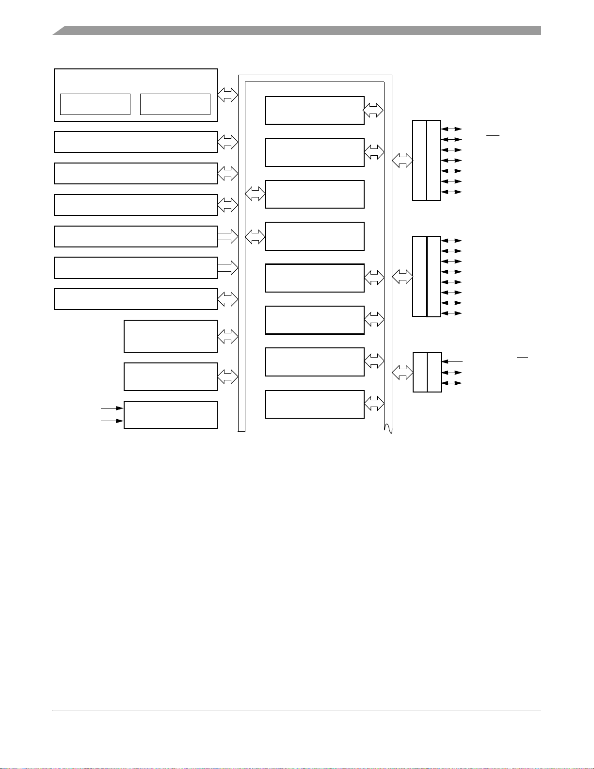
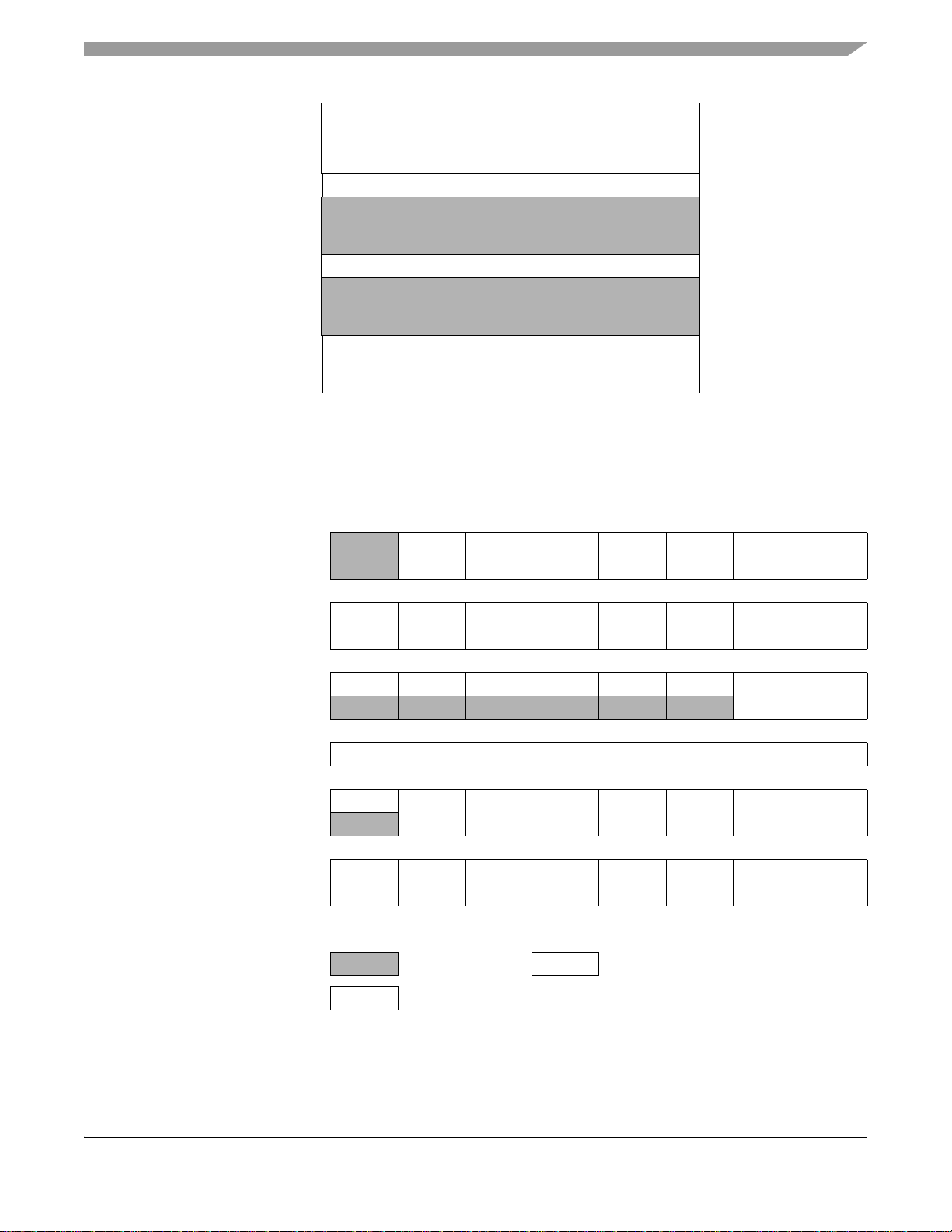
1.3 MCU Block Diagram
MCU Block Diagram
Figure 1-1 shows the structure of the MC68HC908LB8.
MC68HC908LB8 Data Sheet, Rev. 1
Freescale Semiconductor 19
Page 20
General Description
M68HC08 CPU
INTERNAL BUS
CPU
REGISTERS
ARITHMETIC/LOGIC
UNIT (ALU)
CONTROL AND STATUS
REGISTERS — 64 BYTES
USER FLASH — 8 KBYTES
USER RAM — 128 BYTES
MONITOR ROM — 350 BYTES
FLASH PROGRAMMING
ROUTINES ROM — 674 BYTES
USER FLASH VECTOR SPACE — 34 BYTES
OSCILLATOR
MODULE
SYSTEM INTEGRATION
MODULE
DUAL CHANNEL PWM
MODULE
HIGH RESOLUTION PWM
MODULE
LOW-VOLTAGE INHIBIT
MODULE
COMPUTER OPERATING
PROPERLY MODULE
2-CHANNEL TIMER
MODULE
8-BIT ANALOG-TO-DIGITAL
CONVERTER MODULE
KEYBOARD INTERRUPT
MODULE
DDRA
DDRB
DDRC
PORTA
PORTB
PORTC
(1)
/AD5/TCH0/KBI6
PTA6
(1)
/RST/KBI5
PTA5
(1)
/AD4/KBI4
PTA4
(1)
/AD3/KBI3
PTA3
(1)
/AD2/KBI2
PTA2
(1)
/AD1/KBI1
PTA1
(1)
/AD0/KBI0
PTA0
PTB7/V
OUT
PTB6/V–
PTB5/V+
PTB4/PWM1
PTB3/PWM0
PTB2/FAULT
PTB1/BOT
PTB0/TOP
(1)
PTC2
/SHTDWN/IRQ
(1)
PTC1
/OSC2
(1)
/OSC1
PTC0
/AD6/FAULT
(2)
(2)
V
DD
V
SS
POWER
OP AMP/COMPARATOR
MODULE
Notes:
1. Pin contains integrated pullup device.
2. Fault function switchable between pins PTB2 and PTB7.
Figure 1-1. MCU Block Diagram
1.4 Pin Assignments
Figure 1-2 illustrates the pin assignments for the 20-pin SOIC package.
MC68HC908LB8 Data Sheet, Rev. 1
20 Freescale Semiconductor
Page 21
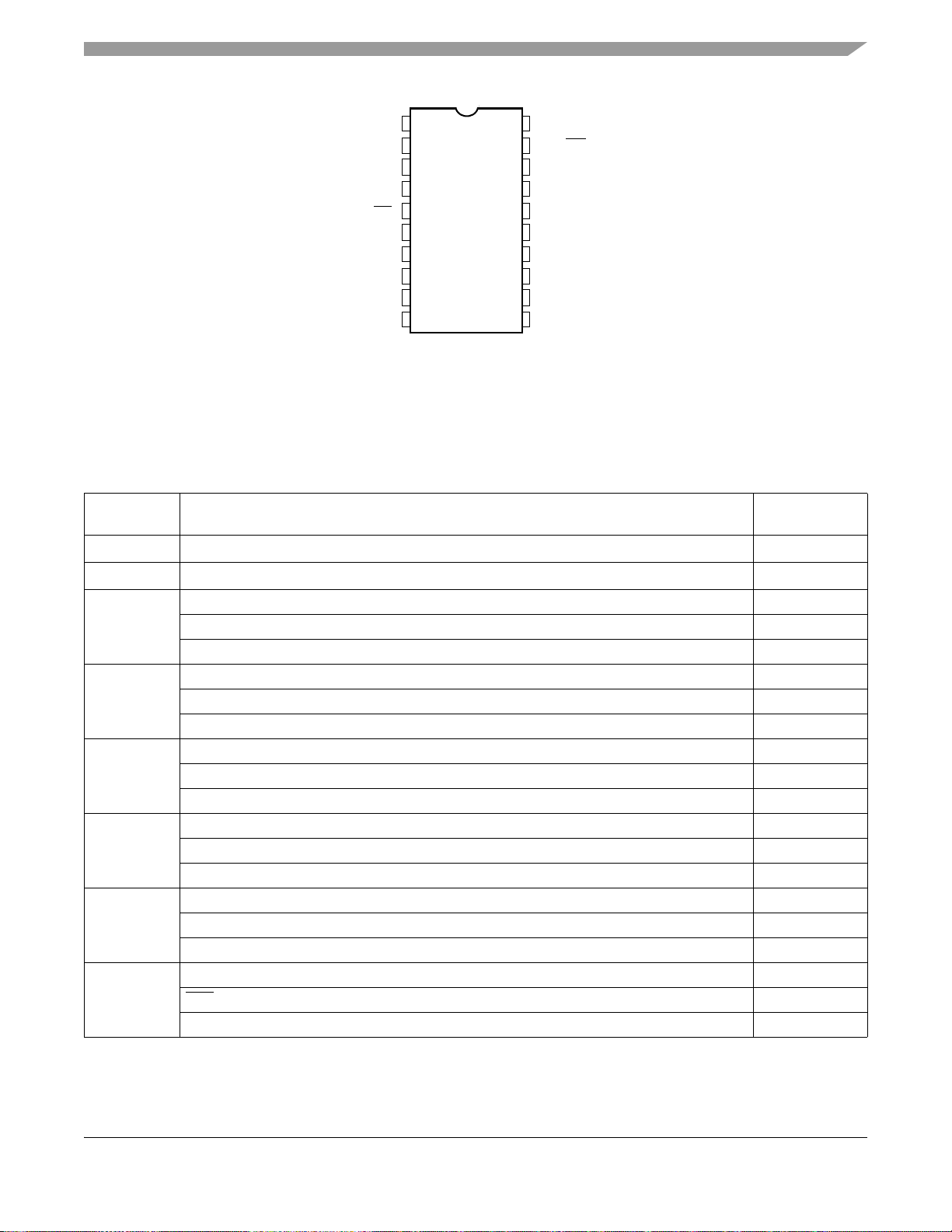
Pin Functions
V
1
DD
2
V
SS
PTC0/OSC1
PTC1/OSC2
PTC2/SHTDWN/IRQ
PTB0/TOP
PTB1/BOT
PTB2/FAULT
PTB3/PWM0
PTB4/PWM1
3
4
5
6
7
8
9
10
Figure 1-2. 20-Pin SOIC and PDIP Pin Assignments
1.5 Pin Functions
Table 1-1 provides a description of the pin functions.
Table 1-1. Pin Functions
Pin
Name
V
DD
V
SS
PTA0
PTA1
PTA2
PTA3
PTA4
PTA5
Power supply Power
Power supply ground Power
PTA0 — General purpose I/O port Input/Output
KBI0 — Keyboard interrupt input 0 Input
ADC0 — A/D channel 0 input Input
PTA1 — General purpose I/O port Input/Output
KBI1 — Keyboard interrupt input 1 Input
ADC1 — A/D channel 1 input Input
PTA2 — General purpose I/O port Input/Output
KBI2 — Keyboard interrupt input 2 Input
ADC2 — A/D channel 2 input Input
PTA3 — General purpose I/O port Input/Output
KBI3 — Keyboard interrupt input 3 Input
ADC3 — A/D channel 3 input Input
PTA4 — General purpose I/O port Input/Output
KBI4 — Keyboard interrupt input 4 Input
ADC4 — A/D channel 4 input Input
PTA5 — General purpose I/O port Input/Output
RST
— Reset input, active low with internal pullup and Schmitt trigger Input
KBI5 — Keyboard interrupt input 5 Input
Description Input/Output
20
PTA6/ADC5/TCH0/KBI6
19
PTA5/RST
18
PTA4/ADC4/KBI4
17
PTA3/ADC3/KBI3
PTA2/ADC2/KBI2
16
PTA1/ADC1/KBI1
15
PTA0/ADC0/KBI0
14
PTB7/V
13
12
11
OUT
PTB6/V–
PTB5/V+
/KBI5
/ADC6/FAULT
MC68HC908LB8 Data Sheet, Rev. 1
Freescale Semiconductor 21
Page 22

General Description
Table 1-1. Pin Functions (Continued)
Pin
Name
PTA6
PTB0
PTB1
PTB2
PTB3
PTB4
PTB5
PTB6
PTB7
PTC0
PTC1
PTC2
Description Input/Output
PTA6 — General purpose I/O port Input/Output
KBI6 — Keyboard interrupt input 6 Input
TCH0 — Timer Channel 0 I/O Input/Output
ADC5 — A/D channel 5 input Input
PTB0 — General purpose I/O port Input/Output
TOP — High resolution PWM output Output
PTB1 — General purpose I/O port Input/Output
BOT — High resolution PWM output Output
PTB2 — General purpose I/O port Input/Output
FAULT — High resolution PWM fault input (switchable between PTB2 and PTB7) Input
PTB3 — General purpose I/O port Input/Output
PWM0 — Pulse-width modulator output 0 Output
PTB4 — General purpose I/O port Input/Output
PWM1 — Pulse-width modulator output 1 Output
PTB5 — General purpose I/O port Input/Output
V+ — Op amp/comparator input Input
PTB6 — General purpose I/O port Input/Output
V– — Op amp/comparator input Input
PTB7 — General purpose I/O port Input/Output
V
— Op amp/comparator output
OUT
ADC6 — A/D channel 6 input Input
FAULT — High resolution PWM fault input (switchable between PTB2 and PTB7) Input
PTC0 — General purpose I/O port Input/Output
OSC1 — XTAL, RC, or external oscillator input Input
PTC1 — General purpose I/O port Input/Output
OSC2 — XTAL oscillator output (XTAL option only)
RC or internal oscillator output (OSC2EN = 1 in PTAPUE register)
PTC2 — General purpose input port Input
SHTDWN — High resolution PWM input Input
IRQ
— External interrupt with programmable pullup and Schmitt trigger Input
Output
Output
Output
1.6 Pin Function Priority
Table 1-2 is meant to resolve the priority if multiple functions are enabled on a single pin.
NOTE
Upon reset all pins come up as input ports regardless of the priority table.
MC68HC908LB8 Data Sheet, Rev. 1
22 Freescale Semiconductor
Page 23
Table 1-2. Function Priority in Shared Pins
Pin Name Highest-to-Lowest Priority Sequence
PTA0 ADC0 → KBI0 → PTA0
PTA1 ADC1 → KBI1 → PTA1
PTA2 ADC2 → KBI2 → PTA2
PTA3 ADC3 → KBI3 → PTA3
PTA4 ADC4 → KBI4 → PTA4
PTA5 RST
PTA6 ADC5 → TCH0 → KBI6 → PTA6
PTB0 TOP → PTB0
PTB1 BOT → PTB1
PTB2
PTB3 PWM0 → PTB3
PTB4 PWM1 → PTB4
PTB5 V+ → PTB5
→ KBI5 → PTA5
(1)
FAULT
→ PTB2
Pin Function Priority
PTB6 V– → PTB6
PTB7
PTC0 OSC1 → PTC0
PTC1 OSC2 → PTC1
PTC2 SHTDWN → IRQ
V
/ ADC6 / FAULT
OUT
(1)(2)
→ PTC2
→ PTB7
NOTES:
1. Fault function is switchable between pins PTB2 and PTB7.
2. V
, ADC6, and FAULT functions all share equal priority. All of these functions can be used
OUT
simultaneously on this pin.
NOTE
Any unused inputs and I/O ports should be tied to an appropriate logic level
(either V
or VSS). Although the I/O ports of the MC68HC908LB8 do not
DD
require termination, termination is recommended to reduce the possibility
of static damage.
MC68HC908LB8 Data Sheet, Rev. 1
Freescale Semiconductor 23
Page 24
General Description
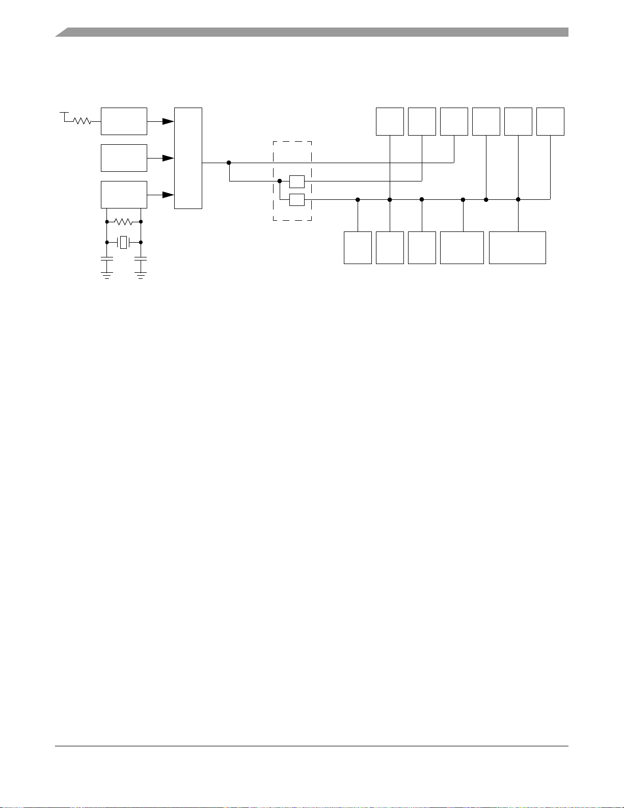
1.7 System Clock Distribution
V
DD
R
EXT
XRC
IRC
OSC
MUX
BUSCLKX4
SIM
÷2
÷4
BUSCLKX4
BUSCLKX2
BUSCLK
CPU FLASH RAM MON ROM
Figure 1-3. System Clock Distribution Diagram
Some of the modules inside the MCU use different clock sources. Figure 1-3 shows a simplified clock
connection diagram. The OSC supplies the clock sources:
• BUSCLKX4 is the basic reference clock of the device. It is either:
– The external crystal oscillator
– An external clock source
– An external RC oscillator
– The internal oscillator
PWM
HRP COP TIM ADC KBI
FLASH
PROGRAMMING
ROM
MC68HC908LB8 Data Sheet, Rev. 1
24 Freescale Semiconductor
Page 25

Chapter 2
Memory
2.1 Introduction
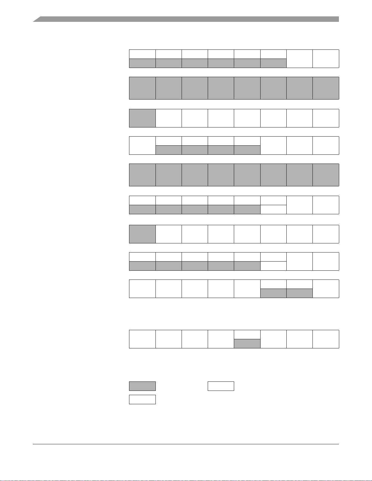
The CPU08 can address 64 Kbytes of memory space. The memory map, shown in Figure 2-1, includes:
• System registers
• 8192 bytes of user FLASH memory
• 128 bytes of random-access memory (RAM)
• 674 bytes of FLASH programming routines read-only memory (ROM)
• 34 bytes of user-defined vectors
2.2 Unimplemented Memory Locations
Accessing an unimplemented location can cause an illegal address reset. In the memory map
(Figure 2-1) and in register figures in this document, unimplemented locations are shaded.
2.3 Reserved Memory Locations
Accessing a reserved location can have unpredictable effects on microcontroller (MCU) operation. In the
Figure 2-1 and in register figures in this document, reserved locations are marked with the word Reserved
or with the letter R.
2.4 Register Section
Most of the control, status, and data registers are in the zero page area of $0000–$0058. Additional I/O
registers have these addresses:
• $FE00; break status register, BSR
• $FE01; SIM reset status register, SRSR
• $FE02; break auxiliary register, BRKAR
• $FE03; break flag control register, BFCR
• $FE04; interrupt status register 1, INT1
• $FE05; interrupt status register 2, INT2
• $FE06; reserved
• $FE07; reserved
• $FE08; FLASH control register, FLCR
• $FE09; break address register high, BRKH
• $FE0A; break address register low, BRKL
• $FE0B; break status and control register, BRKSCR
• $FE0C; LVI status register, LVISR
• $FF7E; FLASH block protect register, FLBPR
MC68HC908LB8 Data Sheet, Rev. 1
Freescale Semiconductor 25
Page 26

Memory
Data registers are shown in Figure 2-2. Table 2-1 is a list of vector locations.
$0000
I/O REGISTERS↓
$0058
$0059
↓
$007F
$0080
↓
$00FF
$0100
↓
$037D
UNIMPLEMENTED
RANDOM-ACCESS MEMORY
128 BYTES
UNIMPLEMENTED
(1)
(1)
$037E
↓
FLASH PROGRAMMING ROUTINES ROM
674 BYTES
$061F
$0620
↓
UNIMPLEMENTED
(1)
$DEFF
$DE00
↓
FLASH MEMORY
8192 BYTES
$FDFF
$FE00 BREAK STATUS REGISTER (BSR)
$FE01 SIM RESET STATUS REGISTER (SRSR)
$FE02 BREAK AUXILIARY REGISTER (BRKAR)
$FE03 BREAK FLAG CONTROL REGISTER (BFCR)
$FE04 INTERRUPT STATUS REGISTER 1 (INT1)
$FE05 INTERRUPT STATUS REGISTER 2 (INT2)
$FE06 RESERVED
$FE07 RESERVED
$FE08 FLASH CONTROL REGISTER (FLCR)
$FE09 BREAK ADDRESS REGISTER HIGH (BRKH)
$FE0A BREAK ADDRESS REGISTER LOW (BRKL)
$FE0B BREAK STATUS AND CONTROL REGISTER (BRKSCR)
$FE0C LVI STATUS REGISTER (LVISR)
$FE0D
↓
UNIMPLEMENTED
$FE1F
Figure 2-1. Memory Map
MC68HC908LB8 Data Sheet, Rev. 1
26 Freescale Semiconductor
Page 27
Register Section
$FE20
↓
$FF7D
$FF7E FLASH BLOCK PROTECT REGISTER (FLBPR)
$FF7F
↓
$FFBF
$FFC0 INTERNAL OSCILLATOR TRIM VALUE
$FFC1
↓
$FFDD
$FFDE
↓
(2)
$FFFF
1. Attempts to execute code from addresses in these ranges will
generate an illegal address reset.
2. $FFF6–$FFFD used for eight security bytes
MONITOR ROM
350 BYTES
UNIMPLEMENTED
UNIMPLEMENTED
FLASH VECTORS
34 BYTES
Figure 2-1. Memory Map (Continued)
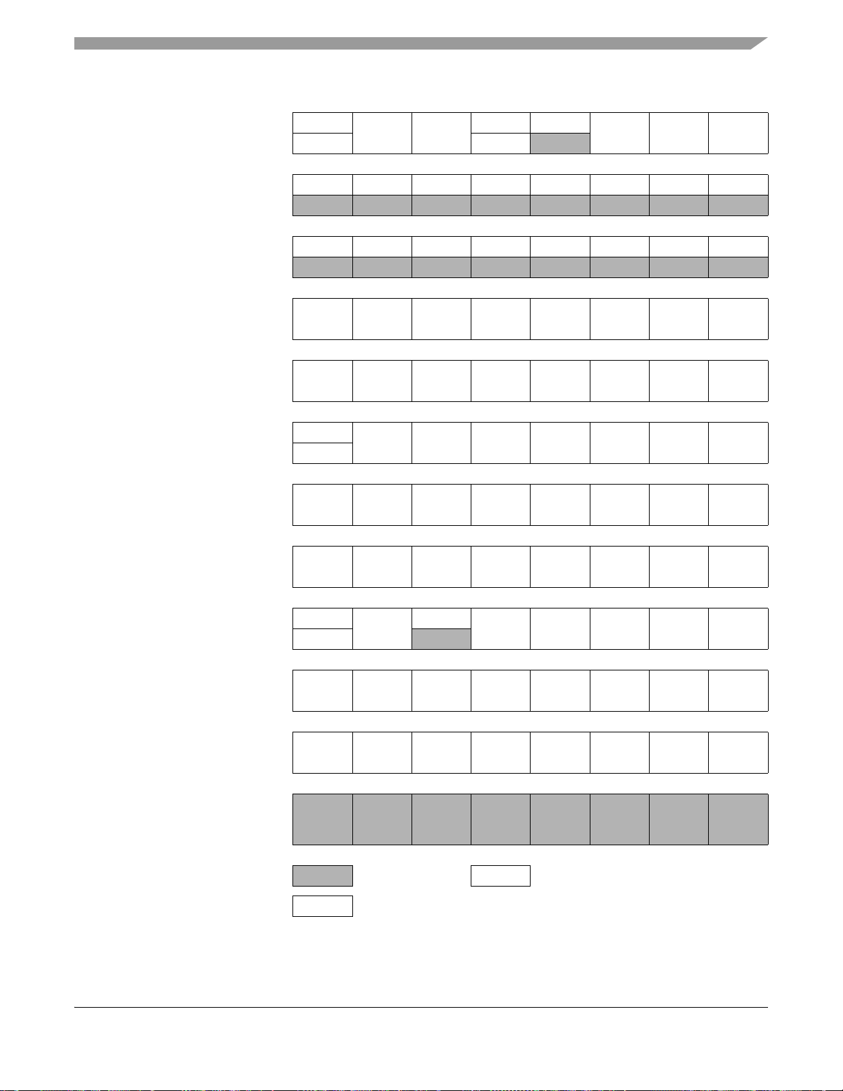
Addr.Register Name Bit 7654321Bit 0
Port A Data Register
$0000
See page 134.
Port B Data Register
$0001
See page 136.
Port C Data Register
$0002
See page 138.
$0003 Reserved Reserved
Read:
(PTA)
Write:
Reset: Unaffected by reset
Read:
Write:
(PTB)
Reset: Unaffected by reset
Read: 00000PTC2
Write:
(PTC)
Reset:00000000
PTB7 PTB6 PTB5 PTB4 PTB3 PTB2 PTB1 PTB0
PTA6 PTA5 PTA4 PTA3 PTA2 PTA1 PTA0
PTC1 PTC0
Read: 0
Write:
Reset:00000000
Read:
Write:
Reset:00000000
DDRB7 DDRB6 DDRB5 DDRB4 DDRB3 DDRB2 DDRB1 DDRB0
Bold = Buffered U = Unaffected
DDRA6 DDRA5 DDRA4 DDRA3 DDRA2 DDRA1 DDRA0
= Unimplemented R = Reserved
$0004
$0005
Data Direction Register A
(DDRA)
See page 135.
Data Direction Register B
(DDRB)
See page 137.
Figure 2-2. Control, Status, and Data Registers (Sheet 1 of 8)
MC68HC908LB8 Data Sheet, Rev. 1
Freescale Semiconductor 27
Page 28
Memory
Addr.Register Name Bit 7654321Bit 0
Read: 000000
Write:
DDRC1 DDRC0
Reset:00000000
$0006
Data Direction Register C
(DDRC)
See page 139.
$0007
↓
Unimplemented
$000C
$000D
$000E
$000F
↓
$0019
$001A
$001B
$001D
$001E
Port A Input Pullup Enable
Register (PTAPUE)
See page 136.
Port C Input Pullup Enable
Register (PTCPUE)
See page 140.
Unimplemented
Keyboard Status
and Control Register
(INTKBSCR)
See page 89.
Keyboard Interrupt Enable
Register (INTKBIER)
See page 90.
IRQ Status and Control
Register (INTSCR)
See page 84.
Configuration Register 2
(CONFIG2)
See page 60.
Read:
Write:
PTA6PUE PTA5PUE PTA4PUE PTA3PUE PTA2PUE PTA1PUE PTA0PUE
Reset:00000000
Read:
Write:
OSC2EN
0000
PTCPUE2 PTCPUE1 PTCPUE0
Reset:00000000
Read: 0000KEYF 0
Write:
ACKK
IMASKK MODEK
Reset:00000000
Read:
Write:
KBIE6 KBIE5 KBIE4 KBIE3 KBIE2 KBIE1 KBIE0
Reset:00000000
Read: 0000IRQF0
Write:
ACK
IMASK MODE
Reset:00000000
Read:
(1)
IRQPUD IRQEN R OSCOPT1 OSCOPT0
Write:
Reset:00000000
00
RSTEN
(2)
1. One-time writable register after each reset.
2. RSTEN reset to 0 by a power-on reset (POR) only.
$001F
Configuration Register 1
(CONFIG1)
See page 61.
Read:
(1)
Write:
COPRS LVISTOP LVIRSTD LVIPWRD
Reset:00000000
0
SSREC STOP COPD
1. One-time writable register after reach reset.
= Unimplemented R = Reserved
Bold = Buffered U = Unaffected
Figure 2-2. Control, Status, and Data Registers (Sheet 2 of 8)
MC68HC908LB8 Data Sheet, Rev. 1
28 Freescale Semiconductor
Page 29
Register Section
Addr.Register Name Bit 7654321Bit 0
$0020
$0021
$0022
$0023
$0024
$0025
$0026
$0027
$0028
$0029
$002A
$002B
↓
$0029
Timer Status and Control
Register (TSC)
See page 195.
Timer Counter
Register High (TCNTH)
See page 196.
Timer Counter
Register Low (TCNTL)
See page 196.
Timer Counter Modulo
Register High (TMODH)
See page 197.
Timer Counter Modulo
Register Low (TMODL)
See page 197.
Timer Channel 0 Status
and Control Register (TSC0)
See page 198.
Timer Channel 0
Register High (TCH0H)
See page 201.
Timer Channel 0
Register Low (TCH0L)
See page 201.
Timer Channel 1 Status
and Control Register (TSC1)
See page 198.
Timer Channel 1
Register High (TCH1H)
See page 201.
Timer Channel 1
Register Low (TCH1L)
See page 201.
Unimplemented
Read: TOF
Write: 0 TRST
Reset:00100000
Read: Bit 15 14 13 12 11 10 9 Bit 8
Write:
Reset:00000000
Read: Bit 7 654321Bit 0
Write:
Reset:00000000
Read:
Write:
Reset:11111111
Read:
Write:
Reset:11111111
Read: CH0F
Write: 0
Reset:00000000
Read:
Write:
Reset: Indeterminate after reset
Read:
Write:
Reset: Indeterminate after reset
Read: CH1F
Write: 0
Reset:00000000
Read:
Write:
Reset: Indeterminate after reset
Read:
Write:
Reset: Indeterminate after reset
Bit 15 14 13 12 11 10 9 Bit 8
Bit 7654321Bit 0
Bit 15 14 13 12 11 10 9 Bit 8
Bit 7654321Bit 0
Bit 15 14 13 12 11 10 9 Bit 8
Bit 7654321Bit 0
TOIE TSTOP
CH0IE MS0B MS0A ELS0B ELS0A TOV0 CH0MAX
CH1IE
0
00
MS1A ELS1B ELS1A TOV1 CH1MAX
PS2 PS1 PS0
= Unimplemented R = Reserved
Bold = Buffered U = Unaffected
Figure 2-2. Control, Status, and Data Registers (Sheet 3 of 8)
MC68HC908LB8 Data Sheet, Rev. 1
Freescale Semiconductor 29
Page 30
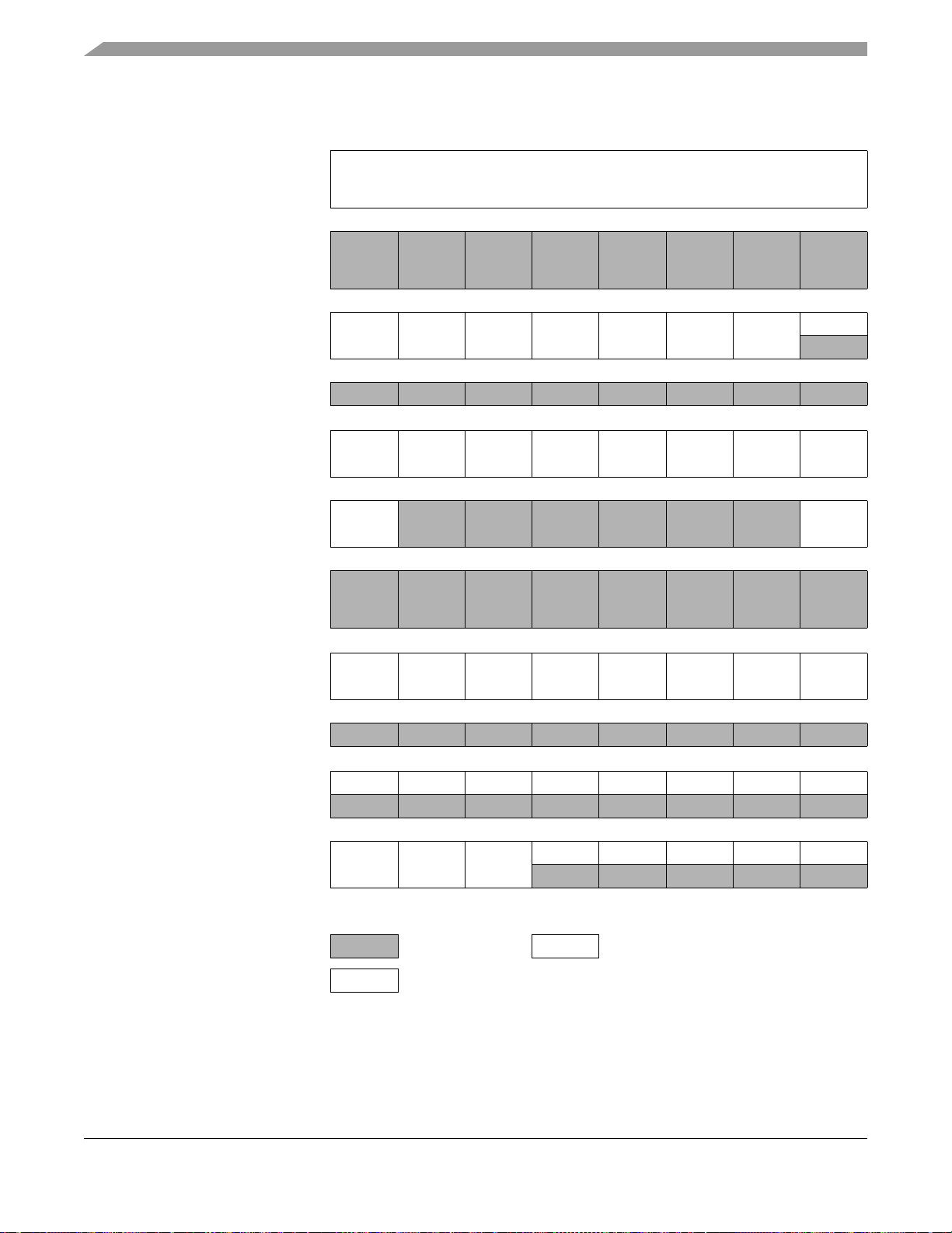
Memory
Addr.Register Name Bit 7654321Bit 0
$0030
↓
$0033
$0034
↓
$0035
Reserved Reserved
Unimplemented
Oscillator Status Register
$0036
$0037 Unimplemented
Oscillator Trim Register
$0038
Op Amp/Comparator Control
$0039
$003A
↓
$003B
ADC Status and Control
$003C
$003D Unimplemented
(OSCSTAT)
See page 130.
(OSCTRIM)
See page 131.
Register (OACCR)
See page 55.
Unimplemented
Register (ADSCR)
See page 48.
Read:
Write:
Reset:00000000
Read:
Write:
Reset:10000000
Read:
Write:
Reset:0UUUUUU 0
Read:
Write:
Reset:00011111
RRRRRRECGON
TRIM7 TRIM6 TRIM5 TRIM4 TRIM3 TRIM2 TRIM1 TRIM0
OACM
COCO AIEN ADCO ADCH4 ADCH3 ADCH2 ADCH1 ADCH0
EGGST
OACE
Read: AD7 AD6 AD5 AD4 A3 AD2 AD1 AD0
(ADR)
Write:
Reset: Unaffected by reset
Read:
Write:
Reset:00000000
ADIV2 ADIV1 ADIV0
= Unimplemented R = Reserved
Bold = Buffered U = Unaffected
00000
$003E
$003F
ADC Data Register
See page 50.
ADC Clock Register
(ADCLK)
See page 50.
Figure 2-2. Control, Status, and Data Registers (Sheet 4 of 8)
MC68HC908LB8 Data Sheet, Rev. 1
30 Freescale Semiconductor
Page 31

Register Section
Addr.Register Name Bit 7654321Bit 0
$0040
$0041
$0042
$0043
$0044
$0045
$0046
$0047
$0048
$0049
$004A
$004B
PWM Control Register 1
(PCTL1)
See page 155.
PWM Control Register 2
(PCTL2)
See page 157.
Fault Control Register
(FCR)
See page 159.
Fault Status Register
(FSR)
See page 159.
Fault Control Register 2
(FCR2)
See page 160.
PWM Counter Register High
(PCNTH)
See page 153.
PWM Counter Register Low
(PCNTL)
See page 153.
PWM Counter Modulo
Register High (PMODH)
See page 154.
PWM Counter Modulo
Register Low (PMODL)
See page 154.
PWM 0 Value Register High
(PVAL0H)
See page 154.
PWM 0 Value Register Low
(PVAL0L)
See page 155.
PWM 1 Value Register High
(PVAL1H)
See page 154.
Read: 0
Write:
Reset:00000000
Read:
Write:
Reset:00001100
Read: 000000
Write:
Reset:00000000
Read: 000000FPINFFLAG
Write:
Reset:U0U0U0U0
Read: 00000000
Write:
Reset:00000000
Read: 0000Bit 11Bit 10Bit 9Bit 8
Write:
Reset:00000000
Read: Bit 7 Bit 6 Bit 5 Bit 4 Bit 3 Bit 2 Bit 1 Bit 0
Write:
Reset:00000000
Read: 0000
Write:
Reset:0000 Indeterminate after reset
Read:
Write:
Reset: Indeterminate after reset
Read:
Write:
Reset:00000000
Read:
Write:
Reset:00000000
Read:
Write:
Reset:00000000
LDFQ1 LDFQ0 DIS1 DIS0 POL1 POL0 PRSC1 PRSC0
Bit 7Bit 6Bit 5Bit 4Bit 3Bit 2Bit 1Bit 0
Bit 15 Bit 14 Bit 13 Bit 12 Bit 11 Bit 10 Bit 9 Bit 8
Bit 7Bit 6Bit 5Bit 4Bit 3Bit 2Bit 1Bit 0
Bit 15 Bit 14 Bit 13 Bit 12 Bit 11 Bit 10 Bit 9 Bit 8
FPOS PWMINT PWMF
00
Bit 11 Bit 10 Bit 9 Bit 8
LDOK PWMEN
FINT FMODE
FTACK
= Unimplemented R = Reserved
Bold = Buffered U = Unaffected
Figure 2-2. Control, Status, and Data Registers (Sheet 5 of 8)
MC68HC908LB8 Data Sheet, Rev. 1
Freescale Semiconductor 31
Page 32

Memory
Addr.Register Name Bit 7654321Bit 0
PWM 1 Value Register Low
$004C
PWM Disable Mapping Write
$004D
$004E
↓
$004F
$0050 Reserved Reserved
Once Register (DISMAP)
(PVAL1L)
See page 155.
See page 158.
Unimplemented
Read:
Write:
Reset:00000000
Read: 000000
Write:
Reset:00000011
Bit 7Bit 6Bit 5Bit 4Bit 3Bit 2Bit 1Bit 0
MAP1 MAP0
HRP Control Register
$0051
HRP Duty Cycle Register
$0052
HRP Duty Cycle Register
$0053
HRP Period Register High
$0054
HRP Period Register Low
$0055
HRP Dead Time Register
$0056
HRP Timebase Register High
$0057
(HRPCTRL)
See page 105.
High (HRPDCH)
See page 107.
Low (HRPDCL)
See page 107.
(HRPPERH)
See page 107.
(HRPPERL)
See page 107.
(HRP_DT)
See page 108.
(HRPTBH)
See page 108.
Read:
Write:
Reset 0000000
1. When HRPMODE bit = 0, STEP[4:0] are mapped into the HRPPERL register —
when HRPMODE = 1, STEP[4:0] are mapped into the HRPDCL register.
Read:
Write:
Reset00000000
Read:
Write:
Reset00000000
Read:
Write:
Reset00000000
Read:
Write:
Reset00000000
Read:
Write:
Reset00001000
Read:
Write:
Reset00000000
DC10 DC9 DC8 DC7 DC6 DC5 DC4 DC3
DC2 DC1 DC0 STEP4 STEP3 STEP3 STEP1 STEP0
P10P9P8P7P6P5P4P3
P2 P1 P0 STEP4 STEP3 STEP2 STEP1 STEP0
DT7 DT6 DT5 DT4 DT3 DT2 DT1 DT0
TB15 TB14 TB13 TB12 TB11 TB10 TB9 TB8
SHTLVL HRPOE SHTIF SHTIE SHTEN
HRP-
MODE
HRPEN
(1)
= Unimplemented R = Reserved
Bold = Buffered U = Unaffected
Figure 2-2. Control, Status, and Data Registers (Sheet 6 of 8)
MC68HC908LB8 Data Sheet, Rev. 1
32 Freescale Semiconductor
Page 33

Register Section
Addr.Register Name Bit 7654321Bit 0
HRP Timebase Register Low
$0058
Frequency Dithering Control
$0059
$005A
↓
$005F
(HRPTBL)
See page 108.
Register (HRPDCR)
See page 109.
Reserved Reserved
Read:
Write:
Reset00000000
Read:
Write:
Reset 0000
TB7 TB6 TB5 TB4 TB3 TB2 TB1 TB0
CLKSRC SEL2 SEL1 SEL0
Break Status Register
$FE00
SIM Reset Status Register
$FE01
Break Auxiliary Register
$FE02
Break Flag Control Register
$FE03
$FE04
↓
$FE07
FLASH Control Register
$FE08
Break Address Register High
$FE09
Break Address Register Low
$FE0A
Read:
(BSR)
Write: (Note)
See page 183.
(SRSR)
See page 184.
(BRKAR)
See page 206.
(BFCR)
See page 185.
Reserved Reserved
(FLCR)
See page 37.
(BRKH)
See page 206.
(BRKL)
See page 206.
Reset:00000000
Read: POR PIN COP ILOP ILAD MODRST LVI 0
Write:
POR:10000000
Read:
Write:
Reset:00000000
Read:
Write:
Reset:00000000
Read: 0000
Write:
Reset:00000000
Read:
Write:
Reset:00000000
Read:
Write:
Reset:00000000
RRRRRR
Note: Writing a 0 clears SBSW.
Bit 7 6 5 4 3 2 1 Bit 0
BCFERRRRRRR
Bit 15 14 13 12 11 10 9 Bit 8
Bit 7654321Bit 0
SBSW
HVEN MASS ERASE PGM
R
= Unimplemented R = Reserved
Bold = Buffered U = Unaffected
Figure 2-2. Control, Status, and Data Registers (Sheet 7 of 8)
MC68HC908LB8 Data Sheet, Rev. 1
Freescale Semiconductor 33
Page 34

Memory
Addr.Register Name Bit 7654321Bit 0
Break Status and Control
$FE0B
$FE0C
$FFC0 Internal Oscillator Trim Value TRIM7 TRIM6 TRIM5 TRIM4 TRIM3 TRIM2 TRIM1 TRIM0
$FFC1 Reserved Reserved
Register (BRKSCR)
See page 205.
LVI Status Register
(LVISR)
See page 121.
Read:
Write:
Reset:00000000
Read: LVIOUT 0000000
Write:
Reset:00000000
BRKE BRKA
000000
Factory programmed FLASH byte
FLASH Block Protect
$FF7E
1. Non-volatile FLASH register
$FFFF
Register (FLBPR)
See page 42.
COP Control Register
(COPCTL)
See page 65.
Figure 2-2. Control, Status, and Data Registers (Sheet 8 of 8)
Read:
(1)
Write:
Reset: Unaffected by reset
Read: Low byte of reset vector
Write: Writing clears COP counter (any value)
Reset: Unaffected by reset
BPR7 BPR6 BPR5 BPR4 BPR3 BPR2 BPR1 BPR0
= Unimplemented R = Reserved
Bold = Buffered U = Unaffected
MC68HC908LB8 Data Sheet, Rev. 1
34 Freescale Semiconductor
Page 35

Random-Access Memory (RAM)
Table 2-1. Vector Addresses
Vector Priority Address Vector
Highest
$FFFF Reset vector (low)
$FFFE Reset vector (high)
$FFFD SWI vector (low)
$FFFC SWI vector (high)
$FFFB IRQ vector (low)
$FFFA IRQ
$FFF9
↓
$FFF8
$FFF7 TIM Channel 0 vector (low)
$FFF6 TIM Channel 0 vector (high)
$FFF5 TIM Channel 1 vector (low)
$FFF4 TIM Channel 1 vector (high)
$FFF3 TIM overflow vector (low)
.
vector (high)
Not used
$FFF2 TIM overflow vector (high)
$FFF1 FAULT (PWM vector) (low)
$FFF0 FAULT (PWM vector) (high)
$FFEF PWMINT (PWM vector) (low)
$FFEE PWMINT (PWM vector) (high)
$FFED SHTDWN (HRP vector) (low)
$FFEC SHTDWN (HRP vector) (high)
$FFEB
Lowest
↓
$FFE2
$FFE1 Keyboard vector (low)
$FFE0 Keyboard vector (high)
$FFDF ADC conversion complete vector (low)
$FFDE ADC conversion complete vector (high)
Not used
2.5 Random-Access Memory (RAM)
Addresses $0080 through $00FF are RAM locations. The location of the stack RAM is programmable.
The 16-bit stack pointer allows the stack to be anywhere in the 64-Kbyte memory space.
MC68HC908LB8 Data Sheet, Rev. 1
Freescale Semiconductor 35
Page 36

Memory
NOTE
For correct operation, the stack pointer must point only to RAM locations.
Before processing an interrupt, the CPU uses five bytes of the stack to save the contents of the CPU
registers.
NOTE
For M6805 compatibility, the H register is not stacked.
During a subroutine call, the CPU uses two bytes of the stack to store the return address. The stack
pointer decrements during pushes and increments during pulls.
NOTE
Be careful when using nested subroutines. The CPU may overwrite data in
the RAM during a subroutine or during the interrupt stacking operation.
2.6 FLASH Memory (FLASH)
This section describes the operation of the embedded FLASH memory. This memory can be read,
programmed, and erased from a single external supply. The program, erase, and read operations are
enabled through the use of an internal charge pump. It is recommended that the user utilize the FLASH
programming routines provided in the on-chip ROM, which are described more fully in a separate
Freescale Semiconductor application note.
The FLASH memory is an array of 8 Kbytes with an additional 34 bytes of user vectors and one byte of
block protection. An erased bit reads as 1 and a programmed bit reads as a 0. Memory in the FLASH
array is organized into two rows per page basis. For the 8-K word by 8-bit embedded FLASH memory,
the page size is 64 bytes per page and the row size is 32 bytes per row. Hence the minimum erase page
size is 64 bytes and the minimum program row size is 32 bytes. Program and erase operations are
facilitated through control bits in FLASH control register (FLCR). Details for these operations appear later
in this section.
The address ranges for the user memory and vectors are:
• $DE00–$FDFF; user memory
•$FE08
; FLASH control register
• $FF7E; FLASH block protect register
• $FFDE–$FFFF; these locations are reserved for user-defined interrupt and reset vectors
MC68HC908LB8 Data Sheet, Rev. 1
36 Freescale Semiconductor
Page 37

FLASH Memory (FLASH)
Programming tools are available from Freescale Semiconductor. Contact your local Freescale
Semiconductor representative for more information.
NOTE
A security feature prevents viewing of the FLASH contents.
(1)
2.6.1 FLASH Control Register
The FLASH control register (FLCR) controls FLASH program and erase operations.
Address: $FE08
Bit 7654321Bit 0
Read:0000
Write:
Reset:00000000
= Unimplemented
Figure 2-3. FLASH Control Register (FLCR)
HVEN — High-Voltage Enable Bit
This read/write bit enables the charge pump to drive high voltages for program and erase operations
in the array. HVEN can only be set if either PGM = 1 or ERASE = 1 and the proper sequence for
program or erase is followed.
1 = High voltage enabled to array and charge pump on
0 = High voltage disabled to array and charge pump off
MASS — Mass Erase Control Bit
Setting this read/write bit configures the 8-Kbyte FLASH array for mass erase operation.
1 = MASS erase operation selected
0 = PAGE erase operation selected
HVEN MASS ERASE PGM
ERASE — Erase Control Bit
This read/write bit configures the memory for erase operation. ERASE is interlocked with the PGM bit
such that both bits cannot be equal to 1 or set to 1 at the same time.
1 = Erase operation selected
0 = Erase operation unselected
PGM — Program Control Bit
This read/write bit configures the memory for program operation. PGM is interlocked with the ERASE
bit such that both bits cannot be equal to 1 or set to 1 at the same time.
1 = Program operation selected
0 = Program operation unselected
2.6.2 FLASH Page Erase Operation
Use this step-by-step procedure to erase a page (64 bytes) of FLASH memory to read as logic 1. A page
consists of 64 consecutive bytes starting from addresses $XX00, $XX40, $XX80, or $XXC0. The 34-byte
user interrupt vectors area also forms a page. Any FLASH memory page can be erased alone, except for
the 34-byte interrupt vectors page, which must be mass erased.
1. No security feature is absolutely secure. However, Freescale Semiconductor’s strategy is to make reading or copying the
FLASH difficult for unauthorized users.
MC68HC908LB8 Data Sheet, Rev. 1
Freescale Semiconductor 37
Page 38

Memory
1. Set the ERASE bit, and clear the MASS bit in the FLASH control register.
2. Read the FLASH block protect register.
3. Write any data to any FLASH location within the address range of the block to be erased.
4. Wait for a time, t
(minimum 10 µs)
NVS
5. Set the HVEN bit.
6. Wait for a time, t
(minimum 1 ms or 4 ms)
Erase
7. Clear the ERASE bit.
8. Wait for a time, t
(minimum 5 µs)
NVH
9. Clear the HVEN bit.
10. After a time, t
(typical 1 µs), the memory can be accessed again in read mode.
RCV
NOTE
Programming and erasing of FLASH locations cannot be performed by
code being executed from FLASH memory. While these operations must be
performed in the order shown, other unrelated operations may occur
between the steps.
CAUTION
Be aware that erasing the vector page will erase the internal oscillator trim
value at $FFC0.
It is highly recommended that interrupts be disabled during program/ erase
operations.
In applications that need more than 1000 program/erase cycles, use the 4-ms page erase specification
to get improved long-term reliability. Any application can use this 4-ms page erase specification.
However, in applications where a FLASH location will be erased and reprogrammed less than 1000 times,
and speed is important, use the 1-ms page erase specification to get a shorter cycle time.
2.6.3 FLASH Mass Erase Operation
Use this step-by-step procedure to erase entire FLASH memory to read as logic 1:
1. Set both the ERASE bit and the MASS bit in the FLASH control register.
2. Read from the FLASH block protect register.
3. Write any data to any FLASH address
4. Wait for a time, t
(minimum 10 µs)
NVS
5. Set the HVEN bit.
6. Wait for a time, t
MErase
(minimum 4 ms)
7. Clear the ERASE and MASS bits.
Mass erase is disabled whenever any block is protected (FLBPR does not
equal $FF).
8. Wait for a time, t
1. When in monitor mode, with security sequence failed (see 19.3.2 Security), write to the FLASH block protect register instead
of any FLASH address.
38 Freescale Semiconductor
(minimum 100 µs)
NVHL
MC68HC908LB8 Data Sheet, Rev. 1
(1)
within the FLASH memory address range.
NOTE
Page 39

FLASH Memory (FLASH)
9. Clear the HVEN bit.
10. After time, t
(typical 1 µs), the memory can be accessed in read mode again.
RCV
NOTE
Programming and erasing of FLASH locations cannot be performed by
code being executed from the FLASH memory. While these operations
must be performed in the order as shown, but other unrelated operations
may occur between the steps.
CAUTION
A mass erase will erase the internal oscillator trim value at $FFC0.
2.6.4 FLASH Program/Read Operation
Programming of the FLASH memory is done on a row basis. A row consists of 32 consecutive bytes
starting from addresses $XX00, $XX20, $XX40, $XX60, $XX80, $XXA0, $XXC0, and $XXE0.
During the programming cycle, make sure that all addresses being written to fit within one of the ranges
specified above. Attempts to program addresses in different row ranges in one programming cycle will
fail. Use this step-by-step procedure to program a row of FLASH memory (Figure 2-4 is a flowchart
representation).
NOTE
In order to avoid program disturbs, the row must be erased before any byte
on that row is programmed.
1. Set the PGM bit. This configures the memory for program operation and enables the latching of
address and data for programming.
2. Read from the FLASH block protect register.
3. Write any data to any FLASH address within the row address range desired.
4. Wait for a time, t
(minimum 10 µs).
NVS
5. Set the HVEN bit.
6. Wait for a time, t
(minimum 5 µs).
PGS
7. Write data to the FLASH address to be programmed.
8. Wait for a time, t
(minimum 30 µs).
PROG
9. Repeat step 7 and 8 until all the bytes within the row are programmed.
10. Clear the PGM bit.
11. Wait for a time, t
(1)
(minimum 5 µs).
NVH
12. Clear the HVEN bit.
13. After time, t
(minimum 1 µs), the memory can be accessed in read mode again.
RCV
NOTE
The COP register at location $FFFF should not be written between steps
5-12, when the HVEN bit is set. Since this register is located at a valid
FLASH address, unpredictable behavior may occur if this location is written
while HVEN is set.
This program sequence is repeated throughout the memory until all data is programmed.
1. The time between each FLASH address change, or the time between the last FLASH address programmed to clearing PGM
bit, must not exceed the maximum programming time, t
MC68HC908LB8 Data Sheet, Rev. 1
Freescale Semiconductor 39
PROG
maximum.
Page 40

Memory
NOTE
Programming and erasing of FLASH locations cannot be performed by
code being executed from the FLASH memory. While these operations
must be performed in the order shown, other unrelated operations may
occur between the steps. Do not exceed t
maximum, see 20.12
PROG
Memory Characteristics.
It is highly recommended that interrupts be disabled during program/erase operations.
Do not exceed t
programming time to the same row before next erase. t
maximum or tHV maximum. tHV is defined as the cumulative high voltage
PROG
must satisfy this condition:
HV
t
NVX
= t
NVH
+ t
PGS
+ (t
x 32) <= tHV maximum
PROG
Refer to 20.12 Memory Characteristics.
The time between programming the FLASH address change (step 7 to step 7), or the time between the
last FLASH programmed to clearing the PGM bit (step 7 to step 10) must not exceed the maximum
programming time, t
PROG
maximum.
CAUTION
Be cautious when programming the FLASH array to ensure that
non-FLASH locations are not used as the address that is written to when
selecting either the desired row address range in step 3 of the algorithm or
the byte to be programmed in step 7 of the algorithm. This applies
particularly to $FFD4–$FFDF.
2.6.5 FLASH Block Protection
Due to the ability of the on-board charge pump to erase and program the FLASH memory in the target
application, provision is made for protecting a block of memory from unintentional erase or program
operations due to system malfunction. This protection is done by using of a FLASH block protect register
(FLBPR). The FLBPR determines the range of the FLASH memory which is to be protected. The range
of the protected area starts from a location defined by FLBPR and ends at the bottom of the FLASH
memory ($FFFF). When the memory is protected, the HVEN bit cannot be set in either ERASE or
PROGRAM operations.
NOTE
In performing a program or erase operation, the FLASH block protect
register must be read after setting the PGM or ERASE bit and before
asserting the HVEN bit
When the FLBPR is program with all 0’s, the entire memory is protected from being programmed and
erased. When all the bits are erased (all 1’s), the entire memory is accessible for program and erase.
When bits within the FLBPR are programmed, they lock a block of memory, address ranges as shown in
2.6.6 FLASH Block Protect Register. Once the FLBPR is programmed with a value other than $FF, any
erase or program of the FLBPR or the protected block of FLASH memory is prohibited. The presence of
a V
on the IRQ pin will bypass the block protection so that all of the memory included in the block
TST
protect register is open for program and erase operations.
NOTE
The FLASH block protect register is not protected with special hardware or
software. Therefore, if this page is not protected by FLBPR the register is
erased by either a page or mass erase operation.
MC68HC908LB8 Data Sheet, Rev. 1
40 Freescale Semiconductor
Page 41

FLASH Memory (FLASH)
Algorithm for Programming
a Row (32 Bytes) of FLASH Memory
1
2
READ THE FLASH BLOCK PROTECT REGISTER
3
WRITE ANY DATA TO ANY FLASH ADDRESS
WITHIN THE ROW ADDRESS RANGE DESIRED
4
5
6
7
WRITE DATA TO THE FLASH ADDRESS
8
SET PGM BIT
WAIT FOR A TIME, t
SET HVEN BIT
WAIT FOR A TIME, t
TO BE PROGRAMMED
WAIT FOR A TIME, t
NVS
PGS
PROG
9
NOTES:
The time between each FLASH address change (step 7 to step 7),
or the time between the last FLASH address programmed
to clearing PGM bit (step 7 to step 10)
must not exceed the maximum programming
time, t
PROG
max.
This row program algorithm assumes the row/s
to be programmed are initially erased.
Figure 2-4. FLASH Programming Flowchart
COMPLETED
PROGRAMMING
THIS ROW?
N
Y
10
11
12
13
CLEAR PGM BIT
WAIT FOR A TIME, t
CLEAR HVEN BIT
WAIT FOR A TIME, t
END OF PROGRAMMING
NVH
RCV
MC68HC908LB8 Data Sheet, Rev. 1
Freescale Semiconductor 41
Page 42

Memory
2.6.6 FLASH Block Protect Register
The FLASH block protect register (FLBPR) is implemented as a byte within the FLASH memory, and
therefore can only be written during a programming sequence of the FLASH memory. The value in this
register determines the starting location of the protected range within the FLASH memory.
Address: $FF7E
Bit 7654321Bit 0
Read:
Write:
Reset:UUUUUUUU
BPR[7:0] — FLASH Block Protect Bits
These eight bits represent bits [13:6] of a 16-bit memory address. Bit 15 and 14 are 1s and bits [5:0]
are 0s.
The resultant 16-bit address is used for specifying the start address of the FLASH memory for block
protection. The FLASH is protected from this start address to the end of FLASH memory, at $FFFF.
With this mechanism, the protect start address can be $XX00, $XX40, $XX80, and $XXC0 (64 bytes
page boundaries) within the FLASH memory.
BPR7 BPR6 BPR5 BPR4 BPR3 BPR2 BPR1 BPR0
U = Unaffected by reset. Initial value from factory is 1.
Write to this register is by a programming sequence to the FLASH memory.
Figure 2-5. FLASH Block Protect Register (FLBPR)
16-BIT MEMORY ADDRESS
START ADDRESS OF FLASH
BLOCK PROTECT
1
1
FLBPR VALUE
000000
Figure 2-6. FLASH Block Protect Start Address
Table 2-2. Examples of Protect Address Ranges
BPR[7:0] Addresses of Protect Range
$00–$78 The entire FLASH memory is protected.
$79 (0111 1001)$DE40 (1101 1110 0100 0000) — $FFFF
$7A (0111 1010)$DE80 (1101 1110 1000 0000) — $FFFF
$7B (0111 1011) $DEC0 (1101 1110 1100 0000) — $FFFF
$7C (0111 1100)$DF00 (1101 1111 0000 0000) — $FFFF
and so on...
$FC (1111 1100)$FF00 (1111 1111 0000 0000) — FFFF
$FD (1111 1101)
$FE (1111 1110)
$FF The entire FLASH memory is not protected.
$FF40 (1111 1111 0100 0000) — $FFFF
FLBPR and vectors are protected
$FF80 (1111 1111 1000 0000) — FFFF
Vectors are protected
MC68HC908LB8 Data Sheet, Rev. 1
42 Freescale Semiconductor
Page 43

FLASH Memory (FLASH)
2.6.7 Wait Mode
Putting the MCU into wait mode while the FLASH is in read mode does not affect the operation of the
FLASH memory directly, but there will not be any memory activity since the CPU is inactive.
The WAIT instruction should not be executed while performing a program or erase operation on the
FLASH, otherwise the operation will discontinue, and the FLASH will be on standby mode.
2.6.8 Stop Mode
Putting the MCU into stop mode while the FLASH is in read mode does not affect the operation of the
FLASH memory directly, but there will not be any memory activity since the CPU is inactive.
The STOP instruction should not be executed while performing a program or erase operation on the
FLASH, otherwise the operation will discontinue, and the FLASH will be on standby mode
NOTE
Standby mode is the power saving mode of the FLASH module in which all
internal control signals to the FLASH are inactive and the current
consumption of the FLASH is at a minimum.
MC68HC908LB8 Data Sheet, Rev. 1
Freescale Semiconductor 43
Page 44

Memory
MC68HC908LB8 Data Sheet, Rev. 1
44 Freescale Semiconductor
Page 45
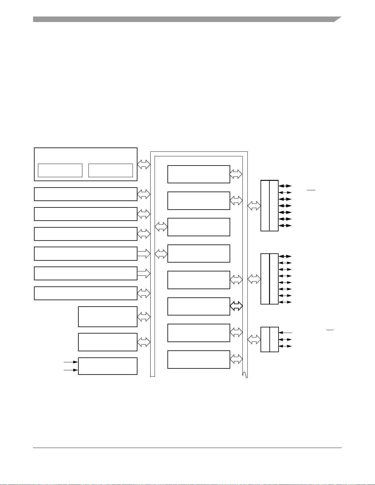
Chapter 3
Analog-to-Digital Converter (ADC)
3.1 Introduction
This section describes the 8-bit analog-to-digital converter (ADC).
INTERNAL BUS
M68HC08 CPU
CPU
REGISTERS
CONTROL AND STATUS
REGISTERS — 64 BYTES
USER FLASH — 8 KBYTES
USER RAM — 128 BYTES
MONITOR ROM — 350 BYTES
FLASH PROGRAMMING
ROUTINES ROM — 674 BYTES
USER FLASH VECTOR SPACE — 34 BYTES
ARITHMETIC/LOGIC
UNIT (ALU)
OSCILLATOR
MODULE
SYSTEM INTEGRATION
MODULE
DUAL CHANNEL PWM
MODULE
HIGH RESOLUTION PWM
MODULE
LOW-VOLTAGE INHIBIT
MODULE
COMPUTER OPERATING
PROPERLY MODULE
2-CHANNEL TIMER
MODULE
8-BIT ANALOG-TO-DIGITAL
CONVERTER MODULE
KEYBOARD INTERRUPT
MODULE
DDRA
DDRB
DDRC
PORTA
PORTB
PORTC
(1)
/AD5/TCH0/KBI6
PTA6
(1)
/RST/KBI5
PTA5
(1)
/AD4/KBI4
PTA4
(1)
/AD3/KBI3
PTA3
(1)
/AD2/KBI2
PTA2
(1)
/AD1/KBI1
PTA1
(1)
/AD0/KBI0
PTA0
PTB7/V
OUT
PTB6/V–
PTB5/V+
PTB4/PWM1
PTB3/PWM0
PTB2/FAULT
PTB1/BOT
PTB0/TOP
(1)
PTC2
/SHTDWN/IRQ
(1)
PTC1
/OSC2
(1)
/OSC1
PTC0
/AD6/FAULT
(2)
(2)
V
DD
V
SS
Notes:
1. Pin contains integrated pullup device.
2. Fault function switchable between pins PTB2 and PTB7.
POWER
OP AMP/COMPARATOR
MODULE
Figure 3-1. Block Diagram Highlighting ADC Block and Pins
MC68HC908LB8 Data Sheet, Rev. 1
Freescale Semiconductor 45
Page 46

Analog-to-Digital Converter (ADC)
3.2 Features
Features of the ADC module include:
• 7 channels with multiplexed input
• Linear successive approximation
• 8-bit resolution
• Single or continuous conversion
• Conversion complete flag or conversion complete interrupt
• Selectable ADC clock
3.3 Functional Description
Seven ADC channels are available for sampling external sources at pins PTB7/ADC6, PTA6/ADC5,
PTA4/ADC4–PTA0/ADC0. An analog multiplexer allows a single ADC converter to select one of seven
ADC channels as ADC voltage in (ADCVIN). ADCVIN is converted by the successive approximation
register based counters. When the conversion is complete, ADC places the result in the ADC data register
and sets a flag or generates an interrupt.
See Figure 3-2.
INTERNAL DATA BUS
READ DDRAx/DDRBx
WRITE DDRAx/DDRBx
WRITE PTAx/PTBx
READ PTAx/PTBx
INTERRUPT
LOGIC
AIEN COCO
RESET
CONVERSION
COMPLETE
BUS CLOCK
DDRAx/DDRAx
PTAx/PTBx
ADC DATA REGISTER
ADC
ADC CLOCK
CLOCK
GENERATOR
ADIV[2:0]
Figure 3-2. ADC Block Diagram
DISABLE
ADC
VOLTAGE IN
)
(V
ADIN
DISABLE
CHANNEL
SELECT
PTAx/PTBx
ADC CHANNEL x
ADCH[4:0]
3.3.1 ADC Port I/O Pins
PTB7/ADC6, PTA6/ADC5, PTA4/ADC4–PTA0/ADC0 are general-purpose I/O (input/output) pins that
share with the ADC channels. The channel select bits define which ADC channel/port pin will be used as
MC68HC908LB8 Data Sheet, Rev. 1
46 Freescale Semiconductor
Page 47

Monotonicity
the input signal. The ADC overrides the port I/O logic by forcing that pin as input to the ADC. The
remaining ADC channels/port pins are controlled by the port I/O logic and can be used as
general-purpose I/O. Writes to the port register or data direction register (DDR) will not have any effect
on the port pin that is selected by the ADC. Read of a port pin in use by the ADC will return a logic 0. If
the DDR bit is at 1, the value in the port data latch is read.
3.3.2 Voltage Conversion
When the input voltage to the ADC equals V
input voltage equals V
, the ADC converts it to $00. Input voltages between V
REFL
, the ADC converts the signal to $FF (full scale). If the
REFH
and V
REFH
REFL
are a
straight-line linear conversion.
V
REFH
and V
are internally connected to VDD and VSS respectively.
REFL
3.3.3 Conversion Time
Conversion starts after a write to the ADC status and control register (ADSCR). One conversion will take
between 16 and 17 ADC clock cycles. The ADIVx bit should be set to provide a 1-MHz ADC clock
frequency.
Conversion time =
16 to 17 ADC cycles
ADC frequency
Number of bus cycles = conversion time × bus frequency
3.3.4 Conversion
In continuous conversion mode, the ADC data register will be filled with new data after each conversion.
Data from the previous conversion will be overwritten whether that data has been read or not.
Conversions will continue until the ADCO bit is cleared. The COCO bit is set after the first conversion and
will stay set until the next write of the ADC status and control register or the next read of the ADC data
register.
In single conversion mode, conversion begins with a write to the ADSCR. Only one conversion occurs
between writes to the ADSCR.
3.3.5 Accuracy and Precision
The conversion process is monotonic and has no missing codes.
3.4 Monotonicity
The conversion process is monotonic and has no missing codes.
3.5 Interrupts
When the AIEN bit is set, the ADC module is capable of generating CPU interrupts after each ADC
conversion. A CPU interrupt is generated if the COCO bit is at 0. The COCO bit is not used as a
conversion complete flag when interrupts are enabled.
MC68HC908LB8 Data Sheet, Rev. 1
Freescale Semiconductor 47
Page 48

Analog-to-Digital Converter (ADC)
3.6 Low-Power Modes
The WAIT and STOP instruction can put the MCU in low power consumption standby modes.
3.6.1 Wait Mode
The ADC continues normal operation during wait mode. Any enabled CPU interrupt request from the ADC
can bring the MCU out of wait mode. If the ADC is not required to bring the MCU out of wait mode, power
down the ADC by setting ADCH4–ADCH0 bits in the ADC status and control register before executing the
WAIT instruction.
3.6.2 Stop Mode
The ADC module is inactive after the execution of a STOP instruction. Any pending conversion is aborted.
ADC functionality resume when the MCU exits stop mode after an external interrupt. Allow one conversion
cycle to stabilize the analog circuitry.
3.7 I/O Signals
The ADC module has seven pins shared with ports A and B: PTB7/ADC6, PTA6/ADC5,
PTA4/ADC4–PTA0/ADC0.
V
is the input voltage signal from one of the seven ADC channels to the ADC module.
ADIN
3.8 I/O Registers
These I/O registers control and monitor ADC operation:
• ADC status and control register (ADSCR)
• ADC data register (ADR)
• ADC clock register (ADCLK)
3.8.1 ADC Status and Control Register
Function of the ADC status and control register (ADSCR) is described here.
Address: $003C
Bit 7654321Bit 0
Read:
Write:
Reset:00011111
COCO — Conversions Complete Bit
When the AIEN bit is a 0, the COCO is a read-only bit which is set each time a conversion is completed
except in the continuous conversion mode where it is set after the first conversion. This bit is cleared
whenever the ADSCR is written or whenever the ADR is read.
If the AIEN bit is a 1, the COCO becomes a read/write bit, which should be cleared to 0 for CPU to
service the ADC interrupt request. Reset clears this bit.
COCO AIEN ADCO ADCH4 ADCH3 ADCH2 ADCH1 ADCH0
Figure 3-3. ADC Status and Control Register (ADSCR)
MC68HC908LB8 Data Sheet, Rev. 1
48 Freescale Semiconductor
Page 49

I/O Registers
1 = Conversion completed (AIEN = 0)
0 = Conversion not completed (AIEN = 0)/CPU interrupt (AIEN = 1)
AIEN — ADC Interrupt Enable Bit
When this bit is set, an interrupt is generated at the end of an ADC conversion. The interrupt signal is
cleared when the data register is read or the status/control register is written. Reset clears the AIEN bit.
1 = ADC interrupt enabled
0 = ADC interrupt disabled
ADCO — ADC Continuous Conversion Bit
When set, the ADC will convert samples continuously and update the ADR register at the end of each
conversion. Only one conversion is completed between writes to the ADSCR when this bit is cleared.
Reset clears the ADCO bit.
1 = Continuous ADC conversion
0 = One ADC conversion
ADCH4–ADCH0 — ADC Channel Select Bits
ADCH4–ADCH0 form a 5-bit field which is used to select one of 7 ADC channels. Only seven channels,
AD6–AD0, are available on this MCU. The channels are detailed in Table 3-1. Care should be taken
when using a port pin as both an analog and digital input simultaneously to prevent switching noise
from corrupting the analog signal. See Table 3-1.
The ADC subsystem is turned off when the channel select bits are all set to 1. This feature allows for
reduced power consumption for the MCU when the ADC is not being used.
NOTE
Recovery from the disabled state requires one conversion cycle to stabilize.
The voltage levels supplied from internal reference nodes, as specified in
Table 3-1, are used to verify the operation of the ADC converter both in production test and for user
applications.
Table 3-1. Mux Channel Select
ADCH4 ADCH3 ADCH2 ADCH1 ADCH0 Input Select
00000 PTA0/AD0
00001 PTA1/AD1
00010 PTA2/AD2
00011 PTA3/AD3
00100 PTA4/AD4
00101 PTA6/AD5
00110 PTB7/AD6
01000
11100
11101
11110
1 1 1 1 1 ADC power off
(1)
Unused↓↓↓↓↓
V
V
REFH
REFL
(2)
(2)
MC68HC908LB8 Data Sheet, Rev. 1
Freescale Semiconductor 49
Page 50

Analog-to-Digital Converter (ADC)
NOTES:
1. If any unused channels are selected, the resulting ADC conversion will be unknown or reserved.
2. V
REFH
and V
are internally connected to VDD and VSS respectively.
REFL
3.8.2 ADC Data Register
One 8-bit result register is provided. This register is updated each time an ADC conversion completes.
Address: $003E
Read: AD7 AD6 AD5 AD4 AD3 AD2 AD1 AD0
Write:
Reset: Unaffected by reset
= Unimplemented
Figure 3-4. ADC Data Register (ADR)
3.8.3 ADC Clock Register
The ADC clock register (ADCLK) selects the clock frequency for the ADC.
Address: $003F
Bit 7654321Bit 0
Read:
ADIV2 ADIV1 ADIV0
Write:
Reset:00000000
= Unimplemented
00000
Figure 3-5. ADC Clock Register (ADCLK)
ADIV2–ADIV0 — ADC Clock Prescaler Bits
ADIV2–ADIV0 form a 3-bit field which selects the divide ratio used by the ADC to generate the internal
ADC clock. Table 3-2 shows the available clock configurations. The ADC clock should be set to
approximately 1 MHz.
Table 3-2. ADC Clock Divide Ratio
ADIV2 ADIV1 ADIV0 ADC Clock Rate
0 0 0 ADC input clock ÷ 1
0 0 1 ADC input clock ÷ 2
0 1 0 ADC input clock ÷ 4
0 1 1 ADC input clock ÷ 8
1
NOTES:
1. X = Don’t care
(1)
X
(1)
X
ADC input clock ÷ 16
MC68HC908LB8 Data Sheet, Rev. 1
50 Freescale Semiconductor
Page 51

I/O Registers
The ADC requires a clock rate of approximately 1 MHz for correct operation. If the selected clock source
is not fast enough, the ADC will generate incorrect conversions. See 20.8 5.0-Volt ADC Characteristics.
f
ADIC
Bus frequency
=
ADIV[2:0]
≅ 1 MHz
MC68HC908LB8 Data Sheet, Rev. 1
Freescale Semiconductor 51
Page 52

Analog-to-Digital Converter (ADC)
MC68HC908LB8 Data Sheet, Rev. 1
52 Freescale Semiconductor
Page 53

Chapter 4
Op Amp/Comparator Module
4.1 Introduction
This section describes the functionality of the op amp/comparator.
4.2 Features
Features of the op amp/comparator include:
• Software enable/disable
• Op amp and comparator modes for optimized performance
• Shared output pin with ADC input pin and PWM fault pin to allow a op amp/comparator circuit to
be inputs to these modules
4.3 Pin Name Conventions
The op amp/comparator shares two input pins and an output pin with the port B input/output (I/O). The full
names of the op amp/comparator pins are listed in
Table 4-1. Note that the generic pin names appear in the text that follows.
Table 4-1. Pin Name Conventions
Generic Pin Name Full Pin Name
V
OUT
V– PTB6/V–
V+ PTB5/V+
PTB7/V
ADC6/FAULT
OUT/
MC68HC908LB8 Data Sheet, Rev. 1
Freescale Semiconductor 53
Page 54

Op Amp/Comparator Module
M68HC08 CPU
INTERNAL BUS
CPU
REGISTERS
CONTROL AND STATUS
REGISTERS — 64 BYTES
USER FLASH — 8 KBYTES
USER RAM — 128 BYTES
MONITOR ROM — 350 BYTES
FLASH PROGRAMMING
ROUTINES ROM — 674 BYTES
USER FLASH VECTOR SPACE — 34 BYTES
ARITHMETIC/LOGIC
UNIT (ALU)
OSCILLATOR
MODULE
SYSTEM INTEGRATION
MODULE
DUAL CHANNEL PWM
MODULE
HIGH RESOLUTION PWM
MODULE
LOW-VOLTAGE INHIBIT
MODULE
COMPUTER OPERATING
PROPERLY MODULE
2-CHANNEL TIMER
MODULE
8-BIT ANALOG-TO-DIGITAL
CONVERTER MODULE
KEYBOARD INTERRUPT
MODULE
DDRA
DDRB
DDRC
PORTA
PORTB
PORTC
(1)
/AD5/TCH0/KBI6
PTA6
(1)
/RST/KBI5
PTA5
(1)
/AD4/KBI4
PTA4
(1)
/AD3/KBI3
PTA3
(1)
/AD2/KBI2
PTA2
(1)
/AD1/KBI1
PTA1
(1)
/AD0/KBI0
PTA0
PTB7/V
OUT
PTB6/V–
PTB5/V+
PTB4/PWM1
PTB3/PWM0
PTB2/FAULT
PTB1/BOT
PTB0/TOP
(1)
PTC2
/SHTDWN/IRQ
(1)
PTC1
/OSC2
(1)
/OSC1
PTC0
/AD6/FAULT
(2)
(2)
V
DD
V
SS
Notes:
1. Pin contains integrated pullup device.
2. Fault function switchable between pins PTB2 and PTB7.
POWER
OP AMP/COMPARATOR
MODULE
Figure 4-1. Block Diagram Highlighting Op Amp/Comparator Block and Pins
4.4 Functional Description
The op amp/comparator module has two modes of operation — op amp mode and comparator mode. Op
amp mode optimizes the module for accurate signal amplification with low input offset voltage.
Comparator mode optimizes the module for use as a comparator with fast output response.
The output of the op amp/comparator shares its pin with an analog-to-digital converter (ADC6) channel.
The fault function of the PWM can also be switched to share this pin. The ADC channel function and the
op amp output can be enabled simultaneously so that the output of the op amp could be sampled directly
by the associated ADC channels. See Figure 4-2.
NOTE
Setting an op amp/comparator enable control bit (OACE) and an op
amp/comparator module selected control bit (OACM) forces V+ and V– to
be inputs and V
to be an output, overriding the data direction register.
OUT
MC68HC908LB8 Data Sheet, Rev. 1
54 Freescale Semiconductor
Page 55

Low Power Modes
In order to read the digital states of the pins configured as inputs, the data
direction register bit must be a 0; to read the states of the pins configured
as outputs the data direction register bit must be a 1.
OACE
V+
GROUND
V–
GROUND
OACE
OACE
+
-
OACE
V
OUT
FLOATING
Figure 4-2. Op Amp/Comparator Block Diagram
4.5 Low Power Modes
4.5.1 Wait Mode
The WAIT instruction places the MCU in a low power consumption mode. While in WAIT the op
amp/comparator cannot be enabled or disabled. If the op amp/comparator module is not needed during
wait mode, reduce power consumption by disabling the op amp/comparator before executing the WAIT
command.
4.5.2 Stop Mode
The op amp/comparator is inactive after execution of the STOP command. The
op amp/comparator will be in a low-power state and will not drive its output pin. When the MCU exits stop
mode after and external interrupt, the op amp/comparator continues operation.
4.6 Op Amp/Comparator Control Register
There is a single operational control register (OACCR) that contains the enable bit for the op
amp/comparator.
Address:
OACM — Op Amp/Comparator Mode Select Bit
This bit selects between 2 modes of operation, op amp mode and comparator mode.
1 = Op amp mode selected
Freescale Semiconductor 55
$0039
Bit 7654321Bit 0
Read:
Write:
Reset:0UUUUUU 0
OACM
= Unimplemented
U = Unaffected
OACE
Figure 4-3. Op Amp/Comparator Control Register (OACCR)
MC68HC908LB8 Data Sheet, Rev. 1
Page 56

Op Amp/Comparator Module
0 = Comparator mode selected
OACE — Op Amp/Comparator Enable Bit
Setting of the corresponding bit in the register enables the associated op amp/comparator and
connects it to the op amp/comparator pins.
1 = Op amp/comparator is connected to pins and powered on
0 = Op amp/comparator is disconnected from pins and powered off
NOTE
Enabling the op amp/comparator prevents PTB[5:7] from being used as
standard I/O. However, the PTB7 pin can be shared with AD6 and FAULT
if the ADC and PWM modules are also enabled.
4.7 Application Information
We make the following assumptions during the design of the operational amplifier.
1. The signal amplified by the operational amplifier is sampled by the internal ADC.
2. Noise resulting from the operation of other circuitry within the MCU will appear at the output of the
circuit due to the amplification set by user.
We recommend the following.
1. An external 500pF capacitor should be added between the output of the operational amplifier
(PTB7) and VSS. This capacitor will act as a filter to internal bus noise caused by the operation of
other digital circuitry in the MCU.
2. Care should be taken to ensure proper filtering at or around the operation bus speed in the
amplification circuit, to prevent noise from being amplified along with the desired signal.
3. The maximum frequency of the signal to be amplified should be limited to 200kHz. This will ensure
that the filtering element will not affect the gain of the desired signal.
4. Do not set the gain of the amplifier to less than 5 (except in the unity gain buffer).
5. Use the circuit component values suggested for the common amplfier configurations shown in the
following figures (Figure 4-4, Figure 4-5, and Figure 4-6).
VDD
Unity Gain Buffer
Vin
+
–
CL
500pF
RL
>20kΩ
Vout
Figure 4-4. Suggested Application Circuit for Unity Gain Buffer
MC68HC908LB8 Data Sheet, Rev. 1
56 Freescale Semiconductor
Page 57

C1
1µF
R2
100k
Application Information
VDD
R1
100k
Inverting Amplifier
+
Vout
–
CL RL
500pF >20k
Vin
R3
10k
R4
>50k
Figure 4-5. Suggested Application Circuit for Inverting Amplifier
VDD
C2
1µF
R6
100k
R3
10k
R5
100k
Non-inverting Amplifier
+
–
CL RL
500pF >20k
R4
>40k
VDD
C1
1µF
Vin
R1
100k
R2
100k
Vout
Figure 4-6. Suggested Application Circuit for Non-inverting Amplifier
MC68HC908LB8 Data Sheet, Rev. 1
Freescale Semiconductor 57
Page 58

Op Amp/Comparator Module
MC68HC908LB8 Data Sheet, Rev. 1
58 Freescale Semiconductor
Page 59

Chapter 5
Configuration Register (CONFIG)
5.1 Introduction
This section describes the configuration registers, CONFIG1 and CONFIG2. The configuration registers
enable or disable these options:
• COP timeout period (2
•STOP instruction
• Stop mode recovery (32 x BUSCLKX4 cycles or
4096 x BUSCLKX4 cycles)
• Computer operating properly module (COP)
• Low-voltage inhibit (LVI) module control
•IRQ
•RST
• OSC option selection
pin
pin
5.2 Functional Description
The configuration registers are used in the initialization of various options. The configuration registers can
be written once after each reset. All of the configuration register bits are cleared during reset. Since the
various options affect the operation of the microcontroller unit (MCU), it is recommended that these
registers be written immediately after reset. The configuration registers are located at $001E and $001F
and may be read at anytime.
18
– 24 or 213 – 24 BUSCLKX4 cycles)
NOTE
On a FLASH device, the options are one-time writable by the user after
each reset. The CONFIG registers are not in the FLASH memory but are
special registers containing one-time writable latches after each reset.
Upon a reset, the CONFIG registers default to predetermined settings as
shown in Figure 5-1 and Figure 5-2.
MC68HC908LB8 Data Sheet, Rev. 1
Freescale Semiconductor 59
Page 60

Configuration Register (CONFIG)
Address: $001E
Bit 7654321Bit 0
Read:
IRQPUD IRQEN R OSCOPT1 OSCOPT0
Write:
Reset:0000000U
POR:00000000
= Unimplemented R = Reserved U = Unaffected
Figure 5-1. Configuration Register 2 (CONFIG2)
IRQPUD — IRQ Pin Pullup Control Bit
1 = Internal pullup is disconnected
0 = Internal pullup is connected between pin IRQ
and V
DD
IRQEN — IRQ Pin Function Selection Bit
1 = Interrupt request function active in pin
0 = Interrupt request function inactive in pin
OSCOPT1 and OSCPOT0 — Selection Bits for Oscillator Option
OSCOPT[1:0] Oscillator Selection
00 Internal oscillator
01 External oscillator
10 External RC oscillator
11 External XTAL oscillator
00
RSTEN
RSTEN — RST
Pin Function Selection
1 = Reset function active in pin
0 = Reset function inactive in pin
The RSTEN bit is cleared by a power-on reset (POR) only. Other resets will
leave this bit unaffected.
NOTE
MC68HC908LB8 Data Sheet, Rev. 1
60 Freescale Semiconductor
Page 61

Address: $001F
Bit 7654321Bit 0
Functional Description
Read:
COPRS LVISTOP LVIRSTD LVIPWRD
Write:
Reset:00000000
= Unimplemented
0
SSREC STOP COPD
Figure 5-2. Configuration Register 1 (CONFIG1)
COPRS — COP Rate Select Bit
COPD selects the COP timeout period. Reset clears COPRS. See Chapter 6 Computer Operating
Properly (COP) Module
1 = COP timeout period = 2
0 = COP timeout period = 2
13
– 24 BUSCLKX4 cycles
18
– 24 BUSCLKX4 cycles
LVISTOP — LVI Enable in Stop Mode Bit
When the LVIPWRD bit is clear, setting the LVISTOP bit enables the LVI to operate during stop mode.
Reset clears LVISTOP.
1 = LVI enabled during stop mode
0 = LVI disabled during stop mode
LVIRSTD — LVI Reset Disable Bit
LVIRSTD disables the reset signal from the LVI module. See Chapter 12 Low-Voltage Inhibit (LVI).
1 = LVI module resets disabled
0 = LVI module resets enabled
LVIPWRD — LVI Power Disable Bit
LVIPWRD disables the LVI module. See Chapter 12 Low-Voltage Inhibit (LVI).
1 = LVI module power disabled
0 = LVI module power enabled
SSREC — Short Stop Recovery Bit
SSREC enables the CPU to exit stop mode with a delay of 32 BUSCLKX4 cycles instead of a
4096-BUSCLKX4 cycle delay.
1 = Stop mode recovery after 32 BUSCLKX4 cycles
0 = Stop mode recovery after 4096 BUSCLKX4 cycles
NOTE
Exiting stop mode by an LVI reset will result in the long stop recovery.
If running with external crystal, it is advisable to set the short stop recovery bit to 0. The short stop
recovery does not provide enough time for oscillator stabilization and for this reason the SSREC bit
should not be set.
When using the LVI during normal operation but disabling during stop mode, the LVI will have an
enable time of t
. The system stabilization time for power-on reset and long stop recovery (both 4096
EN
BUSCLKX4 cycles) gives a delay longer than the LVI enable time for these startup scenarios. There
is no period where the MCU is not protected from a low-power condition. However, when using the
short stop recovery configuration option, the 32-BUSCLKX4 delay must be greater than the LVI’s turn
on time to avoid a period in startup where the LVI is not protecting the MCU.
MC68HC908LB8 Data Sheet, Rev. 1
Freescale Semiconductor 61
Page 62

Configuration Register (CONFIG)
STOP — STOP Instruction Enable Bit
STOP enables the STOP instruction.
1 = STOP instruction enabled
0 = STOP instruction treated as illegal opcode
COPD — COP Disable Bit
COPD disables the COP module. See Chapter 6 Computer Operating Properly (COP) Module.
1 = COP module disabled
0 = COP module enabled
MC68HC908LB8 Data Sheet, Rev. 1
62 Freescale Semiconductor
Page 63

Chapter 6
Computer Operating Properly (COP) Module
6.1 Introduction
The computer operating properly (COP) module contains a free-running counter that generates a reset if
allowed to overflow. The COP module helps software recover from runaway code. Prevent a COP reset
by clearing the COP counter periodically. The COP module can be disabled through the COPD bit in the
configuration 1 (CONFIG1) register.
6.2 Functional Description
SIM MODULE
BUSCLKX4
INTERNAL RESET SOURCES
RESET VECTOR FETCH
COPCTL WRITE
COPEN (FROM SIM)
COPD (FROM CONFIG1)
RESET
COPCTL WRITE
COP RATE SELECT
(COPRS FROM CONFIG1)
12-BIT SIM COUNTER
(1)
CLEAR ALL STAGES
COP CLOCK
CLEAR STAGES 5–12
COP TIMEOUT
COP MODULE
6-BIT COP COUNTER
CLEAR
COP COUNTER
SIM RESET CIRCUIT
RESET STATUS REGISTER
1. See Chapter 17 System Integration Module (SIM) for more details.
Figure 6-1. COP Block Diagram
MC68HC908LB8 Data Sheet, Rev. 1
Freescale Semiconductor 63
Page 64

Computer Operating Properly (COP) Module
The COP counter is a free-running 6-bit counter preceded by the 12-bit system integration module (SIM)
counter. If not cleared by software, the COP counter overflows and generates an asynchronous reset after
18–24
2
configuration register 1. With a 2
or 213–24 BUSCLKX4 cycles; depending on the state of the COP rate select bit, COPRS, in
18–24
BUSCLKX4 cycle overflow option, using the internal clock to
produce bus speed of 4 MHz gives a COP timeout period of 16.383 ms. Writing any value to location
$FFFF before an overflow occurs prevents a COP reset by clearing the COP counter and stages 12–5 of
the SIM counter.
NOTE
Service the COP immediately after reset and before entering or after exiting
stop mode to guarantee the maximum time before the first COP counter
overflow.
A COP reset pulls the RST
pin low for 32 × BUSCLKX4 cycles and sets the COP bit in the reset status
register (RSR). See 17.7.2 SIM Reset Status Register.
NOTE
Place COP clearing instructions in the main program and not in an interrupt
subroutine. Such an interrupt subroutine could keep the COP from
generating a reset even while the main program is not working properly.
6.3 I/O Signals
The following paragraphs describe the signals shown in Figure 6-1.
6.3.1 BUSCLKX4
BUSCLKX4 is the oscillator output signal. BUSCLKX4 frequency is equal to the crystal frequency, the
internal oscillator frequency, or the RC oscillator frequency.
6.3.2 COPCTL Write
Writing any value to the COP control register (COPCTL) (see 6.4 COP Control Register) clears the COP
counter and clears bits 12–5 of the SIM counter. Reading the COP control register returns the low byte of
the reset vector.
6.3.3 Power-On Reset
The power-on reset (POR) circuit in the SIM clears the SIM counter 4096 × BUSCLKX4 cycles after power
up.
6.3.4 Internal Reset
An internal reset clears the SIM counter and the COP counter.
6.3.5 Reset Vector Fetch
A reset vector fetch occurs when the vector address appears on the data bus. A reset vector fetch clears
the SIM counter.
MC68HC908LB8 Data Sheet, Rev. 1
64 Freescale Semiconductor
Page 65

COP Control Register
6.3.6 COPD (COP Disable)
The COPD signal reflects the state of the COP disable bit (COPD) in the configuration register 1
(CONFIG1). See Chapter 5 Configuration Register (CONFIG).
6.3.7 COPRS (COP Rate Select)
The COPRS signal reflects the state of the COP rate select bit (COPRS) in the configuration register 1
(CONFIG1). See Chapter 5 Configuration Register (CONFIG).
6.4 COP Control Register
The COP control register (COPCTL) is located at address $FFFF and overlaps the reset vector. Writing
any value to $FFFF clears the COP counter and starts a new timeout period. Reading location $FFFF
returns the low byte of the reset vector.
Address: $FFFF
Bit 7654321Bit 0
Read: LOW BYTE OF RESET VECTOR
Write: CLEAR COP COUNTER
Reset: Unaffected by reset
Figure 6-2. COP Control Register (COPCTL)
6.5 Interrupts
The COP does not generate CPU interrupt requests.
6.6 Monitor Mode
The COP is disabled in monitor mode when V
is present on the IRQ pin.
TST
6.7 Low-Power Modes
The WAIT and STOP instructions put the microcontroller unit (MCU) in low power-consumption standby
modes.
6.7.1 Wait Mode
The COP remains active during wait mode. If COP is enabled, a reset will occur at COP timeout.
6.7.2 Stop Mode
Stop mode turns off the BUSCLKX4 input to the COP and clears the SIM counter. Service the COP
immediately before entering or after exiting stop mode to ensure a full COP timeout period after entering
or exiting stop mode.
To prevent inadvertently turning off the COP with a STOP instruction, a configuration option is available
that disables the STOP instruction. When the STOP bit in the configuration register has the STOP
instruction disabled, execution of a STOP instruction results in an illegal opcode reset.
MC68HC908LB8 Data Sheet, Rev. 1
Freescale Semiconductor 65
Page 66

Computer Operating Properly (COP) Module
MC68HC908LB8 Data Sheet, Rev. 1
66 Freescale Semiconductor
Page 67

Chapter 7
Central Processor Unit (CPU)
7.1 Introduction
The M68HC08 CPU (central processor unit) is an enhanced and fully object-code-compatible version of
the M68HC05 CPU. The CPU08 Reference Manual (Freescale Semiconductor document order number
CPU08RM/AD) contains a description of the CPU instruction set, addressing modes, and architecture.
7.2 Features
Features of the CPU include:
• Object code fully upward-compatible with M68HC05 Family
• 16-bit stack pointer with stack manipulation instructions
• 16-bit index register with x-register manipulation instructions
• 8-MHz CPU internal bus frequency
• 64-Kbyte program/data memory space
• 16 addressing modes
• Memory-to-memory data moves without using accumulator
• Fast 8-bit by 8-bit multiply and 16-bit by 8-bit divide instructions
• Enhanced binary-coded decimal (BCD) data handling
• Modular architecture with expandable internal bus definition for extension of addressing range
beyond 64 Kbytes
• Low-power stop and wait modes
7.3 CPU Registers
Figure 7-1 shows the five CPU registers. CPU registers are not part of the memory map.
MC68HC908LB8 Data Sheet, Rev. 1
Freescale Semiconductor 67
Page 68

Central Processor Unit (CPU)
7
15
H X
15
15
70
V11HINZC
0
ACCUMULATOR (A)
0
INDEX REGISTER (H:X)
0
STACK POINTER (SP)
0
PROGRAM COUNTER (PC)
CONDITION CODE REGISTER (CCR)
CARRY/BORROW FLAG
ZERO FLAG
NEGATIVE FLAG
INTERRUPT MASK
HALF-CARRY FLAG
TWO’S COMPLEMENT OVERFLOW FLAG
Figure 7-1. CPU Registers
7.3.1 Accumulator
The accumulator is a general-purpose 8-bit register. The CPU uses the accumulator to hold operands and
the results of arithmetic/logic operations.
Bit 7654321Bit 0
Read:
Write:
Reset: Unaffected by reset
Figure 7-2. Accumulator (A)
7.3.2 Index Register
The 16-bit index register allows indexed addressing of a 64-Kbyte memory space. H is the upper byte of
the index register, and X is the lower byte. H:X is the concatenated 16-bit index register.
In the indexed addressing modes, the CPU uses the contents of the index register to determine the
conditional address of the operand.
The index register can serve also as a temporary data storage location.
Bit
151413121110987654321
Read:
Write:
Reset:00000000XXXXXXXX
X = Indeterminate
Bit
0
Figure 7-3. Index Register (H:X)
MC68HC908LB8 Data Sheet, Rev. 1
68 Freescale Semiconductor
Page 69

CPU Registers
7.3.3 Stack Pointer
The stack pointer is a 16-bit register that contains the address of the next location on the stack. During a
reset, the stack pointer is preset to $00FF. The reset stack pointer (RSP) instruction sets the least
significant byte to $FF and does not affect the most significant byte. The stack pointer decrements as data
is pushed onto the stack and increments as data is pulled from the stack.
In the stack pointer 8-bit offset and 16-bit offset addressing modes, the stack pointer can function as an
index register to access data on the stack. The CPU uses the contents of the stack pointer to determine
the conditional address of the operand.
Bit
151413121110987654321
Read:
Write:
Reset:0000000011111111
Bit
0
Figure 7-4. Stack Pointer (SP)
NOTE
The location of the stack is arbitrary and may be relocated anywhere in
random-access memory (RAM). Moving the SP out of page 0 ($0000 to
$00FF) frees direct address (page 0) space. For correct operation, the
stack pointer must point only to RAM locations.
7.3.4 Program Counter
The program counter is a 16-bit register that contains the address of the next instruction or operand to be
fetched.
Normally, the program counter automatically increments to the next sequential memory location every
time an instruction or operand is fetched. Jump, branch, and interrupt operations load the program
counter with an address other than that of the next sequential location.
During reset, the program counter is loaded with the reset vector address located at $FFFE and $FFFF.
The vector address is the address of the first instruction to be executed after exiting the reset state.
Bit
151413121110987654321
Read:
Write:
Reset: Loaded with vector from $FFFE and $FFFF
Bit
0
Figure 7-5. Program Counter (PC)
7.3.5 Condition Code Register
The 8-bit condition code register contains the interrupt mask and five flags that indicate the results of the
instruction just executed. Bits 6 and 5 are set permanently to 1. The following paragraphs describe the
functions of the condition code register.
MC68HC908LB8 Data Sheet, Rev. 1
Freescale Semiconductor 69
Page 70

Central Processor Unit (CPU)
Bit 7654321Bit 0
Read:
Write:
Reset:X11X1XXX
V11HINZC
X = Indeterminate
Figure 7-6. Condition Code Register (CCR)
V — Overflow Flag
The CPU sets the overflow flag when a two's complement overflow occurs. The signed branch
instructions BGT, BGE, BLE, and BLT use the overflow flag.
1 = Overflow
0 = No overflow
H — Half-Carry Flag
The CPU sets the half-carry flag when a carry occurs between accumulator bits 3 and 4 during an
add-without-carry (ADD) or add-with-carry (ADC) operation. The half-carry flag is required for
binary-coded decimal (BCD) arithmetic operations. The DAA instruction uses the states of the H and
C flags to determine the appropriate correction factor.
1 = Carry between bits 3 and 4
0 = No carry between bits 3 and 4
I — Interrupt Mask
When the interrupt mask is set, all maskable CPU interrupts are disabled. CPU interrupts are enabled
when the interrupt mask is cleared. When a CPU interrupt occurs, the interrupt mask is set
automatically after the CPU registers are saved on the stack, but before the interrupt vector is fetched.
1 = Interrupts disabled
0 = Interrupts enabled
NOTE
To maintain M6805 Family compatibility, the upper byte of the index
register (H) is not stacked automatically. If the interrupt service routine
modifies H, then the user must stack and unstack H using the PSHH and
PULH instructions.
After the I bit is cleared, the highest-priority interrupt request is serviced first.
A return-from-interrupt (RTI) instruction pulls the CPU registers from the stack and restores the
interrupt mask from the stack. After any reset, the interrupt mask is set and can be cleared only by the
clear interrupt mask software instruction (CLI).
N — Negative flag
The CPU sets the negative flag when an arithmetic operation, logic operation, or data manipulation
produces a negative result, setting bit 7 of the result.
1 = Negative result
0 = Non-negative result
Z — Zero flag
The CPU sets the zero flag when an arithmetic operation, logic operation, or data manipulation
produces a result of $00.
1 = Zero result
0 = Non-zero result
MC68HC908LB8 Data Sheet, Rev. 1
70 Freescale Semiconductor
Page 71

Arithmetic/Logic Unit (ALU)
C — Carry/Borrow Flag
The CPU sets the carry/borrow flag when an addition operation produces a carry out of bit 7 of the
accumulator or when a subtraction operation requires a borrow. Some instructions — such as bit test
and branch, shift, and rotate — also clear or set the carry/borrow flag.
1 = Carry out of bit 7
0 = No carry out of bit 7
7.4 Arithmetic/Logic Unit (ALU)
The ALU performs the arithmetic and logic operations defined by the instruction set.
Refer to the CPU08 Reference Manual (Freescale Semiconductor document order number
CPU08RM/AD) for a description of the instructions and addressing modes and more detail about the
architecture of the CPU.
7.5 Low-Power Modes
The WAIT and STOP instructions put the MCU in low power-consumption standby modes.
7.5.1 Wait Mode
The WAIT instruction:
• Clears the interrupt mask (I bit) in the condition code register, enabling interrupts. After exit from
wait mode by interrupt, the I bit remains clear. After exit by reset, the I bit is set.
• Disables the CPU clock
7.5.2 Stop Mode
The STOP instruction:
• Clears the interrupt mask (I bit) in the condition code register, enabling external interrupts. After
exit from stop mode by external interrupt, the I bit remains clear. After exit by reset, the I bit is set.
• Disables the CPU clock
After exiting stop mode, the CPU clock begins running after the oscillator stabilization delay.
7.6 CPU During Break Interrupts
If a break module is present on the MCU, the CPU starts a break interrupt by:
• Loading the instruction register with the SWI instruction
• Loading the program counter with $FFFC:$FFFD or with $FEFC:$FEFD in monitor mode
The break interrupt begins after completion of the CPU instruction in progress. If the break address
register match occurs on the last cycle of a CPU instruction, the break interrupt begins immediately.
A return-from-interrupt instruction (RTI) in the break routine ends the break interrupt and returns the MCU
to normal operation if the break interrupt has been deasserted.
MC68HC908LB8 Data Sheet, Rev. 1
Freescale Semiconductor 71
Page 72

Central Processor Unit (CPU)
7.7 Instruction Set Summary
Table 7-1 provides a summary of the M68HC08 instruction set.
Table 7-1. Instruction Set Summary (Sheet 1 of 7)
Source
Form
ADC #opr
ADC opr
ADC opr
ADC opr,X
ADC opr,X
ADC ,X
ADC opr,SP
ADC opr,SP
ADD #opr
ADD opr
ADD opr
ADD opr,X
ADD opr,X
ADD ,X
ADD opr,SP
ADD opr,SP
AIS #opr Add Immediate Value (Signed) to SP
AIX #opr Add Immediate Value (Signed) to H:X
AND #opr
AND opr
AND opr
AND opr,X
AND opr,X
AND ,X
AND opr,SP
AND opr,SP
ASL opr
ASLA
ASLX
ASL opr,X
ASL ,X
ASL opr,SP
ASR opr
ASRA
ASRX
ASR opr,X
ASR opr,X
ASR opr,SP
BCC rel Branch if Carry Bit Clear PC ← (PC) + 2 + rel ? (C) = 0 ––––––REL 24 rr 3
BCLR n, opr Clear Bit n in M Mn ← 0 ––––––
BCS rel Branch if Carry Bit Set (Same as BLO) PC ← (PC) + 2 + rel ? (C) = 1 ––––––REL 25 rr 3
BEQ rel Branch if Equal PC ← (PC) + 2 + rel ? (Z) = 1 ––––––REL 27 rr 3
BGE opr
Add with Carry A ← (A) + (M) + (C) –
Add without Carry A ← (A) + (M) –
Logical AND A ← (A) & (M) 0 – – –
Arithmetic Shift Left
(Same as LSL)
Arithmetic Shift Right ––
Branch if Greater Than or Equal To
(Signed Operands)
Operation Description
SP ← (SP) + (16
H:X ← (H:X) + (16
C
b7
b7
PC ← (PC) + 2 + rel ? (N
« M)
« M)
0
b0
C
b0
⊕ V) = 0
on CCR
VH I NZC
––––––IMM A7 ii 2
––––––IMM AF ii 2
––
––––––REL 90 rr 3
Address
IMM
DIR
EXT
IX2
IX1
IX
SP1
SP2
IMM
DIR
EXT
IX2
IX1
IX
SP1
SP2
IMM
DIR
EXT
IX2
IX1
IX
SP1
SP2
DIR
INH
INH
IX1
IX
SP1
DIR
INH
INH
IX1
IX
SP1
DIR (b0)
DIR (b1)
DIR (b2)
DIR (b3)
DIR (b4)
DIR (b5)
DIR (b6)
DIR (b7)
Mode
A9
B9
C9
D9
E9
F9
9EE9
9ED9
AB
BB
CB
DB
EB
FB
9EEB
9EDB
A4
B4
C4
D4
E4
F4
9EE4
9ED4
38
48
58
68
78
9E68
37
47
57
67
77
9E67
11
13
15
17
19
1B
1D
1F
Opcode
ii
dd
hh ll
ee ff
ff
ff
ee ff
ii
dd
hh ll
ee ff
ff
ff
ee ff
ii
dd
hh ll
ee ff
ff
ff
ee ff
dd
ff
ff
dd
ff
ff
dd
dd
dd
dd
dd
dd
dd
dd
Operand
2
3
4
4
3
2
4
5
2
3
4
4
3
2
4
5
2
3
4
4
3
2
4
5
4
1
1
4
3
5
4
1
1
4
3
5
4
4
4
4
4
4
4
4
Effect
Cycles
MC68HC908LB8 Data Sheet, Rev. 1
72 Freescale Semiconductor
Page 73

Table 7-1. Instruction Set Summary (Sheet 2 of 7)
Instruction Set Summary
Source
Form
BGT opr
BHCC rel Branch if Half Carry Bit Clear PC ← (PC) + 2 + rel ? (H) = 0 ––––––REL 28 rr 3
BHCS rel Branch if Half Carry Bit Set PC ← (PC) + 2 + rel ? (H) = 1 ––––––REL 29 rr 3
BHI rel Branch if Higher PC ← (PC) + 2 + rel ? (C) | (Z) = 0 ––––––REL 22 rr 3
BHS rel
BIH rel Branch if IRQ
BIL rel Branch if IRQ
BIT #opr
BIT opr
BIT opr
BIT opr,X
BIT opr,X
BIT ,X
BIT opr,SP
BIT opr,SP
BLE opr
BLO rel Branch if Lower (Same as BCS) PC ← (PC) + 2 + rel ? (C) = 1 ––––––REL 25 rr 3
BLS rel Branch if Lower or Same PC ← (PC) + 2 + rel ? (C) | (Z) = 1 ––––––REL 23 rr 3
Branch if Greater Than (Signed
Operands)
Branch if Higher or Same
(Same as BCC)
Bit Test (A) & (M) 0 – – –
Branch if Less Than or Equal To
(Signed Operands)
Operation Description
PC ← (PC) + 2 + rel ? (Z) | (N
PC ← (PC) + 2 + rel ? (C) = 0 ––––––REL 24 rr 3
Pin High PC ← (PC) + 2 + rel ? IRQ = 1 ––––––REL 2F rr 3
Pin Low PC ← (PC) + 2 + rel ? IRQ = 0 ––––––REL 2E rr 3
PC ← (PC) + 2 + rel ? (Z) | (N
⊕ V) = 0
⊕ V) = 1
on CCR
VH I NZC
––––––REL 92 rr 3
––––––REL 93 rr 3
Address
IMM
DIR
EXT
IX2
IX1
IX
SP1
SP2
Mode
A5
B5
C5
D5
E5
F5
9EE5
9ED5
Opcode
ii
dd
hh ll
ee ff
ff
ff
ee ff
Operand
2
3
4
4
3
2
4
5
Effect
Cycles
BLT opr Branch if Less Than (Signed Operands)
BMC rel Branch if Interrupt Mask Clear PC ← (PC) + 2 + rel ? (I) = 0 ––––––REL 2C rr 3
BMI rel Branch if Minus PC ← (PC) + 2 + rel ? (N) = 1 ––––––REL 2B rr 3
BMS rel Branch if Interrupt Mask Set PC ← (PC) + 2 + rel ? (I) = 1 ––––––REL 2D rr 3
BNE rel Branch if Not Equal PC ← (PC) + 2 + rel ? (Z) = 0 ––––––REL 26 rr 3
BPL rel Branch if Plus PC ← (PC) + 2 + rel ? (N) = 0 ––––––REL 2A rr 3
BRA rel Branch Always PC ← (PC) + 2 + rel ––––––REL 20 rr 3
BRCLR n,opr,rel Branch if Bit n in M Clear PC ← (PC) + 3 + rel ? (Mn) = 0 –––––
BRN rel Branch Never PC ← (PC) + 2 ––––––REL 21 rr 3
BRSET n,opr,rel Branch if Bit n in M Set PC ← (PC) + 3 +
PC ← (PC) + 2 + rel ? (N
⊕ V) =1
rel ? (Mn) = 1 –––––
––––––REL 91 rr 3
DIR (b0)
DIR (b1)
DIR (b2)
DIR (b3)
DIR (b4)
DIR (b5)
DIR (b6)
DIR (b7)
DIR (b0)
DIR (b1)
DIR (b2)
DIR (b3)
DIR (b4)
DIR (b5)
DIR (b6)
DIR (b7)
01
03
05
07
09
0B
0D
0F
00
02
04
06
08
0A
0C
0E
dd rr
dd rr
dd rr
dd rr
dd rr
dd rr
dd rr
dd rr
dd rr
dd rr
dd rr
dd rr
dd rr
dd rr
dd rr
dd rr
5
5
5
5
5
5
5
5
5
5
5
5
5
5
5
5
MC68HC908LB8 Data Sheet, Rev. 1
Freescale Semiconductor 73
Page 74

Central Processor Unit (CPU)
Table 7-1. Instruction Set Summary (Sheet 3 of 7)
Source
Form
BSET n,opr Set Bit n in M Mn ← 1 ––––––
BSR rel Branch to Subroutine
CBEQ opr,rel
CBEQA #opr,rel
CBEQX #opr,rel
CBEQ opr,X+,rel
CBEQ X+,rel
CBEQ opr,SP,rel
CLC Clear Carry Bit C ← 0 –––––0INH 98 1
CLI Clear Interrupt Mask I ← 0 ––0–––INH 9A 2
CLR opr
CLRA
CLRX
CLRH
CLR opr,X
CLR ,X
CLR opr,SP
CMP #opr
CMP opr
CMP opr
CMP opr,X
CMP opr,X
CMP ,X
CMP opr,SP
CMP opr,SP
COM opr
COMA
COMX
COM opr,X
COM ,X
COM opr,SP
CPHX #opr
CPHX opr
CPX #opr
CPX opr
CPX opr
CPX ,X
CPX opr,X
CPX opr,X
CPX opr,SP
CPX opr,SP
DAA Decimal Adjust A
DBNZ opr,rel
DBNZA rel
DBNZX rel
DBNZ opr,X,rel
DBNZ X,rel
DBNZ opr,SP,rel
Compare and Branch if Equal
Clear
Compare A with M (A) – (M) ––
Complement (One’s Complement)
Compare H:X with M (H:X) – (M:M + 1) ––
Compare X with M (X) – (M) ––
Decrement and Branch if Not Zero
Operation Description
PC ← (PC) + 2; push (PCL)
SP ← (SP) – 1; push (PCH)
SP ← (SP) – 1
PC ← (PC) + rel
PC ← (PC) + 3 + rel ? (A) – (M) = $00
PC ← (PC) + 3 + rel ? (A) – (M) = $00
PC ← (PC) + 3 + rel ? (X) – (M) = $00
PC ← (PC) + 3 + rel ? (A) – (M) = $00
PC ← (PC) + 2 + rel ? (A) – (M) = $00
PC ← (PC) + 4 + rel ? (A) – (M) = $00
M ← $00
A ← $00
X ← $00
H ← $00
M ← $00
M ← $00
M ← $00
M ← (M
) = $FF – (M)
A ← (A
) = $FF – (M)
) = $FF – (M)
X ← (X
M ← (M
) = $FF – (M)
M ← (M
) = $FF – (M)
) = $FF – (M)
M ← (M
(A)
10
A ← (A) – 1 or M ← (M) – 1 or X ← (X) – 1
PC ← (PC) + 3 + rel ? (result) ≠ 0
PC ← (PC) + 2 + rel ? (result) ≠ 0
PC ← (PC) + 2 + rel ? (result) ≠ 0
PC ← (PC) + 3 + rel ? (result) ≠ 0
PC ← (PC) + 2 + rel ? (result) ≠ 0
PC ← (PC) + 4 + rel ? (result) ≠ 0
on CCR
VH I NZC
––––––REL AD rr 4
––––––
0––01–
0––1
U–– INH 72 2
––––––
Address
DIR (b0)
DIR (b1)
DIR (b2)
DIR (b3)
DIR (b4)
DIR (b5)
DIR (b6)
DIR (b7)
DIR
IMM
IMM
IX1+
IX+
SP1
DIR
INH
INH
INH
IX1
IX
SP1
IMM
DIR
EXT
IX2
IX1
IX
SP1
SP2
DIR
INH
INH
IX1
IX
SP1
IMM
DIR
IMM
DIR
EXT
IX2
IX1
IX
SP1
SP2
DIR
INH
INH
IX1
IX
SP1
Mode
Opcode
10
12
14
16
18
1A
1C
1E
31
41
51
61
71
9E61
3F
4F
5F
8C
6F
7F
9E6F
A1
B1
C1
D1
E1
F1
9EE1
9ED1
33
43
53
63
73
9E63
6575ii ii+1dd3
A3
B3
C3
D3
E3
F3
9EE3
9ED3
3B
4B
5B
6B
7B
9E6B
dd
dd
dd
dd
dd
dd
dd
dd
dd rr
ii rr
ii rr
ff rr
rr
ff rr
dd
ff
ff
ii
dd
hh ll
ee ff
ff
ff
ee ff
dd
ff
ff
ii
dd
hh ll
ee ff
ff
ff
ee ff
dd rr
rr
rr
ff rr
rr
ff rr
Operand
4
4
4
4
4
4
4
4
5
4
4
5
4
6
3
1
1
1
3
2
4
2
3
4
4
3
2
4
5
4
1
1
4
3
5
4
2
3
4
4
3
2
4
5
5
3
3
5
4
6
Effect
Cycles
MC68HC908LB8 Data Sheet, Rev. 1
74 Freescale Semiconductor
Page 75

Table 7-1. Instruction Set Summary (Sheet 4 of 7)
Instruction Set Summary
Source
Form
DEC opr
DECA
DECX
DEC opr,X
DEC ,X
DEC opr,SP
DIV Divide
EOR #opr
EOR opr
EOR opr
EOR opr,X
EOR opr,X
EOR ,X
EOR opr,SP
EOR opr,SP
INC opr
INCA
INCX
INC opr,X
INC ,X
INC opr,SP
JMP opr
JMP opr
JMP opr,X
JMP opr,X
JMP ,X
JSR opr
JSR opr
JSR opr,X
JSR opr,X
JSR ,X
LDA #opr
LDA opr
LDA opr
LDA opr,X
LDA opr,X
LDA ,X
LDA opr,SP
LDA opr,SP
LDHX #opr
LDHX opr
LDX #opr
LDX opr
LDX opr
LDX opr,X
LDX opr,X
LDX ,X
LDX opr,SP
LDX opr,SP
LSL opr
LSLA
LSLX
LSL opr,X
LSL ,X
LSL opr,SP
Decrement
Exclusive OR M with A
Increment
Jump PC ← Jump Address ––––––
Jump to Subroutine
Load A from M A ← (M) 0–––
Load H:X from M H:X ← (M:M + 1) 0–––
Load X from M X ← (M) 0–––
Logical Shift Left
(Same as ASL)
Operation Description
M ← (M) – 1
A ← (A) – 1
X ← (X) – 1
M ← (M) – 1
M ← (M) – 1
M ← (M) – 1
A ← (H:A)/(X)
H ← Remainder
A ← (A
⊕ M)
M ← (M) + 1
A ← (A) + 1
X ← (X) + 1
M ← (M) + 1
M ← (M) + 1
M ← (M) + 1
PC ← (PC) + n (n = 1, 2, or 3)
Push (PCL); SP ← (SP) – 1
Push (PCH); SP ← (SP) – 1
PC ← Unconditional Address
C
b7
Effect
on CCR
VH I NZC
–––
––––INH 52 7
0–––
–––
––––––
0
b0
––
Address
DIR
INH
INH
IX1
IX
SP1
IMM
DIR
EXT
IX2
IX1
IX
SP1
SP2
DIR
INH
INH
IX1
IX
SP1
DIR
EXT
IX2
IX1
IX
DIR
EXT
IX2
IX1
IX
IMM
DIR
EXT
IX2
IX1
IX
SP1
SP2
IMM
DIR
IMM
DIR
EXT
IX2
IX1
IX
SP1
SP2
DIR
INH
INH
IX1
IX
SP1
Mode
Opcode
3A
4A
5A
6A
7A
9E6A
A8
B8
C8
D8
E8
F8
9EE8
9ED8
3C
4C
5C
6C
7C
9E6C
BC
CC
DC
EC
FC
BD
CD
DD
ED
FD
A6
B6
C6
D6
E6
F6
9EE6
9ED6
4555ii jjdd3
AE
BE
CE
DE
EE
FE
9EEE
9EDE
38
48
58
68
78
9E68
dd
ff
ff
ii
dd
hh ll
ee ff
ff
ff
ee ff
dd
ff
ff
dd
hh ll
ee ff
ff
dd
hh ll
ee ff
ff
ii
dd
hh ll
ee ff
ff
ff
ee ff
ii
dd
hh ll
ee ff
ff
ff
ee ff
dd
ff
ff
Operand
Cycles
4
1
1
4
3
5
2
3
4
4
3
2
4
5
4
1
1
4
3
5
2
3
4
3
2
4
5
6
5
4
2
3
4
4
3
2
4
5
4
2
3
4
4
3
2
4
5
4
1
1
4
3
5
MC68HC908LB8 Data Sheet, Rev. 1
Freescale Semiconductor 75
Page 76

Central Processor Unit (CPU)
Table 7-1. Instruction Set Summary (Sheet 5 of 7)
Source
Form
LSR opr
LSRA
LSRX
LSR opr,X
LSR ,X
LSR opr,SP
MOV opr,opr
MOV opr,X+
MOV #opr,opr
MOV X+,opr
MUL Unsigned multiply X:A ← (X) × (A) –0–––0INH 42 5
NEG opr
NEGA
NEGX
NEG opr,X
NEG ,X
NEG opr,SP
NOP No Operation None ––––––INH 9D 1
NSA Nibble Swap A A ← (A[3:0]:A[7:4]) ––––––INH 62 3
ORA #opr
ORA opr
ORA opr
ORA opr,X
ORA opr,X
ORA ,X
ORA opr,SP
ORA opr,SP
PSHA Push A onto Stack Push (A); SP ← (SP) – 1 ––––––INH 87 2
PSHH Push H onto Stack Push (H); SP ← (SP) – 1 ––––––INH 8B 2
PSHX Push X onto Stack Push (X); SP ← (SP) – 1 ––––––INH 89 2
PULA Pull A from Stack SP ← (SP + 1); Pull (A) ––––––INH 86 2
PULH Pull H from Stack SP ← (SP + 1); Pull (H) ––––––INH 8A 2
PULX Pull X from Stack SP ← (SP + 1); Pull (X) ––––––INH 88 2
ROL opr
ROLA
ROLX
ROL opr,X
ROL ,X
ROL opr,SP
ROR opr
RORA
RORX
ROR opr,X
ROR ,X
ROR opr,SP
RSP Reset Stack Pointer SP ← $FF ––––––INH 9C 1
RTI Return from Interrupt
RTS Return from Subroutine
Logical Shift Right ––0
Move
Negate (Two’s Complement)
Inclusive OR A and M A ← (A) | (M) 0 – – –
Rotate Left through Carry ––
Rotate Right through Carry ––
Operation Description
b7
(M)
Destination
H:X ← (H:X) + 1 (IX+D, DIX+)
M ← –(M) = $00 – (M)
A ← –(A) = $00 – (A)
X ← –(X) = $00 – (X)
M ← –(M) = $00 – (M)
M ← –(M) = $00 – (M)
C
b7
b7
SP ← (SP) + 1; Pull (CCR)
SP ← (SP) + 1; Pull (A)
SP ← (SP) + 1; Pull (X)
SP ← (SP) + 1; Pull (PCH)
SP ← (SP) + 1; Pull (PCL)
SP ← SP + 1; Pull (PCH)
SP ← SP + 1; Pull (PCL)
b0
← (M)
b0
C0
Source
b0
C
on CCR
VH I NZC
0–––
––
INH 80 7
––––––INH 81 4
Address
DIR
INH
INH
IX1
IX
SP1
DD
DIX+
IMD
IX+D
DIR
INH
INH
IX1
IX
SP1
IMM
DIR
EXT
IX2
IX1
IX
SP1
SP2
DIR
INH
INH
IX1
IX
SP1
DIR
INH
INH
IX1
IX
SP1
Mode
34
44
54
64
74
9E64
4E
5E
6E
7E
30
40
50
60
70
9E60
AA
BA
CA
DA
EA
FA
9EEA
9EDA
39
49
59
69
79
9E69
36
46
56
66
76
9E66
Opcode
dd
ff
ff
dd dd
dd
ii dd
dd
dd
ff
ff
ii
dd
hh ll
ee ff
ff
ff
ee ff
dd
ff
ff
dd
ff
ff
Operand
4
1
1
4
3
5
5
4
4
4
4
1
1
4
3
5
2
3
4
4
3
2
4
5
4
1
1
4
3
5
4
1
1
4
3
5
Effect
Cycles
MC68HC908LB8 Data Sheet, Rev. 1
76 Freescale Semiconductor
Page 77

Table 7-1. Instruction Set Summary (Sheet 6 of 7)
Instruction Set Summary
Source
Form
SBC #opr
SBC opr
SBC opr
SBC opr,X
SBC opr,X
SBC ,X
SBC opr,SP
SBC opr,SP
SEC Set Carry Bit C ← 1 –––––1INH 99 1
SEI Set Interrupt Mask I ← 1 ––1–––INH 9B 2
STA opr
STA opr
STA opr,X
STA opr,X
STA ,X
STA opr,SP
STA opr,SP
STHX opr Store H:X in M (M:M + 1) ← (H:X) 0 – – – DIR 35 dd 4
STOP
STX opr
STX opr
STX opr,X
STX opr,X
STX ,X
STX opr,SP
STX opr,SP
SUB #opr
SUB opr
SUB opr
SUB opr,X
SUB opr,X
SUB ,X
SUB opr,SP
SUB opr,SP
SWI Software Interrupt
TAP Transfer A to CCR CCR ← (A) INH 84 2
TAX Transfer A to X X ← (A) ––––––INH 97 1
TPA Transfer CCR to A A ← (CCR) ––––––INH 85 1
TST opr
TSTA
TSTX
TST opr,X
TST ,X
TST opr,SP
TSX Transfer SP to H:X H:X ← (SP) + 1 ––––––INH 95 2
TXA Transfer X to A A ← (X) ––––––INH 9F 1
TXS Transfer H:X to SP (SP) ← (H:X) – 1 ––––––INH 94 2
Subtract with Carry A ← (A) – (M) – (C) ––
Store A in M M ← (A) 0–––
Enable Interrupts, Stop Processing,
Refer to MCU Documentation
Store X in M M ← (X) 0–––
Subtract A ← (A) – (M) ––
Test for Negative or Zero (A) – $00 or (X) – $00 or (M) – $00 0 – – –
Operation Description
I ← 0; Stop Processing ––0–––INH 8E 1
PC ← (PC) + 1; Push (PCL)
SP ← (SP) – 1; Push (PCH)
SP ← (SP) – 1; Push (X)
SP ← (SP) – 1; Push (A)
SP ← (SP) – 1; Push (CCR)
SP ← (SP) – 1; I ← 1
PCH ← Interrupt Vector High Byte
PCL ← Interrupt Vector Low Byte
on CCR
VH I NZC
––1–––INH 83 9
Address
IMM
DIR
EXT
IX2
IX1
IX
SP1
SP2
DIR
EXT
IX2
IX1
IX
SP1
SP2
DIR
EXT
IX2
IX1
IX
SP1
SP2
IMM
DIR
EXT
IX2
IX1
IX
SP1
SP2
DIR
INH
INH
IX1
IX
SP1
Mode
A2
B2
C2
D2
E2
F2
9EE2
9ED2
B7
C7
D7
E7
F7
9EE7
9ED7
BF
CF
DF
EF
FF
9EEF
9EDF
A0
B0
C0
D0
E0
F0
9EE0
9ED0
3D
4D
5D
6D
7D
9E6D
Opcode
ii
dd
hh ll
ee ff
ff
ff
ee ff
dd
hh ll
ee ff
ff
ff
ee ff
dd
hh ll
ee ff
ff
ff
ee ff
ii
dd
hh ll
ee ff
ff
ff
ee ff
dd
ff
ff
Operand
2
3
4
4
3
2
4
5
3
4
4
3
2
4
5
3
4
4
3
2
4
5
2
3
4
4
3
2
4
5
3
1
1
3
2
4
Effect
Cycles
MC68HC908LB8 Data Sheet, Rev. 1
Freescale Semiconductor 77
Page 78

Central Processor Unit (CPU)
Table 7-1. Instruction Set Summary (Sheet 7 of 7)
Source
Form
WAIT Enable Interrupts; Wait for Interrupt
A Accumulator n Any bit
C Carry/borrow bit opr Operand (one or two bytes)
CCR Condition code register PC Program counter
dd Direct address of operand PCH Program counter high byte
dd rr Direct address of operand and relative offset of branch instruction PCL Program counter low byte
DD Direct to direct addressing mode REL Relative addressing mode
DIR Direct addressing mode rel Relative program counter offset byte
DIX+ Direct to indexed with post increment addressing mode rr Relative program counter offset byte
ee ff High and low bytes of offset in indexed, 16-bit offset addressing SP1 Stack pointer, 8-bit offset addressing mode
EXT Extended addressing mode SP2 Stack pointer 16-bit offset addressing mode
ff Offset byte in indexed, 8-bit offset addressing SP Stack pointer
H Half-carry bit U Undefined
H Index register high byte V Overflow bit
hh ll High and low bytes of operand address in extended addressing X Index register low byte
I Interrupt mask Z Zero bit
ii Immediate operand byte & Logical AND
IMD Immediate source to direct destination addressing mode | Logical OR
IMM Immediate addressing mode
INH Inherent addressing mode ( ) Contents of
IX Indexed, no offset addressing mode –( ) Negation (two’s complement)
IX+ Indexed, no offset, post increment addressing mode # Immediate value
IX+D Indexed with post increment to direct addressing mode
IX1 Indexed, 8-bit offset addressing mode ← Loaded with
IX1+ Indexed, 8-bit offset, post increment addressing mode ? If
IX2 Indexed, 16-bit offset addressing mode : Concatenated with
M Memory location Set or cleared
N Negative bit — Not affected
Operation Description
I bit ← 0; Inhibit CPU clocking
until interrupted
⊕ Logical EXCLUSIVE OR
« Sign extend
on CCR
VH I NZC
––0–––INH 8F 1
Address
Mode
Opcode
Effect
Operand
Cycles
7.8 Opcode Map
See Table 7-2.
MC68HC908LB8 Data Sheet, Rev. 1
78 Freescale Semiconductor
Page 79

2
2
SUB
1IX
4
4
SUB
3 SP1
3
3
SUB
2IX1
5
5
SUB
4 SP2
4
4
SUB
3IX2
4
4
SUB
3EXT
3
3
SUB
2DIR
2
2
SUB
2IMM
3
3
BGE
2REL
4
7
RTI
1INH
4
3
NEG
1IX
6
5
NEG
4
1
1
4
3
4
3 SP1
NEG
2IX1
NEGX
1INH
NEGA
1INH
NEG
2DIR
BRA
2REL
BSET0
2DIR
5
4
4
5
3
4
Table 7-2. Opcode Map
CMP
1IX
CMP
3 SP1
CMP
2IX1
CMP
4 SP2
CMP
3IX2
CMP
3EXT
CMP
2DIR
CMP
2IMM
BLT
2REL
RTS
1INH
CBEQ
2IX+
CBEQ
4 SP1
CBEQ
3IX1+
CBEQX
3IMM
CBEQA
3IMM
CBEQ
3DIR
BRN
2REL
BCLR0
2DIR
2
2
4
3
5
4
4
3
2
3
2
3
7
5
3
4
SBC
1IX
SBC
3 SP1
SBC
2IX1
SBC
4 SP2
SBC
3IX2
SBC
3EXT
SBC
2DIR
SBC
2IMM
BGT
2REL
DAA
1INH
NSA
1INH
DIV
1INH
MUL
1INH
BHI
2REL
BSET1
2DIR
CPX
4
CPX
3
CPX
5
CPX
4
CPX
4
CPX
3
CPX
2
CPX
3
BLE
9
SWI
3
COM
5
COM
4
COM
1
COMX
1
COMA
4
COM
3
BLS
4
BCLR1
1IX
3 SP1
2IX1
4 SP2
3IX2
3EXT
2DIR
2IMM
2REL
1INH
1IX
3 SP1
2IX1
1INH
1INH
2DIR
2REL
2DIR
2
4
3
5
4
4
3
2
2
2
3
5
4
1
1
4
3
4
AND
1IX
AND
3 SP1
AND
2IX1
AND
4 SP2
AND
3IX2
AND
3EXT
AND
2DIR
AND
2IMM
TXS
1INH
TA P
1INH
LSR
1IX
LSR
3 SP1
LSR
2IX1
LSRX
1INH
LSRA
1INH
LSR
2DIR
BCC
2REL
BSET2
2DIR
2
BIT
4
BIT
3
BIT
5
BIT
4
BIT
4
BIT
3
BIT
2
BIT
2
TSX
1
TPA
4
CPHX
3
CPHX
4
LDHX
3
LDHX
4
STHX
3
BCS
4
BCLR2
1IX
3 SP1
2IX1
4 SP2
3IX2
3EXT
2DIR
2IMM
1INH
1INH
2DIR
3IMM
2DIR
3IMM
2DIR
2REL
2DIR
2
4
3
5
4
4
3
2
2
3
5
4
1
1
4
3
4
LDA
1IX
LDA
3 SP1
LDA
2IX1
LDA
4 SP2
LDA
3IX2
LDA
3EXT
LDA
2DIR
LDA
2IMM
PULA
1INH
ROR
1IX
ROR
3 SP1
ROR
2IX1
RORX
1INH
RORA
1INH
ROR
2DIR
BNE
2REL
BSET3
2DIR
2
STA
4
STA
3
STA
5
STA
4
STA
4
STA
3
STA
2
AIS
1
TA X
2
PSHA
3
ASR
5
ASR
4
ASR
1
ASRX
1
ASRA
4
ASR
3
BEQ
4
BCLR3
1IX
3 SP1
2IX1
4 SP2
3IX2
3EXT
2DIR
2IMM
1INH
1INH
1IX
3 SP1
2IX1
1INH
1INH
2DIR
2REL
2DIR
2
4
3
5
4
4
3
2
1
2
3
5
4
1
1
4
3
4
EOR
1IX
EOR
3 SP1
EOR
2IX1
EOR
4 SP2
EOR
3IX2
EOR
3EXT
EOR
2DIR
EOR
2IMM
CLC
1INH
PULX
1INH
LSL
1IX
LSL
3 SP1
LSL
2IX1
LSLX
1INH
LSLA
1INH
LSL
2DIR
BHCC
2REL
BSET4
2DIR
2
4
3
5
4
4
3
2
1
2
3
5
4
1
1
4
3
4
ADC
1IX
ADC
3 SP1
ADC
2IX1
ADC
4 SP2
ADC
3IX2
ADC
3EXT
ADC
2DIR
ADC
2IMM
SEC
1INH
PSHX
1INH
ROL
1IX
ROL
3 SP1
ROL
2IX1
ROLX
1INH
ROLA
1INH
ROL
2DIR
BHCS
2REL
BCLR4
2DIR
2
4
3
5
4
4
3
2
2
2
3
5
4
1
1
4
3
4
ORA
1IX
ORA
3 SP1
ORA
2IX1
ORA
4 SP2
ORA
3IX2
ORA
3EXT
ORA
2DIR
ORA
2IMM
CLI
1INH
PULH
1INH
DEC
1IX
DEC
3 SP1
DEC
2IX1
DECX
1INH
DECA
1INH
DEC
2DIR
BPL
2REL
BSET5
2DIR
2
4
3
5
4
4
3
2
2
2
4
6
5
3
3
5
3
4
2
ADD
1IX
ADD
3 SP1
3
ADD
2IX1
ADD
4 SP2
4
ADD
3IX2
3
ADD
3EXT
2
ADD
2DIR
ADD
2IMM
1
SEI
1INH
1
PSHH
1INH
3
DBNZ
2IX
5
DBNZ
4 SP1
4
DBNZ
3IX1
1
DBNZX
2INH
1
DBNZA
2INH
4
DBNZ
3DIR
3
BMI
2REL
4
BCLR5
2DIR
JMP
1IX
JMP
2IX1
JMP
3IX2
JMP
3EXT
JMP
2DIR
RSP
1INH
CLRH
1INH
INC
1IX
INC
3 SP1
INC
2IX1
INCX
1INH
INCA
1INH
INC
2DIR
BMC
2REL
BSET6
2DIR
4
JSR
5
JSR
6
JSR
5
JSR
4
JSR
4
BSR
1
NOP
2
TST
4
TST
3
TST
1
TSTX
1
TSTA
3
TST
3
BMS
4
BCLR6
1IX
2IX1
3IX2
3EXT
2DIR
2REL
1INH
1IX
3 SP1
2IX1
1INH
1INH
2DIR
2REL
2DIR
2
2
STX
LDX
4
LDX
3
LDX
5
LDX
4
LDX
4
LDX
3
LDX
2
LDX
1
STOP
4
MOV
4
MOV
4
MOV
5
MOV
3
BIL
4
BSET7
1IX
3 SP1
2IX1
4 SP2
3IX2
3EXT
2DIR
2IMM
*
1INH
2IX+D
3IMD
2DIX+
3DD
2REL
2DIR
4
STX
3
STX
5
STX
4
STX
4
STX
3
STX
2
AIX
1
TXA
1
WAIT
2
CLR
4
CLR
3
CLR
1
CLRX
1
CLRA
3
CLR
3
BIH
4
BCLR7
1IX
3 SP1
2IX1
4 SP2
3IX2
3EXT
2DIR
2IMM
1INH
1INH
1IX
3 SP1
2IX1
1INH
1INH
2DIR
2REL
2DIR
MSB
0 High Byte of Opcode in Hexadecimal
LSB
Cycles
Opcode Mnemonic
Number of Bytes / Addressing Mode
5
BRSET0
3DIR
Low Byte of Opcode in Hexadecimal 0
5
5
5
0 1 2 3 4 5 6 9E6 7 8 9 A B C D 9ED E 9EE F
DIR DIR REL DIR INH INH IX1 SP1 IX INH INH IMM DIR EXT IX2 SP2 IX1 SP1 IX
Bit Manipulation Branch Read-Modify-Write Control Register/Memory
MSB
BRSET0
3DIR
0
LSB
BRCLR0
1
3DIR
BRSET1
2
3DIR
5
5
BRSET2
3DIR
3DIR
4
BRCLR1
3
5
5
BRSET3
3DIR
BRCLR2
3DIR
6
5
5
5
BRSET4
3DIR
3DIR
8
BRCLR3
7
5
BRSET5
A
3DIR
5
5
5
BRSET6
BRCLR5
3DIR
3DIR
BRCLR6
3DIR
B
C
D
5
BRCLR4
3DIR
9
5
5
BRSET7
BRCLR7
3DIR
3DIR
F
E
INH Inherent REL Relative SP1 Stack Pointer, 8-Bit Offset
IMM Immediate IX Indexed, No Offset SP2 Stack Pointer, 16-Bit Offset
DIR Direct IX1 Indexed, 8-Bit Offset IX+ Indexed, No Offset with
EXT Extended IX2 Indexed, 16-Bit Offset Post Increment
DD Direct-Direct IMD Immediate-Direct IX1+ Indexed, 1-Byte Offset with
IX+D Indexed-Direct DIX+ Direct-Indexed Post Increment
*Pre-byte for stack pointer indexed instructions
Page 80

Central Processor Unit (CPU)
MC68HC908LB8 Data Sheet, Rev. 1
80 Freescale Semiconductor
Page 81

Chapter 8
External Interrupt (IRQ)
8.1 Introduction
The IRQ (external interrupt) module provides a maskable interrupt input.
8.2 Features
Features of the IRQ module include:
• A multiplexed external interrupt pin (IRQ
• IRQ interrupt control bits
• Hysteresis buffer
• Programmable edge-only or edge and level interrupt sensitivity
• Automatic interrupt acknowledge
• Selectable internal pullup resistor
8.3 Functional Description
IRQ pin functionality is enabled by setting configuration register 2 (CONFIG2) IRQEN bit accordingly. A
zero disables the IRQ function and IRQ
IRQ function.
will assume the other shared functionalities. A one enables the
)
A logic 0 applied to the external interrupt pin can latch a central processor unit (CPU) interrupt request.
Figure 8-1 shows the structure of the IRQ module.
Interrupt signals on the IRQ
the following actions occurs:
• Vector fetch — A vector fetch automatically generates an interrupt acknowledge signal that clears
the latch that caused the vector fetch.
• Software clear — Software can clear an interrupt latch by writing to the appropriate acknowledge
bit in the interrupt status and control register (INTSCR). Writing a 1 to the ACK bit clears the IRQ
latch.
• Reset — A reset automatically clears the interrupt latch.
The external interrupt pin is falling-edge triggered and is software-configurable to be either falling-edge
or falling-edge and low-level triggered. The MODE bit in the INTSCR controls the triggering sensitivity of
the IRQ
When an interrupt pin is edge-triggered only, the interrupt remains set until a vector fetch, software clear,
or reset occurs.
pin.
pin are latched into the IRQ latch. An interrupt latch remains set until one of
MC68HC908LB8 Data Sheet, Rev. 1
Freescale Semiconductor 81
Page 82

External Interrupt (IRQ)
ACK
RESET
VECTOR
FETCH
DECODER
V
DD
IRQPUD
INTERNAL ADDRESS BUS
IRQ
INTERNAL
PULLUP
DEVICE
V
DD
CLR
DQ
CK
IRQ
FF
MODE
IMASK
SYNCHRO-
NIZER
HIGH
VOLTAGE
DETECT
Figure 8-1. IRQ Module Block Diagram
IRQF
TO CPU FOR
BIL/BIH
INSTRUCTIONS
IRQ
INTERRUPT
REQUEST
TO MODE
SELECT
LOGIC
When an interrupt pin is both falling-edge and low-level triggered, the interrupt remains set until both of
these events occur:
• Vector fetch or software clear
• Return of the interrupt pin to logic 1
The vector fetch or software clear may occur before or after the interrupt pin returns to logic 1. As long as
the pin is low, the interrupt request remains pending. A reset will clear the latch and the MODE control bit,
thereby clearing the interrupt even if the pin stays low.
When set, the IMASK bit in the INTSCR masks all external interrupt requests. A latched interrupt request
is not presented to the interrupt priority logic unless the IMASK bit is clear.
NOTE
The interrupt mask (I) in the condition code register (CCR) masks all
interrupt requests, including external interrupt requests.
Addr.Register Name Bit 7654321Bit 0
Read:0000IRQF0
Write: ACK
IMASK MODE
Reset:00000000
$001D
IRQ Status and Control
Register (INTSCR)
See page 84.
= Unimplemented
Figure 8-2. IRQ I/O Register Summary
8.4 IRQ Pin
A logic 0 on the IRQ pin can latch an interrupt request into the IRQ latch. A vector fetch, software clear,
or reset clears the IRQ latch.
MC68HC908LB8 Data Sheet, Rev. 1
82 Freescale Semiconductor
Page 83

IRQ Module During Break Interrupts
If the MODE bit is set, the IRQ pin is both falling-edge-sensitive and low-level-sensitive. With MODE set,
both of the following actions must occur to clear IRQ:
• Vector fetch or software clear — A vector fetch generates an interrupt acknowledge signal to clear
the latch. Software may generate the interrupt acknowledge signal by writing a 1 to the ACK bit in
the interrupt status and control register (INTSCR). The ACK bit is useful in applications that poll the
IRQ
pin and require software to clear the IRQ latch. Writing to the ACK bit prior to leaving an
interrupt service routine can also prevent spurious interrupts due to noise. Setting ACK does not
affect subsequent transitions on the IRQ
pin. A falling edge that occurs after writing to the ACK bit
latches another interrupt request. If the IRQ mask bit, IMASK, is clear, the CPU loads the program
counter with the vector address at locations $FFFA and $FFFB.
• Return of the IRQ
pin to logic 1 — As long as the IRQ pin is at logic 0, IRQ remains active.
The vector fetch or software clear and the return of the IRQ
interrupt request remains pending as long as the IRQ
pin is at logic 0. A reset will clear the latch and the
pin to logic 1 may occur in any order. The
MODE control bit, thereby clearing the interrupt even if the pin stays low.
If the MODE bit is clear, the IRQ
pin is falling-edge-sensitive only. With MODE clear, a vector fetch or
software clear immediately clears the IRQ latch.
The IRQF bit in the INTSCR register can be used to check for pending interrupts. The IRQF bit is not
affected by the IMASK bit, which makes it useful in applications where polling is preferred.
Use the BIH or BIL instruction to read the logic level on the IRQ
pin.
NOTE
If the IRQ function is not enabled for pin PTC2/SHTDWN/IRQ, BIL and BIH
instructions will always read a logic 1 value.
When using the level-sensitive interrupt trigger, avoid false interrupts by
masking interrupt requests in the interrupt routine.
An internal pullup resistor to V
is connected to the IRQ pin; this can be
DD
disabled by setting the IRQPUD bit in the CONFIG2 register ($001E).
8.5 IRQ Module During Break Interrupts
The BCFE bit in the SIM break flag control register (SBFCR) enables software to clear the latch during
the break state. See 19.2 Break Module (BRK).
To allow software to clear the IRQ latch during a break interrupt, write a 1 to the BCFE bit. If a latch is
cleared during the break state, it remains cleared when the MCU exits the break state.
To protect CPU interrupt flags during the break state, write a 0 to the BCFE bit. With BCFE at 0 (its default
state), writing to the ACK bit in the IRQ status and control register during the break state has no effect on
the IRQ interrupt flags.
8.6 IRQ Status and Control Register
The IRQ status and control register (INTSCR) controls and monitors operation of the IRQ module. The
INTSCR:
• Shows the state of the IRQ flag
• Clears the IRQ latch
• Masks IRQ interrupt request
MC68HC908LB8 Data Sheet, Rev. 1
Freescale Semiconductor 83
Page 84

External Interrupt (IRQ)
• Controls triggering sensitivity of the IRQ interrupt pin
Address: $001D
Bit 7654321Bit 0
Read:
Write:
Reset:00000000
= Unimplemented
IRQF 0
ACK
IMASK MODE
Figure 8-3. IRQ Status and Control Register (INTSCR)
IRQF — IRQ Flag Bit
This read-only status bit is high when the IRQ interrupt is pending.
1 = IRQ
0 = IRQ
interrupt pending
interrupt not pending
ACK — IRQ Interrupt Request Acknowledge Bit
Writing a 1 to this write-only bit clears the IRQ latch. ACK always reads as 0. Reset clears ACK.
IMASK — IRQ Interrupt Mask Bit
Writing a 1 to this read/write bit disables IRQ interrupt requests. Reset clears IMASK.
1 = IRQ interrupt requests disabled
0 = IRQ interrupt requests enabled
MODE — IRQ Edge/Level Select Bit
This read/write bit controls the triggering sensitivity of the IRQ
1 = IRQ
0 = IRQ
interrupt requests on falling edges and low levels
interrupt requests on falling edges only
pin. Reset clears MODE.
MC68HC908LB8 Data Sheet, Rev. 1
84 Freescale Semiconductor
Page 85

Chapter 9
Keyboard Interrupt Module (KBI)
9.1 Introduction
The keyboard interrupt module (KBI) provides seven independently maskable external interrupts which
are accessible via PTA0–PTA6. When a port pin is enabled for keyboard interrupt function, an internal
pullup device is also enabled on the pin.
INTERNAL BUS
M68HC08 CPU
CPU
REGISTERS
CONTROL AND STATUS
REGISTERS — 64 BYTES
USER FLASH — 8 KBYTES
USER RAM — 128 BYTES
MONITOR ROM — 350 BYTES
FLASH PROGRAMMING
ROUTINES ROM — 674 BYTES
USER FLASH VECTOR SPACE — 34 BYTES
ARITHMETIC/LOGIC
UNIT (ALU)
OSCILLATOR
MODULE
SYSTEM INTEGRATION
MODULE
DUAL CHANNEL PWM
MODULE
HIGH RESOLUTION PWM
MODULE
LOW-VOLTAGE INHIBIT
MODULE
COMPUTER OPERATING
PROPERLY MODULE
2-CHANNEL TIMER
MODULE
8-BIT ANALOG-TO-DIGITAL
CONVERTER MODULE
KEYBOARD INTERRUPT
MODULE
DDRA
DDRB
DDRC
PORTA
PORTB
PORTC
(1)
PTA6
/AD5/TCH0/KBI6
(1)
/RST/KBI5
PTA5
(1)
PTA4
/AD4/KBI4
(1)
/AD3/KBI3
PTA3
(1)
/AD2/KBI2
PTA2
(1)
/AD1/KBI1
PTA1
(1)
/AD0/KBI0
PTA0
PTB7/V
OUT
PTB6/V–
PTB5/V+
PTB4/PWM1
PTB3/PWM0
PTB2/FAULT
PTB1/BOT
PTB0/TOP
(1)
PTC2
/SHTDWN/IRQ
(1)
PTC1
/OSC2
(1)
/OSC1
PTC0
/AD6/FAULT
(2)
(2)
V
DD
V
SS
Notes:
1. Pin contains integrated pullup device.
2. Fault function switchable between pins PTB2 and PTB7.
POWER
OP AMP/COMPARATOR
MODULE
Figure 9-1. Block Diagram Highlighting KBI Block and Pins
MC68HC908LB8 Data Sheet, Rev. 1
Freescale Semiconductor 85
Page 86

Keyboard Interrupt Module (KBI)
9.2 Features
Features include:
• Seven keyboard interrupt pins with separate keyboard interrupt enable bits and one keyboard
interrupt mask
• Hysteresis buffers
• Programmable edge-only or edge- and level- interrupt sensitivity
• Exit from low-power modes
• I/O (input/output) port bit(s) software configurable with pullup device(s) if configured as input port
bit(s)
INTERNAL BUS
VECTOR FETCH
DECODER
KBI0
TO PULLUP ENABLE
KBIE0
KBI6
ACKK
RESET
V
DD
.
.
.
CLR
DQ
CK
SYNCHRONIZER
IMASKK
KEYF
KEYBOARD
INTERRUPT
REQUEST
TO PULLUP ENABLE
KBIE6
MODEK
Figure 9-2. Keyboard Module Block Diagram
Addr.Register Name Bit 7654321Bit 0
Keyboard Status and Control
$001A
Register (INTKBSCR)
Keyboard Interrupt Enable
$001B
Register (INTKBIER)
See page 89.
See page 90.
Read:0000KEYF 0
Write: ACKK
IMASKK MODEK
Reset:00000000
Read:
Write:
KBIE6 KBIE5 KBIE4 KBIE3 KBIE2 KBIE1 KBIE0
Reset:00000000
= Unimplemented
Figure 9-3. I/O Register Summary
MC68HC908LB8 Data Sheet, Rev. 1
86 Freescale Semiconductor
Page 87

Functional Description
9.3 Functional Description
Writing to the KBIE6–KBIE0 bits in the keyboard interrupt enable register independently enables or
disables each port A pin as a keyboard interrupt pin. Enabling a keyboard interrupt pin also enables its
internal pullup device. A logic 0 applied to an enabled keyboard interrupt pin latches a keyboard interrupt
request. A keyboard interrupt is latched when one or more keyboard pins goes low after all were high.
The MODEK bit in the keyboard status and control register controls the triggering mode of the keyboard
interrupt.
• If the keyboard interrupt is edge-sensitive only, a falling edge on a keyboard pin does not latch an
interrupt request if another keyboard pin is already low. To prevent losing an interrupt request on
one pin because another pin is still low, software can disable the latter pin while it is low.
• If the keyboard interrupt is falling edge- and low-level sensitive, an interrupt request is present as
long as any keyboard interrupt pin is low and the pin is keyboard interrupt enabled.
If the MODEK bit is set, the keyboard interrupt pins are both falling edge- and low-level sensitive, and both
of the following actions must occur to clear a keyboard interrupt request:
• Vector fetch or software clear — A vector fetch generates an interrupt acknowledge signal to clear
the interrupt request. Software may generate the interrupt acknowledge signal by writing a 1 to the
ACKK bit in the keyboard status and control register (INTKBSCR). The ACKK bit is useful in
applications that poll the keyboard interrupt pins and require software to clear the keyboard
interrupt request. Writing to the ACKK bit prior to leaving an interrupt service routine can also
prevent spurious interrupts due to noise. Setting ACKK does not affect subsequent transitions on
the keyboard interrupt pins. A falling edge that occurs after writing to the ACKK bit latches another
interrupt request. If the keyboard interrupt mask bit, IMASKK, is clear, the CPU loads the program
counter with the vector address at locations $FFE0 and $FFE1.
• Return of all enabled keyboard interrupt pins to logic 1 — As long as any enabled keyboard
interrupt pin is at logic 0, the keyboard interrupt remains set.
The vector fetch or software clear and the return of all enabled keyboard interrupt pins to logic 1 may occur
in any order.
If the MODEK bit is clear, the keyboard interrupt pin is falling-edge-sensitive only. With MODEK clear, a
vector fetch or software clear immediately clears the keyboard interrupt request.
Reset clears the keyboard interrupt request and the MODEK bit, clearing the interrupt request even if a
keyboard interrupt pin stays at logic 0.
The keyboard flag bit (KEYF) in the keyboard status and control register can be used to see if a pending
interrupt exists. The KEYF bit is not affected by the keyboard interrupt mask bit (IMASKK) which makes
it useful in applications where polling is preferred.
To determine the logic level on a keyboard interrupt pin, use the data direction register to configure the
pin as an input and read the data register.
NOTE
Setting a keyboard interrupt enable bit (KBIEx) forces the corresponding
keyboard interrupt pin to be an input, overriding the data direction register.
However, the data direction register bit must be a 0 for software to read the
pin.
MC68HC908LB8 Data Sheet, Rev. 1
Freescale Semiconductor 87
Page 88

Keyboard Interrupt Module (KBI)
9.4 Keyboard Initialization
When a keyboard interrupt pin is enabled, it takes time for the internal pullup to reach a logic 1. Therefore,
a false interrupt can occur as soon as the pin is enabled.
To prevent a false interrupt on keyboard initialization:
1. Mask keyboard interrupts by setting the IMASKK bit in the keyboard status and control register.
2. Enable the KBI pins by setting the appropriate KBIEx bits in the keyboard interrupt enable register.
3. Write to the ACKK bit in the keyboard status and control register to clear any false interrupts.
4. Clear the IMASKK bit.
An interrupt signal on an edge-triggered pin can be acknowledged immediately after enabling the pin. An
interrupt signal on an edge- and level-triggered interrupt pin must be acknowledged after a delay that
depends on the external load.
Another way to avoid a false interrupt:
1. Configure the keyboard pins as outputs by setting the appropriate DDRA bits in data direction
register A.
2. Write 1s to the appropriate port A data register bits.
3. Enable the KBI pins by setting the appropriate KBIEx bits in the keyboard interrupt enable register.
9.5 Low-Power Modes
The WAIT and STOP instructions put the microcontroller unit (MCU) in low power-consumption standby
modes.
9.5.1 Wait Mode
The keyboard module remains active in wait mode. Clearing the IMASKK bit in the keyboard status and
control register enables keyboard interrupt requests to bring the MCU out of wait mode.
9.5.2 Stop Mode
The keyboard module remains active in stop mode. Clearing the IMASKK bit in the keyboard status and
control register enables keyboard interrupt requests to bring the MCU out of stop mode.
9.6 Keyboard Module During Break Interrupts
The system integration module (SIM) controls whether the keyboard interrupt latch can be cleared during
the break state. The BCFE bit in the SIM break flag control register (SBFCR) enables software to clear
status bits during the break state.
To allow software to clear the keyboard interrupt latch during a break interrupt, write a 1 to the BCFE bit.
If a latch is cleared during the break state, it remains cleared when the MCU exits the break state.
To protect the latch during the break state, write a 0 to the BCFE bit. With BCFE at 0 (its default state),
writing to the keyboard acknowledge bit (ACKK) in the keyboard status and control register during the
break state has no effect. See 9.7.1 Keyboard Status and Control Register.
MC68HC908LB8 Data Sheet, Rev. 1
88 Freescale Semiconductor
Page 89

9.7 I/O Registers
These registers control and monitor operation of the keyboard module:
• Keyboard status and control register (INTKBSCR)
• Keyboard interrupt enable register (INTKBIER)
9.7.1 Keyboard Status and Control Register
The keyboard status and control register:
• Flags keyboard interrupt requests
• Acknowledges keyboard interrupt requests
• Masks keyboard interrupt requests
• Controls keyboard interrupt triggering sensitivity
Address: $001A
Bit 7654321Bit 0
Read:0000KEYF0
Write:
Reset:00000000
= Unimplemented
ACKK
I/O Registers
IMASKK MODEK
Figure 9-4. Keyboard Status and Control Register (INTKBSCR)
Bits 7–4 — Not used
These read-only bits always read as 0s.
KEYF — Keyboard Flag Bit
This read-only bit is set when a keyboard interrupt is pending. Reset clears the KEYF bit.
1 = Keyboard interrupt pending
0 = No keyboard interrupt pending
ACKK — Keyboard Acknowledge Bit
Writing a 1 to this write-only bit clears the keyboard interrupt request. ACKK always reads as 0. Reset
clears ACKK.
IMASKK — Keyboard Interrupt Mask Bit
Writing a 1 to this read/write bit prevents the output of the keyboard interrupt mask from generating
interrupt requests. Reset clears the IMASKK bit.
1 = Keyboard interrupt requests masked
0 = Keyboard interrupt requests not masked
MODEK — Keyboard Triggering Sensitivity Bit
This read/write bit controls the triggering sensitivity of the keyboard interrupt pins. Reset clears
MODEK.
1 = Keyboard interrupt requests on falling edges and low levels
0 = Keyboard interrupt requests on falling edges only
9.7.2 Keyboard Interrupt Enable Register
The keyboard interrupt enable register enables or disables each port A pin to operate as a keyboard
interrupt pin.
MC68HC908LB8 Data Sheet, Rev. 1
Freescale Semiconductor 89
Page 90

Keyboard Interrupt Module (KBI)
Address: $001B
Bit 7654321Bit 0
Read:
Write:
Reset:00000000
KBIE6 KBIE5 KBIE4 KBIE3 KBIE2 KBIE1 KBIE0
Figure 9-5. Keyboard Interrupt Enable Register (INTKBIER)
KBIE6–KBIE0 — Keyboard Interrupt Enable Bits
Each of these read/write bits enables the corresponding keyboard interrupt pin to latch interrupt
requests. Reset clears the keyboard interrupt enable register.
1 = PTAx pin enabled as keyboard interrupt pin
0 = PTAx pin not enabled as keyboard interrupt pin
MC68HC908LB8 Data Sheet, Rev. 1
90 Freescale Semiconductor
Page 91

Chapter 10
High Resolution PWM (HRP)
10.1 Introduction
The High Resolution PWM (HRP) provides two complementary outputs that can be used to control
half-bridge systems in, for example, light ballast applications. It uses a dithering control method to provide
a high step resolution (3.906 ns from an 8 MHz input clock). It also provides a shutdown input that can be
used to disable the outputs when a fault condition is detected in the application.
The pins supporting the HRP can be seen in Figure 10-1, and a block diagram of the HRP module is
shown in Figure 10-3.
10.2 Features
Features of the HRP include:
• One complementary output pair for driving a half bridge
• Dithering between two frequencies or duty cycles, for increased output resolution
• Automatic calculation of second frequency or duty cycle for output dithering
• Variable frequency mode with automatic 50% duty cycle calculation
• Variable duty cycle mode
• Programmable deadtime insertion
• Shutdown input for fast disabling of outputs
10.3 Pin Name Conventions
The HRP shares two output pins with two port B input/output (I/O) pins and one input pin with one port C
input pin.
Table 10-1. Pin Naming Conventions
HRP Generic Pin Name Full HRP Pin Name
TOP PTB0/TOP
BOT PTB1/BOT
SHTDWN PTC2/SHTDWN/IRQ
MC68HC908LB8 Data Sheet, Rev. 1
Freescale Semiconductor 91
Page 92

High Resolution PWM (HRP)
M68HC08 CPU
INTERNAL BUS
CPU
REGISTERS
CONTROL AND STATUS
REGISTERS — 64 BYTES
USER FLASH — 8 KBYTES
USER RAM — 128 BYTES
MONITOR ROM — 350 BYTES
FLASH PROGRAMMING
ROUTINES ROM — 674 BYTES
USER FLASH VECTOR SPACE — 34 BYTES
ARITHMETIC/LOGIC
UNIT (ALU)
OSCILLATOR
MODULE
SYSTEM INTEGRATION
MODULE
DUAL CHANNEL PWM
MODULE
HIGH RESOLUTION PWM
MODULE
LOW-VOLTAGE INHIBIT
MODULE
COMPUTER OPERATING
PROPERLY MODULE
2-CHANNEL TIMER
MODULE
8-BIT ANALOG-TO-DIGITAL
CONVERTER MODULE
KEYBOARD INTERRUPT
MODULE
DDRA
DDRB
DDRC
PORTA
PORTB
PORTC
(1)
/AD5/TCH0/KBI6
PTA6
(1)
/RST/KBI5
PTA5
(1)
/AD4/KBI4
PTA4
(1)
/AD3/KBI3
PTA3
(1)
/AD2/KBI2
PTA2
(1)
/AD1/KBI1
PTA1
(1)
/AD0/KBI0
PTA0
PTB7/V
OUT
PTB6/V–
PTB5/V+
PTB4/PWM1
PTB3/PWM0
PTB2/FAULT
PTB1/BOT
PTB0/TOP
(1)
PTC2
/SHTDWN/IRQ
(1)
PTC1
/OSC2
(1)
/OSC1
PTC0
/AD6/FAULT
(2)
(2)
V
DD
V
Notes:
SS
1. Pin contains integrated pullup device.
2. Fault function switchable between pins PTB2 and PTB7.
POWER
Figure 10-1. Block Diagram Highlighting HRP Block and Pins
Setting the HRPOE bit in the HRPCTRL register forces the corresponding
HRP output pins to be outputs, overriding the data direction register. In
order to read the states of the pins, the data direction register bit must be
a0.
Setting the SHTEN bit in the HRPCTRL register forces the SHTDWN pin to
be an input, overriding the data direction register. In order to read the state
of the pin, the data direction register bit must be a 0.
OP AMP/COMPARATOR
MODULE
NOTE
MC68HC908LB8 Data Sheet, Rev. 1
92 Freescale Semiconductor
Page 93

Functional Description
Addr.Register Name Bit 7654321Bit 0
HRP Control Register
$0051
HRP Duty Cycle Register
$0052
HRP Duty Cycle Register
$0053
HRP Period Register High
$0054
HRP Period Register Low
$0055
HRP Deadtime Register
$0056
HRP Timebase Register High
$0057
HRP Timebase Register Low
$0058
Frequency Dithering Control
$0059
Register (HRPDCR)
(HRPCTRL)
See page 105.
High (HRPDCH)
See page 107.
Low (HRPDCL)
See page 107.
(HRPPERH)
See page 107.
(HRPPERL)
See page 107.
(HRPDT)
See page 108.
(HRPTBH)
See page 108.
(HRPTBL)
See page 108.
See page 109.
Read:
Write:
Reset 0000000
Read:
Write:
Reset00000000
Read:
Write:
Reset00000000
Read:
Write:
Reset00000000
Read:
Write:
Reset00000000
Read:
Write:
Reset00001000
Read:
Write:
Reset00000000
Read:
Write:
Reset00000000
Read:
Write:
Reset 0000
DC10 DC9 DC8 DC7 DC6 DC5 DC4 DC3
DC2 DC1 DC0 STEP4 STEP3 STEP3 STEP1 STEP0
P10P9P8P7P6P5P4P3
P2 P1 P0 STEP4 STEP3 STEP2 STEP1 STEP0
DT7DT6DT5DT4DT3DT2DT1DT0
TB15 TB14 TB13 TB12 TB11 TB10 TB9 TB8
TB7 TB6 TB5 TB4 TB3 TB2 TB1 TB0
SHTLVL HRPOE SHTIF SHTIE SHTEN HRPMODE HRPEN
CLKSRC SEL2 SEL1 SEL0
= Unimplemented
Figure 10-2. HRP I/O Register Summary
NOTE
When HRPMODE = 0, STEP[4:0] are mapped into the five least significant
bits of the HRPPERL register.
When HRPMODE = 1, STEP[4:0] are mapped into the five least significant
bits of the HRPDCL register.
10.4 Functional Description
Figure 10-3 provides a block diagram of the module.
MC68HC908LB8 Data Sheet, Rev. 1
Freescale Semiconductor 93
Page 94

High Resolution PWM (HRP)
BUSCLK
HRPCLK
INTERNAL BUS
CONTROL
REGISTERS
DUAL
FREQUENCY
GENERATOR
DITHERING
CONTROLLER
DEADTIME GENERATOR
DEADTIME GENERATOR
COMPLEMENTARY OUTPUTS
WITH PROGRAMMABLE DEADTIME
SHUTDOWN DETECT INPUT
FOR FAST DISABLING
OF OUTPUTS
TOP
BOT
SHTDWN
Figure 10-3. Block Diagram of High Resolution PWM (HRP)
The HRP comprises four blocks, as follows
1. A dual frequency generator, which generates a pair of complementary PWM output signals. It
allows dithering between two adjacent frequencies or duty cycles to increase the resolution of the
output signal. After deadtime insertion, these signals are routed to the TOP and BOT output pins
2. A dithering controller, or timebase, which sets the dithering cycle time and the percentage of time
spent on each of the dithering frequencies or duty cycles.
3. Two deadtime generators, for inserting deadtime into the output signals.
4. A set of control registers
The HRP can operate in two modes.
1. Variable Frequency Mode: for variation of the output frequency at a fixed 50% duty cycle
2. Variable Duty Cycle Mode: for variation of the duty cycle at a fixed frequency.
10.4.1 The Principle of Frequency Dithering
Frequency dithering is an averaging technique, which can increase the resolution of an output signal by
switching between two frequencies. By varying the time spent on each frequency, the average output
frequency will be a value between the two frequencies. For example, in Figure 10-4 a signal switches
between 10 kHz and 20 kHz over a fixed cycle time. 30% of each cycle is spent at 20 kHz, 70% at 10 kHz.
The equivalent average frequency over time is 13 kHz.
MC68HC908LB8 Data Sheet, Rev. 1
94 Freescale Semiconductor
Page 95

1 CYCLE
10 kHz 20 kHz
1006050403020 70 80 90 100
20 kHz10 kHz
Functional Description
% CYCLE
t
13 kHz
AVERAGE
SIGNAL
Figure 10-4. Dithering Waveforms
10.4.2 Frequency Dithering on the HRP
The HRP provides frequency dithering between two signals whose periods differ by one HRPCLK cycle.
When the HRP is supplied with an 8 MHz clock, the difference between the period values is 125 ns.
The HRP provides a programmable number of dithering steps, up to a maximum of 32 steps. This results
in a maximum frequency resolution of 125/32 = 3.906 ns when using an 8 MHz clock.
Figure 10-5 shows the relationship between the two dithering frequencies and the output frequency when
32 dithering steps are chosen. In this example, the Period signal is output for 25% of the time, i.e. 8 of the
32 steps, and the Period+1 signal is output for 75% of the time, i.e. 24 of the 32 steps.
MC68HC908LB8 Data Sheet, Rev. 1
Freescale Semiconductor 95
Page 96

High Resolution PWM (HRP)
PERIOD +1 = $81
FREQUENCY = 1/ ($81 * 125 ns) = 62.015 kHz
PERIOD = $80PERIOD +1 = $81
0816 24
AVERAGE FREQUENCY = 62.015 + ((62.500 – 62.015)/32 * 8) = 62.136 kHz
0
PERIOD = $80
FREQUENCY = 1/ ($80 * 125 ns) = 62.500 kHz
STEPS
16
80
24
t
Figure 10-5. High Resolution PWM Dithering
10.4.3 Duty Cycle Dithering
As an alternative to frequency dithering, duty cycle dithering, where dithering occurs between two signals
having the same frequency, but with duty cycles differing by one clock period. The HRP can perform duty
cycle dithering with the same step resolution as the frequency dithering option (125/32 = 3.906 ns, with
an 8 MHz clock).
10.4.4 Frequency Generation
The dual frequency generator block contains a 16-bit up counter, which generates an output signal, based
on the values in the period register HRPPERH:HRPPERL and the duty cycle register HRPDCH:HRPDCL.
The output signal and its inverse are later fed into the deadtime generators for deadtime insertion.
Multiplexors on the inputs of the period register and the duty cycle register select between two period
(PERIOD1 and PERIOD2) and two duty cycle (DUTY1 and DUTY2) values. The values of PERIOD1,
PERIOD2, DUTY1, and DUTY2 are determined by the HRPMODE bit in the HRPCTRL register and the
contents of the HRPPERH:HRPPERL and HRPDCH:HRPDCL registers.
PERIOD1 and DUTY1 define the frequency output by the dual-frequency generator; PERIOD2 and
DUTY2 define a second output frequency, which is automatically calculated by the HRP module.
The module switches between PERIOD1/DUTY1 and PERIOD2/DUTY2.
MC68HC908LB8 Data Sheet, Rev. 1
96 Freescale Semiconductor
Page 97

Functional Description
The rate of switching is controlled by the dithering controller, and is dependent on the values of the
CLKSRC bit and the SEL[2:0] bits in the HRPDCR register, the contents of the HRPTBH:HRPTBL
registers, and, depending on the value of the HRPMODE bit, the five least significant bits in the HRPPERL
or HRPDCL registers.
Table 10-2. HRPMODE Bit Options
HRPMODE Mode PERIOD1 PERIOD2 DUTY1 DUTY2
0
1
Var iable
Frequency
Variable Duty
Cycle
P[10:0] P[10:0] +1 PERIOD1/2 PERIOD2/2
P[10:0] P[10:0] DC[10:0] DC[10:0] +1
For more detailed information, see 10.4.7 Dithering Controller.
MC68HC908LB8 Data Sheet, Rev. 1
Freescale Semiconductor 97
Page 98

HRPMODE
10
TO DEADTIME
GENERATORS
/2
01
STEP[4:0]
+1
DC[10:0]
HRPTBH HRPTBL
DIVIDER
DUTY 1 DUTY 2
01
COMPARE
1
INCREMENT
COMPARE
/2
16-BIT COUNTER
5-BIT
SELECT
FREQUENCY
RESET
0
COUNTER
10
Q
S
+1
10
UP COUNTER
PERIOD REGISTER
DUTY CYCLE REGISTER
R
CLK
SRC
PERIOD 1 PERIOD 2
DITHERING TIMEBASE
P[10:0]
DUAL FREQUENCY GENERATOR
Figure 10-6. Dithering Controller and Dual Frequency Generator Block
COMPARE
MODULUS
SEL[2:0]
CLKSEL = 0, clock from dual frequency generator
CLKSEL = 1, clock from 16-bit timebase counter
HRPCLK
Page 99

Functional Description
1
-
10.4.5 Variable Frequency Mode (HRPMODE = 0)
Variable frequency mode is selected when HRPMODE = 0. In this mode the period of the output signal
can be varied, while keeping the duty cycle fixed at 50%.
PERIOD1, PERIOD2, DUTY1, and DUTY2 are calculated from bits P[10:0] in registers
HRPPERH:HRPPERL to produce two frequencies having periods differing by one clock cycle but both
with 50% duty cycles. Table 10-2 lists the period and duty cycle values based on the HRPMODE bit.
The scaled value in STEP[4:0] (the five least significant bits of HRPPERH:HRPPERL) specifies how
many of the selected number of steps are spent on the longer period (PERIOD2). For more detailed
information, see 10.4.7 Dithering Controller.
The formula for calculating the average output period in variable frequency mode (including dithering) is:
STEP 4:0[]
⎛⎞
-----------------------------
INT
--------------------------------------------------+=
------------------- H R P C L K¥
SEL[2:0]
2
Output Period (seconds)
P10:0[]
-----------------------HRPCLK
where the function INT() represents the integer part of the operand, and 2
factor.
In Variable Frequency Mode, the individual periods and duty cycles are given by:
SEL[2:0]
⎝⎠
2
32
SEL[2:0]
(EQ 10-1)
is the STEP[4:0] scaling
DUTY1
DUTY2
PERIOD1
PERIOD1
-------------------------- 50% duty cycle==
2
9PERIOD2
PERIOD2
-------------------------- 50% duty cycle==
2
P[10:0]
------------------------=
HRPCLK
P[10:0]
=
-------------------------HRPCLK
+
(EQ 10-2)
(EQ 10-3)
(EQ 10-4)
(EQ 10-5)
10.4.6 Variable Duty Cycle Mode (HRPMODE = 1)
Variable duty cycle mode is selected when HRPMODE = 1. This mode allows dithering to be achieved by
varying the duty cycle of the output waveform while keeping the period fixed.
In this mode, the period of both PERIOD1 and PERIOD2 are identical. DUTY2 is automatically set to
DUTY1 + 1. This provides two signals with the same frequency but with duty cycles differing by one bus
clock cycle. Dithering between these two signals can increase the resolution of the output by a factor of
up to 32.
The scaled value in STEP[4:0] (the five least significant bits of HRPDCH:HRPDCL) specifies how many
of the selected number of steps are spent on the longer duty cycle, DUTY2.
For more detailed information, see 10.4.7 Dithering Controller.
MC68HC908LB8 Data Sheet, Rev. 1
Freescale Semiconductor 99
Page 100

High Resolution PWM (HRP)
The formula for calculating the output duty cycle in variable duty cycle mode is:
STEP 4:0[]
⎛⎞
-----------------------------
where 2
SEL[2:0]
Output Duty Cycle
DC 10:0[]
------------------------HRPCLK
is the STEP[4:0] scaling factor.
INT
--------------------------------------------------+=
------------------- H R P C L K¥
SEL[2:0]
2
SEL[2:0]
⎝⎠
2
32
In Variable Duty Cycle Mode, the individual periods and duty cycles are given by:
(EQ 10-6)
PERIOD1
DUTY1 DC[10:0]=
PERIOD2 PERIOD1
DUTY2 DUTY1 1+ DC[10:0] 1+==
P[10:0]
------------------------=
HRPCLK
------------------------==
HRPCLK
P[10:0]
(EQ 10-7)
(EQ 10-8)
(EQ 10-9)
(EQ 10-10)
10.4.7 Dithering Controller
The dithering controller consists of a 5-bit counter with programmable modulus. The counter contents are
compared with a scaled version of the STEP[4:0] bits.
The modulus value (i.e., the total number of steps) and the STEP[4:0] scaling factor are set by the SEL
bits in the HRP configuration register. Table 10-3 lists the available options. Note that the scaling of the
STEP[4:0] bits is linked to the modulus value. For example, if a modulus of 32 is chosen, STEP[4:0] is not
scaled (32 steps of dithering are available). If a modulus of 16 is chosen, STEP[4:0] is divided by 2, so
that only 16 steps of dithering are available.
Table 10-3. Number of Steps and Step Scaling
SEL Number of Steps Divide STEP[4:0] by...
0 32 1
1 16 2
2 8 4
3 4 8
4 2 16
5 0 32
6 Reserved Reserved
7 Reserved Reserved
For example, if you decide to have 16 steps (SEL = 1) instead of the maximum of 32, and you set
STEP[4:0] equal to 23, then the scaled value of STEP will be 11 (i.e., the integer part of 23 divided by 2).
If you decide to have 4 steps instead of 32, the scaled value of 23 would be 2 (the integer part of 23 divided
by 8).
MC68HC908LB8 Data Sheet, Rev. 1
100 Freescale Semiconductor
 Loading...