

Page 1

查询MC908JL16CDWE供应商
MC68HC908JL16
Data Sheet
M68HC08
Microcontrollers
MC68HC908JL16
Rev. 1.1
11/2005
freescale.com
Page 2

Page 3

MC68HC908JL16
Data Sheet
To provide the most up-to-date information, the revision of our documents on the World Wide Web will be
the most current. Your printed copy may be an earlier revision. To verify you have the latest information
available, refer to:
http://freescale.com/
The following revision history table summarizes changes contained in this document. For your
convenience, the page number designators have been linked to the appropriate location.
Freescale™ and the Freescale logo are trademarks of Freescale Semiconductor, Inc.
This product incorporates SuperFlash® technology licensed from SST.
© Freescale Semiconductor, Inc., 2005. All rights reserved.
MC68HC908JL16 Data Sheet, Rev. 1.1
Freescale Semiconductor 3
Page 4

Revision History
Revision History
Date
November,
2005
November,
2005
Revision
Level
1.1 Order part number: MC908JL16CFAE changed to MC908JL16CFJE. 217
1 First general release. N/A
Description
Page
Number(s)
MC68HC908JL16 Data Sheet, Rev. 1.1
4 Freescale Semiconductor
Page 5

List of Chapters
Chapter 1 General Description. . . . . . . . . . . . . . . . . . . . . . . . . . . . . . . . . . . . . . . . . . . . . . . .17
Chapter 2 Memory Map. . . . . . . . . . . . . . . . . . . . . . . . . . . . . . . . . . . . . . . . . . . . . . . . . . . . . .23
Chapter 3 Configuration and Mask Option Registers (CONFIG and MOR) . . . . . . . . . . . .41
Chapter 4 System Integration Module (SIM). . . . . . . . . . . . . . . . . . . . . . . . . . . . . . . . . . . . .45
Chapter 5 Oscillator (OSC). . . . . . . . . . . . . . . . . . . . . . . . . . . . . . . . . . . . . . . . . . . . . . . . . . .63
Chapter 6 Timer Interface Module (TIM) . . . . . . . . . . . . . . . . . . . . . . . . . . . . . . . . . . . . . . . .69
Chapter 7 Serial Communications Interface (SCI) . . . . . . . . . . . . . . . . . . . . . . . . . . . . . . . .85
Chapter 8 Multi-Master IIC Interface (MMIIC) . . . . . . . . . . . . . . . . . . . . . . . . . . . . . . . . . . .109
Chapter 9 Analog-to-Digital Converter (ADC). . . . . . . . . . . . . . . . . . . . . . . . . . . . . . . . . . .123
Chapter 10 Input/Output (I/O) Ports. . . . . . . . . . . . . . . . . . . . . . . . . . . . . . . . . . . . . . . . . . .137
Chapter 11 External Interrupt (IRQ) . . . . . . . . . . . . . . . . . . . . . . . . . . . . . . . . . . . . . . . . . . .151
Chapter 12 Keyboard Interrupt Module (KBI) . . . . . . . . . . . . . . . . . . . . . . . . . . . . . . . . . . .155
Chapter 13 Computer Operating Properly (COP). . . . . . . . . . . . . . . . . . . . . . . . . . . . . . . .161
Chapter 14 Low-Voltage Inhibit (LVI). . . . . . . . . . . . . . . . . . . . . . . . . . . . . . . . . . . . . . . . . . 165
Chapter 15 Central Processor Unit (CPU). . . . . . . . . . . . . . . . . . . . . . . . . . . . . . . . . . . . . .167
Chapter 16 Development Support . . . . . . . . . . . . . . . . . . . . . . . . . . . . . . . . . . . . . . . . . . . .179
Chapter 17 Electrical Specifications . . . . . . . . . . . . . . . . . . . . . . . . . . . . . . . . . . . . . . . . . .203
Chapter 18 Ordering Information and Mechanical Specifications . . . . . . . . . . . . . . . . . .217
MC68HC908JL16 Data Sheet, Rev. 1.1
Freescale Semiconductor 5
Page 6

List of Chapters
MC68HC908JL16 Data Sheet, Rev. 1.1
6 Freescale Semiconductor
Page 7

Table of Contents
Chapter 1
General Description
1.1 Introduction . . . . . . . . . . . . . . . . . . . . . . . . . . . . . . . . . . . . . . . . . . . . . . . . . . . . . . . . . . . . . . . . 17
1.2 Features. . . . . . . . . . . . . . . . . . . . . . . . . . . . . . . . . . . . . . . . . . . . . . . . . . . . . . . . . . . . . . . . . . . 17
1.3 MCU Block Diagram . . . . . . . . . . . . . . . . . . . . . . . . . . . . . . . . . . . . . . . . . . . . . . . . . . . . . . . . . 18
1.4 Pin Assignments . . . . . . . . . . . . . . . . . . . . . . . . . . . . . . . . . . . . . . . . . . . . . . . . . . . . . . . . . . . . 20
1.5 Pin Functions . . . . . . . . . . . . . . . . . . . . . . . . . . . . . . . . . . . . . . . . . . . . . . . . . . . . . . . . . . . . . . . 21
Chapter 2
Memory Map
2.1 Introduction . . . . . . . . . . . . . . . . . . . . . . . . . . . . . . . . . . . . . . . . . . . . . . . . . . . . . . . . . . . . . . . . 23
2.2 I/O Section . . . . . . . . . . . . . . . . . . . . . . . . . . . . . . . . . . . . . . . . . . . . . . . . . . . . . . . . . . . . . . . . . 23
2.3 Monitor ROM . . . . . . . . . . . . . . . . . . . . . . . . . . . . . . . . . . . . . . . . . . . . . . . . . . . . . . . . . . . . . . . 32
2.4 Random-Access Memory (RAM) . . . . . . . . . . . . . . . . . . . . . . . . . . . . . . . . . . . . . . . . . . . . . . . . 33
2.5 FLASH Memory . . . . . . . . . . . . . . . . . . . . . . . . . . . . . . . . . . . . . . . . . . . . . . . . . . . . . . . . . . . . . 33
2.5.1 Functional Description . . . . . . . . . . . . . . . . . . . . . . . . . . . . . . . . . . . . . . . . . . . . . . . . . . . . . 33
2.5.2 FLASH Control Register. . . . . . . . . . . . . . . . . . . . . . . . . . . . . . . . . . . . . . . . . . . . . . . . . . . . 34
2.5.3 FLASH Page Erase Operation . . . . . . . . . . . . . . . . . . . . . . . . . . . . . . . . . . . . . . . . . . . . . . . 35
2.5.4 FLASH Mass Erase Operation. . . . . . . . . . . . . . . . . . . . . . . . . . . . . . . . . . . . . . . . . . . . . . . 35
2.5.5 FLASH Program Operation . . . . . . . . . . . . . . . . . . . . . . . . . . . . . . . . . . . . . . . . . . . . . . . . . 36
2.5.6 FLASH Block Protection. . . . . . . . . . . . . . . . . . . . . . . . . . . . . . . . . . . . . . . . . . . . . . . . . . . . 38
2.5.7 FLASH Block Protect Register . . . . . . . . . . . . . . . . . . . . . . . . . . . . . . . . . . . . . . . . . . . . . . . 38
Chapter 3
Configuration and Mask Option Registers
(CONFIG and MOR)
3.1 Introduction . . . . . . . . . . . . . . . . . . . . . . . . . . . . . . . . . . . . . . . . . . . . . . . . . . . . . . . . . . . . . . . . 41
3.2 Functional Description . . . . . . . . . . . . . . . . . . . . . . . . . . . . . . . . . . . . . . . . . . . . . . . . . . . . . . . . 42
3.3 Configuration Register 1 (CONFIG1). . . . . . . . . . . . . . . . . . . . . . . . . . . . . . . . . . . . . . . . . . . . . 42
3.4 Configuration Register 2 (CONFIG2). . . . . . . . . . . . . . . . . . . . . . . . . . . . . . . . . . . . . . . . . . . . . 43
3.5 Mask Option Register (MOR). . . . . . . . . . . . . . . . . . . . . . . . . . . . . . . . . . . . . . . . . . . . . . . . . . . 44
Chapter 4
System Integration Module (SIM)
4.1 Introduction . . . . . . . . . . . . . . . . . . . . . . . . . . . . . . . . . . . . . . . . . . . . . . . . . . . . . . . . . . . . . . . . 45
4.2 SIM Bus Clock Control and Generation . . . . . . . . . . . . . . . . . . . . . . . . . . . . . . . . . . . . . . . . . . . 47
4.2.1 Bus Timing . . . . . . . . . . . . . . . . . . . . . . . . . . . . . . . . . . . . . . . . . . . . . . . . . . . . . . . . . . . . . . 47
4.2.2 Clock Start-Up from POR or LVI Reset . . . . . . . . . . . . . . . . . . . . . . . . . . . . . . . . . . . . . . . . 47
4.2.3 Clocks in Stop Mode and Wait Mode. . . . . . . . . . . . . . . . . . . . . . . . . . . . . . . . . . . . . . . . . . 48
MC68HC908JL16 Data Sheet, Rev. 1.1
Freescale Semiconductor 7
Page 8

Table of Contents
4.3 Reset and System Initialization . . . . . . . . . . . . . . . . . . . . . . . . . . . . . . . . . . . . . . . . . . . . . . . . . 48
4.3.1 External Pin Reset . . . . . . . . . . . . . . . . . . . . . . . . . . . . . . . . . . . . . . . . . . . . . . . . . . . . . . . . 48
4.3.2 Active Resets from Internal Sources . . . . . . . . . . . . . . . . . . . . . . . . . . . . . . . . . . . . . . . . . . 49
4.3.2.1 Power-On Reset . . . . . . . . . . . . . . . . . . . . . . . . . . . . . . . . . . . . . . . . . . . . . . . . . . . . . . . . 49
4.3.2.2 Computer Operating Properly (COP) Reset . . . . . . . . . . . . . . . . . . . . . . . . . . . . . . . . . . . 50
4.3.2.3 Illegal Opcode Reset . . . . . . . . . . . . . . . . . . . . . . . . . . . . . . . . . . . . . . . . . . . . . . . . . . . . 50
4.3.2.4 Illegal Address Reset . . . . . . . . . . . . . . . . . . . . . . . . . . . . . . . . . . . . . . . . . . . . . . . . . . . . 50
4.3.2.5 Low-Voltage Inhibit (LVI) Reset . . . . . . . . . . . . . . . . . . . . . . . . . . . . . . . . . . . . . . . . . . . . 51
4.4 SIM Counter. . . . . . . . . . . . . . . . . . . . . . . . . . . . . . . . . . . . . . . . . . . . . . . . . . . . . . . . . . . . . . . . 51
4.4.1 SIM Counter During Power-On Reset . . . . . . . . . . . . . . . . . . . . . . . . . . . . . . . . . . . . . . . . . 51
4.4.2 SIM Counter During Stop Mode Recovery. . . . . . . . . . . . . . . . . . . . . . . . . . . . . . . . . . . . . . 51
4.4.3 SIM Counter and Reset States . . . . . . . . . . . . . . . . . . . . . . . . . . . . . . . . . . . . . . . . . . . . . . 51
4.5 Exception Control. . . . . . . . . . . . . . . . . . . . . . . . . . . . . . . . . . . . . . . . . . . . . . . . . . . . . . . . . . . . 51
4.5.1 Interrupts . . . . . . . . . . . . . . . . . . . . . . . . . . . . . . . . . . . . . . . . . . . . . . . . . . . . . . . . . . . . . . . 51
4.5.1.1 Hardware Interrupts . . . . . . . . . . . . . . . . . . . . . . . . . . . . . . . . . . . . . . . . . . . . . . . . . . . . . 53
4.5.1.2 SWI Instruction . . . . . . . . . . . . . . . . . . . . . . . . . . . . . . . . . . . . . . . . . . . . . . . . . . . . . . . . . 54
4.5.2 Interrupt Status Registers . . . . . . . . . . . . . . . . . . . . . . . . . . . . . . . . . . . . . . . . . . . . . . . . . . 54
4.5.2.1 Interrupt Status Register 1 . . . . . . . . . . . . . . . . . . . . . . . . . . . . . . . . . . . . . . . . . . . . . . . . 55
4.5.2.2 Interrupt Status Register 2 . . . . . . . . . . . . . . . . . . . . . . . . . . . . . . . . . . . . . . . . . . . . . . . . 56
4.5.2.3 Interrupt Status Register 3 . . . . . . . . . . . . . . . . . . . . . . . . . . . . . . . . . . . . . . . . . . . . . . . . 56
4.5.3 Reset . . . . . . . . . . . . . . . . . . . . . . . . . . . . . . . . . . . . . . . . . . . . . . . . . . . . . . . . . . . . . . . . . . 56
4.5.4 Break Interrupts . . . . . . . . . . . . . . . . . . . . . . . . . . . . . . . . . . . . . . . . . . . . . . . . . . . . . . . . . . 56
4.5.5 Status Flag Protection in Break Mode . . . . . . . . . . . . . . . . . . . . . . . . . . . . . . . . . . . . . . . . . 57
4.6 Low-Power Modes . . . . . . . . . . . . . . . . . . . . . . . . . . . . . . . . . . . . . . . . . . . . . . . . . . . . . . . . . . . 57
4.6.1 Wait Mode . . . . . . . . . . . . . . . . . . . . . . . . . . . . . . . . . . . . . . . . . . . . . . . . . . . . . . . . . . . . . . 57
4.6.2 Stop Mode . . . . . . . . . . . . . . . . . . . . . . . . . . . . . . . . . . . . . . . . . . . . . . . . . . . . . . . . . . . . . . 58
4.7 SIM Registers . . . . . . . . . . . . . . . . . . . . . . . . . . . . . . . . . . . . . . . . . . . . . . . . . . . . . . . . . . . . . . 59
4.7.1 Break Status Register (BSR) . . . . . . . . . . . . . . . . . . . . . . . . . . . . . . . . . . . . . . . . . . . . . . . . 59
4.7.2 Reset Status Register (RSR) . . . . . . . . . . . . . . . . . . . . . . . . . . . . . . . . . . . . . . . . . . . . . . . . 60
4.7.3 Break Flag Control Register (BFCR) . . . . . . . . . . . . . . . . . . . . . . . . . . . . . . . . . . . . . . . . . . 61
Chapter 5
Oscillator (OSC)
5.1 Introduction . . . . . . . . . . . . . . . . . . . . . . . . . . . . . . . . . . . . . . . . . . . . . . . . . . . . . . . . . . . . . . . . 63
5.2 Oscillator Selection . . . . . . . . . . . . . . . . . . . . . . . . . . . . . . . . . . . . . . . . . . . . . . . . . . . . . . . . . . 63
5.2.1 XTAL Oscillator . . . . . . . . . . . . . . . . . . . . . . . . . . . . . . . . . . . . . . . . . . . . . . . . . . . . . . . . . . 64
5.2.2 RC Oscillator . . . . . . . . . . . . . . . . . . . . . . . . . . . . . . . . . . . . . . . . . . . . . . . . . . . . . . . . . . . . 64
5.3 Internal Oscillator . . . . . . . . . . . . . . . . . . . . . . . . . . . . . . . . . . . . . . . . . . . . . . . . . . . . . . . . . . . . 66
5.4 I/O Signals . . . . . . . . . . . . . . . . . . . . . . . . . . . . . . . . . . . . . . . . . . . . . . . . . . . . . . . . . . . . . . . . . 66
5.4.1 Crystal Amplifier Input Pin (OSC1). . . . . . . . . . . . . . . . . . . . . . . . . . . . . . . . . . . . . . . . . . . . 66
5.4.2 Crystal Amplifier Output Pin (OSC2/RCCLK/PTA6/KBI6) . . . . . . . . . . . . . . . . . . . . . . . . . . 66
5.4.3 Oscillator Enable Signal (SIMOSCEN) . . . . . . . . . . . . . . . . . . . . . . . . . . . . . . . . . . . . . . . . 66
5.4.4 XTAL Oscillator Clock (XTALCLK). . . . . . . . . . . . . . . . . . . . . . . . . . . . . . . . . . . . . . . . . . . . 67
5.4.5 RC Oscillator Clock (RCCLK) . . . . . . . . . . . . . . . . . . . . . . . . . . . . . . . . . . . . . . . . . . . . . . . 67
5.4.6 Oscillator Out 2 (2OSCOUT) . . . . . . . . . . . . . . . . . . . . . . . . . . . . . . . . . . . . . . . . . . . . . . . . 67
5.4.7 Oscillator Out (OSCOUT). . . . . . . . . . . . . . . . . . . . . . . . . . . . . . . . . . . . . . . . . . . . . . . . . . . 67
5.4.8 Internal Oscillator Clock (ICLK) . . . . . . . . . . . . . . . . . . . . . . . . . . . . . . . . . . . . . . . . . . . . . . 67
MC68HC908JL16 Data Sheet, Rev. 1.1
8 Freescale Semiconductor
Page 9

5.5 Low Power Modes . . . . . . . . . . . . . . . . . . . . . . . . . . . . . . . . . . . . . . . . . . . . . . . . . . . . . . . . . . . 67
5.5.1 Wait Mode . . . . . . . . . . . . . . . . . . . . . . . . . . . . . . . . . . . . . . . . . . . . . . . . . . . . . . . . . . . . . . 67
5.5.2 Stop Mode . . . . . . . . . . . . . . . . . . . . . . . . . . . . . . . . . . . . . . . . . . . . . . . . . . . . . . . . . . . . . . 67
5.6 Oscillator During Break Mode . . . . . . . . . . . . . . . . . . . . . . . . . . . . . . . . . . . . . . . . . . . . . . . . . . 67
Chapter 6
Timer Interface Module (TIM)
6.1 Introduction . . . . . . . . . . . . . . . . . . . . . . . . . . . . . . . . . . . . . . . . . . . . . . . . . . . . . . . . . . . . . . . . 69
6.2 Features. . . . . . . . . . . . . . . . . . . . . . . . . . . . . . . . . . . . . . . . . . . . . . . . . . . . . . . . . . . . . . . . . . . 69
6.3 Pin Name Conventions . . . . . . . . . . . . . . . . . . . . . . . . . . . . . . . . . . . . . . . . . . . . . . . . . . . . . . . 69
6.4 Functional Description . . . . . . . . . . . . . . . . . . . . . . . . . . . . . . . . . . . . . . . . . . . . . . . . . . . . . . . . 70
6.4.1 TIM Counter Prescaler. . . . . . . . . . . . . . . . . . . . . . . . . . . . . . . . . . . . . . . . . . . . . . . . . . . . . 72
6.4.2 Input Capture . . . . . . . . . . . . . . . . . . . . . . . . . . . . . . . . . . . . . . . . . . . . . . . . . . . . . . . . . . . . 72
6.4.3 Output Compare. . . . . . . . . . . . . . . . . . . . . . . . . . . . . . . . . . . . . . . . . . . . . . . . . . . . . . . . . . 72
6.4.3.1 Unbuffered Output Compare . . . . . . . . . . . . . . . . . . . . . . . . . . . . . . . . . . . . . . . . . . . . . . 73
6.4.3.2 Buffered Output Compare . . . . . . . . . . . . . . . . . . . . . . . . . . . . . . . . . . . . . . . . . . . . . . . . 73
6.4.4 Pulse Width Modulation (PWM) . . . . . . . . . . . . . . . . . . . . . . . . . . . . . . . . . . . . . . . . . . . . . . 73
6.4.4.1 Unbuffered PWM Signal Generation . . . . . . . . . . . . . . . . . . . . . . . . . . . . . . . . . . . . . . . . 74
6.4.4.2 Buffered PWM Signal Generation . . . . . . . . . . . . . . . . . . . . . . . . . . . . . . . . . . . . . . . . . . 75
6.4.4.3 PWM Initialization . . . . . . . . . . . . . . . . . . . . . . . . . . . . . . . . . . . . . . . . . . . . . . . . . . . . . . . 75
6.5 Interrupts . . . . . . . . . . . . . . . . . . . . . . . . . . . . . . . . . . . . . . . . . . . . . . . . . . . . . . . . . . . . . . . . . . 76
6.6 Low-Power Modes . . . . . . . . . . . . . . . . . . . . . . . . . . . . . . . . . . . . . . . . . . . . . . . . . . . . . . . . . . . 76
6.6.1 Wait Mode . . . . . . . . . . . . . . . . . . . . . . . . . . . . . . . . . . . . . . . . . . . . . . . . . . . . . . . . . . . . . . 76
6.6.2 Stop Mode . . . . . . . . . . . . . . . . . . . . . . . . . . . . . . . . . . . . . . . . . . . . . . . . . . . . . . . . . . . . . . 76
6.7 TIM During Break Interrupts. . . . . . . . . . . . . . . . . . . . . . . . . . . . . . . . . . . . . . . . . . . . . . . . . . . . 76
6.8 I/O Signals . . . . . . . . . . . . . . . . . . . . . . . . . . . . . . . . . . . . . . . . . . . . . . . . . . . . . . . . . . . . . . . . . 77
6.8.1 TIM Clock Pin (ADC12/T2CLK) . . . . . . . . . . . . . . . . . . . . . . . . . . . . . . . . . . . . . . . . . . . . . . 77
6.8.2 TIM Channel I/O Pins (PTD4/T1CH0, PTD5/T1CH1, PTE0/T2CH0, PTE1/T2CH1) . . . . . . 77
6.9 I/O Registers . . . . . . . . . . . . . . . . . . . . . . . . . . . . . . . . . . . . . . . . . . . . . . . . . . . . . . . . . . . . . . . 77
6.9.1 TIM Status and Control Register . . . . . . . . . . . . . . . . . . . . . . . . . . . . . . . . . . . . . . . . . . . . . 78
6.9.2 TIM Counter Registers. . . . . . . . . . . . . . . . . . . . . . . . . . . . . . . . . . . . . . . . . . . . . . . . . . . . . 79
6.9.3 TIM Counter Modulo Registers . . . . . . . . . . . . . . . . . . . . . . . . . . . . . . . . . . . . . . . . . . . . . . 80
6.9.4 TIM Channel Status and Control Registers . . . . . . . . . . . . . . . . . . . . . . . . . . . . . . . . . . . . . 80
6.9.5 TIM Channel Registers . . . . . . . . . . . . . . . . . . . . . . . . . . . . . . . . . . . . . . . . . . . . . . . . . . . . 83
Chapter 7
Serial Communications Interface (SCI)
7.1 Introduction . . . . . . . . . . . . . . . . . . . . . . . . . . . . . . . . . . . . . . . . . . . . . . . . . . . . . . . . . . . . . . . . 85
7.2 Features. . . . . . . . . . . . . . . . . . . . . . . . . . . . . . . . . . . . . . . . . . . . . . . . . . . . . . . . . . . . . . . . . . . 85
7.3 Pin Name Conventions . . . . . . . . . . . . . . . . . . . . . . . . . . . . . . . . . . . . . . . . . . . . . . . . . . . . . . . 86
7.4 Functional Description . . . . . . . . . . . . . . . . . . . . . . . . . . . . . . . . . . . . . . . . . . . . . . . . . . . . . . . . 86
7.4.1 Data Format . . . . . . . . . . . . . . . . . . . . . . . . . . . . . . . . . . . . . . . . . . . . . . . . . . . . . . . . . . . . . 87
7.4.2 Transmitter . . . . . . . . . . . . . . . . . . . . . . . . . . . . . . . . . . . . . . . . . . . . . . . . . . . . . . . . . . . . . . 88
7.4.2.1 Character Length . . . . . . . . . . . . . . . . . . . . . . . . . . . . . . . . . . . . . . . . . . . . . . . . . . . . . . . 89
7.4.2.2 Character Transmission . . . . . . . . . . . . . . . . . . . . . . . . . . . . . . . . . . . . . . . . . . . . . . . . . . 89
7.4.2.3 Break Characters . . . . . . . . . . . . . . . . . . . . . . . . . . . . . . . . . . . . . . . . . . . . . . . . . . . . . . . 89
7.4.2.4 Idle Characters . . . . . . . . . . . . . . . . . . . . . . . . . . . . . . . . . . . . . . . . . . . . . . . . . . . . . . . . . 90
MC68HC908JL16 Data Sheet, Rev. 1.1
Freescale Semiconductor 9
Page 10

Table of Contents
7.4.2.5 Inversion of Transmitted Output . . . . . . . . . . . . . . . . . . . . . . . . . . . . . . . . . . . . . . . . . . . . 90
7.4.2.6 Transmitter Interrupts . . . . . . . . . . . . . . . . . . . . . . . . . . . . . . . . . . . . . . . . . . . . . . . . . . . . 90
7.4.3 Receiver . . . . . . . . . . . . . . . . . . . . . . . . . . . . . . . . . . . . . . . . . . . . . . . . . . . . . . . . . . . . . . . . 90
7.4.3.1 Character Length . . . . . . . . . . . . . . . . . . . . . . . . . . . . . . . . . . . . . . . . . . . . . . . . . . . . . . . 90
7.4.3.2 Character Reception. . . . . . . . . . . . . . . . . . . . . . . . . . . . . . . . . . . . . . . . . . . . . . . . . . . . . 90
7.4.3.3 Data Sampling . . . . . . . . . . . . . . . . . . . . . . . . . . . . . . . . . . . . . . . . . . . . . . . . . . . . . . . . . 92
7.4.3.4 Framing Errors . . . . . . . . . . . . . . . . . . . . . . . . . . . . . . . . . . . . . . . . . . . . . . . . . . . . . . . . . 93
7.4.3.5 Baud Rate Tolerance . . . . . . . . . . . . . . . . . . . . . . . . . . . . . . . . . . . . . . . . . . . . . . . . . . . . 94
7.4.3.6 Receiver Wakeup . . . . . . . . . . . . . . . . . . . . . . . . . . . . . . . . . . . . . . . . . . . . . . . . . . . . . . . 95
7.4.3.7 Receiver Interrupts . . . . . . . . . . . . . . . . . . . . . . . . . . . . . . . . . . . . . . . . . . . . . . . . . . . . . . 96
7.4.3.8 Error Interrupts . . . . . . . . . . . . . . . . . . . . . . . . . . . . . . . . . . . . . . . . . . . . . . . . . . . . . . . . . 96
7.5 Low-Power Modes . . . . . . . . . . . . . . . . . . . . . . . . . . . . . . . . . . . . . . . . . . . . . . . . . . . . . . . . . . . 96
7.5.1 Wait Mode . . . . . . . . . . . . . . . . . . . . . . . . . . . . . . . . . . . . . . . . . . . . . . . . . . . . . . . . . . . . . . 96
7.5.2 Stop Mode . . . . . . . . . . . . . . . . . . . . . . . . . . . . . . . . . . . . . . . . . . . . . . . . . . . . . . . . . . . . . . 97
7.6 SCI During Break Module Interrupts . . . . . . . . . . . . . . . . . . . . . . . . . . . . . . . . . . . . . . . . . . . . . 97
7.7 I/O Signals . . . . . . . . . . . . . . . . . . . . . . . . . . . . . . . . . . . . . . . . . . . . . . . . . . . . . . . . . . . . . . . . . 97
7.7.1 TxD (Transmit Data). . . . . . . . . . . . . . . . . . . . . . . . . . . . . . . . . . . . . . . . . . . . . . . . . . . . . . . 97
7.7.2 RxD (Receive Data) . . . . . . . . . . . . . . . . . . . . . . . . . . . . . . . . . . . . . . . . . . . . . . . . . . . . . . . 97
7.8 I/O Registers . . . . . . . . . . . . . . . . . . . . . . . . . . . . . . . . . . . . . . . . . . . . . . . . . . . . . . . . . . . . . . . 97
7.8.1 SCI Control Register 1 . . . . . . . . . . . . . . . . . . . . . . . . . . . . . . . . . . . . . . . . . . . . . . . . . . . . . 98
7.8.2 SCI Control Register 2 . . . . . . . . . . . . . . . . . . . . . . . . . . . . . . . . . . . . . . . . . . . . . . . . . . . . . 99
7.8.3 SCI Control Register 3 . . . . . . . . . . . . . . . . . . . . . . . . . . . . . . . . . . . . . . . . . . . . . . . . . . . 101
7.8.4 SCI Status Register 1. . . . . . . . . . . . . . . . . . . . . . . . . . . . . . . . . . . . . . . . . . . . . . . . . . . . . 103
7.8.5 SCI Status Register 2. . . . . . . . . . . . . . . . . . . . . . . . . . . . . . . . . . . . . . . . . . . . . . . . . . . . . 105
7.8.6 SCI Data Register . . . . . . . . . . . . . . . . . . . . . . . . . . . . . . . . . . . . . . . . . . . . . . . . . . . . . . . 106
7.8.7 SCI Baud Rate Register. . . . . . . . . . . . . . . . . . . . . . . . . . . . . . . . . . . . . . . . . . . . . . . . . . . 106
Chapter 8
Multi-Master IIC Interface (MMIIC)
8.1 Introduction . . . . . . . . . . . . . . . . . . . . . . . . . . . . . . . . . . . . . . . . . . . . . . . . . . . . . . . . . . . . . . . 109
8.2 Features. . . . . . . . . . . . . . . . . . . . . . . . . . . . . . . . . . . . . . . . . . . . . . . . . . . . . . . . . . . . . . . . . . 109
8.3 I/O Pins . . . . . . . . . . . . . . . . . . . . . . . . . . . . . . . . . . . . . . . . . . . . . . . . . . . . . . . . . . . . . . . . . . 110
8.4 Functional Description . . . . . . . . . . . . . . . . . . . . . . . . . . . . . . . . . . . . . . . . . . . . . . . . . . . . . . . 111
8.4.1 IIC Protocol . . . . . . . . . . . . . . . . . . . . . . . . . . . . . . . . . . . . . . . . . . . . . . . . . . . . . . . . . . . . 111
8.4.2 START Signal . . . . . . . . . . . . . . . . . . . . . . . . . . . . . . . . . . . . . . . . . . . . . . . . . . . . . . . . . . 111
8.4.3 Slave Address Transmission . . . . . . . . . . . . . . . . . . . . . . . . . . . . . . . . . . . . . . . . . . . . . . . 112
8.4.4 Data Transfer . . . . . . . . . . . . . . . . . . . . . . . . . . . . . . . . . . . . . . . . . . . . . . . . . . . . . . . . . . . 112
8.4.5 STOP Signal . . . . . . . . . . . . . . . . . . . . . . . . . . . . . . . . . . . . . . . . . . . . . . . . . . . . . . . . . . . 112
8.4.6 Repeated START Signal . . . . . . . . . . . . . . . . . . . . . . . . . . . . . . . . . . . . . . . . . . . . . . . . . . 113
8.4.7 Arbitration Procedure . . . . . . . . . . . . . . . . . . . . . . . . . . . . . . . . . . . . . . . . . . . . . . . . . . . . . 113
8.4.8 Clock Synchronization . . . . . . . . . . . . . . . . . . . . . . . . . . . . . . . . . . . . . . . . . . . . . . . . . . . . 113
8.4.9 Handshaking . . . . . . . . . . . . . . . . . . . . . . . . . . . . . . . . . . . . . . . . . . . . . . . . . . . . . . . . . . . 114
8.4.10 Clock Stretching . . . . . . . . . . . . . . . . . . . . . . . . . . . . . . . . . . . . . . . . . . . . . . . . . . . . . . . . . 114
8.4.11 Modes of Operation . . . . . . . . . . . . . . . . . . . . . . . . . . . . . . . . . . . . . . . . . . . . . . . . . . . . . . 114
8.5 Interrupts . . . . . . . . . . . . . . . . . . . . . . . . . . . . . . . . . . . . . . . . . . . . . . . . . . . . . . . . . . . . . . . . . 114
8.6 Low-Power Modes . . . . . . . . . . . . . . . . . . . . . . . . . . . . . . . . . . . . . . . . . . . . . . . . . . . . . . . . . . 114
8.6.1 Wait Mode . . . . . . . . . . . . . . . . . . . . . . . . . . . . . . . . . . . . . . . . . . . . . . . . . . . . . . . . . . . . . 114
MC68HC908JL16 Data Sheet, Rev. 1.1
10 Freescale Semiconductor
Page 11

8.6.2 Stop Mode . . . . . . . . . . . . . . . . . . . . . . . . . . . . . . . . . . . . . . . . . . . . . . . . . . . . . . . . . . . . . 114
8.7 MMIIC During Break Interrupts . . . . . . . . . . . . . . . . . . . . . . . . . . . . . . . . . . . . . . . . . . . . . . . . 115
8.8 Multi-Master IIC Registers . . . . . . . . . . . . . . . . . . . . . . . . . . . . . . . . . . . . . . . . . . . . . . . . . . . . 115
8.8.1 Multi-Master IIC Address Register (MMADR) . . . . . . . . . . . . . . . . . . . . . . . . . . . . . . . . . . 115
8.8.2 Multi-Master IIC Control Register (MMCR) . . . . . . . . . . . . . . . . . . . . . . . . . . . . . . . . . . . . 116
8.8.3 Multi-Master IIC Master Control Register (MIMCR) . . . . . . . . . . . . . . . . . . . . . . . . . . . . . . 117
8.8.4 Multi-Master IIC Status Register (MMSR) . . . . . . . . . . . . . . . . . . . . . . . . . . . . . . . . . . . . . 118
8.8.5 Multi-Master IIC Data Transmit Register (MMDTR) . . . . . . . . . . . . . . . . . . . . . . . . . . . . . . 119
8.8.6 Multi-Master IIC Data Receive Register (MMDRR) . . . . . . . . . . . . . . . . . . . . . . . . . . . . . . 120
8.9 Programming Considerations . . . . . . . . . . . . . . . . . . . . . . . . . . . . . . . . . . . . . . . . . . . . . . . . . 120
Chapter 9
Analog-to-Digital Converter (ADC)
9.1 Introduction . . . . . . . . . . . . . . . . . . . . . . . . . . . . . . . . . . . . . . . . . . . . . . . . . . . . . . . . . . . . . . . 123
9.2 Features. . . . . . . . . . . . . . . . . . . . . . . . . . . . . . . . . . . . . . . . . . . . . . . . . . . . . . . . . . . . . . . . . . 123
9.3 Functional Description . . . . . . . . . . . . . . . . . . . . . . . . . . . . . . . . . . . . . . . . . . . . . . . . . . . . . . . 124
9.3.1 Clock Select and Divide Circuit . . . . . . . . . . . . . . . . . . . . . . . . . . . . . . . . . . . . . . . . . . . . . 125
9.3.2 Input Select and Pin Control . . . . . . . . . . . . . . . . . . . . . . . . . . . . . . . . . . . . . . . . . . . . . . . 125
9.3.3 Conversion Control . . . . . . . . . . . . . . . . . . . . . . . . . . . . . . . . . . . . . . . . . . . . . . . . . . . . . . 125
9.3.3.1 Initiating Conversions . . . . . . . . . . . . . . . . . . . . . . . . . . . . . . . . . . . . . . . . . . . . . . . . . . . 125
9.3.3.2 Completing Conversions . . . . . . . . . . . . . . . . . . . . . . . . . . . . . . . . . . . . . . . . . . . . . . . . 125
9.3.3.3 Aborting Conversions . . . . . . . . . . . . . . . . . . . . . . . . . . . . . . . . . . . . . . . . . . . . . . . . . . . 126
9.3.3.4 Total Conversion Time . . . . . . . . . . . . . . . . . . . . . . . . . . . . . . . . . . . . . . . . . . . . . . . . . . 126
9.3.4 Sources of Error . . . . . . . . . . . . . . . . . . . . . . . . . . . . . . . . . . . . . . . . . . . . . . . . . . . . . . . . . 127
9.3.4.1 Sampling Error . . . . . . . . . . . . . . . . . . . . . . . . . . . . . . . . . . . . . . . . . . . . . . . . . . . . . . . . 127
9.3.4.2 Pin Leakage Error. . . . . . . . . . . . . . . . . . . . . . . . . . . . . . . . . . . . . . . . . . . . . . . . . . . . . . 127
9.3.4.3 Noise-Induced Errors . . . . . . . . . . . . . . . . . . . . . . . . . . . . . . . . . . . . . . . . . . . . . . . . . . . 127
9.3.4.4 Code Width and Quantization Error . . . . . . . . . . . . . . . . . . . . . . . . . . . . . . . . . . . . . . . . 128
9.3.4.5 Linearity Errors . . . . . . . . . . . . . . . . . . . . . . . . . . . . . . . . . . . . . . . . . . . . . . . . . . . . . . . . 128
9.3.4.6 Code Jitter, Non-Monotonicity and Missing Codes. . . . . . . . . . . . . . . . . . . . . . . . . . . . . 129
9.4 Interrupts . . . . . . . . . . . . . . . . . . . . . . . . . . . . . . . . . . . . . . . . . . . . . . . . . . . . . . . . . . . . . . . . . 129
9.5 Low-Power Modes . . . . . . . . . . . . . . . . . . . . . . . . . . . . . . . . . . . . . . . . . . . . . . . . . . . . . . . . . . 129
9.5.1 Wait Mode . . . . . . . . . . . . . . . . . . . . . . . . . . . . . . . . . . . . . . . . . . . . . . . . . . . . . . . . . . . . . 129
9.5.2 Stop Mode . . . . . . . . . . . . . . . . . . . . . . . . . . . . . . . . . . . . . . . . . . . . . . . . . . . . . . . . . . . . . 129
9.6 ADC10 During Break Interrupts . . . . . . . . . . . . . . . . . . . . . . . . . . . . . . . . . . . . . . . . . . . . . . . . 130
9.7 Input/Output Signals . . . . . . . . . . . . . . . . . . . . . . . . . . . . . . . . . . . . . . . . . . . . . . . . . . . . . . . . 130
9.7.1 ADC10 Analog Power Pin (VDDA). . . . . . . . . . . . . . . . . . . . . . . . . . . . . . . . . . . . . . . . . . . 130
9.7.2 ADC10 Analog Ground Pin (VSSA) . . . . . . . . . . . . . . . . . . . . . . . . . . . . . . . . . . . . . . . . . . 130
9.7.3 ADC10 Voltage Reference High Pin (VREFH). . . . . . . . . . . . . . . . . . . . . . . . . . . . . . . . . . 130
9.7.4 ADC10 Voltage Reference Low Pin (VREFL) . . . . . . . . . . . . . . . . . . . . . . . . . . . . . . . . . . 131
9.7.5 ADC10 Channel Pins (ADn). . . . . . . . . . . . . . . . . . . . . . . . . . . . . . . . . . . . . . . . . . . . . . . . 131
9.8 Registers . . . . . . . . . . . . . . . . . . . . . . . . . . . . . . . . . . . . . . . . . . . . . . . . . . . . . . . . . . . . . . . . . 131
9.8.1 ADC10 Status and Control Register . . . . . . . . . . . . . . . . . . . . . . . . . . . . . . . . . . . . . . . . . 131
9.8.2 ADC10 Result High Register (ADRH) . . . . . . . . . . . . . . . . . . . . . . . . . . . . . . . . . . . . . . . . 134
9.8.3 ADC10 Result Low Register (ADRL) . . . . . . . . . . . . . . . . . . . . . . . . . . . . . . . . . . . . . . . . . 134
9.8.4 ADC10 Clock Register (ADCLK) . . . . . . . . . . . . . . . . . . . . . . . . . . . . . . . . . . . . . . . . . . . . 135
MC68HC908JL16 Data Sheet, Rev. 1.1
Freescale Semiconductor 11
Page 12

Table of Contents
Chapter 10
Input/Output (I/O) Ports
10.1 Introduction . . . . . . . . . . . . . . . . . . . . . . . . . . . . . . . . . . . . . . . . . . . . . . . . . . . . . . . . . . . . . . . 137
10.2 Port A . . . . . . . . . . . . . . . . . . . . . . . . . . . . . . . . . . . . . . . . . . . . . . . . . . . . . . . . . . . . . . . . . . . . 140
10.2.1 Port A Data Register (PTA) . . . . . . . . . . . . . . . . . . . . . . . . . . . . . . . . . . . . . . . . . . . . . . . . 140
10.2.2 Data Direction Register A (DDRA). . . . . . . . . . . . . . . . . . . . . . . . . . . . . . . . . . . . . . . . . . . 141
10.2.3 Port A Input Pull-Up Enable Registers. . . . . . . . . . . . . . . . . . . . . . . . . . . . . . . . . . . . . . . . 142
10.3 Port B . . . . . . . . . . . . . . . . . . . . . . . . . . . . . . . . . . . . . . . . . . . . . . . . . . . . . . . . . . . . . . . . . . . . 143
10.3.1 Port B Data Register (PTB) . . . . . . . . . . . . . . . . . . . . . . . . . . . . . . . . . . . . . . . . . . . . . . . . 143
10.3.2 Data Direction Register B (DDRB). . . . . . . . . . . . . . . . . . . . . . . . . . . . . . . . . . . . . . . . . . . 143
10.4 Port D. . . . . . . . . . . . . . . . . . . . . . . . . . . . . . . . . . . . . . . . . . . . . . . . . . . . . . . . . . . . . . . . . . . . 144
10.4.1 Port D Data Register (PTD) . . . . . . . . . . . . . . . . . . . . . . . . . . . . . . . . . . . . . . . . . . . . . . . . 145
10.4.2 Data Direction Register D (DDRD). . . . . . . . . . . . . . . . . . . . . . . . . . . . . . . . . . . . . . . . . . . 146
10.4.3 Port D Control Register (PDCR) . . . . . . . . . . . . . . . . . . . . . . . . . . . . . . . . . . . . . . . . . . . . 147
10.5 Port E . . . . . . . . . . . . . . . . . . . . . . . . . . . . . . . . . . . . . . . . . . . . . . . . . . . . . . . . . . . . . . . . . . . . 147
10.5.1 Port E Data Register (PTE) . . . . . . . . . . . . . . . . . . . . . . . . . . . . . . . . . . . . . . . . . . . . . . . . 148
10.5.2 Data Direction Register E (DDRE). . . . . . . . . . . . . . . . . . . . . . . . . . . . . . . . . . . . . . . . . . . 148
Chapter 11
External Interrupt (IRQ)
11.1 Introduction . . . . . . . . . . . . . . . . . . . . . . . . . . . . . . . . . . . . . . . . . . . . . . . . . . . . . . . . . . . . . . . 151
11.2 Features. . . . . . . . . . . . . . . . . . . . . . . . . . . . . . . . . . . . . . . . . . . . . . . . . . . . . . . . . . . . . . . . . . 151
11.3 Functional Description . . . . . . . . . . . . . . . . . . . . . . . . . . . . . . . . . . . . . . . . . . . . . . . . . . . . . . . 151
11.3.1 IRQ
11.4 IRQ Module During Break Interrupts . . . . . . . . . . . . . . . . . . . . . . . . . . . . . . . . . . . . . . . . . . . . 153
11.5 IRQ Status and Control Register (INTSCR). . . . . . . . . . . . . . . . . . . . . . . . . . . . . . . . . . . . . . . 154
Pin. . . . . . . . . . . . . . . . . . . . . . . . . . . . . . . . . . . . . . . . . . . . . . . . . . . . . . . . . . . . . . . . 153
Chapter 12
Keyboard Interrupt Module (KBI)
12.1 Introduction . . . . . . . . . . . . . . . . . . . . . . . . . . . . . . . . . . . . . . . . . . . . . . . . . . . . . . . . . . . . . . . 155
12.2 Features. . . . . . . . . . . . . . . . . . . . . . . . . . . . . . . . . . . . . . . . . . . . . . . . . . . . . . . . . . . . . . . . . . 155
12.3 I/O Pins . . . . . . . . . . . . . . . . . . . . . . . . . . . . . . . . . . . . . . . . . . . . . . . . . . . . . . . . . . . . . . . . . . 155
12.4 Functional Description . . . . . . . . . . . . . . . . . . . . . . . . . . . . . . . . . . . . . . . . . . . . . . . . . . . . . . . 156
12.4.1 Keyboard Initialization . . . . . . . . . . . . . . . . . . . . . . . . . . . . . . . . . . . . . . . . . . . . . . . . . . . . 157
12.5 Keyboard Interrupt Registers . . . . . . . . . . . . . . . . . . . . . . . . . . . . . . . . . . . . . . . . . . . . . . . . . . 157
12.5.1 Keyboard Status and Control Register. . . . . . . . . . . . . . . . . . . . . . . . . . . . . . . . . . . . . . . . 158
12.5.2 Keyboard Interrupt Enable Register. . . . . . . . . . . . . . . . . . . . . . . . . . . . . . . . . . . . . . . . . . 158
12.6 Low-Power Modes . . . . . . . . . . . . . . . . . . . . . . . . . . . . . . . . . . . . . . . . . . . . . . . . . . . . . . . . . . 159
12.6.1 Wait Mode . . . . . . . . . . . . . . . . . . . . . . . . . . . . . . . . . . . . . . . . . . . . . . . . . . . . . . . . . . . . . 159
12.6.2 Stop Mode . . . . . . . . . . . . . . . . . . . . . . . . . . . . . . . . . . . . . . . . . . . . . . . . . . . . . . . . . . . . . 159
12.7 Keyboard Module During Break Interrupts. . . . . . . . . . . . . . . . . . . . . . . . . . . . . . . . . . . . . . . . 159
Chapter 13
Computer Operating Properly (COP)
13.1 Introduction . . . . . . . . . . . . . . . . . . . . . . . . . . . . . . . . . . . . . . . . . . . . . . . . . . . . . . . . . . . . . . . 161
13.2 Functional Description . . . . . . . . . . . . . . . . . . . . . . . . . . . . . . . . . . . . . . . . . . . . . . . . . . . . . . . 161
MC68HC908JL16 Data Sheet, Rev. 1.1
12 Freescale Semiconductor
Page 13

13.3 I/O Signals . . . . . . . . . . . . . . . . . . . . . . . . . . . . . . . . . . . . . . . . . . . . . . . . . . . . . . . . . . . . . . . . 162
13.3.1 ICLK . . . . . . . . . . . . . . . . . . . . . . . . . . . . . . . . . . . . . . . . . . . . . . . . . . . . . . . . . . . . . . . . . . 162
13.3.2 COPCTL Write . . . . . . . . . . . . . . . . . . . . . . . . . . . . . . . . . . . . . . . . . . . . . . . . . . . . . . . . . . 162
13.3.3 Power-On Reset. . . . . . . . . . . . . . . . . . . . . . . . . . . . . . . . . . . . . . . . . . . . . . . . . . . . . . . . . 162
13.3.4 Internal Reset. . . . . . . . . . . . . . . . . . . . . . . . . . . . . . . . . . . . . . . . . . . . . . . . . . . . . . . . . . . 162
13.3.5 Reset Vector Fetch . . . . . . . . . . . . . . . . . . . . . . . . . . . . . . . . . . . . . . . . . . . . . . . . . . . . . . 162
13.3.6 COPD (COP Disable). . . . . . . . . . . . . . . . . . . . . . . . . . . . . . . . . . . . . . . . . . . . . . . . . . . . . 162
13.3.7 COPRS (COP Rate Select) . . . . . . . . . . . . . . . . . . . . . . . . . . . . . . . . . . . . . . . . . . . . . . . . 163
13.4 COP Control Register . . . . . . . . . . . . . . . . . . . . . . . . . . . . . . . . . . . . . . . . . . . . . . . . . . . . . . . 163
13.5 Interrupts . . . . . . . . . . . . . . . . . . . . . . . . . . . . . . . . . . . . . . . . . . . . . . . . . . . . . . . . . . . . . . . . . 163
13.6 Monitor Mode . . . . . . . . . . . . . . . . . . . . . . . . . . . . . . . . . . . . . . . . . . . . . . . . . . . . . . . . . . . . . . 163
13.7 Low-Power Modes . . . . . . . . . . . . . . . . . . . . . . . . . . . . . . . . . . . . . . . . . . . . . . . . . . . . . . . . . . 163
13.7.1 Wait Mode . . . . . . . . . . . . . . . . . . . . . . . . . . . . . . . . . . . . . . . . . . . . . . . . . . . . . . . . . . . . . 164
13.7.2 Stop Mode . . . . . . . . . . . . . . . . . . . . . . . . . . . . . . . . . . . . . . . . . . . . . . . . . . . . . . . . . . . . . 164
13.8 COP Module During Break Mode . . . . . . . . . . . . . . . . . . . . . . . . . . . . . . . . . . . . . . . . . . . . . . 164
Chapter 14
Low-Voltage Inhibit (LVI)
14.1 Introduction . . . . . . . . . . . . . . . . . . . . . . . . . . . . . . . . . . . . . . . . . . . . . . . . . . . . . . . . . . . . . . . 165
14.2 Features. . . . . . . . . . . . . . . . . . . . . . . . . . . . . . . . . . . . . . . . . . . . . . . . . . . . . . . . . . . . . . . . . . 165
14.3 Functional Description . . . . . . . . . . . . . . . . . . . . . . . . . . . . . . . . . . . . . . . . . . . . . . . . . . . . . . . 165
14.4 LVI Control Register (CONFIG2/CONFIG1) . . . . . . . . . . . . . . . . . . . . . . . . . . . . . . . . . . . . . . 166
14.5 Low-Power Modes . . . . . . . . . . . . . . . . . . . . . . . . . . . . . . . . . . . . . . . . . . . . . . . . . . . . . . . . . . 166
14.5.1 Wait Mode . . . . . . . . . . . . . . . . . . . . . . . . . . . . . . . . . . . . . . . . . . . . . . . . . . . . . . . . . . . . . 166
14.5.2 Stop Mode . . . . . . . . . . . . . . . . . . . . . . . . . . . . . . . . . . . . . . . . . . . . . . . . . . . . . . . . . . . . . 166
Chapter 15
Central Processor Unit (CPU)
15.1 Introduction . . . . . . . . . . . . . . . . . . . . . . . . . . . . . . . . . . . . . . . . . . . . . . . . . . . . . . . . . . . . . . . 167
15.2 Features. . . . . . . . . . . . . . . . . . . . . . . . . . . . . . . . . . . . . . . . . . . . . . . . . . . . . . . . . . . . . . . . . . 167
15.3 CPU Registers . . . . . . . . . . . . . . . . . . . . . . . . . . . . . . . . . . . . . . . . . . . . . . . . . . . . . . . . . . . . . 167
15.3.1 Accumulator . . . . . . . . . . . . . . . . . . . . . . . . . . . . . . . . . . . . . . . . . . . . . . . . . . . . . . . . . . . . 168
15.3.2 Index Register . . . . . . . . . . . . . . . . . . . . . . . . . . . . . . . . . . . . . . . . . . . . . . . . . . . . . . . . . . 168
15.3.3 Stack Pointer . . . . . . . . . . . . . . . . . . . . . . . . . . . . . . . . . . . . . . . . . . . . . . . . . . . . . . . . . . . 169
15.3.4 Program Counter . . . . . . . . . . . . . . . . . . . . . . . . . . . . . . . . . . . . . . . . . . . . . . . . . . . . . . . . 169
15.3.5 Condition Code Register . . . . . . . . . . . . . . . . . . . . . . . . . . . . . . . . . . . . . . . . . . . . . . . . . . 170
15.4 Arithmetic/Logic Unit (ALU) . . . . . . . . . . . . . . . . . . . . . . . . . . . . . . . . . . . . . . . . . . . . . . . . . . . 171
15.5 Low-Power Modes . . . . . . . . . . . . . . . . . . . . . . . . . . . . . . . . . . . . . . . . . . . . . . . . . . . . . . . . . . 171
15.5.1 Wait Mode . . . . . . . . . . . . . . . . . . . . . . . . . . . . . . . . . . . . . . . . . . . . . . . . . . . . . . . . . . . . . 171
15.5.2 Stop Mode . . . . . . . . . . . . . . . . . . . . . . . . . . . . . . . . . . . . . . . . . . . . . . . . . . . . . . . . . . . . . 171
15.6 CPU During Break Interrupts . . . . . . . . . . . . . . . . . . . . . . . . . . . . . . . . . . . . . . . . . . . . . . . . . . 171
15.7 Instruction Set Summary . . . . . . . . . . . . . . . . . . . . . . . . . . . . . . . . . . . . . . . . . . . . . . . . . . . . . 172
15.8 Opcode Map . . . . . . . . . . . . . . . . . . . . . . . . . . . . . . . . . . . . . . . . . . . . . . . . . . . . . . . . . . . . . . 177
MC68HC908JL16 Data Sheet, Rev. 1.1
Freescale Semiconductor 13
Page 14

Table of Contents
Chapter 16
Development Support
16.1 Introduction . . . . . . . . . . . . . . . . . . . . . . . . . . . . . . . . . . . . . . . . . . . . . . . . . . . . . . . . . . . . . . . 179
16.2 Break Module (BRK) . . . . . . . . . . . . . . . . . . . . . . . . . . . . . . . . . . . . . . . . . . . . . . . . . . . . . . . . 179
16.2.1 Functional Description . . . . . . . . . . . . . . . . . . . . . . . . . . . . . . . . . . . . . . . . . . . . . . . . . . . . 179
16.2.2 Flag Protection During Break Interrupts. . . . . . . . . . . . . . . . . . . . . . . . . . . . . . . . . . . . . . . 180
16.2.3 CPU During Break Interrupts . . . . . . . . . . . . . . . . . . . . . . . . . . . . . . . . . . . . . . . . . . . . . . . 181
16.2.4 TIM During Break Interrupts. . . . . . . . . . . . . . . . . . . . . . . . . . . . . . . . . . . . . . . . . . . . . . . . 181
16.2.5 COP During Break Interrupts . . . . . . . . . . . . . . . . . . . . . . . . . . . . . . . . . . . . . . . . . . . . . . . 181
16.2.6 Break Module Registers. . . . . . . . . . . . . . . . . . . . . . . . . . . . . . . . . . . . . . . . . . . . . . . . . . . 181
16.2.6.1 Break Status and Control Register (BRKSCR). . . . . . . . . . . . . . . . . . . . . . . . . . . . . . . . 181
16.2.6.2 Break Address Registers . . . . . . . . . . . . . . . . . . . . . . . . . . . . . . . . . . . . . . . . . . . . . . . . 182
16.2.6.3 Break Status Register. . . . . . . . . . . . . . . . . . . . . . . . . . . . . . . . . . . . . . . . . . . . . . . . . . . 182
16.2.6.4 Break Flag Control Register (BFCR) . . . . . . . . . . . . . . . . . . . . . . . . . . . . . . . . . . . . . . . 182
16.2.7 Low-Power Modes . . . . . . . . . . . . . . . . . . . . . . . . . . . . . . . . . . . . . . . . . . . . . . . . . . . . . . . 183
16.2.7.1 Wait Mode . . . . . . . . . . . . . . . . . . . . . . . . . . . . . . . . . . . . . . . . . . . . . . . . . . . . . . . . . . . 183
16.2.7.2 Stop Mode . . . . . . . . . . . . . . . . . . . . . . . . . . . . . . . . . . . . . . . . . . . . . . . . . . . . . . . . . . . 183
16.3 Monitor Module (MON) . . . . . . . . . . . . . . . . . . . . . . . . . . . . . . . . . . . . . . . . . . . . . . . . . . . . . . 184
16.3.1 Functional Description . . . . . . . . . . . . . . . . . . . . . . . . . . . . . . . . . . . . . . . . . . . . . . . . . . . . 184
16.3.2 Entering Monitor Mode. . . . . . . . . . . . . . . . . . . . . . . . . . . . . . . . . . . . . . . . . . . . . . . . . . . . 186
16.3.3 Baud Rate . . . . . . . . . . . . . . . . . . . . . . . . . . . . . . . . . . . . . . . . . . . . . . . . . . . . . . . . . . . . . 188
16.3.4 Data Format . . . . . . . . . . . . . . . . . . . . . . . . . . . . . . . . . . . . . . . . . . . . . . . . . . . . . . . . . . . . 188
16.3.5 Echoing . . . . . . . . . . . . . . . . . . . . . . . . . . . . . . . . . . . . . . . . . . . . . . . . . . . . . . . . . . . . . . . 188
16.3.6 Break Signal. . . . . . . . . . . . . . . . . . . . . . . . . . . . . . . . . . . . . . . . . . . . . . . . . . . . . . . . . . . . 189
16.3.7 Commands. . . . . . . . . . . . . . . . . . . . . . . . . . . . . . . . . . . . . . . . . . . . . . . . . . . . . . . . . . . . . 189
16.3.8 Security . . . . . . . . . . . . . . . . . . . . . . . . . . . . . . . . . . . . . . . . . . . . . . . . . . . . . . . . . . . . . . . 191
16.3.9 ROM-Resident Routines . . . . . . . . . . . . . . . . . . . . . . . . . . . . . . . . . . . . . . . . . . . . . . . . . . 192
16.3.9.1 PRGRNGE . . . . . . . . . . . . . . . . . . . . . . . . . . . . . . . . . . . . . . . . . . . . . . . . . . . . . . . . . . . 194
16.3.9.2 ERARNGE . . . . . . . . . . . . . . . . . . . . . . . . . . . . . . . . . . . . . . . . . . . . . . . . . . . . . . . . . . . 195
16.3.9.3 LDRNGE. . . . . . . . . . . . . . . . . . . . . . . . . . . . . . . . . . . . . . . . . . . . . . . . . . . . . . . . . . . . . 196
16.3.9.4 MON_PRGRNGE . . . . . . . . . . . . . . . . . . . . . . . . . . . . . . . . . . . . . . . . . . . . . . . . . . . . . . 197
16.3.9.5 MON_ERARNGE . . . . . . . . . . . . . . . . . . . . . . . . . . . . . . . . . . . . . . . . . . . . . . . . . . . . . . 197
16.3.9.6 MON_LDRNGE . . . . . . . . . . . . . . . . . . . . . . . . . . . . . . . . . . . . . . . . . . . . . . . . . . . . . . . 198
16.3.9.7 EE_WRITE . . . . . . . . . . . . . . . . . . . . . . . . . . . . . . . . . . . . . . . . . . . . . . . . . . . . . . . . . . . 198
16.3.9.8 EE_READ. . . . . . . . . . . . . . . . . . . . . . . . . . . . . . . . . . . . . . . . . . . . . . . . . . . . . . . . . . . . 201
Chapter 17
Electrical Specifications
17.1 Introduction . . . . . . . . . . . . . . . . . . . . . . . . . . . . . . . . . . . . . . . . . . . . . . . . . . . . . . . . . . . . . . . 203
17.2 Absolute Maximum Ratings . . . . . . . . . . . . . . . . . . . . . . . . . . . . . . . . . . . . . . . . . . . . . . . . . . . 203
17.3 Functional Operating Range . . . . . . . . . . . . . . . . . . . . . . . . . . . . . . . . . . . . . . . . . . . . . . . . . . 204
17.4 Thermal Characteristics . . . . . . . . . . . . . . . . . . . . . . . . . . . . . . . . . . . . . . . . . . . . . . . . . . . . . . 204
17.5 5-V DC Electrical Characteristics. . . . . . . . . . . . . . . . . . . . . . . . . . . . . . . . . . . . . . . . . . . . . . . 205
17.6 5-V Control Timing . . . . . . . . . . . . . . . . . . . . . . . . . . . . . . . . . . . . . . . . . . . . . . . . . . . . . . . . . . 206
17.7 5-V Oscillator Characteristics. . . . . . . . . . . . . . . . . . . . . . . . . . . . . . . . . . . . . . . . . . . . . . . . . . 207
17.8 3-V DC Electrical Characteristics. . . . . . . . . . . . . . . . . . . . . . . . . . . . . . . . . . . . . . . . . . . . . . . 208
17.9 3-V Control Timing . . . . . . . . . . . . . . . . . . . . . . . . . . . . . . . . . . . . . . . . . . . . . . . . . . . . . . . . . . 209
MC68HC908JL16 Data Sheet, Rev. 1.1
14 Freescale Semiconductor
Page 15

17.10 3-V Oscillator Characteristics. . . . . . . . . . . . . . . . . . . . . . . . . . . . . . . . . . . . . . . . . . . . . . . . . . 210
17.11 Typical Supply Currents. . . . . . . . . . . . . . . . . . . . . . . . . . . . . . . . . . . . . . . . . . . . . . . . . . . . . . 211
17.12 Timer Interface Module Characteristics . . . . . . . . . . . . . . . . . . . . . . . . . . . . . . . . . . . . . . . . . . 212
17.13 ADC10 Characteristics. . . . . . . . . . . . . . . . . . . . . . . . . . . . . . . . . . . . . . . . . . . . . . . . . . . . . . . 212
17.14 MMIIC Electrical Characteristics . . . . . . . . . . . . . . . . . . . . . . . . . . . . . . . . . . . . . . . . . . . . . . . 214
17.15 Memory Characteristics . . . . . . . . . . . . . . . . . . . . . . . . . . . . . . . . . . . . . . . . . . . . . . . . . . . . . . 216
Chapter 18
Ordering Information and Mechanical Specifications
18.1 Introduction . . . . . . . . . . . . . . . . . . . . . . . . . . . . . . . . . . . . . . . . . . . . . . . . . . . . . . . . . . . . . . . 217
18.2 MC Order Numbers . . . . . . . . . . . . . . . . . . . . . . . . . . . . . . . . . . . . . . . . . . . . . . . . . . . . . . . . . 217
18.3 Package Dimensions . . . . . . . . . . . . . . . . . . . . . . . . . . . . . . . . . . . . . . . . . . . . . . . . . . . . . . . . 217
MC68HC908JL16 Data Sheet, Rev. 1.1
Freescale Semiconductor 15
Page 16

Table of Contents
MC68HC908JL16 Data Sheet, Rev. 1.1
16 Freescale Semiconductor
Page 17

Chapter 1
General Description
1.1 Introduction
The MC68HC908JL16 is a member of the low-cost, high-performance M68HC08 Family of 8-bit
microcontroller units (MCUs). All MCUs in the family use the enhanced M68HC08 central processor unit
(CPU08) and are available with a variety of modules, memory sizes and types, and package types.
1.2 Features
Features include:
• High-performance M68HC08 architecture
• Fully upward-compatible object code with M6805, M146805, and M68HC05 Families
• Low-power design; fully static with stop and wait modes
• Maximum internal bus frequency:
– 8-MHz at 5-V operating voltage
– 4-MHz at 3-V operating voltage
• Oscillator options:
– Crystal or resonator
– RC oscillator
• 16,384 bytes user program FLASH memory with security
• 512 bytes of on-chip random-access memory (RAM)
• Two 16-bit, 2-channel timer interface modules (TIM1 and TIM2) with selectable input capture,
output compare, and pulse-width modulation (PWM) capability on each channel; external clock
input option on TIM2
• 13-channel, 10-bit analog-to-digital converter with internal bandgap reference channel (ADC10)
• Serial communications interface module (SCI)
• Multi-master IIC module (MMIIC)
• Up to 26 general-purpose input/output (I/O) ports:
– 8 keyboard interrupt with internal pull up
– 11 LED drivers (sink)
–2 × 25 mA open-drain I/O with pull up
– Inputs contain hysteresis buffer for improved noise immunity
• Resident routines for in-circuit programming and EEPROM emulation
• System protection features:
– Optional computer operating properly (COP) reset, driven by internal RC oscillator
– Optional low-voltage detection with reset and selectable trip points for 3-V and 5- V operation
– Illegal opcode detection with reset
– Illegal address detection with reset
(1)
1. No security feature is absolutely secure. However, Freescale’s strategy is to make reading or copying the FLASH difficult for
unauthorized users.
MC68HC908JL16 Data Sheet, Rev. 1.1
Freescale Semiconductor 17
Page 18

General Description
• Master reset pin with internal pull-up and power-on reset
•IRQ
with schmitt-trigger input and programmable pull up
• The MC68HC908JL16 is available in the following packages:
– 28-pin plastic dual in-line package (PDIP)
– 28-pin small outline integrated package (SOIC)
– 32-pin shrink dual in-line package (SDIP)
– 32-pin low-profile quad flat pack (LQFP)
• Specific features in 28-pin packages are:
– 23 general-purpose I/Os only
– 7 keyboard interrupt with internal pull up
– 10 light-emitting diode (LED) drivers (sink)
– 12-channel ADC
– Timer I/O pins on TIM1 only
Features of the CPU08 include the following:
• Enhanced HC05 programming model
• Extensive loop control functions
• 16 addressing modes (eight more than the HC05)
• 16-bit index register and stack pointer
• Memory-to-memory data transfers
• Fast 8 × 8 multiply instruction
• Fast 16/8 divide instruction
• Binary-coded decimal (BCD) instructions
• Optimization for controller applications
• Efficient C language support
1.3 MCU Block Diagram
Figure 1-1 shows the structure of the MC68HC908JL16.
MC68HC908JL16 Data Sheet, Rev. 1.1
18 Freescale Semiconductor
Page 19
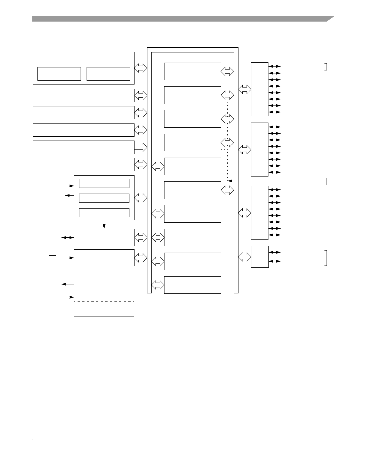
INTERNAL BUS
MCU Block Diagram
M68HC08 CPU
CPU
REGISTERS
ARITHMETIC/LOGIC
UNIT (ALU)
CONTROL AND STATUS REGISTERS — 64 BYTES
USER FLASH — 16,384 BYTES
USER RAM — 512 BYTES
MONITOR ROM — 959 BYTES
USER FLASH VECTORS — 36 BYTES
OSC1
OSC2/RCCLK
(1)
CRYSTAL OSCILLATOR
RC OSCILLATOR
INTERNAL OSCILLATOR
RST
(2)
SYSTEM INTEGRATION
MODULE
KEYBOARD INTERRUPT
MODULE
10-BIT ANALOG-TO-DIGITAL
CONVERTER MODULE
2-CHANNEL TIMER
INTERFACE MODULE 1
2-CHANNEL TIMER
INTERFACE MODULE 2
BREAK
MODULE
SERIAL COMMUNICATIONS
INTERFACE MODULE
POWER-ON RESET
MODULE
LOW-VOLTAGE INHIBIT
MODULE
DDRA
DDRB
DDRD
PORTA
PORTB
PORTD
PTA7/KBI7
PTA6/KBI6
PTA5/KBI5
PTA4/KBI4
(3)(4)
(1)(3)
(3)(4)
(3)(4)
PTA3/KBI3/SCL
PTA2/KBI2/SDA
PTA1/KBI1
PTA0/KBI0
(3)(4)
(3)(4)
PTB7/ADC7
PTB6/ADC6
PTB5/ADC5
PTB4/ADC4
PTB3/ADC3
PTB2/ADC2
PTB1/ADC1
PTB0/ADC0
ADC12/T2CLK
PTD7/RxD/SDA
PTD6/TxD/SCL
PTD5/T1CH1
PTD4/T1CH0
PTD3/ADC8
PTD2/ADC9
(4)
(4)
PTD1/ADC10
PTD0/ADC11
(7)
(3)(4)(6)
(3)(4)(6)
(7)
(3)(4)(5)(6)
(3)(4)(5)(6)
IRQ
(2)
V
DD
V
SS
EXTERNAL INTERRUPT
MODULE
POWER
ADC REFERENCE
NOTES:
1. Shared pin: OSC2/RCCLK/PTA6/KBI6
2. Pin contains integrated pull-up device
3. Pin contains programmable pull-up device
4. LED direct sink pin
5. 25-mA output drive pin
6. Pin is open-drain output when MMIIC function enabled;
position of SDA and SCL are selected in CONFIG2 register.
7. Pins available on 32-pin packages only
Figure 1-1. MC68HC908JL16 Block Diagram
COMPUTER OPERATING
PROPERLY MODULE
MULTI-MASTER IIC
MODULE
DDRE
PTE1/T2CH1
PORTE
PTE0/T2CH0
(7)
MC68HC908JL16 Data Sheet, Rev. 1.1
Freescale Semiconductor 19
Page 20
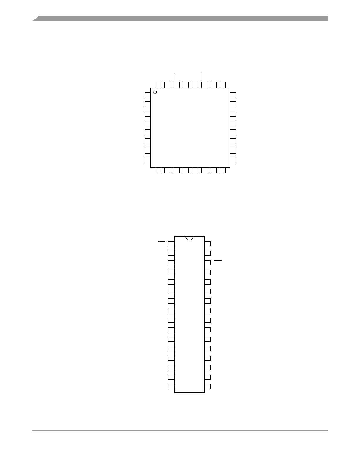
General Description
1.4 Pin Assignments
OSC2/RCCLK/PTA6/KBI6
OSC1
PTA1/KBI1
V
PTA2/KBI2/SDA
PTA3/KBI3/SCL
PTB7/ADC7
PTB6/ADC6
SS
IRQ
PTA0/KBI0
V
32
1
DD
8
31
2
3
4
5
6
7
10
9
ADC12/T2CLK
PTA7/KBI7
30
29
28
11
12
13
RST
27
14
PTA5/KBI5
PTD4/T1CH0
25
26
23
22
21
20
19
18
15
16
24
PTD5/T1CH1
PTD2/ADC9
PTA4/KBI4
PTD3/ADC8
PTB0/ADC0
PTB1/ADC1
PTD1/ADC10
17
PTB2/ADC2
PTB5/ADC5
PTD7/RxD/SDA
PTE0/T2CH0
PTD6/TxD/SCL
PTE1/T2CH1
PTB4/ADC4
PTD0/ADC11
PTB3/ADC3
Figure 1-2. 32-Pin LQFP Pin Assignment
IRQ
PTA0/KBI0
V
OSC1
OSC2/RCCLK/PTA6/KBI6
PTA1/KBI1
V
PTA2/KBI2/SDA
PTA3/KBI3/SCL
PTB7/ADC7
PTB6/ADC6
PTB5/ADC5
PTD7/RxD/SDA
PTD6/TxD/SCL
PTE0/T2CH0
PTE1/T2CH1
1
2
3
SS
4
5
6
7
DD
8
9
10
11
12
13
14
15
16
32
31
30
29
28
27
26
25
24
23
22
21
20
19
18
17
ADC12/T2CLK
PTA7/KBI7
RST
PTA5/KBI5
PTD4/T1CH0
PTD5/T1CH1
PTD2/ADC9
PTA4/KBI4
PTD3/ADC8
PTB0/ADC0
PTB1/ADC1
PTD1/ADC10
PTB2/ADC2
PTB3/ADC3
PTD0/ADC11
PTB4/ADC4
Figure 1-3. 32-Pin SDIP Pin Assignment
MC68HC908JL16 Data Sheet, Rev. 1.1
20 Freescale Semiconductor
Page 21
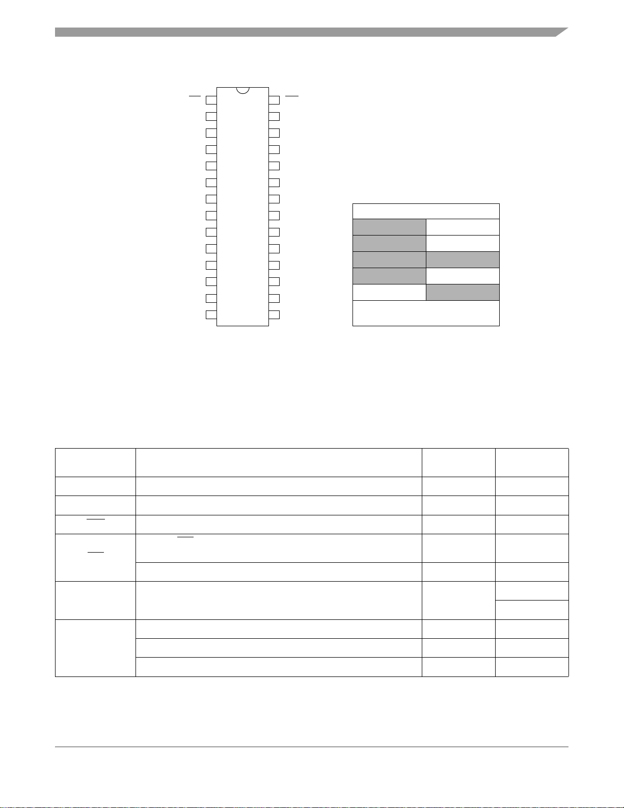
IRQ
PTA0/KBI0
V
OSC1
OSC2/RCCLK/PTA6/KBI6
PTA1/KBI1
V
PTA2/KBI2/SDA
PTA3/KBI3/SCL
PTB7/ADC7
PTB6/ADC6
PTB5/ADC5
PTD7/RxD/SDA
PTD6/TxD/SCL
Pin Functions
28
27
26
25
24
23
22
21
20
19
18
17
16
15
RST
PTA5/KBI5
PTD4/T1CH0
PTD5/T1CH1
PTD2/ADC9
PTA4/KBI4
PTD3/ADC8
PTB0/ADC0
PTB1/ADC1
PTD1/ADC10
PTB2/ADC2
PTB3/ADC3
PTD0/ADC11
PTB4/ADC4
Pins not available on 28-pin packages
PTE0/T2CH0
PTE1/T2CH1
ADC12/T2CLK
PTA7/KBI7
Internal pads are unconnected.
Set these unused port I/Os to output low.
1
2
3
SS
4
5
6
7
DD
8
9
10
11
12
13
14
Figure 1-4. 28-Pin PDIP/SOIC Pin Assignment
1.5 Pin Functions
Description of the pin functions are provided in Table 1-1.
Table 1-1. Pin Functions
Pin Name Pin Description Input/Output
V
DD
V
SS
RST
IRQ
OSC1 Crystal or RC oscillator input Input
OSC2/RCCLK
Power supply Input 5 V or 3 V
Power supply ground Output 0V
Reset input, active low; with internal pull up and Schmitt trigger input Input/output
External IRQ pin; with programmable internal pull up and Schmitt
trigger input
Used for monitor mode entry Input
OSC2: crystal oscillator output; inverted OSC1 signal Output
RCCLK: RC oscillator clock output Output
Pin as PTA6/KBI6 (see PTA0–PTA7) Input/output
Input
Voltage
Level
V
V
V
to V
DD
V
V
V
V
V
DD
DD
TST
DD
DD
DD
DD
DD
Continued on next page
MC68HC908JL16 Data Sheet, Rev. 1.1
Freescale Semiconductor 21
Page 22

General Description
Table 1-1. Pin Functions (Continued)
Pin Name Pin Description Input/Output
ADC12: channel-12 input of ADC Input
ADC12/T2CLK
T2CLK: external input clock for TIM2 Input
8-bit general-purpose I/O port Input/output
Each pin has programmable internal pull up when configured as
input
Input
Pins as keyboard interrupts, KBI0–KBI7 Input
PTA0–PTA7
PTA0–PTA5 and PTA7 have LED direct sink capability Output
PTA6 as OSC2/RCCLK Output
PTA2 as SDA of MMIIC Input/output
PTA3 as SCL of MMIIC Input/output
8-bit general-purpose I/O port Input/output
PTB0–PTB7
Pins as ADC input channels, ADC0–ADC7 Input
8-bit general purpose I/O port; with programmable internal pull ups
on PTD6–PTD7
Input/output
Voltage
Level
to V
V
SS
DD
V
DD
V
DD
V
DD
V
DD
V
DD
V
DD
VSS to VDD
(open-drain)
V
to VDD
SS
(open-drain)
V
DD
to V
V
SS
DD
V
DD
PTD0–PTD3 as ADC input channels, ADC11–ADC8 Input
PTD2–PTD3 and PTD6–PTD7 have LED direct sink capability Output VSS
PTD4 as T1CH0 of TIM1 Input/output
PTD5 as T1CH1 of TIM1 Input/output
PTD0–PTD7
PTD6–PTD7 have configurable 25-mA open-drain output Output
PTD6 as TxD of SCI Output
PTD7 as RxD of SCI Input
PTD6 as SCL of MMIIC Input/output
PTD7 as SDA of MMIIC Input/output
2-bit general-purpose I/O port Input/output
PTE0–PTE1
PTE0 as T2CH0 of TIM2 Input/output
PTE1 as T2CH1 of TIM2 Input/output
NOTE
Devices in 28-pin packages, the following pins are not available:
PTA7/KBI7, PTE0/T2CH0, PTE1/T2CH1, and ADC12/T2CLK.
V
to V
SS
DD
V
DD
V
DD
V
SS
V
DD
V
DD
to VDD
V
SS
(open-drain)
V
to VDD
SS
(open-drain)
V
DD
V
DD
V
DD
MC68HC908JL16 Data Sheet, Rev. 1.1
22 Freescale Semiconductor
Page 23

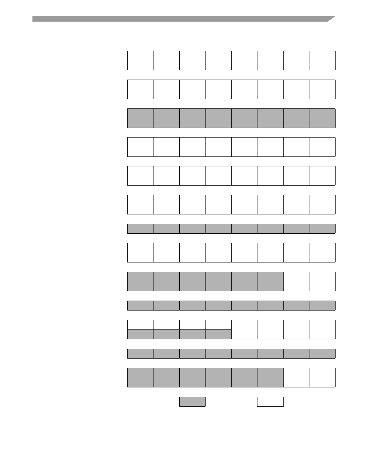
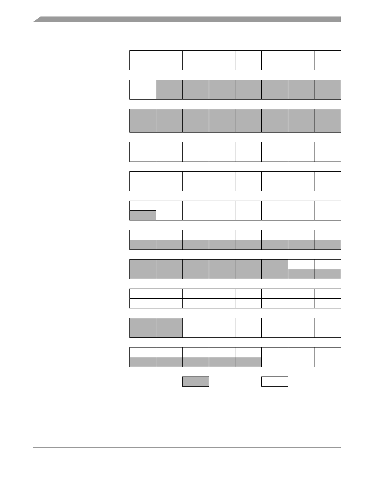
Chapter 2
Memory
2.1 Introduction
The CPU08 can address 64-kbytes of memory space. The memory map, shown in Figure 2-1, includes:
• 16,384 bytes of user FLASH memory
• 36 bytes of user-defined vectors
• 512 bytes of random access memory (RAM)
• 959 bytes of monitor ROM
2.2 I/O Section
Addresses $0000–$003F, shown in Figure 2-2, contain most of the control, status, and data registers.
Additional I/O registers have the following addresses:
• $FE00; Break status register, BSR
• $FE01; Reset status register, RSR
•$FE02; Reserved
• $FE03; Break flag control register, BFCR
• $FE04; Interrupt status register 1, INT1
• $FE05; Interrupt status register 2, INT2
• $FE06; Interrupt status register 3, INT3
•$FE07; Reserved
• $FE08; FLASH control register, FLCR
•$FE09; Reserved
•$FE0A; Reserved
•$FE0B; Reserved
• $FE0C; Break address register high, BRKH
• $FE0D; Break address register low, BRKL
• $FE0E; Break status and control register, BRKSCR
•$FE0F; Reserved
• $FFCF; FLASH block protect register, FLBPR (FLASH register)
• $FFD0; Mask option register, MOR (FLASH register)
• $FFFF; COP control register, COPCTL
MC68HC908JL16 Data Sheet, Rev. 1.1
Freescale Semiconductor 23
Page 24

Memory
$0000
↓
$0045
$0046
↓
$005F
$0060
↓
$025F
$0260
↓
$BBFF
$BC00
↓
$FBFF
$FC00
↓
$FDFF
$FE00 BREAK STATUS REGISTER (BSR)
$FE01 RESET STATUS REGISTER (RSR)
$FE02 RESERVED
$FE03 BREAK FLAG CONTROL REGISTER (BFCR)
$FE04 INTERRUPT STATUS REGISTER 1 (INT1)
$FE05 INTERRUPT STATUS REGISTER 2 (INT2)
$FE06 INTERRUPT STATUS REGISTER 3 (INT3)
$FE07 RESERVED
$FE08 FLASH CONTROL REGISTER (FLCR)
$FE09
↓
$FF0B
$FE0C BREAK ADDRESS HIGH REGISTER (BRKH)
$FE0D BREAK ADDRESS LOW REGISTER (BRKL)
$FE0E BREAK STATUS AND CONTROL REGISTER (BRKSCR)
$FE0F RESERVED
$FE10
↓
$FFCE
$FFCF FLASH BLOCK PROTECT REGISTER (FLBPR)
$FFD0 MASK OPTION REGISTER (MOR)
$FFD1
↓
$FFDB
$FFDC
↓
$FFFF
I/O REGISTERS
70 BYTES
RESERVED
26 BYTES
RAM
512 BYTES
UNIMPLEMENTED
47,520 BYTES
FLASH MEMORY
16,384 BYTES
MONITOR ROM
512 BYTES
RESERVED
MONITOR ROM
447 BYTES
RESERVED
11 BYTES
USER FLASH VECTORS
36 BYTES
Figure 2-1. Memory Map
MC68HC908JL16 Data Sheet, Rev. 1.1
24 Freescale Semiconductor
Page 25
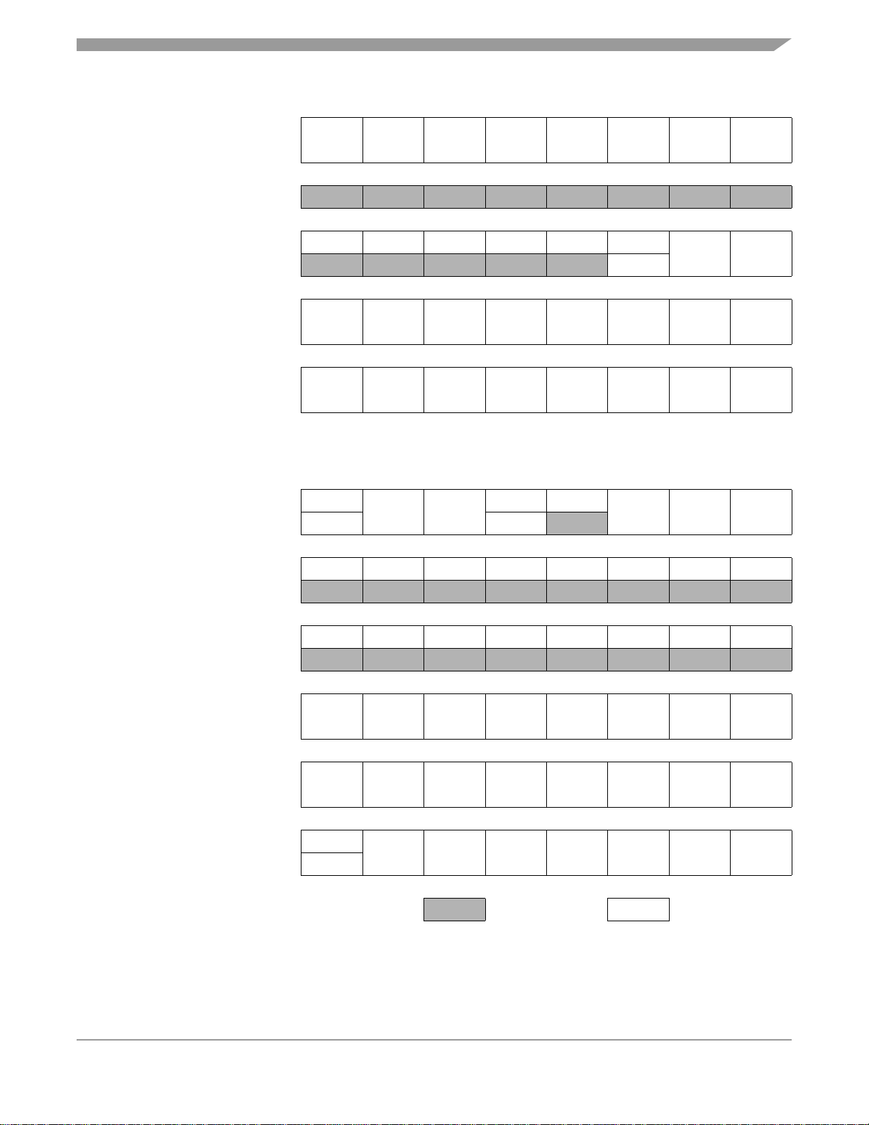
I/O Section
Addr.Register Name Bit 7654321Bit 0
$0000
$0001
$0002 Unimplemented
Port A Data Register
(PTA)
Port B Data Register
(PTB)
Read:
Write:
Reset: Unaffected by reset
Read:
Write:
Reset: Unaffected by reset
Read:
Write:
PTA7 PTA6 PTA5 PTA4 PTA3 PTA2 PTA1 PTA0
PTB7 PTB6 PTB5 PTB4 PTB3 PTB2 PTB1 PTB0
$0003
$0004
$0005
$0006 Unimplemented
$0007
$0008
$0009 Unimplemented
Port D Data Register
(PTD)
Data Direction Register A
(DDRA)
Data Direction Register B
(DDRB)
Data Direction Register D
(DDRD)
Port E Data Register
(PTE)
Read:
Write:
Reset: Unaffected by reset
Read:
Write:
Reset:00000000
Read:
Write:
Reset:00000000
Read:
Write:
Reset:00000000
Read:
Write:
Reset: Unaffected by reset
PTD7 PTD6 PTD5 PTD4 PTD3 PTD2 PTD1 PTD0
DDRA7 DDRA6 DDRA5 DDRA4 DDRA3 DDRA2 DDRA1 DDRA0
DDRB7 DDRB6 DDRB5 DDRB4 DDRB3 DDRB2 DDRB1 DDRB0
DDRD7 DDRD6 DDRD5 DDRD4 DDRD3 DDRD2 DDRD1 DDRD0
PTE1 PTE0
$000A
$000B Unimplemented
$000C
Port D Control Register
(PDCR)
Data Direction Register E
(DDRE)
U = Unaffected X = Indeterminate
Read:0000
Write:
Reset:00000000
Read:
Write:
Reset:00000000
= Unimplemented R = Reserved
SLOWD7 SLOWD6 PTDPU7 PTDPU6
DDRE1 DDRE0
Figure 2-2. Control, Status, and Data Registers (Sheet 1 of 7)
MC68HC908JL16 Data Sheet, Rev. 1.1
Freescale Semiconductor 25
Page 26
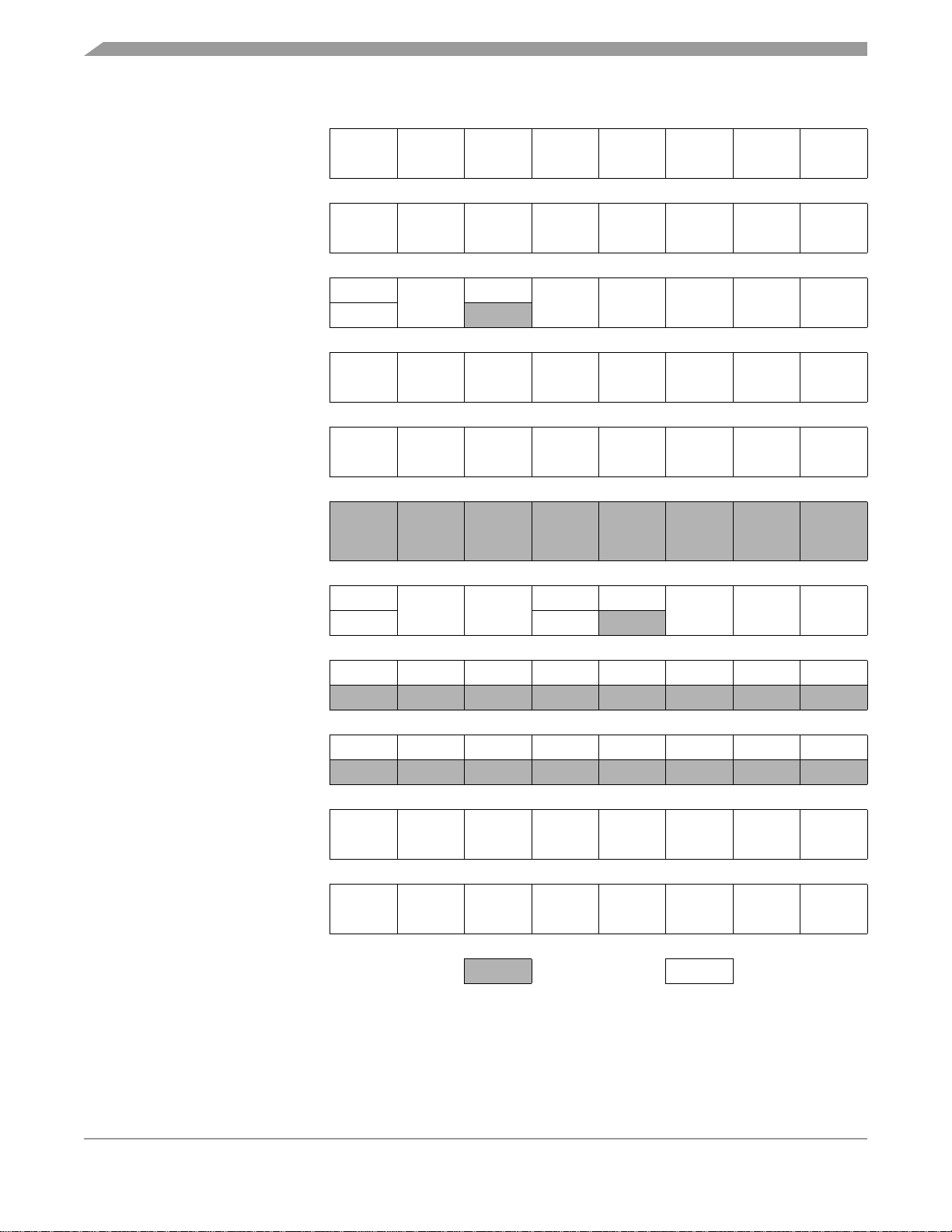
Memory
Addr.Register Name Bit 7654321Bit 0
Read:
$000D
$000E
$000F
↓
$0012
Port A Input Pullup Enable
Register (PTAPUE)
Reset:00000000
PTA7 Input Pullup Enable
Register (PTA7PUE)
Reset:00000000
Unimplemented
PTA6EN PTAPUE6 PTAPUE5 PTAPUE4 PTAPUE3 PTAPUE2 PTAPUE1 PTAPUE0
Write:
Read:
PTAPUE7
Write:
$0013
$0014
$0015
$0016
$0017
$0018
$0019
$001A
SCI Control Register 1
SCI Control Register 2
SCI Control Register 3
SCI Status Register 1
SCI Status Register 2
SCI Baud Rate Register
Keyboard Status and Control
Read:
(SCC1)
(SCC2)
(SCC3)
(SCS1)
(SCS2)
SCI Data Register
(SCDR)
(SCBR)
Register (KBSCR)
U = Unaffected X = Indeterminate
Write:
Reset:00000000
Read:
Write:
Reset:00000000
Read: R8
Write:
Reset:UU000000
Read: SCTE TC SCRF IDLE OR NF FE PE
Write:
Reset:11000000
Read:
Write:
Reset:00000000
Read: R7 R6 R5 R4 R3 R2 R1 R0
Write: T7 T6 T5 T4 T3 T2 T1 T0
Reset: Unaffected by reset
Read:
Write:
Reset:00000000
Read:0000KEYF0
Write:
Reset:00000000
LOOPS ENSCI TXINV M WAKE ILTY PEN PTY
SCTIE TCIE SCRIE ILIE TE RE RWU SBK
T8 DMARE DMATE ORIE NEIE FEIE PEIE
BKF RPF
SCP1 SCP0 R SCR2 SCR1 SCR0
ACKK
= Unimplemented R = Reserved
IMASKK MODEK
Figure 2-2. Control, Status, and Data Registers (Sheet 2 of 7)
MC68HC908JL16 Data Sheet, Rev. 1.1
26 Freescale Semiconductor
Page 27
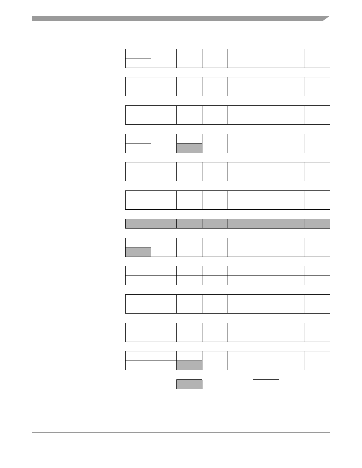
I/O Section
Addr.Register Name Bit 7654321Bit 0
Read:
$001B
Keyboard Interrupt Enable
Register (KBIER)
Write:
KBIE7 KBIE6 KBIE5 KBIE4 KBIE3 KBIE2 KBIE1 KBIE0
Reset:00000000
$001C Unimplemented
Read:0000IRQF0
$001D
IRQ Status and Control
Register (INTSCR)
Write: ACK
Reset:00000000
Read:
$001E
Configuration Register 2
(CONFIG2)
(1)
IRQPUD R R LVIT1 LVIT0 R IICSEL
Write:
Reset:0000
$001F
Configuration Register 1
(CONFIG1)
Read:
Write:
(1)
COPRS R R LVID R SSREC STOP COPD
Reset:00000000
1. One-time writable register after each reset.
2. LVIT1 and LVIT0 reset to 0 by a power-on reset (POR) only.
Read: TOF
$0020
TIM1 Status and Control
Register (T1SC)
Write: 0 TRST
Reset:00100000
Read: Bit 15 Bit 14 Bit 13 Bit 12 Bit 11 Bit 10 Bit 9 Bit 8
$0021
TIM1 Counter Register High
(T1CNTH)
Write:
Reset:00000000
Read:Bit 7Bit 6Bit 5Bit 4Bit 3Bit 2Bit 1Bit 0
$0022
TIM1 Counter Register
Low (T1CNTL)
Write:
Reset:00000000
Read:
TIM Counter Modulo Register
$0023
High (TMODH)
Write:
Bit 15 Bit 14 Bit 13 Bit 12 Bit 11 Bit 10 Bit 9 Bit 8
Reset:11111111
Read:
$0024
TIM1 Counter Modulo
Register Low (T1MODL)
Write:
Bit 7Bit 6Bit 5Bit 4Bit 3Bit 2Bit 1Bit 0
Reset:11111111
Read: CH0F
$0025
TIM1 Channel 0 Status and
Control Register (T1SC0)
Write: 0
Reset:00000000
U = Unaffected X = Indeterminate
IMASK MODE
STOP_
ICLKDIS
(2)
(2)
0
000
00
TOIE TSTOP
PS2 PS1 PS0
CH0IE MS0B MS0A ELS0B ELS0A TOV0 CH0MAX
= Unimplemented R = Reserved
Figure 2-2. Control, Status, and Data Registers (Sheet 3 of 7)
MC68HC908JL16 Data Sheet, Rev. 1.1
Freescale Semiconductor 27
Page 28
Memory
Addr.Register Name Bit 7654321Bit 0
$0026
$0027
$0028
$0029
$002A
$002B
↓
$002F
TIM1 Channel 0 Register
TIM1 Channel 0 Register Low
TIM1 Channel 1 Status and
Control Register (T1SC1)
Register High (T1CH1H)
Register Low (T1CH1L)
High (T1CH0H)
(T1CH0L)
TIM1 Channel 1
TIM1 Channel 1
Unimplemented
Read:
Write:
Reset: Indeterminate after reset
Read:
Write:
Reset: Indeterminate after reset
Read: CH1F
Write: 0
Reset:00000000
Read:
Write:
Reset: Indeterminate after reset
Read:
Write:
Reset: Indeterminate after reset
Bit 15 Bit 14 Bit 13 Bit 12 Bit 11 Bit 10 Bit 9 Bit 8
Bit 7Bit 6Bit 5Bit 4Bit 3Bit 2Bit 1Bit 0
CH1IE
Bit 15 Bit 14 Bit 13 Bit 12 Bit 11 Bit 10 Bit 9 Bit 8
Bit 7Bit 6Bit 5Bit 4Bit 3Bit 2Bit 1Bit 0
0
MS1A ELS1B ELS1A TOV1 CH1MAX
$0030
$0031
$0032
$0033
$0034
TIM2 Status and Control
Register (T2SC)
TIM2 Counter Register High
(T2CNTH)
TIM2 Counter Register
Low
(T2CNTL)
TIM2 Counter Modulo
Register High
(T2MODH)
TIM2 Counter Modulo
Register Low
(T2MODL)
U = Unaffected X = Indeterminate
Figure 2-2. Control, Status, and Data Registers (Sheet 4 of 7)
Read: TOF
Write: 0 TRST
Reset:00100000
Read: Bit 15 Bit 14 Bit 13 Bit 12 Bit 11 Bit 10 Bit 9 Bit 8
Write:
Reset:00000000
Read:Bit 7Bit 6Bit 5Bit 4Bit 3Bit 2Bit 1Bit 0
Write:
Reset:00000000
Read:
Write:
Reset:11111111
Read:
Write:
Reset:11111111
Bit 15 Bit 14 Bit 13 Bit 12 Bit 11 Bit 10 Bit 9 Bit 8
Bit 7Bit 6Bit 5Bit 4Bit 3Bit 2Bit 1Bit 0
TOIE TSTOP
00
= Unimplemented R = Reserved
PS2 PS1 PS0
MC68HC908JL16 Data Sheet, Rev. 1.1
28 Freescale Semiconductor
Page 29
I/O Section
Addr.Register Name Bit 7654321Bit 0
TIM2 Channel 0 Status and
$0035
$0036
TIM2 Channel 0 Register Low
$0037
$0038
$0039
$003A
$003B Unimplemented
TIM2 Channel 1 Status and
Control Register
(T2SC0)
TIM2 Channel 0 Register
High (T2CH0H)
(T2CH0L)
Control Register (T2SC1)
TIM2 Channel 1
Register High (T2CH1H)
TIM2 Channel 1
Register Low (T2CH1L)
Read: CH0F
Write: 0
Reset:00000000
Read:
Write:
Reset: Indeterminate after reset
Read:
Write:
Reset: Indeterminate after reset
Read: CH1F
Write: 0
Reset:00000000
Read:
Write:
Reset: Indeterminate after reset
Read:
Write:
Reset: Indeterminate after reset
Bit 15 Bit 14 Bit 13 Bit 12 Bit 11 Bit 10 Bit 9 Bit 8
Bit 7Bit 6Bit 5Bit 4Bit 3Bit 2Bit 1Bit 0
Bit 15 Bit 14 Bit 13 Bit 12 Bit 11 Bit 10 Bit 9 Bit 8
Bit 7Bit 6Bit 5Bit 4Bit 3Bit 2Bit 1Bit 0
CH0IE MS0B MS0A ELS0B ELS0A TOV0 CH0MAX
CH1IE
0
MS1A ELS1B ELS1A TOV1 CH1MAX
$003C
$003D
$003E
$003F
$0040
ADC10 Status and Control
Register (ADCSC)
ADC10 Data Register High
8/10-Bit Mode (ADRH)
ADC10 Data Register Low
(ADRL)
ADC10 Clock Register
(ADCLK)
Multi-Master IIC
Master Control Register
(MIMCR)
U = Unaffected X = Indeterminate
Figure 2-2. Control, Status, and Data Registers (Sheet 5 of 7)
Read: COCO
Write:
Reset:00011111
Read:0000000/AD90/AD8
Write:RRRRRRRR
Reset:00000000
Read:AD7AD6AD5AD4AD3AD2AD1AD0
Write:RRRRRRRR
Reset:00000000
Read:
Write:
Reset:00000000
Read: MMALIF MMNAKIF MMBB
Write: 0 0
Reset:00000000
ADLPC ADIV1 ADIV0 ADICLK MODE1 MODE0 ADLSMP ADACKEN
AIEN ADCO ADCH4 ADCH3 ADCH2 ADCH1 ADCH0
MMAST MMRW MMBR2 MMBR1 MMBR0
= Unimplemented R = Reserved
MC68HC908JL16 Data Sheet, Rev. 1.1
Freescale Semiconductor 29
Page 30
Memory
Addr.Register Name Bit 7654321Bit 0
Read:
MMAD7 MMAD6 MMAD5 MMAD4 MMAD3 MMAD2 MMAD1 MMEXTAD
Write:
Reset:10100000
Read:
Write:
Reset:00000000
Read: MMRXIF MMTXIF MMATCH MMSRW MMRXAK 0 MMTXBE MMRXBF
Write: 0 0
Reset:00001010
Read:
Write:
Reset:11111111
Read: MMRD7 MMRD6 MMRD5 MMRD4 MMRD3 MMRD2 MMRD1 MMRD0
Write:
Reset:00000000
MMEN MMIEN
MMTD7 MMTD6 MMTD5 MMTD4 MMTD3 MMTD2 MMTD1 MMTD0
00
MMTXAK REPSEN
00
$0041
$0042
$0043
$0044
$0045
Multi-Master IIC Address
Register
(MMADR)
Multi-Master IIC Control
Register
(MMCR)
Multi-Master IIC Status
Register (MMSR)
Multi-Master IIC Data
Transmit Register (MMDTR)
Multi-Master IIC Data
Receive Register (MMDRR)
Read:
$FE00
Note: Writing a 0 clears SBSW.
$FE01
$FE02 Reserved RRRRRRRR
$FE03
$FE04
$FE05
Break Status Register
(BSR)
Reset Status Register
(RSR)
Break Flag Control Register
(BFCR)
Interrupt Status Register 1
(INT1)
Interrupt Status Register 2
(INT2)
U = Unaffected X = Indeterminate
Write: See note
Reset: 0
Read: POR PIN COP ILOP ILAD MODRST LVI 0
Write:
POR:10000000
Read:
Write:
Reset: 0
Read: IF6 IF5 IF4 IF3 0 IF1 0 0
Write:RRRRRRRR
Reset:00000000
Read: IF14 IF13 IF12 IF11 IF10 0 IF8 IF7
Write:RRRRRRRR
Reset:00000000
RRRRRR
BCFERRRRRRR
= Unimplemented R = Reserved
SBSW
R
Figure 2-2. Control, Status, and Data Registers (Sheet 6 of 7)
MC68HC908JL16 Data Sheet, Rev. 1.1
30 Freescale Semiconductor
Page 31

I/O Section
Addr.Register Name Bit 7654321Bit 0
Read:0000000IF15
$FE06
Interrupt Status Register 3
(INT3)
Write:RRRRRRRR
Reset:00000000
$FE07 Reserved RRRRRRRR
Read:0000
$FE08
FLASH Control Register
(FLCR)
Write:
Reset:00000000
$FE09
↓
Reserved RRRRRRRR
$FE0B
Break Address High Register
$FE0C
(BRKH)
Read:
Write:
Bit 15 Bit 14 Bit 13 Bit 12 Bit 11 Bit 10 Bit 9 Bit 8
Reset:00000000
$FE0D
Break Address Low Register
(BRKL)
Read:
Write:
Bit 7Bit 6Bit 5Bit 4Bit 3Bit 2Bit 1Bit 0
Reset:00000000
Read:
BRKE BRKA
Write:
Reset:00000000
Read:
Write:
(1)
BPR7 BPR6 BPR5 BPR4 BPR3 BPR2 BPR1 BPR0
Reset: Unaffected by reset; $FF when blank
Read:
OSCSELRRRRRRR
Write:
(1)
$FE0E
$FFCF
$FFD0
Break Status and Control
Register
(BRKSCR)
FLASH Block Protect
Register
(FLBPR)
Mask Option Register
(MOR)
Reset: Unaffected by reset; $FF when blank
1. Non-volatile FLASH registers; write by programming.
HVEN MASS ERASE PGM
000000
Read: Low byte of reset vector
$FFFF
COP Control Register
(COPCTL)
Write: Writing clears COP counter (any value)
Reset: Unaffected by reset
U = Unaffected X = Indeterminate
= Unimplemented R = Reserved
Figure 2-2. Control, Status, and Data Registers (Sheet 7 of 7)
MC68HC908JL16 Data Sheet, Rev. 1.1
Freescale Semiconductor 31
Page 32

Memory
2.3 Monitor ROM
The 959 bytes at addresses $FC00–$FDFF and $FE10–$FFCE are reserved ROM addresses that
contain the instructions for the monitor functions. (See Chapter 16 Development Support.)
.
Table 2-1. Vector Addresses
Vector Priority INT Flag Address Vector
Lowest
Highest
—
IF15
IF14
IF13
IF12
IF11
IF10
IF9 — Not used
IF8
IF7
IF6
IF5
IF4
IF3
IF2 — Not used
IF1
—
—
$FFD0
↓
$FFDD
$FFDE ADC conversion complete vector (high)
$FFDF ADC Conversion complete vector (low)
$FFE0 Keyboard interrupt vector (high)
$FFE1 Keyboard interrupt vector (low)
$FFE2 SCI transmit vector (high)
$FFE3 SCI transmit vector (low)
$FFE4 SCI receive vector (high)
$FFE5 SCI receive vector (low)
$FFE6 SCI error vector (high)
$FFE7 SCI error vector (low)
$FFE8 MMIIC vector (high)
$FFE9 MMIIC vector (low)
$FFEC TIM2 overflow vector (high)
$FFED TIM2 overflow vector (low)
$FFEE TIM2 channel 1 vector (high)
$FFEF TIM2 channel 1 vector (low)
$FFF0 TIM2 channel 0 vector (high)
$FFF1 TIM2 channel 0 vector (low)
$FFF2 TIM1 overflow vector (high)
$FFF3 TIM1 overflow vector (low)
$FFF4 TIM1 channel 1 vector (high)
$FFF5 TIM1 channel 1 vector (low)
$FFF6 TIM1 channel 0 vector (high)
$FFF7 TIM1 channel 0 vector (low)
$FFFA IRQ
$FFFB IRQ
$FFFC SWI vector (high)
$FFFD SWI vector (low)
$FFFE Reset vector (high)
$FFFF Reset vector (low)
Not Used
vector (high)
vector (low)
MC68HC908JL16 Data Sheet, Rev. 1.1
32 Freescale Semiconductor
Page 33

Random-Access Memory (RAM)
2.4 Random-Access Memory (RAM)
Addresses $0060 through $025F are RAM locations. The location of the stack RAM is programmable.
The 16-bit stack pointer allows the stack to be anywhere in the 64-Kbyte memory space.
NOTE
For correct operation, the stack pointer must point only to RAM locations.
Within page zero are 160 bytes of RAM. Because the location of the stack RAM is programmable, all page
zero RAM locations can be used for I/O control and user data or code. When the stack pointer is moved
from its reset location at $00FF, direct addressing mode instructions can access efficiently all page zero
RAM locations. Page zero RAM, therefore, provides ideal locations for frequently accessed global
variables.
Before processing an interrupt, the CPU uses five bytes of the stack to save the contents of the CPU
registers.
NOTE
For M6805 compatibility, the H register is not stacked.
During a subroutine call, the CPU uses two bytes of the stack to store the return address. The stack
pointer decrements during pushes and increments during pulls.
NOTE
Be careful when using nested subroutines. The CPU may overwrite data in
the RAM during a subroutine or during the interrupt stacking operation.
2.5 FLASH Memory
This sub-section describes the operation of the embedded FLASH memory. The FLASH memory can be
read, programmed, and erased from a single external supply. The program and erase operations are
enabled through the use of an internal charge pump.
2.5.1 Functional Description
The FLASH memory consists of an array of 16,384 bytes for user memory plus a block of 36 bytes for
user interrupt vectors. An erased bit reads as 1 and a programmed bit reads as a 0. The FLASH memory
page size is defined as 64 bytes, and is the minimum size that can be erased in a page erase operation.
Program and erase operations are facilitated through control bits in FLASH control register (FLCR). The
address ranges for the FLASH memory are:
• $BC00–$FBFF; user memory; 16,384 bytes
• $FFDC–$FFFF; user interrupt vectors; 36 bytes
Programming tools are available from Freescale Semiconductor. Contact your local representative for
more information.
NOTE
A security feature prevents viewing of the FLASH contents.
(1)
1. No security feature is absolutely secure. However, Freescale’s strategy is to make reading or copying the FLASH difficult for
unauthorized users.
MC68HC908JL16 Data Sheet, Rev. 1.1
Freescale Semiconductor 33
Page 34

Memory
2.5.2 FLASH Control Register
The FLASH control register (FCLR) controls FLASH program and erase operations.
Address: $FE08
Bit 7654321Bit 0
Read:0000
Write:
Reset:00000000
= Unimplemented
Figure 2-3. FLASH Control Register (FLCR)
HVEN — High Voltage Enable Bit
This read/write bit enables the charge pump to drive high voltages for program and erase operations
in the array. HVEN can only be set if either PGM = 1 or ERASE = 1 and the proper sequence for
program or erase is followed.
1 = High voltage enabled to array and charge pump on
0 = High voltage disabled to array and charge pump off
MASS — Mass Erase Control Bit
This read/write bit configures the memory for mass erase operation or page erase operation when the
ERASE bit is set.
1 = Mass erase operation selected
0 = Page erase operation selected
HVEN MASS ERASE PGM
ERASE — Erase Control Bit
This read/write bit configures the memory for erase operation. ERASE is interlocked with the PGM bit
such that both bits cannot be equal to 1 or set to 1 at the same time.
1 = Erase operation selected
0 = Erase operation not selected
PGM — Program Control Bit
This read/write bit configures the memory for program operation. PGM is interlocked with the ERASE
bit such that both bits cannot be equal to 1 or set to 1 at the same time.
1 = Program operation selected
0 = Program operation not selected
MC68HC908JL16 Data Sheet, Rev. 1.1
34 Freescale Semiconductor
Page 35

FLASH Memory
2.5.3 FLASH Page Erase Operation
Use the following procedure to erase a page of FLASH memory. A page consists of 64 consecutive bytes
starting from addresses $XX00, $XX40, $XX80 or $XXC0. The 36-byte user interrupt vectors area also
forms a page. Any page within the 16,384 bytes user memory area can be erased alone.
1. Set the ERASE bit and clear the MASS bit in the FLASH control register.
2. Read the FLASH block protect register.
3. Write any data to any FLASH address within the page address range desired.
4. Wait for a time, t
5. Set the HVEN bit.
6. Wait for a time t
7. Clear the ERASE bit.
8. Wait for a time, t
9. Clear the HVEN bit.
10. After time, t
RCV
Programming and erasing of FLASH locations cannot be performed by
code being executed from the FLASH memory. While these operations
must be performed in the order as shown, but other unrelated operations
may occur between the steps.
(10 µs).
NVS
(4 ms).
Erase
(5 µs).
NVH
(1 µs), the memory can be accessed in read mode again.
NOTE
2.5.4 FLASH Mass Erase Operation
Use the following procedure to erase the entire FLASH memory:
1. Set both the ERASE bit and the MASS bit in the FLASH control register.
2. Read the FLASH block protect register.
3. Write any data to any FLASH location within the FLASH memory address range.
4. Wait for a time, t
5. Set the HVEN bit.
6. Wait for a time t
7. Clear the ERASE bit.
8. Wait for a time, t
9. Clear the HVEN bit.
10. After time, t
RCV
Programming and erasing of FLASH locations cannot be performed by
code being executed from the FLASH memory. While these operations
must be performed in the order as shown, but other unrelated operations
may occur between the steps.
(10 µs).
NVS
(4 ms).
Erase
(100 µs).
NVH1
(1 µs), the memory can be accessed in read mode again.
NOTE
MC68HC908JL16 Data Sheet, Rev. 1.1
Freescale Semiconductor 35
Page 36

Memory
2.5.5 FLASH Program Operation
Programming of the FLASH memory is done on a row basis. A row consists of 32 consecutive bytes
starting from addresses $XX00, $XX20, $XX40, $XX60, $XX80, $XXA0, $XXC0 or $XXE0. Use this
step-by-step procedure to program a row of FLASH memory:
1. Set the PGM bit. This configures the memory for program operation and enables the latching of
address and data for programming.
2. Read the FLASH block protect register.
3. Write any data to any FLASH location within the address range of the row to be programmed.
4. Wait for a time, t
5. Set the HVEN bit.
6. Wait for a time, t
7. Write data to the FLASH address to be programmed.
8. Wait for time, t
9. Repeat steps 7 and 8 until all bytes within the row are programmed.
10. Clear the PGM bit.
11. Wait for time, t
12. Clear the HVEN bit.
13. After time, t
RCV
Figure 2-4 shows a flowchart of the programming algorithm.
(10 µs).
NVS
(5 µs).
PGS
(30 µs).
PROG
(5 µs).
NVH
(1 µs), the memory can be accessed in read mode again.
This program sequence is repeated throughout the memory until all data is programmed.
NOTE
The time between each FLASH address change (step 7 to step 7), or the
time between the last FLASH addressed programmed to clearing the PGM
bit (step 7 to step 10), must not exceed the maximum programming time,
t
max.
PROG
Programming and erasing of FLASH locations cannot be performed by
code being executed from the FLASH memory. While these operations
must be performed in the order shown, other unrelated operations may
occur between the steps.
MC68HC908JL16 Data Sheet, Rev. 1.1
36 Freescale Semiconductor
Page 37

FLASH Memory
Algorithm for Programming
a Row (32 Bytes) of FLASH Memory
1
2
READ THE FLASH BLOCK PROTECT REGISTER
3
WRITE ANY DATA TO ANY FLASH ADDRESS
WITHIN THE ROW ADDRESS RANGE DESIRED
4
5
6
7
WRITE DATA TO THE FLASH ADDRESS
8
SET PGM BIT
WAIT FOR A TIME, t
SET HVEN BIT
WAIT FOR A TIME, t
TO BE PROGRAMMED
WAIT FOR A TIME, t
NVS
PGS
PROG
9
NOTES:
The time between each FLASH address change (step 7to step 7),
or the time between the last FLASH address programmed
to clearing PGM bit (step 6 to step 10)
must not exceed the maximum programming
PROG
max.
time, t
This row program algorithm assumes the row/s
to be programmed are initially erased.
Figure 2-4. FLASH Programming Flowchart
COMPLETED
PROGRAMMING
THIS ROW?
N
Y
10
11
12
13
CLEAR PGM BIT
WAIT FOR A TIME, t
CLEAR HVEN BIT
WAIT FOR A TIME, t
END OF PROGRAMMING
NVH
RCV
MC68HC908JL16 Data Sheet, Rev. 1.1
Freescale Semiconductor 37
Page 38

Memory
2.5.6 FLASH Block Protection
Due to the ability of the on-board charge pump to erase and program the FLASH memory in the target
application, provision is made to protect blocks of memory from unintentional erase or program operations
due to system malfunction. This protection is done by use of a FLASH block protect register (FLBPR).
The FLBPR determines the range of the FLASH memory which is to be protected. The range of the
protected area starts from a location defined by FLBPR and ends to the bottom of the FLASH memory
($FFFF). When the memory is protected, the HVEN bit cannot be set in either erase or program
operations.
NOTE
In performing a program or erase operation, the FLASH block protect
register must be read after setting the PGM or ERASE bit and before
asserting the HVEN bit
When the FLBPR is program with all 0s, the entire memory is protected from being programmed and
erased. When all the bits are erased (all 1s), the entire memory is accessible for program and erase.
When bits within the FLBPR are programmed, they lock a block of memory, address ranges as shown in
2.5.7 FLASH Block Protect Register. Once the FLBPR is programmed with a value other than $FF, any
erase or program of the FLBPR or the protected block of FLASH memory is prohibited. The FLBPR itself
can be erased or programmed only with an external voltage, V
also allows entry from reset into the monitor mode.
, present on the IRQ pin. This voltage
TST
2.5.7 FLASH Block Protect Register
The FLASH block protect register (FLBPR) is implemented as a byte within the FLASH memory, and
therefore can only be written during a programming sequence of the FLASH memory. The value in this
register determines the starting location of the protected range within the FLASH memory.
Address: $FFCF
Bit 7654321Bit 0
Read:
Write:
Reset: Unaffected by reset; $FF when blank
Non-volatile FLASH register; write by programming.
BPR[7:0] — FLASH Block Protect Bits
BPR[7:0] represent bits [13:6] of a 16-bit memory address. Bits [15:14] are 1s and bits [5:0] are 0s.
Start address of FLASH
The resultant 16-bit address is used for specifying the start address of the FLASH memory for block
protection. The FLASH is protected from this start address to the end of FLASH memory, at $FFFF.
With this mechanism, the protect start address can be XX00, XX40, XX80, or XXC0 (at page
boundaries — 64 bytes) within the FLASH memory.
BPR7 BPR6 BPR5 BPR4 BPR3 BPR2 BPR1 BPR0
Figure 2-5. FLASH Block Protect Register (FLBPR)
16-bit memory address
11 000000
block protect
BPR[7:0]
MC68HC908JL16 Data Sheet, Rev. 1.1
38 Freescale Semiconductor
Page 39

Table 2-2. Examples of Protect Start Address
FLASH Memory
BPR[7:0]
(2)
$00
$01
(0000 0001)
$02
(0000 0010)
$03
(0000 0011)
Start of Address of Protect Range
The entire FLASH memory is protected.
$C040 (1100 0000 0100 0000)
$C080 (1100 0000 1000 0000)
$C0C0 (1100 0000 1100 0000)
and so on...
$FD
(1111 1101)
$FE
(1111 1110)
$FF40 (1111 1111 0100 0000)
$FF80 (1111 1111 1000 0000)
$FF The entire FLASH memory is not protected.
1. The end address of the protected range is always $FFFF.
2. $BC00–$BFFF is always protected unless entire FLASH memory is
unprotected, BPR[7:0} = $FF.
(1)
MC68HC908JL16 Data Sheet, Rev. 1.1
Freescale Semiconductor 39
Page 40

Memory
MC68HC908JL16 Data Sheet, Rev. 1.1
40 Freescale Semiconductor
Page 41

Chapter 3
Configuration and Mask Option Registers
(CONFIG and MOR)
3.1 Introduction
This section describes the configuration registers, CONFIG1 and CONFIG2; and the mask option register
(MOR).
The configuration registers enable or disable these options:
• Computer operating properly module (COP)
• COP timeout period (2
• Internal oscillator during stop mode
• Low voltage inhibit (LVI) module
• LVI module voltage trip point selection
•STOP instruction
• Stop mode recovery time (32 or 4096 ICLK cycles)
• Pull-up on IRQ
pin
• MMIIC pin selection
The mask option register selects the oscillator option:
• Crystal or RC
13–24
or 218–24 ICLK cycles)
Addr.Register Name Bit 7654321Bit 0
Read:
$001E
$001F
$FFD0
1. One-time writable register after each reset.
2. LVIT1 and LVIT0 reset to 0 by a power-on reset (POR) only.
3. Non-volatile FLASH register; write by programming.
Configuration Register 2
(CONFIG2)
Configuration Register 1
(CONFIG1)
Mask Option Register
(MOR)
(1)
Reset:0000
(1)
Reset:00000000
(3)
Reset: Unaffected by reset; $FF when blank
IRQPUD R R LVIT1 LVIT0 R IICSEL
Write:
Read:
COPRS R R LVID R SSREC STOP COPD
Write:
Read:
OSCSELRRRRRRR
Write:
R=Reserved
(2)
(2)
0
000
STOP_
ICLKDIS
Figure 3-1. CONFIG Registers Summary
MC68HC908JL16 Data Sheet, Rev. 1.1
Freescale Semiconductor 41
Page 42

Configuration and Mask Option Registers (CONFIG and MOR)
3.2 Functional Description
The configuration registers are used in the initialization of various options. The configuration registers can
be written once after each reset. All of the configuration register bits are cleared during reset. Since the
various options affect the operation of the MCU, it is recommended that these registers be written
immediately after reset. The configuration registers are located at $001E and $001F. The configuration
registers may be read at anytime.
NOTE
The options except LVIT[1:0] are one-time writable by the user after each
reset. The LVIT[1:0] bits are one-time writable by the user only after each
POR (power-on reset). The CONFIG registers are not in the FLASH
memory but are special registers containing one-time writable latches after
each reset. Upon a reset, the CONFIG registers default to predetermined
settings as shown in Figure 3-2 and Figure 3-3.
The mask option register (MOR) is used to select the oscillator option for the MCU: crystal oscillator or
RC oscillator. The MOR is implemented as a byte in FLASH memory. Hence, writing to the MOR requires
programming the byte.
3.3 Configuration Register 1 (CONFIG1)
Address:
$001F
Bit 7654321Bit 0
Read:
Reset:00000000
COPRS R R LVID R SSREC STOP COPD
Write:
=Reserved
R
Figure 3-2. Configuration Register 1 (CONFIG1)
COPRS — COP Rate Select Bit
COPRS selects the COP time-out period. Reset clears COPRS. (See Chapter 13 Computer Operating
Properly (COP).)
13
1 = COP timeout period is (2
0 = COP timeout period is (2
– 24) ICLK cycles
18
– 24) ICLK cycles
LVID — Low Voltage Inhibit Disable Bit
LVID disables the LVI module. Reset clears LVID. (See Chapter 14 Low-Voltage Inhibit (LVI).)
1 = Low voltage inhibit disabled
0 = Low voltage inhibit enabled
SSREC — Short Stop Recovery Bit
SSREC enables the CPU to exit stop mode with a delay of 32 ICLK cycles instead of a 4096 ICLK cycle
delay.
1 = Stop mode recovery after 32 ICLK cycles
0 = Stop mode recovery after 4096 ICLK cycles
NOTE
Exiting stop mode by pulling reset will result in the long stop recovery. If
using an external crystal, do not set the SSREC bit.
MC68HC908JL16 Data Sheet, Rev. 1.1
42 Freescale Semiconductor
Page 43

Configuration Register 2 (CONFIG2)
STOP — STOP Instruction Enable Bit
STOP enables the STOP instruction.
1 = STOP instruction enabled
0 = STOP instruction treated as illegal opcode
COPD — COP Disable Bit
COPD disables the COP module. Reset clears COPD. (See Chapter 13 Computer Operating Properly
(COP).)
1 = COP module disabled
0 = COP module enabled
3.4 Configuration Register 2 (CONFIG2)
Address:
$001E
Bit 7654321Bit 0
Read:
IRQPUD R R LVIT1 LVIT0 R IICSEL
Write:
Reset:000UU000
POR:00000000
R = Reserved U = Unaffected
STOP_
ICLKDIS
Figure 3-3. Configuration Register 2 (CONFIG2)
IRQPUD — IRQ Pin Pull-Up Disable Bit
IRQPUD disconnects the internal pull-up on the IRQ
pin.
1 = Internal pull-up is disconnected
0 = Internal pull-up is connected between IRQ
pin and V
DD
LVIT1, LVIT0 — LVI Trip Voltage Selection Bits
Detail description of trip voltage selection is given in Chapter 14 Low-Voltage Inhibit (LVI).
IICSEL — MMIIC Pin Selection Bit
IICSEL selects the pins to be used as MMIIC I/Os when the MMIIC module is enabled. (See Chapter
8 Multi-Master IIC Interface (MMIIC).)
1 = SDA on PTA2/KBI2 pin; SCL on PTA3/KBI3 pin
0 = SDA on PTD7/RxD pin; SCL on PTD6/TxD pin
STOP_ICLKDIS — Internal Oscillator Stop Mode Disable Bit
Setting STOP_ICLKDIS disables the internal oscillator during stop mode. When this bit is cleared, the
internal oscillator continues to operate in stop mode. Reset clears this bit.
1 = Internal oscillator disabled during stop mode
0 = Internal oscillator enabled during stop mode
MC68HC908JL16 Data Sheet, Rev. 1.1
Freescale Semiconductor 43
Page 44

Configuration and Mask Option Registers (CONFIG and MOR)
3.5 Mask Option Register (MOR)
The mask option register (MOR) is implemented as a byte within the FLASH memory, and therefore can
only be written during a programming sequence of the FLASH memory. This register is read after a
power-on reset to determine the type of oscillator selected. (See Chapter 5 Oscillator (OSC).)
Address: $FFD0
Bit 7654321Bit 0
Read:
OSCSELRRRRRRR
Write:
Erased:11111111
Reset: Unaffected by reset
Non-volatile FLASH register; write by programming.
R=Reserved
Figure 3-4. Mask Option Register (MOR)
OSCSEL — Oscillator Select Bit
OSCSEL selects the oscillator type for the MCU. The erased or unprogrammed state of this bit is
logic 1, selecting the crystal oscillator option. This bit is unaffected by reset.
1 = Crystal oscillator
0 = RC oscillator
Bits 6–0 — Should be left as logic 1’s.
When Crystal oscillator is selected, the OSC2/RCCLK/PTA6/KBI6 pin is
used as OSC2; other functions such as PTA6/KBI6 will not be available.
NOTE
MC68HC908JL16 Data Sheet, Rev. 1.1
44 Freescale Semiconductor
Page 45

Chapter 4
System Integration Module (SIM)
4.1 Introduction
This section describes the system integration module (SIM), which supports up to 24 external and/or
internal interrupts. Together with the CPU, the SIM controls all MCU activities. A block diagram of the SIM
is shown in Figure 4-1. Figure 4-2 is a summary of the SIM I/O registers. The SIM is a system state
controller that coordinates CPU and exception timing. The SIM is responsible for:
• Bus clock generation and control for CPU and peripherals
– Stop/wait/reset/break entry and recovery
– Internal clock control
• Master reset control, including power-on reset (POR) and COP timeout
• Interrupt control:
– Acknowledge timing
– Arbitration control timing
– Vector address generation
• CPU enable/disable timing
• Modular architecture expandable to 128 interrupt sources
Table 4-1. Signal Name Conventions
Signal Name Description
ICLK Internal oscillator clock
OSCOUT
IAB Internal address bus
IDB Internal data bus
PORRST Signal from the power-on reset module to the SIM
IRST Internal reset signal
R/W
The XTAL or RC frequency divided by two. This signal is again divided by two in the SIM to
generate the internal bus clocks. (Bus clock = OSCOUT ÷ 2)
Read/write signal
MC68HC908JL16 Data Sheet, Rev. 1.1
Freescale Semiconductor 45
Page 46

System Integration Module (SIM)
STOP/WAIT
CONTROL
MODULE STOP
MODULE WAIT
CPU STOP (FROM CPU)
CPU WAIT (FROM CPU)
SIMOSCEN (TO OSCILLATOR)
INTERNAL
PULL-UP
RESET
PIN LOGIC
SIM
COUNTER
÷2
V
DD
CLOCK
CONTROL
POR CONTROL
RESET PIN CONTROL
SIM RESET STATUS REGISTER
INTERRUPT CONTROL
AND PRIORITY DECODE
CLOCK GENERATORS
MASTER
RESET
CONTROL
RESET
COP CLOCK
ICLK (FROM OSCILLATOR)
OSCOUT (FROM OSCILLATOR)
INTERNAL CLOCKS
ILLEGAL OPCODE (FROM CPU)
ILLEGAL ADDRESS (FROM ADDRESS
MAP DECODERS)
COP TIMEOUT (FROM COP MODULE)
LVI RESET (FROM LVI MODULE)
INTERRUPT SOURCES
CPU INTERFACE
Figure 4-1. SIM Block Diagram
Addr.Register Name Bit 7654321Bit 0
$FE00
Break Status Register
(BSR)
Read:
Write: NOTE
RRRRRR
SBSW
R
Reset:00000000
Note: Writing a 0 clears SBSW.
Read: POR PIN COP ILOP ILAD MODRST LVI 0
$FE01
Reset Status Register
(RSR)
Write:
POR:10000000
$FE02 Reserved RRRRRRRR
Figure 4-2. SIM I/O Register Summary
MC68HC908JL16 Data Sheet, Rev. 1.1
46 Freescale Semiconductor
Page 47

SIM Bus Clock Control and Generation
Addr.Register Name Bit 7654321Bit 0
$FE03
$FE04
$FE05
$FE06
Break Flag Control
Register (BFCR)
Interrupt Status Register 1
(INT1)
Interrupt Status Register 2
(INT2)
Interrupt Status Register 3
(INT3)
Read:
Write:
Reset: 0
Read: IF6 IF5 IF4 IF3 0 IF1 0 0
Write:RRRRRRRR
Reset:00000000
Read: IF14 IF13 IF12 IF11 IF10 0 IF8 IF7
Write:RRRRRRRR
Reset:00000000
Read:0000000IF15
Write:RRRRRRRR
Reset:00000000
BCFERRRRRRR
= Unimplemented R = Reserved
Figure 4-2. SIM I/O Register Summary (Continued)
4.2 SIM Bus Clock Control and Generation
The bus clock generator provides system clock signals for the CPU and peripherals on the MCU. The
system clocks are generated from an incoming clock, OSCOUT, as shown in Figure 4-3.
INTERNAL RC
OSCILLATOR
XTALCLK / RCCLK
÷ 2
OSC
ICLK
OSCOUT
SIM COUNTER
÷ 2
SIM
BUS CLOCK
GENERATORS
Figure 4-3. SIM Clock Signals
4.2.1 Bus Timing
In user mode, the internal bus frequency is the oscillator frequency divided by four.
4.2.2 Clock Start-Up from POR or LVI Reset
When the power-on reset module or the low-voltage inhibit module generates a reset, the clocks to the
CPU and peripherals are inactive and held in an inactive phase until after the 4096 ICLK cycle POR
timeout has completed. The RST
start upon completion of the timeout.
pin is driven low by the SIM during this entire period. The IBUS clocks
MC68HC908JL16 Data Sheet, Rev. 1.1
Freescale Semiconductor 47
Page 48

System Integration Module (SIM)
4.2.3 Clocks in Stop Mode and Wait Mode
Upon exit from stop mode by an interrupt, break, or reset, the SIM allows ICLK to clock the SIM counter.
The CPU and peripheral clocks do not become active until after the stop delay time-out. This time-out is
selectable as 4096 or 32 ICLK cycles. (See 4.6.2 Stop Mode.)
In wait mode, the CPU clocks are inactive. The SIM also produces two sets of clocks for other modules.
Refer to the wait mode subsection of each module to see if the module is active or inactive in wait mode.
Some modules can be programmed to be active in wait mode.
4.3 Reset and System Initialization
The MCU has these reset sources:
• Power-on reset module (POR)
• External reset pin (RST
• Computer operating properly module (COP)
• Low-voltage inhibit module (LVI)
• Illegal opcode
• Illegal address
All of these resets produce the vector $FFFE–$FFFF ($FEFE–$FEFF in Monitor mode) and assert the
internal reset signal (IRST). IRST causes all registers to be returned to their default values and all
modules to be returned to their reset states.
)
An internal reset clears the SIM counter (see 4.4 SIM Counter), but an external reset does not. Each of
the resets sets a corresponding bit in the reset status register (RSR). (See 4.7 SIM Registers.)
4.3.1 External Pin Reset
The RST pin circuits include an internal pull-up device. Pulling the asynchronous RST pin low halts all
processing. The PIN bit of the reset status register (RSR) is set as long as RST
of 67 ICLK cycles, assuming that the POR was not the source of the reset. See Table 4-2 for details.
Figure 4-4 shows the relative timing.
Table 4-2. PIN Bit Set Timing
Reset Type Number of Cycles Required to Set PIN
POR 4163 (4096 + 64 + 3)
All others 67 (64 + 3)
ICLK
RST
IAB
PC
VECT H VECT L
is held low for a minimum
Figure 4-4. External Reset Timing
MC68HC908JL16 Data Sheet, Rev. 1.1
48 Freescale Semiconductor
Page 49

Reset and System Initialization
4.3.2 Active Resets from Internal Sources
All internal reset sources actively pull the RST pin low for 32 ICLK cycles to allow resetting of external
peripherals. The internal reset signal IRST continues to be asserted for an additional 32 cycles
(Figure 4-5). An internal reset can be caused by an illegal address, illegal opcode, COP time-out, or POR.
(See Figure 4-6. Sources of Internal Reset.) Note that for POR resets, the SIM cycles through 4096 ICLK
cycles during which the SIM forces the RST
from the falling edge of RST
IRST
shown in Figure 4-5.
pin low. The internal reset signal then follows the sequence
RST
ICLK
IAB
RST PULLED LOW BY MCU
32 CYCLES 32 CYCLES
VECTOR HIGH
Figure 4-5. Internal Reset Timing
The COP reset is asynchronous to the bus clock.
ILLEGAL ADDRESS RST
ILLEGAL OPCODE RST
COPRST
POR
LVI
INTERNAL RESET
Figure 4-6. Sources of Internal Reset
The active reset feature allows the part to issue a reset to peripherals and other chips within a system
built around the MCU.
4.3.2.1 Power-On Reset
When power is first applied to the MCU, the power-on reset module (POR) generates a pulse to indicate
that power-on has occurred. The external reset pin (RST
) is held low while the SIM counter counts out
4096 ICLK cycles. Sixty-four ICLK cycles later, the CPU and memories are released from reset to allow
the reset vector sequence to occur.
At power-on, the following events occur:
• A POR pulse is generated.
• The internal reset signal is asserted.
• The SIM enables OSCOUT.
• Internal clocks to the CPU and modules are held inactive for 4096 ICLK cycles to allow stabilization
of the oscillator.
•The RST
pin is driven low during the oscillator stabilization time.
• The POR bit of the reset status register (RSR) is set and all other bits in the register are cleared.
MC68HC908JL16 Data Sheet, Rev. 1.1
Freescale Semiconductor 49
Page 50

System Integration Module (SIM)
OSC1
PORRST
ICLK
OSCOUT
RST
IAB
4096
CYCLES
32
CYCLES
32
CYCLES
$FFFE $FFFF
Figure 4-7. POR Recovery
4.3.2.2 Computer Operating Properly (COP) Reset
An input to the SIM is reserved for the COP reset signal. The overflow of the COP counter causes an
internal reset and sets the COP bit in the reset status register (RSR). The SIM actively pulls down the
pin for all internal reset sources.
RST
To prevent a COP module time-out, write any value to location $FFFF. Writing to location $FFFF clears
the COP counter and stages 12 through 5 of the SIM counter. The SIM counter output, which occurs at
12
least every (2
– 24) ICLK cycles, drives the COP counter. The COP should be serviced as soon as
possible out of reset to guarantee the maximum amount of time before the first time-out.
The COP module is disabled if the RST
pin or the IRQ pin is held at V
while the MCU is in monitor
TST
mode. The COP module can be disabled only through combinational logic conditioned with the high
voltage signal on the RST
external noise. During a break state, V
or the IRQ pin. This prevents the COP from becoming disabled as a result of
on the RST pin disables the COP module.
TST
4.3.2.3 Illegal Opcode Reset
The SIM decodes signals from the CPU to detect illegal instructions. An illegal instruction sets the ILOP
bit in the reset status register (RSR) and causes a reset.
If the stop enable bit, STOP, in the mask option register is logic zero, the SIM treats the STOP instruction
as an illegal opcode and causes an illegal opcode reset. The SIM actively pulls down the RST
pin for all
internal reset sources.
4.3.2.4 Illegal Address Reset
An opcode fetch from an unmapped address generates an illegal address reset. The SIM verifies that the
CPU is fetching an opcode prior to asserting the ILAD bit in the reset status register (RSR) and resetting
the MCU. A data fetch from an unmapped address does not generate a reset. The SIM actively pulls down
the RST
pin for all internal reset sources.
MC68HC908JL16 Data Sheet, Rev. 1.1
50 Freescale Semiconductor
Page 51

4.3.2.5 Low-Voltage Inhibit (LVI) Reset
SIM Counter
The low-voltage inhibit module (LVI) asserts its output to the SIM when the V
trip voltage V
. The LVI bit in the reset status register (RSR) is set, and the external reset pin (RST) is
TRIP
voltage falls to the LVI
DD
held low while the SIM counter counts out 4096 ICLK cycles. Sixty-four ICLK cycles later, the CPU and
memories are released from reset to allow the reset vector sequence to occur. The SIM actively pulls
down the RST
pin for all internal reset sources.
4.4 SIM Counter
The SIM counter is used by the power-on reset module (POR) and in stop mode recovery to allow the
oscillator time to stabilize before enabling the internal bus (IBUS) clocks. The SIM counter also serves as
a prescaler for the computer operating properly module (COP). The SIM counter uses 12 stages for
counting, followed by a 13th stage that triggers a reset of SIM counters and supplies the clock for the COP
module. The SIM counter is clocked by the falling edge of ICLK.
4.4.1 SIM Counter During Power-On Reset
The power-on reset module (POR) detects power applied to the MCU. At power-on, the POR circuit
asserts the signal PORRST. Once the SIM is initialized, it enables the oscillator to drive the bus clock
state machine.
4.4.2 SIM Counter During Stop Mode Recovery
The SIM counter also is used for stop mode recovery. The STOP instruction clears the SIM counter. After
an interrupt, break, or reset, the SIM senses the state of the short stop recovery bit, SSREC, in the mask
option register. If the SSREC bit is a logic one, then the stop recovery is reduced from the normal delay
of 4096 ICLK cycles down to 32 ICLK cycles. This is ideal for applications using canned oscillators that
do not require long start-up times from stop mode. External crystal applications should use the full stop
recovery time, that is, with SSREC cleared in the configuration register 1 (CONFIG1).
4.4.3 SIM Counter and Reset States
External reset has no effect on the SIM counter. (See 4.6.2 Stop Mode for details.) The SIM counter is
free-running after all reset states. (See 4.3.2 Active Resets from Internal Sources for counter control and
internal reset recovery sequences.)
4.5 Exception Control
Normal, sequential program execution can be changed in three different ways:
• Interrupts
– Maskable hardware CPU interrupts
– Non-maskable software interrupt instruction (SWI)
• Reset
• Break interrupts
4.5.1 Interrupts
An interrupt temporarily changes the sequence of program execution to respond to a particular event.
Figure 4-8 flow charts the handling of system interrupts.
MC68HC908JL16 Data Sheet, Rev. 1.1
Freescale Semiconductor 51
Page 52

System Integration Module (SIM)
FROM RESET
BREAK INTERRUPT?
YES
INTERRUPT?
INTERRUPT?
(As many interrupts as exist on chip)
I BIT SET?
NO
I BIT SET?
NO
IRQ
NO
TIMER 1
NO
YES
YES
YES
STACK CPU REGISTERS.
LOAD PC WITH INTERRUPT VECTOR.
SET I BIT.
FETCH NEXT
INSTRUCTION
SWI
INSTRUCTION?
NO
RTI
INSTRUCTION?
NO
YES
YES
UNSTACK CPU REGISTERS.
EXECUTE INSTRUCTION.
Figure 4-8. Interrupt Processing
MC68HC908JL16 Data Sheet, Rev. 1.1
52 Freescale Semiconductor
Page 53

Exception Control
Interrupts are latched, and arbitration is performed in the SIM at the start of interrupt processing. The
arbitration result is a constant that the CPU uses to determine which vector to fetch. Once an interrupt is
latched by the SIM, no other interrupt can take precedence, regardless of priority, until the latched
interrupt is serviced (or the I bit is cleared).
At the beginning of an interrupt, the CPU saves the CPU register contents on the stack and sets the
interrupt mask (I bit) to prevent additional interrupts. At the end of an interrupt, the RTI instruction recovers
the CPU register contents from the stack so that normal processing can resume. Figure 4-9 shows
interrupt entry timing. Figure 4-10 shows interrupt recovery timing.
MODULE
INTERRUPT
I BIT
IAB
IDB
R/W
MODULE
INTERRUPT
I BIT
IAB
IDB
R/W
DUMMY
SP SP – 1 SP – 2 SP – 3 SP – 4 VECT H VECT L START ADDR
DUMMY PC – 1[7:0] PC – 1[15:8] X A CCR V DATA H V DATA L OPCODE
Figure 4-9
SP – 4 SP – 3 SP – 2 SP – 1 SP PC PC + 1
CCR A X PC – 1[15:8] PC – 1[7:0] OPCODE OPERAND
. Interrupt Entry
Figure 4-10. Interrupt Recovery
4.5.1.1 Hardware Interrupts
A hardware interrupt does not stop the current instruction. Processing of a hardware interrupt begins after
completion of the current instruction. When the current instruction is complete, the SIM checks all pending
hardware interrupts. If interrupts are not masked (I bit clear in the condition code register), and if the
corresponding interrupt enable bit is set, the SIM proceeds with interrupt processing; otherwise, the next
instruction is fetched and executed.
MC68HC908JL16 Data Sheet, Rev. 1.1
Freescale Semiconductor 53
Page 54

System Integration Module (SIM)
If more than one interrupt is pending at the end of an instruction execution, the highest priority interrupt is
serviced first. Figure 4-11 demonstrates what happens when two interrupts are pending. If an interrupt is
pending upon exit from the original interrupt service routine, the pending interrupt is serviced before the
LDA instruction is executed.
CLI
BACKGROUND ROUTINE#$FF
INT1
INT2
Figure 4-11
LDA
PSHH
INT1 INTERRUPT SERVICE ROUTINE
PULH
RTI
PSHH
INT2 INTERRUPT SERVICE ROUTINE
PULH
RTI
. Interrupt Recognition Example
The LDA opcode is prefetched by both the INT1 and INT2 RTI instructions. However, in the case of the
INT1 RTI prefetch, this is a redundant operation.
NOTE
To maintain compatibility with the M6805 Family, the H register is not
pushed on the stack during interrupt entry. If the interrupt service routine
modifies the H register or uses the indexed addressing mode, software
should save the H register and then restore it prior to exiting the routine.
4.5.1.2 SWI Instruction
The SWI instruction is a non-maskable instruction that causes an interrupt regardless of the state of the
interrupt mask (I bit) in the condition code register.
NOTE
A software interrupt pushes PC onto the stack. A software interrupt does
not push PC – 1, as a hardware interrupt does.
4.5.2 Interrupt Status Registers
The flags in the interrupt status registers identify maskable interrupt sources. Table 4-3 summarizes the
interrupt sources and the interrupt status register flags that they set. The interrupt status registers can be
useful for debugging.
MC68HC908JL16 Data Sheet, Rev. 1.1
54 Freescale Semiconductor
Page 55

Table 4-3. Interrupt Sources
Exception Control
Priority Source Flag
Highest Reset — — — $FFFE–$FFFF
SWI Instruction — — — $FFFC–$FFFD
Pin IRQF IMASK IF1 $FFFA–$FFFB
IRQ
Timer 1 Channel 0 Interrupt CH0F CH0IE IF3 $FFF6–$FFF7
Timer 1 Channel 1 Interrupt CH1F CH1IE IF4 $FFF4–$FFF5
Timer 1 Overflow Interrupt TOF TOIE IF5 $FFF2–$FFF3
Timer 2 Channel 0 Interrupt CH0F CH0IE IF6 $FFF0–$FFF1
Timer 2 Channel 1 Interrupt CH1F CH1IE IF7 $FFEE–$FFEF
Timer 2 Overflow Interrupt TOF TOIE IF8 $FFEC–$FFED
MMALIF, MMNAKIF,
MMIIC Interrupt
SCI Error
SCI Receive
SCI Transmit
Keyboard Interrupt KEYF IMASKK IF14 $FFE0–$FFE1
Lowest ADC Conversion Complete Interrupt COCO AIEN IF15 $FFDE–$FFDF
MMBF, MMRXIF,
MMTXIF, MMTXBE,
MMRXBF
OR
NF
FE
PE
SCRF
IDLE
SCTE
TC
Mask
MMIEN
to mask
ORIE
NEIE
FEIE
PEIE
SCRIE
ILIE
SCTIE
TCIE
1(1)
INT Flag Vector Address
IF10 $FFE8–$FFE9
IF11 $FFE6–$FFE7
IF12 $FFE4–$FFE5
IF13 $FFE2–$FFE3
1. The I bit in the condition code register is a global mask for all interrupts sources except the SWI instruction.
4.5.2.1 Interrupt Status Register 1
Address: $FE04
Bit 7654321Bit 0
Read: IF6 IF5 IF4 IF3 0 IF1 0 0
Write:RRRRRRRR
Reset:00000000
R= Reserved
Figure 4-12. Interrupt Status Register 1 (INT1)
IF1, IF3 to IF6 — Interrupt Flags
These flags indicate the presence of interrupt requests from the sources shown in Table 4-3.
1 = Interrupt request present
0 = No interrupt request present
Bit 0, 1, and 3 — Always read 0
MC68HC908JL16 Data Sheet, Rev. 1.1
Freescale Semiconductor 55
Page 56

System Integration Module (SIM)
4.5.2.2 Interrupt Status Register 2
Address: $FE05
Bit 7654321Bit 0
Read: IF14 IF13 IF12 IF11 IF10 0 IF8 IF7
Write:RRRRRRRR
Reset:00000000
R= Reserved
Figure 4-13. Interrupt Status Register 2 (INT2)
IF7, IF8, IF10 to F14 — Interrupt Flags
These flags indicates the presence of interrupt requests from the sources shown in Table 4-3.
1 = Interrupt request present
0 = No interrupt request present
Bit 2 — Always reads 0
4.5.2.3 Interrupt Status Register 3
Address: $FE06
Bit 7654321Bit 0
Read:0000000IF15
Write:RRRRRRRR
Reset:00000000
R= Reserved
Figure 4-14. Interrupt Status Register 3 (INT3)
IF15 — Interrupt Flags
These flags indicate the presence of interrupt requests from the sources shown in Table 4-3.
1 = Interrupt request present
0 = No interrupt request present
Bit 1 to 7 — Always read 0
4.5.3 Reset
All reset sources always have equal and highest priority and cannot be arbitrated.
4.5.4 Break Interrupts
The break module can stop normal program flow at a software-programmable break point by asserting its
break interrupt output. (See Chapter 16 Development Support.) The SIM puts the CPU into the break
state by forcing it to the SWI vector location. Refer to the break interrupt subsection of each module to
see how each module is affected by the break state.
MC68HC908JL16 Data Sheet, Rev. 1.1
56 Freescale Semiconductor
Page 57

Low-Power Modes
4.5.5 Status Flag Protection in Break Mode
The SIM controls whether status flags contained in other modules can be cleared during break mode. The
user can select whether flags are protected from being cleared by properly initializing the break clear flag
enable bit (BCFE) in the break flag control register (BFCR).
Protecting flags in break mode ensures that set flags will not be cleared while in break mode. This
protection allows registers to be freely read and written during break mode without losing status flag
information.
Setting the BCFE bit enables the clearing mechanisms. Once cleared in break mode, a flag remains
cleared even when break mode is exited. Status flags with a two-step clearing mechanism — for example,
a read of one register followed by the read or write of another — are protected, even when the first step
is accomplished prior to entering break mode. Upon leaving break mode, execution of the second step
will clear the flag as normal.
4.6 Low-Power Modes
Executing the WAIT or STOP instruction puts the MCU in a low power-consumption mode for standby
situations. The SIM holds the CPU in a non-clocked state. The operation of each of these modes is
described below. Both STOP and WAIT clear the interrupt mask (I) in the condition code register, allowing
interrupts to occur.
4.6.1 Wait Mode
In wait mode, the CPU clocks are inactive while the peripheral clocks continue to run. Figure 4-15 shows
the timing for wait mode entry.
A module that is active during wait mode can wake up the CPU with an interrupt if the interrupt is enabled.
Stacking for the interrupt begins one cycle after the WAIT instruction during which the interrupt occurred.
In wait mode, the CPU clocks are inactive. Refer to the wait mode subsection of each module to see if the
module is active or inactive in wait mode. Some modules can be programmed to be active in wait mode.
Wait mode can also be exited by a reset or break. A break interrupt during wait mode sets the SIM break
stop/wait bit, SBSW, in the break status register (BSR). If the COP disable bit, COPD, in the mask option
register is logic zero, then the computer operating properly module (COP) is enabled and remains active
in wait mode.
WAIT ADDR
IDB
R/W
NOTE: Previous data can be operand data or the WAIT opcode, depending on the
PREVIOUS DATA NEXT OPCODE SAME
last instruction.
Figure 4-15. Wait Mode Entry Timing
WAIT ADDR + 1 SAME SAMEIAB
SAME
MC68HC908JL16 Data Sheet, Rev. 1.1
Freescale Semiconductor 57
Page 58

System Integration Module (SIM)
Figure 4-16 and Figure 4-17 show the timing for WAIT recovery.
IAB
IDB
EXITSTOPWAIT
NOTE: EXITSTOPWAIT =
Figure 4-16. Wait Recovery from Interrupt or Break
$A6
$6E0B
$A6 $A6
IAB
IDB
RST
ICLK
Figure 4-17. Wait Recovery from Internal Reset
$6E0C$6E0B $00FF $00FE $00FD $00FC
$A6 $A6 $01 $0B $6E$A6
RST pin OR CPU interrupt OR break interrupt
32
Cycles
32
Cycles
RST VCT H RST VCT L
4.6.2 Stop Mode
In stop mode, the SIM counter is reset and the system clocks are disabled. An interrupt request from a
module can cause an exit from stop mode. Stacking for interrupts begins after the selected stop recovery
time has elapsed. Reset or break also causes an exit from stop mode.
The SIM disables the oscillator signals (OSCOUT) in stop mode, stopping the CPU and peripherals. Stop
recovery time is selectable using the SSREC bit in the configuration register 1 (CONFIG1). If SSREC is
set, stop recovery is reduced from the normal delay of 4096 ICLK cycles down to 32. This is ideal for
applications using canned oscillators that do not require long start-up times from stop mode.
NOTE
External crystal applications should use the full stop recovery time by
clearing the SSREC bit.
A break interrupt during stop mode sets the SIM break stop/wait bit (SBSW) in the break status register
(BSR).
The SIM counter is held in reset from the execution of the STOP instruction until the beginning of stop
recovery. It is then used to time the recovery period. Figure 4-18 shows stop mode entry timing.
NOTE
To minimize stop current, all pins configured as inputs should be driven to
a logic 1 or logic 0.
MC68HC908JL16 Data Sheet, Rev. 1.1
58 Freescale Semiconductor
Page 59

CPUSTOP
SIM Registers
IDB
R/W
NOTE: Previous data can be operand data or the STOP opcode, depending on the last
instruction.
ICLK
INT/BREAK
IAB
Figure 4-19. Stop Mode Recovery from Interrupt or Break
4.7 SIM Registers
STOP ADDR
PREVIOUS DATA NEXT OPCODE SAME
STOP ADDR + 1 SAME SAMEIAB
Figure 4-18. Stop Mode Entry Timing
STOP RECOVERY PERIOD
STOP +1
STOP + 2 STOP + 2 SP SP – 1 SP – 2 SP – 3
SAME
The SIM has three memory mapped registers.
• Break Status Register (BSR)
• Reset Status Register (RSR)
• Break Flag Control Register (BFCR)
4.7.1 Break Status Register (BSR)
The break status register contains a flag to indicate that a break caused an exit from stop or wait mode.
Address: $FE00
Bit 7654321Bit 0
Read:
Write: Note
Reset: 0
RRRRRR
R = Reserved 1. Writing a clears SBSW.
Figure 4-20. Break Status Register (BSR)
SBSW — SIM Break Stop/Wait
This status bit is useful in applications requiring a return to wait or stop mode after exiting from a break
interrupt. Clear SBSW by writing a logic zero to it. Reset clears SBSW.
1 = Stop mode or wait mode was exited by break interrupt
0 = Stop mode or wait mode was not exited by break interrupt
SBSW
(1)
R
MC68HC908JL16 Data Sheet, Rev. 1.1
Freescale Semiconductor 59
Page 60

System Integration Module (SIM)
SBSW can be read within the break state SWI routine. The user can modify the return address on the
stack by subtracting one from it.
4.7.2 Reset Status Register (RSR)
This register contains six flags that show the source of the last reset. Clear the SIM reset status register
by reading it. A power-on reset sets the POR bit and clears all other bits in the register.
Address:
$FE01
Bit 7654321Bit 0
Read: POR PIN COP ILOP ILAD MODRST LVI 0
Write:
POR:10000000
= Unimplemented
Figure 4-21. Reset Status Register (RSR)
POR — Power-On Reset Bit
1 = Last reset caused by POR circuit
0 = Read of RSR
PIN — External Reset Bit
1 = Last reset caused by external reset pin (RST
0 = POR or read of RSR
COP — Computer Operating Properly Reset Bit
1 = Last reset caused by COP counter
0 = POR or read of RSR
ILOP — Illegal Opcode Reset Bit
1 = Last reset caused by an illegal opcode
0 = POR or read of RSR
)
ILAD — Illegal Address Reset Bit (opcode fetches only)
1 = Last reset caused by an opcode fetch from an illegal address
0 = POR or read of RSR
MODRST — Monitor Mode Entry Module Reset bit
1 = Last reset caused by monitor mode entry when vector locations $FFFE and $FFFF are $FF after
POR while IRQ
= V
DD
0 = POR or read of RSR
LVI — Low Voltage Inhibit Reset bit
1 = Last reset caused by LVI circuit
0 = POR or read of RSR
MC68HC908JL16 Data Sheet, Rev. 1.1
60 Freescale Semiconductor
Page 61

SIM Registers
4.7.3 Break Flag Control Register (BFCR)
The break control register contains a bit that enables software to clear status bits while the MCU is in a
break state.
Address:
$FE03
Bit 7654321Bit 0
Read:
Write:
Reset: 0
BCFERRRRRRR
R
= Reserved
Figure 4-22. Break Flag Control Register (BFCR)
BCFE — Break Clear Flag Enable Bit
This read/write bit enables software to clear status bits by accessing status registers while the MCU is
in a break state. To clear status bits during the break state, the BCFE bit must be set.
1 = Status bits clearable during break
0 = Status bits not clearable during break
MC68HC908JL16 Data Sheet, Rev. 1.1
Freescale Semiconductor 61
Page 62

System Integration Module (SIM)
MC68HC908JL16 Data Sheet, Rev. 1.1
62 Freescale Semiconductor
Page 63

Chapter 5
Oscillator (OSC)
5.1 Introduction
The oscillator module provides the reference clocks for the MCU system and bus. Two oscillators are
running on the device:
Selectable oscillator — for bus clock
• Crystal oscillator (XTAL) — built-in oscillator that requires an external crystal or ceramic-resonator.
This option also allows an external clock that can be driven directly into OSC1.
• RC oscillator (RC) — built-in oscillator that requires an external resistor-capacitor connection only.
The selected oscillator is used to drive the bus clock, the SIM, and other modules on the MCU. The
oscillator type is selected by programming a bit FLASH memory. The RC and crystal oscillator cannot run
concurrently; one is disabled while the other is selected; because the RC and XTAL circuits share the
same OSC1 pin.
Non-selectable oscillator — for COP
• Internal oscillator — built-in RC oscillator that requires no external components.
This internal oscillator is used to drive the computer operating properly (COP) module and the SIM. The
internal oscillator runs continuously after a POR or reset, and is always available.
5.2 Oscillator Selection
The oscillator type is selected by programming a bit in a FLASH memory location; the mask option register
(MOR), at $FFD0. (See 3.5 Mask Option Register (MOR).)
NOTE
On the ROM device, the oscillator is selected by a ROM-mask layer at
factory.
MC68HC908JL16 Data Sheet, Rev. 1.1
Freescale Semiconductor 63
Page 64

Oscillator (OSC)
Address: $FFD0
Bit 7654321Bit 0
Read:
OSCSELRRRRRRR
Write:
Erased:11111111
Reset: Unaffected by reset
Non-volatile FLASH register; write by programming.
R=Reserved
Figure 5-1. Mask Option Register (MOR)
OSCSEL — Oscillator Select Bit
OSCSEL selects the oscillator type for the MCU. The erased or unprogrammed state of this bit is
logic 1, selecting the crystal oscillator option. This bit is unaffected by reset.
1 = Crystal oscillator
0 = RC oscillator
Bits 6–0 — Should be left as logic 1’s.
NOTE
When Crystal oscillator is selected, the OSC2/RCCLK/PTA6/KBI6 pin is
used as OSC2; other functions such as PTA6/KBI6 will not be available.
5.2.1 XTAL Oscillator
The XTAL oscillator circuit is designed for use with an external crystal or ceramic resonator to provide
accurate clock source.
In its typical configuration, the XTAL oscillator is connected in a Pierce oscillator configuration, as shown
in Figure 5-2. This figure shows only the logical representation of the internal components and may not
represent actual circuitry. The oscillator configuration uses five components:
•Crystal, X
• Fixed capacitor, C
1
1
• Tuning capacitor, C2 (can also be a fixed capacitor)
• Feedback resistor, R
B
• Series resistor, RS (optional)
The series resistor (R
) is included in the diagram to follow strict Pierce oscillator guidelines and may not
S
be required for all ranges of operation, especially with high frequency crystals. Refer to the crystal
manufacturer’s data for more information.
5.2.2 RC Oscillator
The RC oscillator circuit is designed for use with external resistor and capacitor to provide a clock source
with tolerance less than 10%. See Figure 5-3.
In its typical configuration, the RC oscillator requires two external components, one R and one C.
Component values should have a tolerance of 1% or less, to obtain a clock source with less than 10%
tolerance. The oscillator configuration uses two components:
•C
EXT
•R
EXT
MC68HC908JL16 Data Sheet, Rev. 1.1
64 Freescale Semiconductor
Page 65

Oscillator Selection
FROM SIM
SIMOSCEN
MCU
TO SIMTO SIM
OSCOUT2OSCOUT
XTALCLK
R
B
OSC2OSC1
÷ 2
RS*
*RS can be zero (shorted) when used with higher-frequency crystals.
X
1
refer to manufacturer’s data.
See Chapter 17 Electrical Specifications for component value requirements.
C
1
C
2
Figure 5-2. XTAL Oscillator External Connections
SIMOSCEN
MCU
TO SIM
EN
OSCILLATOR
EXT-RC
RCCLK
0
1
C
EXT
RCCLK/PTA6 (OSC2)
See Chapter 17 Electrical Specifications for component value requirements.
OSC1
V
DD
R
EXT
PTA6
Figure 5-3. RC Oscillator External Connections
I/O
TO SIMFROM SIM
OSCOUT2OSCOUT
÷ 2
PTA6
PTA6EN
MC68HC908JL16 Data Sheet, Rev. 1.1
Freescale Semiconductor 65
Page 66

Oscillator (OSC)
5.3 Internal Oscillator
The internal oscillator clock (ICLK) is a free running 50-kHz clock that requires no external components.
It is used as the reference clock input to the computer operating properly (COP) module and the SIM.
The internal oscillator by default is always available and is free running after POR or reset. It can be
stopped in stop mode by setting the STOP_ICLKDIS bit before executing the STOP instruction.
Figure 5-4 shows the logical representation of components of the internal oscillator circuitry.
FROM SIM
SIMOSCEN
CONFIG2
STOP_ICLKDIS
TO SIM AND COP
ICLK
EN
INTERNAL
OSCILLATOR
Figure 5-4. Internal Oscillator
NOTE
The internal oscillator is a free running oscillator and is available after each
POR or reset. It is turned-off in stop mode by setting the STOP_ICLKDIS
bit in CONFIG2 (see 3.4 Configuration Register 2 (CONFIG2)).
5.4 I/O Signals
The following paragraphs describe the oscillator I/O signals.
5.4.1 Crystal Amplifier Input Pin (OSC1)
OSC1 pin is an input to the crystal oscillator amplifier or the input to the RC oscillator circuit.
5.4.2 Crystal Amplifier Output Pin (OSC2/RCCLK/PTA6/KBI6)
For the XTAL oscillator, OSC2 pin is the output of the crystal oscillator inverting amplifier.
For the RC oscillator, OSC2 pin can be configured as a general purpose I/O pin PTA6, or the output of
the RC oscillator, RCCLK.
Oscillator OSC2 Pin Function
XTAL Inverting OSC1
Controlled by PTA6EN bit in PTAPUE ($000D)
RC
PTA6EN = 0: RCCLK output
PTA6EN = 1: PTA6/KBI6
5.4.3 Oscillator Enable Signal (SIMOSCEN)
The SIMOSCEN signal comes from the system integration module (SIM) and enables/disables the XTAL
oscillator circuit or the RC-oscillator.
MC68HC908JL16 Data Sheet, Rev. 1.1
66 Freescale Semiconductor
Page 67

5.4.4 XTAL Oscillator Clock (XTALCLK)
Low Power Modes
XTALCLK is the XTAL oscillator output signal. It runs at the full speed of the crystal (f
directly from the crystal oscillator circuit. Figure 5-2 shows only the logical relation of XTALCLK to OSC1
and OSC2 and may not represent the actual circuitry. The duty cycle of XTALCLK is unknown and may
depend on the crystal and other external factors. Also, the frequency and amplitude of XTALCLK can be
unstable at start-up.
) and comes
XCLK
5.4.5 RC Oscillator Clock (RCCLK)
RCCLK is the RC oscillator output signal. Its frequency is directly proportional to the time constant of the
external R and C. Figure 5-3 shows only the logical relation of RCCLK to OSC1 and may not represent
the actual circuitry.
5.4.6 Oscillator Out 2 (2OSCOUT)
2OSCOUT is same as the input clock (XTALCLK or RCCLK). This signal is driven to the SIM module.
5.4.7 Oscillator Out (OSCOUT)
The frequency of this signal is equal to half of the 2OSCOUT, this signal is driven to the SIM for generation
of the bus clocks used by the CPU and other modules on the MCU. OSCOUT will be divided again in the
SIM and results in the internal bus frequency being one fourth of the XTALCLK or RCCLK frequency.
5.4.8 Internal Oscillator Clock (ICLK)
ICLK is the internal oscillator output signal (typically 50-kHz), for the COP module and the SIM. Its
frequency depends on the V
voltage. (See Chapter 17 Electrical Specifications for ICLK parameters.)
DD
5.5 Low Power Modes
The WAIT and STOP instructions put the MCU in low-power consumption standby modes.
5.5.1 Wait Mode
The WAIT instruction has no effect on the oscillator logic. OSCOUT, 2OSCOUT, and ICLK continues to
drive to the SIM module.
5.5.2 Stop Mode
The STOP instruction disables the XTALCLK or the RCCLK output, hence, OSCOUT and 2OSCOUT are
disabled.
The STOP instruction also turns off the ICLK input to the COP module if the STOP_ICLKDIS bit is set in
configuration register 2 (CONFIG2). After reset, the STOP_ICLKDIS bit is clear by default and ICLK is
enabled during stop mode.
5.6 Oscillator During Break Mode
The OSCOUT, 2OSCOUT, and ICLK clocks continue to be driven out when the device enters the break
state.
MC68HC908JL16 Data Sheet, Rev. 1.1
Freescale Semiconductor 67
Page 68

Oscillator (OSC)
MC68HC908JL16 Data Sheet, Rev. 1.1
68 Freescale Semiconductor
Page 69

Chapter 6
Timer Interface Module (TIM)
6.1 Introduction
This section describes the timer interface (TIM) module. The TIM is a two-channel timer that provides a
timing reference with Input capture, output compare, and pulse-width-modulation functions. Figure 6-1 is
a block diagram of the TIM.
This particular MCU has two timer interface modules which are denoted as TIM1 and TIM2.
6.2 Features
Features of the TIM include:
• Two input capture/output compare channels:
– Rising-edge, falling-edge, or any-edge input capture trigger
– Set, clear, or toggle output compare action
• Buffered and unbuffered pulse-width-modulation (PWM) signal generation
• Programmable TIM clock input
– 7-frequency internal bus clock prescaler selection
– External clock input on timer 2 (bus frequency ÷2 maximum)
• Free-running or modulo up-count operation
• Toggle any channel pin on overflow
• TIM counter stop and reset bits
6.3 Pin Name Conventions
The text that follows describes both timers, TIM1 and TIM2. The TIM input/output (I/O) pin names are
T[1,2]CH0 (timer channel 0) and T[1,2]CH1 (timer channel 1), where “1” is used to indicate TIM1 and “2”
is used to indicate TIM2. The two TIMs share four I/O pins with four I/O port pins. The external clock input
for TIM2 is shared with the an ADC channel pin. The full names of the TIM I/O pins are listed in Table 6-1.
The generic pin names appear in the text that follows.
Table 6-1. Pin Name Conventions
TIM Generic Pin Names: T[1,2]CH0 T[1,2]CH1 T2CLK
Full TIM
Pin Names:
References to either timer 1 or timer 2 may be made in the following text by
omitting the timer number. For example, TCH0 may refer generically to
T1CH0 and T2CH0, and TCH1 may refer to T1CH1 and T2CH1.
Freescale Semiconductor 69
TIM1 PTD4/T1CH0 PTD5/T1CH1 —
TIM2 PTE0/T2CH0 PTE1/T2CH1 ADC12/T2CLK
NOTE
MC68HC908JL16 Data Sheet, Rev. 1.1
Page 70

Timer Interface Module (TIM)
6.4 Functional Description
Figure 6-1 shows the structure of the TIM. The central component of the TIM is the 16-bit TIM counter
that can operate as a free-running counter or a modulo up-counter. The TIM counter provides the timing
reference for the input capture and output compare functions. The TIM counter modulo registers,
TMODH:TMODL, control the modulo value of the TIM counter. Software can read the TIM counter value
at any time without affecting the counting sequence.
The two TIM channels (per timer) are programmable independently as input capture or output compare
channels.
T2CLK
(FOR TIM2 ONLY)
INTERNAL
BUS CLOCK
PRESCALER
PRESCALER SELECT
TSTOP
TRST
INTERNAL BUS
16-BIT COUNTER
16-BIT COMPARATOR
TMODH:TMODL
CHANNEL 0
16-BIT COMPARATOR
TCH0H:TCH0L
16-BIT LATCH
CHANNEL 1
16-BIT COMPARATOR
TCH1H:TCH1L
16-BIT LATCH
PS2 PS1 PS0
ELS0B ELS0A
MS0A
ELS0B ELS0A
MS0A
CH0F
MS0B
CH1F
TOF
TOIE
TOV0
CH0MAX
CH0IE
TOV1
CH1MAX
CH01IE
CH1IE
INTERRUPT
LOGIC
PORT
LOGIC
INTERRUPT
LOGIC
PORT
LOGIC
INTERRUPT
LOGIC
T[1,2]CH0
T[1,2]CH1
Figure 6-1. TIM Block Diagram
Figure 6-2 summarizes the timer registers.
NOTE
References to either timer 1 or timer 2 may be made in the following text by
omitting the timer number. For example, TSC may generically refer to both
T1SC and T2SC.
MC68HC908JL16 Data Sheet, Rev. 1.1
70 Freescale Semiconductor
Page 71

Functional Description
Addr.Register Name Bit 7654321Bit 0
TIM1 Status and Control
$0020
$0021
$0022
$0023
$0024
$0025
$0026
$0027
$0028
$0029
$002A
$0030
$0031
$0032
TIM1 Counter Register High
TIM1 Counter Register
TIM Counter Modulo Register
TIM1 Counter Modulo
TIM1 Channel 0 Status and
TIM1 Channel 1 Status and
TIM2 Status and Control
TIM2 Counter Register High
TIM2 Counter Register
Register
(T1SC)
(T1CNTH)
Low
(T1CNTL)
High
(TMODH)
Register Low
(T1MODL)
Control Register
(T1SC0)
TIM1 Channel 0
Register High
(T1CH0H)
TIM1 Channel 0
Register Low
(T1CH0L)
Control Register
(T1SC1)
TIM1 Channel 1
Register High
(T1CH1H)
TIM1 Channel 1
Register Low
(T1CH1L)
Register
(T2SC)
(T2CNTH)
Low
(T2CNTL)
Read: TOF
Write: 0 TRST
Reset:00100000
Read: Bit 15 14 13 12 11 10 9 Bit 8
Write:
Reset:00000000
Read:Bit 7654321Bit 0
Write:
Reset:00000000
Read:
Write:
Reset:11111111
Read:
Write:
Reset:11111111
Read: CH0F
Write: 0
Reset:00000000
Read:
Write:
Reset: Indeterminate after reset
Read:
Write:
Reset: Indeterminate after reset
Read: CH1F
Write: 0
Reset:00000000
Read:
Write:
Reset: Indeterminate after reset
Read:
Write:
Reset: Indeterminate after reset
Read: TOF
Write: 0 TRST
Reset:00100000
Read: Bit 15 14 13 12 11 10 9 Bit 8
Write:
Reset:00000000
Read:Bit 7654321Bit 0
Write:
Reset:00000000
Bit 15 14 13 12 11 10 9 Bit 8
Bit 7654321Bit 0
Bit 15 14 13 12 11 10 9 Bit 8
Bit 7654321Bit 0
Bit 15 14 13 12 11 10 9 Bit 8
Bit 7654321Bit 0
TOIE TSTOP
CH0IE MS0B MS0A ELS0B ELS0A TOV0 CH0MAX
CH1IE
TOIE TSTOP
= Unimplemented
0
00
MS1A ELS1B ELS1A TOV1 CH1MAX
00
PS2 PS1 PS0
PS2 PS1 PS0
Figure 6-2. TIM I/O Register Summary (Sheet 1 of 2)
MC68HC908JL16 Data Sheet, Rev. 1.1
Freescale Semiconductor 71
Page 72

Timer Interface Module (TIM)
Addr.Register Name Bit 7654321Bit 0
Read:
Write:
Reset:11111111
Read:
Write:
Reset:11111111
Read: CH0F
Write: 0
Reset:00000000
Read:
Write:
Reset: Indeterminate after reset
Read:
Write:
Reset: Indeterminate after reset
Read: CH1F
Write: 0
Reset:00000000
Read:
Write:
Reset: Indeterminate after reset
Read:
Write:
Reset: Indeterminate after reset
Bit 15 14 13 12 11 10 9 Bit 8
Bit 7654321Bit 0
CH0IE MS0B MS0A ELS0B ELS0A TOV0 CH0MAX
Bit 15 14 13 12 11 10 9 Bit 8
Bit 7654321Bit 0
CH1IE
Bit 15 14 13 12 11 10 9 Bit 8
Bit 7654321Bit 0
= Unimplemented
0
MS1A ELS1B ELS1A TOV1 CH1MAX
$0033
$0034
$0035
$0036
$0037
$0038
$0039
$003A
TIM2 Counter Modulo
Register High
(T2MODH)
TIM2 Counter Modulo
Register Low
(T2MODL)
TIM2 Channel 0 Status and
Control Register
(T2SC0)
TIM2 Channel 0
Register High
(T2CH0H)
TIM2 Channel 0
Register Low
(T2CH0L)
TIM2 Channel 1 Status and
Control Register
(T2SC1)
TIM2 Channel 1
Register High
(T2CH1H)
TIM2 Channel 1
Register Low
(T2CH1L)
Figure 6-2. TIM I/O Register Summary (Sheet 2 of 2)
6.4.1 TIM Counter Prescaler
The TIM1 clock source can be one of the seven prescaler outputs; TIM2 clock source can be one of the
seven prescaler outputs or the TIM2 clock pin, T2CLK. The prescaler generates seven clock rates from
the internal bus clock. The prescaler select bits, PS[2:0], in the TIM status and control register select the
TIM clock source.
6.4.2 Input Capture
With the input capture function, the TIM can capture the time at which an external event occurs. When an
active edge occurs on the pin of an input capture channel, the TIM latches the contents of the TIM counter
into the TIM channel registers, TCHxH:TCHxL. The polarity of the active edge is programmable. Input
captures can generate TIM CPU interrupt requests.
6.4.3 Output Compare
With the output compare function, the TIM can generate a periodic pulse with a programmable polarity,
duration, and frequency. When the counter reaches the value in the registers of an output compare
channel, the TIM can set, clear, or toggle the channel pin. Output compares can generate TIM CPU
interrupt requests.
MC68HC908JL16 Data Sheet, Rev. 1.1
72 Freescale Semiconductor
Page 73

Functional Description
6.4.3.1 Unbuffered Output Compare
Any output compare channel can generate unbuffered output compare pulses as described in 6.4.3
Output Compare. The pulses are unbuffered because changing the output compare value requires writing
the new value over the old value currently in the TIM channel registers.
An unsynchronized write to the TIM channel registers to change an output compare value could cause
incorrect operation for up to two counter overflow periods. For example, writing a new value before the
counter reaches the old value but after the counter reaches the new value prevents any compare during
that counter overflow period. Also, using a TIM overflow interrupt routine to write a new, smaller output
compare value may cause the compare to be missed. The TIM may pass the new value before it is written.
Use the following methods to synchronize unbuffered changes in the output compare value on channel x:
• When changing to a smaller value, enable channel x output compare interrupts and write the new
value in the output compare interrupt routine. The output compare interrupt occurs at the end of
the current output compare pulse. The interrupt routine has until the end of the counter overflow
period to write the new value.
• When changing to a larger output compare value, enable TIM overflow interrupts and write the new
value in the TIM overflow interrupt routine. The TIM overflow interrupt occurs at the end of the
current counter overflow period. Writing a larger value in an output compare interrupt routine (at
the end of the current pulse) could cause two output compares to occur in the same counter
overflow period.
6.4.3.2 Buffered Output Compare
Channels 0 and 1 can be linked to form a buffered output compare channel whose output appears on the
TCH0 pin. The TIM channel registers of the linked pair alternately control the output.
Setting the MS0B bit in TIM channel 0 status and control register (TSC0) links channel 0 and channel 1.
The output compare value in the TIM channel 0 registers initially controls the output on the TCH0 pin.
Writing to the TIM channel 1 registers enables the TIM channel 1 registers to synchronously control the
output after the TIM overflows. At each subsequent overflow, the TIM channel registers (0 or 1) that
control the output are the ones written to last. TSC0 controls and monitors the buffered output compare
function, and TIM channel 1 status and control register (TSC1) is unused. While the MS0B bit is set, the
channel 1 pin, TCH1, is available as a general-purpose I/O pin.
NOTE
In buffered output compare operation, do not write new output compare
values to the currently active channel registers. User software should track
the currently active channel to prevent writing a new value to the active
channel. Writing to the active channel registers is the same as generating
unbuffered output compares.
6.4.4 Pulse Width Modulation (PWM)
By using the toggle-on-overflow feature with an output compare channel, the TIM can generate a PWM
signal. The value in the TIM counter modulo registers determines the period of the PWM signal. The
channel pin toggles when the counter reaches the value in the TIM counter modulo registers. The time
between overflows is the period of the PWM signal.
As Figure 6-3 shows, the output compare value in the TIM channel registers determines the pulse width
of the PWM signal. The time between overflow and output compare is the pulse width. Program the TIM
MC68HC908JL16 Data Sheet, Rev. 1.1
Freescale Semiconductor 73
Page 74

Timer Interface Module (TIM)
to clear the channel pin on output compare if the state of the PWM pulse is logic 1. Program the TIM to
set the pin if the state of the PWM pulse is logic 0.
The value in the TIM counter modulo registers and the selected prescaler output determines the
frequency of the PWM output. The frequency of an 8-bit PWM signal is variable in 256 increments. Writing
$00FF (255) to the TIM counter modulo registers produces a PWM period of 256 times the internal bus
clock period if the prescaler select value is $000. See 6.9.1 TIM Status and Control Register.
OVERFLOW OVERFLOW OVERFLOW
PERIOD
PULSE
WIDTH
TCHx
OUTPUT
COMPARE
OUTPUT
COMPARE
OUTPUT
COMPARE
Figure 6-3. PWM Period and Pulse Width
The value in the TIM channel registers determines the pulse width of the PWM output. The pulse width of
an 8-bit PWM signal is variable in 256 increments. Writing $0080 (128) to the TIM channel registers
produces a duty cycle of 128/256 or 50%.
6.4.4.1 Unbuffered PWM Signal Generation
Any output compare channel can generate unbuffered PWM pulses as described in 6.4.4 Pulse Width
Modulation (PWM). The pulses are unbuffered because changing the pulse width requires writing the new
pulse width value over the old value currently in the TIM channel registers.
An unsynchronized write to the TIM channel registers to change a pulse width value could cause incorrect
operation for up to two PWM periods. For example, writing a new value before the counter reaches the
old value but after the counter reaches the new value prevents any compare during that PWM period.
Also, using a TIM overflow interrupt routine to write a new, smaller pulse width value may cause the
compare to be missed. The TIM may pass the new value before it is written.
Use the following methods to synchronize unbuffered changes in the PWM pulse width on channel x:
• When changing to a shorter pulse width, enable channel x output compare interrupts and write the
new value in the output compare interrupt routine. The output compare interrupt occurs at the end
of the current pulse. The interrupt routine has until the end of the PWM period to write the new
value.
• When changing to a longer pulse width, enable TIM overflow interrupts and write the new value in
the TIM overflow interrupt routine. The TIM overflow interrupt occurs at the end of the current PWM
period. Writing a larger value in an output compare interrupt routine (at the end of the current pulse)
could cause two output compares to occur in the same PWM period.
NOTE
In PWM signal generation, do not program the PWM channel to toggle on
output compare. Toggling on output compare prevents reliable 0% duty
cycle generation and removes the ability of the channel to self-correct in the
MC68HC908JL16 Data Sheet, Rev. 1.1
74 Freescale Semiconductor
Page 75

Functional Description
event of software error or noise. Toggling on output compare also can
cause incorrect PWM signal generation when changing the PWM pulse
width to a new, much larger value.
6.4.4.2 Buffered PWM Signal Generation
Channels 0 and 1 can be linked to form a buffered PWM channel whose output appears on the TCH0 pin.
The TIM channel registers of the linked pair alternately control the pulse width of the output.
Setting the MS0B bit in TIM channel 0 status and control register (TSC0) links channel 0 and channel 1.
The TIM channel 0 registers initially control the pulse width on the TCH0 pin. Writing to the TIM channel
1 registers enables the TIM channel 1 registers to synchronously control the pulse width at the beginning
of the next PWM period. At each subsequent overflow, the TIM channel registers (0 or 1) that control the
pulse width are the ones written to last. TSC0 controls and monitors the buffered PWM function, and TIM
channel 1 status and control register (TSC1) is unused. While the MS0B bit is set, the channel 1 pin,
TCH1, is available as a general-purpose I/O pin.
NOTE
In buffered PWM signal generation, do not write new pulse width values to
the currently active channel registers. User software should track the
currently active channel to prevent writing a new value to the active
channel. Writing to the active channel registers is the same as generating
unbuffered PWM signals.
6.4.4.3 PWM Initialization
To ensure correct operation when generating unbuffered or buffered PWM signals, use the following
initialization procedure:
1. In the TIM status and control register (TSC):
a. Stop the TIM counter by setting the TIM stop bit, TSTOP.
b. Reset the TIM counter and prescaler by setting the TIM reset bit, TRST.
2. In the TIM counter modulo registers (TMODH:TMODL), write the value for the required PWM
period.
3. In the TIM channel x registers (TCHxH:TCHxL), write the value for the required pulse width.
4. In TIM channel x status and control register (TSCx):
a. Write 0:1 (for unbuffered output compare or PWM signals) or 1:0 (for buffered output compare
or PWM signals) to the mode select bits, MSxB:MSxA. (See Table 6-3.)
b. Write 1 to the toggle-on-overflow bit, TOVx.
c. Write 1:0 (to clear output on compare) or 1:1 (to set output on compare) to the edge/level
select bits, ELSxB:ELSxA. The output action on compare must force the output to the
complement of the pulse width level. (See Table 6-3.)
NOTE
In PWM signal generation, do not program the PWM channel to toggle on
output compare. Toggling on output compare prevents reliable 0% duty
cycle generation and removes the ability of the channel to self-correct in the
event of software error or noise. Toggling on output compare can also
cause incorrect PWM signal generation when changing the PWM pulse
width to a new, much larger value.
MC68HC908JL16 Data Sheet, Rev. 1.1
Freescale Semiconductor 75
Page 76

Timer Interface Module (TIM)
5. In the TIM status control register (TSC), clear the TIM stop bit, TSTOP.
Setting MS0B links channels 0 and 1 and configures them for buffered PWM operation. The TIM channel
0 registers (TCH0H:TCH0L) initially control the buffered PWM output. TIM status control register 0
(TSCR0) controls and monitors the PWM signal from the linked channels.
Clearing the toggle-on-overflow bit, TOVx, inhibits output toggles on TIM overflows. Subsequent output
compares try to force the output to a state it is already in and have no effect. The result is a 0% duty cycle
output.
Setting the channel x maximum duty cycle bit (CHxMAX) and setting the TOVx bit generates a 100% duty
cycle output. (See 6.9.4 TIM Channel Status and Control Registers.)
6.5 Interrupts
The following TIM sources can generate interrupt requests:
• TIM overflow flag (TOF) — The TOF bit is set when the TIM counter reaches the modulo value
programmed in the TIM counter modulo registers. The TIM overflow interrupt enable bit, TOIE,
enables TIM overflow CPU interrupt requests. TOF and TOIE are in the TIM status and control
register.
• TIM channel flags (CH1F:CH0F) — The CHxF bit is set when an input capture or output compare
occurs on channel x. Channel x TIM CPU interrupt requests are controlled by the channel x
interrupt enable bit, CHxIE. Channel x TIM CPU interrupt requests are enabled when CHxIE = 1.
CHxF and CHxIE are in the TIM channel x status and control register.
6.6 Low-Power Modes
The WAIT and STOP instructions put the MCU in low power- consumption standby modes.
6.6.1 Wait Mode
The TIM remains active after the execution of a WAIT instruction. In wait mode, the TIM registers are not
accessible by the CPU. Any enabled CPU interrupt request from the TIM can bring the MCU out of wait
mode.
If TIM functions are not required during wait mode, reduce power consumption by stopping the TIM before
executing the WAIT instruction.
6.6.2 Stop Mode
The TIM is inactive after the execution of a STOP instruction. The STOP instruction does not affect
register conditions or the state of the TIM counter. TIM operation resumes when the MCU exits stop mode
after an external interrupt.
6.7 TIM During Break Interrupts
A break interrupt stops the TIM counter.
The system integration module (SIM) controls whether status bits in other modules can be cleared during
the break state. The BCFE bit in the break flag control register (BFCR) enables software to clear status
bits during the break state. (See 16.2.6.4 Break Flag Control Register (BFCR).)
MC68HC908JL16 Data Sheet, Rev. 1.1
76 Freescale Semiconductor
Page 77

I/O Signals
To allow software to clear status bits during a break interrupt, write a logic 1 to the BCFE bit. If a status
bit is cleared during the break state, it remains cleared when the MCU exits the break state.
To protect status bits during the break state, write a logic 0 to the BCFE bit. With BCFE at logic 0 (its
default state), software can read and write I/O registers during the break state without affecting status bits.
Some status bits have a 2-step read/write clearing procedure. If software does the first step on such a bit
before the break, the bit cannot change during the break state as long as BCFE is at logic 0. After the
break, doing the second step clears the status bit.
6.8 I/O Signals
Port D shares two of its pins with TIM1 and port E shares two of its pins with TIM2. The ADC12/T2CLK
pin is an external clock input to TIM2. The four TIM channel I/O pins are T1CH0, T1CH1, T2CH0, and
T2CH1.
6.8.1 TIM Clock Pin (ADC12/T2CLK)
ADC12/T2CLK is an external clock input that can be the clock source for the TIM2 counter instead of the
prescaled internal bus clock. Select the ADC12/T2CLK input by writing logic 1’s to the three prescaler
select bits, PS[2:0]. (See 6.9.1 TIM Status and Control Register.) The minimum T2CLK pulse width,
T2CLK
or T2CLK
LMIN
HMIN
, is:
1
------------------------------------- t
bus frequency
+
SU
The maximum T2CLK frequency is:
bus frequency ÷ 2
ADC12/T2CLK is available as a ADC input channel pin when not used as the TIM2 clock input.
6.8.2 TIM Channel I/O Pins (PTD4/T1CH0, PTD5/T1CH1, PTE0/T2CH0, PTE1/T2CH1)
Each channel I/O pin is programmable independently as an input capture pin or an output compare pin.
T1CH0 and T2CH0 can be configured as buffered output compare or buffered PWM pins.
6.9 I/O Registers
NOTE
References to either timer 1 or timer 2 may be made in the following text by
omitting the timer number. For example, TSC may generically refer to both
T1SC AND T2SC.
These I/O registers control and monitor operation of the TIM:
• TIM status and control register (TSC)
• TIM counter registers (TCNTH:TCNTL)
• TIM counter modulo registers (TMODH:TMODL)
• TIM channel status and control registers (TSC0, TSC1)
• TIM channel registers (TCH0H:TCH0L, TCH1H:TCH1L)
MC68HC908JL16 Data Sheet, Rev. 1.1
Freescale Semiconductor 77
Page 78

Timer Interface Module (TIM)
6.9.1 TIM Status and Control Register
The TIM status and control register (TSC):
• Enables TIM overflow interrupts
• Flags TIM overflows
• Stops the TIM counter
• Resets the TIM counter
• Prescales the TIM counter clock
Address: T1SC, $0020 and T2SC, $0030
Bit 7654321Bit 0
Read: TOF
Write: 0 TRST
Reset:00100000
TOIE TSTOP
= Unimplemented
Figure 6-4. TIM Status and Control Register (TSC)
TOF — TIM Overflow Flag Bit
This read/write flag is set when the TIM counter reaches the modulo value programmed in the TIM
counter modulo registers. Clear TOF by reading the TIM status and control register when TOF is set
and then writing a logic 0 to TOF. If another TIM overflow occurs before the clearing sequence is
complete, then writing logic 0 to TOF has no effect. Therefore, a TOF interrupt request cannot be lost
due to inadvertent clearing of TOF. Reset clears the TOF bit. Writing a logic 1 to TOF has no effect.
1 = TIM counter has reached modulo value
0 = TIM counter has not reached modulo value
00
PS2 PS1 PS0
TOIE — TIM Overflow Interrupt Enable Bit
This read/write bit enables TIM overflow interrupts when the TOF bit becomes set. Reset clears the
TOIE bit.
1 = TIM overflow interrupts enabled
0 = TIM overflow interrupts disabled
TSTOP — TIM Stop Bit
This read/write bit stops the TIM counter. Counting resumes when TSTOP is cleared. Reset sets the
TSTOP bit, stopping the TIM counter until software clears the TSTOP bit.
1 = TIM counter stopped
0 = TIM counter active
NOTE
Do not set the TSTOP bit before entering wait mode if the TIM is required
to exit wait mode.
TRST — TIM Reset Bit
Setting this write-only bit resets the TIM counter and the TIM prescaler. Setting TRST has no effect on
any other registers. Counting resumes from $0000. TRST is cleared automatically after the TIM
counter is reset and always reads as logic 0. Reset clears the TRST bit.
1 = Prescaler and TIM counter cleared
0 = No effect
NOTE
Setting the TSTOP and TRST bits simultaneously stops the TIM counter at
a value of $0000.
MC68HC908JL16 Data Sheet, Rev. 1.1
78 Freescale Semiconductor
Page 79

I/O Registers
PS[2:0] — Prescaler Select Bits
These read/write bits select one of the seven prescaler outputs as the input to the TIM counter as
Table 6-2 shows. Reset clears the PS[2:0] bits.
Table 6-2. Prescaler Selection
PS2 PS1 PS0 TIM Clock Source
0 0 0 Internal bus clock ÷ 1
0 0 1 Internal bus clock ÷ 2
0 1 0 Internal bus clock ÷ 4
0 1 1 Internal bus clock ÷ 8
1 0 0 Internal bus clock ÷ 16
1 0 1 Internal bus clock ÷ 32
1 1 0 Internal bus clock ÷ 64
1 1 1 T2CLK (for TIM2 only)
6.9.2 TIM Counter Registers
The two read-only TIM counter registers contain the high and low bytes of the value in the TIM counter.
Reading the high byte (TCNTH) latches the contents of the low byte (TCNTL) into a buffer. Subsequent
reads of TCNTH do not affect the latched TCNTL value until TCNTL is read. Reset clears the TIM counter
registers. Setting the TIM reset bit (TRST) also clears the TIM counter registers.
NOTE
If you read TCNTH during a break interrupt, be sure to unlatch TCNTL by reading TCNTL before exiting
the break interrupt. Otherwise, TCNTL retains the value latched during the break.
Address: T1CNTH, $0021 and T2CNTH, $0031
Bit 7654321Bit 0
Read: Bit 15 14 13 12 11 10 9 Bit 8
Write:
Reset:00000000
= Unimplemented
Figure 6-5. TIM Counter Registers High (TCNTH)
Address: T1CNTL, $0022 and T2CNTL, $0032
Bit 7654321Bit 0
Read:Bit 7654321Bit 0
Write:
Reset:00000000
= Unimplemented
Figure 6-6. TIM Counter Registers Low (TCNTL)
MC68HC908JL16 Data Sheet, Rev. 1.1
Freescale Semiconductor 79
Page 80

Timer Interface Module (TIM)
6.9.3 TIM Counter Modulo Registers
The read/write TIM modulo registers contain the modulo value for the TIM counter. When the TIM counter
reaches the modulo value, the overflow flag (TOF) becomes set, and the TIM counter resumes counting
from $0000 at the next timer clock. Writing to the high byte (TMODH) inhibits the TOF bit and overflow
interrupts until the low byte (TMODL) is written. Reset sets the TIM counter modulo registers.
Address: T1MODH, $0023 and T2MODH, $0033
Bit 7654321Bit 0
Read:
Write:
Reset:11111111
Address: T1MODL, $0024 and T2MODL, $0034
Read:
Write:
Reset:11111111
Bit 15 14 13 12 11 10 9 Bit 8
Figure 6-7. TIM Counter Modulo Register High (TMODH)
Bit 7654321Bit 0
Bit 7654321Bit 0
Figure 6-8. TIM Counter Modulo Register Low (TMODL)
NOTE
Reset the TIM counter before writing to the TIM counter modulo registers.
6.9.4 TIM Channel Status and Control Registers
Each of the TIM channel status and control registers:
• Flags input captures and output compares
• Enables input capture and output compare interrupts
• Selects input capture, output compare, or PWM operation
• Selects high, low, or toggling output on output compare
• Selects rising edge, falling edge, or any edge as the active input capture trigger
• Selects output toggling on TIM overflow
• Selects 0% and 100% PWM duty cycle
• Selects buffered or unbuffered output compare/PWM operation
Address: T1SC0, $0025 and T2SC0, $0035
Bit 7654321Bit 0
Read: CH0F
Write: 0
Reset:00000000
CH0IE MS0B MS0A ELS0B ELS0A TOV0 CH0MAX
Figure 6-9. TIM Channel 0 Status and Control Register (TSC0)
MC68HC908JL16 Data Sheet, Rev. 1.1
80 Freescale Semiconductor
Page 81

I/O Registers
Address: T1SC1, $0028 and T2SC1, $0038
Bit 7654321Bit 0
Read: CH1F
Write: 0
Reset:00000000
CH1IE
0
MS1A ELS1B ELS1A TOV1 CH1MAX
Figure 6-10. TIM Channel 1 Status and Control Register (TSC1)
CHxF — Channel x Flag Bit
When channel x is an input capture channel, this read/write bit is set when an active edge occurs on
the channel x pin. When channel x is an output compare channel, CHxF is set when the value in the
TIM counter registers matches the value in the TIM channel x registers.
When TIM CPU interrupt requests are enabled (CHxIE = 1), clear CHxF by reading TIM channel x
status and control register with CHxF set and then writing a logic 0 to CHxF. If another interrupt request
occurs before the clearing sequence is complete, then writing logic 0 to CHxF has no effect. Therefore,
an interrupt request cannot be lost due to inadvertent clearing of CHxF.
Reset clears the CHxF bit. Writing a logic 1 to CHxF has no effect.
1 = Input capture or output compare on channel x
0 = No input capture or output compare on channel x
CHxIE — Channel x Interrupt Enable Bit
This read/write bit enables TIM CPU interrupt service requests on channel x.
Reset clears the CHxIE bit.
1 = Channel x CPU interrupt requests enabled
0 = Channel x CPU interrupt requests disabled
MSxB — Mode Select Bit B
This read/write bit selects buffered output compare/PWM operation. MSxB exists only in the TIM1
channel 0 and TIM2 channel 0 status and control registers.
Setting MS0B disables the channel 1 status and control register and reverts TCH1 to general-purpose
I/O.
Reset clears the MSxB bit.
1 = Buffered output compare/PWM operation enabled
0 = Buffered output compare/PWM operation disabled
MSxA — Mode Select Bit A
When ELSxB:ELSxA ≠ 0:0, this read/write bit selects either input capture operation or unbuffered
output compare/PWM operation. See Table 6-3.
1 = Unbuffered output compare/PWM operation
0 = Input capture operation
When ELSxB:ELSxA = 0:0, this read/write bit selects the initial output level of the TCHx pin. See
Table 6-3. Reset clears the MSxA bit.
1 = Initial output level low
0 = Initial output level high
NOTE
Before changing a channel function by writing to the MSxB or MSxA bit, set
the TSTOP and TRST bits in the TIM status and control register (TSC).
MC68HC908JL16 Data Sheet, Rev. 1.1
Freescale Semiconductor 81
Page 82

Timer Interface Module (TIM)
ELSxB and ELSxA — Edge/Level Select Bits
When channel x is an input capture channel, these read/write bits control the active edge-sensing logic
on channel x.
When channel x is an output compare channel, ELSxB and ELSxA control the channel x output
behavior when an output compare occurs.
When ELSxB and ELSxA are both clear, channel x is not connected to an I/O port, and pin TCHx is
available as a general-purpose I/O pin. Table 6-3 shows how ELSxB and ELSxA work. Reset clears
the ELSxB and ELSxA bits.
Table 6-3. Mode, Edge, and Level Selection
MSxB:MSxA ELSxB:ELSxA Mode Configuration
X0 00
X1 00 Pin under port control; initial output level low
00 01
00 10 Capture on falling edge only
00 11 Capture on rising or falling edge
01 01
01 10 Clear output on compare
01 11 Set output on compare
1X 01
1X 10 Clear output on compare
1X 11 Set output on compare
Output preset
Input capture
Output compare or PWM
Buffered output
compare or
buffered PWM
Pin under port control; initial output level high
Capture on rising edge only
Toggle output on compare
Toggle output on compare
NOTE
Before enabling a TIM channel register for input capture operation, make
sure that the TCHx pin is stable for at least two bus clocks.
TOVx — Toggle On Overflow Bit
When channel x is an output compare channel, this read/write bit controls the behavior of the channel
x output when the TIM counter overflows. When channel x is an input capture channel, TOVx has no
effect.
Reset clears the TOVx bit.
1 = Channel x pin toggles on TIM counter overflow
0 = Channel x pin does not toggle on TIM counter overflow
NOTE
When TOVx is set, a TIM counter overflow takes precedence over a
channel x output compare if both occur at the same time.
CHxMAX — Channel x Maximum Duty Cycle Bit
When the TOVx bit is at logic 1, setting the CHxMAX bit forces the duty cycle of buffered and
unbuffered PWM signals to 100%. As Figure 6-11 shows, the CHxMAX bit takes effect in the cycle
after it is set or cleared. The output stays at the 100% duty cycle level until the cycle after CHxMAX is
cleared.
MC68HC908JL16 Data Sheet, Rev. 1.1
82 Freescale Semiconductor
Page 83

I/O Registers
OVERFLOW
TCHx
COMPARE
CHxMAX
OVERFLOW OVERFLOW OVERFLOW OVERFLOW
PERIOD
OUTPUT
OUTPUT
COMPARE
OUTPUT
COMPARE
OUTPUT
COMPARE
Figure 6-11. CHxMAX Latency
6.9.5 TIM Channel Registers
These read/write registers contain the captured TIM counter value of the input capture function or the
output compare value of the output compare function. The state of the TIM channel registers after reset
is unknown.
In input capture mode (MSxB:MSxA = 0:0), reading the high byte of the TIM channel x registers (TCHxH)
inhibits input captures until the low byte (TCHxL) is read.
In output compare mode (MSxB:MSxA ≠ 0:0), writing to the high byte of the TIM channel x registers
(TCHxH) inhibits output compares until the low byte (TCHxL) is written.
Address: T1CH0H, $0026 and T2CH0H, $0036
Bit 7654321Bit 0
Read:
Write:
Reset: Indeterminate after reset
Bit 15 14 13 12 11 10 9 Bit 8
Figure 6-12. TIM Channel 0 Register High (TCH0H)
Address: T1CH0L, $0027 and T2CH0L $0037
Bit 7654321Bit 0
Read:
Write:
Reset: Indeterminate after reset
Bit 7654321Bit 0
Figure 6-13. TIM Channel 0 Register Low (TCH0L)
Address: T1CH1H, $0029 and T2CH1H, $0039
Bit 7654321Bit 0
Read:
Write:
Reset: Indeterminate after reset
Bit 15 14 13 12 11 10 9 Bit 8
Figure 6-14. TIM Channel 1 Register High (TCH1H)
MC68HC908JL16 Data Sheet, Rev. 1.1
Freescale Semiconductor 83
Page 84

Timer Interface Module (TIM)
Address: T1CH1L, $002A and T2CH1L, $003A
Read:
Write:
Reset: Indeterminate after reset
Bit 7654321Bit 0
Bit 7654321Bit 0
Figure 6-15. TIM Channel 1 Register Low (TCH1L)
MC68HC908JL16 Data Sheet, Rev. 1.1
84 Freescale Semiconductor
Page 85

Chapter 7
Serial Communications Interface (SCI)
7.1 Introduction
This section describes the serial communications interface (SCI) module, which allows high-speed
asynchronous communications with peripheral devices and other MCUs.
NOTE
References to DMA (direct-memory access) and associated functions are
only valid if the MCU has a DMA module. This MCU does not have the DMA
function. Any DMA-related register bits should be left in their reset state for
normal MCU operation.
7.2 Features
Features of the SCI module include the following:
• Full-duplex operation
• Standard mark/space non-return-to-zero (NRZ) format
• 32 programmable baud rates
• Programmable 8-bit or 9-bit character length
• Separately enabled transmitter and receiver
• Separate receiver and transmitter CPU interrupt requests
• Programmable transmitter output polarity
• Two receiver wakeup methods:
– Idle line wakeup
– Address mark wakeup
• Interrupt-driven operation with eight interrupt flags:
– Transmitter empty
– Transmission complete
– Receiver full
– Idle receiver input
– Receiver overrun
– Noise error
– Framing error
– Parity error
• Receiver framing error detection
• Hardware parity checking
• 1/16 bit-time noise detection
• Bus clock as baud rate clock source
MC68HC908JL16 Data Sheet, Rev. 1.1
Freescale Semiconductor 85
Page 86

Serial Communications Interface (SCI)
7.3 Pin Name Conventions
The generic names of the SCI I/O pins are:
• RxD (receive data)
• TxD (transmit data)
The SCI I/O (input/output) lines are dedicated pins for the SCI module. Table 7-1 shows the full names
and the generic names of the SCI I/O pins.
The generic pin names appear in the text of this section.
Table 7-1. Pin Name Conventions
Generic Pin Names: RxD TxD
Full Pin Names:
1. Position of MMIIC module pins (SDA and SCL) is user selectable using CONFIG2
option bit. Refer to Chapter 3 Configuration and Mask Option Registers (CONFIG and
MOR) for additional information. SDA/SCL have priority over the RxD/TxD when
MMIIC is enabled and using PTD7/PTD6 for its pins. For more information on MMIIC,
(see Chapter 8 Multi-Master IIC Interface (MMIIC)).
PTD7/RxD/SDA
(1)
PTD6/TxD/SCL
(1)
7.4 Functional Description
Figure 7-2 shows the structure of the SCI module. The SCI allows full-duplex, asynchronous, NRZ serial
communication among the MCU and remote devices, including other MCUs. The transmitter and receiver
of the SCI operate independently, although they use the same baud rate generator. During normal
operation, the CPU monitors the status of the SCI, writes the data to be transmitted, and processes
received data. The baud rate clock source for the SCI is the bus clock.
Addr.Register Name Bit 7654321Bit 0
Read:
$0013
$0014
$0015
$0016
$0017
$0018
$0019
SCI Control Register 1
(SCC1)
SCI Control Register 2
(SCC2)
SCI Control Register 3
(SCC3)
SCI Status Register 1
(SCS1)
SCI Status Register 2
(SCS2)
SCI Data Register
(SCDR)
SCI Baud Rate Register
(SCBR)
Reset:00000000
Reset:00000000
Reset:UU000000
Reset:11000000
Reset:00000000
Reset: Unaffected by reset
Reset:00000000
LOOPS ENSCI TXINV M WAKE ILTY PEN PTY
Write:
Read:
Write:
Read: R8
Write:
Read: SCTE TC SCRF IDLE OR NF FE PE
Write:
Read:
Write:
Read: R7 R6 R5 R4 R3 R2 R1 R0
Write: T7 T6 T5 T4 T3 T2 T1 T0
Read: 0 0
Write:
SCTIE TCIE SCRIE ILIE TE RE RWU SBK
T8 DMARE DMATE ORIE NEIE FEIE PEIE
BKF RPF
SCP1 SCP0 R SCR2 SCR1 SCR0
= Unimplemented R = Reserved U = Unaffected
Figure 7-1. SCI I/O Register Summary
MC68HC908JL16 Data Sheet, Rev. 1.1
86 Freescale Semiconductor
Page 87

INTERNAL BUS
Functional Description
RxD
SHIFT REGISTER
SCTIE
TCIE
SCRIE
ILIE
TE
RE
RWU
SBK
SCI DATA
REGISTER
RECEIVE
WAKEUP
CONTROL
SCTE
TC
SCRF
IDLE
DMA
CONTROL
INTERRUPT
RECEIVE
CONTROL
CONTROL
INTERRUPT
TRANSMITTER
LOOPS
CONTROL
RECEIVER
INTERRUPT
OR
NF
FE
PE
FLAG
CONTROL
ERROR
CONTROL
INTERRUPT
LOOPS
ENSCI
SCI DATA
REGISTER
TRANSMIT
SHIFT REGISTER
TXINV
R8
T8
DMARE
DMATE
ORIE
NEIE
FEIE
PEIE
TRANSMIT
CONTROL
TxD
M
WAKE
ILTY
PEN
PTY
BUS CLOCK
÷ 4
ENSCI
PRE-
SCALER
BAUD
DIVIDER
÷ 16
BKF
RPF
DATA SELECTION
CONTROL
Figure 7-2. SCI Module Block Diagram
7.4.1 Data Format
The SCI uses the standard non-return-to-zero mark/space data format illustrated in Figure 7-3.
MC68HC908JL16 Data Sheet, Rev. 1.1
Freescale Semiconductor 87
Page 88

Serial Communications Interface (SCI)
8-BIT DATA FORMAT
BIT M IN SCC1 CLEAR
START
BIT
START
BIT
BIT 0 BIT 1
BIT 0
BIT 2 BIT 3 BIT 4 BIT 6 BIT 7
9-BIT DATA FORMAT
BIT M IN SCC1 SET
BIT 1 BIT 2 BIT 3 BIT 4 BIT 5 BIT 6 BIT 7 BIT 8
BIT 5
Figure 7-3. SCI Data Formats
7.4.2 Transmitter
Figure 7-4 shows the structure of the SCI transmitter.
The baud rate clock source for the SCI is the bus clock.
BUS CLOCK
÷ 4
SCP1
SCP0
SCR1
SCR2
SCR0
PRE-
SCALER
BAUD
DIVIDER
÷ 16
STOP
H876543210L
TXINV
PARITY
INTERNAL BUS
SCI DATA REGISTER
SHIFT REGISTER
MSB
BIT
PARITY
11-BIT
TRANSMIT
STOP
BIT
BIT
NEXT
START
BIT
STOP
BIT
NEXT
START
BIT
START
TxD
PEN
PTY
TRANSMITTER DMA SERVICE REQUEST
TRANSMITTER CPU INTERRUPT REQUEST
PARITY
GENERATION
DMATE
DMATE
SCTIE
SCTE
DMATE
SCTE
SCTIE
TC
TCIE
Figure 7-4. SCI Transmitter
MC68HC908JL16 Data Sheet, Rev. 1.1
M
ALL 0s
BREAK
T8
LOAD FROM SCDR
TRANSMITTER
CONTROL LOGIC
SCTE
SCTIE
TC
TCIE
PREAMBLE
SHIFT ENABLE
ALL 1s
SBK
LOOPS
ENSCI
TE
88 Freescale Semiconductor
Page 89

Functional Description
7.4.2.1 Character Length
The transmitter can accommodate either 8-bit or 9-bit data. The state of the M bit in SCI control register 1
(SCC1) determines character length. When transmitting 9-bit data, bit T8 in SCI control register 3 (SCC3)
is the ninth bit (bit 8).
7.4.2.2 Character Transmission
During an SCI transmission, the transmit shift register shifts a character out to the TxD pin. The SCI data
register (SCDR) is the write-only buffer between the internal data bus and the transmit shift register. To
initiate an SCI transmission:
1. Enable the SCI by writing a logic 1 to the enable SCI bit (ENSCI) in SCI control register 1 (SCC1).
2. Enable the transmitter by writing a logic 1 to the transmitter enable bit (TE) in SCI control register 2
(SCC2).
3. Clear the SCI transmitter empty bit by first reading SCI status register 1 (SCS1) and then writing
to the SCDR.
4. Repeat step 3 for each subsequent transmission.
At the start of a transmission, transmitter control logic automatically loads the transmit shift register with
a preamble of logic 1s. After the preamble shifts out, control logic transfers the SCDR data into the
transmit shift register. A logic 0 start bit automatically goes into the least significant bit position of the
transmit shift register. A logic 1 stop bit goes into the most significant bit position.
The SCI transmitter empty bit, SCTE, in SCS1 becomes set when the SCDR transfers a byte to the
transmit shift register. The SCTE bit indicates that the SCDR can accept new data from the internal data
bus. If the SCI transmit interrupt enable bit, SCTIE, in SCC2 is also set, the SCTE bit generates a
transmitter CPU interrupt request.
When the transmit shift register is not transmitting a character, the TxD pin goes to the idle condition,
logic 1. If at any time software clears the ENSCI bit in SCI control register 1 (SCC1), the transmitter and
receiver relinquish control of the port pin.
7.4.2.3 Break Characters
Writing a logic 1 to the send break bit, SBK, in SCC2 loads the transmit shift register with a break
character. A break character contains all logic 0s and has no start, stop, or parity bit. Break character
length depends on the M bit in SCC1. As long as SBK is at logic 1, transmitter logic continuously loads
break characters into the transmit shift register. After software clears the SBK bit, the shift register finishes
transmitting the last break character and then transmits at least one logic 1. The automatic logic 1 at the
end of a break character guarantees the recognition of the start bit of the next character.
The SCI recognizes a break character when a start bit is followed by eight or nine logic 0 data bits and a
logic 0 where the stop bit should be.
Receiving a break character has these effects on SCI registers:
• Sets the framing error bit (FE) in SCS1
• Sets the SCI receiver full bit (SCRF) in SCS1
• Clears the SCI data register (SCDR)
• Clears the R8 bit in SCC3
• Sets the break flag bit (BKF) in SCS2
• May set the overrun (OR), noise flag (NF), parity error (PE), or reception in progress flag (RPF) bits
MC68HC908JL16 Data Sheet, Rev. 1.1
Freescale Semiconductor 89
Page 90

Serial Communications Interface (SCI)
7.4.2.4 Idle Characters
An idle character contains all logic 1s and has no start, stop, or parity bit. Idle character length depends
on the M bit in SCC1. The preamble is a synchronizing idle character that begins every transmission.
If the TE bit is cleared during a transmission, the TxD pin becomes idle after completion of the
transmission in progress. Clearing and then setting the TE bit during a transmission queues an idle
character to be sent after the character currently being transmitted.
NOTE
When queueing an idle character, return the TE bit to logic 1 before the stop
bit of the current character shifts out to the TxD pin. Setting TE after the stop
bit appears on TxD causes data previously written to the SCDR to be lost.
Toggle the TE bit for a queued idle character when the SCTE bit becomes
set and just before writing the next byte to the SCDR.
7.4.2.5 Inversion of Transmitted Output
The transmit inversion bit (TXINV) in SCI control register 1 (SCC1) reverses the polarity of transmitted
data. All transmitted values, including idle, break, start, and stop bits, are inverted when TXINV is at
logic 1. (See 7.8.1 SCI Control Register 1.)
7.4.2.6 Transmitter Interrupts
These conditions can generate CPU interrupt requests from the SCI transmitter:
• SCI transmitter empty (SCTE) — The SCTE bit in SCS1 indicates that the SCDR has transferred
a character to the transmit shift register. SCTE can generate a transmitter CPU interrupt request.
Setting the SCI transmit interrupt enable bit, SCTIE, in SCC2 enables the SCTE bit to generate
transmitter CPU interrupt requests.
• Transmission complete (TC) — The TC bit in SCS1 indicates that the transmit shift register and the
SCDR are empty and that no break or idle character has been generated. The transmission
complete interrupt enable bit, TCIE, in SCC2 enables the TC bit to generate transmitter CPU
interrupt requests.
7.4.3 Receiver
Figure 7-5 shows the structure of the SCI receiver.
7.4.3.1 Character Length
The receiver can accommodate either 8-bit or 9-bit data. The state of the M bit in SCI control register 1
(SCC1) determines character length. When receiving 9-bit data, bit R8 in SCI control register 2 (SCC2)
is the ninth bit (bit 8). When receiving 8-bit data, bit R8 is a copy of the eighth bit (bit 7).
7.4.3.2 Character Reception
During an SCI reception, the receive shift register shifts characters in from the RxD pin. The SCI data
register (SCDR) is the read-only buffer between the internal data bus and the receive shift register.
After a complete character shifts into the receive shift register, the data portion of the character transfers
to the SCDR. The SCI receiver full bit, SCRF, in SCI status register 1 (SCS1) becomes set, indicating that
the received byte can be read. If the SCI receive interrupt enable bit, SCRIE, in SCC2 is also set, the
SCRF bit generates a receiver CPU interrupt request.
MC68HC908JL16 Data Sheet, Rev. 1.1
90 Freescale Semiconductor
Page 91

SCP1
SCP0
SCR1
SCR2
SCR0
Functional Description
INTERNAL BUS
SCI DATA REGISTER
BUS CLOCK
ERROR CPU INTERRUPT REQUEST
÷ 4 ÷ 16
DMA SERVICE REQUEST
CPU INTERRUPT REQUEST
PRE-
SCALER
BKF
RPF
M
WAKE
ILTY
PEN
PTY
BAUD
DIVIDER
RxD
ALL 0s
WAKEUP
LOGIC
PARITY
CHECKING
IDLE
ILIE
DMARE
SCRF
SCRIE
DMARE
SCRF
SCRIE
DMARE
OR
ORIE
NF
NEIE
FE
FEIE
PE
PEIE
DATA
RECOVERY
RECEIVE SHIFT REGISTER
STOP
H876543210L
ALL 1s
MSB
11-BIT
SCRF
IDLE
R8
ILIE
SCRIE
DMARE
OR
ORIE
NF
NEIE
FE
FEIE
PE
PEIE
START
RWU
Figure 7-5. SCI Receiver Block Diagram
MC68HC908JL16 Data Sheet, Rev. 1.1
Freescale Semiconductor 91
Page 92

Serial Communications Interface (SCI)
7.4.3.3 Data Sampling
The receiver samples the RxD pin at the RT clock rate. The RT clock is an internal signal with a frequency
16 times the baud rate. To adjust for baud rate mismatch, the RT clock is resynchronized at the following
times (see Figure 7-6):
• After every start bit
• After the receiver detects a data bit change from logic 1 to logic 0 (after the majority of data bit
samples at RT8, RT9, and RT10 returns a valid logic 1 and the majority of the next RT8, RT9, and
RT10 samples returns a valid logic 0)
To locate the start bit, data recovery logic does an asynchronous search for a logic 0 preceded by three
logic 1s. When the falling edge of a possible start bit occurs, the RT clock begins to count to 16.
LSB
RT1
RT2
RT3
RT4
RxD
SAMPLES
RT
CLOCK
RT CLOCK
STATE
RT CLOCK
RESET
START BIT
START BIT
QUALIFICATION
RT1
RT1
RT1
RT1
RT1
RT1
RT1
RT1
RT1
VERIFICATION
RT2
RT3
START BIT
RT4
RT5
RT6
DATA
SAMPLING
RT8
RT7
RT11
RT10
RT9
RT12
RT13
RT14
RT15
RT16
Figure 7-6. Receiver Data Sampling
To verify the start bit and to detect noise, data recovery logic takes samples at RT3, RT5, and RT7.
Table 7-2 summarizes the results of the start bit verification samples.
Table 7-2. Start Bit Verification
RT3, RT5, and RT7
Samples
000 Yes 0
Start Bit
Verification
Noise Flag
001 Yes 1
010 Yes 1
011 No 0
100 Yes 1
101 No 0
110 No 0
111 No 0
Start bit verification is not successful if any two of the three verification samples are logic 1s. If start bit
verification is not successful, the RT clock is reset and a new search for a start bit begins.
MC68HC908JL16 Data Sheet, Rev. 1.1
92 Freescale Semiconductor
Page 93

Functional Description
To determine the value of a data bit and to detect noise, recovery logic takes samples at RT8, RT9, and
RT10. Table 7-3 summarizes the results of the data bit samples.
Table 7-3. Data Bit Recovery
RT8, RT9, and RT10
Samples
000 0 0
001 0 1
010 0 1
011 1 1
100 0 1
101 1 1
110 1 1
111 1 0
Data Bit
Determination
Noise Flag
NOTE
The RT8, RT9, and RT10 samples do not affect start bit verification. If any
or all of the RT8, RT9, and RT10 start bit samples are logic 1s following a
successful start bit verification, the noise flag (NF) is set and the receiver
assumes that the bit is a start bit.
To verify a stop bit and to detect noise, recovery logic takes samples at RT8, RT9, and RT10. Table 7-4
summarizes the results of the stop bit samples.
Table 7-4. Stop Bit Recovery
RT8, RT9, and RT10
Samples
000 1 0
001 1 1
010 1 1
011 0 1
100 1 1
101 0 1
110 0 1
111 0 0
Framing
Error Flag
Noise Flag
7.4.3.4 Framing Errors
If the data recovery logic does not detect a logic 1 where the stop bit should be in an incoming character,
it sets the framing error bit, FE, in SCS1. A break character also sets the FE bit because a break character
has no stop bit. The FE bit is set at the same time that the SCRF bit is set.
MC68HC908JL16 Data Sheet, Rev. 1.1
Freescale Semiconductor 93
Page 94

Serial Communications Interface (SCI)
7.4.3.5 Baud Rate Tolerance
A transmitting device may be operating at a baud rate below or above the receiver baud rate.
Accumulated bit time misalignment can cause one of the three stop bit data samples to fall outside the
actual stop bit. Then a noise error occurs. If more than one of the samples is outside the stop bit, a framing
error occurs. In most applications, the baud rate tolerance is much more than the degree of misalignment
that is likely to occur.
As the receiver samples an incoming character, it resynchronizes the RT clock on any valid falling edge
within the character. Resynchronization within characters corrects misalignments between transmitter bit
times and receiver bit times.
Slow Data Tolerance
Figure 7-7 shows how much a slow received character can be misaligned without causing a noise error
or a framing error. The slow stop bit begins at RT8 instead of RT1 but arrives in time for the stop bit data
samples at RT8, RT9, and RT10.
MSB STOP
RECEIVER
RT CLOCK
RT1
RT2
RT3
RT4
RT5
RT6
RT7
RT8
RT9
RT10
RT11
RT12
RT13
RT14
RT15
RT16
DATA
SAMPLES
Figure 7-7. Slow Data
For an 8-bit character, data sampling of the stop bit takes the receiver
9 bit times × 16 RT cycles + 10 RT cycles = 154 RT cycles.
With the misaligned character shown in Figure 7-7, the receiver counts 154 RT cycles at the point when
the count of the transmitting device is
9 bit times × 16 RT cycles + 3 RT cycles = 147 RT cycles.
The maximum percent difference between the receiver count and the transmitter count of a slow 8-bit
character with no errors is
154 147–
-------------------------154
100× 4.54%=
For a 9-bit character, data sampling of the stop bit takes the receiver
10 bit times × 16 RT cycles + 10 RT cycles = 170 RT cycles.
With the misaligned character shown in Figure 7-7, the receiver counts 170 RT cycles at the point when
the count of the transmitting device is
10 bit times × 16 RT cycles + 3 RT cycles = 163 RT cycles.
The maximum percent difference between the receiver count and the transmitter count of a slow 9-bit
character with no errors is
170 163–
-------------------------170
100× 4.12%=
MC68HC908JL16 Data Sheet, Rev. 1.1
94 Freescale Semiconductor
Page 95

Functional Description
Fast Data Tolerance
Figure 7-8 shows how much a fast received character can be misaligned without causing a noise error or
a framing error. The fast stop bit ends at RT10 instead of RT16 but is still there for the stop bit data
samples at RT8, RT9, and RT10.
IDLE OR NEXT CHARACTERSTOP
RECEIVER
RT CLOCK
RT1
RT2
RT3
RT4
RT5
RT6
RT7
RT8
RT9
RT10
RT11
RT12
RT13
RT14
RT15
RT16
DATA
SAMPLES
Figure 7-8. Fast Data
For an 8-bit character, data sampling of the stop bit takes the receiver
9bittimes× 16 RT cycles + 10 RT cycles = 154 RT cycles.
With the misaligned character shown in Figure 7-8, the receiver counts 154 RT cycles at the point when
the count of the transmitting device is
10 bit times × 16 RT cycles = 160 RT cycles.
The maximum percent difference between the receiver count and the transmitter count of a fast 8-bit
character with no errors is
154 160–
-------------------------154
100× 3.90%
·
=
For a 9-bit character, data sampling of the stop bit takes the receiver
10 bit times × 16 RT cycles + 10 RT cycles = 170 RT cycles.
With the misaligned character shown in Figure 7-8, the receiver counts 170 RT cycles at the point when
the count of the transmitting device is
11 bit times × 16 RT cycles = 176 RT cycles.
The maximum percent difference between the receiver count and the transmitter count of a fast 9-bit
character with no errors is
170 176–
-------------------------170
100× 3.53%=
7.4.3.6 Receiver Wakeup
So that the MCU can ignore transmissions intended only for other receivers in multiple-receiver systems,
the receiver can be put into a standby state. Setting the receiver wakeup bit, RWU, in SCC2 puts the
receiver into a standby state during which receiver interrupts are disabled.
Depending on the state of the WAKE bit in SCC1, either of two conditions on the RxD pin can bring the
receiver out of the standby state:
MC68HC908JL16 Data Sheet, Rev. 1.1
Freescale Semiconductor 95
Page 96

Serial Communications Interface (SCI)
• Address mark — An address mark is a logic 1 in the most significant bit position of a received
character. When the WAKE bit is set, an address mark wakes the receiver from the standby state
by clearing the RWU bit. The address mark also sets the SCI receiver full bit, SCRF. Software can
then compare the character containing the address mark to the user-defined address of the
receiver. If they are the same, the receiver remains awake and processes the characters that
follow. If they are not the same, software can set the RWU bit and put the receiver back into the
standby state.
• Idle input line condition — When the WAKE bit is clear, an idle character on the RxD pin wakes the
receiver from the standby state by clearing the RWU bit. The idle character that wakes the receiver
does not set the receiver idle bit, IDLE, or the SCI receiver full bit, SCRF. The idle line type bit,
ILTY, determines whether the receiver begins counting logic 1s as idle character bits after the start
bit or after the stop bit.
NOTE
With the WAKE bit clear, setting the RWU bit after the RxD pin has been
idle may cause the receiver to wake up immediately.
7.4.3.7 Receiver Interrupts
The following sources can generate CPU interrupt requests from the SCI receiver:
• SCI receiver full (SCRF) — The SCRF bit in SCS1 indicates that the receive shift register has
transferred a character to the SCDR. SCRF can generate a receiver CPU interrupt request. Setting
the SCI receive interrupt enable bit, SCRIE, in SCC2 enables the SCRF bit to generate receiver
CPU interrupts.
• Idle input (IDLE) — The IDLE bit in SCS1 indicates that 10 or 11 consecutive logic 1s shifted in
from the RxD pin. The idle line interrupt enable bit, ILIE, in SCC2 enables the IDLE bit to generate
CPU interrupt requests.
7.4.3.8 Error Interrupts
The following receiver error flags in SCS1 can generate CPU interrupt requests:
• Receiver overrun (OR) — The OR bit indicates that the receive shift register shifted in a new
character before the previous character was read from the SCDR. The previous character remains
in the SCDR, and the new character is lost. The overrun interrupt enable bit, ORIE, in SCC3
enables OR to generate SCI error CPU interrupt requests.
• Noise flag (NF) — The NF bit is set when the SCI detects noise on incoming data or break
characters, including start, data, and stop bits. The noise error interrupt enable bit, NEIE, in SCC3
enables NF to generate SCI error CPU interrupt requests.
• Framing error (FE) — The FE bit in SCS1 is set when a logic 0 occurs where the receiver expects
a stop bit. The framing error interrupt enable bit, FEIE, in SCC3 enables FE to generate SCI error
CPU interrupt requests.
• Parity error (PE) — The PE bit in SCS1 is set when the SCI detects a parity error in incoming data.
The parity error interrupt enable bit, PEIE, in SCC3 enables PE to generate SCI error CPU interrupt
requests.
MC68HC908JL16 Data Sheet, Rev. 1.1
96 Freescale Semiconductor
Page 97

Low-Power Modes
7.5 Low-Power Modes
The WAIT and STOP instructions put the MCU in low power- consumption standby modes.
7.5.1 Wait Mode
The SCI module remains active after the execution of a WAIT instruction. In wait mode, the SCI module
registers are not accessible by the CPU. Any enabled CPU interrupt request from the SCI module can
bring the MCU out of wait mode.
If SCI module functions are not required during wait mode, reduce power consumption by disabling the
module before executing the WAIT instruction.
Refer to 4.6 Low-Power Modes in for information on exiting wait mode.
7.5.2 Stop Mode
The SCI module is inactive after the execution of a STOP instruction. The STOP instruction does not
affect SCI register states. SCI module operation resumes after an external interrupt.
Because the internal clock is inactive during stop mode, entering stop mode during an SCI transmission
or reception results in invalid data.
Refer to 4.6 Low-Power Modes for information on exiting stop mode.
7.6 SCI During Break Module Interrupts
The system integration module (SIM) controls whether status bits in other modules can be cleared during
the break state. The BCFE bit in the break flag control register (BFCR) enables software to clear status
bits during the break state.
To allow software to clear status bits during a break interrupt, write a logic 1 to the BCFE bit. If a status
bit is cleared during the break state, it remains cleared when the MCU exits the break state.
To protect status bits during the break state, write a logic 0 to the BCFE bit. With BCFE at logic 0 (its
default state), software can read and write I/O registers during the break state without affecting status bits.
Some status bits have a 2-step read/write clearing procedure. If software does the first step on such a bit
before the break, the bit cannot change during the break state as long as BCFE is at logic 0. After the
break, doing the second step clears the status bit.
7.7 I/O Signals
The two SCI I/O pins are:
• PTD6/TxD/SCL — Transmit data
• PTD7/RxD/SDA — Receive data
7.7.1 TxD (Transmit Data)
The PTD6/TxD/SCL pin is the serial data output from the SCI transmitter.
7.7.2 RxD (Receive Data)
The PTD7/RxD/SDA pin is the serial data input to the SCI receiver.
MC68HC908JL16 Data Sheet, Rev. 1.1
Freescale Semiconductor 97
Page 98

Serial Communications Interface (SCI)
7.8 I/O Registers
These I/O registers control and monitor SCI operation:
• SCI control register 1 (SCC1)
• SCI control register 2 (SCC2)
• SCI control register 3 (SCC3)
• SCI status register 1 (SCS1)
• SCI status register 2 (SCS2)
• SCI data register (SCDR)
• SCI baud rate register (SCBR)
7.8.1 SCI Control Register 1
SCI control register 1:
• Enables loop mode operation
• Enables the SCI
• Controls output polarity
• Controls character length
• Controls SCI wakeup method
• Controls idle character detection
• Enables parity function
• Controls parity type
Address: $0013
Bit 7654321Bit 0
Read:
Write:
Reset:00000000
LOOPS ENSCI TXINV M WAKE ILTY PEN PTY
Figure 7-9. SCI Control Register 1 (SCC1)
LOOPS — Loop Mode Select Bit
This read/write bit enables loop mode operation. In loop mode the RxD pin is disconnected from the
SCI, and the transmitter output goes into the receiver input. Both the transmitter and the receiver must
be enabled to use loop mode. Reset clears the LOOPS bit.
1 = Loop mode enabled
0 = Normal operation enabled
ENSCI — Enable SCI Bit
This read/write bit enables the SCI and the SCI baud rate generator. Clearing ENSCI sets the SCTE
and TC bits in SCI status register 1 and disables transmitter interrupts. Reset clears the ENSCI bit.
1 = SCI enabled
0 = SCI disabled
TXINV — Transmit Inversion Bit
This read/write bit reverses the polarity of transmitted data. Reset clears the TXINV bit.
1 = Transmitter output inverted
0 = Transmitter output not inverted
NOTE
Setting the TXINV bit inverts all transmitted values, including idle, break,
start, and stop bits.
MC68HC908JL16 Data Sheet, Rev. 1.1
98 Freescale Semiconductor
Page 99

I/O Registers
M — Mode (Character Length) Bit
This read/write bit determines whether SCI characters are eight or nine bits long. (See Table 7-5.) The
ninth bit can serve as an extra stop bit, as a receiver wakeup signal, or as a parity bit. Reset clears the
M bit.
1 = 9-bit SCI characters
0 = 8-bit SCI characters
WAKE — Wakeup Condition Bit
This read/write bit determines which condition wakes up the SCI: a logic 1 (address mark) in the most
significant bit position of a received character or an idle condition on the RxD pin. Reset clears the
WAKE bit.
1 = Address mark wakeup
0 = Idle line wakeup
ILTY — Idle Line Type Bit
This read/write bit determines when the SCI starts counting logic 1s as idle character bits. The counting
begins either after the start bit or after the stop bit. If the count begins after the start bit, then a string
of logic 1s preceding the stop bit may cause false recognition of an idle character. Beginning the count
after the stop bit avoids false idle character recognition, but requires properly synchronized
transmissions. Reset clears the ILTY bit.
1 = Idle character bit count begins after stop bit
0 = Idle character bit count begins after start bit
PEN — Parity Enable Bit
This read/write bit enables the SCI parity function. (See Table 7-5.) When enabled, the parity function
inserts a parity bit in the most significant bit position. (See Figure 7-3.) Reset clears the PEN bit.
1 = Parity function enabled
0 = Parity function disabled
PTY — Parity Bit
This read/write bit determines whether the SCI generates and checks for odd parity or even parity.
(See Table 7-5.) Reset clears the PTY bit.
1 = Odd parity
0 = Even parity
NOTE
Changing the PTY bit in the middle of a transmission or reception can
generate a parity error.
Table 7-5. Character Format Selection
Control Bits Character Format
M PEN and PTY Start Bits Data Bits Parity Stop Bits Character Length
0 0X 1 8 None 1 10 bits
1 0X 1 9 None 1 11 bits
0 10 1 7 Even 1 10 bits
0 11 1 7 Odd 1 10 bits
1 10 1 8 Even 1 11 bits
1 11 1 8 Odd 1 11 bits
MC68HC908JL16 Data Sheet, Rev. 1.1
Freescale Semiconductor 99
Page 100

Serial Communications Interface (SCI)
7.8.2 SCI Control Register 2
SCI control register 2:
• Enables the following CPU interrupt requests:
– Enables the SCTE bit to generate transmitter CPU interrupt requests
– Enables the TC bit to generate transmitter CPU interrupt requests
– Enables the SCRF bit to generate receiver CPU interrupt requests
– Enables the IDLE bit to generate receiver CPU interrupt requests
• Enables the transmitter
• Enables the receiver
• Enables SCI wakeup
• Transmits SCI break characters
Address: $0014
Bit 7654321Bit 0
Read:
Write:
Reset:00000000
SCTIE — SCI Transmit Interrupt Enable Bit
This read/write bit enables the SCTE bit to generate SCI transmitter CPU interrupt requests. Reset
clears the SCTIE bit.
1 = SCTE enabled to generate CPU interrupt
0 = SCTE not enabled to generate CPU interrupt
SCTIE TCIE SCRIE ILIE TE RE RWU SBK
Figure 7-10. SCI Control Register 2 (SCC2)
TCIE — Transmission Complete Interrupt Enable Bit
This read/write bit enables the TC bit to generate SCI transmitter CPU interrupt requests. Reset clears
the TCIE bit.
1 = TC enabled to generate CPU interrupt requests
0 = TC not enabled to generate CPU interrupt requests
SCRIE — SCI Receive Interrupt Enable Bit
This read/write bit enables the SCRF bit to generate SCI receiver CPU interrupt requests. Reset clears
the SCRIE bit.
1 = SCRF enabled to generate CPU interrupt
0 = SCRF not enabled to generate CPU interrupt
ILIE — Idle Line Interrupt Enable Bit
This read/write bit enables the IDLE bit to generate SCI receiver CPU interrupt requests. Reset clears
the ILIE bit.
1 = IDLE enabled to generate CPU interrupt requests
0 = IDLE not enabled to generate CPU interrupt requests
MC68HC908JL16 Data Sheet, Rev. 1.1
100 Freescale Semiconductor
 Loading...