


MC68HC908JB16
Technical Data
M68HC08
Microcontrollers
Rev. 1.1
MC68HC908JB16/D
August 1, 2005
freescale.com


MC68HC908JB16
Technical Data
Freescale reserves the right to make changes without further notice to any products
herein. Freescale makes no warranty, representation or guarantee regarding the
suitability of its products for any particular purpose, nor does Freescale assume any
liability arising out of the application or use of any product or circuit, and specifically
disclaims any and all liability, including without limitation consequential or incidental
damages. "Typical" parameters which may be provided in FreescaleFreescale data
sheets and/or specifications can and do vary in different applications and actual
performance may vary over time. All operating parameters, including "Typicals" must
be validated for each customer application by customer's technical experts. Freescale
does not convey any license under its patent rights nor the rights of others. Freescale
products are not designed, intended, or authorized for use as components in systems
intended for surgical implant into the body, or other applicat ions intended to suppo rt or
sustain life, or for any other application in which the failure of the Freescale product
could create a situation where personal injury or death may occur. Should Buyer
purchase or use Freescale products for any such unintended or unauthorized
application, Buyer shall indemnify and hold Freescale and its officers, employees,
subsidiaries, affiliates, and distributors harmless against all claims, costs, damages,
and expenses, and reasonable attorney fees arising out of, directly or indirectly, any
claim of personal injury or death associ ated with such u nintended or unauthor ized use,
even if such claim alleges that Freescale was negligent regarding the design or
manufacture of the part. Freescale, Inc. is an Equal Opportunity/Affirmative Action
Employer.
© Freescale, Inc., 2002
MC68HC908JB16 — Rev. 1.1 Technical Data
Freescale Semiconductor 3
Revision History
To provide the most up-to-date information, the revision of our
documents on the World Wide Web will be the most current. Your printed
copy may be an earlier revision. To verify you have the latest information
available, refer to:
http://freescale.com
The following revision history table summarizes changes contained in
this document. For your convenience, the page number designators
have been linked to the appropriate location.
Revision History
Date
May
2002
Revision
Level
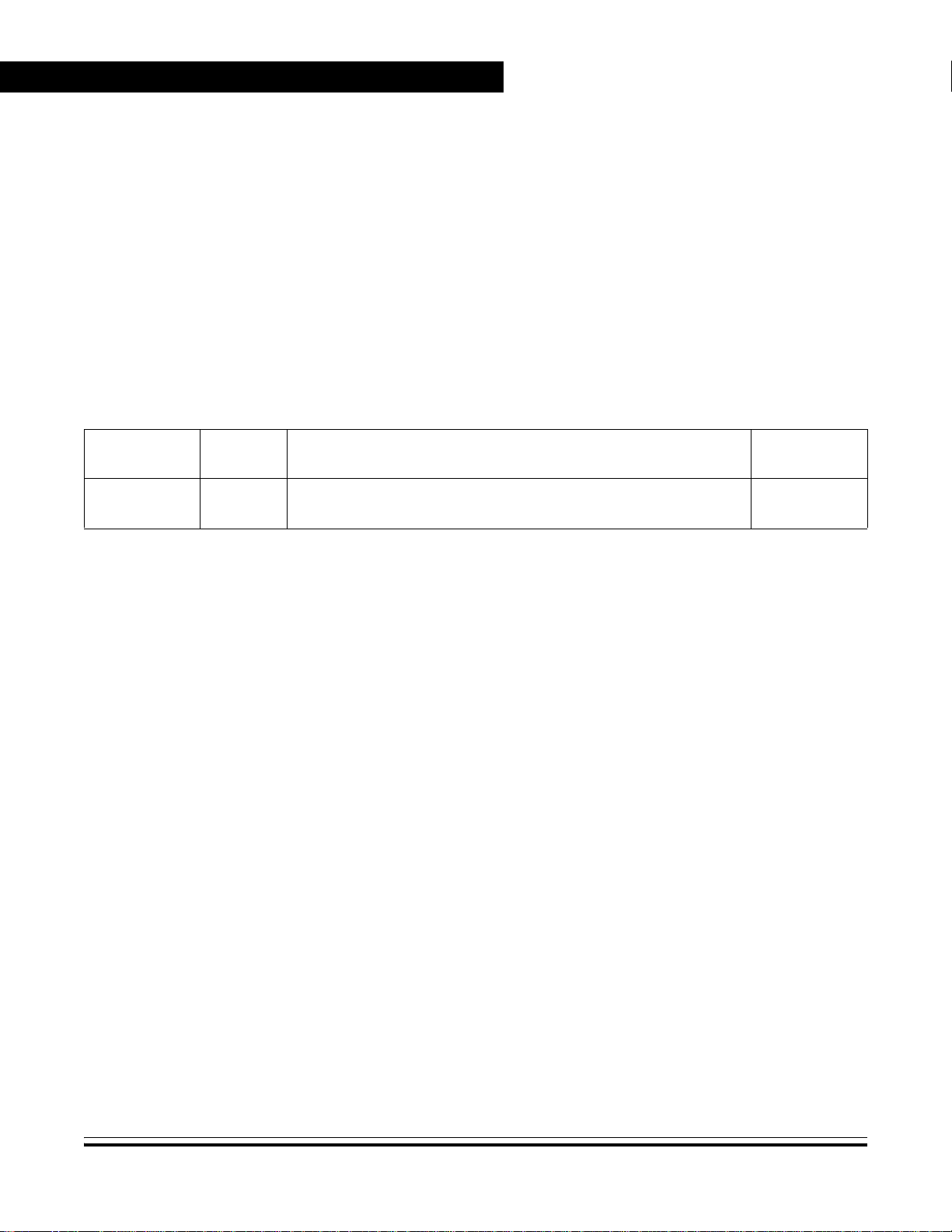
1 First general release. —
Description
Page
Number(s)
Technical Data MC68HC908JB16 — Rev. 1.1
4 Freescale Semiconductor

Technical Data — MC68HC908JB16
Section 1. General Description . . . . . . . . . . . . . . . . . . . . . . . 29
Section 2. Memory Map. . . . . . . . . . . . . . . . . . . . . . . . . . . . . . 41
Section 3. Random-Access Memory (RAM) . . . . . . . . . . . . . 57
Section 4. FLASH Memory . . . . . . . . . . . . . . . . . . . . . . . . . . . 59
Section 5. Configuration Register (CONFIG) . . . . . . . . . . . . 71
Section 6. Central Processor Unit (CPU). . . . . . . . . . . . . . . . 75
Section 7. Oscillator (OSC). . . . . . . . . . . . . . . . . . . . . . . . . . . 93
Section 8. System Integration Module (SIM). . . . . . . . . . . . . 97
Section 9. Monitor ROM (MON) . . . . . . . . . . . . . . . . . . . . . . 123
Section 10. Timer Interface Module (TIM) . . . . . . . . . . . . . . 137
List of Sections
Section 11. Universal Serial Bus Module (USB) . . . . . . . . . 161
Section 12. Serial Communications Interface
Module (SCI). . . . . . . . . . . . . . . . . . . . . . . . . . . 207
Section 13. Clock Generator Module (CGM) . . . . . . . . . . . . 247
Section 14. Input/Output (I/O) Ports. . . . . . . . . . . . . . . . . . . 263
Section 15. External Interrupt (IRQ). . . . . . . . . . . . . . . . . . . 281
Section 16. Keyboard Interrupt Module (KBI). . . . . . . . . . . 289
Section 17. Computer Operating Properly (COP). . . . . . . . 297
Section 18. Low-Voltage Inhibit (LVI) . . . . . . . . . . . . . . . . . 303
Section 19. Break Module (BRK) . . . . . . . . . . . . . . . . . . . . . 307
Section 20. Electrical Specifications . . . . . . . . . . . . . . . . . . 315
Section 21. Mechanical Specifications . . . . . . . . . . . . . . . . 325
Section 22. Ordering Information. . . . . . . . . . . . . . . . . . . . . 329
MC68HC908JB16 — Rev. 1.1 Technical Data
Freescale Semiconductor List of Sections 5

List of Sections
Technical Data MC68HC908JB16 — Rev. 1.1
6 List of Sections Freescale Semiconductor

Technical Data — MC68HC908JB16
Section 1. General Description
1.1 Contents . . . . . . . . . . . . . . . . . . . . . . . . . . . . . . . . . . . . . . . . . .29
1.2 Introduction. . . . . . . . . . . . . . . . . . . . . . . . . . . . . . . . . . . . . . . .29
1.3 Features . . . . . . . . . . . . . . . . . . . . . . . . . . . . . . . . . . . . . . . . . .30
1.4 MCU Block Diagram. . . . . . . . . . . . . . . . . . . . . . . . . . . . . . . . .31
1.5 Pin Assignments. . . . . . . . . . . . . . . . . . . . . . . . . . . . . . . . . . . .33
1.6 Pin Functions . . . . . . . . . . . . . . . . . . . . . . . . . . . . . . . . . . . . . .34
1.6.1 Power Supply Pins (VDD, VSS). . . . . . . . . . . . . . . . . . . . . . .34
1.6.2 Voltage Regulator Output Pin (V
1.6.3 Oscillator Pins (OSC1 and OSC2) . . . . . . . . . . . . . . . . . . . .35
1.6.4 External Reset Pin (RST). . . . . . . . . . . . . . . . . . . . . . . . . . .35
1.6.5 External Interrupt Pins (IRQ, PTE4/D–) . . . . . . . . . . . . . . . .35
1.6.6 CGM Power Supply Pins (V
1.6.7 CGM Voltage Regulator Out (V
1.6.8 CGM Voltage Regulator In (V
1.6.9 External Filter Capacitor Pins (CGMXFC1, CGMXFC2) . . .36
1.6.10 CGM Clock Output Pins (CGMOUT1, CGMOUT2) . . . . . . .36
1.6.11 Port A Input/Output (I/O) Pins (PTA7/KBA7–PTA0/KBA0). .36
1.6.12 Port C I/O Pins (PTC1/RxD, PTC0/TxD) . . . . . . . . . . . . . . .37
1.6.13 Port D I/O Pins (PTD5–PTD0) . . . . . . . . . . . . . . . . . . . . . . .37
1.6.14 Port E I/O Pins (PTE4/D–, PTE3/D+, PTE2/T2CH01,
PTE1/T1CH01, PTE0/TCLK). . . . . . . . . . . . . . . . . . . . . .37
Table of Contents
). . . . . . . . . . . . . . . . . .34
REG
DDA
REGA1
, V
REGA0
SSA0
, V
) . . . . . . . . .36
SSA1
). . . . . . . . . . . . . . . . .36
) . . . . . . . . . . . . . . . . . .36
Section 2. Memory Map
2.1 Contents . . . . . . . . . . . . . . . . . . . . . . . . . . . . . . . . . . . . . . . . . .41
2.2 Introduction. . . . . . . . . . . . . . . . . . . . . . . . . . . . . . . . . . . . . . . .41
2.3 Unimplemented Memory Locations . . . . . . . . . . . . . . . . . . . . .41
MC68HC908JB16 — Rev. 1.1 Technical Data
Freescale Semiconductor Table of Contents 7

Table of Contents
2.4 Reserved Memory Locations . . . . . . . . . . . . . . . . . . . . . . . . . .42
2.5 Input/Output (I/O) Section. . . . . . . . . . . . . . . . . . . . . . . . . . . . .42
Section 3. Random-Access Memory (RAM)
3.1 Contents . . . . . . . . . . . . . . . . . . . . . . . . . . . . . . . . . . . . . . . . . .57
3.2 Introduction. . . . . . . . . . . . . . . . . . . . . . . . . . . . . . . . . . . . . . . .57
3.3 Functional Description . . . . . . . . . . . . . . . . . . . . . . . . . . . . . . .57
Section 4. FLASH Memory
4.1 Contents . . . . . . . . . . . . . . . . . . . . . . . . . . . . . . . . . . . . . . . . . .59
4.2 Introduction. . . . . . . . . . . . . . . . . . . . . . . . . . . . . . . . . . . . . . . .59
4.3 Functional Description . . . . . . . . . . . . . . . . . . . . . . . . . . . . . . .60
4.4 FLASH Control Register. . . . . . . . . . . . . . . . . . . . . . . . . . . . . .61
4.5 FLASH Block Erase Operation. . . . . . . . . . . . . . . . . . . . . . . . .62
4.6 FLASH Mass Erase Operation . . . . . . . . . . . . . . . . . . . . . . . . .63
4.7 FLASH Program Operation. . . . . . . . . . . . . . . . . . . . . . . . . . . .64
4.8 FLASH Protection. . . . . . . . . . . . . . . . . . . . . . . . . . . . . . . . . . .66
4.8.1 FLASH Block Protect Register. . . . . . . . . . . . . . . . . . . . . . .66
4.9 ROM-Resident Routines. . . . . . . . . . . . . . . . . . . . . . . . . . . . . .67
4.9.1 Variables . . . . . . . . . . . . . . . . . . . . . . . . . . . . . . . . . . . . . . .68
4.9.2 ERASE Routine . . . . . . . . . . . . . . . . . . . . . . . . . . . . . . . . . .68
4.9.3 PROGRAM Routine . . . . . . . . . . . . . . . . . . . . . . . . . . . . . . .69
4.9.4 VERIFY Routine. . . . . . . . . . . . . . . . . . . . . . . . . . . . . . . . . .69
Section 5. Configuration Register (CONFIG)
5.1 Contents . . . . . . . . . . . . . . . . . . . . . . . . . . . . . . . . . . . . . . . . . .71
5.2 Introduction. . . . . . . . . . . . . . . . . . . . . . . . . . . . . . . . . . . . . . . .71
5.3 Functional Description . . . . . . . . . . . . . . . . . . . . . . . . . . . . . . .71
5.4 Configuration Register . . . . . . . . . . . . . . . . . . . . . . . . . . . . . . .72
Technical Data MC68HC908JB16 — Rev. 1.1
8 Table of Contents Freescale Semiconductor

Table of Contents
Section 6. Central Processor Unit (CPU)
6.1 Contents . . . . . . . . . . . . . . . . . . . . . . . . . . . . . . . . . . . . . . . . . .75
6.2 Introduction. . . . . . . . . . . . . . . . . . . . . . . . . . . . . . . . . . . . . . . .76
6.3 Features . . . . . . . . . . . . . . . . . . . . . . . . . . . . . . . . . . . . . . . . . .76
6.4 CPU Registers . . . . . . . . . . . . . . . . . . . . . . . . . . . . . . . . . . . . .77
6.4.1 Accumulator . . . . . . . . . . . . . . . . . . . . . . . . . . . . . . . . . . . . .77
6.4.2 Index Register . . . . . . . . . . . . . . . . . . . . . . . . . . . . . . . . . . .78
6.4.3 Stack Pointer . . . . . . . . . . . . . . . . . . . . . . . . . . . . . . . . . . . .78
6.4.4 Program Counter . . . . . . . . . . . . . . . . . . . . . . . . . . . . . . . . .79
6.4.5 Condition Code Register . . . . . . . . . . . . . . . . . . . . . . . . . . .80
6.5 Arithmetic/Logic Unit (ALU) . . . . . . . . . . . . . . . . . . . . . . . . . . .82
6.6 Low-Power Modes . . . . . . . . . . . . . . . . . . . . . . . . . . . . . . . . . .82
6.6.1 Wait Mode . . . . . . . . . . . . . . . . . . . . . . . . . . . . . . . . . . . . . .82
6.6.2 Stop Mode . . . . . . . . . . . . . . . . . . . . . . . . . . . . . . . . . . . . . .83
6.7 CPU During Break Interrupts . . . . . . . . . . . . . . . . . . . . . . . . . .83
6.8 Instruction Set Summary . . . . . . . . . . . . . . . . . . . . . . . . . . . . .83
6.9 Opcode Map. . . . . . . . . . . . . . . . . . . . . . . . . . . . . . . . . . . . . . .83
Section 7. Oscillator (OSC)
7.1 Contents . . . . . . . . . . . . . . . . . . . . . . . . . . . . . . . . . . . . . . . . . .93
7.2 Introduction. . . . . . . . . . . . . . . . . . . . . . . . . . . . . . . . . . . . . . . .93
7.3 Oscillator External Connections . . . . . . . . . . . . . . . . . . . . . . . .94
7.4 I/O Signals . . . . . . . . . . . . . . . . . . . . . . . . . . . . . . . . . . . . . . . .95
7.4.1 Crystal Amplifier Input Pin (OSC1). . . . . . . . . . . . . . . . . . . .95
7.4.2 Crystal Amplifier Output Pin (OSC1) . . . . . . . . . . . . . . . . . .95
7.4.3 Oscillator Enable Signal (SIMOSCEN). . . . . . . . . . . . . . . . .95
7.4.4 Crystal Output Frequency Signal (OSCXCLK). . . . . . . . . . .95
7.4.5 Clock Doubler Out (OSCDCLK). . . . . . . . . . . . . . . . . . . . . .95
7.4.6 Oscillator Out (OSCOUT). . . . . . . . . . . . . . . . . . . . . . . . . . .96
7.5 Low-Power Modes . . . . . . . . . . . . . . . . . . . . . . . . . . . . . . . . . .96
7.5.1 Wait Mode . . . . . . . . . . . . . . . . . . . . . . . . . . . . . . . . . . . . . .96
MC68HC908JB16 — Rev. 1.1 Technical Data
Freescale Semiconductor Table of Contents 9

Table of Contents
7.5.2 Stop Mode . . . . . . . . . . . . . . . . . . . . . . . . . . . . . . . . . . . . . .96
7.6 Oscillator During Break Mode. . . . . . . . . . . . . . . . . . . . . . . . . .96
Section 8. System Integration Module (SIM)
8.1 Contents . . . . . . . . . . . . . . . . . . . . . . . . . . . . . . . . . . . . . . . . . .97
8.2 Introduction. . . . . . . . . . . . . . . . . . . . . . . . . . . . . . . . . . . . . . . .98
8.3 SIM Bus Clock Control and Generation . . . . . . . . . . . . . . . . .100
8.3.1 Bus Timing . . . . . . . . . . . . . . . . . . . . . . . . . . . . . . . . . . . . .101
8.3.2 Clock Startup from POR or LVI Reset . . . . . . . . . . . . . . . .101
8.3.3 Clocks in Stop Mode and Wait Mode. . . . . . . . . . . . . . . . .101
8.4 Reset and System Initialization. . . . . . . . . . . . . . . . . . . . . . . .101
8.4.1 External Pin Reset . . . . . . . . . . . . . . . . . . . . . . . . . . . . . . .102
8.4.2 Active Resets from Internal Sources . . . . . . . . . . . . . . . . .103
8.4.2.1 Power-On Reset . . . . . . . . . . . . . . . . . . . . . . . . . . . . . .104
8.4.2.2 Computer Operating Properly (COP) Reset. . . . . . . . . .105
8.4.2.3 Illegal Opcode Reset . . . . . . . . . . . . . . . . . . . . . . . . . . .105
8.4.2.4 Illegal Address Reset. . . . . . . . . . . . . . . . . . . . . . . . . . .105
8.4.2.5 Low-Voltage Inhibit (LVI) Reset . . . . . . . . . . . . . . . . . . .106
8.4.2.6 Universal Serial Bus (USB) Reset . . . . . . . . . . . . . . . . .106
8.4.2.7 Registers Values After Different Resets. . . . . . . . . . . . .106
8.5 SIM Counter . . . . . . . . . . . . . . . . . . . . . . . . . . . . . . . . . . . . . .107
8.5.1 SIM Counter During Power-On Reset . . . . . . . . . . . . . . . .107
8.5.2 SIM Counter During Stop Mode Recovery. . . . . . . . . . . . .108
8.5.3 SIM Counter and Reset States. . . . . . . . . . . . . . . . . . . . . .108
8.6 Exception Control . . . . . . . . . . . . . . . . . . . . . . . . . . . . . . . . . .108
8.6.1 Interrupts . . . . . . . . . . . . . . . . . . . . . . . . . . . . . . . . . . . . . .108
8.6.1.1 Hardware Interrupts . . . . . . . . . . . . . . . . . . . . . . . . . . . .111
8.6.1.2 SWI Instruction. . . . . . . . . . . . . . . . . . . . . . . . . . . . . . . .112
8.6.2 Interrupt Status Registers. . . . . . . . . . . . . . . . . . . . . . . . . .112
8.6.2.1 Interrupt Status Register 1. . . . . . . . . . . . . . . . . . . . . . .112
8.6.2.2 Interrupt Status Register 2. . . . . . . . . . . . . . . . . . . . . . .114
8.6.3 Reset . . . . . . . . . . . . . . . . . . . . . . . . . . . . . . . . . . . . . . . . .114
8.6.4 Break Interrupts . . . . . . . . . . . . . . . . . . . . . . . . . . . . . . . . .114
8.6.5 Status Flag Protection in Break Mode . . . . . . . . . . . . . . . .114
Technical Data MC68HC908JB16 — Rev. 1.1
10 Table of Contents Freescale Semiconductor

Table of Contents
8.7 Low-Power Modes . . . . . . . . . . . . . . . . . . . . . . . . . . . . . . . . .115
8.7.1 Wait Mode . . . . . . . . . . . . . . . . . . . . . . . . . . . . . . . . . . . . .115
8.7.2 Stop Mode . . . . . . . . . . . . . . . . . . . . . . . . . . . . . . . . . . . . .116
8.8 SIM Registers. . . . . . . . . . . . . . . . . . . . . . . . . . . . . . . . . . . . .118
8.8.1 SIM Break Status Register (SBSR) . . . . . . . . . . . . . . . . . .118
8.8.2 SIM Reset Status Register (SRSR) . . . . . . . . . . . . . . . . . .119
8.8.3 SIM Break Flag Control Register (SBFCR) . . . . . . . . . . . .120
Section 9. Monitor ROM (MON)
9.1 Contents . . . . . . . . . . . . . . . . . . . . . . . . . . . . . . . . . . . . . . . . .123
9.2 Introduction. . . . . . . . . . . . . . . . . . . . . . . . . . . . . . . . . . . . . . .123
9.3 Features . . . . . . . . . . . . . . . . . . . . . . . . . . . . . . . . . . . . . . . . .124
9.4 Functional Description . . . . . . . . . . . . . . . . . . . . . . . . . . . . . .124
9.4.1 Entering Monitor Mode. . . . . . . . . . . . . . . . . . . . . . . . . . . .126
9.4.2 Data Format . . . . . . . . . . . . . . . . . . . . . . . . . . . . . . . . . . . .129
9.4.3 Break Signal. . . . . . . . . . . . . . . . . . . . . . . . . . . . . . . . . . . .129
9.4.4 Baud Rate . . . . . . . . . . . . . . . . . . . . . . . . . . . . . . . . . . . . .129
9.4.5 Commands. . . . . . . . . . . . . . . . . . . . . . . . . . . . . . . . . . . . .130
9.5 Security. . . . . . . . . . . . . . . . . . . . . . . . . . . . . . . . . . . . . . . . . .135
9.5.1 Extended Security . . . . . . . . . . . . . . . . . . . . . . . . . . . . . . .136
Section 10. Timer Interface Module (TIM)
10.1 Contents . . . . . . . . . . . . . . . . . . . . . . . . . . . . . . . . . . . . . . . . .137
10.2 Introduction. . . . . . . . . . . . . . . . . . . . . . . . . . . . . . . . . . . . . . .138
10.3 Features . . . . . . . . . . . . . . . . . . . . . . . . . . . . . . . . . . . . . . . . .138
10.4 Pin Name Conventions. . . . . . . . . . . . . . . . . . . . . . . . . . . . . .139
10.5 Functional Description . . . . . . . . . . . . . . . . . . . . . . . . . . . . . .139
10.5.1 TIM Counter Prescaler. . . . . . . . . . . . . . . . . . . . . . . . . . . .143
10.5.2 Input Capture . . . . . . . . . . . . . . . . . . . . . . . . . . . . . . . . . . .143
10.5.3 Output Compare. . . . . . . . . . . . . . . . . . . . . . . . . . . . . . . . .144
10.5.3.1 Unbuffered Output Compare . . . . . . . . . . . . . . . . . . . . .144
10.5.3.2 Buffered Output Compare . . . . . . . . . . . . . . . . . . . . . . .145
MC68HC908JB16 — Rev. 1.1 Technical Data
Freescale Semiconductor Table of Contents 11

Table of Contents
10.5.4 Pulse Width Modulation (PWM) . . . . . . . . . . . . . . . . . . . . .145
10.5.4.1 Unbuffered PWM Signal Generation . . . . . . . . . . . . . . .146
10.5.4.2 Buffered PWM Signal Generation . . . . . . . . . . . . . . . . .147
10.5.4.3 PWM Initialization . . . . . . . . . . . . . . . . . . . . . . . . . . . . .148
10.6 Interrupts. . . . . . . . . . . . . . . . . . . . . . . . . . . . . . . . . . . . . . . . .149
10.7 Low-Power Modes . . . . . . . . . . . . . . . . . . . . . . . . . . . . . . . . .149
10.7.1 Wait Mode . . . . . . . . . . . . . . . . . . . . . . . . . . . . . . . . . . . . .150
10.7.2 Stop Mode . . . . . . . . . . . . . . . . . . . . . . . . . . . . . . . . . . . . .150
10.8 TIM During Break Interrupts . . . . . . . . . . . . . . . . . . . . . . . . . .150
10.9 I/O Signals . . . . . . . . . . . . . . . . . . . . . . . . . . . . . . . . . . . . . . .151
10.9.1 TIM Clock Pin (PTE0/TCLK) . . . . . . . . . . . . . . . . . . . . . . .151
10.9.2 TIM Channel I/O Pins (PTE1/T1CH01:PTE2/T2CH01) . . .151
10.10 I/O Registers. . . . . . . . . . . . . . . . . . . . . . . . . . . . . . . . . . . . . .152
10.10.1 TIM Status and Control Register . . . . . . . . . . . . . . . . . . . .152
10.10.2 TIM Counter Registers. . . . . . . . . . . . . . . . . . . . . . . . . . . .154
10.10.3 TIM Counter Modulo Registers . . . . . . . . . . . . . . . . . . . . .155
10.10.4 TIM Channel Status and Control Registers . . . . . . . . . . . .156
10.10.5 TIM Channel Registers. . . . . . . . . . . . . . . . . . . . . . . . . . . .159
Section 11. Universal Serial Bus Module (USB)
11.1 Contents . . . . . . . . . . . . . . . . . . . . . . . . . . . . . . . . . . . . . . . . .161
11.2 Introduction. . . . . . . . . . . . . . . . . . . . . . . . . . . . . . . . . . . . . . .162
11.3 Features . . . . . . . . . . . . . . . . . . . . . . . . . . . . . . . . . . . . . . . . .163
11.4 Pin Name Conventions. . . . . . . . . . . . . . . . . . . . . . . . . . . . . .164
11.5 Functional Description . . . . . . . . . . . . . . . . . . . . . . . . . . . . . .168
11.5.1 USB Protocol . . . . . . . . . . . . . . . . . . . . . . . . . . . . . . . . . . .169
11.5.1.1 Sync Pattern . . . . . . . . . . . . . . . . . . . . . . . . . . . . . . . . .170
11.5.1.2 Packet Identifier Field . . . . . . . . . . . . . . . . . . . . . . . . . .171
11.5.1.3 Address Field (ADDR) . . . . . . . . . . . . . . . . . . . . . . . . . .172
11.5.1.4 Endpoint Field (ENDP). . . . . . . . . . . . . . . . . . . . . . . . . .172
11.5.1.5 Cyclic Redundancy Check (CRC) . . . . . . . . . . . . . . . . .172
11.5.1.6 End-of-Packet (EOP) . . . . . . . . . . . . . . . . . . . . . . . . . . .172
11.5.2 Reset Signaling . . . . . . . . . . . . . . . . . . . . . . . . . . . . . . . . .173
Technical Data MC68HC908JB16 — Rev. 1.1
12 Table of Contents Freescale Semiconductor

Table of Contents
11.5.3 Suspend. . . . . . . . . . . . . . . . . . . . . . . . . . . . . . . . . . . . . . .174
11.5.4 Resume After Suspend . . . . . . . . . . . . . . . . . . . . . . . . . . .175
11.5.4.1 Host Initiated Resume . . . . . . . . . . . . . . . . . . . . . . . . . .175
11.5.4.2 USB Reset Signalling. . . . . . . . . . . . . . . . . . . . . . . . . . .175
11.5.4.3 Remote Wakeup . . . . . . . . . . . . . . . . . . . . . . . . . . . . . .175
11.5.5 Low-Speed Device. . . . . . . . . . . . . . . . . . . . . . . . . . . . . . .176
11.6 Clock Requirements . . . . . . . . . . . . . . . . . . . . . . . . . . . . . . . .176
11.7 Hardware Description. . . . . . . . . . . . . . . . . . . . . . . . . . . . . . .177
11.7.1 Voltage Regulator. . . . . . . . . . . . . . . . . . . . . . . . . . . . . . . .177
11.7.2 USB Transceiver . . . . . . . . . . . . . . . . . . . . . . . . . . . . . . . .177
11.7.2.1 Output Driver Characteristics. . . . . . . . . . . . . . . . . . . . .178
11.7.2.2 Low Speed (1.5 Mbps) Driver Characteristics . . . . . . . .178
11.7.2.3 Receiver Data Jitter . . . . . . . . . . . . . . . . . . . . . . . . . . . .179
11.7.2.4 Data Source Jitter . . . . . . . . . . . . . . . . . . . . . . . . . . . . .179
11.7.2.5 Data Signal Rise and Fall Time . . . . . . . . . . . . . . . . . . .180
11.7.3 USB Control Logic . . . . . . . . . . . . . . . . . . . . . . . . . . . . . . .181
11.8 I/O Registers. . . . . . . . . . . . . . . . . . . . . . . . . . . . . . . . . . . . . .181
11.8.1 USB Address Register . . . . . . . . . . . . . . . . . . . . . . . . . . . .182
11.8.2 USB Interrupt Register 0 . . . . . . . . . . . . . . . . . . . . . . . . . .183
11.8.3 USB Interrupt Register 1 . . . . . . . . . . . . . . . . . . . . . . . . . .185
11.8.4 USB Interrupt Register 2 . . . . . . . . . . . . . . . . . . . . . . . . . .188
11.8.5 USB Control Register 0 . . . . . . . . . . . . . . . . . . . . . . . . . . .189
11.8.6 USB Control Register 1 . . . . . . . . . . . . . . . . . . . . . . . . . . .190
11.8.7 USB Control Register 2 . . . . . . . . . . . . . . . . . . . . . . . . . . .191
11.8.8 USB Control Register 3 . . . . . . . . . . . . . . . . . . . . . . . . . . .193
11.8.9 USB Control Register 4 . . . . . . . . . . . . . . . . . . . . . . . . . . .195
11.8.10 USB Status Register 0 . . . . . . . . . . . . . . . . . . . . . . . . . . . .196
11.8.11 USB Status Register 1 . . . . . . . . . . . . . . . . . . . . . . . . . . . .197
11.8.12 USB Endpoint 0 Data Registers. . . . . . . . . . . . . . . . . . . . .198
11.8.13 USB Endpoint 1 Data Registers. . . . . . . . . . . . . . . . . . . . .199
11.8.14 USB Endpoint 2 Data Registers. . . . . . . . . . . . . . . . . . . . .200
11.9 USB Interrupts . . . . . . . . . . . . . . . . . . . . . . . . . . . . . . . . . . . .201
11.9.1 USB End-of-Transaction Interrupt . . . . . . . . . . . . . . . . . . .201
11.9.1.1 Receive Control Endpoint 0 . . . . . . . . . . . . . . . . . . . . . .202
11.9.1.2 Transmit Control Endpoint 0 . . . . . . . . . . . . . . . . . . . . .204
11.9.1.3 Transmit Endpoint 1. . . . . . . . . . . . . . . . . . . . . . . . . . . .205
MC68HC908JB16 — Rev. 1.1 Technical Data
Freescale Semiconductor Table of Contents 13

Table of Contents
11.9.1.4 Transmit Endpoint 2. . . . . . . . . . . . . . . . . . . . . . . . . . . .206
11.9.1.5 Receive Endpoint 2 . . . . . . . . . . . . . . . . . . . . . . . . . . . .206
11.9.2 Resume Interrupt . . . . . . . . . . . . . . . . . . . . . . . . . . . . . . . .206
11.9.3 End-of-Packet Interrupt . . . . . . . . . . . . . . . . . . . . . . . . . . .206
Section 12. Serial Communications Interface Module
(SCI)
12.1 Contents . . . . . . . . . . . . . . . . . . . . . . . . . . . . . . . . . . . . . . . . .207
12.2 Introduction. . . . . . . . . . . . . . . . . . . . . . . . . . . . . . . . . . . . . . .208
12.3 Features . . . . . . . . . . . . . . . . . . . . . . . . . . . . . . . . . . . . . . . . .208
12.4 Pin Name Conventions. . . . . . . . . . . . . . . . . . . . . . . . . . . . . .210
12.5 Functional Description . . . . . . . . . . . . . . . . . . . . . . . . . . . . . .210
12.5.1 Data Format . . . . . . . . . . . . . . . . . . . . . . . . . . . . . . . . . . . .213
12.5.2 Transmitter. . . . . . . . . . . . . . . . . . . . . . . . . . . . . . . . . . . . .213
12.5.2.1 Character Length . . . . . . . . . . . . . . . . . . . . . . . . . . . . . .215
12.5.2.2 Character Transmission. . . . . . . . . . . . . . . . . . . . . . . . .215
12.5.2.3 Break Characters. . . . . . . . . . . . . . . . . . . . . . . . . . . . . .216
12.5.2.4 Idle Characters. . . . . . . . . . . . . . . . . . . . . . . . . . . . . . . .216
12.5.2.5 Inversion of Transmitted Output. . . . . . . . . . . . . . . . . . .217
12.5.2.6 Transmitter Interrupts. . . . . . . . . . . . . . . . . . . . . . . . . . .217
12.5.3 Receiver. . . . . . . . . . . . . . . . . . . . . . . . . . . . . . . . . . . . . . .218
12.5.3.1 Character Length . . . . . . . . . . . . . . . . . . . . . . . . . . . . . .218
12.5.3.2 Character Reception . . . . . . . . . . . . . . . . . . . . . . . . . . .218
12.5.3.3 Data Sampling . . . . . . . . . . . . . . . . . . . . . . . . . . . . . . . .220
12.5.3.4 Framing Errors. . . . . . . . . . . . . . . . . . . . . . . . . . . . . . . .222
12.5.3.5 Baud Rate Tolerance. . . . . . . . . . . . . . . . . . . . . . . . . . .222
12.5.3.6 Receiver Wakeup. . . . . . . . . . . . . . . . . . . . . . . . . . . . . .225
12.5.3.7 Receiver Interrupts. . . . . . . . . . . . . . . . . . . . . . . . . . . . .226
12.5.3.8 Error Interrupts. . . . . . . . . . . . . . . . . . . . . . . . . . . . . . . .226
12.6 Low-Power Modes . . . . . . . . . . . . . . . . . . . . . . . . . . . . . . . . .227
12.6.1 Wait Mode . . . . . . . . . . . . . . . . . . . . . . . . . . . . . . . . . . . . .227
12.6.2 Stop Mode . . . . . . . . . . . . . . . . . . . . . . . . . . . . . . . . . . . . .227
12.7 SCI During Break Module Interrupts. . . . . . . . . . . . . . . . . . . .228
12.8 I/O Signals . . . . . . . . . . . . . . . . . . . . . . . . . . . . . . . . . . . . . . .228
Technical Data MC68HC908JB16 — Rev. 1.1
14 Table of Contents Freescale Semiconductor

Table of Contents
12.8.1 TxD (Transmit Data). . . . . . . . . . . . . . . . . . . . . . . . . . . . . .228
12.8.2 RxD (Receive Data) . . . . . . . . . . . . . . . . . . . . . . . . . . . . . .228
12.9 I/O Registers. . . . . . . . . . . . . . . . . . . . . . . . . . . . . . . . . . . . . .229
12.9.1 SCI Control Register 1 . . . . . . . . . . . . . . . . . . . . . . . . . . . .229
12.9.2 SCI Control Register 2 . . . . . . . . . . . . . . . . . . . . . . . . . . . .232
12.9.3 SCI Control Register 3 . . . . . . . . . . . . . . . . . . . . . . . . . . .235
12.9.4 SCI Status Register 1. . . . . . . . . . . . . . . . . . . . . . . . . . . . .238
12.9.5 SCI Status Register 2. . . . . . . . . . . . . . . . . . . . . . . . . . . . .242
12.9.6 SCI Data Register . . . . . . . . . . . . . . . . . . . . . . . . . . . . . . .243
12.9.7 SCI Baud Rate Register. . . . . . . . . . . . . . . . . . . . . . . . . . .244
Section 13. Clock Generator Module (CGM)
13.1 Contents . . . . . . . . . . . . . . . . . . . . . . . . . . . . . . . . . . . . . . . . .247
13.2 Introduction. . . . . . . . . . . . . . . . . . . . . . . . . . . . . . . . . . . . . . .248
13.3 Functional Description . . . . . . . . . . . . . . . . . . . . . . . . . . . . . .249
13.3.1 Reference Frequency Source (OSCXCLK) . . . . . . . . . . . .250
13.3.2 Voltage Controlled Oscillator . . . . . . . . . . . . . . . . . . . . . . .250
13.3.3 Reference Divider. . . . . . . . . . . . . . . . . . . . . . . . . . . . . . . .251
13.3.4 VCO Frequency Divider . . . . . . . . . . . . . . . . . . . . . . . . . . .251
13.3.5 Phase Detector. . . . . . . . . . . . . . . . . . . . . . . . . . . . . . . . . .251
13.3.6 Phase Detector Filter . . . . . . . . . . . . . . . . . . . . . . . . . . . . .251
13.3.7 Lock Detector. . . . . . . . . . . . . . . . . . . . . . . . . . . . . . . . . . .251
13.4 I/O Signals . . . . . . . . . . . . . . . . . . . . . . . . . . . . . . . . . . . . . . .252
13.4.1 CGM Power Supply Pins (V
13.4.2 CGM1 Voltage Regulator Out (V
13.4.3 CGM2 Voltage Regulator In (V
DDA
, V
SSA0
REGA0
REGA1
, V
) . . . . . . . .252
SSA1
). . . . . . . . . . . . . . .252
) . . . . . . . . . . . . . . . .252
13.4.4 External Filter Capacitor Pins (CGMXFC1, CGMXFC2) . .253
13.4.5 CGM Clock Output Pins (CGMOUT1, CGMOUT2) . . . . . .253
13.5 CGMXFC External Connections. . . . . . . . . . . . . . . . . . . . . . .253
13.6 CGMOUT External Connections. . . . . . . . . . . . . . . . . . . . . . .254
13.7 Calculation of VCO Frequency. . . . . . . . . . . . . . . . . . . . . . . .254
13.8 Programming the PLL. . . . . . . . . . . . . . . . . . . . . . . . . . . . . . .255
13.9 CGM I/O Registers . . . . . . . . . . . . . . . . . . . . . . . . . . . . . . . . .255
MC68HC908JB16 — Rev. 1.1 Technical Data
Freescale Semiconductor Table of Contents 15

Table of Contents
13.9.1 Bandwidth Control Register . . . . . . . . . . . . . . . . . . . . . . . .256
13.9.2 VCO Control Register (PVCR). . . . . . . . . . . . . . . . . . . . . .256
13.9.3 VCO and Reference Divider Select Registers High. . . . . .257
13.9.4 VCO Divider Select Register Low . . . . . . . . . . . . . . . . . . .258
13.9.5 Reference Divider Select Register Low . . . . . . . . . . . . . . .259
13.9.6 Phase Detector Control Register (PDCR) . . . . . . . . . . . . .260
13.10 Pre-Defined VCO Output Frequency Settings . . . . . . . . . . . .260
13.11 Low-Power Modes . . . . . . . . . . . . . . . . . . . . . . . . . . . . . . . . .261
13.11.1 Wait Mode . . . . . . . . . . . . . . . . . . . . . . . . . . . . . . . . . . . . .261
13.11.2 Stop Mode . . . . . . . . . . . . . . . . . . . . . . . . . . . . . . . . . . . . .261
Section 14. Input/Output (I/O) Ports
14.1 Contents . . . . . . . . . . . . . . . . . . . . . . . . . . . . . . . . . . . . . . . . .263
14.2 Introduction. . . . . . . . . . . . . . . . . . . . . . . . . . . . . . . . . . . . . . .263
14.3 Port A . . . . . . . . . . . . . . . . . . . . . . . . . . . . . . . . . . . . . . . . . . .266
14.3.1 Port A Data Register . . . . . . . . . . . . . . . . . . . . . . . . . . . . .266
14.3.2 Data Direction Register A . . . . . . . . . . . . . . . . . . . . . . . . .267
14.4 Port C . . . . . . . . . . . . . . . . . . . . . . . . . . . . . . . . . . . . . . . . . . .269
14.4.1 Port C Data Register . . . . . . . . . . . . . . . . . . . . . . . . . . . . .269
14.4.2 Data Direction Register C. . . . . . . . . . . . . . . . . . . . . . . . . .270
14.5 Port D . . . . . . . . . . . . . . . . . . . . . . . . . . . . . . . . . . . . . . . . . . .272
14.5.1 Port D Data Register . . . . . . . . . . . . . . . . . . . . . . . . . . . . .272
14.5.2 Data Direction Register D. . . . . . . . . . . . . . . . . . . . . . . . . .273
14.6 Port E . . . . . . . . . . . . . . . . . . . . . . . . . . . . . . . . . . . . . . . . . . .275
14.6.1 Port E Data Register . . . . . . . . . . . . . . . . . . . . . . . . . . . . .275
14.6.2 Data Direction Register E. . . . . . . . . . . . . . . . . . . . . . . . . .277
14.7 Port Options . . . . . . . . . . . . . . . . . . . . . . . . . . . . . . . . . . . . . .278
14.7.1 Port Option Control Register . . . . . . . . . . . . . . . . . . . . . . .279
Section 15. External Interrupt (IRQ)
15.1 Contents . . . . . . . . . . . . . . . . . . . . . . . . . . . . . . . . . . . . . . . . .281
15.2 Introduction. . . . . . . . . . . . . . . . . . . . . . . . . . . . . . . . . . . . . . .281
Technical Data MC68HC908JB16 — Rev. 1.1
16 Table of Contents Freescale Semiconductor

Table of Contents
15.3 Features . . . . . . . . . . . . . . . . . . . . . . . . . . . . . . . . . . . . . . . . .281
15.4 Functional Description . . . . . . . . . . . . . . . . . . . . . . . . . . . . . .282
15.5 IRQ Pin. . . . . . . . . . . . . . . . . . . . . . . . . . . . . . . . . . . . . . . . . .284
15.6 PTE4/D– Pin. . . . . . . . . . . . . . . . . . . . . . . . . . . . . . . . . . . . . .285
15.7 IRQ Module During Break Interrupts . . . . . . . . . . . . . . . . . . .285
15.8 IRQ Status and Control Register . . . . . . . . . . . . . . . . . . . . . .286
15.9 IRQ Option Control Register. . . . . . . . . . . . . . . . . . . . . . . . . .287
Section 16. Keyboard Interrupt Module (KBI)
16.1 Contents . . . . . . . . . . . . . . . . . . . . . . . . . . . . . . . . . . . . . . . . .289
16.2 Introduction. . . . . . . . . . . . . . . . . . . . . . . . . . . . . . . . . . . . . . .289
16.3 Features . . . . . . . . . . . . . . . . . . . . . . . . . . . . . . . . . . . . . . . . .290
16.4 Pin Name Conventions. . . . . . . . . . . . . . . . . . . . . . . . . . . . . .290
16.5 Functional Description . . . . . . . . . . . . . . . . . . . . . . . . . . . . . .291
16.6 Keyboard Initialization. . . . . . . . . . . . . . . . . . . . . . . . . . . . . . .293
16.7 I/O Registers. . . . . . . . . . . . . . . . . . . . . . . . . . . . . . . . . . . . . .293
16.7.1 Keyboard Status and Control Register. . . . . . . . . . . . . . . .294
16.7.2 Keyboard Interrupt Enable Register. . . . . . . . . . . . . . . . . .295
16.8 Low-Power Modes . . . . . . . . . . . . . . . . . . . . . . . . . . . . . . . . .295
16.8.1 Wait Mode . . . . . . . . . . . . . . . . . . . . . . . . . . . . . . . . . . . . .295
16.8.2 Stop Mode . . . . . . . . . . . . . . . . . . . . . . . . . . . . . . . . . . . . .295
16.9 Keyboard Module During Break Interrupts . . . . . . . . . . . . . . .296
Section 17. Computer Operating Properly (COP)
17.1 Contents . . . . . . . . . . . . . . . . . . . . . . . . . . . . . . . . . . . . . . . . .297
17.2 Introduction. . . . . . . . . . . . . . . . . . . . . . . . . . . . . . . . . . . . . . .297
17.3 Functional Description . . . . . . . . . . . . . . . . . . . . . . . . . . . . . .298
17.4 I/O Signals . . . . . . . . . . . . . . . . . . . . . . . . . . . . . . . . . . . . . . .299
MC68HC908JB16 — Rev. 1.1 Technical Data
Freescale Semiconductor Table of Contents 17

Table of Contents
17.4.1 OSCDCLK . . . . . . . . . . . . . . . . . . . . . . . . . . . . . . . . . . . . .299
17.4.2 STOP Instruction . . . . . . . . . . . . . . . . . . . . . . . . . . . . . . . .299
17.4.3 COPCTL Write . . . . . . . . . . . . . . . . . . . . . . . . . . . . . . . . . .299
17.4.4 Power-On Reset. . . . . . . . . . . . . . . . . . . . . . . . . . . . . . . . .299
17.4.5 Internal Reset. . . . . . . . . . . . . . . . . . . . . . . . . . . . . . . . . . .300
17.4.6 Reset Vector Fetch. . . . . . . . . . . . . . . . . . . . . . . . . . . . . . .300
17.4.7 COPD (COP Disable). . . . . . . . . . . . . . . . . . . . . . . . . . . . .300
17.4.8 COPRS (COP Rate Select) . . . . . . . . . . . . . . . . . . . . . . . .300
17.5 COP Control Register. . . . . . . . . . . . . . . . . . . . . . . . . . . . . . .301
17.6 Interrupts. . . . . . . . . . . . . . . . . . . . . . . . . . . . . . . . . . . . . . . . .301
17.7 Monitor Mode . . . . . . . . . . . . . . . . . . . . . . . . . . . . . . . . . . . . .301
17.8 Low-Power Modes . . . . . . . . . . . . . . . . . . . . . . . . . . . . . . . . .301
17.8.1 Wait Mode . . . . . . . . . . . . . . . . . . . . . . . . . . . . . . . . . . . . .302
17.8.2 Stop Mode . . . . . . . . . . . . . . . . . . . . . . . . . . . . . . . . . . . . .302
17.9 COP Module During Break Mode. . . . . . . . . . . . . . . . . . . . . .302
Section 18. Low-Voltage Inhibit (LVI)
18.1 Contents . . . . . . . . . . . . . . . . . . . . . . . . . . . . . . . . . . . . . . . . .303
18.2 Introduction. . . . . . . . . . . . . . . . . . . . . . . . . . . . . . . . . . . . . . .303
18.3 Features . . . . . . . . . . . . . . . . . . . . . . . . . . . . . . . . . . . . . . . . .303
18.4 Functional Description . . . . . . . . . . . . . . . . . . . . . . . . . . . . . .304
18.4.1 Low VDD Detector. . . . . . . . . . . . . . . . . . . . . . . . . . . . . . . .304
18.4.2 Low V
18.5 LVI Control and Configuration . . . . . . . . . . . . . . . . . . . . . . . .305
18.6 Low-Power Modes . . . . . . . . . . . . . . . . . . . . . . . . . . . . . . . . .306
18.6.1 Wait Mode . . . . . . . . . . . . . . . . . . . . . . . . . . . . . . . . . . . . .306
18.6.2 Stop Mode . . . . . . . . . . . . . . . . . . . . . . . . . . . . . . . . . . . . .306
Detector. . . . . . . . . . . . . . . . . . . . . . . . . . . . . . .305
REG
Section 19. Break Module (BRK)
19.1 Contents . . . . . . . . . . . . . . . . . . . . . . . . . . . . . . . . . . . . . . . . .307
19.2 Introduction. . . . . . . . . . . . . . . . . . . . . . . . . . . . . . . . . . . . . . .307
Technical Data MC68HC908JB16 — Rev. 1.1
18 Table of Contents Freescale Semiconductor

Table of Contents
19.3 Features . . . . . . . . . . . . . . . . . . . . . . . . . . . . . . . . . . . . . . . . .308
19.4 Functional Description . . . . . . . . . . . . . . . . . . . . . . . . . . . . . .308
19.4.1 Flag Protection During Break Interrupts. . . . . . . . . . . . . . .310
19.4.2 CPU During Break Interrupts . . . . . . . . . . . . . . . . . . . . . . .310
19.4.3 TIM During Break Interrupts. . . . . . . . . . . . . . . . . . . . . . . .310
19.4.4 COP During Break Interrupts . . . . . . . . . . . . . . . . . . . . . . .310
19.5 Low-Power Modes . . . . . . . . . . . . . . . . . . . . . . . . . . . . . . . . .310
19.5.1 Wait Mode . . . . . . . . . . . . . . . . . . . . . . . . . . . . . . . . . . . . .310
19.5.2 Stop Mode . . . . . . . . . . . . . . . . . . . . . . . . . . . . . . . . . . . . .311
19.6 Break Module Registers . . . . . . . . . . . . . . . . . . . . . . . . . . . . .311
19.6.1 Break Status and Control Register. . . . . . . . . . . . . . . . . . .311
19.6.2 Break Address Registers . . . . . . . . . . . . . . . . . . . . . . . . . .312
19.6.3 SIM Break Status Register. . . . . . . . . . . . . . . . . . . . . . . . .312
19.6.4 SIM Break Flag Control Register . . . . . . . . . . . . . . . . . . . .314
Section 20. Electrical Specifications
20.1 Contents . . . . . . . . . . . . . . . . . . . . . . . . . . . . . . . . . . . . . . . . .315
20.2 Introduction. . . . . . . . . . . . . . . . . . . . . . . . . . . . . . . . . . . . . . .316
20.3 Absolute Maximum Ratings . . . . . . . . . . . . . . . . . . . . . . . . . .316
20.4 Functional Operating Range. . . . . . . . . . . . . . . . . . . . . . . . . .317
20.5 Thermal Characteristics . . . . . . . . . . . . . . . . . . . . . . . . . . . . .317
20.6 DC Electrical Characteristics . . . . . . . . . . . . . . . . . . . . . . . . .318
20.7 Control Timing . . . . . . . . . . . . . . . . . . . . . . . . . . . . . . . . . . . .319
20.8 Oscillator Characteristics . . . . . . . . . . . . . . . . . . . . . . . . . . . .319
20.9 TImer Interface Module Characteristics . . . . . . . . . . . . . . . . .320
20.10 USB DC Electrical Characteristics . . . . . . . . . . . . . . . . . . . . .320
20.11 USB Low-Speed Source Electrical Characteristics . . . . . . . .321
20.12 USB Signaling Levels. . . . . . . . . . . . . . . . . . . . . . . . . . . . . . .322
20.13 CGM Electrical Characteristics. . . . . . . . . . . . . . . . . . . . . . . .322
20.14 FLASH Memory Characteristics . . . . . . . . . . . . . . . . . . . . . . .324
MC68HC908JB16 — Rev. 1.1 Technical Data
Freescale Semiconductor Table of Contents 19

Table of Contents
Section 21. Mechanical Specifications
21.1 Contents . . . . . . . . . . . . . . . . . . . . . . . . . . . . . . . . . . . . . . . . .325
21.2 Introduction. . . . . . . . . . . . . . . . . . . . . . . . . . . . . . . . . . . . . . .325
21.3 32-Pin Low-Profile Quad Flat Pack (LQFP) . . . . . . . . . . . . . .326
21.4 28-Pin Small Outline Integrated Circuit (SOIC) . . . . . . . . . . .327
Section 22. Ordering Information
22.1 Contents . . . . . . . . . . . . . . . . . . . . . . . . . . . . . . . . . . . . . . . . .329
22.2 Introduction. . . . . . . . . . . . . . . . . . . . . . . . . . . . . . . . . . . . . . .329
22.3 MC Order Numbers . . . . . . . . . . . . . . . . . . . . . . . . . . . . . . . .329
Technical Data MC68HC908JB16 — Rev. 1.1
20 Table of Contents Freescale Semiconductor

Technical Data — MC68HC908JB16
Figure Title Page
1-1 MC68HC908JB16 MCU Block Diagram. . . . . . . . . . . . . . . . . .32
1-2 32-Pin LQFP Pin Assignment. . . . . . . . . . . . . . . . . . . . . . . . . .33
1-3 28-Pin SOIC Pin Assignment . . . . . . . . . . . . . . . . . . . . . . . . . .33
1-4 Power Supply Bypassing . . . . . . . . . . . . . . . . . . . . . . . . . . . . .34
1-5 Regulator Supply Capacitor Configuration . . . . . . . . . . . . . . . .35
2-1 Memory Map. . . . . . . . . . . . . . . . . . . . . . . . . . . . . . . . . . . . . . .43
2-2 Control, Status, and Data Registers. . . . . . . . . . . . . . . . . . . . .44
4-1 FLASH I/O Register Summary . . . . . . . . . . . . . . . . . . . . . . . . .60
4-2 FLASH Control Register (FLCR) . . . . . . . . . . . . . . . . . . . . . . .61
4-3 FLASH Programming Flowchart. . . . . . . . . . . . . . . . . . . . . . . .65
4-4 FLASH Block Protect Register (FLBPR). . . . . . . . . . . . . . . . . .66
4-5 FLASH Block Protect Start Address. . . . . . . . . . . . . . . . . . . . .66
List of Figures
5-1 Configuration Register (CONFIG). . . . . . . . . . . . . . . . . . . . . . .72
6-1 CPU Registers . . . . . . . . . . . . . . . . . . . . . . . . . . . . . . . . . . . . .77
6-2 Accumulator (A) . . . . . . . . . . . . . . . . . . . . . . . . . . . . . . . . . . . .77
6-3 Index Register (H:X). . . . . . . . . . . . . . . . . . . . . . . . . . . . . . . . .78
6-4 Stack Pointer (SP) . . . . . . . . . . . . . . . . . . . . . . . . . . . . . . . . . .78
6-5 Program Counter (PC) . . . . . . . . . . . . . . . . . . . . . . . . . . . . . . .79
6-6 Condition Code Register (CCR) . . . . . . . . . . . . . . . . . . . . . . . .80
7-1 Oscillator External Connections . . . . . . . . . . . . . . . . . . . . . . . .94
8-1 SIM Block Diagram. . . . . . . . . . . . . . . . . . . . . . . . . . . . . . . . . .99
8-2 SIM I/O Register Summary. . . . . . . . . . . . . . . . . . . . . . . . . . .100
8-3 SIM Clock Signals. . . . . . . . . . . . . . . . . . . . . . . . . . . . . . . . . .100
8-4 External Reset Timing . . . . . . . . . . . . . . . . . . . . . . . . . . . . . .102
MC68HC908JB16 — Rev. 1.1 Technical Data
Freescale Semiconductor List of Figures 21

List of Figures
Figure Title Page
8-5 Internal Reset Timing . . . . . . . . . . . . . . . . . . . . . . . . . . . . . . .103
8-6 Sources of Internal Reset. . . . . . . . . . . . . . . . . . . . . . . . . . . .103
8-7 POR Recovery . . . . . . . . . . . . . . . . . . . . . . . . . . . . . . . . . . . .104
8-8 Interrupt Processing . . . . . . . . . . . . . . . . . . . . . . . . . . . . . . . .109
8-9 Interrupt Entry. . . . . . . . . . . . . . . . . . . . . . . . . . . . . . . . . . . . .110
8-10 Interrupt Recovery . . . . . . . . . . . . . . . . . . . . . . . . . . . . . . . . .110
8-11 Interrupt Recognition Example. . . . . . . . . . . . . . . . . . . . . . . .111
8-12 Interrupt Status Register 1 (INT1). . . . . . . . . . . . . . . . . . . . . .112
8-13 Interrupt Status Register 2 (INT2). . . . . . . . . . . . . . . . . . . . . .114
8-14 Wait Mode Entry Timing. . . . . . . . . . . . . . . . . . . . . . . . . . . . .116
8-15 Wait Recovery from Interrupt or Break. . . . . . . . . . . . . . . . . .116
8-16 Wait Recovery from Internal Reset. . . . . . . . . . . . . . . . . . . . .116
8-17 Stop Mode Entry Timing. . . . . . . . . . . . . . . . . . . . . . . . . . . . .117
8-18 Stop Mode Recovery from Interrupt or Break. . . . . . . . . . . . .117
8-19 SIM Break Status Register (SBSR) . . . . . . . . . . . . . . . . . . . .118
8-20 SIM Reset Status Register (SRSR) . . . . . . . . . . . . . . . . . . . .119
8-21 SIM Break Flag Control Register (SBFCR) . . . . . . . . . . . . . .120
9-1 Monitor Mode Circuit. . . . . . . . . . . . . . . . . . . . . . . . . . . . . . . .125
9-2 Low-Voltage Monitor Mode Entry Flowchart. . . . . . . . . . . . . .127
9-3 Monitor Data Format. . . . . . . . . . . . . . . . . . . . . . . . . . . . . . . .129
9-4 Break Transaction. . . . . . . . . . . . . . . . . . . . . . . . . . . . . . . . . .129
9-5 Read Transaction . . . . . . . . . . . . . . . . . . . . . . . . . . . . . . . . . .130
9-6 Write Transaction . . . . . . . . . . . . . . . . . . . . . . . . . . . . . . . . . .131
9-7 Stack Pointer at Monitor Mode Entry . . . . . . . . . . . . . . . . . . .134
9-8 Monitor Mode Entry Timing. . . . . . . . . . . . . . . . . . . . . . . . . . .135
10-1 TIM Block Diagram. . . . . . . . . . . . . . . . . . . . . . . . . . . . . . . . .140
10-2 TIM I/O Register Summary. . . . . . . . . . . . . . . . . . . . . . . . . . .141
10-3 PWM Period and Pulse Width . . . . . . . . . . . . . . . . . . . . . . . .146
10-4 TIM Status and Control Register (TSC) . . . . . . . . . . . . . . . . .152
10-5 TIM Counter Registers High (TCNTH) . . . . . . . . . . . . . . . . . .154
10-6 TIM Counter Registers Low (TCNTL). . . . . . . . . . . . . . . . . . .155
10-7 TIM Counter Modulo Register High (TMODH) . . . . . . . . . . . .155
10-8 TIM Counter Modulo Register Low (TMODL). . . . . . . . . . . . .155
10-9 TIM Channel 0 Status and Control Register (TSC0) . . . . . . .156
Technical Data MC68HC908JB16 — Rev. 1.1
22 List of Figures Freescale Semiconductor

List of Figures
Figure Title Page
10-10 TIM Channel 1 Status and Control Register (TSC1) . . . . . . .156
10-11 CHxMAX Latency. . . . . . . . . . . . . . . . . . . . . . . . . . . . . . . . . .159
10-12 TIM Channel 0 Register High (TCH0H) . . . . . . . . . . . . . . . . .160
10-13 TIM Channel 0 Register Low (TCH0L). . . . . . . . . . . . . . . . . .160
10-14 TIM Channel 1 Register High (TCH1H) . . . . . . . . . . . . . . . . .160
10-15 TIM Channel 1 Register Low (TCH1L). . . . . . . . . . . . . . . . . .160
11-1 USB I/O Register Summary . . . . . . . . . . . . . . . . . . . . . . . . . .164
11-2 USB Block Diagram . . . . . . . . . . . . . . . . . . . . . . . . . . . . . . . .168
11-3 Supported Transaction Types Per Endpoint. . . . . . . . . . . . . .169
11-4 Supported USB Packet Types . . . . . . . . . . . . . . . . . . . . . . . .170
11-5 Sync Pattern. . . . . . . . . . . . . . . . . . . . . . . . . . . . . . . . . . . . . .170
11-6 SOP, Sync Signaling, and Voltage Levels . . . . . . . . . . . . . . .171
11-7 EOP Transaction Voltage Levels . . . . . . . . . . . . . . . . . . . . . .173
11-8 EOP Width Timing . . . . . . . . . . . . . . . . . . . . . . . . . . . . . . . . .173
11-9 External Low-Speed Device Configuration. . . . . . . . . . . . . . .176
11-10 Regulator Electrical Connections . . . . . . . . . . . . . . . . . . . . . .177
11-11 Receiver Characteristics. . . . . . . . . . . . . . . . . . . . . . . . . . . . .178
11-12 Differential Input Sensitivity Range. . . . . . . . . . . . . . . . . . . . .179
11-13 Data Jitter. . . . . . . . . . . . . . . . . . . . . . . . . . . . . . . . . . . . . . . .180
11-14 Data Signal Rise and Fall Time . . . . . . . . . . . . . . . . . . . . . . .180
11-15 USB Address Register (UADDR) . . . . . . . . . . . . . . . . . . . . . .182
11-16 USB Interrupt Register 0 (UIR0). . . . . . . . . . . . . . . . . . . . . . .183
11-17 USB Interrupt Register 1 (UIR1). . . . . . . . . . . . . . . . . . . . . . .185
11-18 USB Interrupt Register 2 (UIR2). . . . . . . . . . . . . . . . . . . . . . .188
11-19 USB Control Register 0 (UCR0). . . . . . . . . . . . . . . . . . . . . . .189
11-20 USB Control Register 1 (UCR1). . . . . . . . . . . . . . . . . . . . . . .190
11-21 USB Control Register 2 (UCR2). . . . . . . . . . . . . . . . . . . . . . .191
11-22 USB Control Register 3 (UCR3). . . . . . . . . . . . . . . . . . . . . . .193
11-23 USB Control Register 4 (UCR4). . . . . . . . . . . . . . . . . . . . . . .195
11-24 USB Status Register 0 (USR0). . . . . . . . . . . . . . . . . . . . . . . .196
11-25 USB Status Register 2 (USR1). . . . . . . . . . . . . . . . . . . . . . . .197
11-26 USB Endpoint 0 Data Registers (UE0D0–UE0D7 ). . . . . . . . .198
11-27 USB Endpoint 1 Data Registers (UE1D0–UE1D7 ). . . . . . . . .199
11-28 USB Endpoint 2 Data Registers (UE2D0–UE2D7 ). . . . . . . . .200
11-29 OUT Token Data Flow for Receive Endpoint 0. . . . . . . . . . . .202
MC68HC908JB16 — Rev. 1.1 Technical Data
Freescale Semiconductor List of Figures 23

List of Figures
Figure Title Page
11-30 SETUP Token Data Flow for Receive Endpoint 0 . . . . . . . . .203
11-31 IN Token Data Flow for Transmit Endpoint 0 . . . . . . . . . . . . .204
11-32 IN Token Data Flow for Transmit Endpoint 1 . . . . . . . . . . . . .205
12-1 SCI Module Block Diagram. . . . . . . . . . . . . . . . . . . . . . . . . . .211
12-2 SCI I/O Register Summary. . . . . . . . . . . . . . . . . . . . . . . . . . .212
12-3 SCI Data Formats. . . . . . . . . . . . . . . . . . . . . . . . . . . . . . . . . .213
12-4 SCI Transmitter. . . . . . . . . . . . . . . . . . . . . . . . . . . . . . . . . . . .214
12-5 SCI Receiver Block Diagram . . . . . . . . . . . . . . . . . . . . . . . . .219
12-6 Receiver Data Sampling. . . . . . . . . . . . . . . . . . . . . . . . . . . . .220
12-7 Slow Data . . . . . . . . . . . . . . . . . . . . . . . . . . . . . . . . . . . . . . . .223
12-8 Fast Data . . . . . . . . . . . . . . . . . . . . . . . . . . . . . . . . . . . . . . . .224
12-9 SCI Control Register 1 (SCC1). . . . . . . . . . . . . . . . . . . . . . . .230
12-10 SCI Control Register 2 (SCC2). . . . . . . . . . . . . . . . . . . . . . . .233
12-11 SCI Control Register 3 (SCC3). . . . . . . . . . . . . . . . . . . . . . . .235
12-12 SCI Status Register 1 (SCS1) . . . . . . . . . . . . . . . . . . . . . . . .238
12-13 Flag Clearing Sequence. . . . . . . . . . . . . . . . . . . . . . . . . . . . .241
12-14 SCI Status Register 2 (SCS2) . . . . . . . . . . . . . . . . . . . . . . . .242
12-15 SCI Data Register (SCDR). . . . . . . . . . . . . . . . . . . . . . . . . . .243
12-16 SCI Baud Rate Register (SCBR) . . . . . . . . . . . . . . . . . . . . . .244
13-1 CGM I/O Register Summary. . . . . . . . . . . . . . . . . . . . . . . . . .248
13-2 CGM Block Diagram. . . . . . . . . . . . . . . . . . . . . . . . . . . . . . . .250
13-3 CGM Power Supply Connection. . . . . . . . . . . . . . . . . . . . . . .252
13-4 CGMXFC External Connections. . . . . . . . . . . . . . . . . . . . . . .253
13-5 CGMOUT External Connections. . . . . . . . . . . . . . . . . . . . . . .254
13-6 PLL Bandwidth Control Register (PBCR). . . . . . . . . . . . . . . .256
13-7 VCO Control Register (PVCR) . . . . . . . . . . . . . . . . . . . . . . . .256
13-8 PLL1 N & R Divider Select Register High (PNRH1). . . . . . . .257
13-9 PLL2 N & R Divider Select Register High (PNRH2). . . . . . . .257
13-10 PLL1 N Divider Select Register Low (PNSL1) . . . . . . . . . . . .258
13-11 PLL2 N Divider Select Register Low (PNSL2) . . . . . . . . . . . .258
13-12 PLL1 R Divider Select Register Low (PRSL1) . . . . . . . . . . . .259
13-13 PLL2 R Divider Select Register Low (PRSL2) . . . . . . . . . . . .259
13-14 Phase Detector Control Register (PDCR) . . . . . . . . . . . . . . .260
Technical Data MC68HC908JB16 — Rev. 1.1
24 List of Figures Freescale Semiconductor

List of Figures
Figure Title Page
14-1 I/O Port Register Summary. . . . . . . . . . . . . . . . . . . . . . . . . . .264
14-2 Port A Data Register (PTA) . . . . . . . . . . . . . . . . . . . . . . . . . .266
14-3 Data Direction Register A (DDRA) . . . . . . . . . . . . . . . . . . . . .267
14-4 Port A I/O Circuit. . . . . . . . . . . . . . . . . . . . . . . . . . . . . . . . . . .267
14-5 Port C Data Register (PTC) . . . . . . . . . . . . . . . . . . . . . . . . . .269
14-6 Data Direction Register C (DDRC). . . . . . . . . . . . . . . . . . . . .270
14-7 Port C I/O Circuit. . . . . . . . . . . . . . . . . . . . . . . . . . . . . . . . . . .270
14-8 Port D Data Register (PTD) . . . . . . . . . . . . . . . . . . . . . . . . . .272
14-9 Data Direction Register D (DDRD). . . . . . . . . . . . . . . . . . . . .273
14-10 Port D I/O Circuit. . . . . . . . . . . . . . . . . . . . . . . . . . . . . . . . . . .274
14-11 Port E Data Register (PTE) . . . . . . . . . . . . . . . . . . . . . . . . . .275
14-12 Data Direction Register E (DDRE) . . . . . . . . . . . . . . . . . . . . .277
14-13 Port E I/O Circuit. . . . . . . . . . . . . . . . . . . . . . . . . . . . . . . . . . .278
14-14 Port Option Control Register (POCR). . . . . . . . . . . . . . . . . . .279
15-1 IRQ Module Block Diagram . . . . . . . . . . . . . . . . . . . . . . . . . .283
15-2 IRQ I/O Register Summary. . . . . . . . . . . . . . . . . . . . . . . . . . .283
15-3 IRQ Status and Control Register (ISCR) . . . . . . . . . . . . . . . .286
15-4 IRQ Option Control Register (IOCR) . . . . . . . . . . . . . . . . . . .287
16-1 I/O Register Summary . . . . . . . . . . . . . . . . . . . . . . . . . . . . . .290
16-2 Keyboard Module Block Diagram. . . . . . . . . . . . . . . . . . . . . .291
16-3 Keyboard Status and Control Register (KBSCR) . . . . . . . . . .294
16-4 Keyboard Interrupt Enable Register (KBIER). . . . . . . . . . . . .295
17-1 COP Block Diagram . . . . . . . . . . . . . . . . . . . . . . . . . . . . . . . .298
17-2 Configuration Register (CONFIG). . . . . . . . . . . . . . . . . . . . . .300
17-3 COP Control Register (COPCTL). . . . . . . . . . . . . . . . . . . . . .301
18-1 LVI Module Block Diagram. . . . . . . . . . . . . . . . . . . . . . . . . . .304
18-2 Configuration Register (CONFIG). . . . . . . . . . . . . . . . . . . . . .305
19-1 Break Module Block Diagram. . . . . . . . . . . . . . . . . . . . . . . . .309
19-2 Break Module I/O Register Summary. . . . . . . . . . . . . . . . . . .309
19-3 Break Status and Control Register (BRKSCR). . . . . . . . . . . .311
19-4 Break Address Register High (BRKH) . . . . . . . . . . . . . . . . . .312
MC68HC908JB16 — Rev. 1.1 Technical Data
Freescale Semiconductor List of Figures 25

List of Figures
Figure Title Page
19-5 Break Address Register Low (BRKL) . . . . . . . . . . . . . . . . . . .312
19-6 SIM Break Status Register (SBSR) . . . . . . . . . . . . . . . . . . . .313
19-7 SIM Break Flag Control Register (SBFCR) . . . . . . . . . . . . . .314
21-1 32-Pin LQFP (Case #873A) . . . . . . . . . . . . . . . . . . . . . . . . . .326
21-2 28-Pin SOIC (Case #751F). . . . . . . . . . . . . . . . . . . . . . . . . . .327
Technical Data MC68HC908JB16 — Rev. 1.1
26 List of Figures Freescale Semiconductor

Technical Data — MC68HC908JB16
Table Title Page
1-1 Summary of Pin Functions . . . . . . . . . . . . . . . . . . . . . . . . . . . .38
2-1 Vector Addresses . . . . . . . . . . . . . . . . . . . . . . . . . . . . . . . . . . .56
4-1 ROM-Resident Routines. . . . . . . . . . . . . . . . . . . . . . . . . . . . . .67
4-2 Summary of FLASH Routine Variables . . . . . . . . . . . . . . . . . .68
4-3 ERASE Routine . . . . . . . . . . . . . . . . . . . . . . . . . . . . . . . . . . . .68
4-4 PROGRAM Routine . . . . . . . . . . . . . . . . . . . . . . . . . . . . . . . . .69
4-5 VERIFY Routine . . . . . . . . . . . . . . . . . . . . . . . . . . . . . . . . . . . .69
List of Tables
6-1 Instruction Set Summary . . . . . . . . . . . . . . . . . . . . . . . . . . . . .84
6-2 Opcode Map. . . . . . . . . . . . . . . . . . . . . . . . . . . . . . . . . . . . . . .92
8-1 SIM Module Signal Name Conventions . . . . . . . . . . . . . . . . . .99
8-2 PIN Bit Set Timing . . . . . . . . . . . . . . . . . . . . . . . . . . . . . . . . .102
8-3 Registers not Affected by Normal Reset. . . . . . . . . . . . . . . . .107
8-4 Interrupt Sources . . . . . . . . . . . . . . . . . . . . . . . . . . . . . . . . . .113
9-1 Mode Entry Requirements and Options . . . . . . . . . . . . . . . . .126
9-2 Monitor Mode Vector Differences. . . . . . . . . . . . . . . . . . . . . .128
9-3 Monitor Baud Rate Selection . . . . . . . . . . . . . . . . . . . . . . . . .129
9-4 READ (Read Memory) Command . . . . . . . . . . . . . . . . . . . . .131
9-5 WRITE (Write Memory) Command. . . . . . . . . . . . . . . . . . . . .132
9-6 IREAD (Indexed Read) Command . . . . . . . . . . . . . . . . . . . . .132
9-7 IWRITE (Indexed Write) Command . . . . . . . . . . . . . . . . . . . .133
9-8 READSP (Read Stack Pointer) Command. . . . . . . . . . . . . . .133
9-9 RUN (Run User Program) Command. . . . . . . . . . . . . . . . . . .134
9-10 Monitor Mode Security . . . . . . . . . . . . . . . . . . . . . . . . . . . . . .136
MC68HC908JB16 — Rev. 1.1 Technical Data
Freescale Semiconductor List of Tables 27

List of Tables
Table Title Page
10-1 Pin Name Conventions. . . . . . . . . . . . . . . . . . . . . . . . . . . . . .139
10-2 Prescaler Selection. . . . . . . . . . . . . . . . . . . . . . . . . . . . . . . . .154
10-3 Mode, Edge, and Level Selection. . . . . . . . . . . . . . . . . . . . . .158
11-1 USB Module Pin Name Conventions . . . . . . . . . . . . . . . . . . .164
11-2 Supported Packet Identifiers. . . . . . . . . . . . . . . . . . . . . . . . . .171
12-1 Pin Name Conventions. . . . . . . . . . . . . . . . . . . . . . . . . . . . . .210
12-2 Start Bit Verification . . . . . . . . . . . . . . . . . . . . . . . . . . . . . . . .221
12-3 Data Bit Recovery. . . . . . . . . . . . . . . . . . . . . . . . . . . . . . . . . .221
12-4 Stop Bit Recovery. . . . . . . . . . . . . . . . . . . . . . . . . . . . . . . . . .222
12-5 Character Format Selection . . . . . . . . . . . . . . . . . . . . . . . . . .232
12-6 SCI Baud Rate Prescaling . . . . . . . . . . . . . . . . . . . . . . . . . . .244
12-7 SCI Baud Rate Selection . . . . . . . . . . . . . . . . . . . . . . . . . . . .245
12-8 SCI Baud Rate Selection Examples. . . . . . . . . . . . . . . . . . . .246
13-1 Predefined Programming Setting for PLL. . . . . . . . . . . . . . . .260
14-1 Port Control Register Bits Summary. . . . . . . . . . . . . . . . . . . .265
14-2 Port A Pin Functions. . . . . . . . . . . . . . . . . . . . . . . . . . . . . . . .268
14-3 Port C Pin Functions. . . . . . . . . . . . . . . . . . . . . . . . . . . . . . . .271
14-4 Port D Pin Functions. . . . . . . . . . . . . . . . . . . . . . . . . . . . . . . .274
14-5 Port E Pin Functions. . . . . . . . . . . . . . . . . . . . . . . . . . . . . . . .278
16-1 Pin Name Conventions. . . . . . . . . . . . . . . . . . . . . . . . . . . . . .290
22-1 MC Order Numbers . . . . . . . . . . . . . . . . . . . . . . . . . . . . . . . .329
Technical Data MC68HC908JB16 — Rev. 1.1
28 List of Tables Freescale Semiconductor

Technical Data — MC68HC908JB16
1.1 Contents
1.2 Introduction. . . . . . . . . . . . . . . . . . . . . . . . . . . . . . . . . . . . . . . .29
1.3 Features . . . . . . . . . . . . . . . . . . . . . . . . . . . . . . . . . . . . . . . . . .30
1.4 MCU Block Diagram . . . . . . . . . . . . . . . . . . . . . . . . . . . . . . . . .31
1.5 Pin Assignments. . . . . . . . . . . . . . . . . . . . . . . . . . . . . . . . . . . .33
1.6 Pin Functions . . . . . . . . . . . . . . . . . . . . . . . . . . . . . . . . . . . . . .34
1.6.1 Power Supply Pins (VDD, VSS). . . . . . . . . . . . . . . . . . . . . . .34
1.6.2 Voltage Regulator Output Pin (V
1.6.3 Oscillator Pins (OSC1 and OSC2) . . . . . . . . . . . . . . . . . . . .35
1.6.4 External Reset Pin (RST). . . . . . . . . . . . . . . . . . . . . . . . . . .35
1.6.5 External Interrupt Pins (IRQ, PTE4/D–) . . . . . . . . . . . . . . . .35
1.6.6 CGM Power Supply Pins (V
1.6.7 CGM Voltage Regulator Out (V
1.6.8 CGM Voltage Regulator In (V
1.6.9 External Filter Capacitor Pins (CGMXFC1, CGMXFC2) . . .36
1.6.10 CGM Clock Output Pins (CGMOUT1, CGMOUT2) . . . . . . .36
1.6.11 Port A Input/Output (I/O) Pins (PTA7/KBA7–PTA0/KBA0). .36
1.6.12 Port C I/O Pins (PTC1/RxD, PTC0/TxD) . . . . . . . . . . . . . . .37
1.6.13 Port D I/O Pins (PTD5–PTD0) . . . . . . . . . . . . . . . . . . . . . . .37
1.6.14 Port E I/O Pins (PTE4/D–, PTE3/D+, PTE2/T2CH01,
PTE1/T1CH01, PTE0/TCLK). . . . . . . . . . . . . . . . . . . . . .37
Section 1. General Description
). . . . . . . . . . . . . . . . . .34
REG
DDA
REGA1
, V
REGA0
SSA0
, V
) . . . . . . . . .36
SSA1
). . . . . . . . . . . . . . . . .36
) . . . . . . . . . . . . . . . . . .36
1.2 Introduction
The MC68HC908JB16 is a member of the low-cost, high-performance
M68HC08 Family of 8-bit microcontroller units (MCUs). The M68HC08
Family is based on the customer-specified integrated circuit (CSIC)
design strategy.
MC68HC908JB16 — Rev. 1.1 Technical Data
Freescale Semiconductor General Description 29

General Description
1.3 Features
Features of the MC68HC908JB16 MCU include the following:
• High-performance M68HC08 architecture
• Fully upward-compatible object code with M6805, M146805, and
M68HC05 families
• Low-power design; fully static with stop and wait modes
• 6-MHz internal bus frequency
• 16,384 bytes of on-chip FLASH memory with security1 feature
• 384 bytes of on-chip random access memory (RAM)
• Up to 21 general-purpose input/output (I/O) pins, including:
– 15 shared-function I/O pins
– 8-bit keyboard interrupt port
– 1 0mA high current drive for PS/2 connection on 2 pins
(with USB module disabled)
– 1 dedicated I/O pin, with 25mA direct drive for infrared LED
(32-pin package)
– 6 dedicated I/O pins, with 25mA direct drive for infrared LED
on 2 pins and 10mA direct drive for normal LED on 4 pins
(28-pin package)
• Two 16-bit, 2-channel timer interface modules (TIM1 and TIM2)
with selectable input capture, output compare, PWM capability on
each channel, and external clock input option (TCLK)
• Universal Serial Bus specification 2.0 low-speed functions:
– 1.5Mbps data rate
– On-chip 3.3V regulator
– Endpoint 0 with 8-byte transmit buffer and 8-byte receive buffer
– Endpoint 1 with 8-byte transmit buffer
– Endpoint 2 with 8-byte transmit buffer and 8-byte receive buffer
1. No security feature is absolutely secure. However, Freescale’s strategy is to make reading or
copying the FLASH difficult for unauthorized users.
Technical Data MC68HC908JB16 — Rev. 1.1
30 General Description Freescale Semiconductor

General Description
• Serial communications interface module (SCI)
• Dual clock generator modules (CGM) (32-pin package)
• In-circuit programming capability using USB communication or
standard serial link on PTA0 pin
• System protection features:
– Optional computer operating properly (COP) reset
– Optional Low-voltage detection with reset
– Illegal opcode detection with reset
– Illegal address detection with reset
• Master reset pin with internal pull-up and power-on reset
•IRQ interrupt pin with internal pull-up and schmitt-trigger input
• 32-pin low-profile quad flat pack (LQFP) and 28-pin small outline
integrated circuit package (SOIC)
Features of the CPU08 include the following:
• Enhanced HC05 programming model
• Extensive loop control functions
• 16 addressing modes (eight more than the HC05)
• 16-bit index register and stack pointer
• Memory-to-memory data transfers
• Fast 8 × 8 multiply instruction
• Fast 16/8 divide instruction
• Binary-coded decimal (BCD) instructions
• Optimization for controller applications
• Third party C language support
1.4 MCU Block Diagram
Figure 1-1 shows the structure of the MC68HC908JB16.
MC68HC908JB16 — Rev. 1.1 Technical Data
Freescale Semiconductor General Description 31

32 General Description Freescale Semiconductor
Technical Data MC68HC908JB16 — Rev. 1.1
General Description
INTERNAL BUS
M68HC08 CPU
CPU
REGISTERS
CONTROL AND STATUS REGISTERS — 64 BYTES
ARITHMETIC/LOGIC
UNIT (ALU)
KEYBOARD INTERRUPT
MODULE
BREAK
DDRA
PTA
PTA7/KBA7
:
PTA0/KBA0
(3)
MODULE
(5)
(1), (5)
(5)
(1), (5)
(1)
OSC1
(1)
OSC2
CGMXFC1
CGMOUT1
CGMXFC2
CGMOUT2
(2)
RST
(3)
IRQ
USER FLASH MEMORY — 16,384 BYTES
USER RAM — 384 BYTES
MONITOR ROM — 1,472 BYTES
USER FLASH VECTORS — 48 BYTES
OSCILLATOR
DUAL CLOCK
GENERATOR MODULE
SYSTEM INTEGRATION
MODULE
IRQ
MODULE
SERIAL COMMUNICATIONS
INTERFACE MODULE
LOW VOLTAGE INHIBIT
MODULE
POWER-ON RESET
MODULE
COMPUTER OPERATING
PROPERLY MODULE
2-CHANNEL TIMER INTERFACE
MODULE 1
2-CHANNEL TIMER INTERFACE
MODULE 2
USB MODULE
USB ENDPOINT 0, 1, 2
LS USB
TRANSCEIVER
DDRC
DDRD
DDRE
PTC
PTD
PTE
PTC1/RxD
PTC0/TxD
PTD5
PTD4
PTD3
PTD2
PTD1
PTD0
PTE4/D–
PTE3/D+
(3)
(3)
(4), (6)
(4), (6)
(4), (6)
(4), (6)
(4), (6)
(4)
(3), (4)
(3), (4)
PTE2/T2CH01
PTE1/T1CH01
PTE0/TCLK
(3)
(3)
(3)
V
DD
V
SS
V
(3.3V)
REG
(5)
V
DDA
(5)
V
SSA0
(5)
V
REGA0
REGA1
SSA1
(3.3V)
(3.3V)
(5)
V
(5)
V
POWER AND INTERNAL
VOLTAGE REGULATORS
(1) Pins have 3V logic.
(2) Pins have integrated pullup device.
(3) Pins have software configurable pull-up device.
(4) Pins are open-drain when configured as output.
(5) Pins available on 32-pin package only.
(6) Pins available on 28-pin package only.
Figure 1-1. MC68HC908JB16 MCU Block Diagram

1.5 Pin Assignments
1
VSS
RST
32
VREGA0
VDDA
CGMOUT1
31
30
29
VSSA0
28
CGMXFC1
27
CGMXFC2
26
VREGA1
25
24
General Description
VSSA1
OSC1
OSC2
VREG
VDD
PTD0
PTE1/T1CH01
PTE3/D+
PTE1/T1CH01
PTC0/TxD
2
3
4
5
6
7
8
VSS
OSC1
OSC2
VREG
VDD
PTD0
PTD1
PTD2
PTD3
PTD4
PTE3/D+
PTE4/D–
10
9
PTE4/D–
PTC0/TxD
11
IRQ
PTC1/RxD
12
13
PTA7/KBA7
14
PTA6/KBA6
23
22
21
20
19
18
15
PTA5/KBA5
17
16
PTA4/KBA4
CGMOUT2
PTA0/KBA0
PTA1/KBA1
PTA2/KBA2
PTA3/KBA3
PTE0/TCLK
PTE2/T2CH01
Pins not available on 32-pin package:
PTD5 PTD4 PTD3
PTD2 PTD1
Figure 1-2. 32-Pin LQFP Pin Assignment
1
2
3
4
5
6
7
8
9
10
11
12
13
14
28
27
26
25
24
23
22
21
20
19
18
17
16
15
RST
PTA0/KBA0
PTA1/KBA1
PTA2/KBA2
PTA3/KBA3
PTE0/TCLK
PTE2/T2CH01
PTA4/KBA4
PTA5/KBA5
PTA6/KBA6
PTA7/KBA7
PTD5
PTC1/RxD
IRQ
Pins not available on 28-pin package:
CGMXFC1 CGMXFC2
CGMOUT1 CGMOUT2
VREGA0 VREGA1
VSSA0 VSSA1 VDDA
Figure 1-3. 28-Pin SOIC Pin Assignment
MC68HC908JB16 — Rev. 1.1 Technical Data
Freescale Semiconductor General Description 33

General Description
1.6 Pin Functions
Description of pin functions are provided here.
1.6.1 Power Supply Pins (VDD, VSS)
VDD and VSS are the power supply and ground pins. The MCU operates
from a single power supply.
Fast signal transitions on MCU pins place high, short-duration current
demands on the power supply. To prevent noise problems, take special
care to provide power supply bypassing at the MCU as Figure 1-4
shows. Place the bypass capacitors as close to the MCU power pins as
possible. Use high-frequency-response ceramic capacitors for C
C
that require the port pins to source high current levels.
are optional bulk current bypass capacitors for use in applications
BULK
BYPASS
.
1.6.2 Voltage Regulator Output Pin (V
V
is the 3.3V output of the on-chip voltage regulator. V
REG
internally for the MCU operation and the USB data driver. It is also used
to supply the voltage for the external pullup resistor required on the
USB’s D– line. The V
or larger and a 0.1µF ceramic bypass capacitor as Figure 1-5 shows.
Place the bypass capacitors as close to the V
MCU
V
DD
C
BYPASS
0.1 µF
+
C
BULK
V
DD
NOTE: Values shown are typical values.
V
SS
Figure 1-4. Power Supply Bypassing
)
REG
pin requires an external bulk capacitor 4.7µF
REG
pin as possible.
REG
REG
is used
Technical Data MC68HC908JB16 — Rev. 1.1
34 General Description Freescale Semiconductor

General Description
Figure 1-5. Regulator Supply Capacitor Configuration
1.6.3 Oscillator Pins (OSC1 and OSC2)
The OSC1 and OSC2 pins are the connections for the on-chip oscillator
circuit.
1.6.4 External Reset Pin (RST)
V
REG
V
REG
MCU
C
REGBYPASS
0.1 µF
+
C
REGBULK
> 4.7 µF
V
SS
A logic zero on the RST pin forces the MCU to a known start-up state.
RST is bidirectional, allowing a reset of the entire system. It is driven low
when any internal reset source is asserted. The RST pin contains an
internal pullup device to VDD. (See Section 8. System Integration
Module (SIM).)
1.6.5 External Interrupt Pins (IRQ, PTE4/D–)
is an asynchronous external interrupt pin. IRQ is also the pin to
IRQ
enter Monitor mode. The IRQ pin contains a software configurable pullup
device to VDD. PTE4/D– can be programmed to trigger the IRQ interrupt.
(See Section 15. External Interrupt (IRQ).)
MC68HC908JB16 — Rev. 1.1 Technical Data
Freescale Semiconductor General Description 35

General Description
1.6.6 CGM Power Supply Pins (V
V
is the power supply pin, V
DDA
the analog portion of the clock generator modules (CGMs). Connect
V
to the same voltage potential as VDD. Connect V
DDA
pins to the same voltage potential as VSS. Decoupling of these pins
should be as per the digital supply.
1.6.7 CGM Voltage Regulator Out (V
V
REGA0
V
REGA0
is the 3.3V output of the second on-chip voltage regulator.
is used for CGM1 and CGM2 operation. Decoupling of this pin
should be as per the digital V
1.6.8 CGM Voltage Regulator In (V
V
REGA1
V
REGA0
is the 3.3V input pin for CGM2. Connect V
. Decoupling of V
DDA
, V
SSA0
REGA0
REGA1
, V
SSA1
)
SSA0
and V
are the ground pins for
SSA1
and V
SSA0
SSA1
)
.
REG
)
directly to
REGA0
.
REGA1
REGA1
pin should be as per V
1.6.9 External Filter Capacitor Pins (CGMXFC1, CGMXFC2)
CGMXFC1 and CGMXFC2 are external capacitor connections for the
respective CGMs.
1.6.10 CGM Clock Output Pins (CGMOUT1, CGMOUT2)
CGMOUT1 and CGMOUT2 are buffered VCO outputs of the respective
CGMs.
1.6.11 Port A Input/Output (I/O) Pins (PTA7/KBA7
PTA7/KBA7
–PTA0/KBA0 are general-purpose bidirectional I/O port
–PTA0/KBA0)
pins. (See Section 14. Input/Output (I/O) Ports.) Each pin contains a
software configurable pullup device to V
an input. (See 14.7 Port Options.) Each pin can also be programmed
as an external keyboard interrupt pin. (See Section 16. Keyboard
Interrupt Module (KBI).)
when the pin is configured as
DD
Technical Data MC68HC908JB16 — Rev. 1.1
36 General Description Freescale Semiconductor

1.6.12 Port C I/O Pins (PTC1/RxD, PTC0/TxD)
Port C is a 2-bit special function port that shares its pins with the SCI
module. (See Section 14. Input/Output (I/O) Ports.) Each pin contains
a software configurable pullup device to VDD when the pin is configured
as an input. (See 14.7 Port Options.)
1.6.13 Port D I/O Pins (PTD5–PTD0)
PTD5–PTD0 are general-purpose bidirectional I/O port pins; open-drain
when configured as output. (See Section 14. Input/Output (I/O) Ports.)
PTD5–PTC2 are software configurable to be 10mA sink pins for direct
LED connections. PTD1–PTD0 are software configurable to be 25mA
sink pins for direct infrared LED connections. (See 14.7 Port Options.)
General Description
1.6.14 Port E I/O Pins (PTE4/D–, PTE3/D+, PTE2/T2CH01, PTE1/T1CH01, PTE0/TCLK)
Port E is a 5-bit special function port that shares two of its pins with the
USB module and three of its pins with the two timer interface modules.
Each PTE2–PTE0 pin contains a software configurable pullup device to
VDD when the pin is configured as an input or output.
When the USB module is disabled, the PTE4 and PTE3 pins are
general-purpose bidirectional I/O port pins with 10mA sink capability.
Each pin is open-drain when configured as an output; and each pin
contains a software configurable 5kΩ pullup to VDD when configured as
an input. The PTE4 pin can also be enabled to trigger the IRQ interrupt.
When the USB module is enabled, the PTE4/D– and PTE3/D+ pins
become the USB module D– and D+ pins. The USB D– pin contains a
1.5kΩ software configurable pullup device to V
. (See Section 10.
REG
Timer Interface Module (TIM), Section 11. Universal Serial Bus
Module (USB) and Section 14. Input/Output (I/O) Ports.)
NOTE: Any unused inputs and I/O ports should be tied to an appropriate logic
level (either V
do not require termination, termination is recommended to reduce the
possibility of static damage.
MC68HC908JB16 — Rev. 1.1 Technical Data
Freescale Semiconductor General Description 37
or VSS). Although the I/O ports of the MC68HC908JB16
DD

General Description
Summary of the pin functions are provided in Table 1-1.
Table 1-1. Summary of Pin Functions
PIN NAME PIN DESCRIPTION IN/OUT
V
DD
V
SS
V
REG
RST
IRQ
Power supply. IN 4.0 to 5.5V
Power supply ground. OUT 0V
3.3V regulated output from MCU. OUT
Reset input, active low.
With internal pull-up and schmitt trigger input.
External IRQ pin; with programmable internal pull-up and
schmitt trigger input.
IN/OUT
IN
Used for mode entry selection. IN
OSC1 Crystal oscillator input. IN
OSC2 Crystal oscillator output; inverting of OSC1 signal. OUT
(1)
V
DDA
V
SSA0
V
SSA1
V
REGA0
(1)
(1)
(1)
Analog power supply. IN 4.0 to 5.5V
Analog power supply ground. OUT 0V
3.3V regulated output from MCU. OUT
VOLTAGE
LEVEL
V
(3.3V)
REG
V
DD
V
DD
V
to V
REG
V
REG
V
REG
V
REGA0
TST
(3.3V)
REGA1
(1)
V
CGMXFC1
CGMXFC2
CGMOUT1
CGMOUT2
PTA0/KBA0
:
PTA7/KBA7
3.3V input for CGM2. IN
(1)
CGM1 external filter capacitor connection. OUT
(1)
CGM2 external filter capacitor connection. OUT
(1)
CGM1 clock output . OUT
(1)
CGM2 clock output . OUT
8-bit general purpose I/O port. IN/OUT
Pins as keyboard interrupts, KBA0–KBA7.IN
Each pin has programmable int ernal pullup when configured
as input.
IN
V
REGA0
V
REGA0
V
REGA0
V
REGA0
V
REGA0
V
V
V
DD
DD
DD
Technical Data MC68HC908JB16 — Rev. 1.1
38 General Description Freescale Semiconductor

Table 1-1. Summary of Pin Functions
General Description
PIN NAME PIN DESCRIPTION IN/OUT
2-bit general purpose I/O port. IN/OUT
PTC0/TxD
PTC1/RxD
Each pin has programmable internal pull-up device. IN
PTC0 as TxD of SCI module. OUT
PTC1 as RxD of SCI module. IN
6-bit general purpose I/O port;
PTD0–PTD5
open-drain when configured as output.
(2)
PTD0–PTD1 have conf igurable 25mA sink for infrared LED. OUT
OUT
PTD2–PTD5 have conf igurable 10mA sink for LED. OUT
PTE0–PTE2 are general purpose I/O lines. IN/OUT
PTE0/TCLK
PTE1/T1CH01
PTE0–PTE2 have programmable internal pullup when
configured as input or output.
PTE0 as TCLK of TIM1 and TIM2. IN
IN/OUT
PTE2/T2CH01
PTE1 as T1CH01 of TIM1. IN/OUT
IN
VOLTAGE
LEVEL
V
DD
V
DD
V
DD
V
DD
V
DD
V
or V
REG
V
or V
REG
V
or V
REG
V
DD
V
DD
V
DD
V
DD
DD
DD
DD
PTE2 as T2CH01 of TIM2. IN/OUT
PTE3–PTE4 general purpose I/O lines;
open-drain when configured as output.
PTE3–PTE4 have programmable internal pullup when
PTE3/D+
PTE4/D–
configured as input.
PTE3 as D+ of USB module. IN/OUT
PTE4 as D– of USB module. IN/OUT
PTE4 as additional IRQ interrupt. IN
Notes:
1. Pin available on 32-pin package only.
2. PTD[5:1] pins available on 28-pin package only.
IN
OUT
IN
V
REG
V
V
V
DD
V
DD
or V
V
DD
REG
REG
V
DD
DD
MC68HC908JB16 — Rev. 1.1 Technical Data
Freescale Semiconductor General Description 39

General Description
Technical Data MC68HC908JB16 — Rev. 1.1
40 General Description Freescale Semiconductor

Technical Data — MC68HC908JB16
2.1 Contents
2.2 Introduction. . . . . . . . . . . . . . . . . . . . . . . . . . . . . . . . . . . . . . . .41
2.3 Unimplemented Memory Locations . . . . . . . . . . . . . . . . . . . . .41
2.4 Reserved Memory Locations . . . . . . . . . . . . . . . . . . . . . . . . . .42
2.5 Input/Output (I/O) Section. . . . . . . . . . . . . . . . . . . . . . . . . . . . .42
2.2 Introduction
The CPU08 can address 64k-bytes of memory space. The memory map,
shown in Figure 2-1, includes:
Section 2. Memory Map
• 16,384 bytes of FLASH memory
• 384 bytes of random-access memory (RAM)
• 48 bytes of user-defined vectors
• 1,024 + 448 bytes of monitor ROM
2.3 Unimplemented Memory Locations
Accessing an unimplemented location can cause an illegal address
reset if illegal address resets are enabled. In the memory map
(Figure 2-1) and in register figures in this document, unimplemented
locations are shaded.
MC68HC908JB16 — Rev. 1.1 Technical Data
Freescale Semiconductor Memory Map 41

Memory Map
2.4 Reserved Memory Locations
Accessing a reserved location can have unpredictable effects on MCU
operation. In the Figure 2-1 and in register figures in this document,
reserved locations are marked with the word Reserved or with the
letter R.
2.5 Input/Output (I/O) Section
Most of the control, status, and data registers are in the zero page area
of $0000–$007F. Additional I/O registers have these addresses:
• $FE00; SIM break status register, SBSR
• $FE01; SIM reset status register, SRSR
• $FE02; Reserved
• $FE03; SIM break flag control register, SBFCR
• $FE04; Interrupt status register 1, INT1
• $FE05; Interrupt status register 2, INT2
• $FE06; Reserved
• $FE07; Reserved
• $FE08; FLASH control register, FLCR
• $FE09; FLASH block protect register, FLBPR
• $FE0A; Reserved
• $FE0B; Reserved
• $FE0C; Break address register high, BRKH
• $FE0D; Break address register low, BRKL
• $FE0E; Break status and control register, BRKSCR
• $FE0F; Reserved
• $FFFF; COP control register, COPCTL
Data registers are shown in Figure 2-2. Table 2-1 is a list of vector
locations.
Technical Data MC68HC908JB16 — Rev. 1.1
42 Memory Map Freescale Semiconductor

Memory Map
$0000
↓
$007F
$0080
↓
$01FF
$0200
↓
$B9FF
$BA00
↓
$F9FF
$FA00
↓
$FDFF
$FE00 SIM Break Status Register (SBSR)
$FE01 SIM Reset Status Register (SRSR)
$FE02 Reserved
$FE03 SIM Break Flag Control Register (SBFCR)
$FE04 Interrupt Status Register 1 (INT1)
$FE05 Interrupt Status Register 2 (INT2)
I/O Registers
128 Bytes
RAM
384 Bytes
Unimplemented
47,104 Bytes
FLASH Memory
16,384 Bytes
Monitor ROM 1
1,024 Bytes
$FE06 Reserved
$FE07 Reserved
$FE08 FLASH Control Register (FLCR)
$FE09 FLASH Block Protect Register (FLBPR)
$FE0A Reserved
$FE0B Reserved
$FE0C Break Address Register High (BRKH)
$FE0D Break Address Register Low (BRKL)
$FE0E Break Status and Control Register (BRKSCR)
$FE0F Reserved
$FE10
↓
$FFCF
$FFD0
↓
$FFFF
Monitor ROM 2
448 Bytes
FLASH Vectors
48 Bytes
Figure 2-1. Memory Map
MC68HC908JB16 — Rev. 1.1 Technical Data
Freescale Semiconductor Memory Map 43

Memory Map
Addr.Register Name Bit 7654321Bit 0
$0000
$0001 Reserved
$0002
$0003
$0004
* DDRA7 bit is reset by POR or LVI reset only.
Port A Data Register
(PTA)
Port C Data Register
(PTC)
Port D Data Register
(PTD)
Data Direction Register A
(DDRA)
$0005 Reserved
$0006
Data Direction Register C
(DDRC)
Read:
Write:
Reset: Unaffected by reset
Read:
Write:
Reset:
Read: 000000
Write:
Reset: Unaffected by reset
Read: 0 0
Write:
Reset: Unaffected by reset
Read:
Write:
Reset:0*0000000
Read:
Write:
Reset:
Read: 000000
Write:
Reset:00000000
PTA7 PTA6 PTA5 PTA4 PTA3 PTA2 PTA1 PTA0
RRRRRRRR
PTC1 PTC0
PTD5 PTD4 PTD3 PTD2 PTD1 PTD0
DDRA7 DDRA6 DDRA5 DDRA4 DDRA3 DDRA2 DDRA1 DDRA0
RRRRRRRR
DDRC1 DDRC0
$0007
$0008
$0009
Data Direction Register D
Port E Data Register
Data Direction Register E
(DDRD)
(PTE)
(DDRE)
U = Unaffected
Read: 0 0
Write:
Reset:00000000
Read: 0 0 0
Write:
Reset: Unaffected by reset
Read: 0 0 0
Write:
Reset:00000000
X = Indeterminate
DDRD5 DDRD4 DDRD3 DDRD2 DDRD1 DDRD0
PTE4 PTE3 PTE2 PTE1 PTE0
DDRE4 DDRE3 DDRE2 DDRE1 DDRE0
= Unimplemented R = Reserved
Figure 2-2. Control, Status, and Data Registers (Sheet 1 of 12)
Technical Data MC68HC908JB16 — Rev. 1.1
44 Memory Map Freescale Semiconductor

Memory Map
Addr.Register Name Bit 7654321Bit 0
Timer 1 Status and Control
$000A
$000B Reserved
$000C
$000D
Timer 1 Counter Modulo
$000E
Timer 1 Counter Modulo
$000F
Timer 1 Channel 0
$0010
$0011
Status and Control
Timer 1 Channel 0
Register
(T1SC)
Timer 1 Counter
Register High
(T1CNTH)
Timer 1 Counter
Register Low
(T1CNTL)
Register High
(T1MODH)
Register Low
(T1MODL)
Register
(T1SC0)
Register High
(T1CH0H)
Read: TOF
TOIE TSTOP
Write: 0 TRST
Reset:00100000
Read:
RRRRRRRR
Write:
Reset:
Read: Bit15 Bit14 Bit13 Bit12 Bit11 Bit10 Bit9 Bit8
Write:
Reset:00000000
Read: Bit7 Bit6 Bit5 Bit4 Bit3 Bit2 Bit1 Bit0
Write:
Reset:00000000
Read:
Bit15 Bit14 Bit13 Bit12 Bit11 Bit10 Bit9 Bit8
Write:
Reset:11111111
Read:
Bit7 Bit6 Bit5 Bit4 Bit3 Bit2 Bit1 Bit0
Write:
Reset:11111111
Read: CH0F
CH0IE MS0B MS0A ELS0B ELS0A TOV0 CH0MAX
Write: 0
Reset:00000000
Read:
Bit15 Bit14 Bit13 Bit12 Bit11 Bit10 Bit9 Bit8
Write:
Reset: Indeterminate after reset
00
PS2 PS1 PS0
Read:
Write:
Reset: Indeterminate after reset
Read: CH1F
Write: 0
Reset:00000000
Bit7 Bit6 Bit5 Bit4 Bit3 Bit2 Bit1 Bit0
CH1IE CH01IE MS1A ELS1B ELS1A TOV1 CH1MAX
X = Indeterminate
= Unimplemented R = Reserved
$0012
$0013
Timer 1 Channel 0
Register Low
(T1CH0L)
Timer 1 Channel 1
Status and Control
Register
(T1SC1)
U = Unaffected
Figure 2-2. Control, Status, and Data Registers (Sheet 2 of 12)
MC68HC908JB16 — Rev. 1.1 Technical Data
Freescale Semiconductor Memory Map 45

Memory Map
Addr.Register Name Bit 7654321Bit 0
Timer 1 Channel 1
$0014
$0015
$0016
Keyboard Interrupt Enable
$0017
$0018
$0019
$001A
* PULLEN bit is reset by POR or LVI reset only.
USB Interrupt Register 2
USB Control Register 2
USB Control Register 3
Register High
(T1CH1H)
Timer 1 Channel 1
Register Low
(T1CH1L)
Keyboard Status and
Control Register
(KBSCR)
Register
(KBIER)
(UIR2)
(UCR2)
(UCR3)
Read:
Write:
Reset: Indeterminate after reset
Read:
Write:
Reset: Indeterminate after reset
Read: 0000KEYF 0
Write:
Reset:00000000
Read:
Write:
Reset:00000000
Read: 00000000
Write: EOPFR RSTFR TXD2FR RXD2FR TDX1FR
Reset:00000000
Read:
Write:
Reset:00000000
Read: TX1ST 0
Write:
Reset:000000*00
Bit15 Bit14 Bit13 Bit12 Bit11 Bit10 Bit9 Bit8
Bit7 Bit6 Bit5 Bit4 Bit3 Bit2 Bit1 Bit0
ACKK
KBIE7 KBIE6 KBIE5 KBIE4 KBIE3 KBIE2 KBIE1 KBIE0
RESUMFR
T2SEQ STALL2 TX2E RX2E TP2SIZ3 TP2SIZ2 TP2SIZ1 TP2SIZ0
TX1STR
OSTALL0 ISTALL0
0
PULLEN ENABLE2 ENABLE1
IMASKK MODEK
TXD0FR RXD0FR
$001B
$001C
$001D
USB Control Register 4
(UCR4)
IRQ Option Control
Register
(IOCR)
Port Option Control
Register
(POCR)
U = Unaffected
Read: 00000
Write:
Reset:00000000
Read: 00000PTE4IF
Write:
Reset:00000000
Read:
PTE20P PTDLDD PTDILDD PTE4P PTE3P PCP R PAP
Write:
Reset:00000000
X = Indeterminate
= Unimplemented R = Reserved
FUSBO FDP FDM
PTE4IE IRQPD
Figure 2-2. Control, Status, and Data Registers (Sheet 3 of 12)
Technical Data MC68HC908JB16 — Rev. 1.1
46 Memory Map Freescale Semiconductor

Memory Map
Addr.Register Name Bit 7654321Bit 0
IRQ Status and Control
$001E
$001F
† One-time writable register after each reset.
* LVIDR, LVI5OR3, URSTD, and LVID, are reset by POR or LVI reset only.
$0020
$0021
$0022
$0023
$0024
Configuration Register
USB Endpoint 0 Data
USB Endpoint 0 Data
USB Endpoint 0 Data
USB Endpoint 0 Data
USB Endpoint 0 Data
Register
(INTSCR)
(CONFIG)
Register 0
(UE0D0)
Register 1
(UE0D1)
Register 2
(UE0D2)
Register 3
(UE0D3)
Register 4
(UE0D4)
Read: 0000IRQF0
Write: ACK
Reset:00000000
Read:
Write:
†
Reset:0*0*0*0*0000
Read: UE0R07 UE0R06 UE0R05 UE0R04 UE0R03 UE0R02 UE0R01 UE0R00
Write: UE0T07 UE0T06 UE0T05 UE0T04 UE0T03 UE0T02 UE0T01 UE0T00
Reset: Unaffected by reset
Read: UE0R17 UE0R16 UE0R15 UE0R14 UE0R13 UE0R12 UE0R11 UE0R10
Write: UE0T17 UE0T16 UE0T15 UE0T14 UE0T13 UE0T12 UE0T11 UE0T10
Reset: Unaffected by reset
Read: UE0R27 UE0R26 UE0R25 UE0R24 UE0R23 UE0R22 UE0R21 UE0R20
Write: UE0T27 UE0T26 UE0T25 UE0T24 UE0T23 UE0T22 UE0T21 UE0T20
Reset: Unaffected by reset
Read: UE0R37 UE0R36 UE0R35 UE0R34 UE0R33 UE0R32 UE0R31 UE0R30
Write: UE0T37 UE0T36 UE0T35 UE0T34 UE0T33 UE0T32 UE0T31 UE0T30
Reset: Unaffected by reset
Read: UE0R47 UE0R46 UE0R45 UE0R44 UE0R43 UE0R42 UE0R41 UE0R40
Write: UE0T47 UE0T46 UE0T45 UE0T44 UE0T43 UE0T42 UE0T41 UE0T40
Reset: Unaffected by reset
LVIDR LVI5OR3 URSTD LVID SSREC COPRS STOP COPD
IMASK MODE
Read: UE0R57 UE0R56 UE0R55 UE0R54 UE0R53 UE0R52 UE0R51 UE0R50
Write: UE0T57 UE0T56 UE0T55 UE0T54 UE0T53 UE0T52 UE0T51 UE0T50
Reset: Unaffected by reset
Read: UE0R67 UE0R66 UE0R65 UE0R64 UE0R63 UE0R62 UE0R61 UE0R60
Write: UE0T67 UE0T66 UE0T65 UE0T64 UE0T63 UE0T62 UE0T61 UE0T60
Reset: Unaffected by reset
Read: UE0R77 UE0R76 UE0R75 UE0R74 UE0R73 UE0R72 UE0R71 UE0R70
Write: UE0T77 UE0T76 UE0T75 UE0T74 UE0T73 UE0T72 UE0T71 UE0T70
Reset: Unaffected by reset
X = Indeterminate
= Unimplemented R = Reserved
$0025
$0026
$0027
USB Endpoint 0 Data
Register 5
(UE0D5)
USB Endpoint 0 Data
Register 6
(UE0D6)
USB Endpoint 0 Data
Register 7
(UE0D7)
U = Unaffected
Figure 2-2. Control, Status, and Data Registers (Sheet 4 of 12)
MC68HC908JB16 — Rev. 1.1 Technical Data
Freescale Semiconductor Memory Map 47

Memory Map
Addr.Register Name Bit 7654321Bit 0
USB Endpoint 1 Data
$0028
USB Endpoint 1 Data
$0029
USB Endpoint 1 Data
$002A
USB Endpoint 1 Data
$002B
USB Endpoint 1 Data
$002C
$002D
$002E
$002F
$0030
$0031
USB Endpoint 1 Data
USB Endpoint 1 Data
USB Endpoint 1 Data
USB Endpoint 2 Data
USB Endpoint 2 Data
Register 0
(UE1D0)
Register 1
(UE1D1)
Register 2
(UE1D2)
Register 3
(UE1D3)
Register 4
(UE1D4)
Register 5
(UE1D5)
Register 6
(UE1D6)
Register 7
(UE1D7)
Register 0
(UE2D0)
Register 1
(UE2D1)
Read:
Write: UE1T07 UE1T06 UE1T05 UE1T04 UE1T03 UE1T02 UE1T01 UE1T00
Reset: Unaffected by reset
Read:
Write: UE1T17 UE1T16 UE1T15 UE1T14 UE1T13 UE1T12 UE1T11 UE1T10
Reset: Unaffected by reset
Read:
Write: UE1T27 UE1T26 UE1T25 UE1T24 UE1T23 UE1T22 UE1T21 UE1T20
Reset: Unaffected by reset
Read:
Write: UE1T37 UE1T36 UE1T35 UE1T34 UE1T33 UE1T32 UE1T31 UE1T30
Reset: Unaffected by reset
Read:
Write: UE1T47 UE1T46 UE1T45 UE1T44 UE1T43 UE1T42 UE1T41 UE1T40
Reset: Unaffected by reset
Read:
Write: UE1T57 UE1T56 UE1T55 UE1T54 UE1T53 UE1T52 UE1T51 UE1T50
Reset: Unaffected by reset
Read:
Write: UE1T67 UE1T66 UE1T65 UE1T64 UE1T63 UE1T62 UE1T61 UE1T60
Reset: Unaffected by reset
Read:
Write: UE1T77 UE1T76 UE1T75 UE1T74 UE1T73 UE1T72 UE1T71 UE1T70
Reset: Unaffected by reset
Read: UE2R07 UE2R06 UE2R05 UE2R04 UE2R03 UE2R02 UE2R01 UE2R00
Write: UE2T07 UE2T06 UE2T05 UE2T04 UE2T03 UE2T02 UE2T01 UE2T00
Reset: Unaffected by reset
Read: UE2R17 UE2R16 UE2R15 UE2R14 UE2R13 UE2R12 UE2R11 UE2R10
Write: UE2T17 UE2T16 UE2T15 UE2T14 UE2T13 UE2T12 UE2T11 UE2T10
Reset: Unaffected by reset
U = Unaffected
X = Indeterminate
= Unimplemented R = Reserved
Figure 2-2. Control, Status, and Data Registers (Sheet 5 of 12)
Technical Data MC68HC908JB16 — Rev. 1.1
48 Memory Map Freescale Semiconductor

Memory Map
Addr.Register Name Bit 7654321Bit 0
USB Endpoint 2 Data
$0032
USB Endpoint 2 Data
$0033
USB Endpoint 2 Data
$0034
USB Endpoint 2 Data
$0035
USB Endpoint 2 Data
$0036
USB Endpoint 2 Data
$0037
$0038
* USBEN bit is reset by POR or LVI reset only.
USB Address Register
Register 2
(UE2D2)
Register 3
(UE2D3)
Register 4
(UE2D4)
Register 5
(UE2D5)
Register 6
(UE2D6)
Register 7
(UE2D7)
(UADDR)
Read: UE2R27 UE2R26 UE2R25 UE2R24 UE2R23 UE2R22 UE2R21 UE2R20
Write: UE2T27 UE2T26 UE2T25 UE2T24 UE2T23 UE2T22 UE2T21 UE2T20
Reset: Unaffected by reset
Read: UE2R37 UE2R36 UE2R35 UE2R34 UE2R33 UE2R32 UE2R31 UE2R30
Write: UE2T37 UE2T36 UE2T35 UE2T34 UE2T33 UE2T32 UE2T31 UE2T30
Reset: Unaffected by reset
Read: UE2R47 UE2R46 UE2R45 UE2R44 UE2R43 UE2R42 UE2R41 UE2R40
Write: UE2T47 UE2T46 UE2T45 UE2T44 UE2T43 UE2T42 UE2T41 UE2T40
Reset: Unaffected by reset
Read: UE2R57 UE2R56 UE2R55 UE2R54 UE2R53 UE2R52 UE2R51 UE2R50
Write: UE2T57 UE2T56 UE2T55 UE2T54 UE2T53 UE2T52 UE2T51 UE2T50
Reset: Unaffected by reset
Read: UE2R67 UE2R66 UE2R65 UE2R64 UE2R63 UE2R62 UE2R61 UE2R60
Write: UE2T67 UE2T66 UE2T65 UE2T64 UE2T63 UE2T62 UE2T61 UE2T60
Reset: Unaffected by reset
Read: UE2R77 UE2R76 UE2R75 UE2R74 UE2R73 UE2R72 UE2R71 UE2R70
Write: UE2T77 UE2T76 UE2T75 UE2T74 UE2T73 UE2T72 UE2T71 UE2T70
Reset: Unaffected by reset
Read:
USBEN UADD6 UADD5 UADD4 UADD3 UADD2 UADD1 UADD0
Write:
Reset:0*0000000
$0039
$003A
$003B
USB Interrupt Register 0
(UIR0)
USB Interrupt Register 1
(UIR1)
USB Control Register 0
(UCR0)
U = Unaffected
Read:
Write:
Reset:00000000
Read: EOPF RSTF TXD2F RXD2F TXD1F RESUMF TXD0F RXD0F
Write:
Reset:00000000
Read:
Write:
Reset:00000000
EOPIE SUSPND TXD2IE RXD2IE TXD1IE
T0SEQ
X = Indeterminate
0
TX0E RX0E TP0SIZ3 TP0SIZ2 TP0SIZ1 TP0SIZ0
= Unimplemented R = Reserved
0
TXD0IE RXD0IE
Figure 2-2. Control, Status, and Data Registers (Sheet 6 of 12)
MC68HC908JB16 — Rev. 1.1 Technical Data
Freescale Semiconductor Memory Map 49

Memory Map
Addr.Register Name Bit 7654321Bit 0
$003C
$003D
$003E
$003F Unimplemented
USB Control Register 1
(UCR1)
USB Status Register 0
(USR0)
USB Status Register 1
(USR1)
Read:
Write:
Reset:00000000
Read: R0SEQ SETUP 0 0 RP0SIZ3 RP0SIZ2 RP0SIZ1 RP0SIZ0
Write:
Reset: Unaffected by reset
Read: R2SEQ TXACK TXNAK TXSTL RP2SIZ3 RP2SIZ2 RP2SIZ1 RP2SIZ0
Write:
Reset:U000UUUU
Read:
Write:
T1SEQ STALL1 TX1E FRESUM TP1SIZ3 TP1SIZ2 TP1SIZ1 TP1SIZ0
Timer 2 Status and Control
$0040
$0041 Reserved
Timer 2 Counter
$0042
Timer 2 Counter
$0043
Timer 2 Counter Modulo
$0044
Timer 2 Counter Modulo
$0045
Register
(T2SC)
Register High
(T2CNTH)
Register Low
(T2CNTL)
Register High
(T2MODH)
Register Low
(T2MODL)
Read: TOF
TOIE TSTOP
Write: 0 TRST
Reset:00100000
Read:
RRRRRRRR
Write:
Reset:
Read: Bit15 Bit14 Bit13 Bit12 Bit11 Bit10 Bit9 Bit8
Write:
Reset:00000000
Read: Bit7 Bit6 Bit5 Bit4 Bit3 Bit2 Bit1 Bit0
Write:
Reset:00000000
Read:
Bit15 Bit14 Bit13 Bit12 Bit11 Bit10 Bit9 Bit8
Write:
Reset:11111111
Read:
Bit7 Bit6 Bit5 Bit4 Bit3 Bit2 Bit1 Bit0
Write:
Reset:11111111
00
PS2 PS1 PS0
U = Unaffected
X = Indeterminate
= Unimplemented R = Reserved
Figure 2-2. Control, Status, and Data Registers (Sheet 7 of 12)
Technical Data MC68HC908JB16 — Rev. 1.1
50 Memory Map Freescale Semiconductor

Memory Map
Addr.Register Name Bit 7654321Bit 0
Read: CH0F
CH0IE MS0B MS0A ELS0B ELS0A TOV0 CH0MAX
Write: 0
Reset:00000000
Read:
Bit15 Bit14 Bit13 Bit12 Bit11 Bit10 Bit9 Bit8
Write:
Reset: Indeterminate after reset
Read:
Bit7 Bit6 Bit5 Bit4 Bit3 Bit2 Bit1 Bit0
Write:
Reset: Indeterminate after reset
Read: CH1F
CH1IE CH01IE MS1A ELS1B ELS1A TOV1 CH1MAX
Write: 0
Reset:00000000
$0046
$0047
$0048
$0049
Timer 2 Channel 0
Status and Control
Register
(T2SC0)
Timer 2 Channel 0
Register High
(T2CH0H)
Timer 2 Channel 0
Register Low
(T2CH0L)
Timer 2 Channel 1
Status and Control
Register
(T2SC1)
Timer 2 Channel 1
$004A
$004B
$004C Reserved
$004D Reserved
$004E Reserved
$004F Reserved
Register High
(T2CH1H)
Timer 2 Channel 1
Register Low
(T2CH1L)
Read:
Bit15 Bit14 Bit13 Bit12 Bit11 Bit10 Bit9 Bit8
Write:
Reset: Indeterminate after reset
Read:
Bit7 Bit6 Bit5 Bit4 Bit3 Bit2 Bit1 Bit0
Write:
Reset: Indeterminate after reset
Read:
RRRRRRRR
Write:
Reset:
Read:
RRRRRRRR
Write:
Reset:
Read:
RRRRRRRR
Write:
Reset:
Read:
RRRRRRRR
Write:
Reset:
U = Unaffected
X = Indeterminate
= Unimplemented R = Reserved
Figure 2-2. Control, Status, and Data Registers (Sheet 8 of 12)
MC68HC908JB16 — Rev. 1.1 Technical Data
Freescale Semiconductor Memory Map 51

Memory Map
Technical Data MC68HC908JB16 — Rev. 1.1

Memory Map
Addr.Register Name Bit 7654321Bit 0
$005A
$005B
$005C
$005D
$005E
$005F
$0060
$0061 Reserved
$0062 Reserved
$0063 Reserved
SCI Control Register 1
(SCC1)
SCI Control Register 2
(SCC2)
SCI Control Register 3
(SCC3)
SCI Status Register 1
(SCS1)
SCI Status Register 2
(SCS2)
SCI Data Register
(SCDR)
SCI Baud Rate Register
(SCBR)
Read:
Write:
Reset:00000000
Read:
Write:
Reset:00000000
Read: R8
Write:
Reset:
Read: SCTE TC SCRF IDLE OR NF FE PE
Write:
Reset:11000000
Read: 000000BKFRPF
Write:
Reset:00000000
Read: R7 R6 R5 R4 R3 R2 R1 R0
Write: T7 T6 T5 T4 T3 T2 T1 T0
Reset:
Read: 0 0
Write:
Reset:0000 000
Read:
Write:
Reset:
Read:
Write:
Reset:
Read:
Write:
Reset:
LOOPS ENSCI TXINV M WAKE ILTY PEN PTY
SCTIE TCIE SCRIE ILIE TE RE RWU SBK
T8 DMARE DMATE ORIE NEIE FEIE PEIE
UU
UUUUUUUU
RRRRRRRR
RRRRRRRR
RRRRRRRR
000000
SCP1 SCP0 R SCR2 SCR1 SCR0
U = Unaffected
X = Indeterminate
= Unimplemented R = Reserved
Figure 2-2. Control, Status, and Data Registers (Sheet 10 of 12)
MC68HC908JB16 — Rev. 1.1 Technical Data
Freescale Semiconductor Memory Map 53

Memory Map
Addr.Register Name Bit 7654321Bit 0
$0064
$007F
to
Unimplemented
Read:
Write:
Reset:
SIM Break Status Register
$FE00
Note: Writing a logic 0 clears SBSW.
SIM Reset Status Register
$FE01
$FE02 Reserved
SIM Break Flag Control
$FE03
Interrupt Status Register 1
$FE04
Interrupt Status Register 2
$FE05
$FE06 Reserved
(SBSR)
(SRSR)
Register
(SBFCR)
(INT1)
(INT2)
Read:
RRRRRR
Write: Note
Reset: 0
Read: POR PIN COP ILOP ILAD USB LVI 0
Write:
POR:10000000
Read:
RRRRRRRR
Write:
Reset:
Read:
BCFERRRRRRR
Write:
Reset: 0
Read: IF6 IF5 IF4 IF3 IF2 IF1 0 0
Write:RRRRRRRR
Reset:00000000
Read: IF14 IF13 IF12 IF11 IF10 IF9 IF8 IF7
Write:RRRRRRRR
Reset:00000000
Read:
RRRRRRRR
Write:
SBSW
R
Reset:
$FE07 Reserved
U = Unaffected
Read:
Write:
Reset:
RRRRRRRR
X = Indeterminate
= Unimplemented R = Reserved
Figure 2-2. Control, Status, and Data Registers (Sheet 11 of 12)
Technical Data MC68HC908JB16 — Rev. 1.1
54 Memory Map Freescale Semiconductor

Memory Map
Addr.Register Name Bit 7654321Bit 0
$FE08
$FE09
$FE0A Reserved
$FE0B Reserved
$FE0C
$FE0D
$FE0E
FLASH Control Register
(FLCR)
FLASH Block Protect
Register
(FLBPR)
Break Address High
Register (BRKH)
Break Address Low
Register (BRKL)
Break Status and Control
Register
(BRKSCR)
Read: 0000
Write:
Reset:00000000
Read:
Write:
Reset:00000000
Read:
Write:
Reset:
Read:
Write:
Reset:
Read:
Write:
Reset:00000000
Read:
Write:
Reset:00000000
Read:
Write:
Reset:00000000
BPR7 BPR6 BPR5 BPR4 BPR3 BPR2 BPR1 BPR0
RRRRRRRR
RRRRRRRR
Bit 15 14 13 12 11 10 9 Bit 8
Bit 7654321Bit 0
000000
BRKE BRKA
HVEN MASS ERASE PGM
Read: Low byte of reset vector
$FFFF
COP Control Register
(COPCTL)
U = Unaffected
Write: Clears COP counter (any value)
Reset: Unaffected by reset
X = Indeterminate
= Unimplemented R = Reserved
Figure 2-2. Control, Status, and Data Registers (Sheet 12 of 12)
MC68HC908JB16 — Rev. 1.1 Technical Data
Freescale Semiconductor Memory Map 55

Memory Map
Table 2-1. Vector Addresses
.
Vector Priority Vector Address Vector
Lowest
Highest $FFFF Reset Vector (Low)
IF14
IF13
IF12
IF11
IF10
IF9
IF8
IF7
IF6
IF5
IF4
IF3
IF2
IF1
—
—
$FFE0 Keyboard Vector (High)
$FFE1 Keyboard Vector (Low)
$FFE2 SCI Transmit Vector (High)
$FFE3 SCI Transmit Vector (Low)
$FFE4 SCI Receive Vector (High)
$FFE5 SCI Receive Vector (Low)
$FFE6 SCI Error Vector (High)
$FFE7 SCI Error Ve ctor (Low)
$FFE8 TIM2 Overflow Vector (High)
$FFE9 TIM2 Overflow Vector (Low)
$FFEA TIM2 Channel 0 and 1 Vector (High)
$FFEB TIM2 Channel 0 and 1 Vector (Low)
$FFEC TIM2 Channel 1 Vector (High)
$FFED TIM2 Channel 1 Vector (Low)
$FFEE TIM2 Channel 0 Vector (High)
$FFEF TIM2 Channel 0 Vector (Low)
$FFF0 TIM1 Overflow Vector (High)
$FFF1 TIM1 Overflow Vector (Low)
$FFF2 TIM1 Channel 0 and 1 Vector (High)
$FFF3 TIM1 Channel 0 and 1 Vector (Low)
$FFF4 TIM1 Channel 1 Vector (High)
$FFF5 TIM1 Channel 1 Vector (Low)
$FFF6 TIM1 Channel 0 Vector (High)
$FFF7 TIM1 Channel 0 Vector (Low)
$FFF8 IRQ Vector (High)
$FFF9 IRQ Vector (Low)
$FFFA USB Vector (High)
$FFFB USB V ector (Low)
$FFFC SWI Vector (High)
$FFFD SWI Vector (Low)
$FFFE Reset Vector (High)
Technical Data MC68HC908JB16 — Rev. 1.1
56 Memory Map Freescale Semiconductor

Technical Data — MC68HC908JB16
Section 3. Random-Access Memory (RAM)
3.1 Contents
3.2 Introduction. . . . . . . . . . . . . . . . . . . . . . . . . . . . . . . . . . . . . . . .57
3.3 Functional Description . . . . . . . . . . . . . . . . . . . . . . . . . . . . . . .57
3.2 Introduction
This section describes the 384 bytes of RAM (random-access memory).
3.3 Functional Description
Addresses $0080 through $01FF are RAM locations. The location of the
stack RAM is programmable. The 16-bit stack pointer allows the stack to
be anywhere in the 64K-byte memory space.
NOTE: For correct operation, the stack pointer must point only to RAM
locations.
Within page zero are 128 bytes of RAM. Because the location of the
stack RAM is programmable, all page zero RAM locations can be used
for I/O control and user data or code. When the stack pointer is moved
from its reset location at $00FF out of page zero, direct addressing mode
instructions can efficiently access all page zero RAM locations. Page
zero RAM, therefore, provides ideal locations for frequently accessed
global variables.
Before processing an interrupt, the CPU uses five bytes of the stack to
save the contents of the CPU registers.
NOTE: For M6805 compatibility, the H register is not stacked.
MC68HC908JB16 — Rev. 1.1 Technical Data
Freescale Semiconductor Random-Access Memory (RAM) 57

Random-Access Memory (RAM)
During a subroutine call, the CPU uses two bytes of the stack to store
the return address. The stack pointer decrements during pushes and
increments during pulls.
NOTE: Be careful when using nested subroutines. The CPU may overwrite data
in the RAM during a subroutine or during the interrupt stacking
operation.
Technical Data MC68HC908JB16 — Rev. 1.1
58 Random-Access Memory (RAM) Freescale Semiconductor

Technical Data — MC68HC908JB16
4.1 Contents
4.2 Introduction. . . . . . . . . . . . . . . . . . . . . . . . . . . . . . . . . . . . . . . .59
4.3 Functional Description . . . . . . . . . . . . . . . . . . . . . . . . . . . . . . .60
4.4 FLASH Control Register . . . . . . . . . . . . . . . . . . . . . . . . . . . . . .61
4.5 FLASH Block Erase Operation. . . . . . . . . . . . . . . . . . . . . . . . .62
4.6 FLASH Mass Erase Operation . . . . . . . . . . . . . . . . . . . . . . . . .63
4.7 FLASH Program Operation. . . . . . . . . . . . . . . . . . . . . . . . . . . .64
4.8 FLASH Protection. . . . . . . . . . . . . . . . . . . . . . . . . . . . . . . . . . .66
4.8.1 FLASH Block Protect Register. . . . . . . . . . . . . . . . . . . . . . .66
Section 4. FLASH Memory
4.2 Introduction
4.9 ROM-Resident Routines. . . . . . . . . . . . . . . . . . . . . . . . . . . . . .67
4.9.1 Variables . . . . . . . . . . . . . . . . . . . . . . . . . . . . . . . . . . . . . . .68
4.9.2 ERASE Routine . . . . . . . . . . . . . . . . . . . . . . . . . . . . . . . . . .68
4.9.3 PROGRAM Routine . . . . . . . . . . . . . . . . . . . . . . . . . . . . . . .69
4.9.4 VERIFY Routine. . . . . . . . . . . . . . . . . . . . . . . . . . . . . . . . . .69
This section describes the operation of the embedded FLASH memory.
This memory can be read, programmed, and erased from a single
external supply. The program and erase operations are enabled through
the use of an internal charge pump.
MC68HC908JB16 — Rev. 1.1 Technical Data
Freescale Semiconductor FLASH Memory 59

FLASH Memory
Addr.Register Name Bit 7654321Bit 0
Read: 0000
$FE08
FLASH Control Register
(FLCR)
Write:
Reset:00000000
HVEN MASS ERASE PGM
FLASH Block Protect
$FE09
Register
(FLBPR)
Reset:00000000
4.3 Functional Description
The FLASH memory consists of an array of 16,384 bytes for user
memory plus a block of 48 bytes for user interrupt vectors. An erased bit
reads as logic 1 and a programmed bit reads as a logic 0. The FLASH
memory is block erasable. The minimum erase block size is 512 bytes.
Program and erase operation operations are facilitated through control
bits in FLASH Control Register (FLCR).The address ranges for the
FLASH memory are shown as follows:
Read:
BPR7 BPR6 BPR5 BPR4 BPR3 BPR2 BPR1 BPR0
Write:
= Unimplemented
Figure 4-1. FLASH I/O Register Summary
• $BA00–$F9FF (user memory, 16,384 bytes)
• $FFD0–$FFFF (user interrupt vectors, 48 bytes)
Programming tools are available from Freescale. Contact your local
Freescale representative for more information.
NOTE: A security feature prevents viewing of the FLASH contents.
1. No security feature is absolutely secure. However, Freescale’s strategy is to make reading or
copying the FLASH difficult for unauthorized users.
Technical Data MC68HC908JB16 — Rev. 1.1
60 FLASH Memory Freescale Semiconductor
1

4.4 FLASH Control Register
The FLASH control register (FLCR) controls FLASH program and erase
operation.
Address: $FE08
Read: 0000
Write:
Reset:00000000
HVEN — High Voltage Enable Bit
This read/write bit enables high voltage from the charge pump to the
memory for either program or erase operation. It can only be set if
either PGM=1 or ERASE=1 and the sequence for erase or
program/verify is followed.
1 = High voltage enabled to array and charge pump on
0 = High voltage disabled to array and charge pump off
FLASH Memory
Bit 7654321Bit 0
HVEN MASS ERASE PGM
= Unimplemented
Figure 4-2. FLASH Control Register (FLCR)
MASS — Mass Erase Control Bit
This read/write bit configures the memory for mass erase operation or
block erase operation when the ERASE bit is set.
1 = Mass Erase operation selected
0 = Block Erase operation selected
ERASE — Erase Control Bit
This read/write bit configures the memory for erase operation. This bit
and the PGM bit should not be set to 1 at the same time.
1 = Erase operation selected
0 = Erase operation not selected
PGM — Program Control Bit
This read/write bit configures the memory for program operation. This
bit and the ERASE bit should not be set to 1 at the same time.
1 = Program operation selected
0 = Program operation not selected
MC68HC908JB16 — Rev. 1.1 Technical Data
Freescale Semiconductor FLASH Memory 61

FLASH Memory
4.5 FLASH Block Erase Operation
Use the following procedure to erase a block of FLASH memory. A block
consists of 512 consecutive bytes starting from addresses $X000,
$X200, $X400, $X600, $X800, $XA00, $XC00 or $XE00. The 48-byte
user interrupt vectors area also forms a block. Any block within the 16K
bytes user memory area ($BA00–$F9FF) can be erased alone.
NOTE: The 48-byte user interrupt vectors, $FFD0–$FFFF, cannot be erased by
the block erase operation because of security reasons. Mass erase is
required to erase this block.
1. Set the ERASE bit and clear the MASS bit in the FLASH control
register.
2. Write any data to any FLASH address within the address range of
the block to be erased.
3. Wait for a time, t
nvs
(5µs).
4. Set the HVEN bit.
5. Wait for a time t
6. Clear the ERASE bit.
7. Wait for a time, t
8. Clear the HVEN bit.
9. After time, t
(1µs), the memory can be accessed in read mode
rcv
again.
NOTE: Programming and erasing of FLASH locations cannot be performed by
code being executed from the FLASH memory. While these operations
must be performed in the order as shown, but other unrelated operations
may occur between the steps.
Erase
nvh
(10ms).
(5µs).
Technical Data MC68HC908JB16 — Rev. 1.1
62 FLASH Memory Freescale Semiconductor

4.6 FLASH Mass Erase Operation
Use the following procedure to erase the entire FLASH memory:
1. Set both the ERASE bit and the MASS bit in the FLASH control
register.
2. Write any data to any FLASH address within the address range
$FFD0–$FFFF.
FLASH Memory
3. Wait for a time, t
nvs
(5µs).
4. Set the HVEN bit.
5. Wait for a time t
MErase
(200ms).
6. Clear the ERASE bit.
7. Wait for a time, t
nvhl
(100µs).
8. Clear the HVEN bit.
9. After time, t
(1µs), the memory can be accessed in read mode
rcv
again.
NOTE: Programming and erasing of FLASH locations cannot be performed by
executing code from the FLASH memory; the code must be executed
from RAM. While these operations must be performed in the order as
shown, but other unrelated operations may occur between the steps.
MC68HC908JB16 — Rev. 1.1 Technical Data
Freescale Semiconductor FLASH Memory 63

FLASH Memory
4.7 FLASH Program Operation
Programming of the FLASH memory is done on a row basis. A row
consists of 64 consecutive bytes starting from addresses $XX00,
$XX40, $XX80 or $XXC0. The procedure for programming a row of the
FLASH memory is outlined below:
1. Set the PGM bit. This configures the memory for program
operation and enables the latching of address and data for
programming.
2. Write any data to any FLASH address within the address range of
the row to be programmed.
3. Wait for a time, t
nvs
(5µs).
4. Set the HVEN bit.
5. Wait for a time, t
(10µs).
pgs
6. Write data to the byte being programmed.
7. Wait for time, t
Prog
(30µs).
8. Repeat steps 6 and 7 until all the bytes within the row are
programmed.
9. Clear the PGM bit.
10. Wait for time, t
11. Clear the HVEN bit.
12. After time, t
rcv
again.
This program sequence is repeated throughout the memory until all data
is programmed.
NOTE: Programming and erasing of FLASH locations cannot be performed by
executing code from the FLASH memory; the code must be executed
from RAM. While these operations must be performed in the order as
shown, but other unrelated operations may occur between the steps. Do
not exceed t
Characteristics.
maximum. See 20.14 FLASH Memory
Prog
(5µs).
nvh
(1µs), the memory can be accessed in read mode
Figure 4-3 shows a flowchart representation for programming the
FLASH memory.
Technical Data MC68HC908JB16 — Rev. 1.1
64 FLASH Memory Freescale Semiconductor

FLASH Memory
Algorithm for programming
a row (64 bytes) of FLASH memory
1
2
Write any data to any FLASH address
Set PGM bit
within the row address range desired
3
4
5
6
Wait for a time, t
Set HVEN bit
Wait for a time, t
Write data to the FLASH address
to be programmed
7
Wait for a time, t
nvs
pgs
Prog
Completed
programming
this row?
NOTE:
The time between each FLASH address change (step 6 to step 6), or
the time between the last FLASH address programmed
to clearing PGM bit (step 6 to step 9)
must not exceed the maximum programming
Prog
max.
time, t
This row program algorithm assumes the row/s
to be programmed are initially erased.
Figure 4-3. FLASH Programming Flowchart
Y
N
9
10
11
12
Clear PGM bit
Wait for a time, t
nvh
Clear HVEN bit
Wait for a time, t
rcv
End of Programming
MC68HC908JB16 — Rev. 1.1 Technical Data
Freescale Semiconductor FLASH Memory 65

FLASH Memory
4.8 FLASH Protection
Due to the ability of the on-board charge pump to erase and program the
FLASH memory in the target application, provision is made to protect
blocks of memory from unintentional erase or program operations due to
system malfunction. This protection is done by use of a FLASH Block
Protect Register (FLBPR). The FLBPR determines the range of the
FLASH memory which is to be protected. The range of the protected
area starts from a location defined by FLBPR and ends to the bottom of
the FLASH memory ($FFFF). When the memory is protected, the HVEN
bit cannot be set in either ERASE or PROGRAM operations.
NOTE: When the FLBPR is cleared (all 0’s), the entire FLASH memory is
protected from being programmed and erased. When all the bits are set,
the entire FLASH memory is accessible for program and erase.
4.8.1 FLASH Block Protect Register
The FLASH block protect register is implemented as an 8-bit I/O register.
The 7 bits of the 8-bit content of this register determine the starting
location of the protected range within the FLASH memory.
Address: $FE09
Read:
Write:
Reset:00000000
BPR[7:0] — FLASH Block Protect Register Bit 7 to Bit 0
BPR[7:1] represent bits [15:9] of a 16-bit memory address; bits [8:0]
are logic 0’s.
Bit 7654321Bit 0
BPR7 BPR6 BPR5 BPR4 BPR3 BPR2 BPR1 BPR0
Figure 4-4. FLASH Block Protect Register (FLBPR)
16-bit memory address
Start address of FLASH block protect 000000000
BPR[7:1]
Figure 4-5. FLASH Block Protect Start Address
Technical Data MC68HC908JB16 — Rev. 1.1
66 FLASH Memory Freescale Semiconductor

FLASH Memory
BPR0 is used only for BPR[7:0] = $FF, for no block protection.
The resultant 16-bit address is used for specifying the start address
of the FLASH memory for block protection. The FLASH is protected
from this start address to the end of FLASH memory, at $FFFF. With
this mechanism, the protect start address can be X000, X200, X400,
X600, X800, XA00, XC00, or XE00 within the FLASH memory.
Examples of protect start address:
BPR[7:0] Start of Address of Protect Range
$00 to $BA The entire FLASH memory is protected.
$BC (1011 1100) $BC00 (1011 1100 0000 0000)
$BE (1011 1110) $BE00 (1011 1110 0000 0000)
$C0 (1100 0000)$C000 (1100 0000 0000 0000)
$C2 (1100 0010)$C200 (1100 0010 0000 0000)
and so on...
Note:
The end address of the protected range is always $FFFF.
4.9 ROM-Resident Routines
ROM-resident routines can be called by a program running in user mode
or in monitor mode (see Section 9. Monitor ROM (MON)) for FLASH
programming, erasing, and verifying. The range of the FLASH memory
must be unprotected (see 4.8 FLASH Protection) before calling the
erase or programming routine.
Routine Name Call Address Description
VERIFY $FC03 FLASH verify routine
$FE $FFD0–$FFFF (User vectors)
$FF The entire FLASH memory is not protected.
Ta ble 4-1. ROM-Resident Routines
ERASE $FC06 FLASH mass or block erase routine
PROGRAM $FC09 FLASH program routine
MC68HC908JB16 — Rev. 1.1 Technical Data
Freescale Semiconductor FLASH Memory 67

FLASH Memory
4.9.1 Variables
The ROM-resident routines use three variables: CTRLBYT, CPUSPD
and LADDR; and one data buffer. The minimum size of the data buffer
is one byte and the maximum size is 64 bytes.
CPUSPD must be set before calling the erase or programming routines,
and should be set to four times the value of the CPU internal bus speed
in MHz. For example: for CPU speed of 6MHz, CPUSPD should be set
to 24.
Table 4-2. Summary of FLASH Routine Variables
Variable Address Description
CTRLBYT $0088 Control byte for sett ing mass or block erase.
CPUSPD $0089 Timing adjustment for different CPU speeds.
LADDR $008A–$008B Last FLASH address to be programmed.
4.9.2 ERASE Routine
NOTE: A block erase cannot be performed on the last block of FLASH memory
DATABUF $0100–$013F Data buffer for programming and verifying.
The ERASE routine erases the entire or a block of FLASH memory. The
routine does not check for a blank range before or after erase.
(user vector at $FFD0)–$FFFF).
Table 4-3. ERASE Routine
Routine ERASE
Calling Address $FC06
Stack Use 5 Bytes
CPUSPD — CPU speed
HX — Contain s any address in the range to be
Input
CTRLBYT — Mass or block erase
erased
Mass erase if bit 6 = 1
Block erase if bit 6 = 0
Technical Data MC68HC908JB16 — Rev. 1.1
68 FLASH Memory Freescale Semiconductor

4.9.3 PROGRAM Routine
The PROGRAM routine programs a range of addresses in FLASH
memory, which does not have to be on page boundaries, either at the
begin or end address.
Table 4-4. PROGRAM Routine
Routine PROGRAM
Calling Address $FC09
Stack Use 7 Bytes
CPUSPD — CPU speed
Input
HX — FLASH start address to be programmed
LADDR — FLASH end address to be programmed
DATABUF — Contains the data to be programmed
FLASH Memory
4.9.4 VERIFY Routine
The VERIFY routine reads and verifies a range of FLASH memory.
Ta ble 4-5. VERIFY Routine
Routine VERIFY
Calling Address $FC03
Stack Use 6 Bytes
HX — FLASH start address to be verified
Input
Output
LADDR — FLASH end address to be verified
DATABUF — Contains the data to be verified
C Bit — C bit is set if verify passes
DATABUF — Contains the data in the range of the
FLASH memory
MC68HC908JB16 — Rev. 1.1 Technical Data
Freescale Semiconductor FLASH Memory 69

FLASH Memory
Technical Data MC68HC908JB16 — Rev. 1.1
70 FLASH Memory Freescale Semiconductor

Technical Data — MC68HC908JB16
Section 5. Configuration Register (CONFIG)
5.1 Contents
5.2 Introduction. . . . . . . . . . . . . . . . . . . . . . . . . . . . . . . . . . . . . . . .71
5.3 Functional Description . . . . . . . . . . . . . . . . . . . . . . . . . . . . . . .71
5.4 Configuration Register . . . . . . . . . . . . . . . . . . . . . . . . . . . . . . .72
5.2 Introduction
This section describes the configuration register, CONFIG. The
configuration register enables or disables these options:
• Low voltage inhibit (LVI) module control and voltage trip point
selection
• USB reset
• Stop mode recovery time (2048 or 4096 OSCDCLK cycles)
• COP timeout period (218 – 24 or 213 – 24 OSCDCLK cycles)
• STOP instruction
• Computer operating properly module (COP)
5.3 Functional Description
The configuration register is used in the initialization of various options.
The configuration register can be written once after each reset. All of the
configuration register bits are cleared during reset. Since the various
options affect the operation of the MCU, it is recommended that this
register be written immediately after reset. The configuration register is
located at $001F. The configuration register may be read at anytime.
MC68HC908JB16 — Rev. 1.1 Technical Data
Freescale Semiconductor Configuration Register (CONFIG) 71

Configuration Register (CONFIG)
5.4 Configuration Register
Address: $001F
Bit 7654321Bit 0
Read:
LVIDR LVI5OR3 URSTD LVID SSREC COPRS STOP COPD
Write:
Reset: 0* 0* 0* 0* 0 0 0 0
* LVIDR, LVI5OR3, URSTD, and LVID bits are reset by POR (power-on reset) or LVI reset only.
Figure 5-1. Configuration Register (CONFIG)
LVIDR — LVI Disable Bit for V
LVIDR disables the LVI circuit for V
REG
. (See Section 18. Low-
REG
Voltage Inhibit (LVI).)
1 = LVI circuit for V
0 = LVI circuit for V
NOTE: There is no LVI circuit for V
REG
REG
REGA
disabled
enabled
.
LVI5OR3 — LVI Trip Point Voltage Select Bit for V
LVI5OR3 selects the trip point voltage of the LVI circuit for VDD.
(See Section 18. Low-Voltage Inhibit (LVI).)
1 = LVI trips at 3.3V
0 = LVI trips at 2.4V
URSTD — USB Reset Disable Bit
URSTD disables the USB reset signal generating an internal reset to
the CPU and internal registers. Instead, it will generate an interrupt
request to the CPU. (See Section 11. Universal Serial Bus Module
(USB).)
1 = USB reset generates a USB interrupt request to CPU
0 = USB reset generates a chip reset
DD
LVID — LVI Disable Bit for V
DD
LVID disables the LVI circuit for VDD. (See Section 18. Low-Voltage
Inhibit (LVI).)
1 = LVI circuit for V
0 = LVI circuit for V
Technical Data MC68HC908JB16 — Rev. 1.1
72 Configuration Register (CONFIG) Freescale Semiconductor
disabled
DD
enabled
DD

Configuration Register (CONFIG)
SSREC — Short Stop Recovery Bit
SSREC enables the CPU to exit stop mode with a delay of 2048
OSCDCLK cycles instead of a 4096 OSCDCLK cycle delay.
1 = Stop mode recovery after 2048 OSCDCLK cycles
0 = Stop mode recovery after 4096 OSCDCLK cycles
NOTE: Exiting stop mode by pulling reset will result in the long stop recovery.
If using an external crystal oscillator, do not set the SSREC bit.
COPRS — COP Rate Select Bit
COPRS selects the COP timeout period. Reset clears COPRS. (See
Section 17. Computer Operating Properly (COP).)
1 = COP timeout period is 213 – 24 OSCDCLK cycles
0 = COP timeout period is 218 – 24 OSCDCLK cycles
STOP — STOP Instruction Enable Bit
STOP enables the STOP instruction.
1 = STOP instruction enabled
0 = STOP instruction treated as illegal opcode
COPD — COP Disable Bit
COPD disables the COP module. (See Section 17. Computer
Operating Properly (COP).)
1 = COP module disabled
0 = COP module enabled
MC68HC908JB16 — Rev. 1.1 Technical Data
Freescale Semiconductor Configuration Register (CONFIG) 73

Configuration Register (CONFIG)
Technical Data MC68HC908JB16 — Rev. 1.1
74 Configuration Register (CONFIG) Freescale Semiconductor

Technical Data — MC68HC908JB16
Section 6. Central Processor Unit (CPU)
6.1 Contents
6.2 Introduction. . . . . . . . . . . . . . . . . . . . . . . . . . . . . . . . . . . . . . . .76
6.3 Features . . . . . . . . . . . . . . . . . . . . . . . . . . . . . . . . . . . . . . . . . .76
6.4 CPU Registers . . . . . . . . . . . . . . . . . . . . . . . . . . . . . . . . . . . . .77
6.4.1 Accumulator . . . . . . . . . . . . . . . . . . . . . . . . . . . . . . . . . . . . .77
6.4.2 Index Register . . . . . . . . . . . . . . . . . . . . . . . . . . . . . . . . . . .78
6.4.3 Stack Pointer . . . . . . . . . . . . . . . . . . . . . . . . . . . . . . . . . . . .78
6.4.4 Program Counter . . . . . . . . . . . . . . . . . . . . . . . . . . . . . . . . .79
6.4.5 Condition Code Register . . . . . . . . . . . . . . . . . . . . . . . . . . .80
6.5 Arithmetic/Logic Unit (ALU) . . . . . . . . . . . . . . . . . . . . . . . . . . .82
6.6 Low-Power Modes . . . . . . . . . . . . . . . . . . . . . . . . . . . . . . . . . .82
6.6.1 Wait Mode . . . . . . . . . . . . . . . . . . . . . . . . . . . . . . . . . . . . . .82
6.6.2 Stop Mode . . . . . . . . . . . . . . . . . . . . . . . . . . . . . . . . . . . . . .83
6.7 CPU During Break Interrupts . . . . . . . . . . . . . . . . . . . . . . . . . .83
6.8 Instruction Set Summary . . . . . . . . . . . . . . . . . . . . . . . . . . . . .83
6.9 Opcode Map . . . . . . . . . . . . . . . . . . . . . . . . . . . . . . . . . . . . . . .83
MC68HC908JB16 — Rev. 1.1 Technical Data
Freescale Semiconductor Central Processor Unit (CPU) 75

Central Processor Unit (CPU)
6.2 Introduction
The M68HC08 CPU (central processor unit) is an enhanced and fully
object-code-compatible version of the M68HC05 CPU. The CPU08
Reference Manual (Freescale document order number CPU08RM/AD)
contains a description of the CPU instruction set, addressing modes,
and architecture.
6.3 Features
Feature of the CPU include:
• Object code fully upward-compatible with M68HC05 Family
• 16-bit stack pointer with stack manipulation instructions
• 16-Bit index register with X-register manipulation instructions
• 6-MHz CPU internal bus frequency
• 64-Kbyte program/data memory space
• 16 addressing modes
• Memory-to-memory data moves without using accumulator
• Fast 8-bit by 8-bit multiply and 16-bit by 8-bit divide instructions
• Enhanced binary-coded decimal (BCD) data handling
• Modular architecture with expandable internal bus definition for
extension of addressing range beyond 64-Kbytes
• Low-power stop and wait modes
Technical Data MC68HC908JB16 — Rev. 1.1
76 Central Processor Unit (CPU) Freescale Semiconductor

6.4 CPU Registers
Central Processor Unit (CPU)
Figure 6-1 shows the five CPU registers. CPU registers are not part of
the memory map.
6.4.1 Accumulator
7
15
H X
15
15
70
V11HINZC
0
ACCUMULATOR (A)
0
INDEX REGISTER (H:X)
0
STACK POINTER (SP)
0
PROGRAM COUNTER (PC)
CONDITION CODE REGISTER (CCR)
CARRY/BORROW FLAG
ZERO FLAG
NEGATIVE FLAG
INTERRUPT MASK
HALF-CARRY FLAG
TWO’S COMPLEMENT OVERFLOW FLAG
Figure 6-1. CPU Registers
The accumulator is a general-purpose 8-bit register. The CPU uses the
accumulator to hold operands and the results of arithmetic/logic
operations.
Bit 7654321Bit 0
Read:
Write:
Reset: Unaffected by reset
Figure 6-2. Accumulator (A)
MC68HC908JB16 — Rev. 1.1 Technical Data
Freescale Semiconductor Central Processor Unit (CPU) 77

Central Processor Unit (CPU)
6.4.2 Index Register
The 16-bit index register allows indexed addressing of a 64K-byte
memory space. H is the upper byte of the index register, and X is the
lower byte. H:X is the concatenated 16-bit index register.
In the indexed addressing modes, the CPU uses the contents of the
index register to determine the conditional address of the operand.
The index register can serve also as a temporary data storage location.
6.4.3 Stack Pointer
Bit
1413121110987654321
15
Read:
Write:
Reset:00000000XXXXXXXX
X = Indeterminate
Bit
0
Figure 6-3. Index Register (H:X)
The stack pointer is a 16-bit register that contains the address of the next
location on the stack. During a reset, the stack pointer is preset to
$00FF. The reset stack pointer (RSP) instruction sets the least
significant byte to $FF and does not affect the most significant byte. The
stack pointer decrements as data is pushed onto the stack and
increments as data is pulled from the stack.
In the stack pointer 8-bit offset and 16-bit offset addressing modes, the
stack pointer can function as an index register to access data on the
stack. The CPU uses the contents of the stack pointer to determine the
conditional address of the operand.
Bit
1413121110987654321
15
Read:
Write:
Reset:0000000011111111
Bit
0
Figure 6-4. Stack Pointer (SP)
Technical Data MC68HC908JB16 — Rev. 1.1
78 Central Processor Unit (CPU) Freescale Semiconductor

NOTE: The location of the stack is arbitrary and may be relocated anywhere in
6.4.4 Program Counter
Central Processor Unit (CPU)
RAM. Moving the SP out of page 0 ($0000 to $00FF) frees direct
address (page 0) space. For correct operation, the stack pointer must
point only to RAM locations.
The program counter is a 16-bit register that contains the address of the
next instruction or operand to be fetched.
Normally, the program counter automatically increments to the next
sequential memory location every time an instruction or operand is
fetched. Jump, branch, and interrupt operations load the program
counter with an address other than that of the next sequential location.
During reset, the program counter is loaded with the reset vector
address located at $FFFE and $FFFF. The vector address is the
address of the first instruction to be executed after exiting the reset state.
Bit
1413121110987654321
15
Read:
Write:
Reset: Loaded with Vector from $FFFE and $FFFF
Figure 6-5. Program Counter (PC)
Bit
0
MC68HC908JB16 — Rev. 1.1 Technical Data
Freescale Semiconductor Central Processor Unit (CPU) 79

Central Processor Unit (CPU)
6.4.5 Condition Code Register
The 8-bit condition code register contains the interrupt mask and five
flags that indicate the results of the instruction just executed. Bits 6 and
5 are set permanently to logic 1. The following paragraphs describe the
functions of the condition code register.
Bit 7654321Bit 0
Read:
Write:
Reset:
V11HI NZC
X1 1X1XXX
X = Indeterminate
Figure 6-6. Condition Code Register (CCR)
V — Overflow Flag
The CPU sets the overflow flag when a two's complement overflow
occurs. The signed branch instructions BGT, BGE, BLE, and BLT use
the overflow flag.
1 = Overflow
0 = No overflow
H — Half-Carry Flag
The CPU sets the half-carry flag when a carry occurs between
accumulator bits 3 and 4 during an add-without-carry (ADD) or addwith-carry (ADC) operation. The half-carry flag is required for binarycoded decimal (BCD) arithmetic operations. The DAA instruction
uses the states of the H and C flags to determine the appropriate
correction factor.
1 = Carry between bits 3 and 4
0 = No carry between bits 3 and 4
Technical Data MC68HC908JB16 — Rev. 1.1
80 Central Processor Unit (CPU) Freescale Semiconductor

Central Processor Unit (CPU)
I — Interrupt Mask
When the interrupt mask is set, all maskable CPU interrupts are
disabled. CPU interrupts are enabled when the interrupt mask is
cleared. When a CPU interrupt occurs, the interrupt mask is set
automatically after the CPU registers are saved on the stack, but
before the interrupt vector is fetched.
1 = Interrupts disabled
0 = Interrupts enabled
NOTE: To maintain M6805 Family compatibility, the upper byte of the index
register (H) is not stacked automatically. If the interrupt service routine
modifies H, then the user must stack and unstack H using the PSHH and
PULH instructions.
After the I bit is cleared, the highest-priority interrupt request is
serviced first.
A return-from-interrupt (RTI) instruction pulls the CPU registers from
the stack and restores the interrupt mask from the stack. After any
reset, the interrupt mask is set and can be cleared only by the clear
interrupt mask software instruction (CLI).
N — Negative Flag
The CPU sets the negative flag when an arithmetic operation, logic
operation, or data manipulation produces a negative result, setting
bit 7 of the result.
1 = Negative result
0 = Non-negative result
Z — Zero Flag
The CPU sets the zero flag when an arithmetic operation, logic
operation, or data manipulation produces a result of $00.
1 = Zero result
0 = Non-zero result
MC68HC908JB16 — Rev. 1.1 Technical Data
Freescale Semiconductor Central Processor Unit (CPU) 81

Central Processor Unit (CPU)
C — Carry/Borrow Flag
The CPU sets the carry/borrow flag when an addition operation
produces a carry out of bit 7 of the accumulator or when a subtraction
operation requires a borrow. Some instructions — such as bit test and
branch, shift, and rotate — also clear or set the carry/borrow flag.
1 = Carry out of bit 7
0 = No carry out of bit 7
6.5 Arithmetic/Logic Unit (ALU)
The ALU performs the arithmetic and logic operations defined by the
instruction set.
Refer to the CPU08 Reference Manual (Freescale document order
number CPU08RM/AD) for a description of the instructions and
addressing modes and more detail about the architecture of the CPU.
6.6 Low-Power Modes
6.6.1 Wait Mode
The WAIT and STOP ins tr uc ti on s put the MCU in l o w p o w e r- c o ns u m p ti o n
standby modes.
The WAIT instruction:
• Clears the interrupt mask (I bit) in the condition code register,
enabling interrupts. After exit from wait mode by interrupt, the I bit
remains clear. After exit by reset, the I bit is set.
• Disables the CPU clock.
Technical Data MC68HC908JB16 — Rev. 1.1
82 Central Processor Unit (CPU) Freescale Semiconductor

6.6.2 Stop Mode
The STOP instruction:
• Clears the interrupt mask (I bit) in the condition code register,
enabling external interrupts. After exit from stop mode by external
interrupt, the I bit remains clear. After exit by reset, the I bit is set.
• Disables the CPU clock.
After exiting stop mode, the CPU clock begins running after the oscillator
stabilization delay.
6.7 CPU During Break Interrupts
If the break module is enabled, a break interrupt causes the CPU to
execute the software interrupt instruction (SWI) at the completion of the
current CPU instruction. (See Section 19. Break Module (BRK).) The
program counter vectors to $FFFC–$FFFD ($FEFC–$FEFD in monitor
mode).
Central Processor Unit (CPU)
A return-from-interrupt instruction (RTI) in the break routine ends the
break interrupt and returns the MCU to normal operation if the break
interrupt has been deasserted.
6.8 Instruction Set Summary
Table 6-1 provides a summary of the M68HC08 instruction set.
6.9 Opcode Map
The opcode map is provided in Table 6-2.
MC68HC908JB16 — Rev. 1.1 Technical Data
Freescale Semiconductor Central Processor Unit (CPU) 83

Central Processor Unit (CPU)
Table 6-1. Instruction Set Summary (Sheet 1 of 8)
Effect on
Source
Form
ADC #opr
ADC opr
ADC opr
ADC opr,X
ADC opr,X
ADC ,X
ADC opr,SP
ADC opr,SP
ADD #opr
ADD opr
ADD opr
ADD opr,X
ADD opr,X
ADD ,X
ADD opr,SP
ADD opr,SP
AIS #opr Add Immediate Value (Signed) to SP SP ← (SP) + (16 « M) ––––––IMM A7 ii 2
Add with Carry A ← (A) + (M) + (C) ↕↕– ↕↕↕
Add without Carry A ← (A) + (M) ↕↕– ↕↕↕
Operation Description
CCR
VHINZC
IMM
DIR
EXT
IX2
IX1
IX
SP1
SP2
IMM
DIR
EXT
IX2
IX1
IX
SP1
SP2
Address
Mode
Opcode
Operand
ii
A9
dd
B9
hh ll
C9
ee ff
D9
ff
E9
F9
ff
9EE9
ee ff
9ED9
ii
AB
dd
BB
hh ll
CB
ee ff
DB
ff
EB
FB
ff
9EEB
ee ff
9EDB
Cycles
2
3
4
4
3
2
4
5
2
3
4
4
3
2
4
5
AIX #opr Add Immediate Value (Signed) to H:X H:X ← (H:X) + (16 « M) ––––––IMM AF ii 2
AND #opr
AND opr
AND opr
AND opr,X
AND opr,X
AND ,X
AND opr,SP
AND opr,SP
ASL opr
ASLA
ASLX
ASL opr,X
ASL ,X
ASL opr,SP
ASR opr
ASRA
ASRX
ASR opr,X
ASR opr,X
ASR opr,SP
BCC rel Branch if Carry Bit Clear PC ← (PC) + 2 + rel ? (C) = 0 – – – – – – REL 24 rr 3
BCLR n, opr Clear Bit n in M Mn ← 0 ––––––
Logical AND A ← (A) & (M) 0 – – ↕↕–
Arithmetic Shift Left
(Same as LSL)
Arithmetic Shift Right ↕ ––↕↕↕
C
b7
b7
b0
b0
0
C
↕ ––↕↕↕
IMM
DIR
EXT
IX2
IX1
IX
SP1
SP2
DIR
INH
INH
IX1
IX
SP1
DIR
INH
INH
IX1
IX
SP1
DIR (b0)
DIR (b1)
DIR (b2)
DIR (b3)
DIR (b4)
DIR (b5)
DIR (b6)
DIR (b7)
A4
B4
C4
D4
E4
F4
9EE4
9ED4
38
48
58
68
78
9E68
37
47
57
67
77
9E67
11
13
15
17
19
1B
1D
1F
ii
dd
hh ll
ee ff
ff
ff
ee ff
dd
ff
ff
dd
ff
ff
dd
dd
dd
dd
dd
dd
dd
dd
2
3
4
4
3
2
4
5
4
1
1
4
3
5
4
1
1
4
3
5
4
4
4
4
4
4
4
4
Technical Data MC68HC908JB16 — Rev. 1.1
84 Central Processor Unit (CPU) Freescale Semiconductor

Central Processor Unit (CPU)
Table 6-1. Instruction Set Summary (Sheet 2 of 8)
Effect on
Source
Form
BCS rel Branch if Carry Bit Set (Same as BLO) PC ← (PC) + 2 + rel ? (C) = 1 ––––––REL 25 rr 3
BEQ rel Branch if Equal PC ← (PC) + 2 + rel ? (Z) = 1 ––––––REL 27 rr 3
Operation Description
CCR
VHINZC
Address
Mode
Opcode
Operand
Cycles
BGE opr
BGT opr
BHCC rel Branch if Half Carry Bit Clear PC ← (PC) + 2 + rel ? (H) = 0 ––––––REL 28 rr 3
BHCS rel Branch if Half Carry Bit Set PC ← (PC) + 2 + rel ? (H) = 1 ––––––REL 29 rr 3
BHI rel Branch if Higher PC ← (PC) + 2 + rel ? (C) | (Z) = 0 – – – – – – REL 22 rr 3
BHS rel
BIH rel Branch if IRQ
BIL rel Branch if IRQ
BIT #opr
BIT opr
BIT opr
BIT opr,X
BIT opr,X
BIT ,X
BIT opr,SP
BIT opr,SP
BLE opr
BLO rel Branch if Lower (Same as BCS) PC ← (PC) + 2 + rel ? (C) = 1 ––––––REL 25 rr 3
BLS rel Branch if Lower or Same PC ← (PC) + 2 + rel ? (C) | (Z) = 1 – – – – – – REL 23 rr 3
BLT opr Branch if Less Than (Signed Operands) PC ← (PC) + 2 + rel ? (N ⊕ V) =1 ––––––REL 91 rr 3
Branch if Greater Than or Equal To
(Signed Operands)
Branch if Greater Than (Signed
Operands)
Branch if Higher or Same
(Same as BCC)
Pin High PC ← (PC) + 2 + rel ? IRQ = 1 ––––––REL 2F rr 3
Pin Low PC ← (PC) + 2 + rel ? IRQ = 0 ––––––REL 2E rr 3
Bit Test (A) & (M) 0 – – ↕↕–
Branch if Less Than or Equal To
(Signed Operands)
PC ← (PC) + 2 + rel ? (N ⊕ V) = 0 ––––––REL 90 rr 3
PC ← (PC) + 2 + rel ? (Z) | (N ⊕ V) = 0
PC ← (PC) + 2 + rel ? (C) = 0 ––––––REL 24 rr 3
PC ← (PC) + 2 + rel ? (Z) | (N ⊕ V) = 1
––––––REL 92 rr 3
ii
IMM
DIR
EXT
IX2
IX1
IX
SP1
SP2
––––––REL 93 rr 3
A5
B5
C5
D5
E5
F5
9EE5
9ED5
dd
hh ll
ee ff
ff
ff
ee ff
2
3
4
4
3
2
4
5
BMC rel Branch if Interrupt Mask Clear PC ← (PC) + 2 + rel ? (I) = 0 ––––––REL 2C rr 3
BMI rel Branch if Minus PC ← (PC) + 2 + rel ? (N) = 1 ––––––REL 2B rr 3
BMS rel Branch if Interrupt Mask Set PC ← (PC) + 2 + rel ? (I) = 1 ––––––REL 2D rr 3
BNE rel Branch if Not Equal PC ← (PC) + 2 + rel ? (Z) = 0 ––––––REL 26 rr 3
BPL rel Branch if Plus PC ← (PC) + 2 + rel ? (N) = 0 ––––––REL 2A rr 3
BRA rel Branch Always PC ← (PC) + 2 + rel ––––––REL 20 rr 3
MC68HC908JB16 — Rev. 1.1 Technical Data
Freescale Semiconductor Central Processor Unit (CPU) 85

Central Processor Unit (CPU)
Table 6-1. Instruction Set Summary (Sheet 3 of 8)
Effect on
Source
Form
BRCLR n,opr,rel Branch if Bit n in M Clear PC ← (PC) + 3 + rel ? (Mn) = 0 –––––↕
BRN rel Branch Never PC ← (PC) + 2 ––––––REL 21 rr 3
BRSET n,opr,rel Branch if Bit n in M Set PC ← (PC) + 3 + rel ? (Mn) = 1 –––––↕
Operation Description
CCR
VHINZC
Address
Mode
DIR (b0)
DIR (b1)
DIR (b2)
DIR (b3)
DIR (b4)
DIR (b5)
DIR (b6)
DIR (b7)
DIR (b0)
DIR (b1)
DIR (b2)
DIR (b3)
DIR (b4)
DIR (b5)
DIR (b6)
DIR (b7)
01
03
05
07
09
0B
0D
0F
00
02
04
06
08
0A
0C
0E
Opcode
Operand
dd rr
dd rr
dd rr
dd rr
dd rr
dd rr
dd rr
dd rr
dd rr
dd rr
dd rr
dd rr
dd rr
dd rr
dd rr
dd rr
Cycles
5
5
5
5
5
5
5
5
5
5
5
5
5
5
5
5
DIR (b0)
DIR (b1)
BSET n,opr Set Bit n in M Mn ← 1 ––––––
PC ← (PC) + 2; push (PCL)
BSR rel Branch to Subroutine
CBEQ opr,rel
CBEQA #opr,rel
CBEQX #opr,rel
CBEQ opr,X+,rel
CBEQ X+,rel
CBEQ opr,SP,rel
CLC Clear Carry Bit C ← 0 –––––0INH 98 1
CLI Clear Interrupt Mask I ← 0 ––0–––INH 9A 2
CLR opr
CLRA
CLRX
CLRH
CLR opr,X
CLR ,X
CLR opr,SP
Compare and Branch if Equal
Clear
SP ← (SP) – 1; push (PCH)
SP ← (SP) – 1
PC ← (PC) + rel
PC ← (PC) + 3 + rel ? (A) – (M) = $00
PC ← (PC) + 3 + rel ? (A) – (M) = $00
PC ← (PC) + 3 + rel ? (X) – (M) = $00
PC ← (PC) + 3 + rel ? (A) – (M) = $00
PC ← (PC) + 2 + rel ? (A) – (M) = $00
PC ← (PC) + 4 + rel ? (A) – (M) = $00
M ← $00
A ← $00
X ← $00
H ← $00
M ← $00
M ← $00
M ← $00
––––––REL AD rr 4
––––––
0––01–
DIR (b2)
DIR (b3)
DIR (b4)
DIR (b5)
DIR (b6)
DIR (b7)
DIR
IMM
IMM
IX1+
IX+
SP1
DIR
INH
INH
INH
IX1
IX
SP1
10
12
14
16
18
1A
1C
1E
31
41
51
61
71
9E61
3F
4F
5F
8C
6F
7F
9E6F
dd
dd
dd
dd
dd
dd
dd
dd
dd rr
ii rr
ii rr
ff rr
rr
ff rr
dd
ff
ff
4
4
4
4
4
4
4
4
5
4
4
5
4
6
3
1
1
1
3
2
4
Technical Data MC68HC908JB16 — Rev. 1.1
86 Central Processor Unit (CPU) Freescale Semiconductor

CMP #opr
CMP opr
CMP opr
CMP opr,X
CMP opr,X
CMP ,X
CMP opr,SP
CMP opr,SP
COM opr
COMA
COMX
COM opr,X
COM ,X
COM opr,SP
Central Processor Unit (CPU)
Compare A with M (A) – (M) ↕ ––↕↕↕
M ← (M
) = $FF – (M)
A ← (A
) = $FF – (M)
X ← (X
Complement (One’s Complement)
M ← (M
M ← (M
M ← (M
) = $FF – (M)
) = $FF – (M)
) = $FF – (M)
) = $FF – (M)
0––↕↕1
IMM
DIR
EXT
IX2
IX1
IX
SP1
SP2
DIR
INH
INH
IX1
IX
SP1
A1
B1
C1
D1
E1
F1
9EE1
9ED1
33
43
53
63
73
9E63
ii
dd
hh ll
ee ff
ff
ff
ee ff
dd
ff
ff
2
3
4
4
3
2
4
5
4
1
1
4
3
5
CPHX #opr
CPHX opr
Compare H:X with M (H:X) – (M:M + 1)Co22 0 TD0 Tc0 T()Tj/F2 1 1j387601 0 TD0.835 ((0––)Tj/F7 1 Tf840752 0 TD0.9255 [Tc( C)-75(r)]TJ/F2 1 Tf977549 242481 TD0.0009 TIMMINH)Tj0 -1.2556 T009 TD(DIR)Tj5.60 -1.2556 TD0.0004 T65(1)Tj0 -1.2556 T75(1)Tf34660 -1.2556 TD020008 Tc-020006 Twc(6i)4 c(6i7(+17(X)]TJ0 -1.2556 TD0.0004 Tc0 Tc(dd)Tj3.480 -1.2556 T009 T(33)Tj0 -1.2556 TD(5)Tj-61.7143 -2.1278 TD0.0073 Tc0.0004 Tw[(CP)5X)1Tf5.1( #)]TJ/F1 1 Tf0.165 0 TD0.0004 Tc0 Tw(opr)Tj/F2 1 TTf0.165 -1.2556 TD0.0073 Tc[(CP)5X)1Tf5.( #)]TJ/F1 1 Tf3-3.601 0 TD0.0004 Tc(opr)Tj/F2 1 -Tf3-3.665 -1.2481 TD0.0073 Tc[(CP)5X #
MC68HC908JB16 — Rev. 1.1 Technical Data
Freescale Semiconductor Central Processor Unit (CPU) 87

Central Processor Unit (CPU)
Table 6-1. Instruction Set Summary (Sheet 5 of 8)
Source
Form
INC opr
INCA
INCX
INC opr,X
INC ,X
INC opr,SP
JMP opr
JMP opr
JMP opr,X
JMP opr,X
JMP ,X
JSR opr
JSR opr
JSR opr,X
JSR opr,X
JSR ,X
LDA #opr
LDA opr
LDA opr
LDA opr,X
LDA opr,X
LDA ,X
LDA opr,SP
LDA opr,SP
LDHX #opr
LDHX opr
LDX #opr
LDX opr
LDX opr
LDX opr,X
LDX opr,X
LDX ,X
LDX opr,SP
LDX opr,SP
LSL opr
LSLA
LSLX
LSL opr,X
LSL ,X
LSL opr,SP
Increment
Jump PC ← Jump Address ––––––
Jump to Subroutine
Load A from M A ← (M) 0––↕↕–
Load H:X from M H:X ← (M:M + 1) 0––↕↕–
Load X from M X ← (M) 0––↕↕–
Logical Shift Left
(Same as ASL)
Operation Description
M ← (M) + 1
A ← (A) + 1
X ← (X) + 1
M ← (M) + 1
M ← (M) + 1
M ← (M) + 1
PC ← (PC) + n (n = 1, 2, or 3)
Push (PCL); SP ← (SP) – 1
Push (PCH); SP ← (SP) – 1
PC ← Unconditional Address
C
b7
0
b0
Effect on
CCR
VHINZC
↕ ––↕↕–
––––––
↕ ––↕↕↕
DIR
INH
INH
IX1
IX
SP1
DIR
EXT
IX2
IX1
IX
DIR
EXT
IX2
IX1
IX
IMM
DIR
EXT
IX2
IX1
IX
SP1
SP2
IMM
DIR
IMM
DIR
EXT
IX2
IX1
IX
SP1
SP2
DIR
INH
INH
IX1
IX
SP1
Address
Mode
Opcode
Operand
Cycles
dd
ff
ff
dd
hh ll
ee ff
ff
dd
hh ll
ee ff
ff
ii
dd
hh ll
ee ff
ff
ff
ee ff
ii
dd
hh ll
ee ff
ff
ff
ee ff
dd
ff
ff
4
1
1
4
3
5
2
3
4
3
2
4
5
6
5
4
2
3
4
4
3
2
4
5
4
2
3
4
4
3
2
4
5
4
1
1
4
3
5
3C
4C
5C
6C
7C
9E6C
BC
CC
DC
EC
FC
BD
CD
DD
ED
FD
A6
B6
C6
D6
E6
F6
9EE6
9ED6
4555ii jjdd3
AE
BE
CE
DE
EE
FE
9EEE
9EDE
38
48
58
68
78
9E68
dd
LSR opr
LSRA
LSRX
LSR opr,X
LSR ,X
LSR opr,SP
Logical Shift Right ↕ ––0↕↕
b7
C0
b0
DIR
INH
INH
IX1
IX
SP1
34
44
54
64
74
9E64
4
1
1
4
ff
3
5
ff
Technical Data MC68HC908JB16 — Rev. 1.1
88 Central Processor Unit (CPU) Freescale Semiconductor

Central Processor Unit (CPU)
Table 6-1. Instruction Set Summary (Sheet 6 of 8)
Effect on
Source
Form
MOV opr,opr
MOV opr,X+
MOV #opr,opr
MOV X+,opr
MUL Unsigned multiply X:A ← (X) × (A) –0–––0INH 42 5
NEG opr
NEGA
NEGX
NEG opr,X
NEG ,X
NEG opr,SP
NOP No Operation None – – – – – – INH 9D 1
NSA Nibble Swap A A ← (A[3:0]:A[7:4]) – – – – – – INH 62 3
ORA #opr
ORA opr
ORA opr
ORA opr,X
ORA opr,X
ORA ,X
ORA opr,SP
ORA opr,SP
PSHA Push A onto Stack Push (A); SP ← (SP) – 1 ––––––INH 87 2
Move
Negate (Two’s Complement)
Inclusive OR A and M A ← (A) | (M) 0 – – ↕↕–
Operation Description
(M)
Destination
H:X ← (H:X) + 1 (IX+D, DIX+)
M ← –(M) = $00 – (M)
A ← –(A) = $00 – (A)
X ← –(X) = $00 – (X)
M ← –(M) = $00 – (M)
M ← –(M) = $00 – (M)
← (M)
Source
CCR
VHINZC
0––↕↕–
↕ ––↕↕↕
DD
DIX+
IMD
IX+D
DIR
INH
INH
IX1
IX
SP1
IMM
DIR
EXT
IX2
IX1
IX
SP1
SP2
Address
Mode
Opcode
Operand
5
dd dd
4E
4
dd
5E
6E
7E
30
40
50
60
70
9E60
AA
BA
CA
DA
EA
FA
9EEA
9EDA
ii dd
dd
dd
ff
ff
ii
dd
hh ll
ee ff
ff
ff
ee ff
4
4
4
1
1
4
3
5
2
3
4
4
3
2
4
5
Cycles
PSHH Push H onto Stack Push (H); SP ← (SP) – 1 ––––––INH 8B 2
PSHX Push X onto Stack Push (X); SP ← (SP) – 1 ––––––INH 89 2
PULA Pull A from Stack SP ← (SP + 1); Pull (A) ––––––INH 86 2
PULH Pull H from Stack SP ← (SP + 1); Pull (H) ––––––INH 8A 2
PULX Pull X from Stack SP ← (SP + 1); Pull (X) ––––––INH 88 2
dd
ff
ff
dd
ff
ff
4
1
1
4
3
5
4
1
1
4
3
5
ROL opr
ROLA
ROLX
ROL opr,X
ROL ,X
ROL opr,SP
ROR opr
RORA
RORX
ROR opr,X
ROR ,X
ROR opr,SP
RSP Reset Stack Pointer SP ← $FF ––––––INH 9C 1
Rotate Left through Carry ↕ ––↕↕↕
Rotate Right through Carry ↕ ––↕↕↕
C
b7
b7
b0
C
b0
DIR
INH
INH
IX1
IX
SP1
DIR
INH
INH
IX1
IX
SP1
39
49
59
69
79
9E69
36
46
56
66
76
9E66
MC68HC908JB16 — Rev. 1.1 Technical Data
Freescale Semiconductor Central Processor Unit (CPU) 89

Central Processor Unit (CPU)
Table 6-1. Instruction Set Summary (Sheet 7 of 8)
Effect on
Source
Form
RTI Return from Interrupt
RTS Return from Subroutine
SBC #opr
SBC opr
SBC opr
SBC opr,X
SBC opr,X
SBC ,X
SBC opr,SP
SBC opr,SP
SEC Set Carry Bit C ← 1 –––––1INH 99 1
Subtract with Carry A ← (A) – (M) – (C) ↕ ––↕↕↕
Operation Description
SP ← (SP) + 1; Pull (CCR)
SP ← (SP) + 1; Pull (A)
SP ← (SP) + 1; Pull (X)
SP ← (SP) + 1; Pull (PCH)
SP ← (SP) + 1; Pull (PCL)
SP ← SP + 1; Pull (PCH)
SP ← SP + 1; Pull (PCL)
CCR
VHINZC
↕↕↕↕↕↕INH 80 7
––––––INH 81 4
IMM
DIR
EXT
IX2
IX1
IX
SP1
SP2
Address
Mode
Opcode
Operand
ii
A2
dd
B2
hh ll
C2
ee ff
D2
ff
E2
F2
ff
9EE2
ee ff
9ED2
Cycles
2
3
4
4
3
2
4
5
SEI Set Interrupt Mask I ← 1 ––1–––INH 9B 2
STA opr
STA opr
STA opr,X
STA opr,X
STA ,X
STA opr,SP
STA opr,SP
STHX opr Store H:X in M (M:M + 1) ← (H:X) 0 – – ↕↕– DIR 35 dd 4
STOP Enable IRQ
STX opr
STX opr
STX opr,X
STX opr,X
STX ,X
STX opr,SP
STX opr,SP
SUB #opr
SUB opr
SUB opr
SUB opr,X
SUB opr,X
SUB ,X
SUB opr,SP
SUB opr,SP
Store A in M M ← (A) 0––↕↕–
Pin; Stop Oscillator I ← 0; Stop Oscillator – – 0 – – – INH 8E 1
Store X in M M ← (X) 0––↕↕–
Subtract A ← (A) – (M) ↕ ––↕↕↕
DIR
EXT
IX2
IX1
IX
SP1
SP2
DIR
EXT
IX2
IX1
IX
SP1
SP2
IMM
DIR
EXT
IX2
IX1
IX
SP1
SP2
B7
C7
D7
E7
F7
9EE7
9ED7
BF
CF
DF
EF
FF
9EEF
9EDF
A0
B0
C0
D0
E0
F0
9EE0
9ED0
dd
hh ll
ee ff
ff
ff
ee ff
dd
hh ll
ee ff
ff
ff
ee ff
ii
dd
hh ll
ee ff
ff
ff
ee ff
3
4
4
3
2
4
5
3
4
4
3
2
4
5
2
3
4
4
3
2
4
5
Technical Data MC68HC908JB16 — Rev. 1.1
90 Central Processor Unit (CPU) Freescale Semiconductor

Central Processor Unit (CPU)
Table 6-1. Instruction Set Summary (Sheet 8 of 8)
Effect on
Source
Form
SWI Software Interrupt
TAP Transfer A to CCR CCR ← (A) ↕↕↕↕↕↕INH 84 2
TAX Transfer A to X X ← (A) ––––––INH 97 1
TPA Transfer CCR to A A ← (CCR) – – – – – – INH 85 1
TST opr
TSTA
TSTX
TST opr,X
TST ,X
TST opr,SP
TSX Transfer SP to H:X H:X ← (SP) + 1 ––––––INH 95 2
TXA Transfer X to A A ← (X) ––––––INH 9F 1
TXS Transfer H:X to SP (SP) ← (H:X) – 1 ––––––INH 94 2
A Accumulator n Any bit
C Carry/borrow bit opr Operand (one or two bytes)
CCR Condition code register PC Program counter
dd Direct address of operand PCH Program counter high byte
dd rr Direct address of operand and relative offset of branch instruction PCL Program counter low byte
DD Direct to direct addressing mode REL Relative addressing mode
DIR Direct addressing mode rel Relative program counter offset byte
DIX+ Direct to indexed with post increment addressing mode rr Relative program counter offset byte
ee ff High and low bytes of offset in indexed, 16-bit offset addressing SP1 Stack pointer, 8-bit offset addressing mode
EXT Extended addressing mode SP2 Stack pointer 16-bit offset addressing mode
ff Offset byte in indexed, 8-bit offset addressing SP Stack pointer
H Half-carry bit U Undefined
H Index register high byte V Overflow bit
hh ll High and low bytes of operand address in extended addressing X Index register low byte
I Interrupt mask Z Zero bit
ii Immediate operand byte & Logical AND
IMD Immediate source to direct destination addressing mode | Logical OR
IMM Immediate addressing mode
INH Inherent addressing mode ( ) Contents of
IX Indexed, no offset addressing mode –( ) Negation (two’s complement)
IX+ Indexed, no offset, post increment addressing mode # Immediate value
IX+D Indexed with post increment to direct addressing mode
IX1 Indexed, 8-bit offset addressing mode ← Loaded with
IX1+ Indexed, 8-bit offset, post increment addressing mode ? If
IX2 Indexed, 16-bit offset addressing mode : Concatenated with
M Memory location ↕ Set or cleared
N Negative bit — Not affected
Test for Negative or Zero (A) – $00 or (X) – $00 or (M) – $00 0 – – ↕↕–
Operation Description
PC ← (PC) + 1; Push (PCL)
SP ← (SP) – 1; Push (PCH)
SP ← (SP) – 1; Push (X)
SP ← (SP) – 1; Push (A)
SP ← (SP) – 1; Push (CCR)
SP ← (SP) – 1; I ← 1
PCH ← Interrupt Vector High Byte
PCL ← Interrupt Vector Low Byte
⊕ Logical EXCLUSIVE OR
« Sign extend
CCR
VHINZC
––1–––INH 83 9
DIR
INH
INH
IX1
IX
SP1
Address
Mode
Opcode
Operand
dd
3D
4D
5D
6D
7D
9E6D
3
1
1
3
ff
2
4
ff
Cycles
MC68HC908JB16 — Rev. 1.1 Technical Data
Freescale Semiconductor Central Processor Unit (CPU) 91

92 Central Processor Unit (CPU) Freescale Semiconductor
Technical Data MC68HC908JB16 — Rev. 1.1
Central Processor Unit (CPU)
Table 6-2. Opcode Map
Bit Manipulation Branch Read-Modify-Write Control Register/Memory
DIR DIR REL DIR INH INH IX1 SP1 IX INH INH IMM DIR EXT IX2 SP2 IX1 SP1 IX
MSB
LSB
05BRSET0
15BRCLR0
25BRSET1
35BRCLR1
45BRSET2
55BRCLR2
65BRSET3
75BRCLR3
85BRSET4
95BRCLR4
A5BRSET5
B5BRCLR5
C5BRSET6
D5BRCLR6
E5BRSET7
F5BRCLR7
01234569E6789ABCD9EDE9EEF
3DIR
3DIR
3DIR
3DIR
3DIR
3DIR
3DIR
3DIR
3DIR
3DIR
3DIR
3DIR
3DIR
3DIR
3DIR
3DIR
4
BSET0
2DIR
4
BCLR0
2DIR
4
BSET1
2DIR
4
BCLR1
2DIR
4
BSET2
2DIR
4
BCLR2
2DIR
4
BSET3
2DIR
4
BCLR3
2DIR
4
BSET4
2DIR
4
BCLR4
2DIR
4
BSET5
2DIR
4
BCLR5
2DIR
4
BSET6
2DIR
4
BCLR6
2DIR
4
BSET7
2DIR
4
BCLR7
2DIR
3
BRA
2REL
3
BRN
2REL
3
BHI
2REL
3
BLS
2REL
3
BCC
2REL
3
BCS
2REL
3
BNE
2REL
3
BEQ
2REL
3
BHCC
2REL
3
BHCS
2REL
3
BPL
2REL
3
BMI
2REL
3
BMC
2REL
3
BMS
2REL
3
BIL
2REL
3
BIH
2REL
4
NEG
2DIR
5
CBEQ
3DIR
4
COM
2DIR
4
LSR
2DIR
4
STHX
2DIR
4
ROR
2DIR
4
ASR
2DIR
4
LSL
2DIR
4
ROL
2DIR
4
DEC
2DIR
5
DBNZ
3DIR
4
INC
2DIR
3
TST
2DIR
3
CLR
2DIR
1
NEGA
1INH
4
CBEQA
3IMM
5
MUL
1INH
1
COMA
1INH
1
LSRA
1INH
3
LDHX
3IMM
1
RORA
1INH
1
ASRA
1INH
1
LSLA
1INH
1
ROLA
1INH
1
DECA
1INH
3
DBNZA
2INH
1
INCA
1INH
1
TSTA
1INH
5
MOV
3DD
1
CLRA
1INH
1
NEGX
1INH
4
CBEQX
3IMM
7
DIV
1INH
1
COMX
1INH
1
LSRX
1INH
4
LDHX
2DIR
1
RORX
1INH
1
ASRX
1INH
1
LSLX
1INH
1
ROLX
1INH
1
DECX
1INH
3
DBNZX
2INH
1
INCX
1INH
1
TSTX
1INH
4
MOV
2DIX+
1
CLRX
1INH
4
NEG
2IX1
3IX1+
1INH
2IX1
2IX1
3IMM
2IX1
2IX1
2IX1
2IX1
2IX1
3IX1
2IX1
2IX1
3IMD
2IX1
5
CBEQ
3
NSA
4
COM
4
LSR
3
CPHX
4
ROR
4
ASR
4
LSL
4
ROL
4
DEC
5
DBNZ
4
INC
3
TST
4
MOV
3
CLR
3SP1
4SP1
3SP1
3SP1
3SP1
3SP1
3SP1
3SP1
3SP1
4SP1
3SP1
3SP1
3SP1
5
NEG
6
CBEQ
5
COM
5
LSR
ROR
5
ASR
5
LSL
5
ROL
5
DEC
6
DBNZ
5
INC
4
TST
4
CLR
NEG
1IX
CBEQ
2IX+
DAA
1INH
COM
1IX
LSR
1IX
CPHX
2DIR
5
ROR
1IX
ASR
1IX
LSL
1IX
ROL
1IX
DEC
1IX
DBNZ
2IX
INC
1IX
TST
1IX
MOV
2IX+D
CLR
1IX
3
4
2
3
3
4
3
3
3
3
3
4
3
2
4
2
7
RTI
1INH
4
RTS
1INH
9
SWI
1INH
2
TAP
1INH
1
TPA
1INH
2
PULA
1INH
2
PSHA
1INH
2
PULX
1INH
2
PSHX
1INH
2
PULH
1INH
2
PSHH
1INH
1
CLRH
1INH
1
STOP
1INH
1
WAIT
1INH
3
BGE
2REL
3
BLT
2REL
3
BGT
2REL
3
BLE
2REL
2
TXS
1INH
2
TSX
1INH
1
TAX
1INH
1
CLC
1INH
1
SEC
1INH
2
CLI
1INH
2
SEI
1INH
1
RSP
1INH
1
NOP
1INH
*
1
TXA
1INH
2
SUB
2IMM
2
CMP
2IMM
2
SBC
2IMM
2
CPX
2IMM
2
AND
2IMM
2
BIT
2IMM
2
LDA
2IMM
2
AIS
2IMM
2
EOR
2IMM
2
ADC
2IMM
2
ORA
2IMM
2
ADD
2IMM
4
BSR
2REL
2
LDX
2IMM
2
AIX
2IMM
3
SUB
2DIR
3
CMP
2DIR
3
SBC
2DIR
3
CPX
2DIR
3
AND
2DIR
3
BIT
2DIR
3
LDA
2DIR
3
STA
2DIR
3
EOR
2DIR
3
ADC
2DIR
3
ORA
2DIR
3
ADD
2DIR
2
JMP
2DIR
4
JSR
2DIR
3
LDX
2DIR
3
STX
2DIR
4
SUB
3EXT
4
CMP
3EXT
4
SBC
3EXT
4
CPX
3EXT
4
AND
3EXT
4
BIT
3EXT
4
LDA
3EXT
4
STA
3EXT
4
EOR
3EXT
4
ADC
3EXT
4
ORA
3EXT
4
ADD
3EXT
3
JMP
3EXT
5
JSR
3EXT
4
LDX
3EXT
4
STX
3EXT
4
SUB
3IX2
4
CMP
3IX2
4
SBC
3IX2
4
CPX
3IX2
4
AND
3IX2
4
BIT
3IX2
4
LDA
3IX2
4
STA
3IX2
4
EOR
3IX2
4
ADC
3IX2
4
ORA
3IX2
4
ADD
3IX2
4
JMP
3IX2
6
JSR
3IX2
4
LDX
3IX2
4
STX
3IX2
5
SUB
4SP2
5
CMP
4SP2
5
SBC
4SP2
5
CPX
4SP2
5
AND
4SP2
5
BIT
4SP2
5
LDA
4SP2
5
STA
4SP2
5
EOR
4SP2
5
ADC
4SP2
5
ORA
4SP2
5
ADD
4SP2
5
LDX
4SP2
5
STX
4SP2
3
SUB
2IX1
3
CMP
2IX1
3
SBC
2IX1
3
CPX
2IX1
3
AND
2IX1
3
BIT
2IX1
3
LDA
2IX1
3
STA
2IX1
3
EOR
2IX1
3
ADC
2IX1
3
ORA
2IX1
3
ADD
2IX1
3
JMP
2IX1
5
JSR
2IX1
3
LDX
2IX1
3
STX
2IX1
4
SUB
3SP1
4
CMP
3SP1
4
SBC
3SP1
4
CPX
3SP1
4
AND
3SP1
4
BIT
3SP1
4
LDA
3SP1
4
STA
3SP1
4
EOR
3SP1
4
ADC
3SP1
4
ORA
3SP1
4
ADD
3SP1
4
LDX
3SP1
4
STX
3SP1
SUB
1IX
CMP
1IX
SBC
1IX
CPX
1IX
AND
1IX
BIT
1IX
LDA
1IX
STA
1IX
EOR
1IX
ADC
1IX
ORA
1IX
ADD
1IX
JMP
1IX
JSR
1IX
LDX
1IX
STX
1IX
2
2
2
2
2
2
2
2
2
2
2
2
2
4
2
2
INH Inherent REL Relative SP1 Stack Pointer, 8-Bit Offset
IMM Immediate IX Indexed, No Offset SP2 Stack Pointer, 16-Bit Offset
DIR Direct IX1 Indexed, 8-Bit Offset IX+ Indexed, No Offset with
EXT Extended IX2 Indexed, 16-Bit Offset Post Increment
DD Direct-Direct IMD Immediate-Direct IX1+ Indexed, 1-Byte Offset with
IX+D Indexed-Direct DIX+ Direct-Indexed Post Increment
*Pre-byte for stack pointer indexed instructions
MSB
LSB
Low Byte of Opcode in Hexadecimal 05BRSET0
0 High Byte of Opcode in Hexadecimal
3DIR
Cycles
Opcode Mnemonic
Number of Bytes / Addressing Mode

Technical Data — MC68HC908JB16
7.1 Contents
7.2 Introduction. . . . . . . . . . . . . . . . . . . . . . . . . . . . . . . . . . . . . . . .93
7.3 Oscillator External Connections . . . . . . . . . . . . . . . . . . . . . . . .94
7.4 I/O Signals . . . . . . . . . . . . . . . . . . . . . . . . . . . . . . . . . . . . . . . .95
7.4.1 Crystal Amplifier Input Pin (OSC1). . . . . . . . . . . . . . . . . . . .95
7.4.2 Crystal Amplifier Output Pin (OSC1) . . . . . . . . . . . . . . . . . .95
7.4.3 Oscillator Enable Signal (SIMOSCEN). . . . . . . . . . . . . . . . .95
7.4.4 Crystal Output Frequency Signal (OSCXCLK). . . . . . . . . . .95
7.4.5 Clock Doubler Out (OSCDCLK). . . . . . . . . . . . . . . . . . . . . .95
7.4.6 Oscillator Out (OSCOUT). . . . . . . . . . . . . . . . . . . . . . . . . . .96
7.5 Low-Power Modes . . . . . . . . . . . . . . . . . . . . . . . . . . . . . . . . . .96
7.5.1 Wait Mode . . . . . . . . . . . . . . . . . . . . . . . . . . . . . . . . . . . . . .96
7.5.2 Stop Mode . . . . . . . . . . . . . . . . . . . . . . . . . . . . . . . . . . . . . .96
Section 7. Oscillator (OSC)
7.6 Oscillator During Break Mode. . . . . . . . . . . . . . . . . . . . . . . . . .96
7.2 Introduction
The oscillator circuit is designed for use with crystals or ceramic
resonators. The oscillator circuit generates the crystal clock signal,
OSCXCLK, and passes through a clock doubler to produce OSCDCLK.
This clock doubler clock is further divided by two before being passed on
to the system integration module (SIM) for bus clock generation.
Figure 7-1 shows the structure of the oscillator. The oscillator requires
various external components.
The MC68HC908JB16 operates from a nominal 12MHz crystal,
providing a 6MHz internal bus clock. The 12MHz clock is required for
various modules, such as the CGMs and USB. The clock doubler clock,
OSCDCLK, is used as the base clock for the COP module.
MC68HC908JB16 — Rev. 1.1 Technical Data
Freescale Semiconductor Oscillator (OSC) 93

Oscillator (OSC)
7.3 Oscillator External Connections
In its typical configuration, the oscillator requires five external
components. The crystal oscillator is normally connected in a Pierce
oscillator configuration, as shown in Figure 7-1. This figure shows only
the logical representation of the internal components and may not
represent actual circuitry. The oscillator configuration uses five
components:
• Crystal, X1 (nominally 12MHz)
• Fixed capacitor, C
1
• Tuning capacitor, C2 (can also be a fixed capacitor)
• Feedback resistor, R
B
• Series resistor, RS (not required for 12MHz)
FROM SIM
SIMOSCEN
MCU
OSC1 OSC2
R
B
X1
TO CGM TO SIM
OSCXCLK
CLOCK
DOUBLER
÷ 2
RS*
TO COP, SCI
OSCDCLK
TO USB
÷ 2
OSCOUT
12 MHz
C1 C2
* RS can be 0 (shorted) when used with
higher frequency crystals.
Refer to manufacturer’s data.
Figure 7-1. Oscillator External Connections
The series resistor (R
) is included in the diagram to follow strict Pierce
S
oscillator guidelines and may not be required for all ranges of operation,
especially with high-frequency crystals. Refer to the crystal
manufacturer’s data for more information.
Technical Data MC68HC908JB16 — Rev. 1.1
94 Oscillator (OSC) Freescale Semiconductor

7.4 I/O Signals
The following paragraphs describe the oscillator input/output (I/O)
signals.
7.4.1 Crystal Amplifier Input Pin (OSC1)
The OSC1 pin is an input to the crystal oscillator amplifier.
7.4.2 Crystal Amplifier Output Pin (OSC1)
The OSC2 pin is the output of the crystal oscillator inverting amplifier.
7.4.3 Oscillator Enable Signal (SIMOSCEN)
Oscillator (OSC)
The SIMOSCEN signal comes from the system integration module (SIM)
and enables the oscillator.
7.4.4 Crystal Output Frequency Signal (OSCXCLK)
OSCXCLK is the crystal oscillator output signal. It runs at the full speed
of the crystal (f
) and comes directly from the crystal oscillator circuit.
XCLK
Figure 7-1 shows only the logical relation of OSCXCLK to OSC1 and
OSC2 and may not represent the actual circuitry. The duty cycle of
OSCXCLK is unknown and may depend on the crystal and other
external factors. Also, the frequency and amplitude of OSCXCLK can be
unstable at startup.
7.4.5 Clock Doubler Out (OSCDCLK)
OSCDCLK is the clock doubler output signal. It runs at twice the speed
of the crystal (f
) and comes from the clock doubler circuit.
XCLK
MC68HC908JB16 — Rev. 1.1 Technical Data
Freescale Semiconductor Oscillator (OSC) 95

Oscillator (OSC)
7.4.6 Oscillator Out (OSCOUT)
OSCOUT is the divide-by-two signal after the clock doubler circuit. It
runs at the same speed as OSCXCLK, at crystal frequency (f
signal goes to the SIM, which generates the MCU clocks. OSCOUT will
be divided-by-two again in the SIM and results in the internal bus
frequency being one half of the crystal frequency.
7.5 Low-Power Modes
The WAIT and STOP instructions put the MCU in low-powerconsumption standby modes.
7.5.1 Wait Mode
XCLK
). This
The WAIT instruction has no effect on the oscillator logic. OSCXCLK
continues to drive to the MCU.
7.5.2 Stop Mode
The STOP instruction disables the OSCXCLK output.
7.6 Oscillator During Break Mode
The oscillator continues to drive OSCXCLK when the chip enters the
break state.
Technical Data MC68HC908JB16 — Rev. 1.1
96 Oscillator (OSC) Freescale Semiconductor

Technical Data — MC68HC908JB16
Section 8. System Integration Module (SIM)
8.1 Contents
8.2 Introduction. . . . . . . . . . . . . . . . . . . . . . . . . . . . . . . . . . . . . . . .98
8.3 SIM Bus Clock Control and Generation . . . . . . . . . . . . . . . . .100
8.3.1 Bus Timing . . . . . . . . . . . . . . . . . . . . . . . . . . . . . . . . . . . . .101
8.3.2 Clock Startup from POR or LVI Reset . . . . . . . . . . . . . . . .101
8.3.3 Clocks in Stop Mode and Wait Mode. . . . . . . . . . . . . . . . .101
8.4 Reset and System Initialization. . . . . . . . . . . . . . . . . . . . . . . .101
8.4.1 External Pin Reset . . . . . . . . . . . . . . . . . . . . . . . . . . . . . . .102
8.4.2 Active Resets from Internal Sources . . . . . . . . . . . . . . . . .103
8.4.2.1 Power-On Reset . . . . . . . . . . . . . . . . . . . . . . . . . . . . . .104
8.4.2.2 Computer Operating Properly (COP) Reset. . . . . . . . . .105
8.4.2.3 Illegal Opcode Reset . . . . . . . . . . . . . . . . . . . . . . . . . . .105
8.4.2.4 Illegal Address Reset. . . . . . . . . . . . . . . . . . . . . . . . . . .105
8.4.2.5 Low-Voltage Inhibit (LVI) Reset . . . . . . . . . . . . . . . . . . .106
8.4.2.6 Universal Serial Bus (USB) Reset . . . . . . . . . . . . . . . . .106
8.4.2.7 Registers Values After Different Resets. . . . . . . . . . . . .106
8.5 SIM Counter . . . . . . . . . . . . . . . . . . . . . . . . . . . . . . . . . . . . . .107
8.5.1 SIM Counter During Power-On Reset . . . . . . . . . . . . . . . .107
8.5.2 SIM Counter During Stop Mode Recovery. . . . . . . . . . . . .108
8.5.3 SIM Counter and Reset States. . . . . . . . . . . . . . . . . . . . . .108
8.6 Exception Control . . . . . . . . . . . . . . . . . . . . . . . . . . . . . . . . . .108
8.6.1 Interrupts . . . . . . . . . . . . . . . . . . . . . . . . . . . . . . . . . . . . . .108
8.6.1.1 Hardware Interrupts . . . . . . . . . . . . . . . . . . . . . . . . . . . .111
8.6.1.2 SWI Instruction. . . . . . . . . . . . . . . . . . . . . . . . . . . . . . . .112
8.6.2 Interrupt Status Registers. . . . . . . . . . . . . . . . . . . . . . . . . .112
8.6.2.1 Interrupt Status Register 1. . . . . . . . . . . . . . . . . . . . . . .112
8.6.2.2 Interrupt Status Register 2. . . . . . . . . . . . . . . . . . . . . . .114
8.6.3 Reset . . . . . . . . . . . . . . . . . . . . . . . . . . . . . . . . . . . . . . . . .114
8.6.4 Break Interrupts . . . . . . . . . . . . . . . . . . . . . . . . . . . . . . . . .114
MC68HC908JB16 — Rev. 1.1 Technical Data
Freescale Semiconductor System Integration Module (SIM) 97

System Integration Module (SIM)
8.6.5 Status Flag Protection in Break Mode . . . . . . . . . . . . . . . .114
8.7 Low-Power Modes . . . . . . . . . . . . . . . . . . . . . . . . . . . . . . . . .115
8.7.1 Wait Mode . . . . . . . . . . . . . . . . . . . . . . . . . . . . . . . . . . . . .115
8.7.2 Stop Mode . . . . . . . . . . . . . . . . . . . . . . . . . . . . . . . . . . . . .116
8.8 SIM Registers . . . . . . . . . . . . . . . . . . . . . . . . . . . . . . . . . . . . .118
8.8.1 SIM Break Status Register (SBSR) . . . . . . . . . . . . . . . . . .118
8.8.2 SIM Reset Status Register (SRSR) . . . . . . . . . . . . . . . . . .119
8.8.3 SIM Break Flag Control Register (SBFCR) . . . . . . . . . . . .120
8.2 Introduction
This section describes the system integration module (SIM). Together
with the CPU, the SIM controls all MCU activities. The SIM is a system
state controller that coordinates CPU and exception timing. A block
diagram of the SIM is shown in Figure 8-1. Figure 8-2 is a summary of
the SIM I/O registers. The SIM is responsible for:
• Bus clock generation and control for CPU and peripherals
– Stop/wait/reset/break entry and recovery
– Internal clock control
• Master reset control, including power-on reset (POR) and COP
timeout
• Interrupt control:
– Acknowledge timing
– Arbitration control timing
– Vector address generation
• CPU enable/disable timing
• Modular architecture expandable to 128 interrupt sources
Table 8-1 shows the internal signal names used in this section.
Technical Data MC68HC908JB16 — Rev. 1.1
98 System Integration Module (SIM) Freescale Semiconductor

STOP/WAIT
CONTROL
System Integration Module (SIM)
MODULE STOP
MODULE WAIT
CPU STOP (FROM CPU)
CPU WAIT (FROM CPU)
SIMOSCEN (TO OSCILLATOR)
INTERNAL
PULL-UP
RESET
PIN LOGIC
VDD
CLOCK
CONTROL
POR CONTROL
RESET PIN CONTROL
SIM RESET STATUS REGISTER
INTERRUPT CONTROL
AND PRIORITY DECODE
SIM
COUNTER
÷ 2
CLOCK GENERATORS
MASTER
RESET
CONTROL
RESET
COP CLOCK
OSCDCLK (FROM OSC)
OSCOUT (FROM OSC)
INTERNAL CLOCKS
ILLEGAL OPCODE (FROM CPU)
ILLEGAL ADDRESS (FROM ADDRESS
MAP DECODERS)
COP TIMEOUT (FROM COP MODULE)
LVI RESET (FROM LVI MODULE)
USB RESET (FROM USB MODULE)
INTERRUPT SOURCES
CPU INTERFACE
Figure 8-1. SIM Block Diagram
Table 8-1. SIM Module Signal Name Conventions
Signal Name Description
OSCDCLK Clock doubler output which has twice the frequency of OSC1 from the oscillator
The OSCDCLK frequency divided by two. This signal is again divided by two in the
OSCOUT
IAB Internal address bus
IDB Internal data bus
PORRST Signal from the power-on reset module to the SIM
IRST Internal reset signal
R/W
MC68HC908JB16 — Rev. 1.1 Technical Data
Freescale Semiconductor System Integration Module (SIM) 99
SIM to generate the internal bus clocks.
(Bus clock = OSCDCLK ÷ 4 = OSCXCLK ÷ 2)
Read/write signal

System Integration Module (SIM)
Addr.Register Name Bit 7654321Bit 0
SIM Break Status Register
$FE00
Note: Writing a logic 0 clears SBSW.
SIM Reset Status Register
$FE01
SIM Break Flag Control
$FE03
Interrupt Status Register 1
$FE04
Interrupt Status Register 2
$FE05
(SBSR)
(SRSR)
Register
(SBFCR)
(INT1)
(INT2)
Read:
RRRRRR
Write: See note
Reset: 0
Read: POR PIN COP ILOP ILAD USB LVI 0
Write:
POR:10000000
Read:
BCFERRRRRRR
Write:
Reset: 0
Read: IF6 IF5 IF4 IF3 IF2 IF1 0 0
Write:RRRRRRRR
Reset:00000000
Read: IF14 IF13 IF12 IF11 IF10 IF9 IF8 IF7
Write:RRRRRRRR
Reset:00000000
SBSW
R
Figure 8-2. SIM I/O Register Summary
8.3 SIM Bus Clock Control and Generation
The bus clock generator provides system clock signals for the CPU and
peripherals on the MCU. The system clocks are generated from an
incoming clock, OSCOUT, as shown in Figure 8-3.
OSCDCLK
FROM OSC
OSCOUT
Figure 8-3. SIM Clock Signals
Technical Data MC68HC908JB16 — Rev. 1.1
SIM COUNTER
÷ 2
SIM
BUS CLOCK
GENERATORS
100 System Integration Module (SIM) Freescale Semiconductor
 Loading...