

Page 1

MC68HC908GZ16
MC68HC908GZ8
Data Sheet
M68HC08
Microcontrollers
MC68HC908GZ16
Rev. 2
6/2005
freescale.com
Page 2

Page 3

MC68HC908GZ16
MC68HC908GZ8
Data Sheet
To provide the most up-to-date information, the revision of our documents on the World Wide Web will be
the most current. Your printed copy may be an earlier revision. To verify you have the latest information
available, refer to:
http://freescale.com/
Freescale™ and the Freescale logo are trademarks of Freescale Semiconductor, Inc.
This product incorporates SuperFlash® technology licensed from SST.
© Freescale Semiconductor, Inc., 2005. All rights reserved.
MC68HC908GZ16 • MC68HC908GZ8 Data Sheet, Rev. 2
Freescale Semiconductor 3
Page 4
Revision History
The following revision history table summarizes changes contained in this document. For your
convenience, the page number designators have been linked to the appropriate location.
Revision History
Date
February,
2003
October,
2004
June,
2005
Revision
Level
N/A Initial release N/A
Reorganized to meet latest publication standards for M68HC08 Family
documentation
Added Table 1-1. Summary of Device Variations 21
Figure 5-2. Configuration Register 1 (CONFIG1) — Changed bit 0 from
SCIBDSRC to ESCIBDSRC.
Chapter 15 Enhanced Serial Communications Interface (ESCI) Module —
Updated with additional data
Chapter 17 Serial Peripheral Interface (SPI) Module — Removed all references
1.0
2.0
to DMAS
Added DC injection current values to:
21.5 5-Vdc Electrical Characteristics
21.6 3.3-Vdc Electrical Characteristics
21.15 Memory Characteristics — Updated table entries 303
Corrected ICG references to CGM throughout document. N/A
Chapter 22 Ordering Information and Mechanical Specifications — Corrected
device ordering information
Added the following:
Appendix A. MC68HC908GZ8 311–314
Table 15-6. ESCI LIN Control Bits — Corrected Functionality entries 207
15.9.1 ESCI Arbiter Control Register — Corrected bit ACLK bit description 211
15.9.3 Bit Time Measurement — Corrected definition for ACLK bit 212
Description
Page
Number(s)
N/A
82
183–214
N/A
290
292
305
MC68HC908GZ16 • MC68HC908GZ8 Data Sheet, Rev. 2
4 Freescale Semiconductor
Page 5

List of Chapters
Chapter 1 General Description. . . . . . . . . . . . . . . . . . . . . . . . . . . . . . . . . . . . . . . . . . . . . . . . 21
Chapter 2 Memory. . . . . . . . . . . . . . . . . . . . . . . . . . . . . . . . . . . . . . . . . . . . . . . . . . . . . . . . . .29
Chapter 3 Analog-to-Digital Converter (ADC). . . . . . . . . . . . . . . . . . . . . . . . . . . . . . . . . . . . 49
Chapter 4 Clock Generator Module (CGM) . . . . . . . . . . . . . . . . . . . . . . . . . . . . . . . . . . . . . .61
Chapter 5 Configuration Register (CONFIG) . . . . . . . . . . . . . . . . . . . . . . . . . . . . . . . . . . . .81
Chapter 6 Computer Operating Properly (COP) Module . . . . . . . . . . . . . . . . . . . . . . . . . . .85
Chapter 7 Central Processor Unit (CPU). . . . . . . . . . . . . . . . . . . . . . . . . . . . . . . . . . . . . . . .89
Chapter 8 External Interrupt (IRQ). . . . . . . . . . . . . . . . . . . . . . . . . . . . . . . . . . . . . . . . . . . .101
Chapter 9 Keyboard Interrupt Module (KBI) . . . . . . . . . . . . . . . . . . . . . . . . . . . . . . . . . . . .105
Chapter 10 Low-Power Modes . . . . . . . . . . . . . . . . . . . . . . . . . . . . . . . . . . . . . . . . . . . . . . .111
Chapter 11 Low-Voltage Inhibit (LVI). . . . . . . . . . . . . . . . . . . . . . . . . . . . . . . . . . . . . . . . . . 119
Chapter 12 MSCAN08 Controller (MSCAN08). . . . . . . . . . . . . . . . . . . . . . . . . . . . . . . . . . .123
Chapter 13 Input/Output (I/O) Ports. . . . . . . . . . . . . . . . . . . . . . . . . . . . . . . . . . . . . . . . . . .157
Chapter 14 Resets and Interrupts . . . . . . . . . . . . . . . . . . . . . . . . . . . . . . . . . . . . . . . . . . . .171
Chapter 15 Enhanced Serial Communications Interface (ESCI) Module . . . . . . . . . . . . . 183
Chapter 16 System Integration Module (SIM). . . . . . . . . . . . . . . . . . . . . . . . . . . . . . . . . . .215
Chapter 17 Serial Peripheral Interface (SPI) Module . . . . . . . . . . . . . . . . . . . . . . . . . . . . .233
Chapter 18 Timebase Module (TBM) . . . . . . . . . . . . . . . . . . . . . . . . . . . . . . . . . . . . . . . . . .253
Chapter 19 Timer Interface Module (TIM) . . . . . . . . . . . . . . . . . . . . . . . . . . . . . . . . . . . . . .257
Chapter 20 Development Support . . . . . . . . . . . . . . . . . . . . . . . . . . . . . . . . . . . . . . . . . . . .273
Chapter 21 Electrical Specifications . . . . . . . . . . . . . . . . . . . . . . . . . . . . . . . . . . . . . . . . . .289
Chapter 22 Ordering Information and Mechanical Specifications . . . . . . . . . . . . . . . . . .305
Appendix A. MC68HC908GZ8. . . . . . . . . . . . . . . . . . . . . . . . . . . . . . . . . . . . . . . . . . . . . . . . 311
MC68HC908GZ16 • MC68HC908GZ8 Data Sheet, Rev. 2
Freescale Semiconductor 5
Page 6

List of Chapters
MC68HC908GZ16 • MC68HC908GZ8 Data Sheet, Rev. 2
6 Freescale Semiconductor
Page 7

Table of Contents
Chapter 1
General Description
1.1 Introduction . . . . . . . . . . . . . . . . . . . . . . . . . . . . . . . . . . . . . . . . . . . . . . . . . . . . . . . . . . . . . . . . 21
1.2 Features. . . . . . . . . . . . . . . . . . . . . . . . . . . . . . . . . . . . . . . . . . . . . . . . . . . . . . . . . . . . . . . . . . . 21
1.2.1 Standard Features . . . . . . . . . . . . . . . . . . . . . . . . . . . . . . . . . . . . . . . . . . . . . . . . . . . . . . . . 21
1.2.2 Features of the CPU08 . . . . . . . . . . . . . . . . . . . . . . . . . . . . . . . . . . . . . . . . . . . . . . . . . . . . 23
1.3 MCU Block Diagram . . . . . . . . . . . . . . . . . . . . . . . . . . . . . . . . . . . . . . . . . . . . . . . . . . . . . . . . . 23
1.4 Pin Assignments . . . . . . . . . . . . . . . . . . . . . . . . . . . . . . . . . . . . . . . . . . . . . . . . . . . . . . . . . . . . 23
1.5 Pin Functions . . . . . . . . . . . . . . . . . . . . . . . . . . . . . . . . . . . . . . . . . . . . . . . . . . . . . . . . . . . . . . . 26
1.5.1 Power Supply Pins (V
1.5.2 Oscillator Pins (OSC1 and OSC2) . . . . . . . . . . . . . . . . . . . . . . . . . . . . . . . . . . . . . . . . . . . . 26
1.5.3 External Reset Pin (RST
1.5.4 External Interrupt Pin (IRQ
1.5.5 CGM Power Supply Pins (V
1.5.6 External Filter Capacitor Pin (V
1.5.7 ADC Power Supply/Reference Pins (V
1.5.8 Port A Input/Output (I/O) Pins (PTA7/KBD7
1.5.9 Port B I/O Pins (PTB7/AD7–PTB0/AD0) . . . . . . . . . . . . . . . . . . . . . . . . . . . . . . . . . . . . . . . 27
1.5.10 Port C I/O Pins (PTC6–PTC0/CANTX) . . . . . . . . . . . . . . . . . . . . . . . . . . . . . . . . . . . . . . . . 27
1.5.11 Port D I/O Pins (PTD7/T2CH1–PTD0/SS
1.5.12 Port E I/O Pins (PTE5–PTE2, PTE1/RxD, and PTE0/TxD) . . . . . . . . . . . . . . . . . . . . . . . . . 28
and VSS). . . . . . . . . . . . . . . . . . . . . . . . . . . . . . . . . . . . . . . . . . . . 26
DD
). . . . . . . . . . . . . . . . . . . . . . . . . . . . . . . . . . . . . . . . . . . . . . . . . . . 26
) . . . . . . . . . . . . . . . . . . . . . . . . . . . . . . . . . . . . . . . . . . . . . . . . . 26
DDA
and V
CGMXFC
) . . . . . . . . . . . . . . . . . . . . . . . . . . . . . . . . . . . . . 27
SSA
) . . . . . . . . . . . . . . . . . . . . . . . . . . . . . . . . . . . . . . . 27
DDAD/VREFH
and V
SSAD/VREFL
). . . . . . . . . . . . . . . . 27
–PTA0/KBD0) . . . . . . . . . . . . . . . . . . . . . . . . . 27
) . . . . . . . . . . . . . . . . . . . . . . . . . . . . . . . . . . . . . . 27
Chapter 2
Memory
2.1 Introduction . . . . . . . . . . . . . . . . . . . . . . . . . . . . . . . . . . . . . . . . . . . . . . . . . . . . . . . . . . . . . . . . 29
2.2 Unimplemented Memory Locations . . . . . . . . . . . . . . . . . . . . . . . . . . . . . . . . . . . . . . . . . . . . . . 29
2.3 Reserved Memory Locations . . . . . . . . . . . . . . . . . . . . . . . . . . . . . . . . . . . . . . . . . . . . . . . . . . . 29
2.4 Input/Output (I/O) Section . . . . . . . . . . . . . . . . . . . . . . . . . . . . . . . . . . . . . . . . . . . . . . . . . . . . . 29
2.5 Random-Access Memory (RAM) . . . . . . . . . . . . . . . . . . . . . . . . . . . . . . . . . . . . . . . . . . . . . . . . 40
2.6 FLASH Memory (FLASH) . . . . . . . . . . . . . . . . . . . . . . . . . . . . . . . . . . . . . . . . . . . . . . . . . . . . . 40
2.6.1 Functional Description . . . . . . . . . . . . . . . . . . . . . . . . . . . . . . . . . . . . . . . . . . . . . . . . . . . . . 40
2.6.2 FLASH Control Register. . . . . . . . . . . . . . . . . . . . . . . . . . . . . . . . . . . . . . . . . . . . . . . . . . . . 41
2.6.3 FLASH Page Erase Operation. . . . . . . . . . . . . . . . . . . . . . . . . . . . . . . . . . . . . . . . . . . . . . . 42
2.6.4 FLASH Mass Erase Operation. . . . . . . . . . . . . . . . . . . . . . . . . . . . . . . . . . . . . . . . . . . . . . . 43
2.6.5 FLASH Program/Read Operation . . . . . . . . . . . . . . . . . . . . . . . . . . . . . . . . . . . . . . . . . . . . 43
2.6.6 FLASH Block Protection. . . . . . . . . . . . . . . . . . . . . . . . . . . . . . . . . . . . . . . . . . . . . . . . . . . . 46
2.6.7 FLASH Block Protect Register . . . . . . . . . . . . . . . . . . . . . . . . . . . . . . . . . . . . . . . . . . . . . . . 46
2.6.8 Wait Mode . . . . . . . . . . . . . . . . . . . . . . . . . . . . . . . . . . . . . . . . . . . . . . . . . . . . . . . . . . . . . . 47
2.6.9 Stop Mode . . . . . . . . . . . . . . . . . . . . . . . . . . . . . . . . . . . . . . . . . . . . . . . . . . . . . . . . . . . . . . 47
MC68HC908GZ16 • MC68HC908GZ8 Data Sheet, Rev. 2
Freescale Semiconductor 7
Page 8

Table of Contents
Chapter 3
Analog-to-Digital Converter (ADC)
3.1 Introduction . . . . . . . . . . . . . . . . . . . . . . . . . . . . . . . . . . . . . . . . . . . . . . . . . . . . . . . . . . . . . . . . 49
3.2 Features. . . . . . . . . . . . . . . . . . . . . . . . . . . . . . . . . . . . . . . . . . . . . . . . . . . . . . . . . . . . . . . . . . . 49
3.3 Functional Description . . . . . . . . . . . . . . . . . . . . . . . . . . . . . . . . . . . . . . . . . . . . . . . . . . . . . . . . 49
3.3.1 ADC Port I/O Pins . . . . . . . . . . . . . . . . . . . . . . . . . . . . . . . . . . . . . . . . . . . . . . . . . . . . . . . . 49
3.3.2 Voltage Conversion . . . . . . . . . . . . . . . . . . . . . . . . . . . . . . . . . . . . . . . . . . . . . . . . . . . . . . . 51
3.3.3 Conversion Time . . . . . . . . . . . . . . . . . . . . . . . . . . . . . . . . . . . . . . . . . . . . . . . . . . . . . . . . . 52
3.3.4 Conversion . . . . . . . . . . . . . . . . . . . . . . . . . . . . . . . . . . . . . . . . . . . . . . . . . . . . . . . . . . . . . . 52
3.3.5 Accuracy and Precision . . . . . . . . . . . . . . . . . . . . . . . . . . . . . . . . . . . . . . . . . . . . . . . . . . . . 52
3.3.6 Result Justification . . . . . . . . . . . . . . . . . . . . . . . . . . . . . . . . . . . . . . . . . . . . . . . . . . . . . . . . 52
3.4 Monotonicity. . . . . . . . . . . . . . . . . . . . . . . . . . . . . . . . . . . . . . . . . . . . . . . . . . . . . . . . . . . . . . . . 53
3.5 Interrupts . . . . . . . . . . . . . . . . . . . . . . . . . . . . . . . . . . . . . . . . . . . . . . . . . . . . . . . . . . . . . . . . . . 53
3.6 Low-Power Modes . . . . . . . . . . . . . . . . . . . . . . . . . . . . . . . . . . . . . . . . . . . . . . . . . . . . . . . . . . . 53
3.6.1 Wait Mode . . . . . . . . . . . . . . . . . . . . . . . . . . . . . . . . . . . . . . . . . . . . . . . . . . . . . . . . . . . . . . 54
3.6.2 Stop Mode . . . . . . . . . . . . . . . . . . . . . . . . . . . . . . . . . . . . . . . . . . . . . . . . . . . . . . . . . . . . . . 54
3.7 I/O Signals . . . . . . . . . . . . . . . . . . . . . . . . . . . . . . . . . . . . . . . . . . . . . . . . . . . . . . . . . . . . . . . . . 54
3.7.1 ADC Analog Power Pin (V
3.7.2 ADC Analog Ground Pin (V
3.7.3 ADC Voltage Reference High Pin (V
3.7.4 ADC Voltage Reference Low Pin (V
3.7.5 ADC Voltage In (V
) . . . . . . . . . . . . . . . . . . . . . . . . . . . . . . . . . . . . . . . . . . . . . . . . . . . . 55
ADIN
3.8 I/O Registers . . . . . . . . . . . . . . . . . . . . . . . . . . . . . . . . . . . . . . . . . . . . . . . . . . . . . . . . . . . . . . . 55
3.8.1 ADC Status and Control Register . . . . . . . . . . . . . . . . . . . . . . . . . . . . . . . . . . . . . . . . . . . . 55
3.8.2 ADC Data Register High and Data Register Low. . . . . . . . . . . . . . . . . . . . . . . . . . . . . . . . . 57
3.8.2.1 Left Justified Mode . . . . . . . . . . . . . . . . . . . . . . . . . . . . . . . . . . . . . . . . . . . . . . . . . . . . . . 57
3.8.2.2 Right Justified Mode . . . . . . . . . . . . . . . . . . . . . . . . . . . . . . . . . . . . . . . . . . . . . . . . . . . . . 57
3.8.2.3 Left Justified Signed Data Mode. . . . . . . . . . . . . . . . . . . . . . . . . . . . . . . . . . . . . . . . . . . . 58
3.8.2.4 Eight Bit Truncation Mode . . . . . . . . . . . . . . . . . . . . . . . . . . . . . . . . . . . . . . . . . . . . . . . . 58
3.8.3 ADC Clock Register . . . . . . . . . . . . . . . . . . . . . . . . . . . . . . . . . . . . . . . . . . . . . . . . . . . . . . . 59
) . . . . . . . . . . . . . . . . . . . . . . . . . . . . . . . . . . . . . . . . . . . . . 54
DDAD
). . . . . . . . . . . . . . . . . . . . . . . . . . . . . . . . . . . . . . . . . . . . . 54
SSAD
). . . . . . . . . . . . . . . . . . . . . . . . . . . . . . . . . . . . . . 54
REFH
) . . . . . . . . . . . . . . . . . . . . . . . . . . . . . . . . . . . . . . 55
REFL
Chapter 4
Clock Generator Module (CGM)
4.1 Introduction . . . . . . . . . . . . . . . . . . . . . . . . . . . . . . . . . . . . . . . . . . . . . . . . . . . . . . . . . . . . . . . . 61
4.2 Features. . . . . . . . . . . . . . . . . . . . . . . . . . . . . . . . . . . . . . . . . . . . . . . . . . . . . . . . . . . . . . . . . . . 61
4.3 Functional Description . . . . . . . . . . . . . . . . . . . . . . . . . . . . . . . . . . . . . . . . . . . . . . . . . . . . . . . . 61
4.3.1 Crystal Oscillator Circuit. . . . . . . . . . . . . . . . . . . . . . . . . . . . . . . . . . . . . . . . . . . . . . . . . . . . 63
4.3.2 Phase-Locked Loop Circuit (PLL) . . . . . . . . . . . . . . . . . . . . . . . . . . . . . . . . . . . . . . . . . . . . 63
4.3.3 PLL Circuits . . . . . . . . . . . . . . . . . . . . . . . . . . . . . . . . . . . . . . . . . . . . . . . . . . . . . . . . . . . . . 63
4.3.4 Acquisition and Tracking Modes . . . . . . . . . . . . . . . . . . . . . . . . . . . . . . . . . . . . . . . . . . . . . 64
4.3.5 Manual and Automatic PLL Bandwidth Modes . . . . . . . . . . . . . . . . . . . . . . . . . . . . . . . . . . 64
4.3.6 Programming the PLL . . . . . . . . . . . . . . . . . . . . . . . . . . . . . . . . . . . . . . . . . . . . . . . . . . . . . 65
4.3.7 Special Programming Exceptions . . . . . . . . . . . . . . . . . . . . . . . . . . . . . . . . . . . . . . . . . . . . 67
4.3.8 Base Clock Selector Circuit . . . . . . . . . . . . . . . . . . . . . . . . . . . . . . . . . . . . . . . . . . . . . . . . . 67
4.3.9 CGM External Connections . . . . . . . . . . . . . . . . . . . . . . . . . . . . . . . . . . . . . . . . . . . . . . . . . 68
MC68HC908GZ16 • MC68HC908GZ8 Data Sheet, Rev. 2
8 Freescale Semiconductor
Page 9

4.4 I/O Signals . . . . . . . . . . . . . . . . . . . . . . . . . . . . . . . . . . . . . . . . . . . . . . . . . . . . . . . . . . . . . . . . . 69
4.4.1 Crystal Amplifier Input Pin (OSC1). . . . . . . . . . . . . . . . . . . . . . . . . . . . . . . . . . . . . . . . . . . . 69
4.4.2 Crystal Amplifier Output Pin (OSC2) . . . . . . . . . . . . . . . . . . . . . . . . . . . . . . . . . . . . . . . . . . 69
4.4.3 External Filter Capacitor Pin (CGMXFC) . . . . . . . . . . . . . . . . . . . . . . . . . . . . . . . . . . . . . . . 69
4.4.4 PLL Analog Power Pin (V
4.4.5 PLL Analog Ground Pin (V
) . . . . . . . . . . . . . . . . . . . . . . . . . . . . . . . . . . . . . . . . . . . . . . . 69
DDA
) . . . . . . . . . . . . . . . . . . . . . . . . . . . . . . . . . . . . . . . . . . . . . . 69
SSA
4.4.6 Oscillator Enable Signal (SIMOSCEN) . . . . . . . . . . . . . . . . . . . . . . . . . . . . . . . . . . . . . . . . 69
4.4.7 Oscillator Stop Mode Enable Bit (OSCSTOPENB) . . . . . . . . . . . . . . . . . . . . . . . . . . . . . . . 69
4.4.8 Crystal Output Frequency Signal (CGMXCLK) . . . . . . . . . . . . . . . . . . . . . . . . . . . . . . . . . . 70
4.4.9 CGM Base Clock Output (CGMOUT) . . . . . . . . . . . . . . . . . . . . . . . . . . . . . . . . . . . . . . . . . 70
4.4.10 CGM CPU Interrupt (CGMINT) . . . . . . . . . . . . . . . . . . . . . . . . . . . . . . . . . . . . . . . . . . . . . . 70
4.5 CGM Registers . . . . . . . . . . . . . . . . . . . . . . . . . . . . . . . . . . . . . . . . . . . . . . . . . . . . . . . . . . . . . 70
4.5.1 PLL Control Register . . . . . . . . . . . . . . . . . . . . . . . . . . . . . . . . . . . . . . . . . . . . . . . . . . . . . . 71
4.5.2 PLL Bandwidth Control Register . . . . . . . . . . . . . . . . . . . . . . . . . . . . . . . . . . . . . . . . . . . . . 73
4.5.3 PLL Multiplier Select Register High . . . . . . . . . . . . . . . . . . . . . . . . . . . . . . . . . . . . . . . . . . . 74
4.5.4 PLL Multiplier Select Register Low . . . . . . . . . . . . . . . . . . . . . . . . . . . . . . . . . . . . . . . . . . . 75
4.5.5 PLL VCO Range Select Register. . . . . . . . . . . . . . . . . . . . . . . . . . . . . . . . . . . . . . . . . . . . . 75
4.6 Interrupts . . . . . . . . . . . . . . . . . . . . . . . . . . . . . . . . . . . . . . . . . . . . . . . . . . . . . . . . . . . . . . . . . . 76
4.7 Special Modes . . . . . . . . . . . . . . . . . . . . . . . . . . . . . . . . . . . . . . . . . . . . . . . . . . . . . . . . . . . . . . 77
4.7.1 Wait Mode . . . . . . . . . . . . . . . . . . . . . . . . . . . . . . . . . . . . . . . . . . . . . . . . . . . . . . . . . . . . . . 77
4.7.2 Stop Mode . . . . . . . . . . . . . . . . . . . . . . . . . . . . . . . . . . . . . . . . . . . . . . . . . . . . . . . . . . . . . . 77
4.7.3 CGM During Break Interrupts. . . . . . . . . . . . . . . . . . . . . . . . . . . . . . . . . . . . . . . . . . . . . . . . 77
4.8 Acquisition/Lock Time Specifications. . . . . . . . . . . . . . . . . . . . . . . . . . . . . . . . . . . . . . . . . . . . . 77
4.8.1 Acquisition/Lock Time Definitions . . . . . . . . . . . . . . . . . . . . . . . . . . . . . . . . . . . . . . . . . . . . 77
4.8.2 Parametric Influences on Reaction Time . . . . . . . . . . . . . . . . . . . . . . . . . . . . . . . . . . . . . . . 78
4.8.3 Choosing a Filter . . . . . . . . . . . . . . . . . . . . . . . . . . . . . . . . . . . . . . . . . . . . . . . . . . . . . . . . . 78
Chapter 5
Configuration Register (CONFIG)
5.1 Introduction . . . . . . . . . . . . . . . . . . . . . . . . . . . . . . . . . . . . . . . . . . . . . . . . . . . . . . . . . . . . . . . . 81
5.2 Functional Description . . . . . . . . . . . . . . . . . . . . . . . . . . . . . . . . . . . . . . . . . . . . . . . . . . . . . . . . 81
Chapter 6
Computer Operating Properly (COP) Module
6.1 Introduction . . . . . . . . . . . . . . . . . . . . . . . . . . . . . . . . . . . . . . . . . . . . . . . . . . . . . . . . . . . . . . . . 85
6.2 Functional Description . . . . . . . . . . . . . . . . . . . . . . . . . . . . . . . . . . . . . . . . . . . . . . . . . . . . . . . . 85
6.3 I/O Signals . . . . . . . . . . . . . . . . . . . . . . . . . . . . . . . . . . . . . . . . . . . . . . . . . . . . . . . . . . . . . . . . . 86
6.3.1 CGMXCLK . . . . . . . . . . . . . . . . . . . . . . . . . . . . . . . . . . . . . . . . . . . . . . . . . . . . . . . . . . . . . . 86
6.3.2 STOP Instruction . . . . . . . . . . . . . . . . . . . . . . . . . . . . . . . . . . . . . . . . . . . . . . . . . . . . . . . . . 86
6.3.3 COPCTL Write . . . . . . . . . . . . . . . . . . . . . . . . . . . . . . . . . . . . . . . . . . . . . . . . . . . . . . . . . . . 86
6.3.4 Power-On Reset. . . . . . . . . . . . . . . . . . . . . . . . . . . . . . . . . . . . . . . . . . . . . . . . . . . . . . . . . . 86
6.3.5 Internal Reset. . . . . . . . . . . . . . . . . . . . . . . . . . . . . . . . . . . . . . . . . . . . . . . . . . . . . . . . . . . . 86
6.3.6 Reset Vector Fetch . . . . . . . . . . . . . . . . . . . . . . . . . . . . . . . . . . . . . . . . . . . . . . . . . . . . . . . 87
6.3.7 COPD (COP Disable). . . . . . . . . . . . . . . . . . . . . . . . . . . . . . . . . . . . . . . . . . . . . . . . . . . . . . 87
6.3.8 COPRS (COP Rate Select) . . . . . . . . . . . . . . . . . . . . . . . . . . . . . . . . . . . . . . . . . . . . . . . . . 87
6.4 COP Control Register . . . . . . . . . . . . . . . . . . . . . . . . . . . . . . . . . . . . . . . . . . . . . . . . . . . . . . . . 87
6.5 Interrupts . . . . . . . . . . . . . . . . . . . . . . . . . . . . . . . . . . . . . . . . . . . . . . . . . . . . . . . . . . . . . . . . . . 87
6.6 Monitor Mode . . . . . . . . . . . . . . . . . . . . . . . . . . . . . . . . . . . . . . . . . . . . . . . . . . . . . . . . . . . . . . . 87
MC68HC908GZ16 • MC68HC908GZ8 Data Sheet, Rev. 2
Freescale Semiconductor 9
Page 10

Table of Contents
6.7 Low-Power Modes . . . . . . . . . . . . . . . . . . . . . . . . . . . . . . . . . . . . . . . . . . . . . . . . . . . . . . . . . . . 87
6.7.1 Wait Mode . . . . . . . . . . . . . . . . . . . . . . . . . . . . . . . . . . . . . . . . . . . . . . . . . . . . . . . . . . . . . . 87
6.7.2 Stop Mode . . . . . . . . . . . . . . . . . . . . . . . . . . . . . . . . . . . . . . . . . . . . . . . . . . . . . . . . . . . . . . 88
6.8 COP Module During Break Mode . . . . . . . . . . . . . . . . . . . . . . . . . . . . . . . . . . . . . . . . . . . . . . . 88
Chapter 7
Central Processor Unit (CPU)
7.1 Introduction . . . . . . . . . . . . . . . . . . . . . . . . . . . . . . . . . . . . . . . . . . . . . . . . . . . . . . . . . . . . . . . . 89
7.2 Features. . . . . . . . . . . . . . . . . . . . . . . . . . . . . . . . . . . . . . . . . . . . . . . . . . . . . . . . . . . . . . . . . . . 89
7.3 CPU Registers . . . . . . . . . . . . . . . . . . . . . . . . . . . . . . . . . . . . . . . . . . . . . . . . . . . . . . . . . . . . . . 89
7.3.1 Accumulator . . . . . . . . . . . . . . . . . . . . . . . . . . . . . . . . . . . . . . . . . . . . . . . . . . . . . . . . . . . . . 90
7.3.2 Index Register . . . . . . . . . . . . . . . . . . . . . . . . . . . . . . . . . . . . . . . . . . . . . . . . . . . . . . . . . . . 90
7.3.3 Stack Pointer . . . . . . . . . . . . . . . . . . . . . . . . . . . . . . . . . . . . . . . . . . . . . . . . . . . . . . . . . . . . 91
7.3.4 Program Counter . . . . . . . . . . . . . . . . . . . . . . . . . . . . . . . . . . . . . . . . . . . . . . . . . . . . . . . . . 91
7.3.5 Condition Code Register . . . . . . . . . . . . . . . . . . . . . . . . . . . . . . . . . . . . . . . . . . . . . . . . . . . 92
7.4 Arithmetic/Logic Unit (ALU) . . . . . . . . . . . . . . . . . . . . . . . . . . . . . . . . . . . . . . . . . . . . . . . . . . . . 93
7.5 Low-Power Modes . . . . . . . . . . . . . . . . . . . . . . . . . . . . . . . . . . . . . . . . . . . . . . . . . . . . . . . . . . . 93
7.5.1 Wait Mode . . . . . . . . . . . . . . . . . . . . . . . . . . . . . . . . . . . . . . . . . . . . . . . . . . . . . . . . . . . . . . 93
7.5.2 Stop Mode . . . . . . . . . . . . . . . . . . . . . . . . . . . . . . . . . . . . . . . . . . . . . . . . . . . . . . . . . . . . . . 93
7.6 CPU During Break Interrupts . . . . . . . . . . . . . . . . . . . . . . . . . . . . . . . . . . . . . . . . . . . . . . . . . . . 93
7.7 Instruction Set Summary . . . . . . . . . . . . . . . . . . . . . . . . . . . . . . . . . . . . . . . . . . . . . . . . . . . . . . 94
7.8 Opcode Map . . . . . . . . . . . . . . . . . . . . . . . . . . . . . . . . . . . . . . . . . . . . . . . . . . . . . . . . . . . . . . . 99
Chapter 8
External Interrupt (IRQ)
8.1 Introduction . . . . . . . . . . . . . . . . . . . . . . . . . . . . . . . . . . . . . . . . . . . . . . . . . . . . . . . . . . . . . . . 101
8.2 Features. . . . . . . . . . . . . . . . . . . . . . . . . . . . . . . . . . . . . . . . . . . . . . . . . . . . . . . . . . . . . . . . . . 101
8.3 Functional Description . . . . . . . . . . . . . . . . . . . . . . . . . . . . . . . . . . . . . . . . . . . . . . . . . . . . . . . 101
8.4 IRQ
8.5 IRQ Module During Break Interrupts . . . . . . . . . . . . . . . . . . . . . . . . . . . . . . . . . . . . . . . . . . . . 103
8.6 IRQ Status and Control Register . . . . . . . . . . . . . . . . . . . . . . . . . . . . . . . . . . . . . . . . . . . . . . . 104
Pin . . . . . . . . . . . . . . . . . . . . . . . . . . . . . . . . . . . . . . . . . . . . . . . . . . . . . . . . . . . . . . . . . . 103
Chapter 9
Keyboard Interrupt Module (KBI)
9.1 Introduction . . . . . . . . . . . . . . . . . . . . . . . . . . . . . . . . . . . . . . . . . . . . . . . . . . . . . . . . . . . . . . . 105
9.2 Features. . . . . . . . . . . . . . . . . . . . . . . . . . . . . . . . . . . . . . . . . . . . . . . . . . . . . . . . . . . . . . . . . . 105
9.3 Functional Description . . . . . . . . . . . . . . . . . . . . . . . . . . . . . . . . . . . . . . . . . . . . . . . . . . . . . . . 105
9.4 Keyboard Initialization . . . . . . . . . . . . . . . . . . . . . . . . . . . . . . . . . . . . . . . . . . . . . . . . . . . . . . . 108
9.5 Low-Power Modes . . . . . . . . . . . . . . . . . . . . . . . . . . . . . . . . . . . . . . . . . . . . . . . . . . . . . . . . . . 108
9.5.1 Wait Mode . . . . . . . . . . . . . . . . . . . . . . . . . . . . . . . . . . . . . . . . . . . . . . . . . . . . . . . . . . . . . 108
9.5.2 Stop Mode . . . . . . . . . . . . . . . . . . . . . . . . . . . . . . . . . . . . . . . . . . . . . . . . . . . . . . . . . . . . . 109
9.6 Keyboard Module During Break Interrupts. . . . . . . . . . . . . . . . . . . . . . . . . . . . . . . . . . . . . . . . 109
9.7 I/O Registers . . . . . . . . . . . . . . . . . . . . . . . . . . . . . . . . . . . . . . . . . . . . . . . . . . . . . . . . . . . . . . 109
9.7.1 Keyboard Status and Control Register. . . . . . . . . . . . . . . . . . . . . . . . . . . . . . . . . . . . . . . . 109
9.7.2 Keyboard Interrupt Enable Register. . . . . . . . . . . . . . . . . . . . . . . . . . . . . . . . . . . . . . . . . . 110
MC68HC908GZ16 • MC68HC908GZ8 Data Sheet, Rev. 2
10 Freescale Semiconductor
Page 11

Chapter 10
Low-Power Modes
10.1 Introduction . . . . . . . . . . . . . . . . . . . . . . . . . . . . . . . . . . . . . . . . . . . . . . . . . . . . . . . . . . . . . . . 111
10.1.1 Wait Mode . . . . . . . . . . . . . . . . . . . . . . . . . . . . . . . . . . . . . . . . . . . . . . . . . . . . . . . . . . . . . 111
10.1.2 Stop Mode . . . . . . . . . . . . . . . . . . . . . . . . . . . . . . . . . . . . . . . . . . . . . . . . . . . . . . . . . . . . . 111
10.2 Analog-to-Digital Converter (ADC). . . . . . . . . . . . . . . . . . . . . . . . . . . . . . . . . . . . . . . . . . . . . . 111
10.2.1 Wait Mode . . . . . . . . . . . . . . . . . . . . . . . . . . . . . . . . . . . . . . . . . . . . . . . . . . . . . . . . . . . . . 111
10.2.2 Stop Mode . . . . . . . . . . . . . . . . . . . . . . . . . . . . . . . . . . . . . . . . . . . . . . . . . . . . . . . . . . . . . 111
10.3 Break Module (BRK) . . . . . . . . . . . . . . . . . . . . . . . . . . . . . . . . . . . . . . . . . . . . . . . . . . . . . . . . 111
10.3.1 Wait Mode . . . . . . . . . . . . . . . . . . . . . . . . . . . . . . . . . . . . . . . . . . . . . . . . . . . . . . . . . . . . . 111
10.3.2 Stop Mode . . . . . . . . . . . . . . . . . . . . . . . . . . . . . . . . . . . . . . . . . . . . . . . . . . . . . . . . . . . . . 112
10.4 Central Processor Unit (CPU) . . . . . . . . . . . . . . . . . . . . . . . . . . . . . . . . . . . . . . . . . . . . . . . . . 112
10.4.1 Wait Mode . . . . . . . . . . . . . . . . . . . . . . . . . . . . . . . . . . . . . . . . . . . . . . . . . . . . . . . . . . . . . 112
10.4.2 Stop Mode . . . . . . . . . . . . . . . . . . . . . . . . . . . . . . . . . . . . . . . . . . . . . . . . . . . . . . . . . . . . . 112
10.5 Clock Generator Module (CGM) . . . . . . . . . . . . . . . . . . . . . . . . . . . . . . . . . . . . . . . . . . . . . . . 112
10.5.1 Wait Mode . . . . . . . . . . . . . . . . . . . . . . . . . . . . . . . . . . . . . . . . . . . . . . . . . . . . . . . . . . . . . 112
10.5.2 Stop Mode . . . . . . . . . . . . . . . . . . . . . . . . . . . . . . . . . . . . . . . . . . . . . . . . . . . . . . . . . . . . . 112
10.6 Computer Operating Properly Module (COP) . . . . . . . . . . . . . . . . . . . . . . . . . . . . . . . . . . . . . 113
10.6.1 Wait Mode . . . . . . . . . . . . . . . . . . . . . . . . . . . . . . . . . . . . . . . . . . . . . . . . . . . . . . . . . . . . . 113
10.6.2 Stop Mode . . . . . . . . . . . . . . . . . . . . . . . . . . . . . . . . . . . . . . . . . . . . . . . . . . . . . . . . . . . . . 113
10.7 External Interrupt Module (IRQ). . . . . . . . . . . . . . . . . . . . . . . . . . . . . . . . . . . . . . . . . . . . . . . . 113
10.7.1 Wait Mode . . . . . . . . . . . . . . . . . . . . . . . . . . . . . . . . . . . . . . . . . . . . . . . . . . . . . . . . . . . . . 113
10.7.2 Stop Mode . . . . . . . . . . . . . . . . . . . . . . . . . . . . . . . . . . . . . . . . . . . . . . . . . . . . . . . . . . . . . 113
10.8 Keyboard Interrupt Module (KBI) . . . . . . . . . . . . . . . . . . . . . . . . . . . . . . . . . . . . . . . . . . . . . . . 113
10.8.1 Wait Mode . . . . . . . . . . . . . . . . . . . . . . . . . . . . . . . . . . . . . . . . . . . . . . . . . . . . . . . . . . . . . 113
10.8.2 Stop Mode . . . . . . . . . . . . . . . . . . . . . . . . . . . . . . . . . . . . . . . . . . . . . . . . . . . . . . . . . . . . . 113
10.9 Low-Voltage Inhibit Module (LVI). . . . . . . . . . . . . . . . . . . . . . . . . . . . . . . . . . . . . . . . . . . . . . . 113
10.9.1 Wait Mode . . . . . . . . . . . . . . . . . . . . . . . . . . . . . . . . . . . . . . . . . . . . . . . . . . . . . . . . . . . . . 113
10.9.2 Stop Mode . . . . . . . . . . . . . . . . . . . . . . . . . . . . . . . . . . . . . . . . . . . . . . . . . . . . . . . . . . . . . 114
10.10 Enhanced Serial Communications Interface Module (ESCI) . . . . . . . . . . . . . . . . . . . . . . . . . . 114
10.10.1 Wait Mode . . . . . . . . . . . . . . . . . . . . . . . . . . . . . . . . . . . . . . . . . . . . . . . . . . . . . . . . . . . . . 114
10.10.2 Stop Mode . . . . . . . . . . . . . . . . . . . . . . . . . . . . . . . . . . . . . . . . . . . . . . . . . . . . . . . . . . . . . 114
10.11 Serial Peripheral Interface Module (SPI) . . . . . . . . . . . . . . . . . . . . . . . . . . . . . . . . . . . . . . . . . 114
10.11.1 Wait Mode . . . . . . . . . . . . . . . . . . . . . . . . . . . . . . . . . . . . . . . . . . . . . . . . . . . . . . . . . . . . . 114
10.11.2 Stop Mode . . . . . . . . . . . . . . . . . . . . . . . . . . . . . . . . . . . . . . . . . . . . . . . . . . . . . . . . . . . . . 114
10.12 Timer Interface Module (TIM1 and TIM2) . . . . . . . . . . . . . . . . . . . . . . . . . . . . . . . . . . . . . . . . 114
10.12.1 Wait Mode . . . . . . . . . . . . . . . . . . . . . . . . . . . . . . . . . . . . . . . . . . . . . . . . . . . . . . . . . . . . . 114
10.12.2 Stop Mode . . . . . . . . . . . . . . . . . . . . . . . . . . . . . . . . . . . . . . . . . . . . . . . . . . . . . . . . . . . . . 115
10.13 Timebase Module (TBM) . . . . . . . . . . . . . . . . . . . . . . . . . . . . . . . . . . . . . . . . . . . . . . . . . . . . . 115
10.13.1 Wait Mode . . . . . . . . . . . . . . . . . . . . . . . . . . . . . . . . . . . . . . . . . . . . . . . . . . . . . . . . . . . . . 115
10.13.2 Stop Mode . . . . . . . . . . . . . . . . . . . . . . . . . . . . . . . . . . . . . . . . . . . . . . . . . . . . . . . . . . . . . 115
10.14 MSCAN . . . . . . . . . . . . . . . . . . . . . . . . . . . . . . . . . . . . . . . . . . . . . . . . . . . . . . . . . . . . . . . . . . 115
10.14.1 Wait Mode . . . . . . . . . . . . . . . . . . . . . . . . . . . . . . . . . . . . . . . . . . . . . . . . . . . . . . . . . . . . . 115
10.14.2 Stop Mode . . . . . . . . . . . . . . . . . . . . . . . . . . . . . . . . . . . . . . . . . . . . . . . . . . . . . . . . . . . . . 115
10.15 Exiting Wait Mode . . . . . . . . . . . . . . . . . . . . . . . . . . . . . . . . . . . . . . . . . . . . . . . . . . . . . . . . . . 116
10.16 Exiting Stop Mode . . . . . . . . . . . . . . . . . . . . . . . . . . . . . . . . . . . . . . . . . . . . . . . . . . . . . . . . . . 117
MC68HC908GZ16 • MC68HC908GZ8 Data Sheet, Rev. 2
Freescale Semiconductor 11
Page 12

Table of Contents
Chapter 11
Low-Voltage Inhibit (LVI)
11.1 Introduction . . . . . . . . . . . . . . . . . . . . . . . . . . . . . . . . . . . . . . . . . . . . . . . . . . . . . . . . . . . . . . . 119
11.2 Features. . . . . . . . . . . . . . . . . . . . . . . . . . . . . . . . . . . . . . . . . . . . . . . . . . . . . . . . . . . . . . . . . . 119
11.3 Functional Description . . . . . . . . . . . . . . . . . . . . . . . . . . . . . . . . . . . . . . . . . . . . . . . . . . . . . . . 119
11.3.1 Polled LVI Operation . . . . . . . . . . . . . . . . . . . . . . . . . . . . . . . . . . . . . . . . . . . . . . . . . . . . . 120
11.3.2 Forced Reset Operation. . . . . . . . . . . . . . . . . . . . . . . . . . . . . . . . . . . . . . . . . . . . . . . . . . . 120
11.3.3 Voltage Hysteresis Protection . . . . . . . . . . . . . . . . . . . . . . . . . . . . . . . . . . . . . . . . . . . . . . 121
11.3.4 LVI Trip Selection. . . . . . . . . . . . . . . . . . . . . . . . . . . . . . . . . . . . . . . . . . . . . . . . . . . . . . . . 121
11.4 LVI Status Register . . . . . . . . . . . . . . . . . . . . . . . . . . . . . . . . . . . . . . . . . . . . . . . . . . . . . . . . . 121
11.5 LVI Interrupts . . . . . . . . . . . . . . . . . . . . . . . . . . . . . . . . . . . . . . . . . . . . . . . . . . . . . . . . . . . . . . 121
11.6 Low-Power Modes . . . . . . . . . . . . . . . . . . . . . . . . . . . . . . . . . . . . . . . . . . . . . . . . . . . . . . . . . . 122
11.6.1 Wait Mode . . . . . . . . . . . . . . . . . . . . . . . . . . . . . . . . . . . . . . . . . . . . . . . . . . . . . . . . . . . . . 122
11.6.2 Stop Mode . . . . . . . . . . . . . . . . . . . . . . . . . . . . . . . . . . . . . . . . . . . . . . . . . . . . . . . . . . . . . 122
Chapter 12
MSCAN08 Controller (MSCAN08)
12.1 Introduction . . . . . . . . . . . . . . . . . . . . . . . . . . . . . . . . . . . . . . . . . . . . . . . . . . . . . . . . . . . . . . . 123
12.2 Features. . . . . . . . . . . . . . . . . . . . . . . . . . . . . . . . . . . . . . . . . . . . . . . . . . . . . . . . . . . . . . . . . . 123
12.3 External Pins . . . . . . . . . . . . . . . . . . . . . . . . . . . . . . . . . . . . . . . . . . . . . . . . . . . . . . . . . . . . . . 124
12.4 Message Storage. . . . . . . . . . . . . . . . . . . . . . . . . . . . . . . . . . . . . . . . . . . . . . . . . . . . . . . . . . . 125
12.4.1 Background . . . . . . . . . . . . . . . . . . . . . . . . . . . . . . . . . . . . . . . . . . . . . . . . . . . . . . . . . . . . 125
12.4.2 Receive Structures. . . . . . . . . . . . . . . . . . . . . . . . . . . . . . . . . . . . . . . . . . . . . . . . . . . . . . . 126
12.4.3 Transmit Structures . . . . . . . . . . . . . . . . . . . . . . . . . . . . . . . . . . . . . . . . . . . . . . . . . . . . . . 127
12.5 Identifier Acceptance Filter . . . . . . . . . . . . . . . . . . . . . . . . . . . . . . . . . . . . . . . . . . . . . . . . . . . 128
12.6 Interrupts . . . . . . . . . . . . . . . . . . . . . . . . . . . . . . . . . . . . . . . . . . . . . . . . . . . . . . . . . . . . . . . . . 131
12.6.1 Interrupt Acknowledge . . . . . . . . . . . . . . . . . . . . . . . . . . . . . . . . . . . . . . . . . . . . . . . . . . . . 131
12.6.2 Interrupt Vectors. . . . . . . . . . . . . . . . . . . . . . . . . . . . . . . . . . . . . . . . . . . . . . . . . . . . . . . . . 131
12.7 Protocol Violation Protection . . . . . . . . . . . . . . . . . . . . . . . . . . . . . . . . . . . . . . . . . . . . . . . . . . 132
12.8 Low-Power Modes . . . . . . . . . . . . . . . . . . . . . . . . . . . . . . . . . . . . . . . . . . . . . . . . . . . . . . . . . . 132
12.8.1 MSCAN08 Sleep Mode . . . . . . . . . . . . . . . . . . . . . . . . . . . . . . . . . . . . . . . . . . . . . . . . . . . 133
12.8.2 MSCAN08 Soft Reset Mode . . . . . . . . . . . . . . . . . . . . . . . . . . . . . . . . . . . . . . . . . . . . . . . 134
12.8.3 MSCAN08 Power-Down Mode. . . . . . . . . . . . . . . . . . . . . . . . . . . . . . . . . . . . . . . . . . . . . . 134
12.8.4 CPU Wait Mode . . . . . . . . . . . . . . . . . . . . . . . . . . . . . . . . . . . . . . . . . . . . . . . . . . . . . . . . . 135
12.8.5 Programmable Wakeup Function. . . . . . . . . . . . . . . . . . . . . . . . . . . . . . . . . . . . . . . . . . . . 135
12.9 Timer Link . . . . . . . . . . . . . . . . . . . . . . . . . . . . . . . . . . . . . . . . . . . . . . . . . . . . . . . . . . . . . . . . 135
12.10 Clock System . . . . . . . . . . . . . . . . . . . . . . . . . . . . . . . . . . . . . . . . . . . . . . . . . . . . . . . . . . . . . . 135
12.11 Memory Map . . . . . . . . . . . . . . . . . . . . . . . . . . . . . . . . . . . . . . . . . . . . . . . . . . . . . . . . . . . . . . 138
12.12 Programmer’s Model of Message Storage . . . . . . . . . . . . . . . . . . . . . . . . . . . . . . . . . . . . . . . 139
12.12.1 Message Buffer Outline . . . . . . . . . . . . . . . . . . . . . . . . . . . . . . . . . . . . . . . . . . . . . . . . . . . 139
12.12.2 Identifier Registers . . . . . . . . . . . . . . . . . . . . . . . . . . . . . . . . . . . . . . . . . . . . . . . . . . . . . . . 141
12.12.3 Data Length Register (DLR). . . . . . . . . . . . . . . . . . . . . . . . . . . . . . . . . . . . . . . . . . . . . . . . 142
12.12.4 Data Segment Registers (DSRn). . . . . . . . . . . . . . . . . . . . . . . . . . . . . . . . . . . . . . . . . . . . 142
12.12.5 Transmit Buffer Priority Registers . . . . . . . . . . . . . . . . . . . . . . . . . . . . . . . . . . . . . . . . . . . 142
MC68HC908GZ16 • MC68HC908GZ8 Data Sheet, Rev. 2
12 Freescale Semiconductor
Page 13

12.13 Programmer’s Model of Control Registers. . . . . . . . . . . . . . . . . . . . . . . . . . . . . . . . . . . . . . . . 143
12.13.1 MSCAN08 Module Control Register 0 . . . . . . . . . . . . . . . . . . . . . . . . . . . . . . . . . . . . . . . . 144
12.13.2 MSCAN08 Module Control Register 1 . . . . . . . . . . . . . . . . . . . . . . . . . . . . . . . . . . . . . . . . 145
12.13.3 MSCAN08 Bus Timing Register 0 . . . . . . . . . . . . . . . . . . . . . . . . . . . . . . . . . . . . . . . . . . . 146
12.13.4 MSCAN08 Bus Timing Register 1 . . . . . . . . . . . . . . . . . . . . . . . . . . . . . . . . . . . . . . . . . . . 147
12.13.5 MSCAN08 Receiver Flag Register (CRFLG) . . . . . . . . . . . . . . . . . . . . . . . . . . . . . . . . . . . 148
12.13.6 MSCAN08 Receiver Interrupt Enable Register . . . . . . . . . . . . . . . . . . . . . . . . . . . . . . . . . 150
12.13.7 MSCAN08 Transmitter Flag Register. . . . . . . . . . . . . . . . . . . . . . . . . . . . . . . . . . . . . . . . . 151
12.13.8 MSCAN08 Transmitter Control Register . . . . . . . . . . . . . . . . . . . . . . . . . . . . . . . . . . . . . . 152
12.13.9 MSCAN08 Identifier Acceptance Control Register. . . . . . . . . . . . . . . . . . . . . . . . . . . . . . . 152
12.13.10 MSCAN08 Receive Error Counter . . . . . . . . . . . . . . . . . . . . . . . . . . . . . . . . . . . . . . . . . . . 153
12.13.11 MSCAN08 Transmit Error Counter . . . . . . . . . . . . . . . . . . . . . . . . . . . . . . . . . . . . . . . . . . 154
12.13.12 MSCAN08 Identifier Acceptance Registers . . . . . . . . . . . . . . . . . . . . . . . . . . . . . . . . . . . . 154
12.13.13 MSCAN08 Identifier Mask Registers (CIDMR0–CIDMR3). . . . . . . . . . . . . . . . . . . . . . . . . 155
Chapter 13
Input/Output (I/O) Ports
13.1 Introduction . . . . . . . . . . . . . . . . . . . . . . . . . . . . . . . . . . . . . . . . . . . . . . . . . . . . . . . . . . . . . . . 157
13.2 Port A . . . . . . . . . . . . . . . . . . . . . . . . . . . . . . . . . . . . . . . . . . . . . . . . . . . . . . . . . . . . . . . . . . . . 160
13.2.1 Port A Data Register . . . . . . . . . . . . . . . . . . . . . . . . . . . . . . . . . . . . . . . . . . . . . . . . . . . . . 160
13.2.2 Data Direction Register A . . . . . . . . . . . . . . . . . . . . . . . . . . . . . . . . . . . . . . . . . . . . . . . . . 160
13.2.3 Port A Input Pullup Enable Register. . . . . . . . . . . . . . . . . . . . . . . . . . . . . . . . . . . . . . . . . . 161
13.3 Port B . . . . . . . . . . . . . . . . . . . . . . . . . . . . . . . . . . . . . . . . . . . . . . . . . . . . . . . . . . . . . . . . . . . . 162
13.3.1 Port B Data Register . . . . . . . . . . . . . . . . . . . . . . . . . . . . . . . . . . . . . . . . . . . . . . . . . . . . . 162
13.3.2 Data Direction Register B . . . . . . . . . . . . . . . . . . . . . . . . . . . . . . . . . . . . . . . . . . . . . . . . . 162
13.4 Port C. . . . . . . . . . . . . . . . . . . . . . . . . . . . . . . . . . . . . . . . . . . . . . . . . . . . . . . . . . . . . . . . . . . . 164
13.4.1 Port C Data Register . . . . . . . . . . . . . . . . . . . . . . . . . . . . . . . . . . . . . . . . . . . . . . . . . . . . . 164
13.4.2 Data Direction Register C . . . . . . . . . . . . . . . . . . . . . . . . . . . . . . . . . . . . . . . . . . . . . . . . . 164
13.4.3 Port C Input Pullup Enable Register . . . . . . . . . . . . . . . . . . . . . . . . . . . . . . . . . . . . . . . . . 166
13.5 Port D. . . . . . . . . . . . . . . . . . . . . . . . . . . . . . . . . . . . . . . . . . . . . . . . . . . . . . . . . . . . . . . . . . . . 166
13.5.1 Port D Data Register . . . . . . . . . . . . . . . . . . . . . . . . . . . . . . . . . . . . . . . . . . . . . . . . . . . . . 166
13.5.2 Data Direction Register D . . . . . . . . . . . . . . . . . . . . . . . . . . . . . . . . . . . . . . . . . . . . . . . . . 167
13.5.3 Port D Input Pullup Enable Register . . . . . . . . . . . . . . . . . . . . . . . . . . . . . . . . . . . . . . . . . 168
13.6 Port E . . . . . . . . . . . . . . . . . . . . . . . . . . . . . . . . . . . . . . . . . . . . . . . . . . . . . . . . . . . . . . . . . . . . 169
13.6.1 Port E Data Register . . . . . . . . . . . . . . . . . . . . . . . . . . . . . . . . . . . . . . . . . . . . . . . . . . . . . 169
13.6.2 Data Direction Register E . . . . . . . . . . . . . . . . . . . . . . . . . . . . . . . . . . . . . . . . . . . . . . . . . 169
Chapter 14
Resets and Interrupts
14.1 Introduction . . . . . . . . . . . . . . . . . . . . . . . . . . . . . . . . . . . . . . . . . . . . . . . . . . . . . . . . . . . . . . . 171
14.2 Resets . . . . . . . . . . . . . . . . . . . . . . . . . . . . . . . . . . . . . . . . . . . . . . . . . . . . . . . . . . . . . . . . . . . 171
14.2.1 Effects . . . . . . . . . . . . . . . . . . . . . . . . . . . . . . . . . . . . . . . . . . . . . . . . . . . . . . . . . . . . . . . . 171
14.2.2 External Reset . . . . . . . . . . . . . . . . . . . . . . . . . . . . . . . . . . . . . . . . . . . . . . . . . . . . . . . . . . 171
14.2.3 Internal Reset. . . . . . . . . . . . . . . . . . . . . . . . . . . . . . . . . . . . . . . . . . . . . . . . . . . . . . . . . . . 171
14.2.3.1 Power-On Reset (POR) . . . . . . . . . . . . . . . . . . . . . . . . . . . . . . . . . . . . . . . . . . . . . . . . . 172
14.2.3.2 Computer Operating Properly (COP) Reset . . . . . . . . . . . . . . . . . . . . . . . . . . . . . . . . . . 172
14.2.3.3 Low-Voltage Inhibit (LVI) Reset . . . . . . . . . . . . . . . . . . . . . . . . . . . . . . . . . . . . . . . . . . . 172
MC68HC908GZ16 • MC68HC908GZ8 Data Sheet, Rev. 2
Freescale Semiconductor 13
Page 14

Table of Contents
14.2.3.4 Illegal Opcode Reset . . . . . . . . . . . . . . . . . . . . . . . . . . . . . . . . . . . . . . . . . . . . . . . . . . . 173
14.2.3.5 Illegal Address Reset . . . . . . . . . . . . . . . . . . . . . . . . . . . . . . . . . . . . . . . . . . . . . . . . . . . 173
14.2.4 System Integration Module (SIM) Reset Status Register. . . . . . . . . . . . . . . . . . . . . . . . . . 173
14.3 Interrupts . . . . . . . . . . . . . . . . . . . . . . . . . . . . . . . . . . . . . . . . . . . . . . . . . . . . . . . . . . . . . . . . . 174
14.3.1 Effects . . . . . . . . . . . . . . . . . . . . . . . . . . . . . . . . . . . . . . . . . . . . . . . . . . . . . . . . . . . . . . . . 174
14.3.2 Sources . . . . . . . . . . . . . . . . . . . . . . . . . . . . . . . . . . . . . . . . . . . . . . . . . . . . . . . . . . . . . . . 175
14.3.2.1 Software Interrupt (SWI) Instruction . . . . . . . . . . . . . . . . . . . . . . . . . . . . . . . . . . . . . . . . 175
14.3.2.2 Break Interrupt . . . . . . . . . . . . . . . . . . . . . . . . . . . . . . . . . . . . . . . . . . . . . . . . . . . . . . . . 175
14.3.2.3 IRQ
Pin . . . . . . . . . . . . . . . . . . . . . . . . . . . . . . . . . . . . . . . . . . . . . . . . . . . . . . . . . . . . . . 178
14.3.2.4 Clock Generator (CGM) . . . . . . . . . . . . . . . . . . . . . . . . . . . . . . . . . . . . . . . . . . . . . . . . . 178
14.3.2.5 Timer Interface Module 1 (TIM1) . . . . . . . . . . . . . . . . . . . . . . . . . . . . . . . . . . . . . . . . . . 178
14.3.2.6 Timer Interface Module 2 (TIM2) . . . . . . . . . . . . . . . . . . . . . . . . . . . . . . . . . . . . . . . . . . 178
14.3.2.7 Serial Peripheral Interface (SPI). . . . . . . . . . . . . . . . . . . . . . . . . . . . . . . . . . . . . . . . . . . 178
14.3.2.8 Serial Communications Interface (SCI) . . . . . . . . . . . . . . . . . . . . . . . . . . . . . . . . . . . . . 179
14.3.2.9 KBD0
–KBD7 Pins. . . . . . . . . . . . . . . . . . . . . . . . . . . . . . . . . . . . . . . . . . . . . . . . . . . . . . 179
14.3.2.10 Analog-to-Digital Converter (ADC) . . . . . . . . . . . . . . . . . . . . . . . . . . . . . . . . . . . . . . . . . 179
14.3.2.11 Timebase Module (TBM) . . . . . . . . . . . . . . . . . . . . . . . . . . . . . . . . . . . . . . . . . . . . . . . . 180
14.3.2.12 MSCAN. . . . . . . . . . . . . . . . . . . . . . . . . . . . . . . . . . . . . . . . . . . . . . . . . . . . . . . . . . . . . . 180
14.3.3 Interrupt Status Registers . . . . . . . . . . . . . . . . . . . . . . . . . . . . . . . . . . . . . . . . . . . . . . . . . 181
14.3.3.1 Interrupt Status Register 1 . . . . . . . . . . . . . . . . . . . . . . . . . . . . . . . . . . . . . . . . . . . . . . . 182
14.3.3.2 Interrupt Status Register 2 . . . . . . . . . . . . . . . . . . . . . . . . . . . . . . . . . . . . . . . . . . . . . . . 182
14.3.3.3 Interrupt Status Register 3 . . . . . . . . . . . . . . . . . . . . . . . . . . . . . . . . . . . . . . . . . . . . . . . 182
Chapter 15
Enhanced Serial Communications Interface (ESCI) Module
15.1 Introduction . . . . . . . . . . . . . . . . . . . . . . . . . . . . . . . . . . . . . . . . . . . . . . . . . . . . . . . . . . . . . . . 183
15.2 Features. . . . . . . . . . . . . . . . . . . . . . . . . . . . . . . . . . . . . . . . . . . . . . . . . . . . . . . . . . . . . . . . . . 183
15.3 Pin Name Conventions . . . . . . . . . . . . . . . . . . . . . . . . . . . . . . . . . . . . . . . . . . . . . . . . . . . . . . 185
15.4 Functional Description . . . . . . . . . . . . . . . . . . . . . . . . . . . . . . . . . . . . . . . . . . . . . . . . . . . . . . . 185
15.4.1 Data Format . . . . . . . . . . . . . . . . . . . . . . . . . . . . . . . . . . . . . . . . . . . . . . . . . . . . . . . . . . . . 188
15.4.2 Transmitter . . . . . . . . . . . . . . . . . . . . . . . . . . . . . . . . . . . . . . . . . . . . . . . . . . . . . . . . . . . . . 188
15.4.2.1 Character Length . . . . . . . . . . . . . . . . . . . . . . . . . . . . . . . . . . . . . . . . . . . . . . . . . . . . . . 189
15.4.2.2 Character Transmission . . . . . . . . . . . . . . . . . . . . . . . . . . . . . . . . . . . . . . . . . . . . . . . . . 189
15.4.2.3 Break Characters . . . . . . . . . . . . . . . . . . . . . . . . . . . . . . . . . . . . . . . . . . . . . . . . . . . . . . 189
15.4.2.4 Idle Characters . . . . . . . . . . . . . . . . . . . . . . . . . . . . . . . . . . . . . . . . . . . . . . . . . . . . . . . . 190
15.4.2.5 Inversion of Transmitted Output . . . . . . . . . . . . . . . . . . . . . . . . . . . . . . . . . . . . . . . . . . . 190
15.4.2.6 Transmitter Interrupts . . . . . . . . . . . . . . . . . . . . . . . . . . . . . . . . . . . . . . . . . . . . . . . . . . . 190
15.4.3 Receiver . . . . . . . . . . . . . . . . . . . . . . . . . . . . . . . . . . . . . . . . . . . . . . . . . . . . . . . . . . . . . . . 191
15.4.3.1 Character Length . . . . . . . . . . . . . . . . . . . . . . . . . . . . . . . . . . . . . . . . . . . . . . . . . . . . . . 192
15.4.3.2 Character Reception. . . . . . . . . . . . . . . . . . . . . . . . . . . . . . . . . . . . . . . . . . . . . . . . . . . . 192
15.4.3.3 Data Sampling . . . . . . . . . . . . . . . . . . . . . . . . . . . . . . . . . . . . . . . . . . . . . . . . . . . . . . . . 192
15.4.3.4 Framing Errors . . . . . . . . . . . . . . . . . . . . . . . . . . . . . . . . . . . . . . . . . . . . . . . . . . . . . . . . 194
15.4.3.5 Baud Rate Tolerance . . . . . . . . . . . . . . . . . . . . . . . . . . . . . . . . . . . . . . . . . . . . . . . . . . . 194
15.4.3.6 Receiver Wakeup . . . . . . . . . . . . . . . . . . . . . . . . . . . . . . . . . . . . . . . . . . . . . . . . . . . . . . 195
15.4.3.7 Receiver Interrupts . . . . . . . . . . . . . . . . . . . . . . . . . . . . . . . . . . . . . . . . . . . . . . . . . . . . . 196
15.4.3.8 Error Interrupts . . . . . . . . . . . . . . . . . . . . . . . . . . . . . . . . . . . . . . . . . . . . . . . . . . . . . . . . 196
MC68HC908GZ16 • MC68HC908GZ8 Data Sheet, Rev. 2
14 Freescale Semiconductor
Page 15

15.5 Low-Power Modes . . . . . . . . . . . . . . . . . . . . . . . . . . . . . . . . . . . . . . . . . . . . . . . . . . . . . . . . . . 197
15.5.1 Wait Mode . . . . . . . . . . . . . . . . . . . . . . . . . . . . . . . . . . . . . . . . . . . . . . . . . . . . . . . . . . . . . 197
15.5.2 Stop Mode . . . . . . . . . . . . . . . . . . . . . . . . . . . . . . . . . . . . . . . . . . . . . . . . . . . . . . . . . . . . . 197
15.6 ESCI During Break Module Interrupts . . . . . . . . . . . . . . . . . . . . . . . . . . . . . . . . . . . . . . . . . . . 197
15.7 I/O Signals . . . . . . . . . . . . . . . . . . . . . . . . . . . . . . . . . . . . . . . . . . . . . . . . . . . . . . . . . . . . . . . . 197
15.7.1 PTE0/TxD (Transmit Data). . . . . . . . . . . . . . . . . . . . . . . . . . . . . . . . . . . . . . . . . . . . . . . . . 197
15.7.2 PTE1/RxD (Receive Data) . . . . . . . . . . . . . . . . . . . . . . . . . . . . . . . . . . . . . . . . . . . . . . . . . 197
15.8 I/O Registers . . . . . . . . . . . . . . . . . . . . . . . . . . . . . . . . . . . . . . . . . . . . . . . . . . . . . . . . . . . . . . 198
15.8.1 ESCI Control Register 1. . . . . . . . . . . . . . . . . . . . . . . . . . . . . . . . . . . . . . . . . . . . . . . . . . . 198
15.8.2 ESCI Control Register 2. . . . . . . . . . . . . . . . . . . . . . . . . . . . . . . . . . . . . . . . . . . . . . . . . . . 200
15.8.3 ESCI Control Register 3. . . . . . . . . . . . . . . . . . . . . . . . . . . . . . . . . . . . . . . . . . . . . . . . . . . 202
15.8.4 ESCI Status Register 1 . . . . . . . . . . . . . . . . . . . . . . . . . . . . . . . . . . . . . . . . . . . . . . . . . . . 203
15.8.5 ESCI Status Register 2 . . . . . . . . . . . . . . . . . . . . . . . . . . . . . . . . . . . . . . . . . . . . . . . . . . . 205
15.8.6 ESCI Data Register . . . . . . . . . . . . . . . . . . . . . . . . . . . . . . . . . . . . . . . . . . . . . . . . . . . . . . 206
15.8.7 ESCI Baud Rate Register . . . . . . . . . . . . . . . . . . . . . . . . . . . . . . . . . . . . . . . . . . . . . . . . . 206
15.8.8 ESCI Prescaler Register . . . . . . . . . . . . . . . . . . . . . . . . . . . . . . . . . . . . . . . . . . . . . . . . . . 208
15.9 ESCI Arbiter . . . . . . . . . . . . . . . . . . . . . . . . . . . . . . . . . . . . . . . . . . . . . . . . . . . . . . . . . . . . . . . 211
15.9.1 ESCI Arbiter Control Register . . . . . . . . . . . . . . . . . . . . . . . . . . . . . . . . . . . . . . . . . . . . . . 211
15.9.2 ESCI Arbiter Data Register . . . . . . . . . . . . . . . . . . . . . . . . . . . . . . . . . . . . . . . . . . . . . . . . 212
15.9.3 Bit Time Measurement. . . . . . . . . . . . . . . . . . . . . . . . . . . . . . . . . . . . . . . . . . . . . . . . . . . . 212
15.9.4 Arbitration Mode. . . . . . . . . . . . . . . . . . . . . . . . . . . . . . . . . . . . . . . . . . . . . . . . . . . . . . . . . 214
Chapter 16
System Integration Module (SIM)
16.1 Introduction . . . . . . . . . . . . . . . . . . . . . . . . . . . . . . . . . . . . . . . . . . . . . . . . . . . . . . . . . . . . . . . 215
16.2 SIM Bus Clock Control and Generation . . . . . . . . . . . . . . . . . . . . . . . . . . . . . . . . . . . . . . . . . . 217
16.2.1 Bus Timing . . . . . . . . . . . . . . . . . . . . . . . . . . . . . . . . . . . . . . . . . . . . . . . . . . . . . . . . . . . . . 217
16.2.2 Clock Startup from POR or LVI Reset . . . . . . . . . . . . . . . . . . . . . . . . . . . . . . . . . . . . . . . . 217
16.2.3 Clocks in Stop Mode and Wait Mode. . . . . . . . . . . . . . . . . . . . . . . . . . . . . . . . . . . . . . . . . 217
16.3 Reset and System Initialization . . . . . . . . . . . . . . . . . . . . . . . . . . . . . . . . . . . . . . . . . . . . . . . . 218
16.3.1 External Pin Reset . . . . . . . . . . . . . . . . . . . . . . . . . . . . . . . . . . . . . . . . . . . . . . . . . . . . . . . 218
16.3.2 Active Resets from Internal Sources . . . . . . . . . . . . . . . . . . . . . . . . . . . . . . . . . . . . . . . . . 219
16.3.2.1 Power-On Reset . . . . . . . . . . . . . . . . . . . . . . . . . . . . . . . . . . . . . . . . . . . . . . . . . . . . . . . 219
16.3.2.2 Computer Operating Properly (COP) Reset . . . . . . . . . . . . . . . . . . . . . . . . . . . . . . . . . . 220
16.3.2.3 Illegal Opcode Reset . . . . . . . . . . . . . . . . . . . . . . . . . . . . . . . . . . . . . . . . . . . . . . . . . . . 220
16.3.2.4 Illegal Address Reset . . . . . . . . . . . . . . . . . . . . . . . . . . . . . . . . . . . . . . . . . . . . . . . . . . . 220
16.3.2.5 Low-Voltage Inhibit (LVI) Reset . . . . . . . . . . . . . . . . . . . . . . . . . . . . . . . . . . . . . . . . . . . 220
16.3.2.6 Monitor Mode Entry Module Reset (MODRST) . . . . . . . . . . . . . . . . . . . . . . . . . . . . . . . 221
16.4 SIM Counter. . . . . . . . . . . . . . . . . . . . . . . . . . . . . . . . . . . . . . . . . . . . . . . . . . . . . . . . . . . . . . . 221
16.4.1 SIM Counter During Power-On Reset . . . . . . . . . . . . . . . . . . . . . . . . . . . . . . . . . . . . . . . . 221
16.4.2 SIM Counter During Stop Mode Recovery. . . . . . . . . . . . . . . . . . . . . . . . . . . . . . . . . . . . . 221
16.4.3 SIM Counter and Reset States . . . . . . . . . . . . . . . . . . . . . . . . . . . . . . . . . . . . . . . . . . . . . 221
16.5 Exception Control. . . . . . . . . . . . . . . . . . . . . . . . . . . . . . . . . . . . . . . . . . . . . . . . . . . . . . . . . . . 221
16.5.1 Interrupts . . . . . . . . . . . . . . . . . . . . . . . . . . . . . . . . . . . . . . . . . . . . . . . . . . . . . . . . . . . . . . 221
16.5.1.1 Hardware Interrupts . . . . . . . . . . . . . . . . . . . . . . . . . . . . . . . . . . . . . . . . . . . . . . . . . . . . 224
16.5.1.2 SWI Instruction . . . . . . . . . . . . . . . . . . . . . . . . . . . . . . . . . . . . . . . . . . . . . . . . . . . . . . . . 225
16.5.1.3 Interrupt Status Registers. . . . . . . . . . . . . . . . . . . . . . . . . . . . . . . . . . . . . . . . . . . . . . . . 225
MC68HC908GZ16 • MC68HC908GZ8 Data Sheet, Rev. 2
Freescale Semiconductor 15
Page 16

Table of Contents
16.5.2 Reset . . . . . . . . . . . . . . . . . . . . . . . . . . . . . . . . . . . . . . . . . . . . . . . . . . . . . . . . . . . . . . . . . 227
16.5.3 Break Interrupts . . . . . . . . . . . . . . . . . . . . . . . . . . . . . . . . . . . . . . . . . . . . . . . . . . . . . . . . . 227
16.5.4 Status Flag Protection in Break Mode . . . . . . . . . . . . . . . . . . . . . . . . . . . . . . . . . . . . . . . . 227
16.6 Low-Power Modes . . . . . . . . . . . . . . . . . . . . . . . . . . . . . . . . . . . . . . . . . . . . . . . . . . . . . . . . . . 227
16.6.1 Wait Mode . . . . . . . . . . . . . . . . . . . . . . . . . . . . . . . . . . . . . . . . . . . . . . . . . . . . . . . . . . . . . 227
16.6.2 Stop Mode . . . . . . . . . . . . . . . . . . . . . . . . . . . . . . . . . . . . . . . . . . . . . . . . . . . . . . . . . . . . . 228
16.7 SIM Registers . . . . . . . . . . . . . . . . . . . . . . . . . . . . . . . . . . . . . . . . . . . . . . . . . . . . . . . . . . . . . 229
16.7.1 Break Status Register . . . . . . . . . . . . . . . . . . . . . . . . . . . . . . . . . . . . . . . . . . . . . . . . . . . . 230
16.7.2 SIM Reset Status Register . . . . . . . . . . . . . . . . . . . . . . . . . . . . . . . . . . . . . . . . . . . . . . . . 230
16.7.3 Break Flag Control Register . . . . . . . . . . . . . . . . . . . . . . . . . . . . . . . . . . . . . . . . . . . . . . . 231
Chapter 17
Serial Peripheral Interface (SPI) Module
17.1 Introduction . . . . . . . . . . . . . . . . . . . . . . . . . . . . . . . . . . . . . . . . . . . . . . . . . . . . . . . . . . . . . . . 233
17.2 Features. . . . . . . . . . . . . . . . . . . . . . . . . . . . . . . . . . . . . . . . . . . . . . . . . . . . . . . . . . . . . . . . . . 233
17.3 Pin Name Conventions . . . . . . . . . . . . . . . . . . . . . . . . . . . . . . . . . . . . . . . . . . . . . . . . . . . . . . 233
17.4 Functional Description . . . . . . . . . . . . . . . . . . . . . . . . . . . . . . . . . . . . . . . . . . . . . . . . . . . . . . . 235
17.4.1 Master Mode . . . . . . . . . . . . . . . . . . . . . . . . . . . . . . . . . . . . . . . . . . . . . . . . . . . . . . . . . . . 235
17.4.2 Slave Mode . . . . . . . . . . . . . . . . . . . . . . . . . . . . . . . . . . . . . . . . . . . . . . . . . . . . . . . . . . . . 237
17.5 Transmission Formats . . . . . . . . . . . . . . . . . . . . . . . . . . . . . . . . . . . . . . . . . . . . . . . . . . . . . . . 237
17.5.1 Clock Phase and Polarity Controls. . . . . . . . . . . . . . . . . . . . . . . . . . . . . . . . . . . . . . . . . . . 237
17.5.2 Transmission Format When CPHA = 0 . . . . . . . . . . . . . . . . . . . . . . . . . . . . . . . . . . . . . . . 238
17.5.3 Transmission Format When CPHA = 1 . . . . . . . . . . . . . . . . . . . . . . . . . . . . . . . . . . . . . . . 239
17.5.4 Transmission Initiation Latency . . . . . . . . . . . . . . . . . . . . . . . . . . . . . . . . . . . . . . . . . . . . . 239
17.6 Queuing Transmission Data . . . . . . . . . . . . . . . . . . . . . . . . . . . . . . . . . . . . . . . . . . . . . . . . . . 241
17.7 Error Conditions . . . . . . . . . . . . . . . . . . . . . . . . . . . . . . . . . . . . . . . . . . . . . . . . . . . . . . . . . . . . 242
17.7.1 Overflow Error . . . . . . . . . . . . . . . . . . . . . . . . . . . . . . . . . . . . . . . . . . . . . . . . . . . . . . . . . . 242
17.7.2 Mode Fault Error . . . . . . . . . . . . . . . . . . . . . . . . . . . . . . . . . . . . . . . . . . . . . . . . . . . . . . . . 243
17.8 Interrupts . . . . . . . . . . . . . . . . . . . . . . . . . . . . . . . . . . . . . . . . . . . . . . . . . . . . . . . . . . . . . . . . . 245
17.9 Resetting the SPI . . . . . . . . . . . . . . . . . . . . . . . . . . . . . . . . . . . . . . . . . . . . . . . . . . . . . . . . . . . 246
17.10 Low-Power Modes . . . . . . . . . . . . . . . . . . . . . . . . . . . . . . . . . . . . . . . . . . . . . . . . . . . . . . . . . . 246
17.10.1 Wait Mode . . . . . . . . . . . . . . . . . . . . . . . . . . . . . . . . . . . . . . . . . . . . . . . . . . . . . . . . . . . . . 246
17.10.2 Stop Mode . . . . . . . . . . . . . . . . . . . . . . . . . . . . . . . . . . . . . . . . . . . . . . . . . . . . . . . . . . . . . 246
17.11 SPI During Break Interrupts . . . . . . . . . . . . . . . . . . . . . . . . . . . . . . . . . . . . . . . . . . . . . . . . . . . 247
17.12 I/O Signals . . . . . . . . . . . . . . . . . . . . . . . . . . . . . . . . . . . . . . . . . . . . . . . . . . . . . . . . . . . . . . . . 247
17.12.1 MISO (Master In/Slave Out). . . . . . . . . . . . . . . . . . . . . . . . . . . . . . . . . . . . . . . . . . . . . . . . 247
17.12.2 MOSI (Master Out/Slave In). . . . . . . . . . . . . . . . . . . . . . . . . . . . . . . . . . . . . . . . . . . . . . . . 248
17.12.3 SPSCK (Serial Clock) . . . . . . . . . . . . . . . . . . . . . . . . . . . . . . . . . . . . . . . . . . . . . . . . . . . . 248
17.12.4 SS
17.12.5 CGND (Clock Ground) . . . . . . . . . . . . . . . . . . . . . . . . . . . . . . . . . . . . . . . . . . . . . . . . . . . . 249
17.13 I/O Registers . . . . . . . . . . . . . . . . . . . . . . . . . . . . . . . . . . . . . . . . . . . . . . . . . . . . . . . . . . . . . . 249
17.13.1 SPI Control Register . . . . . . . . . . . . . . . . . . . . . . . . . . . . . . . . . . . . . . . . . . . . . . . . . . . . . 249
17.13.2 SPI Status and Control Register . . . . . . . . . . . . . . . . . . . . . . . . . . . . . . . . . . . . . . . . . . . . 250
17.13.3 SPI Data Register . . . . . . . . . . . . . . . . . . . . . . . . . . . . . . . . . . . . . . . . . . . . . . . . . . . . . . . 252
(Slave Select) . . . . . . . . . . . . . . . . . . . . . . . . . . . . . . . . . . . . . . . . . . . . . . . . . . . . . . . . 248
MC68HC908GZ16 • MC68HC908GZ8 Data Sheet, Rev. 2
16 Freescale Semiconductor
Page 17

Chapter 18
Timebase Module (TBM)
18.1 Introduction . . . . . . . . . . . . . . . . . . . . . . . . . . . . . . . . . . . . . . . . . . . . . . . . . . . . . . . . . . . . . . . 253
18.2 Features. . . . . . . . . . . . . . . . . . . . . . . . . . . . . . . . . . . . . . . . . . . . . . . . . . . . . . . . . . . . . . . . . . 253
18.3 Functional Description . . . . . . . . . . . . . . . . . . . . . . . . . . . . . . . . . . . . . . . . . . . . . . . . . . . . . . . 253
18.4 Interrupts . . . . . . . . . . . . . . . . . . . . . . . . . . . . . . . . . . . . . . . . . . . . . . . . . . . . . . . . . . . . . . . . . 253
18.5 TBM Interrupt Rate . . . . . . . . . . . . . . . . . . . . . . . . . . . . . . . . . . . . . . . . . . . . . . . . . . . . . . . . . 254
18.6 Low-Power Modes . . . . . . . . . . . . . . . . . . . . . . . . . . . . . . . . . . . . . . . . . . . . . . . . . . . . . . . . . . 255
18.6.1 Wait Mode . . . . . . . . . . . . . . . . . . . . . . . . . . . . . . . . . . . . . . . . . . . . . . . . . . . . . . . . . . . . . 255
18.6.2 Stop Mode . . . . . . . . . . . . . . . . . . . . . . . . . . . . . . . . . . . . . . . . . . . . . . . . . . . . . . . . . . . . . 255
18.7 Timebase Control Register . . . . . . . . . . . . . . . . . . . . . . . . . . . . . . . . . . . . . . . . . . . . . . . . . . . 256
Chapter 19
Timer Interface Module (TIM)
19.1 Introduction . . . . . . . . . . . . . . . . . . . . . . . . . . . . . . . . . . . . . . . . . . . . . . . . . . . . . . . . . . . . . . . 257
19.2 Features. . . . . . . . . . . . . . . . . . . . . . . . . . . . . . . . . . . . . . . . . . . . . . . . . . . . . . . . . . . . . . . . . . 259
19.3 Pin Name Conventions . . . . . . . . . . . . . . . . . . . . . . . . . . . . . . . . . . . . . . . . . . . . . . . . . . . . . . 259
19.4 Functional Description . . . . . . . . . . . . . . . . . . . . . . . . . . . . . . . . . . . . . . . . . . . . . . . . . . . . . . . 259
19.4.1 TIM Counter Prescaler. . . . . . . . . . . . . . . . . . . . . . . . . . . . . . . . . . . . . . . . . . . . . . . . . . . . 261
19.4.2 Input Capture . . . . . . . . . . . . . . . . . . . . . . . . . . . . . . . . . . . . . . . . . . . . . . . . . . . . . . . . . . . 261
19.4.3 Output Compare. . . . . . . . . . . . . . . . . . . . . . . . . . . . . . . . . . . . . . . . . . . . . . . . . . . . . . . . . 262
19.4.3.1 Unbuffered Output Compare . . . . . . . . . . . . . . . . . . . . . . . . . . . . . . . . . . . . . . . . . . . . . 262
19.4.3.2 Buffered Output Compare . . . . . . . . . . . . . . . . . . . . . . . . . . . . . . . . . . . . . . . . . . . . . . . 262
19.4.4 Pulse Width Modulation (PWM) . . . . . . . . . . . . . . . . . . . . . . . . . . . . . . . . . . . . . . . . . . . . . 263
19.4.4.1 Unbuffered PWM Signal Generation . . . . . . . . . . . . . . . . . . . . . . . . . . . . . . . . . . . . . . . 263
19.4.4.2 Buffered PWM Signal Generation . . . . . . . . . . . . . . . . . . . . . . . . . . . . . . . . . . . . . . . . . 264
19.4.4.3 PWM Initialization . . . . . . . . . . . . . . . . . . . . . . . . . . . . . . . . . . . . . . . . . . . . . . . . . . . . . . 264
19.5 Interrupts . . . . . . . . . . . . . . . . . . . . . . . . . . . . . . . . . . . . . . . . . . . . . . . . . . . . . . . . . . . . . . . . . 265
19.6 Low-Power Modes . . . . . . . . . . . . . . . . . . . . . . . . . . . . . . . . . . . . . . . . . . . . . . . . . . . . . . . . . . 265
19.6.1 Wait Mode . . . . . . . . . . . . . . . . . . . . . . . . . . . . . . . . . . . . . . . . . . . . . . . . . . . . . . . . . . . . . 265
19.6.2 Stop Mode . . . . . . . . . . . . . . . . . . . . . . . . . . . . . . . . . . . . . . . . . . . . . . . . . . . . . . . . . . . . . 266
19.7 TIM During Break Interrupts. . . . . . . . . . . . . . . . . . . . . . . . . . . . . . . . . . . . . . . . . . . . . . . . . . . 266
19.8 I/O Signals . . . . . . . . . . . . . . . . . . . . . . . . . . . . . . . . . . . . . . . . . . . . . . . . . . . . . . . . . . . . . . . . 266
19.9 I/O Registers . . . . . . . . . . . . . . . . . . . . . . . . . . . . . . . . . . . . . . . . . . . . . . . . . . . . . . . . . . . . . . 266
19.9.1 TIM Status and Control Register . . . . . . . . . . . . . . . . . . . . . . . . . . . . . . . . . . . . . . . . . . . . 267
19.9.2 TIM Counter Registers. . . . . . . . . . . . . . . . . . . . . . . . . . . . . . . . . . . . . . . . . . . . . . . . . . . . 268
19.9.3 TIM Counter Modulo Registers . . . . . . . . . . . . . . . . . . . . . . . . . . . . . . . . . . . . . . . . . . . . . 269
19.9.4 TIM Channel Status and Control Registers . . . . . . . . . . . . . . . . . . . . . . . . . . . . . . . . . . . . 269
19.9.5 TIM Channel Registers . . . . . . . . . . . . . . . . . . . . . . . . . . . . . . . . . . . . . . . . . . . . . . . . . . . 272
MC68HC908GZ16 • MC68HC908GZ8 Data Sheet, Rev. 2
Freescale Semiconductor 17
Page 18

Table of Contents
Chapter 20
Development Support
20.1 Introduction . . . . . . . . . . . . . . . . . . . . . . . . . . . . . . . . . . . . . . . . . . . . . . . . . . . . . . . . . . . . . . . 273
20.2 Break Module (BRK) . . . . . . . . . . . . . . . . . . . . . . . . . . . . . . . . . . . . . . . . . . . . . . . . . . . . . . . . 273
20.2.1 Functional Description . . . . . . . . . . . . . . . . . . . . . . . . . . . . . . . . . . . . . . . . . . . . . . . . . . . . 273
20.2.1.1 Flag Protection During Break Interrupts . . . . . . . . . . . . . . . . . . . . . . . . . . . . . . . . . . . . . 275
20.2.1.2 TIM During Break Interrupts . . . . . . . . . . . . . . . . . . . . . . . . . . . . . . . . . . . . . . . . . . . . . . 275
20.2.1.3 COP During Break Interrupts . . . . . . . . . . . . . . . . . . . . . . . . . . . . . . . . . . . . . . . . . . . . . 275
20.2.2 Break Module Registers. . . . . . . . . . . . . . . . . . . . . . . . . . . . . . . . . . . . . . . . . . . . . . . . . . . 275
20.2.2.1 Break Status and Control Register. . . . . . . . . . . . . . . . . . . . . . . . . . . . . . . . . . . . . . . . . 276
20.2.2.2 Break Address Registers . . . . . . . . . . . . . . . . . . . . . . . . . . . . . . . . . . . . . . . . . . . . . . . . 276
20.2.2.3 Break Status Register. . . . . . . . . . . . . . . . . . . . . . . . . . . . . . . . . . . . . . . . . . . . . . . . . . . 277
20.2.2.4 Break Flag Control Register . . . . . . . . . . . . . . . . . . . . . . . . . . . . . . . . . . . . . . . . . . . . . 277
20.2.3 Low-Power Modes . . . . . . . . . . . . . . . . . . . . . . . . . . . . . . . . . . . . . . . . . . . . . . . . . . . . . . . 277
20.3 Monitor ROM (MON) . . . . . . . . . . . . . . . . . . . . . . . . . . . . . . . . . . . . . . . . . . . . . . . . . . . . . . . . 277
20.3.1 Functional Description . . . . . . . . . . . . . . . . . . . . . . . . . . . . . . . . . . . . . . . . . . . . . . . . . . . . 278
20.3.1.1 Normal Monitor Mode . . . . . . . . . . . . . . . . . . . . . . . . . . . . . . . . . . . . . . . . . . . . . . . . . . . 282
20.3.1.2 Forced Monitor Mode . . . . . . . . . . . . . . . . . . . . . . . . . . . . . . . . . . . . . . . . . . . . . . . . . . . 282
20.3.1.3 Monitor Vectors . . . . . . . . . . . . . . . . . . . . . . . . . . . . . . . . . . . . . . . . . . . . . . . . . . . . . . . 282
20.3.1.4 Data Format . . . . . . . . . . . . . . . . . . . . . . . . . . . . . . . . . . . . . . . . . . . . . . . . . . . . . . . . . . 283
20.3.1.5 Break Signal . . . . . . . . . . . . . . . . . . . . . . . . . . . . . . . . . . . . . . . . . . . . . . . . . . . . . . . . . . 283
20.3.1.6 Baud Rate. . . . . . . . . . . . . . . . . . . . . . . . . . . . . . . . . . . . . . . . . . . . . . . . . . . . . . . . . . . . 283
20.3.1.7 Commands . . . . . . . . . . . . . . . . . . . . . . . . . . . . . . . . . . . . . . . . . . . . . . . . . . . . . . . . . . . 283
20.3.2 Security . . . . . . . . . . . . . . . . . . . . . . . . . . . . . . . . . . . . . . . . . . . . . . . . . . . . . . . . . . . . . . . 287
Chapter 21
Electrical Specifications
21.1 Introduction . . . . . . . . . . . . . . . . . . . . . . . . . . . . . . . . . . . . . . . . . . . . . . . . . . . . . . . . . . . . . . . 289
21.2 Absolute Maximum Ratings . . . . . . . . . . . . . . . . . . . . . . . . . . . . . . . . . . . . . . . . . . . . . . . . . . . 289
21.3 Functional Operating Range . . . . . . . . . . . . . . . . . . . . . . . . . . . . . . . . . . . . . . . . . . . . . . . . . . 290
21.4 Thermal Characteristics . . . . . . . . . . . . . . . . . . . . . . . . . . . . . . . . . . . . . . . . . . . . . . . . . . . . . . 290
21.5 5-Vdc Electrical Characteristics . . . . . . . . . . . . . . . . . . . . . . . . . . . . . . . . . . . . . . . . . . . . . . . . 290
21.6 3.3-Vdc Electrical Characteristics . . . . . . . . . . . . . . . . . . . . . . . . . . . . . . . . . . . . . . . . . . . . . . 292
21.7 5.0-Volt Control Timing . . . . . . . . . . . . . . . . . . . . . . . . . . . . . . . . . . . . . . . . . . . . . . . . . . . . . . 294
21.8 3.3-Volt Control Timing . . . . . . . . . . . . . . . . . . . . . . . . . . . . . . . . . . . . . . . . . . . . . . . . . . . . . . 294
21.9 Clock Generation Module Characteristics . . . . . . . . . . . . . . . . . . . . . . . . . . . . . . . . . . . . . . . . 295
21.9.1 CGM Component Specifications . . . . . . . . . . . . . . . . . . . . . . . . . . . . . . . . . . . . . . . . . . . . 295
21.9.2 CGM Electrical Specifications . . . . . . . . . . . . . . . . . . . . . . . . . . . . . . . . . . . . . . . . . . . . . . 295
21.10 5.0-Volt ADC Characteristics . . . . . . . . . . . . . . . . . . . . . . . . . . . . . . . . . . . . . . . . . . . . . . . . . . 296
21.11 3.3-Volt ADC Characteristics . . . . . . . . . . . . . . . . . . . . . . . . . . . . . . . . . . . . . . . . . . . . . . . . . . 297
21.12 5.0-Volt SPI Characteristics . . . . . . . . . . . . . . . . . . . . . . . . . . . . . . . . . . . . . . . . . . . . . . . . . . 298
21.13 3.3-Volt SPI Characteristics . . . . . . . . . . . . . . . . . . . . . . . . . . . . . . . . . . . . . . . . . . . . . . . . . . 299
21.14 Timer Interface Module Characteristics . . . . . . . . . . . . . . . . . . . . . . . . . . . . . . . . . . . . . . . . . . 302
21.15 Memory Characteristics . . . . . . . . . . . . . . . . . . . . . . . . . . . . . . . . . . . . . . . . . . . . . . . . . . . . . . 303
MC68HC908GZ16 • MC68HC908GZ8 Data Sheet, Rev. 2
18 Freescale Semiconductor
Page 19

Chapter 22
Ordering Information and Mechanical Specifications
22.1 Introduction . . . . . . . . . . . . . . . . . . . . . . . . . . . . . . . . . . . . . . . . . . . . . . . . . . . . . . . . . . . . . . . 305
22.2 MC Order Numbers . . . . . . . . . . . . . . . . . . . . . . . . . . . . . . . . . . . . . . . . . . . . . . . . . . . . . . . . . 305
22.3 Package Dimensions . . . . . . . . . . . . . . . . . . . . . . . . . . . . . . . . . . . . . . . . . . . . . . . . . . . . . . . . 305
Appendix A.
MC68HC908GZ8
A.1 Introduction . . . . . . . . . . . . . . . . . . . . . . . . . . . . . . . . . . . . . . . . . . . . . . . . . . . . . . . . . . . . . . . 311
A.2 Block Diagram . . . . . . . . . . . . . . . . . . . . . . . . . . . . . . . . . . . . . . . . . . . . . . . . . . . . . . . . . . . . . 311
A.3 Memory . . . . . . . . . . . . . . . . . . . . . . . . . . . . . . . . . . . . . . . . . . . . . . . . . . . . . . . . . . . . . . . . . . 311
A.4 Ordering Information . . . . . . . . . . . . . . . . . . . . . . . . . . . . . . . . . . . . . . . . . . . . . . . . . . . . . . . . 314
MC68HC908GZ16 • MC68HC908GZ8 Data Sheet, Rev. 2
Freescale Semiconductor 19
Page 20

Table of Contents
MC68HC908GZ16 • MC68HC908GZ8 Data Sheet, Rev. 2
20 Freescale Semiconductor
Page 21

Chapter 1 General Description
1.1 Introduction
The MC68HC908GZ16 is a member of the low-cost, high-performance M68HC08 Family of 8-bit
microcontroller units (MCUs). All MCUs in the family use the enhanced M68HC08 central processor unit
(CPU08) and are available with a variety of modules, memory sizes and types, and package types.
0.
Table 1-1. Summary of Device Variations
Device Memory Size
MC68HC908QZ16 16 Kbytes user FLASH
MC68HC908GZ8 8 Kbytes user FLASH
The information contained in this document pertains to both the MC68HC908GZ16 and the
MC68HC908GZ8 with the exceptions shown Appendix A. MC68HC908GZ8
1.2 Features
For convenience, features have been organized to reflect:
• Standard features
• Features of the CPU08
1.2.1 Standard Features
Features include:
• High-performance M68HC08 architecture optimized for C-compilers
• Fully upward-compatible object code with M6805, M146805, and M68HC05 Families
• 8-MHz internal bus frequency
• Clock generation module supporting 1-MHz to 8-MHz crystals
• MSCAN08 (implementing 2.0b protocol as defined in BOSCH specification dated September 1991)
• FLASH program memory security
• On-chip programming firmware for use with host personal computer which does not require high
voltage for entry
• In-system programming (ISP)
1. No security feature is absolutely secure. However, Freescale’s strategy is to make reading or copying the FLASH difficult for
unauthorized users.
MC68HC908GZ16 • MC68HC908GZ8 Data Sheet, Rev. 2
Freescale Semiconductor 21
(1)
Page 22

General Description
• System protection features:
– Optional computer operating properly (COP) reset
– Low-voltage detection with optional reset and selectable trip points for 3.3-V and 5.0-V
operation
– Illegal opcode detection with reset
– Illegal address detection with reset
• Low-power design; fully static with stop and wait modes
• Standard low-power modes of operation:
– Wait mode
– Stop mode
• Master reset pin and power-on reset (POR)
•On-chip FLASH memory:
– MC68HC908GZ16 — 16 Kbytes
– MC68HC908GZ8 — 8 Kbytes
• 1 Kbyte of on-chip random-access memory (RAM)
• 406 bytes of FLASH programming routines read-only memory (ROM)
• Serial peripheral interface (SPI) module
• Enhanced serial communications interface (ESCI) module
• Fine adjust baud rate prescalers for precise control of baud rate
• Arbiter module:
– Measurement of received bit timings for baud rate recovery without use of external timer
– Bitwise arbitration for arbitrated UART communications
• LIN specific enhanced features:
– Generation of LIN 1.2 break symbols without extra software steps on each message
– Break detection filtering to prevent false interrupts
• Two 16-bit, 2-channel timer interface modules (TIM1 and TIM2) with selectable input capture,
output compare, and pulse-width modulation (PWM) capability on each channel. One 2-channel
timer and one 1-channel timer on the 32-pin package.
• Up to 8-channel, 10-bit successive approximation analog-to-digital converter (ADC) depending on
package choice
• BREAK (BRK) module to allow single breakpoint setting during in-circuit debugging
• Internal pullups on IRQ
and RST to reduce customer system cost
• Up to 37 general-purpose input/output (I/O) pins, including:
– 28 shared-function I/O pins
– Up to nine dedicated I/O pins, depending on package choice
• Selectable pullups on inputs only on ports A, C, and D. Selection is on an individual port bit basis.
During output mode, pullups are disengaged.
• High current 10-mA sink/source capability on all port pins
• Higher current 20-mA sink/source capability on PTC0–PTC4
• Timebase module (TBM) with clock prescaler circuitry for eight user selectable periodic real-time
interrupts with optional active clock source during stop mode for periodic wakeup from stop using
an external crystal
• User selection of having the oscillator enabled or disabled during stop mode
• Up to 8-bit keyboard wakeup port depending on package choice
• 2 mA maximum current injection on all port pins to maintain input protection
• Available packages:
– 32-pin quad flat pack (LQFP)
– 48-pin quad flat pack (LQFP)
MC68HC908GZ16 • MC68HC908GZ8 Data Sheet, Rev. 2
22 Freescale Semiconductor
Page 23

• Specific features of the MC68HC908GZ16 in 32-pin LQFP are:
– Port A is only 4 bits: PTA0–PTA3; 4-pin keyboard interrupt (KBI) module
– Port B is only 6 bits: PTB0–PTB5; 6-channel ADC module
– Port C is only 2 bits: PTC0–PTC1; shared with MSCAN08 module
– Port D is only 7 bits: PTD0–PTD6; shared with SPI, TIM1, and TIM2 modules
– Port E is only 2 bits: PTE0–PTE1; shared with ESCI module
• Specific features of the MC68HC908GZ16 in 48-pin LQFP are:
– Port A is 8 bits: PTA0–PTA7; 8-pin KBI module
– Port B is 8 bits: PTB0–PTB7; 8-channel ADC module
– Port C is only 7 bits: PTC0–PTC6; shared with MSCAN08 module
– Port D is 8 bits: PTD0–PTD7; shared with SPI, TIM1, and TIM2 modules
– Port E is only 6 bits: PTE0–PTE5; shared with ESCI module
1.2.2 Features of the CPU08
Features of the CPU08 include:
• Enhanced HC05 programming model
• Extensive loop control functions
• 16 addressing modes (eight more than the HC05)
• 16-bit index register and stack pointer
• Memory-to-memory data transfers
• Fast 8 × 8 multiply instruction
• Fast 16/8 divide instruction
• Binary-coded decimal (BCD) instructions
• Optimization for controller applications
• Efficient C language support
MCU Block Diagram
1.3 MCU Block Diagram
Figure 1-1 shows the structure of the MC68HC908GZ16.
1.4 Pin Assignments
Figure 1-2 and Figure 1-3 illustrate the pin assignments for the 32-pin LQFP and 48-pin LQFP
respectively.
MC68HC908GZ16 • MC68HC908GZ8 Data Sheet, Rev. 2
Freescale Semiconductor 23
Page 24
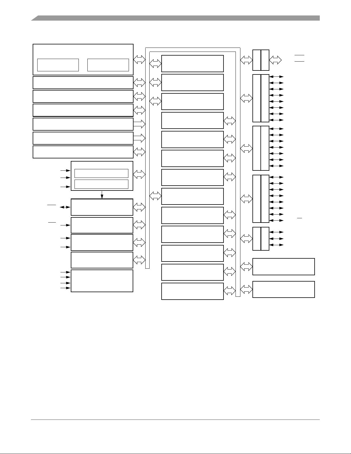
General Description
M68HC08 CPU
CPU
REGISTERS
CONTROL AND STATUS REGISTERS — 64 BYTES
USER FLASH — 15,872 BYTES
USER RAM — 1024 BYTES
MONITOR ROM — 350 BYTES
FLASH PROGRAMMING ROUTINES ROM — 406 BYTES
USER FLASH VECTOR SPACE — 44 BYTES
OSC1
OSC2
CGMXFC
(3)
RST
(3)
IRQ
V
DDAD/VREFH
V
DDAD/VREFL
V
DD
V
SS
V
DDA
V
SSA
ARITHMETIC/LOGIC
UNIT (ALU)
CLOCK GENERATOR MODULE
1–8 MHz OSCILLATOR
PHASE LOCKED LOOP
SYSTEM INTEGRATION
MODULE
SINGLE EXTERNAL
INTERRUPT MODULE
10-BIT ANALOG-TO-DIGITAL
CONVERTER MODULE
POWER-ON RESET
MODULE
POWER
INTERNAL BUS
PROGRAMMABLE TIMEBASE
MODULE
SINGLE BREAKPOINT
BREAK MODULE
DUAL VOLTAGE
LOW-VOLTAGE INHIBIT
MODULE
8-BIT KEYBOARD
INTERRUPT MODULE
2-CHANNEL TIMER
INTERFACE MODULE 1
2-CHANNEL TIMER
INTERFACE MODULE 2
ENHANCED SERIAL
COMUNICATIONS
INTERFACE MODULE
COMPUTER OPERATING
PROPERLY MODULE
SERIAL PERIPHERAL
INTERFACE MODULE
MONITOR MODULE
MEMORY MAP
MODULE
CONFIGURATION
REGISTER 1–2
MODULE
MSCAN08 MODULE
PTA7/KBD7–
DDRA
PORTA
PTA0/KBD0
PTB7/AD7
PTB6/AD6
PTB5/AD5
PTB4/AD4
DDRB
PORTB
PTB3/AD3
PTB2/AD2
PTB1/AD1
PTB0/AD0
PTC6
PTC5
PTC4
DDRC
PORTC
PTC3
PTC2
PTC1/CAN
PTC0/CAN
PTD7/T2CH1
PTD6/T2CH0
PTD5/T1CH1
PTD4/T1CH0
DDRD
PORTD
PTD3/SPSCK
PTD2/MOSI
PTD1/MISO
PTD0/SS
PTE5–PTE2
DDRE
PORTE
PTE1/RxD
PTE0/TxD
SECURITY
MODULE
MONITOR MODE ENTRY
MODULE
(1)
(1)
(1), (2)
(1), (2)
(1), (2)
(1)
(1), (2)
RX
(1), (2)
TX
(1)
(1)
(1)
(1)
(1)
(1)
(1)
(1)
1. Ports are software configurable with pullup device if input port.
2. Higher current drive port pins
3. Pin contains integrated pullup device
Figure 1-1. MCU Block Diagram
MC68HC908GZ16 • MC68HC908GZ8 Data Sheet, Rev. 2
24 Freescale Semiconductor
Page 25
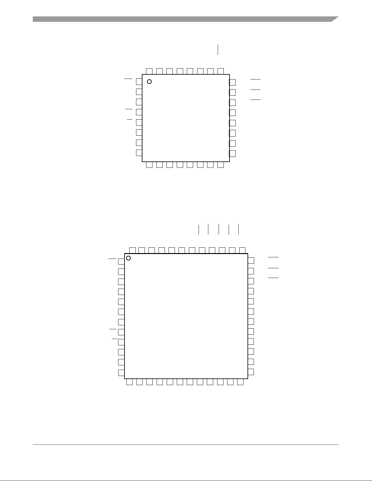
Pin Assignments
TX
OSC1
OSC2
SSAVDDA
CGMXFC
V
PTC1/CANRXPTC0/CAN
32
RST
PTE0/TxD
PTE1/RxD
IRQ
PTD0/SS
PTD1/MISO
PTD2/MOSI
PTD3/SPSCK
1
31
2
3
4
5
6
7
8
9
10
11
12
13
14
15
SS
DD
V
V
PTB0/AD0
PTD4/T1CH0
PTD5/T1CH1
PTD6/T2CH0
PTB1/AD1
26
27
28
29
30
Figure 1-2. 32-Pin LQFP Pin Assignments
RX
TX
PTA3/KBD3
25
24
23
22
21
20
19
18
17
16
PTB2/AD2
PTA2/KBD2
PTA1/KBD1
PTA0/KBD0
V
SSAD/VREFL
V
DDAD/VREFH
PTB5/AD5
PTB4/AD4
PTB3/AD3
RST
PTE0/TxD
PTE1/RxD
PTE2
PTE3
PTE4
PTE5
IRQ
PTD0/SS
PTD1/MISO
PTD2/MOSI
PTD3/SPSCK
OSC1
OSC2
48
1
47
2
3
4
5
6
7
8
9
10
11
12
14
13
SS
DD
V
V
SSAVDDA
CGMXFC
V
46
45
15
16
PTD5/T1CH1
PTD4/T1CH0
PTC1/CAN
44
43
17
18
PTD7/T2CH1
PTD6/T2CH0
PTC0/CAN
42
19
20
PTC3
PTC2
PTA6/KBD6
PTA7/KBD7
41
40
21
PTC4
PTA5/KBD5
39
22
PTB0/AD0
PTA3/KBD3
PTA4/KBD4
37
38
35
34
33
32
31
30
29
28
27
26
23
24
PTB1/AD1
PTB2/AD2
PTA2/KBD2
36
PTA1/KBD1
PTA0/KBD0
PTC6
PTC5
V
V
PTB7/AD7
PTB6/AD6
PTB5/AD5
PTB4/AD4
PTB3/AD3
25
SSAD/VREFL
DDAD/VREFH
Figure 1-3. 48-Pin LQFP Pin Assignments
MC68HC908GZ16 • MC68HC908GZ8 Data Sheet, Rev. 2
Freescale Semiconductor 25
Page 26
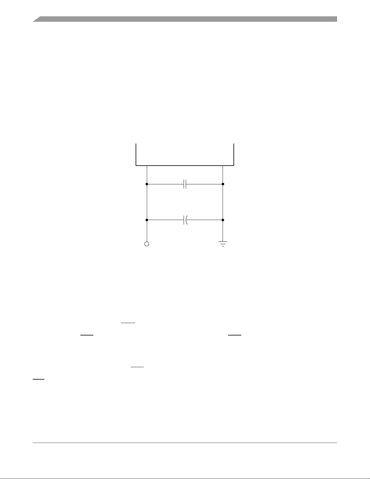
General Description
1.5 Pin Functions
Descriptions of the pin functions are provided here.
1.5.1 Power Supply Pins (VDD and VSS)
VDD and VSS are the power supply and ground pins. The MCU operates from a single power supply.
Fast signal transitions on MCU pins place high, short-duration current demands on the power supply. To
prevent noise problems, take special care to provide power supply bypassing at the MCU as Figure 1-4
shows. Place the C1 bypass capacitor as close to the MCU as possible. Use a high-frequency-response
ceramic capacitor for C1. C2 is an optional bulk current bypass capacitor for use in applications that
require the port pins to source high current levels.
MCU
V
DD
C1
0.1 µF
+
C2
V
DD
Note: Component values shown represent typical applications.
V
SS
Figure 1-4. Power Supply Bypassing
1.5.2 Oscillator Pins (OSC1 and OSC2)
OSC1 and OSC2 are the connections for an external crystal, resonator, or clock circuit. See Chapter 4
Clock Generator Module (CGM).
1.5.3 External Reset Pin (RST)
A logic 0 on the RST pin forces the MCU to a known startup state. RST is bidirectional, allowing a reset
of the entire system. It is driven low when any internal reset source is asserted. This pin contains an
internal pullup resistor. See Chapter 16 System Integration Module (SIM).
1.5.4 External Interrupt Pin (IRQ)
IRQ is an asynchronous external interrupt pin. This pin contains an internal pullup resistor. See
Chapter 8 External Interrupt (IRQ).
MC68HC908GZ16 • MC68HC908GZ8 Data Sheet, Rev. 2
26 Freescale Semiconductor
Page 27

Pin Functions
1.5.5 CGM Power Supply Pins (V
V
DDA
and V
are the power supply pins for the analog portion of the clock generator module (CGM).
SSA
DDA
and V
SSA
)
Decoupling of these pins should be as per the digital supply. See Chapter 4 Clock Generator Module
(CGM).
1.5.6 External Filter Capacitor Pin (V
CGMXFC
)
CGMXFC is an external filter capacitor connection for the CGM. See Chapter 4 Clock Generator Module
(CGM).
1.5.7 ADC Power Supply/Reference Pins (V
V
are the reference voltage pins for the ADC. V
the V
V
to the same voltage potential as V
and V
DDAD
DDAD/VREFH
is the low reference supply for the ADC, and by default the V
REFL
are the power supply pins to the analog-to-digital converter (ADC). V
SSAD
REFH
pin should be externally filtered and connected to the same voltage potential as VDD.
. See Chapter 3 Analog-to-Digital Converter (ADC).
SS
DDAD/VREFH
is the high reference supply for the ADC, and by default
and V
SSAD/VREFL
SSAD/VREFL
)
and V
REFH
pin should be connected
REFL
1.5.8 Port A Input/Output (I/O) Pins (PTA7/KBD7–PTA0/KBD0)
PTA7–PTA0 are general-purpose, bidirectional I/O port pins. Any or all of the port A pins can be
programmed to serve as keyboard interrupt pins. PTA7–PTA4 are only available on the 48-pin LQFP
package. See Chapter 13 Input/Output (I/O) Ports and Chapter 9 Keyboard Interrupt Module (KBI).
These port pins also have selectable pullups when configured for input mode. The pullups are disengaged
when configured for output mode. The pullups are selectable on an individual port bit basis.
1.5.9 Port B I/O Pins (PTB7/AD7–PTB0/AD0)
PTB7–PTB0 are general-purpose, bidirectional I/O port pins that can also be used for analog-to-digital
converter (ADC) inputs. PTB7–PTB4 are only available on the 48-pin LQFP package. See Chapter 13
Input/Output (I/O) Ports and Chapter 3 Analog-to-Digital Converter (ADC).
1.5.10 Port C I/O Pins (PTC6–PTC0/CANTX)
PTC6 and PTC5 are general-purpose, bidirectional I/O port pins. PTC4–PTC0 are general-purpose,
bidirectional I/O port pins that contain higher current sink/source capability. PTC6–PTC2 are only
available on the 48-pin LQFP package. See Chapter 13 Input/Output (I/O) Ports and Chapter 12
MSCAN08 Controller (MSCAN08).
PTC1 and PTC0 can be programmed to be MSCAN08 pins.
These port pins also have selectable pullups when configured for input mode. The pullups are disengaged
when configured for output mode. The pullups are selectable on an individual port bit basis.
1.5.11 Port D I/O Pins (PTD7/T2CH1–PTD0/SS)
PTD7–PTD0 are special-function, bidirectional I/O port pins. PTD3–PTD0 can be programmed to be
serial peripheral interface (SPI) pins, while PTD7–PTD4 can be individually programmed to be timer
interface module (TIM1 and TIM2) pins. PTD7 is only available on the 48-pin LQFP package. See Chapter
19 Timer Interface Module (TIM), Chapter 17 Serial Peripheral Interface (SPI) Module, and Chapter 13
Input/Output (I/O) Ports.
MC68HC908GZ16 • MC68HC908GZ8 Data Sheet, Rev. 2
Freescale Semiconductor 27
Page 28

General Description
These port pins also have selectable pullups when configured for input mode. The pullups are disengaged
when configured for output mode. The pullups are selectable on an individual port bit basis.
1.5.12 Port E I/O Pins (PTE5–PTE2, PTE1/RxD, and PTE0/TxD)
PTE5–PTE0 are general-purpose, bidirectional I/O port pins. PTE1 and PTE0 can also be programmed
to be enhanced serial communications interface (ESCI) pins. PTE5–PTE2 are only available on the
48-pin LQFP package. See Chapter 15 Enhanced Serial Communications Interface (ESCI) Module and
Chapter 13 Input/Output (I/O) Ports.
NOTE
Any unused inputs and I/O ports should be tied to an appropriate logic level
(either V
require termination, termination is recommended to reduce the possibility
of static damage.
or VSS). Although the I/O ports of the MC68HC908GZ16 do not
DD
MC68HC908GZ16 • MC68HC908GZ8 Data Sheet, Rev. 2
28 Freescale Semiconductor
Page 29

Chapter 2 Memory
2.1 Introduction
The CPU08 can address 64 Kbytes of memory space. The memory map, shown in Figure 2-1, includes:
• 15,872 bytes of user FLASH memory
• 1024 bytes of random-access memory (RAM)
• 406 bytes of FLASH programming routines read-only memory (ROM)
• 44 bytes of user-defined vectors
• 350 bytes of monitor ROM
2.2 Unimplemented Memory Locations
Accessing an unimplemented location can cause an illegal address reset. In the memory map
(Figure 2-1) and in register figures in this document, unimplemented locations are shaded.
2.3 Reserved Memory Locations
Accessing a reserved location can have unpredictable effects on microcontroller (MCU) operation. In the
Figure 2-1 and in register figures in this document, reserved locations are marked with the word Reserved
or with the letter R.
2.4 Input/Output (I/O) Section
Most of the control, status, and data registers are in the zero page area of $0000–$003F. Additional I/O
registers have these addresses:
• $FE00; break status register, SBSR
• $FE01; SIM reset status register, SRSR
• $FE02; break auxiliary register, BRKAR
• $FE03; break flag control register, BFCR
• $FE04; interrupt status register 1, INT1
• $FE05; interrupt status register 2, INT2
• $FE06; interrupt status register 3, INT3
• $FE07; reserved
• $FE08; FLASH control register, FLCR
• $FE09; break address register high, BRKH
• $FE0A; break address register low, BRKL
• $FE0B; break status and control register, BRKSCR
• $FE0C; LVI status register, LVISR
• $FF7E; FLASH block protect register, FLBPR
Data registers are shown in Figure 2-2. Table 2-1 is a list of vector locations.
MC68HC908GZ16 • MC68HC908GZ8 Data Sheet, Rev. 2
Freescale Semiconductor 29
Page 30
Memory
$0000
↓ $FE04 INTERRUPT STATUS REGISTER 1 (INT1)
$003F $FE05 INTERRUPT STATUS REGISTER 2 (INT2)
$0040
↓ $FE07 RESERVED
$043F $FE08 FLASH CONTROL REGISTER (FLCR)
$0440
↓ $FE0A BREAK ADDRESS REGISTER LOW (BRKL)
$04FF $FE0B BREAK STATUS AND CONTROL REGISTER (BRKSCR)
$0500
↓ $FE0D
$057F ↓
$0580
↓ $FE10
$1BFF ↓
$1C00
↓ $FE20
$1D95 ↓
$1D96
↓ $FF7E FLASH BLOCK PROTECT REGISTER (FLBPR)
$BFFF $FF7F
$C000
↓ $FFD3
$FDFF $FFD4
$FE00 BREAK STATUS REGISTER (BSR) ↓
$FE01 SIM RESET STATUS REGISTER (SRSR) $FFFF
$FE02 BREAK AUXILIARY REGISTER (BRKAR) 1. $FFF6–$FFFD used for eight security bytes
MSCAN08 CONTROL AND MESSAGE BUFFER
FLASH PROGRAMMING ROUTINES ROM
I/O REGISTERS
64 BYTES
RAM
1024 BYTES
UNIMPLEMENTED
192 BYTES
128 BYTES
UNIMPLEMENTED
5760 BYTES
406 BYTES
UNIMPLEMENTED
41,578 BYTES
FLASH MEMORY
15,872 BYTES
$FE03 BREAK FLAG CONTROL REGISTER (BFCR)
$FE06 INTERRUPT STATUS REGISTER 3 (INT3)
$FE09 BREAK ADDRESS REGISTER HIGH (BRKH)
$FE0C LVI STATUS REGISTER (LVISR)
UNIMPLEMENTED
3 BYTES
$FE0F
UNIMPLEMENTED
16 BYTES
RESERVED FOR COMPATIBILITY WITH MONITOR CODE
$FE1F
$FF7D
↓
(1)
FOR A-FAMILY PART
MONITOR ROM
350 BYTES
UNIMPLEMENTED
85 BYTES
FLASH VECTORS
44 BYTES
Figure 2-1. Memory Map
MC68HC908GZ16 • MC68HC908GZ8 Data Sheet, Rev. 2
30 Freescale Semiconductor
Page 31

Input/Output (I/O) Section
Addr.Register Name Bit 7654321Bit 0
Read:
Write:
(PTA)
Reset: Unaffected by reset
Read:
Write:
(PTB)
Reset: Unaffected by reset
Read: 1
Write:
(PTC)
Reset: Unaffected by reset
Read:
Write:
(PTD)
Reset: Unaffected by reset
Read:
Write:
Reset:00000000
Read:
Write:
Reset:00000000
Read: 0
Write:
Reset:00000000
Read:
Write:
Reset:00000000
Read: 0 0
Write:
(PTE)
Reset: Unaffected by reset
Read:
Write:
Reset:00000000
Read:
Write:
Reset:00000000
Read:
Write:
Reset:00000000
PTA7 PTA6 PTA5 PTA4 PTA3 PTA2 PTA1 PTA0
PTB7 PTB6 PTB5 PTB4 PTB3 PTB2 PTB1 PTB0
PTC6 PTC5 PTC4 PTC3 PTC2 PTC1 PTC0
PTD7 PTD6 PTD5 PTD4 PTD3 PTD2 PTD1 PTD0
DDRA7 DDRA6 DDRA5 DDRA4 DDRA3 DDRA2 DDRA1 DDRA0
DDRB7 DDRB6 DDRB5 DDRB4 DDRB3 DDRB2 DDRB1 DDRB0
DDRC6 DDRC5 DDRC4 DDRC3 DDRC2 DDRC1 DDRC0
DDRD7 DDRD6 DDRD5 DDRD4 DDRD3 DDRD2 DDRD1 DDRD0
PTE5 PTE4 PTE3 PTE2 PTE1 PTE0
PDS2 PDS1 PDS0 PSSB4 PSSB3 PSSB2 PSSB1 PSSB0
AM1
ARD7 ARD6 ARD5 ARD4 ARD3 ARD2 ARD1 ARD0
ALOST
AM0 ACLK
AFIN ARUN AOVFL ARD8
$0000
$0001
$0002
$0003
$0004
$0005
$0006
$0007
$0008
$0009
$000A
$000B
Port A Data Register
See page 160.
Port B Data Register
See page 162.
Port C Data Register
See page 164.
Port D Data Register
See page 166.
Data Direction Register A
(DDRA)
See page 160.
Data Direction Register B
(DDRB)
See page 163.
Data Direction Register C
(DDRC)
See page 164.
Data Direction Register D
(DDRD)
See page 167.
Port E Data Register
See page 169.
ESCI Prescaler Register
(SCPSC)
See page 208.
ESCI Arbiter Control
Register (SCIACTL)
See page 211.
ESCI Arbiter Data
Register (SCIADAT)
See page 212.
= Unimplemented R = Reserved U = Unaffected
Figure 2-2. Control, Status, and Data Registers (Sheet 1 of 8)
MC68HC908GZ16 • MC68HC908GZ8 Data Sheet, Rev. 2
Freescale Semiconductor 31
Page 32
Memory
Addr.Register Name Bit 7654321Bit 0
Data Direction Register E
$000C
Port A Input Pullup Enable
$000D
Port C Input Pullup Enable
$000E
Port D Input Pullup Enable
$000F
SPI Control Register (SPCR)
$0010
SPI Status and Control
$0011
$0012
ESCI Control Register 1
$0013
ESCI Control Register 2
$0014
ESCI Control Register 3
$0015
ESCI Status Register 1
$0016
ESCI Status Register 2
$0017
(DDRE)
See page 170.
Register (PTAPUE)
See page 161.
Register (PTCPUE)
See page 166.
Register (PTDPUE)
See page 168.
See page 249.
Register (SPSCR)
See page 251.
SPI Data Register
(SPDR)
See page 252.
(SCC1)
See page 198.
(SCC2)
See page 200.
(SCC3)
See page 202.
(SCS1)
See page 203.
(SCS2)
See page 205.
Read: 0 0
Write:
Reset:00000000
Read:
PTAPUE7 PTAPUE6 PTAPUE5 PTAPUE4 PTAPUE3 PTAPUE2 PTAPUE1 PTAPUE0
Write:
Reset:00000000
Read: 0
Write:
Reset:00000000
Read:
PTDPUE7 PTDPUE6 PTDPUE5 PTDPUE4 PTDPUE3 PTDPUE2 PTDPUE1 PTDPUE0
Write:
Reset:00000000
Read:
Write:
Reset:00101000
Read: SPRF
Write:
Reset:00001000
Read: R7 R6 R5 R4 R3 R2 R1 R0
Write: T7 T6 T5 T4 T3 T2 T1 T0
Reset: Unaffected by reset
Read:
Write:
Reset:00000000
Read:
Write:
Reset:00000000
Read: R8
Write:
Reset:U0000000
Read: SCTE TC SCRF IDLE OR NF FE PE
Write:
Reset:11000000
Read:
Write:
Reset:00000000
SPRIE R SPMSTR CPOL CPHA SPWOM SPE SPTIE
LOOPS ENSCI TXINV M WAKE ILTY PEN PTY
SCTIE TCIE SCRIE ILIE TE RE RWU SBK
PTCPUE6 PTCPUE5 PTCPUE4 PTCPUE3 PTCPUE2 PTCPUE1 PTCPUE0
ERRIE
T8 R R ORIE NEIE FEIE PEIE
DDRE5 DDRE4 DDRE3 DDRE2 DDRE1 DDRE0
OVRF MODF SPTE
MODFEN SPR1 SPR0
BKF RPF
= Unimplemented R = Reserved U = Unaffected
Figure 2-2. Control, Status, and Data Registers (Sheet 2 of 8)
MC68HC908GZ16 • MC68HC908GZ8 Data Sheet, Rev. 2
32 Freescale Semiconductor
Page 33
Input/Output (I/O) Section
Addr.Register Name Bit 7654321Bit 0
Read: R7 R6 R5 R4 R3 R2 R1 R0
Write: T7 T6 T5 T4 T3 T2 T1 T0
Reset: Unaffected by reset
Read:
Write:
LINT LINR SCP1 SCP0 R SCR2 SCR1 SCR0
Reset:00000000
Read: 0000KEYF 0
Write:
ACKK
IMASKK MODEK
Reset:00000000
Read:
Write:
KBIE7 KBIE6 KBIE5 KBIE4 KBIE3 KBIE2 KBIE1 KBIE0
Reset:00000000
Read: TBIF
Write:
TBR2 TBR1 TBR0
0
TACK
TBIE TBON R
Reset:00000000
Read: 0000IRQF0
Write:
ACK
IMASK MODE
Reset:00000000
Read: 0000
(1)
Write:
MSCANEN TMCLKSEL
OSCENIN-
STOP
ESCIBD-
SRC
$0018
$0019
$001A
$001B
$001C
$001D
$001E
ESCI Data Register
(SCDR)
See page 206.
ESCI Baud Rate Register
(SCBR)
See page 206.
Keyboard Status
and Control Register
(INTKBSCR)
See page 109.
Keyboard Interrupt Enable
Register (INTKBIER)
See page 110.
Timebase Module Control
Register (TBCR)
See page 256.
IRQ Status and Control
Register (INTSCR)
See page 104.
Configuration Register 2
(CONFIG2)
See page 81.
Reset:00000001
Configuration Register 1
$001F
(CONFIG1)
See page 82.
1
.
One-time writable register after each reset, except LVI5OR3 bit. LVI5OR3 bit is only reset via POR (power-on reset).
Read:
(1)
Write:
COPRS LVISTOP LVIRSTD LVIPWRD
Reset:00000000
LVI5OR3
(Note 1)
SSREC STOP COPD
$0020
$0021
$0022
$0023
Timer 1 Status and Control
Register (T1SC)
See page 267.
Timer 1 Counter
Register High (T1CNTH)
See page 268.
Timer 1 Counter
Register Low (T1CNTL)
See page 268.
Timer 1 Counter Modulo
Register High (T1MODH)
See page 269.
Read: TOF
Write: 0 TRST
TOIE TSTOP
Reset:00100000
Read: Bit 15 14 13 12 11 10 9 Bit 8
Write:
Reset:00000000
Read: Bit 7 654321Bit 0
Write:
Reset:00000000
Read:
Write:
Bit 15 14 13 12 11 10 9 Bit 8
Reset:11111111
00
PS2 PS1 PS0
= Unimplemented R = Reserved U = Unaffected
Figure 2-2. Control, Status, and Data Registers (Sheet 3 of 8)
MC68HC908GZ16 • MC68HC908GZ8 Data Sheet, Rev. 2
Freescale Semiconductor 33
Page 34
Memory
Addr.Register Name Bit 7654321Bit 0
Timer 1 Counter Modulo
$0024
$0025
$0026
$0027
$0028
$0029
$002A
$002B
$002C
$002D
$002E
$002F
Register Low (T1MODL)
Timer 1 Channel 0 Status and
Control Register (T1SC0)
Timer 1 Channel 0
Register High (T1CH0H)
Timer 1 Channel 0
Register Low (T1CH0L)
Timer 1 Channel 1 Status and
Control Register (T1SC1)
Timer 1 Channel 1
Register High (T1CH1H)
Timer 1 Channel 1
Register Low (T1CH1L)
Timer 2 Status and Control
Register High (T2CNTH)
Register Low (T2CNTL)
Timer 2 Counter Modulo
Register High (T2MODH)
Timer 2 Counter Modulo
Register Low (T2MODL)
See page 269.
See page 269.
See page 272.
See page 272.
See page 269.
See page 272.
See page 272.
Register (T2SC)
See page 267.
Timer 2 Counter
See page 268.
Timer 2 Counter
See page 268.
See page 269.
See page 269.
Read:
Write:
Reset:11111111
Read: CH0F
Write: 0
Reset:00000000
Read:
Write:
Reset: Indeterminate after reset
Read:
Write:
Reset: Indeterminate after reset
Read: CH1F
Write: 0
Reset:00000000
Read:
Write:
Reset: Indeterminate after reset
Read:
Write:
Reset: Indeterminate after reset
Read: TOF
Write: 0 TRST
Reset:00100000
Read: Bit 15 14 13 12 11 10 9 Bit 8
Write:
Reset:00000000
Read: Bit 7 654321Bit 0
Write:
Reset:00000000
Read:
Write:
Reset:11111111
Read:
Write:
Reset:11111111
Bit 7654321Bit 0
CH0IE MS0B MS0A ELS0B ELS0A TOV0 CH0MAX
Bit 15 14 13 12 11 10 9 Bit 8
Bit 7654321Bit 0
CH1IE
Bit 15 14 13 12 11 10 9 Bit 8
Bit 7654321Bit 0
TOIE TSTOP
Bit 15 14 13 12 11 10 9 Bit 8
Bit 7654321Bit 0
0
MS1A ELS1B ELS1A TOV1 CH1MAX
00
PS2 PS1 PS0
= Unimplemented R = Reserved U = Unaffected
Figure 2-2. Control, Status, and Data Registers (Sheet 4 of 8)
MC68HC908GZ16 • MC68HC908GZ8 Data Sheet, Rev. 2
34 Freescale Semiconductor
Page 35
Input/Output (I/O) Section
Addr.Register Name Bit 7654321Bit 0
Timer 2 Channel 0 Status and
$0030
$0031
$0032
$0033
$0034
$0035
$0036
$0037
$0038
$0039
$003A
$003B Reserved
Control Register (T2SC0)
See page 269.
Timer 2 Channel 0
Register High (T2CH0H)
See page 272.
Timer 2 Channel 0
Register Low (T2CH0L)
See page 272.
Timer 2 Channel 1 Status and
Control Register (T2SC1)
See page 269.
Timer 2 Channel 1
Register High (T2CH1H)
See page 272.
Timer 2 Channel 1
Register Low (T2CH1L)
See page 272.
PLL Control Register
(PCTL)
See page 71.
PLL Bandwidth Control
Register (PBWC)
See page 73.
PLL Multiplier Select High
Register (PMSH)
See page 74.
PLL Multiplier Select Low
Register (PMSL)
See page 75.
PLL VCO Select Range
Register (PMRS)
See page 75.
Read: CH0F
Write: 0
Reset:00000000
Read:
Write:
Reset: Indeterminate after reset
Read:
Write:
Reset: Indeterminate after reset
Read: CH1F
Write: 0
Reset:00000000
Read:
Write:
Reset: Indeterminate after reset
Read:
Write:
Reset: Indeterminate after reset
Read:
Write:
Reset:00100000
Read:
Write:
Reset:00000000
Read: 0000
Write:
Reset:00000000
Read:
Write:
Reset:0000UUUU
Read:
Write:
Reset:01000000
Read: 0000
Write:
Reset:00000001
Bit 15 14 13 12 11 10 9 Bit 8
Bit 7654321Bit 0
Bit 15 14 13 12 11 10 9 Bit 8
Bit 7654321Bit 0
PLLIE
AUTO
MUL7 MUL6 MUL5 MUL4 MUL3 MUL2 MUL1 MUL0
VRS7 VRS6 VRS5 VRS4 VRS3 VRS2 VRS1 VRS0
CH0IE MS0B MS0A ELS0B ELS0A TOV0 CH0MAX
CH1IE
PLLF
LOCK
0
PLLON BCS R R VPR1 VPR0
ACQ
MS1A ELS1B ELS1A TOV1 CH1MAX
0000
MUL11 MUL10 MUL9 MUL8
RRRR
R
= Unimplemented R = Reserved U = Unaffected
Figure 2-2. Control, Status, and Data Registers (Sheet 5 of 8)
MC68HC908GZ16 • MC68HC908GZ8 Data Sheet, Rev. 2
Freescale Semiconductor 35
Page 36
Memory
Addr.Register Name Bit 7654321Bit 0
Read:
Write:
Reset:00011111
Read: 000000AD9AD8
Write:
Reset: Unaffected by reset
Read: AD7 AD6 AD5 AD4 A3 AD2 AD1 AD0
Write:
Reset: Unaffected by reset
Read:
Write:
Reset:00000100
COCO AIEN ADCO ADCH4 ADCH3 ADCH2 ADCH1 ADCH0
ADIV2 ADIV1 ADIV0 ADICLK MODE1 MODE0 R
MSCAN08 control registers (9 bytes)
Refer to 12.13 Programmer’s Model of Control Registers
0
$003C
$003D
$003E
$003F
$0500
↓
$0508
$0509
↓
$050D
ADC Status and Control
Register (ADSCR)
See page 55.
ADC Data High Register
(ADRH)
See page 57.
ADC Data Low Register
(ADRL)
See page 57.
ADC Clock Register
(ADCLK)
See page 59.
MSCAN08 Control
Registers
See page 143.
Reserved Reserved (5 bytes)
$050E
↓
$050F
$0510
↓
$0517
$0518
↓
$053F
$0540
↓
$054F
$0550
↓
$055F
MSCAN08
Error Counters
MSCAN08
Identifier Filter
See page 143.
Reserved Reserved (40 bytes)
MSCAN08
Receive Buffer
See page 139.
MSCAN08 Transmit Buffer 0
See page 139.
MSCAN08 error counters (2 bytes)
MSCAN08 control registers (9 bytes)
Refer to 12.13 Programmer’s Model of Control Registers
MSC08 receive buffer
Refer to 12.12 Programmer’s Model of Message Storage
MSC08 transmitter buffer 0
Refer to 12.12 Programmer’s Model of Message Storage
= Unimplemented R = Reserved U = Unaffected
Figure 2-2. Control, Status, and Data Registers (Sheet 6 of 8)
MC68HC908GZ16 • MC68HC908GZ8 Data Sheet, Rev. 2
36 Freescale Semiconductor
Page 37

Input/Output (I/O) Section
Addr.Register Name Bit 7654321Bit 0
$0560
MSCAN08 Transmit Buffer 1
↓
$056F
$0570
MSCAN08 Transmit Buffer 2
↓
$057F
See page 139.
See page 139.
Refer to 12.12 Programmer’s Model of Message Storage
Refer to 12.12 Programmer’s Model of Message Storage
MSC08 transmitter buffer 1
MSC08 transmitter buffer 2
Break Status Register
$FE00
1. Writing a logic 0 clears SBSW.
SIM Reset Status Register
$FE01
$FE02 Reserved
Break Flag Control
$FE03
Interrupt Status Register 1
$FE04
Interrupt Status Register 2
$FE05
Interrupt Status Register 3
$FE06
$FE07 Reserved
$FE08
Break Address Register High
$FE09
Register (BFCR)
FLASH Control Register
(BSR)
See page 277.
(SRSR)
See page 230.
See page 277.
(INT1)
See page 182.
(INT2)
See page 182.
(INT3)
See page 182.
(FLCR)
See page 41.
(BRKH)
See page 276.
Read:
Write: (Note 1)
Reset:00000000
Read: POR PIN COP ILOP ILAD MODRST LVI 0
Write:
POR:10000000
Read:
Write:
Reset:00000000
Read:
Write:
Reset:00000000
Read: IF6 IF5 IF4 IF3 IF2 IF1 0 0
Write:RRRRRRRR
Reset:00000000
Read: IF14 IF13 IF12 IF11 IF10 IF9 IF8 IF7
Write:RRRRRRRR
Reset:00000000
Read: 0 0 IF20 IF19 IF18 IF17 IF16 IF15
Write:RRRRRRRR
Reset:00000000
Read:
Write:
Reset:00000000
Read: 0000
Write:
Reset:00000000
Read:
Write:
Reset:00000000
RRRRRR
RRRRRRRR
BCFERRRRRRR
RRRRRRRR
HVEN MASS ERASE PGM
Bit 15 14 13 12 11 10 9 Bit 8
SBSW
R
= Unimplemented R = Reserved U = Unaffected
Figure 2-2. Control, Status, and Data Registers (Sheet 7 of 8)
MC68HC908GZ16 • MC68HC908GZ8 Data Sheet, Rev. 2
Freescale Semiconductor 37
Page 38

Memory
Addr.Register Name Bit 7654321Bit 0
Break Address Register Low
$FE0A
Break Status and Control
$FE0B
$FE0C
$FF7E
3. Nonvolatile FLASH register
$FFFF
Register (BRKSCR)
LVI Status Register (LVISR)
FLASH Block Protect
Register (FLBPR)
COP Control Register
(BRKL)
See page 276.
See page 276.
See page 121.
See page 46.
(COPCTL)
See page 87.
Read:
Write:
Reset:00000000
Read:
Write:
Reset:00000000
Read: LVIOUT 0000000
Write:
Reset:00000000
Read:
(3)
Write:
Reset: Unaffected by reset
Read: Low byte of reset vector
Write: Writing clears COP counter (any value)
Reset: Unaffected by reset
Bit 7654321Bit 0
BRKE BRKA
BPR7 BPR6 BPR5 BPR4 BPR3 BPR2 BPR1 BPR0
000000
= Unimplemented R = Reserved U = Unaffected
Figure 2-2. Control, Status, and Data Registers (Sheet 8 of 8)
MC68HC908GZ16 • MC68HC908GZ8 Data Sheet, Rev. 2
38 Freescale Semiconductor
Page 39
Input/Output (I/O) Section
Table 2-1. Vector Addresses
.
Vector Priority Vector Address Vector
Lowest
Highest $FFFF Reset Vector (Low)
IF20
IF19
IF18
IF17
IF16
IF15
IF14
IF13
IF12
IF11
IF10
IF9
IF8
IF7
IF6
IF5
IF4
IF3
IF2
IF1
—
—
$FFD4 MSCAN08 Transmit Vector (High)
$FFD5 MSCAN08 Transmit Vector (Low)
$FFD6 MSCAN08 Receive Vector (High)
$FFD7 MSCAN08 Receive Vector (Low)
$FFD8 MSCAN08 Error Vector (High)
$FFD9 MSCAN08 Error Vector (Low)
$FFDA MSCAN08 Wakeup Vector (High)
$FFDB MSCAN08 Wakeup Vector (Low)
$FFDC Timebase Vector (High)
$FFDD Timebase Vector (Low)
$FFDE ADC Conversion Complete Vector (High)
$FFDF ADC Conversion Complete Vector (Low)
$FFE0 Keyboard Vector (High)
$FFE1 Keyboard Vector (Low)
$FFE2 ESCI Transmit Vector (High)
$FFE3 ESCI Transmit Vector (Low)
$FFE4 ESCI Receive Vector (High)
$FFE5 ESCI Receive Vector (Low)
$FFE6 ESCI Error Vector (High)
$FFE7 ESCI Error Vector (Low)
$FFE8 SPI Transmit Vector (High)
$FFE9 SPI Transmit Vector (Low)
$FFEA SPI Receive Vector (High)
$FFEB SPI Receive Vector (Low)
$FFEC TIM2 Overflow Vector (High)
$FFED TIM2 Overflow Vector (Low)
$FFEE TIM2 Channel 1 Vector (High)
$FFEF TIM2 Channel 1 Vector (Low)
$FFF0 TIM2 Channel 0 Vector (High)
$FFF1 TIM2 Channel 0 Vector (Low)
$FFF2 TIM1 Overflow Vector (High)
$FFF3 TIM1 Overflow Vector (Low)
$FFF4 TIM1 Channel 1 Vector (High)
$FFF5 TIM1 Channel 1 Vector (Low)
$FFF6 TIM1 Channel 0 Vector (High)
$FFF7 TIM1 Channel 0 Vector (Low)
$FFF8 PLL Vector (High)
$FFF9 PLL Vector (Low)
$FFFA IRQ
$FFFB IRQ Vector ( L ow )
$FFFC SWI Vector (High)
$FFFD SWI Vector (Low)
$FFFE Reset Vector (High)
Vector (High)
MC68HC908GZ16 • MC68HC908GZ8 Data Sheet, Rev. 2
Freescale Semiconductor 39
Page 40

Memory
2.5 Random-Access Memory (RAM)
Addresses $0040 through $043F are RAM locations. The location of the stack RAM is programmable.
The 16-bit stack pointer allows the stack to be anywhere in the 64-Kbyte memory space.
NOTE
For correct operation, the stack pointer must point only to RAM locations.
Within page zero are 192 bytes of RAM. Because the location of the stack RAM is programmable, all page
zero RAM locations can be used for I/O control and user data or code. When the stack pointer is moved
from its reset location at $00FF out of page zero, direct addressing mode instructions can efficiently
access all page zero RAM locations. Page zero RAM, therefore, provides ideal locations for frequently
accessed global variables.
Before processing an interrupt, the CPU uses five bytes of the stack to save the contents of the CPU
registers.
NOTE
For M6805 compatibility, the H register is not stacked.
During a subroutine call, the CPU uses two bytes of the stack to store the return address. The stack
pointer decrements during pushes and increments during pulls.
NOTE
Be careful when using nested subroutines. The CPU may overwrite data in
the RAM during a subroutine or during the interrupt stacking operation.
2.6 FLASH Memory (FLASH)
This subsection describes the operation of the embedded FLASH memory. This memory can be read,
programmed, and erased from a single external supply. The program, erase, and read operations are
enabled through the use of an internal charge pump. It is recommended that the user utilize the FLASH
programming routines provided in the on-chip ROM, which are described more fully in a separate
application note.
2.6.1 Functional Description
The FLASH memory is an array of 15,872 bytes with an additional 44 bytes of user vectors and one byte
of block protection. An erased bit reads as logic 1 and a programmed bit reads as a logic 0. Memory in
the FLASH array is organized into two rows per page basis. For the 16-K word by 8-bit embedded FLASH
memory, the page size is 64 bytes per page and the row size is 32 bytes per row. Hence the minimum
erase page size is 64 bytes and the minimum program row size is 32 bytes. Program and erase operation
operations are facilitated through control bits in FLASH control register (FLCR). Details for these
operations appear later in this section.
MC68HC908GZ16 • MC68HC908GZ8 Data Sheet, Rev. 2
40 Freescale Semiconductor
Page 41

FLASH Memory (FLASH)
The address ranges for the user memory and vectors are:
• $C000–$FDFF; user memory
•$FE08
; FLASH control register
• $FF7E; FLASH block protect register
• $FFD4–$FFFF; these locations are reserved for user-defined interrupt and reset vectors
Programming tools are available from Freescale Semiconductor. Contact your local representative for
more information.
NOTE
A security feature prevents viewing of the FLASH contents.
(1)
2.6.2 FLASH Control Register
The FLASH control register (FLCR) controls FLASH program and erase operations.
Address: $FE08
Bit 7654321Bit 0
Read:0000
Write:
Reset:00000000
= Unimplemented
Figure 2-3. FLASH Control Register (FLCR)
HVEN — High-Voltage Enable Bit
This read/write bit enables the charge pump to drive high voltages for program and erase operations
in the array. HVEN can only be set if either PGM = 1 or ERASE = 1 and the proper sequence for
program or erase is followed.
1 = High voltage enabled to array and charge pump on
0 = High voltage disabled to array and charge pump off
HVEN MASS ERASE PGM
MASS — Mass Erase Control Bit
Setting this read/write bit configures the 16-Kbyte FLASH array for mass erase operation.
1 = MASS erase operation selected
0 = PAGE erase operation selected
ERASE — Erase Control Bit
This read/write bit configures the memory for erase operation. ERASE is interlocked with the PGM bit
such that both bits cannot be equal to 1 or set to 1 at the same time.
1 = Erase operation selected
0 = Erase operation unselected
PGM — Program Control Bit
This read/write bit configures the memory for program operation. PGM is interlocked with the ERASE
bit such that both bits cannot be equal to 1 or set to 1 at the same time.
1 = Program operation selected
0 = Program operation unselected
1. No security feature is absolutely secure. However, Freescale’s strategy is to make reading or copying the FLASH difficult for
unauthorized users.
MC68HC908GZ16 • MC68HC908GZ8 Data Sheet, Rev. 2
Freescale Semiconductor 41
Page 42

Memory
2.6.3 FLASH Page Erase Operation
Use this step-by-step procedure to erase a page (64 bytes) of FLASH memory to read as logic 1. A page
consists of 64 consecutive bytes starting from addresses $XX00, $XX40, $XX80, or $XXC0. The 44-byte
user interrupt vectors area also forms a page. Any FLASH memory page can be erased alone.
1. Set the ERASE bit, and clear the MASS bit in the FLASH control register.
2. Read the FLASH block protect register.
3. Write any data to any FLASH location within the page address range of the block to be desired.
4. Wait for a time, t
5. Set the HVEN bit.
6. Wait for a time, t
7. Clear the ERASE bit.
8. Wait for a time, t
9. Clear the HVEN bit.
10. After a time, t
RCV
Programming and erasing of FLASH locations cannot be performed by
code being executed from FLASH memory. While these operations must be
performed in the order shown, other unrelated operations may occur
between the steps.
(minimum 10 µs)
NVS
(minimum 1 ms or 4 ms)
Erase
(minimum 5 µs)
NVH
(typical 1 µs), the memory can be accessed in read mode again.
NOTE
In applications that need more than 1000 program/erase cycles, use the 4-ms page erase specification
to get improved long-term reliability. Any application can use this 4-ms page erase specification.
However, in applications where a FLASH location will be erased and reprogrammed less than 1000 times,
and speed is important, use the 1-ms page erase specification to get a shorter cycle time.
MC68HC908GZ16 • MC68HC908GZ8 Data Sheet, Rev. 2
42 Freescale Semiconductor
Page 43

2.6.4 FLASH Mass Erase Operation
Use this step-by-step procedure to erase entire FLASH memory to read as logic 1:
1. Set both the ERASE bit, and the MASS bit in the FLASH control register.
2. Read from the FLASH block protect register.
3. Write any data to any FLASH address
4. Wait for a time, t
(minimum 10 µs)
NVS
5. Set the HVEN bit.
6. Wait for a time, t
MErase
(minimum 4 ms)
7. Clear the ERASE and MASS bits.
Mass erase is disabled whenever any block is protected (FLBPR does not
equal $FF).
(1)
within the FLASH memory address range.
NOTE
FLASH Memory (FLASH)
8. Wait for a time, t
(minimum 100 µs)
NVHL
9. Clear the HVEN bit.
10. After a time, t
(typical 1 µs), the memory can be accessed in read mode again.
RCV
NOTE
Programming and erasing of FLASH locations cannot be performed by
code being executed from FLASH memory. While these operations must be
performed in the order shown, other unrelated operations may occur
between the steps.
2.6.5 FLASH Program/Read Operation
Programming of the FLASH memory is done on a row basis. A row consists of 32 consecutive bytes
starting from addresses $XX00, $XX20, $XX40, $XX60, $XX80, $XXA0, $XXC0, and $XXE0.
During the programming cycle, make sure that all addresses being written to fit within one of the ranges
specified above. Attempts to program addresses in different row ranges in one programming cycle will
fail. Use this step-by-step procedure to program a row of FLASH memory (Figure 2-4 is a flowchart
representation).
NOTE
Only bytes which are currently $FF may be programmed.
1. Set the PGM bit. This configures the memory for program operation and enables the latching of
address and data for programming.
2. Read from the FLASH block protect register.
3. Write any data to any FLASH address within the row address range desired.
4. Wait for a time, t
5. Set the HVEN bit.
6. Wait for a time, t
7. Write data to the FLASH address to be programmed.
8. Wait for a time, t
9. Repeat step 7 and 8 until all the bytes within the row are programmed.
(minimum 10 µs).
NVS
(minimum 5 µs).
PGS
(minimum 30 µs).
PROG
1. When in monitor mode, with security sequence failed (see 20.3.2 Security), write to the FLASH block protect register instead
of any FLASH address.
MC68HC908GZ16 • MC68HC908GZ8 Data Sheet, Rev. 2
Freescale Semiconductor 43
Page 44

Memory
10. Clear the PGM bit.
11. Wait for a time, t
(1)
(minimum 5 µs).
NVH
12. Clear the HVEN bit.
13. After time, t
(typical 1 µs), the memory can be accessed in read mode again.
RCV
This program sequence is repeated throughout the memory until all data is programmed.
NOTE
Programming and erasing of FLASH locations can not be performed by
code being executed from the same FLASH array.
NOTE
While these operations must be performed in the order shown, other
unrelated operations may occur between the steps. Care must be taken
within the FLASH array memory space such as the COP control register
(COPCTL) at $FFFF.
NOTE
It is highly recommended that interrupts be disabled during program/ erase
operations.
NOTE
Do not exceed t
maximum or tHV maximum. tHV is defined as the
PROG
cumulative high voltage programming time to the same row before next
erase. t
must satisfy this condition:
HV
t
NVS
+ t
NVH
+ t
PGS
+ (t
x 32) ≤ tHV maximum
PROG
Refer to 21.15 Memory Characteristics.
NOTE
The time between programming the FLASH address change (step 7 to step
7), or the time between the last FLASH programmed to clearing the PGM
bit (step 7 to step 10) must not exceed the maximum programming time,
t
maximum.
PROG
CAUTION
Be cautious when programming the FLASH array to ensure that
non-FLASH locations are not used as the address that is written to when
selecting either the desired row address range in step 3 of the algorithm or
the byte to be programmed in step 7 of the algorithm. This applies
particularly to $FFD4–$FFDF.
MC68HC908GZ16 • MC68HC908GZ8 Data Sheet, Rev. 2
44 Freescale Semiconductor
Page 45

FLASH Memory (FLASH)
Algorithm for programming
a row (32 bytes) of FLASH memory
1
2
READ THE FLASH BLOCK PROTECT REGISTER
3
WRITE ANY DATA TO ANY FLASH ADDRESS
WITHIN THE ROW ADDRESS RANGE DESIRED
4
5
6
7
WRITE DATA TO THE FLASH ADDRESS
SET PGM BIT
WAIT FOR A TIME, t
SET HVEN BIT
WAIT FOR A TIME, t
TO BE PROGRAMMED
NVS
PGS
8
WAIT FOR A TIME, t
COMPLETED
PROGRAMMING
THIS ROW?
Note:
The time between each FLASH address change (step 7 to step 7),
or the time between the last FLASH address programmed
to clearing PGM bit (step 7 to step 10)
must not exceed the maximum programming
PROG
max.
time, t
This row program algorithm assumes the row/s
to be programmed are initially erased.
Figure 2-4. FLASH Programming Flowchart
PROG
Y
N
10
11
12
13
CLEAR PGM BIT
WAIT FOR A TIME, t
CLEAR HVEN BIT
WAIT FOR A TIME, t
END OF PROGRAMMING
NVH
RCV
MC68HC908GZ16 • MC68HC908GZ8 Data Sheet, Rev. 2
Freescale Semiconductor 45
Page 46

Memory
2.6.6 FLASH Block Protection
Due to the ability of the on-board charge pump to erase and program the FLASH memory in the target
application, provision is made for protecting a block of memory from unintentional erase or program
operations due to system malfunction. This protection is done by using of a FLASH block protect register
(FLBPR). The FLBPR determines the range of the FLASH memory which is to be protected. The range
of the protected area starts from a location defined by FLBPR and ends at the bottom of the FLASH
memory ($FFFF). When the memory is protected, the HVEN bit cannot be set in either ERASE or
PROGRAM operations.
NOTE
In performing a program or erase operation, the FLASH block protect
register must be read after setting the PGM or ERASE bit and before
asserting the HVEN bit
When the FLBPR is program with all 0’s, the entire memory is protected from being programmed and
erased. When all the bits are erased (all 1’s), the entire memory is accessible for program and erase.
When bits within the FLBPR are programmed, they lock a block of memory, address ranges as shown in
2.6.7 FLASH Block Protect Register. Once the FLBPR is programmed with a value other than $FF or $FE,
any erase or program of the FLBPR or the protected block of FLASH memory is prohibited. Mass erase
is disabled whenever any block is protected (FLBPR does not equal $FF). The presence of a V
pin will bypass the block protection so that all of the memory included in the block protect register is
IRQ
open for program and erase operations.
TST
on the
NOTE
The FLASH block protect register is not protected with special hardware or
software. Therefore, if this page is not protected by FLBPR the register is
erased by either a page or mass erase operation.
2.6.7 FLASH Block Protect Register
The FLASH block protect register (FLBPR) is implemented as a byte within the FLASH memory, and
therefore can only be written during a programming sequence of the FLASH memory. The value in this
register determines the starting location of the protected range within the FLASH memory.
Address: $FF7E
Bit 7654321Bit 0
Read:
Write:
Reset:UUUUUUUU
BPR[7:0] — FLASH Block Protect Bits
These eight bits represent bits [13:6] of a 16-bit memory address.
Bit 15 and Bit 14 are 1s and bits [5:0] are 0s.
BPR7 BPR6 BPR5 BPR4 BPR3 BPR2 BPR1 BPR0
U = Unaffected by reset. Initial value from factory is 1.
Write to this register is by a programming sequence to the FLASH memory.
Figure 2-5. FLASH Block Protect Register (FLBPR)
MC68HC908GZ16 • MC68HC908GZ8 Data Sheet, Rev. 2
46 Freescale Semiconductor
Page 47

FLASH Memory (FLASH)
The resultant 16-bit address is used for specifying the start address of the FLASH memory for block
protection. The FLASH is protected from this start address to the end of FLASH memory, at $FFFF.
With this mechanism, the protect start address can be $XX00, $XX40, $XX80, and $XXC0 (64 bytes
page boundaries) within the FLASH memory.
16-BIT MEMORY ADDRESS
START ADDRESS OF FLASH
BLOCK PROTECT
1
1
FLBPR VALUE
000000
Figure 2-6. FLASH Block Protect Start Address
Table 2-2. Examples of Protect Address Ranges
BPR[7:0] Addresses of Protect Range
$00 The entire FLASH memory is protected.
$01 (0000 0001)$C040 (1100 0000 0100 0000) — $FFFF
$02 (0000 0010)$C080 (1100 0000 1000 0000) — $FFFF
$03 (0000 0011) $C0C0 (1100 0000 1100 0000) — $FFFF
$04 (0000 0100)$C100 (1100 0001 0000 0000) — $FFFF
and so on...
$FC (1111 1100) $FF00 (1111 1111 0000 0000) — FFFF
$FD (1111 1101)
$FE (1111 1110)
$FF The entire FLASH memory is not protected.
$FF40 (1111 1111 0100 0000) — $FFFF
FLBPR and vectors are protected
$FF80 (1111 1111 1000 0000) — FFFF
Vectors are protected
2.6.8 Wait Mode
Putting the MCU into wait mode while the FLASH is in read mode does not affect the operation of the
FLASH memory directly, but there will not be any memory activity since the CPU is inactive.
The WAIT instruction should not be executed while performing a program or erase operation on the
FLASH, otherwise the operation will discontinue, and the FLASH will be on standby mode.
2.6.9 Stop Mode
Putting the MCU into stop mode while the FLASH is in read mode does not affect the operation of the
FLASH memory directly, but there will not be any memory activity since the CPU is inactive.
The STOP instruction should not be executed while performing a program or erase operation on the
FLASH, otherwise the operation will discontinue, and the FLASH will be on standby mode
NOTE
Standby mode is the power saving mode of the FLASH module in which all
internal control signals to the FLASH are inactive and the current
consumption of the FLASH is at a minimum.
MC68HC908GZ16 • MC68HC908GZ8 Data Sheet, Rev. 2
Freescale Semiconductor 47
Page 48

Memory
MC68HC908GZ16 • MC68HC908GZ8 Data Sheet, Rev. 2
48 Freescale Semiconductor
Page 49

Chapter 3 Analog-to-Digital Converter (ADC)
3.1 Introduction
This section describes the 10-bit analog-to-digital converter (ADC).
3.2 Features
Features of the ADC module include:
• Eight channels with multiplexed input
• Linear successive approximation with monotonicity
• 10-bit resolution
• Single or continuous conversion
• Conversion complete flag or conversion complete interrupt
• Selectable ADC clock
• Left or right justified result
• Left justified sign data mode
3.3 Functional Description
The ADC provides eight pins for sampling external sources at pins PTB7/AD7–PTB0/AD0. An analog
multiplexer allows the single ADC converter to select one of eight ADC channels as ADC voltage in
ADIN
). V
(V
When the conversion is completed, ADC places the result in the ADC data register and sets a flag or
generates an interrupt. See Figure 3-2.
is converted by the successive approximation register-based analog-to-digital converter.
ADIN
3.3.1 ADC Port I/O Pins
PTB7/AD7–PTB0/AD0 are general-purpose I/O (input/output) pins that share with the ADC channels. The
channel select bits define which ADC channel/port pin will be used as the input signal. The ADC overrides
the port I/O logic by forcing that pin as input to the ADC. The remaining ADC channels/port pins are
controlled by the port I/O logic and can be used as general-purpose I/O. Writes to the port register or data
direction register (DDR) will not have any affect on the port pin that is selected by the ADC. Read of a port
pin in use by the ADC will return a logic 0.
MC68HC908GZ16 • MC68HC908GZ8 Data Sheet, Rev. 2
Freescale Semiconductor 49
Page 50
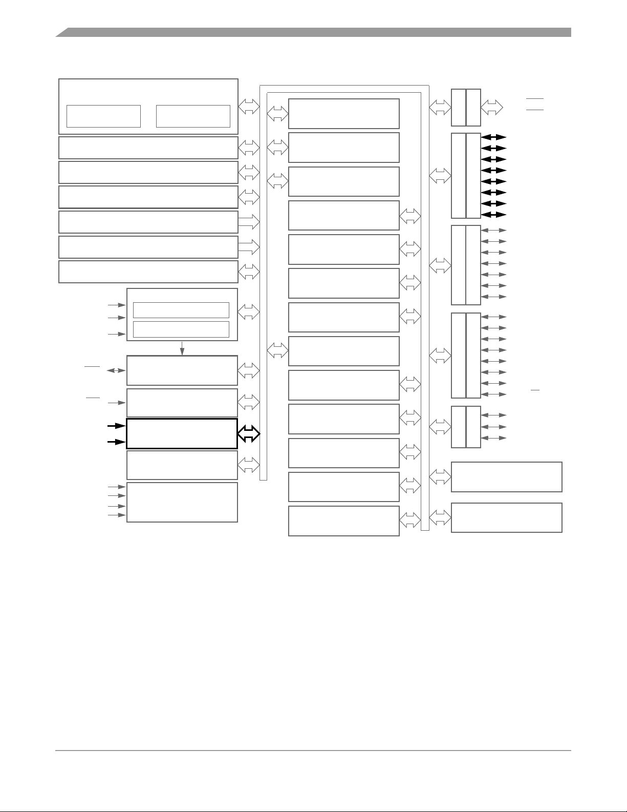
Analog-to-Digital Converter (ADC)
M68HC08 CPU
CPU
REGISTERS
CONTROL AND STATUS REGISTERS — 64 BYTES
USER FLASH — 15,872 BYTES
USER RAM — 1024 BYTES
MONITOR ROM — 350 BYTES
FLASH PROGRAMMING ROUTINES ROM — 406 BYTES
USER FLASH VECTOR SPACE — 44 BYTES
OSC1
OSC2
CGMXFC
(3)
RST
(3)
IRQ
V
DDAD/VREFH
V
DDAD/VREFL
V
DD
V
SS
V
DDA
V
SSA
ARITHMETIC/LOGIC
UNIT (ALU)
CLOCK GENERATOR MODULE
1–8 MHz OSCILLATOR
PHASE LOCKED LOOP
SYSTEM INTEGRATION
MODULE
SINGLE EXTERNAL
INTERRUPT MODULE
10-BIT ANALOG-TO-DIGITAL
CONVERTER MODULE
POWER-ON RESET
MODULE
POWER
INTERNAL BUS
PROGRAMMABLE TIMEBASE
MODULE
SINGLE BREAKPOINT
BREAK MODULE
DUAL VOLTAGE
LOW-VOLTAGE INHIBIT
MODULE
8-BIT KEYBOARD
INTERRUPT MODULE
2-CHANNEL TIMER
INTERFACE MODULE 1
2-CHANNEL TIMER
INTERFACE MODULE 2
ENHANCED SERIAL
COMUNICATIONS
INTERFACE MODULE
COMPUTER OPERATING
PROPERLY MODULE
SERIAL PERIPHERAL
INTERFACE MODULE
MONITOR MODULE
MEMORY MAP
MODULE
CONFIGURATION
REGISTER 1–2
MODULE
MSCAN08 MODULE
PTA7/KBD7–
DDRA
PORTA
PTA0/KBD0
PTB7/AD7
PTB6/AD6
PTB5/AD5
PTB4/AD4
DDRB
PORTB
PTB3/AD3
PTB2/AD2
PTB1/AD1
PTB0/AD0
PTC6
PTC5
PTC4
DDRC
PORTC
PTC3
PTC2
PTC1/CAN
PTC0/CAN
PTD7/T2CH1
PTD6/T2CH0
PTD5/T1CH1
PTD4/T1CH0
DDRD
PORTD
PTD3/SPSCK
PTD2/MOSI
PTD1/MISO
PTD0/SS
PTE5–PTE2
DDRE
PORTE
PTE1/RxD
PTE0/TxD
SECURITY
MODULE
MONITOR MODE ENTRY
MODULE
(1)
(1)
(1), (2)
(1), (2)
(1), (2)
(1)
(1), (2)
RX
(1), (2)
TX
(1)
(1)
(1)
(1)
(1)
(1)
(1)
(1)
1. Ports are software configurable with pullup device if input port.
2. Higher current drive port pins
3. Pin contains integrated pullup device
Figure 3-1. Block Diagram Highlighting ADC Block and Pins
MC68HC908GZ16 • MC68HC908GZ8 Data Sheet, Rev. 2
50 Freescale Semiconductor
Page 51

INTERNAL
DATA BUS
Functional Description
READ DDRBx
WRITE DDRBx
WRITE PTBx
READ PTBx
INTERRUPT
LOGIC
AIEN COCO
RESET
CONVERSION
COMPLETE
CGMXCLK
BUS CLOCK
DDRBx
PTBx
ADC DATA REGISTER
ADC
ADC CLOCK
CLOCK
GENERATOR
DISABLE
ADC
VOLTAGE IN
)
(V
ADIN
DISABLE
CHANNEL
SELECT
PTBx
ADC CHANNEL x
ADCH4–ADCH0
ADIV2–ADIV0 ADICLK
Figure 3-2. ADC Block Diagram
3.3.2 Voltage Conversion
When the input voltage to the ADC equals V
input voltage equals V
straight-line linear conversion.
The ADC input voltage must always be greater than V
V
DDAD
Connect the V
connect the V
The V
, the ADC converts it to $000. Input voltages between V
REFL
.
pin to the same voltage potential as the VDD pin, and
DDAD
pin to the same voltage potential as the VSS pin.
SSAD
pin should be routed carefully for maximum noise immunity.
DDAD
MC68HC908GZ16 • MC68HC908GZ8 Data Sheet, Rev. 2
, the ADC converts the signal to $3FF (full scale). If the
REFH
and V
REFH
NOTE
and less than
SSAD
REFL
are a
Freescale Semiconductor 51
Page 52

Analog-to-Digital Converter (ADC)
3.3.3 Conversion Time
Conversion starts after a write to the ADC status and control register (ADSCR). One conversion will take
between 16 and 17 ADC clock cycles. The ADIVx and ADICLK bits should be set to provide a 1-MHz ADC
clock frequency.
Conversion time =
16 to 17 ADC cycles
ADC frequency
Number of bus cycles = conversion time × bus frequency
3.3.4 Conversion
In continuous conversion mode, the ADC data register will be filled with new data after each conversion.
Data from the previous conversion will be overwritten whether that data has been read or not.
Conversions will continue until the ADCO bit is cleared. The COCO bit is set after each conversion and
will stay set until the next read of the ADC data register.
In single conversion mode, conversion begins with a write to the ADSCR. Only one conversion occurs
between writes to the ADSCR.
When a conversion is in process and the ADCSCR is written, the current conversion data should be
discarded to prevent an incorrect reading.
3.3.5 Accuracy and Precision
The conversion process is monotonic and has no missing codes.
3.3.6 Result Justification
The conversion result may be formatted in four different ways:
1. Left justified
2. Right justified
3. Left Justified sign data mode
4. 8-bit truncation mode
All four of these modes are controlled using MODE0 and MODE1 bits located in the ADC clock register
(ADCLK).
Left justification will place the eight most significant bits (MSB) in the corresponding ADC data register
high, ADRH. This may be useful if the result is to be treated as an 8-bit result where the two least
significant bits (LSB), located in the ADC data register low, ADRL, can be ignored. However, ADRL must
be read after ADRH or else the interlocking will prevent all new conversions from being stored.
Right justification will place only the two MSBs in the corresponding ADC data register high, ADRH, and
the eight LSBs in ADC data register low, ADRL. This mode of operation typically is used when a 10-bit
unsigned result is desired.
Left justified sign data mode is similar to left justified mode with one exception. The MSB of the 10-bit
result, AD9 located in ADRH, is complemented. This mode of operation is useful when a result,
represented as a signed magnitude from mid-scale, is needed. Finally, 8-bit truncation mode will place
the eight MSBs in the ADC data register low, ADRL. The two LSBs are dropped. This mode of operation
MC68HC908GZ16 • MC68HC908GZ8 Data Sheet, Rev. 2
52 Freescale Semiconductor
Page 53

Monotonicity
is used when compatibility with 8-bit ADC designs are required. No interlocking between ADRH and ADRL
is present.
NOTE
Quantization error is affected when only the most significant eight bits are
used as a result. See Figure 3-3.
8-BIT
RESULT
003
10-BIT
RESULT
00B
00A
009
IDEAL 8-BIT CHARACTERISTIC
WITH QUANTIZATION = ±1/2
10-BIT TRUNCATED
TO 8-BIT RESULT
IDEAL 10-BIT CHARACTERISTIC
WITH QUANTIZATION = ±1/2
002
001
000
008
007
006
005
004
003
002
001
000
1/2 2 1/2 4 1/2 6 1/2 8 1/2
1 1/2 3 1/2 5 1/2 7 1/2 9 1/2
1/2 2 1/21 1/2
WHEN TRUNCATION IS USED,
ERROR FROM IDEAL 8-BIT = 3/8 LSB
DUE TO NON-IDEAL QUANTIZATION.
Figure 3-3. Bit Truncation Mode Error
3.4 Monotonicity
The conversion process is monotonic and has no missing codes.
3.5 Interrupts
INPUT VOLTAGE
REPRESENTED AS 10-BIT
INPUT VOLTAGE
REPRESENTED AS 8-BIT
When the AIEN bit is set, the ADC module is capable of generating CPU interrupts after each ADC
conversion. A CPU interrupt is generated if the COCO bit is at logic 0. The COCO bit is not used as a
conversion complete flag when interrupts are enabled.
3.6 Low-Power Modes
The WAIT and STOP instruction can put the MCU in low power-consumption standby modes.
MC68HC908GZ16 • MC68HC908GZ8 Data Sheet, Rev. 2
Freescale Semiconductor 53
Page 54

Analog-to-Digital Converter (ADC)
3.6.1 Wait Mode
The ADC continues normal operation during wait mode. Any enabled CPU interrupt request from the ADC
can bring the MCU out of wait mode. If the ADC is not required to bring the MCU out of wait mode, power
down the ADC by setting ADCH4–ADCH0 bits in the ADC status and control register before executing the
WAIT instruction.
3.6.2 Stop Mode
The ADC module is inactive after the execution of a STOP instruction. Any pending conversion is aborted.
ADC conversions resume when the MCU exits stop mode after an external interrupt. Allow one
conversion cycle to stabilize the analog circuitry.
3.7 I/O Signals
The ADC module has eight pins shared with port B, PTB7/AD7–PTB0/AD0.
3.7.1 ADC Analog Power Pin (V
The ADC analog portion uses V
potential as V
. External filtering may be necessary to ensure clean V
DD
DDAD
)
DDAD
as its power pin. Connect the V
pin to the same voltage
DDAD
for good results.
DDAD
NOTE
For maximum noise immunity, route V
carefully and place bypass
DDAD
capacitors as close as possible to the package.
DDAD
and V
V
3.7.2 ADC Analog Ground Pin (V
The ADC analog portion uses V
potential as V
are double-bonded on the MC68HC908GZ16.
REFH
)
SSAD
as its ground pin. Connect the V
SSAD
.
SS
pin to the same voltage
SSAD
NOTE
Route V
V
SSAD
and V
are double-bonded on the MC68HC908GZ16.
REFL
3.7.3 ADC Voltage Reference High Pin (V
The ADC analog portion uses V
pin to the same voltage potential as V
REFH
cleanly to avoid any offset errors.
SSAD
)
REFH
as its upper voltage reference pin. By default, connect the V
. External filtering is often necessary to ensure a clean V
DD
REFH
REFH
good results. Any noise present on this pin will be reflected and possibly magnified in A/D conversion
values.
for
NOTE
For maximum noise immunity, route V
capacitors as close as possible to the package. Routing V
parallel to V
DDAD
and V
V
54 Freescale Semiconductor
are double-bonded on the MC68HC908GZ16.
REFH
may improve common mode noise rejection.
REFL
MC68HC908GZ16 • MC68HC908GZ8 Data Sheet, Rev. 2
carefully and place bypass
REFH
REFH
close and
Page 55

I/O Registers
3.7.4 ADC Voltage Reference Low Pin (V
The ADC analog portion uses V
to the same voltage potential as V
as its lower voltage reference pin. By default, connect the V
REFL
. External filtering is often necessary to ensure a clean V
SS
REFL
)
pin
REFH
for good
REFL
results. Any noise present on this pin will be reflected and possibly magnified in A/D conversion values.
NOTE
For maximum noise immunity, route V
to V
Routing V
, place bypass capacitors as close as possible to the package.
SS
close and parallel to V
REFH
carefully and, if not connected
REFL
may improve common mode
REFL
noise rejection.
V
3.7.5 ADC Voltage In (V
V
and V
SSAD
is the input voltage signal from one of the eight ADC channels to the ADC module.
ADIN
are double-bonded on the MC68HC908GZ16.
REFL
)
ADIN
3.8 I/O Registers
These I/O registers control and monitor ADC operation:
• ADC status and control register (ADSCR)
• ADC data register (ADRH and ADRL)
• ADC clock register (ADCLK)
3.8.1 ADC Status and Control Register
Function of the ADC status and control register (ADSCR) is described here.
Address: $003C
Bit 7654321Bit 0
Read:
Write:
Reset:00011111
COCO — Conversions Complete Bit
In non-interrupt mode (AIEN = 0), COCO is a read-only bit that is set at the end of each conversion.
COCO will stay set until cleared by a read of the ADC data register. Reset clears this bit.
In interrupt mode (AIEN = 1), COCO is a read-only bit that is not set at the end of a conversion. It
always reads as a logic 0.
1 = Conversion completed (AIEN = 0)
0 = Conversion not completed (AIEN = 0) or CPU interrupt enabled (AIEN = 1)
AIEN — ADC Interrupt Enable Bit
When this bit is set, an interrupt is generated at the end of an ADC conversion. The interrupt signal is
cleared when the data register is read or the status/control register is written. Reset clears the AIEN bit.
1 = ADC interrupt enabled
0 = ADC interrupt disabled
COCO AIEN ADCO ADCH4 ADCH3 ADCH2 ADCH1 ADCH0
Figure 3-4. ADC Status and Control Register (ADSCR)
MC68HC908GZ16 • MC68HC908GZ8 Data Sheet, Rev. 2
Freescale Semiconductor 55
Page 56
Analog-to-Digital Converter (ADC)
ADCO — ADC Continuous Conversion Bit
When set, the ADC will convert samples continuously and update the ADR register at the end of each
conversion. Only one conversion is completed between writes to the ADSCR when this bit is cleared.
Reset clears the ADCO bit.
1 = Continuous ADC conversion
0 = One ADC conversion
ADCH4–ADCH0 — ADC Channel Select Bits
ADCH4–ADCH0 form a 5-bit field which is used to select one of 16 ADC channels. Only eight
channels, AD7–AD0, are available on this MCU. The channels are detailed in Table 3-1. Care should
be taken when using a port pin as both an analog and digital input simultaneously to prevent switching
noise from corrupting the analog signal. See Table 3-1.
The ADC subsystem is turned off when the channel select bits are all set to 1. This feature allows for
reduced power consumption for the MCU when the ADC is not being used.
NOTE
Recovery from the disabled state requires one conversion cycle to stabilize.
The voltage levels supplied from internal reference nodes, as specified in
Table 3-1, are used to verify the operation of the ADC converter both in production test and for user
applications.
Table 3-1. Mux Channel Select
(1)
ADCH4 ADCH3 ADCH2 ADCH1 ADCH0 Input Select
00000 PTB0/AD0
00001 PTB1/AD1
00010 PTB2/AD2
00011 PTB3/AD3
00100 PTB4/AD4
00101 PTB5/AD5
00110 PTB6/AD6
00111 PTB7/AD7
01000
Unused↓↓↓↓↓
11100
11101
11110
11111 ADC power off
1. If any unused channels are selected, the resulting ADC conversion will be unknown or
reserved.
V
V
REFH
REFL
MC68HC908GZ16 • MC68HC908GZ8 Data Sheet, Rev. 2
56 Freescale Semiconductor
Page 57

I/O Registers
3.8.2 ADC Data Register High and Data Register Low
3.8.2.1 Left Justified Mode
In left justified mode, the ADRH register holds the eight MSBs of the 10-bit result. The only difference from
left justified mode is that the AD9 is complemented. The ADRL register holds the two LSBs of the 10-bit
result. All other bits read as 0. ADRH and ADRL are updated each time an ADC single channel conversion
completes. Reading ADRH latches the contents of ADRL until ADRL is read. All subsequent results will
be lost until the ADRH and ADRL reads are completed.
Address: $003D ADRH
Bit 7654321Bit 0
Read: AD9 AD8 AD7 AD6 AD5 AD4 AD3 AD2
Write:
Reset: Unaffected by reset
Address: $003E ADRL
Read:AD1AD0000000
Write:
Reset: Unaffected by reset
= Unimplemented
Figure 3-5. ADC Data Register High (ADRH) and Low (ADRL)
3.8.2.2 Right Justified Mode
In right justified mode, the ADRH register holds the two MSBs of the 10-bit result. All other bits read as 0.
The ADRL register holds the eight LSBs of the 10-bit result. ADRH and ADRL are updated each time an
ADC single channel conversion completes. Reading ADRH latches the contents of ADRL until ADRL is
read. All subsequent results will be lost until the ADRH and ADRL reads are completed.
Address: $003D ADRH
Bit 7654321Bit 0
Read:000000AD9AD8
Write:
Reset: Unaffected by reset
Address: $003E ADRL
Read: AD7 AD6 AD5 AD4 AD3 AD2 AD1 AD0
Write:
Reset: Unaffected by reset
= Unimplemented
Figure 3-6. ADC Data Register High (ADRH) and Low (ADRL)
MC68HC908GZ16 • MC68HC908GZ8 Data Sheet, Rev. 2
Freescale Semiconductor 57
Page 58
Analog-to-Digital Converter (ADC)
3.8.2.3 Left Justified Signed Data Mode
In left justified signed data mode, the ADRH register holds the eight MSBs of the 10-bit result. The only
difference from left justified mode is that the AD9 is complemented. The ADRL register holds the two
LSBs of the 10-bit result. All other bits read as 0. ADRH and ADRL are updated each time an ADC single
channel conversion completes. Reading ADRH latches the contents of ADRL until ADRL is read. All
subsequent results will be lost until the ADRH and ADRL reads are completed.
Address: $003D
Bit 7654321Bit 0
Read: AD9
Write:
Reset: Unaffected by reset
Address: $003E
Read:AD1AD0000000
Write:
Reset: Unaffected by reset
AD8 AD7 AD6 AD5 AD4 AD3 AD2
= Unimplemented
Figure 3-7. ADC Data Register High (ADRH) and Low (ADRL)
3.8.2.4 Eight Bit Truncation Mode
In 8-bit truncation mode, the ADRL register holds the eight MSBs of the 10-bit result. The ADRH register
is unused and reads as 0. The ADRL register is updated each time an ADC single channel conversion
completes. In 8-bit mode, the ADRL register contains no interlocking with ADRH.
Address: $003D ADRH
Bit 7654321Bit 0
Read:00000000
Write:
Reset: Unaffected by reset
Address: $003E ADRL
Read: AD9 AD8 AD7 AD6 AD5 AD4 AD3 AD2
Write:
Reset: Unaffected by reset
= Unimplemented
Figure 3-8. ADC Data Register High (ADRH) and Low (ADRL)
MC68HC908GZ16 • MC68HC908GZ8 Data Sheet, Rev. 2
58 Freescale Semiconductor
Page 59
I/O Registers
3.8.3 ADC Clock Register
The ADC clock register (ADCLK) selects the clock frequency for the ADC.
Address: $003F
Bit 7654321Bit 0
Read:
Write:
Reset:00000100
ADIV2 ADIV1 ADIV0 ADICLK MODE1 MODE0 R
= Unimplemented R = Reserved
Figure 3-9. ADC Clock Register (ADCLK)
ADIV2–ADIV0 — ADC Clock Prescaler Bits
ADIV2–ADIV0 form a 3-bit field which selects the divide ratio used by the ADC to generate the internal
ADC clock. Table 3-2 shows the available clock configurations. The ADC clock should be set to
approximately 1 MHz.
Table 3-2. ADC Clock Divide Ratio
ADIV2 ADIV1 ADIV0 ADC Clock Rate
0 0 0 ADC input clock ÷ 1
0 0 1 ADC input clock ÷ 2
0 1 0 ADC input clock ÷ 4
0 1 1 ADC input clock ÷ 8
1
(1)
X
(1)
X
ADC input clock ÷ 16
0
1. X = Don’t care
ADICLK — ADC Input Clock Select Bit
ADICLK selects either the bus clock or the oscillator output clock (CGMXCLK) as the input clock
source to generate the internal ADC clock. Reset selects CGMXCLK as the ADC clock source.
1 = Internal bus clock
0 = Oscillator output clock (CGMXCLK)
The ADC requires a clock rate of approximately 1 MHz for correct operation. If the selected clock source
is not fast enough, the ADC will generate incorrect conversions. See 21.10 5.0-Volt ADC Characteristics.
f
ADIC
=
f
CGMXCLK
or bus frequency
≅ 1 MHz
ADIV[2:0]
MODE1 and MODE0 — Modes of Result Justification Bits
MODE1 and MODE0 select among four modes of operation. The manner in which the ADC conversion
results will be placed in the ADC data registers is controlled by these modes of operation. Reset returns
right-justified mode.
00 = 8-bit truncation mode
01 = Right justified mode
10 = Left justified mode
11 = Left justified signed data mode
MC68HC908GZ16 • MC68HC908GZ8 Data Sheet, Rev. 2
Freescale Semiconductor 59
Page 60

Analog-to-Digital Converter (ADC)
MC68HC908GZ16 • MC68HC908GZ8 Data Sheet, Rev. 2
60 Freescale Semiconductor
Page 61

Chapter 4 Clock Generator Module (CGM)
4.1 Introduction
This section describes the clock generator module. The CGM generates the crystal clock signal,
CGMXCLK, which operates at the frequency of the crystal. The CGM also generates the base clock
signal, CGMOUT, which is based on either the crystal clock divided by two or the phase-locked loop (PLL)
clock, CGMVCLK, divided by two. In user mode, CGMOUT is the clock from which the SIM derives the
system clocks, including the bus clock, which is at a frequency of CGMOUT/2. The PLL is a fully functional
frequency generator designed for use with crystals or ceramic resonators. The PLL can generate a
maximum bus frequency of 8 MHz using a 1-8MHz crystal or external clock source.
4.2 Features
Features of the CGM include:
• Phase-locked loop with output frequency in integer multiples of an integer dividend of the crystal
reference
• High-frequency crystal operation with low-power operation and high-output frequency resolution
• Programmable hardware voltage-controlled oscillator (VCO) for low-jitter operation
• Automatic bandwidth control mode for low-jitter operation
• Automatic frequency lock detector
• CPU interrupt on entry or exit from locked condition
• Configuration register bit to allow oscillator operation during stop mode
4.3 Functional Description
The CGM consists of three major submodules:
• Crystal oscillator circuit — The crystal oscillator circuit generates the constant crystal frequency
clock, CGMXCLK.
• Phase-locked loop (PLL) — The PLL generates the programmable VCO frequency clock,
CGMVCLK.
• Base clock selector circuit — This software-controlled circuit selects either CGMXCLK divided by
two or the VCO clock, CGMVCLK, divided by two as the base clock, CGMOUT. The SIM derives
the system clocks from either CGMOUT or CGMXCLK.
Figure 4-1 shows the structure of the CGM.
MC68HC908GZ16 • MC68HC908GZ8 Data Sheet, Rev. 2
Freescale Semiconductor 61
Page 62
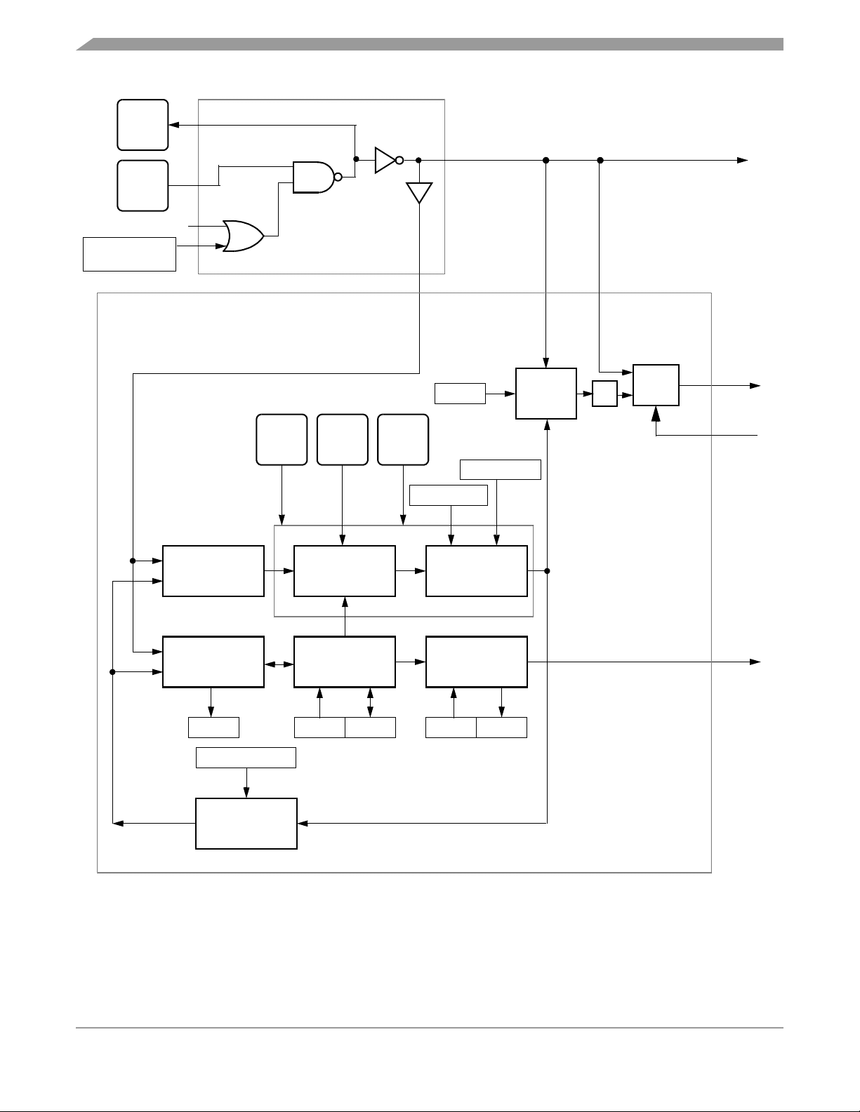
Clock Generator Module (CGM)
OSC2
OSC1
SIMOSCEN (FROM SIM)
OSCSTOPENB
(FROM CONFIG)
OSCILLATOR (OSC)
CGMXCLK
(TO: SIM, TIMTB15A, ADC)
PHASE-LOCKED LOOP (PLL)
CGMRCLK
V
DDA
PHASE
DETECTOR
LOCK
DETECTOR
LOCK AUTO ACQ
MUL11–MUL0
CGMXFC V
LOOP
FILTER
AUTOMATIC
MODE
CONTROL
SSA
VRS7–VRS0
PLL ANALOG
BCS
VPR1–VPR0
VOLTAGE
CONTROLLED
OSCILLATOR
INTERRUPT
CONTROL
PLLIE PLLF
CLOCK
SELECT
CIRCUIT
WHEN S = 1,
*
CGMOUT = B
CGMVCLK
A
÷
2
B
S
*
CGMOUT
(TO SIM)
SIMDIV2
(FROM SIM)
CGMINT
(TO SIM)
CGMVDV
FREQUENCY
DIVIDER
Figure 4-1. CGM Block Diagram
MC68HC908GZ16 • MC68HC908GZ8 Data Sheet, Rev. 2
62 Freescale Semiconductor
Page 63

Functional Description
4.3.1 Crystal Oscillator Circuit
The crystal oscillator circuit consists of an inverting amplifier and an external crystal. The OSC1 pin is the
input to the amplifier and the OSC2 pin is the output. The SIMOSCEN signal from the system integration
module (SIM) or the OSCSTOPENB bit in the CONFIG register enable the crystal oscillator circuit.
The CGMXCLK signal is the output of the crystal oscillator circuit and runs at a rate equal to the crystal
frequency. CGMXCLK is then buffered to produce CGMRCLK, the PLL reference clock.
CGMXCLK can be used by other modules which require precise timing for operation. The duty cycle of
CGMXCLK is not guaranteed to be 50% and depends on external factors, including the crystal and related
external components. An externally generated clock also can feed the OSC1 pin of the crystal oscillator
circuit. Connect the external clock to the OSC1 pin and let the OSC2 pin float.
4.3.2 Phase-Locked Loop Circuit (PLL)
The PLL is a frequency generator that can operate in either acquisition mode or tracking mode, depending
on the accuracy of the output frequency. The PLL can change between acquisition and tracking modes
either automatically or manually.
4.3.3 PLL Circuits
The PLL consists of these circuits:
• Voltage-controlled oscillator (VCO)
• Modulo VCO frequency divider
• Phase detector
• Loop filter
• Lock detector
The operating range of the VCO is programmable for a wide range of frequencies and for maximum
immunity to external noise, including supply and CGMXFC noise. The VCO frequency is bound to a range
from roughly one-half to twice the center-of-range frequency, f
CGMXFC pin changes the frequency within this range. By design, f
center-of-range frequency, f
E
(L × 2
)f
NOM
.
, (71.4 kHz) times a linear factor, L, and a power-of-two factor, E, or
NOM
. Modulating the voltage on the
VRS
is equal to the nominal
VRS
CGMRCLK is the PLL reference clock, a buffered version of CGMXCLK. CGMRCLK runs at a frequency,
f
. The VCO’s output clock, CGMVCLK, running at a frequency, f
RCLK
, is fed back through a
VCLK
programmable modulo divider. The modulo divider reduces the VCO clock by a factor, N. The dividers
output is the VCO feedback clock, CGMVDV, running at a frequency, f
VDV=fVCLK
/(N). For more
information, see 4.3.6 Programming the PLL.
The phase detector then compares the VCO feedback clock, CGMVDV, with the final reference clock,
CGMRDV. A correction pulse is generated based on the phase difference between the two signals. The
loop filter then slightly alters the DC voltage on the external capacitor connected to CGMXFC based on
the width and direction of the correction pulse. The filter can make fast or slow corrections depending on
its mode, described in 4.3.4 Acquisition and Tracking Modes. The value of the external capacitor and the
reference frequency determines the speed of the corrections and the stability of the PLL.
The lock detector compares the frequencies of the VCO feedback clock, CGMVDV, and the reference
clock, CGMRCLK. Therefore, the speed of the lock detector is directly proportional to the reference
MC68HC908GZ16 • MC68HC908GZ8 Data Sheet, Rev. 2
Freescale Semiconductor 63
Page 64

Clock Generator Module (CGM)
frequency, f
. The circuit determines the mode of the PLL and the lock condition based on this
RCLK
comparison.
4.3.4 Acquisition and Tracking Modes
The PLL filter is manually or automatically configurable into one of two operating modes:
• Acquisition mode — In acquisition mode, the filter can make large frequency corrections to the
VCO. This mode is used at PLL start up or when the PLL has suffered a severe noise hit and the
VCO frequency is far off the desired frequency. When in acquisition mode, the ACQ
bit is clear in
the PLL bandwidth control register. (See 4.5.2 PLL Bandwidth Control Register.)
• Tracking mode — In tracking mode, the filter makes only small corrections to the frequency of the
VCO. PLL jitter is much lower in tracking mode, but the response to noise is also slower. The PLL
enters tracking mode when the VCO frequency is nearly correct, such as when the PLL is selected
as the base clock source. (See 4.3.8 Base Clock Selector Circuit.) The PLL is automatically in
tracking mode when not in acquisition mode or when the ACQ
bit is set.
4.3.5 Manual and Automatic PLL Bandwidth Modes
The PLL can change the bandwidth or operational mode of the loop filter manually or automatically.
Automatic mode is recommended for most users.
In automatic bandwidth control mode (AUTO = 1), the lock detector automatically switches between
acquisition and tracking modes. Automatic bandwidth control mode also is used to determine when the
VCO clock, CGMVCLK, is safe to use as the source for the base clock, CGMOUT. (See 4.5.2 PLL
Bandwidth Control Register.) If PLL interrupts are enabled, the software can wait for a PLL interrupt
request and then check the LOCK bit. If interrupts are disabled, software can poll the LOCK bit
continuously (for example, during PLL start up) or at periodic intervals. In either case, when the LOCK bit
is set, the VCO clock is safe to use as the source for the base clock. (See 4.3.8 Base Clock Selector
Circuit.) If the VCO is selected as the source for the base clock and the LOCK bit is clear, the PLL has
suffered a severe noise hit and the software must take appropriate action, depending on the application.
(See 4.6 Interrupts for information and precautions on using interrupts.)
The following conditions apply when the PLL is in automatic bandwidth control mode:
•The ACQ
bit (See 4.5.2 PLL Bandwidth Control Register.) is a read-only indicator of the mode of
the filter. (See 4.3.4 Acquisition and Tracking Modes.)
•The ACQ
bit is set when the VCO frequency is within a certain tolerance and is cleared when the
VCO frequency is out of a certain tolerance. (See 4.8 Acquisition/Lock Time Specifications for
more information.)
• The LOCK bit is a read-only indicator of the locked state of the PLL.
• The LOCK bit is set when the VCO frequency is within a certain tolerance and is cleared when the
VCO frequency is out of a certain tolerance. (See 4.8 Acquisition/Lock Time Specifications for
more information.)
• CPU interrupts can occur if enabled (PLLIE = 1) when the PLL’s lock condition changes, toggling
the LOCK bit. (See 4.5.1 PLL Control Register.)
The PLL also may operate in manual mode (AUTO = 0). Manual mode is used by systems that do not
require an indicator of the lock condition for proper operation. Such systems typically operate well below
f
BUSMAX
64 Freescale Semiconductor
.
MC68HC908GZ16 • MC68HC908GZ8 Data Sheet, Rev. 2
Page 65

Functional Description
The following conditions apply when in manual mode:
•ACQ
• Before entering tracking mode (ACQ
is a writable control bit that controls the mode of the filter. Before turning on the PLL in manual
mode, the ACQ
bit must be clear.
= 1), software must wait a given time, t
(See 4.8
ACQ
Acquisition/Lock Time Specifications.), after turning on the PLL by setting PLLON in the PLL
control register (PCTL).
• Software must wait a given time, t
, after entering tracking mode before selecting the PLL as the
AL
clock source to CGMOUT (BCS = 1).
• The LOCK bit is disabled.
• CPU interrupts from the CGM are disabled.
4.3.6 Programming the PLL
Use the following procedure to program the PLL. For reference, the variables used and their meaning are
shown in Table 4-1.
Table 4-1. Variable Definitions
Variable Definition
f
BUSDES
f
VCLKDES
f
RCLK
f
VCLK
f
BUS
f
NOM
f
VRS
Desired bus clock frequency
Desired VCO clock frequency
Chosen reference crystal frequency
Calculated VCO clock frequency
Calculated bus clock frequency
Nominal VCO center frequency
Programmed VCO center frequency
NOTE
The round function in the following equations means that the real number
should be rounded to the nearest integer number.
1. Choose the desired bus frequency, f
BUSDES
.
2. Calculate the desired VCO frequency (four times the desired bus frequency).
f
VCLKDES
3. Choose a practical PLL (crystal) reference frequency, f
= 4 x f
BUSDES
RCLK
. Typically, the reference crystal is 1–8
MHz.
Frequency errors to the PLL are corrected at a rate of f
RCLK
.
For stability and lock time reduction, this rate must be as fast as possible. The VCO frequency must
be an integer multiple of this rate. The relationship between the VCO frequency, f
reference frequency, f
RCLK,
is:
f
VCLK
= (N) (f
RCLK
)
VCLK
, and the
N, the range multiplier, must be an integer.
MC68HC908GZ16 • MC68HC908GZ8 Data Sheet, Rev. 2
Freescale Semiconductor 65
Page 66

Clock Generator Module (CGM)
In cases where desired bus frequency has some tolerance, choose f
to a value determined
RCLK
either by other module requirements (such as modules which are clocked by CGMXCLK), cost
requirements, or ideally, as high as the specified range allows. See Chapter 21 Electrical
Specifications. After choosing N, the actual bus frequency can be determined using equation in 2
above.
4. Select a VCO frequency multiplier, N.
f
⎛⎞
VCLKDES
N round
=
5. Calculate and verify the adequacy of the VCO and bus frequencies f
f
VCLK
f
BUS
--------------------------
⎜⎟
f
⎝⎠
RCLK
N() f
×=
RCLK
f
()4⁄=
VCLK
VCLK
and f
BUS
.
6. Select the VCO’s power-of-two range multiplier E, according to Table 4-2.
Table 4-2. Power-of-Two Range Selectors
Frequency Range E
0 < f
8 MHz< f
16 MHz< f
VCLK
VCLK
VCLK
≤ 8 MHz
≤ 16 MHz
≤ 32 MHz
0
1
(1)
2
1. Do not program E to a value of 3.
7. Select a VCO linear range multiplier, L, where f
L = Round
= 71.4 kHz
NOM
f
VCLK
2E x f
NOM
8. Calculate and verify the adequacy of the VCO programmed center-of-range frequency, f
center-of-range frequency is the midpoint between the minimum and maximum frequencies
attainable by the PLL.
f
= (L x 2E) f
VRS
NOM
9. For proper operation,
f
–
VRSfVCLK
10. Verify the choice of N, E, and L by comparing f
f
must be within the application’s tolerance of f
VCLK
VCLK
.
to f
f
NOM
---------------------------
≤
VCLK
2E×
2
to f
VRS
VCLKDES
and f
, and f
VCLKDES
VRS
. For proper operation,
must be as close as possible
NOTE
Exceeding the recommended maximum bus frequency or VCO frequency
can crash the MCU.
VRS
. The
MC68HC908GZ16 • MC68HC908GZ8 Data Sheet, Rev. 2
66 Freescale Semiconductor
Page 67
11. Program the PLL registers accordingly:
a. In the VPR bits of the PLL control register (PCTL), program the binary equivalent of E.
b. In the PLL multiplier select register low (PMSL) and the PLL multiplier select register high
(PMSH), program the binary equivalent of N. If using a 1–8 MHz reference, the PMSL register
must be reprogrammed from the reset value before enabling the pll.
c. In the PLL VCO range select register (PMRS), program the binary coded equivalent of L.
Table 4-3 provides numeric examples (register values are in hexadecimal notation):
Table 4- 3. Nu meri c Ex ampl e
Functional Description
f
BUS
500 kHz 1 MHz 002 0 1B
1.25 MHz 1 MHz 005 0 45
2.0 MHz 1 MHz 008 0 70
2.5 MHz 1 MHz 00A 1 45
3.0 MHz 1 MHz 00C 1 53
4.0 MHz 1 MHz 010 1 70
5.0 MHz 1 MHz 014 2 46
7.0 MHz 1 MHz 01C 2 62
8.0 MHz 1 MHz 020 2 70
f
RCLK
NEL
4.3.7 Special Programming Exceptions
The programming method described in 4.3.6 Programming the PLL does not account for two possible
exceptions. A value of 0 for N or L is meaningless when used in the equations given. To account for these
exceptions:
• A 0 value for N is interpreted exactly the same as a value of 1.
• A 0 value for L disables the PLL and prevents its selection as the source for the base clock.
See 4.3.8 Base Clock Selector Circuit.
4.3.8 Base Clock Selector Circuit
This circuit is used to select either the crystal clock, CGMXCLK, or the VCO clock, CGMVCLK, as the
source of the base clock, CGMOUT. The two input clocks go through a transition control circuit that waits
up to three CGMXCLK cycles and three CGMVCLK cycles to change from one clock source to the other.
During this time, CGMOUT is held in stasis. The output of the transition control circuit is then divided by
two to correct the duty cycle. Therefore, the bus clock frequency, which is one-half of the base clock
frequency, is one-fourth the frequency of the selected clock (CGMXCLK or CGMVCLK).
The BCS bit in the PLL control register (PCTL) selects which clock drives CGMOUT. The VCO clock
cannot be selected as the base clock source if the PLL is not turned on. The PLL cannot be turned off if
the VCO clock is selected. The PLL cannot be turned on or off simultaneously with the selection or
deselection of the VCO clock. The VCO clock also cannot be selected as the base clock source if the
factor L is programmed to a 0. This value would set up a condition inconsistent with the operation of the
PLL, so that the PLL would be disabled and the crystal clock would be forced as the source of the base
clock.
MC68HC908GZ16 • MC68HC908GZ8 Data Sheet, Rev. 2
Freescale Semiconductor 67
Page 68
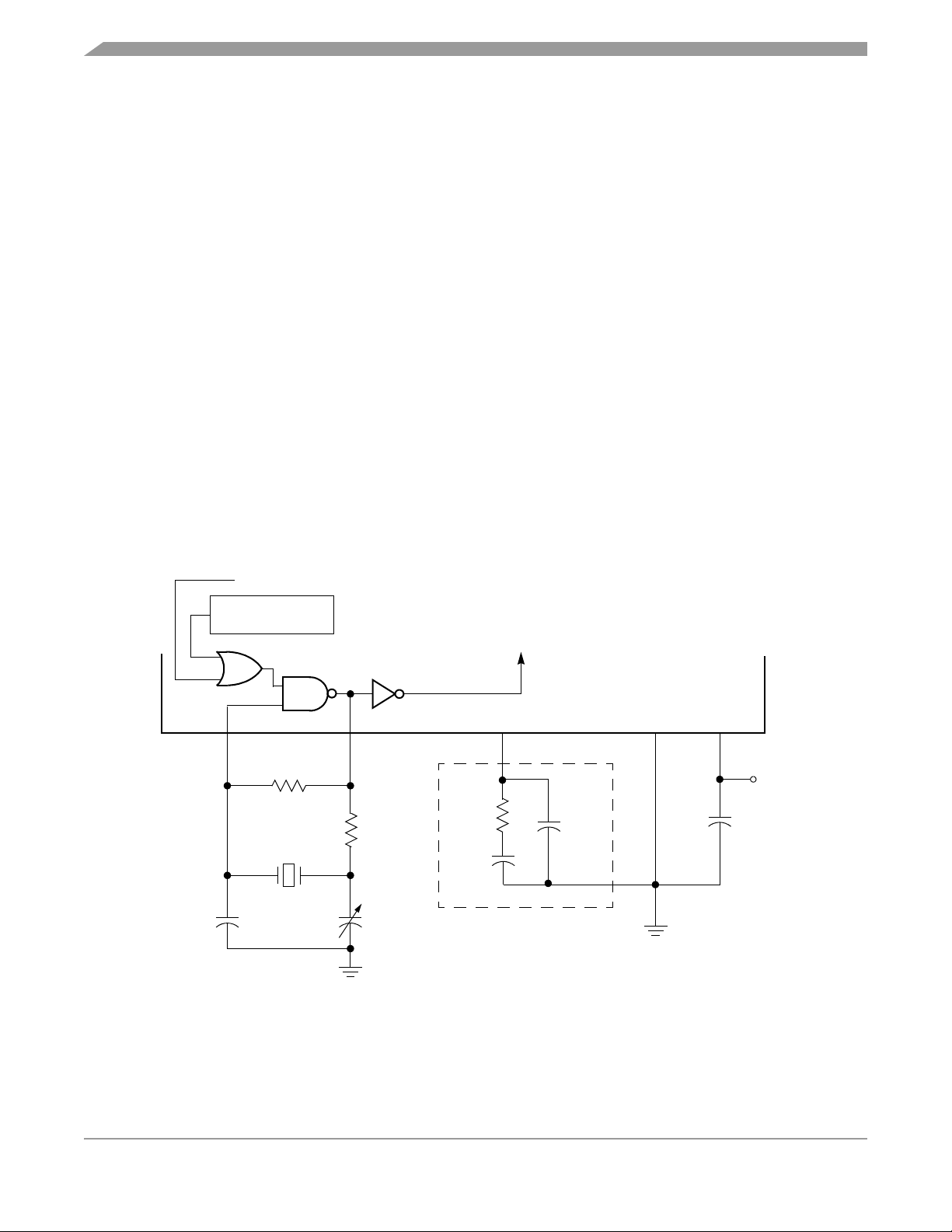
Clock Generator Module (CGM)
4.3.9 CGM External Connections
In its typical configuration, the CGM requires external components. Five of these are for the crystal
oscillator and two or four are for the PLL.
The crystal oscillator is normally connected in a Pierce oscillator configuration, as shown in Figure 4-2.
Figure 4-2 shows only the logical representation of the internal components and may not represent actual
circuitry. The oscillator configuration uses five components:
•Crystal, X
• Fixed capacitor, C
• Tuning capacitor, C2 (can also be a fixed capacitor)
• Feedback resistor, R
• Series resistor, RS
1
1
B
The series resistor (R
) is included in the diagram to follow strict Pierce oscillator guidelines. Refer to the
S
crystal manufacturer’s data for more information regarding values for C1 and C2.
Figure 4-2 also shows the external components for the PLL:
• Bypass capacitor, C
BYP
• Filter network
Routing should be done with great care to minimize signal cross talk and noise.
SIMOSCEN
OSCSTOPENB
(FROM CONFIG)
CGMXCLK
OSC1
RB
OSC2
RS
CGMXFC
R
F1
C
F2
V
SSA
V
DDA
CBYP
0.1 µF
V
DD
C
F1
X1
C
1
C
2
3 Component Filter
Note: Filter network in box can be replaced with a single capacitor, but will degrade stability.
Figure 4-2. CGM External Connections
MC68HC908GZ16 • MC68HC908GZ8 Data Sheet, Rev. 2
68 Freescale Semiconductor
Page 69

I/O Signals
4.4 I/O Signals
The following paragraphs describe the CGM I/O signals.
4.4.1 Crystal Amplifier Input Pin (OSC1)
The OSC1 pin is an input to the crystal oscillator amplifier.
4.4.2 Crystal Amplifier Output Pin (OSC2)
The OSC2 pin is the output of the crystal oscillator inverting amplifier.
4.4.3 External Filter Capacitor Pin (CGMXFC)
The CGMXFC pin is required by the loop filter to filter out phase corrections. An external filter network is
connected to this pin. (See Figure 4-2.)
NOTE
To prevent noise problems, the filter network should be placed as close to
the CGMXFC pin as possible, with minimum routing distances and no
routing of other signals across the network.
4.4.4 PLL Analog Power Pin (V
V
is a power pin used by the analog portions of the PLL. Connect the V
DDA
potential as the V
DD
pin.
DDA
)
pin to the same voltage
DDA
NOTE
Route V
carefully for maximum noise immunity and place bypass
DDA
capacitors as close as possible to the package.
4.4.5 PLL Analog Ground Pin (V
V
is a ground pin used by the analog portions of the PLL. Connect the V
SSA
potential as the V
SS
pin.
SSA
)
pin to the same voltage
SSA
NOTE
Route V
carefully for maximum noise immunity and place bypass
SSA
capacitors as close as possible to the package.
4.4.6 Oscillator Enable Signal (SIMOSCEN)
The SIMOSCEN signal comes from the system integration module (SIM) and enables the oscillator and
PLL.
4.4.7 Oscillator Stop Mode Enable Bit (OSCSTOPENB)
OSCSTOPENB is a bit in the CONFIG register that enables the oscillator to continue operating during
stop mode. If this bit is set, the Oscillator continues running during stop mode. If this bit is not set (default),
the oscillator is controlled by the SIMOSCEN signal which will disable the oscillator during stop mode.
MC68HC908GZ16 • MC68HC908GZ8 Data Sheet, Rev. 2
Freescale Semiconductor 69
Page 70

Clock Generator Module (CGM)
4.4.8 Crystal Output Frequency Signal (CGMXCLK)
CGMXCLK is the crystal oscillator output signal. It runs at the full speed of the crystal (f
) and comes
XCLK
directly from the crystal oscillator circuit. Figure 4-2 shows only the logical relation of CGMXCLK to OSC1
and OSC2 and may not represent the actual circuitry. The duty cycle of CGMXCLK is unknown and may
depend on the crystal and other external factors. Also, the frequency and amplitude of CGMXCLK can be
unstable at start up.
4.4.9 CGM Base Clock Output (CGMOUT)
CGMOUT is the clock output of the CGM. This signal goes to the SIM, which generates the MCU clocks.
CGMOUT is a 50 percent duty cycle clock running at twice the bus frequency. CGMOUT is software
programmable to be either the oscillator output, CGMXCLK, divided by two or the VCO clock, CGMVCLK,
divided by two.
4.4.10 CGM CPU Interrupt (CGMINT)
CGMINT is the interrupt signal generated by the PLL lock detector.
4.5 CGM Registers
These registers control and monitor operation of the CGM:
• PLL control register (PCTL)
(See 4.5.1 PLL Control Register.)
• PLL bandwidth control register (PBWC)
(See 4.5.2 PLL Bandwidth Control Register.)
• PLL multiplier select register high (PMSH)
(See 4.5.3 PLL Multiplier Select Register High.)
• PLL multiplier select register low (PMSL)
(See 4.5.4 PLL Multiplier Select Register Low.)
• PLL VCO range select register (PMRS)
(See 4.5.5 PLL VCO Range Select Register.)
Figure 4-3 is a summary of the CGM registers.
MC68HC908GZ16 • MC68HC908GZ8 Data Sheet, Rev. 2
70 Freescale Semiconductor
Page 71
CGM Registers
Addr.Register Name Bit 7654321Bit 0
PLL Control Register
$0036
PLL Bandwidth Control
$0037
$0038
$0039
$003A
$003B Reserved Register
NOTES:
1. When AUTO = 0, PLLIE is forced clear and is read-only.
2. When AUTO = 0, PLLF and LOCK read as clear.
3. When AUTO = 1, ACQ
4. When PLLON = 0 or VRS7:VRS0 = $0, BCS is forced clear and is read-only.
5. When PLLON = 1, the PLL programming register is read-only.
6. When BCS = 1, PLLON is forced set and is read-only.
Register (PBWC)
PLL Multiplier Select High
Register (PMSH)
PLL Multiplier Select Low
PLL VCO Select Range
Register (PMRS)
(PCTL)
See page 71.
See page 73.
See page 74.
Register (PMSL)
See page 75.
See page 75.
is read-only.
Read:
Write:
Reset:00100000
Read:
Write:
Reset:00000000
Read:0000
Write:
Reset:00000000
Read:
Write:
Reset:01000000
Read:
Write:
Reset:01000000
Read:0000
Write:
Reset:00000001
PLLIE
AUTO
MUL7 MUL6 MUL5 MUL4 MUL3 MUL2 MUL1 MUL0
VRS7 VRS6 VRS5 VRS4 VRS3 VRS2 VRS1 VRS0
PLLF
LOCK
= Unimplemented R = Reserved
PLLON BCS R R VPR1 VPR0
ACQ
0000
MUL11 MUL10 MUL9 MUL8
RRRR
R
Figure 4-3. CGM I/O Register Summary
4.5.1 PLL Control Register
The PLL control register (PCTL) contains the interrupt enable and flag bits, the on/off switch, the base
clock selector bit, and the VCO power-of-two range selector bits.
Address: $0036
Bit 7 6 5 4 3 2 1 Bit 0
Read:
Write:
Reset:00100 0 00
Freescale Semiconductor 71
PLLIE
PLLF
= Unimplemented R = Reserved
PLLON BCS R R VPR1 VPR0
Figure 4-4. PLL Control Register (PCTL)
MC68HC908GZ16 • MC68HC908GZ8 Data Sheet, Rev. 2
Page 72

Clock Generator Module (CGM)
PLLIE — PLL Interrupt Enable Bit
This read/write bit enables the PLL to generate an interrupt request when the LOCK bit toggles, setting
the PLL flag, PLLF. When the AUTO bit in the PLL bandwidth control register (PBWC) is clear, PLLIE
cannot be written and reads as logic 0. Reset clears the PLLIE bit.
1 = PLL interrupts enabled
0 = PLL interrupts disabled
PLLF — PLL Interrupt Flag Bit
This read-only bit is set whenever the LOCK bit toggles. PLLF generates an interrupt request if the
PLLIE bit also is set. PLLF always reads as logic 0 when the AUTO bit in the PLL bandwidth control
register (PBWC) is clear. Clear the PLLF bit by reading the PLL control register. Reset clears the PLLF
bit.
1 = Change in lock condition
0 = No change in lock condition
NOTE
Do not inadvertently clear the PLLF bit. Any read or read-modify-write
operation on the PLL control register clears the PLLF bit.
PLLON — PLL On Bit
This read/write bit activates the PLL and enables the VCO clock, CGMVCLK. PLLON cannot be
cleared if the VCO clock is driving the base clock, CGMOUT (BCS = 1). (See 4.3.8 Base Clock Selector
Circuit.) Reset sets this bit so that the loop can stabilize as the MCU is powering up.
1 = PLL on
0 = PLL off
BCS — Base Clock Select Bit
This read/write bit selects either the crystal oscillator output, CGMXCLK, or the VCO clock,
CGMVCLK, as the source of the CGM output, CGMOUT. CGMOUT frequency is one-half the
frequency of the selected clock. BCS cannot be set while the PLLON bit is clear. After toggling BCS,
it may take up to three CGMXCLK and three CGMVCLK cycles to complete the transition from one
source clock to the other. During the transition, CGMOUT is held in stasis. (See 4.3.8 Base Clock
Selector Circuit.) Reset clears the BCS bit.
1 = CGMVCLK divided by two drives CGMOUT
0 = CGMXCLK divided by two drives CGMOUT
NOTE
PLLON and BCS have built-in protection that prevents the base clock
selector circuit from selecting the VCO clock as the source of the base clock
if the PLL is off. Therefore, PLLON cannot be cleared when BCS is set, and
BCS cannot be set when PLLON is clear. If the PLL is off (PLLON = 0),
selecting CGMVCLK requires two writes to the PLL control register. (See
4.3.8 Base Clock Selector Circuit.).
MC68HC908GZ16 • MC68HC908GZ8 Data Sheet, Rev. 2
72 Freescale Semiconductor
Page 73

CGM Registers
VPR1 and VPR0 — VCO Power-of-Two Range Select Bits
These read/write bits control the VCO’s hardware power-of-two range multiplier E that, in conjunction
with L controls the hardware center-of-range frequency, f
. VPR1:VPR0 cannot be written when the
VRS
PLLON bit is set. Reset clears these bits. (See 4.3.3 PLL Circuits, 4.3.6 Programming the PLL, and
4.5.5 PLL VCO Range Select Register.)
Table 4-4. VPR1 and VPR0 Programming
VPR1 and VPR0 E
00 0 1
01 1 2
10
1. Do not program E to a value of 3.
(1)
2
VCO Power-of-Two
Range Multiplier
4
NOTE
Verify that the value of the VPR1 and VPR0 bits in the PCTL register are
appropriate for the given reference and VCO clock frequencies before
enabling the PLL. See 4.3.6 Programming the PLL for detailed instructions
on selecting the proper value for these control bits.
4.5.2 PLL Bandwidth Control Register
The PLL bandwidth control register (PBWC):
• Selects automatic or manual (software-controlled) bandwidth control mode
• Indicates when the PLL is locked
• In automatic bandwidth control mode, indicates when the PLL is in acquisition or tracking mode
• In manual operation, forces the PLL into acquisition or tracking mode
Address: $0037
Bit 7654321Bit 0
Read:
Write:
Reset:00000000
AUTO
LOCK
= Unimplemented R= Reserved
ACQ
0000
R
Figure 4-5. PLL Bandwidth Control Register (PBWC)
AUTO — Automatic Bandwidth Control Bit
This read/write bit selects automatic or manual bandwidth control. When initializing the PLL for manual
operation (AUTO = 0), clear the ACQ
bit before turning on the PLL. Reset clears the AUTO bit.
1 = Automatic bandwidth control
0 = Manual bandwidth control
MC68HC908GZ16 • MC68HC908GZ8 Data Sheet, Rev. 2
Freescale Semiconductor 73
Page 74

Clock Generator Module (CGM)
LOCK — Lock Indicator Bit
When the AUTO bit is set, LOCK is a read-only bit that becomes set when the VCO clock, CGMVCLK,
is locked (running at the programmed frequency). When the AUTO bit is clear, LOCK reads as logic 0
and has no meaning. The write one function of this bit is reserved for test, so this bit must always be
written a 0. Reset clears the LOCK bit.
1 = VCO frequency correct or locked
0 = VCO frequency incorrect or unlocked
ACQ
— Acquisition Mode Bit
When the AUTO bit is set, ACQ
or tracking mode. When the AUTO bit is clear, ACQ
is a read-only bit that indicates whether the PLL is in acquisition mode
is a read/write bit that controls whether the PLL is
in acquisition or tracking mode.
In automatic bandwidth control mode (AUTO = 1), the last-written value from manual operation is
stored in a temporary location and is recovered when manual operation resumes. Reset clears this bit,
enabling acquisition mode.
1 = Tracking mode
0 = Acquisition mode
4.5.3 PLL Multiplier Select Register High
The PLL multiplier select register high (PMSH) contains the programming information for the high byte of
the modulo feedback divider.
Address: $0038
Bit 7654321Bit 0
Read:0000
Write:
Reset:00000000
= Unimplemented
MUL11 MUL10 MUL9 MUL8
Figure 4-6. PLL Multiplier Select Register High (PMSH)
MUL11–MUL8 — Multiplier Select Bits
These read/write bits control the high byte of the modulo feedback divider that selects the VCO
frequency multiplier N. (See 4.3.3 PLL Circuits and 4.3.6 Programming the PLL.) A value of $0000 in
the multiplier select registers configures the modulo feedback divider the same as a value of $0001.
Reset initializes the registers to $0040 for a default multiply value of 64.
NOTE
The multiplier select bits have built-in protection such that they cannot be
written when the PLL is on (PLLON = 1).
PMSH[7:4] — Unimplemented Bits
These bits have no function and always read as logic 0s.
MC68HC908GZ16 • MC68HC908GZ8 Data Sheet, Rev. 2
74 Freescale Semiconductor
Page 75
CGM Registers
4.5.4 PLL Multiplier Select Register Low
The PLL multiplier select register low (PMSL) contains the programming information for the low byte of
the modulo feedback divider.
Address: $0038
Bit 7654321Bit 0
Read:
Write:
Reset:01000000
For applications using 1–8 MHz reference frequencies this register must be
reprogrammed before enabling the PLL. The reset value of this register will
cause applications using 1–8 MHz reference frequencies to become
unstable if the PLL is enabled without programming an appropriate value.
The programmed value must not allow the VCO clock to exceed 32 MHz.
See 4.3.6 Programming the PLL for detailed instructions on choosing the
proper value for PMSL.
MUL7 MUL6 MUL5 MUL4 MUL3 MUL2 MUL1 MUL0
Figure 4-7. PLL Multiplier Select Register Low (PMSL)
NOTE
MUL7–MUL0 — Multiplier Select Bits
These read/write bits control the low byte of the modulo feedback divider that selects the VCO
frequency multiplier, N. (See 4.3.3 PLL Circuits and 4.3.6 Programming the PLL.) MUL7–MUL0 cannot
be written when the PLLON bit in the PCTL is set. A value of $0000 in the multiplier select registers
configures the modulo feedback divider the same as a value of $0001. Reset initializes the register to
$40 for a default multiply value of 64.
NOTE
The multiplier select bits have built-in protection such that they cannot be
written when the PLL is on (PLLON = 1).
4.5.5 PLL VCO Range Select Register
NOTE
PMRS may be called PVRS on other HC08 derivatives.
The PLL VCO range select register (PMRS) contains the programming information required for the
hardware configuration of the VCO.
Address: $003A
Bit 7654321Bit 0
Read:
Write:
Reset:01000000
VRS7 VRS6 VRS5 VRS4 VRS3 VRS2 VRS1 VRS0
Figure 4-8. PLL VCO Range Select Register (PMRS)
MC68HC908GZ16 • MC68HC908GZ8 Data Sheet, Rev. 2
Freescale Semiconductor 75
Page 76

Clock Generator Module (CGM)
NOTE
Verify that the value of the PMRS register is appropriate for the given
reference and VCO clock frequencies before enabling the PLL. See 4.3.6
Programming the PLL for detailed instructions on selecting the proper value
for these control bits.
VRS7–VRS0 — VCO Range Select Bits
These read/write bits control the hardware center-of-range linear multiplier L which, in conjunction with
E (See 4.3.3 PLL Circuits, 4.3.6 Programming the PLL, and 4.5.1 PLL Control Register.), controls the
hardware center-of-range frequency, f
. VRS7–VRS0 cannot be written when the PLLON bit in the
VRS
PCTL is set. (See 4.3.7 Special Programming Exceptions.) A value of $00 in the VCO range select
register disables the PLL and clears the BCS bit in the PLL control register (PCTL). (See 4.3.8 Base
Clock Selector Circuit and 4.3.7 Special Programming Exceptions.). Reset initializes the register to $40
for a default range multiply value of 64.
NOTE
The VCO range select bits have built-in protection such that they cannot be
written when the PLL is on (PLLON = 1) and such that the VCO clock
cannot be selected as the source of the base clock (BCS = 1) if the VCO
range select bits are all clear.
The PLL VCO range select register must be programmed correctly.
Incorrect programming can result in failure of the PLL to achieve lock.
4.6 Interrupts
When the AUTO bit is set in the PLL bandwidth control register (PBWC), the PLL can generate a CPU
interrupt request every time the LOCK bit changes state. The PLLIE bit in the PLL control register (PCTL)
enables CPU interrupts from the PLL. PLLF, the interrupt flag in the PCTL, becomes set whether
interrupts are enabled or not. When the AUTO bit is clear, CPU interrupts from the PLL are disabled and
PLLF reads as logic 0.
Software should read the LOCK bit after a PLL interrupt request to see if the request was due to an entry
into lock or an exit from lock. When the PLL enters lock, the VCO clock, CGMVCLK, divided by two can
be selected as the CGMOUT source by setting BCS in the PCTL. When the PLL exits lock, the VCO clock
frequency is corrupt, and appropriate precautions should be taken. If the application is not frequency
sensitive, interrupts should be disabled to prevent PLL interrupt service routines from impeding software
performance or from exceeding stack limitations.
NOTE
Software can select the CGMVCLK divided by two as the CGMOUT source
even if the PLL is not locked (LOCK = 0). Therefore, software should make
sure the PLL is locked before setting the BCS bit.
MC68HC908GZ16 • MC68HC908GZ8 Data Sheet, Rev. 2
76 Freescale Semiconductor
Page 77

Special Modes
4.7 Special Modes
The WAIT instruction puts the MCU in low power-consumption standby modes.
4.7.1 Wait Mode
The WAIT instruction does not affect the CGM. Before entering wait mode, software can disengage and
turn off the PLL by clearing the BCS and PLLON bits in the PLL control register (PCTL) to save power.
Less power-sensitive applications can disengage the PLL without turning it off, so that the PLL clock is
immediately available at WAIT exit. This would be the case also when the PLL is to wake the MCU from
wait mode, such as when the PLL is first enabled and waiting for LOCK or LOCK is lost.
4.7.2 Stop Mode
If the OSCSTOPENB bit in the CONFIG register is cleared (default), then the STOP instruction disables
the CGM (oscillator and phase locked loop) and holds low all CGM outputs (CGMXCLK, CGMOUT, and
CGMINT).
If the OSCSTOPENB bit in the CONFIG register is set, then the phase locked loop is shut off but the
oscillator will continue to operate in stop mode.
4.7.3 CGM During Break Interrupts
The system integration module (SIM) controls whether status bits in other modules can be cleared during
the break state. The BCFE bit in the SIM break flag control register (SBFCR) enables software to clear
status bits during the break state. See 16.7.3 Break Flag Control Register.
To allow software to clear status bits during a break interrupt, write a logic 1 to the BCFE bit. If a status
bit is cleared during the break state, it remains cleared when the MCU exits the break state.
To protect the PLLF bit during the break state, write a logic 0 to the BCFE bit. With BCFE at logic 0 (its
default state), software can read and write the PLL control register during the break state without affecting
the PLLF bit.
4.8 Acquisition/Lock Time Specifications
The acquisition and lock times of the PLL are, in many applications, the most critical PLL design
parameters. Proper design and use of the PLL ensures the highest stability and lowest acquisition/lock
times.
4.8.1 Acquisition/Lock Time Definitions
Typical control systems refer to the acquisition time or lock time as the reaction time, within specified
tolerances, of the system to a step input. In a PLL, the step input occurs when the PLL is turned on or
when it suffers a noise hit. The tolerance is usually specified as a percent of the step input or when the
output settles to the desired value plus or minus a percent of the frequency change. Therefore, the
reaction time is constant in this definition, regardless of the size of the step input. For example, consider
a system with a 5 percent acquisition time tolerance. If a command instructs the system to change from
0 Hz to 1 MHz, the acquisition time is the time taken for the frequency to reach 1 MHz ±50 kHz. Fifty kHz
= 5% of the 1-MHz step input. If the system is operating at 1 MHz and suffers a –100-kHz noise hit, the
acquisition time is the time taken to return from 900 kHz to 1 MHz ±5 kHz. Five kHz = 5% of the 100-kHz
step input.
MC68HC908GZ16 • MC68HC908GZ8 Data Sheet, Rev. 2
Freescale Semiconductor 77
Page 78

Clock Generator Module (CGM)
Other systems refer to acquisition and lock times as the time the system takes to reduce the error between
the actual output and the desired output to within specified tolerances. Therefore, the acquisition or lock
time varies according to the original error in the output. Minor errors may not even be registered. Typical
PLL applications prefer to use this definition because the system requires the output frequency to be
within a certain tolerance of the desired frequency regardless of the size of the initial error.
4.8.2 Parametric Influences on Reaction Time
Acquisition and lock times are designed to be as short as possible while still providing the highest possible
stability. These reaction times are not constant, however. Many factors directly and indirectly affect the
acquisition time.
The most critical parameter which affects the reaction times of the PLL is the reference frequency, f
RCLK
This frequency is the input to the phase detector and controls how often the PLL makes corrections. For
stability, the corrections must be small compared to the desired frequency, so several corrections are
required to reduce the frequency error. Therefore, the slower the reference the longer it takes to make
these corrections. This parameter is under user control via the choice of crystal frequency f
XCLK
. (See
4.3.3 PLL Circuits and 4.3.6 Programming the PLL.)
Another critical parameter is the external filter network. The PLL modifies the voltage on the VCO by
adding or subtracting charge from capacitors in this network. Therefore, the rate at which the voltage
changes for a given frequency error (thus change in charge) is proportional to the capacitance. The size
of the capacitor also is related to the stability of the PLL. If the capacitor is too small, the PLL cannot make
small enough adjustments to the voltage and the system cannot lock. If the capacitor is too large, the PLL
may not be able to adjust the voltage in a reasonable time. (See 4.8.3 Choosing a Filter.)
Also important is the operating voltage potential applied to V
. The power supply potential alters the
DDA
characteristics of the PLL. A fixed value is best. Variable supplies, such as batteries, are acceptable if
they vary within a known range at very slow speeds. Noise on the power supply is not acceptable,
because it causes small frequency errors which continually change the acquisition time of the PLL.
Temperature and processing also can affect acquisition time because the electrical characteristics of the
PLL change. The part operates as specified as long as these influences stay within the specified limits.
External factors, however, can cause drastic changes in the operation of the PLL. These factors include
noise injected into the PLL through the filter capacitor, filter capacitor leakage, stray impedances on the
circuit board, and even humidity or circuit board contamination.
.
4.8.3 Choosing a Filter
As described in 4.8.2 Parametric Influences on Reaction Time, the external filter network is critical to the
stability and reaction time of the PLL. The PLL is also dependent on reference frequency and supply
voltage.
Figure 4-9 shows two types of filter circuits. In low-cost applications, where stability and reaction time of
the PLL are not critical, the three component filter network shown in Figure 4-9 (B) can be replaced by a
single capacitor, C
components at various reference frequencies. For reference frequencies between the values listed in the
table, extrapolate to the nearest common capacitor value. In general, a slightly larger capacitor provides
more stability at the expense of increased lock time.
78 Freescale Semiconductor
, as shown in shown in Figure 4-9 (A). Refer to Table 4-5 for recommended filter
F
MC68HC908GZ16 • MC68HC908GZ8 Data Sheet, Rev. 2
Page 79
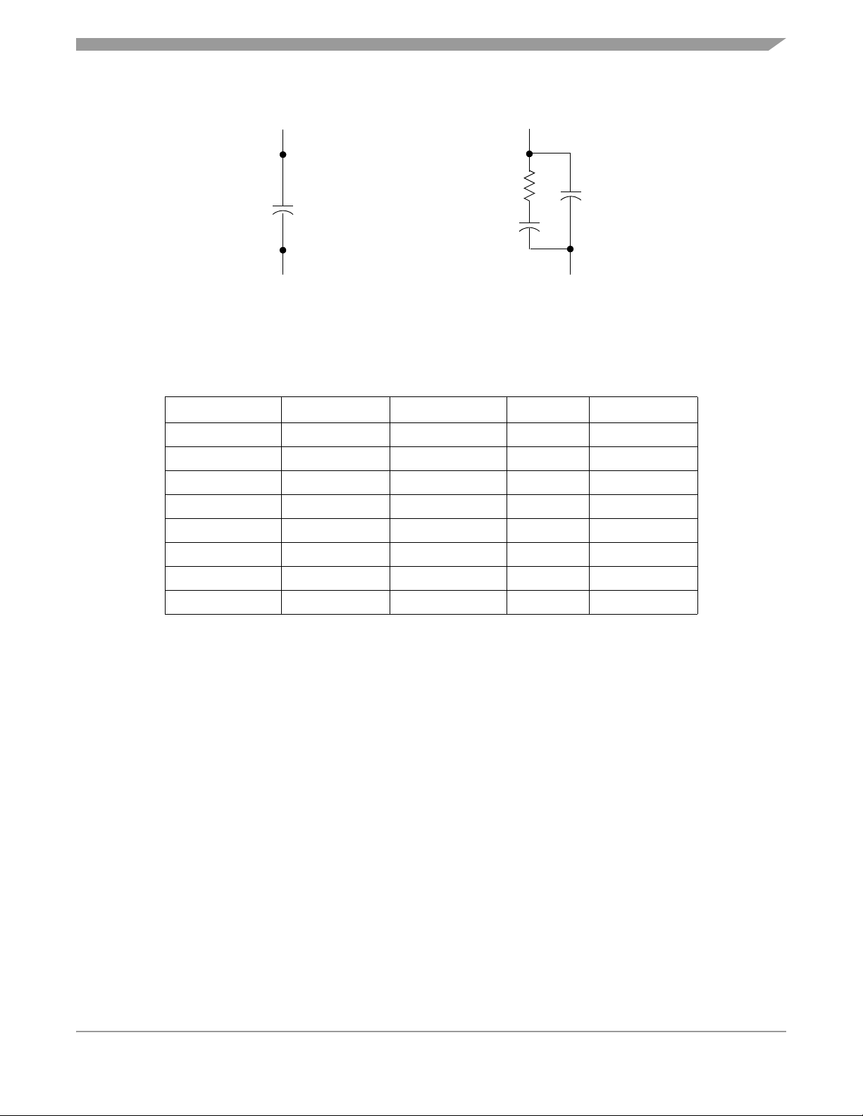
Acquisition/Lock Time Specifications
CGMXFC
C
F
V
SSA
CGMXFC
R
F1
C
F1
C
F2
V
SSA
(A) (B)
Figure 4-9. PLL Filter
Table 4-5. Example Filter Component Values
f
RCLK
1 MHz 8.2 nF 820 pF 2k 18 nF
2 MHz 4.7 nF 470 pF 2k 6.8 nF
3 MHz 3.3 nF 330 pF 2k 5.6 nF
4 MHz 2.2 nF 220 pF 2k 4.7 nF
5 MHz 1.8 nF 180 pF 2k 3.9 nF
C
F1
C
F2
R
F1
C
F
6 MHz 1.5 nF 150 pF 2k 3.3 nF
7 MHz 1.2 nF 120 pF 2k 2.7 nF
8 MHz 1 nF 100 pF 2k 2.2 nF
MC68HC908GZ16 • MC68HC908GZ8 Data Sheet, Rev. 2
Freescale Semiconductor 79
Page 80

Clock Generator Module (CGM)
MC68HC908GZ16 • MC68HC908GZ8 Data Sheet, Rev. 2
80 Freescale Semiconductor
Page 81

Chapter 5 Configuration Register (CONFIG)
5.1 Introduction
This section describes the configuration registers, CONFIG1 and CONFIG2. The configuration registers
enable or disable these options:
• Stop mode recovery time (32 CGMXCLK cycles or 4096 CGMXCLK cycles)
• COP timeout period (2
•STOP instruction
• Computer operating properly module (COP)
• Low-voltage inhibit (LVI) module control and voltage trip point selection
• Enable/disable the oscillator (OSC) during stop mode
• Enable/disable an extra divide by 128 prescaler in timebase module
• Enable for MSCAN
5.2 Functional Description
The configuration registers are used in the initialization of various options. The configuration registers can
be written once after each reset. All of the configuration register bits are cleared during reset. Since the
various options affect the operation of the microcontroller unit (MCU), it is recommended that these
registers be written immediately after reset. The configuration registers are located at $001E and $001F
and may be read at anytime.
18
– 24 or 213 – 24 COPCLK cycles)
NOTE
On a FLASH device, the options except LVI5OR3 are one-time writable by
the user after each reset. The LVI5OR3 bit is one-time writable by the user
only after each POR (power-on reset). The CONFIG registers are not in the
FLASH memory but are special registers containing one-time writable
latches after each reset. Upon a reset, the CONFIG registers default to
predetermined settings as shown in Figure 5-1 and Figure 5-2.
Address: $001E
Bit 765432 1 Bit 0
Read: 0 0 0 0
Write:
Reset: 0 0 0 0 See note 0 0 1
Note: MSCANEN is only reset via POR (power-on reset).
= Unimplemented
MSCANEN TMCLKSEL OSCENINSTOP ESCIBDSRC
Figure 5-1. Configuration Register 2 (CONFIG2)
MC68HC908GZ16 • MC68HC908GZ8 Data Sheet, Rev. 2
Freescale Semiconductor 81
Page 82

Configuration Register (CONFIG)
Address: $001F
Bit 7654321Bit 0
Read:
Write:
Reset:0000See note000
Note: LVI5OR3 bit is only reset via POR (power-on reset).
COPRS LVISTOP LVIRSTD LVIPWRD LVI5OR3 SSREC STOP COPD
Figure 5-2. Configuration Register 1 (CONFIG1)
MSCANEN— MSCAN08 Enable Bit
Setting the MSCANEN
pins.
See Chapter 12 MSCAN08 Controller (MSCAN08) for a more detailed description of the
enables the MSCAN08 module and allows the MSCAN08 to use the PTC0/PTC1
MSCAN08 operation.
1 = Enables MSCAN08 module
0 = Disables the MSCAN08 module
NOTE
The MSCANEN bit is cleared by a power-on reset (POR) only. Other resets
will leave this bit unaffected.
TMCLKSEL— Timebase Clock Select Bit
TMCLKSEL
the extra prescaler and clearing this bit disables it.
enables an extra divide-by-128 prescaler in the timebase module. Setting this bit enables
See Chapter 4 Clock Generator Module (CGM) for
a more detailed description of the external clock operation.
1 = Enables extra divide-by-128 prescaler in timebase module
0 = Disables extra divide-by-128 prescaler in timebase module
OSCENINSTOP — Oscillator Enable In Stop Mode Bit
OSCENINSTOP, when set, will enable the oscillator to continue to generate clocks in stop mode. See
Chapter 4 Clock Generator Module (CGM). This function is used to keep the timebase running while
the reset of the MCU stops. See Chapter 18 Timebase Module (TBM). When clear, oscillator will cease
to generate clocks while in stop mode. The default state for this option is clear, disabling the oscillator
in stop mode.
1 = Oscillator enabled to operate during stop mode
0 = Oscillator disabled during stop mode (default)
ESCIBDSRC — SCI Baud Rate Clock Source Bit
ESCIBDSRC controls the clock source used for the serial communications interface (SCI). The setting
of this bit affects the frequency at which the SCI operates.See Chapter 15 Enhanced Serial
Communications Interface (ESCI) Module.
1 = Internal data bus clock used as clock source for SCI (default)
0 = External oscillator used as clock source for SCI
COPRS — COP Rate Select Bit
COPD selects the COP timeout period. Reset clears COPRS. See Chapter 6 Computer Operating
Properly (COP) Module
1 = COP timeout period = 2
0 = COP timeout period = 2
13
– 24 COPCLK cycles
18
– 24 COPCLK cycles
MC68HC908GZ16 • MC68HC908GZ8 Data Sheet, Rev. 2
82 Freescale Semiconductor
Page 83

Functional Description
LVISTOP — LVI Enable in Stop Mode Bit
When the LVIPWRD bit is clear, setting the LVISTOP bit enables the LVI to operate during stop mode.
Reset clears LVISTOP.
1 = LVI enabled during stop mode
0 = LVI disabled during stop mode
LVIRSTD — LVI Reset Disable Bit
LVIRSTD disables the reset signal from the LVI module. See Chapter 11 Low-Voltage Inhibit (LVI).
1 = LVI module resets disabled
0 = LVI module resets enabled
LVIPWRD — LVI Power Disable Bit
LVIPWRD disables the LVI module. See Chapter 11 Low-Voltage Inhibit (LVI).
1 = LVI module power disabled
0 = LVI module power enabled
LVI5OR3 — LVI 5-V or 3-V Operating Mode Bit
LVI5OR3 selects the voltage operating mode of the LVI module (see Chapter 11 Low-Voltage Inhibit
(LVI)). The voltage mode selected for the LVI should match the operating V
(see Chapter 21
DD
Electrical Specifications) for the LVI’s voltage trip points for each of the modes.
1 = LVI operates in 5-V mode
0 = LVI operates in 3-V mode
NOTE
The LVI5OR3 bit is cleared by a power-on reset (POR) only. Other resets
will leave this bit unaffected.
SSREC — Short Stop Recovery Bit
SSREC enables the CPU to exit stop mode with a delay of 32 CGMXCLK cycles instead of a
4096-CGMXCLK cycle delay.
1 = Stop mode recovery after 32 CGMXCLK cycles
0 = Stop mode recovery after 4096 CGMXCLCK cycles
NOTE
Exiting stop mode by an LVI reset will result in the long stop recovery.
If the system clock source selected is the internal oscillator or the external crystal and the
OSCENINSTOP configuration bit is not set, the oscillator will be disabled during stop mode. The short
stop recovery does not provide enough time for oscillator stabilization and for this reason the SSREC
bit should not be set.
The system stabilization time for power-on reset and long stop recovery (both 4096 CGMXCLK cycles)
gives a delay longer than the LVI enable time for these startup scenarios. There is no period where the
MCU is not protected from a low-power condition. However, when using the short stop recovery
configuration option, the 32-CGMXCLK delay must be greater than the LVI’s turn on time to avoid a
period in startup where the LVI is not protecting the MCU.
STOP — STOP Instruction Enable Bit
STOP enables the STOP instruction.
1 = STOP instruction enabled
0 = STOP instruction treated as illegal opcode
MC68HC908GZ16 • MC68HC908GZ8 Data Sheet, Rev. 2
Freescale Semiconductor 83
Page 84

Configuration Register (CONFIG)
COPD — COP Disable Bit
COPD disables the COP module. See Chapter 6 Computer Operating Properly (COP) Module.
1 = COP module disabled
0 = COP module enabled
MC68HC908GZ16 • MC68HC908GZ8 Data Sheet, Rev. 2
84 Freescale Semiconductor
Page 85
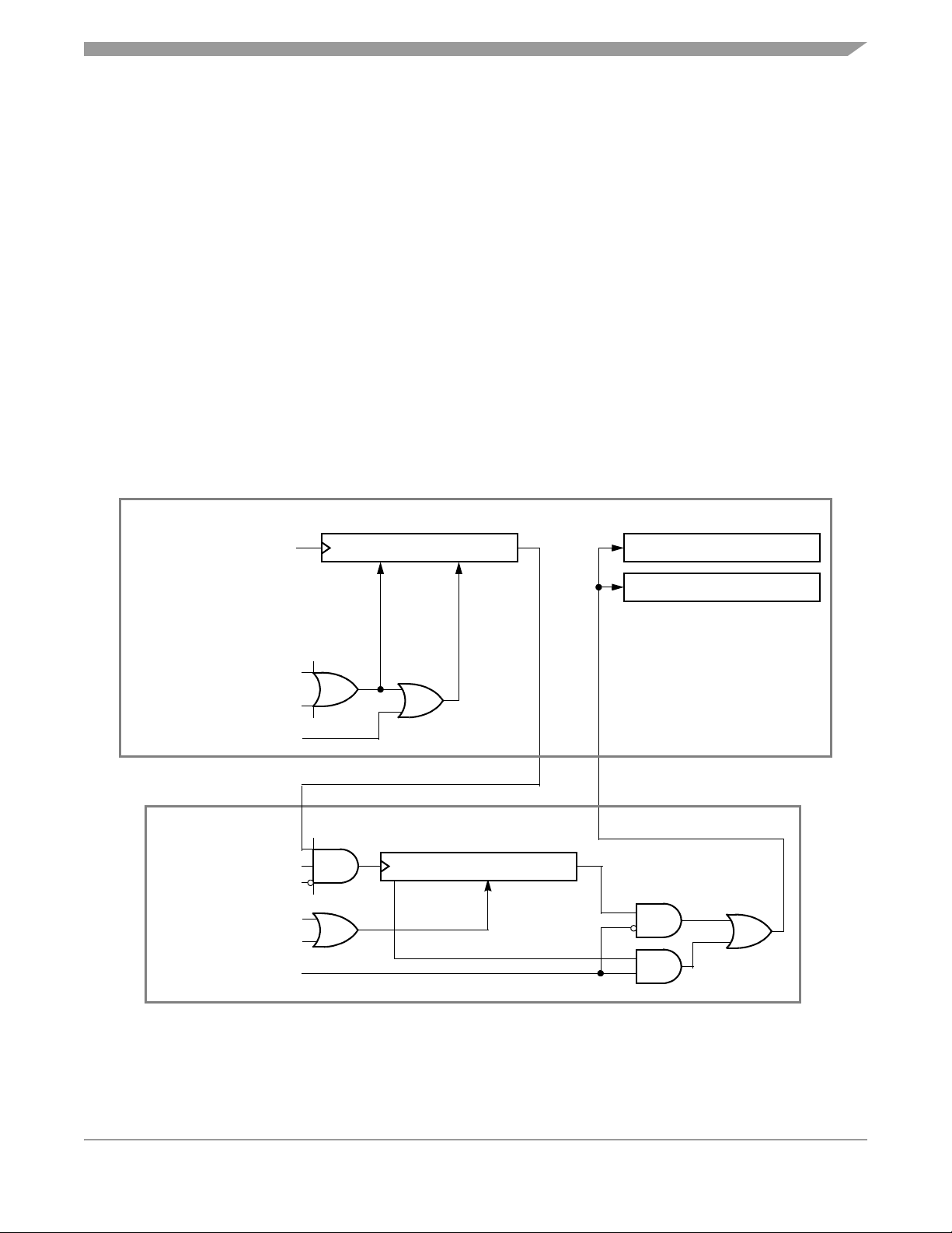
Chapter 6 Computer Operating Properly (COP) Module
6.1 Introduction
The computer operating properly (COP) module contains a free-running counter that generates a reset if
allowed to overflow. The COP module helps software recover from runaway code. Prevent a COP reset
by clearing the COP counter periodically. The COP module can be disabled through the COPD bit in the
CONFIG register.
6.2 Functional Description
Figure 6-1 shows the structure of the COP module.
SIM MODULE
BUSCLKX4
INTERNAL RESET SOURCES
RESET VECTOR FETCH
COPCTL WRITE
COPEN (FROM SIM)
COPD (FROM CONFIG1)
RESET
COPCTL WRITE
COP RATE SELECT
(COPRS FROM CONFIG1)
12-BIT SIM COUNTER
(1)
CLEAR ALL STAGES
COP CLOCK
CLEAR STAGES 5–12
COP TIMEOUT
COP MODULE
6-BIT COP COUNTER
CLEAR
COP COUNTER
SIM RESET CIRCUIT
RESET STATUS REGISTER
1. See Chapter 16 System Integration Module (SIM) for more details.
Figure 6-1. COP Block Diagram
MC68HC908GZ16 • MC68HC908GZ8 Data Sheet, Rev. 2
Freescale Semiconductor 85
Page 86

Computer Operating Properly (COP) Module
The COP counter is a free-running 6-bit counter preceded by a 12-bit prescaler counter. If not cleared by
software, the COP counter overflows and generates an asynchronous reset after 2
18–24
or 213–2
4
CGMXCLK cycles, depending on the state of the COP rate select bit, COPRS, in the configuration
register. With a 2
13–24
CGMXCLK cycle overflow option, a 4.9152-MHz crystal gives a COP timeout
period of 53.3 ms. Writing any value to location $FFFF before an overflow occurs prevents a COP reset
by clearing the COP counter and stages 12–5 of the prescaler.
NOTE
Service the COP immediately after reset and before entering or after exiting
stop mode to guarantee the maximum time before the first COP counter
overflow.
A COP reset pulls the RST
pin low for 32 CGMXCLK cycles and sets the COP bit in the reset status
register (RSR).
In monitor mode, the COP is disabled if the RST
on the RST pin disables the COP.
V
TST
pin or the IRQ1 is held at V
. During the break state,
TST
NOTE
Place COP clearing instructions in the main program and not in an interrupt
subroutine. Such an interrupt subroutine could keep the COP from
generating a reset even while the main program is not working properly.
6.3 I/O Signals
The following paragraphs describe the signals shown in Figure 6-1.
6.3.1 CGMXCLK
CGMXCLK is the crystal oscillator output signal. CGMXCLK frequency is equal to the crystal frequency.
6.3.2 STOP Instruction
The STOP instruction clears the COP prescaler.
6.3.3 COPCTL Write
Writing any value to the COP control register (COPCTL) clears the COP counter and clears bits 12–5 of
the prescaler. Reading the COP control register returns the low byte of the reset vector. See 6.4 COP
Control Register.
6.3.4 Power-On Reset
The power-on reset (POR) circuit clears the COP prescaler 4096 CGMXCLK cycles after power-up.
6.3.5 Internal Reset
An internal reset clears the COP prescaler and the COP counter.
MC68HC908GZ16 • MC68HC908GZ8 Data Sheet, Rev. 2
86 Freescale Semiconductor
Page 87

COP Control Register
6.3.6 Reset Vector Fetch
A reset vector fetch occurs when the vector address appears on the data bus. A reset vector fetch clears
the COP prescaler.
6.3.7 COPD (COP Disable)
The COPD signal reflects the state of the COP disable bit (COPD) in the configuration register. See
Chapter 5 Configuration Register (CONFIG).
6.3.8 COPRS (COP Rate Select)
The COPRS signal reflects the state of the COP rate select bit (COPRS) in the configuration register. See
Chapter 5 Configuration Register (CONFIG).
6.4 COP Control Register
The COP control register (COPCTL) is located at address $FFFF and overlaps the reset vector. Writing
any value to $FFFF clears the COP counter and starts a new timeout period. Reading location $FFFF
returns the low byte of the reset vector.
Address: $FFFF
Bit 7654321Bit 0
Read: Low byte of reset vector
Write: Clear COP counter
Reset: Unaffected by reset
Figure 6-2. COP Control Register (COPCTL)
6.5 Interrupts
The COP does not generate central processor unit (CPU) interrupt requests.
6.6 Monitor Mode
When monitor mode is entered with V
on the IRQ
having V
pin or the RST pin. When monitor mode is entered by having blank reset vectors and not
on the IRQ pin, the COP is automatically disabled until a POR occurs.
TST
on the IRQ pin, the COP is disabled as long as V
TST
remains
TST
6.7 Low-Power Modes
The WAIT and STOP instructions put the microcontroller unit (MCU) in low power-consumption standby
modes.
6.7.1 Wait Mode
The COP remains active during wait mode. If COP is enabled, a reset will occur at COP timeout.
MC68HC908GZ16 • MC68HC908GZ8 Data Sheet, Rev. 2
Freescale Semiconductor 87
Page 88

Computer Operating Properly (COP) Module
6.7.2 Stop Mode
Stop mode turns off the CGMXCLK input to the COP and clears the COP prescaler. Service the COP
immediately before entering or after exiting stop mode to ensure a full COP timeout period after entering
or exiting stop mode.
To prevent inadvertently turning off the COP with a STOP instruction, a configuration option is available
that disables the STOP instruction. When the STOP bit in the configuration register has the STOP
instruction disabled, execution of a STOP instruction results in an illegal opcode reset.
6.8 COP Module During Break Mode
The COP is disabled during a break interrupt when V
is present on the RST pin.
TST
MC68HC908GZ16 • MC68HC908GZ8 Data Sheet, Rev. 2
88 Freescale Semiconductor
Page 89

Chapter 7 Central Processor Unit (CPU)
7.1 Introduction
The M68HC08 CPU (central processor unit) is an enhanced and fully object-code-compatible version of
the M68HC05 CPU. The CPU08 Reference Manual (document order number CPU08RM/AD) contains a
description of the CPU instruction set, addressing modes, and architecture.
7.2 Features
Features of the CPU include:
• Object code fully upward-compatible with M68HC05 Family
• 16-bit stack pointer with stack manipulation instructions
• 16-bit index register with x-register manipulation instructions
• 8-MHz CPU internal bus frequency
• 64-Kbyte program/data memory space
• 16 addressing modes
• Memory-to-memory data moves without using accumulator
• Fast 8-bit by 8-bit multiply and 16-bit by 8-bit divide instructions
• Enhanced binary-coded decimal (BCD) data handling
• Modular architecture with expandable internal bus definition for extension of addressing range
beyond 64 Kbytes
• Low-power stop and wait modes
7.3 CPU Registers
Figure 7-1 shows the five CPU registers. CPU registers are not part of the memory map.
MC68HC908GZ16 • MC68HC908GZ8 Data Sheet, Rev. 2
Freescale Semiconductor 89
Page 90
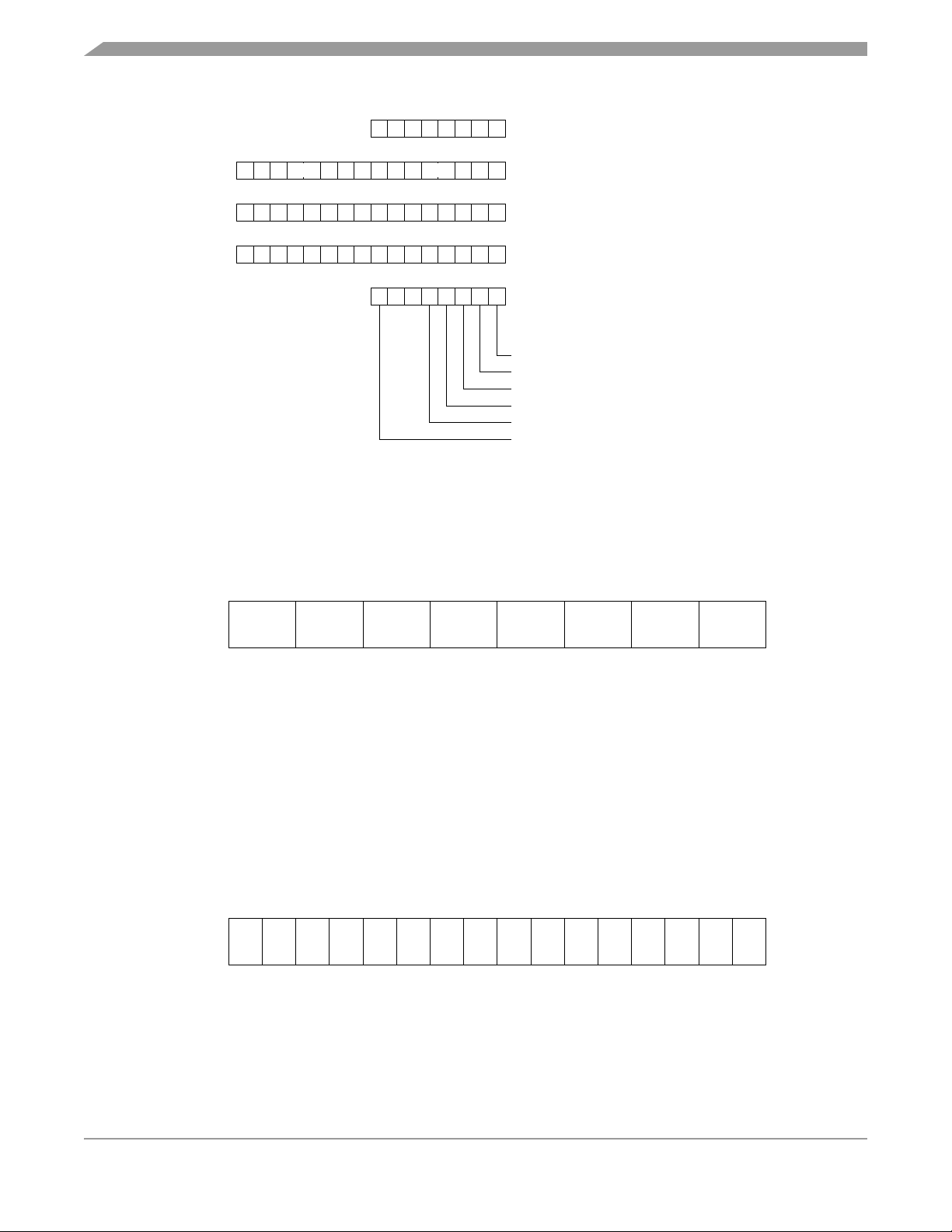
Central Processor Unit (CPU)
7
15
H X
15
15
70
V11H I NZC
0
ACCUMULATOR (A)
0
INDEX REGISTER (H:X)
0
STACK POINTER (SP)
0
PROGRAM COUNTER (PC)
CONDITION CODE REGISTER (CCR)
CARRY/BORROW FLAG
ZERO FLAG
NEGATIVE FLAG
INTERRUPT MASK
HALF-CARRY FLAG
TWO’S COMPLEMENT OVERFLOW FLAG
Figure 7-1. CPU Registers
7.3.1 Accumulator
The accumulator is a general-purpose 8-bit register. The CPU uses the accumulator to hold operands and
the results of arithmetic/logic operations.
Bit 7654321Bit 0
Read:
Write:
Reset: Unaffected by reset
Figure 7-2. Accumulator (A)
7.3.2 Index Register
The 16-bit index register allows indexed addressing of a 64-Kbyte memory space. H is the upper byte of
the index register, and X is the lower byte. H:X is the concatenated 16-bit index register.
In the indexed addressing modes, the CPU uses the contents of the index register to determine the
conditional address of the operand.
The index register can serve also as a temporary data storage location.
Bit
151413121110987654321
Read:
Write:
Reset:00000000XXXXXXXX
X = Indeterminate
Figure 7-3. Index Register (H:X)
Bit
0
MC68HC908GZ16 • MC68HC908GZ8 Data Sheet, Rev. 2
90 Freescale Semiconductor
Page 91

CPU Registers
7.3.3 Stack Pointer
The stack pointer is a 16-bit register that contains the address of the next location on the stack. During a
reset, the stack pointer is preset to $00FF. The reset stack pointer (RSP) instruction sets the least
significant byte to $FF and does not affect the most significant byte. The stack pointer decrements as data
is pushed onto the stack and increments as data is pulled from the stack.
In the stack pointer 8-bit offset and 16-bit offset addressing modes, the stack pointer can function as an
index register to access data on the stack. The CPU uses the contents of the stack pointer to determine
the conditional address of the operand.
Bit
151413121110987654321
Read:
Write:
Reset:0000000011111111
Bit
0
Figure 7-4. Stack Pointer (SP)
NOTE
The location of the stack is arbitrary and may be relocated anywhere in
random-access memory (RAM). Moving the SP out of page 0 ($0000 to
$00FF) frees direct address (page 0) space. For correct operation, the
stack pointer must point only to RAM locations.
7.3.4 Program Counter
The program counter is a 16-bit register that contains the address of the next instruction or operand to be
fetched.
Normally, the program counter automatically increments to the next sequential memory location every
time an instruction or operand is fetched. Jump, branch, and interrupt operations load the program
counter with an address other than that of the next sequential location.
During reset, the program counter is loaded with the reset vector address located at $FFFE and $FFFF.
The vector address is the address of the first instruction to be executed after exiting the reset state.
Bit
151413121110987654321
Read:
Write:
Reset: Loaded with vector from $FFFE and $FFFF
Bit
0
Figure 7-5. Program Counter (PC)
MC68HC908GZ16 • MC68HC908GZ8 Data Sheet, Rev. 2
Freescale Semiconductor 91
Page 92

Central Processor Unit (CPU)
7.3.5 Condition Code Register
The 8-bit condition code register contains the interrupt mask and five flags that indicate the results of the
instruction just executed. Bits 6 and 5 are set permanently to 1. The following paragraphs describe the
functions of the condition code register.
Bit 7654321Bit 0
Read:
Write:
Reset:X11X1XXX
V — Overflow Flag
The CPU sets the overflow flag when a two's complement overflow occurs. The signed branch
instructions BGT, BGE, BLE, and BLT use the overflow flag.
1 = Overflow
0 = No overflow
H — Half-Carry Flag
The CPU sets the half-carry flag when a carry occurs between accumulator bits 3 and 4 during an
add-without-carry (ADD) or add-with-carry (ADC) operation. The half-carry flag is required for
binary-coded decimal (BCD) arithmetic operations. The DAA instruction uses the states of the H and
C flags to determine the appropriate correction factor.
1 = Carry between bits 3 and 4
0 = No carry between bits 3 and 4
V11H I NZC
X = Indeterminate
Figure 7-6. Condition Code Register (CCR)
I — Interrupt Mask
When the interrupt mask is set, all maskable CPU interrupts are disabled. CPU interrupts are enabled
when the interrupt mask is cleared. When a CPU interrupt occurs, the interrupt mask is set
automatically after the CPU registers are saved on the stack, but before the interrupt vector is fetched.
1 = Interrupts disabled
0 = Interrupts enabled
NOTE
To maintain M6805 Family compatibility, the upper byte of the index
register (H) is not stacked automatically. If the interrupt service routine
modifies H, then the user must stack and unstack H using the PSHH and
PULH instructions.
After the I bit is cleared, the highest-priority interrupt request is serviced first.
A return-from-interrupt (RTI) instruction pulls the CPU registers from the stack and restores the
interrupt mask from the stack. After any reset, the interrupt mask is set and can be cleared only by the
clear interrupt mask software instruction (CLI).
N — Negative Flag
The CPU sets the negative flag when an arithmetic operation, logic operation, or data manipulation
produces a negative result, setting bit 7 of the result.
1 = Negative result
0 = Non-negative result
MC68HC908GZ16 • MC68HC908GZ8 Data Sheet, Rev. 2
92 Freescale Semiconductor
Page 93

Arithmetic/Logic Unit (ALU)
Z — Zero Flag
The CPU sets the zero flag when an arithmetic operation, logic operation, or data manipulation
produces a result of $00.
1 = Zero result
0 = Non-zero result
C — Carry/Borrow Flag
The CPU sets the carry/borrow flag when an addition operation produces a carry out of bit 7 of the
accumulator or when a subtraction operation requires a borrow. Some instructions — such as bit test
and branch, shift, and rotate — also clear or set the carry/borrow flag.
1 = Carry out of bit 7
0 = No carry out of bit 7
7.4 Arithmetic/Logic Unit (ALU)
The ALU performs the arithmetic and logic operations defined by the instruction set.
Refer to the CPU08 Reference Manual (document order number CPU08RM/AD) for a description of the
instructions and addressing modes and more detail about the architecture of the CPU.
7.5 Low-Power Modes
The WAIT and STOP instructions put the MCU in low power-consumption standby modes.
7.5.1 Wait Mode
The WAIT instruction:
• Clears the interrupt mask (I bit) in the condition code register, enabling interrupts. After exit from
wait mode by interrupt, the I bit remains clear. After exit by reset, the I bit is set.
• Disables the CPU clock
7.5.2 Stop Mode
The STOP instruction:
• Clears the interrupt mask (I bit) in the condition code register, enabling external interrupts. After
exit from stop mode by external interrupt, the I bit remains clear. After exit by reset, the I bit is set.
• Disables the CPU clock
After exiting stop mode, the CPU clock begins running after the oscillator stabilization delay.
7.6 CPU During Break Interrupts
If a break module is present on the MCU, the CPU starts a break interrupt by:
• Loading the instruction register with the SWI instruction
• Loading the program counter with $FFFC:$FFFD or with $FEFC:$FEFD in monitor mode
The break interrupt begins after completion of the CPU instruction in progress. If the break address
register match occurs on the last cycle of a CPU instruction, the break interrupt begins immediately.
A return-from-interrupt instruction (RTI) in the break routine ends the break interrupt and returns the MCU
to normal operation if the break interrupt has been deasserted.
MC68HC908GZ16 • MC68HC908GZ8 Data Sheet, Rev. 2
Freescale Semiconductor 93
Page 94
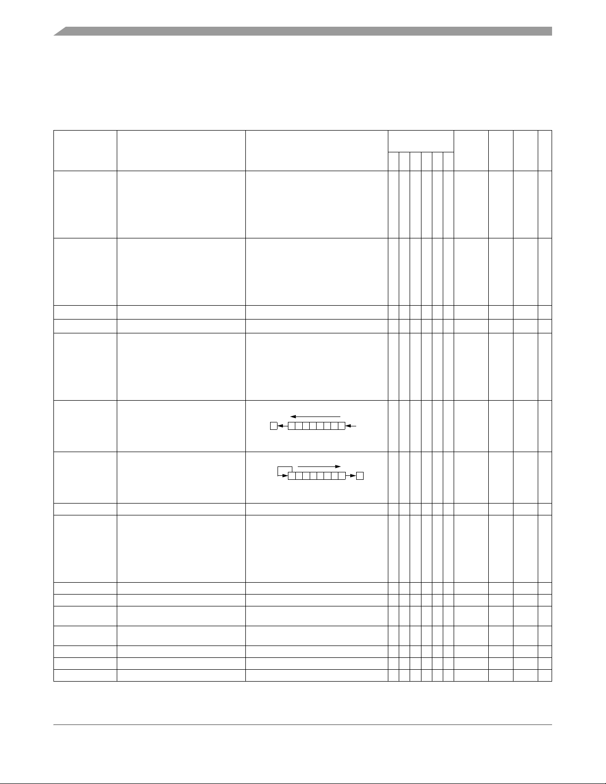
Central Processor Unit (CPU)
7.7 Instruction Set Summary
Table 7-1 provides a summary of the M68HC08 instruction set.
Table 7-1. Instruction Set Summary (Sheet 1 of 6)
Effect
Source
Form
ADC #opr
ADC opr
ADC opr
ADC opr,X
ADC opr,X
ADC ,X
ADC opr,SP
ADC opr,SP
ADD #opr
ADD opr
ADD opr
ADD opr,X
ADD opr,X
ADD ,X
ADD opr,SP
ADD opr,SP
AIS #
opr Add Immediate Value (Signed) to SP
AIX #opr Add Immediate Value (Signed) to H:X
AND #opr
AND opr
AND opr
AND opr,X
AND opr,X
AND ,X
AND opr,SP
AND opr,SP
ASL opr
ASLA
ASLX
ASL opr,X
ASL ,X
ASL opr,SP
ASR opr
ASRA
ASRX
ASR opr,X
ASR opr,X
ASR opr,SP
BCC rel Branch if Carry Bit Clear PC ← (PC) + 2 + rel ? (C) = 0 ––––––REL 24 rr 3
BCLR n, opr Clear Bit n in M Mn ← 0 ––––––
BCS rel Branch if Carry Bit Set (Same as BLO) PC ← (PC) + 2 + rel ? (C) = 1 ––––––REL 25 rr 3
BEQ rel Branch if Equal PC ← (PC) + 2 + rel ? (Z) = 1 ––––––REL 27 rr 3
BGE opr
BGT opr
BHCC rel Branch if Half Carry Bit Clear PC ← (PC) + 2 + rel ? (H) = 0 ––––––REL 28 rr 3
BHCS rel Branch if Half Carry Bit Set PC ← (PC) + 2 + rel ? (H) = 1 ––––––REL 29 rr 3
BHI rel Branch if Higher PC ← (PC) + 2 + rel ? (C) | (Z) = 0 ––––––REL 22 rr 3
Add with Carry A ← (A) + (M) + (C) –
Add without Carry A ← (A) + (M) –
Logical AND A ← (A) & (M) 0 – – –
Arithmetic Shift Left
(Same as LSL)
Arithmetic Shift Right ––
Branch if Greater Than or Equal To
(Signed Operands)
Branch if Greater Than (Signed
Operands)
Operation Description
SP ← (SP) + (16
H:X ← (H:X) + (16
C
b7
b7
PC ← (PC) + 2 + rel ? (N
PC ← (PC) + 2 + rel ? (Z) | (N
« M)
« M)
0
b0
C
b0
⊕ V) = 0
⊕ V) = 0
on CCR
VH I NZC
––––––IMM A7 ii 2
––––––IMM AF ii 2
––
––––––REL 90 rr 3
––––––REL 92 rr 3
Address
IMM
DIR
EXT
IX2
IX1
IX
SP1
SP2
IMM
DIR
EXT
IX2
IX1
IX
SP1
SP2
IMM
DIR
EXT
IX2
IX1
IX
SP1
SP2
DIR
INH
INH
IX1
IX
SP1
DIR
INH
INH
IX1
IX
SP1
DIR (b0)
DIR (b1)
DIR (b2)
DIR (b3)
DIR (b4)
DIR (b5)
DIR (b6)
DIR (b7)
Mode
9EE9
9ED9
9EEB
9EDB
9EE4
9ED4
9E68
9E67
A9
B9
C9
D9
E9
F9
AB
BB
CB
DB
EB
FB
A4
B4
C4
D4
E4
F4
38
48
58
68
78
37
47
57
67
77
11
13
15
17
19
1B
1D
1F
Opcode
ii
dd
hh ll
ee ff
ff
ff
ee ff
ii
dd
hh ll
ee ff
ff
ff
ee ff
ii
dd
hh ll
ee ff
ff
ff
ee ff
dd
ff
ff
dd
ff
ff
dd
dd
dd
dd
dd
dd
dd
dd
Operand
Cycles
2
3
4
4
3
2
4
5
2
3
4
4
3
2
4
5
2
3
4
4
3
2
4
5
4
1
1
4
3
5
4
1
1
4
3
5
4
4
4
4
4
4
4
4
MC68HC908GZ16 • MC68HC908GZ8 Data Sheet, Rev. 2
94 Freescale Semiconductor
Page 95

Instruction Set Summary
Table 7-1. Instruction Set Summary (Sheet 2 of 6)
Effect
Source
Form
BHS rel
BIH rel Branch if IRQ
BIL rel Branch if IRQ
BIT #opr
BIT opr
BIT opr
BIT opr,X
BIT opr,X
BIT ,X
BIT opr,SP
BIT opr,SP
BLE opr
BLO rel Branch if Lower (Same as BCS) PC ← (PC) + 2 + rel ? (C) = 1 ––––––REL 25 rr 3
BLS rel Branch if Lower or Same PC ← (PC) + 2 + rel ? (C) | (Z) = 1 ––––––REL 23 rr 3
BLT opr Branch if Less Than (Signed Operands)
BMC rel Branch if Interrupt Mask Clear PC ← (PC) + 2 + rel ? (I) = 0 ––––––REL 2C rr 3
BMI rel Branch if Minus PC ← (PC) + 2 + rel ? (N) = 1 ––––––REL 2B rr 3
BMS rel Branch if Interrupt Mask Set PC ← (PC) + 2 + rel ? (I) = 1 ––––––REL 2D rr 3
BNE rel Branch if Not Equal PC ← (PC) + 2 + rel ? (Z) = 0 ––––––REL 26 rr 3
BPL rel Branch if Plus PC ← (PC) + 2 + rel ? (N) = 0 ––––––REL 2A rr 3
BRA rel Branch Always PC ← (PC) + 2 + rel ––––––REL 20 rr 3
BRCLR n,opr,rel Branch if Bit n in M Clear PC ← (PC) + 3 + rel ? (Mn) = 0 –––––
BRN rel Branch Never PC ← (PC) + 2 ––––––REL 21 rr 3
BRSET n,opr,rel Branch if Bit n in M Set PC ← (PC) + 3 +
BSET n,opr Set Bit n in M Mn ← 1 ––––––
BSR rel Branch to Subroutine
CBEQ opr,rel
CBEQA #opr,rel
CBEQX #opr,rel
CBEQ opr,X+,rel
CBEQ X+,rel
CBEQ opr,SP,rel
CLC Clear Carry Bit C ← 0 –––––0INH 98 1
CLI Clear Interrupt Mask I ← 0 ––0–––INH 9A 2
Branch if Higher or Same
(Same as BCC)
Bit Test (A) & (M) 0 – – –
Branch if Less Than or Equal To
(Signed Operands)
Compare and Branch if Equal
Operation Description
PC ← (PC) + 2 + rel ? (C) = 0 ––––––REL 24 rr 3
Pin High PC ← (PC) + 2 + rel ? IRQ = 1 ––––––REL 2F rr 3
Pin Low PC ← (PC) + 2 + rel ? IRQ = 0 ––––––REL 2E rr 3
PC ← (PC) + 2 + rel ? (Z) | (N
PC ← (PC) + 2 + rel ? (N
rel ? (Mn) = 1 –––––
PC ← (PC) + 2; push (PCL)
SP ← (SP) – 1; push (PCH)
SP ← (SP) – 1
PC ← (PC) + rel
PC ← (PC) + 3 + rel ? (A) – (M) = $00
PC ← (PC) + 3 + rel ? (A) – (M) = $00
PC ← (PC) + 3 + rel ? (X) – (M) = $00
PC ← (PC) + 3 + rel ? (A) – (M) = $00
PC ← (PC) + 2 + rel ? (A) – (M) = $00
PC ← (PC) + 4 + rel ? (A) – (M) = $00
⊕ V) = 1
⊕ V) =1
on CCR
VH I NZC
––––––REL 93 rr 3
––––––REL 91 rr 3
––––––REL AD rr 4
––––––
Address
IMM
DIR
EXT
IX2
IX1
IX
SP1
SP2
DIR (b0)
DIR (b1)
DIR (b2)
DIR (b3)
DIR (b4)
DIR (b5)
DIR (b6)
DIR (b7)
DIR (b0)
DIR (b1)
DIR (b2)
DIR (b3)
DIR (b4)
DIR (b5)
DIR (b6)
DIR (b7)
DIR (b0)
DIR (b1)
DIR (b2)
DIR (b3)
DIR (b4)
DIR (b5)
DIR (b6)
DIR (b7)
DIR
IMM
IMM
IX1+
IX+
SP1
Mode
9EE5
9ED5
9E61
A5
B5
C5
D5
E5
F5
01
03
05
07
09
0B
0D
0F
00
02
04
06
08
0A
0C
0E
10
12
14
16
18
1A
1C
1E
31
41
51
61
71
Opcode
ii
dd
hh ll
ee ff
ff
ff
ee ff
dd rr
dd rr
dd rr
dd rr
dd rr
dd rr
dd rr
dd rr
dd rr
dd rr
dd rr
dd rr
dd rr
dd rr
dd rr
dd rr
dd
dd
dd
dd
dd
dd
dd
dd
dd rr
ii rr
ii rr
ff rr
rr
ff rr
Operand
2
3
4
4
3
2
4
5
5
5
5
5
5
5
5
5
5
5
5
5
5
5
5
5
4
4
4
4
4
4
4
4
5
4
4
5
4
6
Cycles
MC68HC908GZ16 • MC68HC908GZ8 Data Sheet, Rev. 2
Freescale Semiconductor 95
Page 96
Central Processor Unit (CPU)
Source
Form
CLR opr
CLRA
CLRX
CLRH
CLR opr,X
CLR ,X
CLR opr,SP
CMP #opr
CMP opr
CMP opr
CMP opr,X
CMP opr,X
CMP ,X
CMP opr,SP
CMP opr,SP
COM
opr
COMA
COMX
COM opr,X
COM ,X
COM opr,SP
CPHX #opr
CPHX opr
CPX #opr
CPX opr
CPX opr
CPX ,X
CPX opr,X
CPX opr,X
CPX opr,SP
CPX opr,SP
DAA Decimal Adjust A
DBNZ opr,rel
DBNZA rel
DBNZX rel
DBNZ opr,X,rel
DBNZ X,rel
DBNZ opr,SP,rel
DEC opr
DECA
DECX
DEC opr,X
DEC ,X
DEC opr,SP
DIV Divide
EOR #opr
EOR opr
EOR opr
EOR opr,X
EOR opr,X
EOR ,X
EOR opr,SP
EOR opr,SP
INC opr
INCA
INCX
INC opr,X
INC ,X
INC opr,SP
Clear
Compare A with M (A) – (M) ––
Complement (One’s Complement)
Compare H:X with M (H:X) – (M:M + 1) ––
Compare X with M (X) – (M) ––
Decrement and Branch if Not Zero
Decrement
Exclusive OR M with A
Increment
Operation Description
Table 7-1. Instruction Set Summary (Sheet 3 of 6)
Effect
on CCR
VH I NZC
M ← $00
A ← $00
X ← $00
H ← $00
M ← $00
M ← $00
M ← $00
M ← (M
) = $FF – (M)
A ← (A
) = $FF – (M)
) = $FF – (M)
X ← (X
M ← (M
) = $FF – (M)
M ← (M
) = $FF – (M)
) = $FF – (M)
M ← (M
(A)
10
A ← (A) – 1 or M ← (M) – 1 or X ← (X) – 1
PC ← (PC) + 3 + rel ? (result) ≠ 0
PC ← (PC) + 2 + rel ? (result) ≠ 0
PC ← (PC) + 2 + rel ? (result) ≠ 0
PC ← (PC) + 3 + rel ? (result) ≠ 0
PC ← (PC) + 2 + rel ? (result) ≠ 0
PC ← (PC) + 4 + rel ? (result) ≠ 0
M
← (M) – 1
A ← (A) – 1
X ← (X) – 1
M ← (M) – 1
M ← (M) – 1
M ← (M) – 1
A ← (H:A)/(X)
H ← Remainder
A ← (A
⊕ M)
M ← (M) + 1
A ← (A) + 1
X ← (X) + 1
M ← (M) + 1
M ← (M) + 1
M ← (M) + 1
0––01–
0––1
U–– INH 72 2
––––––
–––
––––INH 52 7
0–––
–––
DIR
INH
INH
INH
IX1
IX
SP1
IMM
DIR
EXT
IX2
IX1
IX
SP1
SP2
DIR
INH
INH
IX1
IX
SP1
IMM
DIR
IMM
DIR
EXT
IX2
IX1
IX
SP1
SP2
DIR
INH
INH
IX1
IX
SP1
DIR
INH
INH
IX1
IX
SP1
IMM
DIR
EXT
IX2
IX1
IX
SP1
SP2
DIR
INH
INH
IX1
IX
SP1
Address
Mode
Opcode
3F
dd
4F
5F
8C
6F
ff
7F
9E6F
ff
ii
A1
dd
B1
hh ll
C1
ee ff
D1
ff
E1
F1
ff
9EE1
ee ff
9ED1
33
dd
43
53
63
ff
73
9E63
ff
6575ii ii+1dd3
A3
ii
B3
dd
C3
hh ll
D3
ee ff
E3
ff
F3
9EE3
ff
9ED3
ee ff
3B
dd rr
4B
rr
5B
rr
6B
ff rr
7B
rr
9E6B
ff rr
3A
dd
4A
5A
6A
ff
7A
9E6A
ff
A8
ii
B8
dd
C8
hh ll
D8
ee ff
E8
ff
F8
9EE8
ff
9ED8
ee ff
3C
dd
4C
5C
6C
ff
7C
9E6C
ff
Operand
Cycles
3
1
1
1
3
2
4
2
3
4
4
3
2
4
5
4
1
1
4
3
5
4
2
3
4
4
3
2
4
5
5
3
3
5
4
6
4
1
1
4
3
5
2
3
4
4
3
2
4
5
4
1
1
4
3
5
MC68HC908GZ16 • MC68HC908GZ8 Data Sheet, Rev. 2
96 Freescale Semiconductor
Page 97

Instruction Set Summary
Table 7-1. Instruction Set Summary (Sheet 4 of 6)
Effect
Source
Form
JMP opr
JMP opr
JMP opr,X
JMP opr,X
JMP ,X
JSR opr
JSR opr
JSR opr,X
JSR opr,X
JSR ,X
LDA #opr
LDA opr
LDA opr
LDA opr,X
LDA opr,X
LDA ,X
LDA opr,SP
LDA opr,SP
LDHX #opr
LDHX opr
LDX #opr
LDX opr
LDX opr
LDX opr,X
LDX opr,X
LDX ,X
LDX opr,SP
LDX opr,SP
LSL opr
LSLA
LSLX
LSL opr,X
LSL ,X
LSL opr,SP
LSR opr
LSRA
LSRX
LSR opr,X
LSR ,X
LSR opr,SP
MOV opr,opr
MOV opr,X+
MOV #opr,opr
MOV X+,opr
MUL Unsigned multiply X:A ← (X) × (A) –0–––0INH 42 5
NEG opr
NEGA
NEGX
NEG opr,X
NEG ,X
NEG opr,SP
NOP No Operation None ––––––INH 9D 1
NSA Nibble Swap A A ← (A[3:0]:A[7:4]) ––––––INH 62 3
ORA #opr
ORA opr
ORA opr
ORA opr,X
ORA opr,X
ORA ,X
ORA opr,SP
ORA opr,SP
PSHA Push A onto Stack Push (A); SP ← (SP) – 1 ––––––INH 87 2
PSHH Push H onto Stack Push (H); SP ← (SP) – 1 ––––––INH 8B 2
PSHX Push X onto Stack Push (X); SP ← (SP) – 1 ––––––INH 89 2
Jump PC ← Jump Address ––––––
Jump to Subroutine
Load A from M A ← (M) 0–––
Load H:X from M H:X ← (M:M + 1) 0–––
Load X from M X ← (M) 0–––
Logical Shift Left
(Same as ASL)
Logical Shift Right ––0
Move
Negate (Two’s Complement)
Inclusive OR A and M A ← (A) | (M) 0 – – –
Operation Description
PC ← (PC) + n (n = 1, 2, or 3)
Push (PCL); SP ← (SP) – 1
Push (PCH); SP ← (SP) – 1
PC ← Unconditional Address
C
b7
b7
(M)
Destination
H:X ← (H:X) + 1 (IX+D, DIX+)
M ← –(M) = $00 – (M)
A ← –(A) = $00 – (A)
X ← –(X) = $00 – (X)
M ← –(M) = $00 – (M)
M ← –(M) = $00 – (M)
← (M)
0
b0
C0
b0
Source
on CCR
VH I NZC
––––––
––
0–––
––
DIR
EXT
IX2
IX1
IX
DIR
EXT
IX2
IX1
IX
IMM
DIR
EXT
IX2
IX1
IX
SP1
SP2
IMM
DIR
IMM
DIR
EXT
IX2
IX1
IX
SP1
SP2
DIR
INH
INH
IX1
IX
SP1
DIR
INH
INH
IX1
IX
SP1
DD
DIX+
IMD
IX+D
DIR
INH
INH
IX1
IX
SP1
IMM
DIR
EXT
IX2
IX1
IX
SP1
SP2
Address
Mode
Opcode
BC
dd
CC
hh ll
DC
ee ff
EC
ff
FC
BD
dd
CD
hh ll
DD
ee ff
ED
ff
FD
A6
ii
B6
dd
C6
hh ll
D6
ee ff
E6
ff
F6
9EE6
ff
9ED6
ee ff
4555ii jjdd3
AE
ii
BE
dd
CE
hh ll
DE
ee ff
EE
ff
FE
9EEE
ff
9EDE
ee ff
38
dd
48
58
68
ff
78
9E68
ff
34
dd
44
54
64
ff
74
9E64
ff
4E
dd dd
5E
dd
6E
ii dd
7E
dd
30
dd
40
50
60
ff
70
9E60
ff
AA
ii
BA
dd
hh ll
CA
ee ff
DA
ff
EA
FA
ff
9EEA
ee ff
9EDA
Operand
2
3
4
3
2
4
5
6
5
4
2
3
4
4
3
2
4
5
4
2
3
4
4
3
2
4
5
4
1
1
4
3
5
4
1
1
4
3
5
5
4
4
4
4
1
1
4
3
5
2
3
4
4
3
2
4
5
Cycles
MC68HC908GZ16 • MC68HC908GZ8 Data Sheet, Rev. 2
Freescale Semiconductor 97
Page 98
Central Processor Unit (CPU)
Table 7-1. Instruction Set Summary (Sheet 5 of 6)
Effect
Source
Form
PULA Pull A from Stack SP ← (SP + 1); Pull (A) ––––––INH 86 2
PULH Pull H from Stack SP ← (SP + 1); Pull (H) ––––––INH 8A 2
PULX Pull X from Stack SP ← (SP + 1); Pull (X) ––––––INH 88 2
ROL opr
ROLA
ROLX
ROL opr,X
ROL ,X
ROL opr,SP
ROR opr
RORA
RORX
ROR opr,X
ROR ,X
ROR opr,SP
RSP Reset Stack Pointer SP ← $FF ––––––INH 9C 1
RTI Return from Interrupt
RTS Return from Subroutine
SBC #opr
SBC opr
SBC opr
SBC opr,X
SBC opr,X
SBC ,X
SBC opr,SP
SBC opr,SP
SEC Set Carry Bit C ← 1 –––––1INH 99 1
SEI Set Interrupt Mask I ← 1 ––1–––INH 9B 2
STA opr
STA opr
STA opr,X
STA opr,X
STA ,X
STA opr,SP
STA opr,SP
STHX opr Store H:X in M (M:M + 1) ← (H:X) 0 – – – DIR 35 dd 4
STOP
STX opr
STX opr
STX opr,X
STX opr,X
STX ,X
STX opr,SP
STX opr,SP
SUB #opr
SUB opr
SUB opr
SUB opr,X
SUB opr,X
SUB ,X
SUB opr,SP
SUB opr,SP
Rotate Left through Carry ––
Rotate Right through Carry ––
Subtract with Carry A ← (A) – (M) – (C) ––
Store A in M M ← (A) 0–––
Enable Interrupts, Stop Processing,
Refer to MCU Documentation
Store X in M M ← (X) 0–––
Subtract A ← (A) – (M) ––
Operation Description
C
b7
b7
SP ← (SP) + 1; Pull (CCR)
SP ← (SP) + 1; Pull (A)
SP ← (SP) + 1; Pull (X)
(SP) + 1; Pull (PCH)
SP ←
SP ← (SP) + 1; Pull (PCL)
SP ← SP + 1; Pull (PCH)
SP ← SP + 1; Pull (PCL)
I ← 0; Stop Processing ––0–––INH 8E 1
b0
b0
C
on CCR
VH I NZC
INH 80 7
––––––INH 81 4
DIR
INH
INH
IX1
IX
SP1
DIR
INH
INH
IX1
IX
SP1
IMM
DIR
EXT
IX2
IX1
IX
SP1
SP2
DIR
EXT
IX2
IX1
IX
SP1
SP2
DIR
EXT
IX2
IX1
IX
SP1
SP2
IMM
DIR
EXT
IX2
IX1
IX
SP1
SP2
Address
Mode
9E69
9E66
9EE2
9ED2
9EE7
9ED7
9EEF
9EDF
9EE0
9ED0
39
49
59
69
79
36
46
56
66
76
A2
B2
C2
D2
E2
F2
B7
C7
D7
E7
F7
BF
CF
DF
EF
FF
A0
B0
C0
D0
E0
F0
Opcode
dd
ff
ff
dd
ff
ff
ii
dd
hh ll
ee ff
ff
ff
ee ff
dd
hh ll
ee ff
ff
ff
ee ff
dd
hh ll
ee ff
ff
ff
ee ff
ii
dd
hh ll
ee ff
ff
ff
ee ff
Operand
Cycles
4
1
1
4
3
5
4
1
1
4
3
5
2
3
4
4
3
2
4
5
3
4
4
3
2
4
5
3
4
4
3
2
4
5
2
3
4
4
3
2
4
5
MC68HC908GZ16 • MC68HC908GZ8 Data Sheet, Rev. 2
98 Freescale Semiconductor
Page 99
Opcode Map
Table 7-1. Instruction Set Summary (Sheet 6 of 6)
Effect
Source
Form
SWI Software Interrupt
TAP Transfer A to CCR CCR ← (A) INH 84 2
TAX Transfer A to X X ← (A) ––––––INH 97 1
TPA Transfer CCR to A A ← (CCR) ––––––INH 85 1
TST opr
TSTA
TSTX
TST opr,X
TST ,X
TST opr,SP
TSX Transfer SP to H:X H:X ← (SP) + 1 ––––––INH 95 2
TXA Transfer X to A A ← (X) ––––––INH 9F 1
TXS Transfer H:X to SP (SP) ← (H:X) – 1 ––––––INH 94 2
WAIT Enable Interrupts; Wait for Interrupt
A Accumulator n Any bit
C Carry/borrow bit opr Operand (one or two bytes)
CCR Condition code register PC Program counter
dd Direct address of operand PCH Program counter high byte
dd rr Direct address of operand and relative offset of branch instruction PCL Program counter low byte
DD Direct to direct addressing mode REL Relative addressing mode
DIR Direct addressing mode rel Relative program counter offset byte
DIX+ Direct to indexed with post increment addressing mode rr Relative program counter offset byte
ee ff High and low bytes of offset in indexed, 16-bit offset addressing SP1 Stack pointer, 8-bit offset addressing mode
EXT Extended addressing mode SP2 Stack pointer 16-bit offset addressing mode
ff Offset byte in indexed, 8-bit offset addressing SP Stack pointer
H Half-carry bit U Undefined
H Index register high byte V Overflow bit
hh ll High and low bytes of operand address in extended addressing X Index register low byte
I Interrupt mask Z Zero bit
ii Immediate operand byte & Logical AND
IMD Immediate source to direct destination addressing mode | Logical OR
IMM Immediate addressing mode
INH Inherent addressing mode ( ) Contents of
IX Indexed, no offset addressing mode –( ) Negation (two’s complement)
IX+ Indexed, no offset, post increment addressing mode # Immediate value
IX+D Indexed with post increment to direct addressing mode
IX1 Indexed, 8-bit offset addressing mode ← Loaded with
IX1+ Indexed, 8-bit offset, post increment addressing mode ? If
IX2 Indexed, 16-bit offset addressing mode : Concatenated with
M Memory location Set or cleared
N Negative bit — Not affected
Test for Negative or Zero (A) – $00 or (X) – $00 or (M) – $00 0 – – –
Operation Description
PC ← (PC) + 1; Push (PCL)
SP ← (SP) – 1; Push (PCH)
SP ← (SP) – 1; Push (X)
SP ← (SP) – 1; Push (A)
SP ← (SP) – 1; Push (CCR)
SP ← (SP) – 1; I ← 1
PCH ← Interrupt Vector High Byte
PCL ← Interrupt Vector Low Byte
I bit ← 0; Inhibit CPU clocking
until interrupted
⊕ Logical EXCLUSIVE OR
« Sign extend
on CCR
VH I NZC
––1–––INH 83 9
––0–––INH 8F 1
DIR
INH
INH
IX1
IX
SP1
Address
Mode
9E6D
3D
4D
5D
6D
7D
Opcode
dd
ff
ff
Operand
3
1
1
3
2
4
Cycles
7.8 Opcode Map
See Table 7-2.
MC68HC908GZ16 • MC68HC908GZ8 Data Sheet, Rev. 2
Freescale Semiconductor 99
Page 100

100 Freescale Semiconductor
MC68HC908GZ16 • MC68HC908GZ8 Data Sheet, Rev. 2
MSB
LSB
05BRSET0
3DIR
15BRCLR0
3DIR
25BRSET1
3DIR
35BRCLR1
3DIR
45BRSET2
3DIR
55BRCLR2
3DIR
65BRSET3
3DIR
75BRCLR3
3DIR
85BRSET4
3DIR
95BRCLR4
3DIR
A5BRSET5
3DIR
B5BRCLR5
3DIR
C5BRSET6
3DIR
D5BRCLR6
3DIR
E5BRSET7
3DIR
F5BRCLR7
3DIR
Table 7-2. Opcode Map
Bit Manipulation Branch Read-Modify-Write Control Register/Memory
DIR DIR REL DIR INH INH IX1 SP1 IX INH INH IMM DIR EXT IX2 SP2 IX1 SP1 IX
0 1 2 3 4 5 6 9E6 7 8 9 A B C D 9ED E 9EE F
4
BSET0
2DIR
4
BCLR0
2DIR
4
BSET1
2DIR
4
BCLR1
2DIR
4
BSET2
2DIR
4
BCLR2
2DIR
4
BSET3
2DIR
4
BCLR3
2DIR
4
BSET4
2DIR
4
BCLR4
2DIR
4
BSET5
2DIR
4
BCLR5
2DIR
4
BSET6
2DIR
4
BCLR6
2DIR
4
BSET7
2DIR
4
BCLR7
2DIR
3
BRA
2REL
3
BRN
2REL
3
BHI
2REL
3
BLS
2REL
3
BCC
2REL
3
BCS
2REL
3
BNE
2REL
3
BEQ
2REL
3
BHCC
2REL
3
BHCS
2REL
3
BPL
2REL
3
BMI
2REL
3
BMC
2REL
3
BMS
2REL
3
BIL
2REL
3
BIH
2REL
4
NEG
2DIR
5
CBEQ
3DIR
4
COM
2DIR
4
LSR
2DIR
4
STHX
2DIR
4
ROR
2DIR
4
ASR
2DIR
4
LSL
2DIR
4
ROL
2DIR
4
DEC
2DIR
5
DBNZ
3DIR
4
INC
2DIR
3
TST
2DIR
3
CLR
2DIR
1
NEGA
1INH
4
CBEQA
3IMM
5
MUL
1INH
1
COMA
1INH
1
LSRA
1INH
3
LDHX
3IMM
1
RORA
1INH
1
ASRA
1INH
1
LSLA
1INH
1
ROLA
1INH
1
DECA
1INH
3
DBNZA
2INH
1
INCA
1INH
1
TSTA
1INH
5
MOV
3DD
1
CLRA
1INH
1
NEGX
1INH
4
CBEQX
3IMM
7
DIV
1INH
1
COMX
1INH
1
LSRX
1INH
4
LDHX
2DIR
1
RORX
1INH
1
ASRX
1INH
1
LSLX
1INH
1
ROLX
1INH
1
DECX
1INH
3
DBNZX
2INH
1
INCX
1INH
1
TSTX
1INH
4
MOV
2DIX+
1
CLRX
1INH
4
NEG
2IX1
3IX1+
1INH
2IX1
2IX1
3IMM
2IX1
2IX1
2IX1
2IX1
2IX1
3IX1
2IX1
2IX1
3IMD
2IX1
5
CBEQ
3
NSA
4
COM
4
LSR
3
CPHX
4
ROR
4
ASR
4
LSL
4
ROL
4
DEC
5
DBNZ
4
INC
3
TST
4
MOV
3
CLR
3 SP1
4 SP1
3 SP1
3 SP1
3 SP1
3 SP1
3 SP1
3 SP1
3 SP1
4 SP1
3 SP1
3 SP1
3 SP1
5
NEG
6
CBEQ
5
COM
5
LSR
ROR
5
ASR
5
LSL
5
ROL
5
DEC
6
DBNZ
5
INC
4
TST
4
CLR
NEG
1IX
CBEQ
2IX+
DAA
1INH
COM
1IX
LSR
1IX
CPHX
2DIR
5
ROR
1IX
ASR
1IX
LSL
1IX
ROL
1IX
DEC
1IX
DBNZ
2IX
INC
1IX
TST
1IX
MOV
2IX+D
CLR
1IX
3
4
2
3
3
4
3
3
3
3
3
4
3
2
4
2
7
RTI
1INH
4
RTS
1INH
9
SWI
1INH
2
TA P
1INH
1
TPA
1INH
2
PULA
1INH
2
PSHA
1INH
2
PULX
1INH
2
PSHX
1INH
2
PULH
1INH
2
PSHH
1INH
1
CLRH
1INH
1
STOP
1INH
1
WAIT
1INH
3
BGE
2REL
3
BLT
2REL
3
BGT
2REL
3
BLE
2REL
2
TXS
1INH
2
TSX
1INH
1
TA X
1INH
1
CLC
1INH
1
SEC
1INH
2
CLI
1INH
2
SEI
1INH
1
RSP
1INH
1
NOP
1INH
*
1
TXA
1INH
2
SUB
2IMM
2
CMP
2IMM
2
SBC
2IMM
2
CPX
2IMM
2
AND
2IMM
2
BIT
2IMM
2
LDA
2IMM
2
AIS
2IMM
2
EOR
2IMM
2
ADC
2IMM
2
ORA
2IMM
2
ADD
2IMM
4
BSR
2REL
2
LDX
2IMM
2
AIX
2IMM
3
SUB
2DIR
3
CMP
2DIR
3
SBC
2DIR
3
CPX
2DIR
3
AND
2DIR
3
BIT
2DIR
3
LDA
2DIR
3
STA
2DIR
3
EOR
2DIR
3
ADC
2DIR
3
ORA
2DIR
3
ADD
2DIR
2
JMP
2DIR
4
JSR
2DIR
3
LDX
2DIR
3
STX
2DIR
4
SUB
3EXT
4
CMP
3EXT
4
SBC
3EXT
4
CPX
3EXT
4
AND
3EXT
4
BIT
3EXT
4
LDA
3EXT
4
STA
3EXT
4
EOR
3EXT
4
ADC
3EXT
4
ORA
3EXT
4
ADD
3EXT
3
JMP
3EXT
5
JSR
3EXT
4
LDX
3EXT
4
STX
3EXT
4
SUB
3IX2
4
CMP
3IX2
4
SBC
3IX2
4
CPX
3IX2
4
AND
3IX2
4
BIT
3IX2
4
LDA
3IX2
4
STA
3IX2
4
EOR
3IX2
4
ADC
3IX2
4
ORA
3IX2
4
ADD
3IX2
4
JMP
3IX2
6
JSR
3IX2
4
LDX
3IX2
4
STX
3IX2
5
SUB
4 SP2
5
CMP
4 SP2
5
SBC
4 SP2
5
CPX
4 SP2
5
AND
4 SP2
5
BIT
4 SP2
5
LDA
4 SP2
5
STA
4 SP2
5
EOR
4 SP2
5
ADC
4 SP2
5
ORA
4 SP2
5
ADD
4 SP2
5
LDX
4 SP2
5
STX
4 SP2
3
SUB
2IX1
3
CMP
2IX1
3
SBC
2IX1
3
CPX
2IX1
3
AND
2IX1
3
BIT
2IX1
3
LDA
2IX1
3
STA
2IX1
3
EOR
2IX1
3
ADC
2IX1
3
ORA
2IX1
3
ADD
2IX1
3
JMP
2IX1
5
JSR
2IX1
3
LDX
2IX1
3
STX
2IX1
4
SUB
3 SP1
4
CMP
3 SP1
4
SBC
3 SP1
4
CPX
3 SP1
4
AND
3 SP1
4
BIT
3 SP1
4
LDA
3 SP1
4
STA
3 SP1
4
EOR
3 SP1
4
ADC
3 SP1
4
ORA
3 SP1
4
ADD
3 SP1
4
LDX
3 SP1
4
STX
3 SP1
2
SUB
1IX
2
CMP
1IX
2
SBC
1IX
2
CPX
1IX
2
AND
1IX
2
BIT
1IX
2
LDA
1IX
2
STA
1IX
2
EOR
1IX
2
ADC
1IX
2
ORA
1IX
2
ADD
1IX
2
JMP
1IX
4
JSR
1IX
2
LDX
1IX
2
STX
1IX
Central Processor Unit (CPU)
INH Inherent REL Relative SP1 Stack Pointer, 8-Bit Offset
IMM Immediate IX Indexed, No Offset SP2 Stack Pointer, 16-Bit Offset
DIR Direct IX1 Indexed, 8-Bit Offset IX+ Indexed, No Offset with
EXT Extended IX2 Indexed, 16-Bit Offset Post Increment
DD Direct-Direct IMD Immediate-Direct IX1+ Indexed, 1-Byte Offset with
IX+D Indexed-Direct DIX+ Direct-Indexed Post Increment
*Pre-byte for stack pointer indexed instructions
MSB
LSB
Low Byte of Opcode in Hexadecimal 05BRSET0
0 High Byte of Opcode in Hexadecimal
3DIR
Cycles
Opcode Mnemonic
Number of Bytes / Addressing Mode
 Loading...