


查询MC68HC908GT16供应商
MC68HC908GT16
MC68HC908GT8
Data Sheet
M68HC08
Microcontrollers
MC68HC908GT16
Rev. 3
09/2004
freescale.com


MC68HC908GT16
MC68HC908GT8
Data Sheet
To provide the most up-to-date information, the revision of our documents on the World Wide Web will be
the most current. Your printed copy may be an earlier revision. To verify you have the latest information
available, refer to:
http://freescale.com
The following revision history table summarizes changes contained in this document. For your
convenience, the page number designators have been linked to the appropriate location.
Revision History (Sheet 1 of 2)
Date
March,
2002
May,
2002
Freescale™ and the Freescale logo are trademarks of Freescale Semiconductor, Inc.
This product incorporates SuperFlash® technology licensed from SST.
© Freescale Semiconductor, Inc., 2004. All rights reserved.
Revision
Level
N/A Original release N/A
7.2 Features — Corrected third bulleted item to reflect ±4 percent variability 75
Figure 15-1. Forced Monitor Mode (Low) — Reworked for clarity 211
Figure 15-2. Forced Monitor Mode (High) — Reworked for clarity 211
Figure 15-3. Standard Monitor Mode — Reworked for clarity 212
1.0
Table 15-1. Monitor Mode Signal Requirements and Op tions — Reworked for
clarity
Figure 12-4. Port A I/O Circuit — Reworked to correct pullup resistor 143
Figure 12-11. Port C I/O Circuit — Reworked to correct pullup resistor 148
Figure 12-15. Port D I/O Circuit — Reworked to correct pullup resistor 151
Description
Page
Number(s)
214
MC68HC908GT16 • MC68HC908GT 8 Da ta She e t , Rev. 3
Freescale Semiconductor 3
Revision History
Revision History (Sheet 2 of 2)
Date
June,
2002
September,
2004
Revision
Level
2.0
3.0
Description
Figure 2-2. Control, Status, and Data Registers — Corrected ESCI arbiter data
register (SCIADAT) to reflect read-only status
Figure 14-19. ESCI Arbiter Control Register (SCIACTL) — Corrected address
location designator from $0018 to $000A
Figure 14-20. ESCI Arbiter Data Register (SCIADAT) — Corrected address
location designator from $0019 to $000B
Page
Number(s)
50
170
171
Reformatted to meet current publications standards Throughout
1.5.6 ADC Reference Pins (V
REFH
and V
) — Corrected connections 24
REFL
2.6.3 FLASH Page Erase Operation — Updated procedure 39
2.6.4 FLASH Mass Erase Operation — Updated procedure 40
2.6.5 FLASH Program/Read Operation — Updated procedure 41
2.6.6 FLASH Block Protection — Description updated for clarity 43
3.3.5 Conversion — Updated for clarity 50
3.6.3 ADC Voltage Reference High Pin (V
3.6.4 ADC Voltage Reference Low Pin (V
) — Corrected connections 51
REFH
) — Corrected connections 51
REFL
3.7.1 ADC Status and Control Register — Updated description of the COCO bit 52
Chapter 4 Configuration Register (CONFIG) — Updated COP tmeout selecti ons 55, 57
Chapter 4 Configuration Register (CONFIG) — Updted SSREC bit usage 58
Chapter 5 Computer Operating Properly (COP) Module — Updated timeout
selections
60
Figure 5-1. COP Block Diagram — Updated illustration for clarity 59
Table 6-1. Instruction Set Summary — Updated definitions for STOP and WAIT 68
Figure 7-9. Code Example for Switching Clock Sources — Replaced example
code
Figure 7-10. Code Example for Enabling the Clock Monitor — Replaced example
code
87
88
Figure 14-18. ESCI Prescaler Register (SCPSC) — Corrected address location 170
Chapter 15 System Integration Module (SIM) — Clarified SIM features and
functionality
177, 180,
181, 182
15.7.2 SIM Reset Status Register — Clarified SRSR operation 192
Table 19-1. Monitor Mode Signal Requirements and Op tions — Reworked 245
19.2.1 Functional Description — Corrected Break description 235, 238
19.3 Monitor Module (MON) — Reworked 241
Chapter 20 Electrical Specifications — Revised/added tables:
20.5 5.0-V DC Electrical Characteristics
20.6 3.0-V DC Electrical Characteristics
20.7 Supply Current Characteristics
20.8 5-V Control Timing
20.9 3-V Control Timing
255
256
257
258
258
20.20 Memory Characteristics — Updated memory table 271
Chapter 20 Electrical Specifications — Added figures:
Figure 20-1. RST and IRQ Timing
Figure 20-2. RST and IRQ Timing
258
258
MC68HC908GT16 • MC68HC908GT 8 Da ta She e t , Rev. 3
4 Freescale Semiconductor

List of Chapters
Chapter 1 General Description. . . . . . . . . . . . . . . . . . . . . . . . . . . . . . . . . . . . . . . . . . . . . . . .19
Chapter 2 Memory. . . . . . . . . . . . . . . . . . . . . . . . . . . . . . . . . . . . . . . . . . . . . . . . . . . . . . . . . .27
Chapter 3 Analog-to-Digital Converter (ADC). . . . . . . . . . . . . . . . . . . . . . . . . . . . . . . . . . . .47
Chapter 4 Configuration Register (CONFIG) . . . . . . . . . . . . . . . . . . . . . . . . . . . . . . . . . . . .55
Chapter 5 Computer Operating Properly (COP) Module . . . . . . . . . . . . . . . . . . . . . . . . . . .59
Chapter 6 Central Processor Unit (CPU). . . . . . . . . . . . . . . . . . . . . . . . . . . . . . . . . . . . . . . .63
Chapter 7 Internal Clock Generator (ICG) Module) . . . . . . . . . . . . . . . . . . . . . . . . . . . . . . .75
Chapter 8 External Interrupt (IRQ). . . . . . . . . . . . . . . . . . . . . . . . . . . . . . . . . . . . . . . . . . . . .99
Chapter 9 Keyboard Interrupt Module (KBI). . . . . . . . . . . . . . . . . . . . . . . . . . . . . . . . . . . .105
Chapter 10 Low-Voltage Inhibit (LVI). . . . . . . . . . . . . . . . . . . . . . . . . . . . . . . . . . . . . . . . . .111
Chapter 11 Low-Power Modes (MODES). . . . . . . . . . . . . . . . . . . . . . . . . . . . . . . . . . . . . . .115
Chapter 12 Input/Output (I/O) Ports (PORTS). . . . . . . . . . . . . . . . . . . . . . . . . . . . . . . . . . .121
Chapter 13 Resets and Interrupts . . . . . . . . . . . . . . . . . . . . . . . . . . . . . . . . . . . . . . . . . . . .135
Chapter 14 Enhanced Serial Communications Interface (ESCI) Module . . . . . . . . . . . . .147
Chapter 15 System Integration Module (SIM). . . . . . . . . . . . . . . . . . . . . . . . . . . . . . . . . . .177
Chapter 16 Serial Peripheral Interface (SPI) Module . . . . . . . . . . . . . . . . . . . . . . . . . . . . .195
Chapter 17 Timebase Module (TBM) . . . . . . . . . . . . . . . . . . . . . . . . . . . . . . . . . . . . . . . . . .215
Chapter 18 Timer Interface Module (TIM) . . . . . . . . . . . . . . . . . . . . . . . . . . . . . . . . . . . . . .219
Chapter 19 Development Support . . . . . . . . . . . . . . . . . . . . . . . . . . . . . . . . . . . . . . . . . . . .235
Chapter 20 Electrical Specifications . . . . . . . . . . . . . . . . . . . . . . . . . . . . . . . . . . . . . . . . . .253
Chapter 21 Ordering Information and Mechanical Specifications . . . . . . . . . . . . . . . . . .273
MC68HC908GT16 • MC68HC908GT 8 Da ta She e t , Rev. 3
Freescale Semiconductor 5

List of Chapters
MC68HC908GT16 • MC68HC908GT 8 Da ta She e t , Rev. 3
6 Freescale Semiconductor

Table of Contents
Chapter 1
General Description
1.1 Introduction . . . . . . . . . . . . . . . . . . . . . . . . . . . . . . . . . . . . . . . . . . . . . . . . . . . . . . . . . . . . . . . . 19
1.2 Features. . . . . . . . . . . . . . . . . . . . . . . . . . . . . . . . . . . . . . . . . . . . . . . . . . . . . . . . . . . . . . . . . . . 19
1.2.1 Standard Features of the MC68HC908GT16/MC68HC908GT8 . . . . . . . . . . . . . . . . . . . . . 19
1.2.2 Features of the CPU08 . . . . . . . . . . . . . . . . . . . . . . . . . . . . . . . . . . . . . . . . . . . . . . . . . . . . 20
1.3 MCU Block Diagram . . . . . . . . . . . . . . . . . . . . . . . . . . . . . . . . . . . . . . . . . . . . . . . . . . . . . . . . . 21
1.4 Pin Assignments . . . . . . . . . . . . . . . . . . . . . . . . . . . . . . . . . . . . . . . . . . . . . . . . . . . . . . . . . . . . 22
1.5 Pin Functions. . . . . . . . . . . . . . . . . . . . . . . . . . . . . . . . . . . . . . . . . . . . . . . . . . . . . . . . . . . . . . . 23
1.5.1 Power Supply Pins (VDD and VSS). . . . . . . . . . . . . . . . . . . . . . . . . . . . . . . . . . . . . . . . . . . . 23
1.5.2 Oscillator Pins (PTE4/OSC1 and PTE3/OSC2). . . . . . . . . . . . . . . . . . . . . . . . . . . . . . . . . . 24
1.5.3 External Reset Pin (RST). . . . . . . . . . . . . . . . . . . . . . . . . . . . . . . . . . . . . . . . . . . . . . . . . . . 24
1.5.4 External Interrupt Pin (IRQ) . . . . . . . . . . . . . . . . . . . . . . . . . . . . . . . . . . . . . . . . . . . . . . . . . 24
1.5.5 ADC and ICG Power Supply Pins (V
1.5.6 ADC Reference Pins (V
REFH
and V
1.5.7 Port A Input/Output (I/O) Pins (PTA7/KBD7–PTA0/KBD0) . . . . . . . . . . . . . . . . . . . . . . . . . 25
1.5.8 Port B I/O Pins (PTB7/AD7–PTB0/AD0) . . . . . . . . . . . . . . . . . . . . . . . . . . . . . . . . . . . . . . . 25
1.5.9 Port C I/O Pins (PTC6–PTC0) . . . . . . . . . . . . . . . . . . . . . . . . . . . . . . . . . . . . . . . . . . . . . . . 25
1.5.10 Port D I/O Pins (PTD7/T2CH1–PTD0/SS). . . . . . . . . . . . . . . . . . . . . . . . . . . . . . . . . . . . . . 25
1.5.11 Port E I/O Pins (PTE4–PTE2, PTE1/RxD, and PTE0/TxD). . . . . . . . . . . . . . . . . . . . . . . . . 25
and V
DDA
). . . . . . . . . . . . . . . . . . . . . . . . . . . . . . . . . . . . . . . 24
REFL
) . . . . . . . . . . . . . . . . . . . . . . . . . . . . . . 24
SSA
Chapter 2
Memory
2.1 Introduction . . . . . . . . . . . . . . . . . . . . . . . . . . . . . . . . . . . . . . . . . . . . . . . . . . . . . . . . . . . . . . . . 27
2.2 Unimplemented Memory Locations . . . . . . . . . . . . . . . . . . . . . . . . . . . . . . . . . . . . . . . . . . . . . . 27
2.3 Reserved Memory Locations. . . . . . . . . . . . . . . . . . . . . . . . . . . . . . . . . . . . . . . . . . . . . . . . . . . 27
2.4 Input/Output (I/O) Section . . . . . . . . . . . . . . . . . . . . . . . . . . . . . . . . . . . . . . . . . . . . . . . . . . . . . 27
2.5 Random-Access Memory (RAM). . . . . . . . . . . . . . . . . . . . . . . . . . . . . . . . . . . . . . . . . . . . . . . . 38
2.6 FLASH Memory . . . . . . . . . . . . . . . . . . . . . . . . . . . . . . . . . . . . . . . . . . . . . . . . . . . . . . . . . . . . . 38
2.6.1 Functional Description . . . . . . . . . . . . . . . . . . . . . . . . . . . . . . . . . . . . . . . . . . . . . . . . . . . . . 38
2.6.2 FLASH Control Register. . . . . . . . . . . . . . . . . . . . . . . . . . . . . . . . . . . . . . . . . . . . . . . . . . . . 39
2.6.3 FLASH Page Erase Operation. . . . . . . . . . . . . . . . . . . . . . . . . . . . . . . . . . . . . . . . . . . . . . . 39
2.6.4 FLASH Mass Erase Operation. . . . . . . . . . . . . . . . . . . . . . . . . . . . . . . . . . . . . . . . . . . . . . . 40
2.6.5 FLASH Program/Read Operation . . . . . . . . . . . . . . . . . . . . . . . . . . . . . . . . . . . . . . . . . . . . 41
2.6.6 FLASH Block Protection. . . . . . . . . . . . . . . . . . . . . . . . . . . . . . . . . . . . . . . . . . . . . . . . . . . . 43
2.6.7 FLASH Block Protect Register. . . . . . . . . . . . . . . . . . . . . . . . . . . . . . . . . . . . . . . . . . . . . . . 43
2.6.8 ICG User Trim Registers (ICGTR5 and ICGTR3) . . . . . . . . . . . . . . . . . . . . . . . . . . . . . . . . 44
2.6.9 Wait Mode . . . . . . . . . . . . . . . . . . . . . . . . . . . . . . . . . . . . . . . . . . . . . . . . . . . . . . . . . . . . . . 45
2.6.10 Stop Mode . . . . . . . . . . . . . . . . . . . . . . . . . . . . . . . . . . . . . . . . . . . . . . . . . . . . . . . . . . . . . . 45
MC68HC908GT16 • MC68HC908GT 8 Da ta She e t , Rev. 3
Freescale Semiconductor 7

Table of Contents
Chapter 3
Analog-to-Digital Converter (ADC)
3.1 Introduction . . . . . . . . . . . . . . . . . . . . . . . . . . . . . . . . . . . . . . . . . . . . . . . . . . . . . . . . . . . . . . . . 47
3.2 Features. . . . . . . . . . . . . . . . . . . . . . . . . . . . . . . . . . . . . . . . . . . . . . . . . . . . . . . . . . . . . . . . . . . 47
3.3 Functional Description . . . . . . . . . . . . . . . . . . . . . . . . . . . . . . . . . . . . . . . . . . . . . . . . . . . . . . . . 47
3.3.1 ADC Port I/O Pins . . . . . . . . . . . . . . . . . . . . . . . . . . . . . . . . . . . . . . . . . . . . . . . . . . . . . . . . 47
3.3.2 ADC Port I/O Pins . . . . . . . . . . . . . . . . . . . . . . . . . . . . . . . . . . . . . . . . . . . . . . . . . . . . . . . . 49
3.3.3 Voltage Conversion . . . . . . . . . . . . . . . . . . . . . . . . . . . . . . . . . . . . . . . . . . . . . . . . . . . . . . . 49
3.3.4 Conversion Time . . . . . . . . . . . . . . . . . . . . . . . . . . . . . . . . . . . . . . . . . . . . . . . . . . . . . . . . . 50
3.3.5 Conversion. . . . . . . . . . . . . . . . . . . . . . . . . . . . . . . . . . . . . . . . . . . . . . . . . . . . . . . . . . . . . . 50
3.3.6 Accuracy and Precision . . . . . . . . . . . . . . . . . . . . . . . . . . . . . . . . . . . . . . . . . . . . . . . . . . . . 50
3.4 Interrupts . . . . . . . . . . . . . . . . . . . . . . . . . . . . . . . . . . . . . . . . . . . . . . . . . . . . . . . . . . . . . . . . . . 50
3.5 Low-Power Modes. . . . . . . . . . . . . . . . . . . . . . . . . . . . . . . . . . . . . . . . . . . . . . . . . . . . . . . . . . . 50
3.5.1 Wait Mode . . . . . . . . . . . . . . . . . . . . . . . . . . . . . . . . . . . . . . . . . . . . . . . . . . . . . . . . . . . . . . 50
3.5.2 Stop Mode . . . . . . . . . . . . . . . . . . . . . . . . . . . . . . . . . . . . . . . . . . . . . . . . . . . . . . . . . . . . . . 51
3.6 I/O Signals . . . . . . . . . . . . . . . . . . . . . . . . . . . . . . . . . . . . . . . . . . . . . . . . . . . . . . . . . . . . . . . . . 51
3.6.1 ADC Analog Power Pin (V
3.6.2 ADC Analog Ground Pin (V
3.6.3 ADC Voltage Reference High Pin (V
3.6.4 ADC Voltage Reference Low Pin (V
3.6.5 ADC Voltage In (V
) . . . . . . . . . . . . . . . . . . . . . . . . . . . . . . . . . . . . . . . . . . . . . . . . . . . . 52
ADIN
3.7 I/O Registers . . . . . . . . . . . . . . . . . . . . . . . . . . . . . . . . . . . . . . . . . . . . . . . . . . . . . . . . . . . . . . . 52
3.7.1 ADC Status and Control Register . . . . . . . . . . . . . . . . . . . . . . . . . . . . . . . . . . . . . . . . . . . . 52
3.7.2 ADC Data Register. . . . . . . . . . . . . . . . . . . . . . . . . . . . . . . . . . . . . . . . . . . . . . . . . . . . . . . . 53
3.7.3 ADC Clock Register. . . . . . . . . . . . . . . . . . . . . . . . . . . . . . . . . . . . . . . . . . . . . . . . . . . . . . . 54
) . . . . . . . . . . . . . . . . . . . . . . . . . . . . . . . . . . . . . . . . . . . . . . 51
DDA
). . . . . . . . . . . . . . . . . . . . . . . . . . . . . . . . . . . . . . . . . . . . . . 51
SSA
). . . . . . . . . . . . . . . . . . . . . . . . . . . . . . . . . . . . . . 51
REFH
) . . . . . . . . . . . . . . . . . . . . . . . . . . . . . . . . . . . . . . 51
REFL
Chapter 4
Configuration Register (CONFIG)
4.1 Introduction . . . . . . . . . . . . . . . . . . . . . . . . . . . . . . . . . . . . . . . . . . . . . . . . . . . . . . . . . . . . . . . . 55
4.2 Functional Description . . . . . . . . . . . . . . . . . . . . . . . . . . . . . . . . . . . . . . . . . . . . . . . . . . . . . . . . 55
Chapter 5
Computer Operating Properly (COP) Module
5.1 Introduction . . . . . . . . . . . . . . . . . . . . . . . . . . . . . . . . . . . . . . . . . . . . . . . . . . . . . . . . . . . . . . . . 59
5.2 Functional Description . . . . . . . . . . . . . . . . . . . . . . . . . . . . . . . . . . . . . . . . . . . . . . . . . . . . . . . . 59
5.3 I/O Signals . . . . . . . . . . . . . . . . . . . . . . . . . . . . . . . . . . . . . . . . . . . . . . . . . . . . . . . . . . . . . . . . . 60
5.3.1 COPCLK . . . . . . . . . . . . . . . . . . . . . . . . . . . . . . . . . . . . . . . . . . . . . . . . . . . . . . . . . . . . . . . 60
5.3.2 STOP Instruction . . . . . . . . . . . . . . . . . . . . . . . . . . . . . . . . . . . . . . . . . . . . . . . . . . . . . . . . . 60
5.3.3 COPCTL Write. . . . . . . . . . . . . . . . . . . . . . . . . . . . . . . . . . . . . . . . . . . . . . . . . . . . . . . . . . . 60
5.3.4 Power-On Reset. . . . . . . . . . . . . . . . . . . . . . . . . . . . . . . . . . . . . . . . . . . . . . . . . . . . . . . . . . 60
5.3.5 Internal Reset. . . . . . . . . . . . . . . . . . . . . . . . . . . . . . . . . . . . . . . . . . . . . . . . . . . . . . . . . . . . 60
5.3.6 Reset Vector Fetch . . . . . . . . . . . . . . . . . . . . . . . . . . . . . . . . . . . . . . . . . . . . . . . . . . . . . . . 61
5.3.7 COPD (COP Disable). . . . . . . . . . . . . . . . . . . . . . . . . . . . . . . . . . . . . . . . . . . . . . . . . . . . . . 61
5.3.8 COPRS (COP Rate Select) . . . . . . . . . . . . . . . . . . . . . . . . . . . . . . . . . . . . . . . . . . . . . . . . . 61
5.4 COP Control Register . . . . . . . . . . . . . . . . . . . . . . . . . . . . . . . . . . . . . . . . . . . . . . . . . . . . . . . . 61
5.5 Interrupts . . . . . . . . . . . . . . . . . . . . . . . . . . . . . . . . . . . . . . . . . . . . . . . . . . . . . . . . . . . . . . . . . . 61
MC68HC908GT16 • MC68HC908GT 8 Da ta She e t , Rev. 3
8 Freescale Semiconductor

5.6 Monitor Mode. . . . . . . . . . . . . . . . . . . . . . . . . . . . . . . . . . . . . . . . . . . . . . . . . . . . . . . . . . . . . . . 61
5.7 Low-Power Modes. . . . . . . . . . . . . . . . . . . . . . . . . . . . . . . . . . . . . . . . . . . . . . . . . . . . . . . . . . . 61
5.7.1 Wait Mode . . . . . . . . . . . . . . . . . . . . . . . . . . . . . . . . . . . . . . . . . . . . . . . . . . . . . . . . . . . . . . 61
5.7.2 Stop Mode . . . . . . . . . . . . . . . . . . . . . . . . . . . . . . . . . . . . . . . . . . . . . . . . . . . . . . . . . . . . . . 62
5.8 COP Module During Break Mode . . . . . . . . . . . . . . . . . . . . . . . . . . . . . . . . . . . . . . . . . . . . . . . 62
Chapter 6
Central Processor Unit (CPU)
6.1 Introduction . . . . . . . . . . . . . . . . . . . . . . . . . . . . . . . . . . . . . . . . . . . . . . . . . . . . . . . . . . . . . . . . 63
6.2 Features. . . . . . . . . . . . . . . . . . . . . . . . . . . . . . . . . . . . . . . . . . . . . . . . . . . . . . . . . . . . . . . . . . . 63
6.3 CPU Registers. . . . . . . . . . . . . . . . . . . . . . . . . . . . . . . . . . . . . . . . . . . . . . . . . . . . . . . . . . . . . . 63
6.3.1 Accumulator. . . . . . . . . . . . . . . . . . . . . . . . . . . . . . . . . . . . . . . . . . . . . . . . . . . . . . . . . . . . . 64
6.3.2 Index Register . . . . . . . . . . . . . . . . . . . . . . . . . . . . . . . . . . . . . . . . . . . . . . . . . . . . . . . . . . . 64
6.3.3 Stack Pointer . . . . . . . . . . . . . . . . . . . . . . . . . . . . . . . . . . . . . . . . . . . . . . . . . . . . . . . . . . . . 65
6.3.4 Program Counter . . . . . . . . . . . . . . . . . . . . . . . . . . . . . . . . . . . . . . . . . . . . . . . . . . . . . . . . . 65
6.3.5 Condition Code Register . . . . . . . . . . . . . . . . . . . . . . . . . . . . . . . . . . . . . . . . . . . . . . . . . . . 66
6.4 Arithmetic/Logic Unit (ALU) . . . . . . . . . . . . . . . . . . . . . . . . . . . . . . . . . . . . . . . . . . . . . . . . . . . . 67
6.5 Low-Power Modes. . . . . . . . . . . . . . . . . . . . . . . . . . . . . . . . . . . . . . . . . . . . . . . . . . . . . . . . . . . 67
6.5.1 Wait Mode . . . . . . . . . . . . . . . . . . . . . . . . . . . . . . . . . . . . . . . . . . . . . . . . . . . . . . . . . . . . . . 67
6.5.2 Stop Mode . . . . . . . . . . . . . . . . . . . . . . . . . . . . . . . . . . . . . . . . . . . . . . . . . . . . . . . . . . . . . . 67
6.6 CPU During Break Interrupts. . . . . . . . . . . . . . . . . . . . . . . . . . . . . . . . . . . . . . . . . . . . . . . . . . . 67
6.7 Instruction Set Summary . . . . . . . . . . . . . . . . . . . . . . . . . . . . . . . . . . . . . . . . . . . . . . . . . . . . . . 68
6.8 Opcode Map . . . . . . . . . . . . . . . . . . . . . . . . . . . . . . . . . . . . . . . . . . . . . . . . . . . . . . . . . . . . . . . 73
Chapter 7
Internal Clock Generator (ICG) Module)
7.1 Introduction . . . . . . . . . . . . . . . . . . . . . . . . . . . . . . . . . . . . . . . . . . . . . . . . . . . . . . . . . . . . . . . . 75
7.2 Features. . . . . . . . . . . . . . . . . . . . . . . . . . . . . . . . . . . . . . . . . . . . . . . . . . . . . . . . . . . . . . . . . . . 75
7.3 Functional Description . . . . . . . . . . . . . . . . . . . . . . . . . . . . . . . . . . . . . . . . . . . . . . . . . . . . . . . . 75
7.3.1 Clock Enable Circuit. . . . . . . . . . . . . . . . . . . . . . . . . . . . . . . . . . . . . . . . . . . . . . . . . . . . . . . 78
7.3.2 Internal Clock Generator . . . . . . . . . . . . . . . . . . . . . . . . . . . . . . . . . . . . . . . . . . . . . . . . . . . 78
7.3.2.1 Digitally Controlled Oscillator . . . . . . . . . . . . . . . . . . . . . . . . . . . . . . . . . . . . . . . . . . . . . . 79
7.3.2.2 Modulo N Divider . . . . . . . . . . . . . . . . . . . . . . . . . . . . . . . . . . . . . . . . . . . . . . . . . . . . . . . 79
7.3.2.3 Frequency Comparator. . . . . . . . . . . . . . . . . . . . . . . . . . . . . . . . . . . . . . . . . . . . . . . . . . . 80
7.3.2.4 Digital Loop Filter . . . . . . . . . . . . . . . . . . . . . . . . . . . . . . . . . . . . . . . . . . . . . . . . . . . . . . . 80
7.3.3 External Clock Generator. . . . . . . . . . . . . . . . . . . . . . . . . . . . . . . . . . . . . . . . . . . . . . . . . . . 81
7.3.3.1 External Oscillator Amplifier . . . . . . . . . . . . . . . . . . . . . . . . . . . . . . . . . . . . . . . . . . . . . . . 81
7.3.3.2 External Clock Input Path. . . . . . . . . . . . . . . . . . . . . . . . . . . . . . . . . . . . . . . . . . . . . . . . . 82
7.3.4 Clock Monitor Circuit . . . . . . . . . . . . . . . . . . . . . . . . . . . . . . . . . . . . . . . . . . . . . . . . . . . . . . 82
7.3.4.1 Clock Monitor Reference Generator. . . . . . . . . . . . . . . . . . . . . . . . . . . . . . . . . . . . . . . . . 82
7.3.4.2 Internal Clock Activity Detector. . . . . . . . . . . . . . . . . . . . . . . . . . . . . . . . . . . . . . . . . . . . . 84
7.3.4.3 External Clock Activity Detector . . . . . . . . . . . . . . . . . . . . . . . . . . . . . . . . . . . . . . . . . . . . 84
7.3.5 Clock Selection Circuit. . . . . . . . . . . . . . . . . . . . . . . . . . . . . . . . . . . . . . . . . . . . . . . . . . . . . 85
7.3.5.1 Clock Selection Switches . . . . . . . . . . . . . . . . . . . . . . . . . . . . . . . . . . . . . . . . . . . . . . . . . 86
7.3.5.2 Clock Switching Circuit. . . . . . . . . . . . . . . . . . . . . . . . . . . . . . . . . . . . . . . . . . . . . . . . . . . 86
MC68HC908GT16 • MC68HC908GT 8 Da ta She e t , Rev. 3
Freescale Semiconductor 9

Table of Contents
7.4 Usage Notes . . . . . . . . . . . . . . . . . . . . . . . . . . . . . . . . . . . . . . . . . . . . . . . . . . . . . . . . . . . . . . . 86
7.4.1 Switching Clock Sources . . . . . . . . . . . . . . . . . . . . . . . . . . . . . . . . . . . . . . . . . . . . . . . . . . . 87
7.4.2 Enabling the Clock Monitor . . . . . . . . . . . . . . . . . . . . . . . . . . . . . . . . . . . . . . . . . . . . . . . . . 87
7.4.3 Using Clock Monitor Interrupts. . . . . . . . . . . . . . . . . . . . . . . . . . . . . . . . . . . . . . . . . . . . . . . 88
7.4.4 Quantization Error in DCO Output . . . . . . . . . . . . . . . . . . . . . . . . . . . . . . . . . . . . . . . . . . . . 88
7.4.4.1 Digitally Controlled Oscillator . . . . . . . . . . . . . . . . . . . . . . . . . . . . . . . . . . . . . . . . . . . . . . 89
7.4.4.2 Binary Weighted Divider. . . . . . . . . . . . . . . . . . . . . . . . . . . . . . . . . . . . . . . . . . . . . . . . . . 89
7.4.4.3 Variable-Delay Ring Oscillator . . . . . . . . . . . . . . . . . . . . . . . . . . . . . . . . . . . . . . . . . . . . . 89
7.4.4.4 Ring Oscillator Fine-Adjust Circuit . . . . . . . . . . . . . . . . . . . . . . . . . . . . . . . . . . . . . . . . . . 90
7.4.5 Switching Internal Clock Frequencies . . . . . . . . . . . . . . . . . . . . . . . . . . . . . . . . . . . . . . . . . 90
7.4.6 Nominal Frequency Settling Time . . . . . . . . . . . . . . . . . . . . . . . . . . . . . . . . . . . . . . . . . . . . 90
7.4.6.1 Settling to Within 15 Percent . . . . . . . . . . . . . . . . . . . . . . . . . . . . . . . . . . . . . . . . . . . . . . 91
7.4.6.2 Settling to Within 5 Percent . . . . . . . . . . . . . . . . . . . . . . . . . . . . . . . . . . . . . . . . . . . . . . . 91
7.4.6.3 Total Settling Time . . . . . . . . . . . . . . . . . . . . . . . . . . . . . . . . . . . . . . . . . . . . . . . . . . . . . . 91
7.4.7 Trimming Frequency on the Internal Clock Generator. . . . . . . . . . . . . . . . . . . . . . . . . . . . . 92
7.5 Low-Power Modes. . . . . . . . . . . . . . . . . . . . . . . . . . . . . . . . . . . . . . . . . . . . . . . . . . . . . . . . . . . 92
7.5.1 Wait Mode . . . . . . . . . . . . . . . . . . . . . . . . . . . . . . . . . . . . . . . . . . . . . . . . . . . . . . . . . . . . . . 92
7.5.2 Stop Mode . . . . . . . . . . . . . . . . . . . . . . . . . . . . . . . . . . . . . . . . . . . . . . . . . . . . . . . . . . . . . . 93
7.6 CONFIG2 Options . . . . . . . . . . . . . . . . . . . . . . . . . . . . . . . . . . . . . . . . . . . . . . . . . . . . . . . . . . . 93
7.6.1 External Clock Enable (EXTCLKEN) . . . . . . . . . . . . . . . . . . . . . . . . . . . . . . . . . . . . . . . . . . 93
7.6.2 External Crystal Enable (EXTXTALEN). . . . . . . . . . . . . . . . . . . . . . . . . . . . . . . . . . . . . . . . 93
7.6.3 Slow External Clock (EXTSLOW) . . . . . . . . . . . . . . . . . . . . . . . . . . . . . . . . . . . . . . . . . . . . 94
7.6.4 Oscillator Enable In Stop (OSCENINSTOP) . . . . . . . . . . . . . . . . . . . . . . . . . . . . . . . . . . . . 94
7.7 Input/Output (I/O) Registers. . . . . . . . . . . . . . . . . . . . . . . . . . . . . . . . . . . . . . . . . . . . . . . . . . . . 94
7.7.1 ICG Control Register . . . . . . . . . . . . . . . . . . . . . . . . . . . . . . . . . . . . . . . . . . . . . . . . . . . . . . 96
7.7.2 ICG Multiplier Register. . . . . . . . . . . . . . . . . . . . . . . . . . . . . . . . . . . . . . . . . . . . . . . . . . . . . 97
7.7.3 ICG Trim Register . . . . . . . . . . . . . . . . . . . . . . . . . . . . . . . . . . . . . . . . . . . . . . . . . . . . . . . . 98
7.7.4 ICG DCO Divider Register. . . . . . . . . . . . . . . . . . . . . . . . . . . . . . . . . . . . . . . . . . . . . . . . . . 98
7.7.5 ICG DCO Stage Register. . . . . . . . . . . . . . . . . . . . . . . . . . . . . . . . . . . . . . . . . . . . . . . . . . . 98
Chapter 8
External Interrupt (IRQ)
8.1 Introduction . . . . . . . . . . . . . . . . . . . . . . . . . . . . . . . . . . . . . . . . . . . . . . . . . . . . . . . . . . . . . . . . 99
8.2 Features. . . . . . . . . . . . . . . . . . . . . . . . . . . . . . . . . . . . . . . . . . . . . . . . . . . . . . . . . . . . . . . . . . . 99
8.3 Functional Description . . . . . . . . . . . . . . . . . . . . . . . . . . . . . . . . . . . . . . . . . . . . . . . . . . . . . . . . 99
8.4 IRQ Pin . . . . . . . . . . . . . . . . . . . . . . . . . . . . . . . . . . . . . . . . . . . . . . . . . . . . . . . . . . . . . . . . . . 101
8.5 IRQ Module During Break Interrupts . . . . . . . . . . . . . . . . . . . . . . . . . . . . . . . . . . . . . . . . . . . . 102
8.6 IRQ Status and Control Register . . . . . . . . . . . . . . . . . . . . . . . . . . . . . . . . . . . . . . . . . . . . . . . 102
Chapter 9
Keyboard Interrupt Module (KBI)
9.1 Introduction . . . . . . . . . . . . . . . . . . . . . . . . . . . . . . . . . . . . . . . . . . . . . . . . . . . . . . . . . . . . . . . 105
9.2 Features. . . . . . . . . . . . . . . . . . . . . . . . . . . . . . . . . . . . . . . . . . . . . . . . . . . . . . . . . . . . . . . . . . 105
9.3 Functional Description . . . . . . . . . . . . . . . . . . . . . . . . . . . . . . . . . . . . . . . . . . . . . . . . . . . . . . . 105
9.4 Keyboard Initialization . . . . . . . . . . . . . . . . . . . . . . . . . . . . . . . . . . . . . . . . . . . . . . . . . . . . . . . 108
MC68HC908GT16 • MC68HC908GT 8 Da ta She e t , Rev. 3
10 Freescale Semiconductor

9.5 Low-Power Modes. . . . . . . . . . . . . . . . . . . . . . . . . . . . . . . . . . . . . . . . . . . . . . . . . . . . . . . . . . 108
9.5.1 Wait Mode . . . . . . . . . . . . . . . . . . . . . . . . . . . . . . . . . . . . . . . . . . . . . . . . . . . . . . . . . . . . . 108
9.5.2 Stop Mode . . . . . . . . . . . . . . . . . . . . . . . . . . . . . . . . . . . . . . . . . . . . . . . . . . . . . . . . . . . . . 109
9.6 Keyboard Module During Break Interrupts. . . . . . . . . . . . . . . . . . . . . . . . . . . . . . . . . . . . . . . . 109
9.7 I/O Registers . . . . . . . . . . . . . . . . . . . . . . . . . . . . . . . . . . . . . . . . . . . . . . . . . . . . . . . . . . . . . . 109
9.7.1 Keyboard Status and Control Register. . . . . . . . . . . . . . . . . . . . . . . . . . . . . . . . . . . . . . . . 109
9.7.2 Keyboard Interrupt Enable Register. . . . . . . . . . . . . . . . . . . . . . . . . . . . . . . . . . . . . . . . . . 110
Chapter 10
Low-Voltage Inhibit (LVI)
10.1 Introduction . . . . . . . . . . . . . . . . . . . . . . . . . . . . . . . . . . . . . . . . . . . . . . . . . . . . . . . . . . . . . . . 111
10.2 Features. . . . . . . . . . . . . . . . . . . . . . . . . . . . . . . . . . . . . . . . . . . . . . . . . . . . . . . . . . . . . . . . . . 111
10.3 Functional Description . . . . . . . . . . . . . . . . . . . . . . . . . . . . . . . . . . . . . . . . . . . . . . . . . . . . . . . 111
10.3.1 Polled LVI Operation . . . . . . . . . . . . . . . . . . . . . . . . . . . . . . . . . . . . . . . . . . . . . . . . . . . . . 112
10.3.2 Forced Reset Operation. . . . . . . . . . . . . . . . . . . . . . . . . . . . . . . . . . . . . . . . . . . . . . . . . . . 112
10.3.3 Voltage Hysteresis Protection . . . . . . . . . . . . . . . . . . . . . . . . . . . . . . . . . . . . . . . . . . . . . . 112
10.3.4 LVI Trip Selection. . . . . . . . . . . . . . . . . . . . . . . . . . . . . . . . . . . . . . . . . . . . . . . . . . . . . . . . 113
10.4 LVI Status Register . . . . . . . . . . . . . . . . . . . . . . . . . . . . . . . . . . . . . . . . . . . . . . . . . . . . . . . . . 113
10.5 LVI Interrupts . . . . . . . . . . . . . . . . . . . . . . . . . . . . . . . . . . . . . . . . . . . . . . . . . . . . . . . . . . . . . . 113
10.6 Low-Power Modes. . . . . . . . . . . . . . . . . . . . . . . . . . . . . . . . . . . . . . . . . . . . . . . . . . . . . . . . . . 113
10.6.1 Wait Mode . . . . . . . . . . . . . . . . . . . . . . . . . . . . . . . . . . . . . . . . . . . . . . . . . . . . . . . . . . . . . 113
10.6.2 Stop Mode . . . . . . . . . . . . . . . . . . . . . . . . . . . . . . . . . . . . . . . . . . . . . . . . . . . . . . . . . . . . . 114
Chapter 11
Low-Power Modes (MODES)
11.1 Introduction . . . . . . . . . . . . . . . . . . . . . . . . . . . . . . . . . . . . . . . . . . . . . . . . . . . . . . . . . . . . . . . 115
11.1.1 Wait Mode . . . . . . . . . . . . . . . . . . . . . . . . . . . . . . . . . . . . . . . . . . . . . . . . . . . . . . . . . . . . . 115
11.1.2 Stop Mode . . . . . . . . . . . . . . . . . . . . . . . . . . . . . . . . . . . . . . . . . . . . . . . . . . . . . . . . . . . . . 115
11.2 Analog-to-Digital Converter (ADC). . . . . . . . . . . . . . . . . . . . . . . . . . . . . . . . . . . . . . . . . . . . . . 115
11.2.1 Wait Mode . . . . . . . . . . . . . . . . . . . . . . . . . . . . . . . . . . . . . . . . . . . . . . . . . . . . . . . . . . . . . 115
11.2.2 Stop Mode . . . . . . . . . . . . . . . . . . . . . . . . . . . . . . . . . . . . . . . . . . . . . . . . . . . . . . . . . . . . . 115
11.3 Break Module (BRK) . . . . . . . . . . . . . . . . . . . . . . . . . . . . . . . . . . . . . . . . . . . . . . . . . . . . . . . . 115
11.3.1 Wait Mode . . . . . . . . . . . . . . . . . . . . . . . . . . . . . . . . . . . . . . . . . . . . . . . . . . . . . . . . . . . . . 115
11.3.2 Stop Mode . . . . . . . . . . . . . . . . . . . . . . . . . . . . . . . . . . . . . . . . . . . . . . . . . . . . . . . . . . . . . 116
11.4 Central Processor Unit (CPU) . . . . . . . . . . . . . . . . . . . . . . . . . . . . . . . . . . . . . . . . . . . . . . . . . 116
11.4.1 Wait Mode . . . . . . . . . . . . . . . . . . . . . . . . . . . . . . . . . . . . . . . . . . . . . . . . . . . . . . . . . . . . . 116
11.4.2 Stop Mode . . . . . . . . . . . . . . . . . . . . . . . . . . . . . . . . . . . . . . . . . . . . . . . . . . . . . . . . . . . . . 116
11.5 Internal Clock Generator Module (ICG). . . . . . . . . . . . . . . . . . . . . . . . . . . . . . . . . . . . . . . . . . 116
11.5.1 Wait Mode . . . . . . . . . . . . . . . . . . . . . . . . . . . . . . . . . . . . . . . . . . . . . . . . . . . . . . . . . . . . . 116
11.5.2 Stop Mode . . . . . . . . . . . . . . . . . . . . . . . . . . . . . . . . . . . . . . . . . . . . . . . . . . . . . . . . . . . . . 116
11.6 Computer Operating Properly Module (COP) . . . . . . . . . . . . . . . . . . . . . . . . . . . . . . . . . . . . . 117
11.6.1 Wait Mode . . . . . . . . . . . . . . . . . . . . . . . . . . . . . . . . . . . . . . . . . . . . . . . . . . . . . . . . . . . . . 117
11.6.2 Stop Mode . . . . . . . . . . . . . . . . . . . . . . . . . . . . . . . . . . . . . . . . . . . . . . . . . . . . . . . . . . . . . 117
11.7 External Interrupt Module (IRQ). . . . . . . . . . . . . . . . . . . . . . . . . . . . . . . . . . . . . . . . . . . . . . . . 117
11.7.1 Wait Mode . . . . . . . . . . . . . . . . . . . . . . . . . . . . . . . . . . . . . . . . . . . . . . . . . . . . . . . . . . . . . 117
11.7.2 Stop Mode . . . . . . . . . . . . . . . . . . . . . . . . . . . . . . . . . . . . . . . . . . . . . . . . . . . . . . . . . . . . . 117
MC68HC908GT16 • MC68HC908GT 8 Da ta She e t , Rev. 3
Freescale Semiconductor 11

Table of Contents
11.8 Keyboard Interrupt Module (KBI). . . . . . . . . . . . . . . . . . . . . . . . . . . . . . . . . . . . . . . . . . . . . . . 117
11.8.1 Wait Mode . . . . . . . . . . . . . . . . . . . . . . . . . . . . . . . . . . . . . . . . . . . . . . . . . . . . . . . . . . . . . 117
11.8.2 Stop Mode . . . . . . . . . . . . . . . . . . . . . . . . . . . . . . . . . . . . . . . . . . . . . . . . . . . . . . . . . . . . . 117
11.9 Low-Voltage Inhibit Module (LVI). . . . . . . . . . . . . . . . . . . . . . . . . . . . . . . . . . . . . . . . . . . . . . . 117
11.9.1 Wait Mode . . . . . . . . . . . . . . . . . . . . . . . . . . . . . . . . . . . . . . . . . . . . . . . . . . . . . . . . . . . . . 117
11.9.2 Stop Mode . . . . . . . . . . . . . . . . . . . . . . . . . . . . . . . . . . . . . . . . . . . . . . . . . . . . . . . . . . . . . 118
11.10 Enhanced Serial Communications Interface Module (SCI) . . . . . . . . . . . . . . . . . . . . . . . . . . . 118
11.10.1 Wait Mode . . . . . . . . . . . . . . . . . . . . . . . . . . . . . . . . . . . . . . . . . . . . . . . . . . . . . . . . . . . . . 118
11.10.2 Stop Mode . . . . . . . . . . . . . . . . . . . . . . . . . . . . . . . . . . . . . . . . . . . . . . . . . . . . . . . . . . . . . 118
11.11 Serial Peripheral Interface Module (SPI) . . . . . . . . . . . . . . . . . . . . . . . . . . . . . . . . . . . . . . . . . 118
11.11.1 Wait Mode . . . . . . . . . . . . . . . . . . . . . . . . . . . . . . . . . . . . . . . . . . . . . . . . . . . . . . . . . . . . . 118
11.11.2 Stop Mode . . . . . . . . . . . . . . . . . . . . . . . . . . . . . . . . . . . . . . . . . . . . . . . . . . . . . . . . . . . . . 118
11.12 Timer Interface Module (TIM1 and TIM2) . . . . . . . . . . . . . . . . . . . . . . . . . . . . . . . . . . . . . . . . 118
11.12.1 Wait Mode . . . . . . . . . . . . . . . . . . . . . . . . . . . . . . . . . . . . . . . . . . . . . . . . . . . . . . . . . . . . . 118
11.12.2 Stop Mode . . . . . . . . . . . . . . . . . . . . . . . . . . . . . . . . . . . . . . . . . . . . . . . . . . . . . . . . . . . . . 119
11.13 Timebase Module (TBM) . . . . . . . . . . . . . . . . . . . . . . . . . . . . . . . . . . . . . . . . . . . . . . . . . . . . . 119
11.13.1 Wait Mode . . . . . . . . . . . . . . . . . . . . . . . . . . . . . . . . . . . . . . . . . . . . . . . . . . . . . . . . . . . . . 119
11.13.2 Stop Mode . . . . . . . . . . . . . . . . . . . . . . . . . . . . . . . . . . . . . . . . . . . . . . . . . . . . . . . . . . . . . 119
11.14 Exiting Wait Mode . . . . . . . . . . . . . . . . . . . . . . . . . . . . . . . . . . . . . . . . . . . . . . . . . . . . . . . . . . 119
11.15 Exiting Stop Mode . . . . . . . . . . . . . . . . . . . . . . . . . . . . . . . . . . . . . . . . . . . . . . . . . . . . . . . . . . 120
Chapter 12
Input/Output (I/O) Ports (PORTS)
12.1 Introduction . . . . . . . . . . . . . . . . . . . . . . . . . . . . . . . . . . . . . . . . . . . . . . . . . . . . . . . . . . . . . . . 121
12.2 Port A. . . . . . . . . . . . . . . . . . . . . . . . . . . . . . . . . . . . . . . . . . . . . . . . . . . . . . . . . . . . . . . . . . . . 124
12.2.1 Port A Data Register . . . . . . . . . . . . . . . . . . . . . . . . . . . . . . . . . . . . . . . . . . . . . . . . . . . . . 124
12.2.2 Data Direction Register A . . . . . . . . . . . . . . . . . . . . . . . . . . . . . . . . . . . . . . . . . . . . . . . . . 124
12.2.3 Port A Input Pullup Enable Register. . . . . . . . . . . . . . . . . . . . . . . . . . . . . . . . . . . . . . . . . . 125
12.3 Port B. . . . . . . . . . . . . . . . . . . . . . . . . . . . . . . . . . . . . . . . . . . . . . . . . . . . . . . . . . . . . . . . . . . . 126
12.3.1 Port B Data Register . . . . . . . . . . . . . . . . . . . . . . . . . . . . . . . . . . . . . . . . . . . . . . . . . . . . . 126
12.3.2 Data Direction Register B . . . . . . . . . . . . . . . . . . . . . . . . . . . . . . . . . . . . . . . . . . . . . . . . . 126
12.4 Port C. . . . . . . . . . . . . . . . . . . . . . . . . . . . . . . . . . . . . . . . . . . . . . . . . . . . . . . . . . . . . . . . . . . . 127
12.4.1 Port C Data Register . . . . . . . . . . . . . . . . . . . . . . . . . . . . . . . . . . . . . . . . . . . . . . . . . . . . . 128
12.4.2 Data Direction Register C . . . . . . . . . . . . . . . . . . . . . . . . . . . . . . . . . . . . . . . . . . . . . . . . . 128
12.4.3 Port C Input Pullup Enable Register . . . . . . . . . . . . . . . . . . . . . . . . . . . . . . . . . . . . . . . . . 129
12.5 Port D. . . . . . . . . . . . . . . . . . . . . . . . . . . . . . . . . . . . . . . . . . . . . . . . . . . . . . . . . . . . . . . . . . . . 130
12.5.1 Port D Data Register . . . . . . . . . . . . . . . . . . . . . . . . . . . . . . . . . . . . . . . . . . . . . . . . . . . . . 130
12.5.2 Data Direction Register D . . . . . . . . . . . . . . . . . . . . . . . . . . . . . . . . . . . . . . . . . . . . . . . . . 131
12.5.3 Port D Input Pullup Enable Register . . . . . . . . . . . . . . . . . . . . . . . . . . . . . . . . . . . . . . . . . 132
12.6 Port E. . . . . . . . . . . . . . . . . . . . . . . . . . . . . . . . . . . . . . . . . . . . . . . . . . . . . . . . . . . . . . . . . . . . 132
12.6.1 Port E Data Register . . . . . . . . . . . . . . . . . . . . . . . . . . . . . . . . . . . . . . . . . . . . . . . . . . . . . 133
12.6.2 Data Direction Register E . . . . . . . . . . . . . . . . . . . . . . . . . . . . . . . . . . . . . . . . . . . . . . . . . 133
MC68HC908GT16 • MC68HC908GT 8 Da ta She e t , Rev. 3
12 Freescale Semiconductor

Chapter 13
Resets and Interrupts
13.1 Introduction . . . . . . . . . . . . . . . . . . . . . . . . . . . . . . . . . . . . . . . . . . . . . . . . . . . . . . . . . . . . . . . 135
13.2 Resets . . . . . . . . . . . . . . . . . . . . . . . . . . . . . . . . . . . . . . . . . . . . . . . . . . . . . . . . . . . . . . . . . . . 135
13.2.1 Effects . . . . . . . . . . . . . . . . . . . . . . . . . . . . . . . . . . . . . . . . . . . . . . . . . . . . . . . . . . . . . . . . 135
13.2.2 External Reset . . . . . . . . . . . . . . . . . . . . . . . . . . . . . . . . . . . . . . . . . . . . . . . . . . . . . . . . . . 135
13.2.3 Internal Reset. . . . . . . . . . . . . . . . . . . . . . . . . . . . . . . . . . . . . . . . . . . . . . . . . . . . . . . . . . . 135
13.2.3.1 Power-On Reset (POR) . . . . . . . . . . . . . . . . . . . . . . . . . . . . . . . . . . . . . . . . . . . . . . . . . 136
13.2.3.2 Computer Operating Properly (COP) Reset. . . . . . . . . . . . . . . . . . . . . . . . . . . . . . . . . . 136
13.2.3.3 Low-Voltage Inhibit Reset. . . . . . . . . . . . . . . . . . . . . . . . . . . . . . . . . . . . . . . . . . . . . . . . 137
13.2.3.4 Illegal Opcode Reset . . . . . . . . . . . . . . . . . . . . . . . . . . . . . . . . . . . . . . . . . . . . . . . . . . . 137
13.2.3.5 Illegal Address Reset . . . . . . . . . . . . . . . . . . . . . . . . . . . . . . . . . . . . . . . . . . . . . . . . . . . 137
13.2.4 SIM Reset Status Register. . . . . . . . . . . . . . . . . . . . . . . . . . . . . . . . . . . . . . . . . . . . . . . . . 137
13.3 Interrupts . . . . . . . . . . . . . . . . . . . . . . . . . . . . . . . . . . . . . . . . . . . . . . . . . . . . . . . . . . . . . . . . . 138
13.3.1 Effects . . . . . . . . . . . . . . . . . . . . . . . . . . . . . . . . . . . . . . . . . . . . . . . . . . . . . . . . . . . . . . . . 138
13.3.2 Sources . . . . . . . . . . . . . . . . . . . . . . . . . . . . . . . . . . . . . . . . . . . . . . . . . . . . . . . . . . . . . . . 141
13.3.2.1 Software Interrupt (SWI) Instruction. . . . . . . . . . . . . . . . . . . . . . . . . . . . . . . . . . . . . . . . 141
13.3.2.2 Break Interrupt . . . . . . . . . . . . . . . . . . . . . . . . . . . . . . . . . . . . . . . . . . . . . . . . . . . . . . . . 142
13.3.2.3 IRQ Pin. . . . . . . . . . . . . . . . . . . . . . . . . . . . . . . . . . . . . . . . . . . . . . . . . . . . . . . . . . . . . . 142
13.3.2.4 Internal Clock Generator (ICG). . . . . . . . . . . . . . . . . . . . . . . . . . . . . . . . . . . . . . . . . . . . 142
13.3.2.5 Timer Interface Module 1 (TIM1) . . . . . . . . . . . . . . . . . . . . . . . . . . . . . . . . . . . . . . . . . . 142
13.3.2.6 Timer Interface Module 2 (TIM2) . . . . . . . . . . . . . . . . . . . . . . . . . . . . . . . . . . . . . . . . . . 142
13.3.2.7 Serial Peripheral Interface (SPI). . . . . . . . . . . . . . . . . . . . . . . . . . . . . . . . . . . . . . . . . . . 142
13.3.2.8 Serial Communications Interface (SCI) . . . . . . . . . . . . . . . . . . . . . . . . . . . . . . . . . . . . . 143
13.3.2.9 KBD0–KBD7 Pins. . . . . . . . . . . . . . . . . . . . . . . . . . . . . . . . . . . . . . . . . . . . . . . . . . . . . . 143
13.3.2.10 Analog-to-Digital Converter (ADC). . . . . . . . . . . . . . . . . . . . . . . . . . . . . . . . . . . . . . . . . 143
13.3.2.11 Timebase Module (TBM) . . . . . . . . . . . . . . . . . . . . . . . . . . . . . . . . . . . . . . . . . . . . . . . . 144
13.3.3 Interrupt Status Registers . . . . . . . . . . . . . . . . . . . . . . . . . . . . . . . . . . . . . . . . . . . . . . . . . 144
13.3.3.1 Interrupt Status Register 1 . . . . . . . . . . . . . . . . . . . . . . . . . . . . . . . . . . . . . . . . . . . . . . . 145
13.3.3.2 Interrupt Status Register 2 . . . . . . . . . . . . . . . . . . . . . . . . . . . . . . . . . . . . . . . . . . . . . . . 145
13.3.3.3 Interrupt Status Register 3 . . . . . . . . . . . . . . . . . . . . . . . . . . . . . . . . . . . . . . . . . . . . . . . 145
Chapter 14
Enhanced Serial Communications Interface (ESCI) Module
14.1 Introduction . . . . . . . . . . . . . . . . . . . . . . . . . . . . . . . . . . . . . . . . . . . . . . . . . . . . . . . . . . . . . . . 147
14.2 Features. . . . . . . . . . . . . . . . . . . . . . . . . . . . . . . . . . . . . . . . . . . . . . . . . . . . . . . . . . . . . . . . . . 147
14.3 Pin Name Conventions . . . . . . . . . . . . . . . . . . . . . . . . . . . . . . . . . . . . . . . . . . . . . . . . . . . . . . 147
14.4 Functional Description . . . . . . . . . . . . . . . . . . . . . . . . . . . . . . . . . . . . . . . . . . . . . . . . . . . . . . . 149
14.4.1 Data Format. . . . . . . . . . . . . . . . . . . . . . . . . . . . . . . . . . . . . . . . . . . . . . . . . . . . . . . . . . . . 150
14.4.2 Transmitter. . . . . . . . . . . . . . . . . . . . . . . . . . . . . . . . . . . . . . . . . . . . . . . . . . . . . . . . . . . . . 151
14.4.2.1 Character Length . . . . . . . . . . . . . . . . . . . . . . . . . . . . . . . . . . . . . . . . . . . . . . . . . . . . . . 151
14.4.2.2 Character Transmission . . . . . . . . . . . . . . . . . . . . . . . . . . . . . . . . . . . . . . . . . . . . . . . . . 151
14.4.2.3 Break Characters . . . . . . . . . . . . . . . . . . . . . . . . . . . . . . . . . . . . . . . . . . . . . . . . . . . . . . 152
14.4.2.4 Idle Characters. . . . . . . . . . . . . . . . . . . . . . . . . . . . . . . . . . . . . . . . . . . . . . . . . . . . . . . . 152
14.4.2.5 Inversion of Transmitted Output. . . . . . . . . . . . . . . . . . . . . . . . . . . . . . . . . . . . . . . . . . . 153
14.4.2.6 Transmitter Interrupts. . . . . . . . . . . . . . . . . . . . . . . . . . . . . . . . . . . . . . . . . . . . . . . . . . . 153
MC68HC908GT16 • MC68HC908GT 8 Da ta She e t , Rev. 3
Freescale Semiconductor 13

Table of Contents
14.4.3 Receiver. . . . . . . . . . . . . . . . . . . . . . . . . . . . . . . . . . . . . . . . . . . . . . . . . . . . . . . . . . . . . . . 153
14.4.3.1 Character Length . . . . . . . . . . . . . . . . . . . . . . . . . . . . . . . . . . . . . . . . . . . . . . . . . . . . . . 153
14.4.3.2 Character Reception. . . . . . . . . . . . . . . . . . . . . . . . . . . . . . . . . . . . . . . . . . . . . . . . . . . . 153
14.4.3.3 Data Sampling . . . . . . . . . . . . . . . . . . . . . . . . . . . . . . . . . . . . . . . . . . . . . . . . . . . . . . . . 155
14.4.3.4 Framing Errors . . . . . . . . . . . . . . . . . . . . . . . . . . . . . . . . . . . . . . . . . . . . . . . . . . . . . . . . 156
14.4.3.5 Baud Rate Tolerance . . . . . . . . . . . . . . . . . . . . . . . . . . . . . . . . . . . . . . . . . . . . . . . . . . . 156
14.4.3.6 Receiver Wakeup. . . . . . . . . . . . . . . . . . . . . . . . . . . . . . . . . . . . . . . . . . . . . . . . . . . . . . 158
14.4.3.7 Receiver Interrupts. . . . . . . . . . . . . . . . . . . . . . . . . . . . . . . . . . . . . . . . . . . . . . . . . . . . . 159
14.4.3.8 Error Interrupts . . . . . . . . . . . . . . . . . . . . . . . . . . . . . . . . . . . . . . . . . . . . . . . . . . . . . . . . 159
14.5 Low-Power Modes. . . . . . . . . . . . . . . . . . . . . . . . . . . . . . . . . . . . . . . . . . . . . . . . . . . . . . . . . . 159
14.5.1 Wait Mode . . . . . . . . . . . . . . . . . . . . . . . . . . . . . . . . . . . . . . . . . . . . . . . . . . . . . . . . . . . . . 159
14.5.2 Stop Mode . . . . . . . . . . . . . . . . . . . . . . . . . . . . . . . . . . . . . . . . . . . . . . . . . . . . . . . . . . . . . 159
14.6 ESCI During Break Module Interrupts . . . . . . . . . . . . . . . . . . . . . . . . . . . . . . . . . . . . . . . . . . . 160
14.7 I/O Signals . . . . . . . . . . . . . . . . . . . . . . . . . . . . . . . . . . . . . . . . . . . . . . . . . . . . . . . . . . . . . . . . 160
14.7.1 PTE0/TxD (Transmit Data). . . . . . . . . . . . . . . . . . . . . . . . . . . . . . . . . . . . . . . . . . . . . . . . . 160
14.7.2 PTE1/RxD (Receive Data). . . . . . . . . . . . . . . . . . . . . . . . . . . . . . . . . . . . . . . . . . . . . . . . . 160
14.8 I/O Registers . . . . . . . . . . . . . . . . . . . . . . . . . . . . . . . . . . . . . . . . . . . . . . . . . . . . . . . . . . . . . . 160
14.8.1 ESCI Control Register 1. . . . . . . . . . . . . . . . . . . . . . . . . . . . . . . . . . . . . . . . . . . . . . . . . . . 161
14.8.2 ESCI Control Register 2. . . . . . . . . . . . . . . . . . . . . . . . . . . . . . . . . . . . . . . . . . . . . . . . . . . 163
14.8.3 ESCI Control Register 3. . . . . . . . . . . . . . . . . . . . . . . . . . . . . . . . . . . . . . . . . . . . . . . . . . . 165
14.8.4 ESCI Status Register 1 . . . . . . . . . . . . . . . . . . . . . . . . . . . . . . . . . . . . . . . . . . . . . . . . . . . 166
14.8.5 ESCI Status Register 2 . . . . . . . . . . . . . . . . . . . . . . . . . . . . . . . . . . . . . . . . . . . . . . . . . . . . . . . . . . . . . . . 168
14.8.6 ESCI Data Register . . . . . . . . . . . . . . . . . . . . . . . . . . . . . . . . . . . . . . . . . . . . . . . . . . . . . . 169
14.8.7 ESCI Baud Rate Register . . . . . . . . . . . . . . . . . . . . . . . . . . . . . . . . . . . . . . . . . . . . . . . . . 169
14.8.8 ESCI Prescaler Register . . . . . . . . . . . . . . . . . . . . . . . . . . . . . . . . . . . . . . . . . . . . . . . . . . 170
14.9 ESCI Arbiter. . . . . . . . . . . . . . . . . . . . . . . . . . . . . . . . . . . . . . . . . . . . . . . . . . . . . . . . . . . . . . . 174
14.9.1 ESCI Arbiter Control Register . . . . . . . . . . . . . . . . . . . . . . . . . . . . . . . . . . . . . . . . . . . . . . 174
14.9.2 ESCI Arbiter Data Register . . . . . . . . . . . . . . . . . . . . . . . . . . . . . . . . . . . . . . . . . . . . . . . . 175
14.9.3 Bit Time Measurement. . . . . . . . . . . . . . . . . . . . . . . . . . . . . . . . . . . . . . . . . . . . . . . . . . . . 175
14.9.4 Arbitration Mode. . . . . . . . . . . . . . . . . . . . . . . . . . . . . . . . . . . . . . . . . . . . . . . . . . . . . . . . . 175
Chapter 15
System Integration Module (SIM)
15.1 Introduction . . . . . . . . . . . . . . . . . . . . . . . . . . . . . . . . . . . . . . . . . . . . . . . . . . . . . . . . . . . . . . . 177
15.2 SIM Bus Clock Control and Generation. . . . . . . . . . . . . . . . . . . . . . . . . . . . . . . . . . . . . . . . . . 179
15.2.1 Bus Timing. . . . . . . . . . . . . . . . . . . . . . . . . . . . . . . . . . . . . . . . . . . . . . . . . . . . . . . . . . . . . 179
15.2.2 Clock Startup from POR or LVI Reset . . . . . . . . . . . . . . . . . . . . . . . . . . . . . . . . . . . . . . . . 180
15.2.3 Clocks in Stop Mode and Wait Mode. . . . . . . . . . . . . . . . . . . . . . . . . . . . . . . . . . . . . . . . . 180
15.3 Reset and System Initialization . . . . . . . . . . . . . . . . . . . . . . . . . . . . . . . . . . . . . . . . . . . . . . . . 180
15.3.1 External Pin Reset . . . . . . . . . . . . . . . . . . . . . . . . . . . . . . . . . . . . . . . . . . . . . . . . . . . . . . . 180
15.3.2 Active Resets from Internal Sources . . . . . . . . . . . . . . . . . . . . . . . . . . . . . . . . . . . . . . . . . 181
15.3.2.1 Power-On Reset. . . . . . . . . . . . . . . . . . . . . . . . . . . . . . . . . . . . . . . . . . . . . . . . . . . . . . . 181
15.3.2.2 Computer Operating Properly (COP) Reset. . . . . . . . . . . . . . . . . . . . . . . . . . . . . . . . . . 182
15.3.2.3 Illegal Opcode Reset . . . . . . . . . . . . . . . . . . . . . . . . . . . . . . . . . . . . . . . . . . . . . . . . . . . 182
15.3.2.4 Illegal Address Reset . . . . . . . . . . . . . . . . . . . . . . . . . . . . . . . . . . . . . . . . . . . . . . . . . . . 183
15.3.2.5 Low-Voltage Inhibit (LVI) Reset . . . . . . . . . . . . . . . . . . . . . . . . . . . . . . . . . . . . . . . . . . . 183
15.3.2.6 Monitor Mode Entry Module Reset (MODRST) . . . . . . . . . . . . . . . . . . . . . . . . . . . . . . . 183
MC68HC908GT16 • MC68HC908GT 8 Da ta She e t , Rev. 3
14 Freescale Semiconductor

15.4 SIM Counter. . . . . . . . . . . . . . . . . . . . . . . . . . . . . . . . . . . . . . . . . . . . . . . . . . . . . . . . . . . . . . . 183
15.4.1 SIM Counter During Power-On Reset . . . . . . . . . . . . . . . . . . . . . . . . . . . . . . . . . . . . . . . . 183
15.4.2 SIM Counter During Stop Mode Recovery. . . . . . . . . . . . . . . . . . . . . . . . . . . . . . . . . . . . . 183
15.4.3 SIM Counter and Reset States . . . . . . . . . . . . . . . . . . . . . . . . . . . . . . . . . . . . . . . . . . . . . 183
15.5 Exception Control. . . . . . . . . . . . . . . . . . . . . . . . . . . . . . . . . . . . . . . . . . . . . . . . . . . . . . . . . . . 184
15.5.1 Interrupts . . . . . . . . . . . . . . . . . . . . . . . . . . . . . . . . . . . . . . . . . . . . . . . . . . . . . . . . . . . . . . 184
15.5.1.1 Hardware Interrupts . . . . . . . . . . . . . . . . . . . . . . . . . . . . . . . . . . . . . . . . . . . . . . . . . . . . 185
15.5.1.2 SWI Instruction . . . . . . . . . . . . . . . . . . . . . . . . . . . . . . . . . . . . . . . . . . . . . . . . . . . . . . . . 186
15.5.1.3 Interrupt Status Registers. . . . . . . . . . . . . . . . . . . . . . . . . . . . . . . . . . . . . . . . . . . . . . . . 186
15.5.2 Reset . . . . . . . . . . . . . . . . . . . . . . . . . . . . . . . . . . . . . . . . . . . . . . . . . . . . . . . . . . . . . . . . . 188
15.5.3 Break Interrupts . . . . . . . . . . . . . . . . . . . . . . . . . . . . . . . . . . . . . . . . . . . . . . . . . . . . . . . . . 188
15.5.4 Status Flag Protection in Break Mode . . . . . . . . . . . . . . . . . . . . . . . . . . . . . . . . . . . . . . . . 188
15.6 Low-Power Modes. . . . . . . . . . . . . . . . . . . . . . . . . . . . . . . . . . . . . . . . . . . . . . . . . . . . . . . . . . 189
15.6.1 Wait Mode . . . . . . . . . . . . . . . . . . . . . . . . . . . . . . . . . . . . . . . . . . . . . . . . . . . . . . . . . . . . . 189
15.6.2 Stop Mode . . . . . . . . . . . . . . . . . . . . . . . . . . . . . . . . . . . . . . . . . . . . . . . . . . . . . . . . . . . . . 190
15.7 SIM Registers . . . . . . . . . . . . . . . . . . . . . . . . . . . . . . . . . . . . . . . . . . . . . . . . . . . . . . . . . . . . . 191
15.7.1 SIM Break Status Register. . . . . . . . . . . . . . . . . . . . . . . . . . . . . . . . . . . . . . . . . . . . . . . . . 191
15.7.2 SIM Reset Status Register . . . . . . . . . . . . . . . . . . . . . . . . . . . . . . . . . . . . . . . . . . . . . . . . 192
15.7.3 SIM Break Flag Control Register . . . . . . . . . . . . . . . . . . . . . . . . . . . . . . . . . . . . . . . . . . . 193
Chapter 16
Serial Peripheral Interface (SPI) Module
16.1 Introduction . . . . . . . . . . . . . . . . . . . . . . . . . . . . . . . . . . . . . . . . . . . . . . . . . . . . . . . . . . . . . . . 195
16.2 Features. . . . . . . . . . . . . . . . . . . . . . . . . . . . . . . . . . . . . . . . . . . . . . . . . . . . . . . . . . . . . . . . . . 195
16.3 Functional Description . . . . . . . . . . . . . . . . . . . . . . . . . . . . . . . . . . . . . . . . . . . . . . . . . . . . . . . 195
16.3.1 Master Mode . . . . . . . . . . . . . . . . . . . . . . . . . . . . . . . . . . . . . . . . . . . . . . . . . . . . . . . . . . . 198
16.3.2 Slave Mode . . . . . . . . . . . . . . . . . . . . . . . . . . . . . . . . . . . . . . . . . . . . . . . . . . . . . . . . . . . . 198
16.4 Transmission Formats . . . . . . . . . . . . . . . . . . . . . . . . . . . . . . . . . . . . . . . . . . . . . . . . . . . . . . . 199
16.4.1 Clock Phase and Polarity Controls. . . . . . . . . . . . . . . . . . . . . . . . . . . . . . . . . . . . . . . . . . . 199
16.4.2 Transmission Format When CPHA = 0 . . . . . . . . . . . . . . . . . . . . . . . . . . . . . . . . . . . . . . . 199
16.4.3 Transmission Format When CPHA = 1 . . . . . . . . . . . . . . . . . . . . . . . . . . . . . . . . . . . . . . . 200
16.4.4 Transmission Initiation Latency . . . . . . . . . . . . . . . . . . . . . . . . . . . . . . . . . . . . . . . . . . . . . 201
16.5 Queuing Transmission Data . . . . . . . . . . . . . . . . . . . . . . . . . . . . . . . . . . . . . . . . . . . . . . . . . . 203
16.6 Error Conditions. . . . . . . . . . . . . . . . . . . . . . . . . . . . . . . . . . . . . . . . . . . . . . . . . . . . . . . . . . . . 204
16.6.1 Overflow Error . . . . . . . . . . . . . . . . . . . . . . . . . . . . . . . . . . . . . . . . . . . . . . . . . . . . . . . . . . 204
16.6.2 Mode Fault Error . . . . . . . . . . . . . . . . . . . . . . . . . . . . . . . . . . . . . . . . . . . . . . . . . . . . . . . . 205
16.7 Interrupts . . . . . . . . . . . . . . . . . . . . . . . . . . . . . . . . . . . . . . . . . . . . . . . . . . . . . . . . . . . . . . . . . 207
16.8 Resetting the SPI. . . . . . . . . . . . . . . . . . . . . . . . . . . . . . . . . . . . . . . . . . . . . . . . . . . . . . . . . . . 208
16.9 Low-Power Modes. . . . . . . . . . . . . . . . . . . . . . . . . . . . . . . . . . . . . . . . . . . . . . . . . . . . . . . . . . 208
16.9.1 Wait Mode . . . . . . . . . . . . . . . . . . . . . . . . . . . . . . . . . . . . . . . . . . . . . . . . . . . . . . . . . . . . . 208
16.9.2 Stop Mode . . . . . . . . . . . . . . . . . . . . . . . . . . . . . . . . . . . . . . . . . . . . . . . . . . . . . . . . . . . . . 208
16.10 SPI During Break Interrupts. . . . . . . . . . . . . . . . . . . . . . . . . . . . . . . . . . . . . . . . . . . . . . . . . . . 208
16.11 I/O Signals . . . . . . . . . . . . . . . . . . . . . . . . . . . . . . . . . . . . . . . . . . . . . . . . . . . . . . . . . . . . . . . . 209
16.11.1 MISO (Master In/Slave Out). . . . . . . . . . . . . . . . . . . . . . . . . . . . . . . . . . . . . . . . . . . . . . . . 209
16.11.2 MOSI (Master Out/Slave In). . . . . . . . . . . . . . . . . . . . . . . . . . . . . . . . . . . . . . . . . . . . . . . . 209
MC68HC908GT16 • MC68HC908GT 8 Da ta She e t , Rev. 3
Freescale Semiconductor 15

Table of Contents
16.11.3 SPSCK (Serial Clock) . . . . . . . . . . . . . . . . . . . . . . . . . . . . . . . . . . . . . . . . . . . . . . . . . . . . 209
16.11.4 SS (Slave Select). . . . . . . . . . . . . . . . . . . . . . . . . . . . . . . . . . . . . . . . . . . . . . . . . . . . . . . . 210
16.12 I/O Registers . . . . . . . . . . . . . . . . . . . . . . . . . . . . . . . . . . . . . . . . . . . . . . . . . . . . . . . . . . . . . . 211
16.12.1 SPI Control Register . . . . . . . . . . . . . . . . . . . . . . . . . . . . . . . . . . . . . . . . . . . . . . . . . . . . . 211
16.12.2 SPI Status and Control Register . . . . . . . . . . . . . . . . . . . . . . . . . . . . . . . . . . . . . . . . . . . . 212
16.12.3 SPI Data Register . . . . . . . . . . . . . . . . . . . . . . . . . . . . . . . . . . . . . . . . . . . . . . . . . . . . . . . 214
Chapter 17
Timebase Module (TBM)
17.1 Introduction . . . . . . . . . . . . . . . . . . . . . . . . . . . . . . . . . . . . . . . . . . . . . . . . . . . . . . . . . . . . . . . 215
17.2 Features. . . . . . . . . . . . . . . . . . . . . . . . . . . . . . . . . . . . . . . . . . . . . . . . . . . . . . . . . . . . . . . . . . 215
17.3 Functional Description . . . . . . . . . . . . . . . . . . . . . . . . . . . . . . . . . . . . . . . . . . . . . . . . . . . . . . . 215
17.4 Timebase Register Description . . . . . . . . . . . . . . . . . . . . . . . . . . . . . . . . . . . . . . . . . . . . . . . . 216
17.5 Interrupts . . . . . . . . . . . . . . . . . . . . . . . . . . . . . . . . . . . . . . . . . . . . . . . . . . . . . . . . . . . . . . . . . 217
17.6 Low-Power Modes. . . . . . . . . . . . . . . . . . . . . . . . . . . . . . . . . . . . . . . . . . . . . . . . . . . . . . . . . . 218
17.6.1 Wait Mode . . . . . . . . . . . . . . . . . . . . . . . . . . . . . . . . . . . . . . . . . . . . . . . . . . . . . . . . . . . . . 218
17.6.2 Stop Mode . . . . . . . . . . . . . . . . . . . . . . . . . . . . . . . . . . . . . . . . . . . . . . . . . . . . . . . . . . . . . 218
Chapter 18
Timer Interface Module (TIM)
18.1 Introduction . . . . . . . . . . . . . . . . . . . . . . . . . . . . . . . . . . . . . . . . . . . . . . . . . . . . . . . . . . . . . . . 219
18.2 Features. . . . . . . . . . . . . . . . . . . . . . . . . . . . . . . . . . . . . . . . . . . . . . . . . . . . . . . . . . . . . . . . . . 221
18.3 Pin Name Conventions . . . . . . . . . . . . . . . . . . . . . . . . . . . . . . . . . . . . . . . . . . . . . . . . . . . . . . 221
18.4 Functional Description . . . . . . . . . . . . . . . . . . . . . . . . . . . . . . . . . . . . . . . . . . . . . . . . . . . . . . . 221
18.4.1 TIM Counter Prescaler. . . . . . . . . . . . . . . . . . . . . . . . . . . . . . . . . . . . . . . . . . . . . . . . . . . . 223
18.4.2 Input Capture . . . . . . . . . . . . . . . . . . . . . . . . . . . . . . . . . . . . . . . . . . . . . . . . . . . . . . . . . . . 223
18.4.3 Output Compare. . . . . . . . . . . . . . . . . . . . . . . . . . . . . . . . . . . . . . . . . . . . . . . . . . . . . . . . . 224
18.4.3.1 Unbuffered Output Compare . . . . . . . . . . . . . . . . . . . . . . . . . . . . . . . . . . . . . . . . . . . . . 224
18.4.3.2 Buffered Output Compare . . . . . . . . . . . . . . . . . . . . . . . . . . . . . . . . . . . . . . . . . . . . . . . 224
18.4.4 Pulse Width Modulation (PWM). . . . . . . . . . . . . . . . . . . . . . . . . . . . . . . . . . . . . . . . . . . . . 225
18.4.4.1 Unbuffered PWM Signal Generation . . . . . . . . . . . . . . . . . . . . . . . . . . . . . . . . . . . . . . . 225
18.4.4.2 Buffered PWM Signal Generation . . . . . . . . . . . . . . . . . . . . . . . . . . . . . . . . . . . . . . . . . 226
18.4.4.3 PWM Initialization. . . . . . . . . . . . . . . . . . . . . . . . . . . . . . . . . . . . . . . . . . . . . . . . . . . . . . 226
18.5 Interrupts . . . . . . . . . . . . . . . . . . . . . . . . . . . . . . . . . . . . . . . . . . . . . . . . . . . . . . . . . . . . . . . . . 227
18.6 Low-Power Modes. . . . . . . . . . . . . . . . . . . . . . . . . . . . . . . . . . . . . . . . . . . . . . . . . . . . . . . . . . 227
18.6.1 Wait Mode . . . . . . . . . . . . . . . . . . . . . . . . . . . . . . . . . . . . . . . . . . . . . . . . . . . . . . . . . . . . . 227
18.6.2 Stop Mode . . . . . . . . . . . . . . . . . . . . . . . . . . . . . . . . . . . . . . . . . . . . . . . . . . . . . . . . . . . . . 228
18.7 TIM During Break Interrupts. . . . . . . . . . . . . . . . . . . . . . . . . . . . . . . . . . . . . . . . . . . . . . . . . . . 228
18.8 I/O Signals . . . . . . . . . . . . . . . . . . . . . . . . . . . . . . . . . . . . . . . . . . . . . . . . . . . . . . . . . . . . . . . . 228
18.9 I/O Registers . . . . . . . . . . . . . . . . . . . . . . . . . . . . . . . . . . . . . . . . . . . . . . . . . . . . . . . . . . . . . . 228
18.9.1 TIM Status and Control Register . . . . . . . . . . . . . . . . . . . . . . . . . . . . . . . . . . . . . . . . . . . . 229
18.9.2 TIM Counter Registers. . . . . . . . . . . . . . . . . . . . . . . . . . . . . . . . . . . . . . . . . . . . . . . . . . . . 230
18.9.3 TIM Counter Modulo Registers . . . . . . . . . . . . . . . . . . . . . . . . . . . . . . . . . . . . . . . . . . . . . 231
18.9.4 TIM Channel Status and Control Registers . . . . . . . . . . . . . . . . . . . . . . . . . . . . . . . . . . . . 231
18.9.5 TIM Channel Registers . . . . . . . . . . . . . . . . . . . . . . . . . . . . . . . . . . . . . . . . . . . . . . . . . . . 234
MC68HC908GT16 • MC68HC908GT 8 Da ta She e t , Rev. 3
16 Freescale Semiconductor

Chapter 19
Development Support
19.1 Introduction . . . . . . . . . . . . . . . . . . . . . . . . . . . . . . . . . . . . . . . . . . . . . . . . . . . . . . . . . . . . . . . 235
19.2 Break Module (BRK) . . . . . . . . . . . . . . . . . . . . . . . . . . . . . . . . . . . . . . . . . . . . . . . . . . . . . . . . 235
19.2.1 Functional Description . . . . . . . . . . . . . . . . . . . . . . . . . . . . . . . . . . . . . . . . . . . . . . . . . . . . 235
19.2.1.1 Flag Protection During Break Interrupts . . . . . . . . . . . . . . . . . . . . . . . . . . . . . . . . . . . . . 238
19.2.1.2 TIM1 and TIM2 During Break Interrupts. . . . . . . . . . . . . . . . . . . . . . . . . . . . . . . . . . . . . 238
19.2.1.3 COP During Break Interrupts . . . . . . . . . . . . . . . . . . . . . . . . . . . . . . . . . . . . . . . . . . . . . 238
19.2.2 Break Module Registers. . . . . . . . . . . . . . . . . . . . . . . . . . . . . . . . . . . . . . . . . . . . . . . . . . . 238
19.2.2.1 Break Status and Control Register. . . . . . . . . . . . . . . . . . . . . . . . . . . . . . . . . . . . . . . . . 239
19.2.2.2 Break Address Registers . . . . . . . . . . . . . . . . . . . . . . . . . . . . . . . . . . . . . . . . . . . . . . . . 239
19.2.2.3 SIM Break Status Register . . . . . . . . . . . . . . . . . . . . . . . . . . . . . . . . . . . . . . . . . . . . . . . 240
19.2.2.4 Break Flag Control Register . . . . . . . . . . . . . . . . . . . . . . . . . . . . . . . . . . . . . . . . . . . . . . 240
19.3 Monitor Module (MON) . . . . . . . . . . . . . . . . . . . . . . . . . . . . . . . . . . . . . . . . . . . . . . . . . . . . . . 241
19.3.1 Functional Description . . . . . . . . . . . . . . . . . . . . . . . . . . . . . . . . . . . . . . . . . . . . . . . . . . . . 241
19.3.1.1 Normal Monitor Mode. . . . . . . . . . . . . . . . . . . . . . . . . . . . . . . . . . . . . . . . . . . . . . . . . . . 245
19.3.1.2 Forced Monitor Mode . . . . . . . . . . . . . . . . . . . . . . . . . . . . . . . . . . . . . . . . . . . . . . . . . . . 246
19.3.1.3 Monitor Vectors . . . . . . . . . . . . . . . . . . . . . . . . . . . . . . . . . . . . . . . . . . . . . . . . . . . . . . . 246
19.3.1.4 Data Format . . . . . . . . . . . . . . . . . . . . . . . . . . . . . . . . . . . . . . . . . . . . . . . . . . . . . . . . . . 247
19.3.1.5 Break Signal . . . . . . . . . . . . . . . . . . . . . . . . . . . . . . . . . . . . . . . . . . . . . . . . . . . . . . . . . . 247
19.3.1.6 Baud Rate. . . . . . . . . . . . . . . . . . . . . . . . . . . . . . . . . . . . . . . . . . . . . . . . . . . . . . . . . . . . 247
19.3.1.7 Commands . . . . . . . . . . . . . . . . . . . . . . . . . . . . . . . . . . . . . . . . . . . . . . . . . . . . . . . . . . . 247
19.3.2 Security . . . . . . . . . . . . . . . . . . . . . . . . . . . . . . . . . . . . . . . . . . . . . . . . . . . . . . . . . . . . . . . 250
Chapter 20
Electrical Specifications
20.1 Introduction . . . . . . . . . . . . . . . . . . . . . . . . . . . . . . . . . . . . . . . . . . . . . . . . . . . . . . . . . . . . . . . 253
20.2 Absolute Maximum Ratings. . . . . . . . . . . . . . . . . . . . . . . . . . . . . . . . . . . . . . . . . . . . . . . . . . . 253
20.3 Functional Operating Range . . . . . . . . . . . . . . . . . . . . . . . . . . . . . . . . . . . . . . . . . . . . . . . . . . 254
20.4 Thermal Characteristics. . . . . . . . . . . . . . . . . . . . . . . . . . . . . . . . . . . . . . . . . . . . . . . . . . . . . . 254
20.5 5.0-V DC Electrical Characteristics . . . . . . . . . . . . . . . . . . . . . . . . . . . . . . . . . . . . . . . . . . . . . 255
20.6 3.0-V DC Electrical Characteristics . . . . . . . . . . . . . . . . . . . . . . . . . . . . . . . . . . . . . . . . . . . . . 256
20.7 Supply Current Characteristics . . . . . . . . . . . . . . . . . . . . . . . . . . . . . . . . . . . . . . . . . . . . . . . . 257
20.8 5-V Control Timing. . . . . . . . . . . . . . . . . . . . . . . . . . . . . . . . . . . . . . . . . . . . . . . . . . . . . . . . . . 258
20.9 3-V Control Timing. . . . . . . . . . . . . . . . . . . . . . . . . . . . . . . . . . . . . . . . . . . . . . . . . . . . . . . . . . 258
20.10 Internal Oscillator Characteristics . . . . . . . . . . . . . . . . . . . . . . . . . . . . . . . . . . . . . . . . . . . . . . 259
20.11 External Oscillator Characteristics. . . . . . . . . . . . . . . . . . . . . . . . . . . . . . . . . . . . . . . . . . . . . . 259
20.12 Trimmed Accuracy of the Internal Clock Generator. . . . . . . . . . . . . . . . . . . . . . . . . . . . . . . . . 260
20.12.1 2.7-Volt to 3.3-Volt Trimmed Internal Clock Generator Characteristics. . . . . . . . . . . . . . . 260
20.12.2 4.5-Volt to 5.5-Volt Trimmed Internal Clock Generator Characteristics. . . . . . . . . . . . . . . 260
20.13 Output High-Voltage Characteristics . . . . . . . . . . . . . . . . . . . . . . . . . . . . . . . . . . . . . . . . . . . . 261
20.14 Output Low-Voltage Characteristics . . . . . . . . . . . . . . . . . . . . . . . . . . . . . . . . . . . . . . . . . . . . 263
20.15 Typical Supply Currents. . . . . . . . . . . . . . . . . . . . . . . . . . . . . . . . . . . . . . . . . . . . . . . . . . . . . . 265
20.16 ADC Characteristics. . . . . . . . . . . . . . . . . . . . . . . . . . . . . . . . . . . . . . . . . . . . . . . . . . . . . . . . . 266
MC68HC908GT16 • MC68HC908GT 8 Da ta She e t , Rev. 3
Freescale Semiconductor 17

Table of Contents
20.17 5.0-V SPI Characteristics. . . . . . . . . . . . . . . . . . . . . . . . . . . . . . . . . . . . . . . . . . . . . . . . . . . . . 267
20.18 3.0-V SPI Characteristics. . . . . . . . . . . . . . . . . . . . . . . . . . . . . . . . . . . . . . . . . . . . . . . . . . . . . 268
20.19 Timer Interface Module Characteristics. . . . . . . . . . . . . . . . . . . . . . . . . . . . . . . . . . . . . . . . . . 271
20.20 Memory Characteristics . . . . . . . . . . . . . . . . . . . . . . . . . . . . . . . . . . . . . . . . . . . . . . . . . . . . . . 271
Chapter 21
Ordering Information and Mechanical Specifications
21.1 Introduction . . . . . . . . . . . . . . . . . . . . . . . . . . . . . . . . . . . . . . . . . . . . . . . . . . . . . . . . . . . . . . . 273
21.2 MC Order Numbers . . . . . . . . . . . . . . . . . . . . . . . . . . . . . . . . . . . . . . . . . . . . . . . . . . . . . . . . . 273
21.3 42-Pin Shrink Dual in-Line Package (SDIP) . . . . . . . . . . . . . . . . . . . . . . . . . . . . . . . . . . . . . . 274
21.4 44-Pin Plastic Quad Flat Pack (QFP) . . . . . . . . . . . . . . . . . . . . . . . . . . . . . . . . . . . . . . . . . . . 275
MC68HC908GT16 • MC68HC908GT 8 Da ta She e t , Rev. 3
18 Freescale Semiconductor

Chapter 1
General Description
1.1 Introduction
The MC68HC908GT16 and the MC68HC908GT8 are members of the low-cost, high-performance
M68HC08 Family of 8-bit microcontroller units (MCUs). All MCUs in the family use the enhanced
M68HC08 central processor unit (CPU08) and are available with a variety of modules, memory sizes and
types, and package types.
All references to the MC68HC908GT16 in this data book apply equally to the MC68HC908GT8, unless
otherwise stated.
1.2 Features
For convenience, features have been organized to reflect:
• Standard features of the MC68HC908GT16/MC68HC908GT8
• Features of the CPU08
1.2.1 Standard Features of the MC68HC908GT16/MC68HC908GT8
• High-performance M68HC08 architecture optimized for C-compilers
• Fully upward-compatible object code with M6805, M146805, and M68HC05 Families
• 8-MHz internal bus frequency
• Internal oscillator requiring no external components:
– Software selectable bus frequencies
– ±25 percent accuracy with trim capability to ±4 percent
– Clock monitor
– Option to allow use of external clock source or external crystal/ceramic resonator
• FLASH program memory security
• On-chip programming firmware for use with host personal computer which does not require high
voltage for entry
• In-system programming (ISP)
• System protection features:
– Optional computer operating properly (COP) reset
– Low-voltage detection with optional reset and selectable trip points for 3.0-V and 5.0-V
operation
– Illegal opcode detection with reset
– Illegal address detection with reset
• Low-power design; fully static with stop and wait modes
• Standard low-power modes of operation:
– Wait mode
– Stop mode
(1)
1. No security feature is absolutely secure. However, Freescale’s strategy is to make reading or copying the FLASH difficult for
unauthorized users.
MC68HC908GT16 • MC68HC908GT 8 Da ta She e t , Rev. 3
Freescale Semiconductor 19

General Description
• Master reset pin and power-on reset (POR)
• 16 Kbytes of on-chip 100k cycle write/erase capable FLASH memory (8 Kbytes on
MC68HC908GT8)
• 512 bytes of on-chip random-access memory (RAM)
• 720 bytes of FLASH programming routines ROM
• Serial peripheral interface module (SPI)
• Serial communications interface module (SCI)
• Two 16-bit, 2-channel timer interface modules (TIM1 and TIM2) with selectable input capture,
output compare, and pulse-width modulation (PWM) capability on each channel
• 8-channel, 8-bit successive approximation analog-to-digital converter (ADC)
• Break module (BRK) to allow single breakpoint setting during in-circuit debugging
• Internal pullups on IRQ
and RST to reduce customer system cost
• Up to 36 general-purpose input/output (I/O) pins, including:
– 28 shared-function I/O pins
– Six or eight dedicated I/O pins, depending on package choice
• Selectable pullups on inputs only on ports A, C, and D. Selection is on a n individual port bit basis.
During output mode, pullups are disengaged.
• High current 10-mA sink/10-mA source capability on all port pins
• Higher current 20-mA sink/source capability on PTC0–PTC4
• Timebase module with clock prescaler circuitry for eight user selectable periodic real-time
interrupts with optional active clock source during stop mode for periodic wakeup from stop using
an external 32-kHz crystal or internal oscillator
• User selection of having the oscillator enabled or disabled during stop mode
• 8-bit keyboard wakeup port
• Available packages:
– 42-pin shrink dual in-line package (SDIP)
– 44-pin quad flat pack (QFP)
• Specific features of the MC68HC908GT16 in 42-pin SDIP are:
– Port C is only 5 bits: PTC0–PTC4
– Port D is 8 bits: PTD0–PTD7; dual 2-channel TIM modules
• Specific features of the MC68HC908GT16 in 44-pin QFP are:
– Port C is 7 bits: PTC0–PTC6
– Port D is 8 bits: PTD0–PTD7; dual 2-channel TIM modules
1.2.2 Features of the CPU08
Features of the CPU08 include:
• Enhanced HC05 programming model
• Extensive loop control functions
• 16 addressing modes (eight more than the HC05)
• 16-bit index register and stack pointer
• Memory-to-memory data transfers
• Fast 8 × 8 multiply instruction
• Fast 16/8 divide instruction
• Binary-coded decimal (BCD) instructions
• Optimization for controller applications
• Efficient C language support
MC68HC908GT16 • MC68HC908GT 8 Da ta She e t , Rev. 3
20 Freescale Semiconductor
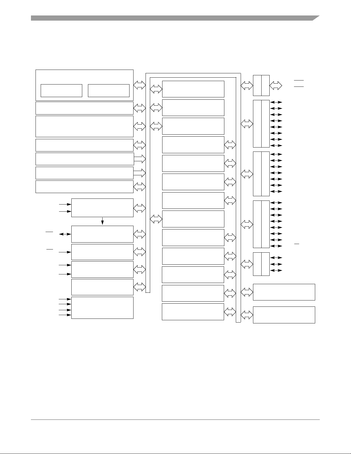
1.3 MCU Block Diagram
Figure 1-1 shows the structure of the MC68HC908GT16.
INTERNAL BUS
M68HC08 CPU
CPU
REGISTERS
ARITHMETIC/LOGIC
UNIT (ALU)
PROGRAMMABLE TIMEBASE
MODULE
MCU Block Diagram
PTA7/KBD7–
DDRA
PTA0/KBD0
PORTA
(1)
CONTROL AND STATUS
REGISTERS — 64 BYTES
USER FLASH
MC68HC908GT16 — 15,872 BYTES
MC68HC908GT8 — 7,680 BYTES
USER RAM — 512 BYTES
MONITOR ROM — 304 BYTES
FLASH PROGRAMMING ROUTINES
ROM — 720 BYTES
USER FLASH VECTOR SPACE — 36 BYTES
PTE4/OSC1
PTE3/OSC2
RST
IRQ
V
REFH
V
REFL
(3)
(3)
INTERNAL CLOCK
GENERATOR MODULE
SYSTEM INTEGRATION
MODULE
SINGLE EXTERNAL
INTERRUPT MODULE
8-BIT ANALOG-TO-DIGITAL
CONVERTER MODULE
POWER-ON RESET
MODULE
V
DD
V
SS
V
DDA
V
SSA
POWER
SINGLE BREAKPOINT BREAK
LOW-VOLTAGE INHIBIT MODULE
2-CHANNEL TIMER INTERFACE
2-CHANNEL TIMER INTERFACE
MODULE
DUAL VOLTAGE
8-BIT KEYBOARD
INTERRUPT MODULE
MODULE 1
MODULE 2
SERIAL COMMUNICATIONS
INTERFACE MODULE
COMPUTER OPERATING
PROPERLY MODULE
SERIAL PERIPHERAL
INTERFACE MODULE
MONITOR MODULE
MEMORY MAP
MODULE
CONFIGURATION REGISTER 1
CONFIGURATION REGISTER 2
MODULE
MODULE
PTB7/AD7
PTB6/AD6
PTB5/AD5
PTB4/AD4
DDRB
PTB3/AD3
PORTB
PTB2/AD2
PTB1/AD1
PTB0/AD0
(1)
PTC6
(1)
PTC5
(1)(2)
PTC4
(1)(2)
PORTC
PTC3
PTC2
PTC1
PTC0
(1)(2)
(1)(2)
(1)(2)
DDRC
PTD7/T2CH1
PTD6/T2CH0
PTD5/T1CH1
PTD4/T1CH0
PORTD
PTD3/SPSCK
PTD2/MOSI
DDRD
PTD1/MISO
PTD0/SS
PTE2
PORTE
PTE1/RxD
PTE0/TxD
DDRE
SECURITY
MODULE
MONITOR MODE ENTRY
MODULE
(1)
(1)
(1)
(1)
(1)
(1)
(1)
(1)
1. Ports are software configurable with pullup device if input port.
2. Higher current drive port pins
3. Pin contains integrated pullup device
Figure 1-1. MCU Block Diagram
MC68HC908GT16 • MC68HC908GT 8 Da ta She e t , Rev. 3
Freescale Semiconductor 21
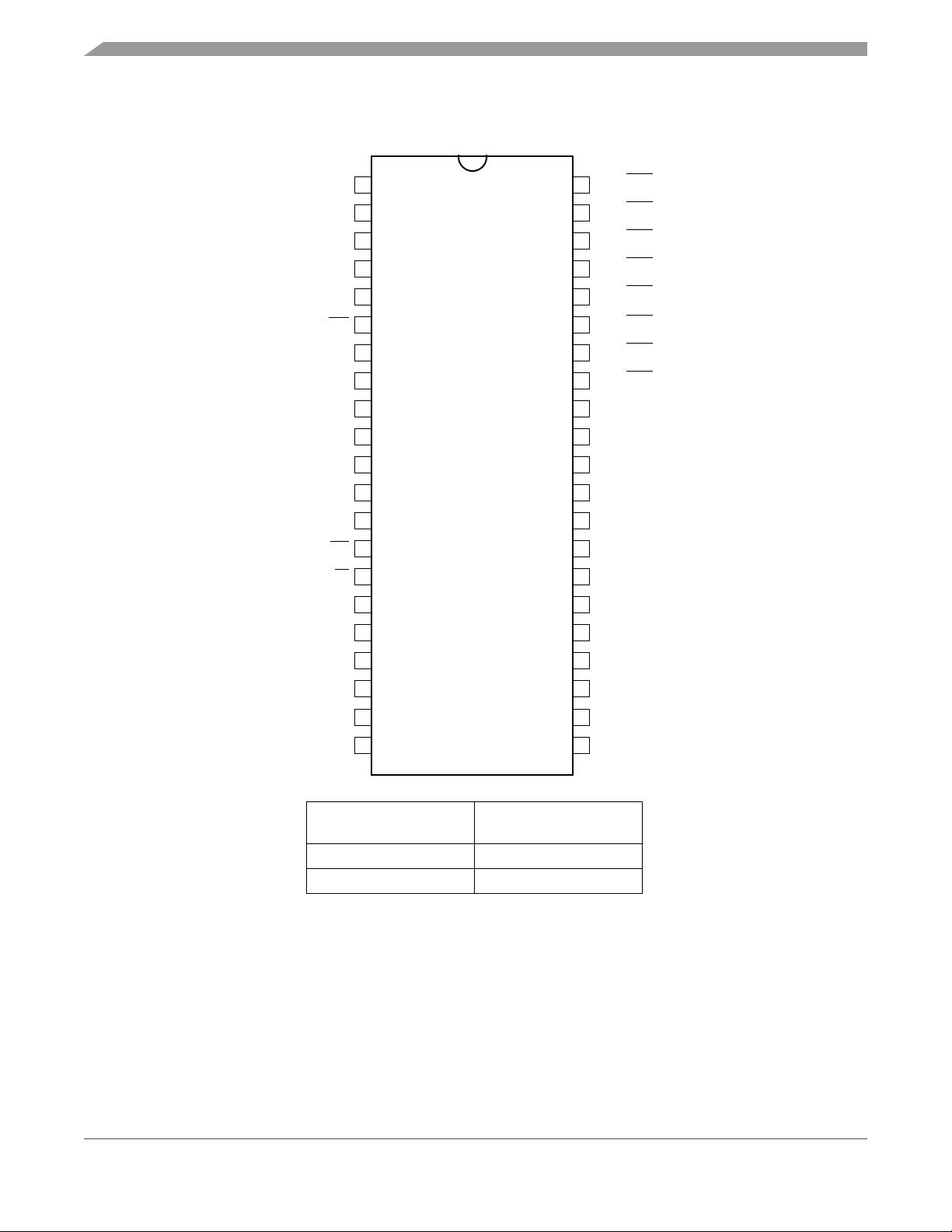
General Description
1.4 Pin Assignments
V
(ADC/ICG)
DDA
V
(ADC/ICG)
SSA
PTE3/OSC2
PTE4/OSC1
PTE0/TxD
PTE1/RxD
PTD1/MISO
PTD2/MOSI
PTE2
RST
PTC0
PTC1
PTC2
PTC3
PTC4
IRQ
PTD0/SS
1
2
3
4
5
6
7
8
9
10
11
12
13
14
15
16
17
42
41
40
39
38
37
36
35
34
33
32
31
30
29
28
27
26
PTA7/KBD7
PTA6/KBD6
PTA5/KBD5
PTA4/KBD4
PTA3/KBD3
PTA2/KBD2
PTA1/KBD1
PTA0/KBD0
V
(ADC)
REFL
V
(ADC)
REFH
PTB7/AD7
PTB6/AD6
PTB5/AD5
PTB4/AD4
PTB3/AD3
PTB2/AD2
PTB1/AD1
PTD3/SPSCK
V
V
PTD4/T1CH0
Pins Not Available
on 42-Pin Package
18
19
SS
20 23
DD
21 22
25
24
Internal
Connection
PTC5 Connected to ground
PTC6 Connected to ground
Figure 1-2. 42-Pin SDIP Pin Assignments
PTB0/AD0
PTD7/T2CH1
PTD6/T2CH0
PTD5/T1CH1
MC68HC908GT16 • MC68HC908GT 8 Da ta She e t , Rev. 3
22 Freescale Semiconductor

RST
PTC0
PTC1
PTC2
PTC3
PTC4
PTC5
PTC6
PTE0/TxD
PTE1/RxD
IRQ
Pin Functions
DDA
SSA
PTE4/OSC1
PTE3/OSC2
PTE2
43
44
1
2
3
4
5
6
7
8
9
10
11
12
42
13
14
V
V
41
40
15
16
PTA7/KBD7
39
17
18
PTA6/KBD6
38
PTA5/KBD5
37
19
20
PTA4/KBD4
PTA3/KBD3
36
21
35
PTA2/KBD2
34
33
32
31
30
29
28
27
26
25
24
23
22
PTA1/KBD1
PTA0/KBD0
V
REFL
V
REFH
PTB7/AD7
PTB6/AD6
PTB5/AD5
PTB4/AD4
PTB3/AD3
PTB2/AD2
PTB1/AD1
SS
DD
V
V
PTD0/SS
PTD1/MISO
PTD2/MOSI
PTD3/SPSCK
PTD5/T1CH1
PTD4/T1CH0
PTD6/T2CH0
PTB0/AD0
PTD7/T2CH1
Figure 1-3. 44-Pin QFP Pin Assignments
1.5 Pin Functions
Descriptions of the pin functions are provided here.
1.5.1 Power Supply Pins (VDD and VSS)
VDD and VSS are the power supply and ground pins. The MCU operates from a single power supply.
Fast signal transitions on MCU pins place high, short-duration current demands on the power supply. To
prevent noise problems, take special care to provide power supply bypassing at the MCU as Figure 1-4
shows. Place the C1 bypass capacitor as close to the MCU as possible. Use a high-frequency-response
ceramic capacitor for C1. C2 is an optional bulk current bypass capacitor for use in applications that
require the port pins to source high current levels.
MC68HC908GT16 • MC68HC908GT 8 Da ta She e t , Rev. 3
Freescale Semiconductor 23
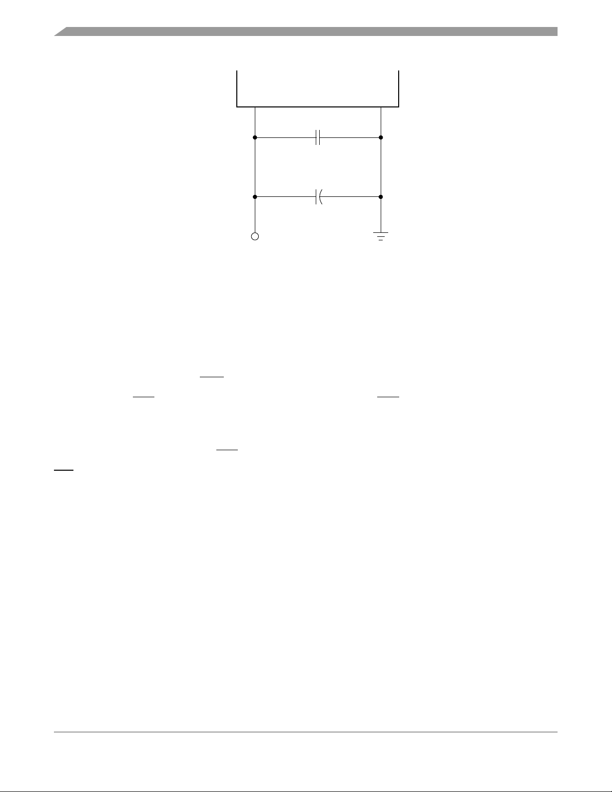
General Description
MCU
V
DD
C1
0.1 µF
+
C2
V
DD
Note: Component values shown represent typical applications.
V
SS
Figure 1-4. Power Supply Bypassing
1.5.2 Oscillator Pins (PTE4/OSC1 and PTE3/OSC2)
PTE4/OSC1 and PTE3/OSC2 are general-purpose, bidirectional I/O port pins. These pins can also be
programmed to be the connections for an external crystal, resonator or clock circuit. See Chapter 7
Internal Clock Generator (ICG) Module).
1.5.3 External Reset Pin (RST)
A logic 0 on the RST pin forces the MCU to a known startup state. RST is bidirectional, allowing a reset
of the entire system. It is driven low when any internal reset source is asserted. This pin contains an
internal pullup resistor. See Chapter 15 System Integration Module (SIM).
1.5.4 External Interrupt Pin (IRQ)
IRQ is an asynchronous external interrupt pin. This pin contains an internal pullup resistor. See
Chapter 8 External Interrupt (IRQ).
1.5.5 ADC and ICG Power Supply Pins (V
V
and V
DDA
generator (ICG). Connect the V
same voltage potential as V
Chapter 3 Analog-to-Digital Converter (ADC) and Chapter 7 Internal Clock Generator (ICG) Module).
1.5.6 ADC Reference Pins (V
V
high reference supply for the ADC and should be filtered. V
potential as the analog supply pin, V
externally filtered. V
See Chapter 3 Analog-to-Digital Converter (ADC).
24 Freescale Semiconductor
REFH
and V
are the power supply pins for the analog-to-digital converter (ADC) and the internal clock
SSA
pin to the same voltage potential as VDD, and the V
DDA
. Decoupling of these pins should be as per the digital supply. See
SS
and V
REFH
are the reference voltage pins for the analog-to-digital converter (ADC). V
REFL
. V
DDA
must be connected to the same voltage potential as the analog supply pin V
REFL
MC68HC908GT16 • MC68HC908GT 8 Da ta She e t , Rev. 3
REFL
REFL
DDA
and V
SSA
)
pin to the
SSA
)
is the
REFH
must be connected to the same voltage
REFH
is the low reference supply for the ADC and should be
SSA
.

Pin Functions
1.5.7 Port A Input/Output (I/O) Pins (PTA7/KBD7–PTA0/KBD0)
PTA7–PTA0 are general-purpose, bidirectional I/O port pins. Any or all of the port A pins can be
programmed to serve as keyboard interrupt pins. See Chapter 12 I nput/Output (I/O) Ports (PORTS) and
Chapter 9 Keyboard Interrupt Module (KBI).
These port pins also have selectable pullups when configured for input mode. The pullups are disengaged
when configured for output mode. The pullups are selectable on an individual port bit basis.
1.5.8 Port B I/O Pins (PTB7/AD7–PTB0/AD0)
PTB7–PTB0 are general-purpose, bidirectional I/O port pins that can also be used for analog-to-digital
converter (ADC) inputs. See Chapter 12 Input/Output (I/O) Ports (PORTS) and Chapter 3
Analog-to-Digital Converter (ADC).
1.5.9 Port C I/O Pins (PTC6–PTC0)
PTC6–PTC0 are general-purpose, bidirectional I/O port pins. PTC0–PTC4 have higher current
sink/source capability. PTC5 and PTC6 are only available on the 44-pin QFP package.
These port pins also have selectable pullups when configured for input mode. The pullups are disengaged
when configured for output mode. The pullups are selectable on an individual port bit basis. See
Chapter 12 Input/Output (I/O) Ports (PORTS).
1.5.10 Port D I/O Pins (PTD7/T2CH1–PTD0/SS)
PTD7–PTD0 are special-function, bidirectional I/O port pins. PTD0–PTD3 can be programmed to be
serial peripheral interface (SPI) pins, while PTD4–PTD7 can be individually programmed to be timer
interface module (TIM1 and TIM2) pins. See Chapter 18 Timer Interface Module (TIM), Chapter 16 Serial
Peripheral Interface (SPI) Module, and Chapter 12 Input/Output (I/O) Ports (PORTS).
These port pins also have selectable pullups when configured for input mode. The pullups are disengaged
when configured for output mode. The pullups are selectable on an individual port bit basis.
1.5.11 Port E I/O Pins (PTE4–PTE2, PTE1/RxD, and PTE0/TxD)
PTE0–PTE4 are general-purpose, bidirectional I/O port pins. PTE0–PTE1 can also be programmed to be
serial communications interface (SCI) pins. See Chapter 14 Enhanced Serial Communications In terface
(ESCI) Module and Chapter 12 Input/Output (I/O) Ports (PORTS).
PTE3 and PTE4 can also be programmed to be clock or oscillator pins. See Chapter 4 Configuration
Register (CONFIG) and Chapter 12 Input/Output (I/O) Ports (PORTS).
NOTE
Any unused inputs and I/O ports should be tied to an appropriate logic level
(either V
termination is recommended to reduce the possibility of static damage.
or VSS). Although the I/O ports do not require termination,
DD
MC68HC908GT16 • MC68HC908GT 8 Da ta She e t , Rev. 3
Freescale Semiconductor 25

General Description
MC68HC908GT16 • MC68HC908GT 8 Da ta She e t , Rev. 3
26 Freescale Semiconductor

Chapter 2
Memory
2.1 Introduction
The CPU08 can address 64 Kbytes of memory space. The memory map, shown in Figure 2-1, includes:
• User FLASH memory:
– MC68HC908GT16 — 15,872 bytes
– MC68HC908GT8 — 7,680 bytes
• 512 bytes of random-access memory (RAM)
• 720 bytes of FLASH programming routines read-only memory (ROM)
• 36 bytes of user-defined vectors
• 304 bytes of monitor ROM
2.2 Unimplemented Memory Locations
Accessing an unimplemented location can cause an illegal address reset. In the memory map (Figure 2-1)
and in register figures in this document, unimplemented locations are shaded.
2.3 Reserved Memory Locations
Accessing a reserved location can have unpredictable effects on MCU operation. In the Figure 2-1 and
in register figures in this document, reserved locations are marked with the word Reserved or with the
letter R.
2.4 Input/Output (I/O) Section
Most of the control, status, and data registers are in the zero page area of $0000–$003F. Additional I/O
registers have these addresses:
• $FE00; SIM break status register, SBSR
• $FE01; SIM reset status register, SRSR
• $FE02; reserved, SUBAR
• $FE03; SIM break flag control register, SBFCR
• $FE04; interrupt status register 1, INT1
• $FE05; interrupt status register 2, INT2
• $FE06; interrupt status register 3, INT3
• $FE07; reserved
• $FE08; FLASH control register, FLCR
• $FE09; break address register high, BRKH
• $FE0A; break address register low, BRKL
• $FE0B; break status and control register, BRKSCR
MC68HC908GT16 • MC68HC908GT 8 Da ta She e t , Rev. 3
Freescale Semiconductor 27
Memory
• $FE0C; LVI status register, LVISR
• $FF7E; FLASH block protect register, FLBPR
• $FF80; ICG user trim register 5V ICGTR5
• $FF81; ICG user trim register 3V ICGTR3
• $FFFF; COP control register, COPCTL
Data registers are shown in Figure 2-2. Table 2-1 is a list of vector locations.
$0000
↓
$003F
$0040
↓
$023F
$0240
↓
$1B4F
$1B50
↓
$1E1F
$1E20
↓
$BFFF
$C000
↓
$FE00 SIM BREAK STATUS REGISTER (SBSR) 1. Inadvertent access to
$FE01 SIM RESET STATUS REGISTER (SRSR)
$FE02 RESERVED (SUBAR)
$FE03 SIM BREAK FLAG CONTROL REGISTER (SBFCR)
$FE04 INTERRUPT STATUS REGISTER 1 (INT1)
$FE05 INTERRUPT STATUS REGISTER 2 (INT2)
$FE06 INTERRUPT STATUS REGISTER 3 (INT3)
$FE07 RESERVED
$FE08 FLASH CONTROL REGISTER (FLCR)
$FE09 BREAK ADDRESS REGISTER HIGH (BRKH)
$FE0A BREAK ADDRESS REGISTER LOW (BRKL)
$FE0B BREAK STATUS AND CONTROL REGISTER (BRKSCR)
FLASH PROGRAMMING ROUTINES ROM
I/O REGISTERS
64 BYTES
RAM
512 BYTES
UNIMPLEMENTED
6416 BYTES
720 BYTES
UNIMPLEMENTED
41,440 BYTES
FLASH MEMORY
MC68HC908GT16
15,872 BYTES
RESERVED
FLASH MEMORY
MC68HC908GT8
7,680 BYTES
these locations will not
cause an illegal address
reset.
(1)
$C000
↓
$DFFF
$E000
↓
$FDFF$FDFF
Figure is continued on the next page
Figure 2-1. Memory Map
MC68HC908GT16 • MC68HC908GT 8 Da ta She e t , Rev. 3
28 Freescale Semiconductor

$FE0C LVI STATUS REGISTER (LVISR)
$FE0D
↓
$FE0F
$FE10
↓
$FE1F
$FE20
↓
$FF4F
$FF50
↓
$FF7D
$FF7E FLASH BLOCK PROTECT REGISTER (FLBPR)
$FF7F
$FF80 ICG USER TRIM REGISTER 5V (ICGTR5)
$FF81 ICG USER TRIM REGISTER 3V (ICGTR3)
$FF82
↓
$FFDB
$FFDC
↓
(2)
$FFFF
2. $FFF6–$FFFD reserved for eight security bytes
RESERVED FOR COMPATIBILITY WITH MONITOR CODE
UNIMPLEMENTED
3 BYTES
UNIMPLEMENTED
16 BYTES
FOR A-FAMILY PART
MONITOR ROM
304 BYTES
UNIMPLEMENTED
46 BYTES
UNIMPLEMENTED 1 BYTE
UNIMPLEMENTED
90 BYTES
FLASH VECTORS
36 BYTES
Input/Output (I/O) Section
Figure 2-1. Memory Map (Continued)
MC68HC908GT16 • MC68HC908GT 8 Da ta She e t , Rev. 3
Freescale Semiconductor 29
Memory
Addr.Register Name Bit 7654321Bit 0
$0000
$0001
$0002
$0003
$0004
$0005
$0006
$0007
$0008
$0009
$000A
$000B
$000C
Port A Data Register
See page 124.
Port B Data Register
See page 126.
Port C Data Register
See page 128.
Port D Data Register (
See page 130.
Data Direction Register A
(DDRA)
See page 124.
Data Direction Register B
(DDRB)
See page 126.
Data Direction Register C
(DDRC)
See page 128.
Data Direction Register D
(DDRD)
See page 131.
Port E Data Register
See page 133.
ESCI Prescaler Register
(SCPSC)
See page 170.
ESCI Arbiter Control
Register (SCIACTL)
See page 174.
ESCI Arbiter Data
Register (SCIADAT)
See page 175.
Data Direction Register E
(DDRE)
See page 134.
(PTA)
Read:
Write:
PTA7 PTA6 PTA5 PTA4 PTA3 PTA2 PTA1 PTA0
Reset: Unaffected by reset
(PTB)
Read:
Write:
PTB7 PTB6 PTB5 PTB4 PTB3 PTB2 PTB1 PTB0
Reset: Unaffected by reset
(PTC)
Read: 0
Write:
PTC6 PTC5 PTC4 PTC3 PTC2 PTC1 PTC0
Reset: Unaffected by reset
PTD)
Read:
Write:
PTD7 PTD6 PTD5 PTD4 PTD3 PTD2 PTD1 PTD0
Reset: Unaffected by reset
Read:
Write:
DDRA7 DDRA6 DDRA5 DDRA4 DDRA3 DDRA2 DDRA1 DDRA0
Reset:00000000
Read:
Write:
DDRB7 DDRB6 DDRB5 DDRB4 DDRB3 DDRB2 DDRB1 DDRB0
Reset:00000000
Read: 0
Write:
DDRC6 DDRC5 DDRC4 DDRC3 DDRC2 DDRC1 DDRC0
Reset:00000000
Read:
Write:
DDRD7 DDRD6 DDRD5 DDRD4 DDRD3 DDRD2 DDRD1 DDRD0
Reset:00000000
Read: 0 0 0
Write:
(PTE)
PTE4 PTE3 PTE2 PTE1 PTE0
Reset: Unaffected by reset
Read:
Write:
PDS2 PDS1 PDS0 PSSB4 PSSB3 PSSB2 PSSB1 PSSB0
Reset:00000000
Read:
Write:
AM1
ALOST
AM0 ACLK
AFIN ARUN AOVFL ARD8
Reset:00000000
Read: ARD7 ARD6 ARD5 ARD4 ARD3 ARD2 ARD1 ARD0
Write:
Reset:00000000
Read: 0 0 0
Write:
DDRE4 DDRE3 DDRE2 DDRE1 DDRE0
Reset:00000000
= Unimplemented R = Reserved U = Unaffected
Figure 2-2. Control, Status, and Data Registers (Sheet 1 of 7)
MC68HC908GT16 • MC68HC908GT 8 Da ta She e t , Rev. 3
30 Freescale Semiconductor
Input/Output (I/O) Section
Addr.Register Name Bit 7654321Bit 0
Read:
PTAPUE7 PTAPUE6 PTAPUE5 PTAPUE4 PTAPUE3 PTAPUE2 PTAPUE1 PTAPUE0
Write:
Reset:00000000
Read: 0
Write:
Reset:00000000
Read:
PTDPUE7 PTDPUE6 PTDPUE5 PTDPUE4 PTDPUE3 PTDPUE2 PTDPUE1 PTDPUE0
Write:
Reset:00000000
Read:
Write:
Reset:00101000
Read: SPRF
Write:
Reset:00001000
Read: R7 R6 R5 R4 R3 R2 R1 R0
Write: T7 T6 T5 T4 T3 T2 T1 T0
Reset: Unaffected by reset
Read:
Write:
Reset:00000000
Read:
Write:
Reset:00000000
Read: R8
Write:
Reset:UU000000
Read: SCTE TC SCRF IDLE OR NF FE PE
Write:
Reset:11000000
Read:
Write:
Reset:00000000
Read: R7 R6 R5 R4 R3 R2 R1 R0
Write: T7 T6 T5 T4 T3 T2 T1 T0
Reset: Unaffected by reset
Read:
Write:
Reset:00000000
SPRIE R SPMSTR CPOL CPHA SPWOM SPE SPTIE
LOOPS ENSCI TXINV M WAKE ILTY PEN PTY
SCTIE TCIE SCRIE ILIE TE RE RWU SBK
PTCPUE6 PTCPUE5 PTCPUE4 PTCPUE3 PTCPUE2 PTCPUE1 PTCPUE0
ERRIE
T8 R R ORIE NEIE FEIE PEIE
= Unimplemented R = Reserved U = Unaffected
OVRF MODF SPTE
SCP1 SCP0 R SCR2 SCR1 SCR0
MODFEN SPR1 SPR0
BKF RPF
$000D
$000E
$000F
$0010
$0011
$0012
$0013
$0014
$0015
$0016
$0017
$0018
$0019
Port A Input Pullup Enable
Register (PTAPUE)
See page 125.
Port C Input Pullup Enable
Register (PTCPUE)
See page 129.
Port D Input Pullup Enable
Register (PTDPUE)
See page 132.
SPI Control Register
(SPCR)
See page 211.
SPI Status and Control
Register (SPSCR)
See page 212.
SPI Data Register
(SPDR)
See page 214.
ESCI Control Register 1
(SCC1)
See page 161.
ESCI Control Register 2
(SCC2)
See page 163.
ESCI Control Register 3
(SCC3)
See page 165.
ESCI Status Register 1
(SCS1)
See page 166.
ESCI Status Register 2
(SCS2)
See page 168.
ESCI Data Register
(SCDR)
See page 169.
ESCI Baud Rate Register
(SCBR)
See page 169.
Figure 2-2. Control, Status, and Data Registers (Sheet 2 of 7)
MC68HC908GT16 • MC68HC908GT 8 Da ta She e t , Rev. 3
Freescale Semiconductor 31

Memory
Addr.Register Name Bit 7654321Bit 0
$001A
$001B
$001C
$001D
$001E
Keyboard Status
and Control Register
(INTKBSCR)
See page 109.
Keyboard Interrupt Enable
Register (INTKBIER)
See page 110.
Timebase Module Control
Register (TBCR)
See page 216.
IRQ Status and Control
Register (INTSCR)
See page 102.
Configuration Register 2
(CONFIG2)
See page 56.
Read: 0000KEYF 0
Write:
ACKK
IMASKK MODEK
Reset:00000000
Read:
Write:
KBIE7 KBIE6 KBIE5 KBIE4 KBIE3 KBIE2 KBIE1 KBIE0
Reset:00000000
Read: TBIF
Write:
TBR2 TBR1 TBR0
0
TACK
TBIE TBON R
Reset:00000000
Read: 0000IRQF10
Write:
ACK1
IMASK1 MODE1
Reset:00000000
†
Read:
Write:
R
0
EXT-
XTALEN
EXT-SLOW
EXT-
CLKEN
0
OSCENIN-
STOP
R
Reset:00000000
$001F
Configuration Register 1
(CONFIG1)
See page 56.
†
Read:
Write:
COPRS LVISTOP LVIRSTD LVIPWRD LVI5OR3
Reset:00000000
(1)
SSREC STOP COPD
1. One-time writable register after each reset, except LVI5OR3 bit. LVI5OR3 bit is only reset via POR (power-on reset).
Timer 1 Status and Control
$0020
$0021
$0022
Register High (T1CNTH)
Register Low (T1CNTL)
Timer 1 Counter Modulo
$0023
Register High (T1MODH)
Timer 1 Counter Modulo
$0024
Register Low (T1MODL)
Timer 1 Channel 0 Status and
$0025
Control Register (T1SC0)
Register (T1SC)
See page 229.
Timer 1 Counter
Read: TOF
Write: 0 TRST
TOIE TSTOP
Reset:00100000
Read: Bit 15 14 13 12 11 10 9 Bit 8
00
Write:
See page 230.
Timer 1 Counter
Reset:00000000
Read: Bit 7 654321Bit 0
Write:
See page 230.
See page 231.
See page 231.
See page 231.
Reset:00000000
Read:
Write:
Bit 15 14 13 12 11 10 9 Bit 8
Reset:11111111
Read:
Write:
Bit 7654321Bit 0
Reset:11111111
Read: CH0F
Write: 0
CH0IE MS0B MS0A ELS0B ELS0A TOV0 CH0MAX
Reset:00000000
= Unimplemented R = Reserved U = Unaffected
Figure 2-2. Control, Status, and Data Registers (Sheet 3 of 7)
PS2 PS1 PS0
MC68HC908GT16 • MC68HC908GT 8 Da ta She e t , Rev. 3
32 Freescale Semiconductor

Input/Output (I/O) Section
Addr.Register Name Bit 7654321Bit 0
Read:
Write:
Reset: Indeterminate after reset
Read:
Write:
Reset: Indeterminate after reset
Read: CH1F
Write: 0
Reset:00000000
Read:
Write:
Reset: Indeterminate after reset
Read:
Write:
Reset: Indeterminate after reset
Read: TOF
Write: 0 TRST
Reset:00100000
Read: Bit 15 14 13 12 11 10 9 Bit 8
Write:
Reset:00000000
Read: Bit 7 654321Bit 0
Write:
Reset:00000000
Read:
Write:
Reset:11111111
Read:
Write:
Reset:11111111
Read: CH0F
Write: 0
Reset:00000000
Read:
Write:
Reset: Indeterminate after reset
Read:
Write:
Reset: Indeterminate after reset
Bit 15 14 13 12 11 10 9 Bit 8
Bit 7654321Bit 0
CH1IE
Bit 15 14 13 12 11 10 9 Bit 8
Bit 7654321Bit 0
TOIE TSTOP
Bit 15 14 13 12 11 10 9 Bit 8
Bit 7654321Bit 0
CH0IE MS0B MS0A ELS0B ELS0A TOV0 CH0MAX
Bit 15 14 13 12 11 10 9 Bit 8
Bit 7654321Bit 0
= Unimplemented R = Reserved U = Unaffected
0
MS1A ELS1B ELS1A TOV1 CH1MAX
00
PS2 PS1 PS0
$0026
$0027
$0028
$0029
$002A
$002B
$002C
$002D
$002E
$002F
$0030
$0031
$0032
Register High (T1CH0H)
Register Low (T1CH0L)
Timer 1 Channel 1 Status and
Control Register (T1SC1)
Register High (T1CH1H)
Register Low (T1CH1L)
Timer 2 Status and Control
Register High (T2CNTH)
Register Low (T2CNTL)
Timer 2 Counter Modulo
Register High (T2MODH)
Timer 2 Counter Modulo
Register Low (T2MODL)
Timer 2 Channel 0 Status and
Control Register (T2SC0)
Register High (T2CH0H)
Register Low (T2CH0L)
Timer 1 Channel 0
See page 234.
Timer 1 Channel 0
See page 234.
See page 232.
Timer 1 Channel 1
See page 234.
Timer 1 Channel 1
See page 234.
Register (T2SC)
See page 229.
Timer 2 Counter
See page 230.
Timer 2 Counter
See page 230.
See page 231.
See page 231.
See page 231.
Timer 2 Channel 0
See page 234.
Timer 2 Channel 0
See page 234.
Figure 2-2. Control, Status, and Data Registers (Sheet 4 of 7)
MC68HC908GT16 • MC68HC908GT 8 Da ta She e t , Rev. 3
Freescale Semiconductor 33

Memory
Addr.Register Name Bit 7654321Bit 0
Timer 2 Channel 1 Status and
$0033
$0034
$0035
$0036
$0037
$0038
$0039
$003A
$003B Reserved
$003C
$003D
$003E
$003F Unimplemented
Control Register (T2SC1)
See page 232.
Timer 2 Channel 1
Register High (T2CH1H)
See page 234.
Timer 2 Channel 1
Register Low (T2CH1L)
See page 234.
ICG Control Register
(ICGCR)
See page 96.
ICG Multiplier Register
(ICGMR)
See page 97.
ICG Trim Register
(ICGTR)
See page 98.
ICG Divider Control
Register (ICGDVR)
See page 98.
ICG DCO Stage Control
Register (ICGDSR)
See page 98.
ADC Status and Control
Register (ADSCR)
See page 52.
ADC Data Register
(ADR)
See page 53.
ADC Clock Register
(ADCLK)
See page 54.
Read: CH1F
Write: 0
Reset:00000000
Read:
Write:
Reset: Indeterminate after reset
Read:
Write:
Reset: Indeterminate after reset
Read:
Write: 0
Reset:00001000
Read:
Write:
Reset:00010101
Read:
Write:
Reset:10000000
Read:
Write:
Reset:0000UUUU
Read: DSTG7 DSTG6 DSTG5 DSTG4 DSTG3 DSTG2 DSTG1 DSTG0
Write:RRRRRRRR
Reset: Unaffected by reset
Read:
Write:
Reset: Indeterminate after reset
Read: COCO
Write: R
Reset:00011111
Read: AD7 AD6 AD5 AD4 AD3 AD2 AD1 AD0
Write:
Reset:00000000
Read:
Write:
Reset:00000000
Read:
Write:
Reset:
Bit 15 14 13 12 11 10 9 Bit 8
Bit 7654321Bit 0
CMIE
TRIM7 TRIM6 TRIM5 TRIM4 TRIM3 TRIM2 TRIM1 TRIM0
RRRRRRRR
ADIV2 ADIV1 ADIV0 ADICLK
CH1IE
CMF
N6 N5 N4 N3 N2 N1 N0
AIEN ADCO ADCH4 ADCH3 ADCH2 ADCH1 ADCH0
= Unimplemented R = Reserved U = Unaffected
0
CMON CS ICGON
MS1A ELS1B ELS1A TOV1 CH1MAX
DDIV3 DDIV2 DDIV1 DDIV0
0000
ICGS
ECGON
ECGS
Figure 2-2. Control, Status, and Data Registers (Sheet 5 of 7)
MC68HC908GT16 • MC68HC908GT 8 Da ta She e t , Rev. 3
34 Freescale Semiconductor
Input/Output (I/O) Section
Addr.Register Name Bit 7654321Bit 0
SIM Break Status Register
$FE00
See page 240.
Note: Writing a 0 clears SBSW.
(SBSR)
Read:
Write: NOTE
Reset:00000000
RRRRRR
SBSW
R
SIM Reset Status Register
$FE01
$FE02
$FE03
$FE04
$FE05
$FE06
$FE07 Reserved
$FE08
$FE09
$FE0A
$FE0B
SIM Upper Byte Address
Register (SUBAR)
SIM Break Flag Control
Register (SBFCR)
Interrupt Status Register 1
Interrupt Status Register 2
Interrupt Status Register 3
FLASH Control Register
Break Address Register High
Break Address Register Low
Break Status and Control
Register (BRKSCR)
(SRSR)
See page 138.
See page 240.
(INT1)
See page 145.
(INT2)
See page 145.
(INT3)
See page 145.
(FLCR)
See page 39.
(BRKH)
See page 239.
(BRKL)
See page 239.
See page 239.
Read: POR PIN COP ILOP ILAD MODRST LVI 0
Write:
POR:10000000
Read:
Write:
Reset:
Read:
Write:
Reset: 0
Read: IF6 IF5 IF4 IF3 IF2 IF1 0 0
Write:RRRRRRRR
Reset:00000000
Read: IF14 IF13 IF12 IF11 IF10 IF9 IF8 IF7
Write:RRRRRRRR
Reset:00000000
Read: 000000IF16IF15
Write:RRRRRRRR
Reset:00000000
Read:
Write:
Reset:00000000
Read: 0000
Write:
Reset:00000000
Read:
Write:
Reset:00000000
Read:
Write:
Reset:00000000
Read:
Write:
Reset:00000000
RRRRRRRR
BCFERRRRRRR
RRRRRRRR
HVEN MASS ERASE PGM
Bit 15 14 13 12 11 10 9 Bit 8
Bit 7654321Bit 0
BRKE BRKA
= Unimplemented R = Reserved U = Unaffected
000000
Figure 2-2. Control, Status, and Data Registers (Sheet 6 of 7)
MC68HC908GT16 • MC68HC908GT 8 Da ta She e t , Rev. 3
Freescale Semiconductor 35

Memory
Addr.Register Name Bit 7654321Bit 0
Read: LVIOUT 0000000
Write:
Reset:00000000
Read:
(1)
Write:
Reset: Unaffected by reset
Read:
(1)
Write:
Reset: Unaffected by reset
Read:
(1)
Write:
Reset: Unaffected by reset
BPR7 BPR6 BPR5 BPR4 BPR3 BPR2 BPR1 BPR0
TRIM7 TRIM6 TRIM5 TRIM4 TRIM3 TRIM2 TRIM1 TRIM0
TRIM7 TRIM6 TRIM5 TRIM4 TRIM3 TRIM2 TRIM1 TRIM0
$FE0C
$FF7E
$FF80
$FF81
LVI Status Register (LVISR)
See page 113.
FLASH Block Protect
Register (FLBPR)
See page 43.
ICG User Trim
Register 5V (ICGTR5)
See page 44.
ICG User Trim
Register 3V (ICGTR3)
See page 44.
COP Control Register
$FFFF
(COPCTL)
See page 61.
1. Non-volatile FLASH register
Figure 2-2. Control, Status, and Data Registers (Sheet 7 of 7)
Read: Low byte of reset vector
Write: Writing clears COP counter (any value)
Reset: Unaffected by reset
= Unimplemented R = Reserved U = Unaffected
MC68HC908GT16 • MC68HC908GT 8 Da ta She e t , Rev. 3
36 Freescale Semiconductor

Input/Output (I/O) Section
Table 2-1. Vector Addresses
.
Vector Priority Vector Address Vector
Lowest
Highest $FFFF Reset Vector (Low)
IF16
IF15
IF14
IF13
IF12
IF11
IF10
IF9
IF8
IF7
IF6
IF5
IF4
IF3
IF2
IF1
—
—
$FFDC Timebase Vector (High)
$FFDD Timebase Vector (Low)
$FFDE ADC Conversion Complete Vector (High)
$FFDF ADC Conversion Complete Vector (Low)
$FFE0 Keyboard Vector (High)
$FFE1 Keyboard Vector (Low)
$FFE2 SCI Transmit Vector (High)
$FFE3 SCI Transmit Vector (Low)
$FFE4 SCI Receive Vector (High)
$FFE5 SCI Receive Vector (Low)
$FFE6 SCI Error Vector (High)
$FFE7 SCI Error Vector (Low)
$FFE8 SPI Transmit Vector (High)
$FFE9 SPI Transmit Vector (Low)
$FFEA SPI Receive Vector (High)
$FFEB SPI Receive Vector (Low)
$FFEC TIM2 Overflow Vector (High)
$FFED TIM2 Overflow Vector (Low)
$FFEE TIM2 Channel 1 Vector (High)
$FFEF TIM2 Channel 1 Vector (Low)
$FFF0 TIM2 Channel 0 Vector (High)
$FFF1 TIM2 Channel 0 Vector (Low)
$FFF2 TIM1 Overflow Vector (High)
$FFF3 TIM1 Overflow Vector (Low)
$FFF4 TIM1 Channel 1 Vector (High)
$FFF5 TIM1 Channel 1 Vector (Low)
$FFF6 TIM1 Channel 0 Vector (High)
$FFF7 TIM1 Channel 0 Vector (Low)
$FFF8 ICG Vector (High)
$FFF9 ICG Vector (Low)
$FFF A IRQ
$FFFB IRQ
$FFFC SWI Vector (High)
$FFFD SWI Vector (Lo w)
$FFFE Reset Vector (High)
Vector (High)
Vector (Low)
MC68HC908GT16 • MC68HC908GT 8 Da ta She e t , Rev. 3
Freescale Semiconductor 37

Memory
2.5 Random-Access Memory (RAM)
Addresses $0040 through $023F are RAM locations. The location of the stack RAM is programmable.
The 16-bit stack pointer allows the stack to be anywhere in the 64-Kbyte memory space.
NOTE
For correct operation, the stack pointer must point only to RAM locations.
Within page zero are 192 bytes of RAM. Because the location of the stack RAM is programmable, all page
zero RAM locations can be used for I/O control and user data or code. When the stack pointer is moved
from its reset location at $00FF out of page zero, direct addressing mode instructions can efficiently
access all page zero RAM locations. Page zero RAM, therefore, provides ideal locations for frequently
accessed global variables.
Before processing an interrupt, the CPU uses five bytes of the stack to save the contents of the CPU
registers.
NOTE
For M6805 compatibility, the H register is not stacked.
During a subroutine call, the CPU uses two bytes of the stack to store the return address. The stack
pointer decrements during pushes and increments during pulls.
NOTE
Be careful when using nested subroutines. The CPU may overwrite data in
the RAM during a subroutine or during the interrupt stacking operation.
2.6 FLASH Memory
This sub-section describes the operation of the embedded FLASH memory. This memory can be read,
programmed, and erased from a single external supply. The program, erase, and read operations are
enabled through the use of an internal charge pump.
2.6.1 Functional Description
The FLASH memory is an array of 15,872 bytes (7,680 bytes on MC68HC908GT8) with an additional
36 bytes of user vectors, one byte of block protection and two bytes of ICG user trim storage. An erased
bit reads as 1 and a programmed bit reads as a 0. Memory in the FLASH array is organized into two rows
per page basis. The page size is 64 bytes per page and the row size is 32 bytes per row. Hence the
minimum erase page size is 64 bytes and the minimum program row size is 32 bytes. Program and erase
operation operations are facilitated through control bits in FLASH control register (FLCR). Details for
these operations appear later in this section.
The address ranges for the user memory and vectors are:
• $C000–$FDFF; user memory ($E000–$FDFF on MC68HC908GT8)
•$FE08
• $FF7E; FLASH block protect register
•$FF80
•$FF81
• $FFDC–$FFFF; these locations are reserved for user-defined interrupt and reset vectors
; FLASH control register
; ICG user trim register (ICGTR5)
; ICG user trim register (ICGTR3)
MC68HC908GT16 • MC68HC908GT 8 Da ta She e t , Rev. 3
38 Freescale Semiconductor

FLASH Memory
2.6.2 FLASH Control Register
The FLASH control register (FLCR) controls FLASH program and erase operations.
Address: $FE08
Bit 7654321Bit 0
Read:0000
Write:
Reset:00000000
= Unimplemented
Figure 2-3. FLASH Control Register (FLCR)
HVEN — High-Voltage Enable Bit
This read/write bit enables the charge pump to drive high voltages for program and erase operations
in the array. HVEN can only be set if either PGM = 1 or ERASE = 1 and the proper sequence for
program or erase is followed.
1 = High voltage enabled to array and charge pump on
0 = High voltage disabled to array and charge pump off
MASS — Mass Erase Control Bit
Setting this read/write bit configures the 16 Kbyte FLASH array for mass erase operation.
1 = MASS erase operation selected
0 = MASS erase operation unselected
HVEN MASS ERASE PGM
ERASE — Erase Control Bit
This read/write bit configures the memory for erase operation. ERASE is interlocked with the PGM bit
such that both bits cannot be equal to 1 or set to 1 at the same time.
1 = Erase operation selected
0 = Erase operation unselected
PGM — Program Control Bit
This read/write bit configures the memory for program operation. PGM is interlocked with the ERASE
bit such that both bits cannot be equal to 1 or set to 1 at the same time.
1 = Program operation selected
0 = Program operation unselected
2.6.3 FLASH Page Erase Operation
Use the following procedure to erase a page (64 bytes) of FLASH memory. A page consists of 64
consecutive bytes starting from addresses $XX00, $XX40, $XX80, or $XXC0. The 36-byte user interrupt
vectors area also forms a page. Any FLASH memory page can be erased alone.
MC68HC908GT16 • MC68HC908GT 8 Da ta She e t , Rev. 3
Freescale Semiconductor 39

Memory
1. Set the ERASE bit and clear the MASS bit in the FLASH control register.
2. Read the FLASH block protect register.
3. Write any data to any FLASH location within the address range of the block to be erased.
4. Wait for a time, t
(minimum 10 µs).
NVS
5. Set the HVEN bit.
6. Wait for a time, t
(minimum 1 ms or 4 ms).
Erase
7. Clear the ERASE bit.
8. Wait for a time, t
(minimum 5 µs).
NVH
9. Clear the HVEN bit.
10. After time, t
(typical 1 µs), the memory can be accessed in read mode again.
RCV
NOTE
Programming and erasing of FLASH locations cannot be performed by
code being executed from the FLASH memory. While these operations
must be performed in the order as shown, but other unrelated operations
may occur between the steps.
CAUTION
A page erase of the vector page will erase the internal oscillator trim values
at $FF80 and $FF81.
In applications that require more than 1000 program/erase cycles, use the 4 ms page erase specification
to get improved long-term reliability. Any application can use this 4 ms page erase specification. However,
in applications where a FLASH location will be erased and reprogrammed less than 1000 times, and
speed is important, use the 1 ms page erase specification to get a shorter cycle time.
2.6.4 FLASH Mass Erase Operation
Use the following procedure to erase the entire FLASH memory to read as a 1:
1. Set both the ERASE bit and the MASS bit in the FLASH control register.
2. Read the FLASH block protect register.
3. Write any data to any FLASH address
4. Wait for a time, t
(minimum 10 µs).
NVS
5. Set the HVEN bit.
6. Wait for a time, t
MErase
(minimum 4 ms).
7. Clear the ERASE and MASS bits.
Mass erase is disabled whenever any block is protected (FLBPR does not
equal $FF).
8. Wait for a time, t
(minimum 100 µs).
NVHL
9. Clear the HVEN bit.
10. After time, t
(typical 1 µs), the memory can be accessed in read mode again.
RCV
Programming and erasing of FLASH locations cannot be performed by
code being executed from the FLASH memory. While these operations
1. When in monitor mode, with security sequence failed (see 19.3.2 Security), write to the FLASH block protect register instead of any FLASH address.
(1)
within the FLASH memory address range.
NOTE
NOTE
MC68HC908GT16 • MC68HC908GT 8 Da ta She e t , Rev. 3
40 Freescale Semiconductor

FLASH Memory
must be performed in the order as shown, but other unrelated operations
may occur between the steps.
CAUTION
A mass erase will erase the internal oscillator trim values at $FF80 and
$FF81.
2.6.5 FLASH Program/Read Operation
Programming of the FLASH memory is done on a row basis. A row consists of 32 consecutive bytes
starting from addresses $XX00, $XX20, $XX40, $XX60, $XX80, $XXA0, $XXC0, or $XXE0. Use the
following step-by-step procedure to program a row of FLASH memory
Figure 2-4 is a flowchart of the programming algorithm.
NOTE
Only bytes which are currently $FF may be programmed.
1. Set the PGM bit. This configures the memory for program operation and enables the latching of
address and data for programming.
2. Read the FLASH block protect register.
3. Write any data to any FLASH location within the address range desired.
4. Wait for a time, t
5. Set the HVEN bit.
6. Wait for a time, t
7. Write data to the FLASH address being programmed
8. Wait for time, t
9. Repeat step 7 and 8 until all desired bytes within the row are programmed.
10. Clear the PGM bit
11. Wait for time, t
12. Clear the HVEN bit.
13. After time, t
RCV
The COP register at location $FFFF should not be written between steps
5-12, when the HVEN bit is set. Since this register is located at a valid
FLASH address, unpredictable behavior may occur if this location is written
while HVEN is set.
(minimum 10 µs).
NVS
(minimum 5 µs).
PGS
(minimum 30 µs).
PROG
(1)
.
(minimum 5 µs).
NVH
(1)
.
(typical 1 µs), the memory can be accessed in read mode again.
NOTE
This program sequence is repeated throughout the memory until all data is programmed.
NOTE
Programming and erasing of FLASH locations cannot be performed by
code being executed from the FLASH memory. While these operations
must be performed in the order shown, other unrelated operations may
occur between the steps. Do not exceed t
maximum, see 20.20
PROG
Memory Characteristics.
1. The time between each FLASH address change, or the time between the last FLASH address programmed to clearing
PGM bit, must not exceed the maximum programming time, t
MC68HC908GT16 • MC68HC908GT 8 Da ta She e t , Rev. 3
Freescale Semiconductor 41
PROG
maximum.

Memory
Algorithm for programming
a row (32 bytes) of FLASH memory
1
2
READ THE FLASH BLOCK PROTECT REGISTER
3
WRITE ANY DATA TO ANY FLASH ADDRESS
WITHIN THE ROW ADDRESS RANGE DESIRED
4
5
6
7
WRITE DATA TO THE FLASH ADDRESS
SET PGM BIT
WAIT FOR A TIME, t
SET HVEN BIT
WAIT FOR A TIME, t
TO BE PROGRAMMED
NVS
PGS
8
WAIT FOR A TIME, t
COMPLETED
PROGRAMMING
THIS ROW?
Note:
The time between each FLASH address change (step 7 to step 7),
or the time between the last FLASH address programmed
to clearing PGM bit (step 7 to step 10)
must not exceed the maximum programming
PROG
max.
time, t
This row program algorithm assumes the row/s
to be programmed are initially erased.
Figure 2-4. FLASH Programming Flowchart
PROG
Y
N
10
11
12
13
CLEAR PGM BIT
WAIT FOR A TIME, t
CLEAR HVEN BIT
WAIT FOR A TIME, t
END OF PROGRAMMING
NVH
RCV
MC68HC908GT16 • MC68HC908GT 8 Da ta She e t , Rev. 3
42 Freescale Semiconductor

FLASH Memory
2.6.6 FLASH Block Protection
Due to the ability of the on-board charge pump to erase and program the FLASH memory in the target
application, provision is made for protecting a block of memory from unintentional erase or program
operations due to system malfunction. This protection is done by using of a FLASH block protect register
(FLBPR). The FLBPR determines the range of the FLASH memory which is to be protected. The range
of the protected area starts from a location defined by FLBPR and ends at the bottom of the FLASH
memory ($FFFF). When the memory is protected, the HVEN bit cannot be set in either ERASE or
PROGRAM operations.
NOTE
In performing a program or erase operation, the FLASH block protect
register must be read after setting the PGM or ERASE bit and before
asserting the HVEN bit
When the FLBPR is program with all 0’s, the entire memory is protected from being programmed and
erased. When all the bits are erased (all 1’s), the entire memory is accessible for program and erase.
When bits within the FLBPR are programmed, they lock a block of memory, address ranges as shown in
2.6.7 FLASH Block Protect Register. Once the FLBPR is programmed with a value other than $FF or $FE,
any erase or program of the FLBPR or the protected block of FLASH memory is prohibited. Mass erase
is disabled whenever any block is protected (FLBPR does not equal $FF). The FLBPR itself can be
erased or programmed only with an external voltage, V
allows entry from reset into the monitor mode.
, present on the IRQ pin. This voltage also
TST
2.6.7 FLASH Block Protect Register
The FLASH block protect register (FLBPR) is implemented as a byte within the FLASH memory, and
therefore can only be written during a programming sequence of the FLASH memory. The value in this
register determines the starting location of the protected range within the FLASH memory.
Address: $FF7E
Bit 7654321Bit 0
Read:
Write:
Reset: Unaffected by reset. Initial value from factory is 1.
BPR[7:0] — FLASH Block Protect Bits
These eight bits represent bits [13:6] of a 16-bit memory addre ss. Bit 15 and Bit 14 are 1s and bits [5:0]
are 0s.
The resultant 16-bit address is used for specifying the start address of the FLASH memory for block
protection. The FLASH is protected from this start address to the end of FLASH memory, at $FFFF.
With this mechanism, the protect start address can be $XX00, $XX40, $XX80, and $XXC0 (64 bytes
page boundaries) within the FLASH memory.
BPR7 BPR6 BPR5 BPR4 BPR3 BPR2 BPR1 BPR0
Write to this register is by a programming sequence to the FLASH memory.
Figure 2-5. FLASH Block Protect Register (FLBPR)
16-BIT MEMORY ADDRESS
START ADDRESS OF FLASH
BLOCK PROTECT
1
1
FLBPR VALUE
000000
Figure 2-6. FLASH Block Protect Start Address
MC68HC908GT16 • MC68HC908GT 8 Da ta She e t , Rev. 3
Freescale Semiconductor 43
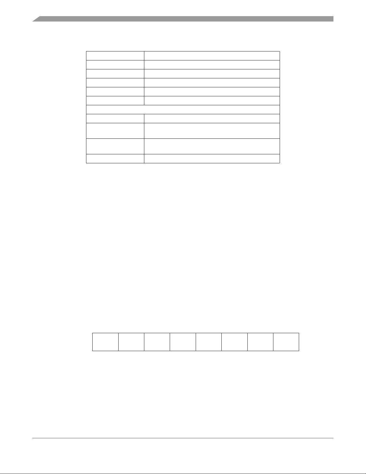
Memory
Table 2-2. Examples of Protect Address Ranges
BPR[7:0] Addresses of Protect Range
$00 The entire FLASH memory is protected.
$01 (0000 0001)$C040 (1100 0000 0100 0000) — $FFFF
$02 (0000 0010)$C080 (1100 0000 1000 0000) — $FFFF
$03 (0000 0011) $C0C0 (1100 0000 1100 0000) — $FFFF
$04 (0000 0100)$C100 (1100 0001 0000 0000) — $FFFF
and so on...
$FC (1111 1100) $FF00 (1111 1111 0000 0000) — FFFF
$FD (1111 1101)
$FE (1111 1110)
$FF The entire FLASH memory is not protected.
$FF40 (1111 1111 0100 0000) — $FFFF
FLBPR and vectors are protected
$FF80 (1111 1111 1000 0000) — FFFF
Vectors are protected
2.6.8 ICG User Trim Registers (ICGTR5 and ICGTR3)
The ICG user trim register are two normal bytes of FLASH memory which are allocated for the user to
store copies of the ICG trim register (ICGTR) value. ICGTR5 is allocated for storage of the trim value
when a 5-V supply is used, ICGTR3 for storage of the trim value when a 3-V supply is used.
Representative trim values are programmed into these locations by Freescale but they may be erased
and reprogrammed by the user at any time.
Storage and retrieval of data in these registers is not automatic and must be performed programmatically.
Typically, these locations are programmed by the user during an in-system calibration procedure and one
of them, depending on the application supply voltage, is subsequently used by the user’s initialization
code to configure the ICG each time following a reset.
ICGTR5 is used by the MC68HC908GT16 monitor ROM program during its initialization sequence if
monitor mode was entered while clocking from the ICG. If the contents of ICGTR5 are not $FF then the
contents are copied to ICGTR.
NOTE
The contents of ICGTR3 are not utilized by the monitor ROM program.
Address: ICGTR5, $FF80 and ICGTR3, $FF81
Bit 7654321Bit 0
Read:
Write:
Reset: Unaffected by reset. Initial value from factory is 1.
TRIM7 TRIM6 TRIM5 TRIM4 TRIM3 TRIM2 TRIM1 TRIM0
Write to this register is by a programming sequence to the FLASH memory.
Figure 2-7. ICG User Trim Registers (ICGTR5 and ICGTR3)
TRIM[7:0] — ICG Trim Factor Bits
These bits are copied by the monitor ROM program following a reset, if monitor mode was entered
while clocking from the ICG and may be copied by the user’s initialization co de to the ICG trim register
(ICGTR).
MC68HC908GT16 • MC68HC908GT 8 Da ta She e t , Rev. 3
44 Freescale Semiconductor

FLASH Memory
2.6.9 Wait Mode
Putting the MCU into wait mode while the FLASH is in read mode does not affect the operation of the
FLASH memory directly, but there will not be any memory activity since the CPU is inactive.
The WAIT instruction should not be executed while performing a program or erase operation on the
FLASH, otherwise the operation will discontinue, and the FLASH will be on standby mode.
2.6.10 Stop Mode
Putting the MCU into stop mode while the FLASH is in read mode does not affect the operation of the
FLASH memory directly, but there will not be any memory activity since the CPU is inactive.
The STOP instruction should not be executed while performing a program or erase operation on the
FLASH, otherwise the operation will discontinue, and the FLASH will be on standby mode
NOTE
Standby mode is the power saving mode of the FLASH module in which all
internal control signals to the FLASH are inactive and the current
consumption of the FLASH is at a minimum.
MC68HC908GT16 • MC68HC908GT 8 Da ta She e t , Rev. 3
Freescale Semiconductor 45

Memory
MC68HC908GT16 • MC68HC908GT 8 Da ta She e t , Rev. 3
46 Freescale Semiconductor

Chapter 3
Analog-to-Digital Converter (ADC)
3.1 Introduction
This section describes the 8-bit analog-to-digital converter (ADC).
3.2 Features
Features of the ADC module include:
• Eight channels with multiplexed input
• Linear successive approximation with monotonicity
• 8-bit resolution
• Single or continuous conversion
• Conversion complete flag or conversion complete interrupt
• Selectable ADC clock
3.3 Functional Description
The ADC provides eight pins for sampling external sources at pins PTB7/AD7–PTB0/AD0. An analog
multiplexer allows the single ADC converter to select one of eight ADC channels as ADC voltage in
(V
When the conversion is completed, ADC places the result in the ADC data register and sets a flag or
generates an interrupt. See Figure 3-2.
ADIN
). V
is converted by the successive approximation register-based analog-to-digital converter.
ADIN
3.3.1 ADC Port I/O Pins
PTB7/AD7–PTB0/AD0 are general-purpose I/O (input/output) pins that share with the ADC channels. The
channel select bits define which ADC channel/port pin will be used as the input signal. The ADC overrides
the port I/O logic by forcing that pin as input to the ADC. The remaining ADC channels/port pins are
controlled by the port I/O logic and can be used as ge neral-purpose I/O. Writes to the port register or data
direction register (DDR) will not have any affect on the port pin that is selected by the ADC. Read of a port
pin in use by the ADC will return a logic 0.
MC68HC908GT16 • MC68HC908GT 8 Da ta She e t , Rev. 3
Freescale Semiconductor 47

Analog-to-Digital Converter (ADC)
M68HC08 CPU
CPU
REGISTERS
ARITHMETIC/LOGIC
UNIT (ALU)
INTERNAL BUS
PROGRAMMABLE TIMEBASE
MODULE
DDRA
PORTA
PTA7/KBD7–
PTA0/KBD0
(1)
CONTROL AND STATUS
REGISTERS — 64 BYTES
USER FLASH
MC68HC908GT16 — 15,872 BYTES
MC68HC908GT8 — 7,680 BYTES
USER RAM — 512 BYTES
MONITOR ROM — 304 BYTES
FLASH PROGRAMMING ROUTINES
ROM — 720 BYTES
USER FLASH VECTOR SPACE — 36 BYTES
PTE4/OSC1
PTE3/OSC2
RST
IRQ
V
REFH
V
REFL
(3)
(3)
INTERNAL CLOCK
GENERATOR MODULE
SYSTEM INTEGRATION
MODULE
SINGLE EXTERNAL
INTERRUPT MODULE
8-BIT ANALOG-TO-DIGITAL
CONVERTER MODULE
POWER-ON RESET
MODULE
V
DD
V
SS
V
DDA
V
SSA
POWER
SINGLE BREAKPOINT BREAK
LOW-VOLTAGE INHIBIT MODULE
2-CHANNEL TIMER INTERFACE
2-CHANNEL TIMER INTERFACE
MODULE
DUAL VOLTAGE
8-BIT KEYBOARD
INTERRUPT MODULE
MODULE 1
MODULE 2
SERIAL COMMUNICATIONS
INTERFACE MODULE
COMPUTER OPERATING
PROPERLY MODULE
SERIAL PERIPHERAL
INTERFACE MODULE
MONITOR MODULE
MEMORY MAP
MODULE
CONFIGURATION REGISTER 1
MODULE
CONFIGURATION REGISTER 2
MODULE
PTB7/AD7
PTB6/AD6
PTB5/AD5
PTB4/AD4
DDRB
PTB3/AD3
PORTB
PTB2/AD2
PTB1/AD1
PTB0/AD0
(1)
PTC6
(1)
PTC5
(1)(2)
PTC4
(1)(2)
DDRC
PTC3
PTC2
PTC1
PTC0
(1)(2)
(1)(2)
(1)(2)
PORTC
PTD7/T2CH1
PTD6/T2CH0
PTD5/T1CH1
PTD4/T1CH0
PORTD
PTD3/SPSCK
PTD2/MOSI
DDRD
PTD1/MISO
PTD0/SS
PTE2
DDRE
PTE1/RxD
PORTE
PTE0/TxD
SECURITY
MODULE
MONITOR MODE ENTRY
MODULE
(1)
(1)
(1)
(1)
(1)
(1)
(1)
(1)
1. Ports are software configurable with pullup device if input port.
2. Higher current drive port pins
3. Pin contains integrated pullup device
Figure 3-1. Block Diagram Highlighting ADC Block and Pins
MC68HC908GT16 • MC68HC908GT 8 Da ta She e t , Rev. 3
48 Freescale Semiconductor

INTERNAL DATA BUS
READ DDRBx
Functional Description
WRITE DDRBx
WRITE PTBx
READ PTBx
INTERRUPT
LOGIC
AIEN COCO
RESET
CONVERSION
COMPLETE
CGMXCLK
BUS CLOCK
DDRBx
PTBx
ADC DATA REGISTER
ADC
ADC CLOCK
CLOCK
GENERATOR
DISABLE
ADC
VOLTAGE IN
)
(V
ADIN
V
REFH
V
REFL
DISABLE
CHANNEL
SELECT
PTBx
ADC CHANNEL x
ADCH4–ADCH0
ADIV2–ADIV0 ADICLK
Figure 3-2. ADC Block Diagram
3.3.2 ADC Port I/O Pins
PTB7/AD7–PTB0/AD0 are general-purpose I/O pins that share with the ADC channels. The channel
select bits define which ADC channel/port pin will be used as the input signal. The ADC overrides the port
I/O logic by forcing that pin as input to the ADC. The remaining ADC channels/port pins are contro lled by
the port I/O logic and can be used as general-purpose I/O. Writes to the port register or data direction
register (DDR) will not have any affect on the port pin that is selected by the ADC. Read of a port pin in
use by the ADC will return a logic 0.
3.3.3 Voltage Conversion
When the input voltage to the ADC equals V
input voltage equals V
, the ADC converts it to $00. Input voltages between V
REFL
straight-line linear conversion.
The ADC input voltage must always be greater than V
V
DDA
. V
must always be greater than or equal to V
REFH
, the ADC converts the signal to $FF (full scale). If the
REFH
and V
REFH
NOTE
and less than
SSA
.
REFL
REFL
are a
MC68HC908GT16 • MC68HC908GT 8 Da ta She e t , Rev. 3
Freescale Semiconductor 49

Analog-to-Digital Converter (ADC)
NOTE
Connect the V
connect the V
pin should be routed carefully for maximum noise immunity.
V
DDA
pin to the same voltage potential as the VDD pin, and
DDA
pin to the same voltage potential as the VSS pin. The
SSA
3.3.4 Conversion Time
Conversion starts after a write to the ADC status and control register (ADSCR). One co nversion will take
between 16 and 17 ADC clock cycles. The ADIVx and ADICLK bits should be set to provide a 1-MHz ADC
clock frequency.
Conversion time =
16 to 17 ADC cycles
ADC frequency
×
Number of bus cycles = conversion time
bus frequency
3.3.5 Conversion
In continuous conversion mode, the ADC data register will be filled with new dat a after each conversion.
Data from the previous conversion will be overwritten whether that data has been read or not.
Conversions will continue until the ADCO bit is cleared. The COCO bit is set after the first conversion and
will stay set until the next read of the ADC data register.
In single conversion mode, conversion begins with a write to the ADSCR. Only one conversion occurs
between writes to the ADSCR.
When a conversion is in process and the ADSCR is written, the current conversion data should be
discarded to prevent an incorrect reading.
3.3.6 Accuracy and Precision
The conversion process is monotonic and has no missing codes.
3.4 Interrupts
When the AIEN bit is set, the ADC module is capable of generating CPU interrupts after each ADC
conversion. A CPU interrupt is generated if the COCO bit is at 0. The COCO bit is not used as a
conversion complete flag when interrupts are enabled.
3.5 Low-Power Modes
The WAIT and STOP instruction can put the MCU in low power-consumption standby modes.
3.5.1 Wait Mode
The ADC continues normal operation during wait mode. Any enabled CPU interrupt request from the ADC
can bring the MCU out of wait mode. If the ADC is not required to bring the MCU out of wait mode, power
down the ADC by setting ADCH4–ADCH0 bits in the ADC status and control register before executing the
WAIT instruction.
MC68HC908GT16 • MC68HC908GT 8 Da ta She e t , Rev. 3
50 Freescale Semiconductor

I/O Signals
3.5.2 Stop Mode
The ADC module is inactive after the execution of a STOP instruction. Any pending conversion is aborted.
ADC conversions resume when the MCU exits stop mode after an external interrupt. Allow one
conversion cycle to stabilize the analog circuitry.
3.6 I/O Signals
The ADC module has eight pins shared with port B, PTB7/AD7–PTB0/AD0.
3.6.1 ADC Analog Power Pin (V
The ADC analog portion uses V
as V
. External filtering may be necessary to ensure clean V
DD
DDA
)
DDA
as its power pin. Connect the V
DDA
pin to the same voltage potential
DDA
for good results.
NOTE
For maximum noise immunity, route V
carefully and place bypass
DDA
capacitors as close as possible to the package.
3.6.2 ADC Analog Ground Pin (V
The ADC analog portion uses V
as V
SS
.
as its ground pin. Connect the V
SSA
SSA
)
pin to the same voltage potential
SSA
NOTE
Route V
3.6.3 ADC Voltage Reference High Pin (V
The ADC analog portion uses V
to the same voltage potential as V
cleanly to avoid any offset errors.
SSA
REFH
as its upper voltage reference pin. The V
REFH
. External filtering is often necessary to ensure a clean V
DDA
)
pin must be connected
REFH
for
REFH
good results. Any noise present on this pin will be reflected and possibly magnified in A/D conversion
values.
NOTE
For maximum noise immunity, route V
capacitors as close as possible to the package. Routing V
parallel to V
may improve common mode noise rejection.
REFL
carefully and place bypass
REFH
REFH
close and
3.6.4 ADC Voltage Reference Low Pin (V
The ADC analog portion uses V
to the same voltage potential as V
as its lower voltage reference pin. The V
REFL
. External filtering is often necessary to ensure a clean V
SSA
REFL
)
pin must be connected
REFL
for
REFL
good results. Any noise present on this pin will be reflected and possibly magnified in A/D conversion
values.
NOTE
For maximum noise immunity, route V
to V
Routing V
, place bypass capacitors as close as possible to the package.
SS
close and parallel to V
REFH
carefully and, if not connected
REFL
may improve common mode
REFL
noise rejection.
MC68HC908GT16 • MC68HC908GT 8 Da ta She e t , Rev. 3
Freescale Semiconductor 51

Analog-to-Digital Converter (ADC)
3.6.5 ADC Voltage In (V
V
is the input voltage signal from one of the eight ADC channels to the ADC module.
ADIN
ADIN
)
3.7 I/O Registers
These I/O registers control and monitor ADC operation:
• ADC status and control register (ADSCR)
• ADC data register (ADR)
• ADC clock register (ADCLK)
3.7.1 ADC Status and Control Register
Function of the ADC status and control register (ADSCR) is described here.
Address: $003C
Bit 7654321Bit 0
Read: COCO
Write: R
Reset:00011111
R= Reserved
Figure 3-3. ADC Status and Control Register (ADSCR)
AIEN ADCO ADCH4 ADCH3 ADCH2 ADCH1 ADCH0
COCO — Conversions Complete Bit
In non-interrupt mode (AIEN = 0), COCO is a read-only bit that is set at the end of each conversion.
COCO will stay set until cleared by a read of the ADC data register. Reset clears this bit.
In interrupt mode (AIEN = 1), COCO is a read-only bit that is not set at the end of a conversion. It
always reads as a 0.
1 = Conversion completed (AIEN = 0)
0 = Conversion not completed (AIEN = 0) or CPU interrupt enabled (AIEN = 1)
NOTE
The write function of the COCO bit is reserved. When writing to the ADSCR
register, always have a 0 in the COCO bit position.
AIEN — ADC Interrupt Enable Bit
When this bit is set, an interrupt is generated at the end of an ADC conversion. The interrupt signal is
cleared when the data register is read or the status/control register is written. Reset clears the AIEN bit.
1 = ADC interrupt enabled
0 = ADC interrupt disabled
ADCO — ADC Continuous Conversion Bit
When set, the ADC will convert samples continuously and update the ADR register at the end of each
conversion. Only one conversion is completed between writes to the ADSCR when this bit is cleared.
Reset clears the ADCO bit.
1 = Continuous ADC conversion
0 = One ADC conversion
MC68HC908GT16 • MC68HC908GT 8 Da ta She e t , Rev. 3
52 Freescale Semiconductor

I/O Registers
ADCH4–ADCH0 — ADC Channel Select Bits
ADCH4–ADCH0 form a 5-bit field which is used to select one of 16 ADC channels. Only eight
channels, AD7–AD0, are available on this MCU. The channels are detailed in Table 3-1. Care should
be taken when using a port pin as both an analog and digital input simultaneously to prevent switching
noise from corrupting the analog signal. See Table 3-1.
The ADC subsystem is turned off when the channel select bits are all set to 1. Th is feature allows fo r
reduced power consumption for the MCU when the ADC is not being used.
NOTE
Recovery from the disabled state requires one conversion cycle to stabilize.
The voltage levels supplied from internal reference nodes, as specified in
Table 3-1, are used to verify the operation of the ADC converter both in production test and for user
applications.
Table 3-1. Mux Channel Select
ADCH4 ADCH3 ADCH2 ADCH1 ADCH0 Input Select
00000 PTB0/AD0
00001 PTB1/AD1
00010 PTB1/AD2
00011 PTB2/AD3
00100 PTB4/AD4
00101 PTB5/AD5
00110 PTB6/AD6
00111 PTB7/AD7
0
↓
1
11101 V
11110 V
1 1 1 1 1 ADC power off
1. If any unused channels are selected, the resulting ADC conversion will be unknown or
reserved.
1
↓
1
0
↓
1
0
↓
0
(1)
0
↓
0
Reserved
REFH
REFL
3.7.2 ADC Data Register
One 8-bit result register, ADC data register (ADR), is provided. This register is updated each time an ADC
conversion completes.
Address: $003D
Bit 7654321Bit 0
Read: AD7 AD6 AD5 AD4 AD3 AD2 AD1 AD0
Write:
Reset:00000000
= Unimplemented
Figure 3-4. ADC Data Register (ADR)
MC68HC908GT16 • MC68HC908GT 8 Da ta She e t , Rev. 3
Freescale Semiconductor 53

Analog-to-Digital Converter (ADC)
3.7.3 ADC Clock Register
The ADC clock register (ADCLK) selects the clock frequency for the ADC.
Address: $003E
Bit 7654321Bit 0
Read:
Write:
Reset:00000000
ADIV2 ADIV1 ADIV0 ADICLK
= Unimplemented
Figure 3-5. ADC Clock Register (ADCLK)
ADIV2–ADIV0 — ADC Clock Prescaler Bits
ADIV2–ADIV0 form a 3-bit field which selects the divide ratio used by the ADC to generate the in ternal
ADC clock. Table 3-2 shows the available clock configurations. The ADC clock should be set to
approximately 1 MHz.
Table 3-2. ADC Clock Divide Ratio
ADIV2 ADIV1 ADIV0 ADC Clock Rate
0 0 0 ADC input clock ÷ 1
0 0 1 ADC input clock ÷ 2
0000
0 1 0 ADC input clock ÷ 4
0 1 1 ADC input clock ÷ 8
1X
1. X = Don’t care
(1)
(1)
X
ADC input clock ÷ 16
ADICLK — ADC Input Clock Select Bit
ADICLK selects either the bus clock or the oscillator output clock (CGMXCLK) as the input clock
source to generate the internal ADC clock. Reset selects CGMXCLK as the ADC clock source.
1 = Internal bus clock
0 = Oscillator output clock (CGMXCLK)
The ADC requires a clock rate of approximately 1 MHz for correct operation. If the selected clock source
is not fast enough, the ADC will generate incorrect conversions. See 20.16 ADC Characteristics.
or bus frequency
≅ 1 MHz
ADIV[2:0]
f
ADIC
=
f
CGMXCLK
MC68HC908GT16 • MC68HC908GT 8 Da ta She e t , Rev. 3
54 Freescale Semiconductor

Chapter 4
Configuration Register (CONFIG)
4.1 Introduction
This section describes the configuration registers, CONFIG1 and CONFIG2. The configuration registers
enable or disable these options:
• Stop mode recovery time (32 CGMXCLK cycles or 4096 CGMXCLK cycles)
• COP timeout period (262,128 or 8176 COPCLK cycles)
•STOP instruction
• Computer operating properly module (COP)
• Low-voltage inhibit (LVI) module control and voltage trip point selection
• Enable/disable the oscillator (OSC) during stop mode
• External clock, external crystal, or ICG clock source
4.2 Functional Description
The configuration registers are used in the initialization of various options. The configuration registers ca n
be written once after each reset. All of the configuration register bits are cleared during reset. Since the
various options affect the operation of the microcontroller unit (MCU), it is recommended that these
registers be written immediately after reset. The configuration registers are located at $001E and $001F
and may be read at anytime.
NOTE
On a FLASH device, the options except LVI5OR3 are one-time writable by
the user after each reset. The LVI5OR3 bit is one-time writable by the user
only after each POR (power-on reset). The CONFIG registers are n ot in the
FLASH memory but are special registers containing one-time writable
latches after each reset. Upon a reset, the CONFIG registers default to
predetermined settings as shown in Figure 4-1 and Figure 4-2.
MC68HC908GT16 • MC68HC908GT 8 Da ta She e t , Rev. 3
Freescale Semiconductor 55

Configuration Register (CONFIG)
Address: $001E
Bit 76 5 432 1 Bit 0
Read: 0 0
Write:
Reset:00000000
= Unimplemented R = Reserved
EXTXTALEN EXTSLOW EXTCLKEN
0
OSCENINSTOP R
Figure 4-1. Configuration Register 2 (CONFIG2)
Address: $001F
Bit 7654321Bit 0
Read:
Write:
Reset:0000See Note000
Note: LVI5OR3 bit is only reset via POR (power-on reset)
COPRS LVISTOP LVIRSTD LVIPWRD LVI5OR3 SSREC STOP COPD
Figure 4-2. Configuration Register 1 (CONFIG1)
EXTXTALEN — External Crystal Enable Bit
EXTXTALEN enables the external oscillator circuits to be configured for a crystal configuration where
the PTE4/OSC1 and PTE3/OSC2 pins are the connections for an external crystal.
Clearing the EXTXTALEN bit (default setting) allows the PTE3/OSC2 pin to function as a
general-purpose I/O pin. Refer to Table 4-1 for configuration options for the external source. See
Chapter 7 Internal Clock Generator (ICG) Module) for a more detailed description of the external clock
operation.
EXTXTALEN, when set, also configures the clock monitor to expect an external clock source in the
valid range of crystals (30 kHz to 100 kHz or 1 MHz to 8 MHz). When EXTXTALEN is clear, the clock
monitor will expect an external clock source in the valid range for externally generated clocks when
using the clock monitor (60 Hz to 32 MHz).
EXTXTALEN, when set, also configures the external clock stabilization divider in the clock monitor fo r
a 4096-cycle timeout to allow the proper stabilization time for a crystal. When EXTXTALEN is clear,
the stabilization divider is configured to 16 cycles since an external clock source does not need a
startup time.
1 = Allows PTE3/OSC2 to be an external crystal connection.
0 = PTE3/OSC2 functions as an I/O port pin (default).
EXTSLOW — Slow External Crystal Enable Bit
The EXTSLOW bit has two functions. It configures the ICG module for a fast (1 MHz to 8 MHz) or slow
(30 kHz to 100 kHz) speed crystal. The option also configures the clock monitor operation in the ICG
module to expect an external frequency higher (307.2 kHz to 32 MHz) or lower (60 Hz to 307.2 kHz)
than the base frequency of the internal oscillator. See Chapter 7 Internal Clock Generator (ICG)
Module).
1 = ICG set for slow external crystal operation
0 = ICG set for fast external crystal operation
NOTE
This bit does not function without setting the EXTCLKEN bit also.
MC68HC908GT16 • MC68HC908GT 8 Da ta She e t , Rev. 3
56 Freescale Semiconductor

Functional Description
EXTCLKEN — External Clock Enable Bit
EXTCLKEN enables an external clock source or crystal/ceramic resonator to be used as a clock input.
Setting this bit enables PTE4/OSC1 pin to be a clock input pin. Clearing this bit (default setting) a llows
the PTE4/OSC1 and PTE3/OSC2 pins to function as a general-purpose input/output (I/O) pin. Refer
to Table 4-1 for configuration options for the external source. See Chapter 7 Internal Clock Generator
(ICG) Module) for a more detailed description of the external clock operation.
1 = Allows PTE4/OSC1 to be an external clock connection
0 = PTE4/OSC1 and PTE3/OSC2 function as I/O port pins (default).
Table 4-1. External Clock Option Settings
External Clock
Configuration Bits
EXTCLKEN EXTXTALEN PTE4/OSC1 PTE3/OSC2
0 0 PTE4 PTE3 Default setting — external oscillator disabled
0 1 PTE4 PTE3 External oscillator disabled since EXTCLKEN not set
1 0 OSC1 PTE3
1 1 OSC1 OSC2
Pin
Function
Description
External oscillator configured for an external clock source
input (square wave) on OSC1
External oscillator configured for an external crystal
configuration on OSC1 and OSC2. System will also
operate with square-wave clock source in OSC1.
OSCENINSTOP — Oscillator Enable In Stop Mode Bit
OSCENINSTOP, when set, will enable the internal clock generator module to continue to generate
clocks (either internal, ICLK, or external, ECLK) in stop mode. See Chapter 7 Internal Clock Generator
(ICG) Module). This function is used to keep the timebase running while the re st of the microcontroller
stops. See Chapter 17 Timebase Module (TBM). When clear, all clock generation will cease and both
ICLK and ECLK will be forced low during stop mode. The default state for this option is clear, disabling
the ICG in stop mode.
1 = Oscillator enabled to operate during stop mode
0 = Oscillator disabled during stop mode (default)
NOTE
This bit has the same functionality as the OSCSTOPENB CONFIG bit in
MC68HC908GP32 and MC68HC908GR8 parts.
COPRS — COP Rate Select Bit
COPD selects the COP timeout period. Reset clears COPRS. See Chapter 5 Computer Operating
Properly (COP) Module
1 = COP timeout period = 262,128 COPCLK cycles
0 = COP timeout period = 8176 COPCLK cycles
LVISTOP — LVI Enable in Stop Mode Bit
When the LVIPWRD bit is clear, setting the LVISTOP bit enables the LVI to operate during stop mode.
Reset clears LVISTOP.
1 = LVI enabled during stop mode
0 = LVI disabled during stop mode
LVIRSTD — LVI Reset Disable Bit
LVIRSTD disables the reset signal from the LVI module. See Chapter 10 Low-Voltage Inhibit (LVI).
1 = LVI module resets disabled
0 = LVI module resets enabled
MC68HC908GT16 • MC68HC908GT 8 Da ta She e t , Rev. 3
Freescale Semiconductor 57

Configuration Register (CONFIG)
LVIPWRD — LVI Power Disable Bit
LVIPWRD disables the LVI module. See Chapter 10 Low-Voltage Inhibit (LVI).
1 = LVI module power disabled
0 = LVI module power enabled
LVI5OR3 — LVI 5-V or 3-V Operating Mode Bit
LVI5OR3 selects the voltage operating mode of the LVI module. See Chapter 10 Low-Vo ltage Inhibit
(LVI) The voltage mode selected for the LVI should match the operating V
. See Chapter 20
DD
Electrical Specifications for the LVI’s voltage trip points for each of the modes.
1 = LVI operates in 5-V mode.
0 = LVI operates in 3-V mode.
NOTE
The LVI5OR3 bit is cleared by a power-on reset (POR) only. Other resets
will leave this bit unaffected.
SSREC — Short Stop Recovery Bit
SSREC enables the CPU to exit stop mode with a delay of 32 CGMXCLK cycles instead of a
4096-CGMXCLK cycle delay.
1 = Stop mode recovery after 32 CGMXCLK cycles
0 = Stop mode recovery after 4096 CGMXCLCK cycles
NOTE
Exiting stop mode by an LVI reset will result in the long stop recovery.
The short stop recovery delay can be enabled when using the internal oscillator, a crystal, or a ceramic
resonator and the OSCENINSTOP bit is set. The short stop recovery delay can be enabled when an
external oscillator is used, regardless of the OSCENINSTOP setting.
The short stop recovery delay must be disabled (SSREC = 0) when the OSCENINSTOP bit is cleared.
STOP — STOP Instruction Enable Bit
STOP enables the STOP instruction.
1 = STOP instruction enabled
0 = STOP instruction treated as illegal opcode
COPD — COP Disable Bit
COPD disables the COP module. See Chapter 5 Computer Operating Properly (COP) Module.
1 = COP module disabled
0 = COP module enabled
MC68HC908GT16 • MC68HC908GT 8 Da ta She e t , Rev. 3
58 Freescale Semiconductor

Chapter 5
Computer Operating Properly (COP) Module
5.1 Introduction
The computer operating properly (COP) module contains a free-running counter that generates a reset if
allowed to overflow. The COP module helps software recover from runaway code. Prevent a COP reset
by clearing the COP counter periodically. The COP module can be disabled through the COPD bit in the
CONFIG register.
5.2 Functional Description
Figure 5-1 shows the structure of the COP module.
SIM MODULE
BUSCLKX4
INTERNAL RESET SOURCES
RESET VECTOR FETCH
COPCTL WRITE
COPEN (FROM SIM)
COPD (FROM CONFIG1)
RESET
COPCTL WRITE
COP RATE SELECT
(COPRS FROM CONFIG1)
12-BIT SIM COUNTER
CLEAR ALL STAGES
COP CLOCK
COP COUNTER
SIM RESET CIRCUIT
RESET STATUS REGISTER
CLEAR STAGES 5–12
COP TIMEOUT
COP MODULE
6-BIT COP COUNTER
CLEAR
Figure 5-1. COP Block Diagram
MC68HC908GT16 • MC68HC908GT 8 Da ta She e t , Rev. 3
Freescale Semiconductor 59

Computer Operating Properly (COP) Module
The COP counter is a free-running 6-bit counter preceded by a 12-bit prescaler counter. If not cleared by
software, the COP counter overflows and generates an asynchronous reset after 262,128 or 8176
COPCLK cycles, depending on the state of the COP rate select bit, COPRS, in th e configuration register.
With a 8176 COPCLK cycle overflow option, a 32.768-kHz crystal gives a COP timeout period of 250 ms.
Writing any value to location $FFFF before an overflow occurs prevents a COP reset by clearing the COP
counter and stages 12 through 5 of the prescaler.
NOTE
Service the COP immediately after reset and before entering or after exiting
stop mode to guarantee the maximum time before the first COP counter
overflow.
A COP reset pulls the RST
pin low for 32 COPCLK cycles and sets the COP bit in the reset status register
(RSR).
In monitor mode, the COP is disabled if the RST
on the RST pin disables the COP.
V
TST
pin or the IRQ1 is held at V
. During the break state,
TST
NOTE
Place COP clearing instructions in the main program and not in an interrupt
subroutine. Such an interrupt subroutine could keep the COP from
generating a reset even while the main program is not working properly.
5.3 I/O Signals
The following paragraphs describe the signals shown in Figure 5-1.
5.3.1 COPCLK
COPCLK is a clock generated by the clock selection circuit in the internal clock generator (ICG). See 7.3.5
Clock Selection Circuit for more details.
5.3.2 STOP Instruction
The STOP instruction clears the COP prescaler.
5.3.3 COPCTL Write
Writing any value to the COP control register (COPCTL) (see 5.4 COP Control Register) clears the COP
counter and clears bits 12 through 5 of the prescaler. Reading the COP control register returns the low
byte of the reset vector.
5.3.4 Power-On Reset
The power-on reset (POR) circuit clears the COP prescaler 4096 CGMXCLK cycles after power-up.
5.3.5 Internal Reset
An internal reset clears the COP prescaler and the COP counter.
MC68HC908GT16 • MC68HC908GT 8 Da ta She e t , Rev. 3
60 Freescale Semiconductor

COP Control Register
5.3.6 Reset Vector Fetch
A reset vector fetch occurs when the vector address appears on the data bus. A reset vector fetch clears
the COP prescaler.
5.3.7 COPD (COP Disable)
The COPD signal reflects the state of the COP disable bit (COPD) in the configuration register. See
Chapter 4 Configuration Register (CONFIG).
5.3.8 COPRS (COP Rate Select)
The COPRS signal reflects the state of the COP rate select bit (COPRS) in the configuration register. See
Chapter 4 Configuration Register (CONFIG).
5.4 COP Control Register
The COP control register is located at address $FFFF and overlaps the reset vector. Writing any value to
$FFFF clears the COP counter and starts a new timeout period. Reading location $FFFF returns the low
byte of the reset vector.
Address: $FFFF
Bit 7654321Bit 0
Read: Low byte of reset vector
Write: Clear COP counter
Reset: Unaffected by reset
Figure 5-2. COP Control Register (COPCTL)
5.5 Interrupts
The COP does not generate central processor unit (CPU) interrupt requests.
5.6 Monitor Mode
When monitor mode is entered with V
on the IRQ
having V
pin or the RST pin. When monitor mode is entered by having blank reset vectors and not
on the IRQ pin, the COP is automatically disabled until a POR occurs.
TST
on the IRQ pin, the COP is disabled as long as V
TST
remains
TST
5.7 Low-Power Modes
The WAIT and STOP instructions put the microcontroller unit (MCU) in low power-consumption standby
modes.
5.7.1 Wait Mode
The COP remains active during wait mode. To prevent a COP reset during wait mode, periodically clea r
the COP counter in a CPU interrupt routine.
MC68HC908GT16 • MC68HC908GT 8 Da ta She e t , Rev. 3
Freescale Semiconductor 61

Computer Operating Properly (COP) Module
5.7.2 Stop Mode
Stop mode turns off the COPCLK input to the COP and clears the COP prescaler. Service the COP
immediately before entering or after exiting stop mode to ensure a full COP timeout period after entering
or exiting stop mode.
To prevent inadvertently turning off the COP with a STOP instruction, a configuration option is available
that disables the STOP instruction. When the STOP bit in the configuration register has the STOP
instruction is disabled, execution of a STOP instruction results in an illegal opcode reset.
5.8 COP Module During Break Mode
The COP is disabled during a break interrupt when V
is present on the RST pin.
TST
MC68HC908GT16 • MC68HC908GT 8 Da ta She e t , Rev. 3
62 Freescale Semiconductor

Chapter 6
Central Processor Unit (CPU)
6.1 Introduction
The M68HC08 CPU (central processor unit) is an enhanced a nd fu lly object-code- compatib le version o f
the M68HC05 CPU. The CPU08 Reference Manual (document order number CPU08RM/AD) contains a
description of the CPU instruction set, addressing modes, and architecture.
6.2 Features
Features of the CPU include:
• Object code fully upward-compatible with M68HC05 Family
• 16-bit stack pointer with stack manipulation instructions
• 16-bit index register with x-register manipulation instructions
• 8-MHz CPU internal bus frequency
• 64-Kbyte program/data memory space
• 16 addressing modes
• Memory-to-memory data moves without using accumulator
• Fast 8-bit by 8-bit multiply and 16-bit by 8-bit divide instructions
• Enhanced binary-coded decimal (BCD) data handling
• Modular architecture with expandable internal bus definition for extension of addressing range
beyond 64 Kbytes
• Low-power stop and wait modes
6.3 CPU Registers
Figure 6-1 shows the five CPU registers. CPU registers are not part of the memory map.
MC68HC908GT16 • MC68HC908GT 8 Da ta She e t , Rev. 3
Freescale Semiconductor 63

Central Processor Unit (CPU)
7
15
H X
15
15
70
V11H I NZC
0
ACCUMULATOR (A)
0
INDEX REGISTER (H:X)
0
STACK POINTER (SP)
0
PROGRAM COUNTER (PC)
CONDITION CODE REGISTER (CCR)
CARRY/BORROW FLAG
ZERO FLAG
NEGATIVE FLAG
INTERRUPT MASK
HALF-CARRY FLAG
TWO’S COMPLEMENT OVERFLOW FLAG
Figure 6-1. CPU Registers
6.3.1 Accumulator
The accumulator is a general-purpose 8-bit register. The CPU uses the accumulator to hold operands and
the results of arithmetic/logic operations.
Bit 7654321Bit 0
Read:
Write:
Reset: Unaffected by reset
Figure 6-2. Accumulator (A)
6.3.2 Index Register
The 16-bit index register allows indexed addressing of a 64-Kbyte memory space. H is the upper byte of
the index register, and X is the lower byte. H:X is the concatenated 16-bit index register.
In the indexed addressing modes, the CPU uses the contents of the index register to determine the
conditional address of the operand.
The index register can serve also as a temporary data storage location.
Bit
151413121110987654321
Read:
Write:
Reset:00000000XXXXXXXX
X = Indeterminate
Figure 6-3. Index Register (H:X)
Bit
0
MC68HC908GT16 • MC68HC908GT 8 Da ta She e t , Rev. 3
64 Freescale Semiconductor

CPU Registers
6.3.3 Stack Pointer
The stack pointer is a 16-bit register that contains the address of the next location on the stack. During a
reset, the stack pointer is preset to $00FF. The reset stack pointer (RSP) instruction sets the least
significant byte to $FF and does not affect the most significant byte. The stack pointer decrements as data
is pushed onto the stack and increments as data is pulled from the stack.
In the stack pointer 8-bit offset and 16-bit offset addressing modes, the stack pointer can function as an
index register to access data on the stack. The CPU uses the contents of the stack pointer to determine
the conditional address of the operand.
Bit
151413121110987654321
Read:
Write:
Reset:0000000011111111
Bit
0
Figure 6-4. Stack Pointer (SP)
NOTE
The location of the stack is arbitrary and may be relocated anywhere in
random-access memory (RAM). Moving the SP out of page 0 ($0000 to
$00FF) frees direct address (page 0) space. For correct operation, the
stack pointer must point only to RAM locations.
6.3.4 Program Counter
The program counter is a 16-bit register that contains the address of the next instruction or operand to be
fetched.
Normally, the program counter automatically increments to the next sequential memory location every
time an instruction or operand is fetched. Jump, branch, and interrupt operations load the program
counter with an address other than that of the next sequential location.
During reset, the program counter is loaded with the reset vector address located at $FFFE and $FFFF.
The vector address is the address of the first instruction to be executed after exiting the reset state.
Bit
151413121110987654321
Read:
Write:
Reset: Loaded with vector from $FFFE and $FFFF
Bit
0
Figure 6-5. Program Counter (PC)
MC68HC908GT16 • MC68HC908GT 8 Da ta She e t , Rev. 3
Freescale Semiconductor 65

Central Processor Unit (CPU)
6.3.5 Condition Code Register
The 8-bit condition code register contains the interrupt mask and five flags that indicate the results of t he
instruction just executed. Bits 6 and 5 are set permanently to 1. The following paragraphs describe the
functions of the condition code register.
Bit 7654321Bit 0
Read:
Write:
Reset:X11X1XXX
V — Overflow Flag
The CPU sets the overflow flag when a two's complement overflow occurs. The signed branch
instructions BGT, BGE, BLE, and BLT use the overflow flag.
1 = Overflow
0 = No overflow
H — Half-Carry Flag
The CPU sets the half-carry flag when a carry occurs between accumulator bits 3 and 4 during an
add-without-carry (ADD) or add-with-carry (ADC) operation. The half-carry flag is required for
binary-coded decimal (BCD) arithmetic operations. The DAA instruction uses the states of the H and
C flags to determine the appropriate correction factor.
1 = Carry between bits 3 and 4
0 = No carry between bits 3 and 4
V11H I NZC
X = Indeterminate
Figure 6-6. Condition Code Register (CCR)
I — Interrupt Mask
When the interrupt mask is set, all maskable CPU interrupts are disabled. CPU interru pts are enabled
when the interrupt mask is cleared. When a CPU interrupt occurs, the interrupt mask is set
automatically after the CPU registers are saved on the stack, but before the interrupt vector is fetched.
1 = Interrupts disabled
0 = Interrupts enabled
NOTE
To maintain M6805 Family compatibility, the upper byte of the index
register (H) is not stacked automatically. If the interrupt service routine
modifies H, then the user must stack and unstack H using the PSHH and
PULH instructions.
After the I bit is cleared, the highest-priority interrupt request is serviced first.
A return-from-interrupt (RTI) instruction pulls the CPU registers from the stack and restores the
interrupt mask from the stack. After any reset, the interrupt mask is set and can be cleared only by the
clear interrupt mask software instruction (CLI).
N — Negative Flag
The CPU sets the negative flag when an arithmetic operation, logic operation, or data manipulation
produces a negative result, setting bit 7 of the result.
1 = Negative result
0 = Non-negative result
MC68HC908GT16 • MC68HC908GT 8 Da ta She e t , Rev. 3
66 Freescale Semiconductor

Arithmetic/Logic Unit (ALU)
Z — Zero Flag
The CPU sets the zero flag when an arithmetic operation, logic operation, or data manipulation
produces a result of $00.
1 = Zero result
0 = Non-zero result
C — Carry/Borrow Flag
The CPU sets the carry/borrow flag when an addition operation produces a carry out of bit 7 of the
accumulator or when a subtraction operation requires a borrow. Some instructions — such as bit test
and branch, shift, and rotate — also clear or set the carry/borrow flag.
1 = Carry out of bit 7
0 = No carry out of bit 7
6.4 Arithmetic/Logic Unit (ALU)
The ALU performs the arithmetic and logic operations defined by the instruction set.
Refer to the CPU08 Reference Manual (document order number CPU08RM/AD) for a description of the
instructions and addressing modes and more detail about the architecture of the CPU.
6.5 Low-Power Modes
The WAIT and STOP instructions put the MCU in low power-consumption standby modes.
6.5.1 Wait Mode
The WAIT instruction:
• Clears the interrupt mask (I bit) in the condition code register, enabling interrupts. After exit from
wait mode by interrupt, the I bit remains clear. After exit by reset, the I bit is set.
• Disables the CPU clock
6.5.2 Stop Mode
The STOP instruction:
• Clears the interrupt mask (I bit) in the condition code register, enabling external interrupts. After
exit from stop mode by external interrupt, the I bit remains clear. After exit by reset, the I bit is set.
• Disables the CPU clock
After exiting stop mode, the CPU clock begins running after the oscillator stabilization delay.
6.6 CPU During Break Interrupts
If a break module is present on the MCU, the CPU starts a break interrupt by:
• Loading the instruction register with the SWI instruction
• Loading the program counter with $FFFC:$FFFD or with $FEFC:$FEFD in monitor mode
The break interrupt begins after completion of the CPU instruction in progress. If the break address
register match occurs on the last cycle of a CPU instruction, the break interrupt begins immediately.
A return-from-interrupt instruction (RTI) in the break routine ends the break interrupt and returns the MCU
to normal operation if the break interrupt has been deasserted.
MC68HC908GT16 • MC68HC908GT 8 Da ta She e t , Rev. 3
Freescale Semiconductor 67

Central Processor Unit (CPU)
6.7 Instruction Set Summary
Table 6-1 provides a summary of the M68HC08 instruction set.
Table 6-1. Instruction Set Summary (Sheet 1 of 6)
Effect
Source
Form
ADC #opr
ADC opr
ADC opr
ADC opr,X
ADC opr,X
ADC ,X
ADC opr,SP
ADC opr,SP
ADD #opr
ADD opr
ADD opr
ADD opr,X
ADD opr,X
ADD ,X
ADD opr,SP
ADD opr,SP
AIS #opr Add Immediate Value (Signed) to SP
AIX #opr Add Immediate Value (Signed ) to H:X
AND #opr
AND opr
AND opr
AND opr,X
AND opr,X
AND ,X
AND opr,SP
AND opr,SP
ASL opr
ASLA
ASLX
ASL opr,X
ASL ,X
ASL opr,SP
ASR opr
ASRA
ASRX
ASR opr,X
ASR opr,X
ASR opr,SP
BCC rel Branch if Carry Bit Clear PC ← (PC) + 2 + rel ? (C) = 0 ––––––REL 24 rr 3
BCLR n, opr Clear Bit n in M Mn ← 0 ––––––
BCS rel Branch if Carry Bit Set (Same as BLO) PC ← (PC) + 2 + rel ? (C) = 1 ––––––REL 25 rr 3
BEQ rel Branch if Equal PC ← (PC) + 2 + rel ? (Z) = 1 ––––––REL 27 rr 3
BGE opr
BGT opr
BHCC rel Branch if Half Carry Bit Clear PC ← (PC) + 2 + rel ? (H) = 0 ––––––REL 28 rr 3
BHCS rel Branch if Half Carry Bit Set PC ← (PC) + 2 + rel ? (H) = 1 ––––––REL 29 rr 3
BHI rel Branch if Higher PC ← (PC) + 2 + rel ? (C) | (Z) = 0 ––––––REL 22 rr 3
Add with Carry A ← (A) + (M) + (C) –
Add without Carry A ← (A) + (M) –
Logical AND A ← (A) & (M) 0 – – –
Arithmetic Shift Left
(Same as LSL)
Arithmetic Shift Right ––
Branch if Greater Than or Equal To
(Signed Operands)
Branch if Greater Than (Signed
Operands)
Operation Description
SP ← (SP) + (16
H:X ← (H:X) + (16
C
b7
b7
PC ← (PC) + 2 + rel ? (N
PC ← (PC) + 2 + rel ? (Z) | (N
« M)
« M)
0
b0
C
b0
⊕ V) = 0
⊕ V) = 0
on CCR
VHI NZC
––––––IMM A7 ii 2
––––––IMM AF ii 2
––
––––––REL 90 rr 3
––––––REL 92 rr 3
Address
IMM
DIR
EXT
IX2
IX1
IX
SP1
SP2
IMM
DIR
EXT
IX2
IX1
IX
SP1
SP2
IMM
DIR
EXT
IX2
IX1
IX
SP1
SP2
DIR
INH
INH
IX1
IX
SP1
DIR
INH
INH
IX1
IX
SP1
DIR (b0)
DIR (b1)
DIR (b2)
DIR (b3)
DIR (b4)
DIR (b5)
DIR (b6)
DIR (b7)
Mode
9EE9
9ED9
9EEB
9EDB
9EE4
9ED4
9E68
9E67
A9
B9
C9
D9
E9
F9
AB
BB
CB
DB
EB
FB
A4
B4
C4
D4
E4
F4
38
48
58
68
78
37
47
57
67
77
11
13
15
17
19
1B
1D
1F
Opcode
ii
dd
hh ll
ee ff
ff
ff
ee ff
ii
dd
hh ll
ee ff
ff
ff
ee ff
ii
dd
hh ll
ee ff
ff
ff
ee ff
dd
ff
ff
dd
ff
ff
dd
dd
dd
dd
dd
dd
dd
dd
Operand
Cycles
2
3
4
4
3
2
4
5
2
3
4
4
3
2
4
5
2
3
4
4
3
2
4
5
4
1
1
4
3
5
4
1
1
4
3
5
4
4
4
4
4
4
4
4
MC68HC908GT16 • MC68HC908GT 8 Da ta She e t , Rev. 3
68 Freescale Semiconductor

Instruction Set Summary
Table 6-1. Instruction Set Summary (Sheet 2 of 6)
Effect
Source
Form
BHS rel
BIH rel Branch if IRQ
BIL rel Branch if IRQ
BIT #opr
BIT opr
BIT opr
BIT opr,X
BIT opr,X
BIT ,X
BIT opr,SP
BIT opr,SP
BLE opr
BLO rel Branch if Lower (Same as BCS) PC ← (PC) + 2 + rel ? (C) = 1 ––––––REL 25 rr 3
BLS rel Branch if Lower or Same PC ← (PC) + 2 + rel ? (C) | (Z) = 1 ––––––REL 23 rr 3
BLT opr Branch if Less Than (Signed Operands)
BMC rel Branch if Interrupt Mask Clear PC ← (PC) + 2 + rel ? (I) = 0 ––––––REL 2C rr 3
BMI rel Branch if Minus PC ← (PC) + 2 + rel ? (N) = 1 ––––––REL 2B rr 3
BMS rel Branch if Interrupt Mask Set PC ← (PC) + 2 + rel ? (I) = 1 ––––––REL 2D rr 3
BNE rel Branch if Not Equal PC ← (PC) + 2 + rel ? (Z) = 0 ––––––REL 26 rr 3
BPL rel Branch if Plus PC ← (PC) + 2 + rel ? (N) = 0 ––––––REL 2A rr 3
BRA rel Branch Always PC ← (PC) + 2 + rel ––––––REL 20 rr 3
BRCLR n,opr,rel Branch if Bit n in M Clear PC ← (PC) + 3 + rel ? (Mn) = 0 –––––
BRN rel Branch Never PC ← (PC) + 2 ––––––REL 21 rr 3
BRSET n,opr,rel Branch if Bit n in M Set PC ← (PC) + 3 + rel ? (Mn) = 1 –––––
BSET n,opr Set Bit n in M Mn ← 1 ––––––
BSR rel Branch to Subroutine
CBEQ opr,rel
CBEQA #opr,rel
CBEQX #opr,rel
CBEQ opr,X+,rel
CBEQ X+,rel
CBEQ opr,SP,rel
CLC Clear Carry Bit C ← 0 –––––0INH 98 1
CLI Clear Interrupt Mask I ← 0 ––0–––INH 9A 2
Branch if Higher or Same
(Same as BCC)
Bit Test (A) & (M) 0 – – –
Branch if Less Than or Equal To
(Signed Operands)
Compare and Branch if Equal
Operation Description
PC ← (PC) + 2 + rel ? (C) = 0 ––––––REL 24 rr 3
Pin High PC ← (PC) + 2 + rel ? IRQ = 1 ––––––REL 2F rr 3
Pin Low PC ← (PC) + 2 + rel ? IRQ = 0 ––––––REL 2E rr 3
PC ← (PC) + 2 + rel ? (Z) | (N
PC ← (PC) + 2 + rel ? (N
PC ← (PC) + 2; push (PCL)
SP ← (SP) – 1; push (PCH)
SP ← (SP) – 1
PC ← (PC) + rel
PC ← (PC) + 3 + rel ? (A) – (M) = $00
PC ← (PC) + 3 + rel ? (A) – (M) = $00
PC ← (PC) + 3 + rel ? (X) – (M) = $00
PC ← (PC) + 3 + rel ? (A) – (M) = $00
PC ← (PC) + 2 + rel ? (A) – (M) = $00
PC ← (PC) + 4 + rel ? (A) – (M) = $00
⊕ V) = 1
⊕ V) =1
on CCR
VHI NZC
––––––REL 93 rr 3
––––––REL 91 rr 3
––––––REL AD rr 4
––––––
Address
IMM
DIR
EXT
IX2
IX1
IX
SP1
SP2
DIR (b0)
DIR (b1)
DIR (b2)
DIR (b3)
DIR (b4)
DIR (b5)
DIR (b6)
DIR (b7)
DIR (b0)
DIR (b1)
DIR (b2)
DIR (b3)
DIR (b4)
DIR (b5)
DIR (b6)
DIR (b7)
DIR (b0)
DIR (b1)
DIR (b2)
DIR (b3)
DIR (b4)
DIR (b5)
DIR (b6)
DIR (b7)
DIR
IMM
IMM
IX1+
IX+
SP1
Mode
9EE5
9ED5
9E61
A5
B5
C5
D5
E5
F5
01
03
05
07
09
0B
0D
0F
00
02
04
06
08
0A
0C
0E
10
12
14
16
18
1A
1C
1E
31
41
51
61
71
Opcode
ii
dd
hh ll
ee ff
ff
ff
ee ff
dd rr
dd rr
dd rr
dd rr
dd rr
dd rr
dd rr
dd rr
dd rr
dd rr
dd rr
dd rr
dd rr
dd rr
dd rr
dd rr
dd
dd
dd
dd
dd
dd
dd
dd
dd rr
ii rr
ii rr
ff rr
rr
ff rr
Operand
2
3
4
4
3
2
4
5
5
5
5
5
5
5
5
5
5
5
5
5
5
5
5
5
4
4
4
4
4
4
4
4
5
4
4
5
4
6
Cycles
MC68HC908GT16 • MC68HC908GT 8 Da ta She e t , Rev. 3
Freescale Semiconductor 69

Central Processor Unit (CPU)
Source
Form
CLR opr
CLRA
CLRX
CLRH
CLR opr,X
CLR ,X
CLR opr,SP
CMP #opr
CMP opr
CMP opr
CMP opr,X
CMP opr,X
CMP ,X
CMP opr,SP
CMP opr,SP
COM opr
COMA
COMX
COM opr,X
COM ,X
COM opr,SP
CPHX #opr
CPHX opr
CPX #opr
CPX opr
CPX opr
CPX ,X
CPX opr,X
CPX opr,X
CPX opr,SP
CPX opr,SP
DAA Decimal Adjust A
DBNZ opr,rel
DBNZA rel
DBNZX rel
DBNZ opr,X,rel
DBNZ X,rel
DBNZ opr,SP,rel
DEC opr
DECA
DECX
DEC opr,X
DEC ,X
DEC opr,SP
DIV Divide
EOR #opr
EOR opr
EOR opr
EOR opr,X
EOR opr,X
EOR ,X
EOR opr,SP
EOR opr,SP
INC opr
INCA
INCX
INC opr,X
INC ,X
INC opr,SP
Clear
Compare A with M (A) – (M) ––
Complement (One’s Complement)
Compare H:X with M (H:X) – (M:M + 1) ––
Compare X with M (X) – (M) ––
Decrement and Branch if Not Zero
Decrement
Exclusive OR M with A
Increment
Operation Description
Table 6-1. Instruction Set Summary (Sheet 3 of 6)
Effect
on CCR
VHI NZC
M ← $00
A ← $00
X ← $00
H ← $00
M ← $00
M ← $00
M ← $00
M ← (M
) = $FF – (M)
A ← (A
) = $FF – (M)
X ← (X) = $FF – (M)
M ← (M
) = $FF – (M)
M ← (M) = $FF – (M)
M ← (M) = $FF – (M)
(A)
10
A ← (A) – 1 or M ← (M) – 1 or X ← (X) – 1
PC ← (PC) + 3 + rel ? (result) ≠ 0
PC ← (PC) + 2 + rel ? (result) ≠ 0
PC ← (PC) + 2 + rel ? (result) ≠ 0
PC ← (PC) + 3 + rel ? (result) ≠ 0
PC ← (PC) + 2 + rel ? (result) ≠ 0
PC ← (PC) + 4 + rel ? (result) ≠ 0
M ← (M) – 1
A ← (A) – 1
X ← (X) – 1
M ← (M) – 1
M ← (M) – 1
M ← (M) – 1
A ← (H:A)/(X)
H ← Remainder
A ← (A
⊕ M)
M ← (M) + 1
A ← (A) + 1
X ← (X) + 1
M ← (M) + 1
M ← (M) + 1
M ← (M) + 1
0––01–
0––1
U––INH 72 2
––––––
–––
––––INH 52 7
0–––
–––
DIR
INH
INH
INH
IX1
IX
SP1
IMM
DIR
EXT
IX2
IX1
IX
SP1
SP2
DIR
INH
INH
IX1
IX
SP1
IMM
DIR
IMM
DIR
EXT
IX2
IX1
IX
SP1
SP2
DIR
INH
INH
IX1
IX
SP1
DIR
INH
INH
IX1
IX
SP1
IMM
DIR
EXT
IX2
IX1
IX
SP1
SP2
DIR
INH
INH
IX1
IX
SP1
Address
Mode
Opcode
3F
dd
4F
5F
8C
6F
ff
7F
9E6F
ff
ii
A1
dd
B1
hh ll
C1
ee ff
D1
ff
E1
F1
ff
9EE1
ee ff
9ED1
33
dd
43
53
63
ff
73
9E63
ff
6575ii ii+1dd3
A3
ii
B3
dd
C3
hh ll
D3
ee ff
E3
ff
F3
9EE3
ff
9ED3
ee ff
3B
dd rr
4B
rr
5B
rr
6B
ff rr
7B
rr
9E6B
ff rr
3A
dd
4A
5A
6A
ff
7A
9E6A
ff
A8
ii
B8
dd
C8
hh ll
D8
ee ff
E8
ff
F8
9EE8
ff
9ED8
ee ff
3C
dd
4C
5C
6C
ff
7C
9E6C
ff
Operand
Cycles
3
1
1
1
3
2
4
2
3
4
4
3
2
4
5
4
1
1
4
3
5
4
2
3
4
4
3
2
4
5
5
3
3
5
4
6
4
1
1
4
3
5
2
3
4
4
3
2
4
5
4
1
1
4
3
5
MC68HC908GT16 • MC68HC908GT 8 Da ta She e t , Rev. 3
70 Freescale Semiconductor

Instruction Set Summary
Table 6-1. Instruction Set Summary (Sheet 4 of 6)
Effect
Source
Form
JMP opr
JMP opr
JMP opr,X
JMP opr,X
JMP ,X
JSR opr
JSR opr
JSR opr,X
JSR opr,X
JSR ,X
LDA #opr
LDA opr
LDA opr
LDA opr,X
LDA opr,X
LDA ,X
LDA opr,SP
LDA opr,SP
LDHX #opr
LDHX opr
LDX #opr
LDX opr
LDX opr
LDX opr,X
LDX opr,X
LDX ,X
LDX opr,SP
LDX opr,SP
LSL opr
LSLA
LSLX
LSL opr,X
LSL ,X
LSL opr,SP
LSR opr
LSRA
LSRX
LSR opr,X
LSR ,X
LSR opr,SP
MOV opr,opr
MOV opr,X+
MOV #opr,opr
MOV X+,opr
MUL Unsigned multiply X:A ← (X) × (A) –0–––0INH 42 5
NEG opr
NEGA
NEGX
NEG opr,X
NEG ,X
NEG opr,SP
NOP No Operation None ––––––INH 9D 1
NSA Nibble Swap A A ← (A[3:0]:A[7:4]) ––––––INH 62 3
ORA #opr
ORA opr
ORA opr
ORA opr,X
ORA opr,X
ORA ,X
ORA opr,SP
ORA opr,SP
PSHA Push A onto Stack Push (A); SP ← (SP) – 1 ––––––INH 87 2
PSHH Push H onto Stack Push (H); SP ← (SP) – 1 ––––––INH 8B 2
PSHX Push X onto Stack Push (X); SP ← (SP) – 1 ––––––INH 89 2
Jump PC ← Jump Address ––––––
Jump to Subroutine
Load A from M A ← (M) 0–––
Load H:X from M H:X ← (M:M + 1) 0–––
Load X from M X ← (M) 0–––
Logical Shift Left
(Same as ASL)
Logical Shift Right ––0
Move
Negate (Two’s Complement)
Inclusive OR A and M A ← (A) | (M) 0 – – –
Operation Description
PC ← (PC) + n (n = 1, 2, or 3)
Push (PCL); SP ← (SP) – 1
Push (PCH); SP ← (SP) – 1
PC ← Unconditional Address
C
b7
b7
(M)
Destination
H:X ← (H:X) + 1 (IX+D, DIX+)
M ← –(M) = $00 – (M)
A ← –(A) = $00 – (A)
X ← –(X) = $00 – (X)
M ← –(M) = $00 – (M)
M ← –(M) = $00 – (M)
← (M)
0
b0
C0
b0
Source
on CCR
VHI NZC
––––––
––
0–––
––
DIR
EXT
IX2
IX1
IX
DIR
EXT
IX2
IX1
IX
IMM
DIR
EXT
IX2
IX1
IX
SP1
SP2
IMM
DIR
IMM
DIR
EXT
IX2
IX1
IX
SP1
SP2
DIR
INH
INH
IX1
IX
SP1
DIR
INH
INH
IX1
IX
SP1
DD
DIX+
IMD
IX+D
DIR
INH
INH
IX1
IX
SP1
IMM
DIR
EXT
IX2
IX1
IX
SP1
SP2
Address
Mode
Opcode
BC
dd
CC
hh ll
DC
ee ff
EC
ff
FC
BD
dd
CD
hh ll
DD
ee ff
ED
ff
FD
A6
ii
B6
dd
C6
hh ll
D6
ee ff
E6
ff
F6
9EE6
ff
9ED6
ee ff
4555ii jjdd3
AE
ii
BE
dd
CE
hh ll
DE
ee ff
EE
ff
FE
9EEE
ff
9EDE
ee ff
38
dd
48
58
68
ff
78
9E68
ff
34
dd
44
54
64
ff
74
9E64
ff
4E
dd dd
5E
dd
6E
ii dd
7E
dd
30
dd
40
50
60
ff
70
9E60
ff
ii
AA
dd
BA
hh ll
CA
ee ff
DA
ff
EA
FA
ff
9EEA
ee ff
9EDA
Operand
2
3
4
3
2
4
5
6
5
4
2
3
4
4
3
2
4
5
4
2
3
4
4
3
2
4
5
4
1
1
4
3
5
4
1
1
4
3
5
5
4
4
4
4
1
1
4
3
5
2
3
4
4
3
2
4
5
Cycles
MC68HC908GT16 • MC68HC908GT 8 Da ta She e t , Rev. 3
Freescale Semiconductor 71

Central Processor Unit (CPU)
Table 6-1. Instruction Set Summary (Sheet 5 of 6)
Effect
Source
Form
PULA Pull A from Stack SP ← (SP + 1); Pull (A) ––––––INH 86 2
PULH Pull H from Stack SP ← (SP + 1); Pull (H) ––––––INH 8A 2
PULX Pull X from Stack SP ← (SP + 1); Pull (X) ––––––INH 88 2
ROL opr
ROLA
ROLX
ROL opr,X
ROL ,X
ROL opr,SP
ROR opr
RORA
RORX
ROR opr,X
ROR ,X
ROR opr,SP
RSP Reset Stack Pointer SP ← $FF ––––––INH 9C 1
RTI Return from Interrupt
RTS Return from Subroutine
SBC #opr
SBC opr
SBC opr
SBC opr,X
SBC opr,X
SBC ,X
SBC opr,SP
SBC opr,SP
SEC Set Carry Bit C ← 1 –––––1INH 99 1
SEI Set Interrupt Mask I ← 1 ––1–––INH 9B 2
STA opr
STA opr
STA opr,X
STA opr,X
STA ,X
STA opr,SP
STA opr,SP
STHX opr Store H:X in M (M:M + 1) ← (H:X) 0 – – – DIR 35 dd 4
STOP
STX opr
STX opr
STX opr,X
STX opr,X
STX ,X
STX opr,SP
STX opr,SP
SUB #opr
SUB opr
SUB opr
SUB opr,X
SUB opr,X
SUB ,X
SUB opr,SP
SUB opr,SP
Rotate Left through Carry ––
Rotate Right through Carry ––
Subtract with Carry A ← (A) – (M) – (C) ––
Store A in M M ← (A) 0–––
Enable Interrupts, Stop Processing,
Refer to MCU Documentation
Store X in M M ← (X) 0–––
Subtract A ← (A) – (M) ––
Operation Description
C
b7
b7
SP ← (SP) + 1; Pull (CCR)
SP ← (SP) + 1; Pull (A)
SP ← (SP) + 1; Pull (X)
SP ← (SP) + 1; Pull (PCH)
SP ← (SP) + 1; Pull (PCL)
SP ← SP + 1; Pull (PCH)
SP ← SP + 1; Pull (PCL)
I ← 0; Stop Processing ––0–––INH 8E 1
b0
b0
C
on CCR
VHI NZC
INH 80 7
––––––INH 81 4
DIR
INH
INH
IX1
IX
SP1
DIR
INH
INH
IX1
IX
SP1
IMM
DIR
EXT
IX2
IX1
IX
SP1
SP2
DIR
EXT
IX2
IX1
IX
SP1
SP2
DIR
EXT
IX2
IX1
IX
SP1
SP2
IMM
DIR
EXT
IX2
IX1
IX
SP1
SP2
Address
Mode
9E69
9E66
9EE2
9ED2
9EE7
9ED7
9EEF
9EDF
9EE0
9ED0
39
49
59
69
79
36
46
56
66
76
A2
B2
C2
D2
E2
F2
B7
C7
D7
E7
F7
BF
CF
DF
EF
FF
A0
B0
C0
D0
E0
F0
Opcode
dd
ff
ff
dd
ff
ff
ii
dd
hh ll
ee ff
ff
ff
ee ff
dd
hh ll
ee ff
ff
ff
ee ff
dd
hh ll
ee ff
ff
ff
ee ff
ii
dd
hh ll
ee ff
ff
ff
ee ff
Operand
Cycles
4
1
1
4
3
5
4
1
1
4
3
5
2
3
4
4
3
2
4
5
3
4
4
3
2
4
5
3
4
4
3
2
4
5
2
3
4
4
3
2
4
5
MC68HC908GT16 • MC68HC908GT 8 Da ta She e t , Rev. 3
72 Freescale Semiconductor

Opcode Map
Table 6-1. Instruction Set Summary (Sheet 6 of 6)
Effect
Source
Form
SWI Software Interrupt
TAP Transfer A to CCR CCR ← (A) INH 84 2
TAX Transfer A to X X ← (A) ––––––INH 97 1
TPA Transfer CCR to A A ← (CCR) ––––––INH 85 1
TST opr
TSTA
TSTX
TST opr,X
TST ,X
TST opr,SP
TSX Transfer SP to H:X H:X ← (SP) + 1 ––––––INH 95 2
TXA Transfer X to A A ← (X) ––––––INH 9F 1
TXS Transfer H:X to SP (SP) ← (H:X) – 1 ––––––INH 94 2
WAIT Enable Interrupts; Wait for Interrupt
A Accumulator n Any bit
C Carry/borrow bit opr Operand (one or two bytes)
CCR Condition code register PC Program counter
dd Direct address of operand PCH Program counter high byte
dd rr Direct address of operand and relative offset of branch instruction PCL Program counter low byte
DD Direct to direct addressing mode REL Relative addressing mode
DIR Direct addressing mode rel Relative program counter offset byte
DIX+ Direct to indexed with post increment addressing mode rr Relative program counter offset byte
ee ff High and low bytes of offset in indexed, 16-bit offset addressing SP1 Stack pointer, 8-bit offset addressing mode
EXT Extended addressing mode SP2 Stack pointer 16-bit offset addressing mode
ff Offset byte in indexed, 8-bit offset addressing SP Stack pointer
H Half-carry bit U Undefined
H Index register high byte V Overflow bit
hh ll High and low bytes of operand address in extended addressing X Index register low byte
I Interrupt mask Z Zero bit
ii Immediate operand byte & Logical AND
IMD Immediate source to direct destination addressing mode | Logical OR
IMM Immediate addressing mode ⊕ Logical EXCLUSIVE OR
INH Inherent addressing mode ( ) Contents of
IX Indexed, no offset addressing mode –( ) Negation (two’s complement)
IX+ Indexed, no offset, post increment addressing mode # Immediate value
IX+D Indexed with post increment to direct addressing mode « Sign extend
IX1 Indexed, 8-bit offset addressing mode ← Loaded with
IX1+ Indexed, 8-bit offset, post increment addressing mode ? If
IX2 Indexed, 16-bit offset addressing mode : Concatenated with
M Memory location Set or cleared
N Negative bit — Not affected
Test for Negative or Zero (A) – $00 or (X) – $00 or (M) – $00 0 – – –
Operation Description
PC ← (PC) + 1; Push (PCL)
SP ← (SP) – 1; Push (PCH)
SP ← (SP) – 1; Push (X)
SP ← (SP) – 1; Push (A)
SP ← (SP) – 1; Push (CCR)
SP ← (SP) – 1; I ← 1
PCH ← Interrupt Vector High Byte
PCL ← Interrupt Vector Low Byte
I bit ← 0; Inhibit CPU clocking
until interrupted
on CCR
VHI NZC
––1–––INH 83 9
––0–––INH 8F 1
DIR
INH
INH
IX1
IX
SP1
Address
Mode
9E6D
3D
4D
5D
6D
7D
Opcode
dd
ff
ff
Operand
3
1
1
3
2
4
Cycles
6.8 Opcode Map
See Table 6-2.
MC68HC908GT16 • MC68HC908GT 8 Da ta She e t , Rev. 3
Freescale Semiconductor 73

Central Processor Unit (CPU)
2
2
SUB
1IX
4
SUB
3 SP1
3
SUB
2IX1
5
SUB
4 SP2
4
SUB
3IX2
4
SUB
3EXT
3
SUB
2DIR
2
SUB
2IMM
3
BGE
2REL
7
RTI
1INH
3
NEG
1IX
5
NEG
4
1
1
4
3
4
3 SP1
NEG
2IX1
NEGX
1INH
NEGA
1INH
NEG
2DIR
BRA
2REL
BSET0
2DIR
Table 6-2. Opcode Map
CMP
4
CMP
3
CMP
5
CMP
4
CMP
4
CMP
3
CMP
2
CMP
3
BLT
4
RTS
4
CBEQ
6
CBEQ
5
CBEQ
4
CBEQX
4
CBEQA
5
CBEQ
3
BRN
4
BCLR0
2
1IX
4
3 SP1
3
2IX1
5
4 SP2
4
3IX2
4
3EXT
3
2DIR
2
2IMM
3
2REL
1INH
2
2IX+
4 SP1
3
3IX1+
7
3IMM
5
3IMM
3DIR
3
2REL
4
2DIR
SBC
SBC
SBC
SBC
SBC
SBC
SBC
SBC
BGT
DAA
NSA
DIV
MUL
BHI
BSET1
1IX
3 SP1
2IX1
4 SP2
3IX2
3EXT
2DIR
2IMM
2REL
1INH
1INH
1INH
1INH
2REL
2DIR
2
CPX
4
CPX
3
CPX
5
CPX
4
CPX
4
CPX
3
CPX
2
CPX
3
BLE
9
SWI
3
COM
5
COM
4
COM
1
COMX
1
COMA
4
COM
3
BLS
4
BCLR1
1IX
3 SP1
2IX1
4 SP2
3IX2
3EXT
2DIR
2IMM
2REL
1INH
1IX
3 SP1
2IX1
1INH
1INH
2DIR
2REL
2DIR
2
4
3
5
4
4
3
2
2
2
3
5
4
1
1
4
3
4
AND
1IX
AND
3 SP1
AND
2IX1
AND
4 SP2
AND
3IX2
AND
3EXT
AND
2DIR
AND
2IMM
TXS
1INH
TAP
1INH
LSR
1IX
LSR
3 SP1
LSR
2IX1
LSRX
1INH
LSRA
1INH
LSR
2DIR
BCC
2REL
BSET2
2DIR
2
BIT
4
BIT
3
BIT
5
BIT
4
BIT
4
BIT
3
BIT
2
BIT
2
TSX
1
TPA
4
CPHX
3
CPHX
4
LDHX
3
LDHX
4
STHX
3
BCS
4
BCLR2
1IX
3 SP1
2IX1
4 SP2
3IX2
3EXT
2DIR
2IMM
1INH
1INH
2DIR
3IMM
2DIR
3IMM
2DIR
2REL
2DIR
2
4
3
5
4
4
3
2
2
3
5
4
1
1
4
3
4
LDA
1IX
LDA
3 SP1
LDA
2IX1
LDA
4 SP2
LDA
3IX2
LDA
3EXT
LDA
2DIR
LDA
2IMM
PULA
1INH
ROR
1IX
ROR
3 SP1
ROR
2IX1
RORX
1INH
RORA
1INH
ROR
2DIR
BNE
2REL
BSET3
2DIR
2
STA
4
STA
3
STA
5
STA
4
STA
4
STA
3
STA
2
AIS
1
TAX
2
PSHA
3
ASR
5
ASR
4
ASR
1
ASRX
1
ASRA
4
ASR
3
BEQ
4
BCLR3
1IX
3 SP1
2IX1
4 SP2
3IX2
3EXT
2DIR
2IMM
1INH
1INH
1IX
3 SP1
2IX1
1INH
1INH
2DIR
2REL
2DIR
2
4
3
5
4
4
3
2
1
2
3
5
4
1
1
4
3
4
EOR
1IX
EOR
3 SP1
EOR
2IX1
EOR
4 SP2
EOR
3IX2
EOR
3EXT
EOR
2DIR
EOR
2IMM
CLC
1INH
PULX
1INH
LSL
1IX
LSL
3 SP1
LSL
2IX1
LSLX
1INH
LSLA
1INH
LSL
2DIR
BHCC
2REL
BSET4
2DIR
2
ADC
4
ADC
3
ADC
5
ADC
4
ADC
4
ADC
3
ADC
2
ADC
1
SEC
2
PSHX
3
ROL
5
ROL
4
ROL
1
ROLX
1
ROLA
4
ROL
3
BHCS
4
BCLR4
1IX
3 SP1
2IX1
4 SP2
3IX2
3EXT
2DIR
2IMM
1INH
1INH
1IX
3 SP1
2IX1
1INH
1INH
2DIR
2REL
2DIR
2
4
3
5
4
4
3
2
2
2
3
5
4
1
1
4
3
4
ORA
1IX
ORA
3 SP1
ORA
2IX1
ORA
4 SP2
ORA
3IX2
ORA
3EXT
ORA
2DIR
ORA
2IMM
CLI
1INH
PULH
1INH
DEC
1IX
DEC
3 SP1
DEC
2IX1
DECX
1INH
DECA
1INH
DEC
2DIR
BPL
2REL
BSET5
2DIR
2
ADD
4
ADD
3
ADD
5
ADD
4
ADD
4
ADD
3
ADD
2
ADD
2
SEI
2
PSHH
4
DBNZ
6
DBNZ
5
DBNZ
3
DBNZX
3
DBNZA
5
DBNZ
3
BMI
4
BCLR5
1IX
3 SP1
2IX1
4 SP2
3IX2
3EXT
2DIR
2IMM
1INH
1INH
2IX
4 SP1
3IX1
2INH
2INH
3DIR
2REL
2DIR
2
3
4
3
2
1
1
3
5
4
1
1
4
3
4
JMP
1IX
JMP
2IX1
JMP
3IX2
JMP
3EXT
JMP
2DIR
RSP
1INH
CLRH
1INH
INC
1IX
INC
3 SP1
INC
2IX1
INCX
1INH
INCA
1INH
INC
2DIR
BMC
2REL
BSET6
2DIR
4
JSR
5
JSR
6
JSR
5
JSR
4
JSR
4
BSR
1
NOP
2
TST
4
TST
3
TST
1
TSTX
1
TSTA
3
TST
3
BMS
4
BCLR6
1IX
2IX1
3IX2
3EXT
2DIR
2REL
1INH
1IX
3 SP1
2IX1
1INH
1INH
2DIR
2REL
2DIR
2
2
STX
LDX
1IX
1IX
4
4
STX
LDX
3 SP1
3 SP1
3
3
STX
LDX
2IX1
2IX1
5
5
STX
LDX
4 SP2
4 SP2
4
4
STX
LDX
3IX2
3IX2
4
4
STX
LDX
3EXT
3EXT
3
3
STX
LDX
2DIR
2DIR
2
2
AIX
LDX
2IMM
2IMM
1
*
TXA
1INH
1
1
WAIT
STOP
1INH
1INH
2
4
CLR
MOV
1IX
2IX+D
4
CLR
3 SP1
3
4
CLR
MOV
2IX1
3IMD
1
4
MOV
CLRX
1INH
2DIX+
1
5
MOV
CLRA
1INH
3DD
3
CLR
2DIR
3
3
BIL
BIH
2REL
2REL
4
4
BSET7
BCLR7
2DIR
2DIR
MSB
0 High Byte of Opcode in Hexadecimal
LSB
Cycles
Opcode Mnemonic
Number of Bytes / Addressing Mode
5
BRSET0
3DIR
Low Byte of Opcode in Hexadecimal 0
5
5
5
0 1 2 3 4 5 6 9E6 7 8 9 A B C D 9ED E 9EE F
DIR DIR REL DIR INH INH IX1 SP1 IX INH INH IMM DIR EXT IX2 SP2 IX1 SP1 IX
Bit Manipulation Branch Read-Modify-Write Control Register/Memory
MSB
BRSET0
BRCLR0
3DIR
3DIR
1
0
LSB
BRSET1
2
3DIR
5
BRCLR1
3DIR
3
5
5
BRSET2
3DIR
4
5
BRSET3
BRCLR2
3DIR
3DIR
5
6
5
5
BRSET4
3DIR
3DIR
8
BRCLR3
7
5
5
BRSET5
3DIR
3DIR
A
BRCLR4
9
5
5
BRCLR5
3DIR
B
BRSET6
C
3DIR
5
BRCLR6
3DIR
D
5
5
BRSET7
BRCLR7
3DIR
3DIR
F
E
INH Inherent REL Relative SP1 Stack Pointer, 8-Bit Offset
IMM Immediate IX Indexed, No Offset SP2 Stack Pointer, 16-Bit Offset
DIR Direct IX1 Indexed, 8-Bit Offset IX+ Indexed, No Offset with
EXT Extended IX2 Indexed, 16-Bit Offset Post Increment
DD Direct-Direct IMD Immediate-Direct IX1+ Indexed, 1-Byte Offset with
IX+D Indexed-Direct DIX+ Direct-Indexed Post Increment
*Pre-byte for stack pointer indexed instructions
MC68HC908GT16 • MC68HC908GT8 Data Sheet, Rev. 3
74 Freescale Semiconductor

Chapter 7
Internal Clock Generator (ICG) Module)
7.1 Introduction
The internal clock generator module (ICG) is used to create a stable clock source for the microcontroller
without using any external components. The ICG generates the oscillator output clock (CGMXCLK),
which is used by the low-voltage inhibit (LVI) and other modules. The ICG also generates the clock
generator output (CGMOUT), which is fed to the system integration module (SIM) to create the bus
clocks. The bus frequency will be one-fourth the frequency of CGMXCLK and one-half the frequency of
CGMOUT. Finally, the ICG generates the timebase clock (TBMCLK), which is used in the timebase
module (TBM) and the computer operating properly (COP) clock (COPCLK) which is used by the COP
module.
7.2 Features
The ICG has these features:
• Selectable external clock generator, either 1-pin external source or 2-pin crystal, multiplexed with
port pins
• Internal clock generator with programmable frequency output in integer multiples of a nominal
frequency (307.2 kHz ± 25 percent)
• Frequency adjust (trim) register to improve variability to ±4 percent
• Bus clock software selectable from either internal or external clock (bus frequency range from
76.8 kHz ± 25 percent to 9.75 MHz ± 25 percent in 76.8-kHz increments
NOTE
Do not exceed the maximum bus frequency of 8 MHz at 5.0 V and 4 MHz
at 3.0 V.
• Timebase clock automatically selected from external if external clock is available
• Clock monitor for both internal and external clocks
7.3 Functional Description
The ICG, shown in Figure 7-2, contains these major submodules:
• Clock enable circuit
• Internal clock generator
• External clock generator
• Clock monitor circuit
• Clock selection circuit
MC68HC908GT16 • MC68HC908GT 8 Da ta She e t , Rev. 3
Freescale Semiconductor 75

Internal Clock Generator (ICG) Module)
M68HC08 CPU
CPU
REGISTERS
ARITHMETIC/LOGIC
UNIT (ALU)
INTERNAL BUS
PROGRAMMABLE TIMEBASE
MODULE
DDRA
PORTA
PTA7/KBD7–
PTA0/KBD0
(1)
CONTROL AND STATUS
REGISTERS — 64 BYTES
USER FLASH
MC68HC908GT16 — 15,872 BYTES
MC68HC908GT8 — 7,680 BYTES
USER RAM — 512 BYTES
MONITOR ROM — 304 BYTES
FLASH PROGRAMMING ROUTINES
ROM — 720 BYTES
USER FLASH VECTOR SPACE — 36 BYTES
PTE4/OSC1
PTE3/OSC2
RST
IRQ
V
REFH
V
REFL
(3)
(3)
INTERNAL CLOCK
GENERATOR MODULE
SYSTEM INTEGRATION
MODULE
SINGLE EXTERNAL
INTERRUPT MODULE
8-BIT ANALOG-TO-DIGITAL
CONVERTER MODULE
POWER-ON RESET
MODULE
V
DD
V
SS
V
DDA
V
SSA
POWER
SINGLE BREAKPOINT BREAK
LOW-VOLTAGE INHIBIT MODULE
2-CHANNEL TIMER INTERFACE
2-CHANNEL TIMER INTERFACE
MODULE
DUAL VOLTAGE
8-BIT KEYBOARD
INTERRUPT MODULE
MODULE 1
MODULE 2
SERIAL COMMUNICATIONS
INTERFACE MODULE
COMPUTER OPERATING
PROPERLY MODULE
SERIAL PERIPHERAL
INTERFACE MODULE
MONITOR MODULE
MEMORY MAP
MODULE
CONFIGURATION REGISTER 1
MODULE
CONFIGURATION REGISTER 2
MODULE
PTB7/AD7
PTB6/AD6
PTB5/AD5
PTB4/AD4
DDRB
PTB3/AD3
PORTB
PTB2/AD2
PTB1/AD1
PTB0/AD0
(1)
PTC6
(1)
PTC5
(1)(2)
PTC4
(1)(2)
DDRC
PTC3
PTC2
PTC1
PTC0
(1)(2)
(1)(2)
(1)(2)
PORTC
PTD7/T2CH1
PTD6/T2CH0
PTD5/T1CH1
PTD4/T1CH0
PORTD
PTD3/SPSCK
PTD2/MOSI
DDRD
PTD1/MISO
PTD0/SS
PTE2
DDRE
PTE1/RxD
PORTE
PTE0/TxD
SECURITY
MODULE
MONITOR MODE ENTRY
MODULE
(1)
(1)
(1)
(1)
(1)
(1)
(1)
(1)
1. Ports are software configurable with pullup device if input port.
2. Higher current drive port pins
3. Pin contains integrated pullup device
Figure 7-1. Block Diagram Highlighting ICG Module and Pins
MC68HC908GT16 • MC68HC908GT 8 Da ta She e t , Rev. 3
76 Freescale Semiconductor
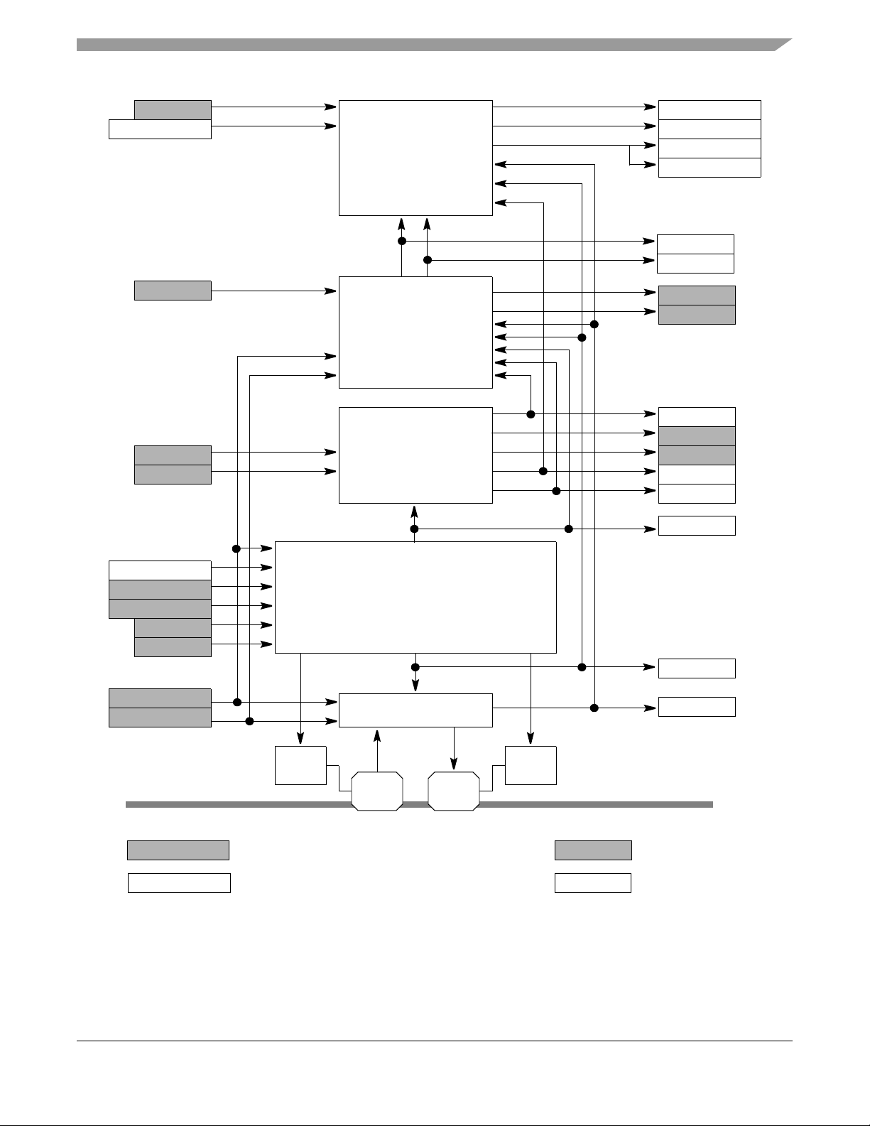
Functional Description
CS CGMOUT
RESET
CLOCK
SELECTION
CIRCUIT
CGMXCLK
TBMCLK
COPCLK
IOFF
EOFF
CMON
N[6:0}
TRIM[7:0]
SIMOSCEN
OSCENINSTOP
EXTCLKEN
ECGON
ICGON
EXTXTALEN
EXTSLOW
CLOCK
MONITOR
CIRCUIT
INTERNAL CLOCK
GENERATOR
CLOCK/PIN
ENABLE
CIRCUIT
EXTERNAL CLOCK
GENERATOR
ECGS
ICGS
FICGS
DDIV[3:0]
DSTG[7:0]
ICLK
IBASE
ICGEN
ECGEN
ECLK
INTERNAL
TO MCU
EXTERNAL
NAME
NAME TOP LEVEL SIGNAL
PTE4
LOGIC
OSC1
PTE4
OSC2
PTE3
PTE3
LOGIC
NAMECONFIG2 REGISTER BIT REGISTER BIT
NAME
MODULE SIGNAL
Figure 7-2. ICG Module Block Diagram
MC68HC908GT16 • MC68HC908GT 8 Da ta She e t , Rev. 3
Freescale Semiconductor 77

Internal Clock Generator (ICG) Module)
7.3.1 Clock Enable Circuit
The clock enable circuit is used to enable the internal clock (ICLK) or external clock (ECLK) and the port
logic which is shared with the oscillator pins (OSC1 and OSC2). The clock enable circuit generates an
ICG stop (ICGSTOP) signal which stops all clocks (ICLK, ECLK, and the low-frequency base clock,
IBASE). ICGSTOP is set and the ICG is disabled in stop mode if the oscillator enable stop bit
(OSCENINSTOP) in the CONFIG2 register is clear. The ICG clocks will be enabled in stop mode if
OSCENINSTOP is high.
The internal clock enable signal (ICGEN) turns on the internal clock generator which generates ICLK.
ICGEN is set (active) whenever the ICGON bit is set and the ICGSTOP signal is clear. When ICGEN is
clear, ICLK and IBASE are both low.
The external clock enable signal (ECGEN) turns on the external clock generator which generates ECLK.
ECGEN is set (active) whenever the ECGON bit is set and the ICGSTOP signal is clear. ECGON cannot
be set unless the external clock enable (EXTCLKEN) bit in the CONFIG2 register is set. when ECGEN is
clear, ECLK is low.
The port E4 enable signal (PE4EN) turns on the port E4 logic. Since po rt E4 is on the same pin as OSC1,
this signal is only active (set) when the external clock function is not desired. Therefore, PE4EN is clear
when ECGON is set. PE4EN is not gated with ICGSTOP, which means that if the ECGON bit is set, the
port E4 logic will remain disabled in stop mode.
The port E3 enable signal (PE3EN) turns on the port E3 logic. Since po rt E3 is on the same pin as OSC2,
this signal is only active (set) when 2-pin oscillator function is not desired. Therefore, PE3EN is clear when
ECGON and the external crystal enable (EXTXTALEN) bit in the CONFIG2 register are both set. PE3EN
is not gated with ICGSTOP, which means that if ECGON and EXTXTALEN are set, the port E3 logic will
remain disabled in stop mode.
7.3.2 Internal Clock Generator
The internal clock generator, shown in Figure 7-3, creates a low frequency base clock (IBASE), which
operates at a nominal frequency (f
an integer multiple of IBASE. This multiple is the ICG multiplier factor (N), which is programmed in the
ICG multiplier register (ICGMR). The internal clock generator is turned off and the output clocks (IBASE
and ICLK) are held low when the internal clock generator enable signal (ICGEN) is clear.
The internal clock generator contains:
• A digitally controlled oscillator
• A modulo N divider
• A frequency comparator, which contains voltage and current references, a frequency to voltage
converter, and comparators
• A digital loop filter
) of 307.2 kHz ± 25 percent, and an internal clock (ICLK) which is
NOM
MC68HC908GT16 • MC68HC908GT 8 Da ta She e t , Rev. 3
78 Freescale Semiconductor

ICGEN
Functional Description
VOLTAGE AND
CURRENT
REFERENCES
NAME
NAME TOP LEVEL SIGNAL
++
+
–
– –
Figure 7-3. Internal Clock Generator Block Diagram
7.3.2.1 Digitally Controlled Oscillator
DIGITAL
LOOP
FILTER
TRIM[7:0]
FREQUENCY
COMPARATOR
CLOCK GENERATOR
DIGITALLY
CONTROLLED
OSCILLATOR
N[6:0]
MODULO
N
DIVIDER
FICGS
DSTG[7:0]
DDIV[3:0]
ICLK
IBASE
NAMECONFIG2 REGISTER BIT REGISTER BIT
NAME
MODULE SIGNAL
The digitally controlled oscillator (DCO) is an inaccurate oscillator which generates the internal clock
(ICLK). The clock period of ICLK is dependent on the digital loo p filter outputs (DSTG[7:0] and DDIV[3:0]).
Because of only a limited number of bits in DDIV and DSTG, the precision of the output (ICLK) is restricted
to a precision of approximately ±0.202 percent to ±0.368 percent when measured over several cycles (of
the desired frequency). Additionally, since the propagation delays of the devices used in the DCO ring
oscillator are a measurable fraction of the bus clock period, reaching the long-term precision may require
alternately running faster and slower than desired, making the worst case cycle-to-cycle frequency
variation ±6.45 percent to ±11.8 percent (of the desired frequency). The valid values of DDIV:DSTG range
from $000 to $9FF. For more information on the quantization error in the DCO, see 7.4.4 Quantization
Error in DCO Output.
7.3.2.2 Modulo N Divider
The modulo N divider creates the low-frequency base clock (IBASE) by dividing the internal clock (ICLK)
by the ICG multiplier factor (N), contained in the ICG multiplier register (ICGMR). When N is programmed
to a $01 or $00, the divider is disabled and ICLK is passed through to IBASE undivided. When the internal
clock generator is stable, the frequency of IBASE will be equal to the nominal frequency (f
) of 307.2
NOM
kHz ± 25 percent.
MC68HC908GT16 • MC68HC908GT 8 Da ta She e t , Rev. 3
Freescale Semiconductor 79

Internal Clock Generator (ICG) Module)
7.3.2.3 Frequency Comparator
The frequency comparator effectively compares the low-frequency base clock (IBASE) to a nominal
frequency, f
. First, the frequency comparator converts IBASE to a voltage by charging a known
NOM
capacitor with a current reference for a period dependent on IBASE. This voltage is compared to a voltage
reference with comparators, whose outputs are fed to the digital loop filter. The dependence of these
outputs on the capacitor size, current reference, and voltage reference causes up to ±25 percent error in
f
.
NOM
7.3.2.4 Digital Loop Filter
The digital loop filter (DLF) uses the outputs of the frequency comparator to adjust the internal clock
(ICLK) clock period. The DLF generates the DCO divider control bits (DDIV[3:0]) and the DCO stage
control bits (DSTG[7:0]), which are fed to the DCO. The DLF first concatenates the DDIV and DSTG
registers (DDIV[3:0]:DSTG[7:0]) and then adds or subtracts a value dependent on the relative error in the
low-frequency base clock’s period, as shown in Table 7-1. In some extreme error conditions, such as
operating at a V
level which is out of specification, the DLF may attempt to use a value above the
DD
maximum ($9FF) or below the minimum ($000). In both cases, the value for DDIV will be between $A and
$F. In this range, the DDIV value will be interpreted the same as $9 (the slowest condition). Recovering
from this condition requires subtracting (increasing frequency) in the normal fashion until the value is
again below $9FF. (If the desired value is $9xx, the value may settle at $Axx through $Fxx. This is an
acceptable operating condition.) If the error is less than ±5 percent, the internal clock generator’s filter
stable indicator (FICGS) is set, indicating relative frequency accuracy to the clock monitor.
Table 7-1. Correction Sizes from DLF to DCO
Frequency Error of IBASE
Compared to f
IBASE < 0.85 f
0.85 f
NOM
IBASE < 0.95 f
0.95 f
NOM
IBASE < f
< IBASE
f
NOM
IBASE < 1.05 f
1.05 f
NOM
IBASE < 1.15 f
1.15 f
NOM
1. x = Maximum error is independent of value in DDIV[3:0]. DDIV increments or decrements when an addition to DSTG[7:0]
carries or borrows.
NOM
NOM
< IBASE
NOM
< IBASE
NOM
NOM
< IBASE
NOM
< IBASE +32 (+$020)
DDVI[3:0]:DSTG[7:0]
Correction
–32 (–$020)
–8 (–$008)
–1 (–$001)
+1 (+$001)
+8 (+$008)
Current to New
DDIV[3:0]:DSTG[7:0]
Minimum $xFF to $xDF –2/31 –6.45%
Maximum $x20 to $x00 –2/19 –10.5%
Minimum $xFF to $xF7 –0.5/31 –1.61%
Maximum $x08 to $x00 –0.5/17.5 –2.86%
Minimum $xFF to $xFE –0.0625/31 –0.202%
Maximum $x01 to $x00 –0.0625/17.0625 –0.366%
Minimum $xFE to $xFF +0.0625/30.9375 +0.202%
Maximum $x00 to $x01 +0.0625/17 +0.368%
Minimum $xF7 to $xFF +0.5/30.5 +1.64%
Maximum $x00 to $x08 +0.5/17 +2.94%
Minimum $xDF to $xFF +2/29 +6.90%
Maximum $x00 to $x20 +2/17 +11.8%
(1)
Relative Correction
in DCO
MC68HC908GT16 • MC68HC908GT 8 Da ta She e t , Rev. 3
80 Freescale Semiconductor

Functional Description
7.3.3 External Clock Generator
The ICG also provides for an external oscillator or external clock source, if desired. The external clock
generator, shown in Figure 7-4, contains an external oscillator amplifier and an external clock input path.
ECGEN
EXTXTALEN
R
AMPLIFIER
B
R
*
S
X
1
C
2
These components are required
for external crystal use only.
EXTSLOW
INTERNAL TO MCU
EXTERNAL
NAME
NAME
NAME
NAME
EXTERNAL
GENERATOR
CONFIG2 BIT
TOP LEVEL SIGNAL
REGISTER BIT
MODULE SIGNAL
CLOCK
OSC1
PTE4
C
1
Figure 7-4. External Clock Generator Block Diagram
INPUT PATH
OSC2
PTE3
*RS can be 0 (shorted)
when used with higherfrequency crystals. Refer
to manufacturer’s data.
ECLK
7.3.3.1 External Oscillator Amplifier
The external oscillator amplifier provides the gain required by an external crystal connected in a Pierce
oscillator configuration. The amount of this gain is controlled by the slow external (EXTSLOW) bit in the
CONFIG2 register. When EXTSLOW is set, the amplifier gain is reduced for operating low-frequency
crystals (32 kHz to 100 kHz). When EXTSLOW is clear, the amplifier gain will be sufficient for 1-MHz to
8-MHz crystals. EXTSLOW must be configured correctly for the given crystal or the circuit may not
operate.
The amplifier is enabled when the external clock generator enable (ECGEN) signal is set and when the
external crystal enable (EXTXTALEN) bit in the CONFIG2 register is set. ECGEN is controlled by the
clock enable circuit (see 7.3.1 Clock Enable Circuit) and indicates that the external clock function is
desired. When enabled, the amplifier will be connected between the PTE4/OSC1 and PTE3/OSC2 pins.
Otherwise, the PTE3/OSC2 pin reverts to its port function.
MC68HC908GT16 • MC68HC908GT 8 Da ta She e t , Rev. 3
Freescale Semiconductor 81

Internal Clock Generator (ICG) Module)
In its typical configuration, the external oscillator requires five external components:
1. Crystal, X
2. Fixed capacitor, C
1
1
3. Tuning capacitor, C2 (can also be a fixed capacitor)
4. Feedback resistor, RB
5. Series resistor, R
(Included in Figure 7-4 to follow strict Pierce oscillator guidelines and may not
S
be required for all ranges of operation, especially with high frequency crystals. Refer to the crystal
manufacturer’s data for more information.)
7.3.3.2 External Clock Input Path
The external clock input path is the means by which the microcontroller uses an external clock source.
The input to the path is the PTE4/OSC1 pin and the output is the external clock (ECLK). The path, which
contains input buffering, is enabled when the external clock generator enable signal (ECGEN) is set.
When not enabled, the PTE4/OSC1 pin reverts to its port function.
7.3.4 Clock Monitor Circuit
The ICG contains a clock monitor circuit which, when enabled, will continuou sly monitor both the external
clock (ECLK) and the internal clock (ICLK) to determine if either clock source has been corrupted. The
clock monitor circuit, shown in Figure 7-5, contains these blocks:
• Clock monitor reference generator
• Internal clock activity detector
• External clock activity detector
7.3.4.1 Clock Monitor Reference Generator
The clock monitor uses a reference based on one clock source to monitor the other clock source. The
clock monitor reference generator generates the external reference clock (EREF) based on the externa l
clock (ECLK) and the internal reference clock (IREF) based on the internal clock (ICLK). To simplify the
circuit, the low-frequency base clock (IBASE) is used in place of ICLK because it always operates at or
near 307.2 kHz. For proper operation, EREF must be at least twice as slow as IBASE and IREF must be
at least twice as slow as ECLK.
To guarantee that IREF is slower than ECLK and EREF is slower than IBASE, one of the signals is divided
down. Which signal is divided and by how much is determined by the external slow (EXTSLOW) and
external crystal enable (EXTXTALEN) bits in the CONFIG2 register, according to the rules in Table 7-2.
NOTE
Each signal (IBASE and ECLK) is always divided by four. A longer divider
is used on either IBASE or ECLK based on the EXTSLOW bit.
MC68HC908GT16 • MC68HC908GT 8 Da ta She e t , Rev. 3
82 Freescale Semiconductor

Functional Description
CMON
FICGS
IBASE
ICGEN
EXTXTALEN
EXTSLOW
ECGEN
ECLK
CMON
FICGS
IBASE
ICGEN
EREF
IBASE
ICGON
EXTXTALEN
EXTSLOW
ECGS
ECLK
ECGEN
ESTBCLK
IREF
ECGEN
ECLK
ICLK
ACTIVITY
DETECTOR
REFERENCE
GENERATOR
ECLK
ACTIVITY
DETECTOR
IOFF
ICGS
EREF
ESTBCLK
IREF
ECGS
IOFF
ICGS
ECGS
EOFF
MODULE SIGNAL
NAME
NAME TOP LEVEL SIGNAL
CMON
EOFF
NAMECONFIG2 REGISTER BIT REGISTER BIT
NAME
Figure 7-5. Clock Monitor Block Diagram
To conserve size, the long divider (divide by 4096) is also used as an external crystal stabilization divider.
The divider is reset when the external clock generator is turned off or in stop mode (ECGEN is clear).
When the external clock generator is first turned on, the external clock generator stable bit (ECGS) will
be clear. This condition automatically selects ECLK as the input to the long divider. The external
stabilization clock (ESTBCLK) will be ECLK divided by 16 when EXTXTALEN is low or 4096 when
EXTXTALEN is high. This timeout allows the crystal to stabilize. The falling edge of ESTBCLK is used to
set ECGS, which will set after a full 16 or 4096 cycles. When ECGS is set, the divider returns to its normal
function. ESTBCLK may be generated by either IBASE or ECLK, but any clocking will only reinforce the
set condition. If ECGS is cleared because the clock monitor determined that ECLK was inactive, the
divider will revert to a stabilization divider. Since this will change the EREF and IREF divide ratios, it is
important to turn the clock monitor off (CMON = 0) after inactivity is detected to ensure valid recovery.
MC68HC908GT16 • MC68HC908GT 8 Da ta She e t , Rev. 3
Freescale Semiconductor 83

Internal Clock Generator (ICG) Module)
7.3.4.2 Internal Clock Activity Detector
The internal clock activity detector, shown in Figure 7-6, looks for at least one falling edge on the
low-frequency base clock (IBASE) every time the external reference (EREF) is low. Since EREF is less
than half the frequency of IBASE, this should occur every time. If it does not occur two consecutive times,
the internal clock inactivity indicator (IOFF) is set. IOFF will be cleared the next time there is a falling edge
of IBASE while EREF is low.
CMON
EREF
CK Q
1/4
R
IOFF
R
DQ
DFFRR
CK
R
R
DQ
DFFRR
CK
R
NAMECONFIG2 REGISTER BIT
NAME
ICGS
REGISTER BIT
MODULE SIGNAL
IBASE
DLF MEASURE
OUTPUT CLOCK
ICGEN
FICGS
NAME
NAME
R
D
DFFRS
CK
Q
S
TOP LEVEL SIGNAL
Figure 7-6. Internal Clock Activity Detector
The internal clock stable bit (ICGS) is also generated in the internal clock activity detector. ICGS is set
when the internal clock generator’s filter stable signal (FICGS) indicates that IBASE is within about 5
percent of the target 307.2 kHz ± 25 percent for two consecutive measurements. ICGS is cleared when
FICGS is clear, the internal clock generator is turned off or is in stop mode (ICGEN is clear), or when IOFF
is set.
7.3.4.3 External Clock Activity Detector
The external clock activity detector, shown in Figure 7-7, looks for at least one falling edg e on the external
clock (ECLK) every time the internal reference (IREF) is low. Since IREF is less than half the frequency
of ECLK, this should occur every time. If it does not occur two consecutive times, the external clock
inactivity indicator (EOFF) is set. EOFF will be cleared the next time there is a falling edge of ECLK while
IREF is low.
The external clock stable bit (E CGS) is also generated in the external clock activity detector. ECGS is set
on a falling edge of the external stabilization clock (ESTBCLK). This will be 4096 ECLK cycles after the
external clock generator on bit is set, or the MCU exits stop mode (ECGEN = 1) if the external crystal
enable (EXTXTALEN) in the CONFIG2 register is set, or 16 cycles when EXTXTALEN is clear. ECGS is
cleared when the external clock generator is turned off or in stop mode (ECGEN is clear) or when EOFF
is set.
MC68HC908GT16 • MC68HC908GT 8 Da ta She e t , Rev. 3
84 Freescale Semiconductor

CMON
IREF
CK Q
1/4
R
Functional Description
EOFF
D
DFFRR
CK
R
Q
R
NAMECONFIG2 REGISTER BIT
NAME
REGISTER BIT
MODULE SIGNAL
EGGS
ECLK
ESTBCLK
ECGEN
NAME
NAME
R
D
DFFRS
CK
Q
S
TOP LEVEL SIGNAL
Figure 7-7. External Clock Activity Detector
7.3.5 Clock Selection Circuit
The clock selection circuit, shown in Figure 7-8, contains two clock switches which generate the oscillator
output clock (CGMXCLK) and the timebase clock (TBMCLK) from either the internal clock (ICLK) or the
external clock (ECLK). The COP clock (COPCLK) is identical to TBMCLK. The clock selection circuit also
contains a divide-by-two circuit which creates the clock generator output clock (CGMOUT), which
generates the bus clocks.
ICLK
ECLK
IOFF
EOFF
RESET
V
ECGON
CS
SS
NAME
NAME
SELECT
ICLK
ECLK
IOFF
EOFF
FORCE_I
FORCE_E
SELECT
ICLK
ECLK
IOFF
EOFF
FORCE_I
FORCE_E
TOP LEVEL SIGNAL
SYNCHRONIZING
SWITCHER
SYNCHRONIZING
SWITCHER
OUTPUT
CLOCK
OUTPUT
CLOCK
Figure 7-8. Clock Selection Circuit Block Diagram
DIV2
NAMECONFIG2 REGISTER BIT
NAME
CGMXCLK
CGMOUT
TBMCLK
COPCLK
REGISTER BIT
MODULE SIGNAL
MC68HC908GT16 • MC68HC908GT 8 Da ta She e t , Rev. 3
Freescale Semiconductor 85

Internal Clock Generator (ICG) Module)
7.3.5.1 Clock Selection Switches
The first switch creates the oscillator output clock (CGMXCLK) from either the internal clock (ICLK) or the
external clock (ECLK), based on the clock select bit (CS; set selects ECLK, clear selects ICLK). When
switching the CS bit, both ICLK and ECLK must be on (ICGON and ECGON set). The clock being
switched to also must be stable (ICGS or ECGS set).
The second switch creates the timebase clock (TBMCLK) and the COP clock (COPCLK) from ICLK or
ECLK based on the external clock on bit. When ECGON is set, the switch automatically selects the
external clock, regardless of the state of the ECGS bit.
7.3.5.2 Clock Switching Circuit
To robustly switch between the internal clock (ICLK) and the external clock (ECLK), the switch assumes
the clocks are completely asynchronous, so a synchronizing circuit is required to make the transition.
When the select input (the clock select bit for the oscillator output clock switch or the external clock on bit
for the timebase clock switch) is changed, the switch will continue to operate off the original clock for
between one and two cycles as the select input is transitioned through one side o f the synchronizer. Next,
the output will be held low for between one and two cycles of the new clock as the select input transitions
through the other side. Then the output starts switching at the new clock’s frequency. This transition
guarantees that no glitches will be seen on the output even though the select input may change
asynchronously to the clocks. The unpredictably of the transition period is a necessary result of the
asynchronicity.
The switch automatically selects ICLK during reset. When the clock monitor is on (CMON is set) and it
determines one of the clock sources is inactive (as indicated by the IOFF or EOFF signa ls) , the circuit is
forced to select the active clock. There are no clocks for the inactive side of the synchronizer to properly
operate, so that side is forced deselected. However, the active side will not be selected until one to two
clock cycles after the IOFF or EOFF signal transitions.
7.4 Usage Notes
The ICG has several features which can provide protection to the microcontroller if properly used. Other
features can greatly simplify usage of the ICG if certain techniques are employed. This section describes
several possible ways to use the ICG and its features. These techniques a re not the only ways to use the
ICG and may not be optimum for all environments. In any case, these techniques should be used only as
a template, and the user should modify them according to the application’s requirements.
These notes include:
• Switching clock sources
• Enabling the clock monitor
• Using clock monitor interrupts
• Quantization error in digitally controlled oscillator (DCO) output
• Switching internal clock frequencies
• Nominal frequency settling time
• Improving frequency settling time
• Trimming frequency
MC68HC908GT16 • MC68HC908GT 8 Da ta She e t , Rev. 3
86 Freescale Semiconductor

Usage Notes
7.4.1 Switching Clock Sources
• Switching from one clock source to another requires both clock sources to be enabled and stable.
A simple flow requires:
• Enable desired clock source
• Wait for it to become stable
• Switch clocks
• Disable previous clock source
The key point to remember in this flow is that the clock source cannot be switched (CS cannot be written)
unless the desired clock is on and stable. A short assembly code example of how to employ this flow is
shown in Figure 7-9.
;* Clock Switching Code Example
;* This code switches from internal to external clock
;* Clock monitor and interrupts are not enabled
;* ICG Clock Switch
SwitchItoE:
bset ECGON,ICGCR ; turn on external oscillator
brclr ECGS,ICGCR,* ; wait until external clock engaged
bset CS,ICGCR ; select external clock for bus
bclr ICGON,ICGCR ; turn off internal clock (if desired)
Figure 7-9. Code Example for Switching Clock Sources
7.4.2 Enabling the Clock Monitor
Many applications require the clock monitor to determine if one of the clock sources has become inactive,
so the other can be used to recover from a potentially dangerous situation. Using the clock monitor
requires both clocks to be active (ECGON and ICGON both set). To enable the clock monitor, both clocks
also must be stable (ECGS and ICGS both set). This is to prevent the use of the clock monitor when a
clock is first turned on and potentially unstable.
Enabling the clock monitor and clock monitor interrupts requires a flow similar to this:
• Enable the alternate clock source
• Wait for both clock sources to be stable
• Switch to the desired clock source if necessary
• Enable the clock monitor
• Enable clock monitor interrupts
These events must happen in sequence. A short assembly code example of how to employ this flow is
shown in Figure 7-10.
MC68HC908GT16 • MC68HC908GT 8 Da ta She e t , Rev. 3
Freescale Semiconductor 87

Internal Clock Generator (ICG) Module)
;* Clock Monitor Enable Code Example
;* This code turns on both clocks, selects the desired one,
;* then turns on the Clock Monitor and CM Interrupt
;* ICG Clock Monitor Enable
CMEnable:
bset ECGON,ICGCR ; turn on external oscillator
; (assumes internal osc is on)
brclr ECGS,ICGCR,* ; wait until external clock engaged
bset CS,ICGCR ; select external clock for bus
bset CMON,ICGCR ; enable Clock Monitor
bset CMIE,ICGCR ; enable CM interrupt
Figure 7-10. Code Example for Enabling the Clock Monitor
7.4.3 Using Clock Monitor Interrupts
The clock monitor circuit can be used to recover from perilous situations such as crystal loss. To use th e
clock monitor effectively, these points should be observed:
• Enable the clock monitor and clock monitor interrupts.
• The first statement in the clock monitor interrupt service routine (CMISR) should be a read to the
ICG control register (ICGCR) to verify that the clock monitor flag (CMF) is set. This is also the first
step in clearing the CMF bit.
• The second statement in the CMISR should be a write to the ICGCR to clear the CMF bit (write the
bit low). Writing the bit high will not affect it. This statement does not need to immediately follow
the first, but must be contained in the CMISR.
• The third statement in the CMISR should be to clear the CMON bit. This is required to ensure
proper reconfiguration of the reference dividers. This statement also must be contained in the
CMISR.
• Although the clock monitor can be enabled only when both clocks are stable (ICGS is set or ECGS
is set), it will remain set if one of the clocks goes unstable.
• The clock monitor only works if the external slow (EXTSLOW) bit in the CONFIG2 register is set to
the correct value.
• The internal and external clocks must both be enabled and running to use the clock monitor.
• When the clock monitor detects inactivity, the inactive clock is automatically deselected and the
active clock selected as the source for CGMXCLK and TBMCLK. The CMISR can use the state of
the CS bit to check which clock is inactive.
• When the clock monitor detects inactivity, the application may have been subjected to extreme
conditions which may have affected other circuits. The CMISR should take any appropriate
precautions.
7.4.4 Quantization Error in DCO Output
The digitally controlled oscillator (DCO) is comprised of three major sub-blocks:
1. Binary weighted divider
2. Variable-delay ring oscillator
3. Ring oscillator fine-adjust circuit
Each of these blocks affects the clock period of the internal clock (ICLK). Since these blocks are controlled
by the digital loop filter (DLF) outputs DDIV and DSTG, the output of the DCO can change only in
MC68HC908GT16 • MC68HC908GT 8 Da ta She e t , Rev. 3
88 Freescale Semiconductor

Usage Notes
quantized steps as the DLF increments or decrements its output. The following sections describe how
each block will affect the output frequency.
7.4.4.1 Digitally Controlled Oscillator
The digitally controlled oscillator (DCO) is an inaccurate oscillator which generates the internal clock
(ICLK), whose clock period is dependent on the digital loop filter outputs (DSTG[7:0] and DDIV[3:0]).
Because of the digital nature of the DCO, the clock period of ICLK will change in quantized steps. This
will create a clock period difference or quantization error (Q-ERR) from one cycle to the next. Over several
cycles or for longer periods, this error is divided out until it reaches a minimum error of 0.202 percent to
0.368 percent. The dependence of this error on the DDIV[3:0 ] value and the number of cycles the error is
measured over is shown in Table 7-2.
Table 7-2. Quantization Error in ICLK
τ
DDIV[3:0] ICLK Cycles Bus Cycles
%0000 (min) 1 NA 6.45%–11.8%
%0000 (min) 4 1 1.61%–2.94%
%0000 (min) ≥ 32 ≥ 8 0.202%–0.368%
%0001 1 NA 3.23%–5.88%
%0001 4 1 0.806%–1.47%
%0001 ≥ 16 ≥ 4 0.202%–0.368%
%0010 1 NA 1.61%–2.94%
%0010 4 1 0.403%–0.735%
%0010 ≥ 8 ≥ 2 0.202%–0.368%
%0011 1 NA 0.806%–1.47%
%0011 ≥ 4 ≥ 1 0.202%–0.368%
%0100 1 NA 0.403%–0.735%
%0100 ≥ 2 ≥ 1 0.202%–0.368%
%0101–%1001 (max) ≥ 1 ≥ 1 0.202%–0.368%
ICLK
Q-ERR
7.4.4.2 Binary Weighted Divider
The binary weighted divider divides the output of the ring oscillator by a power of two, specified by the
DCO divider control bits (DDIV[3:0]). DDIV maximizes at %1001 (values of %1010 through %1111 are
interpreted as %1001), which corresponds to a divide by 512. When DDIV is %0000, the ring oscillator ’s
output is divided by 1. Incrementing DDIV by one will double the period; decrementing DDIV will halve the
period. The DLF cannot directly increment or decrement DDIV; DDIV is only incremented or decremented
when an addition or subtraction to DSTG carries or borrows.
7.4.4.3 Variable-Delay Ring Oscillator
The variable-delay ring oscillator’s period is adjustable from 17 to 31 stage delays, in in crements of two,
based on the upper three DCO stage control bits (DSTG[7:5]). A DSTG[7:5] of %000 corresponds to 17
stage delays; DSTG[7:5] of %111 corresponds to 31 sta ge delays. Adjust ing the DSTG[5] b it has a 6.45
percent to 11.8 percent effect on the output frequency. This also corresponds to the size correction ma de
when the frequency error is greater than ±15 percent. The value of the binary weighted divider does not
affect the relative change in output clock period for a given change in DSTG[7:5].
MC68HC908GT16 • MC68HC908GT 8 Da ta She e t , Rev. 3
Freescale Semiconductor 89

Internal Clock Generator (ICG) Module)
7.4.4.4 Ring Oscillator Fine-Adjust Circuit
The ring oscillator fine-adjust circuit causes the ring oscillator to effectively operate at non-integer
numbers of stage delays by operating at two different points fo r a variable numb er of cycles specifie d by
the lower five DCO stage control bits (DSTG[4:0]). For example:
• When DSTG[7:5] is %011, the ring oscillator nominally operates at 23 stage delays.
• When DSTG[4:0] is %00000, the ring will always operate at 23 stage delays.
• When DSTG[4:0] is %00001, the ring will operate at 25 stage delays for one of 32 cycles and at 23
stage delays for 31 of 32 cycles.
• Likewise, when DSTG[4:0] is %11111, the ring operates at 25 stage delays for 31 of 32 cycles and
at 23 stage delays for one of 32 cycles.
• When DSTG[7:5] is %111, similar results are achieved by including a variable divide-by-two, so the
ring operates at 31 stages for some cycles and at 17 stage delays, with a divide-by-two for an
effective 34 stage delays, for the remainder of the cycles.
Adjusting the DSTG[0] bit has a 0.202 percent to 0.368 percent effect on the output clock period. This
corresponds to the minimum size correction made by the DLF, and the inherent, long-term quantization
error in the output frequency.
7.4.5 Switching Internal Clock Frequencies
The frequency of the internal clock (ICLK) may need to be changed for some applications. For example,
if the reset condition does not provide the correct frequency, or if the clock is slowed down for a low-power
mode (or sped up after a low-power mode), the frequency must be changed by programming the internal
clock multiplier factor (N). The frequency of ICLK is N times the frequency of IBASE, which is 307.2 kHz
±25 percent.
Before switching frequencies by changing the N value, the clock monitor must be disabled. This is
because when N is changed, the frequency of the low-frequency base clock (IBASE) will change
proportionally until the digital loop filter has corrected the error. Since the clock monitor uses IBASE, it
could erroneously detect an inactive clock. The clock monitor cannot be re-enabled until the internal clock
is stable again (ICGS is set).
The following flow is an example of how to change the clock frequency:
• Verify there is no clock monitor interrupt by reading the CMF bit.
• Turn off the clock monitor.
• If desired, switch to the external clock (see 7.4.1 Switching Clock Sources).
• Change the value of N.
• Switch back to internal (see 7.4.1 Switching Clock Sources), if desired.
• Turn on the clock monitor (see 7.4.2 Enabling the Clock Monitor), if desired.
7.4.6 Nominal Frequency Settling Time
Because the clock period of the internal clock (ICLK) is dependent on the digital loop filter outputs (DDIV
and DSTG) which cannot change instantaneously, ICLK temporarily will operate at an incorrect clock
period when any operating condition changes. This happens whenever the part is reset, the ICG multiply
factor (N) is changed, the ICG trim factor (TRIM) is changed, or the internal clock is enabled after inactivity
(stop mode or disabled operation). The time that the ICLK takes to adjust to the correct period is known
as the settling time.
MC68HC908GT16 • MC68HC908GT 8 Da ta She e t , Rev. 3
90 Freescale Semiconductor

Usage Notes
Settling time depends primarily on how many corrections it takes to change the clock period and the
period of each correction. Since the corrections require four periods of the low-frequency base clock
(4*τ
IBASE, each correction takes 4*N*τ
), and since ICLK is N (the ICG multiply factor for the desired frequency) times faster than
IBASE
. The period of ICLK, however, will vary as the corrections occur.
ICLK
7.4.6.1 Settling to Within 15 Percent
When the error is greater than 15 percent, the filter takes eight corrections to double or halve the clock
period. Due to how the DCO increases or decreases the clock period, the total period of these eight
corrections is approximately 11 times the period of the fastest correction. (If the corrections were perfectly
linear, the total period would be 11.5 times the minimum period; however, the ring must be slightly
nonlinear.) Therefore, the total time it takes to double or halve the clock period is 44*N*τ
ICLKFAST
.
If the clock period needs more than doubled or halved, the same relationship applies, only for each time
the clock period needs doubled, the total number of cycles doubles. That is, when transitioning from fast
to slow, going from the initial speed to half speed takes 44*N*τ
takes 88*N*τ
ICLKFAST
series can be expressed as (2
doubled or halved. Since 2
44*N*(τ
ICLKSLOW–τICLKFAST
; going from quarter speed to eighth speed takes 176*N*τ
x
–1)*44*N*τ
x
happens to be equal to τ
ICLKFAST
, where x is the number of times the speed needs
ICLKSLOW/τICLKFAST
).
ICLKFAST
; from half speed to quarter speed
ICLKFAST
; and so on. This
, the equation reduces to
Note that increasing speed takes much longer than decreasing speed since N is higher. This can be
expressed in terms of the initial clock period (τ
τ
15
) minus the final clock period (τ2) as such:
1
abs 44N τ
–()[]=
1τ2
7.4.6.2 Settling to Within 5 Percent
Once the clock period is within 15 percent of the desired clock period, the filter starts making smaller
adjustments. When between 15 percent and 5 percent error, each correction will adjust the clo ck perio d
between 1.61 percent and 2.94 percent. In this mode, a maximum of eight corrections will be required to
get to less than 5 percent error. Since the clock period is relatively close to desired, each correction takes
approximately the same period of time, or 4*τ
. At this point, the internal clock stable bit (ICGS) will
IBASE
be set and the clock frequency is usable, although the error will be as high as 5 percent. The total time to
this point is:
τ
abs 44N τ
5
–()[]32τ
1τ2
+=
IBASE
7.4.6.3 Total Settling Time
Once the clock period is within 5 percent of the desired clock period, the filter starts making minimum
adjustments. In this mode, each correction will adjust the frequency between 0.202 percent and 0.368
percent. A maximum of 24 corrections will be required to get to the minimum error. Each correction takes
approximately the same period of time, or 4*τ
this makes 32 corrections (128*τ
) to get from 15 percent to the minimum error. The total time to the
IBASE
. Added to the corrections for 15 percent to 5 percent,
IBASE
minimum error is:
The equations for τ
, τ5, and τ
15
τ
are dependent on the actual initial and final clock periods τ1 and τ2, not
tot
tot
abs 44N τ
–()[]128τ
1τ2
+=
IBASE
the nominal. This means the variability in the ICLK frequency due to process, temperature, and voltage
must be considered. Additionally, other process factors and noise can affect the actual tolerances of the
points at which the filter changes modes. This means a worst case adjustment of up to 35 percent (ICLK
MC68HC908GT16 • MC68HC908GT 8 Da ta She e t , Rev. 3
Freescale Semiconductor 91

Internal Clock Generator (ICG) Module)
clock period tolerance plus 10 percent) must be added. This adjustment can be reduced with trimming.
Table 7-3 shows some typical values for settling time.
Table 7-3. Typical Settling Time Examples
τ
1
1/ (6.45 MHz) 1/ (25.8 MHz) 84 430 µs 535 µs 850 µs
1/ (25.8 MHz) 1/ (6.45 MHz) 21 107 µs 212 µs 525 µs
1/ (25.8 MHz) 1/ (307.2 kHz) 1 141 µs 246 µs 560 µs
1/ (307.2 kHz) 1/ (25.8 MHz) 84 11.9 ms 12.0 ms 12.3 ms
τ
2
N
τ
15
τ
5
τ
tot
7.4.7 Trimming Frequency on the Internal Clock Generator
The unadjusted frequency of the low-frequency base clock (IBASE), when the comparators in the
frequency comparator indicate zero error, will vary as much as ±25 percent due to process, temperature,
and voltage dependencies. These dependencies are in the voltage and current references, the offset of
the comparators, and the internal capacitor.
The method of changing the unadjusted operating point is by changing the size of the capacitor. This
capacitor is designed with 639 equally sized units. Of that number, 384 of these units are always
connected. The remaining 255 units are put in by adjusting the ICG trim factor (TRIM). The default value
for TRIM is $80, or 128 units, making the default capacitor size 512. Each unit added or removed will
adjust the output frequency by about ±0.195 percent of the unadjusted frequency (adding to TRIM will
decrease frequency). Therefore, the frequency of IBASE can be changed to ±25 percent of its unadjusted
value, which is enough to cancel the process variability mentioned before.
The best way to trim the internal clock is to use the timer to measure the width of an input pulse on an
input capture pin (this pulse must be supplied by the application and should be as long or wide as
possible). Considering the prescale value of the timer and the theoretical (zero error) frequency of the bus
(307.2 kHz *N/4), the error can be calculated. This error, expressed as a percentage, can be divided by
0.195 percent and the resultant factor added or subtracted from TRIM. This process shou ld be repeated
to eliminate any residual error.
7.5 Low-Power Modes
The WAIT and STOP instructions put the MCU in low power- consumption standby modes.
7.5.1 Wait Mode
The ICG remains active in wait mode. If enabled, the ICG interrupt to th e CPU can bring th e MCU out of
wait mode.
In some applications, low power-consumption is desired in wait mode and a high-frequency clock is not
needed. In these applications, reduce power consumption by either selecting a low-frequency external
clock and turn the internal clock generator off or reduce the bus frequency by minimizing the ICG multiplier
factor (N) before executing the WAIT instruction.
MC68HC908GT16 • MC68HC908GT 8 Da ta She e t , Rev. 3
92 Freescale Semiconductor

CONFIG2 Options
7.5.2 Stop Mode
The value of the oscillator enable in stop (OSCENINSTOP) bit in the CONFIG2 register determines the
behavior of the ICG in stop mode. If OSCENINSTOP is low, the ICG is disabled in stop and, upon
execution of the STOP instruction, all ICG activity will cease and the output clocks (CGMXCLK,
CGMOUT, COPCLK, and TBMCLK) will be held low. Power consumption will be minimal.
If OSCENINSTOP is high, the ICG is enabled in stop and activity will continue. This is useful if the
timebase module (TBM) is required to bring the MCU out of stop mode. ICG interrupts will not bring the
MCU out of stop mode in this case.
During stop mode, if OSCENINSTOP is low, several functions in the ICG are affected. The stable bits
(ECGS and ICGS) are cleared, which will enable the external clock stabilization divider upon recovery.
The clock monitor is disabled (CMON = 0) which will also clear the clock monitor interrupt enable (CMIE)
and clock monitor flag (CMF) bits. The CS, ICGON, ECGON, N, TRIM, DDIV, and DSTG bits are
unaffected.
7.6 CONFIG2 Options
Four CONFIG2 register options affect the functionality of the ICG. These options are:
1. EXTCLKEN, external clock enable
2. EXTXTALEN, external crystal enable
3. EXTSLOW, slow external clock
4. OSCENINSTOP, oscillator enable in stop
All CONFIG2 options will have a default setting. Refer to Chapter 4 Configuration Register (CONFIG) on
how the CONFIG2 register is used.
7.6.1 External Clock Enable (EXTCLKEN)
External clock enable (EXTCLKEN), when set, enables the ECGON bit to be set. ECGON turns on the
external clock input path through the PTE4/OSC1 pin. When EXTCLKEN is clear, ECGON cannot be set
and PTE4/OSC1 will always perform the PTE4 function.
The default state for this option is clear.
7.6.2 External Crystal Enable (EXTXTALEN)
External crystal enable (EXTXTALEN), when set, will enable an amplifier to drive the PTE3/OSC2 pin
from the PTE4/OSC1 pin. The amplifier will drive only if the external clock enable (EXTCLKEN) bit and
the ECGON bit are also set. If EXTCLKEN or ECGON are clear, PTE3/OSC2 will perform the PTE3
function. When EXTXTALEN is clear, PTE3/OSC2 will always perform the PTE3 function.
EXTXTALEN, when set, also configures the clock monitor to expect an external clock source in the valid
range of crystals (30 kHz to 100 kHz or 1 MHz to 8 MHz). When EXTXTALEN is clear, the clock monitor
will expect an external clock source in the valid range for externally generated clocks when using the clock
monitor (60 Hz to 32 MHz).
EXTXTALEN, when set, also configures the external clock stabilization divider in the clock monitor for a
4096 cycle timeout to allow the proper stabilization time for a crystal. When EXTXTALEN is clear, the
stabilization divider is configured to 16 cycles since an external clock source does not need a startup time.
The default state for this option is clear.
MC68HC908GT16 • MC68HC908GT 8 Da ta She e t , Rev. 3
Freescale Semiconductor 93

Internal Clock Generator (ICG) Module)
7.6.3 Slow External Clock (EXTSLOW)
Slow external clock (EXTSLOW), when set, will decrease the drive strength of the oscillator amplifier,
enabling low-frequency crystal operation (30 kHz–100 kHz) if properly enabled with the external clock
enable (EXTCLKEN) and external crystal enable (EXTXTALEN) bits. When clear, EXTSLOW enables
high-frequency crystal operation (1 MHz to 8 MHz).
EXTSLOW, when set, also configures the clock monitor to expect an external clock source that is slo wer
than the low-frequency base clock (60 Hz to 307.2 kHz). When EXTSLOW is clear, the clock monitor will
expect an external clock faster than the low-frequency base clock (307.2 kHz to 32 MHz).
The default state for this option is clear.
7.6.4 Oscillator Enable In Stop (OSCENINSTOP)
Oscillator enable in stop (OSCENINSTOP), when set, will enable the ICG to continue to generate clocks
(either CGMXCLK, CGMOUT, COPCLK, or TBMCLK) in stop mode. This function is used to keep the
timebase and COP running while the rest of the microcontroller stops. The clock monitor and
autoswitching functions remain operative.
When OSCENINSTOP is clear, all clock generation will cease and CGMXCLK, CGMOUT, COPCLK, and
TBMCLK will be forced low during stop mode. The clock monitor and autoswitching functions become
inoperative.
The default state for this option is clear.
7.7 Input/Output (I/O) Registers
The ICG contains five registers, summarized in Figure 7-11. These registers are:
1. ICG control register (ICGCR)
2. ICG multiplier register (ICGMR)
3. ICG trim register (ICGTR)
4. ICG DCO divider control register (ICGDVR)
5. ICG DCO stage control register (ICGDSR)
Several of the bits in these registers have interaction where the state of one bit may force another bit to
a particular state or prevent another bit from being set or cleared. A su mmary of this interaction is shown
in Table 7-4.
Addr.Register Name Bit 7654321Bit 0
ICG Control Register
$0036
1. See 7.7.1 ICG Control Register for method of clearing the CMF bit.
ICG Multiply Register
$0037
(ICGCR)
See page 96.
(ICGMR)
See page 97.
Read:
Write: 0
Reset:00001000
Read:
Write:
Reset:00010101
CMIE
CMF
(1)
N6 N5 N4 N3 N2 N1 N0
CMON CS ICGON
ICGS
ECGON
ECGS
= Unimplemented R = Reserved U = Unaffected
Figure 7-11. ICG Module I/O Register Summary
MC68HC908GT16 • MC68HC908GT 8 Da ta She e t , Rev. 3
94 Freescale Semiconductor

Input/Output (I/O) Registers
Addr.Register Name Bit 7654321Bit 0
Read:
Write:
Reset:10000000
TRIM7 TRIM6 TRIM5 TRIM4 TRIM3 TRIM2 TRIM1 TRIM0
$0038
ICG Trim Register
(ICGTR)
See page 98.
DDIV3 DDIV2 DDIV1 DDIV0
$0039
$003A
ICG Divider Control
Register (ICGDVR)
See page 98.
ICG DCO Stage Control
Register (ICGDSR)
See page 98.
Read:
Write:
Reset:0000UUUU
Read: DSTG7 DSTG6 DSTG5 DSTG4 DSTG3 DSTG2 DSTG1 DSTG0
Write:RRRRRRRR
Reset: Unaffected by reset
= Unimplemented R = Reserved U = Unaffected
Figure 7-11. ICG Module I/O Register Summary (Continued)
Table 7-4. ICG Module Register Bit Interaction Summary
Register Bit Results for Given Condition
Condition
CMIE
Reset 00001000$15$80——
OSCENINSTOP = 0,
STOP = 1
EXTCLKEN = 0 00001—00——uwuw
CMF = 1 —(1)1—1—1—uwuwuwuw
CMON = 0 0 0(0)————— — — ——
CMON = 1 ——(1)—1—1—uwuwuwuw
CS = 0 ———(0)1 ——— — —uwuw
CS = 1 ———(1)——1—— ———
ICGON = 0 0001(0)01—————
ICGON = 1 ————(1)———— —uwuw
ICGS = 0 us — us uc — (0) — — — — — —
ECGON = 0 00001—(0)0——uwuw
ECGS = 0 us—usus—— —(0) — — ——
IOFF = 1 — 1* (1) 1 (1) 0 (1) — uw uw uw uw
EOFF = 1 — 1* (1) 0 (1) — (1) 0 uw uw uw uw
N = written (0) (0) (0) — — 0* — — — — — —
TRIM = written (0) (0) (0) — — 0 * — — — — — —
000——0—0————
CMF
CMON
— Register bit is unaffected by the given condition.
0, 1 Register bit is forced clear or set (respectively) in the given condition.
0*, 1* Register bit is temporarily forced clear or set (respectively) in the given condition.
(0), (1) Register bit must be clear or set (respectively) for the given condition to occur.
us, uc, uw Register bit cannot be set, cleared, or writ ten (respectively) in the given condition.
CS
ICGON
ICGS
ECGON
ECGS
N[6:0]
TRIM[7:0]
DDIV[3:0]
DSTG[7:0]
MC68HC908GT16 • MC68HC908GT 8 Da ta She e t , Rev. 3
Freescale Semiconductor 95

Internal Clock Generator (ICG) Module)
7.7.1 ICG Control Register
The ICG control register (ICGCR) contains the control and status bits for the internal clock generator,
external clock generator, and clock monitor as well as the clock select and interrupt enable bits.
Address:
$0036
Bit 7654321Bit 0
Read:
Write: 0
Reset:00001000
CMIE
1. See CMF bit description for method of clearing CMF bit.
CMF
(1)
= Unimplemented
CMON CS ICGON
ICGS
ECGON
ECGS
Figure 7-12. ICG Control Register (ICGCR)
CMIE — Clock Monitor Interrupt Enable Bit
This read/write bit enables clock monitor interrupts. An interrupt will occur whe n both CMIE and CMF
are set. CMIE can be set when the CMON bit has been set for at least one cycle. CMIE is forced clea r
when CMON is clear or during reset.
1 = Clock monitor interrupts enabled
0 = Clock monitor interrupts disabled
CMF — Clock Monitor Interrupt Flag
This read-only bit is set when the clock monitor determines that either ICLK or ECLK becomes inactive
and the CMON bit is set. This bit is cleared by first reading the bit while it is set, followed by writing the
bit low. This bit is forced clear when CMON is clear or during reset.
1 = Either ICLK or ECLK has become inactive.
0 = ICLK and ECLK have not become inactive since the last read of the ICGCR, or the clock monitor
is disabled.
CMON — Clock Monitor On Bit
This read/write bit enables the clock monitor. CMON can be set when both ICLK and ECLK have been
on and stable for at least one bus cycle. (ICGON, ECGON, ICGS, and ECGS are all set.) CMON is
forced set when CMF is set, to avoid inadvertent clearing of CMF. CMON is forced clear when either
ICGON or ECGON is clear, during stop mode with OSCENINSTOP low, or during reset.
1 = Clock monitor output enabled
0 = Clock monitor output disabled
CS — Clock Select Bit
This read/write bit determines which clock will generate the oscillator output clock (CGMXCLK). This
bit can be set when ECGON and ECGS have been set for at least one bus cycle and can be cleared
when ICGON and ICGS have been set for at least one bus cycle. This bit is forced set when the clock
monitor determines the internal clock (ICLK) is inactive or when ICGON is clear. This bit is forced clear
when the clock monitor determines that the external clock (ECLK) is inactive, when ECGON is clear,
or during reset.
1 = External clock (ECLK) sources CGMXCLK
0 = Internal clock (ICLK) sources CGMXCLK
MC68HC908GT16 • MC68HC908GT 8 Da ta She e t , Rev. 3
96 Freescale Semiconductor

Input/Output (I/O) Registers
ICGON — Internal Clock Generator On Bit
This read/write bit enables the internal clock generator. ICGON can be cleared when the CS bit has
been set and the CMON bit has been clear for at least one bus cycle. ICGON is forced set when the
CMON bit is set, the CS bit is clear, or during reset.
1 = Internal clock generator enabled
0 = Internal clock generator disabled
ICGS — Internal Clock Generator Stable Bit
This read-only bit indicates when the internal clock generator has determined that the internal clock
(ICLK) is within about 5 percent of the desired value. This bit is forced clear when the clock monitor
determines the ICLK is inactive, when ICGON is clear, when the ICG multiplier register (ICGMR) is
written, when the ICG TRIM register (ICGTR) is written, during stop mode with OSCENINSTOP low,
or during reset.
1 = Internal clock is within 5 percent of the desired value.
0 = Internal clock may not be within 5 percent of the desired value.
ECGON — External Clock Generator On Bit
This read/write bit enables the external clock generator. ECGON can be cleared when the CS and
CMON bits have been clear for at least one bus cycle. ECGON is fo rced set when the CMON bit or the
CS bit is set. ECGON is forced clear during reset.
1 = External clock generator enabled
0 = External clock generator disabled
ECGS — External Clock Generator Stable Bit
This read-only bit indicates when at least 4096 external clock (ECLK) cycles have elapsed since the
external clock generator was enabled. This is not an assurance of the stability of ECLK but is meant
to provide a startup delay. This bit is forced clear when the clock monitor determines ECLK is inactive,
when ECGON is clear, during stop mode with OSCENINSTOP low, or during reset.
1 = 4096 ECLK cycles have elapsed since ECGON was set.
0 = External clock is unstable, inactive, or disabled.
7.7.2 ICG Multiplier Register
Address:
N6:N0 — ICG Multiplier Factor Bits
These read/write bits change the multiplier used by the internal clock generator. The internal clock
(ICLK) will be:
(307.2 kHz ± 25 percent) * N
A value of $00 in this register is interpreted the same as a value of $01. This register cannot be writt en
when the CMON bit is set. Reset sets this factor to $15 (decimal 21) for default frequency of 6.45 MHz
± 25 percent (1.613 MHz ± 25 percent bus).
$0037
Bit 7654321Bit 0
Read:
Write:
Reset:00010101
N6 N5 N4 N3 N2 N1 N0
= Unimplemented
Figure 7-13. ICG Multiplier Register (ICGMR)
MC68HC908GT16 • MC68HC908GT 8 Da ta She e t , Rev. 3
Freescale Semiconductor 97

Internal Clock Generator (ICG) Module)
7.7.3 ICG Trim Register
Address: $0038
Bit 7654321Bit 0
Read:
Write:
Reset:10000000
TRIM7 TRIM6 TRIM5 TRIM4 TRIM3 TRIM2 TRIM1 TRIM0
Figure 7-14. ICG Trim Register (ICGTR)
TRIM7:TRIM0 — ICG Trim Factor Bits
These read/write bits change the size of the internal capacitor used by the internal clock generator. By
testing the frequency of the internal clock and incrementing or decrementing this factor accordingly,
the accuracy of the internal clock can be improved to ± 2 percent. Incrementing this register by one
decreases the frequency by 0.195 percent of the unadjusted value. Decre menting this register by one
increases the frequency by 0.195 percent. This register cannot be written when the CMON bit is set.
Reset sets these bits to $80, centering the range of possible adjustment.
7.7.4 ICG DCO Divider Register
Address: $0039
Bit 7654321Bit 0
Read:
Write:
Reset:0000UUUU
= Unimplemented U = Unaffected
DDIV3 DDIV2 DDIV1 DDIV0
Figure 7-15. ICG DCO Divider Control Register (ICGDVR)
DDIV3:DDIV0 — ICG DCO Divider Control Bits
These bits indicate the number of divide-by-twos (DDIV) that follow the digitally controlled oscillator.
When ICGON is set, DDIV is controlled by the digital loop filter. The range of valid values for DDIV is
from $0 to $9. Values of $A through $F are interpreted the same as $9. Since the DCO is active during
reset, reset has no effect on DSTG and the value may vary.
7.7.5 ICG DCO Stage Register
Address: $003A
Bit 7654321Bit 0
Read: DSTG7 DSTG6 DSTG5 DSTG4 DSTG3 DSTG2 DSTG1 DSTG0
Write:RRRRRRRR
Reset: Unaffected by reset
R = Reserved
Figure 7-16. ICG DCO Stage Control Register (ICGDSR)
DSTG7:DSTG0 — ICG DCO Stage Control Bits
These bits indicate the number of stages (above the minimum) in the digitally controlled oscillator. The
total number of stages is approximately equal to $1FF, so changing DSTG from $00 to $FF will
approximately double the period. Incrementing DSTG will increase the period (decrease the
frequency) by 0.202 percent to 0.368 percent (decrementing has the opposite effect). DSTG cannot
be written when ICGON is set to prevent inadvertent frequency shifting. When ICGON is set, DSTG is
controlled by the digital loop filter. Since the DCO is active during reset, reset has no effect on DSTG
and the value may vary.
MC68HC908GT16 • MC68HC908GT 8 Da ta She e t , Rev. 3
98 Freescale Semiconductor

Chapter 8
External Interrupt (IRQ)
8.1 Introduction
The IRQ (external interrupt) module provides a maskable interrupt input.
8.2 Features
Features of the IRQ module include:
• A dedicated external interrupt pin (IRQ
• IRQ interrupt control bits
• Hysteresis buffer
• Programmable edge-only or edge and level interrupt sensitivity
• Automatic interrupt acknowledge
• Internal pullup resistor
8.3 Functional Description
A logic 0 applied to the external interrupt pin can latch a central processor unit (CPU) interrupt request.
Figure 8-2 shows the structure of the IRQ module.
)
Interrupt signals on the IRQ
the following actions occurs:
• Vector fetch — A vector fetch automatically generates an interrupt acknowledge signal that clears
the latch that caused the vector fetch.
• Software clear — Software can clear an interrupt latch by writing to the appropriate acknowledge
bit in the interrupt status and control register (INTSCR). Writing a 1 to the ACK bit clears the IRQ
latch.
• Reset — A reset automatically clears the interrupt latch.
The external interrupt pin is falling-edge triggered and is software-configurable to be either falling-edge
or falling-edge and low-level triggered. The MODE bit in the INTSCR controls the triggering sensitivity of
the IRQ
When an interrupt pin is edge-triggered only, the interrupt remains set until a vector fetch, software clear,
or reset occurs.
When an interrupt pin is both falling-edge and low-level triggered, the interrupt remains set until both of
these events occur:
pin.
• Vector fetch or software clear
• Return of the interrupt pin to logic 1
pin are latched into the IRQ latch. An interrupt latch remains set until one of
MC68HC908GT16 • MC68HC908GT 8 Da ta She e t , Rev. 3
Freescale Semiconductor 99

External Interrupt (IRQ)
M68HC08 CPU
CPU
REGISTERS
ARITHMETIC/LOGIC
UNIT (ALU)
INTERNAL BUS
PROGRAMMABLE TIMEBASE
MODULE
DDRA
PORTA
PTA7/KBD7–
PTA0/KBD0
(1)
CONTROL AND STATUS
REGISTERS — 64 BYTES
USER FLASH
MC68HC908GT16 — 15,872 BYTES
MC68HC908GT8 — 7,680 BYTES
USER RAM — 512 BYTES
MONITOR ROM — 304 BYTES
FLASH PROGRAMMING ROUTINES
ROM — 720 BYTES
USER FLASH VECTOR SPACE — 36 BYTES
PTE4/OSC1
PTE3/OSC2
RST
IRQ
V
REFH
V
REFL
(3)
(3)
INTERNAL CLOCK
GENERATOR MODULE
SYSTEM INTEGRATION
MODULE
SINGLE EXTERNAL
INTERRUPT MODULE
8-BIT ANALOG-TO-DIGITAL
CONVERTER MODULE
POWER-ON RESET
MODULE
V
DD
V
SS
V
DDA
V
SSA
POWER
SINGLE BREAKPOINT BREAK
LOW-VOLTAGE INHIBIT MODULE
2-CHANNEL TIMER INTERFACE
2-CHANNEL TIMER INTERFACE
MODULE
DUAL VOLTAGE
8-BIT KEYBOARD
INTERRUPT MODULE
MODULE 1
MODULE 2
SERIAL COMMUNICATIONS
INTERFACE MODULE
COMPUTER OPERATING
PROPERLY MODULE
SERIAL PERIPHERAL
INTERFACE MODULE
MONITOR MODULE
MEMORY MAP
MODULE
CONFIGURATION REGISTER 1
MODULE
CONFIGURATION REGISTER 2
MODULE
PTB7/AD7
PTB6/AD6
PTB5/AD5
PTB4/AD4
DDRB
PTB3/AD3
PORTB
PTB2/AD2
PTB1/AD1
PTB0/AD0
(1)
PTC6
(1)
PTC5
(1)(2)
PTC4
(1)(2)
DDRC
PTC3
PTC2
PTC1
PTC0
(1)(2)
(1)(2)
(1)(2)
PORTC
PTD7/T2CH1
PTD6/T2CH0
PTD5/T1CH1
PTD4/T1CH0
PORTD
PTD3/SPSCK
PTD2/MOSI
DDRD
PTD1/MISO
PTD0/SS
PTE2
DDRE
PTE1/RxD
PORTE
PTE0/TxD
SECURITY
MODULE
MONITOR MODE ENTRY
MODULE
(1)
(1)
(1)
(1)
(1)
(1)
(1)
(1)
1. Ports are software configurable with pullup device if input port.
2. Higher current drive port pins
3. Pin contains integrated pullup device
Figure 8-1. Block Diagram Highlighting IRQ Block and Pins
MC68HC908GT16 • MC68HC908GT 8 Da ta She e t , Rev. 3
100 Freescale Semiconductor
 Loading...