


MC68HC908GR8
MC68HC908GR4
Data Sheet
M68HC08
Microcontrollers
MC68HC908GR8A
Rev. 5
08/2005
freescale.com


MC68HC908GR8
MC68HC908GR4
Data Sheet
To provide the most up-to-date information, the revision of our documents on the World Wide Web will be
the most current. Your printed copy may be an earlier revision. To verify you have the latest information
available, refer to:
http://freescale.com/
Freescale™ and the Freescale logo are trademarks of Freescale Semiconductor, Inc.
This product incorporates SuperFlash® technology licensed from SST.
© Freescale Semiconductor, Inc., 2005. All rights reserved.
MC68HC908GR8 • MC68HC908GR4 Data Sheet, Rev. 5
Freescale Semiconductor 3

MC68HC908GR8 • MC68HC908GR4 Data Sheet, Rev. 5
4 Freescale Semiconductor

List of Chapters
Chapter 1 General Description. . . . . . . . . . . . . . . . . . . . . . . . . . . . . . . . . . . . . . . . . . . . . . . .19
Chapter 2 Memory Map. . . . . . . . . . . . . . . . . . . . . . . . . . . . . . . . . . . . . . . . . . . . . . . . . . . . . .27
Chapter 3 Low-Power Modes . . . . . . . . . . . . . . . . . . . . . . . . . . . . . . . . . . . . . . . . . . . . . . . . .37
Chapter 4 Resets and Interrupts . . . . . . . . . . . . . . . . . . . . . . . . . . . . . . . . . . . . . . . . . . . . . .43
Chapter 5 Analog-to-Digital Converter (ADC). . . . . . . . . . . . . . . . . . . . . . . . . . . . . . . . . . . . 55
Chapter 6 Break Module (BRK) . . . . . . . . . . . . . . . . . . . . . . . . . . . . . . . . . . . . . . . . . . . . . . .61
Chapter 7 Clock Generator Module (CGMC). . . . . . . . . . . . . . . . . . . . . . . . . . . . . . . . . . . . .67
Chapter 8 Configuration Register (CONFIG) . . . . . . . . . . . . . . . . . . . . . . . . . . . . . . . . . . . .87
Chapter 9 Computer Operating Properly (COP) . . . . . . . . . . . . . . . . . . . . . . . . . . . . . . . . . .91
Chapter 10 Central Processing Unit (CPU) . . . . . . . . . . . . . . . . . . . . . . . . . . . . . . . . . . . . . .95
Chapter 11 Flash Memory. . . . . . . . . . . . . . . . . . . . . . . . . . . . . . . . . . . . . . . . . . . . . . . . . . .107
Chapter 12 External Interrupt (IRQ) . . . . . . . . . . . . . . . . . . . . . . . . . . . . . . . . . . . . . . . . . . .115
Chapter 13 Keyboard Interrupt (KBI). . . . . . . . . . . . . . . . . . . . . . . . . . . . . . . . . . . . . . . . . .119
Chapter 14 Low-Voltage Inhibit (LVI). . . . . . . . . . . . . . . . . . . . . . . . . . . . . . . . . . . . . . . . . . 125
Chapter 15 Monitor ROM (MON) . . . . . . . . . . . . . . . . . . . . . . . . . . . . . . . . . . . . . . . . . . . . .129
Chapter 16 Input/Output Ports (I/O). . . . . . . . . . . . . . . . . . . . . . . . . . . . . . . . . . . . . . . . . . .141
Chapter 17 Random-Access Memory (RAM) . . . . . . . . . . . . . . . . . . . . . . . . . . . . . . . . . . .155
Chapter 18 Serial Communications Interface (SCI) . . . . . . . . . . . . . . . . . . . . . . . . . . . . . .157
Chapter 19 System Integration Module (SIM). . . . . . . . . . . . . . . . . . . . . . . . . . . . . . . . . . .183
Chapter 20 Serial Peripheral Interface (SPI) . . . . . . . . . . . . . . . . . . . . . . . . . . . . . . . . . . . . 201
Chapter 21 Timebase Module (TBM) . . . . . . . . . . . . . . . . . . . . . . . . . . . . . . . . . . . . . . . . . .221
Chapter 22 Timer Interface Module (TIM) . . . . . . . . . . . . . . . . . . . . . . . . . . . . . . . . . . . . . .225
Chapter 23 Electrical Specifications . . . . . . . . . . . . . . . . . . . . . . . . . . . . . . . . . . . . . . . . . .243
Chapter 24 Mechanical Specifications . . . . . . . . . . . . . . . . . . . . . . . . . . . . . . . . . . . . . . . .265
Chapter 25 Ordering Information. . . . . . . . . . . . . . . . . . . . . . . . . . . . . . . . . . . . . . . . . . . . .269
MC68HC908GR8 • MC68HC908GR4 Data Sheet, Rev. 5
Freescale Semiconductor 5

List of Chapters
MC68HC908GR8 • MC68HC908GR4 Data Sheet, Rev. 5
6 Freescale Semiconductor

Table of Contents
Chapter 1
General Description
1.1 Introduction . . . . . . . . . . . . . . . . . . . . . . . . . . . . . . . . . . . . . . . . . . . . . . . . . . . . . . . . . . . . . . . . 19
1.2 Features. . . . . . . . . . . . . . . . . . . . . . . . . . . . . . . . . . . . . . . . . . . . . . . . . . . . . . . . . . . . . . . . . . . 19
1.2.1 Standard Features of the MC68HC908GR8 . . . . . . . . . . . . . . . . . . . . . . . . . . . . . . . . . . . . 19
1.2.2 Features of the CPU08 . . . . . . . . . . . . . . . . . . . . . . . . . . . . . . . . . . . . . . . . . . . . . . . . . . . . 20
1.3 MCU Block Diagram . . . . . . . . . . . . . . . . . . . . . . . . . . . . . . . . . . . . . . . . . . . . . . . . . . . . . . . . . 21
1.4 Pin Assignments . . . . . . . . . . . . . . . . . . . . . . . . . . . . . . . . . . . . . . . . . . . . . . . . . . . . . . . . . . . . 22
1.5 Pin Functions . . . . . . . . . . . . . . . . . . . . . . . . . . . . . . . . . . . . . . . . . . . . . . . . . . . . . . . . . . . . . . . 23
1.5.1 Power Supply Pins (V
1.5.2 Oscillator Pins (OSC1 and OSC2) . . . . . . . . . . . . . . . . . . . . . . . . . . . . . . . . . . . . . . . . . . . . 23
1.5.3 External Reset Pin (RST
1.5.4 External Interrupt Pin (IRQ
1.5.5 CGM Power Supply Pins (V
1.5.6 External Filter Capacitor Pin (CGMXFC) . . . . . . . . . . . . . . . . . . . . . . . . . . . . . . . . . . . . . . . 24
1.5.7 Analog Power Supply/Reference Pins (V
1.5.8 Port A Input/Output (I/O) Pins (PTA3/KBD3–PTA0/KBD0) . . . . . . . . . . . . . . . . . . . . . . . . . 24
1.5.9 Port B I/O Pins (PTB5/AD5–PTB0/AD0) . . . . . . . . . . . . . . . . . . . . . . . . . . . . . . . . . . . . . . . 24
1.5.10 Port C I/O Pins (PTC1–PTC0) . . . . . . . . . . . . . . . . . . . . . . . . . . . . . . . . . . . . . . . . . . . . . . . 24
1.5.11 Port D I/O Pins (PTD6/T2CH0–PTD0/SS
1.5.12 Port E I/O Pins (PTE1/RxD–PTE0/TxD) . . . . . . . . . . . . . . . . . . . . . . . . . . . . . . . . . . . . . . . 25
and VSS). . . . . . . . . . . . . . . . . . . . . . . . . . . . . . . . . . . . . . . . . . . . 23
DD
). . . . . . . . . . . . . . . . . . . . . . . . . . . . . . . . . . . . . . . . . . . . . . . . . . . 23
) . . . . . . . . . . . . . . . . . . . . . . . . . . . . . . . . . . . . . . . . . . . . . . . . . 23
DDA
and V
) . . . . . . . . . . . . . . . . . . . . . . . . . . . . . . . . . . . . . 23
SSA
DDAD/VREFH
and V
SSAD
/VR
) . . . . . . . . . . . . . 24
EFL
) . . . . . . . . . . . . . . . . . . . . . . . . . . . . . . . . . . . . . . 24
Chapter 2
Memory Map
2.1 Introduction . . . . . . . . . . . . . . . . . . . . . . . . . . . . . . . . . . . . . . . . . . . . . . . . . . . . . . . . . . . . . . . . 27
2.2 Unimplemented Memory Locations . . . . . . . . . . . . . . . . . . . . . . . . . . . . . . . . . . . . . . . . . . . . . . . 27
2.3 Reserved Memory Locations . . . . . . . . . . . . . . . . . . . . . . . . . . . . . . . . . . . . . . . . . . . . . . . . . . . 27
2.4 Input/Output (I/O) Section . . . . . . . . . . . . . . . . . . . . . . . . . . . . . . . . . . . . . . . . . . . . . . . . . . . . . 27
Chapter 3
Low-Power Modes
3.1 Introduction . . . . . . . . . . . . . . . . . . . . . . . . . . . . . . . . . . . . . . . . . . . . . . . . . . . . . . . . . . . . . . . . 37
3.1.1 Wait Mode . . . . . . . . . . . . . . . . . . . . . . . . . . . . . . . . . . . . . . . . . . . . . . . . . . . . . . . . . . . . . . 37
3.1.2 Stop Mode . . . . . . . . . . . . . . . . . . . . . . . . . . . . . . . . . . . . . . . . . . . . . . . . . . . . . . . . . . . . . . 37
3.2 Analog-to-Digital Converter (ADC). . . . . . . . . . . . . . . . . . . . . . . . . . . . . . . . . . . . . . . . . . . . . . . 37
3.2.1 Wait Mode . . . . . . . . . . . . . . . . . . . . . . . . . . . . . . . . . . . . . . . . . . . . . . . . . . . . . . . . . . . . . . 37
3.2.2 Stop Mode . . . . . . . . . . . . . . . . . . . . . . . . . . . . . . . . . . . . . . . . . . . . . . . . . . . . . . . . . . . . . . 37
3.3 Break Module (BRK) . . . . . . . . . . . . . . . . . . . . . . . . . . . . . . . . . . . . . . . . . . . . . . . . . . . . . . . . . 37
3.3.1 Wait Mode . . . . . . . . . . . . . . . . . . . . . . . . . . . . . . . . . . . . . . . . . . . . . . . . . . . . . . . . . . . . . . 37
3.3.2 Stop Mode . . . . . . . . . . . . . . . . . . . . . . . . . . . . . . . . . . . . . . . . . . . . . . . . . . . . . . . . . . . . . . 38
MC68HC908GR8 • MC68HC908GR4 Data Sheet, Rev. 5
Freescale Semiconductor 7

Table of Contents
3.4 Central Processor Unit (CPU) . . . . . . . . . . . . . . . . . . . . . . . . . . . . . . . . . . . . . . . . . . . . . . . . . . 38
3.4.1 Wait Mode . . . . . . . . . . . . . . . . . . . . . . . . . . . . . . . . . . . . . . . . . . . . . . . . . . . . . . . . . . . . . . 38
3.4.2 Stop Mode . . . . . . . . . . . . . . . . . . . . . . . . . . . . . . . . . . . . . . . . . . . . . . . . . . . . . . . . . . . . . . 38
3.5 Clock Generator Module (CGM) . . . . . . . . . . . . . . . . . . . . . . . . . . . . . . . . . . . . . . . . . . . . . . . . 38
3.5.1 Wait Mode . . . . . . . . . . . . . . . . . . . . . . . . . . . . . . . . . . . . . . . . . . . . . . . . . . . . . . . . . . . . . . 38
3.5.2 Stop Mode . . . . . . . . . . . . . . . . . . . . . . . . . . . . . . . . . . . . . . . . . . . . . . . . . . . . . . . . . . . . . . 38
3.6 Computer Operating Properly Module (COP) . . . . . . . . . . . . . . . . . . . . . . . . . . . . . . . . . . . . . . 39
3.6.1 Wait Mode . . . . . . . . . . . . . . . . . . . . . . . . . . . . . . . . . . . . . . . . . . . . . . . . . . . . . . . . . . . . . . 39
3.6.2 Stop Mode . . . . . . . . . . . . . . . . . . . . . . . . . . . . . . . . . . . . . . . . . . . . . . . . . . . . . . . . . . . . . . 39
3.7 External Interrupt Module (IRQ). . . . . . . . . . . . . . . . . . . . . . . . . . . . . . . . . . . . . . . . . . . . . . . . . 39
3.7.1 Wait Mode . . . . . . . . . . . . . . . . . . . . . . . . . . . . . . . . . . . . . . . . . . . . . . . . . . . . . . . . . . . . . . 39
3.7.2 Stop Mode . . . . . . . . . . . . . . . . . . . . . . . . . . . . . . . . . . . . . . . . . . . . . . . . . . . . . . . . . . . . . . 39
3.8 Keyboard Interrupt Module (KBI) . . . . . . . . . . . . . . . . . . . . . . . . . . . . . . . . . . . . . . . . . . . . . . . . 39
3.8.1 Wait Mode . . . . . . . . . . . . . . . . . . . . . . . . . . . . . . . . . . . . . . . . . . . . . . . . . . . . . . . . . . . . . . 39
3.8.2 Stop Mode . . . . . . . . . . . . . . . . . . . . . . . . . . . . . . . . . . . . . . . . . . . . . . . . . . . . . . . . . . . . . . 39
3.9 Low-Voltage Inhibit Module (LVI). . . . . . . . . . . . . . . . . . . . . . . . . . . . . . . . . . . . . . . . . . . . . . . . 39
3.9.1 Wait Mode . . . . . . . . . . . . . . . . . . . . . . . . . . . . . . . . . . . . . . . . . . . . . . . . . . . . . . . . . . . . . . 39
3.9.2 Stop Mode . . . . . . . . . . . . . . . . . . . . . . . . . . . . . . . . . . . . . . . . . . . . . . . . . . . . . . . . . . . . . . 40
3.10 Serial Communications Interface Module (SCI). . . . . . . . . . . . . . . . . . . . . . . . . . . . . . . . . . . . . 40
3.10.1 Wait Mode . . . . . . . . . . . . . . . . . . . . . . . . . . . . . . . . . . . . . . . . . . . . . . . . . . . . . . . . . . . . . . 40
3.10.2 Stop Mode . . . . . . . . . . . . . . . . . . . . . . . . . . . . . . . . . . . . . . . . . . . . . . . . . . . . . . . . . . . . . . 40
3.11 Serial Peripheral Interface Module (SPI) . . . . . . . . . . . . . . . . . . . . . . . . . . . . . . . . . . . . . . . . . . 40
3.11.1 Wait Mode . . . . . . . . . . . . . . . . . . . . . . . . . . . . . . . . . . . . . . . . . . . . . . . . . . . . . . . . . . . . . . 40
3.11.2 Stop Mode . . . . . . . . . . . . . . . . . . . . . . . . . . . . . . . . . . . . . . . . . . . . . . . . . . . . . . . . . . . . . . 40
3.12 Timer Interface Module (TIM1 and TIM2) . . . . . . . . . . . . . . . . . . . . . . . . . . . . . . . . . . . . . . . . . 40
3.12.1 Wait Mode . . . . . . . . . . . . . . . . . . . . . . . . . . . . . . . . . . . . . . . . . . . . . . . . . . . . . . . . . . . . . . 40
3.12.2 Stop Mode . . . . . . . . . . . . . . . . . . . . . . . . . . . . . . . . . . . . . . . . . . . . . . . . . . . . . . . . . . . . . . 41
3.13 Timebase Module (TBM) . . . . . . . . . . . . . . . . . . . . . . . . . . . . . . . . . . . . . . . . . . . . . . . . . . . . . . 41
3.13.1 Wait Mode . . . . . . . . . . . . . . . . . . . . . . . . . . . . . . . . . . . . . . . . . . . . . . . . . . . . . . . . . . . . . . 41
3.13.2 Stop Mode . . . . . . . . . . . . . . . . . . . . . . . . . . . . . . . . . . . . . . . . . . . . . . . . . . . . . . . . . . . . . . 41
3.14 Exiting Wait Mode . . . . . . . . . . . . . . . . . . . . . . . . . . . . . . . . . . . . . . . . . . . . . . . . . . . . . . . . . . . 41
3.15 Exiting Stop Mode . . . . . . . . . . . . . . . . . . . . . . . . . . . . . . . . . . . . . . . . . . . . . . . . . . . . . . . . . . . 42
Chapter 4
Resets and Interrupts
4.1 Introduction . . . . . . . . . . . . . . . . . . . . . . . . . . . . . . . . . . . . . . . . . . . . . . . . . . . . . . . . . . . . . . . . 43
4.2 Resets . . . . . . . . . . . . . . . . . . . . . . . . . . . . . . . . . . . . . . . . . . . . . . . . . . . . . . . . . . . . . . . . . . . . 43
4.2.1 Effects . . . . . . . . . . . . . . . . . . . . . . . . . . . . . . . . . . . . . . . . . . . . . . . . . . . . . . . . . . . . . . . . . 43
4.2.2 External Reset . . . . . . . . . . . . . . . . . . . . . . . . . . . . . . . . . . . . . . . . . . . . . . . . . . . . . . . . . . . 43
4.2.3 Internal Reset. . . . . . . . . . . . . . . . . . . . . . . . . . . . . . . . . . . . . . . . . . . . . . . . . . . . . . . . . . . . 43
4.2.3.1 Power-On Reset . . . . . . . . . . . . . . . . . . . . . . . . . . . . . . . . . . . . . . . . . . . . . . . . . . . . . . . . 44
4.2.3.2 COP Reset . . . . . . . . . . . . . . . . . . . . . . . . . . . . . . . . . . . . . . . . . . . . . . . . . . . . . . . . . . . . 44
4.2.3.3 Low-Voltage Inhibit Reset. . . . . . . . . . . . . . . . . . . . . . . . . . . . . . . . . . . . . . . . . . . . . . . . . 44
4.2.3.4 Illegal Opcode Reset . . . . . . . . . . . . . . . . . . . . . . . . . . . . . . . . . . . . . . . . . . . . . . . . . . . . 45
4.2.3.5 Illegal Address Reset . . . . . . . . . . . . . . . . . . . . . . . . . . . . . . . . . . . . . . . . . . . . . . . . . . . . 45
4.2.4 SIM Reset Status Register. . . . . . . . . . . . . . . . . . . . . . . . . . . . . . . . . . . . . . . . . . . . . . . . . . 45
MC68HC908GR8 • MC68HC908GR4 Data Sheet, Rev. 5
8 Freescale Semiconductor

4.3 Interrupts . . . . . . . . . . . . . . . . . . . . . . . . . . . . . . . . . . . . . . . . . . . . . . . . . . . . . . . . . . . . . . . . . . 46
4.3.1 Effects . . . . . . . . . . . . . . . . . . . . . . . . . . . . . . . . . . . . . . . . . . . . . . . . . . . . . . . . . . . . . . . . . 47
4.3.2 Sources . . . . . . . . . . . . . . . . . . . . . . . . . . . . . . . . . . . . . . . . . . . . . . . . . . . . . . . . . . . . . . . . 49
4.3.2.1 SWI Instruction . . . . . . . . . . . . . . . . . . . . . . . . . . . . . . . . . . . . . . . . . . . . . . . . . . . . . . . . . 50
4.3.2.2 Break Interrupt . . . . . . . . . . . . . . . . . . . . . . . . . . . . . . . . . . . . . . . . . . . . . . . . . . . . . . . . . 50
4.3.2.3 IRQ
Pin . . . . . . . . . . . . . . . . . . . . . . . . . . . . . . . . . . . . . . . . . . . . . . . . . . . . . . . . . . . . . . . 50
4.3.2.4 CGM (Clock Generator Module). . . . . . . . . . . . . . . . . . . . . . . . . . . . . . . . . . . . . . . . . . . . 50
4.3.2.5 TIM1 (Timer Interface Module 1) . . . . . . . . . . . . . . . . . . . . . . . . . . . . . . . . . . . . . . . . . . . 50
4.3.2.6 TIM2 (Timer Interface Module 2) . . . . . . . . . . . . . . . . . . . . . . . . . . . . . . . . . . . . . . . . . . . 50
4.3.2.7 SPI (Serial Peripheral Interface). . . . . . . . . . . . . . . . . . . . . . . . . . . . . . . . . . . . . . . . . . . . 51
4.3.2.8 SCI (Serial Communications Interface) . . . . . . . . . . . . . . . . . . . . . . . . . . . . . . . . . . . . . . 51
4.3.2.9 KBD0
–KBD4 Pins. . . . . . . . . . . . . . . . . . . . . . . . . . . . . . . . . . . . . . . . . . . . . . . . . . . . . . . 52
4.3.2.10 ADC (Analog-to-Digital Converter) . . . . . . . . . . . . . . . . . . . . . . . . . . . . . . . . . . . . . . . . . . 52
4.3.2.11 TBM (Timebase Module) . . . . . . . . . . . . . . . . . . . . . . . . . . . . . . . . . . . . . . . . . . . . . . . . . 52
4.3.3 Interrupt Status Registers . . . . . . . . . . . . . . . . . . . . . . . . . . . . . . . . . . . . . . . . . . . . . . . . . . 52
4.3.3.1 Interrupt Status Register 1 . . . . . . . . . . . . . . . . . . . . . . . . . . . . . . . . . . . . . . . . . . . . . . . . 53
4.3.3.2 Interrupt Status Register 2 . . . . . . . . . . . . . . . . . . . . . . . . . . . . . . . . . . . . . . . . . . . . . . . . 53
4.3.3.3 Interrupt Status Register 3 . . . . . . . . . . . . . . . . . . . . . . . . . . . . . . . . . . . . . . . . . . . . . . . . 53
Chapter 5
Analog-to-Digital Converter (ADC)
5.1 Introduction . . . . . . . . . . . . . . . . . . . . . . . . . . . . . . . . . . . . . . . . . . . . . . . . . . . . . . . . . . . . . . . . 55
5.2 Features. . . . . . . . . . . . . . . . . . . . . . . . . . . . . . . . . . . . . . . . . . . . . . . . . . . . . . . . . . . . . . . . . . . 55
5.3 Functional Description . . . . . . . . . . . . . . . . . . . . . . . . . . . . . . . . . . . . . . . . . . . . . . . . . . . . . . . . 55
5.3.1 ADC Port I/O Pins . . . . . . . . . . . . . . . . . . . . . . . . . . . . . . . . . . . . . . . . . . . . . . . . . . . . . . . . 55
5.3.2 Voltage Conversion . . . . . . . . . . . . . . . . . . . . . . . . . . . . . . . . . . . . . . . . . . . . . . . . . . . . . . . 56
5.3.3 Conversion Time . . . . . . . . . . . . . . . . . . . . . . . . . . . . . . . . . . . . . . . . . . . . . . . . . . . . . . . . . 56
5.3.4 Conversion . . . . . . . . . . . . . . . . . . . . . . . . . . . . . . . . . . . . . . . . . . . . . . . . . . . . . . . . . . . . . . 57
5.3.5 Accuracy and Precision . . . . . . . . . . . . . . . . . . . . . . . . . . . . . . . . . . . . . . . . . . . . . . . . . . . . 57
5.4 Interrupts . . . . . . . . . . . . . . . . . . . . . . . . . . . . . . . . . . . . . . . . . . . . . . . . . . . . . . . . . . . . . . . . . . 57
5.5 Low-Power Modes . . . . . . . . . . . . . . . . . . . . . . . . . . . . . . . . . . . . . . . . . . . . . . . . . . . . . . . . . . . 57
5.5.1 Wait Mode . . . . . . . . . . . . . . . . . . . . . . . . . . . . . . . . . . . . . . . . . . . . . . . . . . . . . . . . . . . . . . 57
5.5.2 Stop Mode . . . . . . . . . . . . . . . . . . . . . . . . . . . . . . . . . . . . . . . . . . . . . . . . . . . . . . . . . . . . . . 57
5.6 I/O Signals . . . . . . . . . . . . . . . . . . . . . . . . . . . . . . . . . . . . . . . . . . . . . . . . . . . . . . . . . . . . . . . . . 57
5.6.1 ADC Analog Power Pin (V
5.6.2 ADC Analog Ground Pin (V
5.6.3 ADC Voltage In (V
) . . . . . . . . . . . . . . . . . . . . . . . . . . . . . . . . . . . . . . . . . . . . . . . . . . . . 58
ADIN
5.7 I/O Registers . . . . . . . . . . . . . . . . . . . . . . . . . . . . . . . . . . . . . . . . . . . . . . . . . . . . . . . . . . . . . . . 58
5.7.1 ADC Status and Control Register . . . . . . . . . . . . . . . . . . . . . . . . . . . . . . . . . . . . . . . . . . . . 58
5.7.2 ADC Data Register. . . . . . . . . . . . . . . . . . . . . . . . . . . . . . . . . . . . . . . . . . . . . . . . . . . . . . . . 60
5.7.3 ADC Clock Register . . . . . . . . . . . . . . . . . . . . . . . . . . . . . . . . . . . . . . . . . . . . . . . . . . . . . . . 60
)/ADC Voltage Reference High Pin (V
DDAD
)/ADC Voltage Reference Low Pin (V
SSAD
) . . . . . . . . . . . 57
REFH
) . . . . . . . . . . . 58
REFL
Chapter 6
Break Module (BRK)
6.1 Introduction . . . . . . . . . . . . . . . . . . . . . . . . . . . . . . . . . . . . . . . . . . . . . . . . . . . . . . . . . . . . . . . . 61
6.2 Features. . . . . . . . . . . . . . . . . . . . . . . . . . . . . . . . . . . . . . . . . . . . . . . . . . . . . . . . . . . . . . . . . . . 61
6.3 Functional Description . . . . . . . . . . . . . . . . . . . . . . . . . . . . . . . . . . . . . . . . . . . . . . . . . . . . . . . . 61
MC68HC908GR8 • MC68HC908GR4 Data Sheet, Rev. 5
Freescale Semiconductor 9

Table of Contents
6.3.1 Flag Protection During Break Interrupts. . . . . . . . . . . . . . . . . . . . . . . . . . . . . . . . . . . . . . . . 61
6.3.2 CPU During Break Interrupts . . . . . . . . . . . . . . . . . . . . . . . . . . . . . . . . . . . . . . . . . . . . . . . . 62
6.3.3 TIMI and TIM2 During Break Interrupts . . . . . . . . . . . . . . . . . . . . . . . . . . . . . . . . . . . . . . . . 63
6.3.4 COP During Break Interrupts . . . . . . . . . . . . . . . . . . . . . . . . . . . . . . . . . . . . . . . . . . . . . . . . 63
6.4 Low-Power Modes . . . . . . . . . . . . . . . . . . . . . . . . . . . . . . . . . . . . . . . . . . . . . . . . . . . . . . . . . . . 63
6.4.1 Wait Mode . . . . . . . . . . . . . . . . . . . . . . . . . . . . . . . . . . . . . . . . . . . . . . . . . . . . . . . . . . . . . . 63
6.4.2 Stop Mode . . . . . . . . . . . . . . . . . . . . . . . . . . . . . . . . . . . . . . . . . . . . . . . . . . . . . . . . . . . . . . 63
6.5 Break Module Registers. . . . . . . . . . . . . . . . . . . . . . . . . . . . . . . . . . . . . . . . . . . . . . . . . . . . . . . 63
6.5.1 Break Status and Control Register. . . . . . . . . . . . . . . . . . . . . . . . . . . . . . . . . . . . . . . . . . . . 63
6.5.2 Break Address Registers . . . . . . . . . . . . . . . . . . . . . . . . . . . . . . . . . . . . . . . . . . . . . . . . . . . 64
6.5.3 Break Status Register . . . . . . . . . . . . . . . . . . . . . . . . . . . . . . . . . . . . . . . . . . . . . . . . . . . . . 64
6.5.4 Break Flag Control Register. . . . . . . . . . . . . . . . . . . . . . . . . . . . . . . . . . . . . . . . . . . . . . . . . 65
Chapter 7
Clock Generator Module (CGMC)
7.1 Introduction . . . . . . . . . . . . . . . . . . . . . . . . . . . . . . . . . . . . . . . . . . . . . . . . . . . . . . . . . . . . . . . . 67
7.2 Features. . . . . . . . . . . . . . . . . . . . . . . . . . . . . . . . . . . . . . . . . . . . . . . . . . . . . . . . . . . . . . . . . . . 67
7.3 Functional Description . . . . . . . . . . . . . . . . . . . . . . . . . . . . . . . . . . . . . . . . . . . . . . . . . . . . . . . . 67
7.3.1 Crystal Oscillator Circuit. . . . . . . . . . . . . . . . . . . . . . . . . . . . . . . . . . . . . . . . . . . . . . . . . . . . 69
7.3.2 Phase-Locked Loop Circuit (PLL) . . . . . . . . . . . . . . . . . . . . . . . . . . . . . . . . . . . . . . . . . . . . 69
7.3.3 PLL Circuits . . . . . . . . . . . . . . . . . . . . . . . . . . . . . . . . . . . . . . . . . . . . . . . . . . . . . . . . . . . . . 69
7.3.4 Acquisition and Tracking Modes . . . . . . . . . . . . . . . . . . . . . . . . . . . . . . . . . . . . . . . . . . . . . 70
7.3.5 Manual and Automatic PLL Bandwidth Modes . . . . . . . . . . . . . . . . . . . . . . . . . . . . . . . . . . 70
7.3.6 Programming the PLL . . . . . . . . . . . . . . . . . . . . . . . . . . . . . . . . . . . . . . . . . . . . . . . . . . . . . 71
7.3.7 Special Programming Exceptions . . . . . . . . . . . . . . . . . . . . . . . . . . . . . . . . . . . . . . . . . . . . 74
7.3.8 Base Clock Selector Circuit . . . . . . . . . . . . . . . . . . . . . . . . . . . . . . . . . . . . . . . . . . . . . . . . . 74
7.3.9 CGMC External Connections . . . . . . . . . . . . . . . . . . . . . . . . . . . . . . . . . . . . . . . . . . . . . . . . 74
7.4 I/O Signals . . . . . . . . . . . . . . . . . . . . . . . . . . . . . . . . . . . . . . . . . . . . . . . . . . . . . . . . . . . . . . . . . 75
7.4.1 Crystal Amplifier Input Pin (OSC1). . . . . . . . . . . . . . . . . . . . . . . . . . . . . . . . . . . . . . . . . . . . 75
7.4.2 Crystal Amplifier Output Pin (OSC2) . . . . . . . . . . . . . . . . . . . . . . . . . . . . . . . . . . . . . . . . . . 75
7.4.3 External Filter Capacitor Pin (CGMXFC) . . . . . . . . . . . . . . . . . . . . . . . . . . . . . . . . . . . . . . . 75
7.4.4 PLL Analog Power Pin (V
7.4.5 PLL Analog Ground Pin (V
7.4.6 Oscillator Enable Signal (SIMOSCEN) . . . . . . . . . . . . . . . . . . . . . . . . . . . . . . . . . . . . . . . . 76
7.4.7 Oscillator Stop Mode Enable Bit (OSCSTOPENB) . . . . . . . . . . . . . . . . . . . . . . . . . . . . . . . 76
7.4.8 Crystal Output Frequency Signal (CGMXCLK) . . . . . . . . . . . . . . . . . . . . . . . . . . . . . . . . . . 76
7.4.9 CGMC Base Clock Output (CGMOUT) . . . . . . . . . . . . . . . . . . . . . . . . . . . . . . . . . . . . . . . . 76
7.4.10 CGMC CPU Interrupt (CGMINT) . . . . . . . . . . . . . . . . . . . . . . . . . . . . . . . . . . . . . . . . . . . . . 76
7.5 CGMC Registers . . . . . . . . . . . . . . . . . . . . . . . . . . . . . . . . . . . . . . . . . . . . . . . . . . . . . . . . . . . . 77
7.5.1 PLL Control Register . . . . . . . . . . . . . . . . . . . . . . . . . . . . . . . . . . . . . . . . . . . . . . . . . . . . . . 78
7.5.2 PLL Bandwidth Control Register . . . . . . . . . . . . . . . . . . . . . . . . . . . . . . . . . . . . . . . . . . . . . 80
7.5.3 PLL Multiplier Select Register High . . . . . . . . . . . . . . . . . . . . . . . . . . . . . . . . . . . . . . . . . . . 81
7.5.4 PLL Multiplier Select Register Low . . . . . . . . . . . . . . . . . . . . . . . . . . . . . . . . . . . . . . . . . . . 81
7.5.5 PLL VCO Range Select Register. . . . . . . . . . . . . . . . . . . . . . . . . . . . . . . . . . . . . . . . . . . . . 82
7.5.6 PLL Reference Divider Select Register . . . . . . . . . . . . . . . . . . . . . . . . . . . . . . . . . . . . . . . . 82
7.6 Interrupts . . . . . . . . . . . . . . . . . . . . . . . . . . . . . . . . . . . . . . . . . . . . . . . . . . . . . . . . . . . . . . . . . . 83
) . . . . . . . . . . . . . . . . . . . . . . . . . . . . . . . . . . . . . . . . . . . . . . . 76
DDA
) . . . . . . . . . . . . . . . . . . . . . . . . . . . . . . . . . . . . . . . . . . . . . . 76
SSA
MC68HC908GR8 • MC68HC908GR4 Data Sheet, Rev. 5
10 Freescale Semiconductor

7.7 Special Modes . . . . . . . . . . . . . . . . . . . . . . . . . . . . . . . . . . . . . . . . . . . . . . . . . . . . . . . . . . . . . . 83
7.7.1 Wait Mode . . . . . . . . . . . . . . . . . . . . . . . . . . . . . . . . . . . . . . . . . . . . . . . . . . . . . . . . . . . . . . 83
7.7.2 Stop Mode . . . . . . . . . . . . . . . . . . . . . . . . . . . . . . . . . . . . . . . . . . . . . . . . . . . . . . . . . . . . . . 84
7.7.3 CGMC During Break Interrupts . . . . . . . . . . . . . . . . . . . . . . . . . . . . . . . . . . . . . . . . . . . . . . 84
7.8 Acquisition/Lock Time Specifications. . . . . . . . . . . . . . . . . . . . . . . . . . . . . . . . . . . . . . . . . . . . . 84
7.8.1 Acquisition/Lock Time Definitions . . . . . . . . . . . . . . . . . . . . . . . . . . . . . . . . . . . . . . . . . . . . 84
7.8.2 Parametric Influences on Reaction Time . . . . . . . . . . . . . . . . . . . . . . . . . . . . . . . . . . . . . . . 85
7.8.3 Choosing a Filter . . . . . . . . . . . . . . . . . . . . . . . . . . . . . . . . . . . . . . . . . . . . . . . . . . . . . . . . . 85
Chapter 8
Configuration Register (CONFIG)
8.1 Introduction . . . . . . . . . . . . . . . . . . . . . . . . . . . . . . . . . . . . . . . . . . . . . . . . . . . . . . . . . . . . . . . . 87
8.2 Functional Description . . . . . . . . . . . . . . . . . . . . . . . . . . . . . . . . . . . . . . . . . . . . . . . . . . . . . . . . 87
Chapter 9
Computer Operating Properly (COP)
9.1 Introduction . . . . . . . . . . . . . . . . . . . . . . . . . . . . . . . . . . . . . . . . . . . . . . . . . . . . . . . . . . . . . . . . 91
9.2 Functional Description . . . . . . . . . . . . . . . . . . . . . . . . . . . . . . . . . . . . . . . . . . . . . . . . . . . . . . . . 91
9.3 I/O Signals . . . . . . . . . . . . . . . . . . . . . . . . . . . . . . . . . . . . . . . . . . . . . . . . . . . . . . . . . . . . . . . . . 92
9.3.1 CGMXCLK . . . . . . . . . . . . . . . . . . . . . . . . . . . . . . . . . . . . . . . . . . . . . . . . . . . . . . . . . . . . . . 92
9.3.2 STOP Instruction . . . . . . . . . . . . . . . . . . . . . . . . . . . . . . . . . . . . . . . . . . . . . . . . . . . . . . . . . 92
9.3.3 COPCTL Write . . . . . . . . . . . . . . . . . . . . . . . . . . . . . . . . . . . . . . . . . . . . . . . . . . . . . . . . . . . 92
9.3.4 Power-On Reset. . . . . . . . . . . . . . . . . . . . . . . . . . . . . . . . . . . . . . . . . . . . . . . . . . . . . . . . . . 92
9.3.5 Internal Reset. . . . . . . . . . . . . . . . . . . . . . . . . . . . . . . . . . . . . . . . . . . . . . . . . . . . . . . . . . . . 92
9.3.6 Reset Vector Fetch . . . . . . . . . . . . . . . . . . . . . . . . . . . . . . . . . . . . . . . . . . . . . . . . . . . . . . . 92
9.3.7 COPD (COP Disable). . . . . . . . . . . . . . . . . . . . . . . . . . . . . . . . . . . . . . . . . . . . . . . . . . . . . . 93
9.3.8 COPRS (COP Rate Select) . . . . . . . . . . . . . . . . . . . . . . . . . . . . . . . . . . . . . . . . . . . . . . . . . 93
9.4 COP Control Register . . . . . . . . . . . . . . . . . . . . . . . . . . . . . . . . . . . . . . . . . . . . . . . . . . . . . . . . 93
9.5 Interrupts . . . . . . . . . . . . . . . . . . . . . . . . . . . . . . . . . . . . . . . . . . . . . . . . . . . . . . . . . . . . . . . . . . 93
9.6 Monitor Mode . . . . . . . . . . . . . . . . . . . . . . . . . . . . . . . . . . . . . . . . . . . . . . . . . . . . . . . . . . . . . . . 93
9.7 Low-Power Modes . . . . . . . . . . . . . . . . . . . . . . . . . . . . . . . . . . . . . . . . . . . . . . . . . . . . . . . . . . . 93
9.7.1 Wait Mode . . . . . . . . . . . . . . . . . . . . . . . . . . . . . . . . . . . . . . . . . . . . . . . . . . . . . . . . . . . . . . 93
9.7.2 Stop Mode . . . . . . . . . . . . . . . . . . . . . . . . . . . . . . . . . . . . . . . . . . . . . . . . . . . . . . . . . . . . . . 93
9.8 COP Module During Break Mode . . . . . . . . . . . . . . . . . . . . . . . . . . . . . . . . . . . . . . . . . . . . . . . 94
Chapter 10
Central Processing Unit (CPU)
10.1 Features. . . . . . . . . . . . . . . . . . . . . . . . . . . . . . . . . . . . . . . . . . . . . . . . . . . . . . . . . . . . . . . . . . . 95
10.2 CPU Registers . . . . . . . . . . . . . . . . . . . . . . . . . . . . . . . . . . . . . . . . . . . . . . . . . . . . . . . . . . . . . . 95
10.2.1 Accumulator . . . . . . . . . . . . . . . . . . . . . . . . . . . . . . . . . . . . . . . . . . . . . . . . . . . . . . . . . . . . . 96
10.2.2 Index Register . . . . . . . . . . . . . . . . . . . . . . . . . . . . . . . . . . . . . . . . . . . . . . . . . . . . . . . . . . . 96
10.2.3 Stack Pointer . . . . . . . . . . . . . . . . . . . . . . . . . . . . . . . . . . . . . . . . . . . . . . . . . . . . . . . . . . . . 97
10.2.4 Program Counter . . . . . . . . . . . . . . . . . . . . . . . . . . . . . . . . . . . . . . . . . . . . . . . . . . . . . . . . . 97
10.2.5 Condition Code Register . . . . . . . . . . . . . . . . . . . . . . . . . . . . . . . . . . . . . . . . . . . . . . . . . . . 98
10.3 Arithmetic/Logic Unit (ALU) . . . . . . . . . . . . . . . . . . . . . . . . . . . . . . . . . . . . . . . . . . . . . . . . . . . . 99
MC68HC908GR8 • MC68HC908GR4 Data Sheet, Rev. 5
Freescale Semiconductor 11

Table of Contents
10.4 Low-Power Modes . . . . . . . . . . . . . . . . . . . . . . . . . . . . . . . . . . . . . . . . . . . . . . . . . . . . . . . . . . . 99
10.4.1 Wait Mode . . . . . . . . . . . . . . . . . . . . . . . . . . . . . . . . . . . . . . . . . . . . . . . . . . . . . . . . . . . . . . 99
10.4.2 Stop Mode . . . . . . . . . . . . . . . . . . . . . . . . . . . . . . . . . . . . . . . . . . . . . . . . . . . . . . . . . . . . . . 99
10.5 CPU During Break Interrupts . . . . . . . . . . . . . . . . . . . . . . . . . . . . . . . . . . . . . . . . . . . . . . . . . . . 99
10.6 Instruction Set Summary . . . . . . . . . . . . . . . . . . . . . . . . . . . . . . . . . . . . . . . . . . . . . . . . . . . . . 100
10.7 Opcode Map . . . . . . . . . . . . . . . . . . . . . . . . . . . . . . . . . . . . . . . . . . . . . . . . . . . . . . . . . . . . . . 105
Chapter 11
Flash Memory
11.1 Introduction . . . . . . . . . . . . . . . . . . . . . . . . . . . . . . . . . . . . . . . . . . . . . . . . . . . . . . . . . . . . . . . 107
11.2 Functional Description . . . . . . . . . . . . . . . . . . . . . . . . . . . . . . . . . . . . . . . . . . . . . . . . . . . . . . . 107
11.3 FLASH Control Register . . . . . . . . . . . . . . . . . . . . . . . . . . . . . . . . . . . . . . . . . . . . . . . . . . . . . 108
11.4 FLASH Page Erase Operation. . . . . . . . . . . . . . . . . . . . . . . . . . . . . . . . . . . . . . . . . . . . . . . . . 109
11.5 FLASH Mass Erase Operation. . . . . . . . . . . . . . . . . . . . . . . . . . . . . . . . . . . . . . . . . . . . . . . . . 109
11.6 FLASH Program/Read Operation . . . . . . . . . . . . . . . . . . . . . . . . . . . . . . . . . . . . . . . . . . . . . . 110
11.7 FLASH Block Protection . . . . . . . . . . . . . . . . . . . . . . . . . . . . . . . . . . . . . . . . . . . . . . . . . . . . . 110
11.7.1 FLASH Block Protect Register . . . . . . . . . . . . . . . . . . . . . . . . . . . . . . . . . . . . . . . . . . . . . . 112
11.8 Wait Mode . . . . . . . . . . . . . . . . . . . . . . . . . . . . . . . . . . . . . . . . . . . . . . . . . . . . . . . . . . . . . . . . 113
11.9 STOP Mode . . . . . . . . . . . . . . . . . . . . . . . . . . . . . . . . . . . . . . . . . . . . . . . . . . . . . . . . . . . . . . . 113
Chapter 12
External Interrupt (IRQ)
12.1 Introduction . . . . . . . . . . . . . . . . . . . . . . . . . . . . . . . . . . . . . . . . . . . . . . . . . . . . . . . . . . . . . . . 115
12.2 Features. . . . . . . . . . . . . . . . . . . . . . . . . . . . . . . . . . . . . . . . . . . . . . . . . . . . . . . . . . . . . . . . . . 115
12.3 Functional Description . . . . . . . . . . . . . . . . . . . . . . . . . . . . . . . . . . . . . . . . . . . . . . . . . . . . . . . 115
12.4 IRQ1
12.5 IRQ Module During Break Interrupts . . . . . . . . . . . . . . . . . . . . . . . . . . . . . . . . . . . . . . . . . . . . 117
12.6 IRQ Status and Control Register . . . . . . . . . . . . . . . . . . . . . . . . . . . . . . . . . . . . . . . . . . . . . . . 118
Pin . . . . . . . . . . . . . . . . . . . . . . . . . . . . . . . . . . . . . . . . . . . . . . . . . . . . . . . . . . . . . . . . . 117
Chapter 13
Keyboard Interrupt (KBI)
13.1 Introduction . . . . . . . . . . . . . . . . . . . . . . . . . . . . . . . . . . . . . . . . . . . . . . . . . . . . . . . . . . . . . . . 119
13.2 Features. . . . . . . . . . . . . . . . . . . . . . . . . . . . . . . . . . . . . . . . . . . . . . . . . . . . . . . . . . . . . . . . . . 119
13.3 Functional Description . . . . . . . . . . . . . . . . . . . . . . . . . . . . . . . . . . . . . . . . . . . . . . . . . . . . . . . 119
13.4 Keyboard Initialization . . . . . . . . . . . . . . . . . . . . . . . . . . . . . . . . . . . . . . . . . . . . . . . . . . . . . . . 121
13.5 Low-Power Modes . . . . . . . . . . . . . . . . . . . . . . . . . . . . . . . . . . . . . . . . . . . . . . . . . . . . . . . . . . 121
13.5.1 Wait Mode . . . . . . . . . . . . . . . . . . . . . . . . . . . . . . . . . . . . . . . . . . . . . . . . . . . . . . . . . . . . . 121
13.5.2 Stop Mode . . . . . . . . . . . . . . . . . . . . . . . . . . . . . . . . . . . . . . . . . . . . . . . . . . . . . . . . . . . . . 121
13.6 Keyboard Module During Break Interrupts. . . . . . . . . . . . . . . . . . . . . . . . . . . . . . . . . . . . . . . . 121
13.7 I/O Registers . . . . . . . . . . . . . . . . . . . . . . . . . . . . . . . . . . . . . . . . . . . . . . . . . . . . . . . . . . . . . . 122
13.7.1 Keyboard Status and Control Register. . . . . . . . . . . . . . . . . . . . . . . . . . . . . . . . . . . . . . . . 122
13.7.2 Keyboard Interrupt Enable Register. . . . . . . . . . . . . . . . . . . . . . . . . . . . . . . . . . . . . . . . . . 123
MC68HC908GR8 • MC68HC908GR4 Data Sheet, Rev. 5
12 Freescale Semiconductor

Chapter 14
Low-Voltage Inhibit (LVI)
14.1 Introduction . . . . . . . . . . . . . . . . . . . . . . . . . . . . . . . . . . . . . . . . . . . . . . . . . . . . . . . . . . . . . . . 125
14.2 Features. . . . . . . . . . . . . . . . . . . . . . . . . . . . . . . . . . . . . . . . . . . . . . . . . . . . . . . . . . . . . . . . . . 125
14.3 Functional Description . . . . . . . . . . . . . . . . . . . . . . . . . . . . . . . . . . . . . . . . . . . . . . . . . . . . . . . 125
14.3.1 Polled LVI Operation . . . . . . . . . . . . . . . . . . . . . . . . . . . . . . . . . . . . . . . . . . . . . . . . . . . . . 126
14.3.2 Forced Reset Operation. . . . . . . . . . . . . . . . . . . . . . . . . . . . . . . . . . . . . . . . . . . . . . . . . . . 126
14.3.3 Voltage Hysteresis Protection . . . . . . . . . . . . . . . . . . . . . . . . . . . . . . . . . . . . . . . . . . . . . . 126
14.3.4 LVI Trip Selection. . . . . . . . . . . . . . . . . . . . . . . . . . . . . . . . . . . . . . . . . . . . . . . . . . . . . . . . 127
14.4 LVI Status Register . . . . . . . . . . . . . . . . . . . . . . . . . . . . . . . . . . . . . . . . . . . . . . . . . . . . . . . . . 127
14.5 LVI Interrupts . . . . . . . . . . . . . . . . . . . . . . . . . . . . . . . . . . . . . . . . . . . . . . . . . . . . . . . . . . . . . . 127
14.6 Low-Power Modes . . . . . . . . . . . . . . . . . . . . . . . . . . . . . . . . . . . . . . . . . . . . . . . . . . . . . . . . . . 127
14.6.1 Wait Mode . . . . . . . . . . . . . . . . . . . . . . . . . . . . . . . . . . . . . . . . . . . . . . . . . . . . . . . . . . . . . 127
14.6.2 Stop Mode . . . . . . . . . . . . . . . . . . . . . . . . . . . . . . . . . . . . . . . . . . . . . . . . . . . . . . . . . . . . . 127
Chapter 15
Monitor ROM (MON)
15.1 Introduction . . . . . . . . . . . . . . . . . . . . . . . . . . . . . . . . . . . . . . . . . . . . . . . . . . . . . . . . . . . . . . . 129
15.2 Features. . . . . . . . . . . . . . . . . . . . . . . . . . . . . . . . . . . . . . . . . . . . . . . . . . . . . . . . . . . . . . . . . . 129
15.3 Functional Description . . . . . . . . . . . . . . . . . . . . . . . . . . . . . . . . . . . . . . . . . . . . . . . . . . . . . . . 129
15.3.1 Entering Monitor Mode. . . . . . . . . . . . . . . . . . . . . . . . . . . . . . . . . . . . . . . . . . . . . . . . . . . . 131
15.3.2 Data Format . . . . . . . . . . . . . . . . . . . . . . . . . . . . . . . . . . . . . . . . . . . . . . . . . . . . . . . . . . . . 134
15.3.3 Break Signal. . . . . . . . . . . . . . . . . . . . . . . . . . . . . . . . . . . . . . . . . . . . . . . . . . . . . . . . . . . . 134
15.3.4 Baud Rate . . . . . . . . . . . . . . . . . . . . . . . . . . . . . . . . . . . . . . . . . . . . . . . . . . . . . . . . . . . . . 134
15.3.5 Commands. . . . . . . . . . . . . . . . . . . . . . . . . . . . . . . . . . . . . . . . . . . . . . . . . . . . . . . . . . . . . 135
15.4 Security . . . . . . . . . . . . . . . . . . . . . . . . . . . . . . . . . . . . . . . . . . . . . . . . . . . . . . . . . . . . . . . . . . 138
Chapter 16
Input/Output Ports (I/O)
16.1 Introduction . . . . . . . . . . . . . . . . . . . . . . . . . . . . . . . . . . . . . . . . . . . . . . . . . . . . . . . . . . . . . . . 141
16.2 Port A . . . . . . . . . . . . . . . . . . . . . . . . . . . . . . . . . . . . . . . . . . . . . . . . . . . . . . . . . . . . . . . . . . . . 144
16.2.1 Port A Data Register . . . . . . . . . . . . . . . . . . . . . . . . . . . . . . . . . . . . . . . . . . . . . . . . . . . . . 144
16.2.2 Data Direction Register A . . . . . . . . . . . . . . . . . . . . . . . . . . . . . . . . . . . . . . . . . . . . . . . . . 144
16.2.3 Port A Input Pullup Enable Register. . . . . . . . . . . . . . . . . . . . . . . . . . . . . . . . . . . . . . . . . . 145
16.3 Port B . . . . . . . . . . . . . . . . . . . . . . . . . . . . . . . . . . . . . . . . . . . . . . . . . . . . . . . . . . . . . . . . . . . . 146
16.3.1 Port B Data Register . . . . . . . . . . . . . . . . . . . . . . . . . . . . . . . . . . . . . . . . . . . . . . . . . . . . . 146
16.3.2 Data Direction Register B . . . . . . . . . . . . . . . . . . . . . . . . . . . . . . . . . . . . . . . . . . . . . . . . . 147
16.4 Port C. . . . . . . . . . . . . . . . . . . . . . . . . . . . . . . . . . . . . . . . . . . . . . . . . . . . . . . . . . . . . . . . . . . . 148
16.4.1 Port C Data Register . . . . . . . . . . . . . . . . . . . . . . . . . . . . . . . . . . . . . . . . . . . . . . . . . . . . . 148
16.4.2 Data Direction Register C . . . . . . . . . . . . . . . . . . . . . . . . . . . . . . . . . . . . . . . . . . . . . . . . . 148
16.4.3 Port C Input Pullup Enable Register . . . . . . . . . . . . . . . . . . . . . . . . . . . . . . . . . . . . . . . . . 150
16.5 Port D. . . . . . . . . . . . . . . . . . . . . . . . . . . . . . . . . . . . . . . . . . . . . . . . . . . . . . . . . . . . . . . . . . . . 150
16.5.1 Port D Data Register . . . . . . . . . . . . . . . . . . . . . . . . . . . . . . . . . . . . . . . . . . . . . . . . . . . . . 150
16.5.2 Data Direction Register D . . . . . . . . . . . . . . . . . . . . . . . . . . . . . . . . . . . . . . . . . . . . . . . . . 151
16.5.3 Port D Input Pullup Enable Register . . . . . . . . . . . . . . . . . . . . . . . . . . . . . . . . . . . . . . . . . 152
MC68HC908GR8 • MC68HC908GR4 Data Sheet, Rev. 5
Freescale Semiconductor 13

Table of Contents
16.6 Port E . . . . . . . . . . . . . . . . . . . . . . . . . . . . . . . . . . . . . . . . . . . . . . . . . . . . . . . . . . . . . . . . . . . . 153
16.6.1 Port E Data Register . . . . . . . . . . . . . . . . . . . . . . . . . . . . . . . . . . . . . . . . . . . . . . . . . . . . . 153
16.6.2 Data Direction Register E . . . . . . . . . . . . . . . . . . . . . . . . . . . . . . . . . . . . . . . . . . . . . . . . . 153
Chapter 17
Random-Access Memory (RAM)
17.1 Introduction . . . . . . . . . . . . . . . . . . . . . . . . . . . . . . . . . . . . . . . . . . . . . . . . . . . . . . . . . . . . . . . 155
17.2 Functional Description . . . . . . . . . . . . . . . . . . . . . . . . . . . . . . . . . . . . . . . . . . . . . . . . . . . . . . . 155
Chapter 18
Serial Communications Interface (SCI)
18.1 Introduction . . . . . . . . . . . . . . . . . . . . . . . . . . . . . . . . . . . . . . . . . . . . . . . . . . . . . . . . . . . . . . . 157
18.2 Features. . . . . . . . . . . . . . . . . . . . . . . . . . . . . . . . . . . . . . . . . . . . . . . . . . . . . . . . . . . . . . . . . . 157
18.3 Pin Name Conventions . . . . . . . . . . . . . . . . . . . . . . . . . . . . . . . . . . . . . . . . . . . . . . . . . . . . . . 158
18.4 Functional Description . . . . . . . . . . . . . . . . . . . . . . . . . . . . . . . . . . . . . . . . . . . . . . . . . . . . . . . 158
18.4.1 Data Format . . . . . . . . . . . . . . . . . . . . . . . . . . . . . . . . . . . . . . . . . . . . . . . . . . . . . . . . . . . . 160
18.4.2 Transmitter . . . . . . . . . . . . . . . . . . . . . . . . . . . . . . . . . . . . . . . . . . . . . . . . . . . . . . . . . . . . . 161
18.4.2.1 Character Length . . . . . . . . . . . . . . . . . . . . . . . . . . . . . . . . . . . . . . . . . . . . . . . . . . . . . . 162
18.4.2.2 Character Transmission . . . . . . . . . . . . . . . . . . . . . . . . . . . . . . . . . . . . . . . . . . . . . . . . . 162
18.4.2.3 Break Characters . . . . . . . . . . . . . . . . . . . . . . . . . . . . . . . . . . . . . . . . . . . . . . . . . . . . . . 162
18.4.2.4 Idle Characters . . . . . . . . . . . . . . . . . . . . . . . . . . . . . . . . . . . . . . . . . . . . . . . . . . . . . . . . 163
18.4.2.5 Inversion of Transmitted Output . . . . . . . . . . . . . . . . . . . . . . . . . . . . . . . . . . . . . . . . . . . 163
18.4.2.6 Transmitter Interrupts . . . . . . . . . . . . . . . . . . . . . . . . . . . . . . . . . . . . . . . . . . . . . . . . . . . 163
18.4.3 Receiver . . . . . . . . . . . . . . . . . . . . . . . . . . . . . . . . . . . . . . . . . . . . . . . . . . . . . . . . . . . . . . . 163
18.4.3.1 Character Length . . . . . . . . . . . . . . . . . . . . . . . . . . . . . . . . . . . . . . . . . . . . . . . . . . . . . . 163
18.4.3.2 Character Reception. . . . . . . . . . . . . . . . . . . . . . . . . . . . . . . . . . . . . . . . . . . . . . . . . . . . 163
18.4.3.3 Data Sampling . . . . . . . . . . . . . . . . . . . . . . . . . . . . . . . . . . . . . . . . . . . . . . . . . . . . . . . . 165
18.4.3.4 Framing Errors . . . . . . . . . . . . . . . . . . . . . . . . . . . . . . . . . . . . . . . . . . . . . . . . . . . . . . . . 166
18.4.3.5 Baud Rate Tolerance . . . . . . . . . . . . . . . . . . . . . . . . . . . . . . . . . . . . . . . . . . . . . . . . . . . 166
18.4.3.6 Slow Data Tolerance . . . . . . . . . . . . . . . . . . . . . . . . . . . . . . . . . . . . . . . . . . . . . . . . . . . 167
18.4.3.7 Fast Data Tolerance . . . . . . . . . . . . . . . . . . . . . . . . . . . . . . . . . . . . . . . . . . . . . . . . . . . . 168
18.4.3.8 Receiver Wakeup . . . . . . . . . . . . . . . . . . . . . . . . . . . . . . . . . . . . . . . . . . . . . . . . . . . . . . 168
18.4.3.9 Receiver Interrupts . . . . . . . . . . . . . . . . . . . . . . . . . . . . . . . . . . . . . . . . . . . . . . . . . . . . . 169
18.4.3.10 Error Interrupts . . . . . . . . . . . . . . . . . . . . . . . . . . . . . . . . . . . . . . . . . . . . . . . . . . . . . . . . 169
18.5 Low-Power Modes . . . . . . . . . . . . . . . . . . . . . . . . . . . . . . . . . . . . . . . . . . . . . . . . . . . . . . . . . . 169
18.5.1 Wait Mode . . . . . . . . . . . . . . . . . . . . . . . . . . . . . . . . . . . . . . . . . . . . . . . . . . . . . . . . . . . . . 170
18.5.2 Stop Mode . . . . . . . . . . . . . . . . . . . . . . . . . . . . . . . . . . . . . . . . . . . . . . . . . . . . . . . . . . . . . 170
18.6 SCI During Break Module Interrupts . . . . . . . . . . . . . . . . . . . . . . . . . . . . . . . . . . . . . . . . . . . . 170
18.7 I/O Signals . . . . . . . . . . . . . . . . . . . . . . . . . . . . . . . . . . . . . . . . . . . . . . . . . . . . . . . . . . . . . . . . 170
18.7.1 PE2/TxD (Transmit Data). . . . . . . . . . . . . . . . . . . . . . . . . . . . . . . . . . . . . . . . . . . . . . . . . . 170
18.7.2 PE1/RxD (Receive Data) . . . . . . . . . . . . . . . . . . . . . . . . . . . . . . . . . . . . . . . . . . . . . . . . . . 170
18.8 I/O Registers . . . . . . . . . . . . . . . . . . . . . . . . . . . . . . . . . . . . . . . . . . . . . . . . . . . . . . . . . . . . . . 171
18.8.1 SCI Control Register 1 . . . . . . . . . . . . . . . . . . . . . . . . . . . . . . . . . . . . . . . . . . . . . . . . . . . 171
18.8.2 SCI Control Register 2 . . . . . . . . . . . . . . . . . . . . . . . . . . . . . . . . . . . . . . . . . . . . . . . . . . . 173
18.8.3 SCI Control Register 3 . . . . . . . . . . . . . . . . . . . . . . . . . . . . . . . . . . . . . . . . . . . . . . . . . . . 175
18.8.4 SCI Status Register 1 . . . . . . . . . . . . . . . . . . . . . . . . . . . . . . . . . . . . . . . . . . . . . . . . . . . . 176
18.8.5 SCI Status Register 2 . . . . . . . . . . . . . . . . . . . . . . . . . . . . . . . . . . . . . . . . . . . . . . . . . . . . 179
MC68HC908GR8 • MC68HC908GR4 Data Sheet, Rev. 5
14 Freescale Semiconductor

18.8.6 SCI Data Register . . . . . . . . . . . . . . . . . . . . . . . . . . . . . . . . . . . . . . . . . . . . . . . . . . . . . . . 179
18.8.7 SCI Baud Rate Register . . . . . . . . . . . . . . . . . . . . . . . . . . . . . . . . . . . . . . . . . . . . . . . . . . 180
Chapter 19
System Integration Module (SIM)
19.1 Introduction . . . . . . . . . . . . . . . . . . . . . . . . . . . . . . . . . . . . . . . . . . . . . . . . . . . . . . . . . . . . . . . 183
19.2 SIM Bus Clock Control and Generation . . . . . . . . . . . . . . . . . . . . . . . . . . . . . . . . . . . . . . . . . . 185
19.2.1 Bus Timing . . . . . . . . . . . . . . . . . . . . . . . . . . . . . . . . . . . . . . . . . . . . . . . . . . . . . . . . . . . . . 186
19.2.2 Clock Startup from POR or LVI Reset . . . . . . . . . . . . . . . . . . . . . . . . . . . . . . . . . . . . . . . . 186
19.2.3 Clocks in Stop Mode and Wait Mode. . . . . . . . . . . . . . . . . . . . . . . . . . . . . . . . . . . . . . . . . 186
19.3 Reset and System Initialization . . . . . . . . . . . . . . . . . . . . . . . . . . . . . . . . . . . . . . . . . . . . . . . . 186
19.3.1 External Pin Reset . . . . . . . . . . . . . . . . . . . . . . . . . . . . . . . . . . . . . . . . . . . . . . . . . . . . . . . 186
19.3.2 Active Resets from Internal Sources . . . . . . . . . . . . . . . . . . . . . . . . . . . . . . . . . . . . . . . . . 187
19.3.2.1 Power-On Reset . . . . . . . . . . . . . . . . . . . . . . . . . . . . . . . . . . . . . . . . . . . . . . . . . . . . . . . 187
19.3.2.2 Computer Operating Properly (COP) Reset . . . . . . . . . . . . . . . . . . . . . . . . . . . . . . . . . . 188
19.3.2.3 Illegal Opcode Reset . . . . . . . . . . . . . . . . . . . . . . . . . . . . . . . . . . . . . . . . . . . . . . . . . . . 188
19.3.2.4 Illegal Address Reset . . . . . . . . . . . . . . . . . . . . . . . . . . . . . . . . . . . . . . . . . . . . . . . . . . . 189
19.3.2.5 Low-Voltage Inhibit (LVI) Reset . . . . . . . . . . . . . . . . . . . . . . . . . . . . . . . . . . . . . . . . . . . 189
19.3.2.6 Monitor Mode Entry Module Reset (MODRST) . . . . . . . . . . . . . . . . . . . . . . . . . . . . . . . 189
19.4 SIM Counter. . . . . . . . . . . . . . . . . . . . . . . . . . . . . . . . . . . . . . . . . . . . . . . . . . . . . . . . . . . . . . . 189
19.4.1 SIM Counter During Power-On Reset . . . . . . . . . . . . . . . . . . . . . . . . . . . . . . . . . . . . . . . . 189
19.4.2 SIM Counter During Stop Mode Recovery. . . . . . . . . . . . . . . . . . . . . . . . . . . . . . . . . . . . . 189
19.4.3 SIM Counter and Reset States . . . . . . . . . . . . . . . . . . . . . . . . . . . . . . . . . . . . . . . . . . . . . 190
19.5 Exception Control. . . . . . . . . . . . . . . . . . . . . . . . . . . . . . . . . . . . . . . . . . . . . . . . . . . . . . . . . . . 190
19.5.1 Interrupts . . . . . . . . . . . . . . . . . . . . . . . . . . . . . . . . . . . . . . . . . . . . . . . . . . . . . . . . . . . . . . 190
19.5.1.1 Hardware Interrupts . . . . . . . . . . . . . . . . . . . . . . . . . . . . . . . . . . . . . . . . . . . . . . . . . . . . 192
19.5.1.2 SWI Instruction . . . . . . . . . . . . . . . . . . . . . . . . . . . . . . . . . . . . . . . . . . . . . . . . . . . . . . . . 192
19.5.1.3 Interrupt Status Registers. . . . . . . . . . . . . . . . . . . . . . . . . . . . . . . . . . . . . . . . . . . . . . . . 193
19.5.1.4 Interrupt Status Register 1 . . . . . . . . . . . . . . . . . . . . . . . . . . . . . . . . . . . . . . . . . . . . . . . 193
19.5.1.5 Interrupt Status Register 2 . . . . . . . . . . . . . . . . . . . . . . . . . . . . . . . . . . . . . . . . . . . . . . . 194
19.5.1.6 Interrupt Status Register 3 . . . . . . . . . . . . . . . . . . . . . . . . . . . . . . . . . . . . . . . . . . . . . . . 194
19.5.2 Reset . . . . . . . . . . . . . . . . . . . . . . . . . . . . . . . . . . . . . . . . . . . . . . . . . . . . . . . . . . . . . . . . . 194
19.5.3 Break Interrupts . . . . . . . . . . . . . . . . . . . . . . . . . . . . . . . . . . . . . . . . . . . . . . . . . . . . . . . . . 194
19.5.4 Status Flag Protection in Break Mode . . . . . . . . . . . . . . . . . . . . . . . . . . . . . . . . . . . . . . . . 195
19.6 Low-Power Modes . . . . . . . . . . . . . . . . . . . . . . . . . . . . . . . . . . . . . . . . . . . . . . . . . . . . . . . . . . 195
19.6.1 Wait Mode . . . . . . . . . . . . . . . . . . . . . . . . . . . . . . . . . . . . . . . . . . . . . . . . . . . . . . . . . . . . . 195
19.6.2 Stop Mode . . . . . . . . . . . . . . . . . . . . . . . . . . . . . . . . . . . . . . . . . . . . . . . . . . . . . . . . . . . . . 196
19.7 SIM Registers . . . . . . . . . . . . . . . . . . . . . . . . . . . . . . . . . . . . . . . . . . . . . . . . . . . . . . . . . . . . . 197
19.7.1 SIM Break Status Register. . . . . . . . . . . . . . . . . . . . . . . . . . . . . . . . . . . . . . . . . . . . . . . . . 197
19.7.2 SIM Reset Status Register . . . . . . . . . . . . . . . . . . . . . . . . . . . . . . . . . . . . . . . . . . . . . . . . 198
19.7.3 SIM Break Flag Control Register . . . . . . . . . . . . . . . . . . . . . . . . . . . . . . . . . . . . . . . . . . . 199
Chapter 20
Serial Peripheral Interface (SPI)
20.1 Introduction . . . . . . . . . . . . . . . . . . . . . . . . . . . . . . . . . . . . . . . . . . . . . . . . . . . . . . . . . . . . . . . 201
20.2 Features. . . . . . . . . . . . . . . . . . . . . . . . . . . . . . . . . . . . . . . . . . . . . . . . . . . . . . . . . . . . . . . . . . 201
20.3 Pin Name Conventions and I/O Register Addresses. . . . . . . . . . . . . . . . . . . . . . . . . . . . . . . . 202
MC68HC908GR8 • MC68HC908GR4 Data Sheet, Rev. 5
Freescale Semiconductor 15

Table of Contents
20.4 Functional Description . . . . . . . . . . . . . . . . . . . . . . . . . . . . . . . . . . . . . . . . . . . . . . . . . . . . . . . 202
20.4.1 Master Mode . . . . . . . . . . . . . . . . . . . . . . . . . . . . . . . . . . . . . . . . . . . . . . . . . . . . . . . . . . . 204
20.4.2 Slave Mode . . . . . . . . . . . . . . . . . . . . . . . . . . . . . . . . . . . . . . . . . . . . . . . . . . . . . . . . . . . . 204
20.5 Transmission Formats . . . . . . . . . . . . . . . . . . . . . . . . . . . . . . . . . . . . . . . . . . . . . . . . . . . . . . . 205
20.5.1 Clock Phase and Polarity Controls. . . . . . . . . . . . . . . . . . . . . . . . . . . . . . . . . . . . . . . . . . . 205
20.5.2 Transmission Format When CPHA = 0 . . . . . . . . . . . . . . . . . . . . . . . . . . . . . . . . . . . . . . . 205
20.5.3 Transmission Format When CPHA = 1 . . . . . . . . . . . . . . . . . . . . . . . . . . . . . . . . . . . . . . . 206
20.5.4 Transmission Initiation Latency . . . . . . . . . . . . . . . . . . . . . . . . . . . . . . . . . . . . . . . . . . . . . 207
20.6 Queuing Transmission Data . . . . . . . . . . . . . . . . . . . . . . . . . . . . . . . . . . . . . . . . . . . . . . . . . . 209
20.7 Error Conditions . . . . . . . . . . . . . . . . . . . . . . . . . . . . . . . . . . . . . . . . . . . . . . . . . . . . . . . . . . . . 210
20.7.1 Overflow Error . . . . . . . . . . . . . . . . . . . . . . . . . . . . . . . . . . . . . . . . . . . . . . . . . . . . . . . . . . 210
20.7.2 Mode Fault Error . . . . . . . . . . . . . . . . . . . . . . . . . . . . . . . . . . . . . . . . . . . . . . . . . . . . . . . . 211
20.8 Interrupts . . . . . . . . . . . . . . . . . . . . . . . . . . . . . . . . . . . . . . . . . . . . . . . . . . . . . . . . . . . . . . . . . 213
20.9 Resetting the SPI . . . . . . . . . . . . . . . . . . . . . . . . . . . . . . . . . . . . . . . . . . . . . . . . . . . . . . . . . . . 214
20.10 Low-Power Modes . . . . . . . . . . . . . . . . . . . . . . . . . . . . . . . . . . . . . . . . . . . . . . . . . . . . . . . . . . 214
20.10.1 Wait Mode . . . . . . . . . . . . . . . . . . . . . . . . . . . . . . . . . . . . . . . . . . . . . . . . . . . . . . . . . . . . . 214
20.10.2 Stop Mode . . . . . . . . . . . . . . . . . . . . . . . . . . . . . . . . . . . . . . . . . . . . . . . . . . . . . . . . . . . . . 214
20.11 SPI During Break Interrupts . . . . . . . . . . . . . . . . . . . . . . . . . . . . . . . . . . . . . . . . . . . . . . . . . . . 215
20.12 I/O Signals . . . . . . . . . . . . . . . . . . . . . . . . . . . . . . . . . . . . . . . . . . . . . . . . . . . . . . . . . . . . . . . . 215
20.12.1 MISO (Master In/Slave Out). . . . . . . . . . . . . . . . . . . . . . . . . . . . . . . . . . . . . . . . . . . . . . . . 215
20.12.2 MOSI (Master Out/Slave In). . . . . . . . . . . . . . . . . . . . . . . . . . . . . . . . . . . . . . . . . . . . . . . . 215
20.12.3 SPSCK (Serial Clock) . . . . . . . . . . . . . . . . . . . . . . . . . . . . . . . . . . . . . . . . . . . . . . . . . . . . 216
20.12.4 SS
(Slave Select) . . . . . . . . . . . . . . . . . . . . . . . . . . . . . . . . . . . . . . . . . . . . . . . . . . . . . . . . 216
20.12.5 CGND (Clock Ground) . . . . . . . . . . . . . . . . . . . . . . . . . . . . . . . . . . . . . . . . . . . . . . . . . . . . 217
20.13 I/O Registers . . . . . . . . . . . . . . . . . . . . . . . . . . . . . . . . . . . . . . . . . . . . . . . . . . . . . . . . . . . . . . 217
20.13.1 SPI Control Register . . . . . . . . . . . . . . . . . . . . . . . . . . . . . . . . . . . . . . . . . . . . . . . . . . . . . 217
20.13.2 SPI Status and Control Register . . . . . . . . . . . . . . . . . . . . . . . . . . . . . . . . . . . . . . . . . . . . 218
20.13.3 SPI Data Register . . . . . . . . . . . . . . . . . . . . . . . . . . . . . . . . . . . . . . . . . . . . . . . . . . . . . . . 220
Chapter 21
Timebase Module (TBM)
21.1 Introduction . . . . . . . . . . . . . . . . . . . . . . . . . . . . . . . . . . . . . . . . . . . . . . . . . . . . . . . . . . . . . . . 221
21.2 Features. . . . . . . . . . . . . . . . . . . . . . . . . . . . . . . . . . . . . . . . . . . . . . . . . . . . . . . . . . . . . . . . . . 221
21.3 Functional Description . . . . . . . . . . . . . . . . . . . . . . . . . . . . . . . . . . . . . . . . . . . . . . . . . . . . . . . 221
21.4 Timebase Register Description . . . . . . . . . . . . . . . . . . . . . . . . . . . . . . . . . . . . . . . . . . . . . . . . 222
21.5 Interrupts . . . . . . . . . . . . . . . . . . . . . . . . . . . . . . . . . . . . . . . . . . . . . . . . . . . . . . . . . . . . . . . . . 223
21.6 Low-Power Modes . . . . . . . . . . . . . . . . . . . . . . . . . . . . . . . . . . . . . . . . . . . . . . . . . . . . . . . . . . 224
21.6.1 Wait Mode . . . . . . . . . . . . . . . . . . . . . . . . . . . . . . . . . . . . . . . . . . . . . . . . . . . . . . . . . . . . . 224
21.6.2 Stop Mode . . . . . . . . . . . . . . . . . . . . . . . . . . . . . . . . . . . . . . . . . . . . . . . . . . . . . . . . . . . . . 224
Chapter 22
Timer Interface Module (TIM)
22.1 Introduction . . . . . . . . . . . . . . . . . . . . . . . . . . . . . . . . . . . . . . . . . . . . . . . . . . . . . . . . . . . . . . . 225
22.2 Features. . . . . . . . . . . . . . . . . . . . . . . . . . . . . . . . . . . . . . . . . . . . . . . . . . . . . . . . . . . . . . . . . . 225
22.3 Pin Name Conventions . . . . . . . . . . . . . . . . . . . . . . . . . . . . . . . . . . . . . . . . . . . . . . . . . . . . . . 225
22.4 Functional Description . . . . . . . . . . . . . . . . . . . . . . . . . . . . . . . . . . . . . . . . . . . . . . . . . . . . . . . 226
MC68HC908GR8 • MC68HC908GR4 Data Sheet, Rev. 5
16 Freescale Semiconductor

22.4.1 TIM Counter Prescaler. . . . . . . . . . . . . . . . . . . . . . . . . . . . . . . . . . . . . . . . . . . . . . . . . . . . 226
22.4.2 Input Capture . . . . . . . . . . . . . . . . . . . . . . . . . . . . . . . . . . . . . . . . . . . . . . . . . . . . . . . . . . . 226
22.4.3 Output Compare. . . . . . . . . . . . . . . . . . . . . . . . . . . . . . . . . . . . . . . . . . . . . . . . . . . . . . . . . 226
22.4.4 Unbuffered Output Compare . . . . . . . . . . . . . . . . . . . . . . . . . . . . . . . . . . . . . . . . . . . . . . . 229
22.4.5 Buffered Output Compare . . . . . . . . . . . . . . . . . . . . . . . . . . . . . . . . . . . . . . . . . . . . . . . . . 230
22.4.6 Pulse Width Modulation (PWM) . . . . . . . . . . . . . . . . . . . . . . . . . . . . . . . . . . . . . . . . . . . . . 230
22.4.7 Unbuffered PWM Signal Generation . . . . . . . . . . . . . . . . . . . . . . . . . . . . . . . . . . . . . . . . . 231
22.4.8 Buffered PWM Signal Generation . . . . . . . . . . . . . . . . . . . . . . . . . . . . . . . . . . . . . . . . . . . 232
22.4.9 PWM Initialization. . . . . . . . . . . . . . . . . . . . . . . . . . . . . . . . . . . . . . . . . . . . . . . . . . . . . . . . 232
22.5 Interrupts . . . . . . . . . . . . . . . . . . . . . . . . . . . . . . . . . . . . . . . . . . . . . . . . . . . . . . . . . . . . . . . . . 233
22.6 Low-Power Modes . . . . . . . . . . . . . . . . . . . . . . . . . . . . . . . . . . . . . . . . . . . . . . . . . . . . . . . . . . 233
22.6.1 Wait Mode . . . . . . . . . . . . . . . . . . . . . . . . . . . . . . . . . . . . . . . . . . . . . . . . . . . . . . . . . . . . . 233
22.6.2 Stop Mode . . . . . . . . . . . . . . . . . . . . . . . . . . . . . . . . . . . . . . . . . . . . . . . . . . . . . . . . . . . . . 233
22.7 TIM During Break Interrupts. . . . . . . . . . . . . . . . . . . . . . . . . . . . . . . . . . . . . . . . . . . . . . . . . . . 233
22.8 I/O Signals . . . . . . . . . . . . . . . . . . . . . . . . . . . . . . . . . . . . . . . . . . . . . . . . . . . . . . . . . . . . . . . . 234
22.9 I/O Registers . . . . . . . . . . . . . . . . . . . . . . . . . . . . . . . . . . . . . . . . . . . . . . . . . . . . . . . . . . . . . . 234
22.9.1 TIM Status and Control Register . . . . . . . . . . . . . . . . . . . . . . . . . . . . . . . . . . . . . . . . . . . . 234
22.9.2 TIM Counter Registers. . . . . . . . . . . . . . . . . . . . . . . . . . . . . . . . . . . . . . . . . . . . . . . . . . . . 236
22.9.3 TIM Counter Modulo Registers . . . . . . . . . . . . . . . . . . . . . . . . . . . . . . . . . . . . . . . . . . . . . 237
22.9.4 TIM Counter Registers. . . . . . . . . . . . . . . . . . . . . . . . . . . . . . . . . . . . . . . . . . . . . . . . . . . . 238
22.9.5 TIM Channel Status and Control Registers . . . . . . . . . . . . . . . . . . . . . . . . . . . . . . . . . . . . 238
22.9.6 TIM Channel Registers . . . . . . . . . . . . . . . . . . . . . . . . . . . . . . . . . . . . . . . . . . . . . . . . . . . 241
Chapter 23
Electrical Specifications
23.1 Absolute Maximum Ratings . . . . . . . . . . . . . . . . . . . . . . . . . . . . . . . . . . . . . . . . . . . . . . . . . . . 243
23.2 Functional Operating Range . . . . . . . . . . . . . . . . . . . . . . . . . . . . . . . . . . . . . . . . . . . . . . . . . . 244
23.3 Thermal Characteristics . . . . . . . . . . . . . . . . . . . . . . . . . . . . . . . . . . . . . . . . . . . . . . . . . . . . . . 244
23.4 5.0 V DC Electrical Characteristics . . . . . . . . . . . . . . . . . . . . . . . . . . . . . . . . . . . . . . . . . . . . . 245
23.5 3.0 V DC Electrical Characteristics . . . . . . . . . . . . . . . . . . . . . . . . . . . . . . . . . . . . . . . . . . . . . 247
23.6 5.0 V Control Timing . . . . . . . . . . . . . . . . . . . . . . . . . . . . . . . . . . . . . . . . . . . . . . . . . . . . . . . . 249
23.7 3.0 V Control Timing . . . . . . . . . . . . . . . . . . . . . . . . . . . . . . . . . . . . . . . . . . . . . . . . . . . . . . . . 250
23.8 Output High-Voltage Characteristics . . . . . . . . . . . . . . . . . . . . . . . . . . . . . . . . . . . . . . . . . . . . 250
23.9 Output Low-Voltage Characteristics . . . . . . . . . . . . . . . . . . . . . . . . . . . . . . . . . . . . . . . . . . . . 253
23.10 Typical Supply Currents. . . . . . . . . . . . . . . . . . . . . . . . . . . . . . . . . . . . . . . . . . . . . . . . . . . . . . 255
23.11 ADC Characteristics. . . . . . . . . . . . . . . . . . . . . . . . . . . . . . . . . . . . . . . . . . . . . . . . . . . . . . . . . 257
23.12 5.0 V SPI Characteristics . . . . . . . . . . . . . . . . . . . . . . . . . . . . . . . . . . . . . . . . . . . . . . . . . . . . . 258
23.13 3.0 V SPI Characteristics . . . . . . . . . . . . . . . . . . . . . . . . . . . . . . . . . . . . . . . . . . . . . . . . . . . . . 259
23.14 Timer Interface Module Characteristics . . . . . . . . . . . . . . . . . . . . . . . . . . . . . . . . . . . . . . . . . . 262
23.15 Clock Generation Module Characteristics . . . . . . . . . . . . . . . . . . . . . . . . . . . . . . . . . . . . . . . . 262
23.15.1 CGM Component Specifications . . . . . . . . . . . . . . . . . . . . . . . . . . . . . . . . . . . . . . . . . . . . 262
23.15.2 CGM Electrical Specifications . . . . . . . . . . . . . . . . . . . . . . . . . . . . . . . . . . . . . . . . . . . . . . 263
23.16 Memory Characteristics . . . . . . . . . . . . . . . . . . . . . . . . . . . . . . . . . . . . . . . . . . . . . . . . . . . . . . 264
MC68HC908GR8 • MC68HC908GR4 Data Sheet, Rev. 5
Freescale Semiconductor 17

Table of Contents
Chapter 24
Mechanical Specifications
24.1 Introduction . . . . . . . . . . . . . . . . . . . . . . . . . . . . . . . . . . . . . . . . . . . . . . . . . . . . . . . . . . . . . . . 265
24.2 32-Pin LQFP (Case #873A) . . . . . . . . . . . . . . . . . . . . . . . . . . . . . . . . . . . . . . . . . . . . . . . . . . . 266
24.3 28-Pin PDIP (Case #710) . . . . . . . . . . . . . . . . . . . . . . . . . . . . . . . . . . . . . . . . . . . . . . . . . . . . 267
24.4 28-Pin SOIC (Case #751F) . . . . . . . . . . . . . . . . . . . . . . . . . . . . . . . . . . . . . . . . . . . . . . . . . . . 268
Chapter 25
Ordering Information
25.1 Introduction . . . . . . . . . . . . . . . . . . . . . . . . . . . . . . . . . . . . . . . . . . . . . . . . . . . . . . . . . . . . . . . 269
25.2 MC Order Numbers . . . . . . . . . . . . . . . . . . . . . . . . . . . . . . . . . . . . . . . . . . . . . . . . . . . . . . . . . 269
25.3 Development Tools . . . . . . . . . . . . . . . . . . . . . . . . . . . . . . . . . . . . . . . . . . . . . . . . . . . . . . . . . 270
Glossary
Glossary . . . . . . . . . . . . . . . . . . . . . . . . . . . . . . . . . . . . . . . . . . . . . . . . . . . . . . . . . . . . . . . . . 271
Revision History
Revision History . . . . . . . . . . . . . . . . . . . . . . . . . . . . . . . . . . . . . . . . . . . . . . . . . . . . . . . . . . . 281
MC68HC908GR8 • MC68HC908GR4 Data Sheet, Rev. 5
18 Freescale Semiconductor

Chapter 1 General Description
1.1 Introduction
The MC68HC908GR8 is a member of the low-cost, high-performance M68HC08 Family of 8-bit
microcontroller units (MCUs). All MCUs in the family use the enhanced M68HC08 central processor unit
(CPU08) and are available with a variety of modules, memory sizes and types, and package types.
This document also describes the MC68HC908GR4. The MC68HC908GR4 is a device identical to the
MC68HC908GR8 except that it has less Flash memory. Only when there are differences from the
MC68HC908GR8 is the MC68HC908GR4 specifically mentioned in the text.
1.2 Features
For convenience, features have been organized to reflect:
• Standard features of the MC68HC908GR8
• Features of the CPU08
1.2.1 Standard Features of the MC68HC908GR8
• High-performance M68HC08 architecture optimized for C-compilers
• Fully upward-compatible object code with M6805, M146805, and M68HC05 Families
• 8-MHz internal bus frequency
• FLASH program memory security
• On-chip programming firmware for use with host personal computer which does not require high
voltage for entry
• In-system programming
• System protection features:
– Optional computer operating properly (COP) reset
– Low-voltage detection with optional reset and selectable trip points for 3.0 V and 5.0 V
operation
– Illegal opcode detection with reset
– Illegal address detection with reset
• Low-power design; fully static with stop and wait modes
• Standard low-power modes of operation:
– Wait mode
– Stop mode
• Master reset pin and power-on reset (POR)
(1)
1. No security feature is absolutely secure. However, Freescale’s strategy is to make reading or copying the FLASH difficult for
unauthorized users.
MC68HC908GR8 • MC68HC908GR4 Data Sheet, Rev. 5
Freescale Semiconductor 19

General Description
• 7680 bytes of on-chip FLASH memory on the MC68HC908GR8 and 4096 bytes of on-chip FLASH
memory on the MC68HC908GR4 with in-circuit programming capabilities of FLASH program
memory
• 384 bytes of on-chip random-access memory (RAM)
• Serial peripheral interface module (SPI)
• Serial communications interface module (SCI)
• One 16-bit, 2-channel timer (TIM1) and one 16-bit, 1-channel timer (TIM2) interface modules with
selectable input capture, output compare, and PWM capability on each channel
• 6-channel, 8-bit successive approximation analog-to-digital converter (ADC)
• BREAK module (BRK) to allow single breakpoint setting during in-circuit debugging
• Internal pullups on IRQ
and RST to reduce customer system cost
• Clock generator module with on-chip 32-kHz crystal compatible PLL (phase-lock loop)
• Up to 21 general-purpose input/output (I/O) pins, including:
– 19 shared-function I/O pins
– Up to two dedicated I/O pins, depending on package choice
• Selectable pullups on inputs only on ports A, C, and D. Selection is on an individual port bit basis.
During output mode, pullups are disengaged.
• High current 10-mA sink/10-mA source capability on all port pins
• Higher current 15-mA sink/source capability on PTC0–PTC1
• Timebase module with clock prescaler circuitry for eight user selectable periodic real-time
interrupts with optional active clock source during stop mode for periodic wakeup from stop using
an external 32-kHz crystal
• Oscillator stop mode enable bit (OSCSTOPENB) in the CONFIG register to allow user selection of
having the oscillator enabled or disabled during stop mode
• 4-bit keyboard wakeup port
• 32-pin quad flat pack (QFP) or 28-pin plastic dual-in-line package (DIP) or 28-pin small outline
integrated circuit (SOIC)
• Specific features of the MC68HC908GR8 in 28-pin DIP and 28-pin SOIC are:
– Port B is only 4 bits: PTB0–PTB3; 4-channel ADC module
–No Port C bits
1.2.2 Features of the CPU08
Features of the CPU08 include:
• Enhanced HC05 programming model
• Extensive loop control functions
• 16 addressing modes (eight more than the HC05)
• 16-bit index register and stack pointer
• Memory-to-memory data transfers
• Fast 8 × 8 multiply instruction
• Fast 16/8 divide instruction
• Binary-coded decimal (BCD) instructions
• Optimization for controller applications
• Efficient C language support
MC68HC908GR8 • MC68HC908GR4 Data Sheet, Rev. 5
20 Freescale Semiconductor
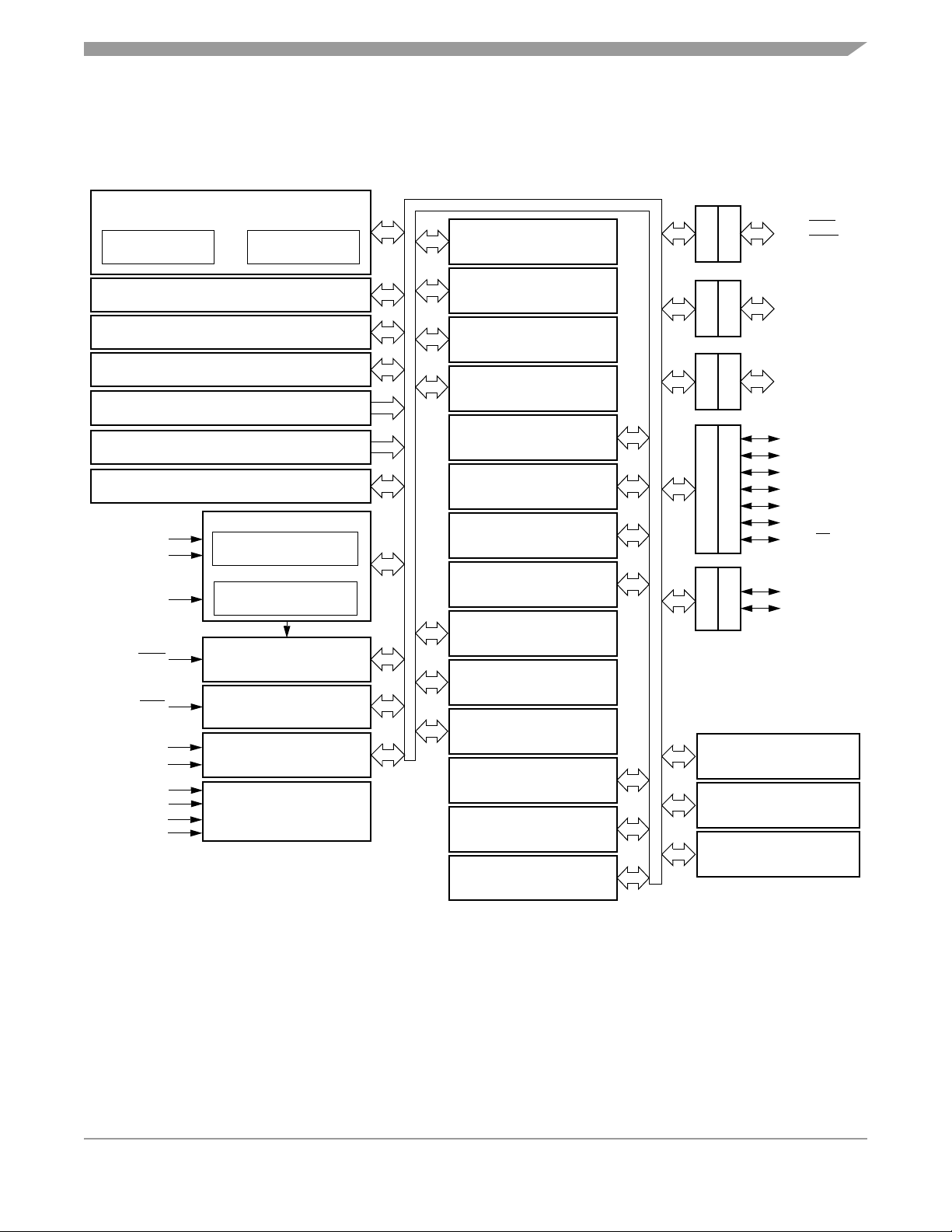
1.3 MCU Block Diagram
Figure 1-1 shows the structure of the MC68HC908GR8.
M68HC08 CPU
CPU
REGISTERS
ARITHMETIC/LOGIC
UNIT (ALU)
PROGR. TIMEBASE
INTERNAL BUS
MODULE
MCU Block Diagram
PTA3/KBD3
DDRA
PORTA
PTA0/KBD0
–
†
CONTROL AND STATUS REGISTERS — 64 BYTES
MC68HC908GR8 USER FLASH — 7680 BYTES
MC68HC908GR4 USER FLASH — 4096BYTES
USER RAM — 384 BYTES
MONITOR ROM — 310 BYTES
FLASH PROGRAMMING (BURN-IN) ROM — 544 BYTES
USER FLASH VECTOR SPACE — 36 BYTES
CLOCK GENERATOR MODULE
CGMXFC
V
DDAD / VREFH
V
/ V
SSAD
OSC1
OSC2
* RST
* IRQ
REFL
V
V
V
DDA
V
SSA
DD
SS
32-kHz OSCILLATOR
PHASE-LOCKED LOOP
24 INTR SYSTEM INTEGRATION
MODULE
SINGLE EXTERNAL IRQ
MODULE
8-BIT ANALOG-TO-DIGITAL
CONVERTER MODULE
POWER
SINGLE BRKPT BREAK
MODULE
DUAL V. LOW-VOLTAGE INHIBIT
2-CHANNEL TIMER INTERFACE
1-CHANNEL TIMER INTERFACE
MODULE
4-BIT KEYBOARD
INTERRUPT MODULE
MODULE 1
MODULE 2
SERIAL COMMUNICATIONS
INTERFACE MODULE
COMPUTER OPERATING
PROPERLY MODULE
SERIAL PERIPHERAL
INTERFACE MODULE
MONITOR MODULE
DATA BUS SWITCH
MODULE
MEMORY MAP
MODULE
MASK OPTION REGISTER1
MODULE
MASK OPTION REGISTER2
MODULE
DDRB
PORTB
DDRC
PORTC
DDRD
PORTD
DDRE
PORTE
POWER-ON RESET
MONITOR MODE ENTRY
PTB5/AD5–
PTB0/AD0
PTC1–PTC0 † ‡
PTD6/T2CH0 †
PTD5/T1CH1 †
PTD4/T1CH0 †
PTD3/SPSCK †
PTD2/MOSI †
PTD1/MISO †
PTD0/SS
PTE1/RxD
PTE0/TxD
MODULE
SECURITY
MODULE
MODULE
†
† Ports are software configurable with pullup device if input port.
‡ Higher current drive port pins
* Pin contains integrated pullup device
Figure 1-1. MCU Block Diagram
MC68HC908GR8 • MC68HC908GR4 Data Sheet, Rev. 5
Freescale Semiconductor 21
General Description
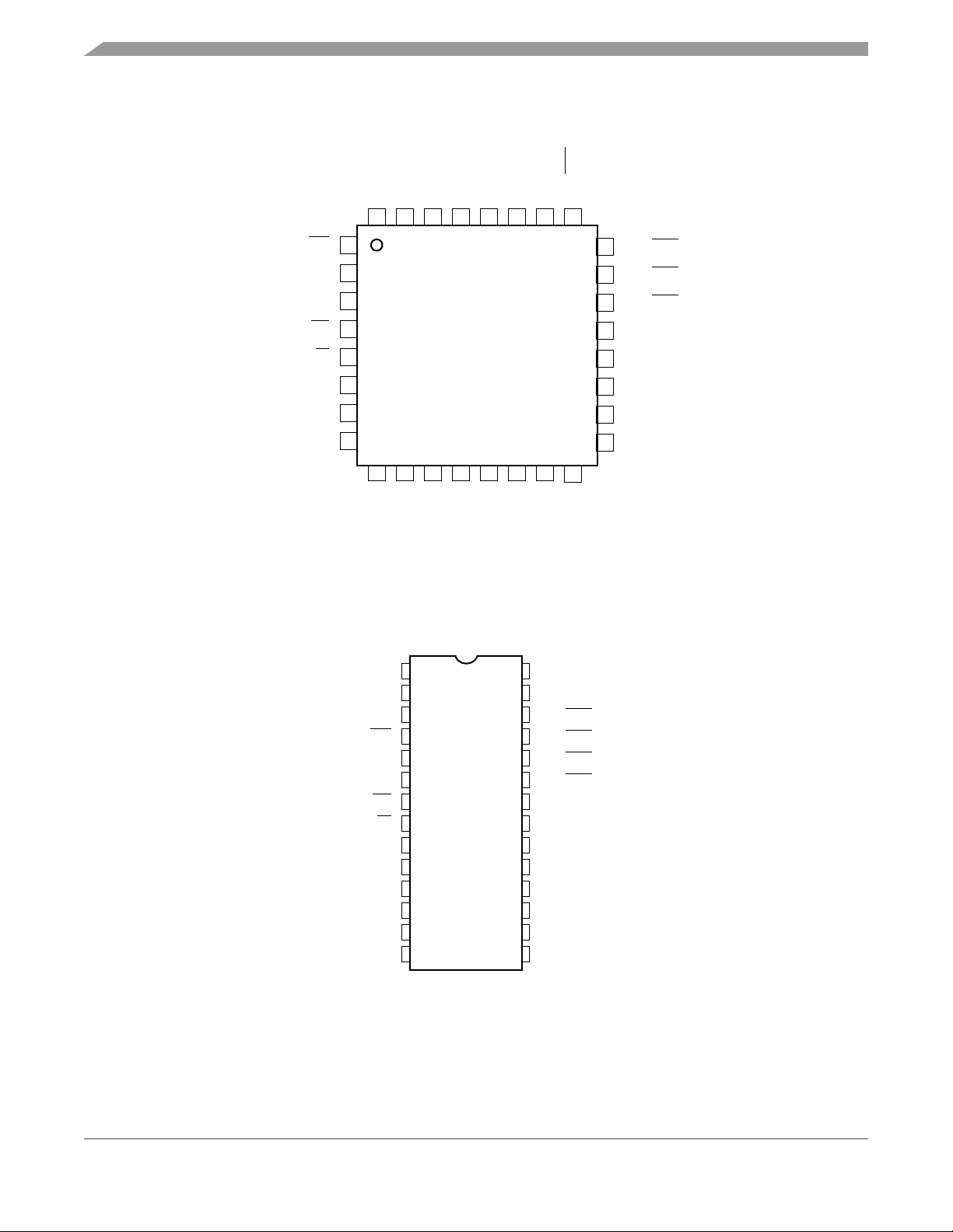
1.4 Pin Assignments
OSC1
OSC2
SSAVDDA
CGMXFC
V
PTC1
PTC0
PTA3/KBD3
32
RST
PTE0/TxD
PTE1/RxD
IRQ
PTD0/SS
PTD1/MISO
PTD2/MOSI
PTD3/SPSCK
1
31
2
3
4
5
6
7
8
9
10
11
12
13
14
SS
DD
V
V
PTB0/AD0
PTD4/T1CH0
PTD5/T1CH1
PTD6/T2CH0
15
PTB1/AD1
PTB2/AD2
24
PTA2/KBD2
23
PTA1/KBD1
22
PTA0/KBD0
V
21
20
19
18
17
16
SSAD/VREFL
V
DDAD/VREFH
PTB5/AD5
PTB4/AD4
PTB3/AD3
25
26
27
28
29
30
NOTE: Ports PTB4, PTB5, PTC0, and PTC1 are available only with the QFP.
Figure 1-2. QFP Pin Assignments
CGMXFC
OSC2
OSC1
RST
PTE0/TxD
PTE1/RxD
IRQ
PTD0/SS
PTD1/MISO
PTD2/MOSI
PTD3/SPSCK
V
V
PTD4/T1CH0
1
2
3
4
5
6
7
8
9
10
11
12
SS
13
DD
14
28
27
26
25
24
23
22
21
20
19
18
17
16
15
V
SSA
V
DDA
PTA3/KBD3
PTA2/KBD2
PTA1/KBD1
PTA0/KBD0
V
SSAD/VREFL
V
DDAD/VREFH
PTB3/AD3
PTB2/AD2
PTB1/AD1
PTB0/AD0
PTD6/T2CH0
PTD5/T1CH1
TE: Ports PTB4, PTB5, PTC0, and PTC1 are available only with the QFP.
Figure 1-3. DIP And SOIC Pin Assignments
MC68HC908GR8 • MC68HC908GR4 Data Sheet, Rev. 5
22 Freescale Semiconductor
Pin Functions
1.5 Pin Functions
Descriptions of the pin functions are provided here.
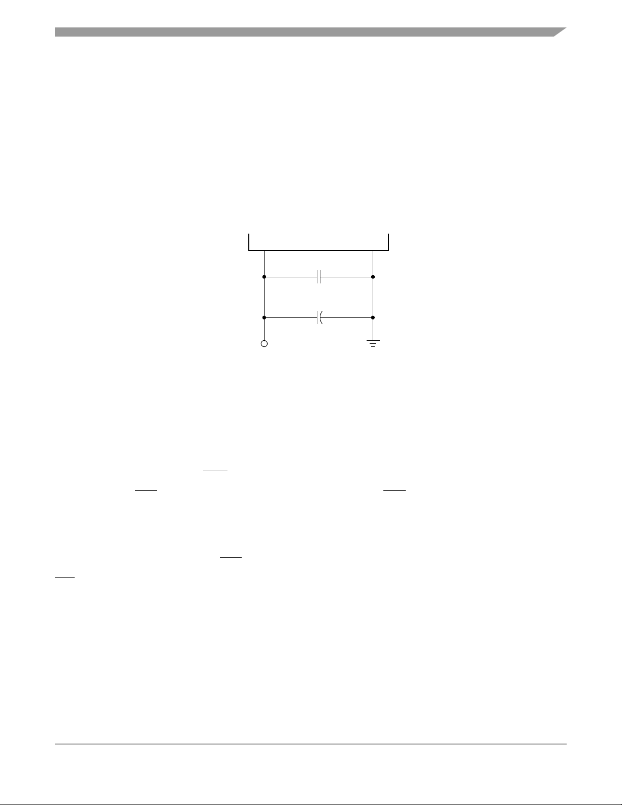
1.5.1 Power Supply Pins (VDD and VSS)
VDD and VSS are the power supply and ground pins. The MCU operates from a single power supply.
Fast signal transitions on MCU pins place high, short-duration current demands on the power supply. To
prevent noise problems, take special care to provide power supply bypassing at the MCU as Figure 1-4
shows. Place the C1 bypass capacitor as close to the MCU as possible. Use a high-frequency-response
ceramic capacitor for C1. C2 is an optional bulk current bypass capacitor for use in applications that
require the port pins to source high current levels.
MCU
V
DD
C1
0.1 µF
+
C2
V
SS
V
DD
NOTE: Component values shown represent typical applications.
Figure 1-4. Power Supply Bypassing
1.5.2 Oscillator Pins (OSC1 and OSC2)
The OSC1 and OSC2 pins are the connections for the on-chip oscillator circuit. See Chapter 7 Clock
Generator Module (CGMC).
1.5.3 External Reset Pin (RST)
A logic 0 on the RST pin forces the MCU to a known startup state. RST is bidirectional, allowing a reset
of the entire system. It is driven low when any internal reset source is asserted. This pin contains an
internal pullup resistor that is always activated, even when the reset pin is pulled low. See Chapter 4
Resets and Interrupts.
1.5.4 External Interrupt Pin (IRQ)
IRQ is an asynchronous external interrupt pin. This pin contains an internal pullup resistor that is always
activated, even when the reset pin is pulled low. See Chapter 12 External Interrupt (IRQ).
1.5.5 CGM Power Supply Pins (V
V
and V
DDA
Decoupling of these pins should be as per the digital supply. See Chapter 7 Clock Generator Module
(CGMC).
are the power supply pins for the analog portion of the clock generator module (CGM).
SSA
DDA
and V
SSA
)
MC68HC908GR8 • MC68HC908GR4 Data Sheet, Rev. 5
Freescale Semiconductor 23

General Description
1.5.6 External Filter Capacitor Pin (CGMXFC)
CGMXFC is an external filter capacitor connection for the CGM. See Chapter 7 Clock Generator Module
(CGMC).
1.5.7 Analog Power Supply/Reference Pins (V
V
DDAD
and V
are the power supply pins for the analog-to-digital converter. Decoupling of these pins
SSAD
DDAD/VREFH
and V
SSAD/VREFL
)
should be as per the digital supply.
NOTE
V
internally connected with V
V
V
connected with V
be tied to the same potential as V
is the high reference supply for the ADC. The V
REFH
and have the same potential as V
DDAD
should be tied to the same potential as VDD via separate traces.
DDAD
is the low reference supply for the ADC. The V
REFL
and has the same potential as V
SSAD
via separate traces.
SS
REFH
pin is internally
REFL
SSAD. VSSAD
signal is
DDAD.
should
See Chapter 5 Analog-to-Digital Converter (ADC).
1.5.8 Port A Input/Output (I/O) Pins (PTA3/KBD3–PTA0/KBD0)
PTA3–PTA0 are special-function, bidirectional I/O port pins. Any or all of the port A pins can be
programmed to serve as keyboard interrupt pins. See Chapter 16 Input/Output Ports (I/O) and See
Chapter 12 External Interrupt (IRQ).
These port pins also have selectable pullups when configured for input mode. The pullups are disengaged
when configured for output mode. The pullups are selectable on an individual port bit basis.
When the port pins are configured for special-function mode (KBI), pullups will be automatically engaged.
As long as the port pins are in special-function mode, the pullups will always be on.
1.5.9 Port B I/O Pins (PTB5/AD5–PTB0/AD0)
PTB5–PTB0 are special-function, bidirectional I/O port pins that can also be used for analog-to-digital
converter (ADC) inputs. See Chapter 16 Input/Output Ports (I/O) and See Chapter 5 Analog-to-Digital
Converter (ADC).
There are no pullups associated with this port.
1.5.10 Port C I/O Pins (PTC1–PTC0)
PTC1–PTC0 are general-purpose, bidirectional I/O port pins. See Chapter 16 Input/Output Ports (I/O).
PTC0 and PTC1 are only available on 32-pin QFP packages.
These port pins also have selectable pullups when configured for input mode. The pullups are disengaged
when configured for output mode. The pullups are selectable on an individual port bit basis.
1.5.11 Port D I/O Pins (PTD6/T2CH0–PTD0/SS)
PTD6–PTD0 are special-function, bidirectional I/O port pins. PTD3–PTD0 can be programmed to be
serial peripheral interface (SPI) pins, while PTD6–PTD4 can be individually programmed to be timer
interface module (TIM1 and TIM2) pins. See Chapter 22 Timer Interface Module (TIM), Chapter 20 Serial
Peripheral Interface (SPI), and See Chapter 16 Input/Output Ports (I/O).
MC68HC908GR8 • MC68HC908GR4 Data Sheet, Rev. 5
24 Freescale Semiconductor

Pin Functions
These port pins also have selectable pullups when configured for input mode. The pullups are disengaged
when configured for output mode. The pullups are selectable on an individual port bit basis.
When the port pins are configured for special-function mode (SPI, TIM1, TIM2), pullups can be selectable
on an individual port pin basis.
1.5.12 Port E I/O Pins (PTE1/RxD–PTE0/TxD)
PTE1–PTE0 are special-function, bidirectional I/O port pins. These pins can also be programmed to be
serial communications interface (SCI) pins. See Chapter 18 Serial Communications Interface (SCI) and
See Chapter 16 Input/Output Ports (I/O).
NOTE
Any unused inputs and I/O ports should be tied to an appropriate logic level
(either V
require termination, termination is recommended to reduce the possibility
of electro-static discharge damage.
or VSS). Although the I/O ports of the MC68HC908GR8 do not
DD
MC68HC908GR8 • MC68HC908GR4 Data Sheet, Rev. 5
Freescale Semiconductor 25

General Description
MC68HC908GR8 • MC68HC908GR4 Data Sheet, Rev. 5
26 Freescale Semiconductor

Chapter 2 Memory Map
2.1 Introduction
The CPU08 can address 64K bytes of memory space. The memory map, shown in Figure 2-1, includes:
• 8K bytes of FLASH memory, 7680 bytes of user space on the MC68HC908GR8 or
4K bytes of FLASH memory, 4096 bytes of user space on the MC68HC908GR4
• 384 bytes of random-access memory (RAM)
• 36 bytes of user-defined vectors
• 310 bytes of monitor routines in read-only memory (ROM)
• 544 bytes of integrated FLASH burn-in routines in ROM
2.2 Unimplemented Memory Locations
Accessing an unimplemented location can cause an illegal address reset if illegal address resets are
enabled. In the memory map (Figure 2-1) and in register figures in this document, unimplemented
locations are shaded.
2.3 Reserved Memory Locations
Accessing a reserved location can have unpredictable effects on MCU operation. In the Figure 2-1 and
in register figures in this document, reserved locations are marked with the word Reserved or with the
letter R.
2.4 Input/Output (I/O) Section
Most of the control, status, and data registers are in the zero page area of $0000–$003F. Additional I/O
registers have these addresses:
• $FE00; SIM break status register, SBSR
• $FE01; SIM reset status register, SRSR
• $FE03; SIM break flag control register, SBFCR
• $FE04; interrupt status register 1, INT1
• $FE05; interrupt status register 2, INT2
• $FE06; interrupt status register 3, INT3
• $FE07; reserved FLASH test control register, FLTCR
• $FE08; FLASH control register, FLCR
• $FE09; break address register high, BRKH
• $FE0A; break address register low, BRKL
• $FE0B; break status and control register, BRKSCR
• $FE0C; LVI status register, LVISR
• $FF7E; FLASH block protect register, FLBPR
Data registers are shown in Figure 2-2, and Table 2-1 is a list of vector locations.
MC68HC908GR8 • MC68HC908GR4 Data Sheet, Rev. 5
Freescale Semiconductor 27
Memory Map
$0000
↓
$003F
$0040
↓
$01BF
$01C0
↓
$1BFF
$1C00
↓
$1E1F
$1E20
↓
$DFFF
$E000
↓
$EDFF
$EE00
↓
$FDFF
$FE00 SIM Break Status Register (SBSR)
$FE01 SIM Reset Status Register (SRSR)
Reserved for Integrated FLASH Burn-in Routines
MC68HC908GR8
FLASH Memory
7680 Bytes
I/O Registers
64 Bytes
RAM
384 Bytes
Unimplemented
6720 Bytes
544 Bytes
Unimplemented
49,632 Bytes
MC68HC908GR4
Unimplemented
MC68HC908GR4
FLASH Memory
3584 Bytes
4096 Bytes
$FE02
$FE03 SIM Break Flag Control Register (SBFCR)
$FE04 Interrupt Status Register 1 (INT1)
$FE05 Interrupt Status Register 2 (INT2)
$FE06 Interrupt Status Register 3 (INT3)
$FE07
$FE08 FLASH Control Register (FLCR)
$FE09 Break Address Register High (BRKH)
$FE0A Break Address Register Low (BRKL)
$FE0B Break Status and Control Register (BRKSCR)
$FE0C LVI Status Register (LVISR)
Reserved for FLASH Test Control Register (FLTCR)
Reserved
Continued on next page
Figure 2-1. Memory Map
MC68HC908GR8 • MC68HC908GR4 Data Sheet, Rev. 5
28 Freescale Semiconductor

$FE0D
↓
$FE0F
$FE10
↓
$FE1F
$FE20
↓
$FF55
$FF56
↓
$FF7D
$FF7E FLASH Block Protect Register (FLBPR)
$FF7F
↓
$FFDB
Reserved for Compatibility with Monitor Code
Reserved
3 Bytes
Unimplemented
16 Bytes
for A-Family Parts
Monitor ROM
310 Bytes
Unimplemented
40 Bytes
Unimplemented
93 Bytes
Input/Output (I/O) Section
Note: $FFF6–$FFFD
contains
8 security bytes
$FFDC
↓
$FFFE
$FFFF
FLASH Vectors
(36 Bytes inluding $FFFF)
Low byte of reset vector when read
COP Control Register (COPCTL)
Figure 2-1. Memory Map (Continued)
Addr.Register Name Bit 7654321Bit 0
$0000
$0001
$0002
$0003
Port A Data Register
(PTA)
Port B Data Register
(PTB)
Port C Data Register
(PTC)
Port D Data Register
(PTD)
Read:0000
Write:
Reset: Unaffected by reset
Read: 0 0
Write:
Reset: Unaffected by reset
Read:000000
Write:
Reset: Unaffected by reset
Read: 0
Write:
Reset: Unaffected by reset
PTD6 PTD5 PTD4 PTD3 PTD2 PTD1 PTD0
= Unimplemented R = Reserved U = Unaffected
PTB5 PTB4 PTB3 PTB2 PTB1 PTB0
PTA3 PTA2 PTA1 PTA0
PTC1 PTC0
Figure 2-2. Control, Status, and Data Registers (Sheet 1 of 7)
MC68HC908GR8 • MC68HC908GR4 Data Sheet, Rev. 5
Freescale Semiconductor 29
Memory Map
Addr.Register Name Bit 7654321Bit 0
$0004
$0005
$0006
$0007
$0008
$0009
↓
$000B
$000C
$000D
$000E
$000F
$0010
$0011
Data Direction Register A
(DDRA)
Data Direction Register B
(DDRB)
Data Direction Register C
(DDRC)
Data Direction Register D
(DDRD)
Port E Data Register
(PTE)
Unimplemented
Data Direction Register E
(DDRE)
Port A Input Pullup Enable
Register (PTAPUE)
Port C Input Pullup Enable
Register (PTCPUE)
Port D Input Pullup Enable
Register (PTDPUE)
SPI Control Register
(SPCR)
SPI Status and Control
Register (SPSCR)
Read:0000
Write:
Reset:00000000
Read: 0 0
Write:
Reset:00000000
Read:000000
Write:
Reset:00000000
Read: 0
Write:
Reset:00000000
Read:000000
Write:
Reset: Unaffected by reset
Read:
Write:
Reset:00000000
Read:000000
Write:
Reset:00000000
Read:0000
Write:
Reset:00000000
Read:000000
Write:
Reset:00000000
Read: 0
Write:
Reset:00000000
Read:
Write:
Reset:00101000
Read: SPRF
Write:
Reset:00001000
SPRIE
DDRD6 DDRD5 DDRD4 DDRD3 DDRD2 DDRD1 DDRD0
PTDPUE6 PTDPUE5 PTDPUE4 PTDPUE3 PTDPUE2 PTDPUE1 PTDPUE0
DMAS
ERRIE
= Unimplemented R = Reserved U = Unaffected
DDRB5 DDRB4 DDRB3 DDRB2 DDRB1 DDRB0
SPMSTR CPOL CPHA SPWOM SPE SPTIE
OVRF MODF SPTE
DDRA3 DDRA2 DDRA1 DDRA0
DDRC1 DDRC0
PTE1 PTE0
DDRE1 DDRE0
PTAPUE3 PTAPUE2 PTAPUE1 PTAPUE0
PTCPUE1 PTCPUE0
MODFEN SPR1 SPR0
Figure 2-2. Control, Status, and Data Registers (Sheet 2 of 7)
MC68HC908GR8 • MC68HC908GR4 Data Sheet, Rev. 5
30 Freescale Semiconductor

Input/Output (I/O) Section
Addr.Register Name Bit 7654321Bit 0
Read: R7 R6 R5 R4 R3 R2 R1 R0
Write: T7 T6 T5 T4 T3 T2 T1 T0
Reset: Unaffected by reset
Read:
Write:
Reset:00000000
Read:
Write:
Reset:00000000
Read: R8
Write:
Reset:UU000000
Read: SCTE TC SCRF IDLE OR NF FE PE
Write:
Reset:11000000
Read:
Write:
Reset:00000000
Read: R7 R6 R5 R4 R3 R2 R1 R0
Write: T7 T6 T5 T4 T3 T2 T1 T0
Reset: Unaffected by reset
Read:
Write:
Reset:00000000
Read:0000KEYF0
Write:
Reset:00000000
Read:
Write:
Reset: 0000
Read: TBIF
Write:
Reset:00000000
Read:0000IRQF10
Write: ACK1
Reset:00000000
LOOPS ENSCI TXINV M WAKE ILTY PEN PTY
SCTIE TCIE SCRIE ILIE TE RE RWU SBK
T8 DMARE DMATE ORIE NEIE FEIE PEIE
BKF RPF
SCP1 SCP0 R SCR2 SCR1 SCR0
ACKK
KBIE3 KBIE2 KBIE1 KBIE0
TBR2 TBR1 TBR0
= Unimplemented R = Reserved U = Unaffected
0
TACK
TBIE TBON R
IMASKK MODEK
IMASK1 MODE1
$0012
$0013
$0014
$0015
$0016
$0017
$0018
$0019
$001A
$001B
$001C
$001D
SPI Data Register
(SPDR)
SCI Control Register 1
(SCC1)
SCI Control Register 2
(SCC2)
SCI Control Register 3
(SCC3)
SCI Status Register 1
(SCS1)
SCI Status Register 2
(SCS2)
SCI Data Register
(SCDR)
SCI Baud Rate Register
(SCBR)
Keyboard Status
and Control Register
(INTKBSCR)
Keyboard Interrupt Enable
Register (INTKBIER)
Time Base Module Control
Register (TBCR)
IRQ Status and Control
Register (INTSCR)
Figure 2-2. Control, Status, and Data Registers (Sheet 3 of 7)
MC68HC908GR8 • MC68HC908GR4 Data Sheet, Rev. 5
Freescale Semiconductor 31

Memory Map
Addr.Register Name Bit 7654321Bit 0
$001E
Configuration Register 2
(CONFIG2)†
Read:000000
Write:
OSC-
STOPENB
SCIBDSRC
Reset:00000000
$001F
Configuration Register 1
(CONFIG1)
Read:
Write:
†
COPRS LVISTOP LVIRSTD LVIPWRD LVI5OR3
†
SSREC STOP COPD
Reset:00000000
$0020
Timer 1 Status and Control
Register (T1SC)
Read: TOF
Write: 0 TRST
TOIE TSTOP
00
PS2 PS1 PS0
Reset:00100000
Read: Bit 15 14 13 12 11 10 9 Bit 8
$0021
Timer 1 Counter Register
High (T1CNTH)
Write:
Reset:00000000
Read:Bit 7654321Bit 0
$0022
Timer 1 Counter Register
Low (T1CNTL)
Write:
Reset:00000000
$0023
Timer 1 Counter Modulo
Register High (T1MODH)
Read:
Write:
Bit 15 14 13 12 11 10 9 Bit 8
Reset:11111111
$0024
Timer 1 Counter Modulo
Register Low (T1MODL)
Read:
Write:
Bit 7654321Bit 0
Reset:11111111
Read: CH0F
Write: 0
CH0IE MS0B MS0A ELS0B ELS0A TOV0 CH0MAX
Reset:00000000
Read:
Write:
Bit 15 14 13 12 11 10 9 Bit 8
$0025
$0026
Timer 1 Channel 0 Status
and Control Register
(T1SC0)
Timer 1 Channel 0
Register High (T1CH0H)
Reset: Indeterminate after reset
$0027
Timer 1 Channel 0
Register Low (T1CH0L)
Read:
Write:
Bit 7654321Bit 0
Reset: Indeterminate after reset
† One-time writeable register after each reset, except LVI5OR3 bit. LVI5OR3 bit is only reset via POR (power-on reset).
Timer 1 Channel 1 Status and
$0028
Control Register (T1SC1)
Read: CH1F
Write: 0
CH1IE
0
MS1A ELS1B ELS1A TOV1 CH1MAX
Reset:00000000
$0029
Timer 1 Channel 1
Register High (T1CH1H)
Read:
Write:
Bit 15 14 13 12 11 10 9 Bit 8
Reset: Indeterminate after reset
= Unimplemented R = Reserved U = Unaffected
Figure 2-2. Control, Status, and Data Registers (Sheet 4 of 7)
MC68HC908GR8 • MC68HC908GR4 Data Sheet, Rev. 5
32 Freescale Semiconductor

Input/Output (I/O) Section
Addr.Register Name Bit 7654321Bit 0
$002A
$002B
$002C
$002D
$002E
$002F
$0030
$0031
$0032
$0033
↓
$0035
$0036
$0037
Timer 1 Channel 1
Register Low (T1CH1L)
Timer 2 Status and Control
Register (T2SC)
Timer 2 Counter Register
High (T2CNTH)
Timer 2 Counter Register
Low (T2CNTL)
Timer 2 Counter Modulo
Register High (T2MODH)
Timer 2 Counter Modulo
Register Low (T2MODL)
Timer 2 Channel 0 Status
and Control Register
(T2SC0)
Timer 2 Channel 0
Register High (T2CH0H)
Timer 2 Channel 0
Register Low (T2CH0L)
Unimplemented
PLL Control Register
(PCTL)
PLL Bandwidth Control
Register (PBWC)
Read:
Write:
Reset: Indeterminate after reset
Read: TOF
Write: 0 TRST
Reset:00100000
Read: Bit 15 14 13 12 11 10 9 Bit 8
Write:
Reset:00000000
Read:Bit 7654321Bit 0
Write:
Reset:00000000
Read:
Write:
Reset:11111111
Read:
Write:
Reset:11111111
Read: CH0F
Write: 0
Reset:00000000
Read:
Write:
Reset: Indeterminate after reset
Read:
Write:
Reset: Indeterminate after reset
Read:
Write:
Reset:00000000
Read:
Write:
Reset:00100000
Read:
Write:
Reset:00000000
Bit 7654321Bit 0
TOIE TSTOP
Bit 15 14 13 12 11 10 9 Bit 8
Bit 7654321Bit 0
CH0IE MS0B MS0A ELS0B ELS0A TOV0 CH0MAX
Bit 15 14 13 12 11 10 9 Bit 8
Bit 7654321Bit 0
PLLIE
AUTO
PLLF
LOCK
= Unimplemented R = Reserved U = Unaffected
PLLON BCS PRE1 PRE0 VPR1 VPR0
ACQ
00
0000
PS2 PS1 PS0
R
Figure 2-2. Control, Status, and Data Registers (Sheet 5 of 7)
MC68HC908GR8 • MC68HC908GR4 Data Sheet, Rev. 5
Freescale Semiconductor 33

Memory Map
Addr.Register Name Bit 7654321Bit 0
$0038
$0039
$003A
$003B
$003C
$003D
$003E
$003F Unimplemented
$FE00
$FE01
$FE02 Unimplemented
$FE03
PLL Multiplier Select High
Register (PMSH)
PLL Multiplier Select Low
Register (PMSL)
PLL VCO Select Range
Register (PMRS)
PLL Reference Divider
Select Register (PMDS)
Analog-to-Digital Status and
Control Register
(ADSCR)
Analog-to-Digital Data
Register (ADR)
Analog-to-Digital Input Clock
Register (ADCLK)
SIM Break Status Register
(SBSR)
Note: Writing a logic 0 clears SBSW.
SIM Reset Status Register
(SRSR)
SIM Break Flag Control
Register (SBFCR)
Read:0000
Write:
Reset:00000000
Read:
Write:
Reset:01000000
Read:
Write:
Reset:01000000
Read:0000
Write:
Reset:00000001
Read: COCO
Write: R
Reset:00011111
Read:AD7AD6AD5AD4AD3AD2AD1AD0
Write:RRRRRRRR
Reset: Indeterminate after reset
Read:
Write: RRRR
Reset:00000000
Read:
Write:
Reset:
Read:
Write: NOTE
Reset:00000000
Read: POR PIN COP ILOP ILAD MODRST LVI 0
Write:
POR:10000000
Read:
Write:
Reset:
Read:
Write:
Reset: 0
MUL7 MUL6 MUL5 MUL4 MUL3 MUL2 MUL1 MUL0
VRS7 VRS6 VRS5 VRS4 VRS3 VRS2 VRS1 VRS0
AIEN ADCO ADCH4 ADCH3 ADCH2 ADCH1 ADCH0
ADIV2 ADIV1 ADIV0 ADICLK
RRRRRR
BCFERRRRRRR
= Unimplemented R = Reserved U = Unaffected
MUL11 MUL10 MUL9 MUL8
RDS3 RDS2 RDS1 RDS0
0000
SBSW
R
Figure 2-2. Control, Status, and Data Registers (Sheet 6 of 7)
MC68HC908GR8 • MC68HC908GR4 Data Sheet, Rev. 5
34 Freescale Semiconductor

Input/Output (I/O) Section
Addr.Register Name Bit 7654321Bit 0
$FE04
$FE05
$FE06
$FE07
$FE08
$FE09
$FE0A
$FE0B
$FE0C LVI Status Register (LVISR)
$FF7E
Interrupt Status Register 1
Interrupt Status Register 2
Interrupt Status Register 3
FLASH Test Control
Register (FLTCR)
FLASH Control Register
(FLCR)
Break Address Register High
(BRKH)
Break Address Register Low
(BRKL)
Break Status and Control
Register (BRKSCR)
FLASH Block Protect
Register (FLBPR)
Read: IF6 IF5 IF4 IF3 IF2 IF1 0 0
Write:RRRRRRRR
(INT1)
Reset:00000000
Read: IF14 IF13 IF12 IF11 IF10 IF9 IF8 IF7
Write:RRRRRRRR
(INT2)
Reset:00000000
Read:000000IF16IF15
Write:RRRRRRRR
(INT3)
Reset:00000000
Read:
Write:
Reset:00000000
Read:0000
Write:
Reset:00000000
Read:
Write:
Reset:00000000
Read:
Write:
Reset:00000000
Read:
Write:
Reset:00000000
Read:LVIOUT0000000
Write:
Reset:00000000
Read:
Write:
†
Reset:UUUUUUUU
RRRRRRRR
HVEN MASS ERASE PGM
Bit 15 14 13 12 11 10 9 Bit 8
Bit 7654321Bit 0
BRKE BRKA
BPR7 BPR6 BPR5 BPR4 BPR3 BPR2 BPR1 BPR0
000000
Read: Low byte of reset vector
Write: Writing clears COP counter (any value)
Reset: Unaffected by reset
= Unimplemented R = Reserved U = Unaffected
$FFFF
COP Control Register
(COPCTL)
† Non-volatile FLASH register
Figure 2-2. Control, Status, and Data Registers (Sheet 7 of 7)
MC68HC908GR8 • MC68HC908GR4 Data Sheet, Rev. 5
Freescale Semiconductor 35

Memory Map
.
Table 2-1. Vector Addresses
Vector Priority Vector Address Vector
Lowest
Highest $FFFF Reset Vector (Low)
IF16
IF15
IF14
IF13
IF12
IF11
IF10
IF9
IF8
IF7
IF6
IF5
IF4
IF3
IF2
IF1
—
—
$FFDC Timebase Vector (High)
$FFDD Timebase Vector (Low)
$FFDE ADC Conversion Complete Vector (High)
$FFDF ADC Conversion Complete Vector (Low)
$FFE0 Keyboard Vector (High)
$FFE1 Keyboard Vector (Low)
$FFE2 SCI Transmit Vector (High)
$FFE3 SCI Transmit Vector (Low)
$FFE4 SCI Receive Vector (High)
$FFE5 SCI Receive Vector (Low)
$FFE6 SCI Error Vector (High)
$FFE7 SCI Error Vector (Low)
$FFE8 SPI Transmit Vector (High)
$FFE9 SPI Transmit Vector (Low)
$FFEA SPI Receive Vector (High)
$FFEB SPI Receive Vector (Low)
$FFEC TIM2 Overflow Vector (High)
$FFED TIM2 Overflow Vector (Low)
$FFEE
$FFEF
$FFF0 TIM2 Channel 0 Vector (High)
$FFF1 TIM2 Channel 0 Vector (Low)
$FFF2 TIM1 Overflow Vector (High)
$FFF3 TIM1 Overflow Vector (Low)
$FFF4 TIM1 Channel 1 Vector (High)
$FFF5 TIM1 Channel 1 Vector (Low)
$FFF6 TIM1 Channel 0 Vector (High)
$FFF7 TIM1 Channel 0 Vector (Low)
$FFF8 PLL Vector (High)
$FFF9 PLL Vector (Low)
$FFFA IRQ
$FFFB IRQ
$FFFC SWI Vector (High)
$FFFD SWI Vector (Low)
$FFFE Reset Vector (High)
Reserved
Reserved
Vector (High)
Vector (Low)
MC68HC908GR8 • MC68HC908GR4 Data Sheet, Rev. 5
36 Freescale Semiconductor

Chapter 3 Low-Power Modes
3.1 Introduction
The MCU may enter two low-power modes: wait mode and stop mode. They are common to all HC08
MCUs and are entered through instruction execution. This section describes how each module acts in the
low-power modes.
3.1.1 Wait Mode
The WAIT instruction puts the MCU in a low-power standby mode in which the CPU clock is disabled but
the bus clock continues to run. Power consumption can be further reduced by disabling the LVI module
and/or the timebase module through bits in the CONFIG register. (See Chapter 8 Configuration Register
(CONFIG).)
3.1.2 Stop Mode
Stop mode is entered when a STOP instruction is executed. The CPU clock is disabled and the bus clock
is disabled if the OSCSTOPENB bit in the CONFIG register is at a logic 0. (See Chapter 8 Configuration
Register (CONFIG).)
3.2 Analog-to-Digital Converter (ADC)
3.2.1 Wait Mode
The ADC continues normal operation during wait mode. Any enabled CPU interrupt request from the ADC
can bring the MCU out of wait mode. If the ADC is not required to bring the MCU out of wait mode, power
down the ADC by setting ADCH4–ADCH0 bits in the ADC status and control register before executing the
WAIT instruction.
3.2.2 Stop Mode
The ADC module is inactive after the execution of a STOP instruction. Any pending conversion is aborted.
ADC conversions resume when the MCU exits stop mode after an external interrupt. Allow one
conversion cycle to stabilize the analog circuitry.
3.3 Break Module (BRK)
3.3.1 Wait Mode
If enabled, the break module is active in wait mode. In the break routine, the user can subtract one from
the return address on the stack if the BW bit in the break status register is set.
MC68HC908GR8 • MC68HC908GR4 Data Sheet, Rev. 5
Freescale Semiconductor 37

Low-Power Modes
3.3.2 Stop Mode
The break module is inactive in stop mode. A break interrupt causes exit from stop mode and sets the BW
bit in the break status register. The STOP instruction does not affect break module register states.
3.4 Central Processor Unit (CPU)
3.4.1 Wait Mode
The WAIT instruction:
• Clears the interrupt mask (I bit) in the condition code register, enabling interrupts. After exit from
wait mode by interrupt, the I bit remains clear. After exit by reset, the I bit is set.
• Disables the CPU clock
3.4.2 Stop Mode
The STOP instruction:
• Clears the interrupt mask (I bit) in the condition code register, enabling external interrupts. After
exit from stop mode by external interrupt, the I bit remains clear. After exit by reset, the I bit is set.
• Disables the CPU clock
After exiting stop mode, the CPU clock begins running after the oscillator stabilization delay.
3.5 Clock Generator Module (CGM)
3.5.1 Wait Mode
The CGM remains active in wait mode. Before entering wait mode, software can disengage and turn off
the PLL by clearing the BCS and PLLON bits in the PLL control register (PCTL). Less power-sensitive
applications can disengage the PLL without turning it off. Applications that require the PLL to wake the
MCU from wait mode also can deselect the PLL output without turning off the PLL.
3.5.2 Stop Mode
If the OSCSTOPEN bit in the CONFIG register is cleared (default), then the STOP instruction disables
the CGM (oscillator and phase-locked loop) and holds low all CGM outputs (CGMXCLK, CGMOUT, and
CGMINT).
If the STOP instruction is executed with the VCO clock, CGMVCLK, divided by two driving CGMOUT, the
PLL automatically clears the BCS bit in the PLL control register (PCTL), thereby selecting the crystal
clock, CGMXCLK, divided by two as the source of CGMOUT. When the MCU recovers from STOP, the
crystal clock divided by two drives CGMOUT and BCS remains clear.
If the OSCSTOPEN bit in the CONFIG register is set, then the phase locked loop is shut off, but the
oscillator will continue to operate in stop mode.
MC68HC908GR8 • MC68HC908GR4 Data Sheet, Rev. 5
38 Freescale Semiconductor

Computer Operating Properly Module (COP)
3.6 Computer Operating Properly Module (COP)
3.6.1 Wait Mode
The COP remains active in wait mode. To prevent a COP reset during wait mode, periodically clear the
COP counter in a CPU interrupt routine or a DMA service routine.
3.6.2 Stop Mode
Stop mode turns off the CGMXCLK input to the COP and clears the COP prescaler. Service the COP
immediately before entering or after exiting stop mode to ensure a full COP timeout period after entering
or exiting stop mode.
The STOP bit in the configuration register (CONFIG) enables the STOP instruction. To prevent
inadvertently turning off the COP with a STOP instruction, disable the STOP instruction by clearing the
STOP bit.
3.7 External Interrupt Module (IRQ)
3.7.1 Wait Mode
The IRQ module remains active in wait mode. Clearing the IMASK1 bit in the IRQ status and control
register enables IRQ
CPU interrupt requests to bring the MCU out of wait mode.
3.7.2 Stop Mode
The IRQ module remains active in stop mode. Clearing the IMASK1 bit in the IRQ status and control
register enables IRQ
CPU interrupt requests to bring the MCU out of stop mode.
3.8 Keyboard Interrupt Module (KBI)
3.8.1 Wait Mode
The keyboard module remains active in wait mode. Clearing the IMASKK bit in the keyboard status and
control register enables keyboard interrupt requests to bring the MCU out of wait mode.
3.8.2 Stop Mode
The keyboard module remains active in stop mode. Clearing the IMASKK bit in the keyboard status and
control register enables keyboard interrupt requests to bring the MCU out of stop mode.
3.9 Low-Voltage Inhibit Module (LVI)
3.9.1 Wait Mode
If enabled, the LVI module remains active in wait mode. If enabled to generate resets, the LVI module can
generate a reset and bring the MCU out of wait mode.
MC68HC908GR8 • MC68HC908GR4 Data Sheet, Rev. 5
Freescale Semiconductor 39

Low-Power Modes
3.9.2 Stop Mode
If enabled, the LVI module remains active in stop mode. If enabled to generate resets, the LVI module
can generate a reset and bring the MCU out of stop mode.
3.10 Serial Communications Interface Module (SCI)
3.10.1 Wait Mode
The SCI module remains active in wait mode. Any enabled CPU interrupt request from the SCI module
can bring the MCU out of wait mode.
If SCI module functions are not required during wait mode, reduce power consumption by disabling the
module before executing the WAIT instruction.
3.10.2 Stop Mode
The SCI module is inactive in stop mode. The STOP instruction does not affect SCI register states. SCI
module operation resumes after the MCU exits stop mode.
Because the internal clock is inactive during stop mode, entering stop mode during an SCI transmission
or reception results in invalid data.
3.11 Serial Peripheral Interface Module (SPI)
3.11.1 Wait Mode
The SPI module remains active in wait mode. Any enabled CPU interrupt request from the SPI module
can bring the MCU out of wait mode.
If SPI module functions are not required during wait mode, reduce power consumption by disabling the
SPI module before executing the WAIT instruction.
3.11.2 Stop Mode
The SPI module is inactive in stop mode. The STOP instruction does not affect SPI register states. SPI
operation resumes after an external interrupt. If stop mode is exited by reset, any transfer in progress is
aborted, and the SPI is reset.
3.12 Timer Interface Module (TIM1 and TIM2)
3.12.1 Wait Mode
The TIM remains active in wait mode. Any enabled CPU interrupt request from the TIM can bring the MCU
out of wait mode.
If TIM functions are not required during wait mode, reduce power consumption by stopping the TIM before
executing the WAIT instruction.
MC68HC908GR8 • MC68HC908GR4 Data Sheet, Rev. 5
40 Freescale Semiconductor

Timebase Module (TBM)
3.12.2 Stop Mode
The TIM is inactive in stop mode. The STOP instruction does not affect register states or the state of the
TIM counter. TIM operation resumes when the MCU exits stop mode after an external interrupt.
3.13 Timebase Module (TBM)
3.13.1 Wait Mode
The timebase module remains active after execution of the WAIT instruction. In wait mode, the timebase
register is not accessible by the CPU.
If the timebase functions are not required during wait mode, reduce the power consumption by stopping
the timebase before enabling the WAIT instruction.
3.13.2 Stop Mode
The timebase module may remain active after execution of the STOP instruction if the oscillator has been
enabled to operate during stop mode through the OSCSTOPEN bit in the CONFIG register. The timebase
module can be used in this mode to generate a periodic wakeup from stop mode.
If the oscillator has not been enabled to operate in stop mode, the timebase module will not be active
during stop mode. In stop mode, the timebase register is not accessible by the CPU.
If the timebase functions are not required during stop mode, reduce the power consumption by stopping
the timebase before enabling the STOP instruction.
3.14 Exiting Wait Mode
These events restart the CPU clock and load the program counter with the reset vector or with an interrupt
vector:
• External reset — A logic 0 on the RST
contents of locations $FFFE and $FFFF.
• External interrupt — A high-to-low transition on an external interrupt pin (IRQ
program counter with the contents of locations: $FFFA and $FFFB; IRQ
• Break interrupt — A break interrupt loads the program counter with the contents of $FFFC and
$FFFD.
• Computer operating properly module (COP) reset — A timeout of the COP counter resets the MCU
and loads the program counter with the contents of $FFFE and $FFFF.
• Low-voltage inhibit module (LVI) reset — A power supply voltage below the V
MCU and loads the program counter with the contents of locations $FFFE and $FFFF.
• Clock generator module (CGM) interrupt — A CPU interrupt request from the phase-locked loop
(PLL) loads the program counter with the contents of $FFF8 and $FFF9.
• Keyboard module (KBI) interrupt — A CPU interrupt request from the KBI module loads the
program counter with the contents of $FFDE and $FFDF.
• Timer 1 interface module (TIM1) interrupt — A CPU interrupt request from the TIM1 loads the
program counter with the contents of:
– $FFF2 and $FFF3; TIM1 overflow
– $FFF4 and $FFF5; TIM1 channel 1
– $FFF6 and $FFF7; TIM1 channel 0
pin resets the MCU and loads the program counter with the
pin) loads the
pin.
voltage resets the
tripf
MC68HC908GR8 • MC68HC908GR4 Data Sheet, Rev. 5
Freescale Semiconductor 41

Low-Power Modes
• Timer 2 interface module (TIM2) interrupt — A CPU interrupt request from the TIM2 loads the
program counter with the contents of:
– $FFEC and $FFED; TIM2 overflow
– $FFF0 and $FFF1; TIM2 channel 0
• Serial peripheral interface module (SPI) interrupt — A CPU interrupt request from the SPI loads
the program counter with the contents of:
– $FFE8 and $FFE9; SPI transmitter
– $FFEA and $FFEB; SPI receiver
• Serial communications interface module (SCI) interrupt — A CPU interrupt request from the SCI
loads the program counter with the contents of:
– $FFE2 and $FFE3; SCI transmitter
– $FFE4 and $FFE5; SCI receiver
– $FFE6 and $FFE7; SCI receiver error
• Analog-to-digital converter module (ADC) interrupt — A CPU interrupt request from the ADC loads
the program counter with the contents of: $FFDE and $FFDF; ADC conversion complete.
• Timebase module (TBM) interrupt — A CPU interrupt request from the TBM loads the program
counter with the contents of: $FFDC and $FFDD; TBM interrupt.
3.15 Exiting Stop Mode
These events restart the system clocks and load the program counter with the reset vector or with an
interrupt vector:
• External reset — A logic 0 on the RST
pin resets the MCU and loads the program counter with the
contents of locations $FFFE and $FFFF.
• External interrupt — A high-to-low transition on an external interrupt pin loads the program counter
with the contents of locations:
– $FFFA and $FFFB; IRQ
pin
– $FFDE and $FFDF; keyboard interrupt pins
• Low-voltage inhibit (LVI) reset — A power supply voltage below the LVI
voltage resets the MCU
tripf
and loads the program counter with the contents of locations $FFFE and $FFFF.
• Break interrupt — A break interrupt loads the program counter with the contents of locations $FFFC
and $FFFD.
• Timebase module (TBM) interrupt — A TBM interrupt loads the program counter with the contents
of locations $FFDC and $FFDD when the timebase counter has rolled over. This allows the TBM
to generate a periodic wakeup from stop mode.
Upon exit from stop mode, the system clocks begin running after an oscillator stabilization delay. A 12-bit
stop recovery counter inhibits the system clocks for 4096 CGMXCLK cycles after the reset or external
interrupt.
The short stop recovery bit, SSREC, in the configuration register controls the oscillator stabilization delay
during stop recovery. Setting SSREC reduces stop recovery time from 4096 CGMXCLK cycles to 32
CGMXCLK cycles.
NOTE
Use the full stop recovery time (SSREC = 0) in applications that use an
external crystal.
MC68HC908GR8 • MC68HC908GR4 Data Sheet, Rev. 5
42 Freescale Semiconductor

Chapter 4 Resets and Interrupts
4.1 Introduction
Resets and interrupts are responses to exceptional events during program execution. A reset re-initializes
the MCU to its startup condition. An interrupt vectors the program counter to a service routine.
4.2 Resets
A reset immediately returns the MCU to a known startup condition and begins program execution from a
user-defined memory location.
4.2.1 Effects
A reset:
• Immediately stops the operation of the instruction being executed
• Initializes certain control and status bits
• Loads the program counter with a user-defined reset vector address from locations $FFFE and
$FFFF
• Selects CGMXCLK divided by four as the bus clock
4.2.2 External Reset
A logic 0 applied to the RST pin for a time, t
PIN bit in the SIM reset status register.
, generates an external reset. An external reset sets the
IRL
4.2.3 Internal Reset
Sources:
• Power-on reset (POR)
• Computer operating properly (COP)
• Low-power reset circuits
• Illegal opcode
• Illegal address
All internal reset sources pull the RST
devices. The MCU is held in reset for an additional 32 CGMXCLK cycles after releasing the RST
RST PIN
CGMXCLK
INTERNAL
RESET
pin low for 32 CGMXCLK cycles to allow resetting of external
PULLED LOW BY MCU
32 CYCLES 32 CYCLES
Figure 4-1. Internal Reset Timing
pin.
MC68HC908GR8 • MC68HC908GR4 Data Sheet, Rev. 5
Freescale Semiconductor 43

Resets and Interrupts
4.2.3.1 Power-On Reset
A power-on reset is an internal reset caused by a positive transition on the V
pin. VDD at the POR must
DD
go completely to 0 V to reset the MCU. This distinguishes between a reset and a POR. The POR is not a
brown-out detector, low-voltage detector, or glitch detector.
A power-on reset:
• Holds the clocks to the CPU and modules inactive for an oscillator stabilization delay of 4096
CGMXCLK cycles
• Drives the RST
pin low during the oscillator stabilization delay
• Releases the RST pin 32 CGMXCLK cycles after the oscillator stabilization delay
• Releases the CPU to begin the reset vector sequence 64 CGMXCLK cycles after the oscillator
stabilization delay
• Sets the POR bit in the SIM reset status register and clears all other bits in the register
OSC1
PORRST
CGMXCLK
(1)
4096
CYCLES32CYCLES32CYCLES
CGMOUT
RST
PIN
INTERNAL
RESET
1. PORRST is an internally generated power-on reset pulse.
Figure 4-2. Power-On Reset Recovery
4.2.3.2 COP Reset
A COP reset is an internal reset caused by an overflow of the COP counter. A COP reset sets the COP
bit in the system integration module (SIM) reset status register.
To clear the COP counter and prevent a COP reset, write any value to the COP control register at location
$FFFF.
4.2.3.3 Low-Voltage Inhibit Reset
A low-voltage inhibit (LVI) reset is an internal reset caused by a drop in the power supply voltage to the
LVI trip voltage, V
TRIPF
.
An LVI reset:
• Holds the clocks to the CPU and modules inactive for an oscillator stabilization delay of 4096
CGMXCLK cycles after the power supply voltage rises to V
• Drives the RST pin low for as long as VDD is below V
TRIPF
and during the oscillator stabilization
TRIPF
delay
• Releases the RST
pin 32 CGMXCLK cycles after the oscillator stabilization delay
MC68HC908GR8 • MC68HC908GR4 Data Sheet, Rev. 5
44 Freescale Semiconductor

Resets
• Releases the CPU to begin the reset vector sequence 64 CGMXCLK cycles after the oscillator
stabilization delay
• Sets the LVI bit in the SIM reset status register
4.2.3.4 Illegal Opcode Reset
An illegal opcode reset is an internal reset caused by an opcode that is not in the instruction set. An illegal
opcode reset sets the ILOP bit in the SIM reset status register.
If the stop enable bit, STOP, in the mask option register is a logic 0, the STOP instruction causes an illegal
opcode reset.
4.2.3.5 Illegal Address Reset
An illegal address reset is an internal reset caused by opcode fetch from an unmapped address. An illegal
address reset sets the ILAD bit in the SIM reset status register.
A data fetch from an unmapped address does not generate a reset.
4.2.4 SIM Reset Status Register
This read-only register contains flags to show reset sources. All flag bits are automatically cleared
following a read of the register. Reset service can read the SIM reset status register to clear the register
after power-on reset and to determine the source of any subsequent reset.
The register is initialized on powerup as shown with the POR bit set and all other bits cleared. During a
POR or any other internal reset, the RST
XCLK cycles later. If the pin is not above a V
pin is pulled low. After the pin is released, it will be sampled 32
at that time, then the PIN bit in the SRSR may be set in
IH
addition to whatever other bits are set.
NOTE
Only a read of the SIM reset status register clears all reset flags. After
multiple resets from different sources without reading the register, multiple
flags remain set.
Address: $FE01
Bit 7654321Bit 0
Read: POR PIN COP ILOP ILAD 0 LVI 0
Write:
POR:10000000
= Unimplemented
Figure 4-3. SIM Reset Status Register (SRSR)
POR — Power-On Reset Flag
1 = Power-on reset since last read of SRSR
0 = Read of SRSR since last power-on reset
PIN — External Reset Flag
1 = External reset via RST
pin since last read of SRSR
0 = POR or read of SRSR since last external reset
MC68HC908GR8 • MC68HC908GR4 Data Sheet, Rev. 5
Freescale Semiconductor 45

Resets and Interrupts
COP — Computer Operating Properly Reset Bit
1 = Last reset caused by timeout of COP counter
0 = POR or read of SRSR
ILOP — Illegal Opcode Reset Bit
1 = Last reset caused by an illegal opcode
0 = POR or read of SRSR
ILAD — Illegal Address Reset Bit
1 = Last reset caused by an opcode fetch from an illegal address
0 = POR or read of SRSR
LVI — Low-Voltage Inhibit Reset Bit
1 = Last reset caused by low-power supply voltage
0 = POR or read of SRSR
4.3 Interrupts
An interrupt temporarily changes the sequence of program execution to respond to a particular event. An
interrupt does not stop the operation of the instruction being executed, but begins when the current
instruction completes its operation.
STACKING
ORDER
•
•
•
CONDITION CODE REGISTER
5
4
3
PROGRAM COUNTER (HIGH BYTE)
2
PROGRAM COUNTER (LOW BYTE)
1
*High byte of index register is not stacked.
ACCUMULATOR
INDEX REGISTER (LOW BYTE)*
•
•
•
Figure 4-4. Interrupt Stacking Order
1
2
3
UNSTACKING
ORDER
4
5
$00FF DEFAULT ADDRESS ON RESET
MC68HC908GR8 • MC68HC908GR4 Data Sheet, Rev. 5
46 Freescale Semiconductor

Interrupts
4.3.1 Effects
An interrupt:
• Saves the CPU registers on the stack. At the end of the interrupt, the RTI instruction recovers the
CPU registers from the stack so that normal processing can resume.
• Sets the interrupt mask (I bit) to prevent additional interrupts. Once an interrupt is latched, no other
interrupt can take precedence, regardless of its priority.
• Loads the program counter with a user-defined vector address
After every instruction, the CPU checks all pending interrupts if the I bit is not set. If more than one
interrupt is pending when an instruction is done, the highest priority interrupt is serviced first. In the
example shown in Figure 4-5, if an interrupt is pending upon exit from the interrupt service routine, the
pending interrupt is serviced before the LDA instruction is executed.
CLI
BACKGROUND
ROUTINE
INT1
INT2
Figure 4-5
#$FF
LDA
PSHH
INT1 INTERRUPT SERVICE ROUTINE
PULH
RTI
PSHH
INT2 INTERRUPT SERVICE ROUTINE
PULH
RTI
. Interrupt Recognition Example
The LDA opcode is prefetched by both the INT1 and INT2 RTI instructions. However, in the case of the
INT1 RTI prefetch, this is a redundant operation.
NOTE
To maintain compatibility with the M6805 Family, the H register is not
pushed on the stack during interrupt entry. If the interrupt service routine
modifies the H register or uses the indexed addressing mode, save the H
register and then restore it prior to exiting the routine.
MC68HC908GR8 • MC68HC908GR4 Data Sheet, Rev. 5
Freescale Semiconductor 47

Resets and Interrupts
FROM RESET
YES
BREAK
INTERRUPT
?
NO
I BIT SET?
I BIT SET?
NO
IRQ
INTERRUPT
?
NO
CGM
INTERRUPT
?
NO
OTHER
INTERRUPTS
?
NO
YES
YES
YES
YES
STACK CPU REGISTERS
LOAD PC WITH INTERRUPT VECTOR
SET I BIT
FETCH NEXT
INSTRUCTION
SWI
INSTRUCTION
?
NO
RTI
INSTRUCTION
?
NO
YES
YES
UNSTACK CPU REGISTERS
EXECUTE INSTRUCTION
Figure 4-6. Interrupt Processing
MC68HC908GR8 • MC68HC908GR4 Data Sheet, Rev. 5
48 Freescale Semiconductor

4.3.2 Sources
Interrupts
The sources in Table 4-1 can generate CPU interrupt requests.
Table 4-1. Interrupt Sources
Source Flag
Reset None None None 0
SWI instruction None None None 0
pin IRQF IMASK1 IF1 1
IRQ
CGM (PLL) PLLF PLLIE IF2 2 $FFF8–$FFF9
TIM1 channel 0 CH0F CH0IE IF3 3 $FFF6–$FFF7
TIM1 channel 1 CH1F CH1IE IF4 4 $FFF4–$FFF5
TIM1 overflow TOF TOIE IF5 5 $FFF2–$FFF3
TIM2 channel 0 CH0F CH0IE IF6 6 $FFF0–$FFF1
TIM2 overflow TOF TOIE IF8 8 $FFEC–$FFED
SPI receiver full SPRF SPRIE
SPI mode fault MODF ERRIE
SPI transmitter empty SPTE SPTIE IF10 10 $FFE8–$FFE9
Mask
(1)
INT Register
Flag
IF9 9 $FFEA–$FFEBSPI overflow OVRF ERRIE
Priority
(2)
Vector
Address
$FFFE
–$FFFF
$FFFC–$FFFD
$FFFA
–$FFFB
SCI receiver overrun OR ORIE
SCI noise fag NF NEIE
SCI framing error FE FEIE
SCI parity error PE PEIE
SCI receiver full SCRF SCRIE
SCI input idle IDLE ILIE
SCI transmitter empty SCTE SCTIE
SCI transmission complete TC TCIE
Keyboard pin KEYF IMASKK IF14 14 $FFDE–$FFDF
ADC conversion complete COCO AIEN IF15 15 $FFDE–$FFDF
Timebase TBIF TBIE IF16 16 $FFDC–$FFDD
1. The I bit in the condition code register is a global mask for all interrupt sources except the SWI instruction.
2. 0 = highest priority
IF11 11 $FFE6–$FFE7
IF12 12 $FFE4–$FFE5
IF13 13 $FFE2–$FFE3
MC68HC908GR8 • MC68HC908GR4 Data Sheet, Rev. 5
Freescale Semiconductor 49

Resets and Interrupts
4.3.2.1 SWI Instruction
The software interrupt instruction (SWI) causes a non-maskable interrupt.
NOTE
A software interrupt pushes PC onto the stack. An SWI does not push
PC – 1, as a hardware interrupt does.
4.3.2.2 Break Interrupt
The break module causes the CPU to execute an SWI instruction at a software-programmable break
point.
4.3.2.3 IRQ
A logic 0 on the IRQ1
Pin
pin latches an external interrupt request.
4.3.2.4 CGM (Clock Generator Module)
The CGM can generate a CPU interrupt request every time the phase-locked loop circuit (PLL) enters or
leaves the locked state. When the LOCK bit changes state, the PLL flag (PLLF) is set. The PLL interrupt
enable bit (PLLIE) enables PLLF CPU interrupt requests. LOCK is in the PLL bandwidth control register.
PLLF is in the PLL control register.
4.3.2.5 TIM1 (Timer Interface Module 1)
TIM1 CPU interrupt sources:
• TIM1 overflow flag (TOF) — The TOF bit is set when the TIM1 counter value rolls over to $0000
after matching the value in the TIM1 counter modulo registers. The TIM1 overflow interrupt enable
bit, TOIE, enables TIM1 overflow CPU interrupt requests. TOF and TOIE are in the TIM1 status
and control register.
• TIM1 channel flags (CH1F–CH0F) — The CHxF bit is set when an input capture or output compare
occurs on channel x. The channel x interrupt enable bit, CHxIE, enables channel x TIM1 CPU
interrupt requests. CHxF and CHxIE are in the TIM1 channel x status and control register.
4.3.2.6 TIM2 (Timer Interface Module 2)
TIM2 CPU interrupt sources:
• TIM2 overflow flag (TOF) — The TOF bit is set when the TIM2 counter value rolls over to $0000
after matching the value in the TIM2 counter modulo registers. The TIM2 overflow interrupt enable
bit, TOIE, enables TIM2 overflow CPU interrupt requests. TOF and TOIE are in the TIM2 status
and control register.
• TIM2 channel flag (CH0F) — The CH0F bit is set when an input capture or output compare occurs
on channel 0. The channel 0 interrupt enable bit, CH0IE, enables channel 0 TIM2 CPU interrupt
requests. CH0F and CH0IE are in the TIM2 channel 0 status and control register.
MC68HC908GR8 • MC68HC908GR4 Data Sheet, Rev. 5
50 Freescale Semiconductor

Interrupts
4.3.2.7 SPI (Serial Peripheral Interface)
SPI CPU interrupt sources:
• SPI receiver full bit (SPRF) — The SPRF bit is set every time a byte transfers from the shift register
to the receive data register. The SPI receiver interrupt enable bit, SPRIE, enables SPRF CPU
interrupt requests. SPRF is in the SPI status and control register and SPRIE is in the SPI control
register.
• SPI transmitter empty (SPTE) — The SPTE bit is set every time a byte transfers from the transmit
data register to the shift register. The SPI transmit interrupt enable bit, SPTIE, enables SPTE CPU
interrupt requests. SPTE is in the SPI status and control register and SPTIE is in the SPI control
register.
• Mode fault bit (MODF) — The MODF bit is set in a slave SPI if the SS
pin goes high during a
transmission with the mode fault enable bit (MODFEN) set. In a master SPI, the MODF bit is set if
the SS
pin goes low at any time with the MODFEN bit set. The error interrupt enable bit, ERRIE,
enables MODF CPU interrupt requests. MODF, MODFEN, and ERRIE are in the SPI status and
control register.
• Overflow bit (OVRF) — The OVRF bit is set if software does not read the byte in the receive data
register before the next full byte enters the shift register. The error interrupt enable bit, ERRIE,
enables OVRF CPU interrupt requests. OVRF and ERRIE are in the SPI status and control
register.
4.3.2.8 SCI (Serial Communications Interface)
SCI CPU interrupt sources:
• SCI transmitter empty bit (SCTE) — SCTE is set when the SCI data register transfers a character
to the transmit shift register. The SCI transmit interrupt enable bit, SCTIE, enables transmitter CPU
interrupt requests. SCTE is in SCI status register 1. SCTIE is in SCI control register 2.
• Transmission complete bit (TC) — TC is set when the transmit shift register and the SCI data
register are empty and no break or idle character has been generated. The transmission complete
interrupt enable bit, TCIE, enables transmitter CPU interrupt requests. TC is in SCI status register
1. TCIE is in SCI control register 2.
• SCI receiver full bit (SCRF) — SCRF is set when the receive shift register transfers a character to
the SCI data register. The SCI receive interrupt enable bit, SCRIE, enables receiver CPU
interrupts. SCRF is in SCI status register 1. SCRIE is in SCI control register 2.
• Idle input bit (IDLE) — IDLE is set when 10 or 11 consecutive logic 1s shift in from the RxD pin.
The idle line interrupt enable bit, ILIE, enables IDLE CPU interrupt requests. IDLE is in SCI status
register 1. ILIE is in SCI control register 2.
• Receiver overrun bit (OR) — OR is set when the receive shift register shifts in a new character
before the previous character was read from the SCI data register. The overrun interrupt enable
bit, ORIE, enables OR to generate SCI error CPU interrupt requests. OR is in SCI status register 1.
ORIE is in SCI control register 3.
• Noise flag (NF) — NF is set when the SCI detects noise on incoming data or break characters,
including start, data, and stop bits. The noise error interrupt enable bit, NEIE, enables NF to
generate SCI error CPU interrupt requests. NF is in SCI status register 1. NEIE is in SCI control
register 3.
• Framing error bit (FE) — FE is set when a logic 0 occurs where the receiver expects a stop bit. The
framing error interrupt enable bit, FEIE, enables FE to generate SCI error CPU interrupt requests.
FE is in SCI status register 1. FEIE is in SCI control register 3.
MC68HC908GR8 • MC68HC908GR4 Data Sheet, Rev. 5
Freescale Semiconductor 51

Resets and Interrupts
• Parity error bit (PE) — PE is set when the SCI detects a parity error in incoming data. The parity
error interrupt enable bit, PEIE, enables PE to generate SCI error CPU interrupt requests. PE is in
SCI status register 1. PEIE is in SCI control register 3.
4.3.2.9 KBD0
–KBD4 Pins
A logic 0 on a keyboard interrupt pin latches an external interrupt request.
4.3.2.10 ADC (Analog-to-Digital Converter)
When the AIEN bit is set, the ADC module is capable of generating a CPU interrupt after each ADC
conversion. The COCO/IDMAS bit is not used as a conversion complete flag when interrupts are enabled.
4.3.2.11 TBM (Timebase Module)
The timebase module can interrupt the CPU on a regular basis with a rate defined by TBR2–TBR0. When
the timebase counter chain rolls over, the TBIF flag is set. If the TBIE bit is set, enabling the timebase
interrupt, the counter chain overflow will generate a CPU interrupt request.
Interrupts must be acknowledged by writing a logic 1 to the TACK bit.
4.3.3 Interrupt Status Registers
The flags in the interrupt status registers identify maskable interrupt sources. Table 4-2 summarizes the
interrupt sources and the interrupt status register flags that they set. The interrupt status registers can be
useful for debugging.
Table 4-2. Interrupt Source Flags
Interrupt Source Interrupt Status Register Flag
Reset —
SWI instruction —
pin IF1
IRQ
CGM (PLL) IF2
TIM1 channel 0 IF3
TIM1 channel 1 IF4
TIM1 overflow IF5
TIM2 channel 0 IF6
Reserved IF7
TIM2 overflow IF8
SPI receive IF9
SPI transmit IF10
SCI error IF11
SCI receive IF12
SCI transmit IF13
Keyboard IF14
ADC conversion complete IF15
Timebase IF16
MC68HC908GR8 • MC68HC908GR4 Data Sheet, Rev. 5
52 Freescale Semiconductor

Interrupts
4.3.3.1 Interrupt Status Register 1
Address: $FE04
Bit 7654321Bit 0
Read: IF6 IF5 IF4 IF3 IF2 IF1 0 0
Write:RRRRRRRR
Reset:00000000
R = Reserved
Figure 4-7. Interrupt Status Register 1 (INT1)
IF6–IF1 — Interrupt Flags 6–1
These flags indicate the presence of interrupt requests from the sources shown in Table 4-2.
1 = Interrupt request present
0 = No interrupt request present
Bit 1 and Bit 0 — Always read 0
4.3.3.2 Interrupt Status Register 2
Address: $FE05
Bit 7654321Bit 0
Read: IF14 IF13 IF12 IF11 IF10 IF9 IF8 IF7
Write:RRRRRRRR
Reset:00000000
R = Reserved
Figure 4-8. Interrupt Status Register 2 (INT2)
IF14–IF7 — Interrupt Flags 14–7
These flags indicate the presence of interrupt requests from the sources shown in Table 4-2.
1 = Interrupt request present
0 = No interrupt request present
4.3.3.3 Interrupt Status Register 3
Address: $FE06
Bit 7654321Bit 0
Read:000000IF16IF15
Write:RRRRRRRR
Reset:00000000
R = Reserved
Figure 4-9. Interrupt Status Register 3 (INT3)
IF16–IF15 — Interrupt Flags 16–15
This flag indicates the presence of an interrupt request from the source shown in Table 4-2.
1 = Interrupt request present
0 = No interrupt request present
Bits 7–2 — Always read 0
MC68HC908GR8 • MC68HC908GR4 Data Sheet, Rev. 5
Freescale Semiconductor 53

Resets and Interrupts
MC68HC908GR8 • MC68HC908GR4 Data Sheet, Rev. 5
54 Freescale Semiconductor

Chapter 5 Analog-to-Digital Converter (ADC)
5.1 Introduction
This section describes the 8-bit analog-to-digital converter (ADC).
For further information regarding analog-to-digital converters on Freescale microcontrollers, please
consult the HC08 ADC Reference Manual, ADCRM/AD.
5.2 Features
Features of the ADC module include:
• Six channels with multiplexed input
• Linear successive approximation with monotonicity
• 8-bit resolution
• Single or continuous conversion
• Conversion complete flag or conversion complete interrupt
• Selectable ADC clock
5.3 Functional Description
The ADC provides six pins for sampling external sources at pins PTB5/ATD5–PTB0/ATD0. An analog
multiplexer allows the single ADC converter to select one of six ADC channels as ADC voltage in (V
V
is converted by the successive approximation register-based analog-to-digital converter. When the
ADIN
conversion is completed, ADC places the result in the ADC data register and sets a flag or generates an
interrupt. See Figure 5-1.
NOTE
References to DMA (direct-memory access) and associated functions are
only valid if the MCU has a DMA module. If the MCU has no DMA, any
DMA-related register bits should be left in their reset state for expected
MCU operation.
ADIN
).
5.3.1 ADC Port I/O Pins
PTB5/ATD5–PTB0/ATD0 are general-purpose I/O (input/output) pins that share with the ADC channels.
The channel select bits define which ADC channel/port pin will be used as the input signal. The ADC
overrides the port I/O logic by forcing that pin as input to the ADC. The remaining ADC channels/port pins
are controlled by the port I/O logic and can be used as general-purpose I/O. Writes to the port register or
DDR will not have any affect on the port pin that is selected by the ADC. Read of a port pin in use by the
ADC will return a logic 0.
MC68HC908GR8 • MC68HC908GR4 Data Sheet, Rev. 5
Freescale Semiconductor 55

Analog-to-Digital Converter (ADC)
INTERNAL DATA BUS
READ DDRBx
WRITE DDRBx
WRITE PTBx
READ PTBx
INTERRUPT
LOGIC
AIEN COCO
RESET
CONVERSION
COMPLETE
CGMXCLK
BUS CLOCK
Figure 5-1. ADC Block Diagram
DDRBx
PTBx
ADC DATA REGISTER
ADC
ADC CLOCK
CLOCK
GENERATOR
ADIV2–ADIV0 ADICLK
DISABLE
ADC
VOLTAGE IN
)
(V
ADIN
DISABLE
CHANNEL
SELECT
PTBx
ADC CHANNEL x
ADCH4–ADCH0
5.3.2 Voltage Conversion
When the input voltage to the ADC equals V
input voltage equals V
, the ADC converts it to $00. Input voltages between V
REFL
straight-line linear conversion. All other input voltages will result in $FF, if greater than V
Inside the ADC module, the reference voltage, V
ADC analog power V
ground V
. Therefore, the ADC input voltage should not exceed the
DDAD
DDAD
; and V
analog supply voltages
For operation, V
should be tied to the same potential as V
DDAD
separate traces
, the ADC converts the signal to $FF (full scale). If the
REFH
and V
REFH
REFH
NOTE
is connected to the
REFH
is connected to the ADC analog
REFL
via
DD
REFL
.
are a
5.3.3 Conversion Time
Conversion starts after a write to the ADSCR. One conversion will take between 16 and 17 ADC clock
cycles. The ADIVx and ADICLK bits should be set to provide a 1 MHz ADC clock frequency.
Conversion time =
Number of bus cycles = conversion time x bus frequency
16 to17 ADC cycles
ADC frequency
MC68HC908GR8 • MC68HC908GR4 Data Sheet, Rev. 5
56 Freescale Semiconductor

Interrupts
5.3.4 Conversion
In continuous conversion mode, the ADC data register will be filled with new data after each conversion.
Data from the previous conversion will be overwritten whether that data has been read or not.
Conversions will continue until the ADCO bit is cleared. The COCO/IDMAS bit is set after the first
conversion and will stay set until the next write of the ADC status and control register or the next read of
the ADC data register.
In single conversion mode, conversion begins with a write to the ADSCR. Only one conversion occurs
between writes to the ADSCR.
5.3.5 Accuracy and Precision
The conversion process is monotonic and has no missing codes.
5.4 Interrupts
When the AIEN bit is set, the ADC module is capable of generating CPU interrupts after each ADC
conversion. A CPU interrupt is generated if the COCO/IDMAS bit is at logic 0. If COCO/IDMAS bit is set,
a DMA interrupt is generated. The COCO/IDMAS bit is not used as a conversion complete flag when
interrupts are enabled.
5.5 Low-Power Modes
The WAIT and STOP instruction can put the MCU in low power-consumption standby modes.
5.5.1 Wait Mode
The ADC continues normal operation during wait mode. Any enabled CPU interrupt request from the ADC
can bring the MCU out of wait mode. If the ADC is not required to bring the MCU out of wait mode, power
down the ADC by setting ADCH4–ADCH0 bits in the ADC status and control register before executing the
WAIT instruction.
5.5.2 Stop Mode
The ADC module is inactive after the execution of a STOP instruction. Any pending conversion is aborted.
ADC conversions resume when the MCU exits stop mode after an external interrupt. Allow one
conversion cycle to stabilize the analog circuitry.
5.6 I/O Signals
The ADC module has six pins shared with port B, PTB5/AD5–PTB0/ATD0.
5.6.1 ADC Analog Power Pin (V
The ADC analog portion uses V
potential as V
. External filtering may be necessary to ensure clean V
DD
For maximum noise immunity, route V
capacitors as close as possible to the package.
DDAD
)/ADC Voltage Reference High Pin (V
DDAD
as its power pin. Connect the V
DDAD
DDAD
NOTE
carefully and place bypass
DDAD
)
REFH
pin to the same voltage
for good results.
MC68HC908GR8 • MC68HC908GR4 Data Sheet, Rev. 5
Freescale Semiconductor 57

Analog-to-Digital Converter (ADC)
5.6.2 ADC Analog Ground Pin (V
The ADC analog portion uses V
potential as V
SS
.
as its ground pin. Connect the V
SSAD
)/ADC Voltage Reference Low Pin (V
SSAD
SSAD
NOTE
Route V
5.6.3 ADC Voltage In (V
V
is the input voltage signal from one of the six ADC channels to the ADC module.
ADIN
cleanly to avoid any offset errors.
SSAD
)
ADIN
5.7 I/O Registers
These I/O registers control and monitor ADC operation:
• ADC status and control register (ADSCR)
• ADC data register (ADR)
• ADC clock register (ADCLK)
5.7.1 ADC Status and Control Register
Function of the ADC status and control register (ADSCR) is described here.
Address: $0003C
Bit 7654321Bit 0
Read:
Write:
Reset:00011111
COCO/
IDMAS
AIEN ADCO ADCH4 ADCH3 ADCH2 ADCH1 ADCH0
)
REFL
pin to the same voltage
Figure 5-2. ADC Status and Control Register (ADSCR)
COCO/IDMAS — Conversions Complete/Interrupt DMA Select Bit
When the AIEN bit is a logic 0, the COCO/IDMAS is a read-only bit which is set each time a conversion
is completed except in the continuous conversion mode where it is set after the first conversion. This
bit is cleared whenever the ADSCR is written or whenever the ADR is read.
If the AIEN bit is a logic 1, the COCO/IDMAS is a read/write bit which selects either CPU or DMA to
service the ADC interrupt request. Reset clears this bit.
1 = Conversion completed (AIEN = 0)/DMA interrupt (AIEN = 1)
0 = Conversion not completed (AIEN = 0)/CPU interrupt (AIEN = 1)
CAUTION
Because the MC68HC908GR8 does NOT have a DMA module, the IDMAS
bit should NEVER be set when AIEN is set. Doing so will mask ADC
interrupts and cause unwanted results.
AIEN — ADC Interrupt Enable Bit
When this bit is set, an interrupt is generated at the end of an ADC conversion. The interrupt signal is
cleared when the data register is read or the status/control register is written. Reset clears the AIEN bit.
1 = ADC interrupt enabled
0 = ADC interrupt disabled
MC68HC908GR8 • MC68HC908GR4 Data Sheet, Rev. 5
58 Freescale Semiconductor

I/O Registers
ADCO — ADC Continuous Conversion Bit
When this bit is set, the ADC will convert samples continuously and update the ADR register at the end
of each conversion. Only one conversion is completed between writes to the ADSCR when this bit is
cleared. Reset clears the ADCO bit.
1 = Continuous ADC conversion
0 = One ADC conversion
ADCH4–ADCH0 — ADC Channel Select Bits
ADCH4–ADCH0 form a 5-bit field which is used to select one of 16 ADC channels. Only six channels,
AD5–AD0, are available on this MCU. The channels are detailed in Table 5-1. Care should be taken
when using a port pin as both an analog and digital input simultaneously to prevent switching noise
from corrupting the analog signal. See Table 5-1.
The ADC subsystem is turned off when the channel select bits are all set to 1. This feature allows for
reduced power consumption for the MCU when the ADC is not being used.
NOTE
Recovery from the disabled state requires one conversion cycle to stabilize.
The voltage levels supplied from internal reference nodes, as specified in Table 5-1, are used to verify the
operation of the ADC converter both in production test and for user applications.
Table 5-1. Mux Channel Select
ADCH4 ADCH3 ADCH2 ADCH1 ADCH0 Input Select
00000 PTB0/ATD0
00001 PTB1/ATD1
00010 PTB2/ATD2
00011 PTB3/ATD3
00100 PTB4/ATD4
00101 PTB5/ATD5
00110 Reserved
00111 Reserved
↓↓↓↓↓ Reserved
11011 Reserved
11100 Reserved
11101
11110
1 1 1 1 1 ADC power off
NOTE: If an unknown channel is selected it should be made clear what value the user will read
from the ADC Data Register, unknown or reserved is not specific enough.
V
V
REFH
REFL
MC68HC908GR8 • MC68HC908GR4 Data Sheet, Rev. 5
Freescale Semiconductor 59

Analog-to-Digital Converter (ADC)
5.7.2 ADC Data Register
One 8-bit result register, ADC data register (ADR), is provided. This register is updated each time an ADC
conversion completes.
Address: $0003D
Bit 7654321Bit 0
Read: AD7 AD6 AD5 AD4 AD3 AD2 AD1 AD0
Write:
Reset:00000000
= Unimplemented
Figure 5-3. ADC Data Register (ADR)
5.7.3 ADC Clock Register
The ADC clock register (ADCLK) selects the clock frequency for the ADC.
Address: $0003E
Bit 7654321Bit 0
Read:
Write:
Reset:00000000
ADIV2 ADIV1 ADIV0 ADICLK
= Unimplemented
0000
Figure 5-4. ADC Clock Register (ADCLK)
ADIV2–ADIV0 — ADC Clock Prescaler Bits
ADIV2–ADIV0 form a 3-bit field which selects the divide ratio used by the ADC to generate the internal
ADC clock. Table 5-2 shows the available clock configurations. The ADC clock should be set to
approximately 1 MHz.
Table 5-2. ADC Clock Divide Ratio
ADIV2 ADIV1 ADIV0 ADC Clock Rate
0 0 0 ADC input clock ÷ 1
0 0 1 ADC input clock ÷ 2
0 1 0 ADC input clock ÷ 4
0 1 1 ADC input clock ÷ 8
1 X X ADC input clock ÷ 16
X = don’t care
ADICLK — ADC Input Clock Select Bit
ADICLK selects either the bus clock or CGMXCLK as the input clock source to generate the internal
ADC clock. Reset selects CGMXCLK as the ADC clock source.
If the external clock (CGMXCLK) is equal to or greater than 1 MHz, CGMXCLK can be used as the
clock source for the ADC. If CGMXCLK is less than 1 MHz, use the PLL-generated bus clock as the
clock source. As long as the internal ADC clock is at approximately 1 MHz, correct operation can be
guaranteed.
1 = Internal bus clock
0 = External clock (CGMXCLK)
ADC input clock frequency
------------------------- --------------------------------------- ------- 1 M H z=
ADIV2 ADIV0–
MC68HC908GR8 • MC68HC908GR4 Data Sheet, Rev. 5
60 Freescale Semiconductor

Chapter 6 Break Module (BRK)
6.1 Introduction
This section describes the break module. The break module can generate a break interrupt that stops
normal program flow at a defined address to enter a background program.
6.2 Features
Features of the break module include:
• Accessible input/output (I/O) registers during the break interrupt
• CPU-generated break interrupts
• Software-generated break interrupts
• COP disabling during break interrupts
6.3 Functional Description
When the internal address bus matches the value written in the break address registers, the break module
issues a breakpoint signal to the CPU. The CPU then loads the instruction register with a software
interrupt instruction (SWI) after completion of the current CPU instruction. The program counter vectors
to $FFFC and $FFFD ($FEFC and $FEFD in monitor mode).
The following events can cause a break interrupt to occur:
• A CPU-generated address (the address in the program counter) matches the contents of the break
address registers.
• Software writes a logic 1 to the BRKA bit in the break status and control register.
When a CPU-generated address matches the contents of the break address registers, the break interrupt
begins after the CPU completes its current instruction. A return-from-interrupt instruction (RTI) in the
break routine ends the break interrupt and returns the MCU to normal operation. Figure 6-1 shows the
structure of the break module.
6.3.1 Flag Protection During Break Interrupts
The BCFE bit in the SIM break flag control register (SBFCR) enables software to clear status bits during
the break state.
MC68HC908GR8 • MC68HC908GR4 Data Sheet, Rev. 5
Freescale Semiconductor 61

Break Module (BRK)
IAB15–IAB8
BREAK ADDRESS REGISTER HIGH
8-BIT COMPARATOR
IAB15–IAB0
CONTROL
8-BIT COMPARATOR
BREAK ADDRESS REGISTER LOW
IAB7–IAB0
BREAK
Figure 6-1. Break Module Block Diagram
Addr.Register Name Bit 7654321Bit 0
$FE00
$FE03
$FE09
$FE0A
$FE0B
Note: Writing a logic 0 clears BW.
SIM Break Status Register
SIM Break Flag Control
Register (SBFCR)
Break Address Register High
Break Address Register Low
Break Status and Control
Register (BRKSCR)
(SBSR)
(BRKH)
(BRKL)
Read:000100BW0
Write:RRRRRRNOTER
Reset:00010000
Read:
Write:
Reset: 0
Read:
Write:
Reset:00000000
Read:
Write:
Reset:00000000
Read:
Write:
Reset:00000000
BCFERRRRRRR
Bit 15 14 13 12 11 10 9 Bit 8
Bit 7654321Bit 0
BRKE BRKA
= Unimplemented R = Reserved
000000
Figure 6-2. I/O Register Summary
6.3.2 CPU During Break Interrupts
The CPU starts a break interrupt by:
• Loading the instruction register with the SWI instruction
• Loading the program counter with $FFFC and $FFFD ($FEFC and $FEFD in monitor mode)
The break interrupt begins after completion of the CPU instruction in progress. If the break address
register match occurs on the last cycle of a CPU instruction, the break interrupt begins immediately.
MC68HC908GR8 • MC68HC908GR4 Data Sheet, Rev. 5
62 Freescale Semiconductor

6.3.3 TIMI and TIM2 During Break Interrupts
A break interrupt stops the timer counters.
6.3.4 COP During Break Interrupts
Low-Power Modes
The COP is disabled during a break interrupt when V
is present on the RST pin.
TST
6.4 Low-Power Modes
The WAIT and STOP instructions put the MCU in low power-consumption standby modes.
6.4.1 Wait Mode
If enabled, the break module is active in wait mode. In the break routine, the user can subtract one from
the return address on the stack if SBSW is set. See Chapter 3 Low-Power Modes. Clear the BW bit by
writing logic 0 to it.
6.4.2 Stop Mode
A break interrupt causes exit from stop mode and sets the SBSW bit in the break status register.
6.5 Break Module Registers
These registers control and monitor operation of the break module:
• Break status and control register (BRKSCR)
• Break address register high (BRKH)
• Break address register low (BRKL)
• SIM break status register (SBSR)
• SIM break flag control register (SBFCR)
6.5.1 Break Status and Control Register
The break status and control register (BRKSCR) contains break module enable and status bits.
Address: $FE0E
Bit 7654321Bit 0
Read:
Write:
Reset:00000000
BRKE BRKA
= Unimplemented
Figure 6-3. Break Status and Control Register (BRKSCR)
BRKE — Break Enable Bit
This read/write bit enables breaks on break address register matches. Clear BRKE by writing a logic 0
to bit 7. Reset clears the BRKE bit.
1 = Breaks enabled on 16-bit address match
0 = Breaks disabled on 16-bit address match
MC68HC908GR8 • MC68HC908GR4 Data Sheet, Rev. 5
Freescale Semiconductor 63
000000

Break Module (BRK)
BRKA — Break Active Bit
This read/write status and control bit is set when a break address match occurs. Writing a logic 1 to
BRKA generates a break interrupt. Clear BRKA by writing a logic 0 to it before exiting the break routine.
Reset clears the BRKA bit.
1 = (When read) Break address match
0 = (When read) No break address match
6.5.2 Break Address Registers
The break address registers (BRKH and BRKL) contain the high and low bytes of the desired breakpoint
address. Reset clears the break address registers.
Address: $FE09
Bit 7654321Bit 0
Read:
Write:
Reset:00000000
Address: $FE0A
Read:
Write:
Reset:00000000
Bit 15 14 13 12 11 10 9 Bit 8
Figure 6-4. Break Address Register High (BRKH)
Bit 7654321Bit 0
Bit 7654321Bit 0
Figure 6-5. Break Address Register Low (BRKL)
6.5.3 Break Status Register
The break status register (SBSR) contains a flag to indicate that a break caused an exit from wait mode.
The flag is useful in applications requiring a return to wait mode after exiting from a break interrupt.
Address: $FE00
Bit 7654321Bit 0
Read:000100BW0
Write:RRRRRRNOTER
Reset:00010000
Note: Writing a logic 0 clears BW. R = Reserved
Figure 6-6. SIM Break Status Register (SBSR)
BW — Break Wait Bit
This read/write bit is set when a break interrupt causes an exit from wait mode. Clear BW by writing a
logic 0 to it. Reset clears BW.
1 = Break interrupt during wait mode
0 = No break interrupt during wait mode
BW can be read within the break interrupt routine. The user can modify the return address on the stack
by subtracting 1 from it. The following code is an example.
MC68HC908GR8 • MC68HC908GR4 Data Sheet, Rev. 5
64 Freescale Semiconductor

Break Module Registers
This code works if the H register was stacked in the break interrupt routine. Execute this code at the end
of the break interrupt routine.
HIBYTE EQU 5
LOBYTE EQU 6
; If not BW, do RTI
BRCLR BW,BSR, RETURN ;;See if wait mode or stop mode
was exited by break.
TST LOBYTE,SP ; If RETURNLO is not 0,
BNE DOLO ; then just decrement low byte.
DEC HIBYTE,SP ; Else deal with high byte also.
DOLO DEC LOBYTE,SP ; Point to WAIT/STOP opcode.
RETURN PULH
RTI
; Restore H register.
6.5.4 Break Flag Control Register
The break flag control register (SBFCR) contains a bit that enables software to clear status bits while the
MCU is in a break state.
Address: $FE03
Bit 7654321Bit 0
Read:
Write:
Reset: 0
BCFERRRRRRR
R= Reserved
Figure 6-7. SIM Break Flag Control Register (SBFCR)
BCFE — Break Clear Flag Enable Bit
This read/write bit enables software to clear status bits by accessing status registers while the MCU is
in a break state. To clear status bits during the break state, the BCFE bit must be set.
1 = Status bits clearable during break
0 = Status bits not clearable during break
MC68HC908GR8 • MC68HC908GR4 Data Sheet, Rev. 5
Freescale Semiconductor 65

Break Module (BRK)
MC68HC908GR8 • MC68HC908GR4 Data Sheet, Rev. 5
66 Freescale Semiconductor

Chapter 7 Clock Generator Module (CGMC)
7.1 Introduction
This section describes the clock generator module. The CGMC generates the crystal clock signal,
CGMXCLK, which operates at the frequency of the crystal. The CGMC also generates the base clock
signal, CGMOUT, which is based on either the crystal clock divided by two or the phase-locked loop (PLL)
clock, CGMVCLK, divided by two. In user mode, CGMOUT is the clock from which the SIM derives the
system clocks, including the bus clock, which is at a frequency of CGMOUT/2. In monitor mode, PTC3
determines the bus clock. The PLL is a fully functional frequency generator designed for use with crystals
or ceramic resonators. The PLL can generate an 8-MHz bus frequency using a 32-kHz crystal.
7.2 Features
Features of the CGMC include:
• Phase-locked loop with output frequency in integer multiples of an integer dividend of the crystal
reference
• Low-frequency crystal operation with low-power operation and high-output frequency resolution
• Programmable prescaler for power-of-two increases in frequency
• Programmable hardware voltage-controlled oscillator (VCO) for low-jitter operation
• Automatic bandwidth control mode for low-jitter operation
• Automatic frequency lock detector
• CPU interrupt on entry or exit from locked condition
• Configuration register bit to allow oscillator operation during stop mode
7.3 Functional Description
The CGMC consists of three major submodules:
• Crystal oscillator circuit — The crystal oscillator circuit generates the constant crystal frequency
clock, CGMXCLK.
• Phase-locked loop (PLL) — The PLL generates the programmable VCO frequency clock,
CGMVCLK.
• Base clock selector circuit — This software-controlled circuit selects either CGMXCLK divided by
two or the VCO clock, CGMVCLK, divided by two as the base clock, CGMOUT. The SIM derives
the system clocks from either CGMOUT or CGMXCLK.
Figure 7-1 shows the structure of the CGMC.
MC68HC908GR8 • MC68HC908GR4 Data Sheet, Rev. 5
Freescale Semiconductor 67

Clock Generator Module (CGMC)
OSC2
OSC1
SIMOSCEN (FROM SIM)
OSCSTOPENB
(FROM CONFIG)
OSCILLATOR (OSC)
CGMXCLK
(TO: SIM, TIMTB15A, ADC)
PHASE-LOCKED LOOP (PLL)
CGMRDV
REFERENCE
DIVIDER
RDS3–RDS0
PHASE
DETECTOR
LOCK
DETECTOR
LOCK AUTO ACQ
MUL11–MUL0
V
DDA
CGMRCLK
CGMXFC V
LOOP
FILTER
AUTOMATIC
MODE
CONTROL
SSA
VRS7–VRS0
PLL ANALOG
PRE1–PRE0
BCS
VPR1–VPR0
VOLTAGE
CONTROLLED
OSCILLATOR
INTERRUPT
CONTROL
PLLIE PLLF
CLOCK
SELECT
CIRCUIT
CGMVCLK
³ 2
CGMOUT
(TO SIM)
PLLIREQ
(TO SIM)
CGMVDV
FREQUENCY
DIVIDER
FREQUENCY
DIVIDER
Figure 7-1. CGMC Block Diagram
MC68HC908GR8 • MC68HC908GR4 Data Sheet, Rev. 5
68 Freescale Semiconductor

Functional Description
7.3.1 Crystal Oscillator Circuit
The crystal oscillator circuit consists of an inverting amplifier and an external crystal. The OSC1 pin is the
input to the amplifier and the OSC2 pin is the output. The SIMOSCEN signal from the system integration
module (SIM) or the OSCSTOPENB bit in the CONFIG register enable the crystal oscillator circuit.
The CGMXCLK signal is the output of the crystal oscillator circuit and runs at a rate equal to the crystal
frequency. CGMXCLK is then buffered to produce CGMRCLK, the PLL reference clock.
CGMXCLK can be used by other modules which require precise timing for operation. The duty cycle of
CGMXCLK is not guaranteed to be 50% and depends on external factors, including the crystal and related
external components. An externally generated clock also can feed the OSC1 pin of the crystal oscillator
circuit. Connect the external clock to the OSC1 pin and let the OSC2 pin float.
7.3.2 Phase-Locked Loop Circuit (PLL)
The PLL is a frequency generator that can operate in either acquisition mode or tracking mode, depending
on the accuracy of the output frequency. The PLL can change between acquisition and tracking modes
either automatically or manually.
7.3.3 PLL Circuits
The PLL consists of these circuits:
• Voltage-controlled oscillator (VCO)
• Reference divider
• Frequency prescaler
• Modulo VCO frequency divider
• Phase detector
• Loop filter
• Lock detector
The operating range of the VCO is programmable for a wide range of frequencies and for maximum
immunity to external noise, including supply and CGM/XFC noise. The VCO frequency is bound to a
range from roughly one-half to twice the center-of-range frequency, f
CGM/XFC pin changes the frequency within this range. By design, f
center-of-range frequency, f
E
(L × 2
)f
NOM
.
, (38.4 kHz) times a linear factor, L, and a power-of-two factor, E, or
NOM
. Modulating the voltage on the
VRS
is equal to the nominal
VRS
CGMRCLK is the PLL reference clock, a buffered version of CGMXCLK. CGMRCLK runs at a frequency,
, and is fed to the PLL through a programmable modulo reference divider, which divides f
f
RCLK
RCLK
by a
factor, R. The divider’s output is the final reference clock, CGMRDV, running at a frequency,
f
RDV=fRCLK
/R. With an external crystal
(30 kHz–100 kHz), always set R = 1 for specified performance. With an external high-frequency clock
source, use R to divide the external frequency to between 30 kHz and 100 kHz.
The VCO’s output clock, CGMVCLK, running at a frequency, f
, is fed back through a programmable
VCLK
prescale divider and a programmable modulo divider. The prescaler divides the VCO clock by a
power-of-two factor P and the modulo divider reduces the VCO clock by a factor, N. The dividers’
output is the VCO feedback clock, CGMVDV, running at a frequency, f
VDV=fVCLK
/(N × 2P). (See
7.3.6 Programming the PLL for more information.)
MC68HC908GR8 • MC68HC908GR4 Data Sheet, Rev. 5
Freescale Semiconductor 69

Clock Generator Module (CGMC)
The phase detector then compares the VCO feedback clock, CGMVDV, with the final reference clock,
CGMRDV. A correction pulse is generated based on the phase difference between the two signals. The
loop filter then slightly alters the DC voltage on the external capacitor connected to CGM/XFC based on
the width and direction of the correction pulse. The filter can make fast or slow corrections depending on
its mode, described in 7.3.4 Acquisition and Tracking Modes. The value of the external capacitor and the
reference frequency determine the speed of the corrections and the stability of the PLL.
The lock detector compares the frequencies of the VCO feedback clock, CGMVDV, and the final
reference clock, CGMRDV. Therefore, the speed of the lock detector is directly proportional to the final
reference frequency, f
. The circuit determines the mode of the PLL and the lock condition based on
RDV
this comparison.
7.3.4 Acquisition and Tracking Modes
The PLL filter is manually or automatically configurable into one of two operating modes:
• Acquisition mode — In acquisition mode, the filter can make large frequency corrections to the
VCO. This mode is used at PLL startup or when the PLL has suffered a severe noise hit and the
VCO frequency is far off the desired frequency. When in acquisition mode, the ACQ
the PLL bandwidth control register. (See 7.5.2 PLL Bandwidth Control Register.)
• Tracking mode — In tracking mode, the filter makes only small corrections to the frequency of the
VCO. PLL jitter is much lower in tracking mode, but the response to noise is also slower. The PLL
enters tracking mode when the VCO frequency is nearly correct, such as when the PLL is selected
as the base clock source. (See 7.3.8 Base Clock Selector Circuit.) The PLL is automatically in
tracking mode when not in acquisition mode or when the ACQ
bit is set.
bit is clear in
7.3.5 Manual and Automatic PLL Bandwidth Modes
The PLL can change the bandwidth or operational mode of the loop filter manually or automatically.
Automatic mode is recommended for most users.
In automatic bandwidth control mode (AUTO = 1), the lock detector automatically switches between
acquisition and tracking modes. Automatic bandwidth control mode also is used to determine when the
VCO clock, CGMVCLK, is safe to use as the source for the base clock, CGMOUT. (See 7.5.2 PLL
Bandwidth Control Register.) If PLL interrupts are enabled, the software can wait for a PLL interrupt
request and then check the LOCK bit. If interrupts are disabled, software can poll the LOCK bit
continuously (during PLL startup, usually) or at periodic intervals. In either case, when the LOCK bit is set,
the VCO clock is safe to use as the source for the base clock. (See 7.3.8 Base Clock Selector Circuit.) If
the VCO is selected as the source for the base clock and the LOCK bit is clear, the PLL has suffered a
severe noise hit and the software must take appropriate action, depending on the application. (See
Interrupts for information and precautions on using interrupts.)
The following conditions apply when the PLL is in automatic bandwidth control mode:
•The ACQ
filter. (See 7.3.4 Acquisition and Tracking Modes.)
•The ACQ
VCO frequency is out of a certain tolerance. (See 7.8 Acquisition/Lock Time Specifications for
more information.)
• The LOCK bit is a read-only indicator of the locked state of the PLL.
bit (see 7.5.2 PLL Bandwidth Control Register) is a read-only indicator of the mode of the
bit is set when the VCO frequency is within a certain tolerance and is cleared when the
MC68HC908GR8 • MC68HC908GR4 Data Sheet, Rev. 5
70 Freescale Semiconductor

Functional Description
• The LOCK bit is set when the VCO frequency is within a certain tolerance and is cleared when the
VCO frequency is out of a certain tolerance. (See 7.8 Acquisition/Lock Time Specifications for
more information.)
• CPU interrupts can occur if enabled (PLLIE = 1) when the PLL’s lock condition changes, toggling
the LOCK bit. (See 7.5.1 PLL Control Register.)
The PLL also may operate in manual mode (AUTO = 0). Manual mode is used by systems that do not
require an indicator of the lock condition for proper operation. Such systems typically operate well below
f
BUSMAX
.
The following conditions apply when in manual mode:
•ACQ
• Before entering tracking mode (ACQ
is a writable control bit that controls the mode of the filter. Before turning on the PLL in manual
mode, the ACQ
bit must be clear.
= 1), software must wait a given time, t
ACQ
(see
7.8 Acquisition/Lock Time Specifications), after turning on the PLL by setting PLLON in the PLL
control register (PCTL).
• Software must wait a given time, t
, after entering tracking mode before selecting the PLL as the
AL
MC68HC908GR8 • MC68HC908GR4 Data Sheet, Rev. 5
Freescale Semiconductor 71

Clock Generator Module (CGMC)
When the tolerance on the bus frequency is tight, choose f
and R = 1. If f
practical choices of f
cannot meet this requirement, use the following equation to solve for R with
RCLK
, and choose the f
RCLK
R round R
f
⎛⎞
⎧⎫
VCLKDES
--------------------------
×=
⎜⎟
⎨⎬
MAX
f
⎝⎠
RCLK
⎩⎭
that gives the lowest R.
RCLK
4. Select a VCO frequency multiplier, N.
×
Rf
⎛⎞
VCLKDES
=
N round
-------------------------------------
⎜⎟
f
⎝⎠
RCLK
Reduce N/R to the lowest possible R.
5. If N is < N
, use P = 0. If N > N
max
, choose P using this table:
max
Current N Value P
0N<N
≤
max
N
N
N
max
max
max
2× N<N
4× N<N
N<N
max
max
max
2×≤
integer
–
4×≤
8×≤
to an integer divisor of f
RCLK
f
⎛⎞
VCLKDES
--------------------------
⎜⎟
f
⎝⎠
RCLK
0
1
2
3
BUSDES
,
Then recalculate N:
×
Rf
⎛⎞
VCLKDES
N round
=
6. Calculate and verify the adequacy of the VCO and bus frequencies f
f
VCLK
f
BUS
-------------------------------------
⎜⎟
⎝⎠
f
RCLK
2PNR⁄×()f
f
()4⁄=
VCLK
×=
2P×
RCLK
VCLK
7. Select the VCO’s power-of-two range multiplier E, according to this table:
Frequency Range E
0 < f
9,830,400 ≤ f
19,660,800 ≤ f
NOTE: Do not program E to a value of 3.
8. Select a VCO linear range multiplier, L, where f
< 9,830,400 0
VCLK
< 19,660,800 1
VCLK
< 39,321,600 2
VCLK
= 38.4 kHz
NOM
f
⎛⎞
VCLK
L round
=
--------------------------
⎜⎟
⎝⎠
2Ef
×
NOM
and f
BUS
.
MC68HC908GR8 • MC68HC908GR4 Data Sheet, Rev. 5
72 Freescale Semiconductor

Functional Description
9. Calculate and verify the adequacy of the VCO programmed center-of-range frequency, f
center-of-range frequency is the midpoint between the minimum and maximum frequencies
attainable by the PLL.
f
VRS
=
E
L2
×()f
NOM
For proper operation,
f
NOM
f
–
VRSfVCLK
--------------------------
≤
10. Verify the choice of P, R, N, E, and L by comparing f
operation, f
as possible to f
must be within the application’s tolerance of f
VCLK
.
VCLK
2E×
2
VCLK
to f
and f
VRS
VCLKDES
VCLKDES
, and f
VRS
. For proper
must be as close
NOTE
Exceeding the recommended maximum bus frequency or VCO frequency
can crash the MCU.
11. Program the PLL registers accordingly:
a. In the PRE bits of the PLL control register (PCTL), program the binary equivalent of P.
b. In the VPR bits of the PLL control register (PCTL), program the binary equivalent of E.
VRS
. The
c. In the PLL multiplier select register low (PMSL) and the PLL multiplier select register high
(PMSH), program the binary equivalent of N.
d. In the PLL VCO range select register (PMRS), program the binary coded equivalent of L.
e. In the PLL reference divider select register (PMDS), program the binary coded equivalent
of R.
Table 7-1 provides numeric examples (numbers are in hexadecimal notation):
Table 7-1. Numeric Example
f
BUS
2.0 MHz 32.768 kHz 1 F5 0 0 D1
2.4576 MHz 32.768 kHz 1 12C 0 1 80
2.5 MHz 32.768 kHz 1 132 0 1 83
4.0 MHz 32.768 kHz 1 1E9 0 1 D1
4.9152 MHz 32.768 kHz 1 258 0 2 80
5.0 MHz 32.768 kHz 1 263 0 2 82
7.3728 MHz 32.768 kHz 1 384 0 2 C0
8.0 MHz 32.768 kHz 1 3D1 0 2 D0
f
RCLK
RNPEL
MC68HC908GR8 • MC68HC908GR4 Data Sheet, Rev. 5
Freescale Semiconductor 73

Clock Generator Module (CGMC)
7.3.7 Special Programming Exceptions
The programming method described in 7.3.6 Programming the PLL does not account for three possible
exceptions. A value of 0 for R, N, or L is meaningless when used in the equations given. To account for
these exceptions:
• A 0 value for R or N is interpreted exactly the same as a value of 1.
• A 0 value for L disables the PLL and prevents its selection as the source for the base clock.
(See 7.3.8 Base Clock Selector Circuit.)
7.3.8 Base Clock Selector Circuit
This circuit is used to select either the crystal clock, CGMXCLK, or the VCO clock, CGMVCLK, as the
source of the base clock, CGMOUT. The two input clocks go through a transition control circuit that waits
up to three CGMXCLK cycles and three CGMVCLK cycles to change from one clock source to the other.
During this time, CGMOUT is held in stasis. The output of the transition control circuit is then divided by
two to correct the duty cycle. Therefore, the bus clock frequency, which is one-half of the base clock
frequency, is one-fourth the frequency of the selected clock (CGMXCLK or CGMVCLK).
The BCS bit in the PLL control register (PCTL) selects which clock drives CGMOUT. The VCO clock
cannot be selected as the base clock source if the PLL is not turned on. The PLL cannot be turned off if
the VCO clock is selected. The PLL cannot be turned on or off simultaneously with the selection or
deselection of the VCO clock. The VCO clock also cannot be selected as the base clock source if the
factor L is programmed to a 0. This value would set up a condition inconsistent with the operation of the
PLL, so that the PLL would be disabled and the crystal clock would be forced as the source of the base
clock.
7.3.9 CGMC External Connections
In its typical configuration, the CGMC requires up to nine external components. Five of these are for the
crystal oscillator and two or four are for the PLL.
The crystal oscillator is normally connected in a Pierce oscillator configuration, as shown in Figure 7-2.
Figure 7-2 shows only the logical representation of the internal components and may not represent actual
circuitry. The oscillator configuration uses five components:
•Crystal, X
• Fixed capacitor, C
• Tuning capacitor, C2 (can also be a fixed capacitor)
• Feedback resistor, R
• Series resistor, RS
The series resistor (R
crystal manufacturer’s data for more information regarding values for C1 and C2.
Figure 7-2 also shows the external components for the PLL:
• Bypass capacitor, C
• Filter network
Routing should be done with great care to minimize signal cross talk and noise.
See 23.15.1 CGM Component Specifications for capacitor and resistor values.
1
1
B
) is included in the diagram to follow strict Pierce oscillator guidelines. Refer to the
S
BYP
MC68HC908GR8 • MC68HC908GR4 Data Sheet, Rev. 5
74 Freescale Semiconductor

SIMOSCEN
OSCSTOPENB
(FROM CONFIG)
I/O Signals
CGMXCLK
OSC1
RB
X1
C1 C2
Note: Filter network in box can be replaced with a 0.47 µF capacitor, but will degrade stability.
OSC2
RS
0.033 µF
CGMXFC
10 k
Figure 7-2. CGMC External Connections
7.4 I/O Signals
The following paragraphs describe the CGMC I/O signals.
7.4.1 Crystal Amplifier Input Pin (OSC1)
The OSC1 pin is an input to the crystal oscillator amplifier.
0.01 µF
V
SSA
V
DDA
CBYP
0.1 µF
V
DD
7.4.2 Crystal Amplifier Output Pin (OSC2)
The OSC2 pin is the output of the crystal oscillator inverting amplifier.
7.4.3 External Filter Capacitor Pin (CGMXFC)
The CGMXFC pin is required by the loop filter to filter out phase corrections. An external filter network is
connected to this pin. (See Figure 7-2.)
NOTE
To prevent noise problems, the filter network should be placed as close to
the CGMXFC pin as possible, with minimum routing distances and no
routing of other signals across the network.
MC68HC908GR8 • MC68HC908GR4 Data Sheet, Rev. 5
Freescale Semiconductor 75

Clock Generator Module (CGMC)
7.4.4 PLL Analog Power Pin (V
V
is a power pin used by the analog portions of the PLL. Connect the V
DDA
potential as the V
DD
pin.
DDA
)
NOTE
Route V
carefully for maximum noise immunity and place bypass
DDA
capacitors as close as possible to the package.
7.4.5 PLL Analog Ground Pin (V
SSA
pin to the same voltage
DDA
MC68HC908GR8 • MC68HC908GR4 Data Sheet, Rev. 5
76 Freescale Semiconductor

CGMC Registers
7.5 CGMC Registers
These registers control and monitor operation of the CGMC:
• PLL control register (PCTL)
(See 7.5.1 PLL Control Register.)
• PLL bandwidth control register (PBWC)
(See 7.5.2 PLL Bandwidth Control Register.)
• PLL multiplier select register high (PMSH)
(See 7.5.3 PLL Multiplier Select Register High.)
• PLL multiplier select register low (PMSL)
(See 7.5.4 PLL Multiplier Select Register Low.)
• PLL VCO range select register (PMRS)
(See 7.5.5 PLL VCO Range Select Register.)
• PLL reference divider select register (PMDS)
(See 7.5.6 PLL Reference Divider Select Register.)
Figure 7-3 is a summary of the CGMC registers.
Addr.Register Name Bit 7654321Bit 0
$0036
$0037
$0038
$0039
$003A
$003B
NOTES:
1. When AUTO = 0, PLLIE is forced clear and is read-only.
2. When AUTO = 0, PLLF and LOCK read as clear.
3. When AUTO = 1, ACQ
4. When PLLON = 0 or VRS7:VRS0 = $0, BCS is forced clear and is read-only.
5. When PLLON = 1, the PLL programming register is read-only.
6. When BCS = 1, PLLON is forced set and is read-only.
PLL Control Register
(PCTL)
PLL Bandwidth Control
Register (PBWC)
PLL Multiplier Select High
Register (PMSH)
PLL Multiplier Select Low
Register (PMSL)
PLL VCO Select Range
Register (PMRS)
PLL Reference Divider
Select Register (PMDS)
is read-only.
Read:
Write:
Reset:00100000
Read:
Write:
Reset:00000000
Read:0000
Write:
Reset:00000000
Read:
Write:
Reset:01000000
Read:
Write:
Reset:01000000
Read:0000
Write:
Reset:00000001
PLLIE
AUTO
MUL7 MUL6 MUL5 MUL4 MUL3 MUL2 MUL1 MUL0
VRS7 VRS6 VRS5 VRS4 VRS3 VRS2 VRS1 VRS0
PLLF
LOCK
= Unimplemented R = Reserved
PLLON BCS PRE1 PRE0 VPR1 VPR0
ACQ
0000
MUL11 MUL10 MUL9 MUL8
RDS3 RDS2 RDS1 RDS0
R
Figure 7-3. CGMC I/O Register Summary
MC68HC908GR8 • MC68HC908GR4 Data Sheet, Rev. 5
Freescale Semiconductor 77

Clock Generator Module (CGMC)
7.5.1 PLL Control Register
The PLL control register (PCTL) contains the interrupt enable and flag bits, the on/off switch, the base
clock selector bit, the prescaler bits, and the VCO power-of-two range selector bits.
Address: $0036
Bit 7654321Bit 0
Read:
Write:
Reset:00100000
PLLIE
PLLIE — PLL Interrupt Enable Bit
This read/write bit enables the PLL to generate an interrupt request when the LOCK bit toggles, setting
the PLL flag, PLLF. When the AUTO bit in the PLL bandwidth control register (PBWC) is clear, PLLIE
cannot be written and reads as logic 0. Reset clears the PLLIE bit.
1 = PLL interrupts enabled
0 = PLL interrupts disabled
PLLF — PLL Interrupt Flag Bit
This read-only bit is set whenever the LOCK bit toggles. PLLF generates an interrupt request if the
PLLIE bit also is set. PLLF always reads as logic 0 when the AUTO bit in the PLL bandwidth control
register (PBWC) is clear. Clear the PLLF bit by reading the PLL control register. Reset clears the PLLF
bit.
1 = Change in lock condition
0 = No change in lock condition
PLLF
= Unimplemented
PLLON BCS PRE1 PRE0 VPR1 VPR0
Figure 7-4. PLL Control Register (PCTL)
NOTE
Do not inadvertently clear the PLLF bit. Any read or read-modify-write
operation on the PLL control register clears the PLLF bit.
PLLON — PLL On Bit
This read/write bit activates the PLL and enables the VCO clock, CGMVCLK. PLLON cannot be
cleared if the VCO clock is driving the base clock, CGMOUT (BCS = 1). (See 7.3.8 Base Clock Selector
Circuit.) Reset sets this bit so that the loop can stabilize as the MCU is powering up.
1 = PLL on
0 = PLL off
BCS — Base Clock Select Bit
This read/write bit selects either the crystal oscillator output, CGMXCLK, or the VCO clock,
CGMVCLK, as the source of the CGMC output, CGMOUT. CGMOUT frequency is one-half the
frequency of the selected clock. BCS cannot be set while the PLLON bit is clear. After toggling BCS,
it may take up to three CGMXCLK and three CGMVCLK cycles to complete the transition from one
source clock to the other. During the transition, CGMOUT is held in stasis. (See 7.3.8 Base Clock
Selector Circuit.) Reset clears the BCS bit.
1 = CGMVCLK divided by two drives CGMOUT
0 = CGMXCLK divided by two drives CGMOUT
NOTE
PLLON and BCS have built-in protection that prevents the base clock
selector circuit from selecting the VCO clock as the source of the base clock
MC68HC908GR8 • MC68HC908GR4 Data Sheet, Rev. 5
78 Freescale Semiconductor

CGMC Registers
if the PLL is off. Therefore, PLLON cannot be cleared when BCS is set, and
BCS cannot be set when PLLON is clear. If the PLL is off (PLLON = 0),
selecting CGMVCLK requires two writes to the PLL control register. (See
7.3.8 Base Clock Selector Circuit.)
PRE1 and PRE0 — Prescaler Program Bits
These read/write bits control a prescaler that selects the prescaler power-of-two multiplier, P. (See
7.3.3 PLL Circuits and 7.3.6 Programming the PLL.) PRE1 and PRE0 cannot be written when the
PLLON bit is set. Reset clears these bits.
NOTE
The value of P is normally 0 when using a 32.768-kHz crystal as the
reference.
Table 7-2. PRE 1 and PRE0 Programming
PRE1 and PRE0 P Prescaler Multiplier
00 0 1
01 1 2
10 2 4
11 3 8
VPR1 and 0 — VCO Power-of-Two Range Select Bits
These read/write bits control the VCO’s hardware power-of-two range multiplier E that, in conjunction
with L (See 7.3.3 PLL Circuits, 7.3.6 Programming the PLL, and 7.5.5 PLL VCO Range Select
Register.) controls the hardware center-of-range frequency, f
. VPR1:VPR0 cannot be written when
VRS
the PLLON bit is set. Reset clears these bits.
Table 7-3. VPR1 and VPR0 Programming
VPR1 and VPR0 E
00 0 1
01 1 2
10 2 4
11
1. Do not program E to a value of 3.
(1)
3
VCO Power-of-Two
Range Multiplier
8
MC68HC908GR8 • MC68HC908GR4 Data Sheet, Rev. 5
Freescale Semiconductor 79

Clock Generator Module (CGMC)
7.5.2 PLL Bandwidth Control Register
The PLL bandwidth control register (PBWC):
• Selects automatic or manual (software-controlled) bandwidth control mode
• Indicates when the PLL is locked
• In automatic bandwidth control mode, indicates when the PLL is in acquisition or tracking mode
• In manual operation, forces the PLL into acquisition or tracking mode
Address: $0037
Bit 7654321Bit 0
Read:
Write:
Reset:00000000
AUTO
LOCK
= Unimplemented R= Reserved
ACQ
Figure 7-5. PLL Bandwidth Control Register (PBWC)
AUTO — Automatic Bandwidth Control Bit
This read/write bit selects automatic or manual bandwidth control. When initializing the PLL for manual
operation (AUTO = 0), clear the ACQ
bit before turning on the PLL. Reset clears the AUTO bit.
1 = Automatic bandwidth control
0 = Manual bandwidth control
0000
R
LOCK — Lock Indicator Bit
When the AUTO bit is set, LOCK is a read-only bit that becomes set when the VCO clock, CGMVCLK,
is locked (running at the programmed frequency). When the AUTO bit is clear, LOCK reads as logic 0
and has no meaning. The write one function of this bit is reserved for test, so this bit must always be
written a 0. Reset clears the LOCK bit.
1 = VCO frequency correct or locked
0 = VCO frequency incorrect or unlocked
ACQ
— Acquisition Mode Bit
When the AUTO bit is set, ACQ
or tracking mode. When the AUTO bit is clear, ACQ
is a read-only bit that indicates whether the PLL is in acquisition mode
is a read/write bit that controls whether the PLL is
in acquisition or tracking mode.
In automatic bandwidth control mode (AUTO = 1), the last-written value from manual operation is
stored in a temporary location and is recovered when manual operation resumes. Reset clears this bit,
enabling acquisition mode.
1 = Tracking mode
0 = Acquisition mode
MC68HC908GR8 • MC68HC908GR4 Data Sheet, Rev. 5
80 Freescale Semiconductor

CGMC Registers
7.5.3 PLL Multiplier Select Register High
The PLL multiplier select register high (PMSH) contains the programming information for the high byte of
the modulo feedback divider.
Address: $0038
Bit 7654321Bit 0
Read:0000
Write:
Reset:00000000
= Unimplemented
Figure 7-6. PLL Multiplier Select Register High (PMSH)
MUL11–MUL8 — Multiplier Select Bits
These read/write bits control the high byte of the modulo feedback divider that selects the VCO
frequency multiplier N. (See 7.3.3 PLL Circuits and 7.3.6 Programming the PLL.) A value of $0000 in
the multiplier select registers configures the modulo feedback divider the same as a value of $0001.
Reset initializes the registers to $0040 for a default multiply value of 64.
NOTE
The multiplier select bits have built-in protection such that they cannot be
written when the PLL is on (PLLON = 1).
MUL11 MUL10 MUL9 MUL8
PMSH[7:4] — Unimplemented Bits
These bits have no function and always read as logic 0s.
7.5.4 PLL Multiplier Select Register Low
The PLL multiplier select register low (PMSL) contains the programming information for the low byte of
the modulo feedback divider.
Address: $0038
Bit 7654321Bit 0
Read:
Write:
Reset:01000000
MUL7–MUL0 — Multiplier Select Bits
These read/write bits control the low byte of the modulo feedback divider that selects the VCO
frequency multiplier, N. (See 7.3.3 PLL Circuits and 7.3.6 Programming the PLL.) MUL7–MUL0 cannot
be written when the PLLON bit in the PCTL is set. A value of $0000 in the multiplier select registers
configures the modulo feedback divider the same as a value of $0001. Reset initializes the register to
$40 for a default multiply value of 64.
The multiplier select bits have built-in protection such that they cannot be
written when the PLL is on (PLLON = 1).
MUL7 MUL6 MUL5 MUL4 MUL3 MUL2 MUL1 MUL0
Figure 7-7. PLL Multiplier Select Register Low (PMSL)
NOTE
MC68HC908GR8 • MC68HC908GR4 Data Sheet, Rev. 5
Freescale Semiconductor 81

Clock Generator Module (CGMC)
7.5.5 PLL VCO Range Select Register
NOTE
PMRS may be called PVRS on other HC08 derivatives.
The PLL VCO range select register (PMRS) contains the programming information required for the
hardware configuration of the VCO.
Address: $003A
Bit 7654321Bit 0
Read:
Write:
Reset:01000000
VRS7–VRS0 — VCO Range Select Bits
These read/write bits control the hardware center-of-range linear multiplier L which, in conjunction with
E (see 7.3.3 PLL Circuits, 7.3.6 Programming the PLL, and 7.5.1 PLL Control Register), controls the
hardware center-of-range frequency, f
PCTL is set. (See 7.3.7 Special Programming Exceptions.) A value of $00 in the VCO range select
register disables the PLL and clears the BCS bit in the PLL control register (PCTL). (See 7.3.8 Base
Clock Selector Circuit and 7.3.7 Special Programming Exceptions.). Reset initializes the register to $40
for a default range multiply value of 64.
VRS7 VRS6 VRS5 VRS4 VRS3 VRS2 VRS1 VRS0
Figure 7-8. PLL VCO Range Select Register (PMRS)
. VRS7–VRS0 cannot be written when the PLLON bit in the
VRS
NOTE
The VCO range select bits have built-in protection such that they cannot be
written when the PLL is on (PLLON = 1) and such that the VCO clock
cannot be selected as the source of the base clock (BCS = 1) if the VCO
range select bits are all clear.
The PLL VCO range select register must be programmed correctly.
Incorrect programming can result in failure of the PLL to achieve lock.
7.5.6 PLL Reference Divider Select Register
NOTE
PMDS may be called PRDS on other HC08 derivatives.
The PLL reference divider select register (PMDS) contains the programming information for the modulo
reference divider.
Address: $003B
Bit 7654321Bit 0
Read:0000
Write:
Reset:00000001
= Unimplemented
RDS3 RDS2 RDS1 RDS0
Figure 7-9. PLL Reference Divider Select Register (PMDS)
MC68HC908GR8 • MC68HC908GR4 Data Sheet, Rev. 5
82 Freescale Semiconductor

Interrupts
RDS3–RDS0 — Reference Divider Select Bits
These read/write bits control the modulo reference divider that selects the reference division factor, R.
(See 7.3.3 PLL Circuits and 7.3.6 Programming the PLL.) RDS7–RDS0 cannot be written when the
PLLON bit in the PCTL is set. A value of $00 in the reference divider select register configures the
reference divider the same as a value of $01. (See 7.3.7 Special Programming Exceptions.) Reset
initializes the register to $01 for a default divide value of 1.
NOTE
The reference divider select bits have built-in protection such that they
cannot be written when the PLL is on (PLLON = 1).
The default divide value of 1 is recommended for all applications.
PMDS7–PMDS4 — Unimplemented Bits
These bits have no function and always read as logic 0s.
7.6 Interrupts
When the AUTO bit is set in the PLL bandwidth control register (PBWC), the PLL can generate a CPU
interrupt request every time the LOCK bit changes state. The PLLIE bit in the PLL control register (PCTL)
enables CPU interrupts from the PLL. PLLF, the interrupt flag in the PCTL, becomes set whether
interrupts are enabled or not. When the AUTO bit is clear, CPU interrupts from the PLL are disabled and
PLLF reads as logic 0.
Software should read the LOCK bit after a PLL interrupt request to see if the request was due to an entry
into lock or an exit from lock. When the PLL enters lock, the VCO clock, CGMVCLK, divided by two can
be selected as the CGMOUT source by setting BCS in the PCTL. When the PLL exits lock, the VCO clock
frequency is corrupt, and appropriate precautions should be taken. If the application is not frequency
sensitive, interrupts should be disabled to prevent PLL interrupt service routines from impeding software
performance or from exceeding stack limitations.
NOTE
Software can select the CGMVCLK divided by two as the CGMOUT source
even if the PLL is not locked (LOCK = 0). Therefore, software should make
sure the PLL is locked before setting the BCS bit.
7.7 Special Modes
The WAIT instruction puts the MCU in low power-consumption standby modes.
7.7.1 Wait Mode
The WAIT instruction does not affect the CGMC. Before entering wait mode, software can disengage and
turn off the PLL by clearing the BCS and PLLON bits in the PLL control register (PCTL) to save power.
Less power-sensitive applications can disengage the PLL without turning it off, so that the PLL clock is
immediately available at WAIT exit. This would be the case also when the PLL is to wake the MCU from
wait mode, such as when the PLL is first enabled and waiting for LOCK or LOCK is lost.
MC68HC908GR8 • MC68HC908GR4 Data Sheet, Rev. 5
Freescale Semiconductor 83

Clock Generator Module (CGMC)
7.7.2 Stop Mode
If the OSCSTOPENB bit in the CONFIG register is cleared (default), then the STOP instruction disables
the CGMC (oscillator and phase locked loop) and holds low all CGMC outputs (CGMXCLK, CGMOUT,
and CGMINT).
If the STOP instruction is executed with the VCO clock, CGMVCLK, divided by two driving CGMOUT, the
PLL automatically clears the BCS bit in the PLL control register (PCTL), thereby selecting the crystal
clock, CGMXCLK, divided by two as the source of CGMOUT. When the MCU recovers from STOP, the
crystal clock divided by two drives CGMOUT and BCS remains clear.
If the OSCSTOPENB bit in the CONFIG register is set, then the phase locked loop is shut off but the
oscillator will continue to operate in stop mode.
7.7.3 CGMC During Break Interrupts
The system integration module (SIM) controls whether status bits in other modules can be cleared during
the break state. The BCFE bit in the SIM break flag control register (SBFCR) enables software to clear
status bits during the break state. (See 19.7.3 SIM Break Flag Control Register.)
To allow software to clear status bits during a break interrupt, write a logic 1 to the BCFE bit. If a status
bit is cleared during the break state, it remains cleared when the MCU exits the break state.
To protect the PLLF bit during the break state, write a logic 0 to the BCFE bit. With BCFE at logic 0 (its
default state), software can read and write the PLL control register during the break state without affecting
the PLLF bit.
7.8 Acquisition/Lock Time Specifications
The acquisition and lock times of the PLL are, in many applications, the most critical PLL design
parameters. Proper design and use of the PLL ensures the highest stability and lowest acquisition/lock
times.
7.8.1 Acquisition/Lock Time Definitions
Typical control systems refer to the acquisition time or lock time as the reaction time, within specified
tolerances, of the system to a step input. In a PLL, the step input occurs when the PLL is turned on or
when it suffers a noise hit. The tolerance is usually specified as a percentage of the step input or when
the output settles to the desired value plus or minus a percentage of the frequency change. Therefore,
the reaction time is constant in this definition, regardless of the size of the step input. For example,
consider a system with a 5 percent acquisition time tolerance. If a command instructs the system to
change from 0 Hz to 1 MHz, the acquisition time is the time taken for the frequency to reach
1MHz±50 kHz. Fifty kHz = 5% of the 1-MHz step input. If the system is operating at 1 MHz and suffers
a –100-kHz noise hit, the acquisition time is the time taken to return from 900 kHz to 1 MHz ±5kHz.
Five kHz = 5% of the 100-kHz step input.
Other systems refer to acquisition and lock times as the time the system takes to reduce the error between
the actual output and the desired output to within specified tolerances. Therefore, the acquisition or lock
time varies according to the original error in the output. Minor errors may not even be registered. Typical
PLL applications prefer to use this definition because the system requires the output frequency to be
within a certain tolerance of the desired frequency regardless of the size of the initial error.
MC68HC908GR8 • MC68HC908GR4 Data Sheet, Rev. 5
84 Freescale Semiconductor

Acquisition/Lock Time Specifications
7.8.2 Parametric Influences on Reaction Time
Acquisition and lock times are designed to be as short as possible while still providing the highest possible
stability. These reaction times are not constant, however. Many factors directly and indirectly affect the
acquisition time.
The most critical parameter which affects the reaction times of the PLL is the reference frequency, f
RDV
This frequency is the input to the phase detector and controls how often the PLL makes corrections. For
stability, the corrections must be small compared to the desired frequency, so several corrections are
required to reduce the frequency error. Therefore, the slower the reference the longer it takes to make
these corrections. This parameter is under user control via the choice of crystal frequency f
XCLK
and the
R value programmed in the reference divider. (See 7.3.3 PLL Circuits, 7.3.6 Programming the PLL, and
7.5.6 PLL Reference Divider Select Register.)
Another critical parameter is the external filter network. The PLL modifies the voltage on the VCO by
adding or subtracting charge from capacitors in this network. Therefore, the rate at which the voltage
changes for a given frequency error (thus change in charge) is proportional to the capacitance. The size
of the capacitor also is related to the stability of the PLL. If the capacitor is too small, the PLL cannot make
small enough adjustments to the voltage and the system cannot lock. If the capacitor is too large, the PLL
may not be able to adjust the voltage in a reasonable time. (See 7.8.3 Choosing a Filter.)
Also important is the operating voltage potential applied to V
. The power supply potential alters the
DDA
characteristics of the PLL. A fixed value is best. Variable supplies, such as batteries, are acceptable if
they vary within a known range at very slow speeds. Noise on the power supply is not acceptable,
because it causes small frequency errors which continually change the acquisition time of the PLL.
Temperature and processing also can affect acquisition time because the electrical characteristics of the
PLL change. The part operates as specified as long as these influences stay within the specified limits.
External factors, however, can cause drastic changes in the operation of the PLL. These factors include
noise injected into the PLL through the filter capacitor, filter capacitor leakage, stray impedances on the
circuit board, and even humidity or circuit board contamination.
.
7.8.3 Choosing a Filter
As described in 7.8.2 Parametric Influences on Reaction Time, the external filter network is critical to the
stability and reaction time of the PLL. The PLL is also dependent on reference frequency and supply
voltage.
Either of the filter networks in Figure 7-10 is recommended when using a 32.768-kHz reference crystal.
In low-cost applications, where stability and reaction time of the PLL is not critical, this filter network can
be replaced by a single capacitor.
CGMXFC
10 k
0.033 µF
Figure 7-10. PLL Filter
MC68HC908GR8 • MC68HC908GR4 Data Sheet, Rev. 5
Freescale Semiconductor 85
0.01 µF
V
SSA

Clock Generator Module (CGMC)
MC68HC908GR8 • MC68HC908GR4 Data Sheet, Rev. 5
86 Freescale Semiconductor

Chapter 8 Configuration Register (CONFIG)
8.1 Introduction
This section describes the configuration registers, CONFIG1 and CONFIG2. The configuration registers
enable or disable these options:
• Stop mode recovery time (32 CGMXCLK cycles or 4096 CGMXCLK cycles)
• COP timeout period (262,128 or 8176 CGMXCLK cycles)
•STOP instruction
• Computer operating properly module (COP)
• Low-voltage inhibit (LVI) module control and voltage trip point selection
• Enable/disable the oscillator (OSC) during stop mode
8.2 Functional Description
The configuration registers are used in the initialization of various options. The configuration registers can
be written once after each reset. All of the configuration register bits are cleared during reset. Since the
various options affect the operation of the MCU, it is recommended that these registers be written
immediately after reset. The configuration registers are located at $001E and $001F. The configuration
register may be read at anytime.
NOTE
To ensure correct operation of the MCU under all operating conditions, the user must write data $1C to
address $0033 immediately after reset. This is to ensure proper termination of an unused module within
the MCU.
NOTE
On a FLASH device, the options except LVI5OR3 are one-time writeable by
the user after each reset. The LVI5OR3 bit is one-time writeable by the user
only after each POR (power-on reset). The CONFIG registers are not in the
FLASH memory but are special registers containing one-time writeable
latches after each reset. Upon a reset, the CONFIG registers default to
predetermined settings as shown in Figure 8-1 and Figure 8-2.
Address: $001E
Bit 7654321Bit 0
Read:000000
Write:
Reset:00000000
= Unimplemented
OSC-
STOPENB
SCIBD-
SRC
Figure 8-1. Configuration Register 2 (CONFIG2)
MC68HC908GR8 • MC68HC908GR4 Data Sheet, Rev. 5
Freescale Semiconductor 87

Configuration Register (CONFIG)
Address: $001F
Bit 7654321Bit 0
Read:
Write:
Reset:0000See Note000
Note: LVI5OR3 bit is only reset via POR (power-on reset)
COPRS LVISTOP LVIRSTD LVIPWRD LVI5OR3 SSREC STOP COPD
Figure 8-2. Configuration Register 1 (CONFIG1)
OSCSTOPENB— Oscillator Stop Mode Enable Bar Bit
OSCSTOPENB enables the oscillator to continue operating during stop mode. Setting the
OSCSTOPENB bit allows the oscillator to operate continuously even during stop mode. This is useful
for driving the timebase module to allow it to generate periodic wakeup while in stop mode. (See Clock
Generator Module (CGM) subsection Stop Mode.)
1 = Oscillator enabled to operate during stop mode
0 = Oscillator disabled during stop mode (default)
SCIBDSRC — SCI Baud Rate Clock Source Bit
SCIBDSRC controls the clock source used for the SCI. The setting of this bit affects the frequency at
which the SCI operates.
1 = Internal data bus clock used as clock source for SCI
0 = External oscillator used as clock source for SCI
COPRS — COP Rate Select Bit
COPRS selects the COP timeout period. Reset clears COPRS. See Chapter 9 Computer Operating
Properly (COP).
1 = COP timeout period = 8176 CGMXCLK cycles
0 = COP timeout period = 262,128 CGMXCLK cycles
LVISTOP — LVI Enable in Stop Mode Bit
When the LVIPWRD bit is clear, setting the LVISTOP bit enables the LVI to operate during stop mode.
Reset clears LVISTOP. See Stop Mode.
1 = LVI enabled during stop mode
0 = LVI disabled during stop mode
LVIRSTD — LVI Reset Disable Bit
LVIRSTD disables the reset signal from the LVI module. See Chapter 14 Low-Voltage Inhibit (LVI).
1 = LVI module resets disabled
0 = LVI module resets enabled
LVIPWRD — LVI Power Disable Bit
LVIPWRD disables the LVI module. See Chapter 14 Low-Voltage Inhibit (LVI).
1 = LVI module power disabled
0 = LVI module power enabled
LVI5OR3 — LVI 5V or 3V Operating Mode Bit
LVI5OR3 selects the voltage operating mode of the LVI module. See Chapter 14 Low-Voltage Inhibit
(LVI). The voltage mode selected for the LVI should match the operating V
. See Chapter 23
DD
Electrical Specifications for the LVI’s voltage trip points for each of the modes.
1 = LVI operates in 5V mode.
0 = LVI operates in 3V mode.
SSREC — Short Stop Recovery Bit
MC68HC908GR8 • MC68HC908GR4 Data Sheet, Rev. 5
88 Freescale Semiconductor

Functional Description
SSREC enables the CPU to exit stop mode with a delay of 32 CGMXCLK cycles instead of a
4096-CGMXCLK cycle delay.
1 = Stop mode recovery after 32 CGMXCLK cycles
0 = Stop mode recovery after 4096 CGMXCLKC cycles
NOTE
Exiting stop mode by pulling reset will result in the long stop recovery.
If using an external crystal oscillator, do not set the SSREC bit.
When the LVISTOP is enabled, the system stabilization time for power on
reset and long stop recovery (both 4096 CGMXCLK cycles) gives a delay
longer than the enable time for the LVI. There is no period where the MCU
is not protected from a low power condition. However, when using the short
stop recovery configuration option, the 32-CGMXCLK delay is less than the
LVI’s turn-on time and there exists a period in startup where the LVI is not
protecting the MCU.
STOP — STOP Instruction Enable Bit
STOP enables the STOP instruction.
1 = STOP instruction enabled
0 = STOP instruction treated as illegal opcode
COPD — COP Disable Bit
COPD disables the COP module. See Chapter 9 Computer Operating Properly (COP)
1 = COP module disabled
0 = COP module enabled
MC68HC908GR8 • MC68HC908GR4 Data Sheet, Rev. 5
Freescale Semiconductor 89

Configuration Register (CONFIG)
MC68HC908GR8 • MC68HC908GR4 Data Sheet, Rev. 5
90 Freescale Semiconductor

Chapter 9 Computer Operating Properly (COP)
9.1 Introduction
The computer operating properly (COP) module contains a free-running counter that generates a reset if
allowed to overflow. The COP module helps software recover from runaway code. Prevent a COP reset
by clearing the COP counter periodically. The COP module can be disabled through the COPD bit in the
CONFIG register.
9.2 Functional Description
Figure 9-1 shows the structure of the COP module.
CGMXCLK
STOP INSTRUCTION
INTERNAL RESET SOURCES
RESET VECTOR FETCH
COPCTL WRITE
COPEN (FROM SIM)
COP DISABLE
(FROM CONFIG)
RESET
COPCTL WRITE
COP RATE SEL
(FROM CONFIG)
12-BIT COP PRESCALER
CLEAR ALL STAGES
COP CLOCK
COP MODULE
CLEAR STAGES 5–12
6-BIT COP COUNTER
CLEAR
COP COUNTER
Figure 9-1. COP Block Diagram
RESET CIRCUIT
RESET STATUS REGISTER
COP TIMEOUT
MC68HC908GR8 • MC68HC908GR4 Data Sheet, Rev. 5
Freescale Semiconductor 91

Computer Operating Properly (COP)
The COP counter is a free-running 6-bit counter preceded by a 12-bit prescaler counter. If not cleared by
software, the COP counter overflows and generates an asynchronous reset after 262,128 or 8176
CGMXCLK cycles, depending on the state of the COP rate select bit, COPRS, in the configuration
register. With a 8176 CGMXCLK cycle overflow option, a 32.768-kHz crystal gives a COP timeout period
of 250 ms. Writing any value to location $FFFF before an overflow occurs prevents a COP reset by
clearing the COP counter and stages 12 through 5 of the prescaler.
NOTE
Service the COP immediately after reset and before entering or after exiting
stop mode to guarantee the maximum time before the first COP counter
overflow.
A COP reset pulls the RST
pin low for 32 CGMXCLK cycles and sets the COP bit in the reset status
register (RSR).
In monitor mode, the COP is disabled if the RST
on the RST pin disables the COP.
V
TST
pin or the IRQ1 is held at V
. During the break state,
TST
NOTE
Place COP clearing instructions in the main program and not in an interrupt
subroutine. Such an interrupt subroutine could keep the COP from
generating a reset even while the main program is not working properly.
9.3 I/O Signals
The following paragraphs describe the signals shown in Figure 9-1.
9.3.1 CGMXCLK
CGMXCLK is the crystal oscillator output signal. CGMXCLK frequency is equal to the crystal frequency.
9.3.2 STOP Instruction
The STOP instruction clears the COP prescaler.
9.3.3 COPCTL Write
Writing any value to the COP control register (COPCTL) (see COP Control Register) clears the COP
counter and clears bits 12 through 5 of the prescaler. Reading the COP control register returns the low
byte of the reset vector.
9.3.4 Power-On Reset
The power-on reset (POR) circuit clears the COP prescaler 4096 CGMXCLK cycles after power-up.
9.3.5 Internal Reset
An internal reset clears the COP prescaler and the COP counter.
9.3.6 Reset Vector Fetch
A reset vector fetch occurs when the vector address appears on the data bus. A reset vector fetch clears
the COP prescaler.
MC68HC908GR8 • MC68HC908GR4 Data Sheet, Rev. 5
92 Freescale Semiconductor

COP Control Register
9.3.7 COPD (COP Disable)
The COPD signal reflects the state of the COP disable bit (COPD) in the configuration register. See
Chapter 8 Configuration Register (CONFIG).
9.3.8 COPRS (COP Rate Select)
The COPRS signal reflects the state of the COP rate select bit (COPRS) in the configuration register. See
Chapter 8 Configuration Register (CONFIG).
9.4 COP Control Register
The COP control register is located at address $FFFF and overlaps the reset vector. Writing any value to
$FFFF clears the COP counter and starts a new timeout period. Reading location $FFFF returns the low
byte of the reset vector.
Address: $FFFF
Bit 7654321Bit 0
Read: Low byte of reset vector
Write: Clear COP counter
Reset: Unaffected by reset
Figure 9-2. COP Control Register (COPCTL)
9.5 Interrupts
The COP does not generate CPU interrupt requests.
9.6 Monitor Mode
When monitor mode is entered with V
on the IRQ
having V
pin or the RST pin. When monitor mode is entered by having blank reset vectors and not
on the IRQ pin, the COP is automatically disabled until a POR occurs.
TST
on the IRQ pin, the COP is disabled as long as V
TST
remains
TST
9.7 Low-Power Modes
The WAIT and STOP instructions put the MCU in low power-consumption standby modes.
9.7.1 Wait Mode
The COP remains active during wait mode. To prevent a COP reset during wait mode, periodically clear
the COP counter in a CPU interrupt routine.
9.7.2 Stop Mode
Stop mode turns off the CGMXCLK input to the COP and clears the COP prescaler. Service the COP
immediately before entering or after exiting stop mode to ensure a full COP timeout period after entering
or exiting stop mode.
MC68HC908GR8 • MC68HC908GR4 Data Sheet, Rev. 5
Freescale Semiconductor 93

Computer Operating Properly (COP)
To prevent inadvertently turning off the COP with a STOP instruction, a configuration option is available
that disables the STOP instruction. When the STOP bit in the configuration register has the STOP
instruction disabled, execution of a STOP instruction results in an illegal opcode reset.
9.8 COP Module During Break Mode
The COP is disabled during a break interrupt when V
is present on the RST pin.
TST
MC68HC908GR8 • MC68HC908GR4 Data Sheet, Rev. 5
94 Freescale Semiconductor

Chapter 10 Central Processing Unit (CPU)
The M68HC08 CPU (central processor unit) is an enhanced and fully object-code-compatible version of
the M68HC05 CPU. The CPU08 Reference Manual (document order number CPU08RM/AD) contains a
description of the CPU instruction set, addressing modes, and architecture.
10.1 Features
Features of the CPU include:
• Object code fully upward-compatible with M68HC05 Family
• 16-bit stack pointer with stack manipulation instructions
• 16-bit index register with x-register manipulation instructions
• 8-MHz CPU internal bus frequency
• 64-Kbyte program/data memory space
• 16 addressing modes
• Memory-to-memory data moves without using accumulator
• Fast 8-bit by 8-bit multiply and 16-bit by 8-bit divide instructions
• Enhanced binary-coded decimal (BCD) data handling
• Modular architecture with expandable internal bus definition for extension of addressing range
beyond 64 Kbytes
• Low-power stop and wait modes
10.2 CPU Registers
Figure 10-1 shows the five CPU registers. CPU registers are not part of the memory map.
MC68HC908GR8 • MC68HC908GR4 Data Sheet, Rev. 5
Freescale Semiconductor 95

Central Processing Unit (CPU)
7
15
H X
15
15
70
V11H I NZC
0
ACCUMULATOR (A)
0
INDEX REGISTER (H:X)
0
STACK POINTER (SP)
0
PROGRAM COUNTER (PC)
CONDITION CODE REGISTER (CCR)
CARRY/BORROW FLAG
ZERO FLAG
NEGATIVE FLAG
INTERRUPT MASK
HALF-CARRY FLAG
TWO’S COMPLEMENT OVERFLOW FLAG
Figure 10-1. CPU Registers
10.2.1 Accumulator
The accumulator is a general-purpose 8-bit register. The CPU uses the accumulator to hold operands and
the results of arithmetic/logic operations.
Bit 7654321Bit 0
Read:
Write:
Reset: Unaffected by reset
Figure 10-2. Accumulator (A)
10.2.2 Index Register
The 16-bit index register allows indexed addressing of a 64-Kbyte memory space. H is the upper byte of
the index register, and X is the lower byte. H:X is the concatenated 16-bit index register.
In the indexed addressing modes, the CPU uses the contents of the index register to determine the
conditional address of the operand.
The index register can serve also as a temporary data storage location.
Bit
151413121110987654321
Read:
Write:
Reset:00000000XXXXXXXX
X = Indeterminate
Figure 10-3. Index Register (H:X)
Bit
0
MC68HC908GR8 • MC68HC908GR4 Data Sheet, Rev. 5
96 Freescale Semiconductor

CPU Registers
10.2.3 Stack Pointer
The stack pointer is a 16-bit register that contains the address of the next location on the stack. During a
reset, the stack pointer is preset to $00FF. The reset stack pointer (RSP) instruction sets the least
significant byte to $FF and does not affect the most significant byte. The stack pointer decrements as data
is pushed onto the stack and increments as data is pulled from the stack.
In the stack pointer 8-bit offset and 16-bit offset addressing modes, the stack pointer can function as an
index register to access data on the stack. The CPU uses the contents of the stack pointer to determine
the conditional address of the operand.
Bit
151413121110987654321
Read:
Write:
Reset:0000000011111111
Bit
0
Figure 10-4. Stack Pointer (SP)
NOTE
The location of the stack is arbitrary and may be relocated anywhere in
random-access memory (RAM). Moving the SP out of page 0 ($0000 to
$00FF) frees direct address (page 0) space. For correct operation, the
stack pointer must point only to RAM locations.
10.2.4 Program Counter
The program counter is a 16-bit register that contains the address of the next instruction or operand to be
fetched.
Normally, the program counter automatically increments to the next sequential memory location every
time an instruction or operand is fetched. Jump, branch, and interrupt operations load the program
counter with an address other than that of the next sequential location.
During reset, the program counter is loaded with the reset vector address located at $FFFE and $FFFF.
The vector address is the address of the first instruction to be executed after exiting the reset state.
Bit
151413121110987654321
Read:
Write:
Reset: Loaded with vector from $FFFE and $FFFF
Bit
0
Figure 10-5. Program Counter (PC)
MC68HC908GR8 • MC68HC908GR4 Data Sheet, Rev. 5
Freescale Semiconductor 97

Central Processing Unit (CPU)
10.2.5 Condition Code Register
The 8-bit condition code register contains the interrupt mask and five flags that indicate the results of the
instruction just executed. Bits 6 and 5 are set permanently to 1. The following paragraphs describe the
functions of the condition code register.
Bit 7654321Bit 0
Read:
Write:
Reset:X1 1X1XXX
V — Overflow Flag
The CPU sets the overflow flag when a two's complement overflow occurs. The signed branch
instructions BGT, BGE, BLE, and BLT use the overflow flag.
1 = Overflow
0 = No overflow
H — Half-Carry Flag
The CPU sets the half-carry flag when a carry occurs between accumulator bits 3 and 4 during an
add-without-carry (ADD) or add-with-carry (ADC) operation. The half-carry flag is required for
binary-coded decimal (BCD) arithmetic operations. The DAA instruction uses the states of the H and
C flags to determine the appropriate correction factor.
1 = Carry between bits 3 and 4
0 = No carry between bits 3 and 4
V11H I NZC
X = Indeterminate
Figure 10-6. Condition Code Register (CCR)
I — Interrupt Mask
When the interrupt mask is set, all maskable CPU interrupts are disabled. CPU interrupts are enabled
when the interrupt mask is cleared. When a CPU interrupt occurs, the interrupt mask is set
automatically after the CPU registers are saved on the stack, but before the interrupt vector is fetched.
1 = Interrupts disabled
0 = Interrupts enabled
NOTE
To maintain M6805 Family compatibility, the upper byte of the index
register (H) is not stacked automatically. If the interrupt service routine
modifies H, then the user must stack and unstack H using the PSHH and
PULH instructions.
After the I bit is cleared, the highest-priority interrupt request is serviced first.
A return-from-interrupt (RTI) instruction pulls the CPU registers from the stack and restores the
interrupt mask from the stack. After any reset, the interrupt mask is set and can be cleared only by the
clear interrupt mask software instruction (CLI).
N — Negative Flag
The CPU sets the negative flag when an arithmetic operation, logic operation, or data manipulation
produces a negative result, setting bit 7 of the result.
1 = Negative result
0 = Non-negative result
MC68HC908GR8 • MC68HC908GR4 Data Sheet, Rev. 5
98 Freescale Semiconductor

Arithmetic/Logic Unit (ALU)
Z — Zero Flag
The CPU sets the zero flag when an arithmetic operation, logic operation, or data manipulation
produces a result of $00.
1 = Zero result
0 = Non-zero result
C — Carry/Borrow Flag
The CPU sets the carry/borrow flag when an addition operation produces a carry out of bit 7 of the
accumulator or when a subtraction operation requires a borrow. Some instructions — such as bit test
and branch, shift, and rotate — also clear or set the carry/borrow flag.
1 = Carry out of bit 7
0 = No carry out of bit 7
10.3 Arithmetic/Logic Unit (ALU)
The ALU performs the arithmetic and logic operations defined by the instruction set.
Refer to the CPU08 Reference Manual (document order number CPU08RM/AD) for a description of the
instructions and addressing modes and more detail about the architecture of the CPU.
10.4 Low-Power Modes
The WAIT and STOP instructions put the MCU in low power-consumption standby modes.
10.4.1 Wait Mode
The WAIT instruction:
• Clears the interrupt mask (I bit) in the condition code register, enabling interrupts. After exit from
wait mode by interrupt, the I bit remains clear. After exit by reset, the I bit is set.
• Disables the CPU clock
10.4.2 Stop Mode
The STOP instruction:
• Clears the interrupt mask (I bit) in the condition code register, enabling external interrupts. After
exit from stop mode by external interrupt, the I bit remains clear. After exit by reset, the I bit is set.
• Disables the CPU clock
After exiting stop mode, the CPU clock begins running after the oscillator stabilization delay.
10.5 CPU During Break Interrupts
If a break module is present on the MCU, the CPU starts a break interrupt by:
• Loading the instruction register with the SWI instruction
• Loading the program counter with $FFFC:$FFFD or with $FEFC:$FEFD in monitor mode
The break interrupt begins after completion of the CPU instruction in progress. If the break address
register match occurs on the last cycle of a CPU instruction, the break interrupt begins immediately.
MC68HC908GR8 • MC68HC908GR4 Data Sheet, Rev. 5
Freescale Semiconductor 99

Central Processing Unit (CPU)
A return-from-interrupt instruction (RTI) in the break routine ends the break interrupt and returns the MCU
to normal operation if the break interrupt has been deasserted.
10.6 Instruction Set Summary
Table 10-1 provides a summary of the M68HC08 instruction set.
Table 10-1. Instruction Set Summary (Sheet 1 of 6)
Effect
Source
Form
ADC #opr
ADC opr
ADC opr
ADC opr,X
ADC opr,X
ADC ,X
ADC opr,SP
ADC opr,SP
ADD #opr
ADD opr
ADD opr
ADD opr,X
ADD opr,X
ADD ,X
ADD opr,SP
ADD opr,SP
AIS #opr Add Immediate Value (Signed) to SP
AIX #opr Add Immediate Value (Signed) to H:X
AND #opr
AND opr
AND opr
AND opr,X
AND opr,X
AND ,X
AND opr,SP
AND opr,SP
ASL opr
ASLA
ASLX
ASL opr,X
ASL ,X
ASL opr,SP
ASR opr
ASRA
ASRX
ASR opr,X
ASR opr,X
ASR opr,SP
BCC rel Branch if Carry Bit Clear PC ← (PC) + 2 + rel ? (C) = 0 ––––––REL 24 rr 3
BCLR n, opr Clear Bit n in M Mn ← 0 ––––––
BCS rel Branch if Carry Bit Set (Same as BLO) PC ← (PC) + 2 + rel ? (C) = 1 ––––––REL 25 rr 3
BEQ rel Branch if Equal PC ← (PC) + 2 + rel ? (Z) = 1 ––––––REL 27 rr 3
BGE opr
BGT opr
Add with Carry A ← (A) + (M) + (C) –
Add without Carry A ← (A) + (M) –
Logical AND A ← (A) & (M) 0 – – –
Arithmetic Shift Left
(Same as LSL)
Arithmetic Shift Right ––
Branch if Greater Than or Equal To
(Signed Operands)
Branch if Greater Than (Signed
Operands)
Operation Description
SP ← (SP) + (16
H:X ← (H:X) + (16
C
b7
b7
PC ← (PC) + 2 + rel ? (N
PC ← (PC) + 2 + rel ? (Z) | (N
« M)
« M)
0
b0
C
b0
⊕ V) = 0
⊕ V) = 0
on CCR
VH I NZC
––––––IMM A7 ii 2
––––––IMM AF ii 2
––
––––––REL 90 rr 3
––––––REL 92 rr 3
Address
IMM
DIR
EXT
IX2
IX1
IX
SP1
SP2
IMM
DIR
EXT
IX2
IX1
IX
SP1
SP2
IMM
DIR
EXT
IX2
IX1
IX
SP1
SP2
DIR
INH
INH
IX1
IX
SP1
DIR
INH
INH
IX1
IX
SP1
DIR (b0)
DIR (b1)
DIR (b2)
DIR (b3)
DIR (b4)
DIR (b5)
DIR (b6)
DIR (b7)
Mode
9EE9
9ED9
9EEB
9EDB
9EE4
9ED4
9E68
9E67
A9
B9
C9
D9
E9
F9
AB
BB
CB
DB
EB
FB
A4
B4
C4
D4
E4
F4
38
48
58
68
78
37
47
57
67
77
11
13
15
17
19
1B
1D
1F
Opcode
Operand
ii
dd
hh ll
ee ff
ff
ff
ee ff
ii
dd
hh ll
ee ff
ff
ff
ee ff
ii
dd
hh ll
ee ff
ff
ff
ee ff
dd
ff
ff
dd
ff
ff
dd
dd
dd
dd
dd
dd
dd
dd
2
3
4
4
3
2
4
5
2
3
4
4
3
2
4
5
2
3
4
4
3
2
4
5
4
1
1
4
3
5
4
1
1
4
3
5
4
4
4
4
4
4
4
4
Cycles
MC68HC908GR8 • MC68HC908GR4 Data Sheet, Rev. 5
100 Freescale Semiconductor
 Loading...