


MC68HC908AZ60A
MC68HC908AS60A
Data Sheet
M68HC08
Microcontrollers
MC68HC908AZ60A
Rev. 5
10/2005
freescale.com


MC68HC908AZ60A
MC68HC908AS60A
Data Sheet
To provide the most up-to-date information, the revision of our documents on the World Wide Web will be
the most current. Your printed copy may be an earlier revision. To verify you have the latest information
available, refer to:
http://freescale.com
Freescale™ and the Freescale logo are trademarks of Freescale Semiconductor, Inc.
This product incorporates SuperFlash® technology licensed from SST.
© Freescale Semiconductor, Inc., 2005. All rights reserved.
MC68HC908AZ60A • MC68HC908AS60A Data Sheet, Rev. 5
Freescale Semiconductor 3

MC68HC908AZ60A • MC68HC908AS60A Data Sheet, Rev. 5
4 Freescale Semiconductor

List of Chapters
Chapter 1 General Description. . . . . . . . . . . . . . . . . . . . . . . . . . . . . . . . . . . . . . . . . . . . . . . . 21
Chapter 2 Memory Map. . . . . . . . . . . . . . . . . . . . . . . . . . . . . . . . . . . . . . . . . . . . . . . . . . . . . .35
Chapter 3 Random-Access Memory (RAM) . . . . . . . . . . . . . . . . . . . . . . . . . . . . . . . . . . . . .49
Chapter 4 FLASH-1 Memory. . . . . . . . . . . . . . . . . . . . . . . . . . . . . . . . . . . . . . . . . . . . . . . . . . 51
Chapter 5 FLASH-2 Memory. . . . . . . . . . . . . . . . . . . . . . . . . . . . . . . . . . . . . . . . . . . . . . . . . . 61
Chapter 6 EEPROM-1 Memory . . . . . . . . . . . . . . . . . . . . . . . . . . . . . . . . . . . . . . . . . . . . . . . .71
Chapter 7 EEPROM-2 Memory . . . . . . . . . . . . . . . . . . . . . . . . . . . . . . . . . . . . . . . . . . . . . . . .85
Chapter 8 Central Processor Unit (CPU). . . . . . . . . . . . . . . . . . . . . . . . . . . . . . . . . . . . . . . .99
Chapter 9 System Integration Module (SIM) . . . . . . . . . . . . . . . . . . . . . . . . . . . . . . . . . . . .111
Chapter 10 Clock Generator Module (CGM) . . . . . . . . . . . . . . . . . . . . . . . . . . . . . . . . . . . .127
Chapter 11 Configuration Register (CONFIG-1) . . . . . . . . . . . . . . . . . . . . . . . . . . . . . . . . .145
Chapter 12 Configuration Register (CONFIG-2) . . . . . . . . . . . . . . . . . . . . . . . . . . . . . . . . .147
Chapter 13 Break Module (BRK) . . . . . . . . . . . . . . . . . . . . . . . . . . . . . . . . . . . . . . . . . . . . .149
Chapter 14 Monitor ROM (MON) . . . . . . . . . . . . . . . . . . . . . . . . . . . . . . . . . . . . . . . . . . . . .153
Chapter 15 Computer Operating Properly (COP) . . . . . . . . . . . . . . . . . . . . . . . . . . . . . . . .163
Chapter 16 Low-Voltage Inhibit (LVI). . . . . . . . . . . . . . . . . . . . . . . . . . . . . . . . . . . . . . . . . . 167
Chapter 17 External Interrupt Module (IRQ) . . . . . . . . . . . . . . . . . . . . . . . . . . . . . . . . . . . .171
Chapter 18 Serial Communications Interface (SCI) . . . . . . . . . . . . . . . . . . . . . . . . . . . . . .177
Chapter 19 Serial Peripheral Interface (SPI) . . . . . . . . . . . . . . . . . . . . . . . . . . . . . . . . . . . . 205
Chapter 20 Timer Interface Module B (TIMB) . . . . . . . . . . . . . . . . . . . . . . . . . . . . . . . . . . . 227
Chapter 21 Programmable Interrupt Timer (PIT) . . . . . . . . . . . . . . . . . . . . . . . . . . . . . . . .243
Chapter 22 Input/Output Ports . . . . . . . . . . . . . . . . . . . . . . . . . . . . . . . . . . . . . . . . . . . . . . .249
Chapter 23 MSCAN Controller (MSCAN08). . . . . . . . . . . . . . . . . . . . . . . . . . . . . . . . . . . . .267
MC68HC908AZ60A • MC68HC908AS60A Data Sheet, Rev. 5
Freescale Semiconductor 5

List of Chapters
Chapter 24 Keyboard Module (KBI) . . . . . . . . . . . . . . . . . . . . . . . . . . . . . . . . . . . . . . . . . . .301
Chapter 25 Timer Interface Module A (TIMA) . . . . . . . . . . . . . . . . . . . . . . . . . . . . . . . . . . . 307
Chapter 26 Analog-to-Digital Converter (ADC). . . . . . . . . . . . . . . . . . . . . . . . . . . . . . . . . .327
Chapter 27 Byte Data Link Controller (BDLC) . . . . . . . . . . . . . . . . . . . . . . . . . . . . . . . . . .335
Chapter 28 Electrical Specifications . . . . . . . . . . . . . . . . . . . . . . . . . . . . . . . . . . . . . . . . . .365
Appendix A MC68HC908AS60 and MC68HC908AZ60 . . . . . . . . . . . . . . . . . . . . . . . . . . . .381
Revision History . . . . . . . . . . . . . . . . . . . . . . . . . . . . . . . . . . . . . . . . . . . . . . . . . . . . . . . . . 385
Glossary. . . . . . . . . . . . . . . . . . . . . . . . . . . . . . . . . . . . . . . . . . . . . . . . . . . . . . . . . . . . . . . . 389
MC68HC908AZ60A • MC68HC908AS60A Data Sheet, Rev. 5
6 Freescale Semiconductor

Table of Contents
Chapter 1
General Description
1.1 Introduction . . . . . . . . . . . . . . . . . . . . . . . . . . . . . . . . . . . . . . . . . . . . . . . . . . . . . . . . . . . . . . . . 21
1.2 Features. . . . . . . . . . . . . . . . . . . . . . . . . . . . . . . . . . . . . . . . . . . . . . . . . . . . . . . . . . . . . . . . . . . 21
1.3 MCU Block Diagram . . . . . . . . . . . . . . . . . . . . . . . . . . . . . . . . . . . . . . . . . . . . . . . . . . . . . . . . . 22
1.4 Pin Assignments . . . . . . . . . . . . . . . . . . . . . . . . . . . . . . . . . . . . . . . . . . . . . . . . . . . . . . . . . . . . 25
1.4.1 Power Supply Pins (V
1.4.2 Oscillator Pins (OSC1 and OSC2) . . . . . . . . . . . . . . . . . . . . . . . . . . . . . . . . . . . . . . . . . . . . 28
1.4.3 External Reset Pin (RST
1.4.4 External Interrupt Pin (IRQ
1.4.5 Analog Power Supply Pin (V
1.4.6 Analog Ground Pin (V
1.4.7 External Filter Capacitor Pin (CGMXFC) . . . . . . . . . . . . . . . . . . . . . . . . . . . . . . . . . . . . . . . 29
1.4.8 ADC Analog Power Supply Pin (V
1.4.9 ADC Analog Ground Pin (AV
1.4.10 ADC Reference High Voltage Pin (V
1.4.11 Port A Input/Output (I/O) Pins (PTA7–PTA0). . . . . . . . . . . . . . . . . . . . . . . . . . . . . . . . . . . . 29
1.4.12 Port B I/O Pins (PTB7/ATD7–PTB0/ATD0) . . . . . . . . . . . . . . . . . . . . . . . . . . . . . . . . . . . . . 29
1.4.13 Port C I/O Pins (PTC5–PTC0) . . . . . . . . . . . . . . . . . . . . . . . . . . . . . . . . . . . . . . . . . . . . . . . 29
1.4.14 Port D I/O Pins (PTD7–PTD0/ATD8) . . . . . . . . . . . . . . . . . . . . . . . . . . . . . . . . . . . . . . . . . . 29
1.4.15 Port E I/O Pins (PTE7/SPSCK–PTE0/TxD) . . . . . . . . . . . . . . . . . . . . . . . . . . . . . . . . . . . . . 30
1.4.16 Port F I/O Pins (PTF6–PTF0/TACH2) . . . . . . . . . . . . . . . . . . . . . . . . . . . . . . . . . . . . . . . . . 30
1.4.17 Port G I/O Pins (PTG2/KBD2–PTG0/KBD0) . . . . . . . . . . . . . . . . . . . . . . . . . . . . . . . . . . . . 30
1.4.18 Port H I/O Pins (PTH1/KBD4–PTH0/KBD3). . . . . . . . . . . . . . . . . . . . . . . . . . . . . . . . . . . . . 30
1.4.19 CAN Transmit Pin (CANTx) . . . . . . . . . . . . . . . . . . . . . . . . . . . . . . . . . . . . . . . . . . . . . . . . . 30
1.4.20 CAN Receive Pin (CANRx) . . . . . . . . . . . . . . . . . . . . . . . . . . . . . . . . . . . . . . . . . . . . . . . . . 30
1.4.21 BDLC Transmit Pin (BDTxD) . . . . . . . . . . . . . . . . . . . . . . . . . . . . . . . . . . . . . . . . . . . . . . . . 30
1.4.22 BDLC Receive Pin (BDRxD) . . . . . . . . . . . . . . . . . . . . . . . . . . . . . . . . . . . . . . . . . . . . . . . . 30
1.5 Ordering Information . . . . . . . . . . . . . . . . . . . . . . . . . . . . . . . . . . . . . . . . . . . . . . . . . . . . . . . . . 34
and VSS). . . . . . . . . . . . . . . . . . . . . . . . . . . . . . . . . . . . . . . . . . . . 28
DD
). . . . . . . . . . . . . . . . . . . . . . . . . . . . . . . . . . . . . . . . . . . . . . . . . . . 28
) . . . . . . . . . . . . . . . . . . . . . . . . . . . . . . . . . . . . . . . . . . . . . . . . . 28
). . . . . . . . . . . . . . . . . . . . . . . . . . . . . . . . . . . . . . . . . . . . . 29
DDA
) . . . . . . . . . . . . . . . . . . . . . . . . . . . . . . . . . . . . . . . . . . . . . . . . . . 29
SSA
DDAREF
SS/VREFL
) . . . . . . . . . . . . . . . . . . . . . . . . . . . . . . . . . . . . . 29
) . . . . . . . . . . . . . . . . . . . . . . . . . . . . . . . . . . . . . . . . 29
). . . . . . . . . . . . . . . . . . . . . . . . . . . . . . . . . . . . . . 29
REFH
Chapter 2
Memory Map
2.1 Introduction . . . . . . . . . . . . . . . . . . . . . . . . . . . . . . . . . . . . . . . . . . . . . . . . . . . . . . . . . . . . . . . . 35
2.2 I/O Section . . . . . . . . . . . . . . . . . . . . . . . . . . . . . . . . . . . . . . . . . . . . . . . . . . . . . . . . . . . . . . . . . 39
2.3 Additional Status and Control Registers . . . . . . . . . . . . . . . . . . . . . . . . . . . . . . . . . . . . . . . . . . 44
2.4 Vector Addresses and Priority . . . . . . . . . . . . . . . . . . . . . . . . . . . . . . . . . . . . . . . . . . . . . . . . . . 46
Chapter 3
Random-Access Memory (RAM)
3.1 Introduction . . . . . . . . . . . . . . . . . . . . . . . . . . . . . . . . . . . . . . . . . . . . . . . . . . . . . . . . . . . . . . . . 49
3.2 Functional Description . . . . . . . . . . . . . . . . . . . . . . . . . . . . . . . . . . . . . . . . . . . . . . . . . . . . . . . . 49
MC68HC908AZ60A • MC68HC908AS60A Data Sheet, Rev. 5
Freescale Semiconductor 7

Table of Contents
Chapter 4
FLASH-1 Memory
4.1 Introduction . . . . . . . . . . . . . . . . . . . . . . . . . . . . . . . . . . . . . . . . . . . . . . . . . . . . . . . . . . . . . . . . 51
4.2 Functional Description . . . . . . . . . . . . . . . . . . . . . . . . . . . . . . . . . . . . . . . . . . . . . . . . . . . . . . . . 51
4.3 FLASH-1 Control and Block Protect Registers . . . . . . . . . . . . . . . . . . . . . . . . . . . . . . . . . . . . . 52
4.3.1 FLASH-1 Control Register . . . . . . . . . . . . . . . . . . . . . . . . . . . . . . . . . . . . . . . . . . . . . . . . . . 52
4.3.2 FLASH-1 Block Protect Register . . . . . . . . . . . . . . . . . . . . . . . . . . . . . . . . . . . . . . . . . . . . . 53
4.4 FLASH-1 Block Protection . . . . . . . . . . . . . . . . . . . . . . . . . . . . . . . . . . . . . . . . . . . . . . . . . . . . . 54
4.5 FLASH-1 Mass Erase Operation . . . . . . . . . . . . . . . . . . . . . . . . . . . . . . . . . . . . . . . . . . . . . . . . 55
4.6 FLASH-1 Page Erase Operation . . . . . . . . . . . . . . . . . . . . . . . . . . . . . . . . . . . . . . . . . . . . . . . . 56
4.7 FLASH-1 Program Operation. . . . . . . . . . . . . . . . . . . . . . . . . . . . . . . . . . . . . . . . . . . . . . . . . . . 56
4.8 Low-Power Modes . . . . . . . . . . . . . . . . . . . . . . . . . . . . . . . . . . . . . . . . . . . . . . . . . . . . . . . . . . . 59
4.8.1 WAIT Mode . . . . . . . . . . . . . . . . . . . . . . . . . . . . . . . . . . . . . . . . . . . . . . . . . . . . . . . . . . . . . 59
4.8.2 STOP Mode . . . . . . . . . . . . . . . . . . . . . . . . . . . . . . . . . . . . . . . . . . . . . . . . . . . . . . . . . . . . . 59
Chapter 5
FLASH-2 Memory
5.1 Introduction . . . . . . . . . . . . . . . . . . . . . . . . . . . . . . . . . . . . . . . . . . . . . . . . . . . . . . . . . . . . . . . . 61
5.2 Functional Description . . . . . . . . . . . . . . . . . . . . . . . . . . . . . . . . . . . . . . . . . . . . . . . . . . . . . . . . 61
5.3 FLASH-2 Control and Block Protect Registers . . . . . . . . . . . . . . . . . . . . . . . . . . . . . . . . . . . . . 62
5.3.1 FLASH-2 Control Register . . . . . . . . . . . . . . . . . . . . . . . . . . . . . . . . . . . . . . . . . . . . . . . . . . 62
5.3.2 FLASH-2 Block Protect Register . . . . . . . . . . . . . . . . . . . . . . . . . . . . . . . . . . . . . . . . . . . . . 62
5.4 FLASH-2 Block Protection . . . . . . . . . . . . . . . . . . . . . . . . . . . . . . . . . . . . . . . . . . . . . . . . . . . . . 64
5.5 FLASH-2 Mass Erase Operation . . . . . . . . . . . . . . . . . . . . . . . . . . . . . . . . . . . . . . . . . . . . . . . . 65
5.6 FLASH-2 Page Erase Operation . . . . . . . . . . . . . . . . . . . . . . . . . . . . . . . . . . . . . . . . . . . . . . . . 66
5.7 FLASH-2 Program Operation. . . . . . . . . . . . . . . . . . . . . . . . . . . . . . . . . . . . . . . . . . . . . . . . . . . 66
5.8 Low-Power Modes . . . . . . . . . . . . . . . . . . . . . . . . . . . . . . . . . . . . . . . . . . . . . . . . . . . . . . . . . . . 69
5.8.1 WAIT Mode . . . . . . . . . . . . . . . . . . . . . . . . . . . . . . . . . . . . . . . . . . . . . . . . . . . . . . . . . . . . . 69
5.8.2 STOP Mode . . . . . . . . . . . . . . . . . . . . . . . . . . . . . . . . . . . . . . . . . . . . . . . . . . . . . . . . . . . . . 69
Chapter 6
EEPROM-1 Memory
6.1 Introduction . . . . . . . . . . . . . . . . . . . . . . . . . . . . . . . . . . . . . . . . . . . . . . . . . . . . . . . . . . . . . . . . 71
6.2 Features. . . . . . . . . . . . . . . . . . . . . . . . . . . . . . . . . . . . . . . . . . . . . . . . . . . . . . . . . . . . . . . . . . . 71
6.3 EEPROM-1 Register Summary . . . . . . . . . . . . . . . . . . . . . . . . . . . . . . . . . . . . . . . . . . . . . . . . . 71
6.4 Functional Description . . . . . . . . . . . . . . . . . . . . . . . . . . . . . . . . . . . . . . . . . . . . . . . . . . . . . . . . 73
6.4.1 EEPROM-1 Configuration . . . . . . . . . . . . . . . . . . . . . . . . . . . . . . . . . . . . . . . . . . . . . . . . . . 73
6.4.2 EEPROM-1 Timebase Requirements . . . . . . . . . . . . . . . . . . . . . . . . . . . . . . . . . . . . . . . . . 73
6.4.3 EEPROM-1 Program/Erase Protection . . . . . . . . . . . . . . . . . . . . . . . . . . . . . . . . . . . . . . . . 74
6.4.4 EEPROM-1 Block Protection . . . . . . . . . . . . . . . . . . . . . . . . . . . . . . . . . . . . . . . . . . . . . . . . 74
6.4.5 EEPROM-1 Programming and Erasing . . . . . . . . . . . . . . . . . . . . . . . . . . . . . . . . . . . . . . . . 75
6.4.5.1 Program/Erase Using AUTO Bit . . . . . . . . . . . . . . . . . . . . . . . . . . . . . . . . . . . . . . . . . . . . 75
6.4.5.2 EEPROM-1 Programming . . . . . . . . . . . . . . . . . . . . . . . . . . . . . . . . . . . . . . . . . . . . . . . . 76
6.4.5.3 EEPROM-1 Erasing . . . . . . . . . . . . . . . . . . . . . . . . . . . . . . . . . . . . . . . . . . . . . . . . . . . . . 77
6.5 EEPROM-1 Register Descriptions . . . . . . . . . . . . . . . . . . . . . . . . . . . . . . . . . . . . . . . . . . . . . . . 78
6.5.1 EEPROM-1 Control Register . . . . . . . . . . . . . . . . . . . . . . . . . . . . . . . . . . . . . . . . . . . . . . . 78
6.5.2 EEPROM-1 Array Configuration Register . . . . . . . . . . . . . . . . . . . . . . . . . . . . . . . . . . . . . . 79
MC68HC908AZ60A • MC68HC908AS60A Data Sheet, Rev. 5
8 Freescale Semiconductor

Table of Contents
6.5.3 EEPROM-1 Nonvolatile Register . . . . . . . . . . . . . . . . . . . . . . . . . . . . . . . . . . . . . . . . . . . . . 81
6.5.4 EEPROM-1 Timebase Divider Register . . . . . . . . . . . . . . . . . . . . . . . . . . . . . . . . . . . . . . . . 81
6.5.5 EEPROM-1 Timebase Divider Nonvolatile Register . . . . . . . . . . . . . . . . . . . . . . . . . . . . . . 82
6.6 Low-Power Modes . . . . . . . . . . . . . . . . . . . . . . . . . . . . . . . . . . . . . . . . . . . . . . . . . . . . . . . . . . . 83
6.6.1 Wait Mode . . . . . . . . . . . . . . . . . . . . . . . . . . . . . . . . . . . . . . . . . . . . . . . . . . . . . . . . . . . . . . 83
6.6.2 Stop Mode . . . . . . . . . . . . . . . . . . . . . . . . . . . . . . . . . . . . . . . . . . . . . . . . . . . . . . . . . . . . . . 83
Chapter 7
EEPROM-2 Memory
7.1 Introduction . . . . . . . . . . . . . . . . . . . . . . . . . . . . . . . . . . . . . . . . . . . . . . . . . . . . . . . . . . . . . . . . 85
7.2 Features. . . . . . . . . . . . . . . . . . . . . . . . . . . . . . . . . . . . . . . . . . . . . . . . . . . . . . . . . . . . . . . . . . . 85
7.3 EEPROM-2 Register Summary . . . . . . . . . . . . . . . . . . . . . . . . . . . . . . . . . . . . . . . . . . . . . . . . . 85
7.4 Functional Description . . . . . . . . . . . . . . . . . . . . . . . . . . . . . . . . . . . . . . . . . . . . . . . . . . . . . . . . 87
7.4.1 EEPROM-2 Configuration . . . . . . . . . . . . . . . . . . . . . . . . . . . . . . . . . . . . . . . . . . . . . . . . . . 87
7.4.2 EEPROM-2 Timebase Requirements . . . . . . . . . . . . . . . . . . . . . . . . . . . . . . . . . . . . . . . . . 87
7.4.3 EEPROM-2 Program/Erase Protection . . . . . . . . . . . . . . . . . . . . . . . . . . . . . . . . . . . . . . . . 88
7.4.4 EEPROM-2 Block Protection . . . . . . . . . . . . . . . . . . . . . . . . . . . . . . . . . . . . . . . . . . . . . . . . 88
7.4.5 EEPROM-2 Programming and Erasing . . . . . . . . . . . . . . . . . . . . . . . . . . . . . . . . . . . . . . . . 89
7.4.5.1 Program/Erase Using AUTO Bit . . . . . . . . . . . . . . . . . . . . . . . . . . . . . . . . . . . . . . . . . . . . 89
7.4.5.2 EEPROM-2 Programming . . . . . . . . . . . . . . . . . . . . . . . . . . . . . . . . . . . . . . . . . . . . . . . . 90
7.4.5.3 EEPROM-2 Erasing . . . . . . . . . . . . . . . . . . . . . . . . . . . . . . . . . . . . . . . . . . . . . . . . . . . . . 91
7.5 EEPROM-2 Register Descriptions . . . . . . . . . . . . . . . . . . . . . . . . . . . . . . . . . . . . . . . . . . . . . . . 92
7.5.1 EEPROM-2 Control Register . . . . . . . . . . . . . . . . . . . . . . . . . . . . . . . . . . . . . . . . . . . . . . . 92
7.5.2 EEPROM-2 Array Configuration Register . . . . . . . . . . . . . . . . . . . . . . . . . . . . . . . . . . . . . . 93
7.5.3 EEPROM-2 Nonvolatile Register . . . . . . . . . . . . . . . . . . . . . . . . . . . . . . . . . . . . . . . . . . . . . 95
7.5.4 EEPROM-2 Timebase Divider Register . . . . . . . . . . . . . . . . . . . . . . . . . . . . . . . . . . . . . . . . 95
7.5.5 EEPROM-2 Timebase Divider Nonvolatile Register . . . . . . . . . . . . . . . . . . . . . . . . . . . . . . 96
7.6 Low-Power Modes . . . . . . . . . . . . . . . . . . . . . . . . . . . . . . . . . . . . . . . . . . . . . . . . . . . . . . . . . . . 97
7.6.1 Wait Mode . . . . . . . . . . . . . . . . . . . . . . . . . . . . . . . . . . . . . . . . . . . . . . . . . . . . . . . . . . . . . . 97
7.6.2 Stop Mode . . . . . . . . . . . . . . . . . . . . . . . . . . . . . . . . . . . . . . . . . . . . . . . . . . . . . . . . . . . . . . 97
Chapter 8
Central Processor Unit (CPU)
8.1 Introduction . . . . . . . . . . . . . . . . . . . . . . . . . . . . . . . . . . . . . . . . . . . . . . . . . . . . . . . . . . . . . . . . 99
8.2 Features. . . . . . . . . . . . . . . . . . . . . . . . . . . . . . . . . . . . . . . . . . . . . . . . . . . . . . . . . . . . . . . . . . . 99
8.3 CPU Registers . . . . . . . . . . . . . . . . . . . . . . . . . . . . . . . . . . . . . . . . . . . . . . . . . . . . . . . . . . . . . . 99
8.3.1 Accumulator . . . . . . . . . . . . . . . . . . . . . . . . . . . . . . . . . . . . . . . . . . . . . . . . . . . . . . . . . . . . 100
8.3.2 Index Register . . . . . . . . . . . . . . . . . . . . . . . . . . . . . . . . . . . . . . . . . . . . . . . . . . . . . . . . . . 100
8.3.3 Stack Pointer . . . . . . . . . . . . . . . . . . . . . . . . . . . . . . . . . . . . . . . . . . . . . . . . . . . . . . . . . . . 101
8.3.4 Program Counter . . . . . . . . . . . . . . . . . . . . . . . . . . . . . . . . . . . . . . . . . . . . . . . . . . . . . . . . 101
8.3.5 Condition Code Register . . . . . . . . . . . . . . . . . . . . . . . . . . . . . . . . . . . . . . . . . . . . . . . . . . 102
8.4 Arithmetic/Logic Unit (ALU) . . . . . . . . . . . . . . . . . . . . . . . . . . . . . . . . . . . . . . . . . . . . . . . . . . . 103
8.5 Low-Power Modes . . . . . . . . . . . . . . . . . . . . . . . . . . . . . . . . . . . . . . . . . . . . . . . . . . . . . . . . . . 103
8.5.1 Wait Mode . . . . . . . . . . . . . . . . . . . . . . . . . . . . . . . . . . . . . . . . . . . . . . . . . . . . . . . . . . . . . 103
8.5.2 Stop Mode . . . . . . . . . . . . . . . . . . . . . . . . . . . . . . . . . . . . . . . . . . . . . . . . . . . . . . . . . . . . . 103
8.6 CPU During Break Interrupts . . . . . . . . . . . . . . . . . . . . . . . . . . . . . . . . . . . . . . . . . . . . . . . . . . 103
8.7 Instruction Set Summary . . . . . . . . . . . . . . . . . . . . . . . . . . . . . . . . . . . . . . . . . . . . . . . . . . . . . 104
8.8 Opcode Map . . . . . . . . . . . . . . . . . . . . . . . . . . . . . . . . . . . . . . . . . . . . . . . . . . . . . . . . . . . . . . 109
MC68HC908AZ60A • MC68HC908AS60A Data Sheet, Rev. 5
Freescale Semiconductor 9

Table of Contents
Chapter 9
System Integration Module (SIM)
9.1 Introduction . . . . . . . . . . . . . . . . . . . . . . . . . . . . . . . . . . . . . . . . . . . . . . . . . . . . . . . . . . . . . . . 111
9.2 SIM Bus Clock Control and Generation . . . . . . . . . . . . . . . . . . . . . . . . . . . . . . . . . . . . . . . . . . 113
9.2.1 Bus Timing . . . . . . . . . . . . . . . . . . . . . . . . . . . . . . . . . . . . . . . . . . . . . . . . . . . . . . . . . . . . . 113
9.2.2 Clock Startup from POR or LVI Reset . . . . . . . . . . . . . . . . . . . . . . . . . . . . . . . . . . . . . . . . 114
9.2.3 Clocks in Stop Mode and Wait Mode. . . . . . . . . . . . . . . . . . . . . . . . . . . . . . . . . . . . . . . . . 114
9.3 Reset and System Initialization . . . . . . . . . . . . . . . . . . . . . . . . . . . . . . . . . . . . . . . . . . . . . . . . 114
9.3.1 External Pin Reset . . . . . . . . . . . . . . . . . . . . . . . . . . . . . . . . . . . . . . . . . . . . . . . . . . . . . . . 114
9.3.2 Active Resets from Internal Sources . . . . . . . . . . . . . . . . . . . . . . . . . . . . . . . . . . . . . . . . . 115
9.3.2.1 Power-On Reset . . . . . . . . . . . . . . . . . . . . . . . . . . . . . . . . . . . . . . . . . . . . . . . . . . . . . . . 116
9.3.2.2 Computer Operating Properly (COP) Reset . . . . . . . . . . . . . . . . . . . . . . . . . . . . . . . . . . 116
9.3.2.3 Illegal Opcode Reset . . . . . . . . . . . . . . . . . . . . . . . . . . . . . . . . . . . . . . . . . . . . . . . . . . . 116
9.3.2.4 Illegal Address Reset . . . . . . . . . . . . . . . . . . . . . . . . . . . . . . . . . . . . . . . . . . . . . . . . . . . 117
9.3.2.5 Low-Voltage Inhibit (LVI) Reset . . . . . . . . . . . . . . . . . . . . . . . . . . . . . . . . . . . . . . . . . . . 117
9.4 SIM Counter. . . . . . . . . . . . . . . . . . . . . . . . . . . . . . . . . . . . . . . . . . . . . . . . . . . . . . . . . . . . . . . 117
9.4.1 SIM Counter During Power-On Reset . . . . . . . . . . . . . . . . . . . . . . . . . . . . . . . . . . . . . . . . 117
9.4.2 SIM Counter During Stop Mode Recovery. . . . . . . . . . . . . . . . . . . . . . . . . . . . . . . . . . . . . 117
9.4.3 SIM Counter and Reset States . . . . . . . . . . . . . . . . . . . . . . . . . . . . . . . . . . . . . . . . . . . . . 118
9.5 Program Exception Control . . . . . . . . . . . . . . . . . . . . . . . . . . . . . . . . . . . . . . . . . . . . . . . . . . . 118
9.5.1 Interrupts . . . . . . . . . . . . . . . . . . . . . . . . . . . . . . . . . . . . . . . . . . . . . . . . . . . . . . . . . . . . . . 118
9.5.1.1 Hardware Interrupts . . . . . . . . . . . . . . . . . . . . . . . . . . . . . . . . . . . . . . . . . . . . . . . . . . . . 120
9.5.1.2 SWI Instruction . . . . . . . . . . . . . . . . . . . . . . . . . . . . . . . . . . . . . . . . . . . . . . . . . . . . . . . . 121
9.5.2 Reset . . . . . . . . . . . . . . . . . . . . . . . . . . . . . . . . . . . . . . . . . . . . . . . . . . . . . . . . . . . . . . . . . 121
9.5.3 Break Interrupts . . . . . . . . . . . . . . . . . . . . . . . . . . . . . . . . . . . . . . . . . . . . . . . . . . . . . . . . . 121
9.5.4 Status Flag Protection in Break Mode . . . . . . . . . . . . . . . . . . . . . . . . . . . . . . . . . . . . . . . . 121
9.6 Low-Power Modes . . . . . . . . . . . . . . . . . . . . . . . . . . . . . . . . . . . . . . . . . . . . . . . . . . . . . . . . . . 121
9.6.1 Wait Mode . . . . . . . . . . . . . . . . . . . . . . . . . . . . . . . . . . . . . . . . . . . . . . . . . . . . . . . . . . . . . 122
9.6.2 Stop Mode . . . . . . . . . . . . . . . . . . . . . . . . . . . . . . . . . . . . . . . . . . . . . . . . . . . . . . . . . . . . . 123
9.7 SIM Registers . . . . . . . . . . . . . . . . . . . . . . . . . . . . . . . . . . . . . . . . . . . . . . . . . . . . . . . . . . . . . 124
9.7.1 SIM Break Status Register. . . . . . . . . . . . . . . . . . . . . . . . . . . . . . . . . . . . . . . . . . . . . . . . . 124
9.7.2 SIM Reset Status Register . . . . . . . . . . . . . . . . . . . . . . . . . . . . . . . . . . . . . . . . . . . . . . . . 124
9.7.3 SIM Break Flag Control Register . . . . . . . . . . . . . . . . . . . . . . . . . . . . . . . . . . . . . . . . . . . . 125
Chapter 10
Clock Generator Module (CGM)
10.1 Introduction . . . . . . . . . . . . . . . . . . . . . . . . . . . . . . . . . . . . . . . . . . . . . . . . . . . . . . . . . . . . . . . 127
10.2 Features. . . . . . . . . . . . . . . . . . . . . . . . . . . . . . . . . . . . . . . . . . . . . . . . . . . . . . . . . . . . . . . . . . 127
10.3 Functional Description . . . . . . . . . . . . . . . . . . . . . . . . . . . . . . . . . . . . . . . . . . . . . . . . . . . . . . . 127
10.3.1 Crystal Oscillator Circuit. . . . . . . . . . . . . . . . . . . . . . . . . . . . . . . . . . . . . . . . . . . . . . . . . . . 129
10.3.2 Phase-Locked Loop Circuit (PLL) . . . . . . . . . . . . . . . . . . . . . . . . . . . . . . . . . . . . . . . . . . . 129
10.3.2.1 Circuits . . . . . . . . . . . . . . . . . . . . . . . . . . . . . . . . . . . . . . . . . . . . . . . . . . . . . . . . . . . . . . 130
10.3.2.2 Acquisition and Tracking Modes. . . . . . . . . . . . . . . . . . . . . . . . . . . . . . . . . . . . . . . . . . . 130
10.3.2.3 Manual and Automatic PLL Bandwidth Modes. . . . . . . . . . . . . . . . . . . . . . . . . . . . . . . . 131
10.3.2.4 Programming the PLL. . . . . . . . . . . . . . . . . . . . . . . . . . . . . . . . . . . . . . . . . . . . . . . . . . . 132
10.3.2.5 Special Programming Exceptions. . . . . . . . . . . . . . . . . . . . . . . . . . . . . . . . . . . . . . . . . . 133
10.3.3 Base Clock Selector Circuit . . . . . . . . . . . . . . . . . . . . . . . . . . . . . . . . . . . . . . . . . . . . . . . . 133
10.3.4 CGM External Connections . . . . . . . . . . . . . . . . . . . . . . . . . . . . . . . . . . . . . . . . . . . . . . . . 134
MC68HC908AZ60A • MC68HC908AS60A Data Sheet, Rev. 5
10 Freescale Semiconductor

Table of Contents
10.4 I/O Signals . . . . . . . . . . . . . . . . . . . . . . . . . . . . . . . . . . . . . . . . . . . . . . . . . . . . . . . . . . . . . . . . 135
10.4.1 Crystal Amplifier Input Pin (OSC1). . . . . . . . . . . . . . . . . . . . . . . . . . . . . . . . . . . . . . . . . . . 135
10.4.2 Crystal Amplifier Output Pin (OSC2) . . . . . . . . . . . . . . . . . . . . . . . . . . . . . . . . . . . . . . . . . 135
10.4.3 External Filter Capacitor Pin (CGMXFC) . . . . . . . . . . . . . . . . . . . . . . . . . . . . . . . . . . . . . . 135
10.4.4 Analog Power Pin (V
). . . . . . . . . . . . . . . . . . . . . . . . . . . . . . . . . . . . . . . . . . . . . . . . . . 135
DDA
10.4.5 Oscillator Enable Signal (SIMOSCEN) . . . . . . . . . . . . . . . . . . . . . . . . . . . . . . . . . . . . . . . 135
10.4.6 Crystal Output Frequency Signal (CGMXCLK) . . . . . . . . . . . . . . . . . . . . . . . . . . . . . . . . . 135
10.4.7 CGM Base Clock Output (CGMOUT) . . . . . . . . . . . . . . . . . . . . . . . . . . . . . . . . . . . . . . . . 135
10.4.8 CGM CPU Interrupt (CGMINT) . . . . . . . . . . . . . . . . . . . . . . . . . . . . . . . . . . . . . . . . . . . . . 135
10.5 CGM Registers . . . . . . . . . . . . . . . . . . . . . . . . . . . . . . . . . . . . . . . . . . . . . . . . . . . . . . . . . . . . 136
10.5.1 PLL Control Register . . . . . . . . . . . . . . . . . . . . . . . . . . . . . . . . . . . . . . . . . . . . . . . . . . . . . 136
10.5.2 PLL Bandwidth Control Register . . . . . . . . . . . . . . . . . . . . . . . . . . . . . . . . . . . . . . . . . . . . 137
10.5.3 PLL Programming Register . . . . . . . . . . . . . . . . . . . . . . . . . . . . . . . . . . . . . . . . . . . . . . . . 138
10.6 Interrupts. . . . . . . . . . . . . . . . . . . . . . . . . . . . . . . . . . . . . . . . . . . . . . . . . . . . . . . . . . . . . . . . . 139
10.7 Low-Power Modes . . . . . . . . . . . . . . . . . . . . . . . . . . . . . . . . . . . . . . . . . . . . . . . . . . . . . . . . . . 140
10.7.1 Wait Mode . . . . . . . . . . . . . . . . . . . . . . . . . . . . . . . . . . . . . . . . . . . . . . . . . . . . . . . . . . . . . 140
10.7.2 Stop Mode . . . . . . . . . . . . . . . . . . . . . . . . . . . . . . . . . . . . . . . . . . . . . . . . . . . . . . . . . . . . . 140
10.8 CGM During Break Interrupts . . . . . . . . . . . . . . . . . . . . . . . . . . . . . . . . . . . . . . . . . . . . . . . . . 140
10.9 Acquisition/Lock Time Specifications. . . . . . . . . . . . . . . . . . . . . . . . . . . . . . . . . . . . . . . . . . . . 140
10.9.1 Acquisition/Lock Time Definitions . . . . . . . . . . . . . . . . . . . . . . . . . . . . . . . . . . . . . . . . . . . 140
10.9.2 Parametric Influences on Reaction Time . . . . . . . . . . . . . . . . . . . . . . . . . . . . . . . . . . . . . . 141
10.9.3 Choosing a Filter Capacitor . . . . . . . . . . . . . . . . . . . . . . . . . . . . . . . . . . . . . . . . . . . . . . . . 142
10.9.4 Reaction Time Calculation . . . . . . . . . . . . . . . . . . . . . . . . . . . . . . . . . . . . . . . . . . . . . . . . . 142
Chapter 11
Configuration Register (CONFIG-1)
11.1 Introduction . . . . . . . . . . . . . . . . . . . . . . . . . . . . . . . . . . . . . . . . . . . . . . . . . . . . . . . . . . . . . . . 145
11.2 Functional Description . . . . . . . . . . . . . . . . . . . . . . . . . . . . . . . . . . . . . . . . . . . . . . . . . . . . . . . 145
Chapter 12
Configuration Register (CONFIG-2)
12.1 Introduction . . . . . . . . . . . . . . . . . . . . . . . . . . . . . . . . . . . . . . . . . . . . . . . . . . . . . . . . . . . . . . . 147
12.2 Functional Description . . . . . . . . . . . . . . . . . . . . . . . . . . . . . . . . . . . . . . . . . . . . . . . . . . . . . . . 147
Chapter 13
Break Module (BRK)
13.1 Introduction . . . . . . . . . . . . . . . . . . . . . . . . . . . . . . . . . . . . . . . . . . . . . . . . . . . . . . . . . . . . . . . 149
13.2 Features. . . . . . . . . . . . . . . . . . . . . . . . . . . . . . . . . . . . . . . . . . . . . . . . . . . . . . . . . . . . . . . . . . 149
13.3 Functional Description . . . . . . . . . . . . . . . . . . . . . . . . . . . . . . . . . . . . . . . . . . . . . . . . . . . . . . . 149
13.3.1 Flag Protection During Break Interrupts. . . . . . . . . . . . . . . . . . . . . . . . . . . . . . . . . . . . . . . 151
13.3.2 CPU During Break Interrupts . . . . . . . . . . . . . . . . . . . . . . . . . . . . . . . . . . . . . . . . . . . . . . . 151
13.3.3 TIM During Break Interrupts. . . . . . . . . . . . . . . . . . . . . . . . . . . . . . . . . . . . . . . . . . . . . . . . 151
13.3.4 COP During Break Interrupts . . . . . . . . . . . . . . . . . . . . . . . . . . . . . . . . . . . . . . . . . . . . . . . 151
13.4 Low-Power Modes . . . . . . . . . . . . . . . . . . . . . . . . . . . . . . . . . . . . . . . . . . . . . . . . . . . . . . . . . . 151
13.4.1 Wait Mode . . . . . . . . . . . . . . . . . . . . . . . . . . . . . . . . . . . . . . . . . . . . . . . . . . . . . . . . . . . . . 151
13.4.2 Stop Mode . . . . . . . . . . . . . . . . . . . . . . . . . . . . . . . . . . . . . . . . . . . . . . . . . . . . . . . . . . . . . 151
13.5 Break Module Registers. . . . . . . . . . . . . . . . . . . . . . . . . . . . . . . . . . . . . . . . . . . . . . . . . . . . . . 151
13.5.1 Break Status and Control Register. . . . . . . . . . . . . . . . . . . . . . . . . . . . . . . . . . . . . . . . . . . 152
13.5.2 Break Address Registers . . . . . . . . . . . . . . . . . . . . . . . . . . . . . . . . . . . . . . . . . . . . . . . . . . 152
MC68HC908AZ60A • MC68HC908AS60A Data Sheet, Rev. 5
Freescale Semiconductor 11

Table of Contents
Chapter 14
Monitor ROM (MON)
14.1 Introduction . . . . . . . . . . . . . . . . . . . . . . . . . . . . . . . . . . . . . . . . . . . . . . . . . . . . . . . . . . . . . . . 153
14.2 Features. . . . . . . . . . . . . . . . . . . . . . . . . . . . . . . . . . . . . . . . . . . . . . . . . . . . . . . . . . . . . . . . . . 153
14.3 Functional Description . . . . . . . . . . . . . . . . . . . . . . . . . . . . . . . . . . . . . . . . . . . . . . . . . . . . . . . 153
14.3.1 Entering Monitor Mode. . . . . . . . . . . . . . . . . . . . . . . . . . . . . . . . . . . . . . . . . . . . . . . . . . . . 155
14.3.2 Data Format . . . . . . . . . . . . . . . . . . . . . . . . . . . . . . . . . . . . . . . . . . . . . . . . . . . . . . . . . . . . 156
14.3.3 Echoing . . . . . . . . . . . . . . . . . . . . . . . . . . . . . . . . . . . . . . . . . . . . . . . . . . . . . . . . . . . . . . . 156
14.3.4 Break Signal. . . . . . . . . . . . . . . . . . . . . . . . . . . . . . . . . . . . . . . . . . . . . . . . . . . . . . . . . . . . 156
14.3.5 Commands. . . . . . . . . . . . . . . . . . . . . . . . . . . . . . . . . . . . . . . . . . . . . . . . . . . . . . . . . . . . . 157
14.3.6 MC68HC908AS60A Baud Rate . . . . . . . . . . . . . . . . . . . . . . . . . . . . . . . . . . . . . . . . . . . . . 159
14.3.7 MC68HC908AZ60A Baud Rate . . . . . . . . . . . . . . . . . . . . . . . . . . . . . . . . . . . . . . . . . . . . . 160
14.3.8 Security . . . . . . . . . . . . . . . . . . . . . . . . . . . . . . . . . . . . . . . . . . . . . . . . . . . . . . . . . . . . . . . 160
Chapter 15
Computer Operating Properly (COP)
15.1 Introduction . . . . . . . . . . . . . . . . . . . . . . . . . . . . . . . . . . . . . . . . . . . . . . . . . . . . . . . . . . . . . . . 163
15.2 Functional Description . . . . . . . . . . . . . . . . . . . . . . . . . . . . . . . . . . . . . . . . . . . . . . . . . . . . . . . 163
15.3 I/O Signals . . . . . . . . . . . . . . . . . . . . . . . . . . . . . . . . . . . . . . . . . . . . . . . . . . . . . . . . . . . . . . . . 163
15.3.1 CGMXCLK . . . . . . . . . . . . . . . . . . . . . . . . . . . . . . . . . . . . . . . . . . . . . . . . . . . . . . . . . . . . . 164
15.3.2 STOP Instruction . . . . . . . . . . . . . . . . . . . . . . . . . . . . . . . . . . . . . . . . . . . . . . . . . . . . . . . . 164
15.3.3 COPCTL Write . . . . . . . . . . . . . . . . . . . . . . . . . . . . . . . . . . . . . . . . . . . . . . . . . . . . . . . . . . 164
15.3.4 Power-On Reset. . . . . . . . . . . . . . . . . . . . . . . . . . . . . . . . . . . . . . . . . . . . . . . . . . . . . . . . . 164
15.3.5 Internal Reset. . . . . . . . . . . . . . . . . . . . . . . . . . . . . . . . . . . . . . . . . . . . . . . . . . . . . . . . . . . 164
15.3.6 Reset Vector Fetch . . . . . . . . . . . . . . . . . . . . . . . . . . . . . . . . . . . . . . . . . . . . . . . . . . . . . . 165
15.3.7 COPD. . . . . . . . . . . . . . . . . . . . . . . . . . . . . . . . . . . . . . . . . . . . . . . . . . . . . . . . . . . . . . . . . 165
15.3.8 COPL . . . . . . . . . . . . . . . . . . . . . . . . . . . . . . . . . . . . . . . . . . . . . . . . . . . . . . . . . . . . . . . . . 165
15.4 COP Control Register . . . . . . . . . . . . . . . . . . . . . . . . . . . . . . . . . . . . . . . . . . . . . . . . . . . . . . . 165
15.5 Interrupts . . . . . . . . . . . . . . . . . . . . . . . . . . . . . . . . . . . . . . . . . . . . . . . . . . . . . . . . . . . . . . . . . 165
15.6 Monitor Mode . . . . . . . . . . . . . . . . . . . . . . . . . . . . . . . . . . . . . . . . . . . . . . . . . . . . . . . . . . . . . . 165
15.7 Low-Power Modes . . . . . . . . . . . . . . . . . . . . . . . . . . . . . . . . . . . . . . . . . . . . . . . . . . . . . . . . . . 165
15.7.1 Wait Mode . . . . . . . . . . . . . . . . . . . . . . . . . . . . . . . . . . . . . . . . . . . . . . . . . . . . . . . . . . . . . 165
15.7.2 Stop Mode . . . . . . . . . . . . . . . . . . . . . . . . . . . . . . . . . . . . . . . . . . . . . . . . . . . . . . . . . . . . . 166
15.8 COP Module During Break Interrupts . . . . . . . . . . . . . . . . . . . . . . . . . . . . . . . . . . . . . . . . . . . 166
Chapter 16
Low-Voltage Inhibit (LVI)
16.1 Introduction . . . . . . . . . . . . . . . . . . . . . . . . . . . . . . . . . . . . . . . . . . . . . . . . . . . . . . . . . . . . . . . 167
16.2 Features. . . . . . . . . . . . . . . . . . . . . . . . . . . . . . . . . . . . . . . . . . . . . . . . . . . . . . . . . . . . . . . . . . 167
16.3 Functional Description . . . . . . . . . . . . . . . . . . . . . . . . . . . . . . . . . . . . . . . . . . . . . . . . . . . . . . . 167
16.3.1 Polled LVI Operation . . . . . . . . . . . . . . . . . . . . . . . . . . . . . . . . . . . . . . . . . . . . . . . . . . . . . 168
16.3.2 Forced Reset Operation. . . . . . . . . . . . . . . . . . . . . . . . . . . . . . . . . . . . . . . . . . . . . . . . . . . 168
16.3.3 False Reset Protection. . . . . . . . . . . . . . . . . . . . . . . . . . . . . . . . . . . . . . . . . . . . . . . . . . . . 168
16.4 LVI Status Register . . . . . . . . . . . . . . . . . . . . . . . . . . . . . . . . . . . . . . . . . . . . . . . . . . . . . . . . . 169
16.5 LVI Interrupts . . . . . . . . . . . . . . . . . . . . . . . . . . . . . . . . . . . . . . . . . . . . . . . . . . . . . . . . . . . . . . 169
16.6 Low-Power Modes . . . . . . . . . . . . . . . . . . . . . . . . . . . . . . . . . . . . . . . . . . . . . . . . . . . . . . . . . . 169
16.6.1 Wait Mode . . . . . . . . . . . . . . . . . . . . . . . . . . . . . . . . . . . . . . . . . . . . . . . . . . . . . . . . . . . . . 169
16.6.2 Stop Mode . . . . . . . . . . . . . . . . . . . . . . . . . . . . . . . . . . . . . . . . . . . . . . . . . . . . . . . . . . . . . 170
MC68HC908AZ60A • MC68HC908AS60A Data Sheet, Rev. 5
12 Freescale Semiconductor

Table of Contents
Chapter 17
External Interrupt Module (IRQ)
17.1 Introduction . . . . . . . . . . . . . . . . . . . . . . . . . . . . . . . . . . . . . . . . . . . . . . . . . . . . . . . . . . . . . . . 171
17.2 Features. . . . . . . . . . . . . . . . . . . . . . . . . . . . . . . . . . . . . . . . . . . . . . . . . . . . . . . . . . . . . . . . . . 171
17.3 Functional Description . . . . . . . . . . . . . . . . . . . . . . . . . . . . . . . . . . . . . . . . . . . . . . . . . . . . . . . 171
17.4 IRQ
Pin . . . . . . . . . . . . . . . . . . . . . . . . . . . . . . . . . . . . . . . . . . . . . . . . . . . . . . . . . . . . . . . . . . 174
17.5 IRQ Module During Break Interrupts . . . . . . . . . . . . . . . . . . . . . . . . . . . . . . . . . . . . . . . . . . . . 174
17.6 IRQ Status and Control Register . . . . . . . . . . . . . . . . . . . . . . . . . . . . . . . . . . . . . . . . . . . . . . . 175
Chapter 18
Serial Communications Interface (SCI)
18.1 Introduction . . . . . . . . . . . . . . . . . . . . . . . . . . . . . . . . . . . . . . . . . . . . . . . . . . . . . . . . . . . . . . . 177
18.2 Features. . . . . . . . . . . . . . . . . . . . . . . . . . . . . . . . . . . . . . . . . . . . . . . . . . . . . . . . . . . . . . . . . . 177
18.3 Pin Name Conventions . . . . . . . . . . . . . . . . . . . . . . . . . . . . . . . . . . . . . . . . . . . . . . . . . . . . . . 177
18.4 Functional Description . . . . . . . . . . . . . . . . . . . . . . . . . . . . . . . . . . . . . . . . . . . . . . . . . . . . . . . 178
18.4.1 Data Format . . . . . . . . . . . . . . . . . . . . . . . . . . . . . . . . . . . . . . . . . . . . . . . . . . . . . . . . . . . . 180
18.4.2 Transmitter . . . . . . . . . . . . . . . . . . . . . . . . . . . . . . . . . . . . . . . . . . . . . . . . . . . . . . . . . . . . . 180
18.4.2.1 Character Length . . . . . . . . . . . . . . . . . . . . . . . . . . . . . . . . . . . . . . . . . . . . . . . . . . . . . . 180
18.4.2.2 Character Transmission . . . . . . . . . . . . . . . . . . . . . . . . . . . . . . . . . . . . . . . . . . . . . . . . . 180
18.4.2.3 Break Characters . . . . . . . . . . . . . . . . . . . . . . . . . . . . . . . . . . . . . . . . . . . . . . . . . . . . . . 182
18.4.2.4 Idle Characters . . . . . . . . . . . . . . . . . . . . . . . . . . . . . . . . . . . . . . . . . . . . . . . . . . . . . . . . 183
18.4.2.5 Inversion of Transmitted Output . . . . . . . . . . . . . . . . . . . . . . . . . . . . . . . . . . . . . . . . . . . 183
18.4.2.6 Transmitter Interrupts . . . . . . . . . . . . . . . . . . . . . . . . . . . . . . . . . . . . . . . . . . . . . . . . . . . 183
18.4.3 Receiver . . . . . . . . . . . . . . . . . . . . . . . . . . . . . . . . . . . . . . . . . . . . . . . . . . . . . . . . . . . . . . . 183
18.4.3.1 Character Length . . . . . . . . . . . . . . . . . . . . . . . . . . . . . . . . . . . . . . . . . . . . . . . . . . . . . . 186
18.4.3.2 Character Reception. . . . . . . . . . . . . . . . . . . . . . . . . . . . . . . . . . . . . . . . . . . . . . . . . . . . 186
18.4.3.3 Data Sampling . . . . . . . . . . . . . . . . . . . . . . . . . . . . . . . . . . . . . . . . . . . . . . . . . . . . . . . . 186
18.4.3.4 Framing Errors . . . . . . . . . . . . . . . . . . . . . . . . . . . . . . . . . . . . . . . . . . . . . . . . . . . . . . . . 188
18.4.3.5 Baud Rate Tolerance . . . . . . . . . . . . . . . . . . . . . . . . . . . . . . . . . . . . . . . . . . . . . . . . . . . 188
18.4.3.6 Receiver Wakeup . . . . . . . . . . . . . . . . . . . . . . . . . . . . . . . . . . . . . . . . . . . . . . . . . . . . . . 190
18.4.3.7 Receiver Interrupts . . . . . . . . . . . . . . . . . . . . . . . . . . . . . . . . . . . . . . . . . . . . . . . . . . . . . 190
18.4.3.8 Error Interrupts . . . . . . . . . . . . . . . . . . . . . . . . . . . . . . . . . . . . . . . . . . . . . . . . . . . . . . . . 190
18.5 Low-Power Modes . . . . . . . . . . . . . . . . . . . . . . . . . . . . . . . . . . . . . . . . . . . . . . . . . . . . . . . . . . 191
18.5.1 Wait Mode . . . . . . . . . . . . . . . . . . . . . . . . . . . . . . . . . . . . . . . . . . . . . . . . . . . . . . . . . . . . . 191
18.5.2 Stop Mode . . . . . . . . . . . . . . . . . . . . . . . . . . . . . . . . . . . . . . . . . . . . . . . . . . . . . . . . . . . . . 191
18.6 SCI During Break Module Interrupts . . . . . . . . . . . . . . . . . . . . . . . . . . . . . . . . . . . . . . . . . . . . 191
18.7 I/O Signals . . . . . . . . . . . . . . . . . . . . . . . . . . . . . . . . . . . . . . . . . . . . . . . . . . . . . . . . . . . . . . . . 192
18.7.1 PTE0/SCTxD (Transmit Data) . . . . . . . . . . . . . . . . . . . . . . . . . . . . . . . . . . . . . . . . . . . . . . 192
18.7.2 PTE1/SCRxD (Receive Data) . . . . . . . . . . . . . . . . . . . . . . . . . . . . . . . . . . . . . . . . . . . . . . 192
18.8 I/O Registers . . . . . . . . . . . . . . . . . . . . . . . . . . . . . . . . . . . . . . . . . . . . . . . . . . . . . . . . . . . . . . 192
18.8.1 SCI Control Register 1 . . . . . . . . . . . . . . . . . . . . . . . . . . . . . . . . . . . . . . . . . . . . . . . . . . . . 192
18.8.2 SCI Control Register 2 . . . . . . . . . . . . . . . . . . . . . . . . . . . . . . . . . . . . . . . . . . . . . . . . . . . . 194
18.8.3 SCI Control Register 3 . . . . . . . . . . . . . . . . . . . . . . . . . . . . . . . . . . . . . . . . . . . . . . . . . . . . 196
18.8.4 SCI Status Register 1 . . . . . . . . . . . . . . . . . . . . . . . . . . . . . . . . . . . . . . . . . . . . . . . . . . . . . . 197
18.8.5 SCI Status Register 2. . . . . . . . . . . . . . . . . . . . . . . . . . . . . . . . . . . . . . . . . . . . . . . . . . . . . 200
18.8.6 SCI Data Register . . . . . . . . . . . . . . . . . . . . . . . . . . . . . . . . . . . . . . . . . . . . . . . . . . . . . . . 201
18.8.7 SCI Baud Rate Register. . . . . . . . . . . . . . . . . . . . . . . . . . . . . . . . . . . . . . . . . . . . . . . . . . . 201
MC68HC908AZ60A • MC68HC908AS60A Data Sheet, Rev. 5
Freescale Semiconductor 13

Table of Contents
Chapter 19
Serial Peripheral Interface (SPI)
19.1 Introduction . . . . . . . . . . . . . . . . . . . . . . . . . . . . . . . . . . . . . . . . . . . . . . . . . . . . . . . . . . . . . . . 205
19.2 Features. . . . . . . . . . . . . . . . . . . . . . . . . . . . . . . . . . . . . . . . . . . . . . . . . . . . . . . . . . . . . . . . . . 205
19.3 Pin Name and Register Name Conventions . . . . . . . . . . . . . . . . . . . . . . . . . . . . . . . . . . . . . . 205
19.4 Functional Description . . . . . . . . . . . . . . . . . . . . . . . . . . . . . . . . . . . . . . . . . . . . . . . . . . . . . . . 206
19.4.1 Master Mode . . . . . . . . . . . . . . . . . . . . . . . . . . . . . . . . . . . . . . . . . . . . . . . . . . . . . . . . . . . 208
19.4.2 Slave Mode . . . . . . . . . . . . . . . . . . . . . . . . . . . . . . . . . . . . . . . . . . . . . . . . . . . . . . . . . . . . 208
19.5 Transmission Formats . . . . . . . . . . . . . . . . . . . . . . . . . . . . . . . . . . . . . . . . . . . . . . . . . . . . . . . 209
19.5.1 Clock Phase and Polarity Controls. . . . . . . . . . . . . . . . . . . . . . . . . . . . . . . . . . . . . . . . . . . 209
19.5.2 Transmission Format When CPHA = 0 . . . . . . . . . . . . . . . . . . . . . . . . . . . . . . . . . . . . . . . 210
19.5.3 Transmission Format When CPHA = 1 . . . . . . . . . . . . . . . . . . . . . . . . . . . . . . . . . . . . . . . 211
19.5.4 Transmission Initiation Latency . . . . . . . . . . . . . . . . . . . . . . . . . . . . . . . . . . . . . . . . . . . . . 211
19.6 Error Conditions . . . . . . . . . . . . . . . . . . . . . . . . . . . . . . . . . . . . . . . . . . . . . . . . . . . . . . . . . . . . 213
19.6.1 Overflow Error . . . . . . . . . . . . . . . . . . . . . . . . . . . . . . . . . . . . . . . . . . . . . . . . . . . . . . . . . . 213
19.6.2 Mode Fault Error . . . . . . . . . . . . . . . . . . . . . . . . . . . . . . . . . . . . . . . . . . . . . . . . . . . . . . . . 214
19.7 Interrupts . . . . . . . . . . . . . . . . . . . . . . . . . . . . . . . . . . . . . . . . . . . . . . . . . . . . . . . . . . . . . . . . . 216
19.8 Queuing Transmission Data . . . . . . . . . . . . . . . . . . . . . . . . . . . . . . . . . . . . . . . . . . . . . . . . . . 217
19.9 Resetting the SPI . . . . . . . . . . . . . . . . . . . . . . . . . . . . . . . . . . . . . . . . . . . . . . . . . . . . . . . . . . . 218
19.10 Low-Power Modes . . . . . . . . . . . . . . . . . . . . . . . . . . . . . . . . . . . . . . . . . . . . . . . . . . . . . . . . . . 218
19.10.1 Wait Mode . . . . . . . . . . . . . . . . . . . . . . . . . . . . . . . . . . . . . . . . . . . . . . . . . . . . . . . . . . . . . 218
19.10.2 Stop Mode . . . . . . . . . . . . . . . . . . . . . . . . . . . . . . . . . . . . . . . . . . . . . . . . . . . . . . . . . . . . . 218
19.11 SPI During Break Interrupts . . . . . . . . . . . . . . . . . . . . . . . . . . . . . . . . . . . . . . . . . . . . . . . . . . . 218
19.12 I/O Signals . . . . . . . . . . . . . . . . . . . . . . . . . . . . . . . . . . . . . . . . . . . . . . . . . . . . . . . . . . . . . . . . 219
19.12.1 MISO (Master In/Slave Out). . . . . . . . . . . . . . . . . . . . . . . . . . . . . . . . . . . . . . . . . . . . . . . . 219
19.12.2 MOSI (Master Out/Slave In). . . . . . . . . . . . . . . . . . . . . . . . . . . . . . . . . . . . . . . . . . . . . . . . 219
19.12.3 SPSCK (Serial Clock) . . . . . . . . . . . . . . . . . . . . . . . . . . . . . . . . . . . . . . . . . . . . . . . . . . . . 219
19.12.4 SS
19.12.5 V
19.13 I/O Registers . . . . . . . . . . . . . . . . . . . . . . . . . . . . . . . . . . . . . . . . . . . . . . . . . . . . . . . . . . . . . . 221
19.13.1 SPI Control Register . . . . . . . . . . . . . . . . . . . . . . . . . . . . . . . . . . . . . . . . . . . . . . . . . . . . . 221
19.13.2 SPI Status and Control Register . . . . . . . . . . . . . . . . . . . . . . . . . . . . . . . . . . . . . . . . . . . . 222
19.13.3 SPI Data Register . . . . . . . . . . . . . . . . . . . . . . . . . . . . . . . . . . . . . . . . . . . . . . . . . . . . . . . 225
(Slave Select) . . . . . . . . . . . . . . . . . . . . . . . . . . . . . . . . . . . . . . . . . . . . . . . . . . . . . . . . 220
(Clock Ground) . . . . . . . . . . . . . . . . . . . . . . . . . . . . . . . . . . . . . . . . . . . . . . . . . . . . . . 221
SS
Chapter 20
Timer Interface Module B (TIMB)
20.1 Introduction . . . . . . . . . . . . . . . . . . . . . . . . . . . . . . . . . . . . . . . . . . . . . . . . . . . . . . . . . . . . . . . 227
20.2 Features. . . . . . . . . . . . . . . . . . . . . . . . . . . . . . . . . . . . . . . . . . . . . . . . . . . . . . . . . . . . . . . . . . 227
20.3 Functional Description . . . . . . . . . . . . . . . . . . . . . . . . . . . . . . . . . . . . . . . . . . . . . . . . . . . . . . . 229
20.3.1 TIMB Counter Prescaler. . . . . . . . . . . . . . . . . . . . . . . . . . . . . . . . . . . . . . . . . . . . . . . . . . . 229
20.3.2 Input Capture . . . . . . . . . . . . . . . . . . . . . . . . . . . . . . . . . . . . . . . . . . . . . . . . . . . . . . . . . . . 229
20.3.3 Output Compare. . . . . . . . . . . . . . . . . . . . . . . . . . . . . . . . . . . . . . . . . . . . . . . . . . . . . . . . . 230
20.3.3.1 Unbuffered Output Compare . . . . . . . . . . . . . . . . . . . . . . . . . . . . . . . . . . . . . . . . . . . . . 230
20.3.3.2 Buffered Output Compare . . . . . . . . . . . . . . . . . . . . . . . . . . . . . . . . . . . . . . . . . . . . . . . 230
20.3.4 Pulse Width Modulation (PWM) . . . . . . . . . . . . . . . . . . . . . . . . . . . . . . . . . . . . . . . . . . . . . 231
20.3.4.1 Unbuffered PWM Signal Generation . . . . . . . . . . . . . . . . . . . . . . . . . . . . . . . . . . . . . . . 231
20.3.4.2 Buffered PWM Signal Generation . . . . . . . . . . . . . . . . . . . . . . . . . . . . . . . . . . . . . . . . . 232
20.3.4.3 PWM Initialization . . . . . . . . . . . . . . . . . . . . . . . . . . . . . . . . . . . . . . . . . . . . . . . . . . . . . . 233
MC68HC908AZ60A • MC68HC908AS60A Data Sheet, Rev. 5
14 Freescale Semiconductor

Table of Contents
20.4 Interrupts . . . . . . . . . . . . . . . . . . . . . . . . . . . . . . . . . . . . . . . . . . . . . . . . . . . . . . . . . . . . . . . . . 234
20.5 Low-Power Modes . . . . . . . . . . . . . . . . . . . . . . . . . . . . . . . . . . . . . . . . . . . . . . . . . . . . . . . . . . 234
20.5.1 Wait Mode . . . . . . . . . . . . . . . . . . . . . . . . . . . . . . . . . . . . . . . . . . . . . . . . . . . . . . . . . . . . . 234
20.5.2 Stop Mode . . . . . . . . . . . . . . . . . . . . . . . . . . . . . . . . . . . . . . . . . . . . . . . . . . . . . . . . . . . . . 234
20.6 TIMB During Break Interrupts . . . . . . . . . . . . . . . . . . . . . . . . . . . . . . . . . . . . . . . . . . . . . . . . . 234
20.7 I/O Signals . . . . . . . . . . . . . . . . . . . . . . . . . . . . . . . . . . . . . . . . . . . . . . . . . . . . . . . . . . . . . . . . 235
20.7.1 TIMB Clock Pin (PTD4/ATD12/TBCLK) . . . . . . . . . . . . . . . . . . . . . . . . . . . . . . . . . . . . . . . 235
20.7.2 TIMB Channel I/O Pins (PTF5/TBCH1–PTF4/TBCH0) . . . . . . . . . . . . . . . . . . . . . . . . . . . 235
20.8 I/O Registers . . . . . . . . . . . . . . . . . . . . . . . . . . . . . . . . . . . . . . . . . . . . . . . . . . . . . . . . . . . . . . 235
20.8.1 TIMB Status and Control Register . . . . . . . . . . . . . . . . . . . . . . . . . . . . . . . . . . . . . . . . . . . 235
20.8.2 TIMB Counter Registers. . . . . . . . . . . . . . . . . . . . . . . . . . . . . . . . . . . . . . . . . . . . . . . . . . . 237
20.8.3 TIMB Counter Modulo Registers . . . . . . . . . . . . . . . . . . . . . . . . . . . . . . . . . . . . . . . . . . . . 238
20.8.4 TIMB Channel Status and Control Registers . . . . . . . . . . . . . . . . . . . . . . . . . . . . . . . . . . . 238
20.8.5 TIMB Channel Registers . . . . . . . . . . . . . . . . . . . . . . . . . . . . . . . . . . . . . . . . . . . . . . . . . . 241
Chapter 21
Programmable Interrupt Timer (PIT)
21.1 Introduction . . . . . . . . . . . . . . . . . . . . . . . . . . . . . . . . . . . . . . . . . . . . . . . . . . . . . . . . . . . . . . . 243
21.2 Features. . . . . . . . . . . . . . . . . . . . . . . . . . . . . . . . . . . . . . . . . . . . . . . . . . . . . . . . . . . . . . . . . . 243
21.3 Functional Description . . . . . . . . . . . . . . . . . . . . . . . . . . . . . . . . . . . . . . . . . . . . . . . . . . . . . . . 243
21.4 PIT Counter Prescaler . . . . . . . . . . . . . . . . . . . . . . . . . . . . . . . . . . . . . . . . . . . . . . . . . . . . . . . 244
21.5 Low-Power Modes . . . . . . . . . . . . . . . . . . . . . . . . . . . . . . . . . . . . . . . . . . . . . . . . . . . . . . . . . . 244
21.5.1 Wait Mode . . . . . . . . . . . . . . . . . . . . . . . . . . . . . . . . . . . . . . . . . . . . . . . . . . . . . . . . . . . . . 244
21.5.2 Stop Mode . . . . . . . . . . . . . . . . . . . . . . . . . . . . . . . . . . . . . . . . . . . . . . . . . . . . . . . . . . . . . 245
21.6 PIT During Break Interrupts . . . . . . . . . . . . . . . . . . . . . . . . . . . . . . . . . . . . . . . . . . . . . . . . . . . 245
21.7 I/O Registers . . . . . . . . . . . . . . . . . . . . . . . . . . . . . . . . . . . . . . . . . . . . . . . . . . . . . . . . . . . . . . 245
21.7.1 PIT Status and Control Register . . . . . . . . . . . . . . . . . . . . . . . . . . . . . . . . . . . . . . . . . . . . 245
21.7.2 PIT Counter Registers . . . . . . . . . . . . . . . . . . . . . . . . . . . . . . . . . . . . . . . . . . . . . . . . . . . . 247
21.7.3 PIT Counter Modulo Registers. . . . . . . . . . . . . . . . . . . . . . . . . . . . . . . . . . . . . . . . . . . . . . 248
Chapter 22
Input/Output Ports
22.1 Introduction . . . . . . . . . . . . . . . . . . . . . . . . . . . . . . . . . . . . . . . . . . . . . . . . . . . . . . . . . . . . . . . 249
22.2 Port A . . . . . . . . . . . . . . . . . . . . . . . . . . . . . . . . . . . . . . . . . . . . . . . . . . . . . . . . . . . . . . . . . . . . 250
22.2.1 Port A Data Register . . . . . . . . . . . . . . . . . . . . . . . . . . . . . . . . . . . . . . . . . . . . . . . . . . . . . 250
22.2.2 Data Direction Register A. . . . . . . . . . . . . . . . . . . . . . . . . . . . . . . . . . . . . . . . . . . . . . . . . . 250
22.3 Port B . . . . . . . . . . . . . . . . . . . . . . . . . . . . . . . . . . . . . . . . . . . . . . . . . . . . . . . . . . . . . . . . . . . . 252
22.3.1 Port B Data Register . . . . . . . . . . . . . . . . . . . . . . . . . . . . . . . . . . . . . . . . . . . . . . . . . . . . . 252
22.3.2 Data Direction Register B . . . . . . . . . . . . . . . . . . . . . . . . . . . . . . . . . . . . . . . . . . . . . . . . . 253
22.4 Port C. . . . . . . . . . . . . . . . . . . . . . . . . . . . . . . . . . . . . . . . . . . . . . . . . . . . . . . . . . . . . . . . . . . . 254
22.4.1 Port C Data Register . . . . . . . . . . . . . . . . . . . . . . . . . . . . . . . . . . . . . . . . . . . . . . . . . . . . . 254
22.4.2 Data Direction Register C . . . . . . . . . . . . . . . . . . . . . . . . . . . . . . . . . . . . . . . . . . . . . . . . . 254
22.5 Port D. . . . . . . . . . . . . . . . . . . . . . . . . . . . . . . . . . . . . . . . . . . . . . . . . . . . . . . . . . . . . . . . . . . . 256
22.5.1 Port D Data Register . . . . . . . . . . . . . . . . . . . . . . . . . . . . . . . . . . . . . . . . . . . . . . . . . . . . . 256
22.5.2 Data Direction Register D . . . . . . . . . . . . . . . . . . . . . . . . . . . . . . . . . . . . . . . . . . . . . . . . . 257
22.6 Port E . . . . . . . . . . . . . . . . . . . . . . . . . . . . . . . . . . . . . . . . . . . . . . . . . . . . . . . . . . . . . . . . . . . . 258
22.6.1 Port E Data Register . . . . . . . . . . . . . . . . . . . . . . . . . . . . . . . . . . . . . . . . . . . . . . . . . . . . . 258
22.6.2 Data Direction Register E . . . . . . . . . . . . . . . . . . . . . . . . . . . . . . . . . . . . . . . . . . . . . . . . . 259
MC68HC908AZ60A • MC68HC908AS60A Data Sheet, Rev. 5
Freescale Semiconductor 15

Table of Contents
22.7 Port F . . . . . . . . . . . . . . . . . . . . . . . . . . . . . . . . . . . . . . . . . . . . . . . . . . . . . . . . . . . . . . . . . . . . 260
22.7.1 Port F Data Register . . . . . . . . . . . . . . . . . . . . . . . . . . . . . . . . . . . . . . . . . . . . . . . . . . . . . 261
22.7.2 Data Direction Register F. . . . . . . . . . . . . . . . . . . . . . . . . . . . . . . . . . . . . . . . . . . . . . . . . . 261
22.8 Port G. . . . . . . . . . . . . . . . . . . . . . . . . . . . . . . . . . . . . . . . . . . . . . . . . . . . . . . . . . . . . . . . . . . . 263
22.8.1 Port G Data Register . . . . . . . . . . . . . . . . . . . . . . . . . . . . . . . . . . . . . . . . . . . . . . . . . . . . . 263
22.8.2 Data Direction Register G . . . . . . . . . . . . . . . . . . . . . . . . . . . . . . . . . . . . . . . . . . . . . . . . . 263
22.9 Port H. . . . . . . . . . . . . . . . . . . . . . . . . . . . . . . . . . . . . . . . . . . . . . . . . . . . . . . . . . . . . . . . . . . . 265
22.9.1 Port H Data Register . . . . . . . . . . . . . . . . . . . . . . . . . . . . . . . . . . . . . . . . . . . . . . . . . . . . . 265
22.9.2 Data Direction Register H . . . . . . . . . . . . . . . . . . . . . . . . . . . . . . . . . . . . . . . . . . . . . . . . . 265
Chapter 23
MSCAN Controller (MSCAN08)
23.1 Introduction . . . . . . . . . . . . . . . . . . . . . . . . . . . . . . . . . . . . . . . . . . . . . . . . . . . . . . . . . . . . . . . 267
23.2 Features. . . . . . . . . . . . . . . . . . . . . . . . . . . . . . . . . . . . . . . . . . . . . . . . . . . . . . . . . . . . . . . . . . 267
23.3 External Pins . . . . . . . . . . . . . . . . . . . . . . . . . . . . . . . . . . . . . . . . . . . . . . . . . . . . . . . . . . . . . . 268
23.4 Message Storage. . . . . . . . . . . . . . . . . . . . . . . . . . . . . . . . . . . . . . . . . . . . . . . . . . . . . . . . . . . 268
23.4.1 Background . . . . . . . . . . . . . . . . . . . . . . . . . . . . . . . . . . . . . . . . . . . . . . . . . . . . . . . . . . . . 268
23.4.2 Receive Structures. . . . . . . . . . . . . . . . . . . . . . . . . . . . . . . . . . . . . . . . . . . . . . . . . . . . . . . 269
23.4.3 Transmit Structures . . . . . . . . . . . . . . . . . . . . . . . . . . . . . . . . . . . . . . . . . . . . . . . . . . . . . . 270
23.5 Identifier Acceptance Filter . . . . . . . . . . . . . . . . . . . . . . . . . . . . . . . . . . . . . . . . . . . . . . . . . . . 271
23.6 Interrupts . . . . . . . . . . . . . . . . . . . . . . . . . . . . . . . . . . . . . . . . . . . . . . . . . . . . . . . . . . . . . . . . . 274
23.6.1 Interrupt Acknowledge . . . . . . . . . . . . . . . . . . . . . . . . . . . . . . . . . . . . . . . . . . . . . . . . . . . . 274
23.6.2 Interrupt Vectors. . . . . . . . . . . . . . . . . . . . . . . . . . . . . . . . . . . . . . . . . . . . . . . . . . . . . . . . . 275
23.7 Protocol Violation Protection . . . . . . . . . . . . . . . . . . . . . . . . . . . . . . . . . . . . . . . . . . . . . . . . . . 275
23.8 Low Power Modes . . . . . . . . . . . . . . . . . . . . . . . . . . . . . . . . . . . . . . . . . . . . . . . . . . . . . . . . . . 275
23.8.1 MSCAN08 Sleep Mode . . . . . . . . . . . . . . . . . . . . . . . . . . . . . . . . . . . . . . . . . . . . . . . . . . . 276
23.8.2 MSCAN08 Soft Reset Mode . . . . . . . . . . . . . . . . . . . . . . . . . . . . . . . . . . . . . . . . . . . . . . . 277
23.8.3 MSCAN08 Power Down Mode. . . . . . . . . . . . . . . . . . . . . . . . . . . . . . . . . . . . . . . . . . . . . . 277
23.8.4 CPU Wait Mode . . . . . . . . . . . . . . . . . . . . . . . . . . . . . . . . . . . . . . . . . . . . . . . . . . . . . . . . . 278
23.8.5 Programmable Wakeup Function. . . . . . . . . . . . . . . . . . . . . . . . . . . . . . . . . . . . . . . . . . . . 278
23.9 Timer Link . . . . . . . . . . . . . . . . . . . . . . . . . . . . . . . . . . . . . . . . . . . . . . . . . . . . . . . . . . . . . . . . 278
23.10 Clock System . . . . . . . . . . . . . . . . . . . . . . . . . . . . . . . . . . . . . . . . . . . . . . . . . . . . . . . . . . . . . . 278
23.11 Memory Map . . . . . . . . . . . . . . . . . . . . . . . . . . . . . . . . . . . . . . . . . . . . . . . . . . . . . . . . . . . . . . 281
23.12 Programmer’s Model of Message Storage . . . . . . . . . . . . . . . . . . . . . . . . . . . . . . . . . . . . . . . 282
23.12.1 Message Buffer Outline . . . . . . . . . . . . . . . . . . . . . . . . . . . . . . . . . . . . . . . . . . . . . . . . . . . 282
23.12.2 Identifier Registers . . . . . . . . . . . . . . . . . . . . . . . . . . . . . . . . . . . . . . . . . . . . . . . . . . . . . . . 282
23.12.3 Data Length Register (DLR). . . . . . . . . . . . . . . . . . . . . . . . . . . . . . . . . . . . . . . . . . . . . . . . 284
23.12.4 Data Segment Registers (DSRn). . . . . . . . . . . . . . . . . . . . . . . . . . . . . . . . . . . . . . . . . . . . 285
23.12.5 Transmit Buffer Priority Registers . . . . . . . . . . . . . . . . . . . . . . . . . . . . . . . . . . . . . . . . . . . 285
23.13 Programmer’s Model of Control Registers. . . . . . . . . . . . . . . . . . . . . . . . . . . . . . . . . . . . . . . . 286
23.13.1 MSCAN08 Module Control Register 0 . . . . . . . . . . . . . . . . . . . . . . . . . . . . . . . . . . . . . . . . 287
23.13.2 MSCAN08 Module Control Register 1 . . . . . . . . . . . . . . . . . . . . . . . . . . . . . . . . . . . . . . . . 288
23.13.3 MSCAN08 Bus Timing Register 0 . . . . . . . . . . . . . . . . . . . . . . . . . . . . . . . . . . . . . . . . . . . 289
23.13.4 MSCAN08 Bus Timing Register 1 . . . . . . . . . . . . . . . . . . . . . . . . . . . . . . . . . . . . . . . . . . . 290
23.13.5 MSCAN08 Receiver Flag Register (CRFLG) . . . . . . . . . . . . . . . . . . . . . . . . . . . . . . . . . . . 291
23.13.6 MSCAN08 Receiver Interrupt Enable Register . . . . . . . . . . . . . . . . . . . . . . . . . . . . . . . . . 293
23.13.7 MSCAN08 Transmitter Flag Register. . . . . . . . . . . . . . . . . . . . . . . . . . . . . . . . . . . . . . . . . 294
MC68HC908AZ60A • MC68HC908AS60A Data Sheet, Rev. 5
16 Freescale Semiconductor

Table of Contents
23.13.8 MSCAN08 Transmitter Control Register . . . . . . . . . . . . . . . . . . . . . . . . . . . . . . . . . . . . . . 295
23.13.9 MSCAN08 Identifier Acceptance Control Register. . . . . . . . . . . . . . . . . . . . . . . . . . . . . . . 296
23.13.10 MSCAN08 Receive Error Counter . . . . . . . . . . . . . . . . . . . . . . . . . . . . . . . . . . . . . . . . . . . 297
23.13.11 MSCAN08 Transmit Error Counter . . . . . . . . . . . . . . . . . . . . . . . . . . . . . . . . . . . . . . . . . . 297
23.13.12 MSCAN08 Identifier Acceptance Registers . . . . . . . . . . . . . . . . . . . . . . . . . . . . . . . . . . . . 298
23.13.13 MSCAN08 Identifier Mask Registers (CIDMR0-3) . . . . . . . . . . . . . . . . . . . . . . . . . . . . . . . 299
Chapter 24
Keyboard Module (KBI)
24.1 Introduction . . . . . . . . . . . . . . . . . . . . . . . . . . . . . . . . . . . . . . . . . . . . . . . . . . . . . . . . . . . . . . . 301
24.2 Features. . . . . . . . . . . . . . . . . . . . . . . . . . . . . . . . . . . . . . . . . . . . . . . . . . . . . . . . . . . . . . . . . . 301
24.3 Functional Description . . . . . . . . . . . . . . . . . . . . . . . . . . . . . . . . . . . . . . . . . . . . . . . . . . . . . . . 301
24.4 Keyboard Initialization . . . . . . . . . . . . . . . . . . . . . . . . . . . . . . . . . . . . . . . . . . . . . . . . . . . . . . . 303
24.5 Low-Power Modes . . . . . . . . . . . . . . . . . . . . . . . . . . . . . . . . . . . . . . . . . . . . . . . . . . . . . . . . . . 304
24.5.1 Wait Mode . . . . . . . . . . . . . . . . . . . . . . . . . . . . . . . . . . . . . . . . . . . . . . . . . . . . . . . . . . . . . 304
24.5.2 Stop Mode . . . . . . . . . . . . . . . . . . . . . . . . . . . . . . . . . . . . . . . . . . . . . . . . . . . . . . . . . . . . . 304
24.6 Keyboard Module During Break Interrupts. . . . . . . . . . . . . . . . . . . . . . . . . . . . . . . . . . . . . . . . 304
24.7 I/O Registers . . . . . . . . . . . . . . . . . . . . . . . . . . . . . . . . . . . . . . . . . . . . . . . . . . . . . . . . . . . . . . 304
24.7.1 Keyboard Status and Control Register. . . . . . . . . . . . . . . . . . . . . . . . . . . . . . . . . . . . . . . . 305
24.7.2 Keyboard Interrupt Enable Register. . . . . . . . . . . . . . . . . . . . . . . . . . . . . . . . . . . . . . . . . . 306
Chapter 25
Timer Interface Module A (TIMA)
25.1 Introduction . . . . . . . . . . . . . . . . . . . . . . . . . . . . . . . . . . . . . . . . . . . . . . . . . . . . . . . . . . . . . . . 307
25.2 Features. . . . . . . . . . . . . . . . . . . . . . . . . . . . . . . . . . . . . . . . . . . . . . . . . . . . . . . . . . . . . . . . . . 307
25.3 Functional Description . . . . . . . . . . . . . . . . . . . . . . . . . . . . . . . . . . . . . . . . . . . . . . . . . . . . . . . 309
25.3.1 TIMA Counter Prescaler. . . . . . . . . . . . . . . . . . . . . . . . . . . . . . . . . . . . . . . . . . . . . . . . . . . 310
25.3.2 Input Capture . . . . . . . . . . . . . . . . . . . . . . . . . . . . . . . . . . . . . . . . . . . . . . . . . . . . . . . . . . . 310
25.3.3 Output Compare. . . . . . . . . . . . . . . . . . . . . . . . . . . . . . . . . . . . . . . . . . . . . . . . . . . . . . . . . 310
25.3.3.1 Unbuffered Output Compare . . . . . . . . . . . . . . . . . . . . . . . . . . . . . . . . . . . . . . . . . . . . . 311
25.3.3.2 Buffered Output Compare . . . . . . . . . . . . . . . . . . . . . . . . . . . . . . . . . . . . . . . . . . . . . . . 311
25.3.4 Pulse Width Modulation (PWM) . . . . . . . . . . . . . . . . . . . . . . . . . . . . . . . . . . . . . . . . . . . . . 312
25.3.4.1 Unbuffered PWM Signal Generation . . . . . . . . . . . . . . . . . . . . . . . . . . . . . . . . . . . . . . . 313
25.3.4.2 Buffered PWM Signal Generation . . . . . . . . . . . . . . . . . . . . . . . . . . . . . . . . . . . . . . . . . 313
25.3.4.3 PWM Initialization . . . . . . . . . . . . . . . . . . . . . . . . . . . . . . . . . . . . . . . . . . . . . . . . . . . . . . 314
25.4 Interrupts . . . . . . . . . . . . . . . . . . . . . . . . . . . . . . . . . . . . . . . . . . . . . . . . . . . . . . . . . . . . . . . . . 315
25.5 Low-Power Modes . . . . . . . . . . . . . . . . . . . . . . . . . . . . . . . . . . . . . . . . . . . . . . . . . . . . . . . . . . 315
25.5.1 Wait Mode . . . . . . . . . . . . . . . . . . . . . . . . . . . . . . . . . . . . . . . . . . . . . . . . . . . . . . . . . . . . . 315
25.5.2 Stop Mode . . . . . . . . . . . . . . . . . . . . . . . . . . . . . . . . . . . . . . . . . . . . . . . . . . . . . . . . . . . . . 315
25.6 TIMA During Break Interrupts . . . . . . . . . . . . . . . . . . . . . . . . . . . . . . . . . . . . . . . . . . . . . . . . . 316
25.7 I/O Signals . . . . . . . . . . . . . . . . . . . . . . . . . . . . . . . . . . . . . . . . . . . . . . . . . . . . . . . . . . . . . . . . 316
25.7.1 TIMA Clock Pin (PTD6/ATD14/TACLK) . . . . . . . . . . . . . . . . . . . . . . . . . . . . . . . . . . . . . . . 316
25.7.2 TIMA Channel I/O Pins (PTF3–PTF0/TACH2 and PTE3/TACH1–PTE2/TACH0). . . . . . . 316
25.8 I/O Registers . . . . . . . . . . . . . . . . . . . . . . . . . . . . . . . . . . . . . . . . . . . . . . . . . . . . . . . . . . . . . . 317
25.8.1 TIMA Status and Control Register . . . . . . . . . . . . . . . . . . . . . . . . . . . . . . . . . . . . . . . . . . . 317
25.8.2 TIMA Counter Registers. . . . . . . . . . . . . . . . . . . . . . . . . . . . . . . . . . . . . . . . . . . . . . . . . . . 318
25.8.3 TIMA Counter Modulo Registers . . . . . . . . . . . . . . . . . . . . . . . . . . . . . . . . . . . . . . . . . . . . 319
25.8.4 TIMA Channel Status and Control Registers . . . . . . . . . . . . . . . . . . . . . . . . . . . . . . . . . . . 320
25.8.5 TIMA Channel Registers . . . . . . . . . . . . . . . . . . . . . . . . . . . . . . . . . . . . . . . . . . . . . . . . . . 323
MC68HC908AZ60A • MC68HC908AS60A Data Sheet, Rev. 5
Freescale Semiconductor 17

Table of Contents
Chapter 26
Analog-to-Digital Converter (ADC)
26.1 Introduction . . . . . . . . . . . . . . . . . . . . . . . . . . . . . . . . . . . . . . . . . . . . . . . . . . . . . . . . . . . . . . . 327
26.2 Features. . . . . . . . . . . . . . . . . . . . . . . . . . . . . . . . . . . . . . . . . . . . . . . . . . . . . . . . . . . . . . . . . . 327
26.3 Functional Description . . . . . . . . . . . . . . . . . . . . . . . . . . . . . . . . . . . . . . . . . . . . . . . . . . . . . . . 327
26.3.1 ADC Port I/O Pins . . . . . . . . . . . . . . . . . . . . . . . . . . . . . . . . . . . . . . . . . . . . . . . . . . . . . . . 328
26.3.2 Voltage Conversion . . . . . . . . . . . . . . . . . . . . . . . . . . . . . . . . . . . . . . . . . . . . . . . . . . . . . . 329
26.3.3 Conversion Time . . . . . . . . . . . . . . . . . . . . . . . . . . . . . . . . . . . . . . . . . . . . . . . . . . . . . . . . 329
26.3.4 Continuous Conversion . . . . . . . . . . . . . . . . . . . . . . . . . . . . . . . . . . . . . . . . . . . . . . . . . . . 329
26.3.5 Accuracy and Precision . . . . . . . . . . . . . . . . . . . . . . . . . . . . . . . . . . . . . . . . . . . . . . . . . . . 329
26.4 Interrupts . . . . . . . . . . . . . . . . . . . . . . . . . . . . . . . . . . . . . . . . . . . . . . . . . . . . . . . . . . . . . . . . . 329
26.5 Low-Power Modes . . . . . . . . . . . . . . . . . . . . . . . . . . . . . . . . . . . . . . . . . . . . . . . . . . . . . . . . . . 330
26.5.1 Wait Mode . . . . . . . . . . . . . . . . . . . . . . . . . . . . . . . . . . . . . . . . . . . . . . . . . . . . . . . . . . . . . 330
26.5.2 Stop Mode . . . . . . . . . . . . . . . . . . . . . . . . . . . . . . . . . . . . . . . . . . . . . . . . . . . . . . . . . . . . . 330
26.6 I/O Signals . . . . . . . . . . . . . . . . . . . . . . . . . . . . . . . . . . . . . . . . . . . . . . . . . . . . . . . . . . . . . . . . 330
26.6.1 ADC Analog Power Pin (V
26.6.2 ADC Analog Ground Pin (V
DDAREF
SSA
26.6.3 ADC Voltage In (ADCVIN) . . . . . . . . . . . . . . . . . . . . . . . . . . . . . . . . . . . . . . . . . . . . . . . . . 330
26.7 I/O Registers . . . . . . . . . . . . . . . . . . . . . . . . . . . . . . . . . . . . . . . . . . . . . . . . . . . . . . . . . . . . . . 330
26.7.1 ADC Status and Control Register . . . . . . . . . . . . . . . . . . . . . . . . . . . . . . . . . . . . . . . . . . . 331
26.7.2 ADC Data Register. . . . . . . . . . . . . . . . . . . . . . . . . . . . . . . . . . . . . . . . . . . . . . . . . . . . . . . 332
26.7.3 ADC Input Clock Register . . . . . . . . . . . . . . . . . . . . . . . . . . . . . . . . . . . . . . . . . . . . . . . . . 333
)/ADC Voltage Reference Pin (V
REFH
)/ADC Voltage Reference Low Pin (V
) . . . . . . . . . . . . . 330
) . . . . . . . . . . . 330
REFL
Chapter 27
Byte Data Link Controller (BDLC)
27.1 Introduction . . . . . . . . . . . . . . . . . . . . . . . . . . . . . . . . . . . . . . . . . . . . . . . . . . . . . . . . . . . . . . . 335
27.2 Features. . . . . . . . . . . . . . . . . . . . . . . . . . . . . . . . . . . . . . . . . . . . . . . . . . . . . . . . . . . . . . . . . . 335
27.3 Functional Description . . . . . . . . . . . . . . . . . . . . . . . . . . . . . . . . . . . . . . . . . . . . . . . . . . . . . . . 335
27.3.1 BDLC Operating Modes. . . . . . . . . . . . . . . . . . . . . . . . . . . . . . . . . . . . . . . . . . . . . . . . . . . 337
27.3.1.1 Power Off Mode . . . . . . . . . . . . . . . . . . . . . . . . . . . . . . . . . . . . . . . . . . . . . . . . . . . . . . . 337
27.3.1.2 Reset Mode . . . . . . . . . . . . . . . . . . . . . . . . . . . . . . . . . . . . . . . . . . . . . . . . . . . . . . . . . . 337
27.3.1.3 Run Mode . . . . . . . . . . . . . . . . . . . . . . . . . . . . . . . . . . . . . . . . . . . . . . . . . . . . . . . . . . . . 338
27.3.1.4 BDLC Wait Mode . . . . . . . . . . . . . . . . . . . . . . . . . . . . . . . . . . . . . . . . . . . . . . . . . . . . . . 338
27.3.1.5 BDLC Stop Mode . . . . . . . . . . . . . . . . . . . . . . . . . . . . . . . . . . . . . . . . . . . . . . . . . . . . . . 338
27.3.1.6 Digital Loopback Mode. . . . . . . . . . . . . . . . . . . . . . . . . . . . . . . . . . . . . . . . . . . . . . . . . . 338
27.3.1.7 Analog Loopback Mode . . . . . . . . . . . . . . . . . . . . . . . . . . . . . . . . . . . . . . . . . . . . . . . . . 338
27.4 BDLC MUX Interface . . . . . . . . . . . . . . . . . . . . . . . . . . . . . . . . . . . . . . . . . . . . . . . . . . . . . . . . 339
27.4.1 Rx Digital Filter. . . . . . . . . . . . . . . . . . . . . . . . . . . . . . . . . . . . . . . . . . . . . . . . . . . . . . . . . . 339
27.4.1.1 Operation . . . . . . . . . . . . . . . . . . . . . . . . . . . . . . . . . . . . . . . . . . . . . . . . . . . . . . . . . . . . 339
27.4.1.2 Performance . . . . . . . . . . . . . . . . . . . . . . . . . . . . . . . . . . . . . . . . . . . . . . . . . . . . . . . . . . 340
27.4.2 J1850 Frame Format . . . . . . . . . . . . . . . . . . . . . . . . . . . . . . . . . . . . . . . . . . . . . . . . . . . . . 340
27.4.3 J1850 VPW Symbols . . . . . . . . . . . . . . . . . . . . . . . . . . . . . . . . . . . . . . . . . . . . . . . . . . . . . 343
27.4.4 J1850 VPW Valid/Invalid Bits and Symbols. . . . . . . . . . . . . . . . . . . . . . . . . . . . . . . . . . . . 345
27.4.5 Message Arbitration . . . . . . . . . . . . . . . . . . . . . . . . . . . . . . . . . . . . . . . . . . . . . . . . . . . . . . 348
27.5 BDLC Protocol Handler . . . . . . . . . . . . . . . . . . . . . . . . . . . . . . . . . . . . . . . . . . . . . . . . . . . . . . 349
27.5.1 Protocol Architecture . . . . . . . . . . . . . . . . . . . . . . . . . . . . . . . . . . . . . . . . . . . . . . . . . . . . . 350
27.5.2 Rx and Tx Shift Registers . . . . . . . . . . . . . . . . . . . . . . . . . . . . . . . . . . . . . . . . . . . . . . . . . 350
27.5.3 Rx and Tx Shadow Registers. . . . . . . . . . . . . . . . . . . . . . . . . . . . . . . . . . . . . . . . . . . . . . . 350
MC68HC908AZ60A • MC68HC908AS60A Data Sheet, Rev. 5
18 Freescale Semiconductor

Table of Contents
27.5.4 Digital Loopback Multiplexer . . . . . . . . . . . . . . . . . . . . . . . . . . . . . . . . . . . . . . . . . . . . . . . 351
27.5.5 State Machine . . . . . . . . . . . . . . . . . . . . . . . . . . . . . . . . . . . . . . . . . . . . . . . . . . . . . . . . . . 351
27.5.5.1 4X Mode . . . . . . . . . . . . . . . . . . . . . . . . . . . . . . . . . . . . . . . . . . . . . . . . . . . . . . . . . . . . . 351
27.5.5.2 Receiving a Message in Block Mode . . . . . . . . . . . . . . . . . . . . . . . . . . . . . . . . . . . . . . . 351
27.5.5.3 Transmitting a Message in Block Mode . . . . . . . . . . . . . . . . . . . . . . . . . . . . . . . . . . . . . 351
27.5.5.4 J1850 Bus Errors . . . . . . . . . . . . . . . . . . . . . . . . . . . . . . . . . . . . . . . . . . . . . . . . . . . . . . 351
27.5.5.5 Summary . . . . . . . . . . . . . . . . . . . . . . . . . . . . . . . . . . . . . . . . . . . . . . . . . . . . . . . . . . . . 353
27.6 BDLC CPU Interface . . . . . . . . . . . . . . . . . . . . . . . . . . . . . . . . . . . . . . . . . . . . . . . . . . . . . . . . 353
27.6.1 BDLC Analog and Roundtrip Delay Register . . . . . . . . . . . . . . . . . . . . . . . . . . . . . . . . . . . 354
27.6.2 BDLC Control Register 1 . . . . . . . . . . . . . . . . . . . . . . . . . . . . . . . . . . . . . . . . . . . . . . . . . . 355
27.6.3 BDLC Control Register 2 . . . . . . . . . . . . . . . . . . . . . . . . . . . . . . . . . . . . . . . . . . . . . . . . . . 356
27.6.4 BDLC State Vector Register . . . . . . . . . . . . . . . . . . . . . . . . . . . . . . . . . . . . . . . . . . . . . . . 361
27.6.5 BDLC Data Register. . . . . . . . . . . . . . . . . . . . . . . . . . . . . . . . . . . . . . . . . . . . . . . . . . . . . . 362
27.7 Low-Power Modes . . . . . . . . . . . . . . . . . . . . . . . . . . . . . . . . . . . . . . . . . . . . . . . . . . . . . . . . . . 363
27.7.1 Wait Mode . . . . . . . . . . . . . . . . . . . . . . . . . . . . . . . . . . . . . . . . . . . . . . . . . . . . . . . . . . . . . 363
27.7.2 Stop Mode . . . . . . . . . . . . . . . . . . . . . . . . . . . . . . . . . . . . . . . . . . . . . . . . . . . . . . . . . . . . . 363
Chapter 28
Electrical Specifications
28.1 Electrical Specifications . . . . . . . . . . . . . . . . . . . . . . . . . . . . . . . . . . . . . . . . . . . . . . . . . . . . . . 365
28.1.1 Maximum Ratings . . . . . . . . . . . . . . . . . . . . . . . . . . . . . . . . . . . . . . . . . . . . . . . . . . . . . . . 365
28.1.2 Functional Operating Range . . . . . . . . . . . . . . . . . . . . . . . . . . . . . . . . . . . . . . . . . . . . . . . 366
28.1.3 Thermal Characteristics . . . . . . . . . . . . . . . . . . . . . . . . . . . . . . . . . . . . . . . . . . . . . . . . . . . 366
28.1.4 5.0 Volt DC Electrical Characteristics . . . . . . . . . . . . . . . . . . . . . . . . . . . . . . . . . . . . . . . . 367
28.1.5 Control Timing . . . . . . . . . . . . . . . . . . . . . . . . . . . . . . . . . . . . . . . . . . . . . . . . . . . . . . . . . . 368
28.1.6 ADC Characteristics. . . . . . . . . . . . . . . . . . . . . . . . . . . . . . . . . . . . . . . . . . . . . . . . . . . . . . 368
28.1.7 5.0 Vdc ± 0.5 V Serial Peripheral Interface (SPI) Timing . . . . . . . . . . . . . . . . . . . . . . . . . . 369
28.1.8 CGM Operating Conditions . . . . . . . . . . . . . . . . . . . . . . . . . . . . . . . . . . . . . . . . . . . . . . . . 372
28.1.9 CGM Component Information . . . . . . . . . . . . . . . . . . . . . . . . . . . . . . . . . . . . . . . . . . . . . . 372
28.1.10 CGM Acquisition/Lock Time Information . . . . . . . . . . . . . . . . . . . . . . . . . . . . . . . . . . . . . . 373
28.1.11 Timer Module Characteristics . . . . . . . . . . . . . . . . . . . . . . . . . . . . . . . . . . . . . . . . . . . . . . 374
28.1.12 RAM Memory Characteristics . . . . . . . . . . . . . . . . . . . . . . . . . . . . . . . . . . . . . . . . . . . . . . 374
28.1.13 EEPROM Memory Characteristics. . . . . . . . . . . . . . . . . . . . . . . . . . . . . . . . . . . . . . . . . . . 374
28.1.14 FLASH Memory Characteristics. . . . . . . . . . . . . . . . . . . . . . . . . . . . . . . . . . . . . . . . . . . . . 375
28.1.15 BDLC Transmitter VPW Symbol Timings. . . . . . . . . . . . . . . . . . . . . . . . . . . . . . . . . . . . . . 376
28.1.16 BDLC Receiver VPW Symbol Timings. . . . . . . . . . . . . . . . . . . . . . . . . . . . . . . . . . . . . . . . 376
28.1.17 BDLC Transmitter DC Electrical Characteristics . . . . . . . . . . . . . . . . . . . . . . . . . . . . . . . . 377
28.1.18 BDLC Receiver DC Electrical Characteristics . . . . . . . . . . . . . . . . . . . . . . . . . . . . . . . . . . 377
28.2 Mechanical Specifications . . . . . . . . . . . . . . . . . . . . . . . . . . . . . . . . . . . . . . . . . . . . . . . . . . . . 378
28.2.1 51-Pin Plastic Leaded Chip Carrier (PLCC). . . . . . . . . . . . . . . . . . . . . . . . . . . . . . . . . . . . 378
28.2.2 64-Pin Quad Flat Pack (QFP) . . . . . . . . . . . . . . . . . . . . . . . . . . . . . . . . . . . . . . . . . . . . . . 379
MC68HC908AZ60A • MC68HC908AS60A Data Sheet, Rev. 5
Freescale Semiconductor 19

Table of Contents
Appendix A
MC68HC908AS60 and MC68HC908AZ60
A.1 Changes from the MC68HC908AS60 and MC68HC908AZ60 (non-A suffix devices). . . . . . . 381
A.1.1 Specification . . . . . . . . . . . . . . . . . . . . . . . . . . . . . . . . . . . . . . . . . . . . . . . . . . . . . . . . . . . . 381
A.1.2 FLASH. . . . . . . . . . . . . . . . . . . . . . . . . . . . . . . . . . . . . . . . . . . . . . . . . . . . . . . . . . . . . . . . . 381
A.1.2.1 FLASH Architecture . . . . . . . . . . . . . . . . . . . . . . . . . . . . . . . . . . . . . . . . . . . . . . . . . . . . 381
A.1.2.2 FLASH Control Registers . . . . . . . . . . . . . . . . . . . . . . . . . . . . . . . . . . . . . . . . . . . . . . . . 381
A.1.2.3 FLASH Programming Procedure . . . . . . . . . . . . . . . . . . . . . . . . . . . . . . . . . . . . . . . . . . 381
A.1.2.4 FLASH Programming Time . . . . . . . . . . . . . . . . . . . . . . . . . . . . . . . . . . . . . . . . . . . . . . 381
A.1.2.5 FLASH Block Protection . . . . . . . . . . . . . . . . . . . . . . . . . . . . . . . . . . . . . . . . . . . . . . . . . 382
A.1.2.6 FLASH Endurance . . . . . . . . . . . . . . . . . . . . . . . . . . . . . . . . . . . . . . . . . . . . . . . . . . . . . 382
A.1.3 EEPROM. . . . . . . . . . . . . . . . . . . . . . . . . . . . . . . . . . . . . . . . . . . . . . . . . . . . . . . . . . . . . . . 382
A.1.3.1 EEPROM Architecture . . . . . . . . . . . . . . . . . . . . . . . . . . . . . . . . . . . . . . . . . . . . . . . . . . 382
A.1.3.2 EEPROM Clock Source and Prescaler . . . . . . . . . . . . . . . . . . . . . . . . . . . . . . . . . . . . . 382
A.1.3.3 EEPROM AUTO Programming & Erasing . . . . . . . . . . . . . . . . . . . . . . . . . . . . . . . . . . . 382
A.1.4 CONFIG-2 . . . . . . . . . . . . . . . . . . . . . . . . . . . . . . . . . . . . . . . . . . . . . . . . . . . . . . . . . . . . . . 383
A.1.5 Keyboard Interrupt. . . . . . . . . . . . . . . . . . . . . . . . . . . . . . . . . . . . . . . . . . . . . . . . . . . . . . . . 383
A.1.6 Current Consumption . . . . . . . . . . . . . . . . . . . . . . . . . . . . . . . . . . . . . . . . . . . . . . . . . . . . . 383
A.1.7 Illegal Address Reset . . . . . . . . . . . . . . . . . . . . . . . . . . . . . . . . . . . . . . . . . . . . . . . . . . . . . 383
A.1.8 Monitor Mode Entry and COP Disable Voltage. . . . . . . . . . . . . . . . . . . . . . . . . . . . . . . . . . 383
A.1.9 Low-Voltage Inhibit (LVI). . . . . . . . . . . . . . . . . . . . . . . . . . . . . . . . . . . . . . . . . . . . . . . . . . . 383
Revision History
Revision History. . . . . . . . . . . . . . . . . . . . . . . . . . . . . . . . . . . . . . . . . . . . . . . . . . . . . . . . . . . . . . . . . . 385
Glossary
Glossary . . . . . . . . . . . . . . . . . . . . . . . . . . . . . . . . . . . . . . . . . . . . . . . . . . . . . . . . . . . . . . . . . . . . . . 389
MC68HC908AZ60A • MC68HC908AS60A Data Sheet, Rev. 5
20 Freescale Semiconductor

Chapter 1 General Description
1.1 Introduction
The MC68HC908AS60A and MC68HC908AZ60A are members of the low-cost, high-performance
M68HC08 Family of 8-bit microcontroller units (MCUs). All MCUs in the family use the enhanced
M68HC08 central processor unit (CPU08) and are available with a variety of modules, memory sizes and
types, and package types.
These parts are designed to emulate the MC68HC08ASxx and MC68HC08AZxx automotive families and
may offer extra features which are not available on those devices. It is the user’s responsibility to ensure
compatibility between the features used on the MC68HC908AS60A and MC68HC908AZ60A and those
which are available on the device which will ultimately be used in the application.
1.2 Features
Features of the MC68HC908AS60A and MC68HC908AZ60A include:
• High-Performance M68HC08 Architecture
• Fully Upward-Compatible Object Code with M6805, M146805, and M68HC05 Families
• 8.4 MHz Internal Bus Frequency
• 60 Kbytes of FLASH Electrically Erasable Read-Only Memory (FLASH)
• FLASH Data Security
• 1 Kbyte of On-Chip Electrically Erasable Programmable Read-Only Memory with Security Option
(EEPROM)
• 2 Kbyte of On-Chip RAM
• Clock Generator Module (CGM)
• Serial Peripheral Interface Module (SPI)
• Serial Communications Interface Module (SCI)
• 8-Bit, 15-Channel Analog-to-Digital Converter (ADC-15)
• 16-Bit, 6-Channel Timer Interface Module (TIMA-6)
• Programmable Interrupt Timer (PIT)
• System Protection Features
– Computer Operating Properly (COP) with Optional Reset
– Low-Voltage Detection with Optional Reset
– Illegal Opcode Detection with Optional Reset
– Illegal Address Detection with Optional Reset
• Low-Power Design (Fully Static with Stop and Wait Modes)
• Master Reset Pin and Power-On Reset
• 16-Bit, 2-Channel Timer Interface Module (TIMB) (AZ only)
MC68HC908AZ60A • MC68HC908AS60A Data Sheet, Rev. 5
Freescale Semiconductor 21

General Description
• 5-Bit Keyboard Interrupt Module (64-Pin QFP only)
• MSCAN Controller Implements CAN 2.0b Protocol as Defined in BOSCH Specification September
1991 (AZ only)
• SAE J1850 Byte Data Link Controller Digital Module (AS only)
Features of the CPU08 include:
• Enhanced HC05 Programming Model
• Extensive Loop Control Functions
• 16 Addressing Modes (Eight More Than the HC05)
• 16-Bit Index Register and Stack Pointer
• Memory-to-Memory Data Transfers
• Fast 8 × 8 Multiply Instruction
• Fast 16/8 Divide Instruction
• Binary-Coded Decimal (BCD) Instructions
• Optimization for Controller Applications
• C Language Support
1.3 MCU Block Diagram
Figure 1-1 shows the structure of the MC68HC908AZ60A.
Figure 1-2 shows the structure of the MC68HC908AS60A.
MC68HC908AZ60A • MC68HC908AS60A Data Sheet, Rev. 5
22 Freescale Semiconductor
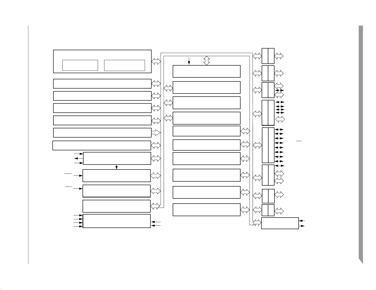
Freescale Semiconductor 23
M68HC08 CPU
CPU
REGISTERS
ARITHMETIC/LOGIC
UNIT (ALU)
V
REFH
ANALOG-TO-DIGITAL
DDRA
MODULE
DDRB
MC68HC908AZ60A • MC68HC908AS60A Data Sheet, Rev. 5
CONTROL AND STATUS REGISTERS — 62 BYTES
USER FLASH — 60 kBYTES
BREAK MODULE
DDRC
LOW-VOLTAGE INHIBIT
USER RAM — 2048BYTES
COMPUTER OPERATING
USER EEPROM — 1024 BYTES
MONITOR ROM — 256 BYTES
MODULE
DDRD
PROPERLY MODULE
TIMER A 6 CHANNEL
INTERFACE MODULE
PTA7–PTA0
PTA
PTB7/ATD7–PTB0/ATD0
PTB
PTC5–PTC3
PTC2/MCLK
PTC
PTC1–PTC0
PTD7
PTD6/ATD14/TACLK
PTD5/ATD13
PTD
PTD4/ATD12/TBCLK
PTD3/ATD11-PTD0/ATD8
PTE7/SPSCK
PTE6/MOSI
PTE5/MISO
USER FLASH VECTOR SPACE — 52 BYTES
OSC1
OSC2
CGMXFC
RST
IRQ
CLOCK GENERATOR
MODULE
SYSTEM INTEGRATION
MODULE
IRQ MODULE
POWER-ON RESET
MODULE
V
SS
V
V
V
DD
DDA
SSA
POWER
AVSS/V
V
DDAREF
TIMER B INTERFACE
MODULE
SERIAL COMMUNICATIONS
INTERFACE MODULE
SERIAL PERIPHERAL
INTERFACE MODULE
KEYBOARD INTERRUPT
MODULE
PROGRAMMABLE INTERRUPT
TIMER MODULE
REFL
DDRE
DDRF
DDRG
DDRH
MSCAN MODULE
PTE4/SS
PTE
PTE3/TACH1
PTE2/TACH0
PTE1/RxD
PTE0/TxD
PTF6
PTF5/TBCH1–PTF4/TBCH0
PTF
PTF3/TACH5-PTF0/TACH2
PTG2/KBD2–PTG0/KBD0
PTG
PTH1/KBD4–PTH0/KBD3
PTH
CANRx
CANTx
MCU Block Diagram
Figure 1-1. MCU Block Diagram for the MC68HC908AZ60A (64-Pin QFP)
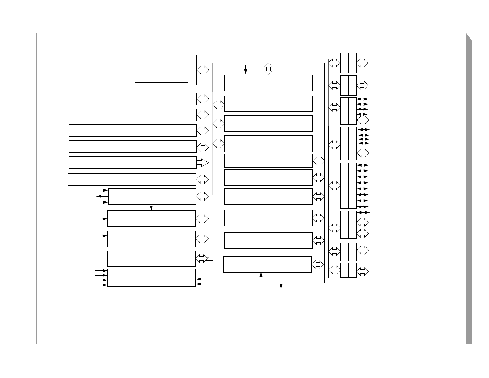
24 Freescale Semiconductor
General Description
M68HC08 CPU
CPU
REGISTERS
ARITHMETIC/LOGIC
UNIT (ALU)
V
REFH
ANALOG-TO-DIGITAL
DDRA
MODULE
DDRB
CONTROL AND STATUS REGISTERS — 62 BYTES
MC68HC908AZ60A • MC68HC908AS60A Data Sheet, Rev. 5
USER FLASH — 60 kBYTES
USER RAM — 2048BYTES
BREAK MODULE
LOW-VOLTAGE INHIBIT
MODULE
DDRC
COMPUTER OPERATING
USER EEPROM — 1024 BYTES
PROPERLY MODULE
DDRD
PTA7–PTA0
PTA
PTB7/ATD7–PTB0/ATD0
PTB
PTC5*
PTC4
PTC3
PTC2/MCLK
PTC
PTC1–PTC0
PTD7*
PTD6/ATD14/TACLK
PTD5/ATD13
PTD4/ATD12/TBCLK
PTD
PTD3/ATD11-PTD0/ATD8
MONITOR ROM — 256 BYTES
USER FLASH VECTOR SPACE — 52 BYTES
OSC1
OSC2
CGMXFC
RST
IRQ
CLOCK GENERATOR
MODULE
SYSTEM INTEGRATION
MODULE
IRQ MODULE
TIMER A 6 CHANNEL
INTERFACE MODULE
PROGRAMMABLE INTERRUPT
TIMER MODULE
SERIAL COMMUNICATIONS
INTERFACE MODULE
SERIAL PERIPHERAL
INTERFACE MODULE
KEYBOARD INTERRUPT
MODULE*
DDRE
DDRF
PTE7/SPSCK
PTE6/MOSI
PTE5/MISO
PTE4/SS
PTE
PTE3/TACH1
PTE2/TACH0
PTE1/RxD
PTE0/TxD
PTF6*
PTF5/TBCH1–PTF4/TBCH0*
PTF
PTF3/TACH5-PTF0/TACH2
PTG2/KBD2–PTG0/KBD0*
V
V
V
V
DDA
SSA
DD
SS
POWER-ON RESET
MODULE
POWER
AVSS/V
V
DDAREF
BYTE DATA LINK CONTROLLER
REFL
BDRxD
BDTxD
DDRG
PTH*
DDRH
PTG*
PTH1/KBD4–PTH0/KBD3*
* = Feature only available on the 64-pin QFP MC68HC908AS60A
Figure 1-2. MCU Block Diagram for the MC68HC908AS60A (64-Pin QFP and 52-Pin PLCC)
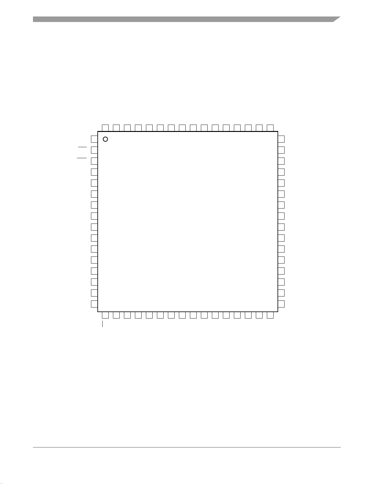
1.4 Pin Assignments
Figure 1-3 shows the MC68HC908AZ60A pin assignments.
SSAVDDA
CGMXFC
PTC5
PTC3
PTC2/MCLK
PTC1
PTC0
OSC1
OSC2
V
Pin Assignments
REFH
V
PTD7
PTD6/ATD14/TACLK
PTD5/ATD13
PTD4/ATD12/TBCLK
PTH1/KBD4
PTC4
IRQ
RST
PTF0/TACH2
PTF1/TACH3
PTF2/TACH4
PTF3/TACH5
PTF4/TBCH0
CANRx
CANTx
PTF5/TBCH1
PTF6
PTE0/TxD
PTE1/RxD
PTE2/TACH0
PTE3/TACH1
16
1
64
2
3
4
5
6
7
8
9
10
11
12
13
14
15
17
PTE4/SS
63
62
18
19
PTE5/MISO
PTE6/MOSI
61
20
PTE7/SPSCK
49
60
59
58
57
56
55
54
53
52
51
50
47
46
45
44
43
42
41
40
39
38
37
36
35
34
21
22
23
24
25
26
27
28
29
30
31
SS
DD
V
V
PTG0/KBD0
PTG1/KBD1
PTG2/KBD2
PTA0
PTA1
PTA2
PTA3
PTA4
PTA5
48
33
32
PTA6
PTH0/KBD3
PTD3/ATD11
PTD2/ATD10
AV
SS /VREFL
V
DDAREF
PTD1/ATD9
PTD0/ATD8
PTB7/ATD7
PTB6/ATD6
PTB5/ATD5
PTB4/ATD4
PTB3/ATD3
PTB2/ATD2
PTB1/ATD1
PTB0/ATD0
PTA7
Figure 1-3. MC68HC908AZ60A (64-Pin QFP)
MC68HC908AZ60A • MC68HC908AS60A Data Sheet, Rev. 5
Freescale Semiconductor 25

General Description
Figure 1-4 shows the MC68HC908AS60A 64-pin QFP pin assignments.
PTC4
IRQ
RST
PTF0/TACH2
PTF1/TACH3
PTF2/TACH4
PTF3/TACH5
PTF4
BDRxD
BDTxD
PTF5
PTF6
PTE0/TxD
PTE1/RxD
PTE2/TACH0
PTE3/TACH1
16
1
PTC5
64
2
3
4
5
6
7
8
9
10
11
12
13
14
15
17
PTE4/SS
PTC3
PTC2/MCLK
63
62
18
19
PTE5/MISO
PTE6/MOSI
PTC1
PTC0
OSC1
61
60
59
20
21
22
SS
DD
V
V
PTE7/SPSCK
CGMXFC
OSC2
58
57
23
24
PTG0/KBD0
PTG1/KBD1
SSAVDDA
V
56
25
PTG2/KBD2
55
26
PTA0
REFH
V
54
27
PTA1
PTD7
53
28
PTA2
PTD6/ATD14/TACLK
52
29
PTA3
PTD5/ATD13
51
30
PTA4
PTD4/ATD12
PTH1/KBD4
49
50
47
46
45
44
43
42
41
40
39
38
37
36
35
34
31
32
PTA5
PTA6
PTH0/KBD3
48
PTD3/ATD11
PTD2/ATD10
AV
V
DDAREF
PTD1/ATD9
PTD0/ATD8
PTB7/ATD7
PTB6/ATD6
PTB5/ATD5
PTB4/ATD4
PTB3/ATD3
PTB2/ATD2
PTB1/ATD1
PTB0/ATD0
PTA7
33
SS /VREFL
Figure 1-4. MC68HC908AS60A (64-Pin QFP)
MC68HC908AZ60A • MC68HC908AS60A Data Sheet, Rev. 5
26 Freescale Semiconductor
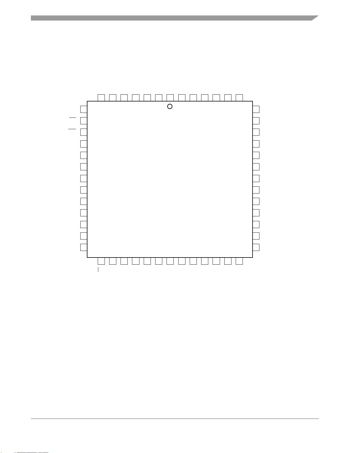
Figure 1-5 shows MC68HC908AS60A 52-pin PLCC pin assignments.
DDAREF
REFL
/V
/V
SSA
DDA
REFH
V
V
PTD6/ATD14/TACLK
51
50
49
PTC4
CGMXFC
PTC3
PTC2/MCLK
PTC1
PTC0
OSC1
OSC2
V
1
7
6
5
4
3
2
8
52
PTD5/ATD13
PTD4/ATD12
47
48
46
Pin Assignments
PTD3/ATD11
IRQ
RST
PTF0/TACH2
PTF1/TACH3
PTF2/TACH4
PTF3/TACH5
BDRxD
BDTxD
PTE0/TxD
PTE1/RxD
PTE2/TACH0
PTE3/TACH1
34
PTD2/ATD10
PTD1/ATD9
PTD0/ATD8
PTB7/ATD7
PTB6/ATD6
PTB5/ATD5
PTB4/ATD4
PTB3/ATD3
PTB2/ATD2
PTB1/ATD1
PTB0/ATD0
PTA7
9
10
11
12
13
14
15
16
17
18
19
45
44
43
42
41
40
39
38
37
36
35
20
21
22
23
24
25
26
27
28
29
30
31
32
33
SS
DD
V
V
PTA0
PTA1
PTA2
PTA3
PTA4
PTA5
PTA6
PTE4/SS
PTE5/MISO
PTE6/MOSI
PTE7/SPSCK
Figure 1-5. MC68HC908AS60A (52-Pin PLCC)
MC68HC908AZ60A • MC68HC908AS60A Data Sheet, Rev. 5
Freescale Semiconductor 27
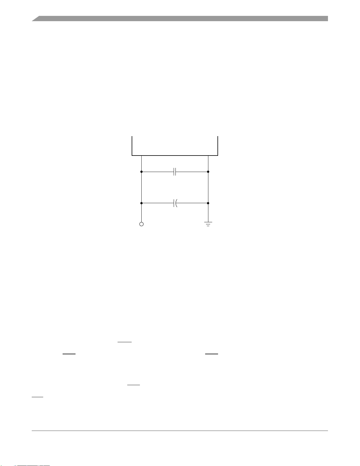
General Description
NOTE
The following pin descriptions are just a quick reference. For a more
detailed representation, see Chapter 22 Input/Output Ports.
1.4.1 Power Supply Pins (VDD and VSS)
VDD and VSS are the power supply and ground pins. The MCU operates from a single power supply.
Fast signal transitions on MCU pins place high, short-duration current demands on the power supply. To
prevent noise problems, take special care to provide power supply bypassing at the MCU as shown in
Figure 1-6. Place the C1 bypass capacitor as close to the MCU as possible. Use a high-frequency
response ceramic capacitor for C1. C2 is an optional bulk current bypass capacitor for use in applications
that require the port pins to source high current levels.
MCU
V
DD
C1
0.1 µF
+
C2
V
DD
NOTE: Component values shown represent typical applications.
V
SS
Figure 1-6. Power Supply Bypassing
is also the ground for the port output buffers and the ground return for the serial clock in the Serial
V
SS
Peripheral Interface module (SPI). See Chapter 19 Serial Peripheral Interface (SPI).
NOTE
V
must be grounded for proper MCU operation.
SS
1.4.2 Oscillator Pins (OSC1 and OSC2)
The OSC1 and OSC2 pins are the connections for the on-chip oscillator circuit. See Chapter 10 Clock
Generator Module (CGM).
1.4.3 External Reset Pin (RST)
A 0 on the RST pin forces the MCU to a known startup state. RST is bidirectional, allowing a reset of the
entire system. It is driven low when any internal reset source is asserted. See Chapter 9 System
Integration Module (SIM) for more information.
1.4.4 External Interrupt Pin (IRQ)
IRQ is an asynchronous external interrupt pin. See Chapter 17 External Interrupt Module (IRQ).
MC68HC908AZ60A • MC68HC908AS60A Data Sheet, Rev. 5
28 Freescale Semiconductor

Pin Assignments
1.4.5 Analog Power Supply Pin (V
V
is the power supply pin for the analog portion of the Clock Generator Module (CGM). See
DDA
DDA
)
Chapter 10 Clock Generator Module (CGM).
1.4.6 Analog Ground Pin (V
V
is the ground connection for the analog portion of the Clock Generator Module (CGM). See
SSA
SSA
)
Chapter 10 Clock Generator Module (CGM).
1.4.7 External Filter Capacitor Pin (CGMXFC)
CGMXFC is an external filter capacitor connection for the Clock Generator Module (CGM). See
Chapter 10 Clock Generator Module (CGM).
1.4.8 ADC Analog Power Supply Pin (V
V
DDAREF
is the power supply pin for the analog portion of the Analog-to-Digital Converter (ADC). See
DDAREF
Chapter 26 Analog-to-Digital Converter (ADC).
1.4.9 ADC Analog Ground Pin (AVSS/V
The AVSS/V
pin provides both the analog ground connection and the reference low voltage for the
REFL
REFL
Analog-to-Digital Converter (ADC). See Chapter 26 Analog-to-Digital Converter (ADC).
)
)
1.4.10 ADC Reference High Voltage Pin (V
V
provides the reference high voltage for the Analog-to-Digital Converter (ADC). See Chapter 26
REFH
REFH
)
Analog-to-Digital Converter (ADC).
1.4.11 Port A Input/Output (I/O) Pins (PTA7–PTA0)
PTA7–PTA0 are general-purpose bidirectional I/O port pins. See Chapter 22 Input/Output Ports.
1.4.12 Port B I/O Pins (PTB7/ATD7–PTB0/ATD0)
Port B is an 8-bit special function port that shares all eight pins with the Analog-to-Digital Converter (ADC).
See Chapter 26 Analog-to-Digital Converter (ADC) and Chapter 22 Input/Output Ports.
1.4.13 Port C I/O Pins (PTC5–PTC0)
PTC5–PTC3 and PTC1–PTC0 are general-purpose bidirectional I/O port pins. PTC2/MCLK is a special
function port that shares its pin with the system clock which has a frequency equivalent to the system
clock. See Chapter 22 Input/Output Ports.
1.4.14 Port D I/O Pins (PTD7–PTD0/ATD8)
Port D is an 8-bit special-function port that shares seven of its pins with the Analog-to-Digital Converter
module (ADC-15), one of its pins with the Timer Interface Module A (TIMA), and one more of its pins with
the Timer Interface Module B (TIMB). See Chapter 25 Timer Interface Module A (TIMA), Chapter 20 Timer
Interface Module B (TIMB), Chapter 26 Analog-to-Digital Converter (ADC) and Chapter 22 Input/Output
Ports.
MC68HC908AZ60A • MC68HC908AS60A Data Sheet, Rev. 5
Freescale Semiconductor 29

General Description
1.4.15 Port E I/O Pins (PTE7/SPSCK–PTE0/TxD)
Port E is an 8-bit special function port that shares two of its pins with the Timer Interface Module A (TIMA),
four of its pins with the Serial Peripheral Interface module (SPI), and two of its pins with the Serial
Communication Interface module (SCI). See Chapter 18 Serial Communications Interface (SCI), Chapter
19 Serial Peripheral Interface (SPI), Chapter 25 Timer Interface Module A (TIMA), and Chapter 22
Input/Output Ports.
1.4.16 Port F I/O Pins (PTF6–PTF0/TACH2)
Port F is a 7-bit special function port that shares its pins with the Timer Interface Module B (TIMB). Six of
its pins are shared with the Timer Interface Module A (TIMA-6). See Chapter 25 Timer Interface Module
A (TIMA), Chapter 20 Timer Interface Module B (TIMB), and Chapter 22 Input/Output Ports.
1.4.17 Port G I/O Pins (PTG2/KBD2–PTG0/KBD0)
Port G is a 3-bit special function port that shares all of its pins with the Keyboard Module (KBD). See
Chapter 24 Keyboard Module (KBI) and Chapter 22 Input/Output Ports.
1.4.18 Port H I/O Pins (PTH1/KBD4–PTH0/KBD3)
Port H is a 2-bit special-function port that shares all of its pins with the Keyboard Module (KBD). See
Chapter 24 Keyboard Module (KBI) and Chapter 22 Input/Output Ports.
1.4.19 CAN Transmit Pin (CANTx)
This pin is the digital output from the CAN module (CANTx). See Chapter 23 MSCAN Controller
(MSCAN08).
1.4.20 CAN Receive Pin (CANRx)
This pin is the digital input to the CAN module (CANRx). See Chapter 23 MSCAN Controller (MSCAN08).
1.4.21 BDLC Transmit Pin (BDTxD)
This pin is the digital output from the BDLC module (BDTxD). See Chapter 27 Byte Data Link Controller
(BDLC).
1.4.22 BDLC Receive Pin (BDRxD)
This pin is the digital input to the CAN module (BDRxD). See Chapter 27 Byte Data Link Controller
(BDLC).
MC68HC908AZ60A • MC68HC908AS60A Data Sheet, Rev. 5
30 Freescale Semiconductor

Table 1-1. External Pins Summary
Pin Assignments
Pin Name Function Driver Type
PTA7–PTA0 General-Purpose I/O Dual State No Input Hi-Z
PTB7/ATD7–PTB0/ATD0
PTC5–PTC0 General-Purpose I/O Dual State No Input Hi-Z
PTD7 General Purpose I/O Dual State No Input Hi-Z
PTD6/ATD14/TACLK
ADC Channel
PTD5/ATD13 ADC Channel
PTD4/ATD12/TBCLK
ADC Channel
PTD3/ATD11–PTD0/ATD8
ADC Channels
PTE7/SPSCK
PTE6/MOSI
PTE5/MISO
General-Purpose I/O
ADC Channel
General-Purpose I/O
ADC Channel/
Timer External Input Clock
General-Purpose I/O
ADC Channel
General-Purpose I/O
ADC Channel/
Timer External Input Clock
General-Purpose I/O
ADC Channel
General-Purpose I/O
SPI Clock
General-Purpose I/O
SPI Data Path
General-Purpose I/O
SPI Data Path
Dual State No Input Hi-Z
Dual State No Input Hi-Z
Dual State No Input Hi-Z
Dual State No Input Hi-Z
Dual State No Input Hi-Z
Dual State
Open Drain
Dual State
Open Drain
Dual State
Open Drain
Hysteresis
(1)
Reset State
Yes Input Hi-Z
Yes Input Hi-Z
Yes Input Hi-Z
PTE4/SS
PTE3/TACH1
PTE2/TACH0
PTE1/RxD
PTE0/TxD
PTF6 General-Purpose I/O Dual State No Input Hi-Z
PTF5/TBCH1–PTF4/TBCH0
PTF3/TACH5
PTF2/TACH4
PTF1/TACH3
General-Purpose I/O
SPI Slave Select
General-Purpose I/O
Timer A Channel 1
General-Purpose I/O
Timer A Channel 0
General-Purpose I/O
SCI Receive Data
General-Purpose I/O
SCI Transmit Data
General-Purpose I/O/
Timer B Channel
General-Purpose I/O
Timer A Channel 5
General-Purpose I/O
Timer A Channel 4
General-Purpose I/O
Timer A Channel 3
Dual State Yes Input Hi-Z
Dual State Yes Input Hi-Z
Dual State Yes Input Hi-Z
Dual State Yes Input Hi-Z
Dual State No Input Hi-Z
Dual State Yes Input Hi-Z
Dual State Yes Input Hi-Z
Dual State Yes Input Hi-Z
Dual State Yes Input Hi-Z
— Continued on next page
MC68HC908AZ60A • MC68HC908AS60A Data Sheet, Rev. 5
Freescale Semiconductor 31
General Description
Table 1-1. External Pins Summary (Continued)
Pin Name Function Driver Type
PTF0/TACH2
PTG2/KBD2–PTG0/KBD0
PTH1/KBD4 –PTH0/KBD3
V
DD
V
SS
V
DDA
V
SSA
V
DDAREF
A
VSS/VREFL
V
REFH
Hysteresis
General-Purpose I/O
Timer A Channel 2
General-Purpose I/O/
Keyboard Wakeup Pin
General-Purpose I/O/
Keyboard Wakeup Pin
Dual State Yes Input Hi-Z
Dual State Yes Input Hi-Z
Dual State Yes Input Hi-Z
Chip Power Supply N/A N/A N/A
Chip Ground N/A N/A N/A
CGM Analog Power Supply
CGM Analog Ground
ADC Power Supply N/A N/A N/A
ADC Ground/
ADC Reference Low Voltage
N/A N/A N/A
A/D Reference High Voltage N/A N/A N/A
(1)
Reset State
OSC1 External Clock In N/A No Input Hi-Z
OSC2 External Clock Out N/A N/A Output
CGMXFC PLL Loop Filter Cap N/A N/A N/A
IRQ
RST
External Interrupt Request N/A N/A Input Hi-Z
Reset N/A N/A Output Low
CANRx CAN Serial Input N/A Yes Input Hi-Z
CANTx CAN Serial Output Output No Output
BDRxD BDLC Serial Input N/A Yes Input Hi-Z
BDTxD BDLC Serial Output Output No Output
1. Hysteresis is not 100% tested but is typically a minimum of 300 mV.
MC68HC908AZ60A • MC68HC908AS60A Data Sheet, Rev. 5
32 Freescale Semiconductor

Table 1-2. Clock Signal Naming Conventions
Clock Signal Name Description
Pin Assignments
CGMXCLK
CGMOUT
Bus Clock CGMOUT divided by two
SPSCK SPI serial clock
TACLK External clock input for TIMA
TBCLK External clock input for TIMB
Buffered version of OSC1 from
Clock Generation Module (CGM)
PLL-based or OSC1-based clock output from
Clock Generator Module (CGM)
Table 1-3. Clock Source Summary
Module Clock Source
ADC CGMXCLK or Bus Clock
CAN CGMXCLK or CGMOUT
COP CGMXCLK
CPU Bus Clock
FLASH Bus Clock
EEPROM CGMXCLK or Bus Clock
RAM Bus Clock
SPI Bus Clock/SPSCK
SCI CGMXCLK
TIMA Bus Clock or PTD6/ATD14/TACLK
TIMB Bus Clock or PTD4/TBCLK
PIT Bus Clock
SIM CGMOUT and CGMXCLK
IRQ Bus Clock
BRK Bus Clock
LVI Bus Clock and CGMXCLK
CGM OSC1 and OSC2
MC68HC908AZ60A • MC68HC908AS60A Data Sheet, Rev. 5
Freescale Semiconductor 33
General Description
1.5 Ordering Information
This subsection contains instructions for ordering the MC68HC908AZ60A / MC68HC908AS60A.
Table 1-4. MC Order Numbers
MC Order Number
MC68HC908AS60ACFU (64-Pin QFP) –40°C to + 85°C
MC68HC908AS60AVFU (64-Pin QFP) –40°C to + 105°C
MC68HC908AS60AMFU (64-Pin QFP) –40°C to + 125°C
MC68HC908AS60ACFN (52-Pin PLCC) –40°C to + 85°C
MC68HC908AS60AVFN (52-Pin PLCC) –40°C to + 105°C
MC68HC908AS60AMFN (52-Pin PLCC) –40°C to + 125°C
MC68HC908AZ60ACFU (64-Pin QFP) –40°C to + 85°C
MC68HC908AZ60AVFU (64-Pin QFP) –40°C to + 105°C
MC68HC908AZ60AMFU (64-Pin QFP) –40°C to + 125°C
Operating
Temperature Range
MC68HC908AZ60A • MC68HC908AS60A Data Sheet, Rev. 5
34 Freescale Semiconductor

Chapter 2 Memory Map
2.1 Introduction
The CPU08 can address 64K bytes of memory space. The memory map, shown in Figure 2-1, includes:
• 60K Bytes of FLASH EEPROM
• 2048 Bytes of RAM
• 1024 Bytes of EEPROM with Protect Option
• 52 Bytes of User-Defined Vectors
• 256 Bytes of Monitor ROM
The following definitions apply to the memory map representation of reserved and unimplemented
locations.
• Reserved — Accessing a reserved location can have unpredictable effects on MCU operation.
• Unused — These locations are reserved in the memory map for future use, accessing an unused
location can have unpredictable effects on MCU operation.
• Unimplemented — Accessing an unimplemented location can cause an illegal address reset
(within the constraints as outlined in the Chapter 9 System Integration Module (SIM)).
MC68HC908AZ60A • MC68HC908AS60A Data Sheet, Rev. 5
Freescale Semiconductor 35

Memory Map
MC68HC908AZ60A MC68HC908AS60A
$0000
↓ ↓
$003F $003F
$0040
↓
$004F $004F
$0050
↓ ↓
$044F $044F
$0450
↓
$04FF
$0500
↓
$057F
$0580
↓
$05FF $05FF
$0600
↓ ↓
$07FF $07FF
$0800
↓ ↓
$09FF $09FF
$0A00
↓ ↓
$0DFF $0DFF
$0E00
↓ ↓
$7FFF $7FFF
$8000
↓ ↓
$FDFF $FDFF
$FE00 SIM BREAK STATUS REGISTER (SBSR) $FE00
$FE01 SIM RESET STATUS REGISTER (SRSR) $FE01
$FE02
CAN CONTROL AND MESSAGE BUFFERS
I/O REGISTERS
16 BYTES
FLASH-2
176 BYTES
128 BYTES
FLASH-2
128 BYTES
I/O REGISTERS
64 BYTES
UNIMPLEMENTED
11 BYTES
I/O REGISTERS
5 BYTES
RAM-1
1024 BYTES
FLASH-2
432 BYTES
EEPROM-2
512 BYTES
EEPROM-1
512 BYTES
RAM-2
1024 BYTES
FLASH-2
29,184 BYTES
FLASH-1
32,256BYTES
RESERVED $FE02
$0000
$0040
↓
$004A
$004B
$0050
$0450
↓
$0600
$0800
$0A00
$0E00
$8000
Figure 2-1. Memory Map (Sheet 1 of 3)
MC68HC908AZ60A • MC68HC908AS60A Data Sheet, Rev. 5
36 Freescale Semiconductor

Introduction
MC68HC908AZ60A MC68HC908AS60A
$FE03 SIM BREAK FLAG CONTROL REGISTER (SBFCR) $FE03
$FE04
$FE05
$FE06
$FE07
$FE08 FLASH-2 CONTROL REGISTER (FL2CR) $FE08
$FE09 CONFIGURATION WRITE-ONCE REGISER (CONFIG-2) $FE09
$FE0A
$FE0B
$FE0C BREAK ADDRESS REGISTER HIGH (BRKH) $FE0C
$FE0D BREAK ADDRESS REGISTER LOW (BRKL) $FE0D
$FE0E BREAK STATUS AND CONTROL REGISTER (BSCR) $FE0E
$FE0F LVI STATUS REGISTER (LVISR) $FE0F
$FE10 EEPROM-1EEDIVH NONVOLATILE REGISTER(EE1DIVHNVR) $FE10
$FE11 EEPROM-1EEDIVL NONVOLATILE REGISTER(EE1DIVLNVR) $FE11
$FE12
$FE13
$FE14
$FE15
$FE16
$FE17
$FE18
$FE19
$FE1A EEPROM-1 EE DIVIDER HIGH REGISTER(EE1DIVH) $FE1A
$FE1B EEPROM-1 EE DIVIDER LOW REGISTER(EE1DIVL) $FE1B
$FE1C EEPROM-1 EEPROM NONVOLATILE REGISTER (EE1NVR) $FE1C
$FE1D EEPROM-1 EEPROM CONTROL REGISTER (EE1CR) $FE1D
$FE1E
$FE1F EEPROM-1 EEPROM ARRAY CONFIGURATION REGISTER (EE1ACR) $FE1F
$FE20
↓ ↓
$FF1F $FF1F
$FF20
↓
$FF6F
$FF70 EEPROM-2 EEDIVH NONVOLATILE REGISTER (EE2DIVHNVR) $FF70
$FF71 EEPROM-2 EEDIVL NONVOLATILE REGISTER (EE2DIVLNVR) $FF71
$FF72
$FF73
$FF74
RESERVED $FE04
RESERVED $FE05
RESERVED $FE06
RESERVED $FE07
RESERVED $FE0A
RESERVED $FE0B
RESERVED $FE12
RESERVED $FE13
RESERVED $FE14
RESERVED $FE15
RESERVED $FE16
RESERVED $FE17
RESERVED $FE18
RESERVED $FE19
RESERVED $FE1E
MONITOR ROM
256BYTES
UNIMPLEMENTED
80 BYTES
RESERVED $FF72
RESERVED $FF73
RESERVED $FF74
$FE20
$FF20
↓
$FF6F
Figure 2-1. Memory Map (Sheet 2 of 3)
MC68HC908AZ60A • MC68HC908AS60A Data Sheet, Rev. 5
Freescale Semiconductor 37

Memory Map
MC68HC908AZ60A MC68HC908AS60A
$FF75
$FF76
$FF77
$FF78
$FF79
$FF7A EEPROM-2 EE DIVIDER HIGH REGISTER (EE2DIVH) $FF7A
$FF7B EEPROM-2 EE DIVIDER LOW REGISTER (EE2DIVL) $FF7B
$FF7C EEPROM-2 EEPROM NONVOLATILE REGISTER (EE2NVR) $FF7C
$FF7D EEPROM-2 EEPROM CONTROL REGISTER (EE2CR) $FF7D
$FF7E
$FF7F EEPROM-2 EEPROM ARRAY CONFIGURATION REGISTER (EE2ACR) $FF7F
$FF80 FLASH-1 BLOCK PROTECT REGISTER (FL1BPR) $FF80
$FF81 FLASH-2 BLOCK PROTECT REGISTER (FL2BPR) $FF81
$FF82
↓ ↓
$FF87 $FF87
$FF88 FLASH-1 CONTROL REGISTER (FL1CR) $FF88
$FF89
$FF8A
$FF8B
↓ ↓
$FFCB $FFCB
$FFCC $FFCC
↓
$FFFF $FFFF
1. Registers appearing in italics are for Freescale test purpose only and only appear in the Memory Map for reference.
2. While some differences between MC68HC908AS60A and MC68HC908AZ60A are highlighted, some registers remain available on both parts. Refer to individual modules for details whether these registers are active or inactive.
RESERVED $FF75
RESERVED $FF76
RESERVED $FF77
RESERVED $FF78
RESERVED $FF79
RESERVED $FF7E
RESERVED
6 BYTES
RESERVED $FF89
RESERVED $FF8A
RESERVED
65 BYTES
VECTORS
52 BYTES
See Table 2-1
$FF82
$FF8B
↓
Figure 2-1. Memory Map (Sheet 3 of 3)
MC68HC908AZ60A • MC68HC908AS60A Data Sheet, Rev. 5
38 Freescale Semiconductor
I/O Section
2.2 I/O Section
Addresses $0000–$004F, shown in Figure 2-2, contain the I/O Data, Status, and Control Registers.
Addr.Register Name Bit 7654321Bit 0
$0000
$0001
$0002
$0003
$0004
$0005
$0006
$0007
$0008
$0009
$000A
$000B
$000C
$000D
$000E
$000F
Port A Data Register
Port B Data Register
(PTB)
Port C Data Register
(PTC)
Port D Data Register
(PTD)
Data Direction Register A
(DDRA)
Data Direction Register B
(DDRB)
Data Direction Register C
(DDRC)
Data Direction Register D
(DDRD)
Port E Data Register
(PTE)
Port F Data Register
(PTF)
Port G Data Register
(PTG)
Port H Data Register
(PTH)
Data Direction Register E
(DDRE)
Data Direction Register F
(DDRF)
Data Direction Register G
(DDRG)
Data Direction Register H
(DDRH)
Read:
(PTA)
Write:
Read:
Write:
Read: 0 0
Write: R R
Read:
Write:
Read:
Write:
Read:
Write:
Read:
Write: R
Read:
Write:
Read:
Write:
Read: 0
Write: R
Read:00000
Write:RRRRR
Read:000000
Write:RRRRRR
Read:
Write:
Read: 0
Write: R
Read:00000
Write:RRRRR
Read:000000
Write:RRRRRR
PTA7 PTA6 PTA5 PTA4 PTA3 PTA2 PTA1 PTA0
PTB7 PTB6 PTB5 PTB4 PTB3 PTB2 PTB1 PTB0
PTC5 PTC4 PTC3 PTC2 PTC1 PTC0
PTD7 PTD6 PTD5 PTD4 PTD3 PTD2 PTD1 PTD0
DDRA7 DDRA6 DDRA5 DDRA4 DDRA3 DDRA2 DDRA1 DDRA0
DDRB7 DDRB6 DDRB5 DDRB4 DDRB3 DDRB2 DDRB1 DDRB0
MCLKEN
DDRD7 DDRD6 DDRD5 DDRD4 DDRD3 DDR2 DDRD1 DDRD0
PTE7 PTE6 PTE5 PTE4 PTE3 PTE2 PTE1 PTE0
DDRE7 DDRE6 DDRE5 DDRE4 DDRE3 DDRE2 DDRE1 DDRE0
0
DDRC5 DDRC4 DDRC3 DDRC2 DDRC1 DDRC0
PTF6 PTF5 PTF4 PTF3 PTF2 PTF1 PTF0
DDRF6 DDRF5 DDRF4 DDRF3 DDRF2 DDRF1 DDRF0
PTG2 PTG1 PTG0
PTH1 PTH0
DDRG2 DDRG1 DDRG0
DDRH1 DDRH0
= Unimplemented R = Reserved
Figure 2-2. I/O Data, Status and Control Registers (Sheet 1 of 5)
MC68HC908AZ60A • MC68HC908AS60A Data Sheet, Rev. 5
Freescale Semiconductor 39
Memory Map
Addr.Register Name Bit 7654321Bit 0
$0010
$0011
$0012
$0013
$0014
$0015
$0016
$0017
$0018
$0019
$001A
$001B
$001C
$001D
$001E
$001F
$0020
SPI Control Register
(SPCR)
SPI Status and Control
Register (SPSCR)
SPI Data Register
(SPDR)
SCI Control Register 1
(SCC1)
SCI Control Register 2
(SCC2)
SCI Control Register 3
(SCC3)
SCI Status Register 1
(SCS1)
SCI Status Register 2
(SCS2)
SCI Data Register
(SCDR)
SCI Baud Rate Register
(SCBR)
IRQ Status and Control
Register (ISCR)
Keyboard Status and Control
Register (KBSCR)
PLL Control Register
(PCTL)
PLL Bandwidth Control
Register (PBWC)
PLL Programming Register
(PPG)
Configuration Write-Once
Register (CONFIG-1)
Timer A Status and Control
Register (TASC)
Read:
Write:
Read: SPRF
Write:
Read:R7R6R5R4R3R2R1R0
Write: T7 T6 T5 T4 T3 T2 T1 T0
Read:
Write:
Read:
Write:
Read: R8
Write:
Read: SCTE TC SCRF IDLE OR NF FE PE
Write:
Read: 0 0 0 0 0 0 BKF RPF
Write:
Read:R7R6R5R4R3R2R1R0
Write: T7 T6 T5 T4 T3 T2 T1 T0
Read: 0 0
Write:
Read: 0 0 0 0 IRQF 0
Write:RRRRRACK
Read: 0 0 0 0 KEYF 0
Write:
Read:
Write:
Read:
Write:
Read:
Write:
Read:
Write:
Read: TOF
Write: 0 TRST R
SPRIE R SPMSTR CPOL CPHA SPWOM SPE SPTIE
ERRIE
LOOPS ENSCI TXINV M WAKE ILTY PEN PTY
SCTIE TCIE SCRIE ILIE TE RE RWU SBK
T8 R R ORIE NEIE FEIE PEIE
PLLIE
AUTO
MUL7 MUL6 MUL5 MUL4 VRS7 VRS6 VRS5 VRS4
LVISTOP R LVIRST LVIPWR SSREC COPL STOP COPD
PLLF
LOCK
TOIE TSTOP
OVRF MODF SPTE
SCP1 SCP0 R SCR2 SCR1 SCR0
PLLON BCS
ACQ XLD
00
MODFEN SPR1 SPR0
IMASK MODE
ACKK
1111
0000
PS2 PS1 PS0
IMASKK MODEK
= Unimplemented R = Reserved
Figure 2-2. I/O Data, Status and Control Registers (Sheet 2 of 5)
MC68HC908AZ60A • MC68HC908AS60A Data Sheet, Rev. 5
40 Freescale Semiconductor
I/O Section
Addr.Register Name Bit 7654321Bit 0
$0021
$0022
$0023
$0024
$0025
$0026
$0027
$0028
$0029
$002A
$002B
$002C
$002D
$002E
$002F
$0030
$0031
Keyboard Interrupt Enable
Register (KBIER)
Timer A Counter Register
High (TACNTH)
Timer A Counter Register
Low (TACNTL)
Timer A Modulo Register
High (TAMODH)
Timer A Modulo Register
Low (TAMODL)
Timer A Channel 0 Status
and Control Register (TASC0)
Timer A Channel 0 Register
High (TACH0H)
Timer A Channel 0 Register
Low (TACH0L)
Timer A Channel 1 Status
and Control Register (TASC1)
Timer A Channel 1 Register
High (TACH1H)
Timer A Channel 1 Register
Low (TACH1L)
Timer A Channel 2 Status
and Control Register (TASC2)
Timer A Channel 2 Register
High (TACH2H)
Timer A Channel 2 Register
Low (TACH2L)
Timer A Channel 3 Status
and Control Register (TASC3)
Timer A Channel 3 Register
High (TACH3H)
Timer A Channel 3 Register
Low (TACH3L)
Read:000
Write:
Read: Bit 15 14 13 12 11 10 9 Bit 8
Write:
Read:Bit 7654321Bit 0
Write:
Read:
Write:
Read:
Write:
Read: CH0F
Write: 0
Read:
Write:
Read:
Write:
Read: CH1F
Write: 0 R
Read:
Write:
Read:
Write:
Read: CH2F
Write: 0
Read:
Write:
Read:
Write:
Read: CH3F
Write: 0 R
Read:
Write:
Read:
Write:
Bit 15 14 13 12 11 10 9 Bit 8
Bit 7 6 5 4 3 2 1 Bit 0
CH0IE MS0B MS0A ELS0B ELS0A TOV0 CH0MAX
Bit 15 14 13 12 11 10 9 Bit 8
Bit 7 6 5 4 3 2 1 Bit 0
0
CH1IE
Bit 15 14 13 12 11 10 9 Bit 8
Bit 7 6 5 4 3 2 1 Bit 0
CH2IE MS2B MS2A ELS2B ELS2A TOV2 CH2MAX
Bit 15 14 13 12 11 10 9 Bit 8
Bit 7 6 5 4 3 2 1 Bit 0
0
CH3IE
Bit 15 14 13 12 11 10 9 Bit 8
Bit 7 6 5 4 3 2 1 Bit 0
KBIE4 KBIE3 KBIE2 KBIE1 KBIE0
MS1A ELS1B ELS1A TOV1 CH1MAX
MS3A ELS3B ELS3A TOV3 CH3MAX
= Unimplemented R = Reserved
Figure 2-2. I/O Data, Status and Control Registers (Sheet 3 of 5)
MC68HC908AZ60A • MC68HC908AS60A Data Sheet, Rev. 5
Freescale Semiconductor 41

Memory Map
Addr.Register Name Bit 7654321Bit 0
$0032
$0033
$0034
$0035
$0036
$0037
$0038
$0039
$003A
$003B
$003C
$003D
$003E
$003F
$0040
$0041
$0042
Timer A Channel 4 Status
and Control Register (TASC4)
Timer A Channel 4 Register
High (TACH4H)
Timer A Channel 4 Register
Low (TACH4L)
Timer A Channel 5 Status
and Control Register (TASC5)
Timer A Channel 5 Register
High (TACH5H)
Timer A Channel 5 Register
Low (TACH5L)
Analog-to-Digital Status and
Control Register (ADSCR)
Analog-to-Digital Data
Register (ADR)
Analog-to-Digital Input Clock
Register (ADICLK)
BDLC Analog and Roundtrip
Delay Register (BARD)
BDLC Control Register 1
(BCR1)
BDLC Control Register 2
(BCR2)
BDLC State Vector Register
(BSVR)
BDLC Data Register
(BDR)
Timer B Status and Control
Register (TBSCR)
Timer B Counter Register
High (TBCNTH)
Timer B Counter Register
Low (TBCNTL)
Read: CH4F
Write: 0
Read:
Write:
Read:
Write:
Read: CH5F
Write: 0 R
Read:
Write:
Read:
Write:
Read: COCO
Write: R
Read: AD7 AD6 AD5 AD4 AD3 AD2 AD1 AD0
Write:
Read:
Write:
Read:
Write: R R
Read:
Write: R R
Read:
Write:
Read:0 0 I3I2I1I0 0 0
Write:RRRRRRRR
Read:
Write:
Read: TOF
Write: 0 TRST R
Read: Bit 15 14 13 12 11 10 9 Bit 8
Write:
Read:Bit 7654321Bit 0
Write:
Bit 15 14 13 12 11 10 9 Bit 8
Bit 7 6 5 4 3 2 1 Bit 0
Bit 15 14 13 12 11 10 9 Bit 8
Bit 7 6 5 4 3 2 1 Bit 0
ADIV2 ADIV1 ADIV0 ADICLK
ATE RXPOL
IMSG CLKS R1 R0
ALOOP DLOOP RX4XE NBFS TEOD TSIFR TMIFR1 TMIFR0
BD7BD6BD5BD4BD3BD2BD1BD0
CH4IE MS4B MS4A ELS4B ELS4A TOV4 CH4MAX
CH5IE
AIEN ADCO ADCH4 ADCH3 ADCH2 ADCH1 ADCH0
TOIE TSTOP
0
00
MS5A ELS5B ELS5A TOV5 CH5MAX
00
0000
BO3 BO2 BO1 BO0
00
PS2 PS1 PS0
IE WCM
= Unimplemented R = Reserved
Figure 2-2. I/O Data, Status and Control Registers (Sheet 4 of 5)
MC68HC908AZ60A • MC68HC908AS60A Data Sheet, Rev. 5
42 Freescale Semiconductor
I/O Section
Addr.Register Name Bit 7654321Bit 0
$0043
$0044
$0045
$0046
$0047
$0048
$0049
$004A
$004B
$004C
$004D
$004E
$004F
Timer B Modulo Register
High (TBMODH)
Timer B Modulo Register
Low (TBMODL)
Timer B CH0 Status and
Control Register (TBSC0)
Timer B CH0 Register
High (TBCH0H)
Timer B CH0 Register
Low (TBCH0L)
Timer B CH1 Status and
Control Register (TBSC1)
Timer B CH1 Register High
(TBCH1H)
Timer B CH1 Register Low
(TBCH1L)
PIT Status and Control
Register (PSC)
PIT Counter Register High
(PCNTH)
PIT Counter Register Low
(PCNTL)
PIT Modulo Register High
(PMODH)
PIT Modulo Register Low
(PMODL)
Read:
Write:
Read:
Write:
Read: CH0F
Write: 0
Read:
Write:
Read:
Write:
Read: CH1F
Write: 0 R
Read:
Write:
Read:
Write:
Read: POF
Write: 0 PRST
Read: Bit 15 14 13 12 11 10 9 Bit 8
Write:
Read:Bit 7654321Bit 0
Write:
Read:
Write:
Read:
Write:
Bit 15 14 13 12 11 10 9 Bit 8
Bit 7 6 5 4 3 2 1 Bit 0
CH0IE MS0B MS0A ELS0B ELS0A TOV0 CH0MAX
Bit 15 14 13 12 11 10 9 Bit 8
Bit 7 6 5 4 3 2 1 Bit 0
CH1IE
Bit 15 14 13 12 11 10 9 Bit 8
Bit 7 6 5 4 3 2 1 Bit 0
POIE PSTOP
Bit 15 14 13 12 11 10 9 Bit 8
Bit 7 6 5 4 3 2 1 Bit 0
0
MS1A ELS1B ELS1A TOV1 CH1MAX
00
PPS2 PPS1 PPS0
= Unimplemented R = Reserved
Figure 2-2. I/O Data, Status and Control Registers (Sheet 5 of 5)
All registers are shown for both MC68HC908AS60A and MC68HC908AZ60A. Refer to individual module
chapters to determine if the module is available and the register active or not.
MC68HC908AZ60A • MC68HC908AS60A Data Sheet, Rev. 5
Freescale Semiconductor 43

Memory Map
2.3 Additional Status and Control Registers
Selected addresses in the range $FE00 to $FFCB contain additional Status and Control registers as
shown in Figure 2-3. A noted exception is the COP Control Register (COPCTL) at address $FFFF.
Addr.Register Name Bit 7654321Bit 0
$FE00
$FE01
$FE03
$FE08
$FE09
$FE0C
$FE0D
$FE0E
$FE0F
$FE10
SIM Break Status Register
(SBSR)
SIM Reset Status Register
(SRSR)
SIM Break Flag Control
Register (SBFCR)
FLASH-2 Control Register
(FL2CR)
Configuration Write-Once
Register (CONFIG-2)
Break Address Register High
(BRKH)
Break Address Register Low
(BRKL)
Break Status and Control
Register (BRKSCR)
LVI Status Register
(LVISR)
EE1DIV Hi Nonvolatile
Register (EE1DIVHNVR)
Read:
Write: 0
Read: POR PIN COP ILOP ILAD 0 LVI 0
Write:
Read:
Write:
Read:0000
Write:
Read:
Write: R
Read:
Write:
Read:
Write:
Read:
Write:
Read:LVIOUT0000000
Write:
Read:
Write:
RRRRRR
BCFERRRRRRR
HVEN VERF ERASE PGM
EEDIVCLK R R MSCAND
Bit 15 14 13 12 11 10 9 Bit 8
Bit 7654321Bit 0
BRKE BRKA
EEDIVS-
ECD
RRRREEDIV10EEDIV9EEDIV8
000000
AT 6 0A
RRAZxx
BW
R
$FE11
$FE1A
$FE1B
$FE1C
$FE1D
EE1DIV Lo Nonvolatile
Register (EE1DIVLNVR)
EE1DIV Divider High Register
(EE1DIVH)
EE1DIV Divider Low Register
(EE1DIVL)
EEPROM-1 Nonvolatile
Register (EE1NVR)
EEPROM-1 Control Register
(EE1CR)
Read:
EEDIV7 EEDIV6 EEDIV5 EEDIV4 EEDIV3 EEDIV2 EEDIV1 EEDIV0
Write:
Read:
EEDIVS-
Write:
Read:
Write:
Read:
Write:
Read:
Write:
ECD
EEDIV7 EEDIV6 EEDIV5 EEDIV4 EEDIV3 EEDIV2 EEDIV1 EEDIV0
UNUSED UNUSED UNUSED EEPRTCT EEBP3 EEBP2 EEBP1 EEBP0
UNUSED
0000
EEDIV10 EEDIV9 EEDIV8
0
EEOFF EERAS1 EERAS0 EELAT AUTO EEPGM
= Unimplemented R = Reserved
Figure 2-3. Additional Status and Control Registers (Sheet 1 of 2)
MC68HC908AZ60A • MC68HC908AS60A Data Sheet, Rev. 5
44 Freescale Semiconductor

Additional Status and Control Registers
Addr.Register Name Bit 7654321Bit 0
$FE1F
$FF70
EEPROM-1 Array Configura-
tion Register (EE1ACR)
EE2DIV Hi Nonvolatile
Register (EE2DIVHNVR)
Read: UNUSED UNUSED UNUSED EEPRTCT EEBP3 EEBP2 EEBP1 EEBP0
Write:
Read:
Write:
EEDIVS-
ECD
RRRREEDIV10EEDIV9EEDIV8
$FF71
$FF7A
$FF7B
$FE7C
$FE7D
$FE7F
$FF80
$FF81
$FF88
EE2DIV Lo Nonvolatile
Register (EE2DIVLNVR)
EE2DIV Divider High Register
EE2DIV Divider Low Register
EEPROM-2 Nonvolatile
EEPROM-2 Control Register
Configuration Register
FLASH-1 Block Protect
FLASH-2 Block Protect
FLASH-1 Control Register
(EE2DIVH)
(EE2DIVL)
Register (EE2NVR)
(EE2CR)
EEPROM-2 Array
(EE2ACR)
Register (FL1BPR)
Register (FL2BPR)
(FL1CR)
Read:
EEDIV7 EEDIV6 EEDIV5 EEDIV4 EEDIV3 EEDIV2 EEDIV1 EEDIV0
Write:
Read:
EEDIVS-
Write:
Read:
Write:
Read:
Write:
Read:
Write:
Read: UNUSED UNUSED UNUSED EEPRTCT EEBP3 EEBP2 EEBP1 EEBP0
Write:
Read:
Write:
Read:
Write:
Read:0000
Write:
ECD
EEDIV7 EEDIV6 EEDIV5 EEDIV4 EEDIV3 EEDIV2 EEDIV1 EEDIV0
UNUSED UNUSED UNUSED EEPRTCT EEBP3 EEBP2 EEBP1 EEBP0
UNUSED
BPR7 BPR6 BPR5 BPR4 BPR3 BPR2 BPR1 BPR0
BPR7 BPR6 BPR5 BPR4 BPR3 BPR2 BPR1 BPR0
0000
EEDIV10 EEDIV9 EEDIV8
0
EEOFF EERAS1 EERAS0 EELAT AUTO EEPGM
HVEN VERF ERASE PGM
$FFFF
COP Control Register
(COPCTL)
Read: LOW BYTE OF RESET VECTOR
Write: WRITING TO $FFFF CLEARS COP COUNTER
= Unimplemented R = Reserved
Figure 2-3. Additional Status and Control Registers (Sheet 2 of 2)
MC68HC908AZ60A • MC68HC908AS60A Data Sheet, Rev. 5
Freescale Semiconductor 45

Memory Map
2.4 Vector Addresses and Priority
Addresses in the range $FFCC to $FFFF contain the user-specified vector locations. The vector
addresses are shown in Table 2-1. Please note that certain vector addresses differ between the
MC68HC908AS60A and the MC68HC908AZ60A as shown in the table. It is recommended that all vector
addresses are defined.
Table 2-1. Vector Addresses
Vector
Address MC68HC908AZ60A MC68HC908AS60A
Lowest Priority $FFCC TIMA Channel 5 Vector (High) Reserved
$FFCD TIMA Channel 5 Vector (Low) Reserved
$FFCE TIMA Channel 4 Vector (High) Reserved
$FFCF TIMA Channel 4 Vector (Low) Reserved
$FFD0 ADC Vector (High) Reserved
$FFD1 ADC Vector (Low) Reserved
$FFD2 Keyboard Vector (High)
$FFD3 Keyboard Vector (Low)
$FFD4 SCI Transmit Vector (High) Reserved
$FFD5 SCI Transmit Vector (Low) Reserved
$FFD6 SCI Receive Vector (High) Reserved
$FFD7 SCI Receive Vector (Low) Reserved
$FFD8 SCI Error Vector (High) Reserved
$FFD9 SCI Error Vector (Low) Reserved
$FFDA CAN Transmit Vector (High) PIT Vector (High)
$FFDB CAN Transmit Vector (Low) PIT Vector (Low)
$FFDC CAN Receive Vector (High) BDLC Vector (High)
$FFDD CAN Receive Vector (Low) BDLC Vector (Low)
$FFDE CAN Error Vector (High) ADC Vector (High)
$FFDF CAN Error Vector (Low) ADC Vector (Low)
$FFE0 CAN Wakeup Vector (High) SCI Transmit Vector (High)
$FFE1 CAN Wakeup Vector (Low) SCI Transmit Vector (Low)
$FFE2 SPI Transmit Vector (High) SCI Receive Vector (High)
$FFE3 SPI Transmit Vector (Low) SCI Receive Vector (Low)
$FFE4 SPI Receive Vector (High) SCI Error Vector (High)
$FFE5 SPI Receive Vector (Low) SCI Error Vector (Low)
$FFE6 TIMB Overflow Vector (High) SPI Transmit Vector (High)
$FFE7 TIMB Overflow Vector (Low) SPI Transmit Vector (Low)
$FFE8 TIMB CH1 Vector (High) SPI Receive Vector (High)
$FFE9 TIMB CH1 Vector (Low) SPI Receive Vector (Low)
$FFEA TIMB CH0 Vector (High) TIMA Overflow Vector (High)
$FFEB TIMB CH0 Vector (Low) TIMA Overflow Vector (Low)
$FFEC TIMA Overflow Vector (High) TIMA Channel 5 Vector (High)
MC68HC908AZ60A • MC68HC908AS60A Data Sheet, Rev. 5
46 Freescale Semiconductor

Table 2-1. Vector Addresses (Continued)
Vector
Address MC68HC908AZ60A MC68HC908AS60A
$FFED TIMA Overflow Vector (Low) TIMA Channel 5 Vector (Low)
$FFEE TIMA CH3 Vector (High) TIMA Channel 4 Vector (High)
$FFEF TIMA CH3 Vector (Low) TIMA Channel 4 Vector (Low)
$FFF0 TIMA CH2 Vector (High) TIMA Channel 3 Vector (High)
$FFF1 TIMA CH2 Vector (Low) TIMA Channel 3 Vector (Low)
$FFF2 TIMA CH1 Vector (High) TIMA Channel 2 Vector (High)
$FFF3 TIMA CH1 Vector (Low) TIMA Channel 2 Vector (Low)
$FFF4 TIMA CH0 Vector (High) TIMA Channel 1 Vector (High)
$FFF5 TIMA CH0 Vector (Low) TIMA Channel 1 Vector (Low)
$FFF6 PIT Vector (High) TIMA Channel 0 Vector (High)
$FFF7 PIT Vector (Low) TIMA Channel 0 Vector (Low)
$FFF8 PLL Vector (High)
$FFF9 PLL Vector (Low)
$FFFA IRQ1 Vector (High)
$FFFB IRQ1 Vector (Low)
$FFFC SWI Vector (High)
$FFFD SWI Vector (Low)
$FFFE Reset Vector (High)
Highest Priority $FFFF Reset Vector (Low)
Vector Addresses and Priority
MC68HC908AZ60A • MC68HC908AS60A Data Sheet, Rev. 5
Freescale Semiconductor 47

Memory Map
MC68HC908AZ60A • MC68HC908AS60A Data Sheet, Rev. 5
48 Freescale Semiconductor

Chapter 3 Random-Access Memory (RAM)
3.1 Introduction
This chapter describes the 2048 bytes of random-access memory (RAM).
3.2 Functional Description
Addresses $0050 through $044F and $0A00 through $0DFF are RAM locations. The location of the stack
RAM is programmable with the reset stack pointer instruction (RSP). The 16-bit stack pointer allows the
stack RAM to be anywhere in the 64K-byte memory space.
NOTE
For correct operation, the stack pointer must point only to RAM locations.
Within page zero are 176 bytes of RAM. Because the location of the stack RAM is programmable, all page
zero RAM locations can be used for input/output (I/O) control and user data or code. When the stack
pointer is moved from its reset location at $00FF, direct addressing mode instructions can access all page
zero RAM locations efficiently. Page zero RAM, therefore, provides ideal locations for frequently
accessed global variables.
Before processing an interrupt, the CPU uses five bytes of the stack to save the contents of the CPU
registers.
NOTE
For M68HC05, M6805, and M146805 compatibility, the H register is not
stacked.
During a subroutine call, the CPU uses two bytes of the stack to store the return address. The stack
pointer decrements during pushes and increments during pulls.
NOTE
Be careful when using nested subroutines. The CPU could overwrite data
in the RAM during a subroutine or during the interrupt stacking operation.
MC68HC908AZ60A • MC68HC908AS60A Data Sheet, Rev. 5
Freescale Semiconductor 49

Random-Access Memory (RAM)
MC68HC908AZ60A • MC68HC908AS60A Data Sheet, Rev. 5
50 Freescale Semiconductor

Chapter 4 FLASH-1 Memory
4.1 Introduction
This chapter describes the operation of the embedded FLASH-1 memory. This memory can be read,
programmed and erased from a single external supply. The program and erase operations are enabled
through the use of an internal charge pump.
4.2 Functional Description
The FLASH-1 memory is an array of 32,256 bytes with two bytes of block protection (one byte for
protecting areas within FLASH-1 array and one byte for protecting areas within FLASH-2 array) and an
additional 40 bytes of user vectors on the MC68HC908AS60A and 52 bytes of user vectors on the
MC68HC908AZ60A. An erased bit reads as a logic 1 and a programmed bit reads as a logic 0.
Memory in the FLASH-1 array is organized into rows within pages. There are two rows of memory per
page with 64 bytes per row. The minimum erase block size is a single page,128 bytes. Programming is
performed on a per-row basis, 64 bytes at a time. Program and erase operations are facilitated through
control bits in the FLASH-1 Control Register (FL1CR). Details for these operations appear later in this
chapter.
The FLASH-1 memory map consists of:
• $8000–$FDFF: User Memory (32,256 bytes)
• $FF80: FLASH-1 Block Protect Register (FL1BPR)
• $FF81: FLASH-2 Block Protect Register (FL2BPR)
• $FF88: FLASH-1 Control Register (FL1CR)
• $FFCC–$FFFF: these locations are reserved for user-defined interrupt and reset vectors. (Please
see 2.4 Vector Addresses and Priority for details)
Programming tools are available from Freescale. Contact your local Freescale representative for more
information.
NOTE
A security feature prevents viewing of the FLASH contents.
1. No security feature is absolutely secure. However, Freescale’s strategy is to make reading or copying the FLASH difficult for
unauthorized users.
(1)
MC68HC908AZ60A • MC68HC908AS60A Data Sheet, Rev. 5
Freescale Semiconductor 51
FLASH-1 Memory
4.3 FLASH-1 Control and Block Protect Registers
The FLASH-1 array has two registers that control its operation, the FLASH-1 Control Register (FL1CR)
and the FLASH-1 Block Protect Register (FL1BPR).
4.3.1 FLASH-1 Control Register
The FLASH-1 Control Register (FL1CR) controls FLASH-1 program and erase operations.
Address: $FF88
Bit 7654321Bit 0
Read:0000
Write:
Reset:00000000
= Unimplemented
HVEN MASS ERASE PGM
Figure 4-1. FLASH-1 Control Register (FL1CR)
HVEN — High-Voltage Enable Bit
This read/write bit enables the charge pump to drive high voltages for program and erase operations
in the array. HVEN can only be set if either PGM = 1 or ERASE = 1 and the proper sequence for
program or erase is followed.
1 = High voltage enabled to array and charge pump on
0 = High voltage disabled to array and charge pump off
MASS — Mass Erase Control Bit
Setting this read/write bit configures the FLASH-1 array for mass or page erase operation.
1 = Mass erase operation selected
0 = Page erase operation selected
ERASE — Erase Control Bit
This read/write bit configures the memory for erase operation. ERASE is interlocked with the PGM bit
such that both bits cannot be set at the same time.
1 = Erase operation selected
0 = Erase operation unselected
PGM — Program Control Bit
This read/write bit configures the memory for program operation. PGM is interlocked with the ERASE
bit such that both bits cannot be equal to 1 or set to 1 at the same time.
1 = Program operation selected
0 = Program operation unselected
MC68HC908AZ60A • MC68HC908AS60A Data Sheet, Rev. 5
52 Freescale Semiconductor

FLASH-1 Control and Block Protect Registers
4.3.2 FLASH-1 Block Protect Register
The FLASH-1 Block Protect Register (FL1BPR) is implemented as a byte within the FLASH-1 memory
and therefore can only be written during a FLASH programming sequence. The value in this register
determines the starting location of the protected range within the FLASH-1 memory.
Address: $FF80
Bit 7654321Bit 0
Read:
Write:
FL1BPR[7:0] — Block Protect Register Bit 7 to Bit 0
These eight bits represent bits [14:7] of a 16-bit memory address. Bit 15 is logic 1 and bits [6:0] are
logic 0s.
The resultant 16-bit address is used for specifying the start address of the FLASH-1 memory for block
protection. FLASH-1 is protected from this start address to the end of FLASH-1 memory at $FFFF.
With this mechanism, the protect start address can be $XX00 and $XX80 (128 byte page boundaries)
within the FLASH-1 array.
Start address of FLASH block protect
BPR7 BPR6 BPR5 BPR4 BPR3 BPR2 BPR1 BPR0
Figure 4-2. FLASH-1 Block Protect Register (FL1BPR)
16-bit memory address
1
FLBPR value
0000000
Figure 4-3. FLASH-1 Block Protect Start Address
FLASH-1 Protected Ranges
FL1BPR[7:0] Protected Range
$FF No Protection
$FE $FF00 – $FFFF
$FD $FE80 – $FFFF
$0B $8580 – $FFFF
$0A $8500 – $FFFF
$09 $8480 – $FFFF
$08 $8400 – $FFFF
$04 $8200 – $FFFF
$03 $8180 – $FFFF
$02 $8100 – $FFFF
$01 $8080 – $FFFF
$00 $8000 – $FFFF
MC68HC908AZ60A • MC68HC908AS60A Data Sheet, Rev. 5
Freescale Semiconductor 53

FLASH-1 Memory
Decreasing the value in FL1BPR by one increases the protected range by one page (128 bytes).
However, programming the block protect register with $FE protects a range twice that size, 256 bytes, in
the corresponding array. $FE means that locations $FF00–$FFFF are protected in FLASH-1.
The FLASH memory does not exist at some locations. The block protection range configuration is
unaffected if FLASH memory does not exist in that range. Refer to the memory map and make sure that
the desired locations are protected.
4.4 FLASH-1 Block Protection
Due to the ability of the on-board charge pump to erase and program the FLASH memory in the target
application, provision is made for protecting blocks of memory from unintentional erase or program
operations due to system malfunction. This protection is done by using the FLASH-1 Block Protection
Register (FL1BPR). FL1BPR determines the range of the FLASH-1 memory which is to be protected. The
range of the protected area starts from a location defined by FL1BPR and ends at the bottom of the
FLASH-1 memory ($FFFF). When the memory is protected, the HVEN bit can not be set in either ERASE
or PROGRAM operations.
NOTE
In performing a program or erase operation, the FLASH-1 Block Protect
Register must be read after setting the PGM or ERASE bit and before
asserting the HVEN bit.
When the FLASH-1 Block Protect Register is programmed with all 0’s, the entire memory is protected
from being programmed and erased. When all the bits are erased (all 1’s), the entire memory is accessible
for program and erase.
When bits within FL1BPR are programmed (logic 0), they lock a block of memory address ranges as
shown in 4.3.2 FLASH-1 Block Protect Register. If FL1BPR is programmed with any value other than $FF,
the protected block of FLASH memory can not be erased or programmed.
NOTE
The vector locations and the FLASH Block Protect Registers are located in
the same page. FL1BPR and FL2BPR are not protected with special
hardware or software; therefore, if this page is not protected by FL1BPR
and the vector locations are erased by either a page or a mass erase
operation, both FL1BPR and FL2BPR will also get erased.
MC68HC908AZ60A • MC68HC908AS60A Data Sheet, Rev. 5
54 Freescale Semiconductor

FLASH-1 Mass Erase Operation
4.5 FLASH-1 Mass Erase Operation
Use this step-by-step procedure to erase the entire FLASH-1 memory to read as logic 1:
1. Set both the ERASE bit and the MASS bit in the FLASH-1 Control Register (FL1CR).
2. Read the FLASH-1 Block Protect Register (FL1BPR).
3. Write to any FLASH-1 address within the FLASH-1 array with any data.
NOTE
If the address written to in Step 3 is within address space protected by the
FLASH-1 Block Protect Register (FL1BPR), no erase will occur.
4. Wait for a time, t
NVS
5. Set the HVEN bit.
6. Wait for a time, t
MERASE
7. Clear the ERASE bit.
8. Wait for a time, t
NVHL
9. Clear the HVEN bit.
10. Wait for a time, t
RCV
A. Programming and erasing of FLASH locations can not be performed by
code being executed from the same FLASH array.
B. While these operations must be performed in the order shown, other
unrelated operations may occur between the steps. Care must be taken
however to ensure that these operations do not access any address within
the FLASH array memory space such as the COP Control Register
(COPCTL) at $FFFF.
C. It is highly recommended that interrupts be disabled during
program/erase operations.
.
.
.
, after which the memory can be accessed in normal read mode.
NOTE
MC68HC908AZ60A • MC68HC908AS60A Data Sheet, Rev. 5
Freescale Semiconductor 55

FLASH-1 Memory
4.6 FLASH-1 Page Erase Operation
Use this step-by-step procedure to erase a page (128 bytes) of FLASH-1 memory to read as logic 1:
1. Set the ERASE bit and clear the MASS bit in the FLASH-1 Control Register (FL1CR).
2. Read the FLASH-1 Block Protect Register (FL1BPR).
3. Write any data to any FLASH-1 address within the address range of the page (128 byte block) to
be erased.
4. Wait for time, t
5. Set the HVEN bit.
6. Wait for time, t
7. Clear the ERASE bit.
8. Wait for time, t
9. Clear the HVEN bit.
10. Wait for a time, t
A. Programming and erasing of FLASH locations can not be performed by
code being executed from the same FLASH array.
B. While these operations must be performed in the order shown, other
unrelated operations may occur between the steps. Care must be taken
however to ensure that these operations do not access any address within
the FLASH array memory space such as the COP Control Register
(COPCTL) at $FFFF.
.
NVS
ERASE
NVH
.
.
, after which the memory can be accessed in normal read mode.
RCV
NOTE
C. It is highly recommended that interrupts be disabled during
program/erase operations.
4.7 FLASH-1 Program Operation
Programming of the FLASH memory is done on a row basis. A row consists of 64 consecutive bytes with
address ranges as follows:
• $XX00 to $XX3F
• $XX40 to $XX7F
• $XX80 to $XXBF
• $XXC0 to $XXFF
During the programming cycle, make sure that all addresses being written to fit within one of the ranges
specified above. Attempts to program addresses in different row ranges in one programming cycle will fail.
Use this step-by-step procedure to program a row of FLASH-1 memory.
NOTE
In order to avoid program disturbs, the row must be erased before any byte
on that row is programmed.
1. Set the PGM bit in the FLASH-1 Control Register (FL1CR). This configures the memory for
program operation and enables the latching of address and data programming.
2. Read the FLASH-1 Block Protect Register (FL1BPR).
MC68HC908AZ60A • MC68HC908AS60A Data Sheet, Rev. 5
56 Freescale Semiconductor

FLASH-1 Program Operation
3. Write to any FLASH-1 address within the row address range desired with any data.
4. Wait for time, t
NVS
.
5. Set the HVEN bit.
6. Wait for time, t
PGS
.
7. Write data byte to the FLASH-1 address to be programmed.
8. Wait for time, t
PROG
.
9. Repeat step 7 and 8 until all the bytes within the row are programmed.
10. Clear the PGM bit.
11. Wait for time, t
NVH
.
12. Clear the HVEN bit.
13. Wait for a time, t
, after which the memory can be accessed in normal read mode.
RCV
The FLASH Programming Algorithm Flowchart is shown in Figure 4-4.
NOTE
A. Programming and erasing of FLASH locations can not be performed by
code being executed from the same FLASH array.
B. While these operations must be performed in the order shown, other
unrelated operations may occur between the steps. Care must be taken
however to ensure that these operations do not access any address within
the FLASH array memory space such as the COP Control Register
(COPCTL) at $FFFF.
C. It is highly recommended that interrupts be disabled during
program/erase operations.
D. Do not exceed t
PROG
maximum or t
maximum. t
HV
is defined as the
HV
cumulative high voltage programming time to the same row before next
erase. t
must satisfy this condition: t
HV
NVS
+ t
NVH
+ t
PGS
+ (t
PROG
X 64) ≤ t
HV
max. Please also see 28.1.14 FLASH Memory Characteristics.
E. The time between each FLASH address change (step 7 to step 7), or the
time between the last FLASH address programmed to clearing the PGM bit
(step 7 to step 10) must not exceed the maximum programming time, t
PROG
max.
F. Be cautious when programming the FLASH-1 array to ensure that
non-FLASH locations are not used as the address that is written to when
selecting either the desired row address range in step 3 of the algorithm or
the byte to be programmed in step 7 of the algorithm. This applies
particularly to:
$FFD2-$FFD3 and $FFDA-$FFFF: Vector area on
MC68HC908AS60A (40 bytes)
$FFCC-$FFFF: Vector area on MC68HC908AZ60A (52 bytes)
MC68HC908AZ60A • MC68HC908AS60A Data Sheet, Rev. 5
Freescale Semiconductor 57
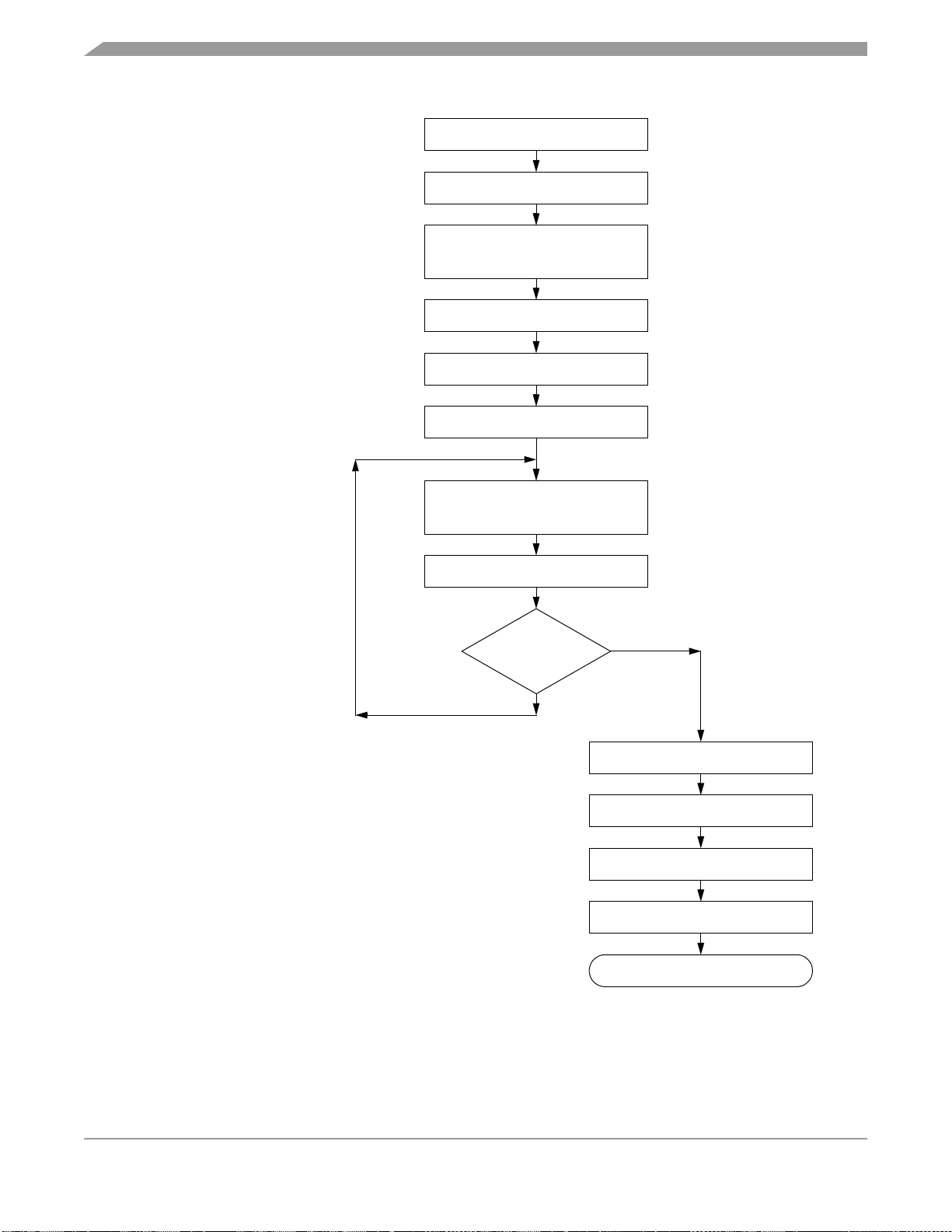
FLASH-1 Memory
Algorithm for programming
a row (64 bytes) of FLASH memory
1
2
Read the FLASH block protect register
3
Write any data to any FLASH address
Set PGM bit
within the row address range desired
4
5
6
7
Wait for a time, t
Set HVEN bit
Wait for a time, t
Write data to the FLASH address
to be programmed
8
Wait for a time, t
nvs
pgs
PROG
Completed
programming
this row?
NOTE:
The time between each FLASH address change (step 7 to step 7), or
the time between the last FLASH address programmed
to clearing PGM bit (step 7 to step 10)
must not exceed the maximum programming
PROG
max.
time, t
This row program algorithm assumes the row/s
to be programmed are initially erased.
Figure 4-4. FLASH Programming Algorithm Flowchart
Y
N
10
11
12
13
Clear PGM bit
Wait for a time, t
Clear HVEN bit
Wait for a time, t
nvh
rcv
End of programming
MC68HC908AZ60A • MC68HC908AS60A Data Sheet, Rev. 5
58 Freescale Semiconductor

Low-Power Modes
4.8 Low-Power Modes
The WAIT and STOP instructions will place the MCU in low power consumption standby modes.
4.8.1 WAIT Mode
Putting the MCU into wait mode while the FLASH is in read mode does not affect the operation of the
FLASH memory directly; however, no memory activity will take place since the CPU is inactive.
The WAIT instruction should not be executed while performing a program or erase operation on the
FLASH. Wait mode will suspend any FLASH program/erase operations and leave the memory in a
Standby Mode.
4.8.2 STOP Mode
Putting the MCU into stop mode while the FLASH is in read mode does not affect the operation of the
FLASH memory directly; however, no memory activity will take place since the CPU is inactive.
The STOP instruction should not be executed while performing a program or erase operation on the
FLASH. Stop mode will suspend any FLASH program/erase operations and leave the memory in a
Standby Mode.
NOTE
Standby Mode is the power saving mode of the FLASH module, in which all
internal control signals to the FLASH are inactive and the current
consumption of the FLASH is minimum.
MC68HC908AZ60A • MC68HC908AS60A Data Sheet, Rev. 5
Freescale Semiconductor 59

FLASH-1 Memory
MC68HC908AZ60A • MC68HC908AS60A Data Sheet, Rev. 5
60 Freescale Semiconductor

Chapter 5 FLASH-2 Memory
5.1 Introduction
This chapter describes the operation of the embedded FLASH-2 memory. This memory can be read,
programmed and erased from a single external supply. The program and erase operations are enabled
through the use of an internal charge pump.
5.2 Functional Description
The FLASH-2 memory is a non-continuos array consisting of a total of 29,616 bytes on the
MC68HC908AS60A and 29,488 bytes on the MC68HC908AZ60A. An erased bit reads as a logic 1 and
a programmed bit reads as a logic 0.
Memory in the FLASH-2 array is organized into rows within pages. There are two rows of memory per
page with 64 bytes per row. The minimum erase block size is a single page,128 bytes. Programming is
performed on a per-row basis, 64 bytes at a time. Program and erase operations are facilitated through
control bits in the FLASH-2 Control Register (FL2CR). Details for these operations appear later in this
chapter.
The FLASH-2 memory map consists of:
• $0450–$05FF: User Memory on MC68HC908AS60A (432 bytes)
• $0450–$04FF: User Memory on MC68HC908AZ60A (176 bytes)
• $0580–$05FF: User Memory on MC68HC908AZ60A (128 bytes)
• $0E00–$7FFF: User Memory (29,616 bytes)
• $FF81: FLASH-2 Block Protect Register (FL2BPR)
NOTE
FL2BPR physically resides within FLASH-1 memory addressing space
• $FE08: FLASH-2 Control Register (FL2CR)
Programming tools are available from Freescale. Contact your local Freescale representative for more
information.
NOTE
A security feature prevents viewing of the FLASH contents.
1. No security feature is absolutely secure. However, Freescale’s strategy is to make reading or copying the FLASH difficult for
unauthorized users.
MC68HC908AZ60A • MC68HC908AS60A Data Sheet, Rev. 5
Freescale Semiconductor 61
(1)
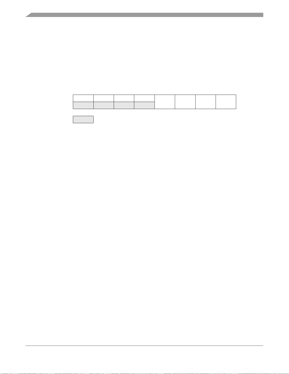
FLASH-2 Memory
5.3 FLASH-2 Control and Block Protect Registers
The FLASH-2 array has two registers that control its operation, the FLASH-2 Control Register (FL2CR)
and the FLASH-2 Block Protect Register (FL2BPR).
5.3.1 FLASH-2 Control Register
The FLASH-2 Control Register (FL2CR) controls FLASH-2 program and erase operations.
Address: $FE08
Bit 7654321Bit 0
Read:0000
Write:
Reset:00000000
= Unimplemented
HVEN MASS ERASE PGM
Figure 5-1. FLASH-2 Control Register (FL2CR)
HVEN — High-Voltage Enable Bit
This read/write bit enables the charge pump to drive high voltages for program and erase operations
in the array. HVEN can only be set if either PGM = 1 or ERASE = 1 and the proper sequence for
program or erase is followed.
1 = High voltage enabled to array and charge pump on
0 = High voltage disabled to array and charge pump off
MASS — Mass Erase Control Bit
Setting this read/write bit configures the FLASH-2 array for mass or page erase operation.
1 = Mass erase operation selected
0 = Page erase operation selected
ERASE — Erase Control Bit
This read/write bit configures the memory for erase operation. ERASE is interlocked with the PGM bit
such that both bits cannot be set at the same time.
1 = Erase operation selected
0 = Erase operation unselected
PGM — Program Control Bit
This read/write bit configures the memory for program operation. PGM is interlocked with the ERASE
bit such that both bits cannot be equal to 1 or set to 1 at the same time.
1 = Program operation selected
0 = Program operation unselected
5.3.2 FLASH-2 Block Protect Register
The FLASH-2 Block Protect Register (FL2BPR) is implemented as a byte within the FLASH-1 memory
and therefore can only be written during a FLASH programming sequence. The value in this register
determines the starting location of the protected range within the FLASH-2 memory.
MC68HC908AZ60A • MC68HC908AS60A Data Sheet, Rev. 5
62 Freescale Semiconductor
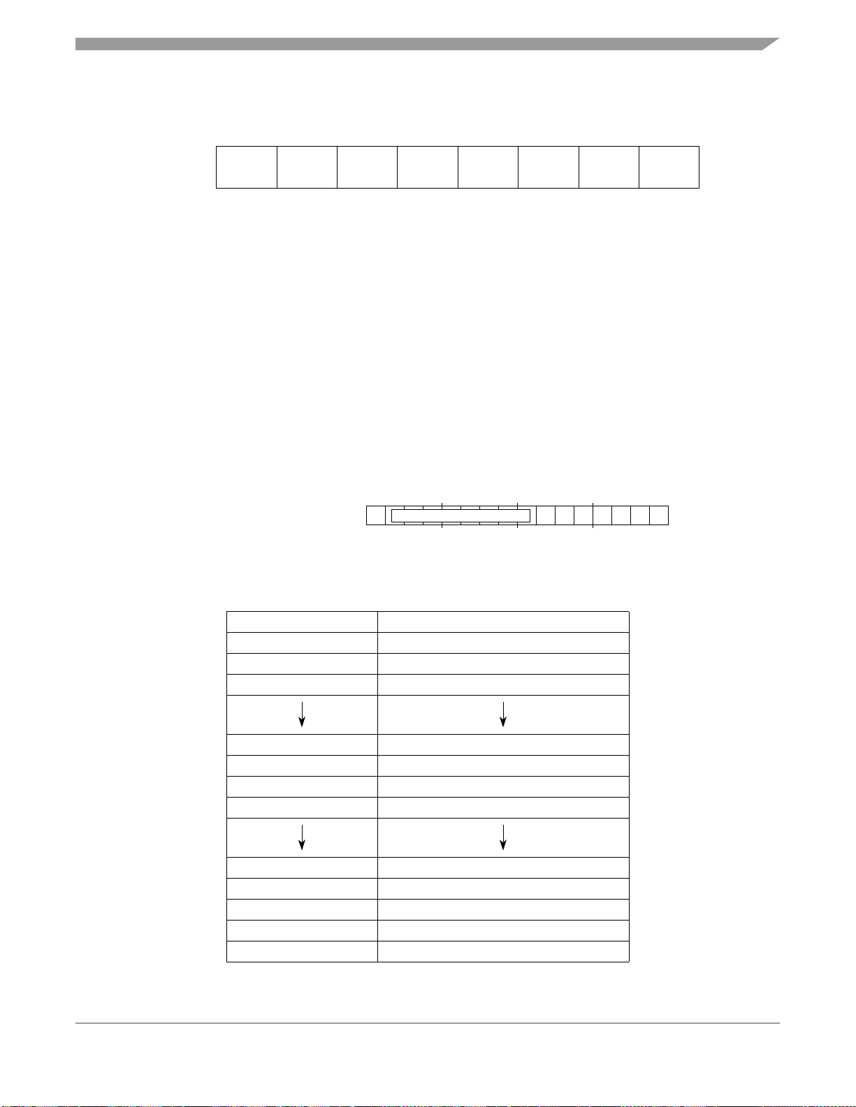
FLASH-2 Control and Block Protect Registers
Address: $FF81
Bit 7654321Bit 0
Read:
Write:
BPR7 BPR6 BPR5 BPR4 BPR3 BPR2 BPR1 BPR0
Figure 5-2. FLASH-2 Block Protect Register (FL2BPR)
NOTE
The FLASH-2 Block Protect Register (FL2BPR) controls the block
protection for the FLASH-2 array. However, FL2BPR is implemented within
the FLASH-1 memory array and therefore, the FLASH-1 Control Register
(FL1CR) must be used to program/erase FL2BPR.
FL2BPR[7:0] — Block Protect Register Bit 7 to Bit 0
These eight bits represent bits [14:7] of a 16-bit memory address. Bit 15 is logic 1 and bits [6:0] are
logic 0s.
The resultant 16-bit address is used for specifying the start address of the FLASH-2 memory for block
protection. FLASH-2 is protected from this start address to the end of FLASH-2 memory at $7FFF.
With this mechanism, the protect start address can be $XX00 and $XX80 (128 byte page boundaries)
within the FLASH-2 array.
Start address of FLASH block protect
Figure 5-3. FLASH-2 Block Protect Start Address
FLASH-2 Protected Ranges:
FL2BPR[7:0] Protected Range
16-bit memory address
1
$FF No Protection
$FE $7F00 – $7FFF
$FD $7E80 – $7FFF
$0B $0580 – $7FFF
$0A $0500 – $7FFF
$09 $0480 – $7FFF
$08 $0450 – $7FFF
$04 $0450 – $7FFF
$03 $0450 – $7FFF
$02 $0450 – $7FFF
$01 $0450 – $7FFF
$00 $0450 – $7FFF
FLBPR value
0000000
MC68HC908AZ60A • MC68HC908AS60A Data Sheet, Rev. 5
Freescale Semiconductor 63

FLASH-2 Memory
Decreasing the value in FL2BPR by one increases the protected range by one page (128 bytes).
However, programming the block protect register with $FE protects a range twice that size, 256 bytes, in
the corresponding array. $FE means that locations $7F00–$7FFF are protected in FLASH-2.
The FLASH memory does not exist at some locations. The block protection range configuration is
unaffected if FLASH memory does not exist in that range. Refer to the memory map and make sure that
the desired locations are protected.
5.4 FLASH-2 Block Protection
Due to the ability of the on-board charge pump to erase and program the FLASH memory in the target
application, provision is made for protecting blocks of memory from unintentional erase or program
operations due to system malfunction. This protection is done by using the FLASH-2 Block Protection
Register (FL2BPR). FL2BPR determines the range of the FLASH-2 memory which is to be protected. The
range of the protected area starts from a location defined by FL2BPR and ends at the bottom of the
FLASH-2 memory ($7FFF). When the memory is protected, the HVEN bit can not be set in either ERASE
or PROGRAM operations.
NOTE
In performing a program or erase operation, the FLASH-2 Block Protect
Register must be read after setting the PGM or ERASE bit and before
asserting the HVEN bit.
When the FLASH-2 Block Protect Register is programmed with all 0’s, the entire memory is protected
from being programmed and erased. When all the bits are erased (all 1’s), the entire memory is accessible
for program and erase.
When bits within FL2BPR are programmed (logic 0), they lock a block of memory address ranges as
shown in 5.3.2 FLASH-2 Block Protect Register. If FL2BPR is programmed with any value other than $FF,
the protected block of FLASH memory can not be erased or programmed.
NOTE
The vector locations and the FLASH Block Protect Registers are located in
the same page. FL1BPR and FL2BPR are not protected with special
hardware or software; therefore, if this page is not protected by FL1BPR
and the vector locations are erased by either a page or a mass erase
operation, both FL1BPR and FL2BPR will also get erased.
MC68HC908AZ60A • MC68HC908AS60A Data Sheet, Rev. 5
64 Freescale Semiconductor

FLASH-2 Mass Erase Operation
5.5 FLASH-2 Mass Erase Operation
Use this step-by-step procedure to erase the entire FLASH-2 memory to read as logic 1:
1. Set both the ERASE bit and the MASS bit in the FLASH-2 Control Register (FL2CR).
2. Read the FLASH-2 Block Protect Register (FL2BPR).
3. Write to any FLASH-2 address within the FLASH-2 array with any data.
NOTE
If the address written to in Step 3 is within address space protected by the
FLASH-2 Block Protect Register (FL2BPR), no erase will occur.
4. Wait for a time, t
NVS
5. Set the HVEN bit.
6. Wait for a time, t
MERASE
7. Clear the ERASE bit.
8. Wait for a time, t
NVHL
9. Clear the HVEN bit.
10. Wait for a time, t
RCV
A. Programming and erasing of FLASH locations can not be performed by
code being executed from the same FLASH array.
B. While these operations must be performed in the order shown, other
unrelated operations may occur between the steps. Care must be taken
however to ensure that these operations do not access any address within
the FLASH array memory space such as the COP Control Register
(COPCTL) at $FFFF.
C. It is highly recommended that interrupts be disabled during
program/erase operations.
.
.
.
, after which the memory can be accessed in normal read mode.
NOTE
MC68HC908AZ60A • MC68HC908AS60A Data Sheet, Rev. 5
Freescale Semiconductor 65

FLASH-2 Memory
5.6 FLASH-2 Page Erase Operation
Use this step-by-step procedure to erase a page (128 bytes) of FLASH-2 memory to read as logic 1:
1. Set the ERASE bit and clear the MASS bit in the FLASH-2 Control Register (FL2CR).
2. Read the FLASH-2 Block Protect Register (FL2BPR).
3. Write any data to any FLASH-2 address within the address range of the page (128 byte block) to
be erased.
4. Wait for time, t
5. Set the HVEN bit.
6. Wait for time, t
7. Clear the ERASE bit.
8. Wait for time, t
9. Clear the HVEN bit.
10. Wait for a time, t
A. Programming and erasing of FLASH locations can not be performed by
code being executed from the same FLASH array.
B. While these operations must be performed in the order shown, other
unrelated operations may occur between the steps. Care must be taken
however to ensure that these operations do not access any address within
the FLASH array memory space such as the COP Control Register
(COPCTL) at $FFFF.
.
NVS
ERASE
NVH
.
.
, after which the memory can be accessed in normal read mode.
RCV
NOTE
C. It is highly recommended that interrupts be disabled during
program/erase operations.
5.7 FLASH-2 Program Operation
Programming of the FLASH memory is done on a row basis. A row consists of 64 consecutive bytes with
address ranges as follows:
• $XX00 to $XX3F
• $XX40 to $XX7F
• $XX80 to $XXBF
• $XXC0 to $XXFF
During the programming cycle, make sure that all addresses being written to fit within one of the ranges
specified above. Attempts to program addresses in different row ranges in one programming cycle will fail.
• Use this step-by-step procedure to program a row of FLASH-2 memory.
NOTE
In order to avoid program disturbs, the row must be erased before any byte
on that row is programmed.
1. Set the PGM bit in the FLASH-2 Control Register (FL2CR). This configures the memory for
program operation and enables the latching of address and data programming.
2. Read the FLASH-2 Block Protect Register (FL2BPR).
3. Write to any FLASH-2 address within the row address range desired with any data.
MC68HC908AZ60A • MC68HC908AS60A Data Sheet, Rev. 5
66 Freescale Semiconductor

FLASH-2 Program Operation
4. Wait for time, t
NVS
.
5. Set the HVEN bit.
6. Wait for time, t
PGS
.
7. Write data byte to the FLASH-2 address to be programmed.
8. Wait for time, t
PROG
.
9. Repeat step 7 and 8 until all the bytes within the row are programmed.
10. Clear the PGM bit.
11. Wait for time, t
NVH
.
12. Clear the HVEN bit.
13. Wait for a time, t
, after which the memory can be accessed in normal read mode.
RCV
The FLASH Programming Algorithm Flowchart is shown in Figure 5-4.
NOTE
A. Programming and erasing of FLASH locations can not be performed by
code being executed from the same FLASH array.
B. While these operations must be performed in the order shown, other
unrelated operations may occur between the steps. Care must be taken
however to ensure that these operations do not access any address within
the FLASH array memory space such as the COP Control Register
(COPCTL) at $FFFF.
C. It is highly recommended that interrupts be disabled during
program/erase operations.
D. Do not exceed t
PROG
maximum or t
maximum. t
HV
is defined as the
HV
cumulative high voltage programming time to the same row before next
erase. t
must satisfy this condition: t
HV
NVS
+ t
NVH
+ t
PGS
+ (t
PROG
X 64) ≤ t
HV
max. Please also see 28.1.14 FLASH Memory Characteristics.
E. The time between each FLASH address change (step 7 to step 7), or the
time between the last FLASH address programmed to clearing the PGM bit
(step 7 to step 10) must not exceed the maximum programming time, t
PROG
max.
F. Be cautious when programming the FLASH-2 array to ensure that
non-FLASH locations are not used as the address that is written to when
selecting either the desired row address range in step 3 of the algorithm or
the byte to be programmed in step 7 of the algorithm. This applies
particularly to:
$0450-$047F: First row of FLASH-2 (48 bytes)
MC68HC908AZ60A • MC68HC908AS60A Data Sheet, Rev. 5
Freescale Semiconductor 67

FLASH-2 Memory
Algorithm for programming
a row (64 bytes) of FLASH memory
1
2
Read the FLASH block protect register
3
Write any data to any FLASH address
Set PGM bit
within the row address range desired
4
5
6
7
Wait for a time, t
Set HVEN bit
Wait for a time, t
Write data to the FLASH address
to be programmed
8
Wait for a time, t
nvs
pgs
PROG
Completed
programming
this row?
NOTE:
The time between each FLASH address change (step 7 to step 7), or
the time between the last FLASH address programmed
to clearing PGM bit (step 7 to step 10)
must not exceed the maximum programming
PROG
max.
time, t
This row program algorithm assumes the row/s
to be programmed are initially erased.
Figure 5-4. FLASH Programming Algorithm Flowchart
Y
N
10
11
12
13
Clear PGM bit
Wait for a time, t
Clear HVEN bit
Wait for a time, t
nvh
rcv
End of programming
MC68HC908AZ60A • MC68HC908AS60A Data Sheet, Rev. 5
68 Freescale Semiconductor

Low-Power Modes
5.8 Low-Power Modes
The WAIT and STOP instructions will place the MCU in low power consumption standby modes.
5.8.1 WAIT Mode
Putting the MCU into wait mode while the FLASH is in read mode does not affect the operation of the
FLASH memory directly; however, no memory activity will take place since the CPU is inactive.
The WAIT instruction should not be executed while performing a program or erase operation on the
FLASH. Wait mode will suspend any FLASH program/erase operations and leave the memory in a
Standby Mode.
5.8.2 STOP Mode
Putting the MCU into stop mode while the FLASH is in read mode does not affect the operation of the
FLASH memory directly; however, no memory activity will take place since the CPU is inactive.
The STOP instruction should not be executed while performing a program or erase operation on the
FLASH. Stop mode will suspend any FLASH program/erase operations and leave the memory in a
Standby Mode.
NOTE
Standby Mode is the power saving mode of the FLASH module, in which all
internal control signals to the FLASH are inactive and the current
consumption of the FLASH is minimum.
MC68HC908AZ60A • MC68HC908AS60A Data Sheet, Rev. 5
Freescale Semiconductor 69

FLASH-2 Memory
MC68HC908AZ60A • MC68HC908AS60A Data Sheet, Rev. 5
70 Freescale Semiconductor

Chapter 6 EEPROM-1 Memory
6.1 Introduction
This chapter describes the 512 bytes of electrically erasable programmable read-only memory
(EEPROM) residing at address range $0800 to $09FF. There are 1024 bytes of EEPROM available on
the MC68HC908AS60A and MC68HC908AZ60A which are physically located in two 512 byte arrays. For
information relating to the array covering address range $0600 to $07FF please see Chapter 7
EEPROM-2 Memory.
6.2 Features
Features of the EEPROM-1 include the following:
• 512 bytes Nonvolatile Memory
• Byte, Block, or Bulk Erasable
• Nonvolatile EEPROM Configuration and Block Protection Options
• On-chip Charge Pump for Programming/Erasing
• Security Option
• AUTO Bit Driven Programming/Erasing Time Feature
6.3 EEPROM-1 Register Summary
The EEPROM-1 Register Summary is shown in Figure 6-1.
MC68HC908AZ60A • MC68HC908AS60A Data Sheet, Rev. 5
Freescale Semiconductor 71

EEPROM-1 Memory
Addr.Register Name Bit 7654321Bit 0
Read:
$FE10
EE1DIV Nonvolatile
Register High
(EE1DIVHNVR)
(1)
Reset: Unaffected by reset; $FF when blank
Write:
EEDIVS-
ECD
RRRREEDIV10EEDIV9EEDIV8
$FE11
$FE1A
$FE1B
$FE1C
$FE1D
$FE1F
EE1DIV Nonvolatile
Register Low
(EE1DIVLNVR)
EE1 Divider Register High
(EE1DIVH)
EE1 Divider Register Low
(EE1DIVL)
EEPROM-1 Nonvolatile
Register (EE1NVR)
EEPROM-1 Control
Register
(EE1CR)
EEPROM-1 Array
Configuration Register
(EE1ACR)
Read:
EEDIV7 EEDIV6 EEDIV5 EEDIV4 EEDIV3 EEDIV2 EEDIV1 EEDIV0
Write:
(1)
Reset: Unaffected by reset; $FF when blank
Read:
Write:
EEDIVS-
ECD
0000
EEDIV10 EEDIV9 EEDIV8
Reset: Contents of EE1DIVHNVR ($FE10), Bits [6:3] = 0
Read:
EEDIV7 EEDIV6 EEDIV5 EEDIV4 EEDIV3 EEDIV2 EEDIV1 EEDIV0
Write:
Reset: Contents of EE1DIVLNVR ($FE11)
Read:
UNUSED UNUSED UNUSED EEPRTCT EEBP3 EEBP2 EEBP1 EEBP0
Write:
(1)
Reset: Unaffected by reset; $FF when blank; factory programmed $F0
Read:
UNUSED
0
EEOFF EERAS1 EERAS0 EELAT AUTO EEPGM
Write:
Reset:00000000
Read: UNUSED UNUSED UNUSED EEPRTCT EEBP3 EEBP2 EEBP1 EEBP0
Write:
Reset: Contents of EE1NVR ($FE1C)
1. Nonvolatile EEPROM register; write by programming.
= Unimplemented R = Reserved UNUSED = Unused
Figure 6-1. EEPROM-1 Register Summary
MC68HC908AZ60A • MC68HC908AS60A Data Sheet, Rev. 5
72 Freescale Semiconductor

Functional Description
6.4 Functional Description
The 512 bytes of EEPROM-1 are located at $0800-$09FF and can be programmed or erased without an
additional external high voltage supply. The program and erase operations are enabled through the use
of an internal charge pump. For each byte of EEPROM, the write/erase endurance is 10,000 cycles.
6.4.1 EEPROM-1 Configuration
The 8-bit EEPROM-1 Nonvolatile Register (EE1NVR) and the 16-bit EEPROM-1 Timebase Divider
Nonvolatile Register (EE1DIVNVR) contain the default settings for the following EEPROM configurations:
• EEPROM-1 Timebase Reference
• EEPROM-1 Security Option
• EEPROM-1 Block Protection
EE1NVR and EE1DIVNVR are nonvolatile EEPROM registers. They are programmed and erased in the
same way as EEPROM bytes. The contents of these registers are loaded into their respective volatile
registers during a MCU reset. The values in these read/write volatile registers define the EEPROM-1
configurations.
For EE1NVR, the corresponding volatile register is the EEPROM-1 Array Configuration Register
(EE1ACR). For the EE1DIVNCR (two 8-bit registers: EE1DIVHNVR and EE1DIVLNVR), the
corresponding volatile register is the EEPROM-1 Divider Register (EE1DIV: EE1DIVH and EE1 DIVL).
6.4.2 EEPROM-1 Timebase Requirements
A 35µs timebase is required by the EEPROM-1 control circuit for program and erase of EEPROM content.
This timebase is derived from dividing the CGMXCLK or bus clock (selected by EEDIVCLK bit in
CONFIG-2 Register) using a timebase divider circuit controlled by the 16-bit EEPROM-1 Timebase
Divider EE1DIV Register (EE1DIVH and EE1DIVL).
As the CGMXCLK or bus clock is user selected, the EEPROM-1 Timebase Divider Register must be
configured with the appropriate value to obtain the 35 µs. The timebase divider value is calculated by
using the following formula:
EE1DIV= INT[Reference Frequency(Hz) x 35 x10
This value is written to the EEPROM-1 Timebase Divider Register (EE1DIVH and EE1DIVL) or
programmed into the EEPROM-1 Timebase Divider Nonvolatile Register prior to any EEPROM program
or erase operations (6.4.1 EEPROM-1 Configuration and 6.4.2 EEPROM-1 Timebase Requirements).
-6
+0.5]
MC68HC908AZ60A • MC68HC908AS60A Data Sheet, Rev. 5
Freescale Semiconductor 73
EEPROM-1 Memory
6.4.3 EEPROM-1 Program/Erase Protection
The EEPROM has a special feature that designates the 16 bytes of addresses from $08F0 to $08FF to
be permanently secured. This program/erase protect option is enabled by programming the EEPRTCT
bit in the EEPROM-1 Nonvolatile Register (EE1NVR) to a logic zero.
Once the EEPRTCT bit is programmed to 0 for the first time:
• Programming and erasing of secured locations $08F0 to $08FF is permanently disabled.
• Secured locations $08F0 to $08FF can be read as normal.
• Programming and erasing of EE1NVR is permanently disabled.
• Bulk and Block Erase operations are disabled for the unprotected locations $0800-$08EF,
$0900-$09FF.
• Single byte program and erase operations are still available for locations $0800-$08EF and
$0900-$09FF for all bytes that are not protected by the EEPROM-1 Block Protect EEBPx bits (see
6.4.4 EEPROM-1 Block Protection and 6.5.2 EEPROM-1 Array Configuration Register)
NOTE
Once armed, the protect option is permanently enabled. As a consequence,
all functions in the EE1NVR will remain in the state they were in
immediately before the security was enabled.
6.4.4 EEPROM-1 Block Protection
The 512 bytes of EEPROM-1 are divided into four 128-byte blocks. Each of these blocks can be protected
from erase/program operations by setting the EEBPx bit in the EE1NVR. Table 6-1 shows the address
ranges for the blocks.
Table 6-1. EEPROM-1 Array Address Blocks
Block Number (EEBPx) Address Range
EEBP0 $0800–$087F
EEBP1 $0880–$08FF
EEBP2 $0900–$097F
EEBP3 $0980–$09FF
These bits are effective after a reset or a upon read of the EE1NVR register. The block protect
configuration can be modified by erasing/programming the corresponding bits in the EE1NVR register
and then reading the EE1NVR register. Please see 6.5.2 EEPROM-1 Array Configuration Register for
more information.
NOTE
Once EEDIVSECD in the EE1DIVHNVR is programmed to 0 and after a
system reset, the EE1DIV security feature is permanently enabled because
the EEDIVSECD bit in the EE1DIVH is always loaded with 0 thereafter.
Once this security feature is armed, erase and program mode are disabled
for EE1DIVHNVR and EE1DIVLNVR. Modifications to the EE1DIVH and
EE1DIVL registers are also disabled. Therefore, be cautious on
programming a value into the EE1DIVHNVR.
MC68HC908AZ60A • MC68HC908AS60A Data Sheet, Rev. 5
74 Freescale Semiconductor
Functional Description
6.4.5 EEPROM-1 Programming and Erasing
The unprogrammed or erase state of an EEPROM bit is a logic 1. The factory default for all bytes within
the EEPROM-1 array is $FF.
The programming operation changes an EEPROM bit from logic 1 to logic 0 (programming cannot change
a bit from logic 0 to a logic 1). In a single programming operation, the minimum EEPROM programming
size is one bit; the maximum is eight bits (one byte).
The erase operation changes an EEPROM bit from logic 0 to logic 1. In a single erase operation, the
minimum EEPROM erase size is one byte; the maximum is the entire EEPROM-1 array.
The EEPROM can be programmed such that one or multiple bits are programmed (written to a logic 0) at
a time. However, the user may never program the same bit location more than once before erasing the
entire byte. In other words, the user is not allowed to program a logic 0 to a bit that is already programmed
(bit state is already logic 0).
For some applications it might be advantageous to track more than 10K events with a single byte of
EEPROM by programming one bit at a time. For that purpose, a special selective bit programming
technique is available. An example of this technique is illustrated in Table 6-2.
Table 6-2. Example Selective Bit Programming Description
Description
Original state of byte (erased) n/a 1111:1111
First event is recorded by programming bit position 0 1111:1110 1111:1110
Second event is recorded by programming bit position 1 1111:1101 1111:1100
Third event is recorded by programming bit position 2 1111:1011 1111:1000
Fourth event is recorded by programming bit position 3 1111:0111 1111:0000
Events five through eight are recorded in a similar fashion
Program Data
in Binary
Result
in Binary
Note that none of the bit locations are actually programmed more than once although the byte was
programmed eight times.
When this technique is utilized, a program/erase cycle is defined as multiple program sequences (up to
eight) to a unique location followed by a single erase operation.
6.4.5.1 Program/Erase Using AUTO Bit
An additional feature available for EEPROM-1 program and erase operations is the AUTO mode. When
enabled, AUTO mode will activate an internal timer that will automatically terminate the program/erase
cycle and clear the EEPGM bit. Please see 6.4.5.2 EEPROM-1 Programming, 6.4.5.3 EEPROM-1
Erasing, and 6.5.1 EEPROM-1 Control Register for more information.
MC68HC908AZ60A • MC68HC908AS60A Data Sheet, Rev. 5
Freescale Semiconductor 75

EEPROM-1 Memory
6.4.5.2 EEPROM-1 Programming
The unprogrammed or erase state of an EEPROM bit is a logic 1. Programming changes the state to a
logic 0. Only EEPROM bytes in the non-protected blocks and the EE1NVR register can be programmed.
Use the following procedure to program a byte of EEPROM:
1. Clear EERAS1 and EERAS0 and set EELAT in the EE1CR.
(A)
NOTE
If using the AUTO mode, also set the AUTO bit during Step 1.
2. Write the desired data to the desired EEPROM address.
EEPGM
(C)
Go to Step 7 if AUTO is set.
, to program the byte.
3. Set the EEPGM bit.
4. Wait for time, t
5. Clear EEPGM bit.
6. Wait for time, t
, for the programming voltage to fall. Go to Step 8.
EEFPV
7. Poll the EEPGM bit until it is cleared by the internal timer.
8. Clear EELAT bits.
(E)
NOTE
A. EERAS1 and EERAS0 must be cleared for programming. Setting the
EELAT bit configures the address and data buses to latch data for
programming the array. Only data with a valid EEPROM-1 address will be
latched. If EELAT is set, other writes to the EE1CR will be allowed after a
valid EEPROM-1 write.
B. If more than one valid EEPROM write occurs, the last address and data
will be latched overriding the previous address and data. Once data is
written to the desired address, do not read EEPROM-1 locations other than
the written location. (Reading an EEPROM location returns the latched data
and causes the read address to be latched).
C. The EEPGM bit cannot be set if the EELAT bit is cleared or a non-valid
EEPROM address is latched. This is to ensure proper programming
sequence. Once EEPGM is set, do not read any EEPROM-1 locations;
otherwise, the current program cycle will be unsuccessful. When EEPGM
is set, the on-board programming sequence will be activated.
(B)
(D)
D. The delay time for the EEPGM bit to be cleared in AUTO mode is less
than t
EEPGM
. However, on other MCUs, this delay time may be different.
For forward compatibility, software should not make any dependency on
this delay time.
E. Any attempt to clear both EEPGM and EELAT bits with a single
instruction will only clear EEPGM. This is to allow time for removal of high
voltage from the EEPROM-1 array.
MC68HC908AZ60A • MC68HC908AS60A Data Sheet, Rev. 5
76 Freescale Semiconductor

Functional Description
6.4.5.3 EEPROM-1 Erasing
The programmed state of an EEPROM bit is logic 0. Erasing changes the state to a logic 1. Only
EEPROM-1 bytes in the non-protected blocks and the EE1NVR register can be erased.
Use the following procedure to erase a byte, block or the entire EEPROM-1 array:
1. Configure EERAS1 and EERAS0 for byte, block or bulk erase; set EELAT in EE1CR.
(A)
NOTE
If using the AUTO mode, also set the AUTO bit in Step 1.
2. Byte erase: write any data to the desired address.
(B)
Block erase: write any data to an address within the desired block.
Bulk erase: write any data to an address within the array.
3. Set the EEPGM bit.
4. Wait for a time: t
(C)
Go to Step 7 if AUTO is set.
EEBYTE
for byte erase; t
EEBLOCK
for block erase; t
5. Clear EEPGM bit.
6. Wait for a time, t
, for the erasing voltage to fall. Go to Step 8.
EEFPV
7. Poll the EEPGM bit until it is cleared by the internal timer.
8. Clear EELAT bits.
(E)
NOTE
A. Setting the EELAT bit configures the address and data buses to latch
data for erasing the array. Only valid EEPROM-1 addresses will be latched.
If EELAT is set, other writes to the EE1CR will be allowed after a valid
EEPROM-1 write.
B. If more than one valid EEPROM write occurs, the last address and data
will be latched overriding the previous address and data. Once data is
written to the desired address, do not read EEPROM-1 locations other than
the written location. (Reading an EEPROM location returns the latched data
and causes the read address to be latched).
(B)
(D)
(B)
EEBULK.
for bulk erase.
C. The EEPGM bit cannot be set if the EELAT bit is cleared or a non-valid
EEPROM address is latched. This is to ensure proper programming
sequence. Once EEPGM is set, do not read any EEPROM-1 locations;
otherwise, the current program cycle will be unsuccessful. When EEPGM
is set, the on-board programming sequence will be activated.
D. The delay time for the EEPGM bit to be cleared in AUTO mode is less
than t
EEBYTE /tEEBLOCK/tEEBULK
. However, on other MCUs, this delay time
may be different. For forward compatibility, software should not make any
dependency on this delay time.
E. Any attempt to clear both EEPGM and EELAT bits with a single
instruction will only clear EEPGM. This is to allow time for removal of high
voltage from the EEPROM-1 array.
MC68HC908AZ60A • MC68HC908AS60A Data Sheet, Rev. 5
Freescale Semiconductor 77
EEPROM-1 Memory
6.5 EEPROM-1 Register Descriptions
Four I/O registers and three nonvolatile registers control program, erase and options of the EEPROM-1
array.
6.5.1 EEPROM-1 Control Register
This read/write register controls programming/erasing of the array.
Address: $FE1D
Bit 7654321Bit 0
Read:
UNUSED
Write:
Reset:00000000
Figure 6-2. EEPROM-1 Control Register (EE1CR)
Bit 7— Unused bit
This read/write bit is software programmable but has no functionality.
EEOFF — EEPROM-1 power down
This read/write bit disables the EEPROM-1 module for lower power consumption. Any attempts to
access the array will give unpredictable results. Reset clears this bit.
1 = Disable EEPROM-1 array
0 = Enable EEPROM-1 array
0
= Unimplemented
EEOFF EERAS1 EERAS0 EELAT AUTO EEPGM
EERAS1 and EERAS0 — Erase/Program Mode Select Bits
These read/write bits set the erase modes. Reset clears these bits.
Table 6-3. EEPROM-1 Program/Erase Mode Select
EEBPx EERAS1 EERAS0 MODE
0 0 0 Byte Program
0 0 1 Byte Erase
010Block Erase
0 1 1 Bulk Erase
1 X X No Erase/Program
X = don’t care
EELAT — EEPROM-1 Latch Control
This read/write bit latches the address and data buses for programming the EEPROM-1 array. EELAT
cannot be cleared if EEPGM is still set. Reset clears this bit.
1 = Buses configured for EEPROM-1 programming or erase operation
0 = Buses configured for normal operation
MC68HC908AZ60A • MC68HC908AS60A Data Sheet, Rev. 5
78 Freescale Semiconductor

EEPROM-1 Register Descriptions
AUTO — Automatic Termination of Program/Erase Cycle
When AUTO is set, EEPGM is cleared automatically after the program/erase cycle is terminated by
the internal timer.
(See note D for 6.4.5.2 EEPROM-1 Programming, 6.4.5.3 EEPROM-1 Erasing, and 28.1.13 EEPROM
Memory Characteristics)
1 = Automatic clear of EEPGM is enabled
0 = Automatic clear of EEPGM is disabled
EEPGM — EEPROM-1 Program/Erase Enable
This read/write bit enables the internal charge pump and applies the programming/erasing voltage to
the EEPROM-1 array if the EELAT bit is set and a write to a valid EEPROM-1 location has occurred.
Reset clears the EEPGM bit.
1 = EEPROM-1 programming/erasing power switched on
0 = EEPROM-1 programming/erasing power switched off
NOTE
Writing logic 0s to both the EELAT and EEPGM bits with a single instruction
will clear EEPGM only to allow time for the removal of high voltage.
6.5.2 EEPROM-1 Array Configuration Register
The EEPROM-1 array configuration register configures EEPROM-1 security and EEPROM-1 block
protection.
This read-only register is loaded with the contents of the EEPROM-1 nonvolatile register (EE1NVR) after
a reset.
Address: $FE1F
Bit 7 6 5 4 3 2 1 Bit 0
Read: UNUSED UNUSED UNUSED EEPRTCT EEBP3 EEBP2 EEBP1 EEBP0
Write:
Reset: Contents of EE1NVR ($FE1C)
= Unimplemented
Figure 6-3. EEPROM-1 Array Configuration Register (EE1ACR)
Bit 7:5 — Unused Bits
These read/write bits are software programmable but have no functionality.
EEPRTCT — EEPROM-1 Protection Bit
The EEPRTCT bit is used to enable the security feature in the EEPROM (see EEPROM-1
Program/Erase Protection).
1 = EEPROM-1 security disabled
0 = EEPROM-1 security enabled
This feature is a write-once feature. Once the protection is enabled it may not be disabled.
MC68HC908AZ60A • MC68HC908AS60A Data Sheet, Rev. 5
Freescale Semiconductor 79

EEPROM-1 Memory
EEBP[3:0] — EEPROM-1 Block Protection Bits
These bits prevent blocks of EEPROM-1 array from being programmed or erased.
1 = EEPROM-1 array block is protected
0 = EEPROM-1 array block is unprotected
Block Number (EEBPx) Address Range
EEBP0 $0800–$087F
EEBP1 $0880–$08FF
EEBP2 $0900–$097F
EEBP3 $0980–$09FF
Table 6-4. EEPROM-1 Block Protect and Security Summary
Address Range EEBPx EEPRTCT = 1 EEPRTCT = 0
$0800 - $087F
$0880 - $08EF
Byte Programming
EEBP0 = 0
EEBP0 = 1 Protected Protected
EEBP1 = 0
EEBP1 = 1 Protected Protected
Available
Bulk, Block and Byte
Erasing Available
Byte Programming
Available
Bulk, Block and Byte
Erasing Available
Byte Programming
Available
Only Byte Erasing
Available
Byte Programming
Available
Only Byte Erasing
Available
$08F0 - $08FF
$0900 - $097F
$0980 - $09FF
Byte Programming
EEBP1 = 0
EEBP1 = 1 Protected
EEBP2 = 0
EEBP2 = 1 Protected Protected
EEBP3 = 0
EEBP3 = 1 Protected Protected
Available
Bulk, Block and Byte
Erasing Available
Byte Programming
Available
Bulk, Block and Byte
Erasing Available
Byte Programming
Available
Bulk, Block and Byte
Available
Secured
(No Programming or
Erasing)
Byte Programming
Available
Only Byte Erasing
Available
Byte Programming
Available
Only Byte Erasing
Available
MC68HC908AZ60A • MC68HC908AS60A Data Sheet, Rev. 5
80 Freescale Semiconductor
EEPROM-1 Register Descriptions
6.5.3 EEPROM-1 Nonvolatile Register
The contents of this register is loaded into the EEPROM-1 array configuration register (EE1ACR) after a
reset.
This register is erased and programmed in the same way as an EEPROM byte. (See 6.5.1 EEPROM-1
Control Register for individual bit descriptions).
Address: $FE1C
Bit 7 6 5 4 3 2 1 Bit 0
Read:
UNUSED UNUSED UNUSED EEPRTCT EEBP3 EEBP2 EEBP1 EEBP0
Write:
Reset: PV
PV = Programmed value or 1 in the erased state.
Figure 6-4. EEPROM-1 Nonvolatile Register (EE1NVR)
NOTE
The EE1NVR will leave the factory programmed with $F0 such that the full
array is available and unprotected.
6.5.4 EEPROM-1 Timebase Divider Register
The 16-bit EEPROM-1 timebase divider register consists of two 8-bit registers: EE1DIVH and EE1DIVL.
The 11-bit value in this register is used to configure the timebase divider circuit to obtain the 35 µs
timebase for EEPROM-1 control.
These two read/write registers are respectively loaded with the contents of the EEPROM-1 timebase
divider nonvolatile registers (EE1DIVHNVR and EE1DIVLNVR) after a reset.
Address: $FE1A
Bit 7 6 5 4 3 2 1 Bit 0
Read:
EEDIVS-
Write:
Reset: Contents of EE1DIVHNVR ($FE10), Bits [6:3] = 0
ECD
0000
= Unimplemented
EEDIV10 EEDIV9 EEDIV8
Figure 6-5. EE1DIV Divider High Register (EE1DIVH)
Address: $FE1B
Bit 7 6 5 4 3 2 1 Bit 0
Read:
Write:
Reset: Contents of EE1DIVLNVR ($FE11)
EEDIV7 EEDIV6 EEDIV5 EEDIV4 EEDIV3 EEDIV2 EEDIV1 EEDIV0
Figure 6-6. EE1DIV Divider Low Register (EE1DIVL)
MC68HC908AZ60A • MC68HC908AS60A Data Sheet, Rev. 5
Freescale Semiconductor 81

EEPROM-1 Memory
EEDIVSECD — EEPROM-1 Divider Security Disable
This bit enables/disables the security feature of the EE1DIV registers. When EE1DIV security feature
is enabled, the state of the registers EE1DIVH and EE1DIVL are locked (including EEDIVSECD bit).
The EE1DIVHNVR and EE1DIVLNVR nonvolatile memory registers are also protected from being
erased/programmed.
1 = EE1DIV security feature disabled
0 = EE1DIV security feature enabled
EEDIV[10:0] — EEPROM-1 timebase prescaler
These prescaler bits store the value of EE1DIV which is used as the divisor to derive a timebase of
35µs from the selected reference clock source (CGMXCLK or bus block in the CONFIG-2 register) for
the EEPROM-1 related internal timer and circuits. EEDIV[10:0] bits are readable at any time. They are
writable when EELAT = 0 and EEDIVSECD = 1.
The EE1DIV value is calculated by the following formula:
EE1DIV= INT[Reference Frequency(Hz) x 35 x10
-6
+0.5]
Where the result inside the bracket is rounded down to the nearest integer value
For example, if the reference frequency is 4.9152MHz, the EE1DIV value is 172
NOTE
Programming/erasing the EEPROM with an improper EE1DIV value may
result in data lost and reduce endurance of the EEPROM device.
6.5.5 EEPROM-1 Timebase Divider Nonvolatile Register
The 16-bit EEPROM-1 timebase divider nonvolatile register consists of two 8-bit registers: EE1DIVHNVR
and EE1DIVLNVR. The contents of these two registers are respectively loaded into the EEPROM-1
timebase divider registers, EE1DIVH and EE1DIVL, after a reset.
These two registers are erased and programmed in the same way as an EEPROM-1 byte.
Address: $FE10
Bit 7 6 5 4 3 2 1 Bit 0
Read:
EEDIVS-
Write:
Reset: Unaffected by reset; $FF when blank
ECD
R=Reserved
Figure 6-7. EEPROM-1 Divider Nonvolatile Register High (EE1DIVHNVR))
Address: $FE11
Bit 7 6 5 4 3 2 1 Bit 0
Read:
Write:
Reset: Unaffected by reset; $FF when blank
EEDIV7 EEDIV6 EEDIV5 EEDIV4 EEDIV3 EEDIV2 EEDIV1 EEDIV0
R R R R EEDIV10 EEDIV9 EEDIV8
Figure 6-8. EEPROM-1 Divider Nonvolatile Register Low (EE1DIVLNVR)
MC68HC908AZ60A • MC68HC908AS60A Data Sheet, Rev. 5
82 Freescale Semiconductor

Low-Power Modes
These two registers are protected from erase and program operations if the EEDIVSECD is set to logic 1
in the EE1DIVH (see EEPROM-1 Timebase Divider Register) or programmed to a logic 1 in the
EE1DIVHNVR.
NOTE
Once EEDIVSECD in the EE1DIVHNVR is programmed to 0 and after a
system reset, the EE1DIV security feature is permanently enabled because
the EEDIVSECD bit in the EE1DIVH is always loaded with 0 thereafter.
Once this security feature is armed, erase and program mode are disabled
for EE1DIVHNVR and EE1DIVLNVR. Modifications to the EE1DIVH and
EE1DIVL registers are also disabled. Therefore, care should be taken
before programming a value into the EE1DIVHNVR.
6.6 Low-Power Modes
The WAIT and STOP instructions can put the MCU in low power-consumption standby modes.
6.6.1 Wait Mode
The WAIT instruction does not affect the EEPROM. It is possible to start the program or erase sequence
on the EEPROM and put the MCU in wait mode.
6.6.2 Stop Mode
The STOP instruction reduces the EEPROM power consumption to a minimum. The STOP instruction
should not be executed while a programming or erasing sequence is in progress.
If stop mode is entered while EELAT and EEPGM are set, the programming sequence will be stopped
and the programming voltage to the EEPROM array removed. The programming sequence will be
restarted after leaving stop mode; access to the EEPROM is only possible after the programming
sequence has completed.
If stop mode is entered while EELAT and EEPGM is cleared, the programming sequence will be
terminated abruptly.
In either case, the data integrity of the EEPROM is not guaranteed.
MC68HC908AZ60A • MC68HC908AS60A Data Sheet, Rev. 5
Freescale Semiconductor 83

EEPROM-1 Memory
MC68HC908AZ60A • MC68HC908AS60A Data Sheet, Rev. 5
84 Freescale Semiconductor

Chapter 7 EEPROM-2 Memory
7.1 Introduction
This chapter describes the 512 bytes of electrically erasable programmable read-only memory
(EEPROM) residing at address range $0600 to $07FF. There are 1024 bytes of EEPROM available on
the MC68HC908AS60A and MC68HC908AZ60A which are physically located in two 512 byte arrays. For
information relating to the array covering address range $0800 to $09FF please see Chapter 6
EEPROM-1 Memory.
7.2 Features
Features of the EEPROM-2 include the following:
• 512 bytes Nonvolatile Memory
• Byte, Block, or Bulk Erasable
• Nonvolatile EEPROM Configuration and Block Protection Options
• On-chip Charge Pump for Programming/Erasing
• Security Option
• AUTO Bit Driven Programming/Erasing Time Feature
7.3 EEPROM-2 Register Summary
The EEPROM-2 Register Summary is shown in Figure 7-1.
MC68HC908AZ60A • MC68HC908AS60A Data Sheet, Rev. 5
Freescale Semiconductor 85

EEPROM-2 Memory
Addr.Register Name Bit 7654321Bit 0
Read:
$FF70
EE2DIV Nonvolatile
Register High
(EE2DIVHNVR)*
Reset: Unaffected by reset; $FF when blank
Write:
EEDIVS-
ECD
RRRREEDIV10EEDIV9EEDIV8
$FF71
$FF7A
$FF7B
$FF7C
$FF7D
$FF7F
EE2DIV Nonvolatile
Register Low
(EE2DIVLNVR)*
EE2 Divider Register High
(EE2DIVH)
EE2 Divider Register Low
(EE2DIVL)
EEPROM-2 Nonvolatile
Register (EE2NVR)*
EEPROM-2 Control
Register
(EE2CR)
EEPROM-2 Array
Configuration Register
(EE2ACR)
Read:
Write:
Reset: Unaffected by reset; $FF when blank
Read:
Write:
Reset: Contents of EE2DIVHNVR ($FF70); Bits[6:3] = 0
Read:
Write:
Reset: Contents of EE2DIVLNVR ($FF71)
Read:
Write:
Reset: Unaffected by reset; $FF when blank; factory programmed $F0
Read:
Write:
Reset:00000000
Read: UNUSED UNUSED UNUSED EEPRTCT EEBP3 EEBP2 EEBP1 EEBP0
Write:
Reset: Contents of EE2NVR ($FF7C)
* Nonvolatile EEPROM register; write by programming.
EEDIV7 EEDIV6 EEDIV5 EEDIV4 EEDIV3 EEDIV2 EEDIV1 EEDIV0
EEDIVS-
ECD
EEDIV7 EEDIV6 EEDIV5 EEDIV4 EEDIV3 EEDIV2 EEDIV1 EEDIV0
UNUSED UNUSED UNUSED EEPRTCT EEBP3 EEBP2 EEBP1 EEBP0
UNUSED
0000
EEDIV10 EEDIV9 EEDIV8
0
EEOFF EERAS1 EERAS0 EELAT AUTO EEPGM
= Unimplemented R = Reserved UNUSED = Unused
Figure 7-1. EEPROM-2 Register Summary
MC68HC908AZ60A • MC68HC908AS60A Data Sheet, Rev. 5
86 Freescale Semiconductor

Functional Description
7.4 Functional Description
The 512 bytes of EEPROM-2 are located at $0600-$07FF and can be programmed or erased without an
additional external high voltage supply. The program and erase operations are enabled through the use
of an internal charge pump. For each byte of EEPROM, the write/erase endurance is 10,000 cycles.
7.4.1 EEPROM-2 Configuration
The 8-bit EEPROM-2 Nonvolatile Register (EE2NVR) and the 16-bit EEPROM-2 Timebase Divider
Nonvolatile Register (EE2DIVNVR) contain the default settings for the following EEPROM configurations:
• EEPROM-2 Timebase Reference
• EEPROM-2 Security Option
• EEPROM-2 Block Protection
EE2NVR and EE2DIVNVR are nonvolatile EEPROM registers. They are programmed and erased in the
same way as EEPROM bytes. The contents of these registers are loaded into their respective volatile
registers during a MCU reset. The values in these read/write volatile registers define the EEPROM-2
configurations.
For EE2NVR, the corresponding volatile register is the EEPROM-2 Array Configuration Register
(EE2ACR). For the EE2DIVNCR (two 8-bit registers: EE2DIVHNVR and EE2DIVLNVR), the
corresponding volatile register is the EEPROM-2 Divider Register (EE2DIV: EE2DIVH and EE2 DIVL).
7.4.2 EEPROM-2 Timebase Requirements
A 35µs timebase is required by the EEPROM-2 control circuit for program and erase of EEPROM content.
This timebase is derived from dividing the CGMXCLK or bus clock (selected by EEDIVCLK bit in
CONFIG-2 Register) using a timebase divider circuit controlled by the 16-bit EEPROM-2 Timebase
Divider EE2DIV Register (EE2DIVH and EE2DIVL).
As the CGMXCLK or bus clock is user selected, the EEPROM-2 Timebase Divider Register must be
configured with the appropriate value to obtain the 35 µs. The timebase divider value is calculated by
using the following formula:
EE2DIV= INT[Reference Frequency(Hz) x 35 x10
This value is written to the EEPROM-2 Timebase Divider Register (EE2DIVH and EE2DIVL) or
programmed into the EEPROM-2 Timebase Divider Nonvolatile Register prior to any EEPROM program
or erase operations (7.4.1 EEPROM-2 Configuration and 7.4.2 EEPROM-2 Timebase Requirements).
-6
+0.5]
MC68HC908AZ60A • MC68HC908AS60A Data Sheet, Rev. 5
Freescale Semiconductor 87

EEPROM-2 Memory
7.4.3 EEPROM-2 Program/Erase Protection
The EEPROM has a special feature that designates the 16 bytes of addresses from $06F0 to $06FF to
be permanently secured. This program/erase protect option is enabled by programming the EEPRTCT
bit in the EEPROM-2 Nonvolatile Register (EE2NVR) to a logic zero.
Once the EEPRTCT bit is programmed to 0 for the first time:
• Programming and erasing of secured locations $06F0 to $06FF is permanently disabled.
• Secured locations $06F0 to $06FF can be read as normal.
• Programming and erasing of EE2NVR is permanently disabled.
• Bulk and Block Erase operations are disabled for the unprotected locations $0600-$06EF,
$0700-$07FF.
• Single byte program and erase operations are still available for locations $0600-$06EF and
$0700-$07FF for all bytes that are not protected by the EEPROM-2 Block Protect EEBPx bits (see
7.4.4 EEPROM-2 Block Protection and 7.5.2 EEPROM-2 Array Configuration Register)
NOTE
Once armed, the protect option is permanently enabled. As a consequence,
all functions in the EE2NVR will remain in the state they were in
immediately before the security was enabled.
7.4.4 EEPROM-2 Block Protection
The 512 bytes of EEPROM-2 are divided into four 128-byte blocks. Each of these blocks can be protected
from erase/program operations by setting the EEBPx bit in the EE2NVR. Table 7-1 shows the address
ranges for the blocks.
Table 7-1. EEPROM-2 Array Address Blocks
Block Number (EEBPx) Address Range
EEBP0 $0600–$067F
EEBP1 $0680–$06FF
EEBP2 $0700–$077F
EEBP3 $0780–$07FF
These bits are effective after a reset or a upon read of the EE2NVR register. The block protect
configuration can be modified by erasing/programming the corresponding bits in the EE2NVR register
and then reading the EE2NVR register. Please see 7.5.2 EEPROM-2 Array Configuration Register for
more information.
NOTE
Once EEDIVSECD in the EE2DIVHNVR is programmed to 0 and after a
system reset, the EE2DIV security feature is permanently enabled because
the EEDIVSECD bit in the EE2DIVH is always loaded with 0 thereafter.
Once this security feature is armed, erase and program mode are disabled
for EE2DIVHNVR and EE2DIVLNVR. Modifications to the EE2DIVH and
EE2DIVL registers are also disabled. Therefore, be cautious on
programming a value into the EE2DIVHNVR.
MC68HC908AZ60A • MC68HC908AS60A Data Sheet, Rev. 5
88 Freescale Semiconductor

Functional Description
7.4.5 EEPROM-2 Programming and Erasing
The unprogrammed or erase state of an EEPROM bit is a logic 1. The factory default for all bytes within
the EEPROM-2 array is $FF.
The programming operation changes an EEPROM bit from logic 1 to logic 0 (programming cannot change
a bit from logic 0 to a logic 1). In a single programming operation, the minimum EEPROM programming
size is one bit; the maximum is eight bits (one byte).
The erase operation changes an EEPROM bit from logic 0 to logic 1. In a single erase operation, the
minimum EEPROM erase size is one byte; the maximum is the entire EEPROM-2 array.
The EEPROM can be programmed such that one or multiple bits are programmed (written to a logic 0) at
a time. However, the user may never program the same bit location more than once before erasing the
entire byte. In other words, the user is not allowed to program a logic 0 to a bit that is already programmed
(bit state is already logic 0).
For some applications it might be advantageous to track more than 10K events with a single byte of
EEPROM by programming one bit at a time. For that purpose, a special selective bit programming
technique is available. An example of this technique is illustrated in Table 7-2.
Table 7-2. Example Selective Bit Programming Description
Description
Original state of byte (erased) n/a 1111:1111
First event is recorded by programming bit position 0 1111:1110 1111:1110
Second event is recorded by programming bit position 1 1111:1101 1111:1100
Third event is recorded by programming bit position 2 1111:1011 1111:1000
Fourth event is recorded by programming bit position 3 1111:0111 1111:0000
Events five through eight are recorded in a similar fashion
Program Data
in Binary
Result
in Binary
NOTE
None of the bit locations are actually programmed more than once although
the byte was programmed eight times.
When this technique is utilized, a program/erase cycle is defined as multiple program sequences (up to
eight) to a unique location followed by a single erase operation.
7.4.5.1 Program/Erase Using AUTO Bit
An additional feature available for EEPROM-2 program and erase operations is the AUTO mode. When
enabled, AUTO mode will activate an internal timer that will automatically terminate the program/erase
cycle and clear the EEPGM bit. Please see 7.4.5.2 EEPROM-2 Programming, 7.4.5.3 EEPROM-2
Erasing, and 7.5.1 EEPROM-2 Control Register for more information.
MC68HC908AZ60A • MC68HC908AS60A Data Sheet, Rev. 5
Freescale Semiconductor 89

EEPROM-2 Memory
7.4.5.2 EEPROM-2 Programming
The unprogrammed or erase state of an EEPROM bit is a logic 1. Programming changes the state to a
logic 0. Only EEPROM bytes in the non-protected blocks and the EE2NVR register can be programmed.
Use the following procedure to program a byte of EEPROM:
1. Clear EERAS1 and EERAS0 and set EELAT in the EE2CR.
(A)
NOTE
If using the AUTO mode, also set the AUTO bit during Step 1.
2. Write the desired data to the desired EEPROM address.
EEPGM
(C)
Go to Step 7 if AUTO is set.
, to program the byte.
3. Set the EEPGM bit.
4. Wait for time, t
5. Clear EEPGM bit.
6. Wait for time, t
, for the programming voltage to fall. Go to Step 8.
EEFPV
7. Poll the EEPGM bit until it is cleared by the internal timer.
8. Clear EELAT bits.
(E)
NOTE
A. EERAS1 and EERAS0 must be cleared for programming. Setting the
EELAT bit configures the address and data buses to latch data for
programming the array. Only data with a valid EEPROM-2 address will be
latched. If EELAT is set, other writes to the EE2CR will be allowed after a
valid EEPROM-2 write.
B. If more than one valid EEPROM write occurs, the last address and data
will be latched overriding the previous address and data. Once data is
written to the desired address, do not read EEPROM-2 locations other than
the written location. (Reading an EEPROM location returns the latched data
and causes the read address to be latched).
C. The EEPGM bit cannot be set if the EELAT bit is cleared or a non-valid
EEPROM address is latched. This is to ensure proper programming
sequence. Once EEPGM is set, do not read any EEPROM-2 locations;
otherwise, the current program cycle will be unsuccessful. When EEPGM
is set, the on-board programming sequence will be activated.
(B)
(D)
D. The delay time for the EEPGM bit to be cleared in AUTO mode is less
than t
EEPGM
. However, on other MCUs, this delay time may be different.
For forward compatibility, software should not make any dependency on
this delay time.
E. Any attempt to clear both EEPGM and EELAT bits with a single
instruction will only clear EEPGM. This is to allow time for removal of high
voltage from the EEPROM-2 array.
MC68HC908AZ60A • MC68HC908AS60A Data Sheet, Rev. 5
90 Freescale Semiconductor

Functional Description
7.4.5.3 EEPROM-2 Erasing
The programmed state of an EEPROM bit is logic 0. Erasing changes the state to a logic 1. Only
EEPROM-2 bytes in the non-protected blocks and the EE2NVR register can be erased.
Use the following procedure to erase a byte, block or the entire EEPROM-2 array:
1. Configure EERAS1 and EERAS0 for byte, block or bulk erase; set EELAT in EE2CR.
(A)
NOTE
If using the AUTO mode, also set the AUTO bit in Step 1.
2. Byte erase: write any data to the desired address.
(B)
Block erase: write any data to an address within the desired block.
Bulk erase: write any data to an address within the array.
3. Set the EEPGM bit.
4. Wait for a time: t
(C)
Go to Step 7 if AUTO is set.
EEBYTE
for byte erase; t
EEBLOCK
for block erase; t
5. Clear EEPGM bit.
6. Wait for a time, t
, for the erasing voltage to fall. Go to Step 8.
EEFPV
7. Poll the EEPGM bit until it is cleared by the internal timer.
8. Clear EELAT bits.
(E)
NOTE
A. Setting the EELAT bit configures the address and data buses to latch
data for erasing the array. Only valid EEPROM-2 addresses will be latched.
If EELAT is set, other writes to the EE2CR will be allowed after a valid
EEPROM-2 write.
B. If more than one valid EEPROM write occurs, the last address and data
will be latched overriding the previous address and data. Once data is
written to the desired address, do not read EEPROM-2 locations other than
the written location. (Reading an EEPROM location returns the latched data
and causes the read address to be latched).
(B)
(D)
(B)
EEBULK.
for bulk erase.
C. The EEPGM bit cannot be set if the EELAT bit is cleared or a non-valid
EEPROM address is latched. This is to ensure proper programming
sequence. Once EEPGM is set, do not read any EEPROM-2 locations;
otherwise, the current program cycle will be unsuccessful. When EEPGM
is set, the on-board programming sequence will be activated.
D. The delay time for the EEPGM bit to be cleared in AUTO mode is less
than t
EEBYTE /tEEBLOCK/tEEBULK
. However, on other MCUs, this delay time
may be different. For forward compatibility, software should not make any
dependency on this delay time.
E. Any attempt to clear both EEPGM and EELAT bits with a single
instruction will only clear EEPGM. This is to allow time for removal of high
voltage from the EEPROM-2 array.
MC68HC908AZ60A • MC68HC908AS60A Data Sheet, Rev. 5
Freescale Semiconductor 91

EEPROM-2 Memory
7.5 EEPROM-2 Register Descriptions
Four I/O registers and three nonvolatile registers control program, erase and options of the EEPROM-2
array.
7.5.1 EEPROM-2 Control Register
This read/write register controls programming/erasing of the array.
Address: $FF7D
Bit 7654321Bit 0
Read:
UNUSED
Write:
Reset:00000000
Figure 7-2. EEPROM-2 Control Register (EE2CR)
Bit 7— Unused bit
This read/write bit is software programmable but has no functionality.
EEOFF — EEPROM-2 power down
This read/write bit disables the EEPROM-2 module for lower power consumption. Any attempts to
access the array will give unpredictable results. Reset clears this bit.
1 = Disable EEPROM-2 array
0 = Enable EEPROM-2 array
0
= Unimplemented
EEOFF EERAS1 EERAS0 EELAT AUTO EEPGM
EERAS1 and EERAS0 — Erase/Program Mode Select Bits
These read/write bits set the erase modes. Reset clears these bits.
Table 7-3. EEPROM-2 Program/Erase Mode Select
EEBPx EERAS1 EERAS0 MODE
0 0 0 Byte Program
0 0 1 Byte Erase
010Block Erase
0 1 1 Bulk Erase
1 X X No Erase/Program
X = don’t care
EELAT — EEPROM-2 Latch Control
This read/write bit latches the address and data buses for programming the EEPROM-2 array. EELAT
cannot be cleared if EEPGM is still set. Reset clears this bit.
1 = Buses configured for EEPROM-2 programming or erase operation
0 = Buses configured for normal operation
MC68HC908AZ60A • MC68HC908AS60A Data Sheet, Rev. 5
92 Freescale Semiconductor

EEPROM-2 Register Descriptions
AUTO — Automatic Termination of Program/Erase Cycle
When AUTO is set, EEPGM is cleared automatically after the program/erase cycle is terminated by
the internal timer.
(See note D for 7.4.5.2 EEPROM-2 Programming, 7.4.5.3 EEPROM-2 Erasing, and 28.1.13 EEPROM
Memory Characteristics)
1 = Automatic clear of EEPGM is enabled
0 = Automatic clear of EEPGM is disabled
EEPGM — EEPROM-2 Program/Erase Enable
This read/write bit enables the internal charge pump and applies the programming/erasing voltage to
the EEPROM-2 array if the EELAT bit is set and a write to a valid EEPROM-2 location has occurred.
Reset clears the EEPGM bit.
1 = EEPROM-2 programming/erasing power switched on
0 = EEPROM-2 programming/erasing power switched off
NOTE
Writing logic 0s to both the EELAT and EEPGM bits with a single instruction
will clear EEPGM only to allow time for the removal of high voltage.
7.5.2 EEPROM-2 Array Configuration Register
The EEPROM-2 array configuration register configures EEPROM-2 security and EEPROM-2 block
protection.
This read-only register is loaded with the contents of the EEPROM-2 nonvolatile register (EE2NVR) after
a reset.
Address: $FF7F
Bit 7 6 5 4 3 2 1 Bit 0
Read: UNUSED UNUSED UNUSED EEPRTCT EEBP3 EEBP2 EEBP1 EEBP0
Write:
Reset: Contents of EE2NVR ($FF7C)
= Unimplemented
Figure 7-3. EEPROM-2 Array Configuration Register (EE2ACR)
Bit 7:5 — Unused Bits
These read/write bits are software programmable but have no functionality.
EEPRTCT — EEPROM-2 Protection Bit
The EEPRTCT bit is used to enable the security feature in the EEPROM (see EEPROM-2
Program/Erase Protection).
1 = EEPROM-2 security disabled
0 = EEPROM-2 security enabled
This feature is a write-once feature. Once the protection is enabled it may not be disabled.
MC68HC908AZ60A • MC68HC908AS60A Data Sheet, Rev. 5
Freescale Semiconductor 93
EEPROM-2 Memory
EEBP[3:0] — EEPROM-2 Block Protection Bits
These bits prevent blocks of EEPROM-2 array from being programmed or erased.
1 = EEPROM-2 array block is protected
0 = EEPROM-2 array block is unprotected
Block Number (EEBPx) Address Range
EEBP0 $0600–$067F
EEBP1 $0680–$06FF
EEBP2 $0700–$077F
EEBP3 $0780–$07FF
Table 7-4. EEPROM-2 Block Protect and Security Summary
Address Range EEBPx EEPRTCT = 1 EEPRTCT = 0
$0600 - $067F
$0680 - $06EF
Byte Programming
EEBP0 = 0
EEBP0 = 1 Protected Protected
EEBP1 = 0
EEBP1 = 1 Protected Protected
Available
Bulk, Block and Byte
Erasing Available
Byte Programming
Available
Bulk, Block and Byte
Erasing Available
Byte Programming
Available
Only Byte Erasing
Available
Byte Programming
Available
Only Byte Erasing
Available
$06F0 - $06FF
$0700 - $077F
$0780 - $07FF
Byte Programming
EEBP1 = 0
EEBP1 = 1 Protected
EEBP2 = 0
EEBP2 = 1 Protected Protected
EEBP3 = 0
EEBP3 = 1 Protected Protected
Available
Bulk, Block and Byte
Erasing Available
Byte Programming
Available
Bulk, Block and Byte
Erasing Available
Byte Programming
Available
Bulk, Block and Byte
Available
Secured
(No Programming or
Erasing)
Byte Programming
Available
Only Byte Erasing
Available
Byte Programming
Available
Only Byte Erasing
Available
MC68HC908AZ60A • MC68HC908AS60A Data Sheet, Rev. 5
94 Freescale Semiconductor
EEPROM-2 Register Descriptions
7.5.3 EEPROM-2 Nonvolatile Register
The contents of this register is loaded into the EEPROM-2 array configuration register (EE2ACR) after a
reset.
This register is erased and programmed in the same way as an EEPROM byte. (See 7.5.1 EEPROM-2
Control Register for individual bit descriptions).
Address: $FF7C
Bit 7 6 5 4 3 2 1 Bit 0
Read:
UNUSED UNUSED UNUSED EEPRTCT EEBP3 EEBP2 EEBP1 EEBP0
Write:
Reset: PV
PV = Programmed value or 1 in the erased state.
Figure 7-4. EEPROM-2 Nonvolatile Register (EE2NVR)
NOTE
The EE2NVR will leave the factory programmed with $F0 such that the full
array is available and unprotected.
7.5.4 EEPROM-2 Timebase Divider Register
The 16-bit EEPROM-2 timebase divider register consists of two 8-bit registers: EE2DIVH and EE2DIVL.
The 11-bit value in this register is used to configure the timebase divider circuit to obtain the 35 µs
timebase for EEPROM-2 control.
These two read/write registers are respectively loaded with the contents of the EEPROM-2 timebase
divider nonvolatile registers (EE2DIVHNVR and EE2DIVLNVR) after a reset.
Address: $FF7A
Bit 7 6 5 4 3 2 1 Bit 0
Read:
EEDIVS-
Write:
Reset: Contents of EE2DIVHNVR ($FF70); Bits[6:3] = 0
ECD
0000
= Unimplemented
EEDIV10 EEDIV9 EEDIV8
Figure 7-5. EE2DIV Divider High Register (EE2DIVH)
Address: $FF7B
Bit 7 6 5 4 3 2 1 Bit 0
Read:
Write:
Reset: Contents of EE2DIVLNVR ($FF71)
EEDIV7 EEDIV6 EEDIV5 EEDIV4 EEDIV3 EEDIV2 EEDIV1 EEDIV0
Figure 7-6. EE2DIV Divider Low Register (EE2DIVL)
MC68HC908AZ60A • MC68HC908AS60A Data Sheet, Rev. 5
Freescale Semiconductor 95

EEPROM-2 Memory
EEDIVSECD — EEPROM-2 Divider Security Disable
This bit enables/disables the security feature of the EE2DIV registers. When EE2DIV security feature
is enabled, the state of the registers EE2DIVH and EE2DIVL are locked (including EEDIVSECD bit).
The EE2DIVHNVR and EE2DIVLNVR nonvolatile memory registers are also protected from being
erased/programmed.
1 = EE2DIV security feature disabled
0 = EE2DIV security feature enabled
EEDIV[10:0] — EEPROM-2 timebase prescaler
These prescaler bits store the value of EE2DIV which is used as the divisor to derive a timebase of
35µs from the selected reference clock source (CGMXCLK or bus block in the CONFIG-2 register) for
the EEPROM-2 related internal timer and circuits. EEDIV[10:0] bits are readable at any time. They are
writable when EELAT = 0 and EEDIVSECD = 1.
The EE2DIV value is calculated by the following formula:
EE2DIV= INT[Reference Frequency(Hz) x 35 x10
-6
+0.5]
Where the result inside the bracket is rounded down to the nearest integer value
For example, if the reference frequency is 4.9152MHz, the EE2DIV value is 172
NOTE
Programming/erasing the EEPROM with an improper EE2DIV value may
result in data lost and reduce endurance of the EEPROM device.
7.5.5 EEPROM-2 Timebase Divider Nonvolatile Register
The 16-bit EEPROM-2 timebase divider nonvolatile register consists of two 8-bit registers: EE2DIVHNVR
and EE2DIVLNVR. The contents of these two registers are respectively loaded into the EEPROM-2
timebase divider registers, EE2DIVH and EE2DIVL, after a reset.
These two registers are erased and programmed in the same way as an EEPROM-2 byte.
Address: $FF70
Bit 7 6 5 4 3 2 1 Bit 0
Read:
EEDIVS-
Write:
Reset: Unaffected by reset; $FF when blank
ECD
R=Reserved
Figure 7-7. EEPROM-2 Divider Nonvolatile Register High (EE2DIVHNVR))
Address: $FF71
Bit 7 6 5 4 3 2 1 Bit 0
Read:
Write:
Reset: Unaffected by reset; $FF when blank
EEDIV7 EEDIV6 EEDIV5 EEDIV4 EEDIV3 EEDIV2 EEDIV1 EEDIV0
Figure 7-8. EEPROM-2 Divider Nonvolatile Register Low (EE2DIVLNVR)
R R R R EEDIV10 EEDIV9 EEDIV8
MC68HC908AZ60A • MC68HC908AS60A Data Sheet, Rev. 5
96 Freescale Semiconductor

Low-Power Modes
These two registers are protected from erase and program operations if the EEDIVSECD is set to logic 1
in EE2DIVH or programmed to a logic 1 in EE2DIVHNVR.
NOTE
Once EEDIVSECD in the EE2DIVHNVR is programmed to 0 and after a
system reset, the EE2DIV security feature is permanently enabled because
the EEDIVSECD bit in the EE2DIVH is always loaded with 0 thereafter.
Once this security feature is armed, erase and program mode are disabled
for EE2DIVHNVR and EE2DIVLNVR. Modifications to the EE2DIVH and
EE2DIVL registers are also disabled. Therefore, care should be taken
before programming a value into the EE2DIVHNVR.
7.6 Low-Power Modes
The WAIT and STOP instructions can put the MCU in low power-consumption standby modes.
7.6.1 Wait Mode
The WAIT instruction does not affect the EEPROM. It is possible to start the program or erase sequence
on the EEPROM and put the MCU in wait mode.
7.6.2 Stop Mode
The STOP instruction reduces the EEPROM power consumption to a minimum. The STOP instruction
should not be executed while a programming or erasing sequence is in progress.
If stop mode is entered while EELAT and EEPGM are set, the programming sequence will be stopped
and the programming voltage to the EEPROM array removed. The programming sequence will be
restarted after leaving stop mode; access to the EEPROM is only possible after the programming
sequence has completed.
If stop mode is entered while EELAT and EEPGM is cleared, the programming sequence will be
terminated abruptly.
In either case, the data integrity of the EEPROM is not guaranteed.
MC68HC908AZ60A • MC68HC908AS60A Data Sheet, Rev. 5
Freescale Semiconductor 97

EEPROM-2 Memory
MC68HC908AZ60A • MC68HC908AS60A Data Sheet, Rev. 5
98 Freescale Semiconductor

Chapter 8 Central Processor Unit (CPU)
8.1 Introduction
The M68HC08 CPU (central processor unit) is an enhanced and fully object-code-compatible version of
the M68HC05 CPU. The CPU08 Reference Manual (document order number CPU08RM/AD) contains a
description of the CPU instruction set, addressing modes, and architecture.
8.2 Features
Features of the CPU include:
• Object code fully upward-compatible with M68HC05 Family
• 16-bit stack pointer with stack manipulation instructions
• 16-bit index register with x-register manipulation instructions
• 8-MHz CPU internal bus frequency
• 64-Kbyte program/data memory space
• 16 addressing modes
• Memory-to-memory data moves without using accumulator
• Fast 8-bit by 8-bit multiply and 16-bit by 8-bit divide instructions
• Enhanced binary-coded decimal (BCD) data handling
• Modular architecture with expandable internal bus definition for extension of addressing range
beyond 64 Kbytes
• Low-power stop and wait modes
8.3 CPU Registers
Figure 8-1 shows the five CPU registers. CPU registers are not part of the memory map.
MC68HC908AZ60A • MC68HC908AS60A Data Sheet, Rev. 5
Freescale Semiconductor 99
Central Processor Unit (CPU)
7
15
H X
15
15
70
V11H I NZC
0
ACCUMULATOR (A)
0
INDEX REGISTER (H:X)
0
STACK POINTER (SP)
0
PROGRAM COUNTER (PC)
CONDITION CODE REGISTER (CCR)
CARRY/BORROW FLAG
ZERO FLAG
NEGATIVE FLAG
INTERRUPT MASK
HALF-CARRY FLAG
TWO’S COMPLEMENT OVERFLOW FLAG
Figure 8-1. CPU Registers
8.3.1 Accumulator
The accumulator is a general-purpose 8-bit register. The CPU uses the accumulator to hold operands and
the results of arithmetic/logic operations.
Bit 7654321Bit 0
Read:
Write:
Reset: Unaffected by reset
Figure 8-2. Accumulator (A)
8.3.2 Index Register
The 16-bit index register allows indexed addressing of a 64-Kbyte memory space. H is the upper byte of
the index register, and X is the lower byte. H:X is the concatenated 16-bit index register.
In the indexed addressing modes, the CPU uses the contents of the index register to determine the
conditional address of the operand.
The index register can serve also as a temporary data storage location.
Bit
151413121110987654321
Read:
Write:
Reset:00000000XXXXXXXX
X = Indeterminate
Figure 8-3. Index Register (H:X)
Bit
0
MC68HC908AZ60A • MC68HC908AS60A Data Sheet, Rev. 5
100 Freescale Semiconductor
 Loading...