

Page 1

MC68HC908AS32A
Data Sheet
M68HC08
Microcontrollers
MC68HC908AS32A
Rev. 1
9/2005
freescale.com
Page 2

Page 3

MC68HC908AS32A
Data Sheet
To provide the most up-to-date information, the revision of our documents on the World Wide Web will be
the most current. Your printed copy may be an earlier revision. To verify you have the latest information
available, refer to:
http://freescale.com/
Freescale™ and the Freescale logo are trademarks of Freescale Semiconductor, Inc.
This product incorporates SuperFlash® technology licensed from SST.
© Freescale Semiconductor, Inc., 2005. All rights reserved.
MC68HC908AS32A Data Sheet, Rev. 1
Freescale Semiconductor 3
Page 4
Revision History
The following revision history table summarizes changes contained in this document. For your
convenience, the page number designators have been linked to the appropriate location.
Revision History
Date
September,
2005
Revision
Level
1
Description
Reformatted to meet new publications guidelines.
Modules updated with additional data
1.4.16 BDLC Receive Pin (BDRxD) — Corrected name of BDLC receive pin
to BDRxD.
Removed Keyboard Interface Module N/A
Removed Timer Interface Module B
Removed all references to TIMB and TBCLK
Page
Number(s)
Throughout
25
N/A
MC68HC908AS32A Data Sheet, Rev. 1
4 Freescale Semiconductor
Page 5

List of Chapters
Chapter 1 General Description. . . . . . . . . . . . . . . . . . . . . . . . . . . . . . . . . . . . . . . . . . . . . . . . 19
Chapter 2 Memory. . . . . . . . . . . . . . . . . . . . . . . . . . . . . . . . . . . . . . . . . . . . . . . . . . . . . . . . . .27
Chapter 3 Analog-to-Digital Converter (ADC). . . . . . . . . . . . . . . . . . . . . . . . . . . . . . . . . . . . 57
Chapter 4 Byte Data Link Controller (BDLC) . . . . . . . . . . . . . . . . . . . . . . . . . . . . . . . . . . . . 65
Chapter 5 Clock Generator Module (CGM) . . . . . . . . . . . . . . . . . . . . . . . . . . . . . . . . . . . . . .95
Chapter 6 Configuration Register (CONFIG1) . . . . . . . . . . . . . . . . . . . . . . . . . . . . . . . . . .113
Chapter 7 Configuration Register (CONFIG2) . . . . . . . . . . . . . . . . . . . . . . . . . . . . . . . . . .115
Chapter 8 Computer Operating Properly (COP) . . . . . . . . . . . . . . . . . . . . . . . . . . . . . . . . .117
Chapter 9 Central Processor Unit (CPU). . . . . . . . . . . . . . . . . . . . . . . . . . . . . . . . . . . . . . .121
Chapter 10 External Interrupt Module (IRQ) . . . . . . . . . . . . . . . . . . . . . . . . . . . . . . . . . . . .133
Chapter 11 Low-Voltage Inhibit (LVI). . . . . . . . . . . . . . . . . . . . . . . . . . . . . . . . . . . . . . . . . . 139
Chapter 12 Programmable Interrupt Timer (PIT) . . . . . . . . . . . . . . . . . . . . . . . . . . . . . . . .143
Chapter 13 Input/Output Ports . . . . . . . . . . . . . . . . . . . . . . . . . . . . . . . . . . . . . . . . . . . . . . .149
Chapter 14 Serial Communications Interface (SCI) . . . . . . . . . . . . . . . . . . . . . . . . . . . . . .163
Chapter 15 System Integration Module (SIM). . . . . . . . . . . . . . . . . . . . . . . . . . . . . . . . . . .187
Chapter 16 Serial Peripheral Interface (SPI) . . . . . . . . . . . . . . . . . . . . . . . . . . . . . . . . . . . . 203
Chapter 17 Timer Interface Module (TIM) . . . . . . . . . . . . . . . . . . . . . . . . . . . . . . . . . . . . . .225
Chapter 18 Development Support . . . . . . . . . . . . . . . . . . . . . . . . . . . . . . . . . . . . . . . . . . . .243
Chapter 19 Electrical Specifications . . . . . . . . . . . . . . . . . . . . . . . . . . . . . . . . . . . . . . . . . .257
Chapter 20 Ordering Information and Mechanical Specifications . . . . . . . . . . . . . . . . . .269
MC68HC908AS32A Data Sheet, Rev. 1
Freescale Semiconductor 5
Page 6

List of Chapters
MC68HC908AS32A Data Sheet, Rev. 1
6 Freescale Semiconductor
Page 7

Table of Contents
Chapter 1
General Description
1.1 Introduction . . . . . . . . . . . . . . . . . . . . . . . . . . . . . . . . . . . . . . . . . . . . . . . . . . . . . . . . . . . . . . . . 19
1.2 Features. . . . . . . . . . . . . . . . . . . . . . . . . . . . . . . . . . . . . . . . . . . . . . . . . . . . . . . . . . . . . . . . . . . 19
1.3 MCU Block Diagram . . . . . . . . . . . . . . . . . . . . . . . . . . . . . . . . . . . . . . . . . . . . . . . . . . . . . . . . . 20
1.4 Pin Assignments . . . . . . . . . . . . . . . . . . . . . . . . . . . . . . . . . . . . . . . . . . . . . . . . . . . . . . . . . . . . 22
1.4.1 Power Supply Pins (V
1.4.2 Oscillator Pins (OSC1 and OSC2) . . . . . . . . . . . . . . . . . . . . . . . . . . . . . . . . . . . . . . . . . . . . 23
1.4.3 External Reset Pin (RST
1.4.4 External Interrupt Pin (IRQ
1.4.5 External Filter Capacitor Pin (CGMXFC) . . . . . . . . . . . . . . . . . . . . . . . . . . . . . . . . . . . . . . . 23
1.4.6 Analog Power Supply Pin (V
1.4.7 Analog Ground Pin (V
1.4.8 ADC Reference High Voltage Pin (V
1.4.9 Port A Input/Output (I/O) Pins (PTA7–PTA0). . . . . . . . . . . . . . . . . . . . . . . . . . . . . . . . . . . . 24
1.4.10 Port B I/O Pins (PTB7/ATD7–PTB0/ATD0) . . . . . . . . . . . . . . . . . . . . . . . . . . . . . . . . . . . . . 24
1.4.11 Port C I/O Pins (PTC4–PTC0) . . . . . . . . . . . . . . . . . . . . . . . . . . . . . . . . . . . . . . . . . . . . . . . 24
1.4.12 Port D I/O Pins (PTD6–PTD0/ATD8) . . . . . . . . . . . . . . . . . . . . . . . . . . . . . . . . . . . . . . . . . . 24
1.4.13 Port E I/O Pins (PTE7/SPSCK–PTE0/TxD) . . . . . . . . . . . . . . . . . . . . . . . . . . . . . . . . . . . . . 24
1.4.14 Port F I/O Pins (PTF3–PTF0/TCH2) . . . . . . . . . . . . . . . . . . . . . . . . . . . . . . . . . . . . . . . . . . 24
1.4.15 BDLC Transmit Pin (BDTxD) . . . . . . . . . . . . . . . . . . . . . . . . . . . . . . . . . . . . . . . . . . . . . . . . 24
1.4.16 BDLC Receive Pin (BDRxD) . . . . . . . . . . . . . . . . . . . . . . . . . . . . . . . . . . . . . . . . . . . . . . . . 25
and VSS). . . . . . . . . . . . . . . . . . . . . . . . . . . . . . . . . . . . . . . . . . . . 22
DD
). . . . . . . . . . . . . . . . . . . . . . . . . . . . . . . . . . . . . . . . . . . . . . . . . . . 23
) . . . . . . . . . . . . . . . . . . . . . . . . . . . . . . . . . . . . . . . . . . . . . . . . . 23
DDA/VDDAREF
SSA/VREFL
) . . . . . . . . . . . . . . . . . . . . . . . . . . . . . . . . . . . . . . . . . . . . 24
) . . . . . . . . . . . . . . . . . . . . . . . . . . . . . . . . . . . . . 23
). . . . . . . . . . . . . . . . . . . . . . . . . . . . . . . . . . . . . . 24
REFH
Chapter 2
Memory
2.1 Introduction . . . . . . . . . . . . . . . . . . . . . . . . . . . . . . . . . . . . . . . . . . . . . . . . . . . . . . . . . . . . . . . . 27
2.2 Unimplemented Memory Locations . . . . . . . . . . . . . . . . . . . . . . . . . . . . . . . . . . . . . . . . . . . . . . 27
2.3 Reserved Memory Locations . . . . . . . . . . . . . . . . . . . . . . . . . . . . . . . . . . . . . . . . . . . . . . . . . . . 27
2.4 Input/Output (I/O) Section . . . . . . . . . . . . . . . . . . . . . . . . . . . . . . . . . . . . . . . . . . . . . . . . . . . . . 27
2.5 Additional Status and Control Registers . . . . . . . . . . . . . . . . . . . . . . . . . . . . . . . . . . . . . . . . . . 27
2.6 Vector Addresses and Priority . . . . . . . . . . . . . . . . . . . . . . . . . . . . . . . . . . . . . . . . . . . . . . . . . . 27
2.7 Random-Access Memory (RAM) . . . . . . . . . . . . . . . . . . . . . . . . . . . . . . . . . . . . . . . . . . . . . . . . 38
2.8 Electrically Erasable Programmable Read-Only Memory (EEPROM). . . . . . . . . . . . . . . . . . . . 38
2.8.1 Functional Description . . . . . . . . . . . . . . . . . . . . . . . . . . . . . . . . . . . . . . . . . . . . . . . . . . . . . 38
2.8.1.1 EEPROM Configuration . . . . . . . . . . . . . . . . . . . . . . . . . . . . . . . . . . . . . . . . . . . . . . . . . . 39
2.8.1.2 EEPROM Timebase Requirements . . . . . . . . . . . . . . . . . . . . . . . . . . . . . . . . . . . . . . . . . 39
2.8.1.3 EEPROM Program/Erase Protection . . . . . . . . . . . . . . . . . . . . . . . . . . . . . . . . . . . . . . . . 39
2.8.1.4 EEPROM Block Protection . . . . . . . . . . . . . . . . . . . . . . . . . . . . . . . . . . . . . . . . . . . . . . . . 40
2.8.1.5 EEPROM Programming and Erasing . . . . . . . . . . . . . . . . . . . . . . . . . . . . . . . . . . . . . . . . 40
2.8.1.6 Program/Erase Using AUTO Bit . . . . . . . . . . . . . . . . . . . . . . . . . . . . . . . . . . . . . . . . . . . . 41
MC68HC908AS32A Data Sheet, Rev. 1
Freescale Semiconductor 7
Page 8

Table of Contents
2.8.1.7 EEPROM Programming . . . . . . . . . . . . . . . . . . . . . . . . . . . . . . . . . . . . . . . . . . . . . . . . . . 41
2.8.1.8 EEPROM Erasing. . . . . . . . . . . . . . . . . . . . . . . . . . . . . . . . . . . . . . . . . . . . . . . . . . . . . . . 42
2.8.2 EEPROM Register Descriptions . . . . . . . . . . . . . . . . . . . . . . . . . . . . . . . . . . . . . . . . . . . . . 43
2.8.2.1 EEPROM Control Register . . . . . . . . . . . . . . . . . . . . . . . . . . . . . . . . . . . . . . . . . . . . . . . 43
2.8.2.2 EEPROM Array Configuration Register . . . . . . . . . . . . . . . . . . . . . . . . . . . . . . . . . . . . . . 44
2.8.2.3 EEPROM Nonvolatile Register. . . . . . . . . . . . . . . . . . . . . . . . . . . . . . . . . . . . . . . . . . . . . 46
2.8.2.4 EEPROM Timebase Divider Register. . . . . . . . . . . . . . . . . . . . . . . . . . . . . . . . . . . . . . . . 46
2.8.2.5 EEPROM Timebase Divider Nonvolatile Register . . . . . . . . . . . . . . . . . . . . . . . . . . . . . . 47
2.8.3 Low-Power Modes . . . . . . . . . . . . . . . . . . . . . . . . . . . . . . . . . . . . . . . . . . . . . . . . . . . . . . . . 48
2.8.3.1 Wait Mode . . . . . . . . . . . . . . . . . . . . . . . . . . . . . . . . . . . . . . . . . . . . . . . . . . . . . . . . . . . . 48
2.8.3.2 Stop Mode . . . . . . . . . . . . . . . . . . . . . . . . . . . . . . . . . . . . . . . . . . . . . . . . . . . . . . . . . . . . 48
2.9 FLASH Memory (FLASH) . . . . . . . . . . . . . . . . . . . . . . . . . . . . . . . . . . . . . . . . . . . . . . . . . . . . . 48
2.9.1 FLASH Control and Block Protect Registers . . . . . . . . . . . . . . . . . . . . . . . . . . . . . . . . . . . . 49
2.9.1.1 FLASH Control Register . . . . . . . . . . . . . . . . . . . . . . . . . . . . . . . . . . . . . . . . . . . . . . . . . . 49
2.9.1.2 FLASH Block Protect Register . . . . . . . . . . . . . . . . . . . . . . . . . . . . . . . . . . . . . . . . . . . . . 50
2.9.2 FLASH Block Protection. . . . . . . . . . . . . . . . . . . . . . . . . . . . . . . . . . . . . . . . . . . . . . . . . . . . 51
2.9.3 FLASH Page Erase Operation . . . . . . . . . . . . . . . . . . . . . . . . . . . . . . . . . . . . . . . . . . . . . . . 52
2.9.4 FLASH Mass Erase Operation. . . . . . . . . . . . . . . . . . . . . . . . . . . . . . . . . . . . . . . . . . . . . . . 53
2.9.5 FLASH Program Operation . . . . . . . . . . . . . . . . . . . . . . . . . . . . . . . . . . . . . . . . . . . . . . . . . 53
2.9.6 Low-Power Modes . . . . . . . . . . . . . . . . . . . . . . . . . . . . . . . . . . . . . . . . . . . . . . . . . . . . . . . . 56
2.9.6.1 Wait Mode . . . . . . . . . . . . . . . . . . . . . . . . . . . . . . . . . . . . . . . . . . . . . . . . . . . . . . . . . . . . 56
2.9.6.2 Stop Mode . . . . . . . . . . . . . . . . . . . . . . . . . . . . . . . . . . . . . . . . . . . . . . . . . . . . . . . . . . . . 56
Chapter 3
Analog-to-Digital Converter (ADC)
3.1 Introduction . . . . . . . . . . . . . . . . . . . . . . . . . . . . . . . . . . . . . . . . . . . . . . . . . . . . . . . . . . . . . . . . 57
3.2 Features. . . . . . . . . . . . . . . . . . . . . . . . . . . . . . . . . . . . . . . . . . . . . . . . . . . . . . . . . . . . . . . . . . . 57
3.3 Functional Description . . . . . . . . . . . . . . . . . . . . . . . . . . . . . . . . . . . . . . . . . . . . . . . . . . . . . . . . 57
3.3.1 ADC Port I/O Pins . . . . . . . . . . . . . . . . . . . . . . . . . . . . . . . . . . . . . . . . . . . . . . . . . . . . . . . . 57
3.3.2 Voltage Conversion . . . . . . . . . . . . . . . . . . . . . . . . . . . . . . . . . . . . . . . . . . . . . . . . . . . . . . . 58
3.3.3 Conversion Time . . . . . . . . . . . . . . . . . . . . . . . . . . . . . . . . . . . . . . . . . . . . . . . . . . . . . . . . . 59
3.3.4 Continuous Conversion . . . . . . . . . . . . . . . . . . . . . . . . . . . . . . . . . . . . . . . . . . . . . . . . . . . . 59
3.3.5 Accuracy and Precision . . . . . . . . . . . . . . . . . . . . . . . . . . . . . . . . . . . . . . . . . . . . . . . . . . . . 60
3.4 Interrupts . . . . . . . . . . . . . . . . . . . . . . . . . . . . . . . . . . . . . . . . . . . . . . . . . . . . . . . . . . . . . . . . . . 60
3.5 Low-Power Modes . . . . . . . . . . . . . . . . . . . . . . . . . . . . . . . . . . . . . . . . . . . . . . . . . . . . . . . . . . . 60
3.5.1 Wait Mode . . . . . . . . . . . . . . . . . . . . . . . . . . . . . . . . . . . . . . . . . . . . . . . . . . . . . . . . . . . . . . 60
3.5.2 Stop Mode . . . . . . . . . . . . . . . . . . . . . . . . . . . . . . . . . . . . . . . . . . . . . . . . . . . . . . . . . . . . . . 60
3.6 I/O Signals . . . . . . . . . . . . . . . . . . . . . . . . . . . . . . . . . . . . . . . . . . . . . . . . . . . . . . . . . . . . . . . . . 60
3.6.1 ADC Analog Power Pin (V
3.6.2 ADC Analog Ground Pin (V
DDAREF
SSA
3.6.3 ADC Voltage In (ADCVIN) . . . . . . . . . . . . . . . . . . . . . . . . . . . . . . . . . . . . . . . . . . . . . . . . . . 61
3.7 I/O Registers . . . . . . . . . . . . . . . . . . . . . . . . . . . . . . . . . . . . . . . . . . . . . . . . . . . . . . . . . . . . . . . 61
3.7.1 ADC Status and Control Register . . . . . . . . . . . . . . . . . . . . . . . . . . . . . . . . . . . . . . . . . . . . 61
3.7.2 ADC Data Register. . . . . . . . . . . . . . . . . . . . . . . . . . . . . . . . . . . . . . . . . . . . . . . . . . . . . . . . 63
3.7.3 ADC Input Clock Register . . . . . . . . . . . . . . . . . . . . . . . . . . . . . . . . . . . . . . . . . . . . . . . . . . 63
)/ADC Voltage Reference Pin (V
REFH
)/ADC Voltage Reference Low Pin (V
) . . . . . . . . . . . . . . 60
) . . . . . . . . . . . . 61
REFL
MC68HC908AS32A Data Sheet, Rev. 1
8 Freescale Semiconductor
Page 9

Table of Contents
Chapter 4
Byte Data Link Controller (BDLC)
4.1 Introduction . . . . . . . . . . . . . . . . . . . . . . . . . . . . . . . . . . . . . . . . . . . . . . . . . . . . . . . . . . . . . . . . 65
4.2 Features. . . . . . . . . . . . . . . . . . . . . . . . . . . . . . . . . . . . . . . . . . . . . . . . . . . . . . . . . . . . . . . . . . . 65
4.3 Functional Description . . . . . . . . . . . . . . . . . . . . . . . . . . . . . . . . . . . . . . . . . . . . . . . . . . . . . . . . 65
4.3.1 BDLC Operating Modes . . . . . . . . . . . . . . . . . . . . . . . . . . . . . . . . . . . . . . . . . . . . . . . . . . . . 67
4.3.1.1 Power Off Mode . . . . . . . . . . . . . . . . . . . . . . . . . . . . . . . . . . . . . . . . . . . . . . . . . . . . . . . . 68
4.3.1.2 Reset Mode . . . . . . . . . . . . . . . . . . . . . . . . . . . . . . . . . . . . . . . . . . . . . . . . . . . . . . . . . . . 68
4.3.1.3 Run Mode . . . . . . . . . . . . . . . . . . . . . . . . . . . . . . . . . . . . . . . . . . . . . . . . . . . . . . . . . . . . . 68
4.3.1.4 BDLC Wait Mode . . . . . . . . . . . . . . . . . . . . . . . . . . . . . . . . . . . . . . . . . . . . . . . . . . . . . . . 68
4.3.1.5 BDLC Stop Mode . . . . . . . . . . . . . . . . . . . . . . . . . . . . . . . . . . . . . . . . . . . . . . . . . . . . . . . 68
4.3.1.6 Digital Loopback Mode. . . . . . . . . . . . . . . . . . . . . . . . . . . . . . . . . . . . . . . . . . . . . . . . . . . 69
4.3.1.7 Analog Loopback Mode . . . . . . . . . . . . . . . . . . . . . . . . . . . . . . . . . . . . . . . . . . . . . . . . . . 69
4.4 BDLC MUX Interface . . . . . . . . . . . . . . . . . . . . . . . . . . . . . . . . . . . . . . . . . . . . . . . . . . . . . . . . . 69
4.4.1 Rx Digital Filter. . . . . . . . . . . . . . . . . . . . . . . . . . . . . . . . . . . . . . . . . . . . . . . . . . . . . . . . . . . 70
4.4.1.1 Operation . . . . . . . . . . . . . . . . . . . . . . . . . . . . . . . . . . . . . . . . . . . . . . . . . . . . . . . . . . . . . 70
4.4.1.2 Performance . . . . . . . . . . . . . . . . . . . . . . . . . . . . . . . . . . . . . . . . . . . . . . . . . . . . . . . . . . . 70
4.4.2 J1850 Frame Format . . . . . . . . . . . . . . . . . . . . . . . . . . . . . . . . . . . . . . . . . . . . . . . . . . . . . . 71
4.4.3 J1850 VPW Symbols . . . . . . . . . . . . . . . . . . . . . . . . . . . . . . . . . . . . . . . . . . . . . . . . . . . . . . 73
4.4.4 J1850 VPW Valid/Invalid Bits and Symbols. . . . . . . . . . . . . . . . . . . . . . . . . . . . . . . . . . . . . 75
4.4.5 Message Arbitration . . . . . . . . . . . . . . . . . . . . . . . . . . . . . . . . . . . . . . . . . . . . . . . . . . . . . . . 78
4.5 BDLC Protocol Handler . . . . . . . . . . . . . . . . . . . . . . . . . . . . . . . . . . . . . . . . . . . . . . . . . . . . . . . 79
4.5.1 Protocol Architecture . . . . . . . . . . . . . . . . . . . . . . . . . . . . . . . . . . . . . . . . . . . . . . . . . . . . . . 80
4.5.2 Rx and Tx Shift Registers . . . . . . . . . . . . . . . . . . . . . . . . . . . . . . . . . . . . . . . . . . . . . . . . . . 80
4.5.3 Rx and Tx Shadow Registers. . . . . . . . . . . . . . . . . . . . . . . . . . . . . . . . . . . . . . . . . . . . . . . . 80
4.5.4 Digital Loopback Multiplexer . . . . . . . . . . . . . . . . . . . . . . . . . . . . . . . . . . . . . . . . . . . . . . . . 81
4.5.5 State Machine . . . . . . . . . . . . . . . . . . . . . . . . . . . . . . . . . . . . . . . . . . . . . . . . . . . . . . . . . . . 81
4.5.5.1 4X Mode . . . . . . . . . . . . . . . . . . . . . . . . . . . . . . . . . . . . . . . . . . . . . . . . . . . . . . . . . . . . . . 81
4.5.5.2 Receiving a Message in Block Mode . . . . . . . . . . . . . . . . . . . . . . . . . . . . . . . . . . . . . . . . 81
4.5.5.3 Transmitting a Message in Block Mode . . . . . . . . . . . . . . . . . . . . . . . . . . . . . . . . . . . . . . 81
4.5.5.4 J1850 Bus Errors . . . . . . . . . . . . . . . . . . . . . . . . . . . . . . . . . . . . . . . . . . . . . . . . . . . . . . . 81
4.5.5.5 Summary . . . . . . . . . . . . . . . . . . . . . . . . . . . . . . . . . . . . . . . . . . . . . . . . . . . . . . . . . . . . . 82
4.6 BDLC CPU Interface . . . . . . . . . . . . . . . . . . . . . . . . . . . . . . . . . . . . . . . . . . . . . . . . . . . . . . . . . 83
4.6.1 BDLC Analog and Roundtrip Delay Register . . . . . . . . . . . . . . . . . . . . . . . . . . . . . . . . . . . . 83
4.6.2 BDLC Control Register 1 . . . . . . . . . . . . . . . . . . . . . . . . . . . . . . . . . . . . . . . . . . . . . . . . . . . 84
4.6.3 BDLC Control Register 2 . . . . . . . . . . . . . . . . . . . . . . . . . . . . . . . . . . . . . . . . . . . . . . . . . . . 86
4.6.4 BDLC State Vector Register . . . . . . . . . . . . . . . . . . . . . . . . . . . . . . . . . . . . . . . . . . . . . . . . 90
4.6.5 BDLC Data Register. . . . . . . . . . . . . . . . . . . . . . . . . . . . . . . . . . . . . . . . . . . . . . . . . . . . . . . 92
4.7 Low-Power Modes . . . . . . . . . . . . . . . . . . . . . . . . . . . . . . . . . . . . . . . . . . . . . . . . . . . . . . . . . . . 92
4.7.1 Wait Mode . . . . . . . . . . . . . . . . . . . . . . . . . . . . . . . . . . . . . . . . . . . . . . . . . . . . . . . . . . . . . . 92
4.7.2 Stop Mode . . . . . . . . . . . . . . . . . . . . . . . . . . . . . . . . . . . . . . . . . . . . . . . . . . . . . . . . . . . . . . 93
Chapter 5
Clock Generator Module (CGM)
5.1 Introduction . . . . . . . . . . . . . . . . . . . . . . . . . . . . . . . . . . . . . . . . . . . . . . . . . . . . . . . . . . . . . . . . 95
5.2 Features. . . . . . . . . . . . . . . . . . . . . . . . . . . . . . . . . . . . . . . . . . . . . . . . . . . . . . . . . . . . . . . . . . . 95
5.3 Functional Description . . . . . . . . . . . . . . . . . . . . . . . . . . . . . . . . . . . . . . . . . . . . . . . . . . . . . . . . 95
MC68HC908AS32A Data Sheet, Rev. 1
Freescale Semiconductor 9
Page 10

Table of Contents
5.3.1 Crystal Oscillator Circuit. . . . . . . . . . . . . . . . . . . . . . . . . . . . . . . . . . . . . . . . . . . . . . . . . . . . 97
5.3.2 Phase-Locked Loop Circuit (PLL) . . . . . . . . . . . . . . . . . . . . . . . . . . . . . . . . . . . . . . . . . . . . 98
5.3.2.1 Circuits . . . . . . . . . . . . . . . . . . . . . . . . . . . . . . . . . . . . . . . . . . . . . . . . . . . . . . . . . . . . . . . 98
5.3.2.2 Acquisition and Tracking Modes. . . . . . . . . . . . . . . . . . . . . . . . . . . . . . . . . . . . . . . . . . . . 98
5.3.2.3 Manual and Automatic PLL Bandwidth Modes. . . . . . . . . . . . . . . . . . . . . . . . . . . . . . . . . 99
5.3.2.4 Programming the PLL. . . . . . . . . . . . . . . . . . . . . . . . . . . . . . . . . . . . . . . . . . . . . . . . . . . 100
5.3.2.5 Special Programming Exceptions. . . . . . . . . . . . . . . . . . . . . . . . . . . . . . . . . . . . . . . . . . 101
5.3.3 Base Clock Selector Circuit . . . . . . . . . . . . . . . . . . . . . . . . . . . . . . . . . . . . . . . . . . . . . . . . 101
5.3.4 CGM External Connections . . . . . . . . . . . . . . . . . . . . . . . . . . . . . . . . . . . . . . . . . . . . . . . . 102
5.4 I/O Signals . . . . . . . . . . . . . . . . . . . . . . . . . . . . . . . . . . . . . . . . . . . . . . . . . . . . . . . . . . . . . . . . 103
5.4.1 Crystal Amplifier Input Pin (OSC1). . . . . . . . . . . . . . . . . . . . . . . . . . . . . . . . . . . . . . . . . . . 103
5.4.2 Crystal Amplifier Output Pin (OSC2) . . . . . . . . . . . . . . . . . . . . . . . . . . . . . . . . . . . . . . . . . 103
5.4.3 External Filter Capacitor Pin (CGMXFC) . . . . . . . . . . . . . . . . . . . . . . . . . . . . . . . . . . . . . . 103
5.4.4 Analog Power Pin (V
). . . . . . . . . . . . . . . . . . . . . . . . . . . . . . . . . . . . . . . . . . . . . . . . . . 103
DDA
5.4.5 Oscillator Enable Signal (SIMOSCEN) . . . . . . . . . . . . . . . . . . . . . . . . . . . . . . . . . . . . . . . 103
5.4.6 Crystal Output Frequency Signal (CGMXCLK) . . . . . . . . . . . . . . . . . . . . . . . . . . . . . . . . . 103
5.4.7 CGM Base Clock Output (CGMOUT) . . . . . . . . . . . . . . . . . . . . . . . . . . . . . . . . . . . . . . . . 103
5.4.8 CGM CPU Interrupt (CGMINT) . . . . . . . . . . . . . . . . . . . . . . . . . . . . . . . . . . . . . . . . . . . . . 103
5.5 CGM Registers . . . . . . . . . . . . . . . . . . . . . . . . . . . . . . . . . . . . . . . . . . . . . . . . . . . . . . . . . . . . 104
5.5.1 PLL Control Register . . . . . . . . . . . . . . . . . . . . . . . . . . . . . . . . . . . . . . . . . . . . . . . . . . . . . 104
5.5.2 PLL Bandwidth Control Register . . . . . . . . . . . . . . . . . . . . . . . . . . . . . . . . . . . . . . . . . . . . 105
5.5.3 PLL Programming Register . . . . . . . . . . . . . . . . . . . . . . . . . . . . . . . . . . . . . . . . . . . . . . . . 106
5.6 Interrupts. . . . . . . . . . . . . . . . . . . . . . . . . . . . . . . . . . . . . . . . . . . . . . . . . . . . . . . . . . . . . . . . . 107
5.7 Low-Power Modes . . . . . . . . . . . . . . . . . . . . . . . . . . . . . . . . . . . . . . . . . . . . . . . . . . . . . . . . . . 108
5.7.1 Wait Mode . . . . . . . . . . . . . . . . . . . . . . . . . . . . . . . . . . . . . . . . . . . . . . . . . . . . . . . . . . . . . 108
5.7.2 Stop Mode . . . . . . . . . . . . . . . . . . . . . . . . . . . . . . . . . . . . . . . . . . . . . . . . . . . . . . . . . . . . . 108
5.8 CGM During Break Interrupts . . . . . . . . . . . . . . . . . . . . . . . . . . . . . . . . . . . . . . . . . . . . . . . . . 108
5.9 Acquisition/Lock Time Specifications. . . . . . . . . . . . . . . . . . . . . . . . . . . . . . . . . . . . . . . . . . . . 108
5.9.1 Acquisition/Lock Time Definitions . . . . . . . . . . . . . . . . . . . . . . . . . . . . . . . . . . . . . . . . . . . 108
5.9.2 Parametric Influences on Reaction Time . . . . . . . . . . . . . . . . . . . . . . . . . . . . . . . . . . . . . . 109
5.9.3 Choosing a Filter Capacitor . . . . . . . . . . . . . . . . . . . . . . . . . . . . . . . . . . . . . . . . . . . . . . . . 110
5.9.4 Reaction Time Calculation . . . . . . . . . . . . . . . . . . . . . . . . . . . . . . . . . . . . . . . . . . . . . . . . . 110
Chapter 6
Configuration Register (CONFIG1)
6.1 Introduction . . . . . . . . . . . . . . . . . . . . . . . . . . . . . . . . . . . . . . . . . . . . . . . . . . . . . . . . . . . . . . . 113
6.2 Functional Description . . . . . . . . . . . . . . . . . . . . . . . . . . . . . . . . . . . . . . . . . . . . . . . . . . . . . . . 113
Chapter 7
Configuration Register (CONFIG2)
7.1 Introduction . . . . . . . . . . . . . . . . . . . . . . . . . . . . . . . . . . . . . . . . . . . . . . . . . . . . . . . . . . . . . . . 115
7.2 Functional Description . . . . . . . . . . . . . . . . . . . . . . . . . . . . . . . . . . . . . . . . . . . . . . . . . . . . . . . 115
MC68HC908AS32A Data Sheet, Rev. 1
10 Freescale Semiconductor
Page 11

Table of Contents
Chapter 8
Computer Operating Properly (COP)
8.1 Introduction . . . . . . . . . . . . . . . . . . . . . . . . . . . . . . . . . . . . . . . . . . . . . . . . . . . . . . . . . . . . . . . 117
8.2 Functional Description . . . . . . . . . . . . . . . . . . . . . . . . . . . . . . . . . . . . . . . . . . . . . . . . . . . . . . . 118
8.3 I/O Signals . . . . . . . . . . . . . . . . . . . . . . . . . . . . . . . . . . . . . . . . . . . . . . . . . . . . . . . . . . . . . . . . 118
8.3.1 CGMXCLK . . . . . . . . . . . . . . . . . . . . . . . . . . . . . . . . . . . . . . . . . . . . . . . . . . . . . . . . . . . . . 118
8.3.2 STOP Instruction . . . . . . . . . . . . . . . . . . . . . . . . . . . . . . . . . . . . . . . . . . . . . . . . . . . . . . . . 118
8.3.3 COPCTL Write . . . . . . . . . . . . . . . . . . . . . . . . . . . . . . . . . . . . . . . . . . . . . . . . . . . . . . . . . . 118
8.3.4 Power-On Reset. . . . . . . . . . . . . . . . . . . . . . . . . . . . . . . . . . . . . . . . . . . . . . . . . . . . . . . . . 118
8.3.5 Internal Reset. . . . . . . . . . . . . . . . . . . . . . . . . . . . . . . . . . . . . . . . . . . . . . . . . . . . . . . . . . . 118
8.3.6 Reset Vector Fetch . . . . . . . . . . . . . . . . . . . . . . . . . . . . . . . . . . . . . . . . . . . . . . . . . . . . . . 119
8.3.7 COPD. . . . . . . . . . . . . . . . . . . . . . . . . . . . . . . . . . . . . . . . . . . . . . . . . . . . . . . . . . . . . . . . . 119
8.3.8 COPL . . . . . . . . . . . . . . . . . . . . . . . . . . . . . . . . . . . . . . . . . . . . . . . . . . . . . . . . . . . . . . . . . 119
8.4 COP Control Register . . . . . . . . . . . . . . . . . . . . . . . . . . . . . . . . . . . . . . . . . . . . . . . . . . . . . . . 119
8.5 Interrupts . . . . . . . . . . . . . . . . . . . . . . . . . . . . . . . . . . . . . . . . . . . . . . . . . . . . . . . . . . . . . . . . . 119
8.6 Monitor Mode . . . . . . . . . . . . . . . . . . . . . . . . . . . . . . . . . . . . . . . . . . . . . . . . . . . . . . . . . . . . . . 119
8.7 Low-Power Modes . . . . . . . . . . . . . . . . . . . . . . . . . . . . . . . . . . . . . . . . . . . . . . . . . . . . . . . . . . 119
8.7.1 Wait Mode . . . . . . . . . . . . . . . . . . . . . . . . . . . . . . . . . . . . . . . . . . . . . . . . . . . . . . . . . . . . . 119
8.7.2 Stop Mode . . . . . . . . . . . . . . . . . . . . . . . . . . . . . . . . . . . . . . . . . . . . . . . . . . . . . . . . . . . . . 119
8.8 COP Module During Break Interrupts . . . . . . . . . . . . . . . . . . . . . . . . . . . . . . . . . . . . . . . . . . . 120
Chapter 9
Central Processor Unit (CPU)
9.1 Introduction . . . . . . . . . . . . . . . . . . . . . . . . . . . . . . . . . . . . . . . . . . . . . . . . . . . . . . . . . . . . . . . 121
9.2 Features. . . . . . . . . . . . . . . . . . . . . . . . . . . . . . . . . . . . . . . . . . . . . . . . . . . . . . . . . . . . . . . . . . 121
9.3 CPU Registers . . . . . . . . . . . . . . . . . . . . . . . . . . . . . . . . . . . . . . . . . . . . . . . . . . . . . . . . . . . . . 121
9.3.1 Accumulator . . . . . . . . . . . . . . . . . . . . . . . . . . . . . . . . . . . . . . . . . . . . . . . . . . . . . . . . . . . . 122
9.3.2 Index Register . . . . . . . . . . . . . . . . . . . . . . . . . . . . . . . . . . . . . . . . . . . . . . . . . . . . . . . . . . 122
9.3.3 Stack Pointer . . . . . . . . . . . . . . . . . . . . . . . . . . . . . . . . . . . . . . . . . . . . . . . . . . . . . . . . . . . 123
9.3.4 Program Counter . . . . . . . . . . . . . . . . . . . . . . . . . . . . . . . . . . . . . . . . . . . . . . . . . . . . . . . . 123
9.3.5 Condition Code Register . . . . . . . . . . . . . . . . . . . . . . . . . . . . . . . . . . . . . . . . . . . . . . . . . . 124
9.4 Arithmetic/Logic Unit (ALU) . . . . . . . . . . . . . . . . . . . . . . . . . . . . . . . . . . . . . . . . . . . . . . . . . . . 125
9.5 Low-Power Modes . . . . . . . . . . . . . . . . . . . . . . . . . . . . . . . . . . . . . . . . . . . . . . . . . . . . . . . . . . 125
9.5.1 Wait Mode . . . . . . . . . . . . . . . . . . . . . . . . . . . . . . . . . . . . . . . . . . . . . . . . . . . . . . . . . . . . . 125
9.5.2 Stop Mode . . . . . . . . . . . . . . . . . . . . . . . . . . . . . . . . . . . . . . . . . . . . . . . . . . . . . . . . . . . . . 125
9.6 CPU During Break Interrupts . . . . . . . . . . . . . . . . . . . . . . . . . . . . . . . . . . . . . . . . . . . . . . . . . . 125
9.7 Instruction Set Summary . . . . . . . . . . . . . . . . . . . . . . . . . . . . . . . . . . . . . . . . . . . . . . . . . . . . . 126
9.8 Opcode Map . . . . . . . . . . . . . . . . . . . . . . . . . . . . . . . . . . . . . . . . . . . . . . . . . . . . . . . . . . . . . . 131
Chapter 10
External Interrupt Module (IRQ)
10.1 Introduction . . . . . . . . . . . . . . . . . . . . . . . . . . . . . . . . . . . . . . . . . . . . . . . . . . . . . . . . . . . . . . . 133
10.2 Features. . . . . . . . . . . . . . . . . . . . . . . . . . . . . . . . . . . . . . . . . . . . . . . . . . . . . . . . . . . . . . . . . . 133
10.3 Functional Description . . . . . . . . . . . . . . . . . . . . . . . . . . . . . . . . . . . . . . . . . . . . . . . . . . . . . . . 133
10.4 IRQ
Pin . . . . . . . . . . . . . . . . . . . . . . . . . . . . . . . . . . . . . . . . . . . . . . . . . . . . . . . . . . . . . . . . . . 135
MC68HC908AS32A Data Sheet, Rev. 1
Freescale Semiconductor 11
Page 12

Table of Contents
10.5 IRQ Module During Break Interrupts . . . . . . . . . . . . . . . . . . . . . . . . . . . . . . . . . . . . . . . . . . . . 137
10.6 IRQ Status and Control Register . . . . . . . . . . . . . . . . . . . . . . . . . . . . . . . . . . . . . . . . . . . . . . . 137
Chapter 11
Low-Voltage Inhibit (LVI)
11.1 Introduction . . . . . . . . . . . . . . . . . . . . . . . . . . . . . . . . . . . . . . . . . . . . . . . . . . . . . . . . . . . . . . . 139
11.2 Features. . . . . . . . . . . . . . . . . . . . . . . . . . . . . . . . . . . . . . . . . . . . . . . . . . . . . . . . . . . . . . . . . . 139
11.3 Functional Description . . . . . . . . . . . . . . . . . . . . . . . . . . . . . . . . . . . . . . . . . . . . . . . . . . . . . . . 139
11.3.1 Polled LVI Operation . . . . . . . . . . . . . . . . . . . . . . . . . . . . . . . . . . . . . . . . . . . . . . . . . . . . . 140
11.3.2 Forced Reset Operation. . . . . . . . . . . . . . . . . . . . . . . . . . . . . . . . . . . . . . . . . . . . . . . . . . . 140
11.3.3 False Reset Protection. . . . . . . . . . . . . . . . . . . . . . . . . . . . . . . . . . . . . . . . . . . . . . . . . . . . 140
11.4 LVI Status Register . . . . . . . . . . . . . . . . . . . . . . . . . . . . . . . . . . . . . . . . . . . . . . . . . . . . . . . . . 140
11.5 LVI Interrupts . . . . . . . . . . . . . . . . . . . . . . . . . . . . . . . . . . . . . . . . . . . . . . . . . . . . . . . . . . . . . . 141
11.6 Low-Power Modes . . . . . . . . . . . . . . . . . . . . . . . . . . . . . . . . . . . . . . . . . . . . . . . . . . . . . . . . . . 141
11.6.1 Wait Mode . . . . . . . . . . . . . . . . . . . . . . . . . . . . . . . . . . . . . . . . . . . . . . . . . . . . . . . . . . . . . 141
11.6.2 Stop Mode . . . . . . . . . . . . . . . . . . . . . . . . . . . . . . . . . . . . . . . . . . . . . . . . . . . . . . . . . . . . . 141
Chapter 12
Programmable Interrupt Timer (PIT)
12.1 Introduction . . . . . . . . . . . . . . . . . . . . . . . . . . . . . . . . . . . . . . . . . . . . . . . . . . . . . . . . . . . . . . . 143
12.2 Features. . . . . . . . . . . . . . . . . . . . . . . . . . . . . . . . . . . . . . . . . . . . . . . . . . . . . . . . . . . . . . . . . . 143
12.3 Functional Description . . . . . . . . . . . . . . . . . . . . . . . . . . . . . . . . . . . . . . . . . . . . . . . . . . . . . . . 143
12.4 PIT Counter Prescaler . . . . . . . . . . . . . . . . . . . . . . . . . . . . . . . . . . . . . . . . . . . . . . . . . . . . . . . 144
12.5 Low-Power Modes . . . . . . . . . . . . . . . . . . . . . . . . . . . . . . . . . . . . . . . . . . . . . . . . . . . . . . . . . . 144
12.5.1 Wait Mode . . . . . . . . . . . . . . . . . . . . . . . . . . . . . . . . . . . . . . . . . . . . . . . . . . . . . . . . . . . . . 144
12.5.2 Stop Mode . . . . . . . . . . . . . . . . . . . . . . . . . . . . . . . . . . . . . . . . . . . . . . . . . . . . . . . . . . . . . 144
12.6 PIT During Break Interrupts . . . . . . . . . . . . . . . . . . . . . . . . . . . . . . . . . . . . . . . . . . . . . . . . . . . 144
12.7 I/O Registers . . . . . . . . . . . . . . . . . . . . . . . . . . . . . . . . . . . . . . . . . . . . . . . . . . . . . . . . . . . . . . 145
12.7.1 PIT Status and Control Register . . . . . . . . . . . . . . . . . . . . . . . . . . . . . . . . . . . . . . . . . . . . 145
12.7.2 PIT Counter Registers . . . . . . . . . . . . . . . . . . . . . . . . . . . . . . . . . . . . . . . . . . . . . . . . . . . . 146
12.7.3 PIT Counter Modulo Registers. . . . . . . . . . . . . . . . . . . . . . . . . . . . . . . . . . . . . . . . . . . . . . 147
Chapter 13
Input/Output Ports
13.1 Introduction . . . . . . . . . . . . . . . . . . . . . . . . . . . . . . . . . . . . . . . . . . . . . . . . . . . . . . . . . . . . . . . 149
13.2 Port A . . . . . . . . . . . . . . . . . . . . . . . . . . . . . . . . . . . . . . . . . . . . . . . . . . . . . . . . . . . . . . . . . . . . 149
13.2.1 Port A Data Register . . . . . . . . . . . . . . . . . . . . . . . . . . . . . . . . . . . . . . . . . . . . . . . . . . . . . 149
13.2.2 Data Direction Register A. . . . . . . . . . . . . . . . . . . . . . . . . . . . . . . . . . . . . . . . . . . . . . . . . . 149
13.3 Port B . . . . . . . . . . . . . . . . . . . . . . . . . . . . . . . . . . . . . . . . . . . . . . . . . . . . . . . . . . . . . . . . . . . . 151
13.3.1 Port B Data Register . . . . . . . . . . . . . . . . . . . . . . . . . . . . . . . . . . . . . . . . . . . . . . . . . . . . . 151
13.3.2 Data Direction Register B . . . . . . . . . . . . . . . . . . . . . . . . . . . . . . . . . . . . . . . . . . . . . . . . . 151
13.4 Port C. . . . . . . . . . . . . . . . . . . . . . . . . . . . . . . . . . . . . . . . . . . . . . . . . . . . . . . . . . . . . . . . . . . . 153
13.4.1 Port C Data Register . . . . . . . . . . . . . . . . . . . . . . . . . . . . . . . . . . . . . . . . . . . . . . . . . . . . . 153
13.4.2 Data Direction Register C . . . . . . . . . . . . . . . . . . . . . . . . . . . . . . . . . . . . . . . . . . . . . . . . . 153
MC68HC908AS32A Data Sheet, Rev. 1
12 Freescale Semiconductor
Page 13

Table of Contents
13.5 Port D. . . . . . . . . . . . . . . . . . . . . . . . . . . . . . . . . . . . . . . . . . . . . . . . . . . . . . . . . . . . . . . . . . . . 155
13.5.1 Port D Data Register . . . . . . . . . . . . . . . . . . . . . . . . . . . . . . . . . . . . . . . . . . . . . . . . . . . . . 155
13.5.2 Data Direction Register D . . . . . . . . . . . . . . . . . . . . . . . . . . . . . . . . . . . . . . . . . . . . . . . . . 155
13.6 Port E . . . . . . . . . . . . . . . . . . . . . . . . . . . . . . . . . . . . . . . . . . . . . . . . . . . . . . . . . . . . . . . . . . . . 157
13.6.1 Port E Data Register . . . . . . . . . . . . . . . . . . . . . . . . . . . . . . . . . . . . . . . . . . . . . . . . . . . . . 157
13.6.2 Data Direction Register E . . . . . . . . . . . . . . . . . . . . . . . . . . . . . . . . . . . . . . . . . . . . . . . . . 158
13.7 Port F . . . . . . . . . . . . . . . . . . . . . . . . . . . . . . . . . . . . . . . . . . . . . . . . . . . . . . . . . . . . . . . . . . . . 159
13.7.1 Port F Data Register . . . . . . . . . . . . . . . . . . . . . . . . . . . . . . . . . . . . . . . . . . . . . . . . . . . . . 159
13.7.2 Data Direction Register F. . . . . . . . . . . . . . . . . . . . . . . . . . . . . . . . . . . . . . . . . . . . . . . . . . 160
Chapter 14
Serial Communications Interface (SCI)
14.1 Introduction . . . . . . . . . . . . . . . . . . . . . . . . . . . . . . . . . . . . . . . . . . . . . . . . . . . . . . . . . . . . . . . 163
14.2 Features. . . . . . . . . . . . . . . . . . . . . . . . . . . . . . . . . . . . . . . . . . . . . . . . . . . . . . . . . . . . . . . . . . 163
14.3 Pin Name Conventions . . . . . . . . . . . . . . . . . . . . . . . . . . . . . . . . . . . . . . . . . . . . . . . . . . . . . . 164
14.4 Functional Description . . . . . . . . . . . . . . . . . . . . . . . . . . . . . . . . . . . . . . . . . . . . . . . . . . . . . . . 165
14.4.1 Data Format . . . . . . . . . . . . . . . . . . . . . . . . . . . . . . . . . . . . . . . . . . . . . . . . . . . . . . . . . . . . 166
14.4.2 Transmitter . . . . . . . . . . . . . . . . . . . . . . . . . . . . . . . . . . . . . . . . . . . . . . . . . . . . . . . . . . . . . 166
14.4.2.1 Character Length . . . . . . . . . . . . . . . . . . . . . . . . . . . . . . . . . . . . . . . . . . . . . . . . . . . . . . 167
14.4.2.2 Character Transmission . . . . . . . . . . . . . . . . . . . . . . . . . . . . . . . . . . . . . . . . . . . . . . . . . 167
14.4.2.3 Break Characters . . . . . . . . . . . . . . . . . . . . . . . . . . . . . . . . . . . . . . . . . . . . . . . . . . . . . . 167
14.4.2.4 Idle Characters . . . . . . . . . . . . . . . . . . . . . . . . . . . . . . . . . . . . . . . . . . . . . . . . . . . . . . . . 168
14.4.2.5 Inversion of Transmitted Output . . . . . . . . . . . . . . . . . . . . . . . . . . . . . . . . . . . . . . . . . . . 168
14.4.2.6 Transmitter Interrupts . . . . . . . . . . . . . . . . . . . . . . . . . . . . . . . . . . . . . . . . . . . . . . . . . . . 168
14.4.3 Receiver . . . . . . . . . . . . . . . . . . . . . . . . . . . . . . . . . . . . . . . . . . . . . . . . . . . . . . . . . . . . . . . 168
14.4.3.1 Character Length . . . . . . . . . . . . . . . . . . . . . . . . . . . . . . . . . . . . . . . . . . . . . . . . . . . . . . 169
14.4.3.2 Character Reception. . . . . . . . . . . . . . . . . . . . . . . . . . . . . . . . . . . . . . . . . . . . . . . . . . . . 170
14.4.3.3 Data Sampling . . . . . . . . . . . . . . . . . . . . . . . . . . . . . . . . . . . . . . . . . . . . . . . . . . . . . . . . 170
14.4.3.4 Framing Errors . . . . . . . . . . . . . . . . . . . . . . . . . . . . . . . . . . . . . . . . . . . . . . . . . . . . . . . . 171
14.4.3.5 Baud Rate Tolerance . . . . . . . . . . . . . . . . . . . . . . . . . . . . . . . . . . . . . . . . . . . . . . . . . . . 172
14.4.3.6 Receiver Wakeup . . . . . . . . . . . . . . . . . . . . . . . . . . . . . . . . . . . . . . . . . . . . . . . . . . . . . . 173
14.4.3.7 Receiver Interrupts . . . . . . . . . . . . . . . . . . . . . . . . . . . . . . . . . . . . . . . . . . . . . . . . . . . . . 174
14.4.3.8 Error Interrupts . . . . . . . . . . . . . . . . . . . . . . . . . . . . . . . . . . . . . . . . . . . . . . . . . . . . . . . . 174
14.5 Low-Power Modes . . . . . . . . . . . . . . . . . . . . . . . . . . . . . . . . . . . . . . . . . . . . . . . . . . . . . . . . . . 174
14.5.1 Wait Mode . . . . . . . . . . . . . . . . . . . . . . . . . . . . . . . . . . . . . . . . . . . . . . . . . . . . . . . . . . . . . 174
14.5.2 Stop Mode . . . . . . . . . . . . . . . . . . . . . . . . . . . . . . . . . . . . . . . . . . . . . . . . . . . . . . . . . . . . . 175
14.6 SCI During Break Module Interrupts . . . . . . . . . . . . . . . . . . . . . . . . . . . . . . . . . . . . . . . . . . . . 175
14.7 I/O Signals . . . . . . . . . . . . . . . . . . . . . . . . . . . . . . . . . . . . . . . . . . . . . . . . . . . . . . . . . . . . . . . . 175
14.7.1 PTE0/SCTxD (Transmit Data) . . . . . . . . . . . . . . . . . . . . . . . . . . . . . . . . . . . . . . . . . . . . . . 175
14.7.2 PTE1/SCRxD (Receive Data) . . . . . . . . . . . . . . . . . . . . . . . . . . . . . . . . . . . . . . . . . . . . . . 175
14.8 I/O Registers . . . . . . . . . . . . . . . . . . . . . . . . . . . . . . . . . . . . . . . . . . . . . . . . . . . . . . . . . . . . . . 176
14.8.1 SCI Control Register 1 . . . . . . . . . . . . . . . . . . . . . . . . . . . . . . . . . . . . . . . . . . . . . . . . . . . . 176
14.8.2 SCI Control Register 2 . . . . . . . . . . . . . . . . . . . . . . . . . . . . . . . . . . . . . . . . . . . . . . . . . . . . 178
14.8.3 SCI Control Register 3 . . . . . . . . . . . . . . . . . . . . . . . . . . . . . . . . . . . . . . . . . . . . . . . . . . . . 180
14.8.4 SCI Status Register 1. . . . . . . . . . . . . . . . . . . . . . . . . . . . . . . . . . . . . . . . . . . . . . . . . . . . . 181
14.8.5 SCI Status Register 2. . . . . . . . . . . . . . . . . . . . . . . . . . . . . . . . . . . . . . . . . . . . . . . . . . . . . 183
14.8.6 SCI Data Register . . . . . . . . . . . . . . . . . . . . . . . . . . . . . . . . . . . . . . . . . . . . . . . . . . . . . . . 184
14.8.7 SCI Baud Rate Register. . . . . . . . . . . . . . . . . . . . . . . . . . . . . . . . . . . . . . . . . . . . . . . . . . . 184
MC68HC908AS32A Data Sheet, Rev. 1
Freescale Semiconductor 13
Page 14

Table of Contents
Chapter 15
System Integration Module (SIM)
15.1 Introduction . . . . . . . . . . . . . . . . . . . . . . . . . . . . . . . . . . . . . . . . . . . . . . . . . . . . . . . . . . . . . . . 187
15.2 SIM Bus Clock Control and Generation . . . . . . . . . . . . . . . . . . . . . . . . . . . . . . . . . . . . . . . . . . 188
15.2.1 Bus Timing . . . . . . . . . . . . . . . . . . . . . . . . . . . . . . . . . . . . . . . . . . . . . . . . . . . . . . . . . . . . . 188
15.2.2 Clock Startup from POR or LVI Reset . . . . . . . . . . . . . . . . . . . . . . . . . . . . . . . . . . . . . . . . 190
15.2.3 Clocks in Stop Mode and Wait Mode. . . . . . . . . . . . . . . . . . . . . . . . . . . . . . . . . . . . . . . . . 190
15.3 Reset and System Initialization . . . . . . . . . . . . . . . . . . . . . . . . . . . . . . . . . . . . . . . . . . . . . . . . 190
15.3.1 External Pin Reset . . . . . . . . . . . . . . . . . . . . . . . . . . . . . . . . . . . . . . . . . . . . . . . . . . . . . . . 190
15.3.2 Active Resets from Internal Sources . . . . . . . . . . . . . . . . . . . . . . . . . . . . . . . . . . . . . . . . . 191
15.3.2.1 Power-On Reset . . . . . . . . . . . . . . . . . . . . . . . . . . . . . . . . . . . . . . . . . . . . . . . . . . . . . . . 192
15.3.2.2 Computer Operating Properly (COP) Reset . . . . . . . . . . . . . . . . . . . . . . . . . . . . . . . . . . 192
15.3.2.3 Illegal Opcode Reset . . . . . . . . . . . . . . . . . . . . . . . . . . . . . . . . . . . . . . . . . . . . . . . . . . . 192
15.3.2.4 Illegal Address Reset . . . . . . . . . . . . . . . . . . . . . . . . . . . . . . . . . . . . . . . . . . . . . . . . . . . 193
15.3.2.5 Low-Voltage Inhibit (LVI) Reset . . . . . . . . . . . . . . . . . . . . . . . . . . . . . . . . . . . . . . . . . . . 193
15.4 SIM Counter. . . . . . . . . . . . . . . . . . . . . . . . . . . . . . . . . . . . . . . . . . . . . . . . . . . . . . . . . . . . . . . 193
15.4.1 SIM Counter During Power-On Reset . . . . . . . . . . . . . . . . . . . . . . . . . . . . . . . . . . . . . . . . 193
15.4.2 SIM Counter During Stop Mode Recovery. . . . . . . . . . . . . . . . . . . . . . . . . . . . . . . . . . . . . 193
15.4.3 SIM Counter and Reset States . . . . . . . . . . . . . . . . . . . . . . . . . . . . . . . . . . . . . . . . . . . . . 194
15.5 Program Exception Control . . . . . . . . . . . . . . . . . . . . . . . . . . . . . . . . . . . . . . . . . . . . . . . . . . . 194
15.5.1 Interrupts . . . . . . . . . . . . . . . . . . . . . . . . . . . . . . . . . . . . . . . . . . . . . . . . . . . . . . . . . . . . . . 194
15.5.2 Reset . . . . . . . . . . . . . . . . . . . . . . . . . . . . . . . . . . . . . . . . . . . . . . . . . . . . . . . . . . . . . . . . . 197
15.5.3 Break Interrupts . . . . . . . . . . . . . . . . . . . . . . . . . . . . . . . . . . . . . . . . . . . . . . . . . . . . . . . . . 197
15.5.4 Status Flag Protection in Break Mode . . . . . . . . . . . . . . . . . . . . . . . . . . . . . . . . . . . . . . . . 197
15.6 Low-Power Modes . . . . . . . . . . . . . . . . . . . . . . . . . . . . . . . . . . . . . . . . . . . . . . . . . . . . . . . . . . 197
15.6.1 Wait Mode . . . . . . . . . . . . . . . . . . . . . . . . . . . . . . . . . . . . . . . . . . . . . . . . . . . . . . . . . . . . . 197
15.6.2 Stop Mode . . . . . . . . . . . . . . . . . . . . . . . . . . . . . . . . . . . . . . . . . . . . . . . . . . . . . . . . . . . . . 199
15.7 SIM Registers . . . . . . . . . . . . . . . . . . . . . . . . . . . . . . . . . . . . . . . . . . . . . . . . . . . . . . . . . . . . . 200
15.7.1 SIM Break Status Register. . . . . . . . . . . . . . . . . . . . . . . . . . . . . . . . . . . . . . . . . . . . . . . . . 200
15.7.2 SIM Reset Status Register . . . . . . . . . . . . . . . . . . . . . . . . . . . . . . . . . . . . . . . . . . . . . . . . 200
15.7.3 SIM Break Flag Control Register . . . . . . . . . . . . . . . . . . . . . . . . . . . . . . . . . . . . . . . . . . . . 201
Chapter 16
Serial Peripheral Interface (SPI)
16.1 Introduction . . . . . . . . . . . . . . . . . . . . . . . . . . . . . . . . . . . . . . . . . . . . . . . . . . . . . . . . . . . . . . . 203
16.2 Features. . . . . . . . . . . . . . . . . . . . . . . . . . . . . . . . . . . . . . . . . . . . . . . . . . . . . . . . . . . . . . . . . . 203
16.3 Pin Name and Register Name Conventions . . . . . . . . . . . . . . . . . . . . . . . . . . . . . . . . . . . . . . 203
16.4 Functional Description . . . . . . . . . . . . . . . . . . . . . . . . . . . . . . . . . . . . . . . . . . . . . . . . . . . . . . . 205
16.4.1 Master Mode . . . . . . . . . . . . . . . . . . . . . . . . . . . . . . . . . . . . . . . . . . . . . . . . . . . . . . . . . . . 206
16.4.2 Slave Mode . . . . . . . . . . . . . . . . . . . . . . . . . . . . . . . . . . . . . . . . . . . . . . . . . . . . . . . . . . . . 206
16.5 Transmission Formats . . . . . . . . . . . . . . . . . . . . . . . . . . . . . . . . . . . . . . . . . . . . . . . . . . . . . . . 207
16.5.1 Clock Phase and Polarity Controls. . . . . . . . . . . . . . . . . . . . . . . . . . . . . . . . . . . . . . . . . . . 207
16.5.2 Transmission Format When CPHA = 0 . . . . . . . . . . . . . . . . . . . . . . . . . . . . . . . . . . . . . . . 208
16.5.3 Transmission Format When CPHA = 1 . . . . . . . . . . . . . . . . . . . . . . . . . . . . . . . . . . . . . . . 209
16.5.4 Transmission Initiation Latency . . . . . . . . . . . . . . . . . . . . . . . . . . . . . . . . . . . . . . . . . . . . . 209
MC68HC908AS32A Data Sheet, Rev. 1
14 Freescale Semiconductor
Page 15

Table of Contents
16.6 Error Conditions . . . . . . . . . . . . . . . . . . . . . . . . . . . . . . . . . . . . . . . . . . . . . . . . . . . . . . . . . . . . 211
16.6.1 Overflow Error . . . . . . . . . . . . . . . . . . . . . . . . . . . . . . . . . . . . . . . . . . . . . . . . . . . . . . . . . . 211
16.6.2 Mode Fault Error . . . . . . . . . . . . . . . . . . . . . . . . . . . . . . . . . . . . . . . . . . . . . . . . . . . . . . . . 213
16.7 Interrupts . . . . . . . . . . . . . . . . . . . . . . . . . . . . . . . . . . . . . . . . . . . . . . . . . . . . . . . . . . . . . . . . . 214
16.8 Queuing Transmission Data . . . . . . . . . . . . . . . . . . . . . . . . . . . . . . . . . . . . . . . . . . . . . . . . . . 215
16.9 Resetting the SPI . . . . . . . . . . . . . . . . . . . . . . . . . . . . . . . . . . . . . . . . . . . . . . . . . . . . . . . . . . . 216
16.10 Low-Power Modes . . . . . . . . . . . . . . . . . . . . . . . . . . . . . . . . . . . . . . . . . . . . . . . . . . . . . . . . . . 216
16.10.1 Wait Mode . . . . . . . . . . . . . . . . . . . . . . . . . . . . . . . . . . . . . . . . . . . . . . . . . . . . . . . . . . . . . 216
16.10.2 Stop Mode . . . . . . . . . . . . . . . . . . . . . . . . . . . . . . . . . . . . . . . . . . . . . . . . . . . . . . . . . . . . . 216
16.11 SPI During Break Interrupts . . . . . . . . . . . . . . . . . . . . . . . . . . . . . . . . . . . . . . . . . . . . . . . . . . . 216
16.12 I/O Signals . . . . . . . . . . . . . . . . . . . . . . . . . . . . . . . . . . . . . . . . . . . . . . . . . . . . . . . . . . . . . . . . 217
16.12.1 MISO (Master In/Slave Out). . . . . . . . . . . . . . . . . . . . . . . . . . . . . . . . . . . . . . . . . . . . . . . . 217
16.12.2 MOSI (Master Out/Slave In). . . . . . . . . . . . . . . . . . . . . . . . . . . . . . . . . . . . . . . . . . . . . . . . 217
16.12.3 SPSCK (Serial Clock) . . . . . . . . . . . . . . . . . . . . . . . . . . . . . . . . . . . . . . . . . . . . . . . . . . . . 218
16.12.4 SS
16.12.5 V
(Slave Select) . . . . . . . . . . . . . . . . . . . . . . . . . . . . . . . . . . . . . . . . . . . . . . . . . . . . . . . . 218
(Clock Ground) . . . . . . . . . . . . . . . . . . . . . . . . . . . . . . . . . . . . . . . . . . . . . . . . . . . . . . 219
SS
16.13 I/O Registers . . . . . . . . . . . . . . . . . . . . . . . . . . . . . . . . . . . . . . . . . . . . . . . . . . . . . . . . . . . . . . 219
16.13.1 SPI Control Register . . . . . . . . . . . . . . . . . . . . . . . . . . . . . . . . . . . . . . . . . . . . . . . . . . . . . 219
16.13.2 SPI Status and Control Register . . . . . . . . . . . . . . . . . . . . . . . . . . . . . . . . . . . . . . . . . . . . 220
16.13.3 SPI Data Register . . . . . . . . . . . . . . . . . . . . . . . . . . . . . . . . . . . . . . . . . . . . . . . . . . . . . . . 223
Chapter 17
Timer Interface Module (TIM)
17.1 Introduction . . . . . . . . . . . . . . . . . . . . . . . . . . . . . . . . . . . . . . . . . . . . . . . . . . . . . . . . . . . . . . . 225
17.2 Features. . . . . . . . . . . . . . . . . . . . . . . . . . . . . . . . . . . . . . . . . . . . . . . . . . . . . . . . . . . . . . . . . . 225
17.3 Functional Description . . . . . . . . . . . . . . . . . . . . . . . . . . . . . . . . . . . . . . . . . . . . . . . . . . . . . . . 225
17.3.1 TIM Counter Prescaler. . . . . . . . . . . . . . . . . . . . . . . . . . . . . . . . . . . . . . . . . . . . . . . . . . . . 225
17.3.2 Input Capture . . . . . . . . . . . . . . . . . . . . . . . . . . . . . . . . . . . . . . . . . . . . . . . . . . . . . . . . . . . 228
17.3.3 Output Compare. . . . . . . . . . . . . . . . . . . . . . . . . . . . . . . . . . . . . . . . . . . . . . . . . . . . . . . . . 228
17.3.3.1 Unbuffered Output Compare . . . . . . . . . . . . . . . . . . . . . . . . . . . . . . . . . . . . . . . . . . . . . 228
17.3.3.2 Buffered Output Compare . . . . . . . . . . . . . . . . . . . . . . . . . . . . . . . . . . . . . . . . . . . . . . . 229
17.3.4 Pulse Width Modulation (PWM) . . . . . . . . . . . . . . . . . . . . . . . . . . . . . . . . . . . . . . . . . . . . . 230
17.3.4.1 Unbuffered PWM Signal Generation . . . . . . . . . . . . . . . . . . . . . . . . . . . . . . . . . . . . . . . 230
17.3.4.2 Buffered PWM Signal Generation . . . . . . . . . . . . . . . . . . . . . . . . . . . . . . . . . . . . . . . . . 231
17.3.4.3 PWM Initialization . . . . . . . . . . . . . . . . . . . . . . . . . . . . . . . . . . . . . . . . . . . . . . . . . . . . . . 232
17.4 Interrupts . . . . . . . . . . . . . . . . . . . . . . . . . . . . . . . . . . . . . . . . . . . . . . . . . . . . . . . . . . . . . . . . . 233
17.5 Low-Power Modes . . . . . . . . . . . . . . . . . . . . . . . . . . . . . . . . . . . . . . . . . . . . . . . . . . . . . . . . . . 233
17.5.1 Wait Mode . . . . . . . . . . . . . . . . . . . . . . . . . . . . . . . . . . . . . . . . . . . . . . . . . . . . . . . . . . . . . 233
17.5.2 Stop Mode . . . . . . . . . . . . . . . . . . . . . . . . . . . . . . . . . . . . . . . . . . . . . . . . . . . . . . . . . . . . . 233
17.6 TIM During Break Interrupts. . . . . . . . . . . . . . . . . . . . . . . . . . . . . . . . . . . . . . . . . . . . . . . . . . . 233
17.7 I/O Signals . . . . . . . . . . . . . . . . . . . . . . . . . . . . . . . . . . . . . . . . . . . . . . . . . . . . . . . . . . . . . . . . 234
17.7.1 TIM Clock Pin (PTD6/ATD14/TCLK) . . . . . . . . . . . . . . . . . . . . . . . . . . . . . . . . . . . . . . . . . 234
17.7.2 TIM Channel I/O Pins (PTF3/TCH5–PTF0/TCH2 and PTE3/TCH1–PTE2/TCH0) . . . . . . 234
17.8 I/O Registers . . . . . . . . . . . . . . . . . . . . . . . . . . . . . . . . . . . . . . . . . . . . . . . . . . . . . . . . . . . . . . 234
17.8.1 TIM Status and Control Register . . . . . . . . . . . . . . . . . . . . . . . . . . . . . . . . . . . . . . . . . . . . 234
17.8.2 TIM Counter Registers. . . . . . . . . . . . . . . . . . . . . . . . . . . . . . . . . . . . . . . . . . . . . . . . . . . . 236
MC68HC908AS32A Data Sheet, Rev. 1
Freescale Semiconductor 15
Page 16

Table of Contents
17.8.3 TIM Counter Modulo Registers . . . . . . . . . . . . . . . . . . . . . . . . . . . . . . . . . . . . . . . . . . . . . 237
17.8.4 TIM Channel Status and Control Registers . . . . . . . . . . . . . . . . . . . . . . . . . . . . . . . . . . . . 237
17.8.5 TIM Channel Registers . . . . . . . . . . . . . . . . . . . . . . . . . . . . . . . . . . . . . . . . . . . . . . . . . . . 241
Chapter 18
Development Support
18.1 Introduction . . . . . . . . . . . . . . . . . . . . . . . . . . . . . . . . . . . . . . . . . . . . . . . . . . . . . . . . . . . . . . . 243
18.2 Break Module (BRK) . . . . . . . . . . . . . . . . . . . . . . . . . . . . . . . . . . . . . . . . . . . . . . . . . . . . . . . . 243
18.2.1 Functional Description . . . . . . . . . . . . . . . . . . . . . . . . . . . . . . . . . . . . . . . . . . . . . . . . . . . . 243
18.2.1.1 Flag Protection During Break Interrupts . . . . . . . . . . . . . . . . . . . . . . . . . . . . . . . . . . . . . 245
18.2.1.2 TIM During Break Interrupts . . . . . . . . . . . . . . . . . . . . . . . . . . . . . . . . . . . . . . . . . . . . . . 245
18.2.1.3 COP During Break Interrupts . . . . . . . . . . . . . . . . . . . . . . . . . . . . . . . . . . . . . . . . . . . . . 245
18.2.2 Break Module Registers. . . . . . . . . . . . . . . . . . . . . . . . . . . . . . . . . . . . . . . . . . . . . . . . . . . 245
18.2.2.1 Break Status and Control Register. . . . . . . . . . . . . . . . . . . . . . . . . . . . . . . . . . . . . . . . . 246
18.2.2.2 Break Address Registers . . . . . . . . . . . . . . . . . . . . . . . . . . . . . . . . . . . . . . . . . . . . . . . . 246
18.2.3 Low-Power Modes . . . . . . . . . . . . . . . . . . . . . . . . . . . . . . . . . . . . . . . . . . . . . . . . . . . . . . . 247
18.3 Monitor Module (MON) . . . . . . . . . . . . . . . . . . . . . . . . . . . . . . . . . . . . . . . . . . . . . . . . . . . . . . 247
18.3.1 Functional Description . . . . . . . . . . . . . . . . . . . . . . . . . . . . . . . . . . . . . . . . . . . . . . . . . . . . 247
18.3.1.1 Monitor Mode Entry . . . . . . . . . . . . . . . . . . . . . . . . . . . . . . . . . . . . . . . . . . . . . . . . . . . . 249
18.3.1.2 Monitor Vectors . . . . . . . . . . . . . . . . . . . . . . . . . . . . . . . . . . . . . . . . . . . . . . . . . . . . . . . 249
18.3.1.3 Data Format . . . . . . . . . . . . . . . . . . . . . . . . . . . . . . . . . . . . . . . . . . . . . . . . . . . . . . . . . . 251
18.3.1.4 Break Signal . . . . . . . . . . . . . . . . . . . . . . . . . . . . . . . . . . . . . . . . . . . . . . . . . . . . . . . . . . 251
18.3.1.5 Baud Rate. . . . . . . . . . . . . . . . . . . . . . . . . . . . . . . . . . . . . . . . . . . . . . . . . . . . . . . . . . . . 251
18.3.1.6 Commands . . . . . . . . . . . . . . . . . . . . . . . . . . . . . . . . . . . . . . . . . . . . . . . . . . . . . . . . . . . 252
18.3.2 Security . . . . . . . . . . . . . . . . . . . . . . . . . . . . . . . . . . . . . . . . . . . . . . . . . . . . . . . . . . . . . . . 255
Chapter 19
Electrical Specifications
19.1 Introduction . . . . . . . . . . . . . . . . . . . . . . . . . . . . . . . . . . . . . . . . . . . . . . . . . . . . . . . . . . . . . . . 257
19.2 Maximum Ratings . . . . . . . . . . . . . . . . . . . . . . . . . . . . . . . . . . . . . . . . . . . . . . . . . . . . . . . . . . 257
19.3 Functional Operating Range . . . . . . . . . . . . . . . . . . . . . . . . . . . . . . . . . . . . . . . . . . . . . . . . . . 258
19.4 Thermal Characteristics . . . . . . . . . . . . . . . . . . . . . . . . . . . . . . . . . . . . . . . . . . . . . . . . . . . . . . 258
19.5 5.0 Volt DC Electrical Characteristics . . . . . . . . . . . . . . . . . . . . . . . . . . . . . . . . . . . . . . . . . . . 259
19.6 Control Timing . . . . . . . . . . . . . . . . . . . . . . . . . . . . . . . . . . . . . . . . . . . . . . . . . . . . . . . . . . . . . 260
19.7 Analog-to-Digital Converter (ADC) Characteristics . . . . . . . . . . . . . . . . . . . . . . . . . . . . . . . . . 260
19.8 5.0 Vdc ± 0.5 V Serial Peripheral Interface (SPI) Timing . . . . . . . . . . . . . . . . . . . . . . . . . . . . . 261
19.9 Clock Generator Module (CGM) Characteristics . . . . . . . . . . . . . . . . . . . . . . . . . . . . . . . . . . . 264
19.9.1 CGM Operating Conditions . . . . . . . . . . . . . . . . . . . . . . . . . . . . . . . . . . . . . . . . . . . . . . . . 264
19.9.2 CGM Component Information . . . . . . . . . . . . . . . . . . . . . . . . . . . . . . . . . . . . . . . . . . . . . . 264
19.9.3 CGM Acquisition/Lock Time Information . . . . . . . . . . . . . . . . . . . . . . . . . . . . . . . . . . . . . . 265
19.10 Timer Module Characteristics . . . . . . . . . . . . . . . . . . . . . . . . . . . . . . . . . . . . . . . . . . . . . . . . . 265
19.11 Memory Characteristics . . . . . . . . . . . . . . . . . . . . . . . . . . . . . . . . . . . . . . . . . . . . . . . . . . . . . . 265
19.11.1 RAM Memory Characteristics . . . . . . . . . . . . . . . . . . . . . . . . . . . . . . . . . . . . . . . . . . . . . . 265
19.11.2 EEPROM Memory Characteristics. . . . . . . . . . . . . . . . . . . . . . . . . . . . . . . . . . . . . . . . . . . 266
19.11.3 FLASH Memory Characteristics. . . . . . . . . . . . . . . . . . . . . . . . . . . . . . . . . . . . . . . . . . . . . 266
MC68HC908AS32A Data Sheet, Rev. 1
16 Freescale Semiconductor
Page 17

Table of Contents
19.12 Byte Data Link Controller (BDLC) Characteristics . . . . . . . . . . . . . . . . . . . . . . . . . . . . . . . . . . 267
19.12.1 BDLC Transmitter VPW Symbol Timings. . . . . . . . . . . . . . . . . . . . . . . . . . . . . . . . . . . . . . 267
19.12.2 BDLC Receiver VPW Symbol Timings. . . . . . . . . . . . . . . . . . . . . . . . . . . . . . . . . . . . . . . . 267
19.12.3 BDLC Transmitter DC Electrical Characteristics . . . . . . . . . . . . . . . . . . . . . . . . . . . . . . . . 268
19.12.4 BDLC Receiver DC Electrical Characteristics . . . . . . . . . . . . . . . . . . . . . . . . . . . . . . . . . . 268
Chapter 20
Ordering Information and Mechanical Specifications
20.1 Introduction . . . . . . . . . . . . . . . . . . . . . . . . . . . . . . . . . . . . . . . . . . . . . . . . . . . . . . . . . . . . . . . 269
20.2 MC Order Numbers . . . . . . . . . . . . . . . . . . . . . . . . . . . . . . . . . . . . . . . . . . . . . . . . . . . . . . . . . 269
20.3 Package Dimensions . . . . . . . . . . . . . . . . . . . . . . . . . . . . . . . . . . . . . . . . . . . . . . . . . . . . . . . . 269
MC68HC908AS32A Data Sheet, Rev. 1
Freescale Semiconductor 17
Page 18

Table of Contents
MC68HC908AS32A Data Sheet, Rev. 1
18 Freescale Semiconductor
Page 19

Chapter 1 General Description
1.1 Introduction
The MC68HC908AS32A is a member of the low-cost, high-performance M68HC08 Family of 8-bit
microcontroller units (MCUs). All MCUs in the family use the enhanced M68HC08 central processor unit
(CPU08) and are available with a variety of modules, memory sizes and types, and package types.
1.2 Features
Features include:
• High-performance M68HC08 architecture
• Fully upward-compatible object code with M6805, M146805, and M68HC05 Families
• 8.4 MHz internal bus frequency
• 32,256 bytes of FLASH electrically erasable read-only memory (FLASH)
• FLASH data security
• 512 bytes of on-chip electrically erasable programmable read-only memory with security option
(EEPROM)
• 1 Kbyte of on-chip RAM
• Clock generator module (CGM)
(1)
(1)
• Serial peripheral interface module (SPI)
• Serial communications interface module (SCI)
• 8-bit, 15-channel analog-to-digital converter (ADC)
• 16-bit, 6-channel timer interface module (TIM)
• Programmable interrupt timer (PIT)
• System protection features
– Computer operating properly (COP) with optional reset
– Low-voltage detection with optional reset
– Illegal opcode detection with optional reset
– Illegal address detection with optional reset
• Low-power design (fully static with stop and wait modes)
• Master reset pin and power-on reset
• SAE J1850 byte data link controller digital module
1. No security feature is absolutely secure. However, Freescale’s strategy is to make reading or copying the FLASH and EEPROM difficult for unauthorized users.
MC68HC908AS32A Data Sheet, Rev. 1
Freescale Semiconductor 19
Page 20

General Description
Features of the CPU08 include:
• Enhanced HC05 programming model
• Extensive loop control functions
• 16 addressing modes (eight more than the HC05)
• 16-bit index register and stack pointer
• Memory-to-memory data transfers
• Fast 8 × 8 multiply instruction
• Fast 16/8 divide instruction
• Binary-coded decimal (BCD) instructions
• Optimization for controller applications
• C language support
1.3 MCU Block Diagram
Figure 1-1 shows the structure of the MC68HC908AS32A.
MC68HC908AS32A Data Sheet, Rev. 1
20 Freescale Semiconductor
Page 21
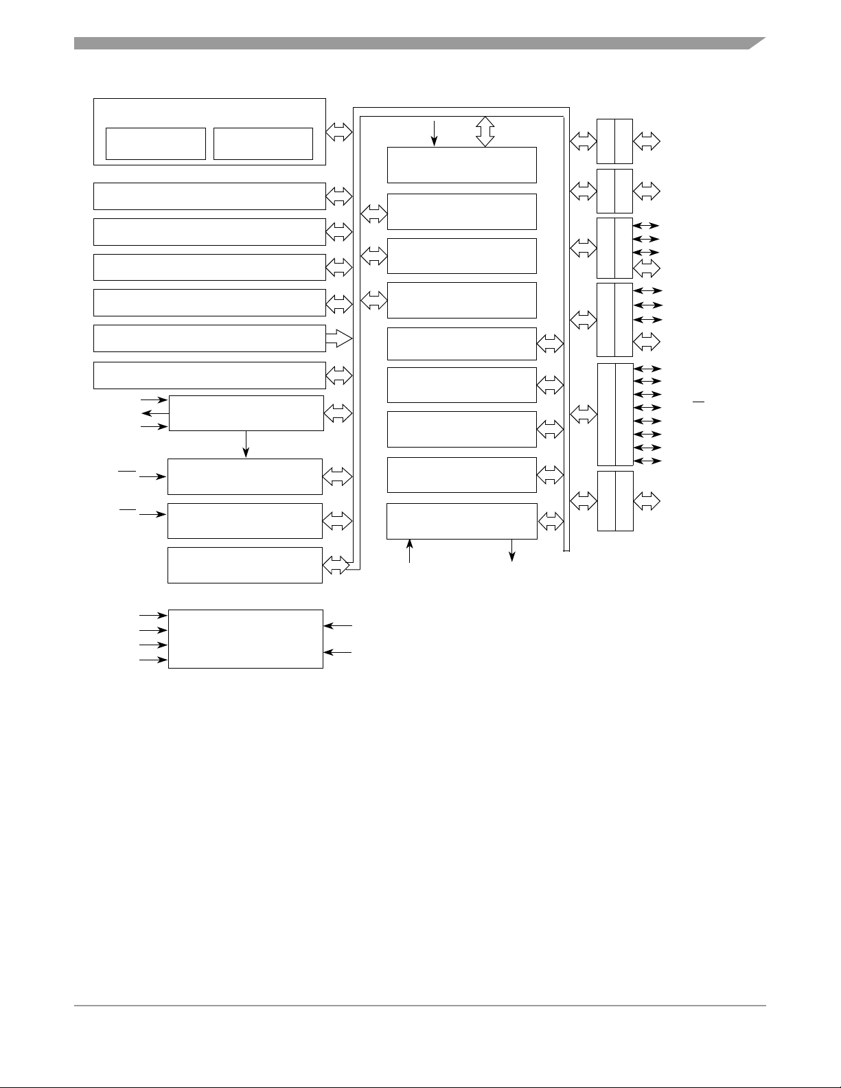
M68HC08 CPU
CPU
REGISTERS
ARITHMETIC/LOGIC
UNIT (ALU)
CONTROL AND STATUS REGISTERS
USER FLASH — 32, 256 BYTES
USER RAM — 1024 BYTES
USER EEPROM — 512 BYTES
MONITOR ROM — 256 BYTES
USER FLASH VECTOR SPACE — 52 BYTES
OSC1
OSC2
CGMXFC
RST
IRQ
CLOCK GENERATOR
MODULE
SYSTEM INTEGRATION
MODULE
IRQ MODULE
V
REFH
ANALOG-TO-DIGITAL
MODULE
BREAK MODULE
LOW-VOLTAGE INHIBIT
MODULE
COMPUTER OPERATING
PROPERLY MODULE
6-CHANNEL TIMER
INTERFACE MODULE
PROGRAMMABLE INTERRUPT
TIMER MODULE
SERIAL COMMUNICATIONS
INTERFACE MODULE
SERIAL PERIPHERAL
INTERFACE MODULE
BYTE DATA LINK CONTROLLER
MCU Block Diagram
PTB
PTC
PTF
PTA7–PTA0
PTB7/ATD7–
PTB0/ATD0
PTC4
PTC3
PTC2/MCLK
PTC1–PTC0
PTD6/ATD14/TCLK
PTD5/ATD13
PTA4/ATD12
PTD3/ATD11–
PTD0/ATD8
PTE7/SPSCK
PTE6/MOSI
PTE5/MISO
PTE4/SS
PTE3/TCH1
PTE2/TCH0
PTE1/RxD
PTE0/TxD
PTF3/TCH5–
PTF0/TCH2
DDRA
DDRB
DDRC
DDRD
DDRE
DDRF
PTA
PTD
PTE
POWER-ON RESET
MODULE
V
SS
V
DD
V
DDA
V
SSA
POWER
BDRxD BDTxD
AVSS/V
REFK
V
DDAREF
Figure 1-1. MCU Block Diagram for the MC68HC908AS32A
MC68HC908AS32A Data Sheet, Rev. 1
Freescale Semiconductor 21
Page 22

General Description
1.4 Pin Assignments
Figure 1-2 shows MC68HC908AS32A 52-pin plastic leaded chip carrier (PLCC) assignments.
DDAREF
REFL
/V
/V
SSA
DDA
REFH
V
V
PTD6/ATD14/TCLK
PTD5/ATD13
PTD4/ATD12
47
51
50
49
48
46
PTD3/ATD11
PTC4
CGMXFC
PTC3
PTC2/MCLK
PTC1
PTC0
OSC1
OSC2
7
6
5
4
3
8
2
V
1
52
IRQ
RST
PTF0/TCH2
PTF1/TCH3
PTF2/TCH4
PTF3/TCH5
BDRxD
BDTxD
PTE0/TxD
PTE1/RxD
PTE2/TCH0
PTE3/TCH1
34
PTD2/ATD10
PTD1/ATD9
PTD0/ATD8
PTB7/ATD7
PTB6/ATD6
PTB5/ATD5
PTB4/ATD4
PTB3/ATD3
PTB2/ATD2
PTB1/ATD1
PTB0/ATD0
PTA7
9
10
11
12
13
14
15
16
17
18
19
20
21
22
23
24
25
26
27
28
29
30
31
SS
DD
V
V
PTA0
PTA1
PTA2
PTA3
PTA4
PTA5
PTE4/SS
PTE5/MISO
PTE6/MOSI
PTE7/SPSCK
45
44
43
42
41
40
39
38
37
36
35
32
33
PTA6
Figure 1-2. 52-Pin PLCC Assignments (Top View)
NOTE
The following pin descriptions are just a quick reference. For a more
detailed representation, see Chapter 13 Input/Output Ports.
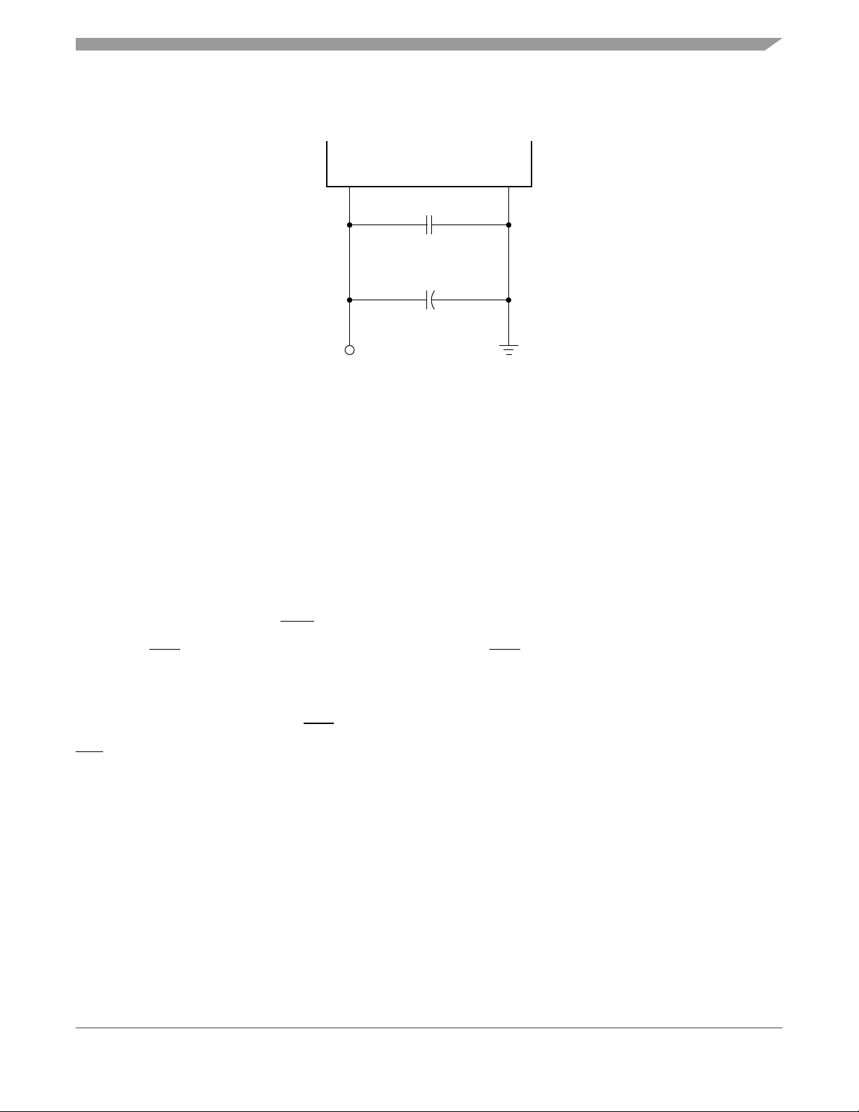
1.4.1 Power Supply Pins (VDD and VSS)
VDD and VSS are the power supply and ground pins. The MCU operates from a single power supply.
Fast signal transitions on MCU pins place high, short-duration current demands on the power supply. To
prevent noise problems, take special care to provide power supply bypassing at the MCU as shown in
Figure 1-3. Place the C1 bypass capacitor as close to the MCU as possible. Use a high-frequency
MC68HC908AS32A Data Sheet, Rev. 1
22 Freescale Semiconductor
Page 23
Pin Assignments
response ceramic capacitor for C1. C2 is an optional bulk current bypass capacitor for use in applications
that require the port pins to source high current levels.
MCU
V
DD
C1
0.1 µF
+
C2
V
DD
NOTE: Component values shown represent typical applications.
V
SS
Figure 1-3. Power Supply Bypassing
V
is also the ground for the port output buffers and the ground return for the serial clock in the SPI. See
SS
Chapter 16 Serial Peripheral Interface (SPI) for more information.
NOTE
V
must be grounded for proper MCU operation.
SS
1.4.2 Oscillator Pins (OSC1 and OSC2)
The OSC1 and OSC2 pins are the connections for the on-chip oscillator circuit. See Chapter 5 Clock
Generator Module (CGM) for more information.
1.4.3 External Reset Pin (RST)
A 0 on the RST pin forces the MCU to a known startup state. RST is bidirectional, allowing a reset of the
entire system. It is driven low when any internal reset source is asserted. See Chapter 15 System
Integration Module (SIM) for more information.
1.4.4 External Interrupt Pin (IRQ)
IRQ is an asynchronous external interrupt pin. See Chapter 10 External Interrupt Module (IRQ) for more
information.
1.4.5 External Filter Capacitor Pin (CGMXFC)
CGMXFC is an external filter capacitor connection for the clock generator module (CGM). See Chapter 5
Clock Generator Module (CGM) for more information.
1.4.6 Analog Power Supply Pin (V
V
DDA/VDDAREF
is the power supply pin for the analog portion of the ADC and the CGM. See Chapter 3
DDA/VDDAREF
Analog-to-Digital Converter (ADC) and Chapter 5 Clock Generator Module (CGM) for more information.
MC68HC908AS32A Data Sheet, Rev. 1
)
Freescale Semiconductor 23
Page 24

General Description
1.4.7 Analog Ground Pin (V
The V
SSA/VREFL
pin provides both the analog ground connection and the reference low voltage for the
SSA/VREFL
)
ADC as well as the ground connection for the CGM. See Chapter 3 Analog-to-Digital Converter (ADC)
and Chapter 5 Clock Generator Module (CGM) for more information.
1.4.8 ADC Reference High Voltage Pin (V
V
provides the reference high voltage for the ADC. See Chapter 3 Analog-to-Digital Converter (ADC)
REFH
REFH
)
for more information.
1.4.9 Port A Input/Output (I/O) Pins (PTA7–PTA0)
PTA7–PTA0 are general-purpose bidirectional input/output (I/O) port pins. See Chapter 13 Input/Output
Ports for more information.
1.4.10 Port B I/O Pins (PTB7/ATD7–PTB0/ATD0)
Port B is an 8-bit special function port that shares all eight pins with the ADC. See Chapter 3
Analog-to-Digital Converter (ADC) and Chapter 13 Input/Output Ports for more information.
1.4.11 Port C I/O Pins (PTC4–PTC0)
PTC4–PTC3 and PTC1–PTC0 are general-purpose bidirectional I/O port pins. PTC2/MCLK is a special
function port that shares its pin with the system clock which has a frequency equivalent to the system
clock. See Chapter 13 Input/Output Ports for more information.
1.4.12 Port D I/O Pins (PTD6–PTD0/ATD8)
Port D is an 7-bit special-function port that shares seven of its pins with the ADC and one of its pins with
the TIM. See Chapter 17 Timer Interface Module (TIM), Chapter 3 Analog-to-Digital Converter (ADC), and
Chapter 13 Input/Output Ports for more information.
1.4.13 Port E I/O Pins (PTE7/SPSCK–PTE0/TxD)
Port E is an 8-bit special function port that shares two of its pins with the TIM, four of its pins with the SPI,
and two of its pins with the SCI. See Chapter 14 Serial Communications Interface (SCI), Chapter 16 Serial
Peripheral Interface (SPI), Chapter 17 Timer Interface Module (TIM), and Chapter 13 Input/Output Ports
for more information.
1.4.14 Port F I/O Pins (PTF3–PTF0/TCH2)
Port F is a 4-bit special function port that shares four of its pins with the TIM. See Chapter 17 Timer
Interface Module (TIM) and Chapter 13 Input/Output Ports for more information.
1.4.15 BDLC Transmit Pin (BDTxD)
This pin is the digital output from the BDLC module (BDTxD). See Chapter 19 Electrical Specifications for
more information.
MC68HC908AS32A Data Sheet, Rev. 1
24 Freescale Semiconductor
Page 25

Pin Assignments
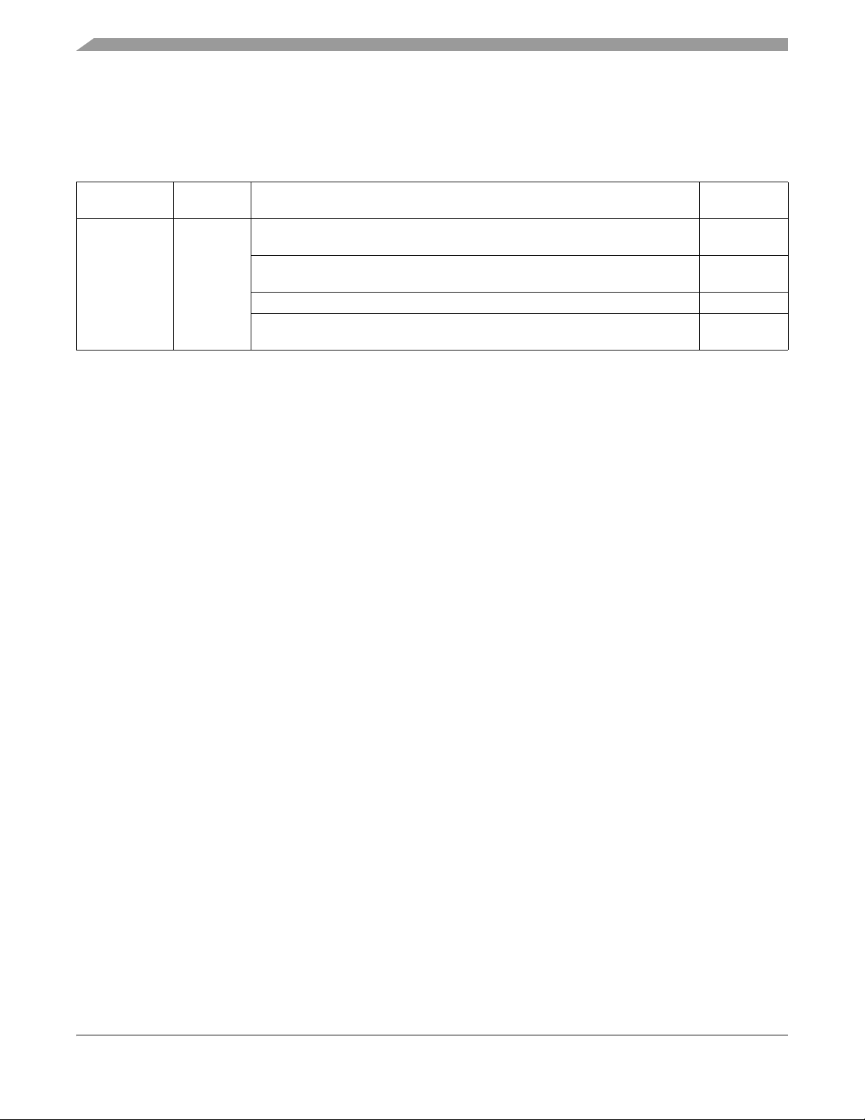
1.4.16 BDLC Receive Pin (BDRxD)
This pin is the digital input to the BDLC module (BDRxD). See Chapter 19 Electrical Specifications for
more information.
Table 1-1. External Pins Summary
Pin Name Function Driver Type
Hysteresis
(1)
Reset State
PTA7–PTA0 General-purpose I/O Dual state No Input Hi-Z
PTB7/ATD7–PTB0/ATD0 General-purpose I/O ADC channel Dual state No Input Hi-Z
PTC4–PTC0 General-purpose I/O Dual state No Input Hi-Z
PTD6/ATD14/TCLK ADC channel
ADC channel/timer external input clock
General-purpose I/O
Dual state No Input Hi-Z
PTD5/ATD13 ADC channel General-purpose I/O ADC channel Dual state No Input Hi-Z
PTD4/ATD12 ADC channel General-purpose I/O ADC channel Dual state No Input Hi-Z
PTD3/ATD11–PTD0/ATD8
ADC channels
PTE7/SPSCK General-purpose I/O SPI clock
PTE6/MOSI General-purpose I/O SPI data path
PTE5/MISO General-purpose I/O SPI data path
PTE4/SS
General-purpose I/O ADC channel Dual state No Input Hi-Z
Dual state
Open drain
Dual state
Open drain
Dual state
Open drain
Yes Input Hi-Z
Yes Input Hi-Z
Yes Input Hi-Z
General-purpose I/O SPI slave select Dual state Yes Input Hi-Z
PTE3/TCH1 General-purpose I/O TIM channel 1 Dual state Yes Input Hi-Z
PTE2/TCH0 General-purpose I/O TIM channel 0 Dual state Yes Input Hi-Z
PTE1/RxD General-purpose I/O SCI receive data Dual state Yes Input Hi-Z
PTE0/TxD General-purpose I/O SCI transmit data Dual state No Input Hi-Z
PTF3/TCH5 General-purpose I/O TIM channel 5 Dual state Yes Input Hi-Z
PTF2/TCH4 General-purpose I/O TIM channel 4 Dual state Yes Input Hi-Z
PTF1/TCH3 General-purpose I/O TIM channel 3 Dual state Yes Input Hi-Z
PTF0/TCH2 General-purpose I/O TIM channel 2 Dual state Yes Input Hi-Z
V
DD
V
SS
V
DDA/VDDAREF
V
SSA/VREFL
V
REFH
Chip power supply N/A N/A N/A
Chip ground N/A N/A N/A
ADC analog power supply
CGM analog power supply
ADC ground/ADC reference
low voltage CGM analog ground
N/A N/A N/A
N/A N/A N/A
A/D reference high voltage N/A N/A N/A
OSC1 External clock in N/A N/A Input Hi-Z
OSC2 External clock out N/A N/A Output
CGMXFC PLL loop filter cap N/A N/A N/A
IRQ External interrupt request N/A N/A Input Hi-Z
RST
Reset N/A N/A Output low
BDRxD BDLC serial input N/A Yes Input Hi-Z
BDTxD BDLC serial output Output No Output
1. Hysteresis is not 100% tested but is typically a minimum of 300 mV.
MC68HC908AS32A Data Sheet, Rev. 1
Freescale Semiconductor 25
Page 26

General Description
Table 1-2. Clock Signal Naming Conventions
Clock Signal Name Description
CGMXCLK Buffered version of OSC1 from CGM
CGMOUT PLL-based or OSC1-based clock output from CGM
Bus clock CGMOUT divided by two
SPSCK SPI serial clock
TCLK External clock input for TIM
Table 1-3. Clock Source Summary
Module Clock Source
ADC CGMXCLK or bus clock
CAN CGMXCLK or CGMOUT
COP CGMXCLK
CPU Bus clock
FLASH Bus clock
EEPROM CGMXCLK or bus clock
RAM Bus clock
SPI Bus clock/SPSCK
SCI CGMXCLK
TIM Bus clock or PTD6/ATD14/TCLK
PIT Bus clock
SIM CGMOUT and CGMXCLK
IRQ Bus clock
BRK Bus clock
LVI Bus clock
CGM OSC1 and OSC2
MC68HC908AS32A Data Sheet, Rev. 1
26 Freescale Semiconductor
Page 27

Chapter 2 Memory
2.1 Introduction
The CPU08 can address 64 Kbytes of memory space. The memory map, shown in Figure 2-1, includes:
• 32,256 bytes of FLASH EEPROM
• 1024 bytes of RAM
• 512 bytes of EEPROM with protect option
• 52 bytes of user-defined vectors
• 256 bytes of monitor ROM
2.2 Unimplemented Memory Locations
Accessing an unimplemented location can have unpredictable effects on MCU operation. In Figure 2-1
and in register figures in this document, unimplemented locations are shaded.
2.3 Reserved Memory Locations
Accessing a reserved location can have unpredictable effects on MCU operation. In Figure 2-1 and in
register figures in this document, reserved locations are marked with the word Reserved or with the
letter R.
2.4 Input/Output (I/O) Section
Addresses $0000–$004F, shown in Figure 2-2, contain the I/O data, status, and control registers.
2.5 Additional Status and Control Registers
Selected addresses in the range $FE00–$FF88 contain additional status and control registers as shown
in Figure 2-3. A noted exception is the computer operating properly (COP) control register (COPCTL) at
address $FFFF.
2.6 Vector Addresses and Priority
Addresses in the range $FFDA–$FFFF contain the user-specified vector locations. The vector addresses
are shown in Table 2-1. It is recommended that all vector addresses are defined.
MC68HC908AS32A Data Sheet, Rev. 1
Freescale Semiconductor 27
Page 28

Memory
$0000
↓
$004F
$0050
↓
$044F
$0450
↓
$07FF
$0800
↓
$09FF
$0A00
↓
$7FFF
$8000
↓
$FDFF
$FE00 SIM BREAK STATUS REGISTER (SBSR)
$FE01 SIM RESET STATUS REGISTER (SRSR)
$FE02 RESERVED
$FE03 SIM BREAK FLAG CONTROL REGISTER (SBFCR)
$FE04
↓
$FE08
$FE09 CONFIGURATION WRITE-ONCE REGISER 2 (CONFIG2)
$FE0A RESERVED
$FE0B RESERVED
$FE0C BREAK ADDRESS REGISTER HIGH (BRKH)
$FE0D BREAK ADDRESS REGISTER LOW (BRKL)
$FE0E BREAK STATUS AND CONTROL REGISTER (BSCR)
$FE0F LVI STATUS REGISTER (LVISR)
$FE10 EEPROM EEDIVH NONVOLATILE REGISTER (EEDIVHNVR)
$FE11 EEPROM EEDIVL NONVOLATILE REGISTER (EEDIVLNVR)
$FE12
↓
$FE19
$FE1A EEPROM EE DIVIDER HIGH REGISTER (EEDIVH)
$FE1B EEPROM EE DIVIDER LOW REGISTER (EEDIVL)
$FE1C EEPROM NONVOLATILE REGISTER (EENVR)
$FE1D EEPROM CONTROL REGISTER (EECR)
$FE1E RESERVED
$FE1F EEPROM ARRAY CONFIGURATION REGISTER (EEACR)
I/O REGISTERS (80 BYTES)
RAM (1024 BYTES)
UNIMPLEMENTED (944 BYTES)
EEPROM (512 BYTES)
UNIMPLEMENTED (30,208 BYTES)
FLASH (32,256 BYTES)
RESERVED
RESERVED
Figure 2-1. Memory Map
MC68HC908AS32A Data Sheet, Rev. 1
28 Freescale Semiconductor
Page 29
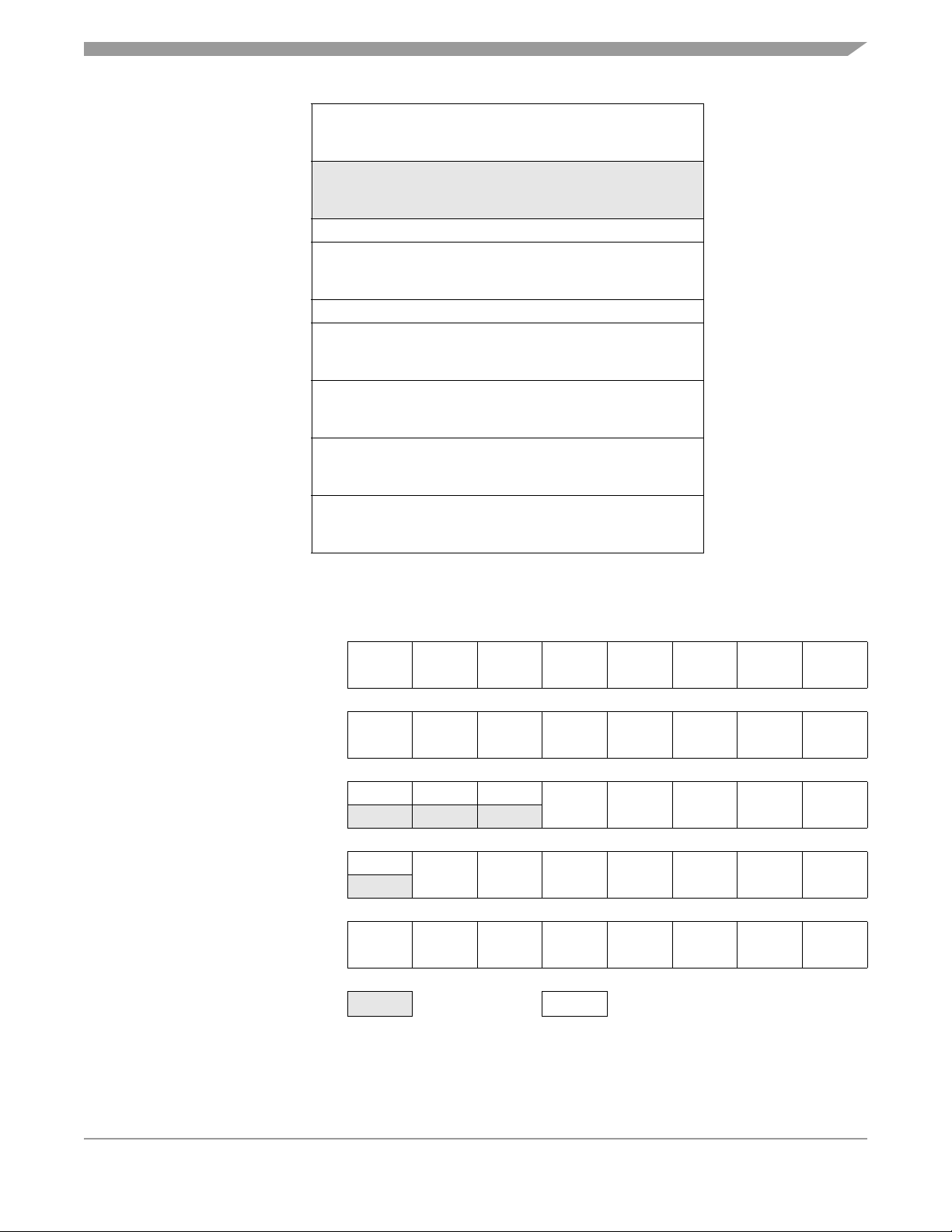
$FE20
↓
$FF1F
$FF20
↓
$FF7F
$FF80 FLASH BLOCK PROTECT REGISTER (FLBPR)
$FF81
↓
$FF87
$FF88 FLASH CONTROL REGISTER (FLCR)
$FF89
↓
$FF8F
$FF90
↓
$FFBF
$FFC0
↓
$FFD9
$FFDA
↓
$FFFF
MONITOR ROM (256 BYTES)
UNIMPLEMENTED (80 BYTES)
RESERVED (7 BYTES)
RESERVED (6 BYTES)
UNIMPLEMENTED (48 BYTES)
RESERVED (26 BYTES)
VECTORS (38 BYTES)
Vector Addresses and Priority
Figure 2-1. Memory Map (Continued)
Addr.Register Name Bit 7654321Bit 0
Read:
(PTA)
Write:
Reset: Unaffected by reset
Read:
(PTB)
Write:
Reset: Unaffected by reset
Read: 0 0 0
(PTC)
Write:
Reset: Unaffected by reset
Read: 0
(PTD)
Write:
Reset: Unaffected by reset
Read:
Write:
Reset:00000000
PTA7 PTA6 PTA5 PTA4 PTA3 PTA2 PTA1 PTA0
PTB7 PTB6 PTB5 PTB4 PTB3 PTB2 PTB1 PTB0
PTC4 PTC3 PTC2 PTC1 PTC0
PTD6 PTD5 PTD4 PTD3 PTD2 PTD1 PTD0
DDRA7 DDRA6 DDRA5 DDRA4 DDRA3 DDRA2 DDRA1 DDRA0
= Unimplemented
= Reserved U = Unaffected
R
$0000
$0001
$0002
$0003
$0004
Port A Data Register
See page 149.
Port B Data Register
See page 151.
Port C Data Register
See page 153.
Port D Data Register
See page 155.
Data Direction Register A
(DDRA)
See page 149.
Figure 2-2. I/O Data, Status and Control Registers (Sheet 1 of 6)
MC68HC908AS32A Data Sheet, Rev. 1
Freescale Semiconductor 29
Page 30
Memory
Addr.Register Name Bit 7654321Bit 0
Data Direction Register B
$0005
Data Direction Register C
$0006
Data Direction Register D
$0007
Port E Data Register
$0008
Port F Data Register
$0009
$000A Reserved RRRRRRRR
(DDRB)
See page 151.
(DDRC)
See page 153.
(DDRD)
See page 156.
See page 157.
See page 159.
Read:
Write:
Reset:00000000
Read:
Write:
Reset:00000000
Read: 0
Write:
Reset:00000000
Read:
Write:
(PTE)
Reset: Unaffected by reset
Read: 0 0 0 0
(PTF)
Write:
Reset: Unaffected by reset
DDRB7 DDRB6 DDRB5 DDRB4 DDRB3 DDRB2 DDRB1 DDRB0
MCLKEN
PTE7 PTE6 PTE5 PTE4 PTE3 PTE2 PTE1 PTE0
00
DDRC4 DDRC3 DDRC2 DDRC1 DDRC0
DDRD6 DDRD5 DDRD4 DDRD3 DDR2 DDRD1 DDRD0
PTF3 PTF2 PTF1 PTF0
$000B Reserved RRRRRRRR
Data Direction Register E
$000C
Data Direction Register F
$000D
$000E Reserved RRRRRRRR
$000F Reserved RRRRRRRR
SPI Control Register
$0010
SPI Status and Control
$0011
$0012
Register (SPSCR)
SPI Data Register
(DDRE)
See page 158.
(DDRF)
See page 160.
(SPCR)
See page 219.
See page 221.
(SPDR)
See page 223.
Read:
Write:
Reset:00000000
Read: 0 0 0 0
Write:
Reset:00000000
Read:
Write:
Reset:00101000
Read: SPRF 0 OVRF MODF SPTE 0
Write:
Reset:00001000
Read:R7R6R5R4R3R2R1R0
Write: T7 T6 T5 T4 T3 T2 T1 T0
Reset: Indeterminate after reset
DDRE7 DDRE6 DDRE5 DDRE4 DDRE3 DDRE2 DDRE1 DDRE0
DDRF3 DDRF2 DDRF1 DDRF0
SPRIE R SPMSTR CPOL CPHA SPWOM SPE SPTIE
SPR1 SPR0
= Unimplemented
= Reserved U = Unaffected
R
Figure 2-2. I/O Data, Status and Control Registers (Sheet 2 of 6)
MC68HC908AS32A Data Sheet, Rev. 1
30 Freescale Semiconductor
Page 31

Vector Addresses and Priority
Addr.Register Name Bit 7654321Bit 0
SCI Control Register 1
$0013
SCI Control Register 2
$0014
SCI Control Register 3
$0015
SCI Status Register 1
$0016
SCI Status Register 2
$0017
SCI Data Register
$0018
SCI Baud Rate Register
$0019
IRQ Status/Control Register
$001A
$001B Reserved RRRRRRRR
(SCC1)
See page 176.
(SCC2)
See page 178.
(SCC3)
See page 180.
(SCS1)
See page 181.
(SCS2)
See page 183.
(SCDR)
See page 184.
(SCBR)
See page 184.
(ISCR)
See page 137.
Read:
Write:
Reset:00000000
Read:
Write:
Reset:00000000
Read: R8
Write:
Reset:UU000000
Read: SCTE TC SCRF IDLE OR NF FE PE
Write:
Reset:11000000
Read:000000BKFRPF
Write:
Reset:00000000
Read:R7R6R5R4R3R2R1R0
Write: T7 T6 T5 T4 T3 T2 T1 T0
Reset: Unaffected by reset
Read: 0 0
Write:
Reset:00000000
Read: 0 0 0 0 IRQF 0
Write:
Reset:00000000
LOOPS ENSCI TXINV M WAKE ILTY PEN PTY
SCTIE TCIE SCRIE ILIE TE RE RWU SBK
T8 R R ORIE NEIE FEIE PEIE
SCP1 SCP0
0
SCR2 SCR1 SCR0
ACK
IMASK MODE
$001C
$001D
$001E
$001F
PLL Control Register
(PCTL)
See page 104.
PLL Bandwidth Control
Register (PBWC)
See page 105.
PLL Programming Register
(PPG)
See page 106.
Configuration Write-Once
Register (CONFIG1)
See page 113.
Read:
Write:
Reset:00101111
Read:
Write:
Reset:00000000
Read:
Write:
Reset:01100110
Read:
Write:
Reset:01110000
PLLIE
AUTO
MUL7 MUL6 MUL5 MUL4 VRS7 VRS6 VRS5 VRS4
LVISTOP R LVIRST LVIPWR SSREC COPL STOP COPD
PLLF
LOCK
= Unimplemented
PLLON BCS
ACQ
XLD
R
1111
0000
= Reserved U = Unaffected
Figure 2-2. I/O Data, Status and Control Registers (Sheet 3 of 6)
MC68HC908AS32A Data Sheet, Rev. 1
Freescale Semiconductor 31
Page 32

Memory
Addr.Register Name Bit 7654321Bit 0
TIM Status and Control
$0020
$0021 Reserved RRRRRRRR
Register (TSC)
See page 235.
Read: TOF
Write: 0 TRST
Reset:00100000
TOIE TSTOP
00
PS2 PS1 PS0
$0022
$0023
$0024
$0025
$0026
$0027
$0028
$0029
$002A
$002B
$002C
TIM Counter Register High
(TCNTH)
See page 236.
TIM Counter Register Low
(TCNTL)
See page 236.
TIM Modulo Register High
(TMODH)
See page 237.
TIM Modulo Register Low
(TMODL)
See page 237.
TIM Channel 0 Status and
Control Register (TSC0)
See page 238.
TIM Channel 0 Register High
(TCH0H)
See page 241.
TIM Channel 0 Register Low
(TCH0L)
See page 241.
TIM Channel 1 Status and
Control Register (TSC1)
See page 238.
TIM Channel 1 Register High
(TCH1H)
See page 241.
TIM Channel 1 Register Low
(TCH1L)
See page 241.
TIM Channel 2 Status and
Control Register (TSC2)
See page 238.
Read: Bit 15 14 13 12 11 10 9 Bit 8
Write:
Reset:00000000
Read:Bit 7654321Bit 0
Write:
Reset:00000000
Read:
Write:
Reset:11111111
Read:
Write:
Reset:11111111
Read: CH0F
Write: 0
Reset:00000000
Read:
Write:
Reset: Indeterminate after reset
Read:
Write:
Reset:
Read: CH1F
Write: 0
Reset:00000000
Read:
Write:
Reset: Indeterminate after reset
Read:
Write:
Reset: Indeterminate after reset
Read: CH2F
Write: 0
Reset:00000000
Bit 15 14 13 12 11 10 9 Bit 8
Bit 7654321Bit 0
CH0IE MS0B MS0A ELS0B ELS0A TOV0 CH0MAX
Bit 15 14 13 12 11 10 9 Bit 8
Bit 7654321Bit 0
CH1IE
Bit 15 14 13 12 11 10 9 Bit 8
Bit 7654321Bit 0
CH2IE MS2B MS2A ELS2B ELS2A TOV2 CH2MAX
= Unimplemented
0
MS1A ELS1B ELS1A TOV1 CH1MAX
= Reserved U = Unaffected
R
Figure 2-2. I/O Data, Status and Control Registers (Sheet 4 of 6)
MC68HC908AS32A Data Sheet, Rev. 1
32 Freescale Semiconductor
Page 33

Vector Addresses and Priority
Addr.Register Name Bit 7654321Bit 0
Read:
Write:
Reset: Indeterminate after reset
Read:
Write:
Reset: Indeterminate after reset
Read: CH3F
Write: 0
Reset:00000000
Read:
Write:
Reset: Indeterminate after reset
Read:
Write:
Reset: Indeterminate after reset
Read: CH4F
Write: 0
Reset:00000000
Read:
Write:
Reset: Indeterminate after reset
Read:
Write:
Reset: Indeterminate after reset
Read: CH5F
Write: 0
Reset:00000000
Read:
Write:
Reset: Indeterminate after reset
Read:
Write:
Reset: Indeterminate after reset
Read: COCO
Write: R
Reset:00000000
Read: AD7 AD6 AD5 AD4 AD3 AD2 AD1 AD0
(ADR)
Write:RRRRRRRR
Reset: Indeterminate after reset
Bit 15 14 13 12 11 10 9 Bit 8
Bit 7654321Bit 0
CH3IE
Bit 15 14 13 12 11 10 9 Bit 8
Bit 7654321Bit 0
CH4IE MS4B MS4A ELS4B ELS4A TOV4 CH4MAX
Bit 15 14 13 12 11 10 9 Bit 8
Bit 7654321Bit 0
CH5IE
Bit 15 14 13 12 11 10 9 Bit 8
Bit 7654321Bit 0
AIEN ADCO ADCH4 ADCH3 ADCH2 ADCH1 ADCH0
= Unimplemented
0
0
MS3A ELS3B ELS3A TOV3 CH3MAX
MS5A ELS5B ELS5A TOV5 CH5MAX
= Reserved U = Unaffected
R
$002D
$002E
$002F
$0030
$0031
$0032
$0033
$0034
$0035
$0036
$0037
$0038
$0039
TIM Channel 2 Register High
(TCH2H)
See page 241.
TIM Channel 2 Register Low
(TCH2L)
See page 241.
TIM Channel 3 Status and
Control Register (TSC3)
See page 238.
TIM Channel 3 Register High
(TCH3H)
See page 241.
TIM Channel 3 Register Low
(TCH3L)
See page 241.
TIM Channel 4 Status and
Control Register (TSC4)
See page 238.
TIM Channel 4 Register High
(TCH4H)
See page 241.
TIM Channel 4 Register Low
(TCH4L)
See page 241.
TIM Channel 5 Status and
Control Register (TSC5)
See page 238.
TIM Channel 5 Register High
(TCH5H)
See page 241.
TIM Channel 5 Register Low
(TCH5L)
See page 241.
ADC Status and Control
Register (ADSCR)
See page 61.
ADC Data Register
See page 63.
Figure 2-2. I/O Data, Status and Control Registers (Sheet 5 of 6)
MC68HC908AS32A Data Sheet, Rev. 1
Freescale Semiconductor 33
Page 34

Memory
Addr.Register Name Bit 7654321Bit 0
$003A
$003B
$003C
$003D
$003E
$003F
$0040
↓
$004A
ADC Input Clock Register
(ADICLK)
See page 63.
BDLC Analog and Roundtrip
Delay Register (BARD)
See page 83.
BDLC Control Register 1
(BCR1)
See page 84.
BDLC Control Register 2
(BCR2)
See page 86.
BDLC State Vector Register
(BSVR)
See page 90.
BDLC Data Register
(BDR)
See page 92.
Reserved RRRRRRRR
Read:
Write:
Reset:00000000
Read:
Write: R R
Reset:11000111
Read:
Write: R R
Reset:11100000
Read:
Write:
Reset:11000000
Read:0 0 I3I2I1I0 0 0
Write:RRRRRRRR
Reset:00000000
Read:
Write:
Reset: Unaffected by reset
ADIV2 ADIV1 ADIV0 ADICLK
ATE RXPOL
IMSG CLKS R1 R0
ALOOP DLOOP RX4XE NBFS TEOD TSIFR TMIFR1 TMIFR0
BD7 BD6 BD5 BD4 BD3 BD2 BD1 BD0
00
0000
BO3 BO2 BO1 BO0
00
IE WCM
$004B
$004C
$004D
$004E
$004F
PIT Status and Control
Register (PSC)
See page 145.
PIT Counter Register High
(PCNTH)
See page 146.
PIT Counter Register Low
(PCNTL)
See page 146.
PIT Counter Modulo Register
High (PMODH)
See page 147.
PIT Counter Modulo Register
Low (PMODL)
See page 147.
Figure 2-2. I/O Data, Status and Control Registers (Sheet 6 of 6)
Read: POF
Write: 0 PRST
Reset:00100000
Read: Bit 15 14 13 12 11 10 9 Bit 8
Write:
Reset:00000000
Read:Bit 7654321Bit 0
Write:
Reset:00000000
Read:
Write:
Reset:11111111
Read:
Write:
Reset:11111111
Bit 15 14 13 12 11 10 9 Bit 8
Bit 7654321Bit 0
POIE PSTOP
= Unimplemented
00
= Reserved U = Unaffected
R
PPS2 PPS1 PPS0
MC68HC908AS32A Data Sheet, Rev. 1
34 Freescale Semiconductor
Page 35

Vector Addresses and Priority
Addr.Register Name Bit 7654321Bit 0
SIM Break Status Register
$FE00
SIM Reset Status Register
$FE01
$FE02 Reserved RRRRRRRR
(SBSR)
See page 200.
(SRSR)
See page 200.
Read:
Write: See note
Reset: 0
Read: POR PIN COP ILOP ILAD 0 LVI 0
Write:
Reset:10000000
RRRRRR
Note: Writing a 0 clears BW
BW
R
$FE03
$FE09
$FE0C
$FE0D
$FE0E
$FE0F
$FE10
$FE11
$FE1A
$FE1B
SIM Break Flag Control Register
(SBFCR)
See page 201.
Configuration Write-Once
Register (CONFIG2)
See page 115.
Break Address Register High
(BRKH)
See page 246.
Break Address Register Low
(BRKL)
See page 246.
Break Status and Control
Register (BRKSCR)
See page 246.
LVI Status Register
(LVISR)
See page 140.
EEDIV High Nonvolatile
Register (EEDIVHNVR)
See page 46.
EEDIV Low Nonvolatile
Register (EEDIVLNVR)
See page 46.
EEDIV Timebase Divider High
Register (EEDIVH)
See page 46.
EEDIV Timebase Divider Low
Register (EEDIVL)
See page 47.
Read:
Write:
Reset:
Read:
Write:
Reset:00011000
Read:
Write:
Reset:00000000
Read:
Write:
Reset:00000000
Read:
Write:
Reset:00000000
Read:LVIOUT0000000
Write:
Reset:00000000
Read:
Write:
Reset: Unaffected by reset; $FF when blank
Read:
Write:
Reset: Unaffected by reset; $FF when blank
Read:
Write:
Reset: Contents of EEDIVHNVR ($FE10), Bits [6:3] = 0
Read:
Write:
Reset: Contents of EEDIVLNVR ($FE11)
BCFERRRRRRR
0
EEDIVCLK R R R AS32A R R R
Bit 15 14 13 12 11 10 9 Bit 8
Bit 7654321Bit 0
BRKE BRKA
EEDIV
SECD
EEDIV7 EEDIV6 EEDIV5 EEDIV4 EEDIV3 EEDIV2 EEDIV1 EEDIV0
EEDIV
SECD
EEDIV7 EEDIV6 EEDIV5 EEDIV4 EEDIV3 EEDIV2 EEDIV1 EEDIV0
= Unimplemented
000000
EEDIV10 EEDIV9 EEDIV8
EEDIV10 EEDIV9 EEDIV8
= Reserved
R
Figure 2-3. Additional Status and Control Registers (Sheet 1 of 2)
MC68HC908AS32A Data Sheet, Rev. 1
Freescale Semiconductor 35
Page 36

Memory
Addr.Register Name Bit 7654321Bit 0
Read:
Write:
Reset: Programmed value or 1 in the erased state
Read:
Write:
Reset:00000000
Read:
Write:
Reset: Contents of EENVR ($FE1C)
Read:
Write:
Reset: Unaffected by reset
Read:0000
Write:
Reset:00000000
BPR7 BPR6 BPR5 BPR4 BPR3 BPR2 BPR1 BPR0
0
EEOFF EERAS1 EERAS0 EELAT AUTO EEPGM
EEPRTCT EEBP3 EEBP2 EEBP1 EEBP0
EEPRTCT EEBP3 EEBP2 EEBP1 EEBP0
HVEN VERF ERASE PGM
$FE1C
$FE1D
$FE1F
$FF80
$FF88
EEPROM Nonvolatile Register
(EENVR)
See page 46.
EEPROM Control Register
(EECR)
See page 43.
EEPROM Array Configuration
Register (EEACR)
See page 44.
FLASH Block Protect Register
(FLBPR)
See page 50.
FLASH Control Register
(FLCR)
See page 49.
$FFFF
COP Control Register
(COPCTL)
See page 119.
Read: LOW BYTE OF RESET VECTOR
Write: WRITING TO $FFFF CLEARS COP COUNTER
Reset: Unaffected by reset
= Unimplemented
R
= Reserved
Figure 2-3. Additional Status and Control Registers (Sheet 2 of 2)
MC68HC908AS32A Data Sheet, Rev. 1
36 Freescale Semiconductor
Page 37

Table 2-1. Vector Addresses
Vector Priority Address Vector
Lowest $FFDA PIT Vector (High)
$FFDB PIT Vector (Low)
$FFDC BDLC Vector (High)
$FFDD BDLC Vector (Low)
$FFDE ADC Vector (High)
$FFDF ADC Vector (Low)
$FFE0 SCI Transmit Vector (High)
$FFE1 SCI Transmit Vector (Low)
$FFE2 SCI Receive Vector (High)
$FFE3 SCI Receive Vector (Low)
$FFE4 SCI Error Vector (High)
$FFE5 SCI Error Vector (Low)
$FFE6 SPI Transmit Vector (High)
$FFE7 SPI Transmit Vector (Low)
$FFE8 SPI Receive Vector (High)
$FFE9 SPI Receive Vector (Low)
$FFEA TIM Overflow Vector (High)
$FFEB TIM Overflow Vector (Low)
$FFEC TIM Channel 5 Vector (High)
$FFED TIM Channel 5 Vector (Low)
$FFEE TIM Channel 4 Vector (High)
$FFEF TIM Channel 4 Vector (Low)
$FFF0 TIM Channel 3 Vector (High)
$FFF1 TIM Channel 3 Vector (Low)
$FFF2 TIM Channel 2 Vector (High)
$FFF3 TIM Channel 2 Vector (Low)
$FFF4 TIM Channel 1 Vector (High)
$FFF5 TIM Channel 1 Vector (Low)
$FFF6 TIM Channel 0 Vector (High)
$FFF7 TIM Channel 0 Vector (Low)
$FFF8 PLL Vector (High)
$FFF9 PLL Vector (Low)
$FFFA IRQ1 Vector (High)
$FFFB IRQ1 Vector (Low)
$FFFC SWI Vector (High)
$FFFD SWI Vector (Low)
$FFFE Reset Vector (High)
Highest $FFFF Reset Vector ( L ow)
Vector Addresses and Priority
MC68HC908AS32A Data Sheet, Rev. 1
Freescale Semiconductor 37
Page 38

Memory
2.7 Random-Access Memory (RAM)
The 1024 bytes of random-access memory (RAM) are located at address $0050–$044F is the RAM
location. The 16-bit stack pointer allows the stack RAM to be anywhere in the 64 Kbyte memory space.
NOTE
For correct operation, the stack pointer must point only to RAM locations.
Within page zero are 176 bytes of RAM. Because the location of the stack RAM is programmable, all page
zero RAM locations can be used for I/O control and user data or code. When the stack pointer is moved
from its reset location at $00FF, direct addressing mode instructions can access all page zero RAM
locations efficiently. Therefore, page zero RAM provides ideal locations for frequently accessed global
variables.
Before processing an interrupt, the CPU uses five bytes of the stack to save the contents of the CPU
registers.
NOTE
For M68HC05, M6805, and M146805 compatibility, the H register is not
stacked.
During a subroutine call, the CPU uses two bytes of the stack to store the return address. The stack
pointer decrements during pushes and increments during pulls.
NOTE
Be careful when using nested subroutines. The CPU could overwrite data
in the RAM during a subroutine or during the interrupt stacking operation.
2.8 Electrically Erasable Programmable Read-Only Memory (EEPROM)
This subsection describes the 512 bytes of electrically erasable programmable read-only memory
(EEPROM) residing at address range $0800–$09FF.
Features include:
• 512 bytes nonvolatile memory
• Byte, block, or bulk erasable
• Nonvolatile EEPROM configuration and block protection options
• On-chip charge pump for programming/erasing
• Security option
• AUTO bit driven programming/erasing time feature
2.8.1 Functional Description
The 512 bytes of EEPROM are located at $0800–$09FF and can be programmed or erased without an
additional external high voltage supply. The program and erase operations are enabled through the use
of an internal charge pump. For each byte of EEPROM, the write/erase endurance is 10,000 cycles.
1. No security feature is absolutely secure. However, Freescale’s strategy is to make reading or copying the EEPROM difficult
for unauthorized users.
(1)
MC68HC908AS32A Data Sheet, Rev. 1
38 Freescale Semiconductor
Page 39

Electrically Erasable Programmable Read-Only Memory (EEPROM)
2.8.1.1 EEPROM Configuration
The 8-bit EEPROM nonvolatile register (EENVR) and the 16-bit EEPROM timebase divider nonvolatile
register (EEDIVNVR) contain the default settings for the following EEPROM configurations:
• EEPROM timebase reference
• EEPROM security option
• EEPROM block protection
EENVR and EEDIVNVR are nonvolatile EEPROM registers that are programmed and erased in the same
way as EEPROM bytes. The contents of these registers are loaded into their respective volatile registers
during a MCU reset. The values in these read/write volatile registers define the EEPROM configurations.
• For EENVR, the corresponding volatile register is the EEPROM array configuration register
(EEACR).
• For the EEDIVNCR (two 8-bit registers: EEDIVHNVR and EEDIVLNVR), the corresponding volatile
register is the EEPROM divider register (EEDIV: EEDIVH and EEDIVL).
2.8.1.2 EEPROM Timebase Requirements
A 35 µs timebase is required by the EEPROM control circuit for program and erase of EEPROM content.
This timebase is derived from dividing the CGMXCLK or bus clock (selected by EEDIVCLK bit in
CONFIG2 register) using a timebase divider circuit controlled by the 16-bit EEPROM timebase divider
EEDIV register (EEDIVH and EEDIVL).
As the CGMXCLK or bus clock is user selected, the EEPROM timebase divider register must be
configured with the appropriate value to obtain the 35 µs. The timebase divider value is calculated by
using the following formula:
EEDIV= INT[Reference Frequency(Hz) x 35 x10
–6
+0.5]
This value is written to the EEPROM timebase divider register (EEDIVH and EEDIVL) or programmed into
the EEPROM timebase divider nonvolatile register prior to any EEPROM program or erase operations
(see 2.8.1.1 EEPROM Configuration and 2.8.1.2 EEPROM Timebase Requirements).
2.8.1.3 EEPROM Program/Erase Protection
The EEPROM has a special feature that designates the 16 bytes of addresses from $08F0–$08FF to be
permanently secured. This program/erase protect option is enabled by programming the EEPRTCT bit in
the EEPROM nonvolatile register to a 0.
Once the EEPRTCT bit is programmed to 0 for the first time:
• Programming and erasing of secured locations $08F0–$08FF is permanently disabled.
• Secured locations $08F0–$08FF can be read as normal.
• Programming and erasing of EENVR is permanently disabled.
• Bulk and block erase operations are disabled for the unprotected locations $0800–$08EF and
$0900–$09FF.
• Single byte program and erase operations are still available for locations $0800–$08EF and
$0900–$09FF for all bytes that are not protected by the EEPROM block protect EEBPx bits (see
2.8.1.4 EEPROM Block Protection and 2.8.2.2 EEPROM Array Configuration Register)
MC68HC908AS32A Data Sheet, Rev. 1
Freescale Semiconductor 39
Page 40

Memory
NOTE
Once armed, the protect option is permanently enabled. As a consequence,
all functions in the EENVR will remain in the state they were in immediately
before the security was enabled.
2.8.1.4 EEPROM Block Protection
The 512 bytes of EEPROM are divided into four 128-byte blocks. Each of these blocks can be protected
from erase/program operations by setting the EEBPx bit in the EENVR. Table 2-2 shows the address
ranges for the blocks.
Table 2-2. EEPROM Array Address Blocks
Block Number (EEBPx) Address Range
EEBP0 $0800–$087F
EEBP1 $0880–$08FF
EEBP2 $0900–$097F
EEBP3 $0980–$09FF
These bits are effective after a reset or a upon read of the EENVR register. The block protect configuration
can be modified by erasing/programming the corresponding bits in the EENVR register and then reading
the EENVR register. See 2.8.2.2 EEPROM Array Configuration Register for more information.
NOTE
Once EEDIVSECD in the EEDIVHNVR is programmed to 0 and after a
system reset, the EEDIV security feature is permanently enabled because
the EEDIVSECD bit in the EEDIVH is always loaded with 0s thereafter.
Once this security feature is armed, erase and program mode are disabled
for EEDIVHNVR and EEDIVLNVR. Modifications to the EEDIVH and
EEDIVL registers are also disabled. Therefore, be cautious on
programming a value into the EEDIVHNVR.
2.8.1.5 EEPROM Programming and Erasing
The unprogrammed or erase state of an EEPROM bit is a 1. The factory default for all bytes within the
EEPROM array is $FF.
The programming operation changes an EEPROM bit from 1 to 0 (programming cannot change a bit from
0 to a 1). In a single programming operation, the minimum EEPROM programming size is one bit; the
maximum is eight bits (one byte).
The erase operation changes an EEPROM bit from 0 to 1. In a single erase operation, the minimum
EEPROM erase size is one byte; the maximum is the entire EEPROM array.
The EEPROM can be programmed such that one or multiple bits are programmed (written to a 0) at a
time. However, the user may never program the same bit location more than once before erasing the
entire byte. In other words, the user is not allowed to program a 0 to a bit that is already programmed (bit
state is already 0).
For some applications it might be advantageous to track more than 10K events with a single byte of
EEPROM by programming one bit at a time. For that purpose, a special selective bit programming
technique is available. An example of this technique is illustrated in Table 2-3.
MC68HC908AS32A Data Sheet, Rev. 1
40 Freescale Semiconductor
Page 41

Electrically Erasable Programmable Read-Only Memory (EEPROM)
Table 2-3. Example Selective Bit Programming Description
Description
Original state of byte (erased) N/A 1111:1111
First event is recorded by programming bit position 0 1111:1110 1111:1110
Second event is recorded by programming bit position 1 1111:1101 1111:1100
Third event is recorded by programming bit position 2 1111:1011 1111:1000
Fourth event is recorded by programming bit position 3 1111:0111 1111:0000
Events five through eight are recorded in a similar fashion
Program Data
in Binary
Result
in Binary
NOTE
None of the bit locations are actually programmed more than once although
the byte was programmed eight times.
When this technique is utilized, a program/erase cycle is defined as multiple program sequences (up to
eight) to a unique location followed by a single erase operation.
2.8.1.6 Program/Erase Using AUTO Bit
An additional feature available for EEPROM program and erase operations is the AUTO mode. When
enabled, AUTO mode will activate an internal timer that will automatically terminate the program/erase
cycle and clear the EEPGM bit. See 2.8.1.7 EEPROM Programming, 2.8.1.8 EEPROM Erasing, and
2.8.2.1 EEPROM Control Register for more information.
2.8.1.7 EEPROM Programming
The unprogrammed or erase state of an EEPROM bit is a 1. Programming changes the state to a 0. Only
EEPROM bytes in the non-protected blocks and the EENVR register can be programmed.
Use the following procedure to program a byte of EEPROM:
1. Clear EERAS1 and EERAS0 and set EELAT in the EECR.
(A)
NOTE
If using the AUTO mode, also set the AUTO bit during step 1.
2. Write the desired data to the desired EEPROM address.
EEPGM
(C)
Go to step 7 if AUTO is set.
, to program the byte.
3. Set the EEPGM bit.
4. Wait for time, t
(B)
5. Clear EEPGM bit.
6. Wait for time, t
7. Poll the EEPGM bit until it is cleared by the internal timer.
8. Clear EELAT bits.
, for the programming voltage to fall. Go to step 8.
EEFPV
(E)
(D)
NOTE
A. EERAS1 and EERAS0 must be cleared for programming. Setting the
EELAT bit configures the address and data buses to latch data for
programming the array. Only data with a valid EEPROM address will be
latched. If EELAT is set, other writes to the EECR will be allowed after a
valid EEPROM write.
MC68HC908AS32A Data Sheet, Rev. 1
Freescale Semiconductor 41
Page 42

Memory
B. If more than one valid EEPROM write occurs, the last address and data
will be latched overriding the previous address and data. Once data is
written to the desired address, do not read EEPROM locations other than
the written location. (Reading an EEPROM location returns the latched data
and causes the read address to be latched).
C. The EEPGM bit cannot be set if the EELAT bit is cleared or a non-valid
EEPROM address is latched. This is to ensure proper programming
sequence. Once EEPGM is set, do not read any EEPROM locations;
otherwise, the current program cycle will be unsuccessful. When EEPGM
is set, the on-board programming sequence will be activated.
D. The delay time for the EEPGM bit to be cleared in AUTO mode is less
than t
EEPGM
For forward compatibility, software should not make any dependency on
this delay time.
E. Any attempt to clear both EEPGM and EELAT bits with a single
instruction will only clear EEPGM. This is to allow time for removal of high
voltage from the EEPROM array.
2.8.1.8 EEPROM Erasing
. However, on other MCUs, this delay time may be different.
The programmed state of an EEPROM bit is a 0. Erasing changes the state to a 1. Only EEPROM bytes
in the non-protected blocks and the EENVR register can be erased.
Use the following procedure to erase a byte, block, or the entire EEPROM array:
1. Configure EERAS1 and EERAS0 for byte, block, or bulk erase; set EELAT in EECR.
(A)
NOTE
If using the AUTO mode, also set the AUTO bit in step 1.
2. Byte erase — write any data to the desired address.
Block erase — write any data to an address within the desired block.
Bulk erase — write any data to an address within the array.
3. Set the EEPGM bit.
4. Wait for a time: t
(C)
Go to Step 7 if AUTO is set.
EEBYTE
for byte erase; t
EEBLOCK
(B)
(B)
for block erase; t
(B)
EEBULK.
for bulk erase.
5. Clear EEPGM bit.
6. Wait for a time, t
7. Poll the EEPGM bit until it is cleared by the internal timer.
8. Clear EELAT bits.
, for the erasing voltage to fall. Go to Step 8.
EEFPV
(E)
(D)
NOTE
A. Setting the EELAT bit configures the address and data buses to latch
data for erasing the array. Only valid EEPROM addresses will be latched.
If EELAT is set, other writes to the EECR will be allowed after a valid
EEPROM write.
B. If more than one valid EEPROM write occurs, the last address and data
will be latched overriding the previous address and data. Once data is
written to the desired address, do not read EEPROM locations other than
MC68HC908AS32A Data Sheet, Rev. 1
42 Freescale Semiconductor
Page 43

Electrically Erasable Programmable Read-Only Memory (EEPROM)
the written location. (Reading an EEPROM location returns the latched data
and causes the read address to be latched).
C. The EEPGM bit cannot be set if the EELAT bit is cleared or a non-valid
EEPROM address is latched. This is to ensure proper programming
sequence. Once EEPGM is set, do not read any EEPROM locations;
otherwise, the current program cycle will be unsuccessful. When EEPGM
is set, the on-board programming sequence will be activated.
D. The delay time for the EEPGM bit to be cleared in AUTO mode is less
than t
EEBYTE /tEEBLOCK/tEEBULK
. However, on other MCUs, this delay time
may be different. For forward compatibility, software should not make any
dependency on this delay time.
E. Any attempt to clear both EEPGM and EELAT bits with a single
instruction will only clear EEPGM. This is to allow time for removal of high
voltage from the EEPROM array.
2.8.2 EEPROM Register Descriptions
Four I/O registers and three nonvolatile registers control program, erase, and options of the EEPROM
array.
2.8.2.1 EEPROM Control Register
This read/write register controls programming/erasing of the array.
Address: $FE1D
Bit 7654321Bit 0
Read:
UNUSED
Write:
Reset:00000000
0
= Unimplemented
EEOFF EERAS1 EERAS0 EELAT AUTO EEPGM
Figure 2-4. EEPROM Control Register (EECR)
Bit 7— Unused Bit
This read/write bit is software programmable but has no functionality.
EEOFF — EEPROM Power Down
This read/write bit disables the EEPROM module for lower power consumption. Any attempts to
access the array will give unpredictable results. Reset clears this bit.
1 = Disable EEPROM array
0 = Enable EEPROM array
EERAS1 and EERAS0 — Erase/Program Mode Select Bits
These read/write bits set the erase modes. Reset clears these bits.
MC68HC908AS32A Data Sheet, Rev. 1
Freescale Semiconductor 43
Page 44

Memory
Table 2-4. EEPROM Program/Erase Mode Select
EEBPx EERAS1 EERAS0 Mode
0 0 0 Byte program
0 0 1 Byte erase
0 1 0 Block erase
0 1 1 Bulk erase
1 X X No erase/program
X = don’t care
EELAT — EEPROM Latch Control
This read/write bit latches the address and data buses for programming the EEPROM array. EELAT
cannot be cleared if EEPGM is still set. Reset clears this bit.
1 = Buses configured for EEPROM programming or erase operation
0 = Buses configured for normal operation
AUTO — Automatic Termination of Program/Erase Cycle
When AUTO is set, EEPGM is cleared automatically after the program/erase cycle is terminated by
the internal timer. See note D for 2.8.1.7 EEPROM Programming, 2.8.1.8 EEPROM Erasing, and
19.11.2 EEPROM Memory Characteristics.
1 = Automatic clear of EEPGM is enabled
0 = Automatic clear of EEPGM is disabled
EEPGM — EEPROM Program/Erase Enable
This read/write bit enables the internal charge pump and applies the programming/erasing voltage to
the EEPROM array if the EELAT bit is set and a write to a valid EEPROM location has occurred. Reset
clears the EEPGM bit.
1 = EEPROM programming/erasing power switched on
0 = EEPROM programming/erasing power switched off
NOTE
Writing 0s to both the EELAT and EEPGM bits with a single instruction will
clear EEPGM only to allow time for the removal of high voltage.
2.8.2.2 EEPROM Array Configuration Register
The EEPROM array configuration register configures EEPROM security and EEPROM block protection.
This read-only register is loaded with the contents of the EEPROM nonvolatile register (EENVR) after a
reset.
Address: $FE1F
Bit 7 6 5 4 3 2 1 Bit 0
Read: UNUSED UNUSED UNUSED EEPRTCT EEBP3 EEBP2 EEBP1 EEBP0
Write:
Reset: Contents of EENVR ($FE1C)
= Unimplemented
Figure 2-5. EEPROM Array Configuration Register (EEACR)
Bit 7–5 — Unused Bits
These read/write bits are software programmable but have no functionality.
MC68HC908AS32A Data Sheet, Rev. 1
44 Freescale Semiconductor
Page 45

Electrically Erasable Programmable Read-Only Memory (EEPROM)
EEPRTCT — EEPROM Protection Bit
The EEPRTCT bit is used to enable the security feature in the EEPROM (see 2.8.1.3 EEPROM
Program/Erase Protection).
1 = EEPROM security disabled
0 = EEPROM security enabled
NOTE
This feature is a write-once feature. Once the protection is enabled it may
not be disabled.
EEBP[3:0] — EEPROM Block Protection Bits
These bits prevent blocks of EEPROM array from being programmed or erased.
1 = EEPROM array block is protected
0 = EEPROM array block is unprotected
Block Number (EEBPx) Address Range
EEBP0 $0800–$087F
EEBP1 $0880–$08FF
EEBP2 $0900–$097F
EEBP3 $0980–$09FF
Table 2-5. EEPROM Block Protect and Security Summary
Address Range EEBPx EEPRTCT = 1 EEPRTCT = 0
$0800–$087F
$0880–$08EF
$08F0–$08FF
$0900– $097F
$0980–$09FF
Byte programming available
EEBP0 = 0
EEBP0 = 1 Protected Protected
EEBP1 = 0
EEBP1 = 1 Protected Protected
EEBP1 = 0
EEBP1 = 1 Protected
EEBP2 = 0
EEBP2 = 1 Protected Protected
EEBP3 = 0
bulk, block, and byte
erasing available
Byte programming available
bulk, block, and byte
erasing available
Byte programming available
bulk, block, and byte
erasing available
Byte programming available
bulk, block, and byte
erasing available
Byte programming available
bulk, block, and byte
erasing available
Byte programming available
only byte erasing available
Byte programming available
only byte erasing available
Secured
(no programming
or erasing)
Byte programming available
only byte erasing available
Byte programming available
only byte erasing available
EEBP3 = 1 Protected Protected
MC68HC908AS32A Data Sheet, Rev. 1
Freescale Semiconductor 45
Page 46

Memory
2.8.2.3 EEPROM Nonvolatile Register
The contents of this register is loaded into the EEPROM array configuration register (EEACR) after a
reset. This register is erased and programmed in the same way as an EEPROM byte. (See 2.8.2.1
EEPROM Control Register for individual bit descriptions).
Address: $FE1C
Bit 7 6 5 4 3 2 1 Bit 0
Read:
UNUSED UNUSED UNUSED EEPRTCT EEBP3 EEBP2 EEBP1 EEBP0
Write:
Reset: PV
PV = Programmed value or 1 in the erased state.
Figure 2-6. EEPROM Nonvolatile Register (EENVR)
NOTE
The EENVR will leave the factory programmed with $F0 such that the full
array is available and unprotected.
2.8.2.4 EEPROM Timebase Divider Register
The 16-bit EEPROM timebase divider register consists of two 8-bit registers: EEDIVH and EEDIVL. The
11-bit value in this register is used to configure the timebase divider circuit to obtain the 35 µs timebase
for EEPROM control. These two read/write registers are respectively loaded with the contents of the
EEPROM timebase divider nonvolatile registers (EEDIVHNVR and EEDIVLNVR) after a reset.
Address: $FE1A
Bit 7 6 5 4 3 2 1 Bit 0
Read:
Write:
Reset: Contents of EEDIVHNVR ($FE10), Bits [6:3] = 0
EEDIV
SECD
0000
EEDIV10 EEDIV9 EEDIV8
= Unimplemented
Figure 2-7. EEDIV Divider High Register (EEDIVH)
Address: $FE1B
Bit 7 6 5 4 3 2 1 Bit 0
Read:
Write:
Reset: Contents of EEDIVLNVR ($FE11)
EEDIV7 EEDIV6 EEDIV5 EEDIV4 EEDIV3 EEDIV2 EEDIV1 EEDIV0
Figure 2-8. EEDIV Divider Low Register (EEDIVL)
EEDIVSECD — EEPROM Divider Security Disable
This bit enables/disables the security feature of the EEDIV registers. When EEDIV security feature is
enabled, the state of the registers EEDIVH and EEDIVL are locked (including EEDIVSECD bit). The
EEDIVHNVR and EEDIVLNVR nonvolatile memory registers are also protected from being
erased/programmed.
1 = EEDIV security feature disabled
0 = EEDIV security feature enabled
MC68HC908AS32A Data Sheet, Rev. 1
46 Freescale Semiconductor
Page 47

Electrically Erasable Programmable Read-Only Memory (EEPROM)
EEDIV[10:0] — EEPROM Timebase Prescaler
These prescaler bits store the value of EEDIV which is used as the divisor to derive a timebase of 35
µs from the selected reference clock source (CGMXCLK or bus block in the CONFIG2 register) for the
EEPROM related internal timer and circuits. EEDIV[10:0] bits are readable at any time. They are
writable when EELAT = 0 and EEDIVSECD = 1.
The EEDIV value is calculated by the following formula:
–6
EEDIV= INT[Reference Frequency(Hz) x 35 x10
+0.5]
Where the result inside the bracket is rounded down to the nearest integer value
For example, if the reference frequency is 4.9152 MHz, the EEDIV value is 172
NOTE
Programming/erasing the EEPROM with an improper EEDIV value may
result in data lost and reduce endurance of the EEPROM device.
2.8.2.5 EEPROM Timebase Divider Nonvolatile Register
The 16-bit EEPROM timebase divider nonvolatile register consists of two 8-bit registers: EEDIVHNVR
and EEDIVLNVR. The contents of these two registers are respectively loaded into the EEPROM timebase
divider registers, EEDIVH and EEDIVL, after a reset. These two registers are erased and programmed in
the same way as an EEPROM byte.
Address: $FE10
Bit 7 6 5 4 3 2 1 Bit 0
Read:
Write:
Reset: Unaffected by reset; $FF when blank
EEDIVS-
ECD
R=Reserved
R R R R EEDIV10 EEDIV9 EEDIV8
Figure 2-9. EEPROM Divider Nonvolatile Register High (EEDIVHNVR))
Address: $FE11
Bit 7 6 5 4 3 2 1 Bit 0
Read:
Write:
Reset: Unaffected by reset; $FF when blank
EEDIV7 EEDIV6 EEDIV5 EEDIV4 EEDIV3 EEDIV2 EEDIV1 EEDIV0
Figure 2-10. EEPROM Divider Nonvolatile Register Low (EEDIVLNVR)
These two registers are protected from erase and program operations if EEDIVSECD is set to 1 in
EEDIVH (see 2.8.2.4 EEPROM Timebase Divider Register) or programmed to a 1 in the EEDIVHNVR.
NOTE
Once EEDIVSECD in the EEDIVHNVR is programmed to 0 and after a
system reset, the EEDIV security feature is permanently enabled because
the EEDIVSECD bit in the EEDIVH is always loaded with 0s thereafter.
Once this security feature is armed, erase and program mode are disabled
for EEDIVHNVR and EEDIVLNVR. Modifications to the EEDIVH and
EEDIVL registers are also disabled. Therefore, care should be taken before
programming a value into the EEDIVHNVR.
MC68HC908AS32A Data Sheet, Rev. 1
Freescale Semiconductor 47
Page 48

Memory
2.8.3 Low-Power Modes
The WAIT and STOP instructions can put the MCU in low power-consumption standby modes.
2.8.3.1 Wait Mode
The WAIT instruction does not affect the EEPROM. It is possible to start the program or erase sequence
on the EEPROM and put the MCU in wait mode.
2.8.3.2 Stop Mode
The STOP instruction reduces the EEPROM power consumption to a minimum. The STOP instruction
should not be executed while a programming or erasing sequence is in progress.
If stop mode is entered while EELAT and EEPGM are set, the programming sequence will be stopped
and the programming voltage to the EEPROM array removed. The programming sequence will be
restarted after leaving stop mode; access to the EEPROM is only possible after the programming
sequence has completed.
If stop mode is entered while EELAT and EEPGM is cleared, the programming sequence will be
terminated abruptly.
In either case, the data integrity of the EEPROM is not guaranteed.
2.9 FLASH Memory (FLASH)
This subsection describes the operation of the embedded FLASH memory. This memory can be read,
programmed, and erased from a single external supply. The program and erase operations are enabled
through the use of an internal charge pump.
The FLASH memory is an array of 32,256 bytes with one byte of block protection and an additional 38
bytes of user vectors. An erased bit reads as a 1 and a programmed bit reads as a 0.
Memory in the FLASH array is organized into rows within pages. There are two rows of memory per page
with 64 bytes per row. The minimum erase block size is a single page,128 bytes. Programming is
performed on a per-row basis, 64 bytes at a time. Program and erase operations are facilitated through
control bits in the FLASH control register (FLCR). Details for these operations appear later. The FLASH
memory map consists of:
• $8000–$FDFF — user memory (32,256 bytes)
• $FF80 — FLASH block protect register (FLBPR)
• $FF88 — FLASH control register (FLCR)
• $FFCC–$FFFF — these locations are reserved for user-defined interrupt and reset vectors
Programming tools are available from Freescale. Contact your local Freescale representative for more
information.
NOTE
A security feature prevents viewing of the FLASH contents.
(1)
1. No security feature is absolutely secure. However, Freescale’s strategy is to make reading or copying the FLASH difficult for
unauthorized users.
MC68HC908AS32A Data Sheet, Rev. 1
48 Freescale Semiconductor
Page 49

FLASH Memory (FLASH)
2.9.1 FLASH Control and Block Protect Registers
The FLASH array has two registers that control its operation, the FLASH control register (FLCR) and the
FLASH bock protect register (FLBPR).
2.9.1.1 FLASH Control Register
The FLASH control register (FLCR) controls FLASH program and erase operations.
Address: $FF88
Bit 7654321Bit 0
Read:0000
Write:
Reset:00000000
= Unimplemented
HVEN MASS ERASE PGM
Figure 2-11. FLASH Control Register (FLCR)
HVEN — High-Voltage Enable Bit
This read/write bit enables the charge pump to drive high voltages for program and erase operations
in the array. HVEN can only be set if either PGM = 1 or ERASE = 1 and the proper sequence for
program or erase is followed.
1 = High voltage enabled to array and charge pump on
0 = High voltage disabled to array and charge pump off
MASS — Mass Erase Control Bit
Setting this read/write bit configures the FLASH array for mass or page erase operation.
1 = Mass erase operation selected
0 = Page erase operation selected
ERASE — Erase Control Bit
This read/write bit configures the memory for erase operation. ERASE is interlocked with the PGM bit
such that both bits cannot be set at the same time.
1 = Erase operation selected
0 = Erase operation unselected
PGM — Program Control Bit
This read/write bit configures the memory for program operation. PGM is interlocked with the ERASE
bit such that both bits cannot be equal to 1 or set to 1 at the same time.
1 = Program operation selected
0 = Program operation unselected
MC68HC908AS32A Data Sheet, Rev. 1
Freescale Semiconductor 49
Page 50

Memory
2.9.1.2 FLASH Block Protect Register
The FLASH block protect register (FLBPR) is implemented as a byte within the FLASH memory and
therefore can only be written during a FLASH programming sequence. The value in this register
determines the starting location of the protected range within the FLASH memory.
Address: $FF80
Bit 7654321Bit 0
Read:
Write:
Reset:UUUUUUUU
U = Unaffected by reset. Initial value from factory is 1.
Write to this register is by a programming sequence to the FLASH memory.
BPR7 BPR6 BPR5 BPR4 BPR3 BPR2 BPR1 BPR0
Figure 2-12. FLASH Block Protect Register (FLBPR)
FLBPR[7:0] — Block Protect Register Bits [7:0]
These eight bits represent bits [14:7] of a 16-bit memory address. Bit 15 is 1 and bits [6:0] are 0s.
The resultant 16-bit address is used for specifying the start address of the FLASH memory for block
protection. FLASH is protected from this start address to the end of FLASH memory at $FFFF. With
this mechanism, the protect start address can be $XX00 and $XX80 (128 byte page boundaries) within
the FLASH array.
START ADDRESS OF
FLASH BLOCK PROTECT
FLBPR VALUE
0
00011
0
0
Figure 2-13. FLASH Block Protect Start Address
Decreasing the value in FLBPR by one increases the protected range by one page (128 bytes). However,
programming the block protect register with $FE protects a range twice that size, 256 bytes, in the
corresponding array. $FE means that locations $FF00–$FFFF are protected in FLASH. See Table 2-6.
The FLASH memory does not exist at some locations. The block protection range configuration is
unaffected if FLASH memory does not exist in that range. Refer to the memory map (Figure 2-1) and
make sure that the desired locations are protected.
MC68HC908AS32A Data Sheet, Rev. 1
50 Freescale Semiconductor
Page 51

Table 2-6. FLASH Protected Ranges
FLBPR[7:0] Protected Range
$FF No Protection
$FE $FF00 – $FFFF
$FD $FE80 – $FFFF
$0B $8580 – $FFFF
$0A $8500 – $FFFF
$09 $8480 – $FFFF
$08 $8400 – $FFFF
$04 $8200 – $FFFF
$03 $8180 – $FFFF
$02 $8100 – $FFFF
$01 $8080 – $FFFF
$00 $8000 – $FFFF
FLASH Memory (FLASH)
2.9.2 FLASH Block Protection
Due to the ability of the on-board charge pump to erase and program the FLASH memory in the target
application, provision is made for protecting blocks of memory from unintentional erase or program
operations due to system malfunction. This protection is done by using the FLASH block protection
register (FLBPR). FLBPR determines the range of the FLASH memory which is to be protected. The
range of the protected area starts from a location defined by FLBPR and ends at the bottom of the FLASH
memory ($FFFF). When the memory is protected, the HVEN bit can not be set in either ERASE or
PROGRAM operations.
NOTE
In performing a program or erase operation, FLBPR must be read after
setting the PGM or ERASE bit and before asserting the HVEN bit.
When the FLBPR is programmed with all 0s, the entire memory is protected from being programmed and
erased. When all the bits are erased (all 1s), the entire memory is accessible for program and erase.
When bits within FLBPR are programmed (0s), they lock a block of memory address ranges as shown in
2.9.1.2 FLASH Block Protect Register. If FLBPR is programmed with any value other than $FF, the
protected block of FLASH memory can not be erased or programmed.
NOTE
The vector locations and the FLBPR are located in the same page. FLBPR
is not protected with special hardware or software; therefore, if this page is
not protected by FLBPR and the vector locations are erased by either a
page or a mass erase operation, FLBPR will also be erased.
MC68HC908AS32A Data Sheet, Rev. 1
Freescale Semiconductor 51
Page 52

Memory
2.9.3 FLASH Page Erase Operation
Use this step-by-step procedure to erase a page (128 bytes) of FLASH memory to read as a 1:
1. Set the ERASE bit and clear the MASS bit in the FLASH control register.
2. Read the FLASH block protect register.
3. Write any data to any FLASH location within the address range of the block to be erased.
4. Wait for a time, t
5. Set the HVEN bit.
6. Wait for a time, t
7. Clear the ERASE bit.
8. Wait for a time, t
9. Clear the HVEN bit.
10. After time, t
RCV
Programming and erasing of FLASH locations cannot be performed by
code being executed from the FLASH memory. While these operations
must be performed in the order as shown, but other unrelated operations
may occur between the steps.
A page erase of the vector page will erase the internal oscillator trim value at $FFC0.
(minimum 10 µs).
NVS
(minimum 1 ms or 4 ms).
Erase
(minimum 5 µs).
NVH
(typical 1 µs), the memory can be accessed in read mode again.
NOTE
CAUTION
In applications that require more than 1000 program/erase cycles, use the 4 ms page erase specification
to get improved long-term reliability. Any application can use this 4 ms page erase specification. However,
in applications where a FLASH location will be erased and reprogrammed less than 1000 times, and
speed is important, use the 1 ms page erase specification to get a shorter cycle time.
MC68HC908AS32A Data Sheet, Rev. 1
52 Freescale Semiconductor
Page 53

2.9.4 FLASH Mass Erase Operation
Use this step-by-step procedure to erase the entire FLASH memory to read as a 1:
1. Set both the ERASE bit and the MASS bit in the FLASH control register.
2. Read the FLASH block protect register.
3. Write any data to any FLASH address
4. Wait for a time, t
(minimum 10 µs).
NVS
5. Set the HVEN bit.
6. Wait for a time, t
(minimum 4 ms).
MErase
7. Clear the ERASE and MASS bits.
Mass erase is disabled whenever any block is protected (FLBPR does not
equal $FF).
(1)
within the FLASH memory address range.
NOTE
FLASH Memory (FLASH)
8. Wait for a time, t
(minimum 100 µs).
NVHL
9. Clear the HVEN bit.
10. After time, t
(typical 1 µs), the memory can be accessed in read mode again.
RCV
NOTE
A. Programming and erasing of FLASH locations can not be performed by
code being executed from the same FLASH array.
B. While these operations must be performed in the order shown, other
unrelated operations may occur between the steps. However, care must be
taken to ensure that these operations do not access any address within the
FLASH array memory space such as the COP control register at $FFFF.
C. It is highly recommended that interrupts be disabled during
program/erase operations.
2.9.5 FLASH Program Operation
Programming of the FLASH memory is done on a row basis. A row consists of 64 consecutive bytes with
address ranges as follows:
• $XX00 to $XX3F
• $XX40 to $XX7F
• $XX80 to $XXBF
• $XXC0 to $XXFF
During the programming cycle, make sure that all addresses being written to fit within one of the ranges
specified above. Attempts to program addresses in different row ranges in one programming cycle will
fail. Use this step-by-step procedure to program a row of FLASH memory.
NOTE
1. When in monitor mode, with security sequence failed (see 18.3.2 Security), write to the FLASH block protect register instead of any FLASH address.
MC68HC908AS32A Data Sheet, Rev. 1
Freescale Semiconductor 53
Page 54

Memory
In order to avoid program disturbs, the row must be erased before any byte on that row is programmed.
1. Set the PGM bit. This configures the memory for program operation and enables the latching of
address and data for programming.
2. Read the FLASH block protect register.
3. Write any data to any FLASH location within the address range desired.
4. Wait for a time, t
(minimum 10 µs).
NVS
5. Set the HVEN bit.
6. Wait for a time, t
7. Write data to the FLASH address being programmed
8. Wait for time, t
(minimum 5 µs).
PGS
(minimum 30 µs).
PROG
(1)
.
9. Repeat step 7 and 8 until all desired bytes within the row are programmed.
10. Clear the PGM bit
11. Wait for time, t
(1)
.
(minimum 5 µs).
NVH
12. Clear the HVEN bit.
13. After time, t
(typical 1 µs), the memory can be accessed in read mode again.
RCV
The FLASH programming algorithm flowchart is shown in Figure 2-14.
NOTE
A. Programming and erasing of FLASH locations can not be performed by
code being executed from the same FLASH array.
B. While these operations must be performed in the order shown, other
unrelated operations may occur between the steps. However, care must be
taken to ensure that these operations do not access any address within the
FLASH array memory space such as the COP control register at $FFFF.
C. It is highly recommended that interrupts be disabled during
program/erase operations.
D. Do not exceed t
PROG
maximum or t
maximum. t
HV
is defined as the
HV
cumulative high voltage programming time to the same row before next
erase. t
must satisfy this condition: t
HV
NVS
+ t
NVH
+ t
PGS
+ (t
PROG
X 64) ≤ t
HV
max. Please also see 19.11.3 FLASH Memory Characteristics.
E. The time between each FLASH address change (step 7 to step 7), or the
time between the last FLASH address programmed to clearing the PGM bit
(step 7 to step 10) must not exceed t
PROG
maximum.
F. Be cautious when programming the FLASH array to ensure that
non-FLASH locations are not used as the address that is written to when
selecting either the desired row address range in step 3 of the algorithm or
the byte to be programmed in step 7 of the algorithm. This applies
particularly to $FFDA–$FFFF (38 bytes)
1. The time between each FLASH address change, or the time between the last FLASH address programmed to clearing PGM
bit, must not exceed the maximum programming time, t
MC68HC908AS32A Data Sheet, Rev. 1
54 Freescale Semiconductor
PROG
maximum.
Page 55

Algorithm for Programming
a Row (64 Bytes) of FLASH Memory
FLASH Memory (FLASH)
1
SET PGM BIT
2
READ THE FLASH BLOCK
PROTECT REGISTER
3
WRITE ANY DATA TO ANY
FLASH ADDRESS WITHIN THE
ROW ADDRESS RANGE DESIRED
4
5
6
7
WAIT FOR A TIME, t
SET HVEN BIT
WAIT FOR A TIME, t
WRITE DATA TO THE FLASH ADDRESS
TO BE PROGRAMMED
8
WAIT FOR A TIME, t
NVS
PGS
PROG
Notes:
The time between each FLASH address change (step 7 to step 7), or
the time between the last FLASH address programmed
to clearing PGM bit (step 7 to step 10)
must not exceed the maximum programming
PROG
maximum.
time, t
This row program algorithm assumes the row/s
to be programmed are initially erased.
Figure 2-14. FLASH Programming Algorithm Flowchart
COMPLETED
PROGRAMMING
THIS ROW?
N
Y
10
11
12
13
CLEAR PGM BIT
WAIT FOR A TIME, t
CLEAR HVEN BIT
WAIT FOR A TIME, t
NVH
RCV
END OF PROGRAMMING
MC68HC908AS32A Data Sheet, Rev. 1
Freescale Semiconductor 55
Page 56

Memory
2.9.6 Low-Power Modes
The WAIT and STOP instructions will place the MCU in low power-consumption standby modes.
2.9.6.1 Wait Mode
Putting the MCU into wait mode while the FLASH is in read mode does not affect the operation of the
FLASH memory directly; however, no memory activity will take place since the CPU is inactive.
The WAIT instruction should not be executed while performing a program or erase operation on the
FLASH. Wait mode will suspend any FLASH program/erase operations and leave the memory in a
standby mode.
2.9.6.2 Stop Mode
Putting the MCU into stop mode while the FLASH is in read mode does not affect the operation of the
FLASH memory directly; however, no memory activity will take place since the CPU is inactive.
The STOP instruction should not be executed while performing a program or erase operation on the
FLASH. Stop mode will suspend any FLASH program/erase operations and leave the memory in a
standby mode.
NOTE
Standby mode is the power saving mode of the FLASH module, in which all
internal control signals to the FLASH are inactive and the current
consumption of the FLASH is minimum.
MC68HC908AS32A Data Sheet, Rev. 1
56 Freescale Semiconductor
Page 57

Chapter 3 Analog-to-Digital Converter (ADC)
3.1 Introduction
This section describes the analog-to-digital converter (ADC). The ADC is an 8-bit analog-to-digital
converter.
For further information regarding analog-to-digital converters on Freescale microcontrollers, please
consult the HC08 ADC Reference Manual, Freescale document order number ADCRM/AD.
3.2 Features
Features include:
• 15 channels with multiplexed input
• Linear successive approximation
• 8-bit resolution
• Single or continuous conversion
• Conversion complete flag or conversion complete interrupt
• Selectable ADC clock
3.3 Functional Description
Fifteen ADC channels are available for sampling external sources at pins
PTD6/ATD14/TACLK
single ADC converter to select one of 15 ADC channels as ADC voltage in (ADCVIN). ADCVIN is
converted by the successive approximation register-based counters. When the conversion is completed,
ADC places the result in the ADC data register and sets a flag or generates an interrupt. See Figure 3-2.
3.3.1 ADC Port I/O Pins
PTD6/ATD14/TACLK–PTD0/ATD8 and PTB7/ATD7–PTB0/ATD0 are general- purpose I/O pins that
share with the ADC channels.
The channel select bits define which ADC channel/port pin will be used as the input signal. The ADC
overrides the port I/O logic by forcing that pin as input to the ADC. The remaining ADC channels/port pins
are controlled by the port I/O logic and can be used as general-purpose I/O. Writes to the port register or
DDR will not have any affect on the port pin that is selected by the ADC. Read of a port pin which is in
use by the ADC will return a 0 if the corresponding DDR bit is at 0. If the DDR bit is at 1, the value in the
port data latch is read.
Do not use ADC channels ATD14 or ATD12 when using the
PTD6/ATD14/TACLK or PTD4/ATD12/TBCLK
the 16-bit timers.
–PTD0/ATD8 and PTB7/ATD7–PTB0/ATD0. An analog multiplexer allows the
NOTE
pins as the clock inputs for
MC68HC908AS32A Data Sheet, Rev. 1
Freescale Semiconductor 57
Page 58

Analog-to-Digital Converter (ADC)
M68HC08 CPU
CPU
REGISTERS
CONTROL AND STATUS REGISTERS
USER FLASH — 32, 256 BYTES
USER RAM — 1024 BYTES
USER EEPROM — 512 BYTES
MONITOR ROM — 256 BYTES
USER FLASH VECTOR SPACE — 52 BYTES
OSC1
OSC2
CGMXFC
RST
IRQ
ARITHMETIC/LOGIC
UNIT (ALU)
CLOCK GENERATOR
MODULE
SYSTEM INTEGRATION
MODULE
IRQ MODULE
V
REFH
ANALOG-TO-DIGITAL
MODULE
BREAK MODULE
LOW-VOLTAGE INHIBIT
MODULE
COMPUTER OPERATING
PROPERLY MODULE
6-CHANNEL TIMER
INTERFACE MODULE
PROGRAMMABLE INTERRUPT
TIMER MODULE
SERIAL COMMUNICATIONS
INTERFACE MODULE
SERIAL PERIPHERAL
INTERFACE MODULE
BYTE DATA LINK CONTROLLER
DDRA
DDRB
DDRC
DDRD
DDRE
DDRF
PTA
PTB
PTC
PTD
PTE
PTF
PTA7–PTA0
PTB7/ATD7–
PTB0/ATD0
PTC4
PTC3
PTC2/MCLK
PTC1–PTC0
PTD6/ATD14/TCLK
PTD5/ATD13
PTA4/ATD12
PTD3/ATD11–
PTD0/ATD8
PTE7/SPSCK
PTE6/MOSI
PTE5/MISO
PTE4/SS
PTE3/TCH1
PTE2/TCH0
PTE1/RxD
PTE0/TxD
PTF3/TCH5–
PTF0/TCH2
POWER-ON RESET
MODULE
V
SS
V
DD
V
DDA
V
SSA
POWER
BDRxD BDTxD
AVSS/V
REFK
V
DDAREF
Figure 3-1. Block Diagram Highlighting ADC Block and Pins
3.3.2 Voltage Conversion
When the input voltage to the ADC equals V
Characteristics), the ADC converts the signal to $FF (full scale). If the input voltage equals V
converts it to $00. Input voltages between V
Conversion accuracy of all other input voltages is not guaranteed. Avoid current injection on unused ADC
inputs to prevent potential conversion error.
Input voltage should not exceed the analog supply voltages.
(see 19.7 Analog-to-Digital Converter (ADC)
REFH
REFH
and V
are a straight-line linear conversion.
SSA
NOTE
SSA,
the ADC
MC68HC908AS32A Data Sheet, Rev. 1
58 Freescale Semiconductor
Page 59

INTERNAL DATA BUS
READ DDRB/DDRB
Functional Description
WRITE DDRB/DDRD
WRITE PTB/PTD
READ PTB/PTD
INTERRUPT
LOGIC
AIEN COCO
BUS CLOCK
CONVERSION
COMPLETE
CGMXCLK
RESET
DDRBx/DDRDx
PTBx/PTDx
ADC DATA REGISTER
ADC
ADC CLOCK
CLOCK
GENERATOR
ADC VOLTAGE IN
(ADCVIN)
DISABLE
DISABLE
ADC CHANNEL x
CHANNEL
SELECT
PTBx/PTDx
ADCH[4:0]
ADIV[2:0] ADICLK
Figure 3-2. ADC Block Diagram
3.3.3 Conversion Time
Conversion starts after a write to the ADSCR (ADC status control register, $0038), and requires between
16 and 17 ADC clock cycles to complete. Conversion time in terms of the number of bus cycles is a
function of ADICLK select, CGMXCLK frequency, bus frequency, and ADIV prescaler bits. For example,
with a CGMXCLK frequency of 4 MHz, bus frequency of 8 MHz, and fixed ADC clock frequency of 1 MHz,
one conversion will take between 16 and 17 µs and there will be between 128 bus cycles between each
conversion. Sample rate is approximately 60 kHz.
Refer to 19.7 Analog-to-Digital Converter (ADC) Characteristics.
Conversion Time = ⎯⎯⎯⎯⎯⎯⎯⎯⎯⎯⎯⎯
16 to 17 ADC Clock Cycles
ADC Clock Frequency
Number of Bus Cycles = Conversion Time x Bus Frequency
3.3.4 Continuous Conversion
In the continuous conversion mode, the ADC data register will be filled with new data after each
conversion. Data from the previous conversion will be overwritten whether that data has been read or not.
MC68HC908AS32A Data Sheet, Rev. 1
Freescale Semiconductor 59
Page 60

Analog-to-Digital Converter (ADC)
Conversions will continue until the ADCO bit (ADC status control register, $0038) is cleared. The COCO
bit is set after the first conversion and will stay set for the next several conversions until the next write of
the ADC status and control register or the next read of the ADC data register.
3.3.5 Accuracy and Precision
The conversion process is monotonic and has no missing codes. See 19.7 Analog-to-Digital Converter
(ADC) Characteristics for accuracy information.
3.4 Interrupts
When the AIEN bit is set, the ADC module is capable of generating a CPU interrupt after each ADC
conversion. If the COCO bit is set, an interrupt is generated. The COCO bit is not used as a conversion
complete flag when interrupts are enabled.
3.5 Low-Power Modes
The following subsections describe the low-power modes.
3.5.1 Wait Mode
The ADC continues normal operation during wait mode. Any enabled CPU interrupt request from the ADC
can bring the MCU out of wait mode. If the ADC is not required to bring the MCU out of wait mode, power
down the ADC by setting the ADCH[4:0] bits in the ADC status and control register before executing the
WAIT instruction.
3.5.2 Stop Mode
The ADC module is inactive after the execution of a STOP instruction. Any pending conversion is aborted.
ADC conversions resume when the MCU exits stop mode. Allow one conversion cycle to stabilize the
analog circuitry before attempting a new ADC conversion after exiting stop mode.
3.6 I/O Signals
The ADC module has 15 channels that are shared with I/O ports B and D. Refer to 19.7 Analog-to-Digital
Converter (ADC) Characteristics for voltages referenced below.
3.6.1 ADC Analog Power Pin (V
The ADC analog portion uses V
voltage potential as V
V
is the high reference voltage for all analog-to-digital conversions.
REFH
Route V
. External filtering may be necessary to ensure clean V
DD
DDAREF
capacitors as close as possible to the package. V
for operation of the ADC.
DDAREF
carefully for maximum noise immunity and place bypass
DDAREF
)/ADC Voltage Reference Pin (V
as its power pin. Connect the V
NOTE
DDAREF
REFH
DDA/VDDAREF
pin to the same
DDAREF
must be present
)
for good results.
MC68HC908AS32A Data Sheet, Rev. 1
60 Freescale Semiconductor
Page 61

I/O Registers
3.6.2 ADC Analog Ground Pin (V
The ADC analog portion uses V
as V
SS
. V
is the lower reference supply for the ADC.
REFL
as its ground pin. Connect the V
SSA
)/ADC Voltage Reference Low Pin (V
SSA
pin to the same voltage potential
SSA
REFL
3.6.3 ADC Voltage In (ADCVIN)
ADCVIN is the input voltage signal from one of the 15 ADC channels to the ADC module.
3.7 I/O Registers
These I/O registers control and monitor ADC operation:
• ADC status and control register (ADSCR)
• ADC data register (ADR)
• ADC clock register (ADICLK)
3.7.1 ADC Status and Control Register
The following paragraphs describe the function of the ADC status and control register.
Address: $0038
Bit 7654321Bit 0
Read: COCO
Write: R
Reset:00011111
R= Reserved
AIEN ADCO CH4 CH3 CH2 CH1 CH0
)
Figure 3-3. ADC Status and Control Register (ADSCR)
COCO — Conversions Complete Bit
When the AIEN bit is a 0, the COCO is a read-only bit which is set each time a conversion is completed.
This bit is cleared whenever the ADC status and control register is written or whenever the ADC data
register is read.
If the AIEN bit is a 1, the COCO is a read/write bit which selects the CPU to service the ADC interrupt
request. Reset clears this bit.
1 = Conversion completed (AIEN = 0)
0 = Conversion not completed (AIEN = 0)
or
CPU interrupt enabled (AIEN = 1)
AIEN — ADC Interrupt Enable Bit
When this bit is set, an interrupt is generated at the end of an ADC conversion. The interrupt signal is
cleared when the data register is read or the status/control register is written. Reset clears the AIEN bit.
1 = ADC interrupt enabled
0 = ADC interrupt disabled
ADCO — ADC Continuous Conversion Bit
When set, the ADC will convert samples continuously and update the ADR register at the end of each
conversion. Only one conversion is allowed when this bit is cleared. Reset clears the ADCO bit.
1 = Continuous ADC conversion
0 = One ADC conversion
MC68HC908AS32A Data Sheet, Rev. 1
Freescale Semiconductor 61
Page 62

Analog-to-Digital Converter (ADC)
ADCH[4:0] — ADC Channel Select Bits
ADCH4, ADCH3, ADCH2, ADCH1, and ADCH0 form a 5-bit field which is used to select one of 15 ADC
channels. Channel selection is detailed in the following table. Care should be taken when using a port
pin as both an analog and a digital input simultaneously to prevent switching noise from corrupting the
analog signal. See Table 3-1.
The ADC subsystem is turned off when the channel select bits are all set to 1. This feature allows for
reduced power consumption for the MCU when the ADC is not used. Reset sets these bits.
NOTE
Recovery from the disabled state requires one conversion cycle to stabilize.
Table 3-1. Mux Channel Select
ADCH4 ADCH3 ADCH2 ADCH1 ADCH0 Input Select
00000 PTB0/ATD0
00001 PTB1/ATD1
00010 PTB2/ATD2
00011 PTB3/ATD3
00100 PTB4/ATD4
00101 PTB5/ATD5
00110 PTB6/ATD6
00111 PTB7/ATD7
01000 PTD0/ATD8/ATD8
01001 PTD1/ATD9/ATD9
01010PTD2/ATD10/ATD10
01011PTD3/ATD11/ATD11
0 1 1 0 0 PTD4/ATD12/TBCLK/ATD12
01101PTD5/ATD13/ATD13
01110PTD6/ATD14/TACLK/ATD14
V
REFH
(1)
(1)
(2)
(2)
Range 01111 ($0F) to 11010 ($1A)
11011 Reserved
11100
11101
11110
11111 [ADC power off]
1. If any unused channels are selected, the resulting ADC conversion will be unknown.
2. The voltage levels supplied from internal reference nodes as specified in the table are used to
verify the operation of the ADC converter both in production test and for user applications.
Unused
Unused
V
SSA/VREFL
MC68HC908AS32A Data Sheet, Rev. 1
62 Freescale Semiconductor
Page 63

I/O Registers
3.7.2 ADC Data Register
One 8-bit result register is provided. This register is updated each time an ADC conversion completes.
Address: $0039
Bit 7654321Bit 0
Read: AD7 AD6 AD5 AD4 AD3 AD2 AD1 AD0
Write:
Reset: Indeterminate after reset
= Unimplemented
Figure 3-4. ADC Data Register (ADR)
3.7.3 ADC Input Clock Register
This register selects the clock frequency for the ADC.
Address: $003A
Bit 7654321Bit 0
Read:
Write:
Reset:00000000
ADIV2 ADIV1 ADIV0 ADICLK
= Unimplemented
0000
Figure 3-5. ADC Input Clock Register (ADICLK)
ADIV2–ADIV0 — ADC Clock Prescaler Bits
ADIV2, ADIV1, and ADIV0 form a 3-bit field which selects the divide ratio used by the ADC to generate
the internal ADC clock. Table 3-2 shows the available clock configurations. The ADC clock should be
set to approximately 1 MHz.
Table 3-2. ADC Clock Divide Ratio
ADIV2 ADIV1 ADIV0 ADC Clock Rate
0 0 0 ADC input clock ÷ 1
0 0 1 ADC input clock ÷ 2
0 1 0 ADC input clock ÷ 4
0 1 1 ADC input clock ÷ 8
1 X X ADC input clock ÷ 16
X = don’t care
MC68HC908AS32A Data Sheet, Rev. 1
Freescale Semiconductor 63
Page 64

Analog-to-Digital Converter (ADC)
ADICLK — ADC Input Clock Register Bit
ADICLK selects either bus clock or CGMXCLK as the input clock source to generate the internal ADC
clock. Reset selects CGMXCLK as the ADC clock source.
If the external clock (CGMXCLK) is equal to or greater than 1 MHz, CGMXCLK can be used as the
clock source for the ADC. If CGMXCLK is less than 1 MHz, use the PLL-generated bus clock as the
clock source. As long as the internal ADC clock is at approximately 1 MHz, correct operation can be
guaranteed. See 19.7 Analog-to-Digital Converter (ADC) Characteristics.
1 = Internal bus clock
0 = External clock (CGMXCLK)
f
or Bus Frequency
1 MHz = ⎯⎯⎯⎯⎯⎯⎯⎯⎯⎯⎯
XCLK
ADIV[2:0]
NOTE
During the conversion process, changing the ADC clock will result in an
incorrect conversion.
MC68HC908AS32A Data Sheet, Rev. 1
64 Freescale Semiconductor
Page 65

Chapter 4 Byte Data Link Controller (BDLC)
4.1 Introduction
The byte data link controller (BDLC) provides access to an external serial communication multiplex bus,
operating according to the Society of Automotive Engineers (SAE) J1850 protocol.
4.2 Features
Features include:
• SAE J1850 class B data communications network interface compatible and ISO compatible for low
speed (<
• 10.4 kbps variable pulse width (VPW) bit format
• Digital noise filter
• Collision detection
• Hardware cyclical redundancy check (CRC) generation and checking
• Two power-saving modes with automatic wakeup on network activity
• Polling and CPU interrupts available
125 kbps) serial data communications in automotive applications
• Block mode receive and transmit supported
• Supports 4X receive mode, 41.6 kbps
• Digital loopback mode
• Analog loopback mode
• In-frame response (IFR) types 0, 1, 2, and 3 supported
4.3 Functional Description
Figure 4-2 shows the organization of the BDLC module. The CPU interface contains the software
addressable registers and provides the link between the CPU and the buffers. The buffers provide storage
for data received and data to be transmitted onto the J1850 bus. The protocol handler is responsible for
the encoding and decoding of data bits and special message symbols during transmission and reception.
The MUX interface provides the link between the BDLC digital section and the analog physical interface.
The wave shaping, driving, and digitizing of data is performed by the physical interface.
Use of the BDLC module in message networking fully implements the SAE Standard J1850 Class B Data
Communication Network Interface specification.
NOTE
It is recommended that the reader be familiar with the SAE J1850 document
and ISO Serial Communication document prior to proceeding with this
section.
MC68HC908AS32A Data Sheet, Rev. 1
Freescale Semiconductor 65
Page 66

Byte Data Link Controller (BDLC)
M68HC08 CPU
CPU
REGISTERS
CONTROL AND STATUS REGISTERS
USER FLASH — 32, 256 BYTES
USER RAM — 1024 BYTES
USER EEPROM — 512 BYTES
MONITOR ROM — 256 BYTES
USER FLASH VECTOR SPACE — 52 BYTES
OSC1
OSC2
CGMXFC
RST
IRQ
ARITHMETIC/LOGIC
UNIT (ALU)
CLOCK GENERATOR
MODULE
SYSTEM INTEGRATION
MODULE
IRQ MODULE
V
REFH
ANALOG-TO-DIGITAL
MODULE
BREAK MODULE
LOW-VOLTAGE INHIBIT
MODULE
COMPUTER OPERATING
PROPERLY MODULE
6-CHANNEL TIMER
INTERFACE MODULE
PROGRAMMABLE INTERRUPT
TIMER MODULE
SERIAL COMMUNICATIONS
INTERFACE MODULE
SERIAL PERIPHERAL
INTERFACE MODULE
BYTE DATA LINK CONTROLLER
DDRA
DDRB
DDRC
DDRD
DDRE
DDRF
PTA
PTB
PTC
PTD
PTE
PTF
PTA7–PTA0
PTB7/ATD7–
PTB0/ATD0
PTC4
PTC3
PTC2/MCLK
PTC1–PTC0
PTD6/ATD14/TCLK
PTD5/ATD13
PTA4/ATD12
PTD3/ATD11–
PTD0/ATD8
PTE7/SPSCK
PTE6/MOSI
PTE5/MISO
PTE4/SS
PTE3/TCH1
PTE2/TCH0
PTE1/RxD
PTE0/TxD
PTF3/TCH5–
PTF0/TCH2
POWER-ON RESET
MODULE
V
SS
V
DD
V
DDA
V
SSA
POWER
BDRxD BDTxD
AVSS/V
REFK
V
DDAREF
Figure 4-1. Block Diagram Highlighting BDLC Block and Pins
MC68HC908AS32A Data Sheet, Rev. 1
66 Freescale Semiconductor
Page 67

Functional Description
TO CPU
CPU INTERFACE
PROTOCOL HANDLER
MUX INTERFACE
PHYSICAL INTERFACE
BDLC
TO J1850 BUS
Figure 4-2. BDLC Block Diagram
4.3.1 BDLC Operating Modes
The BDLC has five main modes of operation which interact with the power supplies, pins, and the
remainder of the MCU as shown in Figure 4-3.
NETWORK ACTIVITY OR
OTHER MCU WAKEUP
BDLC STOP
POWER OFF
VDD ≤ V
(MINIMUM)
DD
RESET
ANY MCU RESET SOURCE ASSERTED
(FROM ANY MODE)
COP, ILLADDR, PU, RESET, LVR, POR
STOP INSTRUCTION OR
WAIT INSTRUCTION AND WCM = 1
RUN
VDD > VDD (MINIMUM) AND
ANY MCU RESET SOURCE ASSERTED
NO MCU RESET SOURCE ASSERTED
NETWORK ACTIVITY OR
OTHER MCU WAKEUP
BDLC WAIT
WAIT INSTRUCTION AND WCM = 0
Figure 4-3. BDLC Operating Modes State Diagram
MC68HC908AS32A Data Sheet, Rev. 1
Freescale Semiconductor 67
Page 68

Byte Data Link Controller (BDLC)
4.3.1.1 Power Off Mode
This mode is entered from reset mode whenever the BDLC supply voltage, V
, drops below its minimum
DD
specified value for the BDLC to guarantee operation. The BDLC will be placed in reset mode by
low-voltage reset (LVR) before being powered down. In this mode, the pin input and output specifications
are not guaranteed.
4.3.1.2 Reset Mode
This mode is entered from the power off mode whenever the BDLC supply voltage, V
minimum specified value (V
–10%) and some MCU reset source is asserted. The internal MCU reset
DD
rises above its
DD,
must be asserted while powering up the BDLC or an unknown state will be entered and correct operation
cannot be guaranteed. Reset mode is also entered from any other mode as soon as one of the MCU’s
possible reset sources (such as LVR, POR, COP watchdog, and reset pin, etc.) is asserted.
In reset mode, the internal BDLC voltage references are operative; V
is supplied to the internal circuits
DD
which are held in their reset state; and the internal BDLC system clock is running. Registers will assume
their reset condition. Outputs are held in their programmed reset state. Therefore, inputs and network
activity are ignored.
4.3.1.3 Run Mode
This mode is entered from the reset mode after all MCU reset sources are no longer asserted. Run mode
is entered from the BDLC wait mode whenever activity is sensed on the J1850 bus.
Run mode is entered from the BDLC stop mode whenever network activity is sensed, although messages
will not be received properly until the clocks have stabilized and the CPU is in run mode also.
In this mode, normal network operation takes place. The user should ensure that all BDLC transmissions
have ceased before exiting this mode.
4.3.1.4 BDLC Wait Mode
This power-conserving mode is entered automatically from run mode whenever the CPU executes a
WAIT instruction and if the WCM bit in the BCR1 register is cleared previously.
In this mode, the BDLC internal clocks continue to run. The first passive-to-active transition of the bus
generates a CPU interrupt request from the BDLC which wakes up the BDLC and the CPU. In addition,
if the BDLC receives a valid EOF symbol while operating in wait mode, then the BDLC also will generate
a CPU interrupt request which wakes up the BDLC and the CPU. See 4.7.1 Wait Mode.
4.3.1.5 BDLC Stop Mode
This power-conserving mode is entered automatically from run mode whenever the CPU executes a
STOP instruction or if the CPU executes a WAIT instruction and the WCM bit in the BCR1 register is set
previously.
In this mode, the BDLC internal clocks are stopped but the physical interface circuitry is placed in a
low-power mode and awaits network activity. If network activity is sensed, then a CPU interrupt request
will be generated, restarting the BDLC internal clocks. See 4.7.2 Stop Mode.
MC68HC908AS32A Data Sheet, Rev. 1
68 Freescale Semiconductor
Page 69

BDLC MUX Interface
4.3.1.6 Digital Loopback Mode
When a bus fault has been detected, the digital loopback mode is used to determine if the fault condition
is caused by failure in the node’s internal circuits or elsewhere in the network, including the node’s analog
physical interface. In this mode, the transmit digital output pin (BDTxD) and the receive digital input pin
(BDRxD) of the digital interface are disconnected from the analog physical interface and tied together to
allow the digital portion of the BDLC to transmit and receive its own messages without driving the J1850
bus.
4.3.1.7 Analog Loopback Mode
Analog loopback is used to determine if a bus fault has been caused by a failure in the node’s off-chip
analog transceiver or elsewhere in the network. The BCLD analog loopback mode does not modify the
digital transmit or receive functions of the BDLC. It does, however, ensure that once analog loopback
mode is exited, the BDLC will wait for an idle bus condition before participation in network communication
resumes. If the off-chip analog transceiver has a loopback mode, it usually causes the input to the output
drive stage to be looped back into the receiver, allowing the node to receive messages it has transmitted
without driving the J1850 bus. In this mode, the output to the J1850 bus is typically high impedance. This
allows the communication path through the analog transceiver to be tested without interfering with
network activity. Using the BDLC analog loopback mode in conjunction with the analog transceiver’s
loopback mode ensures that, once the off-chip analog transceiver has exited loopback mode, the BCLD
will not begin communicating before a known condition exists on the J1850 bus.
4.4 BDLC MUX Interface
The MUX interface is responsible for bit encoding/decoding and digital noise filtering between the protocol
handler and the physical interface.
TO CPU
CPU INTERFACE
PROTOCOL HANDLER
MUX INTERFACE
PHYSICAL INTERFACE
BDLC
TO J1850 BUS
Figure 4-4. BDLC Block Diagram
MC68HC908AS32A Data Sheet, Rev. 1
Freescale Semiconductor 69
Page 70

Byte Data Link Controller (BDLC)
4.4.1 Rx Digital Filter
The receiver section of the BDLC includes a digital low-pass filter to remove narrow noise pulses from the
incoming message. An outline of the digital filter is shown in Figure 4-5.
DATA
LATCHSYNC
FILTERED
RX DATA OUT
RX DATA
FROM
PHYSICAL
INTERFACE
(BDRXD)
MUX
INTERFACE
CLOCK
INPUT
DQ
4-BIT UP/DOWN COUTER
UP/DOWN
OUT D Q
Figure 4-5. BDLC Rx Digital Filter Block Diagram
4.4.1.1 Operation
The clock for the digital filter is provided by the MUX interface clock (see f
parameter in Table 4-3).
BDLC
At each positive edge of the clock signal, the current state of the receiver physical interface (BDRxD)
signal is sampled. The BDRxD signal state is used to determine whether the counter should increment or
decrement at the next negative edge of the clock signal.
The counter will increment if the input data sample is high but decrement if the input sample is low.
Therefore, the counter will thus progress either up toward 15 if, on average, the BDRxD signal remains
high or progress down toward 0 if, on average, the BDRxD signal remains low.
When the counter eventually reaches the value 15, the digital filter decides that the condition of the
BDRxD signal is at a stable logic level 1 and the data latch is set, causing the filtered Rx data signal to
become a logic level 1. Furthermore, the counter is prevented from overflowing and can only be
decremented from this state.
Alternatively, should the counter eventually reach the value 0, the digital filter decides that the condition
of the BDRxD signal is at a stable logic level 0 and the data latch is reset, causing the filtered Rx data
signal to become a logic level 0. Furthermore, the counter is prevented from underflowing and can only
be incremented from this state.
The data latch will retain its value until the counter next reaches the opposite end point, signifying a
definite transition of the signal.
4.4.1.2 Performance
The performance of the digital filter is best described in the time domain rather than the frequency domain.
If the signal on the BDRxD signal transitions, then there will be a delay before that transition appears at
the filtered Rx data output signal. This delay will be between 15 and 16 clock periods, depending on where
the transition occurs with respect to the sampling points. This filter delay must be taken into account when
performing message arbitration.
MC68HC908AS32A Data Sheet, Rev. 1
70 Freescale Semiconductor
Page 71

BDLC MUX Interface
For example, if the frequency of the MUX interface clock (f
) is 1.0486 MHz, then the period (t
BDLC
BDLC
is 954 ns and the maximum filter delay in the absence of noise will be 15.259 µs.
The effect of random noise on the BDRxD signal depends on the characteristics of the noise itself. Narrow
noise pulses on the BDRxD signal will be ignored completely if they are shorter than the filter delay. This
provides a degree of low-pass filtering.
If noise occurs during a symbol transition, the detection of that transition can be delayed by an amount
equal to the length of the noise burst. This is just a reflection of the uncertainty of where the transition is
truly occurring within the noise.
Noise pulses that are wider than the filter delay, but narrower than the shortest allowable symbol length,
will be detected by the next stage of the BDLC’s receiver as an invalid symbol.
Noise pulses that are longer than the shortest allowable symbol length will be detected normally as an
invalid symbol or as invalid data when the frame’s CRC is checked.
4.4.2 J1850 Frame Format
All messages transmitted on the J1850 bus are structured using the format shown in Figure 4-6. J1850
states that each message has a maximum length of 101 PWM bit times or 12 VPW bytes, excluding SOF,
EOD, NB, and EOF, with each byte transmitted MSB first.
All VPW symbol lengths in the following descriptions are typical values at a 10.4 kbps bit rate.
IDLE SOF
PRIORITY
(DATA0)
DATA
MESSAGE ID
(DATA1)
DATA
E
CRC
N
O
D
N
B
OPTIONAL
IFR EOF IDLE
I
F
S
)
Figure 4-6. J1850 Bus Message Format (VPW)
SOF — Start-of-Frame Symbol
All messages transmitted onto the J1850 bus must begin with a long-active 200-µs period SOF symbol.
This indicates the start of a new message transmission. The SOF symbol is not used in the CRC
calculation.
Data — In-Message Data Bytes
The data bytes contained in the message include the message priority/type, message ID byte (typically
the physical address of the responder), and any actual data being transmitted to the receiving node.
The message format used by the BDLC is similar to the 3-byte consolidated header message format
outlined by the SAE J1850 document. See SAE J1850 — Class B Data Communications Network
Interface for more information about 1- and 3-byte headers.
Messages transmitted by the BDLC onto the J1850 bus must contain at least one data byte and,
therefore, can be as short as one data byte and one CRC byte. Each data byte in the message is eight
bits in length and is transmitted MSB to LSB.
CRC — Cyclical Redundancy Check Byte
This byte is used by the receiver(s) of each message to determine if any errors have occurred during
the transmission of the message. The BDLC calculates the CRC byte and appends it onto any
messages transmitted onto the J1850 bus. It also performs CRC detection on any messages it
receives from the J1850 bus.
MC68HC908AS32A Data Sheet, Rev. 1
Freescale Semiconductor 71
Page 72

Byte Data Link Controller (BDLC)
CRC generation uses the divisor polynomial X8 + X4 + X3 + X2 + 1. The remainder polynomial initially
is set to all ones. Each byte in the message after the start of frame (SOF) symbol is processed serially
through the CRC generation circuitry. The one’s complement of the remainder then becomes the 8-bit
CRC byte, which is appended to the message after the data bytes in MSB-to-LSB order.
When receiving a message, the BDLC uses the same divisor polynomial. All data bytes, excluding the
SOF and end of data symbols (EOD) but including the CRC byte, are used to check the CRC. If the
message is error free, the remainder polynomial will equal X
7
+ X6 + X2 = $C4, regardless of the data
contained in the message. If the calculated CRC does not equal $C4, the BDLC will recognize this as
a CRC error and set the CRC error flag in the BSVR.
EOD — End-of-Data Symbol
The EOD symbol is a long 200-µs passive period on the J1850 bus used to signify to any recipients of
a message that the transmission by the originator has completed. No flag is set upon reception of the
EOD symbol.
IFR — In-Frame Response Bytes
The IFR section of the J1850 message format is optional. Users desiring further definition of in-frame
response should review the SAE J1850 — Class B Data Communications Network Interface
specification.
EOF — End-of-Frame Symbol
This symbol is a long 280-µs passive period on the J1850 bus and is longer than an end-of-data (EOD)
symbol, which signifies the end of a message. Since an EOF symbol is longer than a 200-µs EOD
symbol, if no response is transmitted after an EOD symbol, it becomes an EOF, and the message is
assumed to be completed. The EOF flag is set upon receiving the EOF symbol.
IFS — Inter-Frame Separation Symbol
The IFS symbol is a 20-µs passive period on the J1850 bus which allows proper synchronization
between nodes during continuous message transmission. The IFS symbol is transmitted by a node
after the completion of the end-of-frame (EOF) period and, therefore, is seen as a 300-µs passive
period.
When the last byte of a message has been transmitted onto the J1850 bus and the EOF symbol time
has expired, all nodes then must wait for the IFS symbol time to expire before transmitting a
start-of-frame (SOF) symbol, marking the beginning of another message.
However, if the BDLC is waiting for the IFS period to expire before beginning a transmission and a
rising edge is detected before the IFS time has expired, it will synchronize internally to that edge. If a
write to the BDR register (for instance, to initiate transmission) occurred on or before 104 • t
BDLC
the received rising edge, then the BDLC will transmit and arbitrate for the bus. If a CPU write to the
BDR register occurred after 104 • t
from the detection of the rising edge, then the BDLC will not
BDLC
transmit, but will wait for the next IFS period to expire before attempting to transmit the byte.
A rising edge may occur during the IFS period because of varying clock tolerances and loading of the
J1850 bus, causing different nodes to observe the completion of the IFS period at different times. To
allow for individual clock tolerances, receivers must synchronize to any SOF occurring during an IFS
period.
NOTE
If two messages are received with a 300 µs (
± 1 µ
s) interframe separation
(IFS) as measured at the RX pin, the start-of-frame (SOF) symbol of the
second message will generate an invalid symbol interrupt. This interrupt
results in the second message being lost and will therefore be unavailable
from
MC68HC908AS32A Data Sheet, Rev. 1
72 Freescale Semiconductor
Page 73

BDLC MUX Interface
to the application software. Implementations of this BDLC design on silicon
µ
have not been exposed to interframe separation rates faster than 320
s in
practical application and have therefore previously not exhibited this
behavior. Ensuring that no nodes on the J1850 network transmit messages
at 300
µ
s (
± 1 µ
s) IFS will avoid this missed message frame. In addition,
developing application software to robustly handle lost messages will
minimize application impact.
BREAK — Break
The BDLC cannot transmit a BREAK symbol.
If the BDLC is transmitting at the time a BREAK is detected, it treats the BREAK as if a transmission
error had occurred and halts transmission.
If the BDLC detects a BREAK symbol while receiving a message, it treats the BREAK as a reception
error and sets the invalid symbol flag in the BSVR, also ignoring the frame it was receiving. If while
receiving a message in 4X mode, the BDLC detects a BREAK symbol, it treats the BREAK as a
reception error, sets the invalid symbol flag, and exits 4X mode (for example, the RX4XE bit in BCR2
is cleared automatically). If bus control is required after the BREAK symbol is received and the IFS
time has elapsed, the programmer must resend the transmission byte using highest priority.
NOTE
The J1850 protocol BREAK symbol is not related to the HC08 break
module. Refer to 18.2 Break Module (BRK).
IDLE — Idle Bus
An idle condition exists on the bus during any passive period after expiration of the IFS period (for
instance, ≥ 300 µs). Any node sensing an idle bus condition can begin transmission immediately.
4.4.3 J1850 VPW Symbols
Huntsinger’s variable pulse width modulation (VPW) is an encoding technique in which each bit is defined
by the time between successive transitions and by the level of the bus between transitions (for instance,
active or passive). Active and passive bits are used alternately. This encoding technique is used to reduce
the number of bus transitions for a given bit rate.
Each logic 1 or logic 0 contains a single transition and can be at either the active or passive level and one
of two lengths, either 64 µs or 128 µs (t
previous bit. The start-of-frame (SOF), end-of-data (EOD), end-of-frame (EOF), and inter-frame
separation (IFS) symbols always will be encoded at an assigned level and length. See Figure 4-7.
Each message will begin with an SOF symbol an active symbol and, therefore, each data byte (including
the CRC byte) will begin with a passive bit, regardless of whether it is a 1 or a 0.
All VPW bit lengths stated in the following descriptions are typical values at a 10.4 kbps bit rate.
Logic 0
A logic 0 is defined as either:
– An active-to-passive transition followed by a passive period 64 µs in length, or
– A passive-to-active transition followed by an active period 128 µs in length
See Figure 4-7(a).
at 10.4 kbps baud rate), depending upon the encoding of the
NOM
MC68HC908AS32A Data Sheet, Rev. 1
Freescale Semiconductor 73
Page 74

Byte Data Link Controller (BDLC)
ACTIVE
PASSIVE
ACTIVE
PASSIVE
ACTIVE
≥ 240 µs
PASSIVE
(C) BREAK
ACTIVE
280 µs
PASSIVE
128 µs
128 µs
20 µs
(A) LOGIC 0
(B) LOGIC 1
(D) START OF FRAME
300 µs
200 µs
OR
OR
64 µs
64 µs
200 µs
(E) END OF DATA
IDLE > 300 µs
(F) END OF FRAME
(G) INTER-FRAME
SEPARATION
(H) IDLE
Figure 4-7. J1850 VPW Symbols with Nominal Symbol Times
Logic 1
A logic 1 is defined as either:
a. An active-to-passive transition followed by a passive period 128 µs in length, or
b. A passive-to-active transition followed by an active period 64 µs in length
See Figure 4-7(b).
Normalization Bit (NB)
The NB symbol has the same property as a logic 1 or a logic 0. It is only used in IFR message
responses.
Break Signal (BREAK)
The BREAK signal is defined as a passive-to-active transition followed by an active period of at least
240 µs. See Figure 4-7(c).
Start-of-Frame Symbol (SOF)
The SOF symbol is defined as passive-to-active transition followed by an active period 200 µs in length
(see Figure 4-7(d)). This allows the data bytes which follow the SOF symbol to begin with a passive
bit, regardless of whether it is a logic 1 or a logic 0.
End-of-Data Symbol (EOD)
The EOD symbol is defined as an active-to-passive transition followed by a passive period 200 µs in
length (see Figure 4-7(e)).
MC68HC908AS32A Data Sheet, Rev. 1
74 Freescale Semiconductor
Page 75

BDLC MUX Interface
End-of-Frame Symbol (EOF)
The EOF symbol is defined as an active-to-passive transition followed by a passive period 280 µs in
length (see Figure 4-7(f)). If no IFR byte is transmitted after an EOD symbol is transmitted, after
another 80 µs the EOD becomes an EOF, indicating completion of the message.
Inter-Frame Separation Symbol (IFS)
The IFS symbol is defined as a passive period 300 µs in length. The 20-µs IFS symbol contains no
transition, since when used it always appends to an EOF symbol (see Figure 4-7(g)).
Idle
An idle is defined as a passive period greater than 300 µs in length.
4.4.4 J1850 VPW Valid/Invalid Bits and Symbols
The timing tolerances for receiving data bits and symbols from the J1850 bus have been defined to allow
for variations in oscillator frequencies. In many cases the maximum time allowed to define a data bit or
symbol is equal to the minimum time allowed to define another data bit or symbol.
Since the minimum resolution of the BDLC for determining what symbol is being received is equal to a
single period of the MUX interface clock (t
time concurrences equal to one cycle of t
This one clock resolution allows the BDLC to differentiate properly between the different bits and symbols.
This is done without reducing the valid window for receiving bits and symbols from transmitters onto the
J1850 bus which have varying oscillator frequencies.
), an apparent separation in these maximum time/minimum
BDLC
occurs.
BDLC
In Huntsinger’s’ variable pulse width (VPW) modulation bit encoding, the tolerances for both the passive
and active data bits received and the symbols received are defined with no gaps between definitions. For
example, the maximum length of a passive logic 0 is equal to the minimum length of a passive logic 1,
and the maximum length of an active logic 0 is equal to the minimum length of a valid SOF symbol. See
Figure 4-8.
200 µs
128 µs
64 µs
ACTIVE
PASSIVE
a
ACTIVE
PASSIVE
ba
ACTIVE
PASSIVE
bc
ACTIVE
(1) INVALID PASSIVE BIT
(2) VALID PASSIVE LOGIC 0
(3) VALID PASSIVE LOGIC 1
(4) VALID EOD SYMBOL
PASSIVE
cd
Figure 4-8. J1850 VPW Received Passive Symbol Times
MC68HC908AS32A Data Sheet, Rev. 1
Freescale Semiconductor 75
Page 76

Byte Data Link Controller (BDLC)
Invalid Passive Bit
See Figure 4-8(1). If the passive-to-active received transition beginning the next data bit or symbol
occurs between the active-to-passive transition beginning the current data bit (or symbol) and a, the
current bit would be invalid.
Valid Passive Logic 0
See Figure 4-8(2). If the passive-to-active received transition beginning the next data bit (or symbol)
occurs between a and b, the current bit would be considered a logic 0.
Valid Passive Logic 1
See Figure 4-8(3). If the passive-to-active received transition beginning the next data bit (or symbol)
occurs between b and c, the current bit would be considered a logic 1.
Valid EOD Symbol
See Figure 4-8(4). If the passive-to-active received transition beginning the next data bit (or symbol)
occurs between c and d, the current symbol would be considered a valid end-of-data symbol (EOD).
Valid EOF and IFS Symbol
See Figure 4-9.
300 µs
280 µs
ACTIVE
PASSIVE
ACTIVE
PASSIVE
a
b
cd
(1) VALID EOF SYMBOL
(2) VALID EOF+
IFS SYMBOL
Figure 4-9. J1850 VPW Received Passive EOF and IFS Symbol Times
In Figure 4-9(1), if the passive-to-active received transition beginning the SOF symbol of the next
message occurs between a and b, the current symbol will be considered a valid end-of-frame (EOF)
symbol.
See Figure 4-9(2). If the passive-to-active received transition beginning the SOF symbol of the next
message occurs between c and d, the current symbol will be considered a valid EOF symbol followed
by a valid inter-frame separation symbol (IFS). All nodes must wait until a valid IFS symbol time has
expired before beginning transmission. However, due to variations in clock frequencies and bus
loading, some nodes may recognize a valid IFS symbol before others and immediately begin
transmitting. Therefore, any time a node waiting to transmit detects a passive-to-active transition once
a valid EOF has been detected, it should immediately begin transmission, initiating the arbitration
process.
Idle Bus
In Figure 4-9(2), if the passive-to-active received transition beginning the start-of-frame (SOF) symbol
of the next message does not occur before d, the bus is considered to be idle, and any node wishing
to transmit a message may do so immediately.
MC68HC908AS32A Data Sheet, Rev. 1
76 Freescale Semiconductor
Page 77

64 µs
BDLC MUX Interface
200 µs
128 µs
ACTIVE
PASSIVE
a
ACTIVE
PASSIVE
ba
ACTIVE
PASSIVE
bc
ACTIVE
PASSIVE
cd
(1) INVALID ACTIVE BIT
(2) VALID ACTIVE LOGIC 1
(3) VALID ACTIVE LOGIC 0
(4) VALID SOF SYMBOL
Figure 4-10. J1850 VPW Received Active Symbol Times
Invalid Active Bit
In Figure 4-10(1), if the active-to-passive received transition beginning the next data bit (or symbol)
occurs between the passive-to-active transition beginning the current data bit (or symbol) and a, the
current bit would be invalid.
Valid Active Logic 1
In Figure 4-10(2), if the active-to-passive received transition beginning the next data bit (or symbol)
occurs between a and b, the current bit would be considered a logic 1.
Valid Active Logic 0
In Figure 4-10(3), if the active-to-passive received transition beginning the next data bit (or symbol)
occurs between b and c, the current bit would be considered a logic 0.
Valid SOF Symbol
In Figure 4-10(4), if the active-to-passive received transition beginning the next data bit (or symbol)
occurs between c and d, the current symbol would be considered a valid SOF symbol.
Valid BREAK Symbol
In Figure 4-11, if the next active-to-passive received transition does not occur until after e, the current
symbol will be considered a valid BREAK symbol. A BREAK symbol should be followed by a
start-of-frame (SOF) symbol beginning the next message to be transmitted onto the J1850 bus. See
4.4.2 J1850 Frame Format for BDLC response to BREAK symbols.
MC68HC908AS32A Data Sheet, Rev. 1
Freescale Semiconductor 77
Page 78

Byte Data Link Controller (BDLC)
240 µs
ACTIVE
PASSIVE
e
(2) VALID BREAK SYMBOL
Figure 4-11. J1850 VPW Received BREAK Symbol Times
4.4.5 Message Arbitration
Message arbitration on the J1850 bus is accomplished in a non-destructive manner, allowing the
message with the highest priority to be transmitted, while any transmitters which lose arbitration simply
stop transmitting and wait for an idle bus to begin transmitting again.
If the BDLC wants to transmit onto the J1850 bus, but detects that another message is in progress, it waits
until the bus is idle. However, if multiple nodes begin to transmit in the same synchronization window,
message arbitration will occur beginning with the first bit after the SOF symbol and will continue with each
bit thereafter.
The variable pulse width modulation (VPW) symbols and J1850 bus electrical characteristics are chosen
carefully so that a logic 0 (active or passive type) will always dominate over a logic 1 (active or passive
type) that is simultaneously transmitted. Hence, logic 0s are said to be dominant and logic 1s are said to
be recessive.
Whenever a node detects a dominant bit on BDRxD when it transmitted a recessive bit, the node loses
arbitration and immediately stops transmitting. This is known as bitwise arbitration.
Since a logic 0 dominates a logic 1, the message with the lowest value will have the highest priority and
will always win arbitration. For instance, a message with priority 000 will win arbitration over a message
with priority 011.
This method of arbitration will work no matter how many bits of priority encoding are contained in the
message.
During arbitration, or even throughout the transmitting message, when an opposite bit is detected,
transmission is stopped immediately unless it occurs on the 8th bit of a byte. In this case, the BDLC
automatically will append up to two extra logic 1 bits and then stop transmitting. These two extra bits will
be arbitrated normally and thus will not interfere with another message. The second logic 1 bit will not be
sent if the first loses arbitration. If the BDLC has lost arbitration to another valid message, then the two
extra logic 1s will not corrupt the current message. However, if the BDLC has lost arbitration due to noise
on the bus, then the two extra logic 1s will ensure that the current message will be detected and ignored
as a noise-corrupted message.
MC68HC908AS32A Data Sheet, Rev. 1
78 Freescale Semiconductor
Page 79

BDLC Protocol Handler
TRANSMITTER A DETECTS
AN ACTIVE STATE ON
THE BUS AND STOPS
0
0
0
0
DATA
BIT 5
TRANSMITTING
TRANSMITTER B WINS
ARBITRATION AND
CONTINUES
TRANSMITTING
ACTIVE
TRANSMITTER A
PASSIVE
ACTIVE
TRANSMITTER B
PASSIVE
ACTIVE
J1850 BUS
PASSIVE
SOF
0
0
0
DATA
BIT 1
1
1
1
DATA
BIT 2
1
1
1
DATA
BIT 3
1
DATA
BIT 4
Figure 4-12. J1850 VPW Bitwise Arbitrations
4.5 BDLC Protocol Handler
The protocol handler is responsible for framing, arbitration, CRC generation/checking, and error
detection. The protocol handler conforms to SAE J1850 — Class B Data Communications Network
Interface.
NOTE
Freescale assumes that the reader is familiar with the J1850 specification
before this protocol handler description is read.
TO CPU
CPU INTERFACE
PROTOCOL HANDLER
MUX INTERFACE
PHYSICAL INTERFACE
BDLC
TO J1850 BUS
Figure 4-13. BDLC Block Diagram
MC68HC908AS32A Data Sheet, Rev. 1
Freescale Semiconductor 79
Page 80

Byte Data Link Controller (BDLC)
4.5.1 Protocol Architecture
The protocol handler contains the state machine, Rx shadow register, Tx shadow register, Rx shift
register, Tx shift register, and loopback multiplexer as shown in Figure 4-14.
TO PHYSICAL INTERFACE
BDRxD BDTxD
DLOOP FROM BCR2
LOOPBACK CONTROL
Figure 4-14. BDLC Protocol Handler Outline
4.5.2 Rx and Tx Shift Registers
LOOPBACK
MULTIPLEXER
RxD
Rx SHIFT REGISTER
Rx SHADOW REGISTER
8
Rx DATA
TO CPU INTERFACE AND Rx/Tx BUFFERS
BDTxD
STATE MACHINE
CONTROL
CONTROL
Tx SHIFT REGISTER
Tx SHADOW REGISTER
ALOOP
8
Tx DATA
The Rx shift register gathers received serial data bits from the J1850 bus and makes them available in
parallel form to the Rx shadow register. The Tx shift register takes data, in parallel form, from the Tx
shadow register and presents it serially to the state machine so that it can be transmitted onto the J1850
bus.
4.5.3 Rx and Tx Shadow Registers
Immediately after the Rx shift register has completed shifting in a byte of data, this data is transferred to
the Rx shadow register and RDRF or RXIFR is set (see 4.6.4 BDLC State Vector Register) and an
interrupt is generated if the interrupt enable bit (IE) in BCR1 is set. After the transfer takes place, this new
data byte in the Rx shadow register is available to the CPU interface, and the Rx shift register is ready to
shift in the next byte of data. Data in the Rx shadow register must be retrieved by the CPU before it is
overwritten by new data from the Rx shift register.
Once the Tx shift register has completed its shifting operation for the current byte, the data byte in the Tx
shadow register is loaded into the Tx shift register. After this transfer takes place, the Tx shadow register
is ready to accept new data from the CPU when TDRE flag in BSVR is set.
MC68HC908AS32A Data Sheet, Rev. 1
80 Freescale Semiconductor
Page 81

BDLC Protocol Handler
4.5.4 Digital Loopback Multiplexer
The digital loopback multiplexer connects RxD to either BDTxD or BDRxD, depending on the state of the
DLOOP bit in the BCR2 register (see 4.6.3 BDLC Control Register 2).
4.5.5 State Machine
All of the functions associated with performing the protocol are executed or controlled by the state
machine. The state machine is responsible for framing, collision detection, arbitration, CRC
generation/checking, and error detection. The following subsections describe the BDLC’s actions in a
variety of situations.
4.5.5.1 4X Mode
The BDLC can exist on the same J1850 bus as modules which use a special 4X (41.6 kbps) mode of
J1850 variable pulse width modulation (VPW) operation. The BDLC cannot transmit in 4X mode, but can
receive messages in 4X mode, if the RX4X bit is set in BCR2 register. If the RX4X bit is not set in the
BCR2 register, any 4X message on the J1850 bus is treated as noise by the BDLC and is ignored.
4.5.5.2 Receiving a Message in Block Mode
Although not a part of the SAE J1850 protocol, the BDLC does allow for a special block mode of operation
of the receiver. As far as the BDLC is concerned, a block mode message is simply a long J1850 frame
that contains an indefinite number of data bytes. All of the other features of the frame remain the same,
including the SOF, CRC, and EOD symbols.
Another node wishing to send a block mode transmission must first inform all other nodes on the network
that this is about to happen. This is usually accomplished by sending a special predefined message.
4.5.5.3 Transmitting a Message in Block Mode
A block mode message is transmitted inherently by simply loading the bytes one by one into the BDR
register until the message is complete. The programmer should wait until the TDRE flag (see 4.6.4 BDLC
State Vector Register) is set prior to writing a new byte of data into the BDR register. The BDLC does not
contain any predefined maximum J1850 message length requirement.
4.5.5.4 J1850 Bus Errors
The BDLC detects several types of transmit and receive errors which can occur during the transmission
of a message onto the J1850 bus.
Transmission Error
If the message transmitted by the BDLC contains invalid bits or framing symbols on non-byte
boundaries, this constitutes a transmission error. When a transmission error is detected, the BDLC
immediately will cease transmitting. The error condition ($1C) is reflected in the BSVR register (see
Table 4-5). If the interrupt enable bit (IE in BCR1) is set, a CPU interrupt request from the BDLC is
generated.
CRC Error
A cyclical redundancy check (CRC) error is detected when the data bytes and CRC byte of a received
message are processed and the CRC calculation result is not equal to $C4. The CRC code will detect
any single and 2-bit errors, as well as all 8-bit burst errors and almost all other types of errors. The
CRC error flag ($18 in BSVR) is set when a CRC error is detected. See 4.6.4 BDLC State Vector
Register.
MC68HC908AS32A Data Sheet, Rev. 1
Freescale Semiconductor 81
Page 82

Byte Data Link Controller (BDLC)
Symbol Error
A symbol error is detected when an abnormal (invalid) symbol is detected in a message being received
from the J1850 bus. However, if the BDLC is transmitting when this happens, it will be treated as a loss
of arbitration ($14 in BSVR) rather than a transmitter error. The ($1C) symbol invalid or the
out-of-range flag is set when a symbol error is detected. Therefore, ($1C) symbol invalid flag is stacked
behind the ($14) LOA flag during a transmission error process. See 4.6.4 BDLC State Vector Register.
Framing Error
A framing error is detected if an EOD or EOF symbol is detected on a non-byte boundary from the
J1850 bus. A framing error also is detected if the BDLC is transmitting the EOD and instead receives
an active symbol. The ($1C) symbol invalid or the out-of-range flag is set when a framing error is
detected. See 4.6.4 BDLC State Vector Register.
Bus Fault
If a bus fault occurs, the response of the BDLC will depend upon the type of bus fault.
If the bus is shorted to battery, the BDLC will wait for the bus to fall to a passive state before it will
attempt to transmit a message. As long as the short remains, the BDLC will never attempt to transmit
a message onto the J1850 bus.
If the bus is shorted to ground, the BDLC will see an idle bus, begin to transmit the message, and then
detect a transmission error ($1C in BSVR), since the short to ground would not allow the bus to be
driven to the active (dominant) SOF state. The BDLC will abort that transmission and wait for the next
CPU command to transmit.
In any case, if the bus fault is temporary, as soon as the fault is cleared, the BDLC will resume normal
operation. If the bus fault is permanent, it may result in permanent loss of communication on the J1850
bus. See 4.6.4 BDLC State Vector Register.
BREAK — Break
If a BREAK symbol is received while the BDLC is transmitting or receiving, an invalid symbol ($1C in
BSVR) interrupt will be generated. Reading the BSVR register (see 4.6.4 BDLC State Vector Register)
will clear this interrupt condition. The BDLC will wait for the bus to idle, then wait for a start-of-frame
(SOF) symbol.
The BDLC cannot transmit a BREAK symbol. It can only receive a BREAK symbol from the J1850 bus.
4.5.5.5 Summary
Table 4-1. BDLC J1850 Bus Error Summary
Error Condition BDLC Function
Transmission error
Cyclical redundancy check
(CRC) error
Invalid symbol: BDLC receives
invalid bits (noise)
Framing error Invalid symbol interrupt will be generated. The BDLC will wait for start-of-frame (SOF).
Bus short to V
Bus short to GND
BDLC receives BREAK symbol. The BDLC will wait for the next valid SOF. Invalid symbol interrupt will be generated.
DD
For invalid bits or framing symbols on non-byte boundaries, invalid symbol interrupt will
be generated. BDLC stops transmission.
CRC error interrupt will be generated. The BDLC will wait for SOF.
The BDLC will abort transmission immediately. Invalid symbol interrupt will be generated.
The BDLC will not transmit until the bus is idle.
Thermal overload will shut down physical interface. Fault condition is reflected in BSVR
as an invalid symbol.
MC68HC908AS32A Data Sheet, Rev. 1
82 Freescale Semiconductor
Page 83

BDLC CPU Interface
4.6 BDLC CPU Interface
The CPU interface provides the interface between the CPU and the BDLC and consists of five user
registers.
• BDLC analog and roundtrip delay register (BARD)
• BDLC control register 1 (BCR1)
• BDLC control register 2 (BCR2)
• BDLC state vector register (BSVR)
• BDLC data register (BDR)
TO CPU
CPU INTERFACE
PROTOCOL HANDLER
MUX INTERFACE
PHYSICAL INTERFACE
BDLC
TO J1850 BUS
Figure 4-15. BDLC Block Diagram
4.6.1 BDLC Analog and Roundtrip Delay Register
This register programs the BDLC to compensate for various delays of different external transceivers. The
default delay value is16 µs. Timing adjustments from 9 µs to 24 µs in steps of 1 µs are available. The
BARD register can be written only once after each reset, after which they become read-only bits. The
register may be read at any time.
Address: $003B
Bit 7654321Bit 0
Read:
Write: R R
Reset:11000111
ATE RXPOL
R= Reserved
Figure 4-16. BDLC Analog and Roundtrip Delay Register (BARD)
00
BO3 BO2 BO1 BO0
ATE — Analog Transceiver Enable Bit
The analog transceiver enable (ATE) bit is used to select either the on-board or an off-chip analog
transceiver.
1 = Select on-board analog transceiver
0 = Select off-chip analog transceiver
MC68HC908AS32A Data Sheet, Rev. 1
Freescale Semiconductor 83
Page 84

Byte Data Link Controller (BDLC)
NOTE
This device does not contain an on-board transceiver. This bit should be
programmed to a logic 0 for proper operation.
RXPOL — Receive Pin Polarity Bit
The receive pin polarity (RXPOL) bit is used to select the polarity of an incoming signal on the receive
pin. Some external analog transceivers invert the receive signal from the J1850 bus before feeding it
back to the digital receive pin.
1 = Select normal/true polarity; true non-inverted signal from the J1850 bus; for example, the
external transceiver does not invert the receive signal
0 = Select inverted polarity, where an external transceiver inverts the receive signal from the J1850
bus
B03–B00 — BARD Offset Bits
Table 4-2 shows the expected transceiver delay with respect to BARD offset values.
Table 4-2. BDLC Transceiver Delay
BARD Offset Bits
B0[3:0]
4.6.2 BDLC Control Register 1
Corresponding Expected
Transceiver’s Delays (µs)
0000 9
0001 10
0010 11
0011 12
0100 13
0101 14
0110 15
0111 16
1000 17
1001 18
1010 19
1011 20
1100 21
1101 22
1110 23
1111 24
This register is used to configure and control the BDLC.
Address: $003C
Bit 7654321Bit 0
Read:
Write: R R
Reset:11100000
IMSG CLKS R1 R0
R= Reserved
00
IE WCM
Figure 4-17. BDLC Control Register 1 (BCR1)
MC68HC908AS32A Data Sheet, Rev. 1
84 Freescale Semiconductor
Page 85

BDLC CPU Interface
IMSG — Ignore Message Bit
This bit is used to disable the receiver until a new start-of-frame (SOF) is detected.
1 = Disable receiver. When set, all BDLC interrupt requests will be masked and the status bits will
be held in their reset state. If this bit is set while the BDLC is receiving a message, the rest of
the incoming message will be ignored.
0 = Enable receiver. This bit is cleared automatically by the reception of an SOF symbol or a BREAK
symbol. It will then generate interrupt requests and will allow changes of the status register to
occur. However, these interrupts may still be masked by the interrupt enable (IE) bit.
CLKS — Clock Bit
The nominal BDLC operating frequency (f
) must always be 1.048576 MHz or 1 MHz for J1850
BDLC
bus communications to take place. The CLKS register bit allows the user to select the frequency
(1.048576 MHz or 1 MHz) used to adjust symbol timing automatically.
1 = Binary frequency (1.048576 MHz) selected for f
0 = Integer frequency (1 MHz) selected for f
BDLC
BDLC
R1 and R0 — Rate Select Bits
These bits determine the amount by which the frequency of the MCU CGMXCLK signal is divided to
form the MUX interface clock (f
) which defines the basic timing resolution of the MUX interface.
BDLC
They may be written only once after reset, after which they become read-only bits.
The nominal frequency of f
must always be 1.048576 MHz or 1.0 MHz for J1850 bus
BDLC
communications to take place. Hence, the value programmed into these bits is dependent on the
chosen MCU system clock frequency per Table 4-3.
.
Table 4-3. BDLC Rate Selection
f
Frequency
XCLK
1.049 MHz 0 0 1 1.049 MHz
2.097 MHz 0 1 2 1.049 MHz
4.194 MHz 1 0 4 1.049 MHz
8.389 MHz 1 1 8 1.049 MHz
1.000 MHz 0 0 1 1.00 MHz
2.000 MHz 0 1 2 1.00 MHz
4.000 MHz 1 0 4 1.00 MHz
8.000 MHz 1 1 8 1.00 MHz
R1 R0 Division
f
BDLC
IE— Interrupt Enable Bit
This bit determines whether the BDLC will generate CPU interrupt requests in run mode. It does not
affect CPU interrupt requests when exiting the BDLC stop or BDLC wait modes. Interrupt requests will
be maintained until all of the interrupt request sources are cleared by performing the specified actions
upon the BDLC’s registers. Interrupts that were pending at the time that this bit is cleared may be lost.
1 = Enable interrupt requests from BDLC
0 = Disable interrupt requests from BDLC
If the programmer does not wish to use the interrupt capability of the BDLC, the BDLC state vector
register (BSVR) can be polled periodically by the programmer to determine BDLC states. See 4.6.4
BDLC State Vector Register for a description of the BSVR.
MC68HC908AS32A Data Sheet, Rev. 1
Freescale Semiconductor 85
Page 86

Byte Data Link Controller (BDLC)
WCM — Wait Clock Mode Bit
This bit determines the operation of the BDLC during CPU wait mode. See 4.7.2 Stop Mode and 4.7.1
Wait Mode for more details on its use.
1 = Stop BDLC internal clocks during CPU wait mode
0 = Run BDLC internal clocks during CPU wait mode
4.6.3 BDLC Control Register 2
This register controls transmitter operations of the BDLC. It is recommended that BSET and BCLR
instructions be used to manipulate data in this register to ensure that the register’s content does not
change inadvertently.
Address: $003D
Bit 7654321Bit 0
Read:
Write:
Reset:11000000
ALOOP — Analog Loopback Mode Bit
This bit determines whether the J1850 bus will be driven by the analog physical interface’s final drive
stage. The programmer can use this bit to reset the BDLC state machine to a known state after the
off-chip analog transceiver is placed in loopback mode. When the user clears ALOOP, to indicate that
the off-chip analog transceiver is no longer in loopback mode, the BDLC waits for an EOF symbol
before attempting to transmit.
1 = Input to the analog physical interface’s final drive stage is looped back to the BDLC receiver.
The J1850 bus is not driven.
0 = The J1850 bus will be driven by the BDLC. After the bit is cleared, the BDLC requires the bus
to be idle for a minimum of end-of-frame symbol time (t
minimum of inter-frame symbol time (t
Transmitter VPW Symbol Timings.
ALOOP DLOOP RX4XE NBFS TEOD TSIFR TMIFR1 TMIFR0
Figure 4-18. BDLC Control Register 2 (BCR2)
) before message reception or a
TRV4
) before message transmission. See 19.12.1 BDLC
TRV6
DLOOP — Digital Loopback Mode Bit
This bit determines the source to which the digital receive input (BDRxD) is connected and can be used
to isolate bus fault conditions (see Figure 4-14). If a fault condition has been detected on the bus, this
control bit allows the programmer to connect the digital transmit output to the digital receive input. In
this configuration, data sent from the transmit buffer will be reflected back into the receive buffer. If no
faults exist in the BDLC, the fault is in the physical interface block or elsewhere on the J1850 bus.
1 = When set, BDRxD is connected to BDTxD. The BDLC is now in digital loopback mode.
0 = When cleared, BDTxD is not connected to BDRxD. The BDLC is taken out of digital loopback
mode and can now drive the J1850 bus normally.
RX4XE — Receive 4X Enable Bit
This bit determines if the BDLC operates at normal transmit and receive speed (10.4 kbps) or receive
only at 41.6 kbps. This feature is useful for fast download of data into a J1850 node for diagnostic or
factory programming of the node.
1 = When set, the BDLC is put in 4X receive-only operation.
0 = When cleared, the BDLC transmits and receives at 10.4 kbps.
MC68HC908AS32A Data Sheet, Rev. 1
86 Freescale Semiconductor
Page 87

BDLC CPU Interface
NBFS — Normalization Bit Format Select Bit
This bit controls the format of the normalization bit (NB) (see Figure 4-19). SAE J1850 strongly
encourages using an active long (logic 0) for in-frame responses containing cyclical redundancy check
(CRC) and an active short (logic 1) for in-frame responses without CRC.
1 = NB that is received or transmitted is a 0 when the response part of an in-frame response (IFR)
ends with a CRC byte. NB that is received or transmitted is a 1 when the response part of an
in-frame response (IFR) does not end with a CRC byte.
0 = NB that is received or transmitted is a 1 when the response part of an in-frame response (IFR)
ends with a CRC byte. NB that is received or transmitted is a 0 when the response part of an
in-frame response (IFR) does not end with a CRC byte.
TEOD — Transmit End of Data Bit
This bit is set by the programmer to indicate the end of a message is being sent by the BDLC. It will
append an 8-bit CRC after completing transmission of the current byte. This bit also is used to end an
in-frame response (IFR). If the transmit shadow register is full when TEOD is set, the CRC byte will be
transmitted after the current byte in the Tx shift register and the byte in the Tx shadow register have
been transmitted. (See 4.5.3 Rx and Tx Shadow Registers for a description of the transmit shadow
register.) Once TEOD is set, the transmit data register empty flag (TDRE) in the BDLC state vector
register (BSVR) is cleared to allow lower priority interrupts to occur. See 4.6.4 BDLC State Vector
Register.
1 = Transmit end-of-data (EOD) symbol
0 = The TEOD bit will be cleared automatically at the rising edge of the first CRC bit that is sent or
if an error is detected. When TEOD is used to end an IFR transmission, TEOD is cleared when
the BDLC receives back a valid EOD symbol or an error condition occurs.
TSIFR, TMIFR1, and TMIFR0 — Transmit In-Frame Response Control Bits
These three bits control the type of in-frame response being sent. The programmer should not set
more than one of these control bits to a 1 at any given time. However, if more than one of these three
control bits are set to 1, the priority encoding logic will force these register bits to a known value as
shown in Table 4-4. For example, if 011 is written to TSIFR, TMIFR1, and TMIFR0, then internally they
will be encoded as 010. However, when these bits are read back, they will read 011.
Table 4-4. BDLC Transmit In-Frame Response
Control Bit Priority Encoding
Write/Read
TSIFR
000000
1XX100
01X010
001001
Write/Read
TMIFR1
Write/Read
TMIFR0
Actual
TSIFR
Actual
TMIFR1
Actual
TMIFR0
The BDLC supports the in-frame response (IFR) feature of J1850 by setting these bits correctly. The
four types of J1850 IFR are shown below. The purpose of the in-frame response modes is to allow
multiple nodes to acknowledge receipt of the data by responding with their personal ID or physical
address in a concatenated manner after they have seen the EOD symbol. If transmission arbitration is
lost by a node while sending its response, it continues to transmit its ID/address until observing its
unique byte in the response stream. For VPW modulation, because the first bit of the IFR is always
MC68HC908AS32A Data Sheet, Rev. 1
Freescale Semiconductor 87
Page 88

Byte Data Link Controller (BDLC)
passive, a normalization bit (active) must be generated by the responder and sent prior to its
ID/address byte. When there are multiple responders on the J1850 bus, only one normalization bit is
sent which assists all other transmitting nodes to sync up their response.
TSIFR — Transmit Single Byte IFR with No CRC (Type 1 or 2) Bit
The TSIFR bit is used to request the BDLC to transmit the byte in the BDLC data register (BDR, $003F)
as a single byte IFR with no CRC. Typically, the byte transmitted is a unique identifier or address of
the transmitting (responding) node. See Figure 4-19.
1 = If this bit is set prior to a valid EOD being received with no CRC error, once the EOD symbol
has been received the BDLC will attempt to transmit the appropriate normalization bit followed
by the byte in the BDR.
0 = The TSIFR bit will be cleared automatically, once the BDLC has successfully transmitted the
byte in the BDR onto the bus, or TEOD is set, or an error is detected on the bus.
EOD
EOD
EOF
EOD
EOF
NB
ID
SOF
HEADER DATA FIELD CRC
TYPE 0 — NO IFR
SOF
HEADER DATA FIELD CRC
TYPE 1 — SINGLE BYTE TRANSMITTED FROM A SINGLE RESPONDER
EOD
SOF
HEADER DATA FIELD
TYPE 2 — SINGLE BYTE TRANSMITTED FROM MULTIPLE RESPONDERS
SOF
HEADER
TYPE 3 — MULTIPLE BYTES TRANSMITTED FROM A SINGLE RESPONDER
NB = Normalization Bit
ID = Identifier (usually the physical address of the responder(s))
HEADER = Specifies one of three frame lengths
DATA FIELD CRC
CRC
EOD
EOD
NB
NB
ID1
IFR DATA FIELD
ID N
EOF
CRC
(OPTIONAL)
EOD
EOF
Figure 4-19. Types of In-Frame Response (IFR)
If the programmer attempts to set the TSIFR bit immediately after the EOD symbol has been received
from the bus, the TSIFR bit will remain in the reset state and no attempt will be made to transmit the IFR
byte.
If a loss of arbitration occurs when the BDLC attempts to transmit and after the IFR byte winning
arbitration completes transmission, the BDLC will again attempt to transmit the BDR (with no
normalization bit). The BDLC will continue transmission attempts until an error is detected on the bus, or
TEOD is set, or the BDLC transmission is successful.
If loss or arbitration occurs in the last two bits of the IFR byte, two additional 1 bits will not be sent out
because the BDLC will attempt to retransmit the byte in the transmit shift register after the IRF byte
winning arbitration completes transmission.
MC68HC908AS32A Data Sheet, Rev. 1
88 Freescale Semiconductor
Page 89

BDLC CPU Interface
TMIFR1 — Transmit Multiple Byte IFR with CRC (Type 3) Bit
The TMIFR1 bit requests the BDLC to transmit the byte in the BDLC data register (BDR) as the first
byte of a multiple byte IFR with CRC or as a single byte IFR with CRC. Response IFR bytes are still
subject to J1850 message length maximums. See 4.4.2 J1850 Frame Format and Figure 4-19.
If this bit is set prior to a valid EOD being received with no CRC error, once the EOD symbol has been
received the BDLC will attempt to transmit the appropriate normalization bit followed by IFR bytes. The
programmer should set TEOD after the last IFR byte has been written into the BDR register. After
TEOD has been set and the last IFR byte has been transmitted, the CRC byte is transmitted.
The TMIFR1 bit will be cleared automatically – once the BDLC has successfully transmitted the CRC
byte and EOD symbol – by the detection of an error on the multiplex bus or by a transmitter underrun
caused when the programmer does not write another byte to the BDR after the TDRE interrupt.
If the TMIFR1 bit is set, the BDLC will attempt to transmit the normalization symbol followed by the byte
in the BDR. After the byte in the BDR has been loaded into the transmit shift register, a TDRE interrupt
(see 4.6.4 BDLC State Vector Register) will occur similar to the main message transmit sequence. The
programmer should then load the next byte of the IFR into the BDR for transmission. When the last
byte of the IFR has been loaded into the BDR, the programmer should set the TEOD bit in the BDLC
control register 2 (BCR2). This will instruct the BDLC to transmit a CRC byte once the byte in the BDR
is transmitted and then transmit an EOD symbol, indicating the end of the IFR portion of the message
frame.
However, if the programmer wishes to transmit a single byte followed by a CRC byte, the programmer
should load the byte into the BDR before the EOD symbol has been received, and then set the TMIFR1
bit. Once the TDRE interrupt occurs, the programmer should then set the TEOD bit in the BCR2. This
will result in the byte in the BDR being the only byte transmitted before the IFR CRC byte, and no TDRE
interrupt will be generated.
If the programmer attempts to set the TMIFR1 bit immediately after the EOD symbol has been received
from the bus, the TMIFR1 bit will remain in the reset state, and no attempt will be made to transmit an
IFR byte.
If a loss of arbitration occurs when the BDLC is transmitting any byte of a multiple byte IFR, the BDLC
will go to the loss of arbitration state, set the appropriate flag, and cease transmission.
If the BDLC loses arbitration during the IFR, the TMIFR1 bit will be cleared and no attempt will be made
to retransmit the byte in the BDR. If loss of arbitration occurs in the last two bits of the IFR byte, two
additional 1 bits will be sent out.
NOTE
The extra logic 1s are an enhancement to the J1850 protocol which forces
a byte boundary condition fault. This is helpful in preventing noise from
going onto the J1850 bus from a corrupted message.
TMIFR0 — Transmit Multiple Byte IFR without CRC (Type 3) Bit
The TMIFR0 bit is used to request the BDLC to transmit the byte in the BDLC data register (BDR) as
the first byte of a multiple byte IFR without CRC. Response IFR bytes are still subject to J1850
message length maximums. See 4.4.2 J1850 Frame Format and Figure 4-19.
1 = If this bit is set prior to a valid EOD being received with no CRC error, once the EOD symbol
has been received the BDLC will attempt to transmit the appropriate normalization bit followed
by IFR bytes. The programmer should set TEOD after the last IFR byte has been written into
the BDR register. After TEOD has been set, the last IFR byte to be transmitted will be the last
byte which was written into the BDR register.
MC68HC908AS32A Data Sheet, Rev. 1
Freescale Semiconductor 89
Page 90

Byte Data Link Controller (BDLC)
0 = The TMIFR0 bit will be cleared automatically; once the BDLC has successfully transmitted the
EOD symbol; by the detection of an error on the multiplex bus; or by a transmitter underrun
caused when the programmer does not write another byte to the BDR after the TDRE interrupt.
If the TMIFR0 bit is set, the BDLC will attempt to transmit the normalization symbol followed by the byte
in the BDR. After the byte in the BDR has been loaded into the transmit shift register, a TDRE interrupt
(see 4.6.4 BDLC State Vector Register) will occur similar to the main message transmit sequence. The
programmer should then load the next byte of the IFR into the BDR for transmission. When the last
byte of the IFR has been loaded into the BDR, the programmer should set the TEOD bit in the BCR2.
This will instruct the BDLC to transmit an EOD symbol once the byte in the BDR is transmitted,
indicating the end of the IFR portion of the message frame. The BDLC will not append a CRC when
the TMIFR0 is set.
If the programmer attempts to set the TMIFR0 bit after the EOD symbol has been received from the
bus, the TMIFR0 bit will remain in the reset state, and no attempt will be made to transmit an IFR byte.
If a loss of arbitration occurs when the BDLC is transmitting, the TMIFR0 bit will be cleared and no
attempt will be made to retransmit the byte in the BDR. If loss of arbitration occurs in the last two bits
of the IFR byte, two additional 1 bits (active short bits) will be sent out.
NOTE
The extra logic 1s are an enhancement to the J1850 protocol which forces
a byte boundary condition fault. This is helpful in preventing noise from
going onto the J1850 bus from a corrupted message.
4.6.4 BDLC State Vector Register
This register is provided to substantially decrease the CPU overhead associated with servicing interrupts
while under operation of a multiplex protocol. It provides an index offset that is directly related to the
BDLC’s current state, which can be used with a user-supplied jump table to rapidly enter an interrupt
service routine. This eliminates the need for the user to maintain a duplicate state machine in software.
Address: $003E
Bit 7654321Bit 0
Read:0 0 I3I2I1I0 0 0
Write:RRRRRRRR
Reset:00000000
R= Reserved
Figure 4-20. BDLC State Vector Register (BSVR)
I0, I1, I2, and I3 — Interrupt Source Bits
These bits indicate the source of the interrupt request that currently is pending. The encoding of these
bits are listed in Table 4-5.
Bits I0, I1, I2, and I3 are cleared by a read of the BSVR except when the BDLC data register needs
servicing (RDRF, RXIFR, or TDRE conditions). RXIFR and RDRF can be cleared only by a read of the
BSVR followed by a read of the BDLC data register (BDR). TDRE can either be cleared by a read of
the BSVR followed by a write to the BDLC BDR or by setting the TEOD bit in BCR2.
MC68HC908AS32A Data Sheet, Rev. 1
90 Freescale Semiconductor
Page 91

BDLC CPU Interface
Table 4-5. BDLC Interrupt Sources
BSVR I3 I2 I1 I0 Interrupt Source Priority
$00 0000 No interrupts pending 0 (lowest)
$04 0001 Received EOF 1
$08 0010 Received IFR byte (RXIFR) 2
$0C 0011 BDLC Rx data register full (RDRF) 3
$10 0100 BDLC Tx data register empty (TDRE) 4
$14 0101 Loss of arbitration 5
$18 0110 Cyclical redundancy check (CRC) error 6
$1C 0111 Symbol invalid or out of range 7
$20 1000 wakeup 8 (highest)
Upon receiving a BDLC interrupt, the user can read the value within the BSVR, transferring it to the CPU’s
index register. The value can then be used to index into a jump table, with entries four bytes apart, to
quickly enter the appropriate service routine. For example:
Service LDX BSVR Fetch State Vector Number
JMP JMPTAB,X Enter service routine,
* (must end in RTI)
*
JMPTAB JMP SERVE0 Service condition #0
NOP
JMP SERVE1 Service condition #1
NOP
JMP SERVE2 Service condition #2
NOP
*
JMP SERVE8 Service condition #8
END
NOTE
The NOPs are used only to align the JMPs onto 4-byte boundaries so that
the value in the BSVR can be used intact. Each of the service routines must
end with an RTI instruction to guarantee correct continued operation of the
device. Note also that the first entry can be omitted since it corresponds to
no interrupt occurring.
The service routines should clear all of the sources that are causing the pending interrupts. Note that the
clearing of a high priority interrupt may still leave a lower priority interrupt pending, in which case bits I0,
I1, and I2 of the BSVR will then reflect the source of the remaining interrupt request.
If fewer states are used or if a different software approach is taken, the jump table can be made smaller
or omitted altogether.
MC68HC908AS32A Data Sheet, Rev. 1
Freescale Semiconductor 91
Page 92

Byte Data Link Controller (BDLC)
4.6.5 BDLC Data Register
Address: $003F
Bit 7654321Bit 0
Read:
Write:
Reset: Unaffected by Reset
This register is used to pass the data to be transmitted to the J1850 bus from the CPU to the BDLC. It is
also used to pass data received from the J1850 bus to the CPU. Each data byte (after the first one) should
be written only after a Tx data register empty (TDRE) state is indicated in the BSVR.
Data read from this register will be the last data byte received from the J1850 bus. This received data
should only be read after an Rx data register full (RDRF) interrupt has occurred. See 4.6.4 BDLC State
Vector Register.
The BDR is double buffered via a transmit shadow register and a receive shadow register. After the byte
in the transmit shift register has been transmitted, the byte currently stored in the transmit shadow register
is loaded into the transmit shift register. Once the transmit shift register has shifted the first bit out, the
TDRE flag is set, and the shadow register is ready to accept the next data byte. The receive shadow
register works similarly. Once a complete byte has been received, the receive shift register stores the
newly received byte into the receive shadow register. The RDRF flag is set to indicate that a new byte of
data has been received. The programmer has one BDLC byte reception time to read the shadow register
and clear the RDRF flag before the shadow register is overwritten by the newly received byte.
D7 D6 D5 D4 D3 D2 D1 D0
Figure 4-21. BDLC Data Register (BDR)
To abort an in-progress transmission, the programmer should stop loading data into the BDR. This will
cause a transmitter underrun error and the BDLC automatically will disable the transmitter on the next
non-byte boundary. This means that the earliest a transmission can be halted is after at least one byte
plus two extra logic 1s have been transmitted. The receiver will pick this up as an error and relay it in the
state vector register as an invalid symbol error.
NOTE
The extra logic 1s are an enhancement to the J1850 protocol which forces
a byte boundary condition fault. This is helpful in preventing noise from
going onto the J1850 bus from a corrupted message.
4.7 Low-Power Modes
The following information concerns wait mode and stop mode.
4.7.1 Wait Mode
This power-conserving mode is entered automatically from run mode whenever the CPU executes a
WAIT instruction and the WCM bit in BDLC control register 1 (BCR1) is previously clear. In BDLC wait
mode, the BDLC cannot drive any data.
A subsequent successfully received message, including one that is in progress at the time that this mode
is entered, will cause the BDLC to wake up and generate a CPU interrupt request if the interrupt enable
(IE) bit in the BDLC control register 1 (BCR1) is previously set. (See 4.6.2 BDLC Control Register 1 for a
MC68HC908AS32A Data Sheet, Rev. 1
92 Freescale Semiconductor
Page 93

Low-Power Modes
better understanding of IE.) This results in less of a power saving, but the BDLC is guaranteed to receive
correctly the message which woke it up, since the BDLC internal operating clocks are kept running.
NOTE
Ensuring that all transmissions are complete or aborted before putting the
BDLC into wait mode is important.
4.7.2 Stop Mode
This power-conserving mode is entered automatically from run mode whenever the CPU executes a
STOP instruction or if the CPU executes a WAIT instruction and the WCM bit in the BDLC control
register 1 (BCR1) is previously set. This is the lowest power mode that the BDLC can enter.
A subsequent passive-to-active transition on the J1850 bus will cause the BDLC to wake up and generate
a non-maskable CPU interrupt request. When a STOP instruction is used to put the BDLC in stop mode,
the BDLC is not guaranteed to correctly receive the message which woke it up, since it may take some
time for the BDLC internal operating clocks to restart and stabilize. If a WAIT instruction is used to put the
BDLC in stop mode, the BDLC is guaranteed to correctly receive the byte which woke it up, if and only if
an end-of-frame (EOF) has been detected prior to issuing the WAIT instruction by the CPU. Otherwise,
the BDLC will not correctly receive the byte that woke it up.
If this mode is entered while the BDLC is receiving a message, the first subsequent received edge will
cause the BDLC to wake up immediately, generate a CPU interrupt request, and wait for the BDLC
internal operating clocks to restart and stabilize before normal communications can resume. Therefore,
the BDLC is not guaranteed to receive that message correctly.
NOTE
It is important to ensure all transmissions are complete or aborted prior to
putting the BDLC into stop mode.
MC68HC908AS32A Data Sheet, Rev. 1
Freescale Semiconductor 93
Page 94

Byte Data Link Controller (BDLC)
MC68HC908AS32A Data Sheet, Rev. 1
94 Freescale Semiconductor
Page 95

Chapter 5 Clock Generator Module (CGM)
5.1 Introduction
The CGM generates the crystal clock signal, CGMXCLK, which operates at the frequency of the crystal.
The CGM also generates the base clock signal, CGMOUT, from which the system clocks are derived.
CGMOUT is based on either the crystal clock divided by two or the phase-locked loop (PLL) clock,
CGMVCLK, divided by two. The PLL is a frequency generator designed for use with 1-MHz to 8-MHz
crystals or ceramic resonators. The PLL can generate an 8-MHz bus frequency without using high
frequency crystals.
5.2 Features
Features include:
• Phase-locked loop with output frequency in integer multiples of the crystal reference
• Programmable hardware voltage-controlled oscillator (VCO) for low-jitter operation
• Automatic bandwidth control mode for low-jitter operation
• Automatic frequency lock detector
• CPU interrupt on entry or exit from locked condition
5.3 Functional Description
The CGM consists of three major submodules:
• Crystal oscillator circuit — The crystal oscillator circuit generates the constant crystal frequency
clock, CGMXCLK.
• Phase-locked loop (PLL) — The PLL generates the programmable VCO frequency clock
CGMVCLK.
• Base clock selector circuit — This software-controlled circuit selects either CGMXCLK divided by
two or the VCO clock, CGMVCLK, divided by two as the base clock, CGMOUT. The system clocks
are derived from CGMOUT.
Figure 5-2 shows the structure of the CGM.
MC68HC908AS32A Data Sheet, Rev. 1
Freescale Semiconductor 95
Page 96

Clock Generator Module (CGM)
M68HC08 CPU
CPU
REGISTERS
CONTROL AND STATUS REGISTERS
USER FLASH — 32, 256 BYTES
USER RAM — 1024 BYTES
USER EEPROM — 512 BYTES
MONITOR ROM — 256 BYTES
USER FLASH VECTOR SPACE — 52 BYTES
OSC1
OSC2
CGMXFC
RST
IRQ
ARITHMETIC/LOGIC
UNIT (ALU)
CLOCK GENERATOR
MODULE
SYSTEM INTEGRATION
MODULE
IRQ MODULE
V
REFH
ANALOG-TO-DIGITAL
MODULE
BREAK MODULE
LOW-VOLTAGE INHIBIT
MODULE
COMPUTER OPERATING
PROPERLY MODULE
6-CHANNEL TIMER
INTERFACE MODULE
PROGRAMMABLE INTERRUPT
TIMER MODULE
SERIAL COMMUNICATIONS
INTERFACE MODULE
SERIAL PERIPHERAL
INTERFACE MODULE
BYTE DATA LINK CONTROLLER
DDRA
DDRB
DDRC
DDRD
DDRE
DDRF
PTA
PTB
PTC
PTD
PTE
PTF
PTA7–PTA0
PTB7/ATD7–
PTB0/ATD0
PTC4
PTC3
PTC2/MCLK
PTC1–PTC0
PTD6/ATD14/TCLK
PTD5/ATD13
PTA4/ATD12
PTD3/ATD11–
PTD0/ATD8
PTE7/SPSCK
PTE6/MOSI
PTE5/MISO
PTE4/SS
PTE3/TCH1
PTE2/TCH0
PTE1/RxD
PTE0/TxD
PTF3/TCH5–
PTF0/TCH2
POWER-ON RESET
MODULE
V
SS
V
DD
V
DDA
V
SSA
POWER
BDRxD BDTxD
AVSS/V
REFK
V
DDAREF
Figure 5-1. Block Diagram Highlighting CGM Block and Pins
MC68HC908AS32A Data Sheet, Rev. 1
96 Freescale Semiconductor
Page 97

Functional Description
OSC1
CGMRDV
PHASE
DETECTOR
LOCK
DETECTOR
LOCK AUTO ACQ
V
DDA
CGMRCLK
CGMXFC V
LOOP
FILTER
BANDWIDTH
CONTROL
SS
PLL ANALOG
CLOCK
SELECT
CIRCUIT
BCS
VRS7–VRS4
VOLTAGE
CONTROLLED
OSCILLATOR
INTERRUPT
CONTROL
PLLIE PLLF
÷ 2
A
B
S*
CGMINT
*When S = 1,
CGMOUT = B
CGMXCLK
CGMOUT
PTC3
MONITOR MODE
USER MODE
MUL7–MUL4
CGMVDV CGMVCLK
FREQUENCY
DIVIDER
Figure 5-2. CGM Block Diagram
5.3.1 Crystal Oscillator Circuit
The crystal oscillator circuit consists of an inverting amplifier and an external crystal. The OSC1 pin is the
input to the amplifier and the OSC2 pin is the output. The SIMOSCEN signal enables the crystal oscillator
circuit.
The CGMXCLK signal is the output of the crystal oscillator circuit and runs at a rate equal to the crystal
frequency. CGMXCLK is then buffered to produce CGMRCLK, the PLL reference clock.
CGMXCLK can be used by other modules which require precise timing for operation. The duty cycle of
CGMXCLK is not guaranteed to be 50% and depends on external factors, including the crystal and related
external components.
An externally generated clock also can feed the OSC1 pin of the crystal oscillator circuit. Connect the
external clock to the OSC1 pin and let the OSC2 pin float.
MC68HC908AS32A Data Sheet, Rev. 1
Freescale Semiconductor 97
Page 98

Clock Generator Module (CGM)
5.3.2 Phase-Locked Loop Circuit (PLL)
The PLL is a frequency generator that can operate in either acquisition mode or tracking mode, depending
on the accuracy of the output frequency. The PLL can change between acquisition and tracking modes
either automatically or manually.
5.3.2.1 Circuits
The PLL consists of these circuits:
• Voltage-controlled oscillator (VCO)
• Modulo VCO frequency divider
• Phase detector
• Loop filter
• Lock detector
The operating range of the VCO is programmable for a wide range of frequencies and for maximum
immunity to external noise, including supply and CGMXFC noise. The VCO frequency is bound to a range
from roughly one-half to twice the center-of-range frequency, f
CGMVRS
CGMXFC pin changes the frequency within this range. By design, f
center-of-range frequency, f
, (4.9152 MHz) times a linear factor L or (L)f
NOM
CGMRCLK is the PLL reference clock, a buffered version of CGMXCLK. CGMRCLK runs at a frequency,
f
CGMRCLK
running at a frequency f
The VCO’s output clock, CGMVCLK, running at a frequency f
, and is fed to the PLL through a buffer. The buffer output is the final reference clock, CGMRDV,
CGMRDV=fCGMRCLK
.
CGMVCLK
programmable modulo divider. The modulo divider reduces the VCO clock by a factor, N. The divider’s
output is the VCO feedback clock, CGMVDV, running at a frequency f
Programming the PLL for more information.
. Modulating the voltage on the
CGMVRS
is equal to the nominal
.
NOM
, is fed back through a
CGMVDV=fCGMVCLK
/N. See 5.3.2.4
The phase detector then compares the VCO feedback clock, CGMVDV, with the final reference clock,
CGMRDV. A correction pulse is generated based on the phase difference between the two signals. The
loop filter then slightly alters the dc voltage on the external capacitor connected to CGMXFC based on
the width and direction of the correction pulse. The filter can make fast or slow corrections depending on
its mode, as described in 5.3.2.2 Acquisition and Tracking Modes. The value of the external capacitor and
the reference frequency determines the speed of the corrections and the stability of the PLL.
The lock detector compares the frequencies of the VCO feedback clock, CGMVDV, and the final
reference clock, CGMRDV. Therefore, the speed of the lock detector is directly proportional to the final
reference frequency, f
CGMRDV
. The circuit determines the mode of the PLL and the lock condition based
on this comparison.
5.3.2.2 Acquisition and Tracking Modes
The PLL filter is manually or automatically configurable into one of two operating modes:
• Acquisition mode — In acquisition mode, the filter can make large frequency corrections to the
VCO. This mode is used at PLL startup or when the PLL has suffered a severe noise hit and the
VCO frequency is far off the desired frequency. When in acquisition mode, the ACQ
bit is clear in
the PLL bandwidth control register. See 5.5.2 PLL Bandwidth Control Register for more
information.
MC68HC908AS32A Data Sheet, Rev. 1
98 Freescale Semiconductor
Page 99

Functional Description
• Tracking mode — In tracking mode, the filter makes only small corrections to the frequency of the
VCO. PLL jitter is much lower in tracking mode, but the response to noise is also slower. The PLL
enters tracking mode when the VCO frequency is nearly correct, such as when the PLL is selected
as the base clock source. See 5.3.3 Base Clock Selector Circuit for more information. The PLL is
automatically in tracking mode when it’s not in acquisition mode or when the ACQ
bit is set.
5.3.2.3 Manual and Automatic PLL Bandwidth Modes
The PLL can change the bandwidth or operational mode of the loop filter manually or automatically.
In automatic bandwidth control mode (AUTO = 1), the lock detector automatically switches between
acquisition and tracking modes. Automatic bandwidth control mode also is used to determine when the
VCO clock, CGMVCLK, is safe to use as the source for the base clock, CGMOUT. See 5.5.2 PLL
Bandwidth Control Register for more information. If PLL CPU interrupt requests are enabled, the software
can wait for a PLL CPU interrupt request and then check the LOCK bit. If CPU interrupts are disabled,
software can poll the LOCK bit continuously (during PLL startup, usually) or at periodic intervals. In either
case, when the LOCK bit is set, the VCO clock is safe to use as the source for the base clock. See 5.3.3
Base Clock Selector Circuit for more information. If the VCO is selected as the source for the base clock
and the LOCK bit is clear, the PLL has suffered a severe noise hit and the software must take appropriate
action, depending on the application. See 5.6 Interrupts for more information.
These conditions apply when the PLL is in automatic bandwidth control mode:
•The ACQ
bit (see 5.5.2 PLL Bandwidth Control Register) is a read-only indicator of the mode of the
filter. See 5.3.2.2 Acquisition and Tracking Modes for more information.
•The ACQ
the VCO frequency is out of a certain tolerance, ∆
bit is set when the VCO frequency is within a certain tolerance, ∆
. See Chapter 19 Electrical Specifications for
unt
, and is cleared when
trk
more information.
• The LOCK bit is a read-only indicator of the locked state of the PLL.
• The LOCK bit is set when the VCO frequency is within a certain tolerance, ∆
when the VCO frequency is out of a certain tolerance, ∆
. See Chapter 19 Electrical
UNL
, and is cleared
Lock
Specifications for more information.
• CPU interrupts can occur if enabled (PLLIE = 1) when the PLL’s lock condition changes, toggling
the LOCK bit. See 5.5.1 PLL Control Register for more information.
The PLL also can operate in manual mode (AUTO = 0). Manual mode is used by systems that do not
require an indicator of the lock condition for proper operation. Such systems typically operate well below
f
BUSMAX
and require fast startup. The following conditions apply when in manual mode:
•ACQ
• Before entering tracking mode (ACQ
is a writable control bit that controls the mode of the filter. Before turning on the PLL in manual
mode, the ACQ
bit must be clear.
= 1), software must wait a given time, t
(see Chapter 19
ACQ
Electrical Specifications for more information), after turning on the PLL by setting PLLON in the PLL
control register (PCTL).
• Software must wait a given time, t
, after entering tracking mode before selecting the PLL as the
AL
clock source to CGMOUT (BCS = 1).
• The LOCK bit is disabled.
• CPU interrupts from the CGM are disabled.
MC68HC908AS32A Data Sheet, Rev. 1
Freescale Semiconductor 99
Page 100

Clock Generator Module (CGM)
5.3.2.4 Programming the PLL
Use this 9-step procedure to program the PLL. Table 5-1 lists the variables used and their meaning.
Please also reference Figure 5-2
Table 5-1. Variable Definitions
.
Variable Definition
f
BUSDES
f
VCLKDES
f
CGMRCLK
f
CGMVCLK
f
BUS
f
NOM
f
CGMVRS
Desired bus clock frequency
Desired VCO clock frequency
Chosen reference crystal frequency
Calculated VCO clock frequency
Calculated bus clock frequency
Nominal VCO center frequency
Shifted VCO center frequency
1. Choose the desired bus frequency, f
Example: f
BUSDES
= 8 MHz
2. Calculate the desired VCO frequency, f
Example: f
VCLKDES
= 4 × 8 MHz = 32 MHz
3. Using a reference frequency, f
BUSDES
VCLKDES
, equal to the crystal frequency, calculate the VCO frequency
RCLK
multiplier, N. Round the result to the nearest integer.
N
------------------------- ---=
f
4. Calculate the VCO frequency, f
Example: f
5. Calculate the bus frequency, f
Example:
Example:
CGMVCLK
f
CGMVCLK
CGMVCLK
, and compare f
BUS
f
Bus
f
Bus
N
.
.
. f
VCLKDES
f
VCLKDES
CGMRCLK
32 MHz
--------------------=8=
4 MHz
Nf
×=
CGMRCLK
= 4 × f
= 8 × 4 MHz = 32 MHz
with f
BUS
f
CGMVCLK
------------------------- ------=
4
32 MHz
--------------------=8 MHz=
4
BUSDES
BUSDES
.
6. If the calculated f
another f
100 Freescale Semiconductor
RCLK
.
is not within the tolerance limits of your application, select another f
Bus
MC68HC908AS32A Data Sheet, Rev. 1
BUSDES
or
 Loading...