

Page 1

Freescale Semiconductor
© Freescale Semiconductor, Inc., 2004. All rights reserved.
HC11
MC68HC11F1
Technical Data
nc...
Freescale Semiconductor, I
Page 2

Home Page:
www.freescale.com
email:
support@freescale.com
USA/Europe or Locations Not Listed:
Freescale Semiconductor
Technical Information Center, CH370
1300 N. Alma School Road
Chandler, Arizona 85224
(800) 521-6274
480-768-2130
support@freescale.com
Europe, Middle East, and Africa:
Freescale Halbleiter Deutschland GmbH
Technical Information Center
Schatzbogen 7
81829 Muenchen, Germany
+44 1296 380 456 (English)
+46 8 52200080 (English)
+49 89 92103 559 (German)
+33 1 69 35 48 48 (French)
support@freescale.com
Japan:
Freescale Semiconductor Japan Ltd.
Headquarters
ARCO Tower 15F
1-8-1, Shimo-Meguro, Meguro-ku
Tokyo 153-0064, Japan
0120 191014
+81 2666 8080
support.japan@freescale.com
Asia/Pacific:
Freescale Semiconductor Hong Kong Ltd.
Technical Information Center
2 Dai King Street
Tai Po Industrial Estate,
Tai Po, N.T., Hong Kong
+800 2666 8080
support.asia@freescale.com
For Literature Requests Only:
Freescale Semiconductor
Literature Distribution Center
P.O. Box 5405
Denver, Colorado 80217
(800) 441-2447
303-675-2140
Fax: 303-675-2150
LDCForFreescaleSemiconductor
@hibbertgroup.com
Information in this document is provided solely to enable system and software
implementers to use Freescale Semiconductor products. There are no express or
implied copyright licenses granted hereunder to design or fabricate any integrated
circuits or integrated circuits based on the information in this document.
Freescale Semiconductor reserves the right to make changes without further notice to
any products herein. Freescale Semiconductor makes no warranty, representation or
guarantee regarding the suitability of its products for any particular purpose, nor does
Freescale Semiconductor assume any liability arising out of the application or use of
any product or circuit, and specifically disclaims any and all liability, including without
limitation consequential or incidental damages. “Typical” parameters which may be
provided in Freescale Semiconductor data sheets and/or specifications can and do
vary in different applications and actual performance may vary over time. All operating
parameters, including “Typicals” must be validated for each customer application by
customer’s technical experts. Freescale Semiconductor does not convey any license
under its patent rights nor the rights of others. Freescale Semiconductor pro ducts are
not designed, intended, or authorized for customer’s/MC[(v)Tc 0.0poo2s/Mbrd[(ondu)8(ctor pro)86 Tc 0.6s3504 Tc a0norifit9(fothni)9(ca(t9(f09lnoDd 7.02 90 641.10057 Tm47 59.76)9(sc0 TcsurgTd[(lidat)13( impl(ion)1t38 Tw [14(tmicone bodc 0.003du)10r3du)1090.0010( cha1 0 Td[(lidated )s38 Tw [1entati)9d)14(i[(gpp.0030tTw 7.02sp)10(staTd[n Td[fcts )9(f pro)86 Tc 0.6s3504 Tc a0(se)10(, )9(nor doe)17.02 90 641.10057 Tm47 76.6607Tf0 Tcw 7(ctoaw)13(a)1 per)9(i)8 7.021 0 con)Tm[(v)13(a)1(r7.0202 and )h24 Tmmiconescale )9fa.008(ng “Ty)13(p)1(ii)806(r d)9(oesur Tm[(tetmi(s)5.02 90 673.26044 Tmi)9(cal ex)13(pe0.004al ex(f pro)86 Tc 0.6s3504 Tc ali)8(c)-5(ation or use of ]TJET(f09l9/P <</MCID 6 >>BDC057 Tm47 68.6207 1 Tf0.oul0 649creaMbrdr )]T 43 TwtuTd[(she)9(e and )h7.0 pstomersont)13( injur per)9(perbrdatmi(ss)-491 per)9(ccu0030.0.000Smi(soul0Tm[Bu491 per)mer(f pro)86 Tc 0.6s3504 Tc aludin)10(g)1( w)13(ithout )TJETEMC /P <</MCID 12 >>BDC 057 Tm47 60.5807D 10 >>Burchaze)9(d fo13( )[(undut 13( F[(un031 Tc -0054 Tw ord[(cal ex)13(pe0.0w 7.02 se v)13(a)]To)9(r per)9suages. uns/Mb[(on 649.14ctor pro)86 Tc 0.6s3504 Tc 2 w)12(hich )9(may)12( of ]TJET(f09l9/P <</MCID 6 >>BDC057 Tm47 52to)082T0 1 Tf Tm[0030 ded cha1 0 030 cted )030,0.000Bs. ua)1 per)mer(shal)13( in99947m, )-8(in)95ET(f09l69p)1(ical806 d)9(oesnif5(ally)13(holtati) F(all.00121 Tcti) 02 90hni)9(cti)02 0u and do
RoHS-compliant and/or Pb- free versions of Freescale products have the functionality
and electrical characteristics of their non-RoHS-compliant and/or non-Pb- free
counterparts. For further information, see http://www.freescale.com or contact your
Freescale sales representative.
For information on Freescale.s Environmental Products program, go to
http://www.freescale.com/epp.
Freescale Semiconductor, Inc.
nc...
I
cale Semiconductor,
Frees
For More Information On This Product,
Go to: www.freescale.com
Page 3

TABLE OF CONTENTS
Paragraph Title Page
SECTION 1INTRODUCTION
1.1 Features ....................................................................................................1-1
SECTION 2 PIN DESCRIPTIONS
Freescale Semico
2.1 V
2.2 Reset (RESET
DD
and V
..............................................................................................2-2
SS
) ..........................................................................................2-3
2.3 E-Clock Output (E) ....................................................................................2-3
2.4 Crystal Driver and External Clock Input (XTAL, EXTAL) ...........................2-3
2.5 Four Times E-Clock Frequency Output (4XOUT) .....................................2-5
2.6 Interrupt Request (IRQ
2.7 Non-Maskable Interrupt (XIRQ
2.8 MODA and MODB (MODA/LIR
2.9 V
RH
2.10 R/W
and V
...........................................................................................................2-6
.............................................................................................. 2-6
RL
) ............................................................................. 2-5
) .................................................................2-5
and MODB/V
) ..................................2-6
STBY
2.11 Port Signals ...............................................................................................2-6
2.11.1 Port A ................................................................................................2-7
2.11.2 Port B ................................................................................................2-8
2.11.3 Port C ................................................................................................2-8
2.11.4 Port D ................................................................................................2-8
2.11.5 Port E ................................................................................................2-9
2.11.6 Port F .................................................................................................2-9
2.11.7 Port G ................................................................................................2-9
SECTION 3 CENTRAL PROCESSING UNIT
3.1 CPU Registers ...........................................................................................3-1
3.1.1 Accumulators A, B, and D .................................................................3-2
3.1.2 Index Register X (IX) .........................................................................3-3
3.1.3 Index Register Y (IY) .........................................................................3-3
3.1.4 Stack Pointer (SP) .............................................................................3-3
3.1.5 Program Counter (PC) ......................................................................3-5
3.1.6 Condition Code Register (CCR) ........................................................3-5
3.1.6.1 Carry/Borrow (C) .......................................................................3-5
3.1.6.2 Overflow (V) ..............................................................................3-5
3.1.6.3 Zero (Z) .....................................................................................3-6
3.1.6.4 Negative (N) ..............................................................................3-6
3.1.6.5 Interrupt Mask (I) .......................................................................3-6
3.1.6.6 Half Carry (H) ............................................................................3-6
3.1.6.7 X Interrupt Mask (X) ..................................................................3-6
3.1.6.8 Stop Disable (S) ........................................................................3-7
TECHNICAL DATA
Page 4

Freescale Semiconductor, Inc.
TABLE OF CONTENTS
(Continued)
Paragraph Title Page
3.2 Data Types ................................................................................................3-7
3.3 Opcodes and Operands ............................................................................3-7
3.4 Addressing Modes .....................................................................................3-7
3.4.1 Immediate ..........................................................................................3-7
3.4.2 Direct ................................................................................................. 3-8
3.4.3 Extended ...........................................................................................3-8
3.4.4 Indexed ..............................................................................................3-8
3.4.5 Inherent .............................................................................................3-8
3.4.6 Relative .............................................................................................3-8
..
.
3.5 Instruction Set ...........................................................................................3-8
nc
Freescale Semiconductor, I
SECTION 4OPERATING MODES AND ON-CHIP MEMORY
4.1 Operating Modes .......................................................................................4-1
4.1.1 Single-Chip Operating Mode .............................................................4-1
4.1.2 Expanded Operating Mode ...............................................................4-1
4.1.3 Special Test Mode .............................................................................4-1
4.1.4 Special Bootstrap Mode ....................................................................4-1
4.2 On-Chip Memory .......................................................................................4-2
4.2.1 Mapping Allocations ..........................................................................4-2
4.2.2 Memory Map .....................................................................................4-3
4.2.2.1 RAM ..........................................................................................4-3
4.2.2.2 Bootloader ROM .......................................................................4-4
4.2.2.3 EEPROM ...................................................................................4-4
4.2.3 Registers ...........................................................................................4-4
4.3 System Initialization ...................................................................................4-6
4.3.1 Mode Selection ..................................................................................4-7
4.3.1.1 HPRIO Register ........................................................................4-8
4.3.2 Initialization ........................................................................................4-9
4.3.2.1 CONFIG Register ......................................................................4-9
4.3.2.2 INIT Register ...........................................................................4-10
4.3.2.3 OPTION Register ....................................................................4-11
4.3.2.4 OPT2 Register ........................................................................4-12
4.3.2.5 Block Protect Register (BPROT) .............................................4-13
4.4 EEPROM and CONFIG Register ............................................................4-14
4.4.1 EEPROM ......................................................................................... 4-14
4.4.1.1 EEPROM Programming ..........................................................4-14
4.4.1.2 EEPROM Bulk Erase ..............................................................4-15
4.4.1.3 EEPROM Row Erase ..............................................................4-15
4.4.1.4 EEPROM Byte Erase ..............................................................4-16
4.4.2 PPROG EEPROM Programming Control Register .........................4-16
4.4.3 CONFIG Register Programming .....................................................4-17
For More Information On This Product,
Go to: www.freescale.com
TECHNICAL DATA
Page 5

..
.
nc
Freescale Semiconductor, I
Freescale Semiconductor, Inc.
TABLE OF CONTENTS
(Continued)
Paragraph Title Page
4.5 Chip Selects ............................................................................................4-18
4.5.1 Program Chip Select .......................................................................4-18
4.5.2 I/O Chip Selects ..............................................................................4-18
4.5.3 General-Purpose Chip Select ..........................................................4-19
SECTION 5 RESETS AND INTERRUPTS
5.1 Resets .......................................................................................................5-1
5.1.1 Power-On Reset ................................................................................5-1
5.1.2 External Reset (RESET
5.1.3 Computer Operating Properly (COP) Reset ......................................5-2
5.1.4 Clock Monitor Reset ..........................................................................5-2
5.1.5 OPTION Register ..............................................................................5-3
5.1.6 CONFIG Register ..............................................................................5-4
5.2 Effects of Reset .........................................................................................5-4
5.2.1 Central Processing Unit .....................................................................5-5
5.2.2 Memory Map .....................................................................................5-5
5.2.3 Parallel I/O .........................................................................................5-5
5.2.4 Timer .................................................................................................5-5
5.2.5 Real-Time Interrupt (RTI) ..................................................................5-5
5.2.6 Pulse Accumulator ............................................................................5-6
5.2.7 Computer Operating Properly (COP) ................................................5-6
5.2.8 Serial Communications Interface (SCI) .............................................5-6
5.2.9 Serial Peripheral Interface (SPI) ........................................................5-6
5.2.10 Analog-to-Digital Converter ...............................................................5-6
5.2.11 System ..............................................................................................5-6
5.3 Reset and Interrupt Priority .......................................................................5-6
5.3.1 Highest Priority Interrupt and Miscellaneous Register ......................5-7
5.4 Interrupts ...................................................................................................5-8
5.4.1 Interrupt Recognition and Register Stacking .....................................5-9
5.4.2 Non-Maskable Interrupt Request (XIRQ
5.4.3 Illegal Opcode Trap .........................................................................5-10
5.4.4 Software Interrupt ............................................................................5-11
5.4.5 Maskable Interrupts .........................................................................5-11
5.4.6 Reset and Interrupt Processing .......................................................5-11
5.5 Low Power Operation ..............................................................................5-16
5.5.1 WAIT ...............................................................................................5-17
5.5.2 STOP ...............................................................................................5-17
) ...................................................................5-1
) ........................................5-10
SECTION 6 PARALLEL INPUT/OUTPUT
6.1 Port A ........................................................................................................6-1
TECHNICAL DATA
For More Information On This Product,
Go to: www.freescale.com
Page 6

..
.
nc
Freescale Semiconductor, I
Freescale Semiconductor, Inc.
TABLE OF CONTENTS
(Continued)
Paragraph Title Page
6.2 Port B ........................................................................................................6-2
6.3 Port C ........................................................................................................6-2
6.4 Port D ........................................................................................................6-3
6.5 Port E ........................................................................................................6-4
6.6 Port F .........................................................................................................6-4
6.7 Port G ........................................................................................................6-5
6.8 System Configuration Options 2 ................................................................6-5
SECTION 7 SERIAL COMMUNICATIONS INTERFACE
7.1 Data Format ..............................................................................................7-1
7.2 Transmit Operation ....................................................................................7-1
7.3 Receive Operation .....................................................................................7-2
7.4 Wakeup Feature ........................................................................................7-4
7.4.1 Idle-Line Wakeup ..............................................................................7-4
7.4.2 Address-Mark Wakeup ......................................................................7-4
7.5 SCI Error Detection ...................................................................................7-5
7.6 SCI Registers ............................................................................................7-5
7.6.1 Serial Communications Data Register ..............................................7-5
7.6.2 Serial Communications Control Register 1 .......................................7-5
7.6.3 Serial Communications Control Register 2 .......................................7-6
7.6.4 Serial Communication Status Register ..............................................7-7
7.6.5 Baud Rate Register ...........................................................................7-8
7.7 Status Flags and Interrupts .....................................................................7-10
7.7.1 Receiver Flags ................................................................................7-11
SECTION 8 SERIAL PERIPHERAL INTERFACE
8.1 Functional Description ...............................................................................8-1
8.2 SPI Transfer Formats ................................................................................8-2
8.2.1 Clock Phase and Polarity Controls ....................................................8-3
8.3 SPI Signals ................................................................................................8-3
8.3.1 Master In Slave Out ...........................................................................8-4
8.3.2 Master Out Slave In ...........................................................................8-4
8.3.3 Serial Clock .......................................................................................8-4
8.3.4 Slave Select ......................................................................................8-4
8.4 SPI System Errors .....................................................................................8-4
8.5 SPI Registers ............................................................................................8-5
8.5.1 Serial Peripheral Control ...................................................................8-5
8.5.2 Serial Peripheral Status .....................................................................8-7
8.5.3 Serial Peripheral Data Register .........................................................8-7
For More Information On This Product,
Go to: www.freescale.com
TECHNICAL DATA
Page 7

..
.
nc
Freescale Semiconductor, I
Freescale Semiconductor, Inc.
TABLE OF CONTENTS
(Continued)
Paragraph Title Page
SECTION 9 TIMING SYSTEM
9.1 Timer Structure ..........................................................................................9-3
9.2 Input Capture .............................................................................................9-5
9.2.1 Timer Control Register 2 ...................................................................9-5
9.2.2 Timer Input Capture Registers ..........................................................9-6
9.2.3 Timer Input Capture 4/Output Compare 5 Register ..........................9-6
9.3 Output Compare ........................................................................................9-6
9.3.1 Timer Output Compare Registers .....................................................9-7
9.3.2 Timer Compare Force Register .........................................................9-8
9.3.3 Output Compare Mask Registers ......................................................9-8
9.3.4 Output Compare Data Register .........................................................9-9
9.3.5 Timer Counter Register .....................................................................9-9
9.3.6 Timer Control Register 1 ...................................................................9-9
9.3.7 Timer Interrupt Mask Register 1 ......................................................9-10
9.3.8 Timer Interrupt Flag Register 1 .......................................................9-11
9.3.9 Timer Interrupt Mask Register 2 ......................................................9-11
9.3.10 Timer Interrupt Flag Register 2 .......................................................9-12
9.4 Real-Time Interrupt .................................................................................9-12
9.4.1 Timer Interrupt Mask Register 2 ......................................................9-13
9.4.2 Timer Interrupt Flag Register 2 .......................................................9-14
9.4.3 Pulse Accumulator Control Register ...............................................9-14
9.5 Computer Operating Properly Watchdog Function .................................9-15
9.6 Pulse Accumulator ..................................................................................9-15
9.6.1 Pulse Accumulator Control Register ...............................................9-16
9.6.2 Pulse Accumulator Count Register .................................................9-17
9.6.3 Pulse Accumulator Status and Interrupt Bits ...................................9-18
SECTION 10 ANALOG-TO-DIGITAL CONVERTER
10.1 Overview .................................................................................................10-1
10.1.1 Multiplexer ....................................................................................... 10-1
10.1.2 Analog Converter ............................................................................10-3
10.1.3 Digital Control ..................................................................................10-3
10.1.4 Result Registers ..............................................................................10-3
10.1.5 A/D Converter Clocks ......................................................................10-4
10.1.6 Conversion Sequence .....................................................................10-4
10.2 A/D Converter Power-Up and Clock Select .............................................10-5
10.3 Conversion Process ................................................................................10-5
10.4 Channel Assignments .............................................................................10-6
10.5 Single-Channel Operation .......................................................................10-6
10.6 Multiple-Channel Operation .....................................................................10-6
TECHNICAL DATA
For More Information On This Product,
Go to: www.freescale.com
Page 8

Freescale Semiconductor, Inc.
TABLE OF CONTENTS
(Continued)
Paragraph Title Page
10.7 Operation in STOP and WAIT Modes ....................................................10-7
10.8 A/D Control/Status Registers ..................................................................10-7
10.9 A/D Converter Result Registers ..............................................................10-8
APPENDIX A ELECTRICAL CHARACTERISTICS
APPENDIX BMECHANICAL DATA AND ORDERING INFORMATION
B.1 Pin Assignments ....................................................................................... B-1
..
.
B.2 Package Dimensions ................................................................................ B-2
B.3 Ordering Information ................................................................................ B-3
nc
Freescale Semiconductor, I
APPENDIX CDEVELOPMENT SUPPORT
C.1 MC68HC11F1 Development Tools .......................................................... C-1
C.2 MC68HC11EVS — Evaluation System .................................................... C-1
C.3 M68MMDS11 — Modular Development System for M68HC11 Devices . C-1
For More Information On This Product,
Go to: www.freescale.com
TECHNICAL DATA
Page 9

..
.
nc
Freescale Semiconductor, I
Freescale Semiconductor, Inc.
LIST OF ILLUSTRATIONS
Figure Title Page
1-1 MC68HC11F1 Block Diagram ........................................................................ 1-2
2-1 Pin Assignments for MC68HC11F1 68-Pin PLCC ......................................... 2-1
2-2 Pin Assignments for MC68HC11F1 80-Pin QFP ............................................2-2
2-3 External Reset Circuit .....................................................................................2-3
2-4 Common Crystal Connections ........................................................................2-4
2-5 External Oscillator Connections ..................................................................... 2-4
2-6 One Crystal Driving Two MCUs ..................................................................... 2-4
2-7 4XOUT Signal Driving a Second MCU ........................................................... 2-5
3-1 Programming Model ....................................................................................... 3-2
3-2 Stacking Operations ....................................................................................... 3-4
4-1 MC68HC11F1 Memory Map .......................................................................... 4-3
4-2 RAM Standby MODB/V
4-3 Address Map for I/O and Program Chip Selects .......................................... 4-19
4-4 Address Map for General-Purpose Chip Select ........................................... 4-20
5-1 Processing Flow Out of Reset (1 of 2) ......................................................... 5-12
5-2 Processing Flow Out of Reset (2 of 2) ......................................................... 5-13
5-3 Interrupt Priority Resolution (1 of 2) ............................................................. 5-14
5-4 Interrupt Priority Resolution (2 of 2) ............................................................. 5-15
5-5 Interrupt Source Resolution Within SCI ........................................................5-16
7-1 SCI Transmitter Block Diagram ...................................................................... 7-2
7-2 SCI Receiver Block Diagram .......................................................................... 7-3
7-3 SCI Baud Rate Generator Block Diagram .................................................... 7-10
7-4 Interrupt Source Resolution Within SCI ........................................................7-12
8-1 SPI Block Diagram ......................................................................................... 8-2
8-2 SPI Transfer Format ....................................................................................... 8-3
9-1 Timer Clock Divider Chains ............................................................................ 9-2
9-2 Capture/Compare Block Diagram .................................................................. 9-4
9-3 Pulse Accumulator ....................................................................................... 9-16
10-1 A/D Converter Block Diagram ...................................................................... 10-2
10-2 Electrical Model of an A/D Input Pin (Sample Mode) ................................... 10-3
10-3 A/D Conversion Sequence ........................................................................... 10-4
A-1 Test Methods ..................................................................................................A-4
A-2 Timer Inputs ...................................................................................................A-5
A-3 POR External Reset Timing Diagram .............................................................A-6
A-4 STOP Recovery Timing Diagram ...................................................................A-7
A-5 WAIT Recovery from Interrupt Timing Diagram .............................................A-8
A-6 Interrupt Timing Diagram ................................................................................A-9
A-7 Port Read Timing Diagram ...........................................................................A-10
A-8 Port Write Timing Diagram ...........................................................................A-10
A-9 Expansion Bus Timing ..................................................................................A-13
A-10 SPI Master Timing (CPHA = 0) ....................................................................A-15
Connections ..................................................... 4-4
STBY
TECHNICAL DATA
For More Information On This Product,
Go to: www.freescale.com
Page 10

..
.
nc
Freescale Semiconductor, Inc.
LIST OF ILLUSTRATIONS
(Continued)
Figure Title Page
A-11 SPI Master Timing (CPHA = 1) ....................................................................A-15
A-12 SPI Slave Timing (CPHA = 0) ......................................................................A-16
A-13 SPI Slave Timing (CPHA = 1) ......................................................................A-16
B-1 MC68HC11F1 68-Pin PLCC ..........................................................................B-1
B-2 MC68HC11F1 80-Pin Quad Flat Pack ...........................................................B-2
Freescale Semiconductor, I
For More Information On This Product,
Go to: www.freescale.com
TECHNICAL DATA
Page 11

..
.
nc
Freescale Semiconductor, I
Freescale Semiconductor, Inc.
LIST OF TABLES
Table Title Page
2-1 Port Signal Functions...................................................................................... 2-7
3-1 Reset Vector Comparison............................................................................... 3-5
3-2 Instruction Set................................................................................................. 3-9
4-1 Register and Control Bit Assignments.............................................................4-5
4-2 Write Access Limited Registers.......................................................................4-7
4-3 Hardware Mode Select Summary................................................................... 4-7
4-4 EEPROM Mapping........................................................................................ 4-10
4-5 RAM and Register Mapping.......................................................................... 4-11
4-6 EEPROM Block Protection............................................................................ 4-14
4-7 EEPROM Erase Mode Control...................................................................... 4-17
4-8 Chip Select Clock Stretch Control................................................................. 4-20
4-9 Program Chip Select Size Control.................................................................4-21
4-10 General-Purpose Chip Select Starting Address............................................ 4-22
4-11 General-Purpose Chip Select Size Control................................................... 4-22
4-12 Chip Select Control Parameter Summary..................................................... 4-23
5-1 COP Timer Rate Selection.............................................................................. 5-2
5-2 Reset Cause, Operating Mode, and Reset Vector.......................................... 5-4
5-3 Highest Priority Interrupt Selection.................................................................. 5-8
5-4 Interrupt and Reset Vector Assignments.........................................................5-9
5-5 Stacking Order on Entry to Interrupts............................................................ 5-10
6-1 I/O Port Configuration......................................................................................6-1
7-1 Baud Rate Prescaler Selection....................................................................... 7-8
7-2 Baud Rate Selection........................................................................................7-9
8-1 SPI Clock Rates.............................................................................................. 8-6
9-1 Timer Summary............................................................................................... 9-3
9-2 Timer Output Compare Configuration........................................................... 9-10
9-3 Timer Prescaler Selection............................................................................. 9-12
9-4 RTI Rate Selection........................................................................................ 9-13
9-5 Pulse Accumulator Timing.............................................................................9-16
9-6 Pulse Accumulator Edge Detection Control.................................................. 9-17
10-1 A/D Converter Channel Assignments............................................................ 10-6
10-2 A/D Converter Channel Selection ................................................................. 10-8
A-1 Maximum Ratings............................................................................................A-1
A-2 Thermal Characteristics ..................................................................................A-2
A-3 DC Electrical Characteristics...........................................................................A-3
A-4 Control Timing.................................................................................................A-5
A-5 Peripheral Port Timing...................................................................................A-10
A-6 Analog-To-Digital Converter Characteristics.................................................A-11
A-7 Expansion Bus Timing...................................................................................A-12
A-8 Serial Peripheral Interface Timing.................................................................A-14
A-9 EEPROM Characteristics..............................................................................A-17
TECHNICAL DATA
For More Information On This Product,
Go to: www.freescale.com
Page 12

..
.
nc
Freescale Semiconductor, Inc.
LIST OF TABLES
(Continued)
Table Title Page
B-1 Device Ordering Information ...........................................................................B-3
C-1 MC68HC11F1 Development Tools.................................................................C-1
Freescale Semiconductor, I
For More Information On This Product,
Go to: www.freescale.com
TECHNICAL DATA
Page 13

..
.
nc
Freescale Semiconductor, Inc.
SECTION 1INTRODUCTION
The MC68HC11F1 high-performance microcontroller unit (MCU) is an enhanced derivative of the M68HC11 family of microcontrollers and includes many advanced features. This MCU, with a nonmultiplexed expanded bus, is characterized by high speed
and low power consumption. The fully static design allows operation at frequencies
from 4 MHz to dc.
1.1 Features
• M68HC11 Central Processing Unit (CPU)
• Power Saving STOP and WAIT Modes
• 512 Bytes Electrically Erasable Programmable Read-Only Memory (EEPROM)
• 1024 Bytes RAM, Data Retained During Standby
• Nonmultiplexed Address and Data Buses
• Enhanced 16-Bit Timer
• Three Input Capture (IC) Channels
• Four Output Compare (OC) Channels
• One Additional Channel, Selectable as Fourth IC or Fifth OC
• 8-Bit Pulse Accumulator
• Real-Time Interrupt Circuit
• Computer Operating Properly (COP) Watchdog
• Enhanced Asynchronous Nonreturn to Zero (NRZ) Serial Communications Interface (SCI)
• Enhanced Synchronous Serial Peripheral Interface (SPI)
• Eight-Channel 8-Bit Analog-to-Digital (A/D) Converter
• Four Chip-Select Signal Outputs with Programmable Clock Stretching
— Two I/O Chip Selects
— One Program Chip Select
— One General-Purpose Chip Select
• Available in 68-Pin Plastic Leaded Chip Carrier (PLCC) and 80-Pin Plastic Quad
Flat Pack (QFP)
Freescale Semiconductor, I
TECHNICAL DATA 1-1
For More Information On This Product,
Go to: www.freescale.com
INTRODUCTION
Page 14
Freescale Semiconductor, Inc.
..
.
nc
Freescale Semiconductor, I
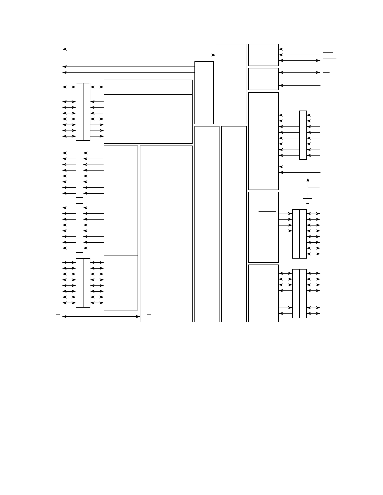
XTAL
EXTAL
4XOUT
PA7
PA6
PA5
PA4
PA3
PA2
PA1
PA0
PB7
PB6
PB5
PB4
PB3
PB2
PB1
PB0
PF7
PF6
PF5
PF4
PF3
PF2
PF1
PF0
PC7
PC6
PC5
PC4
PC3
PC2
PC1
PC0
R/W
PORT E
PORT G
PORT D
IRQ
XIRQ
RESET
MODA/
LIR
MODB/
V
STBY
PE7
PE6
PE5
PE4
PE3
PE2
PE1
PE0
V
RH
V
RL
V
DD
V
SS
PG7
PG6
PG5
PG4
PG3
PG2
PG1
PG0
PD5
PD4
PD3
PD2
PD1
PD0
INTERRUPT
LOGIC
E
MODE
CONTROL
A/D
CONVERTER
AN7
AN6
AN5
AN4
AN3
AN2
AN1
AN0
V
RH
V
RL
CHIP
SELECTS
CSPROG
CSGEN
CSIO1
CSIO2
SS
SCK
SPI
MOSI
MISO
TxD
SCI
RxD
PORT G DDR
PORT D DDR
PORT A
PORT A DDR
PORT B
PORT F
PORT C
PORT C DDR
PAI/OC1
OC2/OC1
OC3/OC1
OC4/OC1
OC5/IC4/OC1
IC1
IC2
IC3
ADDR15
ADDR14
ADDR13
ADDR12
ADDR11
ADDR10
ADDR9
ADDR8
ADDR7
ADDR6
ADDR5
ADDR4
ADDR3
ADDR2
ADDR1
ADDR0
DATA7
DATA6
DATA5
DATA4
DATA3
DATA2
DATA1
DATA0
ACCUMULATOR
PULSE
TIMER
SYSTEM
ADDRESS BUS
DATA BUS
R/W
COP
PERIODIC
INTERRUPT
CPU
CLOCK
LOGIC
1024
BYTES
RAM
OSCILLATOR
512
BYTES
EEPROM
Figure 1-1 MC68HC11F1 Block Diagram
1-2 TECHNICAL DATA
For More Information On This Product,
INTRODUCTION
MC68HC11F1
Go to: www.freescale.com
Page 15

..
.
nc
Freescale Semiconductor, I
Freescale Semiconductor, Inc.
SECTION 2 PIN DESCRIPTIONS
The MC68HC11F1 MCU is available in a 68-pin plastic leaded chip carrier (PLCC) and
an 80-pin plastic quad flat pack (QFP). Most pins on this MCU serve two or more functions, as described in the following paragraphs.
for the PLCC.
Figure 2-2 shows the pin assignments for the QFP.
STBY
EXTAL
XTAL
4XOUT
PC0/DATA0
8
7
9
PC1/DATA1
PC2/DATA2
PC3/DATA3
PC4/DATA4
PC5/DATA5
PC6/DATA6
PC7/DATA7
RESET
PG7/CSPROG
PG6/CSGEN
PG5/CSIO1
PG4/CSIO2 PB3/ADDR11
XIRQ
IRQ
PG3
PG2
PG1
10
11
12
13
14
15
16
17
18
19
20
21
22
23
24
25
26
27282930313233
PG0
PD1/TxD
PD0/RxD
E
R/W
65432
PD4/SCK
PD3/MOSI
PD2/MISO
V
MODB/V
MODA/LIR
1
MC68HC11F1
3435363738
DD
V
PD5/SS
Figure 2-1 shows the pin assignments
SS
RL
VRHV
PE7/AN7
PE3/AN3
PE6/AN6
PE2/AN2
PE5/AN5
PE1/AN1
6768656463
PA7/PAI/OC1
PA5/OC3/OC1
PA6/OC2/OC1
66
39
404142
PA2/IC1
PA4/OC4/OC1
PA3/OC5/IC4/OC1
62
PA1/IC2
PA0/IC3
61
60
PE4/AN4
59
PE0/AN0
58
PF0/ADDR0
57
PF1/ADDR1
PF2/ADDR2
56
PF3/ADDR3
55
PF4/ADDR4
54
PF5/ADDR5
53
PF6/ADDR6
52
PF7/ADDR7
51
PB0/ADDR8
50
PB1/ADDR9
49
PB2/ADDR10
48
47
PB4/ADDR12
46
PB5/ADDR13
45
PB6/ADDR14
44
43
PB7/ADDR15
Figure 2-1 Pin Assignments for MC68HC11F1 68-Pin PLCC
TECHNICAL DATA 2-1
For More Information On This Product,
PIN DESCRIPTIONS
Go to: www.freescale.com
Page 16

Freescale Semiconductor, Inc.
..
.
nc
Freescale Semiconductor, I
DD
V
PA6/OC2/OC1
PA7/PAI/OC1
69
313233
SS
RH
V
V
STBY
MODB/V
PD5/SS
PD4/SCK
PD3/MOSI
686766
343536
E
R/W
MODA/LIR
PD0/RxD
PD2/MISO
PD1/TxD
64
65
636261
37
383940
NC
XTAL
EXTAL
PG0
NC
60
59
58
57
56
55
54
53
52
51
50
49
48
47
46
45
44 PC2/DATA2
43
42
41
4XOUT
PC0/DATA0
NC
PG1
PG2
PG3
PG4/CSIO2
PG5/CSIO1
PG6/CSGEN
PG7/CSPROG
IRQ
XIRQ
RESET
PC7/DATA7
PC6/DATA6
PC5/DATA5
PC4/DATA4
PC3/DATA3
PC1/DATA1
NC
NC
NC
NC
PB6/ADDR14
PB5/ADDR13
PB4/ADDR12
PB3/ADDR11
PB2/ADDR10
PB1/ADDR9
PB0/ADDR8
PF7/ADDR7
PF6/ADDR6
PF5/ADDR5
PF4/ADDR4
PF3/ADDR3
PF2/ADDR2
PF1/ADDR1
PF0/ADDR0
PE0/AN0
PE4/AN4
NC
PB7/ADDR15
NC
NC
79
78
80
1
2
3
4
5
6
7
8
9
10
11
12
13
14
15
16
17
18
19
20
21222324252627
NC
PE1/AN1
PA3/OC5/IC4/OC1
PA5/OC3/OC1
PA2/IC1
PE3/AN3
PA4/OC4/OC1
72
MC68HC11F1
282930
RL
V
PE7/AN7
PA1/IC2
PA0/IC3
77767574737071
PE2/AN2NCPE6/AN6
PE5/AN5
Figure 2-2 Pin Assignments for MC68HC11F1 80-Pin QFP
2.1 V
DD and
Power is supplied to the MCU through V
V
SS
V
SS
DD
and V
SS
. V
is the power supply, and
DD
is ground. The MCU operates from a single 5-volt (nominal) power supply. Very
fast signal transitions occur on the MCU pins. The short rise and fall times place high,
short duration current demands on the power supply. To prevent noise problems, provide good power-supply bypassing at the MCU. Also, use bypass capacitors that have
good high-frequency characteristics and situate them as close to the MCU as possible.
Bypass requirements vary, depending on how heavily the MCU pins are loaded.
2-2 TECHNICAL DATA
For More Information On This Product,
PIN DESCRIPTIONS
MC68HC11F1
Go to: www.freescale.com
Page 17
Freescale Semiconductor, Inc.
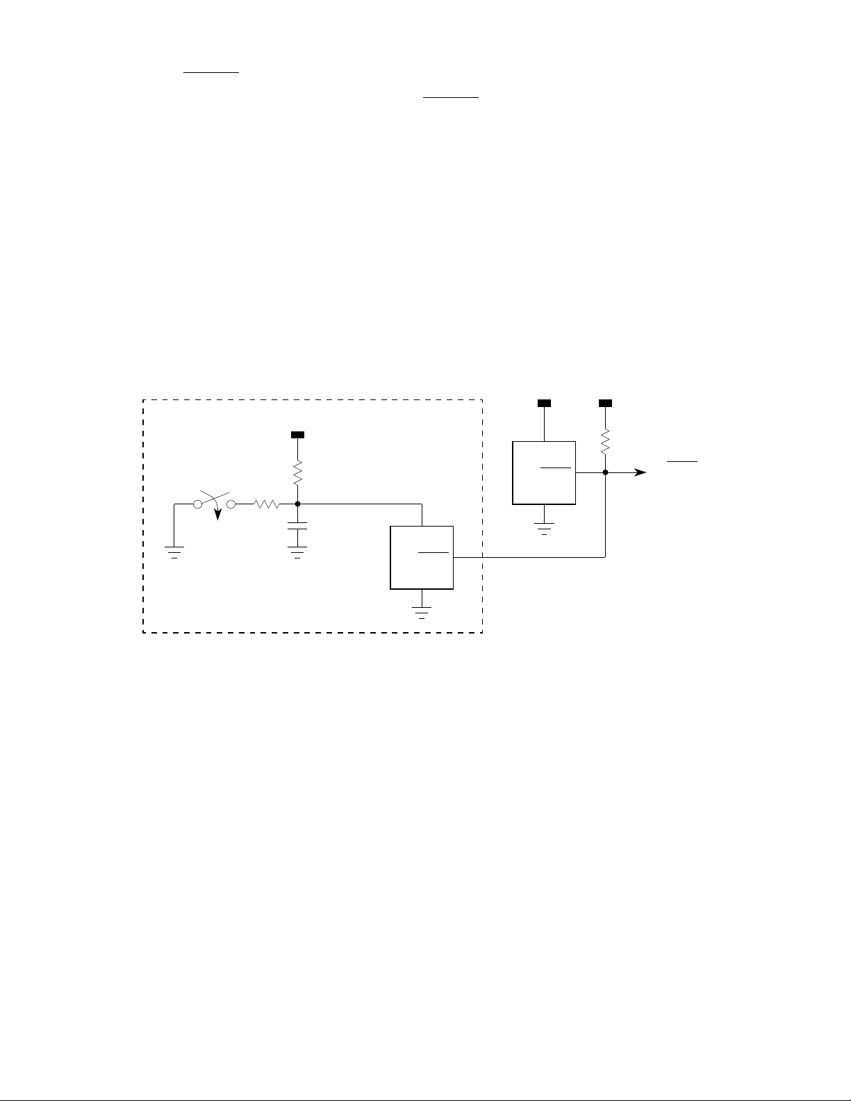
2.2 Reset (RESET )
An active low bidirectional control signal, RESET, acts as an input to initialize the MCU
to a known start-up state. It also acts as an open-drain output to indicate that an internal failure has been detected in either the clock monitor or COP watchdog circuit. The
CPU distinguishes between internal and external reset conditions by sensing whether
the reset pin rises to a logic one in less than two E-clock cycles after a reset has occurred. It is not advisable to connect an external resistor-capacitor (RC) power-up delay circuit to the reset pin of M68HC11 devices because the circuit charge time
constant can cause the device to misinterpret the type of reset that occurred. Refer to
SECTION 5 RESETS AND INTERRUPTS for further information.
Figure 2-3 illustrates a reset circuit that uses an external switch. Other circuits can be
used, however, it is important to incorporate a low voltage interrupt (LVI) circuit to prevent operation at insufficient voltage levels which could result in erratic behavior or cor-
..
.
ruption of RAM.
nc
Freescale Semiconductor, I
V
DD
4.7 kΩ
1
TO RESET
OF M68HC11
MANUAL
RESET SWITCH
4.7 kΩ
OPTIONAL POWER-ON DELAY
AND MANUAL RESET SWITCH
V
DD
V
DD
4.7 kΩ
1.0 µF
MC34164
2
IN
RESET
GND
3
MC34064
1
2
IN
RESET
GND
3
Figure 2-3 External Reset Circuit
2.3 E-Clock Output (E)
E is the output connection for the internally generated E clock. The signal from E is
used as a timing reference. The frequency of the E-clock output is one fourth that of
the input frequency at the EXTAL pin. When E-clock output is low, an internal process
is taking place. When it is high, data is being accessed. All clocks, including the E
clock, are halted when the MCU is in STOP mode. The E clock can be turned off in
single-chip modes to reduce the effects of radio frequency interference (RFI). Refer to
SECTION 9 TIMING SYSTEM .
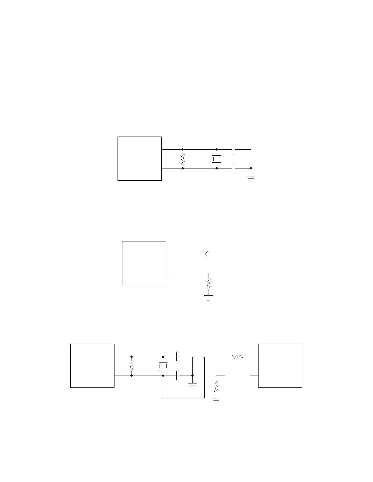
2.4 Crystal Driver and External Clock Input (XTAL, EXTAL)
These two pins provide the interface for either a crystal or a CMOS-compatible clock
to control the internal clock generator circuitry. Either a crystal oscillator or a CMOS
compatible clock can be used. The resulting E-clock rate is the input frequency divided
by four.
TECHNICAL DATA 2-3
For More Information On This Product,
PIN DESCRIPTIONS
Go to: www.freescale.com
Page 18
Ω
..
.
nc
Freescale Semiconductor, Inc.
The XTAL pin is normally left unterminated when an external CMOS compatible clock
is connected to the EXTAL pin. However, a 10 k
to 100 k Ω load resistor connected
from the XTAL output to ground can be used to reduce RFI noise emission.
The XTAL output is normally used to drive a crystal. The XTAL output can be buffered
with a high-impedance buffer, or it can be used to drive the EXTAL input of another
M68HC11 device. Refer to
Figure 2-6 .
In all cases, use caution when designing circuitry associated with the oscillator pins.
Load capacitances shown in the oscillator circuits include all stray layout capacitances. Refer to Figure 2-4, Figure 2-5, and Figure 2-6.
25 pF*
EXTAL
MCU
10M
XTAL
4 x E
CRYSTAL
25 pF*
Values include all stray capacitances.
*
Figure 2-4 Common Crystal Connections
CMOS-COMPATIBLE
EXTERNAL
OSCILLATOR
MCU
EXTAL
XTAL
NC OR
10 k – 100 k
LOAD
Figure 2-5 External Oscillator Connections
Freescale Semiconductor, I
FIRST
MCU
EXTAL
XTAL
10M
25 pF*
4 x E
CRYSTAL
25 pF*
220
NC OR
10 k – 100 k
LOAD
EXTAL
SECOND
MCU
XTAL
Values include all stray capacitances.
*
Figure 2-6 One Crystal Driving Two MCUs
2-4 TECHNICAL DATA
For More Information On This Product,
PIN DESCRIPTIONS
Go to: www.freescale.com
MC68HC11F1
Page 19
Freescale Semiconductor, Inc.
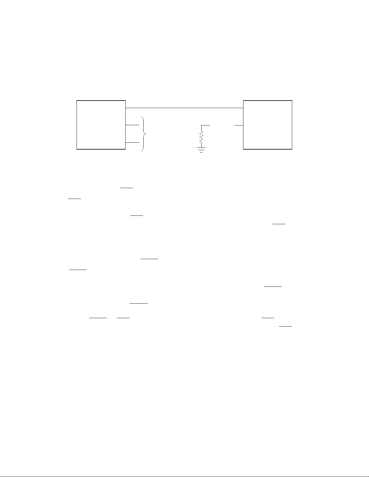
2.5 Four Times E-Clock Frequency Output (4XOUT)
Although the circuit shown in Figure 2-6 will work for any M68HC11 MCU, the
MC68HC11F1 has an additional clock output that is four times the E-clock frequency.
This output (4XOUT) can be used to directly drive the EXTAL input of another
M68HC11 MCU. Refer to Figure 2-7. The 4XOUT output is enabled after reset and
can be disabled by clearing the CLK4X bit in the OPT2 register.
..
.
nc
Freescale Semiconductor, I
MC68HC11F1
4XOUT
EXTAL
XTAL
OSCILLATOR
CIRCUIT OR
CMOS-COMPATIBLE
CLOCK
NC OR
10 k – 100 k
LOAD
EXTAL
XTAL
SECOND
MCU
Figure 2-7 4XOUT Signal Driving a Second MCU
2.6 Interrupt Request (IRQ
)
The IRQ input provides a means of generating asynchronous interrupt requests for the
CPU. Either falling-edge triggering or low-level triggering is selected by the IRQE bit
in the OPTION register. IRQ
Connect an external pull-up resistor, typically 4.7 kΩ, to V
is always configured for level-sensitive triggering at reset.
when IRQ is used in a
DD
level-sensitive wired-OR configuration. Refer to SECTION 5 RESETS AND INTER-
RUPTS.
2.7 Non-Maskable Interrupt (XIRQ
)
The XIRQ input provides a means of requesting a non-maskable interrupt after reset
initialization. During reset, the X bit in the condition code register (CCR) is set and any
interrupt is masked until MCU software enables it. Because the XIRQ
input is level
sensitive, it can be connected to a multiple-source wired-OR network with an external
pull-up resistor to V
. XIRQ is often used as a power loss detect interrupt.
DD
Whenever XIRQ or IRQ are used with multiple interrupt sources (IRQ must be configured for level-sensitive operation if there is more than one source of IRQ
interrupt),
each source must drive the interrupt input with an open-drain type of driver to avoid
contention between outputs. There should be a single pull-up resistor near the MCU
interrupt input pin (typically 4.7 kΩ). There must also be an interlock mechanism at
each interrupt source so that the source holds the interrupt line low until the MCU recognizes and acknowledges the interrupt request. If one or more interrupt sources are
still pending after the MCU services a request, the interrupt line will still be held low
and the MCU will be interrupted again as soon as the interrupt mask bit in the condition
code register (CCR) is cleared (normally upon return from an interrupt). Refer to SEC-
TION 5 RESETS AND INTERRUPTS.
TECHNICAL DATA 2-5
For More Information On This Product,
PIN DESCRIPTIONS
Go to: www.freescale.com
Page 20

Freescale Semiconductor, Inc.
..
.
nc
Freescale Semiconductor, I
2.8 MODA and MODB (MODA/LIR and MODB/V
During reset, MODA and MODB select one of the four operating modes. Refer to SEC-
TION 4 OPERATING MODES AND ON-CHIP MEMORY.
After the operating mode has been selected, the LIR
to indicate that execution of an instruction has begun. The LIR pin is configured for
wired-OR operation (only pulls low). A series of E-clock cycles occurs during execution
of each instruction. The LIR
of each instruction (opcode fetch). This output is provided for assistance in program
debugging.
The V
signal unless the difference between the level of V
V
DD
one MOS threshold (about 0.7 volts). When these voltages differ by more than 0.7
volts, the internal 768-byte RAM and part of the reset logic are powered from V
rather than VDD. This allows RAM contents to be retained without V
to the MCU.
until V
2.9 V
2.10 R/W
and V
RH
These pins provide the reference voltage for the analog-to-digital converter. Bypass
capacitors should be used to minimize noise on these signals. Any noise on V
will directly affect A/D accuracy.
V
RL
In expanded and test modes, R/W indicates the direction of transfers on the external
data bus. A logic level one on this pin indicates that a read cycle is in progress. A logic
zero on this pin indicates that a write cycle is in progress and that no external device
should drive the data bus.
The E-clock can be used to enable external devices to drive data onto the data bus
during the second half of a read bus cycle (E clock high). R/W
control the direction of data transfers. R/W
external data bus. R/W
as when a double-byte store occurs.
pin is used to input RAM standby power. The MCU is powered from the
STBY
Reset must be driven low before V
has been restored to a valid level.
DD
RL
signal is asserted (drives low) during the first E-clock cycle
drives low when data is being written to the
will remain low during consecutive data bus write cycles, such
)
STBY
pin provides an open-drain output
and Vdd is greater than
STBY
power applied
DD
is removed and must remain low
DD
can then be used to
STBY
RH
and
2.11 Port Signals
For the MC68HC11F1, 54 pins are arranged into six 8-bit ports: A, B, C, E, F, and G,
and one 6-bit port (D). Each of these seven ports serves a purpose other than I/O, depending on the operating mode or peripheral functions selected. Note that ports B, C,
and F are available for I/O functions only in single-chip and bootstrap modes. The pins
of ports A, C, D, and G are fully bidirectional. Ports B and F are output-only ports. Port
E is an input-only port. Refer to Table 2-1 for details about the 54 port signals’ functions within different operating modes.
2-6 TECHNICAL DATA
For More Information On This Product,
PIN DESCRIPTIONS MC68HC11F1
Go to: www.freescale.com
Page 21
Freescale Semiconductor, Inc.
Table 2-1 Port Signal Functions
..
.
nc
Freescale Semiconductor, I
Port/Bit Single-Chip and
Bootstrap Mode
PA0 PA0/IC3
PA1 PA1/IC2
PA2 PA2/IC1
PA3 PA3/OC5/IC4/OC1
PA4 PA4/OC4/OC1
PA5 PA5/OC3/OC1
PA6 PA6/OC2/OC1
PA7 PA7/PAI/OC1
PB[7:0] PB[7:0] ADDR[15:8]
PC[7:0] PC[7:0] DATA[7:0]
PD0 PD0/RxD
PD1 PD1/TxD
PD2 PD2/MISO
PD3 PD3/MOSI
PD4 PD4/SCK
PD5 PD5/SS
PE[7:0] PE[7:0]/AN[7:0]
PF[7:0] PF[7:0] ADDR[7:0]
PG0 PG0
PG1 PG1
PG2 PG2
PG3 PG3
PG4 PG4 PG4/CSIO2
PG5 PG5 PG5/CSIO1
PG6 PG6 PG6/CSGEN
PG7 PG7 PG7/CSPROG
Expanded and
Special Test Mode
2.11.1 Port A
Port A is an 8-bit general-purpose I/O port with a data register (PORTA) and a data
direction register (DDRA). Port A pins share functions with the 16-bit timer system.
PORTA can be read at any time. Inputs return the pin level; outputs return the pin driver input level. If written, PORTA stores the data in internal latches. It drives the pins
only if they are configured as outputs. Writes to PORTA do not change the pin state
when the pins are configured for timer output compares.
Out of reset, port A pins [7:0] are general-purpose high-impedance inputs. When the
timer functions associated with these pins are disabled, the bits in DDRA govern the
I/O state of the associated pin. For further information, refer to SECTION 6 PARAL-
LEL INPUT/OUTPUT.
NOTE
When using the information about port functions, do not confuse pin
function with the electrical state of the pin at reset. All general-purpose I/O pins configured as inputs at reset are in a high-impedance
state. Port data registers reflect the logic state of the port at reset.
The pin function is mode dependent.
TECHNICAL DATA 2-7
For More Information On This Product,
PIN DESCRIPTIONS
Go to: www.freescale.com
Page 22

Freescale Semiconductor, Inc.
2.11.2 Port B
Port B is an 8-bit output-only port. In single-chip modes, port B pins are general-purpose output pins (PB[7:0]). In expanded modes, port B pins act as the high-order address lines (ADDR[15:8]) of the address bus.
PORTB can be read at any time. Reads of PORTB return the pin driver input level. If
PORTB is written, the data is stored in internal latches. It drives the pins only in singlechip or bootstrap mode. In expanded operating modes, port B pins are the high-order
address outputs (ADDR[15:8]).
Refer to SECTION 6 PARALLEL INPUT/OUTPUT.
2.11.3 Port C
..
.
nc
Port C is an 8-bit general-purpose I/O port with a data register (PORTC) and a data
direction register (DDRC). In single-chip modes, port C pins are general-purpose I/O
pins (PC[7:0]). In expanded modes, port C pins are configured as data bus pins (DATA[7:0]).
PORTC can be read at any time. Inputs return the pin level; outputs return the pin driver input level. If PORTC is written, the data is stored in internal latches. It drives the
pins only if they are configured as outputs in single-chip or bootstrap mode. Port C pins
are general-purpose inputs out of reset in single-chip and bootstrap modes. In expanded and test modes, these pins are data bus lines out of reset.
The CWOM control bit in the OPT2 register disables port C’s P-channel output drivers.
Because the N-channel driver is not affected by CWOM, setting CWOM causes port
C to become an open-drain-type output port suitable for wired-OR operation. In wiredOR mode, (PORTC bits are at logic level zero), pins are actively driven low by the Nchannel driver. When a port C bit is at logic level one, the associated pin is in a highimpedance state, as neither the N-channel nor the P-channel devices are active. It is
customary to have an external pull-up resistor on lines that are driven by open-drain
devices. Port C can only be configured for wired-OR operation when the MCU is in single-chip or bootstrap modes.
Refer to SECTION 6 PARALLEL INPUT/OUTPUT.
Freescale Semiconductor, I
2.11.4 Port D
Port D, a 6-bit general-purpose I/O port, has a data register (PORTD) and a data direction register (DDRD). The six port D lines (D[5:0]) can be used for general-purpose
I/O, for the serial communications interface (SCI) and serial peripheral interface (SPI)
subsystems.
PORTD can be read at any time. Inputs return the pin level; outputs return the pin driver input level. If PORTD is written, the data is stored in internal latches and can be driven only if port D is configured for general-purpose output.
The DWOM control bit in the SPCR register disables port D’s P-channel output drivers.
Because the N-channel driver is not affected by DWOM, setting DWOM causes port
D to become an open-drain-type output port suitable for wired-OR operation. In wired-
2-8 TECHNICAL DATA
For More Information On This Product,
PIN DESCRIPTIONS MC68HC11F1
Go to: www.freescale.com
Page 23

..
.
nc
Freescale Semiconductor, Inc.
OR mode, (PORTD bits are at logic level zero), pins are actively driven low by the Nchannel driver. When a port D bit is at logic level one, the associated pin is in a highimpedance state, as neither the N-channel nor the P-channel devices are active. It is
customary to have an external pull-up resistor on lines that are driven by open-drain
devices. Port D can be configured for wired-OR operation in any operating mode.
Refer to SECTION 6 PARALLEL INPUT/OUTPUT, SECTION 7 SERIAL COMMUNI-
CATIONS INTERFACE, and SECTION 8 SERIAL PERIPHERAL INTERFACE.
2.11.5 Port E
Port E is an 8-bit input-only port that is also used as the analog input port for the analog-to-digital converter. Port E pins that are not used for the A/D system can be used
as general-purpose inputs. However, PORTE should not be read during the sample
portion of an A/D conversion sequence.
Refer to SECTION 10 ANALOG-TO-DIGITAL CONVERTER.
2.11.6 Port F
Port F is an 8-bit output-only port. In single-chip mode, port F pins are general-purpose
output pins (PF[7:0]). In expanded mode, port F pins act as the low-order address outputs (ADDR[7:0]).
PORTF can be read at any time. Reads of PORTF return the pin driver input level. If
PORTF is written, the data is stored in internal latches. It drives the pins only in singlechip or bootstrap mode. In expanded operating modes, port F pins are the low-order
address outputs (ADDR[7:0]).
Refer to SECTION 6 PARALLEL INPUT/OUTPUT.
2.11.7 Port G
Port G is an 8-bit general-purpose I/O port. When enabled, four chip select signals are
alternate functions of port G bits [7:4].
PORTG can be read at any time. Inputs return the pin level; outputs return the pin driver input level. If PORTG is written, the data is stored in internal latches. It drives the
Freescale Semiconductor, I
pins only if they are configured as outputs.
The GWOM control bit in the OPT2 register disables port G's P-channel output drivers.
Because the N-channel driver is not affected by GWOM, setting GWOM causes port
G to become an open-drain-type output port suitable for wired-OR operation. In wiredOR mode, (PORTG bits are at logic level zero), pins are actively driven low by the Nchannel driver. When a port G bit is at logic level one, the associated pin is in a highimpedance state, as neither the N-channel nor the P-channel devices are active. It is
customary to have an external pull-up resistor on lines that are driven by open-drain
devices. Port G can be configured for wired-OR operation in any operating mode.
Refer to SECTION 6 PARALLEL INPUT/OUTPUT and SECTION 4 OPERATING
MODES AND ON-CHIP MEMORY.
TECHNICAL DATA 2-9
For More Information On This Product,
PIN DESCRIPTIONS
Go to: www.freescale.com
Page 24

..
.
nc
Freescale Semiconductor, Inc.
Freescale Semiconductor, I
2-10 TECHNICAL DATA
For More Information On This Product,
PIN DESCRIPTIONS MC68HC11F1
Go to: www.freescale.com
Page 25

Freescale Semiconductor, Inc.
SECTION 3 CENTRAL PROCESSING UNIT
This section presents information on M68HC11 central processing unit (CPU) architecture. Data types, addressing modes, the instruction set, and the extended addressing range required to support this MCU’s memory expansion feature are also included,
as are special operations such as subroutine calls and interrupts.
The CPU is designed to treat all peripheral, I/O, and memory locations identically as
addresses in the 64 Kbyte memory map. This is referred to as memory-mapped I/O.
There are no special instructions for I/O that are separate from those used for memory.
This architecture also allows accessing an operand from an external memory location
..
.
with no execution-time penalty.
nc
Freescale Semiconductor, I
3.1 CPU Registers
M68HC11 CPU registers are an integral part of the CPU and are not addressed as if
they were memory locations. The seven registers, discussed in the following paragraphs, are shown in Figure 3-1.
CENTRAL PROCESSING UNIT
TECHNICAL DATA 3-1
For More Information On This Product,
Go to: www.freescale.com
Page 26
..
.
nc
Freescale Semiconductor, Inc.
15
DOUBLE ACCUMULATOR D
CONDITION CODE REGISTER X H I N Z V C
70
70
INDEX REGISTER X
INDEX REGISTER Y
STACK POINTER
PROGRAM COUNTER
70
S
ACCUMULATOR A
ACCUMULATOR B
A
B
0
D
015
IX
015
IY
015
SP
015
PC
123456
CCR
CARRY
OVERFLOW
ZERO
NEGATIVE
I INTERRUPT MASK
HALF-CARRY (FROM BIT 3)
X INTERRUPT MASK
STOP DISABLE
Figure 3-1 Programming Model
3.1.1 Accumulators A, B, and D
Accumulators A and B are general-purpose 8-bit registers that hold operands and results of arithmetic calculations or data manipulations. For some instructions, these two
accumulators are treated as a single double-byte (16-bit) accumulator called accumulator D. Although most instructions can use accumulators A or B interchangeably, the
Freescale Semiconductor, I
following exceptions apply:
The ABX and ABY instructions add the contents of 8-bit accumulator B to the contents
of 16-bit register X or Y, but there are no equivalent instructions that use A instead of B.
The TAP and TPA instructions transfer data from accumulator A to the condition code
register, or from the condition code register to accumulator A, however, there are no
equivalent instructions that use B rather than A.
The decimal adjust accumulator A (DAA) instruction is used after binary-coded decimal (BCD) arithmetic operations, but there is no equivalent BCD instruction to adjust
accumulator B.
CENTRAL PROCESSING UNIT MC68HC11F1
3-2 TECHNICAL DATA
For More Information On This Product,
Go to: www.freescale.com
Page 27

Freescale Semiconductor, Inc.
The add, subtract, and compare instructions associated with both A and B (ABA, SBA,
and CBA) only operate in one direction, making it important to plan ahead to ensure
that the correct operand is in the correct accumulator.
3.1.2 Index Register X (IX)
The IX register provides a 16-bit indexing value that can be added to the 8-bit offset
provided in an instruction to create an effective address. The IX register can also be
used as a counter or as a temporary storage register.
3.1.3 Index Register Y (IY)
The 16-bit IY register performs an indexed mode function similar to that of the IX register. However, most instructions using the IY register require an extra byte of machine
code and an extra cycle of execution time because of the way the opcode map is im-
..
.
plemented. Refer to 3.3 Opcodes and Operands for further information.
nc
Freescale Semiconductor, I
3.1.4 Stack Pointer (SP)
The M68HC11 CPU has an automatic program stack. This stack can be located anywhere in the address space and can be any size up to the amount of memory available
in the system. Normally the SP is initialized by one of the first instructions in an application program. The stack is configured as a data structure that grows downward from
high memory to low memory. Each time a new byte is pushed onto the stack, the SP
is decremented. Each time a byte is pulled from the stack, the SP is incremented. At
any given time, the SP holds the 16-bit address of the next free location in the stack.
Figure 3-2 is a summary of SP operations.
CENTRAL PROCESSING UNIT
TECHNICAL DATA 3-3
For More Information On This Product,
Go to: www.freescale.com
Page 28

JSR, JUMP TO SUBROUTINE
MAIN PROGRAM
PC
DIRECT
RTN
PC
INDXD,X
RTN
PC
INDXD,Y
RTN
PC
EXTEND
RTN
BSR, BRANCH TO SUBROUTINE
PC
RTN
$9D = JSR
dd
NEXT MAIN INSTR
MAIN PROGRAM
$AD = JSR
ff
NEXT MAIN INSTR
MAIN PROGRAM
$18 = PRE
$AD = JSR
ff
NEXT MAIN INSTR
MAIN PROGRAM
$BD = JSR
hh
NEXT MAIN INSTR
MAIN PROGRAM
$8D = BSR
rr
NEXT MAIN INSTR
RTI, RETURN FROM INTERRUPT
INTERRUPT PROGRAM
PC
STACK
SP-2
SP-1
SP
ll
SP-2
SP-1
SP
RTN
RTN
STACK
RTN
RTN
H
L
SWI, SOFTWARE INTERRUPT
PC
RTN
WAI, WAIT FOR INTERRUPT
PC
H
RTN
L
$3B = RTI
MAIN PROGRAM
$3F = SWI
MAIN PROGRAM
$3E = WAI
SP
SP+1
SP+2
SP+3
SP+4
SP+5
SP+6
SP+7
SP+8
SP+9
SP-9
SP-8
SP-7
SP-6
SP-5
SP-4
SP-3
SP-2
SP-1
STACK
CONDITION CODE
ACMLTR B
ACMLTR A
STACK
CONDITION CODE
ACMLTR B
ACMLTR A
INDEX REGISTER (X
INDEX REGISTER (X
INDEX REGISTER (YH)
INDEX REGISTER (Y
RTN
H
RTN
L
)
H
)
L
)
L
RTS, RETURN FROM SUBROUTINE
SUBROUTINE
PC
$39 = RTS
SP
SP+1
SP+2
STACK
RTN
LEGEND:
RTN
RTN
H
RTN
L
dd
ff
hh
ll
rr
Address of next instruction in main program to be
executed upon return from subroutine.
Most significant byte of return address.
Least significant byte of return address.
Shaded cells show stack pointer position after
operation is complete.
8-bit direct address ($0000-$00FF) (high byte
assumed to be $00).
8-bit positive offset $00 (0) to $FF (256) is added
to index.
High-order byte of 16-bit extended address.
Low-order byte of 16-bit extended address.
Signed-relative offset $80 (-128) to $7F (+127)
(offset relative to the address following the
machine code offset byte).
Figure 3-2 Stacking Operations
When a subroutine is called by a jump to subroutine (JSR) or branch to subroutine
(BSR) instruction, the address of the instruction after the JSR or BSR is automatically
pushed onto the stack, least significant byte first. When the subroutine is finished, a
return from subroutine (RTS) instruction is executed. The RTS pulls the previously
stacked return address from the stack, and loads it into the program counter. Execution then continues at this recovered return address.
CENTRAL PROCESSING UNIT MC68HC11F1
3-4 TECHNICAL DATA
Page 29

Freescale Semiconductor, Inc.
When an interrupt is recognized, the current instruction finishes normally, the return
address (the current value in the program counter) is pushed onto the stack, all of the
CPU registers are pushed onto the stack, and execution continues at the address
specified by the vector for the interrupt. At the end of the interrupt service routine, an
RTI instruction is executed. The RTI instruction causes the saved registers to be pulled
off the stack in reverse order. Program execution resumes at the return address.
There are instructions that push and pull the A and B accumulators and the X and Y
index registers. These instructions are often used to preserve program context. For
example, pushing accumulator A onto the stack when entering a subroutine that uses
accumulator A, and then pulling accumulator A off the stack just before leaving the
subroutine, ensures that the contents of a register will be the same after returning from
the subroutine as it was before starting the subroutine.
..
.
nc
Freescale Semiconductor, I
3.1.5 Program Counter (PC)
The program counter, a 16-bit register, contains the address of the next instruction to
be executed. After reset, the program counter is initialized from one of six possible
vectors, depending on operating mode and the cause of reset.
Table 3-1 Reset Vector Comparison
POR or RESET Pin Clock Monitor COP Watchdog
Normal $FFFE, F $FFFC, D $FFFA, B
Test or Boot $BFFE, F $BFFC, D $BFFA, B
3.1.6 Condition Code Register (CCR)
This 8-bit register contains five condition code indicators (C, V, Z, N, and H), two interrupt masking bits, (I and X) and a stop disable bit (S). In the M68HC11 CPU, condition
codes are automatically updated by most instructions. For example, load accumulator
A (LDAA) and store accumulator A (STAA) instructions automatically set or clear the
N, Z, and V condition code flags. Pushes, pulls, add B to X (ABX), add B to Y (ABY),
and transfer/exchange instructions do not affect the condition codes. Refer to Table
3-2, which shows what condition codes are affected by a particular instruction.
3.1.6.1 Carry/Borrow (C)
The C bit is set if the arithmetic logic unit (ALU) performs a carry or borrow during an
arithmetic operation. The C bit also acts as an error flag for multiply and divide operations. Shift and rotate instructions operate with and through the carry bit to facilitate
multiple-word shift operations.
3.1.6.2 Overflow (V)
The overflow bit is set if an operation causes an arithmetic overflow. Otherwise, the V
bit is cleared.
CENTRAL PROCESSING UNIT
TECHNICAL DATA 3-5
For More Information On This Product,
Go to: www.freescale.com
Page 30

..
.
nc
Freescale Semiconductor, Inc.
3.1.6.3 Zero (Z)
The Z bit is set if the result of an arithmetic, logic, or data manipulation operation is
zero. Otherwise, the Z bit is cleared. Compare instructions do an internal implied subtraction and the condition codes, including Z, reflect the results of that subtraction. A
few operations (INX, DEX, INY, and DEY) affect the Z bit and no other condition flags.
For these operations, only = and - conditions can be determined.
3.1.6.4 Negative (N)
The N bit is set if the result of an arithmetic, logic, or data manipulation operation is
negative (MSB = 1). Otherwise, the N bit is cleared. A result is said to be negative if
its most significant bit (MSB) is a one. A quick way to test whether the contents of a
memory location has the MSB set is to load it into an accumulator and then check the
status of the N bit.
3.1.6.5 Interrupt Mask (I)
The interrupt request (IRQ) mask (I bit) is a global mask that disables all maskable interrupt sources. While the I bit is set, interrupts can become pending, but the operation
of the CPU continues uninterrupted until the I bit is cleared. After any reset, the I bit is
set by default and can only be cleared by a software instruction. When an interrupt is
recognized, the I bit is set after the registers are stacked, but before the interrupt vector
is fetched. After the interrupt has been serviced, a return from interrupt instruction is
normally executed, restoring the registers to the values that were present before the
interrupt occurred. Normally, the I bit is zero after a return from interrupt is executed.
Although the I bit can be cleared within an interrupt service routine, “nesting” interrupts
in this way should only be done when there is a clear understanding of latency and of
the arbitration mechanism. Refer to SECTION 5 RESETS AND INTERRUPTS.
3.1.6.6 Half Carry (H)
The H bit is set when a carry occurs between bits 3 and 4 of the arithmetic logic unit
during an ADD, ABA, or ADC instruction. Otherwise, the H bit is cleared. Half carry is
used during BCD operations.
3.1.6.7 X Interrupt Mask (X)
Freescale Semiconductor, I
The XIRQ
by default and must be cleared by a software instruction. When an XIRQ
recognized, the X and I bits are set after the registers are stacked, but before the interrupt vector is fetched. After the interrupt has been serviced, an RTI instruction is
normally executed, causing the registers to be restored to the values that were present
before the interrupt occurred. The X interrupt mask bit is set only by hardware (RESET
or XIRQ acknowledge). X is cleared only by program instruction (TAP, where the associated bit of A is zero; or RTI, where bit 6 of the value loaded into the CCR from the
stack has been cleared). There is no hardware action for clearing X.
3-6 TECHNICAL DATA
mask (X) bit disables interrupts from the XIRQ pin. After any reset, X is set
interrupt is
CENTRAL PROCESSING UNIT MC68HC11F1
For More Information On This Product,
Go to: www.freescale.com
Page 31

Freescale Semiconductor, Inc.
3.1.6.8 Stop Disable (S)
Setting the STOP disable (S) bit prevents the STOP instruction from putting the
M68HC11 into a low-power stop condition. If the CPU encounters a STOP instruction
while the S bit is set, it is treated as a no-operation (NOP) instruction, and processing
continues to the next instruction. S is set by reset — STOP disabled by default.
3.2 Data Types
The M68HC11 CPU supports the following data types:
• Bit data
• 8-bit and 16-bit signed and unsigned integers
• 16-bit unsigned fractions
• 16-bit addresses
..
.
nc
Freescale Semiconductor, I
A byte is eight bits wide and can be accessed at any byte location. A word is composed
of two consecutive bytes with the most significant byte at the lower value address. Because the M68HC11 is an 8-bit CPU, there are no special requirements for alignment
of instructions or operands.
3.3 Opcodes and Operands
The M68HC11 family of microcontrollers uses 8-bit opcodes. Each opcode identifies
a particular instruction and associated addressing mode to the CPU. Several opcodes
are required to provide each instruction with a range of addressing capabilities. Only
256 opcodes would be available if the range of values were restricted to the number
able to be expressed in 8-bit binary numbers.
A four-page opcode map has been implemented to expand the number of instructions.
An additional byte, called a prebyte, directs the processor from page 0 of the opcode
map to one of the other three pages. As its name implies, the additional byte precedes
the opcode.
A complete instruction consists of a prebyte, if any, an opcode, and zero, one, two, or
three operands. The operands contain information the CPU needs for executing the
instruction. Complete instructions can be from one to five bytes long.
3.4 Addressing Modes
Six addressing modes can be used to access memory: immediate, direct, extended,
indexed, inherent, and relative. These modes are detailed in the following paragraphs.
All modes except inherent mode use an effective address. The effective address is the
memory address from which the argument is fetched or stored, or the address from
which execution is to proceed. The effective address can be specified within an instruction, or it can be calculated.
3.4.1 Immediate
In the immediate addressing mode an argument is contained in the byte(s) immediately following the opcode. The number of bytes following the opcode matches the size
of the register or memory location being operated on. There are two-, three-, and four-
CENTRAL PROCESSING UNIT
TECHNICAL DATA 3-7
For More Information On This Product,
Go to: www.freescale.com
Page 32

Freescale Semiconductor, Inc.
(if prebyte is required) byte immediate instructions. The effective address is the address of the byte following the instruction.
3.4.2 Direct
In the direct addressing mode, the low-order byte of the operand address is contained
in a single byte following the opcode, and the high-order byte of the address is assumed to be $00. Addresses $00–$FF are thus accessed directly, using two-byte instructions. Execution time is reduced by eliminating the additional memory access
required for the high-order address byte. In most applications, this 256-byte area is reserved for frequently referenced data. In M68HC11 MCUs, the memory map can be
configured for combinations of internal registers, RAM, or external memory to occupy
these addresses.
..
.
nc
3.4.3 Extended
In the extended addressing mode, the effective address of the argument is contained
in two bytes following the opcode byte. These are three-byte instructions (or four-byte
instructions if a prebyte is required). One or two bytes are needed for the opcode and
two for the effective address.
3.4.4 Indexed
In the indexed addressing mode, an 8-bit unsigned offset contained in the instruction
is added to the value contained in an index register (IX or IY). The sum is the effective
address. This addressing mode allows referencing any memory location in the 64
Kbyte address space. These are two- to five-byte instructions, depending on whether
or not a prebyte is required.
3.4.5 Inherent
In the inherent addressing mode, all the information necessary to execute the instruction is contained in the opcode. Operations that use only the index registers or accumulators, as well as control instructions with no arguments, are included in this
addressing mode. These are one- or two-byte instructions.
3.4.6 Relative
Freescale Semiconductor, I
The relative addressing mode is used only for branch instructions. If the branch condition is true, an 8-bit signed offset included in the instruction is added to the contents
of the program counter to form the effective branch address. Otherwise, control proceeds to the next instruction. These are usually two-byte instructions.
3.5 Instruction Set
Refer to Table 3-2, which shows all the M68HC11 instructions in all possible addressing modes. For each instruction, the table shows the operand construction, the number of machine code bytes, and execution time in CPU E clock cycles.
CENTRAL PROCESSING UNIT MC68HC11F1
3-8 TECHNICAL DATA
For More Information On This Product,
Go to: www.freescale.com
Page 33

..
.
nc
Freescale Semiconductor, I
Freescale Semiconductor, Inc.
Table 3-2 Instruction Set (Sheet 1 of 6)
Mnemonic Operation Description Addressing Instruction Condition Codes
ABA Add
ABX Add B to X IX + (00 : B) ⇒ IX INH 3A — 3 ————————
ABY Add B to Y IY + (00 : B) ⇒ IY INH 18 3A — 4 ————————
ADCA (opr) Add with Carry
ADCB (opr) Add with Carry
ADDA (opr) Add Memory
ADDB (opr) Add Memory
ADDD (opr) Add 16-Bit to D D + (M : M + 1) ⇒ D IMM
ANDA (opr) AND A with
ANDB (opr) AND B with
ASL (opr) Arithmetic
ASLA Arithmetic
ASLB Arithmetic
ASLD Arithmetic
ASR Arithmetic
ASRA Arithmetic
ASRB Arithmetic
BCC (rel) Branch if Carry
BCLR (opr)
BCS (rel) Branch if Carry
BEQ (rel) Branch if =
BGE (rel) Branch if ∆
Accumulators
to A
to B
to A
to B
Memory
Memory
Shift Left
Shift Left A
Shift Left B
Shift Left D
Shift Right
Shift Right A
Shift Right B
Clear
Clear Bit(s) M • (mm) ⇒ M DIR
(msk)
Set
Zero
Zero
A + B ⇒ A INH 1B — 2 — — ∆ — ∆∆∆∆
A + M + C ⇒ A A IMM
B + M + C ⇒ B B IMM
A + M ⇒ A A IMM
B + M ⇒ B B IMM
A • M ⇒ A A IMM
B • M ⇒ B B IMM
0
b0
b7
C
0
b0
b7
C
0
b0
b7
C
b0
A
b0
b7
b7
C
B
b0
b7
b7
b7
? C = 0 REL 24rr 3 ————————
? C = 1 REL 25rr 3 ————————
? Z = 1 REL 27rr 3 ————————
? N ⊕ V = 0 REL 2Crr 3 ————————
C
b0
C
b0
C
Mode Opcode Operand Cycles S X H I N Z V C
89
A DIR
A EXT
A IND,X
A IND,Y
B DIR
B EXT
B IND,X
B IND,Y
A DIR
A EXT
A IND,X
A IND,Y
B DIR
B EXT
B IND,X
B IND,Y
DIR
EXT
IND,X
IND,Y
A DIR
A EXT
A IND,X
A IND,Y
B DIR
B EXT
B IND,X
B IND,Y
EXT
IND,X
IND,Y
A INH 48 — 2 ————∆∆∆∆
B INH 58 — 2 ————∆∆∆∆
INH 05 — 3 ———— ∆∆∆∆
0
EXT
IND,X
IND,Y
A INH 47 — 2 ————∆∆∆∆
B INH 57 — 2 ————∆∆∆∆
IND,X
IND,Y
18 A9
18 E9
18 AB
18 EB
18 E3
18 A4
18 E4
18 68
18 67
18 1D
99
B9
A9
C9
D9
F9
E9
8B
9B
BB
AB
CB
DB
FB
EB
C3
D3
F3
E3
84
94
B4
A4
C4
D4
F4
E4
78
68
77
67
15
1D
ii
dd
hh ll
ff
ff
ii
dd
hh ll
ff
ff
ii
dd
hh ll
ff
ff
ii
dd
hh ll
ff
ff
jj kk
dd
hh ll
ff
ff
ii
dd
hh ll
ff
ff
ii
dd
hh ll
ff
ff
hh ll
ff
ff
hh ll
ff
ff
dd mm
ff mm
ff mm
2
——∆ — ∆∆∆∆
3
4
4
5
2
——∆ — ∆∆∆∆
3
4
4
5
2
——∆ — ∆∆∆∆
3
4
4
5
2
——∆ — ∆∆∆∆
3
4
4
5
4
————∆∆∆∆
5
6
6
7
2
————∆∆0—
3
4
4
5
2
————∆∆0—
3
4
4
5
6
————∆∆∆∆
6
7
6
————∆∆∆∆
6
7
6
————∆∆0—
7
8
CENTRAL PROCESSING UNIT
TECHNICAL DATA 3-9
For More Information On This Product,
Go to: www.freescale.com
Page 34

..
.
nc
Freescale Semiconductor, I
Freescale Semiconductor, Inc.
Table 3-2 Instruction Set (Sheet 2 of 6)
Mnemonic Operation Description Addressing Instruction Condition Codes
BGT (rel) Branch if >
BHI (rel) Branch if
BHS (rel) Branch if
BITA (opr) Bit(s) Test A
BITB (opr) Bit(s) Test B
BLE (rel) Branch if ∆
BLO (rel) Branch if
BLS (rel) Branch if
BLT (rel) Branch if <
BMI (rel) Branch if
BNE (rel) Branch if not =
BPL (rel) Branch if Plus ? N = 0 REL 2A rr 3 ————————
BRA (rel) Branch Always ? 1 = 1 REL 20 rr 3 ————————
BRCLR(opr)
(msk)
(rel)
BRN (rel) Branch Never ? 1 = 0 REL 21 rr 3 ————————
BRSET(opr)
(msk)
(rel)
BSET (opr)
(msk)
BSR (rel) Branch to
BVC (rel) Branch if
BVS (rel) Branch if
CBA Compare A to
CLC Clear Carry Bit 0 ⇒ C INH 0C — 2 ———————0
CLI Clear Interrupt
CLR (opr) Clear Memory
CLRA Clear
CLRB Clear
CLV Clear Overflow
CMPA (opr) Compare A to
CMPB (opr) Compare B to
Zero
Higher
Higher or
Same
with Memory
with Memory
Zero
Lower
Lower or
Same
Zero
Minus
Zero
Branch if
Bit(s) Clear
Branch if Bit(s)
Set
Set Bit(s) M + mm ⇒ M DIR
Subroutine
Overflow Clear
Overflow Set
B
Mask
Byte
Accumulator A
Accumulator B
Flag
Memory
Memory
? Z + (N ⊕ V) = 0 REL 2Err 3 ————————
? C + Z = 0 REL 22rr 3 ————————
? C = 0 REL 24rr 3 ————————
A • M A IMM
B • M B IMM
? Z + (N ⊕ V) = 1 REL 2Frr 3 ————————
? C = 1 REL 25rr 3 ————————
? C + Z = 1 REL 23rr 3 ————————
? N ⊕ V = 1 REL 2Drr 3 ————————
? N = 1 REL 2Brr 3 ————————
? Z = 0 REL 26rr 3 ————————
? M • mm = 0 DIR
) • mm = 0 DIR
? (M
See Figure 3–2 REL 8D rr 6 ————————
? V = 0 REL 28rr 3 ————————
? V = 1 REL 29rr 3 ————————
A – B INH 11 — 2 ————∆∆∆∆
0 ⇒ I INH 0E — 2 ——— 0 ————
0 ⇒ M EXT
0 ⇒ A A INH 4F — 2 ———— 0100
0 ⇒ B B INH 5F — 2 ———— 0100
0 ⇒ V INH 0A — 2 ——————0 —
A – M A IMM
B – M B IMM
Mode Opcode Operand Cycles S X H I N Z V C
85
A DIR
A EXT
A IND,X
A IND,Y
B DIR
B EXT
B IND,X
B IND,Y
IND,X
IND,Y
IND,X
IND,Y
IND,X
IND,Y
IND,X
IND,Y
A DIR
A EXT
A IND,X
A IND,Y
B DIR
B EXT
B IND,X
B IND,Y
95
B5
A5
18 A5
C5
D5
F5
E5
18 E5
13
1F
18 1F
12
1E
18 1E
14
1C
18 1C
7F
6F
18 6F
81
91
B1
A1
18 A1
C1
D1
F1
E1
18 E1
ii
dd
hh ll
ff
ff
ii
dd
hh ll
ff
ff
dd mm rr
ff mm rr
ff mm rr
dd mm rr
ff mm rr
ff mm rr
dd mm
ff mm
ff mm
hh ll
ff
ff
ii
dd
hh ll
ff
ff
ii
dd
hh ll
ff
ff
2
————∆∆0—
3
4
4
5
2
————∆∆0—
3
4
4
5
6
————————
7
8
6
————————
7
8
6
————∆∆0—
7
8
6
———— 0100
6
7
2
————∆∆∆∆
3
4
4
5
2
————∆∆∆∆
3
4
4
5
CENTRAL PROCESSING UNIT MC68HC11F1
3-10 TECHNICAL DATA
For More Information On This Product,
Go to: www.freescale.com
Page 35

..
.
nc
Freescale Semiconductor, Inc.
Table 3-2 Instruction Set (Sheet 3 of 6)
Mnemonic Operation Description Addressing Instruction Condition Codes
COM (opr) Ones
Complement
Memory Byte
COMA Ones
Complement
A
COMB Ones
Complement
B
CPD (opr) Compare D to
Memory 16-Bit
CPX (opr) Compare X to
Memory 16-Bit
CPY (opr) Compare Y to
Memory 16-Bit
DAA Decimal Adjust AAdjust Sum to BCD INH 19 — 2 ———— ∆∆∆∆
$FF – M ⇒ M EXT
$FF – A ⇒ A A INH 43 — 2 ———— ∆∆01
$FF – B ⇒ B B INH 53 — 2 ———— ∆∆01
D – M : M + 1 IMM
IX – M : M + 1 IMM
IY – M : M + 1 IMM
Mode Opcode Operand Cycles S X H I N Z V C
IND,X
IND,Y
DIR
EXT
IND,X
IND,Y
DIR
EXT
IND,X
IND,Y
DIR
EXT
IND,X
IND,Y
73
63
18 63
1A 83
1A 93
1A B3
1A A3
CD A3
8C
9C
BC
AC
CD AC
18 8C
18 9C
18 BC
1A AC
18 AC
hh ll
ff
ff
jj kk
dd
hh ll
ff
ff
jj kk
dd
hh ll
ff
ff
jj kk
dd
hh ll
ff
ff
6
————∆∆01
6
7
5
————∆∆∆∆
6
7
7
7
4
————∆∆∆∆
5
6
6
7
5
————∆∆∆∆
6
7
7
7
DEC (opr) Decrement
DECA Decrement
DECB Decrement
DES Decrement
DEX Decrement
DEY Decrement
EORA (opr) Exclusive OR
EORB (opr) Exclusive OR
FDIV Fractional
Freescale Semiconductor, I
IDIV Integer Divide
INC (opr) Increment
INCA Increment
INCB Increment
INS Increment
INX Increment
Memory Byte
Accumulator
A
Accumulator
B
Stack Pointer
Index Register
X
Index Register
Y
A with Memory
B with Memory
Divide 16 by
16
16 by 16
Memory Byte
Accumulator
A
Accumulator
B
Stack Pointer
Index Register
X
M – 1 ⇒ M EXT
IND,X
IND,Y
A – 1 ⇒ A A INH 4A — 2 ————∆∆∆—
B – 1 ⇒ B B INH 5A — 2 ————∆∆∆—
SP – 1 ⇒ SP INH 34 — 3 ————————
IX – 1 ⇒ IX INH 09 — 3 ————— ∆——
IY – 1 ⇒ IY INH 18 09 — 4 ————— ∆ ——
A ⊕ M ⇒ A A IMM
A DIR
A EXT
A IND,X
A IND,Y
B ⊕ M ⇒ B B IMM
B DIR
B EXT
B IND,X
B IND,Y
D / IX ⇒ IX; r ⇒ D INH 03 — 41 —————∆∆∆
D / IX ⇒ IX; r ⇒ D INH 02 — 41 —————∆ 0 ∆
M + 1 ⇒ M EXT
IND,X
IND,Y
A + 1 ⇒ A A INH 4C — 2 ———— ∆∆∆—
B + 1 ⇒ B B INH 5C — 2 ———— ∆∆∆—
SP + 1 ⇒ SP INH 31 — 3 ————————
IX + 1 ⇒ IX INH 08 — 3 ————— ∆——
7A
6A
18 6A
88
98
B8
A8
18 A8
C8
D8
F8
E8
18 E8
7C
6C
18 6C
hh ll
ff
ff
ii
dd
hh ll
ff
ff
ii
dd
hh ll
ff
ff
hh ll
ff
ff
6
————∆∆∆—
6
7
2
————∆∆0—
3
4
4
5
2
————∆∆0—
3
4
4
5
6
————∆∆∆—
6
7
CENTRAL PROCESSING UNIT
TECHNICAL DATA 3-11
For More Information On This Product,
Go to: www.freescale.com
Page 36

..
.
nc
Freescale Semiconductor, I
Freescale Semiconductor, Inc.
Table 3-2 Instruction Set (Sheet 4 of 6)
Mnemonic Operation Description Addressing Instruction Condition Codes
INY Increment
Index Register
Y
JMP (opr) Jump See Figure 3–2 EXT
JSR (opr) Jump to
Subroutine
LDAA (opr) Load
Accumulator
A
LDAB (opr) Load
Accumulator
B
LDD (opr) Load Double
Accumulator
D
LDS (opr) Load Stack
Pointer
LDX (opr) Load Index
Register
X
LDY (opr) Load Index
Register
Y
LSL (opr) Logical Shift
Left
LSLA Logical Shift
Left A
LSLB Logical Shift
Left B
LSLD Logical Shift
Left Double
LSR (opr) Logical Shift
Right
LSRA Logical Shift
Right A
LSRB Logical Shift
Right B
LSRD Logical Shift
Right Double
MUL Multiply 8 by 8 A ∗ B ⇒ D INH 3D — 10 ———————∆
NEG (opr) Two’s
Complement
Memory Byte
NEGA Two’s
Complement
A
NEGB Two’s
Complement
B
IY + 1 ⇒ IY INH 18 08 — 4 ————— ∆ ——
See Figure 3–2 DIR
M ⇒ A A IMM
M ⇒ B B IMM
M ⇒ A,M + 1 ⇒ B IMM
M : M + 1 ⇒ SP IMM
M : M + 1 ⇒ IX IMM
M : M + 1 ⇒ IY IMM
0
b0
b7
C
0
b0
b7
C
0
b0
b7
C
b0
A
b7
C
0
b7
0
b7
0
b7
0
A
b7
0 – M ⇒ M EXT
0 – A ⇒ A A INH 40 — 2 ———— ∆∆∆∆
0 – B ⇒ B B INH 50 — 2 ———— ∆∆∆∆
b0
b7
B
C
b0
C
b0
C
b0
b0
b0
b7
B
Mode Opcode Operand Cycles S X H I N Z V C
7E
IND,X
IND,Y
EXT
IND,X
IND,Y
A DIR
A EXT
A IND,X
A IND,Y
B DIR
B EXT
B IND,X
B IND,Y
DIR
EXT
IND,X
IND,Y
DIR
EXT
IND,X
IND,Y
DIR
EXT
IND,X
IND,Y
DIR
EXT
IND,X
IND,Y
EXT
IND,X
IND,Y
A INH 48 — 2 ————∆∆∆∆
B INH 58 — 2 ————∆∆∆∆
INH 05 — 3 ———— ∆∆∆∆
0
EXT
IND,X
IND,Y
A INH 44 — 2 ————0 ∆∆∆
B INH 54 — 2 ————0 ∆∆∆
INH 04 — 3 ———— 0 ∆∆∆
C
IND,X
IND,Y
18 6E
18 AD
18 A6
18 E6
18 EC
18 AE
CD EE
18 CE
18 DE
18 FE
1A EE
18 EE
18 68
18 64
18 60
6E
9D
BD
AD
86
96
B6
A6
C6
D6
F6
E6
CC
DC
FC
EC
8E
9E
BE
AE
CE
DE
FE
EE
78
68
74
64
70
60
hh ll
ff
ff
dd
hh ll
ff
ff
ii
dd
hh ll
ff
ff
ii
dd
hh ll
ff
ff
jj kk
dd
hh ll
ff
ff
jj kk
dd
hh ll
ff
ff
jj kk
dd
hh ll
ff
ff
jj kk
dd
hh ll
ff
ff
hh ll
ff
ff
hh ll
ff
ff
hh ll
ff
ff
3
————————
3
4
5
————————
6
6
7
2
————∆∆0—
3
4
4
5
2
————∆∆0—
3
4
4
5
3
————∆∆0—
4
5
5
6
3
————∆∆0—
4
5
5
6
3
————∆∆0—
4
5
5
6
4
————∆∆0—
5
6
6
6
6
————∆∆∆∆
6
7
6
———— 0 ∆∆∆
6
7
6
————∆∆∆∆
6
7
CENTRAL PROCESSING UNIT MC68HC11F1
3-12 TECHNICAL DATA
For More Information On This Product,
Go to: www.freescale.com
Page 37
..
.
nc
Freescale Semiconductor, I
Freescale Semiconductor, Inc.
Table 3-2 Instruction Set (Sheet 5 of 6)
Mnemonic Operation Description Addressing Instruction Condition Codes
NOP No operation No Operation INH 01 — 2 ————————
ORAA (opr) OR
Accumulator
A (Inclusive)
ORAB (opr) OR
Accumulator
B (Inclusive)
PSHA Push A onto
Stack
PSHB Push B onto
Stack
PSHX Push X onto
Stack (Lo
First)
PSHY Push Y onto
Stack (Lo
First)
PULA Pull A from
Stack
PULB Pull B from
Stack
PULX Pull X From
Stack (Hi
First)
PULY Pull Y from
Stack (Hi
First)
ROL (opr) Rotate Left EXT
ROLA Rotate Left A A INH 49 — 2 ———— ∆∆∆∆
ROLB Rotate Left B B INH 59 — 2 ———— ∆∆∆∆
ROR (opr) Rotate Right EXT
RORA Rotate Right A A INH 46 — 2 ———— ∆∆∆∆
RORB Rotate Right B B INH 56 — 2 ———— ∆∆∆∆
RTI Return from
Interrupt
RTS Return from
Subroutine
SBA Subtract B
from A
SBCA (opr) Subtract with
Carry from A
SBCB (opr) Subtract with
Carry from B
SEC Set Carry 1 ⇒ C INH 0D — 2 ———————1
SEI Set Interrupt
Mask
SEV Set Overflow
Flag
STAA (opr) Store
Accumulator
A
A + M ⇒ A A IMM
B + M ⇒ B B IMM
A ⇒ Stk,SP = SP – 1 A INH 36 — 3 ————————
B ⇒ Stk,SP = SP – 1 B INH 37 — 3 ————————
IX ⇒ Stk,SP = SP – 2 INH 3C — 4 ————————
IY ⇒ Stk,SP = SP – 2 INH 18 3C — 5 ————————
SP = SP + 1, A ⇐ StkA INH 32 — 4 ————————
SP = SP + 1, B ⇐ StkB INH 33 — 4 ————————
SP = SP + 2, IX ⇐
Stk
SP = SP + 2, IY ⇐
Stk
b0
b7
C
b0
b7
C
b0
b7
C
b0
b7
b7
b7
See Figure 3–2 INH 3B — 12 ∆↓∆∆∆∆∆∆
See Figure 3–2 INH 39 — 5 ————————
A – B ⇒ A INH 10 — 2 ———— ∆∆∆∆
A – M – C ⇒ A A IMM
B – M – C ⇒ B B IMM
C
b0
C
b0
C
1 ⇒ I INH 0F — 2 ——— 1 ————
1 ⇒ V INH 0B — 2 —————— 1 —
A ⇒ M A DIR
Mode Opcode Operand Cycles S X H I N Z V C
8A
A DIR
A EXT
A IND,X
A IND,Y
B DIR
B EXT
B IND,X
B IND,Y
INH 38 — 5 ————————
INH 18 38 — 6 ————————
IND,X
IND,Y
IND,X
IND,Y
A DIR
A EXT
A IND,X
A IND,Y
B DIR
B EXT
B IND,X
B IND,Y
A EXT
A IND,X
A IND,Y
18 AA
18 EA
18 69
18 66
18 A2
18 E2
18 A7
9A
BA
AA
CA
DA
FA
EA
79
69
76
66
82
92
B2
A2
C2
D2
F2
E2
97
B7
A7
ii
dd
hh ll
ff
ff
ii
dd
hh ll
ff
ff
hh ll
ff
ff
hh ll
ff
ff
ii
dd
hh ll
ff
ff
ii
dd
hh ll
ff
ff
dd
hh ll
ff
ff
2
————∆∆0—
3
4
4
5
2
————∆∆0—
3
4
4
5
6
————∆∆∆∆
6
7
6
————∆∆∆∆
6
7
2
————∆∆∆∆
3
4
4
5
2
————∆∆∆∆
3
4
4
5
3
————∆∆0—
4
4
5
CENTRAL PROCESSING UNIT
TECHNICAL DATA 3-13
For More Information On This Product,
Go to: www.freescale.com
Page 38

..
.
nc
Freescale Semiconductor, I
Freescale Semiconductor, Inc.
Table 3-2 Instruction Set (Sheet 6 of 6)
Mnemonic Operation Description Addressing Instruction Condition Codes
STAB (opr) Store
Accumulator
B
STD (opr) Store
Accumulator
D
STOP Stop Internal
Clocks
STS (opr) Store Stack
Pointer
STX (opr) Store Index
Register X
STY (opr) Store Index
Register Y
SUBA (opr) Subtract
Memory from
A
SUBB (opr) Subtract
Memory from
B
SUBD (opr) Subtract
Memory from
D
SWI Software
Interrupt
TAB Transfer A to B A ⇒ B INH 16 — 2 ———— ∆∆0—
TAP Transfer A to
CC Register
TBA Transfer B to A B ⇒ A INH 17 — 2 ———— ∆∆0—
TEST TEST (Only in
Test Modes)
TPA Transfer CC
Register to A
TST (opr) Test for Zero
or Minus
TSTA Test A for Zero
or Minus
TSTB Test B for Zero
or Minus
TSX Transfer
Stack Pointer
to X
TSY Transfer
Stack Pointer
to Y
TXS Transfer X to
Stack Pointer
TYS Transfer Y to
Stack Pointer
WAI Wait for
Interrupt
XGDX Exchange D
with X
XGDY Exchange D
with Y
B ⇒ M B DIR
A ⇒ M, B ⇒ M + 1 DIR
— INH CF — 2 ————————
SP ⇒ M : M + 1 DIR
IX ⇒ M : M + 1 DIR
IY ⇒ M : M + 1 DIR
A – M ⇒ A A IMM
B – M ⇒ B A IMM
D – M : M + 1 ⇒ D IMM
See Figure 3–2 INH 3F — 14 — — — 1 ————
A ⇒ CCR INH 06 — 2 ∆↓∆∆∆∆∆∆
Address Bus Counts INH 00 — * ————————
CCR ⇒ A INH 07 — 2 ————————
M – 0 EXT
A – 0 A INH 4D — 2 ————∆∆00
B – 0 B INH 5D — 2 ————∆∆00
SP + 1 ⇒ IX INH 30 — 3 ————————
SP + 1 ⇒ IY INH 18 30 — 4 ————————
IX – 1 ⇒ SP INH 35 — 3 ————————
IY – 1 ⇒ SP INH 18 35 — 4 ————————
Stack Regs & WAIT INH 3E — ** ————————
IX ⇒ D, D ⇒ IX INH 8F — 3 ————————
IY ⇒ D, D ⇒ IY INH 18 8F — 4 ————————
Mode Opcode Operand Cycles S X H I N Z V C
B EXT
B IND,X
B IND,Y
EXT
IND,X
IND,Y
EXT
IND,X
IND,Y
EXT
IND,X
IND,Y
EXT
IND,X
IND,Y
A DIR
A EXT
A IND,X
A IND,Y
A DIR
A EXT
A IND,X
A IND,Y
DIR
EXT
IND,X
IND,Y
IND,X
IND,Y
D7
F7
E7
18 E7
DD
FD
ED
18 ED
9F
BF
AF
18 AF
DF
FF
EF
CD EF
18 DF
18 FF
1A EF
18 EF
80
90
B0
A0
18 A0
C0
D0
F0
E0
18 E0
83
93
B3
A3
18 A3
7D
6D
18 6D
dd
hh ll
ff
ff
dd
hh ll
ff
ff
dd
hh ll
ff
ff
dd
hh ll
ff
ff
dd
hh ll
ff
ff
ii
dd
hh ll
ff
ff
ii
dd
hh ll
ff
ff
jj kk
dd
hh ll
ff
ff
hh ll
ff
ff
3
————∆∆0—
4
4
5
4
————∆∆0—
5
5
6
4
————∆∆0—
5
5
6
4
————∆∆0—
5
5
6
5
————∆∆0—
6
6
6
2
————∆∆∆∆
3
4
4
5
2
————∆∆∆∆
3
4
4
5
4
————∆∆∆∆
5
6
6
7
6
————∆∆00
6
7
CENTRAL PROCESSING UNIT MC68HC11F1
3-14 TECHNICAL DATA
For More Information On This Product,
Go to: www.freescale.com
Page 39

..
.
nc
Freescale Semiconductor, Inc.
SECTION 4OPERATING MODES AND ON-CHIP MEMORY
This section contains information about the modes that define MC68HC11F1 operating conditions, and about the on-chip memory that allows the MCU to be configured
for various applications.
4.1 Operating Modes
The values of the mode select inputs MODB and MODA during reset determine the
operating mode. Single chip and expanded modes are the normal modes. In singlechip mode only on-board resources are available. Expanded mode, however, allows
access to external memory or peripheral devices. Each of these two normal modes is
paired with a special mode. Bootstrap mode, a variation of the single-chip mode, executes a bootloader program from an internal bootstrap ROM. Test mode allows privileged access to internal resources.
4.1.1 Single-Chip Operating Mode
In single-chip operating mode, the MC68HC11F1 has no external address or data bus.
Ports B, C, and F are available for general-purpose I/O.
4.1.2 Expanded Operating Mode
In expanded operating mode, the MCU can access a 64-Kbyte physical address
space. The address space includes the same on-chip memory addresses used for single-chip mode, in addition to external memory and peripheral devices.
The expansion bus is made up of ports B, C, F and the R/W
high order address bits are output on the port B pins, low order address bits on the port
F pins, and the data bus on port C. The R/W
on the port C bus.
4.1.3 Special Test Mode
Freescale Semiconductor, I
Special test mode, a variation of the expanded mode, is primarily used during Motorola's internal production testing; however, it is accessible for programming the CONFIG register, programming calibration data into EEPROM, and supporting emulation
and debugging during development.
pin indicates the direction of data transfer
signal. In expanded mode,
4.1.4 Special Bootstrap Mode
Bootstrap mode is a special variation of the single-chip mode. Bootstrap mode allows
special-purpose programs to be entered into internal RAM. When boot mode is selected at reset, a small bootstrap ROM becomes present in the memory map. Reset and
interrupt vectors are located in bootstrap ROM at $BFC0–$BFFF. The MCU fetches
the reset vector, then executes the bootloader.
OPERATING MODES AND ON-CHIP MEMORY
TECHNICAL DATA 4-1
For More Information On This Product,
Go to: www.freescale.com
Page 40

Freescale Semiconductor, Inc.
The bootstrap ROM contains a small program which initializes the SCI and allows the
user to download a program of up to 1024 bytes into on-chip RAM. After a four-character delay, or after receiving the character for address $03FF, control passes to the
loaded program at $0000. An external pull-up resistor is required when using the SCI
transmitter pin (TxD) because port D pins are configured for wired-OR operation by
the bootloader. In bootstrap mode, the interrupt vectors point to RAM. This allows the
use of interrupts through a jump table. Refer to Freescale application note AN1060,
M68HC11 Bootstrap Mode.
4.2 On-Chip Memory
The MC68HC11F1 contains 1024 bytes of on-chip RAM and 512 bytes of EEPROM.
The bootloader ROM occupies 256 bytes. The CONFIG register is implemented as a
separate EEPROM byte.
..
.
4.2.1 Mapping Allocations
nc
Freescale Semiconductor, I
Memory locations for on-chip resources are the same for both expanded and singlechip modes. The 96-byte register block originates at $1000 after reset and can be
placed at any other 4-Kbyte boundary ($x000) after reset by writing an appropriate value to the INIT register. Refer to Figure 4-1, which illustrates the memory map.
The on-board 1024-byte RAM is initially located at $0000 after reset. If RAM and registers are both mapped to the same 4-Kbyte boundary, the first 96 bytes of RAM are
inaccessible (registers have higher priority). Remapping is accomplished by writing
appropriate values to the INIT register.
The 512-byte EEPROM array is initially located at $FE00 after reset when EEPROM
is enabled in the memory map by the CONFIG register. In expanded and special test
modes EEPROM can be placed at any other 4-Kbyte boundary ($xE00) by programming bits EE[3:0] in the CONFIG register to an appropriate value. In single-chip and
bootstrap modes the EEPROM is forced on and cannot be remapped.
In special bootstrap mode, a bootloader ROM is enabled at locations $BF00–$BFFF.
The vectors for special bootstrap mode are contained in the bootloader program. The
boot ROM fills 256 bytes of the memory map even though not all locations are used.
OPERATING MODES AND ON-CHIP MEMORY MC68HC11F1
4-2 TECHNICAL DATA
For More Information On This Product,
Go to: www.freescale.com
Page 41

4.2.2 Memory Map
$0000
EXT
$1000
$FFFF
SINGLE
CHIP
NOTES:
1. RAM can be remapped to any 4-Kbyte boundary ($x000). "x" represents the value contained in
RAM[3:0] in the init register.
2. The register block can be remapped to any 4-Kbyte boundary ($y000). "y" represents the value contained in
reg[3:0] in the init register.
3. Special test mode vectors are externally addressed.
4. In special test mode the address locations $zD00–$zDFF are not externally addressable.
"z" represents the value of bits EE[3:0] in the config register.
5. EEPROM can be remapped to any 4-Kbyte boundary ($z000). "z" represents the value contained in
EE[3:0] in the config register.
EXPANDED
BOOTSTRAP
SPECIAL
TEST
x000
1024 BYTES RAM
y000
y05F
BF
zE00
512 BYTES EEPROM 5
1
FFC0
FFFF
NORMAL MODE
INTERRUPT
VECTORS
Figure 4-1 MC68HC11F1 Memory Map
4.2.2.1 RAM
The MC68HC11F1 microcontroller has 1024 bytes of fully static RAM that can be used
for storing instructions, variables, and temporary data during program execution. RAM
can be placed at any 4-Kbyte boundary in the 64 Kbyte address space by writing an
appropriate value to the INIT register.
RAM is initially located at $0000 in the memory map upon reset. Direct addressing
mode can access the first 256 locations of RAM using a one-byte address operand.
Direct mode accesses save program memory space and execution time.
The on-chip RAM is a fully static memory. RAM contents can be preserved during periods of processor inactivity by either of two methods, both of which reduce power consumption.
OPERATING MODES AND ON-CHIP MEMORY
TECHNICAL DATA 4-3
Page 42

Freescale Semiconductor, Inc.
During the software-based STOP mode, MCU clocks are stopped, but the MCU continues to draw power from V
. Power supply current is directly proportional to oper-
DD
ating frequency in CMOS integrated circuits and there is very little leakage when the
clocks are stopped. These two factors reduce power consumption while the MCU is in
STOP mode.
..
.
nc
Freescale Semiconductor, I
To reduce power consumption to a minimum, V
V
pin can be used to supply RAM power from either a battery back-up or a sec-
STBY
can be turned off, and the MODB/
DD
ond power supply. Although this method requires external hardware, it is very effective. Refer to SECTION 2 PIN DESCRIPTIONS for information about how to connect
the standby RAM power supply. Refer to SECTION 5 RESETS AND INTERRUPTS
for a description of low power operation.
V
DD
MAX
690
V
DD
V
OUT
4.8 V
NiCd
+
V
BATT
Figure 4-2 RAM Standby MODB/V
4.7 k
TO MODB/V
OF M68HC11
Connections
STBY
STBY
4.2.2.2 Bootloader ROM
The bootloader ROM is enabled at address $BF00–$BFFF during special bootstrap
mode. The reset vector is fetched from this ROM and the MCU executes the bootloader firmware. In normal modes, the bootloader ROM is disabled.
4.2.2.3 EEPROM
The MC68HC11F1 contains 512 bytes of electrically erasable programmable readonly memory (EEPROM). The default location for EEPROM is $FE00–$FFFF. Other
locations can be chosen according to the values written to EE[3:0] in the CONFIG register. In single-chip and bootstrap modes, the EEPROM is forced on and located at the
default position. In these modes, the EEPROM cannot be remapped. In special test
mode, the EEPROM is disabled initially.
4.2.3 Registers
Table 4-1, a summary of registers and control bits, the registers are shown in ascend-
ing order within the 96-byte register block. The addresses shown are for default block
mapping ($1000–$105F), however, the register block can be remapped to any 4-Kbyte
page ($x000–$x05F) by the INIT register.
OPERATING MODES AND ON-CHIP MEMORY MC68HC11F1
4-4 TECHNICAL DATA
For More Information On This Product,
Go to: www.freescale.com
Page 43

..
.
nc
Freescale Semiconductor, I
Freescale Semiconductor, Inc.
Table 4-1 Register and Control Bit Assignments
The register block can be remapped to any 4-Kbyte boundary.
Bit 7 654321Bit 0
$1000 PA7 PA6 PA5 PA4 PA3 PA2 PA1 PA0 PORTA
$1001 DDA7 DDA6 DDA5 DDA4 DDA3 DDA2 DDA1 DDA0 DDRA
$1002 PG7 PG6 PG5 PG4 PG3 PG2 PG1 PG0 PORTG
$1003 DDG7 DDG6 DDG5 DDG4 DDG3 DDG2 DDG1 DDG0 DDRG
$1004 PB7 PB6 PB5 PB4 PB3 PB2 PB1 PB0 PORTB
$1005 PF7 PF6 PF5 PF4 PF3 PF2 PF1 PF0 PORTF
$1006 PC7 PC6 PC5 PC4 PC3 PC2 PC1 PC0 PORTC
$1007 DDC7 DDC6 DDC5 DDC4 DDC3 DDC2 DDC1 DDC0 DDRC
$1008 0 0 PD5 PD4 PD3 PD2 PD1 PD0 PORTD
$1009 0 0 DDD5 DDD4 DDD3 DDD2 DDD1 DDD0 DDRD
$100A PE7 PE6 PE5 PE4 PE3 PE2 PE1 PE0 PORTE
$100B FOC1 FOC2 FOC3 FOC4 FOC5 0 0 0 CFORC
$100C OC1M7 OC1M6 OC1M5 OC1M4 OC1M3 0 0 0 OC1M
$100D OC1D7 OC1D6 OC1D5 OC1D4 OC1D3 0 0 0 OC1D
$100E Bit 15 14 13 12 11 10 9 Bit 8 TCNT (High)
$100F Bit 7 654321Bit 0 TCNT (Low)
$1010 Bit 15 14 13 12 11 10 9 Bit 8 TIC1 (High)
$1011 Bit 7 654321Bit 0 TIC1 (Low)
$1012 Bit 15 14 13 12 11 10 9 Bit 8 TIC2 (High)
$1013 Bit 7 654321Bit 0 TIC2 (Low)
$1014 Bit 15 14 13 12 11 10 9 Bit 8 TIC3 (High)
$1015 Bit 7 654321Bit 0 TIC3 (Low)
$1016 Bit 15 14 13 12 11 10 9 Bit 8 TOC1 (High)
$1017 Bit 7 654321Bit 0 TOC1 (Low)
$1018 Bit 15 14 13 12 11 10 9 Bit 8 TOC2 (High)
$1019 Bit 7 654321Bit 0 TOC2 (Low)
$101A Bit 15 14 13 12 11 10 9 Bit 8 TOC3 (High)
$101B Bit 7 654321Bit 0 TOC3 (Low)
$101C Bit 15 14 13 12 11 10 9 Bit 8 TOC4 (High)
$101D Bit 7 654321Bit 0 TOC4 (Low)
$101E Bit 15 14 13 12 11 10 9 Bit 8 TI4/O5 (High)
$101F Bit 7 654321Bit 0 TI4/O5 (Low)
$1020 OM2 OL2 OM3 OL3 OM4 OL4 OM5 OL5 TCTL1
$1021 EDG4B EDG4A EDG1B EDG1A EDG2B EDG2A EDG3B EDG3A TCTL2
$1022 OC1I OC2I OC3I OC4I I4/O5I IC1I IC2I IC3I TMSK1
$1023 OC1F OC2F OC3F OC4F I4/O5F IC1F IC2F IC3F TFLG1
$1024 TOI RTII PAOVI PAII 0 0 PR1 PR0 TMSK2
$1025 TOF RTIF PAOVF PAIF 0000TFLG2
$1026 0 PAEN PAMOD PEDGE 0 I4/O5 RTR1 RTR0 PACTL
$1027 Bit 7 654321Bit 0 PACNT
OPERATING MODES AND ON-CHIP MEMORY
TECHNICAL DATA 4-5
For More Information On This Product,
Go to: www.freescale.com
Page 44

..
.
nc
Freescale Semiconductor, I
Freescale Semiconductor, Inc.
Table 4-1 Register and Control Bit Assignments (Continued)
The register block can be remapped to any 4-Kbyte boundary.
Bit 7 654321Bit 0
$1028 SPIE SPE DWOM MSTR CPOL CPHA SPR1 SPR0 SPCR
$1029 SPIF WCOL 0 MODF 0 0 0 Bit 0 SPSR
$102A Bit 7 654321Bit 0 SPDR
$102B TCLR 0 SCP1 SCP0 RCKB SCR2 SCR1 SCR0 BAUD
$102C R8 T8 0 M WAKE 0 0 0 SCCR1
$102D TIE TCIE RIE ILIE TE RE RWU SBK SCCR2
$102E TDRE TC RDRF IDLE OR NF FE 0 SCSR
$102F Bit 7 654321Bit 0 SCDR
$1030 CCF 0 SCAN MULT CD CC CB CA ADCTL
$1031 Bit 7 654321Bit 0 ADR1
$1032 Bit 7 654321Bit 0 ADR2
$1033 Bit 7 654321Bit 0 ADR3
$1034 Bit 7 654321Bit 0 ADR4
$1035 0 0 0 PTCON BPRT3 BPRT2 BPRT1 BPRT0 BPROT
$1036
$1037
$1038 GWOM CWOM CLK4X 00000OPT2
$1039 ADPU CSEL IRQE DLY CME FCME CR1 CR0 OPTION
$103A Bit 7 654321Bit 0 COPRST
$103B ODD EVEN 0 BYTE ROW ERASE EELAT EEPGM PPROG
$103C RBOOT SMOD MDA IRV PSEL3 PSEL2 PSEL1 PSEL0 HPRIO
$103D RAM3 RAM2 RAM1 RAM0 REG3 REG2 REG1 REG0 INIT
$103E TILOP 0 OCCR CBYP DISR FCM FCOP 0 TEST1
$103F EE3` EE2 EE1 EE0 1 NOCOP 1 EEON CONFIG
$1040
to
$105B
$105C IO1SA IO1SB IO2SA IO2SB GSTHA GSTHB PSTHA PSTHB CSSTRH
$105D IO1EN IO1PL IO2EN IO2PL GCSPR PCSEN PSIZA PSIZB CSCTL
$105E GA15 GA14 GA13 GA12 GA11 GA10 0 0 CSGADR
$105F IO1AV IO2AV 0 GNPOL GAVLD GSIZA GSIZB GSIZC CSGSIZ
Reserved
Reserved
Reserved
Reserved
4.3 System Initialization
Registers and bits that control initialization and the basic operation of the MCU are protected against writes except under special circumstances. The following table lists registers that can be written only once after reset or that must be written within the first 64
cycles after reset.
OPERATING MODES AND ON-CHIP MEMORY MC68HC11F1
4-6 TECHNICAL DATA
For More Information On This Product,
Go to: www.freescale.com
Page 45

Freescale Semiconductor, Inc.
Table 4-2 Write Access Limited Registers
..
.
nc
Freescale Semiconductor, I
Register
Address
$x024 Timer Interrupt Mask 2 (TMSK2) Note 1 —
$x035 Block Protect Register (BPROT) Note 2 —
$x038 System Configuration Options 2 (OPT2) No Note 4
$x039 System Configuration Options (OPTION) Note 3 —
$x03C Highest Priority I-bit and Miscellaneous (HPRIO) No Note 5
$x03D RAM and I/O Map Register (INIT) Yes Note 6
Notes:
1. Bits 1 and 0 can be written once only in first 64 cycles. When SMOD = 1, these bits can be written any time. All
other bits can be written at any time.
2. Bits can be written to zero (protection disabled) once only in first 64 cycles or at any time in special modes. Bits
can be set to one at any time.
3. Bits 5, 4, 2, 1, and 0 can be written once only in first 64 cycles. When SMOD = 1, bits 5, 4, 2, 1, and 0 can be
written at any time. All other bits can be written at any time
4. Bit 5 (CLK4X) can be written only one time.
5. Bit 4 (IRV) can be written only one time.
6. Can be written once in first 64 cycles after reset in normal modes or at any time in special modes.
Register
Name
Must be Written in
First 64 Cycles
Write One Time
Only
4.3.1 Mode Selection
The four mode variations are selected by the logic levels present on the MODA and
MODB pins at the rising edge of RESET
. The MODA and MODB logic levels determine
the logic state of SMOD and MDA control bits in the HPRIO register.
After reset is released, the mode select pins no longer influence the MCU operating
mode. In single-chip operating mode, the MODA pin is connected to a logic level zero.
In expanded mode, MODA should be connected to V
4.7 kΩ. The MODA pin also functions as the load instruction register (LIR
the MCU is not in reset. The open-drain active low LIR
through a pull-up resistor of
DD
) pin when
output pin drives low during the
first E cycle of each instruction (opcode fetch). The MODB pin also functions as standby power input (V
. Refer to APPENDIX A ELECTRICAL CHARACTERISTICS for V
V
DD
), which allows RAM contents to be maintained in absence of
STBY
STBY
requirements.
Refer to Table 4-3, which is a summary of mode pin operation, the mode control bits,
and the four operating modes.
voltage
Table 4-3 Hardware Mode Select Summary
Input Levels
at Reset
MODB MODA RBOOT SMOD MDA
1 0 Single Chip 0
1 1 Expanded 0
0 0 Special Bootstrap 1
0 1 Special Test 0
OPERATING MODES AND ON-CHIP MEMORY
TECHNICAL DATA 4-7
For More Information On This Product,
Go to: www.freescale.com
Mode Control Bits in HPRIO
(Latched at Reset)
0 0
0 1
1 0
1 1
Page 46

Freescale Semiconductor, Inc.
A normal mode is selected when MODB is logic one during reset. One of three reset
vectors is fetched from address $FFFA–$FFFF, and program execution begins from
the address indicated by this vector. If MODB is logic zero during reset, the special
mode reset vector is fetched from addresses $BFFA–$BFFF and software has access
to special test features. Refer to SECTION 5 RESETS AND INTERRUPTS for information regarding reset vectors.
4.3.1.1 HPRIO Register
Bits in the HPRIO register select the highest priority interrupt level, select whether
bootstrap ROM is present, and control visibility of internal reads by the CPU. After reset, MDA and SMOD select the operating mode.
..
.
nc
Freescale Semiconductor, I
HPRIO — Highest Priority I-Bit Interrupt and Miscellaneous $103C
Bit 7 654321Bit 0
RBOOT* SMOD* MDA* IRV PSEL3 PSEL2 PSEL1 PSEL0
RESET: 0
0
1
0
*Reset states of RBOOT, SMOD, and MDA bits depend on hardware mode selection. Refer to Table 4-3.
0 000110Single Chip
0 100110Expanded
1 010110Bootstrap
1 110110Special Test
RBOOT — Read Bootstrap ROM
Set to one out of reset in bootstrap mode. Valid while in special modes only. Can be
read anytime. Can only be written in special modes.
0 = Bootloader ROM disabled and not in map
1 = Bootloader ROM enabled and in map at $BF00–$BFFF
SMOD and MDA — Special Mode Select and Mode Select A
The initial value of SMOD is the inverse of the logic level present on the MODB pin at
the rising edge of reset. The initial value of MDA equals the logic level present on the
MODA pin at the rising edge of reset. These tw o bits can be read at any time. The y can
be written at any time in special modes. Neither bit can be wr itten is normal modes.
SMOD cannot be set once it has been cleared. Refer to Table 4-3.
IRV — Internal Read Visibility
IRV can be written at any time in special modes (SMOD = 1). In normal modes (SMOD
= 0) IRV can be written only once. In expanded and test modes, IRV determines
whether internal read visibility is on or off. In single-chip and bootstrap modes, IRV has
no meaning or effect.
0 = No internal read visibility on external bus
1 = Data from internal reads is driven out the external data bus.
PSEL[3:0] — Priority Select Bits [3:0]
Refer to 5.3.1 Highest Priority Interrupt and Miscellaneous Register.
OPERATING MODES AND ON-CHIP MEMORY MC68HC11F1
4-8 TECHNICAL DATA
For More Information On This Product,
Go to: www.freescale.com
Page 47

Freescale Semiconductor, Inc.
4.3.2 Initialization
Because bits in the following registers control the basic configuration of the MCU, an
accidental change of their values could cause serious system problems. The protection mechanism, overridden in special operating modes, requires a write to the protected bits only within the first 64 bus cycles after any reset, or only once after each reset.
Table 4-2 summarizes the write access limited registers.
4.3.2.1 CONFIG Register
CONFIG controls the presence and position of the EEPROM in the memory map.
CONFIG also enables the COP watchdog timer.
CONFIG — System Configuration Register $103F
..
.
nc
Freescale Semiconductor, I
Bit 7 654321Bit 0
EE3 EE2 EE1 EE0 — NOCOP — EEON
RESET: 11111P11Single Chip
11111P(L) 1 1 Bootstrap
PPPP1P1PExpanded
PPPP1P(L) 1 0 Special Test
P indicates a previously programmed bit. P(L) indicates that the bit resets to the logic
level held in the latch prior to reset, but the function of COP is controlled by DISR bit
in TEST1 register.
The CONFIG register consists of an EEPROM byte and static latches that control the
start-up configuration of the MCU. The contents of the EEPROM byte are transferred
into static working latches during reset sequences. The operation of the MCU is controlled directly by these latches and not by CONFIG itself. In normal modes, changes
to CONFIG do not affect operation of the MCU until after the next reset sequence.
When programming, the CONFIG register itself is accessed. When the CONFIG register is read, the static latches are accessed.
These bits can be read at any time. The value read is the one latched into the register
from the EEPROM cells during the last reset sequence. A ne w v alue programmed into
this register cannot be read until after a subsequent reset sequence. Unused bits always read as ones.
In special test mode, the static latches can be written directly at any time. In all modes ,
CONFIG bits can only be programmed using the EEPROM programming sequence,
and are neither readable nor active until latched via the ne xt reset. Ref er to 4.4.3 CON-
FIG Register Programming.
EE[3:0] — EEPROM Mapping Control
EE[3:0] select the upper four bits of the EEPROM base address. In single-chip and
bootstrap modes, EEPROM is forced to $FE00–$FFFF regardless of the value of
EE[3:0].
OPERATING MODES AND ON-CHIP MEMORY
TECHNICAL DATA 4-9
For More Information On This Product,
Go to: www.freescale.com
Page 48

..
.
nc
Freescale Semiconductor, Inc.
Table 4-4 EEPROM Mapping
EE[3:0] EEPROM Position
0 0 0 0 $0E00 – $0FFF
0 0 0 1 $1E00 – $1FFF
0 0 1 0 $2E00 – $2FFF
0 0 1 1 $3E00 – $3FFF
0 1 0 0 $4E00 – $4FFF
0 1 0 1 $5E00 – $5FFF
0 1 1 0 $6E00 – $6FFF
0 1 1 1 $7E00 – $7FFF
1 0 0 0 $8E00 – $8FFF
1 0 0 1 $9E00 – $9FFF
1 0 1 0 $AE00 – $AFFF
1 0 1 1 $BE00 – $BFFF
1 1 0 0 $CE00 – $CFFF
1 1 0 1 $DE00 – $DFFF
1 1 1 0 $EE00 – $EFFF
1 1 1 1 $FE00 – $FFFF
Bit 3 — Not implemented
Always reads one
NOCOP — COP System Disable
0 = COP system enabled (forces reset on time-out)
1 = COP system disabled
Bit 1 — Not implemented
Always reads one
EEON — EEPROM Enable
In single-chip modes EEON is forced to one (EEPROM enabled).
0 = 512 bytes of EEPROM is disabled from the memory map
1 = 512 bytes of EEPROM is present in the memory map
Freescale Semiconductor, I
4.3.2.2 INIT Register
The internal registers used to control the operation of the MCU can be relocated on 4Kbyte boundaries within the memory space with the use of INIT. This 8-bit special-purpose register can change the default locations of the RAM and control registers within
the MCU memory map. It can be written only once within the first 64 E-clock cycles
after a reset. It then becomes a read-only register.
INIT — RAM and I/O Mapping Register $103D
Bit 7 654321Bit 0
RAM3 RAM2 RAM1 RAM0 REG3 REG2 REG1 REG0
RESET: 0000000 1
OPERATING MODES AND ON-CHIP MEMORY MC68HC11F1
4-10 TECHNICAL DATA
For More Information On This Product,
Go to: www.freescale.com
Page 49

..
.
nc
Freescale Semiconductor, Inc.
RAM[3:0] — RAM Map Position
These four bits, which specify the upper he xadecimal digit of the RAM address, control
position of RAM in the memory map. RAM can be positioned at the beginning of any
4-Kbyte page in the memory map. Refer to Table 4-5.
REG[3:0] — 128-Byte Register Block Position
These four bits specify the upper hexadecimal digit of the address for the 128-byte
block of internal registers. The register block is positioned at the beginning of any 4Kbyte page in the memory map. Refer to Table 4-5.
Table 4-5 RAM and Register Mapping
RAM[3:0] Location REG[3:0] Location
0000 $0000–$03FF 0000 $0000–$005F
0001 $1000–$13FF 0001 $1000–$105F
0010 $2000–$23FF 0010 $2000–$205F
0011 $3000–$33FF 0011 $3000–$305F
0100 $4000–$43FF 0100 $4000–$405F
0101 $5000–$53FF 0101 $5000–$505F
0110 $6000–$63FF 0110 $6000–$605F
0111 $7000–$73FF 0111 $7000–$705F
1000 $8000–$83FF 1000 $8000–$805F
1001 $9000–$93FF 1001 $9000–$905F
1010 $A000–$A3FF 1010 $A000–$A05F
1011 $B000–$B3FF 1011 $B000–$B05F
1100 $C000–$C3FF 1100 $C000–$C05F
1101 $D000–$D3FF 1101 $D000–$D05F
1110 $E000–$E3FF 1110 $E000–$E05F
1111 $F000–$F3FF 1111 $F000–$F05F
When the memory map has the 96-byte register block mapped at the same location
as RAM, the registers have priority and the lower 96 bytes of RAM are inaccessible.
No harmful conflicts occur due to a hardware resource priority scheme. On-chip registers have the highest priority of all on-chip resources, f ollowed by on-chip RAM, bootstrap ROM, and on-chip EEPROM.
4.3.2.3 OPTION Register
Freescale Semiconductor, I
The 8-bit special-purpose OPTION register sets internal system configuration options
during initialization. In single-chip and expanded modes (SMOD = 0), IRQE, DLY, FCME, and CR[1:0] can be written only once and only in the first 64 cycles after a reset.
This minimizes the possibility of any accidental changes to the system configuration.
In special test and bootstrap modes (SMOD = 1), these bits can be written at any time.
OPTION — System Configuration Options $1039
Bit 7 654321Bit 0
ADPU CSEL IRQE* DLY* CME FCME* CR1* CR0*
RESET: 0000000 0
*Can be written only once in first 64 cycles out of reset in normal modes or at any time in special modes.
OPERATING MODES AND ON-CHIP MEMORY
TECHNICAL DATA 4-11
For More Information On This Product,
Go to: www.freescale.com
Page 50

Freescale Semiconductor, Inc.
ADPU — A/D Power-Up
Refer to SECTION 10 ANALOG-TO-DIGITAL CONVERTER.
0 = A/D system disabled
1 = A/D system power enabled
CSEL — Clock Select
Selects alternate clock source for on-chip EEPROM and A/D charge pumps. On-chip
RC clock should be used when E clock falls below 1 MHz. Refer to SECTION 10 AN-
ALOG-TO-DIGITAL CONVERTER.
0 = A/D and EEPROM use system E clock
1 = A/D and EEPROM use internal RC clock
..
.
nc
Freescale Semiconductor, I
IRQE — Configure IRQ
Refer to SECTION 5 RESETS AND INTERRUPTS.
0 = Low level-sensitive operation.
1 = Falling edge-sensitive only operation.
DLY — Enable Oscillator Start-up Delay
Refer to SECTION 5 RESETS AND INTERRUPTS.
0 = The oscillator start-up delay coming out of STOP is bypassed and the MCU re-
sumes processing within about four bus cycles.
1 = A delay of approximately 4000 E-clock cycles is imposed as the MCU is started
up from the STOP power-saving mode.
CME — Clock Monitor Enable
In order to use both STOP and clock monitor, the CME bit must be written to zero before executing STOP, then written to one after recovering from STOP. Refer to SEC-
TION 5 RESETS AND INTERRUPTS.
0 = Clock monitor disabled
1 = Clock monitor enabled
FCME — Force Clock Monitor Enable
When FCME equals one, slow or stopped clocks will cause a clock failure reset. To
use STOP mode, FCME must always equal zero. Refer to SECTION 5 RESETS AND
INTERRUPTS.
0 = Clock monitor follows state of CME bit
1 = Clock monitor enabled and cannot be disabled until next reset
CR[1:0] — COP Timer Rate Select Bits
These control bits determine a scaling factor for the watchdog timer. Refer to SEC-
TION 5 RESETS AND INTERRUPTS.
for Falling Edge-Sensitive Operation
4.3.2.4 OPT2 Register
The system configuration options 2 register (OPT2) controls three additional system
options.
OPERATING MODES AND ON-CHIP MEMORY MC68HC11F1
4-12 TECHNICAL DATA
For More Information On This Product,
Go to: www.freescale.com
Page 51

..
.
nc
Freescale Semiconductor, Inc.
OPT2 — System Configuration Options 2 $1038
Bit 7 654321Bit 0
GWOM CWOM CLK4X ———— —
RESET: 0000000 0
GWOM — Port G Wired-OR Mode
Refer to SECTION 6 PARALLEL INPUT/OUTPUT.
0 = Port G operates normally.
1 = Port G outputs are open-drain type.
CWOM — Port C Wired-OR Mode
Refer to SECTION 6 PARALLEL INPUT/OUTPUT.
0 = Port C operates normally.
1 = Port C outputs are open-drain type.
CLK4X — 4XOUT Clock Enable
The 4XOUT signal, when enabled, is a buffered XTAL signal and is four times the frequency of the E-clock. This buffered clock is intended to synchronize external devices
with the MCU. Refer to SECTION 2 PIN DESCRIPTIONS.
0 = The 4XOUT pin is driven low.
1 = The 4XOUT signal is driven on the 4XOUT pin.
Bits [4:0] — Not implemented
Always read zero
4.3.2.5 Block Protect Register (BPROT)
BPROT prevents accidental writes to EEPROM and the CONFIG register. The bits in
this register can be written to zero during the first 64 E-clock cycles after reset in the
normal modes. Once the bits are cleared to zero, the EEPROM array and the CONFIG
register can be programmed or erased. Setting the bits in the BPROT register to logic
one protects the EEPROM and CONFIG register until the next reset. Refer to Table
4-6.
BPROT — Block Protect $1035
Bit 7 654321Bit 0
Freescale Semiconductor, I
RESET: 0001111 1
Bits [7:5] — Not implemented
Always read zero
PTCON — Protect for CONFIG
0 = CONFIG register can be programmed or erased normally
1 = CONFIG register cannot be programmed or erased
— — — PTCON BPRT3 BPRT2 BPRT1 BPRT0
BPRT[3:0] — Block Protect Bits for EEPROM
0 = Protection disabled for associated block
1 = Protection enabled for associated block
OPERATING MODES AND ON-CHIP MEMORY
TECHNICAL DATA 4-13
For More Information On This Product,
Go to: www.freescale.com
Page 52

Freescale Semiconductor, Inc.
Table 4-6 EEPROM Block Protection
Bit Name Block Protected Block Size
BPRT0 $xE00–$xE1F 32 Bytes
BPRT1 $xE20–$xE5F 64 Bytes
BPRT2 $xE60–$xEDF 128 Bytes
BPRT3 $xEE0–$xFFF 288 Bytes
4.4 EEPROM and CONFIG Register
The 512-byte EEPROM array and the single-byte CONFIG register are implemented
with the same type of memory cells. The CONFIG register is a separate address located within the register block rather than in the EEPROM array. Unlike other registers
within the register block, the CONFIG register can only be altered using the EEPROM
..
.
programming procedure.
nc
Freescale Semiconductor, I
4.4.1 EEPROM
The 512-byte on-board EEPROM is initially located from $FE00 to $FFFF after reset
in single-chip modes. It can be mapped to any other 4-Kbyte boundary by programming bits EE[3:0] in the CONFIG register. The EEPROM is enabled by the EEON bit
in the CONFIG register. Programming and erasing is controlled by the PPROG register.
Unlike information stored in ROM, data in the 512 bytes of EEPROM can be erased
and reprogrammed under software control. Because programming and erasing operations use an on-chip charge pump, a separate external power supply is not required.
Use of the block protect register (BPROT) prevents inadvertent writes to (or erases of)
blocks of EEPROM. The CSEL bit in the OPTION register selects an on-chip oscillator
clock for programming and erasing while operating at frequencies below 1 MHz.
4.4.1.1 EEPROM Programming
An exact register access sequence must be followed to allow successful programming
and erasure of the EEPROM. The following procedures for modifying the EEPROM
and CONFIG register detail the sequence. If an attempt is made to set both EELAT
and EEPGM bits in the same write cycle and this attempt occurs before the required
write cycle with the EELAT bit set, then neither bit is set. If a write to an EEPROM address is performed while the EEPGM bit is set, the write is ignored, and the programming operation in progress is not disturbed. If no EEPROM address is written between
the point at which EELAT is set and EEPGM is set, then no program or erase operation
occurs. These safeguards are included to prevent accidental EEPROM changes in
cases of program runaway. If the frequency of the E clock is 1 MHz or less, the CSEL
bit in the OPTION register must be set to select the internal RC clock.
When the EELAT bit in the PPROG register is cleared, the EEPROM can be read as
if it were a ROM. The block protect register has no effect during reads. During EEPROM programming, the ROW and BYTE bits of PPROG are not used.
OPERATING MODES AND ON-CHIP MEMORY MC68HC11F1
4-14 TECHNICAL DATA
For More Information On This Product,
Go to: www.freescale.com
Page 53

Freescale Semiconductor, Inc.
Recall that zeros must be erased by a separate erase operation before programming.
The following example of how to program an EEPROM byte assumes that the appropriate bits in BPROT have been cleared and the data to be programmed is present in
accumulator A.
PROG LDAB #$02 EELAT=1, EEPGM=0
STAB $103B Set EELAT bit
STAA $FE00 Store data to EEPROM address
LDAB #$03 EELAT=1, EEPGM=1
STAB $103B Turn on programming voltage
JSR DLY10 Delay 10 ms
CLR $103B Turn off high voltage and set to READ mode
..
.
nc
Freescale Semiconductor, I
4.4.1.2 EEPROM Bulk Erase
To erase the EEPROM, ensure that the proper bits of the BPROT register are cleared,
then complete the following steps using the PPROG register:
1. Write to PPROG with the ERASE, EELAT, and appropriate BYTE and ROW
bits set.
2. Write to the appropriate EEPROM address with any data. Row erase only requires a write to any location in the row. Bulk erase is accomplished by writing
to any location in the array.
3. Write to PPROG with ERASE, EELAT, EEPGM, and the appropriate BYTE and
ROW bits set.
4. Delay for 10 ms or more, as appropriate.
5. Clear the EEPGM bit in PPROG to turn off the high voltage.
6. Return to step 1 for next byte or row or proceed to step 7.
7. Clear the PPROG register to reconfigure the EEPROM address and data buses
for normal operation.
The following is an example of how to bulk erase the 512-byte EEPROM. The CONFIG
register is not affected in this example. When bulk erasing the CONFIG register, CONFIG and the 512-byte array are all erased.
BULKE LDAB #$06 ERASE=1, EELAT=1, EEPGM=0
STAB $103B Set EELAT bit
STAB $FE00 Store any data to any EEPROM address
LDAB #$07 EELAT=1, EEPGM=1
STAB $103B Turn on programming voltage
JSR DLY10 Delay 10 ms
CLR $103B Turn off high voltage and set to READ mode
4.4.1.3 EEPROM Row Erase
The following example shows how to perform a fast erase of large sections of EEPROM and assumes that index register X contains the address of a location in the desired row.
OPERATING MODES AND ON-CHIP MEMORY
TECHNICAL DATA 4-15
For More Information On This Product,
Go to: www.freescale.com
Page 54

..
.
nc
Freescale Semiconductor, Inc.
ROWE LDAB #$0E ROW=1, ERASE=1, EELAT=1, EEPGM=0
STAB $103B Set to ROW erase mode
STAB 0,X Store any data to any address in ROW
LDAB #$0F ROW=1, ERASE=1, EELAT=1, EEPGM=1
STAB $103B Turn on high voltage
JSR DLY10 Delay 10 ms
CLR $103B Turn off high voltage and set to READ mode
4.4.1.4 EEPROM Byte Erase
The following is an example of how to erase a single byte of EEPROM and assumes
that index register X contains the address of the byte to be erased.
BYTEE LDAB #$16 BYTE=1, ROW=0, ERASE=1, EELAT=1, EEPGM=0
STAB $103B Set to BYTE erase mode
STAB 0,X Store any data to address to be erased
LDAB #$17 BYTE=1, ROW=0, ERASE=1, EELAT=1, EEPGM=1
STAB $103B Turn on high voltage
JSR DLY10 Delay 10 ms
CLR $103B Turn off high voltage and set to READ mode
4.4.2 PPROG EEPROM Programming Control Register
Bits in PPROG register control parameters associated with EEPROM programming.
PPROG — EEPROM Programming Control $103B
Bit 7 654321Bit 0
ODD EVEN — BYTE ROW ERASE EELAT EEPGM
RESET: 0000000 0
ODD — Program Odd Rows in Half of EEPROM (TEST)
EVEN — Program Even Rows in Half of EEPROM (TEST)
Freescale Semiconductor, I
Bit 5 — Not implemented
Always reads zero
BYTE — Byte/Other EEPROM Erase Mode
0 = Row or bulk erase mode used
1 = Erase only one byte of EEPROM
ROW — Row/All EEPROM Erase Mode (only valid when BYTE = 0)
0 = All 512 bytes of EEPROM erased
1 = Erase only one 16-byte row of EEPROM
OPERATING MODES AND ON-CHIP MEMORY MC68HC11F1
4-16 TECHNICAL DATA
For More Information On This Product,
Go to: www.freescale.com
Page 55

Table 4-7 EEPROM Erase Mode Control
BYTE ROW Action
0 0 Bulk Erase (All 512 Bytes)
0 1 Row Erase (16 Bytes)
1 0 Byte Erase
1 1 Byte Erase
ERASE — Erase/Normal Control for EEPROM
Can be read or written any time.
0 = Normal read or program mode
1 = Erase mode
EELAT — EEPROM Latch Control
Can be read or written any time. When EELAT equals one, writes to EEPROM cause
address and data to be latched.
0 = EEPROM address and data bus configured for normal reads
1 = EEPROM address and data bus configured for programming or erasing
EEPGM — EEPROM Program Command
Can be read any time. Can only be written while EELAT = 1.
0 = Program or erase voltage switched off to EEPROM array
1 = Program or erase voltage switched on to EEPROM array
4.4.3 CONFIG Register Programming
Because the CONFIG register is implemented with EEPROM cells, use EEPROM procedures to erase and program this register. The procedure for programming is the
same as for programming a byte in the EEPROM array, except that the CONFIG register address is used. CONFIG can be programmed or erased (including byte erase)
while the MCU is operating in any mode, provided that PTCON in BPROT is clear. To
change the value in the CONFIG register, complete the following procedure. Do not
initiate a reset until the procedure is complete. The new value will not take effect until
after the next reset sequence.
1. Erase the CONFIG register.
2. Program the new value to the CONFIG address.
Freescale Semiconductor, I
CONFIG — System Configuration Register $103F
RESET: 11111P11Single Chip
3. Initiate reset.
Bit 7 654321Bit 0
EE3 EE2 EE1 EE0 — NOCOP — EEON
11111P(L) 1 1 Bootstrap
PPPP1P1PExpanded
PPPP1P(L) 1 0 Special Test
P indicates a previously programmed bit. P(L) indicates that the bit resets to the logic
level held in the EEPROM bit pr ior to reset, but the function of COP is controlled by
DISR bit in TEST1 register.
OPERATING MODES AND ON-CHIP MEMORY
TECHNICAL DATA 4-17
Page 56

Freescale Semiconductor, Inc.
For a description of the bits contained in the CONFIG register refer to 4.3.2.1 CONFIG
Register.
4.5 Chip Selects
The function of the chip selects is to minimize the amount of external glue logic needed
to interface the MCU to external devices. The MC68HC11F1 has four software configured chip selects that can be enabled in expanded modes. The chip selects for I/O
(CSIO1 and CSIO2) are used for I/O expansion. The program chip select (CSPROG
is used with an external memory that contains the program code and reset vectors.
The general-purpose chip select (CSGEN) is the most flexible and is used to enable
external devices.
Such factors as polarity, block size, base address and clock stretching can be con-
..
.
trolled using the four chip-select control registers. When a port G pin is not used for
chip select functions it can be used for general-purpose I/O.
)
nc
Freescale Semiconductor, I
When enabled, a chip select signal is asserted whenever the CPU makes an access
to a designated range of addresses. Bus control signals and chip select signals are
synchronous with the external E clock signal. For more information refer to Table A–
7. Expansion Bus Timing in APPENDIX A ELECTRICAL CHARACTERISTICS. The
length of the external E clock cycle to which the external device is synchronized can
be stretched to accommodate devices that are slower than the MCU.
4.5.1 Program Chip Select
The program chip select (CSPROG
program exists. Refer to Figure 4-3.
When enabled, the CSPROG
signal. Although the general-purpose chip select has priority over the program chip select, CSPROG
CSCTL register. Bits in CSCTL enable the program chip select and determine its address range and priority level. Bits in CSSTRH select from zero to three clock cycles
of delay.
4.5.2 I/O Chip Selects
The I/O chip selects (CSIO1 and CSIO2) are fixed in size and fill the remainder of the
4-Kbyte block occupied by the register block. CSIO1 is mapped at $x060–$x7FF and
CSIO2 is mapped at $x800–$xFFF, where “x” corresponds to the high-order nibble of
the register block base address, represented by the value contained in REG[3:0] in the
INIT register.
can be raised to a higher priority level by setting the GCSPR bit in
is active during address valid time and is an active-low
) is active in the range of memory where the main
Bits in the CSCTL register determine the polarity of the active state and enable both I/
O chip selects. Bits in CSGSIZ select whether each chip select is active for addressvalid or E-valid time. Bits in CSSTRH select from zero to three clock cycles of delay.
Refer to Figure 4-3.
OPERATING MODES AND ON-CHIP MEMORY MC68HC11F1
4-18 TECHNICAL DATA
For More Information On This Product,
Go to: www.freescale.com
Page 57
Freescale Semiconductor, Inc.
..
.
nc
$0000
$1000
$8000
$C000
$E000
$FE00
$FFFF
EXPANDED
MODE
0000
PSIZ[A:B] = 0:0
64K
x000
96-BYTE REGISTER
x05F
BLOCK
x060
I/O CHIP SELECT 1
(CSIO1)
x7FF
x800
I/O CHIP SELECT 2
(CSIO2)
xFFF
REMAPPABLE TO
4-KBYTE BOUNDARY
8000
C000
E000
FFFF
PROGRAM CHIP SELECT
(CSPROG)
PSIZ[A:B] = 0:1
32K
PSIZ[A:B] = 1:0
16K
PSIZ[A:B] = 1:1
8K
Figure 4-3 Address Map for I/O and Program Chip Selects
FFC0
FFFF
VECTORS
4.5.3 General-Purpose Chip Select
The general-purpose chip select (CSGEN) is the most flexible and has the most control bits. Polarity of the active state, E-valid or address-valid timing, size, starting address, and clock delay are all programmable.
A single bit in CSCTL selects a priority between CSGEN and CSPROG
. Bits in CSGSIZ select between address valid or E-clock valid timing, determine the polarity of the
active state and the address range of CSGEN. The value contained in the CSGADR
register determines the starting address for CSGEN. Depending on the size selected
for CSGEN, some bits in CSGADR will be invalid (don’t cares). Note that CSGEN is
disabled when a size of zero is selected. Refer to Figure 4-4.
Freescale Semiconductor, I
OPERATING MODES AND ON-CHIP MEMORY
TECHNICAL DATA 4-19
For More Information On This Product,
Go to: www.freescale.com
Page 58

..
.
nc
$0000
$FFFF
EXP
MODE
ADDR
SPACE
Freescale Semiconductor, Inc.
VALID BASE ADDR BITS:
GSIZA : GSIZB : GSIZC:
SIZE:
Figure 4-4 Address Map for General-Purpose Chip Select
CSSTRH — Chip Select Clock Stretch Select $105C
Bit 7 654321Bit 0
IO1SA IO1SB IO2SA IO2SB GSTHA GSTHB PSTHA PSTHB
RESET: 0000000 0
Freescale Semiconductor, I
N/A GA15 GA[15:14] GA[15:13] GA[15:12] GA[15:11] GA[15:10]
0 : 1 : 1 1 : 0 : 0 1 : 0 : 1 1 : 1 : 00 : 0 : 0 0 : 0 : 1 0 : 1 : 0
8K 4K 2K 1K64K 32K 16K
NOTE: These examples assume a starting address of $0000.
Table 4-8 Chip Select Clock Stretch Control
Bit A Bit B Clock Stretch Selected
0 0 None
0 1 1 cycle
1 0 2 cycles
1 1 3 cycles
GA[15:10]
1 : 1 : 1
DISABLED
IO1SA–IO1SB — I/O Chip Select 1 Clock Stretch Select
Refer to Table 4-8.
IO2SA–IO2SB — I/O Chip Select 2 Clock Stretch Select
Refer to Table 4-8.
GSTHA–GSTHB — General-Purpose Chip Select Clock Stretch Select
Refer to Table 4-8.
PSTHA–PSTHB — Program Chip Select Clock Stretch Select
Refer to Table 4-8.
OPERATING MODES AND ON-CHIP MEMORY MC68HC11F1
4-20 TECHNICAL DATA
For More Information On This Product,
Go to: www.freescale.com
Page 59

Freescale Semiconductor, Inc.
CSCTL — Chip Select Control $105D
Bit 7 654321Bit 0
IO1EN IO1PL IO2EN IO2PL GCSPR PCSEN* PSIZA PSIZB
RESET: 00000—0 0
*PCSEN is set out of reset in expanded modes and cleared in single-chip modes.
IO1EN — I/O Chip Select 1 Enable
0 = CSIO1 is disabled and port G bit 5 is general-purpose I/O.
1 = CSIO1 is enabled and uses port G bit 5.
IO1PL — I/O Chip Select 1 Polarity Select
0 = CSIO1 active low
1 = CSIO1 active high
..
.
nc
Freescale Semiconductor, I
IO2EN — I/O Chip Select 2 Enable
0 = CSIO2 is disabled and port G bit 4 is general-purpose I/O.
1 = CSIO2 is enabled and uses port G bit 4.
IO2PL — I/O Chip Select 2 Polarity Select
0 = CSIO2 active low
1 = CSIO2 active high
GCSPR — General-Purpose Chip Select Priority
0 = Program chip select has priority over general-purpose chip select
1 = General-purpose chip select has priority over program chip select
PCSEN — Program Chip Select Enable
This bit is set out of reset in expanded modes and cleared in single-chip modes.
0 = CSPROG disabled and port G bit 7 available as general-purpose I/O
1 = CSPROG enabled out of reset and uses port G bit 7 pin
PSIZA, PSIZB — Program Chip Select Size (A or B)
Table 4-9 Program Chip Select Size Control
PSIZA PSIZB Size (Bytes) Address Range
0 0 64 K $0000–$FFFF
0 1 32 K $8000–$FFFF
1 0 16 K $C000–$FFFF
1 1 8 K $E000–$FFFF
CSGADR — General-Purpose Chip Select Address Register $105E
Bit 7 654321Bit 0
GA15 GA14 GA13 GA12 GA11 GA10 — —
RESET: 0000000 0
GA[15:10] — General-Purpose Chip Select Base Address
GA[15:10] correspond to MCU address bits ADDR[15:10] and select the starting address of the general-purpose chip select's address range. Which bits are valid depends upon the size selected by GSIZA–GSIZC in CSGSIZ register. Refer to the
following table and to Figure 4-4.
OPERATING MODES AND ON-CHIP MEMORY
TECHNICAL DATA 4-21
For More Information On This Product,
Go to: www.freescale.com
Page 60

Freescale Semiconductor, Inc.
Table 4-10 General-Purpose Chip Select Starting Address
..
.
nc
Size (Bytes) Valid Starting Address
Bits
0 K (Disabled) None
1 K GA[15:10]
2 K GA[15:11]
4 K GA[15:12]
8 K GA[15:13]
16 K GA[15:14]
32 K GA15
64 K None
CSGSIZ — General-Purpose Chip Select Size Control $105F
Bit 7 654321Bit 0
IO1AV IO2AV — GNPOL GAVLD GSIZA GSIZB GSIZC
RESET: 0000011 1
IO1AV — I/O Chip Select 1 Address Valid
0 = I/O chip select 1 is active during E-clock valid time (E-clock high)
1 = I/O chip select 1 is active during address valid time
IO2AV — I/O Chip Select 2 Address Valid
0 = I/O chip select 1 is active during E-clock valid time (E-clock high)
1 = I/O chip select 1 is active during address valid time
GNPOL — General-Purpose Chip Select Polarity Select
0 = CSGEN is active low
1 = CSGEN is active high
GAVLD — General-Purpose Chip Select Address Valid Select
0 = CSGEN is valid during E-clock valid time (E-clock high)
1 = CSGEN is valid during address valid time
G1SZA–G1SZC — General-Purpose Chip Select Size
Refer to Table 4-11.
Freescale Semiconductor, I
4-22 TECHNICAL DATA
Table 4-11 General-Purpose Chip Select Size Control
GSIZA GSIZB GSIZC Size (Bytes)
0 0 0 64 K
0 0 1 32 K
0 1 0 16 K
0 1 1 8 K
100 4 K
101 2 K
110 1 K
1 1 1 0 K (Disabled)
OPERATING MODES AND ON-CHIP MEMORY MC68HC11F1
For More Information On This Product,
Go to: www.freescale.com
Page 61

..
.
nc
Freescale Semiconductor, Inc.
Table 4-12 Chip Select Control Parameter Summary
CSIO1 Enable IO1EN in CSCTL — 1 = On, off at reset (0)
Valid IO1AV in CSGSIZ — 1 = Address valid, 0 = E valid
Polarity IO1PL in CSCTL — 1 = Active high, 0 = Active low
Size Fixed — ($x060–$x7FF)
Start Address $x060 — “x” is determined by REG[3:0] in INIT
Stretch IO1SA–IO1SB in CSSTRH — 0, 1, 2, or 3 E clocks
CSIO2 Enable IO2EN in CSCTL — 1 = On, off at reset (0)
Valid IO2AV in CSGSIZ — 1 = Address valid, 0 = E valid
Polarity IO2PL in CSCTL — 1 = Active high, 0 = Active low
Size Fixed — ($x800–$xFFF)
Start Address $x800 — “x” is determined by REG[3:0] in INIT
Stretch IO2SA–IO2SB in CSSTRH — 0, 1, 2, or 3 E clocks
CSPROG
CSGEN Enable Set size to 0K to disable — 1 = CSGEN above CSPROG
Enable PCSEN in CSCTL — 1 = On, on after reset in expanded modes
off after reset in single-chip modes
Valid Fixed (Address valid)
Polarity Fixed (Active low)
Size PSIZA–PSIZB — 0:0 = 64K ($0000–$FFFF)
in CSCTL 0:1 = 32K ($8000–$FFFF)
1:0 = 16K ($C000–$FFFF)
1:1 = 8K ($E000–$FFFF)
Start Address Fixed (determined by size)
Stretch PSTHA–PSTHB in CSSTRH — 0, 1, 2, or 3 E clocks
1 cycle after reset in expanded mode
no delay after reset in all other modes
Priority GCSPR in CSCTL — 1 = CSGEN above CSPROG
0 = CSPROG above CSGEN
0 = CSPROG above CSGEN
Valid GAVLD in CSGSIZ — Address valid or E valid
Polarity GNPOL in CSGSIZ — Active high or low
Size GSIZA–GSIZC in CSGSIZ — Refer to Table 4–12
Start Address GA[15:10] in CSGADR
Stretch GSTHA–GSTHB in CSSTRH — 0, 1, 2, or 3 E clocks
Freescale Semiconductor, I
OPERATING MODES AND ON-CHIP MEMORY
TECHNICAL DATA 4-23
For More Information On This Product,
Go to: www.freescale.com
Page 62

..
.
nc
Freescale Semiconductor, Inc.
Freescale Semiconductor, I
OPERATING MODES AND ON-CHIP MEMORY MC68HC11F1
4-24 TECHNICAL DATA
For More Information On This Product,
Go to: www.freescale.com
Page 63

Freescale Semiconductor, Inc.
SECTION 5 RESETS AND INTERRUPTS
Resets and interrupt operations load the program counter with a vector that points to
a new location from which instructions are to be fetched. A reset causes the internal
control registers to be initialized to a known state. The program counter is loaded with
a known starting address and execution of instructions begins. An interrupt temporarily
suspends normal program execution while an interrupt service routine is being executed. After an interrupt has been serviced, the main program resumes as if there had
been no interruption.
5.1 Resets
There are four possible sources of reset. Power-on reset (POR) and external reset
share the normal reset vector. The computer operating properly (COP) reset and the
clock monitor reset each has its own vector.
5.1.1 Power-On Reset
A positive transition on V
generates a power-on reset (POR), which is used only for
DD
power-up conditions. POR cannot be used to detect drops in power supply voltages.
A 4064 t
clock generator to stabilize. If RESET
remains in the reset condition until RESET
It is important to protect the MCU during power transitions. To protect data in EEPROM, M68HC11 systems need an external circuit that holds the RESET
whenever V
tector, or other external reset circuits, are the usual source of reset in a system. The
POR circuit only initializes internal circuitry during cold starts. Refer to Figure 2–3.
5.1.2 External Reset (RESET
The CPU distinguishes between internal and external reset conditions by sensing
(internal clock cycle) delay after the oscillator becomes active allows the
cyc
is at logical zero at the end of 4064 t
, the CPU
cyc
goes to logical one.
is below the minimum operating level. This external voltage level de-
DD
)
pin low
whether the reset pin rises to a logic one in less than two E-clock cycles after an inter-
Freescale Semiconductor, I
nal device releases reset. When a reset condition is sensed, the RESET
pin is driven
low by an internal device for four E-clock cycles, then released. Two E-clock cycles
later it is sampled. If the pin is still held low, the CPU assumes that an external reset
has occurred. If the pin is high, it indicates that the reset was initiated internally by either the COP system or the clock monitor. It is not advisable to connect an external
resistor capacitor (RC) power-up delay circuit to the reset pin of M68HC11 devices because the circuit charge time constant can cause the device to misinterpret the type of
reset that occurred.
RESETS AND INTERRUPTS
TECHNICAL DATA 5-1
For More Information On This
Page 64

..
.
nc
Freescale Semiconductor, Inc.
5.1.3 Computer Operating Properly (COP) Reset
The MCU includes a COP system to help protect against software failures. When the
COP is enabled, the software is responsible for keeping a free-running watchdog timer
from timing out. When the software is no longer being executed in the intended sequence, a system reset is initiated.
The state of the NOCOP bit in the CONFIG register determines whether the COP system is enabled or disabled. To change the enable status of the COP system, change
the contents of the CONFIG register and then perform a system reset. In the special
test and bootstrap operating modes, the COP system is initially inhibited by the disable
resets (DISR) control bit in the TEST1 register. The DISR bit can subsequently be written to zero to enable COP resets.
The COP timer rate control bits CR[1:0] in the OPTION register determine the COP
time-out period. The system E clock is divided by the values shown in Table 5-1. After
reset, these bits are zero, which selects the fastest time-out period. In normal operating modes, these bits can only be written once within 64 bus cycles after reset.
Table 5-1 COP Timer Rate Selection
CR[1:0] Divide
0 0
0 1
1 0
1 1
E By
15
2
17
2
19
2
21
2
E = 2.0 MHz 3.0 MHz 4.0 MHz
COPRST — Arm/Reset COP Timer Circuitry $103A
Bit 7 654321Bit 0
76543210
RESET: 0000000 0
Complete the following reset sequence to service the COP timer. Write $55 to COPRST to arm the COP timer clearing mechanism. Then write $AA to COPRST to clear
XTAL = 8.0 MHz Time-
out
–0 ms, +16.4 ms
16.384 ms 10.923 ms 8.192 ms
65.536 ms 43.691 ms 32.768 ms
262.14 ms 174.76 ms 131.07 ms
1.049 s 699.05 ms 524.29 ms
XTAL = 12.0 MHz
Time-out
–0 ms, +10.9 ms
XTAL = 16.0 MHz
Time-out
–0 ms, +8.2 ms
the COP timer. Performing instructions between these two steps is possible as long
Freescale Semiconductor, I
as both steps are completed in the correct sequence before the timer times out.
5.1.4 Clock Monitor Reset
The clock monitor circuit is based on an internal RC time delay. If no MCU clock edges
are detected within this RC time delay, the clock monitor can optionally generate a system reset. The clock monitor function is enabled or disabled by the CME and FCME
control bits in the OPTION register. The presence of a time-out is determined by the
RC delay, which allows the clock monitor to operate without any MCU clocks.
Clock monitor is used as a backup for the COP system. Because the COP needs a
clock to function, it is disabled when the clocks stop. Therefore, the clock monitor system can detect clock failures not detected by the COP system.
RESETS AND INTERRUPTS MC68HC11F1
5-2 TECHNICAL DATA
For More Information On This Product,
Go to: www.freescale.com
Page 65

Freescale Semiconductor, Inc.
Semiconductor wafer processing causes variations of the RC time-out values between
individual devices. An E-clock frequency below 10 kHz is detected as a clock monitor
error. An E-clock frequency of 200 kHz or more prevents clock monitor errors. Using
the clock monitor function when the E-clock is below 200 kHz is not recommended.
Special considerations are needed when a STOP instruction is executed and the clock
monitor is enabled. Because the STOP function causes the clocks to be halted, the
clock monitor function generates a reset sequence if it is enabled at the time the STOP
mode was initiated. Before executing a STOP instruction, clear to zero the CME bit in
the OPTION register to disable the clock monitor. After recovery from STOP, set the
CME bit to logic one to enable the clock monitor.
5.1.5 OPTION Register
..
.
nc
OPTION — System Configuration Options $1039
Bit 7 654321Bit 0
ADPU CSEL IRQE* DLY* CME FCME* CR1* CR0*
RESET: 0001000 0
*Can be written only once in first 64 cycles out of reset in normal modes, or at any time in special modes.
ADPU — Analog-to-Digital Converter Power-Up
Refer to SECTION 10 ANALOG-TO-DIGITAL CONVERTER.
CSEL — Clock Select
Refer to SECTION 10 ANALOG-TO-DIGITAL CONVERTER.
IRQE — Configure IRQ
0 = Low level sensitive operation.
1 = Falling edge sensitive only operation.
DLY — Enable Oscillator Start-up Delay
0 = The oscillator start-up delay coming out of STOP is bypassed and the MCU re-
sumes processing within about four bus cycles.
1 = A delay of approximately 4000 E-clock cycles is imposed as the MCU is started
up from the STOP power-saving mode.
for Edge-Sensitive Only Operation
Freescale Semiconductor, I
CME — Clock Monitor Enable
This control bit can be read or written at any time and controls whether or not the internal clock monitor circuit triggers a reset sequence when the system clock is slow or
absent. When it is clear, the clock monitor circuit is disabled, and when it is set, the
clock monitor circuit is enabled. Reset clears the CME bit.
FCME — Force Clock Monitor Enable
To use STOP mode, the FCME bit must equal zero.
0 = Clock monitor follows the state of the CME bit.
1 = Clock monitor circuit is enabled until next reset
RESETS AND INTERRUPTS
TECHNICAL DATA 5-3
For More Information On This Product,
Go to: www.freescale.com
Page 66

..
.
nc
Freescale Semiconductor, Inc.
CR[1:0] — COP Timer Rate Select
15
The internal E clock is first divided by 2
before it enters the COP watchdog system.
These control bits determine a scaling factor for the watchdog timer. Refer to Table 5-
1.
5.1.6 CONFIG Register
CONFIG — System Configuration Register $103F
Bit 7 654321Bit 0
EE3 EE2 EE1 EE0 — NOCOP — EEON
RESET: 11111P11Single Chip
11111P(L) 1 1 Bootstrap
PPPP1P1PExpanded
PPPP1P(L) 1 0 Special Test
P indicates a previously programmed bit. P(L) indicates that the bit resets to the logic
level held in the latch prior to reset, but the function of COP is controlled by DISR in
TEST1 register.
EE[3:0] — EEPROM Mapping Control
Refer to SECTION 4 OPERATING MODES AND ON-CHIP MEMORY.
Bit 3 — Not implemented
Always reads one
NOCOP — COP System Disable
0 = COP system enabled (forces reset on time-out)
1 = COP system disabled
Bit 1 — Not implemented
Always reads one
EEON — EEPROM Enable
Refer to SECTION 4 OPERATING MODES AND ON-CHIP MEMORY.
5.2 Effects of Reset
When a reset condition is recognized, the internal registers and control bits are forced
Freescale Semiconductor, I
to an initial state. Depending on the cause of the reset and the operating mode, the
reset vector can be fetched from any of six possible locations. Refer to Table 5-2.
Table 5-2 Reset Cause, Operating Mode, and Reset Vector
Cause of Reset Normal Mode Vector Special Test or Bootstrap
POR or RESET Pin $FFFE, FFFF $BFFE, $BFFF
Clock Monitor Failure $FFFC, FFFD $BFFC, $BFFD
COP Watchdog Time-out $FFFA, FFFB $BFFA, $BFFB
These initial states then control on-chip peripheral systems to force them to known
start-up states, as follows:
RESETS AND INTERRUPTS MC68HC11F1
5-4 TECHNICAL DATA
For More Information On This Product,
Go to: www.freescale.com
Page 67

Freescale Semiconductor, Inc.
5.2.1 Central Processing Unit
After reset, the CPU fetches the reset vector from the appropriate address during the
first three cycles, and begins executing instructions. The stack pointer and other CPU
registers are indeterminate immediately after reset; however, the X and I interrupt
mask bits in the condition code register (CCR) are set to mask any interrupt requests.
Also, the S bit in the CCR is set to inhibit the STOP mode.
5.2.2 Memory Map
After reset, the INIT register is initialized to $01, putting the 1024 bytes of RAM at locations $0000 through $03FF, and the control registers at locations $1000 through
$105F. The EE[3:0] bits in the CONFIG register control the location of the 512-byte
EEPROM array.
..
.
nc
Freescale Semiconductor, I
5.2.3 Parallel I/O
When a reset occurs in expanded operating modes, port B, C, and F pins used for parallel I/O are dedicated to the expansion bus. If a reset occurs during a single-chip operating mode, all ports are configured as general-purpose high-impedance inputs.
NOTE
Do not confuse pin function with the electrical state of the pin at reset.
All general-purpose I/O pins configured as inputs at reset are in a
high-impedance state. Port data registers reflect the port's functional
state at reset. The pin function is mode dependent.
5.2.4 Timer
During reset, the timer system is initialized to a count of $0000. The prescaler bits are
cleared, and all output compare registers are initialized to $FFFF. All input capture registers are indeterminate after reset. The output compare 1 mask (OC1M) register is
cleared so that successful OC1 compares do not affect any I/O pins. The other four
output compares are configured so that they do not affect any I/O pins on successful
compares. All input capture edge-detector circuits are configured for capture disabled
operation. The timer overflow interrupt flag and all eight timer function interrupt flags
are cleared. All nine timer interrupts are disabled because their mask bits have been
cleared.
The I4/O5 bit in the PACTL register is cleared to configure the I4/O5 function as OC5;
however, the OM5–OL5 control bits in the TCTL1 register are clear so OC5 does not
control the PA3 pin.
5.2.5 Real-Time Interrupt (RTI)
The real-time interrupt flag (RTIF) is cleared and automatic hardware interrupts are
masked. The rate control bits are cleared after reset and can be initialized by software
before the real-time interrupt (RTI) system is used.
RESETS AND INTERRUPTS
TECHNICAL DATA 5-5
For More Information On This Product,
Go to: www.freescale.com
Page 68

..
.
nc
Freescale Semiconductor, Inc.
5.2.6 Pulse Accumulator
The pulse accumulator system is disabled at reset so that the pulse accumulator input
(PAI) pin defaults to being a general-purpose input pin.
5.2.7 Computer Operating Properly (COP)
The COP watchdog system is enabled if the NOCOP control bit in the CONFIG register is cleared, and disabled if NOCOP is set. The COP rate is set for the shortest duration time-out.
5.2.8 Serial Communications Interface (SCI)
The reset condition of the SCI system is independent of the operating mode. All transmit and receive interrupts are masked and both the transmitter and receiver are disabled so the port pins default to being general-purpose I/O lines. The SCI frame format
is initialized to an 8-bit character size. The send break and receiver wakeup functions
are disabled. The TDRE and TC status bits in the SCI status register are both set, indicating that there is no transmit data in either the transmit data register or the transmit
serial shift register. The RDRF, IDLE, OR, NF, FE, PF, and RAF receive-related status
bits are cleared.
5.2.9 Serial Peripheral Interface (SPI)
The SPI system is disabled by reset. The port pins associated with this function default
to being general-purpose I/O lines.
5.2.10 Analog-to-Digital Converter
The A/D converter configuration is indeterminate after reset. The ADPU bit is cleared
by reset, which disables the A/D system. The conversion complete flag is cleared by
reset.
5.2.11 System
The EEPROM programming controls are disabled, so the memory system is configured for normal read operation. PSEL[3:0] are initialized with the binary value %0101,
causing the external IRQ
configured for level-sensitive operation (for wired-OR systems). The RBOOT, SMOD,
Freescale Semiconductor, I
and MDA bits in the HPRIO register reflect the status of the MODB and MODA inputs
at the rising edge of reset. The DLY control bit is set to specify that an oscillator startup delay is imposed upon recovery from STOP mode. The clock monitor system is disabled because CME and FCME are cleared.
5.3 Reset and Interrupt Priority
pin to have the highest I-bit interrupt priority. The IRQ pin is
Resets and interrupts have a hardware priority that determines which reset or interrupt
is serviced first when simultaneous requests occur. Any maskable interrupt can be given priority over other maskable interrupts.
The first six interrupt sources are not maskable. The priority arrangement for these
sources is as follows:
RESETS AND INTERRUPTS MC68HC11F1
5-6 TECHNICAL DATA
For More Information On This Product,
Go to: www.freescale.com
Page 69

..
.
nc
Freescale Semiconductor, I
Freescale Semiconductor, Inc.
1. POR or RESET pin
2. Clock monitor reset
3. COP watchdog reset
4. XIRQ
interrupt
5. Illegal opcode interrupt
6. Software interrupt (SWI)
The maskable interrupt sources have the following priority arrangement:
1. IRQ
2. Real-time interrupt
3. Timer input capture 1
4. Timer input capture 2
5. Timer input capture 3
6. Timer output compare 1
7. Timer output compare 2
8. Timer output compare 3
9. Timer output compare 4
10.Timer input capture 4/output compare 5
11.Timer overflow
12.Pulse accumulator overflow
13.Pulse accumulator input edge
14.SPI transfer complete
15.SCI system (refer to Figure 5-5)
Any one of these interrupts can be assigned the highest maskable interrupt priority by
writing the appropriate value to the PSEL bits in the HPRIO register. Otherwise, the
priority arrangement remains the same. An interrupt that is assigned highest priority is
still subject to global masking by the I bit in the CCR, or by any associated local bits.
Interrupt vectors are not affected by priority assignment. To avoid race conditions, HPRIO can only be written while I-bit interrupts are inhibited.
5.3.1 Highest Priority Interrupt and Miscellaneous Register
HPRIO — Highest Priority I-Bit Interrupt and Miscellaneous $103C
Bit 7 654321Bit 0
RBOOT* SMOD* MDA* IRV PSEL3 PSEL2 PSEL1 PSEL0
RESET: 0 0 000101Single Chip
00110101Expanded
11000101Bootstrap
01110101Special Test
*The values of the RBOOT, SMOD, MDA, and IRV reset bits depend on the operating mode selected during power-
up. Refer to Table 4–3.
RBOOT — Read Bootstrap ROM
Set to one out of reset in bootstrap mode. Valid while in special modes only. Can be
read any time. Can only be written in special modes. Refer to SECTION 4 OPERAT-
ING MODES AND ON-CHIP MEMORY for more information.
RESETS AND INTERRUPTS
TECHNICAL DATA 5-7
For More Information On This Product,
Go to: www.freescale.com
Page 70

..
.
nc
Freescale Semiconductor, Inc.
SMOD — Special Mode Select
Can be read any time. Can only be written in special modes (SMOD = 1). Can only be
written to zero. Refer to SECTION 4 OPERATING MODES AND ON-CHIP MEMORY
for more information.
MDA — Mode Select A
Can be read any time. Can only be written in special modes (SMOD = 1). Refer to
SECTION 4 OPERATING MODES AND ON-CHIP MEMORY for more information.
IRV — Internal Read Visibility
The IRV control bit allows internal read accesses to be available on the external data
bus during operation in expanded modes. In special modes (SMOD = 1), IRV resets
to one (enabled) and can be written any time. In normal modes (SMOD = 0), IRV resets to zero (disabled) and only one write is allowed.
PSEL[3:0] — Priority Select Bits
These bits select one interrupt source to be elevated above all other I-bit-related
sources and can only be written while the I bit in the CCR is set (interrupts disabled).
Table 5-3 Highest Priority Interrupt Selection
PSEL3 PSEL2 PSEL1 PSEL0 Interrupt Source Promoted
0000Timer Overflow
0001Pulse Accumulator Overflow
0010Pulse Accumulator Input Edge
0011SPI Serial Transfer Complete
0100SCI Serial System
0101Reserved (Default to IRQ
0110IRQ
0111Real-Time Interrupt
1000Timer Input Capture 1
1001Timer Input Capture 2
1010Timer Input Capture 3
1011Timer Output Compare 1
1100Timer Output Compare 2
1101Timer Output Compare 3
1110Timer Output Compare 4
1111Timer Output Compare 5/Input Capture 4
)
Freescale Semiconductor, I
5.4 Interrupts
The MCU has 18 interrupt vectors that support 22 interrupt sources. The 15 maskable
interrupts are generated by on-chip peripheral systems. These interrupts are recognized when the global interrupt mask bit (I) in the condition code register (CCR) is
clear. The three non-maskable interrupt sources are illegal opcode trap, software interrupt, and XIRQ
tor assignments for each source.
pin. Refer to Table 5-4, which shows the interrupt sources and vec-
RESETS AND INTERRUPTS MC68HC11F1
5-8 TECHNICAL DATA
For More Information On This Product,
Go to: www.freescale.com
Page 71

Freescale Semiconductor, Inc.
Table 5-4 Interrupt and Reset Vector Assignments
..
.
nc
Freescale Semiconductor, I
Vector Address Interrupt Source CCR
FFC0, C1 – FFD4, D5 Reserved — —
FFD6, D7 SCI Serial System I
• SCI Receive Data Register Full RIE
• SCI Receiver Overrun RIE
• SCI Transmit Data Register Empty TIE
• SCI Transmit Complete TCIE
• SCI Idle Line Detect ILIE
FFD8, D9 SPI Serial Transfer Complete I SPIE
FFDA, DB Pulse Accumulator Input Edge I PAII
FFDC, DD Pulse Accumulator Overflow I PAOVI
FFDE, DF Timer Overflow I TOI
FFE0, E1 Timer Input Capture 4/Output Compare 5 I I4/O5I
FFE2, E3 Timer Output Compare 4 I OC4I
FFE4, E5 Timer Output Compare 3 I OC3I
FFE6, E7 Timer Output Compare 2 I OC2I
FFE8, E9 Timer Output Compare 1 I OC1I
FFEA, EB Timer Input Capture 3 I IC3I
FFEC, ED Timer Input Capture 2 I IC2I
FFEE, EF Timer Input Capture 1 I IC1I
FFF0, F1 Real-Time Interrupt I RTII
FFF2, F3 IRQ
FFF4, F5 XIRQ
FFF6, F7 Software Interrupt None None
FFF8, F9 Illegal Opcode Trap None None
FFFA, FB COP Failure None NOCOP
FFFC, FD Clock Monitor Fail None CME
FFFE, FF RESET
I None
Pin X None
Mask Bit
None None
Local Mask
For some interrupt sources, such as the SCI interrupts, the flags are automatically
cleared during the normal course of responding to the interrupt requests. For example,
the RDRF flag in the SCI system is cleared by the automatic clearing mechanism consisting of a read of the SCI status register while RDRF is set, followed by a read of the
SCI data register. The normal response to an RDRF interrupt request would be to read
the SCI status register to check for receive errors, then to read the received data from
the SCI data register. These two steps satisfy the automatic clearing mechanism without requiring any special instructions.
5.4.1 Interrupt Recognition and Register Stacking
An interrupt can be recognized at any time after it is enabled by its local mask, if any,
and by the global mask bit in the CCR. Once an interrupt source is recognized, the
CPU responds at the completion of the instruction being executed. Interrupt latency
varies according to the number of cycles required to complete the current instruction.
When the CPU begins to service an interrupt, the contents of the CPU registers are
pushed onto the stack in the order shown in Table 5-5. After the CCR value is stacked,
the I bit and the X bit (if XIRQ
is pending) are set to inhibit further interrupts. The inter-
rupt vector for the highest priority pending source is fetched, and execution continues
RESETS AND INTERRUPTS
TECHNICAL DATA 5-9
For More Information On This Product,
Go to: www.freescale.com
Page 72

..
.
nc
Freescale Semiconductor, Inc.
at the address specified by the vector. At the end of the interrupt service routine, the
return from interrupt instruction is executed and the saved registers are pulled from the
stack in reverse order so that normal program execution can resume. Refer to SEC-
TION 3 CENTRAL PROCESSING UNIT for further information.
Table 5-5 Stacking Order on Entry to Interrupts
Memory Location CPU Registers
SP PCL
SP – 1 PCH
SP – 2 IYL
SP – 3 IYH
SP – 4 IXL
SP – 5 IXH
SP – 6 ACCA
SP – 7 ACCB
SP – 8 CCR
5.4.2 Non-Maskable Interrupt Request (XIRQ
)
Non-maskable interrupts are useful because they can always interrupt CPU operations. The most common use for such an interrupt is for serious system problems, such
as program runaway or power failure. The XIRQ
input is an updated version of the NMI
input of earlier MCUs.
Upon reset, both the X bit and I bit of the CCR are set to inhibit all maskable interrupts
and XIRQ
instruction, enabling XIRQ
an XIRQ
ed interrupt structure has no effect on the X bit, the internal XIRQ
masked. In the interrupt priority logic, the XIRQ
. After minimum system initialization, software can clear the X bit by a TAP
interrupts. Thereafter, software cannot set the X bit. Thus,
interrupt is a nonmaskable interrupt. Because the operation of the I-bit-relat-
pin remains non-
interrupt has a higher priority than any
source that is maskable by the I bit. All I-bit-related interrupts operate normally with
their own priority relationship.
When an I-bit-related interrupt occurs, the I bit is automatically set by hardware after
stacking the CCR byte. The X bit is not affected. When an X-bit-related interrupt occurs, both the X and I bits are automatically set by hardware after stacking the CCR.
Freescale Semiconductor, I
A return from interrupt instruction restores the X and I bits to their pre-interrupt request
state.
5.4.3 Illegal Opcode Trap
Because not all possible opcodes or opcode sequences are defined, the MCU includes an illegal opcode detection circuit, which generates an interrupt request. When
an illegal opcode is detected and the interrupt is recognized, the current value of the
program counter is stacked. After interrupt service is complete, reinitialize the stack
pointer so repeated execution of illegal opcodes does not cause stack underflow. Left
uninitialized, the illegal opcode vector can point to a memory location that contains an
illegal opcode. This condition causes an infinite loop that causes stack underflow. The
stack grows until the system crashes.
RESETS AND INTERRUPTS MC68HC11F1
5-10 TECHNICAL DATA
For More Information On This Product,
Go to: www.freescale.com
Page 73

Freescale Semiconductor, Inc.
The illegal opcode trap mechanism works for all unimplemented opcodes on all four
opcode map pages. The address stacked as the return address for the illegal opcode
interrupt is the address of the first byte of the illegal opcode. Otherwise, it would be
almost impossible to determine whether the illegal opcode had been one or two bytes.
The stacked return address can be used as a pointer to the illegal opcode so the illegal
opcode service routine can evaluate the offending opcode.
5.4.4 Software Interrupt
SWI is an instruction, and thus cannot be interrupted until complete. SWI is not inhibited by the global mask bits in the CCR. Because execution of SWI sets the I mask bit,
once an SWI interrupt begins, other interrupts are inhibited until SWI is complete, or
until user software clears the I bit in the CCR.
..
.
nc
5.4.5 Maskable Interrupts
The maskable interrupt structure of the MCU can be extended to include additional external interrupt sources through the IRQ
low-level sensitive wired-OR network. When an event triggers an interrupt, a software
accessible interrupt flag is set. When enabled, this flag causes a constant request for
interrupt service. After the flag is cleared, the service request is released.
5.4.6 Reset and Interrupt Processing
Figure 5-1 and Figure 5-3 illustrate the reset and interrupt process. Figure 5-1 illus-
trates how the CPU begins from a reset and how interrupt detection relates to normal
opcode fetches. Figure 5-3 is an expansion of a block in Figure 5-1 and illustrates interrupt priorities. Figure 5-5 shows the resolution of interrupt sources within the SCI
subsystem.
pin. The default configuration of this pin is a
Freescale Semiconductor, I
RESETS AND INTERRUPTS
TECHNICAL DATA 5-11
For More Information On This Product,
Go to: www.freescale.com
Page 74

Freescale Semiconductor, Inc.
..
.
nc
Freescale Semiconductor, I
POWER-ON RESET
(POR)
DELAY 4064 E CYCLES
LOAD PROGRAM COUNTER
WITH CONTENTS OF
$FFFE, FFFF (VECTOR FETCH)
1A
HIGHEST
EXTERNAL RESET
YES
CLOCK MONITOR FAIL
(WITH CME = 1)
LOAD PROGRAM COUNTER
WITH CONTENTS OF
$FFFC, FFFD (VECTOR FETCH)
SET S, X, AND I BITS
IN CCR
RESET MCU
HARDWARE
BEGIN AN INSTRUCTION
SEQUENCE
X BIT IN
CCR SET
?
NO
XIRQ
PIN LOW
?
NO
PRIORITY
YES
COP WATCHDOG TIMEOUT
(WITH NOCOP = 0)
LOAD PROGRAM COUNTER
WITH CONTENTS OF
$FFFA, FFFB (VECTOR FETCH)
STACK CPU
REGISTERS
SET X AND I BITS
FETCH VECTOR
$FFE4, FFE5
LOWEST
1B
Figure 5-1 Processing Flow Out of Reset (1 of 2)
RESETS AND INTERRUPTS MC68HC11F1
5-12 TECHNICAL DATA
For More Information On This Product,
Go to: www.freescale.com
Page 75

Freescale Semiconductor, Inc.
1B
..
.
nc
Freescale Semiconductor, I
STACK CPU
REGISTERS
SET X AND I BITS
FETCH VECTOR
$FFE8, FFE9
STACK CPU
REGISTERS
SET X AND I BITS
FETCH VECTOR
$FFE6, FFE7
RESTORE CPU
REGISTERS
FROM STACK
YES
YES
YES
YES
I BIT IN
CCR SET
?
NO
ANY I BIT
INTERRUPT
PENDING
?
NO
FETCH OPCODE
ILLEGAL
OPCODE
?
NO
WAI
?
NO
SWI
?
NO
RTI
?
NO
EXECUTE THIS
INSTRUCTION
YES
YES
STACK CPU
REGISTERS
NO
INTERRUPT
YES
SET I BIT
RESOLVE INTERRUPT
PRIORITY AND FETCH
VECTOR FOR HIGHEST
PENDING SOURCE
(REFER TO FIGURE 5-2)
YET
?
STACK CPU
REGISTERS
START NEXT
1A
INSTRUCTION
SEQUENCE
Figure 5-2 Processing Flow Out of Reset (2 of 2)
RESETS AND INTERRUPTS
TECHNICAL DATA 5-13
For More Information On This Product,
Go to: www.freescale.com
Page 76

BEGIN
X BIT
IN CCR SET
?
NO
Freescale Semiconductor, Inc.
YES
XIRQ
LOW
?
PIN
NO
YES
SET X BIT IN CCR
FETCH VECTOR
$FFF4, FFF5
..
.
nc
Freescale Semiconductor, I
HIGHEST
PRIORITY
INTERRUPT
?
NO
IRQ
?
NO
RTII = 1
?
NO
IC1I = 1
?
NO
IC2I = 1
?
NO
IC3I = 1
?
NO
YES
YES
YES
YES
YES
YES
REAL-TIME
INTERRUPT
?
NO
TIMER
IC1F
?
NO
TIMER
IC2F
?
NO
TIMER
IC3F
?
NO
YES
YES
YES
YES
FETCH VECTOR
FETCH VECTOR
$FFF2, FFF3
FETCH VECTOR
$FFF0, FFF1
FETCH VECTOR
$FFEE, FFEF
FETCH VECTOR
$FFEC, FFED
FETCH VECTOR
$FFEA, FFEB
OC1I = 1
?
NO
2A
YES
TIMER
OC1F
?
NO
YES
FETCH VECTOR
$FFE8, FFE9
2B
Figure 5-3 Interrupt Priority Resolution (1 of 2)
RESETS AND INTERRUPTS MC68HC11F1
5-14 TECHNICAL DATA
For More Information On This Product,
Go to: www.freescale.com
Page 77

Freescale Semiconductor, Inc.
..
.
nc
2A
OC2I = 1
?
NO
OC3I = 1
?
NO
OC4I = 1
?
NO
OC5/IC4I = 1
?
NO
YES
YES
YES
YES
TIMER
OC2F
?
NO
TIMER
OC3F
?
NO
TIMER
OC4F
?
NO
TIMER
OC5/IC4F
?
NO
YES
YES
YES
YES
2B
FETCH VECTOR
$FFE6, FFE7
FETCH VECTOR
$FFE4, FFE5
FETCH VECTOR
$FFE2, FFE3
FETCH VECTOR
$FFE0, FFE1
TOI = 1
?
NO
PAOVI = 1
?
NO
PAII = 1
?
NO
Freescale Semiconductor, I
SPIE = 1
?
NO
SCI
(REFER TO FIG 5-3)
?
NO
YES
YES
YES
YES
YES
SPURIOUS INTERRUPT – TAKE IRQ VECTOR
TIMER
TOF
?
NO
PULSE
ACCUMULATOR
PAOVF
?
NO
PULSE
ACCUMULATOR
PAIF
?
NO
SPIF
OR MODF
?
NO
YES
YES
YES
YES
FETCH VECTOR
$FFDE, FFDF
FETCH VECTOR
$FFDC, FFDD
FETCH VECTOR
$FFDA, FFDB
FETCH VECTOR
$FFD8, FFD9
FETCH VECTOR
$FFD6, FFD7
FETCH VECTOR
$FFF2, FFF3
END
Figure 5-4 Interrupt Priority Resolution (2 of 2)
RESETS AND INTERRUPTS
TECHNICAL DATA 5-15
For More Information On This Product,
Go to: www.freescale.com
Page 78

BEGIN
Freescale Semiconductor, Inc.
..
.
nc
RDRF = 1
?
NO
OR = 1
?
NO
TDRE = 1
?
NO
TC = 1
?
NO
IDLE = 1
?
NO
NO – VALID SCI
REQUEST
Figure 5-5 Interrupt Source Resolution Within SCI
YES
YES
YES
YES
YES
RIE = 1
?
TIE = 1
?
TCIE = 1
?
ILIE = 1
?
NO
NO
NO
NO
YES
YES
YES
YES
RE = 1
?
TE = 1
?
RE = 1
?
NO
NO
NO
YES
YES
YES
YES – VALID SCI
REQUEST
Freescale Semiconductor, I
5.5 Low Power Operation
Both STOP and WAIT suspend CPU operation until a reset or interrupt occurs. The
WAIT condition suspends processing and reduces power consumption to an intermediate level. The STOP condition turns off all on-chip clocks and reduces power consumption to an absolute minimum while retaining the contents of all 1024 bytes of
RAM.
RESETS AND INTERRUPTS MC68HC11F1
5-16 TECHNICAL DATA
For More Information On This Product,
Go to: www.freescale.com
Page 79

Freescale Semiconductor, Inc.
5.5.1 WAIT
The WAI opcode places the MCU in the WAIT condition, during which the CPU registers are stacked and CPU processing is suspended until a qualified interrupt is detected. The interrupt can be an external IRQ
interrupts, such as the timer or serial interrupts. The on-chip crystal oscillator remains
active throughout the WAIT standby period.
The reduction of power in the WAIT condition depends on how many internal clock signals driving on-chip peripheral functions can be shut down. The CPU is always shut
down during WAIT. While in the wait state, the address/data bus repeatedly runs read
cycles to the address where the CCR contents were stacked. Ensuring that the stack
contents are placed in internal RAM will further reduce power consumption. The MCU
leaves the wait state when it senses any interrupt that has not been masked.
, an XIRQ, or any of the internally generated
..
.
nc
Freescale Semiconductor, I
The free-running timer system is shut down only if the I bit is set to one and the COP
system is disabled by NOCOP being set to one. Several other systems can also be in
a reduced power consumption state depending on the state of software-controlled
configuration control bits. Power consumption by the analog-to-digital (A/D) converter
is not affected significantly by the WAIT condition. However, the A/D converter current
can be eliminated by writing the ADPU bit to zero. The SPI system is enabled or disabled by the SPE control bit. The SCI transmitter is enabled or disabled by the TE bit,
and the SCI receiver is enabled or disabled by the RE bit. Therefore the power consumption in WAIT is dependent on the particular application.
5.5.2 STOP
Executing the STOP instruction while the S bit in the CCR is equal to zero places the
MCU in the STOP condition. If the S bit is not zero, the STOP opcode is treated as a
no-op (NOP). The STOP condition offers minimum power consumption because all
clocks, including the crystal oscillator, are stopped while in this mode. To exit STOP
and resume normal processing, a logic low level must be applied to one of the external
interrupts (IRQ
bring the CPU out of STOP.
Because all clocks are stopped in this mode, all internal peripheral functions also stop.
The data in the internal RAM is retained as long as V
state and I/O pin levels are static and are unchanged by STOP. Therefore, when an
interrupt restarts the system, the MCU resumes processing as if there were no interruption. If reset is used to restart the system a normal reset sequence results where
all I/O pins and functions are also restored to their initial states.
or XIRQ) or to the RESET pin. A pending edge-triggered IRQ can also
power is maintained. The CPU
DD
To use the IRQ
clear (IRQ
regardless of the state of the X bit in the CCR, although the recovery sequence depends on the state of the X bit. If X is set to zero (XIRQ
up, beginning with the stacking sequence leading to normal service of the XIRQ
quest. If X is set to one (XIRQ
the instruction that immediately follows the STOP instruction, and no XIRQ
service is requested or pending.
TECHNICAL DATA 5-17
pin as a means of recovering from STOP, the I bit in the CCR must be
not masked). The XIRQ pin can be used to wake up the MCU from STOP
not masked), the MCU starts
re-
masked or inhibited), then processing continues with
interrupt
RESETS AND INTERRUPTS
For More Information On This Product,
Go to: www.freescale.com
Page 80

..
.
nc
Freescale Semiconductor, Inc.
Because the oscillator is stopped in STOP mode, a restart delay may be imposed to
allow oscillator stabilization upon leaving STOP. If the internal oscillator is being used,
this delay is required; however, if a stable external oscillator is being used, the DLY
control bit can be used to bypass this start-up delay. The DLY control bit is set by reset
and can be optionally cleared during initialization. If the DLY equal to zero option is
used to avoid start-up delay on recovery from STOP, then reset should not be used as
the means of recovering from STOP, as this causes DLY to be set again by reset, imposing the restart delay. This same delay also applies to power-on reset, regardless
of the state of the DLY control bit, but does not apply to a reset while the clocks are
running.
Freescale Semiconductor, I
RESETS AND INTERRUPTS MC68HC11F1
5-18 TECHNICAL DATA
For More Information On This Product,
Go to: www.freescale.com
Page 81

..
.
nc
Freescale Semiconductor, Inc.
SECTION 6 PARALLEL INPUT/OUTPUT
The MC68HC11F1 MCU has up to 54 input/output lines, depending on the operating
mode. The data bus of this microcontroller is nonmultiplexed. I/O lines are organized
into seven parallel ports. Ports with bidirectional pins have an associated data direction control register. This register (DDRx) contains a data direction control bit for each
bidirectional port line. The following table is a summary of the configuration and features of each port.
Table 6-1 I/O Port Configuration
Port Input Pins Output Pins Bidirectional Pins Shared Functions
Port A — — 8 Timer
Port B — 8 — High-Order Address
Port C — — 8 Data Bus
Port D — — 6 SCI and SPI
Port E 8 — — A/D Converter
Port F — 8 — Low-Order Address
Port G — — 8 Chip Select Outputs
Port pin function is mode dependent. Do not confuse pin function with the electrical
state of the pin at reset. Port pins are either driven to a specified logic level or are configured as high impedance inputs. I/O pins configured as high-impedance inputs have
port data that is indeterminate. The contents of the corresponding latches are dependent upon the electrical state of the pins during reset. In port descriptions, an “I” indicates this condition. Port pins that are driven to a known logic level during reset are
shown with a value of either one or zero. Some control bits are unaffected by reset.
Reset states for these bits are indicated with a “U”.
6.1 Port A
Port A has eight bidirectional I/O pins and shares functions with the timer system.
Freescale Semiconductor, I
PORTA — Port A Data $1000
Bit 7 654321Bit 0
PA7 PA6 PA5 PA4 PA3 PA2 PA1 PA0
RESET: IIIIIII I
Alt. Pin
Func.: PAI OC2 OC3 OC4 IC4/OC5 IC1 IC2 IC3
And/or: OC1 OC1 OC1 OC1 OC1 — — —
PARALLEL INPUT/OUTPUT
TECHNICAL DATA 6-1
For More Information On This Product,
Go to: www.freescale.com
Page 82

..
.
nc
Freescale Semiconductor, Inc.
DDRA — Data Direction Register for Port A $1001
Bit 7 654321Bit 0
DDA7 DDA6 DDA5 DDA4 DDA3 DDA2 DDA1 DDA0
RESET: 0000000 0
DDA[7:0] — Data Direction for Port A
0 = Input
1 = Output
NOTE
To enable PA3 as fourth input capture, set the I4/O5 bit in the PACTL
register. Otherwise, PA3 is configured as a fifth output compare out
of reset, with bit I4/O5 being cleared. If the DDA3 bit is set (configuring PA3 as an output), and IC4 is enabled, writes to PA3 cause edges
on the pin to result in input captures. Writing to TI4/O5 has no effect
when the TI4/O5 register is acting as IC4. PA7 drives the pulse accumulator input but also can be configured for general-purpose I/O,
or output compare. Note that even when PA7 is configured as an output, the pin still drives the pulse accumulator input.
6.2 Port B
Reset state is mode dependent. In single-chip or bootstrap modes, port B pins are
general-purpose outputs. In expanded and test modes, port B pins are high-order address outputs and PORTB is not in the memory map.
PORTB — Port B Data $1004
Bit 7 654321Bit 0
PB7 PB6 PB5 PB4 PB3 PB2 PB1 PB0
S. Chip or
Boot: PB7 PB6 PB5 PB4 PB3 PB2 PB1 PB0
RESET: 0000000 0
Expan. or
Test: ADDR15 ADDR14 ADDR13 ADDR12 ADDR11 ADDR10 ADDR9 ADDR8
Freescale Semiconductor, I
6.3 Port C
Reset state is mode dependent. In single-chip and bootstrap modes, port C pins are
high-impedance inputs. It is customary to have an external pull-up resistor on lines that
are driven by open-drain devices. In expanded or test modes, port C pins are data bus
inputs/outputs and PORTC is not in the memory map. The R/W
signal is used to con-
trol the direction of data transfers.
The CWOM control bit in the OPT2 register disables port C's P-channel output drivers.
Because the N-channel driver is not affected by CWOM, setting CWOM causes port
C to become an open-drain-type output port suitable for wired-OR operation. In wiredOR mode, (PORTC bits are at logic level zero), pins are actively driven low by the Nchannel driver. When a port C bit is at logic level one, the associated pin is in a high-
PARALLEL INPUT/OUTPUT MC68HC11F1
6-2 TECHNICAL DATA
For More Information On This Product,
Go to: www.freescale.com
Page 83
Freescale Semiconductor, Inc.
impedance state, as neither the N-channel nor the P-channel devices are active. It is
customary to have an external pull-up resistor on lines that are driven by open-drain
devices. Port C can only be configured for wired-OR operation when the MCU is in single-chip or bootstrap modes.
PORTC — Port C Data $1006
Bit 7 654321Bit 0
PC7 PC6 PC5 PC4 PC3 PC2 PC1 PC0
S. Chip or
Boot: PC7 PC6 PC5 PC4 PC3 PC2 PC1 PC0
RESET: IIIIIII I
Expan. or
Test: DATA7 DATA6 DATA5 DATA4 DATA3 DATA2 DATA1 DATA0
..
.
DDRC — Data Direction Register for Port C $1007
nc
Freescale Semiconductor, I
Bit 7 654321Bit 0
DDC7 DDC6 DDC5 DDC4 DDC3 DDC2 DDC1 DDC0
RESET: 0000000 0
DDC[7:0] — Data Direction for Port C
0 = Input
1 = Output
6.4 Port D
In all modes, port D bits [5:0] can be used either for general-purpose I/O, or with the
SCI and SPI subsystems. During reset, port D pins are configured as high impedance
inputs (DDRD bits cleared).
The DWOM control bit in the SPCR register disables port D’s P-channel output drivers.
Because the N-channel driver is not affected by DWOM, setting DWOM causes port
D to become an open-drain-type output port suitable for wired-OR operation. In wiredOR mode, (PORTD bits are at logic level zero), pins are actively driven low by the Nchannel driver. When a port D bit is at logic level one, the associated pin is in a highimpedance state, as neither the N-channel nor the P-channel devices are active. It is
customary to have an external pull-up resistor on lines that are driven by open-drain
devices. Port D can be configured for wired-OR operation in any operating mode.
PORTD — Port D Data $1008
Bit 7 654321Bit 0
— — PD5 PD4 PD3 PD2 PD1 PD0
RESET: 0 0 IIIIII
Alt. Pin
Func.: — — SS
TECHNICAL DATA 6-3
For More Information On This Product,
SCK MOSI MISO TxD RxD
PARALLEL INPUT/OUTPUT
Go to: www.freescale.com
Page 84

DDRD — Data Direction Register for Port D $1009
Bit 7 654321Bit 0
— — DDD5 DDD4 DDD3 DDD2 DDD1 DDD0
RESET: 0000000 0
Bits [7:6] — Not implemented
Always read zero
DDD[5:0] — Data Direction for Port D
0 = Input
1 = Output
NOTE
When the SPI system is in slave mode, DDD5 has no meaning nor
effect. When the SPI system is in master mode, DDD5 determines
whether bit 5 of PORTD is an error detect input (DDD5 = 0) or a general-purpose output (DDD5 = 1). If the SPI system is enabled and expects any of bits [4:2] to be an input, that bit will be an input
regardless of the state of the associated DDR bit. If any of bits [4:2]
are expected to be outputs that bit will be an output only if the associated DDR bit is set.
6.5 Port E
Port E has eight general-purpose input pins and shares functions with the A/D converter system. When some port E pins are being used for general-purpose input and others are being used as A/D inputs, PORTE should not be read during the sample
portion of an A/D conversion.
PORTE — Port E Data $100A
Bit 7 654321Bit 0
PE7 PE6 PE5 PE4 PE3 PE2 PE1 PE0
RESET: IIIIIII I
Alt. Pin
Func.: AN7 AN6 AN5 AN4 AN3 AN2 AN1 AN0
Freescale Semiconductor, I
6.6 Port F
Reset state is mode dependent. In single-chip or bootstrap modes, port F pins are general-purpose outputs. In expanded and test modes, port F pins are low order address
outputs and PORTF is not in the memory map.
PARALLEL INPUT/OUTPUT MC68HC11F1
6-4 TECHNICAL DATA
Page 85

Freescale Semiconductor, Inc.
PORTF — Port F Data $1005
Bit 7 654321Bit 0
PF7 PF6 PF5 PF4 PF3 PF2 PF1 PF0
S. Chip
or Boot: PF7 PF6 PF5 PF4 PF3 PF2 PF1 PF0
RESET: 0000000 0
Expan.
or Test: ADDR7 ADDR6 ADDR5 ADDR4 ADDR3 ADDR2 ADDR1 ADDR0
6.7 Port G
Port G pins reset to high-impedance inputs except in expanded modes where reset
causes PG7 to become the CSPROG
output. Alternate functions for port G bits [7:4]
are chip select outputs. All port G bits are bidirectional and have corresponding data
..
.
direction bits.
nc
Freescale Semiconductor, I
The GWOM control bit in the OPT2 register disables port G's P-channel output drivers.
Because the N-channel driver is not affected by GWOM, setting GWOM causes port
G to become an open-drain-type output port suitable for wired-OR operation. In wiredOR mode, (PORTG bits are at logic level zero), pins are actively driven low by the Nchannel driver. When a port G bit is at logic level one, the associated pin is in a highimpedance state, as neither the N-channel nor the P-channel devices are active. It is
customary to have an external pull-up resistor on lines that are driven by open-drain
devices. Port G can be configured for wired-OR operation in any operating mode.
PORTG — Port G Data $1002
Bit 7 654321Bit 0
PG7 PG6 PG5 PG4 PG3 PG2 PG1 PG0
RESET: IIIIIII I
Alt. Pin
Func.: CSPROG
CSGEN CSIO1 CSIO2 — — — —
DDRG — Data Direction Register for Port G $1003
Bit 7 654321Bit 0
DDG7 DDG6 DDG5 DDG4 DDG3 DDG2 DDG1 DDG0
RESET: 0000000 0
DDG[7:0] — Data Direction for Port G
0 = Input
1 = Output
6.8 System Configuration Options 2
The system configuration options 2 register controls several configuration parameters.
Bit 6, CWOM, is the only bit in this register that directly affects parallel I/O.
PARALLEL INPUT/OUTPUT
TECHNICAL DATA 6-5
For More Information On This Product,
Go to: www.freescale.com
Page 86

Freescale Semiconductor, Inc.
OPT2 — System Configuration Options 2 $1038
Bit 7 654321Bit 0
GWOM CWOM CLK4X ———— —
RESET: 0010000 0
GWOM — Port G Wired-OR Mode
0 = Port G operates normally
1 = Port G outputs are open drain
CWOM — Port C Wired-OR Mode
0 = Port C operates normally
1 = Port C outputs are open drain
..
.
nc
CLK4X — 4XOUT Clock Enable
Refer to SECTION 2 PIN DESCRIPTIONS.
Bits [4:0] — Not implemented
Always read zero
Freescale Semiconductor, I
PARALLEL INPUT/OUTPUT MC68HC11F1
6-6 TECHNICAL DATA
For More Information On This Product,
Go to: www.freescale.com
Page 87

..
.
nc
Freescale Semiconductor, Inc.
SECTION 7 SERIAL COMMUNICATIONS INTERFACE
The serial communications interface (SCI) is a universal asynchronous receiver transmitter (UART), one of two independent serial I/O subsystems in the MC68HC11F1
MCU. It has a standard nonreturn to zero (NRZ) format (one start bit, eight or nine data
bits, and one stop bit). Several baud rates are available. The SCI transmitter and receiver are independent, but use the same data format and bit rate.
7.1 Data Format
The serial data format requires the following conditions:
1. An idle-line in the high state before transmission or reception of a message.
2. A start bit, logic zero, transmitted or received, that indicates the start of each
character.
3. Data that is transmitted and received least significant bit (LSB) first.
4. A stop bit, logic one, used to indicate the end of a frame. (A frame consists of a
start bit, a character of eight or nine data bits, and a stop bit.)
5. A break (defined as the transmission or reception of a logic zero for some multiple number of frames).
Selection of the word length is controlled by the M bit of SCI control register SCCR1.
7.2 Transmit Operation
The SCI transmitter includes a parallel transmit data register (SCDR) and a serial shift
register. The contents of the serial shift register can only be written through the SCDR.
This double buffered operation allows a character to be shifted out serially while another character is waiting in the SCDR to be transferred into the serial shift register.
The output of the serial shift register is applied to TxD as long as transmission is in
progress or the transmit enable (TE) bit of serial communication control register 2
(SCCR2) is set. The block diagram, Figure 7-1, shows the transmit serial shift register
and the buffer logic at the top of the figure.
Freescale Semiconductor, I
SERIAL COMMUNICATIONS INTERFACE
TECHNICAL DATA 7-1
For More Information On This Product,
Go to: www.freescale.com
Page 88
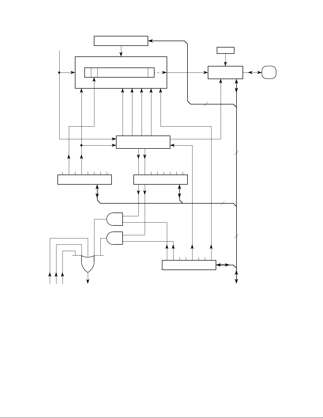
Freescale Semiconductor, Inc.
..
.
nc
TRANSMITTER
BAUD RATE
CLOCK
T8
R8
SCCR1 SCI CONTROL 1
SCDR Tx BUFFER
10 (11) - BIT Tx SHIFT REGISTER
H(8)76543210L
SIZE 8/9
SHIFT ENABLE
TRANSFER Tx BUFFER
TRANSMITTER
CONTROL LOGIC
WAKE
M
TDRE
SCSR INTERRUPT STATUS
(WRITE-ONLY)
JAM ENABLE
BREAK—JAM 0's
PREAMBLE—JAM 1's
TC
IDLE
RDRF
OR
NF
FORCE PIN
DIRECTION (OUT)
FE
PIN BUFFER
AND CONTROL
8
DDD1
PD1/
TxD
8
8
TDRE
TIE
TC
TCIE
TIE
TCIE
SCCR2 SCI CONTROL 2
Freescale Semiconductor, I
SCI Rx
REQUESTS
SCI INTERRUPT
REQUEST
RIE
ILIE
TE
RE
RWU
SBK
8
INTERNAL
DATA BUS
Figure 7-1 SCI Transmitter Block Diagram
7.3 Receive Operation
During receive operations, the transmit sequence is reversed. The serial shift register
receives data and transfers it to a parallel receive data register (SCDR) as a complete
word. This double buffered operation allows a character to be shifted in serially while
another character is already in the SCDR. An advanced data recovery scheme distinguishes valid data from noise in the serial data stream. The data input is selectively
sampled to detect receive data, and a majority voting circuit determines the value and
integrity of each bit.
SERIAL COMMUNICATIONS INTERFACE MC68HC11F1
7-2 TECHNICAL DATA
For More Information On This Product,
Go to: www.freescale.com
Page 89
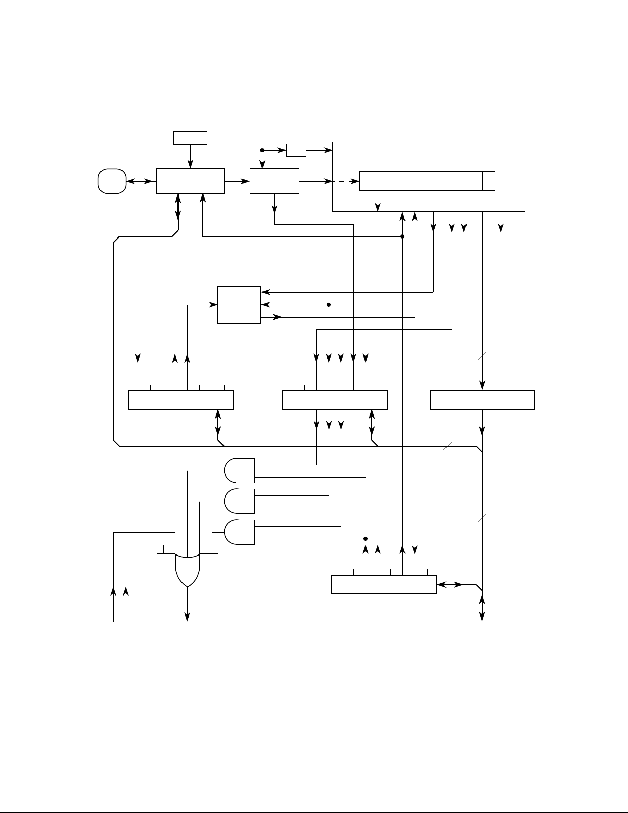
RECEIVER
BAUD RATE
CLOCK
PD0/
RxD
Freescale Semiconductor, Inc.
DDD0
PIN BUFFER
AND CONTROL
DATA
RECOVERY
÷16
10 (11) - BIT
Rx SHIFT REGISTER
STOP
(8)76543210
START
..
.
nc
T8
R8
SCCR1 SCI CONTROL 1
WAKE
M
DISABLE
DRIVER
WAKE-UP
LOGIC
RE
MSB ALL ONES
M
RWU
8
RDRF
IDLE
OR
NF
FE
SCDR Rx BUFFER
8
8
(READ-ONLY)
RDRF
RIE
IDLE
ILIE
OR
RIE
TC
TDRE
SCSR1 SCI STATUS 1
Freescale Semiconductor, I
SCI Tx
REQUESTS
SCI INTERRUPT
REQUEST
TIE
TCIE
SCCR2 SCI CONTROL 2
RIE
ILIE
TE
RE
RWU
SBK
INTERNAL
DATA BUS
Figure 7-2 SCI Receiver Block Diagram
SERIAL COMMUNICATIONS INTERFACE
TECHNICAL DATA 7-3
For More Information On This Product,
Go to: www.freescale.com
Page 90

..
.
nc
Freescale Semiconductor, I
Freescale Semiconductor, Inc.
7.4 Wakeup Feature
The wakeup feature reduces SCI service overhead in multiple receiver systems. Software for each receiver evaluates the first character of each message. The receiver is
placed in wakeup mode by writing a one to the RWU bit in the SCCR2 register. While
RWU is one, all of the receiver-related status flags (RDRF, IDLE, OR, NF, and FE) are
inhibited (cannot become set). Although RWU can be cleared by a software write to
SCCR2, to do so would be unusual. Normally RWU is set by software and is cleared
automatically with hardware. Whenever a new message begins, logic alerts the sleeping receivers to wake up and evaluate the initial character of the new message.
Two methods of wakeup are available: idle-line wakeup and address-mark wakeup.
During idle-line wakeup, a sleeping receiver awakens as soon as the RxD line becomes idle. In the address-mark wakeup, logic one in the most significant bit (MSB) of
a character wakes up all sleeping receivers.
7.4.1 Idle-Line Wakeup
To use the receiver wakeup method, establish a software addressing scheme to allow
the transmitting devices to direct a message to individual receivers or to groups of receivers. This addressing scheme can take any form as long as all transmitting and receiving devices are programmed to understand the same scheme. Because the
addressing information is usually the first frame(s) in a message, receivers that are not
part of the current task do not become burdened with the entire set of addressing
frames. All receivers are awake (RWU = 0) when each message begins. As soon as
a receiver determines that the message is not intended for it, software sets the RWU
bit (RWU = 1), which inhibits further flag setting until the RxD line goes idle at the end
of the message. As soon as an idle line is detected by receiver logic, hardware automatically clears the RWU bit so that the first frame of the next message can be received. This type of receiver wakeup requires a minimum of one idle-line frame time
between messages, and no idle time between frames in a message.
7.4.2 Address-Mark Wakeup
The serial characters in this type of wakeup consist of seven (eight if M = 1) information
bits and an MSB, which indicates an address character (when set to one, or mark).
The first character of each message is an addressing character (MSB = 1). All receivers in the system evaluate this character to determine if the remainder of the message
is directed toward this particular receiver. As soon as a receiver determines that a
message is not intended for it, the receiver activates the RWU function by using a software write to set the RWU bit. Because setting RWU inhibits receiver-related flags,
there is no further software overhead for the rest of this message.
When the next message begins, its first character has its MSB set, which automatically
clears the RWU bit and enables normal character reception. The first character whose
MSB is set is also the first character to be received after wakeup because RWU gets
cleared before the stop bit for that frame is serially received. This type of wakeup allows messages to include gaps of idle time, unlike the idle-line method, but there is a
loss of efficiency because of the extra bit time for each character (address bit) required
for all characters.
SERIAL COMMUNICATIONS INTERFACE MC68HC11F1
7-4 TECHNICAL DATA
For More Information On This Product,
Go to: www.freescale.com
Page 91

..
.
nc
Freescale Semiconductor, Inc.
7.5 SCI Error Detection
Three error conditions, SCDR overrun, received bit noise, and framing can occur during generation of SCI system interrupts. Three bits (OR, NF, and FE) in the serial communications status register (SCSR) indicate if one of these error conditions exists.
The overrun error (OR) bit is set when the next byte is ready to be transferred from the
receive shift register to the SCDR and the SCDR is already full (RDRF bit is set). When
an overrun error occurs, the data that caused the overrun is lost and the data that was
already in SCDR is not disturbed. The OR is cleared when the SCSR is read (with OR
set), followed by a read of the SCDR.
The noise flag (NF) bit is set if there is noise on any of the received bits, including the
start and stop bits. The NF bit is not set until the RDRF flag is set. The NF bit is cleared
when the SCSR is read (with FE equal to one) followed by a read of the SCDR.
When no stop bit is detected in the received data character, the framing error (FE) bit
is set. FE is set at the same time as the RDRF. If the byte received causes both framing and overrun errors, the processor only recognizes the overrun error. The framing
error flag inhibits further transfer of data into the SCDR until it is cleared. The FE bit is
cleared when the SCSR is read (with FE equal to one) followed by a read of the SCDR.
7.6 SCI Registers
There are five addressable registers associated with the SCI. SCCR1, SCCR2, and
BAUD are control registers. SCDR is the SCI data register and SCSR is the SCI status
register. Refer to the BAUD register description as well as the block diagram for the
baud rate generator.
7.6.1 Serial Communications Data Register
SCDR is a parallel register that performs two functions. It is the receive data register
when it is read, and the transmit data register when it is written. Reads access the receive data buffer and writes access the transmit data buffer. Receive and transmit are
double buffered.
SCDR — SCI Data Register $102F
Freescale Semiconductor, I
RESET: IIIIIII I
7.6.2 Serial Communications Control Register 1
The SCCR1 register provides the control bits that determine word length and select
the method used for the wakeup feature.
Bit 7 654321Bit 0
R7/T7 R6/T6 R5/T5 R4/T4 R3/T3 R2/T2 R1/T1 R0/T0
SCCR1 — SCI Control Register 1 $102C
Bit 7 654321Bit 0
R8 T8 — M WAKE — — —
RESET: I I 000000
SERIAL COMMUNICATIONS INTERFACE
TECHNICAL DATA 7-5
For More Information On This Product,
Go to: www.freescale.com
Page 92

Freescale Semiconductor, Inc.
R8 — Receive Data Bit 8
If M bit is set, R8 stores the ninth bit in the receive data character.
T8 — Transmit Data Bit 8
If M bit is set, T8 stores the ninth bit in the transmit data character.
M — Mode (Select Character Format)
0 = Start bit, 8 data bits, 1 stop bit
1 = Start bit, 9 data bits, 1 stop bit
WAKE — Wakeup by Address Mark/Idle
0 = Wakeup by IDLE line recognition
1 = Wakeup by address mark (most significant data bit set)
..
.
nc
Freescale Semiconductor, I
7.6.3 Serial Communications Control Register 2
The SCCR2 register provides the control bits that enable or disable individual SCI
functions.
SCCR2 — SCI Control Register 2 $102D
Bit 7 654321Bit 0
TIE TCIE RIE ILIE TE RE RWU SBK
RESET: 0000000 0
TIE — Transmit Interrupt Enable
0 = TDRE interrupts disabled
1 = SCI interrupt requested when TDRE status flag is set
TCIE — Transmit Complete Interrupt Enable
0 = TC interrupts disabled
1 = SCI interrupt requested when TC status flag is set
RIE — Receiver Interrupt Enable
0 = RDRF and OR interrupts disabled
1 = SCI interrupt requested when RDRF flag or the OR status flag is set
ILIE — Idle-Line Interrupt Enable
0 = IDLE interrupts disabled
1 = SCI interrupt requested when IDLE status flag is set
TE — Transmitter Enable
When TE goes from zero to one, one unit of idle character time (logic one) is queued
as a preamble.
0 = Transmitter disabled
1 = Transmitter enabled
RE — Receiver Enable
0 = Receiver disabled
1 = Receiver enabled
SERIAL COMMUNICATIONS INTERFACE MC68HC11F1
7-6 TECHNICAL DATA
For More Information On This Product,
Go to: www.freescale.com
Page 93

..
.
nc
Freescale Semiconductor, Inc.
RWU — Receiver Wakeup Control
0 = Normal SCI receiver
1 = Wakeup enabled and receiver interrupts inhibited
SBK — Send Break
At least one character time of break is queued and sent each time SBK is written to
one. As long as the SBK bit is set, break characters are queued and sent. More than
one break may be sent if the transmitter is idle at the time the SBK bit is toggled on
and off, as the baud rate clock edge could occur between writing the one and writing
the zero to SBK.
0 = Break generator off
1 = Break codes generated
7.6.4 Serial Communication Status Register
The SCSR provides inputs to the interrupt logic circuits for generation of the SCI system interrupt.
SCSR — SCI Status Register $102E
Bit 7 654321Bit 0
TDRE TC RDRF IDLE OR NF FE —
RESET: 1100000 0
TDRE — Transmit Data Register Empty Flag
This flag is set when SCDR is empty. Clear the TDRE flag by reading SCSR and then
writing to SCDR.
0 = SCDR busy
1 = SCDR empty
TC — Transmit Complete Flag
This flag is set when the transmitter is idle (no data, preamble, or break transmission
in progress). Clear the TC flag by reading SCSR and then writing to SCDR.
0 = Transmitter busy
1 = Transmitter idle
RDRF — Receive Data Register Full Flag
Freescale Semiconductor, I
This flag is set if a received character is ready to be read from SCDR. Clear the RDRF
flag by reading SCSR and then reading SCDR.
0 = SCDR empty
1 = SCDR full
IDLE — Idle Line Detected Flag
This flag is set if the RxD line is idle. Once cleared, IDLE is not set again until the RxD
line has been active and becomes idle again. The IDLE flag is inhibited when RWU =
1. Clear IDLE by reading SCSR and then reading SCDR.
0 = RxD line is active
1 = RxD line is idle
SERIAL COMMUNICATIONS INTERFACE
TECHNICAL DATA 7-7
For More Information On This Product,
Go to: www.freescale.com
Page 94

..
.
nc
Freescale Semiconductor, Inc.
OR — Overrun Error Flag
OR is set if a new character is received before a previously received character is read
from SCDR. Clear the OR flag by reading SCSR and then reading SCDR.
0 = No overrun
1 = Overrun detected
NF — Noise Error Flag
NF is set if majority sample logic detects anything other than a unanimous decision.
Clear NF by reading SCSR and then reading SCDR.
0 = Unanimous decision
1 = Noise detected
FE — Framing Error
FE is set when a zero is detected where a stop bit was expected. Clear the FE flag by
reading SCSR and then reading SCDR.
0 = Stop bit detected
1 = Zero detected
Bit 0 — Not implemented
Always reads zero
7.6.5 Baud Rate Register
Use this register to select different baud rates for the SCI system. The SCP[1:0] bits
select the prescaler rate for the SCR[2:0] bits. Together, these five bits provide multiple baud rate combinations for a given crystal frequency. Normally, this register is written once during initialization. The prescaler is set to its fastest rate by default out of
reset, and can be changed at any time. Refer to Table 7-1 and Table 7-2 for normal
baud rate selections.
BAUD — Baud Rate $102B
Bit 7 654321Bit 0
TCLR — SCP1 SCP0 RCKB SCR2 SCR1 SCR0
RESET: 00000UUU
TCLR — Clear Baud Rate Counters (Test)
Freescale Semiconductor, I
SCP[1:0] — SCI Baud Rate Prescaler Selects
Refer to the SCI baud rate generator block diagram.
Table 7-1 Baud Rate Prescaler Selection
Prescaler Divide Internal Crystal Frequency (MHz)
SCP1 SCP0 Clock By 4.0 4.9152 8.0 12.0 16.0 20.0
0 0 1 62500 76800 125000 187500 25000 312500
0 1 3 20833 25600 41667 62500 83332 104165
1 0 4 15625 19200 31250 46875 62500 78125
1 1 13 4800 5907 9600 14423 19200 24000
SERIAL COMMUNICATIONS INTERFACE MC68HC11F1
7-8 TECHNICAL DATA
For More Information On This Product,
Go to: www.freescale.com
Page 95

Freescale Semiconductor, Inc.
RCKB — SCI Baud Rate Clock Check (Test)
SCR[2:0] — SCI Baud Rate Selects
Selects receiver and transmitter bit rate based on output from baud rate prescaler
stage. Refer to the SCI baud rate generator block diagram.
Table 7-2 Baud Rate Selection
..
.
nc
Divide
Prescaler
SCR[2:0] By 4800 19200 76800 312500
0 0 0 1 4800 19200 76800 312500
0 0 1 2 2400 9600 38400 156250
0 1 0 4 1200 4800 19200 78125
0 1 1 8 600 2400 9600 39063
1 0 0 16 300 1200 4800 19531
1 0 1 32 150 600 2400 9766
1 1 0 64 75 300 1200 4883
1 1 1 128 — 150 600 2441
(Prescaler Output from Previous Table)
Highest Baud Rate
The prescaler bits, SCP[2:0], determine the highest baud rate, and the SCR[2:0] bits
select an additional binary submultiple (≥1, ≥2, ≥4, through ≥128) of this highest baud
rate. The result of these two dividers in series is the 16X receiver baud rate clock. The
SCR[2:0] bits are not affected by reset and can be changed at any time, although they
should not be changed when any SCI transfer is in progress.
Figure 7-3 and Figure 7-4 illustrate the SCI baud rate timing chain. The prescaler select bits determine the highest baud rate. The rate select bits determine additional divide by two stages to arrive at the receiver timing (RT) clock rate. The baud rate clock
is the result of dividing the RT clock by 16.
Freescale Semiconductor, I
SERIAL COMMUNICATIONS INTERFACE
TECHNICAL DATA 7-9
For More Information On This Product,
Go to: www.freescale.com
Page 96
Freescale Semiconductor, Inc.
..
.
nc
EXTAL
XTAL
OSCILLATOR
AND
CLOCK GENERATOR
(
÷4)
E
AS
÷2
÷2
÷2
÷2
÷2
÷2
÷2
÷3 ÷4 ÷13
SCP1:SCP0
0:0 0:1 1:0 1:1
SCR2:SCR1:SCR0
0:0:0
0:0:1
0:1:0
0:1:1
÷16
1:0:0
SCI
TRANSMIT
1:0:1
1:1:0
1:1:1
BAUD RATE
(1X)
SCI
RECEIVE
BAUD RATE
(16X)
Figure 7-3 SCI Baud Rate Generator Block Diagram
INTERNAL
BUS
CLOCK
(PH2)
Freescale Semiconductor, I
7.7 Status Flags and Interrupts
The SCI transmitter has two status flags. These status flags can be read by software
(polled) to tell when the corresponding condition exists. Alternatively, a local interrupt
enable bit can be set to enable each of these status conditions to generate interrupt
requests when the corresponding condition is present. Status flags are automatically
set by hardware logic conditions, but must be cleared by software, which provides an
interlock mechanism that enables logic to know when software has noticed the status
indication. The software clearing sequence for these flags is automatic — functions
that are normally performed in response to the status flags also satisfy the conditions
of the clearing sequence.
SERIAL COMMUNICATIONS INTERFACE MC68HC11F1
7-10 TECHNICAL DATA
For More Information On This Product,
Go to: www.freescale.com
Page 97

..
.
nc
Freescale Semiconductor, Inc.
TDRE and TC flags are normally set when the transmitter is first enabled (TE set to
one). The TDRE flag indicates there is room in the transmit queue to store another
data character in the TDR. The TIE bit is the local interrupt mask for TDRE. When TIE
is zero, TDRE must be polled. When TIE and TDRE are one, an interrupt is requested.
The TC flag indicates the transmitter has completed the queue. The TCIE bit is the local interrupt mask for TC. When TCIE is zero, TC must be polled; when TCIE is one
and TC is one, an interrupt is requested.
Writing a zero to TE requests that the transmitter stop when it can. The transmitter
completes any transmission in progress before actually shutting down. Only an MCU
reset can cause the transmitter to stop and shut down immediately. If TE is written to
zero when the transmitter is already idle, the pin reverts to its general-purpose I/O
function (synchronized to the bit-rate clock). If anything is being transmitted when TE
is written to zero, that character is completed before the pin reverts to general-purpose
I/O, but any other characters waiting in the transmit queue are lost. The TC and TDRE
flags are set at the completion of this last character, even though TE has been disabled.
7.7.1 Receiver Flags
The SCI receiver has five status flags, three of which can generate interrupt requests.
The status flags are set by the SCI logic in response to specific conditions in the receiver. These flags can be read (polled) at any time by software. Refer to Figure 7–4,
which shows SCI interrupt arbitration.
When an overrun takes place, the new character is lost, and the character that was in
its way in the parallel RDR is undisturbed. RDRF is set when a character has been
received and transferred into the parallel RDR. The OR flag is set instead of RDRF if
overrun occurs. A new character is ready to be transferred into RDR before a previous
character is read from RDR.
The NF and FE flags provide additional information about the character in the RDR,
but do not generate interrupt requests.
The last receiver status flag and interrupt source come from the IDLE flag. The RxD
line is idle if it has constantly been at logic one for a full character time. The IDLE flag
Freescale Semiconductor, I
is set only after the RxD line has been busy and becomes idle, which prevents repeated interrupts for the whole time RxD remains idle.
SERIAL COMMUNICATIONS INTERFACE
TECHNICAL DATA 7-11
For More Information On This Product,
Go to: www.freescale.com
Page 98
BEGIN
Freescale Semiconductor, Inc.
..
.
nc
RDRF = 1
?
NO
OR = 1
?
NO
TDRE = 1
?
NO
TC = 1
?
NO
IDLE = 1
?
NO
NO – VALID SCI
REQUEST
Figure 7-4 Interrupt Source Resolution Within SCI
YES
YES
YES
YES
YES
RIE = 1
?
NO
TIE = 1
?
NO
TCIE = 1
?
NO
ILIE = 1
?
NO
YES
YES
YES
YES
RE = 1
?
TE = 1
?
RE = 1
?
NO
NO
NO
YES
YES
YES
YES – VALID SCI
REQUEST
Freescale Semiconductor, I
SERIAL COMMUNICATIONS INTERFACE MC68HC11F1
7-12 TECHNICAL DATA
For More Information On This Product,
Go to: www.freescale.com
Page 99

Freescale Semiconductor, Inc.
SECTION 8 SERIAL PERIPHERAL INTERFACE
The serial peripheral interface (SPI), an independent serial communications subsystem, allows the MCU to communicate synchronously with peripheral devices, such
as transistor-transistor logic (TTL) shift registers, liquid crystal display (LCD) drivers,
analog-to-digital converter subsystems, and other microprocessors. The SPI is also
capable of inter-processor communication in a multiple master system. The SPI system can be configured as either a master or a slave device. When configured as a
master, data transfer rates can be as high as one-half the E-clock rate (2.5 Mbits per
second for a 5-MHz bus frequency). When configured as a slave, data transfers can
..
.
be as fast as the E-clock rate (5 Mbits per second for a 5-MHz bus frequency).
nc
Freescale Semiconductor, I
8.1 Functional Description
The central element in the SPI system is the block containing the shift register and the
read data buffer. The system is single buffered in the transmit direction and double
buffered in the receive direction. This means that new data for transmission cannot be
written to the shifter until the previous transfer is complete; however, received data is
transferred into a parallel read data buffer so the shifter is free to accept a second serial character. As long as the first character is read out of the read data buffer before
the next serial character is ready to be transferred, no overrun condition occurs. A single MCU register address is used for reading data from the read data buffer and for
writing data to the shifter.
The SPI status block represents the SPI status flags (transfer complete, write collision,
and mode fault) located in the SPI status register (SPSR). The SPI control block represents those functions that control the SPI system through the serial peripheral control register (SPCR).
Refer to Figure 8-1, which shows the SPI block diagram.
SERIAL PERIPHERAL INTERFACE
TECHNICAL DATA 8-1
For More Information On This Product,
Go to: www.freescale.com
Page 100
Freescale Semiconductor, Inc.
..
.
nc
INTERNAL
MCU CLOCK
DIVIDER
÷2 ÷4 ÷16 ÷32
SELECT
SPR1
SPR0
SPI CONTROL
SPI CLOCK (MASTER)
MSB LSB
8-BIT SHIFT REGISTER
READ DATA BUFFER
MSTR
SPE
SPIE
CLOCK
LOGIC
CLOCK
S
M
M
S
PIN
CONTROL
LOGIC
S
M
MSTR
SPE
DWOM
MISO/
PD2
MOSI/
PD3
SCK/
PD4
SS
PD5
/
SPIF
WCOL
MODF
SPSR SPI STATUS REGISTER
SPI INTERRUPT
REQUEST
Figure 8-1 SPI Block Diagram
8
8
INTERNAL
DATA BUS
SPIE
SPE
DWOM
MSTR
CPHA
CPOL
SPR1
SPR0
SPCR SPI CONTROL REGISTER
8
Freescale Semiconductor, I
8.2 SPI Transfer Formats
During an SPI transfer, data is simultaneously transmitted and received. A serial clock
line synchronizes shifting and sampling of the information on the two serial data lines.
A slave select line allows individual selection of a slave SPI device; slave devices that
are not selected do not interfere with SPI bus activities. On a master SPI device, the
select line can optionally be used to indicate a multiple master bus contention. Refer
to Figure 8-2.
SERIAL PERIPHERAL INTERFACE MC68HC11F1
8-2 TECHNICAL DATA
For More Information On This Product,
Go to: www.freescale.com
 Loading...