

Page 1

M68060 User’s Manual
Including the
MC68060,
MC68LC060,
and
MC68EC060
Motorola reserves the right to make changes without further notice to any products herein. Motorola makes no warranty, representation or guarantee regarding
the suitability of its products for any particular purpose, nor does Motorola assume any liability arising out of the application or use of any product or circuit, and
specifically disclaims any and all liability, including without limitation consequential or incidental damages. "Typical" parameters can and do vary in different
applications. All operating parameters, including "Typicals" must be validated for each customer application by customer's technical experts. Motorola does not
convey any license under its patent rights nor the rights of others. Motorola products are not designed, intended, or authorized for use as components in systems
intended for surgical implant into the body, or other applications intended to support or sustain life, or for any other application in which the failure of the Motorola
product could create a situation where personal injury or death may occur. Should Buyer purchase or use Motorola products for any such unintended or
unauthorized application, Buyer shall indemnify and hold Motorola and its officers, employees, subsidiaries, affiliates, and distributors harmless against all claims,
costs, damages, and expenses, and reasonable attorney fees arising out of, directly or indirectly, any claim of personal injury or death associated with such
unintended or unauthorized use, even if such claim alleges that Motorola was negligent regarding the design or manufacture of the part. Motorola and are
registered trademarks of Motorola, Inc. Motorola, Inc. is an Equal Opportunity/Affirmative Action Employer.
© MOTOROLA, 1994
µ
Page 2

68K FAX-IT
Documentation Comments
FAX 512-891-8593—Documentation Comments Only
The Motorola High-End Technical Publications Department provides a fax number for you
to submit any questions or comments about this document or how to order other documents.
We welcome your suggestions for improving our documentation. Please do not fax technical
questions.
Please provide the part number and revision number (located in upper right-hand corner of
the cover) and the title of the document. When referring to items in the manual, please reference by the page number, paragraph number, figure number, table number, and line number if needed.
When sending a fax, please provide your name, company, fax number, and phone number
including area code.
Applications and Technical Information
For questions or comments pertaining to technical information, questions, and applications,
please contact one of the following sales offices nearest you.
MOTOROLA
M68060 USER’S MANUAL
iii
Page 3

iv
—
Sales Offices —
Field Applications Engineering Available Through All Sales Offices
ALABAMA , Huntsville (205) 464-6800
UNITED STATES
ARIZONA , Tempe (602) 897-5056
CALIFORNIA , Agoura Hills (818) 706-1929
CALIFORNIA , Los Angeles (310) 417-8848
CALIFORNIA , Irvine (714) 753-7360
CALIFORNIA , Rosevllle (916) 922-7152
CALIFORNIA , San Diego (619) 541-2163
CALIFORNIA , Sunnyvale (408) 749-0510
COLORADO , Colorado Springs (719) 599-7497
COLORADO , Denver (303) 337-3434
CONNECTICUT , Wallingford (203) 949-4100
FLORIDA , Maitland (407) 628-2636
FLORIDA , Pompano Beach/
Fort Lauderdale (305) 486-9776
FLORIDA , Clearwater (813) 538-7750
GEORGlA , Atlanta (404) 729-7100
IDAHO , Boise (208) 323-9413
ILLINOIS , Chicago/Hoffman Estates (708) 490-9500
INDlANA , Fort Wayne (219) 436-5818
INDIANA , Indianapolis (317) 571-0400
INDIANA , Kokomo (317) 457-6634
IOWA , Cedar Rapids (319) 373-1328
KANSAS , Kansas City/Mission (913) 451-8555
MARYLAND , Columbia (410) 381-1570
MASSACHUSETTS , Marborough (508) 481-8100
MASSACHUSETTS , Woburn (617) 932-9700
MICHIGAN , Detroit (313) 347-6800
MINNESOTA , Minnetonka (612) 932-1500
MISSOURI , St. Louis (314) 275-7380
NEW JERSEY , Fairfield (201) 808-2400
NEW YORK , Fairport (716) 425-4000
NEW YORK , Hauppauge (516) 361-7000
NEW YORK , Poughkeepsie/Fishkill (914) 473-8102
NORTH CAROLINA , Raleigh (919) 870-4355
OHIO , Cleveland (216) 349-3100
OHIO , Columbus/Worthington (614) 431-8492
OHIO , Dayton (513) 495-6800
OKLAHOMA , Tulsa (800) 544-9496
OREGON , Portland (503) 641-3681
PENNSYLVANIA , Colmar (215) 997-1020
Philadelphia/Horsham (215) 957-4100
TENNESSEE , Knoxville (615) 690-5593
TEXAS , Austin (512) 873-2000
TEXAS , Houston (800) 343-2692
TEXAS , Plano (214) 516-5100
VIRGINIA , Richmond (804) 285-2100
WASHINGTON , Bellevue (206) 454-4160
Seattle Access (206) 622-9960
WISCONSIN , Milwaukee/Brookfield (414) 792-0122
BRITISH COLUMBIA , Vancouver (604) 293-7605
ONTARIO , Toronto (416) 497-8181
ONTARIO , Ottawa (613) 226-3491
QUEBEC , Montreal (514) 731-6881
AUSTRALIA , Melbourne (61-3)887-0711
AUSTRALIA , Sydney (61(2)906-3855
BRAZIL , Sao Paulo 55(11)815-4200
CHINA , Beijing 86 505-2180
FINLAND , Helsinki 358-0-35161191
Car Phone 358(49)211501
FRANCE , Paris/Vanves 33(1)40 955 900
CANADA
INTERNATIONAL
GERMANY , Langenhagen/ Hanover 49(511)789911
GERMANY , Munich 49 89 92103-0
GERMANY , Nuremberg 49 911 64-3044
GERMANY , Sindelfingen 49 7031 69 910
GERMANY , Wiesbaden 49 611 761921
HONG KONG , Kwai Fong 852-4808333
Tai Po 852-6668333
INDIA , Bangalore (91-812)627094
ISRAEL , Tel Aviv 972(3)753-8222
ITALY , Milan 39(2)82201
JAPAN , Aizu 81(241)272231
JAPAN , Atsugi 81(0462)23-0761
JAPAN , Kumagaya 81(0485)26-2600
JAPAN , Kyushu 81(092)771-4212
JAPAN , Mito 81(0292)26-2340
JAPAN , Nagoya 81(052)232-1621
JAPAN , Osaka 81(06)305-1801
JAPAN, Sendai 81(22)268-4333
JAPAN,
JAPAN,
JAPAN
KOREA , Pusan 82(51)4635-035
KOREA , Seoul 82(2)554-5188
MALAYSIA , Penang 60(4)374514
MEXICO , Mexico City 52(5)282-2864
MEXICO , Guadalajara 52(36)21-8977
Marketing 52(36)21-9023
Customer Service 52(36)669-9160
NETHERLANDS , Best (31)49988 612 11
PUERTO RICO , San Juan (809)793-2170
SINGAPORE
SPAIN , Madrid 34(1)457-8204
or 34(1)457-8254
SWEDEN , Solna 46(8)734-8800
SWITZERLAND , Geneva 41(22)7991111
SWITZERLAND , Zurich 41(1)730 4074
TAlWAN , Taipei 886(2)717-7089
THAILAND , Bangkok (66-2)254-4910
UNITED KINGDOM , Aylesbury 44(296)395-252
COLORADO , Grand Junction
Cheryl Lee Whltely (303) 243-9658
KANSAS , Wichita
Melinda Shores/Kelly Greiving (316) 838 0190
NEVADA , Reno
Galena Technology Group (702) 746 0642
NEW MEXICO , Albuquerque
S&S Technologies, lnc. (505) 298-7177
UTAH , Salt Lake City
Utah Component Sales, Inc. (801) 561-5099
WASHINGTON , Spokane
Doug Kenley (509) 924-2322
ARGENTINA , Buenos Aires
Argonics, S.A. (541) 343-1787
Elmo Semiconductor (818) 768-7400
Minco Technology Labs Inc. (512) 834-2022
Semi Dice Inc. (310) 594-4631
Tachikawa 81(0425)23-6700
Tokyo 81(03)3440-3311
, Yokohama 81(045)472-2751
(65)2945438
FULL LINE REPRESENTATIVES
HYBRID COMPONENTS RESELLERS
M68060 USER’S MANUAL
MOTOROLA
Page 4

PREFACE
The complete documentation package for the MC68060, MC68LC060, and MC68EC060
(collectively called M68060) consists of the M68060UM/AD,
the M68000PM/AD,
Manual
32-bit microprocessors. The
complete instruction set for the M68000 family.
The introduction of this manual includes general information concerning the MC68060 and
summarizes the differences among the M68060 family devices. Additionally, appendices
provide detailed information on how these M68060 derivatives operate differently from the
MC68060.
When reading this manual, disregard information concerning the floating-point unit in reference to the MC68LC060, and disregard information concerning the floating-point unit and
memory management unit in reference to the MC68EC060.
describes the capabilities, operation, and programming of the M68060 superscalar
M68000 Family Programmer’s Reference Manual
M68000 Family Programmer’s Reference Manual
M68060 User’s Manual
. The
M68060 User’s
contains the
, and
The organization of this manual is as follows:
Section 1 Introduction
Section 2 Signal Description
Section 3 Integer Unit
Section 4 Memory Management Unit
Section 5 Caches
Section 6 Floating-Point Unit
Section 7 Bus Operation
Section 8 Exception Processing
Section 9 IEEE 1149.1 Test (JTAG) and Debug Pipe Control Modes
Section 10 Instruction Timings
Section 11 Applications
Section 12 Electrical and Thermal Characteristics
Section 13 Ordering Information and Mechanical Data
Appendix A MC68LC060
Appendix B MC68EC060
Appendix C MC68060 Software Package
Appendix D M68060 Instructions
MOTOROLA
M68060 USER’S MANUAL
v
Page 5

MC68060 ACRONYM LIST
AGU—address generation unit
ALU—arithmetic logic unit
ATC—address translation cache
BUSCR—bus control register
CACR—cache control register
CCR—condition code register
CM—cache mode
CPU—central processing unit
DFC—destination function code
DTTx—data transparent translation register
DRAM—dynamic random access memory
FPIAR—floating-point instruction address register
FPCR—floating-point control register
FPSP—floating-point software package
FPSR—floating-point status register
FPU—floating-point unit
FP7–FP0—floating-point data registers 7–0
FSLW—fault status long word
IEE—integer execute unit
IFP—instruction fetch pipeline
IFU—instruction fetch unit
IPU—instruction pipe unit
ISP—interrupt stack pointer
ITTR—instruction transparent translation register
IU—integer unit
JTAG—Joint Test Action Group
MMU—memory management unit
MOTOROLA
M68060 USER’S MANUAL
vii
Page 6

MC68060 Acronym List
MMUSR—memory management unit status register
M68060SP—M68060 software package
NANs—not-a-numbers
NOP—no operation
OEP—operand execution pipeline
OPU—operand pipe unit
PC—program counter
PCR—processor configuration register
PGI—page index field
PI—pointer index field
PLL—phase-locked loop
pOEP—primary operand execution pipeline
RI—root index field
SFC—source function code
SNAN—signaling not-a-number
sOEP—secondary operand execution pipeline
SP—stack pointer
SR—status register
SRP—supervisor root pointer register
SSP—supervisor stack pointer
TAP—test access port
TCR—translation control register
TTL—transistor-transistor logic
TTR—transparent translation register
UPA—user page attribute
URP—user root pointer register
USP—user stack pointer
VBR—vector base register
VLSI—very large-scale integration
viii
M68060 USER’S MANUAL
MOTOROLA
Page 7

TABLE OF CONTENTS
Section 1
Introduction
1.1 Differences Among M68060 Family Members..............................................1-3
1.1.1 MC68LC060................................................................................................1-3
1.1.2 MC68EC060...............................................................................................1-3
1.1.2.1 Address Translation Differences ..............................................................1-3
1.1.2.2 Instruction Differences..............................................................................1-3
1.2 Features........................................................................................................1-4
1.3 Architecture...................................................................................................1-4
1.4 Processor Overview......................................................................................1-5
1.4.1 Functional Blocks........................................................................................1-5
1.4.2 Integer Unit.................................................................................................1-7
1.4.2.1 Instruction Fetch Unit................................................................................1-7
1.4.2.2 Integer Unit...............................................................................................1-8
1.4.2.3 Floating-Point Unit....................................................................................1-8
1.4.2.4 Memory Units ...........................................................................................1-9
1.4.2.5 Address Translation Caches ....................................................................1-9
1.4.2.6 Instruction and Data Caches ....................................................................1-9
1.4.2.6.1 Cache Organization..............................................................................1-10
1.4.2.6.2 Cache Coherency.................................................................................1-10
1.4.3 Bus Controller...........................................................................................1-10
1.5 Processing States.......................................................................................1-10
1.6 Programming Model....................................................................................1-11
1.7 Data Format Summary................................................................................1-14
1.8 Addressing Capabilities Summary..............................................................1-14
1.9 Instruction Set Overview.............................................................................1-15
1.10 Notational Conventions...............................................................................1-21
Section 2
Signal Description
2.1 Address and Control Signals ........................................................................2-3
2.1.1 Address Bus (A31–A0)...............................................................................2-3
2.1.2 Cycle Long-Word Address (CLA
) ...............................................................2-4
2.2 Data Bus (D31–D0).......................................................................................2-4
2.3 Transfer Attribute Signals .............................................................................2-4
2.3.1 Transfer Cycle Type (TT1, TT0).................................................................2-4
2.3.2 Transfer Cycle Modifier (TM2–TM0)...........................................................2-4
2.3.3 Transfer Line Number (TLN1, TLN0)..........................................................2-5
2.3.4 User-Programmable Page Attributes (UPA1, UPA0)..................................2-5
2.3.5 Read/Write (R/W
MOTOROLA
) .......................................................................................2-6
M68060 USER’S MANUAL
ix
Page 8

x
Table of Contents
2.3.6 Transfer Size (SIZ1, SIZ0)..........................................................................2-6
2.3.7 Bus Lock (LOCK
2.3.8 Bus Lock End (LOCKE
2.3.9 Cache Inhibit Out (CIOUT
2.3.10 Byte Select Lines (BS3
)........................................................................................ 2-6
)..............................................................................2-6
)......................................................................... 2-7
–BS0).....................................................................2-7
2.4 Master Transfer Control Signals................................................................... 2-7
2.4.1 Transfer Start (TS
2.4.2 Transfer in Progress (TIP
2.4.3 Starting Termination Acknowledge Signal Sampling (SAS
)...................................................................................... 2-8
).......................................................................... 2-8
)....................... 2-8
2.5 Slave Transfer Control Signals..................................................................... 2-8
2.5.1 Transfer Acknowledge (TA
2.5.2 Transfer Retry Acknowledge (TRA
)........................................................................2-8
)............................................................ 2-8
2.5.3 Transfer Error Acknowledge (TEA) ............................................................2-9
2.5.4 Transfer Burst Inhibit (TBI
2.5.5 Transfer Cache Inhibit (TCI
2.6 Snoop Control (SNOOP
)......................................................................... 2-9
)....................................................................... 2-9
) ..............................................................................2-9
2.7 Arbitration Signals....................................................................................... 2-10
2.7.1 Bus Request (BR
2.7.2 Bus Grant (BG
2.7.3 Bus Grant Relinquish Control (BGR
2.7.4 Bus Tenure Termination (BTT
2.7.5 Bus Busy (BB
)..................................................................................... 2-10
).........................................................................................2-10
)........................................................2-10
).................................................................2-10
)..........................................................................................2-11
2.8 Processor Control Signals.......................................................................... 2-11
2.8.1 Cache Disable (CDIS
2.8.2 MMU Disable (MDIS
2.8.3 Reset In (RSTI
)......................................................................................... 2-12
2.8.4 Reset Out (RSTO
).............................................................................. 2-11
)................................................................................ 2-12
).................................................................................... 2-12
2.9 Interrupt Control Signals............................................................................. 2-12
2.9.1 Interrupt Priority Level (IPL2
2.9.2 Interrupt Pending Status (IPEND
2.9.3 Autovector (AVEC
)................................................................................... 2-13
–IPL0)..........................................................2-12
) ............................................................2-12
2.10 Status and Clock Signals............................................................................2-13
2.10.1 Processor Status (PST4–PST0)...............................................................2-13
2.10.2 MC68060 Processor Clock (CLK) ............................................................2-14
2.10.3 Clock Enable (CLKEN
)............................................................................. 2-14
2.11 Test Signals................................................................................................2-15
2.11.1 JTAG Enable (JTAG
)................................................................................ 2-15
2.11.2 Test Clock (TCK)...................................................................................... 2-15
2.11.3 Test Mode Select (TMS)........................................................................... 2-15
2.11.4 Test Data In (TDI).....................................................................................2-16
2.11.5 Test Data Out (TDO)................................................................................ 2-16
2.11.6 Test Reset (TRST) ...................................................................................2-16
2.12 Thermal Sensing Pins (THERM1, THERM0)..............................................2-16
2.13 Power Supply Connections.........................................................................2-16
2.14 Signal Summary .........................................................................................2-16
M68060 USER’S MANUAL
MOTOROLA
Page 9

Table of Contents
Section 3
Integer Unit
3.1 Integer Unit Execution Pipelines...................................................................3-1
3.2 Integer Unit Register Description..................................................................3-2
3.2.1 Integer Unit User Programming Model.......................................................3-2
3.2.1.1 Data Registers (D7–D0) ...........................................................................3-2
3.2.1.2 Address Registers (A6–A0)......................................................................3-2
3.2.1.3 User Stack Pointer (A7)............................................................................3-2
3.2.1.4 Program Counter......................................................................................3-3
3.2.1.5 Condition Code Register ..........................................................................3-3
3.2.2 Integer Unit Supervisor Programming Model..............................................3-3
3.2.2.1 Supervisor Stack Pointer..........................................................................3-4
3.2.2.2 Status Register.........................................................................................3-4
3.2.2.3 Vector Base Register................................................................................3-4
3.2.2.4 Alternate Function Code Registers...........................................................3-5
3.2.2.5 Processor Configuration Register.............................................................3-5
Section 4
Memory Management Unit
4.1 Memory Management Programming Model..................................................4-3
4.1.1 User and Supervisor Root Pointer Registers..............................................4-3
4.1.2 Translation Control Register.......................................................................4-4
4.1.3 Transparent Translation Registers .............................................................4-6
4.2 Logical Address Translation..........................................................................4-7
4.2.1 Translation Tables......................................................................................4-7
4.2.2 Descriptors................................................................................................4-12
4.2.2.1 Table Descriptors....................................................................................4-12
4.2.2.2 Page Descriptors....................................................................................4-12
4.2.2.3 Descriptor Field Definitions.....................................................................4-13
4.2.3 Translation Table Example.......................................................................4-15
4.2.4 Variations in Translation Table Structure..................................................4-16
4.2.4.1 Indirect Action.........................................................................................4-16
4.2.4.2 Table Sharing Between Tasks................................................................4-17
4.2.4.3 Table Paging ..........................................................................................4-17
4.2.4.4 Dynamically Allocated Tables.................................................................4-17
4.2.5 Table Search Accesses............................................................................4-19
4.2.6 Address Translation Protection.................................................................4-20
4.2.6.1 Supervisor and User Translation Tables ................................................4-21
4.2.6.2 Supervisor Only......................................................................................4-22
4.2.6.3 Write Protect...........................................................................................4-22
4.3 Address Translation Caches.......................................................................4-24
4.4 Transparent Translation..............................................................................4-27
4.5 Address Translation Summary....................................................................4-28
4.6 RSTI
4.6.1 Effect of RSTI
and MDIS Effect on the MMU............................................................4-28
on the MMUs.....................................................................4-28
MOTOROLA
M68060 USER’S MANUAL
xi
Page 10

Table of Contents
4.6.2 Effect of MDIS on Address Translation .................................................... 4-30
4.7 MMU Instructions........................................................................................4-30
4.7.1 MOVEC ....................................................................................................4-30
4.7.2 PFLUSH ...................................................................................................4-30
4.7.3 PLPA ........................................................................................................4-30
Section 5
Caches
5.1 Cache Operation........................................................................................... 5-1
5.2 Cache Control Register ................................................................................5-5
5.3 Cache Management .....................................................................................5-6
5.4 Caching Modes.............................................................................................5-7
5.4.1 Cachable Accesses.................................................................................... 5-7
5.4.1.1 Writethrough Mode...................................................................................5-7
5.4.1.2 Copyback Mode .......................................................................................5-8
5.4.2 Cache-Inhibited Accesses.......................................................................... 5-8
5.4.3 Special Accesses .......................................................................................5-9
5.5 Cache Protocol.............................................................................................5-9
5.5.1 Read Miss...................................................................................................5-9
5.5.2 Write Miss...................................................................................................5-9
5.5.3 Read Hit......................................................................................................5-9
5.5.4 Write Hit....................................................................................................5-10
5.6 Cache Coherency....................................................................................... 5-10
5.7 Memory Accesses for Cache Maintenance................................................ 5-11
5.7.1 Cache Filling.............................................................................................5-11
5.7.2 Cache Pushes..........................................................................................5-13
5.8 Push Buffer................................................................................................. 5-13
5.9 Store Buffer................................................................................................. 5-13
5.10 Push Buffer and Store Buffer Bus Operation..............................................5-14
5.11 Branch Cache.............................................................................................5-14
5.12 Cache Operation Summary ........................................................................ 5-15
5.12.1 Instruction Cache...................................................................................... 5-15
5.12.2 Data Cache............................................................................................... 5-16
Section 6
Floating-Point Unit
6.1 Floating-Point User Programming Model...................................................... 6-2
6.1.1 Floating-Point Data Registers (FP7–FP0).................................................. 6-3
6.1.2 Floating-Point Control Register (FPCR).....................................................6-3
6.1.2.1 Exception Enable Byte ............................................................................. 6-3
6.1.2.2 Mode Control Byte.................................................................................... 6-3
6.1.3 Floating-Point Status Register (FPSR).......................................................6-4
6.1.3.1 Floating-Point Condition Code Byte ......................................................... 6-5
6.1.3.2 Quotient Byte............................................................................................ 6-5
6.1.3.3 Exception Status Byte .............................................................................. 6-5
xii
M68060 USER’S MANUAL
MOTOROLA
Page 11

Table of Contents
6.1.3.4 Accrued Exception Byte ...........................................................................6-6
6.1.4 Floating-Point Instruction Address Register (FPIAR) .................................6-7
6.2 Floating-Point Data Formats and Data Types...............................................6-7
6.3 Computational Accuracy.............................................................................6-11
6.3.1 Intermediate Result...................................................................................6-12
6.3.2 Rounding the Result.................................................................................6-13
6.4 Postprocessing Operation...........................................................................6-15
6.4.1 Underflow, Round, and Overflow..............................................................6-15
6.4.2 Conditional Testing...................................................................................6-16
6.5 Floating-Point Exceptions...........................................................................6-19
6.5.1 Unimplemented Floating-Point Instructions..............................................6-19
6.5.2 Unsupported Floating-Point Data Types...................................................6-21
6.5.3 Unimplemented Effective Address Exception...........................................6-22
6.6 Floating-Point Arithmetic Exceptions..........................................................6-22
6.6.1 Branch/Set on Unordered (BSUN)............................................................6-24
6.6.1.1 Trap Disabled Results (FPCR BSUN Bit Cleared) .................................6-24
6.6.1.2 Trap Enabled Results (FPCR BSUN Bit Set) .........................................6-24
6.6.2 Signaling Not-a-Number (SNAN)..............................................................6-25
6.6.2.1 Trap Disabled Results (FPCR SNAN Bit Cleared) .................................6-25
6.6.2.2 Trap Enabled Results (FPCR SNAN Bit Set) .........................................6-26
6.6.3 Operand Error...........................................................................................6-26
6.6.3.1 Trap Disabled Results (FPCR OPERR Bit Cleared)...............................6-27
6.6.3.2 Trap Enabled Results (FPCR OPERR Bit Set).......................................6-27
6.6.4 Overflow....................................................................................................6-28
6.6.4.1 Trap Disabled Results (FPCR OVFL Bit Cleared)..................................6-29
6.6.4.2 Trap Enabled Results (FPCR OVFL Bit Set)..........................................6-29
6.6.5 Underflow..................................................................................................6-30
6.6.5.1 Trap Disabled Results (FPCR UNFL Bit Cleared)..................................6-31
6.6.5.2 Trap Enabled Results (FPCR UNFL Bit Set)..........................................6-31
6.6.6 Divide-by-Zero..........................................................................................6-32
6.6.6.1 Trap Disabled Results (FPCR DZ Bit Cleared).......................................6-33
6.6.6.2 Trap Enabled Results (FPCR DZ Bit Set)...............................................6-33
6.6.7 Inexact Result...........................................................................................6-33
6.6.7.1 Trap Disabled Results (FPCR INEX1 Bit and INEX2 Bit Cleared...........6-34
6.6.7.2 Trap Enabled Results (Either FPCR INEX1 Bit or INEX2 Bit Set)..........6-34
6.7 Floating-Point State Frames.......................................................................6-35
Section 7
Bus Operation
7.1 Bus Characteristics.......................................................................................7-1
7.2 Full-, Half-, and Quarter-Speed Bus Operation and BCLK...........................7-3
7.3 Acknowledge Termination Ignore State Capability.......................................7-4
7.4 Bus Control Register.....................................................................................7-4
7.5 Data Transfer Mechanism.............................................................................7-5
7.6 Misaligned Operands....................................................................................7-9
MOTOROLA
M68060 USER’S MANUAL
xiii
Page 12

Table of Contents
7.7 Processor Data Transfers...........................................................................7-12
7.7.1 Byte, Word, and Long-Word Read Transfer Cycles.................................7-12
7.7.2 Line Read Transfer...................................................................................7-15
7.7.3 Byte, Word, and Long-Word Write Cycles................................................7-20
7.7.4 Line Write Cycles.....................................................................................7-25
7.7.5 Locked Read-Modify-Write Cycles..........................................................7-28
7.7.6 Emulating CAS2 and CAS Misaligned......................................................7-31
7.7.7 Using CLA
to Increment A3 and A2.......................................................... 7-32
7.8 Acknowledge Cycles................................................................................... 7-32
7.8.1 Interrupt Acknowledge Cycles................................................................. 7-32
7.8.1.1 Interrupt Acknowledge Cycle (Terminated Normally).............................7-35
7.8.1.2 Autovector Interrupt Acknowledge Cycle ...............................................7-35
7.8.1.3 Spurious Interrupt Acknowledge Cycle ..................................................7-35
7.8.2 Breakpoint Acknowledge Cycle................................................................ 7-36
7.8.2.1 LPSTOP Broadcast Cycle......................................................................7-38
7.9 Bus Exception Control Cycles ....................................................................7-46
7.9.1 Bus Errors.................................................................................................7-46
7.9.2 Retry Operation........................................................................................7-48
7.9.3 Double Bus Fault...................................................................................... 7-51
7.10 Bus Synchronization...................................................................................7-52
7.11 Bus Arbitration ............................................................................................ 7-52
7.11.1 MC68040-Arbitration Protocol (BB Protocol)............................................7-53
7.11.2 MC68060-Arbitration Protocol (BTT Protocol)..........................................7-58
7.11.3 External Arbiter Considerations................................................................7-65
7.12 Bus Snooping Operation............................................................................7-68
7.13 Reset Operation.........................................................................................7-71
7.14 Special Modes of Operation .......................................................................7-74
7.14.1 Acknowledge Termination Ignore State Capability...................................7-74
7.14.2 Acknowledge Termination Protocol.......................................................... 7-76
7.14.3 Extra Data Write Hold Time Mode............................................................7-76
Section 8
Exception Processing
8.1 Exception Processing Overview...................................................................8-1
8.2 Integer Unit Exceptions................................................................................. 8-4
8.2.1 Access Error Exception..............................................................................8-5
8.2.2 Address Error Exception.............................................................................8-7
8.2.3 Instruction Trap Exception..........................................................................8-7
8.2.4 Illegal Instruction and Unimplemented Instruction Exceptions...................8-8
8.2.5 Privilege Violation Exception....................................................................8-10
8.2.6 Trace Exception........................................................................................8-10
8.2.7 Format Error Exception ............................................................................8-11
8.2.8 Breakpoint Instruction Exception.............................................................. 8-11
8.2.9 Interrupt Exception ...................................................................................8-12
8.2.10 Reset Exception .......................................................................................8-14
xiv
M68060 USER’S MANUAL
MOTOROLA
Page 13

Table of Contents
8.3 Exception Priorities.....................................................................................8-17
8.4 Return from Exceptions ..............................................................................8-19
8.4.1 Four-Word Stack Frame (Format $0) .......................................................8-19
8.4.2 Six-Word Stack Frame (Format $2)..........................................................8-20
8.4.3 Floating-Point Post-Instruction Stack Frame (Format $3) ........................8-20
8.4.4 Eight-Word Stack Frame (Format $4).......................................................8-21
8.4.4.1 Program Counter (PC)............................................................................8-21
8.4.4.2 Fault Address .........................................................................................8-22
8.4.4.3 Fault Status Long Word (FSLW).............................................................8-22
8.4.5 Recovering from an Access Error.............................................................8-25
8.4.6 Bus Errors and Pending Memory Writes .................................................8-27
8.4.7 Branch Prediction Error ............................................................................8-29
Section 9
IEEE 1149.1 Test (JTAG) and Debug Pipe Control Modes
9.1 IEEE 1149.1 Test Access Port (Normal JTAG) Mode ..................................9-1
9.1.1 Overview.....................................................................................................9-2
9.1.2 JTAG Instruction Shift Register ..................................................................9-3
9.1.2.1 EXTEST....................................................................................................9-4
9.1.2.2 LPSAMPLE...............................................................................................9-5
9.1.2.3 Private Instructions...................................................................................9-5
9.1.2.4 SAMPLE/PRELOAD.................................................................................9-5
9.1.2.5 IDCODE....................................................................................................9-5
9.1.2.6 CLAMP .....................................................................................................9-6
9.1.2.7 HIGHZ.......................................................................................................9-6
9.1.2.8 BYPASS ...................................................................................................9-6
9.1.3 JTAG Test Data Registers..........................................................................9-7
9.1.3.1 Idcode Register ........................................................................................9-7
9.1.3.2 Boundary Scan Register...........................................................................9-7
9.1.3.3 Bypass Register .....................................................................................9-15
9.1.4 Restrictions...............................................................................................9-15
9.1.5 Disabling the IEEE 1149.1 Standard Operation .......................................9-15
9.1.6 Motorola MC68060 BSDL Description......................................................9-17
9.2 Debug Pipe Control Mode...........................................................................9-24
9.2.1 Debug Command Interface.......................................................................9-25
9.2.2 Debug Pipe Control Mode Commands.....................................................9-27
9.2.3 Emulator Mode .........................................................................................9-31
9.3 Switching between JTAG and Debug Pipe ControlModes of Operation.....9-33
Section 10
Instruction Execution Timing
10.1 Superscalar Operand Execution Pipelines .................................................10-1
10.1.1 Dispatch Test 1: sOEP Opword and Required
Extension Words Are Valid.......................................................................10-2
10.1.2 Dispatch Test 2: Instruction Classification................................................10-2
MOTOROLA
M68060 USER’S MANUAL
xv
Page 14

Table of Contents
10.1.3 Dispatch Test 3: Allowable Effective Addressing Mode in the sOEP.......10-8
10.1.4 Dispatch Test 4: Allowable Operand Data Memory Reference................ 10-8
10.1.5 Dispatch Test 5: No Register Conflicts on sOEP.AGU Resources ..........10-8
10.1.6 Dispatch Test 6: No Register Conflicts on sOEP.IEE Resources ............10-9
10.2 Timing Assumptions .................................................................................10-10
10.3 Cache and ATC Performance Degradation Times ................................... 10-12
10.3.1 Instruction ATC Miss ..............................................................................10-12
10.3.2 Data ATC Miss .......................................................................................10-13
10.3.3 Instruction Cache Miss...........................................................................10-13
10.3.4 Data Cache Miss....................................................................................10-13
10.4 Effective Address Calculation Times ........................................................ 10-14
10.5 Move Instruction Execution Times............................................................10-14
10.6 Standard Instruction Execution Times......................................................10-16
10.7 Immediate Instruction Execution Times....................................................10-17
10.8 Single-Operand Instruction Execution Times ...........................................10-18
10.9 Shift/Rotate Execution Times ...................................................................10-19
10.10 Bit Manipulation and Bit Field Execution Times........................................ 10-19
10.11 Branch Instruction Execution Times.........................................................10-21
10.12 LEA, PEA, and MOVEM Execution Times................................................ 10-22
10.13 Multiprecision Instruction Execution Times............................................... 10-22
10.14 Status Register, MOVES, and Miscellaneous
Instruction Execution Times...................................................................... 10-22
10.15 FPU Instruction Execution Times .............................................................10-24
10.16 Exception Processing Times ....................................................................10-26
Section 11
Applications Information
11.1 Guidelines for Porting Software to the MC68060 .......................................11-1
11.1.1 User Code ................................................................................................11-1
11.1.2 Supervisor Code.......................................................................................11-1
11.1.2.1 Initialization Code (Reset Exception Handler)........................................11-2
11.1.2.1.1 Processor Configuration Register (PCR) (MOVEC of PCR)................11-2
11.1.2.1.2 Default Transparent Translation Register (MOVEC of TCR) ............... 11-2
11.1.2.1.3 MC68060 Software Package (M68060SP). ......................................... 11-2
11.1.2.1.4 Cache Control Register (CACR) (MOVEC of CACR)..........................11-3
11.1.2.1.5 Resource Checking (Access Error Handler) ........................................ 11-3
11.1.2.2 Virtual Memory Software........................................................................11-3
11.1.2.2.1 Translation Control Register (MOVEC of TCR)....................................11-3
11.1.2.2.2 Descriptors in Cacheable Copyback Pages Prohibited........................11-4
11.1.2.2.3 Page and Descriptor Faults (Access Error Handler)............................11-4
11.1.2.2.4 PTEST, MOVEC of MMUSR, and PLPA..............................................11-4
11.1.2.3 Context Switch Interrupt Handlers.......................................................... 11-5
11.1.2.4 Trace Handlers.......................................................................................11-5
11.1.2.5 I/O Device Driver Software.....................................................................11-5
11.1.3 Precise Vs. Imprecise Exception Mode.................................................... 11-6
xvi
M68060 USER’S MANUAL
MOTOROLA
Page 15

Table of Contents
11.1.4 Other Considerations................................................................................11-6
11.2 Using an MC68060 in an Existing MC68040 System .................................11-6
11.2.1 Power Considerations...............................................................................11-6
11.2.1.1 DC to DC Voltage Conversion................................................................11-6
11.2.1.1.1 Linear Voltage Regulator Solution........................................................11-7
11.2.1.1.2 Switching Regulator Solution................................................................11-7
11.2.1.2 Input Signals During Power-Up Requirement.......................................11-11
11.2.2 Output Hold Time Differences ................................................................11-11
11.2.3 Bus Arbitration........................................................................................11-13
11.2.4 Snooping.................................................................................................11-13
11.2.5 Special Modes........................................................................................11-13
11.2.6 Clocking..................................................................................................11-14
11.2.7 PSTx Encoding.......................................................................................11-14
11.2.8 Miscellaneous Pullup Resistors..............................................................11-15
11.3 Example DRAM Access............................................................................11-15
11.4 Thermal Management..............................................................................11-17
11.5 Support Devices.......................................................................................11-20
Section 12
Electrical and Thermal Characteristics
12.1 Maximum Ratings .......................................................................................12-1
12.2 Thermal Characteristics..............................................................................12-1
12.3 Power Dissipation .......................................................................................12-1
12.4 DC Electrical Specifications (Vcc = 3.3 Vdc ± 5%).....................................12-2
12.5 Clock Input Specifications (Vcc = 3.3 Vdc ± 5%)........................................12-3
12.6 Output AC Timing Specifications (Vcc = 3.3 Vdc ± 5%).............................12-4
12.7 Input AC Timing Specifications (Vcc = 3.3 Vdc ± 5%)................................12-6
Section 13
Ordering Information and Mechanical Data
13.1 Ordering Information...................................................................................13-1
13.2 Pin Assignments .........................................................................................13-1
13.2.1 MC68060, MC68LC060, and MC68EC060 Pin Grid Array (RC Suffix) ....13-2
13.2.2 MC68060, MC68LC060, and MC68EC060 Quad Flat Pack (FE Suffix)...13-3
13.3 Mechanical Data .........................................................................................13-4
Appendix A
MC68LC060
Appendix B
MC68EC060
B.1 Address Translation Differences...................................................................B-1
B.2 Instruction Differences..................................................................................B-1
MOTOROLA
M68060 USER’S MANUAL
xvii
Page 16

Table of Contents
Appendix C
MC68060 Software Package
C.1 Module Format..............................................................................................C-2
C.2 Unimplemented Integer Instructions.............................................................C-4
C.2.1 Integer Emulation Results ..........................................................................C-5
C.2.2 Module 1: Unimplemented Integer Instruction Exception
(MC68060ISP)............................................................................................C-5
C.2.2.1 Unimplemented Integer Instruction Exception Module Entry Points ........C-6
C.2.2.2 Unimplemented Integer Instruction Exception Module Call-Outs.............C-6
C.2.2.3 CAS Misaligned Address and CAS2
Emulation-Related Call-Outs and Entry Points ........................................C-6
C.2.3 Module 2: Unimplemented Integer Instruction Library (MC68060ILSP).....C-9
C.3 Floating-Point Emulation Package (MC68060FPSP) .................................C-11
C.3.1 Floating-Point Emulation Results .............................................................C-13
C.3.2 Module 3: Full Floating-Point Kernel ........................................................C-14
C.3.2.1 Full Floating-Point Kernel Module Entry Points......................................C-14
C.3.2.2 Full Floating-Point Kernel Module Call-Outs..........................................C-14
C.3.2.2.1 The F-Line Exception Call-Outs...........................................................C-14
C.3.2.2.2 System-Supplied Floating-Point Arithmetic
Exception Handler Call-Outs................................................................C-15
C.3.2.2.3 Exception-Related Call-Outs...............................................................C-15
C.3.2.2.4 Exit Point Call-Outs..............................................................................C-15
C.3.2.3 Bypassing Module-Supplied Floating-Point Arithmetic Handlers...........C-15
C.3.2.3.1 Overflow/Underflow..............................................................................C-16
C.3.2.3.2 Signalling Not-A-Number, Operand Error.............................................C-17
C.3.2.3.3 Inexact Exception.................................................................................C-18
C.3.2.3.4 Divide-by-Zero Exception.....................................................................C-19
C.3.2.3.5 Branch/Set on Unordered Exception....................................................C-19
C.3.2.4 Exceptions During Emulation.................................................................C-20
C.3.2.4.1 Trap-Disabled Operation......................................................................C-20
C.3.2.4.2 Trap-Enabled Operation.......................................................................C-21
C.3.3 Module 4: Partial Floating-Point Kernel....................................................C-21
C.3.4 Module 5: Floating-Point Library (M68060FPLSP)...................................C-22
C.4 Operating System Dependencies...............................................................C-23
C.4.1 Instruction and Data Fetches....................................................................C-23
C.4.2 Instructions Not Recommended...............................................................C-26
C.5 Installation Notes ........................................................................................C-27
C.5.1 Installing the Library Modules...................................................................C-27
C.5.2 Installing the Kernel Modules ...................................................................C-27
C.5.3 Release Notes and Module Offset Assignments......................................C-28
C.5.4 AESOP Electronic Bulletin Board.............................................................C-29
xviii
Appendix D
MC68060 Instructions
M68060 USER’S MANUAL
MOTOROLA
Page 17

LIST OF ILLUSTRATIONS
1-1 MC68060 Block Diagram ...................................................................................1-6
1-2 Programming Model.........................................................................................1-12
2-1 Functional Signal Groups...................................................................................2-3
3-1 MC68060 Integer Unit Pipeline ..........................................................................3-1
3-2 Integer Unit User Programming Model...............................................................3-2
3-3 Integer Unit Supervisor Programming Model.....................................................3-3
3-4 Status Register...................................................................................................3-4
3-5 Processor Configuration Register ......................................................................3-5
4-1 Memory Management Unit.................................................................................4-2
4-2 Memory Management Programming Model.......................................................4-3
4-3 URP and SRP Register Formats........................................................................4-3
4-4 Translation Control Register Format..................................................................4-4
4-5 Transparent Translation Register Format ..........................................................4-6
4-6 Translation Table Structure................................................................................4-8
4-7 Logical Address Format .....................................................................................4-8
4-8 Detailed Flowchart of Table Search Operation ................................................4-10
4-9 Detailed Flowchart of Descriptor Fetch Operation ...........................................4-11
4-10 Table Descriptor Formats.................................................................................4-12
4-11 Page Descriptor Formats .................................................................................4-12
4-12 Example Translation Table...............................................................................4-15
4-13 Translation Table Using Indirect Descriptors ...................................................4-16
4-14 Translation Table Using Shared Tables...........................................................4-18
4-15 Translation Table with Nonresident Tables......................................................4-19
4-16 Translation Table Structure for Two Tasks ......................................................4-21
4-17 Logical Address Map with Shared Supervisor and User Address Spaces.......4-22
4-18 Translation Table Using S-Bit and W-Bit To Set Protection.............................4-23
4-19 ATC Organization.............................................................................................4-24
4-20 ATC Entry and Tag Fields................................................................................4-25
4-21 Address Translation Flowchart.........................................................................4-29
5-1 MC68060 Instruction and Data Caches .............................................................5-2
5-2 Instruction Cache Line Format...........................................................................5-2
5-3 Data Cache Line Format....................................................................................5-2
5-4 Caching Operation .............................................................................................5-3
5-5 Cache Control Register......................................................................................5-5
5-6 Instruction Cache Line State Diagram..............................................................5-16
5-7 Data Cache Line State Diagrams.....................................................................5-18
6-1 Floating-Point Unit Block Diagram .....................................................................6-2
6-2 Floating-Point User Programming Model...........................................................6-3
6-3 Floating-Point Control Register Format..............................................................6-4
MOTOROLA
M68060 USER’S MANUAL
xix
Page 18

xx
List of Illustrations
6-4 Floating-Point Condition Code (FPSR)..............................................................6-5
6-5 Floating-Point Quotient Byte (FPSR).................................................................6-5
6-6 Floating-Point Exception Status Byte (FPSR)....................................................6-6
6-7 Floating-Point Accrued Exception Byte (FPSR).................................................6-6
6-8 Intermediate Result Format.............................................................................. 6-12
6-9 Rounding Algorithm Flowchart......................................................................... 6-14
6-10 Floating-Point State Frame..............................................................................6-35
6-11 Status Word Contents...................................................................................... 6-36
7-1 Signal Relationships to Clocks...........................................................................7-2
7-2 Full-Speed Clock................................................................................................7-2
7-3 Half-Speed Clock...............................................................................................7-2
7-4 Quarter-Speed Clock .........................................................................................7-3
7-5 Bus Control Register Format.............................................................................. 7-4
7-6 Internal Operand Representation.......................................................................7-5
7-7 Data Multiplexing................................................................................................ 7-6
7-8 Byte Select Signal Generation and PAL Equation.............................................7-8
7-9 Example of a Misaligned Long-Word Transfer.................................................7-10
7-10 Example of Misaligned Word Transfer............................................................. 7-10
7-11 Misaligned Long-Word Read Bus Cycle Timing............................................... 7-11
7-12 Byte, Word, and Long-Word Read Cycle Flowchart ........................................7-13
7-13 Byte, Word, and Long-Word Read Bus Cycle Timing...................................... 7-14
7-14 Line Read Cycle Flowchart..............................................................................7-17
7-15 Line Read Transfer Timing............................................................................... 7-18
7-16 Burst-Inhibited Line Read Cycle Flowchart...................................................... 7-20
7-17 Burst-Inhibited Line Read Bus Cycle Timing.................................................... 7-21
7-18 Byte, Word, and Long-Word Write Transfer Flowchart....................................7-22
7-19 Long-Word Write Bus Cycle Timing................................................................. 7-23
7-20 Line Write Cycle Flowchart ..............................................................................7-26
7-21 Line Write Burst-Inhibited Cycle Flowchart......................................................7-27
7-22 Line Write Bus Cycle Timing............................................................................ 7-28
7-23 Locked Bus Cycle for TAS Instruction Timing..................................................7-30
7-24 Using CLA
in a High-Speed DRAM Design .....................................................7-33
7-25 Interrupt Pending Procedure............................................................................ 7-33
7-26 Assertion of IPEND
..........................................................................................7-34
7-27 Interrupt Acknowledge Cycle Flowchart...........................................................7-36
7-28 Interrupt Acknowledge Bus Cycle Timing ........................................................7-37
7-29 Autovector Interrupt Acknowledge Bus Cycle Timing......................................7-38
7-30 Breakpoint Interrupt Acknowledge Cycle Flowchart......................................... 7-39
7-31 Breakpoint Interrupt Acknowledge Bus Cycle Timing......................................7-40
7-32 LPSTOP Broadcast Cycle Flowchart...............................................................7-41
7-33 LPSTOP Broadcast Bus Cycle Timing, BG Negated....................................... 7-42
7-34 LPSTOP Broadcast Bus Cycle Timing, BG Asserted ......................................7-43
7-35 Exiting LPSTOP Mode Flowchart..................................................................... 7-44
7-36 Exiting LPSTOP Mode Timing Diagram...........................................................7-45
7-37 Word Write Access Bus Cycle Terminated with TEA
Timing........................... 7-48
M68060 USER’S MANUAL
MOTOROLA
Page 19

List of Illustrations
7-38 Line Read Access Bus Cycle Terminated with TEA Timing.............................7-49
7-39 Retry Read Bus Cycle Timing..........................................................................7-50
7-40 Line Write Retry Bus Cycle Timing...................................................................7-51
7-41 MC68040-Arbitration Protocol State Diagram..................................................7-57
7-42 MC68060-Arbitration Protocol State Diagram..................................................7-64
7-43 Processor Bus Request Timing........................................................................7-67
7-44 Arbitration During Relinquish and Retry Timing...............................................7-68
7-45 Implicit Bus Ownership Arbitration Timing........................................................7-69
7-46 Effect of BGR
on Locked Sequences...............................................................7-70
7-47 Snooped Bus Cycle..........................................................................................7-71
7-48 Initial Power-On Reset Timing..........................................................................7-72
7-49 Normal Reset Timing........................................................................................7-73
7-50 Data Bus Usage During Reset.........................................................................7-74
7-51 Acknowledge Termination Ignore State Example ............................................7-75
7-52 Extra Data Write Hold Example........................................................................7-77
8-1 General Exception Processing Flowchart ..........................................................8-2
8-2 General Form of Exception Stack Frame...........................................................8-3
8-3 Interrupt Recognition Examples.......................................................................8-13
8-4 Interrupt Exception Processing Flowchart........................................................8-15
8-5 Reset Exception Processing Flowchart............................................................8-16
8-6 Fault Status Long-Word Format.......................................................................8-22
9-1 JTAG Test Logic Block Diagram........................................................................9-3
9-2 JTAG Idcode Register Format............................................................................9-7
9-3 Output Pin Cell (O.Pin).......................................................................................9-8
9-4 Observe-Only Input Pin Cell (I.Obs)...................................................................9-8
9-5 Input Pin Cell (I.Pin) ...........................................................................................9-9
9-6 Output Control Cell (IO.Ctl)................................................................................9-9
9-7 General Arrangement of Bidirectional Pin Cells...............................................9-10
9-8 JTAG Bypass Register.....................................................................................9-15
9-9 Circuit Disabling IEEE Standard 1149.1...........................................................9-16
9-10 Debug Command Interface Schematic ............................................................9-25
9-11 Interface Timing................................................................................................9-26
9-12 Transition from JTAG to Debug Mode Timing Diagram...................................9-34
9-13 Transition from Debug to JTAG Mode Timing Diagram...................................9-35
11-1 Linear Voltage Regulator Solution....................................................................11-7
11-2 LTC1147 Voltage Regulator Solution...............................................................11-8
11-3 LTC1148 Voltage Regulator Solution...............................................................11-9
11-4 MAX767 Voltage Regulator Solution..............................................................11-10
11-5 MC68040 Address Hold Time........................................................................11-11
11-6 MC68060 Address Hold Time........................................................................11-12
11-7 MC68060 Address Hold Time Fix ..................................................................11-12
11-8 Simple CLK Generation..................................................................................11-14
11-9 Generic CLK Generation................................................................................11-14
11-10 MC68040 BCLK to CLKEN
Relationship........................................................11-15
11-11 DRAM Timing Analysis...................................................................................11-15
MOTOROLA
M68060 USER’S MANUAL
xxi
Page 20

List of Illustrations
12-12 Clock Input Timing Diagram.............................................................................12-3
12-13 Drive Levels and Test Points for AC Specifications......................................... 12-7
12-14 Reset Configuration Timing.............................................................................. 12-8
12-15 Read/Write Timing ...........................................................................................12-9
12-16 Bus Arbitration Timing....................................................................................12-10
12-17 Bus Arbitration Timing (Continued)................................................................ 12-11
12-18 CLA
Timing ....................................................................................................12-12
12-19 Snoop Timing................................................................................................. 12-13
12-20 Other Signals Timing...................................................................................... 12-14
13-1 PGA Package Dimensions (RC Suffix)............................................................13-4
13-2 QFP Package Dimensions (FE Suffix)............................................................. 13-5
C-1 Call-Out Dispatch Table Example......................................................................C-2
C-2 Example Pseudo-Assembly File ........................................................................C-3
C-3 Module Call-In, Call-Out Example......................................................................C-4
C-4 CAS and CAS2 Call-Outs and Entry Points.......................................................C-9
C-5 C-Code Representation of Integer Library Routines........................................C-10
C-6 MUL Instruction Call Example..........................................................................C-11
C-7 CMP2 Instruction Call Example .......................................................................C-11
C-8 SNAN/OPERR Exception Handler Pseudo-Code............................................C-18
C-9 Disabled vs. Enabled Exception Actions..........................................................C-20
C-10 _mem_read Pseudo-Code...............................................................................C-23
C-11 Register Usage of {i,d}mem_{read,write}_{b,w,l}.............................................C-25
C-12 Vector Table and M68060SP Relationship......................................................C-28
xxii
M68060 USER’S MANUAL
MOTOROLA
Page 21

LIST OF TABLES
1-1 Data Formats....................................................................................................1-14
1-2 Effective Addressing Modes.............................................................................1-15
1-3 Instruction Set Summary..................................................................................1-16
1-4 Notational Conventions....................................................................................1-21
2-1 Signal Index........................................................................................................2-1
2-2 Transfer-Type Encoding.....................................................................................2-4
2-3 Normal and MOVE16 Access TMx Encoding.....................................................2-5
2-4 Alternate Access TMx Encoding ........................................................................2-5
2-5 SIZx Encoding....................................................................................................2-6
2-6 Data Bus Byte Select Signals.............................................................................2-7
2-7 PSTx Encoding.................................................................................................2-14
2-8 Signal Summary...............................................................................................2-17
4-1 Updating U-Bit and M-Bit for Page Descriptors................................................4-20
4-2 SFC and DFC Values.......................................................................................4-20
5-1 TLNx Encoding.................................................................................................5-11
5-2 Instruction Cache Line State Transitions..........................................................5-15
5-3 Data Cache Line State Transitions...................................................................5-18
6-1 RND Encoding....................................................................................................6-4
6-2 PREC Encoding .................................................................................................6-4
6-3 MC68060 FPU Data Formats and Data Types ..................................................6-7
6-4 Single-Precision Real Format Summary............................................................6-8
6-5 Double-Precision Real Format Summary...........................................................6-9
6-6 Extended-Precision Real Format Summary.....................................................6-10
6-7 Packed Decimal Real Format Summary..........................................................6-11
6-8 Floating-Point Condition Code Encoding .........................................................6-16
6-9 Floating-Point Conditional Tests ......................................................................6-18
6-10 Floating-Point Exception Vectors.....................................................................6-19
6-11 Unimplemented Instructions.............................................................................6-20
6-12 Possible Operand Errors Exceptions ...............................................................6-27
6-13 Overflow Rounding Mode Values.....................................................................6-29
6-14 Underflow Rounding Mode Values...................................................................6-31
6-15 Possible Divide-by-Zero Exceptions.................................................................6-33
6-16 Rounding Mode Values....................................................................................6-34
7-1 Data Bus Requirements for Read and Write Cycles..........................................7-7
7-2 Summary of Access Types vs. Bus Signal Encoding.........................................7-9
7-3 Memory Alignment Influence on Noncachable and
Writethrough Bus Cycles..................................................................................7-12
7-4 Interrupt Acknowledge Termination Summary.................................................7-34
7-5 Termination Result Summary...........................................................................7-46
7-6 MC68040-Arbitration Protocol Transition Conditions.......................................7-55
MOTOROLA
M68060 USER’S MANUAL
xxiii
Page 22

List of Tables
7-7 MC68040-Arbitration Protocol State Description .............................................7-56
7-8 MC68060-Arbitration Protocol State Transition Conditions.............................. 7-62
7-9 MC68060-Arbitration Protocol State Description .............................................7-63
7-10 Special Mode vs. IPLx
Signals.........................................................................7-74
8-1 Exception Vector Assignments ..........................................................................8-4
8-2 Interrupt Levels and Mask Values....................................................................8-12
8-3 Exception Priority Groups ................................................................................8-17
9-1 JTAG States.......................................................................................................9-2
9-2 JTAG Instructions............................................................................................... 9-4
9-3 Boundary Scan Bit Definitions.......................................................................... 9-10
9-4 Debug Command Interface Pins...................................................................... 9-25
9-5 Command Summary........................................................................................9-28
10-1 Superscalar OEP Dispatch Test Algorithm......................................................10-4
10-2 MC68060 Superscalar Classification of M680x0 Integer Instructions..............10-4
10-3 Superscalar Classification of M680x0 Privileged Instructions..........................10-7
10-4 Superscalar Classification of M680x0 Floating-Point Instructions ...................10-7
10-5 Effective Address Calculation Times.............................................................. 10-14
10-6 Move Byte and Word Execution Times.......................................................... 10-15
10-7 Move Long Execution Times..........................................................................10-15
10-8 MOVE16 Execution Times............................................................................. 10-15
10-9 Standard Instruction Execution Time.............................................................10-16
10-10 Immediate Instruction Execution Times.........................................................10-17
10-11 Single-Operand Instruction Execution Times.................................................10-18
10-12 Clear (CLR) Execution Times ........................................................................10-18
10-13 Shift/Rotate Execution Times.........................................................................10-19
10-14 Bit Manipulation (Dynamic Bit Count) Execution Times.................................10-19
10-15 Bit Manipulation (Static Bit Count) Execution Times......................................10-20
10-16 Bit Field Execution Times............................................................................... 10-20
10-17 Branch Execution Times................................................................................10-21
10-18 JMP, JSR Execution Times............................................................................ 10-21
10-19 Return Instruction Execution Times...............................................................10-21
10-20 LEA, PEA, and MOVEM Instruction Execution Times ...................................10-22
10-21 Multiprecision Instruction Execution Times.................................................... 10-22
10-22 Status Register (SR) Instruction Execution Times......................................... 10-23
10-23 MOVES Execution Times............................................................................... 10-23
10-24 Miscellaneous Instruction Execution Times...................................................10-23
10-25 Floating-Point Instruction Execution Times....................................................10-24
10-26 Exception Processing Times..........................................................................10-26
11-1 With Heat Sink, No Air Flow...........................................................................11-18
11-2 With Heat Sink, with Air Flow......................................................................... 11-18
11-3 No Heat Sink.................................................................................................. 11-19
11-4 Support Devices and Products....................................................................... 11-20
C-1 Call-Out Dispatch Table and Module Size.........................................................C-4
C-2 FPU Comparison..............................................................................................C-12
C-3 Unimplemented Instructions.............................................................................C-13
xxiv
M68060 USER’S MANUAL
MOTOROLA
Page 23

List of Tables
C-4 Unimplemented Data Formats and Data Types.............................................. C-13
C-5 UNIX Operating System Calls......................................................................... C-23
C-6 Instructions Not Handled by the M68060SP ................................................... C-26
C-7 Files Provided in an M68060SP Release........................................................ C-27
D-1 M68000 Family Instruction Set and Processor Cross-Reference ..................... D-1
D-2 M68000 Family Instruction Set.......................................................................... D-6
D-3 Exception Vector Assignments for the M68000 Family................................... D-10
MOTOROLA
M68060 USER’S MANUAL
xxv
Page 24

List of Tables
xxvi
M68060 USER’S MANUAL
MOTOROLA
Page 25

SECTION 1
INTRODUCTION
The superscalar MC68060 represents a new line of Motorola microprocessor products. The
first generation of the M68060 product line consists of the MC68060, MC68LC060, and
MC68EC060. All three microprocessors offer superscalar integer performance of over 100
MIPS at 66 MHz. The MC68060 comes fully equipped with both a floating-point unit (FPU)
and a memory management unit (MMU) for high-performance embedded control and desktop applications. For cost-sensitive embedded control and desktop applications where an
MMU is required, but the additional cost of a FPU is not justified, the MC68LC060 offers
high-performance at a low cost. Specifically designed for low-cost embedded control applications, the MC68EC060 eliminates both the FPU and MMU, permitting designers to leverage MC68060 performance while avoiding the cost of unnecessary features. Throughout
this product brief, all references to the MC68060 also refer to the MC68LC060 and the
MC68EC060, unless otherwise noted.
Leveraging many of the same performance enhancements used by RISC designs as well
as providing innovative architectural techniques, the MC68060 harnesses new levels of performance for the M68000 family. Incorporating 2.5 million transistors on a single piece of silicon, the MC68060 employs a deep pipeline, dual issue superscalar execution, a branch
cache, a high-performance floating-point unit (MC68060 only), eight Kbytes each of on-chip
instruction and data caches, and dual on-chip demand paging MMUs (MC68060 and
MC68LC060 only). The MC68060 allows simultaneous execution of two integer instructions
(or an integer and a float instruction) and one branch instruction during each clock.
The MC68060 features a full internal Harvard architecture. The instruction and data caches
are designed to support concurrent instruction fetch, operand read and operand write references on every clock. Separate 8-Kbyte instruction and 8-Kbyte data caches can be frozen
to prevent allocation over time-critical code or data. The independent nature of the caches
allows instruction stream fetches, data-stream fetches, and external accesses to occur
simultaneously with instruction execution. The operand data cache is four-way banked to
permit simultaneous read and write access each clock.
A very high bandwidth internal memory system coupled with the compact nature of the
M68000 family code allows the MC68060 to achieve extremely high levels of performance,
even when operating from low-cost memory such as a 32-bit wide dynamic random access
memory system.
Instructions are fetched from the internal cache or external memory by a four-stage instruction fetch pipeline. The MC68060 variable-length instruction system is internally decoded
into a fixed-length representation and channeled into an instruction buffer. The instruction
buffer acts as a FIFO which provides a decoupling mechanism between the instruction fetch
MOTOROLA
M68060 USER’S MANUAL
1-1
Page 26

Introduction
unit and the operand execution units. Fixed format instructions are dispatched to dual fourstage pipelined RISC operand execution engines where they are then executed.
The branch cache also plays a major role in achieving the high performance levels of the
MC68060. It has been implemented such that most branches are executed in zero cycles.
Using a technique known as branch folding, the branch cache allows the instruction fetch
pipeline to detect and change the instruction prefetch stream before the change of flow
affects the instruction execution engines, minimizing the need for pipeline refill.
In addition to substantial cost and performance benefits, the MC68060 also offers advantages in power consumption and power management. The MC68060 automatically minimizes power dissipation by using a fully-static design, dynamic power management, and
low-voltage operation. It automatically powers-down internal functional blocks that are not
needed on a clock-by-clock basis. Explicitly the MC68060 power consumption can be controlled from the operating system. Although the MC68060 operates at a lower operating voltage, it directly interfaces to both 3-V and 5-V peripherals and logic.
Complete code compatibility with the M68000 family allows the designer to draw on existing
code and past experience to bring products to market quickly. There is also a broad base of
established development tools, including real-time kernels, operating systems, languages,
and applications, to assist in product design. The functionality provided by the MC68060
makes it the ideal choice for a range of high-performance embedded applications and computing applications. With M68000 family code compatibility, the MC68060 provides a range
of upgrade opportunities to virtually any existing MC68040 application.
1-2
M68060 USER’S MANUAL
MOTOROLA
Page 27

Introduction
1.1 DIFFERENCES AMONG M68060 FAMILY MEMBERS
Because the functionality of individual M68060 family members are similar, this manual is
organized so that the reader will take the following differences into account while reading
the rest of this manual. Unless otherwise noted, all references to MC68060, with the exception of the differences outlined below, will apply to the MC68060, MC68LC060, and
MC68EC060. The following paragraphs describe how the MC68LC060 and the
MC68EC060 differ from the MC68060.
1.1.1 MC68LC060
The MC68LC060 is a derivative of the MC68060. The MC68LC060 has the same execution
unit and MMU as the MC68060, but has no FPU. The MC68LC060 is 100% pin compatible
with the MC68060. Disregard all information concerning the FPU when reading this manual.
The following difference exists between the MC68LC060 and the MC68060:
• The MC68LC060 does not contain an FPU. When floating-point instructions are
encountered, a floating-point disabled exception is taken.
1.1.2 MC68EC060
The MC68EC060 is a derivative of the MC68060. The MC68EC060 has the same execution
unit as the MC68060, but has no FPU or paged MMU, which embedded control applications
generally do not require. Disregard information concerning the FPU and MMU when reading
this manual. The MC68EC060 is pin compatible with the MC68060. The following differences exist between the MC68EC060 and the MC68060:
• The MC68EC060 does not contain an FPU. When floating-point instructions are
encountered, a floating-point disabled exception is taken.
• The MDIS
purposes only.
1.1.2.1 ADDRESS TRANSLATION DIFFERENCES. Although the MC68EC060 has no
paged MMU, the four transparent translation registers (ITT0, ITT1, DTT0, and DTT1) and
the default transparent translation (defined by certain bits in the translation control register
(TCR)) operate normally and can still be used to assign cache modes and supervisor and
write protection for given address ranges. All addresses can be mapped by the four transparent translation registers (TTRs) and the default transparent translation.
1.1.2.2 INSTRUCTION DIFFERENCES. The PFLUSH and PLPA instructions, the supervi-
sor root pointer (SRP) and user root pointer (URP) registers, and the E- and P-bits of the
TCR are not supported by the MC68EC060 and must not be used. Use of these instructions
and registers in the MC68EC060 exhibits poor programming practice since no useful results
can be achieved. Any functional anomalies that may result from their use will require system
software modification (to remove offending instructions) to achieve proper operation.
pin name has been changed to the JS0 pin and is included for boundary scan
The PLPA instruction operates normally except that when an address misses in the four
TTRs, instead of performing a table search operation, the access cache mode and write protection properties are defined by the default transparent translation bits in the TCR. The
address register contents are never changed since all addresses are always transparently
MOTOROLA
M68060 USER’S MANUAL
1-3
Page 28

Introduction
translated. The PLPA instruction can only generate an access error exception only on supervisor or write protection violation cases. The PFLUSH instruction operates as a virtual NOP
instruction.
When the MOVEC instruction is used to access the SRP and URP registers and the E- and
P-bits in the TCR, no exceptions are reported. However, those bits are undefined for the
MC68EC060 and must not be used.
1.2 FEATURES
The main features of the MC68060 are as follows:
• 1.6–1.7 Times the MC68040 Performance at the Same Clock Rate with Existing Compliers. 3.2–3.4 Times the Performance of a 25 MHZ MC68040.
• Harvard Architecture with Independent, Decoupled Fetch and Execution Pipelines.
• Branch Prediction Logic with a 256-Entry, 4-Way Set-Associative, Virtual-Mapped
Branch Cache for Improved Branch Instruction Performance.
• A Superscalar Pipeline and Dual Integer Execution Units Achieving Simultaneous, but
not Out-of-Order Instruction Execution.
• An IEEE Standard, MC68040- and MC68881-/MC68882-Compatible FPU.
• An MC68040-Compatible Paged Memory Management Unit with Dual 64-Entry
Address Translation Caches
• Dual 8-Kbyte Caches (Instruction Cache and Data Cache)
• A Flexible, High-Bandwidth Synchronous Bus Interface
• User Object-Code Compatible with All Earlier M68000 Microprocessors
1.3 ARCHITECTURE
The instruction fetch unit (IFU) is a four-stage pipeline for prefetching instructions. The dual
operand execution pipelines (OEPs) (named primary” (pOEP) and secondary (sOEP)) are
four-stage pipelines for decoding the instructions, fetching the required operand(s), and then
performing the actual execution of the instructions. Since the IFU and OEP are decoupled
by a first-in-first-out (FIFO) instruction buffer, the IFU is able to prefetch instructions in
advance of their actual use by the OEPs.
The MC68060 is designed to maximize the OEP’s efficiency through the use of a superscalar pipeline architecture. This architectural advance improves processor performance dramatically by exploiting instruction-level parallelism. The term superscalar denotes the ability
to detect, dispatch, execute, and return results from more than one instruction during each
machine cycle from an otherwise conventional instruction stream.
As a result, multiple instructions may be executed in a single machine cycle. Since the dual
OEPs perform in a lock-step mode of operation, the multiple instruction execution is performed simultaneously, but not out-of-order. The net effect is a software-invisible pipeline
architecture capable of sustained execution rates of < 1 machine cycle per instruction of the
M68000 instruction set.
1-4
M68060 USER’S MANUAL
MOTOROLA
Page 29

Introduction
Architectural highlights of the MC68060 include:
• Four-Stage Instruction Fetch Unit (IFU)
— 64-Entry Instruction Address Translation Cache (ATC), Organized as 4-Way Set-
Associative, for Fast Virtual-to-Physical Address Translations
— 8- Kbyte, 4-Way Set-Associative, Physically-Mapped Instruction Cache
—256-Entry, 4-Way Set-Associative, Virtually-Mapped Branch Cache, Which Predicts
the Direction of Branches Based on Their Past Execution History
—96-Byte FIFO Instruction Buffer to Allow Decoupling of the IFP and OEPs
• Four-Stage Execution Pipelines Featuring Primary Pipeline (pOEP), Secondary Pipeline (sOEP), and Register File (RGF) Containing Program-Visible General Registers
— 64-Entry Operand Data ATC, Organized as 4-Way Set-Associative, for Fast Virtual-
to-Physical Address Translations
— 8- Kbyte, 4-Way Set-Associative, Physically-Mapped Operand Data Cache
— The Operand Data Cache Is Organized in a Banked Structure to Allow Simultaneous
Read/Write Accesses
— Integer Execute Engines Optimized to Perform Most Instruction Executions in a
Single Machine Cycle
—Floating-Point Execute Engine, with Floating-Point Register File, Optimized for Per-
formance with Extended-Precision-Wide Internal Datapaths.
—Four-Entry Store Buffer and One-Entry Push Buffer That Provide the Performance
Feature of Decoupling the Processor Pipeline from External Memory for Certain
Cache Modes of Operation.
This pipeline architecture supports extremely high data transfer rates within the MC68060
processor. The on-chip instruction and operand data caches provide 600 MBytes/sec @ 50
MHz to the pipelines, while the integer execute engines can support sustained transfer rates
of 1.2 GBytes/sec.
1.4 PROCESSOR OVERVIEW
The following paragraphs provide a general description of the MC68060.
1.4.1 Functional Blocks
Figure 1-1 illustrates a simplified block diagram of the MC68060.
MOTOROLA
M68060 USER’S MANUAL
1-5
Page 30
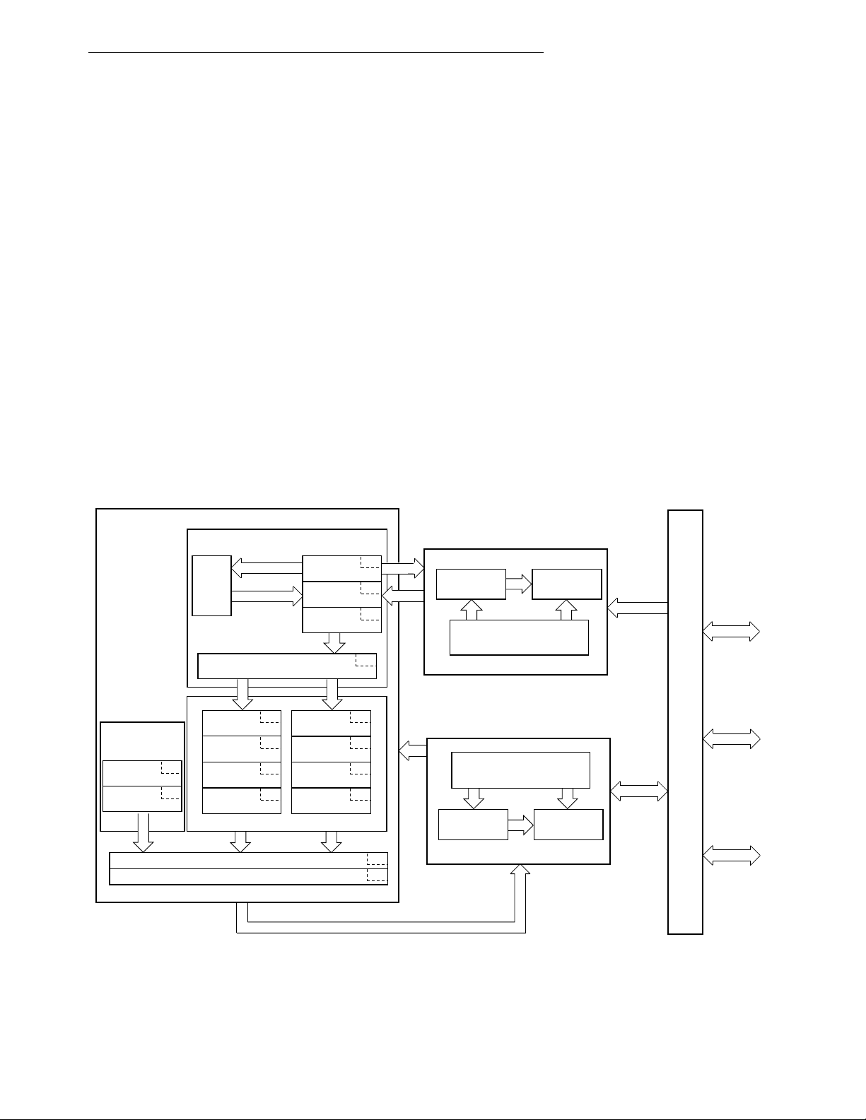
Introduction
The architecture of the MC68060 processor is implemented in the following major blocks:
• Execution Unit
—Instruction Fetch Unit
—Integer Unit
—FPU
• Memory Units
—Instruction Memory Unit
• Instruction ATC
• Instruction Cache
• Instruction Cache Controller
—Data Memory Unit
• Data ATC
• Data Cache
• Data Cache Controller
• Bus Controller
These major units execute concurrently to maximize sustained performance. Note that the
caches reside on separate buses allowing concurrent instruction fetch, data read, and data
write operations (internal Harvard architecture).
EXECUTION UNIT
FLOATING-
POINT
UNIT
OC
EA
FETCH
EXECUTE
FP
EX
INSTRUCTION FETCH UNIT
BRANCH
CACHE
INSTRUCTION
BUFFER
pOEP sOEP
DECODE
CALCULATE
FETCH
EXECUTE
DATA AVAILABLE
WRITE-BACK
DS DS
EA
OC OC
EA
EX
INT
INTEGER UNIT
IA
CALCULATE
INSTRUCTION
FETCH
EARLY
DECODE
DECODE
EA
CALCULATE
EA
FETCH
INT
EXECUTE
AGAG
EX
IB
IAG
IC
IED
DA
WB
INSTRUCTION
ATC
INSTRUCTION
CONTROLLER
INSTRUCTION MEMORY UNIT
CONTROLLER
DATA
ATC
DATA MEMORY UNIT
CACHE
DATA
CACHE
INSTRUCTION
CACHE
DATA
CACHE
B
U
S
C
O
N
T
R
O
L
L
E
R
ADDRESS
DATA
CONTROL
1-6
OPERAND DATA BUS
Figure 1-1. MC68060 Block Diagram
M68060 USER’S MANUAL
MOTOROLA
Page 31

Introduction
The integer unit implements a subset of the MC68040 instruction set. The FPU implements
a subset of the MC68881/2 coprocessor instruction set. The instruction and data memory
manage the ATCs and the instruction and data caches. The ATCs provide on-chip stor-
units
age for the paged MMU’s most recently used address translations. The data and instruction
caches include the logic necessary to read, write, update, invalidate, and flush the caches.
The bus controller manages the interface between the MMUs and the external bus. Snoop
invalidation is supported to maintain cache consistency by monitoring the external bus when
the processor is not the current master.
1.4.2 Integer Unit
The MC68060’s integer unit carries out logical and arithmetic operations. The integer unit
contains an instruction fetch controller, an instruction execution controller, and a branch target cache. The superscalar design of the MC68060 provides dual execution pipelines in the
instruction execution controller, providing simultaneous execution.
The superscalar operation of the integer unit can be disabled in software, turning off the second execution pipeline for debugging. Disabling the superscalar operation also lowers performance and power consumption.
1.4.2.1 INSTRUCTION FETCH UNIT. The instruction fetch unit contains an instruction
fetch pipeline and the logic that interfaces to the branch cache. The instruction fetch pipeline
consists of four stages, providing the ability to prefetch instructions in advance of their actual
use in the instruction execution controller. The continuous fetching of instructions keeps the
instruction execution controller busy for the greatest possible performance. Every instruction
passes through each of the four stages before entering the instruction execution controller.
The four stages in the instruction fetch pipeline are:
1. Instruction Address Calculation (IAG)—The virtual address of the instruction is determined.
2. Instruction Fetch (IC)—The instruction is fetched from memory.
3. Early Decode (IED)—The instruction is pre-decoded for pipeline control information.
4. Instruction Buffer (IB)—The instruction and its pipeline control information are buffered
until the integer execution pipeline is ready to process the instruction.
The branch cache plays a major role in achieving the performance levels of the MC68060.
The concept of the branch cache is to provide a mechanism that allows the instruction fetch
pipeline to detect and change the instruction stream before the change of flow affects the
instruction execution controller.
The branch cache is examined for a valid branch entry after each instruction fetch address
is generated in the instruction fetch pipeline. If a hit does not occur in the branch target
cache, the instruction fetch pipeline continues to fetch instructions sequentially. If a hit
occurs in the branch cache, indicating a branch taken instruction, the current instruction
stream is discarded and a new instruction stream is fetched starting at the location indicated
by the branch cache.
MOTOROLA
M68060 USER’S MANUAL
1-7
Page 32

Introduction
1.4.2.2 INTEGER UNIT. The integer unit contains dual integer execution pipelines, inter-
face logic to the FPU, and control logic for data written to the data cache and MMU. The
superscalar design of the dual integer execution pipelines provide for simultaneous instruction execution, which allows for processing more than one instruction during each machine
clock cycle. The net effect of this is a software invisible pipeline capable of sustained execution rates of less than one machine clock cycle per instruction for the M68000 instruction
set.
The integer unit’s control logic pulls an instruction pair from the instruction buffer every
machine clock cycle, stopping only if the instruction information is not available or if an integer execution pipeline hold condition exists. The six stages in the dual integer execution
pipelines are:
1. Decode (DS)—The instruction is fully decoded.
2. Effective Address Calculation (AG)—If the instruction calls for data from memory, the
location of the data is calculated.
3. Effective Address Fetch (OC)—Data is fetched from the memory location.
4. Integer Execution (EX)—The data is manipulated during execution.
5. Data Available (DA)—The result is available.
6. Write-Back (WB)—The resulting data is written back to on-chip caches or external
memory.
The MC68060 is optimized for most integer instructions to execute in one machine clock
cycle. If during the instruction decode stage, the instruction is determined to be a floatingpoint instruction, it will be passed to the FPU after the effective address calculate stage. If
data is to be written to either the on-chip caches or external memory after instruction execution, the write-back stage holds the data until memory is ready to receive it.
1.4.2.3 FLOATING-POINT UNIT. Floating-point math is distinguished from integer math,
which deals only with whole numbers and fixed decimal point locations. The IEEE-compatible MC68060's FPU computes numeric calculations with a variable decimal point location.
Consolidating the FPU on-chip speeds up overall processing and eliminates the interfacing
overhead associated with external accelerators. The MC68060's FPU operates in parallel
with the integer unit. The FPU performs numeric calculations while the integer unit continues
integer processing.
The FPU has been optimized for the most frequently used instructions and data types to provide the highest possible performance. The FPU can also be disabled in software to reduce
system power consumption.
1-8
M68060 USER’S MANUAL
MOTOROLA
Page 33

Introduction
The MC68060 is compatible with the
Arithmetic
. The MC68060’s FPU has been optimized to execute the most commonly used
ANSI/IEEE Standard 754 for Binary Floating-Point
subset of the MC68881/MC68882 instruction sets. Software emulates floating-point instructions not directly supported in hardware. Refer to Appendix C MC68060 Software Pack-
age for details on software emulation. The MC68060FPSP provides the following features:
• Arithmetic and Transcendental Instructions
• IEEE-Compliant Exception Handlers
• Unimplemented Data Type and Data Format Handlers
1.4.2.4 MEMORY UNITS. The MC68060 contains independent instruction and data mem-
ory units. Each memory unit consists of an 8-Kbyte cache, a cache controller, and an ATC.
The full addressing range of the MC68060 is 4 Gbytes. Even though most MC68060 systems implement a much smaller physical memory, by using virtual memory techniques, the
system can appear to have a full 4 Gbytes of memory available to each user program. Each
MMU fully supports demand-paged virtual-memory operating systems with either 4- or 8Kbyte page sizes. Each MMU protects supervisor areas from accesses by user programs
and provides write protection on a page-by-page basis. For maximum efficiency, each MMU
operates in parallel with other processor activities. The MMUs can be disabled for emulator
and debugging support.
1.4.2.5 ADDRESS TRANSLATION CACHES. The 64-entry, four-way, set-associative
ATCs store recently used logical-to-physical address translation information as page
descriptors for instruction and data accesses. Each MMU initiates address translation by
searching for a descriptor containing the address translation information in the ATC. If the
descriptor does not reside in the ATC, the MMU performs external bus cycles through the
bus controller to search the translation tables in physical memory. After being located, the
page descriptor is loaded into the ATC, and the address is correctly translated for the
access.
1.4.2.6 INSTRUCTION AND DATA CACHES. Studies have shown that typical programs
spend much of their execution time in a few main routines or tight loops. Earlier members of
the M68000 family took advantage of this locality-of-reference phenomenon to varying
degrees. The MC68060 takes further advantage of cache technology with its two, independent, on-chip physical caches, one for instructions and one for data. The caches reduce the
processor's external bus activity and increase CPU throughput by lowering the effective
memory access time. For a typical system design, the large caches of the MC68060 yield a
very high hit rate, providing a substantial increase in system performance.
The autonomous nature of the caches allows instruction-stream fetches, data-stream
fetches, and external accesses to occur simultaneously with instruction execution. For
example, if the MC68060 requires both an instruction access and an external peripheral
access and if the instruction is resident in the on-chip cache, the peripheral access proceeds
unimpeded rather than being queued behind the instruction fetch. If a data operand is also
required and it is resident in the data cache, it can be accessed without hindering either the
instruction access or the external peripheral access. The parallelism inherent in the
MC68060 also allows multiple instructions that do not require any external accesses to exe-
MOTOROLA
M68060 USER’S MANUAL
1-9
Page 34

Introduction
cute concurrently while the processor is performing an external access for a previous
instruction.
Each MC68060 cache is 8 Kbytes, accessed by physical addresses. The data cache can be
configured as write-through or deferred copyback on a page basis. This choice allows for
optimizing the system design for high performance if deferred copyback is used.
Cachability of data in each memory page is controlled by two bits in the page descriptor.
Cachable pages can be either write-through or copyback, with no write-allocate for misses
to write-through pages.
The MC68060 implements a four-entry store buffer that maximizes system performance by
decoupling the integer pipeline from the external system bus. When needed, the store buffer
allows the pipeline to generate writes every clock cycle until full, even if the system bus runs
at a slower speed than the processor.
1.4.2.6.1 Cache Organization. The instruction and data caches are each organized as
four-way set associative, with 16-byte lines. Each line of data has associated with it an
address tag and state information that shows the line’s validity. In the data cache, the state
information indicates whether the line is invalid, valid, or dirty.
1.4.2.6.2 Cache Coherency. The MC68060 has the ability to watch or snoop the external
bus during accesses by other bus masters, maintaining coherency between the MC68060's
caches and external memory systems. External bus cycles can be flagged on the bus as
snoopable or nonsnoopable. When an external cycle is marked as snoopable, the bus
snooper checks the caches and invalidates the matching data. Although the integer execution units and the bus snooper circuit have access to the on-chip caches, the snooper has
priority over the execution units.
1.4.3 Bus Controller
The bus is implemented as a nonmultiplexed, fully synchronous protocol that is clocked off
the rising edge of the input clock. The bus controller operates concurrently with all other
functional units of the MC68060 to maximize system throughput. The timing of the bus is
fully configurable to match external memory requirements.
1.5 PROCESSING STATES
The processor is always in one of three states: normal processing, exception processing, or
halted. It is in the normal processing state when executing instructions, fetching instructions
and operands, and storing instruction results.
Exception processing is the transition from program processing to system, interrupt, and
exception handling. Exception processing includes fetching the exception vector, stacking
operations, and refilling the instruction pipe caused after an exception. The processor enters
exception processing when an exceptional internal condition arises such as tracing an
instruction, an instruction results in a trap, or executing specific instructions. External conditions, such as interrupts and access errors, also cause exceptions. Exception processing
ends when the first instruction of the exception handler begins to execute.
1-10
M68060 USER’S MANUAL
MOTOROLA
Page 35

Introduction
The processor halts when it receives an access error or generates an address error while in
the exception processing state. For example, if during exception processing of one access
error another access error occurs, the MC68060 is unable to complete the transition to normal processing and cannot save the internal state of the machine. The processor assumes
that the system is not operational and halts. Only an external reset can restart a halted processor. Note that when the processor executes a STOP or LPSTOP instruction, it is in a special type of normal processing state, one without bus cycles. The processor stops, but it
does not halt and can be restored by an interrupt or reset.
1.6 PROGRAMMING MODEL
The MC68060 programming model is separated into two privilege modes: supervisor and
user. The integer unit identifies a logical address by accessing either the supervisor or user
address space, maintaining the differentiation between supervisor and user modes. The
MMUs use the indicated privilege mode to control and translate memory accesses, protecting supervisor code, data, and resources from user program accesses. Refer to 1.1.2.1
Address Translation Differences for details concerning the MC68EC060 address transla-
tion.
Programs access registers based on the indicated mode. User programs can only access
registers specific to the user mode; whereas, system software executing in the supervisor
mode can access all registers, using the control registers to perform supervisory functions.
User programs are thus restricted from accessing privileged information, and the operating
system performs management and service tasks for the user programs by coordinating their
activities. This difference allows the supervisor mode to protect system resources from
uncontrolled accesses.
Most instructions execute in either mode, but some instructions that have important system
effects are privileged and can only execute in the supervisor mode. For instance, user programs cannot execute the STOP or RESET instructions. To prevent a user program from
entering the supervisor mode, except in a controlled manner, instructions that can alter the
S-bit in the status register (SR) are privileged. The TRAP instructions provide controlled
access to operating system services for user programs.
If the S-bit in the SR is set, the processor executes instructions in the supervisor mode.
Because the processor performs all exception processing in the supervisor mode, all bus
cycles generated during exception processing are supervisor references, and all stack
accesses use the active supervisor stack pointer. If the S-bit of the SR is clear, the processor
executes instructions in the user mode. The bus cycles for an instruction executed in the
user mode are user references. The values on the transfer modifier pins indicate either
supervisor or user accesses.
The processor utilizes the user mode and the user programming model when it is in normal
processing. During exception processing, the processor changes from user to supervisor
mode. Exception processing saves the current value of the SR on the active supervisor
stack and then sets the S-bit, forcing the processor into the supervisor mode. To return to
the user mode, a system routine must execute one of the following instructions: MOVE to
SR, ANDI to SR, EORI to SR, ORI to SR, or RTE, which execute in the supervisor mode,
MOTOROLA
M68060 USER’S MANUAL
1-11
Page 36

Introduction
modifying the S-bit of the SR. After these instructions execute, the instruction pipeline is
flushed and is refilled from the appropriate address space.
The MC68060 integrates the functions of the integer unit, FPU, and MMU. The registers
depicted in the programming model (see Figure 1-2) provide operand storage and control
for these three units. The registers are partitioned into two levels of privilege modes: user
and supervisor. The user programming model is the same as the user programming model
of the MC68040, which consists of 16 general-purpose 32-bit registers, two control registers, eight 80-bit floating-point data registers, a floating-point control register, a floating-point
status register, and a floating-point instruction address register.
31 0
DATA
REGISTERS
ADDRESS
REGISTERS
31 0
(CCR)
79 0
D0
D1
D2
D3
D4
D5
D6
D7
A0
A1
A2
A3
A4
A5
A6
A7/USP
PC
CCR
PCR
A7/SSP
SR
VBR
SFC
DFC
CACR
URP
SRP
TC
DTT0
DTT1
ITT0
ITT1
BUSCR
FP INSTRUCTION ADDRESS REGISTER
USER STACK POINTER
PROGRAM COUNTER
CONDITION CODE REGISTER
USER PROGRAMMING MODEL
PROCESSOR CONFIGURATION REGISTER
SUPERVISOR STACK POINTER
STATUS REGISTER (CCR IS ALSO SHOWN IN THE USER PROGRAMMING MODEL)
VECTOR BASE REGISTER
SOURCE FUNCTION CODE
DESTINATION FUNCTION CODE
CACHE CONTROL REGISTER
USER ROOT POINTER REGISTER
SUPERVISOR ROOT POINTER REGISTER
TRANSLATION CONTROL REGISTER
DATA TRANSPARENT TRANSLATION REGISTER 0
DATA TRANSPARENT TRANSLATION REGISTER 1
INSTRUCTION TRANSPARENT TRANSLATION REGISTER 0
INSTRUCTION TRANSPARENT TRANSLATION REGISTER 1
BUS CONTROL REGISTER
FLOATING-POINT
DATA
REGISTERS
31 0
FP CONTROL REGISTER
FP STATUS REGISTER
15
0
FP0
FP1
FP2
FP3
FP4
FP5
FP6
FP7
FPCR
FPSR
FPIAR
SUPERVISOR PROGRAMMING MODEL
Figure 1-2. Programming Model
Only system programmers can use the supervisor programming model to implement operating system functions, I/O control, and memory management subsystems. This supervisor/
1-12
M68060 USER’S MANUAL
MOTOROLA
Page 37

Introduction
user distinction in the M68000 family architecture allows for the writing of application software that executes in the user mode and migrates to the MC68060 from any M68000 family
platform without modification. The supervisor programming model contains the control features that system designers need to modify system software when porting to a new design.
For example, only the supervisor software can read or write to the TTRs of the MC68060.
The existence of the TTRs does not affect the programming resources of user application
programs.
The user programming model includes eight data registers, seven address registers, and a
stack pointer register. The address registers and stack pointer can be used as base address
registers or software stack pointers, and any of the 16 registers can be used as index registers. Two control registers are available in the user mode—the program counter (PC),
which usually contains the address of the instruction that the MC68060 is executing, and the
lower byte of the SR, which is accessible as the condition code register (CCR). The CCR
contains the condition codes that reflect the results of a previous operation and can be used
for conditional instruction execution in a program.
The supervisor programming model includes the upper byte of the SR, which contains operation control information. The vector base register (VBR) contains the base address of the
exception vector table, which is used in exception processing. The source function code
(SFC) and destination function code (DFC) registers contain 3-bit function codes. These
function codes can be considered extensions to the 32-bit logical address. The processor
automatically generates function codes to select address spaces for data and program
accesses in the user and supervisor modes. Some instructions use the alternate function
code registers to specify the function codes for various operations.
The processor configuration register (PCR) contains bits which control the internal pipelines
of the MC68060 design.
The bus control register (BUSCR) is used to control software emulation of locked bus transactions.
The cache control register (CACR) controls enabling of the on-chip instruction and data
caches of the MC68060. The supervisor root pointer (SRP) and user root pointer (URP) registers point to the root of the address translation table tree to be used for supervisor and user
mode accesses.
The translation control register (TCR) enables logical-to-physical address translation and
selects either 4- or 8-Kbyte page sizes. There are four TTRs, two for instruction accesses
and two for data accesses. These registers allow portions of the logical address space to be
transparently mapped and accessed without the use of resident descriptors in an ATC.
The user programming model can also access the entire floating-point programming model.
The eight 80-bit floating-point data registers are analogous to the integer data registers. A
32-bit floating-point control register (FPCR) contains an exception enable byte that enables
and disables traps for each class of floating-point exceptions and a mode byte that sets the
user-selectable rounding and precision modes. A floating-point status register (FPSR) contains a condition code byte, quotient byte, exception status byte, and accrued exception
MOTOROLA
M68060 USER’S MANUAL
1-13
Page 38

Introduction
byte. A floating-point exception handler can use the address in the 32-bit floating-point
instruction address register (FPIAR) to locate the floating-point instruction that has caused
an exception. Instructions that do not modify the FPIAR can be used to read the FPIAR in
the exception handler without changing the previous value.
DATA FORMAT SUMMARY
1.7
The MC68060 supports the basic data formats of the M68000 family. Some data formats
apply only to the integer unit, some only to the FPU, and some to both. In addition, the
instruction set supports operations on other data formats such as memory addresses.
The operand data formats supported by the integer unit are the standard twos-complement
data formats defined in the M68000 family architecture plus a new data format (16-byte
block) for the MOVE16 instruction. Registers, memory, or instructions themselves can contain integer unit operands. The operand size for each instruction is either explicitly encoded
in the instruction or implicitly defined by the instruction operation.
Whenever an integer is used in a floating-point operation, the FPU automatically converts it
to an extended-precision floating-point number before using the integer. The FPU implements single-, double-, and extended-precision floating-point data formats as defined by the
IEEE 754 standard. The FPU does not directly support packed decimal real format. However, software emulation supports this format via the unimplemented data format vector.
Additionally, each data format has a special encoding that represents one of five data types:
normalized numbers, denormalized numbers, zeros, infinities, and not-a-numbers (NANs).
Table 1-1 lists the data formats for both the integer unit and the FPU. Refer to M68000PM/
M68000 Family Programmer’s Reference Manual,
AD,
for details on data format organiza-
tion in registers and memory.
Table 1-1. Data Formats
Operand Data Format
Bit 1 Bit Integer Unit —
Bit Field 1–32 Bits Integer Unit Field of Consecutive Bits
Binary-Coded Decimal (BCD) 8 Bits Integer Unit Packed: 2 Digits/Byte; Unpacked: 1 Digit/Byte
Byte Integer 8 Bits Integer Unit, FPU —
Word Integer 16 Bits Integer Unit, FPU —
Long-Word Integer 32 Bits Integer Unit, FPU —
16-Byte 128 Bits Integer Unit Memory Only, Aligned to 16-Byte Boundary
Single-Precision Real 32 Bits FPU 1-Bit Sign, 8-Bit Exponent, 23-Bit Fraction
Double-Precision Real 64 Bits FPU 1-Bit Sign, 11-Bit Exponent, 52-Bit Fraction
Extended-Precision Real 96 Bits FPU 1-Bit Sign, 15-Bit Exponent, 64-Bit Mantissa
Size Supported In Notes
1.8 ADDRESSING CAPABILITIES SUMMARY
The MC68060 supports the basic addressing modes of the M68000 family. The register indirect addressing modes support postincrement, predecrement, offset, and indexing, which
are particularly useful for handling data structures common to sophisticated applications and
high-level languages. The program counter indirect mode also has indexing and offset capabilities. This addressing mode is typically required to support position-independent software.
Besides these addressing modes, the MC68060 provides index sizing and scaling features.
1-14
M68060 USER’S MANUAL
MOTOROLA
Page 39

Introduction
An instruction’s addressing mode can specify the value of an operand, a register containing
the operand, or how to derive the effective address of an operand in memory. Each addressing mode has an assembler syntax. Some instructions imply the addressing mode for an
operand. These instructions include the appropriate fields for operands that use only one
addressing mode. Table 1-2 lists a summary of the effective addressing modes for the
MC68060. Refer to M68000PM/AD,
M68000 Family Programmer’s Reference Manual,
for
details on instruction format and addressing modes.
Table 1-2. Effective Addressing Modes
Addressing Modes
Register Direct
Data
Address
Register Indirect
Address
Address with Postincrement
Address with Predecrement
Address with Displacement
Address Register Indirect with Index
8-Bit Displacement
Base Displacement
Memory Indirect
Postindexed
Preindexed
Program Counter Indirect
with Displacement
Program Counter Indirect with Index
8-Bit Displacement
Base Displacement
Program Counter Memory Indirect
Postindexed
Preindexed
Absolute Data Addressing
Short
Long
Immediate #<xxx>
Syntax
Dn
An
(An)
(An)+
–(An)
(d16,An)
(d8,An,Xn)
(bd,An,Xn)
([bd,An],Xn,od)
([bd,An,Xn],od)
(d16,PC)
(d8,PC,Xn)
(bd,PC,Xn)
([bd,PC],Xn,od)
([bd,PC,Xn],od)
(xxx).W
(xxx).L
1.9 INSTRUCTION SET OVERVIEW
The instruction set is tailored to support high-level languages and is optimized for those
instructions most commonly executed. The floating-point instructions for the MC68060 are
a commonly used subset of the MC68881/MC68882 instruction set with new arithmetic
instructions to explicitly select single- or double-precision rounding. The remaining unimplemented instructions are less frequently used and are efficiently emulated in the
MC68060FPSP, maintaining compatibility with the MC68881/MC68882 floating-point coprocessors. The MC68060 instruction set includes MOVE16 which allows high-speed transfers
of 16-byte blocks between external devices such as memory to memory or coprocessor to
memory. Table 1-3 provides an alphabetized listing of the MC68060 instruction set’s
opcode, operation, and syntax. Refer to Table 1-4 for notations used in Table 1-3. The left
operand in the syntax is always the source operand, and the right operand is the destination
operand. Refer to M68000PM/AD,
M68000 Family Programmer’s Reference Manual,
details on instructions used by the MC68060.
MOTOROLA
M68060 USER’S MANUAL
for
1-15
Page 40

Introduction
Table 1-3. Instruction Set Summary
Opcode Operation Syntax
ABCD BCD Source + BCD Destination + X ˘ Destination
ADD Source + Destination ˘ Destination
ADDA Source + Destination ˘ Destination ADDA <ea>,An
ADDI Immediate Data + Destination ˘ Destination ADDI #<data>,<ea>
ADDQ Immediate Data + Destination ˘ Destination ADDQ #<data>,<ea>
ADDX Source + Destination + X ˘ Destination
AND Source Λ Destination ˘ Destination
ANDI Immediate Data Λ Destination ˘ Destination ANDI #<data>,<ea>
ANDI to CCR
ANDI to SR
ASL, ASR Destination Shifted by count ˘ Destination
Bcc
BCHG
BCLR
BFCHG ~(bit field of Destination) ˘ bit field of Destination BFCHG <ea>{offset:width}
BFCLR 0 ˘ bit field of Destination BFCLR <ea>{offset:width}
BFEXTS bit field of Source ˘ Dn BFEXTS <ea>{offset:width},Dn
BFEXTU bit offset of Source ˘ Dn BFEXTU <ea>{offset:width},Dn
BFFFO bit offset of Source Bit Scan ˘ Dn BFFFO <ea>{offset:width},Dn
BFINS Dn ˘ bit field of Destination BFINS Dn,<ea>{offset:width}
BFSET 1s ˘ bit field of Destination BFSET <ea>{offset:width}
BFTST bit field of Destination BFTST <ea>{offset:width}
BKPT
BRA
BSET
BSR
BTST –(bit number of Destination) ˘ Z;
CAS
CAS2
CHK
CHK2
CINV
Source Λ CCR ˘
If supervisor state
else TRAP
If condition true
~(bit number of Destination) ˘ Z;
~(bit number of Destination) ˘ (bit number) of Destination
~(bit number of Destination) ˘ Z;
0 ˘ bit number of Destination
Run breakpoint acknowledge cycle;
TRAP as illegal instruction
PC + dn ˘ PC
~(bit number of Destination) ˘ Z;
1 ˘ bit number of Destination
SP – 4 ˘ SP; PC ˘ (SP); PC + dn ˘ PC
CAS Destination – Compare Operand ˘ cc;
8
if Z, Update Operand ˘ Destination
else Destination ˘ Compare Operand
CAS2 Destination 1 – Compare 1 ˘ cc;
if Z, Destination 2 – Compare ˘ cc;
if Z, Update 1 ˘ Destination 1;
2
else Destination 1 ˘ Compare 1;
If Dn < 0 or Dn > Source
If Rn < LB or If Rn > UB
2
If supervisor state
else TRAP
CCR
then Source Λ SR ˘ SR
then PC + dn ˘ PC
Update 2 ˘ Destination 2
Destination 2 ˘ Compare 2
then TRAP
then TRAP
then invalidate selected cache lines
ABCD Dy,Dx
ABCD –(Ay),–(Ax)
ADD <ea>,Dn
ADD Dn,<ea>
ADDX Dy,Dx
ADDX –(Ay),–(Ax)
AND <ea>,Dn
AND Dn,<ea>
ANDI #<data>,CCR
ANDI #<data>,SR
ASd Dx,Dy
ASd #<data>,Dy
ASd <ea>
Bcc <label>
BCHG Dn,<ea>
BCHG #<data>,<ea>
BCLR Dn,<ea>
BCLR #<data>,<ea>
BKPT #<data>
BRA <label>
BSET Dn,<ea>
BSET #<data>,<ea>
BSR <label>
BTST Dn,<ea>
BTST #<data>,<ea>
CAS Dc,Du,<ea>
CAS2 Dc1–Dc2,Du1–Du2,(Rn1)–
(Rn2)
CHK <ea>,Dn
CHK2 <ea>,Rn
CINVL <caches>, (An)
CINVP <caches>, (An)
CINVA <caches>
1
1-16
M68060 USER’S MANUAL
MOTOROLA
Page 41

Table 1-3. Instruction Set Summary (Continued)
Opcode Operation Syntax
CLR 0 ˘ Destination CLR <ea>
CMP Destination – Source ˘ cc CMP <ea>,Dn
CMPA Destination – Source CMPA <ea>,An
CMPI Destination – Immediate Data CMPI #<data>,<ea>
CMPM Destination – Source ˘ cc CMPM (Ay)+,(Ax)+
Compare Rn < LB or Rn > UB
2
CMP2
and Set Condition Codes
If supervisor state
CPUSH
then if data cache push selected dirty data
cache lines; invalidate selected cache lines
else TRAP
If condition false
DBcc
then (Dn–1 ˘ Dn;
If Dn ≠ –1
then PC + dn ˘ PC)
DIVS, DIVSL Destination ÷ Source ˘ Destination
DIVU, DIVUL Destination ÷ Source ˘ Destination
EOR Source ⊕ Destination ˘ Destination EOR Dn,<ea>
EORI Immediate Data ⊕ Destination ˘ Destination EORI #<data>,<ea>
EORI to CCR Source ⊕ CCR ˘ CCR EORI #<data>,CCR
If supervisor state
EORI to SR
then Source ⊕ SR ˘ SR
else TRAP
EXG Rx ¯ ˘ Ry
EXT
EXTB
Destination Sign – Extended ˘ Destination
FABS Absolute Value of Source ˘ FPn
FADD
FBcc
FCMP
Source + FPn ˘ FPn
If condition true
then PC + dn ˘ PC
FPn – Source
If condition true
then no operation
FDBcc
if Dn ≠ –1
else Dn – 1 ˘ Dn
2
then PC + dn ˘ PC
else execute next instruction
FDIV
FPn ÷ Source ˘ FPn
CMP2 <ea>,Rn
CPUSHL <caches>, (An)
CPUSHP <caches>, (An)
CPUSHA <caches>
DBcc Dn,<label>
DIVS.W <ea>,Dn32 ÷ 16 ˘ 16r:16q
DIVS.L <ea>,Dq32 ÷ 32 ˘ 32q
DIVS.L <ea>,Dr:Dq64 ÷ 32 ˘ 32r:32q
DIVSL.L <ea>,Dr:Dq 32 ÷ 32 ˘ 32r:32q
DIVU.W <ea>,Dn32 ÷ 16 ˘ 16r:16q
DIVU.L <ea>,Dq32 ÷ 32 ˘ 32q
DIVU.L <ea>,Dr:Dq64 ÷ 32 ˘ 32r:32q
DIVUL.L <ea>,Dr:Dq32 ÷ 32 ˘ 32r:32q
EORI #<data>,SR
EXG Dx,Dy
EXG Ax,Ay
EXG Dx,Ay
EXG Ay,Dx
EXT.W Dnextend byte to word
EXT.L L Dnextend word to long word
EXTB.L Dn extend byte to long word
FABS.<fmt> <ea>,FPn
FABS.X FPm,FPn
FABS.X FPn
FrABS.<fmt> <ea>,FPn
FrABS.X FPm,FPn3
FrABS.X FPn3
FADD.<fmt> <ea>,FPn
FADD.X FPm,FPn
FrADD.<fmt> <ea>,FPn
FrADD.X FPm,FPn3
FBcc.SIZE <label>
FCMP.<fmt> <ea>,FPn
FCMP.X FPm,FPn
FDBcc Dn,<label>
FDIV.<fmt> <ea>,FPn
FDIV.X FPm,FPn
FrDIV.<fmt> <ea>,FPn
FrDIV.X FPm,FPn
Introduction
2
2
3
3
3
3
MOTOROLA M68060 USER’S MANUAL 1-17
Page 42

Introduction
Table 1-3. Instruction Set Summary (Continued)
Opcode Operation Syntax
FINT Floating-Point Integer Part
FINTRZ Floating-Point Integer Part, Round-to-Zero
FMOVE
FMOVE
FMOVEM
FMOVEM
Source ˘ Destination
Source ˘ Destination
Register List ˘ Destination
9
Source ˘ Register List
Register List ˘ Destination
9
Source ˘ Register List
FMUL Source × FPn ˘ FPn
FNEG
FNOP
–(Source) ˘ FPn
None FNOP
If in supervisor state
FRESTORE
else TRAP
then FPU State Frame ˘ Internal State
If in supervisor state
FSAVE
FScc
else TRAP
If condition true
2
else 0s ˘ Destination
then FPU Internal State ˘ State Frame
then 1s ˘ Destination
FSGLDIV FPn ÷ Source ˘ FPn
FSGLMUL Source × FPn ˘ FPn
FSQRT
FSUB
FTRAPcc
FTST
Square Root of Source ˘ FPn
FPn – Source ˘ FPn
If condition true
2
then TRAP
Condition Codes for Operand ˘ FPCC
SSP – 2 ˘ SSP; Vector Offset ˘ (SSP);
ILLEGAL
SSP – 4 ˘ SSP; PC ˘ (SSP);
SSp – 2 ˘ SSP; SR ˘ (SSP);
Illegal Instruction Vector Address ˘ PC
JMP Destination Address ˘ PC JMP <ea>
FINT.<fmt><ea>,FPn
FINT.X FPm,FPn
FINT.X FPn
FINTRZ.<fmt><ea>,FPn
FINTRZ.X FPm,FPn
FINTRZ.X FPn
FMOVE.<fmt> <ea>,FPn
FMOVE.<fmt> FPm,<ea>
FMOVE.P FPm,<ea>{Dn}
FMOVE.P FPm,<ea>{#k}
FrMOVE.<fmt> <ea>,FPn
FMOVE.L <ea>,FPcr
FMOVE.L FPcr,<ea>
FMOVEM.X <list>,<ea>
FMOVEM.X Dn,<ea>
FMOVEM.X <ea>,<list>
FMOVEM.X <ea>,Dn
FMOVEM.L <list>,<ea>
FMOVEM.L <ea>,<list>
FMUL.<fmt> <ea>,FPn
FMUL.X FPm,FPn
FrMUL<fmt> <ea>,FPn
FrMUL.X FPm,FPn
FNEG.<fmt> <ea>,FPn
FNEG.X FPm,FPn
FNEG.X FPn
FrNEG.<fmt> <ea>,FPn
FrNEG.X FPm,FPn
FrNEG.X FPn
FRESTORE <ea>
FSAVE <ea>
FScc.SIZE <ea>
FSGLDIV.<fmt> <ea>,FPn
FSGLDIV.X FPm,FPn
FSGMUL.<fmt> <ea>,FPn
FSGLMUL.X FPm, FPn
FSQRT.<fmt> <ea>,FPn
FSQRT.X FPm,FPn
FSQRT.X FPn
FrSQRT.<fmt> <ea>,FPn
FrSQRT FPm,FPn3
FrSQRT FPn3
FSUB.<fmt> <ea>,FPn
FSUB.X FPm,FPn
FrSUB.<fmt> <ea>,FPn
FrSUB.X FPm,FPn3
FTRAPcc
FTRAPcc.W #<data>
FTRAPcc.L #<data>
FTST.<fmt> <ea>
FTST.X FPm
ILLEGAL
3
4
4
5
5
3
3
3
3
3
3
3
1-18 M68060 USER’S MANUAL MOTOROLA
Page 43

Table 1-3. Instruction Set Summary (Continued)
Opcode Operation Syntax
JSR
LEA <ea> ˘ An LEA <ea>,An
LINK
LPSTOP
LSL, LSR Destination Shifted by count ˘ Destination
MOVE Source ˘ Destination MOVE <ea>,<ea>
MOVEA Source ˘ Destination MOVEA <ea>,An
MOVE
from CCR
MOVE to
CCR
MOVE from
SR
MOVE to SR
MOVE USP
MOVE16 Source block ˘ Destination block
MOVEC
MOVEM
MOVEP
MOVEQ Immediate Data ˘ Destination MOVEQ #<data>,Dn
MOVES
MULS Source × Destination ˘ Destination
MULU Source × Destination ˘ Destination
NBCD
NEG 0 – (Destination) ˘ Destination NEG <ea>
NEGX 0 – (Destination) – X ˘ Destination NEGX <ea>
NOP None NOP
NOT ~ Destination ˘ Destination NOT <ea>
OR Source V Destination ˘ Destination
ORI Immediate Data V Destination ˘ Destination ORI #<data>,<ea>
ORI to CCR Source V CCR ˘ CCR ORI #<data>,CCR
SP – 4 ˘ SP; PC ˘ (SP)
Destination Address ˘ PC
SP – 4 ˘ SP; An ˘ (SP)
SP ˘ An, SP+d ˘ SP
If supervisor state
else TRAP
CCR ˘ Destination MOVE CCR,<ea>
Source ˘ CCR MOVE <ea>,CCR
If supervisor state
else TRAP
If supervisor state
else TRAP
If supervisor state
else TRAP
If supervisor state
else TRAP
Registers ˘ Destination
Source ˘ Registers
2
Source ˘ Destination
If supervisor state
else TRAP
0 – (Destination10) – X ˘ Destination
immediate data ˘ SR
SR ˘ broadcast cycle
STOP
then SR ˘ Destination
then Source ˘ SR
then USP ˘ An or An ˘ USP
then Rc ˘ Rn or Rn ˘ Rc
then Rn ˘ Destination [DFC] or
Source [SFC] ˘ Rn
JSR <ea>
LINK An,d
LPSTOP #<data>
LSd Dx,Dy
LSd #<data>,Dy1
LSd <ea>1
MOVE SR,<ea>
MOVE <ea>,SR
MOVE USP,An
MOVE An,USP
MOVE16 (Ax)+, (Ay)+
MOVE16 (xxx).L, (An)
MOVE16 (An), (xxx).L
MOVE16 (An)+, (xxx).L
MOVEC Rc,Rn
MOVEC Rn,Rc
MOVEM <list>,<ea>
MOVEM <ea>,<list>4
MOVEP Dx,(dn,Ay)
MOVEP (dn,Ay),Dx
MOVES Rn,<ea>
MOVES <ea>,Rn
MULS.W <ea>,Dn 16 × 16 ˘ 32
MULS.L <ea>,Dl 32 × 32 ˘ 32
MULS.L <ea>,Dh–Dl 32 × 32 ˘ 64
MULU.W <ea>,Dn 16 × 16 ˘ 32
MULU.L <ea>,Dl 32 × 32 ˘ 32
MULU.L <ea>,Dh–Dl 32 × 32 ˘ 64
NBCD <ea>
OR <ea>,Dn
OR Dn,<ea>
n
1
Introduction
6
4
2
2
MOTOROLA M68060 USER’S MANUAL 1-19
Page 44

Introduction
Table 1-3. Instruction Set Summary (Continued)
Opcode Operation Syntax
ORI to SR
PACK
PEA SP – 4 ˘ SP; <ea> ˘ (SP) PEA <ea>
PFLUSH
PLPA
RESET
ROL, ROR Destination Rotated by count ˘ Destination
ROXL, ROXR Destination Rotated with X by count ˘ Destination
RTD
RTE
RTR
RTS (SP) ˘ PC; SP + 4 ˘ SP RTS
SBCD
Scc
STOP
SUB Destination – Source ˘ Destination
SUBA Destination – Source ˘ Destination SUBA <ea>,An
SUBI Destination – Immediate Data ˘ Destination SUBI #<data>,<ea>
SUBQ Destination – Immediate Data ˘ Destination SUBQ #<data>,<ea>
SUBX Destination – Source – X ˘ Destination
SWAP Register 31–16 ¯ ˘ Register 15–0 SWAP Dn
TAS
TRAP
TRAPcc
TRAPV
TST Destination Tested ˘ Condition Codes TST <ea>
UNLK An ˘ SP; (SP) ˘ An; SP + 4 ˘ SP UNLK An
UNPK
If supervisor state
then Source V SR ˘ SR
else TRAP
Source (Unpacked BCD) + adjustment ˘
Destination (Packed BCD)
If supervisor state
7
then invalidate instruction and data ATC entries
for destination address
else TRAP
If supervisor state
then logical address translate to physical
address ˘ An
else TRAP
If supervisor state
then Assert RSTO Line
else TRAP
(SP) ˘ PC; SP + 4 + dn ˘ SP RTD #(dn)
If supervisor state
then (SP) ˘ SR; SP + 2 ˘ SP; (SP) ˘ PC;
SP + 4 ˘ SP; restore state and deallocate
stack according to (SP)
else TRAP
(SP) ˘ CCR; SP + 2 ˘ SP;
(SP) ˘ PC; SP + 4 ˘ SP
Destination
– Source10 – X ˘ Destination
10
If condition true
then 1s ˘ Destination
else 0s ˘ Destination
If supervisor state
then Immediate Data ˘ SR; STOP
else TRAP
Destination Tested ˘ Condition Codes;
1 ˘ bit 7 of Destination
SSP – 2 ˘ SSP; Format ÷ Offset ˘ (SSP);
SSP – 4 ˘ SSP; PC ˘ (SSP); SSP – 2 ˘ SSP;
SR ˘ (SSP); Vector Address ˘ PC
If cc
then TRAP
If V
then TRAP
Source (Packed BCD) + adjustment ˘ Destination (Unpacked
BCD)
ORI #<data>,SR
PACK –(Ax),–(Ay),#(adjustment)
PACK Dx,Dy,#(adjustment)
PFLUSH (An)
PFLUSHN (An)
PFLUSHA
PFLUSHAN
PLPAR (An)
PLPAW (An)
RESET
ROd Rx,Dy1
ROXd Dx,Dy
ROXd #<data>,Dy
ROXd <ea>
1
1
RTE
RTR
SBCD Dx,Dy
SBCD –(Ax),–(Ay)
Scc <ea>
STOP #<data>
SUB <ea>,Dn
SUB Dn,<ea>
SUBX Dx,Dy
SUBX –(Ax),–(Ay)
TAS <ea>
TRAP #<vector>
TRAPcc
TRAPcc.W #<data>
TRAPcc.L #<data>
TRAPV
UNPACK –(Ax),–(Ay),#(adjustment)
UNPACK Dx,Dy,#(adjustment)
1
1-20 M68060 USER’S MANUAL MOTOROLA
Page 45

Table 1-3. Instruction Set Summary (Continued)
Opcode Operation Syntax
NOTES:
1.Where d is direction, left or right.
2.Emulation support only, not supported in hardware.
3.Where r is rounding precision, single or double precision.
4.List refers to register.
5.List refers to control registers only.
6.MOVE16 (ax)+,(ay)+ is functionally the same as MOVE16 (ax),(ay)+ when ax = ay. The address register is
only incremented once, and the line is copied over itself rather than to the next line.
7.Not available for the MC68EC060.
8.Emulation support for misaligned operands.
9.Emulation support for FMCVEM with dynamic register list.
1.10 NOTATIONAL CONVENTIONS
Table 1-4 lists the notation conventions used throughout this manual.
Table 1-4. Notational Conventions
Single- And Double-Operand Operations
+ Arithmetic addition or postincrement indicator.
– Arithmetic subtraction or predecrement indicator.
× Arithmetic multiplication.
÷ Arithmetic division or conjunction symbol.
~ Invert; operand is logically complemented.
• Logical AND
+ Logical OR
⊕ Logical exclusive OR
˘
¯ ˘ Two operands are exchanged.
<op> Any double-operand operation.
<operand>tested Operand is compared to zero and the condition codes are set appropriately.
sign-extended All bits of the upper portion are made equal to the high-order bit of the lower portion.
TRAP
STOP Enter the stopped state, waiting for interrupts.
<operand>
If <condition>
then <operations>
else <operations>
Ax, Ay Source and destination address registers, respectively.
Dr, Dq Data register’s remainder or quotient of divide.
Dx, Dy Source and destination data registers, respectively.
10
An Any Address Register n (example: A3 is address register 3)
BR Base Register—An, PC, or suppressed.
Dc Data register D7–D0, used during compare.
Dh, Dl Data registers high- or low-order 32 bits of product.
Dn Any Data Register n (example: D5 is data register 5)
Du Data register D7–D0, used during update.
MRn Any Memory Register n.
Source operand is moved to destination operand.
Other Operations
Equivalent to Format ÷ Offset Word ˘ (SSP); SSP – 2 ˘ SSP; PC ˘ (SSP); SSP – 4 ˘ SSP; SR ˘
(SSP); SSP – 2 ˘ SSP; (Vector) ˘ PC
The operand is BCD; operations are performed in decimal.
Test the condition. If true, the operations after “then” are performed. If the condition is false and
the optional “else” clause is present, the operations after “else” are performed. If the condition is
false and else is omitted, the instruction performs no operation. Refer to the Bcc instruction description as an example.
Register Specification
Introduction
MOTOROLA M68060 USER’S MANUAL 1-21
Page 46

Introduction
Table 1-4. Notational Conventions (Continued)
Rn Any Address or Data Register
Rx, Ry Any source and destination registers, respectively.
Xn Index Register—An, Dn, or suppressed.
Data Format and Type
+ inf Positive Infinity
<fmt>
B, W, L Specifies a signed integer data type (twos complement) of byte, word, or long word.
D Double-precision real data format (64 bits).
k
P Packed BCD real data format (96 bits, 12 bytes).
S Single-precision real data format (32 bits).
X Extended-precision real data format (96 bits, 16 bits unused).
– inf Negative Infinity
#<xxx> or #<data> Immediate data following the instruction word(s).
( ) Identifies an indirect address in a register.
[ ] Identifies an indirect address in memory.
bd Base Displacement
d
n
LSB Least Significant Bit
LSW Least Significant Word
MSB Most Significant Bit
MSW Most Significant Word
od Outer Displacement
SCALE A scale factor (1, 2, 4, or 8, for no-word, word, long-word, or quad-word scaling, respectively).
SIZE The index register’s size (W for word, L for long word).
{offset:width} Bit field selection.
* General Case.
C Carry Bit in CCR
cc Condition Codes from CCR
FC Function Code
N Negative Bit in CCR
U Undefined, Reserved for Motorola Use.
V Overflow Bit in CCR
X Extend Bit in CCR
Z Zero Bit in CCR
— Not Affected or Applicable.
<ea> Effective Address
<label> Assemble Program Label
<list> List of registers, for example D3–D0.
LB Lower Bound
m Bit m of an Operand
m–n Bits m through n of Operand
UB Upper Bound
Operand Data Format: Byte (B), Word (W), Long (L), Single (S), Double (D), Extended (X), or
Packed (P).
A twos complement signed integer (–64 to +17) specifying a number’s format to be stored in the
packed decimal format.
Subfields and Qualifiers
Displacement Value, n Bits Wide (example: d16 is a 16-bit displacement).
Register Codes
Miscellaneous
1-22 M68060 USER’S MANUAL MOTOROLA
Page 47

SECTION 2
SIGNAL DESCRIPTION
This section contains brief descriptions of the MC68060 signals in their functional groups
(see Figure 2-1). Each signal’s function is briefly explained, referencing other sections containing detailed information about the signal and related operations. Table 2-1 lists the
MC68060 signal names, mnemonics, and functional descriptions of the signals. Timing
specifications for these signals can be found in Section 12 Electrical and Thermal Char-
acteristics .
NOTE
Assertion
particular state.
tive or true.
and
negation
Negation
are used to specify forcing a signal to a
Assertion
and
and
assert
negate
refer to a signal that is ac-
refer to a signal that is inactive
or false. These terms are used independently of the voltage level
(high or low) that they represent.
Table 2-1. Signal Index
Signal Name Mnemonic Function
Address Bus A31–A0 32-bit address bus used to address any of 4-Gbytes.
Cycle Long-Word Ad-
dress
Data Bus D31–D0 32-bit data bus used to transfer up to 32 bits of data per bus transfer.
Transfer Type TT1,TT0
Transfer Modifier TM2–TM0 Indicates supplemental information about the access.
Transfer Line Number TLN1,TLN0
User-Programmable
Attributes
Read/Write R/W
Transfer Size SIZ1,SIZ0
Bus Lock LOCK
Bus Lock End LOCKE
Cache Inhibit Out CIOUT
Byte Select BS3
Transfer Start TS
Transfer in Progress TIP
Starting Termination Ac-
knowledge Signal Sampling
Transfer Acknowledge TA
CLA Controls the operation of A3 and A2 during bus cycles.
Indicates the general transfer type: normal, MOVE16, alternate logical function
code, and acknowledge.
Indicates which cache line in a set is being pushed or loaded by the current line
transfer cycle.
UPA1,UPA0
–BS0
SAS
User-defined signals, controlled by the corresponding user attribute bits from the
address translation entry.
Identifies the transfer as a read or write.
Indicates the data transfer size. These signals, together with A0 and A1,
define the active sections of the data bus. Alternately, BS3
this function.
Indicates a bus cycle is part of a read-modify-write operation and that the
sequence of bus cycles should not be interrupted.
Indicates the current bus cycle is the last in a locked sequence of bus cycles.
Indicates the processor will not cache the current bus transfer information.
Indicate which bytes within a long word are selected and which data bus bytes
are valid.
Indicates the beginning of a bus cycle.
Asserted for the duration of a bus cycle.
Indicates the MC68060 will begin sampling the termination acknowledge signals.
Asserted to acknowledge a bus transfer.
–BS0 can be used for
MOTOROLA
M68060 USER’S MANUAL
2-1
Page 48

Signal Description
Table 2-1. Signal Index (Continued)
Signal Name Mnemonic Function
Transfer Retry Acknowledge
Transfer Error Acknowledge
Transfer Cycle Burst Inhibit
Transfer Cache Inhibit TCI
Snoop Control SNOOP
Bus Request BR
Bus Grant BG
Bus Grant Relinquish
Control
Bus Tenure Termination BTT
Bus Busy BB
Cache Disable CDIS
MMU Disable MDIS
Reset In RSTI
Reset Out RSTO
Interrupt Priority Level IPL2
Interrupt Pending IPEND
Autovector AVEC
Processor Status PST4–PST0 Indicates internal processor status.
Processor Clock CLK Clock input used for all internal logic timing.
Clock Enable CLKEN
JTAG Enable JTAG
Test Clock TCK Clock signal for the IEEE P1149.1 test access port (TAP).
Test Mode Select TMS Selects the principal operations of the test-support circuitry.
Test Data Input TDI Serial data input for the TAP.
Test Data Output TDO Serial data output for the TAP.
Test Reset TRST
Thermal Resistor Con-
nections
Power Supply
Ground GND Ground connection.
TRA
TEA
TBI
BGR
–IPL0 Provides an encoded interrupt level to the processor.
THERM1,
THERM0
V
CC
Indicates the need to rerun the bus cycle.
Indicates an error condition exists for a bus transfer.
Indicates the slave cannot handle a line burst access.
Indicates the current bus transfer should not be cached.
Indicates the MC68060 should snoop bus activity while it is not the bus master.
Asserted by the processor to request bus mastership.
Asserted by an arbiter to grant bus mastership privileges to the processor.
Qualifies BG by indicating the degree of necessity for relinquishing bus owner-
ship when BG
Indicates the MC68060 has relinquished the bus in response to the external ar-
biter’s negation of BG
Asserted by the current bus master to indicate it has assumed ownership of the
bus.
Dynamically disables the internal caches to assist emulator support.
Disables the translation mechanism of the MMUs.
Processor reset.
Asserted during execution of a RESET instruction to reset external devices.
Indicates an interrupt is pending.
Used during an interrupt acknowledge transfer to request internal generation of
the vector number.
Defines the speed of the system bus clock to be full, 1/2, or 1/4 the speed of the
processor clock.
Selects between IEEE 1149.1 compliance operation and emulation mode operation.
Provides an asynchronous reset of the TAP controller.
Provides thermal sensing information.
Power supply.
is negated.
.
2-2
M68060 USER’S MANUAL
MOTOROLA
Page 49

Signal Description
ADDRESS BUS
AND CONTROL
DATA BUS
TRANSFER
ATTRIBUTES
A31–A0
CLA
D31–D0
TT1
TT0
TM2
TM1
TM0
TLN1
TLN0
UPA1
UPA0
R/W
SIZ1
SIZ0
LOCK
LOCKE
CIOUT
BS0
BS1
BS2
BS3
MC68060
SNOOP
BR
BG
BGR
BB
BTT
CDIS
MDIS
RSTI
RSTO
IPL2
IPL1
IPL0
IPEND
AVEC
PST4
PST3
PST2
PST1
PST0
CLK
CLKEN
BUS SNOOP CONTROL
BUS ARBITRATION
CONTROL
PROCESSOR
CONTROL
INTERRUPT
CONTROL
STATUS AND
CLOCKS
JTAG
MASTER
TRANSFER
CONTROL
SLAVE
TRANSFER
CONTROL
TS
TIP
SAS
TA
TRA
TEA
TBI
TCI
TCK
TMS
TDI
TDO
TRST
THERM1
THERM0
V
CC
GND
TEST
THERMAL RESISTOR
CONNECTIONS
POWER SUPPLY
Figure 2-1. Functional Signal Groups
2.1 ADDRESS AND CONTROL SIGNALS
The following paragraphs describe the MC68060 address and control signals.
2.1.1 Address Bus (A31–A0)
These three-state bidirectional signals provide the address of the first item of a bus transfer
(except for interrupt acknowledge transfers) when the MC68060 is the bus master. When an
alternate bus master is controlling the bus and asserts the SNOOP
signal, the address sig-
MOTOROLA
M68060 USER’S MANUAL
2-3
Page 50

Signal Description
nals are examined to determine whether the processor should invalidate matching cache
entries to maintain cache coherency.
2.1.2 Cycle Long-Word Address (CLA
)
This active-low input signal controls the operation of A3 and A2 during bus cycles. Following
each clock-enabled clock edge in which CLA is asserted, the long-word address for each of
the four transfers encoded on A3 and A2 will increment in a circular wraparound fashion. If
is negated during a clock-enabled clock edge, the values on A3 and A2 will not change.
CLA
It is not necessary to synchronize CLA
with TA.
2.2 DATA BUS (D31–D0)
These three-state bidirectional signals provide the general-purpose data path between the
MC68060 and all other devices. The data bus can transfer 8, 16, or 32 bits of data per bus
transfer. During a burst bus cycle, the 128 bits of line information are transferred using four
32-bit transfers.
2.3 TRANSFER ATTRIBUTE SIGNALS
The following paragraphs describe the transfer attribute signals, which provide additional
information about the bus transfer cycle. Refer to Section 7 Bus Operation for detailed
information about the relationship of the transfer attribute signals to bus operation.
2.3.1 Transfer Cycle Type (TT1, TT0)
The processor drives these three-state signals to indicate the type of access for the current
bus cycle. During bus cycle transfers by an alternate bus master when the processor is
allowed to snoop bus transactions, TT1 is sampled. Only normal and MOVE16 accesses
can be snooped. Table 2-2 lists the definition of the TTx encoding. The acknowledge access
(TT1 = 1 and TT0 = 1) is used for interrupt acknowledge, breakpoint acknowledge, and lowpower stop broadcast bus cycles.
Table 2-2. Transfer-Type Encoding
TT1 TT0 Transfer Type
0 0 Normal Access
0 1 MOVE16 Access
10
11
Alternate Logical Function Code Access, Debug Access
Acknowledge Access, Low-Power Stop
Broadcast
2.3.2 Transfer Cycle Modifier (TM2–TM0)
These three-state outputs provide supplemental information for each transfer cycle type.
Table 2-3 lists the encoding for normal (TTx = 00) and MOVE16 (TTx = 01) transfers, and
Table 2-4 lists the encoding for alternate access transfers (TTx = 10). For interrupt acknowledge transfers, the TMx signals carry the interrupt level being acknowledged. For breakpoint
2-4
M68060 USER’S MANUAL
MOTOROLA
Page 51

Signal Description
acknowledge transfers and low-power stop broadcast cycles, the TMx signals are negated.
When the MC68060 is not the bus master, the TMx signals are in a high-impedance state.
MOTOROLA
M68060 USER’S MANUAL
2-5
Page 52

Signal Description
Table 2-3. Normal and MOVE16 Access TMx Encoding
TM2 TM1 TM0 Transfer Modifier
0 0 0 Data Cache Push Access
0 0 1 User Data Access*
0 1 0 User Code Access
0 1 1 MMU Table Search Data Access
1 0 0 MMU Table Search Code Access
1 0 1 Supervisor Data Access*
1 1 0 Supervisor Code Access
1 1 1 Reserved
*MOVE16 accesses use only these encodings.
Table 2-4. Alternate Access TMx Encoding
TM2 TM1 TM0 Transfer Modifier
0 0 0 Logical Function Code 0
0 0 1 Debug Access
0 1 0 Reserved
0 1 1 Logical Function Code 3
1 0 0 Logical Function Code 4
1 0 1 Debug Pipe Control Mode Access
1 1 0 Debug Pipe Control Mode Access
1 1 1 Logical Function Code 7
2.3.3 Transfer Line Number (TLN1, TLN0)
These three-state outputs indicate which line in the set of four data or instruction cache lines
is being accessed for normal push and line data read accesses. TLNx signals are undefined
for all other accesses and are placed in a high-impedance state when the processor is not
the bus master.
The TLNx signals can be used in high-performance systems to build an external snoop filter
with a duplicate set of cache tags. The TLNx signals and address bus provide a direct indication of the state of the data caches and can be used to help maintain the duplicate tag
store. The TLNx signals do not indicate the correct TLN number when an instruction cache
burst fill occurs.
2.3.4 User-Programmable Page Attributes (UPA1, UPA0)
The UPAx signals are three-state outputs. These signals are only valid for normal code,
data, and MOVE16 accesses. For all other accesses (including table search and cache line
push accesses), the UPAx signals are low. When the MC68060 is not the bus master, these
signals are placed in a high-impedance state.
During normal and MOVE16 accesses, if a transparent translation register (TTR) is enabled
and the address and attributes match the TTR values, the UPAx signals are defined by the
logical values of the U1 and U0 bits the TTR. If the MMU is enabled via the translation control
register (TCR) and the address and attributes result in an address translation cache (ATC)
hit, the UPAx signals are defined by the logical values of the U1 and U0 bits in the ATC entry.
If a given logical address is not mapped by the TTRs and if address translation is disabled,
2-6
M68060 USER’S MANUAL
MOTOROLA
Page 53

Signal Description
then the MC68060 invokes default transparent translation. The cache mode, user page
attributes, and other TTR fields for the default translation are defined by the contents of the
TCR. For more information about the UPAx signals, refer to Section 4 Memory Manage-
ment Unit .
2.3.5 Read/Write (R/W
)
This three-state output signal defines the data transfer direction for the current bus cycle. A
high (logic one) level indicates a read cycle, and a low (logic zero) level indicates a write
cycle. This signal is placed in a high-impedance state when the MC68060 is not the bus
master.
2.3.6 Transfer Size (SIZ1, SIZ0)
These three-state output signals indicate the data size for the bus cycle. These signals are
placed in a high-impedance state when the MC68060 is not the bus master. Table 2-5
shows the definitions of the SIZx encoding.
Table 2-5. SIZx Encoding
SIZ1 SIZ0 Transfer Size
0 0 Long Word (4 Bytes)
0 1 Byte
1 0 Word (2 Bytes)
1 1 Line (16 Bytes)
2.3.7 Bus Lock (LOCK
This three-state output indicates that the current bus cycle is part of a sequence of locked
bus cycles. An external arbiter can use LOCK
to prevent an alternate bus master from gaining control of the bus and accessing the
BG
same operand between processor accesses for the locked sequence of transfers. Although
CK indicates that the processor requests that the bus be locked, the processor will relin-
LO
quish the bus if the external arbiter negates BG
)
with its control of an alternate bus master’s
and asserts BGR.
When the MC68060 is not the bus master, the LOCK
If the MC68060 relinquishes the bus while LOCK
signal is set to a high-impedance state.
is asserted, LOCK will be negated for one
full clock-enabled clock cycle and then three-stated one clock-enabled clock cycle after the
address bus is idled. If LOCK
was already negated in the clock cycle in which the MC68060
relinquishes the bus, it will be three-stated in the same clock cycle the address bus is idled.
Refer to Section 7 Bus Operation for information on locked transfers.
2.3.8 Bus Lock End (LOCKE
)
This three-state output indicates that the current bus cycle is the last in a sequence of locked
bus cycles (except in the case in which a retry termination is indicated on the last write of a
read-modify-write sequence).
When the MC68060 is not the bus master, the LOCK
state. If the MC68060 relinquishes the bus while LOCKE
MOTOROLA
M68060 USER’S MANUAL
E signal is set to a high-impedance
is asserted, LOCKE will be negated
2-7
Page 54

Signal Description
for one full BCLK cycle and then three-stated one BCLK cycle after the address bus is idled.
If LOCKE
was already negated in the BCLK cycle in which the MC68060 relinquishes the
bus, it will be three-stated in the same BCLK cycle the address bus is idled.
LOCKE
is provided to help make the MC68060 bus compatible with the MC68040-style bus
protocol; however, for new designs, external bus arbitration logic can be simplified with the
use of BGR
Do not use LOCK
instead of LOCKE.
E. The LOCKE protocol breaks the integrity of the locked read-modifywrite sequence if it is possible to retry the last write of a read-modify-write operation. The
reason is that when LOCKE
is asserted, a bus arbiter can grant the bus to an alternate master when the current bus cycle is finished (before the retry is attempted). The bus is arbitrated away, the last write’s retry is deferred until the bus is returned to the processor. In the
meantime, the alternate master can access the same location where the write should have
taken place. Hence, the integrity of the locked read-modify-write sequence is compromised
in this situation.
2.3.9 Cache Inhibit Out (CIOUT
)
When asserted, this three-state output indicates that the MC68060 will not cache the current
bus information in its internal caches. Refer to Section 4 Memory Management Unit for
more information on CIOUT
function. When the MC68060 is not the bus master, the CIOUT
signal is placed in a high-impedance state.
2.3.10 Byte Select Lines (BS3
–BS0)
These three-state outputs indicate which bytes within a long-word transfer are being
selected and which bytes of the data bus will be used for the transfer. BS0 refers to D31–
D24, BS1
refers to D23–D16, BS2 refers to D15–D8, and BS3 refers to D7–D0. These signals are generated to provide byte data select signals which are decoded from the SIZx, A1,
and A0 signals as shown in Table 2-6. These signals are placed in a high-impedance state
when the MC68060 is not the bus master.
Table 2-6. Data Bus Byte Select Signals
Transfer Size SIZ1 SIZ0 A1 A0
Byte 0100 0111
Byte 0101 1011
Byte 0110 1101
Byte 0111 1110
Word 1000 0011
Word 1010 1100
Long Word 0 0 x x 0000
Line 1 1 x x 0000
BS0
D31–D24 D23–D16 D15–D8 D7–D0
BS1 BS2 BS3
2.4 MASTER TRANSFER CONTROL SIGNALS
The following signals provide control functions for bus cycles when the MC68060 is the bus
master. Refer to Section 7 Bus Operation for detailed information about the relationship
of the bus cycle control signals to bus operation.
2-8
M68060 USER’S MANUAL
MOTOROLA
Page 55

Signal Description
2.4.1 Transfer Start (TS
The processor asserts this three-state bidirectional signal for one clock-enabled clock period
to indicate the start of each bus cycle. During alternate bus master accesses, the processor
monitors TS
is placed in a high-impedance state when the MC68060 is not the bus master. To properly
maintain internal state information, all masters on the bus must have their TS
together.
and SNOOP to detect the start of each bus cycle which is to be snooped. TS
2.4.2 Transfer in Progress (TIP
This three-state output is asserted to indicate that a bus cycle is in progress and is negated
during idle bus cycles if the bus is still granted to the processor. TIP remains asserted during
the time between back-to-back bus cycles.
If the MC68060 relinquishes the bus while TIP
period after completion of the final transfer and then goes to a high-impedance state one
clock period after the address is idled. Note that this one clock period in which TIP
negated refers to an MC68060 processor clock period, not a full clock-enabled clock period.
was already negated in the clock period in which the MC68060 relinquishes the bus,
If TIP
it will be placed in a high-impedance state in the same clock period that the address bus
becomes idle.
)
signals tied
)
is asserted, TIP will be negated for one clock
is driven
2.4.3 Starting Termination Acknowledge Signal Sampling (SAS
This three-state output is asserted for one clock-enabled clock period to indicate that the
MC68060 will begin sampling TA, TEA, TRA, TBI, TCI, AVEC, and spurious interrupt indication on the next rising edge of the clock-enabled clock. SAS
while the MC68060 is the bus master. When the MC68060 relinquishes the bus, SAS
driven negated for one clock-enabled clock period and then three-stated one clock-enabled
clock period after the address bus is idled. When the MC68060 newly gains bus ownership
and immediately starts a bus cycle with the assertion of TS
the clock-enabled clock period after TS
is asserted.
is negated at all other times
, SAS remains three-stated until
)
is
2.5 SLAVE TRANSFER CONTROL SIGNALS
The following signals provide control functions for bus transfers when the MC68060 is not
the bus master. Refer to Section 7 Bus Operation for detailed information about the relationship of the bus cycle control signals to bus operation.
2.5.1 Transfer Acknowledge (TA
This input indicates the completion of a requested data transfer operation. During transfers
by the MC68060, TA is an input signal from the referenced slave device indicating completion of the transfer. For the MC68060 to accept the transfer as successful with a transfer
acknowledge, TRA
and TEA must be negated when TA is asserted.
)
2.5.2 Transfer Retry Acknowledge (TRA
For native-MC68060-style (non-MC68040-style) acknowledge termination, this input signal
may be asserted by the current slave on the first transfer of a bus cycle to indicate the need
MOTOROLA
M68060 USER’S MANUAL
)
2-9
Page 56

Signal Description
to rerun the current bus cycle. The assertion of TRA
fer is ignored. The assertion of TRA
over TEA
If the MC68060 processor is to be used with MC68040-style acknowledge termination, then
TRA
slave must assert both TEA
current bus cycle. The assertion of TEA
interpreted by the MC68060 as if only TEA
nates the bus cycle with a bus error indication.
.
must be held negated. In this case, TEA does not have precedence over TA and the
and TA on the first transfer of a bus cycle to cause a retry of the
has precedence over TA, but does not have precedence
and TA on any transfer other than the first will be
had been asserted, which immediately termi-
2.5.3 Transfer Error Acknowledge (TEA
The current slave asserts this input signal to indicate an error condition for the current transfer to immediately terminate the bus cycle. The assertion of TEA
and TA for native-MC68060-style acknowledgment termination.
For MC68040-style acknowledge termination, TEA
cause the current bus cycle to immediately terminate with a bus error indication. For
MC68040-style acknowledge termination, TRA
2.5.4 Transfer Burst Inhibit (TBI
)
on any transfer other than the first trans-
)
has precedence over TRA
must be asserted with TA negated to
must be held negated.
This input signal indicates to the processor that the device cannot support burst mode
accesses and that the requested line transfer cycle should be divided into individual longword bus cycles. Asserting TBI
causing the processor to terminate the burst bus cycle and access the remaining data for
the line as three successive long-word transfer cycles.
2.5.5 Transfer Cache Inhibit (TCI
This input signal inhibits line read data from being loaded into the MC68060 instruction or
data caches. TCI
line reads and burst-inhibited line reads. TCI
transfers.
is ignored during all writes and after the first data transfer for both burst
2.6 SNOOP CONTROL (SNOOP
This input signal controls the operation of the MC68060 internal snoop logic. The MC68060
examines SNOOP
ing is disabled (i.e., SNOOP
will not snoop the bus transaction. If snooping is enabled (i.e., SNOOP
clock when TS
cache lines for either read or write bus cycles without any external indication that a cache
entry has been invalidated upon cache snoop hits.
when TS is asserted by an alternate master controlling the bus. If snoop-
is asserted, the MC68060 will snoop the access and invalidate matching
with TA terminates the first data transfer of a line access,
)
is also ignored during all alternate bus master
)
negated) during the clock when TS is asserted, the MC68060
asserted) during the
Section 5 Caches provides information about the relationship of SNOOP
and Section 7 Bus Operation discusses the relationship of SNOOP
2-10
M68060 USER’S MANUAL
to bus operation.
to the caches,
MOTOROLA
Page 57

Signal Description
2.7 ARBITRATION SIGNALS
The following control signals support bus mastership control by an external arbiter over the
MC68060. Refer to Section 7 Bus Operation for detailed information about the relationship
of the arbitration signals to bus operation.
2.7.1 Bus Request (BR
This output signal indicates to an external arbiter that the processor needs to become bus
master for one or more bus cycles. BR is negated when the MC68060 begins an access to
the external bus with no other internal accesses pending, and BR
another internal request occurs. The assertion and negation of B
activity and there are some situations in which the MC68060 asserts BR
it without having run a bus cycle; this is a disregard request condition. Refer to Section 7
Bus Operation for details about this state.
2.7.2 Bus Grant (BG
This input signal from an external arbiter indicates that the bus is available to the MC68060
as soon as the current bus cycle completes. The MC68060 assumes bus ownership when
is asserted and BB is negated, when BG is asserted and a TS-BTT pair (TS asserted,
BG
followed by BTT
and BTT are asserted and TS is negated. The MC68060 indicates its ownership of the
BG
bus by asserting BB
bus as soon as the current bus cycle is complete unless a locked sequence of bus cycles is
in progress with BGR
of locked bus cycles and then indicate that it is relinquishing the bus by asserting BTT
negating BB
asserted) has occurred in the past without another assertion of TS, or when
. When the external arbiter negates BG, the MC68060 relinquishes the
negated. In this case, the MC68060 will complete the entire sequence
.
)
remains negated until
R are independent of bus
and then negates
)
and
2.7.3 Bus Grant Relinquish Control (BGR
This input signal is a qualifier for BG
for relinquishing bus ownership when BG
MC68060 behavior when BG
asserted). When the external arbiter negates BG during a series of locked bus cycles, the
assertion of BGR
current bus cycle, even though the MC68060 had intended the series to be locked. If BGR
remains negated when BG is negated during locked transfers, then the MC68060 will not
relinquish the bus until the series of locked bus cycles is complete.
will cause the MC68060 to relinquish the bus on the last transfer of the
is negated during sequences of locked bus cycles (LOCK
2.7.4 Bus Tenure Termination (BTT
This three-state bidirectional signal is asserted for one clock-enabled clock period and
negated for one clock-enabled clock period to indicate that the MC68060 has relinquished
its bus tenure following the negation of BG
in a high-impedance state. When an alternate master is controlling the bus, the MC68060
samples BTT
MC68060 may become the bus master. To properly maintain this internal state information,
all masters on the bus must have their TS
together so the MC68060 can keep track of TS
as an input to maintain internal state information and to monitor when the
and indicates to the MC68060 the degree of necessity
is negated by an external arbiter. BGR controls
)
by an external arbiter. At all other times, BTT is
signals tied together and their BTT signals tied
)
-BTT pairs.
MOTOROLA
M68060 USER’S MANUAL
2-11
Page 58

Signal Description
The MC68060 provides the BB
style buses. Either the BTT
should be used. The unused signal, either BTT
tor and tied to V
. Use of the BTT
CC
signal and protocol to provide compatibility with MC68040-
signal and protocol or the BB signal and protocol (but not both)
or BB, must be pulled up with a pullup resis-
signal and protocol yields higher performance at full bus
speed and high operating frequencies. The use of BB and its associated protocol is not recommended at full bus speeds. The BTT protocol is discussed in detail in Section 7 Bus Op-
eration .
2.7.5 Bus Busy (BB
This three-state bidirectional signal indicates that the bus is currently owned. BB
)
is monitored as a processor input to determine when an alternate bus master has released control
of the bus. The MC68060 samples bus availability on each clock-enabled clock edge. BG
must be asserted and both TS and BB must be negated (indicating the bus is free) before
the MC68060 asserts BB
of the bus. The processor keeps BB
(with the first assertion of TS) as an output to assume ownership
asserted until the external arbiter negates BG and the
processor completes the bus cycle in progress. When releasing the bus, the processor
negates BB
sample it as an input. Note that the one clock period in which BB
for one clock period, then places it in a high-impedance state and begins to
is negated is one MC68060
processor clock period, not a full clock-enabled clock period.
The MC68060 provides the BB
style buses. Either the BTT
should be used. The unused signal, either BTT
resistor and tied to V
. Use of the BTT signal and protocol yields higher performance at full
CC
bus speed and high operating frequencies. The use of BB
recommended at full bus speeds. The BTT
signal and protocol to support compatibility with MC68040-
signal and protocol or the BB signal and protocol (but not both)
or BB, must be pulled up through a pullup
and its associated protocol is not
protocol is discussed in detail in Section 7 Bus
Operation.
2.8 PROCESSOR CONTROL SIGNALS
The following signals control the caches and MMUs and support processor and external
device initialization.
2.8.1 Cache Disable (CDIS)
When asserted, this input signal dynamically disables the on-chip caches on the next internal cache access boundary. The caches are enabled on the next boundary after CDIS
negated.
does not flush the data and instruction caches. Cache entries remain unaltered and
CDIS
become available after CDIS
is negated, unless one of the cache invalidate instructions
(CINVA, CINVP, CINVL) are executed. The execution of one of the cache invalidate instructions may invalidate entries even if the caches have been disabled with this signal. The
assertion of CDIS
does not affect snooping.
Refer to Section 5 Caches for information about the caches.
is
2-12
M68060 USER’S MANUAL
MOTOROLA
Page 59

Signal Description
2.8.2 MMU Disable (MDIS)
When asserted, this input signal dynamically disables the MC68060 internal operand data
and instruction MMUs on the next internal access boundary. While MDIS
accesses bypass the MMU ATCs, and thus translate transparently. The execution of one of
the MMU flush instructions (PFLUSHA, PFLUSHAN, PFLUSH, PFLUSHN) may cause the
deletion of the MMU entries, even if the MMU has been disabled by this signal. The MMUs
are enabled on the next boundary after MDIS
agement Unit for a description of address translation.
is negated. Refer to Section 4 Memory Man-
is asserted, all
2.8.3 Reset In (RSTI)
The assertion of this input signal causes the MC68060 to enter reset exception processing.
The RSTI
clock-enabled clock (CLK) edge. All three-state signals will eventually be set to the highimpedance state when RSTI
pins.
8 Exception Processing for information about the reset exception.
signal is an asynchronous input that is internally synchronized to the next rising
is recognized. The assertion of RSTI does not affect the test
Refer to Section 7 Bus Operation for a description of reset operation and to Section
2.8.4 Reset Out (RSTO)
The MC68060 asserts this output during execution of the RESET instruction to initialize
external devices. All bus cycles by the MC68060 are suspended prior to the assertion of
RSTO
a description of reset out bus operation.
, but bus arbitration and snooping still function. Refer to Section 7 Bus Operation for
2.9 INTERRUPT CONTROL SIGNALS
The following signals control the interrupt functions.
2.9.1 Interrupt Priority Level (IPL2–IPL0)
These input signals provide an indication of an interrupt condition with the interrupt level
from a peripheral or external prioritizing circuitry encoded. IPL2
the level number. For example, since the IPLx
responds to an interrupt request at interrupt priority level 2. IPL2
highest priority interrupt and cannot be internally masked. IPL2
cates no interrupt is requested. The I
synchronized to rising clock (CLK) edges.
During a processor reset, the levels on the IPLx
the various operating modes for the MC68060 bus. Refer to Section 7 Bus Operation for
more information on bus operating modes and Section 8 Exception Processing for information on interrupts.
PLx signals are asynchronous inputs that are internally
signals are active low, IPL2–IPL0 = 101 cor-
lines are registered and used to configure
is the most significant bit of
–IPL0 = 000 (level 7) is the
–IPL0 = 111 (level 0) indi-
2.9.2 Interrupt Pending Status (IPEND)
This output signal indicates that an interrupt request has been recognized internally by the
processor and exceeds the current interrupt priority mask in the status register (SR). External devices (other bus masters) can use IPEND
instruction boundaries. IPEND
MOTOROLA M68060 USER’S MANUAL 2-13
is not intended for use as an interrupt acknowledge to exter-
to predict processor operation on the next
Page 60

Signal Description
nal peripheral devices. Refer to Section 7 Bus Operation for bus information related to
interrupts and to Section 8 Exception Processing for interrupt information.
2.9.3 Autovector (AVEC)
This input signal is asserted with TA during an interrupt acknowledge bus cycle to request
internal generation of the vector number. Refer to Section 7 Bus Operation for more information about automatic vectors.
2.10 STATUS AND CLOCK SIGNALS
The following paragraphs describe the signals that provide timing and the internal processor
status.
2.10.1 Processor Status (PST4–PST0)
These outputs indicate the internal execution unit status. The timing is synchronous with the
MC68060 processor clock (CLK), and the status may have nothing to do with the current
bus transfer. Table 2-7 lists the definition of the PSTx encodings.
The encodings $16, $17, and $1C indicate the present status and do not reflect a specific
stage of the pipe. These encodings persist as long as the processor stays in the indicated
state. The default encoding $00 is indicated if none of the above conditions apply. Most
other encodings indicate that the instruction is in its last instruction execution stage. These
encodings exist for only one CLK period per instruction and are mutually exclusive.
In general, the PSTx bits indicate the following information:
PST4 = Supervisor Mode
PST3 = Branch Instruction
PST2 = Taken Branch Instruction
PST1, PST0 = Number of Instructions Completed that Cycle
2-14 M68060 USER’S MANUAL MOTOROLA
Page 61

Signal Description
Table 2-7. PSTx Encoding
Hex PST4 PST3 PST2 PST1 PST0 Internal Processor Status
$0000000Continue Execution in User Mode
$0100001Complete 1 Instruction in User Mode
$0200010Complete 2 Instructions in User Mode
$0300011 —
$0400100 —
$0500101 —
$0600110 —
$0700111 —
$0801000Emulator Mode Entry Exception Processing
$0901001Complete Not Taken Branch in User Mode
$0A01010Complete Not Taken Branch Plus 1 Instruction in User Mode
$0B01011IED Cycle of Branch to Vector, Emulator Entry Exception
$0C01100 —
$0D01101Complete Taken Branch in User Mode
$0E01110Complete Taken Branch Plus 1 Instruction in User Mode
$0F01111Complete Taken Branch Plus 2 Instructions in User Mode
$1010000Continue Execution in Supervisor Mode
$1110001Complete 1 Instruction in Supervisor Mode
$1210010Complete 2 Instructions in Supervisor Mode
$1310011 —
$1410100 —
$1510101Complete RTE Instruction in Supervisor Mode
$1610110Low-Power Stopped State; Waiting for an Interrupt or Reset
$1710111MC68060 Is Stopped Waiting for an Interrupt
$1811000MC68060 Is Processing an Exception
$1911001Complete Not Taken Branch in Supervisor Mode
$1A11010Complete Not Taken Branch Plus 1 Instruction in Supervisor Mode
$1B11011IED Cycle of Branch to Vector, Exception Processing
$1C11100MC68060 Is Halted
$1D11101Complete Taken Branch in Supervisor Mode
$1E11110Complete Taken Branch Plus 1 Instruction in Supervisor Mode
$1F11111Complete Taken Branch Plus 2 Instructions in Supervisor Mode
2.10.2 MC68060 Processor Clock (CLK)
CLK is the synchronous clock of the MC68060. This signal is used internally to clock or
sequence the internal logic of the MC68060 processor and is qualified with CLKEN
to clock
all external bus signals.
Since the MC68060 is designed for static operation, CLK can be gated off to lower power
dissipation (e.g., during low-power stopped states). Refer to Section 7 Bus Operation for
more information on low-power stopped states.
2.10.3 Clock Enable (CLKEN)
This input signal is a qualifier for the MC68060 processor clock (CLK) and is provided to support lower bus frequency MC68060 designs. The internal MC68060 bus interface controller
will sample, assert, negate, or three-state signals (except for BB
MOTOROLA M68060 USER’S MANUAL 2-15
and TIP which can three-
Page 62

Signal Description
state on the rising edge of CLK regardless of the state of the CLKEN) only on those rising
edges of CLK which are spanned by the assertion of CLKEN
.
CLKEN
processor clock which controls all internal operations. The MC68060 bus interface controller
will not detect those rising edges of CLK which are spanned with the negation of CLKEN
To operate the external bus at 1/2 or 1/4 the speed of CLK, CLKEN
stable during the rising edges of CLK which coincide with the system clock running at 1/2 or
1/4 the frequency of the MC68060 processor clock. CLKEN
ing all other rising CLK edges.
For full speed operation of the MC68060 processor, CLKEN
Refer to Section 7 Bus Operation for more information on the MC68060 bus interface and
controller. Refer to Section 12 Electrical and Thermal Characteristics for the timing specifications of CLK and CLKEN
may be used to allow the external bus to run at 1/2 or 1/4 the speed of the MC68060
must be asserted and
must be negated and stable dur-
must be continuously asserted.
.
2.11 TEST SIGNALS
The MC68060 includes dedicated user-accessible test logic that is fully compatible with the
IEEE 1149.1 Standard Test Access Port and Boundary Scan Architecture
ciated with testing high-density circuit boards have led to the development of this standard
under the IEEE Test Technology Committee and Joint Test Action Group (JTAG) sponsorship. The MC68060 implementation supports circuit board test strategies based on this
standard. However, the JTAG interface is not intended to provide an in-circuit test to verify
MC68060 operations; therefore, it is impossible to test MC68060 operations using this interface. Section 9 IEEE 1149.1 Test (JTAG) and Debug Pipe Control Modes describes the
MC68060 implementation of IEEE 1149.1 and is intended to be used with the supporting
IEEE document.
. Problems asso-
.
2.11.1 JTAG Enable (JTAG)
This input signal is used to select between 1149.1 operation and debug emulation mode.
The 1149.1 test access port (TAP) pins are remapped to emulation mode functions when
this pin is negated. For normal 1149.1 operation, JTAG
should be grounded.
2.11.2 Test Clock (TCK)
This input signal is used as a dedicated clock for the test logic. Since clocking of the test
logic is independent of the normal operation of the MC68060, several other components on
a board can share a common test clock with the processor even though each component
may operate from a different system clock. The design of the test logic allows the test clock
to run at low frequencies, or to be gated off entirely as required for test purposes. TCK
should be grounded if it is not used and emulation mode is not to be used.
2.11.3 Test Mode Select (TMS)
This input signal is decoded by the TAP controller and distinguishes the principal operations
of the test support circuitry. TMS should be tied to V
is not to be used.
if it is not used and emulation mode
CC
2-16 M68060 USER’S MANUAL MOTOROLA
Page 63

Signal Description
2.11.4 Test Data In (TDI)
This input signal provides a serial data input to the TAP. TDI should be tied to VCC if it is not
used and emulation mode is not to be used.
2.11.5 Test Data Out (TDO)
This three-state output signal provides a serial data output from the TAP. The TDO output
can be placed in a high-impedance mode to allow parallel connection to board-level test
data paths.
2.11.6 Test Reset (TRST)
This input signal provides an asynchronous reset of the TAP controller. TRST should be
grounded if 1149.1 operation is not to be used.
2.12 THERMAL SENSING PINS (THERM1, THERM0)
THERM1 and THERM0 are connected to an internal thermal resistor and provide information about the average temperature of the die. The resistance across these two pins is proportional to the average temperature of the die. The temperature coefficient of the resistor
is approximately 1.2 Ω/°C with a nominal resistance of 400Ω at 25°C.
2.13 POWER SUPPLY CONNECTIONS
The MC68060 requires connection to a VCC power supply, positive with respect to ground.
The V
sections of the processor. Section 13 Ordering Information and Mechanical Data
describes the groupings of the V
and ground connections are grouped to supply adequate current to the various
CC
and ground connections.
CC
2.14 SIGNAL SUMMARY
Table 2-8 provides a summary of the electrical characteristics of the MC68060 signals.
MOTOROLA M68060 USER’S MANUAL 2-17
Page 64

Signal Description
Table 2-8. Signal Summary
Signal Name Mnemonic
Address Bus A31–A0 Input/Output High Yes Three-Stated
Cycle Long-Word Address CLA
Data Bus D31–D0 Input/Output High Yes Three-Stated
Transfer Type 1 TT1 Input/Output High Yes Three-Stated
Transfer Type 0 TT0 Output High Yes Three-Stated
Transfer Modifier TM2–TM0 Output High Yes Three-Stated
Transfer Line Number TLN1,TLN0 Output High Yes Three-Stated
User-Programmable Attributes UPA1,UPA0 Output High Yes Three-Stated
Read/Write R/W
Transfer Size SIZ1,SIZ0 Output High Yes Three-Stated
Bus Lock LOCK
Bus Lock End LOCKE
Cache Inhibit Out CIOUT
Byte Select BS3
Transfer Start TS
Transfer in Progress TIP
Starting Termination Acknowledge Signal Sampling SAS
Transfer Acknowledge TA
Transfer Retry Acknowledge TRA
Transfer Error Acknowledge TEA
Transfer Burst Inhibit TBI
Transfer Cache Inhibit TCI
Snoop Control SNOOP
Bus Request BR
Bus Grant BG
Bus Grant Relinquish Control BGR
Bus Busy BB
Bus Tenure Termination BTT
Cache Disable CDIS
MMU Disable MDIS
Reset In RSTI
Reset Out RSTO
Interrupt Priority Level IPL2
Interrupt Pending IPEND
Autovector AVEC
Processor Status PST4–PST0 Output High No 10000
Processor Clock CLK Input — — —
Clock Enable CLKEN
JTAG Enable JTAG
Test Clock TCK Input — — —
Test Mode Select TMS Input High — —
Test Data Input TDI Input High — —
Test Data Output TDO Output High Yes Three-Stated
Test Reset TRST
Thermal Resistor Connections
Power Supply
Ground GND Input — — —
–BS0 Output Low Yes Three-Stated
–IPL0 Input Low — —
THERM1,
THERM0
V
CC
Input/
Output
Input Low — —
Output High/Low Yes Three-Stated
Output Low Yes Three-Stated
Output Low Yes Three-Stated
Output Low Yes Three-Stated
Input/Output Low Yes Three-Stated
Output Low Yes Three-Stated
Output Low Yes Three-Stated
Input Low — —
Input Low — —
Input Low — —
Input Low — —
Input Low — —
Input Low — —
Output Low No Negated
Input Low — —
Input Low — —
Input/Output Low Yes Three-Stated
Input/Output Low Yes Three-Stated
Input Low — —
Input Low — —
Input Low — —
Output Low No Negated
Output Low No Negated
Input Low — —
Input Low — —
Input Low — —
Input Low — —
——— —
Input — — —
Active
State
Three-State
Reset
State
2-18 M68060 USER’S MANUAL MOTOROLA
Page 65

SECTION 3
INTEGER UNIT
This section describes the organization of the MC68060 integer unit and presents a brief
description of the associated registers. Refer to Section 4 Memory Management Unit for
details concerning the paged memory management unit (MMU) programming model and to
Section 6 Floating-Point Unit for details concerning the floating-point unit (FPU) program-
ming model.
3.1 INTEGER UNIT EXECUTION PIPELINES
The MC68060 integer unit execution pipelines are four-stage pipelines which perform final
instruction decode, effective address calculation, and execution or integer operations. The
operand execution pipelines (OEPs) are referred to individually as the primary OEP (pOEP)
and the secondary OEP (sOEP). Figure 3-1 shows the integer unit of the MC68060.
EXECUTION UNIT
FLOATING-
POINT
UNIT
OC
EA
FETCH
EXECUTE
FP
EX
INSTRUCTION FETCH UNIT
BRANCH
CACHE
INSTRUCTION
BUFFER
pOEP sOEP
DECODE
CALCULATE
FETCH
INT
EXECUTE
DATA AVAILABLE
WRITE-BACK
DS DS
EA
OC OC
EA
EX
INTEGER UNIT
IA
CALCULATE
INSTRUCTION
FETCH
EARLY
DECODE
DECODE
EA
CALCULATE
EA
FETCH
INT
EXECUTE
AGAG
EX
IB
IAG
IC
IED
DA
WB
INSTRUCTION
ATC
INSTRUCTION
CONTROLLER
INSTRUCTION MEMORY UNIT
CONTROLLER
DATA
ATC
DATA MEMORY UNIT
CACHE
DATA
CACHE
INSTRUCTION
CACHE
DATA
CACHE
B
U
S
C
O
N
T
R
O
L
L
E
R
ADDRESS
DATA
CONTROL
MOTOROLA
OPERAND DATA BUS
Figure 3-1. MC68060 Integer Unit Pipeline
M68060 USER’S MANUAL
3-1
Page 66

Integer Unit
The operation of the instruction fetch unit (IFU) and the OEPs are decoupled by a 96-byte
FIFO instruction buffer. The IFU prefetches instructions every processor clock cycle, stopping only if the instruction buffer is full or encountering a wait condition due to instruction
fetch address translation or cache miss. The OEPs attempt to read instructions from the
instruction buffer and execute them every clock cycle, stopping only if full instruction information is not present in the buffer or due to operand pipeline wait conditions.
3.2 INTEGER UNIT REGISTER DESCRIPTION
The following paragraphs describe the integer unit registers in the user and supervisor programming models. Refer to Section 4 Memory Management Unit for details on the MMU
programming model and Section 6 Floating-Point Unit for details on the FPU programming model.
3.2.1 Integer Unit User Programming Model
Figure 3-2 illustrates the integer unit portion of the user programming model. The model is
the same as for previous M68000 family microprocessors, consisting of the following registers:
• 16 General-Purpose 32-Bit Registers (D7–D0, A7–A0)
• 32-Bit Program Counter (PC)
• 8-Bit Condition Code Register (CCR)
3.2.1.1 DATA REGISTERS (D7–D0). Registers D7–D0 are used as data registers for bit
and bit field (1- to 32-bit), byte (8-bit), word (16-bit), long-word (32-bit), and quad-word (64bit) operations. These registers may also be used as index registers.
3.2.1.2 ADDRESS REGISTERS (A6–A0). These registers can be used as software stack
pointers, index registers, or base address registers. The address registers may be used for
word and long-word operations.
01531
A0
A1
01531
031
0715
A2
A3
A4
A5
A6
A7
(USP)
PC
CCR
ADDRESS
REGISTERS
USER
STACK
POINTER
PROGRAM
COUNTER
CONDITION
CODE
REGISTER
Figure 3-2. Integer Unit User Programming Model
3.2.1.3 USER STACK POINTER (A7). A7 is used as a hardware stack pointer during
implicit or explicit stacking for subroutine calls and exception handling. The register designation A7 refers to the user stack pointer (USP) in the user programming model and to the
3-2
M68060 USER’S MANUAL
MOTOROLA
Page 67

Integer Unit
supervisor stack pointer (SSP) in the supervisor programming model. When the S-bit in the
status register (SR) is clear, the USP is the active stack pointer.
A subroutine call saves the program counter (PC) on the active system stack, and the return
restores the PC from the active system stack. Both the PC and the SR are saved on the
supervisor stack during the processing of exceptions and interrupts. Thus, the execution of
supervisor level code is independent of user code and the condition of the user stack. Conversely, user programs use the USP independently of supervisor stack requirements.
3.2.1.4 PROGRAM COUNTER. The PC contains the address of the currently executing
instruction. During instruction execution and exception processing, the processor automatically increments the contents of the PC or places a new value in the PC, as appropriate.
For some addressing modes, the PC can be used as a pointer for PC-relative addressing.
3.2.1.5 CONDITION CODE REGISTER. The CCR is the least significant byte of the proces-
sor SR. Bits 3–0 represent a condition of a result generated by a processor operation. Bit 4,
the extend bit (X-bit), is an operand for multiprecision computations. The carry bit (C-bit) and
the X-bit are separate in the M68000 family to simplify programming techniques that use
them.
3.2.2 Integer Unit Supervisor Programming Model
Only system programmers use the supervisor programming model (see Figure 3-3) to implement sensitive operating system functions, I/O control, and MMU subsystems. All accesses
that affect the control features of the MC68060 are in the supervisor programming model.
Thus, all application software is written to run in the user mode and migrates to the
MC68060 from any M68000 platform without modification.
31 15
15 7 0
(CCR)
31 0
31 0
Figure 3-3. Integer Unit Supervisor Programming Model
0
A7 (SSP)
SR
VBR
031 2
SFC
DFC
PCR
SUPERVISOR STACK POINTER
STATUS REGISTER
VECTOR BASE REGISTER
ALTERNATE SOURCE AND DESTINATION
FUNCTION CODE REGISTERS
PROCESSOR CONFIGURATION REGISTER
MOTOROLA
M68060 USER’S MANUAL
3-3
Page 68

Integer Unit
The supervisor programming model consists of the registers available to the user as well as
the following control registers:
• 32-Bit Supervisor Stack Pointer (SSP, A7)
• 16-Bit Status Register (SR)
• 32-Bit Vector Base Register (VBR)
• Two 32-Bit Alternate Function Code Registers: Source Function Code (SFC) and Destination Function Code (DFC)
• 32-Bit Processor Configuration Register (PCR)
The following paragraphs describe the supervisor programming model registers. Additional
information on the SSP, SR, and VBR registers can be found in Section 8 Exception Pro-
cessing.
3.2.2.1 SUPERVISOR STACK POINTER. When the MC68060 is operating at the supervi-
sor level, instructions that use the system stack implicitly, or access address register A7
explicitly, use the SSP. The SSP is a general-purpose register and can be used as a software stack pointer, index register, or base address register. The SSP can be used for word
and long-word operations. The initial value of the SSP is loaded from the reset exception
vector, address offset 0.
3.2.2.2 STATUS REGISTER. The SR (see Figure 3-4) stores the processor status and
includes the CCR, the interrupt priority mask, and other control bits. In the supervisor mode,
software can access the entire SR. The control bits indicate the following states for the processor: trace mode (T-bit), supervisor or user mode (S-bit), and master or interrupt state (M).
USER BYTE
CARRY
OVERFLOW
ZERO
NEGATIVE
EXTEND
15 14 13 12 11 10 9 8 7 56 43210
T0SM0I2I1I0 XNZVC000
TRACE ENABLE
SUPERVISOR/USER STATE
MASTER/INTERRUPT STATE
SYSTEM BYTE
(CONDITION CODE REGISTER)
INTERRUPT
PRIORITY MASK
Figure 3-4. Status Register
3.2.2.3 VECTOR BASE REGISTER. The VBR contains the base address of the exception
vector table in memory. The displacement of an exception vector is added to the value in
this register to access the vector table. Refer to Section 8 Exception Processing for information on exception vectors.
3-4
M68060 USER’S MANUAL
MOTOROLA
Page 69

Integer Unit
3.2.2.4 ALTERNATE FUNCTION CODE REGISTERS. The alternate function code regis-
ters contain 3-bit function codes. Function codes can be considered extensions of the 32-bit
logical address that optionally provides as many as eight 4-Gbyte address spaces. The processor automatically generates function codes to select address spaces for data and programs at the user and supervisor modes. Certain instructions use the SFC and DFC
registers to specify the function codes for operations.
3.2.2.5 PROCESSOR CONFIGURATION REGISTER. The PCR is an 32-bit register which
controls the operations of the MC68060 internal pipelines and contains a software readable
revision number. The PCR is shown in Figure 3-5.
31 30 29 28 27 26 25 24 23 22 21 20 19 18 17 16 15 8 7 6 2 1 0
0000010000110000 Revision Number EDEBUG Reserved DFP ESS
Figure 3-5. Processor Configuration Register
Bits 31–16—Identification
These bits are configured with the value which identifies this device as an MC68060.
These bits are ignored when writing to the PCR.
See Appendix A MC68LC060 and Appendix B MC68EC060 for MC68LC060 and
MC68EC060, respectively, identification field values.
Bits 15–8—Revision Number
Bits 15–8 contain the 8-bit device revision number. The first revision is 00000000. These
bits are ignored when writing to the PCR.
EDEBUG—Enable Debug Features
When this bit is set, the MC68060 outputs internal control information on the address bus
(A31–A0) and data bus (D31–D0) during idle bus cycles. This capability is implemented
to support debug of designs that include the MC68060. When this bit is cleared, operation
proceeds in a normal manner and no internal information is output on idle bus cycles. This
bit is cleared at reset.
Bits 6–2—Reserved by Motorola for future use and must always be zero.
DFP—Disable Floating-Point Unit
When this bit is set, the on-chip FPU is disabled and any attempt to execute a floating-
point instruction generates a line F emulator exception. When this bit is cleared, the FPU
executes all floating-point instructions. This bit is cleared at reset. Note that before this bit
is set via the MOVEC instruction, an FNOP must be executed to ensure that all floating-
point exceptions are caught and handled. This would prevent unexpected floating-point
related exceptions to be reported when the FPU is re-enabled at a later time.
ESS—Enable Superscalar Dispatch
When this bit is set, the ability of the MC68060 to execute multiple instructions per
machine cycle is enabled. When this bit is cleared, the ability to execute multiple instruc-
tions per cycle is disabled and the MC68060 operates at a slower rate with lower perfor-
mance. This bit is cleared at reset.
MOTOROLA
M68060 USER’S MANUAL
3-5
Page 70

SECTION 4
MEMORY MANAGEMENT UNIT
NOTE
This section does not apply to the MC68EC060. Refer to
Appendix B MC68EC060 for details.
The MC68060 supports a demand-paged virtual memory environment. Demand means that
programs request permission to use memory area by accessing logical addresses, and
paged means that memory is divided into blocks of equal size, called page frames. Each
page frame is divided into pages of the same size. The operating system assigns pages to
page frames as they are required to meet the needs of the program.
The MC68060 memory management includes the following features:
• Independent Instruction and Data Memory Management Units (MMUs)
• 32-Bit Logical Address Translation to 32-Bit Physical Address
• User-Defined 2-Bit Physical Address Extension
• Addresses Translated in Parallel with Indexing into Data or Instruction Cache
• 64-Entry Four-Way Set-Associative Address Translation Cache (ATC) for Each MMU
(128 Total Entries)
• Global Bit Allowing Flushes of All Nonglobal Entries from ATCs
• Selectable 4- or 8-Kbyte Page Size
• Separate Supervisor and User Translation Tables
• Two Independent Blocks for Each MMU Can Be Defined as Transparent (Untranslated)
• Three-Level Translation Tables with Optional Indirection
• Supervisor and Write Protections
• History Bits Automatically Maintained in Descriptors
• External Translation Disable Input Signal (MDIS
• Caching Mode Selected on Page Basis
) for Emulator Support
• Default Transparent Translation
• Default Cache Mode and User Attributes
The MMUs completely overlap address translation time with other processing activities
when the translation is resident in the corresponding ATC. ATC accesses operate in parallel
with indexing into the on-chip instruction and data caches. The MMU MDIS signal dynamically disables address translation for emulation and diagnostic support.
MOTOROLA
M68060 USER’S MANUAL
4-1
Page 71

Memory Management Unit
Figure 4-1 illustrates the MMUs contained in the two memory units, one for instructions (supporting instruction prefetches) and one for data (supporting all other accesses). Each MMU
contains a 64-entry ATC, two transparent translation registers (TTRs), and control logic. The
ATCs hold recently used logical to physical address translations, cache mode and protection information, and whether or not the page has been written. The TTRs are used for defining the cache modes, enabling protection modes and defining user page attributes for large
regions of untranslated address space. Each MMU also allows enabling a default cache
mode, protection, and user page attributes for address regions not covered by the ATC or
TTRs.
EXECUTION UNIT
INSTRUCTION FETCH UNIT
IAG
IA
CALCULATE
INSTRUCTION
FETCH
EARLY
DECODE
DECODE
EA
CALCULATE
EA
FETCH
INT
EXECUTE
AGAG
EX
IB
IC
IED
DA
WB
INSTRUCTION
ATC
INSTRUCTION
CONTROLLER
INSTRUCTION MEMORY UNIT
CONTROLLER
DATA
ATC
DATA MEMORY UNIT
CACHE
DATA
CACHE
INSTRUCTION
CACHE
DATA
CACHE
B
U
S
C
O
N
T
R
O
L
L
E
R
CONTROL
FLOATING-
POINT
UNIT
EA
FETCH
FP
EXECUTE
BRANCH
CACHE
pOEP sOEP
DECODE
EA
CALCULATE
OC
EX
EA
FETCH
INT
EXECUTE
DATA AVAILABLE
WRITE-BACK
INSTRUCTION
BUFFER
DS DS
OC OC
EX
INTEGER UNIT
ADDRESS
DATA
OPERAND DATA BUS
Figure 4-1. Memory Management Unit
One of the principal functions of the MMU is to provide logical to physical address translation
using translation tables stored in memory. As an MMU receives a request from the corresponding pipe unit, its ATC is searched for the translation, using the upper logical address
bits as a tag. If the translation is resident (or one of the TTRs hit causing transparent translation), the MMU provides the physical address for the corresponding cache lookup. If the
translation is not in the ATC (and the TTRs miss), then a table search is done using translation tables stored in memory. When the translation is obtained, it is used for the cache
lookup, and is placed in the ATC for future use. The table search is performed automatically
by the MC68060 using on-chip logic.
4-2
M68060 USER’S MANUAL
MOTOROLA
Page 72

Memory Management Unit
4.1 MEMORY MANAGEMENT PROGRAMMING MODEL
The memory management programming model is part of the supervisor programming model
for the MC68060. The seven registers that control and provide status information for
address translation in the MC68060 are: the user root pointer register (URP), the supervisor
root pointer register (SRP), the translation control register (TCR), and four independent
transparent translation registers (ITTR0, ITTR1, DTTR0, and DTTR1). Only programs that
execute in the supervisor mode can directly access these registers. Figure 4-2 illustrates the
memory management programming model.
31 0
31 0
31
31 0
31 0
31 0
31 0
URP
SRP
0
TCR
DTTR0
DTTR1
ITTR0
ITTR1
USER ROOT POINTER REGISTER
SUPERVISOR ROOT POINTER REGISTER
TRANSLATION CONTROL REGISTER
DATA TRANSPARENT TRANSLATION REGISTER 0
DATA TRANSPARENT TRANSLATION REGISTER 1
INSTRUCTION TRANSPARENT TRANSLATION
REGISTER 0
INSTRUCTION TRANSPARENT TRANSLATION
REGISTER 1
Figure 4-2. Memory Management Programming Model
4.1.1 User and Supervisor Root Pointer Registers
The SRP and URP registers each contain the physical address of the translation table’s root,
which the MMU uses for supervisor and user accesses, respectively. The URP points to the
translation table for the current user task. When a new task begins execution, the operating
system typically writes a new root pointer to the URP. A new translation table address
implies that the contents of the ATCs may no longer be valid. Writing a root pointer register
does not affect the contents of the ATCs. A PFLUSH instruction should be executed to flush
the ATCs before loading a new root pointer value, if necessary. Figure 4-3 illustrates the format of the 32-bit URP and SRP registers. Bits 8–0 of an address loaded into the URP or the
SRP must be zero. Transfers of data to and from these 32-bit registers are long-word transfers.
31 98 0
USER ROOT POINTER 000000000
SUPERVISOR ROO T POINTER 000000000
Figure 4-3. URP and SRP Register Formats
MOTOROLA
M68060 USER’S MANUAL
4-3
Page 73

Memory Management Unit
4.1.2 Translation Control Register
The 32-bit TCR contains control bits which select translation properties. The operating system must flush the ATCs before enabling address translation since the TCR accesses and
reset do not flush the ATCs. All unimplemented bits of this register are read as zeros and
must always be written as zeros. The MC68060 always uses long-word transfers to access
this 32-bit register. All bits are cleared by reset. Figure 4-4 illustrates the TCR.
31 161514 13 12 11 10 9876 5 43210
0 00000000000000 0 E P NAD NAI FOTC FITC DCO DUO DWO DCI DUI 0
Figure 4-4. Translation Control Register Format
Bits 31–16—Reserved by Motorola. Always read as zero.
E—Enable
This bit enables and disables paged address translation.
0 = Disable
1 = Enable
A reset operation clears this bit. When translation is disabled, logical addresses are used
as physical addresses. The MMU instruction, PFLUSH, can be executed successfully
despite the state of the E-bit. If translation is disabled and an access does not match a
transparent translation register (TTR), the default attributes for the access on the TTR is
defined by the DCO, DUO, DCI, DWO, DUI (default TTR) bits in TCR.
P—Page Size
This bit selects the memory page size.
0 = 4 Kbytes
1 = 8 Kbytes
NAD—No Allocate Mode (Data ATC)
This bit freezes the data ATC in the current state, by enforcing a no-allocate policy for all
accesses. Accesses can still hit, misses will cause a table search. A write access which
finds a corresponding valid read will update the M-bit and the entry remains valid.
0 = Disabled
1 = Enable
NAI—No Allocate Mode (Instruction ATC)
This bit freezes the instruction ATC in the current state, by enforcing a no-allocate policy
for all accesses. Accesses can still hit, misses will cause a table search.
0 = Disabled
1 = Enable
FOTC—1/2-Cache Mode (Data ATC)
0 = The data ATC operates with 64 entries.
1 = The data ATC operates with 32 entries.
4-4
M68060 USER’S MANUAL
MOTOROLA
Page 74

Memory Management Unit
FITC—1/2-Cache Mode (Instruction ATC)
0 = The instruction ATC operates with 64 entries.
1 = The instruction ATC operates with 32 entries.
DCO—Default Cache Mode (Data Cache)
00 = Writethrough, cachable
01 = Copyback, cachable
10 = Cache-inhibited, precise exception model
11 = Cache-inhibited, imprecise exception model
DUO—Default UPA bits (Data Cache)
These bits are two user-defined bits for operand accesses (see 4.2.2.3 Descriptor Field
Definitions ).
DWO—Default Write Protect (Data Cache)
0 = Reads and writes are allowed.
1 = Reads are allowed, writes cause a protection exception.
DCI—Default Cache Mode (Instruction Cache)
00 = Writethrough, cachable
01 = Copyback, cachable
10 = Cache-inhibited, precise exception model
11 = Cache-inhibited, imprecise exception model
DUI—Default UPA Bits (Instruction Cache)
These bits are two user-defined bits for instruction prefetch bus cycles (see 4.2.2.3
Descriptor Field Definitions )
Bit 0—Reserved by Motorola. Always read as zero.
MOTOROLA
M68060 USER’S MANUAL
4-5
Page 75

Memory Management Unit
4.1.3 Transparent Translation Registers
The data transparent translation registers (DTTR0 and DTTR1) and instruction transparent
translation registers (ITTR0 and ITTR1) are 32-bit registers that define blocks of logical
address space that are untranslated by the MMU (the logical address is the physical
address). The TTRs operate independently of the E-bit in the TCR and the state of the MDIS
signal. Data transfers to and from these registers are long-word transfers. The TTR fields
are defined following Figure 4-5, which illustrates TTR format. Bits 12–10, 7, 4, 3, 1, and 0
always read as zero.
31 2423 161514131211109876543210
LOGICAL ADDRESS BASE LOGICAL ADDRESS MASK E S-FIELD 0 0 0 U1 U0 0 CM 0 0 W 0 0
Figure 4-5. Transparent Translation Register Format
Bits 31–24—Logical Address Base
This 8-bit field is compared with address bits A31–A24. Addresses that match in this comparison (and are otherwise eligible) are transparently translated.
Bits 23–16—Logical Address Mask
Since this 8-bit field contains a mask for the Logical Address Mask field, setting a bit in
this field causes the corresponding bit in the Logical Address Base field to be ignored.
Blocks of memory larger than 16 Mbytes can be transparently translated by setting some
of the logical address mask bits to ones. The low-order bits of this field can be set to define
contiguous blocks larger than 16 Mbytes. The mask can be used to define multiple noncontiguous blocks of addresses.
E—Enable
This bit enables or disables transparent translation of the block defined by this register:
0 = Transparent translation disabled
1 = Transparent translation enabled
S—Supervisor Mode
This field specifies the way FC2 is used in matching an address:
00 = Match only if FC2 = 0 (user mode access)
01 = Match only if FC2 = 1 (supervisor mode access)
X = Ignore FC2 when matching
1
U0, U1—User Page Attributes
The user defines these bits, and the MC68060 does not interpret them. U0 and U1 are
echoed to the UPA0 and UPA1 signals, respectively, if an external bus transfer results
4-6
M68060 USER’S MANUAL
MOTOROLA
Page 76

Memory Management Unit
from an access. These bits can be programmed by the user to support external addressing, bus snooping, or other applications.
CM—Cache Mode
This field selects the cache mode and access precision as follows:
00 = Cachable, Writethrough
01 = Cachable, Copyback
10 = Cache-Inhibited, Precise Exception Model
11 = Cache-Inhibited, Imprecise Exception Model
Section 5 Caches provides detailed information on caching modes.
W—Write Protect
This bit indicates the write privilege of the TTR block.
0 = Read and write accesses permitted
1 = Write accesses not permitted
Bits 4,3,1,0—Reserved by Motorola.
4.2 LOGICAL ADDRESS TRANSLATION
The primary function of the MMUs is to translate logical addresses to physical addresses.
The MMUs perform translations according to control information in translation tables. The
operating system creates these translation tables and stores them in memory. The processor then searches through a translation table as needed and stores the resulting translation
in an ATC.
4.2.1 Translation Tables
Both instruction and data access use the same translation tree. Separate translations trees
are available for user and supervisor accesses.
Figure 4-6 illustrates the three-level tree structure of a general translation table supported
by the MC68060. The root- and pointer-level tables contain the base addresses of the tables
at the next level. The page-level tables contain either the physical address for the translation
or a pointer to the memory location containing the physical address. Only a portion of the
translation table for the entire logical address space is required to be resident in memory at
any time—specifically, only the portion of the table that translates the logical addresses of
the currently executing process. Portions of translation tables can be dynamically allocated
as the process requires additional memory.
The current privilege mode determines the use of the URP or SRP for translation of the
access. The root pointer contains the base address of the translation table’s root-level table.
The translation table consists of several linked tables of descriptors. The table descriptors
of the root- and pointer-levels can have resident or invalid descriptor types. The page
descriptors of the page-level table have resident, indirect, or invalid descriptor types. The
page descriptors of the page-level table can be resident, indirect, or invalid. A page descriptor defines the physical address of a page frame in memory that corresponds to the logical
address of a page. An indirect descriptor, which contains a pointer to the actual page
MOTOROLA
M68060 USER’S MANUAL
4-7
Page 77

Memory Management Unit
ROOT POINTER
FIRST
LEVEL
SECOND
LEVEL
THIRD
LEVEL
ROOT
TABLES
POINTER
TABLES
PAGE
TABLES
Figure 4-6. Translation Table Structure
descriptor, can be used when two or more logical addresses access a single page descriptor.
The table search uses logical addresses to access the translation tables. Figure 4-7 illustrates a logical address format, which is segmented into four fields: root index (RI), pointer
index (PI), page index (PGI), and page offset. The first three fields extracted from the logical
address index the base address for each table level. The seven bits of the logical address
RI field are multiplied by 4 or shifted to the left by two bits. This sum is concatenated with
the upper 23 bits of the appropriate root pointer (URP or SRP) to yield the physical address
of a root-level table descriptor. Each of the 128 root-level table descriptors corresponds to
a 32-Mbyte block of memory and points to the base of a pointer-level table.
31 25 24 18 17 13 12 11 0
7 BITS
ROOT INDEX FIELD
(RI)
7 BITS
POINTER INDEX FIELD
(PI)
8K PAGE
4K PAGE
PAGE INDEX FIELD
(PGI)
13 BITS - 8K PAGE
12 BITS - 4K PAGE
PAGE OFFSET
Figure 4-7. Logical Address Format
The seven bits of a logical address PI field are multiplied by 4 (shifted to the left by two bits)
and concatenated with the fetched root-level descriptor’s upper 23 bits to produce the physical address of the pointer-level table descriptor. Each of the 128 pointer-level table descriptors corresponds to a 256-Kbyte block of memory.
4-8
M68060 USER’S MANUAL
MOTOROLA
Page 78

Memory Management Unit
For 8-Kbyte pages, the five bits of the PGI field are multiplied by 4 (shifted to the left by two
bits) and concatenated with the fetched pointer-level descriptor’s upper 25 bits to produce
the physical address of the 8-Kbyte page descriptor. The upper 19 bits of the page descriptor are the page frame’s physical address. There are 32 8-Kbyte page descriptors in a pagelevel table.
Similarly, for 4-Kbyte pages, the six bits of the PGI field are multiplied by 4 (shifted to the left
by two bits) and concatenated with the fetched pointer-level descriptor’s upper 24 bits to produce the physical address of the 4-Kbyte page descriptor. The upper 20 bits of the page
descriptor are the page frame’s physical address. There are 64 4-Kbyte page descriptors in
a page-level table.
Write-protect status is accumulated from each level’s descriptor and combined with the status from the page descriptor to form the ATC entry status. The MC68060 creates the ATC
entry from the page frame address and the associated status bits and uses this address and
attributes to generate a bus access. Refer to 4.3 Address Translation Caches for details
on ATC entries.
If the descriptor from a page table is an indirect descriptor, the page descriptor pointed to by
this descriptor is fetched. Invalid descriptors can be used at any level of the tree except the
root. When a table search for a normal translation encounters an invalid descriptor, the processor takes an access error exception. The invalid descriptor can be used to identify either
a page or branch of the tree that has been stored on an external device and is not resident
in memory or a portion of the translation table that has not yet been defined. In these two
cases, the exception routine can either restore the page from disk or add to the translation
table. Figure 4-8 and Figure 4-9 illustrate detailed flowcharts of table search and descriptor
fetch operations.
A table search terminates successfully when a page descriptor is encountered. The occurrence of an invalid descriptor or a transfer error acknowledge also terminates a table search,
and the MC68060 takes an access error exception immediately on the data access and is
delayed for instruction fetches until the instruction is ready to be executed. The exception
handler should distinguish between anticipated conditions and true error conditions. The
exception handler can correct an invalid descriptor that indicates a nonresident page or one
that identifies a portion of the translation table yet to be allocated. An access error due to a
system malfunction can require the exception handler to write an error message and terminate the task. The fault status long word (FSLW) of the access error stack frame provides
detailed information regarding the cause of the exception. Refer to Section 8 Exception
Processing for more information on exception handling.
The processor does not use the data cache when performing a table search. Therefore,
translation tables must not be placed in copyback space, since the normal accesses which
build the translation tables would be cached and not written to external memory, but the processor only uses tables in external memory. This is a functional difference between the
MC68060 and the MC68040.
Table and page descriptors must not be left in a state that is incoherent to the processor.
Violation of this restriction can result in an undefined operation. Page descriptors must not
MOTOROLA
M68060 USER’S MANUAL
4-9
Page 79

Memory Management Unit
ENTRY
SELECT ROOT POINTER
FC2 = 0:URP, 1:SRP
(INITIALIZE ACCRUED
STATUS)
➧
WP 0
UPDATE FALSE
TYPE 'POINTER'
FETCH ROOT
DESCRIPTOR
(CHECK DESCRIPTOR TYPE)
➧
➧
'INVALID'
'INVALID'
'INVALID'
OTHERWISE
'RESIDENT'
FETCH POINTER
DESCRIPTOR
(CHECK DESCRIPTOR TYPE)
'RESIDENT'
➧
TYPE 'PAGE'
FETCH PAGE
DESCRIPTOR
(CHECK DESCRIPTOR TYPE)
'INDIRECT'
➧
TYPE 'INDIRECT'
FETCH INDIRECT
DESCRIPTOR
(CHECK DESCRIPTOR TYPE)
'RESIDENT'
'RESIDENT'
4-10
PFA = PHYSICAL ADDRESS
FIELD OF DESCRIPTOR
EXIT TABLE SEARCH
ABBREVIATIONS:
PFA - PAGE FRAME ADDRESS
DF[ ] - DESCRIPTOR FIELD
WP - ACCUMULATED WRITE PROTECTION STATUS
➧
ASSIGNMENT OPERATOR
CREATE ATC ENTRY
ATC TAG FC2, LA, DF[G]
ATC ENTRY PFA, DF[U1,U0,S,CM,M],WP
➧
➧
EXIT TABLE SEARCH
Figure 4-8. Detailed Flowchart of Table Search Operation
M68060 USER’S MANUAL
MOTOROLA
Page 80

FETCH DESCRIPTOR &
UPDATE HISTORY AND STATUS
Memory Management Unit
AT PA = TA + (INDEX*4)
(INDEX = RI, PI, OR PGI)
IF SCHEDULED, EXECUTE
WRITE ACCESS (U 1) FOR
PREVIOUS DESCRIPTOR
EXIT TABLE SEARCH
'INVALID'
TYPE = 'PAGE' OR 'POINTER'
FETCH DESCRIPTOR
➧
(SEE NOTE)
OTHERWISE
NORMAL TERMINATION
OF ALL BUS TRANSFERS
TYPE =
'POINTER'
TYPE = 'INDIRECT'
FETCH DESCRIPTOR AT
PA = DESCRIPTOR ADDRESS
TYPE = 'PAGE'
OR 'INDIRECT'
'INVALID'
OR 'INDIRECT'
'RESIDENT''RESIDENT'
➧
U 1
WP = WP V W
U = 0
RETURN
RETURN
SCHEDULE
WRITE ACCESS
(SEE NOTE)
DUE TO ACCESS PIPELINING, A POINTER
NOTE :
DESCRIPTOR WRITE ACCESS TO UPDATE
THE U-BIT OCCURS AFTER THE READ OF
THE NEXT LEVEL DESCRIPTOR.
ABBREVIATIONS:
WP – ACCUMULATED WRITE PROTECTION STATUS
V
– LOGICAL "OR" OPERATOR
➧
– ASSIGNMENT OPERATOR
U = 1
READ ACCESS
U = 0
U = 1
WP = WP V W
WRITE ACCESS
U = 0 &
(WP = 1 OR M = 1)
WP = 0 & M = 0
EXECUTE
LOCKED
RMW ACCESS
➧
U 1
NORMAL TERMINATION
OF ALL BUS TRANSFERS
WRITE ACCESS
U 1, M 1
RETURN
RETURN
(WP = 1 OR M = 1)
EXECUTE
➧
➧
OTHERWISE
U = 1 &
EXIT TABLE SEARCH
MOTOROLA
Figure 4-9. Detailed Flowchart of Descriptor Fetch Operation
M68060 USER’S MANUAL
4-11
Page 81

Memory Management Unit
have an encoding of U-bit = 0, M-bit = 1, and PDT field = 01 or 11. This encoding indicates
that the page descriptor is resident, not used, and modified. The processor’s table search
algorithm never leaves a descriptor in this state. This state is possible through direct manipulation by the operating system for this specific instance.
4.2.2 Descriptors
There are three types of descriptors used in the translation tables, root, pointer, and page.
Root table descriptors are used in root-level tables and pointer table descriptors are used in
pointer-level tables. Descriptors in the page-level tables contain either a page descriptor for
the translation or an indirect descriptor that points to a memory location containing the page
descriptor. The P-bit in the TCR selects the page size as either 4 or 8 Kbytes.
4.2.2.1 TABLE DESCRIPTORS. Figure 4-10 illustrates the formats of the root and pointer
table descriptors.
31 9876543210
POINTER T ABLE ADDRESS XXXXXUW UDT
ROOT TABLE DESCRIPTOR (ROOT LEVEL)
31 9876543210
P AGE TABLE ADDRESS XXXXXUW UDT
POINTER TABLE DESCRIPTOR (POINTER LEVEL)
Figure 4-10. Table Descriptor Formats
4.2.2.2 PAGE DESCRIPTORS. Figure 4-11 illustrates the page descriptors for both
4-Kbyte and 8-Kbyte page sizes. Refer to Section 5 Caches for details concerning caching
page descriptors.
31 1211109876543210
PHYSICAL ADDRESS UR G U1 U0 S CM M U W PDT
4K PAGE DESCRIPTOR (PAGE LEVEL)
31 131211109876543210
PHYSICAL ADDRESS UR UR G U1 U0 S CM M U W PDT
8K PAGE DESCRIPTOR (PAGE LEVEL)
31 76543210
DESCRIPTOR ADDRESS PDT
INDIRECT PAGE DESCRIPTOR (PAGE LEVEL)
Figure 4-11. Page Descriptor Formats
4-12
M68060 USER’S MANUAL
MOTOROLA
Page 82

Memory Management Unit
4.2.2.3 DESCRIPTOR FIELD DEFINITIONS. The field definitions for the table- and page-
level descriptors are listed in alphabetical order:
CM—Cache Mode
This field selects the cache mode and accesses serialization as follows:
00 = Cachable, Writethrough
01 = Cachable, Copyback
10 = Cache-Inhibited, Precise exception model
11 = Cache-Inhibited, Imprecise exception model
Section 5 Caches provides detailed information on caching modes.
Descriptor Address
This 30-bit field, which contains the physical address of a page descriptor, is only used in
indirect descriptors.
G—Global
When this bit is set, it indicates the entry is global which gives the user the option of grouping entries as global or nonglobal for use when PFLUSHing the ATC, and has no other
meaning. PFLUSH instruction variants that specify nonglobal entries do not invalidate global entries, even when all other selection criteria are satisfied. If these PFLUSH variants
are not used, then system software can use this bit.
M—Modified
This bit identifies a page which has been written to by the processor. The MC68060 sets
the M-bit in the corresponding page descriptor before a write operation to a page for which
the M-bit is clear, except for write-protect or supervisor violations in which case the M-bit
is not set. The read portion of a locked read-modify-write access is considered a write for
updating purposes. The MC68060 never clears this bit.
PDT—Page Descriptor Type
This field identifies the descriptor as an invalid descriptor, a page descriptor for a resident
page, or an indirect pointer to another page descriptor.
00 = Invalid
This code indicates that the descriptor is invalid. An invalid descriptor can repre-
sent a nonresident page or a logical address range that is out of bounds. All other
bits in the descriptor are ignored. When an invalid descriptor is encountered, an
ATC entry is not created.
01 or 11 = Resident
These codes indicate that the page is resident.
10 = Indirect
This code indicates that the descriptor is an indirect descriptor. Bits 31–2 contain
the physical address of the page descriptor. This encoding is invalid for a page
descriptor pointed to by an indirect descriptor (that is, only one level of indirection
is allowed).
MOTOROLA
M68060 USER’S MANUAL
4-13
Page 83

Memory Management Unit
Physical Address—
This 20-bit field contains the physical base address of a page in memory. The logical
address supplies the low-order bits of the address required to index into the page. When
the page size is 8-Kbyte, the least significant bit of this field is not used.
S—Supervisor Protected
This bit identifies a page as supervisor only. Only programs operating in the supervisor
mode are allowed to access the portion of the logical address space mapped by this
descriptor when the S-bit is set. If the bit is clear, both supervisor and user accesses are
allowed.
Page Table Address
This field contains the physical base address of a table of page descriptors. The low-order
bits of the address required to index into the page table are supplied by the logical
address.
U—Used
The processor automatically sets this bit when a descriptor is accessed in which the U-bit
is clear. In a page descriptor table, this bit is set to indicate that the page corresponding
to the descriptor has been accessed. In a pointer table, this bit is set to indicate that the
pointer has been accessed by the MC68060 as part of a table search. The U-bit is
updated before the MC68060 allows a page to be accessed. The processor never clears
this bit.
U0, U1—User Page Attributes
These bits are user defined and the processor does not interpret them. U0 and U1 are
echoed to the UPA0 and UPA1 signals, respectively, if an external bus transfer results
from the access. Applications for these bits include extended addressing and snoop protocol selection.
UDT—Upper Level Descriptor Type
These bits indicate whether the next level table descriptor is resident.
00 or 01 =Invalid
These codes indicate that the table at the next level is not resident or that the logical address is out of bounds. All other bits in the descriptor are ignored. When an
invalid descriptor is encountered, an ATC entry is not created.
10 or 11 =Resident
These codes indicate that the page is resident.
UR—User Reserved
These single bit fields are reserved for use by the user.
W—Write Protected
Setting the W-bit in a table descriptor write protects all pages accessed with that descriptor. When the W-bit is set, a write access or a locked read-modify-write access to the logical address corresponding to this entry causes an access error exception to be taken.
4-14
M68060 USER’S MANUAL
MOTOROLA
Page 84

Memory Management Unit
X—Motorola Reserved
These bit fields are reserved for future use by Motorola.
4.2.3 Translation Table Example
Figure 4-12 illustrates an access example to the logical address $76543210 while in the
supervisor mode with an 8-Kbyte memory page size. The RI field of the logical address, $3B,
is mapped into bits 8–2 of the SRP value to select a 32-bit root table descriptor at a rootlevel table. The selected root table descriptor points to the base of a pointer-level table, and
the PI field of the logical address, $15, is mapped into bits 8–2 of this base address to select
a pointer descriptor within the table. This pointer table descriptor points to the base of a
page-level table, and the PGI field of the logical address, $1, is mapped into bits 6–2 of this
base address to select a page descriptor within the table.
LOGICAL ADDRESS
$76543210 =
TABLE ENTRY # =
ADDRESS OFFSET =
SUPERVISOR
MODE
ROOT INDEX POINTER INDEX PAGE INDEX
0111011001010100001XXXXXXXXXXXXX
$3B
$EC
SRP
$3B
$15
$54
TABLE $00
$00001800
$01
$04
TABLE $00
TABLE $3B
$00003000
$15
TABLE $7F TABLE $1F
PAGE OFFSET
$01
FRAME ADDRESS
TABLE $00
TABLE $15
MOTOROLA
ROOT LEVEL
TABLES
POINTER LEVEL
TABLES
Figure 4-12. Example Translation Table
M68060 USER’S MANUAL
PAGE LEVEL
TABLES
4-15
Page 85

Memory Management Unit
4.2.4 Variations in Translation Table Structure
Several aspects of the MMU translation table structure are software configurable, allowing
the system designer flexibility to optimize the performance of the MMUs for a particular system. The following paragraphs discuss the variations of the translation table structure.
4.2.4.1 INDIRECT ACTION. The MC68060 provides the ability to replace an entry in a page
table with a pointer to an alternate entry. The indirection capability allows multiple tasks to
share a physical page while maintaining only a single set of history information for the page
(i.e., the modified indication is maintained only in the single descriptor). The indirection
capability also allows the page frame to appear at arbitrarily different addresses in the logical
address spaces of each task.
Using the indirection capability, single entries or entire tables can be shared between multiple tasks. Figure 4-13 illustrates two tasks sharing a page using indirect descriptors.
LOGICAL ADDRESS
$76543210 =
TABLE ENTRY # =
ADDRESS OFFSET =
ROOT POINTER
TASK A
ROOT POINTER
TASK B
ROOT INDEX POINTER INDEX PAGE INDEX
0111011001010100001XXXXXXXXXXXXX
$3B
$EC
$3B
$15
$54
TABLE $00
$00001800
$01
$04
TABLE $00
TABLE $3B
$00003000
$15
TABLE $7F TABLE $1F
PAGE OFFSET
$01
FRAME ADDRESS
TABLE $00
TABLE $15
$80000010
4-16
ROOT-LEVEL
TABLES
POINTER-LEVEL
TABLES
Figure 4-13. Translation Table Using Indirect Descriptors
M68060 USER’S MANUAL
PAGE-LEVEL
TABLES
MOTOROLA
Page 86

Memory Management Unit
When the MC68060 has completed a normal table search, it examines the PDT field of the
last entry fetched from the page tables. If the PDT field contains an indirect ($2) encoding,
it indicates that the address contained in the highest order 30 bits of the descriptor is a
pointer to the page descriptor that is to be used to map the logical address. The processor
then fetches the page descriptor from this address and uses the physical address field of
the page descriptor as the physical mapping for the logical address.
The page descriptor located at the address given by the indirect descriptor must not have a
PDT field with an indirect encoding (it must be either a resident descriptor or invalid). Otherwise, the descriptor is treated as invalid, and the MC68060 takes an access error exception.
4.2.4.2 TABLE SHARING BETWEEN TASKS. More than one task can share a pointer- or
page-level table by placing a pointer to a shared table in the address translation tables. The
upper (nonshared) tables can contain different write-protected settings, allowing different
tasks to use the memory areas with different write permissions. In Figure 4-14, two tasks
share the memory translated by the table at the pointer table level. Task A cannot write to
the shared area; task B, however, has the W-bit clear in its pointer to the shared table so
that it can read and write the shared area. Also, the shared area appears at different logical
addresses for each task. Figure 4-14 illustrates shared tables in a translation table structure.
4.2.4.3 TABLE PAGING. The entire translation table for an active task need not be resident
in main memory. In the same way that only the working set of pages must be allocated in
main memory, only the tables that describe the resident set of pages need be available.
Placing the invalid code ($0 or $1) in the UDT field of the table descriptor that points to the
absent table(s) implements this paging of tables. When a task attempts to use an address
that an absent table would translate, the MC68060 is unable to locate a translation and takes
an access error exception when the access is needed (immediately for operand accesses
and when the instruction is needed for instructions).
The operating system determines that the invalid code in the descriptor corresponds to nonresident tables. This determination can be facilitated by using the unused bits in the descriptor to store status information concerning the invalid encoding. The MC68060 does not
interpret or modify an invalid descriptor’s fields except for the UDT field. This interpretation
allows the operating system to store system-defined information in the remaining bits. Information typically stored includes the reason for the invalid encoding (tables paged out, region
unallocated, etc.) and possibly the disk address for nonresident tables. Figure 4-15 illustrates an address translation table in which only a single page table (table $15) is resident;
all other page tables are not resident.
4.2.4.4 DYNAMICALLY ALLOCATED TABLES. Similar to paged tables, a complete trans-
lation table need not exist for an active task. The operating system can dynamically allocate
the translation table based on requests for access to particular areas.
Since it is difficult and less efficient to predict and reserve memory in advance for a task, an
operating system may choose to allocate no memory for a task until a demand is made
requesting access. This access may be to a previously unused area or for data that is no
longer resident in memory. If the access error handler adds to and updates the translation
MOTOROLA
M68060 USER’S MANUAL
4-17
Page 87

Memory Management Unit
LOGICAL ADDRESS
$76543210 =
TABLE ENTRY # =
ADDRESS OFFSET =
TASK A
TASK B
ROOT INDEX POINTER INDEX PAGE INDEX
0111011001010100001XXXXXXXXXXXXX
$3B
$EC
ROOT POINTER
$3B
ROOT POINTER
$15
$54
TABLE $00
W-BIT SET
W-BIT CLEAR
$01
$04
TABLE $00
TABLE $3B TABLE $15
$15
$00003000
PAGE OFFSET
$01
FRAME ADDRESS*
TABLE $00
ROOT-LEVEL
TABLES
* PAGE FRAME ADDRESS SHARED BY TASK A AND B; WRITE PROTECTED FROM TASK A.
POINTER-LEVEL
TABLES
PAGE-LEVEL
TABLES
Figure 4-14. Translation Table Using Shared Tables
table for each demand, then the process of making such demands builds the translation
table.
For example, consider an operating system that is preparing the system to execute a previously unexecuted task that has no translation table. Rather than guessing what the memoryusage requirements of the task are, the operating system creates a translation table for the
task that maps one page corresponding to the initial value of the program counter (PC) for
that task and one page corresponding to the initial stack pointer of the task, leaving the other
branches with invalid descriptors. All other branches of the translation table for this task
remain unallocated until the task requests access to the areas mapped by these branches.
This technique allows the operating system to construct a minimal translation table for each
task, conserving physical memory utilization and minimizing operating system overhead.
4-18
M68060 USER’S MANUAL
MOTOROLA
Page 88

LOGICAL ADDRESS
Memory Management Unit
$76543210 =
TABLE ENTRY # =
ADDRESS OFFSET =
SRP
ROOT INDEX POINTER INDEX PAGE INDEX
0111011001010100001XXXXXXXXXXXXX
$3B
$EC
SUPERVISOR
NONRESIDENT
UNALLOCATED)
UDT = INVALID
UDT = INVALID
$3B
UDT = RESIDENT
UDT = INVALID
UDT = INVALID
$15
$54
TABLE $00
(PAGED OR
$01
$04
TABLE $00
NONRESIDENT
(PAGED OR
UNALLOCATED)
TABLE $3B
UDT = INVALID
UDT = INVALID
$15
UDT = RESIDENT
UDT = INVALID
UDT = INVALID
PAGE OFFSET
NONRESIDENT
(PAGED OR
UNALLOCATED)
$01
FRAME ADDRESS
TABLE $00
TABLE $15
NONRESIDENT
(PAGED OR
UNALLOCATED)
ROOT-LEVEL
TABLES
TABLE $7F
NONRESIDENT
(PAGED OR
UNALLOCATED)
POINTER-LEVEL
TABLES
TABLE $1F
NONRESIDENT
(PAGED OR
UNALLOCATED)
PAGE-LEVEL
TABLES
Figure 4-15. Translation Table with Nonresident Tables
4.2.5 Table Search Accesses
Table search accesses bypass the data cache. No allocation is done and no cache search
is performed. Translation tables must not be placed in copyback space, since the normal
accesses which build the translation tables would be cached and not written to external
memory, but the processor only uses tables in external memory.
During a table search, the U- and M-bits of the table descriptors are examined. For any
access, if the U-bit is not set, the processor sets it using a complete read-modify-write
sequence with the LOCK
status in certain multiprocessor applications which share translation tables. For a write
access, if the M-bit in the page descriptor is not set, and if the page is not write-protected
(W = 0) and the access is not a supervisor violation (for user accesses, the S-bit of the page
descriptor must be clear), then the M-bit is set using a simple write. The U- and M-bits are
pin asserted. LOCK is asserted in this case to avoid loss of the
MOTOROLA
M68060 USER’S MANUAL
4-19
Page 89

Memory Management Unit
updated before the MC68060 allows a page to be accessed. Table 4-1 lists the page
descriptor update operations for each combination of U-bit, M-bit, write-protected, and read
or write access type.
Table 4-1. Updating U-Bit and M-Bit for Page Descriptors
Previous Status
U-Bit M-Bit U-Bit M-Bit
00
0 1 Locked RMW Access to Set U 1 1
1 0 None 1 0
1 1 None 1 1
00
0 1 Write to Set U 1 1
1 0 Write to Set M 1 1
1 1 None 1 1
00
0 1 None 0 1
1 0 None 1 0
1 1 None 1 1
NOTE: WP indicates the accumulated write-protect status.
WP Bit
Access
Type
X Read
0
Write
1
Page Descriptor
Update Operation
Locked RMW Access to Set U 1 0
Write to Set U and M 1 1
None 0 0
New Status
An alternate address space access is a special case that is immediately used as a physical
address without translation. Because the MC68060 implements a merged instruction and
data space, instruction address spaces (SFC/DFC = $6 or $2) using the MOVES instruction
are converted into data references (SFC/DFC = $5 or $1). The data memory unit handles
these translated accesses as normal data accesses. If the access fails due to an ATC fault
or a physical bus error, the resulting access error stack frame contains the converted function code in the TM field for the faulted access. If the MOVES instruction is used to write
instruction address space, then to maintain cache coherency, the corresponding addresses
must be invalidated in the instruction cache. The SFC and DFC values and results for normal (TT = 0) and for MOVES (TT = 10) accesses are listed in Table 4-2.
Table 4-2. SFC and DFC Values
SFC/DFC Value
000 10 000
001 00 001
010 00 001
011 10 011
100 10 100
101 00 101
110 00 101
111 10 111
Results
TT TM
4.2.6 Address Translation Protection
The MC68060 MMUs provide separate translation tables for supervisor and user address
spaces. The translation tables contain both mapping and protection information. Each table
and page descriptor includes a write-protect (W) bit that can be set to provide write protec-
4-20
M68060 USER’S MANUAL
MOTOROLA
Page 90

Memory Management Unit
tion at any level. Page descriptors also contain a supervisor-only (S) bit that can limit access
to programs operating at the supervisor privilege level.
The protection mechanisms can be used individually or in any combination to protect:
• Supervisor address space from accesses by user programs.
• User address space from accesses by other user programs.
• Supervisor and user program spaces from write accesses (implicitly supported by
designating all memory pages used for program storage as write protected).
• One or more pages of memory from write accesses.
4.2.6.1 SUPERVISOR AND USER TRANSLATION TABLES. One way of protecting
supervisor and user address spaces from unauthorized accesses is to use separate supervisor and user translation tables. Separate trees protect supervisor programs and data from
accesses by user programs and user programs and data from access by supervisor programs. Supervisor programs may access user space through the MOVES instruction. With
a user-space SFC/DFC, the MOVES access will be translated according to the user-mode
translation tables. This translation table can be common to all tasks. Figure 4-16 illustrates
separate translation tables for supervisor accesses and for two user tasks that share the
common supervisor space. Each user task has a translation table with unique mappings for
the logical addresses in its user address space.
FOR TASK 'A'
URP FOR TASK 'A'
FOR TASK 'B'
URP FOR TASK 'B'
POINTER
COMMON SRP
USER A LEVEL TABLE
•
•
•
USER A LEVEL TABLE
•
•
•
SUPERVISOR A LEVEL TABLE
•
•
•
TRANSLATION
TABLE FOR
TASK 'A'
TRANSLATION
TABLE FOR
TASK 'B'
TRANSLATION
TABLE FOR
ALL SUPERVISOR
ACCESSES
MOTOROLA
Figure 4-16. Translation Table Structure for Two Tasks
M68060 USER’S MANUAL
4-21
Page 91

Memory Management Unit
4.2.6.2 SUPERVISOR ONLY. A second mechanism protects supervisor programs and data
without requiring segmenting of the logical address space into supervisor and user address
spaces. Page descriptors contain S-bits to protect areas of memory from access by user
programs. When a table search for a user access encounters an S-bit set in a page descriptor, the table search ends, and an access error exception is taken immediately for data
accesses, or when the instruction is needed for instruction accesses. The S-bit can be used
to protect one or more pages from user program access. Supervisor and user mode
accesses can share descriptors by using indirect descriptors or by sharing tables. The entire
user and supervisor address spaces can be mapped together by loading the same root
pointer address into both the SRP and URP registers.
4.2.6.3 WRITE PROTECT. The MC68060 provides write protection independent of other
protection mechanisms. All table and page descriptors contain W-bits to protect areas of
memory from write accesses of any kind, including supervisor writes. On a read-only
access, if the ATC misses, and a W-bit (write-protect) is set in one or more of the table
descriptors, the table search completes normally and the ATC is loaded with the internal Wbit set. Subsequent read-only accesses are allowed, but a subsequent write or read-modifywrite access to that address will immediately take the access error exception as a write-protect violation. The ATC entry and the related translation table entries are unchanged. On a
write or read-modify-write access, if the ATC misses and a W-bit is found set in any table
descriptor, the table search will terminate immediately and the access error exception is
taken. In this case the ATC is not loaded, and the translation table history bits (U and M) for
that descriptor are not updated. The W-bit can be used to protect the entire area of memory
defined by a branch of the translation table or protect only one or more pages from write
accesses. Figure 4-17 illustrates a memory map of the logical address space organized to
use supervisor-only and write-protect bits for protection. Figure 4-18 illustrates an example
translation table for this technique.
SUPERVISOR AND USER SP ACE
THIS AREA IS SUPERVISOR ONL Y , READ-ONL Y
THIS AREA IS SUPERVISOR ONL Y , READ/WRITE
THIS AREA IS SUPERVISOR OR USER, READ-ONL Y
THIS AREA IS SUPERVISOR OR USER, READ/WRITE
Figure 4-17. Logical Address Map with Shared
Supervisor and User Address Spaces
4-22 M68060 USER’S MANUAL MOTOROLA
Page 92

PRIVILEGE
MODE
SRP
URP
URP & SRP POINT
TO SAME A LEVEL
TABLE
W =1
W = 0
W = 1
W = 0
Memory Management Unit
THIS PAGE
SUPERVISOR ONLY,
READ ONLY
W = X
W = 0 S = 1,W = 0
W = X
S = 1,W = X
THIS PAGE
SUPERVISOR ONLY,
READ/WRITE
THIS PAGE
SUPERVISOR/USER,
READ ONLY
S = 0,W = X
THIS PAGE
SUPERVISOR/USER,
READ/WRITE
W = 0 S = 0,W = 0
NOTE: X = DON'T CARE
ROOT-LEVEL
TABLE
POINTER-LEVEL
TABLE
PAGE-LEVEL
TABLE
Figure 4-18. Translation Table Using S-Bit and W-Bit To Set Protection
MOTOROLA M68060 USER’S MANUAL 4-23
Page 93

Memory Management Unit
4.3 ADDRESS TRANSLATION CACHES
The ATCs in the MMUs are four-way set-associative caches that each store 64 logical-tophysical address translations and associated page information similar in form to the corresponding page descriptors in memory. The purpose of the ATC is to provide a fast mechanism for address translation by avoiding the overhead associated with a table search of the
logical-to-physical mapping of recently used logical addresses. Figure 4-19 illustrates the
organization of the ATC.
F
C
2
17
121631
PAGE FRAME PAGE OFFSET
16
PAGE SIZE
1
MUX
1
SET
SELECT
4
1
3
SET 0
SET 1
SET 15
0
12
TAG ENTRY
•
•
•
TAG ENTRY
17
COMPARATOR
0
PA(11–0)
PA(12)
MUX
1
PAGE SIZE
•
•
•
3
2
1
HIT 3
HIT 2
HIT 1
HIT 0
29
29
MUX
HIT
DETECT
19
PA(31–13)
9
STATUS
LINE SELECT
HIT
Figure 4-19. ATC Organization
Each ATC entry consists of a physical address, attribute information from a corresponding
page descriptor, and a tag that contains a logical address and status information. Figure 420, which illustrates the entry and tag fields, is followed by field definitions listed in alphabetical order.
4-24 M68060 USER’S MANUAL MOTOROLA
Page 94

Memory Management Unit
U1 U0 CM M W PHYSICAL ADDRESS*
ENTRY
V G FC2 LOGICAL ADDRESS*
TAG
*FOR 4-KBYTE PAGE SIZES, THIS FIELD USES ADDRESS BITS 31–12; FOR 8-KBYTE PAGE SIZES, BITS 31–13.
Figure 4-20. ATC Entry and Tag Fields
CM—Cache Mode
This field selects the cache mode and accesses serialization as follows:
00 = Cachable, Writethrough
01 = Cachable, Copyback
10 = Noncachable, Precise
11 = Noncachable, Imprecise
Section 5 Caches provides detailed information on caching modes.
FC2—Function Code Bit 2 (Supervisor/User)
This bit contains the function code corresponding to the logical address in this entry. FC2
is set for supervisor mode accesses and cleared for user mode accesses.
G—Global
When set, this bit indicates the entry is global. Global entries are not invalidated by the
PFLUSH instruction variants that specify nonglobal entries, even when all other selection
criteria are satisfied.
Logical Address
This 16-bit field contains the most significant logical address bits for this entry. All 16 bits
of this field are used in the comparison of this entry to an incoming logical address when
the page size is 4 Kbytes. For 8-Kbytes pages, the least significant bit of this field is
ignored.
M—Modified
The modified bit is set when a valid write access to the logical address corresponding to
the entry occurs. If the M-bit is clear and a write access to this logical address is
attempted, the MC68060 suspends the access, initiates a table search to set the M-bit in
the page descriptor, and writes over the old ATC entry with the current page descriptor
information. The MMU then allows the original write access to be performed. This procedure ensures that the first write operation to a page sets the M-bit in both the ATC and the
page descriptor in the translation tables, even when a previous read operation to the page
had created an entry for that page in the ATC with the M-bit clear.
Physical Address
The upper bits of the translated physical address are contained in this field.
MOTOROLA M68060 USER’S MANUAL 4-25
Page 95

Memory Management Unit
U0, U1—User Page Attributes
These user-defined bits are not interpreted by the MC68060. U0 and U1 are echoed to
the UPA0 and UPA1 signals, respectively, if an external bus transfer results from the
access.
V—Valid
When set, this bit indicates that the entry is valid. This bit is set when the MC68060 loads
an entry. A flush operation by a PFLUSH or PFLUSHA instruction that selects this entry
clears the bit.
W—Write Protected
This write-protect bit is set when a W-bit is set in any of the descriptors encountered during the table search for this entry. Setting a W-bit in a table descriptor write protects all
pages accessed with that descriptor. When the W-bit is set, a write access or a locked
read-modify-write access to the logical address corresponding to this entry causes an
access error exception to be taken immediately.
For each access to a memory unit, the MMU uses the four bits of the logical address located
just above the page offset (LA16–LA13 for 8K pages, LA15–LA12 for 4K pages) to index
into the ATC. The tags are compared with the remaining upper bits of the logical address
and FC2. If one of the tags matches and is valid, then the multiplexer chooses the corresponding entry to produce the physical address and status information. The ATC outputs
the corresponding physical address to the cache controller, which accesses the data within
the cache and/or requests an external bus cycle. Each ATC entry contains a logical address,
a physical address, and status bits.
When the ATC does not contain the translation for a logical address, a miss occurs. The
MMU aborts the current access and searches the translation tables in memory for the correct translation. If the table search completes without any errors, the MMU stores the translation in the ATC and provides the physical address and attributes for the access. Otherwise,
if any bus errors (TEA asserted) or invalid descriptors are encountered, the ATC is not modified and an access error exception is taken. The MC68040 differs from the MC68060 in that
the MC68040 ATC contains an R-bit. An R-bit is not needed on the MC68060 because the
ATC is not updated when an access error occurs and therefore all ATC entries represent
usable translations.
There are some variations in the logical-to-physical mapping because of the two page sizes.
If the page size is 4 Kbytes, then logical address bit 12 is used to access the ATC's memory,
the tag comparators use bit 16, and physical address bit 12 is an ATC output. If the page
size is 8 Kbytes, then logical address bit 16 is used to access the ATC's memory, and physical address bit 12 is driven by logical address bit 12. It is advisable that a translation always
be disabled before changing size and that the ATCs are flushed before enabling translation
again.
The MMU is organized such that other operations always completely overlap the translation
time of the ATCs; thus, no performance penalty is associated with ATC searches. The
address translation occurs in parallel with indexing into the on-chip instruction and data
caches.
4-26 M68060 USER’S MANUAL MOTOROLA
Page 96

Memory Management Unit
The MMU replaces an invalid entry when the ATC stores a new address translation. When
all entries in an ATC set are valid, the ATC selects a valid entry to be replaced, using a
pseudo round robin replacement algorithm. A 2-bit counter, which is incremented for each
ATC access, points to the entry to replace when an access misses in the ATC. ATC hit rates
are application and page-size dependent, but hit rates ranging from 98% to greater than
99% can be expected. These high rates are achieved because the ATCs are relatively large
(64 entries) and utilization efficiency is high with 8-Kbyte and 4-Kbyte page sizes.
4.4 TRANSPARENT TRANSLATION
Four independent TTRs (DTT0 and DTT1 in the data MMU, ITT0 and ITT1 in the instruction
MMU) define four blocks of logical address space to be translated to physical address
space. These logical address spaces must be at least 16 Mbytes and can overlap or be separate. Each TTR can be disabled and completely ignored. The following description
assumes that the TTRs are enabled.
When an MMU receives an address to be translated, the privilege mode and the eight highorder bits of the address are compared to the logical address spaces defined by the two
TTRs for the corresponding MMU. The logical address space for each TTR is defined by an
S-field, logical base address field, and logical address mask field. The S-field allows matching either user or supervisor accesses or both accesses. When a bit in the logical address
mask field is set, the corresponding bit of the logical base address is ignored in the address
comparison. Setting successively higher order bits in the address mask increases the size
of the physical address space.
The address for the current bus cycle and a TTR address match when the privilege mode
and logical base address bits are equal. Each TTR can specify write protection for the block.
When write protection is enabled for a block, write or locked read-modify-write accesses to
the block are aborted.
By appropriately configuring a TTR, flexible transparent mappings can be specified (refer to
4.1.3 Transparent Translation Registers for field identification). For instance, to transparently translate the user address space, the S-field is set to $0, and the logical address mask
is set to $FF in both an instruction and data TTR. To transparently translate supervisor
accesses of addresses $00000000–$0FFFFFFF with write protection, the logical base
address field is set to $0x, the logical address mask is set to $0F, the W-bit is set to one,
and the S-field is set to $1. It is not necessary for the mask field to specify a contiguous block
of memory. The inclusion of independent TTRs in both the instruction and data MMUs provides an exception to the merged instruction and data address space, allowing different
translations for instruction and operand accesses. Also, since the instruction memory unit is
only used for instruction prefetches, different instruction and data TTRs can cause PC relative operand fetches to be translated differently from instruction prefetches.
If either of the TTRs matched during an access to a memory unit (either instruction or data),
the access is transparently translated. If both registers match, the TT0 status bits are used
for the access. Transparent translation can also be implemented by the translation tables of
the translation tables if the physical addresses of pages are set equal to their logical
addresses.
MOTOROLA M68060 USER’S MANUAL 4-27
Page 97

Memory Management Unit
If the paged MMU is disabled (the E-bit in the TCR register is clear) and the TTRs are disabled or do not match, then the status and protection attributes are defined by the default
translation bits (DCO, DUO, DWO, DCI, and DUI) in the TCR.
4.5 ADDRESS TRANSLATION SUMMARY
If the paged MMU is enabled (the E-bit in the TCR is set), the instruction and data MMUs
process translations by first comparing the logical address and privilege mode with the
parameters of the TTRs if they are enabled. If there is a match, the MMU uses the logical
address as a physical address for the access. If there is no match, the MMU compares the
logical address and privilege mode with the tag portions of the entries in the ATC and uses
the corresponding physical address for the access when a match occurs. When neither a
TTR nor a valid ATC entry matches, the MMU initiates a table search operation to obtain the
corresponding physical address from the translation table. When a table search is required,
the processor suspends instruction execution activity and, at the end of a successful table
search, stores the address mapping in the appropriate ATC and retries the access. The
MMU creates a valid ATC entry for the logical address. If the table search encounters an
invalid descriptor, or a write-protect for a write, or is a user access and encounters a supervisor-only flag, then the access error exception is taken whenever the access is needed
(immediately for operands and deferred for instruction fetches).
If a write or locked read-modify-write access results in an ATC hit but the page is write protected, the access is aborted, and an access error exception is taken. If the page is not write
protected and the modified bit of the ATC entry is clear, a table search proceeds to set the
modified bit in both the page descriptor in memory and in the ATC; the access is retried. The
ATC provides the address translation for the access if the modified bit of the ATC entry is
set for a write or locked read-modify-write access to an unprotected page and if none of the
TTRs (instruction or data, as appropriate) match.
Figure 4-21 illustrates a general flowchart for address translation. The top branch of the flowchart applies to transparent translation. The bottom three branches apply to ATC translation.
4.6 RSTI AND MDIS EFFECT ON THE MMU
The following paragraph describes how the MMU is affected by the RSTI and MDIS pins.
4.6.1 Effect of RSTI on the MMUs
When the MC68060 is reset by the assertion of the reset input signal, the E-bits of the TCR
and TTRs are cleared, disabling address translation. This reset causes logical addresses to
be passed through as physical addresses, allowing an operating system to set up the translation tables and MMU registers as required. After the translation tables and registers are
initialized, the E-bit of the TCR can be set, enabling paged address translation. While
address translation is disabled, the default TTR is used. The default TTR attribute bits are
cleared upon reset, so that immediately after assertion of RSTI
write-through cachable mode, no write protection, user page attribute bits cleared, and 1/2cache mode disabled.
the attributes will specify
A reset of the processor does not invalidate any entries in the ATCs page size. A PFLUSH
instruction must be executed to flush all existing valid entries from the ATCs after a reset
4-28 M68060 USER’S MANUAL MOTOROLA
Page 98

ENTRY
Memory Management Unit
TAKE ACCESS ERROR
(WRITE OR LOCKED RMW CYCLE)
ABORT CYCLE
TABLE SEARCH
OPERATION
OTHERWISE
ATC MISS
[(W = 1) AND
(WRITE OR LOCKED RMW CYCLE)
ABORT CYCLE
EXCEPTION
(M = 0) AND
ATC HIT
OTHERWISE
OTHERWISE
LOGICAL ADDRESS
MATCHES WITH
TTRx*
OTHERWISE
(TTR1*[W] = 1) AND
(WRITE OR LOCKED
RMW ACCESS)
OTHERWISE
ABORT CYCLE
TAKE ACCESS ERROR
EXCEPTION
➧
PA LOGICAL ADDRESS
➧
UPA TTR1* [U1,U0]
➧
CM TTR1* [CM]
EXIT
LOGICAL ADDRESS
MATCHES WITH TTR0*
(TTR0*[W] = 1) AND
(WRITE OR LOCKED
RMW ACCESS)
OTHERWISE
➧
PA LOGICAL ADDRESS
➧
UPA TTR0* [U1,U0]
➧
CM TTR0* [CM]
EXIT
➧
PA ATC ENTRY [PA]
➧
UPA ATC ENTRY [U1,U0]
➧
CM ATC ENTRY [CM]
EXIT
* Refers to either instruction or data transparent translation register.
Figure 4-21. Address Translation Flowchart
operation and before translation is enabled. PFLUSH can be executed even if the E-bit is
cleared.
MOTOROLA M68060 USER’S MANUAL 4-29
Page 99

Memory Management Unit
4.6.2 Effect of MDIS on Address Translation
The assertion of MDIS prevents the MMUs from performing ATC searches and the execution unit from performing table searches. With address translation disabled, logical
addresses are used as physical addresses. MDIS
access boundary when asserted and enables the MMUs on the next boundary after the signal is negated. The assertion of this signal does not affect the operation of the transparent
translation registers or execution of the PFLUSH instruction.
disables the MMUs on the next internal
4.7 MMU INSTRUCTIONS
The MC68060 instruction set includes three privileged instructions that perform MMU operations. The following paragraphs briefly describe each of these instructions. For detailed
descriptions of these instructions, refer to M68000PR/AD,
Reference Manual
.
M68000 Family Programmer's
4.7.1 MOVEC
The MOVEC instruction transfers data between an integer data register and any of the
MC68060 control and status registers. The operating system uses the MOVEC instruction
to control and monitor MMU operation by manipulating and reading the seven MMU registers.
4.7.2 PFLUSH
The PFLUSH instruction invalidates (flushes) address translation descriptors in the specified ATC(s). PFLUSHA, a version of the PFLUSH instruction, flushes all entries. The
PFLUSH instruction flushes a user or supervisor entry with a specified logical address. The
PFLUSHAN and PFLUSHN instruction variants qualify entry selection further by flushing
only entries that are nonglobal, indicated by a cleared G-bit in the entry.
4.7.3 PLPA
The PLPA instruction ensures that an ATC is loaded with a valid translation, and returns the
related physical address. If there is a hit in the ATC, and the access has write and supervisor
privilege as specified, the PLPA returns the related physical address. If the PLPA misses in
the ATC, a table search is performed. A successful table search results in the ATC being
loaded with a valid translation; a table search which encounters an invalid descriptor, writeprotection violation, bus error or a supervisor violation will cause the access error exception
to be taken. There are two variants of PLPA, which are PLPAR and PLPAW, which check
the privilege and set the table and ATC history bits as if a read or write access, respectively,
were being performed.
4-30 M68060 USER’S MANUAL MOTOROLA
Page 100

SECTION 5
CACHES
The MC68060 contains two independent 8-Kbyte, on-chip caches which can be accessed
simultaneously for instruction and operand data. The caches improve system performance
by providing low latency data to the MC68060 instruction and data pipes. This decouples
processor performance from system memory performance and increases bus availability for
alternate bus masters.
As shown in Figure 5-1, the instruction and data caches are contained in the instruction and
data memory units. The appropriate memory unit independently services instruction
prefetch from the instruction fetch unit (IFU) and data requests from the operand pipe unit
(OPU). The memory units translate the logical address in parallel with indexing into the
cache. If the translated (physical) address matches one of the cache entries, the access hits
in the cache. For a read operation, the memory unit supplies the data to the IPU instruction
buffer or the OPU, and for a write operation, the memory unit updates the cache. If the
access does not match one of the cache entries (misses in the cache) or a write access must
be written through to memory, the appropriate memory unit sends an external bus request
to the bus controller. The bus controller then reads or writes the required data. In the event
that the bus controller receives an external bus request from both memory units, the bus
controller invokes its priority scheme to choose between IPU and OPU requests.
To maintain cache coherency, the MC68060 provides automatic snoop-invalidation when it
is not the bus master. Unlike the MC68040, the MC68060 cannot not source or sink cache
data during alternate bus master accesses.
The MC68060 implements a bus snooper that maintains cache coherency by monitoring an
alternate bus master access to memory and invalidating matching cache lines during the
alternate bus master access. The MC68060 requires that memory pages shared with other
bus masters be cache inhibited or marked cachable writethrough (instead of copyback).
When a processor writes to writethrough pages, external memory is always updated through
an external bus access after updating the cache, keeping memory and cached data consistent.
5.1 CACHE OPERATION
Both four-way set-associative caches have 128 sets of four 16-byte lines. Each set in both
caches has a tag (consisting of the upper 21 bits of the physical address), status information,
and four long words (128 bits) of data. The status information for the instruction cache is a
single valid bit for the line. The status information for the data cache is a valid bit and a dirty
MOTOROLA
M68060 USER’S MANUAL
5-1
 Loading...