

Page 1

Freescale Semiconductor, Inc.
µ MOTOROLA
nc...
I
M68040 User’s Manual
cale Semiconductor,
Frees
Including the
MC68040,
MC68040V,
MC68LC040,
MC68EC040,
and
MC68EC040V
©MOTOROLA INC., 1990
Revised 1992, 1993
For More Information On This Product,
Go to: www.freescale.com
Page 2

Freescale Semiconductor, Inc.
nc...
I
Motorola reserves the right to make changes without further notice to any products herein to improve reliability, function or design. Motorola does not assume any
liability arising out of the application or use of any product or circuit described herein; neither does it convey any license under its patent rights nor the rights of
others. Motorola products are not designed, intended, or authorized for use as components in systems intended for surgical implant into the body, or other
applications intended to support or sustain life, or for any other application in which the failure of the Motorola product could create a situation where personal
injury or death may occur. Should Buyer purchase or use Motorola products for any such unintended or unauthorized application, Buyer shall indemnify and hold
Motorola and its officers, employees, subsidiaries, affiliates, and distributors harmless against all claims, costs, damages, and expenses, and reasonable attorney
fees arising out of, directly or indirectly, any claim of personal injury or death associated with such unintended or unauthorized use, even if such claim alleges that
Motorola was negligent regarding the design or manufacture of the part. Motorola and the are registered trademarks of Motorola, Inc. Motorola, Inc. is an
Equal Opportunity/Affirmative Action Employer.
cale Semiconductor,
Frees
©MOTOROLA INC., 1992
For More Information On This Product,
Go to: www.freescale.com
Page 3
Freescale Semiconductor, Inc.
PREFACE
The complete documentation package for the MC68040, MC68040V, MC68LC040,
MC68EC040, and MC68EC040V (collectively called M68040) consists of the
M68040UM/AD,
Programmer’s Reference Manual
operation, and programming of the M68040 32-bit third-generation microprocessors. The
M68040 User’s Manual
. The
M68000 Family Programmer’s Reference Manual
the M68000 family.
The introduction of this manual includes general information concerning the MC68040 and
summarizes the differences between the M68040 member devices. Additionally, three
appendices provide detailed information on how these M68040 dirivatives operate
differently from the MC68040. For detailed information on one of these M68040
nc...
I
dirivatives, use the following table to determine which appendices to read in conjunction
with the rest of this manual.
, and the M68000PM/AD,
M68040 User’s Manual
contains the complete instruction set for
describes the capabilities,
M68000 Family
cale Semiconductor,
Frees
Device Number Appendices
MC68040V Appendix A MC68LC040 and Appendix C MC68040V and MC68EC040V
MC68LC040 Appendix A MC68LC040
MC68EC040 Appendix B MC68EC040
MC68EC040V Appendix B MC68EC040 and Appendix C MC68040V and MC68EC040V
When reading this manual, remember to disregard information concerning floating-point
in reference to the MC68040V and MC68LC040, and to disregard information concerning
floating-point and memory management in reference to the MC68EC040 and
MC68EC040V. The organization of this manual is as follows:
Section 1 Introduction
Section 2 Integer Unit
Section 3 Memory Management Unit (Except MC68EC040 and MC68EC040V)
Section 4 Instruction and Data Caches
Section 5 Signal Description
Section 6 IEEE 1149.1 Test Access Port (JTAG)
Section 7 Bus Operation
Section 8 Exception Processing
Section 9 Floating-Point Unit (MC68040)
Section 10 Instruction Timings
Section 11 MC68040 Electrical and Thermal Characteristics
Section 12 Ordering Information and Mechanical Data
Appendix A MC68LC040
Appendix B MC68EC040
Appendix C MC68040V and MC68EC040V
Appendix D M68000 Family Summary
Appendix E Floating-Point Emulation (M68040FPSP)
Index
iv M68040 USER’S MANUAL MOTOROLA
For More Information On This Product,
Go to: www.freescale.com
Page 4

nc...
I
cale Semiconductor,
Frees
Freescale Semiconductor, Inc.
TABLE OF CONTENTS
Paragraph Page
Number Title Number
Section 1
Introduction
1.1 Differences............................................................................................ 1-1
1.1.1 MC68040V and MC68LC040 ............................................................ 1-1
1.1.2 MC68EC040 and MC68EC040V....................................................... 1-2
1.2 Features................................................................................................ 1-3
1.3 Extensions to the M68000 Family......................................................... 1-3
1.4 Functional Blocks.................................................................................. 1-3
1.5 Processing States ................................................................................. 1-5
1.6 Programming Model.............................................................................. 1-5
1.7 Data Format Summary.......................................................................... 1-9
1.8 Addressing Capabilities Summary........................................................ 1-9
1.9 Notational Conventions......................................................................... 1-11
1.10 Instruction Set Overview....................................................................... 1-13
Section 2
Integer Unit
2.1 Integer Unit Pipeline.............................................................................. 2-1
2.2 Integer Unit Register Description .......................................................... 2-4
2.2.1 Integer Unit User Programming Model.............................................. 2-4
2.2.1.1 Data Registers (D7–D0) ................................................................ 2-4
2.2.1.2 Address Registers (A6–A0) ........................................................... 2-4
2.2.1.3 System Stack Pointer (A7)............................................................. 2-5
2.2.1.4 Program Counter ........................................................................... 2-5
2.2.1.5 Condition Code Register................................................................ 2-5
2.2.2 Integer Unit Supervisor Programming Model .................................... 2-5
2.2.2.1 Interrupt and Master Stack Pointers .............................................. 2-6
2.2.2.2 Status Register .............................................................................. 2-7
2.2.2.3 Vector Base Register..................................................................... 2-7
2.2.2.4 Alternate Function Code Registers................................................ 2-7
2.2.2.5 Cache Control Register ................................................................. 2-8
vi M68040 USER’S MANUAL MOTOROLA
For More Information On This Product,
Go to: www.freescale.com
Page 5

nc...
I
cale Semiconductor,
Frees
Freescale Semiconductor, Inc.
TABLE OF CONTENTS (Continued)
Paragraph Page
Number Title Number
Section 3
Memory Management Unit
(Except MC68EC040 and MC68EC040V)
3.1 Memory Management Programming Model.......................................... 3-3
3.1.1 User and Supervisor Root Pointer Registers..................................... 3-3
3.1.2 Translation Control Register.............................................................. 3-4
3.1.3 Transparent Translation Registers .................................................... 3-5
3.1.4 MMU Status Register ........................................................................ 3-6
3.2 Logical Address Translation.................................................................. 3-7
3.2.1 Translation Tables ............................................................................. 3-7
3.2.2 Descriptors ........................................................................................ 3-12
3.2.2.1 Table Descriptors ........................................................................... 3-12
3.2.2.2 Page Descriptors ........................................................................... 3-13
3.2.2.3 Descriptor Field Definitions ............................................................ 3-13
3.2.3 Translation Table Example................................................................ 3-16
3.2.4 Variations in Translation Table Structure .......................................... 3-16
3.2.4.1 Indirect Action ................................................................................ 3-16
3.2.4.2 Table Sharing Between Tasks....................................................... 3-18
3.2.4.3 Table Paging.................................................................................. 3-19
3.2.4.4 Dynamically Allocated Tables ........................................................ 3-21
3.2.5 Table Search Accesses..................................................................... 3-21
3.2.6 Address Translation Protection ......................................................... 3-23
3.2.6.1 Supervisor and User Translation Tables........................................ 3-23
3.2.6.2 Supervisor Only.............................................................................. 3-23
3.2.6.3 Write Protect .................................................................................. 3-24
3.3 Address Translation Caches ................................................................. 3-26
3.4 Transparent Translation ........................................................................ 3-29
3.5 Address Translation Summary.............................................................. 3-30
3.6 MMU Effect on RSTI and MDIS ............................................................. 3-31
3.6.1 Effect of RSTI on the MMUs .............................................................. 3-31
3.6.2 Effect of MDIS on Address Translation.............................................. 3-31
3.7 MMU Instructions .................................................................................. 3-33
3.7.1 MOVEC ............................................................................................. 3-33
3.7.2 PFLUSH............................................................................................. 3-33
3.7.3 PTEST............................................................................................... 3-33
3.7.4 Register Programming Considerations.............................................. 3-34
MOTOROLA M68040 USER’S MANUAL vii
For More Information On This Product,
Go to: www.freescale.com
Page 6

nc...
I
cale Semiconductor,
Frees
Freescale Semiconductor, Inc.
TABLE OF CONTENTS (Continued)
Paragraph Page
Number Title Number
Section 4
Instruction and Data Caches
4.1 Cache Operation................................................................................... 4-2
4.2 Cache Management.............................................................................. 4-5
4.3 Caching Modes ..................................................................................... 4-6
4.3.1 Cachable Accesses........................................................................... 4-6
4.3.1.1 Write-Through Mode ...................................................................... 4-6
4.3.1.2 Copyback Mode............................................................................. 4-6
4.3.2 Cache-Inhibited Accesses................................................................. 4-7
4.3.3 Special Accesses .............................................................................. 4-7
4.4 Cache Protocol ..................................................................................... 4-7
4.4.1 Read Miss ......................................................................................... 4-8
4.4.2 Write Miss.......................................................................................... 4-8
4.4.3 Read Hit ............................................................................................ 4-8
4.4.4 Write Hit............................................................................................. 4-8
4.5 Cache Coherency ................................................................................. 4-9
4.6 Memory Accesses for Cache Maintenance........................................... 4-11
4.6.1 Cache Filling...................................................................................... 4-11
4.6.2 Cache Pushes................................................................................... 4-13
4.7 Cache Operation Summary................................................................... 4-13
4.7.1 Instruction Cache............................................................................... 4-14
4.7.2 Data Cache........................................................................................ 4-15
Section 5
Signal Description
5.1 Address Bus (A31–A0) ......................................................................... 5-4
5.2 Data Bus (D31–D0)............................................................................... 5-5
5.3 Transfer Attribute Signals...................................................................... 5-5
5.3.1 Transfer Type (TT1, TT0).................................................................. 5-5
5.3.2 Transfer Modifier (TM2–TM0) ........................................................... 5-6
5.3.3 Transfer Line Number (TLN1, TLN0)................................................. 5-6
5.3.4 User-Programmable Attributes (UPA1, UPA0).................................. 5-7
5.3.5 Read/Write (R/W) .............................................................................. 5-7
5.3.6 Transfer Size (SIZ1, SIZ0) ................................................................ 5-7
5.3.7 Lock (LOCK) ...................................................................................... 5-7
5.3.8 Lock End (LOCKE) ............................................................................ 5-7
5.3.9 Cache Inhibit Out (CIOUT) ................................................................ 5-8
5.4 Bus Transfer Control Signals ................................................................ 5-8
5.4.1 Transfer Start (TS)............................................................................. 5-8
viii M68040 USER’S MANUAL MOTOROLA
For More Information On This Product,
Go to: www.freescale.com
Page 7

nc...
I
cale Semiconductor,
Frees
Freescale Semiconductor, Inc.
TABLE OF CONTENTS (Continued)
Paragraph Page
Number Title Number
5.4.2 Transfer in Progress (TIP ) ................................................................. 5-8
5.4.3 Transfer Acknowledge (TA )............................................................... 5-8
5.4.4 Transfer Error Acknowledge (TEA).................................................... 5-8
5.4.5 Transfer Cache Inhibit ( TCI) .............................................................. 5-9
5.4.6 Transfer Burst Inhibit (TBI)................................................................. 5-9
5.5 Snoop Control Signals........................................................................... 5-9
5.5.1 Snoop Control (SC1, SC0) ................................................................ 5-9
5.5.2 Memory Inhibit (MI )............................................................................ 5-9
5.6 Arbitration Signals ................................................................................. 5-10
5.6.1 Bus Request (BR).............................................................................. 5-10
5.6.2 Bus Grant (BG) .................................................................................. 5-10
5.6.3 Bus Busy (BB).................................................................................... 5-10
5.7 Processor Control Signals..................................................................... 5-10
5.7.1 Cache Disable (CDIS)........................................................................ 5-10
5.7.2 Reset In (RSTI) .................................................................................. 5-11
5.7.3 Reset Out (RSTO).............................................................................. 5-11
5.8 Interrupt Control Signals........................................................................ 5-11
5.8.1 Interrupt Priority Level (IPL2–IPL0).................................................... 5-11
5.8.2 Interrupt Pending Status (IPEND) ...................................................... 5-12
5.8.3 Autovector (AVEC)............................................................................. 5-12
5.9 Status And Clock Signals...................................................................... 5-12
5.9.1 Processor Status (PST3–PST0)........................................................ 5-12
5.9.2 Bus Clock (BCLK).............................................................................. 5-14
5.9.3 Processor Clock (PCLK)—Not on MC68040V and MC68EC040V ... 5-14
5.10 MMU Disable (MDIS)—Not on MC68EC040......................................... 5-14
5.11 Data Latch Enable (DLE)—Only on MC68040...................................... 5-14
5.12 Test Signals .......................................................................................... 5-15
5.12.1 Test Clock (TCK) ............................................................................... 5-15
5.12.2 Test Mode Select (TMS).................................................................... 5-15
5.12.3 Test Data In (TDI) .............................................................................. 5-15
5.12.4 Test Data Out (TDO) ......................................................................... 5-15
5.12.5 Test Reset (TRST)—Not on MC68040V and MC68EC040V............. 5-15
5.13 Power Supply Connections................................................................... 5-15
5.14 Signal Summary.................................................................................... 5-16
Section 6
IEEE 1149.1 Test Access Port (JTAG)
6.1 Overview ............................................................................................... 6-2
6.2 Instruction Shift Register ....................................................................... 6-3
6.2.1 EXTEST............................................................................................. 6-3
MOTOROLA M68040 USER’S MANUAL ix
For More Information On This Product,
Go to: www.freescale.com
Page 8

Freescale Semiconductor, Inc.
TABLE OF CONTENTS (Continued)
Paragraph Page
Number Title Number
6.2.2 HIGHZ ............................................................................................... 6-4
6.2.3 SAMPLE/PRELOAD.......................................................................... 6-4
6.2.4 DRVCTL.T......................................................................................... 6-4
6.2.5 SHUTDOWN ..................................................................................... 6-5
6.2.6 PRIVATE ........................................................................................... 6-5
6.2.7 DRVCTL.S......................................................................................... 6-5
6.2.8 BYPASS............................................................................................ 6-6
6.3 Boundary Scan Register....................................................................... 6-6
6.4 Restrictions ........................................................................................... 6-12
nc...
I
6.5 Disabling The IEEE Standard 1149.1A Operation................................ 6-13
6.6 Motorola M68040 BSDL Description (Version 2.2) ............................... 6-15
6.7 MC68040, MC68LC040, MC68EC040
JTAG Electrical Characteristics .......................................................... 6-21
cale Semiconductor,
Frees
Section 7
Bus Operation
7.1 Bus Characteristics ............................................................................... 7-1
7.2 Data Transfer Mechanism..................................................................... 7-3
7.3 Misaligned Operands ............................................................................ 7-6
7.4 Processor Data Transfers ..................................................................... 7-9
7.4.1 Byte, Word, and Long-Word Read Transfers .................................... 7-10
7.4.2 Line Read Transfer............................................................................ 7-12
7.4.3 Byte, Word, and Long-Word Write Transfers .................................... 7-20
7.4.4 Line Write Transfers .......................................................................... 7-22
7.4.5 Read-Modify-Write Transfers (Locked Transfers) ............................. 7-26
7.5 Acknowledge Bus Cycles...................................................................... 7-29
7.5.1 Interrupt Acknowledge Bus Cycles.................................................... 7-29
7.5.1.1 Interrupt Acknowledge BUS Cycle (Terminated Normally)............ 7-31
7.5.1.2 Autovector Interrupt Acknowledge bus Cycle................................ 7-33
7.5.1.3 Spurious Interrupt Acknowledge Bus Cycle................................... 7-34
7.5.2 Breakpoint Interrupt Acknowledge Bus Cycle....................................... 7-35
7.6 Bus Exception Control Cycles............................................................... 7-36
7.6.1 Bus Errors ......................................................................................... 7-37
7.6.2 Retry Operation ................................................................................. 7-41
7.6.3 Double Bus Fault............................................................................... 7-43
7.7 Bus Synchronization ............................................................................. 7-43
7.8 Bus Arbitration And Examples .............................................................. 7-44
7.8.1 Bus Arbitration................................................................................... 7-45
7.8.2 Bus Arbitration Examples .................................................................. 7-52
7.8.2.1 Dual M68040 Fairness Arbitration ................................................. 7-52
7.8.2.2 Dual M68040 Prioritized Arbitration............................................... 7-54
x M68040 USER’S MANUAL MOTOROLA
For More Information On This Product,
Go to: www.freescale.com
Page 9

Freescale Semiconductor, Inc.
TABLE OF CONTENTS (Continued)
Paragraph Page
Number Title Number
7.8.2.3 M68040 Synchronous DMA Arbitration.......................................... 7-55
7.8.2.4 M68040 Asynchronous DMA Arbitration........................................ 7-57
7.9 Bus Snooping Operation ....................................................................... 7-59
7.9.1 Snoop-Inhibited Cycle........................................................................ 7-60
7.9.2 Snoop-Enabled Cycle (No Intervention Required) ............................ 7-61
7.9.3 Snoop Read Cycle (Intervention Required)....................................... 7-63
7.9.4 Snoop Write Cycle (Intervention Required) ....................................... 7-63
7.10 Reset Operation .................................................................................... 7-65
7.11 Special Modes of Operation.................................................................. 7-68
nc...
I
7.11.1 Output Buffer Impedance Selection................................................... 7-68
7.11.2 Multiplexed Bus Mode ....................................................................... 7-68
7.11.3 Data Latch Enable Mode................................................................... 7-69
cale Semiconductor,
Frees
Section 8
Exception Processing
8.1 Exception Processing Overview............................................................ 8-1
8.2 Integer Unit Exceptions......................................................................... 8-5
8.2.1 Access Fault Exception ..................................................................... 8-6
8.2.2 Address Error Exception.................................................................... 8-8
8.2.3 Instruction Trap Exception................................................................. 8-8
8.2.4 Illegal Instruction and Unimplemented Instruction Exceptions .......... 8-9
8.2.5 Privilege Violation Exception ............................................................. 8-9
8.2.6 Trace Exception................................................................................. 8-10
8.2.7 Format Error Exception ..................................................................... 8-11
8.2.8 Breakpoint Instruction Exception....................................................... 8-12
8.2.9 Interrupt Exception ............................................................................ 8-12
8.2.10 Reset Exception................................................................................. 8-17
8.3 Exception Priorities ............................................................................... 8-19
8.4 Return From Exceptions........................................................................ 8-20
8.4.1 Four-Word Stack Frame (Format $0) ................................................ 8-21
8.4.2 Four-Word Throwaway Stack Frame (Format $1)............................. 8-21
8.4.3 Six-Word Stack Frame (Format $2)................................................... 8-22
8.4.4 Floating-Point Post-Instruction Stack Frame (Format $3) ................. 8-23
8.4.5 Eight-Word Stack Frame (Format $4)................................................ 8-23
8.4.6 Access Error Stack Frame (Format $7) ............................................. 8-24
8.4.6.1 Effective Address ........................................................................... 8-24
8.4.6.2 Special Status Word (SSW)........................................................... 8-24
8.4.6.3 Write-Back Status .......................................................................... 8-26
8.4.6.4 Fault Address................................................................................. 8-26
MOTOROLA M68040 USER’S MANUAL xi
For More Information On This Product,
Go to: www.freescale.com
Page 10

nc...
I
cale Semiconductor,
Frees
Freescale Semiconductor, Inc.
TABLE OF CONTENTS (Continued)
Paragraph Page
Number Title Number
8.4.6.5 Write-Back Address and Write-Back Data..................................... 8-26
8.4.6.6 Push Data...................................................................................... 8-27
8.4.6.7 Access Error Stack Frame Return From Exception....................... 8-27
Section 9
Floating-Point Unit (MC68040 Only)
9.1 Floating-Point Unit Pipeline................................................................... 9-1
9.2 Floating-Point User Programming Model.............................................. 9-2
9.2.1 Floating-Point Data Registers (FP7–FP0)......................................... 9-2
9.2.2 Floating-Point Control Register (FPCR) ............................................ 9-3
9.2.2.1 Exception Enable Byte................................................................... 9-3
9.2.2.2 Mode Control Byte ......................................................................... 9-3
9.2.3 Floating-Point Status Register (FPSR).............................................. 9-4
9.2.3.1 Floating-Point Condition Code Byte............................................... 9-4
9.2.3.2 Quotient Byte ................................................................................. 9-5
9.2.3.3 Exception Status Byte.................................................................... 9-5
9.2.3.4 Accrued Exception (AEXC) Byte. .................................................. 9-5
9.2.4 Floating-Point Instruction Address Register (FPIAR) ........................ 9-6
9.3 Floating-Point Data Formats and Data Types....................................... 9-7
9.4 Computational Accuracy....................................................................... 9-11
9.4.1 Intermediate Result ........................................................................... 9-12
9.4.2 Rounding the Result.......................................................................... 9-13
9.5 Postprocessing Operation..................................................................... 9-15
9.5.1 Underflow, Round, Overflow ............................................................. 9-16
9.5.2 Conditional Testing............................................................................ 9-16
9.6 Floating-Point Exceptions ..................................................................... 9-20
9.6.1 Unimplemented Floating-Point Instructions....................................... 9-20
9.6.2 Unsupported Floating-Point Data Types ........................................... 9-22
9.7 Floating-Point Arithmetic Exceptions .................................................... 9-24
9.7.1 Branch/Set on Unordered (BSUN) .................................................... 9-25
9.7.1.1 Maskable Exception Conditions..................................................... 9-26
9.7.1.2 Nonmaskable Exception Conditions .............................................. 9-27
9.7.2 Signaling Not-a-Number (SNAN)....................................................... 9-27
9.7.2.1 Maskable Exception Conditions..................................................... 9-27
9.7.2.2 Nonmaskable Exception Conditions .............................................. 9-27
9.7.3 Operand Error ................................................................................... 9-28
9.7.3.1 Maskable Exception Conditions..................................................... 9-29
9.7.3.2 Nonmaskable Exception Conditions .............................................. 9-30
9.7.4 Overflow ............................................................................................ 9-31
9.7.4.1 Maskable Exception Conditions..................................................... 9-31
9.7.4.2 Nonmaskable Exception Conditions .............................................. 9-31
xii M68040 USER’S MANUAL MOTOROLA
For More Information On This Product,
Go to: www.freescale.com
Page 11

nc...
I
cale Semiconductor,
Frees
Freescale Semiconductor, Inc.
TABLE OF CONTENTS (Continued)
Paragraph Page
Number Title Number
9.7.5 Underflow .......................................................................................... 9-33
9.7.5.1 Maskable Exception Conditions..................................................... 9-34
9.7.5.2 Nonmaskable Exception Conditions .............................................. 9-34
9.7.6 Divide by Zero.................................................................................... 9-36
9.7.7 Inexact Result.................................................................................... 9-36
9.8 Floating-Point State Frames.................................................................. 9-39
Section 10
Instruction Timings
10.1 Overview ............................................................................................... 10-3
10.2 Instruction Timing Examples ................................................................. 10-5
10.3 CINV and CPUSH Instruction Timing.................................................... 10-8
10.4 MOVE Instruction Timing ...................................................................... 10-9
10.5 Miscellaneous Integer Unit Instruction Timings..................................... 10-11
10.6 Integer Unit Instruction Timings ............................................................ 10-13
10.7 Floating-Point Unit Instruction Timings ................................................. 10-29
10.7.1 Miscellaneous Integer Unit Support Timings..................................... 10-29
10.7.2 Integer Unit Support Timings............................................................. 10-30
10.7.3 Timings in the Floating-Point Unit...................................................... 10-35
Section 11
MC68040 Electrical and Thermal Characteristics
11.1 Maximum Ratings ................................................................................. 11-1
11.2 Thermal Characteristics ........................................................................ 11-1
11.3 DC Electrical Specifications .................................................................. 11-2
11.4 Power Dissipation ................................................................................. 11-2
11.5 Clock AC Timing Specifications ............................................................ 11-3
11.6 Output AC Timing Specifications .......................................................... 11-4
11.7 Input AC Timing Specifications ............................................................. 11-5
11.8 MC68040 Thermal Device Characteristics............................................ 11-12
11.8.1 MC68040 Die and Package............................................................... 11-12
11.8.2 MC68040 Power Considerations....................................................... 11-12
11.9 MC68040 Thermal Management Techniques....................................... 11-14
11.9.1 Still Air................................................................................................ 11-17
11.9.2 Forced Air .......................................................................................... 11-18
11.9.3 With Heat Sink................................................................................... 11-19
11.9.4 With Heat Sink and Forced Air .......................................................... 11-22
MOTOROLA M68040 USER’S MANUAL xiii
For More Information On This Product,
Go to: www.freescale.com
Page 12

Freescale Semiconductor, Inc.
TABLE OF CONTENTS (Continued)
Paragraph Page
Number Title Number
Section 12
Ordering Information and Mechanical Data
12.1 Ordering Information............................................................................. 12-1
12.2 Pin Assignments ................................................................................... 12-1
12.2.1 MC68040 Pin Grid Array ................................................................... 12-2
12.2.2 MC68LC040 Pin Grid Array............................................................... 12-3
12.2.3 MC68EC040 Pin Grid Array .............................................................. 12-4
12.2.4 MC68040V and MC68EC040V Pin Grid Array.................................. 12-5
nc...
I
12.2.5 MC68LC040 Quad Flat Pack............................................................. 12-6
12.2.6 MC68EC040 Quad Flat Pack ............................................................ 12-6
12.2.7 MC68040V and MC68EC040V Quad Flat Pack................................ 12-7
12.3 Mechanical Data ................................................................................... 12-9
cale Semiconductor,
Frees
Appendix A
MC68LC040
A.1 MC68LC040 Differences....................................................................... A-5
A.2 Interrupt Priority Level (IPL2–IPL0) ....................................................... A-5
A.3 JTAG Scan (JS0) .................................................................................. A-5
A.4 Data Latch And Multiplexed Bus Modes............................................... A-5
A.5 Floating-Point Unit (FPU) ...................................................................... A-5
A.5.1 Unimplemented Floating-Point Instructions and Exceptions ............. A-6
A.5.2 MC68LC040 Stack Frames ............................................................... A-7
A.6 MC68LC040 Electrical Characteristics ................................................. A-7
A.6.1 Maximum Ratings.............................................................................. A-8
A.6.2 Thermal Characteristics .................................................................... A-8
A.6.3 DC Electrical Specifications .............................................................. A-8
A.6.4 Power Dissipation.............................................................................. A-9
A.6.5 Clock AC Timing Specifications ........................................................ A-9
A.6.6 Output AC Timing Specifications....................................................... A-11
A.6.7 Input AC Timing Specifications.......................................................... A-12
Appendix B
MC68EC040
B.1 MC68EC040 Differences ...................................................................... B-4
B.2 JTAG Scan (JS1–JS0).......................................................................... B-5
B.3 Access Control Units............................................................................. B-5
B.3.1 Access Control Registers .................................................................. B-5
B.3.2 Address Comparison......................................................................... B-7
B.3.3 Effect of RSTI on the ACU................................................................. B-8
xiv M68040 USER’S MANUAL MOTOROLA
For More Information On This Product,
Go to: www.freescale.com
Page 13

Freescale Semiconductor, Inc.
TABLE OF CONTENTS (Continued)
Paragraph Page
Number Title Number
B.4 Special Modes Of Operation ................................................................. B-8
B.5 Exception Processing............................................................................ B-10
B.5.1 Unimplemented Floating-Point Instructions and Exceptions ............. B-10
B.5.2 MC68EC040 Stack Frames............................................................... B-11
B.6 Software Considerations ....................................................................... B-12
B.7 MC68EC040 Electrical Characteristics ................................................. B-12
B.7.1 Maximum Ratings .............................................................................. B-12
B.7.2 Thermal Characteristics..................................................................... B-12
B.7.3 DC Electrical Specifications............................................................... B-13
nc...
I
B.7.4 Power Dissipation.............................................................................. B-13
B.7.5 Clock AC Timing Specifications......................................................... B-14
B.7.6 Output AC Timing Specifications....................................................... B-15
B.7.7 Input AC Timing Specifications.......................................................... B-16
cale Semiconductor,
Frees
Appendix C
MC68040V and MC68EC040V
C.1 Additional Signals.................................................................................. C-1
C.1.1 Low Frequency Operation (LFO)....................................................... C-2
C.1.2 Loss of Clock (LOC) .......................................................................... C-2
C.1.3 System Clock Disable (SCD)............................................................. C-2
C.2 Low-Power Stop Mode.......................................................................... C-3
C.2.1 Bus Arbitration and Snooping............................................................ C-5
C.2.2 Low Frequency Operation ................................................................. C-5
C.2.3 Changing BCLK Frequency............................................................... C-5
C.2.4 LPSTOP Instruction Summary .......................................................... C-6
C.3 Clocking During Normal Operation ....................................................... C-7
C.4 Reset Operation .................................................................................... C-7
C.5 Power Cycling ....................................................................................... C-9
C.6 MC68040V and MC68EC040V JTAG (Preliminary).............................. C-10
C.6.1 Instruction Shift Register ................................................................... C-11
C.6.1.1 EXTEST ......................................................................................... C-12
C.6.1.2 HIGHZ............................................................................................ C-12
C.6.1.3 SAMPLE/PRELOAD ...................................................................... C-12
C.6.1.4 CLAMP........................................................................................... C-12
C.6.1.5 BYPASS......................................................................................... C-13
C.6.2 Boundary Scan Register.................................................................... C-13
C.6.3 Restrictions........................................................................................ C-16
C.6.4 Disabling The IEEE Standard 1149.1A Operation............................. C-16
C.6.5 MC68040V and MC68EC040V JTAG Electrical Characteristics....... C-17
MOTOROLA M68040 USER’S MANUAL xv
For More Information On This Product,
Go to: www.freescale.com
Page 14

Freescale Semiconductor, Inc.
TABLE OF CONTENTS (Continued)
Paragraph Page
Number Title Number
C.7 MC68040V and MC68EC040V Electrical Characteristics..................... C-19
C.7.1 Maximum Ratings.............................................................................. C-19
C.7.2 Thermal Characteristics .................................................................... C-19
C.7.3 DC Electrical Specifications .............................................................. C-20
C.7.4 Power Dissipation.............................................................................. C-20
C.7.5 Clock AC Timing Specifications ........................................................ C-21
C.7.6 Output AC Timing Specifications....................................................... C-22
C.7.7 Input AC Timing Specifications.......................................................... C-23
nc...
I
cale Semiconductor,
Frees
Appendix D
M68000 Family Summary
Appendix E
Floating-Point Emulation (M68040FPSP)
Index
xvi M68040 USER’S MANUAL MOTOROLA
For More Information On This Product,
Go to: www.freescale.com
Page 15

Freescale Semiconductor, Inc.
LIST OF ILLUSTRATIONS
Figure Page
Number Title Number
1-1 Block Diagram .............................................................................................. 1-4
1-2 Programming Model ..................................................................................... 1-7
2-1 Integer Unit Pipeline..................................................................................... 2-2
nc...
I
2-2 Write-Back Cycle Block Diagram ................................................................. 2-3
2-3 Integer Unit User Programming Model......................................................... 2-4
2-4 Integer Unit Supervisor Programming Model............................................... 2-6
2-5 Status Register............................................................................................. 2-7
cale Semiconductor,
Frees
3-1 Memory Management Unit........................................................................... 3-2
3-2 Memory Management Programming Model................................................. 3-3
3-3 URP and SRP Register Formats.................................................................. 3-4
3-4 Translation Control Register Format ............................................................ 3-4
3-5 Transparent Translation Register Format .................................................... 3-5
3-6 MMU Status Register Format....................................................................... 3-6
3-7 Translation Table Structure.......................................................................... 3-8
3-8 Logical Address Format ............................................................................... 3-9
3-9 Detailed Flowchart of Table Search Operation ............................................ 3-10
3-10 Detailed Flowchart of Descriptor Fetch Operation ....................................... 3-11
3-11 Table Descriptor Formats............................................................................. 3-13
3-12 Page Descriptor Formats ............................................................................. 3-13
3-13 Example Translation Table .......................................................................... 3-17
3-14 Translation Table Using Indirect Descriptors ............................................... 3-18
3-15 Translation Table Using Shared Tables....................................................... 3-19
3-16 Translation Table with Nonresident Tables.................................................. 3-20
3-17 Translation Table Structure for Two Tasks .................................................. 3-24
3-18 Logical Address Map with Shared Supervisor and User Address Spaces... 3-24
3-19 Translation Table Using S-Bit and W-Bit To Set Protection......................... 3-25
3-20 ATC Organization......................................................................................... 3-26
3-21 ATC Entry and Tag Fields............................................................................ 3-27
3-22 Address Translation Flowchart..................................................................... 3-32
3-23 MMU Status Interpretation ........................................................................... 3-35
4-1 Overview of Internal Caches ........................................................................ 4-2
4-2 Cache Line Formats..................................................................................... 4-3
4-3 Caching Operation ....................................................................................... 4-4
4-4 Cache Control Register................................................................................ 4-5
MOTOROLA M68040 USER’S MANUAL xvii
For More Information On This Product,
Go to: www.freescale.com
Page 16

Freescale Semiconductor, Inc.
LIST OF ILLUSTRATIONS (Continued)
Figure Page
Number Title Number
4-5 Instruction-Cache Line State Diagram......................................................... 4-14
4-6 Data-Cache Line State Diagram.................................................................. 4-16
5-1 Functional Signal Groups............................................................................. 5-4
6-1 M68040 Test Logic Block Diagram .............................................................. 6-2
6-2 Bypass Register........................................................................................... 6-6
6-3 Output Latch Cell (O.Latch) ......................................................................... 6-7
6-4 Input Pin Cell (I.Pin) ..................................................................................... 6-7
nc...
I
6-5 Output Control Cells (IO.Ctl) ........................................................................ 6-8
6-6 General Arrangement of Bidirectional Pins.................................................. 6-8
6-7 Circuit Disabling IEEE Standard 1149.1A.................................................... 6-14
6-8 Clock Input Timing Diagram......................................................................... 6-22
6-9 TRST Timing Diagram.................................................................................. 6-22
6-10 Boundary Scan Timing Diagram.................................................................. 6-23
6-11 Test Access Port Timing Diagram ............................................................... 6-23
cale Semiconductor,
Frees
7-1 Signal Relationships to Clocks..................................................................... 7-2
7-2 Internal Operand Representation................................................................. 7-3
7-3 Data Multiplexing ......................................................................................... 7-4
7-4 Byte Enable Signal Generation and PAL Equation...................................... 7-5
7-5 Example of a Misaligned Long-Word Transfer............................................. 7-7
7-6 Example of a Misaligned Word Transfer...................................................... 7-7
7-7 Misaligned Long-Word Read Transfer Timing ............................................. 7-8
7-8 Byte, Word, and Long-Word Read Transfer Flowchart................................ 7-10
7-9 Byte, Word, and Long-Word Read Transfer Timing..................................... 7-11
7-10 Line Read Transfer Flowchart...................................................................... 7-14
7-11 Line Read Transfer Timing .......................................................................... 7-15
7-12 Burst-Inhibited Line Read Transfer Flowchart ............................................. 7-18
7-13 Burst-Inhibited Line Read Transfer Timing .................................................. 7-19
7-14 Byte, Word, and Long-Word Write Transfer Flowchart ................................ 7-20
7-15 Long-Word Write Transfer Timing................................................................ 7-21
7-16 Line Write Transfer Flowchart...................................................................... 7-23
7-17 Line Write Transfer Timing........................................................................... 7-24
7-18 Locked Transfer for TAS Instruction Timing ................................................ 7-27
7-19 Interrupt Pending Procedure........................................................................ 7-30
7-20 Assertion of IPEND ...................................................................................... 7-30
7-21 Interrupt Acknowledge Bus Cycle Flowchart ............................................... 7-32
7-22 Interrupt Acknowledge Bus Cycle Timing .................................................... 7-33
7-23 Autovector Interrupt Acknowledge Bus Cycle Timing .................................. 7-34
7-24 Breakpoint Interrupt Acknowledge Bus Cycle Flowchart ............................. 7-35
7-25 Breakpoint Interrupt Acknowledge Bus Cycle Timing .................................. 7-36
xviii M68040 USER’S MANUAL MOTOROLA
For More Information On This Product,
Go to: www.freescale.com
Page 17

nc...
I
cale Semiconductor,
Frees
Freescale Semiconductor, Inc.
LIST OF ILLUSTRATIONS (Continued)
Figure Page
Number Title Number
7-26 Word Write Access Terminated with TEA Timing ........................................ 7-39
7-27 Line Read Access Terminated with TEA Timing .......................................... 7-40
7-28 Retry Read Transfer Timing ......................................................................... 7-41
7-29 Retry Operation on Line Write...................................................................... 7-42
7-30 M68040 Internal Interpretation State Diagram and
External Bus Arbiter Circuit ........................................................................ 7-47
7-31 Lock Violation Example................................................................................ 7-49
7-32 Processor Bus Request Timing.................................................................... 7-50
7-33 Arbitration During Relinquish and Retry Timing ........................................... 7-51
7-34 Implicit Bus Ownership Arbitration Timing.................................................... 7-52
7-35 Dual M68040 Fairness Arbitration State Diagram........................................ 7-53
7-36 Dual M68040 Prioritized Arbitration State Diagram ..................................... 7-55
7-37 M68040 Synchronous DMA Arbitration........................................................ 7-56
7-38 Sample Synchronizer Circuit........................................................................ 7-57
7-39 M68040 Asynchronous DMA Arbitration ...................................................... 7-58
7-40 Snoop-Inhibited Bus Cycle........................................................................... 7-61
7-41 Snoop Access with Memory Response........................................................ 7-62
7-42 Snooped Line Read, Memory Inhibited........................................................ 7-64
7-43 Snooped Long-Word Write, Memory Inhibited ............................................. 7-65
7-44 Initial Power-On Reset Timing...................................................................... 7-66
7-45 Normal Reset Timing ................................................................................... 7-67
7-46 Multiplexed Address and Data Bus (Line Write)........................................... 7-69
7-47 DLE Mode Block Diagram............................................................................ 7-70
7-48 DLE versus Normal Data Read Timing........................................................ 7-71
8-1 General Exception Processing Flowchart .................................................... 8-3
8-2 General Form of Exception Stack Frame..................................................... 8-4
8-3 Interrupt Recognition Examples ................................................................... 8-14
8-4 Interrupt Exception Processing Flowchart.................................................... 8-16
8-5 Reset Exception Processing Flowchart........................................................ 8-18
8-6 Flowchart of RTE Instruction for Throwaway Four-Word Frame.................. 8-22
8-7 Special Status Word Format ........................................................................ 8-24
8-8 Write-Back Status Format ............................................................................ 8-26
9-1 Floating-Point User Programming Model..................................................... 9-2
9-2 Floating-Point Control Register.................................................................... 9-4
9-3 FPSR Condition Code Byte.......................................................................... 9-4
9-4 FPSR Quotient Byte..................................................................................... 9-5
9-5 FPSR Exception Status Byte ....................................................................... 9-5
9-6 FPSR Accrued Exception Byte .................................................................... 9-6
9-7 Intermediate Result Format.......................................................................... 9-12
9-8 Rounding Algorithm Flowchart ..................................................................... 9-14
MOTOROLA M68040 USER’S MANUAL xix
For More Information On This Product,
Go to: www.freescale.com
Page 18

nc...
I
cale Semiconductor,
Frees
Freescale Semiconductor, Inc.
LIST OF ILLUSTRATIONS (Continued)
Figure Page
Number Title Number
9-9 Format of Denormalized Operand in State Frame....................................... 9-24
9-10 MC68040 Floating-Point State Frames........................................................ 9-40
9-11 Mapping of Command Bits for CMDREG3B Field ....................................... 9-42
10-1 Simple Instruction Timing Example.............................................................. 10-5
10-2 Instruction Overlap with Multiple Clocks ...................................................... 10-6
10-3 Interlocked Stages ....................................................................................... 10-7
11-1 Clock Input Timing Diagram......................................................................... 11-3
11-2 Drive Levels and Test Points for AC Specifications..................................... 11-6
11-3 Read/Write Timing ....................................................................................... 11-7
11-4 Bus Arbitration Timing.................................................................................. 11-8
11-5 Snoop Hit Timing ......................................................................................... 11-9
11-6 Snoop Miss Timing ...................................................................................... 11-10
11-7 Other Signal Timing ..................................................................................... 11-11
11-8 MC68040 Termination Network ................................................................... 11-15
11-9 Typical Configuration for RC Termination Network...................................... 11-15
11-10 Heat Sink with Adhesive .............................................................................. 11-20
11-11 Heat Sink with Attachment........................................................................... 11-21
12-1 PGA Package Dimensions........................................................................... 12-9
12-2 QFP Package Dimensions........................................................................... 12-10
A-1 MC68LC040 Block Diagram ........................................................................ A-2
A-2 MC68LC040 Programming Model ............................................................... A-3
A-3 MC68LC040 Functional Signal Groups........................................................ A-4
A-4 Clock Input Timing Diagram......................................................................... A-10
A-5 Read/Write Timing ....................................................................................... A-13
A-6 Bus Arbitration Timing.................................................................................. A-14
A-7 Snoop Hit Timing ......................................................................................... A-15
A-8 Snoop Miss Timing ...................................................................................... A-16
A-9 Other Signal Timing ..................................................................................... A-17
B-1 MC68EC040 Block Diagram........................................................................ B-2
B-2 MC68EC040 Programming Model............................................................... B-3
B-3 MC68EC040 Functional Signal Groups ....................................................... B-4
B-4 MC68EC040 Access Control Register Format ............................................ B-6
B-5 MC68EC040 Initial Power-On Reset Timing................................................ B-8
B-6 MC68EC040 Normal Reset Timing.............................................................. B-9
B-7 Clock Input Timing Diagram......................................................................... B-14
B-8 Read/Write Timing ....................................................................................... B-17
B-9 Bus Arbitration Timing.................................................................................. B-18
xx M68040 USER’S MANUAL MOTOROLA
For More Information On This Product,
Go to: www.freescale.com
Page 19

Freescale Semiconductor, Inc.
LIST OF ILLUSTRATIONS (Continued)
Figure Page
Number Title Number
B-10 Snoop Hit Timing.......................................................................................... B-19
B-11 Snoop Miss Timing....................................................................................... B-20
B-12 Other Signal Timing ..................................................................................... B-21
C-1 MC68040V and MC68EC040V Functional Signal Groups........................... C-3
C-2 MC68040V and MC68EC040V Initial Power-On Reset Timing ................... C-8
C-3 MC68040V and MC68EC040V Normal Reset Timing.................................. C-9
C-4 MC68040V and MC68EC040V Test Logic Block Diagram .......................... C-11
C-5 Bypass Register ........................................................................................... C-13
nc...
I
cale Semiconductor,
C-6 Output Latch Cell (O.Latch) ......................................................................... C-14
C-7 Input Pin Cell (I.Pin) ..................................................................................... C-14
C-8 Output Control Cells (IO.Ctl) ........................................................................ C-15
C-9 General Arrangement of Bidirectional Pins.................................................. C-15
C-10 Circuit Disabling IEEE Standard 1149.1A ................................................... C-17
C-11 Drive Levels and Test Points for AC Specifications ..................................... C-18
C-12 Clock Input Timing Diagram ......................................................................... C-21
C-13 Read/Write Timing........................................................................................ C-24
C-14 Bus Arbitration Timing.................................................................................. C-25
C-15 Snoop Hit Timing.......................................................................................... C-26
C-16 Snoop Miss Timing....................................................................................... C-27
C-17 Other Signal Timing ..................................................................................... C-28
C-18 Going into LPSTOP with Arbitration............................................................. C-29
C-19 LPSTOP no Arbitration, CPU is Master ....................................................... C-30
C-20 Exiting LPSTOP with Interrupt...................................................................... C-31
C-21 Exiting of LPSTOP with RESET................................................................... C-31
Frees
MOTOROLA M68040 USER’S MANUAL xxi
For More Information On This Product,
Go to: www.freescale.com
Page 20

Freescale Semiconductor, Inc.
LIST OF TABLES
Table Page
Number Title Number
1-1 M68040 Data Formats ................................................................................. 1-9
1-2 Effective Addressing Modes ........................................................................ 1-10
1-3 Notational Conventions................................................................................ 1-11
1-4 Instruction Set Summary.............................................................................. 1-14
nc...
I
3-1 Updating U-Bit and M-Bit for Page Descriptors............................................ 3-22
3-2 SFC and DFC Values................................................................................... 3-22
cale Semiconductor,
Frees
4-1 Snoop Control Encoding.............................................................................. 4-9
4-2 TLNx Encoding ............................................................................................ 4-11
4-3 Instruction-Cache Line State Transitions ..................................................... 4-15
4-4 Data-Cache Line State Transitions .............................................................. 4-17
5-1 Signal Index ................................................................................................. 5-2
5-2 Transfer-Type Encoding .............................................................................. 5-5
5-3 Normal and MOVE16 Access Transfer Modifier Encoding .......................... 5-6
5-4 Alternate Access Transfer Modifier Encoding.............................................. 5-6
5-5 Output Driver Control Groups ...................................................................... 5-11
5-6 Processor Status Encoding.......................................................................... 5-13
5-7 Signal Summary........................................................................................... 5-16
6-1 IEEE Standard 1149.1A Instructions ........................................................... 6-3
6-2 Boundary Scan Bit Definitions ..................................................................... 6-10
7-1 Data Bus Requirements for Read and Write Cycles.................................... 7-4
7-2 Summary of Access Types versus Bus Signal Encodings........................... 7-6
7-3 Memory Alignment Influence on Noncachable and
Write-Through Bus Cycles ......................................................................... 7-9
7-4 Interrupt Acknowledge Termination Summary............................................. 7-31
7-5 TA and TEA Assertion Results..................................................................... 7-37
7-6 M68040 Bus Arbitration States .................................................................... 7-48
8-1 Exception Vector Assignments .................................................................... 8-5
8-2 Tracing Control ............................................................................................ 8-11
8-3 Interrupt Levels and Mask Values................................................................ 8-12
8-4 Exception Priority Groups ............................................................................ 8-19
xxii M68040 USER’S MANUAL MOTOROLA
For More Information On This Product,
Go to: www.freescale.com
Page 21

nc...
I
cale Semiconductor,
Frees
Freescale Semiconductor, Inc.
LIST OF TABLES (Continued)
Table Page
Number Title Number
8-5 Write-Back Data Alignment.......................................................................... 8-27
8-6 Access Error Stack Frame Combinations .................................................... 8-31
9-1 Floating-Point Control Register Encodings .................................................. 9-3
9-2 MC68040 FPU Data Formats and Data Types ............................................ 9-7
9-3 Single-Precision Real Format Summary ...................................................... 9-8
9-4 Double-Precision Real Format Summary..................................................... 9-9
9-5 Extended-Precision Real Format Summary................................................. 9-10
9-6 Packed Decimal Real Format Summary ...................................................... 9-11
9-7 Floating-Point Condition Code Encodings.................................................... 9-17
9-8 Floating-Point Conditional Tests .................................................................. 9-19
9-9 Floating-Point Exception Vectors................................................................. 9-20
9-10 Unimplemented Instructions......................................................................... 9-21
9-11 Possible Operand Errors Exceptions ........................................................... 9-29
9-12 Overflow Rounding Mode Values................................................................. 9-32
9-13 Underflow Rounding Mode Values............................................................... 9-34
9-14 Possible Divide by Zero Exceptions............................................................. 9-36
9-15 Divide by Zero Rounding Mode Values........................................................ 9-37
9-16 State Frame Field Information...................................................................... 9-44
10-1 Instruction Timing Index ............................................................................... 10-1
10-2 Number of Memory Accesses ...................................................................... 10-3
10-3 CINV Timing ................................................................................................. 10-8
10-4 CPUSH Best and Worst Case Timing.......................................................... 10-8
11-1 Maximum Power Dissipation for Output Buffer Mode Configuration............ 11-13
11-2 Thermal Parameters with No Heat Sink or Airflow....................................... 11-17
11-3 Thermal Parameters with Forced Airflow and
No Heat Sink for the MC68040 .................................................................. 11-18
11-4 Thermal Parameters with Forced Airflow and
No Heat Sink for the MC68LC040 and MC68EC040 ................................. 11-19
11-5 Thermal Parameters with Heat Sink and No Airflow .................................... 11-21
11-6 Thermal Parameters with Heat Sink and Airflow.......................................... 11-22
C-1 Additional MC68040V and MC68EC040V Signals....................................... C-2
C-2 Bus Encodings During LPSTOP Broadcast Cycle ....................................... C-4
C-3 IEEE Standard 1149.1A Instructions............................................................ C-12
E-1 MC68040 Floating-Point Instructions........................................................... E-2
E-2 MC68040FPSP Floating-Point Instructions.................................................. E-3
E-3 Support for Data Types and Data Formats .................................................. E-4
E-4 Exception Conditions ................................................................................... E-4
MOTOROLA M68040 USER’S MANUAL xxiii
For More Information On This Product,
Go to: www.freescale.com
Page 22

nc...
I
cale Semiconductor,
Frees
Freescale Semiconductor, Inc.
SECTION 1
INTRODUCTION
The MC68040, MC68040V, MC68LC040, MC68EC040, and MC68EC040V (collectively
called M68040) are Motorola’s third generation of M68000-compatible, high-performance,
32-bit microprocessors. All five devices are virtual memory microprocessors employing
multiple concurrent execution units and a highly integrated architecture that provides very
high performance in a monolithic HCMOS device. They integrate an MC68030-compatible
integer unit (IU) and two independent caches. The MC68040, MC68040V, and
MC68LC040 contain dual, independent, demand-paged memory management units
(MMUs) for instruction and data stream accesses and independent, 4-Kbyte instruction
and data caches. The MC68040 contains an MC68881/MC68882-compatible floatingpoint unit (FPU). The use of multiple independent execution pipelines, multiple internal
buses, and a full internal Harvard architecture, including separate physical caches for both
instruction and data accesses, achieves a high degree of instruction execution parallelism
on all three processors. The on-chip bus snoop logic, which directly supports cache
coherency in multimaster applications, enhances cache functionality.
The M68040 family is user object-code compatible with previous M68000 family members
and is specifically optimized to reduce the execution time of compiler-generated code. All
five processors implement Motorola’s latest HCMOS technology, providing an ideal
balance between speed, power, and physical device size.
1.1 DIFFERENCES
Because the functionality of individual M68040 family members are similar, this manual is
organized so that the reader will take the following differences into account while reading
the rest of this manual. Unless otherwise noted, all references to M68040, with the
exception of the differences outlined below, will apply to the MC68040, MC68040V,
MC68LC040, MC68EC040, and MC68EC040V. The following paragraphs describe the
differences of MC68040V, MC68LC040, MC68EC040, and the MC68EC040V from the
MC68040.
1.1.1 MC68040V and MC68LC040
The MC68040V and MC68LC040 are derivatives of the MC68040. They implement the
same IU and MMU as the MC68040, but have no FPU. The MC68LC040 is pin compatible
with the MC68040. The MC68040V is not pin compatible with the MC68040 and contains
some additional features. The following differences exist between the MC68040V,
MC68LC040, and MC68040:
MOTOROLA M68040 USER’S MANUAL 1-1
For More Information On This Product,
Go to: www.freescale.com
Page 23

Freescale Semiconductor, Inc.
• The DLE pin name has been changed to JS0 on both the MC68040V and
MC68LC040. In addition, the MC68040V contains three new pins, system clock
disable (SCD ), low frequency operation (LFO), and loss of clock (LOC).
• The MC68040V and MC68LC040 do not implement the data latch enable (DLE),
multiplexed, or output buffer impedance selection modes of operation. They
implement only the small output buffer mode of operation. All timing and drive
capabilities on both devices are equivalent to those of the MC68040 in small output
buffer impedance mode. The MC68040V has an additional mode of operation, the
low-power stop mode of operation.
• The MC68040V and MC68LC040 do not contain an FPU, causing unimplemented
floating-point exceptions to occur using a new stack frame format.
• The MC68040V is a 3.3 volt static microprocessor that operates down to 0 MHz.
For specific details on the MC68LC040, refer to Appendix A MC68LC040 . For specific
nc...
I
details on the MC68040V, refer to both Appendix A MC68LC040 and Appendix C
MC68040V and MC68EC040V. Disregard all information concerning the FPU when
reading the following subsections.
cale Semiconductor,
Frees
1.1.2 MC68EC040 and MC68EC040V
The MC68EC040 and MC68EC040V are derivatives of the MC68040. They implement the
same IU as the MC68040, but have no FPU or MMU, which embedded control
applications generally do not require. The MC68EC040 is pin compatible with the
MC68040. The following differences exist between the MC68EC040, MC68EC040V, and
the MC68040:
• The DLE and MDIS pin names have been changed to JS0 and JS1, respectively.
• PTEST and PFLUSH instructions cause an undetermined number of bus cycles; the
user should not execute these instructions.
• The access control unit (ACU) replaces the MMU. The MC68EC040 and
MC68EC040V ACU has two data and two instruction registers that are called data
and instruction transparent translation registers in the MC68040.
• The MC68EC040 and MC68EC040V do not implement the DLE, multiplexed, or
output buffer impedance selection modes of operation. They only implement the small
output buffer mode of operation. All MC68EC040 and MC68EC040V timing and drive
capabilities are equivalent to the MC68040 in small output buffer mode.
• The MC68EC040 and MC68EC040V do not contain an FPU, causing unimplemented
floating-point exceptions to occur using a new stack frame format.
• The MC68040V is a 3.3 volt static microprocessor that operates down to 0 MHz.
Refer to Appendix B MC68EC040 for specific details on the MC68EC040. Refer to
Appendix B MC68EC040 and Appendix C MC68040V and MC68EC040V for specific
details on the MC68EC040V. Disregard information concerning the FPU and MMU
when reading the following subsections.
1-2 M68040 USER’S MANUAL MOTOROLA
For More Information On This Product,
Go to: www.freescale.com
Page 24

Freescale Semiconductor, Inc.
1.2 FEATURES
The main features of the M68040 are as follows:
• 6-Stage Pipeline, MC68030-Compatible IU
• MC68881/MC68882-Compatible FPU
• Independent Instruction and Data MMUs
• Simultaneously Accessible, 4-Kbyte Physical Instruction Cache and 4-Kbyte Physical
Data Cache
• Low-Latency Bus Accesses for Reduced Cache Miss Penalty
• Multimaster/Multiprocessor Support via Bus Snooping
• Concurrent IU, FPU, MMU, and Bus Controller Operation Maximizes Throughput
• 32-Bit, Nonmultiplexed External Address and Data Buses with Synchronous Interface
• User Object-Code Compatible with All Earlier M68000 Microprocessors
nc...
I
• 4-Gbyte Direct Addressing Range
• Software Support Including Optimizing C Compiler and UNIX
®
System V Port
cale Semiconductor,
Frees
The on-chip FPU and large physical instruction and data caches yield improved system
performance and increased functionality. The independent instruction and data MMUs and
increased internal parallelism also improve performance.
1.3 EXTENSIONS TO THE M68000 FAMILY
The M68040 is compatible with the ANSI/IEEE
Arithmetic
subset of the MC68881/MC68882 instruction sets and includes additional instruction
formats for single- and double-precision rounding results. Software emulates floating-point
instructions not directly supported in hardware. Refer to Appendix E M68040 Floating -
Point Emulation (MC68040FPSP) for details on software emulation. The MOVE16 user
instruction is new to the instruction set, supporting efficient 16-byte memory-to-memory
data transfers.
. The MC68040’s FPU has been optimized to execute the most commonly used
Standard 754 for Binary Floating-Point
1.4 FUNCTIONAL BLOCKS
Figure 1-1 illustrates a simplified block diagram of the MC68040. Refer to Appendix A
MC68LC040 for information on the MC68LC040’s and MC68040V's functional blocks; and
Appendix B MC68EC040 for information on the MC68EC040’s and MC68EC040V's
functional blocks.
The M68040 IU pipeline has been expanded from the MC68030 to include effective
address calculation (<ea> calculate) and operand fetch (<ea> fetch) stages with
commonly used effective addressing modes. Conditional branches are optimized for the
®
UNIX is a registered trademark of AT&T Bell Laboratories.
MOTOROLA M68040 USER’S MANUAL 1-3
For More Information On This Product,
Go to: www.freescale.com
Page 25
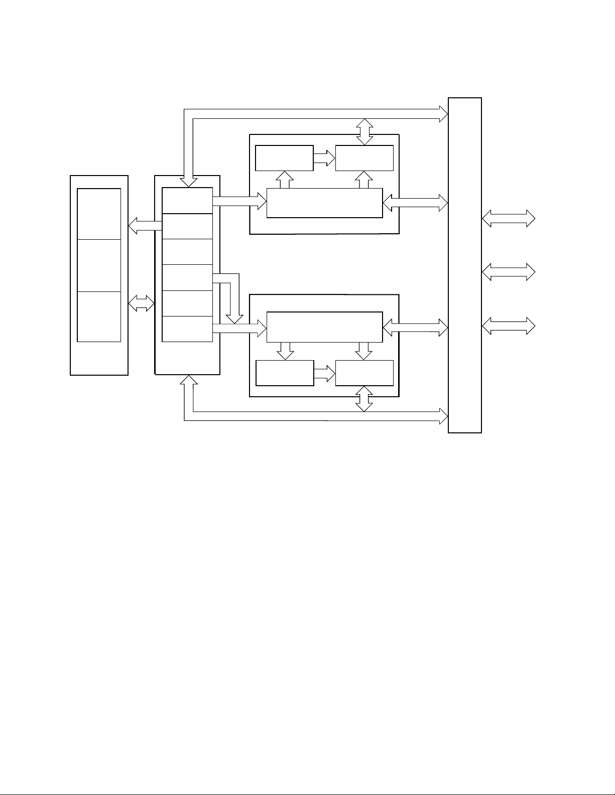
Freescale Semiconductor, Inc.
more common case of the branch taken, and both execution paths of the branch are
fetched and decoded to minimize refilling of the instruction pipeline.
INSTRUCTION DATA BUS
nc...
I
cale Semiconductor,
Frees
CONVERT
EXECUTE
WRITE-
BACK
FLOATING-
POINT
UNIT
INSTRUCTION
FETCH
DECODE
EA
CALCULATE
EA
FETCH
EXECUTE
WRITE-
BACK
INTEGER
UNIT
INSTRUCTION
ATC
INSTRUCTION
MMU/CACHE/SNOOP
CONTROLLER
INSTRUCTION MEMORY UNIT
DATA MEMORY UNIT
MMU/CACHE/SNOOP
CONTROLLER
DATA
ATC
OPERAND DATA BUS
DATA
INSTRUCTION
CACHE
DATA
CACHE
INSTRUCTION
ADDRESS
DATA
ADDRESS
B
U
S
C
O
N
T
R
O
L
L
E
R
ADDRESS
BUS
DATA
BUS
BUS
CONTROL
SIGNALS
Figure 1-1. Block Diagram
To improve memory management, the M68040 includes separate, independent paged
MMUs for instruction and data accesses. Each MMU stores recently used address
mappings in separate 64-entry address translation caches (ATCs). Each MMU also has
two transparent translation registers that define a one-to-one mapping for address space
segments ranging in size from 16 Mbytes to 4 Gbytes each.
Two memory units independently interface with the IU and FPU. Each unit consists of an
MMU, an ATC, a main cache, and a snoop controller. The MMUs perform memory
management on a demand-page basis. By translating logical-to-physical addresses using
translation tables stored in memory, the MMUs support virtual memory systems. Each
MMU stores recently used address mappings in an ATC, reducing the average translation
time.
Separate on-chip instruction and data caches operate independently and are accessed in
parallel with address translation. The caches improve the overall performance of the
system by reducing the number of bus transfers required by the processor to fetch
information from memory and by increasing the bus bandwidth available for alternate bus
1-4 M68040 USER’S MANUAL MOTOROLA
For More Information On This Product,
Go to: www.freescale.com
Page 26

Freescale Semiconductor, Inc.
masters in the system. Both caches are organized as four-way set associative with 64
sets of four lines. Each line contains four long words for a storage capability of 4 Kbytes
for each cache (8 Kbytes total). Each cache and corresponding MMU is allocated
separate internal address and data buses, allowing simultaneous access to both. The
data cache provides write-through or copyback write modes that can be configured on a
page-by-page basis. The caches are physically mapped, reducing software support for
multitasking operating systems, and support external bus snooping to maintain cache
coherency in multimaster systems.
The bus snoop logic provides cache coherency in multimaster applications. The bus
controller executes bus transfers on the external bus and prioritizes external memory
requests from each cache. The M68040 bus controller supports a high-speed,
nonmultiplexed, synchronous, external bus interface supporting burst accesses for both
reads and writes to provide high data transfer rates to and from the caches. Additional bus
signals support bus snooping and external cache tag maintenance.
nc...
I
cale Semiconductor,
Frees
The MC68040 contains an on-chip FPU, which is user object-code compatible with the
MC68881/MC68882 floating-point coprocessors. The FPU has pipelined instruction
execution. Floating-point instructions in the FPU execute concurrently with integer
instructions in the IU.
1.5 PROCESSING STATES
The processor is always in one of three states: normal processing, exception processing,
or halted. It is in the normal processing state when executing instructions, fetching
instructions and operands, and storing instruction results.
Exception processing is the transition from program processing to system, interrupt, and
exception handling. Exception processing includes fetching the exception vector, stacking
operations, and refilling the instruction pipe caused after an exception. The processor
enters exception processing when an exceptional internal condition arises such as tracing
an instruction, an instruction results in a trap, or executing specific instructions. External
conditions, such as interrupts and access errors, also cause exceptions. Exception
processing ends when the first instruction of the exception handler begins to execute.
The processor halts when it receives an access error or generates an address error while
in the exception processing state. For example, if during exception processing of one
access error another access error occurs, the MC68040 is unable to complete the
transition to normal processing and cannot save the internal state of the machine. The
processor assumes that the system is not operational and halts. Only an external reset
can restart a halted processor. Note that when the processor executes a STOP
instruction, it is in a special type of normal processing state, one without bus cycles. The
processor stops, but it does not halt.
1.6 PROGRAMMING MODEL
The MC68040 programming model is separated into two privilege modes : supervisor and
user. The S-bit in the status register (SR) indicates the privilege mode that the processor
MOTOROLA M68040 USER’S MANUAL 1-5
For More Information On This Product,
Go to: www.freescale.com
Page 27

Freescale Semiconductor, Inc.
uses. The IU identifies a logical address by accessing either the supervisor or user
address space, maintaining the differentiation between supervisor and user modes. The
MMUs use the indicated privilege mode to control and translate memory accesses,
protecting supervisor code, data, and resources from user program accesses. Refer to
Appendix B MC68EC040 for details concerning the MC68EC040 address translation.
Programs access registers based on the indicated mode. User programs can only access
registers specific to the user mode; whereas, system software executing in the supervisor
mode can access all registers, using the control registers to perform supervisory functions.
User programs are thus restricted from accessing privileged information, and the
operating system performs management and service tasks for the user programs by
coordinating their activities. This difference allows the supervisor mode to protect system
resources from uncontrolled accesses.
Most instructions execute in either mode, but some instructions that have important
system effects are privileged and can only execute in the supervisor mode. For instance,
nc...
I
user programs cannot execute the STOP or RESET instructions. To prevent a user
program from entering the supervisor mode, except in a controlled manner, instructions
that can alter the S-bit in the SR are privileged. The TRAP instructions provide controlled
access to operating system services for user programs.
cale Semiconductor,
Frees
If the S-bit in the SR is set, the processor executes instructions in the supervisor mode.
Because the processor performs all exception processing in the supervisor mode, all bus
cycles generated during exception processing are supervisor references, and all stack
accesses use the active supervisor stack pointer. If the S-bit of the SR is clear, the
processor executes instructions in the user mode. The bus cycles for an instruction
executed in the user mode are user references. The values on the transfer modifier pins
indicate either supervisor or user accesses.
The processor utilizes the user mode and the user programming model when it is in
normal processing. During exception processing, the processor changes from user to
supervisor mode. Exception processing saves the current value of the SR on the active
supervisor stack and then sets the S-bit, forcing the processor into the supervisor mode.
To return to the user mode, a system routine must execute one of the following
instructions: MOVE to SR, ANDI to SR, EORI to SR, ORI to SR, or RTE, which execute in
the supervisor mode, modifying the S-bit of the SR. After these instructions execute, the
instruction pipeline is flushed and is refilled from the appropriate address space.
The MC68040 integrates the functions of the IU, FPU, and MMU. The registers depicted
in the programming model (see Figure 1-2) provide operand storage and control for these
three units. The registers are partitioned into two levels of privilege modes: user and
supervisor. The user programming model is the same as the user programming model of
the MC68030, which consists of 16, general-purpose, 32-bit registers and two control
registers. The MC68040 user programming model also incorporates the
MC68881/MC68882 programming model consisting of eight, 80-bit, floating-point data
registers, a floating-point control register, a floating-point status register, and a floating point instruction address register.
1-6 M68040 USER’S MANUAL MOTOROLA
For More Information On This Product,
Go to: www.freescale.com
Page 28
Freescale Semiconductor, Inc.
Only system programmers can use the supervisor programming model to implement
operating system functions, I/O control, and memory management subsystems. This
supervisor/user distinction in the M68000 family architecture allows for the writing of
application software that executes in the user mode and migrates to the MC68040 from
any M68000 family platform without modification. The supervisor programming model
contains the control features that system designers need to modify system software when
porting to a new design. For example, only the supervisor software can read or write to
the transparent translation registers of the MC68040. The existence of the transparent
translation registers does not affect the programming resources of user application
programs.
nc...
I
cale Semiconductor,
Frees
31 0
DATA
REGISTERS
ADDRESS
REGISTERS
31 0
(CCR)
79 0
D0
D1
D2
D3
D4
D5
D6
D7
A0
A1
A2
A3
A4
A5
A6
A7/USP
PC
CCR
A7'/ISP
A7"/MSP
SR
VBR
SFC
DFC
CACR
URP
SRP
TC
DTT0
DTT1
ITT0
ITT1
MMUSR
FP INSTRUCTION ADDRESS REGISTER
USER STACK POINTER
PROGRAM COUNTER
CONDITION CODE REGISTER
USER PROGRAMMING MODEL
INTERRUPT STACK POINTER
MASTER STACK POINTER
STATUS REGISTER (CCR IS ALSO SHOWN IN THE USER PROGRAMMING MODEL)
VECTOR BASE REGISTER
SOURCE FUNCTION CODE
DESTINATION FUNCTION CODE
CACHE CONTROL REGISTER
USER ROOT POINTER REGISTER
SUPERVISOR ROOT POINTER REGISTER
TRANSLATION CONTROL REGISTER
DATA TRANSPARENT TRANSLATION REGISTER 0
DATA TRANSPARENT TRANSLATION REGISTER 1
INSTRUCTION TRANSPARENT TRANSLATION REGISTER 0
INSTRUCTION TRANSPARENT TRANSLATION REGISTER 1
MMU STATUS REGISTER
FLOATING-POINT
DATA
REGISTERS
FP CONTROL REGISTER
FP STATUS REGISTER
31 0
15
0
FP0
FP1
FP2
FP3
FP4
FP5
FP6
FP7
FPCR
FPSR
FPIAR
SUPERVISOR PROGRAMMING MODEL
Figure 1-2. Programming Model
MOTOROLA M68040 USER’S MANUAL 1-7
For More Information On This Product,
Go to: www.freescale.com
Page 29

Freescale Semiconductor, Inc.
The user programming model includes eight data registers, seven address registers, and
a stack pointer register. The address registers and stack pointer can be used as base
address registers or software stack pointers, and any of the 16 registers can be used as
index registers. Two control registers are available in the user mode—the program
counter (PC), which usually contains the address of the instruction that the MC68040 is
executing, and the lower byte of the SR, which is accessible as the condition code register
(CCR). The CCR contains the condition codes that reflect the results of a previous
operation and can be used for conditional instruction execution in a program.
The supervisor programming model includes the upper byte of the SR, which contains
operation control information. The vector base register (VBR) contains the base address
of the exception vector table, which is used in exception processing. The source function
code (SFC) and destination function code (DFC) registers contain 3-bit function codes.
These function codes can be considered extensions to the 32-bit logical address. The
processor automatically generates function codes to select address spaces for data and
program accesses in the user and supervisor modes. Some instructions use the alternate
nc...
I
function code registers to specify the function codes for various operations.
cale Semiconductor,
Frees
The cache control register (CACR) controls enabling of the on-chip instruction and data
caches of the MC68040. The supervisor root pointer (SRP) and user root pointer (URP)
registers point to the root of the address translation table tree to be used for supervisor
and user mode accesses.
The translation control register (TCR) enables logical-to-physical address translation and
selects either 4- or 8-Kbyte page sizes. There are four transparent translation registers,
two for instruction accesses and two for data accesses. These registers allow portions of
the logical address space to be transparently mapped and accessed without the use of
resident descriptors in an ATC. The MMU status register (MMUSR) contains status
information derived from the execution of a PTEST instruction. The PTEST instruction
searches the translation tables for the logical address, specified by this instruction’s
effective address field and the DFC, and returns status information corresponding to the
translation.
The user programming model can also access the entire floating-point programming
model. The eight 80-bit floating-point data registers are analogous to the integer data
registers. A 32-bit floating-point control register (FPCR) contains an exception enable byte
that enables and disables traps for each class of floating-point exceptions and a mode
byte that sets the user-selectable rounding and precision modes. A floating-point status
register (FPSR) contains a condition code byte, quotient byte, exception status byte, and
accrued exception byte. A floating-point exception handler can use the address in the 32bit floating-point instruction address register (FPIAR) to locate the floating-point instruction
that has caused an exception. Instructions that do not modify the FPIAR can be used to
read the FPIAR in the exception handler without changing the previous value.
1-8 M68040 USER’S MANUAL MOTOROLA
For More Information On This Product,
Go to: www.freescale.com
Page 30
nc...
I
cale Semiconductor,
Frees
Freescale Semiconductor, Inc.
1.7 DATA FORMAT SUMMARY
The M68040 supports the basic data formats of the M68000 family. Some data formats
apply only to the IU, some only to the FPU, and some to both. In addition, the instruction
set supports operations on other data formats such as memory addresses.
The operand data formats supported by the IU are the standard twos-complement data
formats defined in the M68000 family architecture plus a new data format (16-byte block)
for the MOVE16 instruction. Registers, memory, or instructions themselves can contain IU
operands. The operand size for each instruction is either explicitly encoded in the
instruction or implicitly defined by the instruction operation.
Whenever an integer is used in a floating-point operation, the FPU automatically converts
it to an extended-precision floating-point number before using the integer. The FPU
implements single- and double-precision floating-point data formats as defined by the
IEEE 754 standard. The FPU does not directly support packed decimal real format.
However, by trapping as an unimplemented data format instead of as an illegal instruction,
software emulation supports the packed decimal format. Additionally, each data format
has a special encoding that represents one of five data types: normalized numbers,
denormalized numbers, zeros, infinities, and not-a-numbers (NANs). Table 1-1 lists the
data formats for both the IU and the FPU. Refer to M68000PM/AD,
Programmer’s Reference Manual,
for details on data format organization in registers and
memory.
Table 1-1. M68040 Data Formats
Operand Data Format Size Supported In Notes
Bit 1 Bit IU —
Bit Field 1–32 Bits IU Field of Consecutive Bits
Binary-Coded Decimal (BCD) 8 Bits IU Packed: 2 Digits/Byte; Unpacked: 1 Digit/Byte
Byte Integer 8 Bits IU, FPU —
Word Integer 16 Bits IU, FPU —
Long-Word Integer 32 Bits IU, FPU —
Quad-Word Integer 64 Bits IU Any Two Data Registers
16-Byte 128 Bits IU Memory Only, Aligned to 16-Byte Boundary
Single-Precision Real 32 Bits FPU 1-Bit Sign, 8-Bit Exponent, 23-Bit Fraction
Double-Precision Real 64 Bits FPU 1-Bit Sign, 11-Bit Exponent, 52-Bit Fraction
Extended-Precision Real 80 Bits FPU 1-Bit Sign, 15-Bit Exponent, 64-Bit Mantissa
M68000 Family
1.8 ADDRESSING CAPABILITIES SUMMARY
The M68040 supports the basic addressing modes of the M68000 family. The register
indirect addressing modes support postincrement, predecrement, offset, and indexing,
which are particularly useful for handling data structures common to sophisticated
MOTOROLA M68040 USER’S MANUAL 1-9
For More Information On This Product,
Go to: www.freescale.com
Page 31

nc...
I
cale Semiconductor,
Frees
Freescale Semiconductor, Inc.
applications and high-level languages. The program counter indirect mode also has
indexing and offset capabilities. This addressing mode is typically required to support
position-independent software. Besides these addressing modes, the M68040 provides
index sizing and scaling features.
An instruction’s addressing mode can specify the value of an operand, a register
containing the operand, or how to derive the effective address of an operand in memory.
Each addressing mode has an assembler syntax. Some instructions imply the addressing
mode for an operand. These instructions include the appropriate fields for operands that
use only one addressing mode. Table 1-2 lists a summary of the effective addressing
modes for the M68040. Refer to M68000PM/AD,
Reference Manual,
for details on instruction format and addressing modes.
M68000 Family Programmer’s
Table 1-2. Effective Addressing Modes
Addressing Modes Syntax
Register Direct
Data
Address
Register Indirect
Address
Address with Postincrement
Address with Predecrement
Address with Displacement
Address Register Indirect with Index
8-Bit Displacement
Base Displacement
Memory Indirect
Postindexed
Preindexed
Program Counter Indirect
with Displacement (d16,PC)
Program Counter Indirect with Index
8-Bit Displacement
Base Displacement
Program Counter Memory Indirect
Postindexed
Preindexed
Absolute Data Addressing
Short
Long
Immediate #<xxx>
Dn
An
(An)
(An)+
–(An)
(d16,An)
(d8,An,Xn)
(bd,An,Xn)
([bd,An],Xn,od)
([bd,An,Xn],od)
(d8,PC,Xn)
(bd,PC,Xn)
([bd,PC],Xn,od)
([bd,PC,Xn],od)
(xxx).W
(xxx).L
1-10 M68040 USER’S MANUAL MOTOROLA
For More Information On This Product,
Go to: www.freescale.com
Page 32

nc...
I
cale Semiconductor,
Frees
Freescale Semiconductor, Inc.
1.9 NOTATIONAL CONVENTIONS
Table 1-3 lists the notation conventions used throughout this manual unless otherwise
specified.
Table 1-3. Notational Conventions
Single- And Double-Operand Operations
+ Arithmetic addition or postincrement indicator.
– Arithmetic subtraction or predecrement indicator.
× Arithmetic multiplication.
÷ Arithmetic division or conjunction symbol.
~ Invert; operand is logically complemented.
Λ Logical AND
V Logical OR
⊕ Logical exclusive OR
ø Source operand is moved to destination operand.
ł ø Two operands are exchanged.
<op> Any double-operand operation.
<operand>tested Operand is compared to zero and the condition codes are set appropriately.
sign-extended All bits of the upper portion are made equal to the high-order bit of the lower portion.
Other Operations
TRAP Equivalent to Format ÷ Offset Word ø (SSP); SSP – 2 ø SSP; PC ø (SSP); SSP – 4 ø SSP; SR
(SSP); SSP – 2 ø SSP; (Vector) ø PC
ø
STOP Enter the stopped state, waiting for interrupts.
<operand>
If <condition>
then <operations>
else <operations>
Ax, Ay Source and destination address registers, respectively.
Dr, Dq Data register’s remainder or quotient of divide.
Dx, Dy Source and destination data registers, respectively.
Rx, Ry Any source and destination registers, respectively.
10
An Any Address Register n (example: A3 is address register 3)
BR Base Register—An, PC, or suppressed.
Dc Data register D7–D0, used during compare.
Dh, Dl Data registers high- or low-order 32 bits of product.
Dn Any Data Register n (example: D5 is data register 5)
Du Data register D7–D0, used during update.
MRn Any Memory Register n.
Rn Any Address or Data Register
Xn Index Register—An, Dn, or suppressed.
The operand is BCD; operations are performed in decimal.
Test the condition. If true, the operations after “then” are performed. If the condition is false
and the optional “else” clause is present, the operations after “else” are performed. If the
condition is false and else is omitted, the instruction performs no operation. Refer to the Bcc
instruction description as an example.
Register Specification
MOTOROLA M68040 USER’S MANUAL 1-11
For More Information On This Product,
Go to: www.freescale.com
Page 33

nc...
I
cale Semiconductor,
Frees
Freescale Semiconductor, Inc.
Table 1-3. Notational Conventions (Continued)
Data Format And Type
+ inf Positive Infinity
<fmt> Operand Data Format: Byte (B), Word (W), Long (L), Single (S), Double (D), Extended (X), or
Packed (P).
B, W, L Specifies a signed integer data type (twos complement) of byte, word, or long word.
D Double-precision real data format (64 bits).
k A twos complement signed integer (–64 to +17) specifying a number’s format to be stored in
the packed decimal format.
P Packed BCD real data format (96 bits, 12 bytes).
S Single-precision real data format (32 bits).
X Extended-precision real data format (96 bits, 16 bits unused).
– inf Negative Infinity
Subfields and Qualifiers
#<xxx> or #<data> Immediate data following the instruction word(s).
( ) Identifies an indirect address in a register.
[ ] Identifies an indirect address in memory.
bd Base Displacement
ccc Index into the MC68881/MC68882 Constant ROM
d
n
LSB Least Significant Bit
LSW Least Significant Word
MSB Most Significant Bit
MSW Most Significant Word
od Outer Displacement
SCALE A scale factor (1, 2, 4, or 8, for no-word, word, long-word, or quad-word scaling, respectively).
SIZE The index register’s size (W for word, L for long word).
{offset:width} Bit field selection.
CCR Condition Code Register (lower byte of status register)
DFC Destination Function Code Register
FPcr Any Floating-Point System Control Register (FPCR, FPSR, or FPIAR)
FPm, FPn Any Floating-Point Data Register specified as the source or destination, respectively.
IC, DC, IC/DC Instruction, Data, or Both Caches
MMUSR MMU Status Register
PC Program Counter
Rc Any Non Floating-Point Control Register
SFC Source Function Code Register
SR Status Register
Displacement Value, n Bits Wide (example: d16 is a 16-bit displacement).
Register Names
1-12 M68040 USER’S MANUAL MOTOROLA
For More Information On This Product,
Go to: www.freescale.com
Page 34

nc...
I
cale Semiconductor,
Frees
Freescale Semiconductor, Inc.
Table 1-3. Notational Conventions (Concluded)
Register Codes
* General Case.
C Carry Bit in CCR
cc Condition Codes from CCR
FC Function Code
N Negative Bit in CCR
U Undefined, Reserved for Motorola Use.
V Overflow Bit in CCR
X Extend Bit in CCR
Z Zero Bit in CCR
— Not Affected or Applicable.
Stack Pointers
ISP Supervisor/Interrupt Stack Pointer
MSP Supervisor/Master Stack Pointer
SP Active Stack Pointer
SSP Supervisor (Master or Interrupt) Stack Pointer
USP User Stack Pointer
Miscellaneous
<ea> Effective Address
<label> Assemble Program Label
<list> List of registers, for example D3–D0.
LB Lower Bound
m Bit m of an Operand
m–n Bits m through n of Operand
UB Upper Bound
1.10 INSTRUCTION SET OVERVIEW
The instruction set is tailored to support high-level languages and is optimized for those
instructions most commonly executed. The floating-point instructions for the M68040 are a
commonly used subset of the MC68881/MC68882 instruction set with new arithmetic
instructions to explicitly select single- or double-precision rounding. The remaining
unimplemented instructions are less frequently used and are efficiently emulated in the
M68040FPSP, maintaining compatibility with the MC68881/MC68882 floating-point
coprocessors. The M68040 instruction set includes MOVE16, a new user instruction that
allows high-speed transfers of 16-byte blocks between external devices such as memory
to memory or coprocessor to memory. Table 1-4 provides an alphabetized listing of the
M68040 instruction set’s opcode, operation, and syntax. Refer to Table 1-3 for notations
used in Table 1-4. The left operand in the syntax is always the source operand, and the
right operand is the destination operand. Refer to M68000PM/AD,
Programmer’s Reference Manual,
for details on instructions used by the M68040.
M68000 Family
MOTOROLA M68040 USER’S MANUAL 1-13
For More Information On This Product,
Go to: www.freescale.com
Page 35

nc...
I
cale Semiconductor,
Frees
Freescale Semiconductor, Inc.
Table 1-4. Instruction Set Summary
Opcode Operation Syntax
ABCD BCD Source + BCD Destination + X ø Destination ABCD Dy,Dx
ABCD –(Ay),–(Ax)
ADD Source + Destination ø Destination ADD <ea>,Dn
ADD Dn,<ea>
ADDA Source + Destination ø Destination ADDA <ea>,An
ADDI Immediate Data + Destination ø Destination ADDI #<data>,<ea>
ADDQ Immediate Data + Destination ø Destination ADDQ #<data>,<ea>
ADDX Source + Destination + X ø Destination ADDX Dy,Dx
ADDX –(Ay),–(Ax)
AND Source Λ Destination ø Destination AND <ea>,Dn
AND Dn,<ea>
ANDI Immediate Data Λ Destination ø Destination ANDI #<data>,<ea>
ANDI to CCR Source Λ CCR ø CCR ANDI #<data>,CCR
ANDI to SR If supervisor state
then Source Λ SR ø SR
else TRAP
ASL, ASR Destination Shifted by count ø Destination ASd Dx,Dy
Bcc If condition true
then PC + dn ø PC
BCHG ~(bit number of Destination) ø Z;
~(bit number of Destination) ø (bit number) of
Destination
BCLR ~(bit number of Destination) ø Z;
0 ø bit number of Destination
BFCHG ~(bit field of Destination) ø bit field of Destination BFCHG <ea>{offset:width}
BFCLR 0 ø bit field of Destination BFCLR <ea>{offset:width}
BFEXTS bit field of Source ø Dn BFEXTS <ea>{offset:width},Dn
BFEXTU bit offset of Source ø Dn BFEXTU <ea>{offset:width},Dn
BFFFO bit offset of Source Bit Scan ø Dn BFFFO <ea>{offset:width},Dn
BFINS Dn ø bit field of Destination BFINS Dn,<ea>{offset:width}
BFSET 1s ø bit field of Destination BFSET <ea>{offset:width}
BFTST bit field of Destination BFTST <ea>{offset:width}
BKPT Run breakpoint acknowledge cycle;
TRAP as illegal instruction
BRA PC + dn ø PC BRA <label>
BSET ~(bit number of Destination) ø Z;
1 ø bit number of Destination
BSR SP – 4 ø SP; PC ø (SP); PC + dn ø PC BSR <label>
ANDI #<data>,SR
1
ASd #<data>,Dy
ASd <ea>
Bcc <label>
BCHG Dn,<ea>
BCHG #<data>,<ea>
BCLR Dn,<ea>
BCLR #<data>,<ea>
BKPT #<data>
BSET Dn,<ea>
BSET #<data>,<ea>
1
1
1-14 M68040 USER’S MANUAL MOTOROLA
For More Information On This Product,
Go to: www.freescale.com
Page 36

nc...
I
cale Semiconductor,
Frees
Freescale Semiconductor, Inc.
Table 1-4. Instruction Set Summary (Continued)
Opcode Operation Syntax
BTST –(bit number of Destination) ø Z ; BTST Dn,<ea>
BTST #<data>,<ea>
CAS CAS Destination – Compare Operand ø cc;
if Z, Update Operand ø Destination
else Destination ø Compare Operand
CAS2 CAS2 Destination 1 – Compare 1 ø cc;
if Z, Destination 2 – Compare ø cc;
if Z, Update 1 ø Destination 1;
Update 2 ø Destination 2
else Destination 1 ø Compare 1;
Destination 2 ø Compare 2
CHK If Dn < 0 or Dn > Source
then TRAP
CHK2 If Rn < LB or If Rn > UB
then TRAP
CINV If supervisor state
then invalidate selected cache lines
else TRAP
CLR 0 ø Destination CLR <ea>
CMP Destination – Source ø cc CMP <ea>,Dn
CMPA Destination – Source CMPA <ea>,An
CMPI Destination – Immediate Data CMPI #<data>,<ea>
CMPM Destination – Source ø cc CMPM (Ay)+,(Ax)+
CMP2 Compare Rn < LB or Rn > UB
and Set Condition Codes
CPUSH If supervisor state
then if data cache push selected dirty data
cache lines; invalidate selected cache lines
else TRAP
DBcc If condition false
then (Dn–1 ø Dn;
If Dn ≠ –1
then PC + dn ø PC)
DIVS, DIVSL Destination ÷ Source ø Destination DIVS.W <ea>,Dn 32 ÷ 16 ø 16r:16q
DIVU, DIVUL Destination ÷ Source ø Destination DIVU.W <ea>,Dn 32 ÷ 16 ø 16r:16q
EOR Source ⊕ Destination ø Destination EOR Dn,<ea>
EORI Immediate Data ⊕ Destination ø Destination EORI #<data>,<ea>
EORI to CCR Source ⊕ CCR ø CC R EORI #<data>,CCR
EORI to SR If supervisor state
then Source ⊕ SR ø SR
else TRAP
CAS Dc,Du,<ea>
CAS2 Dc1–Dc2,Du1–Du2,(Rn1)–(Rn2)
CHK <ea>,Dn
CHK2 <ea>,Rn
CINVL <caches>, (An)
CINVP <caches>, (An)
CINVA <caches>
CMP2 <ea>,Rn
CPUSHL <caches>, (An)
CPUSHP <caches>, (An)
CPUSHA <caches>
DBcc Dn,<label>
DIVS.L <ea>,Dq 32 ÷ 32 ø 32q
DIVS.L <ea>,Dr:Dq 64 ÷ 32 ø 32r:32q
DIVSL.L <ea>,Dr:Dq 32 ÷ 32 ø 32r:32q
DIVU.L <ea>,Dq 32 ÷ 32 ø 32q
DIVU.L <ea>,Dr:Dq 64 ÷ 32 ø 32r:32q
DIVUL.L <ea>,Dr:Dq 32 ÷ 32 ø 32r:32q
EORI #<data>,SR
MOTOROLA M68040 USER’S MANUAL 1-15
For More Information On This Product,
Go to: www.freescale.com
Page 37

nc...
I
cale Semiconductor,
Frees
Freescale Semiconductor, Inc.
Table 1-4. Instruction Set Summary (Continued)
Opcode Operation Syntax
EXG Rx ł ø Ry EXG Dx,Dy
EXG Ax,Ay
EXG Dx,Ay
EXG Ay,Dx
EXT
EXTB
2
FABS
2
FADD
2
FBcc
FCMP
FDBcc
2
FDIV
FMOVE
FMOVE
FMOVEM
FMOVEM
2
FMUL
2
2
Destination Sign – Extended ø Destination EXT.W Dn extend byte to word
EXT.L L Dn extend word to long word
EXTB.L Dn extend byte to long word
Absolute Value of Source ø FPn FABS.<fmt> <ea>,FPn
FABS.X FPm,FPn
FABS.X FPn
FrABS.<fmt> <ea>,FPn
FrABS.X FPm,FPn
FrABS.X FPn
Source + FPn ø FPn FADD.<fmt> <ea>,FPn
FADD.X FPm,FPn
FrADD.<fmt> <ea>,FPn
FrADD.X FPm,FPn
If condition true
then PC + dn ø PC
FPn – Source
If condition true
then no operation
else Dn – 1 ø Dn
if Dn ≠ –1
then PC + dn ø PC
else execute next instruction
FPn ÷ Source ø FPn FDIV.<fmt> <ea>,FPn
2
Source ø Destination FMOVE.<fmt> <ea>,FPn
2
Source ø Destination
2
Register List ø Destination
Source ø Register List
2
Register List ø Destination
Source ø Register List
Source × FPn ø FPn FMUL.<fmt> <ea>,FPn
FBcc.SIZE <label>
FCMP.<fmt> <ea>,FPn
FCMP.X FPm,FPn
FDBcc Dn,<label>
FDIV.X FPm,FPn
FrDIV.<fmt> <ea>,FPn
FrDIV.X FPm,FPn
FMOVE.<fmt> FPM,<ea>
FMOVE.P FPm,<ea>{Dn}
FMOVE.P FPm,<ea>{#k}
FrMOVE.<fmt> <ea>,FPn
FMOVE.L <ea>,FPcr
FMOVE.L FPcr,<ea>
FMOVEM.X <list>,<ea>
FMOVEM.X Dn,<ea>
FMOVEM.X <ea>,<list>
FMOVEM.X <ea>,Dn
FMOVEM.L <list>,<ea>
FMOVEM.L <ea>,<list>
FMUL.X FPm,FPn
FrMUL<fmt> <ea>,FPn
FrMUL.X FPm,FPn
3
3
3
3
3
3
3
3
3
4
4
5
5
3
1-16 M68040 USER’S MANUAL MOTOROLA
For More Information On This Product,
Go to: www.freescale.com
Page 38

nc...
I
cale Semiconductor,
Frees
Freescale Semiconductor, Inc.
Table 1-4. Instruction Set Summary (Continued)
Opcode Operation Syntax
2
FNEG
2
FNOP
FRESTORE
2
FSAVE
2
FScc
FSGLDIV FPn ÷ Source ø FPn FSGLDIV.<fmt> <ea>,FPn
FSGLMUL Source × FPn ø FPn FSGMUL.<fmt> <ea>,FPn
2
FSQRT
2
FSUB
FTRAPcc
2
FTST
ILLEGAL SSP – 2 ø SSP; Vector Offset ø (SSP);
JMP Destination Address ø PC JMP <ea>
JSR SP – 4 ø SP; PC ø (SP)
LEA <ea> ø A n LEA <ea>,An
LINK SP – 4 ø SP; An ø (SP)
–(Source) ø FPn FNEG.<fmt> <ea>,FPn
FNEG.X FPm,FPn
FNEG.X FPn
FrNEG.<fmt> <ea>,FPn
FrNEG.X FPm,FPn
FrNEG.X FPn
None FNOP
2
If in supervisor state
then FPU State Frame ø Internal State
else TRAP
If in supervisor state
then FPU Internal State ø State Frame
else TRAP
If condition true
then 1s ø Destination
else 0s ø Destination
Square Root of Source ø FPn FSQRT.<fmt> <ea>,FPn
FPn – Source ø FPn FSUB.<fmt> <ea>,FPn
2
If condition true
then TRAP
Condition Codes for Operand ø FPCC FTST.<fmt> <ea>
SSP – 4 ø SSP; PC ø (SSP);
SSp – 2 ø SSP; SR ø (SSP);
Illegal Instruction Vector Address ø PC
Destination Address ø PC
SP ø An, SP+d ø SP
FRESTORE <ea>
FSAVE <ea>
FScc.SIZE <ea>
FSGLDIV.X FPm,FPn
FSGLMUL.X FPm, FPn
FSQRT.X FPm,FPn
FSQRT.X FPn
FrSQRT.<fmt> <ea>,FPn
FrSQRT FPm,FPn
FrSQRT FPn
FSUB.X FPm,FPn
FrSUB.<fmt> <ea>,FPn
FrSUB.X FPm,FPn
FTRAPcc
FTRAPcc.W #<data>
FTRAPcc.L #<data>
FTST.X FPm
ILLEGAL
JSR <ea>
LINK An,d
3
3
3
3
3
n
3
3
3
MOTOROLA M68040 USER’S MANUAL 1-17
For More Information On This Product,
Go to: www.freescale.com
Page 39

nc...
I
cale Semiconductor,
Frees
Freescale Semiconductor, Inc.
Table 1-4. Instruction Set Summary (Continued)
Opcode Operation Syntax
LPSTOP
LSL, LSR Destination Shifted by count ø Destination LSd Dx,Dy
MOVEA Source ø Destination MOVEA <ea>,An
from CCR
MOVE to CCR Source ø CCR MOVE <ea>,CCR
MOVE from SR If supervisor state
MOVE to SR If supervisor state
MOVE USP If supervisor state
MOVE16 Source block ø Destination block MOVE16 (Ax)+, (Ay)+
MOVEC If supervisor state
MOVEM Registers ø Destination
MOVEP Source ø Destination MOVEP Dx,(dn,Ay)
MOVEQ Immediate Data ø Destination MOVEQ #<data>,Dn
MOVES If supervisor state
6
If supervisor state
immediate data ø SR
SR ø broadcast cycle
STOP
else TRAP
MOVE Source ø Destination MOVE <ea>,<ea>
MOVE
MULS Source × Destination ø Destination MULS.W <ea>,Dn 16 × 16 ø 32
MULU Source × Destination ø Destination MULU.W <ea>,Dn 16 × 16 ø 32
NBCD 0 – (Destination10) – X ø Destination NBCD <ea>
NEG 0 – (Destination) ø Destination NEG <ea>
NEGX 0 – (Destination) – X ø Destination NEGX <ea>
CCR ø Destination MOVE CCR,<ea>
then SR ø Destination
else TRAP
then Source ø SR
else TRAP
then USP ø An or An ø USP
else TRAP
then Rc ø Rn or Rn ø Rc
else TRAP
Source ø Registers
then Rn ø Destination [DFC] or
Source [SFC] ø Rn
else TRAP
LPSTOP #<data>
1
LSd #<data>,Dy
LSd <ea>
MOVE SR,<ea>
MOVE <ea>,SR
MOVE USP,An
MOVE An,USP
MOVE16 (xxx).L, (An)
MOVE16 (An), (xxx).L
MOVE16 (An)+, (xxx).L
MOVEC Rc,Rn
MOVEC Rn,Rc
MOVEM <list>,<ea>
MOVEM <ea>,<list>
MOVEP (dn,Ay),Dx
MOVES Rn,<ea>
MOVES <ea>,Rn
MULS.L <ea>,Dl 32 × 32 ø 32
MULS.L <ea>,Dh–Dl 32 × 32 ø 64
MULU.L <ea>,Dl 32 × 32 ø 32
MULU.L <ea>,Dh–Dl 32 × 32 ø 64
1
1
7
4
4
1-18 M68040 USER’S MANUAL MOTOROLA
For More Information On This Product,
Go to: www.freescale.com
Page 40

nc...
I
cale Semiconductor,
Frees
Freescale Semiconductor, Inc.
Table 1-4. Instruction Set Summary (Continued)
Opcode Operation Syntax
NOP None NOP
NOT ~ Destination ø Destination NOT <ea>
OR Source V Destination ø Destination OR <ea>,Dn
OR Dn,<ea>
ORI Immediate Data V Destination ø Destination ORI #<data>,<ea>
ORI to CCR Source V CCR ø CC R ORI #<data>,CCR
ORI to SR If supervisor state
then Source V SR ø SR
else TRAP
PACK Source (Unpacked BCD) + adjustment ø
Destination (Packed BCD)
PEA SP – 4 ø SP; <ea> ø (SP) PEA <ea>
PFLUSH
PTEST
ROL, ROR Destination Rotated by count ø Destination ROd Rx,Dy
ROXL, ROXR Destination Rotated with X by count ø Destination ROXd Dx,Dy
8
If supervisor state
then invalidate instruction and data ATC entries
for destination address
else TRAP
8
RESET If supervisor state
RTD (SP) ø PC; SP + 4 + dn ø SP RTD #(dn)
RTE If supervisor state
RTR (SP) ø CCR; SP + 2 ø SP;
RTS (SP) ø PC; SP + 4 ø SP RTS
SBCD Destination10 – Source10 – X ø Destination SBCD Dx,Dy
Scc If condition true
STOP If supervisor state
SUB Destination – Source ø Destination SUB <ea>,Dn
If supervisor state
then logical address status ø MMUSR;
entry ø ATC
else TRAP
then Assert RSTO Line
else TRAP
then (SP) ø SR; SP + 2 ø SP; (SP) ø PC;
SP + 4 ø SP; restore state and deallocate
stack according to (SP)
else TRAP
(SP) ø PC; SP + 4 ø SP
then 1s ø Destination
else 0s ø Destination
then Immediate Data ø SR; STOP
else TRAP
ORI #<data>,SR
PACK –(Ax),–(Ay),#(adjustment)
PACK Dx,Dy,#(adjustment)
PFLUSH (An)
PFLUSHN (An)
PFLUSHA
PFLUSHAN
PTESTR (An)
PTESTW (An)
RESET
1
ROd #<data>,Dy
ROXd #<data>,Dy
ROXd <ea>
RTE
RTR
SBCD –(Ax),–(Ay)
Scc <ea>
STOP #<data>
SUB Dn,<ea>
1
1
1
1
MOTOROLA M68040 USER’S MANUAL 1-19
For More Information On This Product,
Go to: www.freescale.com
Page 41

Freescale Semiconductor, Inc.
Table 1-4. Instruction Set Summary (Concluded)
Opcode Operation Syntax
SUBA Destination – Source ø Destination SUBA <ea>,An
SUBI Destination – Immediate Data ø Destination SUBI #<data>,<ea>
SUBQ Destination – Immediate Data ø Destination SUBQ #<data>,<ea>
SUBX Destination – Source – X ø Destination SUBX Dx,Dy
SUBX –(Ax),–(Ay)
SWAP Register 31–16 ¯ ø Register 15–0 SWAP Dn
TAS Destination Tested ø Condition Codes;
1 ø bit 7 of Destination
TRAP SSP – 2 ø SSP; Format ÷ Offset ø (SSP);
SSP – 4 ø SSP; PC ø (SSP); SSP – 2 ø SSP;
SR ø (SSP); Vector Address ø PC
TRAPcc If cc
then TRAP
nc...
I
TRAPV If V
then TRAP
TST Destination Tested ø Condition Codes TST <ea>
UNLK An ø SP; (SP) ø An; SP + 4 ø SP UNLK An
UNPK Source (Packed BCD) + adjustment ø Destination
(Unpacked BCD)
NOTES:
1. Where d is direction, left or right.
2. Available only on the MC68040.
3. Where r is rounding precision, single or double precision.
4. List refers to register.
5. List refers to control registers only.
6. Available only on the MC68040V and MC68EC040V.
7. MOVE16 (ax)+,(ay)+ is functionally the same as MOVE16 (ax),(ay)+ when ax = ay. The address register is only
incremented once, and the line is copied over itself rather than to the next line.
8. Not available for the MC68EC040 or MC68EC040V.
cale Semiconductor,
TAS <ea>
TRAP #<vector>
TRAPcc
TRAPcc.W #<data>
TRAPcc.L #<data>
TRAPV
UNPACK –(Ax),–(Ay),#(adjustment)
UNPACK Dx,Dy,#(adjustment)
Frees
1-20 M68040 USER’S MANUAL MOTOROLA
For More Information On This Product,
Go to: www.freescale.com
Page 42

Freescale Semiconductor, Inc.
SECTION 2
INTEGER UNIT
This section describes the organization of the M68040 integer unit (IU) and presents a
brief description of the associated registers. Refer to Section 3 Memory Management
Unit (Except MC68EC040 and MC68EC040V) for details concerning the memory
management unit (MMU) programming model, and to Section 9 Floating-Point Unit
(MC68040 Only) for details concerning the floating-point unit (FPU) programming model.
nc...
I
cale Semiconductor,
Frees
2.1 INTEGER UNIT PIPELINE
The IU carries out logical and arithmetic operations using six separate subunits. Each unit
is dedicated to a different stage of the IU pipeline, handling a total of six separate
instructions simultaneously. Pipelining is a technique that overlaps the processing of
different parts of several instructions. Pipelining simulates an assembly line with the IU
containing a number of instructions in different phases of processing. The IU pipeline
consists of six stages:
1. Instruction Fetch—Fetching an instruction from memory.
2. Decode—Converting an instruction into micro-instructions.
3. <ea> Calculate—If the instruction calls for data from memory, the location of the
data, its memory address is calculated.
4. <ea> Fetch—Data is fetched from memory.
5. Execute—The data is manipulated during execution.
6. Write-Back—The result of the computation is written back to on-chip caches or
external memory.
The pipeline contains special shadow registers that can begin processing future
instructions for conditional branches while the main pipeline is processing current
instructions. The <ea> calculate stage eliminates pipeline blockage for instructions with
postincrement, postdecrement, or immediate add and load to address register for updates
that occur in the <ea> calculate stage. The write-back stage can write data over the
system bus to store a result in external memory or directly to on-chip caches. These writebacks to memory can be deferred until the most opportune moment because of the
M68040 bus interface. Figure 2-1 illustrates the IU pipeline.
MOTOROLA M68040 USER’S MANUAL 2-1
For More Information On This Product,
Go to: www.freescale.com
Page 43

Freescale Semiconductor, Inc.
INSTRUCTION DATA
FROM CACHE OR BUS
CONTROLLER
nc...
I
cale Semiconductor,
Frees
SHADOW
SHADOW
TO FPU
INSTRUCTION
FETCH
DECODE
<ea> CALCULATE
<ea> FETCH
EXECUTE
WRITE-BACK
TO CACHE OR
BUS CONTROLLER
TO CACHE OR
BUS CONTROLLER
Figure 2-1. Integer Unit Pipeline
An instruction stream is fetched from the instruction memory unit and decoded on an
instruction-by-instruction basis in the decode stage. Multiple instructions are fetched to
keep the pipeline stages full so that the pipeline will not stall.
The decoded instruction is then passed to the <ea> calculate stage to calculate the
effective addresses that the instruction requires. The <ea> calculate stage initiates
additional fetches from the instruction stream to obtain the effective address extension
words and performs the effective address calculation. The initial execution of the
instruction in the execute stage handles any data registers required for the calculation,
which passes the register back to the <ea> calculate stage.
The resulting effective address is passed to the <ea> fetch stage, which initiates an
operand fetch from the data memory controller if the effective address is for a source
operand. The fetched operand is returned to the execute stage, which completes
execution of the instruction and writes any result to either a data register, memory, or back
to the <ea> calculate stage for storage in an address register. For a memory destination,
the <ea> fetch stage passes the address to the execution stage.
The previously described sequence of effective address calculation and fetch can occur
multiple times for an instruction, depending on the source and/or destination addressing
modes. For memory indirect addressing modes, the <ea> calculate stage initiates an
operand fetch from the intermediate indirect memory address, then calculates the final
2-2 M68040 USER’S MANUAL MOTOROLA
For More Information On This Product,
Go to: www.freescale.com
Page 44

nc...
I
cale Semiconductor,
Frees
Freescale Semiconductor, Inc.
effective address. Also, some instructions access multiple memory operands and initiate
fetches for each operand.
The instruction finishes execution in the execute stage. Instructions with write-back
operands to memory generate pending write accesses that are passed to the write-back
stage. The write occurs to the data memory unit if it is not busy. If the following instruction,
which is in the <ea> fetch stage, requires an operand fetch, the write-back stalls in the
write-back stage since it is at a lower priority. The write-back can stall indefinitely until
either the data memory unit is free or another write is pending from the execution stage.
Figure 2-2 illustrates a write cycle, which begins in the IU pipeline. The IU stores the
logical address and data for a write operation in a temporary holding register (WB3). Write
operation control passes from the IU to the data memory unit once the data memory unit
is idle. When the data memory unit receives the logical address and data from the IU, it
stores the logical address and data to a second temporary holding register (WB2). The
data memory unit then translates the logical address into a physical address. If the
address translation is successful, the data memory unit either stores an address
translation in the data cache (write hit) or passes it to the bus controller (write-through with
write miss). Once the bus controller is ready to execute the external write operation, it
multiplexes the data to the correct data byte lanes and stores the multiplexed data and
physical address into a third holding register (WB1). WB1 is used in the actual write
operation seen on the address and data buses. Appendix B MC68EC040 contains details
on address translation in the MC68EC040.
INSTRUCTION
FETCH
DECODE
<ea>
CALCULATE
<ea>
FETCH
EXECUTE
WRITE-
BACK (WB3)
INTEGER UNIT
INSTRUCTION MEMORY UNIT
DATA MEMORY UNIT
LOGICAL ADDRESS
DATA
ATC
WB2
PHYSICAL ADDRESS
DATA MMU/
CACHE/SNOOP
CONTROLLER
DATA CACHE
BUS
CONTROLLER
WB1
DATA MUX
PUSH
BUFFER
ADDRESS
BUS
DATA
BUS
BUS
CONTROL
SIGNALS
Figure 2-2. Write-Back Cycle Block Diagram
MOTOROLA M68040 USER’S MANUAL 2-3
For More Information On This Product,
Go to: www.freescale.com
Page 45

Freescale Semiconductor, Inc.
2.2 INTEGER UNIT REGISTER DESCRIPTION
The following paragraphs describe the IU registers in the user and supervisor
programming models. Refer to Section 3 Memory Management Unit (Except
MC68EC040 and MC68EC040V) for details on the MMU programming model and
Section 9 Floating-Point Unit (MC68040 Only) for details on the FPU programming
model.
2.2.1 Integer Unit User Programming Model
Figure 2-3 illustrates the IU portion of the user programming model . The model is the
same as for previous M68000 family microprocessors, consisting of the following
registers:
• 16 General-Purpose 32-Bit Registers (D7–D0, A7–A0)
• 32-Bit Program Counter (PC)
nc...
I
cale Semiconductor,
Frees
• 8-Bit Condition Code Register (CCR)
2.2.1.1 DATA REGISTERS (D7–D0). These registers are used as data registers for bit
and bit field (1 to 32 bits), byte (8 bit), word (16 bit), long-word (32 bit), and quad-word (64
bit) operations. These registers may also be used as index registers.
2.2.1.2 ADDRESS REGISTERS (A6–A0). These registers can be used as software stack
pointers, index registers, or base address registers . The address registers may be used
for word and long-word operations.
01531
D0
D1
D2
D3
D4
D5
D6
D7
01531
A0
A1
A2
A3
A4
A5
A6
01531
A7
(USP)
031
PC
0715
CCR
DATA
REGISTERS
ADDRESS
REGISTERS
USER
STACK
POINTER
PROGRAM
COUNTER
CONDITION
CODE
REGISTER
Figure 2-3. Integer Unit User Programming Model
2-4 M68040 USER’S MANUAL MOTOROLA
For More Information On This Product,
Go to: www.freescale.com
Page 46

Freescale Semiconductor, Inc.
2.2.1.3 SYSTEM STACK POINTER (A7) . A7 is used as a hardware stack pointer during
stacking for subroutine calls and exception handling. The register designation A7 refers to
three different uses of the register: the user stack pointer (USP) (A7) in the user
programming model and either the interrupt stack pointer (ISP) or master stack pointer
(MSP) (A7' or A7", respectively) in the supervisor programming model. When the S-bit in
the status register (SR) is clear, the USP is the active stack pointer. Explicit references to
the system stack pointer (SSP) refer to the USP while the processor is operating in the
user mode.
A subroutine call saves the program counter (PC) on the active system stack, and the
return restores it from the active system stack. Both the PC and the SR are saved on the
supervisor stack (either ISP or MSP) during the processing of exceptions and interrupts.
Thus, the execution of supervisor level code is independent of user code and condition of
the user stack. Conversely, user programs use the USP independently of supervisor stack
requirements.
nc...
I
cale Semiconductor,
Frees
2.2.1.4 PROGRAM COUNTER . The PC contains the address of the currently executing
instruction. During instruction execution and exception processing, the processor
automatically increments the contents of the PC or places a new value in the PC, as
appropriate. For some addressing modes, the PC can be used as a pointer for PC-relative
addressing.
2.2.1.5 CONDITION CODE REGISTER . The CCR consists of five bits of the SR least
significant byte. The first four bits represent a condition of the result generated by a
processor operation. The fifth bit, the extend bit (X-bit), is an operand for multiprecision
computations. The carry bit (C-bit) and the X-bit are separate in the M68000 family to
simplify programming techniques that use them.
2.2.2 Integer Unit Supervisor Programming Model
Only system programmers use the supervisor programming model (see Figure 2-4) to
implement sensitive operating system functions, I/O control, and MMU subsystems. All
accesses that affect the control features of the M68040 are in the supervisor programming
model. Thus, all application software is written to run in the user mode and migrates to the
M68040 from any M68000 platform without modification.
MOTOROLA M68040 USER’S MANUAL 2-5
For More Information On This Product,
Go to: www.freescale.com
Page 47

Freescale Semiconductor, Inc.
31
31 15
31 0
31 0
15 0
15 7 0
(CCR)
A7 '(ISP)
0
A7 "(MSP)
SR
VBR
031 2
SFC
DFC
CACR
INTERRUPT STACK POINTER
MASTER STACK POINTER
STATUS REGISTER
VECTOR BASE REGISTER
ALTERNATE SOURCE AND DESTINATION
FUNCTION CODE REGISTERS
CACHE CONTROL REGISTER
Figure 2-4. Integer Unit Supervisor Programming Model
The supervisor programming model consists of the registers available to the user as well
nc...
I
as the following control registers:
• Two 32-Bit Supervisor Stack Pointers (ISP, MSP)
• 16-Bit Status Register (SR)
• 32-Bit Vector Base Register (VBR)
cale Semiconductor,
Frees
• Two 32-Bit Alternate Function Code Registers: Source Function Code (SFC) and
Destination Function Code (DFC)
• 32-Bit Cache Control Register (CACR)
The following paragraphs describe the supervisor programming model registers.
Additional information on the ISP, MSP, SR, and VBR registers can be found in Section 8
Exception Processing.
2.2.2.1 INTERRUPT AND MASTER STACK POINTERS. In a multitasking operating
system, it is more efficient to have a supervisor stack pointer associated with each user
task and a separate stack pointer for interrupt-associated tasks. The M68040 provides two
supervisor stack pointers , master and interrupt. Explicit references to the SSP refer to
either the MSP or ISP while the processor is operating in the supervisor mode. All
instructions that use the SSP implicitly reference the active stack pointer. The ISP and
MSP are general-purpose registers and can be used as software stack pointers, index
registers, or base address registers. The ISP and MSP can be used for word and long word operations.
The M-bit of the SR selects whether the ISP or MSP is active. SSP references access the
ISP when the M-bit is clear, putting the processor into the interrupt mode. If an exception
being processed is an interrupt and the M-bit is set, the M-bit is cleared, putting the
processor into the interrupt mode. The interrupt mode is the default condition after reset,
and all SSP references access the ISP. The ISP can be used for interrupt control
information and for workspace area as interrupt exception handling requires.
SSP references access the MSP when the M-bit is set. The operating system uses the
MSP for each task pointing to a task-related area of supervisor data space. This
2-6 M68040 USER’S MANUAL MOTOROLA
For More Information On This Product,
Go to: www.freescale.com
Page 48

Freescale Semiconductor, Inc.
procedure separates task-related supervisor activity from asynchronous, I/O-related
supervisor tasks that can only be coincidental to the currently executing task. The MSP
can separately maintain task control information for each currently executing user task,
and the software updates the MSP when a task switch is performed, providing an efficient
means for transferring task-related stack items. The value of the M-bit does not affect
execution of privileged instructions. Instructions that affect the M-bit are MOVE to SR,
ANDI to SR, EORI to SR, ORI to SR, and RTE. The processor automatically saves the Mbit value and clears it in the SR as part of the exception processing for interrupts.
2.2.2.2 STATUS REGISTER. The SR (see Figure 2-5) stores the processor status. In the
supervisor mode, software can access the full SR, including the CCR available in user
mode (see 2.2.1.5 Condition Code Register) and the interrupt priority mask and
additional control bits available only in the supervisor mode. These bits indicate the
following states for the processor: one of two trace modes (T1, T0), supervisor or user
mode (S), and master or interrupt mode (M).
nc...
I
cale Semiconductor,
Frees
The term SSP refers to the ISP and MSP. The M and S bits of the SR decide which SSP
to use. When the S-bit is one and the M-bit is zero, the ISP is the active stack pointer;
when the S-bit is one and the M-bit is one, the MSP is the active stack pointer. The ISP is
the default mode after reset and corresponds to the MC68000, MC68008, MC68010, and
CPU32 supervisor mode.
USER BYTE
CARRY
OVERFLOW
ZERO
NEGATIVE
EXTEND
15 14 13 12 11 10 9 8 7 56 43210
T1 T0 S M 0 I2 I1 I0 X N Z V C000
TRACE
ENABLE
SUPERVISOR/USER STATE
MASTER/INTERRUPT STATE
SYSTEM BYTE
(CONDITION CODE REGISTER)
INTERRUPT
PRIORITY MASK
Figure 2-5. Status Register
2.2.2.3 VECTOR BASE REGISTER. The VBR contains the base address of the exception
vector table in memory. The displacement of an exception vector is added to the value in
this register to access the vector table. Refer to Section 8 Exception Processing for
information on exception vectors.
2.2.2.4 ALTERNATE FUNCTION CODE REGISTERS. The alternate function code
registers contain 3-bit function codes. Function codes can be considered extensions of the
32-bit logical address that optionally provides as many as eight 4-Gbyte address spaces.
The processor automatically generates function codes to select address spaces for data
and programs at the user and supervisor modes. Certain instructions use the SFC and
DFC registers to specify the function codes for operations.
MOTOROLA M68040 USER’S MANUAL 2-7
For More Information On This Product,
Go to: www.freescale.com
Page 49

Freescale Semiconductor, Inc.
2.2.2.5 CACHE CONTROL REGISTER. The CACR contains two enable bits that allow
the instruction and data caches to be independently enabled or disabled. Setting an
enable bit enables the associated cache without affecting the state of any lines within the
cache. A hardware reset clears the CACR, disabling both caches.
nc...
I
cale Semiconductor,
Frees
2-8 M68040 USER’S MANUAL MOTOROLA
For More Information On This Product,
Go to: www.freescale.com
Page 50

Freescale Semiconductor, Inc.
SECTION 3
MEMORY MANAGEMENT UNIT
(EXCEPT MC68EC040 AND MC68EC040V)
NOTE
This section does not apply to the MC68EC040 and
MC68EC040V. Refer to Appendix B MC68EC040 for details.
All references to M68040 in this section only, refer to the
MC68040, MC68040V, and MC68LC040.
nc...
I
The M68040 supports a demand-paged virtual memory environment. Demand means that
programs request memory accesses through logical addresses, and paged means that
memory is divided into blocks of equal size, called page frames. Each page frame is
divided into pages of the same size. The operating system assigns pages to page frames
as they are required to meet the needs of the program.
cale Semiconductor,
Frees
The M68040 memory management includes the following features:
• Independent Instruction and Data Memory Management Units (MMUs)
• 32-Bit Logical Address Translation to 32-Bit Physical Address
• User-Defined 2-Bit Physical Address Extension
• Addresses Translated in Parallel with Indexing into Data or Instruction Cache
• 64-Entry Four-Way Set-Associative Address Translation Cache (ATC) for Each MMU
(128 Total Entries)
• Global Bit Allowing Flushes of All Nonglobal Entries from ATCs
• Selectable 4K or 8K Page Size
• Separate Supervisor and User Translation tables
• Two Independent Blocks for Each MMU Can Be Defined as Transparent
(Untranslated)
• Three-Level Translation Tables with Optional Indirection
• Supervisor and Write Protections
• History Bits Automatically Maintained in Descriptors
• External Translation Disable Input Signal (MDIS) for Emulator Support
• Caching Mode Selected on Page Basis
The MMUs completely overlap address translation time with other processing activities
when the translation is resident in one of the ATCs. ATC accesses operate in parallel with
MOTOROLA M68040 USER'S MANUAL 3-1
For More Information On This Product,
Go to: www.freescale.com
Page 51
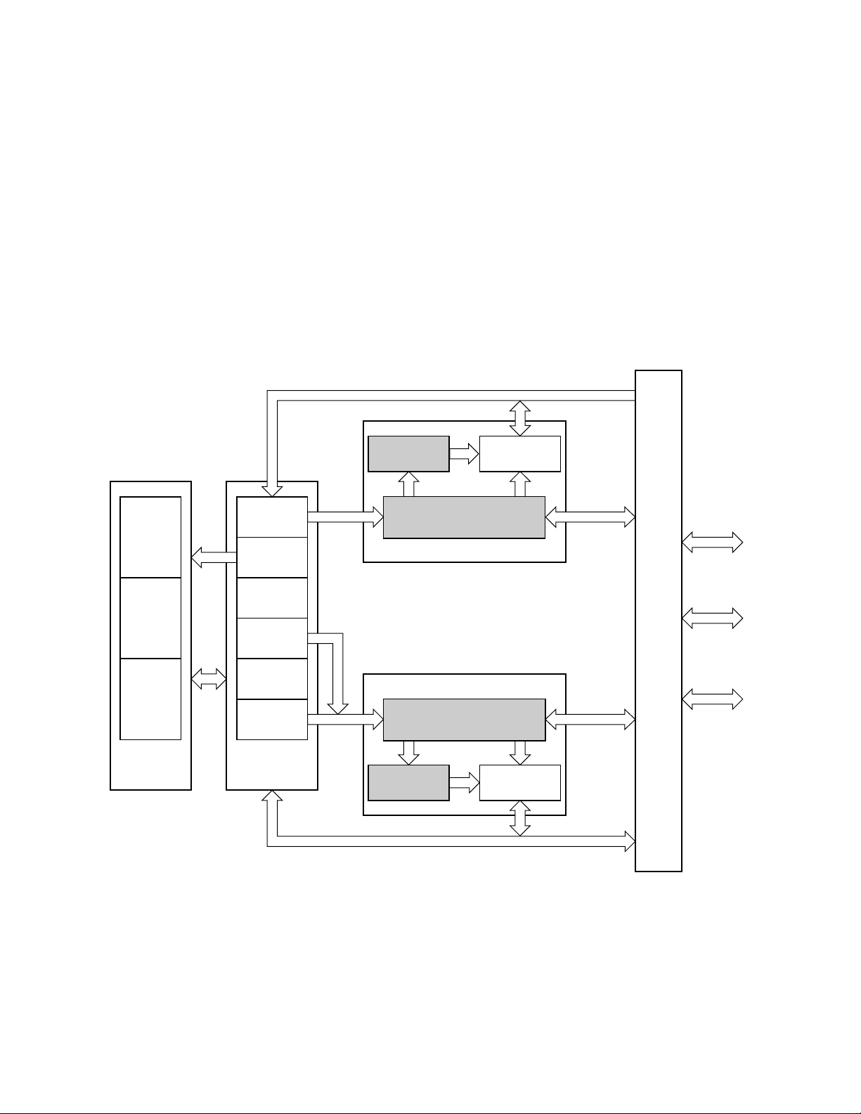
Freescale Semiconductor, Inc.
indexing into the on-chip instruction and data caches . The MMU MDIS signal dynamically
disables address translation for emulation and diagnostic support.
Figure 3-1 illustrates the MMUs contained in the two memory units, one for instructions
(supporting instruction prefetches) and one for data (supporting all other accesses). Each
unit contains an MMU, main cache, and snoop controller. The corresponding MMUs
contain two transparent translation registers, which identify blocks of memory that can be
accessed without translation. The MMUs also contain control logic and corresponding
address translation caches (ATCs) in which recently used logical-to-physical address
translations are stored. The data memory unit contains a data write and data read buffer,
and the instruction memory unit contains an instruction line read buffer. These buffers
temporarily hold data until an opportune moment arises to write the data to external
memory or read the operand/instruction into the integer unit.
nc...
I
INSTRUCTION
CONVERT
EXECUTE
cale Semiconductor,
Frees
WRITE-
BACK
FLOATING-
POINT
UNIT
FETCH
DECODE
EA
CALCULATE
EA
FETCH
EXECUTE
WRITE-
BACK
INTEGER
UNIT
INSTRUCTION DATA BUS
INSTRUCTION
ATC
INSTRUCTION
MMU/CACHE/SNOOP
CONTROLLER
INSTRUCTION MEMORY UNIT B
DATA MEMORY UNIT
MMU/CACHE/SNOOP
CONTROLLER
DATA
ATC
DATA
INSTRUCTION
CACHE
INSTRUCTION
ADDRESS
DATA
ADDRESS
DATA
CACHE
ADDRESS
U
S
C
O
N
T
R
O
L
L
E
R
BUS
DATA
BUS
BUS
CONTROL
SIGNALS
OPERAND DATA BUS
Figure 3-1. Memory Management Unit
The principal MMU function is to translate logical addresses to physical addresses using
translation tables stored in memory. As the MMU receives a logical address from the
integer unit, it searches its ATC for the corresponding physical address using the upper
3-2 M68040 USER'S MANUAL MOTOROLA
For More Information On This Product,
Go to: www.freescale.com
Page 52

Freescale Semiconductor, Inc.
logical address bits. If the translation is resident, the MMU provides the physical address
to the cache controller, which determines if the instruction or data being accessed is
cached. The cache controller uses the lower address bits to index into memory. An
external bus cycle is performed only when explicitly requested by the cache controller.
When the translation is not in the ATC, the MMU searches the translation tables in
memory for the translation information. Microcode and dedicated logic perform the
address calculations and bus cycles required for this search.
3.1 MEMORY MANAGEMENT PROGRAMMING MODEL
The memory management programming model is part of the supervisor programming
model for the M68040. The eight registers that control and provide status information for
address translation in the M68040 are: the user root pointer register (URP), the supervisor
root pointer register (SRP), the translation control register (TCR), four independent
transparent translation registers (ITT0, ITT1, DTT0, and DTT1), and the MMU status
nc...
I
register (MMUSR). Only programs that execute in the supervisor mode can directly
access these registers. Figure 3-2 illustrates the memory management programming
model.
cale Semiconductor,
Frees
31 0
31 0
15
31 0
31 0
31 0
31 0
31
URP
SRP
0
TCR
DTTR0
DTTR1
ITTR0
ITTR1
0
MMUSR
USER ROOT POINTER REGISTER
SUPERVISOR ROOT POINTER REGISTER
TRANSLATION CONTROL REGISTER
DATA TRANSPARENT TRANSLATION REGISTER 0
DATA TRANSPARENT TRANSLATION REGISTER 1
INSTRUCTION TRANSPARENT TRANSLATION
REGISTER 0
INSTRUCTION TRANSPARENT TRANSLATION
REGISTER 1
MMU STATUS REGISTER
Figure 3-2. Memory Management Programming Model
3.1.1 User and Supervisor Root Pointer Registers
The SRP and URP registers each contain the physical address of the translation table’s
root, which the MMU uses for supervisor and user accesses, respectively. The URP points
to the translation table for the current user task. When a new task begins execution, the
operating system typically writes a new root pointer to the URP. A new translation table
address implies that the contents of the ATCs may no longer be valid. A PFLUSH
instruction should be executed to flush the ATCs before loading a new root pointer value,
if necessary. Figure 3-3 illustrates the format of the 32-bit URP and SRP registers. Bits 8–
MOTOROLA M68040 USER'S MANUAL 3-3
For More Information On This Product,
Go to: www.freescale.com
Page 53

Freescale Semiconductor, Inc.
0 of an address loaded into the URP or the SRP must be zero. Transfers of data to and
from these 32-bit registers are long-word transfers.
31 98 0
USER ROOT POINTER 000000000
SUPERVISOR ROOT POINTER 000000000
Figure 3-3. URP and SRP Register Formats
3.1.2 Translation Control Register
The 16-bit TCR contains two control bits to enable paged address translation and to select
page size. The operating system must flush the ATCs before enabling address translation
nc...
I
since the TCR accesses and reset do not flush the ATCs. All unimplemented bits of this
register are read as zeros and must always be written as zeros. The M68040 always uses
word transfers to access this 16-bit register. The fields of the TCRs are defined following
Figure 3-4, which illustrates the TCR.
cale Semiconductor,
Frees
1514131211109876543210
EP00000000000000
NOTE: Bits 13–0 are undefined (reserved).
Figure 3-4. Translation Control Register Format
E—Enable
This bit enables and disables paged address translation.
0 = Disable
1 = Enable
A reset operation clears this bit. When translation is disabled, logical addresses are
used as physical addresses. The MMU instruction, PFLUSH, can be executed
successfully despite the state of the E-bit. PTEST results are undefined if the MMU is
disabled and no table search occurs. If translation is disabled and an access does not
match a transparent translation register (TTR), the access has the following default
attributes on the TTR: the caching mode is cachable/write-through, write protection is
disabled, and the user attribute signals (UPA1 and UPA0) are zero.
P—Page Size
This bit selects the memory page size.
0 = 4 Kbytes
1 = 8 Kbytes
A reset operation does not affect this bit. The bit must be initialized after a reset.
3-4 M68040 USER'S MANUAL MOTOROLA
For More Information On This Product,
Go to: www.freescale.com
Page 54

Freescale Semiconductor, Inc.
3.1.3 Transparent Translation Registers
The data transparent translation registers (DTTR0 and DTTR1) and instruction
transparent translation registers (ITTR0 and ITTR1) are 32-bit registers that define blocks
of logical address space. The TTRs operate independently of the E-bit in the TCR and the
state of the MDIS signal. Data transfers to and from these registers are long-word
transfers. The TTR fields are defined following Figure 3-5, which illustrates TTR format.
Bits 12–10, 7, 4, 3, 1, and 0 always read as zero.
31 2423 161514131211109876543210
LOGICAL ADDRESS BASE LOGICAL ADDRESS MASK E S-FIELD 0 0 0 U1 U0 0 C M 0 0 W 0 0
Figure 3-5. Transparent Translation Register Format
Logical Address Base
nc...
I
This 8-bit field is compared with address bits A31–A24. Addresses that match in this
comparison (and are otherwise eligible) are transparently translated.
cale Semiconductor,
Frees
Logical Address Mask
Since this 8-bit field contains a mask for the Logical Address Mask field, setting a bit in
this field causes the corresponding bit in the Logical Address Base field to be ignored.
Blocks of memory larger than 16 Mbytes can be transparently translated by setting
some of the logical address mask bits to ones. The low-order bits of this field can be set
to define contiguous blocks larger than 16 Mbytes.
E—Enable
This bit enables or disables transparent translation of the block defined by this register:
0 = Transparent translation disabled
1 = Transparent translation enabled
S—Supervisor Mode
This field specifies the way FC2 is used in matching an address:
00 = Match only if FC2 = 0 (user mode access)
01 = Match only if FC2 = 1 (supervisor mode access)
1X = Ignore FC2 when matching
U0, U1—User Page Attributes
The user defines these bits, and the M68040 does not interpret them. U0 and U1 are
echoed to the UPA0 and UPA1 signals, respectively, if an external bus transfer results
from an access. These bits can be programmed by the user to support external
addressing, bus snooping, or other applications.
MOTOROLA M68040 USER'S MANUAL 3-5
For More Information On This Product,
Go to: www.freescale.com
Page 55

Freescale Semiconductor, Inc.
CM—Cache Mode
This field selects the cache mode and access serialization as follows:
00 = Cachable, Write-through
01 = Cachable, Copyback
10 = Noncachable, Serialized
11 = Noncachable
Section 4 Instruction and Data Caches provides detailed information on caching
modes, and Section 7 Bus Operation provides information on serialization.
W—Write Protect
This bit indicates if the transparent block is write protected. If set, write and read-modifywrite accesses are aborted as if the resident bit in a table descriptor were clear.
0 = Read and write accesses permitted
1 = Write accesses not permitted
nc...
I
3.1.4 MMU Status Register
cale Semiconductor,
Frees
The MMUSR is a 32-bit register that contains the status information returned by execution
of the PTEST instruction. The PTEST instruction searches the translation tables to
determine status information about the translation of a specified logical address. Transfers
to and from the MMUSR are long-word transfers. The fields of the MMUSR are defined
following Figure 3-6, which illustrates the MMUSR.
31 1211109876543210
PHYSICAL ADDRESS B G U1 U0 S C M M O W T R
Figure 3-6. MMU Status Register Format
Physical Address
This 20-bit field contains the upper bits of the translated physical address. Merging
these bits with the lower bits of the logical address forms the actual physical address.
Bit 12 is undefined if a PTEST is executed with 8-Kbyte pages selected.
B—Bus Error
The B-bit is set if a transfer error is encountered during the table search for the PTEST
instruction. If the B-bit is set, all other bits are zero.
G—Global
This bit is set if the G-bit is set in the page descriptor.
U1, U0—User Page Attributes
These bits are set if corresponding bits in the page descriptor are set.
3-6 M68040 USER'S MANUAL MOTOROLA
For More Information On This Product,
Go to: www.freescale.com
Page 56

Freescale Semiconductor, Inc.
S—Supervisor Protection
This bit is set if the S-bit in the page descriptor is set. Setting this bit does not indicate
that a violation has occurred.
CM—Cache Mode
This 2-bit field is copied from the CM bits in the page descriptor.
M—Modified
This bit is set if the M-bit is set in the page descriptor associated with the address.
W—Write Protect
This bit is set if the W-bit is set in any of the descriptors encountered during the table
search. Setting this bit does not indicate that a violation has occurred.
nc...
I
cale Semiconductor,
Frees
T—Transparent Translation Register Hit
If the T-bit is set, then the PTEST address matches an instruction or data TTR, the R-bit
is set, and all other bits are zero.
R—Resident
The R-bit is set if the PTEST address matches an instruction or data TTR or if the table
search completes by obtaining a valid page descriptor.
3.2 LOGICAL ADDRESS TRANSLATION
The function of the MMUs is to translate logical addresses to physical addresses. The
MMUs perform translations according to control information in translation tables. The
operating system creates these translation tables and stores them in memory. The
processor then fetches a translation table as needed and stores it in an ATC.
3.2.1 Translation Tables
The M68040 uses the ATCs in the instruction and data memory units with translation
tables stored in memory to perform the translations from logical to physical addresses.
The operating system loads the translation tables for a program into memory. No
distinction is made in the translation of instruction accesses versus data accesses
because the instruction and data MMUs access the same translation table for a specific
privilege mode, either user or supervisor. This lack of distinction results in a merged
instruction and data address space.
Figure 3-7 illustrates the three-level tree structure of a general translation table supported
by the M68040. The root- and pointer-level tables contain the base addresses of the
tables at the next level. The page-level tables contain either the physical address for the
translation or a pointer to the memory location containing the physical address. Only a
portion of the translation table for the entire logical address space is required to be
resident in memory at any time—specifically, only the portion of the table that translates
MOTOROLA M68040 USER'S MANUAL 3-7
For More Information On This Product,
Go to: www.freescale.com
Page 57
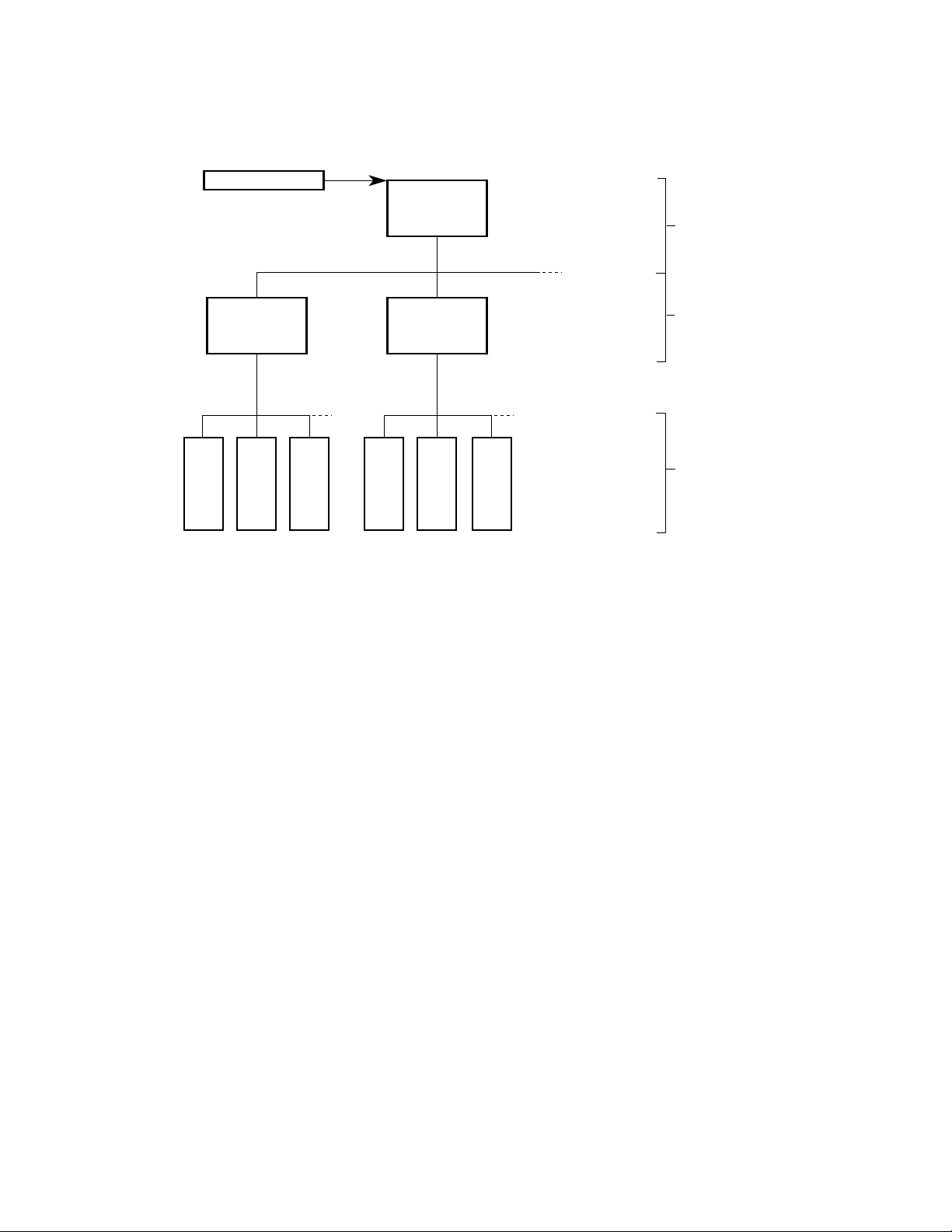
Freescale Semiconductor, Inc.
the logical addresses of the currently executing process. Portions of translation tables can
be dynamically allocated as the process requires additional memory.
ROOT POINTER
nc...
I
cale Semiconductor,
Frees
FIRST
LEVEL
SECOND
LEVEL
THIRD
LEVEL
ROOT
TABLES
POINTER
TABLES
PAGE
TABLES
Figure 3-7. Translation Table Structure
The current privilege mode determines the use of the URP or SRP for translation of the
access. The root pointer contains the base address of the translation table’s root-level
table. The translation table consists of tables of descriptors. The table descriptors of the
root- and pointer-levels can be either resident or invalid. The page descriptors of the pagelevel table can be resident, indirect, or invalid. A page descriptor defines the physical
address of a page frame in memory that corresponds to the logical address of a page. An
indirect descriptor, which contains a pointer to the actual page descriptor, can be used
when two or more logical addresses access a single page descriptor.
The table search uses logical addresses to access the translation tables. Figure 3-8
illustrates a logical address format, which is segmented into four fields: root index (RI),
pointer index (PI), page index (PGI) , and page offset. The first three fields extracted from
the logical address index the base address for each table level. The seven bits of the
logical address RI field are multiplied by 4 or shifted to the left by two bits. This sum is
concatenated with the upper 23 bits of the appropriate root pointer (URP or SRP) to yield
the physical address of a root-level table descriptor. Each of the 128 root-level table
descriptors corresponds to a 32-Mbyte block of memory and points to the base of a
pointer-level table.
3-8 M68040 USER'S MANUAL MOTOROLA
For More Information On This Product,
Go to: www.freescale.com
Page 58

Freescale Semiconductor, Inc.
31 25 24 18 17 13 12 11 0
7 BITS
7 BITS
8K PAGE
4K PAGE
8K PAGE
4K PAGE
nc...
I
cale Semiconductor,
Frees
ROOT INDEX FIELD
(RI)
POINTER INDEX FIELD
(PI)
PAGE INDEX FIELD
(PGI)
PAGE OFFSET
Figure 3-8. Logical Address Format
The seven bits of a logical address PI field are multiplied by 4 (shifted to the left by two
bits) and concatenated with the fetched root-level descriptor’s upper 23 bits to produce the
physical address of the pointer-level table descriptor. Each of the 128 pointer-level table
descriptors corresponds to a 256-Kbyte block of memory.
For 8-Kbyte pages, the five bits of the PGI field are multiplied by 4 (shifted to the left by
two bits) and concatenated with the fetched pointer-level descriptor’s upper 25 bits to
produce the physical address of the 8-Kbyte page descriptor. The upper 19 bits of the
page descriptor are the page frame’s physical address. There are 32 8-Kbyte page
descriptors in a page-level table.
Similarly, for 4-Kbyte pages, the six bits of the PGI field are multiplied by 4 (shifted to the
left by two bits) and concatenated with the fetched pointer-level descriptor’s upper 24 bits
to produce the physical address of the 4-Kbyte page descriptor. The upper 20 bits of the
page descriptor are the page frame’s physical address. There are 64 4-Kbyte page
descriptors in a page-level table.
Write-protect status is accumulated from each level’s descriptor and combined with the
status from the page descriptor to form the ATC entry status. The M68040 creates the
ATC entry from the page frame address and the associated status bits and retries the
original bus access. Refer to 3.3 Address Translation Caches for details on ATC entries.
If the descriptor from a page table is an indirect descriptor, the page descriptor pointed to
by this descriptor is fetched. Invalid descriptors can be used at any level of the tree except
the root. When a table search for a normal translation encounters an invalid descriptor, the
processor takes an access fault exception. The invalid descriptor can be used to identify
either a page or branch of the tree that has been stored on an external device and is not
resident in memory or a portion of the translation table that has not yet been defined. In
these two cases, the exception routine can either restore the page from disk or add to the
translation table. Figures 3-9 and 3-10 illustrate detailed flowcharts of table search and
descriptor fetch operations.
A table search terminates successfully when a page descriptor is encountered. The
occurrence of an invalid descriptor or a transfer error acknowledge also terminates a table
search, and the M68040 takes an exception on the retry of the cycle because of these
conditions. The exception handler should distinguish between anticipated conditions and
true error conditions. The exception handler can correct an invalid descriptor that indicates
a nonresident page or one that identifies a portion of the translation table yet to be
allocated. An access error due to a system malfunction can require the exception handler
to write an error message and terminate the task.
MOTOROLA M68040 USER'S MANUAL 3-9
For More Information On This Product,
Go to: www.freescale.com
Page 59

Freescale Semiconductor, Inc.
ENTRY
SELECT ROOT POINTER
FC2 = 0:URP, 1:SRP
(INITIALIZE ACCRUED
STATUS)
➧
WP 0
UPDATE FALSE
TYPE 'POINTER'
(CHECK DESCRIPTOR TYPE)
➧
➧
FETCH ROOT
DESCRIPTOR
nc...
I
cale Semiconductor,
Frees
'INVALID'
'INVALID'
'INVALID'
OTHERWISE
CREATE ATC ENTRY
WITH R-BIT CLEAR
'RESIDENT'
FETCH POINTER
DESCRIPTOR
(CHECK DESCRIPTOR TYPE)
'RESIDENT'
➧
TYPE 'PAGE'
FETCH PAGE
DESCRIPTOR
(CHECK DESCRIPTOR TYPE)
'INDIRECT'
➧
TYPE 'INDIRECT'
FETCH INDIRECT
DESCRIPTOR
(CHECK DESCRIPTOR TYPE)
'RESIDENT'
'RESIDENT'
PFA = PHYSICAL ADDRESS
FIELD OF DESCRIPTOR
EXIT TABLE SEARCH
ABBREVIATIONS:
PFA - PAGE FRAME ADDRESS
DF[ ] - DESCRIPTOR FIELD
WP - ACCUMULATED WRITE-
PROTECTION STATUS
➧
ASSIGNMENT OPERATOR
CREATE ATC ENTRY WITH R-BIT SET
ATC TAG FC2, LA, DF[G]
ATC ENTRY PFA, DF[U1,U0,S,CM,M],WP
➧
➧
EXIT TABLE SEARCH
Figure 3-9. Detailed Flowchart of Table Search Operation
3-10 M68040 USER'S MANUAL MOTOROLA
For More Information On This Product,
Go to: www.freescale.com
Page 60

Freescale Semiconductor, Inc.
FETCH DESCRIPTOR &
UPDATE HISTORY AND STATUS
nc...
I
cale Semiconductor,
Frees
CREATE ATC ENTRY
WITH R-BIT CLEAR
EXIT TABLE SEARCH
'INVALID'
RETURN
WRITE ACCESS
(SEE NOTE)
TYPE = 'PAGE' OR 'POINTER'
FETCH DESCRIPTOR
AT PA = TA + (INDEX*4)
(INDEX = RI, PI, OR PGI)
IF SCHEDULED, EXECUTE
WRITE ACCESS (U 1) FOR
PREVIOUS DESCRIPTOR
(SEE NOTE)
OTHERWISE
WP = WP V W
U = 0
SCHEDULE
➧
U 1
➧
TYPE =
'POINTER'
U = 1
RETURN
TYPE = 'INDIRECT'
PA = DESCRIPTOR ADDRESS
NORMAL TERMINATION
OF ALL BUS TRANSFERS
TYPE = 'PAGE'
OR 'INDIRECT'
READ ACCESS
U = 0
U = 1
FETCH DESCRIPTOR AT
'INVALID'
OR 'INDIRECT'
'RESIDENT''RESIDENT'
WP = WP V W
WRITE ACCESS
U = 0 &
(WP = 1 OR M = 1)
WP = 0 & M = 0
EXECUTE
LOCKED
RMW ACCESS
➧
U 1
WRITE ACCESS
EXECUTE
➧
U 1, M 1
RETURN
U = 1 &
(WP = 1 OR M = 1)
➧
DUE TO ACCESS PIPELINING, A POINTER
NOTE :
DESCRIPTOR WRITE ACCESS TO UPDATE
THE U-BIT OCCURS AFTER THE READ OF
THE NEXT LEVEL DESCRIPTOR.
ABBREVIATIONS:
WP – ACCUMULATED WRITE PROTECTION STATUS
V
– LOGICAL "OR" OPERATOR
➧
– ASSIGNMENT OPERATOR
NORMAL TERMINATION
OF ALL BUS TRANSFERS
RETURN
OTHERWISE
CREATE ATC ENTRY
WITH R-BIT CLEAR
EXIT TABLE SEARCH
Figure 3-10. Detailed Flowchart of Descriptor Fetch Operation
MOTOROLA M68040 USER'S MANUAL 3-11
For More Information On This Product,
Go to: www.freescale.com
Page 61

Freescale Semiconductor, Inc.
Motorola highly recommends that the translation tables be placed in cache-inhibited
memory space. Motorola also highly recommends table descriptors must not be left in
states that are incoherent to the processor. Future processors may treat these
recommendations as mandatory. The following paragraphs apply only to M68040 systems
that cannot meet these recommendations.
The processor never allocates table descriptors in the data cache when the processor
performs a table search. Only normal accesses to the translation tables cause descriptors
to be allocated in the data cache. If table descriptors are allocated in the data cache and
the cache is disabled, the processor locks up trying to access a cached descriptor during
a table search. Ensuring that the data cache is invalidated before enabling the MMU or
disabling the data cache and ensuring that the pages containing table descriptors are
pushed and invalidated prevents lockup during table searches.
Table and page descriptors must not be left in a state that is incoherent to the processor.
Violation of this restriction can result in an undefined operation. Page descriptors must not
nc...
I
have an encoding of U-bit = 0, M-bit = 1 and PDT field = 01 or 11. This encoding indicates
that the page descriptor is resident, not used, and modified. The processor’s table search
algorithm never leaves a descriptor in this state. This state is possible through direct
manipulation by the operating system for this specific instance. A table search for a
MOVE16 write can corrupt the cache line being written if the table descriptors are marked
copyback.
cale Semiconductor,
Frees
3.2.2 Descriptors
There are two types of descriptors used in the translation tables, table and page. Tableand page-level descriptors can be further divided into types of descriptors. Root table
descriptors are used in root-level tables and pointer table descriptors are used in pointerlevel tables. Descriptors in the page-level tables contain either a page descriptor for the
translation or an indirect descriptor that points to a memory location containing the page
descriptor. The P-bit in the TCR selects the page size as either 4 or 8 Kbytes.
3.2.2.1 TABLE DESCRIPTORS. Figure 3-11 illustrates the formats of the root and pointer
table descriptors. Two descriptor formats are possible at the pointer-level tables to support
4-Kbyte and 8-Kbyte page sizes.
3-12 M68040 USER'S MANUAL MOTOROLA
For More Information On This Product,
Go to: www.freescale.com
Page 62

Freescale Semiconductor, Inc.
31 9876543210
POINTER TABLE ADDRESS XXXXXUW UDT
ROOT TABLE DESCRIPTOR (ROOT LEVEL)
31 876543210
PAGE TABLE ADDRESS XXXXUW UDT
4K POINTER TABLE DESCRIPTOR (POINTER LEVEL)
31 76543210
PAGE TABLE ADDRESS X X X U W UDT
8K POINTER TABLE DESCRIPTOR (POINTER LEVEL)
Figure 3-11. Table Descriptor Formats
nc...
I
cale Semiconductor,
Frees
3.2.2.2 PAGE DESCRIPTORS. Figure 3-12 illustrates the page descriptors for both
4-Kbyte and 8-Kbyte page sizes. Refer to Section 4 Instruction and Data Caches for
details concerning caching page descriptors.
31 1211109876543210
PHYSICAL ADDRESS UR G U1 U0 S CM M U W PDT
4K PAGE DESCIPTOR (PAGE LEVEL)
31 131211109876543210
PHYSICAL ADDRESS UR UR G U1 U0 S CM M U W PDT
8K PAGE DESCRIPTOR (PAGE LEVEL)
31 210
DESCRIPTOR ADDRESS PDT
INDIRECT PAGE DESCRIPTOR (PAGE LEVEL)
Figure 3-12. Page Descriptor Formats
3.2.2.3 DESCRIPTOR FIELD DEFINITIONS. The field definitions for the table- and page-
level descriptors are listed in alphabetical order:
CM—Cache Mode
This field selects the cache mode and accesses serialization as follows:
00 = Cachable, Write-through
01 = Cachable, Copyback
10 = Noncachable, Serialized
11 = Noncachable
Section 4 Instruction and Data Caches provides detailed information on caching
modes, and Section 7 Bus Operation provides information on serialization.
MOTOROLA M68040 USER'S MANUAL 3-13
For More Information On This Product,
Go to: www.freescale.com
Page 63

Freescale Semiconductor, Inc.
Descriptor Address
This 30-bit field, which contains the physical address of a page descriptor, is only used
in indirect descriptors.
G—Global
When this bit is set, it indicates the entry is global. PFLUSH instruction variants that
specify nonglobal entries do not invalidate global entries, even when all other selection
criteria are satisfied. If these PFLUSH variants are not used, then system software can
use this bit.
M—Modified
This bit identifies a modified page. The M68040 sets the M-bit in the corresponding
page descriptor before a write operation to a page for which the M-bit is clear, except for
write-protect or supervisor violations. The read portion of a read-modify-write access is
considered a write for updating purposes. The M68040 never clears this bit.
nc...
I
PDT—Page Descriptor Type
cale Semiconductor,
Frees
This field identifies the descriptor as an invalid descriptor, a page descriptor for a
resident page, or an indirect pointer to another page descriptor.
00 = Invalid
This code indicates that the descriptor is invalid. An invalid descriptor can
represent a nonresident page or a logical address range that is out of
bounds. All other bits in the descriptor are ignored. When an invalid
descriptor is encountered, an ATC entry is created for the logical address
with the resident bit in the MMUSR clear.
01 or 11 = Resident
These codes indicate that the page is resident.
10 = Indirect
This code indicates that the descriptor is an indirect descriptor. Bits 31–2
contain the physical address of the page descriptor. This encoding is invalid
for a page descriptor pointed to by an indirect descriptor.
Physical Address
This 20-bit field contains the physical base address of a page in memory. The logical
address supplies the low-order bits of the address required to index into the page.
When the page size is 8-Kbyte, the least significant bit of this field is not used.
S—Supervisor Protected
This bit identifies a page as supervisor only. Only programs operating in the supervisor
mode are allowed to access the portion of the logical address space mapped by this
descriptor when the S-bit is set. If the bit is clear, both supervisor and user accesses are
allowed.
3-14 M68040 USER'S MANUAL MOTOROLA
For More Information On This Product,
Go to: www.freescale.com
Page 64

Freescale Semiconductor, Inc.
Page Table Address
This field contains the physical base address of a table of page descriptors. The low order bits of the address required to index into the page table are supplied by the logical
address.
U—Used
The processor automatically sets this bit when a descriptor is accessed in which the
U-bit is clear. In a page descriptor table, this bit is set to indicate that the page
corresponding to the descriptor has been accessed. In a pointer table, this bit is set to
indicate that the pointer has been accessed by the M68040 as part of a table search.
The U-bit is updated before the M68040 allows a page to be accessed. The processor
never clears this bit.
U0, U1—User Page Attributes
These bits are user defined and the processor does not interpret them. U0 and U1 are
nc...
I
echoed to the UPA0 and UPA1 signals, respectively, if an external bus transfer results
from the access. Applications for these bits include extended addressing and snoop
protocol selection.
cale Semiconductor,
Frees
UDT—Upper Level Descriptor Type
These bits indicate whether the next level table descriptor is resident.
00 or 01 = Invalid
These codes indicate that the table at the next level is not resident or that
the logical address is out of bounds. All other bits in the descriptor are
ignored. When an invalid descriptor is encountered, an ATC entry is created
for the logical address with the resident bit in the MMUSR clear.
10 or 11 = Resident
These codes indicate that the page is resident.
UR—User Reserved
These single bit fields are reserved for use by the user.
W—Write Protected
Setting the W-bit in a table descriptor write protects all pages accessed with that
descriptor. When the W-bit is set, a write access or a read-modify-write access to the
logical address corresponding to this entry causes an access error exception to be
taken.
X—Motorola Reserved
These bit fields are reserved for future use by Motorola.
MOTOROLA M68040 USER'S MANUAL 3-15
For More Information On This Product,
Go to: www.freescale.com
Page 65

Freescale Semiconductor, Inc.
3.2.3 Translation Table Example
Figure 3-13 illustrates an access example to the logical address $76543210 while in the
supervisor mode with an 8-Kbyte memory page size. The RI field of the logical address,
$3B, is mapped into bits 8–2 of the SRP value to select a 32-bit root table descriptor at a
root-level table. The selected root table descriptor points to the base of a pointer-level
table, and the PI field of the logical address, $15, is mapped into bits 8–2 of this base
address to select a pointer descriptor within the table. This pointer table descriptor points
to the base of a page-level table, and the PGI field of the logical address, $1, is mapped
into bits 6–2 of this base address to select a page descriptor within the table.
3.2.4 Variations in Translation Table Structure
Several aspects of the MMU translation table structure are software configurable, allowing
the system designer flexibility to optimize the performance of the MMUs for a particular
system. The following paragraphs discuss the variations of the translation table structure.
nc...
I
cale Semiconductor,
3.2.4.1 INDIRECT ACTION. The M68040 provides the ability to replace an entry in a page
table with a pointer to an alternate entry. The indirection capability allows multiple tasks to
share a physical page while maintaining only a single set of history information for the
page (i.e., the modified indication is maintained only in the single descriptor). The
indirection capability also allows the page frame to appear at arbitrarily different addresses
in the logical address spaces of each task.
Frees
3-16 M68040 USER'S MANUAL MOTOROLA
For More Information On This Product,
Go to: www.freescale.com
Page 66

Freescale Semiconductor, Inc.
LOGICAL ADDRESS
ROOT INDEX POINTER INDEX PAGE INDEX
$76543210 =
TABLE ENTRY # =
ADDRESS OFFSET =
nc...
I
SUPERVISOR
MODE
0111011001010100001XXXXXXXXXXXXX
$3B
$EC
SRP
$3B
$15
$54
TABLE $00
$00001800
ROOT LEVEL
TABLES
$01
$04
TABLE $00
TABLE $3B
$00003000
$15
TABLE $7F TABLE $1F
POINTER LEVEL
TABLES
Figure 3-13. Example Translation Table
cale Semiconductor,
Using the indirection capability, single entries or entire tables can be shared between
multiple tasks. Figure 3-14 illustrates two tasks sharing a page using indirect descriptors.
PAGE OFFSET
$01
TABLE $00
TABLE $15
FRAME ADDRESS
PAGE LEVEL
TABLES
Frees
When the M68040 has completed a normal table search, it examines the PDT field of the
last entry fetched from the page tables. If the PDT field contains an indirect ($2) encoding,
it indicates that the address contained in the highest order 30 bits of the descriptor is a
pointer to the page descriptor that is to be used to map the logical address. The processor
then fetches the page descriptor from this address and uses the physical address field of
the page descriptor as the physical mapping for the logical address.
The page descriptor located at the address given by the indirect descriptor must not have
a PDT field with an indirect encoding (it must be either a resident descriptor or invalid).
Otherwise, the descriptor is treated as invalid, and the M68040 creates an ATC entry with
a signaled error condition (R-bit in MMUSR is clear).
MOTOROLA M68040 USER'S MANUAL 3-17
For More Information On This Product,
Go to: www.freescale.com
Page 67

Freescale Semiconductor, Inc.
LOGICAL ADDRESS
nc...
I
cale Semiconductor,
Frees
$76543210 =
TABLE ENTRY # =
ADDRESS OFFSET =
TASK A
TASK B
ROOT INDEX POINTER INDEX PAGE INDEX
0111011001010100001XXXXXXXXXXXXX
$3B
$EC
ROOT POINTER
$3B
ROOT POINTER
$15
$54
TABLE $00
$00001800
ROOT-LEVEL
TABLES
$01
$04
TABLE $00
TABLE $3B
$00003000
$15
TABLE $7F TABLE $1F
POINTER-LEVEL
TABLES
PAGE OFFSET
$01
TABLE $00
TABLE $15
$80000010
FRAME ADDRESS
PAGE-LEVEL
TABLES
Figure 3-14. Translation Table Using Indirect Descriptors
3.2.4.2 TABLE SHARING BETWEEN TASKS. More than one task can share a pointer- or
page-level table by placing a pointer to a shared table in the address translation tables.
The upper (nonshared) tables can contain different write-protected settings, allowing
different tasks to use the memory areas with different write permissions. In Figure 3-15,
two tasks share the memory translated by the table at the pointer table level. Task A
cannot write to the shared area; task B, however, has the W-bit clear in its pointer to the
shared table so that it can read and write the shared area. Also, the shared area appears
at different logical addresses for each task. Figure 3-15 illustrates shared tables in a
translation table structure.
3-18 M68040 USER'S MANUAL MOTOROLA
For More Information On This Product,
Go to: www.freescale.com
Page 68
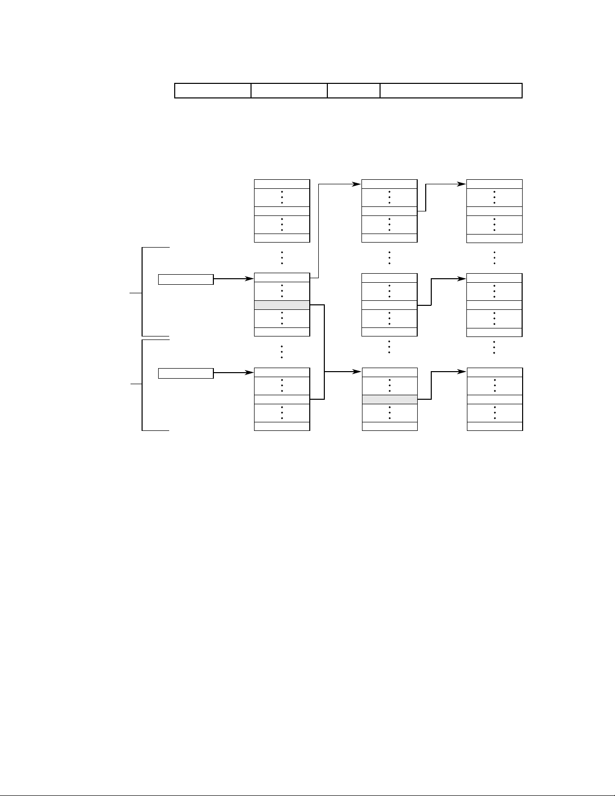
Freescale Semiconductor, Inc.
LOGICAL ADDRESS
nc...
I
cale Semiconductor,
Frees
ROOT INDEX POINTER INDEX PAGE INDEX
$76543210 =
TABLE ENTRY # =
ADDRESS OFFSET =
TASK A
TASK B
* Page frame address shared by task A and B; write protected from task A.
0111011001010100001XXXXXXXXXXXXX
$3B
$EC
ROOT POINTER
$3B
ROOT POINTER
$15
$54
TABLE $00
W-BIT SET
W-BIT CLEAR
ROOT-LEVEL
TABLES
$01
$04
TABLE $00
TABLE $3B TABLE $15
$15
$00003000
POINTER-LEVEL
TABLES
PAGE OFFSET
$01
TABLE $00
FRAME ADDRESS*
PAGE-LEVEL
TABLES
Figure 3-15. Translation Table Using Shared Tables
3.2.4.3 TABLE PAGING . The entire translation table for an active task need not be
resident in main memory. In the same way that only the working set of pages must be
allocated in main memory, only the tables that describe the resident set of pages need be
available. Placing the invalid code ($0 or $1) in the UDT field of the table descriptor that
points to the absent table(s) implements this paging of tables. When a task attempts to
use an address that an absent table would translate, the M68040 is unable to locate a
translation and takes access error exception when the execution unit retries the bus
access that caused the table search to be initiated.
The operating system determines that the invalid code in the descriptor corresponds to
nonresident tables. This determination can be facilitated by using he unused bits in the
descriptor to store status information concerning the invalid encoding. The M68040 does
not interpret or modify an invalid descriptor’s fields except for the UDT field. This
MOTOROLA M68040 USER'S MANUAL 3-19
For More Information On This Product,
Go to: www.freescale.com
Page 69
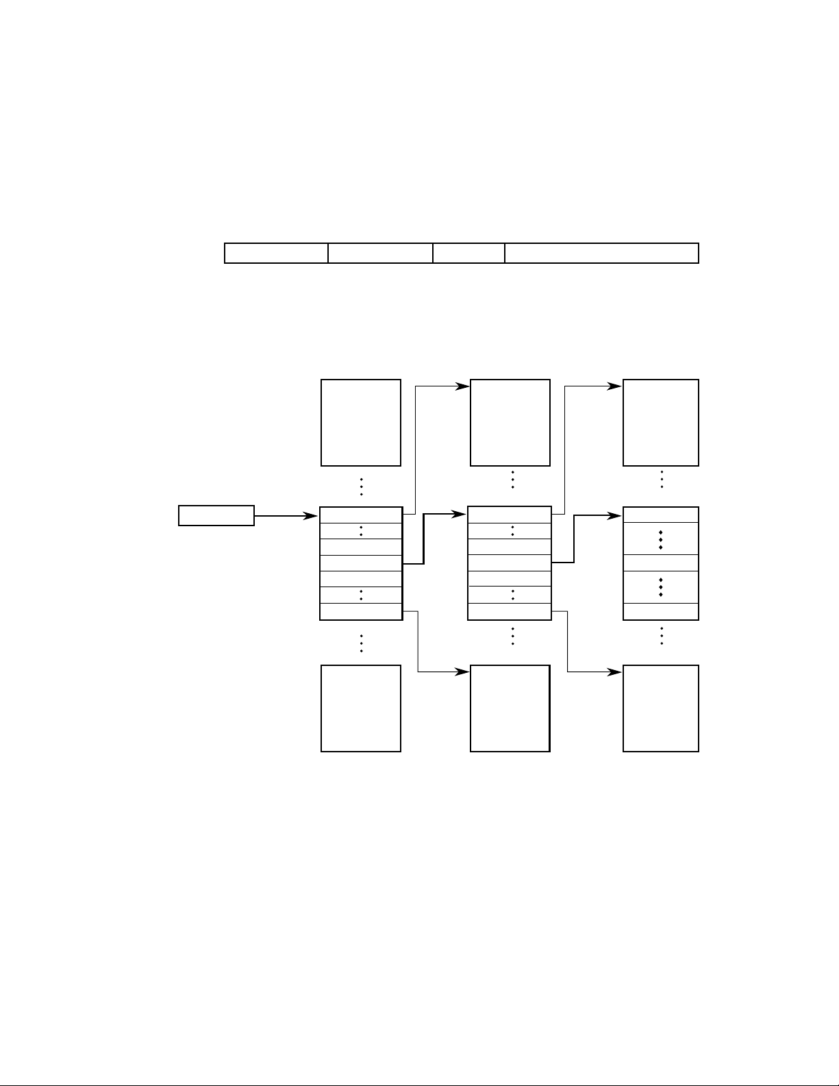
Freescale Semiconductor, Inc.
interpretation allows the operating system to store system-defined information in the
remaining bits. Information typically stored includes the reason for the invalid encoding
(tables paged out, region unallocated, etc.) and possibly the disk address for nonresident
tables. Figure 3-16 illustrates an address translation table in which only a single page
table (table $15) is resident; all other page tables are not resident.
LOGICAL ADDRESS
ROOT INDEX POINTER INDEX PAGE INDEX
$76543210 =
TABLE ENTRY # =
ADDRESS OFFSET =
nc...
I
0111011001010100001XXXXXXXXXXXXX
$15
$54
TABLE $00
(PAGED OR
UDT = INVALID
UDT = INVALID
$01
$04
NONRESIDENT
UNALLOCATED)
UDT = INVALID
UDT = INVALID
$15
UDT = RESIDENT
UDT = INVALID
UDT = INVALID
TABLE $00
(PAGED OR
TABLE $3B
TABLE $7F
SRP
$3B
$EC
SUPERVISOR
NONRESIDENT
UNALLOCATED)
UDT = INVALID
$3B
UDT = RESIDENT
UDT = INVALID
cale Semiconductor,
NONRESIDENT
(PAGED OR
UNALLOCATED)
NONRESIDENT
(PAGED OR
UNALLOCATED)
PAGE OFFSET
$01
TABLE $00
NONRESIDENT
(PAGED OR
UNALLOCATED)
TABLE $15
FRAME ADDRESS
TABLE $1F
NONRESIDENT
(PAGED OR
UNALLOCATED)
Frees
ROOT-LEVEL
TABLES
POINTER-LEVEL
TABLES
PAGE-LEVEL
TABLES
Figure 3-16. Translation Table with Nonresident Tables
3-20 M68040 USER'S MANUAL MOTOROLA
For More Information On This Product,
Go to: www.freescale.com
Page 70

Freescale Semiconductor, Inc.
3.2.4.4 DYNAMICALLY ALLOCATED TABLES. Similar to paged tables, a complete
translation table need not exist for an active task. The operating system can dynamically
allocate the translation table based on requests for access to particular areas.
As in demand paging, it is difficult, if not impossible, to predict the areas of memory that a
task uses over any extended period. Instead of attempting to predict the requirements of
the task, the operating system performs no action for a task until a demand is made
requesting access to a previously unused area or an area that is no longer resident in
memory. This technique can be used to efficiently create a translation table for a task.
For example, consider an operating system that is preparing the system to execute a
previously unexecuted task that has no translation table. Rather than guessing what the
memory-usage requirements of the task are, the operating system creates a translation
table for the task that maps one page corresponding to the initial value of the program
counter (PC) for that task and one page corresponding to the initial stack pointer of the
task. All other branches of the translation table for this task remain unallocated until the
nc...
I
task requests access to the areas mapped by these branches. This technique allows the
operating system to construct a minimal translation table for each task, conserving
physical memory utilization and minimizing operating system overhead.
cale Semiconductor,
Frees
3.2.5 Table Search Accesses
The cache treats table search accesses that are not read-modify-write accesses as
cachable/write-through but do not allocate in the cache for misses. Read-modify-write
table search accesses (required to update some descriptor U-bit and M-bit combinations)
are treated as noncachable and force a matching cache line to be pushed and invalidated.
Table search bus accesses are locked only for the specific portions of the table search
that requires a read-modify-write access.
During a table search, the U-bit in each encountered descriptor is checked and set if not
already set. Similarly, when the table search is for a write access and the M-bit of th e
page descriptor is clear, the processor sets the bit if the table search does not encounter a
set W-bit or a supervisor violation. Repeating the descriptor access as part of a readmodify-write access updates specific combinations of the U and M bits, allowing the
external arbiter to prevent the update operation from being interrupted.
The M68040 asserts the LOCK signal during certain portions of the table search to ensure
proper maintenance of the U-bit and M-bit. The U-bit and M-bit are updated before the
M68040 allows a page to be accessed or written. As descriptors are fetched, the U-bit and
M-bit are monitored. Write cycles modify these bits when required. For a table descriptor,
a write cycle that sets the U-bit occurs only if the U-bit was clear. Table 3-1 lists the page
descriptor update operations for each combination of U-bit, M-bit, write-protected, and
read or write access type.
MOTOROLA M68040 USER'S MANUAL 3-21
For More Information On This Product,
Go to: www.freescale.com
Page 71
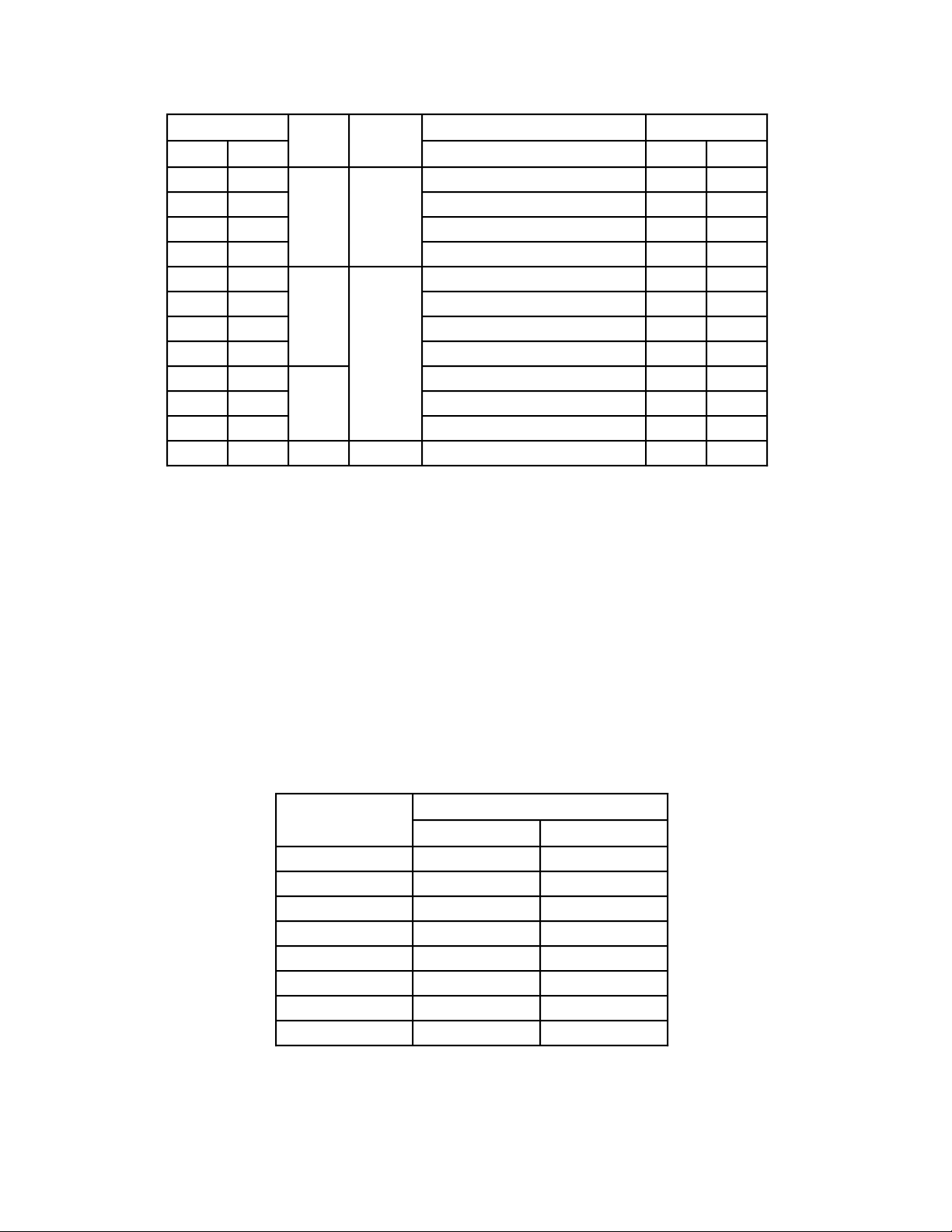
Freescale Semiconductor, Inc.
Table 3-1. Updating U-Bit and M-Bit for Page Descriptors
Previous Status Access Page Descriptor New Status
U-Bit M-Bit WP Bit
0 0 Locked RMW Access to Set U 1 0
0 1 Locked RMW Access to Set U 1 1
1 0 X Read None 1 0
1 1 None 1 1
0 0 Write to Set U and M 1 1
0 1 Locked RMW Access to Set U 1 1
1 0 0 Write to Set M 1 1
1 1 Write None 1 1
0 0 Locked RMW Access to Set U 1 0
0 1 Locked RMW Access to Set U 1 1
nc...
I
1 0 1 None 1 0
1 1 None 1 1
NOTE: WP indicates the accumulated write-protect status.
Type
Update Operation U-Bit M-Bit
cale Semiconductor,
Frees
An alternate address space access is a special case that is immediately used as a
physical address without translation. Because the M68040 implements a merged
instruction and data space, the integer unit translates MOVES accesses to instruction
address spaces (SFC/DFC = $6 or $2) into data references (SFC/DFC = $5 or $1). The
data memory unit handles these translated accesses as normal data accesses. If the
access fails due to an ATC fault or a physical bus error , the resulting access error stack
frame contains the converted function code in the TM field for the faulted access.
Invalidation of the instruction cache line containing the referenced location to maintain
cache coherency must precede MOVES accesses that write the instruction address
space. The SFC and DFC values and results are listed in Table 3-2.
Table 3-2. SFC and DFC Values
Results
SFC/DFC Value
000 10 000
001 00 001
010 00 001
011 10 011
100 10 100
101 00 101
110 00 101
111 10 111
TT TM
3-22 M68040 USER'S MANUAL MOTOROLA
For More Information On This Product,
Go to: www.freescale.com
Page 72

nc...
I
cale Semiconductor,
Frees
Freescale Semiconductor, Inc.
3.2.6 Address Translation Protection
The M68040 MMUs provide separate translation tables for supervisor and user address
spaces. The translation tables contain both mapping and protection information. Each
table and page descriptor includes a write-protect (W) bit that can be set to provide write
protection at any level. Page descriptors also contain a supervisor-only (S) bit that can
limit access to programs operating at the supervisor privilege level.
The protection mechanisms can be used individually or in any combination to protect:
• Supervisor address space from accesses by user programs.
• User address space from accesses by other user programs.
• Supervisor and user program spaces from write accesses (implicitly supported by
designating all memory pages used for program storage as write protected).
• One or more pages of memory from write accesses.
3.2.6.1 SUPERVISOR AND USER TRANSLATION TABLES. One way of protecting
supervisor and user address spaces from unauthorized accesses is to use separate
supervisor and user translation tables. Separate trees protect supervisor programs and
data from accesses by user programs and user programs and data from access by
supervisor programs. Access is granted to the supervisor programs that can accesses any
area of memory with MOVES. The translation table pointed to by the SRP is selected for
all other supervisor mode accesses. This translation table can be common to all tasks.
Figure 3-17 illustrates separate translation tables for supervisor accesses and for two user
tasks that share the common supervisor space. Each user task has an translation table
with unique mappings for the logical addresses in its user address space.
3.2.6.2 SUPERVISOR ONLY . A second mechanism protects supervisor programs and
data without requiring segmenting of the logical address space into supervisor and user
address spaces. Page descriptors contain S-bits to protect areas of memory from access
by user programs. When a table search for a user access encounters an S-bit set in a
page descriptor, the table search ends, and an ATC descriptor corresponding to the
logical address is created with the S-bit set. A subsequent retry of the user access results
in an access error exception being taken. The S-bit can be used to protect one or more
pages from user program access. Supervisor and user mode accesses can share
descriptors by using indirect descriptors or by sharing tables. The entire user and
supervisor address spaces can be mapped together by loading the same root pointer
address into both the SRP and URP registers.
MOTOROLA M68040 USER'S MANUAL 3-23
For More Information On This Product,
Go to: www.freescale.com
Page 73
Freescale Semiconductor, Inc.
FOR TASK 'A'
URP FOR TASK 'A'
FOR TASK 'B'
URP FOR TASK 'B'
nc...
I
POINTER
COMMON SRP
USER A LEVEL TABLE
•
•
•
USER A LEVEL TABLE
•
•
•
SUPERVISOR A LEVEL TABLE
•
•
•
TRANSLATION
TABLE FOR
TASK 'A'
TRANSLATION
TABLE FOR
TASK 'B'
TRANSLATION
TABLE FOR
ALL SUPERVISOR
ACCESSES
cale Semiconductor,
Frees
Figure 3-17. Translation Table Structure for Two Tasks
3.2.6.3 WRITE PROTECT. The M68040 provides write protection independent of other
protection mechanisms. All table and page descriptors contain W-bits to protect areas of
memory from write accesses of any kind, including supervisor writes. An ATC descriptor
corresponding to the logical address is created with the W-bit set after the table search is
completed when a table search encounters a W-bit set in any table or page descriptor.
The subsequent retry of the write access results in an access error exception being taken.
The W-bit can be used to protect the entire area of memory defined by a branch of the
translation table or protect only one or more pages from write accesses. Figure 3-18
illustrates a memory map of the logical address space organized to use supervisor-only
and write-protect bits for protection. Figure 3-19 illustrates an example translation table for
this technique.
SUPERVISOR AND USER SPACE
THIS AREA IS SUPERVISOR ONLY, READ-ONLY
THIS AREA IS SUPERVISOR ONLY, READ/WRITE
THIS AREA IS SUPERVISOR OR USER, READ-ONLY
THIS AREA IS SUPERVISOR OR USER, READ/WRITE
Figure 3-18. Logical Address Map with Shared
Supervisor and User Address Spaces
3-24 M68040 USER'S MANUAL MOTOROLA
For More Information On This Product,
Go to: www.freescale.com
Page 74

Freescale Semiconductor, Inc.
nc...
I
THIS PAGE
SUPERVISOR ONLY,
READ ONLY
W = X
W = 0 S = 1,W = 0
S = 1,W = X
THIS PAGE
SUPERVISOR ONLY,
READ/WRITE
cale Semiconductor,
Frees
THIS PAGE
SUPERVISOR/USER,
PRIVILEGE
MODE
URP & SRP POINT
TO SAME A LEVEL
NOTE: X = Don’t care.
SRP
URP
TABLE
W =1
W = 0
W = 1
W = 0
ROOT-LEVEL
TABLE
W = X
W = 0 S = 0,W = 0
POINTER-LEVEL
TABLE
READ ONLY
S = 0,W = X
THIS PAGE
SUPERVISOR/USER,
READ/WRITE
PAGE-LEVEL
TABLE
Figure 3-19. Translation Table Using S-Bit and W-Bit To Set Protection
MOTOROLA M68040 USER'S MANUAL 3-25
For More Information On This Product,
Go to: www.freescale.com
Page 75

Freescale Semiconductor, Inc.
3.3 ADDRESS TRANSLATION CACHES
The ATCs in the MMUs are four-way set-associative caches that each store 64 logical-tophysical address translations and associated page information similar in form to the
corresponding page descriptors in memory. The purpose of the ATC is to provide a fast
mechanism for address translation by avoiding the overhead associated with a table
search of the logical-to-physical mapping of recently used logical addresses. Figure 3-20
illustrates the organization of the ATC.
F
C
2
nc...
I
PAGE FRAME PAGE OFFSET
16
PAGE SIZE
17
MUX
SET
SELECT
4
121631
1
1
1
3
SET 0
SET 1
SET 15
cale Semiconductor,
Figure 3-20. ATC Organization
0
12
TAG ENTRY
•
•
•
TAG ENTRY
17
COMPARATOR
0
PA(11–0)
PA(12)
MUX
1
PAGE SIZE
•
•
•
3
2
1
HIT 3
HIT 2
HIT 1
HIT 0
29
29
MUX
HIT
DETECT
19
PA(31–13)
9
STATUS
LINE SELECT
HIT
Frees
3-26 M68040 USER'S MANUAL MOTOROLA
For More Information On This Product,
Go to: www.freescale.com
Page 76

Freescale Semiconductor, Inc.
Each ATC entry consists of a physical address, attribute information from a corresponding
page descriptor, and a tag that contains a logical address and status information. Figure
3-21, which illustrates the entry and tag fields, is followed by field definitions listed in
alphabetical order.
U1 U 0 S CM M W R PHYSICAL ADDRESS*
ENTRY
V G FC 2 LOGICAL ADDRESS*
TAG
* For 4-Kbyte page sizes this field uses address bits 31–12; for 8-Kbyte page sizes, bits 31–13.
Figure 3-21. ATC Entry and Tag Fields
nc...
I
cale Semiconductor,
Frees
CM—Cache Mode
This field selects the cache mode and accesses serialization as follows:
00 = Cachable, Write-through
01 = Cachable, Copyback
10 = Noncachable, Serialized
11 = Noncachable
Section 4 Instruction and Data Caches provides detailed information on caching
modes, and Section 7 Bus Operation provides information on serialization.
FC2—Function Code Bit 2 (Supervisor/User)
This bit contains the function code corresponding to the logical address in this entry.
FC2 is set for supervisor mode accesses and cleared for user mode accesses.
G—Global
When set, this bit indicates the entry is global. Global entries are not invalidated by the
PFLUSH instruction variants that specify nonglobal entries, even when all other
selection criteria are satisfied.
Logical Address
This 13-bit field contains the most significant logical address bits for this entry. All 16
bits of this field are used in the comparison of this entry to an incoming logical address
when the page size is 4 Kbytes. For 8-Kbytes pages, the least significant bit of this field
is ignored.
M—Modified
The modified bit is set when a valid write access to the logical address corresponding to
the entry occurs. If the M-bit is clear and a write access to this logical address is
attempted, the M68040 suspends the access, initiates a table search to set the M-bit in
the page descriptor, and writes over the old ATC entry with the current page descriptor
information. The MMU then allows the original write access to be performed. This
MOTOROLA M68040 USER'S MANUAL 3-27
For More Information On This Product,
Go to: www.freescale.com
Page 77

Freescale Semiconductor, Inc.
procedure ensures that the first write operation to a page sets the M-bit in both the ATC
and the page descriptor in the translation tables, even when a previous read operation
to the page had created an entry for that page in the ATC with the M-bit clear.
Physical Address
The upper bits of the translated physical address are contained in this field.
R—Resident
This bit is set if the table search successfully completes without encountering either a
nonresident page or a transfer error acknowledge during the search.
S—Supervisor Protected
This bit identifies a pointer table or a page as a supervisor-only table or page. Only
programs operating in the supervisor privilege mode are allowed to access the portion
of the logical address space mapped by this descriptor when the S-bit is set. If the bit is
nc...
I
clear, both supervisor and user accesses are allowed.
cale Semiconductor,
Frees
U0, U1—User Page Attributes
These user-defined bits are not interpreted by the M68040. U0 and U1 are echoed to
the UPA0 and UPA1 signals, respectively, if an external bus transfer results from the
access.
V—Valid
When set, this bit indicates the validity of the entry. This bit is set when the M68040
loads an entry. A flush operation by a PFLUSH or PFLUSHA instruction that selects this
entry clears the bit.
W—Write Protected
This write-protect bit is set when a W-bit is set in any of the descriptors encountered
during the table search for this entry. Setting a W-bit in a table descriptor write protects
all pages accessed with that descriptor. When the W-bit is set, a write access or a readmodify-write access to the logical address corresponding to this entry causes an access
error exception to be taken immediately.
For each access to a memory unit, the MMU uses the four bits of the logical address
located just above the page offset (LA16–LA13 for 8K pages, LA15–LA12 for 4K pages) to
index into the ATC. The tags are compared with the remaining upper bits of the logical
address and FC2. If one of the tags matches and is valid, then the multiplexer choses the
corresponding entry to produce the physical address and status information. The ATC
outputs the corresponding physical address to the cache controller, which accesses the
data within the cache and/or requests an external bus cycle. Each ATC entry contains a
logical address, a physical address, and status bits.
When the ATC does not contain the translation for a logical address, a miss occurs. The
MMU aborts the current access and searches the translation tables in memory for the
correct translation. If the table search completes without any errors, the MMU stores the
3-28 M68040 USER'S MANUAL MOTOROLA
For More Information On This Product,
Go to: www.freescale.com
Page 78

Freescale Semiconductor, Inc.
translation in the ATC and provides the physical address for the access, allowing the
memory unit to retry the original access.
There are some variations in the logical-to-physical mapping because of the two page
sizes. If the page size is 4 Kbytes, then logical address bit 12 is used to access the ATC's
memory, the tag comparators use bit 16, and physical address bit 12 is an ATC output. If
the page size is 8 Kbytes, then logical address bit 16 is used to access the ATC's
memory, and physical address bit 12 is driven by logical address bit 12. It is advisable that
a translation always be disabled before changing size and that the ATCs are flushed
before enabling translation again.
The M68040 is organized such that other operations always completely overlap the
translation time of the ATCs; thus, no performance penalty is associated with ATC
searches. The address translation occurs in parallel with indexing into the on-chip
instruction and data caches.
nc...
I
cale Semiconductor,
Frees
The MMU replaces an invalid entry when the ATC stores a new address translation. When
all entries in an ATC set are valid, the ATC selects a valid entry to be replaced, using a
pseudo-random replacement algorithm. A 2-bit counter, which is incremented for each
ATC access, points to the entry to replace when an access misses in the ATC. ATC hit
rates are application and page-size dependent, but hit rates ranging from 98% to greater
than 99% can be expected. These high rates are achieved because the ATCs are
relatively large (64 entries) and utilization efficiency is high with 8-Kbyte and 4-Kbyte page
sizes.
3.4 TRANSPARENT TRANSLATION
Four independent TTRs (DTT0 and DTT1 in the data MMU, ITT0 and ITT1 in the
instruction MMU) define four blocks of logical address space to be translated to physical
address space. These logical address spaces must be at least 16 Mbytes and can overlap
or be separate. Each TTR can be disabled and completely ignored. The following
description assumes that the TTRs are enabled.
When an MMU receives an address to be translated, the privilege mode and the eight
high-order bits of the address are compared to the logical address spaces defined by the
two TTRs for the corresponding MMU. The logical address space for each TTR is defined
by an S-field, logical base address field, and logical address mask field. The S-field allows
matching either user or supervisor accesses or both accesses. When a bit in the logical
address mask field is set, the corresponding bit of the logical base address is ignored in
the address comparison and privilege mode. Setting successively higher order bits in the
address mask increases the size of the physical address space.
The address for the current bus cycle and a TTR address match when the privilege mode
and logical base address bits are equal. Each TTR can specify write protection for the
block. When write protection is enabled for a block, write or read-modify-write accesses to
the block are aborted.
MOTOROLA M68040 USER'S MANUAL 3-29
For More Information On This Product,
Go to: www.freescale.com
Page 79

Freescale Semiconductor, Inc.
By appropriately configuring a TTR, flexible transparent mappings can be specified (refer
to 3.1.3 Transparent Translation Registers for field identification). For instance, to
transparently translate the user address space, the S-field is set to $0, and the logical
address mask is set to $FF in both an instruction and data TTR. To transparently translate
supervisor accesses of addresses $00000000–$0FFFFFFF with write protection, the
logical base address field is set to $0x, the logical address mask is set to $0F, the W-bit is
set to one, and the S-field is set to $1. The inclusion of independent TTRs in both the
instruction and data MMUs provides an exception to the merged instruction and data
address space, allowing different translations for instruction and operand accesses. Also,
since the instruction memory unit is only used for instruction prefetches, different
instruction and data TTRs can cause PC relative operand fetches to be translated
differently from instruction prefetches.
If either of the TTRs matched during an access to a memory unit (either instruction or
data), the access is transparently translated. If both registers match, the TT0 status bits
are used for the access. Transparent translation can also be implemented by the
nc...
I
translation tables of the translation tables if the physical addresses of pages are set equal
to their logical addresses.
cale Semiconductor,
Frees
3.5 ADDRESS TRANSLATION SUMMARY
The instruction and data MMUs process translations by first comparing the logical address
and privilege mode with the parameters of the TTRs. If there is a match, the MMU uses
the logical address as a physical address for the access. If there is no match, the MMU
compares the logical address and privilege mode with the tag portions of the entries in the
ATC and uses the corresponding physical address for the access when a match occurs.
When neither a TTR nor a valid ATC entry matches, the MMU initiates a table search
operation to obtain the corresponding physical address from the translation table. When a
table search is required, the processor suspends instruction execution activity and, at the
end of a successful table search, stores the address mapping in the appropriate ATC and
retries the access. The MMU creates a valid ATC entry for the logical address, and the
access is retried. If an access hits in the ATC but an access error or invalid page
descriptor was detected during the table search that created the ATC entry, the access is
aborted, and a bus error exception is taken.
If a write or read-modify-write access results in an ATC hit but the page is write protected,
the access is aborted, and an access error exception is taken. If the page is not write
protected and the modified bit of the ATC entry is clear, a table search proceeds to set the
modified bit in both the page descriptor in memory and in the ATC; the access is retried.
The ATC provides the address translation for the access if the modified bit of the ATC
entry is set for a write or read-modify-write access to an unprotected page, if the resident
bit is set (indicating the table search for the entry completed successfully), and if none of
the TTRs (instruction or data, as appropriate) match.
An ATC access error is not reported immediately, if the last 16 bits of a page is either an
A-line, illegal, CHK, or unimplemented instruction and the next page is non-resident.
Instead, the M68040 attempts to prefetch the next instruction on the missing page, then
the ATC access error exception is reported. The stacked PC points to the exceptional
3-30 M68040 USER'S MANUAL MOTOROLA
For More Information On This Product,
Go to: www.freescale.com
Page 80
RSTI
MDIS
RSTI
MDIS
Freescale Semiconductor, Inc.
instruction, and the stacked FA points to the first longword in the missing page. When an
ATC access error occurs while prefetching the next instruction on the non-existant page
after a change of flow instruction, the exception should be cleared by execution of the new
instruction flow. Either avoid this scenario, or have a dummy resident page following the
exceptional instruction.
Figure 3-22 illustrates a general flowchart for address translation. The top branch of the
flowchart applies to transparent translation. The bottom three branches apply to ATC
translation.
nc...
I
cale Semiconductor,
Frees
3.6 MMU EFFECT ON
The following paragraphs describe MMU effects on the RSTI and MDIS pins.
3.6.1 Effect of
When the M68040 is reset by the assertion of the reset input signal, the E-bits of the TCR
and TTRs are cleared, disabling address translation. This reset causes logical addresses
to be passed through as physical addresses, allowing an operating system to set up the
translation tables and MMU registers as required. After the translation tables and registers
are initialized, the E-bit of the TCR can be set, enabling paged address translation. While
address translation is disabled, the attribute bits for an access that an ATC entry or a TTR
normally supplies are zero, selecting write-through cachable mode, no write protection,
and user page attribute bits cleared. RSTI does not affect the P-bit of the TCR.
A reset of the processor does not invalidate any entries in the ATCs or alter the page size.
A PFLUSH instruction must be executed to flush all existing valid entries from the ATCs
after a reset operation and before translation is enabled. PFLUSH can be executed even if
the E-bit is cleared.
3.6.2 Effect of
The assertion of MDIS prevents the MMUs from performing ATC searches and the
execution unit from performing table searches. With address translation disabled, logical
addresses are used as physical addresses. MDIS disables the MMUs on the next internal
access boundary when asserted and enables the MMUs on the next boundary after the
signal is negated. The assertion of this signal does not affect the operation of the
transparent translation registers or execution of the PFLUSH or PTEST instructions.
on the MMUs
on Address Translation
AND
MOTOROLA M68040 USER'S MANUAL 3-31
For More Information On This Product,
Go to: www.freescale.com
Page 81

Freescale Semiconductor, Inc.
ENTRY
nc...
I
cale Semiconductor,
Frees
TAKE ACCESS ERROR
ABORT CYCLE
TABLE SEARCH
OPERATION
ATC MISS
(R = 0) OR
[(W = 1) AND
(WRITE OR RMW CYCLE)]
ABORT CYCLE
EXCEPTION
(M = 0) AND
(WRITE OR RMW CYCLE)
OTHERWISE
ATC HIT
OTHERWISE
OTHERWISE
PA LOGICAL ADDRESS
UPA TTR1* [U1,U0]
CM TTR1* [CM]
➧
PA ATC ENTRY [PA]
➧
UPA ATC ENTRY [U1,U0]
➧
CM ATC ENTRY [CM]
LOGICAL ADDRESS
MATCHES WITH
TTRx*
OTHERWISE
(TTR1*[W] = 1) AND
(WRITE OR RMW
OTHERWISE
➧
➧
➧
EXIT
ACCESS)
ABORT CYCLE
TAKE ACCESS ERROR
EXCEPTION
LOGICAL ADDRESS
MATCHES WITH TTR0*
(TTR0*[W] = 1) AND
(WRITE OR RMW
ACCESS)
OTHERWISE
➧
PA LOGICAL ADDRESS
➧
UPA TTR0* [U1,U0]
➧
CM TTR0* [CM]
EXIT
EXIT
* Refers to either instruction or data transparent translation register.
Figure 3-22. Address Translation Flowchart
3-32 M68040 USER'S MANUAL MOTOROLA
For More Information On This Product,
Go to: www.freescale.com
Page 82

Freescale Semiconductor, Inc.
3.7 MMU INSTRUCTIONS
The M68040 instruction set includes three privileged instructions that perform MMU
operations. The following paragraphs briefly describe each of these instructions. For
detailed descriptions of these instructions, refer to M68000PR/AD,
Programmer's Reference Manual
.
M68000 Family
3.7.1 MOVEC
The MOVEC instruction transfers data between an integer data register, or memory
location, and any of the M68040 control and status registers. The operating system uses
the MOVEC instruction to control and monitor MMU operation by manipulating and
reading the eight MMU registers.
3.7.2 PFLUSH
nc...
I
cale Semiconductor,
Frees
The PFLUSH instruction flushes or invalidates address translation descriptors in the
ATCs. PFLUSHA, a version of the PFLUSH instruction, flushes all entries. The PFLUSH
instruction flushes a user or supervisor entry with a specified logical address. The
PFLUSHAN and PFLUSHN instruction variants qualify entry selection further by flushing
only entries that are nonglobal, indicated by a cleared G-bit in the entry.
3.7.3 PTEST
The PTEST instruction performs a table search operation for a specified function code and
logical address and sets the appropriate bit fields in the MMUSR to indicate conditions
encountered during the search. PTEST automatically flushes the corresponding entry from
the cache before searching the tables and loads the latest information from the translation
tables into the ATC. The exception routines of the operating system can use this
instruction to identify MMU faults.
PTEST is primarily used in access error exception handlers. For example, if a bus error
has occurred, the handler can execute an instruction sequence such as the following
sequence:
MOVE.B (A7,offset1),D0 Copy transfer modifier field from stack frame
MOVEC D0,DFC into DFC register
MOVEA.L (A7,offset2),A0 Copy fault address from stack frame into address register
PTESTW (A0) Test address in A0 with function code in DFC registers
The transfer modifier field copied into the destination function code (DFC) register
indicates whether the faulted access was a supervisor or user mode access and whether
it was an instruction prefetch or data access. The PTEST instruction uses the DFC value
to determine which translation table (supervisor or user) to search and which ATC (data or
instruction) to create the entry in. After executing this code sequence, the handler can
examine the MMUSR for the source of the fault.
The M68040 MMU instructions use opcodes that are different from those for the
corresponding instructions in the MC68030 and MC68851. All MMU opcodes for the
MOTOROLA M68040 USER'S MANUAL 3-33
For More Information On This Product,
Go to: www.freescale.com
Page 83

Freescale Semiconductor, Inc.
MC68030 and MC68851 cause F-line unimplemented instruction exceptions if executed in
either supervisor or user mode by the M68040.
3.7.4 Register Programming Considerations
If the entries in the ATCs are no longer valid when a reset operation occurs (as is normally
expected), an explicit flush operation must be specified by the system software. The
assertion of RSTI disables translation by clearing the E-bits of the TCR, DTTRx, and
ITTRx, but it does not flush the ATCs. Reading or writing any of the MMU registers (URP,
SRP, TCR, MMUSR, DTTR0, DTTR1, ITTR0, ITTR1) does not flush the ATCs. Since a
write to these registers can cause some or all the address translations to change, the write
should be followed by a PFLUSH operation to flush the ATCs if necessary.
The status bits in the MMUSR indicate conditions to which the operating system should
respond. In a typical access error exception handler, the flowchart illustrated in Figure
3-23 can be used to determine the cause of an MMU fault. The PTEST instruction sets
nc...
I
the bits in the MMUSR appropriately, and the program can branch to the appropriate code
segment for the condition.
cale Semiconductor,
Frees
3-34 M68040 USER'S MANUAL MOTOROLA
For More Information On This Product,
Go to: www.freescale.com
Page 84
Freescale Semiconductor, Inc.
PTEST (An)
R = 0
B = 1R = 1
BRANCH TO "BUS ERROR
DURING TABLE SEARCH" CODE
T = 0
S = 1 AND (USER ACCESS
INDICATED IN STACK FRAME)
OTHERWISE
nc...
I
W = 0
cale Semiconductor,
NOT MMU
* Refers to either instruction or data transparent translation register.
BRANCH TO "SUPERVISOR
VOILATION" CODE
W = 1
OTHERWISE
WRITE OR RMW ACCESS
INDICATED IN STACK
FRAME
T = 1
MATCH TTR1*
TTR1*[W] = 1 AND (WRITE OR
RMW ACCESS INDICATED IN
STACK FRAME)
BRANCH TO "WRITE
VIOLATION" CODE
B = 0
BRANCH TO "PAGE FAULT" OR
"INVALID DESCRIPTOR" CODE
OTHERWISE MATCH TTR0*
OTHERWISE OTHERWISE
TTR0*[W] = 1 AND (WRITE OR
RMW ACCESS INDICATED IN
STACK FRAME)
OTHERWISE
BRANCH TO "WRITE
VIOLATION" CODE
NOT MMU
Frees
Figure 3-23. MMU Status Interpretation
MOTOROLA M68040 USER'S MANUAL 3-35
For More Information On This Product,
Go to: www.freescale.com
Page 85

nc...
I
cale Semiconductor,
Frees
Freescale Semiconductor, Inc.
SECTION 4
INSTRUCTION AND DATA CACHES
NOTE
Ignore all references to the memory management unit (MMU)
when reading for the MC68EC040 and MC68EC040V. The
functionality of the MC68040 transparent translation registers
has been changed in the MC68EC040 and MC68EC040V to
the access control registers. Refer to Appendix B
MC68EC040 for details.
The M68040 contains two independent, 4-Kbyte, on-chip caches located in the physical
address space. Accessing instruction words and data simultaneously through separate
caches increases instruction throughput. The M68040 caches improve system
performance by providing cached data to the on-chip execution unit with very low latency.
Systems with an alternate bus master receive increased bus availability.
Figure 4-1 illustrates the instruction and data caches contained in the instruction and data
memory units. The appropriate memory unit independently services instruction prefetch
and data requests from the integer unit (IU). The memory units translate the logical
address in parallel with indexing into the cache. If the translated address matches one of
the cache entries, the access hits in the cache. For a read operation, the memory unit
supplies the data to the IU, and for a write operation, the memory unit updates the cache.
If the access does not match one of the cache entries (misses in the cache) or a write
access must be written through to memory, the memory unit sends an external bus
request to the bus controller. The bus controller then reads or writes the required data.
Cache coherency in the M68040 is optimized for multimaster applications in which the
M68040 is the caching master sharing memory with one or more noncaching masters
(such as DMA controllers). The M68040 implements a bus snooper that maintains cache
coherency by monitoring an alternate bus master’s access and performing cache
maintenance operations as requested by the alternate bus master. Matching cache entries
can be invalidated during the alternate bus master’s access to memory, or memory can be
inhibited to allow the M68040 to respond to the access as a slave. For an external write
operation, the processor can intervene in the access and update its internal caches (sink
data). For an external read operation, the processor supplies cached data to the alternate
bus muster ( source dat a). This prevents the M68040 caches from accumulating old or
invalid copies of data ( stale data ). Alternate bus masters are allowed access to locally
modified data within the caches that is no longer consistent with external memory (dirty
data). Allowing memory pages to be specified as write-through instead of copyback also
supports cache coherency. When a processor writes to write-through pages, external
MOTOROLA M68040 USER’S MANUAL 4-1
For More Information On This Product,
Go to: www.freescale.com
Page 86
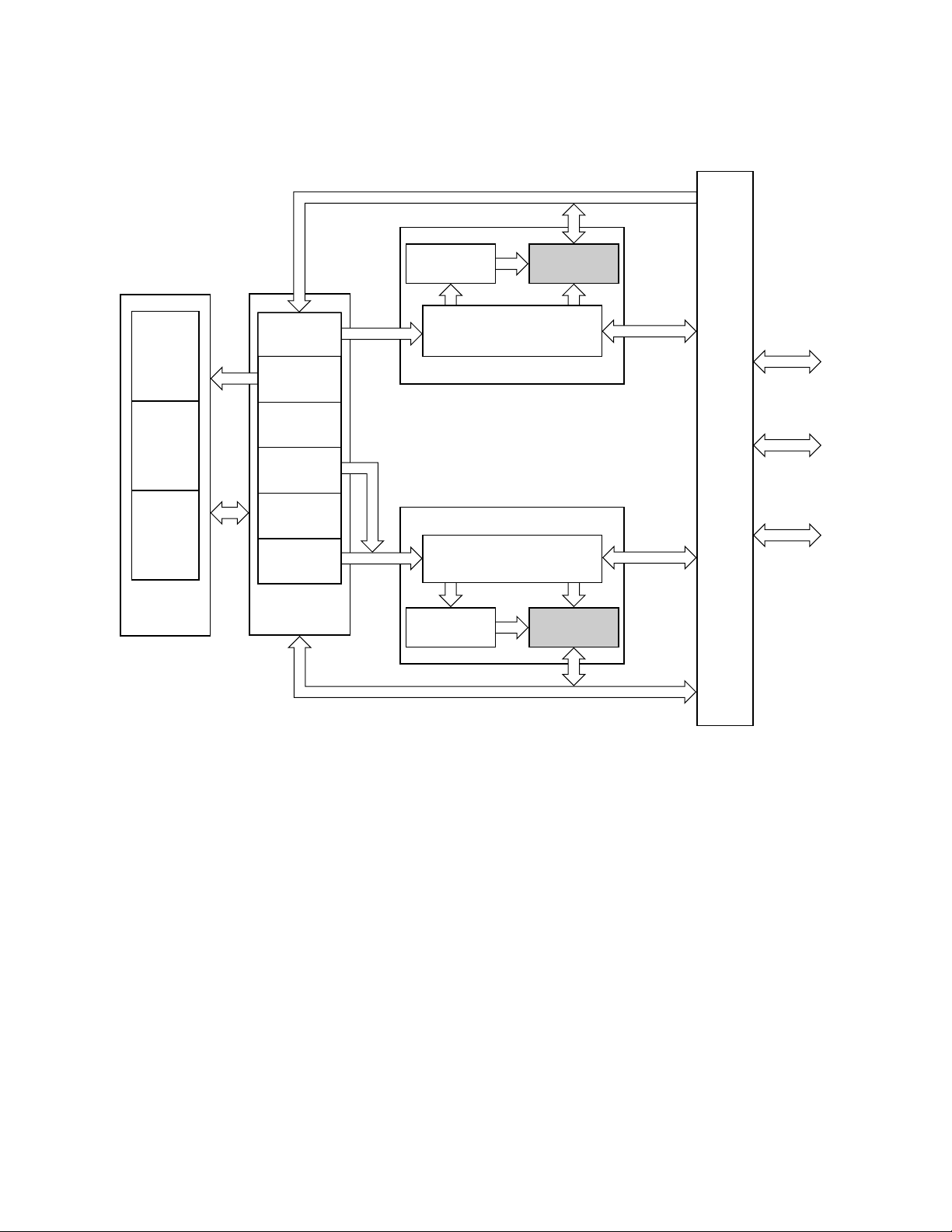
Freescale Semiconductor, Inc.
memory is always updated through an external bus access after updating the cache,
keeping memory and cached data consistent.
INSTRUCTION DATA BUS
INSTRUCTION
ATC
INSTRUCTION
FETCH
CONVERT
DECODE
EA
nc...
I
EXECUTE
WRITE-
BACK
FLOATING-
POINT UNIT
cale Semiconductor,
CALCULATE
EA
FETCH
EXECUTE
WRITEBACK
INTEGER
UNIT
OPERAND DATA BUS
Figure 4-1. Overview of Internal Caches
INSTRUCTION
MMU/CACHE/SNOOP
CONTROLLER
INSTRUCTION MEMORY UNIT B
DATA MEMORY UNIT
MMU/CACHE/SNOOP
CONTROLLER
DATA
ATC
4.1 CACHE OPERATION
DATA
INSTRUCTION
CACHE
DATA
CACHE
INSTRUCTION
ADDRESS
DATA
ADDRESS
U
ADDRESS
S
C
O
N
T
R
O
L
L
E
R
BUS
DATA
BUS
BUS
CONTROL
SIGNALS
Frees
Both four-way set-associative caches have 64 sets of four 16-byte lines. There are two
formats that define each cache line, an instruction cache line format and a data cache line
format. Each format contains an address tag consisting of the upper 22 bits of the physical
address, status information, and four long words (128 bits) of data. The status information
for the instruction cache line address tag consists of a single valid bit for the entire line.
The status information for the data cache line address tag contains a valid bit and four
additional bits to indicate dirty status for each long word in the line. Note that only the data
cache supports dirty cache lines. Figure 4-2 illustrates the instruction cache line format (a)
and the data cache line format (b).
4-2 M68040 USER'S MANUAL MOTOROLA
For More Information On This Product,
Go to: www.freescale.com
Page 87

Freescale Semiconductor, Inc.
TAG V LW3 LW2 LW1 LW0
TAG V LW3 D3 LW2 D2 LW1 D1 LW0 D0
TAG — 22-Bit Physical Address Tag
V — Line VALID Bit
LW — Long Word n (32-Bit) Data Entry
Dn — DIRTY Bit for Long Word n
The cache stores an entire line, providing validity on a line-by-line basis. Only burst mode
accesses that successfully read four long words can be cached. Memory devices unable
nc...
I
to support bursting can respond to a cache line read or write access by asserting the
transfer burst inhibit (TBI) signal, forcing the processor to complete the access as a
sequence of three long-word accesses. The cache recognizes burst accesses as if the
access were never inhibited, detecting no difference.
(a) Instruction Cache Line
(b) Data Cache Line
Figure 4-2. Cache Line Formats
cale Semiconductor,
Frees
A cache line is always in one of three states: invalid, valid, or dirty. For invalid lines, the Vbit is clear, causing the cache line to be ignored during lookups. Valid lines have their V-bit
set and D-bits cleared, indicating all four long words in the line contain valid data
consistent with memory. Dirty cache lines have the V-bit and one or more D-bits set,
indicating that the line has valid long-word entries that have not been written to memory
(long words whose D-bit is set). A cache line changes from valid to invalid if the execution
of the CINV or CPUSH instruction explicitly invalidates the cache line; if a snooped write
access hits the cache line and the line is not dirty; or if the SCx signals for a snooped read
access invalidates the line. Both caches should be explicitly cleared after a hardware reset
of the processor since reset does not invalidate the cache lines.
Figure 4-3 illustrates the general flow of a caching operation. The corresponding memory
unit translates the logical address of each access to a physical address allowing the IU to
access the data in the cache. To minimize latency of the requested data, the lower
untranslated bits of the logical address map directly to the physical address bits and are
used to access a set of cache lines in parallel with the translation. Physical address bits
9–4 are used to index into the cache and select one of the 64 sets of four cache lines. The
four tags from the selected cache set are compared with the translated physical address
bits 31–12 and bits 11 and 10 of the untranslated page offset. If any one of the four tags
matches and the tag status is either valid or dirty, then the cache has a hit. During read
accesses, a half-line (two long words) is accessed at a time, requiring two cache accesses
for reads that are greater than a half-line or two long words. Write accesses within a cache
line require a single cache access. If a misaligned access crosses two pages, then the
partial access to the first page always happens twice, even if the pages are serialized.
Consequently, if the accesses span page boundaries, misaligned accesses to peripherals
are not possible unless the peripheral can tolerate double reads or writes.
MOTOROLA M68040 USER’S MANUAL 4-3
For More Information On This Product,
Go to: www.freescale.com
Page 88
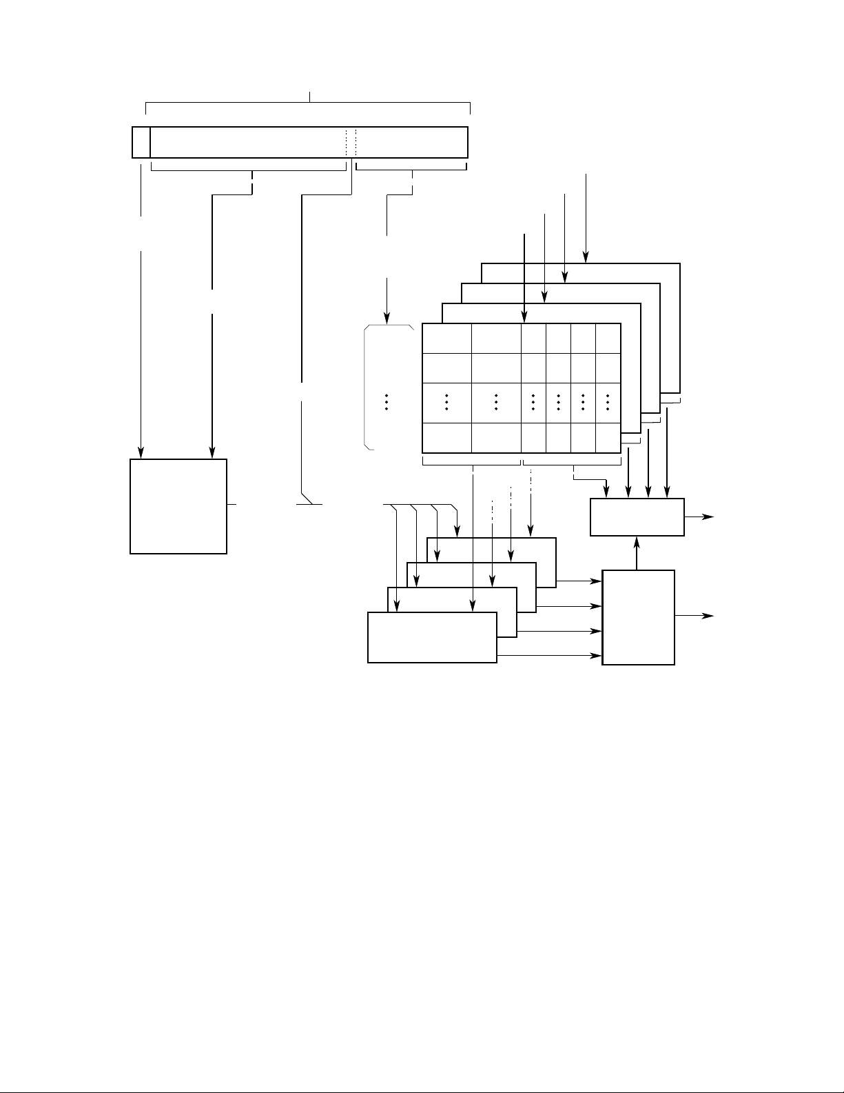
31 12 0
S
SUPERVISOR
BIT
Freescale Semiconductor, Inc.
LOGICAL ADDRESS
PAGE FRAME PAGE OFFSET
LA31–LA12
PHYSICAL
SET SELECT
PA9–PA4
LINE 3
LINE 2
LINE 1
LINE 0
nc...
I
cale Semiconductor,
Frees
ADDRESS
TRANSLATION
CACHE
PA11–PA10
PA31–PA12
SET 63
TRANSLATED
PHYSICAL
ADDRESS
PA31–PA10
SET 0
SET 1
COMPARATOR
TAG STATUS
TAG STATUS
0
D0 D1 D2 D3
D0 D1 D2 D3
3
2
1
HIT 3
HIT 2
HIT 1
HIT 0
MUX
LINE SELECT
LOGICAL OR
DATA OR
INSTRUCTION
HIT
Figure 4-3. Caching Operation
Both caches contain circuitry to automatically determine which cache line in a set to use
for a new line. The cache controller locates the first invalid line and uses it; if no invalid
lines exist, then a pseudo-random replacement algorithm is used to select a valid line,
replacing it with the new line. Each cache contains a 2-bit counter, which is incremented
for each access to the cache. The instruction cache counter is incremented for each half line accessed in the instruction cache. The data cache counter is incremented for each
half-line accessed during reads, for each full line accessed during writes in copyback
mode, and for each bus transfer resulting from a write in write-through mode. When a
miss occurs and all four lines in the set are valid, the line pointed to by the current counter
value is replaced, after which the counter is incremented.
4-4 M68040 USER'S MANUAL MOTOROLA
For More Information On This Product,
Go to: www.freescale.com
Page 89

Freescale Semiconductor, Inc.
4.2 CACHE MANAGEMENT
Using the MOVEC ins truction, the caches are individually enabled to access the 32-bit
cache control register (CACR) illustrated in Figure 4-4. The CACR contains two enable
bits that allow the instruction and data caches to be independently enabled or disabled.
Setting one of these bits enables the associated cache without affecting the state of any
lines within the cache. A hardware reset clears the CACR, disabling both caches;
however, reset does not affect the tags, state information, and data within the caches. The
CINV instruction must clear the caches before enabling them. It is not recommended that
page descriptors be cached. Specifically, the M68040 does not support the caching of
page descriptors in copyback mode with the bit pattern U = 0, M = 1, and R = 1 in a page
descriptor. The M68040 table search algorithm will never leave this bit pattern for a page
descriptor.
31 30 16 15 14 0
DE UNDEFINED IE UNDEFINED
nc...
I
DE = Enable Data Cache
IE = Enable Instruction Cache
cale Semiconductor,
Frees
Figure 4-4. Cache Control Register
System hardware can assert the cache disable (CDIS) signal to dynamically disable both
caches, regardless of the state of the enable bits in the CACR. The caches are disabled
immediately after the current access completes. If CDIS is asserted during the access for
the first half of a misaligned operand spanning two cache lines, the data cache is disabled
for the second half of the operand. Accesses by the execution units bypass the caches
while they are disabled and do not affect their contents (with the exception of CINV and
CPUSH instructions). Disabling the caches with CDIS does not affect snoop operations.
CDIS is intended primarily for use by in-circuit emulators to allow swapping between the
tags and emulator memories.
Even if the instruction cache is disabled, the M68040 can cache instructions because of
an internal cache line register. This happens for instruction loops that are completely
resident within the first six bytes of a half-line. Thus, the cache line holding register can
operate as a small cache. If a loop fits anywhere within the first three words of a half-line,
then it becomes cached.
The CINV and CPUSH instructions support cache management in the supervisor mode .
CINV allows selective invalidation of cache entries. CPUSH performs two operations: 1)
any selected data cache lines containing dirty data are pushed to memory; 2) all selected
cache lines are invalidated. This operation can be used to update a page in memory
before swapping it out with snooping disabled or to push dirty data when changing a page
caching mode to write-through. Because of the size of the caches, pushing pages or an
entire cache incurs a significant time penalty. However, these instructions are
interruptable to avoid large interrupt latencies. The state of the CDIS signal or the cache
enable bits in the CACR does not affect the operation of CINV and CPUSH. Both
instructions allow operation on a single cache line, all cache lines in a specific page, or an
MOTOROLA M68040 USER’S MANUAL 4-5
For More Information On This Product,
Go to: www.freescale.com
Page 90

Freescale Semiconductor, Inc.
entire cache, and can select one or both caches for the operation. For line and page
operations, a physical address in an address register specifies the memory address.
4.3 CACHING MODES
Every IU access to the cache has an associated caching mode that determines how the
cache handles the access. An access can be cachable in either the write-through or
copyback modes, or it can be cache inhibited in nonserialized or serialized modes. The
CM field corresponding to the logical address of the access normally specifies, on a pageby-page basis, one of these caching modes. The default memory access caching mode is
nonserialized. When the cache is enabled and memory management is disabled, the
default caching mode is write-through. The transparent translation registers and MMUs
allow the defaults to be overridden. In addition, some instructions and IU operations
perform data accesses that have an implicit caching mode associated with them. The
following paragraphs discuss the different caching accesses and their related cache
nc...
I
modes.
4.3.1 Cachable Accesses
cale Semiconductor,
Frees
If a page descriptor’s CM field indicates write-through or copyback, then the access is
cachable. A read access to a write-through or copyback page is read from the cache if
matching data is found. Otherwise, the data is read from memory and used to update the
cache. Since instruction cache accesses are always reads, the selection of write-through
or copyback modes do not affected them. The following paragraphs describe the write through and copyback modes in detail.
4.3.1.1 WRITE-THROUGH MODE . Accesses to pages specified as write-through are
always written to the external address, although the cycle can be buffered, keeping
memory and cache data consistent. Writes in write-through mode are handled with a no write-allocate policy—i.e., writes that miss in a data cache are written to memory but do
not cause the corresponding line in memory to be loaded into the cache. Write accesses
always write through to memory and update matching cache lines. Specifying writethrough mode for the shared pages maintains cache coherency for shared memory areas
in a multiprocessing environment. The cache supplies data to instruction or data read
accesses that hit in the appropriate cache; misses cause a new cache line to be loaded
into the cache, replacing a valid cache line if there are no invalid lines.
4.3.1.2 COPYBACK MODE. Copyback pages are typically used for local data structures
or stacks to minimize external bus usage and reduce write access latency. Write accesses
to pages specified as copyback that hit in the data cache update the cache line and set
the corresponding D-bits without an external bus access. The dirty cached data is only
written to memory if 1) the line is replaced due to a miss, 2) a cache inhibited access
matches the line, or 3) the CPUSH instruction explicitly pushes the line. If a write access
misses in the cache, the memory unit reads the needed cache line from memory and
updates the cache. When a miss causes a dirty cache line to be selected for replacement,
the memory unit places the line in an internal copyback buffer. The replacement line is
read into the cache, and writing the dirty cache line back to memory updates memory.
4-6 M68040 USER'S MANUAL MOTOROLA
For More Information On This Product,
Go to: www.freescale.com
Page 91

nc...
I
cale Semiconductor,
Frees
Freescale Semiconductor, Inc.
4.3.2 Cache-Inhibited Accesses
Address space regions containing targets such as I/O devices and shared data structures
in multiprocessing systems can be designated cache inhibited. If a page descriptor’s CM
field indicates nonserialized or serialized, then the access is cache inhibited. The caching
operation is identical for both cache-inhibited modes. If the CM field of a matching address
indicates either nonserialized or serialized modes, the cache controller bypasses the
cache and performs an external bus transfer. The data associated with the access is not
cached internally, and the cache inhibited out (CIOUT) signal is asserted during the bus
transfer to indicate to external memory that the access should not be cached. If the data
cache line is already resident in an internal cache, then the data cache line is pushed from
the cache if it is dirty or the data cache line is invalidated if it is valid.
If the CM field indicates serialized, then the sequence of read and write accesses to the
page is guaranteed to match the sequence of the instruction order. Without serialization,
the IU pipeline allows read accesses to occur before completion of a write-back for a
previous instruction. Serialization forces operand read accesses for an instruction to occur
only once by preventing the instruction from being interrupted after the operand fetch
stage. Otherwise, the instruction is aborted, and the operand is accessed when the
instruction is restarted. These guarantees apply only when the CM field indicates the
serialized mode and the accesses are aligned. Regardless of the selected cache mode,
locked accesses are implicitly serialized. The TAS, CAS, and CAS2 instructions use
locked accesses for operands in memory and for updating translation table entries during
table search operations.
4.3.3 Special Accesses
Several other processor operations result in accesses that have special caching
characteristics besides those with an implied cache-inhibited access in the serialized
mode. Exception stack accesses, exception vector fetches, and table searches that miss
in the cache do not allocate cache lines in the data cache, preventing replacement of a
cache line. Cache hits by these accesses are handled in the normal manner according to
the caching mode specified for the accessed address.
Accesses by the MOVE16 instruction also do not allocate cache lines in the data cache for
either read or write misses. Read hits on either valid or dirty cache lines are read from the
cache. Write hits invalidate a matching line and perform an external access. Interacting
with the cache in this manner prevents a large block move or block initialization
implemented with a MOVE16 from being cached, since the data may not be needed
immediately.
If the data cache is re-enabled after a locked access has hit and the data cache was
disabled, the next non-locked access that results in a data cache miss will not be cached.
4.4 CACHE PROTOCOL
The cache protocol for processor and snooped accesses is described in the following
paragraphs. In all cases, an external bus transfer will cause a cache line state to change
MOTOROLA M68040 USER’S MANUAL 4-7
For More Information On This Product,
Go to: www.freescale.com
Page 92

Freescale Semiconductor, Inc.
only if the bus transfer is marked as snoopable on the bus. The protocols described in the
following paragraphs assume that the data is cachable (i.e., write-through and copyback).
4.4.1 Read Miss
A processor read that misses in the cache causes the cache controller to request a bus
transaction that reads the needed line from memory and supplies the required data to the
IU. The line is placed in the cache in the valid state. Snooped external reads that miss in
the cache have no affect on the cache.
4.4.2 Write Miss
The cache controller handles processor writes that miss in the cache differently for writethrough and copyback pages. Write misses to copyback pages cause the processor to
perform a bus transaction that writes the needed cache line into its cache from memory in
the same manner as for a read miss. The new cache line is then updated with the write
nc...
I
data, and the D-bits are set for each long word that has been modified, leaving the cache
line in the dirty state. Write misses to write-through pages write directly to memory without
loading the corresponding cache line in the cache. Snooped external writes that miss in
the cache have no affect on the cache.
cale Semiconductor,
Frees
4.4.3 Read Hit
The cache controller handles processor reads that hit in the cache differently for writethrough and copyback pages. No bus transaction is performed, and the state of the cache
line does not change. Physical address bit 3 selects either the upper or lower half-line
containing the required operand. This half-line is driven onto the internal bus. If the
required data is allocated entirely within the half-line, only one access into the cache is
required. Because the organization of the cache does not allow selection of more than one
half-line at a time, misalignment across a half-line boundary requires two accesses into
the cache.
A snooped external read that hits in the cache is ignored if the cache line is valid. If the
snooped access hits a dirty line, memory is inhibited from responding, and the data is
sourced from the cache directly to the alternate bus master. A snooped read hit does not
change the state of the cache line unless the snooped access also indicates mark invalid,
which causes the line to be invalidated after the access, even if it is dirty. Alternate bus
master s should indicate mark invalid only for line reads to ensure the entire line is
transferred before invalidating.
4.4.4 Write Hit
The cache controller handles processor writes that hit in the cache differently for writethrough and copyback pages. For write-through accesses, a processor write hit causes
the cache controller to update the affected long-word entries in the cache line and to
request an external memory write transfer to update memory. The cache line state does
not change. A write-through access to a line containing dirty data constitutes a system
programming error even if the D-bits for the line are unchanged. This situation can be
4-8 M68040 USER'S MANUAL MOTOROLA
For More Information On This Product,
Go to: www.freescale.com
Page 93

Freescale Semiconductor, Inc.
avoided by pushing cache lines when a page descriptor is changed and ensuring that
alternate bus masters indicate the appropriate snoop operation for writes to corresponding
pages (i.e., mark invalid for write-through pages and sink data for copyback pages). If the
access is copyback, the cache controller updates the cache line and sets the D-bit for of
the appropriate long words in the cache line. An external write is not performed, and the
cache line state changes to, or remains in, the dirty state.
An alternate bus master can drive the SCx signals for a write access with an encoding that
indicates to the M68040 that it should sink the data, inhibit memory, and respond as a
slave if the access hits in the cache. The cache operation depends on the access size and
current line state. A snooped line write that hits a valid line always causes the
corresponding cache line to be invalidated. For snooped writes of byte, word, or long-word
size that hit a dirty line, the processor inhibits memory and responds to the alternate bus
master as a slave, sinking the data. Data received from the alternate bus master is written
to the appropriate long word in the cache line, and the D-bit is set for that entry. The cache
controller invalidates a cache line if the snoop control pins have indicated that a matching
nc...
I
cache line is marked invalid for a snoop write.
cale Semiconductor,
Frees
4.5 CACHE COHERENCY
The M68040 provides several different mechanisms to assist in maintaining cache
coherency in multimaster systems. Both write-through and copyback memory update
techniques are supported to maintain coherency between the data cache and memory.
Alternate bus master accesses can reference data that the M68040 caches, causing
coherency problems if the accesses are not handled properly. The M68040 snoops the
bus during alternate bus master transfers. If a write access hits in the cache, the M68040
can update its internal caches, or if a read access hits, it can intervene in the access to
supply dirty data. Caches can be snooped even if they are disabled. The alternate bus
master controls snooping through the snoop control signals, indicating which access can
be snooped and the required operation for snoop hits. Table 4-1 lists the requested snoop
operation for each encoding of the snoop control signals. Since the processor and the bus
snooper must both access the caches, the snoop controller has priority over the processor
for snoopable accesses to maintain cache coherency.
Table 4-1. Snoop Control Encoding
Requested Snoop Operation
SC1 SC0 Alternate Bus Master Read Access Alternate Bus Master Write Access
0 0 Inhibit Snooping Inhibit Snooping
0 1 Supply Dirty Data and Leave Dirty Data Sink Byte/Word/Long/Long Word
1 0 Supply Dirty Data and Mark Line Invalid Invalidate Line
1 1 Reserved (Snoop Inhibited) Reserved (Snoop Inhibited)
The snooping protocol and caching mechanism supported by the M68040 are optimized to
support multimaster systems with the M68040 as the single caching master. In systems
MOTOROLA M68040 USER’S MANUAL 4-9
For More Information On This Product,
Go to: www.freescale.com
Page 94

nc...
I
cale Semiconductor,
Frees
Freescale Semiconductor, Inc.
implementing multiple MC68040s as bus masters, shared data should be stored in write through pages. This procedure allows each processor to cache shared data for read
access while forcing a processor write to shared data to appear as an external write to
memory, which the other processors can snoop.
If shared data is stored in copyback pages, only one processor at a time can cache the
data since writes to copyback pages do not access the external bus. If a processor
accesses shared data cached by another processor, the slave can source the data to the
master without invalidating its own copy only if the transfer to the master is cache
inhibited. For the master processor to cache the data, it must force invalidation of the
slave processor’s copy of the data (by specifying mark invalid for the snoop operation),
and the memory controller must monitor the data transfer between the processors and
update memory with the transferred data. The memory update is required since the
master processor is unaware of the sourced data (valid data from memory or dirty data
from a snooping processor) and initially creates a valid cache line, losing dirty status if a
snooping processor supplies the data.
Coherency between the instruction cache and the data cache must be maintained in
software since the instruction cache does not monitor data accesses. Processor writes
that modify code segments (i.e., resulting from self-modifying code or from code executed
to load a new page from disk) access memory through the data memory unit. Because the
instruction cache does not monitor these data accesses, stale data occurs in the
instruction cache if the corresponding data in memory is modified. Invalidating instruction
cache lines before writing to the corresponding memory lines can prevent this coherency
problem, but only if the data cache line is in write-through mode and the page is marked
serialized. A cache coherency problem could arise if the data cache line is configured as
copyback and no serialization is done.
To fully support self-modifying code in any situation, it is imperative that a CPUSHA
instruction be executed before the execution of the first self-modified instruction. The
CPUSHA instruction has the effect of ensuring that there is no stale data in memory, the
pipeline is flushed, and instruction prefetches are repeated and taken from external
memory.
Another potential coherency problem exists due to the relationship between the cache
state information and the translation table descriptors. Because each cache line reflects
page state information, a page should be flushed from the cache before any of the page
attributes are changed. The presence of a valid or dirty cache line implicitly indicates that
accesses to the page containing the line are cachable. The presence of a dirty cache line
implies that the page is not write protected and that writes to the page are in copyback
mode. A system programming error occurs when page attributes are changed without
flushing the corresponding page from the cache, resulting in cache line states inconsistent
with their page definitions. Even with these inconsistencies, the cache is defined and
predictable.
4-10 M68040 USER'S MANUAL MOTOROLA
For More Information On This Product,
Go to: www.freescale.com
Page 95

Freescale Semiconductor, Inc.
4.6 MEMORY ACCESSES FOR CACHE MAINTENANCE
The cache controller in each memory unit performs all maintenance activities that supply
data from the cache to the execution units. The activities include requesting accesses to
the bus interface unit for reading new cache lines and writing dirty cache lines to memory.
The following paragraphs describe the memory accesses resulting from cache fill
operations (by both caches) and push operations (by the data cache). Refer to Section 7
Bus Operation for detailed information about the bus cycles required.
4.6.1 Cache Filling
When a new cache line is required, the cache controller requests a line read from the bus
controller. The bus controller requests a burst read transfer by indicating a line access
with the size signals (SIZ1, SIZ0) and indicates which line in the set is being loaded with
the transfer line number signals (TLN1, TLN0). TLN1 and TLN0 are undefined for the
instruction cache. These pins indicate the appropriate line numbers for data cache
nc...
I
transfers only. Table 4-2 lists the definition of the TLNx encoding.
cale Semiconductor,
Frees
Table 4-2. TLNx Encoding
TLN1 TLN0 Line
0 0 Zero
0 1 One
1 0 Two
1 1 Three
The responding device sequentially supplies four long words of data and can assert the
transfer cache inhibit signal (TCI) if the line is not cachable. If the responding device does
not support the burst mode, it should assert the TBI signal for the first long word of the line
access. The bus controller responds by terminating the line access and completes the
remainder of the line read as three, sequential, long-word reads.
Bus controller line accesses implicitly request burst mode operations from external
memory. To operate in the burst mode, the device or external hardware must be able to
increment the low-order address bits as described in Section 7 Bus Operation. The
device indicates its ability to support the burst access by acknowledging the initial longword transfer with transfer acknowledge (TA ) asserted and TBI negated. This procedure
causes the processor to continue to drive the address and bus control signals and to latch
a new data value for the cache line at the completion of each subsequent cycle (as
defined by TA ) for a total of four cycles. The bursting mechanism requires addresses to
wrap around so that the entire four long words in the cache line are filled in a single
operation.
When a cache line read is initiated, the first cycle attempts to load the line entry
corresponding to the instruction half-line or data item requested by the IU. Subsequent
transfers are for the remaining entries in the cache line. In the case of a misaligned
MOTOROLA M68040 USER’S MANUAL 4-11
For More Information On This Product,
Go to: www.freescale.com
Page 96

Freescale Semiconductor, Inc.
access in which the operand spans two line entries, the first cycle corresponds to the line
entry containing the portion of the operand at the lower address.
The cache controller temporarily stores the data from each cycle in a line read buffer,
where it is immediately available to the IU. If a misaligned access spans two entries in the
line, the second portion of the operand is available to the IU as soon as the second
memory cycle completes. A new IU access that hits the cache line being filled is also
supplied data as soon as the required long word has been received from the bus
controller. During the period required to fill the buffer, other IU accesses that hit in the
cache are supplied data. This is vertical for a short cache-inhibited code loop that is less
than eight bytes in length. Subsequent interactions of the loop hit in the buffer, but appear
to hit in the cache since there is no external bus activity associated with the reads.
The assertion of TCI during the first cycle of a burst read operation inhibits loading of the
buffered line into the cache, but it does not cause the burst transfer (or pseudo-burst
transfer if TBI is asserted with TCI) to be terminated early. The data placed in the buffer is
nc...
I
accessible by the IU until the last long word of the burst is transferred from the bus
controller, after which the contents of the buffer are invalidated without being copied into
the cache. The assertion of TCI is ignored during the second, third, or fourth cycle of a
burst operation and is ignored for write operations.
cale Semiconductor,
Frees
A bus error occurring during a burst operation causes the burst operation to abort. If the
bus error occurs during the first cycle of a burst, the data from the bus is ignored. If the
access is a data cycle, exception processing proceeds immediately. If the cycle is for an
instruction prefetch, a bus error exception is pending. The bus error is processed only if
the IU attempts to use either instruction word. Refer to Section 7 Bus Operation for more
information about pipeline operation.
For either cache, when a bus error occurs on the second cycle or later, the burst operation
is aborted and the line buffer is invalidated. The processor may or may not take an
exception, depending on the status of the pending data request. If the bus error cycle
contains a portion of a data operand that the processor is specifically waiting for (e.g., the
second half of a misaligned operand), the processor immediately takes an exception.
Otherwise, no exception occurs, and the cache line fill is repeated the next time data
within the line is required. In the case of an instruction cache line fill, the data from the
aborted cycle is completely ignored.
On the initial access of a line read, a retry (indicated by the assertion of TA
causes the bus controller to retry the bus cycle. However, a retry signaled during the
remaining cycles of the line access (either burst or pseudo-burst) is recognized as a bus
error, and the processor handles it as described in the previous paragraphs.
A cache inhibit or bus error on a line read can change the state of the line being replaced,
even though the new line is not copied into the cache. Before loading a new line, the
cache line being replaced is copied to the push buffer; if it is dirty, the cache line is
invalidated. If a cache inhibit or bus error occurs on a replacement line read, a dirty line is
restored to the cache from the push buffer. However, the line being replaced is not
restored in the cache if it was originally valid and the cache line remains invalid. If the line
and TEA )
4-12 M68040 USER'S MANUAL MOTOROLA
For More Information On This Product,
Go to: www.freescale.com
Page 97

Freescale Semiconductor, Inc.
read resulting from a write miss in copyback mode is cache inhibited, the write access
misses in the cache and writes through to memory.
4.6.2 Cache Pushes
When the cache controller selects a dirty data cache line for replacement, memory must
be updated with the dirty data before the line is replaced. This occurs when a CPUSH
instruction execution explicitly selects the cache and when a cache inhibit access hits in
the cache. To reduce the requested data’s latency in the new line, the dirty line being
replaced is temporarily placed in a push buffer while the new line is fetched from memory.
When a line is allocated to the push buffer , an alternate bus master can snoop it, but the
execution units cannot access it. After the bus transfer for the new line successfully
completes, the dirty cache line is copied back to memory, and the push buffer is
invalidated. If the operation to access the replacement line is abnormally terminated or
signaled as cache inhibited, the line in the push buffer is copied back into its original
position in the cache, and the processor continues operation as described in the previous
nc...
I
paragraphs.
cale Semiconductor,
Frees
The number of dirty long words in the line to be pushed determines the size of the push
transfer on the bus, minimizing bus bandwidth required for the push. A single long word is
written to memory using a long-word push transfer if it is dirty. A push transfer is
distinguished from a normal write transfer by an encoding of 000 on the transfer modifier
signals (TM2–TM0) for the push. Asserting TA and TEA retries the transfer; a bus-errorasserted TEA terminates it
immediately takes an exception.
A line containing two or more dirty long words is copied back to memory, using a line push
transfer. For a line push, the bus controller requests a burst write transfer by indicating a
line access with SIZ1 and SIZ0. The responding device sequentially accepts four long
words of data. If the responding device does not support the burst mode, it should assert
TBI for the first long word of the line access. The bus controller responds by terminating
the line access and completes the remainder of the line push as three, sequential, longword writes. The first cycle of the burst can be retried, but the bus controller interprets a
retry for any of the three remaining cycles as a bus error. If a bus error occurs in any cycle
in the line push transfer, the processor immediately takes an exception.
A dirty cache line hit by a cache-inhibited access is pushed before the external bus access
occurs. If the access is part of a locked transfer sequence for TAS, CAS, or CAS2
operand accesses or translation table updates, the LOCK signal is also asserted for the
push access.
. If a bus error terminates a push transfer, the processor
4.7 CACHE OPERATION SUMMARY
The instruction and data caches function independently when servicing access requests
from the IU. The following paragraphs discuss the operational details for the caches and
present state diagrams depicting the cache line state transitions.
MOTOROLA M68040 USER’S MANUAL 4-13
For More Information On This Product,
Go to: www.freescale.com
Page 98
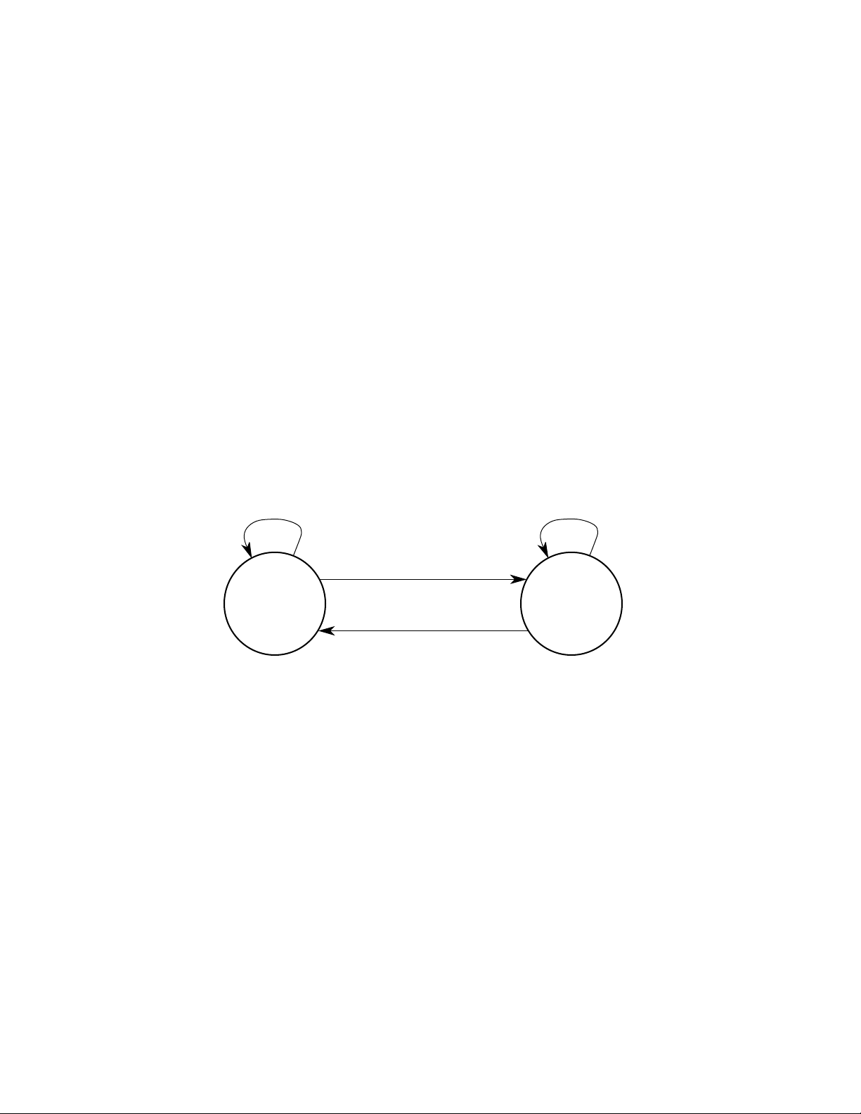
Freescale Semiconductor, Inc.
4.7.1 Instruction Cache
The IU uses the instruction cache to store instruction prefetches as it requests them.
Instruction prefetches are normally requested from sequential memory locations except
when a change of program flow occurs (e.g., a branch taken) or when an instruction that
can modify the status register (SR) is executed, in which case the instruction pipe is
automatically flushed and refilled. The instruction cache supports a line-based protocol
that allows individual cache lines to be in either the invalid or valid states.
For instruction prefetch requests that hit in the cache, the half-line selected by physical
address bit 3 is multiplexed onto the internal instruction data bus. When an access misses
in the cache, the cache controller requests the line containing the required data from
memory and places it in the cache. If available, an invalid line is selected and updated
with the tag and data from memory. The line state then changes from invalid to valid by
setting the V-bit. If all lines in the set are already valid, a pseudo-random replacement
algorithm is used to select one of the four cache lines replacing the tag and data contents
nc...
I
of the line with the new line information. Figure 4-5 illustrates the instruction-cache line
state transitions resulting from processor and snoop controller accesses. Transitions are
labeled with a capital letter, indicating the previous state, followed by a number indicating
the specific case listed in Table 4-3.
cale Semiconductor,
Frees
I3–CINV/CPUSH V1–CPU READ MISS
I1-CPU READ MISS
INVALID
V3–CINV/CPUSH
V5–SNOOP READ HIT
V6–SNOOP WRITE HIT
V2–CPU READ HIT
VALID
Figure 4-5. Instruction-Cache Line State Diagram
4-14 M68040 USER'S MANUAL MOTOROLA
For More Information On This Product,
Go to: www.freescale.com
Page 99
Freescale Semiconductor, Inc.
Table 4-3. Instruction-Cache Line State Transitions
Current State
Cache Operation Invalid Cases Valid Cases
CPU Read Miss I1 Read line from memory;
supply data to CPU and
update cache; go to valid
state.
CPU Read Hit
Cache Invalidate or Push
(CINV or CPUSH)
Alternate Master Read Hit
(Snoop Control = 01 — Leave Dirty)
Alternate Master Read Hit
nc...
I
(Snoop Control = 10 — Invalidate)
Alternate Master Write Hit
(Snoop Control = 01 — Leave Dirty or
Snoop Control = 10 — Invalidate)
I2
Not Possible V2 Supply data to CPU; remain in
I3
No action; remain in
current state.
I4
Not possible; not snooped. V4 Not possible; not snooped.
I5
Not Possible V5 No action; go to invalid state.
I6
Not Possible V6 No action; go to invalid state.
V1 Read line from memory; supply
data to CPU and update cache
(replacing old line); remain in
current state.
current state.
V3 No action; go to invalid state.
cale Semiconductor,
Frees
4.7.2 Data Cache
The IU uses the data cache to store operand data as it generates the data. The data
cache supports a line-based protocol allowing individual cache lines to be in one of three
states: invalid, valid, or dirty. To maintain coherency with memory, the data cache
supports both write-through and copyback modes, specified by the CM field for the page.
Read misses and write misses to copyback pages cause the cache controller to read a
new cache line from memory into the cache. If available, an invalid line in the selected set
is updated with the tag and data from memory. The line state then changes from invalid to
valid by setting the V-bit for the line. If all lines in the set are already valid or dirty, the
pseudo-random replacement algorithm is used to select one of the four lines and replace
the tag and data contents of the line with the new line information. Before replacement,
dirty lines are temporarily buffered and later copied back to memory after the new line has
been read from memory. If a snoop access occurs before the buffered line is written to
memory, the snoop controller snoops the buffer and the caches. Figure 4-6 illustrates the
three possible states for a data cache line, with the possible transitions caused by either
the processor or snooped accesses. Transitions are labeled with a capital letter, indicating
the previous state, followed by a number indicating the specific case listed in Table 4-4.
MOTOROLA M68040 USER’S MANUAL 4-15
For More Information On This Product,
Go to: www.freescale.com
Page 100

Freescale Semiconductor, Inc.
V7—CINV
V8—CPUSH
V10—SNOOP READ HIT/INVALIDATE
I4—CPU WRITE MISS/WT
I7—CINV
I8—CPUSH
nc...
I
D7—CINV
D8—CPUSH
D10—SNOOP READ
HIT/INVALIDATE
D11—SNOOP WRITE HIT/
INVALIDATE
D13—SNOOP WRITE HIT/SINK
cale Semiconductor,
DATA & SIZE = LINE
ABBREVIATIONS:
WT—WRITE-THROUGH MODE
CB—COPYBACK MODE
SNOOP OPERATION INDICATES:
READ OR WRITE / SNOOP CONTROL
ENCODING
INVALID
I3—CPU WRITE MISS/CB
V11—SNOOP WRITE HIT/INVALIDATE
V12—SNOOP WRITE HIT/SINK DATA &
SIZE = LINE
V13—SNOOP WRITE HIT/SINK DATA &
SIZE = LINE
I1—CPU READ MISS
V3—CPU WRITE MISS/CB
V5—CPU WRITE HIT/CB
DIRTY
D2—CPU READ HIT
D3—CPU WRITE MISS/CB
D4—CPU WRITE MISS/WT
D5—CPU WRITE HIT/CB
D6—CPU WRITE HIT/WT
D9—SNOOP READ HIT/LEAVE DIRTY
D12—SNOOP WRITE HIT/SINK DATA
& SIZE = LINE
V1—CPU READ MISS
V2—CPU READ HIT
V4—CPU WRITE MISS/WT
V6—CPU WRITE HIT/WT
V9—SNOOP READ HIT/LEAVE DIRTY
VALID
D1—CPU READ MISS
Frees
Figure 4-6. Data-Cache Line State Diagram
4-16 M68040 USER'S MANUAL MOTOROLA
For More Information On This Product,
Go to: www.freescale.com
 Loading...