

MOTOROLA
SEMICONDUCTOR TECHNICAL DATA
M u Iti-Character
lED Display/lamp Driver
CMOS
The MC144898 is a flexible light-emitting-diode driver which directly interfaces to individual lamps, 7-segment displays, or various combinations of
both. LEOs wired with common cathodes are driven in a multiplexed-by-5
fashion. Communication with an MCUIMPU is established through a synchronous serial port. The MC 144898 features data retention plus decode and scan
circuitry, thus relieving processor overhead. A single, current-setting resistor
is the only ancillary component required.
A single device can drive anyone of the following: a 5-digit display plus
decimals, a 4-112-digit display plus decimals and sign, or 25 lamps. A special
technique allows driving 5 112 digits; see Figure 16. A configuration register
allows the drive capability to be partitioned off to suit many additional applications. The on-chip decoder outputs 7-segment-format numerals O to 9, hexadecimal characters A to F, plus 151etters and symbols.
The MC144898 is compatible with the Motorola SPI and National MICRO-WIRETM serial data ports. The chip's patented 8itGrabberTM registers
augment the serial interface by allowing random access without steering or
address bits. A 24-bit transfer updates the display register. Changing the configuration register requires an 8-bit transfer.
.Operating Voltage Range of Drive Circuitry: 4.5 to 5.5 V
.Operating Junction Temperature Range: -40° to 130°C
.Current Sources Controlled by Single Resistor Provide Anode Drive
.Low-Resistance FET Switches Provide Direct Common Cathode Interface
.Low-Power Mode (Extinguishes the LEDs) and Brightness Controlled via
Serial Port
.Special Circuitry Minimizes EMI when Display is Driven and Eliminates EMI
in Low-Power Mode
.Power-On Reset (POR) Blanks the Display on Power-Up, Independent of
Supply Ramp Up Time
.May Be Used with Double-Heterojunction LEDs for Optimum Efficiency
.Chip Complexity: 4300 Elements (FETs, Resistors, Capacitors, etc.)
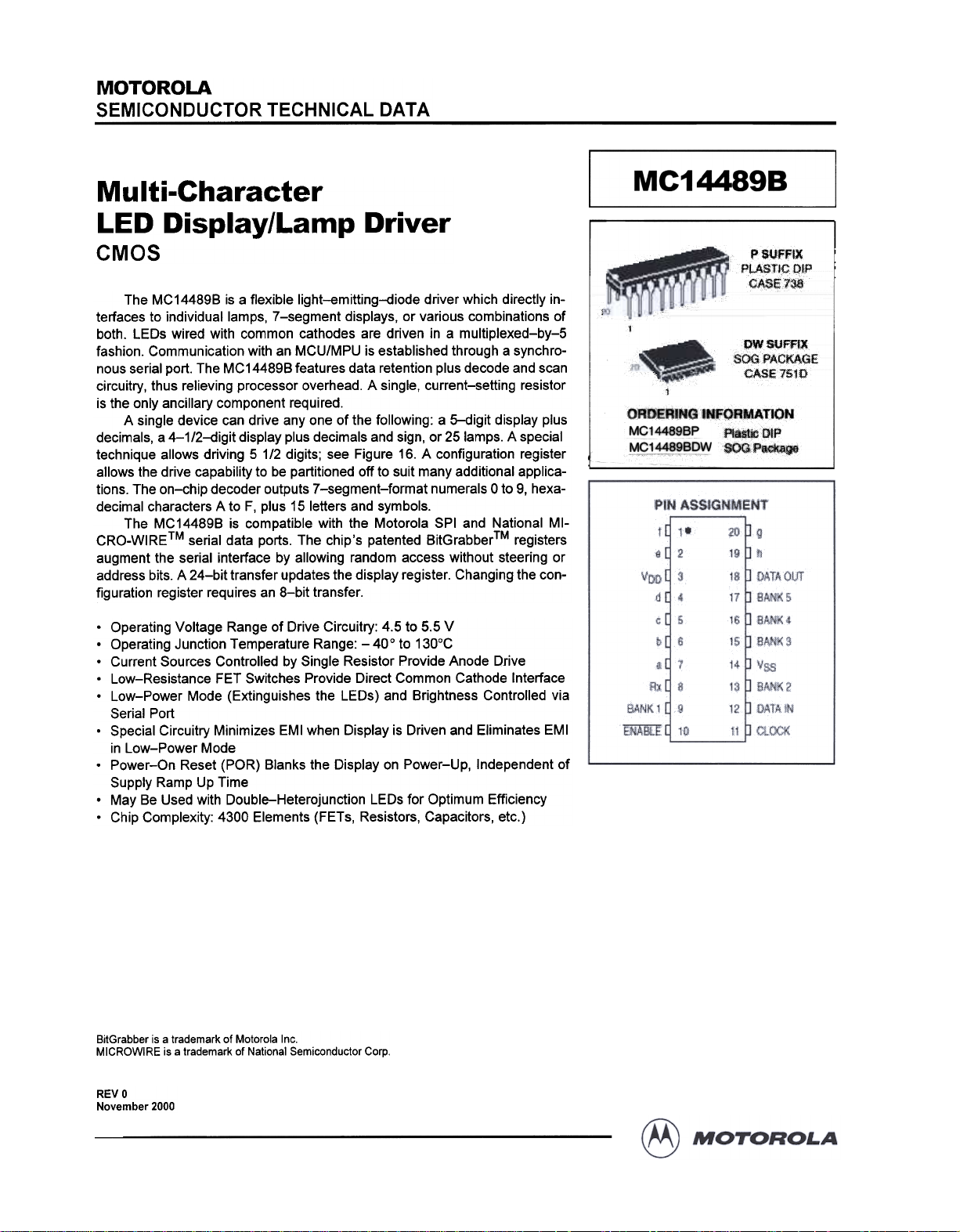
MC14489B
p SVFFiX
PLASTICOIP
CASE73$
PW SUFF,~
SOOPACKAGE"
CASE 7510
ORDERING INFQRMATJON
MC14489BP PlaSticDtP
MC14489BDW SOOP~gec
..
BitGrabber is a trademark of Motorola Inc.
MICROWIRE is a trademark of National Semiconductor Corp.
REVO
November 2000
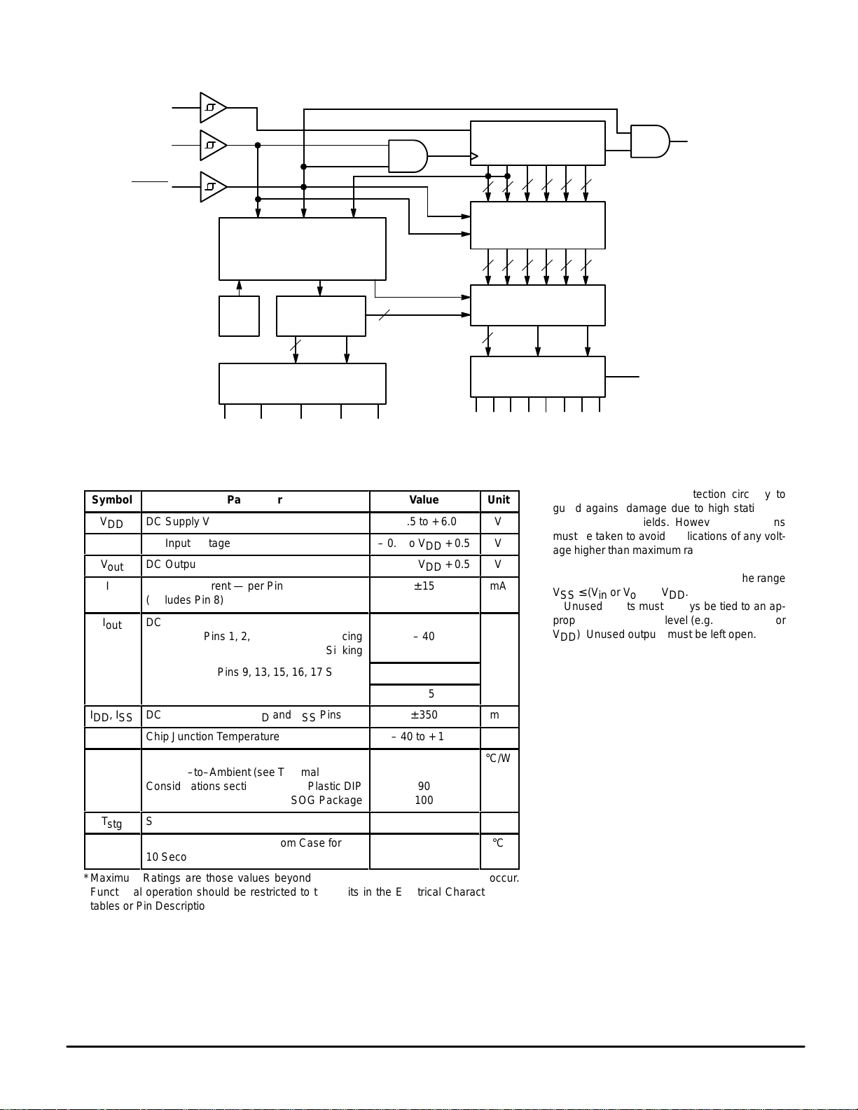
BLOCK DIAGRAM
Á
Á
Á
Á
Á
Á
Á
Á
Á
Á
Á
Á
Á
Á
Á
Á
Á
Á
Á
Á
10
12
D
11
24–1/2–STAGE
SHIFT REGISTER
C
44
DATA IN
CLOCK
ENABLE
DISPLAY REGISTER
BitGrabber
CONFIGURATION REGISTER
8 BITS
NIBBLE MUX AND
DECODER ROM
a TO g
7
POR
OSCILLATOR AND
CONTROL LOGIC
5
BLANK
5
ANODE DRIVERS
BANK SWITCHES (FETs)
913151617
BANK 1BANK 2BANK 3BANK 4BANK 5
MAXIMUM RATINGS* (Voltages Referenced to V
Symbol
V
V
ÁÁ
I
ÁÁ
DC Supply Voltage
DD
V
DC Input Voltage
in
DC Output Voltage
out
I
DC Input Current — per Pin
in
ББББББББББ
(Includes Pin 8)
DC Output Current —
out
ББББББББББ
IDD, ISSDC Supply Current, VDD and VSS Pins
T
Chip Junction Temperature
J
R
ÁÁ
ÁÁ
T
ÁÁ
Device Thermal Resistance,
θJA
stg
T
ББББББББББ
Junction–to–Ambient (see Thermal
Considerations section) Plastic DIP
ББББББББББ
Storage Temperature
Lead Temperature, 1 mm from Case for
L
ББББББББББ
10 Seconds
Parameter
Pins 1, 2, 4 – 7, 19, 20 Sourcing
Sinking
Pins 9, 13, 15, 16, 17 Sinking
Pin 18
SOG Package
)
SS
– 0.5 to + 6.0
– 0.5 to VDD + 0.5
– 0.5 to VDD + 0.5
ÁÁÁÁ
ÁÁÁÁ
– 40 to + 130
ÁÁÁÁ
ÁÁÁÁ
– 65 to + 150
ÁÁÁÁ
Value
±15
– 40
10
320
±15
±350
90
100
260
(CURRENT SOURCES)
ab
Unit
V
V
V
mA
Á
mA
Á
mA
°C
°C/W
Á
Á
°C
°C
Á
*Maximum Ratings are those values beyond which damage to the device may occur.
Functional operation should be restricted to the limits in the Electrical Characteristics
tables or Pin Descriptions section.
4
444
BitGrabber
24 BITS
4
44444
h DIM/BRIGHT
220
1
194567
cdefgh
This device contains protection circuitry to
guard against damage due to high static voltages or electric fields. However, precautions
must be taken to avoid applications of any voltage higher than maximum rated voltages to this
high–impedance circuit. For proper operation,
Vin and V
VSS ≤ (Vin or V
out
Unused inputs must always be tied to an appropriate logic voltage level (e.g., either VSS or
VDD). Unused outputs must be left open.
18
DATA OUT
PIN 3 = V
DD
PIN 14 = V
8
Rx
SS
should be constrained to the range
) ≤ VDD.
out
MC14489B MOTOROLA
2
ELECTRICAL CHARACTERISTICS (Voltages Referenced to V
Symbol
V
DD
VDD (stby) Minimum Standby Voltage Bits Retained in Display and
V
V
V
Hys
V
OL
V
OH
I
in
i
OL
i
OH
I
OZ
R
on
IDD, I
I
ss
*See Thermal Considerations section.
Power Supply Voltage Range of LED Drive Circuitry — 4.5 to 5.5 V
Maximum Low–Level Input Voltage
IL
IH
SS
(Data In, Clock, Enable
Minimum High–Level Input Voltage
(Data In, Clock, Enable
Minimum Hysteresis Voltage
(Data In, Clock, Enable
Maximum Low–Level Output Voltage
(Data Out)
Minimum High–Level Output Voltage
(Data Out)
Maximum Input Leakage Current
(DataInClockEnable
(Data In, Clock, Enable)
Minimum Sinking Current
(a, b, c, d, e, f, g, h)
Peak Sourcing Current — See Figure 7 for currents up to
35 mA (a, b, c, d, e, f, g, h)
Maximum Output Leakage Current
(Bank1Bank2Bank3Bank4Bank5)
(Bank 1, Bank 2, Bank 3, Bank 4, Bank 5)
Maximum ON Resistance
(Bank 1, Bank 2, Bank 3, Bank 4, Bank 5)
Maximum Quiescent Supply Current
Maximum RMS Operating Supply Current
(The VSS leg does not contain the Rx current component.
See Pin Descriptions.)
Parameter Test Condition
)
)
)
)
, TJ = – 40° to 130°C* unless otherwise indicated)
SS
Configuration Registers, Data
Port Fully Functional
I
= 20 µA 3.0
out
I
= 1.3 mA 4.5 0.4
out
I
= – 20 µA 3.0
out
I
= – 800 µA 4.5 4.1
out
Vin = VDD or V
Vin = VDD or VSS,
TJ = 25°C only
V
= 1.0 V 4.5 0.2 mA
out
Rx = 2.0 kΩ, V
Dimmer Bit = High
Rx = 2.0 kΩ, V
Dimmer Bit = Low
V
= VDD (FET Leakage) 5.5 50
out
V
= VDD (FET Leakage),
out
TJ = 25°C only
V
= VSS (Protection Diode
out
Leakage)
I
= 0 to 200 mA 5.0 10 Ω
out
Device in Low–Power Mode,
Vin = VSS or VDD, Rx in
Place, Outputs Open
Same as Above, TJ = 25°C 5.5 20
Device NOT in Low–Power
Mode, Vin = VSS or VDD,
Outputs Open
SS
out
out
= 3.0 V,
= 3.0 V,
V
Guaranteed
DD
V
— 3.0 V
3.0
5.5
3.0
5.5
3.0
5.5
5.5
5.5
5.5 ± 2.0
5.5 ± 0.1
5.0 13 to 17.5
5.0 6 to 9
5.5 1
5.5 1
5.5 100
5.5 1.5 mA
Limit
0.9
1.65
2.1
3.85
0.2
0.4
0.1
0.1
2.9
5.4
Unit
V
V
V
V
V
µA
mA
µA
µA
MC14489BMOTOROLA
3
AC ELECTRICAL CHARACTERISTICS (T
Symbol
f
clk
t
PLH
t
PHL
t
TLH
t
THL
f
R
C
*See Thermal Considerations section.
Serial Data Clock Frequency, Single Device or Cascaded Devices
NOTE: Refer to Clock tw below
(Figure 1)
,
Maximum Propagation Delay, Clock to Data Out
(Figures 1 and 5)
,
Maximum Output Transistion Time, Data Out
(Figures 1 and 5)
Refresh Rate — Bank 1 through Bank 5
(Figures 2 and 6)
Maximum Input Capacitance — Data In, Clock, Enable — 10 pF
in
= – 40° to 130°C*, CL = 50 pF, Input tr = tf = 10 ns)
J
Parameter
V
DD
V
3.0
4.5
5.5
3.0
4.5
5.5
3.0
4.5
5.5
3.0
4.5
5.5
Guaranteed
Limit
dc to 3.0
dc to 4.0
dc to 4.0
140
80
80
70
50
50
NA
700 to 1900
700 to 1900
Unit
MHz
ns
ns
Hz
TIMING REQUIREMENTS (T
Symbol Parameter
tsu, t
tsu, th,
t
rec
t
w(L)
t
w(H)
t
w
tr, t
*See Thermal Considerations section.
**For a high–speed 8–Clock access, th for Enable
where th is in ns and f
NOTES:
Minimum Setup and Hold Times, Data In versus Clock
h
f
VDD = 3 to 4.5 V, f
VDD = 4.5 to 5.5 V, f
1.This restriction does NOT apply for f
2.This restriction does NOT apply for an access involving more than 8 Clocks. For > 8 Clocks, use the th limits in the above table.
(Figure 3)
Minimum Setup, Hold, ** and Recovery Times, Enable versus Clock
(Figure 4)
Minimum Active–Low Pulse Width, Enable
(Figure 4)
Minimum Inactive–High Pulse Width, Enable
(Figure 4)
Minimum Pulse Width, Clock
(Figure 1)
Maximum Input Rise and Fall Times — Data In, Clock, Enable
(Figure 1)
clk
clk
clk
= – 40° to 130°C*, Input tr = tf = 10 ns unless otherwise indicated)
J
> 1.78 MHz: th = 4350 – (7500/f
> 2.34 MHz: th = 3300 – (7500/f
is in MHz.
is determined as follows:
rates less than those listed above. For “slow” f
clk
clk
clk
)
)
V
DD
V
3.0
4.5
5.5
3.0
4.5
5.5
3.0
4.5
5.5
3.0
4.5
5.5
3.0
4.5
5.5
3.0
4.5
5.5
rates, use the th limits in the above table.
clk
Guaranteed
Limit
50
40
40
150
100
100
4.5
3.4
3.4
300
150
150
167
125
125
1
1
1
Unit
ns
ns
µs
ns
ns
ms
MC14489B MOTOROLA
4
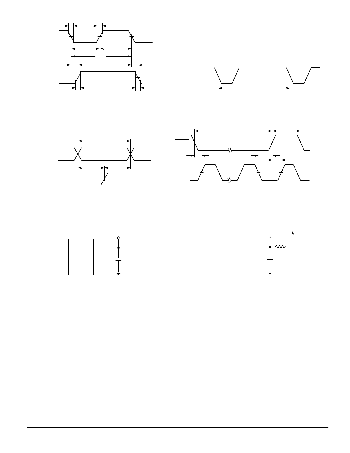
CLOCK
DATA OUT
90%
50%
10%
90%
50%
10%
t
f
t
w
t
PLH
t
TLH
1/f
clk
t
r
t
w
t
PHL
t
THL
V
DD
V
SS
BANK
OUTPUT
50%
Figure 1. Figure 2.
1/f
R
D
ATA IN
CLOCK
VALID
50%
t
su
50%
t
h
Figure 3. Figure 4.
TEST POINT
DEVICE
UNDER
TEST
*
C
L
*Includes all probe and fixture capacitance.
Figure 5. Figure 6.
tw(L)
ENABLE
V
DD
V
SS
V
DD
V
SS
CLOCK
50%
CLOCK
t
su
50%
FIRST
t
LAST
CLOCK
TEST POINT
DEVICE
UNDER
TEST
tw(H)
h
56
C
t
rec
V
DD
Ω
*
L
V
DD
V
SS
V
DD
V
SS
*Includes all probe and fixture capacitance.
MC14489BMOTOROLA
5

PIN DESCRIPTIONS
DIGITAL INTERFACE
Data In (Pin 12)
Serial Data Input. The bit stream begins with the MSB and
is shifted in on the low–to–high transition of Clock. When the
device is not cascaded, the bit pattern is either 1 byte (8 bits)
long to change the configuration register or 3 bytes (24 bits)
long to update the display register. For two chips cascaded,
the pattern is either 4 or 6 bytes, respectively. The display
does not change during shifting (until Enable
to–high transition) which allows slow serial data rates, if desired.
The bit stream needs neither address nor steering bits due
to the innovative BitGrabber registers. Therefore, all bits in
the stream are available to be data for the two registers. Random access of either register is provided. That is, the registers may be accessed in any sequence. Data is retained in
the registers over a supply range of 3 to 5.5 V. Formats are
shown in Figures 8 through 14 and summarized in Table 2.
Information on the segment decoder is given in Table 1.
Data In typically switches near 50% of VDD and has a
Schmitt–triggered input buffer. These features combine to
maximize noise immunity for use in harsh environments and
bus applications. This input can be directly interfaced to
CMOS devices with outputs guaranteed to switch near rail–
to–rail. When interfacing to NMOS or TTL devices, either a
level shifter (MC14504B, MC74HCT04A) or pullup resistor of
1 kΩ to 10 kΩ must be used. Parameters to be considered
when sizing the resistor are the worst–case IOL of the driving
device, maximum tolerable power consumption, and maximum data rate.
Clock (Pin 11)
Serial Data Clock Input. Low–to–high transitions on Clock
shift bits available at Data In, while high–to–low transitions
shift bits from Data Out. The chip’s 24–1/2–stage shift register is static, allowing clock rates down to dc in a continuous or
intermittent mode. The Clock input does not need to be synchronous with the on–chip clock oscillator which drives the
multiplexing circuit.
Eight clock cycles are required to access the configuration
register, while 24 are needed for the display register when the
MC14489B is not cascaded. See Figures 8 and 9.
As shown in Figure 10, two devices may be cascaded. In
this case, 32 clock cycles access the configuration register
and 48 access the display register, as depicted in Figure 10.
Cascading of 3, 4, 5, and 6 devices is shown in Figures 11,
12, 13, and 14, respectively. Also, reference Table 2.
Clock typically switches near 50% of VDD and has a
Schmitt–triggered input buffer. Slow Clock rise and fall times
are tolerated. See the last paragraph of Data In for more information.
NOTE
To guarantee proper operation of the power–on
reset (POR) circuit, the Clock pin must NOT be
floated or toggled during power–up. That is, the
Clock pin must be stable until the VDD pin
reaches at least 3 V.
If control of the Clock pin during power–up is not
practical, then the MC14489B must be reset via bit
C0 in the C register. To accomplish this, C0 is reset low, then set high.
makes a low–
(Pin 10)
Enable
Active–Low Enable Input. This pin allows the MC14489B to
be used on a serial bus, sharing Data In and Clock with other
peripherals. When Enable
Out is forced to a known (low) state, shifting is inhibited, and
the port is held in the initialized state. To transfer data to the
device, Enable
low, a serial transfer is made via Data In and Clock, and
is taken high. The low–to–high transition on Enable
Enable
transfers data to either the configuration or display register,
depending on the data stream length.
Every rising edge on Enable
while data is loaded. Thus, continually loading the device with
the same data may cause the LEDs on some banks to appear
dimmer than others.
Transitions on Enable
while Clock is high. This puts the device out of
synchronization with the microcontroller. Resynchronization occurs when Enable
Clock is low.
This input is also Schmitt–triggered and switches near 50%
of VDD, thereby minimizing the chance of loading erroneous
data in the registers. See the last paragraph of Data In for
more information.
Data Out (Pin 18)
Serial Data Output. Data is transferred out of the shift register through Data Out on the high–to–low transition of Clock.
This output is a no connect, unless used in one of the manners discussed below.
When cascading MC14489B’s, Data Out feeds Data In of the
next device per Figures 10, 11, 12, 13, and 14.
Data Out could be fed back to an MCU/MPU to perform a
wrap–around test of serial data. This could be part of a system check conducted at power–up to test the integrity of the
system’s processor, pc board traces, solder joints, etc.
The pin could be monitored at an in–line Q.A. test during
board manufacturing.
Finally, Data Out facilitates troubleshooting a system.
DISPLAY INTERFACE
Rx (Pin 8)
External Current–Setting Resistor. A resistor tied between
this pin and ground (VSS) determines the peak segment drive
current delivered at pins a through h. Pin 8’s resistor ties into
a current mirror with an approximate current gain of 10 when
bit D23 = high (brighten). With D23 = low, the peak current is
reduced about 50%. Values for Rx range from 700 Ω to infinity. When Rx = ∞ (open circuit), the display is extinguished.
For proper current control, resistors having ±1% tolerance
should be used. See Figure 7.
Small Rx values may cause the chip to overheat
if precautions are not observed. See Thermal
Considerations.
(which initially must be inactive high) is taken
is in an inactive high state, Data
initiates a blanking interval
NOTE
must not be attempted
is high and
CAUTION
MC14489B MOTOROLA
6
a through h (Pins 1, 2, 4 – 7, 19, 20)
Anode–Driver Current Sources. These outputs are closely–matched current sources which directly tie to the anodes
of external discrete LEDs (lamps) or display segment LEDs.
Each output is capable of sourcing up to 35 mA.
When used with lamps, outputs a, b, c, and d are used to
independently control up to 20 lamps. Output h is used to control up to 5 lamps dependently. (See Figure 17.) For lamps,
No Decode
the
mode is selected via the configuration regis-
ter, forcing e, f, and g inactive (low).
When used with segmented displays, outputs a through g
drive segments a through g, respectively. Output h is used to
drive the decimals. Refer to Figure 9. If unused, h must be left
open.
Bank 1 through Bank 5 (Pins 9, 13, 15, 16, 17)
Diode–Bank FET Switches. These outputs are low–resistance switches to ground (VSS) capable of handling currents
of up to 320 mA each. These pins directly tie to the common
cathodes of segmented displays or the cathodes of lamps
(wired with cathodes common).
The display is refreshed at a nominal 1 kHz rate to achieve
optimum brightness from the LEDs. A 20% duty cycle is utilized.
Special design techniques are used on–chip to accommodate the high currents with low EMI (electromagnetic interference) and minimal spiking on the power lines.
POWER SUPPLY
VSS (Pin 14)
Most–negative supply potential. This pin is usually ground.
Resistor Rx is externally tied to ground (VSS). Therefore,
the chip’s VSS pin does not contain the Rx current component.
VDD (Pin 13)
Most–positive supply potential.
To guarantee data integrity in the registers and to ensure
the serial interface is functional, this voltage may range from
3 to 6 volts with respect to VSS. For example, within this voltage range, the chip could be placed in and out of the low–
power mode.
To adequately drive the LEDs, this voltage must be 4.5 to
6 volts with respect to VSS.
The VDD pin contains the Rx current component plus the
chip’s current drain. In the low–power mode, the current mirror and clock oscillator are turned off, thus significantly reducing the VDD current, IDD.
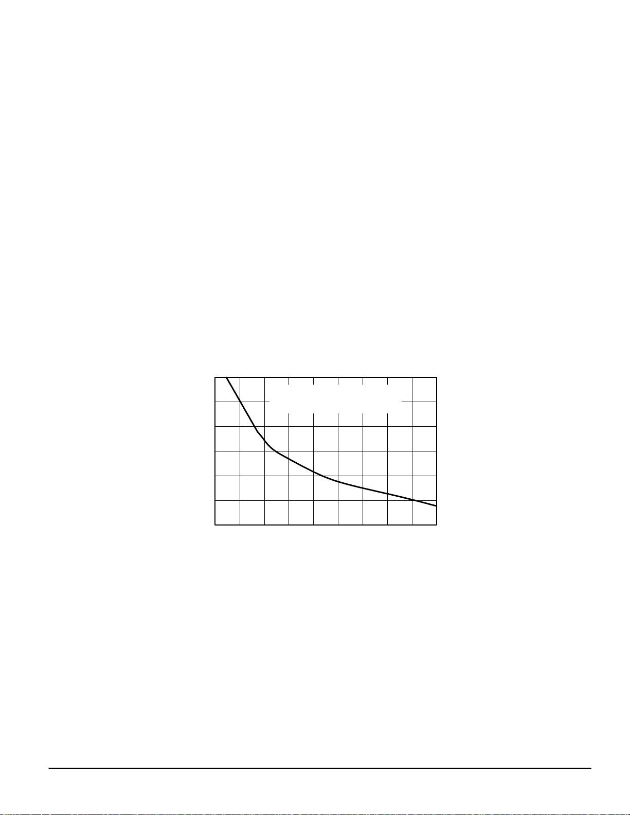
35
30
25
20
15
PEAK DRIVE CURRENT (mA)
OH,
i
10
5
400 800 1.2 k 2.0 k 2.4 k 2.8 k 3.2 k 3.6 k 4.0 k1.6 k
NOTE:Drive current tolerance is approximately ± 15%.
BIT D23 = HIGH (BRIGHTEN LEDs)
WITH D23 = LOW, iOH IS CUT BY
Rx, EXTERNAL RESISTOR (Ω)
5 V SUPPLY
∼
50%.
Figure 7. a through h Nominal Current per Output versus Rx
MC14489BMOTOROLA
7

Table 1. Triple-Mode Segment Decoder Function Table
Lamp Conditions
No DecodeG)
7-Segment Display
CharactersBank Nibble Value
Hex Decode
L
H
L
H
(Invoked via
Bits C1 to C5)
"
u
I
I
2
3
l./
s
@
G
,
,
8
~
9
@
'-I
,-,
'c,
,-
L
,
c'
E
F
Binary
Hexadecimal
$0
$1
$2
$3
$4
$5
$6
$7
$8
$9
$A
$B
$C
$0
$E
$F
NOTES:
1. In the No Decode mode, outputs e, f, and g are unused and are all forced inactive (low). Output
h decoding is unaffected, i.e., unchanged from the other modes. The No Decode mode is used
for three purposes:
a. Individually controlling lamps.
b. Controlling a half digit with sign.
c. Controlling annunciators. examples: AM, PM, UHF, kV, mm Hg.
2. Can be used as capital S.
3. Can be used as capital B.
4. Can be used as small g.
MSB LSB
L L L
L L H
L H L
L H H
H L L
H L H
H H L
H H H
IH L L L
H L L H
H L H L
H L H H
H
H
H
H
H
H
H r
H
Special
Decode
(Invoked via
Bits C1 to C7)
c
,','
,'I
,
u
I
L
"
O
O
,
,-
u
LI
~
0
(Invoked via
Bits C1 to C7)
d bc
on
on on
on
on on
on on
on on
on
on
on
on on on
on on
on on
on on on
on on on on
on
a
on
on
on
on
MC14489B
8
MOTOROLA
~

D0
D1
D2
D3
D4
D5
D6
NOTE: The low–power (standby) mode places the device
in a static state, thus eliminating EMI and mux switching
noise. Therefore, during precision analog measurements,
the low–power mode could be invoked by a system’s MCU.
Also, the low–power mode blanks the display, and could
be used to flash the LEDs on and off.
SEE TABLE 1
D7
D8
D9
D10
D11
BANK 1
NIBBLE
BANK 2
NIBBLE
BANK 3
NIBBLE
SEE TABLE 1
23456781
LSB
MSB
L = LOW POWER MODE (BLANKS THE DISPLAY), FORCED LOW (L) BY POWER ON RESET
H = NORMAL MODE
C0
C6 C5 C4 C3 C2 C1C7
L = HEX DECODE, H = DEPENDS ON C6
CONTROLS BANK 2: L = HEX DECODE, H = DEPENDS ON C6
CONTROLS BANK 3: L = HEX DECODE, H = DEPENDS ON C6
CONTROLS BANK 4: L = HEX DECODE, H = DEPENDS ON C7
CONTROLS BANK 1:
CONTROLS BANK 5: L = HEX DECODE, H = DEPENDS ON C7
(a) Configuration Register Format (1 Byte)
L = NO DECODE, H = SPECIAL DECODE (REFER TO C4 AND C5)
L = NO DECODE, H = SPECIAL DECODE (REFER TO C1, C2, AND C3)
234567891011121314151617181920212223241
MSB LSB
D12
D13
D14
D15
D16
D17
D18
D19
D20
D21
D22
D23
BANK 4
NIBBLE
BANK 5
NIBBLE
= ALL h OUTPUTS INACTIVE
= ACTIVATE h IN BANK 1
= ACTIVATE h IN BANK 2
LHLHLHL
LLHHLLH
LLLLHHH
THE LSBs OF EACH BANK NIBBLE ARE D0, D4, D8, D12, AND D16.
= ACTIVATE h IN BANK 3
= ACTIVATE h IN BANK 4
= ACTIVATE h IN BANK 5
= ACTIVATE h IN BOTH BANKS 1 AND 2
= ACTIVATE h IN ALL BANKS
H
H
H
(b) Display Register Format (3 Bytes)
NOTE: L = Low V oltage Level (Logic 0), H = High Voltage Level (Logic 1)
L = DIM LEDs, H = BRIGHTEN LEDs
ENABLE
CLOCK
DATA IN
ENABLE
CLCOK
DATA IN
Figure 8. Timing Diagrams for Non–Cascaded Devices
MC14489BMOTOROLA
9

+ 5 V
CMOS
MCU/MPU
+ 5 V
OPTIONAL
Rx
V
DD
V
SS
DATA OUT
Rx
DATA IN
CLOCK
ENABLE
APPLICATIONS INFORMATION
MC14489B
a
b
c
d
e
g
h
BANK 5
BANK 4
BANK 3
BANK 2
BANK 1
8
f
88888
a
b
f
g
•
#5 #4 #3 #2 #1
ce
d
h
Figure 9. Non–Cascaded Application Example: 5 Character Common Cathode
LED Display with Two Intensities as Controlled via Serial Port
MC14489B MOTOROLA
10

~o~
z~z
<~<
00 tO
~o~
zt-z
~ ~
"
~
I/)
c
~
Q)
" .c
Q) -
-c
I/) .-
II)
~
i:;Q-
~
I ~~~
aJ (!)U)-
--Gj
~
I ~~Q
("I
-'
<
Q In
1- GI
~ .~
>
I GI
I ~
Lt)
i .!
Dl
C
=6
~
1,)
In
~
(J
:§:
I w
~
I ~
ID 1-
C 2:
II:
I o
(0) C
~ I ~
ID
I ~
D Z
~
~ ~O~
I
~~
I ~~~~- --~
';!?rn ~ffio
au.
Sa:
cn
...
w
ow
.51
w
a:
c
o
;
IV
...
~
CI
;0=
C
0
(J
--
8.
c I/)
~~
>..c
"'-
'Q.°
I/) ~
.-Q)
"C.c
Q) E
>. ~
cb ;
.c
O ~
~ 0
~ 01
I/) C
C .-
." "C
~ C
-Q)
C Q.
.0 Q)
~ "C
~ .
~
~ I/)
Q)
-
.g' .~
U)
C >
0 Q)
.51
U "C
Q)
Q) "C
a:
>m
!~
ii
U)
~ ~
'"" Q)
c
C .c
Q) -
u
Q) C
-
.c .-
-I/)
OI~
C ~
.c U
~ 8
"C ~
~~
.Q I/)
J, ~
> -
u Q)
." >.
-.c
g-.b
-" ~
I/) 0
~J
.QI ."
.c ~
Q) Q)
> :5
U .a;
"' .
C .c
.-01
Q) .-
.c.C
--"
I/) U
~ jg
E >..c
= 01
"' ~
'"" 0
:5 .5
.c .!a
Figure 10. Bit Stream Formats for Two Devices Cascaded
1~li « c
z Q)
UJ.C
..s:
UJ
~

1/1
..
Q)
...
1/1
.51
Q)
11:
c
.2
~
..
~
C)
;;:
c
O
u
B
Figure 11. Bit Stream Formats for Three Devices Cascaded
..:
'*
c: Q)
(\1.0
~ c: .
>-B.C:
~ .2'
c.Q).c.
.~ >. Q)
"c .0 .~
Q). u
>.~(\1
-9 B .5
~W .-c:-1
O ...
~oaJ
O"cc(
~. Z
2.Q)W
U) c:
c:°Q)
(\IQ)~
~ -(\I
---
c:-~
° .Il)
.-~ ~
"§1!."C
U) c:
:J .-(\I
.2' &JI .
'E~U)
o>-Q)
U(\1>.
Q)Q..O
>. .~ C')
~ "ccn
Q) (\I
.c.-
Q) -~
.= 01 2.
-c:U)
C::QC:
Q) (\I e
Q)"C-
.c.c.~
-:J-.r
0Ic:~
Q) .
c:
.c: U
:J.C.Q)
"c~C.
U)
~ ~
~-~
OQ)J:
->~
J, "' ~
> (\I -
:;: E Q)
In
...
UQ)Q)
(\I .-U)
41
-<{ c. .c:
"cn
Q) .CJ
~ U) .-
'61
41
a:
>la
"5.
In
c
:§:
Q).C.
.~ .!J Q)
~»
.c: Q) .-
OI"cU
.-"c (\I
.c: Q) .5
~"c
(\I (\I [D
.5 U ~
Q)Q)w
.O=Q)
-c:0)
~ .-3
E ~ c.
>-:J~
-HC')
~o-:
...~ U)
Q) Q)
C:
.-->.
.c.0).o
U c:
.-(\I co
.c. "'
~ -~
~Q)2.
~ UJ >. 0)
-1-9C:
aJoe
c(.-:::.
z~C\I
WO~
"I:i.b~
Q) -
"Cc:Q)
.2 (\I >
U ~ .c:Q)U
.-.c: (\I
~ ...
U).r:aJ
Q) .2' c(
>..c:Z
.O~W
, U Q)
~~~
B-s
.c.~
...01.-
C::J~
O O ..
"C ~ ~
, .0 ~
OIU)O
c: .-=
.-" .O
"C~-
(\I-1U)
Q)aJ(\1
-a;c("C
.c:ZQ)
-W-
c:c:C:
Q) Q) ..c:.c:E
~~~
Uj
b
z
~UJ U~-1
~UJ (\IQ)-1
(\I


:.:=0:.:
Z
I- Z
< <
00 00
.c
~
"'
~o~
ZI-Z
~ ~
.c
~
"'
~o~
z
t- z
< <
00 00
.c
~
...
~o~
2
1- 2
< <
00 00
.c
9
"'
"'
"'
"'
"'
~~
~o
Lt)
:11:
m
0>
~
v
v
.-
u
~
~z
<-
n
~~
~o
M
=11=
ID
0)
~
~
~
,-
U
~
<
~~i
'"' i
~~
~o
N
*
m
0>
~
qo
,..
U
~
~z
<-
1"
~~
00
~
0) ~,
~ W
"'"
"'" ~
U 8
~ ;1
~z
~-
0
I~
~
UJI
8
-'
0
I~
§
u
In
Q)
u
">
Q)
0
Q)
>
~
CI
C
w
ffi
~
"I
~
<.>
I ~~
::J
<n a.
o~
~::J
uu
~
-' IU
~ (,)
0 --
-IU
1- --
~
0
:g
U
In
OLL
I gJ.!..
~0",
W~
I ~0:.. ~fi3 5~~
mt;: -->
I ZLL(!)W cn:c 8 wo ~cn 0:
I--
(/)
Qj
-u;
'61
0)
~
c
o
;
cu
..
~
Dl
-=
C
0
U
§:
c:
Q) "'
.c: Q)
$:'(iJ
"' ~
Q) '"'
'(iJ;
C:.c:
~ -
~ c:
>- .~ I/)
-Q)
~>-
.-.Q
"0-
Q) 0
>-'"'
;b~
.-:3
'"' c
0 Q)
'"'.C:
Q)-
'(iJ C
C 0
~ CI
-C
C .0"0
.-C
-Q)
~ a.
:. Q)
CI"0
IC -
C U>
8 .~
Q) >
III ~>- ~
.."0
Q) Q)
-.-"0
~ Q) B
CI .= I/)
Q) -~
~ ~ u
>Q)Q)
ca £:5
-c:
c. CI .-
.! .E ~
c :.:3
"0 u
u ~8
"-' 0'"'
1~
> c:
~ ~
U '"'
~ -
-Q)
a.>.
~;b
:c-'"'
ClO
:c~
Q) .>
~ ~
U '"'
"' Q)
.E £
Q) .a;
.Q .
-.c:
U> CI
:. .E.C:
>-u
= ~
.~ .Q
,.. -
c: .c:
.-CI
.c: ~
U 0
:c.c
~ I/)
~.-
lili
~
z
c:
~
~

~o~
Z
I- Z
~ ~
.c
~
...
~o~
ZI-Z
~ ~
.c
~
"'
~ ~
zgz
< <
CD CD
.c
~
...
~o~
ZLZ
<~<
CD CD
.c
~
m
II)
"'
"'
"'
ID
=!I:
ID
0)
CO
~
~
~
()
~
M
'#:
m
01
~
q-
q-
~
U
~
('II
=11:
m
0)
~
~
~
?-
u
~
~z
<-
a
~5
~o
,..
m ~
0) z
rD w
~
q- ~
c:; 8
~ 5
.<
~~
"1
<
'<~
0
~!;
~o
z
au.
1=" ~a-
~~ '
~5
~o
I~
~
§
u
~z
<-
n
~I:;
~o
UJ
-'
00
~
III
8
d
UI
Q)
U
'>
Q)
C
><
in
Dl
C
--' IV
< U
z O IV
1-
CI.
O
=6
~
III
w
-'
[0
<
z
w
8
-'
(.)
Iw :11: -J
=>
Inll.
o~
~=>
l>~
1 ~ ~ ~
;;:aJ ~a(t;
10
!
z
~~'"'
~a:-
::I1:!~
(!)00-
-->
LL(!)W
8~o
I ~ 11.
~ ~~~
IIJ 115!7j~
~ I~~~
~ I
~ ~
z
Ou.
-0."
'< ..
a:a:w
::J~U
<.?CI)-
-->
u.<.?w
Zwc
Sa:
Ou.
I g~-
F;°~
~~
I ~ ~ ~
>=~ (.!)cn-
aJtL: [!:a[;j
f--
1 ~wc cn:l: Olr
~cn (,)
8 wc -11:
~
<
u
1-
Z
~
w
~
1-
~
w
a:
5
1-
Z
8
w
Ir
~
UI
...
Q)
~
'51
Q)
a:
c
o
;:
la
...
~
CI
;;:
C
O
(J
e:
~
w
Ir
<
u
~
8
w
a:
<
(.)
1-
Z
8
~
~
~
z
8
c
w ~
~.;
~ as
.p!.;.
(/) Q!
C.c
as -
;. c
>. .as (/)
-w
.~~
-0Q! 0
l~
,.. :.
...c
0 Q!
W-
in C
C 0
~ CJ
-C
C .0 -0
.-C
"§ ~
:. W
CJ-0
10= .
C (/)
8 .~
w Q!
cn ~-0
..I -0
GI(OW
-,..-0
~ Q! ~
CI~~
GI c ~
a: W
>- Q!~
ca .c-
--c
c. CJ .-
~ .2 ~
0 :.:.
-0 u
~ >u
CJ ~ 0
0...
1.;
> C
-:: ~
U (1J Q!
c.>.
~~
.-,..
:2"...
CJO
:2~
W ,..
>
-:: (1J
U ...
(1J Q!
.E :5
w .a;
.c .
-.c
"' CJ
:. .E.C
>.u
= as
~.c
.2 :E
-CJ
.c :.
u 0
.c.c
~ (/)
~.-
I~ I~
~ID
Z<
wffi
w
b
z
c
c
~
Figure 14. Bit Stream Formats tor Six Devices Cascaded
15
~

Table 2. Register Access for Two or More Cascaded Devices
Configuration Register Access Display Register Access
Number of Leading
Cii*
Criteria*
If 3N is a Multiple of 4 3N 2 3N + 2 2
If 3N – 1 is a Multiple of 4 3N – 1 1 3N + 1 1
If 3N – 2 is a Multiple of 4 3N – 2 0 3N 0
If 3N – 3 is a Multiple of 4 3N – 2 0 3N 0
*N = number of devices that are cascaded. For example, to drive 10 digits, 2 devices are cascaded; therefore, N = 2. To drive 35 digits, seven
devices are cascaded; therefore N = 7.
Total Number of Bytes
“Don’t Care” Bytes
LED DISPLAY
Total Number of Bytes
Number of Leading
“Don’t Care” Bytes
+ 5 V
CMOS
MCU/MPU
NOTE:R1 limits the maximum current to avoid damaging the display and/or the MC14489B
due to overheating. See the Thermal Considerations section. An 1/8 watt resistor
may be used for R1. R2 is a 1 kΩ or 5 kΩ potentiometer (≥ 1/8 watt). R2 may be a
light–sensitive resistor.
85
V
DD
MC14489B
Rx
V
SS
+ 5 V
R1
R2
Figure 15. Common–Cathode LED Display with Dial–Adjusted Brightness
MC14489B MOTOROLA
16

UNIVERSAL OVERFLOW
(“1” OR “HALF–DIGIT”)
USE TO DRIVE LAMP
OR MINUS SIGN
MC14489B
INPUT LINES
NOTE:A Universal Overflow pins out all anodes and cathodes.
Figure 16. Driving 5 1/2 Digits
5–DIGIT DISPLAY
4
BANK OUTPUTS
3
7
5h
a TO g321
MC14489BMOTOROLA
17

MC14489B
a
b
c
d
THESE LAMPS
INDEPENDENTLY
CONTROLLED WITH
BITS D0 TO D19
3
CMOS
MCU/MPU
e
f
g
h
BANK 1
BANK 2
BANK 3
BANK 4
BANK 5
NC
NC
NC
THESE LAMPS DEPENDENTLY
CONTROLLED WITH
BITS D20, D21, AND D22*
*If required, this group of lamps can be independently controlled. To accomplish independent control, only connect lamps to BANK 1 and
BANK 2 for output h (two lamps). Then, use bits D20, D21, and D22 for control of these two lamps.
Figure 17. 25–Lamp Application
MC14489B MOTOROLA
18

4
•
4
a TO d BANK 1
4 4
e TO h
TO
BANK 4
MC14489B
3
CMOS MCU/MPU
BANK 5
Figure 18. 4–Digit Display Plus Decimals with Four Annunciators
or 4–1/2–Digit Display Plus Sign
MUXED 5–DIGIT MONOLITHIC DISPLAY (CLUSTER)
HEWLETT–PACKARD 5082–7415 OR EQUIVALENT
14
123621085113497
6 5 4 2 1 20 19 17 16 15 13 97
8
MC14489B
3
INPUT LINES
Figure 19. Compact Display System with Three Components
MC14489BMOTOROLA
19

THERMAL CONSIDERATIONS
The MC14489B is designed to operate with a
chip–junction
temperature (TJ) ranging from – 40 to 130°C, as indicated in
the electrical characteristics tables. The
temperature range (TA) is dependent on R
ambient
operating
, the internal
θJA
chip current, how many anode drivers are used, the number
of bank drivers used, the drive current, and how the package
is cooled. The maximum ratings table gives the thermal resistance, junction–to–ambient, of the MC14489B mounted on a
pc board using natural convection to be 90°C per watt for the
plastic DIP. The SOG thermal resistance is 100°C per watt.
The following general equation (1) is used to determine the
power dissipated by the MC14489B.
PT = PD + P
I
(1)
where
PT=Total power dissipation of the MC14489B
PD=Power dissipated in the driver circuitry (mW)
PI=Power dissipated by the internal chip
circuitry (mW)
The equations for the two terms of the general equation
are:
PD = (iOH) (N)(VDD – V
)(B/5) (2)
LED
(3)PI = (1.5 mA)(VDD) + IRx(VDD – IRxRx)
where
iOH=Peak anode driver current (mA)
IRx=iOH /10, with iOH = the peak anode driver current
(mA) when the dimmer bit is high
N=Number of anode drivers used
B=Number of bank drivers used
Rx=External resistor value (kΩ)
VDD=Maximum supply voltage, referenced to V
SS
(volts)
V
=Minimum anticipated voltage drop across the
LED
LED
1.5 mA=Operating supply current of the MC14489B
The following two examples show how to calculate the
maximum allowable ambient temperature.
That is, if TA = 79°C, the maximum junction temperature is
130°C. The chip’s average temperature for this example is
lower than 130°C because all segments are usually not illuminated simultaneously for an indefinite period.
Worst–Case Analysis Example 2:
16 lamps (4 banks and 4 anode drivers)
SOG without heat sink on PC board
iOH=30 mA max
V
=1.8 V min
LED
VDD=5.5 max
PD = (30)(4)(5.5 – 1.8)(4/5) = 355 mW Ref. (2)
PI = (1.5)(5.5) + 3[5.5 – 3(1.0)] = 16 mW Ref. (3)
Therefore, PT = 355 + 16 = 371 mW Ref. (1)
and ∆T
chip
= R
= (100°C/W)(0.371) = 37°C
θJAPT
Finally, the maximum allowable
TA = TJmax – ∆T
= 130 – 37 = 93°C
chip
To extend the allowable ambient temperature range or to
reduce TJ, which extends chip life, a heat sink such as shown
in Figure 20 can be used in high–current applications. Alternatively, heat–spreader techniques can be used on the PC
board, such as running a wide trace under the MC14489B and
using thermal paste. Wide, radial traces from the MC14489B
leads also act as heat spreaders.
AAVID #5804 or equivalent
(Tel. 603/524–4443, FAX 603/528–1478)
Motorola cannot recommend one supplier over another and
in no way suggests that this is the only heat sink supplier.
Worst–Case Analysis Example 1:
Figure 20. Heat Sink
5–digit display with decimals (5 banks and 8 anode drivers)
DIP without heat sink on PC board
iOH=20 mA max
V
=1.8 V min
LED
VDD=5.25 max
PD = (20)(8)(5.25 – 1.8)(5/5) = 552 mW Ref. (2)
PI = (1.5)(5.25) + 2[5.25 – 2(2)] = 10 mW Ref. (3)
Therefore, PT = 552 + 10 = 562 mW Ref. (1)
and ∆T
chip
= R
= (90°C/W)(0.562) = 51°C
θJAPT
Finally, the maximum allowable
TA = TJmax – ∆T
= 130 – 51 = 79°C
chip
Table 3. LED Lamp and Common–Cathode Display
Manufacturers
Supplier
QT Optoelectronics
Hewlett–Packard (HP), Components Group
Industrial Electronic Engineers (IEE), Component Products Div.
Purdy Electronics Corp., AND Product Line
NOTE:Motorola cannot recommend one supplier over another
and in no way suggests that this is a complete listing of
LED suppliers.
MC14489B MOTOROLA
20

PACKAGE DIMENSIONS
P SUFFIX
PLASTIC DIP
CASE 738–03
-T-
SEATING
PLANE
-A-
1120
B
110
C
K
E
N
GF
D
20 PL
0.25 (0.010) T A
M M
DW SUFFIX
SOG PACKAGE
CASE 751D–04
L
J 20 PL
0.25 (0.010) T B
M
M M
NOTES:
1.DIMENSIONING AND TOLERANCING PER ANSI
Y14.5M, 1982.
2.CONTROLLING DIMENSION: INCH.
3.DIMENSION L TO CENTER OF LEAD WHEN
FORMED PARALLEL.
4.DIMENSION B DOES NOT INCLUDE MOLD
FLASH.
INCHES MILLIMETERS
MIN MINMAX MAX
DIM
A
B
C
D
E
F
G
J
K
L
M
N
1.010
0.240
0.150
0.015
0.050 BSC
0.050
0.100 BSC
0.008
0.110
0.300 BSC
°
0
0.020
1.070
0.260
0.180
0.022
0.070
0.015
0.140
15
0.040
25.66
27.17
6.10
6.60
3.81
4.57
0.39
0.55
1.27 BSC
1.27
1.77
2.54 BSC
0.21
0.38
2.80
3.55
7.62 BSC
°
°
°
0
15
1.01
0.51
–A–
20
1
D20X
0.010 (0.25) B
11
S
P10X
0.010 (0.25)
MBM
J
–B–
10
SAM
T
F
R
X 45
_
C
SEATING
–T–
18X
G
K
PLANE
M
NOTES:
1.DIMENSIONING AND TOLERANCING PER
ANSI Y14.5M, 1982.
2.CONTROLLING DIMENSION: MILLIMETER.
3.DIMENSIONS A AND B DO NOT INCLUDE
MOLD PROTRUSION.
4.MAXIMUM MOLD PROTRUSION 0.150
(0.006) PER SIDE.
5.DIMENSION D DOES NOT INCLUDE
DAMBAR PROTRUSION. ALLOWABLE
DAMBAR PROTRUSION SHALL BE 0.13
(0.005) TOTAL IN EXCESS OF D DIMENSION
AT MAXIMUM MATERIAL CONDITION.
DIM MIN MAX MIN MAX
A 12.65 12.95 0.499 0.510
B 7.40 7.60 0.292 0.299
C 2.35 2.65 0.093 0.104
D 0.35 0.49 0.014 0.019
F 0.50 0.90 0.020 0.035
G 1.27 BSC 0.050 BSC
J 0.25 0.32 0.010 0.012
K 0.10 0.25 0.004 0.009
M 0 7 0 7
__
P 10.05 10.55 0.395 0.415
R 0.25 0.75 0.010 0.029
INCHESMILLIMETERS
__
MC14489BMOTOROLA
21

Motorola reserves the right to make changes without further notice to any products herein. Motorola makes no warranty, representation or guarantee regarding
the suitability of its products for any particular purpose, nor does Motorola assume any liability arising out of the application or use of any product or circuit, and
specifically disclaims any and all liability, including without limitation consequential or incidental damages. “Typical” parameters which may be provided in Motorola
data sheets and/or specifications can and do vary in different applications and actual performance may vary over time. All operating parameters, including “Typicals”
must be validated for each customer application by customer’s technical experts. Motorola does not convey any license under its patent rights nor the rights of
others. Motorola products are not designed, intended, or authorized for use as components in systems intended for surgical implant into the body, or other
applications intended to support or sustain life, or for any other application in which the failure of the Motorola product could create a situation where personal injury
or death may occur. Should Buyer purchase or use Motorola products for any such unintended or unauthorized application, Buyer shall indemnify and hold Motorola
and its officers, employees, subsidiaries, affiliates, and distributors harmless against all claims, costs, damages, and expenses, and reasonable attorney fees
arising out of, directly or indirectly, any claim of personal injury or death associated with such unintended or unauthorized use, even if such claim alleges that
Motorola was negligent regarding the design or manufacture of the part. Motorola and are registered trademarks of Motorola, Inc. Motorola, Inc. is an Equal
Opportunity/Affirmative Action Employer.
How to reach us:
USA/EUROPE/Locations Not Listed: Motorola Literature Distribution; JAPAN: Nippon Motorola Ltd.; SPD, Strategic Planning Office, 141,
P.O. Box 5405, Denver, Colorado 80217. 1–303–675–2140 or 1–800–441–2447 4–32–1 Nishi–Gotanda, Shinagawa–ku, Tokyo, Japan. 81–3–5487–8488
Customer Focus Center: 1–800–521–6274
Mfax: RMFAX0@email.sps.mot.com– TOUCHTONE 1–602–244–6609 ASIA/PACIFIC: Motorola Semiconductors H.K. Ltd.; Silicon Harbor Center,
Motorola Fax Back System – US & Canada ONLY 1–800–774–1848 2 Dai King Street, Tai Po, N.T., Hong Kong. fax: 852–26666123
– http://sps.motorola.com/mfax/
HOME PAGE: http://mot-sps.com/
Mfax is a trademark of Motorola, Inc.
MC14489 A
22
MC14489B
 Loading...