

Page 1
Freescale Semiconductor
Technical Data
MC13211/212/213/214
Document Number: MC1321x
Rev. 0.0, 03/2006
MC1321x
Package Information
Case 1664-01
71-pin LGA [9x9 mm]
ZigBee™- Compliant Platform -
2.4 GHz Low Power Transceiver
for the IEEE
®
802.15.4 Standard
plus Microcontroller
1 Introduction
The MC1321x family is Freescale’s second-generation
ZigBee platform which incorporates a low power 2.4
GHz radio frequency transceiver and an 8-bit
microcontroller into a single 9x9x1 mm 71-pin LGA
package. The MC1321x solution can be used for wireless
applications from simple proprietary point-to-point
connectivity to a complete ZigBee mesh network. The
combination of the radio and a microcontroller in a small
footprint package allows for a cost-effective solution.
The MC1321x contains an RF transceiver which is an
802.15.4-compliant radio that operates in the 2.4
IEEE
GHz ISM frequency band. The transceiver includes a
low noise amplifier, 1mW nominal output power, PA
with internal voltage controlled oscillator (VCO),
integrated transmit/receive switch, on-board power
supply regulation, and full spread-spectrum encoding
and decoding.
Ordering Information
Device Device Marking Package
MC13211
MC13212
MC13213
MC13214
1
See Table 1 for more details.
Contents
1 Introduction . . . . . . . . . . . . . . . . . . . . . . . . . . 1
2 MC1321x Pin Assignment and Connections 8
3 MC1321x Serial Peripheral Interface (SPI) . 14
4 IEEE 802.15.4 Modem . . . . . . . . . . . . . . . . . . 16
5 MCU . . . . . . . . . . . . . . . . . . . . . . . . . . . . . . . . 25
6 System Electrical Specification . . . . . . . . . 46
7 Application Considerations . . . . . . . . . . . . . 63
8 Mechanical Diagrams . . . . . . . . . . . . . . . . . . 68
1
1
1
1
13211 LGA
13212 LGA
13213 LGA
13214 LGA
The MC1321x also contains a microcontroller based on
the HCS08 Family of Microcontroller Units (MCU) and
can provide up to 60KB of flash memory and 4KB of
RAM. The onboard MCU allows the communications
Freescale reserves the right to change the detail specificatio ns as may be required to permit improvements in the design of i ts
products.
© Freescale Semiconductor, Inc., 2005, 2006. All rights reserved.
Page 2

stack and also the application to reside on the same system-in-package (SIP). The MC1321x family is
organized as follows:
• The MC13211 has 16KB of flash and 1KB of RAM and is an ideal solution for low cost,
proprietary applications that require wireless point-to-point or star network connectivity. The
MC13211 combined with the Freescale Simple MAC (SMAC) provides the foundation for
proprietary applications by supplying the necessary source code and application examples to get
users started on implementing wireless connectivity.
• The MC13212 contains 32K of flash and 2KB of RAM and is intended for use with the Freescale
fully compliant 802.15.4 MAC. Custom networks based on the 802.15.4 standard MAC can be
implemented to fit user needs. The 802.15.4 standard supports star, mesh and cluster tree
topologies as well as beaconed networks.
• The MC13213 contains 60K of flash and 4KB of RAM and is also intended for use with the
Freescale fully compliant 802.15.4 MAC where larger memory is required. In addition, this device
can support ZigBee applications that use a stack from 3rd party vendors.
• The MC13214 is a fully compliant ZigBee platform. The MC13214 contains 60K of flash and 4KB
of RAM and uses the Figure 8 Wireless ZigBee Stack (Z-stack) software. Applications can be
added to develop fully certified ZigBee products.
Applications include, but are not limited to, the following:
• Residential and commercial automation
— Lighting control
— Security
— Access control
— Heating, ventilation, air-conditioning (HVAC)
— Automated meter reading (AMR)
• Industrial Control
— Asset tracking and monitoring
— Homeland security
— Process management
— Environmental monitoring and control
—HVAC
— Automated meter reading
• Health Care
— Patient monitoring
— Fitness monitoring
MC13211/212/213/214 Technical Data, Rev. 0.0,
2 Freescale Semiconductor
Page 3

1.1 Ordering Information
Table 1 provides additional details about the MC1321x family.
Table 1. Orderable Parts Details
Operating
Device
MC13211 -40° to 85° C LGA 1KB RAM,
MC13211R2 -40° to 85° C LGA
MC13212 -40° to 85° C LGA 2KB RAM,
MC13212R2 -40° to 85° C LGA
MC13213 -40° to 85° C LGA 4KB RAM,
MC13213R2 -40° to 85° C LGA
MC13214 -40° to 85° C LGA 4KB RAM,
MC13214R2 -40° to 85° C LGA
Temp Ran ge
(TA.)
Package
Tape and Reel
Tape and Reel
Tape and Reel
Tape and Reel
Memory
Options
16KB Flash
1KB RAM,
16KB Flash
32KB Flash
2KB RAM,
32KB Flash
60KB Flash
4KB RAM,
60KB Flash
60KB Flash
4KB RAM,
60KB Flash
Description
Intended for proprietary applications and Freescale
Simple MAC (SMAC)
Intended for proprietary applications and Freescale
Simple MAC (SMAC)
Intended for IEEE 802.15.4 compliant applications and
Freescale 802.15.4 MAC
Intended for IEEE 802.15.4 compliant applications and
Freescale 802.15.4 MAC
Intended for IEEE 802.15.4 compliant applications and
Freescale 802.15.4 MAC.
Also supports ZigBee applications that use a stack from a
3rd party vendor.
Intended for IEEE 802.15.4 compliant applications and
Freescale 802.15.4 MAC.
Also supports ZigBee applications that use a stack from a
3rd party vendor.
Intended for full ZigBee compliant applications using the
F8 Wireless Z-Stack
Intended for full ZigBee compliant applications using the
F8 Wireless Z-Stack
1.2 General Platform Features
• IEEE 802.15.4 standard compliant on-chip transceiver/modem
— 2.4GHz
— 16 selectable channels
— Programmable output power
• Multiple power saving modes
• 2V to 3.4V operating voltage with on-chip voltage regulators
• -40°C to +85°C temperature range
• Low external component count
• Supports single 16 MHz crystal clock source operation or dual crystal operation
• Support for SMAC, IEEE 802.15.4, and ZigBee software
• 9mm x 9mm x 1mm 71-pin LGA
MC13211/212/213/214 Technical Data, Rev. 0.0,
Freescale Semiconductor 3
Page 4

1.3 Microcontroller Features
• Low voltage MCU with 40 MHz low power HCS08 CPU core
• Up to 60K flash memory with block protection and security and 4K RAM
— MC13211: 16KB Flash, 1KB RAM
— MC13212: 32KB Flash, 2KB RAM
— MC13213: 60KB Flash, 4KB RAM
— MC13214: 60KB Flash, 4KB RAM with ZigBee Z-stack
• Low power modes (Wait plus Stop2 and Stop3 modes)
• Dedicated serial peripheral interface (SPI) connected internally to 802.15.4 modem
• One 4-channel and one 1-channel 16-bit timer/pulse width modulator (TPM) module with
selectable input capture, output capture, and PWM capability.
• 8-bit port keyboard interrupt (KBI)
• 8-channel 8-10-bit ADC
• Two independent serial communication interfaces (SCI)
• Multiple clock source options
— Internal clock generator (ICG) with 243 kHz oscillator that has +/-0.2% trimming resolution
and +/-0.5% deviation across voltage.
— Startup oscillator of approximately 8 MHz
— External crystal or resonator
— External source from modem clock for very high accuracy source or system low-cost option
• Inter-integrated circuit (IIC) interface.
• In-circuit debug and flash programming available via on-chip background debug module (BDM)
— Two comparator and 9 trigger modes
— Eight deep FIFO for storing change-of-flow addresses and event-only data
— Tag and force breakpoints
— In-circuit debugging with single breakpoint
• System protection features
— Programmable low voltage interrupt (LVI)
— Optional watchdog timer (COP)
— Illegal opcode detection
• Up to 32 MCU GPIO with programmable pullups
MC13211/212/213/214 Technical Data, Rev. 0.0,
4 Freescale Semiconductor
Page 5

1.4 RF Modem Features
• Fully compliant IEEE 802.15.4 transceiver supports 250 kbps O-QPSK data in 5.0 MHz channels
and full spread-spectrum encode and decode
• Operates on one of 16 selectable channels in the 2.4 GHz ISM band
• -1 dBm to 0 dBm nominal output power, programmable from -27 dBm to +3 dBm typical
• Receive sensitivity of <-92 dBm (typical) at 1% PER, 20-byte packet, much better than the IEEE
802.15.4 specification of -85 dBm
• Integrated transmit/receive switch
• Dual PA ouput pairs which can be programmed for full differential single-port or dual-port
operation that supports an external LNA and/or PA.
• Three low power modes for increased battery life
• Programmable frequency clock output for use by MCU
• Onboard trim capability for 16 MHz crystal reference oscillator eliminates need for external
variable capacitors and allows for automated production frequency calibration
• Four internal timer comparators available to supplement MCU timer resources
• Supports both packet data mode and streaming data mode
• Seven GPIO to supplement MCU GPIO
1.5 Software Features
Freescale provides a wide range of software functionality to complement the MC1321x hardware. There
are three levels of application solutions:
1. Simple proprietary wireless connectivity.
2. User networks built on the IEEE 802.15.4 MAC standard.
3. ZigBee-compliant network stack.
1.5.1 Simple MAC (SMAC)
• Small memory footprint (about 3 Kbytes typical)
• Supports point-to-point and star network configurations
• Proprietary networks
• Source code and application examples provided
1.5.2 IEEE 802.15.4-Compliant MAC
• Supports star, mesh and cluster tree topologies
• Supports beaconed networks
• Supports GTS for low latency
MC13211/212/213/214 Technical Data, Rev. 0.0,
Freescale Semiconductor 5
Page 6
1.5.3 ZigBee-Compliant Network Stack
• Supports ZigBee 1.0 specification
• Supports star, mesh and tree networks
• Advanced Encryption Standard (AES) 128-bit security
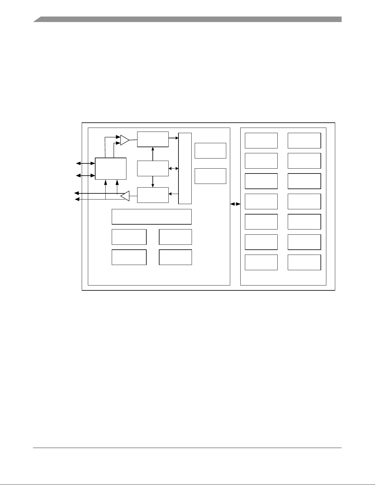
1.6 System Block Diagram
Figure 1 shows a simplified block diagram of the MC1321x solution.
RIN_P(PAO_P)
RIN_M(PAO_M)
PAO_P
PAO_M
Analog Receiver
Transmit/Receive
Switch
IRQ Arbiter RAM Arbiter
Power Management Voltage Regulators
Frequency
Generator
Analog Transmitter
Buffer RAM
Figure 1. MC1321x System Level Block Diagram
HCS08 CPU
RFIC Timers
16-60 KB
Flash Memory
Digital
Digital Control
Transceiver
Logic
1-4 KB RAM
Dedicated
SPI
Low Voltage Detect
Keyboard Interrupt
Internal Clock
Generator
Background
Debug Module
8 Channel
10 Bit ADC
2x SCI
I2C
1 Channel & 4
Channel 16-bit
Timers
COP
Up to 32 GPIO
802.15.4 M odem H CS08 M CU
MC13211/212/213/214 Technical Data, Rev. 0.0,
6 Freescale Semiconductor
Page 7
1.7 System Clock Configuration
The MC321x device allows for a wide array of system clock configurations:
• Pins are provided for a separate external clock source for the CPU. The external clock source can
by derived from a crystal oscillator or from an external clock source
• Pins are provided for a 16 MHz crystal for the modem clock source (required)
• The modem crystal oscillator frequency can be trimmed through programming to maintain the tight
tolerances required by IEEE 802.15.4
• The modem provides a CLKO programmable frequency clock output that can be used as an
external source to the CPU. As a result, a single crystal system clock solution is possible
• Out of reset, the MCU uses an internally generated clock (approximately 8-MHz) for start-up. This
allows recovery from stop or reset without a long crystal start-up delay
• The MCU contains an internal clock generator (which can be trimmed) that can be used to run the
MCU for low power operation. This internal reference is approximately 243 kHz
MC 1321X
802.15.4 MODEM HCS08 M CU
XTAL1 XTAL2 CLKO
EXTAL XTAL
27
16MHz
Figure 2. MC1321x Single Crystal System Clock Structure
28 10
98
MC13211/212/213/214 Technical Data, Rev. 0.0,
Freescale Semiconductor 7
Page 8
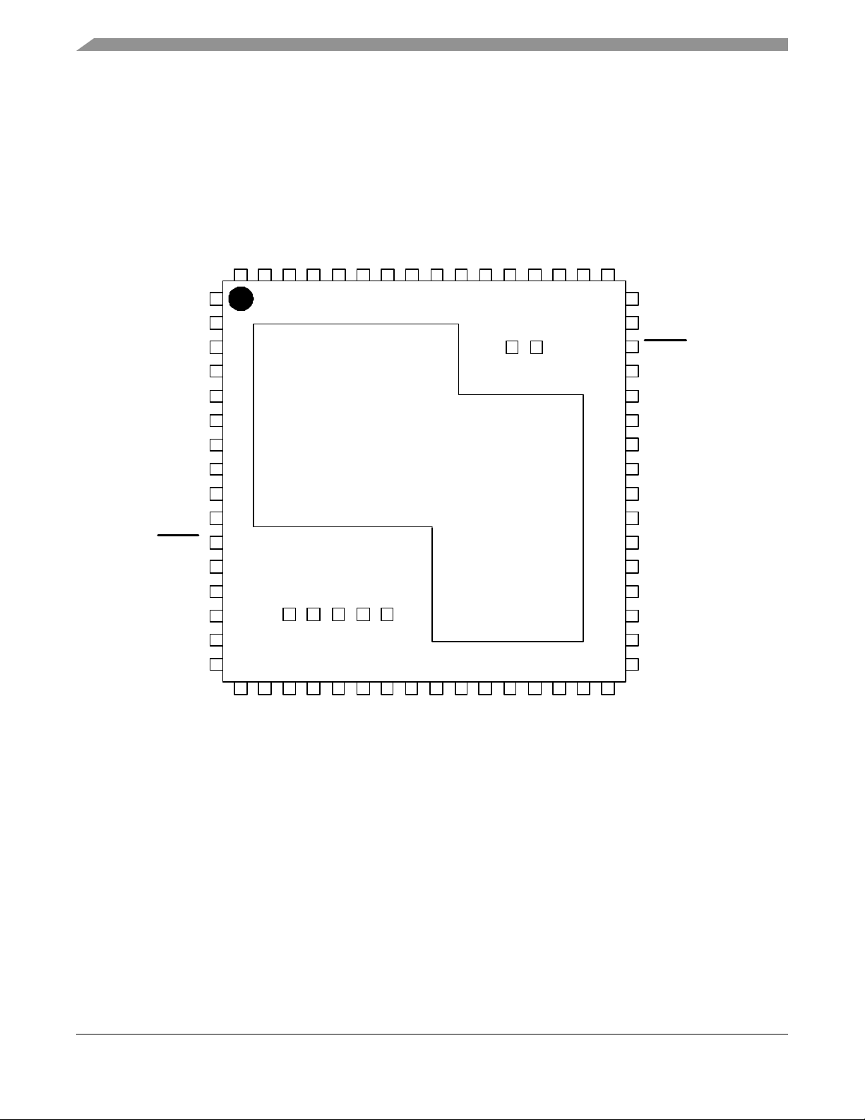
2 MC1321x Pin Assignment and Connections
Figure 3 shows the MC1321x pinout.
PTA3/KBI1P3
PTA4/KBI1P4
PTA5/KBI1P5
PTA6/KBI1P6
PTA7/KBI1P7
VDDAD
PTG0/BKGD/MS
PTG1/XTAL
PTG2/EXTAL
CLKO
RESET
PTC0/TXD2
PTC1/RXD2
PTC2/SDA1
PTC3/SCL1
PTC4
PTB6/AD1P6
PTA2/KBI1P2
1
16
63 62 61 60 59 58 57 56 55 54 53 52 51 50
2
3
4
5
6
7
8
9
10
11
12
13
14
15
18 19 20 21 22 23 24 25 26 27 28 29 30 31
17
PTC5
PTC6
VREF L
TEST
65
66
PTC7
PTE0/TXD1
PTA0/KBI1P0
PTA1/KBI1P1
PTB7/AD1P7
VREFH
MC1321x
Flag opening
67 68
VDDD
PTE1/RXD1
PTB5/AD1P5
69
VDDINT
GPIO5
PTB4/AD1P4
PTB3/AD1P3
GPIO6
GPIO7
PTB1/AD1P1
PTB2/AD1P2
PTB0/AD1P0
71 70
TEST
XTAL1
XTAL2
VDDLO2
PTD7/TPM2CH4
VDDLO1
PTD6/TPM2CH3
PTD5/TPM2CH2
4964
48
47
46
45
44
43
42
41
40
39
38
37
36
35
34
33
32
VDDVCO
VBATT
PTD4/TPM2CH1
PTD2/TPM1CH2
ATTN
VDD
GPIO1
GPIO2
GPIO3
GPIO4
SM
PAO_M
PAO_P
NC
RFIN_P
RFIN_M
CT_Bias
VDDA
Figure 3. Preliminary MC1321x Pinout
MC13211/212/213/214 Technical Data, Rev. 0.0,
8 Freescale Semiconductor
Page 9

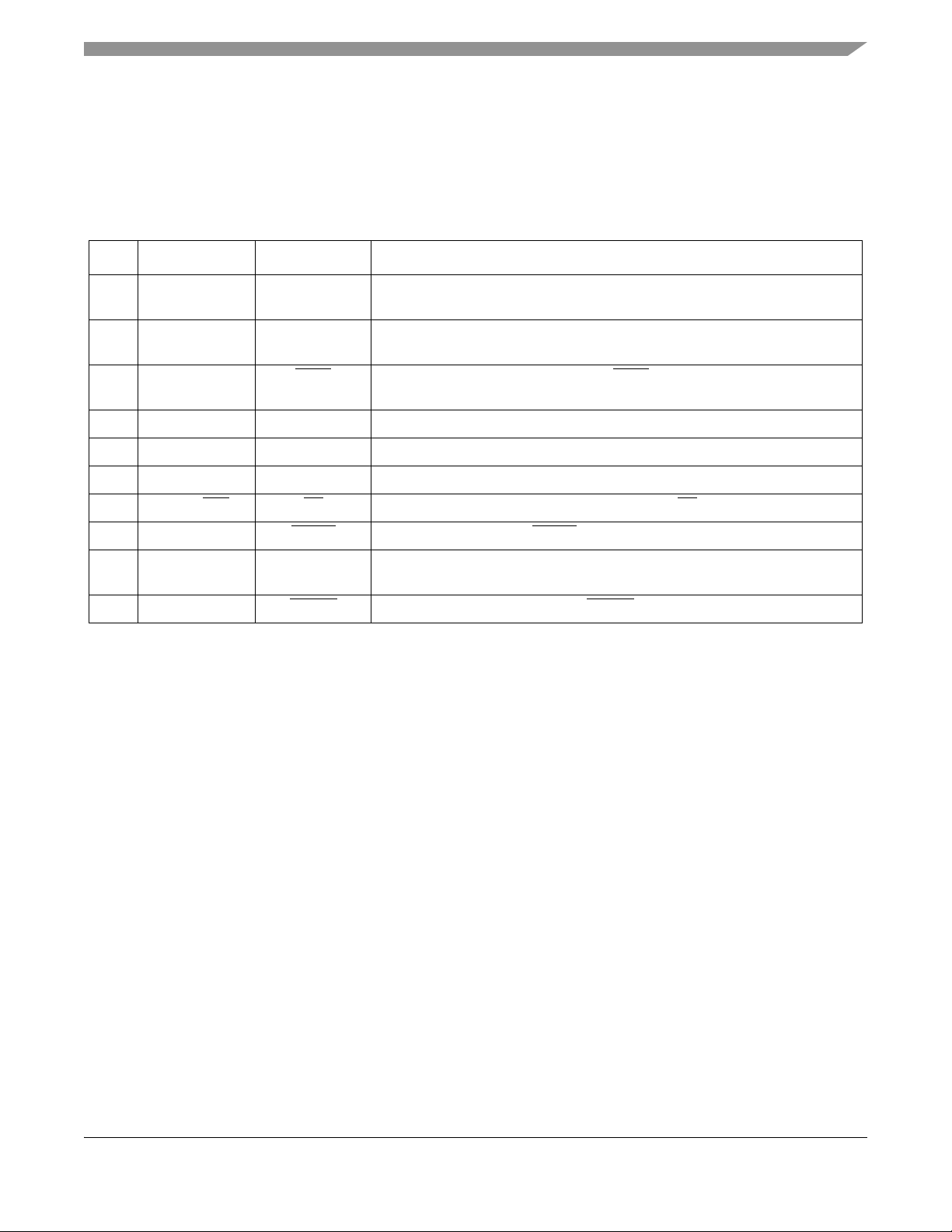
2.1 Pin Definitions
Table 2 details the MC1321x pinout and functionality.
Table 2. Pin Function Description
Pin # Pin Name Type Description Functionality
1 PTA3/KBI1P3 Digital
Input/Output
2 PTA4/KBI1P4 Digital
Input/Output
3 PTA5/KBI1P5 Digital
Input/Output
4 PTA6/KBI1P6 Digital
Input/Output
5 PTA7/KBI1P7 Digital
Input/Output
6 VDDAD Power Input MCU power supply to ATD Decouple to ground.
7 PTG0/BKGND/MS Digital
Input/Output
8 PTG1/XTAL Digital
Input/Output/
Output
9 PTG2/EXTAL Digital
Input/Output/
Input
10 CLKO Digital Output Modem Clock Output Programmable frequencies of:
MCU Port A Bit 3 /
Keyboard Input Bit 3
MCU Port A Bit 4 /
Keyboard Input Bit 4
MCU Port A Bit 5 /
Keyboard Input Bit 5
MCU Port A Bit 6 /
Keyboard Input Bit 6
MCU Port A Bit 7 /
Keyboard Input Bit 7
MCU Port G Bit 0 /
Background / Mode Select
MCU Port G Bit 1 / Crystal
oscillator output
MCU Port G Bit 2 / Crystal
oscillator input
PTG0 is output only . Pin is I/O when used as BDM
function.
Full I/O when not used as clock source.
Full I/O when not used as clock source.
16 MHz, 8 MHz, 4 MHz, 2 MHz, 1 MHz, 62.5 kHz,
32.786+ kHz (default),
and 16.393+ kHz.
11 RESET Digital
Input/Output
12 PTC0/TXD2 Digital
Input/Output
13 PTC1/RXD2 Digital
Input/Output
14 PTC2/SDA1 Digital
Input/Output
15 PTC3/SCL1 Digital
Input/Output
16 PTC4 Digital
Input/Output
17 PTC5 Digital
Input/Output
MC13211/212/213/214 Technical Data, Rev. 0.0,
Freescale Semiconductor 9
MCU reset. Active low
MCU Port C Bit 0 / SCI2
TX data out
MCU Port C Bit 1/ SCI2 RX
data in
MCU Port C Bit 1/ IIC bus
data
MCU Port C Bit 1/ IIC bus
clock
MCU Port C Bit 4
MCU Port C Bit 5
Page 10

18 PTC6 Digital
Input/Output
MCU Port C Bit 6
19 PTC7 Digital
Input/Output
20 PTE0/TXD1 Digital
Input/Output
21 PTE1/RXD1 Digital
Input/Output
22 VDDD Power Output Modem regulated output
23 VDDINT Power Input Modem digital interface
24 GPIO5 Digital
Input/Output
25 GPIO6 Digital
Input/Output
26 GPIO7 Digital
Input/Output
27 XTAL1 Input Modem crystal reference
28 XTAL2 Input/Output Modem crystal reference
MCU Port C Bit 7
MCU Port E Bit 0 / SCI1 TX
data out
MCU Port E Bit 1/ SCI1 RX
data in
supply voltage
supply
Modem General Purpose
Input/Output 5
Modem General Purpose
Input/Output 6
Modem General Purpose
Input/Output 7
oscillator input
oscillator output
Decouple to ground.
2.0 to 3.4 V. Decouple to ground. Connect to
Battery.
Connect to 16 MHz crystal and load capacitor.
Connect to 16 MHz crystal and load capacitor. Do
not load this pin by using it as a 16 MHz source.
Measure 16 MHz output at CLKO, programmed for
16 MHz.
29 VDDLO2 Power Input Modem LO2 VDD supply Connect to VDDA externally.
30 VDDLO1 Power Input Modem LO1 VDD supply Connect to VDDA externally.
31 VDDVCO Power Output Modem VCO regulated
supply bypass
32 VBATT Power Input Modem voltage regulators’
input
33 VDDA Power Output Modem analog regulated
65 RFIN_ RF Input
(Output)
34 CT_Bias RF Control
Output
35 RFIN_M RF Input
(Output)
MC13211/212/213/214 Technical Data, Rev. 0.0,
10 Freescale Semiconductor
Modem RF input/output
supply output
(i).8((i).8ive)]TJET1 sc350.82 132.36ml556.8 132.36 l556.8 033.86 l350.82 033.86 lfBT9 0 0 9 353.82 241.32 Tm0 sc-0.002 Tc-0.0025 Tw[(W)-4.8(hen )-6.7(use)-5.8(d)0.8( w)-6.5(i)0.2(th i)-6.5(n)0.8(ternal)-6.5( T)-4.5(/)2.5(R)-6.5( swi)-6.5(t)2.5(ch, )-6.7(th)-5.8(is i)-6.5(s)-2( a )]TJT*-0.0019 Tc0.0041 Tw[(bi)-6.4(0 Tctioan)-5.7nal(RF)-4.4( )6.7ponted nted Li
Modem bias
voltage/control signal for
RF external components
Modem RF input/output
negative
Decouple to ground.
Decouple to ground. Connect to Battery.
Decouple to ground. Connect to directly VDDLO1
and VDDLO2 externally and to PAO_P and
PAO_M through a bias network.
When used with internal T/R switch, provides
ground reference for RX and VDDA reference for
TX. Can also be used as a control signal with
external LNA, antenna switch, and/or PA.
When used with internal T/R switch, this is a
bi0 TctioanRF ted nted Li
Page 11

Table 2. Pin Function Description (continued)
Pin # Pin Name Type Description Functionality
37 NC Not used May be grounded or left open
38 PAO_P RF Output Modem power amplifier
RF output positive
39 PAO_M RF Output Modem power amplifier
RF output negative
40 SM Input Test Mode pin Must be grounded for normal operation
41 GPIO4 Digital
Input/Output
42 GPIO3 Digital
Input/Output
43 GPIO2 Test Point MCU Port E Bit 6 / Modem
44 GPIO1 Test Point MCU Port E Bit 7 / Modem
45 VDD Power Input MCU main power supply Decouple to ground.
46 ATTN Test Point MCU Port D Bit 0 / Modem
47 PTD2/TPM1CH2 Digital
Input/Output
Modem General Purpose
Input/Output 4
Modem General Purpose
Input/Output 3
General Purpose
Input/Output 2
General Purpose
Input/Output 1
attention input
MCU Port D Bit 2 / TPM1
Channel 2
Open drain. Connect to VDDA through a bias
network when used with external balun. Not used
when internal T/R switch is used.
Open drain. Connect to VDDA through a bias
network when used with external balun. Not used
when internal T/R switch is used.
Internally connected pins. When gpio_alt_en,
Register 9, Bit 7 = 1, GPIO2 functions as a “CRC
Valid” indicator.
Internally connected pins. When gpio_alt_en,
Register 9, Bit 7 = 1, GPIO1 functions as an “Out of
Idle” indicator.
Internally connected pins.
48 PTD4/TPM2CH1 Digital
Input/Output
49 PTD5/TPM2CH2 Digital
Input/Output
50 PTD6/TPM2CH3 Digital
Input/Output
51 PTD7/TPM2CH4 Digital
Input/Output
52 PTB0/AD1P0 Input/Output MCU Port B Bit 0 / ATD
53 PTB1/AD1P1 Input/Output MCU Port B Bit 1 / ATD
54 PTB2/AD1P2 Input/Output MCU Port B Bit 2 / ATD
55 PTB3/AD1P3 Input/Output MCU Port B Bit 3 / ATD
56 PTB4/AD1P4 Input/Output MCU Port B Bit 4 / ATD
MC13211/212/213/214 Technical Data, Rev. 0.0,
MCU Port D Bit 4 / TPM2
Channel 1
MCU Port D Bit 5 / TPM2
Channel 2
MCU Port D Bit 6 / TPM2
Channel 3
MCU Port D Bit 7 / TPM2
Channel 4
analogChannel 0
analog Channel 1
analog Channel 2
analog Channel 3
analog Channel 4
Freescale Semiconductor 11
Page 12

Table 2. Pin Function Description (continued)
Pin # Pin Name Type Description Functionality
57 PTB5/AD1P5 Input/Output MCU Port B Bit 5 / ATD
analog Channel 5
58 PTB6/AD1P6 Input/Output MCU Port B Bit 6 / ATD
analog Channel 6
59 PTB7/AD1P7 Input/Output MCU Port B Bit 7 / ATD
analog Channel 7
60 VREFH Input MCU high reference
voltage for ATD
61 VREFL Input MCU low reference
voltage for ATD
62 PTA0/KBI1P0 Digital
Input/Output
63 PTA1/KBI1P1 Digital
Input/Output
64 PTA2/KBI1P2 Digital
Input/Output
65 TEST Test Point For factory test Do not connect
66 TEST Test Point For factory test Do not connect
67 TEST Test Point For factory test Do not connect
68 TEST Test Point For factory test Do not connect
69 TEST Test Point For factory test Do not connect
70 TEST Test Point For factory test Do not connect
71 TEST Test Point For factory test Do not connect
FLAG VSS Power input External package flag.
MCU Port A Bit 0 /
Keyboard Input Bit 0
MCU Port A Bit 1 /
Keyboard Input Bit 1
MCU Port A Bit 2 /
Keyboard Input Bit 2
Connect to ground.
Common VSS
MC13211/212/213/214 Technical Data, Rev. 0.0,
12 Freescale Semiconductor
Page 13
2.2 Internal Functional Interconnects
The MCU provides control for the 802.15.4 modem. The required interconnects between the devices are
routed onboard the SiP. In addition, the signals are brought out to external pads primarily for use as test
points. These signals can be useful when writing and debugging software.
Table 3. Internal Functional Interconnects
Pin # MCU Signal Modem Signal Description
43 PTE6 GPIO2 Modem GPIO2 output acts as “CRC Valid” status indicator for Stream Data
Mode to MCU.
44 PTE7 GPIO1 Modem GPIO1 output acts as “Out of Idle” status indicator for Stream Data
Mode to MCU.
46 PTD0 ATTN
PTE5/SPSCK1 SPICLK MCU SPI master SPI clock output drives modem SPICLK slave clock input.
PTE4/MOSI1 MOSI MCU SPI master MOSI output drives modem slave MOSI input
PTE3/MISO1 MISO Modem SPI slave MISO output drives MCU master MISO input
PTE2/SS1
IRQ M_IRQ Modem interrupt request M_IRQ output drives MCU IRQ input
PTD1 RXTXEN MCU Port D Bit 1 drives the RXTXEN input to the modem to enable TX or RX
PTD3 M_RST MCU Port D Bit 3 drives the reset M_RST input to the modem.
CE MCU SPI master SS output drives modem slave CE input
MCU Port D Bit 0 drives the attention (ATTN) input of the modem to wake
modem from Hibernate or Doze Mode.
or CCA operations.
NOTE
T o use the MCU and modem signals as described in Table 3, the MCU needs
to be programmed appropriately for the stated function.
MC13211/212/213/214 Technical Data, Rev. 0.0,
Freescale Semiconductor 13
Page 14
3 MC1321x Serial Peripheral Interface (SPI)
The MC1321x modem and CPU communicate primarily through the onboard SPI command channel.
Figure 4 shows the SiP internal interconnects with the SPI bus highlighted. The MCU has a single SPI
module that is dedicated to the modem SPI interface. The modem is a slave only and the MCU SPI must
be programmed and used as a master only. Further, the SPI performance is limited by the modem
constraints of 8 MHz SPI clock frequency, and use of the SPI must be programmed to meet the modem
SPI protocol.
3.1 SiP Level SPI Pin Connections
The SiP level SPI pin connections are all internal to the device. Figure 4 shows the SiP interconnections
with the SPI bus highlighted.
MC1321x
M_RST PTD3
M_IRQ
ATTN
RXTXEN
MODEM MCU
MCU Signal Modem Signal Description
GPIO1/Out_of_Idle
GPIO2/CRC_Valid
MOSI
MISO
SPICLK
CE PTE2/SS1
Figure 4. MC1321x Internal Interconnects Highlighting SPI Bus
Table 4. MC1321x Internal SPI Connections
474443
IRQ
PT D0
PT D1
PT E7
PT E6
PTE4/MOSI1
PTE3/MISO1
PTE5/SPSCK1
11
RESET
PTE5/SPSCK1 SPICLK MCU SPI master SPI clock output drives modem SPICLK slave clock input.
PTE4/MOSI1 MOSI MCU SPI master MOSI output drives modem slave MOSI input
PTE3/MISO1 MISO Modem SPI slave MISO output drives MCU master MISO input
PTE2/SS1 CE MCU SPI master SS output drives modem slave CE input
MC13211/212/213/214 Technical Data, Rev. 0.0,
14 Freescale Semiconductor
Page 15
3.2 SPI Features
• MCU bus master
• Modem bus slave
• Programmable SPI clock rate; maximum rate is 8 MHz
• Double-buffered transmit and receive at MCU
• Serial clock phase and polarity must meet modem requirements (MCU control bits
• Slave select programmed to meet modem protocol
3.3 SPI System Block Diagram
Figure 5 shows the SPI system level diagram.
MCU (MASTER)
SPI SHIFTER
7 6 5 4 3 2 1 0
CLOCK
GENERATOR
MOS1
MISO1
SPSCK1
PTE2/SS1
Figure 5. SPI System Block Diagram
MOSI
MISO
SPICLK
CE
MODEM (SLAVE)
SPI SHIFTER
7 6 5 4 3 2 1 0
Figure 5 shows the SPI modules of the MCU and modem in the master-slave arrangement. The MCU
(master) initiates all SPI transfers. During a transfer, the master shifts data out (on the MOSI pin) to the
slave while simultaneously shifting data in (on the MISO pin) from the slave. Although the SPI interface
supports simultaneous data exchange between master and slave, the modem SPI protocol only uses data
exchange in one direction at a time. The SPSCK signal is a clock output from the master and an input to
the slave. The slave device must be selected by a low level on the slave select input (SS1 pin).
MC13211/212/213/214 Technical Data, Rev. 0.0,
Freescale Semiconductor 15
Page 16
4 IEEE 802.15.4 Modem
4.1 Block Diagram
2nd IF Mix er
IF = 1 MHz
RFIN_P
(PAO_P)
RFIN_M
(PAO_M)
T / R
LNA
1st IF Mi x er
IF = 65 MHz
CT_Bias
VDD LO2 ÷4
XTAL1
XTAL2
VDDLO1
PAO_P
PAO_M
256 MHz
Crystal
Oscillator
16 MHz
PA
Phase Shift Modulator
PMA
Decimation
Filter
AGC
Synthesizer
Baseband
Mixer
2.45 GHz
VCO
Matched
Filter
Programmable
Prescaler
MUX
CCA
Transmit
Packet RAM 2
Transmit
Packet RAM 1
FCS
Generation
DCD
Receive
Packet R AM
24 Bit Event Timer
4 Programmable
Timer Com parators
Transmit RAM
Header
Generation
Correlator
Arbiter
Symbol
Synch & Det
Receive RAM
Packet
Processor
Arbiter
Symbol
Generation
Power-Up
Control
Logic
Sequence
Manager
(Control Logic)
Analog
Regulator VBATT
Digital
Regulator L
Digital
Regulator H
Crystal
Regulator
VCO
Regulator
SERIAL
PERIPHERAL
IRQ
Arbiter
INTERFACE
VDDINT
VDDD
VDDVCO
(SPI)
VDDA
RXTXEN
CE
MOSI
MISO
SPICLK
ATTN
RST
GPIO1
GPIO2
GPIO3
GPIO4
GPIO5
GPIO6
GPIO7
IRQ
CLKO
Figure 6. 802.15.4 Modem Block Diagram
MC13211/212/213/214 Technical Data, Rev. 0.0,
16 Freescale Semiconductor
Page 17

4.2 Data Transfer Modes
The 802.15.4 modem has two data transfer modes:
1. Packet Mode — Data is buffered in on-chip RAM
2. Streaming Mode — Data is processed word-by-word
The Freescale 802.15.4 MAC software only supports the streaming mode of data transfer . For proprietary
applications, packet mode can be used to conserve MCU resources.
4.3 Packet Structure
Figure 7 shows the packet structure of the 802.15.4 modem. Payloads of up to 125 bytes are supported.
The 802.15.4 modem adds a four-byte preamble, a one-byte Start of Frame Delimiter (SFD), and a
one-byte Frame Length Indicator (FLI) before the data. A Frame Check Sequence (FCS) is calculated and
appended to the end of the data.
4 bytes 1 byte 1 byte 125 bytes maximum 2 bytes
Preamble SFD FLI P ayload Data FCS
Figure 7. 802.15.4 modem Packet Structure
4.4 Receive Path Description
In the receive signal path, the RF input is converted to low IF In-phase and Quadrature (I & Q) signals
through two down-conversion stages. A Clear Channel Assessment (CCA) can be performed based upon
the baseband energy integrated over a specific time interval. The digital back end performs Differential
Chip Detection (DCD), the correlator “de-spreads” the Direct Sequence Spread Spectrum (DSSS) Offset
QPSK (O-QPSK) signal, determines the symbols and packets, and detects the data.
The preamble, SFD, and FLI are parsed and used to detect the payload data and FCS (which are stored in
RAM in Packet Mode). A two-byte FCS is calculated on the received data and compared to the FCS value
appended to the transmitted data, which generates a Cyclical Redundancy Check (CRC) result. A
parameter of received energy during the reception called the Link Quality Indicator is measured over a 64
µs period after the packet preamble and stored in an SPI register.
If the 802.15.4 modem is in Packet Mode, the data is stored in RAM and processed as an entire packet.
The MCU is notified that an entire packet has been received via an interrupt.
If the 802.15.4 modem is in streaming mode, the MCU is notified by a recurring interrupt on a
word-by-word basis.
Figure 8 shows CCA reported power level versus input power. Note that CCA reported power saturates at
about -57 dBm input power which is well above IEEE 802.15.4 Standard requirements. Figure 9 shows
energy detection/LQI reported level versus input power.
MC13211/212/213/214 Technical Data, Rev. 0.0,
Freescale Semiconductor 17
Page 18
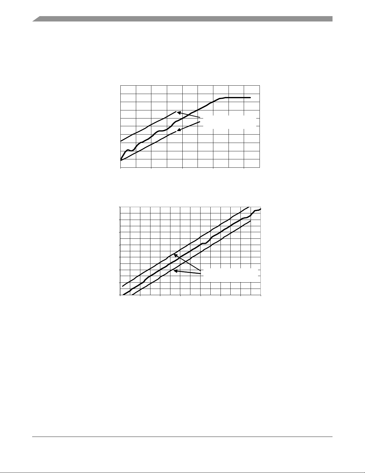
NOTE
For both graphs, the required IEEE 802.15.4 Standard accuracy and range
limits are shown. A 3.5 dBm offset has been programmed into the CCA
reporting level to center the level over temperature in the graphs.
-50
-60
-70
-80
-90
Reported Power Level (dBm)
-100
-90 -80 -70 -60 -50
Input Power (dBm)
802.15.4 Accura cy
and range Requirements
Figure 8. Reported Power Level versus Input Power in Clear Channel Assessment Mode
-15
-25
-35
-45
-55
-65
Reported Power Level (dBm)
-75
802.15.4 Accur ac y
and Range Requirements
-85
-85 -75 -65 -55 -45 -35 -25 -15
Input Power Level (dBm)
Figure 9. Reported Power Level Versus Input Power for Energy Detect or Link Quality Indicator
4.5 Transmit Path Description
For the transmit path, the TX data that was previously written to the internal RAM is retrieved (packet
mode) or the TX data is clocked in via the SPI (stream mode), formed into packets per the 802.15.4 PHY,
spread, and then up-converted to the transmit frequency.
If the 802.15.4 modem is in packet mode, data is processed as an entire packet. The data is first loaded into
the TX buffer. The MCU then requests that the modem transmit the data. The MCU is notified via an
interrupt when the whole packet has successfully been transmitted.
MC13211/212/213/214 Technical Data, Rev. 0.0,
18 Freescale Semiconductor
Page 19
In streaming mode, the data is fed to the 802.15.4 modem on a word-by-word basis with an interrupt
serving as a notification that the 802.15.4 modem is ready for more data. This continues until the whole
packet is transmitted.
In both modes, a two-byte FCS is calculated in hardware from the payload data and appended to the packet.
This done without intervention from the user.
4.6 Functional Description
4.6.1 802.15.4 Modem Operational Modes
The 802.15.4 modem has a number of operational modes that allow for low-current operation. Transition
from the Off to Idle mode occurs when M_RST is negated. Once in Idle, the SPI is active and is used to
control the IC. Transition to Hibernate and Doze modes is enabled via the SPI. These modes are
summarized, along with the transition times, in Table 5. Current drain in the various modes is listed in
Table 8, DC Electrical Characteristics.
Table 5. 802.15.4 Modem Mode Definitions and Transition Times
Mode Definition
Off All IC functions Off, Leakage only. M_RST asserted. Digital outputs are tri-stated
including IRQ
Hibernate Crystal Reference Oscillator Off. (SPI not functional.) IC Responds to ATTN. Data
is retained.
Doze Crystal Reference Oscillator On but CLKO output available only if Register 7, Bit 9
= 1 for frequencies of 1 MHz or less. (SPI not functional.) Responds to ATTN and
can be programmed to enter Idle Mode through an internal timer comparator.
Idle Crystal Reference Oscillator On with CLKO output available. SPI active.
Receive Crystal Reference Oscillator On. Receiver On. 144 µs from Idle
Transmit Crystal Reference Oscillator On. Transmitter On. 144 µs from Idle
Transition Time
To or From Idle
10 - 25 ms to Idle
7 - 20 ms to Idle
(300 + 1/CLKO) µs to Idle
4.6.2 Serial Peripheral Interface (SPI)
The MCU directs the 802.15.4 modem, checks its status, and reads/writes data to the device through the
4-wire SPI port. The transceiver operates as a SPI slave device only. A transaction between the host and
the 802.15.4 modem occurs as multiple 8-bit bursts on the SPI. The modem SPI signals are:
1. Chip Enable (CE) - A transaction on the SPI port is framed by the active low CE input signal. A
transaction is a minimum of 3 SPI bursts and can extend to a greater number of bursts.
2. SPI Clock (SPICLK) - The host drives the SPICLK input to the 802.15.4 modem. Data is clocked
into the master or slave on the leading (rising) edge of the return-to-zero SPICLK and data out
changes state on the trailing (falling) edge of SPICLK.
MC13211/212/213/214 Technical Data, Rev. 0.0,
Freescale Semiconductor 19
Page 20

NOTE
For the MCU, the SPI clock format is the clock phase control bit CPHA = 0
and the clock polarity control bit CPOL = 0.
3. Master Out/Slave In (MOSI) - Incoming data from the host is presented on the MOSI input.
4. Master In/Slave Out (MISO) - The 802.15.4 modem presents data to the master on the MISO
output.
Although the SPI port is fully static, internal memory , timer and interrupt arbiters require an internal clock
(CLK
), derived from the crystal reference oscillator, to communicate from the SPI regis ters to internal
core
registers and memory.
4.6.2.1 SPI Burst Operation
The SPI port of the MCU transfers data in bursts of 8 bits with most significant bit (MSB) first. The master
(MCU) can send a byte to the slave (transceiver) on the MOSI line and the slave can send a byte to the
master on the MISO line. Although an 802.15.4 modem transaction is three or more SPI bursts long, the
timing of a single SPI burst is shown in Figure 10. The maximum SPI clock rate is 8 Mhz from the MCU
because the modem is limited by this number.
1
Figure 10. SPI Single Burst Timing Diagram
MC13211/212/213/214 Technical Data, Rev. 0.0,
20 Freescale Semiconductor
Page 21
4.6.2.2 SPI Transaction Operation
Although the SPI port of the MCU transfers data in bursts of 8 bits, the 802.15.4 modem requires that a
complete SPI transaction be framed by CE, and there will be three (3) or more bursts per transaction. The
assertion of CE to low signals the start of a transaction. The first SPI burst is a write of an 8-bit header to
the transceiver (MOSI is valid) that defines a 6-bit address of the internal resource being accessed and
identifies the access as being a read or write operation. In this context, a write is data written to the 802.15.4
modem and a read is data written to the SPI master . The following SPI bursts will be either the write data
(MOSI is valid) to the transceiver or read data from the transceiver (MISO is valid).
Although the SPI bus is capable of sending data simultaneously between master and slave, the 802.15.4
modem never uses this mode. The number of data bytes (payload) will be a minimum of 2 bytes and can
extend to a larger number depending on the type of access. After the final SPI burst, CE is negated to high
to signal the end of the transaction.
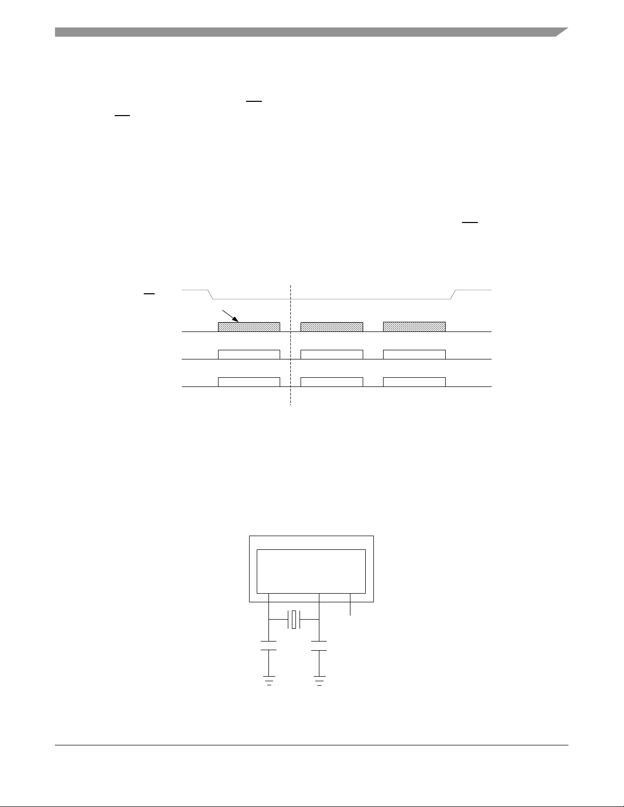
An example SPI read transaction with a 2-byte payload is shown in Figure 11.
CE
Clock Burst
SPICLK
MISO
MOSI
Valid
Header Read data
Figure 11. SPI Read Transaction Diagram
Valid Valid
4.7 Modem Crystal Oscillator
The modem crystal oscillator uses the following external pins as shown in Figure 12.
1. XTAL1 - reference oscillator input.
2. XTAL2 - reference oscillator output. Note that this pin should not be loaded as a reference source
or to measure frequency; instead use CLKO to measure or supply 16 MHz.
MC1321X
802.15.4 MODEM
XTAL1 XTAL2 CLKO
27
28 10
16MH z
Figure 12. Modem Crystal Oscillator
MC13211/212/213/214 Technical Data, Rev. 0.0,
Freescale Semiconductor 21
Page 22

The IEEE 802.15.4 Standard requires that several frequency tolerances be kept within ± 40 ppm accuracy.
This means that a total offset up to 80 ppm between transmitter and receiver will still result in acceptable
performance. The primary determining factor in meeting this specification is the tolerance of the crystal
oscillator reference frequency. A number of factors can contribute to this tolerance and a crystal
specification will quantify each of them:
1. The initial (or make) tolerance of the crystal resonant frequency itself.
2. The variation of the crystal resonant frequency with temperature.
3. The variation of the crystal resonant frequency with time, also commonly known as aging.
4. The variation of the crystal resonant frequency with load capacitance, also commonly known as
pulling. This is affected by:
a) The external load capacitor values - initial tolerance and variation with temperature.
b) The internal trim capacitor values - initial tolerance and variation with temperature.
c) Stray capacitance on the crystal pin nodes - including stray on-chip capacitance, stray package
capacitance and stray board capacitance; and its initial tolerance and variation with
temperature.
Freescale has specified that a 16 MHz crystal with a <9 pF load capacitance is required. The 802.15.4
modem does not contain a reference divider, so 16 MHz is the only frequency that can be used. A crystal
requiring higher load capacitance is prohibited because a higher load on the amplifier circuit may
compromise its performance. The crystal manufacture r defines the load capacitance as that total external
capacitance seen across the two terminals of the crystal. The oscillator amplifier c onfiguration used in the
802.15.4 modem requires two balanced load capacitors from each terminal of the crystal to ground. As
such, the capacitors are seen to be in series by the crystal, so each must be <18 pF for proper loading.
The modem uses the 16 MHz crystal oscillator as the reference oscillator for the system and a
programmable warp capability is provided. It is controlled by programming CLKO_Ctl Register 0A, Bits
15-8 (xtal_trim[7:0]). The trimming procedure varies the frequency by a few hertz per step, depending on
the type of crystal. The high end of the frequency spectrum is set when xtal_trim[7:0] is set to zero. As
xtal_trim[7:0] is increased, the frequency is decreased. Accuracy of this feature can be observed by
varying xtal_trim[7:0] and using a spectrum analyzer or frequency counter to track the change in
frequency of the crystal signal. The reference oscillator frequency can be measured at the CLKO contact
by programming CLKO_Ctl Register 0A, Bits 2-0, to value 000.
MC13211/212/213/214 Technical Data, Rev. 0.0,
22 Freescale Semiconductor
Page 23

0
0 50 100 150 200 250 300
-100
-200
-300
-400
-500
-600
-700
Frequency Decrease (Hz)
-800
-900
xtal_t r i m[ 7:0] ( decim al )
Figure 13. Crystal Frequency Variation vs. xtal_trim[7:0]
Figure 13 shows typical oscillator frequency decrease versus the value programmed in xtal_trim[7:0].
4.8 Radio Usage
The MC1321x RF analog interface has been designed to provide maximum flexibility as well as low
external part count and cost. An on-chip transmit/receive (T/R) switch with bias switch (CT_Bias) can be
used for a simple single antenna interface with a balun. Alternately, separate full differential RFIN and
PAO outputs can be utilized for separate RX and TX antennae or external LNA and PA designs.
Figure 14 shows three possible configurations for the transceiver radio RF usage.
1. Figure 14A shows a single antenna configuration in which the MC1321x internal T/R switch is
used. The balun converts the single-ended antenna to differential signals that interface to the
RFIN_x (PAO_x) pins of the radio. The CT_Bias pin provides the proper bias point to the balun
depending on operation, that is, CT_Bias is at VDDA voltage for transmit and is at ground for
receive. The internal T/R switch enables the signal to an onboard LNA for receive and enables the
onboard PAs for transmit.
2. Figure 14B shows a single antenna configuration with an external low noise amplifier (LNA) for
greater range. An external antenna switch is used to multiplex the antenna between receive and
transmit. An LNA is in the receive path to add gain for greater receive sensitivity. Two external
baluns are required to convert the single-ended antenna switch signals to the differential signals
required by the radio. Separate RFIN and P AO signals are provided for connection with the baluns,
and the CT_Bias signal is programmed to provide the external switch control. The polarity of the
external switch control is selectable.
MC13211/212/213/214 Technical Data, Rev. 0.0,
Freescale Semiconductor 23
Page 24

3. Figure 14C shows a dual antenna configuration where there is a RX antenna and a TX antenna. For
the receive side, the RX antenna is ac-coupled to the differential RFIN inputs and these capacitors
along with inductor L1 form a matching network. Inductors L2 and L3 are ac-coupled to ground to
form a frequency trap. For the transmit side, the TX antenna is connected to the differential PAO
outputs, and inductors L4 and L5 provide dc-biasing to VDDA but are ac isolated.
VDD
RFIN_P (PAO_P)
Balun
Bypass
L1
RFI N_M (PAO_M)
CT_Bias
MC1321x
PAO_P
PAO_M
14A) Using Onboard T/R Switch
RX Antenna
L1
TX Antenna
L2 L3
Bypass Bypass
VDDA
Ant
Sw
LNA
Balun
Balun
Bypass
VDDA
Bypass
RFIN_P (PAO_P)
L1
RFIN_M (PAO_M)
(Ant Sw C tl)
PAO_P
PAO_M
14B) Using External Antenna Switch With LNA
RFIN_P (PAO_P)
RFIN_M (PAO_M)
MC1321x
MC1321x
CT_Bias
L4 L5
CT_Bias
PAO_P
PAO_M
14C) Using Dual Antennae
Figure 14. Using the MC1321x with External RF Components
MC13211/212/213/214 Technical Data, Rev. 0.0,
24 Freescale Semiconductor
Page 25

5MCU
5.1 MCU Block Diagram
RESET
VDDAD
VSSAD
VREFH
VREFL
IRQ
MCU CORE
CPUBDC
MCU SYSTEM CONTROL
RESETS AND INTERRUPTS
MODES OF OPERATION
POWER MANAGEMENT
RTI
IRQ LVD
USER FLASH
(61,268 BYTES MAX)
USER RAM
(4096 BYTES MAX)
10-BIT
ANALOG-TO-DIGITAL
CONVERTER (ATD1)
INTERNAL CLOCK
GENERATOR (ICG)
LOW-POWER OSCILLATOR
COP
INTERNAL BUS
DEBUG
MODULE (DBG)
8-BIT KEYBOARD
INTERRUPT MODULE (KBI1)
IIC MODULE (IIC)
SERIAL COMMUNICATIONS
INTERFACE MODULE (SCI1)
SERIAL COMMUNICATIONS
INTERFACE MODULE (SCI2)
1-CHANNEL TIMER/PWM
MODULE (TPM1)
4-CHANNEL TIMER/PWM
MODULE (TPM2)
DEDICATED SERIAL
PERIPHERAL INTERFACE
MODULE (SPI)
8
PORT A
8
PORT B
PORT C
PORT D
PORT E
See Note 1.
PORT F
PTA7/KBI1P7–
PTA0/KBI1P0
PTB7/AD1P7–
PTB0/AD1P0
PTC7
PTC6
PTC5
PTC4
PTC3/SCL1
PTC2/SDA1
PTC1/RxD2
PTC0/TxD2
PTD7/TPM2CH4
PTD6/TPM2CH3
PTD5/TPM2CH2
PTD4/TPM2CH1
PTD3
PTD2/TPM1CH2
PTD1
PTD0
PTE7
PTE6
PTE5/SPSCK
PTE4/MOSI
PTE3/MISO
PTE2/SS
PTE1/RxD1
PTE0/TxD1
VDD
VSS
Notes
1. All Port F and Port G signals are present on the MCU,
2.
VOLTAGE
REGULATOR
but only the signals used by the MC1321x are designated.
For lowest power operation, all unused I/O should be programmed
as outputs during initialization.
Timer channels are limited as noted due to use of Port D I/O for
internal signals.
See Note 1.
PORT G
PTG2/EXTAL
PTG1/XTAL
PTG0/BKGD/MS
Figure 15. MCU Block Diagram
MC13211/212/213/214 Technical Data, Rev. 0.0,
Freescale Semiconductor 25
Page 26

5.2 MCU Modes of Operation
The MCU has multiple operational modes to facilitate maximum system performance while also providing
low-power modes. In the MC1321x, the MCU can use the following modes:
•Run
•Wait
• Stop2
• Stop3
NOTE
The MCU can also be programmed for Stop1 mode, but this mode IS NOT
USABLE. The reset to the modem function is controlled by an MCU GPIO
and the GPIO state must be maintained during the MCU “stop” condition.
Stop1 mode does not control I/O states as required during modem power
down condition.
5.2.1 Run Mode
This is the normal operating mode for the HCS08. This mode is selected when the BKGD/MS pin is high
at the rising edge of reset. In this mode, the CPU executes code from internal memory with execution
beginning at the address fetched from memory at $FFFE:$FFFF after reset.
5.2.2 Wait Mode
W ait Mode is entered by executing a WAIT instruction. Upon execution of the WAIT instruction, the CPU
enters a low-power state in which it is not clocked. The I bit in CCR is cleared when the CPU enters the
wait mode, enabling interrupts. When an interrupt request occurs, the CPU exits the wait mode and
resumes processing, beginning with the stacking operations leading to the interrupt service routine.
While the MCU is in Wait Mode, there are some restrictions on which background debug commands can
be used. Only the BACKGROUND command and memory-access-with-status commands are available
when the MCU is in wait mode. The memory-access-with-status commands do not allow memory access,
but they report an error indicating that the MCU is in either stop or wait mode. The BACKGROUND
command can be used to wake the MCU from Wait Mode and enter active background mode.
5.2.3 Stop 2
The Stop2 Mode provides very low standby power consumption and maintains the contents of RAM and
the current state of all of the I/O pins. Stop2 can be entered only if the LVD circuit is not enabled in Stop
Modes (either LVDE or LVDSE not set).
Before entering Stop2 Mode, the user must save the contents of the I/O port registers, as well as any other
memory-mapped registers they want to restore after exit of Stop2, to locations in RAM. Upon exit of
Stop2, these values can be restored by user software before pin latches are opened.
MC13211/212/213/214 Technical Data, Rev. 0.0,
26 Freescale Semiconductor
Page 27

When the MCU is in Stop2 Mode, all internal circuits that are powered from the voltage regulator are
turned off, except for the RAM. The voltage regulator is in a low-power standby state, as is the ATD. Upon
entry into Stop2, the states of the I/O pins are latched. The states are held while in Stop2 Mode and after
exiting Stop2 Mode until a 1 is written to PPDACK in SPMSC2.
Exit from Stop2 is performed by asserting either of the wake-up pins: RESET or IRQ, or by an RTI
interrupt. IRQ is always an active low input when the MCU is in Stop2, regardless of how it was
configured before entering Stop2.
Upon wake-up from Stop2 Mode, the MCU will start up as from a power-on reset (POR) except pin states
remain latched. The CPU will take the reset vector. The system and all peripherals will be in their default
reset states and must be initialized.
After waking up from Stop2, the PPDF bit in SPMSC2 is set. This flag may be used to direct user code to
go to a Stop2 recovery routine. PPDF remains set and the I/O pin states remain latched until a 1 is written
to PPDACK in SPMSC2.
To maintain I/O state for pins that were configured as general-purpose I/O, the user must restore the
contents of the I/O port registers, which have been saved in RAM, to the port registers before writing to
the PPDACK bit. If the port registers are not restored from RAM before writing to PPDACK, then the
register bits will assume their reset states when the I/O pin latches are opened and the I/O pins will switch
to their reset states.
For pins that were configured as peripheral I/O, the user must reconfigure the peripheral module that
interfaces to the pin before writing to the PPDACK bit. If the peripheral module is not enabled before
writing to PPDACK, the pins will be controlled by their associated port control registers when the I/O
latches are opened.
A separate self-clocked source (approximately 1 kHz) for the real-time interrupt allows a walk-up from
Stop2 or Stop3 Modes with no external components. When RTIS2:RTIS1:RTIS0 = 0:0:0, the real-time
interrupt function and this 1-kHz source are disabled. Power consumption is lower when the 1-kHz source
is disabled, but in that case the real-time interrupt cannot wake the MCU from stop.
5.2.4 Stop3
Upon entering the Stop3 Mode, all of the clocks in the MCU, including the oscillator itself, are halted. The
ICG is turned off, the ATD is disabled, and the voltage regulator is put in standby. The states of all of the
internal registers and logic, as well as the RAM content, are maintained. The I/O pin states are not latched
at the pin as in Stop2. Instead they are maintained by virtue of the states of the internal logic driving the
pins being maintained.
Exit from Stop3 is performed by asserting RESET
interrupt. The asynchronous interrupt pins are the IRQ or KBI pins.
If Stop3 is exited by means of the RESET pin, then the MCU will be reset and operation will resume after
taking the reset vector. Exit by means of an asynchronous interrupt or the real-time interrupt will result in
the MCU taking the appropriate interrupt vector.
, an asynchronous interrupt pin, or through the real-time
MC13211/212/213/214 Technical Data, Rev. 0.0,
Freescale Semiconductor 27
Page 28

A separate self-clocked source (approximately1 kHz) for the real-time interrupt allows a wake up from
Stop2 or Stop3 Modes with no external components. When RTIS2:RTIS1:RTIS0 = 0:0:0, the real-time
interrupt function and this 1-kHz source are disabled. Power consumption is lower when the 1-kHz source
is disabled, but in that case the real-time interrupt cannot wake the MCU from stop.
5.3 MCU Memory
As shown in Figure 16, on-chip memory in the MC1321x series of MCUs consists of RAM, FLASH
program memory for non-volatile data storage, plus I/O and control/status registers. The registers are
divided into three groups:
• Direct-page registers ($0000 through $007F)
• High-page registers ($1800 through $182B)
• Nonvolatile registers ($FFB0 through $FFBF)
DIRECT PAGE REGISTERS
RAM
4096 BYTES
FLASH
1920 BYTES
HIGH PAGE REGISTERS
FLASH
59348 BYTES
$0000
$007F
$0080
$107F
$1080
$17FF
$1800
$182B
$182C
DIRECT PAGE REGISTERS
RAM
2048 BYTES
UNIMPLEMENTED
3968 BYTES
HIGH PAGE REGISTERS
UNIMPLEMENTED
26580 BYTES
FLASH
32768 BYTES
$0000
$007F
$0080
$087F
$0880
$17FF
$1800
$182B
$182C
$7FFF
$8000
DIRECT PAGE REGISTERS
RAM 1024 BYTES
UNIMPLEMENTED
4992 BYTES
HIGH PAGE REGISTERS
UNIMPLEMENTED
42964 BYTES
FLASH
$0000
$007F
$0080
$047F
$0480
$17FF
$1800
$182B
$182C
$BFFF
$C000
16384 BYTES
$FFFF
MC13213/214 MC13212
$FFFF
MC13211
$FFFF
Figure 16. MC1321X Memory Maps
MC13211/212/213/214 Technical Data, Rev. 0.0,
28 Freescale Semiconductor
Page 29

5.4 MCU Internal Clock Generator (ICG)
The ICG provides multiple options for MCU clock sources. This block along with the ability to provide
the MCU clock form the modem offers a user great flexibility when making choices between cost,
precision, current draw , and performance. As seen in Figure 17, the ICG consists of four functional blocks.
• Oscillator Block — The Oscillator Block provides means for connecting an external crystal or
resonator. Two frequency ranges are software selectable to allow optimal start-up and stability.
Alternatively , the oscillator block can be used to route an external square wave to the MCU system
clock. External sources such as the modem CLKO output can provide a low cost source or a very
precise clock source. The oscillator is capable of being configured for low power mode or high
amplitude mode as selected by HGO.
• Internal Reference Generator — The Internal Reference Generator consists of two controlled
clock sources. One is designed to be approximately 8 MHz and can be selected as a local clock for
the background debug controller. The other internal reference clock source is typically 243 kHz
and can be trimmed for finer accuracy via software when a precise timed event is input to the MCU.
This provides a highly reliable, low-cost clock source.
• Frequency-Locked Loop — A Frequency-Locked Loop (FLL) stage takes either the internal or
external clock source and multiplies it to a higher frequency . Status bits provide information when
the circuit has achieved lock and when it falls out of lock. Additionally , this block can monitor the
external reference clock and signals whether the clock is valid or not.
• Clock Select Block — The Clock Select Block provides several switch options for connecting
different clock sources to the system clock tree. ICGDCLK is the multiplied clock frequency out
of the FLL, ICGERCLK is the reference clock frequency from the crystal or external clock source,
and FFE (fixed frequency enable) is a control signal used to control the system fixed frequency
clock (XCLK). ICGLCLK is the clock source for the background debug controller (BDC).
The module is intended to be very user friendly with many of the features occurring automatically without
user intervention.
5.4.1 Features
Features of the ICG and clock distribution system:
• Several options for the MCU primary clock source allow a wide range of cost, frequency, and
precision choices:
— 32 kHz–100 kHz crystal or resonator
— 1 MHz–16 MHz crystal or resonator
— External clock supplied by modem CLKO or other source
— Internal reference generator
• Defaults to self-clocked mode to minimize startup delays
• Frequency-locked loop (FLL) generates 8 MHz to 40 MHz (for bus rates up to 20 MHz). When
using modem CLKO as external source, maximum FLL frequency is 32 MHz (16 MHz bus rate)
with CLKO = 16 MHz or maximum FLL frequency is 40 MHz (20 MHz bus rate) with CLKO =
4 MHz.
MC13211/212/213/214 Technical Data, Rev. 0.0,
Freescale Semiconductor 29
Page 30

— Uses external or internal clock as reference frequency
• Automatic lockout of non-running clock sources
• Reset or interrupt on loss of clock or loss of FLL lock
• Digitally-controlled oscillator (DCO) preserves previous frequency settings, allowing fast
frequency lock when recovering from stop3 mode
• DCO will maintain operating frequency during a loss or removal of reference clock. When FLL is
engaged (FEE or FEI) loss of lock or loss of clock adds a divide-by-2 to ICG to prevent
over-clocking of the system.
• Post-FLL divider selects 1 of 8 bus rate divisors (/1 through /128)
• Separate self-clocked source for real-time interrupt
• Trimmable internal clock source supports SCI communications without additional external
components
• Automatic FLL engagement after lock is acquired
• Selectable low-power/high-gain oscillator modes
5.4.2 Modes of Operation
This section provides a high-level description only.
• Mode 1 — Off
The output clock, ICGOUT, is static. This mode may be entered when the STOP instruction is
executed.
• Mode 2 — Self-clocked (SCM)
Default mode of operation that is entered out of reset. The ICG’ s FLL is open loop and the digitally
controlled oscillator (DCO) is free running at a frequency set by the filter bits.
• Mode 3 — FLL engaged internal tio.000Spera.00039may be eno..2(sm-i-the digitall.3(d)Tj-p5-thc1 Ttstatic. 8.29unning )Tj17.375 0 TD-0.0000.0002 Tis sde ofarew[(gris fr0004cations)Tj4-1.415 TD-0.0012a114ly-co150.m0.0ipl2-i-thck. Whe8.53n is
MC13211/212/213/214 Technical Data, Rev. 0.0,
30 Freescale Semiconductor
Page 31

— FLL engaged external locked is a state which occurs when the FLL detects that the DCO is
locked to a multiple of the internal reference.
Figure 17 is a top-level diagram that shows the functional organization of the internal clock generation
(ICG) module.
EXTAL
ICG
DCO
ICGDCLK
CLOCK
SELECT
OUTPUT
CLOCK
SELECT
FIXED
CLOCK
SELECT
/R
FFE
ICGLCLK
ICGOUT
XTAL
VDD
VSS
OSCILLATOR (OSC)
WITH EXTERNAL REF
SELECT
TYP 243 kHz
INTERNAL
REFERENCE
GENERATORS
IRG
8 MHz
RG
ICGERCLK
FREQUENCY
REF
SELECT
LOCKED
LOOP (FLL)
LOSS OF LOCK
AND CLOCK DETECTOR
ICGIRCLK
LOCAL CLOCK FOR OPTIONAL USE WITH BDC
Figure 17. ICG Block Diagram
5.5 Central Processing Unit (CPU)
The HCS08 CPU is fully source- and object-code-compatible with the M68HC08 CPU. Several
instructions and enhanced addressing modes were added to improve C compiler efficiency and to support
a new background debug system which replaces the monitor mode of earlier M68HC08 microcontrollers
(MCU).
5.5.1 CPU Features
Features of the CPU include:
• Object code fully upward-compatible with M68HC05 and M68HC08 Families
• All registers and memory are mapped to a single 64-Kbyte address space
• 16-bit stack pointer (any size stack anywhere in 64-Kbyte address space)
• 16-bit index register (H:X) with powerful indexed addressing modes
• 8-bit accumulator (A)
• Many instructions treat X as a second general-purpose 8-bit register
• Seven addressing modes:
MC13211/212/213/214 Technical Data, Rev. 0.0,
Freescale Semiconductor 31
Page 32

— Inherent — Operands in internal registers
— Relative — 8-bit signed offset to branch destination
— Immediate — Operand in next object code byte(s)
— Direct — Operand in memory at 0x0000–0x00FF
— Extended — Operand anywhere in 64-Kbyte address space
— Indexed relative to H:X — Five submodes including auto increment
— Indexed relative to SP — Improves C efficiency dramatically
• Memory-to-memory data move instructions with four address mode combinations
• Overflow, half-carry, negative, zero, and carry condition codes support conditional branching on
the results of signed, unsigned, and binary-coded decimal (BCD) operations
• Efficient bit manipulation instructions
• Fast 8-bit by 8-bit multiply and 16-bit by 8-bit divide instructions
• STOP and WAIT instructions to invoke low-power operating modes
5.5.2 Programmer’s Model and CPU Registers
Figure 18 shows the five CPU registers. CPU registers are not part of the memory map.
16-BIT INDEX REGISTER H:X
H
15
STACK POINTER
15
PROGRAM COUNTER
CONDITION CODE REGISTER
7
ACCUMULATOR
INDEX REGISTER (LOW)INDEX REGISTER (HIGH)
87
70
0
A
X
0
SP
0
PC
CCR
CV11HINZ
CARRY
ZERO
NEGATIVE
INTERRUPT MASK
HALF-CARRY (FROM BIT 3)
TWO’S COMPLEMENT OVERFLOW
Figure 18. CPU Registers
MC13211/212/213/214 Technical Data, Rev. 0.0,
32 Freescale Semiconductor
Page 33

5.6 Parallel Input/Output
The MC1321x HCS08 has seven I/O ports which include a total of 56 general-purpose I/O signals (one of
these pins, PTG0, is output only). The MC1321x family does not use all the these signals as denoted in
Figure 15. Port F and part of port G are not utilized. The MC1321x family makes use of the remaining I/O
as pinned-out I/O or as internally dedicated signal for communication with the 802.15.4 modem.
As stated above port F and part of port G are not utilized. These signals and any unused IO should be
programmed as outputs during initialization for lowest power operation. Many of these pins are shared
with on-chip peripherals such as timer systems, various communication ports, or keyboard interrupts.
When these other modules are not controlling the port pins, they revert to general-purpose I/O control. For
each I/O pin, a port data bit provides access to input (read) and output (write) data, a data direction bit
controls the direction of the pin, and a pullup enable bit enables an internal pullup device (provided the pin
is configured as an input), and a slew rate control bit controls the rise and fall times of the pins.Parallel I/O
features include:
• A total of 32 general-purpose I/O pins in seven ports (PTG0 is output only)
• High-current drivers on port C
• Hysteresis input buffers
• Software-controlled pullups on each input pin
• Software-controlled slew rate output buffers
• Eight port A pins shared with KBI1
• Eight port B pins shared with ATD1
• Eight high-current port C pins shared with SCI2 and IIC1
• Eight port D pins shared with TPM1 and TPM2
• Eight port E pins shared with SCI1 and SPI1
• Eight port G pins shared with EXTAL, XTAL, and BKGD/MS
NOTE
Not all port G signals and no port F signals are bonded out, but are present
in the MCU hardware (see Figure 15). These port I/O signals should be
programmed as outputs set to the low state.
5.7 MCU Peripherals
5.7.1 Modem Dedicated Serial Peripheral Interface (SPI) Module
The HCS08 provides one serial peripheral interface (SPI) module which is connected within the SiP to the
modem SPI port. The four pins associated with SPI functionality are shared with port E pins 2–5. When
the SPI is enabled, the direction of pins is controlled by module configuration.
The MCU SPI port is used only in master mode on the MC1321x family. The user must program the SPI
module for the proper characteristics as listed in the features below and also program the SS
the proper use to support the modem transaction protocol for the modem CE
signal.
signal to have
MC13211/212/213/214 Technical Data, Rev. 0.0,
Freescale Semiconductor 33
Page 34

5.7.1.1 SPI Features
Features of the SPI module use include:
• Used in master mode only
• Programmable transmit bit rate (maximum usable rate is 8 MHz with modem)
• Double-buffered transmit and receive
• Serial clock phase and polarity option must be programmed to CPHA = 0 and CPOL = 0
• Programmable slave select output to support modem SPI protocol
• MSB-first data transfer
5.7.1.2 SPI Module Block Diagram
Figure 19 is a block diagram of the SPI module. The central element of the SPI is the SPI shift register.
Data is written to the double-buffered transmitter (write to SPI1D) and gets transferred to the SPI shift
register at the start of a data transfer. After shifting in a byte of data, the data is transferred into the
double-buffered receiver where it can be read (read from SPI1D). Pin multiplexing logic controls
connections between MCU pins and the SPI module.
When the SPI is configured as a master, the clock output is routed to the SPSCK pin, the shifter output is
routed to MOSI, and the shifter input is routed from the MISO pin.
SPE
ENABLE
SPI SYSTEM
LSBFE
BUS RATE
CLOCK
MSTR
SHIFT
OUT
SHIFT
DIRECTION
SPIBR
CLOCK GENERATOR
MASTER/SLAVE
MODE SELECT
PIN CONTROL
M
S
Tx BUFFER (WRITE
M
SPI SHIFT REGISTER
Rx BUFFER (READ)
Rx BUFFER
SHIFT
CLOCK
CLOCK
LOGIC
MODE FAULT
DETECTION
FULL
SPRF
MODF
SHIFT
IN
Tx BUFFER
EMPTY
SPTEF
SPTIE
SPIE
SPC0
BIDIROE
MASTER CLOCK
SLAVE CLOCK
MOD-
SSOE
S
M
S
MASTER/
SLAVE
SPI
INTERRUPT
REQUEST
Figure 19. Modem Dedicated SPI Block Diagram
MOSI
MISO
SPSCK
SS
Connected onboard SiP
MOSI
MISO
MODEM
SPICLK
CE
SPI
PORT
MC13211/212/213/214 Technical Data, Rev. 0.0,
34 Freescale Semiconductor
Page 35

5.7.2 Keyboard Interrupt (KBI) Module
The HCS08 has one KBI module with eight keyboard interrupt inputs that share port A pins.
The KBI module allows up to eight pins to act as additional interrupt sources. Four of these pins allow
falling-edge sensing while the other four can be configured for either rising-edge sensing or falling-edge
sensing. The sensing mode for all eight pins can also be modified to detect edges and levels instead of only
edges.
This on-chip peripheral module is called a keyboard interrupt (KBI) module because originally it was
designed to simplify the connection and use of row-column matrices of keyboard switches. However, these
inputs are also useful as extra external interrupt inputs and as an external means of waking up the MCU
from stop or wait low-power modes.
5.7.3 KBI Features
The keyboard interrupt (KBI) module features include:
• Keyboard interrupts selectable on eight port pins:
— Four falling-edge/low-level sensitive
— Four falling-edge/low-level or rising-edge/high-level sensitive
— Choice of edge-only or edge-and-level sensitivity
— Common interrupt flag and interrupt enable control
— Capable of waking up the MCU from stop3 or wait mode
5.7.3.1 KBI Block Diagram
Figure 20 shows the block diagram for the KBI module.
KBIP0
KBIPE0
KBIP3
VDD
KBIMOD
CLR
DQ
CK
KBIP4
KBEDG4
KBIPn
KBEDGn
KBIPE3
1
0
S
KBIPE4
1
0
S
KBIPEn
Figure 20. KBI Block Diagram
KBACK
RESET
KEYBOARD
INTERRUPT FF
STOP
BUSCLK
SYNCHRONIZER
STOP BYPASS
KBIE
KBF
KEYBOARD
INTERRUPT
REQUEST
MC13211/212/213/214 Technical Data, Rev. 0.0,
Freescale Semiconductor 35
Page 36

5.7.4 Timer/PWM (TPM) Module Introduction
The HCS08 includes two independent Timer/PWM (TPM) modules which support traditional input
capture, output compare, or buffered edge-aligned pulse-width modulation (PWM) on each channel. A
control bit in each TPM configures all channels in that timer to operate as center-aligned PWM functions.
In each of these two TPMs, timing functions are based on a separate 16-bit counter with prescaler and
modulo features to control frequency and range (period between overflows) of the time reference. This
timing system is ideally suited for a wide range of control applications, and the center-aligned PWM
capability on the 3-channel TPM extends the field of applications to motor control in small appliances.
The use of the fixed system clock, XCLK, as the clock source for either of the TPM modules allows the
TPM prescaler to run using the oscillator rate divided by two (ICGERCLK/2). This clock source must be
selected only if the ICG is configured in either FBE or FEE mode. In FBE mode, this selection is redundant
because the BUSCLK frequency is the same as XCLK. In FEE mode, the proper conditions must be met
for XCLK to equal ICGERCLK/2. Selecting XCLK as the clock source with the ICG in either FEI or SCM
mode will result in the TPM being non-functional.
5.7.4.1 TPM Features
The timer system in the MC1321x family MCU includes a 1-channel TPM1 and a separate 4-channel
TPM2. Timer system features include:
• A total of 5 channels:
— Each channel may be input capture, output compare, or buffered edge-aligned PWM
— Rising-edge, falling-edge, or any-edge input capture trigger
— Set, clear, or toggle output compare action
— Selectable polarity on PWM outputs
• Each TPM may be configured for buffered, center-aligned pulse-w idth modulation (CPWM) on all
channels
• Clock source to prescaler for each TPM is independently selectable as bus clock, fixed system
clock, or an external pin
• Prescale taps for divide by 1, 2, 4, 8, 16, 32, 64, or 128
• 16-bit free-running or up/down (CPWM) count operation
• 16-bit modulus register to control counter range
• Timer system enable
• One interrupt per channel plus terminal count interrupt
MC13211/212/213/214 Technical Data, Rev. 0.0,
36 Freescale Semiconductor
Page 37
5.7.4.2 TPM Block Diagram
The TPM uses one input/output (I/O) pin per channel, TPMxCHn where x is the TPM number (for
example, 1 or 2) and n is the channel number (for example, 1–4). The TPM shares its I/O pins with
general-purpose I/O port pins. Figure 21 shows the structure of a TPM. Some MCUs include more than
one TPM, with various numbers of channels.
BUSCLK
XCLK
TPM1) EXT CLK
CPWMS
MAIN 16-BIT COUNTER
16-BIT COMPARATOR
TPM1MODH:TPM1MODL
CHANNEL 1
16-BIT COMPARATOR
TPM1C1VH:TPM1C1VL
16-BIT LATCH
SYNC
CLOCK SOURCE
SELECT
OFF, BUS, XCLK, EXT
CLKSB
COUNTER RESET
ELS1B
MS1B MS1A
CLKSA
ELS1A
PRESCALE AND SELECT
DIVIDE BY
1, 2, 4, 8, 16, 32, 64, or 128
PS2 PS1 PS0
TOF
TFIE
CH1F
CH1IE
Figure 21. TPM Block Diagram
5.7.5 Serial Communications Interface (SCI) Module
INTERRUPT
LOGIC
PORT
LOGIC
INTERRUPT
LOGIC
TPM1CH1
The HCS08 includes two independent serial communications interface (SCI) modules — sometimes called
universal asynchronous receiver/transmitters (UAR T s). Typically, these systems are used to connect to the
RS232 serial input/output (I/O) port of a personal computer or workstation, and they can also be used to
communicate with other embedded controllers.
A flexible, 13-bit, modulo-based baud rate generator supports a broad range of standard baud rates beyond
115.2 kbaud. Transmit and receive within the same SCI use a common baud rate, and each SCI module
has a separate baud rate generator.
This SCI system offers many advanced features not commonly found on other asynchronous serial I/O
peripherals on other embedded controllers. The receiver employs an advanced data sampling technique
that ensures reliable communication and noise detection. Hardware parity, receiver wakeup, and double
buffering on transmit and receive are also included.
MC13211/212/213/214 Technical Data, Rev. 0.0,
Freescale Semiconductor 37
Page 38

5.7.5.1 SCI Features
Features of SCI module include:
• Full-duplex, standard non-return-to-zero (NRZ) format
• Double-buffered transmitter and receiver with separate enables
• Programmable baud rates (13-bit modulo divider)
• Interrupt-driven or polled operation:
— Transmit data register empty and transmission complete
— Receive data register full
— Receive overrun, parity error, framing error, and noise error
— Idle receiver detect
• Hardware parity generation and checking
• Programmable 8-bit or 9-bit character length
• Receiver walk-up by idle-line or address-mark
MC13211/212/213/214 Technical Data, Rev. 0.0,
38 Freescale Semiconductor
Page 39

5.7.5.2 SCI Block Diagrams
The SCI allows full-duplex, asynchronous, NRZ serial communication among the MCU and remote
devices, including other MCUs. The SCI comprises a baud rate generator, transmitter, and receiver block.
The transmitter and receiver operate independently, although they use the same baud rate generator.
During normal operation, the MCU monitors the status of the SCI, writes the data to be transmitted, and
processes received data. Figure 22 and Figure 23 show the SCI transmitter and receiver block diagrams.
INTERNAL BUS
(WRITE-ONLY)
SCID – Tx BUFFER
1 ¥ BAUD
RATE CLOCK
ENABLE
H 8 7 6 5 4 3 2 1 0 L
PARITY
GENERATION
11-BIT TRANSMIT SHIFT REGISTER
STOP
SHIFT DIRECTION
SHIFT ENABLE
TRANSMIT CONTROL
PREAMBLE (ALL 1s)
START
LSB
BREAK (ALL 0s)
SCI CONTROLS TxD1
TxD1 DIRECTION
LOOP
CONTROL
TO RECEIVE
DATA IN
TO TxD1 PIN
TO TxD1
PIN LOGIC
Figure 22. SCI Transmitter
MC13211/212/213/214 Technical Data, Rev. 0.0,
Freescale Semiconductor 39
Page 40

INTERNAL BUS
(READ-ONLY)
FROM RxD1 PIN
LOOPS
RSRC
TRANSMITTER
16 ¥ BAUD
RATE CLOCK
SINGLE-WIRE
LOOP CONTROL
FROM
DIVIDE
BY 16
M
DATA RECOVERY
WAKE
ILT
ALL 1s
WAKEUP
LOGIC
SCID – Rx BUFFER
11-BIT RECEIVE SHIFT REGISTER
STOP
H 8 7 6 5 4 3 2 1 0 L
MSB
SHIFT DIRECTION
RWU
RDRF
RIE
IDLE
ILIE
START
LSB
Rx INTERRUPT
REQUEST
OR
ORIE
FE
FEIE
NF
ERROR INTERRUPT
REQUEST
NEIE
PE
PT
PARITY
CHECKING
PF
PEIE
Figure 23. SCI Receiver
MC13211/212/213/214 Technical Data, Rev. 0.0,
40 Freescale Semiconductor
Page 41

5.7.6 Inter-Integrated Circuit (IIC) Module
The HCS08 microcontroller provides one inter-integrated circuit (IIC) module for communication with
other integrated circuits. The two pins associated with this module, SDA and SCL share port C pins 2 and
3, respectively. All functionality as described in this section is available on HCS08. When the IIC is
enabled, the direction of pins is controlled by module configuration. If the IIC is disabled, both pins can
be used as general-purpose I/O.
The inter-integrated circuit (IIC) provides a method of communication between a number of
devices{statement}. The interface is designed to operate up to 100 kbps with maximum bus loading and
timing. The device is capable of operating at higher baud rates, up to a maximum of clock/20, with reduced
bus loading. The maximum communication length and the number of devices that can be connected are
limited by a maximum bus capacitance of 400 pF.
5.7.6.1 IIC Features
The IIC includes these features:
• IP bus V2.0 compliant Compatible with IIC bus standard
• Multi-master operation {statement}
• Software programmable for one of 64 different serial clock frequencies {iic_prescale.asm}
• Software selectable acknowledge bit {iic_ack.asm}
• Interrupt driven byte-by-byte data transfer {iic_int.asm}
• Arbitration lost interrupt with automatic mode switching from master to slave {iic_int.asm}
• Calling address identification interrupt {iic_int.asm}
• START and STOP signal generation/detection
{iic_transmit.asm}{iic_receive.asm}{iic_receive_addon.asm}
• Repeated START signal generation {iic_transmit.asm}
• Acknowledge bit generation/detection {iic_ack.asm}
• Bus busy detection {iic_bus_busy.asm}
5.7.6.2 IIC Modes of Operation
The IIC functions the same in normal and monitor modes. A brief description of the IIC in the various
MCU modes is given here.
Run mode This is the basic mode of operation. To conserve power in this mode, disable the
module.
Wait mode The module will continue to operate while the MCU is in wait mode and can
provide a wake-up interrupt.
Stop mode The IIC is inactive in Stop3 Mode for reduced power consumption. The STOP
instruction does not affect IIC register states. Stop1 and Stop2 will reset the
register contents.
MC13211/212/213/214 Technical Data, Rev. 0.0,
Freescale Semiconductor 41
Page 42

5.7.6.3 IIC Block Diagram
Figure 24 shows a block diagram of the IIC module.
ADDRESS
INTERRUPT
ADDR_DECODE DATA_MUX
CTRL_REG FREQ_REG ADDR_REG STATUS_REG DATA_REG
INPUT
SYNC
START
STOP
ARBITRATION
CONTROL
CLOCK
CONTROL
IN/OUT
DATA
SHIFT
REGISTER
ADDRESS
COMPARE
DATA BUS
SCL
SDA
Figure 24. IIC Functional Block Diagram
MC13211/212/213/214 Technical Data, Rev. 0.0,
42 Freescale Semiconductor
Page 43

5.7.7 Analog-to-Digital (ATD) Module
The HCS08 provides one 8-channel analog-to-digital (ATD) module. The eight ATD channels share
Port B. Each channel individually can be configured for general-purpose I/O or for ATD functionality.
5.7.7.1 ATD Features
• 8-/10-bit resolution
• 14.0 µsec, 10-bit single conversion time at a conversion frequency of 2 MHz
• Left-/right-justified result data
• Left-justified signed data mode
• Conversion complete flag or conversion complete interrupt generation
• Analog input multiplexer for up to eight analog input channels
• Single or continuous conversion mode
5.7.7.2 ATD Modes of Operation
The ATD has two modes for low power
1. Stop mode
2. Power-down mode
5.7.7.2.1 ATD Stop Mode
When the MCU goes into Stop Mode, the MCU stops the clocks and the ATD analog circuitry is turned
off, placing the module into a low-power state. Once in stop mode, the ATD module aborts any single or
continuous conversion in progress. Upon exiting stop mode, no conversions occur and the registers have
their previous values. As long as the ATDPU bit is set prior to entering stop mode, the module is
reactivated coming out of stop.
5.7.7.2.2 ATD Power Down Mode
Clearing the ATDPU bit in register ATD1C also places the ATD module in a low-power state. The ATD
conversion clock is disabled and the analog circuitry is turned off, placing the module in power-down
mode. (This mode does not remove power to the ATD module.) Once in power-down mode, the ATD
module aborts any conversion in progress. Upon setting the ATDPU bit, the module is reactivated. During
power-down mode, the ATD registers are still accessible.
NOTE
The reset state of the ATDPU bit is zero. Therefore, the module is reset into
the power-down state.
MC13211/212/213/214 Technical Data, Rev. 0.0,
Freescale Semiconductor 43
Page 44

5.7.7.3 ATD Block Diagram
Figure 25 shows the functional structure of the ATD module.
CONTROL
INTERRUPT
ADDRESS
R/W DATA
VDD
VSS
BUSCLK
VREFH
VREFL
VDDAD
VSSAD
AD1P0
AD1P1
AD1P2
AD1P3
AD1P4
AD1P5
AD1P6
AD1P7
CONTROL AND
INPUT
MUX
STATUS
REGISTERS
PRESCALER
CLOCK
PRESCALER
CONVERSION CLOCK
POWERDOWN
DATA
JUSTIFICATION
CTL
STATUS
CTL
CONVERSION MODE
CONTROL BLOCK
SUCCESSIVE APPROXIMATION REGISTER
ANALOG-TO-DIGITAL CONVERTER (ATD) BLOCK
= INTERNAL PINS
RESULT REGISTERS
STATE
MACHINE
ANALOG
CTL
SAR_REG
<9:0>
DIGITAL
CONVERSION REGISTER
= CHIP PADS
Figure 25. ATD Block Diagram
MC13211/212/213/214 Technical Data, Rev. 0.0,
44 Freescale Semiconductor
Page 45

5.7.8 Development Support
Development support systems in the include the background debug controller (BDC) and the on-chip
debug module (DBG). The BDC provides a single-wire debug interface to the target MCU that provides a
convenient interface for programming the on-chip FLASH and other non-volatile memories. The BDC is
also the primary debug interface for development and allows non-intrusive access to memory data and
traditional debug features such as CPU register modify, breakpoints, and single instruction trace
commands.
Address and data bus signals are not available on external pins (not even in test modes). Debug is done
through commands fed into the MCU via the single-wire background debug interface. The debug module
provides a means to selectively trigger and capture bus information so an external development system can
reconstruct what happened inside the MCU on a cycle-by-cycle basis without having external access to the
address and data signals.
The alternate BDC clock source for HCS08 is the ICGLCLK.
5.7.8.1 Development Support Features
Features of the background debug controller (BDC) include:
• Single pin for mode selection and background communications
• BDC registers are not located in the memory map
• SYNC command to determine target communications rate
• Non-intrusive commands for memory access
• Active background mode commands for CPU register access
• GO and TRACE1 commands
• BACKGROUND command can wake CPU from stop or wait modes
• One hardware address breakpoint built into BDC
• Oscillator runs in stop mode, if BDC enabled
• COP watchdog disabled while in active background mode
Features of the debug module (DBG) include:
• Two trigger comparators:
— Two address + read/write (R/W) or
— One full address + data + R/W
• Flexible 8-word by 16-bit FIFO (first-in, first-out) buffer for capture information:
— Change-of-flow addresses or
— Event-only data
• Two types of breakpoints:
— Tag breakpoints for instruction opcodes
— Force breakpoints for any address access
• Nine trigger modes:
MC13211/212/213/214 Technical Data, Rev. 0.0,
Freescale Semiconductor 45
Page 46

— A-only
— A OR B
— A then B
— A AND B data (full mode)
— A AND NOT B data (full mode)
— Event-only B (store data)
— A then event-only B (store data)
— Inside range (A ≤ address ≤ B)
— Outside range (address < A or address > B)
6 System Electrical Specification
This section details maximum ratings for the 71 pin LGA package and recommended operating conditions,
DC characteristics, and AC characteristics for the modem, and the MCU.
6.1 SiP LGA Package Maximum Ratings
Absolute maximum ratings are stress ratings only, and functional operation at the maximum rating is not
guaranteed. Stress beyond the limits specified in Table 6 may affect device reliability or cause permanent
damage to the device. For functional operating conditions, refer to the remaining tables in this section.
This device contains circuitry protecting against damage due to high static voltage or electrical fields;
however, it is advised that normal precautions be taken to avoid application of any voltages higher than
maximum-rated voltages to this high-impedance circuit. Reliability of operation is enhanced if unused
inputs are tied to an appropriate logic voltage level (for instance, either VSS or VDD) or the programmable
pull-up resistor associated with the pin is enabled.
Table 6 shows the maximum ratings for the 71 Pin LGA package.
Table 6. LGA Package Maximum Ratings
Rating Symbol Value Unit
Maximum Junction Temperature T
Storage Temperatur e Range T
Power Supply Voltage V
RF Input Power P
Maximum Current into V
Instantaneous Maximum Current (Single Pin Limit)1,2,
Note: Maximum Ratings are those values beyond which damage to the device may occur.
Functional operation should be restricted to the limits in the Electrical Characteristics
or Recommended Operating Conditions tables.
Note: Meets Human Body Model (HBM) = 2 kV. RF input/output pins have no ESD protection.
DD
3
BATT
, V
I
stg
max
DD
I
D
J
DDINT
125 °C
-55 to 125 °C
3.6 Vdc
10 dBm
120 mA
± 25 mA
MC13211/212/213/214 Technical Data, Rev. 0.0,
46 Freescale Semiconductor
Page 47

1
Input must be current limited to the value specified. T o determine the value of the required current-limiting resistor, calculate
resistance values for positive (VDD) and negative (VSS) clamp voltages, then use the larger of the two resistance values.
2
All functional non-supply pins are internally clamped to VSS and VDD.
3
Power supply must maintain regulation within operating V
conditions. If positive injection current (V
> VDD) is greater than IDD, the injection current may flow out of VDD and could
In
range during instantaneous and operating maximum current
DD
result in external power supply going out of regulation. Ensure external VDD load will shunt current greater than maximum
injection current. This will be the greatest risk when the MCU is not consuming power. Examples are: if no system clock is
present, or if the clock rate is very low which would reduce overall power consumption.
6.2 802.15.4 Modem Electrical Characteristics
6.2.1 Modem Recommended Operating Conditions
Table 7. Recommended Operating Conditions
Characteristic Symbol Min Typ Max Unit
Power Supply Voltage (V
BATT
= V
)V
DDINT
V
DDINT
Input Frequency f
Operating Temperature Range T
Logic Input Voltage Low V
Logic Input Voltage High V
SPI Clock Rate f
RF Input Power P
Crystal Reference Oscillator Frequency (±40 ppm over operating
conditions to meet the 802.15.4 standard.)
BATT,
in
A
IL
IH
SPI
max
f
ref
2.0 2.7 3.4 Vdc
2.405 - 2.480 GHz
-40 25 85 °C
0 - 30%
70%
V
DDINT
-V
V
DDINT
DDINT
V
V
--8.0MHz
--10dBm
16 MHz Only
MC13211/212/213/214 Technical Data, Rev. 0.0,
Freescale Semiconductor 47
Page 48

6.2.2 Modem DC Electrical Characteristics
Table 8. DC Electrical Characteristics
(V
, V
BATT
Characteristic Symbol Min Typ Max Unit
= 2.7 V, TA = 25 °C, unless otherwise noted)
DDINT
Power Supply Current (V
Off
Hibernate
Doze (No CLKO)
Idle
Transmit Mode
Receive Mode
Input Current (V
= 0 V or V
IN
BATT
+ V
DDINT
)
DDINT
) (All digital inputs) I
I
leakage
I
CCH
I
CCD
I
I
CCT
I
CCR
Input Low Voltage (All digital inputs) V
Input High Voltage (all digital inputs) V
Output High Voltage (IOH = -1 mA) (All digital outputs) V
Output Low Voltage (I
= 1 mA) (All digital outputs) V
OL
6.2.3 Modem AC Electrical Characteristics
NOTE
All AC parameters measured with SPI Registers at default settings except
where noted.
CCI
IN
IH
OH
OL
-
-
-
-
-
-
0.2
1.0
35
500
30
37
1.0
6.0
102
800
35
42
µA
µA
µA
µA
mA
mA
--±1µA
IL
0-30%
V
DDINT
70%
V
DDINT
80%
V
DDINT
-V
-V
DDINT
DDINT
0-20%
V
DDINT
V
V
V
V
Table 9. Receiver AC Electrical Characteristics
(V
, V
BATT
Characteristic Symbol Min Typ Max Unit
Sensitivity for 1% Packet Error Rate (PER) (-40 to +85 °C) SENS
Sensitivity for 1% Packet Error Rate (PER) (+25 °C) - -92 -87 dBm
Saturation (maximum input level) SENS
Channel Rejection for 1% PER (desired signal -82 dBm)
+5 MHz (adjacent channel)
-5 MHz (adjacent channel)
+10 MHz (alternate channel)
-10 MHz (alternate channel)
>= 15 MHz
Frequency Error Tolerance - - 200 kHz
Symbol Rate Error Tolerance - - 80 ppm
48 Freescale Semiconductor
= 2.7 V, TA = 25 °C, f
DDINT
= 16 MHz, unless otherwise noted.)
ref
per
max
MC13211/212/213/214 Technical Data, Rev. 0.0,
--92-dBm
-10-dBm
-
-
-
-
-
34
29
44
44
46
-
-
-
-
-
dB
dB
dB
dB
dB
Page 49

Table 10. Transmitter AC Electrical Characteristics
t
(V
, V
BATT
Characteristic Symbol Min Typ Max Unit
Power Spectral Density (-40 to +85 °C) Absolute limit - -47 - dBm
Power Spectral Density (-40 to +85 °C) Relative limit - 47 Nominal Output Power
Maximum Output Power
1
2
Error Vector Magnitude EVM - 18 35 %
Ouput Power Control Range - 30 - dB
Over the Air Data Rate - 250 - kbps
2nd Harmonic
3rd Harmonic
1
SPI Register 12 is default value of 0x00BC which sets output power to nominal (-1 dBm typical).
2
SPI Register 12 programmed to 0x00FC which sets output power to maximum.
3
Measurements taken at output of evaluation circuit set for maximum power out.
3
3
U4
44
GPIO1
39
PAO_M
38
PAO_P
36
RFIN_P
35
RFIN_M
34
CT_Bias
MC1321x
= 2.7 V, TA = 25 °C, f
DDINT
L10
4.7nH
C17
L11
4.7nH
L13
3.3nH
L14
3.3nH
1.0pF
C18
1.8pF
VDDA
Z4
3
2
4
LDB212G4005C-001
C12
10pF
Z5
3
2
4
LDB212G4005C-001
= 16 MHz, unless otherwise noted.)
ref
P
out
-4 -1 2 dBm
--43-dBc
--45-dBc
C13
1
10pF
5
6
C14
1
10pF
5
6
IC2
3
OUT2
1
OUT1
2
GND
VCONT
µPG2012TK-E2
VDD
6
C16
5
IN
4
10pF
L12
2.2nH
3dBm
1
2
34J3
C15
1.8pF
5
SMA_edge_Recep
Figure 26. RF Parametric Evaluation Circuit
MC13211/212/213/214 Technical Data, Rev. 0.0,
Freescale Semiconductor 49
Page 50

6.3 MCU Electrical Characteristics
6.3.1 MCU DC Characteristics
Table 11. MCU DC Characteristics
(Temperature Range = –40 to 85°C Ambient)
Parameter Symbol Min Typical
Supply voltage (run, wait and stop modes.)
0 < f
0 < f
Minimum RAM retention supply voltage
Low-voltage detection threshold — high range
< 8 MHz
Bus
< 20 MHz
Bus
applied to V
DD
V
V
(VDD falling)
(VDD rising)
Low-voltage detection threshold — low range
(V
falling)
DD
V
(VDD rising)
Low-voltage warning threshold — high range
V
(VDD falling)
(V
Low-voltage warning threshold — low range
(V
rising)
DD
falling)
DD
V
(VDD rising)
Power on reset (POR) re-arm voltage
(2)
V
Mode = stop
Mode = run and Wait
Input high voltage (VDD > 2.3 V) (all digital inputs) V
Input high voltage (1.8 V ≤ VDD ≤ 2.3 V)
(all digital inputs)
V
DD
RAM
LVDH
LVDL
LVWH
LVWL
Rearm
IH
V
IH
1.8
2.08
1.0
2.08
2.16
1.80
1.88
2.35
2.35
2.08
2.16
0.20
0.50
0.70 × V
0.85 × V
1
Max Unit
V
3.6
3.6
2
—V
V
2.1
2.19
2.2
2.27
V
1.82
1.90
1.91
1.99
2.5 V
2.40
2.40
V
2.1
2.19
0.30
0.80
DD
DD
2.2
2.27
0.40
V
1.2
—V
—
V
Input low voltage (VDD > 2.3 V) (all digital inputs) V
Input low voltage (1.8 V ≤ VDD ≤ 2.3 V)
(all digital inputs)
Input hysteresis (all digital inputs) V
Input leakage current (per pin)
VIn = VDD or V
High impedance (off-state) leakage current (per pin)
V
= V
or V
In
DD
Internal pullup and pulldown resistors
all input only pins
SS,
, all input/output
SS
|I
3
R
(all port pins and IRQ)
Internal pulldown resistors (Port A4–A7 and IRQ) R
IL
V
IL
hys
|IIn| — 0.025 1.0
| — 0.025 1.0
OZ
PU
PD
— 0.35 × V
— 0.30 × V
0.06 × V
DD
DD
DD
—V
17.5 52.5
17.5 52.5 kohm
V
V
µA
µA
kohm
MC13211/212/213/214 Technical Data, Rev. 0.0,
50 Freescale Semiconductor
Page 51

Table 11. MCU DC Characteristics (continued)
(Temperature Range = –40 to 85°C Ambient)
Parameter Symbol Min Typical
Output high voltage (V
= –2 mA (ports A, B, D, E, and G) V
I
OH
Output high voltage (ports C and F)
I
= –10 mA (VDD ≥ 2.7 V)
OH
= –6 mA (VDD ≥ 2.3 V)
I
OH
I
= –3 mA (VDD ≥ 1.8 V)
OH
Maximum total I
OH
Output low voltage (VDD ≥ 1.8 V)
I
= 2.0 mA (ports A, B, D, E, and G)
OL
≥ 1.8 V)
DD
for all port pins |I
VDD – 0.5 —
V
– 0.5
DD
|— 60 mA
OHT
V
OH
OL
—0.5
Output low voltage (ports C and F)
I
= 10.0 mA (VDD ≥ 2.7 V)
OL
I
= 6 mA (VDD ≥ 2.3 V)
OL
I
= 3 mA (VDD ≥ 1.8 V)
OL
Maximum total IOL for all port pins I
SS
4, 5, 6, 7, 8
, V
IN
> V
DD
dc injection current
V
< V
IN
OLT
|I
|
IC
Single pin limit
Total MCU limit, includes sum of all stressed pins
Input capacitance (all non-supply pins)
1
Typicals are measured at 25°C.
2
This parameter is characterized and not tested on each device.
3
Measurement condition for pull resistors: VIn = VSS for pullup and VIn = VDD for pulldown.
4
Power supply must maintain regulation within operating V
(2)
C
In
range during instantaneous and operating maximum current
DD
—
—
—
—60mA
—
—
—7pF
1
Max Unit
—
V
—
—
0.5
V
0.5
0.5
0.2
5
mA
mA
conditions. If positive injection current (VIn > VDD) is greater than IDD, the injection current may flow out of VDD and could
result in external power supply going out of regulation. Ensure external V
load will shunt current greater than maximum
DD
injection current. This will be the greatest risk when the MCU is not consuming power. Examples are: if no system clock is
present, or if clock rate is very low which would reduce overall power consumption.
5
All functional non-supply pins are internally clamped to VSS and VDD.
6
Input must be current limited to the value specified. To determine the value of the required current-limiting resistor, calculate
resistance values for positive and negative clamp voltages, then use the larger of the two values.
7
This parameter is characterized and not tested on each device.
8
IRQ does not have a clamp diode to VDD. Do not drive IRQ above VDD.
MC13211/212/213/214 Technical Data, Rev. 0.0,
Freescale Semiconductor 51
Page 52

6.3.2 MCU Supply Current Characteristics
Table 12. MCU Supply Current Characteristics
(Temperature Range = –40 to 85°C Ambient)
Parameter Symbol VDD (V) Typical
Run supply current
(CPU clock = 2 M Hz, f
Run supply current
3
measured at
Bus
(3)
measured at
(CPU clock = 16 MHz, f
Stop1 mode supply current
Stop2 mode supply current
Stop3 mode supply current
= 1 MHz)
= 8 MHz)
Bus
RI
RI
S1I
S2I
S3I
DD
DD
DD
DD
DD
3 1.1 mA
2 0.8 mA
3 6.5 mA
2 4.8 mA
3 25 nA
2 20 nA
3 550 nA
2 400 nA
3 675 nA
2 500 nA
1
Max
2.1 mA
2.1 mA
2.1 mA
1.8 mA
1.8 mA
1.8 mA
7.5 mA
7.5 mA
7.5 mA5
5.8 mA
5.8 mA
5.8 mA
0.6 µA
1.8 µA
4.0 µA
500 nA
1.5 µA
3.3 µA
3.0 µA
5.5 µA
11 µA
2.4 µA
5.0 µA
9.5 µA
4.3 µA
7.2 µA
17.0 µA
3.5 µA
6.2 µA
15.0 µA
2
4
(4)
(4)
(4)
(4)
(4)
(4)
(4)
(4)
(4)
(4)
(4)
(4)
(5)
(4)
(4)
(4)
(4)
(4)
(5)
(4)
(4)
(4)
(4)
(4)
(5)
(4)
(4)
(4)
Temp. (°C)
55
70
85
55
70
85
55
70
85
55
70
85
55
70
85
55
70
85
55
70
85
55
70
85
55
70
85
55
70
85
55
RTI adder to stop2 or stop3
3 300 nA
6
2 300 nA
70
85
55
70
85
MC13211/212/213/214 Technical Data, Rev. 0.0,
52 Freescale Semiconductor
Page 53

Table 12. MCU Supply Current Characteristics (continued)
(Temperature Range = –40 to 85°C Ambient)
Parameter Symbol VDD (V) Typical
1
370 µA
LVI adder to stop3
(LVDSE = LVDE = 1)
260 µA
Parameter Symbol V
(V) Typical
DD
7
3 1.1 mA
Run supply current
(CPU clock = 2 M Hz, f
9
measured at
= 1 MHz)
Bus
RI
DD
2 0.8 mA
3 6.5 mA
(3)
Run supply current
(CPU clock = 16 MHz, f
measured at
= 8 MHz)
Bus
RI
DD
2 4.8 mA
3 25 nA
Stop1 mode supply current
S1I
DD
2 20 nA
3 550 nA
Stop2 mode supply current
S2I
DD
2 400 nA
Stop3 mode supply current
1
Typicals are measured at 25°C.
2
Values given here are preliminary estimates prior to completing characterization.
3
All modules except ATD active, ICG configured for FBE, and does not include any dc loads on port pins
4
Values are characterized but not tested on every part.
S3I
DD
3 675 nA
2
Max
8
Max
2.1 mA
2.1 mA
2.1 mA
1.8 mA
1.8 mA
1.8 mA
7.5 mA
7.5 mA
7.5 mA11
5.8 mA
5.8 mA
5.8 mA
0.6 µA
1.8 µA
4.0 µA
500 nA
1.5 µA
3.3 µA
3.0 µA
5.5 µA
(5)
11 µA
2.4 µA
5.0 µA
9.5 µA
4.3 µA
7.2 µA
17.0 µA
10
(4)
(4)
(4)
(4)
(4)
(4)
(4)
(4)
(4)
(4)
(4)
(4)
(5)
(4)
(4)
(4)
(4)
(4)
(4)
(4)
(4)
(4)
(4)
(5)
Temp. (°C)
55
70
85
55
70
85
Temp. (°C)
55
70
85
55
70
85
55
70
85
55
70
85
55
70
85
55
70
85
55
70
85
55
70
85
55
70
85
MC13211/212/213/214 Technical Data, Rev. 0.0,
Freescale Semiconductor 53
Page 54

5
Every unit tested to this parameter. All other values in the Max column are guaranteed by characterization.
6
Most customers are expected to find that auto-wakeup from stop2 or stop3 can be used instead of the higher current wait mode.
Wait mode typical is 560 µA at 3 V and 422 µA at 2V with f
7
Typicals are measured at 25°C.
8
Values given here are preliminary estimates prior to completing characterization.
9
All modules except ATD active, ICG configured for FBE, and does not include any dc loads on port pins
10
Values are characterized but not tested on every part.
11
Every unit tested to this parameter. All other values in the Max column are guaranteed by characterization.
= 1 MHz.
Bus
6.3.3 MCU ATD Characteristics
Table 13. MCU ATD Electrical Characteristics (Operating)
Num Characteristic Condition Symbol Min Typical Max Unit
1 ATD supply
1
2 ATD supply current Enabled I
Disabled
(ATDPU = 0
or STOP)
V
DDAD
DDADrun
I
DDADstop
1.80 — 3.6 V
—0.71.2mA
— 0.02 0.6 µA
3 Differential supply voltage VDD–V
4 Differential ground voltage VSS–V
DDAD
SSAD
5 Reference potential, low |V
Reference potential, high 2.08V < V
DDAD
<
3.6V
V
1.80V <
DDAD
<
2.08V
6 Reference supply current
(V
REFH
to V
REFL
)
Enabled I
Disabled
(ATDPU = 0
or STOP)
7 Analog input voltage
1
V
must be at same potential as VDD.
DDAD
2
Maximum electrical operating range, not valid conversion range.
2
|V
| — — 100 mV
DDLT
|V
SDLT
|— —V
REFL
V
REFH
REF
I
REF
V
INDC
— — 100 mV
SSAD
2.08 — V
V
DDAD
—V
DDAD
DDAD
— 200 300 µA
— <0.01 0.02
V
– 0.3 — V
SSAD
DDAD
V
V
+ 0.3 V
MC13211/212/213/214 Technical Data, Rev. 0.0,
54 Freescale Semiconductor
Page 55

Table 14. ATD Timing/Performance Characteristics
1
Num Characteristic Symbol Condition Min Typ Max Unit
1 ATD conversion clock
f
frequency
2 Conversion cycles
(continuous convert)
2
3 Conversion time T
ATDCLK
CCP 28 28 <30 ATDCLK
conv
2.08V < V
1.80V < V
2.08V < V
1.80V < V
4 Source impedance at
5 Analog Input Voltage
input
3
4
6 Ideal resolution (1 LSB)
5
R
AS
V
AIN
RES 2.08V < V
1.80V < V
7 Differential non-linearity6
8 Integral non-line arity
9 Zero-scale error
10 Full-scale error
11 Input leakage error
12 Total unadjusted
1
All ACCURACY numbers are based on processor and system being in WAIT state (very little activity and no IO switching) and
error
11
7
8
9
10
DNL 1.80V <
INL 1.80 V <
E
ZS
E
FS
E
IL
E
TU
1.80V < V
1.80V < V
1.80V < V
1.80V < V
< 3.6V 0.5 — 2.0 MHz
DDAD
< 2.08V 0.5 — 1.0
DDAD
< 3.6V 14.0 — 60.0 µS
DDAD
< 2.08V 28.0 — 60 .0
DDAD
——10kΩ
V
REFL
< 3.6V 2.031 — 3.516 mV
DDAD
< 2.08V 1.758 — 2.031
DDAD
V
< 3.6V — +0.5 +1.0 LSB
DDAD
V
< 3.6V — +0.5 +1.0 LSB
DDAD
< 3.6V — +0.4 +1.0 LSB
DDAD
< 3.6V — +0.4 +1.0 LSB
DDAD
< 3.6V — +0.05 +5LSB
DDAD
< 3.6V — +1.1 +2.5 LSB
DDAD
V
REFH
cycles
V
that adequate low-pass filtering is present on analog input pins (filter with 0.01 µF to 0.1 µF capacitor between analog input
and V
). Failure to observe these guidelines may result in system or microcontroller noise causing accuracy errors which
REFL
will vary based on board layout and the type and magnitude of the activity.
2
This is the conversion time for subsequent conversions in continuous convert mode. Actual conversion time for single
conversions or the first conversion in continuous mode is extended by one ATD clock cycle and 2 bus cycles due to starting
the conversion and setting the CCF flag. The total conversion time in Bus Cycles for a conversion is:
SC Bus Cycles = ((PRS+1)*2) * (28+1) + 2 CC Bus Cycles = ((PRS+1)*2) * (28)
3
RAS is the real portion of the impedance of the network driving the analog input pin. V alues greater than this amount may not
fully charge the input circuitry of the ATD resulting in accuracy error.
4
Analog input must be between V
full scale error (E
5
The resolution is the ideal step size or 1LSB = (V
6
Differential non-linearity is the difference between the current code width and the ideal code width (1LSB). The current code
FS
).
REFL
and V
for valid conversion. Values greater than V
REFH
REFH–VREFL
)/1024
will convert to $3FF less the
REFH
width is the difference in the transition voltages to and from the current code.
7
Integral non-linearity is the difference between the transition voltage to the current code and the adjusted ideal transition
voltage for the current code. The adjusted ideal transition voltage is (Current Code–1/2)*(1/((V
8
Zero-scale error is the difference between the transition to the first valid code and the ideal transition to that code. The Ideal
transition voltage to a given code is (Code–1/2)*(1/(V
9
Full-scale error is the difference between the transition to the last valid code and the ideal transition to that code. The ideal
transition voltage to a given code is (Code–1/2)*(1/(V
10
Input leakage error is error due to input leakage across the real portion of the impedance of the network driving the analog pin.
REFH–VREFL
REFH–VREFL
)).
)).
REFH+EFS
)–(V
REFL+EZS
Reducing the impedance of the network reduces this error.
))).
MC13211/212/213/214 Technical Data, Rev. 0.0,
Freescale Semiconductor 55
Page 56

11
Total unadjusted error is the difference between the transition voltage to the current code and the ideal straight-line transfer
function. This measure of error includes inherent quantization error (1/2LSB) and circuit error (differential, integral, zero-scale,
and full-scale) error. The specified value of ET assumes zero EIL (no leakage or zero real source impedance).
6.3.4 MCU Internal Clock Generation Module Characteristics
ICG
EXTAL XTAL
R
F
C
1
NOTE:
Use fundamental mode crystal or ceramic resonator only.
Crystal or Resonator (See Note)
R
S
C
2
Figure 27. ICG Clock Basic Schematic
Table 15. MCU ICG DC Electrical Specifications
(Temperature Range = –40 to 85°C Ambient)
Characteristic Symbol Min Typ
Load capacitors C
Feedback resistor
1
C
2
R
F
Low range (32k to 100 kHz)
High range (1M – 16 MHz)
Series Resistor R
1
Data in Typical column was characterized at 3.0 V, 25°C or is typical recommended
S
value.
1
Max Unit
2
10
1
0 Ω
MΩ
MW
2
See crystal or resonator manufacturer’s recommendation.
MC13211/212/213/214 Technical Data, Rev. 0.0,
56 Freescale Semiconductor
Page 57

6.3.5 MCU ICG Frequency Specifications
(V
= V
DDA
DDA
Characteristic Symbol Min Typical Max Unit
Oscillator crystal or resonator (REFS = 1)
(Fundamental mode crystal or ceramic resonator)
Low range
High range , FLL bypassed external (CLKS = 10)
High range , FLL engaged external (CLKS = 11)
Input clock frequency (CLKS = 11, REFS = 0)
Low range
High range
Input clock frequency (CLKS = 10, REFS = 0) f
Internal reference frequency (untrimmed) f
Duty cycle of input clock 4 (REFS = 0) t
Output clock ICGOUT frequency
CLKS = 10, REFS = 0
All other cases
Minimum DCO clock (ICGDCLK) frequency f
Maximum DCO clock (ICGDCLK) frequency f
Self-clock mode (ICGOUT) frequency
Self-clock mode reset (ICGOUT) frequency f
Loss of reference frequency
Low range
High range
Loss of DCO frequency
Crystal start-up time
3
4, 5
Low range
High range
FLL lock time
4, 6
Low range
High range
FLL frequency unlock range n
FLL frequency lock range n
Table 16. MCU ICG Frequency Specifications
(min) to V
1
2
(max), Temperature Range = –40 to 85°C Ambient)
DDA
f
lo
f
hi_byp
f
hi_eng
f
lo
f
hi_eng
Extal
ICGIRCLK
dc
f
ICGOUT
ICGDCLKmin
ICGDCLKma
x
f
Self
Self_reset
f
LOR
f
LOD
t
CSTL
t
CSTH
t
Lockl
t
Lockh
Unlock
Lock
32
2
2
32
2
—
—
—
—
—
100
16
10
100
10
kHz
MHz
MHz
kHz
MHz
0—40MHz
182.25 243 303.75 kHz
40 — 60 %
f
Extal
f
lo
(min)
(min)
f
(max)
Extal
f
ICGDCLKma
(max)
x
MHz
8— MHz
—40MHz
f
ICGDCLKmin
f
ICGDCLKma
x
MHz
5.5 8 10.5 MHz
5
50
25
500
kHz
0.5 1.5 MHz
—
—
430
4
—
—
ms
ms
—
—
2
2
–4*N 4*N counts
–2*N 2*N counts
MC13211/212/213/214 Technical Data, Rev. 0.0,
Freescale Semiconductor 57
Page 58

ICGOUT period jitter,
4, 7
measured at f
ICGOUT
Max
C
Jitter
Long term jitter (averaged over 2 ms interval)
—0.2
Internal oscillator deviation from trimmed frequency
= 1.8 – 3.6 V, (constant temperature)
V
DD
VDD = 3.0 VSemico =w( )Tj/TT2 109 80.4867 0 TD-0.0023 Tc05.007 T10 tri t 16 -9.24 641.2267 TD-0.0023(ACTw(C)Tj7.2 0 0 720.3q52 3642.4 Tm088067 Tin)8ar
6.4 MCU AC Peripheral Characteristics
This section describes ac timing characteristics for each peripheral system.
% f
ICG
6.4.1 MCU Control Timing
MC13211/212/213/214 Technical Data, Rev. 0.0,
58 Freescale Semiconductor
Page 59

1
This is the shortest pulse that is guaranteed to be recognized as a reset pin request. Shorter pulses are not guaranteed to
override reset requests from internal sources.
2
When any reset is initiated, internal circuitry drives the reset pin low for about 34 cycles of f
Self_reset
and then samples the
level on the reset pin about 38 cycles later to distinguish external reset requests from internal requests.
3
This is the minimum pulse width that is guaranteed to pass through the pin synchronization circuitry. Shorter pulses may or
may not be recognized. In stop mode, the synchronizer is bypassed so shorter pulses can be recognized in that case.
4
Timing is shown with respect to 20% VDD and 80% VDD levels. Temperature range –40°C to 85°C.
t
extrst
RESET PIN
Figure 28. Control Reset Timing
BKGD/MS
RESET
t
MSH
t
MSSU
Figure 29. Control Active Background Debug Mode Latch Timing
t
ILIH
IRQ
Figure 30. Control IRQ Timing
6.4.2 MCU Timer/PWM (TPM) Module Timing
Synchronizer circuits determine the shortest input pulses that can be recognized or the fastest clock that
can be used as the optional external source to the timer counter. These synchronizers operate from the
current bus rate clock.
Table 18. TPM Input Timing
Function Symbol Min Max Unit
External clock frequency f
External clock period t
External clock high time t
External clock low time t
Input capture pulse width t
TPMext
TPMext
clkh
clkl
ICPW
dc f
4—t
1.5 — t
1.5 — t
1.5 — t
/4 MHz
Bus
cyc
cyc
cyc
cyc
MC13211/212/213/214 Technical Data, Rev. 0.0,
Freescale Semiconductor 59
Page 60

TPMxCHn
TPMxCHn
TPMxCHn
t
Text
t
clkh
t
clkl
Figure 31. Timer External Clock
t
ICPW
t
ICPW
Figure 32. Timer Input Capture Pulse
MC13211/212/213/214 Technical Data, Rev. 0.0,
60 Freescale Semiconductor
Page 61

6.4.3 System SPI Timing
Table 19 describes the timing requirements for the SPI system.
Table 19. SP I Timin g
No. Function Symbol Min Max Unit
Operating frequency
Master
1 SCK period
Master
2 Enable lead time
Master
3 Enable lag time
Master
4 Clock (SCK) high or low time
Master
5 Data setup time (inputs)
Master
6 Data hold time (inputs)
Master
7 Data valid (after SCK edge)
Master
8 Data hold time (outputs)
Master
9Rise time
Input
Output
10 Fall time
Input
Output
f
op
t
SCK
tLead
t
Lag
t
WSCK
t
SU
t
HI
t
v
t
HO
t
RI
t
RO
t
FI
t
FO
Hz
f
/2048 f
Bus
/2 = 8 MHz
Bus
22048tcyc
1/2—t
1/2—t
62.5 1024 t
cyc
SCK
SCK
ns
15 — ns
0—ns
—25ns
0—ns
—
—
—
—
t
cyc
t
cyc
– 25
25
– 25
25
ns
ns
ns
ns
MC13211/212/213/214 Technical Data, Rev. 0.0,
Freescale Semiconductor 61
Page 62
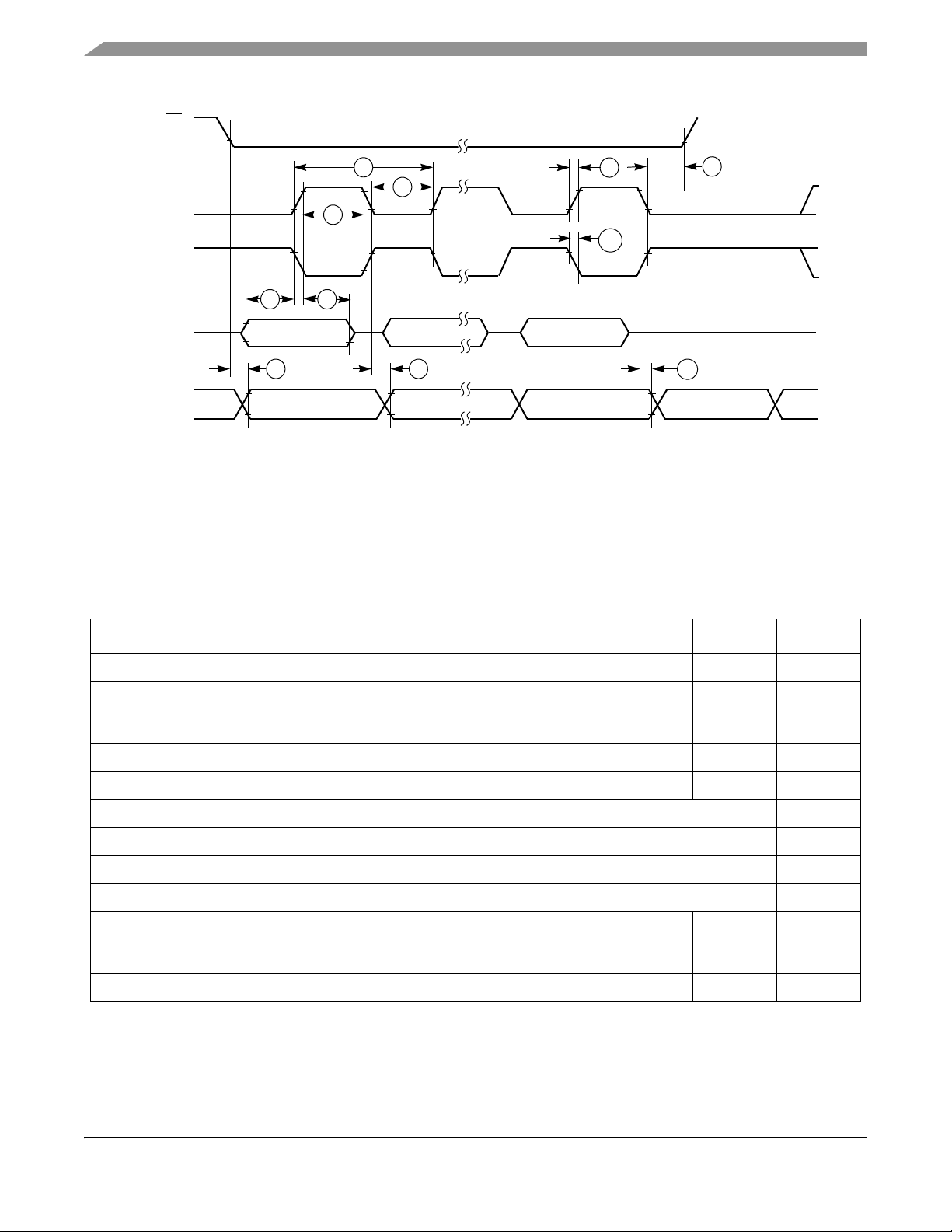
SS
(OUTPUT)
1
SCK
(CPOL = 0)
(OUTPUT)
SCK
(CPOL = 1)
(OUTPUT)
MISO
(INPUT)
MOSI
(OUTPUT)
5
2
MSB IN
MSB OUT
1
4
4
6
2
2
BIT 6 . . . 1
7
BIT 6 . . . 1
9
10
LSB IN
LSB OUT
3
8
Figure 33. SPI Master Timing (CPHA = 0)
6.4.4 FLASH Specifications
This section provides details about program/erase times and program-erase endurance for the FLASH
memory. Program and erase operations do not require any special power sources other than the normal
VDD supply.
Table 20. FLASH Characteristics
Characteristic Symbol Min Typical Max Unit
Supply voltage for program/erase V
Supply voltage for read operation
0 < f
0 < f
Internal FCLK frequency
< 8 MHz
Bus
< 20 MHz
Bus
1
Internal FCLK period (1/FCLK) t
Byte program time (random location)
Byte program time (burst mode)
Page erase time
Mass erase time
Program/erase endurance
2
(2)
3
(2)
(2)
prog/erase
V
Read
f
FCLK
Fcyc
t
prog
t
Burst
t
Page
t
Mass
TL to TH = –40°C to + 85°C
T = 25°C
Data retention
1
The frequency of this clock is controlled by a software setting.
2
These values are hardware state machine controlled. User code does not need to count cycles. This information supplied
4
t
D_ret
2.1 3.6 V
1.8
2.08
3.6
3.6
150 200 kHz
56.67µs
9t
4t
4000 t
20,000 t
10,000
100,000
—
—
15 100 — years
Fcyc
Fcyc
Fcyc
Fcyc
cycles
for calculating approximate time to program and erase.
V
MC13211/212/213/214 Technical Data, Rev. 0.0,
62 Freescale Semiconductor
Page 63

3
Typical endurance for FLASH was evaluated for this product family on the 9S12Dx64. For additional information on how
Freescale Semiconductor defines typical endurance, please refer to Engineering Bulletin EB619/D, Typical Endurance for
Nonvolatile Memory.
4
T ypical data retention values are based on intrinsic capability of the technology measured at high temperature and de-rated
to 25°C using the Arrhenius equation. For additional information on how Freescale Semiconductor defines typical data
retention, please refer to Engineering Bulletin EB618/D, Typical Data Retention for Non-volatile Memory.
7 Application Considerations
7.1 Crystal Oscillator Reference Frequency
The IEEE 802.15.4 Standard requires that several frequency tolerances be kept within ± 40 ppm accuracy.
This means that a total offset up to 80 ppm between transmitter and receiver will still result in acceptable
performance. The MC1321x transceiver provides onboard crystal trim capacitors to assist in meeting this
performance. The primary determining factor in meeting the 802.15.4 standard, is the tolerance of the
crystal oscillator reference frequency. A number of factors can contribute to this tolerance and a crystal
specification will quantify each of them:
1. The initial (or make) tolerance of the crystal resonant frequency itself.
2. The variation of the crystal resonant frequency with temperature.
3. The variation of the crystal resonant frequency with time, also commonly known as aging.
4. The variation of the crystal resonant frequency with load capacitance, also commonly known as
pulling. This is affected by:
a) The external load capacitor values - initial tolerance and variation with temperature.
b) The internal trim capacitor values - initial tolerance and variation with temperature.
c) Stray capacitance on the crystal pin nodes - including stray on-chip capacitance, stray package
capacitance and stray board capacitance; and its initial tolerance and variation with
temperature.
5. Whether or not a frequency trim step will be performed in production
7.1.1 Crystal Oscillator Design Considerations
Freescale requires that a 16 MHz crystal with a <9 pF load capacitance is used. The MC1321x does not
contain a reference divider, so 16 MHz is the only frequency that can be used. A crystal requiring higher
load capacitance is prohibited because a higher load on the amplifier circuit may compromise its
performance. The crystal manufacturer defines the load capacitance as that total external capacitance seen
across the two terminals of the crystal. The oscillator amplifier configuration used in the MC1321x
requires two balanced load capacitors from each terminal of the crystal to ground. As such, the capacitors
are seen to be in series by the crystal, so each must be <18 pF for proper loading.
In the Figure 34 crystal reference schematic, the external load capacitors are shown as 6.8 pF each, used
in conjunction with a crystal that requires an 8 pF load capacitance. The default internal trim capacitor
value (2.4 pF) and stray capacitance total value (6.8 pF) sum up to 9.2 pF giving a total of 16 pF . The value
for the stray capacitance was determined empirically assuming the default internal trim capacitor value and
for a specific board layout. A different board layout may require a different external load capacitor value.
MC13211/212/213/214 Technical Data, Rev. 0.0,
Freescale Semiconductor 63
Page 64

The on-chip trim capability may be used to determine the closest standard value by adjusting the trim value
via the SPI and observing the frequency at CLKO. Each internal trim load capacitor has a trim range of
approximately 5 pF in 20 fF steps.
Initial tolerance for the internal trim capacitance is approximately ±15%.
Since the MC1321x contains an on-chip reference frequency trim capability, it is possible to trim out
virtually all of the initial tolerance factors and put the frequency within 0.12 ppm on a board-by-board
basis. Individual trimming of each board in a production environment allows use of the lowest cost crystal,
but requires that each board go through a trimming procedure. This step can be avoided by
using/specifying a crystal with a tighter stability tolerance, but the crystal will be slightly higher in cost.
A tolerance analysis budget may be created using all the previously stated factors. It is an engineering
judgment whether the worst case tolerance will assume that all factors will vary in the same direction or if
the various factors can be statistically rationalized using RSS (Root-Sum-Square) analysis. The aging
factor is usually specified in ppm/year and the product designer can determine how many years are to be
assumed for the product lifetime. T aking all of the factors into account, the product designer can determine
the needed specifications for the crystal and external load capacitors to meet the IEEE 802.15.4
specification.
U3
XTAL1
XTAL2
MC1321x
27
28
Y1
16MHz
C10
6.8pF
C11
6.8pF
Y1 = Daishinku KDS - DSX321G ZD00882
Figure 34. MC1321x Modem Crystal Circuit
7.1.2 Suggested Crystals
Three suggested crystal types are shown in Table 21, Table 22, and Table 23. These variations are given
because the crystals have different trade-offs between cost and usage.
Table 21. Daishinku KDS - DSX321G ZD00882 Crystal Specifications
Parameter Value Unit Condition
1,2
Type DSX321G surface mount
Frequency 16 MHz
Frequency tolerance ± 20 ppm at 25 °C ± 3 °C
Equivalent series resistance 100 Ω max
MC13211/212/213/214 Technical Data, Rev. 0.0,
64 Freescale Semiconductor
Page 65

Table 21. Daishinku KDS - DSX321G ZD00882 Crystal Specifications (continued)
1,2
Parameter Value Unit Condition
Temperature drift ± 20 ppm -10 °C to +60 °C
Load capacitance 8.0 pF
Drive level 10 µW± 2 µW
Shunt capacitance 2 pF max
Mode of oscillation fundamental
1
With this crystal, the oscillator frequency requires trimming in production.
2
This crystal is not recommended for applications that employ Doze mode over the entire temperature range.
Table 22. Toyocom TSX-10A 16MHZ TN4-26139 Crystal Specifications
1,2
Parameter Value Unit Condition
Type TSX-10A surface mount
Frequency 16 MHz
Frequency tolerance ± 10 ppm at 25 °C ± 3 °C
Equivalent series resistance 40 Ω max
Temperature drift ± 16 ppm -40 °C to +85 °C
Load capacitance 9 pF
Drive level 100 µWmax
Shunt capacitance 1.2 pF typical
Mode of oscillation fundamental
1
With this crystal oscillator frequency trimming is NOT required in production.
2
This crystal not recommended for applications that employ Doze mode over the entire tempera ture range.
Table 23. NDK EXS00A-03311 Crystal Specifications
1,2
Parameter Value Unit Condition
Type NX3225 surface mount
Frequency 16 MHz
Frequency tolerance ± 10 ppm at 25 °C ± 3 °C
Equivalent series resistance 80 Ω max (42 typ)
Temperature drift ± 15 ppm -40 °C to +85 °C
Load capacitance 7.2 pF
Drive level 100 µWmax
Shunt capacitance 0.8 pF typical
Mode of oscillation fundamental
MC13211/212/213/214 Technical Data, Rev. 0.0,
Freescale Semiconductor 65
Page 66

1
c
With this crystal oscillator frequency trimming is NOT required in production.
2
This crystal recommended for applications that employ Doze mode.
NOTE
Crystal suppliers frequently specify the crystal package separately form the
desired crystal parameters. Care should be taken that desired crystal
specifications can be obtained in the desired package.
7.2 RF Single Port Application with an F Antenna
Figure 35 shows a typical single port RF application topology in which part count is minimized and a
printed copper F antenna is used for low cost. Only the RFIN port of the MC1321x is required because the
differential port is bi-directional and uses the on-chip T/R switch. Matching to near 50 Ohms is
accomplished with L1, L2, L3, and the traces on the PCB. A balun transforms the differential signal to
single-ended to interface with the F antenna.
The proper DC bias to the RFIN_x (P AO_x) pins is provided through the balun. The CT_Bias pin provides
the proper bias voltage point to the balun depending on operation, that is, CT_Bias is at VDDA voltage for
transmit and is at ground for receive. CT_Bias is switched between these two voltages based on the
operation. Capacitor C2 provides some high frequency bypass to the dc bias point. The L3/C1 network
provides a simple bandpass filter to limit out-of-band harmonics from the transmitter.
NOTE
Passive component values can vary as a function of circuit board layout as
required to obtain best matching and RF performance.
U1
GPIO1
PAO_M
PAO_P
RFIN_P
RFIN_M
CT_Bias
MC1321x
44
39
38
36
35
34
L1
1.5nH
L4
1.5nH
L2
3.9nH
Z1
3
2
4
LDB212G4005C-001
C2
10pF
R1
1
5
6
L3
3.9n H
C1
1.0pF
0R
R2
0R
Not Mou nt e d
ANT1
F_Ant enna
1
2
34J1
SMA_edge_Recepta
5
Figure 35. RF Single Port Application with an F-Antenna
7.3 RF Dual Port Application with an F-Antenna
Figure 36 shows a typical dual port application topology which also uses a printed copper F antenna. Both
the RFIN and PAO ports are used and the internal T/R switch is bypassed. Matching is provided for both
differential ports by L5, L6, L7, and L9 and C4 and C7. A balun is used for both receive and transmit paths
which are provided by the external T/R switch, IC1. This implementation, while more complicated, gives
MC13211/212/213/214 Technical Data, Rev. 0.0,
66 Freescale Semiconductor
Page 67

better performance due to the reduced loss of the external T/R switch and the more optimum match
provided to the PAO and RFIN ports.
The switch control is connected to the CT_Bias pin which serves as its control signal. The CT_Bias signal
can be programmed to be active high or active low (depending on TX versus RX) and will switch
appropriately based on the radio operation. No interaction with the MCU on an operation-by-operation
basis is required.
NOTE
Passive component values can vary as a function of circuit board layout as
required to obtain best matching and RF performance.
The VDD voltage to the antenna switch is connected to GPIO1. This is a useful feature when GPIO1 is
programmed as an “Out of Idle” status indicator. When the radio is out of Idle (or active), the antenna
switch is powered. In this manner, the antenna switch only consuina 1urr ent when it needs to be active.
The GPIO1 can only be used as a VDD source for a very low 1urrent load.
VDDA
L5
4.7nH
L6
4.7nH
Z2
3
2
4
LDB212G4005C-001
C6
10pF
Z3
3
2
4
LDB212G4005C-001
C3
1
5
10pF
6
C8
1
10pF
5
6
IC1
3
OUT2
1
OUT1
2
GND
VCONT
µPG2012TK-E2
VDD
6
5
IN
4
L8
2.2nH
C9
1.8pF
R3
0R
R4
0R
Not Mounted
ANT2
F_Antenna
1
2
34J2
SMA_edge_Receptacle_Female
5
Figure 36. RF Dual Port Application with an F-Antenna
MC13211/212/213/214 Technical Data, Rev. 0.0,
Freescale Semiconductor 67
Page 68

8 Mechanical Diagrams
Figure 37 and Figure 38 show the MC1321x mechanical information.
Figure 37. Top V iew Mechanical (1 of 2)
MC13211/212/213/214 Technical Data, Rev. 0.0,
68 Freescale Semiconductor
Page 69
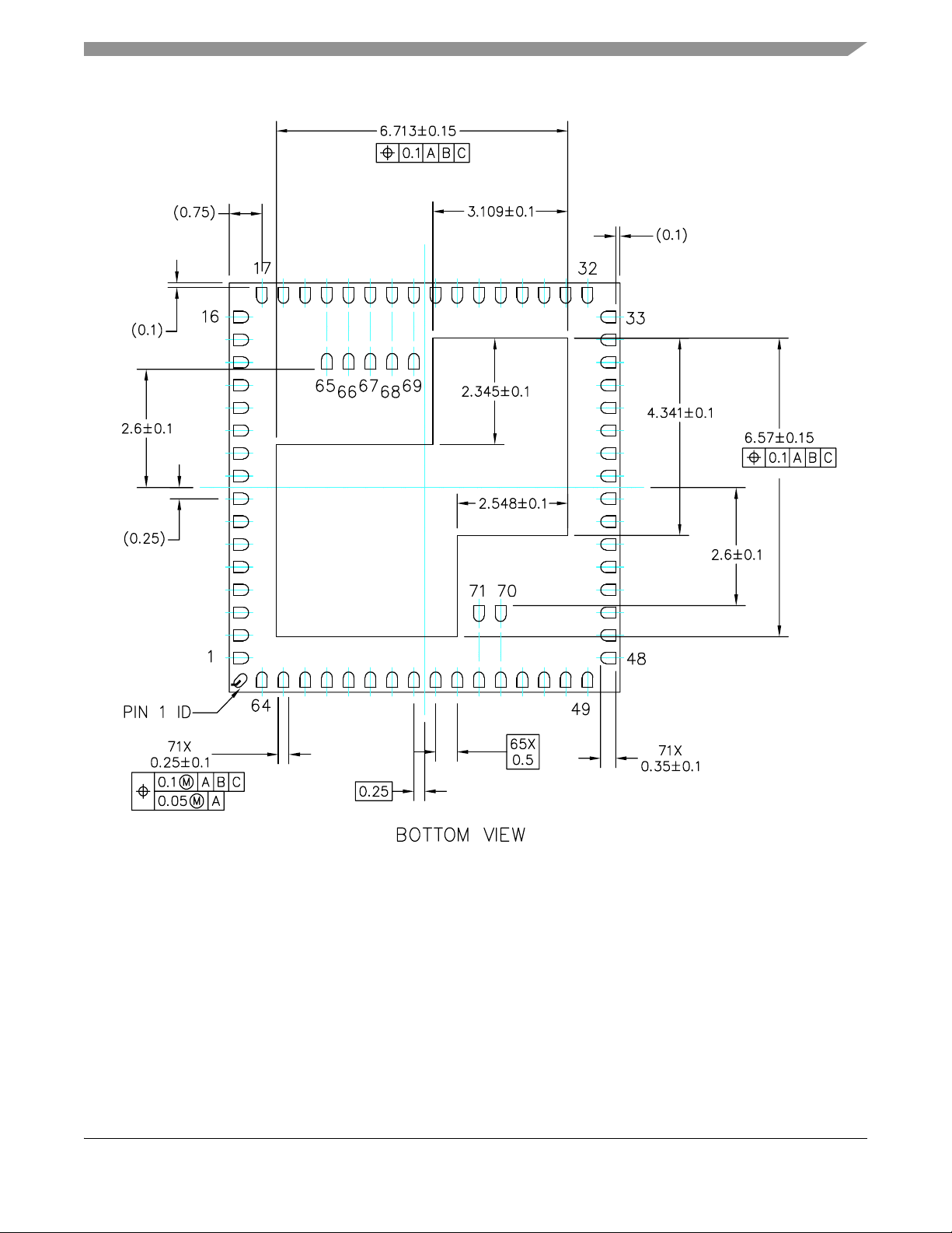
Figure 38. Bottom View Mechanical (2 of 2)
MC13211/212/213/214 Technical Data, Rev. 0.0,
Freescale Semiconductor 69
Page 70

How to Reach Us:
Home Page:
www.freescale.com
E-mail:
support@freescale.com
USA/Europe or Locations Not Listed:
Freescale Semiconductor
Technical Information Center, CH370
1300 N. Alma School Road
Chandler, Arizona 85224
+1-800-521-6274 or +1-480-768-2130
support@freescale.com
Europe, Middle East, and Africa:
Freescale Halbleiter Deutschland GmbH
Technical Information Center
Schatzbogen 7
81829 Muenchen, Germany
+44 1296 380 456 (English)
+46 8 52200080 (English)
+49 89 92103 559 (German)
+33 1 69 35 48 48 (French)
support@freescale.com
Japan:
Freescale Semiconductor Japan Ltd.
Headquarters
ARCO Tower 15F
1-8-1, Shimo-Meguro, Meguro-ku,
Tokyo 153-0064, Japan
0120 191014 or +81 3 5437 9125
support.japan@freescale.com
Asia/Pacific:
Freescale Semiconductor Hong Kong Ltd.
Technical Information Center
2 Dai King Street
Tai Po Industrial Estate
Tai Po, N.T., Hong Kong
+800 2666 8080
support.asia@freescale.com
For Literature Requests Only:
Freescale Semiconductor Literature Distribution Center
P.O. Box 5405
Denver, Colorado 80217
1-800-521-6274 or 303-675-2140
Fax: 303-675-2150
LDCForFreescaleSemiconductor@hibbertgroup.com
Information in this document is provided solely to enable system and software implementers to use
Freescale Semiconductor products. There are no express or implied copyright licenses granted
hereunder to design or fabricate any integrated circuits or int egrated circuits based on the informa tion
in this document.
Freescale Semiconductor reserves the right to make changes without furt her notice to any product s
herein. Freescale Semiconductor makes no warranty, representation or guarantee regarding the
suitability of its products for any particular purpose, nor does Freescale Semiconductor assume any
liability arising out of the application or use of any product or circuit, and specifically disclaims any
and all liability, including without limitation consequential or incident al damages. “Typical” parameters
that may be provided in Freescale Semiconductor data sheet s and/or specifications can and do vary
in different applications and actual performance may vary over time. All operating parameters,
including “Typicals”, must be vali dated for each customer application by customer’s technical
experts. Freescale Semiconductor does not convey any l icense und er it s paten t rights no r the right s
of others. Freescale Semiconductor products are not designed, intended, or authorized for use as
components in systems intended for surgical implant into the body, or other applications intended to
support or sustain life, or for any other applicatio n in which the failure of the Freescale Semiconductor
product could create a situation where personal injury or death may occur. Should Buyer purchase
or use Freescale Semiconductor products for any such unintended or unauthorized application,
Buyer shall indemnify and hold Freescale Semiconductor and its officers, employees, subsidiaries,
affiliates, and distributors harmless against all claims, costs, damages, and expenses, and
reasonable attorney fees arising out of, directly or indirectly, any claim of personal injury or death
associated with such unintended or unauthorized use, even if such claim alleges that Freescale
Semiconductor was negligent regarding the design or manufacture of the part.
Freescale™ and the Freescale logo are trademarks of Freescale Semiconductor, Inc. All other
product or service names are the property of their respective owners.
© Freescale Semiconductor, Inc. 200 5, 2006. All rights reserved.
Docu m e nt Number: MC 1321x
Rev. 0.0,
03/2006
 Loading...