


M68HC12B Family
Data Sheet
M68HC12
Microcontrollers
M68HC12B
Rev. 9.1
07/2005
freescale.com


M68HC12B Family
Data Sheet
To provide the most up-to-date information, the revision of our documents on the World Wide Web will be
the most current. Your printed copy may be an earlier revision. To verify you have the latest information
available, refer to:
http://freescale.com
Freescale™ and the Freescale logo are trademarks of Freescale Semiconductor, Inc.
This product incorporates SuperFlash® technology licensed from SST.
© Freescale Semiconductor, Inc., 2005. All rights reserved.
M68HC12B Family Data Sheet, Rev. 9.1
Freescale Semiconductor 3
Revision History
The following revision history table summarizes changes contained in this document. For your
convenience, the page number designators have been linked to the appropriate location.
Revision History
Date
June,
2001
September,
2001
April,
2002
January,
2003
April,
2003
May,
2003
July,
2003
June,
2004
July,
2005
Revision
Level
Figure 1-7. BDM Tool Connector — Added NC (no connect) designator to
pin 3
Figure 18-16. BDM Tool Connector — Added NC designator to pin 3 305
Table 14-2. Loop Mode Functions — Corrected table header, third column,
from DDRS1 to DDS1
2.0
3.0
4.0
5.0
6.0
7.0
8.0
9.0
9.1 Updated to meet Freescale identity guidelines. Throughout
WOMS bit description, fifth line, changed (via DDRS0/2)
to (via DDS0/2)
SSOE bit description, second line, changed DDRS7 to DDS7 205
In the table notes following the SPC0 bit description, corrected bit
designators from DDRS4, DDRS5, DDRS6, and DDRS7 to DDS4, DDS5,
DDS6, and DDS7.
Table 13-3. Prescaler Selection — Added value column and updated
prescale factors
19.11 EEPROM Characteristics — Corrected minimum and maximum
values for programming and erase times
Document type changed from Advance Information to Technical Data
reflecting qualification.
Figure 3-9. Condition Code Register (CCR) — Reset value for S bit
corrected from U to 1
14.2.3.3 SCI Control Register 2 — Removed erroneous reference to Port S
bit 3 in the definition for the transmitter enable bit (TE).
Figure 14-20. Port S Data Register (PORTS) — Removed erroneous pin
function for PS3 and PS2.
Reformatted to meet publication standards N/A
19.2 Maximum Ratings — Corrected maximum values for VDD, VDDA,
VDDX, and VIn
19.7 ATD Maximum Ratings — Corrected maximum values for VRH and
VRL
Figure 19-1. Programming Voltage Envelope — Corrected maximum values
for VFP and VDD
19.12.1 Programming Voltage Supply Envelope — Added subsection for
clarity.
19.12.2 Example V
19.2 Maximum Ratings — Updated values 307
19.7 ATD Maximum Ratings — Updated values 310
Table 13-3. Prescaler Selection — Corrected prescaler factor for
values 6 and 7
Protection Circuitry — Added subsection for clarity.
FP
Description
Page
Number(s)
29
195
195
205
172
313
N/A
62
197
208
307
310
315
315
316
183
M68HC12B Family Data Sheet, Rev. 9.1
4 Freescale Semiconductor

List of Chapters
Chapter 1 General Description. . . . . . . . . . . . . . . . . . . . . . . . . . . . . . . . . . . . . . . . . . . . . . . . 19
Chapter 2 Register Block . . . . . . . . . . . . . . . . . . . . . . . . . . . . . . . . . . . . . . . . . . . . . . . . . . . .39
Chapter 3 Central Processor Unit (CPU). . . . . . . . . . . . . . . . . . . . . . . . . . . . . . . . . . . . . . . .59
Chapter 4 Resets and Interrupts . . . . . . . . . . . . . . . . . . . . . . . . . . . . . . . . . . . . . . . . . . . . . .67
Chapter 5 Operating Modes and Resource Mapping. . . . . . . . . . . . . . . . . . . . . . . . . . . . . . 75
Chapter 6 Bus Control and Input/Output (I/O) . . . . . . . . . . . . . . . . . . . . . . . . . . . . . . . . . . . 85
Chapter 7 EEPROM . . . . . . . . . . . . . . . . . . . . . . . . . . . . . . . . . . . . . . . . . . . . . . . . . . . . . . . . .93
Chapter 8 FLASH EEPROM . . . . . . . . . . . . . . . . . . . . . . . . . . . . . . . . . . . . . . . . . . . . . . . . . .99
Chapter 9 Read-Only Memory (ROM) . . . . . . . . . . . . . . . . . . . . . . . . . . . . . . . . . . . . . . . . .111
Chapter 10 Clock Generation Module (CGM) . . . . . . . . . . . . . . . . . . . . . . . . . . . . . . . . . . . 113
Chapter 11 Pulse-Width Modulator (PWM) . . . . . . . . . . . . . . . . . . . . . . . . . . . . . . . . . . . . .125
Chapter 12 Standard Timer (TIM). . . . . . . . . . . . . . . . . . . . . . . . . . . . . . . . . . . . . . . . . . . . .141
Chapter 13 Enhanced Capture Timer (ECT) Module . . . . . . . . . . . . . . . . . . . . . . . . . . . . .159
Chapter 14 Serial Interface . . . . . . . . . . . . . . . . . . . . . . . . . . . . . . . . . . . . . . . . . . . . . . . . . .191
Chapter 15 Byte Data Link Communications (BDLC) . . . . . . . . . . . . . . . . . . . . . . . . . . . .213
Chapter 16 msCAN12 Controller . . . . . . . . . . . . . . . . . . . . . . . . . . . . . . . . . . . . . . . . . . . . .243
Chapter 17 Analog-to-Digital Converter (ATD) . . . . . . . . . . . . . . . . . . . . . . . . . . . . . . . . . .277
Chapter 18 Development Support . . . . . . . . . . . . . . . . . . . . . . . . . . . . . . . . . . . . . . . . . . . .289
Chapter 19 Electrical Specifications . . . . . . . . . . . . . . . . . . . . . . . . . . . . . . . . . . . . . . . . . .307
Chapter 20 Mechanical Specifications . . . . . . . . . . . . . . . . . . . . . . . . . . . . . . . . . . . . . . . .331
M68HC12B Family Data Sheet, Rev. 9.1
Freescale Semiconductor 5

List of Chapters
M68HC12B Family Data Sheet, Rev. 9.1
6 Freescale Semiconductor

Table of Contents
Chapter 1
General Description
1.1 Introduction . . . . . . . . . . . . . . . . . . . . . . . . . . . . . . . . . . . . . . . . . . . . . . . . . . . . . . . . . . . . . . . . 19
1.2 Features. . . . . . . . . . . . . . . . . . . . . . . . . . . . . . . . . . . . . . . . . . . . . . . . . . . . . . . . . . . . . . . . . . . 20
1.3 Slow-Mode Clock Divider Advisory . . . . . . . . . . . . . . . . . . . . . . . . . . . . . . . . . . . . . . . . . . . . . . 21
1.4 Block Diagrams . . . . . . . . . . . . . . . . . . . . . . . . . . . . . . . . . . . . . . . . . . . . . . . . . . . . . . . . . . . . . 22
1.5 Ordering Information . . . . . . . . . . . . . . . . . . . . . . . . . . . . . . . . . . . . . . . . . . . . . . . . . . . . . . . . . 24
1.6 Pinout and Signal Descriptions . . . . . . . . . . . . . . . . . . . . . . . . . . . . . . . . . . . . . . . . . . . . . . . . . 24
1.6.1 Pin Assignments . . . . . . . . . . . . . . . . . . . . . . . . . . . . . . . . . . . . . . . . . . . . . . . . . . . . . . . . . 24
1.6.2 Power Supply Pins . . . . . . . . . . . . . . . . . . . . . . . . . . . . . . . . . . . . . . . . . . . . . . . . . . . . . . . . 24
1.6.2.1 V
1.6.2.2 V
1.6.2.3 V
1.6.2.4 V
1.6.2.5 V
1.6.3 Signal Descriptions . . . . . . . . . . . . . . . . . . . . . . . . . . . . . . . . . . . . . . . . . . . . . . . . . . . . . . . 27
1.6.3.1 XTAL and EXTAL . . . . . . . . . . . . . . . . . . . . . . . . . . . . . . . . . . . . . . . . . . . . . . . . . . . . . . . 27
1.6.3.2 ECLK . . . . . . . . . . . . . . . . . . . . . . . . . . . . . . . . . . . . . . . . . . . . . . . . . . . . . . . . . . . . . . . . 28
1.6.3.3 RESET
1.6.3.4 IRQ
1.6.3.5 XIRQ
1.6.3.6 SMODN, MODA, and MODB . . . . . . . . . . . . . . . . . . . . . . . . . . . . . . . . . . . . . . . . . . . . . . 29
1.6.3.7 BKGD . . . . . . . . . . . . . . . . . . . . . . . . . . . . . . . . . . . . . . . . . . . . . . . . . . . . . . . . . . . . . . . . 29
1.6.3.8 ADDR15–ADDR0 and DATA15–DATA0 . . . . . . . . . . . . . . . . . . . . . . . . . . . . . . . . . . . . . 30
1.6.3.9 R/W
1.6.3.10 LSTRB
1.6.3.11 IPIPE1 and IPIPE0 . . . . . . . . . . . . . . . . . . . . . . . . . . . . . . . . . . . . . . . . . . . . . . . . . . . . . . 30
1.6.3.12 DBE
1.6.4 Port Signals . . . . . . . . . . . . . . . . . . . . . . . . . . . . . . . . . . . . . . . . . . . . . . . . . . . . . . . . . . . . . 32
1.6.4.1 Port A . . . . . . . . . . . . . . . . . . . . . . . . . . . . . . . . . . . . . . . . . . . . . . . . . . . . . . . . . . . . . . . . 32
1.6.4.2 Port B . . . . . . . . . . . . . . . . . . . . . . . . . . . . . . . . . . . . . . . . . . . . . . . . . . . . . . . . . . . . . . . . 33
1.6.4.3 Port E . . . . . . . . . . . . . . . . . . . . . . . . . . . . . . . . . . . . . . . . . . . . . . . . . . . . . . . . . . . . . . . . 33
1.6.4.4 Port DLC. . . . . . . . . . . . . . . . . . . . . . . . . . . . . . . . . . . . . . . . . . . . . . . . . . . . . . . . . . . . . . 34
1.6.4.5 Port CAN . . . . . . . . . . . . . . . . . . . . . . . . . . . . . . . . . . . . . . . . . . . . . . . . . . . . . . . . . . . . . 34
1.6.4.6 Port AD . . . . . . . . . . . . . . . . . . . . . . . . . . . . . . . . . . . . . . . . . . . . . . . . . . . . . . . . . . . . . . . 34
1.6.4.7 Port P . . . . . . . . . . . . . . . . . . . . . . . . . . . . . . . . . . . . . . . . . . . . . . . . . . . . . . . . . . . . . . . . 35
1.6.4.8 Port T . . . . . . . . . . . . . . . . . . . . . . . . . . . . . . . . . . . . . . . . . . . . . . . . . . . . . . . . . . . . . . . . 35
1.6.4.9 Port S . . . . . . . . . . . . . . . . . . . . . . . . . . . . . . . . . . . . . . . . . . . . . . . . . . . . . . . . . . . . . . . . 35
1.6.5 Port Pullup, Pulldown, and Reduced Drive . . . . . . . . . . . . . . . . . . . . . . . . . . . . . . . . . . . . . 36
and VSS. . . . . . . . . . . . . . . . . . . . . . . . . . . . . . . . . . . . . . . . . . . . . . . . . . . . . . . . . . . 24
DD
and V
DDX
and V
DDA
and VRL. . . . . . . . . . . . . . . . . . . . . . . . . . . . . . . . . . . . . . . . . . . . . . . . . . . . . . . . . . . 24
RH
(MC68HC912B32 and MC68HC912BC32 only) . . . . . . . . . . . . . . . . . . . . . . . . . . . . 27
FP
. . . . . . . . . . . . . . . . . . . . . . . . . . . . . . . . . . . . . . . . . . . . . . . . . . . . . . . . . 24
SSX
. . . . . . . . . . . . . . . . . . . . . . . . . . . . . . . . . . . . . . . . . . . . . . . . . . . . . . . . . 24
SSA
. . . . . . . . . . . . . . . . . . . . . . . . . . . . . . . . . . . . . . . . . . . . . . . . . . . . . . . . . . . . . . . 28
. . . . . . . . . . . . . . . . . . . . . . . . . . . . . . . . . . . . . . . . . . . . . . . . . . . . . . . . . . . . . . . . . . 28
. . . . . . . . . . . . . . . . . . . . . . . . . . . . . . . . . . . . . . . . . . . . . . . . . . . . . . . . . . . . . . . . . 29
. . . . . . . . . . . . . . . . . . . . . . . . . . . . . . . . . . . . . . . . . . . . . . . . . . . . . . . . . . . . . . . . . . 30
. . . . . . . . . . . . . . . . . . . . . . . . . . . . . . . . . . . . . . . . . . . . . . . . . . . . . . . . . . . . . . . 30
. . . . . . . . . . . . . . . . . . . . . . . . . . . . . . . . . . . . . . . . . . . . . . . . . . . . . . . . . . . . . . . . . 30
M68HC12B Family Data Sheet, Rev. 9.1
Freescale Semiconductor 7

Table of Contents
Chapter 2
Register Block
2.1 Introduction . . . . . . . . . . . . . . . . . . . . . . . . . . . . . . . . . . . . . . . . . . . . . . . . . . . . . . . . . . . . . . . . 39
2.2 Registers . . . . . . . . . . . . . . . . . . . . . . . . . . . . . . . . . . . . . . . . . . . . . . . . . . . . . . . . . . . . . . . . . . 40
Chapter 3
Central Processor Unit (CPU)
3.1 Introduction . . . . . . . . . . . . . . . . . . . . . . . . . . . . . . . . . . . . . . . . . . . . . . . . . . . . . . . . . . . . . . . . 59
3.2 Programming Model. . . . . . . . . . . . . . . . . . . . . . . . . . . . . . . . . . . . . . . . . . . . . . . . . . . . . . . . . . 59
3.3 CPU Registers . . . . . . . . . . . . . . . . . . . . . . . . . . . . . . . . . . . . . . . . . . . . . . . . . . . . . . . . . . . . . . 60
3.3.1 Accumulators A and B . . . . . . . . . . . . . . . . . . . . . . . . . . . . . . . . . . . . . . . . . . . . . . . . . . . . . 60
3.3.2 Accumulator D . . . . . . . . . . . . . . . . . . . . . . . . . . . . . . . . . . . . . . . . . . . . . . . . . . . . . . . . . . . 60
3.3.3 Index Registers X and Y . . . . . . . . . . . . . . . . . . . . . . . . . . . . . . . . . . . . . . . . . . . . . . . . . . . 61
3.3.4 Stack Pointer . . . . . . . . . . . . . . . . . . . . . . . . . . . . . . . . . . . . . . . . . . . . . . . . . . . . . . . . . . . . 61
3.3.5 Program Counter . . . . . . . . . . . . . . . . . . . . . . . . . . . . . . . . . . . . . . . . . . . . . . . . . . . . . . . . . 62
3.3.6 Condition Code Register . . . . . . . . . . . . . . . . . . . . . . . . . . . . . . . . . . . . . . . . . . . . . . . . . . . 62
3.4 Data Types. . . . . . . . . . . . . . . . . . . . . . . . . . . . . . . . . . . . . . . . . . . . . . . . . . . . . . . . . . . . . . . . . 63
3.5 Addressing Modes . . . . . . . . . . . . . . . . . . . . . . . . . . . . . . . . . . . . . . . . . . . . . . . . . . . . . . . . . . . 63
3.6 Indexed Addressing Modes . . . . . . . . . . . . . . . . . . . . . . . . . . . . . . . . . . . . . . . . . . . . . . . . . . . . 64
3.7 Opcodes and Operands. . . . . . . . . . . . . . . . . . . . . . . . . . . . . . . . . . . . . . . . . . . . . . . . . . . . . . . 65
Chapter 4
Resets and Interrupts
4.1 Introduction . . . . . . . . . . . . . . . . . . . . . . . . . . . . . . . . . . . . . . . . . . . . . . . . . . . . . . . . . . . . . . . . 67
4.2 Exception Priority . . . . . . . . . . . . . . . . . . . . . . . . . . . . . . . . . . . . . . . . . . . . . . . . . . . . . . . . . . . . 67
4.3 Maskable Interrupts . . . . . . . . . . . . . . . . . . . . . . . . . . . . . . . . . . . . . . . . . . . . . . . . . . . . . . . . . . 67
4.4 Latching of Interrupts . . . . . . . . . . . . . . . . . . . . . . . . . . . . . . . . . . . . . . . . . . . . . . . . . . . . . . . . . 70
4.5 Interrupt Control and Priority Registers . . . . . . . . . . . . . . . . . . . . . . . . . . . . . . . . . . . . . . . . . . . 70
4.5.1 Interrupt Control Register. . . . . . . . . . . . . . . . . . . . . . . . . . . . . . . . . . . . . . . . . . . . . . . . . . . 70
4.5.2 Highest Priority I Interrupt Register . . . . . . . . . . . . . . . . . . . . . . . . . . . . . . . . . . . . . . . . . . . 71
4.6 Resets . . . . . . . . . . . . . . . . . . . . . . . . . . . . . . . . . . . . . . . . . . . . . . . . . . . . . . . . . . . . . . . . . . . . 71
4.6.1 Power-On Reset (POR) . . . . . . . . . . . . . . . . . . . . . . . . . . . . . . . . . . . . . . . . . . . . . . . . . . . . 71
4.6.2 External Reset . . . . . . . . . . . . . . . . . . . . . . . . . . . . . . . . . . . . . . . . . . . . . . . . . . . . . . . . . . . 71
4.6.3 Computer Operating Properly (COP) Reset. . . . . . . . . . . . . . . . . . . . . . . . . . . . . . . . . . . . . 71
4.6.4 Clock Monitor Reset. . . . . . . . . . . . . . . . . . . . . . . . . . . . . . . . . . . . . . . . . . . . . . . . . . . . . . . 72
4.7 Effects of Reset . . . . . . . . . . . . . . . . . . . . . . . . . . . . . . . . . . . . . . . . . . . . . . . . . . . . . . . . . . . . . 72
4.7.1 Operating Mode and Memory Map . . . . . . . . . . . . . . . . . . . . . . . . . . . . . . . . . . . . . . . . . . . 72
4.7.2 Clock and Watchdog Control Logic . . . . . . . . . . . . . . . . . . . . . . . . . . . . . . . . . . . . . . . . . . . 72
4.7.3 Interrupts . . . . . . . . . . . . . . . . . . . . . . . . . . . . . . . . . . . . . . . . . . . . . . . . . . . . . . . . . . . . . . . 72
4.7.4 Parallel Input/Output (I/O) . . . . . . . . . . . . . . . . . . . . . . . . . . . . . . . . . . . . . . . . . . . . . . . . . . 72
4.7.5 Central Processing Unit (CPU) . . . . . . . . . . . . . . . . . . . . . . . . . . . . . . . . . . . . . . . . . . . . . . 72
4.7.6 Memory . . . . . . . . . . . . . . . . . . . . . . . . . . . . . . . . . . . . . . . . . . . . . . . . . . . . . . . . . . . . . . . . 72
4.7.7 Other Resources . . . . . . . . . . . . . . . . . . . . . . . . . . . . . . . . . . . . . . . . . . . . . . . . . . . . . . . . . 73
4.8 Interrupt Recognition . . . . . . . . . . . . . . . . . . . . . . . . . . . . . . . . . . . . . . . . . . . . . . . . . . . . . . . . . 73
M68HC12B Family Data Sheet, Rev. 9.1
8 Freescale Semiconductor

Chapter 5
Operating Modes and Resource Mapping
5.1 Introduction . . . . . . . . . . . . . . . . . . . . . . . . . . . . . . . . . . . . . . . . . . . . . . . . . . . . . . . . . . . . . . . . 75
5.2 Operating Modes . . . . . . . . . . . . . . . . . . . . . . . . . . . . . . . . . . . . . . . . . . . . . . . . . . . . . . . . . . . . 75
5.2.1 Normal Operating Modes . . . . . . . . . . . . . . . . . . . . . . . . . . . . . . . . . . . . . . . . . . . . . . . . . . . 76
5.2.1.1 Normal Expanded Wide Mode . . . . . . . . . . . . . . . . . . . . . . . . . . . . . . . . . . . . . . . . . . . . . 76
5.2.1.2 Normal Expanded Narrow Mode . . . . . . . . . . . . . . . . . . . . . . . . . . . . . . . . . . . . . . . . . . . 76
5.2.1.3 Normal Single-Chip Mode . . . . . . . . . . . . . . . . . . . . . . . . . . . . . . . . . . . . . . . . . . . . . . . . 76
5.2.2 Special Operating Modes. . . . . . . . . . . . . . . . . . . . . . . . . . . . . . . . . . . . . . . . . . . . . . . . . . . 76
5.2.2.1 Special Expanded Wide Mode . . . . . . . . . . . . . . . . . . . . . . . . . . . . . . . . . . . . . . . . . . . . . 76
5.2.2.2 Special Expanded Narrow Mode . . . . . . . . . . . . . . . . . . . . . . . . . . . . . . . . . . . . . . . . . . . 76
5.2.2.3 Special Single-Chip Mode . . . . . . . . . . . . . . . . . . . . . . . . . . . . . . . . . . . . . . . . . . . . . . . . 76
5.2.2.4 Special Peripheral Mode . . . . . . . . . . . . . . . . . . . . . . . . . . . . . . . . . . . . . . . . . . . . . . . . . 77
5.2.3 Background Debug Mode . . . . . . . . . . . . . . . . . . . . . . . . . . . . . . . . . . . . . . . . . . . . . . . . . . 77
5.3 Internal Resource Mapping . . . . . . . . . . . . . . . . . . . . . . . . . . . . . . . . . . . . . . . . . . . . . . . . . . . . 77
5.4 Mode and Resource Mapping Registers . . . . . . . . . . . . . . . . . . . . . . . . . . . . . . . . . . . . . . . . . . 78
5.4.1 Mode Register . . . . . . . . . . . . . . . . . . . . . . . . . . . . . . . . . . . . . . . . . . . . . . . . . . . . . . . . . . . 78
5.4.2 Register Initialization Register . . . . . . . . . . . . . . . . . . . . . . . . . . . . . . . . . . . . . . . . . . . . . . . 80
5.4.3 RAM Initialization Register . . . . . . . . . . . . . . . . . . . . . . . . . . . . . . . . . . . . . . . . . . . . . . . . . . 80
5.4.4 EEPROM Initialization Register . . . . . . . . . . . . . . . . . . . . . . . . . . . . . . . . . . . . . . . . . . . . . . 81
5.4.5 Miscellaneous Mapping Control Register. . . . . . . . . . . . . . . . . . . . . . . . . . . . . . . . . . . . . . . 81
5.5 Memory Map . . . . . . . . . . . . . . . . . . . . . . . . . . . . . . . . . . . . . . . . . . . . . . . . . . . . . . . . . . . . . . . 83
Chapter 6
Bus Control and Input/Output (I/O)
6.1 Introduction . . . . . . . . . . . . . . . . . . . . . . . . . . . . . . . . . . . . . . . . . . . . . . . . . . . . . . . . . . . . . . . . 85
6.2 Detecting Access Type from External Signals . . . . . . . . . . . . . . . . . . . . . . . . . . . . . . . . . . . . . . 85
6.3 Registers . . . . . . . . . . . . . . . . . . . . . . . . . . . . . . . . . . . . . . . . . . . . . . . . . . . . . . . . . . . . . . . . . . 85
6.3.1 Port A Data Register . . . . . . . . . . . . . . . . . . . . . . . . . . . . . . . . . . . . . . . . . . . . . . . . . . . . . . 86
6.3.2 Port A Data Direction Register . . . . . . . . . . . . . . . . . . . . . . . . . . . . . . . . . . . . . . . . . . . . . . . 86
6.3.3 Port B Data Register . . . . . . . . . . . . . . . . . . . . . . . . . . . . . . . . . . . . . . . . . . . . . . . . . . . . . . 87
6.3.4 Port B Data Direction Register . . . . . . . . . . . . . . . . . . . . . . . . . . . . . . . . . . . . . . . . . . . . . . . 87
6.3.5 Port E Data Register . . . . . . . . . . . . . . . . . . . . . . . . . . . . . . . . . . . . . . . . . . . . . . . . . . . . . . 88
6.3.6 Port E Data Direction Register . . . . . . . . . . . . . . . . . . . . . . . . . . . . . . . . . . . . . . . . . . . . . . . 88
6.3.7 Port E Assignment Register . . . . . . . . . . . . . . . . . . . . . . . . . . . . . . . . . . . . . . . . . . . . . . . . . 89
6.3.8 Pullup Control Register . . . . . . . . . . . . . . . . . . . . . . . . . . . . . . . . . . . . . . . . . . . . . . . . . . . . 91
6.3.9 Reduced Drive of I/O Lines . . . . . . . . . . . . . . . . . . . . . . . . . . . . . . . . . . . . . . . . . . . . . . . . . 92
Chapter 7
EEPROM
7.1 Introduction . . . . . . . . . . . . . . . . . . . . . . . . . . . . . . . . . . . . . . . . . . . . . . . . . . . . . . . . . . . . . . . . 93
7.2 EEPROM Programmer’s Model . . . . . . . . . . . . . . . . . . . . . . . . . . . . . . . . . . . . . . . . . . . . . . . . . 93
7.3 EEPROM Control Registers. . . . . . . . . . . . . . . . . . . . . . . . . . . . . . . . . . . . . . . . . . . . . . . . . . . . 94
7.3.1 EEPROM Module Configuration Register . . . . . . . . . . . . . . . . . . . . . . . . . . . . . . . . . . . . . . 94
7.3.2 EEPROM Block Protect Register . . . . . . . . . . . . . . . . . . . . . . . . . . . . . . . . . . . . . . . . . . . . . 95
7.3.3 EEPROM Test Register . . . . . . . . . . . . . . . . . . . . . . . . . . . . . . . . . . . . . . . . . . . . . . . . . . . . 95
7.3.4 EEPROM Control Register. . . . . . . . . . . . . . . . . . . . . . . . . . . . . . . . . . . . . . . . . . . . . . . . . . 96
M68HC12B Family Data Sheet, Rev. 9.1
Freescale Semiconductor 9

Table of Contents
Chapter 8
FLASH EEPROM
8.1 Introduction . . . . . . . . . . . . . . . . . . . . . . . . . . . . . . . . . . . . . . . . . . . . . . . . . . . . . . . . . . . . . . . . 99
8.2 FLASH EEPROM Array . . . . . . . . . . . . . . . . . . . . . . . . . . . . . . . . . . . . . . . . . . . . . . . . . . . . . . . 99
8.3 FLASH EEPROM Registers. . . . . . . . . . . . . . . . . . . . . . . . . . . . . . . . . . . . . . . . . . . . . . . . . . . . 99
8.3.1 FLASH EEPROM Lock Control Register . . . . . . . . . . . . . . . . . . . . . . . . . . . . . . . . . . . . . . 100
8.3.2 FLASH EEPROM Module Configuration Register . . . . . . . . . . . . . . . . . . . . . . . . . . . . . . . 100
8.3.3 FLASH EEPROM Module Test Register . . . . . . . . . . . . . . . . . . . . . . . . . . . . . . . . . . . . . . 100
8.3.4 FLASH EEPROM Control Register . . . . . . . . . . . . . . . . . . . . . . . . . . . . . . . . . . . . . . . . . . 102
8.4 Operation . . . . . . . . . . . . . . . . . . . . . . . . . . . . . . . . . . . . . . . . . . . . . . . . . . . . . . . . . . . . . . . . . 103
8.4.1 Bootstrap Operation Single-Chip Mode . . . . . . . . . . . . . . . . . . . . . . . . . . . . . . . . . . . . . . . 103
8.4.2 Normal Operation. . . . . . . . . . . . . . . . . . . . . . . . . . . . . . . . . . . . . . . . . . . . . . . . . . . . . . . . 103
8.4.3 Program/Erase Operation . . . . . . . . . . . . . . . . . . . . . . . . . . . . . . . . . . . . . . . . . . . . . . . . . 103
8.4.3.1 Read/Write Accesses During Program/Erase . . . . . . . . . . . . . . . . . . . . . . . . . . . . . . . . 103
8.4.3.2 Program/Erase Verification. . . . . . . . . . . . . . . . . . . . . . . . . . . . . . . . . . . . . . . . . . . . . . . 104
8.4.3.3 Program/Erase Sequence . . . . . . . . . . . . . . . . . . . . . . . . . . . . . . . . . . . . . . . . . . . . . . . 104
8.5 Programming the FLASH EEPROM . . . . . . . . . . . . . . . . . . . . . . . . . . . . . . . . . . . . . . . . . . . . 105
8.6 Erasing the FLASH EEPROM . . . . . . . . . . . . . . . . . . . . . . . . . . . . . . . . . . . . . . . . . . . . . . . . . 107
8.7 Program/Erase Protection Interlocks . . . . . . . . . . . . . . . . . . . . . . . . . . . . . . . . . . . . . . . . . . . . 109
8.8 Stop or Wait Mode . . . . . . . . . . . . . . . . . . . . . . . . . . . . . . . . . . . . . . . . . . . . . . . . . . . . . . . . . . 109
8.9 Test Mode . . . . . . . . . . . . . . . . . . . . . . . . . . . . . . . . . . . . . . . . . . . . . . . . . . . . . . . . . . . . . . . . 109
Chapter 9
Read-Only Memory (ROM)
9.1 Introduction . . . . . . . . . . . . . . . . . . . . . . . . . . . . . . . . . . . . . . . . . . . . . . . . . . . . . . . . . . . . . . . 111
9.2 ROM Array . . . . . . . . . . . . . . . . . . . . . . . . . . . . . . . . . . . . . . . . . . . . . . . . . . . . . . . . . . . . . . . . 111
Chapter 10
Clock Generation Module (CGM)
10.1 Introduction . . . . . . . . . . . . . . . . . . . . . . . . . . . . . . . . . . . . . . . . . . . . . . . . . . . . . . . . . . . . . . . 113
10.2 Block Diagram . . . . . . . . . . . . . . . . . . . . . . . . . . . . . . . . . . . . . . . . . . . . . . . . . . . . . . . . . . . . . 113
10.3 Register Map . . . . . . . . . . . . . . . . . . . . . . . . . . . . . . . . . . . . . . . . . . . . . . . . . . . . . . . . . . . . . . 114
10.4 Clock Selection and Generation . . . . . . . . . . . . . . . . . . . . . . . . . . . . . . . . . . . . . . . . . . . . . . . 114
10.5 Slow Mode Divider . . . . . . . . . . . . . . . . . . . . . . . . . . . . . . . . . . . . . . . . . . . . . . . . . . . . . . . . . . 116
10.6 Clock Functions . . . . . . . . . . . . . . . . . . . . . . . . . . . . . . . . . . . . . . . . . . . . . . . . . . . . . . . . . . . . 116
10.6.1 Computer Operating Properly (COP) . . . . . . . . . . . . . . . . . . . . . . . . . . . . . . . . . . . . . . . . . 116
10.6.2 Real-Time Interrupt . . . . . . . . . . . . . . . . . . . . . . . . . . . . . . . . . . . . . . . . . . . . . . . . . . . . . . 116
10.6.3 Clock Monitor . . . . . . . . . . . . . . . . . . . . . . . . . . . . . . . . . . . . . . . . . . . . . . . . . . . . . . . . . . . 116
10.7 Clock Registers . . . . . . . . . . . . . . . . . . . . . . . . . . . . . . . . . . . . . . . . . . . . . . . . . . . . . . . . . . . . 117
10.7.1 Slow Mode Divider Register. . . . . . . . . . . . . . . . . . . . . . . . . . . . . . . . . . . . . . . . . . . . . . . . 117
10.7.2 Real-Time Interrupt Control Register . . . . . . . . . . . . . . . . . . . . . . . . . . . . . . . . . . . . . . . . . 118
10.7.3 Real-Time Interrupt Flag Register . . . . . . . . . . . . . . . . . . . . . . . . . . . . . . . . . . . . . . . . . . . 119
10.7.4 COP Control Register . . . . . . . . . . . . . . . . . . . . . . . . . . . . . . . . . . . . . . . . . . . . . . . . . . . . 119
10.7.5 Arm/Reset COP Timer Register. . . . . . . . . . . . . . . . . . . . . . . . . . . . . . . . . . . . . . . . . . . . . 120
10.8 Clock Divider Chains . . . . . . . . . . . . . . . . . . . . . . . . . . . . . . . . . . . . . . . . . . . . . . . . . . . . . . . . 121
M68HC12B Family Data Sheet, Rev. 9.1
10 Freescale Semiconductor

Chapter 11
Pulse-Width Modulator (PWM)
11.1 Introduction . . . . . . . . . . . . . . . . . . . . . . . . . . . . . . . . . . . . . . . . . . . . . . . . . . . . . . . . . . . . . . . 125
11.2 PWM Register Descriptions . . . . . . . . . . . . . . . . . . . . . . . . . . . . . . . . . . . . . . . . . . . . . . . . . . . 128
11.2.1 PWM Clocks and Concatenate Register . . . . . . . . . . . . . . . . . . . . . . . . . . . . . . . . . . . . . . 128
11.2.2 PWM Clock Select and Polarity Register. . . . . . . . . . . . . . . . . . . . . . . . . . . . . . . . . . . . . . 129
11.2.3 PWM Enable Register . . . . . . . . . . . . . . . . . . . . . . . . . . . . . . . . . . . . . . . . . . . . . . . . . . . . 130
11.2.4 PWM Prescale Counter . . . . . . . . . . . . . . . . . . . . . . . . . . . . . . . . . . . . . . . . . . . . . . . . . . . 131
11.2.5 PWM Scale Register 0 . . . . . . . . . . . . . . . . . . . . . . . . . . . . . . . . . . . . . . . . . . . . . . . . . . . . 131
11.2.6 PWM Scale Counter 0 Value . . . . . . . . . . . . . . . . . . . . . . . . . . . . . . . . . . . . . . . . . . . . . . . 131
11.2.7 PWM Scale Register 1 . . . . . . . . . . . . . . . . . . . . . . . . . . . . . . . . . . . . . . . . . . . . . . . . . . . . 132
11.2.8 PWM Scale Counter 1 Value . . . . . . . . . . . . . . . . . . . . . . . . . . . . . . . . . . . . . . . . . . . . . . . 132
11.2.9 PWM Channel Counters 0–3 . . . . . . . . . . . . . . . . . . . . . . . . . . . . . . . . . . . . . . . . . . . . . . . 133
11.2.10 PWM Channel Period Registers 0–3 . . . . . . . . . . . . . . . . . . . . . . . . . . . . . . . . . . . . . . . . . 134
11.2.11 PWM Channel Duty Registers 0–3 . . . . . . . . . . . . . . . . . . . . . . . . . . . . . . . . . . . . . . . . . . 135
11.2.12 PWM Control Register . . . . . . . . . . . . . . . . . . . . . . . . . . . . . . . . . . . . . . . . . . . . . . . . . . . . 136
11.2.13 PWM Special Mode Register . . . . . . . . . . . . . . . . . . . . . . . . . . . . . . . . . . . . . . . . . . . . . . . 137
11.2.14 Port P Data Register . . . . . . . . . . . . . . . . . . . . . . . . . . . . . . . . . . . . . . . . . . . . . . . . . . . . . 137
11.2.15 Port P Data Direction Register . . . . . . . . . . . . . . . . . . . . . . . . . . . . . . . . . . . . . . . . . . . . . . 138
11.3 PWM Boundary Cases. . . . . . . . . . . . . . . . . . . . . . . . . . . . . . . . . . . . . . . . . . . . . . . . . . . . . . . 138
11.4 Using the Output Compare 7 Feature to Generate a PWM . . . . . . . . . . . . . . . . . . . . . . . . . . . 138
11.4.1 PWM Period Calculation . . . . . . . . . . . . . . . . . . . . . . . . . . . . . . . . . . . . . . . . . . . . . . . . . . 139
11.4.2 Equipment . . . . . . . . . . . . . . . . . . . . . . . . . . . . . . . . . . . . . . . . . . . . . . . . . . . . . . . . . . . . . 139
11.4.3 Code Listing . . . . . . . . . . . . . . . . . . . . . . . . . . . . . . . . . . . . . . . . . . . . . . . . . . . . . . . . . . . . 140
Chapter 12
Standard Timer (TIM)
12.1 Introduction . . . . . . . . . . . . . . . . . . . . . . . . . . . . . . . . . . . . . . . . . . . . . . . . . . . . . . . . . . . . . . . 141
12.2 Timer Registers . . . . . . . . . . . . . . . . . . . . . . . . . . . . . . . . . . . . . . . . . . . . . . . . . . . . . . . . . . . . 141
12.2.1 Timer Input Capture/Output Compare Select Register . . . . . . . . . . . . . . . . . . . . . . . . . . . 141
12.3 Block Diagram . . . . . . . . . . . . . . . . . . . . . . . . . . . . . . . . . . . . . . . . . . . . . . . . . . . . . . . . . . . . . 142
12.3.1 Timer Compare Force Register . . . . . . . . . . . . . . . . . . . . . . . . . . . . . . . . . . . . . . . . . . . . . 143
12.3.2 Output Compare 7 Mask Register . . . . . . . . . . . . . . . . . . . . . . . . . . . . . . . . . . . . . . . . . . . 143
12.3.3 Output Compare 7 Data Register. . . . . . . . . . . . . . . . . . . . . . . . . . . . . . . . . . . . . . . . . . . . 143
12.3.4 Timer Count Register . . . . . . . . . . . . . . . . . . . . . . . . . . . . . . . . . . . . . . . . . . . . . . . . . . . . . 144
12.3.5 Timer System Control Register . . . . . . . . . . . . . . . . . . . . . . . . . . . . . . . . . . . . . . . . . . . . . 144
12.3.6 Timer Control Registers . . . . . . . . . . . . . . . . . . . . . . . . . . . . . . . . . . . . . . . . . . . . . . . . . . . 145
12.3.7 Timer Interrupt Mask Registers . . . . . . . . . . . . . . . . . . . . . . . . . . . . . . . . . . . . . . . . . . . . . 146
12.3.8 Timer Interrupt Flag Registers . . . . . . . . . . . . . . . . . . . . . . . . . . . . . . . . . . . . . . . . . . . . . . 148
12.3.9 Timer Input Capture/Output Compare Registers . . . . . . . . . . . . . . . . . . . . . . . . . . . . . . . . 149
12.3.10 Pulse Accumulator Control Register . . . . . . . . . . . . . . . . . . . . . . . . . . . . . . . . . . . . . . . . . 151
12.3.11 Pulse Accumulator Flag Register. . . . . . . . . . . . . . . . . . . . . . . . . . . . . . . . . . . . . . . . . . . . 153
12.3.12 16-Bit Pulse Accumulator Count Register . . . . . . . . . . . . . . . . . . . . . . . . . . . . . . . . . . . . . 153
12.3.13 Timer Test Register . . . . . . . . . . . . . . . . . . . . . . . . . . . . . . . . . . . . . . . . . . . . . . . . . . . . . . 154
12.3.14 Timer Port Data Register . . . . . . . . . . . . . . . . . . . . . . . . . . . . . . . . . . . . . . . . . . . . . . . . . . 154
12.3.15 Data Direction Register for Timer Port. . . . . . . . . . . . . . . . . . . . . . . . . . . . . . . . . . . . . . . . 155
12.4 Timer Operation in Modes . . . . . . . . . . . . . . . . . . . . . . . . . . . . . . . . . . . . . . . . . . . . . . . . . . . . 155
M68HC12B Family Data Sheet, Rev. 9.1
Freescale Semiconductor 11

Table of Contents
12.5 Using the Output Compare Function to Generate a Square Wave . . . . . . . . . . . . . . . . . . . . . 156
12.5.1 Sample Calculation to Obtain Period Counts. . . . . . . . . . . . . . . . . . . . . . . . . . . . . . . . . . . 156
12.5.2 Equipment . . . . . . . . . . . . . . . . . . . . . . . . . . . . . . . . . . . . . . . . . . . . . . . . . . . . . . . . . . . . . 156
12.5.3 Code Listing . . . . . . . . . . . . . . . . . . . . . . . . . . . . . . . . . . . . . . . . . . . . . . . . . . . . . . . . . . . . 156
Chapter 13
Enhanced Capture Timer (ECT) Module
13.1 Introduction . . . . . . . . . . . . . . . . . . . . . . . . . . . . . . . . . . . . . . . . . . . . . . . . . . . . . . . . . . . . . . . 159
13.2 Basic Timer Overview . . . . . . . . . . . . . . . . . . . . . . . . . . . . . . . . . . . . . . . . . . . . . . . . . . . . . . . 159
13.3 Enhanced Capture Timer Modes of Operation . . . . . . . . . . . . . . . . . . . . . . . . . . . . . . . . . . . . 159
13.3.1 IC Channels . . . . . . . . . . . . . . . . . . . . . . . . . . . . . . . . . . . . . . . . . . . . . . . . . . . . . . . . . . . . 160
13.3.1.1 Non-Buffered IC Channels . . . . . . . . . . . . . . . . . . . . . . . . . . . . . . . . . . . . . . . . . . . . . . . 160
13.3.1.2 Buffered IC Channels . . . . . . . . . . . . . . . . . . . . . . . . . . . . . . . . . . . . . . . . . . . . . . . . . . . 160
13.3.2 Pulse Accumulators . . . . . . . . . . . . . . . . . . . . . . . . . . . . . . . . . . . . . . . . . . . . . . . . . . . . . . 163
13.3.2.1 Pulse Accumulator Latch Mode . . . . . . . . . . . . . . . . . . . . . . . . . . . . . . . . . . . . . . . . . . . 163
13.3.2.2 Pulse Accumulator Queue Mode . . . . . . . . . . . . . . . . . . . . . . . . . . . . . . . . . . . . . . . . . . 163
13.3.3 Modulus Down-Counter . . . . . . . . . . . . . . . . . . . . . . . . . . . . . . . . . . . . . . . . . . . . . . . . . . . 163
13.4 Timer Registers . . . . . . . . . . . . . . . . . . . . . . . . . . . . . . . . . . . . . . . . . . . . . . . . . . . . . . . . . . . . 163
13.4.1 Timer Input Capture/Output Compare Select Register . . . . . . . . . . . . . . . . . . . . . . . . . . . 166
13.4.2 Timer Compare Force Register . . . . . . . . . . . . . . . . . . . . . . . . . . . . . . . . . . . . . . . . . . . . . 166
13.4.3 Output Compare 7 Mask Register . . . . . . . . . . . . . . . . . . . . . . . . . . . . . . . . . . . . . . . . . . . 166
13.4.4 Output Compare 7 Data Register. . . . . . . . . . . . . . . . . . . . . . . . . . . . . . . . . . . . . . . . . . . . 167
13.4.5 Timer Count Registers . . . . . . . . . . . . . . . . . . . . . . . . . . . . . . . . . . . . . . . . . . . . . . . . . . . . 168
13.4.6 Timer System Control Register . . . . . . . . . . . . . . . . . . . . . . . . . . . . . . . . . . . . . . . . . . . . . 168
13.4.7 Timer Control Registers . . . . . . . . . . . . . . . . . . . . . . . . . . . . . . . . . . . . . . . . . . . . . . . . . . . 169
13.4.8 Timer Interrupt Mask Registers . . . . . . . . . . . . . . . . . . . . . . . . . . . . . . . . . . . . . . . . . . . . . 171
13.4.9 Main Timer Interrupt Flag Registers. . . . . . . . . . . . . . . . . . . . . . . . . . . . . . . . . . . . . . . . . . 172
13.4.10 Timer Input Capture/Output Compare Registers . . . . . . . . . . . . . . . . . . . . . . . . . . . . . . . . 173
13.4.11 16-Bit Pulse Accumulator A Control Register . . . . . . . . . . . . . . . . . . . . . . . . . . . . . . . . . . 176
13.4.12 Pulse Accumulator A Flag Register . . . . . . . . . . . . . . . . . . . . . . . . . . . . . . . . . . . . . . . . . . 177
13.4.13 Pulse Accumulators Count Registers. . . . . . . . . . . . . . . . . . . . . . . . . . . . . . . . . . . . . . . . . 178
13.4.14 16-Bit Modulus Down-Counter Control Register . . . . . . . . . . . . . . . . . . . . . . . . . . . . . . . . 179
13.4.15 16-Bit Modulus Down-Counter Flag Register. . . . . . . . . . . . . . . . . . . . . . . . . . . . . . . . . . . 180
13.4.16 Input Control Pulse Accumulators Control Register. . . . . . . . . . . . . . . . . . . . . . . . . . . . . . 181
13.4.17 Delay Counter Control Register . . . . . . . . . . . . . . . . . . . . . . . . . . . . . . . . . . . . . . . . . . . . . 181
13.4.18 Input Control Overwrite Register . . . . . . . . . . . . . . . . . . . . . . . . . . . . . . . . . . . . . . . . . . . . 182
13.4.19 Input Control System Control Register. . . . . . . . . . . . . . . . . . . . . . . . . . . . . . . . . . . . . . . . 182
13.4.20 Timer Test Register . . . . . . . . . . . . . . . . . . . . . . . . . . . . . . . . . . . . . . . . . . . . . . . . . . . . . . 183
13.4.21 Timer Port Data Register . . . . . . . . . . . . . . . . . . . . . . . . . . . . . . . . . . . . . . . . . . . . . . . . . . 184
13.4.22 Data Direction Register for Timer Port. . . . . . . . . . . . . . . . . . . . . . . . . . . . . . . . . . . . . . . . 184
13.4.23 16-Bit Pulse Accumulator B Control Register . . . . . . . . . . . . . . . . . . . . . . . . . . . . . . . . . . 185
13.4.24 Pulse Accumulator B Flag Register . . . . . . . . . . . . . . . . . . . . . . . . . . . . . . . . . . . . . . . . . . 185
13.4.25 8-Bit Pulse Accumulators Holding Registers . . . . . . . . . . . . . . . . . . . . . . . . . . . . . . . . . . . 186
13.4.26 Modulus Down-Counter Count Registers. . . . . . . . . . . . . . . . . . . . . . . . . . . . . . . . . . . . . . 187
13.4.27 Timer Input Capture Holding Registers . . . . . . . . . . . . . . . . . . . . . . . . . . . . . . . . . . . . . . . 187
13.5 Timer and Modulus Counter Operation in Different Modes . . . . . . . . . . . . . . . . . . . . . . . . . . . 189
M68HC12B Family Data Sheet, Rev. 9.1
12 Freescale Semiconductor

Chapter 14
Serial Interface
14.1 Introduction . . . . . . . . . . . . . . . . . . . . . . . . . . . . . . . . . . . . . . . . . . . . . . . . . . . . . . . . . . . . . . . 191
14.2 Serial Communication Interface (SCI) . . . . . . . . . . . . . . . . . . . . . . . . . . . . . . . . . . . . . . . . . . . 192
14.2.1 Data Format . . . . . . . . . . . . . . . . . . . . . . . . . . . . . . . . . . . . . . . . . . . . . . . . . . . . . . . . . . . . 193
14.2.2 SCI Baud Rate Generation . . . . . . . . . . . . . . . . . . . . . . . . . . . . . . . . . . . . . . . . . . . . . . . . 193
14.2.3 SCI Register Descriptions . . . . . . . . . . . . . . . . . . . . . . . . . . . . . . . . . . . . . . . . . . . . . . . . . 194
14.2.3.1 SCI Baud Rate Control Register. . . . . . . . . . . . . . . . . . . . . . . . . . . . . . . . . . . . . . . . . . . 194
14.2.3.2 SCI Control Register 1 . . . . . . . . . . . . . . . . . . . . . . . . . . . . . . . . . . . . . . . . . . . . . . . . . . 195
14.2.3.3 SCI Control Register 2 . . . . . . . . . . . . . . . . . . . . . . . . . . . . . . . . . . . . . . . . . . . . . . . . . . 197
14.2.3.4 SCI Status Register 1 . . . . . . . . . . . . . . . . . . . . . . . . . . . . . . . . . . . . . . . . . . . . . . . . . . . 198
14.2.3.5 SCI Status Register 2 . . . . . . . . . . . . . . . . . . . . . . . . . . . . . . . . . . . . . . . . . . . . . . . . . . . 199
14.2.3.6 SCI Data Register. . . . . . . . . . . . . . . . . . . . . . . . . . . . . . . . . . . . . . . . . . . . . . . . . . . . . . 200
14.3 Serial Peripheral Interface (SPI) . . . . . . . . . . . . . . . . . . . . . . . . . . . . . . . . . . . . . . . . . . . . . . . 201
14.3.1 SPI Baud Rate Generation. . . . . . . . . . . . . . . . . . . . . . . . . . . . . . . . . . . . . . . . . . . . . . . . . 202
14.3.2 SPI Operation. . . . . . . . . . . . . . . . . . . . . . . . . . . . . . . . . . . . . . . . . . . . . . . . . . . . . . . . . . . 202
14.3.3 SS
14.3.4 Bidirectional Mode (MOMI or SISO). . . . . . . . . . . . . . . . . . . . . . . . . . . . . . . . . . . . . . . . . . 204
14.3.5 SPI Register Descriptions . . . . . . . . . . . . . . . . . . . . . . . . . . . . . . . . . . . . . . . . . . . . . . . . . 204
14.3.5.1 SPI Control Register 1 . . . . . . . . . . . . . . . . . . . . . . . . . . . . . . . . . . . . . . . . . . . . . . . . . . 204
14.3.5.2 SPI Control Register 2 . . . . . . . . . . . . . . . . . . . . . . . . . . . . . . . . . . . . . . . . . . . . . . . . . . 205
14.3.5.3 SPI Baud Rate Register . . . . . . . . . . . . . . . . . . . . . . . . . . . . . . . . . . . . . . . . . . . . . . . . . 206
14.3.5.4 SPI Status Register . . . . . . . . . . . . . . . . . . . . . . . . . . . . . . . . . . . . . . . . . . . . . . . . . . . . 207
14.3.5.5 SPI Data Register. . . . . . . . . . . . . . . . . . . . . . . . . . . . . . . . . . . . . . . . . . . . . . . . . . . . . . 207
14.4 Port S . . . . . . . . . . . . . . . . . . . . . . . . . . . . . . . . . . . . . . . . . . . . . . . . . . . . . . . . . . . . . . . . . . . . 208
14.4.1 Port S Data Register . . . . . . . . . . . . . . . . . . . . . . . . . . . . . . . . . . . . . . . . . . . . . . . . . . . . . 208
14.4.2 Port S Data Direction Register . . . . . . . . . . . . . . . . . . . . . . . . . . . . . . . . . . . . . . . . . . . . . . 208
14.4.3 Pullup and Reduced Drive Register for Port S. . . . . . . . . . . . . . . . . . . . . . . . . . . . . . . . . . 209
14.5 Serial Character Transmission using the SCI . . . . . . . . . . . . . . . . . . . . . . . . . . . . . . . . . . . . . 210
14.5.1 Equipment . . . . . . . . . . . . . . . . . . . . . . . . . . . . . . . . . . . . . . . . . . . . . . . . . . . . . . . . . . . . . 210
14.5.2 Code Listing . . . . . . . . . . . . . . . . . . . . . . . . . . . . . . . . . . . . . . . . . . . . . . . . . . . . . . . . . . . . 210
14.6 Synchronous Character Transmission using the SPI . . . . . . . . . . . . . . . . . . . . . . . . . . . . . . . 211
14.6.1 Equipment . . . . . . . . . . . . . . . . . . . . . . . . . . . . . . . . . . . . . . . . . . . . . . . . . . . . . . . . . . . . . 211
14.6.2 Code Listing . . . . . . . . . . . . . . . . . . . . . . . . . . . . . . . . . . . . . . . . . . . . . . . . . . . . . . . . . . . . 211
Output. . . . . . . . . . . . . . . . . . . . . . . . . . . . . . . . . . . . . . . . . . . . . . . . . . . . . . . . . . . . . . 203
Chapter 15
Byte Data Link Communications (BDLC)
15.1 Introduction . . . . . . . . . . . . . . . . . . . . . . . . . . . . . . . . . . . . . . . . . . . . . . . . . . . . . . . . . . . . . . . 213
15.2 Features. . . . . . . . . . . . . . . . . . . . . . . . . . . . . . . . . . . . . . . . . . . . . . . . . . . . . . . . . . . . . . . . . . 213
15.3 Functional Description . . . . . . . . . . . . . . . . . . . . . . . . . . . . . . . . . . . . . . . . . . . . . . . . . . . . . . . 213
15.4 BDLC Operating Modes. . . . . . . . . . . . . . . . . . . . . . . . . . . . . . . . . . . . . . . . . . . . . . . . . . . . . . 214
15.4.1 Power Off Mode . . . . . . . . . . . . . . . . . . . . . . . . . . . . . . . . . . . . . . . . . . . . . . . . . . . . . . . . . 215
15.4.2 Reset Mode . . . . . . . . . . . . . . . . . . . . . . . . . . . . . . . . . . . . . . . . . . . . . . . . . . . . . . . . . . . . 215
15.4.3 Run Mode. . . . . . . . . . . . . . . . . . . . . . . . . . . . . . . . . . . . . . . . . . . . . . . . . . . . . . . . . . . . . . 215
15.5 Power-Conserving Modes . . . . . . . . . . . . . . . . . . . . . . . . . . . . . . . . . . . . . . . . . . . . . . . . . . . . 215
15.5.1 BDLC Wait and CPU Wait Mode . . . . . . . . . . . . . . . . . . . . . . . . . . . . . . . . . . . . . . . . . . . . 216
15.5.2 BDLC Stop and CPU Wait Mode . . . . . . . . . . . . . . . . . . . . . . . . . . . . . . . . . . . . . . . . . . . . 216
M68HC12B Family Data Sheet, Rev. 9.1
Freescale Semiconductor 13

Table of Contents
15.5.3 BDLC Stop and CPU Stop Mode . . . . . . . . . . . . . . . . . . . . . . . . . . . . . . . . . . . . . . . . . . . . 217
15.6 Loopback Modes . . . . . . . . . . . . . . . . . . . . . . . . . . . . . . . . . . . . . . . . . . . . . . . . . . . . . . . . . . . 217
15.6.0.1 Digital Loopback Mode . . . . . . . . . . . . . . . . . . . . . . . . . . . . . . . . . . . . . . . . . . . . . . . . . . 217
15.6.0.2 Analog Loopback Mode . . . . . . . . . . . . . . . . . . . . . . . . . . . . . . . . . . . . . . . . . . . . . . . . . 217
15.7 BDLC MUX Interface . . . . . . . . . . . . . . . . . . . . . . . . . . . . . . . . . . . . . . . . . . . . . . . . . . . . . . . . 218
15.7.1 Rx Digital Filter. . . . . . . . . . . . . . . . . . . . . . . . . . . . . . . . . . . . . . . . . . . . . . . . . . . . . . . . . . 218
15.7.1.1 Operation . . . . . . . . . . . . . . . . . . . . . . . . . . . . . . . . . . . . . . . . . . . . . . . . . . . . . . . . . . . . 218
15.7.1.2 Performance . . . . . . . . . . . . . . . . . . . . . . . . . . . . . . . . . . . . . . . . . . . . . . . . . . . . . . . . . . 219
15.7.2 J1850 Frame Format . . . . . . . . . . . . . . . . . . . . . . . . . . . . . . . . . . . . . . . . . . . . . . . . . . . . . 219
15.7.2.1 SOF — Start-of-Frame Symbol . . . . . . . . . . . . . . . . . . . . . . . . . . . . . . . . . . . . . . . . . . . 219
15.7.2.2 Data — In-Message Data Bytes . . . . . . . . . . . . . . . . . . . . . . . . . . . . . . . . . . . . . . . . . . . 220
15.7.2.3 CRC — Cyclical Redundancy Check Byte . . . . . . . . . . . . . . . . . . . . . . . . . . . . . . . . . . . 220
15.7.2.4 EOD — End-of-Data Symbol . . . . . . . . . . . . . . . . . . . . . . . . . . . . . . . . . . . . . . . . . . . . . 220
15.7.2.5 IFR — In-Frame Response Bytes . . . . . . . . . . . . . . . . . . . . . . . . . . . . . . . . . . . . . . . . . 220
15.7.2.6 EOF — End-of-Frame Symbol . . . . . . . . . . . . . . . . . . . . . . . . . . . . . . . . . . . . . . . . . . . . 220
15.7.2.7 IFS — Interframe Separation Symbol. . . . . . . . . . . . . . . . . . . . . . . . . . . . . . . . . . . . . . . 220
15.7.2.8 BREAK — Break . . . . . . . . . . . . . . . . . . . . . . . . . . . . . . . . . . . . . . . . . . . . . . . . . . . . . . 221
15.7.2.9 IDLE — Idle Bus . . . . . . . . . . . . . . . . . . . . . . . . . . . . . . . . . . . . . . . . . . . . . . . . . . . . . . . 221
15.7.3 J1850 VPW Symbols . . . . . . . . . . . . . . . . . . . . . . . . . . . . . . . . . . . . . . . . . . . . . . . . . . . . . 221
15.7.3.1 Logic 0 . . . . . . . . . . . . . . . . . . . . . . . . . . . . . . . . . . . . . . . . . . . . . . . . . . . . . . . . . . . . . . 222
15.7.3.2 Logic 1 . . . . . . . . . . . . . . . . . . . . . . . . . . . . . . . . . . . . . . . . . . . . . . . . . . . . . . . . . . . . . . 222
15.7.3.3 Normalization Bit (NB) . . . . . . . . . . . . . . . . . . . . . . . . . . . . . . . . . . . . . . . . . . . . . . . . . . 222
15.7.3.4 Break Signal (BREAK) . . . . . . . . . . . . . . . . . . . . . . . . . . . . . . . . . . . . . . . . . . . . . . . . . . 222
15.7.3.5 Start-of-Frame Symbol (SOF) . . . . . . . . . . . . . . . . . . . . . . . . . . . . . . . . . . . . . . . . . . . . 223
15.7.3.6 End-of-Data Symbol (EOD) . . . . . . . . . . . . . . . . . . . . . . . . . . . . . . . . . . . . . . . . . . . . . . 223
15.7.3.7 End-of-Frame Symbol (EOF) . . . . . . . . . . . . . . . . . . . . . . . . . . . . . . . . . . . . . . . . . . . . . 223
15.7.3.8 Inter-Frame Separation Symbol (IFS) . . . . . . . . . . . . . . . . . . . . . . . . . . . . . . . . . . . . . . 223
15.7.3.9 Idle . . . . . . . . . . . . . . . . . . . . . . . . . . . . . . . . . . . . . . . . . . . . . . . . . . . . . . . . . . . . . . . . . 223
15.7.4 J1850 VPW Valid/Invalid Bits and Symbols. . . . . . . . . . . . . . . . . . . . . . . . . . . . . . . . . . . . 223
15.7.4.1 Invalid Passive Bit . . . . . . . . . . . . . . . . . . . . . . . . . . . . . . . . . . . . . . . . . . . . . . . . . . . . . 224
15.7.4.2 Valid Passive Logic 0 . . . . . . . . . . . . . . . . . . . . . . . . . . . . . . . . . . . . . . . . . . . . . . . . . . . 224
15.7.4.3 Valid Passive Logic 1 . . . . . . . . . . . . . . . . . . . . . . . . . . . . . . . . . . . . . . . . . . . . . . . . . . . 224
15.7.4.4 Valid EOD Symbol . . . . . . . . . . . . . . . . . . . . . . . . . . . . . . . . . . . . . . . . . . . . . . . . . . . . . 224
15.7.4.5 Valid EOF and IFS Symbols. . . . . . . . . . . . . . . . . . . . . . . . . . . . . . . . . . . . . . . . . . . . . . 225
15.7.4.6 Idle Bus. . . . . . . . . . . . . . . . . . . . . . . . . . . . . . . . . . . . . . . . . . . . . . . . . . . . . . . . . . . . . . 225
15.7.4.7 Invalid Active Bit . . . . . . . . . . . . . . . . . . . . . . . . . . . . . . . . . . . . . . . . . . . . . . . . . . . . . . . 226
15.7.4.8 Valid Active Logic 1 . . . . . . . . . . . . . . . . . . . . . . . . . . . . . . . . . . . . . . . . . . . . . . . . . . . . 226
15.7.4.9 Valid Active Logic 0 . . . . . . . . . . . . . . . . . . . . . . . . . . . . . . . . . . . . . . . . . . . . . . . . . . . . 226
15.7.4.10 Valid SOF Symbol . . . . . . . . . . . . . . . . . . . . . . . . . . . . . . . . . . . . . . . . . . . . . . . . . . . . . 226
15.7.4.11 Valid BREAK Symbol . . . . . . . . . . . . . . . . . . . . . . . . . . . . . . . . . . . . . . . . . . . . . . . . . . . 227
15.7.5 Message Arbitration . . . . . . . . . . . . . . . . . . . . . . . . . . . . . . . . . . . . . . . . . . . . . . . . . . . . . . 227
15.8 BDLC Protocol Handler . . . . . . . . . . . . . . . . . . . . . . . . . . . . . . . . . . . . . . . . . . . . . . . . . . . . . . 228
15.8.1 Protocol Architecture . . . . . . . . . . . . . . . . . . . . . . . . . . . . . . . . . . . . . . . . . . . . . . . . . . . . . 228
15.8.2 Rx and Tx Shift Registers . . . . . . . . . . . . . . . . . . . . . . . . . . . . . . . . . . . . . . . . . . . . . . . . . 228
15.8.3 Rx and Tx Shadow Registers. . . . . . . . . . . . . . . . . . . . . . . . . . . . . . . . . . . . . . . . . . . . . . . 228
15.8.4 Digital Loopback Multiplexer . . . . . . . . . . . . . . . . . . . . . . . . . . . . . . . . . . . . . . . . . . . . . . . 229
M68HC12B Family Data Sheet, Rev. 9.1
14 Freescale Semiconductor

15.8.5 State Machine . . . . . . . . . . . . . . . . . . . . . . . . . . . . . . . . . . . . . . . . . . . . . . . . . . . . . . . . . . 229
15.8.5.1 4X Mode . . . . . . . . . . . . . . . . . . . . . . . . . . . . . . . . . . . . . . . . . . . . . . . . . . . . . . . . . . . . . 229
15.8.5.2 Receiving a Message in Block Mode . . . . . . . . . . . . . . . . . . . . . . . . . . . . . . . . . . . . . . . 229
15.8.5.3 Transmitting a Message in Block Mode . . . . . . . . . . . . . . . . . . . . . . . . . . . . . . . . . . . . . 230
15.8.5.4 J1850 Bus Errors . . . . . . . . . . . . . . . . . . . . . . . . . . . . . . . . . . . . . . . . . . . . . . . . . . . . . . 230
15.8.5.5 Summary . . . . . . . . . . . . . . . . . . . . . . . . . . . . . . . . . . . . . . . . . . . . . . . . . . . . . . . . . . . . 231
15.9 BDLC Registers . . . . . . . . . . . . . . . . . . . . . . . . . . . . . . . . . . . . . . . . . . . . . . . . . . . . . . . . . . . . 231
15.9.1 BDLC Control Register 1 . . . . . . . . . . . . . . . . . . . . . . . . . . . . . . . . . . . . . . . . . . . . . . . . . . 231
15.9.2 BDLC Control Register 2 . . . . . . . . . . . . . . . . . . . . . . . . . . . . . . . . . . . . . . . . . . . . . . . . . . 233
15.9.3 BDLC State Vector Register . . . . . . . . . . . . . . . . . . . . . . . . . . . . . . . . . . . . . . . . . . . . . . . 237
15.9.4 BDLC Data Register. . . . . . . . . . . . . . . . . . . . . . . . . . . . . . . . . . . . . . . . . . . . . . . . . . . . . . 239
15.9.5 BDLC Analog Roundtrip Delay Register . . . . . . . . . . . . . . . . . . . . . . . . . . . . . . . . . . . . . . 240
15.9.6 Port DLC Control Register . . . . . . . . . . . . . . . . . . . . . . . . . . . . . . . . . . . . . . . . . . . . . . . . . 241
15.9.7 Port DLC Data Register . . . . . . . . . . . . . . . . . . . . . . . . . . . . . . . . . . . . . . . . . . . . . . . . . . . 242
15.9.8 Port DLC Data Direction Register . . . . . . . . . . . . . . . . . . . . . . . . . . . . . . . . . . . . . . . . . . . 242
Chapter 16
msCAN12 Controller
16.1 Introduction . . . . . . . . . . . . . . . . . . . . . . . . . . . . . . . . . . . . . . . . . . . . . . . . . . . . . . . . . . . . . . . 243
16.2 External Pins . . . . . . . . . . . . . . . . . . . . . . . . . . . . . . . . . . . . . . . . . . . . . . . . . . . . . . . . . . . . . . 243
16.3 Message Storage. . . . . . . . . . . . . . . . . . . . . . . . . . . . . . . . . . . . . . . . . . . . . . . . . . . . . . . . . . . 243
16.3.1 Background . . . . . . . . . . . . . . . . . . . . . . . . . . . . . . . . . . . . . . . . . . . . . . . . . . . . . . . . . . . . 244
16.3.2 Receive Structures. . . . . . . . . . . . . . . . . . . . . . . . . . . . . . . . . . . . . . . . . . . . . . . . . . . . . . . 245
16.3.3 Transmit Structures . . . . . . . . . . . . . . . . . . . . . . . . . . . . . . . . . . . . . . . . . . . . . . . . . . . . . . 246
16.4 Identifier Acceptance Filter . . . . . . . . . . . . . . . . . . . . . . . . . . . . . . . . . . . . . . . . . . . . . . . . . . . 247
16.5 Interrupts . . . . . . . . . . . . . . . . . . . . . . . . . . . . . . . . . . . . . . . . . . . . . . . . . . . . . . . . . . . . . . . . . 250
16.5.1 Interrupt Acknowledge . . . . . . . . . . . . . . . . . . . . . . . . . . . . . . . . . . . . . . . . . . . . . . . . . . . . 250
16.5.2 Interrupt Vectors. . . . . . . . . . . . . . . . . . . . . . . . . . . . . . . . . . . . . . . . . . . . . . . . . . . . . . . . . 250
16.6 Protocol Violation Protection . . . . . . . . . . . . . . . . . . . . . . . . . . . . . . . . . . . . . . . . . . . . . . . . . . 251
16.7 Low-Power Modes . . . . . . . . . . . . . . . . . . . . . . . . . . . . . . . . . . . . . . . . . . . . . . . . . . . . . . . . . . 251
16.7.1 msCAN12 Sleep Mode. . . . . . . . . . . . . . . . . . . . . . . . . . . . . . . . . . . . . . . . . . . . . . . . . . . . 252
16.7.2 msCAN12 Soft-Reset Mode. . . . . . . . . . . . . . . . . . . . . . . . . . . . . . . . . . . . . . . . . . . . . . . . 253
16.7.3 msCAN12 Power-Down Mode . . . . . . . . . . . . . . . . . . . . . . . . . . . . . . . . . . . . . . . . . . . . . . 254
16.7.4 Programmable Wakeup Function. . . . . . . . . . . . . . . . . . . . . . . . . . . . . . . . . . . . . . . . . . . . 254
16.8 Timer Link . . . . . . . . . . . . . . . . . . . . . . . . . . . . . . . . . . . . . . . . . . . . . . . . . . . . . . . . . . . . . . . . 254
16.9 Clock System . . . . . . . . . . . . . . . . . . . . . . . . . . . . . . . . . . . . . . . . . . . . . . . . . . . . . . . . . . . . . . 254
16.10 Memory Map . . . . . . . . . . . . . . . . . . . . . . . . . . . . . . . . . . . . . . . . . . . . . . . . . . . . . . . . . . . . . . 257
16.11 Programmer’s Model of Message Storage . . . . . . . . . . . . . . . . . . . . . . . . . . . . . . . . . . . . . . . 257
16.11.1 Message Buffer Organization. . . . . . . . . . . . . . . . . . . . . . . . . . . . . . . . . . . . . . . . . . . . . . . 257
16.11.2 Identifier Registers . . . . . . . . . . . . . . . . . . . . . . . . . . . . . . . . . . . . . . . . . . . . . . . . . . . . . . . 258
16.11.3 Data Length Register . . . . . . . . . . . . . . . . . . . . . . . . . . . . . . . . . . . . . . . . . . . . . . . . . . . . . 260
16.11.4 Data Segment Registers . . . . . . . . . . . . . . . . . . . . . . . . . . . . . . . . . . . . . . . . . . . . . . . . . . 261
16.11.5 Transmit Buffer Priority Register . . . . . . . . . . . . . . . . . . . . . . . . . . . . . . . . . . . . . . . . . . . . 261
16.12 Programmer’s Model of Control Registers. . . . . . . . . . . . . . . . . . . . . . . . . . . . . . . . . . . . . . . . 262
16.12.1 msCAN12 Module Control Register 0 . . . . . . . . . . . . . . . . . . . . . . . . . . . . . . . . . . . . . . . . 262
16.12.2 msCAN12 Module Control Register 1 . . . . . . . . . . . . . . . . . . . . . . . . . . . . . . . . . . . . . . . . 263
16.12.3 msCAN12 Bus Timing Register 0 . . . . . . . . . . . . . . . . . . . . . . . . . . . . . . . . . . . . . . . . . . . 264
M68HC12B Family Data Sheet, Rev. 9.1
Freescale Semiconductor 15

Table of Contents
16.12.4 msCAN12 Bus Timing Register 1 . . . . . . . . . . . . . . . . . . . . . . . . . . . . . . . . . . . . . . . . . . . 265
16.12.5 msCAN12 Receiver Flag Register . . . . . . . . . . . . . . . . . . . . . . . . . . . . . . . . . . . . . . . . . . . 266
16.12.6 msCAN12 Receiver Interrupt Enable Register. . . . . . . . . . . . . . . . . . . . . . . . . . . . . . . . . . 268
16.12.7 msCAN12 Transmitter Flag Register . . . . . . . . . . . . . . . . . . . . . . . . . . . . . . . . . . . . . . . . . 269
16.12.8 msCAN12 Transmitter Control Register. . . . . . . . . . . . . . . . . . . . . . . . . . . . . . . . . . . . . . . 270
16.12.9 msCAN12 Identifier Acceptance Control Register . . . . . . . . . . . . . . . . . . . . . . . . . . . . . . . 270
16.12.10 msCAN12 Receive Error Counter . . . . . . . . . . . . . . . . . . . . . . . . . . . . . . . . . . . . . . . . . . . 271
16.12.11 msCAN12 Transmit Error Counter . . . . . . . . . . . . . . . . . . . . . . . . . . . . . . . . . . . . . . . . . . . 272
16.12.12 msCAN12 Identifier Acceptance Registers . . . . . . . . . . . . . . . . . . . . . . . . . . . . . . . . . . . . 272
16.12.13 msCAN12 Identifier Mask Registers . . . . . . . . . . . . . . . . . . . . . . . . . . . . . . . . . . . . . . . . . 273
16.12.14 msCAN12 Port CAN Control Register . . . . . . . . . . . . . . . . . . . . . . . . . . . . . . . . . . . . . . . . 275
16.12.15 msCAN12 Port CAN Data Register . . . . . . . . . . . . . . . . . . . . . . . . . . . . . . . . . . . . . . . . . . 275
16.12.16 msCAN12 Port CAN Data Direction Register . . . . . . . . . . . . . . . . . . . . . . . . . . . . . . . . . . 276
Chapter 17
Analog-to-Digital Converter (ATD)
17.1 Introduction . . . . . . . . . . . . . . . . . . . . . . . . . . . . . . . . . . . . . . . . . . . . . . . . . . . . . . . . . . . . . . . 277
17.2 Functional Description . . . . . . . . . . . . . . . . . . . . . . . . . . . . . . . . . . . . . . . . . . . . . . . . . . . . . . . 277
17.3 ATD Registers . . . . . . . . . . . . . . . . . . . . . . . . . . . . . . . . . . . . . . . . . . . . . . . . . . . . . . . . . . . . . 279
17.3.1 ATD Control Register 0 . . . . . . . . . . . . . . . . . . . . . . . . . . . . . . . . . . . . . . . . . . . . . . . . . . . 279
17.3.2 ATD Control Register 1 . . . . . . . . . . . . . . . . . . . . . . . . . . . . . . . . . . . . . . . . . . . . . . . . . . . 279
17.3.3 ATD Control Register 2 . . . . . . . . . . . . . . . . . . . . . . . . . . . . . . . . . . . . . . . . . . . . . . . . . . . 279
17.3.4 ADT Control Register 3 . . . . . . . . . . . . . . . . . . . . . . . . . . . . . . . . . . . . . . . . . . . . . . . . . . . 280
17.3.5 ATD Control Register 4 . . . . . . . . . . . . . . . . . . . . . . . . . . . . . . . . . . . . . . . . . . . . . . . . . . . 281
17.3.6 ATD Control Register 5 . . . . . . . . . . . . . . . . . . . . . . . . . . . . . . . . . . . . . . . . . . . . . . . . . . . 282
17.3.7 ATD Status Registers. . . . . . . . . . . . . . . . . . . . . . . . . . . . . . . . . . . . . . . . . . . . . . . . . . . . . 284
17.3.8 ATD Test Registers . . . . . . . . . . . . . . . . . . . . . . . . . . . . . . . . . . . . . . . . . . . . . . . . . . . . . . 285
17.3.9 Port AD Data Input Register. . . . . . . . . . . . . . . . . . . . . . . . . . . . . . . . . . . . . . . . . . . . . . . . 286
17.3.10 ATD Result Registers. . . . . . . . . . . . . . . . . . . . . . . . . . . . . . . . . . . . . . . . . . . . . . . . . . . . . 286
17.4 ATD Mode Operation . . . . . . . . . . . . . . . . . . . . . . . . . . . . . . . . . . . . . . . . . . . . . . . . . . . . . . . . 287
17.5 Using the ATD to Measure a Potentiometer Signal . . . . . . . . . . . . . . . . . . . . . . . . . . . . . . . . . 287
17.5.1 Equipment . . . . . . . . . . . . . . . . . . . . . . . . . . . . . . . . . . . . . . . . . . . . . . . . . . . . . . . . . . . . . 287
17.5.2 Code Listing . . . . . . . . . . . . . . . . . . . . . . . . . . . . . . . . . . . . . . . . . . . . . . . . . . . . . . . . . . . . 287
Chapter 18
Development Support
18.1 Introduction . . . . . . . . . . . . . . . . . . . . . . . . . . . . . . . . . . . . . . . . . . . . . . . . . . . . . . . . . . . . . . . 289
18.2 Instruction Queue. . . . . . . . . . . . . . . . . . . . . . . . . . . . . . . . . . . . . . . . . . . . . . . . . . . . . . . . . . . 289
18.3 Background Debug Mode (BDM). . . . . . . . . . . . . . . . . . . . . . . . . . . . . . . . . . . . . . . . . . . . . . . 290
18.3.1 BDM Serial Interface . . . . . . . . . . . . . . . . . . . . . . . . . . . . . . . . . . . . . . . . . . . . . . . . . . . . . 290
18.3.2 Enabling BDM Firmware Commands. . . . . . . . . . . . . . . . . . . . . . . . . . . . . . . . . . . . . . . . . 292
18.3.3 BDM Commands . . . . . . . . . . . . . . . . . . . . . . . . . . . . . . . . . . . . . . . . . . . . . . . . . . . . . . . . 293
18.3.4 BDM Registers . . . . . . . . . . . . . . . . . . . . . . . . . . . . . . . . . . . . . . . . . . . . . . . . . . . . . . . . . . 295
18.3.5 BDM Instruction Register . . . . . . . . . . . . . . . . . . . . . . . . . . . . . . . . . . . . . . . . . . . . . . . . . . 296
18.3.5.1 Hardware Command . . . . . . . . . . . . . . . . . . . . . . . . . . . . . . . . . . . . . . . . . . . . . . . . . . . 296
18.3.5.2 Firmware Command . . . . . . . . . . . . . . . . . . . . . . . . . . . . . . . . . . . . . . . . . . . . . . . . . . . . 297
M68HC12B Family Data Sheet, Rev. 9.1
16 Freescale Semiconductor

18.3.6 BDM Status Register . . . . . . . . . . . . . . . . . . . . . . . . . . . . . . . . . . . . . . . . . . . . . . . . . . . . . 298
18.3.7 BDM Shifter Register . . . . . . . . . . . . . . . . . . . . . . . . . . . . . . . . . . . . . . . . . . . . . . . . . . . . . 298
18.3.8 BDM Address Register. . . . . . . . . . . . . . . . . . . . . . . . . . . . . . . . . . . . . . . . . . . . . . . . . . . . 299
18.3.9 BDM CCR Holding Register. . . . . . . . . . . . . . . . . . . . . . . . . . . . . . . . . . . . . . . . . . . . . . . . 299
18.4 Breakpoints . . . . . . . . . . . . . . . . . . . . . . . . . . . . . . . . . . . . . . . . . . . . . . . . . . . . . . . . . . . . . . . 299
18.4.1 Breakpoint Modes . . . . . . . . . . . . . . . . . . . . . . . . . . . . . . . . . . . . . . . . . . . . . . . . . . . . . . . 300
18.4.1.1 SWI Dual Address Mode . . . . . . . . . . . . . . . . . . . . . . . . . . . . . . . . . . . . . . . . . . . . . . . . 300
18.4.1.2 BDM Full Breakpoint Mode. . . . . . . . . . . . . . . . . . . . . . . . . . . . . . . . . . . . . . . . . . . . . . . 300
18.4.1.3 BDM Dual Address Mode . . . . . . . . . . . . . . . . . . . . . . . . . . . . . . . . . . . . . . . . . . . . . . . . 300
18.4.2 Breakpoint Registers . . . . . . . . . . . . . . . . . . . . . . . . . . . . . . . . . . . . . . . . . . . . . . . . . . . . . 301
18.4.2.1 Breakpoint Control Register 0 . . . . . . . . . . . . . . . . . . . . . . . . . . . . . . . . . . . . . . . . . . . . 301
18.4.2.2 Breakpoint Control Register 1 . . . . . . . . . . . . . . . . . . . . . . . . . . . . . . . . . . . . . . . . . . . . 302
18.4.2.3 Breakpoint Address Register High . . . . . . . . . . . . . . . . . . . . . . . . . . . . . . . . . . . . . . . . . 303
18.4.2.4 Breakpoint Address Register Low . . . . . . . . . . . . . . . . . . . . . . . . . . . . . . . . . . . . . . . . . 303
18.4.2.5 Breakpoint Data Register High . . . . . . . . . . . . . . . . . . . . . . . . . . . . . . . . . . . . . . . . . . . . 304
18.4.2.6 Breakpoint Data Register Low Byte . . . . . . . . . . . . . . . . . . . . . . . . . . . . . . . . . . . . . . . . 304
18.5 Instruction Tagging . . . . . . . . . . . . . . . . . . . . . . . . . . . . . . . . . . . . . . . . . . . . . . . . . . . . . . . . . 304
Chapter 19
Electrical Specifications
19.1 Introduction . . . . . . . . . . . . . . . . . . . . . . . . . . . . . . . . . . . . . . . . . . . . . . . . . . . . . . . . . . . . . . . 307
19.2 Maximum Ratings . . . . . . . . . . . . . . . . . . . . . . . . . . . . . . . . . . . . . . . . . . . . . . . . . . . . . . . . . . 307
19.3 Functional Operating Range . . . . . . . . . . . . . . . . . . . . . . . . . . . . . . . . . . . . . . . . . . . . . . . . . . 308
19.4 Thermal Characteristics . . . . . . . . . . . . . . . . . . . . . . . . . . . . . . . . . . . . . . . . . . . . . . . . . . . . . . 308
19.5 5.0 Volt DC Electrical Characteristics . . . . . . . . . . . . . . . . . . . . . . . . . . . . . . . . . . . . . . . . . . . 309
19.6 Supply Current . . . . . . . . . . . . . . . . . . . . . . . . . . . . . . . . . . . . . . . . . . . . . . . . . . . . . . . . . . . . . 310
19.7 ATD Maximum Ratings . . . . . . . . . . . . . . . . . . . . . . . . . . . . . . . . . . . . . . . . . . . . . . . . . . . . . . 310
19.8 ATD DC Electrical Characteristics . . . . . . . . . . . . . . . . . . . . . . . . . . . . . . . . . . . . . . . . . . . . . . 311
19.9 Analog Converter Operating Characteristics . . . . . . . . . . . . . . . . . . . . . . . . . . . . . . . . . . . . . . 312
19.10 ATD AC Operating Characteristics (Operating) . . . . . . . . . . . . . . . . . . . . . . . . . . . . . . . . . . . . 313
19.11 EEPROM Characteristics. . . . . . . . . . . . . . . . . . . . . . . . . . . . . . . . . . . . . . . . . . . . . . . . . . . . . 313
19.12 FLASH EEPROM Characteristics . . . . . . . . . . . . . . . . . . . . . . . . . . . . . . . . . . . . . . . . . . . . . . 314
19.12.1 Programming Voltage Supply Envelope . . . . . . . . . . . . . . . . . . . . . . . . . . . . . . . . . . . . . . 315
19.12.2 Example V
19.13 Pulse-Width Modulator Characteristics . . . . . . . . . . . . . . . . . . . . . . . . . . . . . . . . . . . . . . . . . . 319
19.14 Control Timing . . . . . . . . . . . . . . . . . . . . . . . . . . . . . . . . . . . . . . . . . . . . . . . . . . . . . . . . . . . . . 320
19.15 Peripheral Port Timing . . . . . . . . . . . . . . . . . . . . . . . . . . . . . . . . . . . . . . . . . . . . . . . . . . . . . . . 325
19.16 Multiplexed Expansion Bus Timing . . . . . . . . . . . . . . . . . . . . . . . . . . . . . . . . . . . . . . . . . . . . . 326
19.17 Serial Peripheral Interface (SPI) Timing . . . . . . . . . . . . . . . . . . . . . . . . . . . . . . . . . . . . . . . . . 328
Protection Circuitry. . . . . . . . . . . . . . . . . . . . . . . . . . . . . . . . . . . . . . . . . . . . 316
FP
Chapter 20
Mechanical Specifications
20.1 Introduction . . . . . . . . . . . . . . . . . . . . . . . . . . . . . . . . . . . . . . . . . . . . . . . . . . . . . . . . . . . . . . . 331
20.2 80-Pin Quad Flat Pack (Case 841B-02) . . . . . . . . . . . . . . . . . . . . . . . . . . . . . . . . . . . . . . . . . 332
M68HC12B Family Data Sheet, Rev. 9.1
Freescale Semiconductor 17

Table of Contents
M68HC12B Family Data Sheet, Rev. 9.1
18 Freescale Semiconductor
Chapter 1 General Description
1.1 Introduction
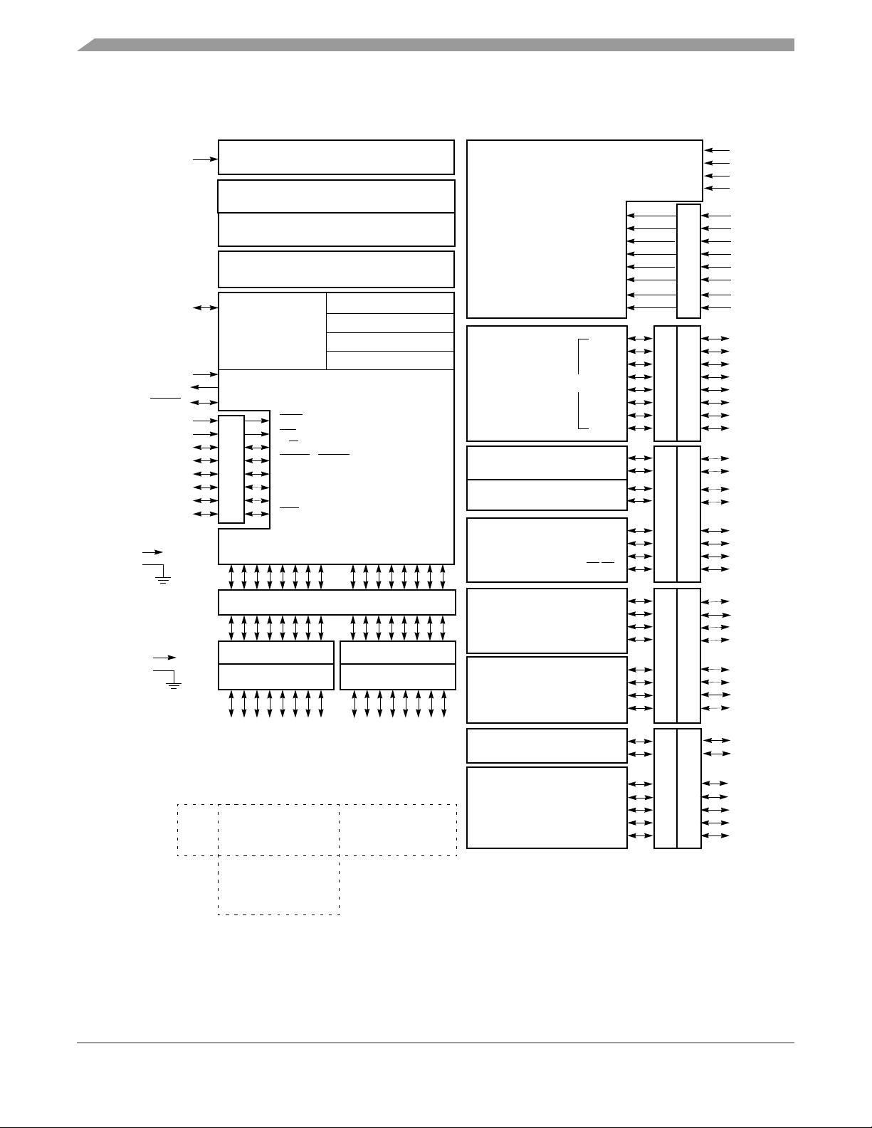
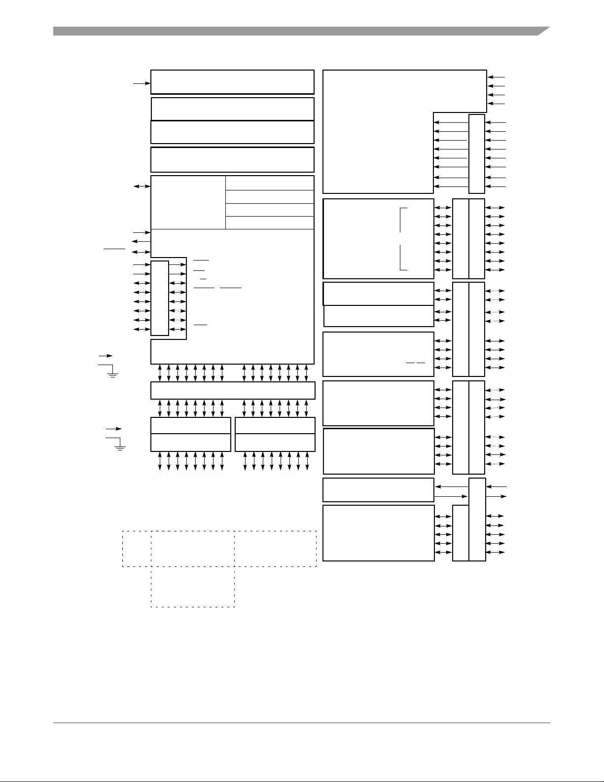
The MC68HC912B32, MC68HC12BE32 and MC68HC(9)12BC32, are 16-bit microcontroller units
(MCUs) composed of standard on-chip peripherals. The multiplexed external bus can also operate in an
8-bit narrow mode for interfacing with single 8-bit wide memory in lower-cost systems. There is a slight
feature set difference between the four pin-for-pin compatible devices as shown in Table 1-1.
Table 1-1. M68HC12B Series Feature Set Comparisons
Features MC68HC912B32 MC68HC12BE32 MC68HC912BC32 MC68HC12BC32
CPU12 X X X X
Multiplexed bus X X X X
32-Kbyte FLASH electrically erasable,
programmable read-only memory (EEPROM)
32-Kbyte read-only memory (ROM) X X
768-byte EEPROM X X X X
1-Kbyte random-access memory (RAM) X X X X
Analog-to-digital (A/D) converter X X X X
XX
Standard timer module (TIM) X X X
Enhanced capture timer (ECT) X
Pulse-width modulator (PWM) X X X X
Asynchronous serial communications
interface (SCII)
Synchronous serial peripheral interface (SPI) X X X X
J1850 byte data link communication (BDLC) X X
Controller area network module (CAN) X X
Computer operating properly (COP)
watchdog timer
Slow mode clock divider X X X X
80-pin quad flat pack (QFP) X X X X
Single-wire background debug mode (BDM) X X X X
M68HC12B Family Data Sheet, Rev. 9.1
XX X X
XX X X
Freescale Semiconductor 19

General Description
1.2 Features
Features include:
• 16-bit CPU12:
– Upwardly compatible with the M68HC11 instruction set
– Interrupt stacking and programmer’s model identical to the M68HC11
– 20-bit arithmetic logic unit (ALU)
– Instruction queue
– Enhanced indexed addressing
– Fuzzy logic instructions
• Multiplexed bus:
– Single chip or expanded
– 16-bit by 16-bit wide or 16-bit by 8-bit narrow modes
•Memory:
– 32-Kbyte FLASH electrically erasable, programmable read-only memory (EEPROM) with
2-Kbyte erase-protected boot block — MC68HC912B32 and MC68HC912BC32 only
– 32-Kbyte ROM — MC68HC12BE32 and MC68HC12BC32 only
– 768-byte EEPROM
– 1-Kbyte random-access memory (RAM) with single-cycle access for aligned or misaligned
read/write
• 8-channel, 10-bit analog-to-digital converter (ATD)
• 8-channel standard timer module (TIM) — MC68HC912B32 and MC68HC(9)12BC32 only:
– Each channel fully configurable as either input capture or output compare
– Simple pulse-width modulator (PWM) mode
– Modulus reset of timer counter
• Enhanced capture timer (ECT) — MC68HC12BE32 only:
– 16-bit main counter with 7-bit prescaler
– Eight programmable input capture or output compare channels; four of the eight input captures
with buffer
– Input capture filters and buffers, three successive captures on four channels, or two captures
on four channels with a capture/compare selectable on the remaining four
– Four 8-bit or two 16-bit pulse accumulators
– 16-bit modulus down-counter with 4-bit prescaler
– Four user-selectable delay counters for signal filtering
• 16-bit pulse accumulator:
– External event counting
– Gated time accumulation
• Pulse-width modulator (PWM):
– 8-bit, 4-channel or 16-bit, 2-channel
– Separate control for each pulse width and duty cycle
– Programmable center-aligned or left-aligned outputs
M68HC12B Family Data Sheet, Rev. 9.1
20 Freescale Semiconductor

Slow-Mode Clock Divider Advisory
• Serial interfaces:
– Asynchronous serial communications interface (SCI)
– Synchronous serial peripheral interface (SPI)
– J1850 byte data link communication (BDLC), MC68HC912B32 and MC68HC12BE32 only
– Controller area network (CAN), MC68HC(9)12BC32 only
• Computer operating properly (COP) watchdog timer, clock monitor, and periodic interrupt timer
• Slow-mode clock divider
• 80-pin quad flat pack (QFP)
• Up to 63 general-purpose input/output (I/O) lines
• Single-wire background debug mode (BDM)
• On-chip hardware breakpoints
1.3 Slow-Mode Clock Divider Advisory
Current versions of the M68HC12B-series devices include a slow-mode clock divider feature. This feature
is fully described in Chapter 10 Clock Generation Module (CGM). The register that controls this feature is
located at $00E0. Older device mask sets do not support the slow-mode clock divider feature. This
register address is reserved in older devices and provides no function.
Mask sets that do not have the slow-mode clock divider feature on the MC68HC912B32 include: G96P,
G86W, and H91F.
Mask sets that do not have the slow-mode clock divider feature on the MC68HC12BE32 include: H54T
and J38M.
Mask sets that do not have the slow-mode clock divider feature on the MC68HC(9)12BC32 include: J15G.
M68HC12B Family Data Sheet, Rev. 9.1
Freescale Semiconductor 21
General Description
1.4 Block Diagrams
VDD × 2
V
× 2
SS
V
BKGD
EXTAL
XTAL
RESET
PE0
PE1
PE2
PE3
PE4
PE5
PE6
PE7
V
FP
32-KBYTE FLASH EEPROM/ROM
1-KBYTE RAM
RH
V
RL
V
DDA
V
SSA
AN0
768-BYTE EEPROM
CPU12
ATD
CONVERTER
AN1
AN2
AN3
AN4
AN5
PORT AD
AN6
SMODN / TAGHI
SINGLE-WIRE
BACKGROUND
DEBUG MODULE
XIRQ
IRQ
R/W
LSTRB / TAGLO
PORT E
ECLK
IPIPE0 / MODA
IPIPE1 / MODB
DBE
PERIODIC INTERRUPT
COP WATCHDOG
CLOCK MONITOR
BREAK POINTS
TIMER AND
PULSE
ACCUMULATOR
/V
PP
LITE
INTEGRATION
MODULE
(LIM)
SCI
I/O
SPI
AN7
IOC0
IOC1
IOC2
IOC3
OC7
IOC4
IOC5
IOC6
PAI
RxD
TxD
I/O
I/O
SDI/MISO
SDO/MOSI
SCK
CS
/SS
DDRT
DDRS
PORT T
PORT S
V
RH
V
RL
V
DDA
V
SSA
PAD0
PAD1
PAD2
PAD3
PAD4
PAD5
PAD6
PAD7
PT0
PT1
PT2
PT3
PT4
PT5
PT6
PT7
PS0
PS1
PS2
PS3
PS4
PS5
PS6
PS7
POWER FOR
INTERNAL
CIRCUITRY
V
× 2
DDX
V
× 2
SSX
POWER FOR
I/O DRIVERS
MULTIPLEXED ADDRESS/DATA BUS
PWM
PW0
PW1
PW2
PW3
DDRA
PORT A
DDRB
PORT B
I/O
I/O
I/O
I/O
I/O
PB4
PB3
PB2
PB1
2
3
R
R
D
D
D
D
A
A
DATA3
DATA2
PB0
0
1
R
R
D
D
D
D
A
A
DATA1
DATA0
BDLC
I/O
DLCRx
DLCTx
I/O
I/O
I/O
I/O
I/O
WIDE
BUS
PA7
5
1
R
D
D
A
DATA15
DATA7
PA6
4
1
R
D
D
A
DATA14
DATA6
PA5
3
1
R
D
D
A
DATA13
DATA5
PA4
2
1
R
D
D
A
DATA12
DATA4
PA3
1
1
R
D
D
A
DATA11
DATA3
PA2
0
1
R
D
D
A
DATA10
DATA2
PA1
9
R
D
D
A
DATA9
DATA1
PA0
8
R
D
D
A
DATA8
DATA0
PB7
PB6
6
7
R
R
D
D
D
D
A
A
DATA7
DATA6
PB5
4
5
R
R
D
D
D
D
A
A
DATA5
DATA4
NARROW BUS
Figure 1-1. Block Diagram for MC68HC912B32 and MC68HC12BE32
DDRP
DDRDLC
PORT P
PORT DLC
PP0
PP1
PP2
PP3
PP4
PP5
PP6
PP7
PDLC0
PDLC1
PDLC2
PDLC3
PDLC4
PDLC5
PDLC6
M68HC12B Family Data Sheet, Rev. 9.1
22 Freescale Semiconductor
Block Diagrams
VDD × 2
V
× 2
SS
V
BKGD
EXTAL
XTAL
RESET
PE0
PE1
PE2
PE3
PE4
PE5
PE6
PE7
V
FP
32-KBYTE FLASH EEPROM/ROM
1-KBYTE RAM
RH
V
RL
V
DDA
V
SSA
AN0
768-BYTE EEPROM
CPU12
ATD
CONVERTER
AN1
AN2
AN3
AN4
AN5
PORT AD
AN6
SMODN / TAGHI
SINGLE-WIRE
BACKGROUND
DEBUG MODULE
XIRQ
IRQ
R/W
LSTRB / TAGLO
PORT E
ECLK
IPIPE0 / MODA
IPIPE1 / MODB
DBE
PERIODIC INTERRUPT
COP WATCHDOG
CLOCK MONITOR
BREAK POINTS
TIMER AND
PULSE
ACCUMULATOR
/V
PP
LITE
INTEGRATION
MODULE
(LIM)
SCI
I/O
SPI
AN7
IOC0
IOC1
IOC2
IOC3
OC7
IOC4
IOC5
IOC6
PAI
RxD
TxD
I/O
I/O
SDI/MISO
SDO/MOSI
SCK
CS
/SS
DDRT
DDRS
PORT T
PORT S
V
RH
V
RL
V
DDA
V
SSA
PAD0
PAD1
PAD2
PAD3
PAD4
PAD5
PAD6
PAD7
PT0
PT1
PT2
PT3
PT4
PT5
PT6
PT7
PS0
PS1
PS2
PS3
PS4
PS5
PS6
PS7
POWER FOR
INTERNAL
CIRCUITRY
V
× 2
DDX
× 2
V
SSX
POWER FOR
I/O DRIVERS
WIDE
BUS
MULTIPLEXED ADDRESS/DATA BUS
PWM
PA7
5
1
R
D
D
A
PORT A
PA6
4
1
1
R
R
D
D
D
D
A
A
DDRA
PA4
PA5
2
3
1
R
D
D
A
PA3
1
1
R
D
D
A
PA2
0
1
R
D
D
A
PA1
9
R
D
D
A
PA0
8
R
D
D
A
PB7
7
R
D
D
A
PB6
6
R
D
D
A
DDRB
PORT B
PB4
PB5
4
5
R
R
D
D
D
D
A
A
PB3
3
R
D
D
A
PB2
2
R
D
D
A
PB1
1
R
D
D
A
PB0
0
R
D
D
A
I/O
msCAN
I/O
DATA15
DATA14
DATA13
DATA12
DATA11
DATA7
DATA6
DATA5
DATA4
DATA3
DATA10
DATA2
DATA9
DATA1
DATA8
DATA0
DATA7
DATA6
DATA5
DATA4
DATA3
DATA2
DATA1
DATA0
NARROW BUS
Figure 1-2. Block Diagram for MC68HC(9)12BC32
PW0
PW1
PW2
PW3
I/O
I/O
I/O
I/O
RxCAN
TxCAN
I/O
I/O
I/O
I/O
I/O
DDRP
PORT P
PORT CAN
DDRCAN
PP0
PP1
PP2
PP3
PP4
PP5
PP6
PP7
RxCAN
TxCAN
PCAN2
PCAN3
PCAN4
PCAN5
PCAN6
M68HC12B Family Data Sheet, Rev. 9.1
Freescale Semiconductor 23

General Description
1.5 Ordering Information
The M68HC12B-series devices are available in 80-pin quad flat pack (QFP) packaging and are shipped
in 2-piece sample packs, 84-piece trays, or 420-piece bricks.
Operating temperature range, package type, and voltage requirements are specified when ordering the
specific device.
Documents to assist in product selection are available from the Freescale Literature Distribution Center
or your local Freescale sales offices.
Product selection guides can also be found on the worldwide web at this URL:
http://freescale.com
Evaluation boards, assemblers, compilers, and debuggers are available from Freescale and from
third-party suppliers. An up-to-date list of products that support the M68HC12 Family of microcontrollers
can be found on the worldwide web at this URL:
http://freescale.com
1.6 Pinout and Signal Descriptions
1.6.1 Pin Assignments
The MCU is available in an 80-pin quad flat pack (QFP). Figure 1-3 and Figure 1-4 show the pin
assignments. Most pins perform two or more functions, as described in the 1.6.3 Signal Descriptions.
1.6.2 Power Supply Pins
The MCU power and ground pins are described here and summarized in Table 1-2.
1.6.2.1 V
VDD and VSS are the internal power supply and ground pins. Because fast signal transitions place high,
short-duration current demands on the power supply, use bypass capacitors with high-frequency
characteristics and place them as close to the MCU as possible. Bypass requirements depend on how
heavily the MCU pins are loaded.
1.6.2.2 V
V
and V
DDX
short-duration current demands on the power supply, use bypass capacitors with high-frequency
characteristics and place them as close to the MCU as possible. Bypass requirements depend on how
heavily the MCU pins are loaded.
1.6.2.3 V
V
and V
DDA
allows the supply voltage to be bypassed independently.
and V
DD
DDX
SSX
DDA
SSA
SS
and V
SSX
are the external power supply and ground pins. Because fast signal transitions place high,
and V
SSA
are the power supply and ground pins for the analog-to-digital converter (ATD). This
1.6.2.4 V
RH
and V
RL
VRH and VRL are the reference voltage pins for the ATD.
M68HC12B Family Data Sheet, Rev. 9.1
24 Freescale Semiconductor
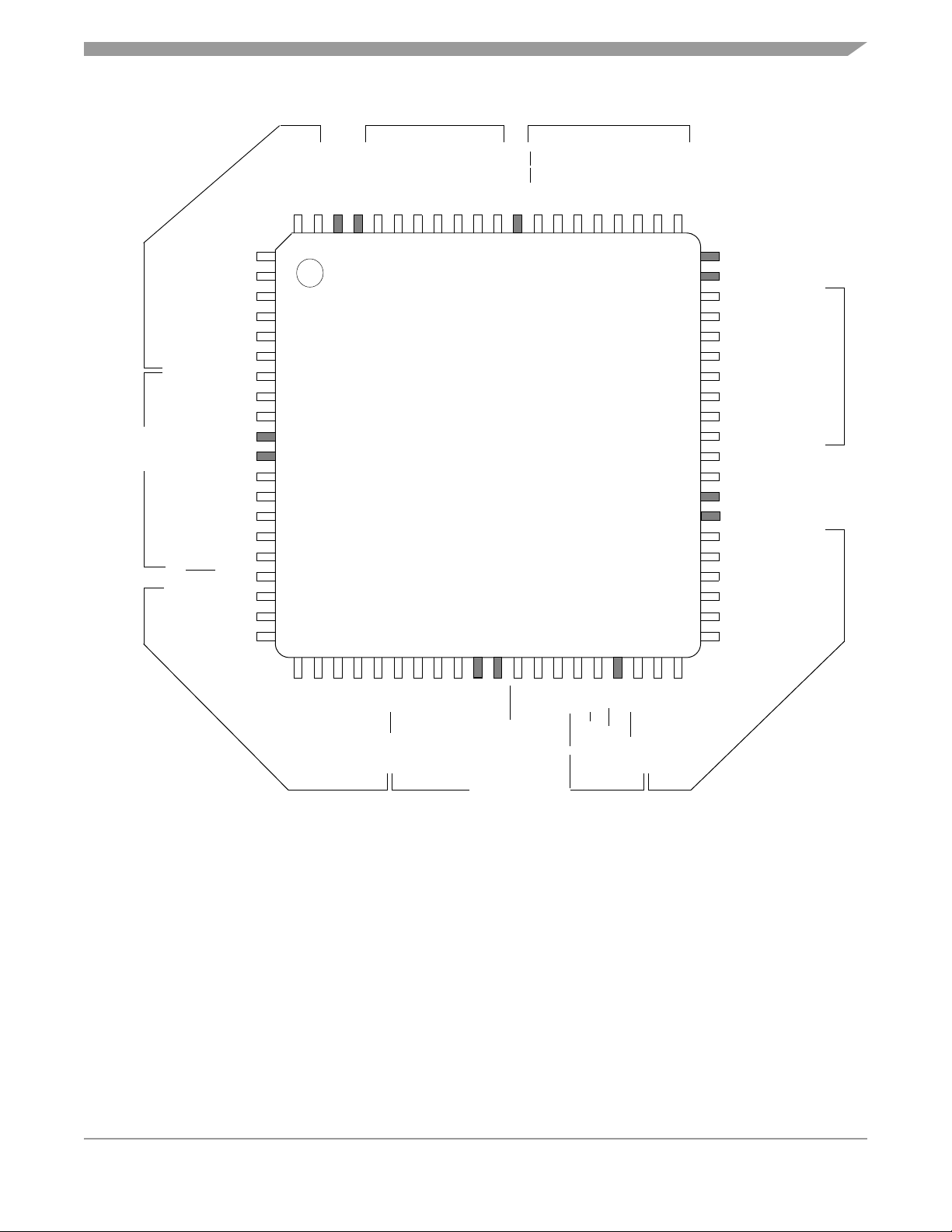
Pinout and Signal Descriptions
PORT P
PW3 / PP3
PW2 / PP2
PW1/ PP1
PW0/ PP0
IOC0 / PT0
IOC1 / PT1
PORT TPORT T
SMODN / TAGHI
ADDR0 / DATA0 / PB0
ADDR1 / DATA1 / PB1
ADDR2 / DATA2 / PB2
IOC2 / PT2
IOC3 / PT3
IOC4 / PT4
IOC5 / PT5
IOC6 / PT6
PAI / IOC7 / PT7
/ BKGD
PP5
PP4
V
V
/SS
PS7 / CS
68
PS6 / SCK
67
PORT S
PS4 / SDI/MISO
PS5 / SDO/MOSI
65
66
PS3
64
PS2
63
Shaded pins are
power and ground
PS0 / RxD
PS1 / TxD
61
62
V
60
V
59
PAD7 / AN7
58
PAD6 / AN6
57
PAD5 / AN5
56
PAD4 / AN4
55
PAD3 / AN3
54
PAD2 / AN2
53
PAD1 / AN1
52
PAD0 / AN0
51
V
50
V
49
V
48
V
47
46
PA7 / DATA15 / ADDR15
45
PA6 / DATA14 / ADDR14
44
PA5 / DATA13 / ADDR13
43
PA4 / DATA12 / ADDR12
42
PA3 / DATA11 / ADDR11
41
PA2 / DATA10 / ADDR10
40
SSA
DDA
PORT AD
RL
RH
SS
DD
PORT DLC
(1)
/NC
SSX
DDX
V
PP7
79
V
PDLC1 / DLCTx
PDLC0 / DLCRx
75
76
77
78
PDLC3
PDLC2
73
74
PDLC4
72
MC68HC912B32
80-PIN QFP
PP6
80
1
2
3
4
5
6
7
8
9
10
DD
11
SS
12
13
14
15
16
17
18
19
20
21222324252627282930313233343536373839
PDLC6
PDLC5
70
71
FP
V
69
SSX
DDX
PORT B
ADDR4 / DATA4 / PB4
ADDR3 / DATA3 / PB3
ADDR6 / DATA6 / PB6
ADDR5 / DATA5 / PB5
/ PE7
DBE
ADDR7 / DATA7 / PB7
MODB / IPIPE1 / PE6
PORT E
V
ECLK / PE4
MODA / IPIPE0 / PE5
V
EXTAL
RESET
XTAL
/ PE2
R/W
/ TAGLO / PE3
LSTRB
PORT E
/ PE1
IRQ
/ PE0
XIRQ
ADDR9 / DATA9 / PA1
ADDR8 / DATA8 / PA0
Notes:
1. Pin 69 is an NC (no connect) on the MC68HC12BE32.
2. In narrow mode, high and low data bytes are multiplexed in alternate bus cycles on port A.
Figure 1-3. Pin Assignments for MC68HC912B32 and MC68HC12BE32 Devices
M68HC12B Family Data Sheet, Rev. 9.1
PORT A
(2)
Freescale Semiconductor 25
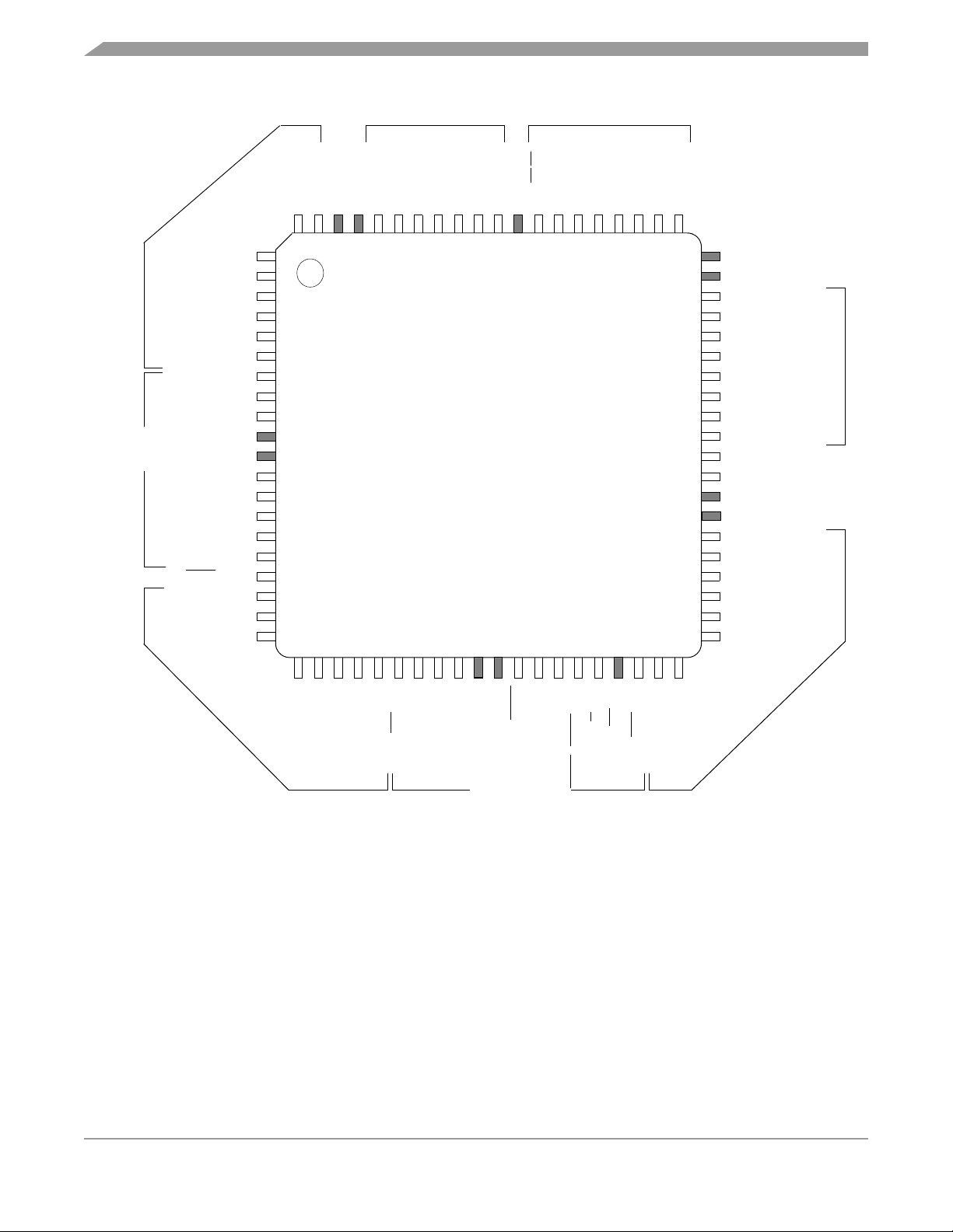
General Description
PORT P
PW3 / PP3
PW2 / PP2
PW1/ PP1
PW0/ PP0
IOC0 / PT0
IOC1 / PT1
PORT TPORT T
SMODN / TAGHI
ADDR0 / DATA0 / PB0
ADDR1 / DATA1 / PB1
ADDR2 / DATA2 / PB2
IOC2 / PT2
IOC3 / PT3
IOC4 / PT4
IOC5 / PT5
IOC6 / PT6
PAI / IOC7 / PT7
/ BKGD
PP5
PP4
V
V
/SS
PS7 / CS
68
PS6 / SCK
67
PORT S
PS4 / SDI/MISO
PS5 / SDO/MOSI
65
66
PS3
64
PS2
63
Shaded pins are
power and ground
PS0 / RxD
PS1 / TxD
61
62
V
60
V
59
PAD7 / AN7
58
PAD6 / AN6
57
PAD5 / AN5
56
PAD4 / AN4
55
PAD3 / AN3
54
PAD2 / AN2
53
PAD1 / AN1
52
PAD0 / AN0
51
V
50
V
49
V
48
V
47
46
PA7 / DATA15 / ADDR15
45
PA6 / DATA14 / ADDR14
44
PA5 / DATA13 / ADDR13
43
PA4 / DATA12 / ADDR12
42
PA3 / DATA11 / ADDR11
41
PA2 / DATA10 / ADDR10
40
SSA
DDA
PORT AD
RL
RH
SS
DD
PORT CAN
(1)
/NC
SSX
DDX
V
PP7
79
V
TxCAN
RxCAN
75
76
77
78
PCAN3
PCAN2
73
74
PCAN4
72
MC68HC(9)12BC32
80-PIN QFP
PP6
80
1
2
3
4
5
6
7
8
9
10
DD
11
SS
12
13
14
15
16
17
18
19
20
21222324252627282930313233343536373839
PCAN6
PCAN5
70
71
FP
V
69
SSX
DDX
PORT B
ADDR4 / DATA4 / PB4
ADDR3 / DATA3 / PB3
ADDR6 / DATA6 / PB6
ADDR5 / DATA5 / PB5
/ PE7
DBE
ADDR7 / DATA7 / PB7
MODB / IPIPE1 / PE6
PORT E
V
ECLK / PE4
MODA / IPIPE0 / PE5
V
EXTAL
RESET
XTAL
/ PE2
R/W
/ TAGLO / PE3
LSTRB
PORT E
/ PE1
IRQ
/ PE0
XIRQ
ADDR8 / DATA8 / PA0
Notes:
1. Pin 69 is an NC (no connect) on the MC68HC12BC32.
2. In narrow mode, high and low data bytes are multiplexed in alternate bus cycles on port A.
Figure 1-4. Pin Assignments for MC68HC(9)12BC32 Devices
M68HC12B Family Data Sheet, Rev. 9.1
PORT A
ADDR9 / DATA9 / PA1
(2)
26 Freescale Semiconductor
Pinout and Signal Descriptions
1.6.2.5 VFP (MC68HC912B32 and MC68HC912BC32 only)
is the FLASH EEPROM programming voltage and supply voltage during normal operation for the
V
FP
MC68HC912B32 and MC68HC912BC32 only.
Table 1-2. Power and Ground Connection Summary
Mnemonic Pin Number Description
V
V
V
V
V
V
DDX
SSX
DDA
SSA
V
V
V
DD
SS
RH
RL
FP
10, 47
11, 48
31, 78
30, 77
59
60
49
50
69
Internal power and ground
External power and ground supply to pin drivers
Operating voltage and ground for the ATD; allows the supply
voltage to be bypassed independently
Reference voltages for the analog-to-digital converter
Programming voltage for the FLASH EEPROM and required
supply for normal operation — MC68HC912B32 and
MC68HC912BC32 only.
Pin 69 is a no connect (NC) on the MC68HC12BE32 and
MC68HC12BC32.
1.6.3 Signal Descriptions
The MCU signals are described here and summarized in Table 1-3.
1.6.3.1 XTAL and EXTAL
XTAL and EXTAL are the crystal driver and external clock input pins. They provide the interface for either
a crystal or a CMOS compatible clock to control the internal clock generator circuitry. Out of reset the
frequency applied to EXTAL is twice the desired E-clock rate. All the device clocks are derived from the
EXTAL input frequency.
XTAL is the crystal output. The XTAL pin must be left unterminated when an external CMOS compatible
clock input is connected to the EXTAL pin. The XTAL output is normally intended to drive only a crystal.
The XTAL output can be buffered with a high-impedance buffer to drive the EXTAL input of another
device.
NOTE
In all cases, take extra care in the circuit board layout around the oscillator
pins. Load capacitances shown in the oscillator circuits include all stray
layout capacitances. Refer to Figure 1-5 and Figure 1-6 for diagrams of
oscillator circuits.
M68HC12B Family Data Sheet, Rev. 9.1
Freescale Semiconductor 27
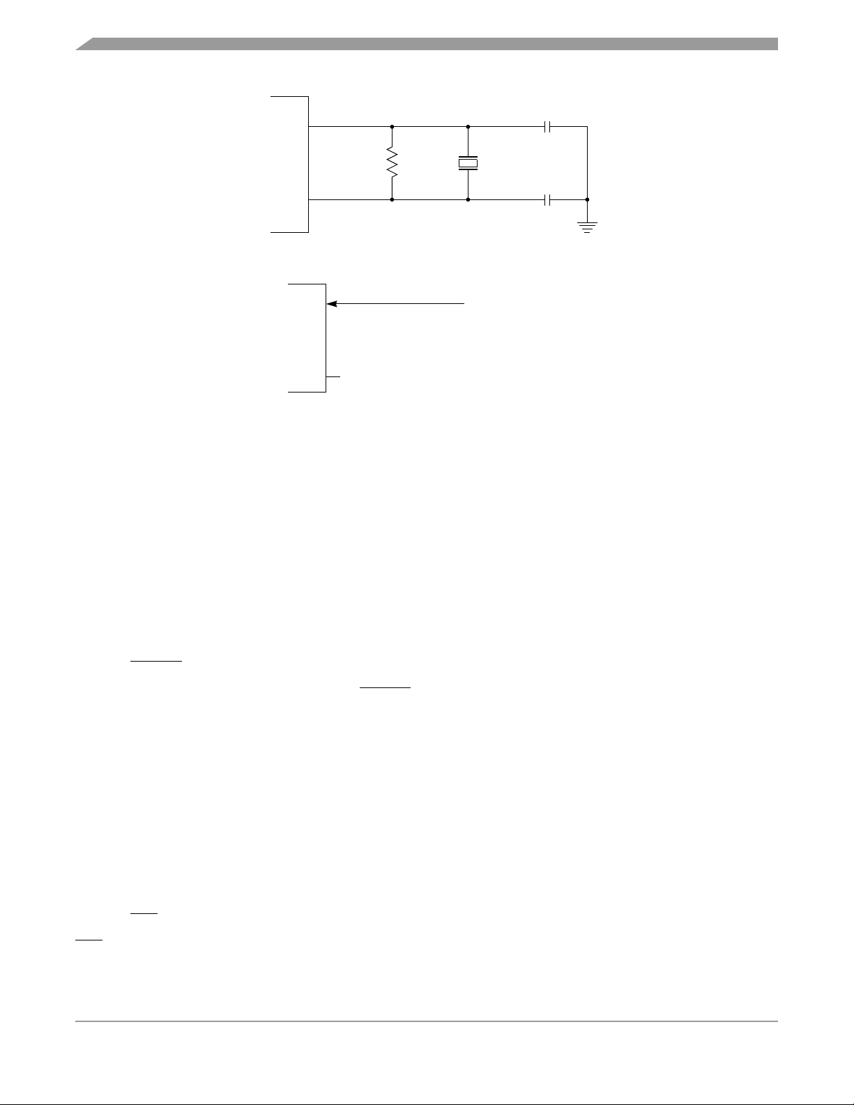
General Description
C
C
MCU
EXTAL
XTAL
10 MΩ
2 x E
CRYSTAL
Figure 1-5. Common Crystal Connections
2 x E
CMOS-COMPATIBLE
MCU
EXTAL
XTAL
EXTERNAL OSCILLATOR
NC
Figure 1-6. External Oscillator Connections
1.6.3.2 ECLK
ECLK is the output connection for the internal bus clock and is used to demultiplex the address and data
and is used as a timing reference. ECLK frequency is equal to one half the crystal frequency out of reset.
In normal single-chip mode, the E-clock output is off at reset to reduce the effects of radio frequency
interference (RFI), but it can be turned on if necessary.
In special single-chip mode, the E-clock output is on at reset but can be turned off.
In special peripheral mode, the E clock is an input to the MCU.
All clocks, including the E clock, are halted when the MCU is in stop mode. It is possible to configure the
MCU to interface to slow external memory. ECLK can be stretched for such accesses.
1.6.3.3 RESET
An active-low, bidirectional control signal, RESET is an input to initialize the MCU to a known startup
state. It also acts as an open-drain output to indicate that an internal failure has been detected in either
the clock monitor or COP watchdog circuit. The MCU goes into reset asynchronously and comes out of
reset synchronously. This allows the part to reach a proper reset state even if the clocks have failed, while
allowing synchronized operation when starting out of reset.
It is possible to determine whether a reset was caused by an internal source or an external source. An
internal source drives the pin low for 16 cycles; eight cycles later, the pin is sampled. If the pin has
returned high, either the COP watchdog vector or clock monitor vector is taken. If the pin is still low, the
external reset is determined to be active and the reset vector is taken. Hold reset low for at least 32 cycles
to assure that the reset vector is taken in the event that an internal COP watchdog timeout or clock monitor
fail occurs.
1.6.3.4 IRQ
IRQ is the maskable external interrupt request pin. It provides a means of applying asynchronous interrupt
requests to the MCU. Either falling edge-sensitive triggering or level-sensitive triggering is program
M68HC12B Family Data Sheet, Rev. 9.1
28 Freescale Semiconductor

Pinout and Signal Descriptions
selectable (interrupt control register, INTCR). IRQ is always configured to level-sensitive triggering at
reset. When the MCU is reset, the IRQ
function is masked in the condition code register.
This pin is always an input and can always be read. In special modes, it can be used to apply external
EEPROM V
and erase cycles. Because the IRQ
in support of EEPROM testing. External VPP is not needed for normal EEPROM program
PP
pin is also used as an EEPROM programming voltage pin, there is
an internal resistive pullup on the pin.
1.6.3.5 XIRQ
XIRQ is the non-maskable external interrupt pin. It provides a means of requesting a non-maskable
interrupt after reset initialization. During reset, the X bit in the condition code register (CCR) is set and any
interrupt is masked until MCU software enables it. Because the XIRQ
input is level sensitive, it can be
connected to a multiple-source wired-OR network. This pin is always an input and can always be read.
There is an active pullup on this pin while in reset and immediately out of reset. The pullup can be turned
off by clearing the PUPE bit in the pullup control register (PUCR). XIRQ
is often used as a power loss
detect interrupt.
When XIRQ
operation if there is more than one source of IRQ
or IRQ are used with multiple interrupt sources (IRQ must be configured for level-sensitive
interrupt), each source must drive the interrupt input
with an open-drain type of driver to avoid contention between outputs. There must also be an interlock
mechanism at each interrupt source so that the source holds the interrupt line low until the MCU
recognizes and acknowledges the interrupt request. If the interrupt line is held low, the MCU recognizes
another interrupt as soon as the interrupt mask bit in the MCU is cleared, normally upon return from an
interrupt.
1.6.3.6 SMODN, MODA, and MODB
SMODN, MODA, and MODB are the mode-select signals. Their state during reset determines the MCU
operating mode. After reset, MODA and MODB can be configured as instruction queue tracking signals
IPIPE0 and IPIPE1. MODA and MODB have active pulldowns during reset.
The SMODN pin can be used as BKGD or TAGHI
after reset.
NOTE
To aid in mode selection, refer to Figure 1-8 and Figure 1-9. These
schematics are provided as suggestive layouts only.
1.6.3.7 BKGD
BKGD is the single-wire background mode pin. It receives and transmits serial background debugging
commands. A special self-timing protocol is used. The BKGD pin has an active pullup when configured
as input; BKGD has no pullup control. Currently, the tool connection configuration shown in Figure 1-7 is
used.
BKGD
NC
V
1
3
FP
2
4
65
GND
RESET
V
DD
Figure 1-7. BDM Tool Connector
M68HC12B Family Data Sheet, Rev. 9.1
Freescale Semiconductor 29

General Description
1.6.3.8 ADDR15–ADDR0 and DATA15–DATA0
ADDR15–ADDR0 and DATA15–DATA0 are the external address and data bus pins. They share functions
with general-purpose I/O ports A and B. In single-chip operating modes, the pins can be used for I/O; in
expanded modes, the pins are used for the external buses.
In expanded wide mode, ports A and B multiplex 16-bit data and address buses. The PA7–PA0 pins
multiplex ADDR15–ADDR8 and DATA15–DATA8. The PB7–PB0 pins multiplex ADDR7–ADDR0 and
DATA7–DATA0.
In expanded narrow mode, ports A and B are used for the 16-bit address bus. An 8-bit data bus is
multiplexed with the most significant half of the address bus on port A. In this mode, 16-bit data is handled
as two back-to-back bus cycles, one for the high byte followed by one for the low byte. The PA7–PA0 pins
multiplex ADDR15–ADDR8, DATA15–DATA8, and DATA7–DATA0. The state of the address pin should
be latched at the rising edge of E. To allow for maximum address setup time at external devices, a
transparent latch should be used.
1.6.3.9 R/W
R/W is the read/write pin. In all modes, this pin can be used as input/output (I/O) and is a general-purpose
input with an active pullup out of reset. If the read/write function is required, it should be enabled by setting
the RDWE bit in the port E assignment register (PEAR). External writes are not possible until enabled.
1.6.3.10 LSTRB
LSTRB is the low-byte strobe pin. In all modes, this pin can be used as I/O and is a general-purpose input
with an active pullup out of reset. If the strobe function is required, it should be enabled by setting the
LSTRE bit in the PEAR register. This signal is used in write operations and so external low-byte writes
are not possible until this function is enabled. This pin is also used as TAGLO
and is multiplexed with the LSTRB
function.
in special expanded modes
1.6.3.11 IPIPE1 and IPIPE0
IPIPE1 and IPIPE0 are the instruction queue tracking pins. Their signals are used to track the state of the
internal instruction execution queue. Execution state is time-multiplexed on the two signals.
1.6.3.12 DBE
DBE is the data bus enable signal. It is an active-low signal that is asserted low during E-clock high time.
DBE
provides separation between output of a multiplexed address and the input of data. When an
external address is stretched, DBE
is asserted during what would be the last quarter cycle of the last
E-clock cycle of stretch. In expanded modes, this pin is used to enable the drive control of external buses
during external reads only. Use of the DBE
is controlled by the NDBE bit in the PEAR register. DBE is
enabled out of reset in expanded modes. This pin has an active pullup during and after reset in single-chip
modes.
M68HC12B Family Data Sheet, Rev. 9.1
30 Freescale Semiconductor

Table 1-3. Signal Description Summary
Pinout and Signal Descriptions
Pin
Name
Pin
Number
Description
PW3–PW0 3–6 Pulse-width modulator channel outputs
ADDR7–ADDR0
DATA7–DATA0
ADDR15–ADDR8
DATA15–DATA8
IOC7–IOC0 16–12, 9–7
25–18
46–39
External bus pins share function with general-purpose I/O ports A and B. In single-chip
modes, the pins can be used for I/O. In expanded modes, the pins are used for the
external buses.
Pins used for input capture and output compare in the timer and pulse accumulator
subsystem
PAI 16 Pulse accumulator input
AN7–AN0 58–51 Analog inputs for the analog-to-digital conversion module
DBE
26
Data bus control and, in expanded mode, enables the drive control of external buses
during external reads
MODB, MODA 27, 28 State of mode select pins during reset determines the initial operating mode of the
IPIPE1, IPIPE0 27, 28
ECLK 29
RESET 32
EXTAL 33
XTAL 34
MCU. After reset, MODB and MODA can be configured as instruction queue tracking
signals IPIPE1 and IPIPE0 or as general-purpose I/O pins.
E-clock is the output connection for the external bus clock. ECLK is used as a timing
reference and for address demultiplexing.
An active low bidirectional control signal, RESET
acts as an input to initialize the MCU
to a known startup state and an output when COP or clock monitor causes a reset.
Crystal driver and external clock input pins. On reset all the device clocks are derived
from the EXTAL input frequency. XTAL is the crystal output.
Low byte strobe (0 = low byte valid), in all modes this pin can be used as I/O. The low
LSTRB
35
strobe function is the exclusive-NOR of A0 and the internal SZ8 signal. The SZ8
internal signal indicates the size 16/8 access.
TA GL O
R/W
35 Pin used in instruction tagging
36
Indicates direction of data on expansion bus; shares function with general-purpose I/O;
read/write in expanded modes
Maskable interrupt request input provides a means of applying asynchronous interrupt
IRQ
37
requests to the MCU. Either falling edge-sensitive triggering or level-sensitive
triggering is program selectable (INTCR register).
XIRQ
38
BKGD 17
Provides a means of requesting asynchronous non-maskable interrupt requests after
reset initialization
Single-wire background interface pin is dedicated to the background debug function.
During reset, this pin determines special or normal operating mode.
TAGHI 17 Pin used in instruction tagging
DLCRx/RxCAN
DLCTx/TxCAN
CS
/SS 68 Slave-select output for SPI master mode; input for slave mode or master mode
(1)
(1)
76 BDLC receive pin
75 BDLC transmit pin
SCK 67 Serial clock for SPI system
SDO/MOSI 66 Master out/slave in pin for serial peripheral interface
SDI/MISO 65 Master in/slave out pin for serial peripheral interface
TxD0 62 SCI transmit pin
RxD0 61 SCI receive pin
1. The RxCAN and TxCAN designations are for the MC68HC(9)12BC32 only.
M68HC12B Family Data Sheet, Rev. 9.1
Freescale Semiconductor 31

General Description
1.6.4 Port Signals
The MCU incorporates eight ports which are used to control and access the various device subsystems.
When not used for these purposes, port pins may be used for general-purpose I/O. In addition to the pins
described here, each port consists of:
• A data register which can be read and written at any time
• With the exception of port AD and PE1–PE0, a data direction register which controls the direction
of each pin
After reset, all port pins are configured as input. (Refer to Table 1-4 for a summary of the port signal
descriptions.)
Table 1-4. Port Description Summary
Port Name
Por t A
PA 7– PA 0
Por t B
PB7–PB0
Por t AD
PA D7 – PAD 0
Port DLC/PCAN
PDLC6–PDLC0
PCAN6–PCAN2
Por t E
PE7–PE0
Por t P
PP7–PP0
Por t S
PS7–PS0
Por t T
PT7–PT0
(1)
Pin
Numbers
46–39
25–18
58–51 In Analog-to-digital converter and general-purpose I/O
70–76
26–29, 35–38
79, 80, 1–6
68–61
16–12, 9–7
Data Direction
DD Register (Address)
In/Out
DDRA ($0002)
In/Out
DDRB ($0003)
In/Out
DDRDLC ($00FF)
PE1–PE0 In
PE7–PE2 In/Out
DDRE ($0009)
In/Out
DDRP ($0057)
In/Out
DDRS ($00D7)
In/Out
DDRT ($00AF)
Description
Port A and port B pins are used for address and data in
expanded modes. The port data registers are not in the
address map during expanded and peripheral mode
operation. When in the map, port A and port B can be
read or written anytime.
DDRA and DDRB are not in the address map in
expanded or peripheral modes.
Byte data link communication (BDLC) subsystem and
general-purpose I/O
Mode selection, bus control signals, and interrupt
service request signals; or general-purpose I/O
General-purpose I/O. PP3–PP0 are used with the
pulse-width modulator when enabled.
Serial communications interface and serial peripheral
interface subsystems and general-purpose I/O
General-purpose I/O when not enabled for input capture
and output compare in the timer and pulse accumulator
subsystem
1. Port DLC applies to the MC68HC912B32 and MC68HC12BE32 and PCAN to the MC68HC(9)12BC32.
1.6.4.1 Port A
Port A pins are used for address and data in expanded modes. The port data register is not in the address
map during expanded and peripheral mode operation. When it is in the map, port A can be read or written
at anytime.
The port A data direction register (DDRA) determines whether each port A pin is an input or output. DDRA
is not in the address map during expanded and peripheral mode operation. Setting a bit in DDRA makes
M68HC12B Family Data Sheet, Rev. 9.1
32 Freescale Semiconductor

Pinout and Signal Descriptions
the corresponding bit in port A an output; clearing a bit in DDRA makes the corresponding bit in port A an
input. The default reset state of DDRA is all 0s.
When the PUPA bit in the PUCR register is set, all port A input pins are pulled up internally by an active
pullup device. This bit has no effect if the port is being used in expanded modes as the pullups are
inactive.
Setting the RDPA bit in the reduced drive register (RDRIV) causes all port A outputs to have reduced drive
levels. RDRIV can be written once after reset and is not in the address map in peripheral mode. Refer to
Chapter 6 Bus Control and Input/Output (I/O).
1.6.4.2 Port B
Port B pins are used for address and data in expanded modes. The port data register is not in the address
map during expanded and peripheral mode operation. When it is in the map, port B can be read or written
at anytime.
The port B data direction register (DDRB) determines whether each port B pin is an input or output. DDRB
is not in the address map during expanded and peripheral mode operation. Setting a bit in DDRB makes
the corresponding bit in port B an output; clearing a bit in DDRB makes the corresponding bit in port B an
input. The default reset state of DDRB is all 0s.
When the PUPB bit in the PUCR register is set, all port B input pins are pulled up internally by an active
pullup device. This bit has no effect if the port is being used in expanded modes because the pullups are
inactive.
Setting the RDPB bit in register RDRIV causes all port B outputs to have reduced drive levels. RDRIV can
be written once after reset. RDRIV is not in the address map in peripheral mode. Refer to Chapter 6 Bus
Control and Input/Output (I/O).
1.6.4.3 Port E
Port E pins operate differently from port A and B pins. Port E pins are used for bus control signals and
interrupt service request signals. When a pin is not used for one of these specific functions, it can be used
as general-purpose I/O. However, two of the pins, PE1 and PE0, can be used only for input, and the states
of these pins can be read in the port data register even when they are used for IRQ
and XIRQ.
The PEAR register determines pin function, and the data direction register (DDRE) determines whether
each pin is an input or output when it is used for general-purpose I/O. PEAR settings override DDRE
settings. Because PE1 and PE0 are input-only pins, only DDRE7–DDRE2 have effect. Setting a bit in the
DDRE register makes the corresponding bit in port E an output; clearing a bit in the DDRE register makes
the corresponding bit in port E an input. The default reset state of DDRE is all 0s.
When the PUPE bit in the PUCR register is set, PE7, PE3, PE2, and PE0 are pulled up. PE7, PE3, PE2,
and PE0 are active pulled-up devices, while PE1 is always pulled up by means of an internal resistor.
Port E and DDRE are not in the map in peripheral mode or in expanded modes when the EME bit in the
MODE register is set.
Setting the RDPE bit in register RDRIV causes all port E outputs to have reduced drive level. RDRIV can
be written once after reset. RDRIV is not in the address map in peripheral mode. Refer to Chapter 6 Bus
Control and Input/Output (I/O).
M68HC12B Family Data Sheet, Rev. 9.1
Freescale Semiconductor 33

General Description
1.6.4.4 Port DLC
The MC68HC912B32 and MC68HC12BE32 contain the port DLC.
Byte data link communications (BDLC) pins can be configured as general-purpose I/O port DLC. When
BDLC functions are not enabled, the port has seven general-purpose I/O pins, PDLC6–PDLC0. The port
DLC control register (DLCSCR) controls port DLC function. The BDLC function, enabled with the
BDLCEN bit, takes precedence over other port functions.
The port DLC data direction register (DDRDLC) determines whether each port DLC pin is an input or
output. Setting a bit in DDRDLC makes the corresponding pin in port DLC an output; clearing a bit makes
the corresponding pin an input. After reset, port DLC pins are configured as inputs.
When the PUPDLC bit in the DLCSCR register is set, all port DLC input pins are pulled up internally by
an active pullup device.
Setting the RDPDLC bit in register DLCSCR causes all port DLC outputs to have reduced drive level.
Levels are at normal drive capability after reset. RDPDLC can be written anytime after reset. Refer to
Chapter 15 Byte Data Link Communications (BDLC).
1.6.4.5 Port CAN
The MC68HC(9)12BC32 contains the port CAN.
The port CAN has five general-purpose I/O pins, PCAN[6:2]. The msCAN12 receive pin, RxCAN, and
transmit pin, TxCAN, cannot be configured as general-purpose I/O on port CAN.
The msCAN data direction register (DDRCAN) determines whether each port CAN pin PCAN[6:2] is an
input or output. Setting a bit in DDRCAN makes the corresponding pin in port CAN an output; clearing a
bit makes the corresponding pin an input. After reset, port CAN pins PCAN[6:2] are configured as inputs.
When a read to the port CAN is performed, the value read from the most significant bit (MSB) depends
on the MSB, PCAN7, of the port CAN data register, PORTCAN, and the MSB of DDRCAN: it is 0 if
DDRCAN7 = 0 and is PCAN7 if DDRCAN7 = 1.
When the PEUCAN bit in the port CAN control register (PCTLCAN) is set, port CAN input pins PCAN[6:2]
are pulled up internally by an active pullup device.
Setting the RDRCAN bit in register PCTLCAN causes the port CAN outputs PCAN[6:2} to have reduced
drive level. Levels are at normal drive capability after reset. RDRCAN can be written anytime after reset.
Refer to Chapter 16 msCAN12 Controller.
1.6.4.6 Port AD
Port AD provides input to the analog-to-digital subsystem and general-purpose input. When
analog-to-digital functions are not enabled, the port has eight general-purpose input pins, PAD7–PAD0.
The ADPU bit in the ATD control register 2 (ATDCTL2) enables the A/D function.
Port AD pins are inputs; no data direction register is associated with this port. The port has no resistive
input loads and no reduced drive controls. Refer to Chapter 17 Analog-to-Digital Converter (ATD).
M68HC12B Family Data Sheet, Rev. 9.1
34 Freescale Semiconductor

Pinout and Signal Descriptions
1.6.4.7 Port P
The four pulse-width modulation channel outputs share general-purpose port P pins. The PWM function
is enabled with the PWM enable register (PWEN). Enabling PWM pins takes precedence over the
general-purpose port. When pulse-width modulation is not in use, the port pins may be used for
general-purpose I/O.
The port P data direction register (DDRP) determines pin direction of port P when used for
general-purpose I/O. When DDRP bits are set, the corresponding pin is configured for output. On reset,
the DDRP bits are cleared and the corresponding pin is configured for input.
When the PUPP bit in the PWM control register (PWCTL) register is set, all input pins are pulled up
internally by an active pullup device. Pullups are disabled after reset.
Setting the RDPP bit in the PWCTL register configures all port P outputs to have reduced drive levels.
Levels are at normal drive capability after reset. The PWCTL register can be read or written anytime after
reset. Refer to Chapter 11 Pulse-Width Modulator (PWM).
1.6.4.8 Port T
This port provides eight general-purpose I/O pins when not enabled for input capture and output compare
in the timer and pulse accumulator subsystem. The TEN bit in the timer system control register (TSCR)
enables the timer function. The pulse accumulator subsystem is enabled with the PAEN bit in the pulse
accumulator control register (PACTL).
The port T data direction register (DDRT) determines pin direction of port T when used for
general-purpose I/O. When DDRT bits are set, the corresponding pin is configured for output. On reset
the DDRT bits are cleared and the corresponding pin is configured for input.
When the PUPT bit in the timer mask register 2 (TMSK2) is set, all input pins are pulled up internally by
an active pullup device. Pullups are disabled after reset.
Setting the RDPT bit in the TMSK2 register configures all port T outputs to have reduced drive levels.
Levels are at normal drive capability after reset. The TMSK2 register can be read or written anytime after
reset. For the MC68HC912B32 and MC68HC(9)12BC32, refer to Chapter 12 Standard Timer (TIM). For
the MC68HC12BE32, refer to Chapter 13 Enhanced Capture Timer (ECT) Module.
1.6.4.9 Port S
Port S is the 8-bit interface to the standard serial interface consisting of the serial communications
interface (SCI) and serial peripheral interface (SPI) subsystems. Port S pins are available for
general-purpose parallel I/O when standard serial functions are not enabled.
Port S pins serve several functions depending on the various internal control registers. If WOMS bit in the
SCI control register 1 (SC0CR1) is set, the P-channel drivers of the output buffers are disabled for bits
0–1 (2–3). If SWOM bit in the SP0CR1 register is set, the P-channel drivers of the output buffers are
disabled for bits 4–7 (wired-OR mode). The open drain control affects both the serial and the
general-purpose outputs. If the RDPSx bits in the PURDS register are set, the appropriate port S pin drive
capabilities are reduced. If PUPSx bits in the port S pullup, reduced drive register (PURDS) are set, the
appropriate pullup device is connected to each port S pin which is programmed as a general-purpose
input. If the pin is programmed as a general-purpose output, the pullup is disconnected from the pin
regardless of the state of the individual PUPSx bits.
M68HC12B Family Data Sheet, Rev. 9.1
Freescale Semiconductor 35

General Description
1.6.5 Port Pullup, Pulldown, and Reduced Drive
MCU ports can be configured for internal pullup. To reduce power consumption and RFI, the pin output
drivers can be configured to operate at a reduced drive level. Reduced drive causes a slight increase in
transition time depending on loading and should be used only for ports which have a light loading. Table
1-5 summarizes the port pullup default status and controls.
Table 1-5. Port Pullup, Pulldown, and Reduced Drive Summary
Port
Name
Port A Pullup
Port B Pullup
Por t E
PE7, PE3, PE2,
PE1, PE0
Por t E
PE4
Por t E
PE6, PE5
Port P Pullup
Por t S
PS1–PS0
Por t S
PS3–PS2
Por t S
PS7–PS4
Port T Pullup
Port DLC/PCAN
Port AD None — —
BKGD Pullup — — Enabled — — Full drive
1. Port DLC applies to the MC68HC912B32 and MC68HC12BE32 and PCAN to the MC68HC(9)12BC32.
(1)
Resistive
Input Loads
Pullup
None —
Pulldown Enabled during reset — — —
Pullup
Pullup
Pullup
Pullup
Register
(Address)
PUCR
($000C)
PUCR
($000C)
PUCR
($000C)
PWCTL
($0054)
PURDS
($00DB)
PURDS
($00DB)
PURDS
($00DB)
TMSK2
($008D)
DLCSCR
($00FD)
Enable Bit Reduced Drive Control Bit
Bit
Name
PUPA Disabled
PUPB Disabled
PUPE Enabled
PUPP Disabled
PUPS0 Disabled
PUPS1 Disabled
PUPS2 Disabled
PUPT Disabled
DLCPUE Disabled
Reset
State
Register
(Address)
RDRIV
($000D)
RDRIV
($000D)
RDRIV
($000D)
RDRIV
($000D)
PWCTL
($0054)
PURDS
($00DB)
PURDS
($00DB)
PURDS
($00DB)
TMSK2
($008D)
DLCSCR
($00FD)
Bit
Name
RDPA Full drive
RDPB Full drive
RDPE Full drive
RDPE Full drive
RDPP Full drive
RDPS0 Full drive
RDPS1 Full drive
RDPS2 Full drive
RDPT Full drive
DLCRDV Full drive
Reset
State
M68HC12B Family Data Sheet, Rev. 9.1
36 Freescale Semiconductor

Freescale Semiconductor 37
M68HC12B Family Data Sheet, Rev. 9.1
1
2
U2
MC34064
21
RSET
IN
DN
RESET
3
Y1
R14
C2 C1
R32
4.7 K
RESET
1
GND
2
3
4
V
FP
5
V
DD
6
VDDV
DD
R2
4.7 K
S1
3
R3
4.7 K
4
MODA
MODB
SW DIP-2
GROUND
JP1
1
2
3
4
5
6
HEADER 6
V
DD0
10
V
V
DD1
V
DDX0
V
DDX1
V
DDAD
V
FP
MODA
MODB
V
DD
47
78
31
59
11
48
77
30
49
50
69
33
34
32
17
38
37
36
35
29
28
27
26
6
5
4
3
2
1
80
79
76
75
74
73
72
71
70
DD0
V
DD1
V
DDX0
V
DDX1
V
DDAD
V
SS0
V
SS1
V
SSX0
V
SSX1
V
RH
V
RL
V
FP
EXTAL
XTAL
RESET
BKGD
PE0
PE1
PE2/R/W
PE3/LSTRB
PE4/ECLOCK
PE5/MODA
PE6/MODB
PE7/DBE
PP0
PP1
PP2
PP3
PP4
PP5
PP6
PP7
PDLC0
PDLC1
PDLC2
PDLC3
PDLC4
PDLC5
PDLC6
U1
MC68HC912B32
PB0
PB1
PB2
PB3
PB4
PB5
PB6
PB7
PA0
PA1
PA2
PA3
PA4
PA5
PA6
PA7
PS0
PS1
PS2
PS3
PS4
PS5
PS6
PS7
PAD0
PAD1
PAD2
PAD3
PAD4
PAD5
PAD6
PAD7
PT0
PT1
PT2
PT3
PT4
PT5
PT6
PT7
18
19
DD0
C3
1.0
V
µ
20
V
21
22
23
F
DD1
V
DDEX0VDDAD
C4
µ
F
1.0
C5
1.0
C6
µ
F
µ
F
1.0
24
25
39
40
41
42
43
44
45
46
61
62
63
64
65
66
67
V
DDEX0
68
51
52
53
54
55
56
57
58
7
8
9
12
13
14
15
16
R29
R31
R34
R36
R38
R40
R42
R44
R46
R48
R50
R52
R54
R56
R57
R58
Pinout and Signal Descriptions
NOTE: This figure provides a suggested schematic only.
Figure 1-8. Basic Single-Chip Mode Schematic

38 Freescale Semiconductor
M68HC12B Family Data Sheet, Rev. 9.1
V
RAM
FLASH
DD
V
DD
V
DDX0
V
DDX1
V
DD
V
FP
R/W
E CLOCK
MODA
MODB
10
47
78
31
59
11
48
77
30
49
50
69
33
34
32
17
38
37
36
35
29
28
27
26
6
5
4
3
2
1
80
79
76
75
74
73
72
71
70
V
DD0
V
DD1
V
DDX0
V
DDX1
V
DDAD
V
SS0
V
SS1
V
SSX0
V
SSX1
V
RH
V
RL
V
FP
EXTAL
XTAL
RESET
BKGD
PE0
PE1
PE2/R/W
PE3/LSTRB
PE4/ECLOCK
PE5/MODA
PE6/MODB
PE7/DBE
PP0
PP1
PP2
PP3
PP4
PP5
PP6
PP7
PDLC0
PDLC1
PDLC2
PDLC3
PDLC4
PDLC5
PDLC6
U1
MC34064
21
RSET
IN
DN
3
RESET
GROUND
Y1
R1
C2
C1
R32
4.7 K
RESET
JP1
1
GND
V
V
1
2
2
3
3
4
4
FP
5
5
6
DD
6
HEADER 6
U6
A13
1
A
A14
A15
2
3
Y0
B
Y1
C
Y2
Y3
E CLOCK
6
4
5
G1
G2A
G2B
Y4
Y5
Y6
Y7
74AHCT138
15
14
13
12
11
10
9
7
NOTE: This figure provides a suggested schematic only.
U2
MC68HC912B32
PB0
PB1
PB2
PB3
PB4
PB5
PB6
PB7
PA0
PA1
PA2
PA3
PA4
PA5
PA6
PA7
PS0
PS1
PS2
PS3
PS4
PS5
PS6
PS7
PAD0
PAD1
PAD2
PAD3
PAD4
PAD5
PAD6
PAD7
PT0
PT1
PT2
PT3
PT4
PT5
PT6
PT7
General Description
VDDV
DD
V
18
19
20
21
22
23
1
2
SW DIP-2
R2
4.7 K
S1
R3
4.7 K
4
3
MODA
MODB
DD1
24
25
D0
D1
D2
D3
D4
D5
D6
D7
D0
D1
D2
D3
D4
D5
D6
D7
39
40
41
42
43
44
45
46
61
62
63
64
E CLOCK
65
66
67
68
51
52
53
54
55
56
57
58
7
8
9
12
13
14
A0
A1
A2
A3
A4
A5
A6
A7
A8
A9
A10
A11
A12
A13
A14
A15
15
16
FLASH
GROUND
R62
V
DD
10 K
13
14
17
18
11
3
4
7
8
1
12
11
10
9
8
7
6
5
27
26
23
25
4
28
29
3
22
24
31
D0
D1
D2
D3
D4
D5
D6
D7
OC
CLK
74HC374
A0
A1
A2
A3
A4
A5
A6
A7
A8
A9
A10
A11
A12
A13
A14
A15
2
A16
CE
OE
PGM
1
V
U3
Q0
Q1
Q2
Q3
Q4
Q5
Q6
Q7
U4
FLASH
PP
AM27C010
2
5
6
9
12
15
16
19
D0
D1
D2
D3
D4
D5
D6
D7
A15
A14
A13
A12
A11
A10
A9
A8
13
14
15
17
18
19
20
21
A0
A1
A2
A3
A4
A5
A6
A7
A8
A9
A10
A11
A12
A13
A14
RAM
R/W
D0
D1
D2
D3
D4
D5
D6
D7
C8
0.1
V
µ
DDX0
F
C9
0.1
V
DDX1
C10
µ
0.1
F
µ
F
U4
10
A0
9
A1
8
A2
7
A3
6
A4
5
A5
4
A6
3
A7
25
A8
24
A9
21
A10
23
A11
2
A12
26
A13
1
A14
20
CE
27
R/W
22
OE
D0
D1
D2
D3
D4
D5
D6
D7
D0
11
12
D1
13
D2
D3
14
15
D4
D5
16
17
D6
18
D7
RAM IC
Figure 1-9. RAM Expansion Schematic with FLASH in Narrow Mode

Chapter 2 Register Block
2.1 Introduction
The register block can be mapped to any 2-Kbyte boundary within the standard 64-Kbyte address space
by manipulating bits REG15–REG11 in the register initialization register (INITRG). INITRG establishes
the upper five bits of the register block’s 16-bit address. The register block occupies the first 512 bytes of
the 2-Kbyte block.
Default addressing (after reset) is indicated in Figure 2-1. For additional information, refer to Chapter 5
Operating Modes and Resource Mapping.
NOTE
In expanded and peripheral modes, these registers are not in the map:
• Port A data register, PORTA
• Port B data register, PORTB
• Port A data direction register, DDRA
• Port B data direction register, DDRB
In peripheral mode or in expanded modes with the emulate port E bit (EME) set, these registers are not
in the map:
• Port E data register, PORTE
• Port E data direction register, DDRE
In peripheral mode, these registers are not in the map:
• Mode register, MODE
• Pullup control register, PUCR
• Reduced drive register, RDRIV
M68HC12B Family Data Sheet, Rev. 9.1
Freescale Semiconductor 39

Register Block
2.2 Registers
Addr. Register Name Bit 7654321Bit 0
Port A Data Register
$0000
Port B Data Register
$0001
Data Direction Register A
$0002
Data Direction Register B
$0003
$0004 Reserved R R R R R R R R
↓
$0007 Reserved R R R R R R R R
(PORTA)
See page 86.
(PORTB)
See page 87.
(DDRA)
See page 86.
(DDRB)
See page 87.
Read:
Write:
Reset:UUUUUUUU
Read:
Write:
Reset:UUUUUUUU
Read:
Write:
Reset:00000000
Read:
Write:
Reset:00000000
PA7 PA6 PA5 PA4 PA3 PA2 PA1 PA0
PB7 PB6 PB5 PB4 PB3 PB2 PB1 PB0
DDA7 DDA6 DDA5 DDA4 DDA3 DDA2 DDA1 DDA0
DDB7 DDB6 DDB5 DDB4 DDB3 DDB2 DDB1 DDB0
Port E Data Register
$0008
Data Direction Register E
$0009
Port E Assignment Register
$000A
$000B
Pullup Control Register
$000C
Reduced Drive Register
$000D
$000E Reserved R R R R R R R R
$000F Reserved R R R R R R R R
(PORTE)
See page 88.
(DDRE)
See page 88.
(PEAR)
See page 89.
Mode Register
(MODE)
See page 78.
(PUCR)
See page 91.
(RDRIV)
See page 92.
Read:
Write:
Reset:00000000
Read:
Write:
Reset:00001000
Read:
Write:
Reset:10010000
Read:
Write:
Reset:00011001
Read: 0 0 0
Write:
Reset:00010000
Read:0000
Write:
Reset:00000000
PE7 PE6 PE5 PD4 PD3 PD2 PD1 PD0
DDE7 DDE6 DDE5 DDE4 DDE3 DDE2
NDBE
SMODN MODB MODA ESTR IVIS EBSWAI 0 EME
CGMTE
PIPOE NECLK LSTRE RDWE
PUPE
00
RDPE
0
00
00
PUPB PUPA
RDPB RDPA
= Unimplemented R = Reserved U = Unaffected
Notes:
1. Available only on MC68HC912B32 and MC68HC912BC32 devices.
2. Available only on MC68HC912B32 and MC68HC12BE32 devices.
3. Available only on MC68HC(9)12BC32 devices.
Figure 2-1. Register Map (Sheet 1 of 19)
M68HC12B Family Data Sheet, Rev. 9.1
40 Freescale Semiconductor

Registers
Addr. Register Name Bit 7654321Bit 0
RAM Initialization Register
$0010
Register Initialization Register
$0011
EEPROM Initialization Register
$0012
Miscellaneous Mapping Control
$0013
Real-Time Interrupt Control
$0014
Real-Time Interrupt Flag Register
$0015
COP Control Register
$0016
Arm/Reset COP Timer
$0017
$0018 Reserved R R R R R R R R
↓
$001D Reserved R R R R R R R R
Register (COPRST)
(INITRM)
See page 80.
(INITRG)
See page 80.
(INITEE)
See page 81.
Register (MISC)
See page 82.
Register (RTICTL)
See page 118.
(RTIFLG)
See page 119.
(COPCTL)
See page 119.
See page 120.
Read:
Write:
Reset:00001000
Read:
Write:
Reset:00000000
Read:
Write:
Reset:00010001
Read:
Write:
Reset:00000000
Read:
Write:
Reset:00000000
Read:
Write:
Reset:00000000
Read:
Write:
Reset:00000001
Read:
Write:
Reset:00000000
RAM15RAM14RAM13RAM12RAM11 0 0 0
REG15 REG14 REG13 REG12 REG11 0 0 MMSWAI
EE15 EE14 EE13 EE12 0 0 0 EEON
0 NDRF RFSTR1 RFSTR0 EXSTR1 EXSTR0 MAPROM ROMON
RTIE RSWAI RSBCK
RTIF0000000
CME FCME FCM FCOP DISR CR2 CR1 CR0
Bit 7Bit 6Bit 5Bit 4Bit 3Bit 2Bit 1Bit 0
0
RTBYP RTR2 RTR1 RTR0
Interrupt Control Register
$001E
Highest Priority I Interrupt Register
$001F
Breakpoint Control Register 0
$0020
Notes:
1. Available only on MC68HC912B32 and MC68HC912BC32 devices.
2. Available only on MC68HC912B32 and MC68HC12BE32 devices.
3. Available only on MC68HC(9)12BC32 devices.
(INTCR)
See page 70.
(HPRIO)
See page 71.
(BRKCT0)
See page 301.
Read:
Write:
Reset:01100000
Read: 1 1
Write:
Reset:11110010
Read:
Write:
Reset:00000000
IRQEIRQENDLY00000
PSEL5 PSEL4 PSEL3 PSEL2 PSEL1
BKEN1 BKEN0 BKPM 0 BK1ALE BK0ALE 0 0
= Unimplemented R = Reserved U = Unaffected
0
Figure 2-1. Register Map (Sheet 2 of 19)
M68HC12B Family Data Sheet, Rev. 9.1
Freescale Semiconductor 41

Register Block
Addr. Register Name Bit 7654321Bit 0
Breakpoint Control Register 1
$0021
Breakpoint Address Register High
$0022
Breakpoint Address Register Low
$0023
Breakpoint Data Register High
$0024
Breakpoint Data Register Low
$0025
$0026 Reserved R R R R R R R R
↓
$003F Reserved R R R R R R R R
(BRKCT1)
See page 302.
(BRKAH)
See page 303.
(BRKAL)
See page 303.
(BRKDH)
See page 304.
(BRKDL)
See page 304.
Read:
Write:
Reset:00000000
Read:
Write:
Reset:00000000
Read:
Write:
Reset:00000000
Read:
Write:
Reset:00000000
Read:
Write:
Reset:00000000
0 BKDBE BKMBH BKMBL BK1RWE BK1RW BK0RWE BK0RW
Bit 15 Bit 14 Bit 13 Bit 12 Bit 11 Bit 10 Bit 9 Bit 8
Bit 7 Bit 6 Bit 5 Bit 4 Bit 3 Bit 2 Bit 1 Bit 0
Bit 15 Bit 14 Bit 13 Bit 12 Bit 11 Bit 10 Bit 9 Bit 8
Bit 7Bit 6Bit 5Bit 4Bit 3Bit 2Bit 1Bit 0
PWM Clocks and Concatenate
$0040
PWM Clock Select and Polarity
$0041
$0042
PWM Prescaler Counter Register
$0043
$0044
PWM Scale Counter Register 0
$0045
Notes:
1. Available only on MC68HC912B32 and MC68HC912BC32 devices.
2. Available only on MC68HC912B32 and MC68HC12BE32 devices.
3. Available only on MC68HC(9)12BC32 devices.
Register (PWCLK)
See page 128.
Register (PWPOL)
See page 129.
PWM Enable Register
(PWEN)
See page 130.
(PWPRES)
See page 131.
PWM Scale Register 0
(PWSCAL0)
See page 131.
(PWSCNT0)
See page 131.
Read:
Write:
Reset:00000000
Read:
Write:
Reset:00000000
Read:0000
Write:
Reset:00000000
Read: 0
Write:
Reset:00000000
Read:
Write:
Reset:00000000
Read:Bit 7Bit 6Bit 5Bit 4Bit 3Bit 2Bit 1Bit 0
Write:
Reset:00000000
CON23 CON01 PCKA2 PCKA1 PCKA0 PCKB2 PCKB1 PCKB0
PCLK3 PCLK2 PCLK1 PCLK0 PPOL3 PPOL2 PPOL1 PPOL0
Bit 6Bit 5Bit 4Bit 3Bit 2Bit 1Bit 0
Bit 7Bit 6Bit 5Bit 4Bit 3Bit 2Bit 1Bit 0
= Unimplemented R = Reserved U = Unaffected
PWEN3 PWEN2 PWEN1 PWEN0
Figure 2-1. Register Map (Sheet 3 of 19)
M68HC12B Family Data Sheet, Rev. 9.1
42 Freescale Semiconductor

Registers
Addr. Register Name Bit 7654321Bit 0
PWM Scale Register 1 (PWSCAL1)
$0046
PWM Scale Counter Register 1
$0047
PWM Channel Counter Register 0
$0048
PWM Channel Counter Register 1
$0049
PWM Channel Counter Register 2
$004A
PWM Channel Counter Register 3
$004B
PWM Channel Period Register 0
$004C
PWM Channel Period Register 1
$004D
PWM Channel Period Register 2
$004E
PWM Channel Period Register 3
$004F
PWM Channel Duty Register 0
$0050
PWM Channel Duty Register 1
$0051
Notes:
1. Available only on MC68HC912B32 and MC68HC912BC32 devices.
2. Available only on MC68HC912B32 and MC68HC12BE32 devices.
3. Available only on MC68HC(9)12BC32 devices.
See page 132.
(PWSCNT1)
See page 132.
(PWCNT0)
See page 133.
(PWCNT1)
See page 133.
(PWCNT2)
See page 133.
(PWCNT3)
See page 133.
(PWPER0)
See page 134.
(PWPER1)
See page 134.
(PWPER2)
See page 134.
(PWPER3)
See page 134.
(PWDTY0)
See page 135.
(PWDTY1)
See page 135.
Read:
Write:
Reset:00000000
Read:Bit 7Bit 6Bit 5Bit 4Bit 3Bit 2Bit 1Bit 0
Write:
Reset:00000000
Read:
Write:
Reset:00000000
Read:
Write:
Reset:00000000
Read:
Write:
Reset:00000000
Read:
Write:
Reset:00000000
Read:
Write:
Reset:11111111
Read:
Write:
Reset:11111111
Read:
Write:
Reset:11111111
Read:
Write:
Reset:11111111
Read:
Write:
Reset:11111111
Read:
Write:
Reset:11111111
Bit 7Bit 6Bit 5Bit 4Bit 3Bit 2Bit 1Bit 0
Bit 7Bit 6Bit 5Bit 4Bit 3Bit 2Bit 1Bit 0
Bit 7Bit 6Bit 5Bit 4Bit 3Bit 2Bit 1Bit 0
Bit 7Bit 6Bit 5Bit 4Bit 3Bit 2Bit 1Bit 0
Bit 7Bit 6Bit 5Bit 4Bit 3Bit 2Bit 1Bit 0
Bit 7Bit 6Bit 5Bit 4Bit 3Bit 2Bit 1Bit 0
Bit 7Bit 6Bit 5Bit 4Bit 3Bit 2Bit 1Bit 0
Bit 7Bit 6Bit 5Bit 4Bit 3Bit 2Bit 1Bit 0
Bit 7Bit 6Bit 5Bit 4Bit 3Bit 2Bit 1Bit 0
Bit 7Bit 6Bit 5Bit 4Bit 3Bit 2Bit 1Bit 0
Bit 7Bit 6Bit 5Bit 4Bit 3Bit 2Bit 1Bit 0
= Unimplemented R = Reserved U = Unaffected
Figure 2-1. Register Map (Sheet 4 of 19)
M68HC12B Family Data Sheet, Rev. 9.1
Freescale Semiconductor 43

Register Block
Addr. Register Name Bit 7654321Bit 0
PWM Channel Duty Register 2
$0052
PWM Channel Duty Register 3
$0053
PWM Control Register
$0054
PWM Special Mode Register
$0055
Port P Data Register
$0056
Port P Data Direction Register
$0057
$0058 Reserved R R R R R R R R
↓
$005F Reserved R R R R R R R R
(PWDTY2)
See page 135.
(PWDTY3)
See page 135.
(PWCTL)
See page 136.
(PWTST)
See page 137.
(PORTP)
See page 137.
(DDRP)
See page 138.
Read:
Write:
Reset:11111111
Read:
Write:
Reset:11111111
Read: 0 0 0
Write:
Reset:00000000
Read:
Write:
Reset:00000000
Read:
Write:
Reset:UUUUUUUU
Read:
Write:
Reset:00000000
Bit 7Bit 6Bit 5Bit 4Bit 3Bit 2Bit 1Bit 0
Bit 7Bit 6Bit 5Bit 4Bit 3Bit 2Bit 1Bit 0
PSWAI CENTR RDPP PUPP PSBCK
DISCR DISCP DISCAL
PP7 PP6 PP5 PP4 PP3 PP2 PP1 PP0
DDP7 DDP6 DDP5 DDP4 DDP3 DDP2 DDP1 DDP0
00000
ATD Control Register 0
$0060
ATD Control Register 1
$0061
ATD Control Register 2
$0062
ATD Control Register 3
$0063
ATD Control Register 4
$0064
Notes:
1. Available only on MC68HC912B32 and MC68HC912BC32 devices.
2. Available only on MC68HC912B32 and MC68HC12BE32 devices.
3. Available only on MC68HC(9)12BC32 devices.
(ATDCTL0)
See page 279.
(ATDCTL1)
See page 279.
(ATDCTL2)
See page 279.
(ATDCTL3)
See page 280.
(ATDCTL4)
See page 281.
Read:
Write:
Reset:00000000
Read:
Write:
Reset:00000000
Read:
Write:
Reset:00000000
Read:000000
Write:
Reset:00000000
Read:
Write:
Reset:00000001
00000000
00000000
ADPU AFFC AWAI
S10BMSMP1SMP0PRS4PRS3PRS2PRS1PRS0
= Unimplemented R = Reserved U = Unaffected
Figure 2-1. Register Map (Sheet 5 of 19)
000
ASCIE
ASCIF
FRZ1 FRZ0
M68HC12B Family Data Sheet, Rev. 9.1
44 Freescale Semiconductor

Registers
Addr. Register Name Bit 7654321Bit 0
ATD Control Register 5
$0065
$0066
$0067
ATD Test Register High
$0068
ATD Test Register Low
$0069
$006A Reserved R R R R R R R R
↓
$006E Reserved R R R R R R R R
(ATDCTL5)
See page 282.
ATD Status Register
(ATDSTAT)
See page 284.
ATD Status Register
(ATDSTAT)
See page 284.
(ATDTSTH)
See page 285.
(ATDTSTL)
See page 285.
Read:
Write:
Reset:00000000
Read: SCF 0 0 0 0 CC2 CC1 CC0
Write:
Reset:00000000
Read: CCF7 CCF6 CCF5 CCF4 CCF3 CCF2 CCF1 CCF0
Write:
Reset:00000000
Read:
Write:
Reset:00000000
Read:
Write:
Reset:00000000
SAR9 SAR8 SAR7 SAR6 SAR5 SAR4 SAR3 SAR2
SAR1 SAR0 RST TSTOUT TST3 TST2 TST1 TST0
S8CM SCAN MULT CD CC CB CA
Port AD Data Input Register
$006F
ATD Result Register 0
$0070
ATD Result Register 0
$0071
ATD Result Register 1
$0072
ATD Result Register 1
$0073
ATD Result Register 2
$0074
Notes:
1. Available only on MC68HC912B32 and MC68HC912BC32 devices.
2. Available only on MC68HC912B32 and MC68HC12BE32 devices.
3. Available only on MC68HC(9)12BC32 devices.
(PORTAD)
See page 286.
(ADRx0H)
See page 286.
(ADRx0L)
See page 286.
(ADRx1H)
See page 286.
(ADRx1L)
See page 286.
(ADRx2H)
See page 286.
Read:
Write:
Reset: After reset, reflect the state of the input pins
Read: Bit 15 Bit 14 Bit 13 Bit 12 Bit 11 Bit 10 Bit 9 Bit 8
Write:
Reset: Undefined
Read:Bit 7Bit 6Bit 5Bit 4Bit 3Bit 2Bit 1Bit 0
Write:
Reset: Undefined
Read: Bit 15 Bit 14 Bit 13 Bit 12 Bit 11 Bit 10 Bit 9 Bit 8
Write:
Reset: Undefined
Read:Bit 7Bit 6Bit 5Bit 4Bit 3Bit 2Bit 1Bit 0
Write:
Reset: Undefined
Read: Bit 15 Bit 14 Bit 13 Bit 12 Bit 11 Bit 10 Bit 9 Bit 8
Write:
Reset: Undefined
PAD7 PAD6 PAD5 PAD4 PAD3 PAD2 PAD1 PAD0
= Unimplemented R = Reserved U = Unaffected
Figure 2-1. Register Map (Sheet 6 of 19)
M68HC12B Family Data Sheet, Rev. 9.1
Freescale Semiconductor 45

Register Block
Addr. Register Name Bit 7654321Bit 0
ATD Result Register 2
$0075
ATD Result Register 3
$0076
ATD Result Register 3
$0077
ATD Result Register 4
$0078
ATD Result Register 4
$0079
ATD Result Register 5
$007A
ATD Result Register 5
$007B
ATD Result Register 6
$007C
ATD Result Register 6
$007D
ATD Result Register 7
$007E
ATD Result Register 7
$007F
Timer IC/OC Select Register
$0080
Notes:
1. Available only on MC68HC912B32 and MC68HC912BC32 devices.
2. Available only on MC68HC912B32 and MC68HC12BE32 devices.
3. Available only on MC68HC(9)12BC32 devices.
(ADRx2L)
See page 286.
(ADRx3H)
See page 286.
(ADRx3L)
See page 286.
(ADRx4H)
See page 286.
(ADRx4L)
See page 286.
(ADRx5H)
See page 286.
(ADRx5L)
See page 286.
(ADRx6H)
See page 286.
(ADRx6L)
See page 286.
(ADRx7H)
See page 286.
(ADRx7L)
See page 286.
(TIOS)
See page 141.
Read:Bit 7Bit 6Bit 5Bit 4Bit 3Bit 2Bit 1Bit 0
Write:
Reset: Undefined
Read: Bit 15 Bit 14 Bit 13 Bit 12 Bit 11 Bit 10 Bit 9 Bit 8
Write:
Reset: Undefined
Read:Bit 7Bit 6Bit 5Bit 4Bit 3Bit 2Bit 1Bit 0
Write:
Reset: Undefined
Read: Bit 15 Bit 14 Bit 13 Bit 12 Bit 11 Bit 10 Bit 9 Bit 8
Write:
Reset: Undefined
Read:Bit 7Bit 6Bit 5Bit 4Bit 3Bit 2Bit 1Bit 0
Write:
Reset: Undefined
Read: Bit 15 Bit 14 Bit 13 Bit 12 Bit 11 Bit 10 Bit 9 Bit 8
Write:
Reset: Undefined
Read:Bit 7Bit 6Bit 5Bit 4Bit 3Bit 2Bit 1Bit 0
Write:
Reset: Undefined
Read: Bit 15 Bit 14 Bit 13 Bit 12 Bit 11 Bit 10 Bit 9 Bit 8
Write:
Reset: Undefined
Read:Bit 7Bit 6Bit 5Bit 4Bit 3Bit 2Bit 1Bit 0
Write:
Reset: Undefined
Read: Bit 15 Bit 14 Bit 13 Bit 12 Bit 11 Bit 10 Bit 9 Bit 8
Write:
Reset: Undefined
Read:Bit 7Bit 6Bit 5Bit 4Bit 3Bit 2Bit 1Bit 0
Write:
Reset: Undefined
Read:
Write:
Reset:00000000
IOS7 IOS6 IOS5 IOS4 IOS3 IOS2 IOS1 IOS0
= Unimplemented R = Reserved U = Unaffected
Figure 2-1. Register Map (Sheet 7 of 19)
M68HC12B Family Data Sheet, Rev. 9.1
46 Freescale Semiconductor

Registers
Addr. Register Name Bit 7654321Bit 0
Timer Compare Force Register
$0081
Timer Output Compare 7 Mask
$0082
Timer Output Compare 7 Data
$0083
Timer Count Register High
$0084
Timer Count Register Low
$0085
Timer System Control Register
$0086
$0087 Reserved R R R R R R R R
(CFORC)
See page 141.
Register (OC7M)
See page 143.
Register (OC7D)
See page 143.
(TCNTH)
See page 144.
(TCNTL)
See page 144.
(TSCR)
See page 144.
Read:
Write:
Reset:00000000
Read:
Write:
Reset:00000000
Read:
Write:
Reset:00000000
Read: Bit 15 Bit 14 Bit 13 Bit 12 Bit 11 Bit 10 Bit 9 Bit 8
Write:
Reset:00000000
Read:Bit 7Bit 6Bit 5Bit 4Bit 3Bit 2Bit 1Bit 0
Write:
Reset:00000000
Read:
Write:
Reset:00000000
FOC7 FOC6 FOC5 FOC4 FOC3 FOC2 FOC1 FOC0
OC7M7OC7M6OC7M5OC7M4OC7M3OC7M2OC7M1OC7M0
OC7D7 OC7D6 OC7D5 OC7D4 OC7D3 OC7D2 OC7D1 OC7D0
TEN TSWAI TSBCK TFFCA
Timer Control Register 1
$0088
Timer Control Register 2
$0089
Timer Control Register 3
$008A
Timer Control Register 4
$008B
Timer Mask Register 1
$008C
Timer Mask Register 2
$008D
Notes:
1. Available only on MC68HC912B32 and MC68HC912BC32 devices.
2. Available only on MC68HC912B32 and MC68HC12BE32 devices.
3. Available only on MC68HC(9)12BC32 devices.
(TCTL1)
See page 145.
(TCTL2)
See page 145.
(TCTL3)
See page 146.
(TCTL4)
See page 146.
(TMSK1)
See page 146.
(TMSK2)
See page 147.
Read:
Write:
Reset:00000000
Read:
Write:
Reset:00000000
Read:
Write:
Reset:00000000
Read:
Write:
Reset:00000000
Read:
Write:
Reset:00000000
Read:
Write:
Reset:00000000
OM7 OL7 OM6 OL6 OM5 OL5 OM4 OL4
OM3 OL3 OM2 OL2 OM1 OL1 OM0 OL0
EDG7B EDG7A EDG6B EDG6A EDG5B EDG5A EDG4B EDG4A
EDG3B EDG3A EDG2B EDG2A EDG1B EDG1A EDG0B EDG0A
C7I C6I C5I C4I C3I C2I C1I C0I
TOI
0
= Unimplemented R = Reserved U = Unaffected
PUPT RDPT TCRE PR2 PR1 PR0
Figure 2-1. Register Map (Sheet 8 of 19)
M68HC12B Family Data Sheet, Rev. 9.1
Freescale Semiconductor 47

Register Block
Addr. Register Name Bit 7654321Bit 0
Timer Interrupt Flag Register 1
$008E
Timer Interrupt Flag Register 2
$008F
Timer Input Capture/Output
$0090
$0091
$0092
$0093
$0094
$0095
$0096
$0097
$0098
$0099
Compare 0 Register High (TC0H)
Timer Input Capture/Output
Compare 0 Register Low (TC0L)
Timer Input Capture/Output
Compare 1 Register High (TC1H)
Timer Input Capture/Output
Compare 1 Register Low (TC1L)
Timer Input Capture/Output
Compare 2 Register High (TC2H)
Timer Input Capture/Output
Compare 2 Register Low (TC2L)
Timer Input Capture/Output
Compare 3 Register High (TC3H)
Timer Input Capture/Output
Compare 3 Register Low (TC3L)
Timer Input Capture/Output
Compare 4 Register High (TC4H)
Timer Input Capture/Output
Compare 4 Register Low (TC4L)
Notes:
1. Available only on MC68HC912B32 and MC68HC912BC32 devices.
2. Available only on MC68HC912B32 and MC68HC12BE32 devices.
3. Available only on MC68HC(9)12BC32 devices.
(TFLG1)
See page 148.
(TFLG2)
See page 148.
See page 149.
See page 149.
See page 149.
See page 149.
See page 150.
See page 150.
See page 150.
See page 150.
See page 150.
See page 150.
Read:
Write:
Reset:00000000
Read:
Write:
Reset:00000000
Read:
Write:
Reset:00000000
Read:
Write:
Reset:00000000
Read:
Write:
Reset:00000000
Read:
Write:
Reset:00000000
Read:
Write:
Reset:00000000
Read:
Write:
Reset:00000000
Read:
Write:
Reset:00000000
Read:
Write:
Reset:00000000
Read:
Write:
Reset:00000000
Read:
Write:
Reset:00000000
C7F C6F C5F C4F C3F C2F C1F C0F
TOF0000000
Bit 15 Bit 14 Bit 13 Bit 12 Bit 11 Bit 10 Bit 9 Bit 8
Bit 7Bit 6Bit 5Bit 4Bit 3Bit 2Bit 1Bit 0
Bit 15 Bit 14 Bit 13 Bit 12 Bit 11 Bit 10 Bit 9 Bit 8
Bit 7Bit 6Bit 5Bit 4Bit 3Bit 2Bit 1Bit 0
Bit 15 Bit 14 Bit 13 Bit 12 Bit 11 Bit 10 Bit 9 Bit 8
Bit 7Bit 6Bit 5Bit 4Bit 3Bit 2Bit 1Bit 0
Bit 15 Bit 14 Bit 13 Bit 12 Bit 11 Bit 10 Bit 9 Bit 8
Bit 7Bit 6Bit 5Bit 4Bit 3Bit 2Bit 1Bit 0
Bit 15 Bit 14 Bit 13 Bit 12 Bit 11 Bit 10 Bit 9 Bit 8
Bit 7Bit 6Bit 5Bit 4Bit 3Bit 2Bit 1Bit 0
= Unimplemented R = Reserved U = Unaffected
Figure 2-1. Register Map (Sheet 9 of 19)
M68HC12B Family Data Sheet, Rev. 9.1
48 Freescale Semiconductor

Registers
Addr. Register Name Bit 7654321Bit 0
Timer Input Capture/Output
$009A
$009B
$009C
$009D
$009E
$009F
$00A0
$00A1
$00A2
$00A3
$00A4
$00A5
Compare 5 Register High (TC5H)
See page 150.
Timer Input Capture/Output
Compare 5 Register Low (TC5L)
See page 150.
Timer Input Capture/Output
Compare 6 Register High (TC6H)
See page 151.
Timer Input Capture/Output
Compare 6 Register Low (TC6L)
See page 151.
Timer Input Capture/Output
Compare 7 Register High (TC7H)
See page 151.
Timer Input Capture/Output
Compare 7 Register Low (TC7L)
See page 151.
Pulse Accumulator Control
Register (PACTL)
See page 151.
Pulse Accumulator Flag Register
(PAFLG)
See page 153.
Pulse Accumulator Count
Register 3 (PACN3)
See page 178.
Pulse Accumulator Count
Register 2 (PACN2)
See page 178.
Pulse Accumulator Count
Register 1 (PACN1)
See page 178.
Pulse Accumulator Count
Register 0 (PACN0)
See page 178.
Notes:
1. Available only on MC68HC912B32 and MC68HC912BC32 devices.
2. Available only on MC68HC912B32 and MC68HC12BE32 devices.
3. Available only on MC68HC(9)12BC32 devices.
Read:
Write:
Reset:00000000
Read:
Write:
Reset:00000000
Read:
Write:
Reset:00000000
Read:
Write:
Reset:00000000
Read:
Write:
Reset:00000000
Read:
Write:
Reset:00000000
Read: 0
Write:
Reset:00000000
Read:
Write:
Reset:00000000
Read:
Write:
Reset:00000000
Read:
Write:
Reset:00000000
Read:
Write:
Reset:00000000
Read:
Write:
Reset:00000000
Bit 15 Bit 14 Bit 13 Bit 12 Bit 11 Bit 10 Bit 9 Bit 8
Bit 7Bit 6Bit 5Bit 4Bit 3Bit 2Bit 1Bit 0
Bit 15 Bit 14 Bit 13 Bit 12 Bit 11 Bit 10 Bit 9 Bit 8
Bit 7Bit 6Bit 5Bit 4Bit 3Bit 2Bit 1Bit 0
Bit 15 Bit 14 Bit 13 Bit 12 Bit 11 Bit 10 Bit 9 Bit 8
Bit 7Bit 6Bit 5Bit 4Bit 3Bit 2Bit 1Bit 0
PAEN PAMOD PEDGE CLK1 CLK0 PAOVI PAI
0 0 0 0 0 0 PAOVF PAIF
Bit 7Bit 6Bit 5Bit 4Bit 3Bit 2Bit 1Bit 0
Bit 7Bit 6Bit 5Bit 4Bit 3Bit 2Bit 1Bit 0
Bit 7Bit 6Bit 5Bit 4Bit 3Bit 2Bit 1Bit 0
Bit 7Bit 6Bit 5Bit 4Bit 3Bit 2Bit 1Bit 0
= Unimplemented R = Reserved U = Unaffected
Figure 2-1. Register Map (Sheet 10 of 19)
M68HC12B Family Data Sheet, Rev. 9.1
Freescale Semiconductor 49

Register Block
Addr. Register Name Bit 7654321Bit 0
16-Bit Modulus Down-Counter
$00A6
$00A7
$00A8
$00A9
$00AA
$00AB
$00AC Reserved R R R R R R R R
Control Register (MCCTL)
See page 179.
16-Bit Modulus Down-Counter Flag
Register (MCFLG)
See page 180.
Input Control Pulse Accumulators
Control Register (ICPACR)
See page 181.
Delay Counter Control Register
(DLYCT)
See page 181.
Input Control Overwrite Register
(ICOVW)
See page 182.
Input Control System Control
Register (ICSYS)
See page 182.
Read:
Write:
Reset:00000000
Read:
Write:
Reset:00000000
Read:
Write:
Reset:00000000
Read:
Write:
Reset:00000000
Read:
Write:
Reset:00000000
Read:
Write:
Reset:00000000
MCZI MODMC RDMCL ICLAT FLMC MCEN MCPR1 MCPR0
MCZF 0 0 0 POLF3 POLF2 POLF1 POLF0
0 0 0 0 PA3EN PA2EN PA1EN PA0EN
000000DLY1DLY0
NOVW7 NOVW6 NOVW5 NOVW4 NOVW3 NOVW2 NOVW1 NOVW0
SH37 SH26 SH15 HS04 TFMOD PACMX BUFEN LATQ
Timer Test Register
$00AD
Timer Port Data Register
$00AE
Data Direction Register for Timer
$00AF
16-Bit Pulse Accumulator B Control
$00B0
Pulse Accumulator B Flag Register
$00B1
8-Bit Pulse Accumulator Holding
$00B2
Notes:
1. Available only on MC68HC912B32 and MC68HC912BC32 devices.
2. Available only on MC68HC912B32 and MC68HC12BE32 devices.
3. Available only on MC68HC(9)12BC32 devices.
(TIMTST)
See page 183.
(PORTT)
See page 184.
Port (DDRT)
See page 184.
Register (PBCTL)
See page 185.
(PBFLG)
See page 185.
Register 3 (PA3H)
See page 186.
Read: 0 0 0 0 0 0 TCBYP PCBYP
Write:
Reset:00000000
Read:
Write:
Reset:00000000
Read:
Write:
Reset:00000000
Read:
Write:
Reset:00000000
Read:
Write:
Reset:00000000
Read:
Write:
Reset:00000000
PT7 PT6 PT5 PT4 PT3 PT2 PT1 PT0
DDT7 DDT6 DDT5 DDT4 DDT3 DDT2 DDT1 DDT0
0 PBEN 0 0 0 0 PBOV 0
000000PBOV0
Bit 7Bit 6Bit 5Bit 4Bit 3Bit 2Bit 1Bit 0
= Unimplemented R = Reserved U = Unaffected
(1)
Figure 2-1. Register Map (Sheet 11 of 19)
M68HC12B Family Data Sheet, Rev. 9.1
50 Freescale Semiconductor

Registers
Addr. Register Name Bit 7654321Bit 0
8-Bit Pulse Accumulator Holding
$00B3
8-Bit Pulse Accumulator Holding
$00B4
8-Bit Pulse Accumulator Holding
$00B5
Modulus Down-Counter Count
$00B6
Modulus Down-Counter Count
$00B7
Timer Input Capture Holding
$00B8
Timer Input Capture Holding
$00B9
Timer Input Capture Holding
$00BA
Timer Input Capture Holding
$00BB
Timer Input Capture Holding
$00BC
Timer Input Capture Holding
$00BD
Timer Input Capture Holding
$00BE
Notes:
1. Available only on MC68HC912B32 and MC68HC912BC32 devices.
2. Available only on MC68HC912B32 and MC68HC12BE32 devices.
3. Available only on MC68HC(9)12BC32 devices.
Register 2 (PA2H)
See page 186.
Register 1 (PA1H)
See page 186.
Register 0 (PA0H)
See page 186.
Register (MCCNT)
See page 187.
Register (MCCNT)
See page 187.
Register 0 (TC0H)
See page 187.
Register 0 (TC0H)
See page 188.
Register 1 (TC1H)
See page 188.
Register 1 (TC1H)
See page 188.
Register 2 (TC2H)
See page 188.
Register 2 (TC2H)
See page 188.
Register 3 (TC3H)
See page 188.
Read:
Write:
Reset:00000000
Read:
Write:
Reset:00000000
Read:
Write:
Reset:00000000
Read:
Write:
Reset:11111111
Read:
Write:
Reset:11111111
Read:
Write:
Reset:00100000
Read:
Write:
Reset:00000000
Read:
Write:
Reset:00000000
Read:
Write:
Reset:00000000
Read:
Write:
Reset:00000000
Read:
Write:
Reset:00000000
Read:
Write:
Reset:00000000
Bit 7Bit 6Bit 5Bit 4Bit 3Bit 2Bit 1Bit 0
Bit 7Bit 6Bit 5Bit 4Bit 3Bit 2Bit 1Bit 0
Bit 7Bit 6Bit 5Bit 4Bit 3Bit 2Bit 1Bit 0
Bit 15 Bit 14 Bit 13 Bit 12 Bit 11 Bit 10 Bit 9 Bit 8
Bit 7Bit 6Bit 5Bit 4Bit 3Bit 2Bit 1Bit 0
Bit 15 Bit 14 Bit 13 Bit 12 Bit 11 Bit 10 Bit 9 Bit 8
Bit 7Bit 6Bit 5Bit 4Bit 3Bit 2Bit 1Bit 0
Bit 15 Bit 14 Bit 13 Bit 12 Bit 11 Bit 10 Bit 9 Bit 8
Bit 7Bit 6Bit 5Bit 4Bit 3Bit 2Bit 1Bit 0
Bit 15 Bit 14 Bit 13 Bit 12 Bit 11 Bit 10 Bit 9 Bit 8
Bit 7Bit 6Bit 5Bit 4Bit 3Bit 2Bit 1Bit 0
Bit 15 Bit 14 Bit 13 Bit 12 Bit 11 Bit 10 Bit 9 Bit 8
= Unimplemented R = Reserved U = Unaffected
Figure 2-1. Register Map (Sheet 12 of 19)
M68HC12B Family Data Sheet, Rev. 9.1
Freescale Semiconductor 51

Register Block
Addr. Register Name Bit 7654321Bit 0
Timer Input Capture Holding
$00BF
SCI 0 Baud Rate Control Register
$00C0
SCI 0 Baud Rate Control Register
$00C1
$00C2
$00C3
$00C4
$00C5
$00C6
$00C7
$00C8 Reserved R R R R R R R R
↓
$00CF Reserved R R R R R R R R
Register 3 (TC3H)
See page 188.
High (SC0BDH)
See page 194.
Low (SC0BDL)
See page 194.
SCI Control Register 1
(SC0CR1)
See page 195.
SCI Control Register 2
(SC0CR2)
See page 197.
SCI Status Register 1
(SC0SR1)
See page 198.
SCI Status Register 2
(SC0SR2)
See page 199.
SCI Data Register High
(SC0DRH)
See page 200.
SCI Data Register Low
(SC0DRL)
See page 200.
Read:
Write:
Reset:00000000
Read:
Write:
Reset:00000000
Read:
Write:
Reset:00000100
Read:
Write:
Reset:00000000
Read:
Write:
Reset:00000000
Read: TDRE TC RDRF IDLE OR NF FE PF
Write:
Reset:11000000
Read:0000000RAF
Write:
Reset:00000000
Read: R8
Write:
Reset:UU000000
Read:
Write:
Reset: Unaffected by reset
Bit 7Bit 6Bit 5Bit 4Bit 3Bit 2Bit 1Bit 0
BTST BSPL BRLD SBR12 SBR11 SBR10 SBR9 SBR8
SBR7 SBR6 SBR5 SBR4 SBR3 SBR2 SBR1 SBR0
LOOPS WOMS RSRC M WAKE ILT PE PT
TIE TCIE RIE ILIE TE RE RWU SBK
T8000000
R7T7 R6T6 R5T5 R4T4 R3T3 R2T2 R1T1 R0T0
SPI Control Register 1
$00D0
SPI Control Register 2
$00D1
Notes:
1. Available only on MC68HC912B32 and MC68HC912BC32 devices.
2. Available only on MC68HC912B32 and MC68HC12BE32 devices.
3. Available only on MC68HC(9)12BC32 devices.
(SP0CR1)
See page 204.
(SP0CR2)
See page 205.
Read:
Write:
Reset:00000000
Read:0000
Write:
Reset:00001000
SPIE SPE SWOM MSTR CPOL CPHA SSOE LSBF
PUPS RDS
= Unimplemented R = Reserved U = Unaffected
0
SPC0
Figure 2-1. Register Map (Sheet 13 of 19)
M68HC12B Family Data Sheet, Rev. 9.1
52 Freescale Semiconductor

Registers
Addr. Register Name Bit 7654321Bit 0
SPI Baud Rate Register
$00D2
SPI Status Register
$00D3
$00D4 Reserved R R R R R R R R
(SP0BR)
See page 206.
(SP0SR)
See page 207.
Read:00000
Write:
Reset:00000000
Read: SPIF WCOL 0 MODF 0 0 0 0
Write:
Reset:00000000
SPR2 SPR1 SPR0
SPI Data Register
$00D5
Port S Data Register
$00D6
Port S Data Direction Register
$00D7
$00D8 Reserved R R R R R R R R
↓
$00DA Reserved R R R R R R R R
Port S Pullup/Reduced Drive
$00DB
$00DC Reserved RRRRRRRR
↓
$00DF Reserved R R R R R R R R
Slow Mode Divider Register
$00E0
$00E1 Reserved R R R R R R R R
↓
$00EF Reserved R R R R R R R R
Register (PURDS)
(SP0DR)
See page 207.
(PORTS)
See page 208.
(DDRS)
See page 208.
See page 209.
(SLOW)
See page 117.
Read:
Write:
Reset: Unaffected by reset
Read:
Write:
Reset: After reset all bits configured as general-purpose inputs
Read:
Write:
Reset: After reset all bits configured as general-purpose inputs
Read: 0
Write:
Reset:00000000
Read:00000
Write:
Reset:00000000
Bit 7Bit 6Bit 5Bit 4Bit 3Bit 2Bit 1Bit 0
PS7 PS6 PS5 PS4 PS3 PS2 PS1 PS0
DDS7 DDS6 DDS5 DDS4 DDS3 DDS2 DDS1 DDS0
RDPS2 RDPS1 RDPS0
0
PUPS2 PUPS1 PUPS0
SLDV2 SLDV1 SLDV0
EEPROM Configuration Register
$00F0
Notes:
1. Available only on MC68HC912B32 and MC68HC912BC32 devices.
2. Available only on MC68HC912B32 and MC68HC12BE32 devices.
3. Available only on MC68HC(9)12BC32 devices.
(EEMCR)
See page 94.
Read:
Write:
Reset:11111100
1 1 1 1 1 EESWAI PROTLCK EERC
= Unimplemented R = Reserved U = Unaffected
Figure 2-1. Register Map (Sheet 14 of 19)
M68HC12B Family Data Sheet, Rev. 9.1
Freescale Semiconductor 53

Register Block
Addr. Register Name Bit 7654321Bit 0
Read:
Write:
1 1 1 BRPROT4 BRPROT3 BRPROT2 BRPROT1 BRPROT0
Reset:11111111
Read:
EEODD EEVEN MARG EECPD EECPRD 0 EECPM 0
Write:
$00F1
$00F2
EEPROM Block Protect Register
(EEPROT)
See page 95.
EEPROM Test Register (EETST)
See page 95.
Reset:00000000
Read:
Write:
BULKP 0 0 BYTE ROW ERASE EELAT EEPGM
Reset:10000000
Read:
(1)
Write:
0000000LOCK
Reset:00000000
Read:
(1)
Write:
0000000BOOTP
Reset:00000001
Read:
(1)
Write:
FSTE GADR HVT FENLV FDISVFP VTCK STRE MWPR
Reset:00000000
Read:
(1)
Write:
0 0 0 FEESWAI SVFP ERAS LAT ENPE
Reset:00000000
Read:
(2)
Write: R R
IMSG CLKS R1 R0
00
IE WC M
Reset:11100000
Read: 0 0 I3 I2 I1 I0 0 0
(2)
Write:
Reset:00000000
Read:
(2)
ALOOP DLOOP RX4XE NBFS TEOD TSIFR TMIFR1 TMIFR0
Write:
Reset:11000000
Read:
(2)
Write:
BD7 BD6 BD5 BD4 BD3 BD2 BD1 BD0
Reset: Indeterminate after reset
Read:
(2)
Write:
ATE RXPOL
00
BO3 BO2 BO1 BO0
Reset:11000111
$00F3
$00F4
$00F5
$00F6
$00F7
$00F8
$00F9
$00FA
$00FB
$00FC
EEPROM Control Register
(EEPROG)
See page 96.
FLASH EEPROM Lock Control
Register (FEELCK)
See page 100.
FLASH EEPROM Configuration
Register (FEEMCR)
See page 100.
FLASH EEPROM Test
Register (FEETST)
See page 100.
FLASH EEPROM Control Register
(FEECTL)
See page 102.
BDLC Control Register 1
(BCR1)
See page 231.
BDLC State Vector Register
(BSVR)
See page 237.
BDLC Control Register 2
(BCR2)
See page 233.
BDLC Data Register
(BDR)
See page 239.
BDLC Analog Roundtrip Delay
Register (BARD)
See page 240.
= Unimplemented R = Reserved U = Unaffected
Notes:
1. Available only on MC68HC912B32 and MC68HC912BC32 devices.
2. Available only on MC68HC912B32 and MC68HC12BE32 devices.
3. Available only on MC68HC(9)12BC32 devices.
Figure 2-1. Register Map (Sheet 15 of 19)
M68HC12B Family Data Sheet, Rev. 9.1
54 Freescale Semiconductor

Registers
Addr. Register Name Bit 7654321Bit 0
Read:00000
(2)
Write:
BDLCEN PUPDLC RDPDLC
Reset:00000000
Read: 0
(2)
Write:
Bit 6 Bit 5 Bit 4 Bit 3 Bit 2 Bit 1 Bit 0
Reset:0 UUUUUUU
Read: 0
(2)
Write:
DDDLC6 DDDLC5 DDDLC4 DDD LC3 DD DLC 2 DDDL C1 D DDLC0
Reset:00000000
Read: 0 0
(3)
Write:
CSWAI
SYNCH
TLNKEN
SLPAK
SLPRQ SFTRES
Reset:00100001
Read:00000
(3)
Write:
LOOPB WUPM CLKSRC
Reset:00000000
Read:
(3)
Write:
SJW1 SJW0 BRP5 BRP4 BPR3 BPR2 BPR1 BPR0
Reset:00000000
Read:
(3)
Write:
SAMP TSEG22 TSEG21 TSEG20 TSEG13 TSEG12 TSEG11 TSEG10
Reset:00000000
Read:
(3)
Write:
WUPIF RWRNIF TWRNIF RERRIF TERRIF BOFFIF OVRIF RXF
Reset:00000000
Read:
(3)
Write:
WUPIE RWRNIE TWRNIE RERRIE TERRIE BOFFIE OVRIE RXFIE
Reset:00000000
Read: 0 ABTAK2 ABTAK1 ABTAK0 0
(3)
Write:
TXE2 TXE1 TXE0
Reset:00000111
Read: 0
(3)
Write:
ABTRQ2 ABTRQ1 ABTRQ0
0
TXEIE2 TXEIE1 TXEIE0
Reset:00000000
Read: 0 0
(3)
Write:
IDAM1 IDAM0
0 IDHIT2 IDHIT1 IDHIT0
Reset:00000000
$00FD
$00FE
$00FF
$0100
$0101
$0102
$0103
$0104
$0105
$0106
$0107
$0108
Port DLC Control Register
(DLCSCR)
See page 241.
Port DLC Data Register
(PORTDLC)
See page 242.
Port DLC Data Direction Register
(DDRDLC)
See page 242.
msCAN12 Module Control
Register 0 (CMCR0)
See page 262.
msCAN12 Module Control
Register 1 (CMCR1)
See page 263.
msCAN12 Bus Timing
Register 0 (CBTR0)
See page 264.
msCAN12 Bus Timing
Register 1 (CBTR1)
See page 265.
msCAN12 Receiver Flag
Register (CRFLG)
See page 266.
msCAN12 Receiver Interrupt
Enable Register (CRIER)
See page 268.
msCAN12 Transmitter Flag
Register (CTFLG)
See page 269.
msCAN12 Transmitter Control
Register (CTCR)
See page 270.
msCAN12 Identifier Acceptance
Control Register (CIDAC)
See page 270.
$0109 Reserved R R R R R R R R
↓
= Unimplemented R = Reserved U = Unaffected
Notes:
1. Available only on MC68HC912B32 and MC68HC912BC32 devices.
2. Available only on MC68HC912B32 and MC68HC12BE32 devices.
3. Available only on MC68HC(9)12BC32 devices.
Figure 2-1. Register Map (Sheet 16 of 19)
M68HC12B Family Data Sheet, Rev. 9.1
Freescale Semiconductor 55

Register Block
Addr. Register Name Bit 7654321Bit 0
$010D Reserved R R R R R R R R
Read: RXERR7 RXERR6 RXERR5 RXERR4 RXERR3 RXERR2 RXERR1 RXERR0
(3)
Write:
Reset:00000000
Read: TXERR7 TXERR6 TXERR5 TXERR4 TXERR3 TXERR2 TXERR1 TXERR0
(3)
Write:
Reset:00000000
Read:
(3)
Write:
AC7 AC6 AC5 AC4 AC3 AC2 AC1 AC0
Reset: Unaffected by reset
Read:
(3)
Write:
AC7 AC6 AC5 AC4 AC3 AC2 AC1 AC0
Reset: Unaffected by reset
Read:
(3)
Write:
AC7 AC6 AC5 AC4 AC3 AC2 AC1 AC0
Reset: Unaffected by reset
Read:
(3)
Write:
AC7 AC6 AC5 AC4 AC3 AC2 AC1 AC0
Reset: Unaffected by reset
Read:
(3)
Write:
AM7 AM6 AM5 AM4 AM3 AM2 AM1 AM0
Reset: Unaffected by reset
Read:
(3)
Write:
AM7 AM6 AM5 AM4 AM3 AM2 AM1 AM0
Reset: Unaffected by reset
Read:
(3)
Write:
AM7 AM6 AM5 AM4 AM3 AM2 AM1 AM0
Reset: Unaffected by reset
Read:
(3)
Write:
AM7 AM6 AM5 AM4 AM3 AM2 AM1 AM0
Reset: Unaffected by reset
Read:
(3)
Write:
AC7 AC6 AC5 AC4 AC3 AC2 AC1 AC0
Reset: Unaffected by reset
Read:
(3)
Write:
AC7 AC6 AC5 AC4 AC3 AC2 AC1 AC0
Reset: Unaffected by reset
$010E
$010F
$0110
$0111
$0112
$0113
$0114
$0115
$0116
$0117
$0118
$0119
msCAN12 Receive Error Counter
(CRXERR)
See page 271.
msCAN12 Transmit Error Counter
(CTXERR)
See page 272.
msCAN12 Identifier Acceptance
Register 0 (CIDAR0)
See page 272.
msCAN12 Identifier Acceptance
Register 1 (CIDAR1)
See page 272.
msCAN12 Identifier Acceptance
Register 2 (CIDAR2)
See page 272.
msCAN12 Identifier Acceptance
Register 3 (CIDAR3)
See page 272.
msCAN12 Identifier Mask
Register 0 (CIDMR0)
See page 274.
msCAN12 Identifier Mask
Register 1 (CIDMR1)
See page 274.
msCAN12 Identifier Mask
Register 2 (CIDMR2)
See page 274.
msCAN12 Identifier Mask
Register 3 (CIDMR3)
See page 274.
msCAN12 Identifier Acceptance
Register 4 (CIDAR4)
See page 273.
msCAN12 Identifier Acceptance
Register 5 (CIDAR5)
See page 273.
= Unimplemented R = Reserved U = Unaffected
Notes:
1. Available only on MC68HC912B32 and MC68HC912BC32 devices.
2. Available only on MC68HC912B32 and MC68HC12BE32 devices.
3. Available only on MC68HC(9)12BC32 devices.
Figure 2-1. Register Map (Sheet 17 of 19)
M68HC12B Family Data Sheet, Rev. 9.1
56 Freescale Semiconductor

Registers
Addr. Register Name Bit 7654321Bit 0
Read:
(3)
Write:
AC7 AC6 AC5 AC4 AC3 AC2 AC1 AC0
Reset: Unaffected by reset
Read:
(3)
Write:
AC7 AC6 AC5 AC4 AC3 AC2 AC1 AC0
Reset: Unaffected by reset
Read:
(3)
Write:
AM7 AM6 AM5 AM4 AM3 AM2 AM1 AM0
Reset: Unaffected by reset
Read:
(3)
Write:
AM7 AM6 AM5 AM4 AM3 AM2 AM1 AM0
Reset: Unaffected by reset
Read:
(3)
Write:
AM7 AM6 AM5 AM4 AM3 AM2 AM1 AM0
Reset: Unaffected by reset
Read:
(3)
Write:
AM7 AM6 AM5 AM4 AM3 AM2 AM1 AM0
Reset: Unaffected by reset
$011A
$011B
$011C
$011D
$011E
$011F
msCAN12 Identifier Acceptance
Register 6 (CIDAR6)
See page 273.
msCAN12 Identifier Acceptance
Register 7 (CIDAR7)
See page 273.
msCAN12 Identifier Mask
Register 4 (CIDMR4)
See page 274.
msCAN12 Identifier Mask
Register 5 (CIDMR5)
See page 274.
msCAN12 Identifier Mask
Register 6 (CIDMR6)
See page 274.
msCAN12 Identifier Mask
Register 7 (CIDMR7)
See page 274.
$0120 Reserved R R R R R R R R
↓
$013C Reserved R R R R R R R R
msCAN12 Port CAN Control
$013D
Register (PCTLCAN)
msCAN12 Port CAN Data Register
$013E
msCAN12 Port CAN Data Direction
$013F
Register (DDRCAN)
See page 275.
(PORTCAN)
See page 275.
See page 276.
Read:000000
(3)
Write:
Reset:00000000
Read:
(3)
Write:
PCAN7 PCAN6 PCAN5 PCAN4 PCAN2 PCAN2
Reset: Unaffected by reset
Read:
(3)
DDRCAN7 DDRCAN6 DDRCAN5 DDRCAN4 DDRCAN3 DDRCAN2
Write:
Reset:00000000
$0140
↓
RECEIVE BUFFER (RxFG)
$014F
$0150
↓
TRANSMIT BUFFER 0 (Tx0)
$015F
= Unimplemented R = Reserved U = Unaffected
Notes:
1. Available only on MC68HC912B32 and MC68HC912BC32 devices.
2. Available only on MC68HC912B32 and MC68HC12BE32 devices.
3. Available only on MC68HC(9)12BC32 devices.
Figure 2-1. Register Map (Sheet 18 of 19)
(3)
— SEE 16.3.2 Receive Structures
(3)
— SEE 16.3.3 Transmit Structures
PUECAN RDPCAN
TxCAN RxCAN
00
M68HC12B Family Data Sheet, Rev. 9.1
Freescale Semiconductor 57

Register Block
Addr. Register Name Bit 7654321Bit 0
$0160
↓
TRANSMIT BUFFER 1 (TX1)
(3)
— SEE 16.3.3 Transmit Structures
$016F
$0170
↓
TRANSMIT BUFFER 2 (Tx2)
$017F
= Unimplemented R = Reserved U = Unaffected
Notes:
1. Available only on MC68HC912B32 and MC68HC912BC32 devices.
2. Available only on MC68HC912B32 and MC68HC12BE32 devices.
3. Available only on MC68HC(9)12BC32 devices.
Figure 2-1. Register Map (Sheet 19 of 19)
(3)
— SEE 16.3.3 Transmit Structures
M68HC12B Family Data Sheet, Rev. 9.1
58 Freescale Semiconductor

Chapter 3 Central Processor Unit (CPU)
3.1 Introduction
The CPU12 is a high-speed, 16-bit processor unit. It has full 16-bit data paths and wider internal registers
(up to 20 bits) for high-speed extended math instructions. The instruction set is a proper superset of the
M68HC11instruction set. The CPU12 allows instructions with odd byte counts, including many single-byte
instructions. This provides efficient use of ROM space. An instruction queue buffers program information
so the CPU always has immediate access to at least three bytes of machine code at the start of every
instruction. The CPU12 also offers an extensive set of indexed addressing capabilities.
3.2 Programming Model
CPU12 registers are an integral part of the CPU and are not addressed as if they were memory locations.
See Figure 3-1.
7
15
15
15
15
15
AB
70
D
X
Y
SP
PC
NSXH I ZVC
0
8-BIT ACCUMULATORS A AND B
0
16-BIT DOUBLE ACCUMULATOR D (A : B)
0
INDEX REGISTER X
0
INDEX REGISTER Y
0
STACK POINTER
0
PROGRAM COUNTER
CONDITION CODE REGISTER
CARRY
OVERFLOW
ZERO
NEGATIVE
IRQ INTERRUPT MASK (DISABLE)
HALF-CARRY FOR BCD ARITHMETIC
XIRQ INTERRUPT MASK (DISABLE)
STOP DISABLE (IGNORE STOP OPCODES)
Figure 3-1. Programming Model
M68HC12B Family Data Sheet, Rev. 9.1
Freescale Semiconductor 59

Central Processor Unit (CPU)
3.3 CPU Registers
This section describes the CPU registers.
3.3.1 Accumulators A and B
Accumulators A and B are general-purpose 8-bit accumulators that contain operands and results of
arithmetic calculations or data manipulations.
Bit 7654321Bit 0
Read:
Write:
Reset: Unaffected by reset
Read:
Write:
Reset: Unaffected by reset
A7 A6 A5 A4 A3 A2 A1 A0
Figure 3-2. Accumulator A (A)
Bit 7654321Bit 0
B7 B6 B5 B4 B3 B2 B1 B0
Figure 3-3. Accumulator B (B)
3.3.2 Accumulator D
Accumulator D is the concatenation of accumulators A and B. Some instructions treat the combination of
these two 8-bit accumulators as a 16-bit double accumulator.
NOTE
The LDD and STD instructions can be used to manipulate data in and out
of accumulator D.
Figure 3-4. Accumulator D (D)
Bit 15 14 13 12 11 10 9 8 7 6 5 4 3 2 1 Bit 0
Read:
D15
D14
(A7)
Write:
Reset: Unaffected by reset
(A6)
D13
(A5)
D12
(A4)
D11
(A3)
D10
(A2)D9(A1)D8(A0)D7(B7)D6(B6)
D5
(B5)D4(B4)D3(B3)D2(B2)D1(B1)
D0
(B0)
M68HC12B Family Data Sheet, Rev. 9.1
60 Freescale Semiconductor

CPU Registers
3.3.3 Index Registers X and Y
Index registers X and Y are used for indexed addressing. Indexed addressing adds the value in an index
register to a constant or to the value in an accumulator to form the effective address of the operand.
Index registers X and Y can also serve as temporary data storage locations.
NOTE
The LDX and STX instructions can be used to manipulate data in and out
of index register X.
Figure 3-5. Index Register X (X)
Bit 15 14 13 12 11 10 9 8 7 6 5 4 3 2 1 Bit 0
Read:
X15 X14 X13 X12 X11 X10 X9 X8 X7 X6 X5 X4 X3 X2 X1 X0
Write:
Reset: Unaffected by reset
NOTE
The LDY and STY instructions can be used to manipulate data in and out
of index register Y.
Figure 3-6. Index Register Y (Y)
Bit 15 14 13 12 11 10 9 8 7 6 5 4 3 2 1 Bit 0
Read:
Y15 Y14 Y13 Y12 Y11 Y10 Y9 Y8 Y7 Y6 Y5 Y4 Y3 Y2 Y1 Y0
Write:
Reset: Unaffected by reset
3.3.4 Stack Pointer
The stack pointer (SP) contains the last stack address used. The CPU12 supports an automatic program
stack that is used to save system context during subroutine calls and interrupts.
The stack pointer can also serve as a temporary data storage location or as an index register for indexed
addressing.
NOTE
The LDS and STS instructions can be used to manipulate data in and out
of the stack pointer.
Figure 3-7. Stack Pointer (SP)
Bit 15 14 13 12 11 10 9 8 7 6 5 4 3 2 1 Bit 0
Read:
SP15 SP14 SP13 SP12 SP11 SP10 SP9 SP8 SP7 SP6 SP5 SP4 SP3 SP2 SP1 SP0
Write:
Reset: Unaffected by reset
M68HC12B Family Data Sheet, Rev. 9.1
Freescale Semiconductor 61

Central Processor Unit (CPU)
3.3.5 Program Counter
The program counter contains the address of the next instruction to be executed.
The program counter can also serve as an index register in all indexed addressing modes except
autoincrement and autodecrement.
Figure 3-8. Program Counter (PC)
Bit 15 14 13 12 11 10 9 8 7 6 5 4 3 2 1 Bit 0
Read:
SP15 SP14 SP13 SP12 SP11 SP10 SP9 SP8 SP7 SP6 SP5 SP4 SP3 SP2 SP1 SP0
Write:
Reset: Unaffected by reset
3.3.6 Condition Code Register
Bit 7654321Bit 0
Read:
Write:
Reset:1 1U 1 UUUU
SXH I NZVC
U = Unaffected
Figure 3-9. Condition Code Register (CCR)
S — Stop Disable Bit
Setting the S bit disables the STOP instruction.
X — XIRQ Interrupt Mask Bit
Setting the X bit masks interrupt requests from the XIRQ
pin.
H — Half-Carry Flag
The H flag is used only for BCD arithmetic operations. It is set when an ABA, ADD, or ADC instruction
produces a carry from bit 3 of accumulator A. The DAA instruction uses the H flag and the C flag to
adjust the result to the correct BCD format.
I — Interrupt Mask Bit
Setting the I bit disables maskable interrupt sources.
N — Negative Flag
The N flag is set when the result of an operation is less than 0.
Z — Zero Flag
The Z flag is set when the result of an operation is all 0s.
V — Two’s Complement Overflow Flag
The V flag is set when a two’s complement overflow occurs.
C — Carry/Borrow Flag
The C flag is set when an addition or subtraction operation produces a carry or borrow.
M68HC12B Family Data Sheet, Rev. 9.1
62 Freescale Semiconductor

Data Types
3.4 Data Types
The CPU12 supports four data types:
1. Bit data
2. 8-bit and 16-bit signed and unsigned integers
3. 16-bit unsigned fractions
4. 16-bit addresses
A byte is eight bits wide and can be accessed at any byte location. A word is composed of two consecutive
bytes with the most significant byte at the lower value address. There are no special requirements for
alignment of instructions or operands.
3.5 Addressing Modes
Addressing modes determine how the CPU accesses memory locations to be operated upon. The CPU12
includes all of the addressing modes of the M68HC11 CPU as well as several new forms of indexed
addressing. Table 3-1 is a summary of the available addressing modes.
Table 3-1. Addressing Mode Summary
Addressing Mode Source Format Abbreviation Description
Inherent INST INH Operands (if any) are in CPU registers.
INST #opr8i
Immediate
Direct INST opr8a DIR
Extended INST opr16a EXT Operand is a 16-bit address.
Relative
Indexed
5-bit offset
Indexed
auto pre-decrement
Indexed
auto pre-increment
Indexed
auto postdecrement
Indexed
auto post-increment
Indexed
accumulator offset
Indexed
9-bit offset
Indexed
16-bit offset
INST oprx16,xysp
or
INST #opr16i
INST rel8
or
INST rel16
INST oprx5,xysp IDX 5-bit signed constant offset from x, y, sp, or pc
INST oprx3,–xys IDX Auto pre-decrement x, y, or sp by 1 ~ 8
INST oprx3,+xys IDX Auto pre-increment x, y, or sp by 1 ~ 8
INST oprx3,xys– IDX Auto post-decrement x, y, or sp by 1 ~ 8
INST oprx3,xys+ IDX Auto post-increment x, y, or sp by 1 ~ 8
INST abd,xysp IDX
INST oprx9,xysp IDX1
IMM
REL
IDX2
Operand is included in instruction stream
8- or 16-bit size implied by context.
Operand is the lower 8 bits of an address in the range
$0000–$00FF.
An 8-bit or 16-bit relative offset from the current pc is
supplied in the instruction.
Indexed with 8-bit (A or B) or 16-bit (D) accumulator
offset from x, y, sp, or pc
9-bit signed constant offset from x, y, sp, or pc
(lower 8 bits of offset in one extension byte)
16-bit constant offset from x, y, sp, or pc
(16-bit offset in two extension bytes)
Table continued on next page
M68HC12B Family Data Sheet, Rev. 9.1
Freescale Semiconductor 63

Central Processor Unit (CPU)
Table 3-1. Addressing Mode Summary (Continued)
Addressing Mode Source Format Abbreviation Description
Indexed-Indirect
16-bit offset
Indexed-Indirect
D accumulator
offset
INST [oprx16,xysp][IDX2]
INST [D,xysp][D,IDX]
Pointer to operand is found at
16-bit constant offset from x, y, sp, or pc
(16-bit offset in two extension bytes)
Pointer to operand is found at
x, y, sp, or pc plus the value in D
3.6 Indexed Addressing Modes
The CPU12 indexed modes reduce execution time and eliminate code size penalties for using the Y index
register. CPU12 indexed addressing uses a postbyte plus zero, one, or two extension bytes after the
instruction opcode. The postbyte and extensions do these tasks:
• Specify which index register is used
• Determine whether a value in an accumulator is used as an offset
• Enable automatic pre- or post-increment or decrement
• Specify use of 5-bit, 9-bit, or 16-bit signed offsets
Table 3-2. Summary of Indexed Operations
Postbyte
Code (xb)
rr0nnnnn,rn,r
111rr0zs
111rr011 [n,r]
rr1pnnnn
111rr1aa
111rr111 [D,r]
rr: 00 = X, 01 = Y, 10 = SP, 11 = PC
Source Code
Syntax
–n,r
n,r
–n,r
n,–r n,+r
n,r– n,r+
A,r
B,r
D,r
5-bit constant offset n = –16 to +15
r can specify X, Y, SP, or PC
Constant offset (9- or 16-bit signed)
z:0 = 9-bit with sign in LSB of postbyte(s)
if z = s = 1, 16-bit offset indexed-indirect (see below)
rr can specify X, Y, SP, or PC
16-bit offset indexed-indirect
rr can specify X, Y, SP, or PC
Auto pre-decrement/increment
or Auto post-decrement/increment;
p = pre-(0) or post-(1), n = –8 to –1, +1 to +8
rr can specify X, Y, or SP (PC not a valid choice)
Accumulator offset (unsigned 8-bit or 16-bit)
aa:00 = A
rr can specify X, Y, SP, or PC
Accumulator D offset indexed-indirect
rr can specify X, Y, SP, or PC
Comments
1 = 16-bit
01 = B
10 = D (16-bit)
11 = see accumulator D offset indexed-indirect
M68HC12B Family Data Sheet, Rev. 9.1
64 Freescale Semiconductor

Opcodes and Operands
3.7 Opcodes and Operands
The CPU12 uses 8-bit opcodes. Each opcode identifies a particular instruction and associated addressing
mode to the CPU. Several opcodes are required to provide each instruction with a range of addressing
capabilities.
Only 256 opcodes would be available if the range of values were restricted to the number that can be
represented by 8-bit binary numbers. To expand the number of opcodes, a second page is added to the
opcode map. Opcodes on the second page are preceded by an additional byte with the value $18.
To provide additional addressing flexibility, opcodes can also be followed by a postbyte or extension
bytes. Postbytes implement certain forms of indexed addressing, transfers, exchanges, and loop
primitives. Extension bytes contain additional program information such as addresses, offsets, and
immediate data.
M68HC12B Family Data Sheet, Rev. 9.1
Freescale Semiconductor 65

Central Processor Unit (CPU)
M68HC12B Family Data Sheet, Rev. 9.1
66 Freescale Semiconductor

Chapter 4 Resets and Interrupts
4.1 Introduction
Resets and interrupts are exceptions. Each exception has a 16-bit vector that points to the memory
location of the associated exception-handling routine. Vectors are stored in the upper 128 bytes of the
standard 64-Kbyte address map.
The six highest vector addresses are used for resets and non-maskable interrupt sources. The remainder
of the vectors are used for maskable interrupts, and all must be initialized to point to the address of the
appropriate service routine.
4.2 Exception Priority
A hardware priority hierarchy determines which reset or interrupt is serviced first when simultaneous
requests are made. Six sources are not maskable. The remaining sources are maskable, and any one of
them can be given priority over other maskable interrupts.
The priorities of the non-maskable sources are:
1. Power-on reset (POR) or RESET
2. Clock monitor reset
3. Computer operating properly (COP) watchdog reset
4. Unimplemented instruction trap
5. Software interrupt instruction (SWI)
6. XIRQ
signal if X bit in CCR = 0
pin
4.3 Maskable Interrupts
Maskable interrupt sources include on-chip peripheral systems and external interrupt service requests.
Interrupts from these sources are recognized when the global interrupt mask bit (I) in the condition code
register (CCR) is cleared. The default state of the I bit out of reset is 1, but it can be written at any time.
Interrupt sources are prioritized by default but any one maskable interrupt source may be assigned the
highest priority by means of the HPRIO register. The relative priorities of the other sources remain the
same.
An interrupt that is assigned highest priority is still subject to global masking by the I bit in the CCR or by
any associated local bits. Interrupt vectors are not affected by priority assignment. HPRIO can be written
only while the I bit is set (interrupts inhibited). Table 4-1 lists interrupt sources and vectors in default order
of priority for all devices except the MC68HC(9)12BC32. Table 4-2 lists the interrupt sources and vectors
for the MC68HC(9)12BC32.
M68HC12B Family Data Sheet, Rev. 9.1
Freescale Semiconductor 67

Resets and Interrupts
Table 4-1. Interrupt Vector Map
Vector
Address
$FFFE, $FFFF Reset None None None —
$FFFC, $FFFD COP clock monitor fail reset None COPCTL CME, FCME —
$FFFA, $FFFB COP failure reset None None COP rate selected —
$FFF8, $FFF9 Unimplemented instruction trap None None None —
$FFF6, $FFF7 SWI None None None —
$FFF4, $FFF5 XIRQ X bit None None —
$FFF2, $FFF3 IRQ I bit INTCR IRQEN $F2
$FFF0, $FFF1 Real-time interrupt I bit RTICTL RTIE $F0
$FFEE, $FFEF Timer channel 0 I bit TMSK1 C0I $EE
$FFEC, $FFED Timer channel 1 I bit TMSK1 C1I $EC
$FFEA, $FFEB Timer channel 2 I bit TMSK1 C2I $EA
$FFE8, $FFE9 Timer channel 3 I bit TMSK1 C3I $E8
$FFE6, $FFE7 Timer channel 4 I bit TMSK1 C4I $E6
$FFE4, $FFE5 Timer channel 5 I bit TMSK1 C5I $E4
$FFE2, $FFE3 Timer channel 6 I bit TMSK1 C6I $E2
$FFE0, $FFE1 Timer channel 7 I bit TMSK1 C7I $E0
$FFDE, $FFDF Timer overflow I bit TMSK2 TOI $DE
$FFDC, $FFDD Pulse accumulator overflow I bit PACTL PAOVI $DC
$FFDA, $FFDB Pulse accumulator input edge I bit PACTL PAI $DA
$FFD8, $FFD9 SPI serial transfer complete I bit SP0CR1 SPIE $D8
$FFD6, $FFD7 SCI 0 I bit SC0CR2 TIE, TCIE, RIE, ILIE $D6
$FFD4, $FFD5 Reserved I bit — — $D4
$FFD2, $FFD3 ATD I bit ATDCTL2 ASCIE $D2
$FFD0, $FFD1 BDLC I bit BCR1 IE $D0
$FF80–$FFC1 Reserved (not implemented) I bit — — $80–$C0
$FFC2–$FFC9 Reserved (implemented) I bit — — $C2–$C8
$FFCA, $FFCB Pulse accumulator B overflow I bit PBCTL PBOVI $CA
$FFCC, $FFCD Modulus down counter underflow I bit MCCTL MCZI $CC
$FFCE, $FFCF Reserved (implemented) I bit — — $CE
1. See Table 4-2 for the MC68HC(9)12BC32 interrupt vector map.
Interrupt Source
CCR
Mask
Register Bit(s)
(1)
Local Enable HPRIO Value
to Elevate
to Highest I Bit
M68HC12B Family Data Sheet, Rev. 9.1
68 Freescale Semiconductor

Table 4-2. MC68HC(9)12BC32 Interrupt Vector Map
Maskable Interrupts
Vector
Address
$FFFE, $FFFF Reset None None None —
$FFFC, $FFFD COP clock monitor fail reset None COPCTL CME, FCME —
$FFFA, $FFFB COP failure reset None None COP rate selected —
$FFF8, $FFF9 Unimplemented instruction trap None None None —
$FFF6, $FFF7 SWI None None None —
$FFF4, $FFF5 XIRQ X bit None None —
$FFF2, $FFF3 IRQ I bit INTCR IRQEN $F2
$FFF0, $FFF1 Real-time interrupt I bit RTICTL RTIE $F0
$FFEE, $FFEF Timer channel 0 I bit TMSK1 C0I $EE
$FFEC, $FFED Timer channel 1 I bit TMSK1 C1I $EC
$FFEA, $FFEB Timer channel 2 I bit TMSK1 C2I $EA
$FFE8, $FFE9 Timer channel 3 I bit TMSK1 C3I $E8
$FFE6, $FFE7 Timer channel 4 I bit TMSK1 C4I $E6
$FFE4, $FFE5 Timer channel 5 I bit TMSK1 C5I $E4
$FFE2, $FFE3 Timer channel 6 I bit TMSK1 C6I $E2
$FFE0, $FFE1 Timer channel 7 I bit TMSK1 C7I $E0
$FFDE, $FFDF Timer overflow I bit TMSK2 TOI $DE
$FFDC, $FFDD Pulse accumulator overflow I bit PACTL PAOVI $DC
$FFDA, $FFDB Pulse accumulator input edge I bit PACTL PAI $DA
$FFD8, $FFD9 SPI serial transfer complete I bit SP0CR1 SPIE $D8
$FFD6, $FFD7 SCI 0 I bit SC0CR2 TIE, TCIE, RIE, ILIE $D6
$FFD4, $FFD5 Reserved I bit — — $D4
$FFD2, $FFD3 ATD I bit ATDCTL2 ASCIE $D2
$FFD0, $FFD1 MSCAN wakeup I bit CRIER WUPIE $D0
$FFCA–$FFCF Reserved (not implemented) I bit — — $CA–$CF
$FFC8–$FFC9 MSCAN errors I bit CRIER
$FFC6, $FFC7 MSCAN receive I bit CRIER RXFIE $C6
$FFC4, $FFC5 MSCAN transmit I bit CTCR TXEIE[2:0] $C4
$FF80, $FFC3 Reserved (implemented) I bit — — $80–$C3
Interrupt Source
CCR
Mask
Register Bit(s)
Local Enable HPRIO Value
to Elevate
to Highest I Bit
RWRNIE, TWRNIE,
RERRIE, TERRIE,
BOFFIE, OVRIE
$C8
M68HC12B Family Data Sheet, Rev. 9.1
Freescale Semiconductor 69

Resets and Interrupts
4.4 Latching of Interrupts
XIRQ is always level triggered and IRQ can be selected as a level-triggered interrupt. These
level-triggered interrupt pins should be released only during the appropriate interrupt service routine.
Generally, the interrupt service routine will handshake with the interrupting logic to release the pin. In this
way, the MCU will never start the interrupt service sequence only to determine that there is no longer an
interrupt source. In the event that this does occur, the trap vector will be taken.
If IRQ
is selected as an edge-triggered interrupt, the hold time of the level after the active edge is
independent of when the interrupt is serviced. As long as the minimum hold time is met, the interrupt will
be latched inside the MCU. In this case, the IRQ edge interrupt latch is cleared automatically when the
interrupt is serviced.
All of the remaining interrupts are latched by the MCU with a flag bit. These interrupt flags should be
cleared during an interrupt service routine or when the interrupts are masked by the I bit. By doing this,
the MCU will never get an unknown interrupt source and take the trap vector.
4.5 Interrupt Control and Priority Registers
This section describes the interrupt control and priority registers.
4.5.1 Interrupt Control Register
Address:
$001E
Bit 7654321Bit 0
Read:
Write:
Reset:01100000
IRQEIRQENDLY00000
Figure 4-1. Interrupt Control Register (INTCR)
Read: Anytime
Write: Varies from bit to bit
IRQE — IRQ
Edge-Sensitive Only Bit
IRQE can be written once in normal modes. In special modes, IRQE can be written anytime, but the
first write is ignored.
1 = IRQ
0 = IRQ
IRQEN — External IRQ
IRQEN can be written anytime in all modes. The IRQ
1 = IRQ
0 = IRQ
pin responds only to falling edges.
pin responds to low levels.
Enable Bit
pin has an internal pullup.
pin connected to interrupt logic
pin disconnected from interrupt logic
DLY — Oscillator Startup Delay on Exit from Stop Mode Bit
DLY can be written once in normal modes. In special modes, DLY can be written anytime.
The delay time of about 4096 cycles is based on the E-clock rate.
1 = Stabilization delay on exit from stop mode
0 = No stabilization delay on exit from stop mode
M68HC12B Family Data Sheet, Rev. 9.1
70 Freescale Semiconductor

4.5.2 Highest Priority I Interrupt Register
Resets
Address:
Read: 1 1
Write:
Reset:11110010
$001F
Bit 7654321Bit 0
PSEL5 PSEL4 PSEL3 PSEL2 PSEL1
0
Figure 4-2. Highest Priority I Interrupt Register (HPRIO)
Read: Anytime
Write: Only if I bit in CCR = 1 (interrupts inhibited)
To give a maskable interrupt source highest priority, write the low byte of the vector address to the HPRIO
register. For example, writing $F0 to HPRIO assigns highest maskable interrupt priority to the real-time
interrupt timer ($FFF0). If an unimplemented vector address or a non-I-masked vector address (a value
higher than $F2) is written, then IRQ
is the default highest priority interrupt.
4.6 Resets
There are four possible sources of reset. POR and external reset on the RESET pin share the normal
reset vector. COP reset and the clock monitor reset each has a vector. Entry into reset is asynchronous
and does not require a clock, but the MCU cannot sequence out of reset without a system clock.
4.6.1 Power-On Reset (POR)
A positive transition on VDD causes a POR. An external voltage level detector or other external reset
circuits are the usual source of reset in a system. The POR circuit only initializes internal circuitry during
cold starts and cannot be used to force a reset as system voltage drops.
4.6.2 External Reset
The CPU distinguishes between internal and external reset conditions by sensing whether the reset pin
rises to a logic 1 in less than eight E-clock cycles after an internal device releases reset. When a reset
condition is sensed, the RESET
pin is driven low by an internal device for about 16 E-clock cycles, then
released. Eight E-clock cycles later it is sampled. If the pin is still held low, the CPU assumes that an
external reset has occurred. If the pin is high, it indicates that the reset was initiated internally by either
the COP system or the clock monitor.
To prevent a COP or clock monitor reset from being detected during an external reset, hold the reset pin
low for at least 32 cycles. An external resistor-capacitor (RC) power-up delay circuit on the reset pin is not
recommended because circuit charge time can cause the MCU to misinterpret the type of reset that has
occurred.
4.6.3 Computer Operating Properly (COP) Reset
The MCU includes a COP system to help protect against software failures. When COP is enabled,
software must write $55 and $AA (in this order) to the COPRST register to keep a watchdog timer from
timing out. Other instructions may be executed between these writes. A write of any value other than $55
or $AA or software failing to execute the sequence properly causes a COP reset to occur.
M68HC12B Family Data Sheet, Rev. 9.1
Freescale Semiconductor 71

Resets and Interrupts
4.6.4 Clock Monitor Reset
If clock frequency falls below a predetermined limit when the clock monitor is enabled, a reset occurs.
4.7 Effects of Reset
When a reset occurs, MCU registers and control bits are changed to known startup states, as described
here.
4.7.1 Operating Mode and Memory Map
The states of the BKGD, MODA, and MODB pins during reset determine the operating mode and default
memory mapping. The SMODN, MODA, and MODB bits in the MODE register reflect the status of the
mode-select inputs at the rising edge of reset. Operating mode and default maps can subsequently be
changed according to strictly defined rules.
4.7.2 Clock and Watchdog Control Logic
Reset enables the COP watchdog with the CR2–CR0 bits set for the shortest timeout period. The clock
monitor is disabled. The RTIF flag is cleared and automatic hardware interrupts are masked. The rate
control bits are cleared and must be initialized before the return-from-interrupt (RTI) system is used. The
DLY control bit is set to specify an oscillator startup delay upon recovery from stop mode.
4.7.3 Interrupts
Reset initializes the HPRIO register with the value $F2, causing the IRQ pin to have the highest I-bit
interrupt priority. The IRQ
the I and X bits in the CCR are set, masking IRQ
pin is configured for level-sensitive operation (for wired-OR systems). However,
and XIRQ interrupt requests.
4.7.4 Parallel Input/Output (I/O)
If the MCU comes out of reset in an expanded mode, port A and port B are the multiplexed address/data
bus. Port E pins are normally used to control the external bus. The port E assignment register (PEAR)
affects port E pin operation.
If the MCU comes out of reset in a single-chip mode, all ports are configured as general-purpose
high-impedance inputs.
4.7.5 Central Processing Unit (CPU)
After reset, the CPU fetches a vector from the appropriate address and begins executing instructions. The
stack pointer and other CPU registers are indeterminate immediately after reset. The condition code
register (CCR) X and I interrupt mask bits are set to mask any interrupt requests. The S bit is also set to
inhibit the STOP instruction.
4.7.6 Memory
After reset, the internal register block is located at $0000–$01FF, the register-following space is at
$0200–$03FF, and RAM is at $0800–$0BFF. EEPROM is located at $0D00–$0FFF. FLASH
EEPROM/ROM is located at $8000–$FFFF in single-chip modes and at $0000–$7FFF (but disabled) in
expanded modes.
M68HC12B Family Data Sheet, Rev. 9.1
72 Freescale Semiconductor

Interrupt Recognition
4.7.7 Other Resources
The timer, serial communications interface (SCI), serial peripheral interface (SPI), byte data link controller
(BDLC), pulse-width modulator (PWM), analog-to-digital converter (ATD), and MSCAN are off after reset.
4.8 Interrupt Recognition
Once enabled, an interrupt request can be recognized at any time after the I bit in the CCR is cleared.
When an interrupt request is recognized, the CPU responds at the completion of the instruction being
executed. Interrupt latency varies according to the number of cycles required to complete the instruction.
Some of the longer instructions can be interrupted and resume normally after servicing the interrupt.
When the CPU begins to service an interrupt request, it:
• Clears the instruction queue
• Calculates the return address
• Stacks the return address and the contents of the CPU registers as shown in Table 4-3
Table 4-3. Stacking Order on Entry to Interrupts
Memory Location Stacked Values
RTN
SP – 2
SP – 4
SP – 6
SP – 8 B : A
SP – 9 CCR
: RTNL
H
: YL
Y
H
X
: XL
H
After stacking the CCR, the CPU:
• Sets the I bit to prevent other interrupts from disrupting the interrupt service routine
• Sets the X bit if an XIRQ
interrupt request is pending
• Fetches the interrupt vector for the highest-priority request that was pending at the beginning of the
interrupt sequence
• Begins execution of the interrupt service routine at the location pointed to by the vector
If no other interrupt request is pending at the end of the interrupt service routine, a return-from-interrupt
(RTI) instruction recovers the stacked values. Program execution resumes program at the return address.
If another interrupt request is pending at the end of an interrupt service routine, the RTI instruction
recovers the stacked values. However, the CPU then:
• Adjusts the stack pointer to point again at the stacked CCR location, SP – 9
• Fetches the vector of the pending interrupt
• Begins execution of the interrupt service routine at the location pointed to by the vector
M68HC12B Family Data Sheet, Rev. 9.1
Freescale Semiconductor 73

Resets and Interrupts
M68HC12B Family Data Sheet, Rev. 9.1
74 Freescale Semiconductor

Chapter 5 Operating Modes and Resource Mapping
5.1 Introduction
The MCU can operate in eight different modes. Each mode has a different default memory map and
external bus configuration. After reset, most system resources can be mapped to other addresses by
writing to the appropriate control registers.
5.2 Operating Modes
The states of the BKGD, MODB, and MODA pins during reset determine the operating mode after reset.
The SMODN, MODB, and MODA bits in the MODE register show current operating mode and provide
limited mode switching during operation. The states of the BKGD, MODB, and MODA pins are latched
into these bits on the rising edge of the reset signal. During reset an active pullup is connected to the
BKGD pin (as input) and active pulldowns are connected to the MODB and MODA pins. If an open occurs
on any of these pins, the device will operate in normal single-chip mode.
Table 5-1. Mode Selection
BKGD MODB MODA Mode Port A Port B
0 0 0 Special single chip General-purpose I/O General-purpose I/O
0 0 1 Special expanded narrow
0 1 0 Special peripheral
0 1 1 Special expanded wide
1 0 0 Normal single chip General-purpose I/O General-purpose I/O
1 0 1 Normal expanded narrow
110
1 1 1 Normal expanded wide
Reserved
(forced to peripheral)
ADDR[15:8]
DATA[7:0]
ADDR
DATA
ADDR
DATA
ADDR[15:8]
DATA[7:0]
——
ADDR
DATA
ADDR[7:0]
ADDR
DATA
ADDR
DATA
ADDR[7:0]
ADDR
DATA
The two basic types of operating modes are:
1. Normal modes — Some registers and bits are protected against accidental changes.
2. Special modes — Protected control registers and bits are allowed greater access for special
purposes such as testing and emulation.
A system development and debug feature, background debug mode (BDM) is available in all modes. In
special single-chip mode, BDM is active immediately after reset.
M68HC12B Family Data Sheet, Rev. 9.1
Freescale Semiconductor 75

Operating Modes and Resource Mapping
5.2.1 Normal Operating Modes
These modes provide three operating configurations. Background debugging is available in all three
modes, but must first be enabled for some operations by means of a BDM command. BDM can then be
made active by another BDM command.
5.2.1.1 Normal Expanded Wide Mode
The 16-bit external address and data buses use ports A and B. ADDR15–ADDR8 and DATA15–DATA8
are multiplexed on port A. ADDR7–ADDR0 and DATA7–DATA0 are multiplexed on port B.
5.2.1.2 Normal Expanded Narrow Mode
The 16-bit external address bus uses port A for the high byte and port B for the low byte. The 8-bit external
data bus uses port A. ADDR15–ADDR8 and DATA7–DATA0 are multiplexed on port A.
5.2.1.3 Normal Single-Chip Mode
Normal single-chip mode has no external buses. Ports A, B, and E are configured for general-purpose
input/output (I/O). Port E bits 1 and 0 are input only with internal pullups and the other 22 pins are
bidirectional I/O pins that are initially configured as high-impedance inputs. Port E pullups are enabled on
reset. Port A and B pullups are disabled on reset.
5.2.2 Special Operating Modes
Special operating modes are commonly used in factory testing and system development.
5.2.2.1 Special Expanded Wide Mode
This mode is for emulation of normal expanded wide mode and emulation of normal single-chip mode with
a 16-bit bus. The bus-control pins of port E are all configured for their bus-control output functions rather
than general-purpose I/O.
5.2.2.2 Special Expanded Narrow Mode
This mode is for emulation of normal expanded narrow mode. External 16-bit data is handled as two
back-to-back bus cycles, one for the high byte followed by one for the low byte. Internal operations
continue to use full 16-bit data paths.
5.2.2.3 Special Single-Chip Mode
This mode can be used to force the MCU to active BDM mode to allow system debug through the BKGD
pin. The MCU does not fetch the reset vector and execute application code as it would in other modes.
Instead, the active background mode is in control of CPU execution and BDM firmware waits for additional
serial commands through the BKGD pin. There are no external address and data buses in this mode. The
MCU operates as a stand-alone device and all program and data space are on-chip. External port pins
can be used for general-purpose I/O.
M68HC12B Family Data Sheet, Rev. 9.1
76 Freescale Semiconductor

Internal Resource Mapping
5.2.2.4 Special Peripheral Mode
The CPU is not active in this mode. An external master can control on-chip peripherals for testing
purposes. It is not possible to change to or from this mode without going through reset. Background
debugging should not be used while the MCU is in special peripheral mode as internal bus conflicts
between BDM and the external master can cause improper operation of both modes.
5.2.3 Background Debug Mode
Background debug mode (BDM) is an auxiliary operating mode that is used for system development.
BDM is implemented in on-chip hardware and provides a full set of debug operations. Some BDM
commands can be executed while the CPU is operating normally. Other BDM commands are firmware
based and require the BDM firmware to be enabled and active for execution.
In special single-chip mode, BDM is enabled and active immediately out of reset. BDM is available in all
other operating modes, but must be enabled before it can be activated. BDM should not be used in special
peripheral mode because of potential bus conflicts.
Once enabled, background mode can be made active by a serial command sent via the BKGD pin or
execution of a CPU12 BGND instruction. While background mode is active, the CPU can interpret special
debugging commands, read and write CPU registers, peripheral registers, and locations in memory.
While BDM is active, the CPU executes code located in a small on-chip ROM mapped to addresses
$FF00 to $FFFF; BDM control registers are accessible at addresses $FF00 to $FF06. The BDM ROM
replaces the regular system vectors while BDM is active. While BDM is active, the user memory from
$FF00 to $FFFF is not in the map except through serial BDM commands.
BDM allows read and write access to internal memory-mapped registers and RAM and read access to
EEPROM, FLASH EEPROM, or ROM without interrupting the application code executing in the CPU. This
non-intrusive mode uses dead bus cycles to access the memory and in most cases will remain cycle
deterministic. Refer to 18.3 Background Debug Mode (BDM) for more details.
5.3 Internal Resource Mapping
The internal register block, RAM, FLASH EEPROM/ROM, and EEPROM have default locations within the
64-Kbyte standard address space but may be reassigned to other locations during program execution by
setting bits in mapping registers INITRG, INITRM, and INITEE. During normal operating modes, these
registers can be written once. It is advisable to explicitly establish these resource locations during the
initialization phase of program execution, even if default values are chosen, to protect the registers from
inadvertent modification later.
Writes to the mapping registers go into effect between the cycle that follows the write and the cycle after
that. To assure that there are no unintended operations, a write to one of these registers should be
followed with a no operation (NOP) instruction.
If conflicts occur when mapping resources, the register block will take precedence over the other
resources; RAM, FLASH EEPROM/ROM, or EEPROM addresses occupied by the register block will not
be available for storage. When active, BDM ROM takes precedence over other resources, although a
conflict between BDM ROM and register space is not possible. Table 5-2 shows resource mapping
precedence.
In expanded modes, all address space not utilized by internal resources is by default external memory.
M68HC12B Family Data Sheet, Rev. 9.1
Freescale Semiconductor 77

Operating Modes and Resource Mapping
Table 5-2. Mapping Precedence
Precedence Resource
1 BDM ROM (if active)
2 Register space
3RAM
4 EEPROM
5 FLASH EEPROM/ROM
6External memory
5.4 Mode and Resource Mapping Registers
This section describes the mode and resource mapping registers.
5.4.1 Mode Register
The mode register (MODE) controls the MCU operating mode and various configuration options. This
register is not in the map in peripheral mode.
Read:
Write:
$000B
Bit 7654321Bit 0
SMODN MODB MODA ESTR IVIS EBSWAI 0 EME
Address:
Reset states:
Normal expanded narrow: 1 0 110000
Normal expanded wide:11110000
Special expanded narrow: 0 0 111001
Special expanded wide:01111001
Peripheral:01011001
Normal single-chip:10010000
Special single-chip:00011001
Figure 5-1. Mode Register (MODE)
Read: Anytime
Write: Varies from bit to bit
SMODN, MODB, MODA — Mode Select Special, B, and A Bits
These bits show the current operating mode and reflect the status of the BKGD, MODB, and MODA
input pins at the rising edge of reset.
SMODN can be written only if SMODN = 0 (in special modes) but the first write is ignored; MODB,
MODA may be written once if SMODN = 1; anytime if SMODN = 0, except that special peripheral and
reserved modes cannot be selected.
M68HC12B Family Data Sheet, Rev. 9.1
78 Freescale Semiconductor

Mode and Resource Mapping Registers
ESTR — E Clock Stretch Enable Bit
ESTR determines if the E clock behaves as a simple free-running clock or as a bus control signal that
is active only for external bus cycles. ESTR is always 1 in expanded modes since it is required for
address demultiplexing and must follow stretched cycles.
1 = E stretches high during external access cycles and low during non-visible internal accesses
0 = E never stretches (always free running)
Normal modes: Write once
Special modes: Write anytime
IVIS — Internal Visibility Bit
IVIS determines whether internal ADDR/DATA, R/W
, and LSTRB signals can be seen on the bus
during accesses to internal locations. In special expanded narrow mode, it is possible to configure the
MCU to show internal accesses on an external 16-bit bus. The IVIS control bit must be set to 1. When
the system is configured this way, visible internal accesses are shown as if the MCU was configured
for expanded wide mode, but normal external accesses operate as if the bus in narrow mode. In normal
expanded narrow mode, internal visibility is not allowed and IVIS is ignored.
1 = Internal bus operations visible on external bus
0 = No visibility of internal bus operations on external bus
Normal modes: Write once
Special modes: Write anytime except the first time
EBSWAI — External Bus Module Stop in Wait Bit
This bit controls access to the external bus interface when in wait mode. The module delays before
shutting down in wait mode to allow for final bus activity to complete.
1 = External bus shut down during wait mode
0 = External bus and registers continue functioning in wait mode.
Normal modes: Write anytime
Special modes: Write never
EME — Emulate Port E Bit
Removing the registers from the map allows the user to emulate the function of these registers
externally. In single-chip mode, port E data register (PORTE) and port E data direction register (DDRE)
are always in the map regardless of the state of this bit.
1 = PORTE and DDRE removed from the memory map (expanded mode)
0 = PORTE and DDRE in the memory map
Normal modes: Write once
Special modes: Write anytime except the first time
M68HC12B Family Data Sheet, Rev. 9.1
Freescale Semiconductor 79

Operating Modes and Resource Mapping
5.4.2 Register Initialization Register
After reset, the 512-byte register block resides at location $0000 but can be reassigned to any 2-Kbyte
boundary within the standard 64-Kbyte address space. Mapping of internal registers is controlled by five
bits in the register initialization register (INITRG). The register block occupies the first 512 bytes of the
2-Kbyte block.
Address:
$0011
Bit 7654321Bit 0
Read:
Write:
Reset:00000000
REG15REG14REG13REG12REG11 0 0 MMSWAI
Figure 5-2. Register Initialization Register (INITRG)
Read: Anytime
Write: Once in normal modes; anytime in special modes
REG15–REG11 — Register Position Bits
These bits specify the upper five bits of the 16-bit register address.
MMSWAI — Memory Mapping Interface Stop in Wait Control Bit
This bit controls access to the memory mapping interface when in wait mode.
0 = Memory mapping interface continues to function in wait mode.
1 = Memory mapping interface access shuts down in wait mode.
Normal modes: Write anytime
Special modes: Write never
5.4.3 RAM Initialization Register
After reset, addresses of the 1-Kbyte RAM array begin at location $0800 but can be assigned to any
2-Kbyte boundary within the standard 64-Kbyte address space. Mapping of internal RAM is controlled by
five bits in the RAM initialization register (INITRM). The RAM array occupies the first 1 Kbyte of the
2-Kbyte block.
Address:
$0010
Bit 7654321Bit 0
Read:
Write:
Reset:00001000
RAM15 RAM14 RAM13 RAM12 RAM11 0 0 0
Figure 5-3. RAM Initialization Register (INITRM)
Read: Anytime
Write: Once in normal modes; anytime in special modes
RAM15–RAM11 — RAM Position Bits
These bits specify the upper five bits of the 16-bit RAM address.
M68HC12B Family Data Sheet, Rev. 9.1
80 Freescale Semiconductor

Mode and Resource Mapping Registers
5.4.4 EEPROM Initialization Register
The MCU has 768 bytes of EEPROM which are activated by the EEON bit in the EEPROM initialization
register (INITEE).
Mapping of internal EEPROM is controlled by four bits in the INITEE register. After reset, EEPROM
address space begins at location $0D00 but can be mapped to any 4-Kbyte boundary within the standard
64-Kbyte address space.
Address:
$0012
Bit 7654321Bit 0
Read:
Write:
Reset:00000001
EE15 EE14 EE13 EE12 0 0 0 EEON
Figure 5-4. EEPROM Initialization Register (INITEE)
Read: anytime
Write: varies from bit to bit
EE15–EE12 — Internal EEPROM Position Bits
These bits specify the upper four bits of the 16-bit EEPROM address. Write once in normal modes or
anytime in special modes.
EEON — EEPROM On Bit
EEON allows read access to the EEPROM array. EEPROM control registers can be accessed and
EEPROM locations can be programmed or erased regardless of the state of EEON.
EEON is forced to 1 in single-chip modes.
Write only in expanded and peripheral modes.
1 = EEPROM in memory map
0 = EEPROM removed from memory map
5.4.5 Miscellaneous Mapping Control Register
Additional mapping controls are available that can be used in conjunction with FLASH EEPROM/ROM
and memory expansion.
The 32-Kbyte FLASH EEPROM/ROM can be mapped to either the upper or lower half of the 64-Kbyte
address space. When mapping conflicts occur, registers, RAM, and EEPROM have priority over FLASH
EEPROM.
NOTE
Only the MC68HC912B32 contains FLASH EEPROM. The
MC68HC12BE32 contains ROM.
To use memory expansion, the part must be operated in one of the expanded modes.
M68HC12B Family Data Sheet, Rev. 9.1
Freescale Semiconductor 81

Operating Modes and Resource Mapping
Read:
Write:
$0013
Bit 7654321Bit 0
0 NDRF RFSTR1 RFSTR0 EXSTR1 EXSTR0 MAPROM ROMON
00001100
00001111
Address:
Reset states:
Expanded
modes:
Single-chip
modes:
Figure 5-5. Miscellaneous Mapping Control Register (MISC)
Read: Anytime
Write: Once in normal modes; anytime in special modes
NDRF — Narrow Data Bus for Register-Following Map Bit
This bit enables a narrow bus feature for the 512-byte register-following map. In expanded narrow
(8-bit) modes, single-chip modes, and peripheral mode, NDRF has no effect. The register-following
map always begins at the byte following the 512-byte register map. If the registers are moved, this
space moves also.
1 = Register-following map space acts the same as an 8-bit external data bus.
0 = Register-following map space acts as a full 16-bit external data bus.
RFSTR1 and RFSTR0 — Register-Following Stretch Bits
These bits determine the amount of clock stretch on accesses to the 512-byte register-following map.
It is valid regardless of the state of the NDRF bit. In single-chip and peripheral modes, these bits have
no meaning or effect. See Table 5-3.
Table 5-3. Register-Following Stretch Bit Function
RFSTR1 and RFSTR0 E Clocks Stretched
00 0
01 1
10 2
11 3
EXSTR1 and EXSTR0 — External Access Stretch Bit 1 and Bit 0
These bits determine the amount of clock stretch on accesses to the external address space. In
single-chip and peripheral modes, these bits have no meaning or effect.
Table 5-4. Expanded Stretch Bit Function
EXSTR1 and EXSTR0 E Clocks Stretched
00 0
01 1
10 2
11 3
M68HC12B Family Data Sheet, Rev. 9.1
82 Freescale Semiconductor

Memory Map
MAPROM — FLASH EEPROM/ROM Map Bit
This bit determines the location of the on-chip FLASH EEPROM/ROM. In expanded modes, it is reset
to 0. In single-chip modes, it is reset to 1. If ROMON is 0, this bit has no meaning or effect.
1 = FLASH EEPROM/ROM is located from $8000 to $FFFF.
0 = FLASH EEPROM/ROM is located from $0000 to $7FFF.
ROMON — FLASH EEPROM/ROM Enable Bit
In expanded modes, ROMON is reset to 0. In single-chip modes, it is reset to 1. If the internal RAM,
registers, EEPROM, or BDM ROM (if active) are mapped to the same space as the FLASH
EEPROM/ROM, they will have priority over the FLASH EEPROM/ROM.
1 = Enables the FLASH EEPROM/ROM in the memory map
0 = Disables the FLASH EEPROM/ROM in the memory map
5.5 Memory Map
Figure 5-6 illustrates the memory map for each mode of operation immediately after reset.
$0000
$0800
$0D00
$8000
$F000
$FF00
$FFC0
$FFFF
VECTORS VECTORS VECTORS
EXPANDED
SINGLE-CHIP
NORMAL
SINGLE-CHIP
SPECIAL
$0000
REGISTERS
512 BYTES
MAP TO ANY 2-K SPACE
$01FF
$0200
REGISTER FOLLOWING
SPACE
512 BYTES
$03FF
$0800
1-KBYTE RAM
MAP TO ANY 2-K SPACE
$0BFF
$0D00
768 BYTES EEPROM
MAP TO ANY 4-K SPACE
$0FFF
FLASH EEPROM/ROM
MAP WITH MAPROM BIT
$FF00
BDM
IF ACTIVE
$0000
$7FFF
$8000
IN MISC REGISTER
TO $0000–$7FFF
OR $8000–$FFFF
$FFFF$FFFF
Figure 5-6. Memory Map
M68HC12B Family Data Sheet, Rev. 9.1
Freescale Semiconductor 83

Operating Modes and Resource Mapping
M68HC12B Family Data Sheet, Rev. 9.1
84 Freescale Semiconductor

Chapter 6 Bus Control and Input/Output (I/O)
6.1 Introduction
Internally, the MCU has full 16-bit data paths, but depending upon the operating mode and control
registers, the external bus may be eight or 16 bits. There are cases where 8-bit and 16-bit accesses can
appear on adjacent cycles using the LSTRB
6.2 Detecting Access Type from External Signals
The external signals LSTRB, R/W, and A0 can be used to determine the type of bus access that is taking
place. Accesses to the internal RAM module are the only accesses that produce LSTRB
because the internal RAM is specifically designed to allow misaligned 16-bit accesses in a single cycle.
In these cases, the data for the address that was accessed is on the low half of the data bus and the data
for address +1 is on the high half of the data bus (data order is swapped).
Table 6-1. Detecting Access Type
LSTRB A0 R/W Type of Access
1 0 1 8-bit read of an even address
signal to indicate 8-bit or 16-bit data.
=A0=1,
0 1 1 8-bit read of an odd address
1 0 0 8-bit write to an even address
0 1 0 8-bit write to an odd address
0 0 1 16-bit read of an even address
1 1 1 16-bit read of an odd address (low/high data swapped)
0 0 0 16-bit write to an even address
1 1 0 16-bit write to an odd address (low/high data swapped)
6.3 Registers
Under certain conditions, not all registers are visible in the memory map. In special peripheral mode, the
first 16 registers associated with bus expansion are removed from the memory map.
In expanded modes, some or all of port A, port B, and port E are used for expansion buses and control
signals. To allow emulation of the single-chip functions of these ports, some of these registers must be
rebuilt in an external port replacement unit. In any expanded mode,
port A and port B are used for address and data lines so registers for these ports, as well as the data
direction registers for these ports, are removed from the on-chip memory map and become external
accesses.
In any expanded mode, port E pins may be needed for bus control (for example, ECLK and R/W
regain the single-chip functions of port E, the emulate port E (EME) control bit in the MODE register may
). To
M68HC12B Family Data Sheet, Rev. 9.1
Freescale Semiconductor 85

Bus Control and Input/Output (I/O)
be set. In this special case of expanded mode and EME set, the port E data register (PORTE) and port E
data direction register (DDRE) are removed from the on-chip memory map and become external
accesses so port E may be rebuilt externally.
6.3.1 Port A Data Register
Address:
Expanded wide and peripheral:
Expanded narrow:
$0000
Bit 7654321Bit 0
Read:
Write:
Reset: Unaffected by reset
PA7 PA6 PA5 PA4 PA3 PA2 PA1 PA0
ADDR15
DATA15
ADDR15
DATA15/7
ADDR14
DATA14
ADDR14
DATA14/6
ADDR13
DATA13
ADDR13
DATA13/5
ADDR12
DATA12
ADDR12
DATA12/4
ADDR11
DATA11
ADDR11
DATA11/3
ADDR10
DATA10
ADDR10
DATA10/2
ADDR9
DATA9
ADDR9
DATA9/1
ADDR8
DATA8
ADDR8
DATA8/0
Figure 6-1. Port A Data Register (PORTA)
Read: Anytime, if register is in the map
Write: Anytime, if register is in the map
Bits PA7–PA0 are associated with addresses ADDR15–ADDR8 and DATA15–DATA8. When this port is
not used for external addresses and data, such as in single-chip mode, these pins can be used as
general-purpose input/output (I/O). DDRA determines the primary direction of each pin. This register is
not in the on-chip map in expanded and peripheral modes.
6.3.2 Port A Data Direction Register
Address:
$0002
Bit 7654321Bit 0
Read:
Write:
Reset:00000000
DDA7 DDA6 DDA5 DDA4 DDA3 DDA2 DDA1 DDA0
Figure 6-2. Port A Data Direction Register (DDRA)
Read: Anytime, if register is in the map
Write: Anytime, if register is in the map
This register determines the primary direction for each port A pin when functioning as a general-purpose
I/O port. DDRA is not in the on-chip map in expanded and peripheral modes.
1 = Associated pin is an output.
0 = Associated pin is a high-impedance input.
M68HC12B Family Data Sheet, Rev. 9.1
86 Freescale Semiconductor

6.3.3 Port B Data Register
Registers
Address:
Alternate functions:
Expanded wide and peripheral:
Expanded narrow: ADDR7 ADDR6 ADDR5 ADDR4 ADDR3 ADDR2 ADDR1 ADDR0
$0001
Bit 7654321Bit 0
Read:
Write:
Reset: Unaffected by reset
PB7 PB6 PB5 PB4 PB3 PB2 PB1 PB0
ADDR7
DATA7
ADDR6
DATA6
ADDR5
DATA5
ADDR4
DATA4
ADDR3
DATA3
ADDR2
DATA2
ADDR1
DATA1
ADDR0
DATA0
Figure 6-3. Port B Data Register (PORTB)
Read: Anytime, if register is in the map
Write: Anytime, if register is in the map
Bits PB7–PB0 are associated with addresses ADDR7–ADDR0 and DATA7–DATA0. When port B is not
used for external addresses and data such as in single-chip mode, these pins can be used as
general-purpose I/O. DDRB determines the primary direction of each pin. This register is not in the
on-chip map in expanded and peripheral modes.
6.3.4 Port B Data Direction Register
Address:
$0003
Bit 7654321Bit 0
Read:
Write:
Reset:00000000
DDB7 DDB6 DDB5 DDB4 DDB3 DDB2 DDB1 DDB0
Figure 6-4. Port B Data Direction Register (DDRB)
Read: Anytime, if register is in the map
Write: Anytime, if register is in the map
This register determines the primary direction for each port B pin when functioning as a general-purpose
I/O port. DDRB is not in the on-chip map in expanded and peripheral modes.
1 = Associated pin is an output.
0 = Associated pin is a high-impedance input.
M68HC12B Family Data Sheet, Rev. 9.1
Freescale Semiconductor 87

Bus Control and Input/Output (I/O)
6.3.5 Port E Data Register
Address:
Alternate function: DBE
$0008
Bit 7654321Bit 0
Read:
Write:
Reset:00000000
PE7 PE6 PE5 PE4 PE3 PE2 PE1 PE0
MODB or
IPIPE1
MODA or
IPIPE0
ECLK
LSTRB or
TAGLO
R/W IRQ XIRQ
Figure 6-5. Port E Data Register (PORTE)
Read: Anytime, if register is in the map
Write: Anytime, if register is in the map
This register is associated with external bus control signals and interrupt inputs including:
• Data bus enable (DBE
)
• Mode select (MODB/IPIPE1 and MODA/IPIPE0)
•E clock
• Data size (LSTRB
• Read/write (R/W
/TAGLO)
)
•IRQ
•XIRQ
When the associated pin is not used for one of these specific functions, the pin can be used as
general-purpose I/O. The port E assignment register (PEAR) selects the function of each pin. DDRE
determines the primary direction of each port E pin when configured to be general-purpose I/O.
Some of these pins have software selectable pullups (DBE
enables the pullups for all these pins which are configured as inputs. IRQ
, LSTRB, R/W, and XIRQ). A single control bit
always has a pullup.
This register is not in the map in peripheral mode or expanded modes when the EME bit is set.
6.3.6 Port E Data Direction Register
Address:
Read: Anytime, if register is in the map
Write: Anytime, if register is in the map
This register determines the primary direction for each port E pin configured as general-purpose I/O.
1 = Associated pin is an output.
0 = Associated pin is a high-impedance input.
$0009
Bit 7654321Bit 0
Read:
Write:
Reset:00000000
DDE7 DDE6 DDE5 DDE4 DDE3 DDE2
= Unimplemented
00
Figure 6-6. Port E Data Direction Register (DDRE)
M68HC12B Family Data Sheet, Rev. 9.1
88 Freescale Semiconductor

Registers
PE1 and PE0 are associated with XIRQ and IRQ and cannot be configured as outputs. These pins can
be read regardless of whether the alternate interrupt functions are enabled.
This register is not in the map in peripheral mode and expanded modes while the EME control bit is set.
6.3.7 Port E Assignment Register
Read:
Write:
$000A
Bit 7654321Bit 0
NDBE
CGMTE
= Unimplemented
PIPOE NECLK LSTRE RDWE
00
Address:
Reset states:
Normal single-chip:10010000
Special single-chip:00101100
Normal expanded: 00000000
Special expanded: 00101100
Peripheral:11010000
Figure 6-7. Port E Assignment Register (PEAR)
Read: Anytime, if register is in the map
Write: Varies from bit to bit, if register is in the map
The PEAR register is used to choose between the general-purpose I/O functions and the alternate bus
control functions of port E. When an alternate control function is selected, the associated DDRE bits are
overridden.
The reset condition of this register depends on the mode of operation because bus-control signals are
needed immediately after reset in some modes.
In normal single-chip mode
, no external bus control signals are needed, so all of port E is configured for
general-purpose I/O.
In special single-chip mode
, the E clock is enabled as a timing reference, and the other bits of port E are
configured for general-purpose I/O.
In normal expanded modes
for this access but R/W
, the reset vector is located in external memory. The E clock may be required
is only needed by the system when there are external writable resources.
Therefore, in normal expanded modes, only the E clock is configured for its alternate bus control function
and the other bits of port E are configured for general-purpose I/O. If the normal expanded system needs
any other bus-control signals, PEAR would need to be written before any access that needed the
additional signals.
In special expanded modes
In peripheral mode
, the PEAR register is not accessible for reads or writes.
, IPIPE1, IPIPE0, E, R/W, and LSTRB are configured as bus-control signals.
NDBE — No Data Bus Enable Bit
Normal: Write once
Special: Write anytime except the first time
1 = PE7 used for general-purpose I/O
0 = PE7 used for external control of data enables on memories
M68HC12B Family Data Sheet, Rev. 9.1
Freescale Semiconductor 89

Bus Control and Input/Output (I/O)
CGMTE — CGM Test Output Enable
Normal: Write once
Special: Write anytime except the first time.
This bit is read at anytime.
1 = PE6 is a test signal output from the CGM module (no effect in single chip or normal expanded
modes). PIPOE = 1 overrides this function and forces PE6 to be a pipe status output signal.
0 = PE6 is a general-purpose I/O or pipe output.
PIPOE — Pipe Signal Output Enable Bit
Normal: Write once
Special: Write anytime except the first time.
This bit has no effect in single chip modes.
1 = PE6–PE5 are outputs and indicate state of instruction queue.
0 = PE6–PE5 are general-purpose I/O.
NECLK — No External E Clock Bit
In expanded modes, writes to this bit have no effect. E clock is required for demultiplexing the external
address; NECLK remains 0 in expanded modes. NECLK can be written once in normal single-chip
mode and can be written anytime in special single-chip mode.
1 = PE4 is a general-purpose I/O pin.
0 = PE4 is the external E clock pin subject to this limitation: In single-chip modes, PE4 is
general-purpose I/O unless NECLK = 0 and either IVIS = 1 or ESTR = 0. A 16-bit write to
PEAR:MODE can configure all three bits in one operation.
LSTRE — Low Strobe (LSTRB
) Enable Bit
Normal: Write once
Special: Write anytime except the first time
This bit has no effect in single-chip modes or normal expanded narrow mode.
1 = PE3 is configured as the LSTRB
bus-control output.
0 = PE3 is a general-purpose I/O pin.
LSTRB
is used during external writes. After reset in normal expanded mode, LSTRB is disabled. If
needed, it should be enabled before external writes. External reads do not normally need LSTRB
because all 16 data bits can be driven even if the MCU only needs eight bits of data.
TAG L O
is a shared function of the PE3/LSTRB pin. In special expanded modes with LSTRE set and
the BDM instruction tagging on, a 0 at the falling edge of E tags the instruction word low byte being
read into the instruction queue.
RDWE — Read/Write Enable Bit
Normal: Write once
Special: Write anytime except the first time
This bit has no effect in single-chip modes.
1 = PE2 configured as R/W
pin
0 = PE2 configured as general-purpose I/O pin
is used for external writes. After reset in normal expanded mode, it is disabled. If needed, it should
R/W
be enabled before any external writes.
M68HC12B Family Data Sheet, Rev. 9.1
90 Freescale Semiconductor

6.3.8 Pullup Control Register
Registers
Address:
$000C
Bit 7654321Bit 0
Read: 0 0 0
Write:
Reset:00010000
= Unimplemented
PUPE
00
PUPB PUPA
Figure 6-8. Pullup Control Register (PUCR)
Read: Anytime, if register is in the map
Write: Anytime, if register is in the map
These bits select pullup resistors for any pin in the corresponding port that is currently configured as an
input. This register is not in the map in peripheral mode.
PUPE — Pullup Port E Enable Bit
Pin PE1 always has a pullup. Pins PE6, PE5, and PE4 never have pullups.
1 = Enable port E pullups on PE7, PE3, PE2, PE1, and PE0
0 = Disable port E pullups on PE7, PE3, PE2, PE1, and PE0
PUPB — Pullup Port B Enable Bit
1 = Enable pullups for all port B input pins
0 = Disable port B pullups
This bit has no effect if port B is used as part of the address/data bus (pullups are inactive).
PUPA — Pullup Port A Enable Bit
0 = Disable port A pullups
1 = Enable pullups for all port A input pins
This bit has no effect, if port A is used as part of the address/data bus (pullups are inactive).
M68HC12B Family Data Sheet, Rev. 9.1
Freescale Semiconductor 91

Bus Control and Input/Output (I/O)
6.3.9 Reduced Drive of I/O Lines
Address:
$000D
Bit 7654321Bit 0
Read:0000
Write:
Reset:00000000
= Unimplemented
RDPE
0
RDPB RDPA
Figure 6-9. Reduced Drive of I/O Lines (RDRIV)
Read: Anytime, if register is in the map
Write: Once in normal modes; anytime, except the first time, in special modes
These bits select reduced drive for the associated port pins. This gives reduced power consumption and
reduced radio frequency interference (RFI) with a slight increase in transition time (depending on loading).
The reduced drive function is independent of which function is being used on a particular port. This
register is not in the map in peripheral mode.
RDPE — Reduced Drive of Port E Bit
1 = Reduced drive for all port E output pins
0 = Full drive for all port E output pins
RDPB — Reduced Drive of Port B Bit
1 = Reduced drive for all port B output pins
0 = Full drive for all port B output pins
RDPA — Reduced Drive of Port A Bit
1 = Reduced drive for all port A output pins
0 = Full drive for all port A output pins
M68HC12B Family Data Sheet, Rev. 9.1
92 Freescale Semiconductor

Chapter 7 EEPROM
7.1 Introduction
The MCU is electrically erasable, programmable read-only memory (EEPROM) serves as a 768-byte
non-volatile memory which can be used for frequently accessed static data or as fast access program
code.
The MCU’s EEPROM is arranged in a 16-bit configuration. The EEPROM array may be read as either
bytes, aligned words, or misaligned words. Access time is one bus cycle for byte and aligned word access
and two bus cycles for misaligned word operations.
Programming is by byte or aligned word. Attempts to program or erase misaligned words will fail. Only the
lower byte will be latched and programmed or erased. Programming and erasing of the user EEPROM
can be done in all operating modes.
Each EEPROM byte or aligned word must be erased before programming. The EEPROM module
supports byte, aligned word, row (32 bytes), or bulk erase, all using the internal charge pump. Bulk
erasure of odd and even rows is also possible in test modes; the erased state is $FF. The EEPROM
module has hardware interlocks which protect stored data from corruption by accidentally enabling the
program/erase voltage. Programming voltage is derived from the internal V
charge pump. The EEPROM has a minimum program/erase life of 10,000 cycles over the complete
operating temperature range.
supply with an internal
DD
7.2 EEPROM Programmer’s Model
The EEPROM module consists of two separately addressable sections. The first is a 4-byte memory
mapped control register block used for control, testing, and configuration of the EEPROM array. The
second section is the EEPROM array itself.
At reset, the 4-byte register section starts at address $00F0 and the EEPROM array is located from
addresses $0D00 to $0FFF (see Figure 7-1). For information on remapping the register block and
EEPROM address space, refer to Chapter 5 Operating Modes and Resource Mapping.
Read access to the memory array section can be enabled or disabled by the EEON control bit in the
EEPROM initialization register (INITEE). This feature allows the access of memory mapped resources
that have lower priority than the EEPROM memory array. EEPROM control registers can be accessed
and EEPROM locations may be programmed or erased regardless of the state of EEON.
Using the normal EEPROG control, it is possible to continue program/erase operations during wait. For
lowest power consumption during wait, stop program/erase by turning off EEPGM.
If the stop mode is entered during programming or erasing, program/erase voltage will be turned off
automatically and the resistor-capacitor (RC) clock (if enabled) is stopped. However, the EEPGM control
bit will remain set. When stop mode is terminated, the program/erase voltage will be turned back on
automatically if EEPGM is set.
M68HC12B Family Data Sheet, Rev. 9.1
Freescale Semiconductor 93

EEPROM
At bus frequencies below 1 MHz, the RC clock must be turned on for program/erase.
$_D00
BPROT4
256 BYTES
$_E00
BPROT3
256 BYTES
$_F00
$_F80
$_FC0
BPROT2
128 BYTES
BPROT1
BPROT0
Figure 7-1. EEPROM Block Protect Mapping
7.3 EEPROM Control Registers
This section describes the EEPROM control registers.
7.3.1 EEPROM Module Configuration Register
Address: $00F0
Bit 7654321Bit 0
Read:
Write:
Reset:11111100
EESWAI — EEPROM Stops in Wait Mode Bit
0 = Module is not affected during wait mode.
1 = Module ceases to be clocked during wait mode.
This bit should be cleared if the wait mode vectors are mapped in the EEPROM array.
11111EESWAI PROTLCK EERC
Figure 7-2. EEPROM Module Configuration Register (EEMCR)
PROTLCK — Block Protect Write Lock Bit
0 = Block protect bits and bulk erase protection bit can be written.
1 = Block protect bits are locked.
Read anytime. Write once in normal modes (SMODN = 1); set and clear anytime in special modes
(SMODN = 0).
EERC — EEPROM Charge Pump Clock Bit
0 = System clock is used as clock source for the internal charge pump. Internal RC oscillator is
stopped.
1 = Internal RC oscillator drives the charge pump.
The RC oscillator is required when the system bus clock is lower than f
PROG
.
Read and write anytime.
M68HC12B Family Data Sheet, Rev. 9.1
94 Freescale Semiconductor

EEPROM Control Registers
7.3.2 EEPROM Block Protect Register
Address: $00F1
Bit 7654321Bit 0
Read:
Write:
Reset:11111111
The EEPROM block protect register (EEPROT) prevents accidental writes to EEPROM.
Read anytime.
Write anytime if EEPGM = 0 and PROTLCK = 0.
BPROT4–BPROT0 — EEPROM Block Protection Bit
0 = Associated EEPROM block can be programmed and erased.
1 = Associated EEPROM block is protected from being programmed and erased.
Cannot be modified while programming is taking place (EEPGM = 1).
1 1 1 BRPROT4 BRPROT3 BRPROT2 BRPROT1 BRPROT0
Figure 7-3. EEPROM Block Protect Register (EEPROT)
Table 7-1. 768-Byte EEPROM Block Protection
Bit Name Block Protected Block Size
BPROT4 $0D00 to $0DFF 256 bytes
BPROT3 $0E00 to $0EFF 256 bytes
BPROT2 $0F00 to $0F7F 128 bytes
BPROT1 $0F80 to $0FBF 64 bytes
BPROT0 $0FC0 to $0FFF 64 bytes
7.3.3 EEPROM Test Register
Address: $00F2
Bit 7654321Bit 0
Read:
Write:
Reset:00000000
Read anytime. Write in special modes only (SMODN = 0). These bits are used for test purposes only. In
normal modes, the bits are forced to 0.
EEODD — Odd Row Programming Bit
0 = Odd row bulk programming/erasing is disabled.
1 = Bulk program/erase all odd rows.
Refers to a physical location in the array rather than an odd byte address
EEVEN — Even Row Programming Bit
0 = Even row bulk programming/erasing is disabled.
1 = Bulk program/erase all even rows.
Refers to a physical location in the array rather than an even byte address.
EEOD D EEVEN MARG EECPD EECPRD 0 EECPM 0
Figure 7-4. EEPROM Test Register (EETST)
M68HC12B Family Data Sheet, Rev. 9.1
Freescale Semiconductor 95

EEPROM
MARG — Program and Erase Voltage Margin Test Enable Bit
0 = Normal operation
1 = Program and erase margin test
This bit is used to evaluate the program/erase voltage margin.
EECPD — Charge Pump Disable Bit
0 = Charge pump is turned on during program/erase.
1 = Disable charge pump.
EECPRD — Charge Pump Ramp Disable Bit
0 = Charge pump is turned on progressively during program/erase.
1 = Disable charge pump controlled ramp up.
Known to enhance write/erase endurance of EEPROM cells.
EECPM — Charge Pump Monitor Enable Bit
0 = Normal operation
1 = Output the charge pump voltage on the IRQ
/VPP pin.
7.3.4 EEPROM Control Register
Address: $00F3
Bit 7654321Bit 0
Read:
Write:
Reset:10000000
BULKP 0 0 BYTE ROW ERASE EELAT EEPGM
Figure 7-5. EEPROM Control Register (EEPROG)
BULKP — Bulk Erase Protection Bit
0 = EEPROM can be bulk erased.
1 = EEPROM is protected from being bulk or row erased.
Read anytime. Write anytime if EEPGM = 0 and PROTLCK = 0.
BYTE — Byte and Aligned Word Erase Bit
0 = Bulk or row erase is enabled.
1 = One byte or one aligned word erase only
Read anytime. Write anytime if EEPGM = 0.
ROW — Row or Bulk Erase Bit (when BYTE = 0)
0 = Erase entire EEPROM array.
1 = Erase only one 32-byte row.
Read anytime. Write anytime if EEPGM = 0.
BYTE and ROW have no effect when ERASE = 0.
Table 7-2. Erase Selection
BYTE ROW Block Size
0 0 Bulk erase entire EEPROM array
0 1 Row erase 32 bytes
1 0 Byte or aligned word erase
1 1 Byte or aligned word erase
M68HC12B Family Data Sheet, Rev. 9.1
96 Freescale Semiconductor

EEPROM Control Registers
If BYTE = 1 and test mode is not enabled, only the location specified by the address written to the
programming latches will be erased. The operation will be a byte or an aligned word erase depending on
the size of written data.
ERASE — Erase Control Bit
0 = EEPROM configuration for programming or reading
1 = EEPROM configuration for erasure
Read anytime. Write anytime if EEPGM = 0.
Configures the EEPROM for erasure or programming.
When test mode is not enabled and unless BULKP is set, erasure is by byte, aligned word, row, or bulk.
EELAT — EEPROM Latch Control Bit
0 = EEPROM set up for normal reads
1 = EEPROM address and data bus latches set up for programming or erasing
Read anytime. Write anytime if EEPGM = 0.
NOTE
When EELAT is set, the entire EEPROM is unavailable for reads.
Therefore, no program residing in the EEPROM can be executed while
attempting to program unused EEPROM space. Care should be taken that
no references to the EEPROM are used while programming. Interrupts
should be turned off if the vectors are in the EEPROM. Timing and any
serial communications must be done with polling during the programming
process.
BYTE, ROW, ERASE, and EELAT bits can be written simultaneously or in any sequence.
EEPGM — Program and Erase Enable Bit
0 = Disables program/erase voltage to EEPROM
1 = Applies program/erase voltage to EEPROM
The EEPGM bit can be set only after EELAT has been set. When an attempt is made to set EELAT
and EEPGM simultaneously, EEPGM remains clear but EELAT is set.
The BULKP, BYTE, ROW, ERASE, and EELAT bits cannot be changed when EEPGM is set. To complete
a program or erase, a write to clear EEPGM and EELAT bits is required before reading the programmed
data. A write to an EEPROM location has no effect when EEPGM is set. Latched address and data cannot
be modified during program or erase.
A program or erase operation should follow this sequence:
1. Write BYTE, ROW, and ERASE to the desired value;
write EELAT = 1.
2. Write a byte or an aligned word to an EEPROM address.
3. Write EEPGM = 1.
4. Wait for programming (
t
) or erase (t
PROG
) delay time.
Erase
5. Write EEPGM = 0 and EELAT = 0.
To program/erase more bytes or words without intermediate EEPROM reads, only write EEPGM = 0 in
step 5, leaving EELAT = 1, and jump to step 2.
M68HC12B Family Data Sheet, Rev. 9.1
Freescale Semiconductor 97

EEPROM
M68HC12B Family Data Sheet, Rev. 9.1
98 Freescale Semiconductor

Chapter 8 FLASH EEPROM
8.1 Introduction
The 32-Kbyte FLASH EEPROM module for the MC68HC912B32 and MC68HC912BC32 serves as
electrically erasable and programmable, non-volatile ROM emulation memory. The module can be used
for program code that must either execute at high speed or is frequently executed, such as operating
system kernels and standard subroutines, or it can be used for static data which is read frequently. The
FLASH EEPROM is ideal for program storage for single-chip applications allowing for field
reprogramming.
NOTE
The MC68HC12BE32 and MC68HC12BC32 does not contain FLASH
EEPROM.
The FLASH EEPROM array is arranged in a 16-bit configuration and may be read as either bytes, aligned
words or misaligned words. Access time is one bus cycle for byte and aligned word access and two bus
cycles for misaligned word operations.
The FLASH EEPROM module requires an external program/erase voltage (V
FLASH EEPROM array. The external program/erase voltage is provided to the FLASH EEPROM module
via an external V
equal to V
bulk erase only.
The FLASH EEPROM module has hardware interlocks which protect stored data from accidental
corruption. An erase- and program-protected 2-Kbyte block for boot routines is located at $7800–$7FFF
or $F800–$FFFF, depending upon the mapped location of the FLASH EEPROM array. (The protected
boot block on the initial mask sets, G86W and G75R, is 1-Kbyte and is located at $7C00–$7FFF or
$FC00–$FFFF.)
DD
pin. To prevent damage to the FLASH array, VFP should always be greater than or
FP
–0.35 V. Programming is by byte or aligned word. The FLASH EEPROM module supports
) to program or erase the
FP
8.2 FLASH EEPROM Array
After reset, the FLASH EEPROM array is located from addresses $8000 to $FFFF in single-chip mode.
In expanded modes, the FLASH EEPROM array is located from address $0000 to $7FFF; however, it is
disabled from the memory map. The FLASH EEPROM can be mapped to an alternate address range.
See Chapter 5 Operating Modes and Resource Mapping.
8.3 FLASH EEPROM Registers
A 4-byte register block controls the FLASH EEPROM module operation. Configuration information is
specified and
4-byte register section starts at address $00F4.
programmed independently from the contents of the FLASH EEPROM array. At reset, the
M68HC12B Family Data Sheet, Rev. 9.1
Freescale Semiconductor 99

FLASH EEPROM
8.3.1 FLASH EEPROM Lock Control Register
Address: $00F4
Bit 7654321Bit 0
Read:
Write:
Reset:00000000
0000000LOCK
Figure 8-1. FLASH EEPROM Lock Control Register (FEELCK)
In normal modes, the LOCK bit can be written only once after reset.
LOCK — Lock Register Bit
0 = Enable write to FEEMCR register.
1 = Disable write to FEEMCR register.
8.3.2 FLASH EEPROM Module Configuration Register
Address: $00F5
Bit 7654321Bit 0
Read:
Write:
Reset:00000001
0000000BOOTP
Figure 8-2. FLASH EEPROM Module Configuration Register (FEEMCR)
This register controls the operation of the FLASH EEPROM array. BOOTP cannot be changed when the
LOCK control bit in the FEELCK register is set or if ENPE in the FEECTL register is set.
The boot block is located at $7800–$7FFF or $F800–$FFFF, depending upon the mapped location of the
FLASH EEPROM array and mask set ($7C00–$7FFF or $FC00–$FFFF for 1-Kbyte block).
BOOTP — Boot Protect Bit
0 = Enable erase and program of 1-Kbyte or 2-Kbyte boot block.
1 = Disable erase and program of 1-Kbyte or 2-Kbyte boot block.
8.3.3 FLASH EEPROM Module Test Register
Address: $00F6
Bit 7654321Bit 0
Read:
Write:
Reset:00000000
In normal mode, writes to FEETST control bits have no effect and always read 0. The FLASH EEPROM
module cannot be placed in test mode inadvertently during normal operation.
FSTE GADR HVT FENLV FDISVFP VTCK STRE MWPR
Figure 8-3. FLASH EEPROM Module Test Register (FEETST)
FSTE — Stress Test Enable Bit
0 = Disables the gate/drain stress circuitry
1 = Enables the gate/drain stress circuitry
M68HC12B Family Data Sheet, Rev. 9.1
100 Freescale Semiconductor
 Loading...