

Page 1

M68HC11E Family
Data Sheet
HC11
Microcontrollers
M68HC11E
Rev. 5.1
07/2005
freescale.com
Page 2

Page 3

MC68HC11E Family
Data Sheet
To provide the most up-to-date information, the revision of our documents on the World Wide Web will be
the most current. Your printed copy may be an earlier revision. To verify you have the latest information
available, refer to:
http://freescale.com/
The following revision history table summarizes changes contained in this document. For your
convenience, the page number designators have been linked to the appropriate location.
Freescale™ and the Freescale logo are trademarks of Freescale Semiconductor, Inc.
© Freescale Semiconductor, Inc., 2005. All rights reserved.
M68HC11E Family Data Sheet, Rev. 5.1
Freescale Semiconductor 3
Page 4

Revision History
Revision History
Date
May, 2001 3.1
June, 2001 3.2
December,
2001
July, 2002 4
June, 2003 5
July, 2005 5.1 Updated to meet Freescale identity guidelines. Throughout
Revision
Level
3.3
Description
2.3.3.1 System Configuration Register — Addition to NOCOP bit description 44
Added 10.21 EPROM Characteristics 175
10.21 EPROM Characteristics — For clarity, addition to note 2 following the
table
7.7.2 Serial Communications Control Register 1 — SCCR1 bit 4 (M)
description corrected
10.7 MC68L11E9/E20 DC Electrical Characteristics — Title changed to
include the MC68L11E20
10.8 MC68L11E9/E20 Supply Currents and Power Dissipation — Title
changed to include the MC68L11E20
10.10 MC68L11E9/E20 Control Timing — Title changed to include the
MC68L11E20
10.12 MC68L11E9/E20 Peripheral Port Timing — Title changed to include the
MC68L11E20
10.14 MC68L11E9/E20 Analog-to-Digital Converter Characteristics — Title
changed to include the MC68L11E20
10.16 MC68L11E9/E20 Expansion Bus Timing Characteristics — Title
changed to include the MC68L11E20
10.18 MC68L11E9/E20 Serial Peirpheral Interface Characteristics — Title
changed to include the MC68L11E20
— Title changed to include the MC68L11E20 175
11.4 Extended Voltage Device Ordering Information (3.0 Vdc to 5.5 Vdc) —
Updated table to include MC68L1120
Format updated to current publications standards Throughout
1.4.6 Non-Maskable Interrupt (XIRQ/VPPE) — Added Caution note pertaining
to EPROM programming of the MC68HC711E9 device only.
6.4 Port C — Clarified description of DDRC[7:0] bits 100
10.21 EPROM Characteristics — Added note pertaining to EPROM
programming of the MC68HC711E9 device only.
Page
Number(s)
175
110
153
154
157
163
167
169
172
181
23
175
M68HC11E Family Data Sheet, Rev. 5.1
4 Freescale Semiconductor
Page 5

List of Chapters
Chapter 1 General Description. . . . . . . . . . . . . . . . . . . . . . . . . . . . . . . . . . . . . . . . . . . . . . . .13
Chapter 2 Operating Modes and On-Chip Memory . . . . . . . . . . . . . . . . . . . . . . . . . . . . . . .29
Chapter 3 Analog-to-Digital (A/D) Converter . . . . . . . . . . . . . . . . . . . . . . . . . . . . . . . . . . . .57
Chapter 4 Central Processor Unit (CPU) . . . . . . . . . . . . . . . . . . . . . . . . . . . . . . . . . . . . . . .65
Chapter 5 Resets and Interrupts . . . . . . . . . . . . . . . . . . . . . . . . . . . . . . . . . . . . . . . . . . . . . .79
Chapter 6 Parallel Input/Output (I/O) Ports . . . . . . . . . . . . . . . . . . . . . . . . . . . . . . . . . . . . .97
Chapter 7 Serial Communications Interface (SCI) . . . . . . . . . . . . . . . . . . . . . . . . . . . . . . .105
Chapter 8 Serial Peripheral Interface (SPI) . . . . . . . . . . . . . . . . . . . . . . . . . . . . . . . . . . . . 119
Chapter 9 Timing Systems . . . . . . . . . . . . . . . . . . . . . . . . . . . . . . . . . . . . . . . . . . . . . . . . . .127
Chapter 10 Electrical Characteristics. . . . . . . . . . . . . . . . . . . . . . . . . . . . . . . . . . . . . . . . .149
Chapter 11 Ordering Information and Mechanical Specifications . . . . . . . . . . . . . . . . . .177
Appendix A Development Support . . . . . . . . . . . . . . . . . . . . . . . . . . . . . . . . . . . . . . . . . . .187
Appendix B EVBU Schematic . . . . . . . . . . . . . . . . . . . . . . . . . . . . . . . . . . . . . . . . . . . . . . .191
AN1060 — M68HC11 Bootstrap Mode . . . . . . . . . . . . . . . . . . . . . . . . . . . . . . . . . . . . . . . .193
EB184 — Enabling the Security Feature on the MC68HC711E9 Devices
with PCbug11 on the M68HC711E9PGMR . . . . . . . . . . . . . . . . . . . . . . . . . . . . . . . . . . . 229
EB188 — Enabling the Security Feature on M68HC811E2 Devices
with PCbug11 on the M68HC711E9PGMR . . . . . . . . . . . . . . . . . . . . . . . . . . . . . . . . . . . 233
EB296 — Programming MC68HC711E9 Devices with PCbug11
and the M68HC11EVBU . . . . . . . . . . . . . . . . . . . . . . . . . . . . . . . . . . . . . . . . . . . . . . . . . .237
M68HC11E Family Data Sheet, Rev. 5.1
Freescale Semiconductor 5
Page 6

List of Chapters
M68HC11E Family Data Sheet, Rev. 5.1
6 Freescale Semiconductor
Page 7

Table of Contents
Chapter 1
General Description
1.1 Introduction . . . . . . . . . . . . . . . . . . . . . . . . . . . . . . . . . . . . . . . . . . . . . . . . . . . . . . . . . . . . . . . . 13
1.2 Features. . . . . . . . . . . . . . . . . . . . . . . . . . . . . . . . . . . . . . . . . . . . . . . . . . . . . . . . . . . . . . . . . . . 13
1.3 Structure . . . . . . . . . . . . . . . . . . . . . . . . . . . . . . . . . . . . . . . . . . . . . . . . . . . . . . . . . . . . . . . . . . 14
1.4 Pin Descriptions . . . . . . . . . . . . . . . . . . . . . . . . . . . . . . . . . . . . . . . . . . . . . . . . . . . . . . . . . . . . . 14
1.4.1 V
1.4.2 RESET
1.4.3 Crystal Driver and External Clock Input (XTAL and EXTAL) . . . . . . . . . . . . . . . . . . . . . . . . 22
1.4.4 E-Clock Output (E). . . . . . . . . . . . . . . . . . . . . . . . . . . . . . . . . . . . . . . . . . . . . . . . . . . . . . . . 23
1.4.5 Interrupt Request (IRQ
1.4.6 Non-Maskable Interrupt (XIRQ
1.4.7 MODA and MODB (MODA/LIR
1.4.7.1 V
1.4.8 STRA/AS . . . . . . . . . . . . . . . . . . . . . . . . . . . . . . . . . . . . . . . . . . . . . . . . . . . . . . . . . . . . . . . 25
1.4.9 STRB/R/W
1.4.10 Port Signals . . . . . . . . . . . . . . . . . . . . . . . . . . . . . . . . . . . . . . . . . . . . . . . . . . . . . . . . . . . . . 25
1.4.10.1 Port A . . . . . . . . . . . . . . . . . . . . . . . . . . . . . . . . . . . . . . . . . . . . . . . . . . . . . . . . . . . . . . . . 25
1.4.10.2 Port B . . . . . . . . . . . . . . . . . . . . . . . . . . . . . . . . . . . . . . . . . . . . . . . . . . . . . . . . . . . . . . . . 27
1.4.10.3 Port C . . . . . . . . . . . . . . . . . . . . . . . . . . . . . . . . . . . . . . . . . . . . . . . . . . . . . . . . . . . . . . . . 27
1.4.10.4 Port D . . . . . . . . . . . . . . . . . . . . . . . . . . . . . . . . . . . . . . . . . . . . . . . . . . . . . . . . . . . . . . . . 28
1.4.10.5 Port E . . . . . . . . . . . . . . . . . . . . . . . . . . . . . . . . . . . . . . . . . . . . . . . . . . . . . . . . . . . . . . . . 28
and VSS . . . . . . . . . . . . . . . . . . . . . . . . . . . . . . . . . . . . . . . . . . . . . . . . . . . . . . . . . . . . 21
DD
. . . . . . . . . . . . . . . . . . . . . . . . . . . . . . . . . . . . . . . . . . . . . . . . . . . . . . . . . . . . . . . . . 22
) . . . . . . . . . . . . . . . . . . . . . . . . . . . . . . . . . . . . . . . . . . . . . . . . . . . . 23
/V
) . . . . . . . . . . . . . . . . . . . . . . . . . . . . . . . . . . . . . . . . . 23
PPE
and MODB/V
and VRH. . . . . . . . . . . . . . . . . . . . . . . . . . . . . . . . . . . . . . . . . . . . . . . . . . . . . . . . . . . 24
RL
) . . . . . . . . . . . . . . . . . . . . . . . . . . . . . . . 24
STBY
. . . . . . . . . . . . . . . . . . . . . . . . . . . . . . . . . . . . . . . . . . . . . . . . . . . . . . . . . . . . . . 25
Chapter 2
Operating Modes and On-Chip Memory
2.1 Introduction . . . . . . . . . . . . . . . . . . . . . . . . . . . . . . . . . . . . . . . . . . . . . . . . . . . . . . . . . . . . . . . . 29
2.2 Operating Modes . . . . . . . . . . . . . . . . . . . . . . . . . . . . . . . . . . . . . . . . . . . . . . . . . . . . . . . . . . . . 29
2.2.1 Single-Chip Mode. . . . . . . . . . . . . . . . . . . . . . . . . . . . . . . . . . . . . . . . . . . . . . . . . . . . . . . . . 29
2.2.2 Expanded Mode. . . . . . . . . . . . . . . . . . . . . . . . . . . . . . . . . . . . . . . . . . . . . . . . . . . . . . . . . . 29
2.2.3 Test Mode . . . . . . . . . . . . . . . . . . . . . . . . . . . . . . . . . . . . . . . . . . . . . . . . . . . . . . . . . . . . . . 30
2.2.4 Bootstrap Mode . . . . . . . . . . . . . . . . . . . . . . . . . . . . . . . . . . . . . . . . . . . . . . . . . . . . . . . . . . 30
2.3 Memory Map . . . . . . . . . . . . . . . . . . . . . . . . . . . . . . . . . . . . . . . . . . . . . . . . . . . . . . . . . . . . . . . 31
2.3.1 RAM and Input/Output Mapping. . . . . . . . . . . . . . . . . . . . . . . . . . . . . . . . . . . . . . . . . . . . . . 39
2.3.2 Mode Selection . . . . . . . . . . . . . . . . . . . . . . . . . . . . . . . . . . . . . . . . . . . . . . . . . . . . . . . . . . 40
2.3.3 System Initialization . . . . . . . . . . . . . . . . . . . . . . . . . . . . . . . . . . . . . . . . . . . . . . . . . . . . . . . 42
2.3.3.1 System Configuration Register. . . . . . . . . . . . . . . . . . . . . . . . . . . . . . . . . . . . . . . . . . . . . 43
2.3.3.2 RAM and I/O Mapping Register . . . . . . . . . . . . . . . . . . . . . . . . . . . . . . . . . . . . . . . . . . . . 45
2.3.3.3 System Configuration Options Register . . . . . . . . . . . . . . . . . . . . . . . . . . . . . . . . . . . . . . 46
2.4 EPROM/OTPROM . . . . . . . . . . . . . . . . . . . . . . . . . . . . . . . . . . . . . . . . . . . . . . . . . . . . . . . . . . . 47
2.4.1 Programming an Individual EPROM Address . . . . . . . . . . . . . . . . . . . . . . . . . . . . . . . . . . . 48
2.4.2 Programming the EPROM with Downloaded Data . . . . . . . . . . . . . . . . . . . . . . . . . . . . . . . 48
M68HC11E Family Data Sheet, Rev. 5.1
Freescale Semiconductor 7
Page 8

Table of Contents
2.4.3 EPROM and EEPROM Programming Control Register. . . . . . . . . . . . . . . . . . . . . . . . . . . . 49
2.5 EEPROM . . . . . . . . . . . . . . . . . . . . . . . . . . . . . . . . . . . . . . . . . . . . . . . . . . . . . . . . . . . . . . . . . . 51
2.5.1 EEPROM and CONFIG Programming and Erasure . . . . . . . . . . . . . . . . . . . . . . . . . . . . . . 51
2.5.1.1 Block Protect Register . . . . . . . . . . . . . . . . . . . . . . . . . . . . . . . . . . . . . . . . . . . . . . . . . . . 51
2.5.1.2 EPROM and EEPROM Programming Control Register . . . . . . . . . . . . . . . . . . . . . . . . . . 53
2.5.1.3 EEPROM Bulk Erase . . . . . . . . . . . . . . . . . . . . . . . . . . . . . . . . . . . . . . . . . . . . . . . . . . . . 54
2.5.1.4 EEPROM Row Erase . . . . . . . . . . . . . . . . . . . . . . . . . . . . . . . . . . . . . . . . . . . . . . . . . . . . 54
2.5.1.5 EEPROM Byte Erase . . . . . . . . . . . . . . . . . . . . . . . . . . . . . . . . . . . . . . . . . . . . . . . . . . . . 55
2.5.1.6 CONFIG Register Programming. . . . . . . . . . . . . . . . . . . . . . . . . . . . . . . . . . . . . . . . . . . . 55
2.5.2 EEPROM Security . . . . . . . . . . . . . . . . . . . . . . . . . . . . . . . . . . . . . . . . . . . . . . . . . . . . . . . . 55
Chapter 3
Analog-to-Digital (A/D) Converter
3.1 Introduction . . . . . . . . . . . . . . . . . . . . . . . . . . . . . . . . . . . . . . . . . . . . . . . . . . . . . . . . . . . . . . . . 57
3.2 Overview . . . . . . . . . . . . . . . . . . . . . . . . . . . . . . . . . . . . . . . . . . . . . . . . . . . . . . . . . . . . . . . . . . 57
3.2.1 Multiplexer . . . . . . . . . . . . . . . . . . . . . . . . . . . . . . . . . . . . . . . . . . . . . . . . . . . . . . . . . . . . . . 57
3.2.2 Analog Converter . . . . . . . . . . . . . . . . . . . . . . . . . . . . . . . . . . . . . . . . . . . . . . . . . . . . . . . . . 57
3.2.3 Digital Control. . . . . . . . . . . . . . . . . . . . . . . . . . . . . . . . . . . . . . . . . . . . . . . . . . . . . . . . . . . . 59
3.2.4 Result Registers. . . . . . . . . . . . . . . . . . . . . . . . . . . . . . . . . . . . . . . . . . . . . . . . . . . . . . . . . . 59
3.2.5 A/D Converter Clocks. . . . . . . . . . . . . . . . . . . . . . . . . . . . . . . . . . . . . . . . . . . . . . . . . . . . . . 59
3.2.6 Conversion Sequence . . . . . . . . . . . . . . . . . . . . . . . . . . . . . . . . . . . . . . . . . . . . . . . . . . . . . 59
3.3 A/D Converter Power-Up and Clock Select . . . . . . . . . . . . . . . . . . . . . . . . . . . . . . . . . . . . . . . . 60
3.4 Conversion Process. . . . . . . . . . . . . . . . . . . . . . . . . . . . . . . . . . . . . . . . . . . . . . . . . . . . . . . . . . 61
3.5 Channel Assignments . . . . . . . . . . . . . . . . . . . . . . . . . . . . . . . . . . . . . . . . . . . . . . . . . . . . . . . . 61
3.6 Single-Channel Operation . . . . . . . . . . . . . . . . . . . . . . . . . . . . . . . . . . . . . . . . . . . . . . . . . . . . . 61
3.7 Multiple-Channel Operation . . . . . . . . . . . . . . . . . . . . . . . . . . . . . . . . . . . . . . . . . . . . . . . . . . . . 62
3.8 Operation in Stop and Wait Modes . . . . . . . . . . . . . . . . . . . . . . . . . . . . . . . . . . . . . . . . . . . . . . 62
3.9 A/D Control/Status Register. . . . . . . . . . . . . . . . . . . . . . . . . . . . . . . . . . . . . . . . . . . . . . . . . . . . 62
3.10 A/D Converter Result Registers. . . . . . . . . . . . . . . . . . . . . . . . . . . . . . . . . . . . . . . . . . . . . . . . . 64
Chapter 4
Central Processor Unit (CPU)
4.1 Introduction . . . . . . . . . . . . . . . . . . . . . . . . . . . . . . . . . . . . . . . . . . . . . . . . . . . . . . . . . . . . . . . . 65
4.2 CPU Registers . . . . . . . . . . . . . . . . . . . . . . . . . . . . . . . . . . . . . . . . . . . . . . . . . . . . . . . . . . . . . . 65
4.2.1 Accumulators A, B, and D . . . . . . . . . . . . . . . . . . . . . . . . . . . . . . . . . . . . . . . . . . . . . . . . . . 66
4.2.2 Index Register X (IX) . . . . . . . . . . . . . . . . . . . . . . . . . . . . . . . . . . . . . . . . . . . . . . . . . . . . . . 66
4.2.3 Index Register Y (IY) . . . . . . . . . . . . . . . . . . . . . . . . . . . . . . . . . . . . . . . . . . . . . . . . . . . . . . 66
4.2.4 Stack Pointer (SP) . . . . . . . . . . . . . . . . . . . . . . . . . . . . . . . . . . . . . . . . . . . . . . . . . . . . . . . . 66
4.2.5 Program Counter (PC) . . . . . . . . . . . . . . . . . . . . . . . . . . . . . . . . . . . . . . . . . . . . . . . . . . . . . 68
4.2.6 Condition Code Register (CCR). . . . . . . . . . . . . . . . . . . . . . . . . . . . . . . . . . . . . . . . . . . . . . 68
4.2.6.1 Carry/Borrow (C) . . . . . . . . . . . . . . . . . . . . . . . . . . . . . . . . . . . . . . . . . . . . . . . . . . . . . . . 68
4.2.6.2 Overflow (V) . . . . . . . . . . . . . . . . . . . . . . . . . . . . . . . . . . . . . . . . . . . . . . . . . . . . . . . . . . . 68
4.2.6.3 Zero (Z). . . . . . . . . . . . . . . . . . . . . . . . . . . . . . . . . . . . . . . . . . . . . . . . . . . . . . . . . . . . . . . 68
4.2.6.4 Negative (N) . . . . . . . . . . . . . . . . . . . . . . . . . . . . . . . . . . . . . . . . . . . . . . . . . . . . . . . . . . . 68
4.2.6.5 Interrupt Mask (I) . . . . . . . . . . . . . . . . . . . . . . . . . . . . . . . . . . . . . . . . . . . . . . . . . . . . . . . 69
4.2.6.6 Half Carry (H) . . . . . . . . . . . . . . . . . . . . . . . . . . . . . . . . . . . . . . . . . . . . . . . . . . . . . . . . . . 69
4.2.6.7 X Interrupt Mask (X) . . . . . . . . . . . . . . . . . . . . . . . . . . . . . . . . . . . . . . . . . . . . . . . . . . . . . 69
4.2.6.8 STOP Disable (S) . . . . . . . . . . . . . . . . . . . . . . . . . . . . . . . . . . . . . . . . . . . . . . . . . . . . . . . 69
M68HC11E Family Data Sheet, Rev. 5.1
8 Freescale Semiconductor
Page 9

4.3 Data Types. . . . . . . . . . . . . . . . . . . . . . . . . . . . . . . . . . . . . . . . . . . . . . . . . . . . . . . . . . . . . . . . . 69
4.4 Opcodes and Operands. . . . . . . . . . . . . . . . . . . . . . . . . . . . . . . . . . . . . . . . . . . . . . . . . . . . . . . 70
4.5 Addressing Modes . . . . . . . . . . . . . . . . . . . . . . . . . . . . . . . . . . . . . . . . . . . . . . . . . . . . . . . . . . . 70
4.5.1 Immediate . . . . . . . . . . . . . . . . . . . . . . . . . . . . . . . . . . . . . . . . . . . . . . . . . . . . . . . . . . . . . . 70
4.5.2 Direct . . . . . . . . . . . . . . . . . . . . . . . . . . . . . . . . . . . . . . . . . . . . . . . . . . . . . . . . . . . . . . . . . . 70
4.5.3 Extended . . . . . . . . . . . . . . . . . . . . . . . . . . . . . . . . . . . . . . . . . . . . . . . . . . . . . . . . . . . . . . . 71
4.5.4 Indexed . . . . . . . . . . . . . . . . . . . . . . . . . . . . . . . . . . . . . . . . . . . . . . . . . . . . . . . . . . . . . . . . 71
4.5.5 Inherent . . . . . . . . . . . . . . . . . . . . . . . . . . . . . . . . . . . . . . . . . . . . . . . . . . . . . . . . . . . . . . . . 71
4.5.6 Relative . . . . . . . . . . . . . . . . . . . . . . . . . . . . . . . . . . . . . . . . . . . . . . . . . . . . . . . . . . . . . . . . 71
4.6 Instruction Set . . . . . . . . . . . . . . . . . . . . . . . . . . . . . . . . . . . . . . . . . . . . . . . . . . . . . . . . . . . . . . 71
Chapter 5
Resets and Interrupts
5.1 Introduction . . . . . . . . . . . . . . . . . . . . . . . . . . . . . . . . . . . . . . . . . . . . . . . . . . . . . . . . . . . . . . . . 79
5.2 Resets . . . . . . . . . . . . . . . . . . . . . . . . . . . . . . . . . . . . . . . . . . . . . . . . . . . . . . . . . . . . . . . . . . . . 79
5.2.1 Power-On Reset (POR) . . . . . . . . . . . . . . . . . . . . . . . . . . . . . . . . . . . . . . . . . . . . . . . . . . . . 79
5.2.2 External Reset (RESET
5.2.3 Computer Operating Properly (COP) Reset. . . . . . . . . . . . . . . . . . . . . . . . . . . . . . . . . . . . . 80
5.2.4 Clock Monitor Reset. . . . . . . . . . . . . . . . . . . . . . . . . . . . . . . . . . . . . . . . . . . . . . . . . . . . . . . 81
5.2.5 System Configuration Options Register. . . . . . . . . . . . . . . . . . . . . . . . . . . . . . . . . . . . . . . . 82
5.2.6 Configuration Control Register. . . . . . . . . . . . . . . . . . . . . . . . . . . . . . . . . . . . . . . . . . . . . . . 83
5.3 Effects of Reset . . . . . . . . . . . . . . . . . . . . . . . . . . . . . . . . . . . . . . . . . . . . . . . . . . . . . . . . . . . . . 83
5.3.1 Central Processor Unit (CPU) . . . . . . . . . . . . . . . . . . . . . . . . . . . . . . . . . . . . . . . . . . . . . . . 83
5.3.2 Memory Map . . . . . . . . . . . . . . . . . . . . . . . . . . . . . . . . . . . . . . . . . . . . . . . . . . . . . . . . . . . . 84
5.3.3 Timer . . . . . . . . . . . . . . . . . . . . . . . . . . . . . . . . . . . . . . . . . . . . . . . . . . . . . . . . . . . . . . . . . . 84
5.3.4 Real-Time Interrupt (RTI). . . . . . . . . . . . . . . . . . . . . . . . . . . . . . . . . . . . . . . . . . . . . . . . . . . 84
5.3.5 Pulse Accumulator . . . . . . . . . . . . . . . . . . . . . . . . . . . . . . . . . . . . . . . . . . . . . . . . . . . . . . . . 84
5.3.6 Computer Operating Properly (COP). . . . . . . . . . . . . . . . . . . . . . . . . . . . . . . . . . . . . . . . . . 84
5.3.7 Serial Communications Interface (SCI) . . . . . . . . . . . . . . . . . . . . . . . . . . . . . . . . . . . . . . . . 84
5.3.8 Serial Peripheral Interface (SPI) . . . . . . . . . . . . . . . . . . . . . . . . . . . . . . . . . . . . . . . . . . . . . 84
5.3.9 Analog-to-Digital (A/D) Converter . . . . . . . . . . . . . . . . . . . . . . . . . . . . . . . . . . . . . . . . . . . . 85
5.3.10 System . . . . . . . . . . . . . . . . . . . . . . . . . . . . . . . . . . . . . . . . . . . . . . . . . . . . . . . . . . . . . . . . . 85
5.4 Reset and Interrupt Priority . . . . . . . . . . . . . . . . . . . . . . . . . . . . . . . . . . . . . . . . . . . . . . . . . . . . 85
5.4.1 Highest Priority Interrupt and Miscellaneous Register . . . . . . . . . . . . . . . . . . . . . . . . . . . . . 86
5.5 Interrupts . . . . . . . . . . . . . . . . . . . . . . . . . . . . . . . . . . . . . . . . . . . . . . . . . . . . . . . . . . . . . . . . . . 87
5.5.1 Interrupt Recognition and Register Stacking . . . . . . . . . . . . . . . . . . . . . . . . . . . . . . . . . . . . 88
5.5.2 Non-Maskable Interrupt Request (XIRQ). . . . . . . . . . . . . . . . . . . . . . . . . . . . . . . . . . . . . . . 89
5.5.3 Illegal Opcode Trap . . . . . . . . . . . . . . . . . . . . . . . . . . . . . . . . . . . . . . . . . . . . . . . . . . . . . . . 89
5.5.4 Software Interrupt (SWI) . . . . . . . . . . . . . . . . . . . . . . . . . . . . . . . . . . . . . . . . . . . . . . . . . . . 90
5.5.5 Maskable Interrupts . . . . . . . . . . . . . . . . . . . . . . . . . . . . . . . . . . . . . . . . . . . . . . . . . . . . . . . 90
5.5.6 Reset and Interrupt Processing . . . . . . . . . . . . . . . . . . . . . . . . . . . . . . . . . . . . . . . . . . . . . . 90
5.6 Low-Power Operation . . . . . . . . . . . . . . . . . . . . . . . . . . . . . . . . . . . . . . . . . . . . . . . . . . . . . . . . 90
5.6.1 Wait Mode . . . . . . . . . . . . . . . . . . . . . . . . . . . . . . . . . . . . . . . . . . . . . . . . . . . . . . . . . . . . . . 90
5.6.2 Stop Mode . . . . . . . . . . . . . . . . . . . . . . . . . . . . . . . . . . . . . . . . . . . . . . . . . . . . . . . . . . . . . . 95
) . . . . . . . . . . . . . . . . . . . . . . . . . . . . . . . . . . . . . . . . . . . . . . . . . . . 80
M68HC11E Family Data Sheet, Rev. 5.1
Freescale Semiconductor 9
Page 10

Table of Contents
Chapter 6
Parallel Input/Output (I/O) Ports
6.1 Introduction . . . . . . . . . . . . . . . . . . . . . . . . . . . . . . . . . . . . . . . . . . . . . . . . . . . . . . . . . . . . . . . . 97
6.2 Port A . . . . . . . . . . . . . . . . . . . . . . . . . . . . . . . . . . . . . . . . . . . . . . . . . . . . . . . . . . . . . . . . . . . . . 98
6.3 Port B . . . . . . . . . . . . . . . . . . . . . . . . . . . . . . . . . . . . . . . . . . . . . . . . . . . . . . . . . . . . . . . . . . . . . 99
6.4 Port C. . . . . . . . . . . . . . . . . . . . . . . . . . . . . . . . . . . . . . . . . . . . . . . . . . . . . . . . . . . . . . . . . . . . . 99
6.5 Port D. . . . . . . . . . . . . . . . . . . . . . . . . . . . . . . . . . . . . . . . . . . . . . . . . . . . . . . . . . . . . . . . . . . . 100
6.6 Port E . . . . . . . . . . . . . . . . . . . . . . . . . . . . . . . . . . . . . . . . . . . . . . . . . . . . . . . . . . . . . . . . . . . . 101
6.7 Handshake Protocol. . . . . . . . . . . . . . . . . . . . . . . . . . . . . . . . . . . . . . . . . . . . . . . . . . . . . . . . . 101
6.8 Parallel I/O Control Register . . . . . . . . . . . . . . . . . . . . . . . . . . . . . . . . . . . . . . . . . . . . . . . . . . 102
Chapter 7
Serial Communications Interface (SCI)
7.1 Introduction . . . . . . . . . . . . . . . . . . . . . . . . . . . . . . . . . . . . . . . . . . . . . . . . . . . . . . . . . . . . . . . 105
7.2 Data Format . . . . . . . . . . . . . . . . . . . . . . . . . . . . . . . . . . . . . . . . . . . . . . . . . . . . . . . . . . . . . . . 105
7.3 Transmit Operation . . . . . . . . . . . . . . . . . . . . . . . . . . . . . . . . . . . . . . . . . . . . . . . . . . . . . . . . . 105
7.4 Receive Operation . . . . . . . . . . . . . . . . . . . . . . . . . . . . . . . . . . . . . . . . . . . . . . . . . . . . . . . . . . 107
7.5 Wakeup Feature . . . . . . . . . . . . . . . . . . . . . . . . . . . . . . . . . . . . . . . . . . . . . . . . . . . . . . . . . . . 107
7.5.1 Idle-Line Wakeup . . . . . . . . . . . . . . . . . . . . . . . . . . . . . . . . . . . . . . . . . . . . . . . . . . . . . . . . 107
7.5.2 Address-Mark Wakeup. . . . . . . . . . . . . . . . . . . . . . . . . . . . . . . . . . . . . . . . . . . . . . . . . . . . 109
7.6 SCI Error Detection . . . . . . . . . . . . . . . . . . . . . . . . . . . . . . . . . . . . . . . . . . . . . . . . . . . . . . . . . 109
7.7 SCI Registers. . . . . . . . . . . . . . . . . . . . . . . . . . . . . . . . . . . . . . . . . . . . . . . . . . . . . . . . . . . . . . 109
7.7.1 Serial Communications Data Register . . . . . . . . . . . . . . . . . . . . . . . . . . . . . . . . . . . . . . . . 110
7.7.2 Serial Communications Control Register 1 . . . . . . . . . . . . . . . . . . . . . . . . . . . . . . . . . . . . 110
7.7.3 Serial Communications Control Register 2 . . . . . . . . . . . . . . . . . . . . . . . . . . . . . . . . . . . . 111
7.7.4 Serial Communication Status Register . . . . . . . . . . . . . . . . . . . . . . . . . . . . . . . . . . . . . . . 112
7.7.5 Baud Rate Register . . . . . . . . . . . . . . . . . . . . . . . . . . . . . . . . . . . . . . . . . . . . . . . . . . . . . . 113
7.8 Status Flags and Interrupts . . . . . . . . . . . . . . . . . . . . . . . . . . . . . . . . . . . . . . . . . . . . . . . . . . . 116
7.9 Receiver Flags . . . . . . . . . . . . . . . . . . . . . . . . . . . . . . . . . . . . . . . . . . . . . . . . . . . . . . . . . . . . . 117
Chapter 8
Serial Peripheral Interface (SPI)
8.1 Introduction . . . . . . . . . . . . . . . . . . . . . . . . . . . . . . . . . . . . . . . . . . . . . . . . . . . . . . . . . . . . . . . 119
8.2 Functional Description . . . . . . . . . . . . . . . . . . . . . . . . . . . . . . . . . . . . . . . . . . . . . . . . . . . . . . . 119
8.3 SPI Transfer Formats. . . . . . . . . . . . . . . . . . . . . . . . . . . . . . . . . . . . . . . . . . . . . . . . . . . . . . . . 119
8.4 Clock Phase and Polarity Controls . . . . . . . . . . . . . . . . . . . . . . . . . . . . . . . . . . . . . . . . . . . . . 120
8.5 SPI Signals . . . . . . . . . . . . . . . . . . . . . . . . . . . . . . . . . . . . . . . . . . . . . . . . . . . . . . . . . . . . . . . 121
8.5.1 Master In/Slave Out . . . . . . . . . . . . . . . . . . . . . . . . . . . . . . . . . . . . . . . . . . . . . . . . . . . . . . 121
8.5.2 Master Out/Slave In . . . . . . . . . . . . . . . . . . . . . . . . . . . . . . . . . . . . . . . . . . . . . . . . . . . . . . 121
8.5.3 Serial Clock . . . . . . . . . . . . . . . . . . . . . . . . . . . . . . . . . . . . . . . . . . . . . . . . . . . . . . . . . . . . 122
8.5.4 Slave Select . . . . . . . . . . . . . . . . . . . . . . . . . . . . . . . . . . . . . . . . . . . . . . . . . . . . . . . . . . . . 122
8.6 SPI System Errors . . . . . . . . . . . . . . . . . . . . . . . . . . . . . . . . . . . . . . . . . . . . . . . . . . . . . . . . . . 122
8.7 SPI Registers . . . . . . . . . . . . . . . . . . . . . . . . . . . . . . . . . . . . . . . . . . . . . . . . . . . . . . . . . . . . . . 123
8.7.1 Serial Peripheral Control Register . . . . . . . . . . . . . . . . . . . . . . . . . . . . . . . . . . . . . . . . . . . 123
8.7.2 Serial Peripheral Status Register. . . . . . . . . . . . . . . . . . . . . . . . . . . . . . . . . . . . . . . . . . . . 124
8.7.3 Serial Peripheral Data I/O Register . . . . . . . . . . . . . . . . . . . . . . . . . . . . . . . . . . . . . . . . . . 125
M68HC11E Family Data Sheet, Rev. 5.1
10 Freescale Semiconductor
Page 11

Chapter 9
Timing Systems
9.1 Introduction . . . . . . . . . . . . . . . . . . . . . . . . . . . . . . . . . . . . . . . . . . . . . . . . . . . . . . . . . . . . . . . 127
9.2 Timer Structure . . . . . . . . . . . . . . . . . . . . . . . . . . . . . . . . . . . . . . . . . . . . . . . . . . . . . . . . . . . . 129
9.3 Input Capture . . . . . . . . . . . . . . . . . . . . . . . . . . . . . . . . . . . . . . . . . . . . . . . . . . . . . . . . . . . . . . 129
9.3.1 Timer Control Register 2 . . . . . . . . . . . . . . . . . . . . . . . . . . . . . . . . . . . . . . . . . . . . . . . . . . 131
9.3.2 Timer Input Capture Registers. . . . . . . . . . . . . . . . . . . . . . . . . . . . . . . . . . . . . . . . . . . . . . 131
9.3.3 Timer Input Capture 4/Output Compare 5 Register . . . . . . . . . . . . . . . . . . . . . . . . . . . . . . 133
9.4 Output Compare . . . . . . . . . . . . . . . . . . . . . . . . . . . . . . . . . . . . . . . . . . . . . . . . . . . . . . . . . . . 133
9.4.1 Timer Output Compare Registers . . . . . . . . . . . . . . . . . . . . . . . . . . . . . . . . . . . . . . . . . . . 134
9.4.2 Timer Compare Force Register . . . . . . . . . . . . . . . . . . . . . . . . . . . . . . . . . . . . . . . . . . . . . 135
9.4.3 Output Compare Mask Register. . . . . . . . . . . . . . . . . . . . . . . . . . . . . . . . . . . . . . . . . . . . . 136
9.4.4 Output Compare Data Register . . . . . . . . . . . . . . . . . . . . . . . . . . . . . . . . . . . . . . . . . . . . . 136
9.4.5 Timer Counter Register . . . . . . . . . . . . . . . . . . . . . . . . . . . . . . . . . . . . . . . . . . . . . . . . . . . 137
9.4.6 Timer Control Register 1 . . . . . . . . . . . . . . . . . . . . . . . . . . . . . . . . . . . . . . . . . . . . . . . . . . 137
9.4.7 Timer Interrupt Mask 1 Register. . . . . . . . . . . . . . . . . . . . . . . . . . . . . . . . . . . . . . . . . . . . . 138
9.4.8 Timer Interrupt Flag 1 Register . . . . . . . . . . . . . . . . . . . . . . . . . . . . . . . . . . . . . . . . . . . . . 138
9.4.9 Timer Interrupt Mask 2 Register. . . . . . . . . . . . . . . . . . . . . . . . . . . . . . . . . . . . . . . . . . . . . 139
9.4.10 Timer Interrupt Flag Register 2 . . . . . . . . . . . . . . . . . . . . . . . . . . . . . . . . . . . . . . . . . . . . . 140
9.5 Real-Time Interrupt (RTI). . . . . . . . . . . . . . . . . . . . . . . . . . . . . . . . . . . . . . . . . . . . . . . . . . . . . 140
9.5.1 Timer Interrupt Mask Register 2. . . . . . . . . . . . . . . . . . . . . . . . . . . . . . . . . . . . . . . . . . . . . 141
9.5.2 Timer Interrupt Flag Register 2 . . . . . . . . . . . . . . . . . . . . . . . . . . . . . . . . . . . . . . . . . . . . . 142
9.5.3 Pulse Accumulator Control Register . . . . . . . . . . . . . . . . . . . . . . . . . . . . . . . . . . . . . . . . . 142
9.6 Computer Operating Properly (COP) Watchdog Function. . . . . . . . . . . . . . . . . . . . . . . . . . . . 143
9.7 Pulse Accumulator . . . . . . . . . . . . . . . . . . . . . . . . . . . . . . . . . . . . . . . . . . . . . . . . . . . . . . . . . . 143
9.7.1 Pulse Accumulator Control Register . . . . . . . . . . . . . . . . . . . . . . . . . . . . . . . . . . . . . . . . . 145
9.7.2 Pulse Accumulator Count Register . . . . . . . . . . . . . . . . . . . . . . . . . . . . . . . . . . . . . . . . . . 146
9.7.3 Pulse Accumulator Status and Interrupt Bits . . . . . . . . . . . . . . . . . . . . . . . . . . . . . . . . . . . 146
Chapter 10
Electrical Characteristics
10.1 Introduction . . . . . . . . . . . . . . . . . . . . . . . . . . . . . . . . . . . . . . . . . . . . . . . . . . . . . . . . . . . . . . . 149
10.2 Maximum Ratings for Standard and Extended Voltage Devices . . . . . . . . . . . . . . . . . . . . . . . 149
10.3 Functional Operating Range . . . . . . . . . . . . . . . . . . . . . . . . . . . . . . . . . . . . . . . . . . . . . . . . . . 150
10.4 Thermal Characteristics . . . . . . . . . . . . . . . . . . . . . . . . . . . . . . . . . . . . . . . . . . . . . . . . . . . . . . 150
10.5 DC Electrical Characteristics . . . . . . . . . . . . . . . . . . . . . . . . . . . . . . . . . . . . . . . . . . . . . . . . . . 151
10.6 Supply Currents and Power Dissipation . . . . . . . . . . . . . . . . . . . . . . . . . . . . . . . . . . . . . . . . . 152
10.7 MC68L11E9/E20 DC Electrical Characteristics. . . . . . . . . . . . . . . . . . . . . . . . . . . . . . . . . . . . 153
10.8 MC68L11E9/E20 Supply Currents and Power Dissipation . . . . . . . . . . . . . . . . . . . . . . . . . . . 154
10.9 Control Timing . . . . . . . . . . . . . . . . . . . . . . . . . . . . . . . . . . . . . . . . . . . . . . . . . . . . . . . . . . . . . 156
10.10 MC68L11E9/E20 Control Timing . . . . . . . . . . . . . . . . . . . . . . . . . . . . . . . . . . . . . . . . . . . . . . . 157
10.11 Peripheral Port Timing . . . . . . . . . . . . . . . . . . . . . . . . . . . . . . . . . . . . . . . . . . . . . . . . . . . . . . . 162
10.12 MC68L11E9/E20 Peripheral Port Timing. . . . . . . . . . . . . . . . . . . . . . . . . . . . . . . . . . . . . . . . . 163
10.13 Analog-to-Digital Converter Characteristics. . . . . . . . . . . . . . . . . . . . . . . . . . . . . . . . . . . . . . . 166
10.14 MC68L11E9/E20 Analog-to-Digital Converter Characteristics . . . . . . . . . . . . . . . . . . . . . . . . 167
M68HC11E Family Data Sheet, Rev. 5.1
Freescale Semiconductor 11
Page 12

Table of Contents
10.15 Expansion Bus Timing Characteristics . . . . . . . . . . . . . . . . . . . . . . . . . . . . . . . . . . . . . . . . . . 168
10.16 MC68L11E9/E20 Expansion Bus Timing Characteristics . . . . . . . . . . . . . . . . . . . . . . . . . . . . 169
10.17 Serial Peripheral Interface Timing Characteristics. . . . . . . . . . . . . . . . . . . . . . . . . . . . . . . . . . 171
10.18 MC68L11E9/E20 Serial Peirpheral Interface Characteristics . . . . . . . . . . . . . . . . . . . . . . . . . 172
10.19 EEPROM Characteristics. . . . . . . . . . . . . . . . . . . . . . . . . . . . . . . . . . . . . . . . . . . . . . . . . . . . . 175
10.20 MC68L11E9/E20 EEPROM Characteristics . . . . . . . . . . . . . . . . . . . . . . . . . . . . . . . . . . . . . . 175
10.21 EPROM Characteristics . . . . . . . . . . . . . . . . . . . . . . . . . . . . . . . . . . . . . . . . . . . . . . . . . . . . . . 175
Chapter 11
Ordering Information and Mechanical Specifications
11.1 Introduction . . . . . . . . . . . . . . . . . . . . . . . . . . . . . . . . . . . . . . . . . . . . . . . . . . . . . . . . . . . . . . . 177
11.2 Standard Device Ordering Information . . . . . . . . . . . . . . . . . . . . . . . . . . . . . . . . . . . . . . . . . . 177
11.3 Custom ROM Device Ordering Information . . . . . . . . . . . . . . . . . . . . . . . . . . . . . . . . . . . . . . . 179
11.4 Extended Voltage Device Ordering Information (3.0 Vdc to 5.5 Vdc) . . . . . . . . . . . . . . . . . . . 181
11.5 52-Pin Plastic-Leaded Chip Carrier (Case 778). . . . . . . . . . . . . . . . . . . . . . . . . . . . . . . . . . . . 182
11.6 52-Pin Windowed Ceramic-Leaded Chip Carrier (Case 778B) . . . . . . . . . . . . . . . . . . . . . . . . 183
11.7 64-Pin Quad Flat Pack (Case 840C) . . . . . . . . . . . . . . . . . . . . . . . . . . . . . . . . . . . . . . . . . . . . 184
11.8 52-Pin Thin Quad Flat Pack (Case 848D) . . . . . . . . . . . . . . . . . . . . . . . . . . . . . . . . . . . . . . . . 185
11.9 56-Pin Dual in-Line Package (Case 859). . . . . . . . . . . . . . . . . . . . . . . . . . . . . . . . . . . . . . . . . 186
11.10 48-Pin Plastic DIP (Case 767) . . . . . . . . . . . . . . . . . . . . . . . . . . . . . . . . . . . . . . . . . . . . . . . . . 186
Appendix A
Development Support
A.1 Introduction . . . . . . . . . . . . . . . . . . . . . . . . . . . . . . . . . . . . . . . . . . . . . . . . . . . . . . . . . . . . . . . 187
A.2 M68HC11 E-Series Development Tools . . . . . . . . . . . . . . . . . . . . . . . . . . . . . . . . . . . . . . . . . 187
A.3 EVS — Evaluation System . . . . . . . . . . . . . . . . . . . . . . . . . . . . . . . . . . . . . . . . . . . . . . . . . . . 187
A.4 Modular Development System (MMDS11) . . . . . . . . . . . . . . . . . . . . . . . . . . . . . . . . . . . . . . . 188
A.5 SPGMR11 — Serial Programmer for M68HC11 MCUs. . . . . . . . . . . . . . . . . . . . . . . . . . . . . . 189
Appendix B
EVBU Schematic
AN1060 — M68HC11 Bootstrap Mode . . . . . . . . . . . . . . . . . . . . . . . . . . . . . . . . . . . . . . . . . . . . . . . . 193
EB184 — Enabling the Security Feature on the MC68HC711E9 Devices with PCbug11 on the
M68HC711E9PGMR . . . . . . . . . . . . . . . . . . . . . . . . . . . . . . . . . . . . . . . . . . . . . . . . . . . . . . . . . . . 229
EB188 — Enabling the Security Feature on M68HC811E2 Devices
with PCbug11 on the M68HC711E9PGMR . . . . . . . . . . . . . . . . . . . . . . . . . . . . . . . . . . . . . . . . . 233
EB296 — Programming MC68HC711E9 Devices with PCbug11
and the M68HC11EVBU . . . . . . . . . . . . . . . . . . . . . . . . . . . . . . . . . . . . . . . . . . . . . . . . . . . . . . . . 237
M68HC11E Family Data Sheet, Rev. 5.1
12 Freescale Semiconductor
Page 13

Chapter 1 General Description
1.1 Introduction
This document contains a detailed description of the M68HC11 E series of 8-bit microcontroller units
(MCUs). These MCUs all combine the M68HC11 central processor unit (CPU) with high-performance,
on-chip peripherals.
The E series is comprised of many devices with various configurations of:
• Random-access memory (RAM)
• Read-only memory (ROM)
• Erasable programmable read-only memory (EPROM)
• Electrically erasable programmable read-only memory (EEPROM)
• Several low-voltage devices are also available.
With the exception of a few minor differences, the operation of all E-series MCUs is identical. A fully static
design and high-density complementary metal-oxide semiconductor (HCMOS) fabrication process allow
the E-series devices to operate at frequencies from 3 MHz to dc with very low power consumption.
1.2 Features
Features of the E-series devices include:
• M68HC11 CPU
• Power-saving stop and wait modes
• Low-voltage devices available (3.0–5.5 Vdc)
• 0, 256, 512, or 768 bytes of on-chip RAM, data retained during standby
• 0, 12, or 20 Kbytes of on-chip ROM or EPROM
• 0, 512, or 2048 bytes of on-chip EEPROM with block protect for security
• 2048 bytes of EEPROM with selectable base address in the MC68HC811E2
• Asynchronous non-return-to-zero (NRZ) serial communications interface (SCI)
• Additional baud rates available on MC68HC(7)11E20
• Synchronous serial peripheral interface (SPI)
• 8-channel, 8-bit analog-to-digital (A/D) converter
• 16-bit timer system:
– Three input capture (IC) channels
– Four output compare (OC) channels
– One additional channel, selectable as fourth IC or fifth OC
• 8-bit pulse accumulator
• Real-time interrupt circuit
M68HC11E Family Data Sheet, Rev. 5.1
Freescale Semiconductor 13
Page 14

General Description
• Computer operating properly (COP) watchdog system
• 38 general-purpose input/output (I/O) pins:
– 16 bidirectional I/O pins
– 11 input-only pins
– 11 output-only pins
• Several packaging options:
– 52-pin plastic-leaded chip carrier (PLCC)
– 52-pin windowed ceramic leaded chip carrier (CLCC)
– 52-pin plastic thin quad flat pack, 10 mm x 10 mm (TQFP)
– 64-pin quad flat pack (QFP)
– 48-pin plastic dual in-line package (DIP), MC68HC811E2 only
– 56-pin plastic shrink dual in-line package, .070-inch lead spacing (SDIP)
1.3 Structure
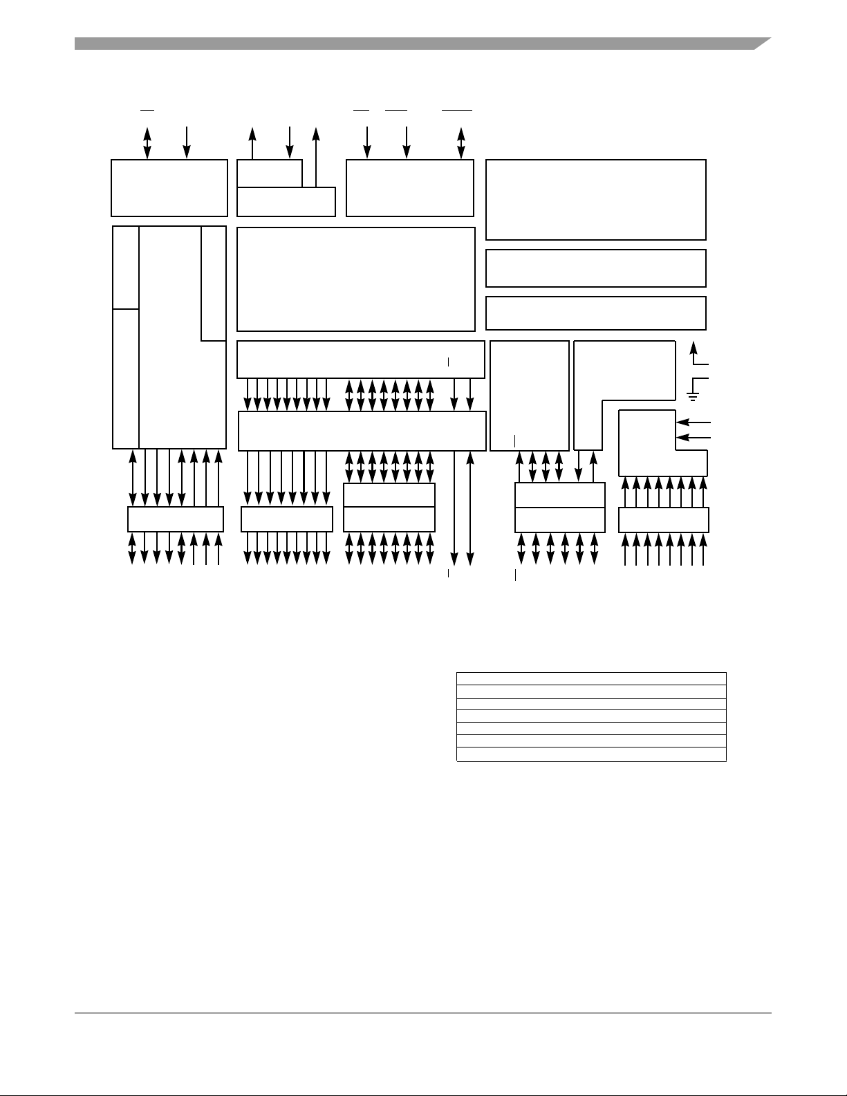
See Figure 1-1 for a functional diagram of the E-series MCUs. Differences among devices are noted in
the table accompanying Figure 1-1.
1.4 Pin Descriptions
M68HC11 E-series MCUs are available packaged in:
• 52-pin plastic-leaded chip carrier (PLCC)
• 52-pin windowed ceramic leaded chip carrier (CLCC)
• 52-pin plastic thin quad flat pack, 10 mm x 10 mm (TQFP)
• 64-pin quad flat pack (QFP)
• 48-pin plastic dual in-line package (DIP), MC68HC811E2 only
• 56-pin plastic shrink dual in-line package, .070-inch lead spacing (SDIP)
Most pins on these MCUs serve two or more functions, as described in the following paragraphs. Refer
to Figure 1-2, Figure 1-3, Figure 1-4, Figure 1-5, and Figure 1-6 which show the M68HC11 E-series pin
assignments for the PLCC/CLCC, QFP, TQFP, SDIP, and DIP packages.
M68HC11E Family Data Sheet, Rev. 5.1
14 Freescale Semiconductor
Page 15
MODA/
LIR
MODB/
V
STBY
XTAL EXTAL E IRQ XIRQ/V
PPE*
Pin Descriptions
RESET
MODE CONTROL
TIMER
SYSTEM
COPPULSE ACCUMULATOR
OC2
OC3
OC4
PAI
OC5/IC4/OC1
PORT A
PERIODIC INTERRUPT
IC1
IC2
IC3
OSC
CLOCK LOGIC
BUS EXPANSION
ADDRESS
STROBE AND HANDSHAKE
PORT B
M68HC11 CPU
ADDRESS/DATA
PARALLEL I/O
CONTROL
PORT C
INTERRUPT
LOGIC
R/W
STRB
STRA
AS
SERIAL
PERIPHERAL
INTERFACE
SPI
SCK
SS
CONTROL
PORT D
ROM OR EPROM
(SEE TABLE)
EEPROM
(SEE TABLE)
RAM
(SEE TABLE)
COMMUNICATION
INTERFACE
MOSI
MISO
TxD
RxD
SERIAL
SCI
A/D CONVERTER
PORT E
V
DD
V
SS
V
RH
V
RL
PA2/IC1
PA1/IC2
PA7/PAI
PA6/OC2/OC1
PA5/OC3/OC1
PA4/OC4/OC1
PA0/IC3
PB7/ADDR15
PB6/ADDR14
PA3/OC5/IC4/OC1
* V
applies only to devices with EPROM/OTPROM.
PPE
Figure 1-1. M68HC11 E-Series Block Diagram
PD5/SS
STRA/AS
PC1/ADDR1/DATA1
STRB/R/W
PC0/ADDR0/DATA0
PB1/ADDR9
PB5/ADDR13
PB4/ADDR12
PB0/ADDR8
PB3/ADDR11
PB2/ADDR10
PC7/ADDR7/DATA7
PC6/ADDR6/DATA6
PC5/ADDR5/DATA5
PC4/ADDR4/DATA4
PC3/ADDR3/DATA3
PC2/ADDR2/DATA2
PD4/SCK
DEVICE
MC68HC11E0
MC68HC11E1
MC68HC11E9
MC68HC711E9
MC68HC11E20
MC68HC711E20
PD3/MOSI
RAM
512
512
512
512
768
768
PD2/MISO
PD1/TxD
PD0/RxD
ROM
—
—
12 K
—
20 K
—
PE7/AN7
PE6/AN6
EPROM
—
—
—
12 K
—
20 K
PE5/AN5
PE4/AN4
PE3/AN3
EEPROM
PE2/AN2
—
512
512
512
512
512
PE1/AN1
PE0/AN0
256 — — 2048MC68HC811E2
M68HC11E Family Data Sheet, Rev. 5.1
Freescale Semiconductor 15
Page 16
General Description
STBY
EXTAL
STRB/R/WESTRA/AS
7
6
XTAL
8
PC0/ADDR0/DATA0
PC1/ADDR1/DATA1
PC2/ADDR2/DATA2
PC3/ADDR3/DATA3
PC4/ADDR4/DATA4
PC5/ADDR5/DATA5
PC6/ADDR6/DATA6
PC7/ADDR7/DATA7
RESET
* XIRQ/V
PD0/RxD
* V
applies only to devices with EPROM/OTPROM.
PPE
PPE
IRQ
9
10
11
12
13
14
15
16
17
18
19
20
2122232425262728293031
PD1/TxD
PD2/MISO
MODA/LIR
MODB/V
VSSVRHVRLPE7/AN7
5
4
312
M68HC11 E SERIES
DD
V
PD5/SS
PD4/SCK
PD3/MOSI
52
PA7/PAI/OC1
PA6/OC2/OC1
PE3/AN3
51
50
49
PA5/OC3/OC1
PA4/OC4/OC1
PA3/OC5/IC4/OC1
PE6/AN648PE2/AN2
47
45
44
43
42
41
40
39
38
37
36
35
34
33
PA2/IC132PA1/IC2
PE5/AN546
PE1/AN1
PE4/AN4
PE0/AN0
PB0/ADDR8
PB1/ADDR9
PB2/ADDR10
PB3/ADDR11
PB4/ADDR12
PB5/ADDR13
PB6/ADDR14
PB7/ADDR15
PA0/IC3
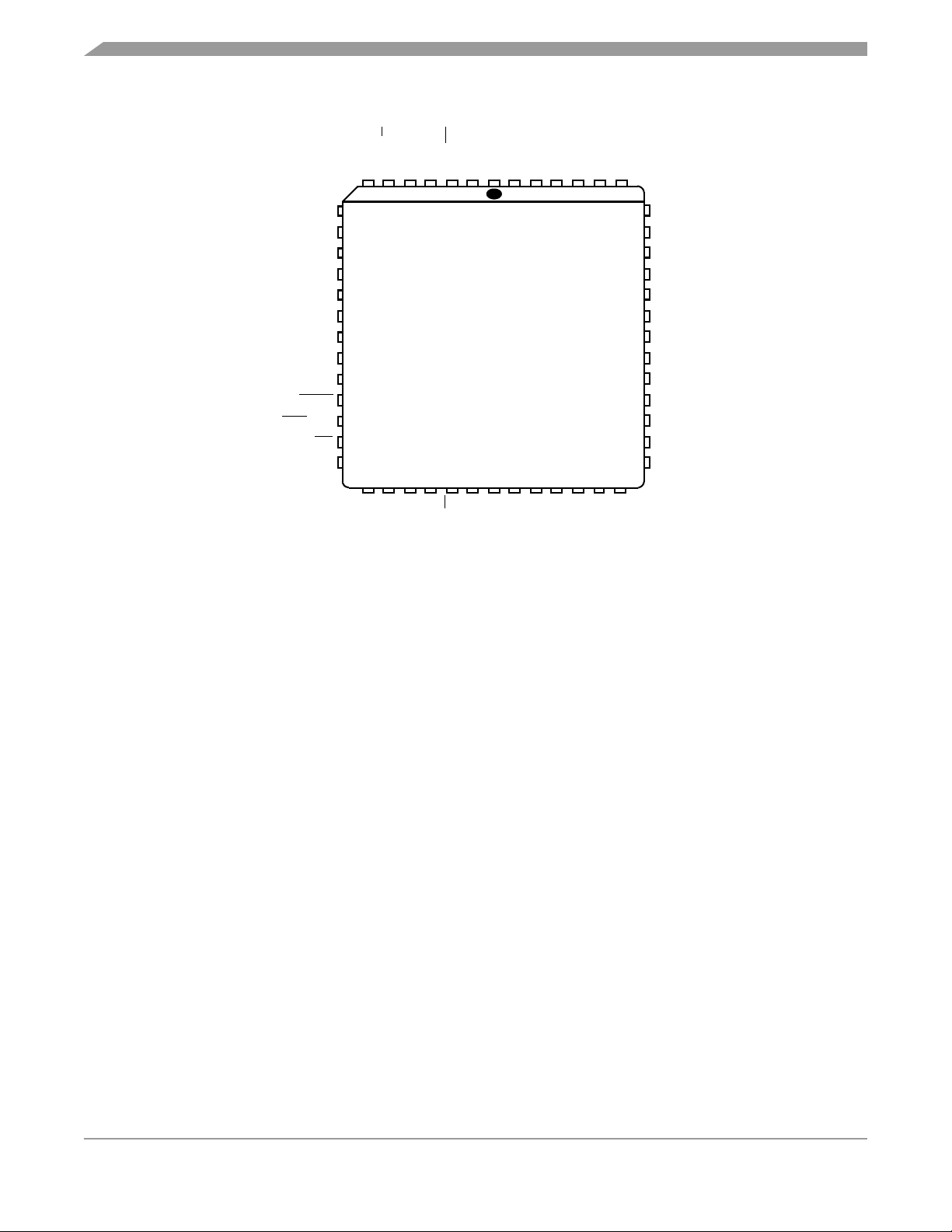
Figure 1-2. Pin Assignments for 52-Pin PLCC and CLCC
M68HC11E Family Data Sheet, Rev. 5.1
16 Freescale Semiconductor
Page 17
Pin Descriptions
PA1/IC2
PA2/IC1
PA0/IC3
NC
NC
NC
PB7/ADDR15
PB6/ADDR14
PB5/ADDR13
PB4/ADDR12
PB3/ADDR11
PB2/ADDR10
PB1/ADDR9
PB0/ADDR8
PE0/AN0
PE4/AN4
PE1/AN1
PE5/AN5
PA3/OC5/IC4/OC1NCNC
64
63626160595857
1
2
3
4
5
6
7
8
9
10
11
12
13
14
15
16
PA4/OC4/OC1
PA5/OC3/OC1
M68HC11 E SERIES
17181920212223
RL
RH
V
VSSV
V
PE2/AN2
PE6/AN6
PE3/AN3
PE7/AN7
1. V
applies only to devices with EPROM/OTPROM.
PPE
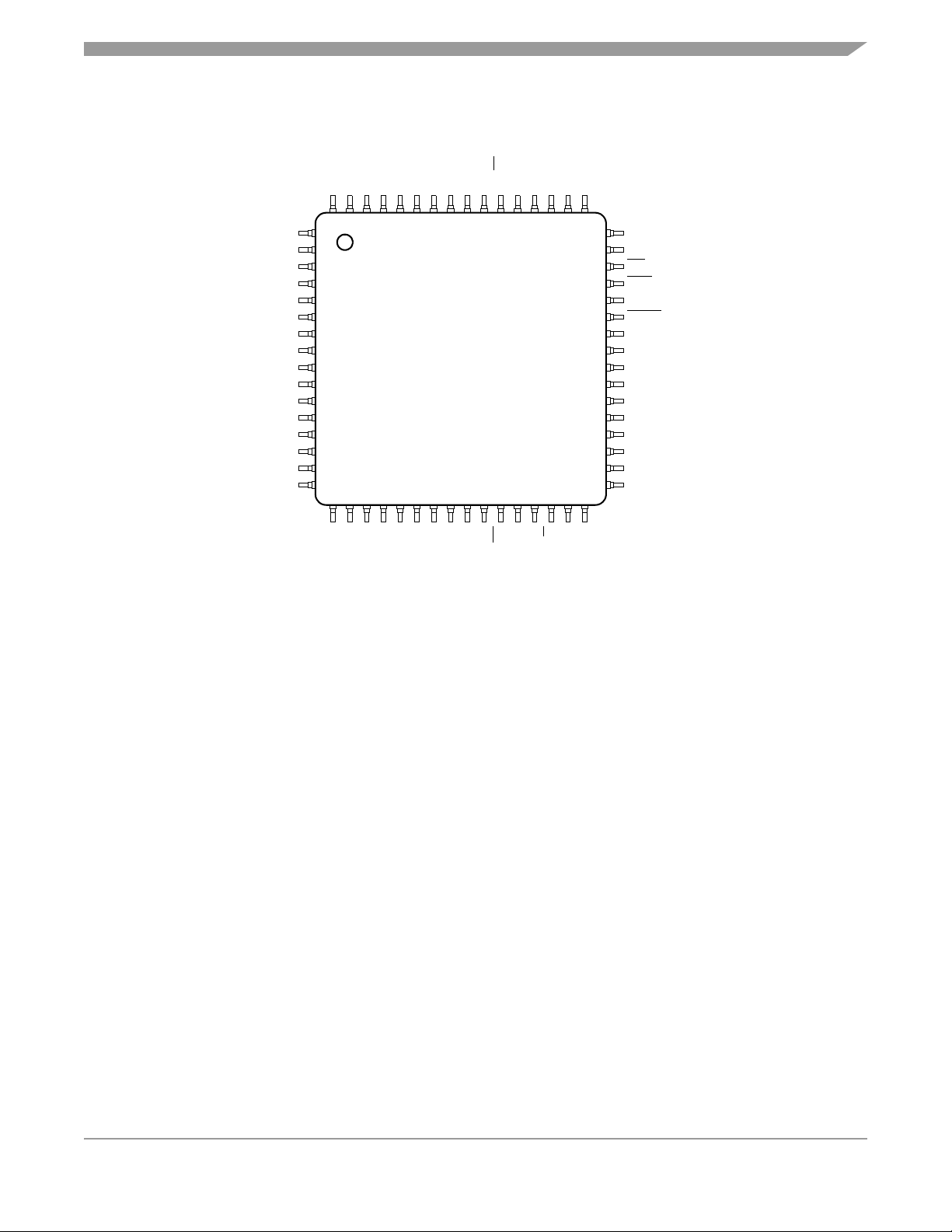
Figure 1-3. Pin Assignments for 64-Pin QFP
PA6/OC2/OC1
PA7/PAI/OC1
PD5/SS
VDDPD4/SCK
55
56
54
26
25
STBY
MODB/V
27
NC
MODA/LIR
24
SS
PD3/MOSI
PD2/MISO
PD1/TxD
V
5352515049
2829303132
E
STRA/AS
EXTAL
STRB/R/W
SS
NC
48
PD0/RxD
47
IRQ
46
45
XIRQ/V
NC
44
RESET
43
PC7/ADDR7/DATA7
42
PC6/ADDR6/DATA6
41
PC5/ADDR5/DATA5
40
PC4/ADDR4/DATA4
39
PC3/ADDR3/DATA3
38
37
PC2/ADDR2/DATA2
36
PC1/ADDR1/DATA1
35
NC
34
PC0/ADDR0/DATA0
33
XTAL
NC
PPE
(1)
M68HC11E Family Data Sheet, Rev. 5.1
Freescale Semiconductor 17
Page 18

General Description
PA0/IC3
PB7/ADDR15
PB6/ADDR14
PB5/ADDR13
PB4/ADDR12
PB3/ADDR11
PB2/ADDR10
PB1/ADDR9
PB0/ADDR8
PE0/AN0
PE4/AN4
PE1/AN1
PE5/AN5
PA1/IC2
PA2/IC1
PA3/OC5/IC4/OC1
PA4/OC4/OC1
PA5/OC3/OC1
PA6/OC2/OC1
PA7/PAI/OC1
52
51504948474645
1
2
3
4
5
6
7
M68HC11 E SERIES
8
9
10
11
12
13
1415161718192021222423
PD5/SS
VDDPD4/SCK
44
PD3/MOSI
PD2/MISO
PD1/TxD
42
43
41
40
PD0/RxD
39
IRQ
38
XIRQ/V
37
36
RESET
35
PC7/ADDR7/DATA7
PC6/ADDR6/DATA6
34
PC5/ADDR5/DATA5
33
32
PC4/ADDR4/DATA4
31
PC3/ADDR3/DATA3
PC2/ADDR2/DATA2
30
PC1/ADDR1/DATA1
29
28
PC0/ADDR0/DATA0
27
25
XTAL
26
PPE
(1)
RL
SS
RH
V
V
V
PE2/AN2
PE6/AN6
PE3/AN3
PE7/AN7
1. V
applies only to devices with EPROM/OTPROM.
PPE
STBY
MODB/V
E
STRA/AS
MODA/LIR
EXTAL
STRB/R/W
Figure 1-4. Pin Assignments for 52-Pin TQFP
M68HC11E Family Data Sheet, Rev. 5.1
18 Freescale Semiconductor
Page 19
Pin Descriptions
V
MODB/V
STBY
MODA/LIR
STRA/AS
STRB/R/W
EXTAL
XTAL
PC0/ADDR0/DATA0
PC1/ADDR1/DATA1
PC2/ADDR2/DATA2
PC3/ADDR3/DATA3
PC4/ADDR4/DATA4
PC5/ADDR5/DATA5
PC6/ADDR6/DATA6
PC7/ADDR7/DATA7
RESET
* XIRQ/V
PPE
IRQ
PD0/RxD
EV
SS
PD1/TxD
PD2/MISO
PD3/MOSI
PD4/SCK
PD5/SS
V
DD
V
SS
SS
1
2
3
4
E
5
6
7
8
9
10
11
12
13
14
15
M68HC11 E SERIES
16
17
18
19
20
21
22
23
24
25
26
27
28
EV
56
SS
V
RH
55
V
54
RL
PE7/AN7
53
PE3/AN3
52
PE6/AN6
51
PE2/AN2
50
PE5/AN5
49
PE1/AN1
48
PE4/AN4
47
PE0/AN0
46
PB0/ADDR8
45
PB1/ADDR9
44
PB2/ADDR10
43
PB3/ADDR11
42
PB4/ADDR12
41
PB5/ADDR13
40
PB6/ADDR14
39
PB7/ADDR15
38
PA0/IC3
37
PA1/IC2
36
PA2/IC1
35
PA3/OC5/IC4/OC1
34
PA4/OC4/OC1
33
PA5/OC3/OC1
32
PA6/OC2/OC1
31
PA7/PAI/OC1
30
EV
29
DD
* V
applies only to devices with EPROM/OTPROM.
PPE
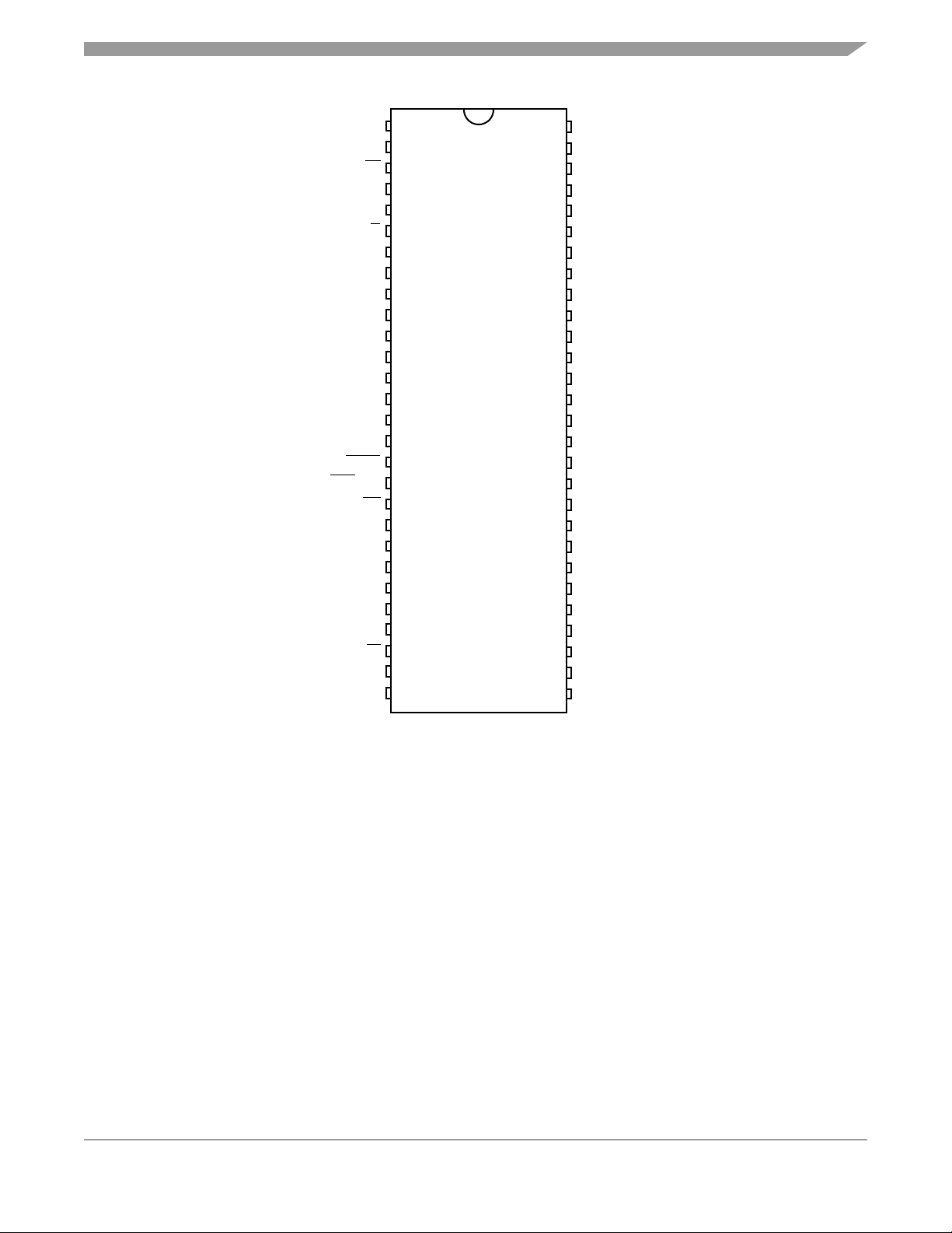
Figure 1-5. Pin Assignments for 56-Pin SDIP
M68HC11E Family Data Sheet, Rev. 5.1
Freescale Semiconductor 19
Page 20
General Description
PA7/PAI/OC1
PA6/OC2/OC1
PA5/OC3/OC1
PA4/OC4/OC1
PA3/OC5/IC4/OC1
PA2/IC1
PA1/IC2
PA0/IC3
PB7/ADDR15
PB6/ADDR14
PB5/ADDR13
PB4/ADDR12
PB3/ADDR11
PB2/ADDR10
PB1/ADDR9
PB0/ADDR8
PE0/AN0
PE1/AN1
PE2/AN2
PE3/AN3
V
V
RH
V
SS
MODB/V
STBY
V
1
2
3
4
5
6
7
8
9
10
11
MC68HC811E2
12
13
14
15
16
17
18
19
20
21
RL
22
23
24
48
DD
PD5/SS
47
PD4/SCK46
PD3/MOSI
45
PD2/MISO44
PD1/TxD
43
PD0/RxD42
IRQ
41
XIRQ
40
RESET
39
PC7/ADDR7/DATA7
38
PC6/ADDR6/DATA6
37
PC5/ADDR5/DATA5
36
PC4/ADDR4/DATA4
35
PC3/ADDR3/DATA3
34
PC2/ADDR2/DATA2
33
PC1/ADDR1/DATA1
32
PC0/ADDR0/DATA0
31
XTAL
30
EXTAL
29
STRB/R/W
28
E27
STRA/AS26
25
MODA/LIR
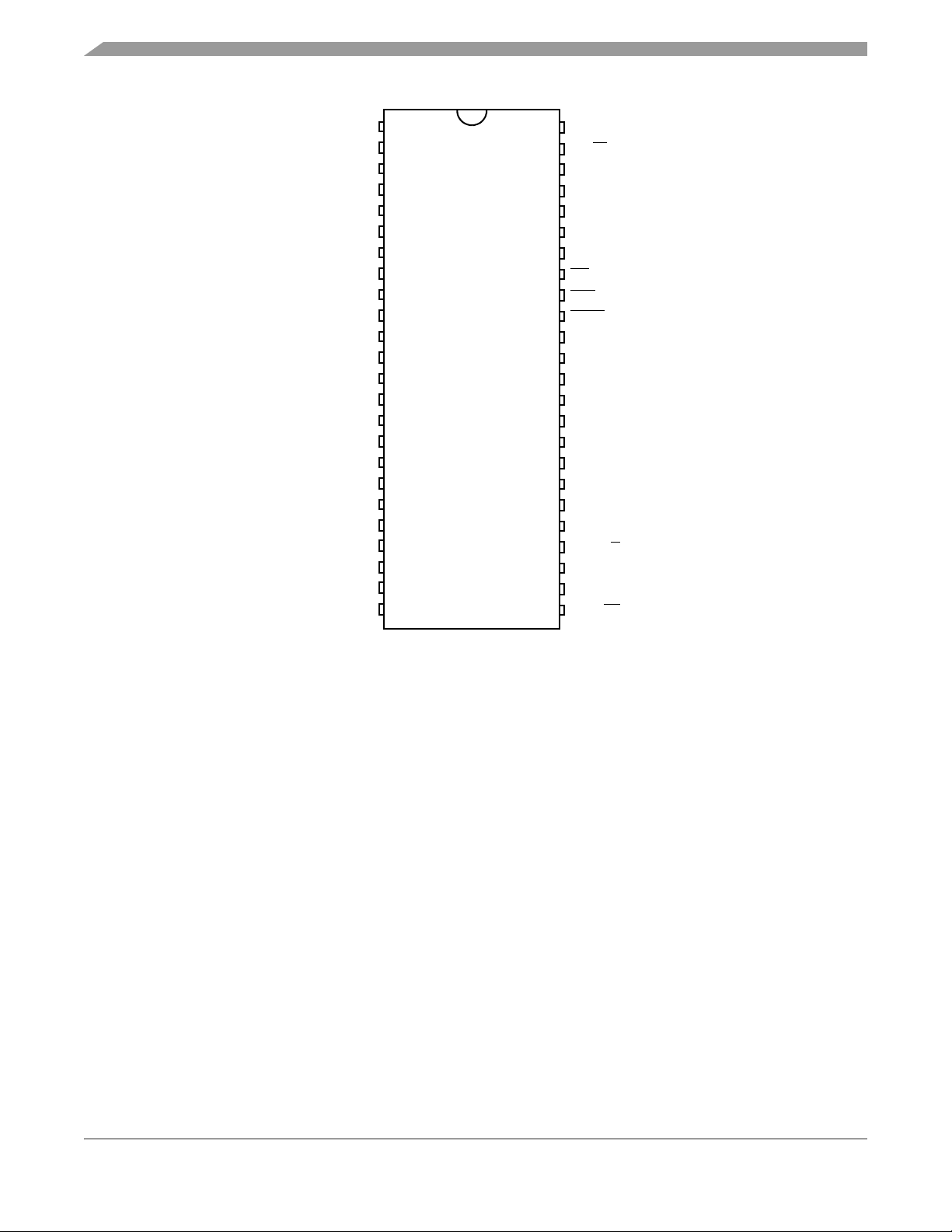
Figure 1-6. Pin Assignments for 48-Pin DIP (MC68HC811E2)
M68HC11E Family Data Sheet, Rev. 5.1
20 Freescale Semiconductor
Page 21
Pin Descriptions
1.4.1 VDD and VSS
Power is supplied to the MCU through VDD and VSS. VDD is the power supply, VSS is ground. The MCU
operates from a single 5-volt (nominal) power supply. Low-voltage devices in the E series operate at
3.0–5.5 volts.
Very fast signal transitions occur on the MCU pins. The short rise and fall times place high, short duration
current demands on the power supply. To prevent noise problems, provide good power supply bypassing
at the MCU. Also, use bypass capacitors that have good
high-frequency characteristics and situate them as close to the MCU as possible. Bypass requirements
vary, depending on how heavily the MCU pins are loaded.
MANUAL
RESET SWITCH
4.7 kΩ
V
DD
2
IN
RESET
MC34(0/1)64
GND
3
V
DD
4.7 kΩ
1
TO RESET
OF M68HC11
Figure 1-7. External Reset Circuit
V
DD
IN
RESET
V
DD
4.7 kΩ
MC34064
GND
V
DD
4.7 kΩ
TO RESET
OF M68HC11
1.0 µF
IN
RESET
MC34164
GND
OPTIONAL POWER-ON DELAY AND MANUAL RESET SWITCH
Figure 1-8. External Reset Circuit with Delay
M68HC11E Family Data Sheet, Rev. 5.1
Freescale Semiconductor 21
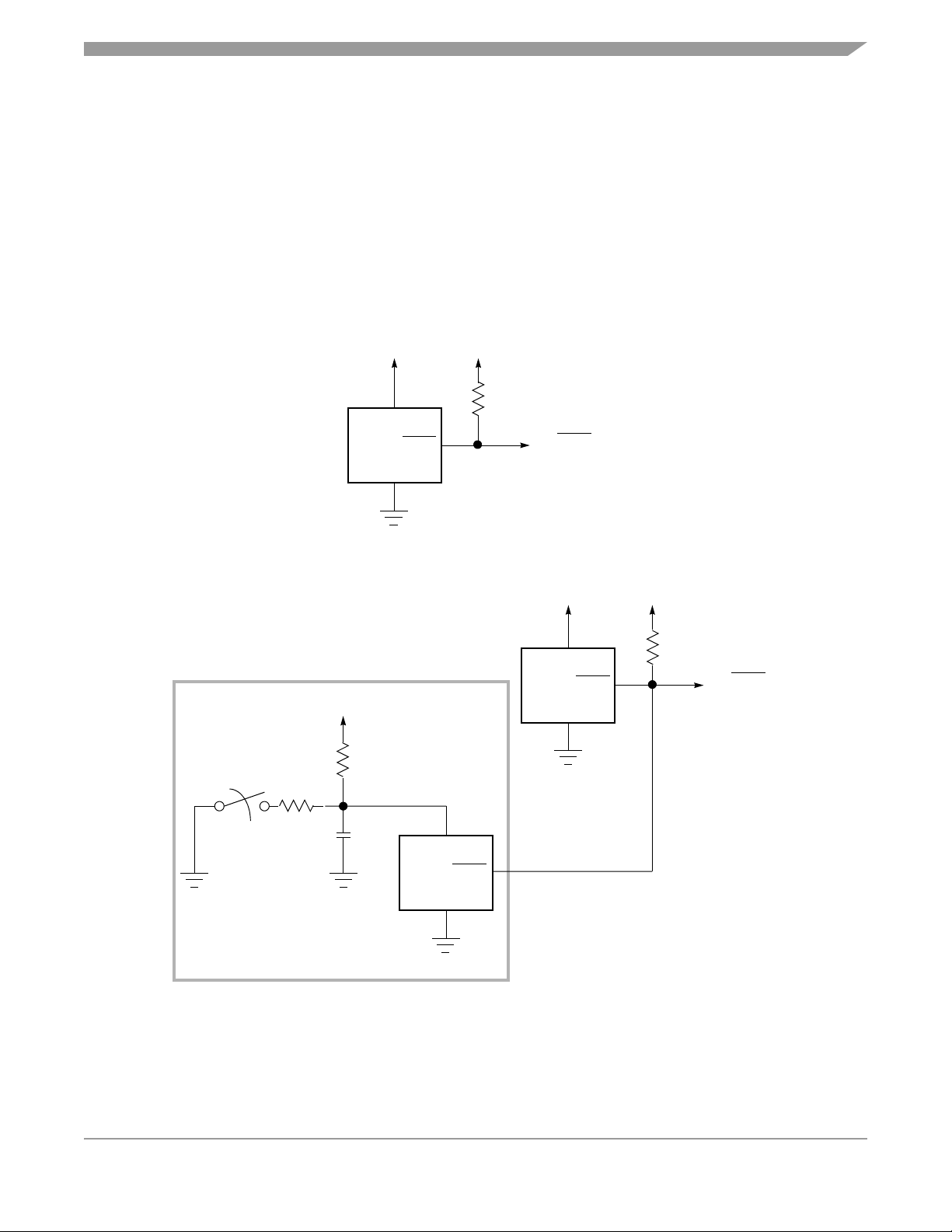
Page 22

General Description
1.4.2 RESET
A bidirectional control signal, RESET, acts as an input to initialize the MCU to a known startup state. It
also acts as an open-drain output to indicate that an internal failure has been detected in either the clock
monitor or computer operating properly (COP) watchdog circuit. The CPU distinguishes between internal
and external reset conditions by sensing whether the reset pin rises to a logic 1 in less than two E-clock
cycles after a reset has occurred. See Figure 1-7 and Figure 1-8.
CAUTION
Do not connect an external resistor capacitor (RC) power-up delay circuit
to the reset pin of M68HC11 devices because the circuit charge time
constant can cause the device to misinterpret the type of reset that
occurred.
Because the CPU is not able to fetch and execute instructions properly when V
falls below the minimum
DD
operating voltage level, reset must be controlled. A low-voltage inhibit (LVI) circuit is required primarily for
protection of EEPROM contents. However, since the configuration register (CONFIG) value is read from
the EEPROM, protection is required even if the EEPROM array is not being used.
Presently, there are several economical ways to solve this problem. For example, two good external
components for LVI reset are:
1. The Seiko S0854HN (or other S805 series devices):
a. Extremely low power (2 µA)
a. TO-92 package
a. Limited temperature range, –20°C to +70°C
a. Available in various trip-point voltage ranges
2. The Freescale MC34064:
a. TO-92 or SO-8 package
a. Draws about 300 µA
a. Temperature range –40°C to 85°C
a. Well controlled trip point
a. Inexpensive
Refer to Chapter 5 Resets and Interrupts for further information.
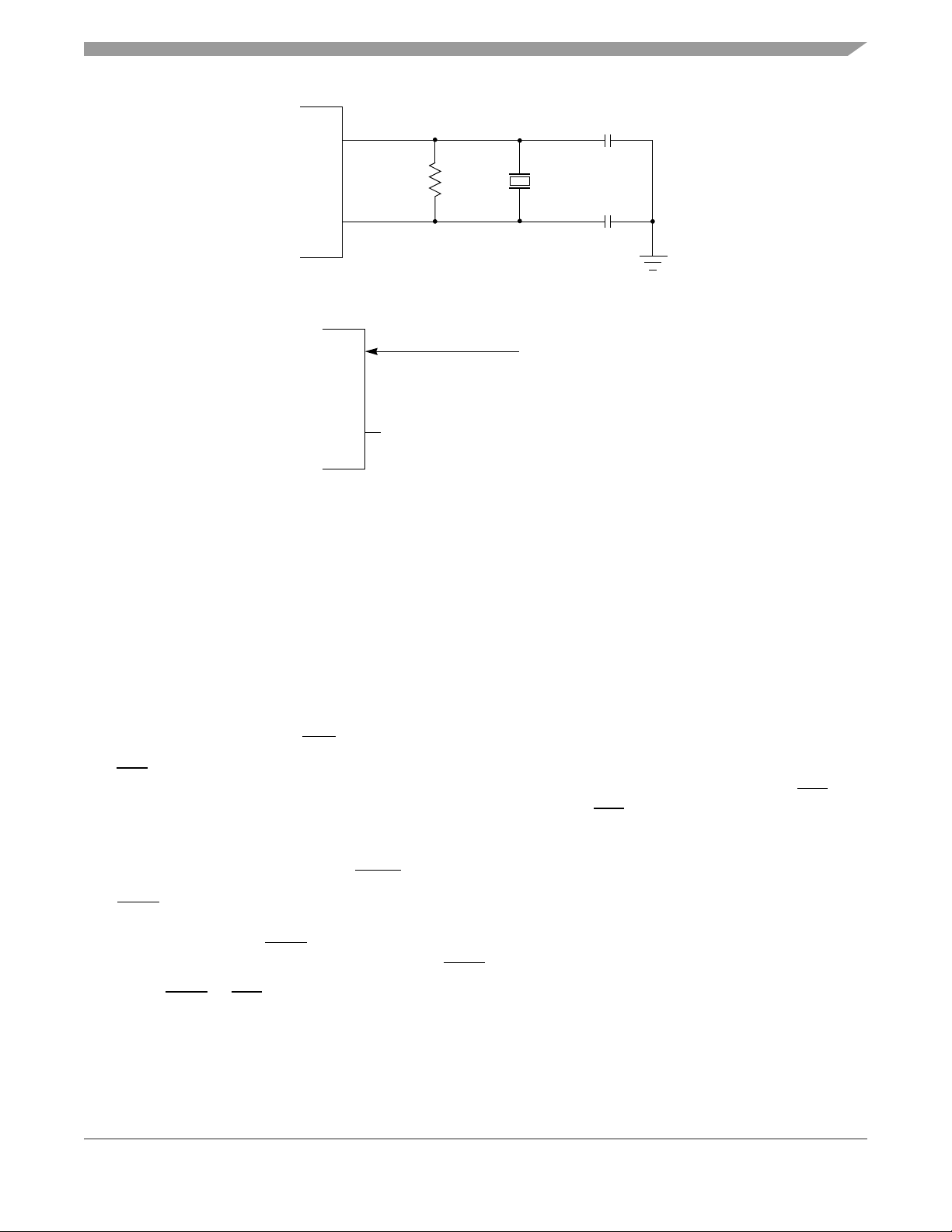
1.4.3 Crystal Driver and External Clock Input (XTAL and EXTAL)
These two pins provide the interface for either a crystal or a CMOS- compatible clock to control the
internal clock generator circuitry. The frequency applied to these pins is four times higher than the desired
E-clock rate.
The XTAL pin must be left unterminated when an external CMOS- compatible clock input is connected to
the EXTAL pin. The XTAL output is normally intended to drive only a crystal. Refer to Figure 1-9 and
Figure 1-10.
CAUTION
In all cases, use caution around the oscillator pins. Load capacitances
shown in the oscillator circuit are specified by the crystal manufacturer and
should include all stray layout capacitances.
M68HC11E Family Data Sheet, Rev. 5.1
22 Freescale Semiconductor
Page 23
EXTAL
Pin Descriptions
C
L
MCU
10 MΩ
XTAL
4 x E
CRYSTAL
C
L
Figure 1-9. Common Parallel Resonant Crystal Connections
4 x E
CMOS-COMPATIBLE
MCU
EXTAL
XTAL
EXTERNAL OSCILLATOR
NC
Figure 1-10. External Oscillator Connections
1.4.4 E-Clock Output (E)
E is the output connection for the internally generated E clock. The signal from E is used as a timing
reference. The frequency of the E-clock output is one fourth that of the input frequency at the XTAL and
EXTAL pins. When E-clock output is low, an internal process is taking place. When it is high, data is being
accessed.
All clocks, including the E clock, are halted when the MCU is in stop mode. To reduce RFI emissions, the
E-clock output of most E-series devices can be disabled while operating in single-chip modes.
The E-clock signal is always enabled on the MC68HC811E2.
1.4.5 Interrupt Request (IRQ)
The IRQ input provides a means of applying asynchronous interrupt requests to the MCU. Either negative
edge-sensitive triggering or level-sensitive triggering is program selectable (OPTION register). IRQ
always configured to level-sensitive triggering at reset. When using IRQ
configuration, connect an external pullup resistor, typically 4.7 kΩ, to V
1.4.6 Non-Maskable Interrupt (XIRQ/V
PPE
)
in a level-sensitive wired-OR
.
DD
The XIRQ input provides a means of requesting a non-maskable interrupt after reset initialization. During
reset, the X bit in the condition code register (CCR) is set and any interrupt is masked until MCU software
enables it. Because the XIRQ
network with an external pullup resistor to V
Whenever XIRQ
or IRQ is used with multiple interrupt sources each source must drive the interrupt input
input is level-sensitive, it can be connected to a multiple-source wired-OR
. XIRQ is often used as a power loss detect interrupt.
DD
with an open-drain type of driver to avoid contention between outputs.
is
M68HC11E Family Data Sheet, Rev. 5.1
Freescale Semiconductor 23
Page 24

General Description
NOTE
must be configured for level-sensitive operation if there is more than
IRQ
one source of IRQ
interrupt.
There should be a single pullup resistor near the MCU interrupt input pin (typically 4.7 kΩ). There must
also be an interlock mechanism at each interrupt source so that the source holds the interrupt line low
until the MCU recognizes and acknowledges the interrupt request. If one or more interrupt sources are
still pending after the MCU services a request, the interrupt line will still be held low and the MCU will be
interrupted again as soon as the interrupt mask bit in the MCU is cleared (normally upon return from an
interrupt). Refer to Chapter 5 Resets and Interrupts.
V
is the input for the 12-volt nominal programming voltage required for EPROM/OTPROM
PPE
programming. On devices without EPROM/OTPROM, this pin is only an XIRQ
input.
CAUTION
During EPROM programming of the MC68HC711E9 device, the V
PPE
pin
circuitry may latch-up and be damaged if the input current is not limited to
10 mA. For more information please refer to MC68HC711E9 8-Bit
Microcontroller Unit Mask Set Errata 3 (Freescale document order number
68HC711E9MSE3.
1.4.7 MODA and MODB (MODA/LIR and MODB/V
STBY
)
During reset, MODA and MODB select one of the four operating modes:
• Single-chip mode
• Expanded mode
• Test mode
• Bootstrap mode
Refer to Chapter 2 Operating Modes and On-Chip Memory.
After the operating mode has been selected, the load instruction register (LIR
) pin provides an open-drain
output to indicate that execution of an instruction has begun. A series of E-clock cycles occurs during
execution of each instruction. The LIR
signal goes low during the first E-clock cycle of each instruction
(opcode fetch). This output is provided for assistance in program debugging.
The V
pin is more than one MOS threshold (about 0.7 volts) above the V
of the reset logic are powered from this signal rather than the V
retained without V
must remain low until V
pin is used to input random-access memory (RAM) standby power. When the voltage on this
STBY
voltage, the internal RAM and part
DD
input. This allows RAM contents to be
DD
power applied to the MCU. Reset must be driven low before VDD is removed and
DD
has been restored to a valid level.
DD
1.4.8 VRL and VRH
These two inputs provide the reference voltages for the analog-to-digital (A/D) converter circuitry:
•V
•V
For proper A/D converter operation:
•V
•V
is the low reference, typically 0 Vdc.
RL
is the high reference.
RH
should be at least 3 Vdc greater than VRL.
RH
and VRH should be between VSS and VDD.
RL
M68HC11E Family Data Sheet, Rev. 5.1
24 Freescale Semiconductor
Page 25

Pin Descriptions
1.4.9 STRA/AS
The strobe A (STRA) and address strobe (AS) pin performs either of two separate functions, depending
on the operating mode:
• In single-chip mode, STRA performs an input handshake (strobe input) function.
• In the expanded multiplexed mode, AS provides an address strobe function.
AS can be used to demultiplex the address and data signals at port C. Refer to Chapter 2 Operating
Modes and On-Chip Memory.
1.4.10 STRB/R/W
The strobe B (STRB) and read/write (R/W) pin act as either an output strobe or as a data bus direction
indicator, depending on the operating mode.
In single-chip operating mode, STRB acts as a programmable strobe for handshake with other parallel
devices. Refer to Chapter 6 Parallel Input/Output (I/O) Ports for further information.
In expanded multiplexed operating mode, R/W
data bus. A low on the R/W
pin indicates data is being written to the external data bus. A high on this pin
indicates that a read cycle is in progress. R/W
is used to indicate the direction of transfers on the external
stays low during consecutive data bus write cycles, such
as a double-byte store. It is possible for data to be driven out of port C, if internal read visibility (IRV) is
enabled and an internal address is read, even though R/W
is in a high-impedance state. Refer to
Chapter 2 Operating Modes and On-Chip Memory for more information about IRVNE (internal read
visibility not E).
1.4.11 Port Signals
Port pins have different functions in different operating modes. Pin functions for port A, port D, and port
E are independent of operating modes. Port B and port C, however, are affected by operating mode. Port
B provides eight general-purpose output signals in single-chip operating modes. When the microcontroller
is in expanded multiplexed operating mode, port B pins are the eight high-order address lines.
Port C provides eight general-purpose input/output signals when the MCU is in the single-chip operating
mode. When the microcontroller is in the expanded multiplexed operating mode, port C pins are a
multiplexed address/data bus.
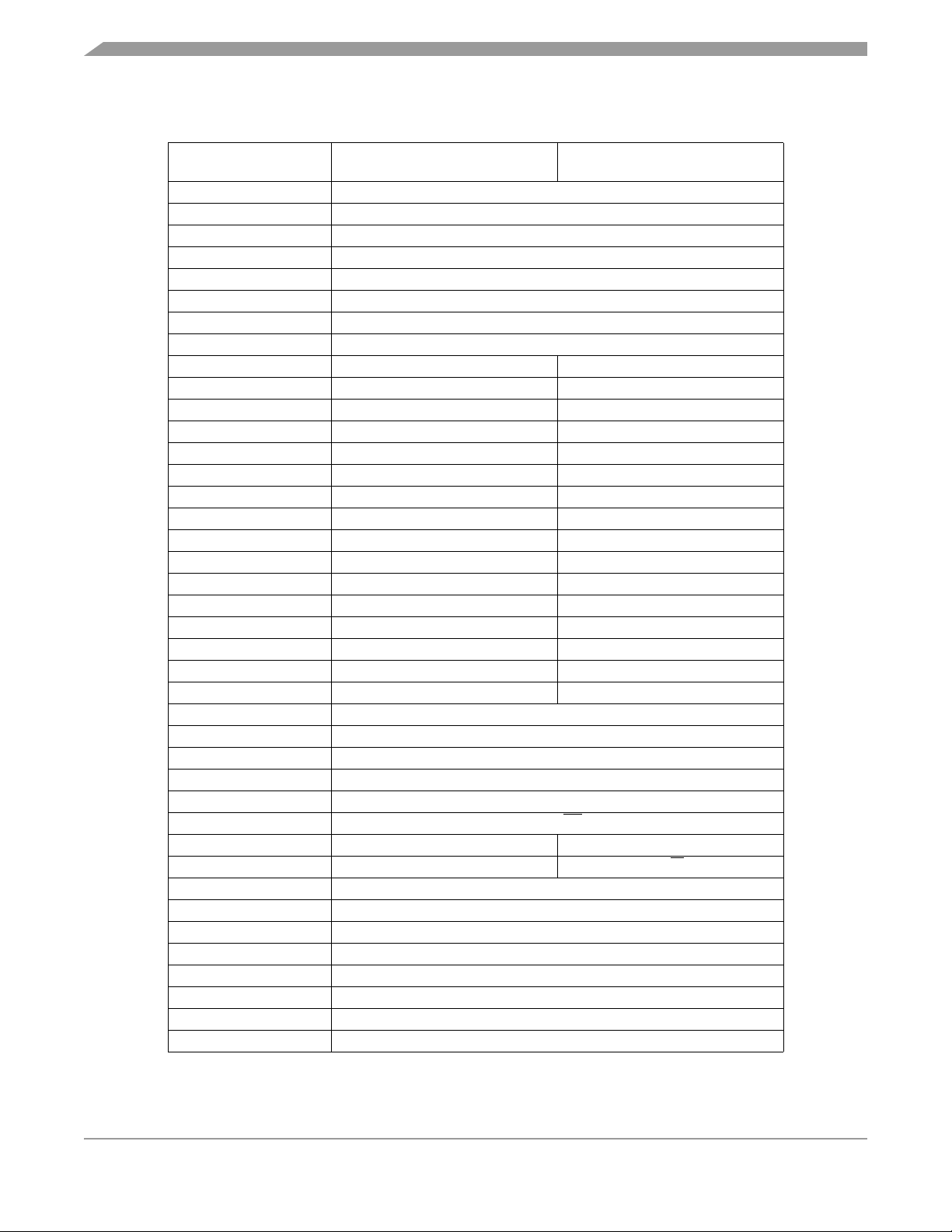
Refer to Table 1-1 for a functional description of the 40 port signals within different operating modes.
Terminate unused inputs and input/output (I/O) pins configured as inputs high or low.
1.4.12 Port A
In all operating modes, port A can be configured for three timer input capture (IC) functions and four timer
output compare (OC) functions. An additional pin can be configured as either the fourth IC or the fifth OC.
Any port A pin that is not currently being used for a timer function can be used as either a general-purpose
input or output line. Only port A pins PA7 and PA3 have an associated data direction control bit that allows
the pin to be selectively configured as input or output. Bits DDRA7 and DDRA3 located in PACTL register
control data direction for PA7 and PA3, respectively. All other port A pins are fixed as either input or
output.
PA7 can function as general-purpose I/O or as timer output compare for OC1. PA7 is also the input to the
pulse accumulator, even while functioning as a general-purpose I/O or an OC1 output.
M68HC11E Family Data Sheet, Rev. 5.1
Freescale Semiconductor 25
Page 26
General Description
Table 1-1. Port Signal Functions
Port/Bit
PA 0 PA 0/ I C3
PA 1 PA 1/ I C2
PA 2 PA 2/ I C1
PA3 PA3/OC5/IC4/OC1
PA4 PA4/OC4/OC1
PA5 PA5/OC3/OC1
PA6 PA6/OC2/OC1
PA7 PA7/PAI/OC1
PB0 PB0 ADDR8
PB1 PB1 ADDR9
PB2 PB2 ADDR10
PB3 PB3 ADDR11
PB4 PB4 ADDR12
PB5 PB5 ADDR13
PB6 PB6 ADDR14
PB7 PB7 ADDR15
PC0 PC0 ADDR0/DATA0
PC1 PC1 ADDR1/DATA1
PC2 PC2 ADDR2/DATA2
PC3 PC3 ADDR3/DATA3
PC4 PC4 ADDR4/DATA4
PC5 PC5 ADDR5/DATA5
PC6 PC6 ADDR6/DATA6
PC7 PC7 ADDR7/DATA7
PD0 PD0/RxD
PD1 PD1/TxD
PD2 PD2/MISO
PD3 PD3/MOSI
PD4 PD4/SCK
PD5 PD5/SS
— STRA AS
—STRB R/W
PE0 PE0/AN0
PE1 PE1/AN1
PE2 PE3/AN2
PE3 PE3/AN3
PE4 PE4/AN4
PE5 PE5/AN5
PE6 PE6/AN6
PE7 PE7/AN7
Single-Chip and
Bootstrap Modes
Expanded and
Test Modes
M68HC11E Family Data Sheet, Rev. 5.1
26 Freescale Semiconductor
Page 27

Pin Descriptions
PA6–PA4 serve as either general-purpose outputs, timer input captures, or timer output compare 2–4. In
addition, PA6–PA4 can be controlled by OC1.
PA3 can be a general-purpose I/O pin or a timer IC/OC pin. Timer functions associated with this pin
include OC1 and IC4/OC5. IC4/OC5 is software selectable as either a fourth input capture or a fifth output
compare. PA3 can also be configured to allow OC1 edges to trigger IC4 captures.
PA2–PA0 serve as general-purpose inputs or as IC1–IC3.
PORTA can be read at any time. Reads of pins configured as inputs return the logic level present on the
pin. Pins configured as outputs return the logic level present at the pin driver input. If written, PORTA
stores the data in an internal latch, bits 7 and 3. It drives the pins only if they are configured as outputs.
Writes to PORTA do not change the pin state when pins are configured for timer input captures or output
compares. Refer to Chapter 6 Parallel Input/Output (I/O) Ports.
1.4.13 Port B
During single-chip operating modes, all port B pins are general-purpose output pins. During MCU reads
of this port, the level sensed at the input side of the port B output drivers is read. Port B can also be used
in simple strobed output mode. In this mode, an output pulse appears at the STRB signal each time data
is written to port B.
In expanded multiplexed operating modes, all of the port B pins act as high order address output signals.
During each MCU cycle, bits 15–8 of the address bus are output on the PB7–PB0 pins. The PORTB
register is treated as an external address in expanded modes.
1.4.14 Port C
While in single-chip operating modes, all port C pins are general-purpose I/O pins. Port C inputs can be
latched into an alternate PORTCL register by providing an input transition to the STRA signal. Port C can
also be used in full handshake modes of parallel I/O where the STRA input and STRB output act as
handshake control lines.
When in expanded multiplexed modes, all port C pins are configured as multiplexed address/data signals.
During the address portion of each MCU cycle, bits 7–0 of the address are output on the PC7–PC0 pins.
During the data portion of each MCU cycle (E high), PC7–PC0 are bidirectional data signals,
DATA7–DATA0. The direction of data at the port C pins is indicated by the R/W
The CWOM control bit in the PIOC register disables the port C P-channel output driver. CWOM
simultaneously affects all eight bits of port C. Because the N-channel driver is not affected by CWOM,
setting CWOM causes port C to become an open-drain type output port suitable for wired-OR operation.
In wired-OR mode:
• When a port C bit is at logic level 0, it is driven low by the N-channel driver.
• When a port C bit is at logic level 1, the associated pin has high-impedance, as neither the
N-channel nor the P-channel devices are active.
It is customary to have an external pullup resistor on lines that are driven by open-drain devices. Port C
can only be configured for wired-OR operation when the MCU is in single-chip mode. Refer to Chapter 6
Parallel Input/Output (I/O) Ports for additional information about port C functions.
signal.
M68HC11E Family Data Sheet, Rev. 5.1
Freescale Semiconductor 27
Page 28

General Description
1.4.15 Port D
Pins PD5–PD0 can be used for general-purpose I/O signals. These pins alternately serve as the serial
communication interface (SCI) and serial peripheral interface (SPI) signals when those subsystems are
enabled.
• PD0 is the receive data input (RxD) signal for the SCI.
• PD1 is the transmit data output (TxD) signal for the SCI.
• PD5–PD2 are dedicated to the SPI:
– PD2 is the master in/slave out (MISO) signal.
– PD3 is the master out/slave in (MOSI) signal.
– PD4 is the serial clock (SCK) signal.
– PD5 is the slave select (SS
) input.
1.4.16 Port E
Use port E for general-purpose or analog-to-digital (A/D) inputs.
CAUTION
If high accuracy is required for A/D conversions, avoid reading port E during
sampling, as small disturbances can reduce the accuracy of that result.
M68HC11E Family Data Sheet, Rev. 5.1
28 Freescale Semiconductor
Page 29

Chapter 2 Operating Modes and On-Chip Memory
2.1 Introduction
This section contains information about the operating modes and the on-chip memory for M68HC11
E-series MCUs. Except for a few minor differences, operation is identical for all devices in the E series.
Differences are noted where necessary.
2.2 Operating Modes
The values of the mode select inputs MODB and MODA during reset determine the operating mode.
Single-chip and expanded multiplexed are the normal modes.
• In single-chip mode only on-chip memory is available.
• Expanded mode, however, allows access to external memory.
Each of the two normal modes is paired with a special mode:
• Bootstrap, a variation of the single-chip mode, is a special mode that executes a bootloader
program in an internal bootstrap ROM.
• Test is a special mode that allows privileged access to internal resources.
2.2.1 Single-Chip Mode
In single-chip mode, ports B and C and strobe pins A (STRA) and B (STRB) are available for
general-purpose parallel input/output (I/O). In this mode, all software needed to control the MCU is
contained in internal resources. If present, read-only memory (ROM) and/or erasable, programmable
read-only memory (EPROM) will always be enabled out of reset, ensuring that the reset and interrupt
vectors will be available at locations $FFC0–$FFFF.
NOTE
For the MC68HC811E2, the vector locations are the same; however, they
are contained in the 2048-byte EEPROM array.
2.2.2 Expanded Mode
In expanded operating mode, the MCU can access the full 64-Kbyte address space. The space includes:
• The same on-chip memory addresses used for single-chip mode
• Addresses for external peripherals and memory devices
The expansion bus is made up of ports B and C, and control signals AS (address strobe) and R/W
(read/write). R/W
same pins. During the first half of each bus cycle address information is present. During the second half
of each bus cycle the pins become the bidirectional data bus. AS is an active-high latch enable signal for
an external address latch. Address information is allowed through the transparent latch while AS is high
and is latched when AS drives low.
and AS allow the low-order address and the 8-bit data bus to be multiplexed on the
M68HC11E Family Data Sheet, Rev. 5.1
Freescale Semiconductor 29
Page 30
Operating Modes and On-Chip Memory
The address, R/W, and AS signals are active and valid for all bus cycles, including accesses to internal
memory locations. The E clock is used to enable external devices to drive data onto the internal data bus
during the second half of a read bus cycle (E clock high). R/W
drives low when data is being written to the internal data bus. R/W
controls the direction of data transfers. R/W
will remain low during consecutive data
bus write cycles, such as when a double-byte store occurs.
Refer to Figure 2-1.
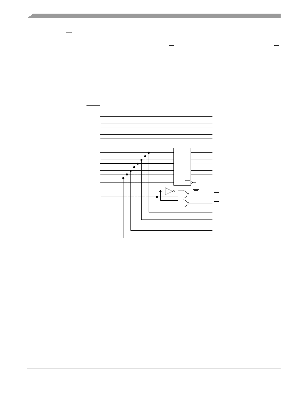
NOTE
The write enable signal for an external memory is the NAND of the E clock
and the inverted R/W
signal.
2.2.3 Test Mode
MCU
PB7
PB6
PB5
PB4
PB3
PB2
PB1
PB0
PC7
PC6
PC5
PC4
PC3
PC2
PC1
PC0
AS
R/W
E
HC373
D1
D2
D3
D4
D5
D6
D7
D8
LE
Q1
Q2
Q3
Q4
Q5
Q6
Q7
Q8
OE
Figure 2-1. Address/Data Demultiplexing
ADDR15
ADDR14
ADDR13
ADDR12
ADDR11
ADDR10
ADDR9
ADDR8
ADDR7
ADDR6
ADDR5
ADDR4
ADDR3
ADDR2
ADDR1
ADDR0
WE
OE
DATA7
DATA6
DATA5
DATA4
DATA3
DATA2
DATA1
DATA0
Test mode, a variation of the expanded mode, is primarily used during Freescale’s internal production
testing; however, it is accessible for programming the configuration (CONFIG) register, programming
calibration data into electrically erasable, programmable read-only memory (EEPROM), and supporting
emulation and debugging during development.
2.2.4 Bootstrap Mode
When the MCU is reset in special bootstrap mode, a small on-chip read-only memory (ROM) is enabled
at address $BF00–$BFFF. The ROM contains a bootloader program and a special set of interrupt and
reset vectors. The MCU fetches the reset vector, then executes the bootloader.
Bootstrap mode is a special variation of the single-chip mode. Bootstrap mode allows special-purpose
programs to be entered into internal random-access memory (RAM). When bootstrap mode is selected
at reset, a small bootstrap ROM becomes present in the memory map. Reset and interrupt vectors are
M68HC11E Family Data Sheet, Rev. 5.1
30 Freescale Semiconductor
Page 31

Memory Map
located in this ROM at $BFC0–$BFFF. The bootstrap ROM contains a small program which initializes the
serial communications interface (SCI) and allows the user to download a program into on-chip RAM. The
size of the downloaded program can be as large as the size of the on-chip RAM. After a 4-character delay,
or after receiving the character for the highest address in RAM, control passes to the loaded program at
$0000. Refer to Figure 2-2, Figure 2-3, Figure 2-4, Figure 2-5, and Figure 2-6.
Use of an external pullup resistor is required when using the SCI transmitter pin because port D pins are
configured for wired-OR operation by the bootloader. In bootstrap mode, the interrupt vectors are directed
to RAM. This allows the use of interrupts through a jump table. Refer to the application note AN1060
entitled M68HC11 Bootstrap Mode, that is included in this data book.
2.3 Memory Map
The operating mode determines memory mapping and whether external addresses can be accessed.
Refer to Figure 2-2, Figure 2-3, Figure 2-4, Figure 2-5, and Figure 2-6, which illustrate the memory maps
for each of the three families comprising the M68HC11 E series of MCUs.
Memory locations for on-chip resources are the same for both expanded and single-chip modes. Control
bits in the configuration (CONFIG) register allow EPROM and EEPROM (if present) to be disabled from
the memory map. The RAM is mapped to $0000 after reset. It can be placed at any 4-Kbyte boundary
($x000) by writing an appropriate value to the RAM and I/O map register (INIT). The 64-byte register block
is mapped to $1000 after reset and also can be placed at any 4-Kbyte boundary ($x000) by writing an
appropriate value to the INIT register. If RAM and registers are mapped to the same boundary, the first
64 bytes of RAM will be inaccessible.
Refer to Figure 2-7, which details the MCU register and control bit assignments. Reset states shown are
for single-chip mode only.
$0000
$1000
$B600
$D000
$FFFF
EXT
EXT EXT
EXPANDED
BOOTSTRAP SPECIAL
EXT
TEST
0000
512 BYTES RAM
01FF
1000
64-BYTE REGISTER BLOCK
103F
BOOT
BF00
ROM
BFFF
NORMAL
FFC0
MODES
INTERRUPT
FFFF
VECTORS
BFC0
BFFF
SPECIAL MODES
INTERRUPT
VECTORS
Figure 2-2. Memory Map for MC68HC11E0
M68HC11E Family Data Sheet, Rev. 5.1
Freescale Semiconductor 31
Page 32

Operating Modes and On-Chip Memory
$0000
$1000
$B600
$D000
$FFFF
EXT
EXT EXT
EXT
EXPANDED
BOOTSTRAP SPECIAL
Figure 2-3. Memory Map for MC68HC11E1
EXT
EXT
TEST
0000
512 BYTES RAM
01FF
1000
64-BYTE REGISTER BLOCK
103F
B600
512 BYTES EEPROM
B7FF
BOOT
BF00
ROM
BFFF
NORMAL
FFC0
MODES
INTERRUPT
FFFF
VECTORS
BFC0
BFFF
SPECIAL MODES
INTERRUPT
VECTORS
$0000
$1000
$B600
$D000
$FFFF
SINGLE
CHIP
EXT
EXT EXT
EXT
EXPANDED
BOOTSTRAP SPECIAL
EXT
EXT
BFFF
TEST
Figure 2-4. Memory Map for MC68HC(7)11E9
0000
512 BYTES RAM
01FF
1000
64-BYTE REGISTER BLOCK
103F
B600
512 BYTES EEPROM
B7FF
BOOT
BF00
ROM
12 KBYTES ROM/EPROM
D000
FFFF
BFC0
BFFF
FFC0
FFFF
SPECIAL MODES
INTERRUPT
VECTORS
NORMAL
MODES
INTERRUPT
VECTORS
M68HC11E Family Data Sheet, Rev. 5.1
32 Freescale Semiconductor
Page 33

Memory Map
$0000
EXT
$1000
EXT
$9000
EXT
$B600
EXT
$D000
$FFFF
SINGLE
CHIP
* 20 Kbytes ROM/EPROM are contained in two segments of 8 Kbytes and 12 Kbytes each.
EXPANDED
BOOTSTRAP SPECIAL
EXT
EXT
EXT
EXT
TEST
0000
768 BYTES RAM
02FF
1000
64-BYTE REGISTER BLOCK
103F
9000
8 KBYTES ROM/EPROM *
AFFF
B600
512 BYTES EEPROM
B7FF
BOOT
BF00
ROM
BFFF
12 KBYTES ROM/EPROM *
D000
FFFF
Figure 2-5. Memory Map for MC68HC(7)11E20
BFC0
BFFF
FFC0
FFFF
SPECIAL MODES
INTERRUPT
VECTORS
NORMAL
MODES
INTERRUPT
VECTORS
$0000
$1000
$F800
$FFFF
SINGLE
CHIP
EXT
EXT EXT
EXPANDED
BOOTSTRAP SPECIAL
Figure 2-6. Memory Map for MC68HC811E2
EXT
TEST
0000
256 BYTES RAM
00FF
1000
64-BYTE REGISTER BLOCK
103F
BOOT
BF00
ROM
BFFF
2048 BYTES EEPROM
F800
FFFF
BFC0
BFFF
FFC0
FFFF
SPECIAL MODES
INTERRUPT
VECTORS
NORMAL
MODES
INTERRUPT
VECTORS
M68HC11E Family Data Sheet, Rev. 5.1
Freescale Semiconductor 33
Page 34

Operating Modes and On-Chip Memory
Addr. Register Name Bit 7 6 5 4 3 2 1 Bit 0
Port A Data Register
$1000
$1001 Reserved R R R R R R R R
(PORTA)
See page 98.
Read:
Write:
Reset: I 0 0 0 I I I I
PA7 PA6 PA5 PA4 PA3 PA2 PA1 PA0
Parallel I/O Control Register
$1002
Port C Data Register
$1003
Port B Data Register
$1004
Port C Latched Register
$1005
$1006 Reserved R R R R R R R R
Port C Data Direction Register
$1007
Port D Data Register
$1008
Port D Data Direction Register
$1009
Port E Data Register
$100A
Timer Compare Force Register
$100B
Output Compare 1 Mask Register
$100C
(PIOC)
See page 102.
(PORTC)
See page 99.
(PORTB)
See page 99.
(PORTCL)
See page 99.
(DDRC)
See page 100.
(PORTD)
See page 100.
(DDRD)
See page 100.
(PORTE)
See page 101.
(CFORC)
See page 135.
(OC1M)
See page 136.
Read:
Write:
Reset: 0 0 0 0 0 U 1 1
Read:
Write:
Reset: Indeterminate after reset
Read:
Write:
Reset: 0 0 0 0 0 0 0 0
Read:
Write:
Reset: Indeterminate after reset
Read:
Write:
Reset: 0 0 0 0 0 0 0 0
Read:
Write:
Reset: U U I I I I I I
Read:
Write:
Reset: 0 0 0 0 0 0 0 0
Read:
Write:
Reset: Indeterminate after reset
Read:
Write:
Reset: 0 0 0 0 0 0 0 0
Read:
Write:
Reset: 0 0 0 0 0 0 0 0
STAF STAI CWOM HNDS OIN PLS EGA INVB
PC7 PC6 PC5 PC4 PC3 PC2 PC1 PC0
PB7 PB6 PB5 PB4 PB3 PB2 PB1 PB0
PCL7 PCL6 PCL5 PCL4 PCL3 PCL2 PCL1 PCL0
DDRC7 DDRC6 DDRC5 DDRC4 DDRC3 DDRC2 DDRC1 DDRC0
0 0 PD5 PD4 PD3 PD2 PD1 PD0
DDRD5 DDRD4 DDRD3 DDRD2 DDRD1 DDRD0
PE7 PE6 PE5 PE4 PE3 PE2 PE1 PE0
FOC1 FOC2 FOC3 FOC4 FOC5
OC1M7 OC1M6 OC1M5 OC1M4 OC1M3
= Unimplemented R = Reserved U = Unaffected
I = Indeterminate after reset
Figure 2-7. Register and Control Bit Assignments (Sheet 1 of 6)
M68HC11E Family Data Sheet, Rev. 5.1
34 Freescale Semiconductor
Page 35

Memory Map
Addr. Register Name Bit 7 6 5 4 3 2 1 Bit 0
Output Compare 1 Data Register
$100D
Timer Counter Register High
$100E
Timer Counter Register Low
$100F
Timer Input Capture 1 Register
$1010
Timer Input Capture 1 Register
$1011
Timer Input Capture 2 Register
$1012
TImer Input Capture 2 Register
$1013
Timer Input Capture 3 Register
$1014
Timer Input Capture 3 Register
$1015
Timer Output Compare 1 Register
$1016
Timer Output Compare 1 Register
$1017
Timer Output Compare 2 Register
$1018
(OC1D)
See page 136.
(TCNTH)
See page 137.
(TCNTL)
See page 137.
High (TIC1H)
See page 132.
Low (TIC1L)
See page 132.
High (TIC2H)
See page 132.
Low (TIC2L)
See page 132.
High (TIC3H)
See page 132.
Low (TIC3L)
See page 132.
High (TOC1H)
See page 134.
Low (TOC1L)
See page 134.
High (TOC2H)
See page 134.
Read:
OC1D7 OC1D6 OC1D5 OC1D4 OC1D3
Write:
Reset: 0 0 0 0 0 0 0 0
Read: Bit 15 Bit 14 Bit 13 Bit 12 Bit 11 Bit 10 Bit 9 Bit 8
Write:
Reset: 0 0 0 0 0 0 0 0
Read: Bit 7 Bit 6 Bit 5 Bit 4 Bit 3 Bit 2 Bit 1 Bit 0
Write:
Reset: 0 0 0 0 0 0 0 0
Read:
Bit 15 Bit 14 Bit 13 Bit 12 Bit 11 Bit 10 Bit 9 Bit 8
Write:
Reset: Indeterminate after reset
Read:
Write:
Reset: Indeterminate after reset
Read:
Write:
Reset: Indeterminate after reset
Read:
Write:
Reset: Indeterminate after reset
Read:
Write:
Reset: Indeterminate after reset
Read:
Write:
Reset: Indeterminate after reset
Read:
Write:
Reset: 11 1 1 1 1 11
Read:
Write:
Reset: 11 1 1 1 1 11
Read:
Write:
Reset: 11 1 1 1 1 11
Bit 7 Bit 6 Bit 5 Bit 4 Bit 3 Bit 2 Bit 1 Bit 0
Bit 15 Bit 14 Bit 13 Bit 12 Bit 11 Bit 10 Bit 9 Bit 8
Bit 7 Bit 6 Bit 5 Bit 4 Bit 3 Bit 2 Bit 1 Bit 0
Bit 15 Bit 14 Bit 13 Bit 12 Bit 11 Bit 10 Bit 9 Bit 8
Bit 7 Bit 6 Bit 5 Bit 4 Bit 3 Bit 2 Bit 1 Bit 0
Bit 15 Bit 14 Bit 13 Bit 12 Bit 11 Bit 10 Bit 9 Bit 8
Bit 7 Bit 6 Bit 5 Bit 4 Bit 3 Bit 2 Bit 1 Bit 0
Bit 15 Bit 14 Bit 13 Bit 12 Bit 11 Bit 10 Bit 9 Bit 8
= Unimplemented R = Reserved U = Unaffected
I = Indeterminate after reset
Figure 2-7. Register and Control Bit Assignments (Sheet 2 of 6)
M68HC11E Family Data Sheet, Rev. 5.1
Freescale Semiconductor 35
Page 36

Operating Modes and On-Chip Memory
Addr. Register Name Bit 7 6 5 4 3 2 1 Bit 0
Timer Output Compare 2 Register
$1019
Timer Output Compare 3 Register
$101A
Timer Output Compare 3 Register
$101B
Timer Output Compare 4 Register
$101C
Timer Output Compare 4 Register
$101D
Timer Input Capture 4/Output
$101E
$101F
$1020
$1021
$1022
$1023
$1024
Compare 5 Register High
(TI4/O5) See page 133.
Timer Input Capture 4/Output
Compare 5 Register Low
(TI4/O5) See page 133.
Timer Control Register 1
Timer Control Register 2
Timer Interrupt Mask 1 Register
Timer Interrupt Flag 1
Timer Interrupt Mask 2 Register
Low (TOC2L)
See page 134.
High (TOC3H)
See page 135.
Low (TOC3L)
See page 135.
High (TOC4H)
See page 135.
Low (TOC4L)
See page 135.
(TCTL1)
See page 137.
(TCTL2)
See page 131.
(TMSK1)
See page 138.
(TFLG1)
See page 138.
(TMSK2)
See page 139.
Read:
Write:
Reset: 11 1 1 1 1 11
Read:
Write:
Reset: 11 1 1 1 1 11
Read:
Write:
Reset: 11 1 1 1 1 11
Read:
Write:
Reset: 11 1 1 1 1 11
Read:
Write:
Reset: 11 1 1 1 1 11
Read:
Write:
Reset: 11 1 1 1 1 11
Read:
Write:
Reset: 11 1 1 1 1 11
Read:
Write:
Reset: 0 0 0 0 0 0 0 0
Read:
Write:
Reset: 0 0 0 0 0 0 0 0
Read:
Write:
Reset: 0 0 0 0 0 0 0 0
Read:
Write:
Reset: 0 0 0 0 0 0 0 0
Read:
Write:
Reset: 0 0 0 0 0 0 0 0
Bit 7 Bit 6 Bit 5 Bit 4 Bit 3 Bit 2 Bit 1 Bit 0
Bit 15 Bit 14 Bit 13 Bit 12 Bit 11 Bit 10 Bit 9 Bit 8
Bit 7 Bit 6 Bit 5 Bit 4 Bit 3 Bit 2 Bit 1 Bit 0
Bit 15 Bit 14 Bit 13 Bit 12 Bit 11 Bit 10 Bit 9 Bit 8
Bit 7 Bit 6 Bit 5 Bit 4 Bit 3 Bit 2 Bit 1 Bit 0
Bit 15 Bit 14 Bit 13 Bit 12 Bit 11 Bit 10 Bit 9 Bit 8
Bit 7 Bit 6 Bit 5 Bit 4 Bit 3 Bit 2 Bit 1 Bit 0
OM2 OL2 OM3 OL3 OM4 OL4 OM5 OL5
EDG4B EDG4A EDG1B EDG1A EDG2B EDG2A EDG3B EDG3A
OC1I OC2I OC3I OC4I I4/O5I IC1I IC2I IC3I
OC1F OC2F OC3F OC4F I4/O5F IC1F IC2F IC3F
TOI RTII PAOVI PAII
= Unimplemented R = Reserved U = Unaffected
I = Indeterminate after reset
PR1 PR0
Figure 2-7. Register and Control Bit Assignments (Sheet 3 of 6)
M68HC11E Family Data Sheet, Rev. 5.1
36 Freescale Semiconductor
Page 37

Memory Map
Addr. Register Name Bit 7 6 5 4 3 2 1 Bit 0
Timer Interrupt Flag 2
$1025
Pulse Accumulator Control Regis-
$1026
Pulse Accumulator Count Regis-
$1027
Serial Peripheral Control Register
$1028
Serial Peripheral Status Register
$1029
Serial Peripheral Data I/O Regis-
$102A
Baud Rate Register
$102B
Serial Communications Control
$102C
Serial Communications Control
$102D
Serial Communications Status
$102E
1. SCP2 adds ÷39 to SCI prescaler and is present only in MC68HC(7)11E20.
Serial Communications Data Reg-
$102F
Analog-to-Digital Control Status
$1030
Register 1 (SCCR1)
Register 2 (SCCR2)
Register (ADCTL)
(TFLG2)
See page 142.
ter (PACTL)
See page 142.
ter (PACNT)
See page 146.
(SPCR)
See page 123.
(SPSR)
See page 124.
ter (SPDR)
See page 125.
(BAUD)
See page 113.
See page 110.
See page 111.
Register (SCSR)
See page 112.
ister (SCDR)
See page 110.
See page 62.
Read:
Write:
Reset: 0 0 0 0 0 0 0 0
Read:
Write:
Reset: 0 0 0 0 0 0 0 0
Read:
Write:
Reset: Indeterminate after reset
Read:
Write:
Reset: 0 0 0 0 0 1 U U
Read:
Write:
Reset: 0 0 0 0 0 0 0 0
Read:
Write:
Reset: Indeterminate after reset
Read:
Write:
Reset: 0 0 0 0 0 U U U
Read:
Write:
Reset: I I 0 0 0 0 0 0
Read:
Write:
Reset: 0 0 0 0 0 0 0 0
Read:
Write:
Reset: 1 1 0 0 0 0 0 0
Read:
Write:
Reset: Indeterminate after reset
Read: CCF
Write:
Reset: 0 0 Indeterminate after reset
TOF RTIF PAOVF PAIF
DDRA7 PAEN PAMOD PEDGE DDRA3 I4/O5 RTR1 RTR0
Bit 7 Bit 6 Bit 5 Bit 4 Bit 3 Bit 2 Bit 1 Bit 0
SPIE SPE DWOM MSTR CPOL CPHA SPR1 SPR0
SPIF WCOL
Bit 7 Bit 6 Bit 5 Bit 4 Bit 3 Bit 2 Bit 1 Bit 0
TCLR SCP2
R8 T8
TIE TCIE RIE ILIE TE RE RWU SBK
TDRE TC RDRF IDLE OR NF FE
R7/T7 R6/T6 R5/T5 R4/T4 R3/T3 R2/T2 R1/T1 R0/T0
I = Indeterminate after reset
(1)
SCP1 SCP0 RCKB SCR2 SCR1 SCR0
SCAN MULT CD CC CB CA
= Unimplemented R = Reserved U = Unaffected
MODF
M WAKE
Figure 2-7. Register and Control Bit Assignments (Sheet 4 of 6)
M68HC11E Family Data Sheet, Rev. 5.1
Freescale Semiconductor 37
Page 38

Operating Modes and On-Chip Memory
Addr. Register Name Bit 7 6 5 4 3 2 1 Bit 0
Read: Bit 7 Bit 6 Bit 5 Bit 4 Bit 3 Bit 2 Bit 1 Bit 0
Write:
Reset: Indeterminate after reset
Read: Bit 7 Bit 6 Bit 5 Bit 4 Bit 3 Bit 2 Bit 1 Bit 0
Write:
Reset: Indeterminate after reset
Read: Bit 7 Bit 6 Bit 5 Bit 4 Bit 3 Bit 2 Bit 1 Bit 0
Write:
Reset: Indeterminate after reset
Read: Bit 7 Bit 6 Bit 5 Bit 4 Bit 3 Bit 2 Bit 1 Bit 0
Write:
Reset: Indeterminate after reset
Read:
Write:
PTCON BPRT3 BPRT2 BPRT1 BPRT0
Reset: 0 0 0 1 1 1 1 1
Read:
(1)
Write:
MBE
ELAT EXCOL EXROW T1 T0 PGM
Reset: 0 0 0 0 0 0 0 0
$1031
$1032
$1033
$1034
$1035
$1036
Analog-to-Digital Results
Register 1 (ADR1)
See page 64.
Analog-to-Digital Results
Register 2 (ADR2)
See page 64.
Analog-to-Digital Results
Register 3 (ADR3)
See page 64.
Analog-to-Digital Results
Register 4 (ADR4)
See page 64.
Block Protect Register
(BPROT)
See page 52.
EPROM Programming Control
Register (EPROG)
See page 53.
$1037 Reserved R R R R R R R R
1. MC68HC711E20 only
$1038 Reserved R R R R R R R R
$1039
$103A
$103B
$103C
$103D
System Configuration Options
Register (OPTION)
See page 46.
Arm/Reset COP Timer Circuitry
Register (COPRST)
See page 81.
EPROM and EEPROM Program-
ming Control Register (PPROG)
See page 49.
Highest Priority I Bit Interrupt and
Miscellaneous Register (HPRIO)
See page 41.
RAM and I/O Mapping Register
(INIT)
See page 45.
Read:
ADPU CSEL IRQE
Write:
Reset: 0 0 0 1 0 0 0 0
Read:
Write:
Bit 7 Bit 6 Bit 5 Bit 4 Bit 3 Bit 2 Bit 1 Bit 0
Reset: 0 0 0 0 0 0 0 0
Read:
Write:
ODD EVEN ELAT
Reset: 0 0 0 0 0 0 0 0
Read:
RBOOT SMOD MDA IRV(NE) PSEL3 PSEL2 PSEL1 PSEL0
Write:
Reset: 0 0 0 0 0 1 1 0
Read:
RAM3 RAM2 RAM1 RAM0 REG3 REG2 REG1 REG0
Write:
Reset: 0 0 0 0 0 0 0 1
(1)
(2)
(1)
DLY
CME CR1
BYTE ROW ERASE EELAT EPGM
(1)
CR0
= Unimplemented R = Reserved U = Unaffected
I = Indeterminate after reset
(1)
Figure 2-7. Register and Control Bit Assignments (Sheet 5 of 6)
M68HC11E Family Data Sheet, Rev. 5.1
38 Freescale Semiconductor
Page 39

Memory Map
Addr. Register Name Bit 7 6 5 4 3 2 1 Bit 0
$103E Reserved R R R R R R R R
System Configuration Register
$103F
System Configuration Register
$103F
1. Can be written only once in first 64 cycles out of reset in normal modes or at any time during special modes.
2. MC68HC711E9 only
3. MC68HC811E2 only
(CONFIG)
See page 43.
(CONFIG)
See page 43.
Read:
Write:
Reset: 0 0 0 0 U U 1 U
Read:
(3)
Write:
Reset: 1 1 1 1 U U 1 1
EE3 EE2 EE1 EE0 NOSEC NOCOP
= Unimplemented R = Reserved U = Unaffected
I = Indeterminate after reset
NOSEC NOCOP ROMON EEON
EEON
Figure 2-7. Register and Control Bit Assignments (Sheet 6 of 6)
2.3.1 RAM and Input/Output Mapping
Hardware priority is built into RAM and I/O mapping. Registers have priority over RAM and RAM has
priority over ROM. When a lower priority resource is mapped at the same location as a higher priority
resource, a read/write of a location results in a read/write of the higher priority resource only. For example,
if both the register block and the RAM are mapped to the same location, only the register block will be
accessed. If RAM and ROM are located at the same position, RAM has priority.
The fully static RAM can be used to store instructions, variables, and temporary data. The direct
addressing mode can access RAM locations using a 1-byte address operand, saving program memory
space and execution time, depending on the application.
RAM contents can be preserved during periods of processor inactivity by two methods, both of which
reduce power consumption. They are:
1. In the software-based stop mode, the clocks are stopped while V
powers the MCU. Because
DD
power supply current is directly related to operating frequency in CMOS integrated circuits, only a
very small amount of leakage exists when the clocks are stopped.
2. In the second method, the MODB/V
pin can supply RAM power from a battery backup or from
STBY
a second power supply. Figure 2-8 shows a typical standby voltage circuit for a standard 5-volt
device. Adjustments to the circuit must be made for devices that operate at lower voltages. Using
the MODB/V
of external circuitry is operating from V
be held low whenever V
pin may require external hardware, but can be justified when a significant amount
STBY
. If V
DD
is below normal operating level. Refer to Chapter 5 Resets and
DD
is used to maintain RAM contents, reset must
STBY
Interrupts.
M68HC11E Family Data Sheet, Rev. 5.1
Freescale Semiconductor 39
Page 40

Operating Modes and On-Chip Memory
4.8-V
NiCd
V
DD
MAX
690
V
DD
V
OUT
V
BATT
+
4.7 k
TO MODB/V
OF M68HC11
STBY
Figure 2-8. RAM Standby MODB/V
Connections
STBY
The bootloader program is contained in the internal bootstrap ROM. This ROM, which appears as internal
memory space at locations $BF00–$BFFF, is enabled only if the MCU is reset in special bootstrap mode.
In expanded modes, the ROM/EPROM/OTPROM (if present) is enabled out of reset and located at the
top of the memory map if the ROMON bit in the CONFIG register is set. ROM or EPROM is enabled out
of reset in single-chip and bootstrap modes, regardless of the state of ROMON.
For devices with 512 bytes of EEPROM, the EEPROM is located at $B600–$B7FF and has the same read
cycle time as the internal ROM. The 512 bytes of EEPROM cannot be remapped to other locations.
For the MC68HC811E2, EEPROM is located at $F800–$FFFF and can be remapped to any 4-Kbyte
boundary. EEPROM mapping control bits (EE[3:0] in CONFIG) determine the location of the 2048 bytes
of EEPROM and are present only on the MC68HC811E2. Refer to 2.3.3.1 System Configuration Register
for a description of the MC68HC811E2 CONFIG register.
EEPROM can be programmed or erased by software and an on-chip charge pump, allowing EEPROM
changes using the single V
supply.
DD
2.3.2 Mode Selection
The four mode variations are selected by the logic states of the MODA and MODB pins during reset. The
MODA and MODB logic levels determine the logic state of SMOD and the MDA control bits in the highest
priority I-bit interrupt and miscellaneous (HPRIO) register.
After reset is released, the mode select pins no longer influence the MCU operating mode. In single-chip
operating mode, the MODA pin is connected to a logic level 0. In expanded mode, MODA is normally
connected to V
register LIR
the first E cycle of each instruction. The MODB pin also functions as standby power input (V
allows RAM contents to be maintained in absence of V
through a pullup resistor of 4.7 kΩ. The MODA pin also functions as the load instruction
DD
pin when the MCU is not in reset. The open-drain active low LIR output pin drives low during
), which
STBY
.
DD
Refer to Table 2-1, which is a summary of mode pin operation, the mode control bits, and the four
operating modes.
M68HC11E Family Data Sheet, Rev. 5.1
40 Freescale Semiconductor
Page 41

Table 2-1. Hardware Mode Select Summary
Memory Map
Input Levels
at Reset
MODB MODA RBOOT SMOD MDA
1 0 Single chip 0 0 0
1 1 Expanded 0 0 1
00Bootstrap110
01Special test011
Mode
Control Bits in HPRIO
(Latched at Reset)
A normal mode is selected when MODB is logic 1 during reset. One of three reset vectors is fetched from
address $FFFA–$FFFF, and program execution begins from the address indicated by this vector. If
MODB is logic 0 during reset, the special mode reset vector is fetched from addresses $BFFA–$BFFF,
and software has access to special test features. Refer to Chapter 5 Resets and Interrupts.
Address: $103C
Bit 7 6 5 4 3 2 1 Bit 0
Read:
Write:
Resets:
Single chip:0000 0110
Expanded:0010 0110
Bootstrap:1100 0110
Test:0111 0110
1. The reset values depend on the mode selected at the RESET pin rising edge.
RBOOT
(1)
SMOD
(1)
MDA
(1)
IRV(NE)
(1)
PSEL3 PSEL2 PSEL1 PSEL0
Figure 2-9. Highest Priority I-Bit Interrupt and Miscellaneous
Register (HPRIO)
RBOOT — Read Bootstrap ROM Bit
Valid only when SMOD is set (bootstrap or special test mode); can be written only in special modes
0 = Bootloader ROM disabled and not in map
1 = Bootloader ROM enabled and in map at $BE00–$BFFF
SMOD and MDA — Special Mode Select and Mode Select A Bits
The initial value of SMOD is the inverse of the logic level present on the MODB pin at the rising edge
of reset. The initial value of MDA equals the logic level present on the MODA pin at the rising edge of
reset. These two bits can be read at any time. They can be written anytime in special modes. MDA can
be written only once in normal modes. SMOD cannot be set once it has been cleared.
Input
Mode
MODB MODA SMOD MDA
1 0 Single chip 0 0
1 1 Expanded 0 1
M68HC11E Family Data Sheet, Rev. 5.1
Freescale Semiconductor 41
Latched at Reset
Page 42

Operating Modes and On-Chip Memory
0 0 Bootstrap 1 0
0 1 Special test 1 1
IRV(NE) — Internal Read Visibility (Not E) Bit
IRVNE can be written once in any mode. In expanded modes, IRVNE determines whether IRV is on
or off. In special test mode, IRVNE is reset to 1. In all other modes, IRVNE is reset to 0. For the
MC68HC811E2, this bit is IRV and only controls the internal read visibility function.
0 = No internal read visibility on external bus
1 = Data from internal reads is driven out the external data bus.
In single-chip modes this bit determines whether the E clock drives out from the chip. For the
MC68HC811E2, this bit has no meaning or effect in single-chip and bootstrap modes.
0 = E is driven out from the chip.
1 = E pin is driven low. Refer to the following table.
Mode
Single chip 0 On Off E Once
Expanded 0 On Off IRV Once
Bootstrap 0 On Off E Once
Special test 1 On On IRV Once
IRVNE Out
of Reset
E Clock Out
of Reset
IRV Out
of Reset
IRVNE
Affects Only
IRVNE Can
Be Written
PSEL[3:0] — Priority Select Bits
Refer to Chapter 5 Resets and Interrupts.
2.3.3 System Initialization
Registers and bits that control initialization and the basic operation of the MCU are protected against
writes except under special circumstances. Table 2-2 lists registers that can be written only once after
reset or that must be written within the first 64 cycles after reset.
Table 2-2. Write Access Limited Registers
Operating
Mode
SMOD = 0 $x024 Timer interrupt mask 2 (TMSK2) Bits [1:0], once only Bits [7:2]
SMOD = 1 $x024 Timer interrupt mask 2 (TMSK2) — All, set or clear
Register
Address
$x035 Block protect register (BPROT) Clear bits, once only Set bits only
$x039 System configuration options (OPTION) Bits [5:4], bits [2:0], once only Bits [7:6], bit 3
$x03C
$x03D RAM and I/O map register (INIT) Yes, once only —
$x035 Block protect register (BPROT) — All, set or clear
$x039 System configuration options (OPTION) — All, set or clear
$x03C
$x03D RAM and I/O map register (INIT) — All, set or clear
Highest priority I-bit interrupt
and miscellaneous (HPRIO)
Highest priority I-bit interrupt and
miscellaneous (HPRIO)
Register Name
Must be Written
in First 64 Cycles
See HPRIO description See HPRIO description
See HPRIO description See HPRIO description
Write
Anytime
M68HC11E Family Data Sheet, Rev. 5.1
42 Freescale Semiconductor
Page 43

Memory Map
2.3.3.1 System Configuration Register
The system configuration register (CONFIG) consists of an EEPROM byte and static latches that control
the startup configuration of the MCU. The contents of the EEPROM byte are transferred into static
working latches during reset sequences. The operation of the MCU is controlled directly by these latches
and not by CONFIG itself. In normal modes, changes to CONFIG do not affect operation of the MCU until
after the next reset sequence. When programming, the CONFIG register itself is accessed. When the
CONFIG register is read, the static latches are accessed. See 2.5.1 EEPROM and CONFIG
Programming and Erasure for information on modifying CONFIG.
To take full advantage of the MCU’s functionality, customers can program the CONFIG register in
bootstrap mode. This can be accomplished by setting the mode pins to logic 0 and downloading a small
program to internal RAM. For more information, Freescale application note AN1060 entitled M68HC11
Bootstrap Mode has been included at the back of this document. The downloadable talker will consist of:
• Bulk erase
• Byte programming
• Communication server
All of this functionality is provided by PCbug11 which can be found on the Freescale Web site at
http://www.freescale.com. For more information on using PCbug11 to program an E-series device,
Freescale engineering bulletin EB296 entitled Programming MC68HC711E9 Devices with PCbug11 and
the M68HC11EVBU has been included at the back of this document.
NOTE
The CONFIG register on the 68HC11 is an EEPROM cell and must be
programmed accordingly.
Operation of the CONFIG register in the MC68HC811E2 differs from other devices in the M68HC11 E
series. See Figure 2-10 and Figure 2-11.
Address: $103F
Bit 7654321Bit 0
Read:
Write:
Resets:
Single chip:
Bootstrap:
Expanded:
Test:
U indicates a previously programmed bit. U(L) indicates that the bit resets to the logic level held in the latch prior to reset,
but the function of COP is controlled by the DISR bit in TEST1 register.
0
0
0
0
0
0
0
0
= Unimplemented
0
0
0
0
0
0
0
0
NOSEC NOCOP ROMON EEON
U
U
1
1
U
U(L)
U
U(L)
1
U
U
U
U
U
U
U
Figure 2-10. System Configuration Register (CONFIG)
M68HC11E Family Data Sheet, Rev. 5.1
Freescale Semiconductor 43
Page 44

Operating Modes and On-Chip Memory
Address: $103F
Bit 7654321Bit 0
Read:
Write:
Resets:
Single chip:
Bootstrap:
Expanded:
Test:
U indicates a previously programmed bit. U(L) indicates that the bit resets to the logic level held in the latch prior to reset,
but the function of COP is controlled by the DISR bit in TEST1 register.
EE3 EE2 EE1 EE0 NOSEC NOCOP
1
1
U
U
1
1
U
U
= Unimplemented
1
1
U
U
1
1
U
U
U
U
1
1
U
U(L)
U
U(L)
1
1
1
1
EEON
1
1
U
0
Figure 2-11. MC68HC811E2 System Configuration Register (CONFIG)
EE[3:0] — EEPROM Mapping Bits
EE[3:0] apply only to MC68HC811E2 and allow the 2048 bytes of EEPROM to be remapped to any
4-Kbyte boundary. See Table 2-3.
Table 2-3. EEPROM Mapping
EE[3:0] EEPROM Location
0 0 0 0 $0800–$0FFF
0 0 0 1 $1800–$1FFF
0 0 1 0 $2800–$2FFF
0 0 1 1 $3800–$3FFF
0 1 0 0 $4800–$4FFF
0 1 0 1 $5800–$5FFF
0 1 1 0 $6800–$6FFF
0 1 1 1 $7800–$7FFF
1 0 0 0 $8800–$8FFF
1 0 0 1 $9800–$9FFF
1 0 1 0 $A800–$AFFF
1 0 1 1 $B800–$BFFF
1 1 0 0 $C800–$CFFF
1 1 0 1 $D800–$DFFF
1 1 1 0 $E800–$EFFF
1 1 1 1 $F800–$FFFF
M68HC11E Family Data Sheet, Rev. 5.1
44 Freescale Semiconductor
Page 45

Memory Map
NOSEC — Security Disable Bit
NOSEC is invalid unless the security mask option is specified before the MCU is manufactured. If the
security mask option is omitted NOSEC always reads 1. The enhanced security feature is available in
the MC68S711E9 MCU. The enhancement to the standard security feature protects the EPROM as
well as RAM and EEPROM.
0 = Security enabled
1 = Security disabled
NOCOP — COP System Disable Bit
Refer to Chapter 5 Resets and Interrupts.
1 = COP disabled
0 = COP enabled
ROMON — ROM/EPROM/OTPROM Enable Bit
When this bit is 0, the ROM or EPROM is disabled and that memory space becomes externally
addressed. In single-chip mode, ROMON is forced to 1 to enable ROM/EPROM regardless of the state
of the ROMON bit.
0 = ROM disabled from the memory map
1 = ROM present in the memory map
EEON — EEPROM Enable Bit
When this bit is 0, the EEPROM is disabled and that memory space becomes externally addressed.
0 = EEPROM removed from the memory map
1 = EEPROM present in the memory map
2.3.3.2 RAM and I/O Mapping Register
The internal registers used to control the operation of the MCU can be relocated on 4-Kbyte boundaries
within the memory space with the use of the RAM and I/O mapping register (INIT). This 8-bit
special-purpose register can change the default locations of the RAM and control registers within the
MCU memory map. It can be written only once within the first 64 E-clock cycles after a reset in normal
modes, and then it becomes a read-only register.
Address: $103D
Bit 7654321Bit 0
Read:
Write:
Reset: 00000001
RAM3 RAM2 RAM1 RAM0 REG3 REG2 REG1 REG0
Figure 2-12. RAM and I/O Mapping Register (INIT)
RAM[3:0] — RAM Map Position Bits
These four bits, which specify the upper hexadecimal digit of the RAM address, control position of RAM
in the memory map. RAM can be positioned at the beginning of any 4-Kbyte page in the memory map.
It is initialized to address $0000 out of reset. Refer to Table 2-4.
REG[3:0] — 64-Byte Register Block Position
These four bits specify the upper hexadecimal digit of the address for the 64-byte block of internal
registers. The register block, positioned at the beginning of any 4-Kbyte page in the memory map, is
initialized to address $1000 out of reset. Refer to Table 2-5.
M68HC11E Family Data Sheet, Rev. 5.1
Freescale Semiconductor 45
Page 46

Operating Modes and On-Chip Memory
Table 2-4. RAM Mapping Table 2-5. Register Mapping
RAM[3:0] Address REG[3:0] Address
0000 $0000–$0xFF 0000 $0000–$003F
0001 $1000–$1xFF 0001 $1000–$103F
0010 $2000–$2xFF 0010 $2000–$203F
0011 $3000–$3xFF 0011 $3000–$303F
0100 $4000–$4xFF 0100 $4000–$403F
0101 $5000–$5xFF 0101 $5000–$503F
0110 $6000–$6xFF 0110 $6000–$603F
0111 $7000–$7xFF 0111 $7000–$703F
1000 $8000–$8xFF 1000 $8000–$803F
1001 $9000–$9xFF 1001 $9000–$903F
1010 $A000–$AxFF 1010 $A000–$A03F
1011 $B000–$BxFF 1011 $B000–$B03F
1100 $C000–$CxFF 1100 $C000–$C03F
1101 $D000–$DxFF 1101 $D000–$D03F
1110 $E000–$ExFF 1110 $E000–$E03F
1111 $F000–$FxFF 1111 $F000–$F03F
2.3.3.3 System Configuration Options Register
The 8-bit, special-purpose system configuration options register (OPTION) sets internal system
configuration options during initialization. The time protected control bits, IRQE, DLY, and CR[1:0], can
be written only once after a reset and then they become read-only. This minimizes the possibility of any
accidental changes to the system configuration.
Address: $1039
Bit 7654321Bit 0
Read:
Write:
Reset: 00010000
1. Can be written only once in first 64 cycles out of reset in normal modes or at any time during
special modes.
ADPU CSEL IRQE
= Unimplemented
(1)
DLY
(1)
CME CR1
(1)
CR0
(1)
Figure 2-13. System Configuration Options Register (OPTION)
ADPU — Analog-to-Digital Converter Power-Up Bit
Refer to Chapter 3 Analog-to-Digital (A/D) Converter.
CSEL — Clock Select Bit
Selects alternate clock source for on-chip EEPROM charge pump. Refer to 2.5.1 EEPROM and
CONFIG Programming and Erasure for more information on EEPROM use.
CSEL also selects the clock source for the A/D converter, a function discussed in Chapter 3
Analog-to-Digital (A/D) Converter.
M68HC11E Family Data Sheet, Rev. 5.1
46 Freescale Semiconductor
Page 47

EPROM/OTPROM
IRQE — Configure IRQ for Edge-Sensitive Only Operation Bit
Refer to Chapter 5 Resets and Interrupts.
DLY — Enable Oscillator Startup Delay Bit
0 = The oscillator startup delay coming out of stop mode is bypassed and the MCU resumes
processing within about four bus cycles.
1 = A delay of approximately 4000 E-clock cycles is imposed as the MCU is started up from the stop
power-saving mode. This delay allows the crystal oscillator to stabilize.
CME — Clock Monitor Enable Bit
Refer to Chapter 5 Resets and Interrupts.
Bit 2 — Not implemented
Always reads 0
CR[1:0] — COP Timer Rate Select Bits
The internal E clock is divided by 2
15
before it enters the COP watchdog system. These control bits
determine a scaling factor for the watchdog timer. Refer to Chapter 5 Resets and Interrupts.
2.4 EPROM/OTPROM
Certain devices in the M68HC11 E series include on-chip EPROM/OTPROM. For instance:
• The MC68HC711E9 devices contain 12 Kbytes of on-chip EPROM (OTPROM in non-windowed
package).
• The MC68HC711E20 has 20 Kbytes of EPROM (OTPROM in non-windowed package).
• The MC68HC711E32 has 32 Kbytes of EPROM (OTPROM in non-windowed package).
Standard MC68HC71E9 and MC68HC711E20 devices are shipped with the EPROM/OTPROM contents
erased (all 1s). The programming operation programs zeros. Windowed devices must be erased using a
suitable ultraviolet light source before reprogramming. Depending on the light source, erasing can take
from 15 to 45 minutes.
Using the on-chip EPROM/OTPROM programming feature requires an external 12-volt nominal power
supply (V
). Normal programming is accomplished using the EPROM/OTPROM programming register
PPE
(PPROG).
PPROG is the combined EPROM/OTPROM and EEPROM programming register on all devices with
EPROM/OTPROM except the MC68HC711E20. For the MC68HC711E20, there is a separate register for
EPROM/OTPROM programming called the EPROG register.
As described in the following subsections, these two methods of programming and verifying EPROM are
possible:
1. Programming an individual EPROM address
2. Programming the EPROM with downloaded data
M68HC11E Family Data Sheet, Rev. 5.1
Freescale Semiconductor 47
Page 48

Operating Modes and On-Chip Memory
2.4.1 Programming an Individual EPROM Address
• In this method, the MCU programs its own EPROM by controlling the PPROG register (EPROG in
MC68HC711E20). Use these procedures to program the EPROM through the MCU with:
• The ROMON bit set in the CONFIG register
• The 12-volt nominal programming voltage present on the XIRQ
• The IRQ
pin must be pulled high.
NOTE
Any operating mode can be used.
This example applies to all devices with EPROM/OTPROM except for the MC68HC711E20.
/V
PPE
pin
EPROG LDAB #$20
STAB $103B Set ELAT bit in (EPGM = 0) to enable
EPROM latches.
STAA $0,X Store data to EPROM address
LDAB #$21
STAB $103B Set EPGM bit with ELAT = 1 to enable
EPROM programming voltage
JSR DLYEP Delay 2–4 ms
CLR $103B Turn off programming voltage and set
to READ mode
This example applies only to MC68HC711E20.
EPROG LDAB #$20
STAB $1036 Set ELAT bit (EPGM = 0) to enable
STAA $0,X Store data to EPROM address
LDAB #$21
STAB $1036 Set EPGM bit with ELAT = 1 to enable
JSR DLYEP Delay 2–4 ms
CLR $1036 Turn off programming voltage and set
EPROM latches.
EPROM programming voltage
to READ mode
2.4.2 Programming the EPROM with Downloaded Data
When using this method, the EPROM is programmed by software while in the special test or bootstrap
modes. User-developed software can be uploaded through the SCI or a ROM-resident EPROM
programming utility can be used. The 12-volt nominal programming voltage must be present on the
XIRQ
/V
pin. To use the resident utility, bootload a 3-byte program consisting of a single jump
PPE
instruction to $BF00. $BF00 is the starting address of a resident EPROM programming utility. The utility
program sets the X and Y index registers to default values, then receives programming data from an
external host, and puts it in EPROM. The value in IX determines programming delay time. The value in
IY is a pointer to the first address in EPROM to be programmed (default = $D000).
When the utility program is ready to receive programming data, it sends the host the $FF character. Then
it waits. When the host sees the $FF character, the EPROM programming data is sent, starting with the
first location in the EPROM array. After the last byte to be programmed is sent and the corresponding
verification data is returned, the programming operation is terminated by resetting the MCU.
For more information, Freescale application note AN1060 entitled M68HC11 Bootstrap Mode has been
included at the back of this document.
M68HC11E Family Data Sheet, Rev. 5.1
48 Freescale Semiconductor
Page 49

EPROM/OTPROM
2.4.3 EPROM and EEPROM Programming Control Register
The EPROM and EEPROM programming control register (PPROG) enables the EPROM programming
voltage and controls the latching of data to be programmed.
• For MC68HC711E9, PPROG is also the EEPROM programming control register.
• For the MC68HC711E20, EPROM programming is controlled by the EPROG register and
EEPROM programming is controlled by the PPROG register.
Address: $103B
Bit 7654321Bit 0
Read:
Write:
Reset: 00000000
1. MC68HC711E9 only
ODD EVEN ELAT
Figure 2-14. EPROM and EEPROM Programming
Control Register (PPROG)
ODD — Program Odd Rows in Half of EEPROM (Test) Bit
Refer to 2.5 EEPROM.
(1)
BYTE ROW ERASE EELAT EPGM
EVEN — Program Even Rows in Half of EEPROM (Test) Bit
Refer to 2.5 EEPROM.
ELAT — EPROM/OTPROM Latch Control Bit
When ELAT = 1, writes to EPROM cause address and data to be latched and the EPROM/OTPROM
cannot be read. ELAT can be read any time. ELAT can be written any time except when EPGM = 1;
then the write to ELAT is disabled.
0 = EPROM address and data bus configured for normal reads
1 = EPROM address and data bus configured for programming
For the MC68HC711E9:
a. EPGM enables the high voltage necessary for both EEPROM and EPROM/OTPROM
programming.
b. ELAT and EELAT are mutually exclusive and cannot both equal 1.
BYTE — Byte/Other EEPROM Erase Mode Bit
Refer to 2.5 EEPROM.
ROW — Row/All EEPROM Erase Mode Bit
Refer to 2.5 EEPROM.
ERASE — Erase Mode Select Bit
Refer to 2.5 EEPROM.
EELAT — EEPROM Latch Control Bit
Refer to 2.5 EEPROM.
EPGM —EPROM/OTPROM/EEPROM Programming Voltage Enable Bit
EPGM can be read any time and can be written only when ELAT = 1 (for EPROM/OTPROM
programming) or when EELAT = 1 (for EEPROM programming).
0 = Programming voltage to EPROM/OTPROM/EEPROM array disconnected
1 = Programming voltage to EPROM/OTPROM/EEPROM array connected
M68HC11E Family Data Sheet, Rev. 5.1
Freescale Semiconductor 49
Page 50

Operating Modes and On-Chip Memory
Address: $1036
Bit 7654321Bit 0
Read:
Write:
Reset: 00000000
MBE
= Unimplemented
ELAT EXCOL EXROW T1 T0 PGM
Figure 2-15. MC68HC711E20 EPROM Programming
Control Register (EPROG)
MBE — Multiple-Byte Programming Enable Bit
When multiple-byte programming is enabled, address bit 5 is considered a don’t care so that bytes with
address bit 5 = 0 and address bit 5 = 1 both get programmed. MBE can be read in any mode and
always reads 0 in normal modes. MBE can be written only in special modes.
0 = EPROM array configured for normal programming
1 = Program two bytes with the same data
Bit 6 — Unimplemented
Always reads 0
ELAT — EPROM/OTPROM Latch Control Bit
When ELAT = 1, writes to EPROM cause address and data to be latched and the EPROM/OTPROM
cannot be read. ELAT can be read any time. ELAT can be written any time except when PGM = 1; then
the write to ELAT is disabled.
0 = EPROM/OTPROM address and data bus configured for normal reads
1 = EPROM/OTPROM address and data bus configured for programming
EXCOL — Select Extra Columns Bit
0 = User array selected
1 = User array is disabled and extra columns are accessed at bits [7:0]. Addresses use bits [13:5]
and bits [4:0] are don’t care. EXCOL can be read and written only in special modes and always
returns 0 in normal modes.
EXROW — Select Extra Rows Bit
0 = User array selected
1 = User array is disabled and two extra rows are available. Addresses use bits [7:0] and bits [13:8]
are don’t care. EXROW can be read and written only in special modes and always returns 0 in
normal modes.
T[1:0] — EPROM Test Mode Select Bits
These bits allow selection of either gate stress or drain stress test modes. They can be read and written
only in special modes and always read 0 in normal modes.
T1 T0 Function Selected
0 0 Normal mode
01 Reserved
1 0 Gate stress
1 1 Drain stress
M68HC11E Family Data Sheet, Rev. 5.1
50 Freescale Semiconductor
Page 51

EEPROM
PGM — EPROM Programming Voltage Enable Bit
PGM can be read any time and can be written only when ELAT = 1.
0 = Programming voltage to EPROM array disconnected
1 = Programming voltage to EPROM array connected
2.5 EEPROM
Some E-series devices contain 512 bytes of on-chip EEPROM. The MC68HC811E2 contains 2048 bytes
of EEPROM with selectable base address. All E-series devices contain the EEPROM-based CONFIG
register.
2.5.1 EEPROM and CONFIG Programming and Erasure
The erased state of an EEPROM bit is 1. During a read operation, bit lines are precharged to 1. The
floating gate devices of programmed bits conduct and pull the bit lines to 0. Unprogrammed bits remain
at the precharged level and are read as ones. Programming a bit to 1 causes no change. Programming
a bit to 0 changes the bit so that subsequent reads return 0.
When appropriate bits in the BPROT register are cleared, the PPROG register controls programming and
erasing the EEPROM. The PPROG register can be read or written at any time, but logic enforces defined
programming and erasing sequences to prevent unintentional changes to EEPROM data. When the
EELAT bit in the PPROG register is cleared, the EEPROM can be read as if it were a ROM.
The on-chip charge pump that generates the EEPROM programming voltage from V
uses MOS
DD
capacitors, which are relatively small in value. The efficiency of this charge pump and its drive capability
are affected by the level of V
and the frequency of the driving clock. The load depends on the number
DD
of bits being programmed or erased and capacitances in the EEPROM array.
The clock source driving the charge pump is software selectable. When the clock select (CSEL) bit in the
OPTION register is 0, the E clock is used; when CSEL is 1, an on-chip resistor-capacitor (RC) oscillator
is used.
The EEPROM programming voltage power supply voltage to the EEPROM array is not enabled until there
has been a write to PPROG with EELAT set and PGM cleared. This must be followed by a write to a valid
EEPROM location or to the CONFIG address, and then a write to PPROG with both the EELAT and
EPGM bits set. Any attempt to set both EELAT and EPGM during the same write operation results in
neither bit being set.
2.5.1.1 Block Protect Register
This register prevents inadvertent writes to both the CONFIG register and EEPROM. The active bits in
this register are initialized to 1 out of reset and can be cleared only during the first 64 E-clock cycles after
reset in the normal modes. When these bits are cleared, the associated EEPROM section and the
CONFIG register can be programmed or erased. EEPROM is only visible if the EEON bit in the CONFIG
register is set. The bits in the BPROT register can be written to 1 at any time to protect EEPROM and the
CONFIG register. In test or bootstrap modes, write protection is inhibited and BPROT can be written
repeatedly. Address ranges for protected areas of EEPROM differ significantly for the MC68HC811E2.
Refer to Figure 2-16.
M68HC11E Family Data Sheet, Rev. 5.1
Freescale Semiconductor 51
Page 52

Operating Modes and On-Chip Memory
Address: $1035
Bit 7654321Bit 0
Read:
Write:
Reset: 00011111
= Unimplemented
PTCON BPRT3 BPRT2 BPRT1 BPRT0
Figure 2-16. Block Protect Register (BPROT)
Bits [7:5] — Unimplemented
Always read 0
PTCON — Protect CONFIG Register Bit
0 = CONFIG register can be programmed or erased normally.
1 = CONFIG register cannot be programmed or erased.
BPRT[3:0] — Block Protect Bits for EEPROM
When set, these bits protect a block of EEPROM from being programmed or electronically erased.
Ultraviolet light, however, can erase the entire EEPROM contents regardless of BPRT[3:0] (windowed
packages only). Refer to Table 2-6 and Table 2-7.
When cleared, BPRT[3:0] allow programming and erasure of the associated block.
Table 2-6. EEPROM Block Protect
Bit Name Block Protected Block Size
BPRT0 $B600–$B61F 32 bytes
BPRT1 $B620–$B65F 64 bytes
BPRT2 $B660–$B6DF 128 bytes
BPRT3 $B6E0–$B7FF 288 bytes
Table 2-7. EEPROM Block Protect in MC68HC811E2 MCUs
Bit Name Block Protected Block Size
BPRT0
BPRT1
BPRT2
BPRT3
1. x is determined by the value of EE[3:0] in CONFIG register. Refer to Figure
2-13.
$x800–$x9FF
$xA00–$xBFF
$xC00–$xDFF
$xE00–$xFFF
(1)
(1)
(1)
(1)
512 bytes
512 bytes
512 bytes
512 bytes
M68HC11E Family Data Sheet, Rev. 5.1
52 Freescale Semiconductor
Page 53

EEPROM
2.5.1.2 EPROM and EEPROM Programming Control Register
The EPROM and EEPROM programming control register (PPROG) selects and controls the EEPROM
programming function. Bits in PPROG enable the programming voltage, control the latching of data to be
programmed, and select the method of erasure (for example, byte, row, etc.).
Address: $103B
Bit 7654321Bit 0
Read:
Write:
Reset: 0
1. MC68HC711E9 only
ODD EVEN ELAT
0000000
(1)
BYTE ROW ERASE EELAT EPGM
Figure 2-17. EPROM and EEPROM Programming
Control Register (PPROG)
ODD — Program Odd Rows in Half of EEPROM (Test) Bit
EVEN — Program Even Rows in Half of EEPROM (Test) Bit
ELAT — EPROM/OTPROM Latch Control Bit
For the MC68HC711E9, EPGM enables the high voltage necessary for both EPROM/OTPROM and
EEPROM programming.
For MC68HC711E9, ELAT and EELAT are mutually exclusive and cannot both equal 1.
0 = EPROM address and data bus configured for normal reads
1 = EPROM address and data bus configured for programming
BYTE — Byte/Other EEPROM Erase Mode Bit
This bit overrides the ROW bit.
0 = Row or bulk erase
1 = Erase only one byte
ROW — Row/All EEPROM Erase Mode Bit
If BYTE is 1, ROW has no meaning.
0 = Bulk erase
1 = Row erase
Table 2-8. EEPROM Erase
BYTE ROW Action
0 0 Bulk erase (entire array)
0 1 Row erase (16 bytes)
1 0 Byte erase
1 1 Byte erase
ERASE — Erase Mode Select Bit
0 = Normal read or program mode
1 = Erase mode
EELAT — EEPROM Latch Control Bit
0 = EEPROM address and data bus configured for normal reads and cannot be programmed
1 = EEPROM address and data bus configured for programming or erasing and cannot be read
M68HC11E Family Data Sheet, Rev. 5.1
Freescale Semiconductor 53
Page 54

Operating Modes and On-Chip Memory
EPGM — EPROM/OTPROM/EEPROM Programming Voltage Enable Bit
0 = Programming voltage to EEPROM array switched off
1 = Programming voltage to EEPROM array switched on
During EEPROM programming, the ROW and BYTE bits of PPROG are not used. If the frequency of the
E clock is 1 MHz or less, set the CSEL bit in the OPTION register. Recall that 0s must be erased by a
separate erase operation before programming. The following examples of how to program an EEPROM
byte assume that the appropriate bits in BPROT are cleared.
PROG LDAB #$02 EELAT = 1
STAB $103B Set EELAT bit
STAA $XXXX Store data to EEPROM address
LDAB #$03 EELAT = 1, EPGM = 1
STAB $103B Turn on programming voltage
JSR DLY10 Delay 10 ms
CLR $103B Turn off high voltage and set
(for valid EEPROM address see memory
map for each device)
to READ mode
2.5.1.3 EEPROM Bulk Erase
This is an example of how to bulk erase the entire EEPROM. The CONFIG register is not affected in this
example.
BULKE LDAB #$06 EELAT = 1, ERASE = 1
STAB $103B Set to BULK erase mode
STAA $XXXX Store data to any EEPROM address (for
valid EEPROM address see memory map
LDAB #$07 EELAT = 1, EPGM = 1, ERASE = 1
STAB $103B Turn on high voltage
JSR DLY10 Delay 10 ms
CLR $103B Turn off high voltage and set
for each device)
to READ mode
2.5.1.4 EEPROM Row Erase
This example shows how to perform a fast erase of large sections of EEPROM.
ROWE LDAB #$0E ROW = 1, ERASE = 1, EELAT = 1
STAB $103B Set to ROW erase mode
STAB 0,X Write any data to any address in ROW
LDAB #$0F ROW = 1, ERASE = 1, EELAT = 1, EPGM = 1
STAB $103B Turn on high voltage
JSR DLY10 Delay 10 ms
CLR $103B Turn off high voltage and set
to READ mode
M68HC11E Family Data Sheet, Rev. 5.1
54 Freescale Semiconductor
Page 55

EEPROM
2.5.1.5 EEPROM Byte Erase
This is an example of how to erase a single byte of EEPROM.
BYTEE LDAB #$16 BYTE = 1, ERASE = 1, EELAT = 1
STAB $103B Set to BYTE erase mode
STAB 0,X Write any data to address to be erased
LDAB #$17 BYTE = 1, ERASE = 1, EELAT = 1,
STAB $103B Turn on high voltage
JSR DLY10 Delay 10 ms
CLR $103B Turn off high voltage and set
EPGM = 1
to READ mode
2.5.1.6 CONFIG Register Programming
Because the CONFIG register is implemented with EEPROM cells, use EEPROM procedures to erase
and program this register. The procedure for programming is the same as for programming a byte in the
EEPROM array, except that the CONFIG register address is used. CONFIG can be programmed or
erased (including byte erase) while the MCU is operating in any mode, provided that PTCON in BPROT
is clear.
To change the value in the CONFIG register, complete this procedure.
1. Erase the CONFIG register.
2. Program the new value to the CONFIG address.
3. Initiate reset.
NOTE
Do not initiate a reset until the procedure is complete.
2.5.2 EEPROM Security
The optional security feature, available only on ROM-based MCUs, protects the EEPROM and RAM
contents from unauthorized access. A program, or a key portion of a program, can be protected against
unauthorized duplication. To accomplish this, the protection mechanism restricts operation of protected
devices to the single-chip modes. This prevents the memory locations from being monitored externally
because single-chip modes do not allow visibility of the internal address and data buses. Resident
programs, however, have unlimited access to the internal EEPROM and RAM and can read, write, or
transfer the contents of these memories.
An enhanced security feature which protects EPROM contents, RAM, and EEPROM from unauthorized
accesses is available in MC68S711E9. Refer to Chapter 11 Ordering Information and Mechanical
Specifications for the exact part number.
For further information, these engineering bulletins have been included at the back of this data book:
• EB183 — Enabling the Security Feature on the MC68HC711E9 Devices with PCbug11 on the
M68HC711E9PGMR
• EB188 — Enabling the Security Feature on M68HC811E2 Devices with PCbug11 on the
M68HC711E9PGMR
M68HC11E Family Data Sheet, Rev. 5.1
Freescale Semiconductor 55
Page 56

Operating Modes and On-Chip Memory
M68HC11E Family Data Sheet, Rev. 5.1
56 Freescale Semiconductor
Page 57

Chapter 3 Analog-to-Digital (A/D) Converter
3.1 Introduction
The analog-to-digital (A/D) system, a successive approximation converter, uses an all-capacitive charge
redistribution technique to convert analog signals to digital values.
3.2 Overview
The A/D system is an 8-channel, 8-bit, multiplexed-input converter. The converter does not require
external sample and hold circuits because of the type of charge redistribution technique used. A/D
converter timing can be synchronized to the system E clock or to an internal resistor capacitor (RC)
oscillator.
The A/D converter system consists of four functional blocks: multiplexer, analog converter, digital control,
and result storage. Refer to Figure 3-1.
3.2.1 Multiplexer
The multiplexer selects one of 16 inputs for conversion. Input selection is controlled by the value of bits
CD:CA in the ADCTL register. The eight port E pins are fixed-direction analog inputs to the multiplexer,
and additional internal analog signal lines are routed to it.
Port E pins also can be used as digital inputs. Digital reads of port E pins are not recommended during
the sample portion of an A/D conversion cycle, when the gate signal to the N-channel input gate is on.
Because no P-channel devices are directly connected to either input pins or reference voltage pins,
voltages above V
maximum ratings. Refer to Figure 3-2, which is a functional diagram of an input pin.
do not cause a latchup problem, although current should be limited according to
DD
3.2.2 Analog Converter
Conversion of an analog input selected by the multiplexer occurs in this block. It contains a
digital-to-analog capacitor (DAC) array, a comparator, and a successive approximation register (SAR).
Each conversion is a sequence of eight comparison operations, beginning with the most significant bit
(MSB). Each comparison determines the value of a bit in the successive approximation register.
The DAC array performs two functions. It acts as a sample and hold circuit during the entire conversion
sequence and provides comparison voltage to the comparator during each successive comparison.
The result of each successive comparison is stored in the SAR. When a conversion sequence is
complete, the contents of the SAR are transferred to the appropriate result register.
A charge pump provides switching voltage to the gates of analog switches in the multiplexer. Charge
pump output must stabilize between 7 and 8 volts within up to 100 µs before the converter can be used.
The charge pump is enabled by the ADPU bit in the OPTION register.
M68HC11E Family Data Sheet, Rev. 5.1
Freescale Semiconductor 57
Page 58

Analog-to-Digital (A/D) Converter
PE0
AN0
PE1
AN1
PE2
AN2
PE3
AN3
PE4
AN4
PE5
AN5
PE6
AN6
PE7
AN7
ANALOG
MUX
8-BIT CAPACITIVE DAC
WITH SAMPLE AND HOLD
SUCCESSIVE APPROXIMATION
REGISTER AND CONTROL
RESULT
RESULT REGISTER INTERFACE
CCF
SCAN
MULTCDCCCBCA
ADCTL A/D CONTROL
V
RH
V
Rl
INTERNAL
DATA BUS
ADR1 A/D RESULT 1 ADR2 A/D RESULT 2 ADR3 A/D RESULT 3 ADR4 A/D RESULT 4
Figure 3-1. A/D Converter Block Diagram
ANALOG
INPUT
PIN
< 2 pF
INPUT
PROTECTION
DEVICE
+ ~20 V
– ~0.7 V
+ ~12V
– ~0.7V
DUMMY N-CHANNEL
OUTPUT DEVICE
* THIS ANALOG SWITCH IS CLOSED ONLY DURING THE 12-CYCLE SAMPLE TIME.
Figure 3-2. Electrical Model of an A/D Input Pin (Sample Mode)
DIFFUSION/POLY
COUPLER
ð 4 kΩ
400 nA
JUNCTION
LEAKAGE
*
~ 20 pF
DAC
CAPACITANCE
V
RL
M68HC11E Family Data Sheet, Rev. 5.1
58 Freescale Semiconductor
Page 59

Overview
3.2.3 Digital Control
All A/D converter operations are controlled by bits in register ADCTL. In addition to selecting the analog
input to be converted, ADCTL bits indicate conversion status and control whether single or continuous
conversions are performed. Finally, the ADCTL bits determine whether conversions are performed on
single or multiple channels.
3.2.4 Result Registers
Four 8-bit registers ADR[4:1] store conversion results. Each of these registers can be accessed by the
processor in the CPU. The conversion complete flag (CCF) indicates when valid data is present in the
result registers. The result registers are written during a portion of the system clock cycle when reads do
not occur, so there is no conflict.
3.2.5 A/D Converter Clocks
The CSEL bit in the OPTION register selects whether the A/D converter uses the system E clock or an
internal RC oscillator for synchronization. When E-clock frequency is below 750 kHz, charge leakage in
the capacitor array can cause errors, and the internal oscillator should be used. When the RC clock is
used, additional errors can occur because the comparator is sensitive to the additional system clock
noise.
3.2.6 Conversion Sequence
A/D converter operations are performed in sequences of four conversions each. A conversion sequence
can repeat continuously or stop after one iteration. The conversion complete flag (CCF) is set after the
fourth conversion in a sequence to show the availability of data in the result registers. Figure 3-3 shows
the timing of a typical sequence. Synchronization is referenced to the system E clock.
E CLOCK
12 E CYCLES
SAMPLE ANALOG INPUT SUCCESSIVE APPROXIMATION SEQUENCE
WRITE TO ADCTL
CONVERT FIRST
CHANNEL, UPDATE
0 32 64 96 128 — E CYCLES
ADR1
CONVERT SECOND
CHANNEL, UPDATE
MSB
CYCLES
ADR2
Figure 3-3. A/D Conversion Sequence
BIT 6
BIT 5
BIT 4
BIT 3
BIT 2
BIT 1
LSB
4
2
2
CYC
CYC
CONVERT THIRD
CHANNEL, UPDATE
2
CYC
ADR3
CYC
2
2
2
CYC
CYC
CONVERT FOURTH
CHANNEL, UPDATE
2
CYC
ADR4
CYC
END
2
REPEAT SEQUENCE, SCAN = 1
SET CC FLAG
M68HC11E Family Data Sheet, Rev. 5.1
Freescale Semiconductor 59
Page 60

Analog-to-Digital (A/D) Converter
3.3 A/D Converter Power-Up and Clock Select
Bit 7 of the OPTION register controls A/D converter power-up. Clearing ADPU removes power from and
disables the A/D converter system. Setting ADPU enables the A/D converter system. Stabilization of the
analog bias voltages requires a delay of as much as 100 µs after turning on the A/D converter. When the
A/D converter system is operating with the MCU E clock, all switching and comparator operations are
inherently synchronized to the main MCU clocks. This allows the comparator output to be sampled at
relatively quiet times during MCU clock cycles. Since the internal RC oscillator is asynchronous to the
MCU clock, there is more error attributable to internal system clock noise. A/D converter accuracy is
reduced slightly while the internal RC oscillator is being used (CSEL = 1).
Address: $1039
Bit 7654321Bit 0
Read:
Write:
Reset:00010000
1. Can be written only once in first 64 cycles out of reset in normal modes or at any time in special modes
ADPU CSEL IRQE
= Unimplemented
Figure 3-4. System Configuration Options Register (OPTION)
(1)
DLY
(1)
CME CR1
(1)
CR0
(1)
ADPU — A/D Power-Up Bit
0 = A/D powered down
1 = A/D powered up
CSEL — Clock Select Bit
0 = A/D and EEPROM use system E clock.
1 = A/D and EEPROM use internal RC clock.
IRQE — Configure IRQ
for Edge-Sensitive Only Operation
Refer to Chapter 5 Resets and Interrupts.
DLY — Enable Oscillator Startup Delay Bit
0 = The oscillator startup delay coming out of stop is bypassed and the MCU resumes processing
within about four bus cycles.
1 = A delay of approximately 4000 E-clock cycles is imposed as the MCU is started up from the stop
power-saving mode. This delay allows the crystal oscillator to stabilize.
CME — Clock Monitor Enable Bit
Refer to Chapter 5 Resets and Interrupts.
Bit 2 — Not implemented
Always reads 0
CR[1:0] — COP Timer Rate Select Bits
Refer to Chapter 5 Resets and Interrupts and Chapter 9 Timing Systems.
M68HC11E Family Data Sheet, Rev. 5.1
60 Freescale Semiconductor
Page 61

Conversion Process
3.4 Conversion Process
The A/D conversion sequence begins one E-clock cycle after a write to the A/D control/status register,
ADCTL. The bits in ADCTL select the channel and the mode of conversion.
An input voltage equal to V
converts to $00 and an input voltage equal to VRH converts to $FF (full
RL
scale), with no overflow indication. For ratiometric conversions of this type, the source of each analog
input should use V
as the supply voltage and be referenced to VRL.
RH
3.5 Channel Assignments
The multiplexer allows the A/D converter to select one of 16 analog signals. Eight of these channels
correspond to port E input lines to the MCU, four of the channels are internal reference points or test
functions, and four channels are reserved. Refer to Table 3-1.
Table 3-1. Converter Channel Assignments
Channel
Number
1 AN0 ADR1
2 AN1 ADR2
3 AN2 ADR3
4 AN3 ADR4
5 AN4 ADR1
6 AN5 ADR2
7 AN6 ADR3
8 AN7 ADR4
9 – 12 Reserved —
13
14
15
16
1. Used for factory testing
Channel
Signal
(1)
V
RH
(1)
V
RL
)/2
(V
RH
Reserved
(1)
(1)
Result in ADRx
if MULT = 1
ADR1
ADR2
ADR3
ADR4
3.6 Single-Channel Operation
The two types of single-channel operation are:
1. When SCAN = 0, the single selected channel is converted four consecutive times. The first result
is stored in A/D result register 1 (ADR1), and the fourth result is stored in ADR4. After the fourth
conversion is complete, all conversion activity is halted until a new conversion command is written
to the ADCTL register.
2. When SCAN = 1, conversions continue to be performed on the selected channel with the fifth
conversion being stored in register ADR1 (overwriting the first conversion result), the sixth
conversion overwriting ADR2, and so on.
M68HC11E Family Data Sheet, Rev. 5.1
Freescale Semiconductor 61
Page 62

Analog-to-Digital (A/D) Converter
3.7 Multiple-Channel Operation
The two types of multiple-channel operation are:
1. When SCAN = 0, a selected group of four channels is converted one time each. The first result is
stored in A/D result register 1 (ADR1), and the fourth result is stored in ADR4. After the fourth
conversion is complete, all conversion activity is halted until a new conversion command is written
to the ADCTL register.
2. When SCAN = 1, conversions continue to be performed on the selected group of channels with the
fifth conversion being stored in register ADR1 (replacing the earlier conversion result for the first
channel in the group), the sixth conversion overwriting ADR2, and so on.
3.8 Operation in Stop and Wait Modes
If a conversion sequence is in progress when either the stop or wait mode is entered, the conversion of
the current channel is suspended. When the MCU resumes normal operation, that channel is resampled
and the conversion sequence is resumed. As the MCU exits wait mode, the A/D circuits are stable and
valid results can be obtained on the first conversion. However, in stop mode, all analog bias currents are
disabled and it is necessary to allow a stabilization period when leaving stop mode. If stop mode is exited
with a delay (DLY = 1), there is enough time for these circuits to stabilize before the first conversion. If
stop mode is exited with no delay (DLY bit in OPTION register = 0), allow 10 ms for the A/D circuitry to
stabilize to avoid invalid results.
3.9 A/D Control/Status Register
All bits in this register can be read or written, except bit 7, which is a read-only status indicator, and bit 6,
which always reads as 0. Write to ADCTL to initiate a conversion. To quit a conversion in progress, write
to this register and a new conversion sequence begins immediately.
Address: $1030
Bit 7654321Bit 0
Read: CCF
Write:
Reset: 0 0 Indeterminate after reset
= Unimplemented
Figure 3-5. A/D Control/Status Register (ADCTL)
CCF — Conversion Complete Flag
A read-only status indicator, this bit is set when all four A/D result registers contain valid conversion
results. Each time the ADCTL register is overwritten, this bit is automatically cleared to 0 and a
conversion sequence is started. In the continuous mode, CCF is set at the end of the first conversion
sequence.
Bit 6 — Unimplemented
Always reads 0
SCAN MULT CD CC CB CA
SCAN — Continuous Scan Control Bit
M68HC11E Family Data Sheet, Rev. 5.1
62 Freescale Semiconductor
Page 63

A/D Control/Status Register
When this control bit is clear, the four requested conversions are performed once to fill the four result
registers. When this control bit is set, conversions are performed continuously with the result registers
updated as data becomes available.
MULT — Multiple Channel/Single Channel Control Bit
When this bit is clear, the A/D converter system is configured to perform four consecutive conversions
on the single channel specified by the four channel select bits CD:CA (bits [3:0] of the ADCTL register).
When this bit is set, the A/D system is configured to perform a conversion on each of four channels
where each result register corresponds to one channel.
NOTE
When the multiple-channel continuous scan mode is used, extra care is
needed in the design of circuitry driving the A/D inputs. The charge on the
capacitive DAC array before the sample time is related to the voltage on the
previously converted channel. A charge share situation exists between the
internal DAC capacitance and the external circuit capacitance. Although
the amount of charge involved is small, the rate at which it is repeated is
every 64 µs for an E clock of 2 MHz. The RC charging rate of the external
circuit must be balanced against this charge sharing effect to avoid errors
in accuracy. Refer to M68HC11 Reference Manual, Freescale document
order number M68HC11RM/AD, for further information.
CD:CA — Channel Selects D:A Bits
Refer to Table 3-2. When a multiple channel mode is selected (MULT = 1), the two least significant
channel select bits (CB and CA) have no meaning and the CD and CC bits specify which group of four
channels is to be converted.
Table 3-2. A/D Converter Channel Selection
Channel Select
Control Bits
CD:CC:CB:CA
0000 AN0 ADR1
0001 AN1 ADR2
0010 AN2 ADR3
0011 AN3 ADR4
0100 AN4 ADR1
0101 AN5 ADR2
0110 AN6 ADR3
0111 AN7 ADR4
10XX Reserved —
1100
1101
1110
1111
1. Used for factory testing
Channel Signal
(1)
V
RH
(1)
V
RL
RH
)/2
(1)
(1)
(V
Reserved
Result in ADRx
if MULT = 1
ADR1
ADR2
ADR3
ADR4
M68HC11E Family Data Sheet, Rev. 5.1
Freescale Semiconductor 63
Page 64

Analog-to-Digital (A/D) Converter
3.10 A/D Converter Result Registers
These read-only registers hold an 8-bit conversion result. Writes to these registers have no effect. Data
in the A/D converter result registers is valid when the CCF flag in the ADCTL register is set, indicating a
conversion sequence is complete. If conversion results are needed sooner, refer to Figure 3-3, which
shows the A/D conversion sequence diagram.
Register name: Analog-to-Digital Converter Result Register 1 Address: $1031
Bit 7654321Bit 0
Read: Bit 7 Bit 6 Bit 5 Bit 4 Bit 3 Bit 2 Bit 1 Bit 0
Write:
Reset: Indeterminate after reset
Register name: Analog-to-Digital Converter Result Register 2 Address: $1032
Bit 7654321Bit 0
Read: Bit 7 Bit 6 Bit 5 Bit 4 Bit 3 Bit 2 Bit 1 Bit 0
Write:
Reset: Indeterminate after reset
Register name: Analog-to-Digital Converter Result Register 3 Address: $1033
Bit 7654321Bit 0
Read: Bit 7 Bit 6 Bit 5 Bit 4 Bit 3 Bit 2 Bit 1 Bit 0
Write:
Reset: Indeterminate after reset
Register name: Analog-to-Digital Converter Result Register 4 Address: $1034
Bit 7654321Bit 0
Read: Bit 7 Bit 6 Bit 5 Bit 4 Bit 3 Bit 2 Bit 1 Bit 0
Write:
Reset: Indeterminate after reset
= Unimplemented
Figure 3-6. Analog-to-Digital Converter
Result Registers (ADR1–ADR4)
M68HC11E Family Data Sheet, Rev. 5.1
64 Freescale Semiconductor
Page 65

Chapter 4 Central Processor Unit (CPU)
4.1 Introduction
Features of the M68HC11 Family include:
• Central processor unit (CPU) architecture
• Data types
• Addressing modes
• Instruction set
• Special operations such as subroutine calls and interrupts
The CPU is designed to treat all peripheral, input/output (I/O), and memory locations identically as
addresses in the 64-Kbyte memory map. This is referred to as memory-mapped I/O. There are no special
instructions for I/O that are separate from those used for memory. This architecture also allows accessing
an operand from an external memory location with no execution time penalty.
4.2 CPU Registers
M68HC11 CPU registers are an integral part of the CPU and are not addressed as if they were memory
locations. The seven registers, discussed in the following paragraphs, are shown in Figure 4-1.
7070
15 0
AB
D
IX
IY
SP
PC
70
8-BIT ACCUMULATORS A & B
OR 16-BIT DOUBLE ACCUMULATOR D
INDEX REGISTER X
INDEX REGISTER Y
STACK POINTER
PROGRAM COUNTER
CVZNIHXS
CONDITION CODES
CARRY/BORROW FROM MSB
OVERFLOW
ZERO
NEGATIVE
I-INTERRUPT MASK
HALF CARRY (FROM BIT 3)
X-INTERRUPT MASK
STOP DISABLE
Figure 4-1. Programming Model
M68HC11E Family Data Sheet, Rev. 5.1
Freescale Semiconductor 65
Page 66

Central Processor Unit (CPU)
Page 67

CPU Registers
At the end of the interrupt service routine, an return-from interrupt (RTI) instruction is executed. The RTI
instruction causes the saved registers to be pulled off the stack in reverse order. Program execution
resumes at the return address.
Certain instructions push and pull the A and B accumulators and the X and Y index registers and are often
used to preserve program context. For example, pushing accumulator A onto the stack when entering a
subroutine that uses accumulator A and then pulling accumulator A off the stack just before leaving the
subroutine ensures that the contents of a register will be the same after returning from the subroutine as
it was before starting the subroutine.
JSR, JUMP TO SUBROUTINE
MAIN PROGRAM
PC
$9D = JSR
DIRECT
RTN
dd
NEXT MAIN INSTR.
MAIN PROGRAM
PC
$AD = JSR
INDEXED, X
RTN
ff
NEXT MAIN INSTR.
MAIN PROGRAM
PC
$18 = PRE
INDEXED, Y
RTN
$AD = JSR
ff
NEXT MAIN INSTR.
MAIN PROGRAM
PC
$BD = PRE
INDEXED, Y
RTN
hh
ll
NEXT MAIN INSTR.
BSR, BRANCH TO SUBROUTINE
MAIN PROGRAM
PC
$8D = BSR
RTS, RETURN FROM
SUBROUTINE
MAIN PROGRAM
PC
$39 = RTS
STACK
70
È SP–2
SP–1
SP
STACK
70
È SP–2
SP–1
SP
SP
SP+1
È SP+2
RTN
H
RTN
L
STACK
70
RTN
H
RTN
L
RTN
RTN
RTI, RETURN FROM INTERRUPT
STACK
INTERRUPT ROUTINE
PC
$3B = RTI
H
L
70
SP
SP+1
SP+2
SP+3
SP+4
SP+5
SP+6
SP+7
SP+8
È SP+9
CCR
ACCB
ACCA
IX
IX
IY
IY
RTN
RTN
H
L
H
L
H
L
SWI, SOFTWARE INTERRUPT
STACK
MAIN PROGRAM
PC
$3F = SWI
WAI, WAIT FOR INTERRUPT
MAIN PROGRAM
PC
$3E = WAI
70
È SP–9
SP–8
SP–7
SP–6
SP–5
SP–4
SP–3
SP–2
SP–1
SP
CCR
ACCB
ACCA
IX
IX
IY
IY
RTN
RTN
H
L
H
L
H
L
LEGEND:
RTN = ADDRESS OF NEXT INSTRUCTION IN MAIN PROGRAM TO
BE EXECUTED UPON RETURN FROM SUBROUTINE
= MOST SIGNIFICANT BYTE OF RETURN ADDRESS
RTN
H
= LEAST SIGNIFICANT BYTE OF RETURN ADDRESS
RTN
L
È = STACK POINTER POSITION AFTER OPERATION IS COMPLETE
dd = 8-BIT DIRECT ADDRESS ($0000–$00FF) (HIGH BYTE ASSUMED
TO BE $00)
ff = 8-BIT POSITIVE OFFSET $00 (0) TO $FF (255) IS ADDED TO INDEX
hh = HIGH-ORDER BYTE OF 16-BIT EXTENDED ADDRESS
ll = LOW-ORDER BYTE OF 16-BIT EXTENDED ADDRESS
rr= SIGNED RELATIVE OFFSET $80 (–128) TO $7F (+127) (OFFSET
RELATIVE TO THE ADDRESS FOLLOWING THE MACHINE CODE
OFFSET BYTE)
Figure 4-2. Stacking Operations
M68HC11E Family Data Sheet, Rev. 5.1
Freescale Semiconductor 67
Page 68

Central Processor Unit (CPU)
4.2.5 Program Counter (PC)
The program counter, a 16-bit register, contains the address of the next instruction to be executed. After
reset, the program counter is initialized from one of six possible vectors, depending on operating mode
and the cause of reset. See Table 4-1.
Table 4-1. Reset Vector Comparison
Mode POR or RESET Pin Clock Monitor COP Watchdog
Normal $FFFE, F $FFFC, D $FFFA, B
Test or Boot $BFFE, F $BFFC, D $BFFA, B
4.2.6 Condition Code Register (CCR)
This 8-bit register contains:
• Five condition code indicators (C, V, Z, N, and H),
• Two interrupt masking bits (IRQ
• A stop disable bit (S)
In the M68HC11 CPU, condition codes are updated automatically by most instructions. For example, load
accumulator A (LDAA) and store accumulator A (STAA) instructions automatically set or clear the N, Z,
and V condition code flags. Pushes, pulls, add B to X (ABX), add B to Y (ABY), and transfer/exchange
instructions do not affect the condition codes. Refer to Table 4-2, which shows what condition codes are
affected by a particular instruction.
and XIRQ)
4.2.6.1 Carry/Borrow (C)
The C bit is set if the arithmetic logic unit (ALU) performs a carry or borrow during an arithmetic operation.
The C bit also acts as an error flag for multiply and divide operations. Shift and rotate instructions operate
with and through the carry bit to facilitate multiple-word shift operations.
4.2.6.2 Overflow (V)
The overflow bit is set if an operation causes an arithmetic overflow. Otherwise, the V bit is cleared.
4.2.6.3 Zero (Z)
The Z bit is set if the result of an arithmetic, logic, or data manipulation operation is 0. Otherwise, the Z
bit is cleared. Compare instructions do an internal implied subtraction and the condition codes, including
Z, reflect the results of that subtraction. A few operations (INX, DEX, INY, and DEY) affect the Z bit and
no other condition flags. For these operations, only = and ≠ conditions can be determined.
4.2.6.4 Negative (N)
The N bit is set if the result of an arithmetic, logic, or data manipulation operation is negative (MSB = 1).
Otherwise, the N bit is cleared. A result is said to be negative if its most significant bit (MSB) is a 1. A quick
way to test whether the contents of a memory location has the MSB set is to load it into an accumulator
and then check the status of the N bit.
M68HC11E Family Data Sheet, Rev. 5.1
68 Freescale Semiconductor
Page 69

Data Types
4.2.6.5 Interrupt Mask (I)
The interrupt request (IRQ) mask (I bit) is a global mask that disables all maskable interrupt sources.
While the I bit is set, interrupts can become pending, but the operation of the CPU continues uninterrupted
until the I bit is cleared. After any reset, the I bit is set by default and can only be cleared by a software
instruction. When an interrupt is recognized, the I bit is set after the registers are stacked, but before the
interrupt vector is fetched. After the interrupt has been serviced, a return-from-interrupt instruction is
normally executed, restoring the registers to the values that were present before the interrupt occurred.
Normally, the I bit is 0 after a return from interrupt is executed. Although the I bit can be cleared within an
interrupt service routine, "nesting" interrupts in this way should only be done when there is a clear
understanding of latency and of the arbitration mechanism. Refer to Chapter 5 Resets and Interrupts.
4.2.6.6 Half Carry (H)
The H bit is set when a carry occurs between bits 3 and 4 of the arithmetic logic unit during an ADD, ABA,
or ADC instruction. Otherwise, the H bit is cleared. Half carry is used during BCD operations.
4.2.6.7 X Interrupt Mask (X)
The XIRQ mask (X) bit disables interrupts from the XIRQ
be cleared by a software instruction. When an XIRQ
pin. After any reset, X is set by default and must
interrupt is recognized, the X and I bits are set after
the registers are stacked, but before the interrupt vector is fetched. After the interrupt has been serviced,
an RTI instruction is normally executed, causing the registers to be restored to the values that were
present before the interrupt occurred. The X interrupt mask bit is set only by hardware (RESET
or XIRQ
acknowledge). X is cleared only by program instruction (TAP, where the associated bit of A is 0; or RTI,
where bit 6 of the value loaded into the CCR from the stack has been cleared). There is no hardware
action for clearing X.
4.2.6.8 STOP Disable (S)
Setting the STOP disable (S) bit prevents the STOP instruction from putting the M68HC11 into a
low-power stop condition. If the STOP instruction is encountered by the CPU while the S bit is set, it is
treated as a no-operation (NOP) instruction, and processing continues to the next instruction. S is set by
reset; STOP is disabled by default.
4.3 Data Types
The M68HC11 CPU supports four data types:
1. Bit data
2. 8-bit and 16-bit signed and unsigned integers
3. 16-bit unsigned fractions
4. 16-bit addresses
A byte is eight bits wide and can be accessed at any byte location. A word is composed of two consecutive
bytes with the most significant byte at the lower value address. Because the M68HC11 is an 8-bit CPU,
there are no special requirements for alignment of instructions or operands.
M68HC11E Family Data Sheet, Rev. 5.1
Freescale Semiconductor 69
Page 70

Central Processor Unit (CPU)
4.4 Opcodes and Operands
The M68HC11 Family of microcontrollers uses 8-bit opcodes. Each opcode identifies a particular
instruction and associated addressing mode to the CPU. Several opcodes are required to provide each
instruction with a range of addressing capabilities. Only 256 opcodes would be available if the range of
values were restricted to the number able to be expressed in 8-bit binary numbers.
A 4-page opcode map has been implemented to expand the number of instructions. An additional byte,
called a prebyte, directs the processor from page 0 of the opcode map to one of the other three pages.
As its name implies, the additional byte precedes the opcode.
A complete instruction consists of a prebyte, if any, an opcode, and zero, one, two, or three operands.
The operands contain information the CPU needs for executing the instruction. Complete instructions can
be from one to five bytes long.
4.5 Addressing Modes
Six addressing modes can be used to access memory:
•Immediate
•Direct
• Extended
• Indexed
• Inherent
• Relative
These modes are detailed in the following paragraphs. All modes except inherent mode use an effective
address. The effective address is the memory address from which the argument is fetched or stored or
the address from which execution is to proceed. The effective address can be specified within an
instruction, or it can be calculated.
4.5.1 Immediate
In the immediate addressing mode, an argument is contained in the byte(s) immediately following the
opcode. The number of bytes following the opcode matches the size of the register or memory location
being operated on. There are 2-, 3-, and 4- (if prebyte is required) byte immediate instructions. The
effective address is the address of the byte following the instruction.
4.5.2 Direct
In the direct addressing mode, the low-order byte of the operand address is contained in a single byte
following the opcode, and the high-order byte of the address is assumed to be $00. Addresses $00–$FF
are thus accessed directly, using 2-byte instructions. Execution time is reduced by eliminating the
additional memory access required for the high-order address byte. In most applications, this
256-byte area is reserved for frequently referenced data. In M68HC11 MCUs, the memory map can be
configured for combinations of internal registers, RAM, or external memory to occupy these addresses.
M68HC11E Family Data Sheet, Rev. 5.1
70 Freescale Semiconductor
Page 71

Instruction Set
4.5.3 Extended
In the extended addressing mode, the effective address of the argument is contained in two bytes
M68HC11E Family Data Sheet, Rev. 5.1
Freescale Semiconductor 71
Page 72

Central Processor Unit (CPU)
Table 4-2. Instruction Set (Sheet 1 of 7)
Mnemonic Operation Description
ABA Add
Accumulators
A + B ⇒ AINH1B—2——∆ — ∆∆∆∆
ABX Add B to X IX + (00 : B) ⇒ IX INH 3A — 3 ————————
ABY Add B to Y IY + (00 : B) ⇒ IY INH 18 3A — 4 ————————
ADCA (opr) Add with Carry
A + M + C ⇒ AA IMM
to A
ADCB (opr) Add with Carry
ADDA (opr) Add Memory to
to B
A
ADDB (opr) Add Memory to
B + M + C ⇒ BB IMM
A + M ⇒ A A IMM
B + M ⇒ BBIMM
B
ADDD (opr) Add 16-Bit to D D + (M : M + 1) ⇒ DIMM
ANDA (opr) AND A with
Memory
ANDB (opr) AND B with
A • M ⇒ AA IMM
B • M ⇒ BBIMM
Memory
ASL (opr) Arithmetic Shift
Left
b7 b0
C
ASLA Arithmetic Shift
Left A
ASLB Arithmetic Shift
ASLD Arithmetic Shift
ASR Arithmetic Shift
Left B
Left D
Right
C
C
b7 b0ABb7
C
b7 b0
b7 b0
b0
b0
b7
ASRA Arithmetic Shift
Right A
ASRB Arithmetic Shift
BCC (rel) Branch if Carry
BCLR (opr)
Right B
Clear
Clear Bit(s) M • (mm
b7 b0
b7 b0
? C = 0 REL 24 rr 3 ————————
) ⇒ M DIR
(msk)
BCS (rel) Branch if Carry
? C = 1 REL 25 rr 3 ————————
Set
BEQ (rel) Branch if = Zero ? Z = 1 REL 27 rr 3 — — — — — — — —
BGE (rel) Branch if ∆ Zero ? N ⊕ V = 0 REL 2C rr 3 ————————
Addressing Instruction Condition Codes
Mode Opcode Operand Cycles S X H I N Z V C
89
ADIR
AEXT
AIND,X
AIND,Y
BDIR
BEXT
BIND,X
BIND,Y
ADIR
AEXT
AIND,X
AIND,Y
BDIR
BEXT
BIND,X
BIND,Y
DIR
EXT
IND,X
IND,Y
A DIR
A EXT
AIND,X
AIND,Y
BDIR
BEXT
BIND,X
BIND,Y
EXT
0
IND,X
IND,Y
99
B9
A9
18 A9
C9
D9
F9
E9
18 E9
8B
9B
BB
AB
18 AB
CB
DB
FB
EB
18 EB
C3
D3
F3
E3
18 E3
84
94
B4
A4
18 A4
C4
D4
F4
E4
18 E4
78
68
18 68
dd
hh ll
ff
ff
ii
dd
hh ll
ff
ff
ii
dd
hh ll
ff
ff
ii
dd
hh ll
ff
ff
jj kk
dd
hh ll
ff
ff
ii
dd
hh ll
ff
ff
ii
dd
hh ll
ff
ff
hh ll
ff
ff
A INH 48 — 2 ————
0
ii
2
—— ∆ — ∆∆∆∆
3
4
4
5
2
—— ∆ — ∆∆∆∆
3
4
4
5
2
—— ∆ — ∆∆∆∆
3
4
4
5
2
—— ∆ — ∆∆∆∆
3
4
4
5
4
———— ∆∆∆∆
5
6
6
7
2
———— ∆∆0—
3
4
4
5
2
———— ∆∆0—
3
4
4
5
6
———— ∆∆∆∆
6
7
∆∆∆∆
B INH 58 — 2 ———— ∆∆∆∆
0
INH 05 — 3 — — — — ∆∆∆∆
0
EXT
IND,X
C
IND,Y
18 67
77
hh ll
67
ff
ff
6
———— ∆∆∆∆
6
7
A INH 47 — 2 ———— ∆∆∆∆
C
B INH 57 — 2 ———— ∆∆∆∆
C
15
IND,X
IND,Y
1D
18 1D
dd mm
ff mm
ff mm
6
———— ∆∆0—
7
8
M68HC11E Family Data Sheet, Rev. 5.1
72 Freescale Semiconductor
Page 73

Instruction Set
Table 4-2. Instruction Set (Sheet 2 of 7)
Mnemonic Operation Description
BGT (rel) Branch if > Zero ? Z + (N ⊕ V) = 0 REL 2E rr 3 ————————
BHI (rel) Branch if
BHS (rel) Branch if
BITA (opr) Bit(s) Test A
BITB (opr) Bit(s) Test B
BLE (rel) Branch if ∆ Zero ? Z + (N ⊕ V) = 1 REL 2F rr 3 ————————
BLO (rel) Branch if Lower ? C = 1 REL 25 rr 3 ————————
BLS (rel) Branch if Lower
BLT (rel) Branch if < Zero ? N ⊕ V = 1 REL 2D rr 3 ————————
BMI (rel) Branch if Minus ? N = 1 REL 2B rr 3 ————————
BNE (rel) Branch if not =
BPL (rel) Branch if Plus ? N = 0 REL 2A rr 3 ————————
BRA (rel) Branch Always ? 1 = 1 REL 20 rr 3 ————————
BRCLR(opr)
(msk)
(rel)
BRN (rel) Branch Never ? 1 = 0 REL 21 rr 3 ————————
BRSET(opr)
(msk)
(rel)
BSET (opr)
(msk)
BSR (rel) Branch to
BVC (rel) Branch if
BVS (rel) Branch if
CBA Compare A to B A – B INH 11 — 2 — — — — ∆∆∆∆
CLC Clear Carry Bit 0 ⇒ C INH 0C — 2 ——————— 0
CLI Clear Interrupt
CLR (opr) Clear Memory
CLRA Clear
CLRB Clear
CLV Clear Overflow
CMPA (opr) Compare A to
Higher
Higher or Same
with Memory
with Memory
or Same
Zero
Branch if
Bit(s) Clear
Branch if Bit(s)
Set
Set Bit(s) M + mm ⇒ MDIR
Subroutine
Overflow Clear
Overflow Set
Mask
Byte
Accumulator A
Accumulator B
Flag
Memory
? C + Z = 0 REL 22 rr 3 ————————
? C = 0 REL 24 rr 3 ————————
A • M A IMM
B • M B IMM
? C + Z = 1 REL 23 rr 3 ————————
? Z = 0 REL 26 rr 3 ————————
? M • mm = 0 DIR
) • mm = 0 DIR
? (M
See Figure 3–2 REL 8D rr 6 ————————
? V = 0 REL 28 rr 3 ————————
? V = 1 REL 29 rr 3 ————————
0 ⇒ I INH 0E — 2 ——— 0 ————
0 ⇒ MEXT
0 ⇒ A A INH 4F — 2 — — — — 0 1 0 0
0 ⇒ B B INH 5F — 2 — — — — 0 1 0 0
0 ⇒ V INH 0A — 2 —————— 0 —
A – M A IMM
Addressing Instruction Condition Codes
Mode Opcode Operand Cycles S X H I N Z V C
85
ADIR
AEXT
AIND,X
AIND,Y
BDIR
BEXT
BIND,X
BIND,Y
IND,X
IND,Y
IND,X
IND,Y
IND,X
IND,Y
IND,X
IND,Y
ADIR
AEXT
AIND,X
AIND,Y
95
B5
A5
18 A5
C5
D5
F5
E5
18 E5
13
1F
18 1F
12
1E
18 1E
14
1C
18 1C
7F
6F
18 6F
81
91
B1
A1
18 A1
ii
dd
hh ll
ff
ff
ii
dd
hh ll
ff
ff
dd mm
rr
ff mm
rr
ff mm
rr
dd mm
rr
ff mm
rr
ff mm
rr
dd mm
ff mm
ff mm
hh ll
ff
ff
ii
dd
hh ll
ff
ff
2
———— ∆∆0—
3
4
4
5
2
———— ∆∆0—
3
4
4
5
6
————————
7
8
6
————————
7
8
6
———— ∆∆0—
7
8
6
———— 0 1 0 0
6
7
2
———— ∆∆∆∆
3
4
4
5
M68HC11E Family Data Sheet, Rev. 5.1
Freescale Semiconductor 73
Page 74

Central Processor Unit (CPU)
Table 4-2. Instruction Set (Sheet 3 of 7)
Mnemonic Operation Description
CMPB (opr) Compare B to
COM (opr) Ones
COMA Ones
COMB Ones
CPD (opr) Compare D to
CPX (opr) Compare X to
CPY (opr) Compare Y to
DAA Decimal Adjust AAdjust Sum to BCD INH 19 — 2 — — — — ∆∆∆∆
Memory
Complement
Memory Byte
Complement
A
Complement
B
Memory 16-Bit
Memory 16-Bit
Memory 16-Bit
B – M B IMM
$FF – M ⇒ MEXT
$FF – A ⇒ AA INH 43 — 2————∆∆01
$FF – B ⇒ BB INH 53 — 2————∆∆01
D – M : M + 1 IMM
IX – M : M + 1 IMM
IY – M : M + 1 IMM
Addressing Instruction Condition Codes
Mode Opcode Operand Cycles S X H I N Z V C
BDIR
BEXT
BIND,X
BIND,Y
IND,X
IND,Y
DIR
EXT
IND,X
IND,Y
DIR
EXT
IND,X
IND,Y
DIR
EXT
IND,X
IND,Y
C1
D1
F1
E1
18 E1
73
63
18 63
1A 83
1A 93
1A B3
1A A3
CD A3
8C
9C
BC
AC
CD AC
18 8C
18 9C
18 BC
1A AC
18 AC
ii
dd
hh ll
ff
ff
hh ll
ff
ff
jj kk
dd
hh ll
ff
ff
jj kk
dd
hh ll
ff
ff
jj kk
dd
hh ll
ff
ff
2
———— ∆∆∆∆
3
4
4
5
6
———— ∆∆01
6
7
5
———— ∆∆∆∆
6
7
7
7
4
———— ∆∆∆∆
5
6
6
7
5
———— ∆∆∆∆
6
7
7
7
DEC (opr) Decrement
DECA Decrement
DECB Decrement
DES Decrement
DEX Decrement
DEY Decrement
EORA (opr) Exclusive OR A
EORB (opr) Exclusive OR B
FDIV Fractional
IDIV Integer Divide
INC (opr) Increment
INCA Increment
Memory Byte
Accumulator
A
Accumulator
B
Stack Pointer
Index Register
X
Index Register
Y
with Memory
with Memory
Divide 16 by 16
16 by 16
Memory Byte
Accumulator
A
M – 1 ⇒ MEXT
A – 1 ⇒ AAINH 4A — 2————∆∆∆—
B – 1 ⇒ BBINH 5A — 2————∆∆∆—
SP – 1 ⇒ SP INH 34 — 3 ————————
IX – 1 ⇒ IX INH 09 — 3 — — — — — ∆ ——
IY – 1 ⇒ IY INH 18 09 — 4 — — — — — ∆ ——
A ⊕ M ⇒ A A IMM
B ⊕ M ⇒ B B IMM
D / IX ⇒ IX; r ⇒ D INH 03 — 41 ————— ∆∆∆
D / IX ⇒ IX; r ⇒ D INH 02 — 41 ————— ∆ 0 ∆
M + 1 ⇒ MEXT
A + 1 ⇒ A A INH 4C — 2 — — — — ∆∆∆—
IND,X
IND,Y
ADIR
AEXT
AIND,X
AIND,Y
BDIR
BEXT
BIND,X
BIND,Y
IND,X
IND,Y
7A
6A
18 6A
88
98
B8
A8
18 A8
C8
D8
F8
E8
18 E8
7C
6C
18 6C
hh ll
ff
ff
ii
dd
hh ll
ff
ff
ii
dd
hh ll
ff
ff
hh ll
ff
ff
6
———— ∆∆∆—
6
7
2
————
3
4
4
5
2
———— ∆∆0—
3
4
4
5
6
———— ∆∆∆—
6
7
∆∆0—
M68HC11E Family Data Sheet, Rev. 5.1
74 Freescale Semiconductor
Page 75

Table 4-2. Instruction Set (Sheet 4 of 7)
Mnemonic Operation Description
INCB Increment
INS Increment
Accumulator
B
Stack Pointer
INX Increment
Index Register
X
INY Increment
Index Register
Y
B + 1 ⇒ B B INH 5C — 2 — — — — ∆∆∆—
SP + 1 ⇒ SP INH 31 — 3 ————————
IX + 1 ⇒ IX INH 08 — 3 ————— ∆ ——
IY + 1 ⇒ IY INH 18 08 — 4 ————— ∆ ——
JMP (opr) Jump See Figure 3–2 EXT
JSR (opr) Jump to
See Figure 3–2 DIR
Subroutine
LDAA (opr) Load
Accumulator
A
LDAB (opr) Load
Accumulator
B
LDD (opr) Load Double
Accumulator
M ⇒ A A IMM
M ⇒ B B IMM
M ⇒ A,M + 1 ⇒ BIMM
D
LDS (opr) Load Stack
Pointer
LDX (opr) Load Index
Register
X
LDY (opr) Load Index
Register
M : M + 1 ⇒ SP IMM
M : M + 1 ⇒ IX IMM
M : M + 1 ⇒ IY IMM
Y
LSL (opr) Logical Shift
Left
b7 b0
C
LSLA Logical Shift
Left A
b7 b0
LSLB Logical Shift
LSLD Logical Shift
Left B
Left Double
C
b7 b0
C
b0
b7 b0
ABb7
C
LSR (opr) Logical Shift
Right
LSRA Logical Shift
LSRB Logical Shift
Right A
Right B
0
b7 b0
0
b7 b0
0
b7 b0
Addressing Instruction Condition Codes
Mode Opcode Operand Cycles S X H I N Z V C
IND,X
IND,Y
EXT
IND,X
IND,Y
A DIR
A EXT
A IND,X
A IND,Y
B DIR
B EXT
B IND,X
B IND,Y
DIR
EXT
IND,X
IND,Y
DIR
EXT
IND,X
IND,Y
DIR
EXT
IND,X
IND,Y
DIR
EXT
IND,X
IND,Y
EXT
0
IND,X
IND,Y
A INH 48 — 2 ———— ∆∆∆∆
0
B INH 58 — 2 ———— ∆∆∆∆
0
INH 05 — 3 — — — — ∆∆∆∆
0
EXT
IND,X
C
IND,Y
A INH 44 — 2 ———— 0 ∆∆∆
C
B INH 54 — 2 ———— 0 ∆∆∆
C
7E
6E
18 6E
9D
BD
AD
18 AD
86
96
B6
A6
18 A6
C6
D6
F6
E6
18 E6
CC
DC
FC
EC
18 EC
8E
9E
BE
AE
18 AE
CE
DE
FE
EE
CD EE
18 CE
18 DE
18 FE
1A EE
18 EE
78
68
18 68
74
64
18 64
hh ll
ff
ff
dd
hh ll
ff
ff
ii
dd
hh ll
ff
ff
ii
dd
hh ll
ff
ff
jj kk
dd
hh ll
ff
ff
jj kk
dd
hh ll
ff
ff
jj kk
dd
hh ll
ff
ff
jj kk
dd
hh ll
ff
ff
hh ll
ff
ff
hh ll
ff
ff
Instruction Set
3
————————
3
4
5
————————
6
6
7
2
———— ∆∆0—
3
4
4
5
———— ∆∆0—
2
3
4
4
5
3
———— ∆∆0—
4
5
5
6
3
———— ∆∆0—
4
5
5
6
3
———— ∆∆0—
4
5
5
6
———— ∆∆0—
4
5
6
6
6
6
———— ∆∆∆∆
6
7
6
———— 0 ∆∆∆
6
7
M68HC11E Family Data Sheet, Rev. 5.1
Freescale Semiconductor 75
Page 76

Central Processor Unit (CPU)
Table 4-2. Instruction Set (Sheet 5 of 7)
Mnemonic Operation Description
LSRD Logical Shift
Right Double
0
b7 b0ABb7
b0
MUL Multiply 8 by 8 A ∗ B ⇒ D INH 3D — 10 ——————— ∆
NEG (opr) Two’s
NEGA Two’s
NEGB Two’s
Complement
Memory Byte
Complement
A
Complement
B
0 – M ⇒ MEXT
0 – A ⇒ AAINH 40 — 2————∆∆∆∆
0 – B ⇒ BBINH 50 — 2————∆∆∆∆
NOP No operation No Operation INH 01 — 2 — — — — — — — —
ORAA (opr) OR
Accumulator
A + M ⇒ A A IMM
A (Inclusive)
ORAB (opr) OR
Accumulator
B (Inclusive)
PSHA Push A onto
B + M ⇒ B B IMM
A ⇒ Stk,SP = SP – 1 A INH 36 — 3 — — — — — — — —
Stack
PSHB Push B onto
B ⇒ Stk,SP = SP – 1 B INH 37 — 3 — — — — — — — —
Stack
PSHX Push X onto
Stack (Lo
IX ⇒ Stk,SP = SP – 2 INH 3C — 4 ————————
First)
PSHY Push Y onto
Stack (Lo
IY ⇒ Stk,SP = SP – 2 INH 18 3C — 5 ————————
First)
PULA Pull A from
PULB Pull B from
Stack
Stack
PULX Pull X From
Stack (Hi
First)
PULY Pull Y from
Stack (Hi
First)
SP = SP + 1, A ⇐ StkA INH 32 — 4 ————————
SP = SP + 1, B ⇐ StkB INH 33 — 4 ————————
SP = SP + 2, IX ⇐ Stk INH 38 — 5 ————————
SP = SP + 2, IY ⇐ Stk INH 18 38 — 6 ————————
ROL (opr) Rotate Left EXT
b7 b0
C
ROLA Rotate Left A A INH 49 — 2 — — — — ∆∆∆∆
b7 b0
C
ROLB Rotate Left B B INH 59 — 2 — — — — ∆∆∆∆
b7 b0
C
ROR (opr) Rotate Right EXT
b7 b0
C
RORA Rotate Right A A INH 46 — 2 — — — — ∆∆∆∆
b7 b0
C
RORB Rotate Right B B INH 56 — 2 — — — — ∆∆∆∆
RTI Return from
RTS Return from
Interrupt
Subroutine
SBA Subtract B from
b7 b0
See Figure 3–2 INH 3B — 12 ∆↓∆∆∆∆∆∆
See Figure 3–2 INH 39 — 5 — — — — — — — —
A – B ⇒ A INH 10 — 2 ———— ∆∆∆∆
C
A
Addressing Instruction Condition Codes
Mode Opcode Operand Cycles S X H I N Z V C
INH 04 — 3 — — — — 0 ∆∆∆
C
70
IND,X
IND,Y
ADIR
AEXT
AIND,X
AIND,Y
BDIR
BEXT
BIND,X
BIND,Y
IND,X
IND,Y
IND,X
IND,Y
60
18 60
8A
9A
BA
AA
18 AA
CA
DA
FA
EA
18 EA
79
69
18 69
76
66
18 66
hh ll
ff
ff
ii
dd
hh ll
ff
ff
ii
dd
hh ll
ff
ff
hh ll
ff
ff
hh ll
ff
ff
6
———— ∆∆∆∆
6
7
2
———— ∆∆0—
3
4
4
5
2
———— ∆∆0—
3
4
4
5
6
———— ∆∆∆∆
6
7
6
———— ∆∆∆∆
6
7
M68HC11E Family Data Sheet, Rev. 5.1
76 Freescale Semiconductor
Page 77

Instruction Set
Table 4-2. Instruction Set (Sheet 6 of 7)
Mnemonic Operation Description
SBCA (opr) Subtract with
SBCB (opr) Subtract with
SEC Set Carry 1 ⇒ C INH 0D — 2 ——————— 1
SEI Set Interrupt
SEV Set Overflow
STAA (opr) Store
STAB (opr) Store
STD (opr) Store
STOP Stop Internal
STS (opr) Store Stack
STX (opr) Store Index
STY (opr) Store Index
SUBA (opr) Subtract
SUBB (opr) Subtract
SUBD (opr) Subtract
SWI Software
TAB Transfer A to B A ⇒ B INH 16 — 2 ———— ∆∆0—
TAP Transfer A to
TBA Transfer B to A B ⇒ A INH 17 — 2 ———— ∆∆0—
TEST TEST (Only in
TPA Transfer CC
TST (opr) Test for Zero or
Carry from A
Carry from B
Mask
Flag
Accumulator
A
Accumulator
B
Accumulator
D
Clocks
Pointer
Register X
Register Y
Memory from
A
Memory from
B
Memory from
D
Interrupt
CC Register
Test Modes)
Register to A
Minus
A – M – C ⇒ AA IMM
B – M – C ⇒ BB IMM
1 ⇒ I INH 0F — 2 ——— 1 ————
1 ⇒ V INH 0B — 2 —————— 1 —
A ⇒ MADIR
B ⇒ MBDIR
A ⇒ M, B ⇒ M + 1 DIR
— INH CF — 2 ————————
SP ⇒ M : M + 1 DIR
IX ⇒ M : M + 1 DIR
IY ⇒ M : M + 1 DIR
A – M ⇒ AAIMM
B – M ⇒ BAIMM
D – M : M + 1 ⇒ DIMM
See Figure 3–2 INH 3F — 14 — — — 1 — — — —
A ⇒ CCR INH 06 — 2 ∆↓∆∆∆∆∆∆
Address Bus Counts INH 00 — * — — — — — — — —
CCR ⇒ A INH 07 — 2 ————————
M – 0 EXT
Addressing Instruction Condition Codes
Mode Opcode Operand Cycles S X H I N Z V C
ADIR
AEXT
AIND,X
AIND,Y
BDIR
BEXT
BIND,X
BIND,Y
AEXT
AIND,X
AIND,Y
BEXT
BIND,X
BIND,Y
EXT
IND,X
IND,Y
EXT
IND,X
IND,Y
EXT
IND,X
IND,Y
EXT
IND,X
IND,Y
ADIR
AEXT
AIND,X
AIND,Y
ADIR
AEXT
AIND,X
AIND,Y
DIR
EXT
IND,X
IND,Y
IND,X
IND,Y
82
92
B2
A2
18 A2
C2
D2
F2
E2
18 E2
97
B7
A7
18 A7
D7
F7
E7
18 E7
DD
FD
ED
18 ED
9F
BF
AF
18 AF
DF
FF
EF
CD EF
18 DF
18 FF
1A EF
18 EF
80
90
B0
A0
18 A0
C0
D0
F0
E0
18 E0
83
93
B3
A3
18 A3
7D
6D
18 6D
ii
dd
hh ll
ff
ff
ii
dd
hh ll
ff
ff
dd
hh ll
ff
ff
dd
hh ll
ff
ff
dd
hh ll
ff
ff
dd
hh ll
ff
ff
dd
hh ll
ff
ff
dd
hh ll
ff
ff
ii
dd
hh ll
ff
ff
ii
dd
hh ll
ff
ff
jj kk
dd
hh ll
ff
ff
hh ll
ff
ff
2
———— ∆∆∆∆
3
4
4
5
2
———— ∆∆∆∆
3
4
4
5
3
———— ∆∆0—
4
4
5
3
———— ∆∆
4
4
5
4
———— ∆∆0—
5
5
6
4
———— ∆∆0—
5
5
6
4
———— ∆∆0—
5
5
6
5
———— ∆∆0—
6
6
6
2
———— ∆∆∆∆
3
4
4
5
2
———— ∆∆∆∆
3
4
4
5
4
———— ∆∆∆∆
5
6
6
7
6
————
6
7
∆∆00
0—
M68HC11E Family Data Sheet, Rev. 5.1
Freescale Semiconductor 77
Page 78

Central Processor Unit (CPU)
Table 4-2. Instruction Set (Sheet 7 of 7)
Mnemonic Operation Description
TSTA Test A for Zero
TSTB Test B for Zero
TSX Transfer Stack
TSY Transfer Stack
TXS Transfer X to
TYS Transfer Y to
WAI Wait for
XGDX Exchange D
XGDY Exchange D
Cycle
* Infinity or until reset occurs
** 12 cycles are used beginning with the opcode fetch. A wait state is entered which remains in effect for an integer number of MPU E-clock
Operands
dd = 8-bit direct address ($0000–$00FF) (high byte assumed to be $00)
ff = 8-bit positive offset $00 (0) to $FF (255) (is added to index)
hh = High-order byte of 16-bit extended address
ii = One byte of immediate data
jj = High-order byte of 16-bit immediate data
kk = Low-order byte of 16-bit immediate data
ll = Low-order byte of 16-bit extended address
mm = 8-bit mask (set bits to be affected)
rr = Signed relative offset $80 (–128) to $7F (+127)
Operators
( ) Contents of register shown inside parentheses
⇐ Is transferred to
⇑ Is pulled from stack
⇓ Is pushed onto stack
• Boolean AND
+ Arithmetic addition symbol except where used as inclusive-OR symbol
⊕ Exclusive-OR
∗ Multiply
: Concatenation
– Arithmetic subtraction symbol or negation symbol (two’s complement)
or Minus
or Minus
Pointer to X
Pointer to Y
Stack Pointer
Stack Pointer
Interrupt
with X
with Y
cycles (n) until an interrupt is recognized. Finally, two additional cycles are used to fetch the appropriate interrupt vector (14 + n total).
(offset relative to address following machine code offset byte))
in Boolean formula
A – 0 A INH 4D — 2 — — — — ∆∆00
B – 0 B INH 5D — 2 — — — — ∆∆00
SP + 1 ⇒ IX INH 30 — 3 ————————
SP + 1 ⇒ IY INH 18 30 — 4 ————————
IX – 1 ⇒ SP INH 35 — 3 ————————
IY – 1 ⇒ SP INH 18 35 — 4 ————————
Stack Regs & WAIT INH 3E — ** — — — — — — — —
IX ⇒ D, D ⇒ IX INH 8F — 3 ————————
IY ⇒ D, D ⇒ IY INH 18 8F — 4 ————————
Addressing Instruction Condition Codes
Mode Opcode Operand Cycles S X H I N Z V C
Condition Codes
— Bit not changed
0 Bit always cleared
1 Bit always set
∆ Bit cleared or set, depending on operation
↓ Bit can be cleared, cannot become set
M68HC11E Family Data Sheet, Rev. 5.1
78 Freescale Semiconductor
Page 79

Chapter 5 Resets and Interrupts
5.1 Introduction
Resets and interrupt operations load the program counter with a vector that points to a new location from
which instructions are to be fetched. A reset immediately stops execution of the current instruction and
forces the program counter to a known starting address. Internal registers and control bits are initialized
so the MCU can resume executing instructions. An interrupt temporarily suspends normal program
execution while an interrupt service routine is being executed. After an interrupt has been serviced, the
main program resumes as if there had been no interruption.
5.2 Resets
The four possible sources of reset are:
• Power-on reset (POR)
• External reset (RESET
• Computer operating properly (COP) reset
• Clock monitor reset
)
POR and RESET
vector.
share the normal reset vector. COP reset and the clock monitor reset each has its own
5.2.1 Power-On Reset (POR)
A positive transition on VDD generates a power-on reset (POR), which is used only for power-up
conditions. POR cannot be used to detect drops in power supply voltages. A 4064 t
cycle) delay after the oscillator becomes active allows the clock generator to stabilize. If RESET
logical 0 at the end of 4064 t
The POR circuit only initializes internal circuitry during cold starts. Refer to
Figure 1-7. External Reset Circuit.
It is important to protect the MCU during power transitions. Most M68HC11
systems need an external circuit that holds the RESET
is below the minimum operating level. This external voltage level
V
DD
detector, or other external reset circuits, are the usual source of reset in a
system.
, the CPU remains in the reset condition until RESET goes to logical 1.
CYC
NOTE
pin low whenever
(internal clock
CYC
is at
M68HC11E Family Data Sheet, Rev. 5.1
Freescale Semiconductor 79
Page 80

Resets and Interrupts
5.2.2 External Reset (RESET)
The CPU distinguishes between internal and external reset conditions by sensing whether the reset pin
rises to a logic 1 in less than two E-clock cycles after an internal device releases reset. When a reset
condition is sensed, the RESET
pin is driven low by an internal device for four E-clock cycles, then
released. Two E-clock cycles later it is sampled. If the pin is still held low, the CPU assumes that an
external reset has occurred. If the pin is high, it indicates that the reset was initiated internally by either
the COP system or the clock monitor.
CAUTION
Do not connect an external resistor capacitor (RC) power-up delay circuit to the reset pin of M68HC11
devices because the circuit charge time constant can cause the device to misinterpret the type of reset
that occurred.
5.2.3 Computer Operating Properly (COP) Reset
The MCU includes a COP system to help protect against software failures. When the COP is enabled, the
software is responsible for keeping a free-running watchdog timer from timing out. When the software is
no longer being executed in the intended sequence, a system reset is initiated.
The state of the NOCOP bit in the CONFIG register determines whether the COP system is enabled or
disabled. To change the enable status of the COP system, change the contents of the CONFIG register
and then perform a system reset. In the special test and bootstrap operating modes, the COP system is
initially inhibited by the disable resets (DISR) control bit in the TEST1 register. The DISR bit can
subsequently be written to 0 to enable COP resets.
The COP timer rate control bits CR[1:0] in the OPTION register determine the COP timeout period. The
system E clock is divided by 2
15
and then further scaled by a factor shown in Table 5-1. After reset, these
bits are 0, which selects the fastest timeout period. In normal operating modes, these bits can be written
only once within 64 bus cycles after reset.
Table 5-1. COP Timer Rate Select
CR[1:0]
0 0 1 32.768 ms 16.384 ms 10.923 ms 8.19 ms
0 1 4 131.072 ms 65.536 ms 43.691 ms 32.8 ms
1 0 16 524.28 ms 262.14 ms 174.76 ms 131 ms
1 1 64 2.098 s 1.049 s 699.05 ms 524 ms
Divide
15
E/2
E = 1.0 MHz 2.0 MHz 3.0 MHz 4.0 MHz
XTAL = 4.0 MHz
By
Timeout
– 0 ms, + 32.8 ms
XTAL = 8.0 MHz
Timeout
– 0 ms, + 16.4 ms
XTAL = 12.0 MHz
Timeout
– 0 ms, + 10.9 ms
XTAL = 16.0 MHz
Timeout
– 0 ms, + 8.2 ms
M68HC11E Family Data Sheet, Rev. 5.1
80 Freescale Semiconductor
Page 81

Resets
Address $103A
Bit 7654321Bit 0
Read:
Write:
Reset: 0
BIT 7 BIT 6 BIT 5 BIT 4 BIT 3 BIT 2 BIT 1 BIT 0
0000000
Figure 5-1. Arm/Reset COP Timer Circuitry Register (COPRST)
Complete this 2-step reset sequence to service the COP timer:
1. Write $55 to COPRST to arm the COP timer clearing mechanism.
2. Write $AA to COPRST to clear the COP timer.
Performing instructions between these two steps is possible as long
as both steps are completed in the correct sequence before the timer times out.
5.2.4 Clock Monitor Reset
The clock monitor circuit is based on an internal resistor capacitor (RC) time delay. If no MCU clock edges
are detected within this RC time delay, the clock monitor can optionally generate a system reset. The
clock monitor function is enabled or disabled by the CME control bit in the OPTION register. The presence
of a timeout is determined by the RC delay, which allows the clock monitor to operate without any MCU
clocks.
Clock monitor is used as a backup for the COP system. Because the COP needs a clock to function, it is
disabled when the clock stops. Therefore, the clock monitor system can detect clock failures not detected
by the COP system.
Semiconductor wafer processing causes variations of the RC timeout values between individual devices.
An E-clock frequency below 10 kHz is detected as a clock monitor error. An E-clock frequency of 200 kHz
or more prevents clock monitor errors. Using the clock monitor function when the E-clock is below 200
kHz is not recommended.
Special considerations are needed when a STOP instruction is executed and the clock monitor is enabled.
Because the STOP function causes the clocks to be halted, the clock monitor function generates a reset
sequence if it is enabled at the time the stop mode was initiated. Before executing a STOP instruction,
clear the CME bit in the OPTION register to 0 to disable the clock monitor. After recovery from STOP, set
the CME bit to logic 1 to enable the clock monitor. Alternatively, executing a STOP instruction with the
CME bit set to logic 1 can be used as a software initiated reset.
M68HC11E Family Data Sheet, Rev. 5.1
Freescale Semiconductor 81
Page 82

Resets and Interrupts
5.2.5 System Configuration Options Register
Address: $1039
Bit 7654321Bit 0
Read:
Write:
Reset: 0
1. Can be written only once in first 64 cycles out of reset in normal mode or at any time in special modes
ADPU CSEL IRQE
0010000
= Unimplemented
Figure 5-2. System Configuration Options Register (OPTION)
ADPU — Analog-to-Digital Converter Power-Up Bit
Refer to Chapter 3 Analog-to-Digital (A/D) Converter.
CSEL — Clock Select Bit
Refer to Chapter 3 Analog-to-Digital (A/D) Converter.
(1)
DLY
(1)
CME CR1
(1)
CR0
(1)
IRQE — Configure IRQ
0 = IRQ
1 = IRQ
is configured for level-sensitive operation.
is configured for edge-sensitive-only operation.
for Edge-Sensitive-Only Operation Bit
DLY — Enable Oscillator Startup Delay Bit
Refer to Chapter 2 Operating Modes and On-Chip Memory and Chapter 3 Analog-to-Digital (A/D)
Converter.
CME — Clock Monitor Enable Bit
This control bit can be read or written at any time and controls whether or not the internal clock monitor
circuit triggers a reset sequence when the system clock is slow or absent. When it is clear, the clock
monitor circuit is disabled, and when it is set, the clock monitor circuit is enabled. Reset clears the CME
bit.
0 = Clock monitor circuit disabled
1 = Slow or stopped clocks cause reset
Bit 2 — Unimplemented
Always reads 0
CR[1:0] — COP Timer Rate Select Bit
The internal E clock is first divided by 2
15
before it enters the COP watchdog system. These control
bits determine a scaling factor for the watchdog timer. See Table 5-1 for specific timeout settings.
M68HC11E Family Data Sheet, Rev. 5.1
82 Freescale Semiconductor
Page 83

Effects of Reset
5.2.6 Configuration Control Register
Address: $103F
Bit 7654321Bit 0
Read:
Write:
Reset: 0
EE[3:0] — EEPROM Mapping Bits
EE[3:0] apply only to MC68HC811E2. Refer to Chapter 2 Operating Modes and On-Chip Memory.
NOSEC — Security Mode Disable Bit
Refer to Chapter 2 Operating Modes and On-Chip Memory.
NOCOP — COP System Disable Bit
0 = COP enabled (forces reset on timeout)
1 = COP disabled (does not force reset on timeout)
ROMON — ROM (EPROM) Enable Bit
Refer to Chapter 2 Operating Modes and On-Chip Memory.
EE3 EE2 EE1 EE0 NOSEC NOCOP ROMON EEON
0001111
Figure 5-3. Configuration Control Register (CONFIG)
EEON — EEPROM Enable Bit
Refer to Chapter 2 Operating Modes and On-Chip Memory.
5.3 Effects of Reset
When a reset condition is recognized, the internal registers and control bits are forced to an initial state.
Depending on the cause of the reset and the operating mode, the reset vector can be fetched from any
of six possible locations. Refer to Table 5-2.
Table 5-2. Reset Cause, Reset Vector, and Operating Mode
Cause of Reset
POR or RESET
Clock monitor failure $FFFC, FFFD $BFFC, $BFFD
COP Watchdog Timeout $FFFA, FFFB $BFFA, $BFFB
pin $FFFE, FFFF $BFFE, $BFFF
Normal Mode
Vector
These initial states then control on-chip peripheral systems to force them to known startup states, as
described in the following subsections.
5.3.1 Central Processor Unit (CPU)
Special Test
or Bootstrap
After reset, the central processor unit (CPU) fetches the restart vector from the appropriate address during
the first three cycles and begins executing instructions. The stack pointer and other CPU registers are
indeterminate immediately after reset; however, the X and I interrupt mask bits in the condition code
register (CCR) are set to mask any interrupt requests. Also, the S bit in the CCR is set to inhibit stop mode.
M68HC11E Family Data Sheet, Rev. 5.1
Freescale Semiconductor 83
Page 84

Resets and Interrupts
5.3.2 Memory Map
After reset, the INIT register is initialized to $01, mapping the RAM at $00 and the control registers at
$1000.
For the MC68HC811E2, the CONFIG register resets to $FF. EEPROM mapping bits (EE[3:0]) place the
EEPROM at $F800. Refer to the memory map diagram for MC68HC811E2 in
M68HC11E Family Data Sheet, Rev. 5.1
84 Freescale Semiconductor
Page 85

Reset and Interrupt Priority
5.3.9 Analog-to-Digital (A/D) Converter
The analog-to-digital (A/D) converter configuration is indeterminate after reset. The ADPU bit is cleared
by reset, which disables the A/D system. The conversion complete flag is indeterminate.
5.3.10 System
The EEPROM programming controls are disabled, so the memory system is configured for normal read
operation. PSEL[3:0] are initialized with the value %0110, causing the external IRQ
highest I-bit interrupt priority. The IRQ
pin is configured for level-sensitive operation (for wired-OR
pin to have the
systems). The RBOOT, SMOD, and MDA bits in the HPRIO register reflect the status of the MODB and
MODA inputs at the rising edge of reset. MODA and MODB inputs select one of the four operating modes.
After reset, writing SMOD and MDA in special modes causes the MCU to change operating modes. Refer
to the description of HPRIO register in Chapter 2 Operating Modes and On-Chip Memory for a detailed
description of SMOD and MDA. The DLY control bit is set to specify that an oscillator startup delay is
imposed upon recovery from stop mode. The clock monitor system is disabled because CME is cleared.
5.4 Reset and Interrupt Priority
Resets and interrupts have a hardware priority that determines which reset or interrupt is serviced first
when simultaneous requests occur. Any maskable interrupt can be given priority over other maskable
interrupts.
The first six interrupt sources are not maskable. The priority arrangement for these sources is:
1. POR or RESET
pin
2. Clock monitor reset
3. COP watchdog reset
4. XIRQ
interrupt
5. Illegal opcode interrupt
6. Software interrupt (SWI)
The maskable interrupt sources have this priority arrangement:
1. IRQ
2. Real-time interrupt
3. Timer input capture 1
4. Timer input capture 2
5. Timer input capture 3
6. Timer output compare 1
7. Timer output compare 2
8. Timer output compare 3
9. Timer output compare 4
10. Timer input capture 4/output compare 5
11. Timer overflow
12. Pulse accumulator overflow
13. Pulse accumulator input edge
14. SPI transfer complete
15. SCI system (refer to Figure 5-7)
M68HC11E Family Data Sheet, Rev. 5.1
Freescale Semiconductor 85
Page 86

Resets and Interrupts
Any one of these interrupts can be assigned the highest maskable interrupt priority by writing the
appropriate value to the PSEL bits in the HPRIO register. Otherwise, the priority arrangement remains the
same. An interrupt that is assigned highest priority is still subject to global masking by the I bit in the CCR,
or by any associated local bits. Interrupt vectors are not affected by priority assignment. To avoid race
conditions, HPRIO can be written only while I-bit interrupts are inhibited.
5.4.1 Highest Priority Interrupt and Miscellaneous Register
Address: $103C
Bit 7654321Bit 0
Read:
Write:
Reset:
Single chip:00000110
Expanded:00100110
Bootstrap:11000110
Special test:01110110
1. The values of the RBOOT, SMOD, and MDA reset bits depend on the mode selected at the
RESET pin rising edge. Refer to Table 2-1. Hardware Mode Select Summary.
RBOOT
(1)
SMOD
(1)
MDA
(1)
IRVNE PSEL2 PSEL2 PSEL1 PSEL0
Figure 5-4. Highest Priority I-Bit Interrupt
and Miscellaneous Register (HPRIO)
RBOOT — Read Bootstrap ROM Bit
Has meaning only when the SMOD bit is a 1 (bootstrap mode or special test mode). At all other times
this bit is clear and cannot be written. Refer to Chapter 2 Operating Modes and On-Chip Memory for
more information.
SMOD — Special Mode Select Bit
This bit reflects the inverse of the MODB input pin at the rising edge of reset. Refer to Chapter 2
Operating Modes and On-Chip Memory for more information.
MDA — Mode Select A Bit
The mode select A bit reflects the status of the MODA input pin at the rising edge of reset. Refer to
Chapter 2 Operating Modes and On-Chip Memory for more information.
IRVNE — Internal Read Visibility/Not E Bit
The IRVNE control bit allows internal read accesses to be available on the external data bus during
operation in expanded modes. In single-chip and bootstrap modes, IRVNE determines whether the E
clock is driven out an external pin. For the MC68HC811E2, this bit is IRV and only controls internal
read visibility. Refer to Chapter 2 Operating Modes and On-Chip Memory for more information.
PSEL[3:0] — Priority Select Bits
These bits select one interrupt source to be elevated above all other I-bit-related sources and can be
written only while the I bit in the CCR is set (interrupts disabled).
M68HC11E Family Data Sheet, Rev. 5.1
86 Freescale Semiconductor
Page 87

Table 5-3. Highest Priority Interrupt Selection
PSEL[3:0] Interrupt Source Promoted
0 0 0 0 Timer overflow
0 0 0 1 Pulse accumulator overflow
0 0 1 0 Pulse accumulator input edge
0 0 1 1 SPI serial transfer complete
0 1 0 0 SCI serial system
0 1 0 1 Reserved (default to IRQ
0 1 1 0 IRQ
0 1 1 1 Real-time interrupt
1 0 0 0 Timer input capture 1
1 0 0 1 Timer input capture 2
1 0 1 0 Timer input capture 3
1 0 1 1 Timer output compare 1
1 1 0 0 Timer output compare 2
1 1 0 1 Timer output compare 3
1 1 1 0 Timer output compare 4
1 1 1 1 Timer input capture 4/output compare 5
(external pin or parallel I/O)
)
Interrupts
5.5 Interrupts
The MCU has 18 interrupt vectors that support 22 interrupt sources. The 15 maskable interrupts are
generated by on-chip peripheral systems. These interrupts are recognized when the global interrupt mask
bit (I) in the condition code register (CCR) is clear. The three non-maskable interrupt sources are illegal
opcode trap, software interrupt, and XIRQ
vector assignments for each source.
For some interrupt sources, such as the SCI interrupts, the flags are automatically cleared during the
normal course of responding to the interrupt requests. For example, the RDRF flag in the SCI system is
cleared by the automatic clearing mechanism consisting of a read of the SCI status register while RDRF
is set, followed by a read of the SCI data register. The normal response to an RDRF interrupt request
would be to read the SCI status register to check for receive errors, then to read the received data from
the SCI data register. These steps satisfy the automatic clearing mechanism without requiring special
instructions.
pin. Refer to Table 5-4, which shows the interrupt sources and
M68HC11E Family Data Sheet, Rev. 5.1
Freescale Semiconductor 87
Page 88

Resets and Interrupts
Table 5-4. Interrupt and Reset Vector Assignments
Vector Address Interrupt Source
FFC0, C1 – FFD4, D5 Reserved — —
SCI serial system
• SCI receive data register full
FFD6, D7
FFD8, D9 SPI serial transfer complete I SPIE
FFDA, DB Pulse accumulator input edge I PAII
FFDC, DD Pulse accumulator overflow I PAOVI
FFDE, DF Timer overflow I TOI
FFE0, E1 Timer input capture 4/output compare 5 I I4/O5I
FFE2, E3 Timer output compare 4 I OC4I
FFE4, E5 Timer output compare 3 I OC3I
FFE6, E7 Timer output compare 2 I OC2I
FFE8, E9 Timer output compare 1 I OC1I
FFEA, EB Timer input capture 3 I IC3I
FFEC, ED Timer input capture 2 I IC2I
• SCI receiver overrun
• SCI transmit data register empty
• SCI transmit complete
• SCI idle line detect
CCR
Mask Bit
I
Local
Mask
RIE
RIE
TIE
TCIE
ILIE
FFEE, EF Timer input capture 1 I IC1I
FFF0, F1 Real-time interrupt I RTII
FFF2, F3 IRQ
FFF4, F5 XIRQ
FFF6, F7 Software interrupt None None
FFF8, F9 Illegal opcode trap None None
FFFA, FB COP failure None NOCOP
FFFC, FD Clock monitor fail None CME
FFFE, FF RESET
(external pin) I None
pin X None
None None
5.5.1 Interrupt Recognition and Register Stacking
An interrupt can be recognized at any time after it is enabled by its local mask, if any, and by the global
mask bit in the CCR. Once an interrupt source is recognized, the CPU responds at the completion of the
instruction being executed. Interrupt latency varies according to the number of cycles required to
complete the current instruction. When the CPU begins to service an interrupt, the contents of the CPU
registers are pushed onto the stack in the order shown in Table 5-5. After the CCR value is stacked, the
I bit and the X bit, if XIRQ
priority pending source is fetched and execution continues at the address specified by the vector. At the
is pending, are set to inhibit further interrupts. The interrupt vector for the highest
M68HC11E Family Data Sheet, Rev. 5.1
88 Freescale Semiconductor
Page 89

Interrupts
end of the interrupt service routine, the return-from-interrupt instruction is executed and the saved
registers are pulled from the stack in reverse order so that normal program execution can resume. Refer
to Chapter 4 Central Processor Unit (CPU).
Table 5-5. Stacking Order on Entry to Interrupts
Memory Location CPU Registers
SP PCL
SP–1 PCH
SP–2 IYL
SP–3 IYH
SP–4 IXL
SP–5 IXH
SP–6 ACCA
SP–7 ACCB
SP–8 CCR
5.5.2 Non-Maskable Interrupt Request (XIRQ)
Non-maskable interrupts are useful because they can always interrupt CPU operations. The most
common use for such an interrupt is for serious system problems, such as program runaway or power
failure. The XIRQ
input is an updated version of the NMI (non-maskable interrupt) input of earlier MCUs.
Upon reset, both the X bit and I bit of the CCR are set to inhibit all maskable interrupts and XIRQ
minimum system initialization, software can clear the X bit by a TAP instruction, enabling XIRQ
Thereafter, software cannot set the X bit. Thus, an XIRQ
interrupt is a non-maskable interrupt. Because
the operation of the I-bit-related interrupt structure has no effect on the X bit, the internal XIRQ
unmasked. In the interrupt priority logic, the XIRQ
interrupt has a higher priority than any source that is
. After
interrupts.
pin remains
maskable by the I bit. All I-bit-related interrupts operate normally with their own priority relationship.
When an I-bit-related interrupt occurs, the I bit is automatically set by hardware after stacking the CCR
byte. The X bit is not affected. When an X-bit-related interrupt occurs, both the X and I bits are
automatically set by hardware after stacking the CCR. A return-from-interrupt instruction restores the X
and I bits to their pre-interrupt request state.
5.5.3 Illegal Opcode Trap
Because not all possible opcodes or opcode sequences are defined, the MCU includes an illegal opcode
detection circuit, which generates an interrupt request. When an illegal opcode is detected and the
interrupt is recognized, the current value of the program counter is stacked. After interrupt service is
complete, reinitialize the stack pointer so repeated execution of illegal opcodes does not cause stack
underflow. Left uninitialized, the illegal opcode vector can point to a memory location that contains an
illegal opcode. This condition causes an infinite loop that causes stack underflow. The stack grows until
the system crashes.
The illegal opcode trap mechanism works for all unimplemented opcodes on all four opcode map pages.
The address stacked as the return address for the illegal opcode interrupt is the address of the first byte
of the illegal opcode. Otherwise, it would be almost impossible to determine whether the illegal opcode
had been one or two bytes. The stacked return address can be used as a pointer to the illegal opcode so
the illegal opcode service routine can evaluate the offending opcode.
M68HC11E Family Data Sheet, Rev. 5.1
Freescale Semiconductor 89
Page 90

Resets and Interrupts
5.5.4 Software Interrupt (SWI)
SWI is an instruction, and thus cannot be interrupted until complete. SWI is not inhibited by the global
mask bits in the CCR. Because execution of SWI sets the I mask bit, once an SWI interrupt begins, other
interrupts are inhibited until SWI is complete, or until user software clears the I bit in the CCR.
5.5.5 Maskable Interrupts
The maskable interrupt structure of the MCU can be extended to include additional external interrupt
sources through the IRQ
network. When an event triggers an interrupt, a software accessible interrupt flag is set. When enabled,
this flag causes a constant request for interrupt service. After the flag is cleared, the service request is
released.
pin. The default configuration of this pin is a low-level sensitive wired-OR
5.5.6 Reset and Interrupt Processing
Figure 5-5 and Figure 5-6 illustrate the reset and interrupt process. Figure 5-5 illustrates how the CPU
begins from a reset and how interrupt detection relates to normal opcode fetches. Figure 5-6 is an
expansion of a block in Figure 5-5 and illustrates interrupt priorities. Figure 5-7 shows the resolution of
interrupt sources within the SCI subsystem.
5.6 Low-Power Operation
Both stop mode and wait mode suspend CPU operation until a reset or interrupt occurs. Wait mode
suspends processing and reduces power consumption to an intermediate level. Stop mode turns off all
on-chip clocks and reduces power consumption to an absolute minimum while retaining the contents of
the entire RAM array.
5.6.1 Wait Mode
The WAI opcode places the MCU in wait mode, during which the CPU registers are stacked and CPU
processing is suspended until a qualified interrupt is detected. The interrupt can be an external IRQ
, or any of the internally generated interrupts, such as the timer or serial interrupts. The on-chip
XIRQ
crystal oscillator remains active throughout the wait standby period.
The reduction of power in the wait condition depends on how many internal clock signals driving on-chip
peripheral functions can be shut down. The CPU is always shut down during wait. While in the wait state,
the address/data bus repeatedly runs read cycles to the address where the CCR contents were stacked.
The MCU leaves the wait state when it senses any interrupt that has not been masked.
The free-running timer system is shut down only if the I bit is set to 1 and the COP system is disabled by
NOCOP being set to 1. Several other systems also can be in a reduced power-consumption state
depending on the state of software-controlled configuration control bits. Power consumption by the
analog-to-digital (A/D) converter is not affected significantly by the wait condition. However, the A/D
converter current can be eliminated by writing the ADPU bit to 0. The SPI system is enabled or disabled
by the SPE control bit. The SCI transmitter is enabled or disabled by the TE bit, and the SCI receiver is
enabled or disabled by the RE bit. Therefore, the power consumption in wait is dependent on the
particular application.
, an
M68HC11E Family Data Sheet, Rev. 5.1
90 Freescale Semiconductor
Page 91

POWER-ON RESET
(POR)
DELAY 4064 E CYCLES
HIGHEST
PRIORITY
EXTERNAL RESET
CLOCK MONITOR FAIL
(WITH CME = 1)
Low-Power Operation
LOWEST
PRIORITY
COP WATCHDOG
TIMEOUT
(WITH NOCOP = 0)
LOAD PROGRAM COUNTER
WITH CONTENTS OF
$FFFE, $FFFF
(VECTOR FETCH)
1A
LOAD PROGRAM COUNTER
SET BITS S, I, AND X
RESET MCU
HARDWARE
BEGIN INSTRUCTION
SEQUENCE
BIT X IN
Y
CCR = 1?
N
XIRQ
PIN LOW?
N
WITH CONTENTS OF
$FFFC, $FFFD
(VECTOR FETCH)
Y
STACK CPU
REGISTERS
SET BITS I AND X
LOAD PROGRAM COUNTER
WITH CONTENTS OF
$FFFA, $FFFB
(VECTOR FETCH)
FETCH VECTOR
2A
$FFF4, $FFF5
Figure 5-5. Processing Flow Out of Reset (Sheet 1 of 2)
M68HC11E Family Data Sheet, Rev. 5.1
Freescale Semiconductor 91
Page 92

Resets and Interrupts
2A
Y
BIT I IN
CCR = 1?
N
STACK CPU
REGISTERS
SET BIT I IN CCR
FETCH VECTOR
$FFF8, $FFF9
STACK CPU
REGISTERS
SET BIT I IN CCR
FETCH VECTOR
$FFF6, $FFF7
RESTORE CPU
REGISTERS
FROM STACK
ANY I-BIT
INTERRUPT
PENDING?
FETCH OPCODE
Y
ILLEGAL
OPCODE?
INSTRUCTION?
Y
INSTRUCTION?
Y
INSTRUCTION?
EXECUTE THIS
INSTRUCTION
WAI
SWI
RTI
Y
N
N
Y
N
N
N
STACK CPU
REGISTERS
N
ANY
INTERRUPT
PENDING?
Y
SET BIT I IN CCR
RESOLVE INTERRUPT
PRIORITY AND FETCH
VECTOR FOR HIGHEST
PENDING SOURCE
SEE FIGURE 5–2
STACK CPU
REGISTERS
1A
Figure 5-5. Processing Flow Out of Reset (Sheet 2 of 2)
M68HC11E Family Data Sheet, Rev. 5.1
92 Freescale Semiconductor
Page 93

BEGIN
Low-Power Operation
X BIT
IN CCR
SET ?
NO
HIGHEST
PRIORITY
INTERRUPT
?
NO
IRQ
?
NO
RTII = 1 ?
NO
IC1I = 1 ?
NO
YES
YES
YES
YES
YES
XIRQ
PIN
LOW ?
NO
REAL-TIME
INTERRUPT
?
NO
TIMER
IC1F ?
NO
YES
YES
YES
SET X BIT IN CCR
FETCH VECTOR
$FFF4, FFF5
FETCH VECTOR
FETCH VECTOR
$FFF2, FFF3
FETCH VECTOR
$FFF0, FFF1
FETCH VECTOR
$FFEE, FFEF
IC2I = 1 ?
NO
IC3I = 1 ?
NO
OC1I = 1 ?
NO
2A
YES
YES
YES
TIMER
IC2F ?
TIMER
IC3F ?
TIMER
OC1F ?
NO
NO
NO
YES
YES
YES
FETCH VECTOR
$FFEC, FFED
FETCH VECTOR
$FFEA, FFEB
FETCH VECTOR
$FFE8, FFE9
Figure 5-6. Interrupt Priority Resolution (Sheet 1 of 2)
M68HC11E Family Data Sheet, Rev. 5.1
2B
Freescale Semiconductor 93
Page 94

Resets and Interrupts
2A 2B
OC2I = 1?
N
OC3I = 1?
N
OC4I = 1?
N
I4/O5I = 1?
N
TOI = 1?
N
PAOVI = 1?
Y
Y
Y
Y
Y
Y
FLAG
OC2F = 1?
FLAG
OC3F = 1
FLAG
OC4F = 1?
FLAG
I4/O5IF = 1?
FLAG
TOF = 1?
FLAG
PAOVF = 1
Y
N
Y
N
Y
N
Y
N
Y
N
Y
FETCH VECTOR
$FFE6, $FFE7
FETCH VECTOR
$FFE4, $FFE5
FETCH VECTOR
$FFE2, $FFE3
FETCH VECTOR
$FFE0, $FFE1
FETCH VECTOR
$FFDE, $FFDF
FETCH VECTOR
$FFDC, $FFDD
N
PAII = 1?
N
SPIE = 1?
N
SCI
INTERRUPT?
SEE FIGURE
5–3
N
Y
Y
Y
N
FLAG
PAIF = 1?
N
FLAGS
SPIF = 1? OR
MODF = 1?
N
Y
Y
FETCH VECTOR
$FFDA, $FFDB
FETCH VECTOR
$FFD8, $FFD9
FETCH VECTOR
$FFD6, $FFD7
FETCH VECTOR
$FFF2, $FFF3
Figure 5-6. Interrupt Priority Resolution (Sheet 2 of 2)
END
M68HC11E Family Data Sheet, Rev. 5.1
94 Freescale Semiconductor
Page 95

Low-Power Operation
Figure 5-7. Interrupt Source Resolution Within SCI
5.6.2 Stop Mode
Executing the STOP instruction while the S bit in the CCR is equal to 0 places the MCU in stop mode. If
the S bit is not 0, the stop opcode is treated as a no-op (NOP). Stop mode offers minimum power
consumption because all clocks, including the crystal oscillator, are stopped while in this mode. To exit
stop and resume normal processing, a logic low level must be applied to one of the external interrupts
(IRQ
or XIRQ) or to the RESET pin. A pending edge-triggered IRQ can also bring the CPU out of stop.
Because all clocks are stopped in this mode, all internal peripheral functions also stop. The data in the
internal RAM is retained as long as V
and are unchanged by stop. Therefore, when an interrupt comes to restart the system, the MCU resumes
processing as if there were no interruption. If reset is used to restart the system, a normal reset sequence
results in which all I/O pins and functions are also restored to their initial states.
To use the IRQ
masked). The XIRQ
pin as a means of recovering from stop, the I bit in the CCR must be clear (IRQ not
pin can be used to wake up the MCU from stop regardless of the state of the X bit in
the CCR, although the recovery sequence depends on the state of the X bit. If X is set to 0 (XIRQ
Freescale Semiconductor 95
power is maintained. The CPU state and I/O pin levels are static
DD
M68HC11E Family Data Sheet, Rev. 5.1
not c.7 re158.52 695.7 52157.08 690.6 l156.08 690.652e158.52 695.6158.82 696.78 l158.86 l.78 4e158.5226.78 04e15f 0.54.0001 TcOim58.5226.76e158.5226.78 04e15.56 692.2 0 0 l 0.83997 8 04e15.559.2 .78 4e15f5.56 692.2ET1m58.860
Page 96

Resets and Interrupts
masked), the MCU starts up, beginning with the stacking sequence leading to normal service of the XIRQ
request. If X is set to 1 (XIRQ
immediately follows the STOP instruction, and no XIRQ
masked or inhibited), then processing continues with the instruction that
interrupt service is requested or pending.
Because the oscillator is stopped in stop mode, a restart delay may be imposed to allow oscillator
stabilization upon leaving stop. If the internal oscillator is being used, this delay is required; however, if a
stable external oscillator is being used, the DLY control bit can be used to bypass this startup delay. The
DLY control bit is set by reset and can be optionally cleared during initialization. If the DLY equal to 0
option is used to avoid startup delay on recovery from stop, then reset should not be used as the means
of recovering from stop, as this causes DLY to be set again by reset, imposing the restart delay. This same
delay also applies to power-on reset, regardless of the state of the DLY control bit, but does not apply to
a reset while the clocks are running.
M68HC11E Family Data Sheet, Rev. 5.1
96 Freescale Semiconductor
Page 97

Chapter 6 Parallel Input/Output (I/O) Ports
6.1 Introduction
All M68HC11 E-series MCUs have five input/output (I/O) ports and up to 38 I/O lines, depending on the
operating mode. Refer to Table 6-1 for a summary of the ports and their shared functions.
Table 6-1. Input/Output Ports
Port
Port A 3 3 2 Timer
Port B — 8 — High-order address
Port C — — 8 Low-order address and data bus
Por t D — — 6
Port E 8 — — Analog-to-digital (A/D) converter
Input
Pins
Output
Pins
Bidirectional
Pins
Shared Functions
Serial communications interface (SCI)
and serial peripheral interface (SPI)
Port pin function is mode dependent. Do not confuse pin function with the electrical state of the pin at
reset. Port pins are either driven to a specified logic level or are configured as high-impedance inputs. I/O
pins configured as high-impedance inputs have port data that is indeterminate.
In port descriptions, an I indicates this condition. Port pins that are driven to a known logic level during
reset are shown with a value of either 1 or 0. Some control bits are unaffected by reset. Reset states for
these bits are indicated with a U.
M68HC11E Family Data Sheet, Rev. 5.1
Freescale Semiconductor 97
Page 98

Parallel Input/Output (I/O) Ports
6.2 Port A
Port A shares functions with the timer system and has:
• Three input-only pins
• Three output-only pins
• Two bidirectional I/O pins
Address: $1000
Bit 7654321Bit 0
Read:
Write:
Reset:I000IIII
Alternate function: PAI OC2 OC3 OC4 IC4/OC5 IC1 IC2 IC3
And/or: OC1 OC1 OC1 OC1 OC1 — — —
Address: $1026
Read:
Write:
Reset:00000000
PA7 PA6 PA5 PA4 PA3 PA2 PA1 PA0
I = Indeterminate after reset
Figure 6-1. Port A Data Register (PORTA)
Bit 7654321Bit 0
DDRA7 PAEWN PAMOD PEDGE DDRA3 I4/O5 RTR1 RTR0
Figure 6-2. Pulse Accumulator Control Register (PACTL)
DDRA7 — Data Direction for Port A Bit 7
Overridden if an output compare function is configured to control the PA7 pin
0 = Input
1 = Output
The pulse accumulator uses port A bit 7 as the PAI input, but the pin can also be used as
general-purpose I/O or as an output compare.
NOTE
Even when port A bit 7 is configured as an output, the pin still drives the
input to the pulse accumulator.
PAEN — Pulse Accumulator System Enable Bit
Refer to Chapter 9 Timing Systems.
PAMOD — Pulse Accumulator Mode Bit
Refer to Chapter 9 Timing Systems.
PEDGE — Pulse Accumulator Edge Control Bit
Refer to Chapter 9 Timing Systems.
DDRA3 — Data Direction for Port A Bit 3
This bit is overridden if an output compare function is configured to control the PA3 pin.
0 = Input
1 = Output
I4/O5 — Input Capture 4/Output Compare 5 Bit
Refer to Chapter 9 Timing Systems.
RTR[1:0] — RTI Interrupt Rate Select Bits
Refer to Chapter 9 Timing Systems.
M68HC11E Family Data Sheet, Rev. 5.1
98 Freescale Semiconductor
Page 99

Port B
6.3 Port B
In single-chip or bootstrap modes, port B pins are general-purpose outputs. In expanded or special test
modes, port B pins are high-order address outputs.
Address: $1004
Bit 7654321Bit 0
Single-chip or bootstrap modes:
Read:
Write:
Reset:00000000
Expanded or special test modes:
Read:
Write:
Reset:00000000
PB7 PB6 PB5 PB4 PB3 PB2 PB1 PB0
ADDR15 ADDR14 ADDR13 ADDR12 ADDR11 ADDR10 ADDR9 ADDR8
Figure 6-3. Port B Data Register (PORTB)
6.4 Port C
In single-chip and bootstrap modes, port C pins reset to high-impedance inputs. (DDRC bits are set to 0.)
In expanded and special test modes, port C pins are multiplexed address/data bus and the port C register
address is treated as an external memory location.
Address: $1003
Bit 7654321Bit 0
Single-chip or bootstrap modes:
Read:
Write:
Reset: Indeterminate after reset
Expanded or special test modes:
Read:
Write:
Reset: Indeterminate after reset
PC7 PC6 PC5 PC4 PC3 PC2 PC1 PC0
ADDR7
DATA7
ADDR6
DATA6
ADDR5
DATA5
ADDR4
DATA4
ADDR3
DATA3
ADDR2
DATA2
ADDR1
DATA1
ADDR0
DATA0
Figure 6-4. Port C Data Register (PORTC)
Address: $1005
Bit 7654321Bit 0
Read:
Write:
Reset: Indeterminate after reset
PCL7 PCL6 PCL5 PCL4 PCL3 PCL2 PCL1 PCL0
Figure 6-5. Port C Latched Register (PORTCL)
M68HC11E Family Data Sheet, Rev. 5.1
Freescale Semiconductor 99
Page 100

Parallel Input/Output (I/O) Ports
PORTCL is used in the handshake clearing mechanism. When an active edge occurs on the STRA pin,
port C data is latched into the PORTCL register. Reads of this register return the last value latched into
PORTCL and clear STAF flag (following a read of PIOC with STAF set).
Address: $1007
Bit 7654321Bit 0
Read:
Write:
Reset:00000000
DDRC7 DDRC6 DDRC5 DDRC4 DDRC3 DDRC2 DDRC1 DDRC0
Figure 6-6. Port C Data Direction Register (DDRC)
DDRC[7:0] — Port C Data Direction Bits
In the 3-state variation of output handshake mode, clear the corresponding DDRC bits. Refer to Figure
10-13. 3-State Variation of Output Handshake Timing Diagram (STRA Enables Output Buffer).
0 = Input
1 = Output
6.5 Port D
In all modes, port D bits [5:0] can be used either for general-purpose I/O or with the serial communications
interface (SCI) and serial peripheral interface (SPI) subsystems. During reset, port D pins PD[5:0] are
configured as high-impedance inputs (DDRD bits cleared).
Address: $1008
Bit 7654321Bit 0
Read:
Write:
Reset:——IIIIII
Alternate Function: — —
0 0 PD5 PD4 PD3 PD2 PD1 PD0
PD5
SS
I = Indeterminate after reset
Figure 6-7. Port D Data Register (PORTD)
Address: $1009
Bit 7654321Bit 0
Read:
Write:
Reset:00000000
= Unimplemented
DDRD5 DDRD4 DDRD3 DDRD2 DDRD1 DDRD0
Figure 6-8. Port D Data Direction Register (DDRD)
Bits [7:6] — Unimplemented
Always read 0
DDRD[5:0] — Port D Data Direction Bits
When DDRD bit 5 is 1 and MSTR = 1 in SPCR, PD5/SS
logic is disabled.
0 = Input
1 = Output
PD4
SCK
PD3
MOSI
PD2
MISO
PD1
Tx
PD0
RxD
is a general-purpose output and mode fault
M68HC11E Family Data Sheet, Rev. 5.1
100 Freescale Semiconductor
 Loading...