

Freescale Semiconductor, Inc.
MOTOROLA
SEMICONDUCTOR DATA SHEET
Order this document by:
DSP56367/D
Rev 0.1
01/02
nc...
I
cale Semiconductor,
Frees
Data Sheet
DSP56367
24-Bit Audio Digital Signal Processor
This document briefly descibes the DSP56367 24-bit digital signal processor (DSP). The
DSP56367 is a member of the DSP56300 family of programmable CMOS DSPs. The DSP56367
is targeted to applications that require digital audio compression/decompression, sound field
processing, acoustic equalization and other digital audio algorithms. The DSP56367 offers 150
million instructions per second (MIPS) using an internal 150 MHz clock at 1.8 V and 100 million
instructions per second (MIPS) using an internal 100 MHz clock at 1.5 V.
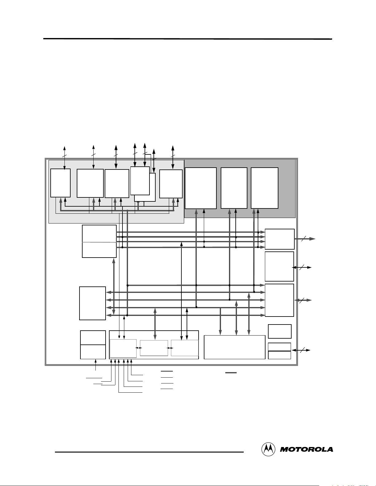
4
8
ESAI
INTER-
FACE
EXPANSION AREA
PIO_EB
6
INTER-
FACE
ESAI_1
PERIPHERAL
24-BIT
DSP56300
Core
PROGRAM
DECODE
CONTROLLE
5
SHI
PROGRAM
ADDRESS
GENERATOR
MEMORY EXPANSION AREA
PROGRAM
RAM
/INSTR.
CACHE
3K x 24
PROGRAM
ROM
40K x 24
Bootstrap
PM_EB
YAB
XAB
PAB
DAB
DDB
YDB
XDB
PDB
GDB
24X24+56->56-BIT MAC
TWO 56-BIT ACCUMULATORS
BARREL SHIFTER
X MEMORY
RAM
13K X 24
ROM
32K x 24
DATA ALU
Y MEMORY
7K X 24
8K x 24
XM_EB
RAM
ROM
YM_EB
EXTERNAL
ADDRESS
SRAM BUS
INTERFACE
I - CACHE
EXTERNAL
DATA BUS
BUS
SWITCH
DRAM &
&
SWITCH
POWER
MNGMNT
JTAG
OnCE™
18
ADDRESS
10
CONTROL
24
DAT A
4
TRIPLE
TIMER
1
2
DAX
(SPDIF Tx.)
INTER-
FACE
ADDRESS
GENERATION
UNIT
SIX CHANNELS
DMA UNIT
INTERNAL
DATA
BUS
PLL
CLOCK
GENERAT
16
HOST
INTER-
FACE
PROGRAM
INTERRUPT
CONTROLLER
EXTAL
RESET
PINIT/NMI
MODA/IRQA
MODB/IRQB
MODC/IRQC
MODD/IRQD
24 BITS BUS
Figure 1 DSP56367 Block Diagram
This document contains information on a new product. Specifications and information herein are subject to change without notice.
Data Sheet
©2001, 2002 MOTOROLA, INC.
For More Information On This Product,
Go to: www.freescale.com

Table of Contents
Freescale Semiconductor, Inc.
TABLE OF CONTENTS
SECTION 1 SIGNAL/CONNECTION DESCRIPTIONS. . . . . . . . . . . . . . . . . . . . 1-1
SECTION 2 SPECIFICATIONS. . . . . . . . . . . . . . . . . . . . . . . . . . . . . . . . . . . . . . 2-1
SECTION 3 PACKAGING . . . . . . . . . . . . . . . . . . . . . . . . . . . . . . . . . . . . . . . . . . 3-1
SECTION 4 DESIGN CONSIDERATIONS . . . . . . . . . . . . . . . . . . . . . . . . . . . . . 4-1
APPENDIX A POWER CONSUMPTION BENCHMARK . . . . . . . . . . .APPENDIX A-1
APPENDIX B IBIS MODEL. . . . . . . . . . . . . . . . . . . . . . . . . . . . . . . . . .APPENDIX B-1
nc...
I
FOR TECHNICAL ASSISTANCE:
Telephone: 1-800-521-6274
Email: dsphelp@dsp.sps.mot.com
Internet: http://www.motorola-dsp.com
Data Sheet Conventions
This data sheet uses the following conventions:
OVERBAR Used to indicate a signal that is active when pulled low (For example, the RESET pin is
cale Semiconductor,
Frees
“asserted” Means that a high true (active high) signal is high or that a low true (active low) signal is
“deasserted” Means that a high true (active high) signal is low or that a low true (active low) signal is
Examples:
Note: Values for VIL, VOL, VIH, and VOH are defined by individual product specifications.
active when low.)
low
high
Signal/Symbol Logic State Signal State Voltage
PIN
PIN False Deasserted VIH/V
PIN True Asserted VIH/V
PIN False Deasserted VIL/V
True Asserted VIL/V
OL
OH
OH
OL
1 DSP56367 Data Sheet MOTOROLA
For More Information On This Product,
Go to: www.freescale.com

Freescale Semiconductor, Inc.
FEATURES
Core features are described fully in the DSP56300 Family Manual.
DSP56300 MODULAR CHASSIS
• 150 Million Instructions Per Second (MIPS) with a 150 MHz clock at internal logic supply
(QVCCL) of 1.8V.
• 100 Million Instructions Per Second (MIPS) with a 100 MHz clock at internal logic supply
(QVCCL) of 1.5V.
• Object Code Compatible with the 56K core.
DSP56367
Features
nc...
I
cale Semiconductor,
Frees
• Data ALU wit h a 24 x 24 bit multiplier -accumulator and a 56-bi t barrel shifter . 16-bit arithmeti c
support.
• Program Control with position independent code support and instruction cache support.
• Six-channel DMA controller.
• PLL based clocking with a wide range of frequency multiplications (1 to 4096), predivider
factors (1 to 16) and power saving clock divider (2
• Internal address tracing support and OnCE for Hardware/Software debugging.
• JTAG port.
• Very l o w-power CMOS design, fully static design with operating frequencies down to DC.
• STOP and WAIT low-power standby modes.
i
: i=0 to 7). Reduces clock noise.
ON-CHIP MEMORY CONFIGURATION
• 7Kx24 Bit Y-Data RAM and 8Kx24 Bit Y-Data ROM.
• 13Kx24 Bit X-Data RAM and 32Kx24 Bit X-Data ROM.
• 40Kx24 Bit Progr am ROM.
• 3Kx24 Bit Program RAM and 192x24 Bit Bootstrap ROM. 1K of Program RAM may be used
as Instruction Cache or for Program ROM patching.
• 2Kx24 Bit from Y Data RAM and 5Kx24 Bit from X Data RAM can be switched to Program
RAM resulting in up to 10Kx24 Bit of Program RAM.
Data Sheet
MOTOROLA DSP56367 2
For More Information On This Product,
Go to: www.freescale.com

DSP56367
Off-chip memory expansion
Freescale Semiconductor, Inc.
OFF-CHIP MEMORY EXPANSION
• External Memory Expansion Port.
• Off-chip expansion up to two 16M x 24-bit word of Data memory.
• Off-chip expansion up to 16M x 24-bit word of Program memory.
• Simultaneous glueless interface to SRAM and DRAM.
PERIPHERAL MODULES
• Ser ial Audio Inter face (ESAI): up to 4 recei vers and up to 6 transmitter s, master or s lave. I2S,
Sony, AC97, network and other programmable protocols.
nc...
I
cale Semiconductor,
• Serial Audio Interface I(ESAI_1): up to 4 receivers and up to 6 transmi tters, master or slave.
2
I
S, Sony, AC97, network and other programmable protocols
The ESAI_1 shares four of the data pins with ESAI, and ESAI_1 does NOT support HCKR
and HCKT (high frequency clocks)
• Ser ial Host Interface (SHI): SPI and I
FIFO, support for 8, 16 and 24-bit words.
• Byte-wide parallel Host Interface (HDI08) with DMA support.
• Triple Timer module (TEC).
• Digital Audio Transmitter (DAX): 1 serial transmitter capable of supporting the SPDIF,
IEC958, CP-340 and AES/EBU digital audio formats.
• Pi n s of unused peripherals (except SHI) may be programmed as GPIO lines.
144-PIN PLASTIC LQFP PACKAGE
Frees
2
C protocols, multi master capability, 10-word receive
Data Sheet
3 DSP56367 MOTOROLA
For More Information On This Product,
Go to: www.freescale.com
Freescale Semiconductor, Inc.
DSP56367
Documentation
DOCUMENTATION
Table 1 lists the documents that provide a complete description of the DSP56367 and are required
to design properly with the part. Documentation is avail able from a local Motorola distributor, a
Motorola semiconductor sales office, a Motorola Literature Distribution Center, or through the
Motorola DSP home page on the Internet (the source for the latest inf ormation).
Table 1 DSP56367 Documentation
Document Name Description Order Number
DSP56300 Family Manual Detailed description of the 56000-family
architecture and the 24-bit core processor
and instruction set
DSP56367 Product Brief Brief description of the chip DSP56367P/D
nc...
I
DSP56367 User’s Manual DSP56367 User’s Manual DSP56367UM/AD
cale Semiconductor,
DSP56300FM/AD
Frees
Data Sheet
MOTOROLA DSP56367 4
For More Information On This Product,
Go to: www.freescale.com

DSP56367
Documentation
nc...
I
Freescale Semiconductor, Inc.
cale Semiconductor,
Frees
Data Sheet
5 DSP56367 MOTOROLA
For More Information On This Product,
Go to: www.freescale.com
Freescale Semiconductor, Inc.
SECTION 1
SIGNAL/CONNECTION DESCRIPTIONS
SIGNAL GROUPINGS
The input and output signals of the DSP56367 are organized into functional groups, which are
listed in Table 1 and illustrated in Figure 1.
The DSP56367 is operated from a 1.8V supply; however, some of the inputs can tolerate 3.3V. A
nc...
I
special notice for this feature is added to the signal descriptions of those inputs.
Remember, the DSP56367 offers 150 million instructions per second (MIPS) using an internal
150 MHz clock at 1.8 V and 100 million instructions per second (MIPS) using an internal 100
MHz clock at 1.3.3V.
cale Semiconductor,
Frees
Table 1 DSP56367 Functional Signal Groupings
Functional Group
Power (V
Ground (GND) 18 Table 3
Clock and PLL 3 Table 4
Address bus
Data bus 24 Table 6
Bus control 10 Table 7
Interrupt and mode control 5 Table 8
HDI08
SHI 5 Table 10
ESAI
ESAI_1
Digital audio transmitter (DAX)
) 20 Table 2
CC
1
Port A
2
Port B
3
Port C
5
Port E
4
Port D
Number of
Signals
18 Table 5
16 Table 9
12 Table 11
6 Table 12
2 Table 13
Detailed
Description
Timer 1 Table 14
JTAG/OnCE Port 4 Table 15
MOTOROLA DSP56367 Data Sheet 1-1
For More Information On This Product,
Go to: www.freescale.com

Freescale Semiconductor, Inc.
Signal/Connection Descriptions
Signal Groupings
Table 1 DSP56367 Functional Signal Groupings (Continued)
Functional Group
Note: 1. Port A is the external memory interface port, including the external address bus, data bus, and
control signals.
2. Port B signals are the GPIO port signals which are multiplexed with the HDI08 signals.
3. Port C signals are the GPIO port signals which are multiplexed with the ESAI signals.
4. Port D signals are the GPIO port signals which are multiplexed with the DAX signals.
5. Port E signals are the GPIO port signals which are multiplexed with the ESAI_1 signals.
nc...
I
Number of
Signals
cale Semiconductor,
Detailed
Description
Frees
1-2 DSP56367 Data Sheet MOTOROLA
For More Information On This Product,
Go to: www.freescale.com
Freescale Semiconductor, Inc.
Signal/Connection Descriptions
Signal Groupings
nc...
I
cale Semiconductor,
Frees
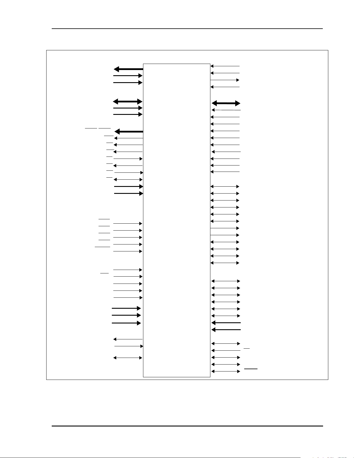
PORT A ADDRESS BUS
A0-A17
VCCA (3)
GNDA (4)
PORT A DATA BUS
D0-D23
VCCD (4)
GNDD (4)
PORT A BUS CONTROL
AA0-AA2/RAS0-RAS2
CAS
RD
WR
TA
BR
BG
BB
VCCC (2)
GNDC (2)
INTERRUPT AND
MODE CONTROL
MODA/IRQA
MODB/IRQB
MODC/IRQC
MODD/IRQD
RESET
PLL AND CLOCK
EXTAL
PINIT/NMI
PCAP
VCCP
GNDP
QUIET POWER
VCCQH (3)
VCCQL (4)
GNDQ (4)
SPDIF TRANSMITTER (DAX)
ADO [PD1]
ACI [PD0]
TIMER 0
TIO0 [TIO0]
DSP56367
Port D
Port B
Port C
Port E
OnCE ON-CHIP EMULATION/
TDI
TCK
TDO
TMS
JTAG PORT
PARALLEL HOST PORT (HDI08)
HAD(7:0) [PB0-PB7]
HAS/HA0 [PB8]
HA8/HA1 [PB9]
HA9/HA2 [PB10]
HRW/HRD [PB11]
HDS/HWR [PB12]
HCS/HA10 [PB13]
HOREQ/HTRQ [PB14]
HACK/HRRQ [PB15]
VCCH
GNDH
SERIAL AUDIO INTERFACE (ESAI)
SCKT[PC3]
FST [PC4]
HCKT [PC5]
SCKR [PC0]
FSR [PC1]
HCKR [PC2]
SDO0[PC11] / SDO0_1[PE11]
SDO1[PC10] / SDO1_1[PE10]
SDO2/SDI3[PC9] / SDO2_1/SDI3_1[PE9]
SDO3/SDI2[PC8] / SDO3_1/SDI2_1[PE8]
SDO4/SDI1 [PC7]
SDO5/SDI0 [PC6]
SERIAL AUDIO INTERFACE(ESAI_1)
SCKT_1[PE3]
FS
T_1[PE4]
SCKR_1[PE0]
FSR_1[PE1]
SDO4_1/SDI1_1[PE7]
SDO5_1/SDI0_1[PE6]
VCCS (2)
GNDS (2)
SERIAL HOST INTERFACE (SHI)
MOSI/HA0
/HA2
SS
MISO/SDA
SCK/SCL
HREQ
Figure 1 Signals Identified by Functional Group
MOTOROLA DSP56367 Data Sheet 1-3
For More Information On This Product,
Go to: www.freescale.com
Freescale Semiconductor, Inc.
Signal/Connection Descriptions
Power
POWER
Table 2 Power Inputs
Power Name Description
nc...
I
cale Semiconductor,
Frees
V
CCP
V
(4) Quiet Core (Low) Power— V
CCQL
V
(3) Quiet External (High) Power—V
CCQH
(3) Address Bus Power—V
V
CCA
V
(4) Data Bus Power—V
CCD
V
(2) Bus Control Power—V
CCC
V
CCH
V
(2) SHI, ESAI, ESAI_1, DAX and Timer Power —V
CCS
PLL Power—V
provided with an extr emely low impedance path to the V
externally to all other V
must provide adequate external decoupling capa ci tors. There are four V
other chip power inputs.The user must provide a dequate decoupling capacitors. There are three V
externally to all ot her chip power inputs. The user must provi de adequate external dec oupling capacitors. There are
three V
CCA
externally to all ot her chip power inputs. The user must provi de adequate external dec oupling capacitors. There are
four V
all other chip power inputs. The user must provide a d equate external decou pl ing capacitors. There are two V
inputs.
Host Power—V
chip power inputs . The user must provide adequate external decoupling capacitors. There is one V
Timer. This inpu t must be tied external ly to all other chip power inputs. The user mu s t provide adequate ext ernal
decoupling capa citors. There are tw o V
CCD
inputs.
is VCC dedicated for PLL use. The volt age should be well-regulate d and the input should be
CCP
is an isolated power for the int ernal processing logic. This input must be tied
CCQL
power pins and the V
inputs.
CCQL
is a quiet power source for I/O lines. This input must be tied externally to all
CCQH
is an isolated power for sections of the address bus I/O drivers. This input must be tied
CCA
is an isolated power for sections of the data bus I/O drivers. This input must be tied
CCD
is an isolated power for the bus control I/O drivers. This input must be tied externally to
CCC
is an isolated pow er for the HDI08 I/O drivers. This input must be tied externally to all other
CCH
CCS
CCP
inputs.
GROUND
Table 3 Grounds
Ground Name Description
power rail. There is one V
CC
power pin only. Do not tie with other power pins. The user
inputs.
CCQL
is an isolated power for the SHI, ESAI, ESAI_1, DAX and
CCS
CCP
input.
CCQH
CCH
inputs.
input.
CCC
GND
P
(4) Quiet Ground—GNDQ is an isolated ground for t h e i nternal processing logic. This connection must be ti ed
GND
Q
1-4 DSP56367 Data Sheet MOTOROLA
PLL Ground—GNDP is a ground dedicated for PLL us e. The connection should be provided with an extreme ly
low-impedance path to ground. V
possible to the chi p package. There is one GND
externally to all other chip ground connections. The user must provi de adequate external decoupling capacitors.
There are four GN D
connections.
Q
should be bypassed to GNDP by a 0.47 µF capacitor located as close as
CCP
connection.
P
For More Information On This Product,
Go to: www.freescale.com
Freescale Semiconductor, Inc.
Signal/Connection Descriptions
Clock and PLL
Table 3 Grounds
Ground Name Description
GNDA (4) Address Bus Ground—GNDA is an isolated ground for sections of the address bus I/O drivers. This conne ction
must be tied externally to all other chip ground connections. The user must provide adequate external decoupling
capacitors. There are four GND
GND
(4) Data Bus Ground—GNDD is an isolated ground for sections of the data bus I/O drivers. This connection must be
D
GND
(2) Bus Control Ground—GNDC is an isolated ground for the bus control I/O drivers. This co nne ction must be tied
C
tied externally to all other chip ground connections. The user must provide adequate external decoupling capaci tors.
There are four GN D
externally to all other chip ground connections. The user must provi de adequate external de coupling capacitors.
There are two G N D
connections.
D
connections.
C
connections.
A
nc...
I
cale Semiconductor,
Frees
GND
H
GND
(2) SHI, ESAI, ESAI_1, DAX and Timer Ground—GNDS is an isolated ground for the SHI, ESAI, ESAI_ 1, DAX
S
Host Ground—GNDh is an isolated ground for the HD08 I/O drivers. This connection must be tied externally to all
other chip ground connec ti ons. The user must provide adequa t e external decoupling capa ci tors. There is one GND
connection.
and Timer. This connection must be tied externall y to all other chip ground connec ti ons. The user must provide
adequate ext ernal decoupling ca p acitors. There are two GND
CLOCK AND PLL
Signal Name Type
EXTAL Input Input External Clock Input—An external clock source must be connected to EXTAL in
PCAP Input Input PLL Capacitor—PCAP is a n input connecting an off-ch ip c apacitor to the PLL filter.
PINIT/NMI
Input Input PLL Initial/Nonmaskable Interrupt—During a ssert ion of RESET, the valu e of
State
during
Reset
connections.
S
Table 4 Clock and PLL Signals
Signal Description
order to supply the cloc k to the internal clock generator and PLL.
Connect one capacitor t erm i nal to PCAP and the other termina l t o V
If the PLL is not use d, PCAP may be tied to V
PINIT/NMI
determining whethe r the PLL is enabled or disabled. A fte r RESET
during normal instruction processing, the PINIT/NMI
negative-edge-tri ggered nonmaskable interru pt (N MI) re quest internally synchroni ze d
to internal system clock.
is written into the PLL Enable (PEN) bit of the PLL control register,
, GND, or left floating.
CC
Schmitt-trigger input is a
.
CCP
de assertion and
H
EXTERNAL MEMORY EXPANSION PORT (PORT A)
When the DSP56367 enters a low-power standby mode (stop or wait), it releases bus mastership
and tri-states the relevant port A signals: A0–A17, D0–D23, AA0/RAS0–AA2/RAS2, RD, WR,
BB, CAS.
MOTOROLA DSP56367 Data Sheet 1-5
For More Information On This Product,
Go to: www.freescale.com
Signal/Connection Descriptions
External Address Bus
EXTERNAL ADDRESS BUS
Signal Name Type
A0–A17 Output Tri-stated Address Bus—When the DSP is the bus master, A0–A17 are active-high outputs that
EXTERNAL DATA BUS
nc...
I
Freescale Semiconductor, Inc.
Table 5 External Address Bus Signals
State
during
Reset
specify the addre s s for external program and d at a m emory accesses. Otherwise, the
signals are tri-stated. To mini mi ze power dissipation, A0–A17 do not change sta te
when external memo ry spaces are not being accessed.
Signal Description
Table 6 External Data Bus Signals
Signal Name Type State during Reset Signal Description
D0–D23 Input/Output Tri-stated Data Bus—When the DSP is the bus master, D0–D23 are
EXTERNAL BUS CONTROL
Signal
cale Semiconductor,
Name
AA0–AA2/
–RAS
RAS0
2
Type
Output Tri-stated Address Attribute or Row Address Strobe—When defined as AA, these signals can be
Frees
CAS
Output Tri-stated Column Address Strobe— When the DSP is the bus master, CAS is an active-low output
State
during
Reset
active-high, bidirectional input/outputs that provide the bidirectional
data bus for external program and data memory acc esse s. Oth er w ise ,
D0–D23 are tri-s tated.
Table 7 External Bus Control Sign als
Signal Description
used as chip sele ct s o r additional address lines. When defined as RA S
be used as RAS
programmable polarity.
used by DRAM to strobe the column addre ss. Otherwi se, if th e bus m aste rship enable
(BME) bit in the DRAM control register is cleared, the signal is tri-stated.
for DRAM interface. These sign al s are tri -sta ta bl e ou tputs with
, these signals can
RD
WR
1-6 DSP56367 Data Sheet MOTOROLA
Output Tri-stated Read Enable—When the DSP is the bus master, RD is an active-low output that is
asserted to read external me mory on the data bus (D0-D23). Otherwise, R D
Output Tri-stated Write Enable —When the DSP is the bus master, WR is an active-low output that is
asserted to write external memory on the data bus (D0-D23). Otherwise, WR
is tri-stated.
is tri-stated.
For More Information On This Product,
Go to: www.freescale.com
Freescale Semiconductor, Inc.
Signal/Connection Descriptions
Table 7 External Bus Control Signals (Continued)
External Bus Control
nc...
I
cale Semiconductor,
Frees
Signal
Name
TA Input Ig nore d
BR
BG
BB
Type
Output Output
Input Ignored
Input/
Output
State
during
Reset
Input
(deasserted)
Input
Input Bus Busy—BB is a bidirectional active-low input/output. BB indicates that the bus is
Signal Description
Transfer Acknowledge—If the DSP is the bus master and there is no external bus
activity, or the DSP is not the bus master, the TA
transfer acknowledge (DT A CK) function that can extend an e xternal bus cycle
indefinitely. Any number of wait states (1, 2. . .in finity) may be added to the wait stat e s
inserted by the BCR by keeping TA
the start of a bus cycle, is asserted to enable completion of the bus cycle, and is deasserted
before the next bus cycle. The current bus cycle completes one clock period after TA
asserted synchronous to the i nternal system clock. The nu mber of wait states is
determined by the TA
BCR can be used to set the minimum number of wait states in ext ernal bus cycles.
In order to use the TA
state. A zero wait st ate access cannot be ex tended by TA
operation may result. TA
setting of the TAS bit in the operati ng mode register (OMR).
TA
functionality may not be used whi le performing DRAM type accesses, othe rwi s e
improper operation m ay resul t.
Bus Request—BR is an active-low output, never tri-stated. BR is asserted when the DSP
requests bus mastership. BR
be asserted or deasserted independent of whether the DSP56367 is a bus master or a bus
slave. Bus “parking” allows BR
master. (See the descript ion of bus “parking” in the BB
request hold (BRH) bit in the BCR allows BR
though the DSP does not need the bus. BR
that controls the priority, parking, and tenure of each master on the same external bus. BR
is only affected by DSP requests for the external bus, neve r for t he i nternal bus. During
hardware reset, BR
Bus Grant—BG is an active-low input. BG is as s erted by an external bu s arbitration
circuit when the DSP56367 becomes the next bus master. When BG
DSP56367 must wait until BB
deasserted, bus mastership is typically given up at the end of t he current bus cycle. This
may occur in the middle of an instruction that requires more than one external bus cycle
for execution.
For proper BG
register must be set.
active. Only after BB
(and then assert the signal again). The bus master may keep BB
activity regardless of whether BR
and allows the current bus m ast er to reuse the bus without rearbitration until another
device requires the bus. The deassertion of BB
is driven high and then released and held high by an external pull-up resistor).
BB
input or by the bus control register (BCR), whichever is longer. The
functionality, the BCR must be programmed to at le ast one wait
can operate synchronously or asynchronously, depending on the
is deasserted and the arbitration is reset to the bus slave stat e.
operation, the async hronous bus arbitration enabl e bi t (ABE) in the OMR
is deasserted can the pendi ng bus master become the bus mast er
deasserted. In typi ca l operation, TA is deasserted at
is deasserted when the DSP no longer needs the bus. BR may
to be deasserted even though the D SP563 67 is the bus
is deasserted before taking bus mast ership. When BG is
is asserted or deasserted. This is called “bus parking”
input is ignored. Th e TA input is a data
is
deassertion, otherwise improper
signal description.) The bus
to be asserted under softw are control even
is typically sent to an ext ernal bus arbitrator
is asserted, th e
asserted af ter ceasing b u s
is done by an “active pull-up” method (i.e.,
For proper BB
register must be set.
requires an external pull-up resistor.
BB
MOTOROLA DSP56367 Data Sheet 1-7
operation, the async hronous bus arbitration enable bit (ABE) in the OMR
For More Information On This Product,
Go to: www.freescale.com
Freescale Semiconductor, Inc.
Signal/Connection Descriptions
Interrupt and Mode Control
INTERRUPT AND MODE CONTROL
The interrupt and mode control signals select the chip’s operating mode as it comes out of
hardware reset. After RESET is deasserted, these inputs are hardware interrupt request lines.
Table 8 Interrupt and Mode Control
State
Signal Name Type
during
Reset
Signal Description
nc...
I
cale Semiconductor,
Frees
MODA/IRQA
MODB/IRQB
MODC/IRQC
MODD/IRQD
RESET
Input Input Mode Select A/External Interrupt Request A—MODA/IRQA is an active-low
Schmitt-trigger input, internally synchronized to the DSP clock. MODA/IRQA
initial chip operating mod e du ring hardware reset and becomes a le ve l-se nsitive or
negative-edge-triggered, maskable interrupt request input during normal instruction
processing. MODA, MODB, MODC, and MODD select one of 16 initial chip operating
modes, latched int o the OMR when the RESET
stop standby state and the MODA/IRQA
stop state.
This input is 3.3V tolerant.
Input Input Mode Select B/External Interrupt Request B—MODB/IRQB is an active-low
Input Input Mode Select C/External Interrupt Request C—MODC/IRQC is an active-low
Input Input Mode Select D/External Interrupt Request D—MODD/IRQD is an active-low
Input Input Reset—RESET is an active-lo w , Schmitt-trigger input. Wh en asserted, the chip is placed in
Schmitt-trigger input, internally synchronized to the DSP clock. MODB/IRQB
initial chip operating mod e du ring hardware reset and becomes a le ve l-se nsitive or
negative-edge-triggered, maskable interrupt request input during normal instruction
processing. MODA, MODB, MODC, and MODD select one of 16 initial chip operating
modes, latche d into OMR when the RESET
This input is 3.3V tole r an t.
Schmitt-trigger input, internally synchronized to the DSP clock. MODC/IRQC
initial chip operating mod e du ring hardware reset and becomes a le ve l-se nsitive or
negative-edge-triggered, maskable interrupt request input during normal instruction
processing. MODA, MODB, MODC, and MODD select one of 16 initial chip operating
modes, latche d into OMR when the RESET
This input is 3.3V tole r an t.
Schmitt-trigger input, internally synchronized to the DSP clock. MODD/IRQD
initial chip operating mod e du ring hardware reset and becomes a le ve l-se nsitive or
negative-edge-triggered, maskable interrupt request input during normal instruction
processing. MODA, MODB, MODC, and MODD select one of 16 initial chip operating
modes, latche d into OMR when the RESET
This input is 3.3V tole r an t.
the Reset stat e and the internal phase generator is reset. T h e Sc hmitt-trigger inpu t al lows a
slowly rising input (such as a capac itor charging) to reset the chip reliabl y. Wh en the
signal is deasserted, the initial chip operating mode is latched from the MODA,
RESET
MODB, MODC, and MODD inputs. The RESET
A stable EXTAL signal must be supplied while RESET
This input is 3.3V tolerant.
signal is deasserted. If the processor is in the
pin is pulled to GND, the processor will exit the
signal is deasserted.
signal is deasserted.
signal is deasserted.
signal must be asserted during power up.
is being asserted.
selects the
selects the
selects the
selects the
1-8 DSP56367 Data Sheet MOTOROLA
For More Information On This Product,
Go to: www.freescale.com

Freescale Semiconductor, Inc.
Signal/Connection Descriptions
Parallel Host Interface (HDI08)
PARALLEL HOST INTERFACE (HDI08)
The HDI08 provides a fast, 8-bit, parallel data port that may be connected directly to the host bus.
The HDI08 supports a variety of standard buses and can be directly connected to a number of
industry standard microcomputers, microprocessors, DSPs, and DMA hardware.
nc...
I
cale Semiconductor,
Frees
MOTOROLA DSP56367 Data Sheet 1-9
For More Information On This Product,
Go to: www.freescale.com

Freescale Semiconductor, Inc.
Signal/Connection Descriptions
Parallel Host Interface (HDI08)
Table 9 Host Interface
nc...
I
cale Semiconductor,
Frees
Signal Name Type
H0–H7 Input/
HAD0–HAD7 Input/
PB0–PB7 Input, output, or
HA0 Input GPIO
HAS Input Host Address Strobe—When HDI08 is programmed to inte rface a
HAS/
PB8 Input, output, or
HA1 Input GPIO
HA8 Input Host Address 8—When HDI08 is programmed to int erf ace a multiplexed
PB9 Input, output, or
output
output
disconnected
disconnected
disconnected
State during
Reset
GPIO
disconnected
disconnected
disconnected
Host Data—When HDI08 is programmed to interface a nonmultiplexed
host bus and the HI function is sele cted, these signals are lines 0–7 of the
bidirectional, tri-state data bus.
Host Address/Data—When HDI08 is programmed to interface a
multiplexed host bus and the HI function is selected, these signals are lines
0–7 of the address/data bidirectional, multiplex ed , tr i-state bus.
Port B 0–7—When the HDI08 is c onfi gu red as GPIO, these signals are
individually programmable as input, output, or int er n a ll y disconnected.
The default state after reset for the s e si gna ls is GPIO di sconnected.
These inputs are 3.3V tolerant.
Host Address Input 0—When the HDI08 is programm e d to interface a
nonmultiplexed host bus and the HI function is selected, this signal is line 0
of the host address input bus.
multiplexed ho s t bus and the HI function is s el ected, this signal is the host
address strobe (HAS) Schmitt -trigger input. The pola rit y of the address
strobe is programmable, but is co nfi gure d active-low (HAS
reset.
Port B 8—When the HDI08 is con figured as GPIO, this signal is
individually programmed as input, output, or internally disconnected.
The default state after reset for this signal is GPIO disconnected.
This input is 3.3V toleran t.
Host Address Input 1—When the HDI08 is programm e d to interface a
nonmultiplexed host bus and the HI function is selected, this signal is line 1
of the host address (HA1) input bus.
host bus and the HI function is selected, this signal is line 8 of the host
address (HA8) input bus.
Port B 9—When the HDI08 is con figured as GPIO, this signal is
individually programmed as input, output, or internally disconnected.
Signal Description
) following
The default state after reset for this signal is GPIO disconnected.
This input is 3.3V toleran t.
1-10 DSP56367 Data Sheet MOTOROLA
For More Information On This Product,
Go to: www.freescale.com
Freescale Semiconductor, Inc.
Signal/Connection Descriptions
Parallel Host Interface (HDI08)
Table 9 Host Interface (Continued)
nc...
I
cale Semiconductor,
Frees
Signal Name Type
HA2 Input GPIO
HA9 Input Host Address 9—When HDI08 is programmed to int erf ace a multiplexed
PB10 Input, Output, or
HRW Input GPIO
/
HRD
HRD
PB11 Input, Output, or
HDS
/
HDS
/
HWR
HWR
Disconnecte d
Input Host Read Data—When HDI08 is programmed to int e rfa ce a
Disconnecte d
Input GPIO
Input Host Write Data—When HDI08 is programm ed to interface a
State during
Reset
disconnected
disconnected
disconnected
Host Address Input 2—When the HDI08 is program m ed to interface a
non-multiplexed host bus and the HI function is selected, this signa l is li ne
2 of the host address (HA2) input bus.
host bus and the HI function is selected, this signal is line 9 of the host
address (HA9) input bus.
Port B 10—When th e HDI08 is configured as GPIO, this signal is
individually programmed as input, output, or internally disconnected.
The default state after reset for this signal is GPIO disconnected.
This input is 3.3V toleran t.
Host Read/Write—When HDI08 is program med to interface a
single-data-strobe host bus and the HI function is selected, this signal is the
Host Read/Wri te
double-data-strobe host bus and the HI function is selected, this signal is
the host read data strobe (HRD) Schmitt-trigger input. The pol arity of the
data strobe is programm a ble, but is configured as active -l ow (HRD
reset.
Port B 11—When th e HDI08 is configured as GPIO, this signal is
individually programmed as input, output, or internally disconnected.
The default state after reset for this signal is GPIO disconnected.
This input is 3.3V toleran t.
Host Data Strobe—When HDI0 8 is programmed to inter face a
single-data-strobe host bus and the HI function is selected, this signal is the
host data strobe (HDS ) Schm itt-trigger input. The polarity of the data
strobe is programmable, but is co nfi gure d as active-low (HDS
reset.
double-data-strobe host bus and the HI function is selected, this signal is
the host write data strobe (HWR) Schmitt-trigger input. The polarity of the
data strobe is programm a ble, but is configured as active -l ow (HWR
following reset.
(HRW) input.
Signal Description
) following
) after
)
PB12 Input, output, or
MOTOROLA DSP56367 Data Sheet 1-11
disconnected
Port B 12—When th e HDI0 8 is configured as GPIO, this signal is
individually programmed as input, output, or internally disconnected.
The default state after reset for this signal is GPIO disconnected.
This input is 3.3V toleran t.
For More Information On This Product,
Go to: www.freescale.com
Freescale Semiconductor, Inc.
Signal/Connection Descriptions
Parallel Host Interface (HDI08)
Table 9 Host Interface (Continued)
nc...
I
cale Semiconductor,
Frees
Signal Name Type
HCS Input GPIO
HA10 Input Host Address 10—When HDI08 is programmed to interface a multiplexed
PB13 Input, output, or
/HOREQ Output GPIO
HOREQ
/
HTRQ
HTRQ
PB14 Input, output, or
HACK
/
HACK
/
HRRQ
HRRQ
disconnected
Output Transmit Host Request—When HDI08 is programmed to interface a
disconnected
Input GPIO
Output Receive Host Request—When HDI08 is programmed to int er fac e a
State during
Reset
disconnected
disconnected
disconnected
Host Chip Select—When HDI08 is programmed to interface a
nonmultiplexed host bus and the H I function is select ed, this signal is the
host chip select (HCS) input. The po larity of the chip sel ect is
programmable, but is configured active-lo w (HCS
host bus and the HI function is selected, this signal is line 10 of the host
address (HA10) input bus.
Port B 13—When th e HDI0 8 is configured as GPIO, this signal is
individually programmed as input, output, or internally disconnected.
The default state after reset for this signal is GPIO disconnected.
This input is 3.3V toleran t.
Host Request—When HDI08 is programmed t o int er fac e a single host
request host bus and the HI function is sele cted, this signal is the host
request (HOREQ) outpu t. The pol arity of the host request is
programmable, but is configured as active-lo w (HORE Q
The host request may be programmed as a driven or open-drain output.
double host request host bus a nd the HI function is selected, this signal is
the transmit host request (HTRQ) output. The polarity of the host request is
programmable, but is configured as active-low (HTRQ
The host request may be programmed as a driven or open-drain output.
Port B 14—When th e HDI0 8 is configured as GPIO, this signal is
individually programmed as input, output, or internally disconnected.
The default state after reset for this signal is GPIO disconnected.
This input is 3.3V toleran t.
Host Acknowledge—When HDI08 is programmed to interface a singl e
host request host bus and th e HI function is selected, this sign al is the host
acknowledge (HACK) Schmitt-trigger input. The polarity of the host
acknowledge is programmable, but is configured as active-low (HACK
after reset.
double host request host bus and the HI function is selected, this signal is
the receive host reques t (HRRQ) output. The polarity of the host request is
programmable, but is configured as active-low (HRRQ
host request may be program m ed a s a dri ven or open-drain output.
Signal Description
) after reset.
) following reset.
) following reset.
) after reset. Th e
)
PB15 Input, output, or
1-12 DSP56367 Data Sheet MOTOROLA
disconnected
Port B 15—When th e HDI08 is configured as GPIO, this signal is
individually programmed as input, output, or internally disconnected.
The default state after reset for this signal is GPIO disconnected.
This input is 3.3V toleran t.
For More Information On This Product,
Go to: www.freescale.com
Freescale Semiconductor, Inc.
Signal/Connection Descriptions
Serial Host Interface
SERIAL HOST INTERFACE
The SHI has five I/O signals that can be configured to allow the SHI to operate in either SPI or
I2C mode.
Table 10 Serial Host Interface Signals
nc...
I
cale Semiconductor,
Frees
Signal
Name
SCK Input or
SCL Input or
MISO Input or
SDA Input or
Signal Type
output
output
output
open-drain
output
State
during
Reset
Tri-stated SPI Serial Clock—The SCK signal is an output when the SPI is configured as a master and
Tri-stated SPI Master-In-Slave-Out—When the SPI is confi gured as a master, MISO is the master
a Schmitt-trigger input when the SPI is configured as a slave. When the SPI is configured as
a master, the SCK signal is deriv ed fr om the internal SHI clock generator. When the SPI is
configured as a slave, the SCK signal is an input, and the clock signal from the external
master synchronizes the data transfer. The SCK signal is ignored by the SPI if it is defined as
a slave and the slave select (SS
devices, data is shifted on on e edge of the SCK signal and is sample d on t he opposite edge
where data is stable. Edge polarity is determined by the SP I tra n s fer protocol.
2
C Serial Clock—SCL carries the clock for I2C bus transactions in the I2C mode. SCL is a
I
Schmitt-trigger input when configured as a slave and an open-drain output when configured
as a master. SCL should be connec ted to V
This signal is tri-state d during hardware, software, and indi vi dual reset. Thus, there is no
need for an external pull-up in this state.
This input is 3.3V tolerant.
data input line. The MISO signal is used in conjunction with the MOSI signal for
transmitting and receiving serial data. This signal is a Schmitt-trigger input when configured
for the SPI Master mode, an output when configured for the SPI Slave mode, and tri-stated if
configured for the SPI S lave mode when S S
required for SPI operation.
2
I
C Data and Acknowledge—In I2C mode, SDA is a Schmitt-trigger input when receiving
and an open-drain output when transmitting. SDA shoul d be connected to V
pull-up resistor. SDA carries the data for I
during the high period of SCL. The data in SDA is only allowed to change when SCL is low.
When the bus is free, SDA is high. The SDA line is only allowed to change during the time
SCL is high in the case of start and stop events. A high-to-low transition of the SDA line
while SCL is high is a unique situation, and is defined as the start event. A low-to -high
transition of SDA while SCL is high is a unique situation defined as the stop event.
This signal is tri-state d during hardware, software, and indi vi dual reset. Thus, there is no
need for an external pull-up in this state.
Signal Description
) signal is not asse rted. In both the master and slave SPI
through a pull-up resistor.
CC
is deasserted. An external pull-up resistor is not
through a
2
C transactions. The data in SDA must be stable
CC
This input is 3.3V tolerant.
MOTOROLA DSP56367 Data Sheet 1-13
For More Information On This Product,
Go to: www.freescale.com
Freescale Semiconductor, Inc.
Signal/Connection Descriptions
Serial Host Interface
Table 10 Serial Host Interface Signals (Continued)
nc...
I
cale Semiconductor,
Frees
Signal
Name
MOSI Input or
HA0 Input
SS
HA2 Input
HREQ
Signal Type
output
Input Tri-stated SPI Slave Select—This signal is an active low Schmitt-trigger input when configured for
Input or
Output
State
during
Reset
Tri-stated SPI Master-Out-Slave-In— When the SPI is configured as a master, MOSI is the master
data output line. The MOSI si gnal is used in conjunction with the MISO signal for
transmitting and receiving serial data. MOSI is the slave data input line when the SPI is
configured as a slave . Th i s signa l i s a Schmi tt -trigger input when configur ed for the SPI
Slave mode.
2
C Slave Address 0—This signal uses a Schmitt-trigger input when configured for the I2C
I
mode. When configured for I
address. HA0 is ignored when co nfi gured for the I
This signal is tri-state d during hardware, software, and indi vi dual reset. Thus, there is no
need for an external pull-up in this state.
This input is 3.3V tolerant.
the SPI mode. When configured for the SPI Slave mode, this signal is used to enable the SPI
slave for transfer. When co nfi gured for the SPI master mode, this signal should be kept
deasserted (pulled high). If it is asserted while configured as SPI master, a bus error
condition is flagged. If SS
output signal in the high-impedance state.
2
I
C Slave Address 2—This signal uses a Schmitt-trigger input when configured for the I2C
mode. When configured for the I
device address. HA2 is ignored in the I
This signal is tri-state d during hardware, software, and indi vi dua l reset. Thus, there is no
need for an external pull-up in this state.
This input is 3.3V tolerant.
Tri-stated Host Request—This signal is an active low Schmi tt -tri gger input when configured for the
master mode but an ac ti ve low output when configured for the slave mode.
When configured for the slave mode, HREQ
the next data word tran sf er and deasserted at the first clock pulse of the new data word
transfer. When confi gured for the master mode, HREQ
external slave device, it will trigge r the start of the data wor d transfer by the master. After
finishing the data word transfer, the master will await the next assertion of HREQ
to the next trans fer.
This signal is tri-stated dur ing hardware, software, personal reset , or when t he
HREQ1–HREQ0 bit s in the HCSR are cleared. The re is no need for external pu ll -up in this
state.
is deasserted, the SHI ignores SCK clocks and keeps the MISO
Signal Description
2
C slave mode, the HA0 signal is used to form the slave device
2
C Slave mode, the HA2 signal is used t o form the slave
2
C master mode.
2
C master mode.
is asserted to indicate tha t the SHI is ready for
is an input. When asserted by the
to proceed
This input is 3.3V tolerant.
1-14 DSP56367 Data Sheet MOTOROLA
For More Information On This Product,
Go to: www.freescale.com

Freescale Semiconductor, Inc.
ENHANCED SERIAL AUDIO INTERFACE
Table 11 Enhanced Serial Audio Interface Signals
Signal/Connection Descriptions
Enhanced Serial Audio Interface
nc...
I
cale Semiconductor,
Frees
Signal
Name
HCKR Input or output GPIO disconnected High Frequency Clock for Receiver—When programmed as an input, this
PC2 Input, output, or
HCKT Input or output GPIO disconnected High Frequency Clock for Transmitter—When programmed as an input,
PC5 Input, output, or
FSR Inp ut or output GPIO disconnected Frame Sync for Receiver—Thi s is the receiver frame sync input /output
PC1 Input, output, or
FST Input or output GPIO disconnected Frame Sync for Transmitter—This is the transmitter frame sync input/output
Signal Type State during Reset Signal Description
signal provides a high frequency clock source for the ESAI receiver as an
alternate to the DSP core clock. When programmed as an output, this signal
can serve as a high-freque nc y sam p l e c loc k (e .g., for external digital to anal og
converters [DACs]) or as an additional system clock.
Port C 2—When the ESAI is configured as GPIO, thi s signa l is i ndividually
disconnected
disconnected
disconnected
programmable as input, output, or internally disconnected.
The default stat e after reset is GPIO dis connected.
This input is 3.3V tolerant.
this signal provides a high frequency clock source for the ESAI t ransmitter as
an alternate to the DSP core clock. When programmed as an output, this signal
can serve as a high frequen cy sample clock (e.g., for exte rna l DACs) or as an
additional system clock.
Port C 5—When the ESAI is configured as GPIO, thi s signa l is i ndividually
programmable as input, output, or internally disconnected.
The default stat e after reset is GPIO dis connected.
This input is 3.3V tolerant.
signal. In the asynchronous mode (SYN=0), the FSR pin operates as the frame
sync input or output used by all the enabled receivers. In the synchronous mode
(SYN=1), it operates as ei the r the serial flag 1 pin (TEBE=0 ), or as the
transmitter external buffer enable control (TEBE=1, RFSD=1).
When this pin is configured as serial flag pin, its direction is determined by the
RFSD bit in the RCCR register. When configured as the output flag OF1, this
pin will reflect the val ue of the OF1 bit in the SAICR register, a nd t h e da t a in
the OF1 bit will show up at the pin synchronized to the frame sync in normal
mode or the slot in network mode. When configured a s the input flag IF1, the
data value at the pin will be store d in the IF1 bit in the SAISR register,
synchronized by the fram e sync in normal mode or the slot in netw ork mode.
Port C 1—When the ESAI is configured as GPIO, thi s signa l is i ndividually
programmable as input, output, or internally disconnected.
The default stat e after reset is GPIO dis connected.
This input is 3.3V tolerant.
signal. For synchronous mode, thi s signal is the frame sync for both
transmitters and receivers. For asynchronous mode, FST is the frame sync for
the transmitter s o nly. The dir ecti on is dete r mined b y t he t ran smit ter frame sy nc
direction (TFSD) bit in the ESAI transmit clock control register (TCCR).
PC4 Input, output, or
disconnected
MOTOROLA DSP56367 Data Sheet 1-15
For More Information On This Product,
Go to: www.freescale.com
Port C 4—When the ESAI is configured as GPIO, thi s signa l is i ndividually
programmable as input, output, or internally disconnected.
The default stat e after reset is GPIO dis connected.
This input is 3.3V tolerant.

Freescale Semiconductor, Inc.
Signal/Connection Descriptions
Enhanced Serial Audio Interface
Table 11 Enhanced Serial Audio Interface Signals (Continued)
nc...
I
cale Semiconductor,
Frees
Signal
Name
SCKR Input or output GPIO disconnected Receiver Serial Clock—SCKR provides the receiver serial bit clock for the
PC0 Input, output, or
SCKT Input or output GPIO disconnected Transmitter Serial Clock—This signal provides the serial bit rate clock for
PC3 In put , output, or
SDO5 Output GPIO disconnected Serial Data Output 5— W he n programmed as a transmitter, SD O5 is use d to
SDI0 Input Serial Data Input 0—When programme d as a rec ei ve r, SDI0 is used to
PC6 Input, output, or
SDO4 Output GPIO disconnected Serial Data Output 4— W he n programmed as a transmitter, SD O4 is use d to
SDI1 Input Serial Data Input 1—When programme d as a rec ei ve r, SDI1 is used to
PC7 Input, output, or
Signal Type State during Reset Signal Description
ESAI. The SCKR operates as a clock input or output used by al l the enabled
receivers in the asynchronous mode (SYN=0), or as serial flag 0 pin in the
synchronous mode (SYN=1).
When this pin is configured as serial flag pin, its direction is determined by the
RCKD bit in the RCCR register. When configured as the output flag OF0, this
pin will refle ct the value of the OF0 bit in th e S A IC R r egister, and the da ta in
the OF0 bit will show up at the pin synchronized to the frame sync in normal
mode or the slot in network mode. When configured as the inp u t fl ag IF0, the
data value at the pi n wil l be store d in the IF0 bit in the SAISR register,
synchronized by the frame sync in normal mode or the slot in network mode.
disconnected
disconnected
disconnected
disconnected
Port C 0—When the ESAI is configured as GPIO, this signal is individually
programmable as input, output, or interna ll y disconnected.
The default state after reset is GPIO disconnected.
This input is 3.3V toleran t.
the ESAI. SCKT is a clock input or output used by all enabled transmitters and
receivers in synchronous mode, or by all enabled transmitters in asynchronous
mode.
Port C 3—When the ESAI is configured as GPIO, this signal is individually
programmable as input, output, or interna ll y disconnected.
The default state after reset is GPIO disconnected.
This input is 3.3V toleran t.
transmit data from the TX5 serial transmit shift register.
receive serial data into the RX0 serial receive shift register.
Port C 6—When the ESAI is configured as GPIO, this signal is individually
programmable as input, output, or interna ll y disconnected.
The default state after reset is GPIO disconnected.
This input is 3.3V toleran t.
transmit data from the TX4 serial transmit shift register.
receive serial data into the RX1 serial receive shift register.
Port C 7—When the ESAI is configured as GPIO, this signal is individually
programmable as input, output, or interna ll y disconnected.
The default state after reset is GPIO disconnected.
This input is 3.3V toleran t.
1-16 DSP56367 Data Sheet MOTOROLA
For More Information On This Product,
Go to: www.freescale.com

Freescale Semiconductor, Inc.
Signal/Connection Descriptions
Enhanced Serial Audio Interface
Table 11 Enhanced Serial Audio Interface Signals (Continued)
nc...
I
cale Semiconductor,
Frees
Signal
Name
SDO3/SD
O3_1
SDI2/SDI
2_1
PC8/PE8 Input, outp ut, or
SDO2/SD
O2_1
SDI3/SDI
3_1
PC9/PE9 Input, outp ut, or
SDO1/SD
O1_1
PC10/PE10Input, output, or
SDO0/SD
O0_1
PC11/PE11Input, output, or
Signal Type State during Reset Signal Description
Output GPIO disconnected Serial Data Output 3—When programm ed as a transmitter, SDO3 is used to
Input Se rial Data Input 2—W hen programmed as a receiver, SDI2 is used to
disconnected
Output GPIO disconnected Serial Data Output 2—When programm ed as a transmitter, SDO2 is used to
Input Se rial Data Input 3—W hen programmed as a receiver, SDI3 is used to
disconnected
Output GPIO disconnected Serial Data Output 1—SDO1 is used to transmit data from the TX1 serial
disconnected
Output GPIO disconnected Serial Data Output 0—SDO0 is used to transmit data from the TX0 serial
disconnected
transmit data from the TX3 serial transmit shift register.
When enabled for ESAI_1 operation, this is the ESAI_1 Serial Data Output 3.
receive serial data in to the RX2 serial receive shift re gister.
When enabled for ESAI_1 operation, this is the ESAI_1 Serial Data Input 2.
Port C 8—When the ESAI is configured as GPIO, thi s signa l is i ndividually
programmable as input, output, or internally disconnected.
When enabled for ESAI_1 GPIO, this is the Port E 8 signal.
The default stat e after reset is GPIO d isconnected.
This input is 3.3V tolerant.
transmit data from the TX2 serial transmit shift register.
When enabled for ESAI_1 operation, this is the ESAI_1 Serial Data Output 2.
receive serial data in to the RX3 serial receive shift re gister.
When enabled for ESAI_1 operation, this is the ESAI_1 Serial Data Input 3.
Port C 9—When the ESAI is configured as GPIO, thi s signa l is i ndividually
programmable as input, output, or internally disconnected.
When enabled for ESAI_1 GPIO, this is the Port E 9 signal.
The default stat e after reset is GPIO d isconnected.
This input is 3.3V tolerant.
transmit shift register.
When enabled for ESAI_1 operation, this is the ESAI_1 Serial Data Output 1.
Port C 10—When th e ESAI is configured as GPIO, this signal is indi vidually
programmable as input, output, or internally disconnected.
When enabled for ESAI_1 GPIO, this is the Port E 10 signal.
The default stat e after reset is GPIO d isconnected.
This input is 3.3V tolerant.
transmit shift register.
When enabled for ESAI_1 operation, this is the ESAI_1 Serial Data Output 0.
Port C 11—When th e ESAI is configured as GPIO, this signal is indi vidually
programmable as input, output, or internally disconnected.
When enabled for ESAI_1 GPIO, this is the Port E 11 signal.
The default stat e after reset is GPIO d isconnected.
This input is 3.3V tolerant.
MOTOROLA DSP56367 Data Sheet 1-17
For More Information On This Product,
Go to: www.freescale.com

Freescale Semiconductor, Inc.
Signal/Connection Descriptions
Enhanced Serial Audio Interface_1
ENHANCED SERIAL AUDIO INTERFACE_1
Table 12 Enhanced Serial Audio Interface_1 Signals
nc...
I
cale Semiconductor,
Frees
Signal
Name
FSR_1 Inpu t or output GPIO disconnected Frame Sync for Receive r_1—This is the receiver frame sync input/output
PE1 Input, output, or
FST_1 Input or output GPIO disconnected Frame Sync for Tr ansmitter_1—This is the transmitte r fr ame sync
PE4 Input, output, or
SCKR_1 Input or output GPIO disconnected Receiver Serial Clock_1—SCKR provides the receiver seri al bit cl ock for
PE0 Input, output, or
Signal Type State during Reset Signal Description
signal. In the asynchronous mode (SYN=0), the FSR pin operates as the frame
sync input or output used by al l the enabled receivers. In the synchronous
mode (SYN=1), it operates as either the serial flag 1 pin (TEBE=0), or as the
transmitter external buffe r enable control (TEBE =1, RFSD=1).
When this pin is configured as serial fl ag pi n, its direction is determined by
the RFSD bit in the RCCR regi ste r. When configured as the output flag OF1,
this pin will reflect the value of the OF1 bit in the SAICR regis ter, and the
data in the OF1 bit will show up at the pin synchronized to the fram e sync in
normal mode or the slot in ne twork mode. When configur ed a s the inpu t flag
IF1, the data value at t h e pin will be stored in th e IF 1 bit in the SAISR
register, synchronized by the frame sync in normal mode or the slot in
network mode.
Port E 1—When the ESAI is configured as GP IO, thi s signa l i s indi vidually
disconnected
disconnected
disconnected
programmable as input, output, or internally disconnected.
The default state after reset is GPIO disco nne cted.
This input cannot tolerate 3.3V .
input/output signal. For synchronous mode, this signal is the frame sync for
both transmitters and re ceivers. For asynchronous mode, FST is the frame
sync for the transmitters only. The direction is determined by the transm i tt er
frame sync direction (TFSD) bit in the ESAI transmit clock control register
(TCCR).
Port E 4—When the ESAI is configured as GP IO, thi s signa l i s indi vidually
programmable as input, output, or internally disconnected.
The default state after reset is GPIO disco nne cted.
This input cannot tolerate 3.3V .
the ESAI. The SC K R operates as a clock input or output used by all the
enabled receivers in the asynchronous mode (SYN=0), or as serial flag 0 pin
in the synchronous mode (SYN=1).
When this pin is configured as serial fl ag pi n, its direction is determined by
the RCKD bit in the RCCR register. When configured as the output flag OF0,
this pin will reflect the value of the OF0 bit in the SAICR regis ter, and the
data in the OF0 bit will show up at the pin synchronized to the fram e sync in
normal mode or the slot in ne twork mode. When configur ed a s the inpu t flag
IF0, the data value at t h e pin will be stored in th e IF 0 bit in the SAISR
register, synchronized by the frame sync in normal mode or the slot in
network mode.
Port E 0—When the ESAI is configured as GP IO, thi s signa l i s indi vidually
programmable as input, output, or internally disconnected.
The default state after reset is GPIO disco nne cted.
This input cannot tolerate 3.3V .
1-18 DSP56367 Data Sheet MOTOROLA
For More Information On This Product,
Go to: www.freescale.com

Freescale Semiconductor, Inc.
Signal/Connection Descriptions
SPDIF Transmitter Digital Audio Interface
Table 12 Enhanced Serial Audio Interface_1 Signals
nc...
I
cale Semiconductor,
Frees
Signal
Name
SCKT_1 Input or ou tput GPIO disconnect ed Transmitter Serial Clock_1—This signal provides the serial bit rate clock
PE3 Input, output, or
SDO5_1 Output GPIO disconnected Serial Data Output 5_1—When programmed as a transmitter, SDO5 is used
SDI0_1 Input Serial Data Input 0_1—When programme d a s a receive r, SDI0 is use d to
PE6 Input, output, or
SDO4_1 Output GPIO disconnected Serial Data Output 4_1—When programmed as a transmitter, SDO4 is used
SDI1_1 Input Serial Data Input 1_1—When programme d a s a receive r, SDI1 is use d to
PE7 Input, output, or
Signal Type State during Reset Signal Description
for the ESAI. SCKT is a clock input or output used by all enabled transmitters
and receivers in synchronous mode, or by all enabled transmitters in
asynchronous mode.
disconnected
disconnected
disconnected
Port E 3—When the ESAI is configured as GP IO, this signa l i s indi vi dually
programmable as input, output, or internally disconnected.
The default state after reset is GPIO disco nne cted.
This input canno t tolerate 3.3V.
to transmit data from the TX5 seri al transmit shift register.
receive serial data into the RX0 seri al r ec ei v e shift register.
Port E 6—When the ESAI is configured as GP IO, this signa l i s indi vi dually
programmable as input, output, or internally disconnected.
The default state after reset is GPIO disco nne cted.
This input canno t tolerate 3.3V.
to transmit data from the TX4 seri al transmit shift register.
receive serial data into the RX1 seri al r ec ei v e shift register.
Port E 7—When the ESAI is configured as GP IO, this signa l i s indi vi dually
programmable as input, output, or internally disconnected.
The default state after reset is GPIO disco nne cted.
This input is 3.3V tolerant.
SPDIF TRANSMITTER DIGITAL AUDIO INTERFACE
Table 13 Digital Audio Interface (DAX) Signals
Signal
Name
ACI Input GPIO Disconnected Audio Clock Input—This is the DAX clock input. When programmed to use
Type State During Reset Signal Description
an external clock, this input supplies the DAX clock. The external clock
frequency must be 256, 384, or 512 times the audio sampling frequency (256 ×
Fs, 384 × Fs or 512 × Fs, respectively).
PD0 Input,
MOTOROLA DSP56367 Data Sheet 1-19
output, or
disconnected
For More Information On This Product,
Go to: www.freescale.com
Port D 0—When the DAX is configured as GPIO, th is signal is individually
programmable as input, output, or internally di sconnected.
The default state after reset is GPIO disc onnected.
This input is 3.3V tolerant.
Freescale Semiconductor, Inc.
Signal/Connection Descriptions
Timer
Table 13 Digital Audio Interface (DAX) Signals (Continued)
nc...
I
Signal
Name
ADO Output GPIO Disconnected Digital Audio Data Output—This signal is an audio and no n-a udio output in
PD1 Input,
TIMER
Signal Name Type
TIO0 Input or Output Inp ut Timer 0 Schmitt-Trigger Input/Output— When timer 0 functions as an ext e rnal
Type State During Reset Signal Description
output, or
disconnected
cale Semiconductor,
JTAG/OnCE INTERFACE
State during
Reset
the form of AES/EBU, CP340 a nd IE C958 data in a biphase mark format.
Port D 1—When the DAX is configured as GPIO, this signal is individually
programmable as input, output, or internal ly disconnected.
The default state after reset is GPIO disc onnected.
This input is 3.3V tolerant.
Table 14 Timer Signal
Signal Description
event counter or in measurement mode, TIO0 is used as input. When timer 0 functions
in watchdog, timer, or pul se m odulation mode, TIO0 is used as out put.
The default mode after reset is GPIO input. This can be changed to output or
configured as a timer input/output through the timer 0 control/status register (TCSR0).
If TIO0 is not being used, it is recommended to either de fine it as GPIO output
immediately at the beginning of operation or leave it defined as GPIO input but
connected to Vcc through a pull-up resistor in order to ensure a stable logic level at this
input.
This input is 3.3V tolerant.
Frees
Table 15 JTAG/OnCE Interface
Signal
Name
TCK Input Input Test Clock—TCK is a test clock input sign al used to synchronize the JTAG test l ogi c. It
1-20 DSP56367 Data Sheet MOTOROLA
Signal
Type
State
during
Reset
Signal Description
has an internal pull-up resistor.
This input is 3.3V toler ant.
For More Information On This Product,
Go to: www.freescale.com
Freescale Semiconductor, Inc.
Signal/Connection Descriptions
Table 15 JTAG/OnCE Interface (Continued)
Signal
Name
TDI Input Input Test Data Input—TDI is a test data serial input signa l used for test instructions and data.
TDO Output Tri-stated Test Data Output—TDO is a te st data serial output signal used for test instructions and
TMS Input Input Test Mode Select—TM S is an input signal used to s equence the test cont roller’s state
nc...
I
Signal
Type
cale Semiconductor,
State
during
Reset
Signal Description
TDI is sampled on the rising edge of TCK and has an intern al pull-up resistor.
This input is 3.3V toler ant.
data. TDO is tri-stat able and is acti ve ly dr ive n in the sh ift -IR and shif t-DR contro ller sta tes.
TDO changes on the falling edge of TCK.
machine. TMS is sampled on the rising edge of TCK and has an internal pull-up resistor.
This input is 3.3V toler ant.
Frees
MOTOROLA DSP56367 Data Sheet 1-21
For More Information On This Product,
Go to: www.freescale.com

Signal/Connection Descriptions
nc...
I
Freescale Semiconductor, Inc.
cale Semiconductor,
Frees
1-22 DSP56367 Data Sheet MOTOROLA
For More Information On This Product,
Go to: www.freescale.com

Freescale Semiconductor, Inc.
SECTION 2
SPECIFICATIONS
INTRODUCTION
The DSP56367 is a high density CMOS device with Transistor-Transistor Logic (TTL)
compatible inputs and outputs.
Note: This document contains information on a new product.
nc...
I
Finalized specifications may be published after further characterization and device qualifications
are completed.
Specifications and information herein are subject to change without notice.
cale Semiconductor,
Frees
MAXIMUM RATINGS
CAUTION
This device contains circuitry protecting
against damage due to high static voltage
or electrical fields. However, normal
precautions should be taken to avoid
exceeding maximum voltage ratings.
Reliability of operation is enhanced if
unused inputs are pulled to an
appropriate logic voltage level (e.g., either
GND or VCC). The suggested value for a
pullup or pulldown resistor is 10 kΩ.
Note: In the calculation of timing requirements, adding a maximum value of one
specification to a minimum value of another specification does not yield a reasonable
sum. A maximum specification is calculated using a worst case variation of process
parameter values in one direction. The minimum specification is calculated using the
worst case for the same parameters in the opposite direction. Therefore, a “maximum”
value for a specification will never occur in the same device that has a “minimum”
MOTOROLA DSP56367 Data Sheet 2-1
For More Information On This Product,
Go to: www.freescale.com
Specifications
Maximum Ratings
value for another specification; adding a maximum to a minimum represents a
condition that can never exist.
Freescale Semiconductor, Inc.
Table 1 Maximum Ratings
1
Rating
Supply Voltage V
All “3.3V to lerant” input voltages
Current drain per pin ex cluding V
nc...
I
Operating temperature range
Storage temperat ure T
Note: 1. GND = 0 V, VCCP, VCCQL = 1.8 V ±5%, TJ = –4 0× C to + 95×C, CL = 50 pF
All other VCC = 3.3 V ± 5%, TJ = –40×C to +95 ×C , CL = 50 pF
2. Absolute maximum ratings are stress ratings only, and functional operation at th e m aximum is not guaranteed. Stress
beyond the maximum rating may affect devi ce reliability or cause permanent damage to the device.
3. Temperatures below -0°C are qu alified for consumer appli cations.
and GND I 10 mA
CC
3
Symbol
CCQL, VCCP
V
CCQH, VCCA,
V
CCD, VCCC,
V
CCH, VCCS,
V
IN
T
J
STG
GND − 0.3 to V
cale Semiconductor,
Value
1, 2
Unit
−0.3 to + 2.0
−0.3 to + 4.0
+ 0.7
CC
−40 to + 95 °C
−55 to +125 °C
V
V
V
Frees
2-2 DSP56367 Data Sheet MOTOROLA
For More Information On This Product,
Go to: www.freescale.com

Freescale Semiconductor, Inc.
THERMAL CHARACTERISTICS
Table 2 Thermal Characteristics
Characteristic Symbol T QFP Value Unit
Specifications
Thermal Characteristics
nc...
I
cale Semiconductor,
Frees
Natural Convection, Junction-to-ambient the rm al resistance
Junction-to-case thermal resistance
Natural Convection, Thermal characterization parameter
Note: 1. Junction temperat ure is a function of die size, on-chip power dissipation, packag e t hermal resistance, mount ing site
(board) temperature , ambient temperature , air flow, power dissipation of other compon ents on the board, and board
thermal resistanc e.
2. Per SEMI G38-87 and JEDEC JESD51-2 with the single layer board horizontal.
3. Thermal resi stance between the die and the case top surface as measured by the col d plate method (MIL SPEC-883
Method 1012.1).
4. Therm al characterization param eter indicating the t em p e rature difference betwe en package top and the junc ti on
temperature pe r J ED E C JESD51-2. When Greek letters are not available, the therm al characteriza ti on parameter is
written as Psi-JT.
3
1,2
4
R
θJA or θJA
R
θJC or θJC
Ψ
45.0
10.0
JT
3.0
DC ELECTRICAL CHARACTERISTICS
Table 3 DC Electrical Characteristics
Characteristics Symbol Min Typ Max Unit
Supply voltages
• Core (V
• PLL(V
Supply voltages
•V
CCQH
•V
CCA
•V
CCD
•V
CCC
•V
CCH
•V
CCS
Input high voltage
• D( 0:23), BG
SDO4_1)
•MOD
JTAG/ESAI_1/Timer/HDI08/DAX/
SDO4_1)
•SHI
• EXTAL V
(I2C mode)
)
CCQL
)
CCP
, BB, TA, ESAI_1
1
/IRQ1, RESET, PINIT/NMI and all
/SHI
(SPI mode)
V
(except
(only
V
CC
V
CC
V
IH
V
IHP
IHP
IHX
1.71 1.8 1.89 V
3.14 3.3 3.46 V
2.0 — V
2.0 — V
1.5 — V
0.8 × V
CCQH
5
CCQH
for both V
CCQH
for both V
—0.8 × V
CCQH
+ 03 max
+ 03 max
CCQH
IHP
IHP
°C/W
°C/W
°C/W
V
MOTOROLA DSP56367 Data Sheet 2-3
For More Information On This Product,
Go to: www.freescale.com

Specifications
AC Electrical Characteristics
Table 3 DC Electrical Characteristics5 (Continued)
Characteristics Symbol Min Typ Max Unit
Freescale Semiconductor, Inc.
nc...
I
cale Semiconductor,
Frees
Input low voltage
• D( 0:23), BG
SDO4_1)
•MOD
JTAG/ESAI/Timer/HDI08/DAX/ESAI_1
ly SDO4_1)
• SHI
• EXTAL V
Input leakage current I
High impedance (off-state) input current (@ 2.4 V / 0.4 V)I
Output high voltage
Output low voltage
Internal supply current
• In N orm a l mode
• In Wait mode I
• In Stop mode
PLL supply current — 1 2.5 mA
Input capacitance
Note: 1. Refers to MODA/IRQA
2. The Power Consumption Considerations section provides a formula to compute the estima ted current requirements in
3. In order to obtain these results, all inputs, which are not disconnected at Stop mode, must be terminated (i.e., not allowed
4. Periodically sampled and not 100% tested
5. V
6. This characteristic does not apply to P CAP .
, BB, TA, ESAI_1
1
/IRQ1, RESET, PINIT/NMI and all
/SHI
(SPI mode)
(I2C mode)
6
6
2
at internal clock of 150MHz
3
4
Normal mode. In order to obtain these results, all inputs must be terminated (i.e., not allowed to float). Measurements are
based on synthetic intensive DSP benchmarks. The power consumption numbers in this specification are 90% of the
measured results of this benchmark. This reflects typical DSP applications. Typica l internal supply current is m ea s ured
with V
V
CC(other)
to float).
CCQL
All other V
= 1.8V, V
CCQL
= 3.46V at TJ = 95°C.
= 1.8 V ± 5%, TJ = –40°C to +95°C, CL = 50 pF
= 3.3 V ± 5%, TJ = –40°C to +95°C, CL = 50 pF
CC
(except
, MODB/IRQB, MODC/IRQC,and MODD/IRQD pins
= 3.3V at TJ = 25°C. Maximum internal supply current is measured with V
CC(other)
(on
V
V
V
V
V
I
CCI
CCW
I
CCS
C
ILP
ILP
ILX
IN
TSI
OH
OL
IN
IL
–0.3 — 0.8
–0.3 — 0.8
–0.3 — 0.3 x V
–0.3 — 0.2 x V
–10 — 10 µA
–10 — 10 µA
2.4 — — V
— — 0.4
— 58.0 115 mA
—7.3 20mA
—2.0 4 mA
— — 10 pF
CC
CCQH
CCQL
V
V
= 1.89V,
AC ELECTRICAL CHARACTERISTICS
The timing waveforms shown in the AC electrical characteristics section are tested with a VIL
maximum of 0.4 V and a VIH minimum of 2.4 V for all pins except EXTAL. AC timing
specifications, which are referenced to a device input signal, are measured in production with
respect to the 50% point of the respective input signal’s transition. DSP56367 output levels are
2-4 DSP56367 Data Sheet MOTOROLA
For More Information On This Product,
Go to: www.freescale.com

Freescale Semiconductor, Inc.
Specifications
Internal Clocks
measured with the production test machine VOL and VOH reference levels set at 0.4 V and 2.4 V,
respectively.
Note: Although the minimum value for the frequency of EXTAL is 0 MHz, the device AC
test conditions are 15 MHz and rated speed.
INTERNAL CLOCKS
Table 4 Intern al Clocks
nc...
I
cale Semiconductor,
Frees
Characteris tics Symbol
Min Typ Max
Internal operation frequency with PLL
enabled
Internal operation frequency with PLL
disabled
Internal cl ock high peri o d
• With PLL disabled — ET
• With PLL enabled and
MF ≤ 4
• With PLL enabled and
MF > 4
Internal cl ock low period
• With PLL disabled — ET
• With PLL enabled and
MF ≤ 4
• With PLL enabled and
MF > 4
Internal clo ck cycle time with PLL
enabled
Internal clo ck cycle time with PLL
disabled
Instructio n cycle time I
Note: 1. DF = Division Factor
Ef = External frequenc y
= External cloc k cycle
ET
C
MF = Multiplication Factor
PDF = Prediv is ion Factor
= internal clock cy cl e
T
C
2. Refer to the
DSP56300 Family Manual for a detailed discussion of the P LL.
f —(Ef × MF)/
f— Ef/2 —
T
H
T
T
T
CYC
0.49 × ET
PDF × DF/MF
0.47 × ET
PDF × DF/MF
L
0.49 × ET
PDF × DF/MF
0.47 × ET
PDF × DF/MF
C
C
×
C
×
C
×
C
×
C
—ET
—2 × ET
—TC—
Expression
(PDF × DF)
1, 2
C
— 0.51 × ETC ×
PDF × DF/MF
— 0.53 × ETC ×
PDF × DF/MF
C
— 0.51 × ETC ×
PDF × DF/MF
— 0.53 × ETC ×
PDF × DF/MF
× PDF ×
C
DF/MF
C
—
—
—
—
—
MOTOROLA DSP56367 Data Sheet 2-5
For More Information On This Product,
Go to: www.freescale.com

Freescale Semiconductor, Inc.
Specifications
External Clock Operation
EXTERNAL CLOCK OPERATION
The DSP56367 system clock is an externally supplied square wave voltage source connected to
EXTAL(Figure 1).
V
IHC
EXTAL
Midpoint
nc...
I
cale Semiconductor,
Frees
ET
V
ILC
H
2
Note: The midpoint is 0.5 (V
4
IHC
ET
+ V
L
3
ET
C
).
ILC
Figure 1 External Clock Timing
Table 5 Clock Operation
No. Characteristics Symbol Min Max
1 Frequency of EXTAL (EXTA L Pin Frequency )
The rise and fall time of this exte rnal clock should be 2 ns
maximum.
1, 2
1, 2
2
CYC
= T
3
C
2
EXTAL input high
• Wi th PLL disabl ed (46.7%–53.3% duty cycle4)
• With PLL enabled (42.5%–57.5% duty cycle
3
EXTAL input low
• Wi th PLL disabl ed (46.7%–53.3% duty cycle4)
• With PLL enabled (42.5%–57.5% duty cycle
4
EXTAL cycle time
• With PLL disabled
• With PLL enabled 6.7 ns 273.1 µs
7
Instruction cycle time = I
• With PLL disabled
• With PLL enabled 6.67 ns 8.53 µs
Note: 1. Me asur ed at 50% of the input transition
2. The maximum value for PLL enabled is given for minimum V
3. The maximum value for PLL enabled is given for minimum V
4. The indi ca ted duty cycle is for the spe ci fi ed maximum frequency for which a part is rated. The
minimum clock high or lo w time required for correct operation, however, remains the same at lower
operating frequencies; the re fore , when a lower clock frequency is used, the sign al symm e tr y ma y vary
from the specified duty cycle as long as the minimum high time and low time requirem ent s are met.
4
) 2.83 ns 157.0 µs
4
) 2.83 ns 157.0 µs
Ef 2.0 ns 150.0
ET
H
ET
L
ET
C
I
CYC
and maximum MF.
CO
and maximum DF.
CO
3.11 ns ∞
3.11 ns ∞
6.7 ns ∞
13.33 ns ∞
2-6 DSP56367 Data Sheet MOTOROLA
For More Information On This Product,
Go to: www.freescale.com

Freescale Semiconductor, Inc.
Phase Lock Loop (PLL) Characteristics
PHASE LOCK LOOP (PLL) CHARACTERISTICS
Table 6 PLL Characteristics
Characteristics Min Max Unit
Specifications
nc...
I
cale Semiconductor,
Frees
V
frequency when PLL enabled
CO
(MF × E
PLL external capacit or (PCAP pin to V
Note: 1. C
× 2/PDF)
f
1)
) (C
CCP
PCAP
• @ MF ≤ 4 (MF × 580) − 100 (MF × 780) − 140
• @ MF > 4 MF × 830 MF × 1470
is the value of the PLL capacitor (connected between the PCAP pin and V
PCAP
pF for C
(MF x 680)-120, for MF ≤ 4, or
MF x 1100, for MF > 4.
can be computed from one of the following equa tions:
PCAP
30 300 MHz
). The recommended value in
CCP
RESET, STOP, MODE SELECT, AND INTERRUPT TIMING
Table 7 Reset, Stop, Mode Select, and Interrupt Timing
No. C har acteristics Expression Min Max Unit
8
Delay from RESET
9
Required RESET
• Powe r on, external clock generator , PL L
• Powe r on, external clock generator , PL L e nabled 1000 × ET
• Powe r on, Int ernal oscillator
• During STOP, XTAL disabled
• During STOP, XTAL enabled
• During normal operation
10 Delay from asynchronous RESET
external address output (internal reset deassertion)
•Minimum
assertion to all pins at re set value
4
duration
disabled
deassertion to first
3
5
— — 26.0 ns
50 × ET
C
C
75000 × ET
75000 × ET
2.5 × T
2.5 × T
3.25 × TC + 2.0 23.7 — ns
C
C
C
C
333.4 — ns
6.7 — µs
500
500
16.7
16.7
pF
—
—
—
—
µs
µs
ns
ns
• Maximum 20.25 × TC + 10 — 145.0 ns
11 Syn reset setup ti m e fro m RESET
•Maximum
12 Syn reset deassert delay time
•Minimum
•Maximum
13 Mod e s elect setup time 30.0 — ns
MOTOROLA DSP56367 Data Sheet 2-7
T
3.25 × T
20.25 × T
C
C
C
+ 1.0
+ 5.0
—6.7ns
22.7
—
—
140.0nsns
For More Information On This Product,
Go to: www.freescale.com

Freescale Semiconductor, Inc.
Specifications
Reset, Stop, Mode Select, and Interrupt Timing
Table 7 Reset, Stop, Mode Select, and Interrupt Timing
No. C har acteristics Expression Min Max Unit
14 Mode select hold time 0.0 —ns
15 Minimum edge-triggered interrupt request assertion width 4.4 — ns
16 Minimum edge-triggered interrupt request deassertion width 4.4 — ns
nc...
I
cale Semiconductor,
Frees
17 Delay from IRQA
external memory ac c ess address out valid
• Caused by first interrupt instruct ion fetch 4.25 × T
• Cau se d by first interrupt instruct ion execution 7.25 × T
18 Delay from IRQA
general-purpose transfer output valid caused by first
interrupt instru ct ion execution
19 Delay from address output valid caused by first inter rupt
instruction execute to interrupt request deassertion for level
sensitive fast interrupt s
20 Delay from RD
level sensitiv e fa st interrupts
21 Delay from WR
level sensitiv e fa st interrupts
• DRAM for all WS (WS + 3.5) × T
• SRAM WS = 1 N/A — Note 8
• SRAM WS = 2, 3 1.75 × T
• SRAM WS ≥ 42.75 × T
22 Synchronous int setup time from IRQs NMI assertion to the
CLKOUT trans.
23 Synch. int delay time from the CLKOUT trans2 to the first
external address out valid caused by first inst fetch
•Minimum
•Maximum
24 Duration for IRQA
, IRQB, IRQC, IRQ D, NMI assertion to
, IRQB, IRQC, IRQ D, NMI assertion to
1,7,8
assertion to interrupt request deassertion for
assertion to interrupt request deassertion for
1,7,8
1, 7, 8
assertion to recover from Sto p sta te 0.6 × TC − 0.1 3.9 — ns
+ 2.0 30.3 — ns
C
+ 2.0 50.3 — ns
C
10 × TC + 5.0 71.7 — ns
(WS + 3.75) × T
(WS + 3.25) × TC – 10.94 — Note 8 ns
0.6 × T
9.25 × T
24.75 × T
– 10.94 — Note 8 ns
C
– 10.94 — Note 8
C
– 4.0 — Note 8
C
– 4.0 — Note 8
C
– 0.1 3.9 — ns
C
+ 1.0
C
C
+ 5.0
62.7
—
—
170.0nsns
ns
2-8 DSP56367 Data Sheet MOTOROLA
For More Information On This Product,
Go to: www.freescale.com

Freescale Semiconductor, Inc.
Specifications
Reset, Stop, Mode Select, and Interrupt Timing
Table 7 Reset, Stop, Mode Select, and Interrupt Timing
No. C har acteristics Expression Min Max Unit
25 Delay from IRQA assertion to fetch of first instruction
(when exiting Stop)
• PLL is not active during Stop (PCTL Bit 17 = 0)
• PLL is not active during Stop (PCTL Bit 17 = 0)
• PLL is active during Stop (PCTL Bit 17 = 1)
26 Duration of level sensitive IRQA
nc...
I
interrupt service (when exiting Stop)
• PLL is not active during Stop (PCTL Bit 17 = 0)
• PLL is not active during Stop (PCTL Bit 17 = 0)
• PLL is active during Stop (PCTL Bit 17 = 1)
27 Interrupt Re que sts Rate
• HDI08, ESAI, ESAI_1, SHI, DAX, Timer 12T
• DMA 8T
• IRQ
• IRQ
28 DMA Requests Rate
• Data read from HDI0 8, ESAI, ESAI _1, SHI,
cale Semiconductor,
• Data writ e to HDI08, ESAI, ESAI_1, SHI, DAX 7T
• Timer 2T
2, 3
PLC × ET
and Stop delay is enabled
(OMR Bit 6 = 0)
PLC × ET
and Stop delay is not enabl ed (OMR Bit 6 = 1)
(Implies No Stop Delay) (8.25 ± 0.5) × T
assertion to ensure
2, 3
PLC × ET
and Stop delay is enabled
(OMR Bit 6 = 0)
PLC × ET
and Stop delay is not enabl ed
(OMR Bit 6 = 1)
(implies no Stop delay)
, NMI (edge trigger) 8T
(level trigger) 12T
DAX
× PDF + (128 K −
C
PLC/2) × T
× PDF + (23.75 +/-
C
0.5) × T
C
× PDF + (128 K −
C
PLC/2) × T
× PDF + (20.5 +/-
C
0.5) × T
C
5.5 × T
C
C
C
C
C
6T
C
C
C
C
C
C
——ms
——ms
51.7 58.3 ns
——ms
——ms
36.7 — ns
— 80.0 ns
— 53.0 ns
— 53.0 ns
— 80.0 ns
— 40.0 ns
— 46.7 ns
13.3
Frees
• IRQ
MOTOROLA DSP56367 Data Sheet 2-9
, NMI (edge trigger) 3T
C
— 20.0 ns
For More Information On This Product,
Go to: www.freescale.com

Freescale Semiconductor, Inc.
Specifications
Reset, Stop, Mode Select, and Interrupt Timing
Table 7 Reset, Stop, Mode Select, and Interrupt Timing
No. C har acteristics Expression Min Max Unit
nc...
I
cale Semiconductor,
Frees
29 Delay from IRQA, IRQB, IRQC, IRQD, NMI assertion to
external memory (DMA source) access address out valid
Note: 1. When using fast interrupts and IRQA
apply to prevent multiple interrupt service. To avoi d these timing restrictions, the deasserted Edge-trigger ed mode is
recommended when using fast interrupts. Long inte rrupts are recommended wh en using Level-sensitive mode .
2. This timin g de pends on several settings:
For PLL disable, using external clock (PCTL Bit 16 = 1), no stabi li zation delay is required and recovery time will be
defined by the PCTL Bit 17 and OMR Bit 6 settings.
For PLL enable, if PCTL Bit 17 is 0, the PLL is shutdown during Stop. Recovering from Stop requires the PLL to get
locked. The PLL loc k proc edure duration, PLL Lock Cycles (PLC), may be in the range of 0 to 1000 cycles. This
procedure occurs in parallel with the stop delay counter, and stop recovery will end when the last of these two events
occurs: the stop de lay counter complet es count or PLL lock proc edure completion.
PLC value for PLL disable is 0.
The maximum val ue fo r ET
4096/150 MHz = 27.3 µs). During the stabili za ti on pe ri od, T
vary, so timing may vary as well.
3. Periodically sampled and not 100% tested
4. RESET
5. If PLL does not lose lock
6. V
7. WS = numbe r of wa it states (measured in clock cy cl es, number of T
8. Use expression to compute maximum value.
duration is measured du ring the time in which RESET is asserted, VCC is valid, and the EX T A L input is
active and valid. When the V
have not been yet me t, the device circuit ry w i ll be in an uninitialized state that can resul t in significant powe r
consumption and heat-up. Designs should minimiz e th is state to the shortest possible dura ti on.
= 3.3 V ± 5%; V
CCQH
RESET
All Pins
C
CC=
8
, IRQB, IRQC, and IRQD are defined as level-sensitive, timings 19 through 21
is 4096 (maximum MF) divided by the desired internal frequency (i.e., for 150 MHz it is
is valid, but the other “req uired RESET duration” conditions (as specified above)
CC
1.8V ± 5%; TJ = –40°C to + 95°C, CL = 50 pF
4.25 × TC + 2.0 30.3 —ns
, TH, and TL will not be constant, and their wi dth may
C
).
C
9 10
Reset Value
V
IH
A0–A17
First Fet c h
AA0460
Figure 2 Reset Timing
2-10 DSP56367 Data Sheet MOTOROLA
For More Information On This Product,
Go to: www.freescale.com

Freescale Semiconductor, Inc.
Reset, Stop, Mode Select, and Interrupt Timing
Specifications
A0–A17
RD
WR
IRQA, IRQB,
nc...
I
IRQC
IRQA
IRQC
, IRQD,
NMI
a) First Interrupt Instruction Execution
General
Purpose
I/O
18
, IRQB,
, IRQD,
NMI
b) General Purpose I/O
cale Semiconductor,
Figure 3 External Fast Interrupt Timing
First Interrupt Instruction
Execution/Fetch
20
21
1917
Frees
IRQA, IRQB,
IRQC,
IRQD,
NMI
15
IRQA, IRQB,
I
RQC, IRQD,
NMI
Figure 4 External Interrupt Timing (Negative Edge-Triggered)
MOTOROLA DSP56367 Data Sheet 2-11
For More Information On This Product,
Go to: www.freescale.com
16
AA0463

Freescale Semiconductor, Inc.
Specifications
Reset, Stop, Mode Select, and Interrupt Timing
nc...
I
cale Semiconductor,
Frees
RESET
MODA, MODB,
MODC, MODD,
PINIT
IRQA
A0–A17
Figure 6 Recovery from Stop State Using IRQA Interrupt Service
IRQA
A0–A17
13
V
IH
V
IL
Figure 5 Operating Mode Select Timing
24
25
First Instruction Fetch
26
25
V
IH
14
V
IH
IRQA, IRQB,
IRQD
V
IL
First IRQA Interrupt
Instruction Fetch
, NMI
AA0465
AA0466
AA0467
Figure 7 Recovery from Stop State Using IRQA
2-12 DSP56367 Data Sheet MOTOROLA
For More Information On This Product,
Go to: www.freescale.com
Interrupt Ser vice

Freescale Semiconductor, Inc.
Reset, Stop, Mode Select, and Interrupt Timing
Specifications
A0–A17
RD
WR
29
IRQA, IRQB,
IRQC, IRQD,
NMI
nc...
I
Figure 8 External Memory Access (DMA Source) Timing
First Interrupt Instruction Execution
cale Semiconductor,
DMA Source Address
AA1104
Frees
MOTOROLA DSP56367 Data Sheet 2-13
For More Information On This Product,
Go to: www.freescale.com

Freescale Semiconductor, Inc.
Specifications
External Memory Expansion Port (Port A)
EXTERNAL MEMORY EXPANSION PORT (PORT A)
SRAM Timing
Table 8 SRAM Read and Write Accesses
150 MHz
Unit
Min Max
22.7
69.3——
3.0 — ns
6.3 — ns
9.3 — ns
19.3 — ns
4.3
11.0——
—13.3ns
ns
ns
ns
ns
C
C
− 4.0
C
− 2.0
C
− 4.0
1
− 4.0
No. Characteristics Symbol
100 Address valid and AA assertion pulse width t
nc...
I
101 Addre ss and AA va li d to WR
102 WR
103 WR deassertion to address not val id t
assertion pulse width t
assertion t
RC
, t
AS
WP
WR
WC
cale Semiconductor,
104 Ad dress and AA valid to input data vali d t
AA
, t
AC
Expression
(WS + 2) × TC − 4.0
[2 ≤ WS ≤ 7]
(WS + 3) × T
[WS ≥ 8]
0.75 × TC − 2.0
[2 ≤ WS ≤ 3]
1.25 × T
[WS ≥ 4]
WS × TC − 4.0
[2 ≤ WS ≤ 3]
(WS − 0.5) × T
[WS ≥ 4]
1.25 × TC − 4.0
[2 ≤ WS ≤ 7]
2.25 × T
[WS ≥ 8]
(WS + 0.75) × TC − 5.0
[WS ≥ 2]
Frees
105 RD
106 RD
107
108 Data valid to WR
2-14 DSP56367 Data Sheet MOTOROLA
assertion to input data valid t
deassertion to data not vali d (da ta hold time) t
Address valid to WR
deassertion (data setu p time) tDS (tDW)(WS − 0.25) × TC − 3.0
deassertion
2
OE
OHZ
t
AW
(WS + 0.25) × TC − 5.0
[WS ≥ 2]
(WS + 0.75) × TC − 4.0
[WS ≥ 2]
[WS ≥ 2]
—10.0ns
0.0 — ns
14.3 — ns
8.7 — ns
For More Information On This Product,
Go to: www.freescale.com

Freescale Semiconductor, Inc.
External Memory Expansion Port (Port A)
Table 8 SRAM Read and Write Accesses (Continued)
Specifications
nc...
I
cale Semiconductor,
Frees
No. Characteristics Symbol
109 Data hold time from WR deassertion t
110 WR
111 WR
112 Previous RD
113 RD
114 WR
deassertion time 1.75 × TC − 4.0
deassertion time 2.0 × TC − 4.0
assertion to data active — 0.25 × TC − 3.7
deassertion to data high impedance — 0.25 × TC + 0.2
deassertion to data active (writ e) — 1.25 × TC − 4.0
DH
Expression
1.25 × TC − 2.0
[2 ≤ WS ≤ 7]
2.25 × T
−0.25 × T
1.25 × T
2.25 × T
2.25 × T
3.25 × T
2.75 × T
− 2.0
C
[WS ≥ 8]
[2 ≤ WS ≤ 3]
C
[WS ≥ 4]
[2 ≤ WS ≤ 3]
+ 0.2
C
[4 ≤ WS ≤ 7]
+ 0.2
C
[WS ≥ 8]
[2 ≤ WS ≤ 3]
− 4.0
C
[4 ≤ WS ≤ 7]
− 4.0
C
[WS ≥ 8]
[2 ≤ WS ≤ 7]
− 4.0
C
[WS ≥ 8]
[2 ≤ WS ≤ 3]
1
− 3.7
150 MHz
Unit
Min Max
6.3
13.0——
-2.0
-5.4
—1.9ns
—8.5
—15.2
4.3 — ns
11.0 —
17.7 —
7.7 — ns
14.3 — ns
9.3 — ns
ns
ns
—
ns
—
ns
− 4.0
2.5 × T
C
[4 ≤ WS ≤ 7]
− 4.0
3.5 × T
C
[WS ≥ 8]
115 Addre ss valid to RD
116 RD
assertion pulse width (WS + 0.25) × TC −4.0 11.0 — ns
MOTOROLA DSP56367 Data Sheet 2-15
assertion 0.5 × TC − 2.0 1.3 — ns
12.7 — ns
19.3 — ns
For More Information On This Product,
Go to: www.freescale.com

Freescale Semiconductor, Inc.
Specifications
External Memory Expansion Port (Port A)
Table 8 SRAM Read and Write Accesses (Continued)
nc...
I
cale Semiconductor,
Frees
150 MHz
Unit
Min Max
6.3 —ns
13.0 — ns
117
118
AA0468
C
119
1
− 2.0
Data
In
No. Characteristics Symbol
117 RD deassertion to address not valid 1.25 × TC − 2.0
118
TA
setup before RD or WR deassertion
119 TA
Note: 1. WS is the num be r of wait states specified in the BCR. The va lue is gi ven for the minimum for a given categ ory. (For
hold after RD or WR deassert ion 0.0 — ns
example, for a category of [2 £ WS £ 7] timing is specified for 2 wait states.) Two wait states is the min im um
otherwise.
2. Timings 100, 107 are guaranteed by design, not tested.
3. In the cas e of TA
A0–A17
AA0–AA2
RD
WR
TA
D0–D23
negation: timing 118 is relative to the deassert ion edge of RD or WR were TA to remain active
3
100
113
115 105 106
104
Expression
[2 ≤ WS ≤ 7]
2.25 × T
[WS ≥ 8]
0.25 × TC + 2.0 3.7 — ns
116
Figure 9 SRAM Read Access
2-16 DSP56367 Data Sheet MOTOROLA
For More Information On This Product,
Go to: www.freescale.com

A0–A17
AA0–AA2
WR
RD
Freescale Semiconductor, Inc.
External Memory Expansion Port (Port A)
100
107
102101
114
119
Specifications
103
118
nc...
I
cale Semiconductor,
Frees
TA
108
109
D0–D23
Figure 10 SRAM Write Access
Data
Out
DRAM Timing
The selection guides provided in Figure 11 and Figure 14 should be used for primary selection
only. Final selection should be based on the timing provided in the following tables. As an
example, the selection guide suggests that 4 wait states must be us ed for 100 MHz operation when
using Page Mode DRAM. However, by using the information in the appropriate table, a designer
may choose to evaluate whether fewer wait states might be used by determining which timing
prevents operation at 100 MHz, running the chip at a slightly lower frequency (e.g., 95 MHz),
using faster DRAM (if it becomes available), and control factors such as capacitive and resistive
load to improve overall system performance.
MOTOROLA DSP56367 Data Sheet 2-17
For More Information On This Product,
Go to: www.freescale.com

7
Freescale Semiconductor, Inc.
Specifications
External Memory Expansion Port (Port A)
nc...
I
cale Semiconductor,
Frees
DRAM Type
(t
ns)
RAC
100
80
70
60
50
40 66 80 100
1 Wait States
2 Wait States
Note: This figure should be use for primary selection.
For exact and detailed timings see the
following tables.
Chip Frequency
(MHz)
120
3 Wait States
4 Wait States
Figure 11 DRAM Page Mode Wait States Selection Guide
Table 9 DRAM Page Mode Timings, Three Wait States
No. Characteristics Symbol Expression
100 MHz
Min Max
AA04
Unit
131 Page mode cycle time for two consecutiv e accesses of the same
direction
Page mode cycle time for mi x ed (read and write) accesses 1. 25 × T
132 CAS
133 Column address val id to data valid (read) t
134 CAS
2-18 DSP56367 Data Sheet MOTOROLA
assertion to data valid (read) t
deassertion to data not valid (read hold time) t
For More Information On This Product,
Go to: www.freescale.com
2 × T
t
PC
CAC
3 × TC − 7.0 — 23.0 ns
AA
OFF
C
C
2 × TC − 7.0 — 13.0 ns
20.0 —ns
12.5 —
0.0 — ns

Freescale Semiconductor, Inc.
External Memory Expansion Port (Port A)
Table 9 DRAM Page Mode Timings, Three Wait States (Continued)
No. Characteristics Symbol Expression
Specifications
100 MHz
Unit
Min Max
nc...
I
cale Semiconductor,
Frees
135 Last CAS assertion to RAS deassertion t
136 Previous CAS
137 CAS
138
139 CAS
140 Column address valid to CAS
141 CAS
142 Last c o lumn address vali d to RAS
143 WR
144 CAS
145 CAS
146 WR
147 Last WR
148 WR
149 Data valid to CAS
150 CAS
151 WR
152 Last RD
assertion pulse width t
Last CAS
deassertion pulse width t
assertion to column address not vali d t
deassertion to CAS assertion t
deassertion to WR assertion t
assertion to WR deassertion t
assertion pulse width t
assertion to CAS deassertion t
assertion to data not valid (write) t
assertion to CAS assertion t
deassertion to RAS deassertion t
deassertion to RAS assertion
• BRW[1:0] = 00, 01— not applicabl e
• BRW[1:0] = 10 4.75 × TC − 6.0 41.5 — ns
• BRW[1:0] = 11 6.75 × T
assertion to RAS deassertion t
assertion (write) t
assertion to RAS deassertion t
5
assertion t
deassertion t
RSH
RHCP
CAS
t
CRP
CP
ASC
CAH
RAL
RCS
RCH
WCH
WP
RWL
CWL
DS
DH
WCS
ROH
2.5 × TC − 4.0 21.0 —ns
4.5 × TC − 4.0 41.0 — ns
2 × TC − 4.0 16.0 — ns
− 6.0 61.5 — ns
C
1.5 × TC − 4.0 11.0 — ns
TC − 4.0 6.0 — ns
2.5 × TC − 4.0 21.0 — ns
4 × TC − 4.0 36.0 — ns
1.25 × TC − 4.0 8.5 — ns
0.75 × TC − 4.0 3.5 — ns
2.25 × TC − 4.2 18.3 — ns
3.5 × TC − 4.5 30.5 — ns
3.75 × TC − 4.3 33.2 — ns
3.25 × TC − 4.3 28.2 — ns
0.5 × TC − 4.0 1.0 — ns
2.5 × TC − 4.0 21.0 — ns
1.25 × TC − 4.3 8.2 — ns
3.5 × TC − 4.0 31.0 — ns
153 RD
154
155 WR
156 WR
MOTOROLA DSP56367 Data Sheet 2-19
assertion to data valid t
RD
deassertion to data not va l id6
assertion to data active 0.75 × TC − 0.3 7.2 — ns
deassertion to data high im pe d ance 0.25 × T
t
GA
GZ
2.5 × TC − 7.0 — 18.0 ns
0.0 — ns
C
—2.5ns
For More Information On This Product,
Go to: www.freescale.com

Freescale Semiconductor, Inc.
Specifications
External Memory Expansion Port (Port A)
Table 9 DRAM Page Mode Timings, Three Wait States (Continued)
No. Characteristics Symbol Expression
100 MHz
Unit
Min Max
nc...
I
cale Semiconductor,
Frees
Note: 1. The number of wait states for Page mode access is specified in the DCR.
2. The refresh period is specified in the DCR.
3. The asynchronous delays specified in the expressions are valid for DSP5636 7.
4. All the ti m ings are calculated for the worst case. Som e of th e timings are better for specific case s (e.g., t
for read-after-read or write-a ft er-write sequences).
5. BRW[1:0] (DRAM c ontrol register bits) defines the number of wait sta tes tha t shoul d be inserted in each DRAM out-of
page-access.
deassertion will always occur after CA S deassertion; therefore, the restricted timing is t
6. RD
Table 10 DRAM Page Mode Timings, Four Wait States
No. Characteristics Symbol
131 Pag e mode cycle time for two consecutive accesses
132 CAS assertion to data va lid (read) t
133 Co lum n address valid to data valid (read) tAA 3.75 × TC − 5.7 —
134 CAS deassertion to data not val id (read hold time) t
135 Last CAS assertion to RAS deassertion t
136 Previo us CAS deassertion to RAS deassertion t
137 CAS assertion pulse width t
138
of the same direction
Page mode cycle time for mixed (read and write)
accesses
Last CAS
BRW[1–0] = 00, 01—Not applicable
BRW[1–0] = 10
BRW[1–0] = 11
deassertion to RAS assertion
5
t
PC
CAC
OFF
RSH
RHCP
CAS
t
CRP
Expression
5 × T
C
4.5 × T
C
2.75 × TC − 5.7 —
3.5 × TC − 4.0 31.0
6 × TC − 4.0 56.0
2.5 × TC − 4.0 21.0
—
5.25 × T
C
7.25 × T
C
4
− 6.0
− 6.0
and not tGZ.
OFF
1, 2, 3
Min Max
50.0
45.0
0.0
—
46.5
66.5
PC
100 MHz
—
—
21.8 ns
31.8 ns
—ns
—ns
—ns
—ns
—
—
—
equals 4 × TC
Unit
ns
ns
—
ns
ns
139 CAS deassertion pulse wid th t
140 Colum n address valid to CAS assertion t
141 CAS assertion to column address not valid t
142 Last column address valid to RAS deassertion t
143 WR deassertion to CAS assertion t
2-20 DSP56367 Data Sheet MOTOROLA
CP
ASC
CAH
RAL
RCS
2 × TC − 4.0 16.0
TC − 4.0 6.0
3.5 × TC − 4.0 31.0
5 × TC − 4.0 46.0
1.25 × TC − 4.0 8.5
—ns
—ns
—ns
—ns
—ns
For More Information On This Product,
Go to: www.freescale.com

Freescale Semiconductor, Inc.
External Memory Expansion Port (Port A)
Table 10 DRAM Page Mode Timings, Four Wait States
1, 2, 3
(Continued)
Specifications
No. Characteristics Symbol
144 CAS deassertion to WR assertion t
145 CAS assertion to WR deassertion t
146 WR assertion pulse width t
147 Last WR assertion to RAS deassertion t
148 WR assertion to CAS deassertion t
149 Data valid to CAS assertion (write) t
nc...
I
cale Semiconductor,
150 CAS assertion to data not val id (write) t
151 WR assertion to CAS assertion t
152 Last RD assertion to RAS deassertion t
153 RD assertion to data va lid t
154
155 WR assertion to data active 0.75 × TC – 1.5 6.0
156 WR deassertion to data hig h im pedance 0.25 × T
Note: 1. The number of wait states for Page mode acce ss is spec ifi ed in the DCR.
deassertion to data not valid
RD
2. The refresh period is specified in the DCR.
3. The asynchronous delays specified in the expressions are valid for DSP5636 7.
4. All the timings are calculated for the worst case. Some of the timings are better for specific cases (for example, t
equals 3 × T
or minimum value listed, as appropriate.
5. BRW[1 –0] (DRAM control register bits) defines th e number of wait states that should be i nserted in each DRAM
out-of-page acc ess.
deassertion always occurs after CAS deassertion; therefore, the restricted timing is t
6. RD
for read-after-read or write-after-write sequences). An expressions is used to calculate the maximum
C
6
RCH
WCH
WP
RWL
CWL
DS
DH
WCS
ROH
GA
t
GZ
Expression
1.25 × TC – 3.7 8.8
3.25 × TC − 4.2 28.3
4.5 × TC − 4.5 40.5
4.75 × TC − 4.3 43.2
3.75 × TC − 4.3 33.2
0.5 × TC – 4.5 0.5
3.5 × TC − 4.0 31.0
1.25 × TC − 4.3 8.2
4.5 × TC − 4.0 41.0
3.25 × TC − 5.7 —
4
C
100 MHz
Min Max
0.0
—
and not tGZ.
OFF
Unit
—ns
—ns
—ns
—ns
—ns
—ns
—ns
—ns
—ns
26.8 ns
—ns
—ns
2.5 ns
PC
Frees
MOTOROLA DSP56367 Data Sheet 2-21
For More Information On This Product,
Go to: www.freescale.com

Freescale Semiconductor, Inc.
Specifications
External Memory Expansion Port (Port A)
RAS
CAS
136
135131
Address
Data Out Data Out Data Out
141
Column
144151
150
139
138
142
Last Column
Address
143
147
148146
AA0473
137
140
A0–A17
nc...
I
WR
RD
D0–D23
Row
Add
Figure 12 DRAM Page Mode Write Accesses
Column
Address
145
155 156
149
cale Semiconductor,
Frees
2-22 DSP56367 Data Sheet MOTOROLA
For More Information On This Product,
Go to: www.freescale.com

RAS
CAS
Freescale Semiconductor, Inc.
External Memory Expansion Port (Port A)
Specifications
136
135131
137
140
A0–A17
nc...
I
WR
RD
D0–D23
Row
Add
Column
Address Address
143
Figure 13 DRAM Page Mode Read Accesses
141 142
Column
132
153
134
154
Data In Data InData In
cale Semiconductor,
138139
Last Column
Address
152133
AA0474
Frees
MOTOROLA DSP56367 Data Sheet 2-23
For More Information On This Product,
Go to: www.freescale.com

Freescale Semiconductor, Inc.
Specifications
External Memory Expansion Port (Port A)
DRAM Type
ns)
(t
RAC
100
80
70
Note:This figure should be use for primary selection. For
exact and detailed timings see the following tables.
nc...
I
cale Semiconductor,
Frees
60
50
40
66 80 100
4 Wait States
8 Wait States
Figure 14 DRAM Out-of-Page Wait States Selection Guide
Table 11 DRAM Out-of-Page and Refresh Timings, Four Wait States
No.
157 Random read or write cycle time t
158 RAS
159 CAS
160 Column address valid to data valid
(read)
161 CAS
hold time)
162 RAS
Characteristics
assertion to data valid (read) t
assertion to data valid (read) t
deassertion to data not valid (read
deassertion to RAS assertion tRP 1.75 × TC − 4.083.5—54.3—ns
3
Symbol Expression
Chip Frequency
20 MHz
(MHz)
4
30 MHz
4
120
11 Wait States
15 Wait States
Min Max Min Max
5 × T
RC
RAC
CAC
t
AA
t
OFF
2.75 × TC − 7.5 — 130.0 — 84.2 ns
1.25 × TC − 7.5 — 55.0 — 34.2 ns
1.5 × TC − 7.5 — 67.5 — 42.5 ns
C
250.0 — 166.7 — ns
0.0 — 0.0 — ns
AA0475
Unit
163 RAS
164 CAS
2-24 DSP56367 Data Sheet MOTOROLA
assertion pulse width t
assertion to RAS deassertion t
For More Information On This Product,
RAS
RSH
Go to: www.freescale.com
3.25 × TC − 4.0 158.5 — 104.3 — ns
1.75 × TC − 4.083.5—54.3—ns

Freescale Semiconductor, Inc.
Specifications
External Memory Expansion Port (Port A)
Table 11 DRAM Out-of-Page and Refresh Timings, Four Wait States (Continued)
nc...
I
cale Semiconductor,
Frees
No.
165 RAS assertion to CAS deassertion t
166 CAS
167 RAS
168 RAS
169 CAS
170 CAS
171 Row address valid to RAS
172 RAS
173 Column address valid to CAS
174 CAS
valid
175 RAS
valid
176 Column address valid to RAS
deassertion
177 WR
178 CAS
179 RAS
180 CAS
181 RAS
182 WR
183 WR
184 WR
185 Data vali d to CAS
186 CAS
187 RAS
188 WR
189 CAS
(refresh)
190 RAS
(refresh)
191 RD
192 RD
193
RD
194 WR
Characteristics
assertion pulse width t
assertion to CAS assertion t
assertion to co lumn address valid t
deassertion to RAS assertion t
deassertion pulse width t
assertion to row address not valid t
assertion to co lumn address not
assertion to co lumn address not
deassertion to CAS assertion t
deassertion to WR assertion t
deassertion to WR assertion t
assertion to WR deassertion t
assertion to WR deassertion t
assertion pulse width t
assertion to RAS deassertion t
assertion to CAS deassertion t
assertion to data not valid (write) t
assertion to data not valid (write) t
assertion to CAS assertion t
assertion to RAS assertion
deassertion to CAS assertion
assertion to RAS deassertion t
assertion to data valid t
deassertion to data not valid
assertion to data active 0.75 × TC − 0.337.2—24.7—ns
3
assertion t
assertion t
assertion (write) t
3
Symbol Expression
CSH
CAS
RCD
RAD
CRP
CP
ASR
RAH
ASC
t
CAH
t
AR
t
RAL
RCS
RCH
RRH
WCH
WCR
WP
RWL
CWL
DS
DH
DHR
WCS
t
CSR
t
RPC
ROH
GA
t
GZ
2.75 × TC − 4.0 133.5 —87.7—ns
1.25 × TC − 4.058.5—37.7—ns
1.5 × TC ± 2 73.0 77.0 48.0 52.0 ns
1.25 × TC ± 2 60.5 64.5 39.7 43.7 ns
2.25 × TC − 4.0 108.5 — 71.0 — ns
1.75 × TC − 4.083.5—54.3—ns
1.75 × TC − 4.083.5—54.3—ns
1.25 × TC − 4.058.5—37.7—ns
0.25 × TC − 4.0 8.5 — 4.3 — ns
1.75 × TC − 4.083.5—54.3—ns
3.25 × TC − 4.0 158.5 — 104.3 — ns
2 × TC − 4.0 96.0—62.7—ns
1.5 × TC − 3.871.2—46.2—ns
0.75 × TC − 3.733.8—21.3—ns
0.25 × TC − 3.7 8.8 — 4.6 — ns
1.5 × TC − 4.270.8—45.8—ns
3 × TC − 4.2 145.8 — 95.8 — ns
4.5 × TC − 4.5 220.5 — 145.5 — ns
4.75 × TC − 4.3 233.2 — 154.0 — ns
4.25 × TC − 4.3 208.2 — 137.4 — ns
2.25 × TC − 4.0 108.5 — 71.0 — ns
1.75 × TC − 4.083.5—54.3—ns
3.25 × TC − 4.0 158.5 — 104.3 — ns
3 × TC − 4.3 145.7 — 95.7 — ns
0.5 × TC − 4.021.0—12.7—ns
1.25 × TC − 4.058.5—37.7—ns
4.5 × TC − 4.0 221.0 — 146.0 — ns
4 × TC − 7.5 — 192.5 — 125.8 ns
4
20 MHz
Min Max Min Max
0.0 — 0.0 — ns
30 MHz
4
Unit
MOTOROLA DSP56367 Data Sheet 2-25
For More Information On This Product,
Go to: www.freescale.com

Freescale Semiconductor, Inc.
Specifications
External Memory Expansion Port (Port A)
Table 11 DRAM Out-of-Page and Refresh Timings, Four Wait States (Continued)
4
No.
195 WR deassertion to data high
impedance
Note: 1. T h e num ber of wait states for out of page access is specifi ed in th e DCR.
nc...
I
Characteristics
2. The refresh period is specified in the DCR.
deassertion will always occur after CAS deassertion; therefore, the restri cted timing is t
3. RD
4. Reduced DSP clock spee d allow s use of DRAM out-of-page access with four Wait states (Figure 14).
3
Symbol Expression
0.25 × T
C
20 MHz
Min Max Min Max
—12.5— 8.3ns
and not tGZ.
OFF
cale Semiconductor,
30 MHz
4
Unit
Frees
2-26 DSP56367 Data Sheet MOTOROLA
For More Information On This Product,
Go to: www.freescale.com

Freescale Semiconductor, Inc.
External Memory Expansion Port (Port A)
Table 12 DRAM Out-of-Page and Refresh Timings, Eleven Wait States
Specifications
No.
157 Random read or write cycle time t
158 RAS
159 CAS
160 Column address va li d to data valid (read) t
161 CAS
162 RAS
nc...
I
cale Semiconductor,
163 RAS
164 CAS
165 RAS
166 CAS
167 RAS
168 RAS
169 CAS
170 CAS
171 Row address valid to RAS
172 RAS
173 Column addre ss valid to CAS
174 CAS
175 RAS
assertion to data valid (read) t
assertion to data valid (read) t
deassertion to data not valid (read hold time) t
deassertion to RAS assertion t
assertion pulse width t
assertion to RAS deassertion t
assertion to CAS deassertion t
assertion pulse width t
assertion to CAS assertion t
assertion to column address valid t
deassertion to RAS assertion t
deassertion pulse width t
assertion to row address not valid t
assertion to column address not valid t
assertion to column address not valid t
Characteristics
assertion t
4
assertion t
Symbol
RC
RAC
CAC
AA
OFF
RP
RAS
RSH
CSH
CAS
RCD
RAD
CRP
CP
ASR
RAH
ASC
CAH
AR
Expression
12 × T
6.25 × TC − 7.0 — 55.5 ns
3.75 × TC − 7.0 — 30.5 ns
4.5 × TC − 7.0 — 38.0 ns
4.25 × TC − 4.0 38.5 — ns
7.75 × TC − 4.0 73.5 — ns
5.25 × TC − 4.0 48.5 — ns
6.25 × TC − 4.0 58.5 — ns
3.75 × TC − 4.0 33.5 — ns
2.5 × TC ± 4.0 21.0 29.0 ns
1.75 × TC ± 4.0 13.5 21.5 ns
5.75 × TC − 4.0 53.5 — ns
4.25 × TC − 4.0 38.5 — ns
4.25 × TC − 4.0 38.5 — ns
1.75 × TC − 4.0 13.5 — ns
0.75 × TC − 4.0 3.5 — ns
5.25 × TC − 4.0 48.5 — ns
7.75 × TC − 4.0 73.5 — ns
3
C
100 MHz
Unit
Min Max
120.0 —ns
0.0 — ns
Frees
176 Column addre ss valid to RAS
177 WR
178
179
180 CAS
181 RAS
182 WR
183 WR
deassertion to CAS assertion t
CAS
deassertion to WR5 assertion
RAS
deassertion to WR5 assertion
assertion to WR deassertion t
assertion to WR deassertion t
assertion pulse width t
assertion to RAS deassertion t
MOTOROLA DSP56367 Data Sheet 2-27
deassertion t
RAL
RCS
t
RCH
t
RRH
WCH
WCR
WP
RWL
6 × TC − 4.0 56.0 — ns
3.0 × TC − 4.0 26.0 — ns
1.75 × TC − 4.0 13.5 — ns
0.25 × TC − 2.0 0.5 — ns
5 × TC − 4.2 45.8 — ns
7.5 × TC − 4.2 70.8 — ns
11.5 × TC − 4.5 110.5 — ns
11.75 × TC − 4.3 113.2 — ns
For More Information On This Product,
Go to: www.freescale.com

Freescale Semiconductor, Inc.
Specifications
External Memory Expansion Port (Port A)
Table 12 DRAM Out-of-Page and Refresh Timings, Eleven Wait States (Continued)
nc...
I
cale Semiconductor,
Frees
No.
184 WR assertion to CAS deassertion t
185 Data valid to CAS
186 CAS
187 RAS
188 WR
189 CAS
190 RAS
191 RD
192 RD
193
194 WR
195 WR
Note: 1. T he number of wait states for out-of-p age access is specified in the DCR.
assertion to data not valid (wri te ) t
assertion to data not valid (wri te ) t
assertion to CAS assertion t
assertion to RAS assertion (refresh) t
deassertion to CAS assertion (refresh) t
assertion t o RA S deassertion t
assertion to data valid t
RD
deassertion to data not valid
assertion to data active 0.75 × TC − 0.3 7.2 — ns
deassertion to data high impedance 0.2 5 × T
2. The refresh pe ri od is spe ci fi ed in th e DCR.
3. The asynchrono us delays specified in the expressions are valid for DSP56367.
4. RD deassertion will always occur after CAS deassertion; therefore, the restricted timing is t
5. Either t
Characteristics
assertion (write) t
or t
RCH
must be satisfied for read cycles.
RRH
4
4
Symbol
CWL
DS
DH
DHR
WCS
CSR
RPC
ROH
GA
tGZ 0.0 — ns
Table 13 DRAM Out-of-Page and Refresh Timings, Fifteen Wait States
No. Characteristics Symbol
Expression
10.25 × TC − 4.3 103.2 —ns
5.75 × TC − 4.0 53.5 — ns
5.25 × TC − 4.0 48.5 — ns
7.75 × TC − 4.0 73.5 — ns
6.5 × TC − 4.3 60.7 — ns
1.5 × TC − 4.0 11.0 — ns
2.75 × TC − 4.0 23.5 — ns
11.5 × TC − 4.0 111.0 — ns
10 × TC − 7.0
Expression
3
C
3
100 MHz
Unit
Min Max
—93.0ns
—2.5ns
and not tGZ.
OFF
1, 2
100 MHz
Unit
Min Max
157 R andom read or write cy cle time t
158 RAS
159 CAS
160 C ol um n address valid to data valid (rea d) t
161 CAS
162 RAS
163 RAS
2-28 DSP56367 Data Sheet MOTOROLA
assertion to data valid (read) t
assertion to data valid (read) t
deassertion to data not valid (read hold time) t
deassertion to RAS assertion t
assertion pulse width t
RC
RAC
CAC
AA
OFF
RP
RAS
16 × T
C
8.25 × TC − 5.7 — 76.8 ns
4.75 × TC − 5.7 — 41.8 ns
5.5 × TC − 5.7 — 49.3 ns
0.0 0.0 — ns
6.25 × TC − 4.0 58.5 — ns
9.75 × TC − 4.0 93.5 — ns
160.0 — ns
For More Information On This Product,
Go to: www.freescale.com

Freescale Semiconductor, Inc.
External Memory Expansion Port (Port A)
Table 13 DRAM Out-of-Page and Refresh Timings, Fifteen Wait States
1, 2
(Continued)
Specifications
nc...
I
cale Semiconductor,
Frees
No. Characteristics Symbol
164 CAS assertion to RAS deassertion t
165 RAS
166 CAS
167 RAS
168 RAS
169 CAS
170 CAS
171 Row address valid to RAS
172 RAS
173 Col umn address valid to CAS
174 CAS
175 RAS
176 Col umn address valid to RAS
177 WR
178
179
180 CAS
181 RAS
182 WR
183 WR
184 WR
185 Da ta valid to CAS
186 CAS
187 RAS
188 WR
189 CAS
190 RAS
191 RD
192 RD
193
194 WR
assertion to CAS deassertion t
assertion pulse width t
assertion to CAS assertion t
assertion to column address val i d t
deassertion to RAS assertion t
deassertion pulse width t
assertion t
assertion to row address not valid t
assertion t
assertion to column address not valid t
assertion to column address not valid t
deassertion t
deassertion to CAS assertion t
CAS
deassertion to WR4 assertion
RAS
deassertion to WR4 assertion
assertion to WR deassertion t
assertion to WR deassertion t
assertion pulse width t
assertion to RAS deassertion t
assertion to CAS deassertion t
assertion (write) t
assertion to data not valid (write) t
assertion to data not valid (write) t
assertion to CAS assertion t
assertion to RAS assertion (refresh) t
deassertion to CAS assertion (refresh) t
assertion to RAS deassertion t
assertion to data valid tGA 14 × TC − 5.7 — 134.3
RD
deassertion to data not valid
assertion to data active 0.75 × TC – 1.5 6.0 — ns
5
RSH
CSH
CAS
RCD
RAD
CRP
CP
ASR
RAH
ASC
CAH
AR
RAL
RCS
t
RCH
t
RRH
WCH
WCR
WP
RWL
CWL
DS
DH
DHR
WCS
CSR
RPC
ROH
t
GZ
Expression
6.25 × TC − 4.0 58.5 —ns
8.25 × TC − 4.0 78.5 — ns
4.75 × TC − 4.0 43.5 — ns
3.5 × TC ± 2 33.0 37.0 ns
2.75 × TC ± 2 25.5 29.5 ns
7.75 × TC − 4.0 73.5 — ns
6.25 × TC – 6.0 56.5 — n s
6.25 × TC − 4.0 58.5 — ns
2.75 × TC − 4.0 23.5 — ns
0.75 × TC − 4.0 3.5 — ns
6.25 × TC − 4.0 58.5 — ns
9.75 × TC − 4.0 93.5 — ns
7 × TC − 4.0 66.0 — ns
5 × TC − 3.8 46.2 — ns
1.75 × TC – 3.7 13.8 — n s
0.25 × TC − 2.0 0.5 — ns
6 × TC − 4.2 55.8 — ns
9.5 × TC − 4.2 90.8 — ns
15.5 × TC − 4.5 150.5 — ns
15.75 × TC − 4.3 153.2 — ns
14.25 × TC − 4.3 138.2 — ns
8.75 × TC − 4.0 83.5 — ns
6.25 × TC − 4.0 58.5 — ns
9.75 × TC − 4.0 93.5 — ns
9.5 × TC − 4.3 90.7 — ns
1.5 × TC − 4.0 11.0 — ns
4.75 × TC − 4.0 43.5 — ns
15.5 × TC − 4.0 151.0 — ns
3
100 MHz
Unit
Min Max
ns
0.0 — ns
MOTOROLA DSP56367 Data Sheet 2-29
For More Information On This Product,
Go to: www.freescale.com

Freescale Semiconductor, Inc.
Specifications
External Memory Expansion Port (Port A)
Table 13 DRAM Out-of-Page and Refresh Timings, Fifteen Wait States
1, 2
(Continued)
No. Characteristics Symbol
195 WR deassertion to data high impedance 0.25 × T
Note: 1. The number of wait states for an out-of-page access is specified in the DCR.
2. The refresh pe ri od is specified in the DCR.
3. An expression is used to compute the maximum or minimum value listed (or both if the expression includes ±).
4. Either t
5. RD
nc...
I
or t
RCH
deassertion always occurs after CAS deassertion; therefore, the restricted timing is t
must be satisfied for read cycles.
RRH
Expression
3
C
OFF
cale Semiconductor,
100 MHz
Unit
Min Max
—2.5ns
and not tGZ.
Frees
2-30 DSP56367 Data Sheet MOTOROLA
For More Information On This Product,
Go to: www.freescale.com

Freescale Semiconductor, Inc.
External Memory Expansion Port (Port A)
157
Specifications
nc...
I
cale Semiconductor,
Frees
RAS
CAS
A0–A17
WR
RD
D0–D23
162
167
169
170
171
Row Address Column Address
177
Figure 15 DRAM Out-of-Page Read Access
168
173
172
192
163
165
164
166
174
175
176
191
160
159
158
Data
In
168
193
161
162
179
AA0476
MOTOROLA DSP56367 Data Sheet 2-31
For More Information On This Product,
Go to: www.freescale.com

Freescale Semiconductor, Inc.
Specifications
External Memory Expansion Port (Port A)
157
162 163
167
165
164
166
176
Column AddressRow Address
181
175
180188
182
184
183
187
186
RAS
169
168
170
CAS
171 173
nc...
I
A0–A17
WR
RD
172
cale Semiconductor,
185
194
174
162
195
Frees
2-32 DSP56367 Data Sheet MOTOROLA
D0–D23
Figure 16 DRAM Out-of-Page Write Access
For More Information On This Product,
Go to: www.freescale.com
Data Out
AA0477

Freescale Semiconductor, Inc.
External Memory Expansion Port (Port A)
157
Specifications
162
RAS
190
170 165
CAS
189
177
nc...
I
WR
Figure 17 DRAM Refresh Access
163
cale Semiconductor,
162
AA0478
Frees
MOTOROLA DSP56367 Data Sheet 2-33
For More Information On This Product,
Go to: www.freescale.com

Freescale Semiconductor, Inc.
Specifications
External Memory Expansion Port (Port A)
Arbitration Timings
Table 14 Asynchronous Bus Arbitration Timing
150 MHz
No. Characteristics Expression
Min Max
250 BB asserti on windo w from BG input
negation.
251 Delay from BB
Note: 1. B it 13 in t he OMR register must be set to enter Asynchronous Arbitration mode
nc...
I
2. If Asynchronous Arbitration mode is active, none of the timings in Table 14 is required.
3. In order to gu arantee timings 250, and 251, it is recommended to assert BG
BG1
BB
BG2
cale Semiconductor,
assertion to BG assertion
different 56300 devices (on the same bus) in a non overlap manner as shown in Figure
18.
Figure 18 Asynchronous Bus Arbitration Timing
2 .5* Tc + 5 — 21.7 ns
2 * Tc + 5 18.3 — ns
250
251
inputs to
Un
it
Frees
BG1
BG2
250+251
Figure 19 Asynchronous Bus Arbitration Timing
2-34 DSP56367 Data Sheet MOTOROLA
For More Information On This Product,
Go to: www.freescale.com

Freescale Semiconductor, Inc.
Specifications
Parallel Host Interface (HDI08) Timing
Background explanation for Asynchronous Bus Arbitration:
The asynchronous bus arbitration is enabled by internal synchronization circuits on BG and BB
inputs. These synchronization circuits add delay from the external signal until it is exposed to
internal logic. As a result of this delay, a 56300 part may assume mastership and assert BB for
some time after BG is negated. This is the reason for timing 250.
Once BB is asserted, there is a synchronization delay from BB assertion to the time this assertion
is exposed to other 56300 components which are potential masters on the same bus. If BG input is
asserted before that time, a situation of BG asserted, and BB negated, may cause another 56300
component to assume mastership at the same time. Therefore some non-overlap period between
one BG input active to another BG input active is required. Timing 251 ensures that such a
situation is avoided.
nc...
I
PARALLEL HOST INTERFACE (HDI08) TIMING
cale Semiconductor,
Frees
Table 15 Host Interface (HDI08) Timing
No.
317
Read data strobe assertion width
HACK read assertion width
318
Read data strobe dea ssert ion width
HACK read deassertion width
319
Read data strobe dea ssert ion width
5,6
, or between two consecutive CVR, ICR, or ISR
reads
7
reads
HACK deassertion width after “Last Data Register” rea ds
320
Write data st robe assertion width
HACK write assertion width
Write data strob e deassertion width
321
HACK write deassertion width
• aft er ICR, CVR and “Last Data Regist er” writes
• aft er IVR writes, or
• after TXH:TXM writes (with HBE=0), or
• after TXL:TXM writes (with HBE=1)
Characteristics
4
4
4
after “Last Data Register”
8
8
3
5,6
Expression
TC + 9.9 16.7 —ns
—9.9—ns
2.5 × TC + 6.6 23.3 — ns
— 13.2 — ns
2.5 × TC + 6.6 23.3 — ns
5
150 MHz
Min Max
16.5 —
Unit
HAS
322
323
324
MOTOROLA DSP56367 Data Sheet 2-35
assertion width
HAS
deassertion to data strobe assertion
Host data input setup time before write data strobe deassertion
Host data input setup ti m e be fore HACK write deassertion
9
For More Information On This Product,
Go to: www.freescale.com
—9.9—ns
—0.0—ns
8
—9.9—ns

Freescale Semiconductor, Inc.
Specifications
Parallel Host Interface (HDI08) Timing
Table 15 Host Interface (HDI08) Timing (Continued)
nc...
I
cale Semiconductor,
Frees
No.
325
Host data input hold time after writ e data strobe deassertion
Host data input hold time after HACK write deassertion
Read data strobe assertion to output data active from hi gh
326
impedance
HACK read assertion to output data active from hi gh
impedance
327
Read data strobe assert ion to output data valid
HACK
328
Read data strobe dea ssert ion to output data high impedance
HACK
329
Output data hold tim e a fte r read data strobe deassertion
Output data hold tim e a fte r HACK
330
HCS
331
HCS
HCS
332
333
HCS
Address (AD7–AD0) setup time before HAS
334
(HMUX=1)
Address (AD7–AD0) hold time after HAS
335
(HMUX=1)
A10–A8 (HMUX=1), A2–A0 (HMUX=0), HR/W
336
before data st robe assertio n
A10–A8 (HMUX=1), A2–A0 (HMUX=0), HR/W
337
after data strobe deassertion
4
read assertion to output data valid
read deassertion to output data high impedance
assertion to read data strobe dea ssert ion
assertion to write data strobe deassertion
assertion to output data val id
hold time after data strob e deassertion
•Read
•Write
Characteristics
read deassertion
9
9
3
4
4
8
9
deassertion
deassertion
setup time
hold time
150 MHz
Expression
Unit
Min Max
8
4
4
—3.3—ns
—3.3—ns
——24.2ns
— — 9.9 ns
—3.3—ns
TC +9.9 16.7 — ns
—9.9—ns
——19.1ns
—0.0—ns
—4.7—ns
—3.3—ns
—0—ns
4.7 —
—3.3—ns
Delay from read data strobe deassertion to host request
338
assertion for “Last Data Register” read
Delay from write data strobe deassertion to host reque st
339
assertion for “Last Data Registe r” write
Delay from data strobe assertion to host requ est deassertion for
340
“Last Data Register” read or write (H ROD = 0)
2-36 DSP56367 Data Sheet MOTOROLA
4, 5, 10
5, 8, 10
5, 9, 10
T
C
2 × T
C
——19.1ns
6.7 — ns
13.4 — ns
For More Information On This Product,
Go to: www.freescale.com

Freescale Semiconductor, Inc.
Parallel Host Interface (HDI08) Timing
Table 15 Host Interface (HDI08) Timing (Continued)
Specifications
No.
Delay from data strobe assertion to host requ est deassertion for
341
“Last Data Register” read or write (HROD = 1, open drain Host
5, 9, 10, 11
Request)
Delay from DMA HACK
342
• For “Last Data Register” read
• For “Last Data Register” write
• For other cases
Delay from DMA HACK
nc...
I
cale Semiconductor,
343
344
Note: 1. See Host Port Usage Considerations in the DSP56367 User’s Manual.
• HROD = 0
Delay from DMA HACK
“Last Data Register” read or write
• HROD = 1, open drain Host Request
2. In the timi ng di agrams below, the controls pin s are drawn as active low. The pin polarity is programmable.
3. V
CC
4. The read data strobe is HRD in the dual data strobe mo de and HDS in the sing le data strobe mo de .
5. The “last data register” is the registe r at address $7, which is the last location to be read or written in data
transfers .
6. This tim i ng is applicable only if a rea d from the “last data register” is followed by a read from t he RXL,
RXM, or RXH registers without first polling RXDF or HREQ bits, or waiting for the assertion of the
HOREQ signal.
7. This tim i ng is applicable only if two consecutive reads from on e of the s e re gisters are executed.
8. The write data strobe is HWR in the dual data strobe mode and HDS in the single data strobe mode.
9. The data str obe is host read (HRD) or host write (HWR ) in th e dual data strobe mode and host da ta strobe
(HDS) in the single data strob e mode.
10. The host request is HORE Q in th e sin gl e host request mode and HRRQ and HTRQ in the double host
request mode.
11. In this calcula ti on, the host request signal is pulled up by a 4.7 kΩ resistor in the open-drai n mode.
Characteristics
deassertion to HO REQ assertion
assertion to HOREQ deassertion
5
assertion to HOREQ deassert ion for
= 1.8 V ± 5%; TJ = –40°C to +95°C, CL = 50 pF
3
5
5
5, 11
Expression
— — 300.0 ns
2 × TC + 19.1 32.5 —
1.5 × TC + 19.1 29.2 —
——20.2ns
— — 300.0 ns
150 MHz
Min Max
0.0 —
Unit
ns
Frees
MOTOROLA DSP56367 Data Sheet 2-37
For More Information On This Product,
Go to: www.freescale.com

Freescale Semiconductor, Inc.
Specifications
Parallel Host Interface (HDI08) Timing
HACK
317 318
333
328
AA1105
327
HD7–HD0
HOREQ
nc...
I
Figure 20 Host Interrupt Vector Register (IVR) Read Timing Diagram
HA0–HA2
HCS
HRD, HDS
cale Semiconductor,
HD0–HD7
326
337336
330
317
328
332 319
327
326
329
318
329
Frees
341
HOREQ,
HRRQ,
HTRQ
Figure 21 Read Timing Diagram, Non-Multiplexed Bus
2-38 DSP56367 Data Sheet MOTOROLA
For More Information On This Product,
Go to: www.freescale.com
340
338
AA0484

Freescale Semiconductor, Inc.
HA0–HA2
Parallel Host Interface (HDI08) Timing
Specifications
325
333
339340
337
AA0485
336
HCS
HWR, HDS
nc...
I
HOREQ, HRRQ, HTRQ
HD0–HD7
341
Figure 22 Write Timing Diagram, Non-Multiplexed Bus
331
320
321
324
cale Semiconductor,
Frees
MOTOROLA DSP56367 Data Sheet 2-39
For More Information On This Product,
Go to: www.freescale.com

Freescale Semiconductor, Inc.
Specifications
Parallel Host Interface (HDI08) Timing
HA8–HA10
322
HAS
HRD, HDS
334
nc...
I
HOREQ, HRRQ, HTRQ
HAD0–HAD7
Figure 23 Read Timing Diagram, Multiplexed Bus
Address Data
cale Semiconductor,
336 337
323
335
327
340
341
317
326
329
328
318
319
338
AA0486
Frees
2-40 DSP56367 Data Sheet MOTOROLA
For More Information On This Product,
Go to: www.freescale.com

Freescale Semiconductor, Inc.
HA8–HA10
Specifications
Parallel Host Interface (HDI08) Timing
nc...
I
cale Semiconductor,
Frees
HAS
HWR, HDS
HAD0–HAD7
HOREQ, HRRQ, HTR Q
HOREQ
(Output)
HACK
(Input)
320
336
323
320
324
Data
340
341
342
321
322
334
335
Address
Figure 24 Write Timing Diagram, Multiplexed Bus
343
344
TXH/M/L
Write
339
321
325
AA0487
324
325
H0–H7
(Input)
Figure 25 Host DMA Write Timing Diagram
MOTOROLA DSP56367 Data Sheet 2-41
For More Information On This Product,
Go to: www.freescale.com
Data
Valid

Freescale Semiconductor, Inc.
Specifications
Parallel Host Interface (HDI08) Timing
HOREQ
(Output)
343
342
342
317
HACK
(Input)
327 328
326
H0-H7
nc...
I
(Output)
Figure 26 Host DMA Read Timing Diagram
RXH
Read
Data
Valid
cale Semiconductor,
318
329
Frees
2-42 DSP56367 Data Sheet MOTOROLA
For More Information On This Product,
Go to: www.freescale.com

Freescale Semiconductor, Inc.
Serial Host Interface SPI Protocol Timing
SERIAL HOST INTERFACE SPI PROTOCOL TIMING
Table 16 Serial Host Interface SPI Protocol Timing
Specifications
nc...
I
cale Semiconductor,
Frees
No.
140 Tolerable spike wi dth o n cl oc k or dat a in — Bypassed — — 0 ns
141
Minimum serial clock c ycle =
t
SPICC
142 S erial clock high period Master Bypasse d 0.5×t
143 Serial clock low per iod Master Bypassed 0.5×t
144 Serial clock rise/ f all time Master — — — 10 ns
146 S S
CPHA = 0
Characteristics
(min)
assertion to first SCK edge
1
Mode
Master Bypassed 6×T
Slave Byp assed 2.5×T
Slave Byp assed 2.5×T
Slave — — — 2000 ns
Slave Byp assed 3.5×TC+15 38.5 — ns
Filter
Mode
Narrow — — 50 ns
Wide — — 100 ns
Narrow 6×T
Wide 6×T
Narrow 0.5×t
Wide 0.5×t
Narrow 2.5×T
Wide 2.5×T
Narrow 0.5×t
Wide 0.5×t
Narrow 2.5×T
Wide 2.5×T
Narrow 0 0 — ns
Expression
3
Min Max Unit
+46 86.2 — ns
C
+152 192.2 — ns
C
+223 263.2 — ns
C
–10 38 — ns
SPICC
–10 91 — ns
SPICC
–10 126.5 — ns
SPICC
+12 28.8 — ns
C
+102 118.8 — ns
C
+189 205.8 — ns
C
–10 38 — ns
SPICC
–10 91 — ns
SPICC
–10 126.5 — ns
SPICC
+12 28.8 — ns
C
+102 118.8 — ns
C
+189 205.8 — ns
C
Wide 0 0 — ns
CPHA = 1 Slave Bypassed 10 10 — ns
Narrow 0 0 — ns
Wide 0 0 — ns
MOTOROLA DSP56367 Data Sheet 2-43
For More Information On This Product,
Go to: www.freescale.com

Freescale Semiconductor, Inc.
Specifications
Serial Host Interface SPI Protocol Timing
Table 16 Serial Host Interface SPI Protocol Timing (Continued)
nc...
I
cale Semiconductor,
Frees
No.
147 Last SCK edge to SS not asserted Slave Bypassed 12 12 —ns
148 Data input valid to SCK edge (data input
set-up time)
149 SCK last sampling edge to data input
not valid
150 SS
151
SS
152 S CK e dge to data out valid
(data out delay time)
153 S CK e dge to data out not valid
(data out hold time )
154 SS
(CPHA = 0)
157 First SCK sampling edge to HREQ
output deassertion
158 Last SCK sampling edge to HREQ
output not deasserted (CPH A = 1)
Characteristics
assertion to data out activ e Slave — 2 2 — ns
deassertion to data high im p e d ance
assertion to data out valid
1
Mode
Master/
Slave
Master/
Slave
2
Slave — 9 — 9 ns
Master/
Slave
Master/
Slave
Slave — TC+33 — 39.7 ns
Slave Byp assed 2.5×TC+30 — 46.8 ns
Slave Byp assed 2.5×TC+30 46.8 — ns
Filter
Mode
Narrow 102 102 — ns
Wide 189 189 — ns
Bypassed 0 0 — ns
Narrow MAX{(20-T
Wide MAX{(40-T
Bypassed 2.5×T
Narrow 2.5×T
Wide 2.5×T
Bypassed 2×T
Narrow 2×T
Wide 2×T
Bypassed T
Narrow T
Wide T
Narrow 2.5×T
Wide 2.5×T
Narrow 2.5×T
Expression
3
Min Max Unit
), 0} 13.3 — ns
C
), 0} 33.3 — ns
C
+10 26.8 — ns
C
+30 46.8 — ns
C
+50 66.8 — ns
C
+33 — 46.4 ns
C
+123 — 136.4 ns
C
+210 — 223.4 ns
C
+5 11.7 — ns
C
+55 61.7 — ns
C
+106 112.7 — ns
C
+120 — 136.8 ns
C
+217 — 233.8 ns
C
+80 96.8 — ns
C
Wide 2.5×T
159 SS
160 SS
2-44 DSP56367 Data Sheet MOTOROLA
deassertion to HREQ output not
deasserted (CPHA = 0)
deassertion pulse width (CPHA = 0) Slave — TC+6 12.7 — ns
Slave — 2.5×TC+30 46.8 — ns
+136 152.8 — ns
C
For More Information On This Product,
Go to: www.freescale.com

Freescale Semiconductor, Inc.
Serial Host Interface SPI Protocol Timing
Table 16 Serial Host Interface SPI Protocol Timing (Continued)
Specifications
No.
161 HREQ in assertion to first SCK edge Master Bypassed 0.5 × t
162 HREQ
sampling edge (H RE Q
(CPHA = 1)
163 First SCK edge to HREQ
nc...
I
Note: 1. V
(HREQ
2. Periodically sampled, not 100% tested
3. The timing values calculated are based on simulation data at 150MHz. Tester restrictions limit SHI testing to lower
Characteristics
in deassertion to last SCK
in hold time)
= 1.8 V ± 5%; TJ = –40°C to +95°C, CL = 50 pF
CC
clock frequencies.
1
in set-up time)
in not assert ed
Mode
Master — 0 0 — ns
Master — 0 0 — ns
cale Semiconductor,
Filter
Mode
Narrow 0.5 ×t
Wide 0.5 ×t
Expression
2.5×T
2.5×T
2.5×T
SPICC
+43
C
SPICC
+43
C
SPICC
+43
C
3
Min Max Unit
+
97.8 —ns
160.8 — ns
+
+
196.8 — ns
Frees
MOTOROLA DSP56367 Data Sheet 2-45
For More Information On This Product,
Go to: www.freescale.com

Freescale Semiconductor, Inc.
Specifications
Serial Host Interface SPI Protocol Timing
SS
(Input)
142
SCK (CPOL = 0)
(Output)
143
141
144 144
142
143
SCK (CPOL = 1)
(Output)
148
149
MISO
nc...
I
(Input)
MOSI
(Output)
161
HREQ
(Input)
MSB
Valid
152
MSB LSB
163
Figure 27 SPI Master Timing (CPHA = 0)
144
148
cale Semiconductor,
141
LSB
Valid
153
144
149
AA0271
Frees
2-46 DSP56367 Data Sheet MOTOROLA
For More Information On This Product,
Go to: www.freescale.com

(Input)
SCK (CPOL = 0)
(Output)
SS
Freescale Semiconductor, Inc.
142
143
Serial Host Interface SPI Protocol Timing
141
144 144
Specifications
142
143
SCK (CPOL = 1)
(Output)
149
MISO
nc...
I
(Input)
MOSI
(Output)
HREQ
(Input)
MSB LSB
161 162
Figure 28 SPI Master Timing (CPHA = 1)
148 148
MSB
Valid
152 153
163
144
cale Semiconductor,
141
144
LSB
Valid
149
AA0272
Frees
MOTOROLA DSP56367 Data Sheet 2-47
For More Information On This Product,
Go to: www.freescale.com

Freescale Semiconductor, Inc.
Specifications
Serial Host Interface SPI Protocol Timing
SS
(Input)
142
SCK (CPOL = 0)
(Input)
143
141
144 144
147
160
146
SCK (CPOL = 1)
(Input)
154
150
nc...
I
MISO
(Output)
148
MOSI
(Input)
HREQ
(Output)
Figure 29 SPI Slave Timing (CPHA = 0)
142
143
153
MSB LSB
149
MSB
Valid
152
144
153
148
cale Semiconductor,
141
LSB
Valid
144
149
151
159157
AA0273
Frees
2-48 DSP56367 Data Sheet MOTOROLA
For More Information On This Product,
Go to: www.freescale.com

SS
(Input)
Freescale Semiconductor, Inc.
Serial Host Interface (SHI) I
Specifications
2
C Protocol Timing
nc...
I
cale Semiconductor,
Frees
141
144
153
148
SCK (CPOL = 0)
(Input)
SCK (CPOL = 1)
(Input)
MISO
(Output)
MOSI
(Input)
HREQ
(Output)
150
146
152
142
148
143
144 144
142
143
152
MSB LSB
MSB LSB
Valid Valid
144
149
157
Figure 30 SPI Slave Timing (CPHA = 1)
SERIAL HOST INTERFACE (SHI) I2C PROTOCOL TIMING
Table 17 SHI I2C Protocol Timing
Standard I2C*
No.
171 SCL clock frequency F
171 SCL clock cycle T
172 Bus free time T
Characteristics
Tolerable spike width on SCL or SDA —
Filters bypassed — 0 — 0 ns
Narrow filters enabled — 50 — 50 ns
Wide filters enabled — 100 — 100 ns
1,2,3
Symbol/
Expression
SCL
SCL
BUF
Standard
Min Max Min Max
— 100 — 400 kHz
10 — 2.5 — µs
4.7 — 1.3 — µs
4,6
Fast-Mode5
151
5,6
149
158
147
AA0274
Unit
MOTOROLA DSP56367 Data Sheet 2-49
For More Information On This Product,
Go to: www.freescale.com

Specifications
Serial Host Interface (SHI) I
No.
173 Start condition set-up time T
174 Start condition hold time T
175 SCL low period T
176 SCL high period T
177 SCL and SDA rise time T
178 SCL and SDA fall time T
179 Data set-up time T
180 Data hold time T
181 DSP clock frequency F
nc...
I
cale Semiconductor,
Frees
182 S CL low to data out valid T
183 Stop condition setup time T
184 HREQ
186 First SCL sampling edge to HREQ
187
188 HREQ in assertion to first SCL edge T
187 First SCL edge to HREQ in not asserted
Note: 1. V
• Filters bypasse d 10.6 — 28 .5 — MHz
• Narrow fi lters enabled 11.8 — 39.7 — MHz
• W ide filters enable d 13.1 — 61 .0 — MHz
in deassert io n to l ast SCL e d ge (H REQ in
deassertion
• Filters bypasse d
• Narrow fi lters enabled
• W ide filters enable d
Last SCL edge to HREQ output not deasserted
• Filters bypasse d
• Narrow fi lters enabled
• W ide filters enable d
• Filters by passe d 4327 — 927 — ns
• Narrow fi lters enabled 4282 — 882 — ns
• Wide filters enabled 4238 — 838 — ns
2. Pull-up resistor: R
3. Capacitive load: C
4. It is reco m mended to enable the w ide filters when opera ting in the I
5. It is recom mended to enable the na rrow filters when operatin g in the I
6. The timing values are derived from frequencies not exceeding 100 MHz.
Freescale Semiconductor, Inc.
2
C Protocol Timing
Table 17 SHI I2C Protocol Timing (Continued)
Standard I2C*
2
Symbol/
Expression
t
T
× T
2
× T
2
2
× T
T
× T
2
× T
2
2
× T
0.5 × T
0.5
t
Characteristics
set-up time)
2
(HREQ in hold time.)
= 1.8 V ± 5%; TJ = –40°C to +95°C, CL = 50 pF
CC
1,2,3
output
P (min) = 1.5 kOhm
b (max) = 400 pF
SU;STA
HD;STA
LOW
HIGH
R
F
SU;DAT
HD;DAT
DSP
VD;DAT
SU;STO
SU;RQI
NG;RQO
+ 30
C
+ 120
C
+ 208
C
AS;RQO
+ 30
C
+ 80
C
+ 135
C
AS;RQI
I2CCP
× T
C
HO;RQI
- 21
Standard
Min Max Min Max
4.7 —0.6—µs
4.0 — 0.6 — µs
4.7 — 1.3 — µs
4.0 — 1.3 — µs
— 1000
—300
250 — 100 — ns
0.0 — 0.0 0.9 µs
— 3.4 — 0.9 µs
4.0 — 0.6 — µs
0.0 — 0.0 — ns
—50—50ns
—140 — 140ns
— 228 — 228 ns
50—50—ns
100 — 100 — ns
155 — 155 — ns
-
0.0 — 0.0 — ns
4,6
20 + 0.1
20 + 0.1
2 C Standard Mode.
2 C Fast Mode.
Fast-Mode5
× C
× C
b
b
5,6
300 ns
300 ns
Unit
2-50 DSP56367 Data Sheet MOTOROLA
For More Information On This Product,
Go to: www.freescale.com

Freescale Semiconductor, Inc.
Programming the Serial Clock
Serial Host Interface (SHI) I
Specifications
2
C Protocol Timing
The programmed serial clock cycle, T
, is specified by the value of the HDM[7:0] and HRS
I2CCP
bits of the HCKR (SHI clock control register).
The expression for T
I2CCP
T
I2CCP
is
= [TC × 2 × (HDM[7:0] + 1) × (7 × (1 – HRS) + 1)]
where
– HRS is the prescaler rate select bit. When HRS is cleared, the fixed
divide-by-eight prescaler is operational. When HRS is set, the prescaler is bypassed.
– HDM[7:0] are the divider modulus select bits. A divide ratio from 1 to 256 (HDM[7:0]
nc...
I
= $00 to $FF) may be selected.
In I2C mode, the user may select a value for the programmed serial clock cycle from
6 × TC (if HDM[7:0] = $02 and HRS = 1)
to
4096 × T
C
The programmed serial clock cycle (T
chosen in order to achieve the desired SCL serial clock cycle (T
Table 18 SCL Serial Clock Cycle (T
Filters bypassed
cale Semiconductor,
Narrow filters enabled
Wide filters enabled
(if HDM[7:0] = $FF and HRS = 0)
), SCL rise time (TR), and the filters selected should be
I2CCP
SCL
) Generated as Master
SCL
T
T
T
+ 2.5 × TC + 45ns + T
I2CCP
+ 2.5 × TC + 135ns + T
I2CCP
+ 2.5 × TC + 223ns + T
I2CCP
R
R
R
), as shown in Table 18.
Frees
EXAMPLE:
For DSP clock frequency of 100 MHz (i.e. TC = 10ns), operating in a standard mode I2C
environment (F
T
I2CCP
= 100 kHz (i.e. T
SCL
= 10µs - 2.5×10ns - 223ns - 1000ns = 8752ns
= 10µs), TR = 1000ns), with wide filters enabled:
SCL
Choosing HRS = 0 gives
HDM[7:0] = 8752ns / (2 × 10ns × 8) - 1 = 53.7
Thus the HDM[7:0] value should be programmed to $36 (=54).
MOTOROLA DSP56367 Data Sheet 2-51
For More Information On This Product,
Go to: www.freescale.com

Specifications
Serial Host Interface (SHI) I
Freescale Semiconductor, Inc.
2
C Protocol Timing
The resulting T
nc...
I
cale Semiconductor,
SCL
SDA
HREQ
will be:
I2CCP
T
= [TC × 2 × (HDM[7:0] + 1) × (7 × (1 – 0) + 1)]
I2CCP
T
= [10ns × 2 × (54 + 1) × (7 × (1 – 0) + 1)]
I2CCP
T
= [10ns × 2 × 54 × 8] = 8640ns
I2CCP
171
173 176 175
172
Stop
177
179
Start
174
189
188
178
186 182 183
Figure 31 I
184
2
C Timing
180
ACKMSB LSB
187
Stop
AA0275
Frees
2-52 DSP56367 Data Sheet MOTOROLA
For More Information On This Product,
Go to: www.freescale.com

Freescale Semiconductor, Inc.
Enhanced Serial Audio Interface Timing
ENHANCED SERIAL AUDIO INTERFACE TIMING
Table 19 Enhanced Serial Audio Interface Timing
Specifications
No.
430
431 Clock high period
nc...
I
432 Clock low period
433 RXC rising edge to FSR out (bl) high — — —
434 RXC rising edge to FSR out (bl) low — — —
435
436
437 RXC rising edge to FSR out (wl ) high — — —
438 RXC rising edge to FSR out (wl ) low — — —
Characteristics
Clock cycle
RXC rising edge to FSR out (wr) hig h
RXC rising edge to FSR out (wr) low
5
• For internal clock
• For external clock 1.5 × T
• For internal clock
• For external clock 1.5 × T
1, 2, 3
Symbol
t
SSICC
—2 × T
—2 × T
6
———
6
———
Expression
TXC:max[3*tc;
cale Semiconductor,
439 Data in setup time before RXC (SCK in
synchronous mode) falling e dge
— — 0.0
3
4 × T
C
3 × T
C
t454]
− 10.0 3.4 — ns
C
C
− 10.0 3.4 — ns
C
C
Min Max
26.8 —i ckns
20.1 — x ck
26.5 — x ck
10.0 —
10.0 —
—
—
—
—
—
—
19.0
37.0
22.0
37.0
22.0
39.0
24.0
39.0
24.0
36.0
21.0
37.0
22.0
—
—
Condition
x ck
i ck a
x ck
i ck a
x ck
i ck a
x ck
i ck a
x ck
i ck a
x ck
i ck a
x ck
i ck
4
Unit
ns
ns
ns
ns
ns
ns
ns
Frees
440 Data in hold time after RXC falling
edge
441 FSR input (bl, wr) high before RXC
falling edge
442 FSR input (wl) high before RXC
falling edge
443 FSR input hold time afte r RXC falling
edge
444 Flags input setup be fore RXC falling
edge
MOTOROLA DSP56367 Data Sheet 2-53
6
— — 5.0
— — 23.0
— — 23.0
— — 3.0
—
—0.0
3.0
1.0
1.0
0.0
19.0
—
—
—
—
—
—
—
—
—
—
x ck
i ck
x ck
i ck a
x ck
i ck a
x ck
i ck a
x ck
i ck s
ns
ns
ns
ns
ns
For More Information On This Product,
Go to: www.freescale.com

Freescale Semiconductor, Inc.
Specifications
Enhanced Serial Audio Interface Timing
Table 19 Enhanced Serial Audio Interface Timing (Continued)
No.
445 Flags input hold time after RXC falling
446 TXC rising edge to FST out (bl) high — — —
447 TXC rising edge to FST out (bl) low — — —
448
449
nc...
I
cale Semiconductor,
450 TXC rising edge to FST out (wl) high — — —
451 TXC rising edge to FST out (wl) low — — —
452 TXC ris ing edge to data out en able
453 TXC rising edge to transmitter #0 drive
454 TXC rising edge to dat a out valid — 23 + 0.5 × T
455 TXC rising edge to dat a out high
456 TXC rising edge to transmitter #0 drive
457 FST input (bl, wr) set up time before
458 FST inp u t (w l ) to data out enable from
Characteristics
edge
TXC rising edge to FST out (wr) high
TXC rising edge to FST out (wr) low
from high impedance
enable asse rti o n
impedance
enable deass ertion
TXC falling edge
high impedance
7
1, 2, 3
7
6
Symbol
— — 6.0
6
———
6
———
———
———
———
———
— — 2.0
Expression
—
3
C
21.0
— — 27.0 — ns
Min Max
—
0.0
—
—
—
—
—
—
—
—
—
—
—
—
21.0
—
29.0
15.0
31.0
17.0
31.0
17.0
33.0
19.0
30.0
16.0
31.0
17.0
31.0
17.0
34.0
20.0
26.5
21.0
31.0
16.0
34.0
20.0
—
—
Condition
4
x ck
i ck s
x ck
i ck
x ck
i ck
x ck
i ck
x ck
i ck
x ck
i ck
x ck
i ck
x ck
i ck
x ck
i ck
x ck
i ck
x ck
i ck
x ck
i ck
x ck
i ck
Unit
ns
ns
ns
ns
ns
ns
ns
ns
ns
ns
ns
ns
ns
Frees
459 FST input (wl) to transmitter #0 drive
enable asse rti o n
460 FST input (wl) setup time before TXC
falling edge
461 FST input hold time afte r TXC falling
edge
462 Flag output valid after TXC rising edge — — —
463 HCKR/HCKT cl oc k cycle — — 4 0. 0 — ns
2-54 DSP56367 Data Sheet MOTOROLA
— — — 31. 0 — ns
— — 2.0
21.0
— — 4.0
0.0
—
—
—
—
—
32.0
18.0
x ck
i ck
x ck
i ck
x ck
i ck
For More Information On This Product,
Go to: www.freescale.com
ns
ns
ns

Freescale Semiconductor, Inc.
Enhanced Serial Audio Interface Timing
Table 19 Enhanced Serial Audio Interface Timing (Continued)
Specifications
No.
464 HCKT input rising edge to TXC output — — — 27.5 ns
465 HCKR input rising edge to RXC output — — — 27.5 ns
Note: 1. V
nc...
I
Characteristics
= 1.8 V ± 5%; TJ = –40°C to +95°C, CL = 50 pF
CC
2. i ck = internal clock
x ck = external cloc k
i ck a = internal clock, asynchronous mode
(asynchronous implies that TXC and RXC are two different clocks)
i ck s = internal clock, synchronous mode
3. bl = bit length
4. TXC(SCKT pi n) = tra nsm it clo ck
5. For the internal clock, the externa l clock cycle is defined by Icyc and the ESAI control register.
6. The word-relative frame sync signal waveform relative to the clock operates in the same manner as the bit-length frame
7. Periodic al ly sampled and not 100% tested
8. The timing values calcul ated are based on simulation data at 150MHz. Tester restrictio ns limit ESAI testing to lower
9. ESAI_1 specs match those of ESAI_0.
(synchronous implies that TX C and RXC are the same clock)
wl = word length
wr = word length relative
RXC(SCKR pin) = receive clock
FST(FST pin) = transmit frame sync
FSR(FSR pin) = receive frame sync
HCKT(HCKT pin) = transmit hig h fre que ncy clock
HCKR(HCKR pin) = receive high frequency clock
sync signal waveform, but spreads fro m one serial clock before first bit cl oc k (sa me as bi t length frame sync signal),
until the one before last bit clock of the first word in frame.
clock frequencies .
1, 2, 3
Symbol
Expression
cale Semiconductor,
3
Min Max
Condition
4
Unit
Frees
MOTOROLA DSP56367 Data Sheet 2-55
For More Information On This Product,
Go to: www.freescale.com

Freescale Semiconductor, Inc.
Specifications
Enhanced Serial Audio Interface Timing
430
431
TXC
(Input/
Output)
446 447
FST (Bit)
Out
FST (Word)
Out
432
450 451
454454
nc...
I
cale Semiconductor,
Frees
452
First Bit
Data Out
Transmitter
#0 Drive
Enable
FST (Bit) In
FST (Word)
In
Flags Out
Note: In network mode, output flag transitions can occur at the start of each time slot
within the frame. In normal mode, the output flag state is asserted for the entire
frame period.
457
459
458
461
460
461
462
Last Bit
456453
See Note
455
AA0490
Figure 32 ESAI Transmitter Timing
2-56 DSP56367 Data Sheet MOTOROLA
For More Information On This Product,
Go to: www.freescale.com

Freescale Semiconductor, Inc.
Enhanced Serial Audio Interface Timing
430
431
Specifications
RXC
(Input/Output)
433
FSR (Bit)
Out
FSR (Word)
Out
nc...
I
Data In
441
FSR (Bit)
In
FSR (Word)
In
Flags In
Figure 33 ESAI Receiver Timing
cale Semiconductor,
432
434
437 438
439
First Bit
443
442 443
444
440
Last Bit
445
AA0491
Frees
MOTOROLA DSP56367 Data Sheet 2-57
For More Information On This Product,
Go to: www.freescale.com

Freescale Semiconductor, Inc.
Specifications
Enhanced Serial Audio Interface Timing
HCKT
SCKT(output)
HCKR
nc...
I
SCKR (output)
cale Semiconductor,
463
464
Figure 34 ESAI HCKT Timing
463
465
Figure 35 ESAI HCKR Timing
Frees
2-58 DSP56367 Data Sheet MOTOROLA
For More Information On This Product,
Go to: www.freescale.com

Freescale Semiconductor, Inc.
DIGITAL AUDIO TRANSMITTER TIMING
Table 20 Digital Audio Transmitter Timing
No. Characteristic Expression
Specifications
Digital Audio Transmitter Timing
150 MHz
Unit
Min Max
ACI freque ncy (see note)
ACI period
220
ACI high duration
221
ACI low duration
222
nc...
I
Note: In order to assure proper operation of the DAX, the ACI frequency should be
ACI
223
ADO
cale Semiconductor,
ACI rising edge to ADO valid
223
less than 1/2 of the DSP56367 internal clock frequency. For example, if the
DSP56367 is running at 150 MHz internally, the ACI frequency should be less
than 75 MHz.
220
Figure 36 Digital Audio Transmitter Timing
1 / (2 x T
221 222
) — 75 MHz
C
2 × T
0.5 × T
0.5 × T
1.5 × T
C
C
C
C
13.4 — ns
3.4 — ns
3.4 — ns
— 10.0 ns
AA1280
Frees
TIMER TIMING
Table 21 Timer Timing
150 MHz
No
.
TIO Low
480
TIO High
481
MOTOROLA DSP56367 Data Sheet 2-59
Characteristics Expression
2 × TC + 2.0 15.4 — ns
2 × T
+ 2.0 15.4 — ns
C
For More Information On This Product,
Go to: www.freescale.com
Uni
t MinMa
x

Specifications
Timer Timing
nc...
I
Freescale Semiconductor, Inc.
Table 21 Timer Timing (Continued)
No
.
Note: VCC = 1.8 V ± 0.09 V; TJ = –40°C to +95°C, CL = 50 pF
TIO
Characteristics Expression
Figure 37 TIO Timer Event Input Restrictions
481480
150 MHz
Uni
t MinMa
x
AA0492
cale Semiconductor,
Frees
2-60 DSP56367 Data Sheet MOTOROLA
For More Information On This Product,
Go to: www.freescale.com

GPIO TIMING
Freescale Semiconductor, Inc.
Table 22 GPIO Timing
Specifications
GPIO Timing
No.
2
EXTAL edge to GPIO out valid (GPIO out delay time) — 32.8 ns
490
491 EXTAL edge to GPIO out not valid (GPIO out hold time) 4.8 — ns
492 GPIO In valid to EXTAL edge (GPIO in set- up ti me) 10.2 — ns
493 E X T A L edg e to GPIO in not valid (GPIO in hold time) 1.8 — ns
2
Fetch to EXTAL edge befor e GPIO change 6.75 × TC-1.8 43.4 — ns
494
495 GPIO out rise time — — 13 ns
nc...
I
cale Semiconductor,
496 GPIO out fall time — — 13 ns
Note: 1. V
2. Valid only when PLL enabled with multiplication factor equal to one.
EXTAL
(Input)
GPIO
(Output)
GPIO
(Input)
A0–A17
= 1.8 V ± 0.09 V; TJ = -40°C to +95°C, CL = 50 pF
CC
Characteristics
492
1
Valid
Expression Min Max
490
491
493
Uni
t
Frees
494
Fetch the instruction MOVE X0,X:(R0); X0 contains the new value of GPIO
and R0 contains the address of GPIO data register.
GPIO
(Output)
495 496
Figure 38 GPIO Timing
MOTOROLA DSP56367 Data Sheet 2-61
For More Information On This Product,
Go to: www.freescale.com

Specifications
JTAG Timing
JTAG TIMING
No. Characteristics
Freescale Semiconductor, Inc.
Table 23 JTAG Timing
All frequencies
Min Max
Unit
500 TCK frequency of operation (1/(T
501 TCK cycle time in Crystal mode 45.0 —ns
502 T CK clock pulse width measured at 1.5 V 20.0 — ns
503 TCK rise and fall times 0.0 3.0 ns
504 Boundary scan input data setup time 5.0 — ns
505 Boundary scan input data hold time 24. 0 — ns
nc...
I
cale Semiconductor,
506 TCK low to output data valid 0.0 40.0 ns
507 TCK low to output high impedance 0.0 40.0 ns
508 TMS, TDI data setup time 5.0 — ns
509 TMS, TDI data hold time 25.0 — ns
510 T CK low to TDO data valid 0.0 44.0 ns
511 T CK low to TDO high impedance 0.0 44.0 ns
Note: 1. V
2. All timings apply to OnCE module dat a tr ansfers because it uses the JTAG port as an interface.
TCK
(Input)
= 1.8 V ± 0.09 V; TJ = -40°C to +95°C, CL = 50 pF
CC
V
× 3); maximum 22 MHz) 0.0 22. 0 MHz
C
501
502
V
IH
V
IL
M V
502
M
503503
AA0496
Frees
2-62 DSP56367 Data Sheet MOTOROLA
Figure 39 Test Clock Input Timing Diagram
For More Information On This Product,
Go to: www.freescale.com

Freescale Semiconductor, Inc.
Specifications
JTAG Timing
nc...
I
cale Semiconductor,
Frees
TCK
(Input)
Data
Inputs
Data
Outputs
Data
Outputs
Data
Outputs
TCK
(Input)
TDI
TMS
(Input)
TDO
(Output)
TDO
(Output)
V
IL
Input Data Valid
506
Output Data Valid
507
506
Output Data Valid
Figure 40 Boundary Scan (JTAG) Timing Diagram
V
IL
508
Input Data Valid
510
Output Data Valid
511
510
V
IH
505504
AA0497
V
IH
509
TDO
(Output)
Figure 41 Test Access Port Timing Diagram
MOTOROLA DSP56367 Data Sheet 2-63
For More Information On This Product,
Go to: www.freescale.com
Output Data Valid
AA0498

Specifications
JTAG Timing
nc...
I
Freescale Semiconductor, Inc.
cale Semiconductor,
Frees
2-64 DSP56367 Data Sheet MOTOROLA
For More Information On This Product,
Go to: www.freescale.com

Freescale Semiconductor, Inc.
SECTION 3
PACKAGING
PIN-OUT AND PACKAGE INFORMATION
This section provides information about the available package for this product, including
diagrams of the package pinouts and tables describing how the signals described in Section 1 are
allocated for the package. The DSP56367 is available in a 144-pin LQFP package. Table 1and
Table 2 show the pin/name assignments for the packages.
nc...
I
cale Semiconductor,
Frees
LQFP Package Description
Top view of the 144-pin LQFP package is shown in Figure 1 with its pin-outs. The package
drawing is shown in Figure 2.
MOTOROLA DSP56367 Data Sheet 3-1
For More Information On This Product,
Go to: www.freescale.com

Packaging
Pin-out and Package Information
SCK/SCL 1
SS#/HA2 2
HREQ# 3
SDO0/SDO0_1 4
SDO2/SDI3/SDO2_1/SDI3_1 6
SDO3/SDI2/SDO3_1/SDI2_1 7
nc...
I
SDO1/SDO1_1 5
VCCS 8
GNDS 9
SDO4/SDI1 10
SDO5/SDI0 11
FST 12
FSR 13
SCKT 14
SCKR 15
HCKT 16
HCKR 17
VCCQL 18
GNDQ 19
VCCQH 20
HDS/HWR 21
HRW/HRD 22
HACK/HRRQ 23
HOREQ/HTRQ 24
VCCS 25
GNDS 26
ADO 27
ACI 28
TIO0 29
HCS/HA10 30
HA9/HA2 31
HA8/HA1 32
HAS/HA0 33
HAD7 34
HAD6 35
HAD5 36
cale Semiconductor,
Freescale Semiconductor, Inc.
144 MISO/SDA
143 MOSI/HA0
142 TMS
141 TCK
140 TDI
HAD4 37
HAD3 40
HAD2 41
VCCH 38
GNDH 38
139 TDO
138 SDO4_1/SDI1_1
137 MODA/IRQA#
136 MODB/IRQB#
135 MODCIRQC#
134 MODD/IRQD#
133 D23
132 D22
131 D21
130 GNDD
129 VCCD
128 D20
127 GNDQ
126 VCCQL
125 D19
124 D18
123 D17
122 D16
121 D15
120 GNDD
119 VCCD
118 D14
117 D13
116 D12
115 D11
AA2 51
HAD1 42
HAD0 43
PCAP 46
GNDP 47
VCCP 45
RESET# 44
CAS# 52
FST_1 50
VCCQH 49
SDO5_1/SDI0_1 48
VCCC 57
GNDQ 54
EXTAL 55
VCCQL 56
SCKT_1 53
TA# 62
BB# 64
BR# 63
GNDC 58
FSR_1 59
SCKR_1 60
VCCC 65
GNDC 66
PINIT/NMI# 61
114 D10
113 D9
112 GNDD
111 VCCD
110 D8
109 D7
108 D6
107 D5
106 D4
105 D3
104 GNDD
103 VCCD
102 D2
101 D1
100 D0
99 A17
98 A16
97 A15
96 GNDA
95 VCCQH
94 A14
93 A13
92 A12
91 VCCQL
90 GNDQ
89 A11
88 A10
87 GNDA
86 VCCA
85 A9
84 A8
83 A7
82 A6
81 GNDA
80 VCCA
79 A5
78 A4
77 A3
76 A2
75 GNDA
74 VCCA
73 A1
A0 72
AA1 69
AA0 70
RD# 68
BG# 71
WR# 67
Frees
3-2 DSP56367 Data Sheet MOTOROLA
Figure 1 144-pin package
For More Information On This Product,
Go to: www.freescale.com

Freescale Semiconductor, Inc.
Pin-out and Package Information
Table 1 Signal Identification by Name
Packaging
Signal Name
A0 72 D9 113 GNDS 9 SDO0/SDO0_1 4
A1 73 D10 114 GNDS 26 SDO1/SDO1_1 5
A2 76 D11 115 HA8/HA1 32
A3 77 D12 116 HA9/HA2 31
A4 78 D13 117 HACK/HRRQ 23 SDO4/SDI1 10
A5 79 D14 118 HAD0 43 SDO4_1/SDI1_1 138
nc...
I
cale Semiconductor,
A6 82 D15 121 HAD1 42 SDO5/SDI0 11
A7 83 D16 122 HAD2 41 SDO5_1/SDI0_1 48
A8 84 D17 123 HAD3 40 SS#/HA2 2
A9 85 D18 124 HAD4 37 TA# 62
A10 88 D19 125 HAD5 36 TCK 141
A11 89 D20 128 HAD6 35 TDI 140
A12 92 D21 131 HAD7 34 TDO 139
A13 93 D22 132 HAS/HA0 33 TIO0 29
A14 94 D23 133 HCKR 17 TMS 142
A15 97 EXTAL 55 HCKT 16 VCCA 74
A16 98 FSR 13 HCS/HA10 30 VCCA 80
A17 99 FSR_1 59 HDS/HWR 21 VCCA 86
AA0 70 FST 12 HOREQ/HTRQ 24 VCCC 57
AA1 69 FST_1 50 HREQ# 3 VCCC 65
Pin
No.
Signal Name
Pin
No.
Signal Name
Pin
No.
Signal Name
SDO2/SDI3/
SDO2_1/SDI3_1
SDO3/SDI2/
SDO3_1/SDI2_1
Pin
No.
6
7
Frees
AA2 51 GNDA 75 HRW/HRD 22 VCCD 103
ACI 28 GNDA 81 MODA/IRQA# 137 VCCD 111
ADO 27 GNDA 87 MODB/IRQB# 136 VCCD 119
BB# 64 GNDA 96 MODC/IRQC# 135 VCCD 129
BG# 71 GNDC 58 MODD/IRQD# 134 VCCH 38
BR# 63 GNDC 66 MISO/SDA 144 VCCQH 20
CAS# 52 GNDD 104 MOSI/HA0 143 VCCQH 95
D0 100 GNDD 112 PCAP 46 VCCQH 49
D1 101 GNDD 120 PINIT/NMI# 61 VCCQL 18
MOTOROLA DSP56367 Data Sheet 3-3
For More Information On This Product,
Go to: www.freescale.com

Freescale Semiconductor, Inc.
Packaging
Pin-out and Package Information
Table 1 Signal Identification by Name (Continued)
Signal Name
D2 102 GNDD 130 RD# 68 VCCQL 56
D3 105 GNDH 39 RESET# 44 VCCQL 91
D4 106 GNDP 47 SCK/SCL 1 VCCQL 126
D5 107 GNDQ 19 SCKR 15 VCCP 45
D6 108 GNDQ 54 SCKR_1 60 VCCS 8
D7 109 GNDQ 90 SCKT 14 VCCS 25
D8 110 GNDQ 127 SCKT_1 53 WR# 67
nc...
I
Pin
No.
Signal Name
Pin
No.
Signal Name
Pin
No.
Signal Name
cale Semiconductor,
Pin
No.
Frees
3-4 DSP56367 Data Sheet MOTOROLA
For More Information On This Product,
Go to: www.freescale.com

Freescale Semiconductor, Inc.
Pin-out and Package Information
Table 2 Signal Identification by Pin Number
Packaging
nc...
I
cale Semiconductor,
Frees
Pin
No.
1 SCK/SCL 37 HAD4 73 A1 109 D7
2 SS#/HA2 38 VCCH 74 VCCA 110 D8
3 HREQ# 39 GNDH 75 GNDA 111 VCCD
4 SDO0/SDO0_1 40 HAD3 76 A2 112 GNDD
5 SDO1/SDO1_1 41 HAD2 77 A3 113 D9
6 SDO2/SDI3/SDO2_1/
7 SDO3/SDI2/SDO3_1/
8 VCCS 44 RESET# 80 VCCA 116 D12
9 GNDS 45 VCCP 81 GNDA 117 D13
10 SDO4/SDI1 46 PCAP 82 A6 118 D14
11 SDO5/SDI0 47 GNDP 83 A7 119 VCCD
12 FST 48 SDO5_1/SDI0_1 84 A8 120 GNDD
13 FSR 49 VCCQH 85 A9 121 D15
14 SCKT 50 FST_1 86 VCCA 122 D16
15 SCKR 51 AA2 87 GNDA 123 D17
16 HCKT 52 CAS# 88 A10 124 D18
17 HCKR 53 SCKT_1 89 A11 125 D19
18 VCCQL 54 GNDQ 90 GNDQ 126 VCCQL
19 GNDQ 55 EXTAL 91 VCCQL 127 GNDQ
20 VCCQH 56 VCCQL 92 A12 128 D20
21 HDS/HWR 57 VCCC 93 A13 129 VCCD
22 HRW/HRD 58 GNDC 94 A14 130 GNDD
23 HACK/HRRQ 59 FSR_1 95 VCCQH 131 D21
24 HOREQ/HTRQ 60 SCKR_1 96 GNDA 132 D22
25 VCCS 61 PINIT/NMI# 97 A15 133 D23
26 GNDS 62 TA# 98 A16 134 MODD/IRQD#
27 ADO 63 BR# 99 A17 135 MODC/IRQC#
28 ACI 64 BB# 100 D0 136 MODB/IRQB#
29 TIO0 65 VCCC 101 D1 137 MODA/IRQA#
30 HCS/HA10 66 GNDC 102 D2 138 SDO4_1/SDI1_1
31 HA9/HA2 67 WR# 103 VCCD 139 TDO
32 HA8/HA1 68 RD# 104 GNDD 140 TDI
33 HAS/HA0 69 AA1 105 D3 141 TCK
34 HAD7 70 AA0 106 D4 142 TMS
35 HAD6 71 BG# 107 D5 143 MOSI/HA0
36 HAD5 72 A0 108 D6 144 MISO/SDA
Signal Name
SDI3_1
SDI2_1
Pin
No.
42 HAD1 78 A4 114 D10
43 HAD0 79 A5 115 D11
Signal Name
Pin
No.
Signal Name
Pin
No.
Signal Name
MOTOROLA DSP56367 Data Sheet 3-5
For More Information On This Product,
Go to: www.freescale.com

Freescale Semiconductor, Inc.
Packaging
Pin-out and Package Information
LQFP Package Mechanical Drawing
nc...
I
cale Semiconductor,
Frees
3-6 DSP56367 Data Sheet MOTOROLA
For More Information On This Product,
Go to: www.freescale.com

Freescale Semiconductor, Inc.
Figure 2 DSP56367 144-pin LQFP Package (1 of 3)
nc...
I
Packaging
Pin-out and Package Information
cale Semiconductor,
Frees
Figure 3 DSP56367 144-pin LQFP Package (2 of 3)
MOTOROLA DSP56367 Data Sheet 3-7
For More Information On This Product,
Go to: www.freescale.com

Packaging
Pin-out and Package Information
nc...
I
Freescale Semiconductor, Inc.
cale Semiconductor,
Frees
Figure 4 DSP56367 144-pin LQFP Package (3 of 3)
3-8 DSP56367 Data Sheet MOTOROLA
For More Information On This Product,
Go to: www.freescale.com
 Loading...