

Technical Data
DSP56362/D
Rev. 3, 02/2004
24-Bit Audio Digital
Signal Processor
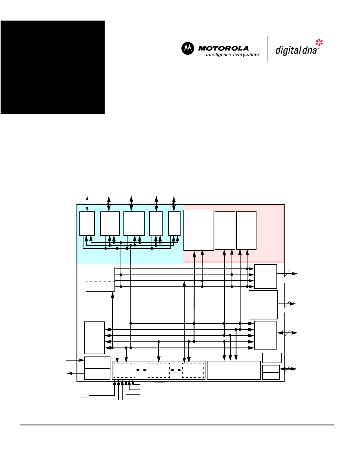
Motorola designed the DSP56362 to support digital audio applications requiring digital audio compression
and decompression, sound field processing, acoustic equalization, and other digital audio algorithms. The
DSP56362 uses the high performance, single-clock-per-cycle DSP56300 core family of programmable
CMOS digital signal processors (DSPs) combined with the audio signal processing capability of the
nc...
I
Motorola Symphony™ DSP family, as shown in Figure 1. This design provides a two-fold performance
increase over Motorola’s popular Symphony family of DSPs while retaining code compatibility. Significant
architectural enhancements include a barrel shifter, 24-bit addressing, instruction cache, and direct
memory access (DMA). The DSP56362 offers 100 million instructions per second (MIPS) using an internal
100 MHz clock at 3.3 V.
Freescale Semiconductor, Inc.
cale Semiconductor,
Frees
EXTAL
CLKOUT
PINIT/NMI
Triple
Timer
RESET
Address
Generation
Unit
Six Channel
DMA Unit
Internal
Data
Bus
Switch
Clock
Generator
PLL
2
DAX
(SPDIF)
Interface
PIO_EB
Program
Interrupt
Controller
1216
Host
ESAI
Peripheral
Expansion Area
Program
Decode
Controller
MODA/IRQA
MODB/IRQB
MODC/IRQC
MODD/IRQD
5
SHI
Program RAM/
Instruction
Cache
× 24
3072
Program ROM
× 24
30K
Bootstrap ROM
× 24
192
PM_EB
24-Bit
DSP56300
Core
DDB
YDB
XDB
PDB
GDB
Program
Address
Generator
YAB
XAB
PAB
DAB
24
Figure 1 DSP56362 Block Diagram
X Data
RAM
5632
ROM
6144
×
24 + 56 → 56-bit MAC
Two 56-bit Accumulators
56-bit Barrel Shifter
× 24
5632
× 24
6144
XM_EB
Data ALU
Y Data
RAM
× 24
ROM
× 24
YM_EB
DRAM/SRAM
Memory
Expansion
Area
External
Address
Bus
Switch
Bus
Interface
&
I - Cache
Control
External
Data Bus
Switch
Power
Mngmnt.
JTAG
OnCE
18
Address
11
Control
24
Data
6
AA0456G
This document contains information on a new product. Specifications and information herein are subject to change without notice.
IMOTOROLA DSP56362 Advance Information
For More Information On This Product,
Go to: www.freescale.com

Freescale Semiconductor, Inc.
nc...
I
cale Semiconductor,
Frees
THIS PAGE INTENTIONALLY LEFT BLANK
For More Information On This Product,
Go to: www.freescale.com

Freescale Semiconductor, Inc.
nc...
I
cale Semiconductor,
Frees
MOTOROLA DSP56362 Advance Information iii
For More Information On This Product,
Go to: www.freescale.com

Freescale Semiconductor, Inc.
SIGNAL/CONNECTION DESCRIPTIONS . . . . . . . . . . . . . . . . . . . . . . . . . . . 1-1
SPECIFICATIONS . . . . . . . . . . . . . . . . . . . . . . . . . . . . . . . . . . . . . . . . . . . . . 2-1
PACKAGING . . . . . . . . . . . . . . . . . . . . . . . . . . . . . . . . . . . . . . . . . . . . . . . . . . 3-1
DESIGN CONSIDERATIONS . . . . . . . . . . . . . . . . . . . . . . . . . . . . . . . . . . . . . 4-1
ORDERING INFORMATION. . . . . . . . . . . . . . . . . . . . . . . . . . . . . . . . . . . . . . 5-1
POWER CONSUMPTION BENCHMARK. . . . . . . . . . . . . . . . . . . . . . . . . . . . A-1
IBIS MODEL . . . . . . . . . . . . . . . . . . . . . . . . . . . . . . . . . . . . . . . . . . . . . . . . . . B-1
INDEX . . . . . . . . . . . . . . . . . . . . . . . . . . . . . . . . . . . . . . . . . . . . . . . . . . . INDEX-I
nc...
I
cale Semiconductor,
Frees
FOR TECHNICAL ASSISTANCE:
Telephone: 1-800-521-6274
Email: dsphelp@dsp.sps.mot.com
Internet: http://www.motorola-dsp.com
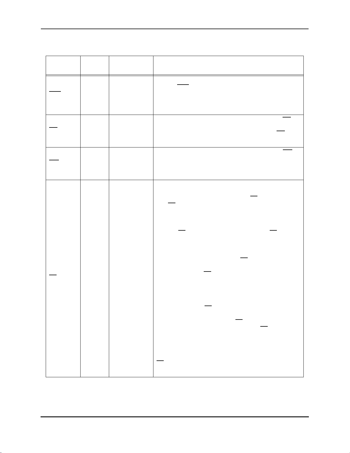
Data Sheet Conventions
This data sheet uses the following conventions:
OVERBAR Used to indicate a signal that is active when pulled low (For example, the RESET
pin is active when low.)
“asserted” Means that a high true (active high) signal is high or that a low true (active low)
signal is low
“deasserted” Means that a high true (active high) signal is low or that a low true (active low)
signal is high
Examples:
Signal/Symbol Logic State Signal State Voltage*
PIN
True Asserted VIL/V
OL
PIN False Deasserted VIH/V
PIN True Asserted VIH/V
PIN False Deasserted VIL/V
Note: *Values for VIL, VOL, VIH, and VOH are defined by individual product specifications.
!! DSP56362 Advance Information MOTOROLA
For More Information On This Product,
Go to: www.freescale.com
OH
OH
OL

Freescale Semiconductor, Inc.
FEATURES
• Multimode, multichannel decoder software functionality
– Dolby Digital and Pro Logic
– MPEG2 5.1
–DTS
– Bass management
OVERVIEW
nc...
I
cale Semiconductor,
Frees
• Digital audio post-processing capabilities
– 3D Virtual surround sound
– Lucasfilm THX5.1
– Soundfield processing
– Equalization
• Digital Signal Processing Core
– 100 MIPS with a 100 MHz clock at 3.3 V +/- 5%
– Object code compatible with the DSP56000 core
– Highly parallel instruction set
– Data arithmetic logic unit (ALU)
• Fully pipelined 24 x 24-bit parallel multiplier-accumulator (MAC)
• 56-bit parallel barrel shifter (fast shift and normalization; bit stream generation and
parsing)
• Conditional ALU instructions
• 24-bit or 16-bit arithmetic support under software control
– Program control unit (PCU)
• Position independent code (PIC) support
• Addressing modes optimized for DSP applications (including immediate offsets)
• On-chip instruction cache controller
• On-chip memory-expandable hardware stack
• Nested hardware DO loops
• Fast auto-return interrupts
– Direct memory access (DMA)
• Six DMA channels supporting internal and external accesses
• One-, two-, and three- dimensional transfers (including circular buffering)
MOTOROLA DSP56362 Advance Information 1
For More Information On This Product,
Go to: www.freescale.com

Overview
Features
• End-of-block-transfer interrupts
• Triggering from interrupt lines and all peripherals
– Phase-locked loop (PLL)
• Software programmable PLL-based frequency synthesizer for the core clock
• Allows change of low-power divide factor (DF) without loss of lock
• Output clock with skew elimination
– Hardware debugging support
• On-Chip Emulation (OnCE‘) module
• Joint Action Test Group (JTAG) test access port (TAP)
• Address trace mode reflects internal program RAM accesses at the external port
• On-Chip Memories
Freescale Semiconductor, Inc.
nc...
I
cale Semiconductor,
Frees
– Modified Harvard architecture allows simultaneous access to program and data memories
– 30720 x 24-bit on-chip program ROM
– 6144 x 24-bit on-chip X-data ROM
– 6144 x 24-bit on-chip Y-data ROM
– Program RAM, instruction cache, X data RAM, and Y data RAM sizes are programmable
Instruction
Cache
Disabled Disabled 3072 × 24-bit 0 5632 × 24-bit 5632 × 24-bit
Enabled Disabled 2048 × 24-bit 1024 × 24-bit 5632 × 24-bit 5632 × 24-bit
Disabled Enabled 5120 × 24-bit 0 5632 × 24-bit 3584 × 24-bit
Enabled Enabled 4096 × 24-bit 1024 × 24-bit 5632 × 24-bit 3584 × 24-bit
– 192 x 24-bit bootstrap ROM (disabled in sixteen-bit compatibility mode)
• Off-Chip Memory Expansion
– Data memory expansion to 256K x 24-bit word memory for P, X, and Y memory using SRAM.
– Data memory expansion to 16M x 24-bit word memory for P, X, and Y memory using DRAM.
– External memory expansion port( twenty-four data pins for high speed external memory
access allowing for a large number of external accesses per sample)
Switch
Mode
Program RAM
Size
1
(disabled in 16-bit compatibility mode)
1
1
.
Instruction
Cache Size
X Data RAM
Size
Y Data RAM
Size
– Chip select logic for glueless interface to SRAMs
– On-chip DRAM controller for glueless interface to DRAMs
• Peripheral and Support Circuits
– Enhanced serial audio interface (ESAI) includes:
• Six serial data lines, 4 selectable as receive or transmit and 2 transmit only.
• Master or slave capability
2
•I
S, Sony, AC97, and other audio protocol implementations
1.These ROMs may be factory programmed with data or programs provided by the application developer.
2 DSP56362 Advance Information MOTOROLA
For More Information On This Product,
Go to: www.freescale.com

Freescale Semiconductor, Inc.
– Serial host interface (SHI) features:
• SPI protocol with multi-master capability
2
•I
C protocol with single-master capability
• Ten-word receive FIFO
• Support for 8-, 16-, and 24-bit words.
– Byte-wide parallel host interface (HDI08) with DMA support
– DAX features one serial transmitter capable of supporting S/PDIF, IEC958, IEC1937, CP-340,
and AES/EBU digital audio formats; alternate configuration supports up to two GPIO lines
– Triple timer module with single external interface or GPIO line
– On-chip peripheral registers are memory mapped in data memory space
• Reduced Power Dissipation
– Very low-power (3.3 V) CMOS design
nc...
I
– Wait and stop low-power standby modes
– Fully-static logic, operation frequency down to 0 Hz (dc)
Overview
Documentation
cale Semiconductor,
Frees
– Optimized power management circuitry (instruction-dependent, peripheral-dependent, and
mode-dependent)
Package
• 144-pin plastic thin quad flat pack (LQFP) surface-mount package
DOCUMENTATION
Table 1 lists the documents that provide a complete description of the DSP56362 and are required to
design properly with the part. Documentation is available from a local Motorola distributor, a Motorola
semiconductor sales office, a Motorola Literature Distribution Center, or through the Motorola DSP home
page on the Internet (the source for the latest information).
Table 1 DSP56362 Documentation
Document Name Description Order Number
DSP56300 Family Manual Detailed description of the 56000-family
architecture and the 24-bit core processor and
instruction set
DSP56362 User’s Manual Detailed description of memory, peripherals,
and interfaces
DSP56362 Advance Information Electrical and timing specifications; pin and
package descriptions
DSP56300FM/AD
DSP56362UM/AD
DSP56362/D
There is also a product brief for this chip.
DSP56362 Product Brief Brief description of the chip DSP56362P/D
MOTOROLA DSP56362 Advance Information 3
For More Information On This Product,
Go to: www.freescale.com

Freescale Semiconductor, Inc.
NOTES
nc...
I
cale Semiconductor,
Frees
For More Information On This Product,
Go to: www.freescale.com
Freescale Semiconductor, Inc.
SECTION 1
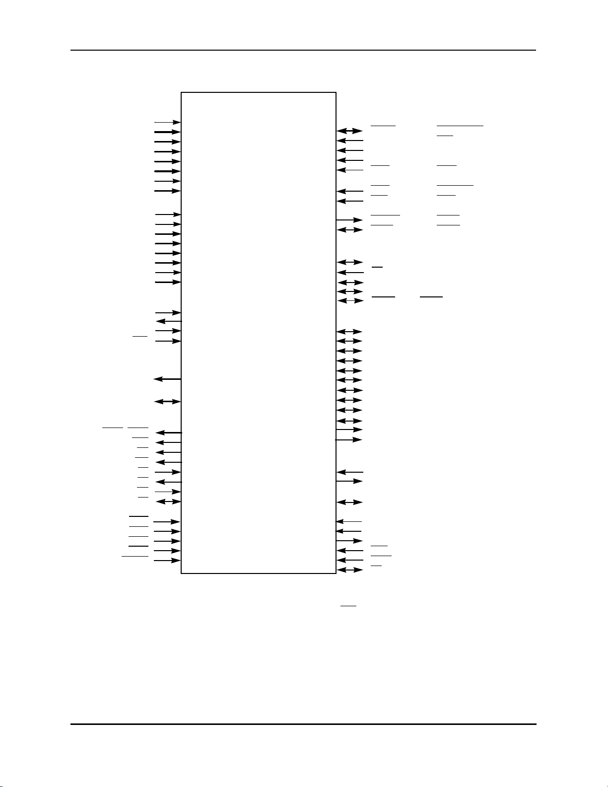
SIGNAL/CONNECTION DESCRIPTIONS
SIGNAL GROUPINGS
The input and output signals of the DSP56362 are organized into functional groups, which are listed in
Table 1-1 and illustrated in Figure 1-1.
The DSP56362 is operated from a 3.3 V supply; however, some of the inputs can tolerate 5 V. A special
notice for this feature is added to the signal descriptions of those inputs.
nc...
I
cale Semiconductor,
Frees
Table 1-1 DSP56362 Functional Signal Groupings
Functional Group
Power (V
Ground (GND)
Clock and PLL
Address bus
Data bus
Bus control
Interrupt and mode control
HDI08
SHI
ESAI
Digital audio transmitter (DAX)
Timer
CC
)
Port A
Port B
Port C
Port D
Number of
Signals
20 Table 1-2
19 Table 1-3
4 Table 1-4
18 Table 1-5
1
2
3
4
24 Table 1-6
11 Table 1-7
5 Table 1-8
16 Table 1-9
5 Table 1-10
12 Table 1-11
2 Table 1-12
1 Table 1-13
Detailed
Description
JTAG/OnCE Port
Port A is the external memory interface port, including the external address bus, data bus, and
control signals.
Port B signals are the GPIO port signals which are multiplexed with the HDI08 signals.
Port C signals are the GPIO port signals which are multiplexed with the ESAI signals.
Port D signals are the GPIO port signals which are multiplexed with the DAX signals.
MOTOROLA DSP56362 Advance Information 1-1
6 Table 1-14
For More Information On This Product,
Go to: www.freescale.com
nc...
I
cale Semiconductor,
Frees
Freescale Semiconductor, Inc.
Signal/Connection Descriptions
Signal Groupings
DSP56362
V
CCP
V
CCQH
V
CCQL
V
CCA
V
CCD
V
CCC
V
CCH
V
CCS
GNDP
GNDP1
GND
GND
GND
GND
GND
GND
EXTAL
CLKOUT
PCAP
PINIT/NMI
Q
A
D
C
H
S
Power Inputs:
PLL
3
External I/O
4
Internal Logic
3
Address Bus
4
Data Bus
2
Bus Control
HDI08
2
SHI/ESAI/DAX/Timer
Grounds:
PLL
PLL
4
Internal Logic
4
Address Bus
4
Data Bus
2
Bus Control
HDI08
2
SHI/ESAI/DAX/Timer
Clock and
PLL
Host
Interface
(HDI08)
Port
Serial
Host
Interface
(SHI)
1
Port A
18
24
4
External
Address Bus
External
Data Bus
External
Bus
Control
Transmitter (DAX)
Interrupt/
Mode
Control
A0–A17
D0–D23
AA0–AA3/
–RAS3
RAS0
CAS
RD
WR
TA
BR
BG
BB
MODA/IRQA
MODB/IRQB
MODC/IRQC
MODD/IRQD
RESET
Notes: 1. The HDI08 port supports a nonmultiplexed or a multiplexed bus, single or double data strobe (DS), and single or
double host request (HR) configurations. Since each of these modes is configured independently, any
combination of these modes is possible. These HDI08 signals can also be configured alternately as GPIO
signals (PB0–PB15). Signals with dual designations (e.g., HAS
2. The ESAI signals are multiplexed with the port C GPIO signals (PC0–PC11). The DAX signals are multiplexed
with the Port D GPIO signals (PD0–PD1). The timer 0 signal can be configured alternately as the timer GPIO
signal (TIO0).
Enhanced
Serial
Audio
Interface
(ESAI)
Digital Audio
Timer 0
JTAG/
OnCE Port
2
2
2
NonMultiplexed Bus
8
H0–H7
HA0
HA1
HA2
HCS
HCS/
Single DS
HRW
HDS/HDS
Single HR
/HOREQ
HOREQ
HACK
/HACK
SPI Mode
MOSI
SS
MISO
SCK
HREQ
SCKR
FSR
HCKR
SCKT
FST
HCKT
SDO5/SDI0
SDO4/SDI1
SDO3/SDI2
SDO2/SDI3
SDO1
SDO0
ACI
ADO
TIO0
TCK
TDI
TDO
TMS
TRST
DE
/HAS) have configurable polarity.
Multiplexed
Bus
HAD0–HAD7
HAS/HAS
HA8
HA9
HA10
Double DS
HRD/HRD
HWR/HWR
Double HR
/HTRQ
HTRQ
HRRQ
I2C Mode
HA0
HA2
SDA
SCL
HREQ
Port C GPIO
PC0
PC1
PC2
PC3
PC4
PC5
PC6
PC7
PC8
PC9
PC10
PC11
Port D GPIO
PD0
PD1
Timer GPIO
TIO0
/HRRQ
Port B
GPIO
PB0–PB7
PB8
PB9
PB10
PB13
PB11
PB12
PB14
PB15
AA0601
Figure 1-1 Signals Identified by Functional Group
1-2 DSP56362 Advance Information MOTOROLA
For More Information On This Product,
Go to: www.freescale.com

POWER
Freescale Semiconductor, Inc.
Signal/Connection Descriptions
Table 1-2 Power Inputs
Power
nc...
I
cale Semiconductor,
Frees
V
CCP
V
CCQL
V
CCQH
V
CCA
V
CCD
V
CCC
V
CCH
V
CCS
Power
Name
(4)
(3)
(3)
(4)
(2)
(2)
Description
PLL Power—V
regulated and the input should be provided with an extremely low impedance path
to the V
Quiet Core (Low) Power—V
logic. This input must be tied externally to all other chip power inputs. The user
must provide adequate external decoupling capacitors. There are four V
Quiet External (High) Power—V
input must be tied externally to all other chip power inputs. The user must provide
adequate decoupling capacitors. There are three V
Address Bus Power—V
O drivers. This input must be tied externally to all other chip power inputs. The user
must provide adequate external decoupling capacitors. There are three V
inputs.
Data Bus Power—V
drivers. This input must be tied externally to all other chip power inputs. The user
must provide adequate external decoupling capacitors. There are four V
Bus Control Power—V
This input must be tied externally to all other chip power inputs. The user must
provide adequate external decoupling capacitors. There are two V
Host Power—V
be tied externally to all other chip power inputs. The user must provide adequate
external decoupling capacitors. There is one V
SHI, ESAI, DAX, and Timer Power—V
DAX, and Timer I/O drivers. This input must be tied externally to all other chip
power inputs. The user must provide adequate external decoupling capacitors.
There are two V
power rail. There is one V
CC
is VCC dedicated for PLL use. The voltage should be well-
CCP
input.
CCP
is an isolated power for the core processing
CCQL
CCQ
is a quiet power source for I/O lines. This
CCQH
inputs.
CCQH
is an isolated power for sections of the address bus I/
CCA
is an isolated power for sections of the data bus I/O
CCD
CCD
is an isolated power for the bus control I/O drivers.
CCC
inputs.
CCC
is an isolated power for the HDI08 I/O drivers. This input must
CCH
input.
CCH
is an isolated power for the SHI, ESAI,
CCS
inputs.
CCS
inputs.
CCA
inputs.
MOTOROLA DSP56362 Advance Information 1-3
For More Information On This Product,
Go to: www.freescale.com

Freescale Semiconductor, Inc.
Signal/Connection Descriptions
Ground
GROUND
Table 1-3 Grounds
nc...
I
cale Semiconductor,
Frees
Ground
Name
GND
GND
GND
GND
GND
GND
GND
GND
P
P1
(4)
Q
A (4)
(4)
D
(2)
C
H
(2)
S
Description
PLL Ground—GNDP is a ground dedicated for PLL use. The connection should be
provided with an extremely low-impedance path to ground. V
bypassed to GND
package. There is one GND
PLL Ground 1—GNDP1 is a ground dedicated for PLL use. The connection should
be provided with an extremely low-impedance path to ground. There is one GND
connection.
Quiet Ground—GND
connection must be tied externally to all other chip ground connections. The user
must provide adequate external decoupling capacitors. There are four GND
connections.
Address Bus Ground—GNDA is an isolated ground for sections of the address
bus I/O drivers. This connection must be tied externally to all other chip ground
connections. The user must provide adequate external decoupling capacitors.
There are four GND
Data Bus Ground—GND
drivers. This connection must be tied externally to all other chip ground
connections. The user must provide adequate external decoupling capacitors.
There are four GND
Bus Control Ground—GND
This connection must be tied externally to all other chip ground connections. The
user must provide adequate external decoupling capacitors. There are two GND
connections.
Host Ground—GNDH is an isolated ground for the HDI08 I/O drivers. This
connection must be tied externally to all other chip ground connections. The user
must provide adequate external decoupling capacitors. There is one GND
connection.
SHI, ESAI, DAX, and Timer Ground—GND
ESAI, DAX, and Timer I/O drivers. This connection must be tied externally to all
other chip ground connections. The user must provide adequate external
decoupling capacitors. There are two GND
by a 0.47 µF capacitor located as close as possible to the chip
P
Q
connections.
A
connections.
D
connection.
P
is an isolated ground for the internal processing logic. This
is an isolated ground for sections of the data bus I/O
D
is an isolated ground for the bus control I/O drivers.
C
is an isolated ground for the SHI,
S
connections.
S
should be
CCP
P1
Q
C
H
1-4 DSP56362 Advance Information MOTOROLA
For More Information On This Product,
Go to: www.freescale.com

CLOCK AND PLL
Freescale Semiconductor, Inc.
Signal/Connection Descriptions
Table 1-4 Clock and PLL Signals
Clock and PLL
nc...
I
cale Semiconductor,
Frees
Signal
Name
EXTAL Input Input
CLKOUT Output Chip-driven
PCAP Input Input
PINIT/
NMI
Type
Input Input
State during
Reset
Signal Description
External Clock Input—An external clock source must be
connected to EXTAL in order to supply the clock to the
internal clock generator and PLL.
This input cannot tolerate 5V.
Clock Output—CLKOUT provides an output clock
synchronized to the internal core clock phase.
If the PLL is enabled and both the multiplication and division
factors equal one, then CLKOUT is also synchronized to
EXTAL.
If the PLL is disabled, the CLKOUT frequency is half the
frequency of EXTAL. CLKOUT is not functional at
frequencies of 100 MHz and above.
PLL Capacitor—PCAP is an input connecting an off-chip
capacitor to the PLL filter. Connect one capacitor terminal to
PCAP and the other terminal to V
If the PLL is not used, PCAP may be tied to V
floating.
PLL Initial/Non maskable Interrupt—During assertion of
RESET
(PEN) bit of the PLL control register, determining whether the
PLL is enabled or disabled. After RESET
during normal instruction processing, the PINIT/NMI
trigger input is a negative-edge-triggered non maskable
interrupt (NMI) request internally synchronized to CLKOUT.
PINIT/NMI
, the value of PINIT/NMI is written into the PLL Enable
cannot tolerate 5 V.
CCP
.
, GND, or left
CC
deassertion and
Schmitt-
EXTERNAL MEMORY EXPANSION PORT (PORT A)
When the DSP56362 enters a low-power standby mode (stop or wait), it releases bus mastership and tristates the relevant port A signals: A0–A17, D0–D23, AA0/RAS0
MOTOROLA DSP56362 Advance Information 1-5
For More Information On This Product,
Go to: www.freescale.com
–AA3/RAS3, RD, WR, BB, CAS.
Freescale Semiconductor, Inc.
Signal/Connection Descriptions
External Memory Expansion Port (Port A)
External Address Bus
Table 1-5 External Address Bus Signals
nc...
I
cale Semiconductor,
Frees
Signal
Name
A0–A17 Output Tri-stated
Type
State during
External Data Bus
Table 1-6 External Data Bus Signals
Signal
Name
D0–D23 Input/Output Tri-stated
Type
State during
External Bus Control
Table 1-7 External Bus Control Signals
Signal
Name
Type
State during
Reset
Reset
Reset
Signal Description
Address Bus—When the DSP is the bus master,
A0–A17 are active-high outputs that specify the
address for external program and data memory
accesses. Otherwise, the signals are tri-stated. To
minimize power dissipation, A0–A17 do not change
state when external memory spaces are not being
accessed.
Signal Description
Data Bus—When the DSP is the bus master,
D0–D23 are active-high, bidirectional input/
outputs that provide the bidirectional data bus for
external program and data memory accesses.
Otherwise, D0–D23 are tri-stated.
Signal Description
Address Attribute or Row Address Strobe—When
AA0–AA3/
RAS0
–
RAS3
1-6 DSP56362 Advance Information MOTOROLA
Output Tri-stated
defined as AA, these signals can be used as chip selects
or additional address lines. When defined as RAS
signals can be used as RAS
signals are can be tri-stated outputs with programmable
polarity.
for DRAM interface. These
, these
For More Information On This Product,
Go to: www.freescale.com
Freescale Semiconductor, Inc.
Table 1-7 External Bus Control Signals (Continued)
Signal/Connection Descriptions
External Memory Expansion Port (Port A)
nc...
I
cale Semiconductor,
Frees
Signal
Name
CAS Output Tri-stated
RD
WR
TA
Type
Output Tri-stated
Output Tri-stated
Input Ignored Input
State during
Reset
Signal Description
Column Address Strobe—When the DSP is the bus
master, CAS
strobe the column address. Otherwise, if the bus
mastership enable (BME) bit in the DRAM control
register is cleared, the signal is tri-stated.
Read Enable—When the DSP is the bus master, RD
an active-low output that is asserted to read external
memory on the data bus (D0–D23). Otherwise, RD
stated.
Write Enable—When the DSP is the bus master, WR
an active-low output that is asserted to write external
memory on the data bus (D0–D23). Otherwise, the
signals are tri-stated.
Transfer Acknowledge—If the DSP56362 is the bus
master and there is no external bus activity, or the
DSP56362 is not the bus master, the TA
The TA
function that can extend an external bus cycle
indefinitely. Any number of wait states (1, 2. . .infinity)
may be added to the wait states inserted by the BCR by
keeping TA
deasserted at the start of a bus cycle, is asserted to
enable completion of the bus cycle, and is deasserted
before the next bus cycle. The current bus cycle
completes one clock period after TA
synchronous to CLKOUT. The number of wait states is
determined by the TA
(BCR), whichever is longer. The BCR can be used to set
the minimum number of wait states in external bus
cycles.
In order to use the TA
programmed to at least one wait state. A zero wait state
access cannot be extended by TA
otherwise improper operation may result. TA
synchronously or asynchronously, depending on the
setting of the TAS bit in the operating mode register
(OMR).
is an active-low output used by DRAM to
is
is tri-
is
input is ignored.
input is a data transfer acknowledge (DTACK)
deasserted. In typical operation, TA is
is asserted
input or by the bus control register
functionality, the BCR must be
deassertion,
can operate
TA
functionality may not be used while performing DRAM
type accesses, otherwise improper operation may result.
MOTOROLA DSP56362 Advance Information 1-7
For More Information On This Product,
Go to: www.freescale.com

Freescale Semiconductor, Inc.
Signal/Connection Descriptions
External Memory Expansion Port (Port A)
Table 1-7 External Bus Control Signals (Continued)
nc...
I
cale Semiconductor,
Frees
Signal
Name
BR Output
BG
Type
Input Ignored Input
State during
Reset
Output
(deasserted)
Signal Description
Bus Request—BR
stated. BR
mastership. BR
needs the bus. BR
independent of whether the DSP56362 is a bus master
or a bus slave. Bus “parking” allows BR
even though the DSP56362 is the bus master. (See the
description of bus “parking” in the BB
The bus request hold (BRH) bit in the BCR allows BR
be asserted under software control even though the DSP
does not need the bus. BR
bus arbitrator that controls the priority, parking, and
tenure of each master on the same external bus. BR
only affected by DSP requests for the external bus, never
for the internal bus. During hardware reset, BR
deasserted and the arbitration is reset to the bus slave
state.
Bus Grant—BG
an external bus arbitration circuit when the DSP56362
becomes the next bus master. When BG
DSP56362 must wait until BB
bus mastership. When BG
is typically given up at the end of the current bus cycle.
This may occur in the middle of an instruction that
requires more than one external bus cycle for execution.
The default mode of operation of this signal requires a
setup and hold time referred to CLKOUT. But CLKOUT
operation is not guaranteed from 100MHz and up, so the
asynchronous bus arbitration must be used for clock
frequencies 100MHz and above. The asynchronous bus
arbitration is enabled by setting the ABE bit in the OMR
register.
is asserted when the DSP requests bus
is an active-low output, never tri-
is deasserted when the DSP no longer
may be asserted or deasserted
to be deasserted
signal description.)
to
is typically sent to an external
is
is
is an active-low input. BG is asserted by
is asserted, the
is deasserted before taking
is deasserted, bus mastership
1-8 DSP56362 Advance Information MOTOROLA
For More Information On This Product,
Go to: www.freescale.com
Freescale Semiconductor, Inc.
Table 1-7 External Bus Control Signals (Continued)
Signal/Connection Descriptions
External Memory Expansion Port (Port A)
Signal
Name
BB
nc...
I
Type
Input/
Output
cale Semiconductor,
State during
Reset
Input
Signal Description
Bus Busy—BB
BB
indicates that the bus is active. Only after BB is
deasserted can the pending bus master become the bus
master (and then assert the signal again). The bus
master may keep BB
regardless of whether BR
is called “bus parking” and allows the current bus master
to reuse the bus without rearbitration until another device
requires the bus. The deassertion of BB
“active pull-up” method (i.e., BB
released and held high by an external pull-up resistor).
The default mode of operation of this signal requires a
setup and hold time referred to CLKOUT. But CLKOUT
operation is not guaranteed from 100MHz and up, so the
asynchronous bus arbitration must be used for clock
frequencies 100MHz and above. The asynchronous bus
arbitration is enabled by setting the ABE bit in the OMR
register.
BB
requires an external pull-up resistor.
is a bidirectional active-low input/output.
asserted after ceasing bus activity
is asserted or deasserted. This
is done by an
is driven high and then
Frees
MOTOROLA DSP56362 Advance Information 1-9
For More Information On This Product,
Go to: www.freescale.com
Freescale Semiconductor, Inc.
Signal/Connection Descriptions
Interrupt and Mode Control
INTERRUPT AND MODE CONTROL
The interrupt and mode control signals select the chip’s operating mode as it comes out of hardware reset.
After RESET
is deasserted, these inputs are hardware interrupt request lines.
Table 1-8 Interrupt and Mode Control
nc...
I
cale Semiconductor,
Frees
Signal Name Type
MODA/IRQA
MODB/IRQB
Input Input
Input Input
State during
Reset
Signal Description
Mode Select A/External Interrupt Request A—
MODA/IRQA
internally synchronized to the DSP clock. MODA/IRQA
selects the initial chip operating mode during hardware
reset and becomes a level-sensitive or negative-edgetriggered, maskable interrupt request input during
normal instruction processing. MODA, MODB, MODC,
and MODD select one of 16 initial chip operating
modes, latched into the OMR when the RESET
is deasserted. If IRQA
CLKOUT, multiple processors can be resynchronized
using the WAIT instruction and asserting IRQA
the wait state. If the processor is in the stop standby
state and the MODA/IRQA
processor will exit the stop state.
This input is 5 V tolerant.
Mode Select B/External Interrupt Request B—
MODB/IRQB
internally synchronized to the DSP clock. MODB/IRQB
selects the initial chip operating mode during hardware
reset and becomes a level-sensitive or negative-edgetriggered, maskable interrupt request input during
normal instruction processing. MODA, MODB, MODC,
and MODD select one of 16 initial chip operating
modes, latched into OMR when the RESET
deasserted. If IRQB
CLKOUT, multiple processors can be re-synchronized
using the WAIT instruction and asserting IRQB
the wait state.
is an active-low Schmitt-trigger input,
signal
is asserted synchronous to
to exit
pin is pulled to GND, the
is an active-low Schmitt-trigger input,
signal is
is asserted synchronous to
to exit
This input is 5 V tolerant.
1-10 DSP56362 Advance Information MOTOROLA
For More Information On This Product,
Go to: www.freescale.com

Freescale Semiconductor, Inc.
Table 1-8 Interrupt and Mode Control (Continued)
Signal/Connection Descriptions
Interrupt and Mode Control
Signal Name Type
MODC/IRQC Input Input
nc...
I
MODD/IRQD
Input Input
cale Semiconductor,
State during
Reset
Signal Description
Mode Select C/External Interrupt Request C—
MODC/IRQC
internally synchronized to the DSP clock. MODC/IRQC
selects the initial chip operating mode during hardware
reset and becomes a level-sensitive or negative-edgetriggered, maskable interrupt request input during
normal instruction processing. MODA, MODB, MODC,
and MODD select one of 16 initial chip operating
modes, latched into OMR when the RESET
deasserted. If IRQC
CLKOUT, multiple processors can be resynchronized
using the WAIT instruction and asserting IRQC
the wait state.
This input is 5 V tolerant.
Mode Select D/External Interrupt Request D—
MODD/IRQD
internally synchronized to the DSP clock. MODD/IRQD
selects the initial chip operating mode during hardware
reset and becomes a level-sensitive or negative-edgetriggered, maskable interrupt request input during
normal instruction processing. MODA, MODB, MODC,
and MODD select one of 16 initial chip operating
modes, latched into OMR when the RESET
deasserted. If IRQD
CLKOUT, multiple processors can be resynchronized
using the WAIT instruction and asserting IRQD
the wait state.
This input is 5 V tolerant.
is an active-low Schmitt-trigger input,
signal is
is asserted synchronous to
to exit
is an active-low Schmitt-trigger input,
signal is
is asserted synchronous to
to exit
Frees
MOTOROLA DSP56362 Advance Information 1-11
For More Information On This Product,
Go to: www.freescale.com

Freescale Semiconductor, Inc.
Signal/Connection Descriptions
Host Interface (HDI08)
Table 1-8 Interrupt and Mode Control (Continued)
Signal Name Type
RESET
nc...
I
Input Input
State during
Reset
Signal Description
Reset—RESET
When asserted, the chip is placed in the reset state
and the internal phase generator is reset. The Schmitttrigger input allows a slowly rising input (such as a
capacitor charging) to reset the chip reliably. If RESET
is deasserted synchronous to CLKOUT, exact start-up
timing is guaranteed, allowing multiple processors to
start synchronously and operate together in “lockstep.” When the RESET
chip operating mode is latched from the MODA,
MODB, MODC, and MODD inputs. The RESET
must be asserted during power up. A stable EXTAL
signal must be supplied while RESET
asserted.
This input is 5 V tolerant.
is an active-low, Schmitt-trigger input.
signal is deasserted, the initial
signal
is being
HOST INTERFACE (HDI08)
The HDI08 provides a fast, 8-bit, parallel data port that may be connected directly to the host bus. The
HDI08 supports a variety of standard buses and can be directly connected to a number of industry
standard microcomputers, microprocessors, DSPs, and DMA hardware.
Host Port Configuration
cale Semiconductor,
Signal functions associated with the HDI08 vary according to the interface operating mode as determined
by the HDI08 port control register (HPCR). See 6.5.6 Host Port Control Register (HPCR) on
page Section 6-13 for detailed descriptions of this register and (See Host Interface (HDI08) on
page Section 6-1.) for descriptions of the other HDI08 configuration registers.
Frees
1-12 DSP56362 Advance Information MOTOROLA
For More Information On This Product,
Go to: www.freescale.com

Freescale Semiconductor, Inc.
Signal/Connection Descriptions
Table 1-9 Host Interface
Host Interface (HDI08)
Signal
Name
H0–H7
HAD0–
HAD7
nc...
I
PB0–PB7
HA0
HAS
cale Semiconductor,
/
HAS
Type
Input/
output
Input/
output
Input, output,
or
disconnected
Input
Input
State during
Reset
GPIO
disconnected
GPIO
disconnected
Signal Description
Host Data—When the HDI08 is programmed to
interface a nonmultiplexed host bus and the HI
function is selected, these signals are lines 0–7
of the bidirectional, tri-state data bus.
Host Address—When HDI08 is programmed to
interface a multiplexed host bus and the HI
function is selected, these signals are lines 0–7
of the address/data bidirectional, multiplexed, tristate bus.
Port B 0–7—When the HDI08 is configured as
GPIO, these signals are individually
programmable as input, output, or internally
disconnected.
The default state after reset for these signals is
GPIO disconnected.
This input is 5 V tolerant.
Host Address Input 0—When the HDI08 is
programmed to interface a nonmultiplexed host
bus and the HI function is selected, this signal is
line 0 of the host address input bus.
Host Address Strobe—When HDI08 is
programmed to interface a multiplexed host bus
and the HI function is selected, this signal is the
host address strobe (HAS) Schmitt-trigger input.
The polarity of the address strobe is
programmable, but is configured active-low
(HAS
) following reset.
Frees
Port B 8—When the HDI08 is configured as
GPIO, this signal is individually programmed as
Input, output,
PB8
MOTOROLA DSP56362 Advance Information 1-13
or
disconnected
input, output, or internally disconnected.
The default state after reset for this signal is
GPIO disconnected.
This input is 5 V tolerant.
For More Information On This Product,
Go to: www.freescale.com

Freescale Semiconductor, Inc.
Signal/Connection Descriptions
Host Interface (HDI08)
Table 1-9 Host Interface (Continued)
nc...
I
cale Semiconductor,
Frees
Signal
Name
HA1
HA8
PB9
HA2
HA9
PB10
Type
Input
Input
Input, output,
or
disconnected
Input
Input
Input, Output,
or
Disconnected
State during
Reset
GPIO
disconnected
GPIO
disconnected
Signal Description
Host Address Input 1—When the HDI08 is
programmed to interface a nonmultiplexed host
bus and the HI function is selected, this signal is
line 1 of the host address (HA1) input bus.
Host Address 8—When HDI08 is programmed
to interface a multiplexed host bus and the HI
function is selected, this signal is line 8 of the
host address (HA8) input bus.
Port B 9—When the HDI08 is configured as
GPIO, this signal is individually programmed as
input, output, or internally disconnected.
The default state after reset for this signal is
GPIO disconnected.
This input is 5 V tolerant.
Host Address Input 2—When the HDI08 is
programmed to interface a non-multiplexed host
bus and the HI function is selected, this signal is
line 2 of the host address (HA2) input bus.
Host Address 9—When HDI08 is programmed
to interface a multiplexed host bus and the HI
function is selected, this signal is line 9 of the
host address (HA9) input bus.
Port B 10—When the HDI08 is configured as
GPIO, this signal is individually programmed as
input, output, or internally disconnected.
The default state after reset for this signal is
GPIO disconnected.
This input is 5 V tolerant.
1-14 DSP56362 Advance Information MOTOROLA
For More Information On This Product,
Go to: www.freescale.com
Freescale Semiconductor, Inc.
Table 1-9 Host Interface (Continued)
Signal/Connection Descriptions
Host Interface (HDI08)
nc...
I
cale Semiconductor,
Frees
Signal
Name
HRW
HRD
HRD
PB11
HDS
HDS
HWR
HWR
Type
Input
Input
/
Input, Output,
or
Disconnected
Input
/
Input
/
State during
Reset
GPIO
disconnected
GPIO
disconnected
Signal Description
Host Read/Write—When HDI08 is programmed
to interface a single-data-strobe host bus and the
HI function is selected, this signal is the Host
Read/Write
Host Read Data—When HDI08 is programmed
to interface a double-data-strobe host bus and
the HI function is selected, this signal is the host
read data strobe (HRD) Schmitt-trigger input. The
polarity of the data strobe is programmable, but is
configured as active-low (HRD
Port B 11—When the HDI08 is configured as
GPIO, this signal is individually programmed as
input, output, or internally disconnected.
The default state after reset for this signal is
GPIO disconnected.
This input is 5 V tolerant.
Host Data Strobe—When HDI08 is programmed
to interface a single-data-strobe host bus and the
HI function is selected, this signal is the host data
strobe (HDS) Schmitt-trigger input. The polarity
of the data strobe is programmable, but is
configured as active-low (HDS
Host Write Data—When HDI08 is programmed
to interface a double-data-strobe host bus and
the HI function is selected, this signal is the host
write data strobe (HWR) Schmitt-trigger input.
The polarity of the data strobe is programmable,
but is configured as active-low (HWR
reset.
(HRW) input.
) after reset.
) following reset.
) following
Port B 12—When the HDI08 is configured as
GPIO, this signal is individually programmed as
input, output, or internally disconnected.
Input, output,
PB12
MOTOROLA DSP56362 Advance Information 1-15
or
disconnected
The default state after reset for this signal is
GPIO disconnected.
This input is 5 V tolerant.
For More Information On This Product,
Go to: www.freescale.com
Freescale Semiconductor, Inc.
Signal/Connection Descriptions
Host Interface (HDI08)
Table 1-9 Host Interface (Continued)
nc...
I
cale Semiconductor,
Frees
Signal
Name
HCS
HA10
PB13
HOREQ
HOREQ
HTRQ
HTRQ
Type
Input
Input
Input, output,
or
disconnected
Output
/
Output
/
State during
Reset
GPIO
disconnected
GPIO
disconnected
Signal Description
Host Chip Select—When HDI08 is programmed
to interface a nonmultiplexed host bus and the HI
function is selected, this signal is the host chip
select (HCS) input. The polarity of the chip select
is programmable, but is configured active-low
(HCS
) after reset.
Host Address 10—When HDI08 is programmed
to interface a multiplexed host bus and the HI
function is selected, this signal is line 10 of the
host address (HA10) input bus.
Port B 13—When the HDI08 is configured as
GPIO, this signal is individually programmed as
input, output, or internally disconnected.
The default state after reset for this signal is
GPIO disconnected.
This input is 5 V tolerant.
Host Request—When HDI08 is programmed to
interface a single host request host bus and the
HI function is selected, this signal is the host
request (HOREQ) output. The polarity of the host
request is programmable, but is configured as
active-low (HOREQ
request may be programmed as a driven or
open-drain output.
Transmit Host Request—When HDI08 is
programmed to interface a double host request
host bus and the HI function is selected, this
signal is the transmit host request (HTRQ)
output. The polarity of the host request is
programmable, but is configured as active-low
(HTRQ
programmed as a driven or open-drain output.
) following reset. The host request may be
) following reset. The host
Port B 14—When the HDI08 is configured as
GPIO, this signal is individually programmed as
input, output, or internally disconnected.
Input, output,
PB14
1-16 DSP56362 Advance Information MOTOROLA
or
disconnected
The default state after reset for this signal is
GPIO disconnected.
This input is 5 V tolerant.
For More Information On This Product,
Go to: www.freescale.com

Freescale Semiconductor, Inc.
Table 1-9 Host Interface (Continued)
Signal/Connection Descriptions
Host Interface (HDI08)
Signal
Name
HACK/
HACK
HRRQ
nc...
I
/
HRRQ
PB15
Type
Input
Output
Input, output,
or
disconnected
cale Semiconductor,
State during
Reset
GPIO
disconnected
Signal Description
Host Acknowledge—When HDI08 is
programmed to interface a single host request
host bus and the HI function is selected, this
signal is the host acknowledge (HACK) Schmitttrigger input. The polarity of the host
acknowledge is programmable, but is configured
as active-low (HACK
Receive Host Request—When HDI08 is
programmed to interface a double host request
host bus and the HI function is selected, this
signal is the receive host request (HRRQ) output.
The polarity of the host request is programmable,
but is configured as active-low (HRRQ
reset. The host request may be programmed as a
driven or open-drain output.
Port B 15—When the HDI08 is configured as
GPIO, this signal is individually programmed as
input, output, or internally disconnected.
The default state after reset for this signal is
GPIO disconnected.
This input is 5 V tolerant.
) after reset.
) after
Frees
MOTOROLA DSP56362 Advance Information 1-17
For More Information On This Product,
Go to: www.freescale.com

nc...
I
cale Semiconductor,
Frees
Freescale Semiconductor, Inc.
Signal/Connection Descriptions
Serial Host Interface
SERIAL HOST INTERFACE
The SHI has five I/O signals that can be configured to allow the SHI to operate in either SPI or I2C mode.
Table 1-10 Serial Host Interface Signals
State
Signal Name Signal Type
SCK
SCL
Input or
output
Input or
output
during
Reset
Tri-stated
Signal Description
SPI Serial Clock—The SCK signal is an output
when the SPI is configured as a master and a
Schmitt-trigger input when the SPI is configured as
a slave. When the SPI is configured as a master,
the SCK signal is derived from the internal SHI
clock generator. When the SPI is configured as a
slave, the SCK signal is an input, and the clock
signal from the external master synchronizes the
data transfer. The SCK signal is ignored by the SPI
if it is defined as a slave and the slave select (SS
signal is not asserted. In both the master and slave
SPI devices, data is shifted on one edge of the SCK
signal and is sampled on the opposite edge where
data is stable. Edge polarity is determined by the
SPI transfer protocol.
2
I
C Serial Clock—SCL carries the clock for I2C bus
transactions in the I
trigger input when configured as a slave and an
open-drain output when configured as a master.
SCL should be connected to V
resistor.
This signal is tri-stated during hardware, software,
and individual reset. Thus, there is no need for an
external pull-up in this state.
This input is 5 V tolerant.
2
C mode. SCL is a Schmitt-
through a pull-up
CC
)
1-18 DSP56362 Advance Information MOTOROLA
For More Information On This Product,
Go to: www.freescale.com

Freescale Semiconductor, Inc.
Table 1-10 Serial Host Interface Signals (Continued)
Signal Name Signal Type
Input or
nc...
I
MISO
SDA
output
Input or
open-drain
output
cale Semiconductor,
State
during
Reset
Tri-stated
Signal/Connection Descriptions
Serial Host Interface
Signal Description
SPI Master-In-Slave-Out—When the SPI is
configured as a master, MISO is the master data
input line. The MISO signal is used in conjunction
with the MOSI signal for transmitting and receiving
serial data. This signal is a Schmitt-trigger input
when configured for the SPI Master mode, an
output when configured for the SPI Slave mode,
and tri-stated if configured for the SPI Slave mode
when SS
is not required for SPI operation.
2
I
C Data and Acknowledge—In I2C mode, SDA is
a Schmitt-trigger input when receiving and an opendrain output when transmitting. SDA should be
connected to V
carries the data for I
SDA must be stable during the high period of SCL.
The data in SDA is only allowed to change when
SCL is low. When the bus is free, SDA is high. The
SDA line is only allowed to change during the time
SCL is high in the case of start and stop events. A
high-to-low transition of the SDA line while SCL is
high is a unique situation, and is defined as the start
event. A low-to-high transition of SDA while SCL is
high is a unique situation defined as the stop event.
This signal is tri-stated during hardware, software,
and individual reset. Thus, there is no need for an
external pull-up in this state.
This input is 5 V tolerant.
is deasserted. An external pull-up resistor
through a pull-up resistor. SDA
CC
2
C transactions. The data in
Frees
MOTOROLA DSP56362 Advance Information 1-19
For More Information On This Product,
Go to: www.freescale.com

Freescale Semiconductor, Inc.
Signal/Connection Descriptions
Serial Host Interface
Table 1-10 Serial Host Interface Signals (Continued)
State
Signal Name Signal Type
MOSI
nc...
I
HA0
Input or
output
Input
during
Reset
Tri-stated
Signal Description
SPI Master-Out-Slave-In—When the SPI is
configured as a master, MOSI is the master data
output line. The MOSI signal is used in conjunction
with the MISO signal for transmitting and receiving
serial data. MOSI is the slave data input line when
the SPI is configured as a slave. This signal is a
Schmitt-trigger input when configured for the SPI
Slave mode.
2
I
C Slave Address 0—This signal uses a Schmitt-
trigger input when configured for the I
When configured for I
signal is used to form the slave device address.
HA0 is ignored when configured for the I
mode.
2
C slave mode, the HA0
2
C mode.
2
C master
cale Semiconductor,
Frees
SS
HA2
Input
Input
Tri-stated
This signal is tri-stated during hardware, software,
and individual reset. Thus, there is no need for an
external pull-up in this state.
This input is 5 V tolerant.
SPI Slave Select—This signal is an active low
Schmitt-trigger input when configured for the SPI
mode. When configured for the SPI Slave mode,
this signal is used to enable the SPI slave for
transfer. When configured for the SPI master mode,
this signal should be kept deasserted (pulled high).
If it is asserted while configured as SPI master, a
bus error condition is flagged. If SS
the SHI ignores SCK clocks and keeps the MISO
output signal in the high-impedance state.
2
I
C Slave Address 2—This signal uses a Schmitt-
trigger input when configured for the I
When configured for the I
signal is used to form the slave device address.
HA2 is ignored in the I
This signal is tri-stated during hardware, software,
and individual reset. Thus, there is no need for an
external pull-up in this state.
2
C Slave mode, the HA2
2
C master mode.
is deasserted,
2
C mode.
This input is 5 V tolerant.
1-20 DSP56362 Advance Information MOTOROLA
For More Information On This Product,
Go to: www.freescale.com

Freescale Semiconductor, Inc.
Table 1-10 Serial Host Interface Signals (Continued)
Signal Name Signal Type
State
during
Reset
Signal/Connection Descriptions
Serial Host Interface
Signal Description
Host Request—This signal is an active low
Schmitt-trigger input when configured for the
master mode but an active low output when
configured for the slave mode.
When configured for the slave mode, HREQ
asserted to indicate that the SHI is ready for the
next data word transfer and deasserted at the first
clock pulse of the new data word transfer. When
configured for the master mode, HREQ
nc...
I
HREQ
Input or
Output
Tri-stated
When asserted by the external slave device, it will
trigger the start of the data word transfer by the
master. After finishing the data word transfer, the
master will await the next assertion of HREQ
proceed to the next transfer.
This signal is tri-stated during hardware, software,
personal reset, or when the HREQ1–HREQ0 bits in
the HCSR are cleared. There is no need for
external pull-up in this state.
This input is 5 V tolerant.
cale Semiconductor,
is
is an input.
to
Frees
MOTOROLA DSP56362 Advance Information 1-21
For More Information On This Product,
Go to: www.freescale.com

Freescale Semiconductor, Inc.
Signal/Connection Descriptions
Enhanced Serial Audio Interface
ENHANCED SERIAL AUDIO INTERFACE
Table 1-11 Enhanced Serial Audio Interface Signals
Signal
Name
HCKR
nc...
I
PC2
HCKT
cale Semiconductor,
PC5
Signal Type
Input or output
Input, output,
or
disconnected
Input or output
Input, output,
or
disconnected
State during
Reset
GPIO
disconnected
GPIO
disconnected
Signal Description
High Frequency Clock for Receiver—When
programmed as an input, this signal provides a high
frequency clock source for the ESAI receiver as an
alternate to the DSP core clock. When programmed
as an output, this signal can serve as a highfrequency sample clock (e.g., for external digital to
analog converters [DACs]) or as an additional
system clock.
Port C 2—When the ESAI is configured as GPIO,
this signal is individually programmable as input,
output, or internally disconnected.
The default state after reset is GPIO disconnected.
This input is 5 V tolerant.
High Frequency Clock for Transmitter—When
programmed as an input, this signal provides a high
frequency clock source for the ESAI transmitter as
an alternate to the DSP core clock. When
programmed as an output, this signal can serve as a
high frequency sample clock (e.g., for external
DACs) or as an additional system clock.
Port C 5—When the ESAI is configured as GPIO,
this signal is individually programmable as input,
output, or internally disconnected.
The default state after reset is GPIO disconnected.
Frees
This input is 5 V tolerant.
1-22 DSP56362 Advance Information MOTOROLA
For More Information On This Product,
Go to: www.freescale.com

Freescale Semiconductor, Inc.
Table 1-11 Enhanced Serial Audio Interface Signals (Continued)
Signal/Connection Descriptions
Enhanced Serial Audio Interface
nc...
I
cale Semiconductor,
Frees
Signal
Name
FSR
PC1
FST
PC4
Signal Type
Input or output
Input, output,
or
disconnected
Input or output
Input, output,
or
disconnected
State during
Reset
GPIO
disconnected
GPIO
disconnected
Signal Description
Frame Sync for Receiver—This is the receiver
frame sync input/output signal. In the asynchronous
mode (SYN=0), the FSR pin operates as the frame
sync input or output used by all the enabled
receivers. In the synchronous mode (SYN=1), it
operates as either the serial flag 1 pin (TEBE=0), or
as the transmitter external buffer enable control
(TEBE=1, RFSD=1).
When this pin is configured as serial flag pin, its
direction is determined by the RFSD bit in the RCCR
register. When configured as the output flag OF1,
this pin will reflect the value of the OF1 bit in the
SAICR register, and the data in the OF1 bit will show
up at the pin synchronized to the frame sync in
normal mode or the slot in network mode. When
configured as the input flag IF1, the data value at the
pin will be stored in the IF1 bit in the SAISR register,
synchronized by the frame sync in normal mode or
the slot in network mode.
Port C 1—When the ESAI is configured as GPIO,
this signal is individually programmable as input,
output, or internally disconnected.
The default state after reset is GPIO disconnected.
This input is 5 V tolerant.
Frame Sync for Transmitter—This is the
transmitter frame sync input/output signal. For
synchronous mode, this signal is the frame sync for
both transmitters and receivers. For asynchronous
mode, FST is the frame sync for the transmitters
only. The direction is determined by the transmitter
frame sync direction (TFSD) bit in the ESAI transmit
clock control register (TCCR).
Port C 4—When the ESAI is configured as GPIO,
this signal is individually programmable as input,
output, or internally disconnected.
The default state after reset is GPIO disconnected.
This input is 5 V tolerant.
MOTOROLA DSP56362 Advance Information 1-23
For More Information On This Product,
Go to: www.freescale.com

Freescale Semiconductor, Inc.
Signal/Connection Descriptions
Enhanced Serial Audio Interface
Table 1-11 Enhanced Serial Audio Interface Signals (Continued)
nc...
I
cale Semiconductor,
Frees
Signal
Name
SCKR
PC0
SCKT
PC3
Signal Type
Input or output
Input, output,
or
disconnected
Input or output
Input, output,
or
disconnected
State during
Reset
GPIO
disconnected
GPIO
disconnected
Signal Description
Receiver Serial Clock—SCKR provides the
receiver serial bit clock for the ESAI. The SCKR
operates as a clock input or output used by all the
enabled receivers in the asynchronous mode
(SYN=0), or as serial flag 0 pin in the synchronous
mode (SYN=1).
When this pin is configured as serial flag pin, its
direction is determined by the RCKD bit in the
RCCR register. When configured as the output flag
OF0, this pin will reflect the value of the OF0 bit in
the SAICR register, and the data in the OF0 bit will
show up at the pin synchronized to the frame sync in
normal mode or the slot in network mode. When
configured as the input flag IF0, the data value at the
pin will be stored in the IF0 bit in the SAISR register,
synchronized by the frame sync in normal mode or
the slot in network mode.
Port C 0—When the ESAI is configured as GPIO,
this signal is individually programmable as input,
output, or internally disconnected.
The default state after reset is GPIO disconnected.
This input is 5 V tolerant.
Transmitter Serial Clock—This signal provides the
serial bit rate clock for the ESAI. SCKT is a clock
input or output used by all enabled transmitters and
receivers in synchronous mode, or by all enabled
transmitters in asynchronous mode.
Port C 3—When the ESAI is configured as GPIO,
this signal is individually programmable as input,
output, or internally disconnected.
The default state after reset is GPIO disconnected.
This input is 5 V tolerant.
1-24 DSP56362 Advance Information MOTOROLA
For More Information On This Product,
Go to: www.freescale.com

Freescale Semiconductor, Inc.
Table 1-11 Enhanced Serial Audio Interface Signals (Continued)
Signal/Connection Descriptions
Enhanced Serial Audio Interface
Signal
Name
SDO5
SDI0
nc...
I
PC6
SDO4
SDI1
PC7
Signal Type
Output
Input
Input, output,
or
disconnected
Output
Input
Input, output,
or
disconnected
cale Semiconductor,
State during
Reset
GPIO
disconnected
GPIO
disconnected
Signal Description
Serial Data Output 5—When programmed as a
transmitter, SDO5 is used to transmit data from the
TX5 serial transmit shift register.
Serial Data Input 0—When programmed as a
receiver, SDI0 is used to receive serial data into the
RX0 serial receive shift register.
Port C 6—When the ESAI is configured as GPIO,
this signal is individually programmable as input,
output, or internally disconnected.
The default state after reset is GPIO disconnected.
This input is 5 V tolerant.
Serial Data Output 4—When programmed as a
transmitter, SDO4 is used to transmit data from the
TX4 serial transmit shift register.
Serial Data Input 1—When programmed as a
receiver, SDI1 is used to receive serial data into the
RX1 serial receive shift register.
Port C 7—When the ESAI is configured as GPIO,
this signal is individually programmable as input,
output, or internally disconnected.
The default state after reset is GPIO disconnected.
This input is 5 V tolerant.
Frees
MOTOROLA DSP56362 Advance Information 1-25
For More Information On This Product,
Go to: www.freescale.com

Freescale Semiconductor, Inc.
Signal/Connection Descriptions
Enhanced Serial Audio Interface
Table 1-11 Enhanced Serial Audio Interface Signals (Continued)
nc...
I
cale Semiconductor,
Frees
Signal
Name
SDO3
SDI2
PC8
SDO2
SDI3
PC9
SDO1
PC10
Signal Type
Output
Input
Input, output,
or
disconnected
Output
Input
Input, output,
or
disconnected
Output
Input, output,
or
disconnected
State during
Reset
GPIO
disconnected
GPIO
disconnected
GPIO
disconnected
Signal Description
Serial Data Output 3—When programmed as a
transmitter, SDO3 is used to transmit data from the
TX3 serial transmit shift register.
Serial Data Input 2—When programmed as a
receiver, SDI2 is used to receive serial data into the
RX2 serial receive shift register.
Port C 8—When the ESAI is configured as GPIO,
this signal is individually programmable as input,
output, or internally disconnected.
The default state after reset is GPIO disconnected.
This input is 5 V tolerant.
Serial Data Output 2—When programmed as a
transmitter, SDO2 is used to transmit data from the
TX2 serial transmit shift register.
Serial Data Input 3—When programmed as a
receiver, SDI3 is used to receive serial data into the
RX3 serial receive shift register.
Port C 9—When the ESAI is configured as GPIO,
this signal is individually programmable as input,
output, or internally disconnected.
The default state after reset is GPIO disconnected.
This input is 5 V tolerant.
Serial Data Output 1—SDO1 is used to transmit
data from the TX1 serial transmit shift register.
Port C 10—When the ESAI is configured as GPIO,
this signal is individually programmable as input,
output, or internally disconnected.
The default state after reset is GPIO disconnected.
This input is 5 V tolerant.
1-26 DSP56362 Advance Information MOTOROLA
For More Information On This Product,
Go to: www.freescale.com

Freescale Semiconductor, Inc.
Table 1-11 Enhanced Serial Audio Interface Signals (Continued)
Signal/Connection Descriptions
Enhanced Serial Audio Interface
Signal
Name
SDO0
PC11
nc...
I
Signal Type
Output
Input, output,
or
disconnected
cale Semiconductor,
State during
Reset
GPIO
disconnected
Signal Description
Serial Data Output 0—SDO0 is used to transmit
data from the TX0 serial transmit shift register.
Port C 11—When the ESAI is configured as GPIO,
this signal is individually programmable as input,
output, or internally disconnected.
The default state after reset is GPIO disconnected.
This input is 5 V tolerant.
Frees
MOTOROLA DSP56362 Advance Information 1-27
For More Information On This Product,
Go to: www.freescale.com

Freescale Semiconductor, Inc.
Signal/Connection Descriptions
Digital Audio Interface (DAX)
DIGITAL AUDIO INTERFACE (DAX)
Table 1-12 Digital Audio Interface (DAX) Signals
Signal
Name
ACI
nc...
I
PD0
ADO
PD1
Type
Input
Input,
output, or
disconnected
Output
Input,
output, or
disconnected
cale Semiconductor,
State During
Reset
Disconnecte
d
Disconnecte
d
Signal Description
Audio Clock Input—This is the DAX clock input. When
programmed to use an external clock, this input supplies
the DAX clock. The external clock frequency must be
256, 384, or 512 times the audio sampling frequency
(256 × Fs, 384 × Fs or 512 × Fs, respectively).
Port D 0—When the DAX is configured as GPIO, this
signal is individually programmable as input, output, or
internally disconnected.
The default state after reset is GPIO disconnected.
This input is 5 V tolerant.
Digital Audio Data Output—This signal is an audio and
non-audio output in the form of AES/EBU, CP340 and
IEC958 data in a biphase mark format.
Port D 1—When the DAX is configured as GPIO, this
signal is individually programmable as input, output, or
internally disconnected.
The default state after reset is GPIO disconnected.
This input is 5 V tolerant.
Frees
1-28 DSP56362 Advance Information MOTOROLA
For More Information On This Product,
Go to: www.freescale.com

TIMER
Freescale Semiconductor, Inc.
Signal/Connection Descriptions
Table 1-13 Timer Signal
Timer
nc...
I
cale Semiconductor,
Frees
Signal Name Type
TIO0
JTAG/O
Signal
Name
TCK Input Input
TDI Input Input
nCE INTERFACE
Input or
Output
Type
State during
Reset
Timer 0 Schmitt-Trigger Input/Output—When
timer 0 functions as an external event counter or
in measurement mode, TIO0 is used as input.
When timer 0 functions in watchdog, timer, or
pulse modulation mode, TIO0 is used as output.
The default mode after reset is GPIO input. This
can be changed to output or configured as a
Input
Table 1-14 JTAG/OnCE™ Interface
State
during
Reset
Test Clock—TCK is a test clock input signal used to synchronize
the JTAG test logic. It has an internal pull-up resistor.
This input is 5 V tolerant.
Test Data Input—TDI is a test data serial input signal used for test
instructions and data. TDI is sampled on the rising edge of TCK
and has an internal pull-up resistor.
timer input/output through the timer 0 control/
status register (TCSR0). If TIO0 is not being
used, it is recommended to either define it as
GPIO output immediately at the beginning of
operation or leave it defined as GPIO input but
connected it to Vcc through a pull-up resistor in
order to ensure a stable logic level at the input.
This input is 5 V tolerant.
Signal Description
Signal Description
This input is 5 V tolerant.
Test Data Output—TDO is a test data serial output signal used for
TDO Output
MOTOROLA DSP56362 Advance Information 1-29
Tristated
test instructions and data. TDO can be tri-stated and is actively
driven in the shift-IR and shift-DR controller states. TDO changes
on the falling edge of TCK.
For More Information On This Product,
Go to: www.freescale.com
Freescale Semiconductor, Inc.
Signal/Connection Descriptions
JTAG/O
nc...
I
cale Semiconductor,
nCE Interface
Table 1-14 JTAG/OnCE™ Interface (Continued)
Signal
Name
TMS Input Input
TRST
DE
Type
Input Input
Input/
Output
State
during
Reset
Input
Signal Description
Test Mode Select—TMS is an input signal used to sequence the
test controller’s state machine. TMS is sampled on the rising edge
of TCK and has an internal pull-up resistor.
This input is 5 V tolerant.
Test Reset—TRST
used to asynchronously initialize the test controller. TRST
internal pull-up resistor.
The use of TRST
recommended to leave TRST
This input is 5 V tolerant.
Debug Event—DE
providing, as an input, a means of entering the debug mode of
operation from an external command controller, and, as an output,
a means of acknowledging that the chip has entered the debug
mode. This signal, when asserted as an input, causes the
DSP56300 core to finish the current instruction being executed,
save the instruction pipeline information, enter the debug mode,
and wait for commands to be entered from the debug serial input
line. This signal is asserted as an output for three clock cycles
when the chip enters the debug mode as a result of a debug
request or as a result of meeting a breakpoint condition. The DE
has an internal pull-up resistor.
This is not a standard part of the JTAG TAP controller. The signal
connects directly to the OnCE module to initiate debug mode
directly or to provide a direct external indication that the chip has
entered the debug mode. All other interface with the OnCE module
must occur through the JTAG port.
is an active-low Schmitt-trigger input signal
has an
is not recommended for new designs. It is
disconnected.
is an open-drain, bidirectional, active-low signal
Frees
The use of DE
recommended to leave DE
This input is not 5 V tolerant.
1-30 DSP56362 Advance Information MOTOROLA
is not recommended for new designs. It is
disconnected.
For More Information On This Product,
Go to: www.freescale.com

Freescale Semiconductor, Inc.
SECTION 2
SPECIFICATIONS
INTRODUCTION
The DSP56362 is fabricated in high density CMOS with Transistor-Transistor Logic (TTL) compatible
inputs and outputs. The DSP56362 specifications are preliminary and are from design simulations, and
may not be fully tested or guaranteed. Finalized specifications will be published after full characterization
and device qualifications are complete.
nc...
I
MAXIMUM RATINGS
cale Semiconductor,
Frees
CAUTION
This device contains circuitry protecting
against damage due to high static voltage or
electrical fields. However, normal precautions
should be taken to avoid exceeding maximum
voltage ratings. Reliability of operation is
enhanced if unused inputs are pulled to an
appropriate logic voltage level (e.g., either
GND or V
pullup or pulldown resistor is 10 kΩ.
Note: In the calculation of timing requirements, adding a maximum value of one
specification to a minimum value of another specification does not yield a reasonable
sum. A maximum specification is calculated using a worst case variation of process
parameter values in one direction. The minimum specification is calculated using the
worst case for the same parameters in the opposite direction. Therefore, a “maximum”
value for a specification will never occur in the same device that has a “minimum”
value for another specification; adding a maximum to a minimum represents a
condition that can never exist.
). The suggested value for a
CC
MOTOROLA DSP56362 Advance Information 2-1
For More Information On This Product,
Go to: www.freescale.com
Specifications
Thermal Characteristics
Freescale Semiconductor, Inc.
Table 2-1 Maximum Ratings
nc...
I
cale Semiconductor,
Frees
Rating
Supply Voltage
All input voltages excluding “5 V tolerant” inputs
All “5 V tolerant” input voltages
Current drain per pin excluding V
Operating temperature range
Storage temperature
Notes: 1. GND = 0 V, VCC = 3.3 V ± .16V, TJ = 0°C to +100°C, CL = 50 pF
2. Absolute maximum ratings are stress ratings only, and functional operation at the maximum is not
guaranteed. Stress beyond the maximum rating may affect device reliability or cause permanent
damage to the device.
3. CAUTION: All “5 V Tolerant” input voltages must not be more than 3.95 V greater than the supply
voltage; this restriction applies to “power on”, as well as during normal operation. In any case, the input
voltages cannot be more than 5.75 V. “5 V Tolerant” inputs are inputs that tolerate 5 V.
1
3
and GND
CC
Symbol
V
CC
3
V
IN
V
IN5
I10mA
T
J
T
STG
GND −0.3 to VCC + 0.3 V
GND −0.3 to VCC + 3.95 V
−0.3 to +4.0 V
−40 to +105 °C
−55 to +125 °C
Value
1, 2
THERMAL CHARACTERISTICS
Table 2-2 Thermal Characteristics
Characteristic Symbol LQFP Value Unit
Junction-to-ambient thermal resistance
Junction-to-case thermal resistance
Thermal characterization parameter
Notes: 1. Junction-to-ambient thermal resistance is based on measurements on a horizontal single-
sided printed circuit board per SEMI G38-87 in natural convection.(SEMI is Semiconductor
Equipment and Materials International, 805 East Middlefield Rd., Mountain View, CA 94043,
(415) 964-5111.)
Measurements were done with parts mounted on thermal test boards conforming to
specification EIA/JESD51-3.
2. Junction-to-case thermal resistance is based on measurements using a cold plate per SEMI
G30-88, with the exception that the cold plate temperature is used for the case temperature.
1
2
R
θJA or θJA
R
θJC or θJC
Ψ
JT
45.3 °C/W
10.1 °C/W
5.5 °C/W
Unit
2-2 DSP56362 Advance Information MOTOROLA
For More Information On This Product,
Go to: www.freescale.com
Freescale Semiconductor, Inc.
DC ELECTRICAL CHARACTERISTICS
Table 2-3 DC Electrical Characteristics6
Characteristics Symbol Min Typ Max Unit
Specifications
DC Electrical Characteristics
nc...
I
cale Semiconductor,
Frees
Supply voltage
Input high voltage
• D(0:23), BG
NMI
•MOD1/IRQ1, RESET, and TCK/TDI/
TMS/TRST
SHI
(SPI mode)
•SHI
(I2C mode)
• EXTAL
Input low voltage
• D(0:23), BG
RESET
• All JTAG/ESAI/Timer/HDI08/ SHI
mode)
•SHI
(I2C mode)
• EXTAL
Input leakage current
High impedance (off-state) input current
(@ 2.4 V / 0.4 V)
Output high voltage
• TTL (I
•CMOS (I
Output low voltage
• TTL (I
I
= 6.7 mA)
OL
•CMOS (I
Internal supply current
(Operating frequency 100MHz for
current measurements)
, BB, TA, DE, and PINIT/
/ESAI/Timer/HDI08/
pins
pins 1.5 V
8
, BB, TA, MOD1/IRQ1,
, PINIT/NMI
pins
pins –0.3 — 0.3 × V
8
2
5,7
5
5
:
= –0.4 mA)
OH
= –10 µιχροA)
OH
= 3.0 mA, open-drain pins
OL
5,7
= 10 µιχροA)
OL
(SPI
V
V
V
V
V
V
V
V
V
I
I
TSI
CC
IH
IHP
IHX
IL
ILP
ILX
IN
OH
OL
3.14 3.3 3.46 V
2.0 — V
2.0 — V
0.8 ξ V
VCC – 0.01 — —
CC
–0.3 — 0.8
–0.3 — 0.8
–0.3 0.2 ξ V
–10 — 10 µA
–10 — 10 µA
2.4 —
——
—V
CC
+ 3.95
CC
CC + 3.95
CC
0.4
0.01
CC
CC
V
V
V
V
• In Normal mode I
• In Wait mode I
CCI
CCW
— 127 181 mA
—7. 5 11mA
MOTOROLA DSP56362 Advance Information 2-3
For More Information On This Product,
Go to: www.freescale.com

Freescale Semiconductor, Inc.
Specifications
AC Electrical Characteristics
nc...
I
cale Semiconductor,
Frees
Table 2-3 DC Electrical Characteristics6
Characteristics Symbol Min Typ Max Unit
• In Stop mode
PLL supply current
Input capacitance
Notes: 1. Refers to MODA/IRQA, MODB/IRQB, MODC/IRQC, and MODD/IRQD pins
2.
3. Deleted.
4. In order to obtain these results, all inputs, which are not disconnected at Stop mode, must be
5. Periodically sampled and not 100% tested
6. V
7. This characteristic does not apply to PCAP.
8. Driving EXTAL to the low V
4
5
Power Consumption Considerations on page 4-3 provides a formula to compute the
estimated current requirements in Normal mode. In order to obtain these results, all inputs must be
terminated (i.e., not allowed to float). Measurements are based on synthetic intensive DSP
benchmarks. The power consumption numbers in this specification are 90% of the measured
results of this benchmark. This reflects typical DSP applications. Typical internal supply current is
measured with V
3.46 V at T
terminated (i.e., not allowed to float).
CC
current). To minimize power consumption, the minimum V
0.9 ξ V
J
= 3.3 V ± 5% V; TJ = 0°C to +100°C, CL = 50 pF
and the maximum V
CC
= 3.3V at TJ = 100°C. Maximum internal supply current is measured with VCC =
CC
= 100°C.
I
CCS
C
IN
or the high V
IHX
should be no higher than 0.1 ξ VCC.
ILX
— 100 150 µA
—1 2.5mA
— — 10 pF
value may cause additional power consumption (DC
ILX
(Continued)
should be no lower than
IHX
AC ELECTRICAL CHARACTERISTICS
The timing waveforms shown in the AC electrical characteristics section are tested with a VIL maximum of
0.3 V and a V
in Note 6 of the previous table. AC timing specifications, which are referenced to a device input signal, are
measured in production with respect to the 50% point of the respective input signal's transition. DSP56362
output levels are measured with the production test machine V
and 2.4 V, respectively.
minimum of 2.4 V for all pins except EXTAL, which is tested using the input levels shown
IH
and VOH reference levels set at 0.4 V
OL
Note: Although the minimum value for the frequency of EXTAL is 0 MHz, the device AC test
conditions are 15 MHz and rated speed.
2-4 DSP56362 Advance Information MOTOROLA
For More Information On This Product,
Go to: www.freescale.com

Freescale Semiconductor, Inc.
INTERNAL CLOCKS
Table 2-4 Internal Clocks, CLKOUT
Specifications
Internal Clocks
nc...
I
cale Semiconductor,
Frees
Characteristics Symbol
Min Typ Max
Internal operation frequency and
CLKOUT with PLL enabled
Internal operation frequency and
CLKOUT with PLL disabled
Internal clock and CLKOUT high
period
• With PLL disabled — ET
• With PLL enabled and
MF ≤ 4
• With PLL enabled and
MF > 4
Internal clock and CLKOUT low
period
• With PLL disabled — ET
• With PLL enabled and
MF ≤ 4
• With PLL enabled and
MF > 4
Internal clock and CLKOUT cycle
time with PLL enabled
Internal clock and CLKOUT cycle
time with PLL disabled
Instruction cycle time
Notes: 1. DF = Division Factor
Ef = External frequency
ETC = External clock cycle
MF = Multiplication Factor
PDF = Predivision Factor
= internal clock cycle
T
C
2. See the PLL and Clock Generation section in the DSP56300 Family Manual for a detailed discussion
of the PLL.
f—
f — Ef/2 —
T
T
T
T
I
CYC
H
C
C
0.49 × ET
PDF × DF/MF
0.47 × ET
PDF × DF/MF
0.49 × ET
L
PDF × DF/MF
0.47 × ET
PDF × DF/MF
×
C
×
C
×
C
×
C
—
—2 × ET
—TC—
Expression
(Ef × MF)/
(PDF × DF)
—
—
—
—
× PDF ×
ET
C
DF/MF
1, 2
—
C
C
C
—
0.51 × ETC ×
PDF × DF/MF
0.53 × ETC ×
PDF × DF/MF
—
0.51 × ETC ×
PDF × DF/MF
0.53 × ETC ×
PDF × DF/MF
—
—
MOTOROLA DSP56362 Advance Information 2-5
For More Information On This Product,
Go to: www.freescale.com

Freescale Semiconductor, Inc.
Specifications
EXTERNAL CLOCK OPERATION
EXTERNAL CLOCK OPERATION
The DSP56362 system clock is an externally supplied square wave voltage source connected to
EXTAL(Figure 2-1)
.
V
IHC
EXTAL
Midpoint
nc...
I
cale Semiconductor,
Frees
ETH
V
ILC
CLKOUT With
PLL Disabled
CLKOUT With
PLL Enabled
6a
Note: The midpoint is 0.5 (V
2
5
4
IHC
ETL
+ V
3
ETC
ILC
6b
).
Figure 2-1 External Clock Timing
Table 2-5 Clock Operation 100 and 120 MHz Values
No. Characteristics Symbol
Frequency of EXTAL (EXTAL Pin
Frequency)
1
The rise and fall time of this external clock
should be 3 ns maximum.
2
EXTAL input high
1, 2
Ef 0 100.0 0 120.0
5
7
7
AA0459
100 MHz 120 MHz
Min Max Min Max
• With PLL disabled (46.7%–53.3% duty
• With PLL enabled (42.5%–57.5% duty
3
EXTAL input low
• With PLL disabled (46.7%–53.3% duty
cycle
cycle
cycle
6
)
6
)
1, 2
6
)
ET
ET
4.67 ns ∞ 0.00 ns ∞
H
4.25 ns 157.0 µs 0.00 ns 157.0 µs
L
4.67 ns ∞ 4.67 ns —
2-6 DSP56362 Advance Information MOTOROLA
For More Information On This Product,
Go to: www.freescale.com

Freescale Semiconductor, Inc.
EXTERNAL CLOCK OPERATION
Table 2-5 Clock Operation (Continued) 100 and 120 MHz Values
Specifications
nc...
I
cale Semiconductor,
Frees
No. Characteristics Symbol
• With PLL enabled (42.5%–57.5% duty
EXTAL cycle time
4
• With PLL disabled 10.00 ns ∞ 8.33 ns —
• With PLL enabled 10.00 ns 273.1 µs 8.33 ns 273.1 µs
CLKOUT change from EXTAL fall with PLL
5
disabled
CLKOUT rising edge from EXTAL rising
edge with PLL enabled (MF = 1,
PDF = 1, Ef > 15 MHz)
CLKOUT falling edge from EXTAL rising
6
edge with PLL enabled (MF = 2 or 4, PDF =
1, Ef > 15 MHz)
CLKOUT falling edge from EXTAL falling
edge with PLL enabled (MF ≤ 4, PDF ≠ 1,
Ef / PDF > 15 MHz)
Instruction cycle time = I
See Table 2-5 (46.7%–53.3% duty cycle)
7
• With PLL disabled 0.00 ns ∞
• With PLL enabled 0.00 ns 8.53 µs 8.53 µs
Notes: 1. Measured at 50% of the input transition
6
cycle
)
2
ET
C
3,5
3,5
3,5
4
= T
CYC
2. The maximum value for PLL enabled is given for minimum V
maximum MF.
3. Periodically sampled and not 100% tested
4. The maximum value for PLL enabled is given for minimum V
maximum DF.
5. The skew is not guaranteed for any other MF value.
6. The indicated duty cycle is for the specified maximum frequency for which
a part is rated. The minimum clock high or low time required for correction
operation, however, remains the same at lower operating frequencies;
therefore, when a lower clock frequency is used, the signal symmetry may
vary from the specified duty cycle as long as the minimum high time and
low time requirements are met.
C
I
CYC
100 MHz 120 MHz
Min Max Min Max
4.25 ns 157.0 µs 4.25 ns 1570.00
4.3 ns 11.0 ns
0.0 ns 1.8 ns
0.0 ns 1.8 ns
0.0 ns 1.8 ns
and
CO
and
CO
MOTOROLA DSP56362 Advance Information 2-7
For More Information On This Product,
Go to: www.freescale.com

Freescale Semiconductor, Inc.
Specifications
Phase Lock Loop (PLL) Characteristics
PHASE LOCK LOOP (PLL) CHARACTERISTICS
Table 2-6 PLL Characteristics
Characteristics
frequency when PLL enabled
V
CO
(MF × E
PLL external capacitor (PCAP pin
to V
•@ MF ≤ 4(MF × 580) − 100 (MF × 780) − 140 pF
•@ MF > 4 MF × 830 MF × 1470 pF
nc...
I
Note: C
× 2/PDF)
f
) (C
CCP
PCAP
is the value of the PLL capacitor (connected between the PCAP pin and
PCAP
). The recommended value in pF for C
V
CCP
following equations:
(680 × MF) – 120, for MF ≤ 4, or
1100 × MF, for MF > 4.
1)
Min Max
30 200 MHz
100 MHz
can be computed from one of the
PCAP
Unit
RESET, STOP, MODE SELECT, AND INTERRUPT TIMING
Table 2-7 Reset, Stop, Mode Select, and Interrupt Timing 100 and 120 MHz Values
No. Characteristics Expression
Delay from RESET
8
all pins at reset value
assertion to
3
— — 26.0 26.0 ns
100 MHz 120 MHz
Min Max Min Max
6
Unit
cale Semiconductor,
Required RESET
duration
4
Frees
• Power on, external clock
generator, PLL disabled
9
• Power on, external clock
generator, PLL enabled
• Power on, internal oscillator 75000 × ET
• During STOP, XTAL
disabled (PCTL Bit 16 = 0)
• During STOP, XTAL enabled
(PCTL Bit 16 = 1)
• During normal operation 2.5 × T
50 × ET
1000 × ET
75000 × ET
2.5 × T
C
C
C
500.0 — 416.7 — ns
C
C
C
10.0 — 8.3 — µs
750 — 625 — µs
750 — 625 — µs
25.0 — 20.8 — ns
25.0 — 20.8 — ns
2-8 DSP56362 Advance Information MOTOROLA
For More Information On This Product,
Go to: www.freescale.com

Freescale Semiconductor, Inc.
Specifications
Reset, Stop, Mode Select, and Interrupt Timing
Table 2-7 Reset, Stop, Mode Select, and Interrupt Timing 100 and 120 MHz Values6
nc...
I
cale Semiconductor,
Frees
No. Characteristics Expression
Delay from asynchronous
RESET
external address output
10
(internal reset deassertion)
• Minimum 3.25 × TC + 2.0 34.5 — 29.1 ns
• Maximum 20.25 T
Synchronous reset setup time
from RESET
CLKOUT Transition 1
11
•Minimum
• Maximum — 10.0 ns
Synchronous reset deasserted,
delay time from the CLKOUT
Transition 1 to the first external
12
address output
• Minimum 3.25 × T
• Maximum 20.25 T
13
Mode select setup time
14
Mode select hold time
Minimum edge-triggered
15
interrupt request assertion
width
Minimum edge-triggered
16
interrupt request deassertion
width
Delay from IRQA
IRQD
external memory access
address out valid
17
• Caused by first interrupt
• Caused by first interrupt
deassertion to first
deassertion to
, IRQB, IRQC,
, NMI assertion to
instruction fetch
instruction execution
5
+ 7.50 — 211.5 176.2 ns
C
T
C
+ 2.0 33.5 — ns
C
+ 7.5 — 207.5 ns
C
4.25 × T
7.25 × T
+ 2.0 44.5 — 37.4 ns
C
+ 2.0 74.5 — 62.4 ns
C
100 MHz 120 MHz
Min Max Min Max
5.9 — ns
30.0 — 30.0 ns
0.0 — 0.0 ns
6.6 — 5.5 ns
6.6 — 5.5 ns
Unit
Delay from IRQA
IRQD
, NMI assertion to
18
general-purpose transfer output
valid caused by first interrupt
instruction execution
, IRQB, IRQC,
10 × T
+ 5.0 105.0 — 88.3 ns
C
MOTOROLA DSP56362 Advance Information 2-9
For More Information On This Product,
Go to: www.freescale.com
Freescale Semiconductor, Inc.
Specifications
Reset, Stop, Mode Select, and Interrupt Timing
Table 2-7 Reset, Stop, Mode Select, and Interrupt Timing 100 and 120 MHz Values6
nc...
I
cale Semiconductor,
Frees
No. Characteristics Expression
Delay from address output valid
caused by first interrupt
19
instruction execute to interrupt
request deassertion for level
sensitive fast interrupts
Delay from RD
interrupt request deassertion
20
for level sensitive fast
interrupts
Delay from WR
interrupt request deassertion
for level sensitive fast
interrupts
•DRAM for all WS
21
•SRAM WS =1
•SRAM WS=2,3
•SRAM WS
Synchronous interrupt setup
time from IRQA
22
IRQD
, NMI assertion to the
CLKOUT Transition 2
Synchronous interrupt delay
time from the CLKOUT
Transition 2 to the first external
address output valid caused by
the first instruction fetch after
23
coming out of Wait Processing
state
• Minimum 9.25 × T
• Maximum 24.75 × T
Duration for IRQA
24
recover from Stop state
assertion to
1
assertion to
1
≥ 4
, IRQB, IRQC,
1
assertion to
(3.75 + WS) × T
10.94
(3.25 + WS) × TC –
10.94
(WS + 3.5) × T
10.94
(WS + 3.5) × T
10.94
1.75 × T
2.75 × TC – 4.0
0.6 × T
C
0.6 × T
C
C
– 4.0
C
– 0.1
+ 1.0 93.5 — 78.1 — ns
C
+ 5.0 — 252.5 — 211.2 ns
C
− 0.1 5.9 — 4.9 — ns
C
C
–
–
–
100 MHz 120 MHz
Min Max Min Max
— (Note 9) — (Note 9) ns
— (Note 9) — (Note 9)
— (Note 9) — (Note 9) ns
— (Note 9) — (Note 9) ns
— (Note 9) — (Note 9) ns
— (Note 9) — (Note 9) ns
5.9
4.9 — ns
Unit
2-10 DSP56362 Advance Information MOTOROLA
For More Information On This Product,
Go to: www.freescale.com
Freescale Semiconductor, Inc.
Specifications
Reset, Stop, Mode Select, and Interrupt Timing
Table 2-7 Reset, Stop, Mode Select, and Interrupt Timing 100 and 120 MHz Values6
nc...
I
cale Semiconductor,
Frees
No. Characteristics Expression
Delay from IRQA
fetch of first instruction (when
exiting Stop)
• PLL is not active during Stop
(PCTL Bit 17 = 0) and Stop
delay is enabled
25
26
(OMR Bit 6 = 0)
• PLL is not active during Stop
(PCTL Bit 17 = 0) and Stop
delay is not enabled (OMR
Bit 6 = 1)
• PLL is active during Stop
(PCTL Bit 17 = 1) (Implies
No Stop Delay)
Duration of level sensitive IRQA
assertion to ensure interrupt
service (when exiting Stop)
• PLL is not active during Stop
(PCTL Bit 17 = 0) and Stop
delay is enabled
(OMR Bit 6 = 0)
• PLL is not active during Stop
(PCTL Bit 17 = 0) and Stop
delay is not enabled
(OMR Bit 6 = 1)
• PLL is active during Stop
(PCTL Bit 17 = 1) (implies no
Stop delay)
assertion to
2, 3
PLC × ET
(128 K − PLC/2) × T
PLC × ET
(23.75 ± 0.5) × T
(8.25 ± 0.5) × T
2, 3
PLC × ET
(128K − PLC/2) × T
PLC × ET
(20.5 ± 0.5) × T
× PDF +
C
× PDF +
C
C
× PDF +
C
5.5 × T
× PDF +
C
100 MHz 120 MHz
Min Max Min Max
1.3 13.6 — — ms
C
232.5
C
77.5 87.5 64.6 72.9 ns
C
13.6 — ms
C
12.3 — ms
C
55.0 — 45.8 — ns
12.3 ms — —
ns
Unit
Interrupt Requests Rate
27
• HI08, ESAI, SHI, Timer 12T
•DMA 8T
•IRQ
, NMI (edge trigger) 8T
•IRQ
, NMI (level trigger) 12T
C
C
C
C
— 120.0 — 100.0 ns
— 80.0 — 66.7 ns
— 80.0 — 66.7 ns
— 120.0 — 100.0 ns
MOTOROLA DSP56362 Advance Information 2-11
For More Information On This Product,
Go to: www.freescale.com
Freescale Semiconductor, Inc.
Specifications
Reset, Stop, Mode Select, and Interrupt Timing
Table 2-7 Reset, Stop, Mode Select, and Interrupt Timing 100 and 120 MHz Values6
No. Characteristics Expression
DMA Requests Rate
• Data read from HI08, ESAI,
28
nc...
I
SHI
• Data write to HI08, ESAI,
SHI
• Timer 2T
•IRQ
, NMI (edge trigger) 3T
6T
7T
C
C
C
C
cale Semiconductor,
100 MHz 120 MHz
Unit
Min Max Min Max
— 60.0 — 50.0 ns
— 70.0 — 58.0 ns
— 20.0 — 16.7 ns
— 30.0 — 25.0 ns
Frees
2-12 DSP56362 Advance Information MOTOROLA
For More Information On This Product,
Go to: www.freescale.com
Freescale Semiconductor, Inc.
Specifications
Reset, Stop, Mode Select, and Interrupt Timing
Table 2-7 Reset, Stop, Mode Select, and Interrupt Timing 100 and 120 MHz Values6
nc...
I
cale Semiconductor,
Frees
No. Characteristics Expression
Delay from IRQA
IRQD
29
Notes: 1. When using fast interrupts and IRQA, IRQB, IRQC, and IRQD are defined as level-sensitive, timings
, NMI assertion to
external memory (DMA source)
access address out valid
19 through 21 apply to prevent multiple interrupt service. To avoid these timing restrictions, the
deasserted Edge-triggered mode is recommended when using fast interrupts. Long interrupts are
recommended when using Level-sensitive mode.
2. This timing depends on several settings:
For PLL disable, using internal oscillator (PLL Control Register (PCTL) Bit 16 = 0) and oscillator
disabled during Stop (PCTL Bit 17 = 0), a stabilization delay is required to assure the oscillator is
stable before executing programs. In that case, resetting the Stop delay (OMR Bit 6 = 0) will provide
the proper delay. While it is possible to set OMR Bit 6 = 1, it is not recommended and these
specifications do not guarantee timings for that case.
For PLL disable, using internal oscillator (PCTL Bit 16 = 0) and oscillator enabled during Stop (PCTL
Bit 17=1), no stabilization delay is required and recovery time will be minimal (OMR Bit 6 setting is
ignored).
For PLL disable, using external clock (PCTL Bit 16 = 1), no stabilization delay is required and recovery
time will be defined by the PCTL Bit 17 and OMR Bit 6 settings.
For PLL enable, if PCTL Bit 17 is 0, the PLL is shutdown during Stop. Recovering from Stop requires
the PLL to get locked. The PLL lock procedure duration, PLL Lock Cycles (PLC), may be in the range
of 0 to 1000 cycles. This procedure occurs in parallel with the stop delay counter, and stop recovery
will end when the last of these two events occurs. The stop delay counter completes count or PLL lock
procedure completion.
PLC value for PLL disable is 0.
The maximum value for ET
100 MHz it is 4096/100 MHz = 40.96µs). During the stabilization period, T
constant, and their width may vary, so timing may vary as well.
3. Periodically sampled and not 100% tested
4. For an external clock generator, RESET
asserted, V
For internal oscillator, RESET
V
CC
number is affected both by the specifications of the crystal and other components connected to the
oscillator and reflects worst case conditions.
When the V
not been yet met, the device circuitry will be in an uninitialized state that can result in significant power
consumption and heat-up. Designs should minimize this state to the shortest possible duration.
5. If PLL does not lose lock
6. V
CC
7. WS = number of wait states (measured in clock cycles, number of T
8. Use expression to compute maximum value.
9. These values depend on the number of wait states (WS) selected
, IRQB, IRQC,
4.25 × T
is 4096 (maximum MF) divided by the desired internal frequency (i.e., for
C
is valid, and the EXTAL input is active and valid.
CC
is valid. The specified timing reflects the crystal oscillator stabilization time after power-up. This
is valid, but the other “required RESET duration” conditions (as specified above) have
CC
= 3.3 V ± 0.16 V; TJ = 0°C to +100°C, CL = 50 pF
duration is measured during the time in which RESET is asserted and
+ 2.0 44.0 — 37.4 — ns
C
duration is measured during the time in which RESET is
100 MHz 120 MHz
Min Max Min Max
, TH, and TL will not be
C
)
C
Unit
MOTOROLA DSP56362 Advance Information 2-13
For More Information On This Product,
Go to: www.freescale.com
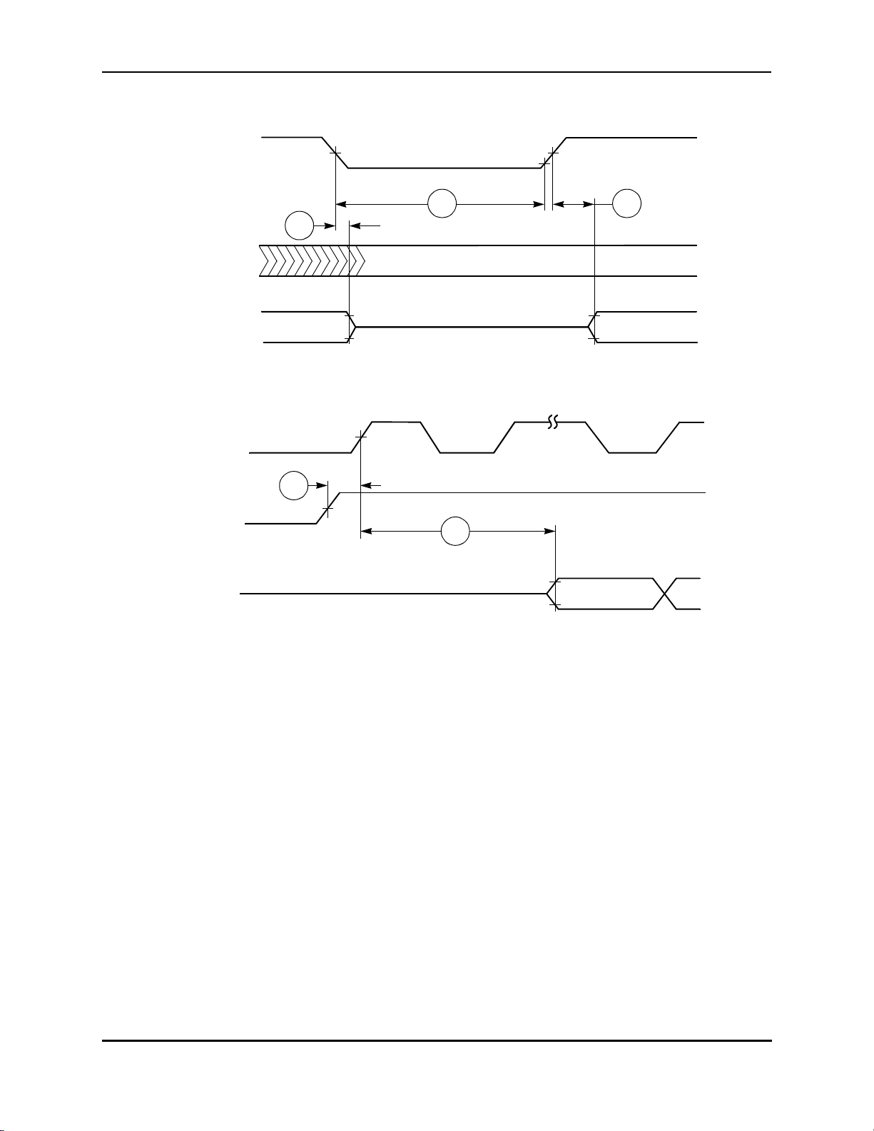
Freescale Semiconductor, Inc.
Specifications
Reset, Stop, Mode Select, and Interrupt Timing
RESET
8
9 10
V
IH
All Pins
A0–A17
Figure 2-2 Reset Timing
nc...
I
CLKOUT
11
RESET
A0–A17
Figure 2-3 Synchronous Reset Timing
cale Semiconductor,
Reset Value
12
First Fetch
AA0460
AA0461
Frees
2-14 DSP56362 Advance Information MOTOROLA
For More Information On This Product,
Go to: www.freescale.com

Freescale Semiconductor, Inc.
Reset, Stop, Mode Select, and Interrupt Timing
Specifications
A0–A17
RD
WR
nc...
I
cale Semiconductor,
IRQA, IRQB,
, IRQD,
IRQC
NMI
General
Purpose
I/O
IRQA
, IRQB,
IRQC
, IRQD,
NMI
a) First Interrupt Instruction Execution
18
b) General Purpose I/O
Figure 2-4 External Fast Interrupt Timing
First Interrupt Instruction
Execution/Fetch
20
21
1917
AA0462
Frees
IRQA, IRQB,
, IRQD,
IRQC
NMI
15
IRQA, IRQB,
, IRQD,
IRQC
NMI
Figure 2-5 External Interrupt Timing (Negative Edge-Triggered)
MOTOROLA DSP56362 Advance Information 2-15
16
AA0463
For More Information On This Product,
Go to: www.freescale.com
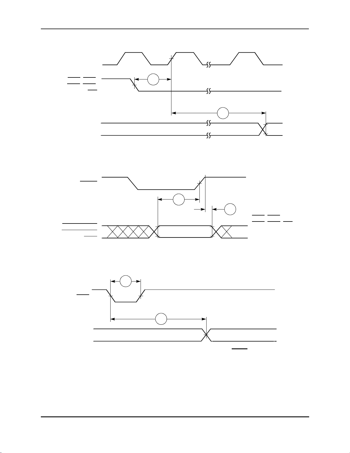
Freescale Semiconductor, Inc.
Specifications
Reset, Stop, Mode Select, and Interrupt Timing
CLKOUT
, IRQB,
IRQA
, IRQD,
IRQC
NMI
A0–A17
nc...
I
MODA, MODB,
MODC, MODD,
Figure 2-6 Synchronous Interrupt from Wait State Timing
RESET
PINIT
Figure 2-7 Operating Mode Select Timing
cale Semiconductor,
IRQA
24
22
13
23
AA0464
V
IH
14
V
IH
V
IL
V
IH
V
IL
IRQA, IRQB,
IRQC
, IRQD, NMI
AA0465
Frees
25
A0–A17
First Instruction Fetch
AA0466
Figure 2-8 Recovery from Stop State Using IRQA
2-16 DSP56362 Advance Information MOTOROLA
For More Information On This Product,
Go to: www.freescale.com
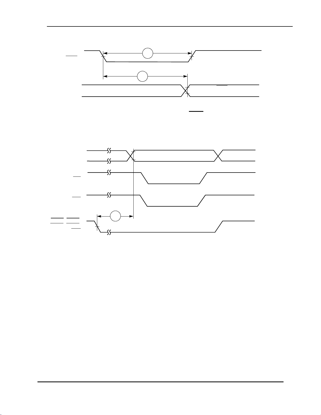
IRQA
Freescale Semiconductor, Inc.
Reset, Stop, Mode Select, and Interrupt Timing
26
25
Specifications
A0–A17
Figure 2-9 Recovery from Stop State Using IRQA Interrupt Service
nc...
I
A0–A17
RD
WR
29
IRQA, IRQB,
IRQC, IRQD,
NMI
Figure 2-10 External Memory Access (DMA Source) Timing
First Interrupt Instruction Execution
DMA Source Address
cale Semiconductor,
First IRQA Interrupt
Instruction Fetch
AA0467
AA1104
Frees
MOTOROLA DSP56362 Advance Information 2-17
For More Information On This Product,
Go to: www.freescale.com
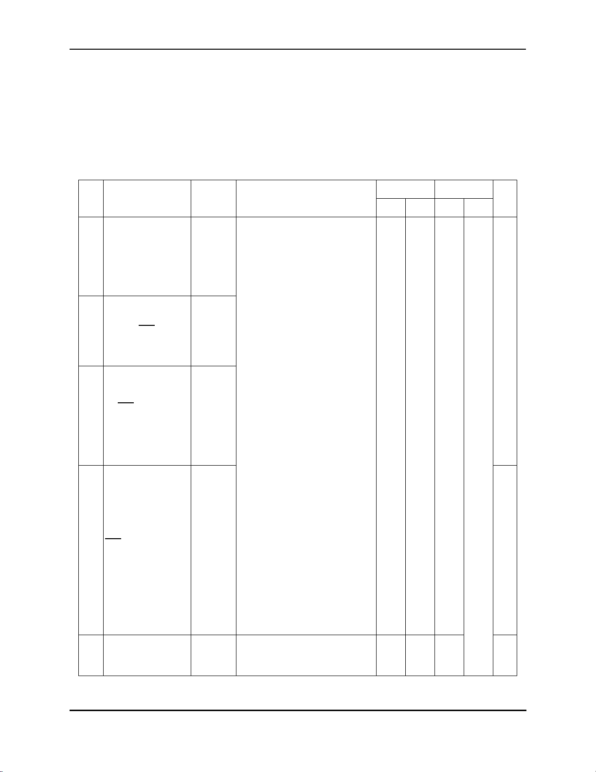
Freescale Semiconductor, Inc.
Specifications
External Memory Expansion Port (Port A)
EXTERNAL MEMORY EXPANSION PORT (PORT A)
SRAM Timing
Table 2-8 SRAM Read and Write Accesses 100 and 120 MHz3
nc...
I
cale Semiconductor,
Frees
No. Characteristics Symbol
Address valid and
100
AA assertion pulse
width
Address and AA
101
valid to WR
assertion
assertion
102
103
WR
pulse width
deassertion to
WR
address not valid
t
RC
t
t
WP
t
WR
, t
AS
WC
Expression
(WS + 1) × TC − 4.0
[1 ≤ WS ≤ 3]
(WS + 2) × T
[4 ≤ WS ≤ 7]
(WS + 3) × T
[WS ≥ 8]
100 MHz:
0.25 × T
[WS = 1]
1.25 × T
[WS ≥ 4]
100 MHz:
1.5 × T
All frequencies:
WS × T
[2 ≤ WS ≤ 3]
(WS − 0.5) × T
[WS ≥ 4]
100 MHz:
0.25 × T
[1 ≤ WS ≤ 3]
1.25 × T
[4 ≤ WS ≤ 7]
2.25 × T
[WS ≥ 8]
− 2.0
C
− 2.0
C
− 4.0 [WS = 1]
C
− 4.0
C
− 2.0
C
− 2.0
C
− 2.0
C
− 4.0
C
− 4.0
C
− 4.0
C
1
100 MHz 120 MHz
Min Max Min Max
16.0 — 12.0 — ns
56.0 — 46.0 — ns
106.0 — 87.0 — ns
0.5 — 0.1 — ns
10.5 — 8.4 — ns
11.0 — 8.5 — ns
16.0 — 12.7 — ns
31.0 --- 25.2 —
0.5 — 0.1 —
10.5 — 8.4 —
20.5 — 16.7 —
Unit
ns
Address and AA
104
valid to input data
valid
t
AA
All frequencies:
1.25 × T
[4 ≤ WS ≤ 7]
2.25 × T
[WS ≥ 8]
100 MHz:
, t
(WS + 0.75) × T
AC
[WS ≥ 1]
C
C
− 4.0
− 4.0
− 7.0
C
8.5
18.5
—10.5 7.6ns
—6.4—
— 14.7 —
2-18 DSP56362 Advance Information MOTOROLA
For More Information On This Product,
Go to: www.freescale.com

Freescale Semiconductor, Inc.
Specifications
External Memory Expansion Port (Port A)
Table 2-8 SRAM Read and Write Accesses 100 and 120 MHz3 (Continued)
nc...
I
cale Semiconductor,
Frees
No. Characteristics Symbol
RD
105
106
107
108
109
110
111
assertion to
input data valid
deassertion to
RD
data not valid (data
hold time)
Address valid to
deassertion
WR
Data valid to WR
deassertion (data
setup time)
Data hold time
from WR
deassertion
assertion to
WR
data active
deassertion to
WR
data high
impedance
2
t
DS
t
OE
t
OHZ
t
AW
(tDW)
t
DH
− 7.0
C
− 3.0
C
1
Expression
100 MHz:
(WS + 0.25) × T
[WS ≥ 1]
(WS + 0.75) × TC − 4.0
[WS ≥ 1]
100 MHz:
(WS − 0.25) × T
[WS ≥ 1]
100 MHz:
0.25 × T
[1 ≤ WS ≤ 3]
1.25 × T
[4 ≤ WS ≤ 7]
2.25 × T
[WS ≥ 8]
0.75 × T
[WS = 1]
0.25 × T
[2 ≤ WS ≤ 3]
−0.25 × T
[WS ≥ 4]
0.25 × T
[1 ≤ WS ≤ 3]
1.25 × T
[4 ≤ WS ≤ 7]
− 2.0
C
− 2.0
C
− 2.0
C
− 3.7
C
− 3.7
C
C
+ 0.2
C
+ 0.2
C
− 3.7
100 MHz 120 MHz
Min Max Min Max
—5.5—3.4ns
0.0 — 0.0 — ns
13.5 — 10.6 — ns
4.5 — 3.2 —
0.5 — 0.1 —
10.5 — 8.4 —
20.5 — 16.7 —
——ns2.5 —
——0.0—
——0.0—
——ns—2.3
— — — 10.6
Unit
ns
ns
+ 0.2
C
− 4.0
C
− 4.0
C
− 4.0
C
— — — 18.9
——ns6.4 —
— — 14.7 —
— — 23.1 —
Previous RD
112
deassertion to data
active (write)
2.25 × T
[WS ≥ 8]
1.25 × T
[1 ≤ WS ≤ 3]
2.25 × T
[4 ≤ WS ≤ 7]
3.25 × T
[WS ≥ 8]
MOTOROLA DSP56362 Advance Information 2-19
For More Information On This Product,
Go to: www.freescale.com

Freescale Semiconductor, Inc.
Specifications
External Memory Expansion Port (Port A)
Table 2-8 SRAM Read and Write Accesses 100 and 120 MHz3 (Continued)
nc...
I
cale Semiconductor,
Frees
No. Characteristics Symbol
RD
113
114
115
116
117
118
deassertion
time
WR
deassertion
time
Address valid to
assertion
RD
RD
assertion pulse
width
deassertion to
RD
address not valid
setup before
TA
RD
or WR
deassertion
4
Expression
100 MHz
0.75 × T
[1 ≤ WS ≤ 3]
1.75 × T
[4 ≤ WS ≤ 7]
2.75 × T
[WS ≥ 8]
100 MHz
0.5 × T
[WS = 1]
− 2.0
T
C
[2 ≤ WS ≤ 3]
2.5 × T
[4 ≤ WS ≤ 7]
3.5 × T
[WS ≥ 8]
100 MHz
0.5 × TC − 4.0
100 MHz
(WS + 0.25) × T
100 MHz
0.25 × T
[1 ≤ WS ≤ 3]
1.25 × T
[4 ≤ WS ≤ 7]
2.25 × T
[WS ≥ 8]
0.25 × TC + 2.0
C
C
C
− 4.0
C
− 4.0
C
− 4.0
C
C
C
C
− 4.0
− 4.0
− 4.0
− 2.0
− 2.0
− 2.0
C
−4.0
1
100 MHz 120 MHz
Unit
Min Max Min Max
3.5 — 2.2 —
13.5 — 10.6 —
23.5 — 18.9 —
1.0 — 0.2 —
6.0 — 6.3 —
21.0 — 16.8 —
31.0 — 25.2 —
1.0 — 0.2 — ns
8.5 — 6.4 — ns
0.5 — 0.1 —
10.5 — 8.4 —
20.5 — 16.7 —
4.5 — 4.1 — ns
ns
ns
ns
hold after RD or
TA
119
WR
deassertion
Notes: 1. WS is the number of wait states specified in the BCR.
2. Timings 100, 107 are guaranteed by design, not tested.
3. All timings for 100 MHz are measured from 0.5
4. In the case of TA negation: timing 118 is relative to the deassertion edge of RD or WR were TA to
remain active
5. Timing 110, 111, and 112, are not specified for 100 MHz.
· Vcc to .05 · Vcc
0 — 0.0 — ns
2-20 DSP56362 Advance Information MOTOROLA
For More Information On This Product,
Go to: www.freescale.com
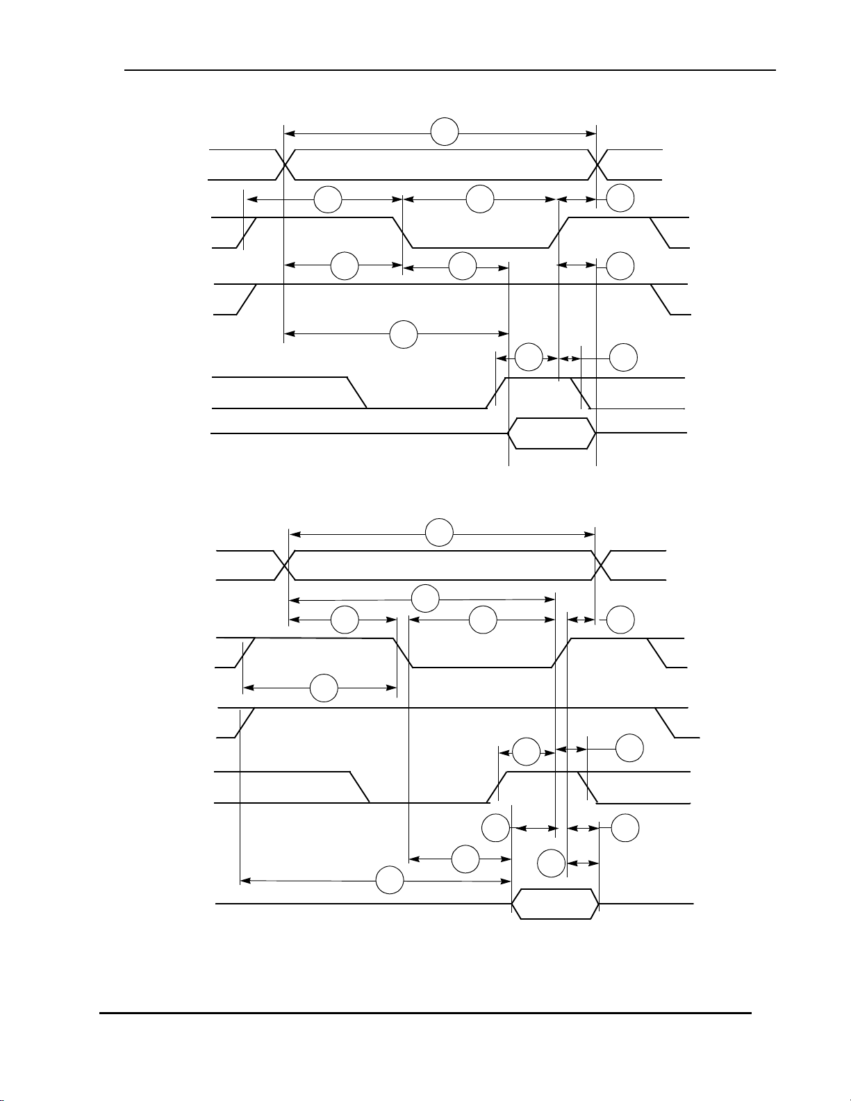
A0–A17
AA0–AA3
Freescale Semiconductor, Inc.
External Memory Expansion Port (Port A)
100
Specifications
nc...
I
cale Semiconductor,
Frees
RD
WR
TA
D0–D23
A0–A17
AA0–AA3
WR
RD
113
115 105 106
104
Figure 2-11 SRAM Read Access
107
114
116
119
Data
In
100
102101
119
117
118
103
118
AA0468
TA
111108
110
112
D0–D23
Figure 2-12 SRAM Write Access
MOTOROLA DSP56362 Advance Information 2-21
109
Data
Out
AA0469
For More Information On This Product,
Go to: www.freescale.com

Freescale Semiconductor, Inc.
Specifications
External Memory Expansion Port (Port A)
DRAM Timing
The selection guides provided in Figure 2-13 and Figure 2-16 should be used for primary selection only.
Final selection should be based on the timing provided in the following tables. As an example, the
selection guide suggests that 4 wait states must be used for 100 MHz operation when using Page Mode
DRAM. However, by using the information in the appropriate table, a designer may choose to evaluate
whether fewer wait states might be used by determining which timing prevents operation at 100 MHz,
running the chip at a slightly lower frequency (e.g., 95 MHz), using faster DRAM (if it becomes available),
and control factors such as capacitive and resistive load to improve overall system performance.
DRAM Type
(tRAC ns)
nc...
I
100
80
70
60
cale Semiconductor,
50
40 66 80 100
Note: This figure should be used for primary selection.
For exact and detailed timings see the following
tables.
Chip Frequency
(MHz)
120
Frees
1 Wait States
2 Wait States
Figure 2-13 DRAM Page Mode Wait States Selection Guide
2-22 DSP56362 Advance Information MOTOROLA
3 Wait States
4 Wait States
AA0472
For More Information On This Product,
Go to: www.freescale.com

Freescale Semiconductor, Inc.
External Memory Expansion Port (Port A)
Specifications
nc...
I
cale Semiconductor,
Frees
Table 2-9 DRAM Page Mode Timings, One Wait State
(Low-Power Applications)
No. Characteristics Symbol Expression
Page mode cycle time for
two consecutive accesses of
the same direction
131
Page mode cycle time for
mixed (read and write)
accesses.
CAS
132
133
134
135
136
137
138
139
140
141
assertion to data valid
(read)
Column address valid to
data valid (read)
deassertion to data not
CAS
valid (read hold time)
Last CAS
deassertion
Previous CAS
RAS
CAS
Last CAS
RAS
• BRW[1:0] = 00 1.75 × T
• BRW[1:0] = 01 3.25 × T
• BRW[1:0] = 10 4.25 × T
• BRW[1:0] = 11 6.25 × T
CAS
Column address valid to
CAS
CAS
address not valid
assertion to RAS
deassertion to
deassertion
assertion pulse width
deassertion to
deassertion
deassertion pulse width
assertion
assertion to column
4
t
PC
t
CAC
t
AA
t
OFF
t
RSH
t
RHCP
t
CAS
t
CRP
t
CP
t
ASC
t
CAH
1.5 × TC − 7.5 — 67.5 — 42.5 ns
2 × T
C
1.25 x Tc 62.5 — 41.7 —
TC − 7.5 — 42.5 — 25.8 ns
0.75 × TC − 4.0 33.5 — 21.0 — ns
2 × TC − 4.0 96.0 — 62.7 — ns
0.75 × TC − 4.0 33.5 — 21.0 — ns
− 6.0 81.5 — 52.3 —
C
− 6.0 156.5 — 102.2 —
C
− 6.0 206.5 — 135.5 —
C
– 6.0 306.5 — 202.1 —
C
0.5 × TC − 4.0 21.0 — 12.7 — ns
0.5 × TC − 4.0 21.0 — 12.7 — ns
0.75 × TC − 4.0 33.5 — 21.0 — ns
1, 2, 3
20 MHz
Min Max Min Max
100.0 — 66.7 —
0.0 — 0.0 — ns
6
30 MHz
6
Unit
ns
ns
Last column address valid to
142
143
144
145
RAS
deassertion
deassertion to CAS
WR
assertion
CAS
deassertion to WR
assertion
CAS
assertion to WR
deassertion
t
RAL
t
RCS
t
RCH
t
WCH
2 × TC − 4.0 96.0 — 62.7 — ns
0.75 × TC − 3.8 33.7 — 21.2 — ns
0.25 × TC − 3.7 8.8 — 4.6 — ns
0.5 × TC − 4.2 20.8 — 12.5 — ns
MOTOROLA DSP56362 Advance Information 2-23
For More Information On This Product,
Go to: www.freescale.com

Freescale Semiconductor, Inc.
Specifications
External Memory Expansion Port (Port A)
nc...
I
cale Semiconductor,
Frees
Table 2-9 DRAM Page Mode Timings, One Wait State
(Low-Power Applications)
No. Characteristics Symbol Expression
146
147
148
149
150
151
152
153
154
155
156
Notes: 1. The number of wait states for Page mode access is specified in the DCR.
assertion pulse width
WR
Last WR
deassertion
WR
deassertion
Data valid to CAS
(Write)
CAS
valid (write)
WR
assertion
Last RD
deassertion
RD
RD
valid
WR
WR
impedance
2. The refresh period is specified in the DCR.
3. All the timings are calculated for the worst case. Some of the timings are better for specific cases
4. BRW[1:0] (DRAM control register bits) defines the number of wait states that should be inserted in
5. RD
6. Reduced DSP clock speed allows use of Page Mode DRAM with one Wait state. See
assertion to RAS
assertion to CAS
assertion
assertion to data not
assertion to CAS
assertion to RAS
assertion to data valid
deassertion to data not
5
assertion to data active
deassertion to data high
(e.g., t
each DRAM out-of-page access.
not t
equals 2 × TC for read-after-read or write-after-write sequences).
PC
deassertion will always occur after CAS deassertion; therefore, the restricted timing is t
.
GZ
tWP 1.5 × TC − 4.5 70.5 — 45.5 — ns
t
RWL
t
CWL
t
DS
t
DH
t
WCS
t
ROH
t
GA
t
GZ
1.75 × TC − 4.3 83.2 — 54.0 — ns
1.75 × TC − 4.3 83.2 — 54.0 — ns
0.25 × TC − 4.0 8.5 — 4.3 — ns
0.75 × TC − 4.0 33.5 — 21.0 — ns
1.5 × TC − 4.0 71.0 — 46.0 — ns
T
0.75 × T
1, 2, 3
(Continued)
20 MHz
Min Max Min Max
TC − 4.3 45.7 — 29.0 — ns
− 7.5 — 42.5 — 25.8 ns
C
0.0 — 0.0 — ns
− 0.3 37.2 — 24.7 — ns
C
0.25 × T
C
— 12.5 — 8.3 ns
6
Table 2-10 DRAM Page Mode Timings, Two Wait States
30 MHz
1, 2, 3, 7
6
Unit
and
OFF
Figure 2-13.
No. Characteristics Symbol Expression
Page mode cycle time for two
consecutive accesses of the same
direction
131
Page mode cycle time for mixed (read
and write) accesses.
t
PC
3 × T
C
2.75 x Tc
80 MHz
Min Max
37.5 —
34.4
—
Unit
ns
2-24 DSP56362 Advance Information MOTOROLA
For More Information On This Product,
Go to: www.freescale.com

Freescale Semiconductor, Inc.
External Memory Expansion Port (Port A)
Specifications
nc...
I
cale Semiconductor,
Frees
Table 2-10 DRAM Page Mode Timings, Two Wait States
No. Characteristics Symbol Expression
132
CAS
assertion to data valid (read)
Column address valid to data valid
133
(read)
deassertion to data not valid (read
CAS
134
hold time)
135
Last CAS
Previous CAS
136
deassertion
137
CAS
Last CAS
deassertion
• BRW[1:0] = 00 2.0 × T
138
• BRW[1:0] = 01 3.5 × T
• BRW[1:0] = 10 4.5 × T
• BRW[1:0] = 11 6.5 × T
139
CAS
140
Column address valid to CAS
CAS
141
valid
Last column address valid to RAS
142
deassertion
143
WR
144
CAS
145
CAS
146
WR
147
Last WR
148
WR
149
Data valid to CAS
150
CAS
151
WR
152
Last RD
153
RD
154
RD
155
WR
assertion to RAS deassertion
deassertion to RAS
assertion pulse width
deassertion to RAS
5
deassertion pulse width
assertion
assertion to column address not
deassertion to CAS assertion
deassertion to WR assertion
assertion to WR deassertion
assertion pulse width
assertion to RAS deassertion
assertion to CAS deassertion
assertion (write)
assertion to data not valid (write)
assertion to CAS assertion
assertion to RAS deassertion
assertion to data valid
deassertion to data not valid
assertion to data active
6
t
CAC
t
AA
t
OFF
t
RSH
t
RHCP
t
CAS
t
CRP
t
CP
t
ASC
t
CAH
t
RAL
t
RCS
t
RCH
t
WCH
2.5 × TC − 4.5 26.8 — ns
t
WP
t
RWL
t
CWL
t
DS
t
DH
t
WCS
t
ROH
t
GA
t
GZ
1.5 × TC − 6.5 — 12.3 ns
2.5 × TC − 6.5 — 24.8 ns
1.75 × TC − 4.0 17.9 — ns
3.25 × TC − 4.0 36.6 — ns
1.5 × TC − 4.0 14.8 — ns
1.25 × TC − 4.0 11.6 — ns
TC − 4.0 8.5 — ns
1.75 × TC − 4.0 17.9 — ns
3 × TC − 4.0 33.5 — ns
1.25 × TC − 3.8 11.8 — ns
0.5 × TC − 3.7 2.6 — ns
1.5 × TC − 4.2 14.6 — ns
2.75 × TC − 4.3 30.1 — ns
2.5 × TC − 4.3 27.0 — ns
0.25 × TC − 3.0 0.1 — ns
1.75 × TC − 4.0 17.9 — ns
TC − 4.3 8.2 — ns
2.5 × TC − 4.0 27.3 — ns
1.75 × TC − 6.5 — 15.4 ns
0.75 × T
1, 2, 3, 7
− 6.0 19.0 —
C
− 6.0 37.8 —
C
− 6.0 50.3 —
C
− 6.0 75.3 —
C
− 0.3 9.1 — ns
C
(Continued)
80 MHz
Min Max
0.0 — ns
0.0 — ns
Unit
ns
MOTOROLA DSP56362 Advance Information 2-25
For More Information On This Product,
Go to: www.freescale.com
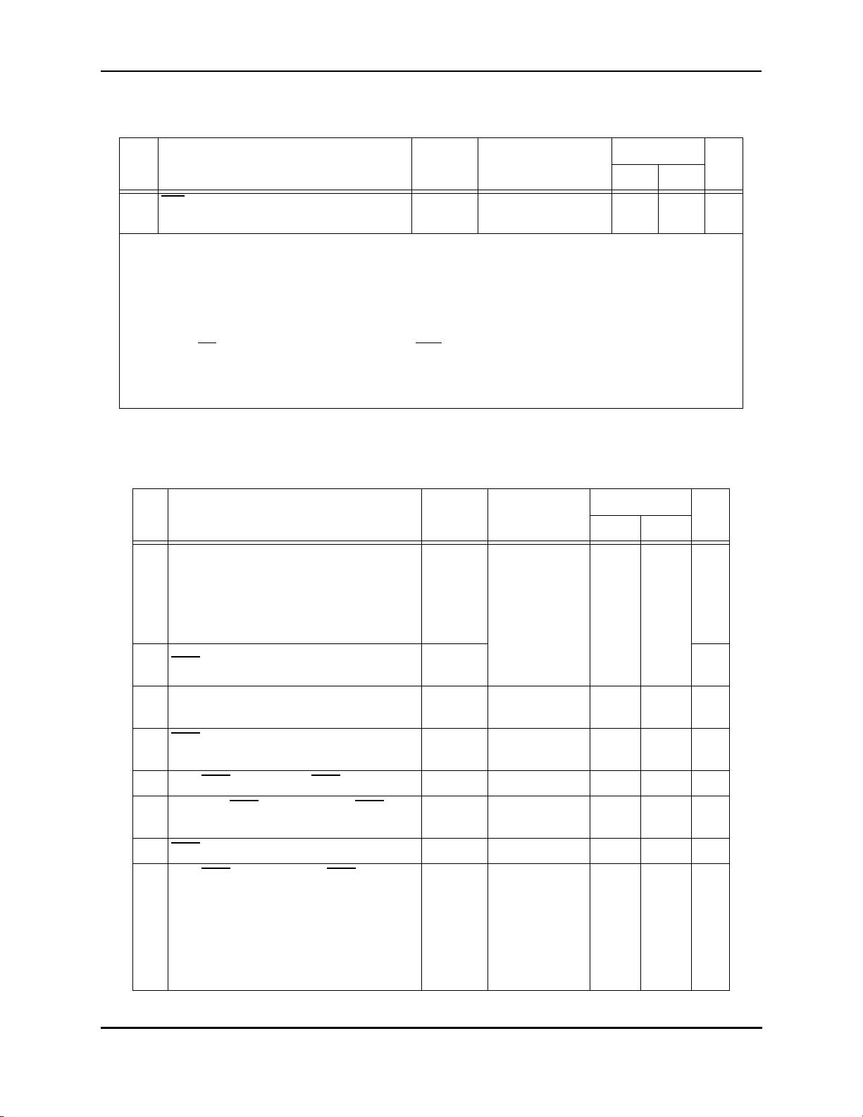
Freescale Semiconductor, Inc.
Specifications
External Memory Expansion Port (Port A)
nc...
I
cale Semiconductor,
Frees
Table 2-10 DRAM Page Mode Timings, Two Wait States
No. Characteristics Symbol Expression
WR
156
Notes: 1. The number of wait states for Page mode access is specified in the DCR.
deassertion to data high
impedance
2. The refresh period is specified in the DCR.
3. The asynchronous delays specified in the expressions are valid for
4. All the timings are calculated for the worst case. Some of the timings are better for specific cases
(e.g., tPC equals 3 × TC for read-after-read or write-after-write sequences).
5. BRW[1:0] (DRAM Control Register bits) defines the number of wait states that should be inserted
in each DRAM out-of-page access.
6. RD
7. There are not any fast enough DRAMs to fit to two wait states Page mode @ 100MHz. See
deassertion will always occur after CAS deassertion; therefore, the restricted timing is t
and not t
Figure 2-13.
GZ.
0.25 × T
1, 2, 3, 7
C
DSP56362.
Table 2-11 DRAM Page Mode Timings, Three Wait States
No. Characteristics Symbol Expression
Page mode cycle time for two
consecutive accesses of the same
direction
131
Page mode cycle time for mixed (read
and write) accesses.
132
CAS
assertion to data valid (read)
Column address valid to data valid
133
(read)
CAS
134
135
deassertion to data not valid (read
hold time)
Last CAS
assertion to RAS deassertion
t
PC
t
CAC
t
AA
t
OFF
t
RSH
4 × T
C
3.5 x Tc 35.0 —
100 MHz:
2 × T
100 MHz:
3 × T
2.5 × TC − 4.0 21.0 — ns
C
C
− 7.0
− 7.0
(Continued)
80 MHz
Min Max
—3.1ns
1, 2, 3
100 MHz
Unit
Min Max
40.0 —
— 13.0 ns
— 23.0 ns
0.0 — ns
Unit
OFF
ns
Previous CAS
136
deassertion
137
CAS
assertion pulse width
Last CAS
assertion
• BRW[1:0] = 00 2.25 × T
138
• BRW[1:0] = 01 3.75 × T
• BRW[1:0] = 10 4.75 × T
• BRW[1:0] = 11 6.75 × T
deassertion to RAS
deassertion to RAS
5
t
RHCP
t
CAS
t
CRP
4.5 × TC − 4.0 41.0 — ns
2 × TC − 4.0 16.0 — ns
− 6.0 — —
C
− 6.0 — —
C
− 6.0 41.5 —
C
− 6.0 61.5 —
C
ns
2-26 DSP56362 Advance Information MOTOROLA
For More Information On This Product,
Go to: www.freescale.com

Freescale Semiconductor, Inc.
External Memory Expansion Port (Port A)
Specifications
nc...
I
cale Semiconductor,
Frees
Table 2-11 DRAM Page Mode Timings, Three Wait States
No. Characteristics Symbol Expression
139
CAS
deassertion pulse width
140
Column address valid to CAS
CAS
141
142
143
144
145
146
147
148
149
150
151
152
153
154
155
156
Notes: 1. The number of wait states for Page mode access is specified in the DCR.
assertion to column address not
valid
Last column address valid to RAS
deassertion
WR
deassertion to CAS assertion
CAS
deassertion to WR assertion
CAS
assertion to WR deassertion
WR
assertion pulse width
Last WR
WR
Data valid to CAS
CAS
WR
Last RD
RD
RD
WR
WR
impedance
assertion to RAS deassertion
assertion to CAS deassertion
assertion (write)
assertion to data not valid (write)
assertion to CAS assertion
assertion to RAS deassertion
assertion to data valid
deassertion to data not valid6
assertion to data active
deassertion to data high
2. The refresh period is specified in the DCR.
3. The asynchronous delays specified in the expressions are valid for DSP56362.
4. All the timings are calculated for the worst case. Some of the timings are better for specific
cases (e.g., t
5. BRW[1:0] (DRAM control register bits) defines the number of wait states that should be
inserted in each DRAM out-of page-access.
6. RD
deassertion will always occur after CAS deassertion; therefore, the restricted timing is
and not tGZ.
t
OFF
equals 4 × TC for read-after-read or write-after-write sequences).
PC
assertion
t
CP
t
ASC
t
CAH
t
RAL
t
RCS
t
RCH
t
WCH
t
WP
t
RWL
t
CWL
t
DS
t
DH
t
WCS
t
ROH
t
GA
t
GZ
1.5 × TC − 4.0 11.0 — ns
TC − 4.0 6.0 — ns
2.5 × TC − 4.0 21.0 — ns
4 × TC − 4.0 36.0 — ns
100 MHz:
1.25 × T
100 MHz:
0.75 × T
2.25 × TC − 4.2 18.3 — ns
3.5 × TC − 4.5 30.5 — ns
3.75 × TC − 4.3 33.2 — ns
3.25 × TC − 4.3 28.2 — ns
0.5 × TC − 4.0 1.0 — ns
2.5 × TC − 4.0 21.0 — ns
1.25 × TC − 4.3 8.2 — ns
3.5 × TC − 4.0 31.0 — ns
100 MHz:
2.5 × T
0.75 × T
0.25 × T
1, 2, 3
Min Max
− 4.0
C
− 4.0
C
− 7.0
C
− 0.3 7.2 — ns
C
C
8.5 ns
3.5 ns
— 18.0 ns
0.0 — ns
—2.5ns
(Continued)
100 MHz
Unit
MOTOROLA DSP56362 Advance Information 2-27
For More Information On This Product,
Go to: www.freescale.com
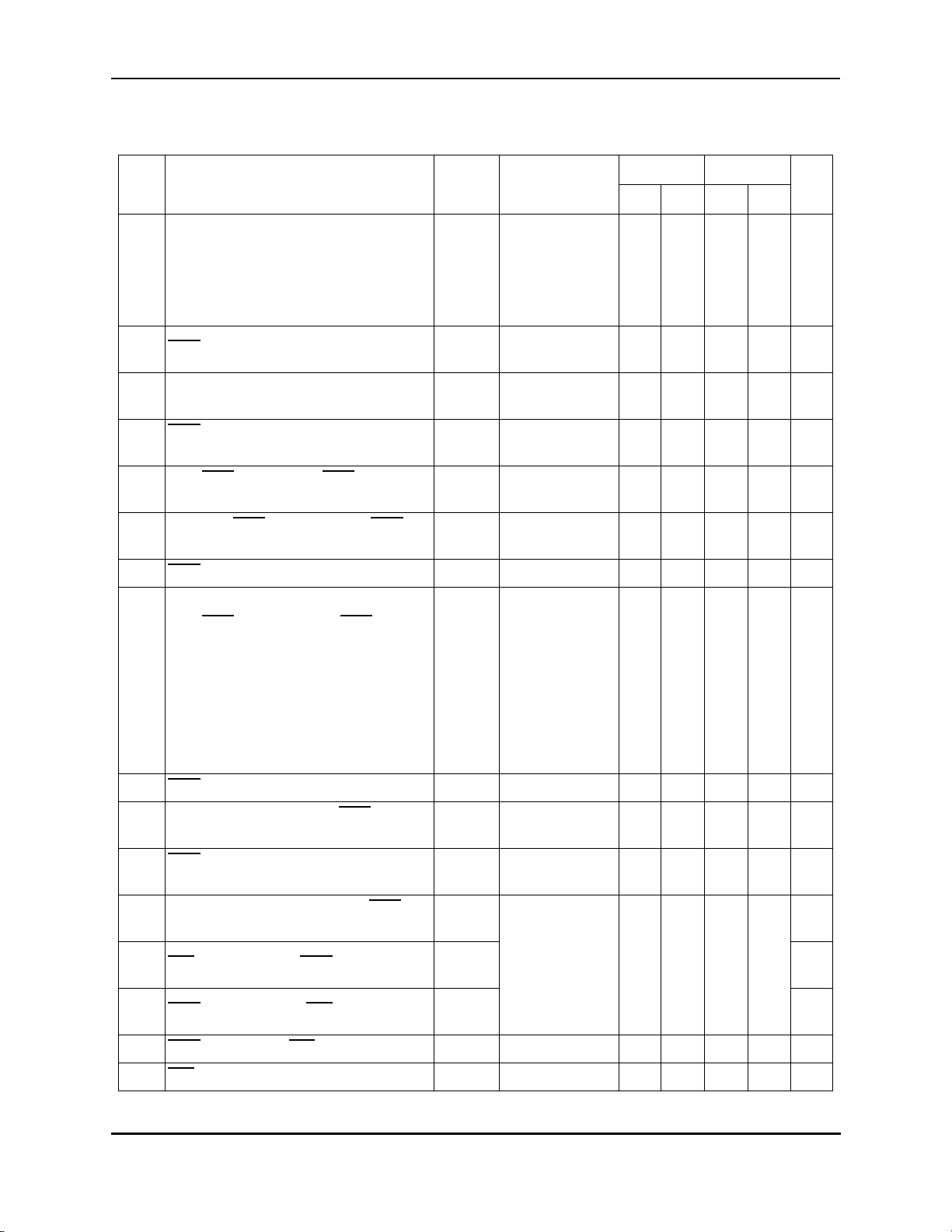
Freescale Semiconductor, Inc.
Specifications
External Memory Expansion Port (Port A)
nc...
I
cale Semiconductor,
Frees
Table 2-12 DRAM Page Mode Timings, Four Wait States 100 and 120MHz
No. Characteristics Symbol Expression
Page mode cycle time for two
consecutive accesses of the same
direction
131
Page mode cycle time for mixed (read
and write) accesses.
132
133
134
135
136
137
138
139
140
141
assertion to data valid (read)
CAS
Column address valid to data valid
(read)
deassertion to data not valid
CAS
(read hold time)
Last CAS
deassertion
Previous CAS
deassertion
CAS
Last CAS
assertion
• BRW[1:0] = 00 2.75 × T
• BRW[1:0] = 01 4.25 × T
• BRW[1:0] = 10 5.25 × T
• BRW[1:0] = 11 7.25 × T
CAS
Column address valid to CAS
assertion
CAS
valid
assertion to RAS
deassertion to RAS
assertion pulse width
deassertion to RAS
5
deassertion pulse width
assertion to column address not
t
PC
t
CAC
t
AA
t
OFF
t
RSH
t
RHCP
t
CAS
t
CRP
t
CP
t
ASC
t
CAH
5 × T
C
4.5 × T
C
100 MHz:
2.75 × T
100 MHz:
3.75 × T
3.5 × TC − 4.0 31.0 — 25.2 — ns
6 × TC − 4.0 56.0 — 46.0 — ns
2.5 × TC − 4.0 21.0 — 16.8 — ns
2 × TC − 4.0 16.0 — 12.7 — ns
3.5 × TC − 4.0 31.0 — 25.2 — ns
− 7.0
C
− 7.0
C
− 6.0————
C
− 6.0————
C
− 6.0 46.5 — 37.7 —
C
− 6.0 66.5 — 54.4 —
C
TC − 4.0 6.0 — 4.3 — ns
100 MHz 120 MHz
Min Max Min Max
50.0 — 41.7
45.0 — 37.5
— 20.5 — 15.9 ns
— 30.5 — 24.2 ns
0.0 — 0.0 — ns
1, 2, 3
Unit
ns
ns
Last column address valid to RAS
142
deassertion
143
WR
deassertion to CAS assertion
144
CAS
deassertion to WR assertion
145
CAS
assertion to WR deassertion
146
WR
assertion pulse width
t
RAL
t
RCS
t
RCH
t
WCH
t
WP
5 × TC − 4.0 46.0 — 37.7 — ns
100 MHz:
1.25 × T
100 MHz:
1.25 × T
3.25 × TC − 4.2 28.3 — 22.9 — ns
4.5 × TC − 4.5 40.5 — 33.0 — ns
C
C
− 4.0
− 4.0
8.5 — 6.4 — ns
8.5 — 6.4 — ns
2-28 DSP56362 Advance Information MOTOROLA
For More Information On This Product,
Go to: www.freescale.com
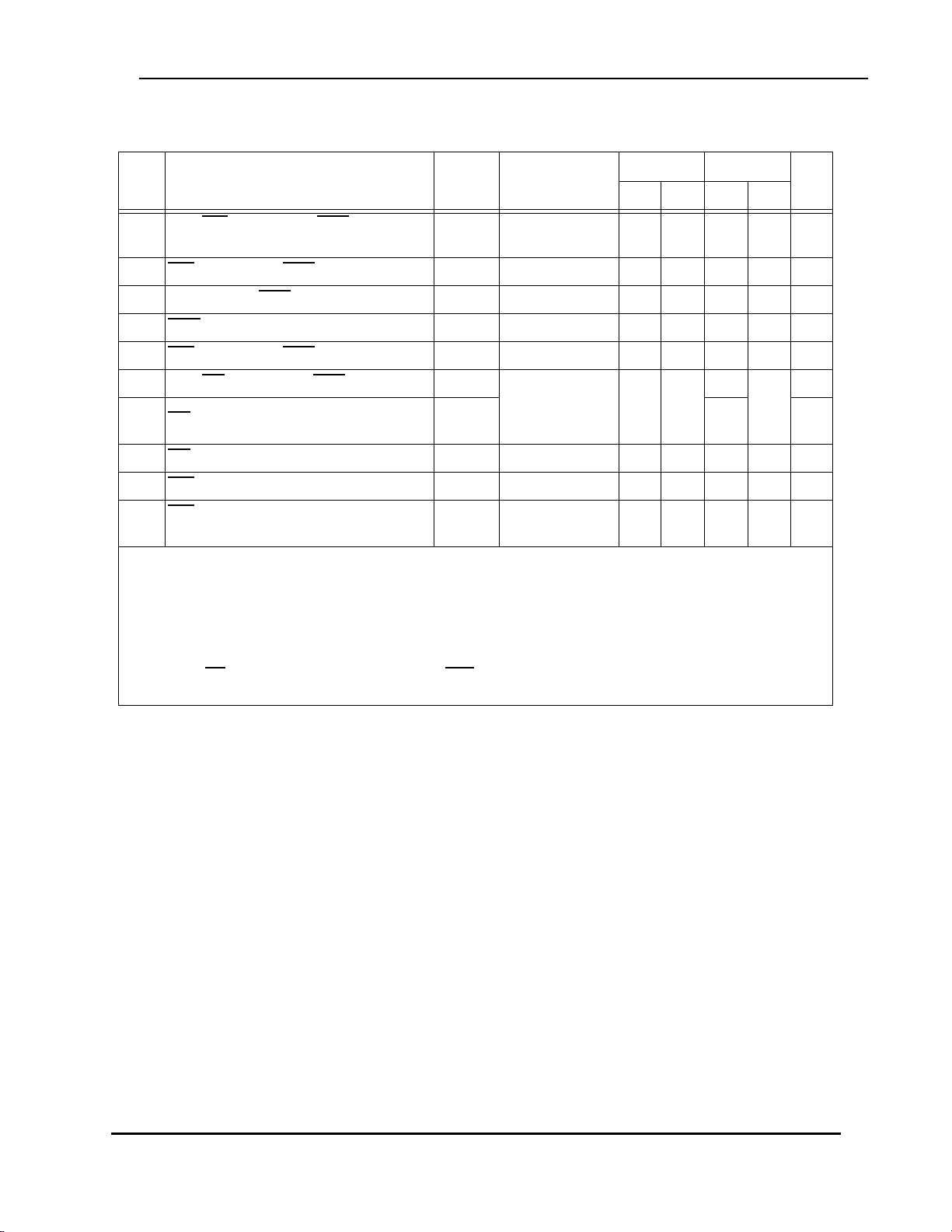
Freescale Semiconductor, Inc.
External Memory Expansion Port (Port A)
Specifications
Table 2-12 DRAM Page Mode Timings, Four Wait States 100 and 120MHz
No. Characteristics Symbol Expression
Last WR
147
deassertion
148
WR
149
Data valid to CAS
150
CAS
151
WR
152
Last RD
153
nc...
I
RD
154
RD
155
WR
WR
156
impedance
Notes: 1. The number of wait states for Page mode access is specified in the DCR.
2. The refresh period is specified in the DCR.
3. The asynchronous delays specified in the expressions are valid for DSP56362.
4. All the timings are calculated for the worst case. Some of the timings are better for specific cases
5. BRW[1:0] (DRAM control register bits) defines the number of wait states that should be inserted in
6. RD
assertion to RAS
assertion to CAS deassertion
assertion (write)
assertion to data not valid (write)
assertion to CAS assertion
assertion to RAS deassertion
assertion to data valid
deassertion to data not valid
assertion to data active
deassertion to data high
(e.g., t
each DRAM out-of-page access.
not t
equals 3 × TC for read-after-read or write-after-write sequences).
PC
deassertion will always occur after CAS deassertion; therefore, the restricted timing is t
.
GZ
6
t
RWL
t
CWL
t
DS
t
DH
t
WCS
t
ROH
t
GA
t
GZ
4.75 × TC − 4.3 43.2 — 35.3 — ns
3.75 × TC − 4.3 33.2 — 26.9 — ns
0.5 × TC − 4.0 1.0 — 0.2 — ns
3.5 × TC − 4.0 31.0 — 25.2 — ns
1.25 × TC − 4.3 8.2 — 6.1 — ns
4.5 × TC − 4.0 41.0 — 33.5 — ns
100 MHz:
3.25 × T
0.75 × T
0.25 × T
− 7.0
C
− 0.3 7.2 — 5.9 ns
C
C
100 MHz 120 MHz
Min Max Min Max
— 25.5 — 20.1 ns
0.0 — 0.0 — ns
—2.5—2.1ns
cale Semiconductor,
1, 2, 3
(Continued)
OFF
Unit
and
Frees
MOTOROLA DSP56362 Advance Information 2-29
For More Information On This Product,
Go to: www.freescale.com
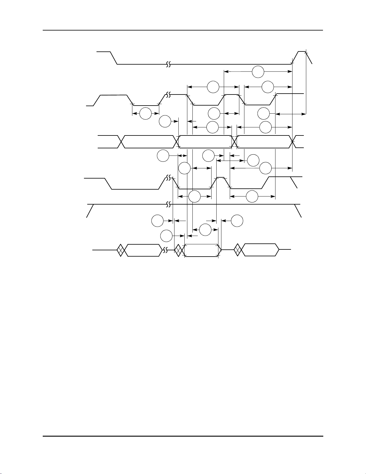
Freescale Semiconductor, Inc.
Specifications
External Memory Expansion Port (Port A)
RAS
CAS
136
135131
137
140
A0–A17
nc...
I
WR
RD
D0–D23
Row
Add
Figure 2-14 DRAM Page Mode Write Accesses
Column
Address
145
155 156
149
cale Semiconductor,
139
141
Address Address
144151
150
Data Out Data Out Data Out
Last ColumnColumn
143
148146
138
142
147
AA0473
Frees
2-30 DSP56362 Advance Information MOTOROLA
For More Information On This Product,
Go to: www.freescale.com
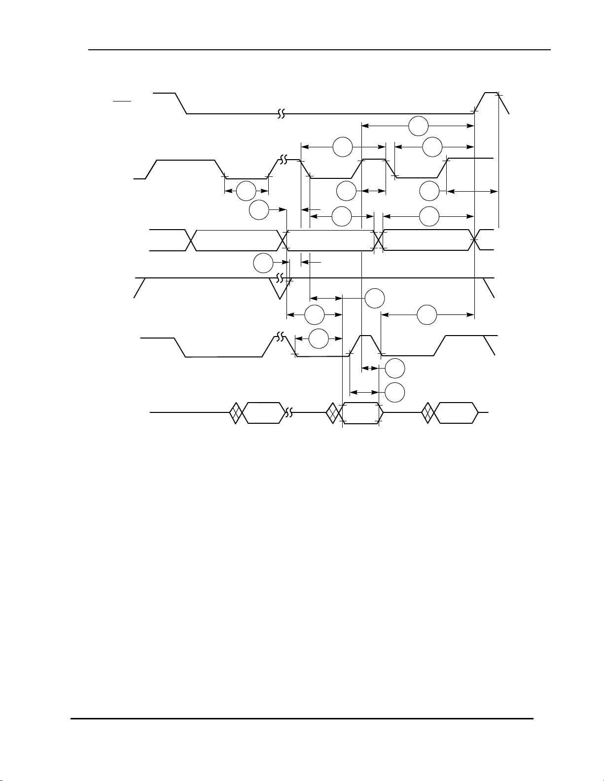
RAS
CAS
Freescale Semiconductor, Inc.
External Memory Expansion Port (Port A)
136
Specifications
135131
137
140
A0–A17
nc...
I
WR
RD
D0–D23
Row
Add
Figure 2-15 DRAM Page Mode Read Accesses
Column
Address Address
143
141 142
Column
132
153
134
154
Data In Data InData In
cale Semiconductor,
138139
Last Column
Address
152133
AA0474
Frees
MOTOROLA DSP56362 Advance Information 2-31
For More Information On This Product,
Go to: www.freescale.com
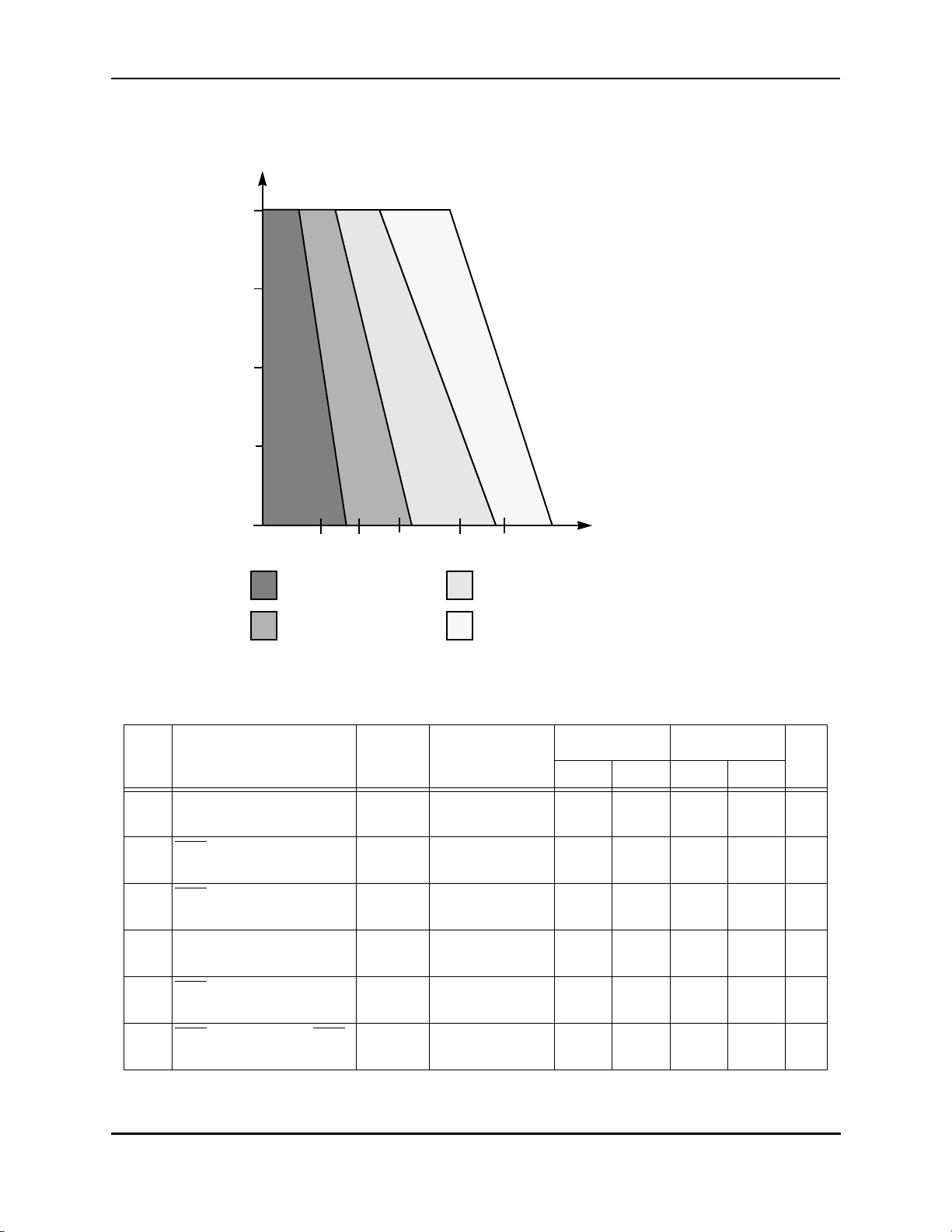
Freescale Semiconductor, Inc.
Specifications
External Memory Expansion Port (Port A)
DRAM Type
(tRAC ns)
100
80
70
Note: This figure should be use for primary selection. For
exact and detailed timings see the following tables.
nc...
I
cale Semiconductor,
Frees
60
50
66 80 100
40
4 Wait States
8 Wait States
120
11 Wait States
15 Wait States
Chip Frequency
(MHz)
Figure 2-16 DRAM Out-of-Page Wait States Selection Guide
Table 2-13 DRAM Out-of-Page and Refresh Timings, Four Wait States
4
No.
157
158
Characteristics
Random read or write
cycle time
RAS
assertion to data
valid (read)
3
Symbol Expression
t
5 × T
RC
t
RAC
2.75 × TC − 7.5 — 130.0 — 84.2 ns
C
20 MHz
Min Max Min Max
250.0 — 166.7 — ns
30 MHz
AA0475
1, 2
4
Unit
CAS
159
160
161
162
assertion to data
valid (read)
Column address valid to
data valid (read)
deassertion to data
CAS
not valid (read hold time)
RAS
deassertion to RAS
assertion
t
CAC
t
t
OFF
t
AA
RP
1.25 × TC − 7.5 — 55.0 — 34.2 ns
1.5 × TC − 7.5 — 67.5 — 42.5 ns
0.0 — 0.0 — ns
1.75 × TC − 4.0 83.5 — 54.3 — ns
2-32 DSP56362 Advance Information MOTOROLA
For More Information On This Product,
Go to: www.freescale.com
Freescale Semiconductor, Inc.
External Memory Expansion Port (Port A)
Specifications
nc...
I
cale Semiconductor,
Frees
Table 2-13 DRAM Out-of-Page and Refresh Timings, Four Wait States
4
No.
163
164
165
166
167
168
169
170
171
172
173
174
175
176
Characteristics
RAS
assertion pulse
width
assertion to RAS
CAS
deassertion
RAS
assertion to CAS
deassertion
assertion pulse
CAS
width
RAS
assertion to CAS
assertion
assertion to column
RAS
address valid
CAS
deassertion to RAS
assertion
deassertion pulse
CAS
width
Row address valid to
RAS
assertion
RAS
assertion to row
address not valid
Column address valid to
assertion
CAS
CAS
assertion to column
address not valid
RAS
assertion to column
address not valid
Column address valid to
RAS
deassertion
3
Symbol Expression
t
RAS
t
RSH
t
CSH
t
CAS
t
RCD
t
RAD
t
CRP
t
t
ASR
t
RAH
t
ASC
t
CAH
t
t
RAL
CP
AR
3.25 × TC − 4.0 158.5 — 104.3 — ns
1.75 × TC − 4.0 83.5 — 54.3 — ns
2.75 × TC − 4.0 133.5 — 87.7 — ns
1.25 × TC − 4.0 58.5 — 37.7 — ns
1.5 × TC ± 2 73.0 77.0 48.0 52.0 ns
1.25 × TC ± 2 60.5 64.5 39.7 43.7 ns
2.25 × TC − 4.0 108.5 — 71.0 — ns
1.75 × TC − 4.0 83.5 — 54.3 — ns
1.75 × TC − 4.0 83.5 — 54.3 — ns
1.25 × TC − 4.0 58.5 — 37.7 — ns
0.25 × TC − 4.0 8.5 — 4.3 — ns
1.75 × TC − 4.0 83.5 — 54.3 — ns
3.25 × TC − 4.0 158.5 — 104.3 — ns
2 × TC − 4.0 96.0 — 62.7 — ns
20 MHz
Min Max Min Max
1, 2
(Continued)
30 MHz
4
Unit
WR
177
178
179
180
181
deassertion to CAS
assertion
CAS
deassertion to WR
assertion
deassertion to WR
RAS
assertion
CAS
assertion to WR
deassertion
RAS
assertion to WR
deassertion
t
RCS
t
RCH
t
RRH
t
WCH
t
WCR
1.5 × TC − 3.8 71.2 — 46.2 — ns
0.75 × TC − 3.7 33.8 — 21.3 — ns
0.25 × TC − 3.7 8.8 — 4.6 — ns
1.5 × TC − 4.2 70.8 — 45.8 — ns
3 × TC − 4.2 145.8 — 95.8 — ns
MOTOROLA DSP56362 Advance Information 2-33
For More Information On This Product,
Go to: www.freescale.com
Freescale Semiconductor, Inc.
Specifications
External Memory Expansion Port (Port A)
nc...
I
cale Semiconductor,
Frees
Table 2-13 DRAM Out-of-Page and Refresh Timings, Four Wait States
No.
182
183
184
185
186
187
188
189
190
191
192
193
194
195
Notes: 1. The number of wait states for out of page access is specified in the DCR.
Characteristics
WR
assertion pulse width
WR
assertion to RAS
deassertion
WR
assertion to CAS
deassertion
Data valid to CAS
assertion (write)
CAS
assertion to data not
valid (write)
RAS
assertion to data not
valid (write)
assertion to CAS
WR
assertion
CAS
assertion to RAS
assertion (refresh)
deassertion to CAS
RAS
assertion (refresh)
RD
assertion to RAS
deassertion
RD
assertion to data valid
RD
deassertion to data
not valid
WR
active
WR
high impedance
2. The refresh period is specified in the DCR.
3. RD
4. Reduced DSP clock speed allows use of DRAM out-of-page access with four Wait states. See
3
assertion to data
deassertion to data
deassertion will always occur after CAS deassertion; therefore, the restricted timing is t
not t
.
GZ
Figure 2-16.
3
Symbol Expression
t
WP
t
RWL
t
CWL
t
DS
t
DH
t
DHR
t
WCS
t
CSR
t
RPC
t
ROH
t
GA
t
GZ
4.5 × TC − 4.5 220.5 — 145.5 — ns
4.75 × TC − 4.3 233.2 — 154.0 — ns
4.25 × TC − 4.3 208.2 — 137.4 — ns
2.25 × TC − 4.0 108.5 — 71.0 — ns
1.75 × TC − 4.0 83.5 — 54.3 — ns
3.25 × TC − 4.0 158.5 — 104.3 — ns
3 × TC − 4.3 145.7 — 95.7 — ns
0.5 × TC − 4.0 21.0 — 12.7 — ns
1.25 × TC − 4.0 58.5 — 37.7 — ns
4.5 × TC − 4.0 221.0 — 146.0 — ns
4 × TC − 7.5 — 192.5 — 125.8 ns
0.75 × T
0.25 × T
− 0.3 37.2 — 24.7 — ns
C
C
20 MHz
Min Max Min Max
0.0 — 0.0 — ns
— 12.5 — 8.3 ns
4
1, 2
(Continued)
30 MHz
4
OFF
Unit
and
2-34 DSP56362 Advance Information MOTOROLA
For More Information On This Product,
Go to: www.freescale.com

Freescale Semiconductor, Inc.
External Memory Expansion Port (Port A)
Specifications
nc...
I
cale Semiconductor,
Frees
Table 2-14 DRAM Out-of-Page and Refresh Timings, Eight Wait States
No.
157
Random read or write cycle time
158
RAS
assertion to data valid (read)
159
CAS
assertion to data valid (read)
160
Column address valid to data valid (read)
CAS
161
162
163
164
165
166
167
168
169
170
171
172
173
174
175
176
177
178
179
180
181
182
183
184
185
deassertion to data not valid (read
hold time)
RAS
deassertion to RAS assertion
RAS
assertion pulse width
CAS
assertion to RAS deassertion
RAS
assertion to CAS deassertion
CAS
assertion pulse width
RAS
assertion to CAS assertion
RAS
assertion to column address valid
CAS
deassertion to RAS assertion
CAS
deassertion pulse width
Row address valid to RAS
RAS
assertion to row address not valid
Column address valid to CAS
CAS
assertion to column address not valid
RAS
assertion to column address not valid
Column address valid to RAS
WR
deassertion to CAS assertion
CAS
deassertion to WR5 assertion
RAS
deassertion to WR5 assertion
CAS
assertion to WR deassertion
RAS
assertion to WR deassertion
assertion pulse width
WR
WR
assertion to RAS deassertion
WR
assertion to CAS deassertion
Data valid to CAS
Characteristics
assertion (write)
4
assertion
assertion
deassertion
Symbol
9 × T
t
RC
t
RAC
t
CAC
t
AA
t
OFF
t
RP
t
RAS
t
RSH
t
CSH
t
CAS
t
RCD
t
RAD
t
CRP
t
CP
t
ASR
t
RAH
t
ASC
t
CAH
t
AR
t
RAL
t
RCS
t
RCH
t
RRH
t
WCH
t
WCR
t
WP
t
RWL
t
CWL
t
DS
Expression
4.75 × TC − 6.5 52.9 ns
2.25 × TC − 6.5 — 21.6 ns
3 × TC − 6.5 — 31.0 ns
3.25 × TC − 4.0 36.6 — ns
5.75 × TC − 4.0 67.9 — ns
3.25 × TC − 4.0 36.6 — ns
4.75 × TC − 4.0 55.4 — ns
2.25 × TC − 4.0 24.1 — ns
2.5 × TC ± 2 29.3 33.3 ns
1.75 × TC ± 2 19.9 23.9 ns
4.25 × TC − 4.0 49.1 — ns
2.75 × TC − 4.0 30.4 — ns
3.25 × TC − 4.0 36.6 — ns
1.75 × TC − 4.0 17.9 — ns
0.75 × TC − 4.0 5.4 — ns
3.25 × TC − 4.0 36.6 — ns
5.75 × TC − 4.0 67.9 — ns
4 × TC − 4.0 46.0 — ns
2 × TC − 3.8 21.2 — ns
1.25 × TC − 3.7 11.9 — ns
0.25 × TC − 3.0 0.1 — ns
3 × TC − 4.2 33.3 — ns
5.5 × TC − 4.2 64.6 — ns
8.5 × TC − 4.5
8.75 × TC − 4.3
7.75 × TC − 4.3 92.6 — ns
4.75 × TC − 4.0 55.4 — ns
3
C
1, 2
80 MHz
Min Max
112.
5
0.0 — ns
101.
8
105.
1
Unit
—ns
—ns
—ns
MOTOROLA DSP56362 Advance Information 2-35
For More Information On This Product,
Go to: www.freescale.com

Freescale Semiconductor, Inc.
Specifications
External Memory Expansion Port (Port A)
nc...
I
cale Semiconductor,
Frees
Table 2-14 DRAM Out-of-Page and Refresh Timings, Eight Wait States
No.
186
CAS
assertion to data not valid (write)
187
RAS
assertion to data not valid (write)
188
WR
assertion to CAS assertion
189
CAS
assertion to RAS assertion (refresh)
190
RAS
deassertion to CAS assertion (refresh)
191
192
193
194
195
Notes: 1. The number of wait states for out-of-page access is specified in the DCR.
assertion to RAS deassertion
RD
RD
assertion to data valid
RD
deassertion to data not valid
WR
assertion to data active
WR
deassertion to data high impedance
2. The refresh period is specified in the DCR.
3. The asynchronous delays specified in the expressions are valid for DSP56362.
4. RD
5. Either t
Characteristics
deassertion will always occur after CAS deassertion; therefore, the restricted timing is t
and not t
GZ
RCH
.
or t
RRH
4
4
must be satisfied for read cycles.
Symbol
t
DH
t
DHR
t
WCS
t
CSR
t
RPC
t
ROH
t
GA
t
GZ
0.25 × T
Expression
3.25 × TC − 4.0 36.6 — ns
5.75 × TC − 4.0 67.9 — ns
5.5 × TC − 4.3 64.5 — ns
1.5 × TC − 4.0 14.8 — ns
1.75 × TC − 4.0 17.9 — ns
8.5 × TC − 4.0
7.5 × TC − 6.5 — 87.3 ns
0.0 0.0 — ns
0.75 × T
3
Min Max
102.
− 0.3 9.1 — ns
C
C
Table 2-15 DRAM Out-of-Page and Refresh Timings,
1, 2
100 MHz
Expression
12 × T
6.25 × TC − 7.0 — 55.5 ns
3.75 × TC − 7.0 — 30.5 ns
4.5 × TC − 7.0 — 38.0 ns
3
Min Max
C
120.0 — ns
No.
157
Random read or write cycle time
158
RAS
159
CAS
Column address valid to data valid
160
(read)
Characteristics
assertion to data valid (read)
assertion to data valid (read)
Eleven Wait States
4
Symbol
t
RC
t
RAC
t
CAC
t
AA
1, 2
(Continued)
80 MHz
3
—3.1ns
Unit
—ns
OFF
Unit
CAS
161
162
163
164
165
deassertion to data not valid (read
hold time)
RAS
deassertion to RAS assertion
RAS
assertion pulse width
CAS
assertion to RAS deassertion
RAS
assertion to CAS deassertion
t
OFF
t
t
RAS
t
RSH
t
CSH
RP
0.0 — ns
4.25 × TC − 4.0 38.5 — ns
7.75 × TC − 4.0 73.5 — ns
5.25 × TC − 4.0 48.5 — ns
6.25 × TC − 4.0 58.5 — ns
2-36 DSP56362 Advance Information MOTOROLA
For More Information On This Product,
Go to: www.freescale.com
Freescale Semiconductor, Inc.
External Memory Expansion Port (Port A)
Specifications
nc...
I
cale Semiconductor,
Frees
Table 2-15 DRAM Out-of-Page and Refresh Timings,
No.
166
CAS
167
RAS
168
RAS
169
CAS
170
CAS
171
Row address valid to RAS
172
RAS
173
Column address valid to CAS
CAS
174
valid
RAS
175
valid
Column address valid to RAS
176
deassertion
177
WR
deassertion to CAS assertion
178
CAS
179
RAS
180
CAS
181
RAS
182
WR
assertion pulse width
183
WR
assertion to RAS deassertion
184
WR
assertion to CAS deassertion
185
Data valid to CAS
186
CAS
187
RAS
188
WR
assertion to CAS assertion
CAS
189
(refresh)
Characteristics
assertion pulse width
assertion to CAS assertion
assertion to column address valid
deassertion to RAS assertion
deassertion pulse width
assertion to row address not valid
assertion to column address not
assertion to column address not
deassertion to WR5 assertion
deassertion to WR5 assertion
assertion to WR deassertion
assertion to WR deassertion
assertion (write)
assertion to data not valid (write)
assertion to data not valid (write)
assertion to RAS assertion
Eleven Wait States
4
assertion
assertion
Symbol
1, 2
(Continued)
t
CAS
t
RCD
t
RAD
t
CRP
t
CP
t
ASR
t
RAH
t
ASC
t
CAH
t
AR
t
RAL
t
RCS
t
RCH
t
RRH
t
WCH
t
WCR
t
WP
t
RWL
t
CWL
t
DS
t
DH
t
DHR
t
WCS
t
CSR
100 MHz
Expression
3.75 × TC − 4.0 33.5 — ns
2.5 × TC ± 4.021.029.0ns
1.75 × TC ± 4.0 13.5 21.5 ns
5.75 × TC − 4.0 53.5 — ns
4.25 × TC − 4.0 38.5 — ns
4.25 × TC − 4.0 38.5 — ns
1.75 × TC − 4.0 13.5 — ns
0.75 × TC − 4.0 3.5 — ns
5.25 × TC − 4.0 48.5 — ns
7.75 × TC − 4.0 73.5 — ns
6 × TC − 4.0 56.0 — ns
3.0 × TC − 4.0 26.0 — ns
1.75 × TC − 4.0 13.5 — ns
0.25 × TC − 3.0 — —
0.25 × T
5 × TC − 4.2 45.8 — ns
7.5 × TC − 4.2 70.8 — ns
11.5 × TC − 4.5 110.5 — ns
11.75 × TC − 4.3 113.2 — ns
10.25 × TC − 4.3 103.2 — ns
5.75 × TC − 4.0 53.5 — ns
5.25 × TC − 4.0 48.5 — ns
7.75 × TC − 4.0 73.5 — ns
6.5 × TC − 4.3 60.7 — ns
1.5 × TC − 4.0 11.0 — ns
3
Min Max
− 2.0 0.5 —
C
Unit
ns
RAS
190
191
192
deassertion to CAS assertion
(refresh)
RD
assertion to RAS deassertion
RD
assertion to data valid
t
RPC
t
ROH
t
GA
2.75 × TC − 4.0 23.5 — ns
11.5 × TC − 4.0 111.0 — ns
10 × TC − 7.0 93.0 ns
MOTOROLA DSP56362 Advance Information 2-37
For More Information On This Product,
Go to: www.freescale.com

Freescale Semiconductor, Inc.
Specifications
External Memory Expansion Port (Port A)
nc...
I
cale Semiconductor,
Frees
Table 2-15 DRAM Out-of-Page and Refresh Timings,
Eleven Wait States
No.
193
194
195
Notes: 1. The number of wait states for out-of-page access is specified in the DCR.
deassertion to data not valid
RD
WR
assertion to data active
WR
deassertion to data high
impedance
2. The refresh period is specified in the DCR.
3. The asynchronous delays specified in the expressions are valid for DSP56362.
4. RD
5. Either t
Characteristics
deassertion will always occur after CAS deassertion; therefore, the restricted timing is
t
and not tGZ.
OFF
RCH
or t
RRH
4
4
must be satisfied for read cycles.
1, 2
(Continued)
Symbol
tGZ 0.0 — ns
0.25 × T
Expression
0.75 × T
Table 2-16 DRAM Out-of-Page and Refresh Timings,
Fifteen Wait States 100 and 120MHz
No.
157
Random read or write cycle time
158
RAS
159
CAS
Column address valid to data valid
160
(read)
CAS
161
(read hold time)
162
RAS
163
RAS
164
CAS
165
RAS
166
CAS
167
RAS
Characteristics
assertion to data valid (read)
assertion to data valid (read)
deassertion to data not valid
deassertion to RAS assertion
assertion pulse width
assertion to RAS deassertion
assertion to CAS deassertion
assertion pulse width
assertion to CAS assertion
3
Symbol Expression
t
t
RAC
t
CAC
t
t
OFF
t
t
RAS
t
RSH
t
CSH
t
CAS
t
RCD
RC
AA
RP
16 × T
C
8.25 × TC − 5.7 — 76.8 — 63.0 ns
4.75 × TC − 5.7 — 41.8 — 33.9 ns
5.5 × TC − 5.7 — 49.3 40.1 ns
0.0 0.0 — 0.0 — ns
6.25 × TC − 4.0 58.5 — 48.1 — ns
9.75 × TC − 4.0 93.5 — 77.2 — ns
6.25 × TC − 4.0 58.5 — 48.1 — ns
8.25 × TC − 4.0 78.5 — 64.7 — ns
4.75 × TC − 4.0 43.5 — 35.6 — ns
3.5 × TC ± 2 33.0 37.0 27.2 31.2 ns
160.0 — 133.3 — ns
100 MHz
3
Min Max
− 0.3 7.2 — ns
C
C
1, 2
100 MHz 120 MHz
Min Max Min Max
—2.5ns
Unit
Unit
RAS
168
169
170
171
assertion to column address
valid
CAS
deassertion to RAS assertion
CAS
deassertion pulse width
Row address valid to RAS
assertion
t
RAD
t
CRP
t
CP
t
ASR
2.75 × TC ± 2 25.5 29.5 20.9 24.9 ns
7.75 × TC − 4.0 73.5 — 60.6 — ns
6.25 × TC − 4.0 58.5 — 48.1 — ns
6.25 × TC − 4.0 58.5 — 48.1 — ns
2-38 DSP56362 Advance Information MOTOROLA
For More Information On This Product,
Go to: www.freescale.com

Freescale Semiconductor, Inc.
External Memory Expansion Port (Port A)
Specifications
nc...
I
cale Semiconductor,
Frees
Table 2-16 DRAM Out-of-Page and Refresh Timings,
No.
RAS
172
valid
Column address valid to CAS
173
assertion
CAS
174
not valid
RAS
175
not valid
Column address valid to RAS
176
deassertion
177
WR
178
CAS
179
RAS
180
CAS
181
RAS
182
WR
183
WR
184
WR
185
Data valid to CAS
CAS
186
(write)
RAS
187
(write)
188
WR
CAS
189
(refresh)
Characteristics
assertion to row address not
assertion to column address
assertion to column address
deassertion to CAS assertion
deassertion to WR5 assertion
deassertion to WR5 assertion
assertion to WR deassertion
assertion to WR deassertion
assertion pulse width
assertion to RAS deassertion
assertion to CAS deassertion
assertion (write)
assertion to data not valid
assertion to data not valid
assertion to CAS assertion
assertion to RAS assertion
Fifteen Wait States 100 and 120MHz
3
Symbol Expression
t
RAH
t
ASC
t
CAH
t
AR
t
RAL
t
RCS
t
RCH
t
RRH
t
WCH
t
WCR
t
WP
t
RWL
t
CWL
t
DS
t
DH
t
DHR
t
WCS
t
CSR
2.75 × TC − 4.0 23.5 — 18.9 — ns
0.75 × TC − 4.0 3.5 — 2.2 — ns
6.25 × TC − 4.0 58.5 — 48.1 — ns
9.75 × TC − 4.0 93.5 — 77.2 — ns
7 × TC − 4.0 66.0 — 54.3 — ns
5 × TC − 3.8 46.2 — 37.9 — ns
1.75 × TC − 3.7 13.8 — 10.9 — ns
0.25 × TC − 2.0 0.5 — 0.1 — ns
6 × TC − 4.2 55.8 — 45.8 — ns
9.5 × TC − 4.2 90.8 — 75.0 — ns
15.5 × TC − 4.5 150.5 — 124.7 — ns
15.75 × TC − 4.3 153.2 — 126.9 — ns
14.25 × TC − 4.3 138.2 — 114.4 — ns
8.75 × TC − 4.0 83.5 — 68.9 — ns
6.25 × TC − 4.0 58.5 — 48.1 — ns
9.75 × TC − 4.0 93.5 — 77.2 — ns
9.5 × TC − 4.3 90.7 — 74.9 — ns
1.5 × TC − 4.0 11.0 — 8.5 — ns
1, 2
(Continued)
100 MHz 120 MHz
Min Max Min Max
Unit
RAS
190
191
192
193
194
195
deassertion to CAS assertion
(refresh)
RD
assertion to RAS deassertion
RD
assertion to data valid
RD
deassertion to data not valid
WR
assertion to data active
WR
deassertion to data high
impedance
t
RPC
t
ROH
t
GA
3
t
GZ
4.75 × TC − 4.0 43.5 — 35.6 — ns
15.5 × TC − 4.0 151.0 — 125.2 — ns
14 × TC − 5.7 — 134.3 — 111.0 ns
0.0 — 0.0 — ns
0.75 × T
0.25 × T
− 0.3 7.2 — 5.9 — ns
C
C
—2.5—2.1ns
MOTOROLA DSP56362 Advance Information 2-39
For More Information On This Product,
Go to: www.freescale.com

Freescale Semiconductor, Inc.
Specifications
External Memory Expansion Port (Port A)
Table 2-16 DRAM Out-of-Page and Refresh Timings,
163
1, 2
(Continued)
157
164
166
175
176
100 MHz 120 MHz
Min Max Min Max
and not tGZ.
OFF
162
174
179
168
Unit
Fifteen Wait States 100 and 120MHz
No.
Notes: 1. The number of wait states for out-of-page access is specified in the DCR.
nc...
I
Characteristics
2. The refresh period is specified in the DCR.
3. RD deassertion will always occur after CAS deassertion; therefore, the restricted timing is t
4. Either t
RAS
CAS
A0–A17
RCH
or t
cale Semiconductor,
WR
3
must be satisfied for read cycles.
RRH
162
169
171
Symbol Expression
168
170
173
Row Address Column Address
172
177
165
167
191
160
Frees
159
RD
193
161
AA0476
D0–D23
158
192
Data
In
Figure 2-17 DRAM Out-of-Page Read Access
2-40 DSP56362 Advance Information MOTOROLA
For More Information On This Product,
Go to: www.freescale.com

Freescale Semiconductor, Inc.
External Memory Expansion Port (Port A)
157
Specifications
nc...
I
cale Semiconductor,
Frees
RAS
CAS
A0–A17
WR
RD
D0–D23
162 163
167
169
168
170
171 173
172
181
182
184
183
187
185
194
165
164
166
176
Column AddressRow Address
175
180188
186
Data Out
174
162
195
AA0477
Figure 2-18 DRAM Out-of-Page Write Access
MOTOROLA DSP56362 Advance Information 2-41
For More Information On This Product,
Go to: www.freescale.com
Freescale Semiconductor, Inc.
Specifications
External Memory Expansion Port (Port A)
157
162
RAS
190
170 165
CAS
189
nc...
I
WR
177
Figure 2-19 DRAM Refresh Access
163
cale Semiconductor,
162
AA0478
Frees
2-42 DSP56362 Advance Information MOTOROLA
For More Information On This Product,
Go to: www.freescale.com
Freescale Semiconductor, Inc.
Synchronous Timings (SRAM)
Specifications
External Memory Expansion Port (Port A)
nc...
I
cale Semiconductor,
Frees
Table 2-17 External Bus Synchronous Timings (SRAM Access)
100 MHz
No. Characteristics
CLKOUT high to address, and
198
AA valid
CLKOUT high to address, and
199
AA invalid
TA
200
(setup time)
CLKOUT high to TA
201
(hold time)
202
CLKOUT high to data out active
203
CLKOUT high to data out valid
CLKOUT high to data out
204
invalid
CLKOUT high to data out high
205
impedance
Data in valid to CLKOUT high
206
(setup)
CLKOUT high to data in invalid
207
(hold)
208
CLKOUT high to RD
CLKOUT high to RD
209
deassertion
210
CLKOUT high to WR
CLKOUT high to WR
211
deassertion
Notes: 1. WS is the number of wait states specified in the BCR.
5
5
valid to CLKOUT high
invalid
assertion
assertion3
2. The asynchronous delays specified in the expressions are valid for
DSP56362.
3. If WS > 1, WR
4. External bus synchronous timings should be used only for reference
to the clock and not for relative timings.
5. T198 and T199 are valid for Address Trace mode if the ATE bit in
the OMR is set. Use the status of BR
whether the access referenced by A0–A23 is internal or external,
when this mode is enabled
assertion refers to the next rising edge of CLKOUT.
Expression
0.25 × TC + 4.0 — 6.5 ns
0.25 × T
0.25 × T
0.25 × T
0.25 × T
0.25 × T
0.75 × T
0.5 × T
[WS = 1 or
WS ≥ 4]
All frequencies:
[2 ≤ WS ≤ 3]
1, 2
Min Max
C
C
+ 4.0 3.3 6.5 ns
C
C
C
+ 4.0 8.2 11.5 ns
C
+ 4.3
C
(See T212) to determine
2.5 — ns
4.0 — ns
0.0 — ns
2.5 — ns
2.5 — ns
—2.5ns
4.0 — ns
0.0 — ns
0.0 4.0 ns
6.3 9.3
1.3 4.3
0.0 3.8 ns
Unit
ns
4
MOTOROLA DSP56362 Advance Information 2-43
For More Information On This Product,
Go to: www.freescale.com

Freescale Semiconductor, Inc.
Specifications
External Memory Expansion Port (Port A)
CLKOUT
A0–A17
AA0–AA3
TA
WR
198
199
201
200
211
nc...
I
cale Semiconductor,
Frees
210
204203
D0–D23
202
208 209
RD
D0–D23
Figure 2-20 Synchronous Bus Timings SRAM 1 WS (BCR Controlled)
Data Out
206
Data In
205
207
AA0479
2-44 DSP56362 Advance Information MOTOROLA
For More Information On This Product,
Go to: www.freescale.com
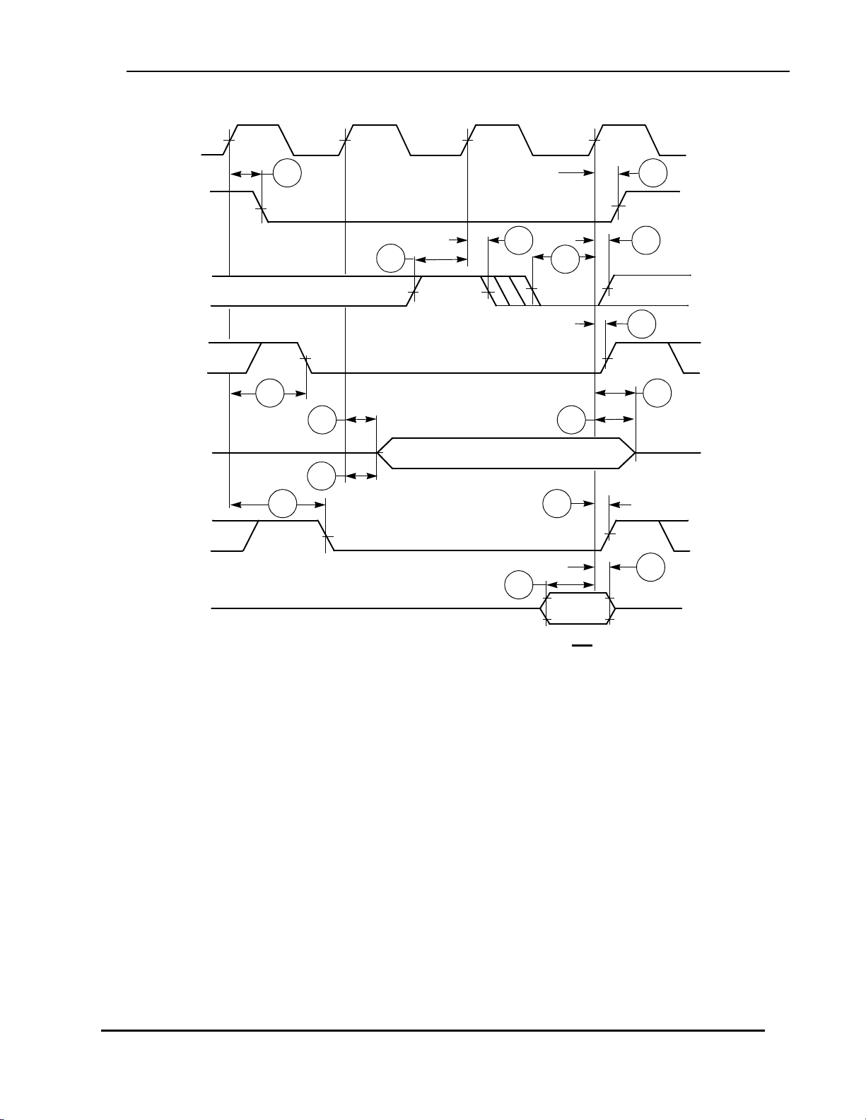
CLKOUT
A0–A17
AA0–AA3
Freescale Semiconductor, Inc.
198 199
External Memory Expansion Port (Port A)
Specifications
201
200
TA
WR
nc...
I
D0–D23
RD
D0–D23
Figure 2-21 Synchronous Bus Timings SRAM 2 WS (TA Controlled)
210
203
Data Out
202
208
206
200
204
209
Data In
cale Semiconductor,
201
211
207
205
AA0480
Frees
MOTOROLA DSP56362 Advance Information 2-45
For More Information On This Product,
Go to: www.freescale.com
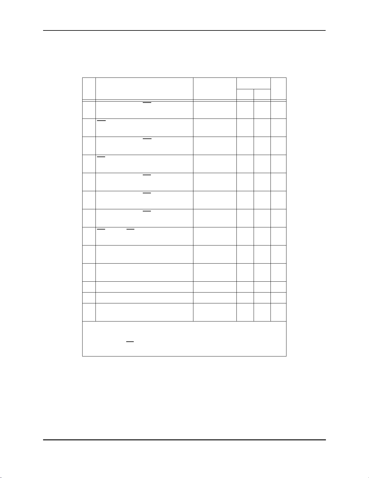
Freescale Semiconductor, Inc.
Specifications
External Memory Expansion Port (Port A)
Arbitration Timings
nc...
I
cale Semiconductor,
Frees
Table 2-18 Arbitration Bus Timings
No. Characteristics Expression
CLKOUT high to BR
212
deassertion
BG
213
214
215
216
217
218
219
220
221
222
223
224
Notes: 1. The asynchronous delays specified in the expressions are valid for
asserted/deasserted to
CLKOUT high (setup)
CLKOUT high to BG
asserted (hold)
BB
deassertion to CLKOUT high
(input setup)
CLKOUT high to BB
(input hold)
CLKOUT high to BB
(output)
CLKOUT high to BB
(output)
high to BB high impedance
BB
(output)
CLKOUT high to address and
controls active
CLKOUT high to address and
controls high impedance
CLKOUT high to AA active
CLKOUT high to AA deassertion
CLKOUT high to AA high
impedance
2. T212 is valid for Address Trace mode when the ATE bit in the OMR is
2
DSP56362.
set. BR
accesses.
assertion/
deasserted/
assertion
assertion
deassertion
0.25 × T
0.25 × T
0.25 × T
0.25 × T
is deasserted for internal accesses and asserted for external
C
0.75 × T
1
100 MHz
Min Max
1.0 4.0 ns
4.0 — ns
0.0 — ns
4.0 — ns
0.0 — ns
1.0 4.0 ns
1.0 4.0 ns
—4.5ns
2.5 — ns
C
C
C
+ 4.0 3.2 6.5 ns
C
—2.5ns
2.5 — ns
—7.5ns
Unit
2-46 DSP56362 Advance Information MOTOROLA
For More Information On This Product,
Go to: www.freescale.com
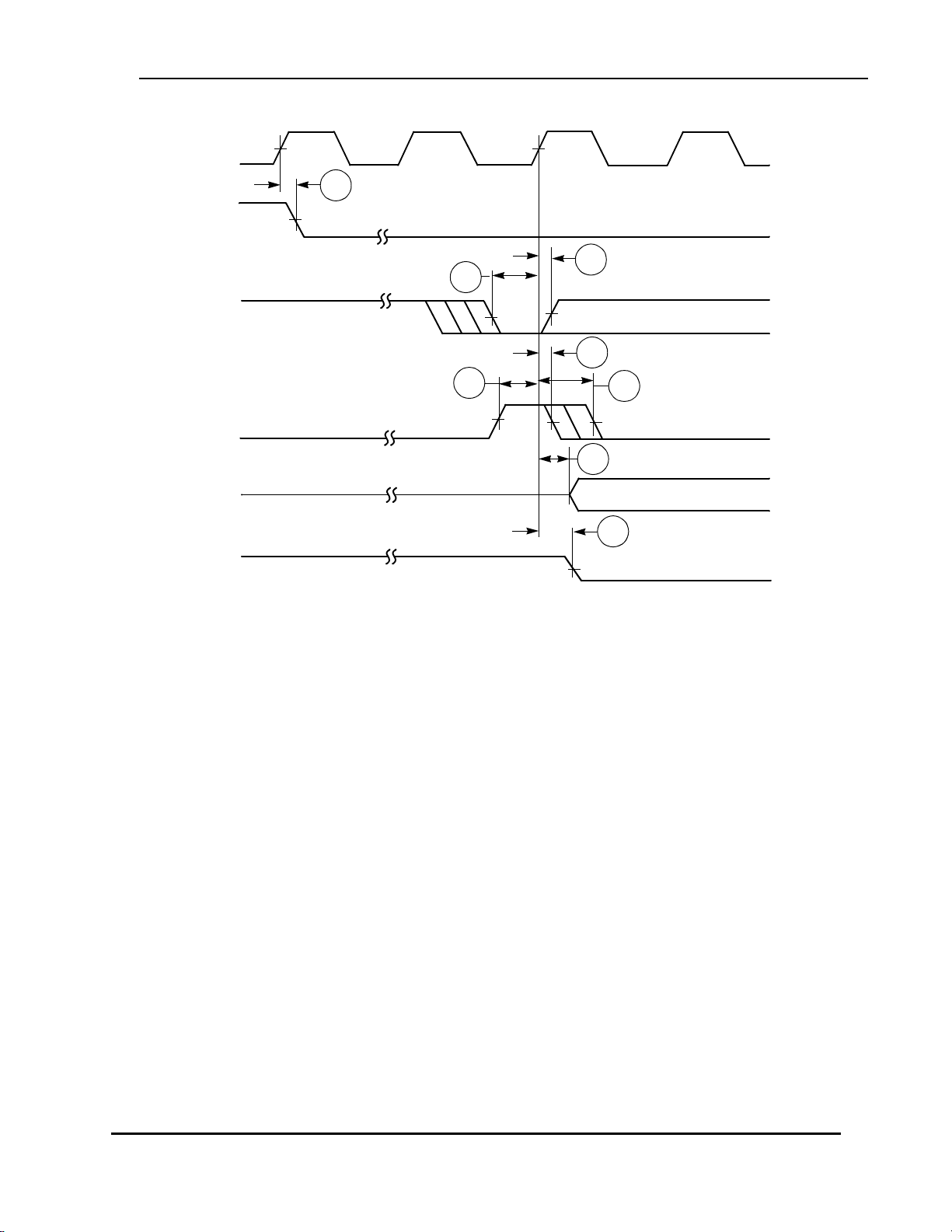
CLKOUT
BR
BG
Freescale Semiconductor, Inc.
212
External Memory Expansion Port (Port A)
214
213
216
Specifications
215
BB
nc...
I
A0–A17
RD, WR
AA0–AA3
Figure 2-22 Bus Acquisition Timings
cale Semiconductor,
220
217
222
AA0481
Frees
MOTOROLA DSP56362 Advance Information 2-47
For More Information On This Product,
Go to: www.freescale.com
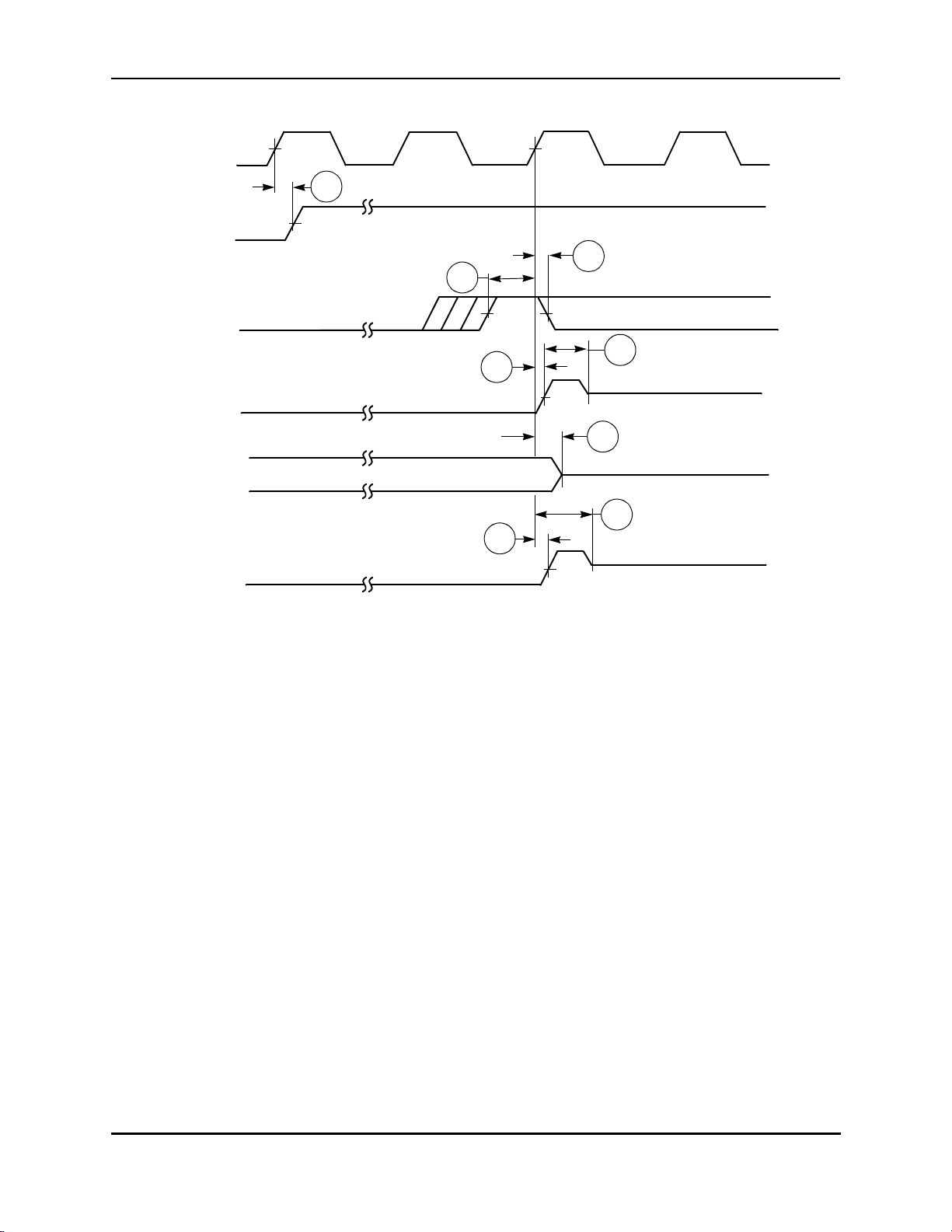
Freescale Semiconductor, Inc.
Specifications
External Memory Expansion Port (Port A)
CLKOUT
212
BR
BG
BB
214
213
219
218
nc...
I
cale Semiconductor,
Frees
A0–A17
RD, WR
AA0–AA3
Figure 2-23 Bus Release Timings Case 1 (BRT Bit in OMR Cleared)
223
221
224
AA0482
2-48 DSP56362 Advance Information MOTOROLA
For More Information On This Product,
Go to: www.freescale.com
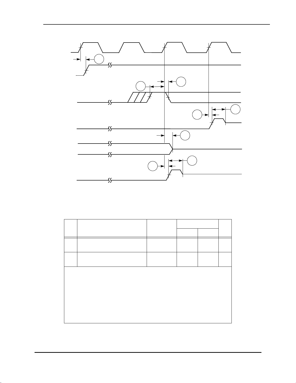
CLKOUT
BR
Freescale Semiconductor, Inc.
212
External Memory Expansion Port (Port A)
Specifications
nc...
I
cale Semiconductor,
Frees
BG
BB
A0–A17
RD, WR
AA0–AA3
213
223
Figure 2-24 Bus Release Timings Case 2 (BRT Bit in OMR Set)
Table 2-19 Asynchronous Bus Arbitration timing
No. Characteristics Expression
BB assertion window from BG
250
input negation.
Delay from BB assertion to BG
251
assertion
Comments:
1. Bit 13 in the OMR register must be set to enter Asynchro-
2. At 100 MHz it is recommended to use Asynchronous Arbi-
3. If Asynchronous Arbitration mode is active, none of the tim-
4. In order to guarantee timings 250, and 251, it is recommend-
nous Arbitration mode
tration mode.
ings in
ed to assert BG inputs to different 56300 devices (on the
same bus) in a non overlap manner as shown in
2-25
Table 2-19 is required.
.
2 .5* Tc + 5 — 20 ns
2 * Tc + 5 20 — ns
214
218
221
224
100 MHz
Min Max
Figure
Unit
219
AA0483
MOTOROLA DSP56362 Advance Information 2-49
For More Information On This Product,
Go to: www.freescale.com

Freescale Semiconductor, Inc.
Specifications
External Memory Expansion Port (Port A)
BG1
BB
BG2
250
251
nc...
I
cale Semiconductor,
Frees
Figure 2-25 Asynchronous Bus Arbitration Timing
BG1
BG2
250+251
Figure 2-26 Asynchronous Bus Arbitration Timing
Background explanation for Asynchronous Bus Arbitration:
The asynchronous bus arbitration is enabled by internal synchronization circuits on BG
These synchronization circuits add delay from the external signal until it is exposed to internal logic. As a
result of this delay, a 56300 part may assume mastership and assert BB
negated. This is the reason for timing 250.
Once BB
exposed to other 56300 components which are potential masters on the same bus. If BG
before that time, a situation of BG
assume mastership at the same time. Therefore some non-overlap period between one BG
another BG
is asserted, there is a synchronization delay from BB assertion to the time this assertion is
asserted, and BB negated, may cause another 56300 component to
input active, is required. Timing 251 ensures that such a situation is avoided.
, for some time after BG is
, and BB inputs.
input is asserted
input active to
2-50 DSP56362 Advance Information MOTOROLA
For More Information On This Product,
Go to: www.freescale.com
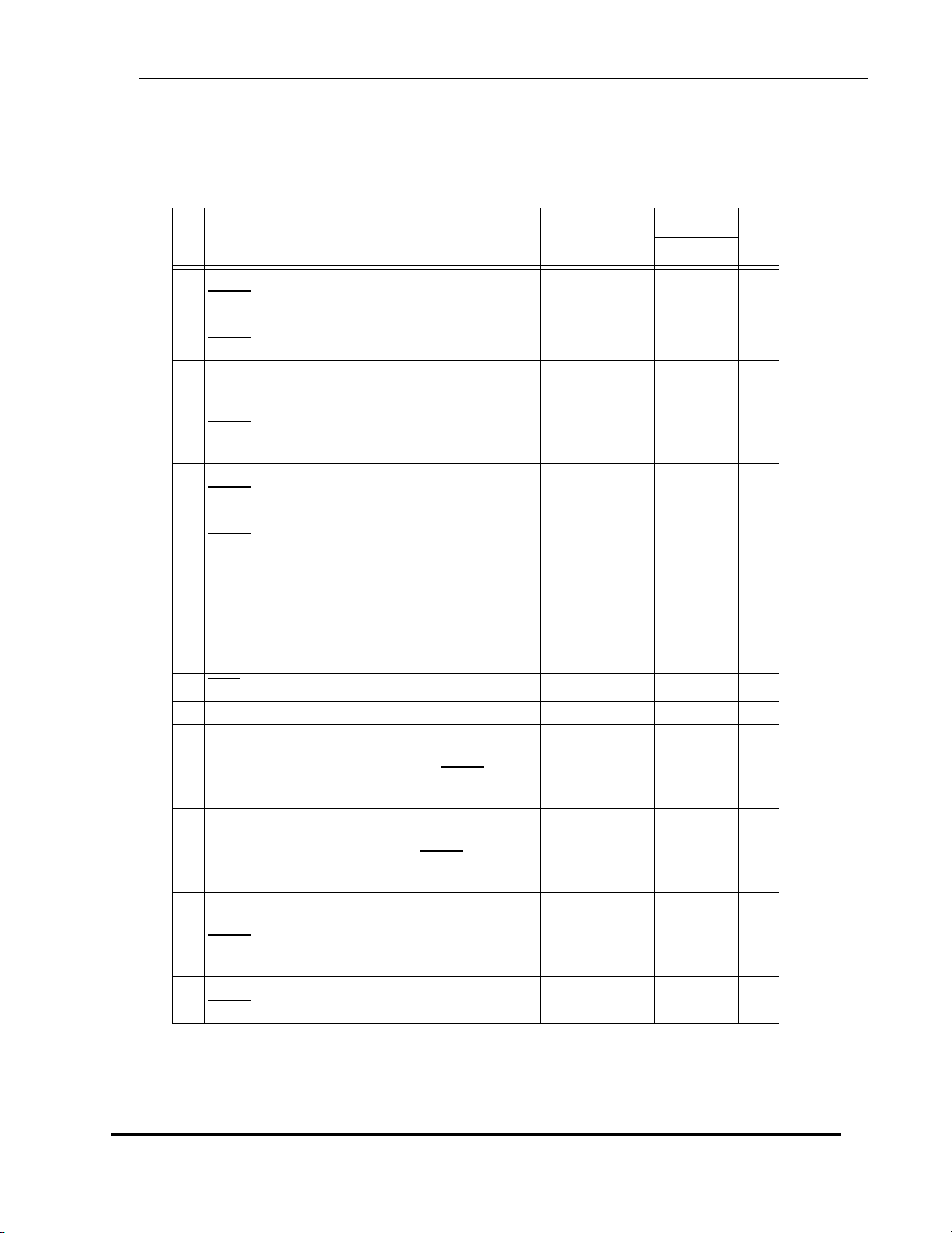
Freescale Semiconductor, Inc.
Parallel Host Interface (HDI08) Timing
PARALLEL HOST INTERFACE (HDI08) TIMING
Specifications
nc...
I
cale Semiconductor,
Frees
Table 2-20 Host Interface (HDI08) Timing
No.
Read data strobe assertion width
317
HACK read assertion width
Read data strobe deassertion width
318
HACK read deassertion width
Read data strobe deassertion width
Data Register” reads
319
consecutive CVR, ICR, or ISR reads
HACK deassertion width after “Last Data
Register” reads
Write data strobe assertion width
320
HACK write assertion width
Write data strobe deassertion width
HACK write deassertion width
• after ICR, CVR and “Last Data Register”
321
• after IVR writes, or
• after TXH:TXM writes (with HBE=0), or
•
322
HAS
323 HAS
Host data input setup time before write data
strobe deassertion
324
Host data input setup time before HACK write
deassertion
Host data input hold time after write data strobe
deassertion
325
Host data input hold time after HACK write
deassertion
5
writes
after TXL:TXM writes (with HBE=1)
assertion width
deassertion to data strobe assertion
Characteristics
5,6
5,6
8
8
, or between two
3
4
4
4
7
8
8
after “Last
9
1, 2
Expression
+ 9.9 19.9 — ns
T
C
—9.9—ns
2.5 × TC + 6.6 31.6 — ns
—13.2—ns
2.5 × TC + 6.6
—9.9—ns
—0.0—ns
—9.9—ns
—3.3—ns
100 MHz
Unit
Min Max
31.6 — ns
16.5 —
Read data strobe assertion to output data active
from high impedance
326
HACK read assertion to output data active from
high impedance
Read data strobe assertion to output data valid
327
HACK
read assertion to output data valid
4
4
—3.3—ns
——24.2ns
MOTOROLA DSP56362 Advance Information 2-51
For More Information On This Product,
Go to: www.freescale.com
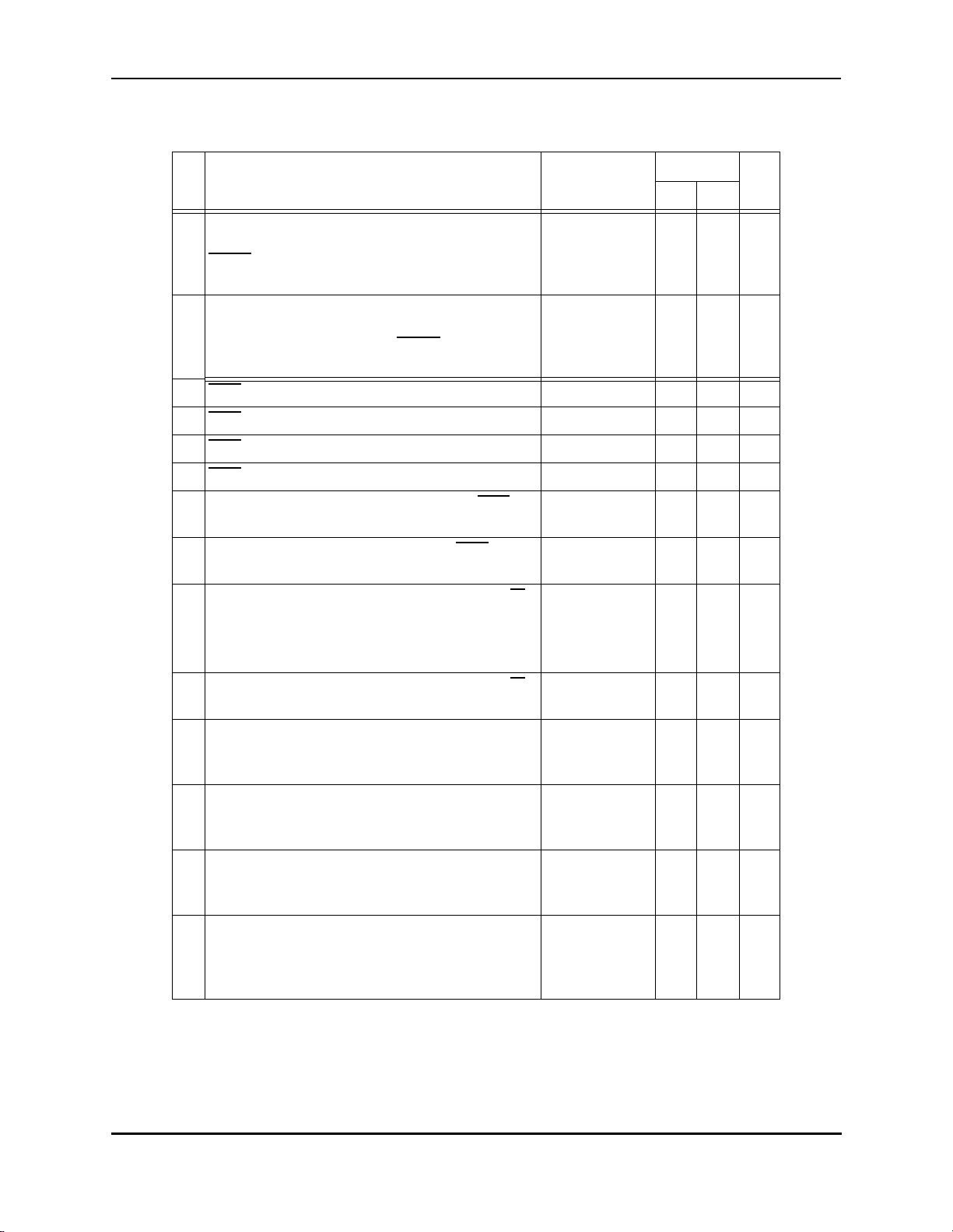
Freescale Semiconductor, Inc.
Specifications
Parallel Host Interface (HDI08) Timing
nc...
I
cale Semiconductor,
Frees
Table 2-20 Host Interface (HDI08) Timing
No.
Read data strobe deassertion to output data
high impedance
328
HACK
read deassertion to output data high
impedance
Output data hold time after read data strobe
deassertion
329
Output data hold time after HACK
deassertion
330
HCS
assertion to read data strobe deassertion
331
HCS
assertion to write data strobe deassertion
332
HCS
assertion to output data valid
333
HCS
hold time after data strobe deassertion
Address (AD7–AD0) setup time before HAS
334
deassertion (HMUX=1)
Address (AD7–AD0) hold time after HAS
335
deassertion (HMUX=1)
A10–A8 (HMUX=1), A2–A0 (HMUX=0), HR/W
setup time before data strobe assertion
336
• Read
•Write 4.7 —
A10–A8 (HMUX=1), A2–A0 (HMUX=0), HR/W
337
hold time after data strobe deassertion
Delay from read data strobe deassertion to host
338
request assertion for “Last Data Register” read
5, 10
Delay from write data strobe deassertion to host
339
request assertion for “Last Data Register”
5, 8, 10
write
Delay from data strobe assertion to host request
340
deassertion for “Last Data Register” read or
write (HROD = 0)
Characteristics
4
4
5, 9, 10
3
read
4
8
9
9
9
4,
1, 2
(Continued)
Expression
——9.9ns
—3.3—ns
TC +9.9 19.9 — ns
—9.9—ns
——19.1ns
—0.0—ns
—4.7—ns
—3.3—ns
—0—
—3.3—ns
T
C
2 × T
C
——19.1ns
100 MHz
Unit
Min Max
10 — ns
20 — ns
ns
Delay from data strobe assertion to host request
deassertion for “Last Data Register” read or
341
write (HROD = 1, open drain Host Request)
10, 11
5, 9,
——
300.
0
ns
2-52 DSP56362 Advance Information MOTOROLA
For More Information On This Product,
Go to: www.freescale.com
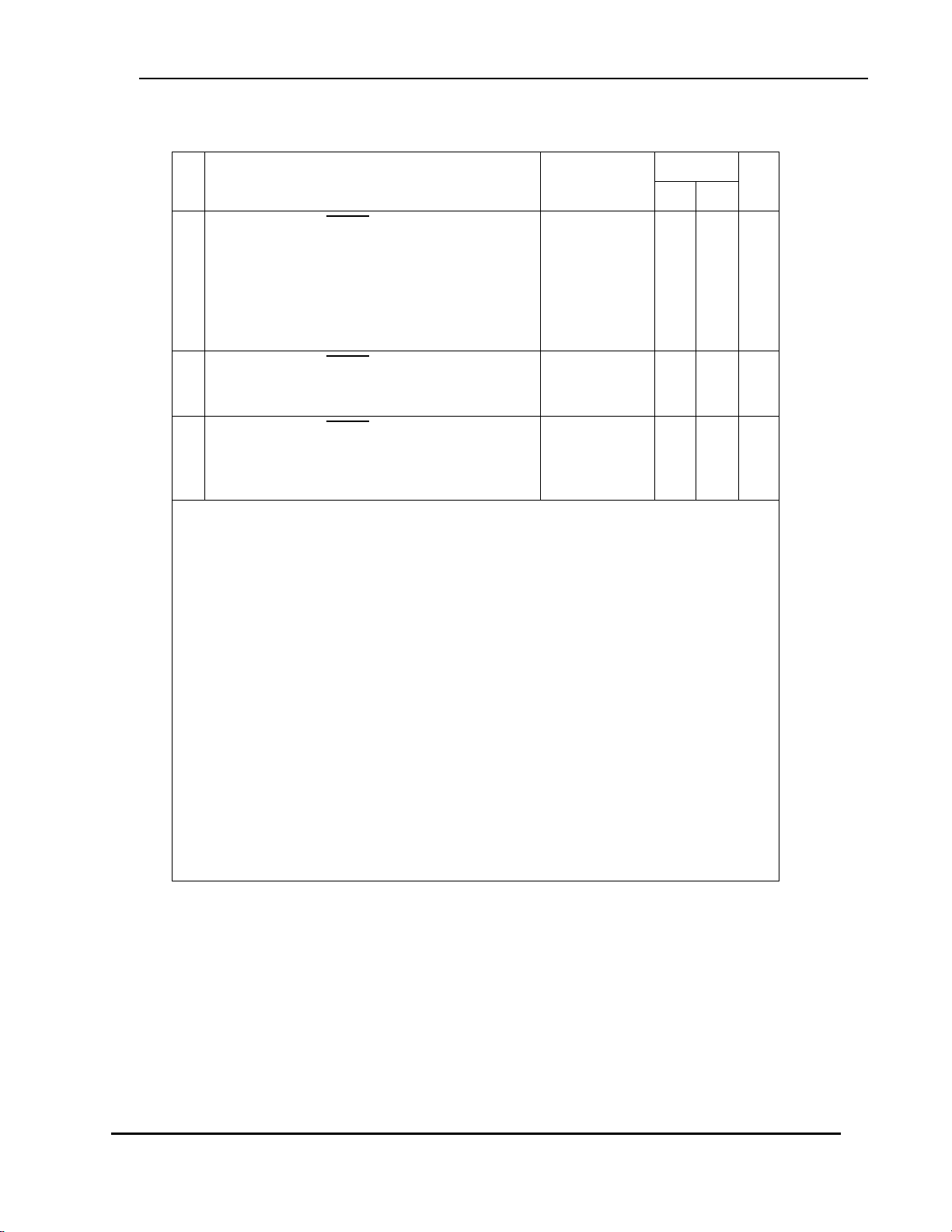
Freescale Semiconductor, Inc.
Parallel Host Interface (HDI08) Timing
Specifications
nc...
I
cale Semiconductor,
Frees
Table 2-20 Host Interface (HDI08) Timing
No.
Delay from DMA HACK
assertion
• For “Last Data Register” read
342
• For “Last Data Register” write
• For other cases 0.0 —
Delay from DMA HACK
343
deassertion
•HROD = 0
Delay from DMA HACK
deassertion for “Last Data Register” read or
344
write
• HROD = 1, open drain Host Request
Notes: 1. See Host Port Usage Considerations in the DSP56362 User Design Manual.
2. In the timing diagrams below, the controls pins are drawn as active low. The pin
polarity is programmable.
3. V
4. The read data strobe is HRD in the dual data strobe mode and HDS in the single
data strobe mode.
5. The “last data register” is the register at address $7, which is the last location to be
read or written in data transfers. This is RXL/TXL in the little endian mode (HBE = 0),
or RXH/TXH in the big endian mode (HBE = 1).
6. This timing is applicable only if a read from the “last data register” is followed by a
read from the RXL, RXM, or RXH registers without first polling RXDF or HREQ bits,
or waiting for the assertion of the HOREQ signal.
7. This timing is applicable only if two consecutive reads from one of these registers
are executed.
8. The write data strobe is HWR in the dual data strobe mode and HDS in the single
data strobe mode.
9. The data strobe is host read (HRD) or host write (HWR) in the dual data strobe
mode and host data strobe (HDS) in the single data strobe mode.
10. The host request is HOREQ in the single host request mode and HRRQ and HTRQ
in the double host request mode.
11. In this calculation, the host request signal is pulled up by a 4.7 kΩ resistor in the
open-drain mode.
Characteristics
deassertion to HOREQ
assertion to HOREQ
5
assertion to HOREQ
= 3.3 V ± 0.16 V; TJ = 0°C to +100°C, CL = 50 pF
CC
3
5
5
5, 11
1, 2
(Continued)
Expression
2 × T
1.5 × TC + 19.1 34.1 —
+ 19.1 39.1 —
C
——20.2ns
——
100 MHz
Min Max
300.
0
Unit
ns
ns
MOTOROLA DSP56362 Advance Information 2-53
For More Information On This Product,
Go to: www.freescale.com

Freescale Semiconductor, Inc.
Specifications
Parallel Host Interface (HDI08) Timing
HACK
317 318
nc...
I
cale Semiconductor,
Frees
HD7–HD0
HOREQ
Figure 2-27 Host Interrupt Vector Register (IVR) Read Timing Diagram
HA0–HA2
HCS
HRD, HDS
HD0–HD7
327
326
337336
330
317
328
332 319
327
326
329
318
329
333
328
AA1105
340
341
HOREQ,
HRRQ,
HTRQ
Figure 2-28 Read Timing Diagram, Non-Multiplexed Bus
2-54 DSP56362 Advance Information MOTOROLA
338
AA0484
For More Information On This Product,
Go to: www.freescale.com

Freescale Semiconductor, Inc.
HA0–HA2
Parallel Host Interface (HDI08) Timing
Specifications
325
333
339340
337
AA0485
336
HCS
HWR, HDS
nc...
I
HD0–HD7
341
HOREQ, HRRQ, HTRQ
Figure 2-29 Write Timing Diagram, Non-Multiplexed Bus
331
320
321
324
cale Semiconductor,
Frees
MOTOROLA DSP56362 Advance Information 2-55
For More Information On This Product,
Go to: www.freescale.com
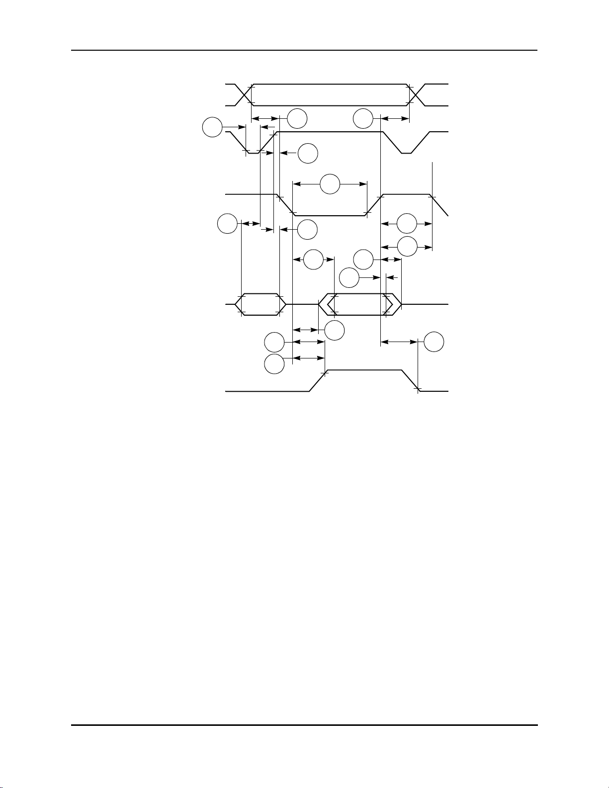
Freescale Semiconductor, Inc.
Specifications
Parallel Host Interface (HDI08) Timing
HA8–HA10
322
HAS
HRD, HDS
334
nc...
I
HAD0–HAD7
HOREQ, HRRQ, HTRQ
Figure 2-30 Read Timing Diagram, Multiplexed Bus
Address Data
cale Semiconductor,
336 337
323
335
327
340
341
317
326
329
328
318
319
338
AA0486
Frees
2-56 DSP56362 Advance Information MOTOROLA
For More Information On This Product,
Go to: www.freescale.com

HA8–HA10
Freescale Semiconductor, Inc.
Parallel Host Interface (HDI08) Timing
Specifications
322
HAS
HWR, HDS
334
335
nc...
I
HOREQ, HRRQ, HTRQ
cale Semiconductor,
HAD0–HAD7
Figure 2-31 Write Timing Diagram, Multiplexed Bus
HOREQ
(Output)
Address
343
344
336
323
341
342
320
324
340
Data
339
321
325
AA0487
Frees
320
HACK
(Input)
H0–H7
(Input)
Figure 2-32 Host DMA Write Timing Diagram
MOTOROLA DSP56362 Advance Information 2-57
TXH/M/L
Write
324
321
325
Data
Valid
For More Information On This Product,
Go to: www.freescale.com
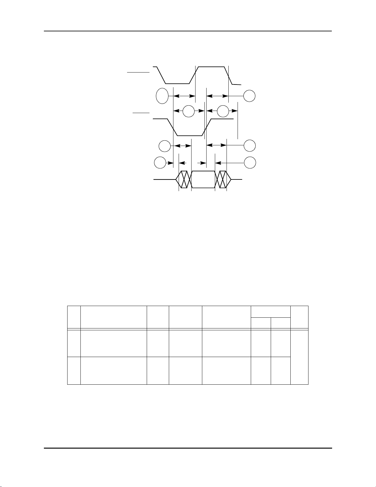
Freescale Semiconductor, Inc.
Specifications
Serial Host Interface SPI Protocol Timing
HOREQ
(Output)
343
342
342
nc...
I
cale Semiconductor,
Frees
HACK
(Input)
327 328
H0-H7
(Output)
Figure 2-33 Host DMA Read Timing Diagram
326
317
RXH
Read
Data
Valid
318
329
SERIAL HOST INTERFACE SPI PROTOCOL TIMING
Table 2-21 Serial Host Interface SPI Protocol Timing
No. Characteristics Mode
Tolerable spike width
140
on clock or data in
Minimum serial clock
141
cycle =
t
SPICC
(min)
—
Master
Filter
Mode
Bypassed
Wide — 100
Bypassed 6×T
Wide 6×T
Expression
—
+46 106 —
C
+152 212 —
C
+223 283 —
C
100MHz
Min Max
—0
Unit
nsNarrow — 50
nsNarrow 6×T
2-58 DSP56362 Advance Information MOTOROLA
For More Information On This Product,
Go to: www.freescale.com
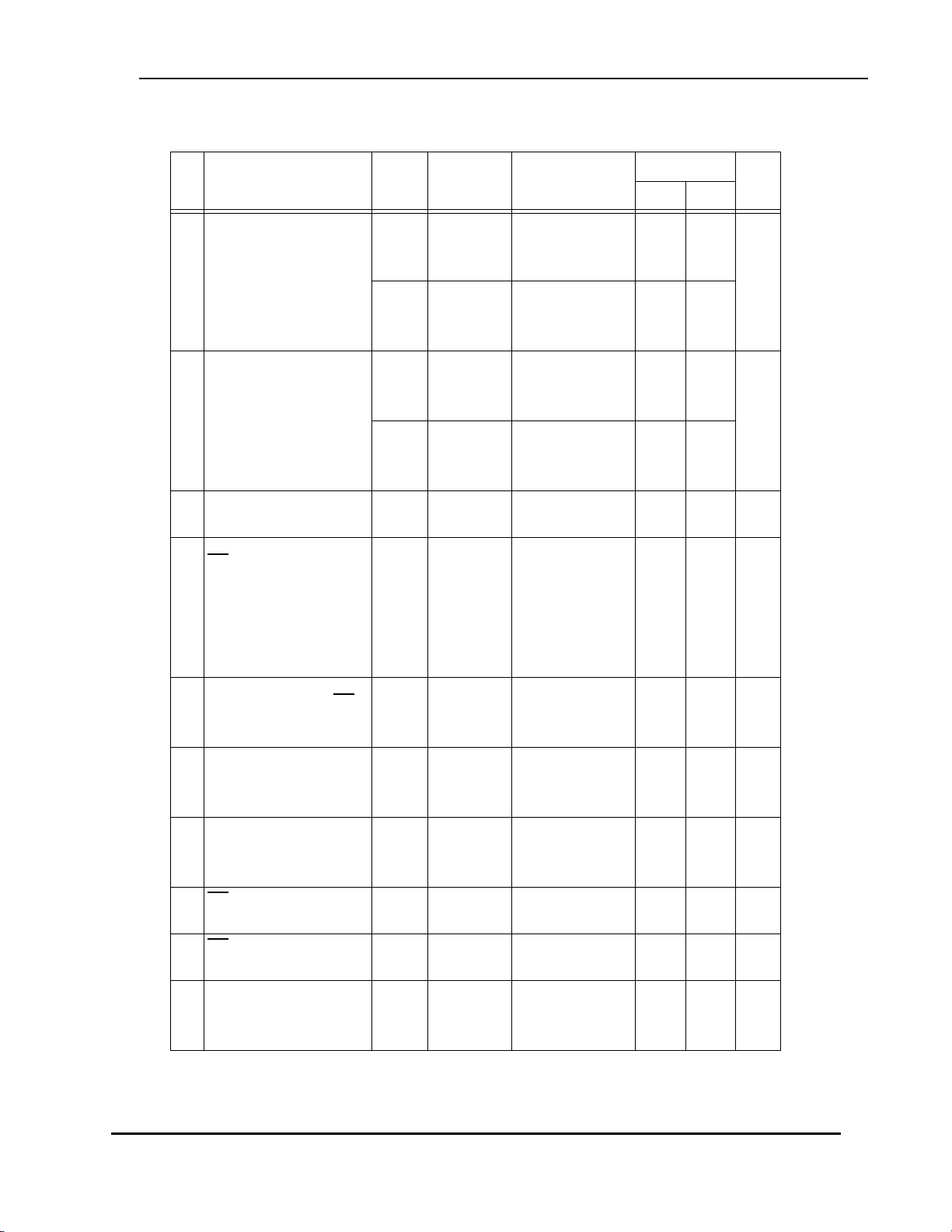
Freescale Semiconductor, Inc.
Serial Host Interface SPI Protocol Timing
Table 2-21 Serial Host Interface SPI Protocol Timing (Continued)
Specifications
nc...
I
cale Semiconductor,
Frees
No. Characteristics Mode
Master
142
Serial clock high period
Slave
Master
143
Serial clock low period
Slave
Serial clock rise/fall
144
time
assertion to first
SS
SCK edge CPHA = 0
146
CPHA = 1
Last SCK edge to SS
147
not asserted
Data input valid to SCK
148
edge (data input set-up
time)
SCK last sampling
149
edge to data input not
valid
SS
150
assertion to data
out active
Master — — — 10
Slave — — — 2000
Slave
Slave
slave
Master
/Slave
Master
/Slave
Slave — 2 2 — ns
Filter
Mode
Bypassed 0.5×t
Narrow 0.5×t
Wide 0.5×t
Bypassed 2.5×T
Narrow 2.5×T
Wide 2.5×T
Bypassed 0.5×t
Narrow 0.5×t
Wide 0.5×t
Bypassed 2.5×T
Narrow 2.5×T
Wide 2.5×T
Bypassed 3.5×T
Narrow 0 0 —
Wide 0 0 —
Bypassed 10 10 —
Narrow 0 0 —
Wide 0 0 —
Bypassed 12 12 —
Wide 189 189 —
Bypassed 0 0 —
Wide MAX{(40-T
Bypassed 2.5×T
Wide 2.5×T
Expression
–10 43 —
SPICC
–10 96 —
SPICC
–10 131 —
SPICC
+12 37 —
C
+102 127 —
C
+189 214 —
C
–10 43 —
SPICC
–10 96 —
SPICC
–10 131 —
SPICC
+12 37 —
C
+102 127 —
C
+189 214 —
C
+15 50 —
C
), 0} 10 —
C
), 0} 30 —
C
+10 35 —
C
+30 55 —
C
+50 75 —
C
100MHz
Min Max
Unit
ns
ns
ns
ns
nsNarrow 102 102 —
nsNarrow MAX{(20-T
nsNarrow 2.5×T
deassertion to data
SS
151
high impedance
SCK edge to data out
152
valid (data out delay
time)
Slave — 9 — 9 ns
Master
Bypassed 2×T
/Slave
Wide 2×T
+33 — 53
C
+123 — 143
C
+210 — 230
C
nsNarrow 2×T
MOTOROLA DSP56362 Advance Information 2-59
For More Information On This Product,
Go to: www.freescale.com
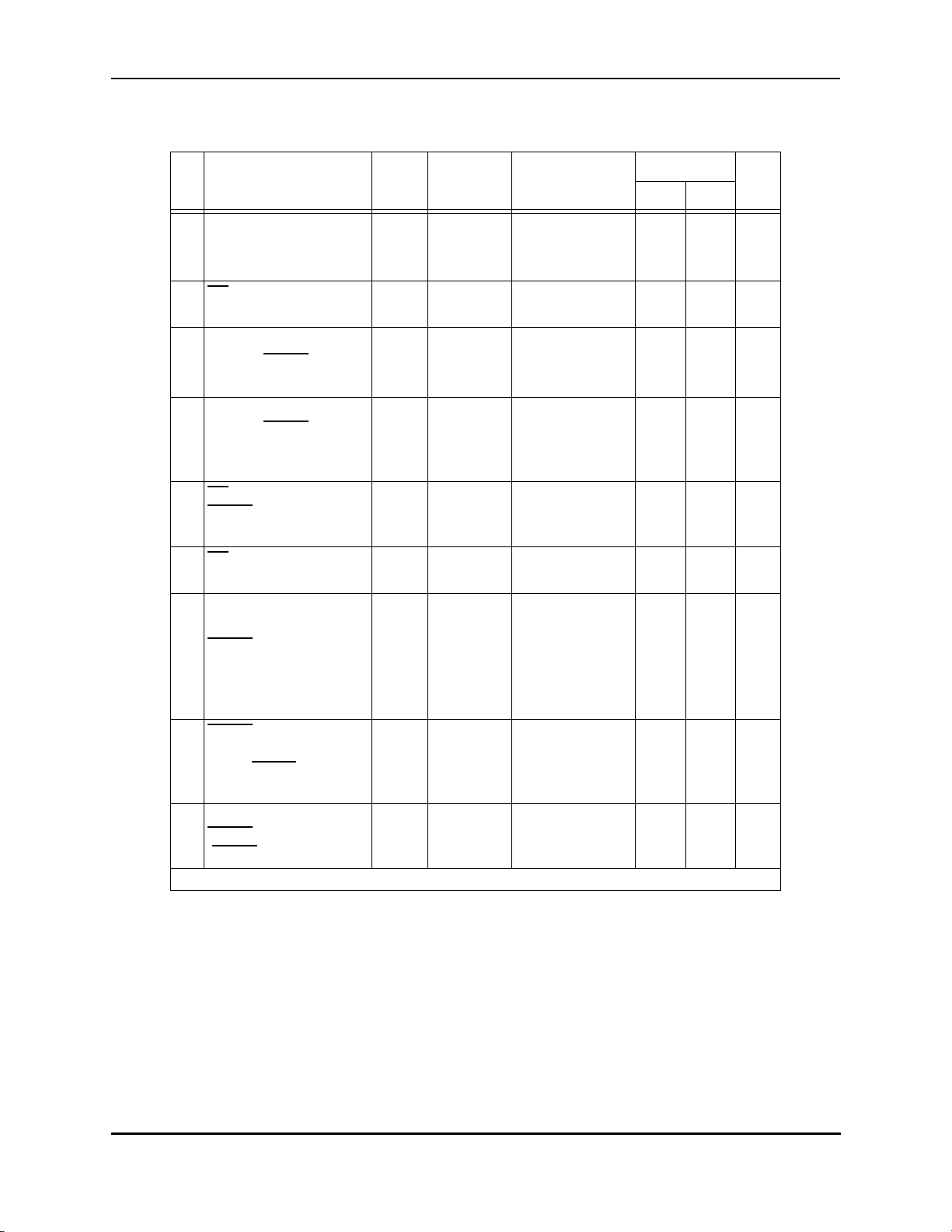
Freescale Semiconductor, Inc.
Specifications
Serial Host Interface SPI Protocol Timing
Table 2-21 Serial Host Interface SPI Protocol Timing (Continued)
nc...
I
cale Semiconductor,
Frees
No. Characteristics Mode
SCK edge to data out
153
not valid
(data out hold time)
SS
154
157
158
159
160
161
162
163
Note: Periodically sampled, not 100% tested
assertion to data
out valid (CPHA = 0)
First SCK sampling
edge to HREQ
deassertion
Last SCK sampling
edge to HREQ
not deasserted
(CPHA = 1)
deassertion to
SS
HREQ
output not
deasserted (CPHA = 0)
deassertion pulse
SS
width (CPHA = 0)
in assertion to
HREQ
first SCK edge
HREQ
in deassertion
to last SCK sampling
edge (HREQ
time) (CPHA = 1)
First SCK edge to
HREQ
in not asserted
(HREQ
in hold time)
output
output
in set-up
Master
/Slave
Slave — T
Slave
Slave
Slave — 2.5×T
Slave — T
Master
Master — 0 0 — ns
Master — 0 0 — ns
Filter
Mode
Bypassed T
Wide T
Bypassed 2.5×T
Wide 2.5×T
Bypassed 2.5×T
Narrow 2.5×T
Wide 2.5×T
Bypassed
Wide
+
100MHz
Min Max
121 —
174 —
209 —
Expression
+5 15 —
C
+55 65 —
C
+106 116 —
C
+33 — 43 ns
C
+30 — 55
C
+120 — 145
C
+217 — 242
C
+30 55 —
C
+80 105 —
C
+136 161 —
C
+30 55 — ns
C
+6 16 — ns
C
0.5 × t
SPICC
2.5×T
0.5 ×t
2.5×T
0.5 ×t
2.5×T
+43
C
SPICC
+43
C
SPICC
+43
C
+
+
Unit
nsNarrow T
nsNarrow 2.5×T
ns
nsNarrow
2-60 DSP56362 Advance Information MOTOROLA
For More Information On This Product,
Go to: www.freescale.com
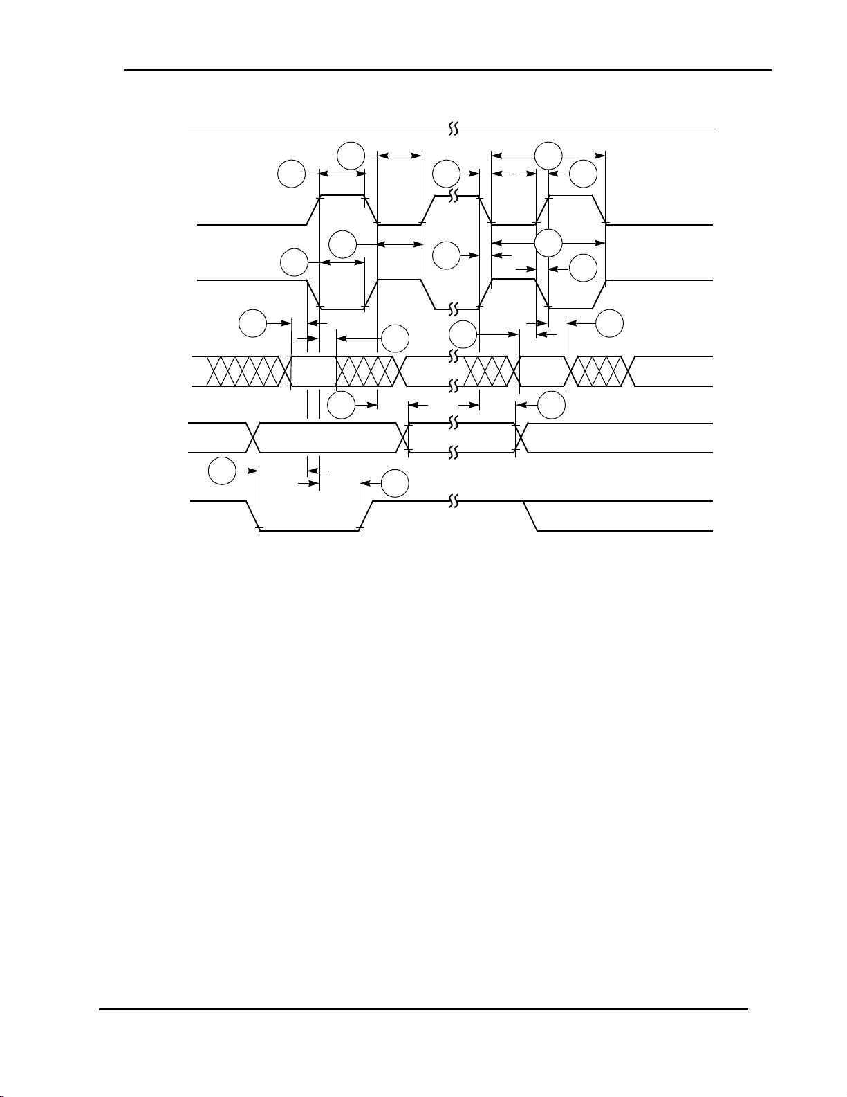
SS
(Input)
SCK (CPOL=0
(Output)
SCK (CPOL =
1 (Output)
Freescale Semiconductor, Inc.
142
143
143
142
Serial Host Interface SPI Protocol Timing
141
144 144
141
144
144
Specifications
148
149
MISO
nc...
I
(Input)
MOSI
(Output)
161
HREQ
(Input)
MSB
Valid
152
MSB LSB
163
Figure 2-34 SPI Master Timing (CPHA = 0)
148
LSB
Valid
153
cale Semiconductor,
149
AA0271
Frees
MOTOROLA DSP56362 Advance Information 2-61
For More Information On This Product,
Go to: www.freescale.com
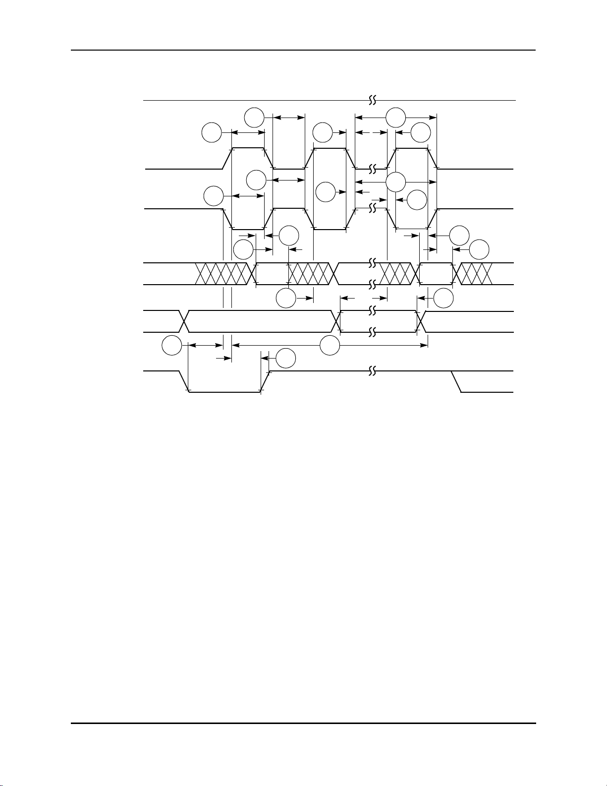
Freescale Semiconductor, Inc.
Specifications
Serial Host Interface SPI Protocol Timing
SS
(Input)
142
SCK (CPOL = 0
(Output)
SCK (CPOL = 1
(Output)
143
143
142
149
141
144 144
141
144
144
148 148
149
nc...
I
cale Semiconductor,
Frees
MISO
(Input)
MOSI
(Output)
HREQ
(Input)
MSB
Valid
152 153
MSB LSB
161 162
163
Figure 2-35 SPI Slave Timing (CPHA = 0)
LSB
Valid
AA0272
2-62 DSP56362 Advance Information MOTOROLA
For More Information On This Product,
Go to: www.freescale.com
 Loading...