Freescale 34674 Advance Information
Freescale Semiconductor
Advance Information
High Input Voltage Travel Charger for Single-cell Li-Ion Batteries
Document Number: MC34674
Rev. 1.0, 01/2008
34674
The MC34674 is a fully integrated single-cell Li-Ion and Li-Polymer
battery charger optimized for travel charger applications. The few
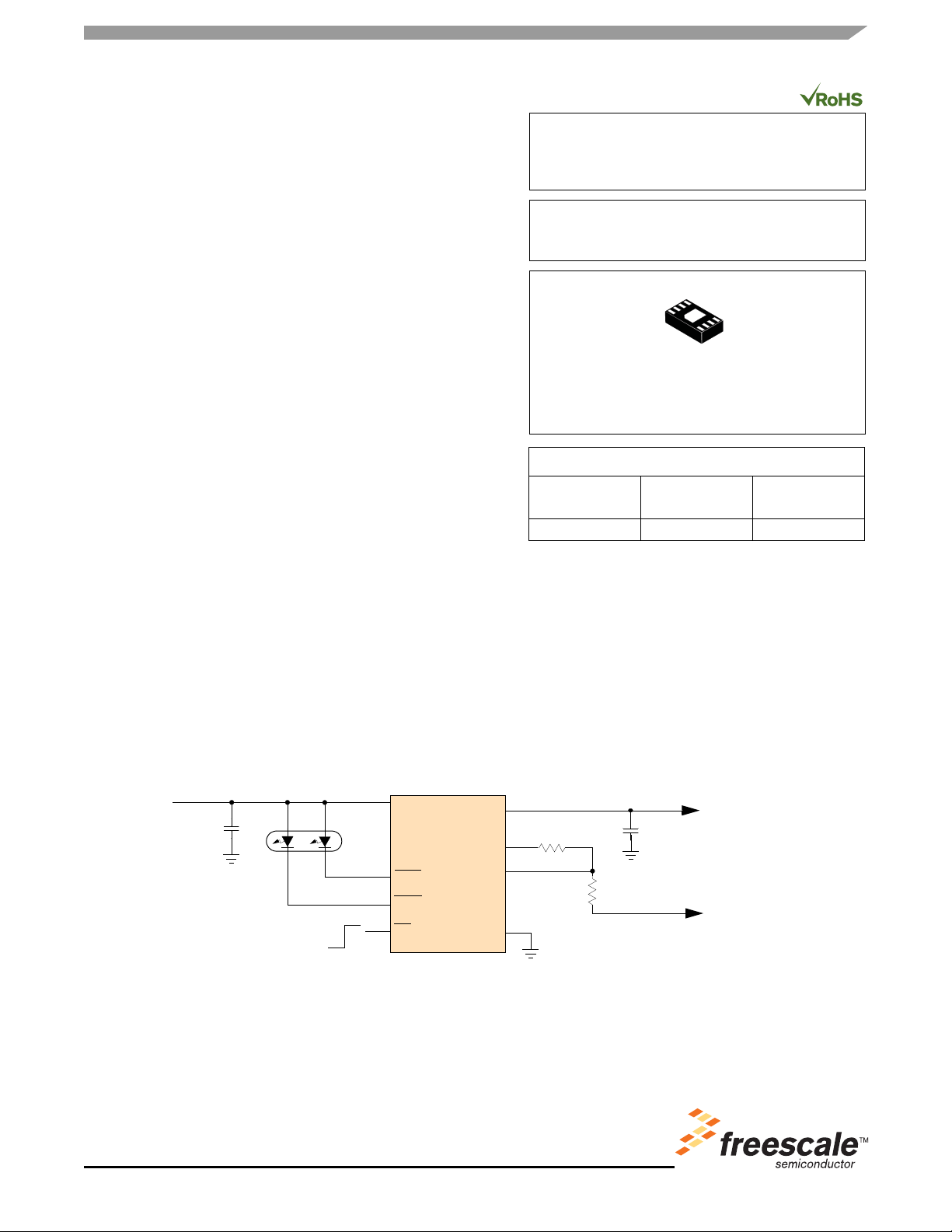
external components required include a dual-color LED for chargestatus indication, a negative temperature coefficient (NTC) thermistor
circuit for setting the charge temperature window, and two decoupling
capacitors. The high input voltage, up to 28V, allows low-cost ac/dc
converters to be used for further system cost reduction. A typical
charge cycle of the MC34674 includes trickle, constant-current (CC)
and constant-voltage (CV) charge modes. The CC-mode current is
selectable from 50mA to 1.05A with 8% accuracy and the constantoutput voltage in the CV-mode is fixed at 4.2V with 0.4% accuracy over
-20°C to 70°C temperature range.
The MC34674 has all the features such as trickle charging for a
deeply discharged battery, an internal timer for termination to prevent
charging a failed battery, charger current thermal foldback for thermal
protection, and smart battery connection verification to prevent
charging in case there is no battery connected. It also protects the
system with its input over-voltage protection (OVP) feature. In addition,
it has a 2.6V falling power-on-reset (POR) threshold, making it perfect
to work with current limited power supplies. When the charger is
disabled, the BAT pin leaks less than 1
µA current from the battery. All
the above functions are fit into a small 8-lead 2X3 UDFN package.
Features
• No external MOSFET, reverse-blocking diode or current-
• Driving a dual-color LED and smart battery connection
sense resistor are required
• 28V maximum input voltage rating with 11V over-voltage
protection threshold
• Factory programmable charge current
• Trickle charge for fully discharged batteries
• Interface to NTC thermistor
• Internal timer and thermal current limit
• Small 2X3 mm2 thermally enhanced UDFN package
• Pb-free packaging designated by suffix code EP
• ±0.4% voltage accuracy over -20°C to 70°C
POWER MANAGEMENT IC
EP SUFFIX (PB-FREE)
98ASA10774D
8-PIN UDFN
ORDERING INFORMATION
Device
MC34674AEP/R2 -40°C to 85°C 8-UDFN
Temperature
Range (T
)
A
Package
verification optimized for travel charger applications
V
IN
C
IN
OFF
ON
VIN
RED
GRN
EN
34674
BAT
VREF
TEMP
GND
Figure 1. 34674 Simplified Application Diagram
* This document contains certain information on a new product.
Specifications and information herein are subject to change without notice.
© Freescale Semiconductor, Inc., 2007-8. All rights reserved.
C
R
PU
R
OUT
S
TO BATTERY
TO BATTERY NTC
(THERMISTOR)
DEVICE VARIATIONS
DEVICE VARIATIONS
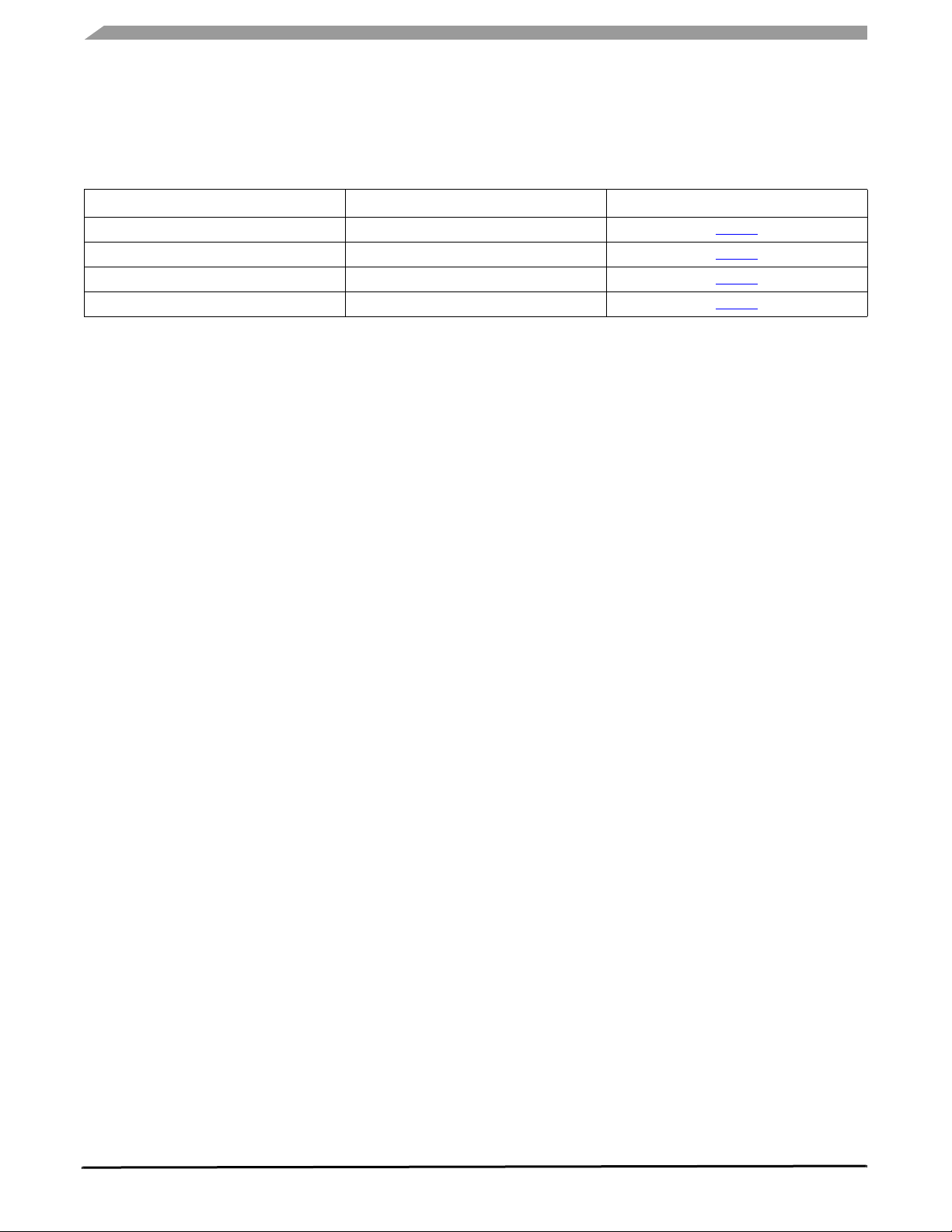
Table 1. Device Variations
Freescale Part No.
MC34674A
MC34674B
MC34674C
MC34674D
Notes
1. Freescale offers a series of MC34674 variations. Each variation has an increment of 50mA or 100mA for the CC-mode current.
(1)
CC-Mode Current (ICC) Reference Location
1.05A Table 6
850mA Table 6
650mA Table 6
450mA Table 6
34674
Analog Integrated Circuit Device Data
2 Freescale Semiconductor
INTERNAL BLOCK DIAGRAM
INTERNAL BLOCK DIAGRAM
VIN
RED
GRN
EN
V
IN
Monitor
6mA
6mA
Internal
Supply
REF
VIN
+
BAT
V
–
OS
Charge
Control
+
–
Logic
Control
GND
–
+
–
+
–
+
+
–
V
REF
Die
Temp
110°C
I
REF
I
EOC
NTC
Interface
BAT
VREF
TEMP
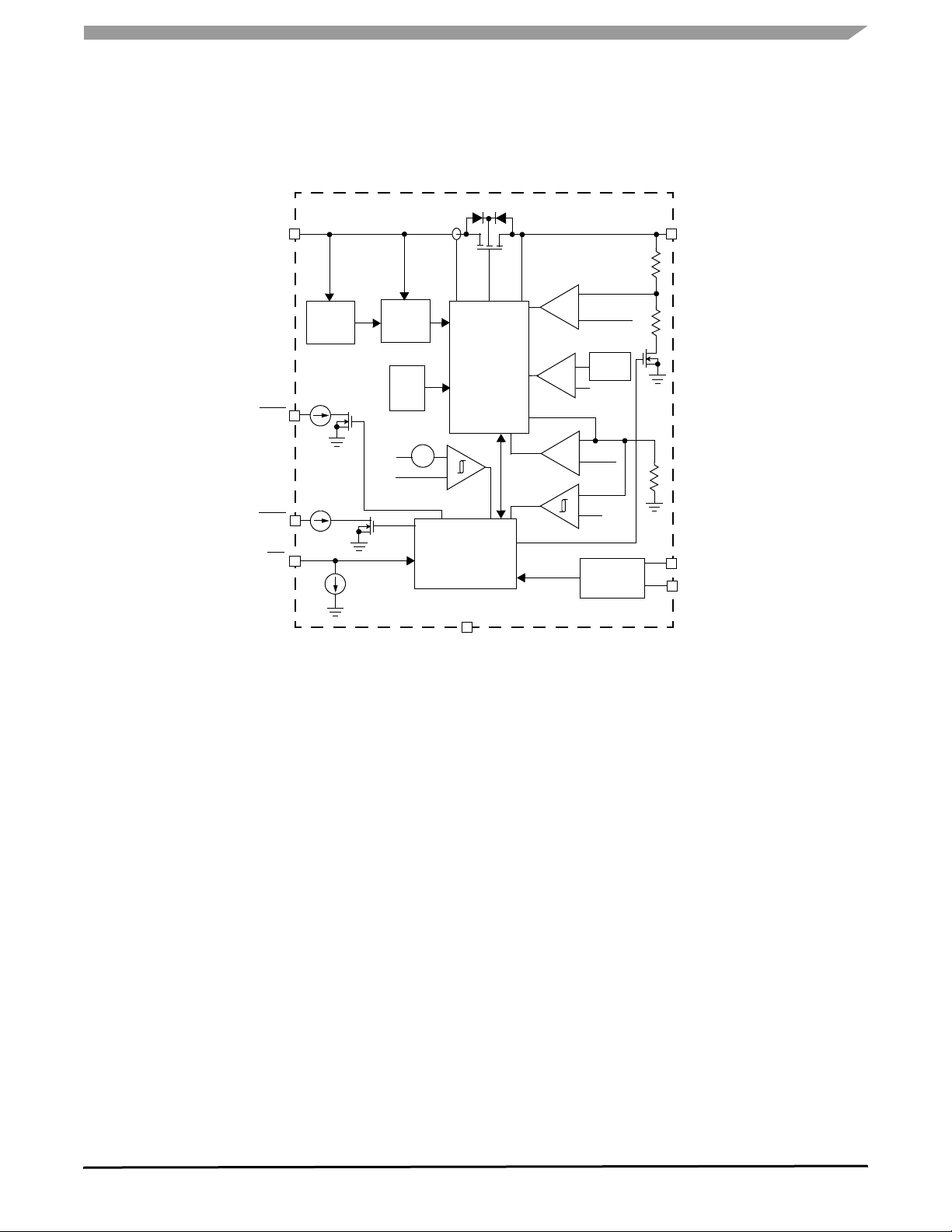
Figure 2. 34674 Simplified Internal Block Diagram
34674
Analog Integrated Circuit Device Data
Freescale Semiconductor 3

PIN CONNECTIONS
PIN CONNECTIONS
VIN
GRN
1
2
BAT
8
VREF
7
EPAD
RED
EN
3
4
TEMP
6
GND
5
Figure 3. 34674 Pin Connections
Table 2. 34674 Pin Definitions
A functional description of each pin can be found in the Functional Pin Description section beginning on page 12.
Pin Number Pin Name Pin Function Formal Name Definition
1
2
3
4
5
6
7
8
EPAD
VIN Input Input supply
GRN Output Green indicator
RED Output Red indicator
EN Input Enable
GND Ground Ground
TEMP Input NTC interface input
VREF Output NTC interface bias
voltage
BAT Output Charger output
EPAD N/A Exposed pad
The supply input.
Indication of the charge status. Open drain output with 6mA current limit.
Indication of the charge status. Open drain output with 6mA current limit.
Active-low enable logic input.
Ground.
The NTC thermistor interface pin.
The bias voltage for the NTC interface circuit.
The charger output pin to the battery.
Exposed pad for thermal dissipation enhancement. Must be soldered on
the large ground plane on the PCB to increase the thermal dissipation.
The pad must be connected to GND electrically.
34674
Analog Integrated Circuit Device Data
4 Freescale Semiconductor

ELECTRICAL CHARACTERISTICS
MAXIMUM RATINGS
ELECTRICAL CHARACTERISTICS
MAXIMUM RATINGS
Table 3. Maximum Ratings
All voltages are with respect to ground unless otherwise noted. Exceeding these ratings may cause a malfunction or
permanent damage to the device.
Ratings Symbol Value Unit
ELECTRICAL RATINGS
Input voltage range
VIN Pin
GRN and RED Pins
EN, BAT, REF and TEMP Pins
ESD Voltage
(2)
Human Body Model (HBM)
Machine Model (MM)
THERMAL RATINGS
Operating Temperature
Ambient
Junction
Storage Temperature
Thermal Resistance
(3)
Junction-to-Case
Junction-to-Ambient
Peak Package Reflow Temperature During Reflow
(4),(5)
Notes
2. ESD testing is performed in accordance with the Human Body Model (HBM) (C
(MM) (C
= 200pF, R
ZAP
ZAP
= 0Ω).
3. Device mounted on the Freescale EVB test board per JEDEC DESD51-2.
4. Pin soldering temperature limit is for 10 seconds maximum duration. Not designed for immersion soldering. Exceeding these limits may
cause malfunction or permanent damage to the device.
5. Freescale’s Package Reflow capability meets Pb-free requirements for JEDEC standard J-STD-020C. For Peak Package Reflow
Temperature and Moisture Sensitivity Levels (MSL), Go to www.freescale.com, search by part number [e.g. remove prefixes/suffixes
and enter the core ID to view all orderable parts. (i.e. MC33xxxD enter 33xxx), and review parametrics.
V
GRN
VEN, V
V
REF
V
T
ZAP
T
R
V
IN
, V
RED
,
BAT
, V
TEMP
ESD
T
A
T
J
STG
θJC
R
θJA
PPRT
= 100pF, R
-0.3 to 28
-0.3 to 12
-0.3 to 5.5
±2000
±200
-40 to 85
-40 to 150
-65 to 150
°C/W
10
70
Note 5
= 1500Ω), and the Machine Model
ZAP
V
V
°C
°C
°C
34674
Analog Integrated Circuit Device Data
Freescale Semiconductor 5

ELECTRICAL CHARACTERISTICS
STATIC ELECTRICAL CHARACTERISTICS
STATIC ELECTRICAL CHARACTERISTICS
Table 4. Static Electrical Characteristics
Characteristics noted under conditions VIN = 5.0V, -40°C ≤ TA ≤ 85°C, CIN = C
noted. Typical values noted reflect the approximate parameter means at VIN = 5.0V and TA = 25°C under nominal conditions,
unless otherwise noted.
Characteristic Symbol Min Typ Max Unit
POWER INPUT
Input Voltage Range
VIN Pin Supply Current
Charger enabled
Charger disabled
Power On Reset
Rising VIN threshold
Falling VIN threshold
(6)
(7)
V
V
I
IN
POR
IN
= 1µF (see Figure 1), unless otherwise
OUT
4.3 10 V
-
-
3.0
-
1400
300
-
2.4
-
350
3.9
2.6
µA
V
Over-Voltage Protection Rising Threshold
Over-Voltage-Protection Threshold Hysteresis
VIN-BAT Offset Voltage
V
OVP
V
OVPHYS
V
OS
Rising threshold
Falling threshold
OUTPUT
Regulated Output Voltage
VIN = 5.0V; I
VIN = 5.0V; I
VIN = 5.0V; I
= 100mA; TA = 25°C
BAT
= 100mA; TA = -20 to 70°C
BAT
= 100mA; TA = -40 to 85°C
BAT
Power MOSFET On Resistance
V
BAT
= 4.0V; I
BAT
= 0.5A; I
CHG
BAT Pin Standby Current
= 1.05A
V
R
DS(ON)
I
STDBY
BAT
VIN not powered or charger disabled
VIN powered and in charge completion state (average over 2
seconds)
(8)
CHARGE CURRENT
Constant-Current-Mode Charge Current Range
I
Accuracy
CHG
Tested at 650mA
Trickle-Mode Charge Current
(8)
(9)
(9)
End-of-Charge (EOC) Threshold
When I
is set to 650mA
CHG
(8)
I
CHG
I
CHG
I
TRKL
I
EOC
Notes
6. Refer to the Power-on-Reset parameter for VIN turn on and turn off values.
7. Supply current does not include the current delivered to the battery through the BAT pin.
8. Not tested. Guaranteed by design.
9. Tested over the temperature range -20°C ≤ TA ≤ 85°C
10 11 12 V
- 400 - mV
-
1.0
4.190
4.183
4.179
-
-
4.20
4.20
4.20
60
22
4.210
4.217
4.221
- 265 450
-
-2.0
-
-
1.0
4.0
50 - 1050 mA
92 100 108
7.0 10 13 % I
52 65 78
mV
V
mΩ
µA
%
CHG
mA
34674
Analog Integrated Circuit Device Data
6 Freescale Semiconductor
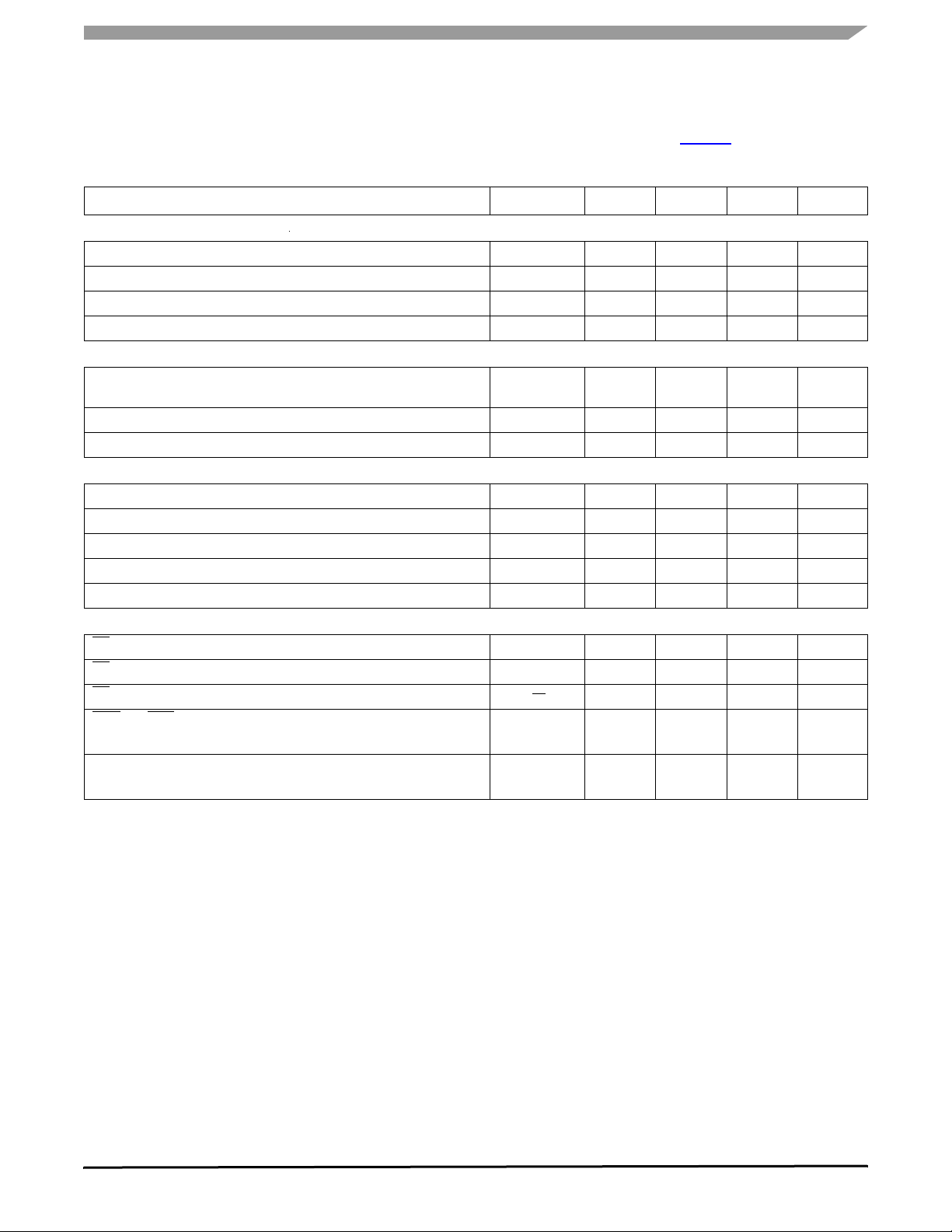
Table 4. Static Electrical Characteristics (continued)
Characteristics noted under conditions VIN = 5.0V, -40°C ≤ TA ≤ 85°C, CIN = C
noted. Typical values noted reflect the approximate parameter means at V
unless otherwise noted.
Characteristic Symbol Min Typ Max Unit
CHARGE THRESHOLDS
Trickle-mode Rising Threshold Voltage
Trickle-mode Threshold Voltage Hysteresis
Recharge Falling Threshold Voltage
Recharge Threshold Voltage Hysteresis
BATTERY CONNECTION VERIFICATION
Battery Connection Verification Discharge Current (Over 0.8V to
(10)
5.0V)
Output Current in Charge Completion State
(10)
Discharge Current in Charge Completion State During the 82ms
NTC INTERFACE
Low Temperature Rising Threshold
Low Temperature Falling Threshold
High Temperature Falling Threshold
High Temperature Rising Threshold
(11)
(11)
(11)
(11)
Die Thermal Limit
LOGIC INPUT AND OUTPUT
EN Input High Threshold Voltage
EN Input Low Threshold Voltage
EN Pin Internal Pull-Down Current
GRN and RED Sink Current
Pin voltage is between 0.8V and 5.0V
Open-Drain Off Leakage
Biased at 5.0V
Notes
10. Not tested. Guaranteed by design.
11. These threshold parameters are specified as a ratio of V
rises when the temperature is falling from high to low, and V
(10)
/VREF. Due to the negative-temperature-coefficient thermistor, V
TEMP
TEMP
V
TRKL
V
TRKLHYS
V
RECH
V
THRCHG
I
DCHG
I
CC
I
DCC
V
LTRT
V
LTFT
V
HTFT
V
HTRT
T
LIM
V
IH
V
I
EN
I
GRSINK
I
ODLEAK
falls when the temperature is rising from low to high.
STATIC ELECTRICAL CHARACTERISTICS
= 1µF (see Figure 1), unless otherwise
OUT
= 5.0V and TA = 25°C under nominal conditions,
IN
ELECTRICAL CHARACTERISTICS
2.8 2.9 3.0 V
- 100 - mV
4.07 4.10 4.135 V
- 25 50 mV
4.5 6.0 7.5 mA
- 24 - µA
- 585 - µA
0.6592 2/3 0.6741 VREF
- 0.6468 - VREF
0.3297 1/3 0.3389 VREF
- 0.3441 - VREF
95 110 125 °C
1.5 - - V
IL
- - 0.5 V
- 2.0 7.5 µA
5.0 6.0 7.0
- - 1.0
mA
µA
TEMP
34674
Analog Integrated Circuit Device Data
Freescale Semiconductor 7
ELECTRICAL CHARACTERISTICS
DYNAMIC ELECTRICAL CHARACTERISTICS
DYNAMIC ELECTRICAL CHARACTERISTICS
Table 5. Dynamic Electrical Characteristics
Characteristics noted under conditions V
noted. Typical values noted reflect the approximate parameter means at VIN = 5.0V and TA = 25°C under nominal conditions,
unless otherwise noted.
Characteristic Symbol Min Typ Max Unit
END OF CHARGE
EOC Filtering Time
OSCILLATOR
Oscillator Frequency
INTERNAL TIMER
Safety Timer for Fast Charge Mode
Safety Timer for Trickle Charge Mode
ENABLE VERIFICATION
Enable Verification Time
BATTERY CONNECTION VERIFICATION
Discharge Time in Charge Completion State
Discharge Repeating Time
Notes
12. Not tested. Guaranteed by design.
(12)
(12)
= 5.0V, -40°C ≤ TA ≤ 85°C, CIN = C
IN
(12)
t
EOC
f
OSC
t
FCM
t
TCM
t
EV
t
DCCC
t
DR
= 1µF (see Figure 1), unless otherwise
OUT
500 - 1000 ms
40.0 50.0 60.0 kHz
3.68 4.6 5.52 Hour
0.46 0.575 0.69 Hour
- 100 - ms
- 82 - ms
- 1968 - ms
34674
Analog Integrated Circuit Device Data
8 Freescale Semiconductor
 Loading...