

Page 1
Freescale Semiconductor
Advance Information
Enhanced Class B Serial
Transceiver
The 33990 is a serial transceiv er designed to provide bi- directional
half-duplex communication meeting the automotive SAE Standard J1850 Class
is designed to interface directly to on-board vehicle microcontrollers
and serves to transmit and receive data on a single-wire bus at data
rates of 10.4
The 33990 operates directly from a v ehicle's 12
functions in a true logic fashion as an I/O interface between the
microcontroller's 5.0
to 7.0
is short circuit current limited.
Features
• Designed for SAE J-1850 Class B Data Rates
• Full Operational Bus Dynamics Over a Supply Voltage of 9 .0 V
• Ambient Operating Temperature of -40°C to 125°C
• Interfaces Directly to Standard 5.0 V CMOS Microcontroller
• BUS Pin Protected Against Shorts to Battery and Ground
• Thermal Shutdown with Hysteresis
• Voltage Waveshaping of Bus Output Driver
• Internally Reverse Battery Protected
•40 V Max V
• Pb-Free Packaging Designated by Suffix Code EF
B Data Communication Network Interface spe cification. It
kbps using Variable Pulse Width Modulation (VPWM).
V battery system and
V CMOS logic level swings and the required 0 V
V waveshaped signal swings of the bus. The bus output driver
V
to 16
Capability
BAT
J-1850 SERIAL TRANSCEIVER
ORDERING INFORMATION
Device
MC33990D/DR2
MCZ33990EF/R2
Document Number: MC33990
Rev 3.0, 11/2006
33990
D SUFFIX
EF SUFFIX (PB-FREE)
98ASB42564B
8-PIN SOICN
Temperature
Range (T
-40°C to 125°C 8 SOICNN
)
A
Package
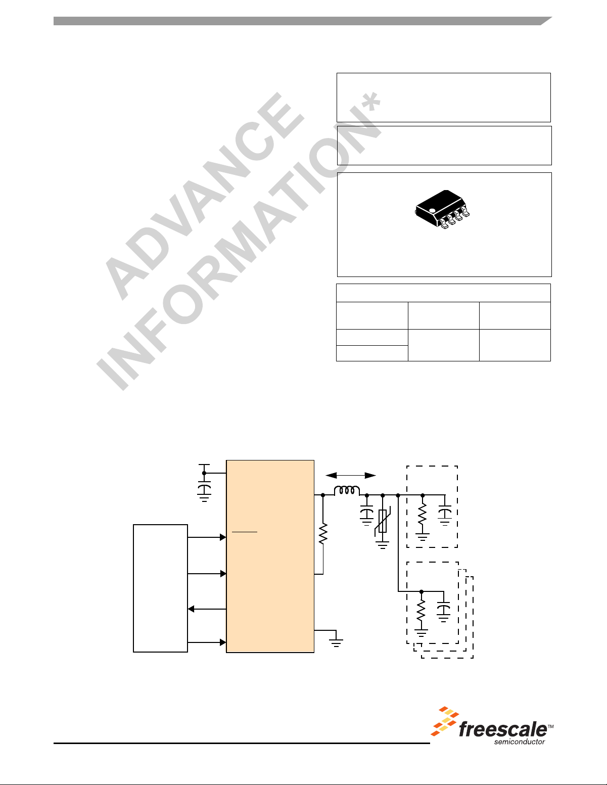
+VBAT
SLEEP
TX
RX
4X/LOOP
33990
BUS
LOAD
GND
MCU
V
BAT
Figure 1. 33990 Simplified Application Diagram
* This document contains certain information on a new product.
Specifications and information herein are subject to change without notice.
© Freescale Semiconductor, Inc., 2006. All rights reserved.
Primary
Node
Secondary
Nodes
Page 2

INTERNAL BLOCK DIAGRAM
INTERNAL BLOCK DIAGRAM
33990
VBAT
SLEEP
4.5 V
Reference
TX
RX
4X/LOOP
Note This device contains approximately 400 active transistors and 250 gates.
Digital Output
Driver
Figure 2. 33990 Simplified Internal Block Diagram
Voltage
Regulator
Waveshaping
Filter
4X Enable
Loopback
Bus
Driver
Thermal
Shutdown
Loss of Ground
Protection
BUS
LOAD
GND
33990
Analog Integrated Circuit Device Data
2 Freescale Semiconductor
Page 3
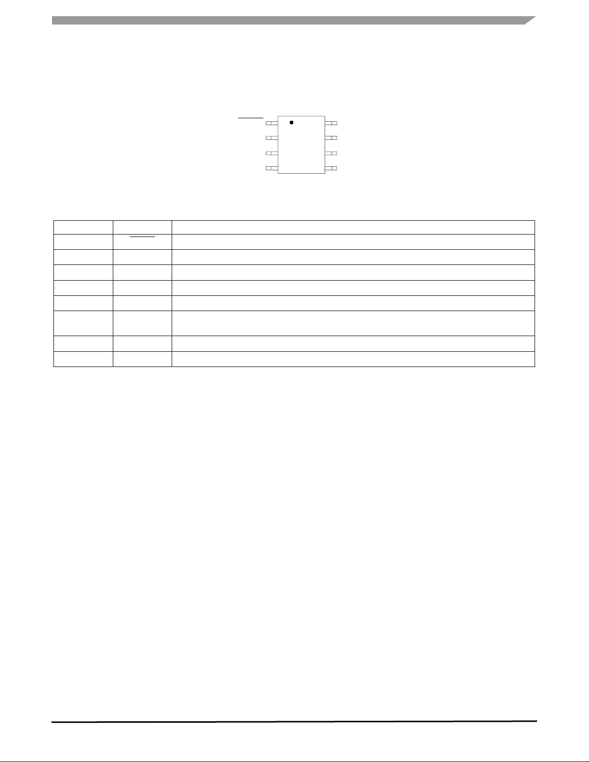
PIN CONNECTIONS
PIN CONNECTIONS
5
8
7
6
8
7
6
5
RX
TX
4X/LOOP
V
SLEEP
GND
LOAD
BUS
1
1
2
2
3
3
4
4
Figure 3. 33990 Pin Connections
Table 1. 33990 Pin Definitions
Pin Number Pin Name Definition
1 SLEEP
2 GND
3 LOAD
4 BUS
5 VBAT
6 4X/ LOOP
7 TX
8 RX
Enables the transceiver when Logic 1 and disables the transceiver when Logic 0.
Device ground pin.
Accommodates an external pull-down resist or to ground to provide loss of ground protection.
Waveshaped SAE Standard J-1850 Class B transmitter output and receiver input.
Provides device operating input power.
Tristate input mode control; Logic 0 = normal waveshaping, Logic 1 = waveshaping disabled for 4X
transmitting, high impedance = loopback mode.
Serial data input (DI) from the microcontroller to be transmitted onto Bus.
Bus received serial data output (DO) s ent to the microcontroller.
BAT
33990
Analog Integrated Circuit Device Data
Freescale Semiconductor 3
Page 4
ELECTRICAL CHARACTERISTICS
MAXIMUM RATINGS
ELECTRICAL CHARACTERISTICS
MAXIMUM RATINGS
Table 2. Maximum Ratings
All voltages are with respect to ground unless otherwise noted.
Rating Symbol Value Unit
VBAT DC Supply Voltage
Input I/O Pins
(2)
BUS and LOAD Outputs
ESD Voltage
Human Body Model
Machine Model
Storage Temperature
Operating Ambient Temperature
Operating Junction Temperature
Peak Package Reflow Temperature During Reflow
Thermal Resistance (Junction-to-Ambien t)
Notes
1. An external series diode must be used to provide reverse battery protection of the device.
2. SLEEP, TX, RX, and 4X / LOOP are normally connected to a microcontroller.
3. ESD1 testing is performed in accordance with the Huma n Body Model (C
4. ESD2 testing is performed in accordance with the Machine Model (C
5. Pin soldering temperature limit is for 1 0 seco nds maxi mum durat ion. No t desig ned for imm ersion solder ing. Exc eeding thes e limits may
cause malfunction or permanent damage to the device.
6. Freescale’s Package Reflow capability meets Pb-free requirements for JEDEC standard J-STD-020C. For Peak Package Reflow
Temperature and Moisture Sensitivity Levels (MSL),
Go to www.freescale.com, search by part number [e.g. remove prefixes/suffixes and enter the core ID to view all orderable parts. (i.e.
MC33xxxD enter 33xxx), and review para m et rics.
(1)
(3)
(4)
(5), (6)
V
V
I/O(CPU)
V
V
ESD1
V
ESD2
T
T
PPRT
R
ZAP
= 200 pF, R
ZAP
BAT
BUS
STG
T
A
T
J
J-A
θ
= 100 pF, R
ZAP
ZAP
= 0 Ω).
-16 to 40 V
-0.3 to 7.0 V
-2.0 to 16 V
±2000
±200
-65 to 150 °C
-40 to 125 °C
-40 to 150 °C
Note 6.
180 °C / W
= 1500 Ω).
V
°C
33990
Analog Integrated Circuit Device Data
4 Freescale Semiconductor
Page 5
STATIC ELECTRICAL CHARACTERISTICS
Table 3. Static Electrical Characteristics
Characteristics noted under conditio ns of 7.0 V ≤ V
Typical values reflect the parameter's approximate midpoint average value with V
are into the pin. All negative currents are out of the pin.
Characteristic Symbol Min Typ Max Unit
POWER CONSUMPTION
Operational Battery Current (RMS with Tx = 7.812 kHz Square Wave)
BUS Load = 1380 Ω to GND, 3.6 nF to GND
BUS Load = 257 Ω to GND, 20.2 nF to GND
Battery Bus Low Input Current
After SLEEP Toggle Low to High; Prior to Tx Toggling
After Tx Toggle High to Low
Sleep State Battery Current
V
= 0 V
SLEEP
BUS
BUS Input Receiver Threshold
Threshold High (Bus Increasing until Rx ≥ 3.0 V)
Threshold Low (Bus Decreasing until Rx ≤ 3.0 V)
Threshold in Sleep State (SLEEP = 0 V)
Hysteresis (V
BUS(IH)
BUS-Out Voltage (Tx = 5.0 V, 257 Ω ≤ R
8.2 V ≤ V
4.25 V ≤ V
BAT
BAT
≤ 16 V
≤ 8.2 V
Tx = 0 V
BUS Short Circuit Output Current
Tx = 5.0 V, -2.0 V ≤ V
BUS Leakage Current
-2.0 V ≤ V
0 V ≤ V
0 V ≤ V
≤ 0 V (≥ 2.0 ms after Tx Falls to 0 V)
BUS
≤ V
BUS
BAT
≤ 8.0 V
BUS
BUS Thermal Shutdown
Increase Temperature until V
BUS Thermal Shutdown Hysteresis
T
BUS (LIM)
- T
BUS (REEN)
LOAD Input Current with Loss of Ground
V
= -18 V (see Figure 4)
LOAD
BUS Input Current with Loss of Ground
V
= -18 V (see Figure 4)
BUS
Notes
7. Typical threshold value is the approximate actual occurring switch point value with V
8. Device characterized but not production tested for thermal shutdown.
9. Device characterized but not production tested for thermal shutdown hysteresis.
(7)
- V
BUS(IL)
≤ 4.8 V
BUS
(8)
(Tx = 5.0 V, I
BUS
, SLEEP = 0 V)
BUS(L)
= -0.1 mA)
BUS
≤ 2.5 V
(9)
to GND ≤ 1380 Ω)
≤ 16 V, -40°C ≤ T
BAT
A
I
BAT (OP1)
I
BAT (OP2)
I
BAT(BUS L1)
I
BAT(BUS L2)
I
BAT(SLEEP)
V
BUS(IH)
V
BUS(IL)
BUS
TH(SLEEP)
V
BUS(HYST)
V
BUS (OUT1)
V
BUS (OUT2)
V
BUS (OUT3)
I
BUS (SHORT)
I
BUS (LEAK1)
I
BUS (LEAK2)
I
BUS (LEAK3)
T
BUS (LIM)
T
BUS (LI MHYS)
I
LOAD (LOG)
I
BUS (LOG)
≤ 125°C, SLEEP = 5.0 V unless o therwise note d.
STATIC ELECTRICAL CHARACTERISTICS
= 13 V, TA = 25°C. All positive currents
BAT
ELECTRICAL CHARACTERISTICS
–
–
–
–
3.0
22.4
1.1
6.4
11.5
32
3.0
8.5
– 38.2 65
4.25
–
2.4
0.1
6.25
V
- 1.6
BAT
–
3.9
3.7
3.0
0.2
6.9
–
0.27
V
–
3.5
3.4
0.6
8.0
BAT
0.7
60 129 170
-0.5
-0.5
–
-0.055
0.5
0.25
0.5
1.0
0.5
150 170 190
10 12 15
-1.0 – 0.1
-1.0 – 0.1
= 13 V, TA = 25°C.
BAT
mA
mA
µA
V
V
mA
mA
°C
°C
mA
mA
33990
Analog Integrated Circuit Device Data
Freescale Semiconductor 5
Page 6

ELECTRICAL CHARACTERISTICS
STATIC ELECTRICAL CHARACTERISTICS
Table 4. Static Electrical Characteristics (continued)
Characteristics noted under conditions o f 7.0 V ≤ V
≤ 16 V, -40°C ≤ T
BAT
≤ 125°C, SLEEP = 5.0 V unless otherwise noted.
A
Typical values reflect the parameter's approximate midpoint average value with V
are into the pin. All negative currents are out of the pin.
Characteristic Symbol Min Typ Max Unit
BUS (CONTINUED)
BUS Input Current with Loss of V
V
= 9.0 V (see Figure 5)
BUS
LOAD Output
IL = 6.0 mA
Unpowered LOAD Output
V
= 0 V, IL = 6.0 mA
BAT
TX
TX Input Voltage
V
≤ 3.875 V
BUS
V
≥ 3.875 V
BUS
TX Input Current
VTx = 5.0 V
VTx = 0 V
LOOP
4X / LOOP Input Current
V
4X / LOOP
V
4X / LOOP
= 0 V (Normal Mode)
= 5.0 V (4X Mode)
4X / LOOP Input Threshold (Tx = 4096 Hz square wave)
Normal Mode to Loopback Mode
Loopback Mode to 4X Mode
RX
RX Output Voltage Low
V
= 0 V, IRx = 1.6 mA
BUS
RX Output Voltage High
V
= 7.0 V, IRx = -200 µA
BUS
RX Output Current
V
= High; Short Circuit Protection Limits
R
x
RX Sleep State Output Voltage
SLEEP = 0 V, 0 ≤ V
SLEEP Input Current
V
= 0 V
SLEEP
V
= 5.0 V
SLEEP
BUS
≤ 7.0 V
BAT
I
BUS (LOB)
L
ON
L
DIO
V
Tx(IL)
V
Tx(IH)
I
Tx(IH)
I
Tx(IL)
I
4X / LOOP(IL)
I
4X / LOOP(IH)
V
4X / LOOP(IL)
V
4X / LOOP(IH)
V
Rx (LOW)
V
Rx(HIGH)
I
Rx
V
Rx
I
SLEEP (IL)
I
SLEEP (IH)
= 13 V, TA = 25°C. All positive currents
BAT
– – 0.5
– 0.07 0.2
0.3 0.67 0.9
–
3.5
50
-2.0
-200
–
1.4
3.2
2.27
2.27
120
-0.1
-95
95
1.6
3.43
0.8
–
200
2.0
–
200
1.8
3.6
0.01 0.18 0.4
4.25 4.48 4.75
2.0 5.9 8.0
4.25 4.56 4.85
–
1.0
-0.003
9.5
-2.0
20
mA
V
V
V
µA
µA
V
V
V
mA
V
µA
33990
Analog Integrated Circuit Device Data
6 Freescale Semiconductor
Page 7

DYNAMIC ELECTRICAL CHARACTERISTICS
Table 5. Dynamic Electrical Characteristics
Characteristics noted under conditions of 7.0 V ≤ V
Typical values reflect the parameter's approximate midpoint average value with V
are into the pin. All negative currents are out of the pin.
Characteristic Symbol Min Typ Max Unit
BUS
BUS Voltage Rise Time
Wave) (see Figure 6)
BUS Load = 3,300 pF and 1.38 kΩ to GND
BUS Load = 16,500 pF and 300 Ω to GND
BUS Voltage Fall Time
Wave) (see Figure 6)
BUS Load = 3,300 pF and 1.38 kΩ to GND
BUS Load = 16,500 pF and 300 Ω to GND
Pulse Width Distortion Time (9.0 V ≤ V
Wave) (see
Figure 7)
BUS Load = 3,300 pF and 1.38 kΩ to GND
Propagation Delay
TX Threshold to RX Threshold
TX
TX to BUS Delay Time (Tx = 2.5 V to V
4X Mode
Normal Mode
SLEEP to Tx Setup Time (Figure 8)
RX
RX Output Delay Time (TX = 2.5 V to V
Low-to-Output High
High-to-Output Low
RX Output Transition Time (CRx = 50 pF to GND, 10% and 90% Points)
(see
Figure 10)
Low-to-Output High
High-to-Output Low
Rx Output Transition Time
90% Points) (see Figure 10)
Low-to-Output High
High-to-Output Low
Notes
10. Typical is the parameter's approximate average value with V
11. RX Output Transition Time from a sleep state.
(10)
(9.0 V ≤ V
(10)
(9.0 V ≤ V
(11)
(CRx = 50 pF to GND, SLEEP = 0 V, 10% and
≤ 16 V, Tx = 7.812 kHz Square
BAT
≤ 16 V, Tx = 7.812 kHz Square
BAT
≤ 16 V, Tx = 7.812 kHz Square
BAT
= 3.875 V) (Figure 8)
BUS
= 3.875 V) (see Figure 9)
BUS
≤ 16 V, -40°C ≤ T
BAT
= 13 V, TA = 25°C.
BAT
≤ 125°C, SLEEP = 5.0 V unless otherwise noted.
A
t
rise (BUS)
t
fall (BUS)
t
pwd (BUS)
t
pd (BUS)
t
TxDelay
t
SLEEPTxSU
t
RxDelay / L–H
t
RxDelay / H–L
t
RxTrans / L–H
t
RxTrans /H–L
t
RxTrans / L–H
t
RxTrans /H–L
DYNAMIC ELECTRICAL CHARACTERISTICS
= 13 V, TA = 25°C. All positive currents
BAT
ELECTRICAL CHARACTERISTICS
9.0
9.0
9.0
9.0
11.15
11.86
10.50
11.17
15
15
15
15
35 62 93
– 17.7 25
–
13
2.6
17.3
4.0
24
80 40 – µs
–
–
–
–
–
–
0.11
0.38
0.34
0.08
0.32
0.08
2.0
2.0
1.0
1.0
5.0
5.0
µs
µs
µs
µs
µs
µs
µs
µs
33990
Analog Integrated Circuit Device Data
Freescale Semiconductor 7
Page 8

ELECTRICAL CHARACTERISTICS
ELECTRICAL PERFORMANCE CURVES
33990
BUS
LOAD
Floating
V
BAT
GND
ELECTRICAL PERFORMANCE CURVES
TEST FIGURES
5.0 V
Tx
0 V
I
BUS (LOG)
-18 V
I
LOAD (LOG)
1.5 V t
64 µs
t
pwd(min)
t
pwd
pwd(max)
Figure 4. Loss of Ground Test Circuit
33990
Floating
VBAT
GND
Figure 5. Loss of V
3.5 V
Tx
0.8 V
80%
BUS
20%
64 µs
BUS
BAT
Test Circuit
I
BUS (LOB)
9.0 V
SLEEP
Tx
BUS
BUS
Rx
Figure 7. Pulse Width Distortion
2.5 V
t
SLEEPTxSU
2.5 V
t
TxDelay
Figure 8. SLEEP to Tx Delay Times
122 µs 3.875 V
t
RxDelay / low-
to-output high
t
RxDelay /high-to-
output low
3.875 V
2.5 V
t
rise
Figure 6. BUS Rise and Fall Times
t
fall
Figure 9. BUS-to-Rx Delay Time
33990
Analog Integrated Circuit Device Data
8 Freescale Semiconductor
Page 9

t
RxTrans / L–H
t
RxTrans
/
H–L
ELECTRICAL CHARACTERISTICS
TEST FIGURES
90%
Rx
10%
90%
10%
Figure 10. Rx Rise and Fall Time
33990
Analog Integrated Circuit Device Data
Freescale Semiconductor 9
Page 10

FUNCTIONAL DESCRIPTION
INTRODUCTION
FUNCTIONAL DESCRIPTION
INTRODUCTION
The 33990 is a serial transc eiver device d esigned to me et
the SAE Standard J-1850 Class B performance for bidirectional half-duplex communication. The devic e is
packaged in an economical surface-mount SOIC plastic
package. An internal block diagram of the device is shown in
Figure 2.
The 33990 derives its robustness to temperature and
voltage extremes from being built on a SMA RTMOS process,
FUNCTIONAL PIN DESCRIPTION
Input Power (VBAT Pin)
This is the only required input power source necessary to
operate the 33990. The internal voltage reference of the
33990 will remain fully operational with a minimum of 9.0
V
on this pin. Bus transmissions can continue with battery
voltages down to 5.0 V. The bus output voltage will follow the
battery voltage down and, in doing so, track approximately
V below the battery voltage. The device will continue to
1.6
receive and transmit bus data to the microcontroller with
battery voltages as low as 4.25
voltages from -16
V to 40 V.
V. The pin can withstand
Sleep Input (SLEEP Pin)
This input is used to enable and disable the Class B
transmitter. The Class B receiver is always enabled so long
as adequate V
voltage is 5.0
input is logic low, the Class B transmitter will be d isabled and
less than 65
pin also provides a 5.0
used to establish the Rx output level and slew rate times.
pin voltage is applied. When the SLEEP pin
BAT
V, the Class B transmitter is enabled. If this
µA of current will be drawn by the V
pin. The
BAT
V reference, internal to the device,
incorporating CMOS logic, bipolar/MOS analog circui try, and
DMOS power FETs. Though the 33990 was principally
designed for automotive applications requiring SAE J-1850
B standards, it is suited for othe r serial communicat ion
Class
applications. It is parametrically specified over an ambient
temperature range of -40°C ≤ T
V supply. The economical 8-pin SOICN surface mount
16
≤ 125°C and 7.0 V ≤ V
A
BAT
plastic package makes the device a cost-effective solution.
1.5 kΩ ±
nodes, there is no primary node (see
5% pull-down resistor to ground. With mo re than 26
Figure 13). All nodes
will have a 470 ± 10% pF capacitor and a 10.6 kΩ ± 5% pull-
down resistor. No matter how many seconda ry nodes are on
the Class B bus, the RC time constant of the Class
maintained at approximately 5.0
µs. The minimum and
maximum capacitance and resistance on the Class
given by the expressions shown in
10.6 kΩ
Table 6.
One Primary Node
B bus is
B bus is
3300 pF1.5 kΩ470 pF
Figure 11. Minimum Bus Load
Primary Node
≤
Class B Functional Description
The transmitter provides an analog waveshaped 0 V to
V waveform on the BUS output. It also receives
7.0
10.6 kΩ
1.5 kΩ470 pF
waveforms and transmits a digital level signal back to a logic
IC. The transmitter can drive up to 32 secondary Class B
transceivers (see
nodes may be at ground pote ntials that ar e ± 2.0 V relative to
Figures 11 and 12). These secondary
24 Secondary Nodes
the control assembly. Waveshaping will only be maintained
during 2 of the 4 corners when the 0 to ±
potential difference condition exists. The 33990 is a
secondary node on the Class B bus. Each secondary
transceiver has a 470 ±
10% pF capacitor on its output for
EMI suppression purposes, as well as a 10.6
down resistor to ground. The primary node has a 3300
pF capacitor on its output for EMI suppression, as well as a
33990
2.0 V ground
442 Ω
kΩ ± 5% pull-
± 10%
Figure 12. Maximum Number of Nodes
Analog Integrated Circuit Device Data
10 Freescale Semiconductor
3300 pF
11280 pF
Page 11

31 Secondary Nodes
FUNCTIONAL DESCRIPTION
FUNCTIONAL PIN DESCRIPTION
10.6 kΩ
14570 pF342 Ω470 pF
Figure 13. Maximum Bus Load
Table 6. Class B Bus Capacitance and Resistance Expressions
Level Capacitance Resistance to Ground
Minimum (3.3 x 0.9) + (0.47 x 0.9) = 3.39 nF (1.5 x 0.95) || (10.6 x 0.95) / 25 = 314 Ω
Maximum (3.3 x 1.1) + 25 (0.47 x 1.1) = 16.55 nF (1.5 x 1.05) || (10.6 x 1.05) = 1.38 kΩ
33990
Analog Integrated Circuit Device Data
Freescale Semiconductor 11
Page 12

TYPICAL APPLICATIONS
FUNCTIONAL PIN DESCRIPTION
TYPICAL APPLICATIONS
CLASS B MODULE INPUTS
Transmitter Data from the MCU (TX)
The Tx input is a push-pull (N-channel / P-channel FETs)
buffer with hysteresis for noise immunity purpos es. This pin is a
V CMOS logic level input from the MCU following a true
5.0
logic protocol. A logic [0] input drives the BUS output to 0
V (via
the external pull-down resistor to ground on each node), while
a logic [1] input produces a high voltage at the BUS output. A
logic [0] input level is guaranteed when the Tx input pin is an
open-circuit by virtue of an internal 40
kΩ pull-down resistor. No
external resistor is required for its operation.
CLASS B MODULE OUTPUTS
Transceiver Output (BUS)
This is the output driver stage that sources current to the bus.
Its output follows the waveshaped waveform input. Its output
voltage is limited to 6.25
conditions. The limited level is controlled by an internal
regulator/clamp circuit. Once the battery voltage drops below
V, the regulator / clamp circuit saturate s, causing the bus
9.0
voltage to track the battery voltage. A 1.5
resistor (as well as any 10.6
secondary nodes) sinks the cu rrent to discharg e the capacitor s
during high-to-low tra nsitions. This sourcing output is short
circuit-protected (60
and sinks less than 1.0
occurs, the overtemperature shutdown circuit protects the
source driver of the device. In the event battery power is lost to
the assembly, the bus transmitter's output stage wil l be disabled
and the leakage current from the BUS output will not source or
sink more than 100
with a remote ground offset of ±
transmission will not be rounded during this condition.
Receiver Output to the Microcontroller (RX)
This is a 5.0 V CMOS compatible push-pull output used to
send received data to the microcontroller. It does not require an
external pull-up resistor to be used. The receiver is always
enabled and draws less than 65
receive threshold is dependent on the state of the
The initial state of this output is always a logic [0] after supply
voltage is applied, but before the
state. The receiver circuitry is able to operate with V
voltages as low as 4.25
up” the 33990 when remote Class
When the SLEEP pin is low and message activity occurs on
the bus, the receiver passes the bus messa ge thro ugh to the
microcontroller. The 33990 does not automatically “wake up”
V to 8.0 V under normal battery level
kΩ ± 5% external
kΩ pull-down resistors of any
mA to 170 mA) against a short to -2.0 V
mA when shorted to V
. If a short
BAT
mA of current. The transceiver will operate
2.0 V, but the lower corners of
µA of current from V
SLEEP pin goes to a logic [1]
. The
BAT
SLEEP pin.
BAT
V and still remains capable of “waking
B activity is detected.
Waveshaping and 4X / Loop
This input is a tristateable input: 0 V = normal wa veshapi ng,
V = waveshaping is disabled for 4X transmitting, and high
5.0
impedance = loopback mode of operation. This is a logic level
input used to select whether waveshaping for the Class
B
output is enabled or disabled. A logic [0] enables wave shaping,
while a logic [1] disables waveshaping. In the 4X mode, the
BUS output rise time is less than 2.0
than 5.0
µs (owing to the external RC pull-down to ground). In
µs and the fall time is less
the loopback condition, the Tx signal is fed back to the Rx
output after waveshaping without being transmitted onto the
BUS. This mode of operation is useful for system diagnostic
purposes.
from a sleep state when bus activity occurs: the microcontroller
must tell it to do so.
In the Static Electrical Characteristics table, the maximum
voltage for Rx is specified as 4.75
-40°C to 125°C temperature and 7.0
maximum Rx voltage is compatible with the minimum V
V over an operating range of
V to 16 V V
BAT
. This
DD
voltage of microcontrollers to prevent the 33990 from sourcing
current to the microcontroller's output.
Switched Ground Output (LOAD)
Normally this output is a saturated switch to ground, which
pulls down the external resistor between the BUS and LOAD
outputs. In the event ground is lost to the assembly, the LOAD
output will bias itself “off” and will not leak more than 100
µA of
current out of this pin.
Overtemperature Shutdown
If the BUS output becomes shorted to ground for any
duration, an overtemperature shutdown circ uit “la tches off” th e
output source transistor whenever the die temperature exce eds
150°C to 190°C. The output transistor remains latched off until
the Tx input is toggled from a logic [0] to a logic [1]. The rising
edge provides the clearing function, provided the locally sensed
temperature is 10°C to 15°C below the latch-off temperature tr ip
temperature.
Waveshaping
Waveshaping is incorporated into the 33990 to minimize
radiated EMI emissions.
Receiver Protocol
The Class B communication scheme uses a variable pulse
width (VPW) protocol. The microcontroller provides the VPW
decoding function. Once the receiver dete cts a transition on Rx,
it starts an internal counter. The initial “start of frame” bit is a
logic [1] and lasts 200
µs. For subsequent bits, if there is a bus
33990
Analog Integrated Circuit Device Data
12 Freescale Semiconductor
Page 13

TYPICAL APPLICATIONS
FUNCTIONAL PIN DESCRIPTION
transition before 96 µs, one logic state is inferre d. If there is a
bus transition after 96
“end of data” bit is a logic [0] and lasts 200
activity on the bus for 280
µs, the other logic state is inferred. The
µs. If there is no
µs to 320 µs following a broadcast
message, multiple unit nodes may arbi trate f or co ntro l of the
next message. During an arbitration, aft er the “start of frame”
bit has been transmitted, the secondary node transmitting the
most consecutive logic [0] bits will be granted sole
transmission access to the bus for that message.
Loss of Assembly Ground Connection
The definition of a loss of assembly grou nd condition at the
device level is that all pins of the 33990, with th e exception of
BUS and LOAD, see a very low impedance to V
BAT
.
The LOAD pin of the device has an internal transistor
switch connected to it that is normally saturated to ground.
This pulls the LOAD-side of the external resistor (tied from
BUS to LOAD) to ground under normal conditions. The LOAD
pin switch is essentially that of an “upside d own” FET, which
is normally biased “on” so long as module grou nd is present
V
BAT
33990
+VBAT
and biased “off” when loss-of-ground occurs. Wh en a loss of
assembly ground occurs, the load transistor switch is selfbiased “off”, allowing no more than 100
µA of leakage current
to flow in the LOAD pin. During such a loss of assembly
ground condition, the BUS and LOAD pins exhibit a high
impedance to V
. During this condition the BUS pin is prevented from
to V
BAT
; all other pins will exhibit a low impedance
BAT
sourcing any current or loading the bus, which would cause a
corruption of any data being transmitte d on the bus . Wh ile a
particular assembly is experiencing a los s of ground, all other
assembly nodes are permitted to function nor mally. It should
be noted that with other nodes existing on the bus, the bus
will always have some minimum
ground as shown in
Table 6, page 11.
/ maximum impedance to
Loss of Assembly Battery Connection
The definition of a loss of assemb ly battery condition at the
device level is that the V
impedance to V
, but there is some undefined impedan ce
BAT
pin of the 33990 sees an infinite
BAT
between these pins and ground.
Primary
Node
BUS
47
µH
470pF
MCU
SLEEP
TX
RX
4X/LOOP
LOAD
GND
10.6kΩ
Figure 14. Typical Application
Secondary
Nodes
33990
Analog Integrated Circuit Device Data
Freescale Semiconductor 13
Page 14

PACKAGING
PACKAGE DIMENSIONS
PACKAGING
PACKAGE DIMENSIONS
For the most current package revisi on, vis it www.freescale.com and perform a keyword search using the “98A” liste d below.
D SUFFIX
EF SUFFIX (PB-FREE)
33990
8-PIN
PLASTIC PACKAGE
98ASB42564B
Analog Integrated Circuit Device Data
14 Freescale Semiconductor
Page 15

REVISION HISTORY
REVISION DATE DESCRIPTION OF CHANGES
2.0
3.0
10/2006
11/2006
• Implemented Revision History page
• Converted to Freescale format
• Removed Peak Package Reflow Temperature During Reflow (solde r reflow) parameter from
Maximum Ratings on page 4. Added note wit h instructions to obtain this information from
www.freescale.com.
REVISION HISTORY
33990
Analog Integrated Circuit Device Data
Freescale Semiconductor 15
Page 16

How to Reach Us:
Home Page:
www.freescale.com
Web Support:
http://www.freescale.com/support
USA/Europe or Locations Not Listed:
Freescale Semiconductor, Inc.
Technical Information Center, EL516
2100 East Elliot Road
Tempe, Arizona 85284
+1-800-521-6274 or +1-480-768-2130
www.freescale.com/support
Europe, Middle East, and Africa:
Freescale Halbleiter Deutschland GmbH
Technical Information Center
Schatzbogen 7
81829 Muenchen, Germany
+44 1296 380 456 (English)
+46 8 52200080 (English)
+49 89 92103 559 (German)
+33 1 69 35 48 48 (French)
www.freescale.com/support
Japan:
Freescale Semiconductor Japan Ltd.
Headquarters
ARCO Tower 15F
1-8-1, Shimo-Meguro, Meguro-ku,
Tokyo 153-0064
Japan
0120 191014 or +81 3 5437 9125
support.japan@freescale.com
Asia/Pacific:
Freescale Semiconductor Hong Kong Ltd.
Technical Information Center
2 Dai King Street
Tai Po Industrial Estate
Tai Po, N.T., Hong Kong
+800 2666 8080
support.asia@freescale.com
For Literature Requests Only:
Freescale Semiconductor Literature Distribution Center
P.O. Box 5405
Denver, Colorado 80217
1-800-441-2447 or 303-675-2140
Fax: 303-675-2150
LDCForFreescaleSemiconductor@hibbertgroup.com
RoHS-compliant and/or Pb-free versions of F r eescale products have the functionality
and electrical characteristics of their non-RoHS-c ompliant and/or non-Pb-free
counterparts. For further information, see http://www.freescale.com or contact your
Freescale sales representative.
For information on Freescale’s Environmental Products program, go to http://
www.freescale.com/epp.
Information in this document is provided solely to enable system and software
implementers to use Freescale Semiconductor produ cts. Th ere are no express or
implied copyright licenses granted hereunde r to design or fabricate any integrated
circuits or integrated circuits based on the information in this document.
Freescale Semiconductor reserves the right to make changes without further notice to
any products herein. Freescale Semiconductor makes no warranty, representation or
guarantee regarding the suitability of its products for any particula r purpose, nor does
Freescale Semiconductor assume any liability arising out of the application or use of any
product or circuit, and specifically disclaims any and all liability, including without
limitation consequential or incidental damages. “Typical” parameters that may be
provided in Freescale Semiconductor data sheets and/or specifications can and do vary
in different applications and actual performance may vary over time. All operating
parameters, including “Typicals”, must be validated for each customer application by
customer’s technical experts. Freescale Semic onductor does not convey any license
under its patent rights nor the rights of others. Freescale Semiconductor products are
not designed, intended, or authorized f or use as components in systems intended for
surgical implant into the body, or other applications intended to support or sustain life,
or for any other application in which the failure of the Freesca le Semico nductor prod uct
could create a situation where personal injury or death may occur. Should Buyer
purchase or use Freescale Semiconductor products for any such unintended or
unauthorized application, Buyer shall indemnify and hold Freescale Semiconductor and
its officers, employees, subsidiaries, affiliates, and di stributors harmless against all
claims, costs, damages, and expenses, and reasonab le attorney fees arising out of,
directly or indirectly, any claim of personal injury or death associated with such
unintended or unauthorized use, even if such claim alleges that Freescale
Semiconductor was negligent regarding t he design or manufacture of the part.
Freescale™ and the Freescale logo are trademarks of Freescale Semiconductor, Inc.
All other product or service names are the property of their respective owners.
© Freescale Semiconductor, Inc., 2006. All rights reserved.
MC33990
Rev 3.0
11/2006
 Loading...