

Freescale Semiconductor
Technical Data
System Basis Chip with
Document Number: MC33989
Rev. 13.0, 3/2007
High-Speed CAN Transceiver
The 33989 is a monolithic integrated circuit combining many
functions used by microcontrollers (MCU) found in automotive
Engine Control Units (ECUs). The device incorporates
functions such as: two voltage regulators, four high voltage
(wake up) inputs, a 1Mbaud capable CAN physical interface,
an SPI interface to the MCU and VSUP monitoring and fault
detection circuitry. The 33989 also provides reset control in
conjunction with VSUP monitoring and the watchdog timer
features. Also, an Interrupt can be generated, for the MCU,
based on CAN bus activity as well as mode changes.
Features
•V
•V
• V2: Tracking Function of V
• Low Stand-By Current Consumption in Stop and Sleep Modes
• High-Speed 1 MBaud CAN Physical Interface
• Four External High Voltage Wake-up Inputs Associated with HS1
• 150 mA Output Current Capability for HS1 V
•V
• 40 V Maximum Transient Voltage
• Pb Free designated by suffix code EG
: Low Drop Voltage Regulator, Current Limitation,
DD1
Overtemperature Detection, Monitoring, and Reset Function
: Total Current Capability 200 mA
DD1
External Bipolar Ballast Transistor for High Flexibility in Choice of
Peripheral Voltage and Current Supply
V
Switch
BAT
Drive of External Switches Pull-Up Resistors or Relays
Failure Detection
SUP
Regulator. Control Circuitry for
DD1
Switch Allowing
BAT
33989
Device
MC33989DW/R2
MCZ33989EG/R2
V
PWR
33989
SYSTEM BASIS CHIP
WITH HIGH-SPEED CAN
DW SUFFIX
EG SUFFIX (PB-FREE)
98ASB42345B
28-PIN SOICW
ORDERING INFORMATION
Temperature
Range (T
- 40°C to 125°C 28 SOICW
)
A
Package
5.0 V
MCU
SCLK
MOSI
MISO
CS
SPI
VDD1
GND
RST
INT
CS
SCLK
MOSI
MISO
VSUP
V2CTRL
V2
HS1
L0
L1
L2
L3
WD
TX
RX
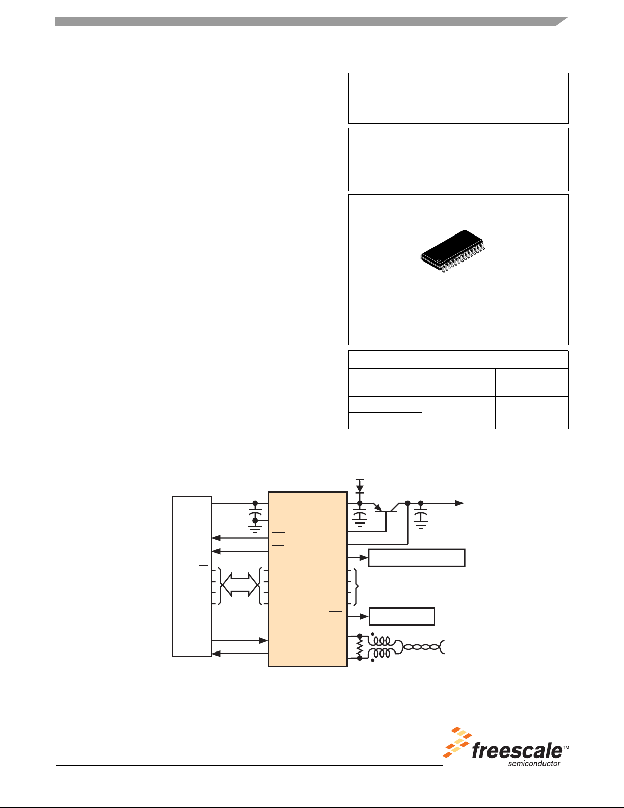
Figure 1. MC33989 Simplified Application Diagram
Freescale Semiconductor, Inc. reserves the right to change the detail specifications,
as may be required, to permit improvements in the design of its products.
© Freescale Semiconductor, Inc., 2007. All rights reserved.
CANH
CANL
V2
Local Module Supply
Wake-Up Inputs
Safe Circuits
Twisted
CAN Bus
Pair

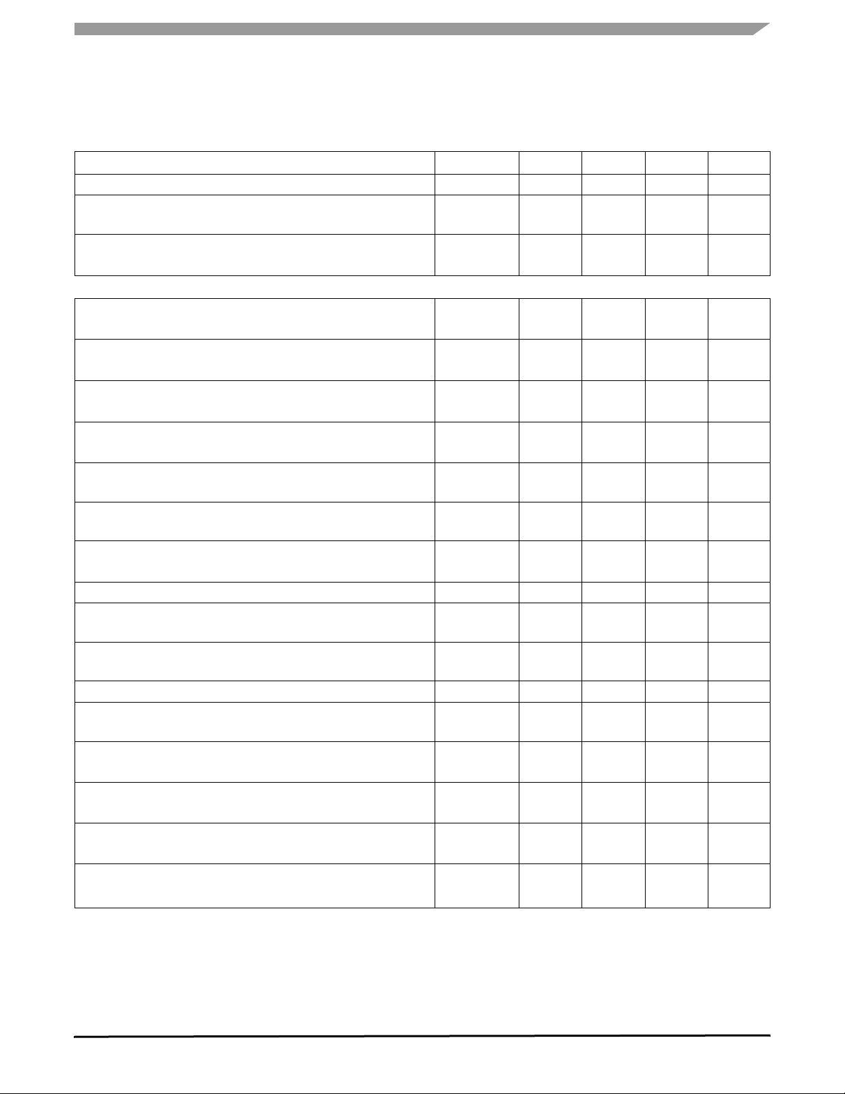
INTERNAL BLOCK DIAGRAM
VSUP
INTERNAL BLOCK DIAGRAM
VSUP Monitor Dual
Voltage Regulator
VDD1 Monitor
VDD1
HS1
L0
L1
TX
RX
CAN H
CAN L
HS1 Control
Oscillator
Interrupt
Watchdog
Programmable
Reset
Wake-Up Inputs
Mode Control
SPI
High Speed
Interface
1.0 MB/s CAN
Physical
Interface
Figure 2. 33989 Simplified Internal Block Diagram
INT
WD
RST
CS
SCLK
MOSI
MISO
GND
33989
Analog Integrated Circuit Device Data
2 Freescale Semiconductor
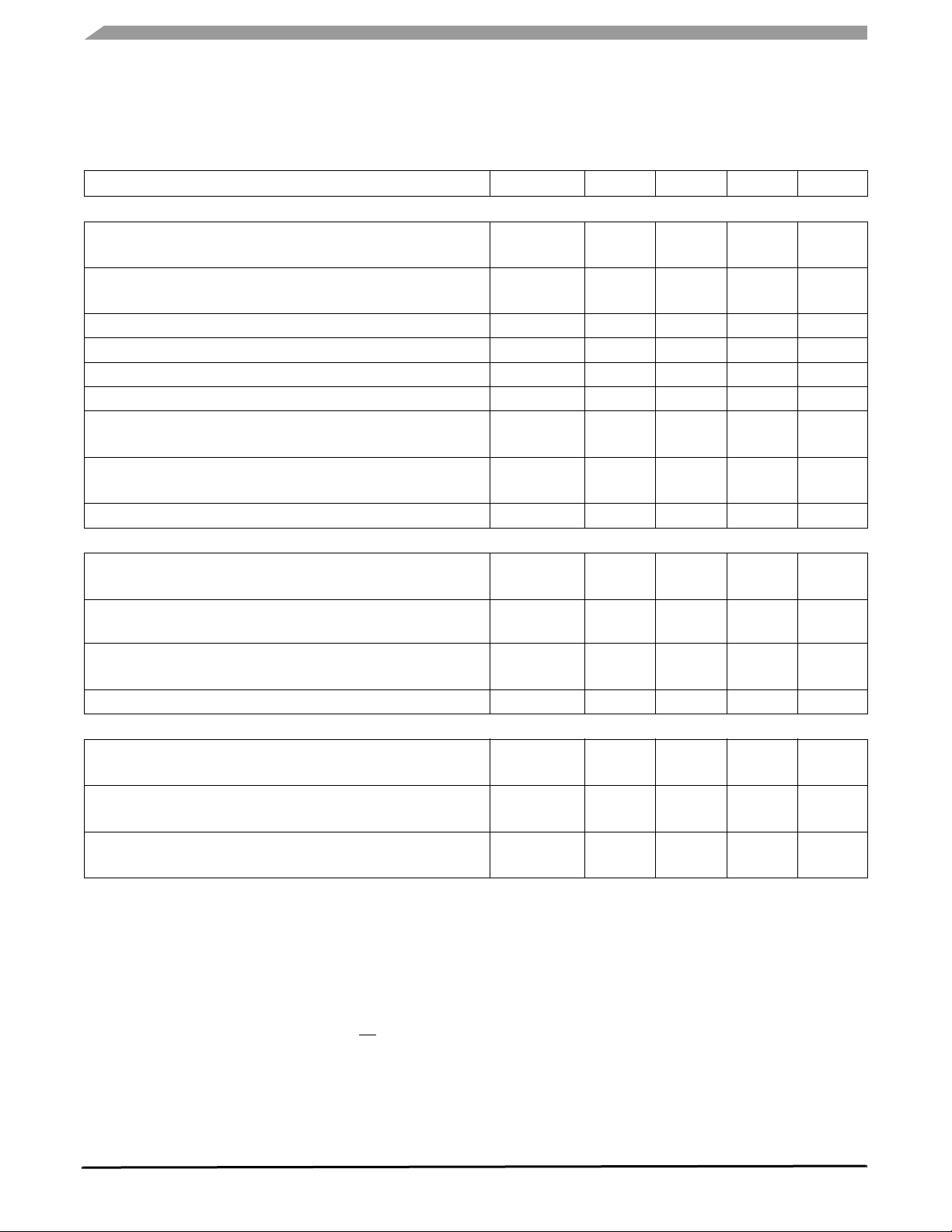
PIN CONNECTIONS
PIN CONNECTIONS
RX
TX
VDD1
RST
INT
GND
GND
GND
GND
V2
V2CTRL
VSUP
HS1
L0
1
2
3
4
5
6
7
8
9
10
11
12
13
14
28
WD
27
CS
26
MOSI
25
MISO
24
SCLK
23
GND
22
GND
21
GND
20
GND
19
CANL
18
CANH
17
L3
16
L2
15
L1
Figure 3. 33989 Pin Connections
Table 1. 33989 Pin Definitions
A functional description of each pin can be found in the Functional Pin Description section beginning on page 18.
Pin Number Pin Name Pin Function Formal Name Definition
1 RX Output Receive Data
2 TX Input Transmit Data
3 VDD1 Power
Output
Voltage Digital Drain
One
4 RST Output Reset
5 INT Output Interrupt
6–9
GND Ground Ground
20–23
10 V2 Input Voltage Source Two
11 V2CTRL Power
Voltage Control
Output
12 VSUP Power Voltage Supply
13 HS1 Output High Side One
14–17 L0:L3 Input Level 0: 3
22 CANH Output CAN High
23 CANL Output CAN Low
24 SCLK Input System Clock
25 MISO Output Master In/Slave Out
26 MOSI Input Master Out/Slave In
27 CS Input Chip Select
28 WD Output Watch Dog
CAN bus receive data output pin.
CAN bus transmit data input pin.
5.0 V regulator output pin. Supply pin for the MCU.
This is the device reset output pin whose main function is to reset the
MCU. This pin has an internal pullup current source to VDD.
This output is asserted LOW when an enabled interrupt condition occurs.
The output is a push-pull structure.
These device ground pins are internally connected to the package lead
frame to provide a 33989-to-PCB thermal path.
Sense input for the V2 regulator using an external series pass transistor.
V2 is also the internal supply for the CAN transceiver.
Output drive source for the V2 regulator connected to the external series
pass transistor.
Supply input pin for the 33989.
Output of the internal high-side switch. The output current is internally
limited to 150
mA.
Inputs from external switches or from logic circuitry.
CAN high output pin.
CAN low output pin.
Clock input pin for the Serial Peripheral Interface (SPI).
SPI data sent to the MCU by the 33989. When CS is HIGH, the pin is in
the high-impedance state.
SPI data received by the 33989.
The CS input pin is used with the SPI bus to select the 33989.
The WD output pin is asserted LOW if the software watchdog is not
correctly triggered.
33989
Analog Integrated Circuit Device Data
Freescale Semiconductor 3

ELECTRICAL CHARACTERISTICS
MAXIMUM RATINGS
ELECTRICAL CHARACTERISTICS
MAXIMUM RATINGS
Table 2. Maximum Ratings
All voltages are with respect to ground unless otherwise noted. Exceeding these ratings may cause a malfunction or
permanent damage to the device.
Ratings Symbol Value Unit
ELECTRICAL RATINGS
Power Supply Voltage at VSUP
Continuous (Steady-State)
Transient Voltage (Load Dump)
Logic Signals (RX, TX, MOSI, MISO, CS, SCLK, RST, WD, and INT)
Output Current VDD1
HS1
Voltage
Output Current
ESD Voltage, Human Body Model
(1)
HS1, L0, L1, L2, L3
All Other Pins
ESD Voltage Machine Model
All Pins Except CANH and CANL
L0, L1, L2, L3
DC Input Voltage
DC Input Current
Transient Input Voltage with External Component
(2)
CANL and CANH Continuous Voltage
CANL and CANH Continuous Current
CANH and CANL Transient Voltage (Load Dump)
CANH and CANL Transient Voltage
(5)
(4)
Logic Inputs (TX and RX)
ESD Voltage (HBM 100 pF, 1.5 k) CANL, CANH
ESD Voltage Machine Model
CANH and CANL
Notes
1. ESD1 testing is performed in accordance with the Human Body Model (C
= 0 Ω), and the Charge Device Model (CDM), Robotic (C
R
ZAP
ZAP
= 4.0pF).
2. According to ISO 7637 specification. See Table 6, page 24.
3. Load Dump test according to ISO 7637 part 1.
4. Transient test according to ISO 7637 part 1, pulses 1, 2, 3a, and 3b according to schematic in Table 17, page 35.
V
V
V
SUP
SUP
LOG
-0.3 to 27
-0.3 to 40
-0.3 to V
+ 0.3 V
DD1
I Internally Limited A
V
V
I
ESDH
-0.3 to V
SUP
+ 0.3
Internally Limited
- 4.0 to 4.0
-2.0 to 2.0
V
ESDM
±200
V
WUDC
-0.3 to 40
-2.0 to 2.0
-100 to 100
V
CANH/L
I
CANH/L
V
TRH/L
V
TRH/L
-27 to 40 V
200 mA
40 V
-40 to 40 V
V -0.5 to 6.0 V
V
ESDCH
V
ESDCM
-4.0 to 4.0 KV
-200 to 200
= 100 pF, 1.5 k), the Machine Model (MM) (C
ZAP
= 200 pF,
ZAP
V
V
A
kV
V
V
mA
V
V
33989
Analog Integrated Circuit Device Data
4 Freescale Semiconductor

THERMAL RATINGS
Operating Junction Temperature
Storage Temperature
Ambient Temperature
Thermal Resistance Junction to GND Pins
(5)
Peak Package Reflow Temperature During Reflow
(6), (7)
R
T
T
J
T
S
T
A
J/P
Θ
PPRT
ELECTRICAL CHARACTERISTICS
MAXIMUM RATINGS
-40 to 150 °C
-55 to 165 °C
-40 to 125 °C
20 °C/W
Note 7.
°C
33989
Analog Integrated Circuit Device Data
Freescale Semiconductor 5

ELECTRICAL CHARACTERISTICS
STATIC ELECTRICAL CHARACTERISTICS
STATIC ELECTRICAL CHARACTERISTICS
Table 3. Static Electrical Characteristics
Characteristics noted under conditions 5.5 V ≤ V
values noted reflect the approximate parameter means at T
Characteristic Symbol Min Typ Max Unit
POWER INPUT (VSUP)
Nominal DC Supply Voltage Range
Extended DC Voltage Range 1
Reduced Functionality
Extended DC Voltage Range 2
Input Voltage During Load Dump
Load Dump Situation
Input Voltage During Jump Start
Jump Start Situation
Supply Current in Standby Mode
I
at V
= 40 mA CAN recessive or Sleep-Disable State
OUT
DD1
Supply Current in Normal Mode
I
at V
= 40 mA CAN recessive or Sleep-Disable State
OUT
DD1
Supply Current in Sleep Mode
V
and V2 OFF, V
DD1
Sleep-Disable State
Supply Current in Sleep Mode
V
and V2 OFF, V
DD1
Sleep-Disable State
Supply Current in Sleep Mode
V
and V2 OFF, V
DD1
Sleep-Disable State
Supply Current in Stop Mode I
V
ON, V
DD1
SUP
Sleep-Disable State
Supply Current in Stop Mode I
V
ON, V
DD1
SUP
Sleep-Disable State
Supply Current in Stop Mode I
V
ON, V
DD1
SUP
Sleep-Disable State
BATFAIL Flag Internal Threshold
Notes
8. V
> 4.0 V, Reset high, Logic pin high level reduced, device is functional.
DD1
9. Device is fully functional. All functions are operating. All modes available and operating. Watchdog, HS1 turn ON turn OFF, CAN cell
operating, L0:L3 inputs operating, SPI read/write operation. Overtemperature may occur.
10. Current measured at V
11. With CAN cell in Sleep-Disable state. If CAN cell is Sleep-Enabled for wake-up, an additional 60 µA must be added to specified value.
12. Oscillator running means Forced Wake-up or Cyclic Sense of Software Watchdog is Stop mode are not activated.
(8)
(9)
(10) (11)
(10)
(10) (11)
< 12 V, Oscillator Running
SUP
(10) (11)
< 12 V, Oscillator Not Running
SUP
(10) (11)
> 12 V, Oscillator Running
SUP
V
OUT
< 12 V, Oscillator Running
OUT VDD1
< 2.0 mA
DD1
< 2.0 mA
(12)
< 12 V, Oscillator Not Running
OUT VDD1
> 12 V, Oscillator Running
SUP
< 2.0 mA
(12)
pin.
CAN in
(11)
(12)
(10) (11)
CAN in
≤ 18 V, - 40°C ≤ T
SUP
(12)
CAN in
(12)
(12)
CAN in
(10) (11)
CAN in
≤ 125°C, GND = 0 V unless otherwise noted. Typical
= 25°C under nominal conditions unless otherwise noted.
A
A
V
SUP
V
SUPEX1
5.5 — 18 V
4.5 — 5.5
V
SUPEX2
V
SUPLD
18 — 27 V
— — 40
V
SUPJS
— — 27
I
SUP(STDBY)
— 42 45
I
SUP(NORM)
— 42.5 45
I
SUP(SLEEP1)
— 72 105
I
SUP(SLEEP2)
CAN in
I
SUP(SLEEP3)
— 57 90
— 100 150
I
SUP(STOP1)
— 135 210
I
SUP(STOP2)
— 130 210
I
SUP(STOP3)
— 160 230
VBF 1.5 3.0 4.0 V
V
V
V
mA
mA
µA
µA
µA
µA
µA
µA
33989
Analog Integrated Circuit Device Data
6 Freescale Semiconductor
STATIC ELECTRICAL CHARACTERISTICS
ELECTRICAL CHARACTERISTICS
Table 3. Static Electrical Characteristics (continued)
Characteristics noted under conditions 5.5 V ≤ V
≤ 18 V, - 40°C ≤ T
SUP
≤ 125°C, GND = 0 V unless otherwise noted. Typical
A
values noted reflect the approximate parameter means at TA = 25°C under nominal conditions unless otherwise noted.
Characteristic Symbol Min Typ Max Unit
BATFAIL Flag Hysteresis
Battery Fall Early Warning Threshold
In Normal and Standby Mode
Battery Fall Early Warning Hysteresis
In Normal and Standby Mode
POWER OUTPUT (VDD1)
VDD1 Output Voltage
I
from 2.0 to 200 mA T
DD1
VDD1 Output Voltage
I
from 2.0 to 200 mA, 4.5 V < V
DD1
Dropout Voltage
I
= 200 mA
DD1
Dropout Voltage, Limited Output Current
I
= 50 mA, 4.5 V < V
DD1
I
Output Current
DD1
Internally Limited
Junction Thermal Shutdown
Normal or Standby Modes
Junction Over Temperature Pre-Warning
V
Temperature Threshold Difference
Reset Threshold 1
Selectable by SPI. Default Value After Reset.
Reset Threshold 2
Selectable by SPI
V
DD1
Reset Delay Time
Measured at 50% of Reset Signal
Line Regulation (C at V
9.0 V V
Line Regulation (C at V
5.5 < V
Load Regulation (C at V
1.0 mA < I
Thermal Stability
V
Notes
13. With CAN cell in Sleep-Disable state. If CAN cell is Sleep-Enabled for wake-up, an additional 60 µA must be added to specified value.
14. I
15. Guaranteed by design; however, it is not production tested.
Bit Set
DDTEMP
Range for Reset Active
< 18, IDD = 10 mA
SUP
< 27 V, IDD = 10 mA
SUP
< 200 mA
IDD
= 13.5 V, 1 = -100 mA Not Tested
SUP
is the total regulator output current. VDD specification with external capacitor. Stability requirement: C > 47 µF ESR < 1.3 Ω
DD1
(tantalum capacitor). In reset, normal request, normal and standby modes. Measure with C = 47 µF Tantalum.
(13)
(13)
(14)
-40 to 125°C, 5.5 V < V
AMB
SUP
= 47 µF Tantal)
DD1
= 47 µF Tantal)
DD1
= 47 µF Tantal)
DD1
SUP
< 5.5 V
(15)
SUP
< 27 V
VBF
(HYS)
BF
EW
BF
EWH
V
DD1OUT
V
DD1OUT2
V
DD1DRP
V
DD1DRP2
I
DD1
T
SD
T
PW
T
- T
SD
PW
RST
TH1
RST
TH2
V
DDR
t
D
LR1
LR2 —
LD
THERM
S
— 1.0 — V
5.3 5.8 6.3
0.1 0.2 0.3
4.9 5.0 5.1
4.0 — —
— 0.2 0.5
— 0.1 0.25
200 285 350
160 — 200
125 — 160
20 — 40 °C
4.5 4.6 4.7
4.1 4.2 4.3
1.0 — — V
—
4.0
30
—
5.0 25
10 25
— 25 75
— 30 50
V
V
V
V
V
V
mA
°C
°C
V
V
µs
mV
mV
mV
mV
33989
Analog Integrated Circuit Device Data
Freescale Semiconductor 7
ELECTRICAL CHARACTERISTICS
STATIC ELECTRICAL CHARACTERISTICS
Table 3. Static Electrical Characteristics (continued)
Characteristics noted under conditions 5.5 V ≤ V
≤ 18 V, - 40°C ≤ T
SUP
≤ 125°C, GND = 0 V unless otherwise noted. Typical
A
values noted reflect the approximate parameter means at TA = 25°C under nominal conditions unless otherwise noted.
Characteristic Symbol Min Typ Max Unit
SUP
(16)
(19)
< 27 V
(17)
(18)
V
DDSTOP
V
DDSTOP2
I
DD1SWU
I
DD1DGLT
RST
STOP1
RST
STOP2
LR
LD
V
DDst-cap
V2
I2
12
CTRL
V2L
V
OL
V
OH
I
HZ
S
S
TH
4.75 5.00 5.25
4.75 5.00 5.25
10 17 25 mA
40 55 75 µs
4.5 4.6 4.7 V
4.1 4.2 4.3 V
— 5.0 25
— 15 75
— — 200 µF
0.99 1.0 1.01
200 — —
0.0 — 10
3.75 4.0 4.25 V
0.0 — 1.0
V
DD1-0.9
— V
DD1
-2.0 — 2.0
” parameter.
DDst-cap
and prevent the device to stay in
DDSWU
POWER OUTPUT (VDD1) IN STOP MODE
VDD1 Output Voltage
I
< = 2.0 mA
DD1
VDD1 Output Voltage
I
< = 10 mA
DD1
I
Stop Output Current to Wake-up SBC
DD1
I
Over Current to Wake-up Deglitcher Time
DD1
Reset Threshold
Reset Threshold
Line Regulation (C at V
5.5 V < V
< 27 V, IDD = 2.0 mA
SUP
Load Regulation (C at V
= 47 µF Tantal)
DD1
= 47 µF Tantal)
DD1
1 mA < IDD < 10 mA
Max Decoupling Capacitor at VDD1 Pin, in Stop Mode
TRACKING VOLTAGE REGULATOR (V2)
V2 Output Voltage (C at V2 = 10 µF Tantal)
I2 from 2.0 to 200 mA, 5.5 V < V
I2 Output Current (for information only)
Depending Upon External Ballast Transistor
V2 Control Drive Current Capability
Worst Case at TJ = 125°C
V2LOW Flag Threshold
LOGIC OUTPUT PIN (MISO)
(20)
Low Level Output Voltage
I
= 1.5 mA
OUT
High Level Output Voltage
I
= 250 µA
OUT
Tri-Stated MISO Leakage Current
0 V < V
MISO
< V
DD
Notes
16. If stop mode is used, the capacitor connected at VDD pin should not exceed the maximum specified by the “V
If capacitor value is exceeded, upon entering stop mode, VDD output current may exceed the I
stop mode.
17. Guaranteed by design; however, it is not production tested.
18. Guaranteed by design.
19. V2 specification with external capacitor
- Stability requirement: C > 42 µF and ESR < 1.3 Ω (Tantalum capacitor), external resistor between base and emitter required
- Measurement conditions: Ballast transistor MJD32C, C = 10 µF Tantalum, 2.2 k resistor between base and emitter of ballast transistor
20. Push/Pull structure with tri-state condition CS high.
V
V
V
mV
mV
DD1
mA
mA
V
V
µA
33989
Analog Integrated Circuit Device Data
8 Freescale Semiconductor

STATIC ELECTRICAL CHARACTERISTICS
ELECTRICAL CHARACTERISTICS
Table 3. Static Electrical Characteristics (continued)
Characteristics noted under conditions 5.5 V ≤ V
≤ 18 V, - 40°C ≤ T
SUP
≤ 125°C, GND = 0 V unless otherwise noted. Typical
A
values noted reflect the approximate parameter means at TA = 25°C under nominal conditions unless otherwise noted.
Characteristic Symbol Min Typ Max Unit
LOGIC INPUT PINS (MOSI, SCLK, CS)
High Level Input Voltage
Low Level Input Voltage
High Level Input Current on CS
Low Level Input Current on CS
MOSI and SCLK Input Current
RESET PIN (RST)
(21)
High Level Output Current
0 < V
OUT
< 0.7 V
DD
Low Level Output Voltage (I0 = 1.5 mA)
5.5 V < V
SUP
< 27 V
Low Level Output Voltage (I0 = 0 µA
1.0 V < V
SUP
< 5.5 V
Reset Pull Down Current
V > 0.9 V
Reset Duration After V
WATCHDOG OUTPUT PIN (WD)
DD1
High
(22)
Low Level Output Voltage (I0 = 1.5 mA)
1.0 V < V
SUP
< 27 V
High Level Output Voltage (I0 = 250 µA)
INTERRUPT PIN (INT)
(22)
Low Level Output Voltage (I0 = 1.5 mA)
High Level Output Voltage (I0 = 250 µA)
HIGH SIDE OUTPUT PIN (HS1)
R
at TJ = 25°C, and I
DSON
V
> 9.0 V
SUP
R
at TA = 125°C, and I
DSON
V
> 9.0 V
SUP
R
at TA = 125°C, and I
DSON
5.5 < V
SUP
< 9.0 V
OUT
OUT
OUT
- 150 mA
- 150 mA
- 120 mA
Output Current Limitation
HS1 Overtemperature Shutdown
HS1 Leakage Current
Output Clamp Voltage at I
OUT
= -10 mA
No Inductive Load Drive Capability
Notes
21. Push/Pull structure with tri-state condition CS high.
22. Output pin only. Supply from VDD1. Structure switch to ground with pull-up current source.
V
V
I
RST
V
V
V
V
RON
RON
RON
L
O
L
V
IH
V
IL
L
IH
L
IL
L
N
I
OH
OL
OL
PDW
DUR
OL
OH
OL
OH
125-2
LIM
VT
LEAK
V
CL
25
125
0.7 V
DD1
-0.3 — 0.3 V
— V
+ 0.3 V
DD1
DD1
-100 — -20 µA
-100 — -20 µA
-10 — 10 µA
-300 -250 -150
0.0 — 0.9
0.0 — 0.9
2.3 — 5.0
3.0 3.4 4.0 ms
0.0 — 0.9
V
-0.9 — V
DD1
DD1
0.0 — 0.9 V
V
-0.9 — V
DD1
DD1
— 2.0 2.5
— — 4.5
— 3.5 5.5
160 — 500 mA
155 — 190 °C
— — 10 µA
-1.5 — -0.3
V
µA
V
V
mA
V
V
V
Ω
Ω
Ω
V
33989
Analog Integrated Circuit Device Data
Freescale Semiconductor 9

ELECTRICAL CHARACTERISTICS
STATIC ELECTRICAL CHARACTERISTICS
Table 3. Static Electrical Characteristics (continued)
Characteristics noted under conditions 5.5 V ≤ V
≤ 18 V, - 40°C ≤ T
SUP
≤ 125°C, GND = 0 V unless otherwise noted. Typical
A
values noted reflect the approximate parameter means at TA = 25°C under nominal conditions unless otherwise noted.
Characteristic Symbol Min Typ Max Unit
LOGIC INPUTS (L0:L3)
Negative Switching Threshold
5.5 V < V
6.0 V < V
18 V < V
SUP
SUP
SUP
< 6.0 V
< 18 V
< 27 V
Positive Switching Threshold
5.5 V < V
6.0 V < V
18 V < V
SUP
SUP
SUP
< 6.0 V
< 18 V
< 27 V
Hysteresis
5.5 V < V
SUP
< 27 V
Input Current
-0.2 V < V
IN
< 40 V
CAN SUPPLY (V2)
Supply Current Cell
Recessive State
Supply Current Cell
Dominant State without Bus Load
Supply Current Cell, CAN in Sleep State Wake-up Enable
V2 Regulator OFF
Supply Current Cell, CAN in Sleep State Wake-up Disable
V2 Regulator OFF
(23)
Notes
23. Push/Pull structure.
V
THN
V
THP
V
HYS
L
IN
I
RES
I
DOM
I
SLEEP
I
DIS
2.0
2.5
2.7
2.7
3.0
3.5
2.5
3.0
3.2
3.3
4.0
4.2
3.0
3.6
3.7
3.8
4.6
4.7
0.6 — 1.3
-10 — 10
— 1.5 3.0
— 2.0 6.0
— 55 70
— — 1.0
V
V
V
µA
mA
mA
µA
µA
33989
Analog Integrated Circuit Device Data
10 Freescale Semiconductor
STATIC ELECTRICAL CHARACTERISTICS
ELECTRICAL CHARACTERISTICS
Table 3. Static Electrical Characteristics (continued)
Characteristics noted under conditions 5.5 V ≤ V
≤ 18 V, - 40°C ≤ T
SUP
≤ 125°C, GND = 0 V unless otherwise noted. Typical
A
values noted reflect the approximate parameter means at TA = 25°C under nominal conditions unless otherwise noted.
Characteristic Symbol Min Typ Max Unit
CANH AND CANL
Bus Pins Common Mode Voltage
Differential Input Voltage (Common Mode Between -3.0 and 7.0 V)
Recessive State at RXD
Dominant State at RXD
Differential Input Hysteresis (RXD)
Input Resistance
Differential Input Resistance
Unpowered Node Input Current
CANH Output Voltage
TXD Dominant State
TXD Recessive State
CANL Output Voltage
TXD Dominant State
TXD Recessive State
Differential Output Voltage
TXD Dominant State
TXD Recessive State
CANH AND CANL
Output Current Capability (Dominant State)
CANH
CANL
Overtemperature Shutdown
CANL Over Current Detection
Error Reported in CANR
CANH Over Current Detection
Error Reported in CANR
TX AND RX
TX Input High Voltage
TX Input Low Voltage
TX High Level Input Current, VTX = V
DD
TX Low Level Input Current, VTX = 0 V
RX Output Voltage High, IRX = 250 µA
RX Output Voltage Low, IRX = 1.0 mA
V
CM
V
CANH-VCANL
V
HYS
R
IN
R
IND
I
CANUP
V
CANHD
V
CANHR
V
CANLD
V
CANLR
V
DIFFD
V
DIFFR
I
CANH
I
CANL
T
SHUT
I
CANL/OC
I
CANH/OC
V
IH
V
ILP
L
IH
L
IL
V
OH
V
OL
-27 — 40 V
—
900
—
—
500
—
100 — — mV
5.0 — 100 KΩ
10 — 100 KΩ
— — 1.5 mA
2.75
—
0.5
2.0
1.5
—
—
—
—
—
—
—
—
4.5
3.0
2.25
—
3.0
100
— -35
35
160 180°C — °C
60 — 200
-200 — -60
0.7 V
DD
-0.4 — 0.3 V
— VDD + 0.4 V
DD
-10 — 10 µA
-100 -50 -20 µA
VDD-1 — — V
— — 0.5 V
mV
V
V
V
mV
mA
mA
mA
V
33989
Analog Integrated Circuit Device Data
Freescale Semiconductor 11
ELECTRICAL CHARACTERISTICS
DYNAMIC ELECTRICAL CHARACTERISTICS
DYNAMIC ELECTRICAL CHARACTERISTICS
Table 4. Dynamic Electrical Characteristics
Characteristics noted under conditions 7.0 V ≤ V
values noted reflect the approximate parameter means at T
Characteristic Symbol Min Typ Max Unit
DIGITAL INTERFACE TIMING (SCLK, CS, MOSI, MISO)
SPI Operation Frequency
SCLK Clock Period
SCLK Clock High Time
SCLK Clock Low Time
Falling Edge of CS to Rising Edge of SCLK
Falling Edge of SCLK to Rising Edge of CS
MOSI to Falling Edge of SCLK
Falling Edge of SCLK to MOSI
MISO Rise Time (CL = 220 pF)
MISO Fall Time (CL = 220 pF)
Time from Falling or Rising Edges of CS to:
MISO Low Impedance
MISO High Impedance
Time from Rising Edge of SCLK to MISO Data Valid
0.2 V1 = <MISO> = 0.8 V1, CL = 200 pF
≤ 18 V, - 40°C ≤ T
SUP
≤ 125°C, GND = 0 V unless otherwise noted. Typical
= 25°C under nominal conditions unless otherwise noted.
A
A
F
REQ
t
PCLK
t
WSCLKH
t
WSCLKH
t
LEAD
t
LAG
t
SISU
t
SIH
t
RSO
t
FSO
t
SOEN
t
SODIS
t
VALID
0.25 — 4.0 MHz
250 — N/A ns
125 — N/A ns
125 — N/A ns
100 — N/A ns
100 — N/A ns
40 — N/A ns
40 — N/A ns
— 25 50 ns
— 25 50 ns
—
—
—
—
50
50
— — 50
ns
ns
STATE MACHINE TIMING (CS, SCLK, MOSI, MISO, WD, INT)
Delay Between CS Low to High Transition (End of SPI Stop Command) and
Stop Mode Activation Detected by V2 OFF
(24)
Interrupt Low Level Duration
SBC in Stop Mode
Internal Oscillator Frequency
All Modes Except Sleep and Stop
(24)
Internal Low Power Oscillator Frequency
Sleep and Stop Modes
(24)
Watchdog Period 1
Normal and Standby Modes
Watchdog Period 2
Normal and Standby Modes
Watchdog Period 3
Normal and Standby Modes
Watchdog Period 4
Normal and Standby Modes
Watchdog Period Accuracy
Normal and Standby Modes
Notes
24. Guaranteed by design; however it is not production tested.
t
CS
t
O
SCF1
O
SCF2
WD
WD
WD
WD
f
1ACC
STOP
INT
1
2
3
4
µs
18 — 34
µs
7.0 10 13
kHz
— 100 —
kHz
— 100 —
ms
8.58 9.75 10.92
ms
39.6 45 50.4
ms
88 100 112
ms
308 350 392
%
-12 — 12
33989
Analog Integrated Circuit Device Data
12 Freescale Semiconductor

DYNAMIC ELECTRICAL CHARACTERISTICS
ELECTRICAL CHARACTERISTICS
Table 4. Dynamic Electrical Characteristics (continued)
Characteristics noted under conditions 7.0 V ≤ V
≤ 18 V, - 40°C ≤ T
SUP
≤ 125°C, GND = 0 V unless otherwise noted. Typical
A
values noted reflect the approximate parameter means at TA = 25°C under nominal conditions unless otherwise noted.
Characteristic Symbol Min Typ Max Unit
Normal Request Mode Timeout
Normal Request Modes
Watchdog Period 1 - Stop
Stop Mode
Watchdog Period 2 - Stop
Stop Mode
Watchdog Period 3 - Stop
Stop Mode
Watchdog Period 4 - Stop
Stop Mode
Stop Mode Watchdog Period Accuracy
Stop Mode
Cyclic Sense/FWU Timing 1
Sleep and Stop Modes
Cyclic Sense/FWU Timing 2
Sleep and Stop Modes
Cyclic Sense/FWU Timing 3
Sleep and Stop Modes
Cyclic Sense/FWU Timing 4
Sleep and Stop Modes
Cyclic Sense/FWU Timing 5
Sleep and Stop Modes
Cyclic Sense/FWU Timing 6
Sleep and Stop Modes
Cyclic Sense/FWU Timing 7
Sleep and Stop Modes
Cyclic Sense/FWU Timing 8
Sleep and Stop Modes
Cyclic Sense ON Time
Sleep and Stop Modes Threshold and Condition to be Added
Cyclic Sense/FWU Timing Accuracy
Sleep and Stop Modes
Delay Between SPI Command and HS1 Turn ON
Delay Between SPI Command and HS1 Turn OFF
Delay Between SPI and V2 Turn ON
(25)
(25)
(25)
Standby Mode
Delay Between SPI and V2 Turn OFF
(25)
Normal Mode
Notes
25. Delay starts at falling edge of clock cycle #8 of the SPI command and start of Turn ON or Turn OFF of HS1 or V2.
NR
TOUT
WD
1STOP
WD
2STOP
WD
3STOP
WD
4STOP
f
2ACC
CS
FWU1
CS
FWU2
CS
FWU3
CS
FWU4
CS
FWU5
CS
FWU6
CS
FWU7
CS
FWU8
t
ON
t
ACC
t
SHSON
t
SHSOFF
tS
V2ON
tS
V2OFF
308 350 392
6.82 9.75 12.7
31.5 45 58.5
70 100 130
245 350 455
-30 — 30
3.22 4.6 5.98
6.47 9.25 12
12.9 18.5 24
25.9 37 48.1
51.8 74 96.2
66.8 95.5 124
134 191 248
271 388 504
200 350 500
-30 — 30
— — 22 µs
— — 22 µs
9.0 — 22
9.0 — 22
ms
ms
ms
ms
ms
%
ms
ms
ms
ms
ms
ms
ms
ms
µs
%
µs
µs
33989
Analog Integrated Circuit Device Data
Freescale Semiconductor 13

ELECTRICAL CHARACTERISTICS
DYNAMIC ELECTRICAL CHARACTERISTICS
Table 4. Dynamic Electrical Characteristics (continued)
Characteristics noted under conditions 7.0 V ≤ V
≤ 18 V, - 40°C ≤ T
SUP
≤ 125°C, GND = 0 V unless otherwise noted. Typical
A
values noted reflect the approximate parameter means at TA = 25°C under nominal conditions unless otherwise noted.
Characteristic Symbol Min Typ Max Unit
Delay Between Normal Request and Normal Mode After WD Trigger Command
Normal Request Mode
Delay Between SPI and CAN Normal Mode
SBC Normal Mode
(26)
Delay Between SPI and CAN Normal Mode
SBC Normal Mode
(26)
Delay Between CS Wake-up (CS Low to High) and SBC Normal Request Mode
(V
on and Reset High)
DD1
SBC in Stop Mode
Delay Between CS Wake-up (CS Low to High) and First Accepted API
Command
SBC in Stop Mode
Delay Between INT Pulse and First SPI Command Accepted
In Stop Mode After Wake-up
INPUT TERMINNALS (L0, L1, L2, AND L3)
Wake-up Filter Time
CAN MODULE-SIGNAL EDGE RISE AND FALL TIMES (CANH, CANL)
Dominant State Timeout
Propagation Loop Delay TX to RX, Recessive to Dominant
Slew Rate 3
Slew Rate 2
Slew Rate 1
Slew Rate 0
Propagation Delay TX to CAN
Slew Rate 3
Slew Rate 2
Slew Rate 1
Slew Rate 0
Propagation Delay CAN to RX, Recessive to Dominant
Propagation Loop Delay TX to RX, Dominant to Recessive
Slew Rate 3
Slew Rate 2
Slew Rate 1
Slew Rate 0
Propagation Delay TX to CAN
Slew Rate 3
Slew Rate 2
Slew Rate 1
Slew Rate 0
Propagation Delay CAN to RX, Dominant to Recessive
Notes
26. Guaranteed by design; however, it is not production tested.
tS
tS
tS
tW
tW
tS
1STSPI
t
t
DOUT
t
t
t
t
t
t
NR2N
CANN
CANS
CS
SPI
WUF
LRD
TRD
RRD
LDR
TDR
RDR
15 35 70
— — 10
— — 10
15 40 90
90 — N/A
20 —
N/A
8.0 20 38 µs
200 360 520 µs
70
80
100
110
20
40
60
100
140
155
180
220
65
80
120
160
210
225
255
310
110
150
200
300
30 80 140 ns
70
90
100
130
60
65
75
90
120
135
160
200
110
120
150
190
170
180
220
260
130
150
200
300
20 40 60
µs
µs
µs
µs
µs
µs
ns
ns
ns
ns
33989
Analog Integrated Circuit Device Data
14 Freescale Semiconductor
DYNAMIC ELECTRICAL CHARACTERISTICS
ELECTRICAL CHARACTERISTICS
Table 4. Dynamic Electrical Characteristics (continued)
Characteristics noted under conditions 7.0 V ≤ V
≤ 18 V, - 40°C ≤ T
SUP
≤ 125°C, GND = 0 V unless otherwise noted. Typical
A
values noted reflect the approximate parameter means at TA = 25°C under nominal conditions unless otherwise noted.
Characteristic Symbol Min Typ Max Unit
Non Differential Slew Rate (CANL or CANH)
Slew Rate 3
Slew Rate 2
Slew Rate 1
Slew Rate 0
t
t
t
t
SL3
SL2
SL1
SL0
4.0
3.0
2.0
1.0
19
13.5
8.0
5.0
40
20
15
10
V/µs
CANH
CANL
WU Receiver
Standby
Pulse Width
Filter
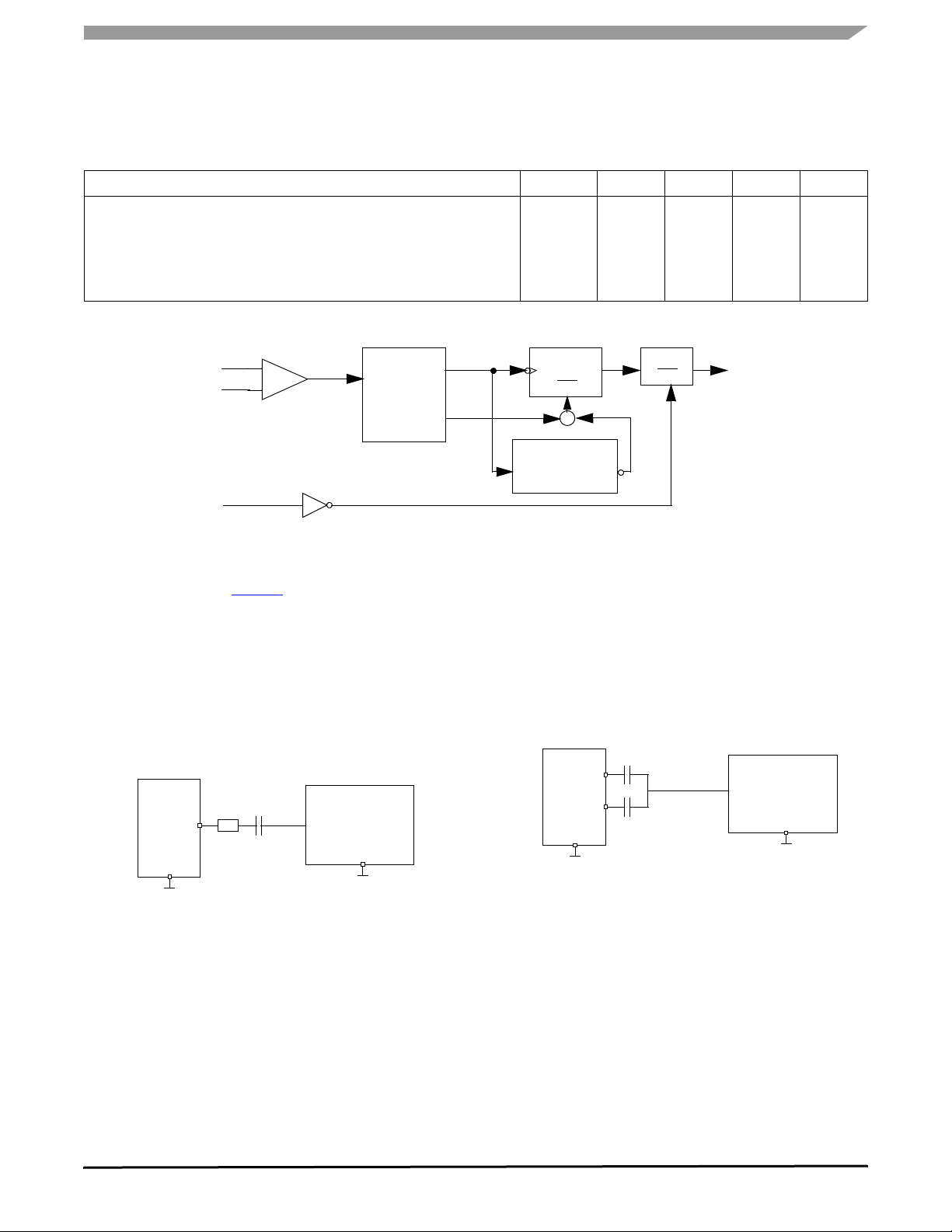
Figure 4. Wake-Up Block Diagram
The block diagram in Figure 4 illustrates how the wake-up
signal is generated. First the CAN signal is detected by a low
consumption receiver (WU receiver). Then the signal passes
through a pulse width filter which discards the undesired
pulses. The pulse must have a width bigger than 0.5 µs and
smaller than 500 µs to be accepted. When a pulse is
discarded the pulse counter is reset and no wake signal is
generated, otherwise when a pulse is accepted the pulse
counter is incremental and after three pulses the wake signal
is asserted.
1nF
LX
10 k
GND
Note: Waveform in accordance to
ISO 7637 part1, test pulses 1, 2, 3a and 3b.
Transient Pulse
Generator
(Note)
GND
Figure 5. Transient Test Pulse for L0:L3 Inputs
Pulse OK
Narrow
Pulse
Counter
RST
+
Timeout
Generator
Latch
RST
Timeout
WU
OUT
Each one of the pulses must be spaced by no more than
500 µs. In that case the pulse counter is reset and no wake
signal is generated. This is accomplished by the wake
timeout generator. The wake-up cycle is completed (and the
wake flag reset) when the CAN interface is brought to CAN
Normal mode.
The wake-up capability of the CAN can be disabled, refer
to SPI interface and register section, CAN register.
1nF
CANH
CANL
GND
1nF
Note: Waveform in accordance to
ISO 7637 part1, test pulses 1, 2, 3a and 3b.
Transient Pulse
Generator
Figure 6. Transient Test Pulses for CANH/CANL
(Note)
GND
33989
Analog Integrated Circuit Device Data
Freescale Semiconductor 15
ELECTRICAL CHARACTERISTICS
DYNAMIC ELECTRICAL CHARACTERISTICS
T
TX
LRD
2.0 V
0.8 V
RX
0.8 V
T
LDR
2.0 V
TX
V
V
0.8 V
DIFF
0.9 V
DIFF
T
TRD
0.9 V
T
RRD
V
DIFF
= V
CANH
2.0 V
- V
0.5 V
CANL
T
TDR
0.5 V
T
RDR
RX
0.8 V
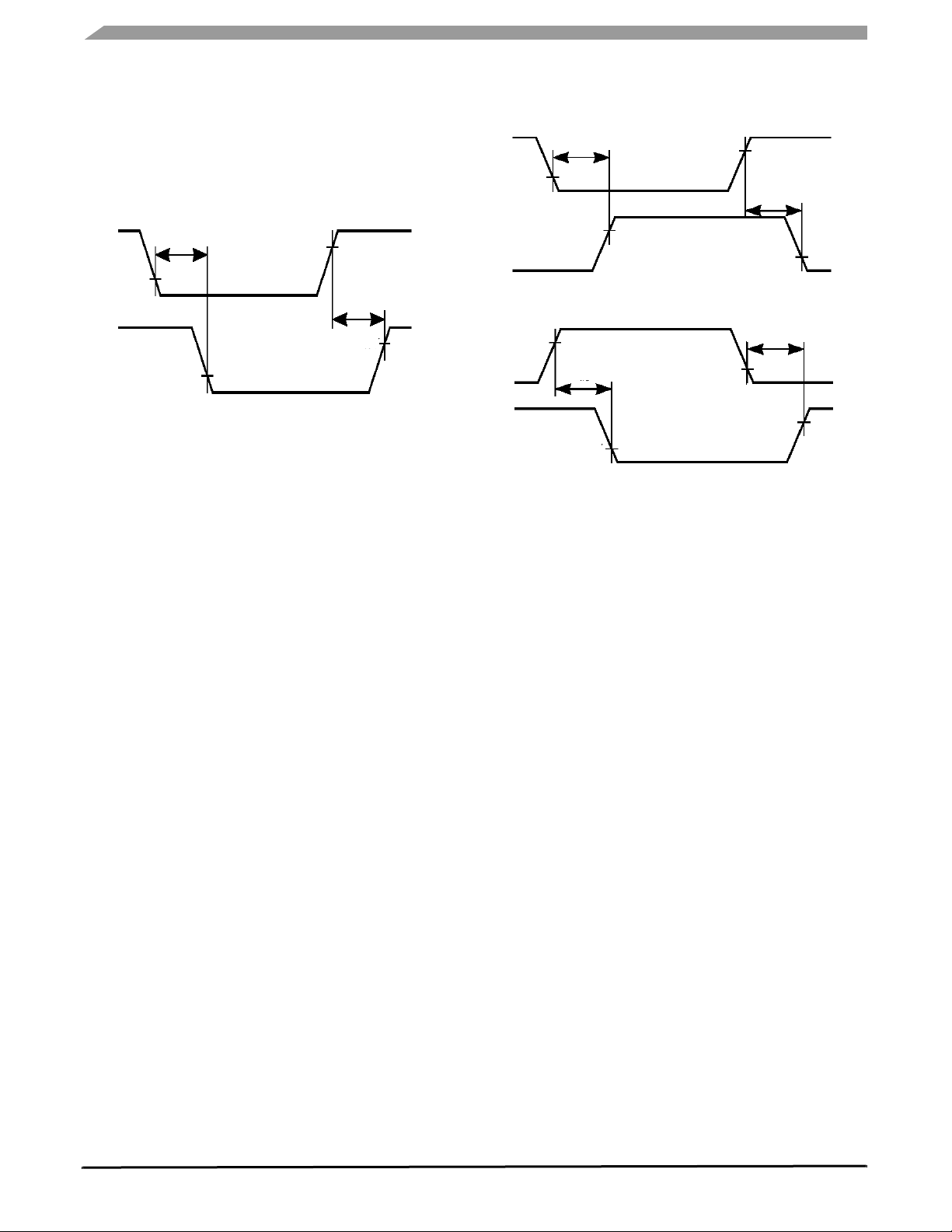
Figure 7. Transceiver AC Characteristics
2.0 V
33989
Analog Integrated Circuit Device Data
16 Freescale Semiconductor

TIMING DIAGRAMS
ELECTRICAL CHARACTERISTICS
TIMING DIAGRAMS
Figure 8. SPI Timing Characteristics
33989
Analog Integrated Circuit Device Data
Freescale Semiconductor 17

FUNCTIONAL DESCRIPTION
INTRODUCTION
FUNCTIONAL DESCRIPTION
INTRODUCTION
The 33989 is an integrated circuit dedicated to automotive
applications. Its functions include:
• One full protected voltage regulator with 200 mA total
output current capability available at V
external pin
DD1
FUNCTIONAL PIN DESCRIPTION
RECEIVE AND TRANSMIT DATA (RXD AND TXD)
The RX and TX pins (receive data and transmit data pins,
respectively) are connected to a microcontroller’s CAN
protocol handler. TXD is an input and controls the CANH and
CANL line state (dominant when TXD is LOW, recessive
when TXD is HIGH). RXD is an output and reports the bus
state (RXD LOW when CAN bus is dominant, HIGH when
CAN bus is recessive).
VOLTAGE DIGITAL DRAIN ONE (VDD1)
The VDD1 pin is the output pin of the 5.0 V internal
regulator. It can deliver up to 200 mA. This output is protected
against overcurrent and overtemperature. It includes an
overtemperature pre-warning flag, which is set when the
internal regulator temperature exceeds 130°C typical. When
the temperature exceeds the overtemperature shutdown
(170°C typical), the regulator is turned off.
VDD1 includes an undervoltage reset circuitry, which sets
the RST pin LOW when V
threshold.
is below the undervoltage reset
DD1
RESET (RST)
The Reset pin RST is an output that is set LOW when the
device is in reset mode. The
device is not in reset mode.
current source. When RST is LOW, the sink current capability
is limited, allowing
debug or software download purposes.
RST to be shorted to 5.0 V for software
RST pin is set HIGH when the
RST includes an internal pullup
INTERRUPT (INT)
The Interrupt pin INT is an output that is set LOW when an
interrupt occurs.
(INTR). When an interrupt occurs,
interrupt source is cleared.
INT output also reports a wake-up event by a 10 µs typical
pulse when the device is in Stop mode.
INT is enabled using the Interrupt Register
INT stays LOW until the
VOLTAGE SOURCE TWO (V2)
The V2 pin is the input sense for the V2 regulator. It is
connected to the external series pass transistor. V2 is also
the 5.0 V supply of the internal CAN interface. It is possible to
• Driver for an external path transistor for the V2 regulator
function
• Reset, programmable watchdog function, interrupt, and
four operational modes
• Programmable wake-up input and Cyclic Sense wake-up
• CAN high-speed physical interface
connect V2 to an external 5.0
output when no external series pass transistor is used. In this
case, the V2CTRL pin must be left open.
V regulator or to the VDD1
VOLTAGE SOURCE 2 CONTROL (V2CTRL)
The V2CTRL pin is the output drive pin for the V2 regulator
connected to the external series pass transistor.
VOLTAGE SUPPLY (VSUP)
The VSUP pin is the battery supply input of the device.
HIGH-SIDE ONE (HS1)
The HS1 pin is the internal high-side driver output. It is
internally protected against overcurrent and
overtemperature.
LEVEL 0-3 INPUTS (L0:L3)
The L0:L3 pins can be connected to contact switches or
the output of other ICs for external inputs. The input states
can be read by SPI. These inputs can be used as wake-up
events for the SBC when operating in the Sleep or Stop
mode.
CAN HIGH AND CAN LOW OUTPUTS
(CANH AND CANL)
The CAN High and CAN Low pins are the interfaces to the
CAN bus lines. They are controlled by TX input level, and the
state of CANH and CANL is reported through RX output. A
Ω termination resistor is connected between CANH and
60
CANL pins.
SYSTEM CLOCK (SCLK)
SCLK is the System Clock input pin of the serial peripheral
interface.
MASTER IN SLAVE OUT (MISO)
MISO is the Master In Slave Out pin of the serial peripheral
interface. Data is sent from the SBC to the microcontroller
through the MISO pin.
33989
Analog Integrated Circuit Device Data
18 Freescale Semiconductor

FUNCTIONAL DESCRIPTION
FUNCTIONAL PIN DESCRIPTION
MASTER OUT SLAVE IN (MOSI)
MOSI is the Master Out Slave In pin of the serial peripheral
interface. Control data from a microcontroller is received
through this pin.
CHIP SELECT (CS)
CS is the Chip Select pin of the serial peripheral interface.
When this pin is LOW, the SPI port of the device is selected.
WATCHDOG (WD)
The Watchdog output pin is asserted LOW to flag that the
software watchdog has not been properly triggered.
33989
Analog Integrated Circuit Device Data
Freescale Semiconductor 19

FUNCTIONAL DEVICE OPERATION
OPERATIONAL MODES
FUNCTIONAL DEVICE OPERATION
DEVICE SUPPLY
The device is supplied from the battery line through the
VSUP pin. An external diode is required to protect against
negative transients and reverse battery. It can operate from
4.5 V and under the jump start condition at 27
Vdc. This pin
sustains standard automotive voltage conditions such as
load dump at 40 V. When V
falls below 3.0 V typical the
SUP
33989 detects it and stores the information into the SPI
register in a bit called BATFAIL. This detection is available in
all operation modes.
The device incorporates a battery early warning function,
providing a maskable interrupt when the V
voltage is
SUP
below 6.0 V typical. A hysteresis is included. Operation is
only in Normal and Standby modes. V
low is reported in
SUP
the Input/Output Register (IOR).
VDD1 VOLTAGE REGULATOR
The VDD1 Regulator is a 5.0 V output voltage with output
current capability up to 200 mA. It includes a voltage
monitoring circuitry associated with a reset function. The
VDD1 regulator is fully protected against overcurrent and
short-circuit. It has over- temperature detection warning flags
(bit V
in MCR and interrupt registers), and
DDTEMP
overtemperature shutdown with hysteresis.
V2 REGULATOR
V2 Regulator circuitry is designed to drive an external path
transistor increasing output current flexibility. Two pins are
used to achieve the flexibility. Those pins are V2 and V2
control. The output voltage is 5.0 V and is realized by a
tracking function of the VDD1 regulator. The recommended
ballast transistor is MJD32C. Other transistors can be used;
however, depending upon the PNP gain an external resistorcapacitor network might be connected. The V2 is the supply
input for the CAN cell. The state of V2 is reported in the IOR
(bit V2LOW set to 1 if V2 is below 4.5 V typical).
HS1 VBAT SWITCH OUTPUT
The HS1 output is a 2.0 Ω typical switch from the VSUP
pin. It allows the supply of external switches and their
associated pull-up or pull down circuitry, in conjunction with
the wake-up input pins, for example. Output current is limited
to 200 mA and HS1 is protected against short-circuit and has
an overtemperature shutdown (bit HS1OT in IOR and bit
HS1OT-V2LOW in
INT register). The HS1 output is controlled
from the internal register and the SPI. Because of an internal
timer, it can be activated at regular intervals in Sleep and
Stop modes. It can also be permanently turned on in Normal
or Standby modes to drive loads or supply peripheral
components. No internal clamping protection circuit is
implemented, thus a dedicated external protection circuit is
required in case of inductive load drive.
BATTERY FALL EARLY WARNING
Refer to the discussion under the heading: Device Supply.
INTERNAL CLOCK
The device has an internal clock used to generate all
timings (Reset, Watchdog, Cyclic Wake-up, Filtering Time,
etc.). Two oscillators are implemented. A high accuracy
percent) used in Normal Request, Normal and Standby
(±12
modes, and a low accuracy (±30 percent) used in Sleep and
Stop modes.
OPERATIONAL MODES
FUNCTIONAL MODES
The device has four primary operation modes:
1. Standby mode
2. Normal mode
3. Stop mode
4. Sleep mode
All modes are controlled by the SPI. An additional
temporary mode called Normal Request mode is
automatically accessed by the device after reset or wake-up
from Stop mode. A Reset (
RST) mode is also implemented.
Special modes and configuration are possible for debug and
program MCU flash memory.
STANDBY MODE
Only regulator 1 is ON. Regulator 2 is turned OFF by
disabling the V2 control pin. Only the wake-up capability of
the CAN interface is available. Other functions available are
33989
20 Freescale Semiconductor
wake-up input reading through SPI and HS1 activation. The
Watchdog is running.
NORMAL MODE
In this mode both regulators are ON. This corresponds to
the normal application operation. All functions are available in
this mode (Watchdog, wake-up input reading through SPI,
HS1 activation, CAN communication). The software
Watchdog is running and must be periodically cleared
through SPI.
STOP MODE
Regulator 2 is turned OFF by disabling the V2 control pin.
The regulator 1 is activated in a special low power mode,
allowing to deliver few mA. The objective is to maintain the
MCU of the application supplied while it is turned into power
saving condition (i.e Stop or Wait modes). In Stop mode the
device supply current from V
Analog Integrated Circuit Device Data
is very low.
BAT

FUNCTIONAL DEVICE OPERATION
OPERATIONAL MODES
When the application is in Stop mode (both MCU and
SBC), the application can wake-up from the SBC side (for
example: cyclic sense, forced wake-up, CAN message,
wake-up inputs and over current on VDD1), or the MCU side
(key wake-up, etc.).
Stop mode is always selected by the SPI. In Stop mode the
software Watchdog can be running or idle depending upon
selection by the SPI (RCR, bit WDSTOP). To clear the
watchdog, the SBC must be awakened by a
CS pin (SPI
wake-up). In Stop mode, SBC wake-up capability are
identical as in Sleep mode. Please refer to
Table 5.
SLEEP MODE
Regulators 1 and 2 are OFF. The current from V
reduced. In this mode, the device can be awakened internally
by cyclic sense via the wake-up inputs pins and HS1 output,
from the forced wake-up function and from the CAN physical
interface. When a wake-up occurs the SBC goes first into
reset mode before entering Normal Request mode.
SUP
pin is
RESET MODE
In this mode, the Reset (RST) pin is low and a timer is
running for a time RST
. After this time is elapsed, the SBC
DUR
enters Normal Request mode. Reset mode is entered if a
reset condition occurs (V
low, watchdog timeout or
DD1
watchdog trigger in a closed window).
NORMAL REQUEST MODE
This is a temporary mode automatically accessed by the
device after the reset mode, or after the SBC wake-up from
mode. After wake-up from the Sleep mode or after the
Stop
device power-up, the SBC enters the Reset mo de be fo re
entering the Normal Request mode. After a wake-up from the
Stop mode, the SBC enters Normal Request mode directly.
In Normal Request mode the VDD1 regulator is ON, V2 is
OFF, the reset pin is high. As soon as the device enters the
Normal Request mode an internal 350 ms timer is started.
During these 350 ms the microcontroller of the application
must address the SBC via the SPI, configuring the Watchdog
register. This is the condition for the SBC to stop the 350 ms
timer and to go into the Normal or Standby mode and to set
the watchdog timer according to configuration.
NORMAL REQUEST ENTERED AND NO WD
CONFIGURATION OCCURS
In case the Normal Request mode is entered after SBC
power-up, or after a wake-up from Stop mode, and if no
configuration occurs while the SBC is in Normal Request
mode, the SBC goes to Reset mode after the 350 ms time
period is expired before again going into Normal Request
mode. If no
WD configuration is achieved, the SBC
alternatively goes from Normal Request into reset, then
Normal Request modes etc.
In case the Normal Request mode is entered after a wake-
up from Sleep mode, and if no
WD configuration occurs while
WD
the SBC is in Normal Request mode, the SBC goes back to
Sleep mode.
APPLICATION WAKE-UP FROM SBC SIDE
When an application is in Stop mode, it can wake-up from
the SBC side. When a wake-up is detected by the SBC (for
example, CAN, Wake-up input, etc.) the SBC turns itself into
Normal Request mode and generates an interrupt pulse at
INT pin.
the
APPLICATION WAKE-UP FROM MCU SIDE
When application is in Stop mode, the wake-up event may
come from the MCU side. In this case the MCU signals to the
SBC by a low to high transition on the CS pin. Then the SBC
goes into Normal Request mode and generates an interrupt
pulse at the
INT pin.
STOP MODE CURRENT MONITOR
If the VDD1 output current exceed an internal threshold
(I
mode and generates an interrupt at the
), the SBC goes automatically into Normal Request
DD1SWU
INT pin. The interrupt
is not maskable and the interrupt register will has no flag set.
INTERRUPT GENERATION WHEN WAKE-UP
FROM STOP MODE
When the SBC wakes up from Stop mode, it first enters the
Normal Request mode before generating a pulse (10 µs
typical) on the
INT pin. These interrupts are not maskable,
and the wake-up event can be read through the SPI registers
(CANWU bit in Reset Control Register (RCR) and LCTRx bit
in Wake-Up Register (WUR). In case of wake-up from Stop
mode over current or from forced wake-up, no bit is set. After
INT pulse the SBC accept SPI command after a time
the
S1STSPI
parameter).
delay (t
SOFTWARE WATCHDOG IN STOP MODE
If Watchdog is enabled, the MCU has to wake-up
independently of the SBC before the end of the SBC
watchdog time. In order to do this the MCU must signal the
wake-up to the SBC through the SPI wake-up (
CS activation).
The SBC then wakes up and jumps into the Normal Request
mode. MCU has to configured the SBC to go to either Normal
or Standby mode. The MCU can then decide to go back again
to Stop mode.
When there is no MCU wake-up occurring within the
watchdog timing, the SBC activates the Reset pin, jumping
into the Normal Request mode. The MCU can then be
initialized.
STOP MODE ENTER COMMAND
Stop mode is entered at the end of the SPI message, and
at the rising edge of the
CS. Please refer to the t
in Dynamic Electrical Characteristics table on page 11.
Once Stop mode is entered the SBC could wake-up from
the V1 regulator over current detection. In order to allow time
for the MCU to complete the last CPU instruction, allowing
CSSTOP
data
33989
Analog Integrated Circuit Device Data
Freescale Semiconductor 21
FUNCTIONAL DEVICE OPERATION
RESET AND WATCHDOG PINS, SOFTWARE WATCHDOG OPERATIONS
the MCU to enter its low power mode, a deglitcher time of
typical 40 µs is implemented.
SPI Stop/ Sleep Command
SPI CS
t
SBC in Normal or Stand-by mode
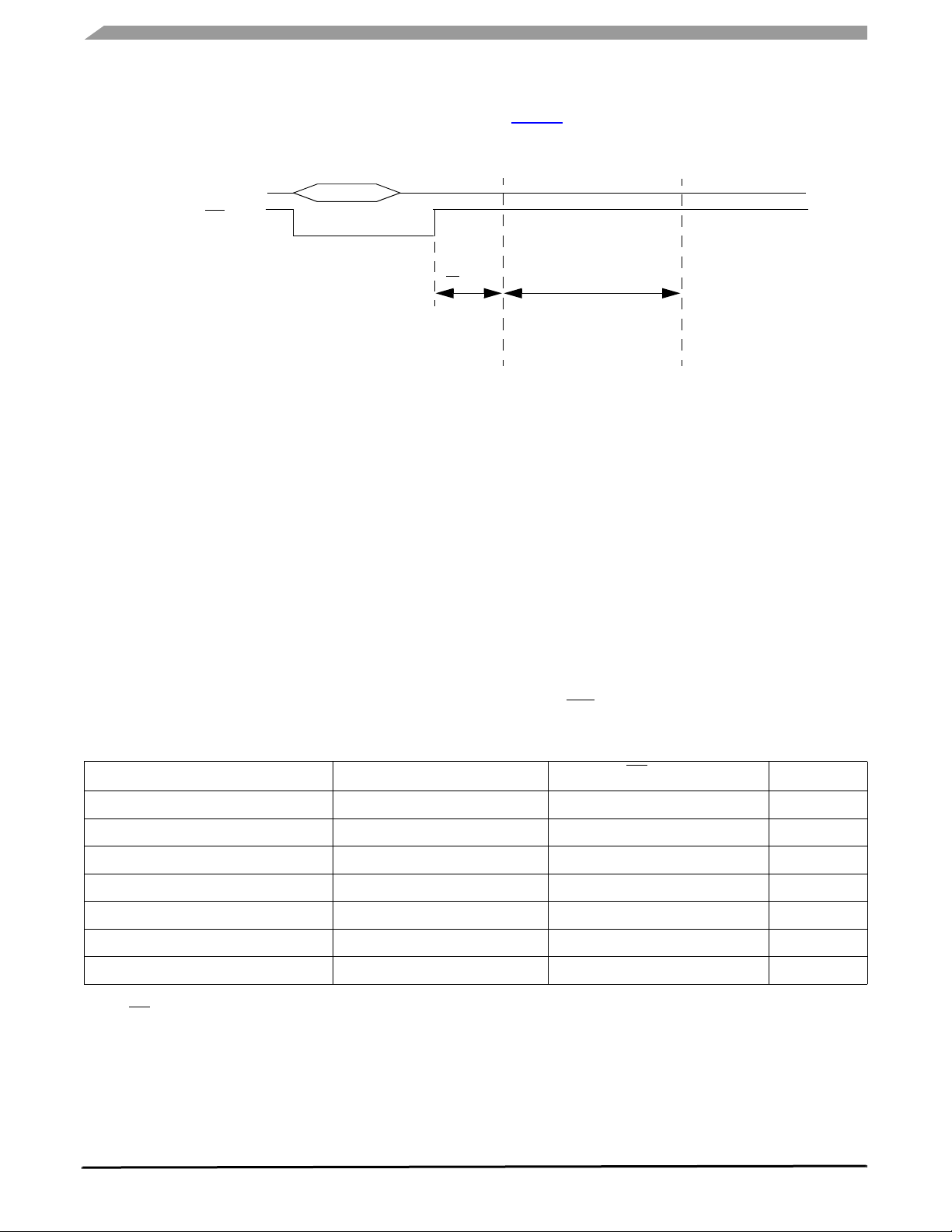
Figure 9. Operation Entering Stop Mode
RESET AND WATCHDOG PINS, SOFTWARE WATCHDOG OPERATIONS
SOFTWARE WATCHDOG (SELECTABLE WINDOW
OR TIMEOUT WATCHDOG)
Software watchdog uses in the SBC Normal and Standby
modes is to monitor MCU. The Watchdog can be either
window or timeout. This is selectable by SPI (register TIM1,
bit WDW). Default is window watchdog. The period for the
watchdog is selectable from the SPI from 10 ms to 350 ms
(register TIM1, bits WDT0 and WDT1). When the window
watchdog is selected, the closed window is the first part of the
selected period, and the open window is the second part of
the period. Refer to the SPI TIM register description.
Watchdog can only be cleared within the open window time.
An attempt to clear the watchdog in the closed window will
generate a reset. Watchdog is cleared through SPI by
addressing the TIM1 register.
CS
Figure 9 indicates the operation to enter Stop mode.
STOP
I
DD1DGLT
SBC in Stop mode
no I
over I wake-up
DD1
SBC in Stop mode
with I
over I wake-up
DD1
RESET PIN DESCRIPTION
A reset output is necessary and available to reset the
microcontroller. Modes 1 and 2 are available for the reset pin
(please refer to
Reset causes when SBC is in mode 1:
•V
falling out of range — If V
DD1
threshold (parameter R
V
returns to the normal voltage.
DD1
• Power-on reset — At device power-on or at device wake-
up from Sleep mode, the reset is maintained low until V
is within its operation range.
Watchdog timeout — If watchdog is not cleared, the SBC
will pull the reset pin low for the duration of the reset time
(parameter
Table 5 for reset pin operation).
DD1
), the ret pin is pulled low until
STTH
RST
DUR)
.
falls below the reset
DD1
Table 5. Reset and Watchdog Output Operation
Events Mode WD Output Reset Output
Devices Power-up
V
Normal Watchdog Properly Triggered
DD1
V
< RST
DD1
Watchdog Timeout Reached
V
DD1
V
DD1
Watchdog Timeout Reached
Notes
27. WD stays low until the Watchdog register is properly addressed through SPI.
TH
Normal Watchdog Properly Triggered
< RST
TH
In Mode 2, the reset pin is not activated in case of
Watchdog timeout. Please refer to
Table 6 for more detail.
For debug purposes at 25°C, the Reset pin can be shorted
to 5.0 V because of its internal limited current drive capability.
33989
1 or 2 (Safe Mode) Low to High Low to High
1 High High
1 High Low
1 Low (Note) Low
2 (Safe Mode) High High
2 (Safe Mode) High Low
2 (Safe Mode) Low (Note) High
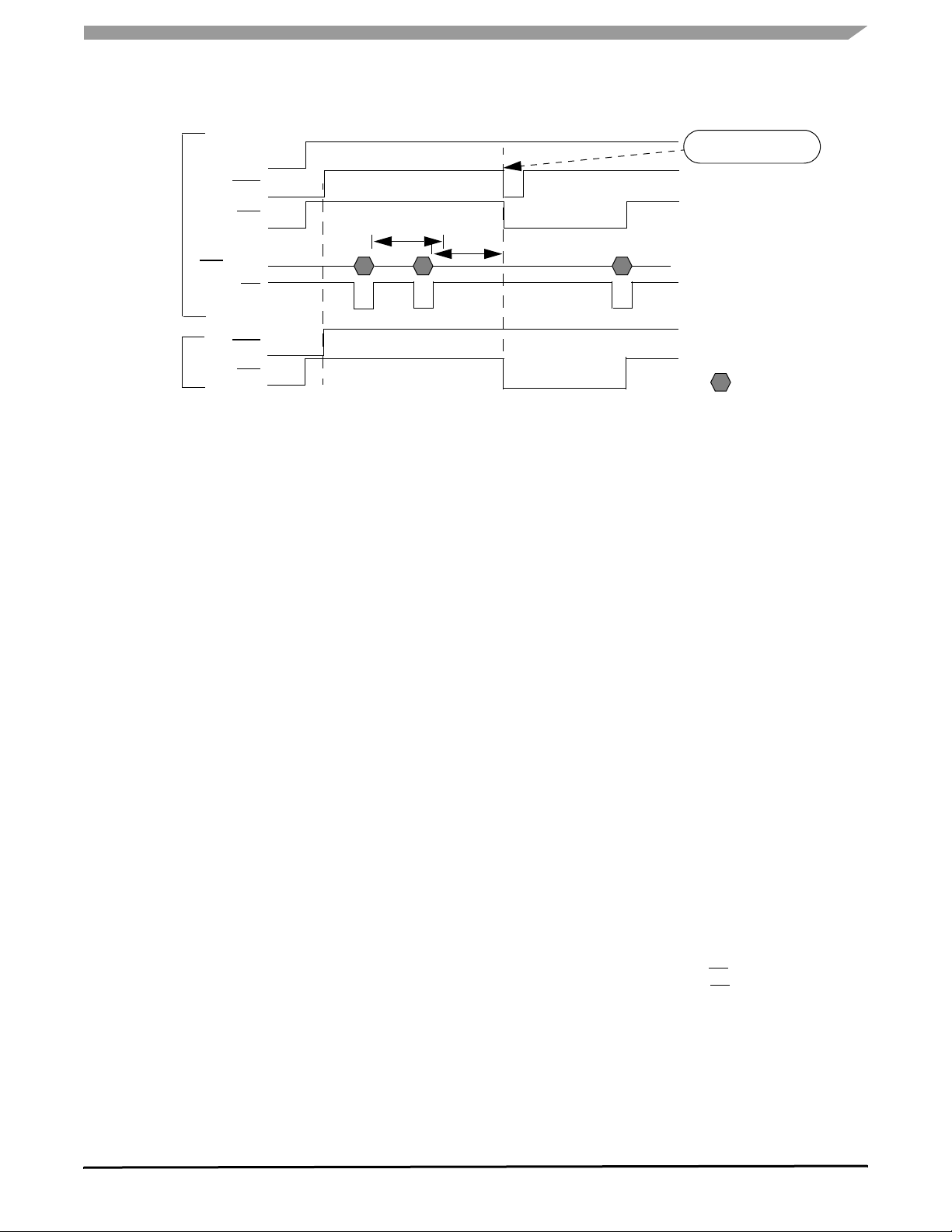
RESET AND WATCHDOG OPERATION: MODES1
AND 2
Watchdog and Reset functions have two modes of
operation:
Analog Integrated Circuit Device Data
22 Freescale Semiconductor

RESET AND WATCHDOG PINS, SOFTWARE WATCHDOG OPERATIONS
FUNCTIONAL DEVICE OPERATION
1. Mode 1
2. Mode 2 (also called Safe mode)
These modes are independent of the SBC modes
(Normal, Standby, Sleep, and Stop). Modes 1 and 2 selection
is achieved through the SPI (register MCR, bit SAFE). Default
mode after reset is Mode 1.
Table 5 provides Reset and Watchdog output mode
of operation. Two modes (modes 1 and 2) are available and
can be selected through the SPI Safe bit. Default operation,
after reset or power-up, is Mode 1.
In both modes reset is active at device power-up and
wake-up.
• In mode 1–Reset is activated in case of V
DD1
fall or
watchdog not triggered. WD output is active low as soon
as reset goes low. It remains low as long as the watchdog
is not properly re-activated by the SPI.
• In mode 2–(Safe mode) Reset is not activated in case of
watchdog fault.
WD output has the same behavior as in
mode 1–The Watchdog output pin is a push-pull structure
driving external components of the application for signal
instance of an MCU wrong operation.
33989
Analog Integrated Circuit Device Data
Freescale Semiconductor 23

FUNCTIONAL DEVICE OPERATION
RESET AND WATCHDOG PINS, SOFTWARE WATCHDOG OPERATIONS
Table 6. Table of Operation
Mode
Voltage Regulator
HS1 Switch
Wake-up
Capabilities
(if enabled)
Reset Pin INT
Software
Watchdog
CAN Cell
Normal
Request
Normal V
HS1:Controllable
Standby V
HS1:Controllable
Stop V
(Limited Current
Capability)
HS1:OFF or Cyclic
Sleep V
HS1:OFF or Cyclic
Debug
Same as Normal — Normally High
Normal
Debug
Same as Standby — Normally High
Standby
V
:ON
DD1
V2:OFF
HS1:OFF
:ON
DD1
V2:ON
:ON
DD1
V2:OFF
:ON
DD1
V2:OFF
:OFF
DD1
V2:OFF
— Low for Reset-DUR
—
Active Low if
V
occurs (and mode 1
— Same as Normal
CAN
SPI
L0:L3
Active Low if WD
Cyclic Sense
Forced Wake-up
I
Over Current
DD1
(28)
CAN
SPI
L0:L3
Cyclic Sense
Forced Wake-up
Active Low if V
Active Low if V
— — —
Time, then High
Normally High
WD or
under voltage
DD1
If Enabled, Signal
Failure (V
DD1
Pre-
Warning Temp,
CAN, HS1)
Running Tx/Rx
selected)
Mode
Normally High
(29)
or V
Under
DD1
Voltage Occurs
Same as Normal
Mode
Signal SBC Wake-
up and
IDD > I
DD1S/WU
(Not Maskable)
Running Low Power
Running if Enabled
Not Running if
Disabled
Wake-up Capability
Low Not Active Not Running Low Power
Wake-up Capability
Same as Normal Not Running Same as Normal
DD1
Under Voltage
Occurs
Same as Standby Not Running Same as Standby
DD1
Under Voltage
Occurs
Low Power
if Enabled
if Enabled
33989
Analog Integrated Circuit Device Data
24 Freescale Semiconductor
top D(eb )-7.5g( )]TJETEMC/Span <</MCID984>>BDCBT7.98 0 0 7.981217.56 63.408 Tm0.011 Tc-0.0065 Tw(Same as Soep)TjETEMC/Span <</MCID985>>BDCBT7.98 0 0 7.98 9-6.23.63.408 Tm(Same as Soep)TjETEMC/Span <</MCID986>>BDCBT7.98 0 0 7.98 271.32 63.408 Tm0.0006 Tc-0.0002 Tw[(Nor)-4.7(m)-1(ally High)]TJ-0.9398 -1.2556 TD-0.0079 Tw[(Act)-7.2(i)4.8(ve Low if V)]TJETEMC/Span <</MCID978>>BDCBT6.36 0 0 6.36 316.082491408 Tm0.0043 Tc0 Tw(DD1)TjETEMC/Span <</MCID978>>BDCBT7.98 0 0 7.98 328.86293.46011 Tm0 Tc( )Tj-7.2632 -1.2556 TD0.0004 Tc(Under Voltage )Tj1.609 -1.2481 TD0.0046 Tc[(Occ)8.4(u)4.4(rs)]TJETEMC/Span <</MCID 89>>BDCBT7.98 0 0 7.98 46.32 63.408 Tm0.011 Tc-0.0065 Tw(Same as Soep)TjETEMC/Span <</MCID1090>>BDCBT7.98 0 0 7.98 423.96 63.408 Tm0.0004 Tc0 Tw[(No)-7.4(t Running)]TJETEMC/Span <</MCID1091>>BDCBT7.98 0 0 7.98 953.96 63.408 Tm0.011 Tc-0.0065 Tw(Same as Soep)TjETEMC/Span <</MCID1092>>BDCBT7.98 0 0 7.982715082576.8011 Tm0 TwFlash( )Tj19.732 -1.2556 TD6 Tc[Progor
ammino
ng
MODE 1
VDD1
RST
WD
SPI
WD Clear
SPI CS
Watchdog
Period
RESET AND WATCHDOG PINS, SOFTWARE WATCHDOG OPERATIONS
FUNCTIONAL DEVICE OPERATION
Watchdog Timeout
MODE 2
RST
WD
Figure 10. Reset and Watchdog Functions Diagram in Modes 1 and 2
WAKE-UP CAPABILITIES
Several wake-up capabilities are available for the device
when it is in Sleep, or Stop modes. When a wake-up has
occurred, the wake-up event is stored into the WUR or CAN
registers. The MCU can then access to the wake-up source.
The wake-up options are able to be selected through the SPI
while the device is in Normal or Standby mode and prior to
entering low power mode (Sleep or Stop mode). When a
wake-up occurs from sleep mode the device activates V
It generates an interrupt if wake-up occurs from Stop mode.
DD1
WAKE-UP FROM WAKE-UP INPUTS (L0:L3)
WITHOUT CYCLIC SENSE
The wake-up lines are dedicated to sense external switch
states and if changes occur to wake-up the MCU (in Sleep or
Stop modes). The wake-up pins are able to handle 40 V DC.
The internal threshold is 3.0 V typical and these inputs can be
used as an input port expander. The wake-up inputs state are
read through SPI (register WUR).
In order to select and activate direct wake-up from the LX
inputs, the WUR register must be configured with the
appropriate level sensitivity. Additionally, the LPC register
must be configured with 0x0 data (bits LX2HS1and
HS1AUTO are set at 0).
Level sensitivity is selected by WUR register. Level
sensitivity is configured by a pair of Lx inputs: L0 and L1 level
sensitivity are configured together while L2 and L3 are
configured together.
CYCLIC SENSE WAKE-UP (CYCLIC SENSE TIMER
AND WAKE-UP INPUTS L0, L1, L2, L3)
The SBC can wake-up upon state change of one of the
four wake-up input lines (L0, L1, L2 and L3) while the external
pull-up or pull down resistor of the switches associated to the
wake-up input lines are biased with HS1 VSUP switch. The
HS1 switch is activated in Sleep or Stop modes from an
Watchdog
Addressed
internal timer. Cyclic Sense and Forced Wake-up are
exclusive. If Cyclic Sense is enabled the forced wake-up can
not be enabled.
In order to select and activate the cyclic sense wake-up
from the Lx inputs the WUR register must be configured with
the appropriate level sensitivity, and the LPC register must be
configured with 1xx1 data (bit LX2HS1 set at 1 and bit
HS1AUTO set at 1). The wake-up mode selection (direct or
cyclic sense) is valid for all 4 wake-up inputs.
.
FORCED WAKE-UP
The SBC can wake-up automatically after a predetermined
time spent in Sleep or Stop mode. Cyclic sense and Forced
wake-up are exclusive. If Forced wake-up is enabled (FWU
bit set to 1 in LPC register) the Cyclic Sense can not be
enabled.
CAN INTERFACE WAKE-UP
The device incorporates a high-speed 1MBaud CAN
physical interface. Its electrical parameters for the CANL,
CANH, RX and TX pins are compatible with ISO 11898
specification (IS0
physical interface operation is accomplished through the SPI.
CAN modes are independent of the SBC operation modes.
The device can wake-up from a CAN message if the CAN
wake-up is enabled. Please refer to the CAN module
description for detail of wake-up detection.
11898: 1993(E)). The control of the CAN
SPI WAKE-UP
The device can wake-up by the CS pin in Sleep or Stop
modes. Wake-up is detected by the
to a high level. In Stop mode, this corresponds with the
condition where the MCU and SBC are in Stop mode; and
when the application wake-up event comes through the
MCU.
CS pin transition from low
Register
33989
Analog Integrated Circuit Device Data
Freescale Semiconductor 25

FUNCTIONAL DEVICE OPERATION
RESET AND WATCHDOG PINS, SOFTWARE WATCHDOG OPERATIONS
DEVICE POWER-UP, SBC WAKE-UP
After device or system power-up, or after the SBC wakes
up from Sleep mode, it enters into Reset mode prior to
moving into Normal Request mode.
DEBUG MODE: HARDWARE AND SOFTWARE
DEBUG WITH THE SBC
When the SBC is mounted on the same printed circuit
board as the microcontroller it supplies, both application
software and SBC dedicated routine must be debugged. The
following features allow debug of the software by allowing the
possibility of disabling the SBC internal software Watchdog
timer.
DEVICE POWER-UP, RESET PIN CONNECTED TO
VDD1
At SBC power-up the VDD1 voltage is provided, but if no
SPI communication occurs to configure the device, a reset
occurs every 350 ms. In order to allow software debug and
avoid MCU reset, the Reset pin can be connected directly to
VDD1 by a jumper.
DEBUG MODES WITH SOFTWARE WATCHDOG
DISABLED THOUGH SPI (NORMAL DEBUG,
STANDBY AND STOP DEBUG)
The Watchdog software can be disabled through SPI. To
avoid unwanted watchdog disable while limiting the risk of
disabling Watchdog during SBC normal operation, the
watchdog disable must be achieved the following sequence:
• Step 1–Power down the SBC
• Step 2–Power-up the SBC (The BATFAIL bit is set,
allowing the SBC to enter Normal Request mode)
• Step 3–Write to TIM1 register allowing SBC entering
Normal mode
• Step 4–Write to MCR register with data 0000, enabling the
Debug mode. Complete SPI byte: 000 1 0000
• Step 5–Write to MCR register normal debug (0001x101)
• Step 6–To leave the Debug mode, write 0000 to MCR
register
While in Debug mode, the SBC can be used without
having to clear the
WD on a regular basis to facilitate
software and hardware debug.
At Step 2, the SBC is in Normal Request. Steps 3, 4, and
5 should be completed consecutively and within the 350 ms
time period of the Normal Request mode. If this step is not
accomplished in a timely manner, the SBC will go into Reset
mode, entering Normal Request again.
When the SBC is in Debug mode, and set in Stop Debug
or Sleep Debug, when a wake-up occurs the SBC enters
Normal Request mode for a time period of 350 ms. To avoid
the SBC generating a reset (enter Reset mode) the desired
next Debug mode (Normal Debug or Standby Debug) should
be configured within the 350 ms time period of the Normal
Request mode. For details, please refer to State Machine in
Debug mode,
Figure 16.
To avoid entering Debug mode after a power-up, first read
BATFAIL bit (MCR read) and write 0000 into MCR. Figure 15
illustrates the Debug mode enter.
VSUP
VDD1
Batfail
TIM1(Step 3)
MCR (Step5)
SPI
MCR(Step4)
Debug Mode
SPI: Read Batfail
SBC in Debug Mode, No WD
Figure 11. Debug Mode Enter
MCU FLASH PROGRAMMING CONFIGURATION
To download software into the application memory (MCU
EEPROM or Flash) the SBC capabilities allows the V
be forced by an external power supply to 5.0 V; the reset and
WD outputs by external signal sources are forced to zero or
5.0 V, both without damage. This allows, for example, supply
of the complete application board by external power supply,
DD1
to
MCR (Step6)
SBC Not in Debug Mode and WD ON
applying the correct signal to reset pins. No function of the
SBC is operating.
Due to pass transistor from VDD1 to VSUP, supplying the
device from VDD1 pin biases the VSUP pin. Therefore, V
SUP
should not be forced to a value above 5.0 V. The Reset pin is
periodically pulled low for
before being pulled to V
RST
DD1
time reset is low, the reset pin sinks 5.0 mA maximum (L
time (3.4 ms typical)
DUR
for 350 ms typical. During the
PDW
parameter).
33989
Analog Integrated Circuit Device Data
26 Freescale Semiconductor

RESET AND WATCHDOG PINS, SOFTWARE WATCHDOG OPERATIONS
FUNCTIONAL DEVICE OPERATION
VSUP (Open or > 5.0 V
SBC MCU = Flash
External supply and sources applied to V
and WD
VDD1
RST
WD
test points on application circuit board.
Figure 12. Simplified Schematic for Flash Programming
PACKAGE AND THERMAL CONSIDERATION
The device is proposed in a standard surface mount
SOIC28 package. In order to improve the thermal
performances of the SOIC28 package, eight pins are
internally connected to the lead frame and are used for heat
transfer to the printed circuit board.
WD: Timeout OR V
Reset Counter (3.4
ms) Expired
SBC Power-
Power
Down
Reset
V
Low OR WD:
:
T
i
m
e
o
DD1
Timeout 350 ms
&!Nostop
u
t
O
R
V
D
D
1
L
o
WD: Timeout OR V
W
D
w
(
3
1
0
)
1
Normal
2
Wake-up
2
Stop
DD1
Programming Bus
, RST ,
DD1
Table 6, page 24, describes the SBC operation modes.
Normal, Stand-by, and Stop Debug modes are entered
through special sequence described in the Debug mode
paragraph.
Low
DD1
WD: Timeout & Nostop
Low
4
Sto
Hi
SPI:
to
SPI: Stop & CS
Low to High
Transition
SPI: Stand-by
Trigger
& WD
3
Low
n
o
CS
&
p
ransiti
T
WD:
h
g
T
ri
g
ger
Normal
1
Stand-by
SPI: Stand-by
SPI: Normal
1
Low to High
CS
Nostop & SPI: Sleep &
Low
Nostop & SPI:
Sleep & CS
Wake-up
(V
1 2 3 4
DD1
denotes priority
High T emperature OR (V
1 Low > 100ms & V
DD1
>BFew)) & Nostop &!BA TF AIL
SUP
Sleep
STATE MACHINE DESCRIPTION:
28. Nostop = Nostop bit = 1
29. ! Nostop = Nostop bit = 0
30. BATFAIL = Batfail bit = 1
31. ! BATFAIL = Batfail bit = 0
32. V
33. V
34. V
35. WD
Over Temperature = V
DD1
low = V
DD1
low >100 ms = V
DD1
below reset threshold
DD1
DD1
thermal shutdown occurs
DD1
below reset threshold for more than 100 ms
: Trigger = TIM1 register write operation.
Figure 13. State Machine (Not Valid in Debug Modes)
Notes These two SPI commands must be sent consecutively in this sequence.
30. If WD activated.
33989
Analog Integrated Circuit Device Data
Freescale Semiconductor 27
FUNCTIONAL DEVICE OPERATION
RESET AND WATCHDOG PINS, SOFTWARE WATCHDOG OPERATIONS
Power-Up
Behavior after power-up if no trigger appears
Behavior after reset of BATFAIL if no trigger appears
Reset
Normal
Request
Yes No
NoNo
Yes
Trigger Batfail No Stop Sleep
Yes
Normal
Figure 14. Behavior at SBC Power-Up
WD: Timeout 350 ms
Normal Request
r
e
g
g
i
r
T
:
D
W
Reset Counter
(3.4 ms) Expired
SPI: MCR (0000) & Normal Debug
Reset
Normal
Power
Down
Normal Debug
SPI: MCR (0000) & Stand-by Deb ug
St and-by Debug
Figure 15. Transitions to Enter Debug Modes
33989
Analog Integrated Circuit Device Data
28 Freescale Semiconductor

Stop (1)
Wake-up
Normal Request
WD: Time-out 350 ms
Reset Counter
(3.4 ms) Expired
Reset
FUNCTIONAL DEVICE OPERATION
LOGIC COMMANDS AND REGISTERS
Wake-up
Sleep
R
up
-
e
R
Wa
k
Stop Debug
SPI: Stop
High Transition
SPI: Stop Debug & CS Low to
(1) If Stop mode entered, it is entered without watchdog, no matter the WDSTOP bit.
(E) Debug mode entry point (Step 5 of the Debug mode entering sequence).
(R) Represents transitions to Reset mode due to V
: Trigger
WD
SPI: Stand-by &
Stand-by
SPI: Stand-by
St and-by Debug
low.
DD1
R
R
S
P
I
:
N
o
r
m
a
l
D
e
b
SPI:
u
E
g
SPI: Stand-by Debug
SPI: Normal Debug
R
W
D
:
T
r
nd-by Debu
a
St
i
g
g
e
r
Normal
g
E
R
R
& SPI: Sleep
&!BATFAILNOSTOP
SPI: Normal Debug
Normal Debug
R
Figure 16. Simplified State Machine in Debug Modes
LOGIC COMMANDS AND REGISTERS
SPI INTERFACE AND REGISTER DESCRIPTION
Table 7 illustrates a register, an 8-bit SPI. The first three
bits are used to identify the internal SBC register address. Bit
four is a read/write bit. The last four bits are Data Send from
MCU to SBC, or read back from SBC to MCU.
There is no significance during write operation state of
MISO.
During read operation only the final four bits of MISO have
a meaning (content of the accessed register).
The following tables describe the SPI register list, and
register bit meaning.
Registers reset value is also described along with the reset
condition. Reset condition is the condition causing the bit to
be set at the reset value.
Table 7. Data Format Description
Bit 7 Bit 6 Bit 5 Bit 4 Bit 3 Bit 2 Bit 1 Bit 0
A2 A1 A0 R/W D3 D2 D1 D0
Read operation: R/W Bit = 0
Write operation: R/W Bit = 1
Possible reset conditions include:
SBC Reset: Power-On Reset POR
SBC Mode Transition: NR2R - Normal Request to Reset Mode
NR2N - Normal Request to Normal Mode
NR2STB - Normal Request to Standby
Mode
N2R - Normal to Reset Mode
STB2R - Standby to Reset Mode
STO2R - Stop to Reset Mode
STO2NR - Stop to Normal Request
SBC Mode: RESET - SBC in Reset Mode
33989
Analog Integrated Circuit Device Data
Freescale Semiconductor 29

FUNCTIONAL DEVICE OPERATION
LOGIC COMMANDS AND REGISTERS
Table 8. List of Registers
Name Address Description Comment and Use
MCR $000 Mode Control Register
RCR $001 Reset Control Register
CAN $010 CAN Control Register
IOR $011 I/O Control Register
WUR $100 Wake-up Input
Register
TIM $101 Timing Register
LPC $110 Low Power Mode
Control Register
INT $111 Interrupt Register
Write: Control of Normal, Standby, Sleep, Stop, Debug Modes
Read: BATFAIL flag and other status bits and flags
Write: Configuration for reset voltage level, Safe bit, Stop mode
Read: CAN wake-up and CAN failure status bits
Write: CAN module control: TX/RX and Sleep modes, slope control, wake
enable/disable
Read: CAN wake-up and CAN failure status bits
Write: HS1 (High Side switch) control in Normal and Standby mode
Read: HS1 over temp bit, V
Write: Control of wake-up input polarity
Read: Wake-up input and real time LX input state
Write: TIM1, Watchdog timing control, window, or Timeout mode
Write: TIM2, Cyclic sense and force wake-up timing selection
Write: Control HS1 periodic activation in Sleep and Stop modes, force
wake-up
Write: Interrupt source configuration
Read: INT source
and V2 Low status
SUP
33989
Analog Integrated Circuit Device Data
30 Freescale Semiconductor

FUNCTIONAL DEVICE OPERATION
LOGIC COMMANDS AND REGISTERS
Mode Control Register (MCR)
Table 9 provides Mode Control Register data.
Table 9. MCR Register
MCR D3 D2 D1 D0
$000B W — MCTR2 MCTR1 MCTR0
R BATFAIL
(31)
VDDTEMP GFAIL WDRST
Reset Value — 0 0 0
Reset Condition — POR, RESET POR, RESET POR, RESET
Notes
31. Bit BATFAIL cannot be set by SPI. BATFAIL is set when V
falls below 3.0 V.
SUP
Table 10. MCR Control Bits
MCTR2 MCTR1 MCTR0 SBC Mode Description
0 0 0 Enter/Exit Debug Mode
To enter/exit Debug Mode, refer to detail
Debug Mode: Hardware and Software Debug...
0 0 1 Normal —
0 1 0 Standby —
(33)
(32)
(32)
—
—
—
No watchdog running, Debug Mode
0 1 1 Stop, Watchdog OFF
0 1 1 Stop, Watchdog ON
1 0 0 Sleep
1 0 1 Normal
1 1 0 Standby
1 1 1 Stop
Notes
32. Watchdog ON or OFF depends on RCR bit D3.
33. Before entering Sleep mode, bit BATFAIL in MCR must be previously cleared (MCR read operation), and bit NOSTOP in RCR must be
previously set to 1.
Table 11. MCR Status Bits
Status Bits Description
GFAIL
BATFAIL
VDDTEMP
WDRST
Logic OR of CAN Failure (TXF Permanent Dominant, or CAN Over Current or CAN thermal), or HS1 Over
Temperature, or V2 Low
Battery Fail Flag (set when V
SUP
< 3.0 V)
Temperature Pre-Warning on VDD (latched)
Watchdog Reset Occurred
33989
Analog Integrated Circuit Device Data
Freescale Semiconductor 31

FUNCTIONAL DEVICE OPERATION
LOGIC COMMANDS AND REGISTERS
Reset Control Register (RCR)
Table 12 provides Reset Control Register data while
Table 13 outlines the RCR Control Bits, and Table 14
provides RCR Status Bits data.
Table 12. RCR Register
RCR D3 D2 D1 D0
$001B W WDSTOP NOSTOP SAFE RSTTH
R
Reset Value 1 0 0 0
Reset Condition POR,RST,
STO2NR
POR, NR2N NR2STB POR POR
Table 13. RCR Control Bits
SAFE WD Pin Reset Pin Condition
0
1
0
1
0
1
0
1
0 0 = > 1
1 1
1
1
1
0 0
0
1
1
Table 14. RCR Status Bits
Status Bits Bit Value Description
WDSTOP 0
NOSTOP 0
R
STTH
1
1
0
1
No Watchdog in Stop Mode
Watchdog Runs in Stop Mode
Device Cannot Enter Sleep Mode
Sleep Mode Allowed, Device Can Enter Sleep Mode
Reset Threshold 1 Selected (typ 4.6 V)
Reset Threshold 2 Selected (typ 4.2 V)
Device Power-Up
V1 Normal, WD Properly Triggered
V1 Drops Below R
WD Timeout
STTH
CAN Register (CAN)
Table 15 provides control of the high-speed CAN module,
mode, slew rate, and wake-up.
Table 15. CAN Register
CAN D3 D2 D1 D0
$010B W — SC1 SC0 MODE
R CANWU TXF CUR THERM
Reset Value — 0 0 0
Reset Condition — POR POR POR
33989
Analog Integrated Circuit Device Data
32 Freescale Semiconductor

FUNCTIONAL DEVICE OPERATION
LOGIC COMMANDS AND REGISTERS
High-Speed CAN Transceiver Modes
The mode bit (D0) controls the state of the CAN module,
Normal or Sleep modes. Please see Table 16. SC0 bit (D1)
defines the slew rate when the CAN module is in Normal
mode, and controls the wake-up option (wake-up enable or
disable) when the CAN module is in Sleep mode. CAN
module modes (Normal and Sleep) are independent of the
SBC modes. Please see Table 17.
Table 16. CAN High-Speed Transceiver Modes
SC1 SC0 MODE CAN Mode
0 0 0
0 1 0
1 0 0
1 1 0
x 1 1
x 0 1
CAN Normal, Slew Rate 0
CAN Normal, Slew Rate 1
CAN Normal, Slew Rate 2
CAN Normal, Slew Rate 3
CAN Sleep and CAN Wake-up Disable
CAN Sleep and CAN Wake-up Enable
Table 17. CAN Status Bits
Status Bits Description
CANWU
TXF
CUR(1)
THERM
CAN Wake-up Occurred
Permanent Dominant TX
CAN Transceiver in Current Limitation
CAN Transceiver in Thermal Shutdown
• Return to CAN NORMAL
Error bits are latched in the CAN registers. Bit (1) CUR is
set to 1 when the CAN interface is programmed into CAN
NORMAL for the first time after V2 turn ON. To clear the CUR
bit, follow this procedure:
Input/Output Control Register (IOR)
Table 18 provides data about HS1 control in Normal and
Standby modes, while Table 19 provides control bit data.
• Turn V2 ON (SBC in Normal mode and V2 above V2
threshold) the CAN interface must be set into CAN Sleep
Table 18. IOR Register
IOR D3 D2 D1 D0
$011B W — HS1ON — —
R V2LOW HS1OT VSUPLOW DEBUG
Reset Value — 0 — —
Reset Condition — POR — —
Table 19. IOR Control Bits
HS1ON HS1 State
0
1
HS1 OFF, in Normal and Standby Modes
HS1 ON, in Normal and Standby Modes
appropriate control bit to 1. Error bits are latched in the Input/
When HS1 is turned OFF due to an over temperature
Output Registers (IOR). Please see Table 20.
condition, it can be turned ON again by setting the
33989
Analog Integrated Circuit Device Data
Freescale Semiconductor 33

FUNCTIONAL DEVICE OPERATION
LOGIC COMMANDS AND REGISTERS
Table 20. IOR Status Bits
Status Bit Description
V2LOW
HS1OT
VSUPLOW
DEBUG
V2 Below 4.0 V
High Side 1 Over Temperature
V
Below 6.1 V
SUP
If Set, SBC Accepts Command to go to Debug Modes (No WD)
Wake-up Input Register (WUR)
The local wake-up inputs, L0, L1, L2, and L3 can be used
as and for waking up the SBC in Sleep or Stop modes.
Please see
Table 21.
in both Normal and Standby modes as port expander, as well
Table 21. WUR Register
WUR D3 D2 D1 D0
$100B W LCTR3 LCTR2 LCTR1 LCTR0
R L3WU L2WU L1WU L0WU
Reset Value 0 0 0 0
Reset Condition POR, NR2R, N2R, STB2R, STO2R
The wake-up inputs can be configured separately, while
L0 and L1 are configured together. Bits L2 and L3 are
configured together. Please see
Table 22.
Table 22. WUR Control Bits
LCTR3 LCTR2 LCTR1 LCTR0 L0/L1 Config L2/L3 Config
x x 0 0 Inputs Disabled —
x x 0 1 High Level Sensitive
x x 1 0 Low Level Sensitive
x x 1 1 Both Level Sensitive
0 0 x x — Inputs Disabled
0 1 x x High Level Sensitive
1 0 x x Low Level Sensitive
1 1 x x Both Level Sensitive
Table 23 provides Status bits data.
Table 23. WUR Status Bits
Status Bit Description
L3WU
L2WU
L1WU
L0WU
Notes: Status bits have two functions. After SBC wake-up, they indicate the wake-up source (Example: L2WU set at 1 if wake-up source is L2
input). After SBC wake and once the WUR has been read, status bits indicates the real time state of the LX inputs (1 mean LX is above
threshold, 0 means that LX input is below threshold).
If, after a wake-up from LX input, a WD timeout occurs before the first reading of the WUR register, the LXxWU bits are reset. This can occur
only if SBC was in Stop mode.
33989
Wake-up Occurred (Sleep/Stop Modes), Logic State on Lx (Standby/Normal Modes)
Analog Integrated Circuit Device Data
34 Freescale Semiconductor
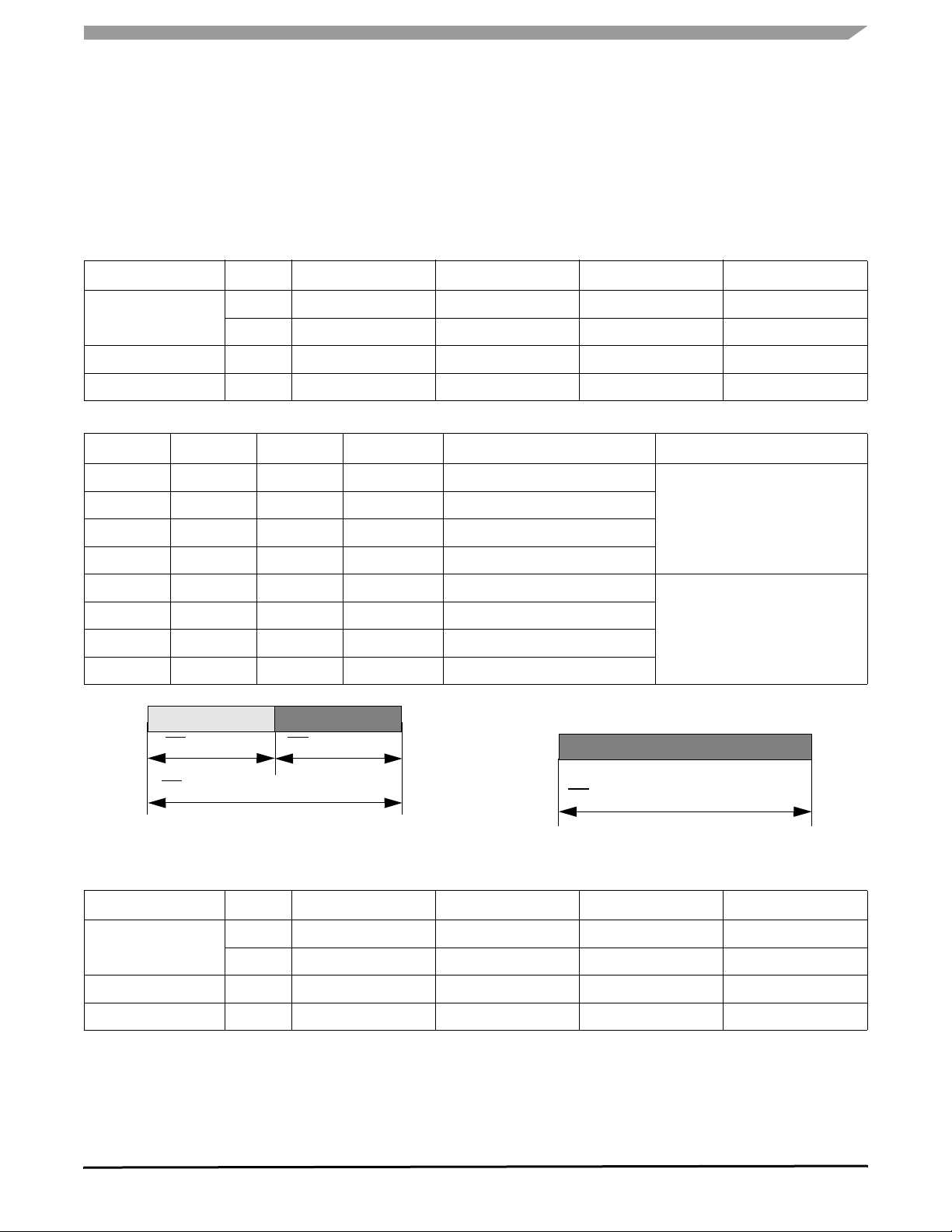
FUNCTIONAL DEVICE OPERATION
LOGIC COMMANDS AND REGISTERS
Timing Register (TIM1/2)
This register is composed of two registers:
1. TIM1–controls the watchdog timing selection as well as
the window or timeout option. TIM1 is selected when
bit D3 is 0. Please see
Table 24.
2. TIM2–is used to define the timing for the cyclic sense
and forced wake-up function. TIM2 is selected when bit
D3 is read operation it is not allowed in either TIM1 or
TIM2 registers. Please see
Table 26.
Table 24. TIM1 Register
TMI1 D3 D2 D1 D0
$101B W 0 WDW WDT1 WDT0
R — — — —
Reset Value — 0 0 0
Reset Condition — POR, RST POR, RST POR, RST
Table 25. TIM1 Control Bits
WDW WDT1 WDT0 Timing (ms) Parameter
0 0 0 10 Watchdog Period 1 No Window Watchdog
0 0 1 45 Watchdog Period 2
0 1 0 100 Watchdog Period 3
0 1 1 350 Watchdog Period 4
1 0 0 10 Watchdog Period 1 Window Watchdog Enabled (Window
1 0 1 45 Watchdog Period 2
1 1 0 100 Watchdog Period 3
1 1 1 350 Watchdog Period 4
WD Timing x 50%WD Timing x 50%
Timing Selected by TIM1 Bit WDW=1)
(WD
Figure 17. Window Watchdog
Watchdog Period
(WD
Figure 18. Timeout Watchdog
Timing Selected by TIM1 Bit WDW=1)
Length is Half the Watchdog Timing)
Window Open
for Watchdog Clear
Watchdog Period
Table 26. TIM2 Register
TMI2 D3 D2 D1 D0
$101B W 1 CSP2 CSP1 CSP0
R — — — —
Reset Value — 0 0 0
Reset Condition — POR, RST POR, RST POR, RST
33989
Analog Integrated Circuit Device Data
Freescale Semiconductor 35

FUNCTIONAL DEVICE OPERATION
LOGIC COMMANDS AND REGISTERS
Table 27. TIM1 Control Bits
CSP2 CSP1 CSP0 Cyclic Sense Timing (ms) Parameter
0 0 0 5 Cyclic Sense/FWU Timing 1
0 0 1 10 Cyclic Sense/FWU Timing 2
0 1 0 20 Cyclic Sense/FWU Timing 3
0 1 1 40 Cyclic Sense/FWU Timing 4
1 0 0 75 Cyclic Sense/FWU Timing 5
1 0 1 100 Cyclic Sense/FWU Timing 6
1 1 0 200 Cyclic Sense/FWU Timing 7
1 1 1 400 Cyclic Sense/FWU Timing 8
Cyclic Sense on Time
This register controls:
• The state of HS1 in Stop and Sleep mode (HS1
Low Power Mode Control Register (LPC)
permanently off or HS1 cyclic)
• Enable or disable the forced wake-up function (SBC
automatic wake-up after time spend in Sleep or Stop
modes, time is defined by the TIM2 register)
HS1
Cyclic Sense Timing, Off Time
HS1 OFF
HS1 ON
10 µs
• Enable or disable the sense of the wake-up inputs (Lx) at
Sample
Lx Sampling Point
t
sampling point of the Cyclic Sense period (LX2HS1 bit).
Figure 19. HS1 Operation when Cyclic Sense is Selected
Table 28. LPC Register
LPC D3 D2 D1 D0
$110B W LX2HS1 FWU — HS1AUTO
R — — — —
Reset Value 0 0 — 0
Reset Condition POR, NR2R
N2R,STB2RSTO2R
POR, NR2R
N2R,STB2RSTO2R
— POR, NR2R
N2R,STB2RSTO2R
Please refer to the Cyclic Sense Wake-up discussion for
details of the LPC register setup required for proper Cyclic
Sense or direct wake-up operation.
Table 29. LX2HS1 Control Bits
LX2HS1 Wake-Up Inputs Supplied by HS1
0 No
1 Yes, Lx Inputs Sensed at Sampling Point
33989
Table 30. HS1AUTO Control Bits
HS1AUTO Auto Timing HS1 in Sleep and Stop Modes
0 OFF
1 ON, HS1 Cyclic, Period Defined in TIM2 Register
Analog Integrated Circuit Device Data
36 Freescale Semiconductor

FUNCTIONAL DEVICE OPERATION
LOGIC COMMANDS AND REGISTERS
Interrupt Register (INT)
This register allows masking or enabling the interrupt
source. A read operation informs about the interrupt source.
Table 31. INT Register
INT D3 D2 D1 D0
$111B W VSUPLOW HS1OT-V2LOW VDDTEMP CANF
R VSUPLOW HS1OT VDDTEMP CANF
Reset Value 0 0 0 0
Reset Condition POR, RST POR, RST POR, RST POR, RST
Table 32. INT Control Bits
Control Bit Description
CANF
V
DDTEMP
HS1OT - V2LOW
V
SUPLOW
Mask Bit for CAN Failures
Mask Bit for VDD Medium Temperature (Pre-Warning)
Mask Bit for HS1 Over Temperature AND V2 Below 4.0 V
Mask Bit for V
When the mask bit is set, INT pin goes low if the
appropriate condition occurs.
Table 33. INT Status Bits
Status Bit Description
CANF
V
DDTEMP
HS1OT
V
SUPLOW
If HS1OT - V2
INT register), reading INT register bit D2 leads to two
in
CAN Failure
VDD Medium Temperature (pre-warning)
HS1 Over Temperature
V
Below 6.1 V
SUP
interrupt is only selected (only bit D2 set
LOW
possibilities:
Below 6.1 V
SUP
1. Bit D2 = 1: INT source is HS1OT
2. Bit D2 = 0: INT source is V2LOW
HS1OT and V2
bits status are available in IOR.
LOW
Upon a wake-up condition from Stop mode due to over
current detection (I
DD1SW-U1
or I
DD1S-WU2
), an INT pulse is
generated; however, INT register content remains at 0000
(not bit set into the INT register).
The status bit of the INT register content is a copy of the
IOR and CAN registers status content. To clear the
INT
register bit the IOR and/or CAN register must be cleared
(read register). Once this operation is done at IOR and CAN
register the
INT register is updated.
Errors bits are latched in the CAN register and IOR.
33989
Analog Integrated Circuit Device Data
Freescale Semiconductor 37
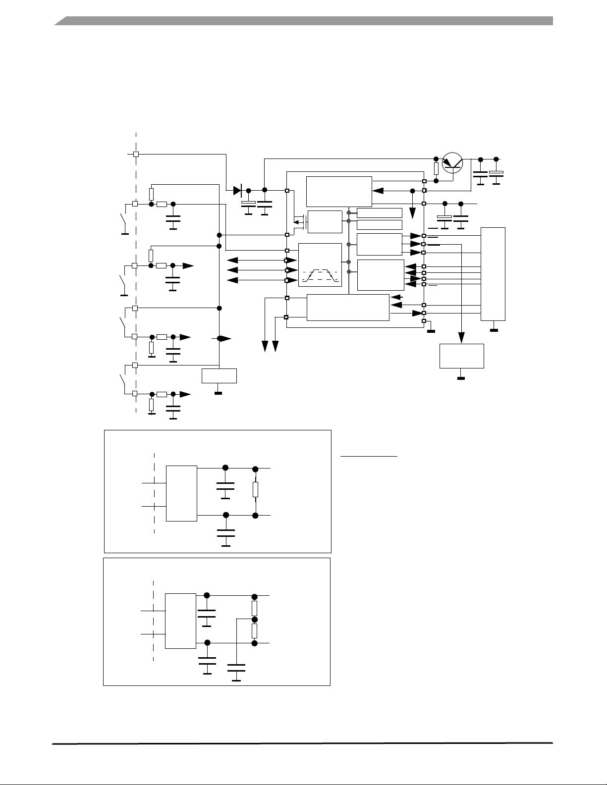
TYPICAL APPLICATIONS
TYPICAL APPLICATIONS
MC33989, SBC High Speed Typical Application Schematic
VBAT
SW1
SW2
SW3
SW4
Connector
Rp
Rp
Rd
Rd
Q1
C10
V2
C5
MCU
R6
D1
R1
to L0
C6
R2
to L1
C7
R3
R4
to L2
C8
to L3
C9
C1
Internal
Clamp(1)
Module
Supply
VSUP
C2
HS1
L0
L1
L2
L3
CANH
CANL
Vsup monitor
Dual Voltage Regulator
Vdd1 Monitor
HS1
control
Programmable
wake-up input
1Mbit/s CAN
Physical Interface
5V/200mA
Mode control
Oscillator
Int
Watchdog
Reset
SPI Interface
V2CTRL
V2
C3
V2
INT
WD
Vdd1
C4
RST
MOSI
SCLK
MISO
CS
V2
TX
RX
GND
Safe Circuitry
Detail of CAN standard termination schematic
(not split termination)
CANH (SBC)
CANH
R5
120 ohms
CANL (SBC)
CANL
CAN Connector
L1
CH
CL
Detail of CAN split termination schematic
CANH (SBC)
CANH
CH
R6, 60 ohms
L1
CANL
CAN Connector
CL
R7, 60 ohms
CANL (SBC)
CS
Figure 20. Typical Application Diagram
Component values:
D1:
Q1: MJD32C
R1,R2,R3,R4: 10k
R5: 120
Rp, Rd:
R6: 2.2k
C1: 10uF
C2: 100nF
C3: 47uF
C4: 100nF
C5: 47uF tantal
C6,C7,C8,C9,C10: 100nF
CL, CH: 220 pF
33989
Analog Integrated Circuit Device Data
38 Freescale Semiconductor

SUPPLEMENTAL APPLICATION NOTES
SUPPLEMENTAL APPLICATION NOTES
TYPICAL APPLICATIONS
MC33989 - GENERAL INFORMATION
MC33989 device supply on page 39
Voltage Regulator on page 40
Failure on VDD1, Watchdog, Reset, INT Pins on page 41
WAKE-UP TIMINGS - SLEEP MODE
LX Wakes up SBC from Sleep Mode on page 42
CAN Wake-Up on page 42
LX with Cyclic Sense on page 43
WAKE UP TIMING: STOP MODE
LX Wake-Up on page 43
CAN Wake-Up on page 44
CS Wake-Up on page 44
Overcurrent Wake-Up on page 44
LX with Cyclic Sense on page 45
CAN Driver Overtemperature: on page 52
Overcurrent Detection: on page 52
Protection on page 52
Current in Case of Bus Short Conditions on page 52
SOFTWARE ASPECTS
Introduction on page 54
How to Enter in Normal Mode After a Power-Up on page
55
How to Change CAN Slew Rate on page 55
How to Set the CAN Interface in Sleep Mode on page 55
How to Control HS1 Output on page 55
How to Configure Wake-Up Before Going in Low Power
Mode on page 56
Disable all Wake-Up on page 56
How to Enter in Sleep Mode on page 57
MC33989 CAN INTERFACE
Block Diagram on page 45
CAN Interface Supply on page 46
Main Operation Modes Description on page 46
CAN Driver Operation in Normal Mode on page 46
CAN Mode versus SBC Modes on page 48
How to Test the MC33989 CAN Interface on page 48
CAN LOW POWER MODE AND WAKE-UP
Low Power Mode on page 49
Wake-Up on page 49
FAILURE ON V2 SUPPLY, CAN BUS LINES, AND TX
PIN
V2LOW on page 51
TX Permanent Dominant on page 51
How to Enter in Stop Mode with Watchdog on page 57
How to Enter in Stop Mode without Watchdog on page 57
How to Recognize and Distinguish the Wake-Up Sou rce
on page 58
How to Use the Interrupt Function on page 59
Recognition and Recovery on page 59
How to Distinguish Between V2LOW and HS1
Overtemperature on page 59
GENERAL INFORMATION
The parameters given in the application section are for
information only. Reference the electrical tables beginning on
page 4 for actual operating parameters.
MC33989 device supply
The MC33989 is supplied from the battery line. A serial
diode is necessary to protect the device against negative
transient pulses and from reverse battery situation. This is
illustrated in the device typical application schematic.
33989
Analog Integrated Circuit Device Data
Freescale Semiconductor 39
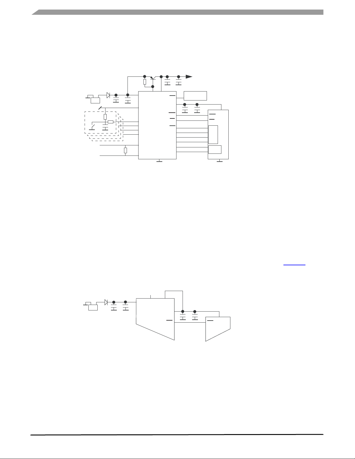
TYPICAL APPLICATIONS
SUPPLEMENTAL APPLICATION NOTES
Voltage Regulator
The MC33989 contains two 5 V regulators: The V1
regulator, fully integrated and protected, and the V2 regulator
Q1
R1
V2
V2CTRL
VSUP
C2
HS1
L0
MC33989
L1
L2
L3
CANH
Rt
CANL
GND
S0
CAN bus
Rp0
C1
Rs0
CL0
Figure 21. Device Typical Application Schematic
V1 Regulator
The V1 regulator is 5 V output, 2% accuracy with current
capability of 200 mA max. It requires external decoupling and
stabilizing capacitors. The minimum recommended value
are:
• C4: 100 nF
• C3: 10 µF < C3 < 22 µF, esr < 1 ohms. 22 µF < C3 <
47 µF, esr < 5 ohms. C3 > = 47 µF, esr < 10 ohms
V2 Regulator: Operation with External Ballast Transistor
The V2 regulator is a tracking regulator of the V1 output.
Its accuracy relative to V1 is ±1%. It requires external
decoupling and stabilizing capacitors. The recommended
value are: 22
µF esr < 5 ohms, and 47 µF esr < 10 ohms.
C5
WD
VDD1
RST
INT
CS
MISO
MOSI
SCK
TX
RX
which operates with an external ballast transistor. This is
illustrated in the following device typical application
schematic.
Auxiliary 5V
C6
Components list:
Safe circuitry
C3
C4
RST
INT
SPI
CAN
VDD
MCU
GND
C1: 22uF , C2: 100nF
C3: >10uF
C4: 100nF
C5: >10uF
C6: 100nF
R1: 2.2k
Rt: 60 - 120
Rp0 to Rp3: 22k
Rs0 to Rs3: 22 k
CL0 to CL3: 10nF
Q1: MJD32C
The V2 pin has two functions: sense input for the V2
regulator and 5 V power supply input to the CAN interface.
Ballast transistor selection: PNP or PMOS transistors can be
used. A resistor between base and emitter (or source and
drain) is necessary to ensure proper operation and optimized
performances. Recommended bipolar transistor is MJD32C.
V2 Regulator: Operation without Ballast Transistor
The external ballast transistor is optional. If the application
does not requires more than the maximum output current
capability of the V1 regulator, then the ballast transistor can
be omitted. The thermal aspects must be analyzed as well.
The electrical connections are shown in Figure 22.
no connect
V2CTRL
C2
VSUP
MC33989
Partial View
C1
V2
VDD1
RST
Components list:
C1: 22uF , C2: 100nF
C3
C4
VDD
RST
MCU
partial view
C3: >10uF
C4: 100nF
Figure 22. V2 Regulator Operation
33989
Analog Integrated Circuit Device Data
40 Freescale Semiconductor

SUPPLEMENTAL APPLICATION NOTES
TYPICAL APPLICATIONS
Failure on VDD1, Watchdog, Reset, INT Pins
The paragraphs below describe the behavior of the device
and of the INT, RST, and WD pins at power up and under
failure of VDD1.
Power Up and SBC Entering Normal Operation
After a power-up the SBC enters in Normal request mode
(CAN interface is in TX/RX mode): V
is on, V2 is off. After
DD1
VDD1
SPI (CS)
WD
RST
INT
SBC in
RESET
SBC in Normal request
mode
mode
350 ms if no watchdog is written (no TIM1 register write) a
reset occurs, and the SBC returns to normal request
mode.During this sequence
Once watchdog is written the SBC goes to normal mode:
is still on and V2 turns on, WD is no longer active and
V
DD1
the reset pin is high. If the watchdog is not refreshed, the SBC
generates a reset and returns to Normal request mode.
SBC in Normal
mode
WD is active (low level).
SBC in Normal
request mode
SBC in Normal
mode
Figure 23. Power Up and SBC Entering Normal Operation
Power Up and V
Going Low with Stop Mode as
DD1
Default Low Power Mode Selected
The first part of the following figure is identical to the
above. If V
is pulled below the V
DD1
under voltage reset
DD1
(typ 4.6 V) for instance by an overcurrent or short circuit (ex
short to 4 V), and if a low power mode previously selected
was stop mode, the SBC enters reset mode (reset pin is
active). The pin
follows the V
When the V
WD stays high, but the high level (VOH)
level. The interrupt pin goes low.
DD1
overload condition is removed, the SBC
DD1
restarts in Normal request mode.
Figure 24. Power Up and V
Going Low with Stop Mode as Default Low Power Mode Selected
DD1
33989
Analog Integrated Circuit Device Data
Freescale Semiconductor 41
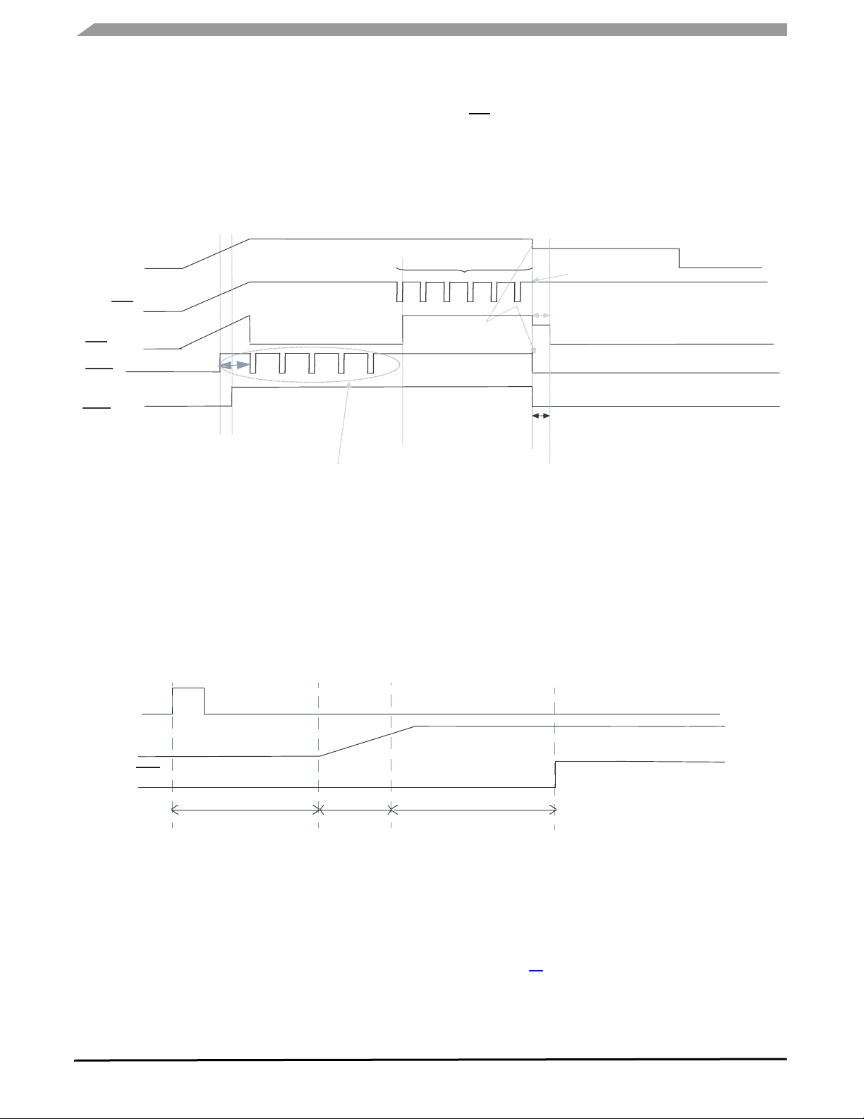
TYPICAL APPLICATIONS
SUPPLEMENTAL APPLICATION NOTES
Power Up and V
Going Low with Sleep Mode as
DD1
Default Low Power Mode Selected
The first part of the graph is the same as the previous
figure. If V
(typ 4.6
is pulled below the V
DD1
under voltage reset
DD1
V) for instance by an over current or short circuit (ex
short to 4 V), and if the low power mode previously selected
was sleep mode and if the BATFAIL flag has been cleared,
VDD1
SPI (CS)
WD
350 ms
RST
INT
SBC in
RESET
mode
Figure 25. Power up and V
SBC in Norm al request
mode
Reset every 350 ms
Going Low with Sleep Mode as Default Low Power Mode Selected
DD1
the SBC enters reset mode for a time period of 100 ms. The
WD stays high, but the high level (VOH) follows the V
pin
level.The reset and interrupt pins are low. Afte r the 100 ms,
the SBC goes into sleep mode. V
following figure is an example where V
and after 100 ms the SBC enters sleep mode.
Write Watchdog
each X ms
SBC in Normal
mode
No problem on
Watchdog period
100 ms
SBC in Sleep mode
SBC in Reset
mode
(B ATFAIL flag
must be cleared)
and V2 are off (The
DD1
is shorted to 4 V,
DD1
DD1
WAKE-UP TIMINGS — SLEEP MODE
The paragraphs below describe the wake-up events from
sleep mode, and the sequence of the signals at the SBC
level. The wake-up time described is the time from the wakeup event to the SBC reset pin release. The wake-up time is
the sum of several timings: wake-up signal detection, V
regulator start-up and decoupling capacitor charge, and reset
LX
VDD1
RST
t1
• T1 (LX high level to V
•T2: V
rising time is dependent on the capacitor and
DD1
the load connected to V
turn on): typ 100 µs.
DD1
. It can be approximated by
DD1
the capacitor charging time with the regulator output
current limitation: T2 = (C x U)/I. With C
= 200 mA min., U = 5 V so T2 = 2.5 ms).
I
DD1
= 100 mF,
DD1
t2
Figure 26.
time. At the end of the reset time, the reset pin goes from low
to high and the MCU is ready to start software operations.
LX Wakes up SBC from Sleep Mode
Below is the case where the SBC is in sleep mode and is
awaked by LX positive edge.
t3
• T3 (VDD1>RST-TH (4.6 V by default) to reset high):
parameter Rest dur: 4 ms max.
• The total time is 6.6 ms in this example.
CAN Wake-Up
The following case describes the signal for CAN wake up.
Refer to
page 49 for more details on CAN wake up signals
and the TCAN analysis.
33989
Analog Integrated Circuit Device Data
42 Freescale Semiconductor

CAN
VDD1
RESET
• T1(third valid CAN dominant pulse to V
DD1
80 µs.
• T2 and T3 identical to page 39 above
• The total time is 6.58 ms in this example.
t1
Figure 27. CAN Wake-Up
LX with Cyclic Sense
turn on): typ
The case below is a description of the wake-up by LX input
associated with the cyclic sense function.
SUPPLEMENTAL APPLICATION NOTES
TYPICAL APPLICATIONS
Figure 28.
• T1: Is dependent on the selected cyclic sense timing in
the TIM2 register (5 ms to 400 ms). LX is sampled
•10 µs before the end of cyclic sense on time. If the LX
correct wake-up level happens just after the sample
• point, the wake-up will be detected at the next HS1
activation and a complete period is lost.
• T2: It is the same time as LX to VDD1 turn on: typ
µs
100
• T3 & T4: same as page 39
• The total time is 11.5 ms (for a cyclic sense total time of
5 ms) in this example.
WAKE-UP TIMING: STOP MODE
The following paragraphs describe the wake-up events
from stop mode, and the sequence of the signals at the SBC
level. The wake-up time described is the time from the wakeup event to the SBC
INT pin. The wake-up time is the sum of
several timings: wake-up signal detection, the INT pulse, and
a minimum delay between INT and SBC ready to operate. At
the end of the wake-up time, the SBC is ready to operate,
however the MCU might have already been in a restart
operation.
LX Wake-Up
Below is the case where the SBC is in stop mode and is
awakened by an LX positive edge
• T1(L0 high level to INT pulse): typ 100 µs.
• The total time is 133 µs in this case.
33989
Analog Integrated Circuit Device Data
Freescale Semiconductor 43

TYPICAL APPLICATIONS
SUPPLEMENTAL APPLICATION NOTES
L0
INT
t1
t
+ t
INT
S-1STSPI
Wake-up signalled to MCU.
CAN Wake-Up
The case below describes the signal for CAN wake-up.
Refer to
page 49 for more details on CAN wake-up signals
and the TCAN analysis.
CAN
INT
tCAN
t1
Wake-up signalled to MCU.
Figure 30. CAN Wake-Up
•TCAN: refer to page 49 for more details.
• T1: Third pulse on CAN to INT pulse: typ 80 µs.
• The total time is 113 µs in this case.
(33µs max)
SBC ready to accept SPI command.
Figure 29. Lx Wake-Up
t
+ t
INT
S-1STSPI
CS Wake-Up
The figure below describes the wake up from a CS signal
transition, while the SBC is in stop mode.
(33µs max)
SBC ready to accept SPI command.
CS
INT
T1
Wake-up signalled to MCU.
t
INT
+ t
S-1STSPI
µs max)
(33
SBC ready to accept SPI command.
Figure 31. CS Wake-Up
Overcurrent Wake-Up
•T1: CS rising edge to INT pulse: typ 60 µs.
• The total time is 133 µs in this case.
The following figure describes the signal when an
overcurrent is detected at V
DD1
. A V
overcurrent condition
DD1
will lead to a wake-up from stop mode.
33989
Analog Integrated Circuit Device Data
44 Freescale Semiconductor
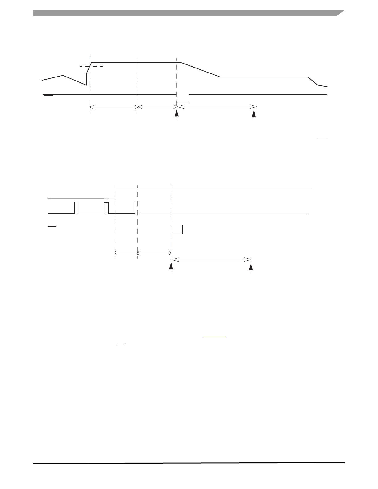
I
DD1S-WU
(17 mA typ)
IDD1 current
SUPPLEMENTAL APPLICATION NOTES
TYPICAL APPLICATIONS
INT
•T1:V
DD1
55 µs
LX
HS1
INT
t1
t2
Wake-up signalled to MCU.
Figure 32. Overcurrent Wake-Up
output current deglitcher time:IDD1-DGLT: typ
t1
t2
t
INT
t
INT
+ t
S-1STSPI
(33µs max)
SBC ready to accept SPI command.
• T2: Over current detected to SBC wake-up (INT pulse)
= typ 60 µs
• The total time is 148 µs in this case.
LX with Cyclic Sense
+ t
S-1STSPI
(33µs max)
Wake-up signalled to MCU.
SBC ready to accept SPI command.
Figure 33.
MC33989 CAN INTERFACE
• T1: Is dependent on the selected cyclic sense timing in
the TIM2 register (5 ms to 400 ms). LX is sampled 10
µs
before the end of cyclic sense on time. If the LX correct
wake-up level happens just after sample point, the
wake-up will be detected at the next HS1 activation and
a complete period is lost.
• T2: It is the same than Lx to INT pulse: typ 100 µs
• The total time is around 5.13 ms (for a cyclic sense total
time of 5 ms) in the above example.
Analog Integrated Circuit Device Data
Freescale Semiconductor 45
This section is a detailed description of the CAN interface
of the MC33989.
Block Diagram
Figure 34 is a simplified block diagram of the CAN
interface of the MC33989.
33989
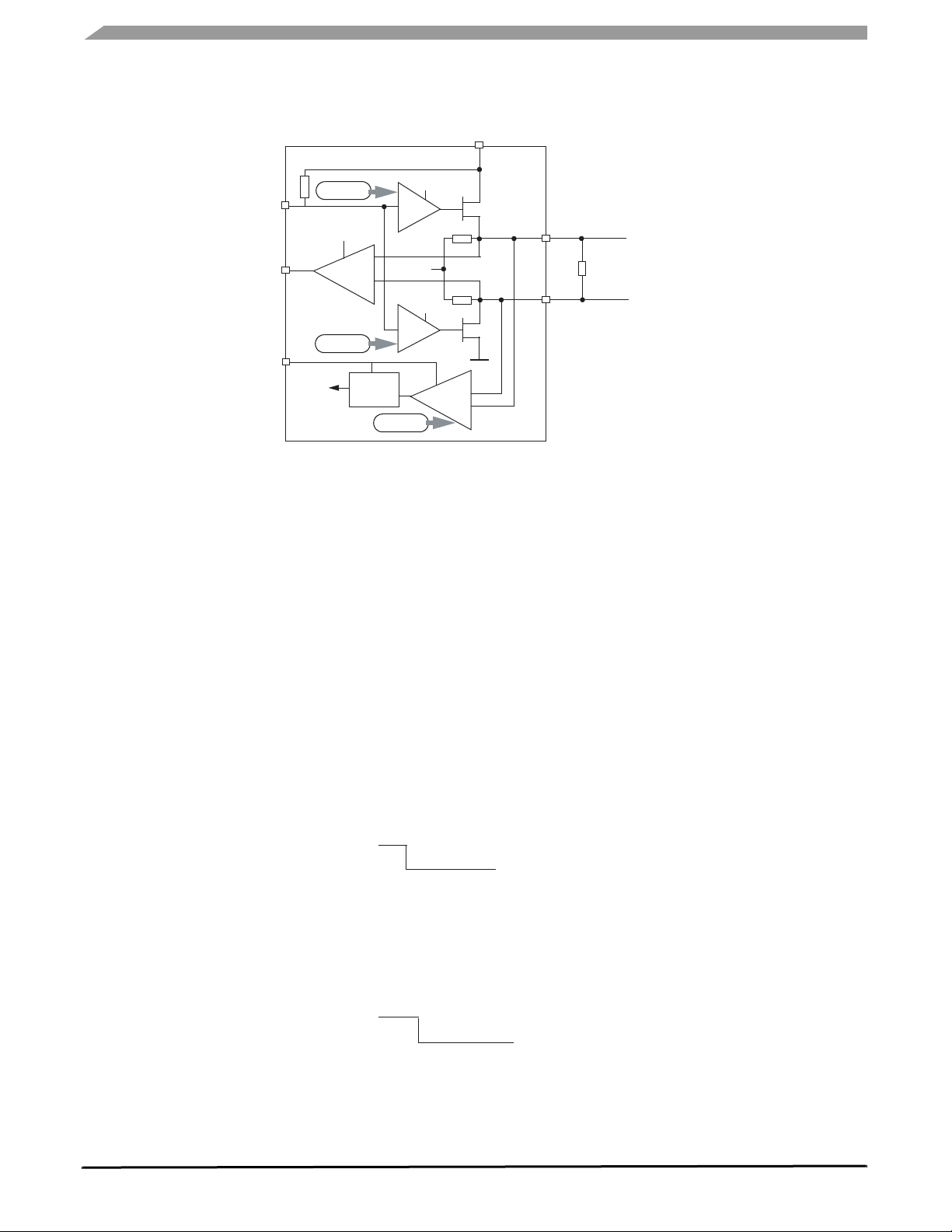
TYPICAL APPLICATIONS
SUPPLEMENTAL APPLICATION NOTES
TX
RX
VSUP
Internal
wake-up
signal
V2
SPI control
Differential
SPI control
V2
V2
V2
receiver
Wake-up
pattern
recognition
Driver
2.5V
Driver
SPI control
V2
Wake- up
receiver
QH
QL
Figure 34. 33989 CAN Interface
CANH
CANH line
Bus termination (60 ohms)
CAN L line
CANL
CAN Interface Supply
The supply voltage for the CAN driver is the V2 pin. The
CAN interface also has a supply path from the battery line,
through the pin VSUP. This path is used in CAN sleep mode
to allow wake-up detection.
During CAN communication (transmission and reception)
the CAN interface current is sourced from the V2 pin. During
a CAN low power mode, the current is sourced from the
VSUP pin.
Main Operation Modes Description
The CAN interface of the MC33989 has two main
operation modes: Normal mode and sleep mode. The modes
are controlled by the SPI command.
In normal mode, used for communication, four different
slew rates are available for the user.
In sleep mode, the user has the option to enable or disable
the remote CAN wake-up capability.
CAN Driver Operation in Normal Mode
When the CAN interface of the MC33989 is in Normal
mode, the driver has two states: recessive or dominant. The
driver state is controlled by the TX pin. The bus state is
reported through the RX pin.
When TX is high, the driver is set in a recessive state,
CANH and CANL lines are biased to the voltage set at V2
divided by 2, approx. 2.5
V.
When TX is low, the bus is set into dominant state: the
CANL and CANH drivers are active. CANL is pulled to gnd,
CANH is pulled high toward 5
V (the voltage at V2).
The RX pin reports the bus state: the CANH minus the
CANL voltage is compared versus an internal threshold (a
few hundred mV). If “CANH minus CANL” is below the
threshold, the bus is recessive and RX is set high.
If “CANH minus CANL” is above the threshold, the bus is
dominant and RX is set low. This is illustrated in the figure
below.
Figure 35. CAN Driver Operation in Normal Mode
33989
Analog Integrated Circuit Device Data
46 Freescale Semiconductor
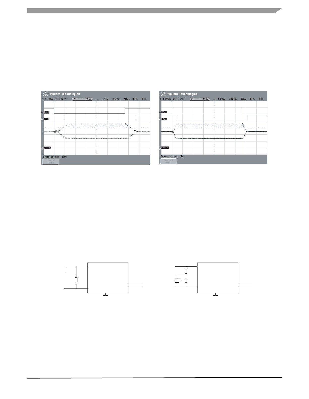
SUPPLEMENTAL APPLICATION NOTES
TYPICAL APPLICATIONS
TX and RX Pins
The TX pin has an internal pull up to V2. The state of TX
depends on the V2 status. RX is a push-pull structure,
supplied by V2. When V2 is set at 5V, and CAN is in normal
mode, RX reports the bus status. When V2 is off RX is low.
CAN signal with slew rate 0 selected
R=60 ohms, CL = CH = 100pF
Figure 36. Normal Mode and Slew Rate Selection
Normal Mode and Slew Rate Selection
The slew rate selection is done via the SPI. Four slew rates
are available. The slew rate affects the recessive to dominant
and dominant to recessive transitions. This affect is also the
delay time from the TX pin to the bus, and from the bus to RX.
The loop time is thus affected by the slew rate selection.
The following figure is an illustration of the slew rate on
CANH, CANL, TX and RX.
CAN signal with slew rate 3 selected
Minimum Baud Rate
As TX permanent dominant is detected after TDOUT (min
200 µs), a minimum Baud rate is required in order to get good
behavior: once TX permanent dominant is detected the CAN
driver is off.
The maximum number of consecutive dominant bits in a
frame is 12 (6 bits of active error flag and its echo error flag).
200 µs/12 = 16.7 µs. The minimum Baud rate is 1/6.7 µs =
60 KBaud.
CANH
MC33989
(partial drawing)
CAN bus
RT
CANL
Gnd
Differential termination concept
TX
RX
Figure 37. Bus Termination
Termination
The MC33989 supports the two main types of bus
termination:
• Differential termination resistors between CANH and
CANL lines.
• Split termination concept, with mid point of the
differential termination connected to gnd through a
capacitor.
CAN bus
CANH
RT /2
RT /2
MC33989
(partial drawing)
CANL
Gnd
Split termination concept
TX
RX
33989
Analog Integrated Circuit Device Data
Freescale Semiconductor 47

TYPICAL APPLICATIONS
SUPPLEMENTAL APPLICATION NOTES
CAN Mode versus SBC Modes
The table below indicates the CAN interface modes versus
the SBC modes as well as the status of TX, RX and the CAN
bus pins.
Table 34. CAN vs SBC Modes
SBC mode
Unpowered
Reset (with ballast)
Normal request (with ballast)
Normal
Normal
Standby with external ballast
Standby without external
ballast, V2 connected to V1
Standby without external
ballast, V2 connected to V1
Sleep
External
ballast
for V2
CAN mode
V2
voltage
TX RX
CANH/CANL
(disconnected
from other
nodes)
YES Unpowered 0 V LOW LOW Floating to gnd
YES 0 V LOW LOW Floating to gnd
YES 0 V LOW LOW Floating to gnd
YES Normal Slew rate
0,1,2,3
5 V Internal pull up
to V2.
Report bus state
High if bus
recessive, Low if
Bus recessive
CANH = CANL =
2.5 V
dominant
YES Sleep mode 5 V 5 V 5 V Floating to gnd
YES Normal or sleep 0 V LOW LOW Floating to gnd
NO Normal 5 V Same as
normal mode
Same as normal
mode
Same as normal
mode
NO Sleep 5 V 5 V 5 V Floating to gnd
— Sleep 0 V LOW LOW Floating to gnd
Stop
How to Test the MC33989 CAN Interface
The CAN interface can be easily set up and tested.
MC33989 can be connected as in the following figure. V2 is
connected to V1. The device is supplied with nominal supply
V at VSUP input pin). After power on, reset the device,
(12
— Sleep 0 V LOW LOW Floating to gnd
enter normal request mode, and the CAN interface is set in
normal mode, slew rate 0. TX can be driven by a signal
generator. RX will report the bus state. The figure below is a
simple test schematic.
V2CTRL
V2
C1
VSUP
C2
HS1
WD
RST
RESET
V1
C3
C4
Components list:
C1: 22uF, C2: 100nF
C3: >10uF
C4: 100nF
Rt: 60 ohms
MC33989
CANH
CANL
CAN bus
L0
L1
L2
L3
CANH
RT
CANL
GND
INT
CS
MISO
MOSI
SCK
TX
RX
Signal generator
F<500kz (1Mb/s)
Signal at RX output
Figure 38. Testing the CAN Interface
33989
Analog Integrated Circuit Device Data
48 Freescale Semiconductor
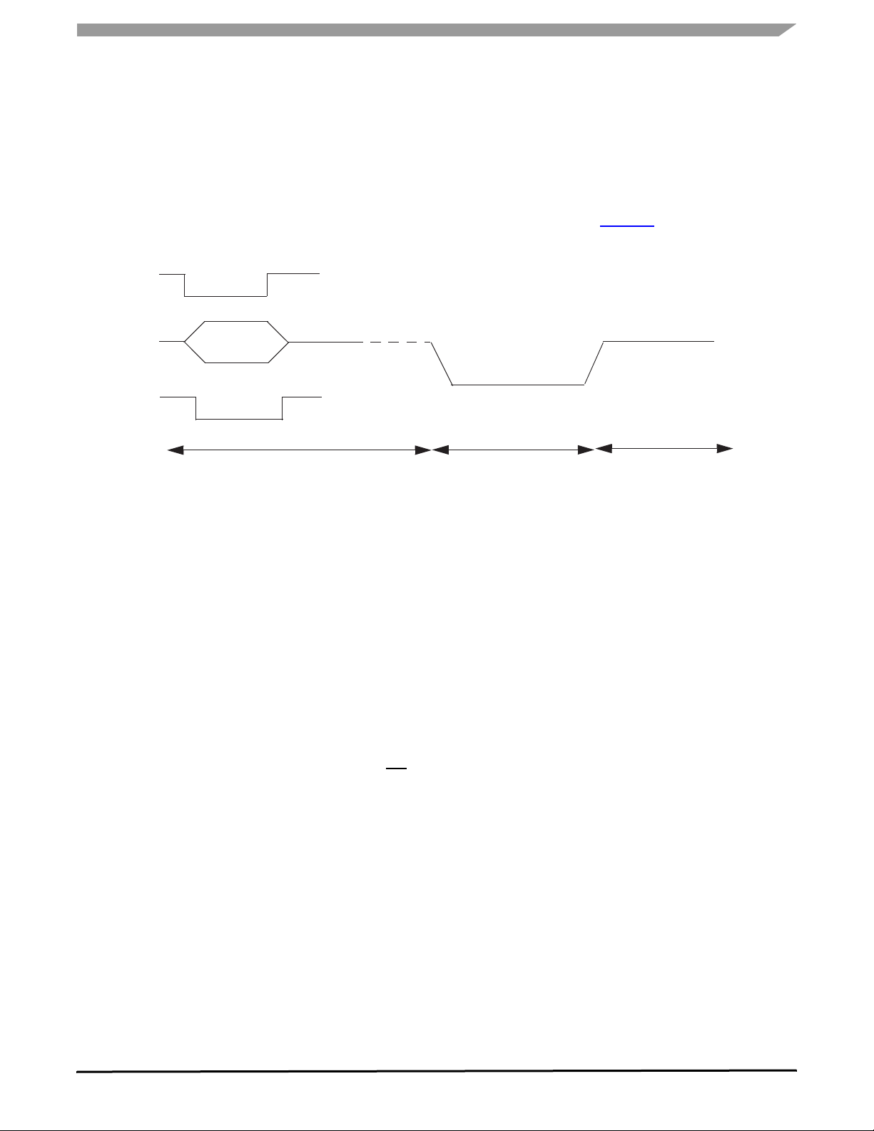
SUPPLEMENTAL APPLICATION NOTES
TYPICAL APPLICATIONS
CAN LOW POWER MODE AND WAKE UP
Low Power Mode
In low power mode the CAN is internally supplied from the
VSUP pin. The voltage at V2 pin can be either at 5 V or turned
off. The current sourced from V2, when the CAN is in sleep
mode, is extremely low. In most case the V2 voltage is off,
however the CAN can be set into sleep mode even with 5
applied on V2.
TX
CANH-DOM
CANH
2.5V
CANL
CANL-DOM
RX
CANL/CANH-REC
CAN in Normal mode
Figure 39. Low Power Mode
Wake-Up
When the CAN interface is in sleep mode with wake up
enabled, the CAN bus traffic is detected. The wake-up option
has to be enabled prior to setting the CAN in sleep mode. The
CAN bus wake-up is a pattern wake-up.
If the CAN is set into sleep mode with “wake-up disabled”,
bus traffic will not be detected by the MC33989.
V
In low power mode the CANH and CANL driver are
disabled, and the receiver is also disabled. CANH and CANL
have a typical 50 k ohm impedance to gnd. The wake-up
receiver can be activated if wake-up is enable by an SPI
command.
When the device is set back into TX RX mode by an SPI
command, CANH and CANL are set back into the recessive
level. This is illustrated in
GND
CAN in Sleep mode
(wake-up enable or disable)
Figure 39.
CAN in TX RX mode
(controlled by SPI command)
wake-up will be reported by the bit CANWU in the CAN
register.
In case the SBC uses such configuration, the SBC in
normal mode and CAN sleep mode with wake up enable, it is
recommended to check for the CAN WU bit prior to setting
the MC33989 is sleep or stop mode, in case bus traffic has
occurred while the CAN interface was in sleep mode.
CAN Wake-Up Report: From the SBC in Sleep or Stop
Mode
The CAN wake-up reports depend upon the MC33989 low
power mode. If the MC33989 is set into sleep mode (V1 and
V2 off), the CAN wake-up or any wake-up is reported to the
MCU by the V1 turn on, leading to MCU supply turn on and
reset release.
If the SBC is in stop mode (V2 of and V1 active), the CAN
wake-up or any wake-up is reported by a pulse on the INT
output.
CAN Wake-Up Report: From the SBC in Normal or
Standby Mode
If the SBC is in normal or standby mode, and the CAN
interface is in sleep mode with wake-up enabled, the CAN
CAN Wake-Up Report in the SPI Registers
After a CAN wake-up, a flag is set in the CAN register. Bit
CAN-WU reports a CAN wake-up event while the SBC was in
sleep, stop, normal or standby mode. This bit is set until the
CAN is set by the SPI command in normal mode and CAN
register read.
Pattern Wake-Up
In order to wake-up the CAN interface, the following
criteria must be fulfilled:
• The CAN interface wake-up receiver must receive a
series of 3 consecutive valid dominant pulses, each of
them has to be longer than 500
µs.
500
ns and shorter than
• The distance between 2 pulses must be lower than
500 µs and the three pulse must occur within a time
frame of 1
ms.
33989
Analog Integrated Circuit Device Data
Freescale Semiconductor 49

TYPICAL APPLICATIONS
SUPPLEMENTAL APPLICATION NOTES
TX
CANH-DOM
CANH
2.5V
CANL
CANL-DOM
RX
MC33989 CAN in Tx Rx mode
CANL/CANH-REC
GND
CAN bus sleep state
WU receiver
Figure 40. Pattern Wake-Up
TX sending node.
CANH-DOM
Pulse # 1
CANL-DOM
MC33989 CAN in Sleep mode (wake-up enable)
min 500ns
max 500us
CANH-DOM
Pulse # 2
CANL-DOM
Incoming CAN message
Internal wake-up signal
CANH-DOM
Pulse # 3
CANL-DOM
The following figure illustrates the SBC key signals when
a CAN wake-up occurs in sleep or stop mode.
VDD start
CAN bus
CAN wake-up: SBC in sleep mode. V1 turn on.
Figure 41. SBC Key Signals
INT
Terminal
CAN wake-up: SBC in stop mode. INT pulse
33989
Analog Integrated Circuit Device Data
50 Freescale Semiconductor

Analysis: CAN Frame with 11 Bits of Identifier Field at 1
Figure 42 is the calculation for the TCAN time with only “1”
in the identifier field.
SUPPLEMENTAL APPLICATION NOTES
TYPICAL APPLICATIONS
SOF 5 recessive bits Stuff bit 5 recessive bits
TCAN
13 bits are needed to wake-up the SBC.
If the minimum baud rate is used (60 KBaud), TCAN = 16.7 µs*13= 217.1 µs
If 250 KBaud is used: TC AN = 4µs *13= 52 µs
Figure 42. CAN Frame with 11 Bits of Identifier Field at 1
Analysis: CAN Frame with 11 Bits of Identifier Field at 0
Figure 43 is the calculation for the TCAN time with only “0”
in the identifier field.
4 dominant bits
SOF
Stuff bit
5 dominant bits
Stuff bit
17 bits are needed to wake-up the SBC.
If the minimum baud rate is used (60 KBaud), TACN = 16.7 µs*17= 284 µs
If 250 KBaud is used, TCAN = 4µs *17= 68 µs.
Figure 43. CAN Frame with 11 Bits of Identifier Field at 0
FAILURE ON V2 SUPPLY, CAN BUS LINES AND TX
PIN
Stuff bit
3 dominant bit if RTR IDE & DLC=0
2 dominant bits
1 recessive bit
SBC wakes up
SBC wakes up
reset pin is active, and the MCU will not send or receive
any CAN messages.
V2LOW
In order to have proper operation of the CAN interface, V2
must be ON. Two case can be considered:
• V2 is connected with an external ballast: in case of a V2
over load condition, the flag V2LOW is set in to the SBC
IOR register. This flag is set when V2 is below the 4
typical. An interrupt can also be triggered upon a
V2LOW event. When V2 is low, the CAN interface
cannot operate.
• V2 is connected to V1 (no ballast transistor used): V2
will be supplied by the V1 voltage. In case V1 is in an
undervoltage condition (ex V1 below the V1 under
voltage reset, typ 4.6
V), the device will enter the reset
mode. The V2LOW flag will also be set. In this case, the
V
TX Permanent Dominant
A TX permanent dominant condition is detected by the
CAN interface and leads to a disable of the CAN driver. The
TX permanent dominant is detected if TX stays in dominant
(TX low) from more than 360
µs typical. The driver is
automatically re-enabled when TX goes to a high level again.
When a TX permanent dominant is detected, a bit is set into
the SPI register, (bit D2 named TXF in the CAN register). This
bit is latched. In order to clear the bit, two conditions are
necessary:
• No longer “TX permanent failure” AND
• CAN register read operation.
An interrupt can be enabled.The GFAIL flag in the MCR
register will also be set.
33989
Analog Integrated Circuit Device Data
Freescale Semiconductor 51
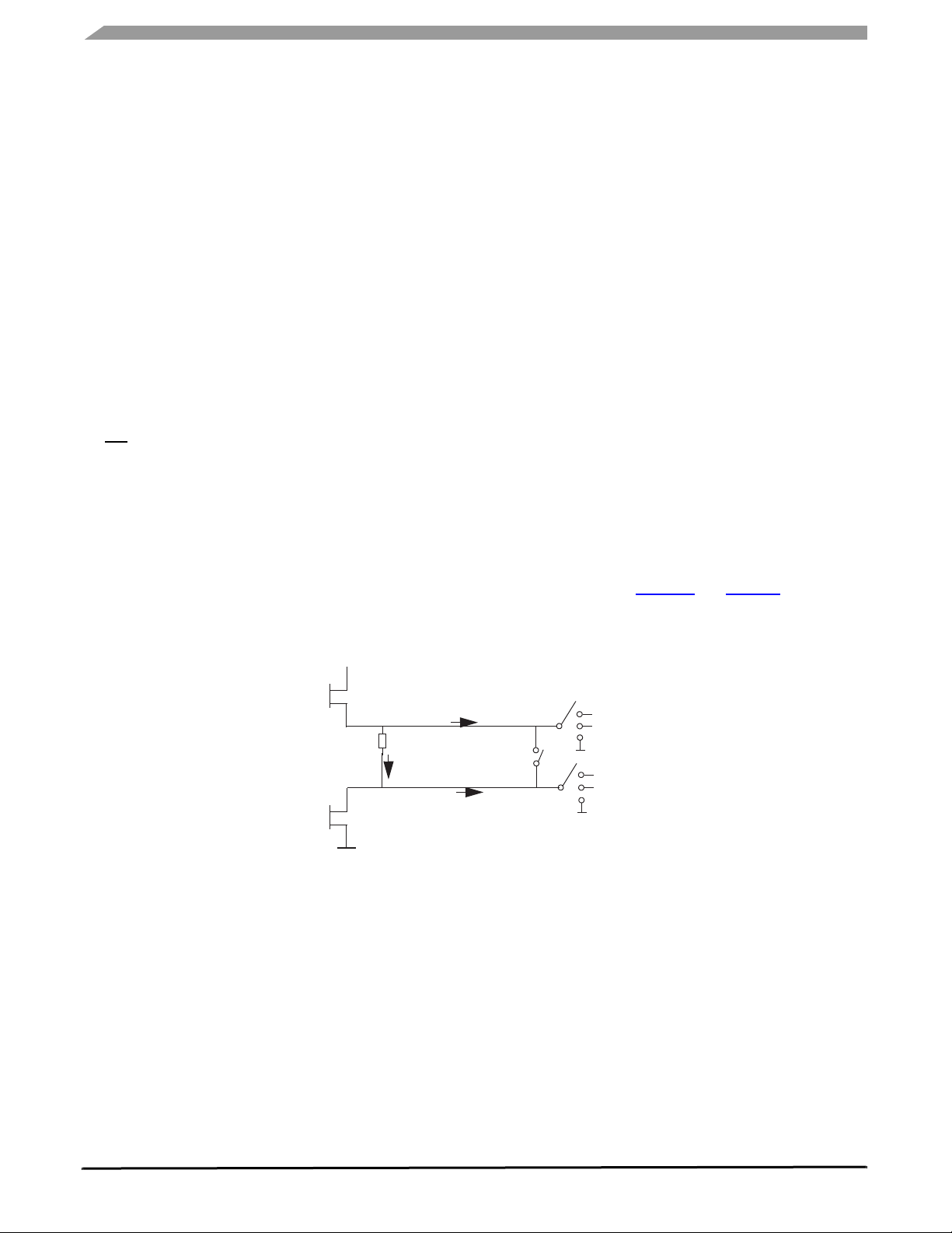
TYPICAL APPLICATIONS
SUPPLEMENTAL APPLICATION NOTES
CAN Driver Overtemperature:
In case of an overtemperature condition at the CANH or
CANL driver, the driver will be automatically disabled and the
THERM bit set in the CAN register. If enabled, an interrupt
will be signalled. The GFAIL flag is set in the MCR register.
When the CAN is in an overtemperature situation, the
device is no longer able to transmit. As soon as the
temperature is below the overtemperature level minus
hysteresis, the CAN driver is automatically re-enabled.
The THERM bit is latched and two conditions are
necessary to clear it:
• No longer “CAN overtemperature situation” AND
• Read operation of the CAN register.
Overcurrent Detection:
The CAN interface can detect and signal over current
condition, occurring for instance in case of CANL shorted to
VBAT. This is signalled by the bit CUR in the CAN register.
INT can be enabled, and GFAIL bit is set. The CUR bit is
An
latched and two conditions are necessary to clear it:
• No longer “CAN over current situation” AND
• Read operation of the CAN register.
Protection
The MC33989 CAN output is protected for automotive
environments.
The CAN driver is protected against overtemperature and
overcurrent.
ISO7637 Transient
The CANH and CANL are rated from +40 Vdc to -27 Vdc.
This means that the MC33989 CAN output can handle failure
situations like the bus directly shorted to the battery line in a
load dump situation (+40
V).
Ground disconnection of the module will lead to the CANH
and CANL line floating high to the VBAT supply. The rest of
the network will not be affected. However the CANH and
CANL lines of the ungrounded module will see a negative
voltage of the VBAT value, with respect to their gnd level.
Such situations can be handled by the CAN interface of the
MC33989, but also in cases of a jump start (battery at 27
V)
and gnd disconnection.
Fast transient pulses, ISO7637-3. During these pulses, the
maximum rating of the CANH and CANL lines of +40 Vdc and
-27 Vdc must be respected.
ESD
The CANH and CANL line of the MC33989 are rated at
±4 kV. An external capacitor between CANH and CANL to
gnd or a zener diode suppressor can be added to ensure a
higher module resistance to ESD.
Current in Case of Bus Short Conditions
In case of short circuit condition on the CAN bus the
current in the CAN supply, the CAN line can be different from
the nominal case. The
Figure 44 and Table 35 describe the
various cases.
V2 Terminal
CANH
CANL
60 ohms
I_TERM
I_H
I_L
CANH line
CAN L line
VBAT
5V
VBAT
5V
Figure 44. Current in Case of Bus Short Conditions
33989
Analog Integrated Circuit Device Data
52 Freescale Semiconductor

Table 35. Current in Case of Bus Short Conditions
SUPPLEMENTAL APPLICATION NOTES
TYPICAL APPLICATIONS
Condition
No failure
CANH line to gnd
CANH line to 5 V
CANH line to +VBAT
CANL line to gnd
CANL line to 5 V
CANL line to VBAT
CANH line shorted to
CANL line
Notes
34. For the failure case which leads to loss of communication and current flow for a very short time period as illustrated in Figure 45. So for
instance for CANH to gnd, the impact of the peak current on the V2 voltage regulator is very limited. The TX, RX, and CAN signal in the
figure are placed in a CANH to CANL short circuit condition.
I term
current
32 0 0
0 150 0
55 -55 0
150 -150 0
50 0 50
0 0 -150
0 0 -240
0 70 -70
I_H
current
peak current (mA)
current
I-L
Comment
Normal communication.
No communication. Current flowing from V2 pin, during CAN driver dominant
(34)
state.
communication OK.
communication OK.
communication OK.
no communication
no communication
no communication
(34)
(34)
(34)
Figure 45. CANH to CANL Short Circuit Condition
When it is in error passive, it sends a passive error frame
The sender node drives TX and the CAN bus, but doesn’t
receive anything on RX, so the CAN protocol handler inside
the MCU increases its TEC «transmit error counter» by 8.The
sender node keeps driving TX in dominant until it reaches the
error passive level (TEC=128).
(23 bits in recessive). Then the sender nodes drive the bus
and send only 1 dominant bit, and as nothing is received on
RX, the TEC is incremental by 8. After TX is driven 15 times,
the TEC reaches 255: then the node is in the BUS OFF state.
When the node is in the BUS OFF state, it needs 128
occurrences of 11 recessive bits (1.408 ms at 1MBauds) in
order to recover and be able to transmit again.
33989
Analog Integrated Circuit Device Data
Freescale Semiconductor 53
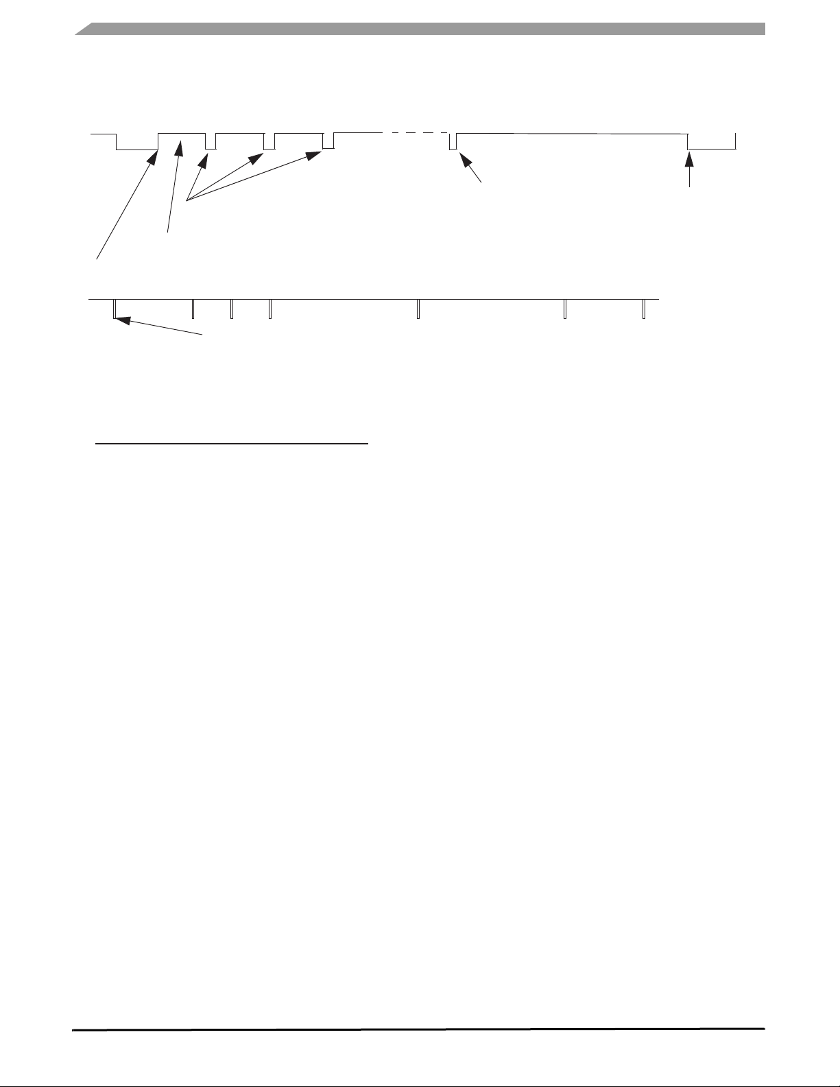
TYPICAL APPLICATIONS
r
SUPPLEMENTAL APPLICATION NOTES
TX
128 occurrences of 11 recessive bits
TEC reaches 255: the node is BUS OFF
Node sends one dominant bit. As there is still the fault, the TEC is incremented by 8 each time.
23 recessive bits: CAN passive error frame
TEC=128: the node reaches the error passive level
RX
Rx is driven only during the glitch occuring on the CAN bus (the dominant time is shorter than a bit time)
The DC current can be calculated as follows:
Idc= (Time in dominant * peak current of the fault) / total error frame time
Idc= (17+15)*peak current / ((23*15)+1408)=32 / 1753*peak current
Example for CANL2Vbat (peak current = - 240 mA)
Figure 46. Node is in Bus Off State
SOFTWARE ASPECTS
Introduction
This section describes the MC33989 operation and the
microcontroller SPI software routine that has to be executed
: Idc = 32*(-) 240 / 1753=(-)4.38 mA
in order to control the device. Structure of the Byte: ADR
bits) + R/W (1bit) + DATA (4 bits). MSB is sent first. Refer
(3
to MC33989 specifications for more details.
BUS OFF is recove
33989
Analog Integrated Circuit Device Data
54 Freescale Semiconductor

How to Enter in Normal Mode After a Power-Up
Power-up
Reset
SUPPLEMENTAL APPLICATION NOTES
TYPICAL APPLICATIONS
Normal request
Normal
How to Change CAN Slew Rate
CAN TX_RX
Write CAN =$5X
CAN TX_RX
slew rate X
Read WUR ($80)
Write TIM1 =$BX
Read IOR ($60)
Read MCR ($00)
Read CAN ($40)
Write TIM1= $BX
Figure 47. Normal Mode After Power-Up
• X is the slew rate.(ex:$56 for slew rate 3).
note: default slew rate is slew rate 0 (the minus one).
• read LX wa ke-up flag
• Write watchdog
X is the period of the watchdog ex:$00 for 10 ms
• Clear V2low, Vsuplow flags
• Clear Batfail, Gfail,Wdrst flags
• read CAN/WU flag
ALL FLAGS ARE READ
• Write watchdog
X is the period of the watchdog ex $00 for 10 ms
note:this register has to be refreshed before the end of the wat chdog
period
Figure 48. Change CAN Slew Rate
How to Set the CAN Interface in Sleep Mode
How to Control HS1 Output
CAN
in normal
Write CAN =$51
Write CAN =$53
• Can go to sleep and wake-up enable
• Can go to sleep and wake-up disable
CAN in Sleep
Figure 49. HS1 Output Control
33989
Analog Integrated Circuit Device Data
Freescale Semiconductor 55
TYPICAL APPLICATIONS
SUPPLEMENTAL APPLICATION NOTES
How to Configure Wake-Up Before Going in Low Power
Mode
Write IOR= $74
Write IOR= $70
Figure 50. Wake-Up Configure Before Low Power Mode
Enable CAN Wake-Up
Write CAN= $51
• CAN sleep and CAN wake-up enable
note:
CAN interface will enter sleep mode as soon as this command is sent in
Figure 51. Enable CAN Wake-Up
Enable Wake-Up From LX, No Cyclic Function
Write LPC =$D0
Write WUR= $9X
• no force wake-up, no cyclic sense, no LX cyclic
• Wake-up levels on LX
Figure 52. Enable Wake-Up From LX without Cyclic Sense
Enable Wake-Up From LX, with Cyclic Sense Function
Write LPC =$D9
Write TIM2= $BX
Write WUR =$9X
• No force wake-up, cyclic sense function, LX cyclic
• Cyclic sense period
• Wake-up levels on LX
• Turn on HS1
• Turn off HS1
refer to the specification for details
Force Wake-Up
Disable all Wake-Up
Figure 53. Enable Wake-Up From LX with Cyclic Sense
Write LPC= $D4
Write TIM2= $BX
• Force wake-up, no cyclic sense function, LX cyclic
• Force wake-up period
Figure 54. Force Wake-Up
Write LPC =$D0
Write WUR =$90
Write CAN =$53
• Disable Force wake-up,LX cyclic
• Disable LX
• CAN sleep and CAN wake-up disable
note: can interface will enter sleep mode as soon as $53 is sent
Figure 55. Disable all Wake-Up
33989
Analog Integrated Circuit Device Data
56 Freescale Semiconductor

How to Enter in Sleep Mode
SUPPLEMENTAL APPLICATION NOTES
TYPICAL APPLICATIONS
SBC in normal or
Standby
SBC in Sleep
How to Enter in Stop Mode with Watchdog
SBC in normal or
Standby
Write RCR =$38
Write MCR =$13
SBC in Stop
Write RCR= $34
Write MCR =$14
• Bit NoStop=»1»: sleep mode is allowed
• SBC and CAN module go to sleep mode
Figure 56. Enter Sleep Mode
• Bit NoStop=»0»: sleep mode is disabled
• SBC is in stop mode VDD1 cannot deliver more than 10 mA &
CAN module is in sleep mode.
it will sleep on the rising edge of CS
it will sleep on the rising edge of CS
Wake-up event
Figure 57. Enter Stop Mode with Watchdog
How to Enter in Stop Mode without Watchdog
SBC in normal or
Standby
Write RCR =$30
Write MCR =$13
SBC in Stop
Figure 58. Enter Stop Mode without Watchdog
•The
SBC has to wake-up before the watchdog selected
by:SPI, CAN, Lx, Force wake-up.
• Bit NoStop=»0»: sleep mode is disabled
• SBC goes into Stop mode & CAN module
goes into sleep mode
it will sleep on the rising edge of CS
33989
Analog Integrated Circuit Device Data
Freescale Semiconductor 57

TYPICAL APPLICATIONS
SUPPLEMENTAL APPLICATION NOTES
How to Recognize and Distinguish the Wake-Up Source
SBC wake-up
Read IOR ($60)
Read MCR ($00)
Read CAN ($40)
Read WUR ($80)
Batfail in MCR
register =»1»?
NO
CANWU in CAN
register=»1»?
NO
WUR =XX?
NO
YES
YES
YES
• Power-up
• Wake-up from CAN
• Wake-up from LX
SBC was in
stop mode
Was FWU
YES
• Force wake-up
enabled?
NO
Was any SPI
command sent?
YES
• CS wake-up
NO
Vsuplow in IOR
register =»1»?
YES
•
VBAT undervoltage (<6.1 V) leading
a VDD1 undervoltage reset
NO
• Idd1_stop over current (>10 mA)
Figure 59. Recognize and Distinguish the Wake-Up Source
33989
Analog Integrated Circuit Device Data
58 Freescale Semiconductor

How to Use the Interrupt Function
The interruptions are configurable in the INTR register.
CAN failure, V2 voltage below 4
V
below 6.1 V are interruption configurable.
SUP
V, HS1 overtemperature,
Recognition and Recovery
SUPPLEMENTAL APPLICATION NOTES
TYPICAL APPLICATIONS
INT
Terminal
Read INTR ($E0)
Write
INT
INTR=INTR& $FX
Terminal
Figure 60. Recognition and Recovery
How to Distinguish Between V2LOW and HS1
Overtemperature
Read IOR ($60)
Figure 61. Distinguish Between V2LOW and HS1 O vertemperature
• In order to identified the source of the interruption
•
INTR =$X 4 &
IOR=$X 8
NO
INTR =$X 4 &
IOR=$X 4
note: V2 and HS1-OT are merged in the same bit
Mask the interruption running to deactivate
the INT terminal
• Interrupt from V2LOW
• Interrupt from HS1
33989
Analog Integrated Circuit Device Data
Freescale Semiconductor 59
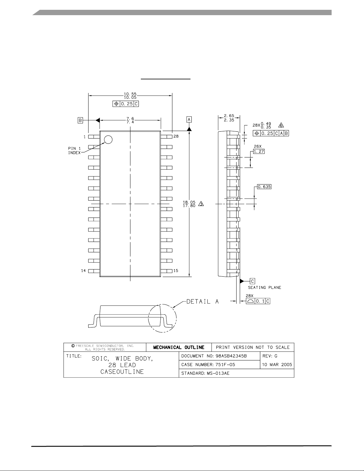
PACKAGING
PACKAGE DIMENSIONS
PACKAGING
PACKAGE DIMENSIONS
For the most current package revision, visit www.freescale.com and perform a keyword search using the “98A” listed below.
DW SUFFIX
EG SUFFIX (Pb-Free)
28-PIN
98ASB42345B
ISSUE G
33989
Analog Integrated Circuit Device Data
60 Freescale Semiconductor
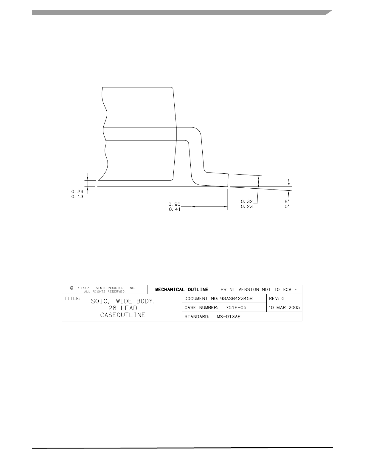
PACKAGE DIMENSIONS
PACKAGING
DW SUFFIX
EG SUFFIX (Pb-Free)
28-PIN
98ASB42345B
ISSUE G
33989
Analog Integrated Circuit Device Data
Freescale Semiconductor 61

ADDITIONAL DOCUMENTATION
THERMAL ADDENDUM (REV 2.0)
ADDITIONAL DOCUMENTATION
THERMAL ADDENDUM (REV 2.0)
INTRODUCTION
This thermal addendum is provided as a supplement to the MC33989 technical
datasheet. The addendum provides thermal performance information that may be
critical in the design and development of system applications. All electrical,
application, and packaging information is provided in the data sheet.
Packaging and Thermal Considerations
The MC33989 is offered in a 28 pin SOICW, single die package. There is a
single heat source (P), a single junction temperature (T
(R
).
θJA
), and thermal resistance
J
33989DWB
33989EG
28-PIN
SOICW
T
=
J
R
θJA
.
P
The stated values are solely for a thermal performance comparison of one
package to another in a standardized environment. This methodology is not
meant to and will not predict the performance of a package in an applicationspecific environment. Stated values were obtained by measurement and
simulation according to the standards listed below.
Standards
Table 36. Thermal Performance Comparison
Thermal Resistance [°C/W]
(1) (2)
R
θJA
(2) (3)
R
θJB
(1) (4)
R
θJA
(5)
R
θJC
Notes
1. Per JEDEC JESD51-2 at natural convection, still air
condition.
2. 2s2p thermal test board per JEDEC JESD51-7.
3. Per JEDEC JESD51-8, with the board temperature on the
center trace near the center lead.
4. Single layer thermal test board per JEDEC JESD51-3.
5. Thermal resistance between the die junction and the
package top surface; cold plate attached to the package top
surface and remaining surfaces insulated.
41
10
68
220
Figure 62. Surface Mount for SOIC Wide Body
DWB SUFFIX
EG SUFFIX (PB-FREE)
98ASB42345B
28-PIN SOICW
Note For package dimensions, refer to
the 33989 device datasheet.
28 Terminal SOICW
1.27 mm Pitch
18.0 mm x 7.5 mm Body
non-Exposed Pad
33989
Analog Integrated Circuit Device Data
62 Freescale Semiconductor

ADDITIONAL DOCUMENTATION
THERMAL ADDENDUM (REV 2.0)
1
RX
2
TX
INT
V2
L0
3
4
5
6
7
8
9
10
11
12
13
14
VDD1
RST
GND
GND
GND
GND
V2CTRL
VSUP
HS1
33989 Pin Connections
28-Pin SOICW
1.27 mm Pitch
18.0 mm x 7.5 mm Body
Device on Thermal Test Board
28
WD
27
CS
26
MOSI
25
MISO
24
SCLK
23
GND
22
GND
21
GND
20
GND
19
CANL
18
CANH
17
L3
16
L2
15
L1
A
Figure 63. Thermal Test Board
Material: Single layer printed circuit board
FR4, 1.6 mm thickness
Cu traces, 0.07 mm thickness
Outline: 80 mm x 100 mm board area, including
edge connector for thermal testing
Table 37. Thermal Resistance Performance
Thermal Resistance Area A (mm2) °C/W
R
JA
θ
0 68
300 52
600 47
Area A: Cu heat-spreading areas on board
surface
Ambient Conditions: Natural convection, still air
R
is the thermal resistance between die junction and
JA
θ
ambient air.
33989
Analog Integrated Circuit Device Data
Freescale Semiconductor 63

ADDITIONAL DOCUMENTATION
THERMAL ADDENDUM (REV 2.0)
Thermal Resistance [ºC/W]
80
70
60
50
40
30
20
10
x
R
θJA
0
0 300 600
Heat spr eading area A [mm²]
100
10
Figure 64. Device on Thermal Test Board R
x
R
θJA
1
θJA
Thermal Res i stanc e [º C/ W]
0.1
1.00E-03 1.00E-02 1.00E-01 1.00E+0 0 1.00E+01 1.00E+ 02 1.00E+03 1.00E+04
Tim e[s]
Figure 65. Transient Thermal Resistance R
1 W Step response, Device on Thermal Test Board Area A = 600 (mm2)
JA
θ
33989
Analog Integrated Circuit Device Data
64 Freescale Semiconductor

REVISION HISTORY
REVISION DATE DESCRIPTION OF CHANGES
4.91
5.0
6.0
7.0
8.0
9.0
10.0
11.0
12.0
13.0
7/2002
8/2005
9/2005
11/2005
11/2005
1/2006
6/2006
11/2006
12/2006
3/2007
• Released XC33989: Motorola Format
• Changed document to Freescale format
• Added New Orderable Part Number
• Maximum Rating Table; Added CANH, CANL and ESD ratings
• Static Electrical Characteristics - Table 3
• POWER INPUT (V
• POWER OUTPUT(V
SUP
): (I
DD1
• Added CAN SUPPLY, CANH and CANL, TX and RX ratings
• Dynamic Electrical Characteristics - Table 4
• STATE MACHINE TIMING (CS, SCLK, MOSI, MISO, WD, INT): CS
changed from 248 to 128 ms
• Added CAN MODULE-SIGNAL EDGE RISE AND FALL TIMES (CANH, CANL) ratings
• Revised Application Section
• Added supplemental Application Notes
• Added Thermal Addendum
• Cosmetic corrections
• CS, INT and WD Pins were changed to CS, INT and WD
• Published in error
• Static Electrical Characteristics - Table 3, added new parameter “VDDst-cap” and
Notes 14 and 16, corrected VDD1 output voltage V
previously published in revision 4.91.
• Dynamic Electrical Characteristics - Table 4, Corrected Max Rating of 248 ms for
Cyclic Sense/FWU Timing 7 CS
• Dynamic Electrical Characteristics - Table 4,Corrected “Cyclic Sense ON Time”
measurement “Unit” from ms to µs
• Updated to the prevailing Freescale form and style
• Updated from Advance Information to Final documentation
• Removed PC33989EG/R2 and replaced with MCZ33989EG/R2 in the Ordering
Information block
• Replaced the label Logic Inputs with Logic Signals (RX, TX, MOSI, MISO, CS, SCLK,
RST, WD, and INT) on page 4
• Replaced Logic Output Pins with LOGIC Input PINS (MOSI, SCLK, CS) on page 9
• Reviewed labeling for device pins VDD1, RST, INT, CS, VSUP, TX, RX, V2CTRL, V2,
WD throughout the data sheet, and made corrections as applicable.
and
• Made changes to Supply Current in Standby Mode
in Normal Mode
(10)
on page 6
• Removed Peak Package Reflow Temperature During Reflow (solder reflow) parameter
from
Maximum Ratings on page 4. Added note with instructions to obtain this information
from www.freescale.com.
• Added the EG suffix to the included thermal addendum
SUP(STOP2);
): V
DD1OUT
FWU7 as
Max rating changed from 410 to 210 µA)
Min rating changed from 4.0 to 4.75 V
FWU7
DD1OUT2
to minimum 4.0 V as
previously published in revision 4.91
(10) (11)
on page 6 and Supply Current
REVISION HISTORY
max rating
33989
Analog Integrated Circuit Device Data
Freescale Semiconductor 65

 Loading...