

Page 1
www.DataSheet4U.com
Freescale Semiconductor
Advance Information
Single High-Side Switch
Document Number: MC33981
Rev. 6.0, 5/2007
(4.0 mΩ), PWM clock up to 60kHz
The 33981 is a high-frequency, self-protected 4.0 mΩ R
side switch used to replace electromechanical relays, fuses, and
discrete devices in power management applications.
The 33981 can be controlled by Pulse-Width Modulation (PWM) with
a frequency up to 60 kHz. It is designed for harsh environments, and it
includes self-recovery features. The 33981 is suitable for loads with
high in-rush current, as well as motors and all types of resistive and
inductive loads.
The 33981 is packaged in a 12 x 12 non-leaded power-enhanced
Power QFN package with exposed tabs.
Features
• Single 4.0 mΩ R
Maximum High-Side Switch
DS(ON)
• PWM Capability up to 60 kHz with Duty Cycle from 5% to 100%
• Very Low Standby Current
• Slew Rate Control with External Capacitor
• Overcurrent and Overtemperature Protection, Undervoltage
Shutdown and Fault Reporting
• Reverse Battery Protection
• Gate Drive Signal for External Low-Side N-Channel MOSFET with
Protection Features
• Output Current Monitoring
• Temperature Feedback
• Pb-Free Packaging Designated by Suffix Code PNA
DS(ON)
high-
33981B
HIGH-SIDE SWITCH
Bottom View
SCALE 1:1
PNA (Pb-Free Suffix)
98ARL10521D
16-PIN PQFN (12 X 12)
ORDERING INFORMATION
Device
MC33981BPNA/R2 - 40°C to 125°C
Temperature
Range (T
)
A
Package
16 PQFN
V
DD
V
DD
V
PWR
33981
MCU
I/O
I/O
I/O
I/O
A/D
A/D
CONF
FS
INLS
EN
INHS
TEMP
CSNS
OCLS SR GND
VPWR
CBOOT
OUT
DLS
GLS
Figure 1. 33981 Simplified Application Diagram
M
* This document contains certain information on a new product.
Specifications and information herein are subject to change without notice.
© Freescale Semiconductor, Inc., 2007. All rights reserved.
Page 2
INTERNAL BLOCK DIAGRAM
TEMP
Temperature
Feedback
INTERNAL BLOCK DIAGRAM
Undervoltage
Detection
Bootstrap Supply
VPWR
CBOOT
SR
FS
EN
INHS
INLS
CONF
5.0 V
I
CONF
R
DWN
Slew Rate Control
I
DWN
Cross-
Conduction
Logic
Current
Protection
Overtemperature
Detection
GND
Figure 2. 33981 Simplified Internal Block Diagram
Gate Driver
OUT Current
Recopy
5.0 V
CSNS
Low-Side
Gate Driver
and Protection
I
OCLS
OCLS
OUT
GLS
DLS
33981
Analog Integrated Circuit Device Data
2 Freescale Semiconductor
Page 3
PIN CONNECTIONS
Package Transparent Top View
CBOOT
GLS
SR
DLS
CONF
OCLS
INLS
FS
INHS
TEMP
EN
PIN CONNECTIONS
CSNS
12
11
10
98765
GND
13
VPWR
14
4
OUTOUT
1
3
2
1615
Figure 3. Pin Connections
Table 1. PIN DEFINITIONS
Descriptions of the pins listed in the table below can be found in the Functional Description section located on page 12.
Pin
Number
1 CSNS Reports Output Current Monitoring
2 TEMP Reports Temperature Feedback
3EN
4 INHS Input Serial Input High Side
5FS
6 INLS Input Serial Input Low Side
7 CONF Input Configuration Input
8 OCLS Input Low-Side Overload
9 DLS Input Drain Low Side
10 GLS Output Low-Side Gate
11 SR Input Slew Rate Control
12 CBOOT Input Bootstrap Capacitor
13 GND Ground Ground
14 VPWR Input Positive Power Supply
15, 16 OUT Output Output
Pin Name
Pin
Function
Input Enable
Reports Fault Status
Formal Name Definition
(Active High)
(Active Low)
This pin is used to generate a ground-referenced voltage for the
microcontroller (MCU) to monitor output current.
This pin is used by the MCU to monitor board temperature.
This pin is used to place the device in a low-current sleep mode.
This input pin is used to control the output of the device.
This pin monitors fault conditions and is active LOW.
This pin is used to control an external low-side N-channel MOSFET.
This input manages MOSFET N-channel cross-conduction.
This pin sets the V
MOSFET.
This pin is the drain of the external low-side N-channel MOSFET.
This output pin drives the gate of the external low-side N-channel
MOSFET.
This pin controls the output slew rate.
This pin provides the high-pulse current to drive the device.
This is the ground pin of the device.
This pin is the source input of operational power for the device.
These pins provide a protected high-side power output to the load
connected to the device.
protection level of the external low-side
DS
33981
Analog Integrated Circuit Device Data
Freescale Semiconductor 3
Page 4
ELECTRICAL CHARACTERISTICS
MAXIMUM RATINGS
ELECTRICAL CHARACTERISTICS
MAXIMUM RATINGS
Table 2. Maximum Ratings
All voltages are with respect to ground unless otherwise noted.
Rating Symbol Value Unit
ELECTRICAL RATINGS
Power Supply Voltage
Steady-State
Input/Output Pins Voltage
(1)
Output Voltage
Positive
Negative
(2)
Continuous Output Current
CSNS Input Clamp Current
EN Input Clamp Current
SR Voltage
C
BOOT Voltage
OCLS Voltage
Low-Side Gate Voltage
Low-Side Drain Voltage
ESD Voltage
(3)
Human Body Model (HBM)
Charge Device Model (CDM)
Corner Pins (1, 12, 15, 16)
All Other Pins (2-11, 13-14)
THERMAL RATINGS
Operating Temperature
Ambient
Junction
Storage Temperature
Thermal Resistance
(4)
Junction to Power Die Case
Junction to Ambient
Peak Pin Reflow Temperature During Solder Mounting
(5)
Notes
1. Exceeding voltage limits on INHS, INLS, CONF, CSNS, FS
, TEMP, and EN pins may cause a malfunction or permanent damage to the
device.
2. Continuous high-side output rating as long as maximum junction temperature is not exceeded. Calculation of maximum output current
using package thermal resistance is required.
3. ESD testing is performed in accordance with the Human Body Model (HBM) (C
Model (CDM), Robotic (C
ZAP
= 4.0 pF).
4. Device mounted on a 2s2p test board per JEDEC JESD51-2.
5. pin soldering temperature limit is for 10 seconds maximum duration. Not designed for immersion soldering. Exceeding these limits may
cause malfunction or permanent damage to the device.
V
PWR
INHS, INLS,
CONF, CSNS, FS
TEMP, EN
V
OUT
I
OUT
I
CL(CSNS)
I
CL(
EN)
V
SR
C
BOOT
V
OCLS
V
GLS
V
DLS
V
ESD
TA
TJ
T
STG
R
JC
θ
R
JA
θ
T
SOLDER
= 100 pF, R
ZAP
-16 to 41
- 0.3 to 7.0 V
,
41.0
-5.0
40.0 A
15.0 mA
2.5 mA
- 0.3 to 54.0 V
- 0.3 to 54.0 V
- 5.0 to 7.0 V
- 0.3 to 15.0 V
- 5.0 to 41.0 V
± 2000
± 750
± 500
- 40 to 125
- 40 to 150
- 55 to 150 °C
1.0
20.0
245 °C
= 1500 Ω) and the Charge Device
ZAP
V
V
V
°C
°C/W
33981
Analog Integrated Circuit Device Data
4 Freescale Semiconductor
Page 5
STATIC ELECTRICAL CHARACTERISTICS
ELECTRICAL CHARACTERISTICS
STATIC ELECTRICAL CHARACTERISTICS
Table 3. Static Electrical Characteristics
Characteristics noted under conditions 6.0 V ≤ V
noted reflect the approximate parameter mean at TA = 25°C under nominal conditions unless otherwise noted.
Characteristic Symbol Min Typ Max Unit
POWER INPUT (VPWR)
Battery Supply Voltage Range
Fully Operational
Extended
V
PWR
INHS = 1 and OUT Open
INLS = 0
V
PWR
INHS = INLS = 0, EN = 5.0 V, OUT Connected to GND
Sleep State Supply Current
(V
PWR
T
A
T
A
Undervoltage Shutdown
Undervoltage Hysteresis
POWER OUTPUT (IOUT, VPWR)
Output Drain-to-Source ON Resistance
V
PWR
V
PWR
V
PWR
Output Drain-to-Source ON Resistance (I
V
PWR
V
PWR
V
PWR
Output Source-to-Drain ON Resistance
V
PWR
Output Overcurrent Detection Level
9.0 V < V
Current Sense Ratio
9.0 V <
Current Sense Ratio (C
9.0 V <
Output Current
5.0 A
15 A, 20 A and 30 A
Current Sense Voltage Clamp
I
CSNS
Notes
6. OUT can be commanded fully on, PWM is available at room. Low Side Gate driver is available. Protections and Diagnosis are not
7. Source-Drain ON Resistance (Reverse Drain-to-Source ON Resistance) with negative polarity V
(6)
Supply Current
Supply Current
< 14 V, EN = 0 V, OUT Connected to GND)
= 25°C
= 125°C
(I
= 20 A, TA = 25°C)
OUT
= 6.0 V
= 9.0 V
= 13.0 V
= 20 A, TA = 150°C)
OUT
= 6.0 V
= 9.0 V
= 13.0 V
(I
= -20 A, TA = 25°C)
OUT
= - 12 V
< 16 V
PWR
V
< 16 V, CSNS < 4.5 V
PWR
) Accuracy
SR
V
< 16 V, CSNS < 4.5 V
PWR
= 15 mA
available. Min/max parameters are not guaranteed.
≤ 27 V, -40°C ≤ TA ≤ 125°C unless otherwise noted. Typical values
PWR
V
PWR
I
PWR(ON)
6.0
4.5
–
–
27.0
27.0
– 10.0 12.0
I
PWR(SBY)
– 10.0 12.0
I
PWR(SLEEP)
–
–
V
PWR(UV)
V
PWR(UVHYS)
R
DS(ON)25
2.0 4.0 4.5 V
0.05 0.15 0.3 V
–
–
–
R
DS(ON)150
–
–
–
(7)
R
SD(ON)
–
–
–
–
–
–
–
–
5.0
50.0
6.0
5.0
4.0
10.2
8.5
6.8
––8.0
I
OCH
75 100 125
C
SR
– 1/20000 –
C
SR_ACC
V
CL(CSNS)
-20
-15
–
–
20
15
4.5 6.0 7.0
.
PWR
V
mA
mA
µA
mΩ
mΩ
mΩ
A
–
%
V
33981
Analog Integrated Circuit Device Data
Freescale Semiconductor 5
Page 6
ELECTRICAL CHARACTERISTICS
STATIC ELECTRICAL CHARACTERISTICS
Table 3. Static Electrical Characteristics (continued)
Characteristics noted under conditions 6.0 V ≤ V
≤ 27 V, -40°C ≤ TA ≤ 125°C unless otherwise noted. Typical values
PWR
noted reflect the approximate parameter mean at TA = 25°C under nominal conditions unless otherwise noted.
Characteristic Symbol Min Typ Max Unit
POWER OUTPUT (VPWR) (continued)
Overtemperature Shutdown
Overtemperature Shutdown Hysteresis
(8)
LOW SIDE GATE DRIVER (VPWR, VGLS, VOCLS)
Low-Side Gate Voltage
V
= 6.0 V
PWR
= 9.0 V
V
PWR
= 13 V
V
PWR
= 27 V
V
PWR
Low-Side Gate Sinked Current
V
GLS
= 2 V, V
PWR
= 13 V
Low-Side Gate Sourced Current
V
GLS
= 2 V, V
PWR
= 13 V
Low-Side Overload Detection Level versus Low-Side Drain Voltage
V
- V
OCLS
DLS
, (V
OCLS
≤ 4.0 ς)
CONTROL INTERFACE (CONF, INHS, INLS, EN, OCLS)
Input Logic High Voltage (CONF, INHS, INLS)
Input Logic Low Voltage (CONF, INHS, INLS)
Input Logic Voltage Hysteresis (CONF, INHS, INLS)
Input Logic Active Pulldown Current (INHS, INLS)
Enable Pull-down Resistor (EN
Enable Voltage Threshold (EN
Input Clamp Voltage (EN
I
< 2.5 mA
EN
Input Forward Voltage (EN
Input Active Pullup Current (OCLS
)
)
)
)
)
Input Active Pullup Current (CONF)
FS
Tri-State Capacitance
FS
Low-State Output Voltage
I
= -1.6 mA
FS
(8)
Temperature Feedback
T
= 25°C for V
A
Temperature Feedback Derating
PWR
= 14 V
(8)
Notes
8. Parameter is guaranteed by process monitoring but is not production tested.
T
SD
T
SDHYS
V
GLS
I
GLSNEG
I
GLSPOS
V
DS_LS
V
IH
V
IL
V
INHYS
I
DWN
R
DWN
V
EN
V
CLEN
V
F(EN)
I
OCLS p
I
CONF
C
FS
V
FSL
V
TFEED
DT
FEED
160 175 190 °C
5.0 – 20 °C
5.0
8.0
12.0
12.0
5.4
8.4
12.4
12.4
6.0
9.0
13.0
13.0
– 100 –
– 100 –
-50 – +50
3.3 – – V
– – 1.0 V
100 600 1200 mV
5.0 10 20 µA
100 200 400 kΩ
2.5 V
7.0 – 14
-2.0–-0.3V
50 100 200 µA
5.0 10 20 µA
– – 20 pF
–0.20.4
3.35 3.45 3.55
-8.5 -8.9 -9.3 mV/°C
V
mA
mA
mV
V
V
V
33981
Analog Integrated Circuit Device Data
6 Freescale Semiconductor
Page 7
DYNAMIC ELECTRICAL CHARACTERISTICS
STATIC ELECTRICAL CHARACTERISTICS
DYNAMIC ELECTRICAL CHARACTERISTICS
Table 4. Dynamic Electrical Characteristics
Characteristics noted under conditions 6.0 V ≤ V
noted reflect the approximate parameter mean at TA = 25°C under nominal conditions unless otherwise noted.
Characteristic Symbol Min Typ Max Unit
CONTROL INTERFACE AND POWER OUTPUT TIMING (CBOOT, VPWR)
Charge Blanking Time (CBOOT)
Output Rising Slew Rate
V
= 13 V, from 10% to 90% of V
PWR
= 5.0 Ω
R
L
Output Falling Slew Rate
V
= 13 V, from 90% to 10% of V
PWR
= 5.0 Ω
R
L
Output Turn-ON Delay Time
V
= 13 V, SR Capacitor = 4.7 nF
PWR
Output Turn-OFF Delay Time
V
= 13 V, SR Capacitor = 4.7 nF
PWR
Input Switching Frequency
Output PWM ratio @ 60kHz
Time to Reset Fault Diagnosis
(over load on high side or external low side)
Output Over Current Detection Time
Notes
9. The MC33981 can work down (~100Hz). The fault management reset can not be guaranteed with PWM frequency lower than 5kHz
(INHS=0 during 200us typ)
10. Values for CBOOT=100nF. Refer to the paragraph entitled Sleep Mode on page 13. Parameter is guaranteed by design and not
production tested.
11. Turn-ON delay time measured from rising edge of INHS that turns the output ON to V
12. Turn-OFF delay time measured from falling edge of INHS that turns the output OFF to V
13. The ratio is measured at V
(10)
SR Capacitor = 4.7 nF,
OUT,
SR Capacitor = 4.7 nF,
OUT,
(11)
(12)
(9)
(13)
= 50% V
out
without SR capacitor. The device is capable of 100% duty cycle.
PWR
≤ 27 V, -40°C ≤ TA ≤ 125°C unless otherwise noted. Typical values
PWR
t
SR
ON
R
10 25 50 µs
8.0 16 35
SR
F
8.0 16 35
t
DLYON
200 400 700
t
DLYOFF
500 1000 1500
f
PWM
R
PWM
t
RSTDIAG
– 20 60 kHz
5.0 95 %
100 200 400
t
OCH
1.0 10 20 µs
= 0.5 V with RL= 5.0 Ω resistive load.
OUT
= V
OUT
-0.5 V with RL= 5.0 Ω resistive load.
PWR
V/µs
V/µs
ns
ns
µs
33981
Analog Integrated Circuit Device Data
Freescale Semiconductor 7
Page 8
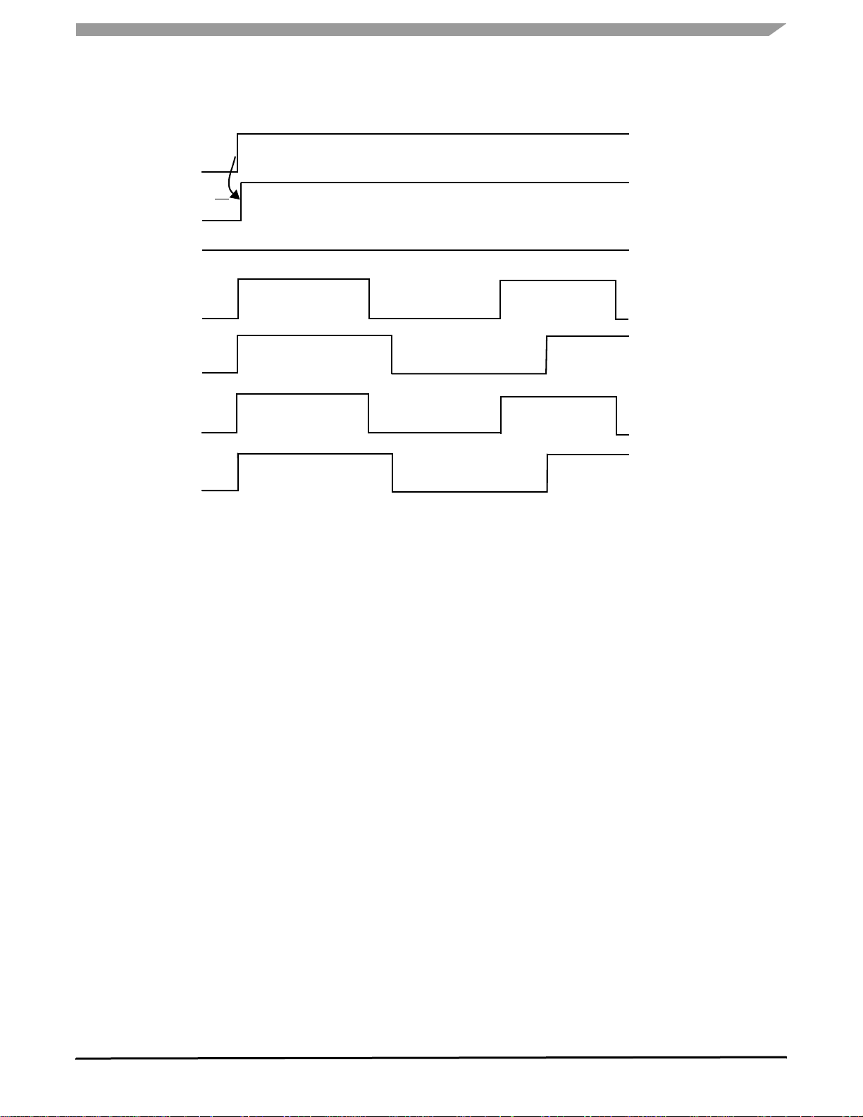
TIMING DIAGRAMS
STATIC ELECTRICAL CHARACTERISTICS
INHS
5.0 V
0.0 V
Vout
TIMING DIAGRAMS
V
PWR
90% Vout
EN
FS
- 0.5 V
0.5 V
Vout
10% Vout
t
After
ON
t
DLY(OFF)
SR
t
DLY(ON)
R
Figure 4. Time Delays Functional Diagrams
R
SR
PWM
F
50%V
PWR
5.0 V
CONF
INHS
INLS
OUT
GLS
Figure 5. Normal Mode, Cross-Conduction Management
33981
Analog Integrated Circuit Device Data
8 Freescale Semiconductor
Page 9
EN
FS
t
ON
After
STATIC ELECTRICAL CHARACTERISTICS
TIMING DIAGRAMS
CONF
INHS
INLS
OUT
GLS
High Side ON
High Side OFF
Figure 6. Normal Mode, Independent High Side a nd Low Side
0.0 V
33981
Analog Integrated Circuit Device Data
Freescale Semiconductor 9
Page 10
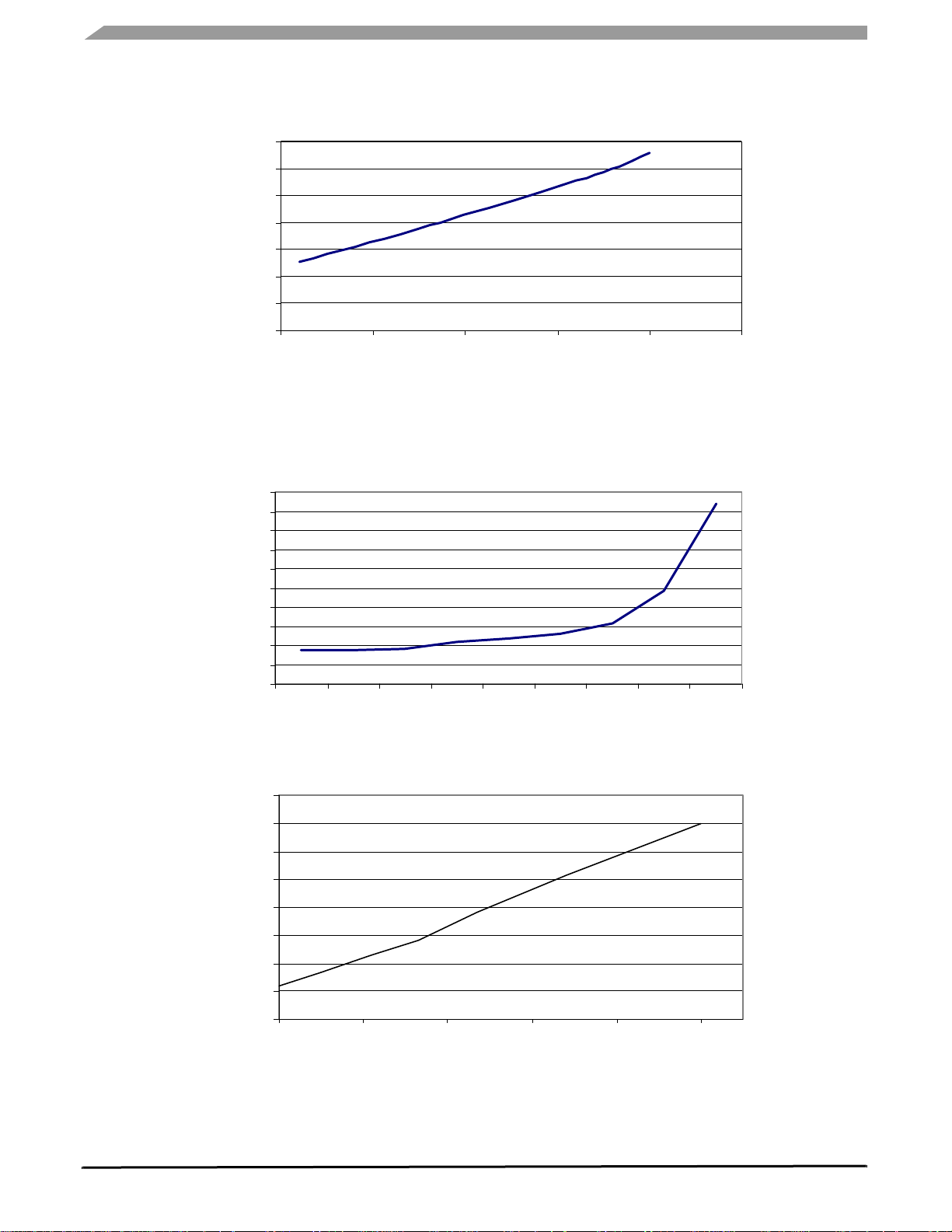
ELECTRICAL PERFORMANCE CURVES
STATIC ELECTRICAL CHARACTERISTICS
ELECTRICAL PERFORMANCE CURVES
7.0
6.0
)
5.0
Ω
4.0
(m
3.0
DS(ON)
2.0
R
RdsON (mOh m)
1.0
0.0
-50 0 50 100 150 200
Temperature (°C)
Temperature (°C)
Figure 7. Typical R
vs. Temperature at V
DS(ON)
10.0
9.0
8.0
7.0
(µA)
6.0
5.0
4.0
3.0
PWR(SLEEP)
Ipwr(sleep)(µA)
I
2.0
1.0
0.0
4.5 6.0 9.0 12.0 12.5 13.0 14.0 17.0 21.0
V
Vpwr(V)
PWR
Figure 8. Typical Sleep State Supply Current vs. V
1600
1400
1200
1000
(V)
PWR
PWR
= 13 V
at 150°C
800
600
Vout Rise Time (ns)
400
200
0
0 2.0
4.0
6.0 8.0
10
SR Capacitor (nF)
Figure 9. V
33981
10 Freescale Semiconductor
Rise Time vs. SR Capacitor From 10% to 90% of V
OUT
at 25°C and V
OUT
Analog Integrated Circuit Device Data
PWR
= 13 V
Page 11
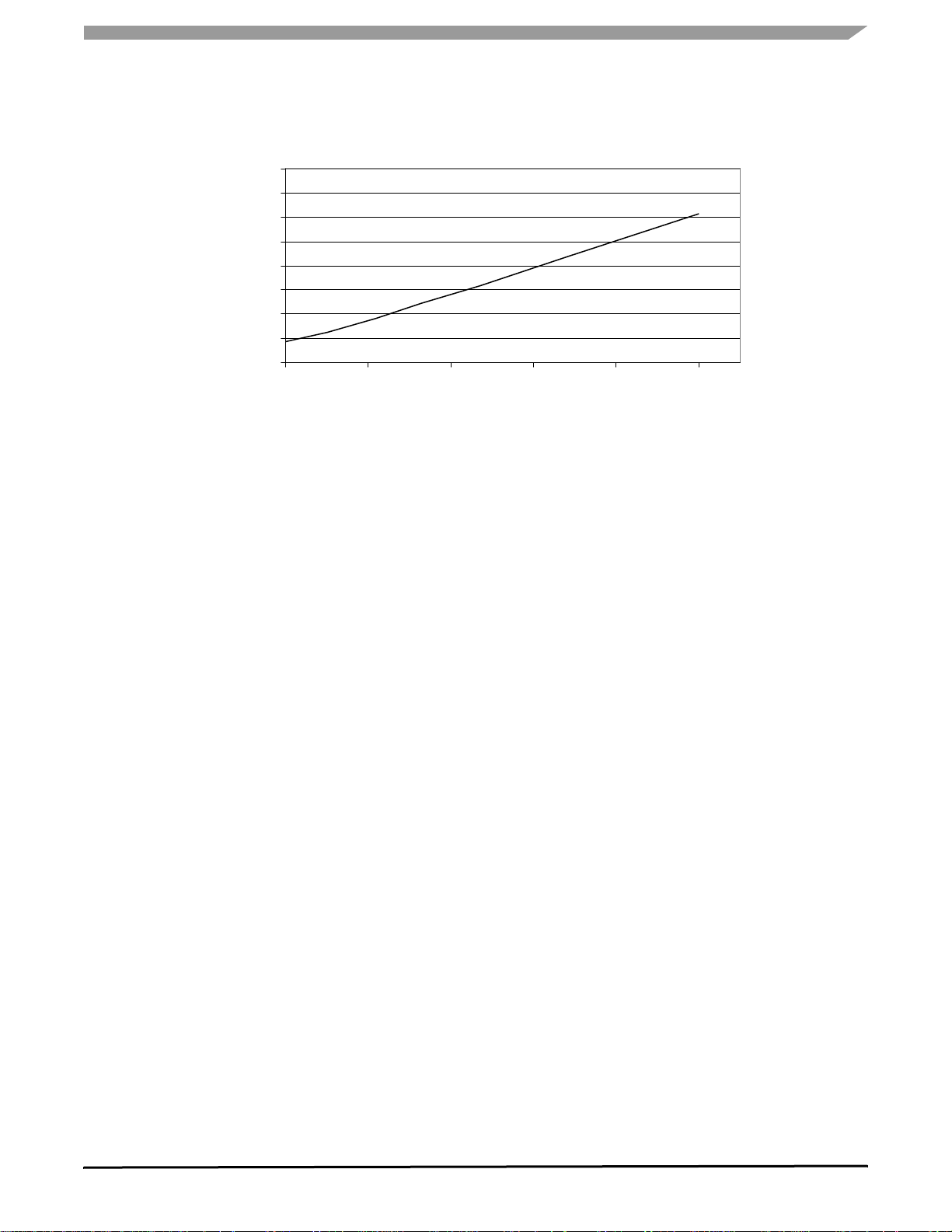
Vout Fall Time (ns)
1600
1400
1200
1000
800
600
400
200
0
0 2.0
ELECTRICAL PERFORMANCE CURVES
STATIC ELECTRICAL CHARACTERISTICS
ELECTRICAL PERFORMANCE CURVES
4.0 6.0
SR Capacitor (nF)
8.0
10
Figure 10. V
Fall Time vs. SR Capacitor From 10% to 90% of V
OUT
at 25°C and V
OUT
PWR
= 13 V
33981
Analog Integrated Circuit Device Data
Freescale Semiconductor 11
Page 12

FUNCTIONAL DESCRIPTION
INTRODUCTION
FUNCTIONAL DESCRIPTION
INTRODUCTION
The 33981 is a high-frequency self-protected silicon
4.0 mΩ R
electromechanical relays, fuses, and discrete devices in
power management applications. The 33981 can be
controlled by pulse-width modulation (PWM) with a frequency
up to 60 kHz. It is designed for harsh environments, and it
includes self-recovery features.
high-side switch used to replace
DS(ON)
FUNCTIONAL PIN DESCRIPTIONS
OUTPUT CURRENT MONITORING (CSNS)
This pin is used to output a current proportional to the highside OUT current and is used externally to generate a
ground-referenced voltage for the microcontroller (MCU) to
monitor OUT current.
TEMPERATURE FEEDBACK (TEMP)
This pin reports an analog value proportional to the
temperature of the GND flag (pin 13). It is used by the MCU
to monitor board temperature.
ENABLE [ACTIVE HIGH] (EN)
This is an input used to place the device in a low current
sleep mode. This pin has an active passive internal pulldown.
INPUT HIGH SIDE (INHS)
The input pin is used to directly control the OUT. This input
has an active internal pulldown current source and requires
CMOS logic levels.
FAULT STATUS (FS)
This pin is an open drain-configured output requiring an
external pullup resistor to V
When a device fault condition is detected, this pin is active
LOW.
(5.0 V) for fault reporting.
DD
INPUT LOW SIDE (INLS)
This input pin is used to directly control an external lowside N-channel MOSFET and has an active internal pulldown
current source and requires CMOS logic levels. It can be
controlled independently of the INHS depending of CONF
pin.
CONFIGURATION INPUT (CONF)
This input pin is used to manage the cross-conduction
between the internal high-side N-channel MOSFET and the
external low-side N-channel MOSFET. The pin has an active
internal pullup current source. When CONF is at 0 V, the two
The 33981 is suitable for loads with high inrush current, as
well as motors and all types of resistive and inductive loads.
A dedicated parallel input is available for an external low-side
control with protection features and cross-conduction
management.
MOSFETs are controlled independently. When CONF is at
5.0 V, the two MOSFETs cannot be on at the same time.
V
DD
LOW-SIDE OVERLOAD (OCLS)
This pin sets the VDS protection level of the external lowside MOSFET. This pin has an active internal pullup current
source. It must be connected to an external resistor.
DRAIN LOW SIDE (DLS)
This pin is the drain of the external low-side N-channel
MOSFET. Its monitoring allows protection features: low side
short protection and V
short protection.
PWR
LOW-SIDE GATE (GLS)
This pin is an output used to drive the gate of the external
low-side N-channel MOSFET.
SLEW RATE CONTROL (SR)
A capacitor connected between this pin and ground is
used to control the output slew rate.
BOOTSTRAP CAPACITOR (CBOOT)
A capacitor connected between this pin and OUT is used
to switch the OUT in PWM mode.
GROUND (GND)
This pin is the ground for the logic and analog circuitry of
the device.
POSITIVE POWER SUPPLY (VPWR)
This pin connects to the positive power supply and is the
source input of operational power for the device. The V
pin is a backside surface mount tab of the package.
PWR
OUTPUT (OUT)
Protected high-side power output to the load. Output pins
must be connected in parallel for operation.
33981
Analog Integrated Circuit Device Data
12 Freescale Semiconductor
Page 13

FUNCTIONAL DEVICE OPERATION
OPERATIONAL MODES
FUNCTIONAL DEVICE OPERATION
OPERATIONAL MODES
The 33981 has 2 operating modes: Sleep and Normal
depending on EN input.
NORMAL MODE
The 33981 will go to the normal operating mode when the
EN pin is logic [1]. The INHS and INLS commands will be
SLEEP MODE
Sleep mode is the state of the 33981 when the EN is
disabled t
charge of the bootstrap capacitor.
after the EN transitions to logic [1] to enable the
ON
logic [0]. In this mode, OUT, the gate driver for the external
MOSFET, and all unused internal circuitry are off to minimize
current draw.
Table 5. Operating Modes
Condition CONF INHS INLS OUT GLS FS EN Comments
Sleep x x x x x H L
Normal L H H H H H H
Normal L L L L L H H
Normal L L H L H H H
Normal L H L H L H H
Normal H PWM H PWM PWM_bar H H
H = High level
L = Low level
x = Don’t care
PWM_bar = Opposite of pulse-width modulation signal.
Device is in Sleep mode. The OUT and low-side gate are OFF.
Normal mode. High side and low side are controlled
independently. The high side and the low side are both on.
Normal mode. High side and low side are controlled
independently. The high side and the low side are both off.
Normal mode. Half-bridge configuration. The high side is off
and the low side is on.
Normal mode. Half-bridge configuration. The high side is on
and the low side is off.
Normal mode. Cross-conduction management is activated.
Half-bridge configuration.
PROTECTION AND DIAGNOSTIC FEATURES
UNDERVOLTAGE
The 33981 incorporates undervoltage protection. In case
V
of
PWR<VPWR
supply rises to V
reset below
, the OUT is switched OFF until the power
V
(UV)
PWR
PWR
(UV)
(UV)
.
+V
PWR
. The latched fault are
(UVHYS)
offending load is removed. FS
disabled typically t ON after to enable the charge of the
bootstrap capacitor.
Overtemperature faults force the TEMP pin to 0 V.
pin transition to logic [1] will be
OVERCURRENT FAULT ON HIGH SIDE
OVERTEMPERATURE FAULT
The 33981 incorporates over temperature detection and
shutdown circuitry on OUT. Overtemperature detection also
protects the low-side gate driver (GLS pin). Overtemperature
detection occurs when OUT is in the ON or OFF state and
GLS is at high or low level.
For OUT, an over temperature fault condition results in
OUT turning OFF until the temperature falls below T
cycle will continue indefinitely until the offending load is
removed.
Figure 12, page 16 and Figure 18, page 20 show an
over temperature on OUT.
An over temperature fault on the low-side gate drive
results in OUT turning OFF and the GLS going to 0 V until the
temperature falls below T
. This cycle will continue until the
SD
Analog Integrated Circuit Device Data
Freescale Semiconductor 13
SD
. This
The OUT pin has an overcurrent high-detection level
called I
for maximum device protection. If at any time the
OCH
current reaches this level, OUT will stay OFF and the CSNS
pin will go to 0 V. The OUT pin is reset (and the fault is
delatched) by a logic [0] at the INHS pin for at least t
RST(diag)
When INHS goes to 0 V, CSNS goes to 5.0 V.
Figure 16, page 19, the OUT pin is short-circuited to 0 V.
In
When the current reaches I
owing to internal logic circuit.
t
OCH
, OUT is turned OFF within
OCH
OVERLOAD FAULT ON LOW SIDE
This fault detection is active when INLS is logic [1]. Lowside overload protection does not measure the current
directly but rather its effects on the low-side MOSFET. When
33981
.
Page 14

FUNCTIONAL DEVICE OPERATION
PROTECTION AND DIAGNOSTIC FEATURES
V
DLS
> V
, the GLS pin goes to 0 V and the OCLS
OCLS
internal current source is disconnected and OCLS goes to
0 V. The GLS pin and the OCLS pin are reset (and the fault
is delatched) by a logic [0] at the INLS pin for at least
t
RST(diag)
. Figure 13, page 17 and Figure 14, page 18 illustrate the
behavior in case of overload on Low Side Gate driver.
When connected to an external resistor, the OCLS pin with
its internal current source sets the V
level. By changing
OCLS
the external resistance, the protection level can be adjusted
depending on low-side characteristics. A 33kΩ resistor gives
level of 3.3 V typical.
a V
DS
This protection circuitry measures the voltage between the
drain of the low side (DLS pin) and the 33981 ground (GND
pin). For this reason it is key that the low-side source, the
33981 ground, and the external resistance ground
connection are connected together in order to prevent false
error detection due to ground shifts.
The maximum OCLS voltage being 4.0V, a resistor bridge
on DLS must be used to detect a higher voltage across the
low side.
CONFIGURATION
The CONF pin manages the cross-conduction between
the internal MOSFET and the external low-side MOSFET.
With the CONF pin at 0 V, the two MOSFETs can be
independently controlled. A load can be placed between the
high side and the low side.
With the CONF pin at 5.0 V, the two MOSFETs cannot be
on at the same time. They are in half-bridge configuration as
shown in the simplified application diagram on page
1. If
INHS and INLS are at 5.0 V at the same time, INHS has
priority and OUT will be at V
. If INHS changes from 5.0 V
PWR
to 0 V with INLS at 5.0 V, GLS will go to high state as soon
as the V
of the internal MOSFET is lower than 2.0 V
GS
typically. A half-bridge application could consist in sending
PWM signal to the INHS pin and 5.0 V to the INLS pin with
the CONF pin at 5.0 V.
Figure 20, page 22, illustrates the simplified application
diagram on page
1 with a DC motor and external low side.
The CONF and INLS pins are at 5.0 V. When INHS is at
5.0 V, current is flowing in the motor. When INHS goes to 0 V,
the load current recirculates in the external low side.
BOOTSTRAP SUPPLY
Bootstrap supply provides current to charge the bootstrap
capacitor through the V
the application of power to the device to charge the bootstrap
capacitor. A typical value for this capacitor is 100 nF. An
internal charge pump allows continuous MOSFET drive.
When the device is in the sleep mode, this bootstrap supply
is off to minimize current consumption.
pin. A short time is required after
PWR
HIGH-SIDE GATE DRIVER
The high-side gate driver switches the bootstrap capacitor
voltage to the gate of the MOSFET. The driver circuit has a
low-impedance drive to ensure that the MOSFET remains
OFF in the presence of fast falling dV/dt transients on the
OUT pin.
This bootstrap capacitor connected between the power
supply and the C
pin provides the high pulse current to
BOOT
drive the device. The voltage across this capacitor is limited
to about 13 V typical.
An external capacitor connected between pins SR and
GND is used to control the slew ra te at the OU T pin.
and Figure 10, page 11 give Vout rise and fall time
page 10
Figure 9,
versus different SR capacitors.
LOW-SIDE GATE DRIVER
The low-side control circuitry is PWM capable. It can drive
a standard MOSFET with an R
frequency up to 60 kHz. The V
as low as 10.0 mΩ at a
DS(ON)
is internally clamped at
GS
12 V typically to protect the gate of the MOSFET. The GLS
pin is protected against short by a local over temperature
sensor.
THERMAL FEEDBACK
The 33981 has an analog feedback output (TEMP pin) that
provides a value in inverse proportion to the temperature of
the GND flag (pin 13). The controlling microcontroller can
“read” the temperature proportional voltage with its analogto- digital converter (ADC). This can be used to provide realtime monitoring of the PC board temperature to optimize the
motor speed and to protect the whole electronic system.
TEMP pin value is V
coefficient of DT
TFEED with a negative temperature
.
FEED
REVERSE BATTERY
The 33981 survives the application of reverse battery
voltage as low as -16 V. Under these conditions, the output’s
gate is enhanced to decrease device power dissipation. No
additional passive components are required. The 33981
survives these conditions until the maximum junction rating is
reached.
In the case of reverse battery in a half-bridge application,
a direct current passes through the external freewheeling
diode and the internal high-side.
As Figure 11
line. The proposed solution is an external N-channel low-side
with its gate tied to battery voltage through a resistor. A
high-side in the V
shows, it is essential to protect this power
line could be another solution.
PWR
33981
Analog Integrated Circuit Device Data
14 Freescale Semiconductor
Page 15

PROTECTION AND DIAGNOSTIC FEATURES
FUNCTIONAL DEVICE OPERATION
V
DD
MCU
No current
V
PWR
GND
33981
OUT
If the DC motor module ground is disconnected from load
ground, the device protects itself and safely turns OFF the
output regardless of the output state at the time of
disconnection. A 10k resistor needs to be added between the
EN pin and the rest of the circuitry in order to ensure the
device turns off in case of ground disconnect and to prevent
exceeding this pin’s maximum ratings.
FAULT REPORTING
GROUND (GND) DISCONNECT PROTECTION
Diode
M
10.0 k
V
Ω
PWR
Figure 11. Reverse Battery Protection
Table 6. Functional Truth Table in Fault Mode
Conditions CONF INHS INLS OUT GLS FS EN TEMP CSNS OCLS Comments
Overtemperature
on OUT
Overtemperature
on GLS
Overcurrent
on OUT
Overload
on External Low-
Side MOSFET
H = High level
L = Low level
x = Don’t care
x x x L H L H L x x
x x x L L L H L x x
x H L L x L H x L x
L L H x L L H x x L
This 33981 indicates the faults below as they occur by
driving the FS pin to logic [0]:
• Overtemperature fault
• Overcurrent fault on OUT
• Overload fault on the external low-side MOSFET
The FS pin will return to logic [1] when the over
temperature fault condition is removed. The two other faults
are latched.
The 33981 is currently in fault mode.
The OUT is OFF. TEMP at 0 V
indicates this fault. Once the fault is
removed 33981 recovers its normal
mode.
The 33981 is currently in fault mode.
The OUT is OFF and GLS is at 0 V.
TEMP at 0 V indicates this fault. Once
the fault is removed 33981 recovers its
normal mode.
The 33981 is currently in fault mode.
The OUT is OFF. It is reset by a
logic [0] at INHS for at least
When INHS goes to 0 V, CSNS goes to
5.0 V.
The 33981 is currently in fault mode.
GLS is at 0 V and OCLS internal
current source is off. The external
resistance connected between OCLS
and GND pin will pull OCLS pin to 0 V.
The fault is reset by a logic [0] at INLS
for at least
t
RST(diag)
t
RST(diag)
.
.
33981
Analog Integrated Circuit Device Data
Freescale Semiconductor 15
Page 16

FUNCTIONAL DEVICE OPERATION
PROTECTION AND DIAGNOSTIC FEATURES
EN
CONF
INHS
INLS
OUT
GLS
FS
0.0 V
0.0 V
5.0 V
5.0 V
5.0 V
5.0 V
0.0 V
TEMP
Temperature
OUT
0.0 V
TSD
Hysteresis
Thermal Shutdown
on OUT
Figure 12. Overtemperature on Output
High Side ON
TSD
Hysteresis
Thermal Shutdown
on OUT
High Side OFF
33981
Analog Integrated Circuit Device Data
16 Freescale Semiconductor
Page 17

PROTECTION AND DIAGNOSTIC FEATURES
FUNCTIONAL DEVICE OPERATION
EN
INLS
GLS
FS
OCLS
V
DS_LS
V
DS_LS = VOCLS
Overload on Low Side
0.0 V
Low Side OFF
0.0 V
t
RST(diag)
0.0 V
0.0 V
Case 1: Overload Removed
5.0 V
5.0 V
5.0 V
Figure 13. Overload on Low-Side Gate Drive, Case 1
33981
Analog Integrated Circuit Device Data
Freescale Semiconductor 17
Page 18

FUNCTIONAL DEVICE OPERATION
PROTECTION AND DIAGNOSTIC FEATURES
EN
5.0 V
INLS
OCLS
V
DS_LS
GLS
FS
0.0 V
0.0 V
Low Side OFF
t
RST(diag)
0.0 V
0.0 V
V
DS_LS = VOCLS
Case 2: Low Side Still Overloaded
Overload on Low Side
Figure 14. Overload on Low-Side Gate Drive, Case 2
33981
Analog Integrated Circuit Device Data
18 Freescale Semiconductor
Page 19

EN
PROTECTION AND DIAGNOSTIC FEATURES
FUNCTIONAL DEVICE OPERATION
5.0 V
INHS
OUT
FS
CSNS
I
OUT
0.0 V
t
RST(diag)
0.0 V
0.0 V
VCL (CSNS)
0.0 V
I
OCH
Overcurrent on High Side
Figure 15. Overcurrent on Output
5.0 V
Fault Removed
Figure 16. High-Side Overcurrent
33981
Analog Integrated Circuit Device Data
Freescale Semiconductor 19
Page 20

FUNCTIONAL DEVICE OPERATION
PROTECTION AND DIAGNOSTIC FEATURES
Recirculation in Low SideCurrent in Motor
Figure 17. Cross-Conduction with Low Side
Overtemperature
INHS
TEMP
OUT
I
OUT
Figure 18. Overtemperature on OUT
33981
Analog Integrated Circuit Device Data
20 Freescale Semiconductor
Page 21

PROTECTION AND DIAGNOSTIC FEATURES
FUNCTIONAL DEVICE OPERATION
Figure 19. Maximum Operating Frequency for SR Capacitor of 4.7 nF
33981
Analog Integrated Circuit Device Data
Freescale Semiconductor 21
Page 22

TYPICAL APPLICATIONS
INTRODUCTION
TYPICAL APPLICATIONS
INTRODUCTION
Figure 20 shows a typical application for the 33981. A brush DC motor is connected to the output. A low-side gate driver is
used for the freewheeling phase. Typical values for external capacitors and resistors are given.
.
33981
VPWR
CBOOT
OUT
GND
V
DLS
GLS
PWR
330µF
100 nF
100 nF
M
V
PWR
V
DD
Voltage regulator
MCU
I/O
I/O
I/O
I/O
A/D
A/D
1.0 k
V
DD
33 k
SR
CONF
FS
INLS
EN
INHS
TEMP
CSNS
OCLS
Ω
1.0 k
Ω
2.2 nF
10 k
10 k
10 k
10 k
Ω
Ω
Ω
Ω
Ω
Figure 20. 33981 Typical Application Diagram
EMC AND EMI RECOMMENDATIONS
INTRODUCTION
This section relates the EMC capability for 33981, High
Frequency High-Current High-Side Switch. This device is a
self-protected silicon switch used to replace
electromechanical relays, fuses, and discrete circuits in
power management applications.
This section presents the key features of the device and its
targeted applications. The automotive standard to measure
conducted and radiated emissions is provided. Concrete
measurements on the 33981 and improvements to reduce
electromagnetic emission are described.
DEVICE FEATURES
This 33981 is a 4.0 mΩ self-protected, high-side switch
digitally controlled from a microcontroller (MCU) with
extended diagnostics, able to drive DC motors up to 60 kHz.
A bootstrap architecture has been used to provide fast
transient gate voltage in order to reach 4.0 mΩ R
maximum at room temperature. In parallel, a charge pump is
implemented to offer continuous on-state capability. This
dual current supply of the high-side MOSFET allows a duty
cycle from 5% to 100%. An external capacitor connected
between pins SR and GND is used to control the slew rate at
DS(ON)
the output and, therefore, reduce electromagnetic
perturbations.
In standard configuration, the motor current recirculation is
handled by an external freewheeling diode. To reduce global
power dissipation, the freewheeling diode can be replaced by
an external discrete MOSFET in low-side configuration . The
IC integrates a gate driver that controls and protects this
external MOSFET in the event of short circuit to battery. The
product manages the cross conduction between the internal
high side and the external low side when used in a half bridge
configuration. The two MOSFETs can be controlled
independently when the CONF pin is at 0 V. To eliminates
fuses, the device is self-protected from severe short-circuits
(100 A typical) with an innovative overcurrent strategy.
The 33981 has a current feedback for real-time monitoring
of the load current through an MCU analog/digital converter
to facilitate closed-loop operation for motor speed control.
The 33981 has an analog thermal feedback that can be
used by the MCU to monitor PC board temperature to
optimize the motor control and to protect the entire electronic
system. Therefore, an over temperature shutdown feature
protects the IC against high overload condition.
33981
Analog Integrated Circuit Device Data
22 Freescale Semiconductor
Page 23

EMC AND EMI RECOMMENDATIONS
pp
y
m
TYPICAL APPLICATIONS
Figure 21 illustrates the typical application diagram.
Figure 21. Typical Application Diagram
APPLICATION
Engine cooling, air conditioning, and fuel pump are the
targeted automotive applications for the 33981. Conventional
solutions are designed with discrete components that are not
optimized in terms of component board size, protection, and
diagnostics. The 33981 is the right candidate to develop
lighter and more compact units.
DC motor speed adjustment allows optimization of energy
consumption by reducing supply voltage, hence the mean
voltage, applied to the motor. The commonly used control
technique is pulse wide modulation (PWM) where the
average voltage is proportional to the duty cycle. Most
applications require a PWM frequency of at least 20 kHz to
avoid audible noise. Figure 22
illustrates typical waveforms
when switching the 33981 at 20 kHz with a duty cycle of 80%.
The output voltage (OUT) and current in the motor (I
MOTOR
waveforms are represented.
OUT
Imotor (10A/div)
MC33981 OFF
MC33981 ON
Figure 22. Current and Voltage waveforms
HOW TO MEASURE ELECTROMAGNETIC
EMISSION ACCORDING TO THE CISPR25
One EMC standard in the automotive world (at system
level) is the CISPR25, edited by the International
Electrotechnical Commission. This standard describes the
measurement method to measure both conducted and
radiated emission.
CONDUCTED EMISSION MEASUREMENT
Conducted emission is the emission produced by the
device on the battery cable. The test bench is described by
CISPR25 (see Figure 23,
Test Bench for Conducted
Emission, on page 23).
The Line Impedance Stabilization Network (LISN), also
called Artificial Network (AN), in a given frequency range
(150 kHz to 108 MHz) provides a specified load impedance
for the measurement of disturbance voltages and isolates the
equipment under test (EUT) from the supply in that frequency
range.
Power Supply
BF Generator
Electrical to Optical
Converter
12V Power Supply
+
-
Contact to
Ground Plane
LISN
Load
Coaxial Cable
Spectrum Analyzer
200
+
m
200
0
Out
Non-Conductive
Material
High Side Driver Signal
Ground Plane in Copper
EUT
Figure 23. Test Bench for Conducted Emission
The EUT must operate under typical loading and other
conditions just as it must in the vehicle so maximum emission
)
state occurs. These operating conditions must be clearly
defined in the test plan to ensure that both supplier and
customer are performing identical tests.
For the testing described in this application note, the out
pin of the 33981 was connected to an inductive load (0.47 Ω
+ 1.0 mH) switching at 20 kHz with a duty cycle of 80%. The
output current was 17 A continuous.
The ground return of the EUT to the chassis must be as
short as possible. The power supply is 13.5 V.
RADIATED EMISSION MEASUREMENT
The radiated emission measurement consists of
measuring the electromagnetic radiation produced by the
equipment under test. CISPR 25 gives the schematic test
bench described in Figure 24,
Emission, on page 24.
To measure radiated emission over all frequency ranges,
several antenna types must be used:
• 0.15 MHz to 30 MHz: 1.0 m vertical monopole in vertical
polarization.
• 30 MHz to 200 MHz: a biconical antenna used in vertical
and horizontal polarization.
• 200 MHz to 1,000 MHz: a log-periodic antenna used in
vertical and horizontal polarization.
Test Bench for Radiated
Su
l
Ground
33981
Analog Integrated Circuit Device Data
Freescale Semiconductor 23
Page 24

TYPICAL APPLICATIONS
EMC AND EMI RECOMMENDATIONS
No SR capacitor is used. Therefore, the obtained
switching times are the maximum values. A capacitor of
1000 mF is connected between VPWR and GND.
Key
1 EUT (grounded locally if
required in test plan)
2 Test harness – –
3 Load simulator (placement
and ground connection)
4 Power supply (location
optional)
5 Artificial Network (AN) 12 Measuring instrument
6 Ground plane (bonded to
shielded enclosure)
7 Low relative permittivity
support (
ερ ≤ 1.4)
8 Biconical antenna
10 High quality double-
shielded coaxial cable
(50
Ω)
11 Bulkhead connector
13 RF absorber material
14 Stimulation and monitoring
system
Figure 24. Test Bench for Radiated Emission
EMC RESULTS AND IMPROVEMENTS
The 33981 OUT is connected to an inductive load (0.47 Ω
+ 1.0 mH) switching at 20 kHz with duty = 80%. The current
in the load was 17 A continuous.
BOARD SETUP
The initial configuration of our 33981 board is represented
in Figure 25.
Out
GND
33981
Figure 25.
33981 Initial Configuration
V
PWR
CONDUCTED MEASUREMENTS
TEST SETUP
To perform a conducted emission measurement in
accordance with the CISPR 25 standard, the test bench in
Figure 26,
developed.
Conducted Emission Test Setup, on page 24 was
Power Supply
LISN
Measurement
Point for
Conducted
Emission
EUT
Non-Conductive
Material
Load (1.0 mH + 0.47 Ω)
Optical PWM Signal
Figure 26. Conducted Emission Test Setup
EFFECTS OF SOME PARAMETERS
The conducted emissions level rise with the duty cycle.
When the duty increases the di/dt on the VPWR line is higher.
The device has to deliver more current and provide more
energy. Figure 27
on the V
PWR
level rises with the output frequency. This is due to the
increasing number of commutations.
33981
24 Freescale Semiconductor
describes the effect of duty cycle increase
current waveform. The conducted emission
Analog Integrated Circuit Device Data
Page 25

EMC AND EMI RECOMMENDATIONS
t
TYPICAL APPLICATIONS
Duty Cycle
I(t) on V
BAT
Increase
di/dt
Figure 27. VPWR Current
HOW TO REDUCE ELECTROMAGNETIC EMISSION
By adjusting the slew rate of the device during turn ON and
turn OFF with SR capacitor, the electromagnetic emissions
can be reduced.
Conductive emission tests were performed (taking care of
the board filtering and routing that have a big impact on EMC
performances).
An optimized solution was found by adding the following
external components to the initial board:
• PI filter on the V
• RC IN filter between V
series with a 100 nF capacitor
• RC Out filter between OUT and GND: a 4.7 Ω resistor
in series with a 100 nF capacitor
• Capacitor C1 of 10 nF between V
• Capacitor C2 of 10 nF between OUT and GND
• Capacitor C3 of 10 nF between OUT and V
• Capacitor SR of 3.3 nF
: 2 x 3 mF and 3.5 uH
PWR
and GND: a 2.0 Ω resistor in
PWR
PWR
and GND
PWR
di/dt
RC Out
Filter C2
RC In
Filter
C3
C1
SR
Figure 29. Enhanced Board
The chart in Figure 30
shows the spectrum of the
enhanced board and the initial board. The improvement is
appreciatively 15 dB to 20 dB in the all frequency range. The
enhanced board is now in accordance with the Class 3 limits
of the CISPR25 standard for conducted emission.
PI
Filter
C3 = 10 nF
PI filter
3.5 µH
BAT
V
3000 µF
RC In Filter
100 nF
2 Ω
OUT
33981
33891
SR
C1 = 10 nF
3.3 nF
GND
RC Out Filter
C2 = 10 nF
100 nF
4.7 Ω
Free Wheel Diode
Figure 28. 33981 with Filter
The EMC enhanced board with adapted value filter is
represented in Figure 29, Enhanced Board, on page 25.
Inductive Load
Figure 30. Conducted Emission Spectrum for 33981
RADIATED MEASUREMENTS
This test was performed in order to evaluate the
characteristic of the device relating to radiated emission.
Measurements have been done in accordance with the
33981
Analog Integrated Circuit Device Data
Freescale Semiconductor 25
Page 26

TYPICAL APPLICATIONS
POWER DISSIPATION
CISPR 25 standard as shown in Figure 31. The tested board
was the EMC enhanced board.
1.5 m Length
of Cable
Anechoic
Chamber
LISN and
Inductive Load
EUT
1 m Vertical
Monopole
Antenna
Figure 31. Radiated Emission Test Set Up
The results of these measurements are represented in
Figure 32. The enhanced board is in accordance with the
Class 3 limits of the CISPR25 standard for radiated emission.
CISPR
Class 3
Limits
33981
Emission
Figure 32. Radiated Emission Spectrum for 33981
CONCLUSION
This document explains how to measure conducted and
radiated emission in accordance with the automotive
CISPR25 standard. Measurements were performed on the
33981 in real application conditions when driving an inductive
load. An optimized filtering solution was put in place to have
the tested system in accordance with the Class 3 limits. The
same method can be used with other PC boards.
POWER DISSIPATION
INTRODUCTION
This section relates to the power dissipation capability for
33981, High Frequency High-Current High-Side Switch. This
device is a self-protected silicon switch used to replace
electromechanical relays, fuses, and discrete circuits in
power management applications.
This section presents the key features of the device and its
targeted applications. The theoretical calculations for power
dissipation and die junction temperatures are determined in
this document for inductive loads. A concrete example with
DC motor driven by the 33981 is analyzed in section DC
Motor 200 W.
DEVICE FEATURES
This 33981 is a 4.0 mΩ self-protected, high-side switch
digitally controlled from a microcontroller (MCU) with
extended diagnostics, able to drive DC motors up to 60 kHz.
A bootstrap architecture has been used to provide fast
transient gate voltage in order to reach 4.0 mΩ R
maximum at room temperature. In parallel, a charge pump is
implemented to offer continuous on-state capability. This
dual current supply of the high-side MOSFET allows a duty
cycle from 5% to 100%. An external capacitor connected
DS(ON)
between pins SR and GND is used to control the slew rate at
the output and, therefore, reduce electromagnetic
perturbations.
In standard configuration, the motor current recirculation is
handled by an external freewheeling diode. To reduce global
power dissipation, the freewheeling diode can be replaced by
an external discrete MOSFET in low-side configuration . The
IC integrates a gate driver that controls and protects this
external MOSFET in the event of short circuit to battery. The
product manages the cross conduction between the internal
high side and the external low side when used in a half bridge
configuration. The two MOSFETs can be controlled
independently when the CONF pin is at 0 V. To eliminates
fuses, the device is self-protected from severe short-circuits
(100 A typical) with an innovative overcurrent strategy.
The 33981 has a current feedback for real-time monitoring
of the load current through an MCU analog/digital converter
to facilitate closed-loop operation for motor speed control.
The 33981 has an analog thermal feedback that can be
used by the MCU to monitor PC board temperature to
optimize the motor control and to protect the entire electronic
system. Therefore, an over temperature shutdown feature
protects the IC against high overload condition.
33981
Analog Integrated Circuit Device Data
26 Freescale Semiconductor
Page 27

TYPICAL APPLICATIONS
POWER DISSIPATION
Figure 33 illustrates the typical application diagram.
Figure 33. Typical Application Diagram
APPLICATION
Engine cooling, air conditioning, and fuel pump are the
targeted automotive applications for the 33981. Conventional
solutions are designed with discrete components that are not
optimized in terms of component board size, protection, and
diagnostics. The 33981 is the right candidate to develop
lighter and more compact units.
The adjustment of the DC motor speed allows optimizing
of energy consumption. It is realized by chopping the supply
voltage, hence the mean voltage, applied to the motor. The
commonly used control technique is pulse wide modulation
(PWM) where the average voltage is proportional to the duty
cycle. Most applications require a PWM frequency of at least
20 kHz to avoid audible noise. Figure 34
waveforms when switching the 33981 at 20 kHz with a duty
cycle of 80%. The output voltage (OUT) and current in the
motor (I
) waveforms are represented.
MOTOR
illustrates typical
POWER DISSIPATION
The 33981 power dissipation is the sum of two kinds of
losses:
• On-State losses when device is fully ON,
• Switching losses when the device switches ON and
OFF.
The analysis that follows assumes an inductive load and
assumes that the current is constant in the load.
The case being considered in this paper is inductive load
and the hypothesis is that the current is constant in the load.
ON-STATE LOSSES
The mean on-state loss periods in the 33981 can be
calculated as follows:
Pon_state = a · R
DS(ON)
The critical parameter is the on resistance (R
increases with temperature. The 33981 has a maximum
R
at 25ºC of 4.0 mΩ and its deviation with temperature
DS(ON)
is only 1.7 as shown in Figure 35.
7
6
5
4
(mOhm)
3
DSON
2
R
1
0
-50 0 50 100 150 200
Figure 35. R
2
· I
where ‘a’ is the duty cycle.
OUT
Temperature (°C)
vs. Temperature
DS(ON)
DS(ON)
) that
SWITCHING LOSSES
OUT
Imotor (10A/div)
MC339 81 OFF
MC33981 ON
Figure 34. Current and Voltage waveforms
Analog Integrated Circuit Device Data
Freescale Semiconductor 27
The mean switching losses in the 33981 can be calculated
as follows:
Pswitching = (tON . F
V
PWR
where tON/t
is the turn on/off time.
OFF
. I
REQ
OUT
. V
) / 2
PWR
. I
OUT
) / 2 + (t
OFF
. F
REQ
.
The switching time is a critical parameter. The 33981
provides adjustable slew rates through an external capacitor
(SR) that slow down the rise and fall times to reduce the
electromagnetic emissions. However, this adjustment will
have an impact on power dissipation. Figure 36
positive (SR
) and negative (SRF) slew rate versus different
R
gives the
values of SR. This is illustrated in Figure 37.
33981
Page 28

TYPICAL APPLICATIONS
POWER DISSIPATION
120
100
80
60
SRr(V/µ s)
40
20
0
4.56 91427
Vbat
0
1
2.2
3.3
4.7
6.8
the freewheeling diode can be replaced by an external lowside discrete MOSFET.
The power dissipation during the recirculation phase is
calculated as follows for the diode and the low-side MOSFET
respectively:
Pdiode = (1-a) . V
. I
F
OUT
where ‘a’ is the duty cycle
. I
OUT
2
where R
Pmosfet_ls = (1-a) . R
DS(ON)_ls
is the on resistance of the low side.
DS(ON)_ls
APPLICATIONS EXAMPLES
90
80
70
60
50
40
SRf(V/µs)
30
20
10
0
4.5 6 9 14 27
Vbat
Figure 36. Positive and Negative Slew Rate
vs. SR Capacitor
0
1
2.2
3.3
4.7
6.8
EXCEL TOOL
An excel tool has been created with all the above formulas
to calculate the dissipated power and the junction
temperature knowing the application conditions. An example
of the interface is given in Figure 38
concern the load, the high-side device, the recirculation, and
the board. They are V
, DC current in the load (Imax for
PWR
100% of duty cycle), PWM frequency, 33981 R
150ºC, SR capacitor, low-side R
temperature, and thermal impedance.
Load
Vpwr
Imax
INPUTS
Frequency
R
DSON
High Side
Device (HS)
@150°C
SR
Capacitor
Low Side Characteristics
Recirculation
R
DSON
@150°C
. The parameters to enter
at 150ºC, ambient
DS(ON)
12
V
20
A
20
KHz
6.8 mOhm
0
nF
20
mOhm
DS(ON)
at
Figure 37. OUT switching vs. SR Capacitor
Board
T ambiant
15
85
°C/W
°C
Rthja
JUNCTION TEMPERATURE
The junction temperature of the 33981 can be calculated
knowing the power dissipation and the thermal
characteristics of the PC board with this formula:
= TA + (Pon_state + Pswitching). R
T
J
THJA
where TJ is the junction temperature, TA the ambient
temperature, and R
the thermal impedance junction to
THJA
ambient.
RECIRCULATION PHASE
The calculations are done with the maximum R
the 33981 and the low side. The current is also considered
constant in the load. The model taken for the V
is (0.4 + 0.01 . I
The listed conditions in Figure 38 are the ones chosen for
the entire document.
In standard configuration, the motor current recirculation is
handled by an external freewheeling diode. With the 33981,
33981
28 Freescale Semiconductor
Figure 38. Excel Tool
) Volts.
OUT
Analog Integrated Circuit Device Data
for
DS(ON)
of the diode
F
Page 29

TYPICAL APPLICATIONS
POWER DISSIPATION
DC MOTOR 200 W
A concrete example is the 33981. A 200 W DC motor, a
frequency of 20 kHz, and an ambient temperature of 85ºC are
chosen. The 33981 is evaluated using the following board.
The thermal impedance of the board is in the range of
15ºC/W.
Figure 39. 33981 Evaluation Board
POWER DISSIPATION
Figure 40 illustrates the power dissipation in the 33981.
The conditions are listed in Figure 38. Maximum power
dissipation of 3.1 W is obtained with a duty of 95%.
3.5
3.0
2.5
2.0
1.5
1.0
MC33981 Power Dissipation (W)
0.5
0
0
10 20 30 40 50 60 70 80 90 100
MC33981 Power Dissipation
Pon_state
P switching
Ptotal
Duty Cycle (%)
Figure 40. Power Dissipation (Pon and Pswitching) vs.
Duty Cycle
INFLUENCE OF SR CAPACITOR
The SR capacitor value has an impact on these switching
losses. Figure 41
illustrates the percentage of the switching
losses versus the total power dissipation for the same load
conditions as Figure 38. The higher the SR capacitor value,
the higher the switching losses. They can be more than 50%
of the total power dissipation in the 33981 with a 4.7 nF
capacitor and is a basic applications trade-off. A compromise
should be found between the power dissipation and the
electromagnetic capability (EMC) performance.
6
6
5
5
4
4
3
3
2
2
Power Dissipation (W)
Power Dissipation (W)
1
1
0
0
02.23.34.7
02.23.34.7
Pswitching
Pswitching
Pon
Pon
Csr (nF)
Csr (nF)
Figure 41. Power Switching vs. SR Capacitor
RECIRCULATION PHASE
Figure 42 illustrates the power dissipation for the two
recirculation approaches, diode or low-side MOSFET. The
power dissipation gain for the entire system when using the
low side instead of the diode can reach up to 1.5 W with a
duty cycle of 50%.
Total Board Power Dissipation
4.5
4.0
3.5
3.0
2.5
2.0
1.5
1.0
Power Dissipation (W)
0.5
0.0
0 10 20 30 40 50 60 70 80 90 100
Ratio PWM %
Power HS
Power Diode
Power Total Board with Diode
Power LS
Power Total Board with LS
Figure 42. Total Board Power Dissipation
JUNCTION TEMPERATURE
The junction temperature of the 33981 versus duty cycle
for the condition listed in Figure 38, is given in Figure 43. The
maximum obtained junction temperature is 132ºC with a duty
33981
Analog Integrated Circuit Device Data
Freescale Semiconductor 29
Page 30

TYPICAL APPLICATIONS
POWER DISSIPATION
cycle of 95%. This value is far from the 150ºC maximum
guaranteed junction.
140.00
120.00
100.00
80.00
60.00
40.00
Junction Tempera tur e (°C)
20.00
0.00
0 10 20 30 40 50 60 70 80 90 100
Duty cycle (%)
Figure 43. Junction Temperature vs. Duty Cycle
CONCLUSION
Knowing the application conditions, this document
explained how to calculate power dissipation during on-state
and switching phases and the junction temperature for the
33981 when controlling a DC motor. A concrete example with
a 200 W DC motor was given in section DC Motor 200 W. The
same principle can be used for other DC motor and other
environmental conditions.
33981
Analog Integrated Circuit Device Data
30 Freescale Semiconductor
Page 31

SOLDERING INFORMATION
PACKAGING
PACKAGING
SOLDERING INFORMATION
The 33981 is not designed for immersion soldering. The maximum peak temperature during the soldering process should not
exceed 245oC. Pin soldering limit is for 10 seconds maximum duration. Exceeding these limits may cause malfunction or
permanent damage to the device.
PACKAGING DIMENSIONS
For the most current package revision, visit www.freescale.com and perform a keyword search using “98ARL10521D”.
PNA SUFFIX
16-PIN PQFN
PLASTIC PACKAGE
98ARL10521D
ISSUE C
33981
Analog Integrated Circuit Device Data
Freescale Semiconductor 31
Page 32

PACKAGING
PACKAGING DIMENSIONS
PNA SUFFIX
16-PIN PQFN
PLASTIC PACKAGE
98ARL10521D
ISSUE C
33981
Analog Integrated Circuit Device Data
32 Freescale Semiconductor
Page 33

ADDITIONAL DOCUMENTATION
ADDITIONAL DOCUMENTATION
THERMAL ADDENDUM (REV 2.0)
THERMAL ADDENDUM (REV 2.0)
33981
INTRODUCTION
This thermal addendum is provided as a supplement to the 33981 technical
datasheet. The addendum provides thermal performance information that may be
critical in the design and development of system applications. All electrical,
application, and packaging information is provided in the datasheet.
16-PIN
PQFN
PACKAGING AND THERMAL CONSIDERATIONS
This package is a dual die package. There are two heat sources in the package
independently heating with P1 and P2. This results in two junction temperatures,
TJ1 and TJ2, and a thermal resistance matrix with Rθ
For m, n = 1, Rθ
is the thermal resistance from Junction 1 to the reference
JA11
temperature while only heat source 1 is heating with P
For m = 1, n = 2, Rθ
is the thermal resistance from Junction 1 to the
JA12
reference temperature while heat source 2 is heating with P2. This applies to
Rθ
and Rθ
J21
respectively.
J22,
T
J1
=
T
J2
R
R
θJA11
θJA21
R
R
θJA12
θJA22
P
1
.
P
2
The stated values are solely for a thermal performance comparison of one package to another in a standardized environment.
This methodology is not meant to and will not predict the performance of a package in an application-specific environment. Stated
values were obtained by measurement and simulation according to the standards listed below.
JAmn
1
.
.
PNA SUFFIX
98ARL10521D
16-PIN PQFN
12 MM X 12 MM
Note For package dimensions, refer to
the 33981 device datasheet.
STANDARDS
Table 7. Thermal Performance Comparison
Thermal
Resistance
(1), (2)
Ρ
θJAmn
(2), (3)
Ρ
θJBmn
(1), (4)
Ρ
θJAmn
(5)
Ρ
θJCmn
Notes
1. Per JEDEC JESD51-2 at natural convection, still air
condition.
2. 2s2p thermal test board per JEDEC JESD51-7and
JESD51-5.
3. Per JEDEC JESD51-8, with the board temperature on the
center trace near the power outputs.
4. Single layer thermal test board per JEDEC JESD51-3 and
JESD51-5.
5. Thermal resistance between the die junction and the
exposed pad, “infinite” heat sink attached to exposed pad.
1 = Power Chip, 2 = Logic Chip [°C/W]
m = 1,
n = 1
22 18 41
7.0 4.0 27
62 48 81
<1.0 0.0 1.0
m = 1, n = 2
m = 2, n = 1
m = 2,
n = 2
0.2 mm spacing
between PCB pads
0.2 mm spacing
between PCB pads
Note: Recommended via diameter is 0.5 mm. PTH (plated through
hole) via must be plugged / filled with epoxy or solder mask in order
to minimize void formation and to avoid any solder wicking into the
via.
Figure 44. Surface mount for power PQFN
with exposed pads
33981
Analog Integrated Circuit Device Data
Freescale Semiconductor 33
Page 34

ADDITIONAL DOCUMENTATION
THERMAL ADDENDUM (REV 2.0)
Transparent Top View
CBOOT
SR
GLS
CONF
OCLS
DLS
INLS
FS
INHS
EN
CSNS
TEMP
98765
11
10
12
GND
13
VPWR
14
33981 Pin Connections
16-Pin PQFN
0.90 mm Pitch
12.0 mm x 12.0 mm Body
with exposed pads
4
1
3
2
A
1615
OUTOUT
Figure 45. Thermal Test Board
Device on Thermal Test Board
Material: Single layer printed circuit board
FR4, 1.6 mm thickness
Cu traces, 0.07 mm thickness
Outline: 80 mm x 100 mm board area,
including edge connector for thermal
testing
Area A: Cu heat-spreading areas on board
surface
Ambient Conditions: Natural convection, still air
Table 8. Thermal Resistance Performance
Thermal
Resistance
Ρ
θJAmn
R
JA
θ
Area A
(mm
300 47 37 73
600 43 34 70
is the thermal resistance between die junction and
1 = Power Chip, 2 = Logic Chip (°C/W)
2
066 51 84
m = 1,
)
n = 1
m = 1, n = 2
m = 2, n = 1
ambient air.
m = 2,
n = 2
This device is a dual die package. Index m indicates the
die that is heated. Index n refers to the number of the die
where the junction temperature is sensed.
33981
Analog Integrated Circuit Device Data
34 Freescale Semiconductor
Page 35

ADDITIONAL DOCUMENTATION
THERMAL ADDENDUM (REV 2.0)
90
80
70
60
50
40
R
x
θ
30
20
10
Thermal Resistance [ºC/W]
JA11
R
θ
JA22
R
=R
θ
JA12
θ
JA21
0
0 300 600
Heat spreading area A [mm²]
Figure 46. Device on Thermal Test Board R
100
10
1
Therm al Res is tance [ºC/W]
0.1
1.00E-03 1.00E -02 1.00E-01 1.00E+ 00 1.00E+ 01 1.00E+ 0 2 1.00E+03 1.00E +04
Time[s]
Figure 47. Transient Thermal Resistance R
1W Step response,Device on Thermal Test Board Area A = 600 (mm
x
θJA
θ
JA
R
θ
JA11
R
θ
JA22
R
=R
θ
JA12
θ
JA21
,
2
)
33981
Analog Integrated Circuit Device Data
Freescale Semiconductor 35
Page 36

REVISION HISTORY
REVISION HISTORY
REVISION DATE DESCRIPTION OF CHANGES
3.0
4.0
5.0
6.0
1/2006
3/2006
7/2006
5/2007
• Implemented Revision History page
• Made content updates and changes
• Converted to Freescale format
• Added Thermal Addendum
• Made minor content changes to pages 6 and 7.
• Updated to Product Preview status
• Changed Part Number from PC33981PNA to MC33981BPNA (page 1)
• Changed Electrical Characteristics, Maximum Ratings, Table 2, Maximum Ratings,
Electrical Ratings, OCLS Voltage, from “-5.0 to 5.0” to “-5.0 to 7.0” (page 4
• Changed Electrical Characteristics, Static Electrical Characteristics, Table 3, Static
Electrical Characteristics, Low Side Gate Driver (VPWR, VGLS, VOCLS), Low-Side
Overload Detection Level versus Low-Side Drain Voltage Minimum, from “-75” to “-50”
and Maximum from “+75” to “+50” (page 6).
• Changed Electrical Characteristics, Dynamic Electrical Characteristics, Table 4,
Dynamic Electrical Characteristics, Control Interface and Power Output Timing
(CBOOT, VPWR), Input Switching Frequency, Minimum from “20” to “-” and Typical from
“-” to “20” (page 7).
• Updated to Advanced status
• Changed CSNS Input Clamp Current in MAXIMUM RATINGS
• Changed Figure 11,
Reverse Battery Protection
• Removed unnecessary line in Figure 14, Overload on Low-Side Gate Drive, Case 2
• Corrected label in Figure 28, 33981 with Filter
).
33981
Analog Integrated Circuit Device Data
36 Freescale Semiconductor
Page 37

How to Reach Us:
Home Page:
www.freescale.com
Web Support:
http://www.freescale.com/support
USA/Europe or Locations Not Listed:
Freescale Semiconductor, Inc.
Technical Information Center, EL516
2100 East Elliot Road
Tempe, Arizona 85284
+1-800-521-6274 or +1-480-768-2130
www.freescale.com/support
Europe, Middle East, and Africa:
Freescale Halbleiter Deutschland GmbH
Technical Information Center
Schatzbogen 7
81829 Muenchen, Germany
+44 1296 380 456 (English)
+46 8 52200080 (English)
+49 89 92103 559 (German)
+33 1 69 35 48 48 (French)
www.freescale.com/support
Japan:
Freescale Semiconductor Japan Ltd.
Headquarters
ARCO Tower 15F
1-8-1, Shimo-Meguro, Meguro-ku,
Tokyo 153-0064
Japan
0120 191014 or +81 3 5437 9125
support.japan@freescale.com
Asia/Pacific:
Freescale Semiconductor Hong Kong Ltd.
Technical Information Center
2 Dai King Street
Tai Po Industrial Estate
Tai Po, N.T., Hong Kong
+800 2666 8080
support.asia@freescale.com
For Literature Requests Only:
Freescale Semiconductor Literature Distribution Center
P.O. Box 5405
Denver, Colorado 80217
1-800-441-2447 or 303-675-2140
Fax: 303-675-2150
LDCForFreescaleSemiconductor@hibbertgroup.com
Information in this document is provided solely to enable system and software
implementers to use Freescale Semiconductor products. There are no express or
implied copyright licenses granted hereunder to design or fabricate any integrated
circuits or integrated circuits base d on the information in this document.
Freescale Semiconductor reserves the right to make changes without further notice to
any products herein. Freescale Semiconductor makes no warranty, representation or
guarantee regarding the suitability of its products for any particular purpose, nor does
Freescale Semiconductor assume any liability arising out of the application o r use of any
product or circuit, and specifically disclaims any and all liability, including without
limitation consequential or incidental damages. “Typical” parameters that may be
provided in Freescale Semiconductor data sheet s and/or specifications can and do vary
in different applications and actual performance may vary over time. All operating
parameters, including “Typicals”, must be validated for each customer application by
customer’s technical experts. Freescale Semiconductor does not convey any license
under its patent rights nor the rights of others. Freescale Semiconductor products are
not designed, intended, or authorized for use as components in systems intended for
surgical implant into the body, or other applications intended to support or sustain life,
or for any other application in which the failure of the Freescale Semiconduct or product
could create a situation where personal injury or death may occur. Should Buyer
purchase or use Freescale Semiconductor products for any such unintended or
unauthorized application, Buyer shall indemnify and hold Freescale Semiconductor and
its officers, employees, subsidiaries, affiliates, and distributors harmless against all
claims, costs, damages, and expenses, and reasonable attorney fee s arising out of,
directly or indirectly, any claim of personal injury or death associated with such
unintended or unauthorized use, even if such claim alleges that Freescale
Semiconductor was negligent regarding the design or manufacture of the part.
Freescale™ and the Freescale logo are trademarks of Freescale Semiconductor, Inc.
All other product or service names are the property of their respective owners.
© Freescale Semiconductor, Inc., 2007. All rights reserved.
MC33981
Rev. 6.0
5/2007
 Loading...