

Page 1

www.DataSheet4U.com
Freescale Semiconductor
Advance Information
Multiple Switch Detection
Interface with Suppressed
Wake-Up
Document Number: MC33972
Rev. 9.0, 4/2007
33972
33972A
The 33972 Multiple Switch Detection Interface with Suppressed
Wake-Up is designed to detect the closing and opening of up to 22
switch contacts. The switch status, either open or closed, is transferred
to the microprocessor unit (MCU) through a serial peripheral interface
(SPI). The device also features a 22-to-1 analog multiplexer for reading
inputs as analog. The analog input signal is buffered and provided on
the AMUX output pin for the MCU to read.
The 33972 device has two modes of operation, Normal and Sleep.
Normal mode allows programming of the device and supplies switch
contacts with pullup or pulldown current as it monitors switch change
of state. The Sleep mode provides low quiescent current, which makes
the 33972 ideal for automotive and industrial products requiring low
sleep state currents.
Features
• Designed to Operate 5.5 V ≤ V
• Switch Input Voltage Range -14 V to V
PWR
≤ 26 V
PWR
, 40 V Max
• Interfaces Directly to MPU using 3.3 V / 5.0 V SPI Protocol
• Selectable Wake-Up on Change of State
• Selectable Wetting Current (16 mA or 2.0 mA)
• 8 Programmable Inputs (Switches to Battery or Ground)
• 14 Switch-to-Ground Inputs
• Typical Standby Current - V
100 µA and VDD = 20 µA
PWR =
• Active Interrupt (INT) on Change-of-Switch State
• Pb-Free Packaging Designated by Suffix Code EW
V
BAT
V
V
BAT
BAT
SP0
SP1
SP7
SG0
SG1
SG12
33972
VPWR
VDD
WAKE
SCLK
CS
SO
INT
AMUX
V
DD
SI
DETECTION INTERFACE
EW SUFFIX (Pb-FREE)
ORDERING INFORMATION
Device
MC33972DWB/R2
MCZ33972AEW/R2
V
Power Supply
LVI
Enable
Watchdog
Reset
MULTIPLE SWITCH
DWB SUFFIX
98ARH99137A
32-PIN SOICW
Temperature
Range (T
-40°C to 125°C 32 SOICWMC33972EW/R2
DD
MCU
MOSI
SCLK
CS
MISO
INT
AN0
)
A
Package
SG13
GND
Figure 1. 33972 Simplified Application Diagram
* This document contains certain information on a new product.
Specifications and information herein are subject to change without notice.
© Freescale Semiconductor, Inc., 2007. All rights reserved.
Page 2

DEVICE VARIATIONS
DEVICE VARIATIONS
Table 1. Device Variations
Device Switch Input Voltage Range
33972
33972A
-14 to 38 V
-14 to 40 V
DC
DC
Reference
Location
6
6
33972
Analog Integrated Circuit Device Data
2 Freescale Semiconductor
Page 3
SP0
SP1
SP2
SP3
SP4
SP5
SP6
SP7
SG0
SG1
SG2
SG3
SG4
SG5
SG6
SG7
SG8
SG9
SG10
SG11
SG12
SG13
V
16.0
mA
16.0
mA
V
16.0
mA
16.0
mA
V
16.0
mA
V
16.0
mA
PWR
PWR
PWR
PWR
V
V
V
V
PWR
PWR
PWR
PWR
2.0
mA
2.0
mA
2.0
mA
2.0
mA
2.0
mA
2.0
mA
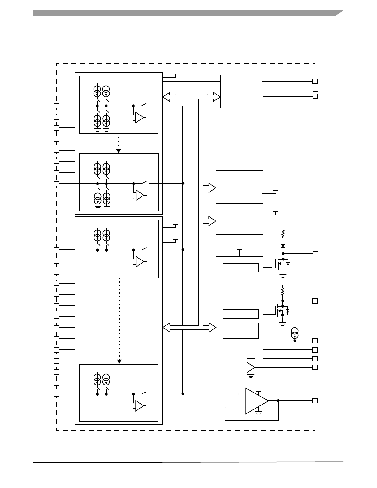
INTERNAL BLOCK DIAGRAM
5.0 V
V
PWR
PWR
4.0 V
Ref
Comparator
4.0 V
Ref
Comparator
4.0 V
Ref
Comparator
4.0 V
Ref
Comparator
+
–
+
–
+
–
+
–
SP0
To
SPI
SP7
To
SPI
SG0
To
SPI
SG13
To
SPI
5.0 V
V
V
, VDD, 5.0 V
PWR
POR
Bandgap
Sleep PWR
Oscillator
and
Clock Control
Temperature
Monitor and
Control
5.0 V
WAKE Control
SPI Interface
and Control
INT Control
MUX Interface
V
+
–
DD
V
DD
INTERNAL BLOCK DIAGRAM
VPWR
VDD
GND
5.0 V
V
PWR
5.0 V
5.0 V
125 kΩ
V
DD
125 kΩ
V
DD
40 µA
Analog Mux
Output
WAKE
INT
CS
SCLK
SI
SO
AMUX
Figure 2. 33972 Simplified Internal Block Diagram
33972
Analog Integrated Circuit Device Data
Freescale Semiconductor 3
Page 4
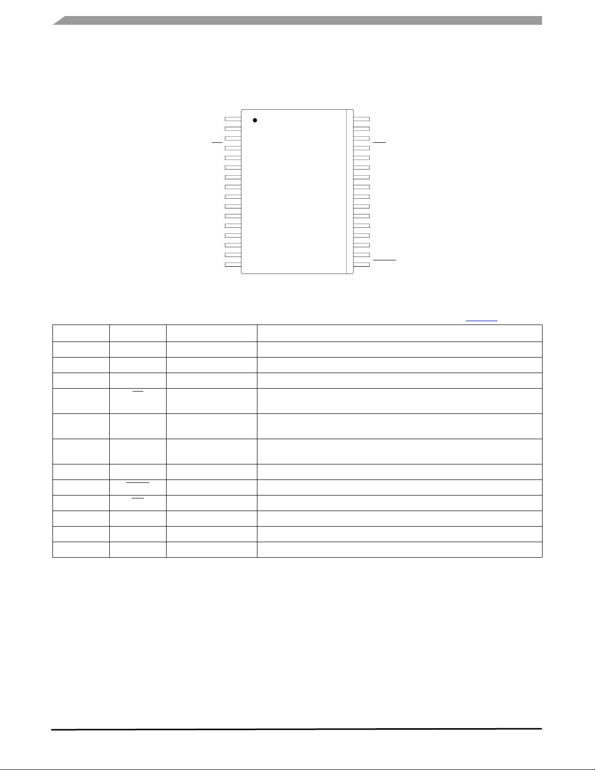
PIN CONNECTIONS
PIN CONNECTIONS
GND
SCLK
CS
SP0
SP1
SP2
SP3
SG0
SG1
SG2
SG3
SG4
SG5
SG6
VPWR
SI
1
2
3
4
5
6
7
8
9
10
11
12
13
14
15
16
32
31
30
29
28
27
26
25
24
23
22
21
20
19
18
17
SO
VDD
AMUX
INT
SP7
SP6
SP5
SP4
SG7
SG8
SG9
SG10
SG11
SG12
SG13
WAKE
Figure 3. 33972 Pin Connections
Table 2. 33972 Pin Definitions
A functional description of each pin can be found in the Functional Pin Description section beginning on page 10.
Pin Number Pin Name Formal Name Definition
1 GND Ground
2 SI SPI Slave In
3 SCLK Serial Clock
4 CS Chip Select
5 – 8
25
– 28
9 – 15,
18
– 24
SP0 – 3
SP4
– 7
SG0 – 6,
SG13
Programmable Switches
Switch-to-Ground Inputs
– 7
0
0
– 7
– 13
16 VPWR Battery Input
17 WAKE Wake-Up
29 INT Interrupt
30 AMUX Analog Multiplex Output
31 VDD Voltage Drain Supply
32 SO SPI Slave Out
Ground for logic, analog, and switch to battery inputs.
SPI control data input pin from MCU to 33972.
SPI control clock input pin.
SPI control chip select input pin from MCU to 33972. Logic [0} allows data to be
transferred in.
Programmable switch-to-battery or switch-to-ground input pins.
Switch-to-ground input pins.
Battery supply input pin. Pin requires external reverse battery protection.
Open drain wake-up output. Designed to control a power supply enable pin.
Open-drain output to MCU. Used to indicate input switch change of state.
Analog multiplex output.
3.3 / 5.0 V supply. Sets SPI communication level for SO driver.
Provides digital data from 33972 to MCU.
33972
Analog Integrated Circuit Device Data
4 Freescale Semiconductor
Page 5
ELECTRICAL CHARACTERISTICS
MAXIMUM RATINGS
ELECTRICAL CHARACTERISTICS
MAXIMUM RATINGS
Table 3. Maximum Ratings
All voltages are with respect to ground unless otherwise noted. Exceeding these ratings may cause a malfunction or
permanent damage to the device.
Ratings Symbol Value Unit
ELECTRICAL RATINGS
VDD Supply Voltage
CS, SI, SO, SCLK, INT, AMUX
(1)
WAKE
VPWR Supply Voltage
(1)
VPWR Supply Voltage at -40C
(1)
(1)
Switch Input Voltage Range
Frequency of SPI Operation (VDD = 5.0 V)
ESD Voltage
Human Body Model
(3)
(2)
Applies to all non-input pins
Machine Model
– -0.3 to 7.0
– -0.3 to 40 V
– -0.3 to 50 V
– -0.3 to 45 V
– -14 to 40 V
– 6.0 MHz
V
ESD
±2000
±2000
±200
Charge Device Model
Corner Pins
Interior Pins
750
500
THERMAL RATINGS
Operating Temperature
Ambient
Junction
Case
Storage Temperature
Power Dissipation (TA = 25°C)
(4)
T
T
A
T
J
T
C
STG
P
D
- 40 to 125
- 40 to 150
- 40 to 125
- 55 to 150 °C
1.7 W
Thermal Resistance
Junction to Ambient
Junction to Lead
Peak Package Reflow Temperature During Reflow
(5), (6)
R
R
T
JA
θ
JL
θ
PPRT
74
25
Note 6.
Notes
1. Exceeding these limits may cause malfunction or permanent damage to the device.
2. ESD data available upon request.
3. ESD1 testing is performed in accordance with the Human Body Model (C
in accordance with the Machine Model (C
= 200 pF, R
ZAP
ZAP
= 0 Ω).
= 100 pF, R
ZAP
= 1500 Ω), and ESD2 testing is performed
ZAP
4. Maximum power dissipation at TJ = 150°C junction temperature with no heat sink used.
5. Pin soldering temperature limit is for 10 seconds maximum duration. Not designed for immersion soldering. Exceeding these limits may
cause malfunction or permanent damage to the device.
6. Freescale’s Package Reflow capability meets Pb-free requirements for JEDEC standard J-STD-020C. For Peak Package Reflow
Temperature and Moisture Sensitivity Levels (MSL),
Go to www.freescale.com, search by part number [e.g. remove prefixes/suffixes and enter the core ID to view all orderable parts. (i.e.
MC33xxxD enter 33xxx), and review parametrics.
V
°C
°C/W
°C
DC
DC
DC
DC
DC
V
33972
Analog Integrated Circuit Device Data
Freescale Semiconductor 5
Page 6
ELECTRICAL CHARACTERISTICS
STATIC ELECTRICAL CHARACTERISTICS
STATIC ELECTRICAL CHARACTERISTICS
Table 4. Static Electrical Characteristics
Characteristics noted under conditions 3.1 V ≤ V
noted. Where applicable, typical values reflect the parameter’s approximate average value with V
Characteristic Symbol Min Typ Max Unit
POWER INPUT
Supply Voltage
Supply Voltage Range Quasi-Functional
Fully Operational
Supply Voltage Range Quasi-Functional
Supply Current
All Switches Open, Normal Mode, Tri-State Disabled
Sleep State Supply Current
Scan Timer = 64 ms, Switches Open
Logic Supply Voltage
Logic Supply Current
All Switches Open, Normal Mode
Sleep State Logic Supply Current
Scan Timer = 64 ms, Switches Open
SWITCH INPUT
Pulse Wetting Current Switch-to-Battery (Current Sink)
Pulse Wetting Current Switch-to-Ground (Current Source)
Sustain Current Switch-to-Battery Input (Current Sink)
Sustain Current Switch-to-Ground Input (Current Source)
Sustain Current Matching Between Channels on Switch-to-Ground I/Os
I
SUS(MAX)
I
-
I
SUS(MIN)
SUS(MIN)
X 100
(7)
(7)
≤ 5.25 V, 8.0 V ≤ V
DD
PWR
V
PWR (QF
V
PWR (FO
V
PWR (QF
I
PWR (ON
I
PWR (SS
V
DD
I
DD
I
DD(SS
I
PULSE
I
PULSE
I
SUSTAIN
I
SUSTAIN
I
MATCH
≤ 16 V, -40°C ≤ TC ≤ 125°C, unless otherwise
)
)
)
)
)
)
5.5
8.0
26
– 2.0 4.0
40 70 100
3.1 – 5.25 V
– 0.25 0.5
– 10 20
12 15 18 mA
12 16 18 mA
1.8 2.0 2.2 mA
1.8 2.0 2.2 mA
– 2.0 4.0
= 13 V, TA = 25°C.
PWR
–
–
–
8.0
26
38/40
V
mA
µA
mA
µA
%
Input Offset Current When Selected as Analog
Input Offset Voltage When Selected as Analog
V
(SP&SGINPUTS)
to AMUX Output
Analog Operational Amplifier Output Voltage
Sink 250 µA
Analog Operational Amplifier Output Voltage
Source 250 µA
Switch Detection Threshold
33972 / 33972A
Switch Input Voltage Range
33972
33972A
Temperature Monitor
Temperature Monitor Hysteresis
(8), (9)
(9)
I
OFFSET
V
OFFSET
V
OL
V
OH
V
TH
V
T
LIM
T
LIM(HYS)
-2.0 1.4 2.0 µA
mV
-10 2.5 10
mV
– 10 30
V
V
- 0.1 – –
DD
V
3.70 4.0 4.3
IN
-14
-14
–
–
38
40
V
155 – 185 °C
5.0 10 15 °C
Notes
7. Device operational. Table parameters may be out of specification.
8. Thermal shutdown of 16 mA pullup and pulldown current sources only. 2.0 mA current source / sink and all other functions remain active.
9. This parameter is guaranteed by design but is not production tested.
33972
Analog Integrated Circuit Device Data
6 Freescale Semiconductor
Page 7

STATIC ELECTRICAL CHARACTERISTICS
ELECTRICAL CHARACTERISTICS
Table 4. Static Electrical Characteristics (continued)
Characteristics noted under conditions 3.1 V ≤ V
≤ 5.25 V, 8.0 V ≤ V
DD
≤ 16 V, -40°C ≤ TC ≤ 125°C, unless otherwise
PWR
noted. Where applicable, typical values reflect the parameter’s approximate average value with V
Characteristic Symbol Min Typ Max Unit
DIGITAL INTERFACE
Input Logic Voltage Thresholds
SCLK, SI, Tri-State SO Input Current
0 V to VDD
CS Input Current
CS = V
DD
CS Pullup Current
CS = 0 V
SO High-State Output Voltage
I
SO (HIGH
= -200 µA
)
SO Low-State Output Voltage
I
SO (HIGH
= 1.6 mA
)
Input Capacitance on SCLK, SI, Tri-State SO
INT Internal Pullup Current
INT Voltage
INT = Open Circuit
INT Voltage
I
= 1.0 mA
INT
WAKE Internal Pullup Current
WAKE Voltage
WAKE = Open Circuit
WAKE Voltage
I
= 1.0 mA
WAKE
WAKE Voltage
Maximum Voltage Applied to WAKE Through External Pullup
Notes
10. Upper and lower logic threshold voltage levels apply to SI, CS, and SCLK.
11. This parameter is guaranteed by design but is not production tested.
(10)
(11)
V
INLOGIC
I
SCLK, ISI,
I
SO (TRI)
I
CS
0.8 – 2.2 V
-10 – 10
-10 – 10
I
CS
30 – 100
V
SO (HIGH
)
VDD - 0.8 – V
V
SO (LOW
)
– – 0.4
C
IN
– – 20 pF
– 15 40 100 µA
V
INT (HIGH)
VDD - 0.5 – V
V
INT (LOW)
– 0.2 0.4
I
WAKE (PU)
V
WAKE (HIGH)
20 40 100 µA
4.0 4.3 5.3
V
WAKE(LOW
)
– 0.2 0.4
V
WAKE(MAX
)
– – 40
= 13 V, TA = 25°C.
PWR
DD
DD
µA
µA
µA
V
V
V
V
V
V
V
33972
Analog Integrated Circuit Device Data
Freescale Semiconductor 7
Page 8
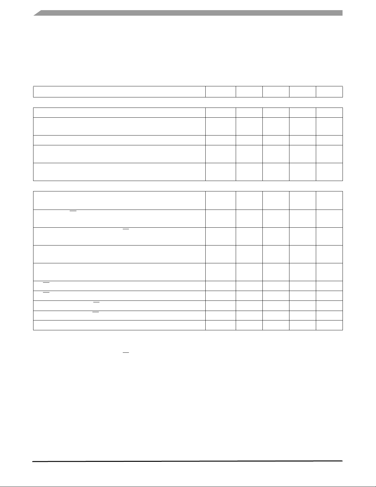
ELECTRICAL CHARACTERISTICS
DYNAMIC ELECTRICAL CHARACTERISTICS
DYNAMIC ELECTRICAL CHARACTERISTICS
Table 5. Dynamic Electrical Characteristics
Characteristics noted under conditions 3.1 V ≤ V
noted. Where applicable, typical values reflect the parameter’s approximate average value with V
Characteristic Symbol Min Typ Max Unit
SWITCH INPUT
Pulse Wetting Current Time
Interrupt Delay Time
Normal Mode
Sleep Mode Switch Scan Time
Calibrated Scan Timer Accuracy
Sleep Mode
Calibrated Interrupt Timer Accuracy
Sleep Mode
DIGITAL INTERFACE TIMING
Required Low-State Duration on V
V
≤ 0.2 V
PWR
Falling Edge of CS to Rising Edge of SCLK
Required Setup Time
Falling Edge of SCLK to Rising Edge of CS
Required Setup Time
SI to Falling Edge of SCLK
Required Setup Time
Falling Edge of SCLK to SI
Required Hold Time
SI, CS, SCLK Signal Rise Time
SI, CS, SCLK Signal Fall Time
Time from Falling Edge of CS to SO Low Impedance
Time from Rising Edge of CS to SO High Impedance
Time from Rising Edge of SCLK to SO Data Valid
Notes
12. These parameters are guaranteed by design. Production test equipment uses 4.16 MHz, 5.0 V SPI interface.
13. This parameter is guaranteed by design but not production tested.
14. Rise and Fall time of incoming SI, CS, and SCLK signals suggested for design consideration to prevent the occurrence of double pulsing.
15. Time required for valid output status data to be available on SO pin.
16. Time required for output states data to be terminated at SO pin.
17. Time required to obtain valid data out from SO following the rise of SCLK with 200 pF load.
(12)
(14)
(14)
PWR
for Reset
(13)
(17)
≤ 5.25 V, 8.0 V ≤ V
DD
(15)
(16)
≤ 16 V, -40°C ≤ TC ≤ 125°C, unless otherwise
PWR
t
PULSE (ON)
t
INT-DLY
15 16 20 ms
= 13 V, TA = 25°C.
PWR
– 5.0 16
t
SCAN
t
SCAN TIMER
100 200 300 µs
– – 10
t
INT TIMER
– – 10
t
RESET
– – 10
t
LEAD
100 – –
t
LAG
50 – –
t
SI (SU)
16 – –
t
SI (HOLD)
20 – –
t
R (SI)
t
F (SI)
t
SO (EN)
t
SO (DIS)
t
VALID
– 5.0 – ns
– 5.0 – ns
– – 55 ns
– – 55 ns
– 25 55 ns
µs
%
%
µs
ns
ns
ns
ns
33972
Analog Integrated Circuit Device Data
8 Freescale Semiconductor
Page 9
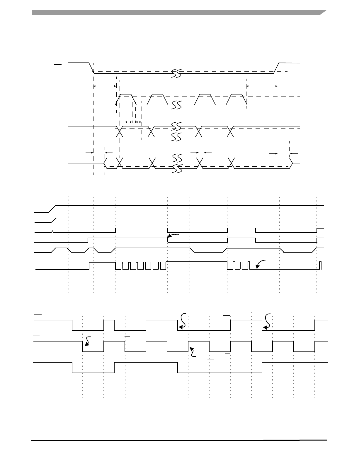
TIMING DIAGRAMS
ELECTRICAL CHARACTERISTICS
TIMING DIAGRAMS
VPWR
VDD
WAKE
INT
CS
CS
SCLK
SI
SO
t
SO(EN)
0.2 V
DD
0.7 V
0.2 V
t
LEAD
DD
DD
0.7 V
0.2 V
0.7 V
0.2 V
DD
DD
t
SI(SU)tSI(HOLD)
DD
MSB IN
DD
t
VALID
MSB OUT LSB OUT
t
LAG
t
SO(DIS)
Figure 4. SPI Timing Characteristics
Wake-Up From Interrupt
Timer Expire
SGn
Power-Up
Normal Mode
.
INT
CS
SGn
SGn Bit in SPI Word
Tri-State
Command
(Disable
Tri-State)
Command
Sleep Sleep Mode Normal
Command
Figure 5. Sleep Mode to Normal Mode Operation
Latch switch status
on falling edge of CS
Switch
Status
Switch
Status
Command
Figure 6. Normal Mode Interrupt Operation
Mode
Switch
Status
Command
Sleep Command
Switch state change with
CS LOW generates INT
Rising edge of CS does not
clear
INT because state change
occurred while CS
Switch closed “1”
1001
Switch
Status
Command
Sleep Mode
was LOW
Wake-Up From
Closed Switch
Normal
Mode
1
Switch
Status
Command
Sleep Command
Switch state change with
CS LOW generates INT
Switch open “0”
0
Switch
Status
Command
33972
Analog Integrated Circuit Device Data
Freescale Semiconductor 9
Page 10

FUNCTIONAL DESCRIPTION
INTRODUCTION
FUNCTIONAL DESCRIPTION
INTRODUCTION
The 33972 device is an integrated circuit designed to
provide systems with ultra-low quiescent sleep / wake-up
modes and a robust interface between switch contacts and a
microprocessor. The 33972 replaces many of the discrete
components required when interfacing to microprocessorbased systems while providing switch ground offset
protection, contact wetting current, and system wake-up.
The 33972 features 8-programmable switch-to-ground or
switch-to-battery inputs and 14 switch-to-ground inputs. All
FUNCTIONAL PIN DESCRIPTION
CHIP SELECT (CS)
The system MCU selects the 33972 to receive
communication using the chip select (
CS) pin. With the CS in
a logic LOW state, command words may be sent to the 33972
via the serial input (SI) pin, and switch status information can
be received by the MCU via the serial output (SO) pin. The
falling edge of
CS enables the SO output, latches the state of
the INT pin, and the state of the external switch inputs.
Rising edge of the CS initiates the following operation:
1. Disables the SO driver (high impedance)
2. INT pin is reset to logic [1], except when additional
switch changes occur during CS LOW. (See Figure 6
on page 9.)
3. Activates the received command word, allowing the
33972 to act upon new data from switch inputs.
To avoid any spurious data, it is essential the HIGH-to-
LOW and LOW-to-HIGH transitions of the
CS signal occur
only when SCLK is in a logic LOW state. Internal to the 33972
device is an active pullup to VDD on CS.
In Sleep mode the negative edge of CS (VDD applied) will
wake up the 33972 device. Data received from the device
CS wake-up may not be accurate.
during
SYSTEM CLOCK (SCLK)
The system clock (SCLK) pin clocks the internal shift
register of the 33972. The SI data is latched into the input
shift register on the falling edge of SCLK signal. The SO pin
shifts the switch status bits out on the rising edge of SCLK.
The SO data is available for the MCU to read on the falling
edge of SCLK. False clocking of the shift register must be
avoided to ensure validity of data. It is essential the SCLK pin
be in a logic LOW state whenever
For this reason, it is recommended, though not necessary,
that the SCLK pin is commanded to a logic LOW state as long
as the device is not accessed and
When the
CS is in a logic HIGH state, any signal on the SCLK
and SI pins will be ignored and the SO pin is tri-state.
CS makes any transition.
CS is in a logic HIGH state.
switch inputs may be read as analog inputs through the
analog multiplexer (AMUX). Other features include a
programmable wake-up timer, programmable interrupt timer,
programmable wake-up
/interrupt bits, and programmable
wetting current settings.
This device is designed primarily for automotive
applications but may be used in a variety of other applications
such as computer, telecommunications, and industrial
controls.
SPI SLAVE IN (SI)
The SI pin is used for serial instruction data input. SI
information is latched into the input register on the falling
edge of SCLK. A logic HIGH state present on SI will program
a one in the command word on the rising edge of the
signal. To program a complete word, 24
bits of information
CS
must be entered into the device.
SPI SLAVE OUT (SO)
The SO pin is the output from the shift register. The SO pin
remains tri-stated until the CS pin transitions to a logic LOW
state. All open switches are reported as zero, all closed
switches are reported as one. The negative transition of
CS
enables the SO driver.
The first positive transition of SCLK will make the status
24 available on the SO pin. Each successive positive
data bit
clock will make the next status data bit available for the MCU
to read on the falling edge of SCLK. The SI / SO shifting of the
data follows a first-in, first-out protocol, with both input and
output words transferring the most significant bit (MSB) first.
iNTERRUPT (INT)
The INT pin is an interrupt output from the 33972 device.
The INT pin is an open-drain output with an internal pullup to
. In Normal mode, a switch state change will trigger the
V
DD
INT pin (when enabled). The INT pin and INT bit in the SPI
register are latched on the falling edge of
MCU to determine the origin of the interrupt. When two 33972
devices are used, only the device initiating the interrupt will
have the INT
CS. The INT pin will not clear with rising edge of CS if a
of
bit set. The INT pin is cleared on the rising edge
switch contact change has occurred while
In a multiple 33972 device system with WAKE HIGH and
VDD on (Sleep mode), the falling edge of INT will place all
33972s in Normal mode.
CS. This permits the
CS was LOW.
33972
Analog Integrated Circuit Device Data
10 Freescale Semiconductor
Page 11

FUNCTIONAL DESCRIPTION
FUNCTIONAL PIN DESCRIPTION
WAKE-UP (WAKE)
The WAKE pin is an open-drain output and a wake-up
input. The pin is designed to control a power supply Enable
pin. In the Normal mode, the
WAKE pin is LOW. In the Sleep
mode, the WAKE pin is HIGH. The WAKE pin has a pullup to
the internal +
5.0 V supply.
In Sleep mode with the WAKE pin HIGH, falling edge of
WAKE will place the 33972 in Normal mode. In Sleep mode
with V
applied, the INT pin must be HIGH for negative edge
DD
of WAKE to wake up the device. If VDD is not applied to the
device in Sleep mode, INT does not affect WAKE operation.
BATTERY INPUT (VPWR)
The VPWR pin is battery input and Power-ON Reset to the
33972 IC. The VPWR pin requires external reverse battery
and transient protection. Maximum input voltage on VPWR is
V. All wetting, sustain, and internal logic current is
50
provided from the VPWR pin.
VOLTAGE DRAIN SUPPLY (VDD)
The VDD input pin is used to determine logic levels on the
microprocessor interface (SPI) pins. Current from VDD is
used to drive SO output and the pullup current for CS and INT
pins. VDD
CS or INT.
must be applied for wake-up from negative edge of
PROGRAMMABLE SWITCHES (SP0 : SP7)
The 33972 device has 8 switch inputs capable of being
programmed to read switch-to-ground or switch-to-battery
contacts. The input is compared with a 4.0
V reference.
When programmed to be switch-to-battery, voltages greater
than 4.0
V are considered closed. Voltages less than 4.0 V
are considered open. The opposite holds true when inputs
are programmed as switch-to-ground. Programming features
are defined in
Table 6 through Table 11 in the functional
Device Operation section of this datasheet beginning on
page 12. Voltages greater than the VPWR supply voltage will
source current through the SP inputs to the VPWR pin.
Transient battery voltages greater than 38/40 V must be
clamped by an external device.
SWITCH-TO-GROUND INPUTS (SG0 : SG13)
The SGn pins are switch-to-ground inputs only. The input
is compared with a 4.0 V reference. Voltages greater than
4.0 V are considered open. Voltages less than 4.0 V are
considered closed. Programming features are defined in
Table 6 through Table 11 in the functional Device Operation
section of this datasheet beginning on page 12. Voltages
greater than the VPWR supply voltage will source current
through the SG inputs to the VPWR pin. Transient battery
voltages greater than 40 V must be clamped by an external
device.
GROUND (GND)
The GND pin provides ground for the IC as well as ground
for inputs programmed as switch-to-battery inputs.
33972
Analog Integrated Circuit Device Data
Freescale Semiconductor 11
Page 12

FUNCTIONAL DEVICE OPERATION
OPERATIONAL MODES
FUNCTIONAL DEVICE OPERATION
OPERATIONAL MODES
MCU INTERFACE DESCRIPTION
The 33972 device directly interfaces to a 3.3 V or 5.0 V
microcontroller unit (MCU). SPI serial clock frequencies up to
MHz may be used for programming and reading switch
6.0
input status (production tested at 4.16
illustrates the configuration between an MCU and one 33972.
Serial peripheral interface (SPI) data is sent to the 33972
device through the SI input pin. As data is being clocked into
the SI pin, status information is being clocked out of the
device by the SO output pin. The response to a SPI
command will always return the switch status, interrupt flag,
and thermal flag. Input switch states are latched into the SO
register on the falling edge of the chip select (
Twenty-four bits are required to complete a transfer of
information between the 33972 and the MCU.
MC68HCXX
Microcontroller
MOSI SI
MISO SO
SCLK
Receive
Buffer
Parallel
Ports
Figure 7. SPI Interface with Microprocessor
Two or more 33972 devices may be used in a module
system. Multiple ICs may be SPI-configured in parallel or
serial. Figures 8 and 9 show the configurations. When using
the serial configuration, 48-clock cycles are required to
transfer data in
/ out of the ICs.
MHz). Figure 7
CS) pin.
33972
24-Bit Shift RegisterShift Register
To Logic
CS
INTINT
MC68HCXX
Microcontroller
Shift Register
Parallel
Ports
MOSI
MISO
SCLK
INT
33972
SI
SO
SCLK
CS
INT
33972
SI
SO
SCLK
CS
INT
Figure 8. SPI Parallel Interface with Microprocessor
MC68HCXX
Microcontroller
Shift Register
Parallel
Ports
MOSI
MISO
SCLK
INT
33972
SI
SO
SCLK
CS
INT
33972
SI
SO
SCLK
CS
INT
Figure 9. SPI Serial Interface with Microprocessor
33972
Analog Integrated Circuit Device Data
12 Freescale Semiconductor
Page 13

FUNCTIONAL DEVICE OPERATION
OPERATIONAL MODES
POWER SUPPLY
The 33972 is designed to operate from 5.5 V to 40 V on
the VPWR pin. Characteristics are provided from 8.0
V to
16 V for the device. Switch contact currents and the internal
logic supply are generated from the VPWR pin. The VDD
supply pin is used to set the SPI communication voltage
levels, current source for the SO driver, and pullup current on
INT and CS.
VDD supply may be removed from the device to reduce
quiescent current. If VDD is removed while the device is in
Normal mode, the device will remain in Normal mode. If VDD
is removed in Sleep mode, the device will remain in Sleep
mode until wake-up input is received (
WAKE HIGH to LOW,
switch input or interrupt timer expires).
Removing VDD from the device disables SPI
communication and will not allow the device to wake up from
INT and CS pins.
POWER-ON RESET (POR)
Applying V
and place the device in Normal mode.
Default settings from Power-ON Reset via V
Command are as follows:
• Programmable Switch – Set to Switch to Battery
• All Inputs Set as Wake-Up
• Wetting Current On (16 mA)
• Wetting Current Timer On (20 ms)
• All Inputs Tri-State
• Analog Select 00000 (No Input Channel Selected)
to the device will cause a Power-ON Reset
PWR
PWR
or Reset
NORMAL AND SLEEP MODES
The 33972 has two operating modes, Normal mode and
Sleep mode. A discussion on Normal mode begins below.
A discussion on Sleep mode begins on page 18.
Normal Mode
Normal mode may be entered by the following events:
• Application of V
• Change-of-Switch State (when enabled)
PWR
to the IC
• Falling Edge of WAKE
• Falling Edge of INT (with VDD = 5.0 V and WAKE at
Logic [1])
• Falling Edge of CS (with VDD = 5.0 V)
• Interrupt Timer Expires
Only in Normal mode with VDD applied can the registers of
the 33972 be programmed through the SPI.
The registers that may be programmed in Normal mode
are listed below. Further explanation of each register is
provided in subsequent paragraphs.
•Programmable Switch Register (Settings Command )
•Wake-Up / Interrupt Register (Wake-Up / Interrupt
Command )
•Wetting Current Register (Metallic Command )
•Wetting Current Timer Register (Wetting Current Timer
Enable Command )
•Tri-State Register (Tri-State Command )
•Analog Select Register (Analog Command )
•Calibration of Timers (Calibration Command )
•Reset (Reset Command )
Figure 6, page 9, is a graphical description of the device
operation in Normal mode. Switch states are latched into the
input register on the falling edge of
CS. The INT to the MCU
is cleared on the rising edge of CS. However, INT will not
clear on rising edge of CS if a switch has closed during SPI
communication (
CS LOW). This prevents switch states from
being missed by the MCU.
PROGRAMMABLE SWITCH REGISTER
Inputs SP0 to SP7 may be programmable for switch-tobattery or switch-to-ground. These inputs types are defined
using the settings command (
for switch-to-battery, a logic [1] for the appropriate bit must be
set. To set an SPn input for switch-to-ground, a logic [0] for
the appropriate bit must be set. The MCU may change or
update the Programmable Switch Register via software at
any time in Normal mode. Regardless of the setting, when the
SPn input switch is closed a logic
Serial Output Response Register (
Table 6). To set an SPn input
[1] will be placed in the
Table 17, page 18).
Table 6. Settings Command
Settings Command Not used Battery/Ground Select
23 22 21 20 19 18 17 16 15 14 13 12 11 10 9 8 7 6 5 4 3 2 1 0
0 0 0 0 0 0 0 1 X X X X X X X X sp7 sp6 sp5 sp4 sp3 sp2 sp1 sp0
WAKE-UP / INTERRUPT REGISTER
The Wake-Up / Interrupt Register defines the inputs that
are allowed to wake the 33972 from Sleep mode or set the
INT pin LOW in Normal mode. Programming the wake-up /
interrupt bit to logic [0] will disable the specific input from
generating an interrupt and will disable the specific input from
waking the IC in Sleep mode (
wake-up /interrupt bit to logic [1] will enable the specific input
to generate an interrupt with switch change of state and will
enable the specific input as wake-up. The MCU may change
or update the Wake-Up
time in Normal mode.
Table 7). Programming the
/ Interrupt Register via software at any
33972
Analog Integrated Circuit Device Data
Freescale Semiconductor 13
Page 14

FUNCTIONAL DEVICE OPERATION
OPERATIONAL MODES
Table 7. Wake-Up / Interrupt Command
Wake-Up /Interrupt Command Command Bits
23 22 21 20 19 18 17 16 15 14 13 12 11 10 9 8 7 6 5 4 3 2 1 0
0 0 0 0 0 0 1 0 X X X X X X X X sp7 sp6 sp5 sp4 sp3 sp2 sp1 sp0
0 0 0 0 0 0 1 1 X X sg13 sg12 sg11 sg10 sg9 sg8 sg7 sg6 sg5 sg4 sg3 sg2 sg1 sg0
WETTING CURRENT REGISTER
The 33972 has two levels of switch contact current, 16 mA
and 2.0 mA (see Figure 10). The metallic command is used
to set the switch contact current level (Table 8). Programming
the metallic bit to logic [0] will set the switch wetting current to
2.0 mA. Programming the metallic bit to logic [1] will set the
switch contact wetting current to 16 mA. The MCU may
change or update the Wetting Current Register via software
at any time in Normal mode.
Wetting current is designed to provide higher levels of
current during switch closure. The higher level of current is
designed to keep switch contacts from building up oxides that
form on the switch contact surface.
Switch Contact Voltage
16 mA Switch Wetting Current
2.0 mA Switch Sustain Current
20 ms Wetting Current Timer
Figure 10. Contact Wetting and Sustain Current
Table 8. Metallic Command
Metallic Command Command Bits
23 22 21 20 19 18 17 16 15 14 13 12 11 10 9 8 7 6 5 4 3 2 1 0
0 0 0 0 0 1 0 0 X X X X X X X X sp7 sp6 sp5 sp4 sp3 sp2 sp1 sp0
0 0 0 0 0 1 0 1 X X sg13 sg12 sg11 sg10 sg9 sg8 sg7 sg6 sg5 sg4 sg3 sg2 sg1 sg0
closed switch contact. With multiple wetting current timers
disabled, power dissipation for the IC must be considered.
WETTING CURRENT TIMER REGISTER
Each switch input has a designated 20 ms timer. The timer
starts when the specific switch input crosses the comparator
threshold (4.0
current is reduced from 16 mA to 2.0 mA. The wetting current
timer may be disabled for a specific input. When the timer is
disabled, 16
V). When the 20 ms timer expires, the contact
mA of current will continue to flow through the
The MCU may change or update the Wetting Current
Timer Register via software at any time in Normal mode. This
allows the MCU to control the amount of time wetting current
is applied to the switch contact. Programming the wetting
current timer bit to logic
[0] will disable the wetting current
timer. Programming the wetting current timer bit to logic [1]
will enable the wetting current timer (
Table 9).
Table 9. Wetting Current Timer Enable Command
Wetting Current Timer Commands Command Bits
23 22 21 20 19 18 17 16 15 14 13 12 11 10 9 8 7 6 5 4 3 2 1 0
0 0 0 0 0 1 1 1 X X X X X X X X sp7 sp6 sp5 sp4 sp3 sp2 sp1 sp0
0 0 0 0 1 0 0 0 X X sg13 sg12 sg11 sg10 sg9 sg8 sg7 sg6 sg5 sg4 sg3 sg2 sg1 sg0
TRI-STATE REGISTER
The tri-state command is use to set the SPn or SGn input
node as high impedance (
Register bit to logic [1], the input will be high impedance
33972
Table 10). By setting the Tri-State
regardless of the metallic command setting. The comparator
on each input remains active. This command allows the use
of each input as a comparator with a 4.0
V threshold. The
MCU may change or update the Tri-State Register via
software at any time in Normal mode.
Analog Integrated Circuit Device Data
14 Freescale Semiconductor
Page 15

FUNCTIONAL DEVICE OPERATION
OPERATIONAL MODES
Table 10. Tri-State Command
Tri-State Commands Command Bits
23 22 21 20 19 18 17 16 15 14 13 12 11 10 9 8 7 6 5 4 3 2 1 0
0 0 0 0 1 0 0 1 X X X X X X X X sp7 sp6 sp5 sp4 sp3 sp2 sp1 sp0
0 0 0 0 1 0 1 0 X X sg13 sg12 sg11 sg10 sg9 sg8 sg7 sg6 sg5 sg4 sg3 sg2 sg1 sg0
ANALOG SELECT REGISTER
The analog voltage on switch inputs may be read by the
MCU using the analog command (Table 11). Internal to the
IC is a 22-to-1 analog multiplexer. The voltage present on the
selected input pin is buffered and made available on the
AMUX output pin. The AMUX output pin is clamped to a
maximum of V
present on the input pin. After an input has been selected as
the analog, the corresponding bit in the next SO data stream
will be logic
analog, the user must also set the desired current (16
2.0 mA, or high impedance). Setting bit 6 and bit 5 to 0,0
volts regardless of the higher voltages
DD
[0]. When selecting a channel to be read as
mA,
selects the input as high impedance. Setting bit
0,1 selects 2.0 mA, and 1,0 selects 16 mA. Setting bit 6 and
5 to 1,1 in the Analog Select Register is not allowed and
bit
will place the input as an analog input with high impedance.
Analog currents set by the analog command are pullup
currents for all SGn and SPn inputs (Table 11). The analog
command does not allow pulldown currents on the SPn
inputs. Setting the current to 16 mA or 2.0 mA may be useful
for reading sensor inputs. Further information is provided in
Typical Applications section of this datasheet beginning
the
on page 20. The MCU may change or update the Analog
Select Register via software at any time in Normal mode.
6 and bit 5 to
Table 11. Analog Command
Analog Command Not used Current Select Analog Channel Select
23 22 21 20 19 18 17 16 15 14 13 12 11 10 9 8 7 6 5 4 3 2 1 0
0 0 0 0 0 1 1 0 X X X X X X X X X 16 mA 2.0 mA 0 0 0 0 0
33972
Analog Integrated Circuit Device Data
Freescale Semiconductor 15
Page 16

FUNCTIONAL DEVICE OPERATION
OPERATIONAL MODES
Table 12. Analog Channel
Bits 43210 Analog Channel Select
00000 No Input Selected
00001 SG0
00010 SG1
00011 SG2
00100 SG3
00101 SG4
00110 SG5
00111 SG6
01000 SG7
01001 SG8
01010 SG9
01011 SG10
01100 SG11
01101 SG12
01110 SG13
01111 SP0
10000 SP1
10001 SP2
10010 SP3
10011 SP4
10100 SP5
10101 SP6
10110 SP7
CALIBRATION OF TIMERS
In cases where an accurate time base is required, the user
may calibrate the internal timers using the calibration
command (
calibration command, the device expects 512 µs logic [0]
calibration pulse on the CS pin. The pulse is used to calibrate
the internal clock. No other SPI pins should transition during
Table 13). After the 33972 device receives the
this 512
frequency changes with temperature, calibration is required
for an accurate time base. Calibrating the timers has no affect
on the quiescent current measurement. The calibration
command simply makes the time base more accurate. The
calibration command may be used to update the device on a
periodic basis.
µs calibration pulse. Because the oscillator
Table 13. Calibration Command
Calibration Command Command Bits
23 22 21 20 19 18 17 16 15 14 13 12 11 10 9 8 7 6 5 4 3 2 1 0
0 0 0 0 1 0 1 1 X X X X X X X X X X X X X X X X
33972
Analog Integrated Circuit Device Data
16 Freescale Semiconductor
Page 17

FUNCTIONAL DEVICE OPERATION
OPERATIONAL MODES
RESET
The reset command resets all registers to Power-ON
Reset (POR) state. Refer to
Table 15, page 17, for POR
states or the paragraph entitled Power-ON Reset (POR) on
page 13 of this datasheet.
Table 14. Reset Command
Reset Command Command Bits
23 22 21 20 19 18 17 16 15 14 13 12 11 10 9 8 7 6 5 4 3 2 1 0
0 1 1 1 1 1 1 1 X X X X X X X X X X X X X X X X
SPI COMMAND SUMMARY
Table 15 below provides a comprehensive list of SPI
commands recognized by the 33972 and the reset state of
Output (SO) data for input voltages greater or less than the
threshold level. Open switches are always indicated with a
logic [0], closed switches are indicated with logic [1].
each register. Table 16 and Table 17 contain the Serial
Table 15. SPI Command Summary
MSB Command Bits Setting Bits LSBI
23 22 21 20 19 18 17 16 15 14 13 12 11 10 9 8 7 6 5 4 3 2 1 0
Switch Status
Command
Settings Command
Bat = 1, Gnd = 0
(Default state = 1)
Wake-Up/Interrupt Bit
Wake-Up = 1
Non-Wake-Up = 0
(Default state = 1)
Metallic Command
Metallic = 1
Non-metallic = 0
(Default state = 1)
Analog Command 0 0 0 0 0 1 1 0 X X X X X X X X X
Wetting Current Timer
Enable Command
Timer ON = 1
Timer OFF = 0
(Default state = 1)
Tri-State Command
Input Tri-State = 1
Input Active = 0
(Default state = 1)
Calibration Command
(Default state –
'uncalibrated)
Sleep Command
(Refer to Sleep Mode
on page 18.)
Reset Command 0 1 1 1 1 1 1 1 X X X X X X X X X X X X X X X X
SO Response Will
Always Send
0 0 0 0 0 0 0 0 X X X X X X X X X X X X X X X X
0 0 0 0 0 0 0 1 X X X X X X X X SP7 SP6 SP5 SP4 SP3 SP2 SP1 SP0
0 0 0 0 0 0 1 0 X X X X X X X X SP7 SP6 SP5 SP4 SP3 SP2 SP1 SP0
0 0 0 0 0 0 1 1 X X SG13 SG12 SG11 SG10 SG9 SG8 SG7 SG6 SG5 SG4 SG3 SG2 SG1 SG0
0 0 0 0 0 1 0 0 X X X X X X X X SP7 SP6 SP5 SP4 SP3 SP2 SP1 SP0
0 0 0 0 0 1 0 1 X X SG13 SG12 SG11 SG10 SG9 SG8 SG7 SG6 SG5 SG4 SG3 SG2 SG1 SG0
16mA02.0mA
0 0 0 0 0 1 1 1 X X X X X X X X SP7 SP6 SP5 SP4 SP3 SP2 SP1 SP0
0 0 0 0 1 0 0 0 X X SG13 SG12 SG11 SG10 SG9 SG8 SG7 SG6 SG5 SG4 SG3 SG2 SG1 SG0
0 0 0 0 1 0 0 1 X X X X X X X X SP7 SP6 SP5 SP4 SP3 SP2 SP1 SP0
0 0 0 0 1 0 1 0 X X SG13 SG12 SG11 SG10 SG9 SG8 SG7 SG6 SG5 SG4 SG3 SG2 SG1 SG0
0 0 0 0 1 0 1 1 X X X X X X X X X X X X X X X X
0 0 0 0 1 1 0 0 X X X X X X X X X X
them
int
flg
SP7 SP6 SP5 SP4 SP3 SP2 SP1 SP0 SG13 SG12 SG11 SG10 SG9 SG8 SG7 SG6 SG5 SG4 SG3 SG2 SG1 SG0
flg
0 0 0 0 0
0
int
int
timer
int
timer
timer
scan
timer
scan
timer
scan
timer
33972
Analog Integrated Circuit Device Data
Freescale Semiconductor 17
Page 18

FUNCTIONAL DEVICE OPERATION
OPERATIONAL MODES
Table 16. Serial Output (SO) Bit Data
Type of Input
SP Switch to Ground SPn < 4.0 V 1
SG N/A SGn < 4.0 V 1
Input
Programmed
Switch to Ground SPn > 4.0 V 0
Switch to Battery SPn < 4.0 V 0
Switch to Battery SPn > 4.0 V 1
N/A SGn > 4.0 V 0
Table 17. Serial Output (SO) Response Register
them
SO Response Will
Always Send
int
flg
SP7 SP6 SP5 SP4 SP3 SP2 SP1 SP0 SG13 SG12 SG11 SG10 SG9 SG8 SG7 SG6 SG5 SG4 SG3 SG2 SG1 SG0
flg
EXAMPLE OF NORMAL MODE OPERATION
The operation of the device in Normal Mode is defined by
the states of the programmable internal control registers. A
typical application may have the following settings:
• Programmable Switch – Set to Switch-to-Ground
• All Inputs Set as Wake-Up
• Wetting Current On (16 mA)
• Wetting Current Timer On (20 ms)
• All inputs Tri-State-Disabled (comparator is active)
• Analog select 00000 (no input channel selected)
With the device programmed as above, an interrupt will be
generated with each switch contact change of state (open-toclose or close-to-open) and 16
will be source for 20 ms. The INT pin will remain LOW until
switch status is acknowledged by the microprocessor. It is
critical to understand
INT will not be cleared on the rising
edge of CS if a switch closure occurs while CS is LOW. The
maximum duration a switch state change can exist without
acknowledgement depends on the software response time to
the interrupt.
Figure 6, page 9, shows the interaction
between changing input states and the INT and CS pins.
If desired the user may disable interrupts (wake up/
interrupt command) from the 33972 device and read the
switch states on a periodic basis. Switch activation and
deactivation faster than the MCU read rate will not be
acknowledged.
The 33972 device will exit the Normal mode and enter the
Sleep mode only with a valid sleep command.
mA of contact wetting current
Voltage on
Input Pin
SO SPI Bit
SLEEP MODE
Sleep mode is used to reduce system quiescent currents.
Sleep mode may be entered only by sending the sleep
command. All register settings programmed in Normal mode
will be maintained in Sleep mode.
The 33972 will exit Sleep mode and enter Normal mode
when any of the following events occur:
• Input Switch Change of State (when enabled)
• Interrupt Timer Expire
• Falling Edge of WAKE
• Falling Edge of INT (with VDD = 5.0 V and WAKE at
Logic [1])
• Falling Edge of CS (with VDD = 5.0 V)
• Power-ON Reset (POR)
The VDD supply may be removed from the device during
Sleep mode. However removing VDD from the device in Sleep
mode will disable a wake-up from falling edge of
Note In cases where CS is used to wake the device, the
first SO data message is not valid.
The sleep command contains settings for two
programmable timers for Sleep mode, the interrupt timer and
the scan timer, as shown in
Table 18 The interrupt timer is
used as a periodic wake-up timer. When the timer expires, an
interrupt is generated and the device enters Normal mode.
Note The interrupt timer in the 33972 device may be
disabled by programming the interrupt bits to logic
Table 19 shows the programmable settings of the Interrupt
timer.
INT and CS.
[1 1 1].
Table 18. Sleep Command
Sleep Command Command Bits
23 22 21 20 19 18 17 16 15 14 13 12 11 10 9 8 7 6 5 4 3 2 1 0
int timer
0 0 0 0 1 1 0 0 X X X X X X X X X X
33972
int timer
int timer
scan timer
scan timer
scan timer
Analog Integrated Circuit Device Data
18 Freescale Semiconductor
Page 19

FUNCTIONAL DEVICE OPERATION
OPERATIONAL MODES
Table 19. Interrupt Timer
Bits 543 Interrupt Period
000 32 ms
001 64 ms
010 128 ms
011 256 ms
100 512 ms
101 1.024 s
110 2.048 s
111 No interrupt wake-up
The scan timer sets the polling period between input
switch reads in Sleep mode. The period is set in the sleep
command and may be set to 000 (no period) to 111 (64 ms).
In Sleep mode when the scan timer expires, inputs will
behave as programmed prior to sleep command. The 33972
will wake up for approximately 125
inputs. At the end of the 125
µs and read the switch
µs, the input switch states are
compared with the switch state prior to sleep command.
When switch state changes are detected, an interrupt (when
enabled; refer to wake-up
/ interrupt command description on
page 14) is generated and the device enters Normal mode.
Without switch state changes, the 33972 will reset the scan
timer, inputs become tri-state, and the Sleep mode continues
until the scan timer expires again.
Table 20 shows the programmable settings of the Scan
timer.
Table 20. Scan Timer
Bits 210 Scan Period
000 No Scan
001 1.0 ms
010 2.0 ms
011 4.0 ms
100 8.0 ms
101 16 ms
110 32 ms
111 64 ms
Note The interrupt and scan timers are disabled in the
Normal mode.
Figure 5, page 9, is a graphical description of how the
33972 device exits Sleep mode and enters Normal mode.
Notice that the device will exit Sleep mode when the interrupt
timer expires or when a switch change of state occurs. The
falling edge of
INT triggers the MCU to wake from Sleep state.
Figure 11 illustrates the current consumed during Sleep
mode. During the 125 µs, the device is fully active and switch
states are read. The quiescent current is calculated by
integrating the normal running current over scan period plus
approximately 60
Inputs active for 125 us
Inputs active for 125 us
Inputs active for 125 us
out of 32 ms
out of 32 ms
out of 32 ms
µA.
I=V/R or 0.270V/100ohm = 2.7mA
I=V/R or 0.270V/100ohm = 2.7mA
I=V/R or 0.270V/100ohm = 2.7mA
I= V/R or 0.270 V/ 100 Ω =2.7 mA
Inputs active for
125 µs out of 32 ms
I=V/R or 6mV/100ohm = 60 uA
I=V/R or 6mV/100ohm = 60 uA
I=V/R or 6mV/100ohm = 60 uA
I=V/R or
6.0 mV/100 Ω=60 µA
Figure 11. Sleep Current Waveform
TEMPERATURE MONITOR
With multiple switch inputs closed and the device
programmed with the wetting current timers disabled,
considerable power will be dissipated by the IC. For this
reason temperature monitoring has been implemented. The
temperature monitor is active in the Normal mode only. When
the IC temperature is above the thermal limit, the temperature
monitor will do all of the following:
• Generate an interrupt.
• Force all 16 mA pullup and pulldown current sources to
revert to 2.0 mA current sources.
• Maintain the 2.0 mA current source and all other
functionality.
• Set the thermal flag bit in the SPI output register.
The thermal flag bit in the SPI word will be cleared on rising
edge of
the thermal limit. When die temperature has cooled below
thermal limit, the device will resume previously programmed
settings.
CS provided the die temperature has cooled below
33972
Analog Integrated Circuit Device Data
Freescale Semiconductor 19
Page 20

TYPICAL APPLICATIONS
INTRODUCTION
TYPICAL APPLICATIONS
INTRODUCTION
The 33972’s primary function is the detection of open or
closed switch contacts. However, there are many features
that allow the device to be used in a variety of applications.
The following is a list of applications to consider for the IC:
Sensor Power Supply
Switch Monitor for Metallic or Elastomeric Switches
Analog Sensor Inputs (Ratiometric)
Power MOSFET / LED Driver and Monitor
Multiple 33972 Devices in a Module System
The following paragraphs describe the applications in
detail.
SENSOR POWER SUPPLY
Each input may be used to supply current to sensors
external to a module. Many sensors such as Hall effect,
pressure sensors, and temperature sensors require a supply
voltage to power the sensor and provide an open collector or
analog output.
to supply power and interface to these types of sensors. In an
application where the input makes continuous transitions,
consider using the wake-up
the interrupt for the particular input.
VBAT
VBAT
16 mA
Hall-Effect
Sensor
Reg
X
Figure 12 shows how the 33972 may be used
/ interrupt command to disable
33972
SP0
SP1
SP7
SG0
SG1
16 2.0
mA
SG12
16 2.0
mA
SG13
V
PWRVPWR
V
PWRVPWR
mA
mA
2.5 k
Ω
V
PWR
V
WAKE
SCLK
CS
SO
INT
2.5 k
V
DD
DD
SI
Ω
MCU
MOSI
SCLK
CS
MISO
INT
IOC[7:0]
Input Capture
Timer Port
Figure 12. Sensor Power Supply
METALLIC / ELASTOMERIC SWITCH
Metallic switch contacts often develop higher contact
resistance over time owing to contact corrosion. The
corrosion is induced by humidity, salt, and other elements
that exist in the environment. For this reason the 33972
provides two settings for contacts. When programmed for
metallic switches, the device provides higher wetting current
to keep switch contacts free of oxides. The higher current
occurs for the first 20
ms of switch closure. Where longer
duration of wetting current is desired, the user may send the
wetting current timer command and disable the timer. Wetting
current will be continuous to the closed switch. After the time
period set by the MCU, the wetting current timer command
may be sent again to enable the timer. The user must
consider power dissipation on the device when disabling the
timer. (Refer to the paragraph entitled
Temperature Monitor,
page 19.)
To increase the amount of wetting current for a switch
contact, the user has two options. Higher wetting current to a
switch may be achieved by paralleling SGn or SPn inputs.
This will increase wetting current by 16
mA for each input
added to the switch contact. The second option is to simply
add an external resistor pullup to the V
supply for switch-
PWR
to-ground inputs or a resistor to ground for a switch-to-battery
input. Adding an external resistor has no effect on the
operation of the device.
Elastomeric switch contacts are made of carbon and have
a high contact resistance. Resistance of 1.0
kΩ is common.
In applications with elastomeric switches, the pullup and
pulldown currents must be reduced to prevent excessive
power dissipation at the contact. Programming for a lower
current settings is provided in the
functional Device
Operation Section beginning on page 12 under Table 8,
Metallic Command.
ANALOG SENSOR INPUTS (RATIOMETRIC)
The 33972 features a 22-to-1 analog multiplexer. Setting
the binary code for a specific input in the analog command
allows the microcontroller to perform analog to digital
conversion on any of the 22 inputs. On rising edge of
multiplexer connects a requested input to the AMUX pin. The
AMUX pin is clamped to max of VDD volts regardless of the
higher voltages present on the input pin. After an input has
been selected as the analog, the corresponding bit in the next
SO data stream will be logic
[0].
The input pin, when selected as analog, may be
configured as analog with high impedance, analog with
mA pullup, or analog with 16 mA pullup. Figure 13,
2.0
page 21, shows how the 33972 may be used to provide a
ratiometric reading of variable resistive input.
CS the
33972
Analog Integrated Circuit Device Data
20 Freescale Semiconductor
Page 21

VBAT
SP0
SP1
VBAT
SP7
SG0
SG1
I
1
2.0 mA
R
Analog Sensor
or Analog Switch
SG12
1
SG13
2.0 mA
33972
V
V
PWR
16 2.0
mA
V
V
PWR
16
mA
I
2
4.54 V to 5.02 V
Ω
2.39 k
0.1%
PWR
PWR
mA
2.0
mA
TYPICAL APPLICATIONS
INTRODUCTION
conversion may be obtained. Using the equation yields the
following:
V
PWR
V
WAKE
SCLK
CS
SO
INT
AMUX
ADC =
V
DD
DD
MCU
ADC =
I1 x R1
I2 x R2
2.0 mA x 2.0 kΩ
2.0 mA x 2.39 kΩ
ADC = 213 counts
SI
MOSI
SCLK
CS
MISO
INT
AN0
Analog
Ports
The ADC value of 213 counts is the value with 0% error
(neglecting the resistor tolerance and AMUX input offset
voltage). Now we can calculate the count value induced by
the mismatch in current sources. From a sample device the
maximum current source was measured at 2.05
minimum current source was measured at 1.99
yields 3% error in A
/ D conversion. The A / D measurement
x225
x 225
mA and
mA. This
will be as follows:
ADC =
V
R
2
REF(H)
V
REF(L)
This A / D conversion is 3% low in value. The error
1.99 mA x 2.0 kΩ
2.05 mA x 2.39 kΩ
ADC = 207 counts
x225
correction factor of 1.03 may be used to correct the value:
Figure 13. Analog Ratiometric Conversion
To read a potentiometer sensor, the wiper should be
grounded and brought back to the module ground, as
illustrated in Figure 13. With the wiper changing the
impedance of the sensor, the analog voltage on the input will
represent the position of the sensor.
Using the Analog feature to provide 2.0 mA of pullup
current to an analog sensor may induce error due to the
accuracy of the current source. For this reason, a ratiometric
conversion must be considered. Using two current sources
(one for the sensor and one to set the reference voltage to the
/ D converter) will yield a maximum error (owing to the
A
33972) of 4%.
Higher accuracy may be achieved through module level
calibration. In this example, we use the resistor values from
Figure 13 and assume the current sources are 4% from each
other. The user may use the module end-of-line tester to
calculate the error in the A / D conversion. By placing a
kΩ, 0.1% resistor in the end-of-line test equipment and
2.0
assuming a perfect 2.0 mA current source from the 33972, a
calculated A
/ D
ADC = 207 counts x 1.03
ADC = 213 counts
An error correction factor may then be stored in E2
memory and used in the A / D calculation for the specific input.
Each input used as analog measurement will have a
dedicated calibrated error correction factor.
POWER MOSFET / LED DRIVER AND MONITOR
Because of the flexible programming of the 33972 device,
it may be used to drive small loads like LEDs or MOSFET
gates. It was specifically designed to power up in the Normal
mode with the inputs tri-state. This was done to ensure the
LEDs or MOSFETs connected to the 33972 power up in the
off-state. The Switch Programmable (SP0
a source-and-sink capability, providing effective MOSFET
gate control. To complete the circuit, a pulldown resistor
should be used to keep the gate from floating during the
Sleep modes.
Figure 14, page 22, shows an application
where the SG0 input is used to monitor the drain-to-source
voltage of the external MOSFET. The 1.5
to set the drain-to-source trip voltage. With the 2.0 mA
current source enabled, an interrupt will be generated when
the drain-to-source voltage is approximately 1.0
– SP7) inputs have
kΩ resistor is used
V.
33972
Analog Integrated Circuit Device Data
Freescale Semiconductor 21
Page 22

TYPICAL APPLICATIONS
INTRODUCTION
VBAT
LOAD
1.5 kΩ
100 kΩ
SG0
SP0
SG13
V
V
PWR
PWR
16
mA
4.0 V Ref
V
V
PWR
PWR
16
mA
4.0 V
V
PWR
V
PWR
4.0 V Ref
Ref
2.0 mA
mA
16
mA
16 2.0
mA
2.0
mA
+
-
Comparator
2.0
mA
+
-
Comparator
+
-
Comparator
SG0
AMUX
To SPI
SG0
To SPI
SG13
To SPI
Figure 14. MOSFET or LED Driver Output
The sequence of commands (from Normal mode with
inputs tri-state) required to set up the device to drive a
MOSFET are as follows:
• wetting current timer enable command – Disable SPn
wetting current timer (refer to Table 9, page 14).
• metallic command – Set SPn to 16 mA or 2.0 mA gate
drive current (refer to Table 8, page 14).
• settings command – Set SPn as switch-to-battery (refer
Table 6, page 13).
to
• tri-state command – Disable tri-state for SPn (refer to
Table 10, page 15).
After the tri-state command has been sent (tri-state
disable), the MOSFET gate will be pulled to ground. From this
point forward the MOSFET may be turned on and off by
sending the settings command
:
• settings command – SPn as switch-to-ground
(MOSFET ON).
• settings command – SPn as switch-to-battery
(MOSFET OFF).
Monitoring of the MOSFET drain in the OFF state provides
open load detection. This is done by using an SGn input
comparator. With the SGn input in tri-state, the load will pull
up the SGn input to battery. With open load the SGn pin is
pulled down to ground through an external resistor. The open
load is indicated by a logic
[1] in the SO data bit.
The analog command may be used to monitor the drain
voltage in the MOSFET ON state. By sourcing 2.0 mA of
current to the 1.5 kΩ resistor, the analog voltage on the SGn
pin will be approximately:
V
= I
SGn
x 1.5 kΩ + V
SGn
DS
As the voltage on the drain of the MOSFET increases, so
does the voltage on the SGn pin. With the SGn pin selected
as analog, the MCU may perform the A
/ D conversion.
Using this method for controlling unclamped inductive
loads is not recommended. Inductive flyback voltages greater
than V
may damage the IC.
PWR
The SP0 : SP7 pins of this device may also be used to send
signals from one module to another. Operation is similar to
the gate control of a MOSFET.
• For LED applications a resistor in series with the LED is
recommended but not required. The switch-to-ground
inputs are recommended for LED application. To drive
the LED use the following commands:
• wetting current timer enable command – Disable SGn
wetting current timer.
• metallic command – Set SGn to 16 mA.
From this point forward the LED may be turned on and off
using the tri-state command :
• tri-state command – Disable tri-state for SGn (LED ON).
• tri-state command – Enable tri-state for SGn (LED
OFF).
These parameters are easily programmed via SPI
commands in Normal mode.
MULTIPLE 33972 DEVICES IN A MODULE SYSTEM
Connecting power to the 33972 and the MCU for Sleep
mode operation may be done in several ways. Table 21
shows several system configurations for power between the
MCU and the 33972 and their specific requirements for
functionality.
Table 21. Sleep Mode Power Supply
MCU
5.0 V 5.0 V
5.0 V 0 V
SPI control may be done in parallel or serial. However when
parallel mode is used, each device is addressed
independently (refer to
33972
V
DD
V
DD
Comments
All wake-up conditions apply. (Refer to Sleep
Mode, page 18.)
SPI wake-up is not possible.
0 V 5.0 V
Sleep mode not possible. Current from CS
pullup will flow through MCU to V
been switched off. Negative edge of
that has
DD
CS will put
33972 in Normal mode.
0 V 0 V
SPI wake-up is not possible.
Multiple 33972 devices may be used in a module system.
MCU Interface Description, page 12).
33972
Analog Integrated Circuit Device Data
22 Freescale Semiconductor
Page 23

TYPICAL APPLICATIONS
INTRODUCTION
Therefore when sending the sleep command, one device will
enter sleep before the other. For multiple devices in a system,
it is recommended that the devices are controlled in serial (S0
from first device is connected to SI of second device). With
two devices, 48
clock pulses are required to shift data in.
When the WAKE feature is used to enable the power supply,
WAKE pins should be connected to the enable pin on the
both
power supply. The
INT pins may be connected to one
interrupt pin on the MCU or may have their own dedicated
interrupt to the MCU.
The transition from Normal to Sleep mode is done by
sending the sleep command. With the devices connected in
serial and the sleep command sent, both will enter Sleep
mode on the rising edge of
CS. When Sleep mode is entered,
the WAKE pin will be logic [1]. If either device wakes up, the
WAKE pin will transition LOW, waking the other device.
A condition exists where the MCU is sending the sleep
command (CS logic [0]) and a switch input changes state.
With this event the device that detects this input will not
transition to Sleep mode, while the second device will enter
Sleep mode. In this case two switch status commands must
be sent to receive accurate switch status data. The first
switch status command will wake the device in Sleep mode.
Switch status data may not be valid from the first switch
status command because of the time required for the input
voltage to rise above the 4.0
V input comparator threshold.
This time is dependant on the impedance of SGn or SPn
node. The second switch status command will provide
accurate switch status information. It is recommended that
software wait 10
ms to 20 ms between the two switch status
commands, allowing time for switch input voltages to
stabilize. With all switch states acknowledged by the MCU,
the sleep sequence may be initiated. All parameters for Sleep
mode should be updated prior to sending the sleep
command.
The 33972 IC has an internal 5.0 V supply from V
PWR
pin.
A POR circuit monitors the internal 5.0 V supply. In the event
of transients on the V
pin, an internal reset may occur.
PWR
Upon reset the 33972 will enter Normal mode with the
internal registers as defined in
Table 15, page 17. Therefore
it is recommended that the MCU periodically update all
registers internal to the IC.
USING THE WAKE FEATURE
The 33972 provides a WAKE output and wake-up input
designed to control an enable pin on system power supply.
While in the Normal mode, the
WAKE output is LOW,
enabling the power supply. In the Sleep mode, the WAKE pin
is HIGH, disabling the power supply. The WAKE pin has a
passive pullup to the internal 5.0
up through a resistor to V
V supply but may be pulled
supply (see Figure 16,
PWR
page 24)
When the WAKE output is not used the pin should be
pulled up to the V
supply through a resistor as shown in
DD
Figure 15, page 24.
During the Sleep mode, a switch closure will set the WAKE
pin LOW, causing the 33972 to enter the Normal mode. The
power supply will then be activated, supplying power to the
pin and the microprocessor and the 33972. The
V
DD
microprocessor can determine the source of the wake-up by
reading the interrupt flag.
COST AND FLEXIBILITY
Systems requiring a significant number of switch
interfaces have many discrete components. Discrete
components on standard PWB consume board space and
must be checked for solder joint integrity. An integrated
approach reduces solder joints, consumes less board space,
and offers wider operating voltage, analog interface
capability, and greater interfacing flexibility.
33972
Analog Integrated Circuit Device Data
Freescale Semiconductor 23
Page 24

TYPICAL APPLICATIONS
INTRODUCTION
VBAT
VBAT
VBAT
SP0
SP1
33972
VPWR
VDD
V
PWR
V
DD
V
Power
DD
Supply
V
DD
VBAT
VBAT
SP7
SG0
SG1
SG12
SG13
SP0
SP1
WAKE
CS
INT
SI
SO
SCLK
AMUX
Figure 15. Power Supply Active in Sleep Mode
Power
Supply
33972
V
PWR
Enable
VPWR
MC68HCXX
Microprocessor
CS
INT
MOSI
MISO
SCLK
AN0
V
DD
V
DD
V
VBAT
SP7
SG0
SG1
SG12
SG13
WAKE
VDD
CS
INT
SI
SO
SCLK
AMUX
DD
MC68HCXX
Microprocessor
CS
INT
MOSI
MISO
SCLK
AN0
Figure 16. Power Supply Shutdown in Sleep Mode
33972
Analog Integrated Circuit Device Data
24 Freescale Semiconductor
Page 25

PACKAGE DIMENSIONS
PACKAGING
PACKAGE DIMENSIONS
For the most current package revision, visit www.freescale.com and perform a keyword search using the 98A listed below.
PACKAGING
DWB SUFFIX
EW SUFFIX (Pb-FREE)
32-LEAD SOIC WIDE BODY
PLASTIC PACKAGE
98ARH99137A
33972
Analog Integrated Circuit Device Data
Freescale Semiconductor 25
Page 26

PACKAGING
PACKAGE DIMENSIONS (CONTINUED)
PACKAGE DIMENSIONS (CONTINUED)
33972
Analog Integrated Circuit Device Data
26 Freescale Semiconductor
Page 27

REVISION HISTORY
REVISION DATE DESCRIPTION OF CHANGES
4.0
5.0
6.0
7.0
8.0
9.0
2/2006
6/2006
7/2006
11/2006
12/2006
4/2007
• Converted to Freescale format
• Added PC33972A version
• Changed Figure 15, Power Supply Active in Sleep Mode
• Changed Figure 16, Power Supply Shutdown in Sleep Mode
• Updated Outline Drawing for package
• Update to the prevailing Freescale form and style.
• Added MC33972T devices.
• Updated StatiC Electrical Characteristics on page 6 with 33972T parameters.
• Changed Human Body Model parameters in Maximum Ratings table.
• Replaced Part Number MC33972TEW/R2 with MCZ33972TEW/R2
• Removed Peak Package Reflow Temperature During Reflow (solder reflow) parameter
Maximum Ratings on page 5. Added note with instructions to obtain this information
from
from www.freescale.com.
• Restated note
(6)
• Changed Part Number MCZ33972TEW/R2 with MC33972TEW/R2
• Removed all references to the 33972T device.
• Removed the MC33972TDWB/R2, MC33972TEW/R2, and PC33972AEW/R2 from the
ordering information.
• Added MCZ33972AEW/R2 to the ordering information.
REVISION HISTORY
33972
Analog Integrated Circuit Device Data
Freescale Semiconductor 27
Page 28

How to Reach Us:
Home Page:
www.freescale.com
Web Support:
http://www.freescale.com/support
USA/Europe or Locations Not Listed:
Freescale Semiconductor, Inc.
Technical Information Center, EL516
2100 East Elliot Road
Tempe, Arizona 85284
+1-800-521-6274 or +1-480-768-2130
www.freescale.com/support
Europe, Middle East, and Africa:
Freescale Halbleiter Deutschland GmbH
Technical Information Center
Schatzbogen 7
81829 Muenchen, Germany
+44 1296 380 456 (English)
+46 8 52200080 (English)
+49 89 92103 559 (German)
+33 1 69 35 48 48 (French)
www.freescale.com/support
Japan:
Freescale Semiconductor Japan Ltd.
Headquarters
ARCO Tower 15F
1-8-1, Shimo-Meguro, Meguro-ku,
Tokyo 153-0064
Japan
0120 191014 or +81 3 5437 9125
support.japan@freescale.com
Asia/Pacific:
Freescale Semiconductor Hong Kong Ltd.
Technical Information Center
2 Dai King Street
Tai Po Industrial Estate
Tai Po, N.T., Hong Kong
+800 2666 8080
support.asia@freescale.com
For Literature Requests Only:
Freescale Semiconductor Literature Distribution Center
P.O. Box 5405
Denver, Colorado 80217
1-800-441-2447 or 303-675-2140
Fax: 303-675-2150
LDCForFreescaleSemiconductor@hibbertgroup.com
RoHS-compliant and/or Pb-free versions of Freescale products have the functionality
and electrical characteristics of their non-RoHS-compliant and/or non-Pb-free
counterparts. For further information, see http://www.freescale.com or contact your
Freescale sales representative.
For information on Freescale’s Environmental Products program, go to http://
www.freescale.com/epp.
Information in this document is provided solely to enable system and software
implementers to use Freescale Semiconductor products. There are no express or
implied copyright licenses granted hereunder to design or fabricate any integrated
circuits or integrated circuits based on the information in this document.
Freescale Semiconductor reserves the right to make changes without further notice to
any products herein. Freescale Semiconductor makes no warranty, representation or
guarantee regarding the suitability of its products for any particular purpose, nor does
Freescale Semiconductor assume any liability arising out of the application or use of any
product or circuit, and specifically disclaims any and all liability, including without
limitation consequential or incidental damages. “Typical” parameters that may be
provided in Freescale Semiconductor data sheets and/or specifications can and do vary
in different applications and actual performance may vary over time. All operating
parameters, including “Typicals”, must be validated for each customer application by
customer’s technical experts. Freescale Semiconductor does not convey any license
under its patent rights nor the rights of others. Freescale Semiconductor products are
not designed, intended, or authorized for use as components in systems intended for
surgical implant into the body, or other applications intended to support or sustain life,
or for any other application in which the failure of the Freescale Semiconductor product
could create a situation where personal injury or death may occur. Should Buyer
purchase or use Freescale Semiconductor products for any such unintended or
unauthorized application, Buyer shall indemnify and hold Freescale Semiconductor and
its officers, employees, subsidiaries, affiliates, and distributors harmless against all
claims, costs, damages, and expenses, and reasonable attorney fees arising out of,
directly or indirectly, any claim of personal injury or death associated with such
unintended or unauthorized use, even if such claim alleges that Freescale
Semiconductor was negligent regarding the design or manufacture of the part.
Freescale™ and the Freescale logo are trademarks of Freescale Semiconductor, Inc.
All other product or service names are the property of their respective owners.
© Freescale Semiconductor, Inc., 2007. All rights reserved.
MC33972
Rev. 9.0
4/2007
 Loading...