

查询MC33889DDW供应商
Freescale Semiconductor
Technical Data
System Basis Chip with Low
Document Number: MC33889
Rev. 12.0, 3/2007
Speed Fault Tolerant CAN
Interface
An SBC device is a monolithic IC combining many functions
repeatedly found in standard microcontroller-based systems, e.g.,
protection, diagnostics, communication, power, etc. The 33889 is an
SBC having fully protected, fixed 5.0
current limit, over-temperature pre-warning and reset.
An output drive with sense input is also provided to implement a
second 5.0
V regulator using an external PNP. The 33889 has Normal,
Standby, Stop and Sleep modes; an internally switched high-side
power supply output with two wake-up inputs; programmable timeout
or window watchdog, Interrupt, Reset, SPI input control, and a lowspeed fault tolerant CAN transceiver, compatible with CAN 2.0 A and
B protocols for module-to-module communications. The combination
is an economical solution for power management, high-speed
communication, and control in MCU-based systems.
Features
• VDD1: 5.0 V low drop voltage regulator, current limitation,
overtemperature detection, monitoring and reset function with total
current capability 200
mA
•V2: tracking function of VDD1 regulator; control circuitry for external
bipolar ballast transistor for high flexibility in choice of peripheral
voltage and current supply
• Four operational modes
• Low standby current consumption in Stop and Sleep modes
• Built-in low speed 125 kbps fault tolerant CAN physical interface.
• External high voltage wake-up input, associated with HS1 VBAT
switch
•150 mA output current capability for HS1 VBAT switch allowing
drive of external switches pull-up resistors or relays
• Pb-Free Packaging Designated by Suffix Code EG
V low drop-out regulator, with
33889
SYSTEM BASIS CHIP
DW SUFFIX
EG SUFFIX (PB-FREE)
PLASTIC PACKAGE
98ASB42345B
28-PIN SOICW
ORDERING INFORMATION
Device
MC33889BDW/R2
MCZ33889BEG/R2
MC33889DDW/R2
*MCZ33889DEG/R2
*Recommended for new designs
Temperature
Range (T
-40°C to 125°C 28 SOICW
)
A
Package
V
PWR
33889
VDD1
GND
RST
INT
CS
SCLK
MOSI
MISO
TXD
RXD
MCU
SCLK
MOSI
MISO
5.0 V
CS
SPI
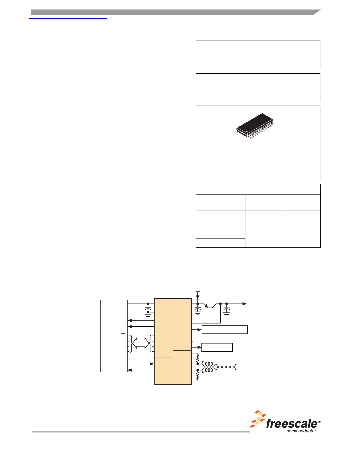
Figure 1. 33889 Simplified Application Diagram
Freescale Semiconductor, Inc. reserves the right to change the detail specifications, as
may be required, to permit improvements in the design of its products.
© Freescale Semiconductor, Inc., 2007. All rights reserved.
VSUP
V2CTRL
V2
HS1
WDOG
RTH
CANH
CANL
RTL
L0
Wake-Up Inputs
L1
Local Module Supply
Safe Circuits
Twisted
Pair
V
CAN Bus
2
DEVICE VARIATIONS
DEVICE VARIATIONS
Table 1. Device Variations Between the 33889D and 33889B Versions
(1)
Device Part Number
Parameters Symbol Trait
Differential Receiver, Recessive To Dominant Threshold
(By Definition, V
DIFF
= V
CANH-VCANL
)
V
DIFF1
MC33889B
Min 3.2 V 3.5 V
Typ 2.6 V 3.0 V
(2)
MC33889D
Max 2.1 V 2.5 V
Differential Receiver, Dominant To Recessive Threshold
(Bus Failures 1, 2, 5)
V
DIFF2
Min 3.2 V 3.5 V
Typ 2.6 V 3.0 V
Max 2.1 V 2.5 V
CANH Output Current (V
= 0; TX = 0.0)
CANH
I
CANH
Min 50 mA 50 mA
Typ 75 mA 100 mA
Max 110 mA 130 mA
CANL Output Current (V
= 14 V; TX = 0.0)
CANL
I
CANL
Min 50 mA 50 mA
Typ 90 mA 140 mA
Max 135 mA 170 mA
Detection threshold for Short circuit to Battery voltage
loop time Tx to Rx, no bus failure, ISO configuration
loop time Tx to Rx, with bus failure, ISO configuration
loop time Tx to Rx, with bus failure and +-1.5V gnd shift,
5
node network, ISO configuration
Minimum Dominant time for Wake up on CANL or CANH
(Tem Vbat mode)
Vcanh max Vsup/2 + 5V Vsup/2 + 4.55V
tLOOPRD max N/A 1.5us
tLOOPRD-F max N/A 1.9us
tLOOPRD/DR-F+GS N/A 3.6us
tWAKE min N/A 8
typ 30 16
max N/A 30
T2SPI timing
T2spi min not specified, 25us
25us
spec applied
DEVICE BEHAVIOR
CANH or CANL open wire recovery principle
Rx behavior in TermVbat mode
Reference MC33889B: on page
33
after 4 non
consecutive pulses
after 4 consecutive
pulses
Reference MC33889D: on page 34Rx recessive, no pulse Rx recessive, dominant
pulse to signal bus
traffic
Notes
1. This datasheet uses the term 33889 in the inclusive sense, referring to both the D version (33889D) and the B version (33689B).
2. The 33889D and 33889B versions are nearly identical. However, where variations in characteristic occur, these items will be separated
onto individual lines.
(2)
33889
Analog Integrated Circuit Device Data
2 Freescale Semiconductor
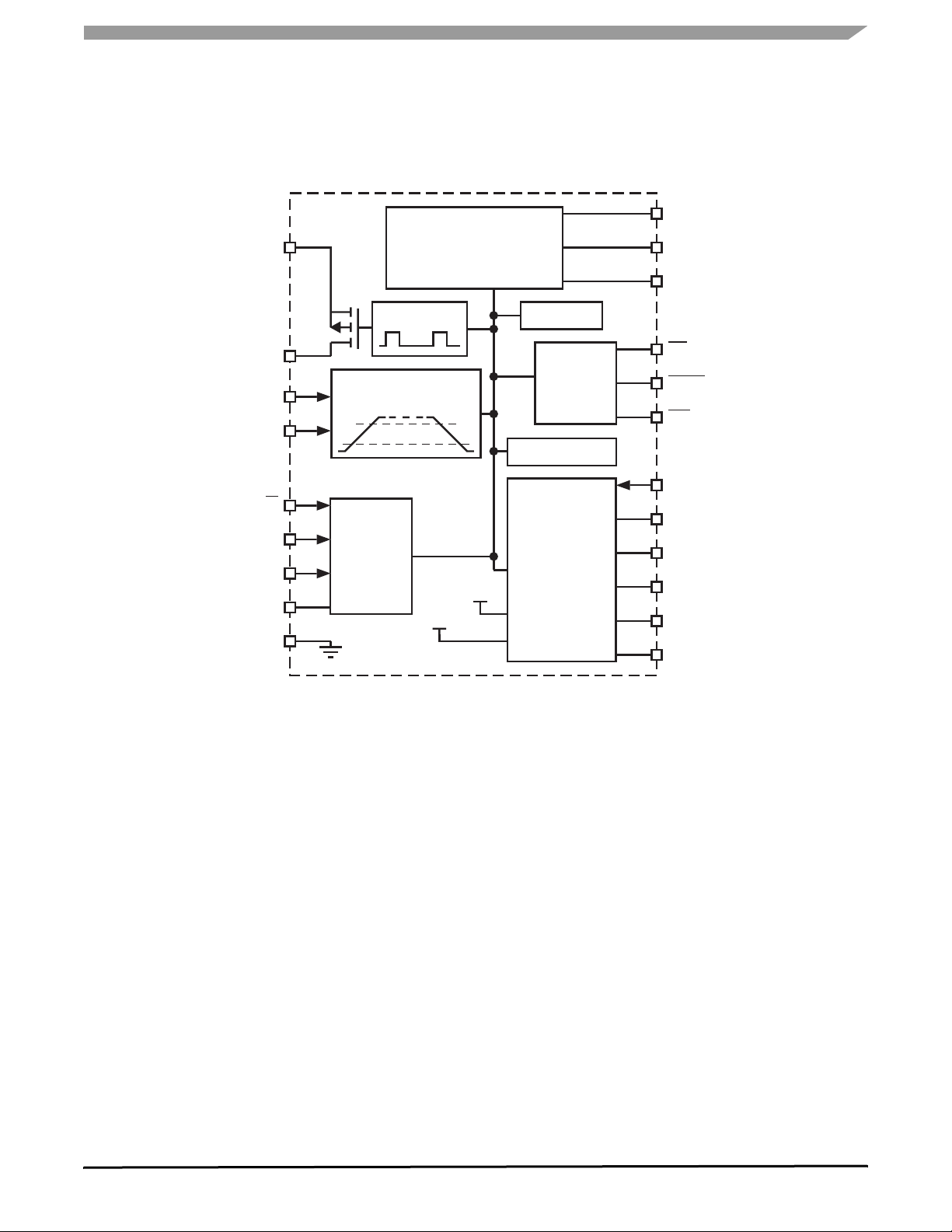
INTERNAL BLOCK DIAGRAM
33889 Internal Block Diagram
INTERNAL BLOCK DIAGRAM
VSUP
HS1
L0
L1
CS
SCLK
MOSI
MISO
GND
HS1 Control
Programmable
Wake-Up Inputs
SPI
Interface
Dual Voltage Regulator
V
Voltage Monitor
SUP
V
Voltage Monitor
DD1
Mode Control
Fault Tolerant
V
SUP
V
2
Oscillator
Interrupt
Watchdog
Reset
CAN
Transceiver
V2CTRL
V2
VDD1
INT
WDOG
RST
TX
RX
RTH
CAN H
CAN L
RTL
33889
Analog Integrated Circuit Device Data
Freescale Semiconductor 3
PIN CONNECTIONS
PIN CONNECTIONS
RX
TX
VDD1
RST
INT
GND
GND
GND
GND
V2CTRL
VSUP
HS1
L0
L1
1
2
3
4
5
6
7
8
9
10
11
12
13
14
28
WDOG
27
CS
26
MOSI
25
MISO
24
SCLK
23
GND
22
GND
21
GND
20
GND
19
CANL
18
CANH
17
RTL
16
RTH
15
V2
Figure 2. 33889 Pin Connections
Table 2. Pin Definitions
A functional description of each pin can be found in the Functional pin description section page 24.
Pin Pin Name
1
RX
2 TX Input Transmitter Data
3
VDD1
4 RST Output Reset
Pin
Function
Formal Name Definition
Output Receiver Data
Power
Voltage Regulator One
Output
CAN bus receive data output pin
CAN bus receive data input pin
5.0 V pin is a 2% low drop voltage regulator for to the microcontroller
supply.
This is the device reset output pin whose main function is to reset the
MCU.
5 INT Output Interrupt
This output is asserted LOW when an enabled interrupt condition
occurs.
6 -9,
GND Ground Ground
20 - 23
10 V2CTRL Output Voltage Source 2 Control
These device ground pins are internally connected to the package lead
frame to provide a 33889-to-PCB thermal path.
Output drive source for the V2 regulator connected to the external series
pass transistor.
11 VSUP Power
Voltage Supply
Supply input pin.
Input
12 HS1 Output High-Side Output
13 - 14
L0, L1
Input Level 0 - 1 Inputs
15 V2 Input Voltage Regulator Two
Output of the internal high-side switch.
Inputs from external switches or from logic circuitry.
5.0 V pin is a low drop voltage regulator dedicated to the peripherals
supply.
16 RTH Output RTH
17 RTL Output RTL
18
CANH
Output CAN High
19 CANL Output CAN Low
24
SCLK
Input System Clock
Pin for connection of the bus termination resistor to CANH.
Pin for connection of the bus termination resistor to CANL.
CAN high output pin.
CAN low output pin.
Clock input pin for the Serial Peripheral Interface (SPI).
33889
Analog Integrated Circuit Device Data
4 Freescale Semiconductor

Table 2. Pin Definitions (continued)
A functional description of each pin can be found in the Functional pin description section page 24.
PIN CONNECTIONS
Pin Pin Name
Pin
Function
Formal Name Definition
25 MISO Output Master In/Slave Out
26 MOSI Input Master Out/Slave In
27 CS Input Chip Select
28 WDOG Output Watchdog
SPI data sent to the MCU by the 33889. When CS
is in the high impedance state.
is HIGH, the pin
LOW
SPI data received by the 33889.
The CS
the CS
bus.
input pin is used with the SPI bus to select the 33889. When
LOW
is asserted LOW, the 33889 is the selected device of the SPI
LOW
The WDOG output pin is asserted LOW if the software watchdog is not
correctly triggered.
33889
Analog Integrated Circuit Device Data
Freescale Semiconductor 5

ELECTRICAL CHARACTERISTICS
MAXIMUM RATINGS
ELECTRICAL CHARACTERISTICS
MAXIMUM RATINGS
Table 3. Maximum Ratings
All voltages are with respect to ground unless otherwise noted. Exceeding these ratings may cause a malfunction or
permanent damage to the device.
Ratings Symbol Max Unit
ELECTRICAL RATINGS
Supply Voltage at VSUP
Continuous voltage
Transient voltage (Load dump)
Logic Signals
(RX, TX, MOSI, MISO, CS, SCLK, RST, WDOG, INT)
Output current VDD1
HS1
Voltage
Output Current
L0, L1
DC Input voltage
DC Input current
Transient input voltage (according to ISO7637 specification) and with
external component per
Figure 3.
DC voltage at V2 (V2INT) V
DC Voltage On Pins CANH, CANL V
Transient Voltage At Pins CANH, CANL
0.0 < V2-INT < 5.5 V; VSUP = 0.0; T < 500 ms
V
Transient Voltage On Pins CANH, CANL
(Coupled Through 1.0 nF Capacitor)
V
SUP
-0.3 to 27
40
V
LOG
-0.3 to V
+0.3 V
DD1
I Internally Limited mA
V
I
V
WU
I
WU
V
TRWU
2INT
BUS
CANH/VCANL
V
TR
-0.2 to V
SUP
+0.3
Internally Limited
-0.3 to 40
-2.0 to 2.0
+-100
0 to 5.25 V
-20 to +27 V
-40 to +40 V
-150 to +100 V
V
V
A
V
mA
V
DC Voltage On Pins RTH, RTL V
Transient Voltage At Pins RTH, RTL
0.0 < V2-INT < 5.5 V; VSUP = 0.0; T < 500 ms
, V
RTL
V
RTH/VRTL
RTH
-0.3 to +27V V
-0.3 to +40 V
33889
Analog Integrated Circuit Device Data
6 Freescale Semiconductor
ELECTRICAL CHARACTERISTICS
MAXIMUM RATINGS
Table 3. Maximum Ratings (continued)
All voltages are with respect to ground unless otherwise noted. Exceeding these ratings may cause a malfunction or
permanent damage to the device.
Ratings Symbol Max Unit
ESD voltage (HBM 100 pF, 1.5 k)
CANL, CANH, HS1, L0, L1
RTH, RTL
All other pins
ESD voltage (Machine Model) All pins, MC33889B
ESD voltage (CDM) All pins, MC33889D
Pins 1,14,15, & 28
All other pins
RTH, RTL Termination Resistance R
(3)
V
ESDH
±4.0
±3.0
±2.0
(3) (4)
(4)
V
ESD-MM
V
ESD-CDM
±200 V
750
500
T
500 to 16000 ohms
THERMAL RATINGS
Junction Temperature
Storage Temperature
Ambient Temperature (for info only)
Thermal resistance junction to gnd pin
T
J
T
S
T
A
(5)
R
THJ/P
-40 to 150
-55 to 165
-40 to 125
20
Notes:
3. Testing done in accordance with the Human Body Model (CZAP=100 pF, RZAP=1500 ), Machine Model (CZAP=200 pF, RZAP=0 ).
4. ESD machine model (MM) is for MC33889B only. MM is now replaced by CDM (Charged Discharged model).
5. Gnd pins 6,7,8,9,20, 21, 22, 23.
kV
V
°C
°C
°C
°C/W
1nF
LX
Transient Pulse
Generator
(note)
10 k
Gnd
Gnd
Note: Waveform in accordance to ISO7637 part1, test pulses 1, 2, 3a and 3b.
Figure 3. Transient test pulse for L0 and L1 inputs
33889
Analog Integrated Circuit Device Data
Freescale Semiconductor 7

ELECTRICAL CHARACTERISTICS
STATIC ELECTRICAL CHARACTERISTICS
STATIC ELECTRICAL CHARACTERISTICS
Table 4. Static Electrical Characteristics .
Characteristics noted under conditions - VSUP From 5.5 V to 18 V and TJ from -40°C to 125°C, unless otherwise noted. Typical
values noted reflect the approximate parameter means at T
Description Symbol Min Typ Max Unit
INPUT PIN (VSUP)
= 25°C under nominal conditions unless otherwise noted.
A
Nominal DC Voltage range
Extended DC Voltage range 1
Reduced functionality
Extended DC Voltage range 2
(6)
(8)
Input Voltage during Load Dump
Load dump situation
Input Voltage during jump start
Jump start situation
Supply Current in Sleep Mode
V
& V2 off, V
DD1
SUP
Supply Current in Sleep Mode
V
& V2 off, V
DD1
SUP
Supply current in sleep mode
V
& V2 off, V
DD1
SUP
(7)
≤ 12 V, oscillator running
(7)
≤ 12 V, oscillator not running
(7)
= 18 V, oscillator running
Supply Current in Stand-by Mode
Iout at V
= 40 mA, CAN recessive state or disabled
DD1
Supply Current in Normal Mode
Iout at V
Supply Current in Stop mode
I out V
running
Supply Current in Stop mode
Iout V
not running
Supply Current in Stop mode
Iout V
running
= 40 mA, CAN recessive state or disabled
DD1
(7),(9)
< 2.0 mA, V
DD1
(10)
< 2.0 mA, V
DD1
(10)
< 2.0 mA, V
DD1
(10)
DD1
DD1
DD1
on
(7),(9)
on
(7),(9)
on
(7)
(11)
(11)
(11)
(7),(9)
, V
≤ 12 V, oscillator
SUP
V
≤ 12V, oscillator
SUP
, V
= 18 V, oscillator
SUP
(10)
(10)
V
SUP
V
SUP-EX1
V
SUP-EX2
V
SUPLD
V
SUPJS
I
SUP
(SLEEP1)
I
SUP
(SLEEP2)
I
SUP
(SLEEP3)
I
SUP(STDBY
I
SUP(NORM)
I
SUP
(STOP1)
I
SUP
(STOP2)
I
SUP
(STOP3)
5.5 - 18 V
4.5 - 5.5 V
18 - 27 V
- - 40 V
- - 27 V
- 95 130 µA
- 55 90 µA
- 170 270 µA
) - 42 45 mA
- 42.5 45 mA
- 120 150 µA
- 80 110 µA
- 200 285 µA
Notes
6. V
7. Current measured at V
> 4.0 V, reset high, if R
DD1
SUP
pin.
STTH-2
selected and I
OUT VDD1
reduced, logic pin high level reduced, device is functional.
8. Device is fully functional. All modes available and operating, Watchdog, HS1 turn ON turn OFF, CAN cell operating, L0 and L1 inputs
operating, SPI read write operation. Over temperature may occur.
9. Measured in worst case condition with 5.0 V at V2 pin (V2 pin tied to VDD1).
10. Oscillator running means “Forced Wake-Up” or “Cyclic Sense” or “Software Watchdog” timer activated. Software Watchdog is
available in stop mode only.
11. V
is ON with 2.0 mA typical output current capability.
DD1
33889
Analog Integrated Circuit Device Data
8 Freescale Semiconductor

STATIC ELECTRICAL CHARACTERISTICS
ELECTRICAL CHARACTERISTICS
Table 4. Static Electrical Characteristics (continued).
Characteristics noted under conditions - VSUP From 5.5 V to 18 V and TJ from -40°C to 125°C, unless otherwise noted. Typical
values noted reflect the approximate parameter means at T
Description Symbol Min Typ Max Unit
= 25°C under nominal conditions unless otherwise noted.
A
Supply Fail Flag internal threshold
Supply Fail Flag hysteresis
(12)
Battery fall early warning threshold
In normal & standby mode
Battery fall early warning hysteresis
In normal & standby mode
OUTPUT PIN (VDD1)
(12)
(13)
VDD1 Output Voltage
I
from 2.0 to 200mA
DD1
5.5 V < V
4.5 V < V
Drop Voltage V
I
DD1
Drop Voltage V
I
= 50 mA
DD1
4.5 V < V
I
Output Current
DD1
SUP
SUP
SUP
= 200 mA
SUP
SUP
< 27 V
< 5.5 V
> V
> V
< 27 V
DDOUT
, limited output current
DDOUT
Internally limited
VDD1 Output Voltage in stop mode
Iout < 2.0 mA
V
THRESH
V
DETHYST
BF
EW
BF
EWH
V
DD1OUT
V
DD1DROP
V
DD1DP2
I
DD1
V
DDSTOP
1.5 3.0 4.0 V
- 1.0 - V
5.8 6.1 6.4 V
0.1 0.2 0.3 V
4.9
4.0
5.0
5.1
-
-
- 0.2 0.5 V
- 0.1 0.25 V
200 270 350 mA
4.75 5.00 5.25 V
V
I
stop output current to wake-up SBC
DD1
Default value after reset.
I
stop output current to wake-up SBC
DD1
I
over current wake deglitcher
DD1
(with I
DD1S-WU1
I
over current wake deglitcher
DD1
(with I
DD1S-WU2
selected)
selected)
(14)
(12)
(12)
Thermal Shutdown
(14)
I
DD1S-WU1
I
DD1S-WU2
I
DD1-DGIT11
I
DD1-DGIT2
T
SD
2.0 3.5 6.0 mA
10 14 18 mA
40 55 75 µs
- 150 - µs
160 - 190 °C
Normal or standby mode
Over temperature pre warning
T
PW
130 - 160 °C
VDDTEMP bit set
Temperature Threshold difference
TSD-T
PW
20 - 40 °C
Notes
12. Guaranteed by design
13. I
is the total regulator output current. VDD specification with external capacitor C ≥ 22µF and ESR < 1O ohm.
DD1
14. Selectable by SPI
33889
Analog Integrated Circuit Device Data
Freescale Semiconductor 9

ELECTRICAL CHARACTERISTICS
STATIC ELECTRICAL CHARACTERISTICS
Table 4. Static Electrical Characteristics (continued).
Characteristics noted under conditions - VSUP From 5.5 V to 18 V and TJ from -40°C to 125°C, unless otherwise noted. Typical
values noted reflect the approximate parameter means at T
Description Symbol Min Typ Max Unit
= 25°C under nominal conditions unless otherwise noted.
A
Reset threshold 1
Default value after reset.
Reset threshold 2
(15)
Reset duration
VDD1 range for Reset Active
Reset Delay Time
Measured at 50% of reset signal.
Line Regulation
9.0 V < V
SUP
< 18, I
= 10 mA
DD
Line Regulation
5.5 V < V
SUP
< 27 V, I
DD
Load Regulation
1 mA < I
< 200 mA
IDD
Thermal stability
V
= 13.5 V, I = 100 mA
SUP
V2 REGULATOR (V2)
(17)
V2 Output Voltage
I2 from 2.0 to 200 mA
5.5 V < V
SUP
< 27 V
(15)
= 10 mA
(16)
V
RST-TH1
V
RST-TH2
4.5 4.6 4.7 V
4.1 4.2 4.3 V
RESET-DUR 0.85 1.0 2.0 ms
V
DD
t
D
1.0 - - V
5.0 - 20 µs
LR1 - 5.0 25 mV
LR2 - 10 25 mV
LD - 25 75 mV
THERMS - 5.0 - mV
V2 0.99 1.0 1.01 V
DD1
I2 output current (for information only)
I2 200 - - mA
Depending on the external ballast transistor
V2 CTRL sink current capability
V2LOW flag threshold
Internal V2 Supply Current (CAN and SBC in Normal
Mode). TX = 5.0 V, CAN in Recessive State
Internal V2 Supply Current (CAN and SBC in Normal
Mode). TX = 0.0 V, No Load, CAN in Dominant State
Internal V2 Supply Current (CAN in Receive Only Mode,
SBC in Normal mode). V
SUP
= 12 V
Internal V2 Supply Current (CAN in Bus TermVbat mode,
SBC in normal mode), V
SUP
= 12 V
I2
V2L
I
I
I
CTRL
V2RS
V2DS
I
V2R
V2BT
TH
10 - - mA
3.75 4.0 4.25 V
3.8 5.6 6.8 mA
4.0 5.8 7.0 mA
80 120 µA
35 60 µA
Notes
15. Selectable by SPI
16. Guaranteed by design
17. V2 TRACKING VOLTAGE REGULATOR - V2 specification with external capacitor
- option 1: C ≥ 22 µF and ESR < 10 ohm. Using a resistor of 2 kohm or less between the base and emitter of the external PNP is
recommended.
- option2: 1.0 µF < C < 22 µF and ESR < 10 ohm. In this case depending on the ballast transistor gain an additional resistor and
capacitor network between emitter and base of PNP ballast transistor might be required. Refer to Freescale application information
or contact your local technical support.
- option 3: 10uF < C < 22uF ESR > 0.2 ohms: a resistor of 2 kohm or less is required between the base and emitter of the external PNP.
33889
Analog Integrated Circuit Device Data
10 Freescale Semiconductor
STATIC ELECTRICAL CHARACTERISTICS
ELECTRICAL CHARACTERISTICS
Table 4. Static Electrical Characteristics (continued).
Characteristics noted under conditions - VSUP From 5.5 V to 18 V and TJ from -40°C to 125°C, unless otherwise noted. Typical
values noted reflect the approximate parameter means at T
Description Symbol Min Typ Max Unit
LOGIC OUTPUT PINS (MISO)
= 25°C under nominal conditions unless otherwise noted.
A
Low Level Output Voltage
I
= 1.5 mA
OUT
High Level Output Voltage
I
= -250 µA
OUT
Tri-state MISO Leakage Current
0.0 V < V
miso
< V
DD
LOGIC INPUT PINS (MOSI, SCLK, CS)
High Level Input Voltage
Low Level Input Voltage
Input Current on CS
VI = 4.0 V
VI = 1.0 V
Low Level Input Current CS
VI = 1.0 V
MOSI, SCLK Input Current
0.0 < V
IN
< V
DD
RESET PIN (RST)
High Level Output current
0.0 < V
out
< 0.7 V
DD
V
OL
V
OH
I
HZ
V
IH
V
IL
- - 1.0 V
V
DD1-0.9
- - V
-2.0 - +2.0 µA
0.7V
DD1
-0.3 - 0.3 V
- V
DD1
+0.3V
DD1
V
-100 - -20 µA
I
IH
I
IL
I
IL
I
IN
I
OH
-100 - -20 µA
-10 - 10 µA
-350 -250 -150 µA
Low Level Output Voltage (I0 = 1.5 mA)
5.5 v < V
1.0 V < V
SUP
DD1
< 27 V
Reset pull down current
V
I
PDW
OL
V
0.0
0.0
-
-
0.9
0.9
2.3 - 5.0 mA
WATCHDOG PIN (WDOG)
Low Level Output Voltage (I0 = 1.5 mA)
5.5 V < V
SUP
< 27 V
High Level Output Voltage (I0 = -250 µA)
V
OL
V
OH
0.0 - 0.9 V
V
-0.9 - V
DD1
DD1
V
INTERRUPT PIN (INT)
Low Level Output Voltage (I0 = 1.5 mA)
High Level Output Voltage (I0 = -250 µA)
V
OL
V
OH
0.0 - 0.9 V
V
-0.9 - V
DD1
DD1
V
HIGH-SIDE OUTPUT PIN (HS1)
R
at Tj = 25°C, and I
DSON
V
>9V
SUP
OUT
-150 mA
R
DSON25
- - 2.5 Ohms
33889
Analog Integrated Circuit Device Data
Freescale Semiconductor 11

ELECTRICAL CHARACTERISTICS
STATIC ELECTRICAL CHARACTERISTICS
Table 4. Static Electrical Characteristics (continued).
Characteristics noted under conditions - VSUP From 5.5 V to 18 V and TJ from -40°C to 125°C, unless otherwise noted. Typical
values noted reflect the approximate parameter means at T
Description Symbol Min Typ Max Unit
R
at Tj = 125°C, and I
DSON
V
> 9.0 V
SUP
R
at Tj = 125°C, and I
DSON
5.5 V < V
SUP
< 9.0 V
OUT
OUT
-150 mA
-120 mA
= 25°C under nominal conditions unless otherwise noted.
A
R
DSON125
R
DON125-2
- - 5.0 Ohms
- 4.0 5.5 Ohms
Output current limitation
Over temperature Shutdown
Leakage current
Output Clamp Voltage at I
OUT
no inductive load drive capability
INPUT PINS (L0 AND L1)
L0 Negative Switching Threshold
5.5 V < V
6.0 V < V
18 V < V
SUP
SUP
SUP
< 6.0 V
< 18 V
< 27 V
L0 Positive Switching Threshold
5.5 V < V
6.0 V < V
18 V < V
SUP
SUP
SUP
< 6.0 V
< 18 V
< 27 V
L1 Negative Switching Threshold
5.5 V < V
6.0 V < V
18 V < V
SUP
SUP
SUP
< 6.0 V
< 18 V
< 27 V
L1 Positive Switching Threshold
5.5 V < V
6.0 V < V
18 V < V
SUP
SUP
SUP
< 6.0 V
< 18V
< 27 V
= -1.0 mA
(18)
O
I
LEAK
V
V
V
V
V
I
LIM
VT
CL
TH0N
TH0P
TH1N
TH1P
160 - 500 mA
155 - 190 °C
- - 10 µA
-1.5 - -0.3 V
V
1.7
2.0
2.0
2.0
2.4
2.5
3.0
3.0
3.1
V
2.2
2.5
2.5
2.75
3.4
3.5
4.0
4.0
4.1
V
2.0
2.5
2.7
2.5
3.0
3.2
3.0
3.7
3.8
V
2.7
3.0
3.5
3.3
4.0
4.2
3.8
4.7
4.8
Hysteresis
5.5 V < V
Input current
SUP
< 27 V
V
HYST
I
IN
0.6 1.0 1.3 V
-10 - 10 µA
-0.2 V < VIN < 40 V
CAN MODULE SPECIFICATION (TX, RX, CANH, CANL, RTH, AND RTL)
DC Voltage On Pins TX, RX
DC voltage at V2 (V2INT)
DC Voltage On Pins CANH, CANL
V
LOGIC
V2
V
INT
BUS
-0.3 V
+ 0.3 V
DD1
0.0 5.25 V
-20 +27 V
Notes
18. Refer to HS1 negative maximum rating voltage limitation of -0.2V.
33889
Analog Integrated Circuit Device Data
12 Freescale Semiconductor
STATIC ELECTRICAL CHARACTERISTICS
ELECTRICAL CHARACTERISTICS
Table 4. Static Electrical Characteristics (continued).
Characteristics noted under conditions - VSUP From 5.5 V to 18 V and TJ from -40°C to 125°C, unless otherwise noted. Typical
values noted reflect the approximate parameter means at T
Description Symbol Min Typ Max Unit
= 25°C under nominal conditions unless otherwise noted.
A
Transient Voltage At Pins CANH, CANL
0.0 < V
2-INT
< 5.5 V; V
≥ 0.0; T < 500 ms
SUP
Transient Voltage On Pins CANH, CANL (Coupled Through
1.0 nF Capacitor)
Detection Threshold For Short-circuit To Battery Voltage
(Term VBAT Mode) MC33889B
Detection Threshold For Short-circuit To Battery Voltage
(Term VBAT Mode) MC33889D
DC Voltage On Pins RTH, RTL
Transient Voltage At Pins RTH, RTL
0.0 < V
2-INT
< 5.5 V; V
≥ 0.0; T < 500 ms
SUP
TRANSMITTER DATA PIN (TX)
High Level Input Voltage
Low Level Input Voltage
TX High Level Input Current (VI = 4.0 V)
TX Low Level Input Current (VI = 1.0 V)
RECEIVE DATA PIN (RX)
High Level Output Voltage RX (I0 = -250 µA)
Low Level Output Voltage (I0 = 1.5 mA)
CAN HIGH AND CAN LOW PINS (CANH, CANL)
V
CANH/VCANL
V
TR
V
CANH
V
CANH
V
, V
RTL
V
RTH/VRTL
V
IH
V
IL
I
TXH
I
TXL
V
OH
V
OL
RTH
-40 40 V
-150 100 V
V
/2+3 V
SUP
V
/2+3 V
SUP
/2+5 V
SUP
/
SUP
2+4.55
-0.3 +27 V
-0.3 40 V
0.7*V
2
-0.3 0.3 * V
V2+0.3V V
2
-100 -50 -25 µA
-100 -50 -25 µA
V
- 0.9 V
2-INT
2-INT
0.0 0.9 V
V
V
V
Differential Receiver, Recessive To Dominant Threshold
(By Definition, V
DIFF
= V
CANH-VCANL
)
For 33889D
For 33889B
Differential Receiver, Dominant To Recessive Threshold
(Bus Failures 1, 2, 5)
For 33889D
For 33889B
CANH Recessive Output Voltage
TX = 5.0 V; R
(RTH)
< 4.0 k
CANL Recessive Output Voltage
TX = 5.0 V; R
(RTL)
< 4.0 k
V
V
V
V
DIFF1
DIFF2
CANH
CANL
-3.5
-3.2
-3.5
-3.2
-3.0
-2.6
-3.0
-2.6
-2.5
-2.1
-2.5
-2.1
0.2 V
V
- 0.2 V
2-INT
V
V
33889
Analog Integrated Circuit Device Data
Freescale Semiconductor 13

ELECTRICAL CHARACTERISTICS
STATIC ELECTRICAL CHARACTERISTICS
Table 4. Static Electrical Characteristics (continued).
Characteristics noted under conditions - VSUP From 5.5 V to 18 V and TJ from -40°C to 125°C, unless otherwise noted. Typical
values noted reflect the approximate parameter means at T
Description Symbol Min Typ Max Unit
= 25°C under nominal conditions unless otherwise noted.
A
CANH Output Voltage, Dominant
TX = 0.0 V; I
= -40 mA; Normal Operating Mode
CANH
(19)
CANL Output Voltage, Dominant
TX = 0.0 V; I
= 40 mA; Normal Operating Mode
CANL
CANH Output Current (V
= 0; TX = 0.0)
CANH
(19)
For 33889D
For 33889B
CANL Output Current (V
= 14 V; TX = 0.0)
CANL
For 33889D
For 33889B
Detection Threshold For Short-circuit To Battery Voltage
(Normal Mode)
Detection Threshold For Short-circuit To Battery Voltage
(Term VBAT Mode), MC33889B
Detection Threshold For Short-circuit To Battery Voltage
(Term VBAT Mode), MC33889D
CANH Output Current (Term V
Failure3)
CANL Output Current (Term V
V
= 12 V, Failure 4)
BAT
BAT
BAT
Mode; V
Mode; V
CANH
CANL
= 12 V,
= 0.0 V;
CANL Wake-Up Voltage Threshold
CANH Wake-Up Voltage Threshold
Wake-Up Threshold Difference (Hysteresis)
CANH Single Ended Receiver Threshold (Failures 4, 6, 7)
CANL Single Ended Receiver Threshold (Failures 3, 8)
CANL Pull Up Current (Normal Mode)
CANH Pull Down Current (Normal Mode)
Receiver Differential Input Impedance CANH / CANL
Differential Receiver Common Mode Voltage Range
(20)
CANH To Ground Capacitance
CANL To Ground Capacitance
C
CANL
to C
Capacitor Difference
CANH
CAN Driver Thermal Shutdown
Notes
19. For MC33889B, after 128 pulses on TX and no bus failure.
20. Guaranteed by design
V
V
V
I
I
CANH
CANH
CANL
CANH
CANL
, V
CANL
V2 - 1.4 V
1.4 V
50
50
50
50
100
75
140
90
130
110
170
135
7.3 7.9 8.9 V
VcanH Vsup/2+3 Vsup/2+5 V
VcanH Vsup/2+3
I
CANH
I
CANL
V
WAKE,L
V
WAKE,H
V
WAKEL
V
WAKEH
V
SE, CANH
V
SE, CANL
I
CANL,PU
I
CANH,PD
R
DIFF
V
COM
C
CANH
C
CANL
DC
t
CSD
-
CAN
2.5 3.0 3.9 V
1.2 2.0 2.7 V
0.2 V
1.5 1.85 2.15 V
2.8 3.05 3.4 V
45 75 90 µA
45 75 90 µA
100 300 kohm
-10 10 V
150 160 °C
5.0 10 µA
0.0 2.0 µA
Vsup/
2+4.55
50 pF
50 pF
10 pF
mA
mA
V
33889
Analog Integrated Circuit Device Data
14 Freescale Semiconductor

STATIC ELECTRICAL CHARACTERISTICS
ELECTRICAL CHARACTERISTICS
Table 4. Static Electrical Characteristics (continued).
Characteristics noted under conditions - VSUP From 5.5 V to 18 V and TJ from -40°C to 125°C, unless otherwise noted. Typical
values noted reflect the approximate parameter means at T
Description Symbol Min Typ Max Unit
BUS TERMINATION PINS (RTH, RTL)
= 25°C under nominal conditions unless otherwise noted.
A
RTL to V2 Switch On Resistance
(I
< -10 mA; Normal Operating Mode)
OUT
RTL to BAT Switch Series Resistance (term V
RTH To Ground Switch On Resistance (I
Normal Operating Mode)
OUT
Mode)
BAT
< 10 mA;
R
RTL
R
RTL
R
RTH
10 30 90 ohms
8.0 12.5 20 kohm
10 30 90 ohm
33889
Analog Integrated Circuit Device Data
Freescale Semiconductor 15

ELECTRICAL CHARACTERISTICS
DYNAMIC ELECTRICAL CHARACTERISTICS
DYNAMIC ELECTRICAL CHARACTERISTICS
Table 5. Dynamic Electrical Characteristics
V
From 5.5 V to 18 V, V2INT from 4.75 to 5.25 V and TJ from -40°C to 150°C unless otherwise noted. Typical values
SUP
noted reflect the approximate parameter means at T
Conditions Symbol Min Typ Max Unit
DIGITAL INTERFACE TIMING (SCLK, CS, MOSI, MISO)
= 25°C under nominal conditions unless otherwise noted.
A
SPI operation frequency
SCLK Clock Period
SCLK Clock High Time
SCLK Clock Low Time
Falling Edge of CS to Rising
Edge of SCLK
Falling Edge of SCLK to Rising Edge of CS
MOSI to Falling Edge of SCLK
Falling Edge of SCLK to MOSI
MISO Rise Time (CL = 220 pF)
MISO Fall Time (CL = 220 pF)
Time from Falling or Rising Edges of CS to:
- MISO Low Impedance
- MISO High Impedance
FREQ - - 4.0 MHz
t
PCLK
t
WSCLKH
t
WSCLKL
t
lLEAD
t
LAG
t
SISU
t
SIH
t
RSO
t
fSO
250 - - ns
125 - - ns
125 - - ns
100 50 - ns
100 50 - ns
40 25 - ns
40 25 - ns
- 25 50 ns
- 25 50 ns
- -
t
SOEN
t
SODIS
50
50
ns
Time from Rising Edge of SCLK to MISO Data Valid
t
VALID
- - 50 ns
0.2 V1 ≤ SO ≥ 0.8 V1, CL = 200 pF
Delay between CS low to high transition (at end of SPI stop
command) and Stop or sleep mode activation
(21)
T
CS-STOP
18 - 34 µs
detected by V2 off
Interrupt low level duration
T
INT
7.0 10 13 µs
SBC in stop mode
Internal oscillator frequency
All modes except Sleep and Stop
(21)
O
SC-F1
- 100 - kHz
Notes
21. Guaranteed by design
33889
Analog Integrated Circuit Device Data
16 Freescale Semiconductor

Table 5. Dynamic Electrical Characteristics (continued)
V
From 5.5 V to 18 V, V2INT from 4.75 to 5.25 V and TJ from -40°C to 150°C unless otherwise noted. Typical values
SUP
noted reflect the approximate parameter means at T
Conditions Symbol Min Typ Max Unit
= 25°C under nominal conditions unless otherwise noted.
A
DYNAMIC ELECTRICAL CHARACTERISTICS
ELECTRICAL CHARACTERISTICS
Internal low power oscillator frequency
Sleep and Stop modes
(22)
Watchdog period 1
Normal and standby modes
Watchdog period 2
Normal and standby modes
Watchdog period 3
Normal and standby modes
Watchdog period 4
Normal and standby modes
Watchdog period accuracy
Normal and standby modes
Normal request mode timeout
Normal request mode
Watchdog period 1 - stop
Stop mode
O
F1
NR
WD1
SC-F2
W
D1
W
D2
W
D3
W
D4
ACC
TOUT
STOP
- 100 - kHz
8.58 9.75 10.92 ms
39.6 45 50.4 ms
88 100 112 ms
308 350 392 ms
-12 - 12 %
308 350 392 ms
6.82 9.75 12.7 ms
Watchdog period 2- stop
WD2
STOP
31.5 45 58.5 ms
Stop mode
Watchdog period 3 - stop
WD3
STOP
70 100 130 ms
Stop mode
Watchdog period 4 - stop
WD4
STOP
245 350 455 ms
Stop mode
Stop mode watchdog period accuracy
F2
ACC
-30 - 30 %
Stop mode
Cyclic sense/FWU timing 1
CSFWU1 3.22 4.6 5.98 ms
Sleep and stop modes
Cyclic sense/FWU timing 2
CSFWU2 6.47 9.25 12 ms
Sleep and stop modes
Notes
22. Guaranteed by design
33889
Analog Integrated Circuit Device Data
Freescale Semiconductor 17

ELECTRICAL CHARACTERISTICS
DYNAMIC ELECTRICAL CHARACTERISTICS
Table 5. Dynamic Electrical Characteristics (continued)
V
From 5.5 V to 18 V, V2INT from 4.75 to 5.25 V and TJ from -40°C to 150°C unless otherwise noted. Typical values
SUP
noted reflect the approximate parameter means at T
Conditions Symbol Min Typ Max Unit
= 25°C under nominal conditions unless otherwise noted.
A
Cyclic sense/FWU timing 3
Sleep and stop modes
Cyclic sense/FWU timing 4
Sleep and stop modes
Cyclic sense/FWU timing 5
Sleep and stop modes
Cyclic sense/FWU timing 6
Sleep and stop modes
Cyclic sense/FWU timing 7
Sleep and stop modes
Cyclic sense/FWU timing 8
Sleep and stop modes
Cyclic sense On time
in sleep and stop modes
Cyclic sense/FWU timing accuracy
in sleep and stop mode
CSFWU3 12.9 18.5 24 ms
CSFWU4 25.9 37 48.1 ms
CSFWU5 51.8 74 96.2 ms
CSFWU6 66.8 95.5 124 ms
CSFWU7 134 191 248 ms
CSFWU8 271 388 504 ms
t
ON
t
ACC
200 300 400 µs
-30 - +30 %
Delay between SPI command and HS1 turn on
Normal or standby mode, V
SUP
> 9.0 V
Delay between SPI command and HS1 turn off
Normal or standby mode, V
Delay between SPI and V2 turn on
SUP
> 9.0 V
(23)
(23)
(23)
t
S-HSON
t
S-HSOFF
t
S-V2ON
- - 22 µs
- - 22 µs
9.0 - 25 µs
Standby mode
Delay between SPI and V2 turn off
(23)
t
S-V2OFF
9.0 - 25 µs
Normal modes
Delay between Normal Request and Normal mode, after
W/D trigger command
t
S-NR2N
15 35 70 µs
Normal request mode
Notes
23. State Machine Timing - Delay starts at rising edge of CS (end of SPI command) and start of Turn on or Turn off of HS1 or V2.
33889
Analog Integrated Circuit Device Data
18 Freescale Semiconductor

Table 5. Dynamic Electrical Characteristics (continued)
V
From 5.5 V to 18 V, V2INT from 4.75 to 5.25 V and TJ from -40°C to 150°C unless otherwise noted. Typical values
SUP
noted reflect the approximate parameter means at T
Conditions Symbol Min Typ Max Unit
= 25°C under nominal conditions unless otherwise noted.
A
DYNAMIC ELECTRICAL CHARACTERISTICS
ELECTRICAL CHARACTERISTICS
Delay between SPI and “CAN normal mode”
SBC Normal mode
(24)
Delay between SPI and “CAN sleep mode”
SBC Normal mode
(24)
Delay between CS wake-up (CS low to high) and SBC
normal request mode (V
on & reset high)
DD1
SBC in stop mode
Delay between CS wake-up (CS low to high) and first
accepted SPI command
SBC in stop mode
Delay between INT pulse and 1st SPI command accepted
In stop mode after wake-up
Delay between two SPI messages addressing the same
register
For 33889D only
INPUT PINS (L0 AND L1)
Wake-up Filter Time (enable/disable option on L0 input)
(If filter enabled)
t
S-CANN
t
S-CANS
t
W-CS
t
W-SPI
t
S-1STSPI
t2
SPI
t
WUF
- - 10 µs
- - 10 µs
15 40 90 µs
90 - - µs
20 - - µs
µs
25 - -
8.0 20 38 µs
PIN AC CHARACTERISTICS (CANH, CANL, RX, TX)
CANL and CANH Slew Rates (25% to 75% CAN signal).
Recessive to Dominant state
Dominant to Recessive state
Propagation Delay
TX to RX Low. -40°C < T ≤ 25°C.
TX to RX Low. 25°C < T < 125°C.
Propagation Delay TX to RX High.
(26)
(26)
(26)
(25)
t
SLDR
t
ONRX
t
OFFRX
2.0
2.0
V/µs
8.0
9.0
µs
1.2
1.1
1.6
1.8
1.8 2.2 µs
Notes
24. Guaranteed by design
25. Dominant to recessive slew rate is dependant upon the bus load characteristics.
26. AC Characteristics measured according to schematic Figure 4
33889
Analog Integrated Circuit Device Data
Freescale Semiconductor 19

ELECTRICAL CHARACTERISTICS
DYNAMIC ELECTRICAL CHARACTERISTICS
Table 5. Dynamic Electrical Characteristics (continued)
V
From 5.5 V to 18 V, V2INT from 4.75 to 5.25 V and TJ from -40°C to 150°C unless otherwise noted. Typical values
SUP
noted reflect the approximate parameter means at T
Conditions Symbol Min Typ Max Unit
= 25°C under nominal conditions unless otherwise noted.
A
Loop time Tx to Rx, no bus failure, MC33889D only ((27),
t
Figure 5) (ISO ICT test series 10)
Tx high to low transition (dominant edge)
Tx low to high transition (recessive edge)
Loop time Tx to Rx, with bus failure, MC33889D only ((27),
Figure 6) (ISO ICT test series 10)
t
LOOPRD-F
Tx high to low transition (dominant edge)
Tx low to high transition (recessive edge)
Loop time Tx to Rx, with bus failure and +-1.5V gnd shift, 5
nodes network, MC33889D,(
(28), Figure 7, ISO ICT tests
t
LOOPRD/DR-F+GS
series 11)
Min. Dominant Time For Wake-up On CANL or CANH
(Term Vbat; V
= 12V) Guaranteed by design.
SUP
MC33889B
MC33889D
Failure 3 Detection Time (Normal Mode) t
Failure 3 Recovery Time (Normal Mode) t
Failure 6 Detection Time (Normal Mode) t
LOOPRD
t
WAKE
DF3
DR3
DF6
1.15
1.45
-
-
1.5
1.5
1.9
1.9
3.6 µs
30
8.0
16 30
10 30 80 µs
160 µs
50 200 500 µs
µs
µs
µs
Failure 6 Recovery Time (Normal Mode) t
Failure 4, 7 Detection Time (Normal Mode) t
Failure 4, 7 Recovery Time (Normal Mode) t
Failure 3a, 8 Detection Time (Normal Mode) t
Failure 3a, 8 Recovery Time (Normal Mode) tT
Failure 4, 7 Detection Time, (Term V
Failure 4, 7 Recovery Time (Term V
Failure 3 Detection Time (Term V
Failure 3 Recovery Time (Term V
Failure 3a, 8Detection Time (Term V
Failure 3a, 8 Recovery Time (Term V
BAT
BAT
; V
BAT
BAT
; V
; V
BAT
BAT
= 12 V) t
SUP
; V
= 12 V) t
SUP
= 12 V) t
SUP
= 12 V) t
SUP
; V
= 12 V) t
SUP
; V
= 12 V) t
SUP
DR6
DF47
DR47
DF8
DR8
DR47
DR47
DR3
DR3
DR8
DR8
150 200 1000 µs
0.75 1.5 4.0 ms
10 30 60 µs
0.75 1.7 4.0 ms
0.75 1.5 4.0 ms
0.8 1.2 8.0 ms
1.92 ms
3.84 ms
1.92 ms
2.3 ms
1.2 ms
Notes
27. AC characteristic according to ISO11898-3, tested per figure 5 and 6. Guaranteed by design, room temperature only.
28. AC characteristic according to ISO11898-3, tested per figure 7. Max reported is the typical measurement under the worst condition
(gnd shift, dominant/recessive edge, at source or destination node. ref to ISO test specification). Guaranteed by design, room
temperature only.
33889
Analog Integrated Circuit Device Data
20 Freescale Semiconductor

Table 5. Dynamic Electrical Characteristics (continued)
V
From 5.5 V to 18 V, V2INT from 4.75 to 5.25 V and TJ from -40°C to 150°C unless otherwise noted. Typical values
SUP
noted reflect the approximate parameter means at T
Conditions Symbol Min Typ Max Unit
= 25°C under nominal conditions unless otherwise noted.
A
DYNAMIC ELECTRICAL CHARACTERISTICS
ELECTRICAL CHARACTERISTICS
Edge Count Difference Between CANH and CANL for Failures
1, 2, 5 Detection (Failure bit set, Normal Mode)
Edge Count Difference Between CANH And CANL For
Failures 1, 2, 5 Recovery (Normal Mode)
TX Permanent Dominant Timer Disable Time
(Normal Mode And Failure Mode)
TX Permanent Dominant Timer Enable Time
(Normal Mode And Failure Mode)
VDD
R
C
CANL
R = 100ohms
C
C = 1nF
CANH
R
C
E
E
t
t
CDF
CDR
TX,D
TX,E
Tx
MC33889D
CANH
Rx
3
3
0.75 4.0 ms
10 60 µs
5V
RtL
CANL
RtH
RcanL = RcanH = 125 ohms
500
500
RcanL
RcanH
Figure 4. Test Circuit for AC Characteristics Figure 5. ISO loop time without bus failure
1nF
1nF
Vbat
Tx
Rx
CANL
MC33889D
CANH
RtL
RtH
500
Bus
Failure
Generator (*)
500
RcanL = RcanH = 125 ohms
except for failure CANH short to CANL
(Rcanl = 1M ohms)
(*) List of failure
CANL short to gnd, Vdd, Vbat
CANHshort to gnd, Vdd, Vbat
CANL short to CANH
CANL and CANH open
RcanL
RcanH
1nF
1nF
Figure 6. ISO Loop Time with Bus Failure
33889
Analog Integrated Circuit Device Data
Freescale Semiconductor 21

ELECTRICAL CHARACTERISTICS
DYNAMIC ELECTRICAL CHARACTERISTICS
Figure 7. Test Set Up for Propagation Delay with GND Shift in a 5 Node Configuration
33889
Analog Integrated Circuit Device Data
22 Freescale Semiconductor

TIMING DIAGRAMS
ELECTRICAL CHARACTERISTICS
TIMING DIAGRAMS
V
CANL
CANH
V
DIFF
V
RX
TX HIgh: RECESSIVE Bit
TX
t
ONRX
TX Low: DOMINANT Bit
V
TH(RD)
DOMINANT Bit RECESSIVE BitRECESSIVE Bit
Figure 8. Device Signal Waveforms
TX High: RECESSIVE Bit
V
TH(DR)
t
OFFTX
t
OFFRX
5.0V
3.6V
1.4V
0.0V
2.2V
-5.0V
0.7V
0.3V
CC
CC
t
CS
SCLK
MOSI
MISO
T
LEAD
Undefined
T
VAL ID
T
SOEN
T
WCLKH
D0
T
T
PCLK
T
WCLKL
SISU
D0
T
SIH
Don’t Care
Don’t Care
Figure 9. Timing Characteristic
T
LAG
D7 Don’t Care
T
SODIS
D7
33889
Analog Integrated Circuit Device Data
Freescale Semiconductor 23

FUNCTIONAL DESCRIPTION
INTRODUCTION
FUNCTIONAL DESCRIPTION
INTRODUCTION
The MC33889 is an integrated circuit dedicated to
automotive applications. It includes the following functions:
• One full protected voltage regulator with 200 mA total
output current capability.
• Driver for external path transistor for V2 regulator function.
FUNCTIONAL PIN DESCRIPTION
RECEIVE AND TRANSMIT DATA (RX AND TX)
The RX and TX pins (receive data and transmit data pins,
respectively) are connected to a microcontroller’s CAN
protocol handler. TX is an input and controls the CANH and
CANL line state (dominant when TX is LOW, recessive when
TX is HIGH). RX is an output and reports the bus state (RX
LOW when CAN bus is dominant, HIGH when CAN bus is
recessive).
VOLTAGE REGULATOR ONE (VDD1)
The VDD1 pin is the output pin of the 5.0 V internal
regulator. It can deliver up to 200 mA. This output is protected
against overcurrent and overtemperature. It includes an
overtemperature pre-warning flag, which is set when the
internal regulator temperature exceeds 130°C typical. When
the temperature exceeds the overtemperature shutdown
(170°C typical), the regulator is turned off. VDD1 includes an
undervoltage reset circuitry, which sets the
when VDD is below the undervoltage reset threshold.
RST pin LOW
RESET (RST)
The Reset pin RST is an output that is set LOW when the
device is in reset mode. The
device is not in reset mode.
current source. When
is limited, allowing
debug or software download purposes.
RST to be shorted to 5.0 V for software
RST pin is set HIGH when the
RST includes an internal pullup
RST is LOW, the sink current capability
• Reset, programmable watchdog function
• Four operational modes
• Wake-up capabilities: Forced wake-up, cyclic sense and
wake-up inputs, CAN and the SPI
• Can low speed fault tolerant physical interface.
VOLTAGE SUPPLY (VSUP)
The VSUP pin is the battery supply input of the device.
HIGH-SIDE OUTPUT 1 (HS1)
The HS pin is the internal high-side driver output. It is
internally protected against overcurrent and
overtemperature.
LEVEL 0-1 INPUTS (L0: L1)
The L0: L1 pins can be connected to contact switches or
the output of other ICs for external inputs. The input states
can be read by the SPI. These inputs can be used as wakeup events for the SBC when operating in the Sleep or Stop
mode.
VOLTAGE REGULATOR TWO (V2)
The V2 pin is the input sense for the V2 regulator. It is
connected to the external series pass transistor. V2 is also
V supply of the internal CAN interface. It is possible to
the 5.0
connect V2 to an external 5.0
output when no external series pass transistor is used. In this
case, the V2CTRL pin must be left open.
V regulator or to the VDD
RTH (RTH)
Pin for the connection of the bus termination resistor to
CANH
INTERRUPT (INT)
The Interrupt pin INT is an output that is set LOW when an
interrupt occurs.
(INTR). When an interrupt occurs,
interrupt source is cleared.
event by a 10 sec. typical pulse when the device is in Stop
mode.
INT is enabled using the Interrupt Register
INT stays LOW until the
INT output also reports a wake-up
GROUND (GND)
This pin is the ground of the integrated circuit.
RTL (RTL)
Pin for the connection of the bus termination resistor to
CANL
CAN HIGH AND CAN LOW OUTPUTS
(CANH AND CANL)
The CAN High and CAN Low pins are the interfaces to the
CAN bus lines. They are controlled by TXD input level, and
the state of CANH and CANL is reported through RXD output.
SYSTEM CLOCK (SCLK)
V2CTRL (V2CTRL)
The V2CTRL pin is the output drive pin for the V2 regulator
connected to the external series pass transistor.
33889
24 Freescale Semiconductor
SCLK is the Serial Data Clock input pin of the serial
peripheral interface.
Analog Integrated Circuit Device Data

FUNCTIONAL INTERNAL BLOCK DESCRIPTION
FUNCTIONAL DESCRIPTION
MASTER IN/SLAVE OUT (MISO
MISO is the Master In Slave Out pin of the serial peripheral
interface. Data is sent from the SBC to the microcontroller
through the MISO pin.
MASTER OUT/SLAVE IN (MOSI)
MOSI is the Master Out Slave In pin of the serial peripheral
interface. Control data from a microcontroller is received
through this pin.
FUNCTIONAL INTERNAL BLOCK DESCRIPTION
DEVICE SUPPLY
The device is supplied from the battery line through the
VSUP pin. An external diode is required to protect against
negative transients and reverse battery. It can operate from
V and under the jump start condition at 27 V DC. This pin
4.5
sustains standard automotive voltage conditions such as
load dump at 40
V. When V
MC33889 detects it and stores the information in the SPI
register, in a bit called “BATFAIL”. This detection is available
in all operation modes.
VDD1 VOLTAGE REGULATOR
VDD1 Regulator is a 5.0 V output voltage with total current
capability of 200
mA. It includes a voltage monitoring circuitry
associated with a reset function. The VDD1 regulator is fully
protected against overcurrent, short-circuit and has
overtemperature detection warning flags and shutdown with
hysteresis.
falls below 3.0 V typical, the
SUP
CHIP SELECT (CS)
CS is the Chip Select pin of the serial peripheral interface.
When this pin is LOW, the SPI port of the device is selected.
WATCH DOG (WDOG)
The Watchdog output pin is asserted LOW to flag that the
software watchdog has not been properly triggered.
HS1 VBAT SWITCH OUTPUT
HS1 output is a 2.0 ohm typical switch from the VSUP pin.
It allows the supply of external switches and their associated
pullup or pull-down circuitry, for example, in conjunction with
the wake-up input pins. Output current is limited to 200
and HS1 is protected against short-circuit and has an over
temperature shutdown (reported into the IOR register). The
HS1 output is controlled from the internal register and the
SPI. It can be activated at regular intervals in sleep mode
thanks to an internal timer. It can also be permanently turned
on in normal or stand-by modes to drive external loads, such
as relays or supply peripheral components. In case of
inductive load drive, external clamp circuitry must be added.
SPI
The complete device control as well as the status report is
done through an 8 bit SPI interface. Refer to the SPI
paragraph.
mA
V2 REGULATOR
V2 Regulator circuitry is designed to drive an external path
transistor in order to increase output current flexibility. Two
pins are used: V2 and V2CTRL. Output voltage is 5.0
V and
is realized by a tracking function of the VDD1 regulator. A
recommended ballast transistor is the MJD32C. Other
transistors might be used, however depending upon the PNP
gain, an external resistor capacitor network might be
connected between the emitter and base of the PNP. The use
of external ballast is optional (refer to simplified typical
application). The state of V2 is reported into the IOR register
(if V2 is below 4.5
V typical, or in cases of overload or short-
circuit).
CAN
The device incorporates a low speed fault tolerant CAN
physical interface. The speed rate is up to 125
kBauds.
The state of the CAN interface is programmable through
the SPI. Reference the
CAN transceiver description on page
30.
PACKAGE AND THERMAL CONSIDERATION
The device is proposed in a standard surface mount SO28
package. In order to improve the thermal performances of the
SO28 package, 8 pins are internally connected to the lead
frame and are used for heat transfer to the printed circuit
board.
33889
Analog Integrated Circuit Device Data
Freescale Semiconductor 25

FUNCTIONAL DEVICE OPERATION
OPERATIONAL MODES
FUNCTIONAL DEVICE OPERATION
OPERATIONAL MODES
INTRODUCTION
The device has four modes of operation, normal, stand-by,
sleep and stop modes. All modes are controlled by the SPI.
An additional temporary mode called “normal request mode”
is automatically accessed by the device (refer to state
machine) after wake-up events. Special mode and
configurations are possible for software application debug
and flash memory programming.
NORMAL MODE
In this mode both regulators are ON, and this corresponds
to the normal application operation. All functions are
available in this mode (watchdog, wake-up input reading
through the SPI, HS1 activation, and CAN communication).
The software watchdog is running and must be periodically
cleared through the SPI.
STANDBY MODE
Only the Regulator 1 is ON. Regulator 2 is turned OFF by
disabling the V2CTRL pin. The CAN cell is not available, as
powered from V2. Other functions are available: wake-up
input reading through the SPI and HS1 activation. The
watchdog is running.
SLEEP MODE
Regulators 1 and 2 are OFF. In this mode, the MCU is not
powered. The device can be awakened internally by cyclic
sense via the wake-up input pins and HS1 output, from the
forced wake function, the CAN physical interface, and the SPI
CS pin).
(
STOP MODE
Regulator 2 is turned OFF by disabling the V2CTRL pin.
Regulator 1 is activated in a special low power mode which
allows it to deliver 2.0
mA. The objective is to supply the MCU
of the application while it is turned into a power saving
condition (i.e stop or wait mode).
Stop mode is entered through the SPI. Stop mode is
dedicated to powering the Microcontroller when it is in low
power mode (stop, pseudo stop, wait etc.). In these modes,
the MCU supply current is less than 1.0
mA. The MCU can
restart its software application very quickly without the
complete power up and reset sequence.
When the application is in stop mode (both MCU and
SBC), the application can wake-up from the SBC side (ex
cyclic sense, forced wake-up, CAN message, wake-up
inputs) or the MCU side (key wake-up etc.).
When Stop mode is selected by the SPI, stop mode
becomes active 20
µs after end of the SPI message. The “go
to stop” instruction must be the last instruction executed by
the MCU before going to low power mode.
In Stop mode, the Software watchdog can be “running” or
“not running” depending on the selection by the SPI. Refer to
the SPI description, RCR register bit WDSTOP. If the W/D is
enabled, the SBC must wake-up before the W/D time has
expired, otherwise a reset is generated. In stop mode, the
SBC wake-up capability is identical as in sleep mode.
STOP MODE: WAKE-UP FROM SBC SIDE, INT PIN
ACTIVATION
When an application is in stop mode, it can wake-up from
the SBC side. When a wake-up is detected by the SBC (CAN,
Wake-up input, forced wake-up, etc.), the SBC turns itself
into Normal request mode and activates the VDD1 main
regulator. When the main regulator is fully active, then the
wake-up is signalled to the MCU through the
pin is pulled low for 10
µs and then returns high. Wake-up
INT pin. The INT
events can be read through the SPI registers.
STOP MODE: WAKE-UP FROM MCU SIDE
When the application is in stop mode, the wake-up event
may come to the MCU. In this case, the MCU has to signal to
the SBC that it has to go into Normal mode in order for the
VDD1 regulator to be able to deliver full current capability.
This is done by a low to high transition of the
CS pin. The CS
pin low to high activation has to be done as soon as possible
after the MCU. The SBC generates a pulse at the
INT pin.
Alternatively the L0 and L1 inputs can also be used as wakeup from the Stop mode.
STOP MODE CURRENT MONITORING
If the current in Stop mode exceeds the I
DD1S-WU
threshold, the SBC jumps into Normal request mode,
activates the VDD1 main regulator, and generates an
interrupt to the MCU. This interrupt is not maskable and a not
bit are set into the
INT register.
SOFTWARE WATCHDOG IN STOP MODE
If the watchdog is enabled (register MCR, bit WDSTOP
set), the MCU has to wake-up independently of the SBC
before the end of the SBC watchdog time. In order to do this,
the MCU has to signal the wake-up to the SBC through the
SPI wake-up (
CS pin low to high transition to activated the
SPI wake-up). Then the SBC wakes up and jumps into the
normal request mode. The MCU has to configure the SBC to
go to either into normal or standby mode. The MCU can then
choose to go back into stop mode.
If no MCU wake-up occurs within the watchdog timing, the
SBC will activate the reset pin and jump into the normal
request mode. The MCU can then be initialized.
33889
Analog Integrated Circuit Device Data
26 Freescale Semiconductor

FUNCTIONAL DEVICE OPERATION
OPERATIONAL MODES
NORMAL REQUEST MODE
This is a temporary mode automatically accessed by the
device after a wake-up event from sleep or stop mode, or
after device power up. In this mode, the VDD1 regulator is
ON, V2 is off, and the reset pin is high. As soon as the device
enters the normal request mode, an internal 350
started. During these 350
ms, the microcontroller of the
ms timer is
application must address the SBC via the SPI and configure
the watchdog register (TIM1 register). This is the condition for
the SBC to leave the Normal request Mode and enter the
Normal mode, and to set the watchdog timer according to the
configuration done during the Normal Request mode.
The “BATFAIL flag” is a bit which is triggered when V
falls below 3.0
V. This bit is set into the MCR register. It is
SUP
reset by the MCR register read.
INTERNAL CLOCK
This device has an internal clock used to generate all
timings (reset, watchdog, cyclic wake-up, filtering time
etc....).
RESET PIN
A reset output is available in order to reset the
microcontroller. Reset causes are:
•V
falling out of range: if V
DD1
threshold (parameter
until V
returns to the nominal voltage.
DD1
falls below the reset
DD1
R
), the reset pin is pulled low
ST-TH
• Power on reset: at device power on or at device wake-up
from sleep mode, the reset is maintained low until V
DD1
is
within its operation range.
• Watchdog timeout: if the watchdog is not cleared, the SBC
will pull the reset pin low for the duration of the reset
duration time
(parameter: RESET-DUR).
For debug purposes at 25°C, the reset pin can be shorted
V.
to 5.0
SOFTWARE WATCHDOG (SELECTABLE WINDOW OR
TIMEOUT WATCHDOG)
The software watchdog is used in the SBC normal and
stand-by modes for monitoring the MCU. The watchdog can
be either a window or timeout. This is selectable by the SPI
(register TIM, bit WDW). Default is the window watchdog.
The period of the watchdog is selectable by the SPI from 5.0
ms (register TIM, bits WDT0 and WDT1). When the
to 350
window watchdog is selected, the closed window is the first
half of the selected period, and the open window is the
second half of the period. The watchdog can only be cleared
within the open window time. An attempt to clear the
watchdog in the closed window will generate a reset. The
Watchdog is cleared through the SPI by addressing the TIM
register.
Refer to ”table for reset pin operations” operation in mode
2.
WAKE-UP CAPABILITIES
Several wake-up capabilities are available for the device
when it is in sleep or stop mode. When a wake-up has
occurred, the wake-up event is stored into the WUR or CAN
registers. The MCU can then access the wake-up source.
The wake-up options are selectable through the SPI while the
device is in normal or standby mode, and prior to entering low
power mode (sleep or stop mode).
WAKE-UP FROM WAKE-UP INPUTS (L0, L1) WITHOUT
CYCLIC SENSE
The wake-up lines are dedicated to sense external switch
states, and when changes occur to wake-up the MCU (In
sleep or stop modes). The wake-up pins are able to handle
V DC. The internal threshold is 3.0 V typical, and these
40
inputs can be used as an input port expander. The wake-up
inputs state can be read through the SPI (register WUR). L0
has a lower threshold than L1 in order to allow a connection
and wake-up from a digital output such as a CAN physical
interface.
CYCLIC SENSE WAKE-UP (CYCLIC SENSE TIMER AND
WAKE-UP INPUTS L0, L1)
The SBC can wake-up from a state change of one of the
wake-up input lines (L0, L1), while the external pullup or
pulldown resistor of the switches associated to the wake-up
input lines are biased with HS1 VSUP switch. The HS1 switch
is activated in sleep or stop mode from an internal timer.
Cyclic sense and forced wake-up are exclusive. If Cyclic
sense is enabled, the forced wake-up can not be enabled.
INFO FOR CYCLIC SENSE + DUAL EDGE SELECTION
In case the Cyclic sense and Lx both level sensitive
conditions are use together, the initial value for Lx inputs are
sampled in two cases:
1) When the register LPC[D3 and D0] are set and
2) At cyclic sense event, that is when device is in sleep or
stop mode and HS1 is active.
The consequence is that when the device wake up by Lx
transition, the new value is sampled as default, then when the
device is set back into low power again, it will automatically
wake up.
The user should reset the LPC bits [D3 and D0] to 0 and
set them again to the desired value prior to enter sleep or
stop mode.
FORCED WAKE-UP
The SBC can wake-up automatically after a
predetermined time spent in sleep or stop mode. Forced
wake-up is enabled by setting bit FWU in the LPC register.
Cyclic sense and forced wake-up are exclusive. If forced
wake-up is enabled, the Cyclic sense can not be enabled.
33889
Analog Integrated Circuit Device Data
Freescale Semiconductor 27

FUNCTIONAL DEVICE OPERATION
OPERATIONAL MODES
CAN WAKE-UP
The device can wake-up from a CAN message. A CAN
wake-up cannot be disabled.
SPI WAKE-UP
The device can wake-up by the CS pin in sleep or stop
mode. Wake-up is detected by the
CS pin transition from a
low to high level. In stop mode this correspond to the
condition where the MCU and SBC are both in Stop mode,
and when the application wake-up events come through the
MCU.
SYSTEM POWER UP
At power up the device automatically wakes up.
DEVICE POWER UP, SBC WAKE UP
After device or system power up or a wake-up from sleep
mode, the SBC enters into “reset mode” then into “normal
request mode”.
VDD1
BATTERY FALL EARLY WARNING
This function provides an interrupt when the VSUP
voltage is below the 6.1
V typical. This interrupt is maskable.
A hysteresis is included. Operation is only in Normal and
Stand-by modes. VBAT low state reports in the IOR register.
RESET AND WDOG OPERATION
The following figure shows the reset and watchdog output
operations. Reset is active at device power up and wake-up.
Reset is activated in case the VDD1 falls or the watchdog is
not triggered. The
WDOG output is active low as soon as the
reset goes low and stays low for as long as the watchdog is
not properly re-activated by the SPI.
The WDOG output pin is a push pull structure than can
drive external components of the application, for instance to
signal the MCU is in a wrong operation. Even if it is internally
turned on (low-state), the reset pin can be forced to 5.0
V at
25°C only, thanks to its internally limited current drive
capability. The
WDOG stays low until the Watchdog register
is properly addressed through the SPI.
Watchdog timeout
RESET
WDOG
Watchdog
period
SPI
W/D clear
SPI CS
Watchdog register addressed
Figure 10. Reset and WDOG Function Diagram
DEBUG MODE APPLICATION HARDWARE AND
SOFTWARE DEBUG WITH THE SBC.
When the SBC is mounted on the same printed circuit
board as the micro controller, it supplies both application
software and the SBC with a dedicated routine that must be
debugged. The following features allow the user to debug the
software by disabling the SBC internal software watchdog
timer.
DEVICE POWER UP, RESET PIN CONNECTED TO VDD1
At SBC power up, the VDD1 voltage is provided, but if no
SPI communication occurs to configure the device, a reset
occurs every 350
ms. In order to allow software debugging
and avoid an MCU reset, the Reset pin can be connected
directly to VDD1 by a jumper.
DEBUG MODES WITH SOFTWARE WATCHDOG
DISABLED THOUGH SPI (NORMAL DEBUG, STANDBY
DEBUG AND STOP DEBUG)
The software watchdog can be disabled through the SPI.
In order to avoid unwanted watchdog disables, and to limit the
risk of disabling the watchdog during an SBC normal
operation, the watchdog disable has to be performed with the
following sequence:
Step 1) Power down the SBC
Step 2) Power up the SBC (The BATFAIL bit is set, and the
SBC enters normal request mode)
Step 3) Write to the TIM1 register to allow the SBC to enter
Normal mode
Step 4) Write to the MCR register with data 0000 (this
enables the debug mode). (Complete SPI byte: 000 1 0000)
33889
Analog Integrated Circuit Device Data
28 Freescale Semiconductor

FUNCTIONAL DEVICE OPERATION
OPERATIONAL MODES
Step 5) Write to the MCR register normal debug (0001
x101), stand-by debug (0001 x110), or Stop debug (0001
x111)
While in debug mode, the SBC can be used without
having to clear the W/D on a regular basis to facilitate
software and hardware debugging.
VSUP
VDD1
BATFAIL
TIM1(step 3)
MCR (step5)
SPI
MCR(step4)
debug mode
SPI: read batfail
SBC in debug Mode, no W/D
Figure 11. Debug Mode Enter
MCU FLASH PROGRAMMING CONFIGURATION
To facilitate the possibility of down loading software into
the application memory (MCU EEPROM or Flash), the SBC
allows the following capabilities: The VDD1 can be forced by
an external power supply to 5.0
V and the reset and WDOG
Step 6) To leave the debug mode, write 0000 to the MCR
register.
To avoid entering the debug mode after a power up, first
read the BATFAIL bit (MCR read) and write 0000 into the
MCR.
Figure 11 illustrates entering the debug mode.
MCR (step6)
SBC not in debug Mode and W/D on
output by external signal sources to zero or 5.0 V without
damage. This supplies the complete application board with
external power supply and applies the correct signal to the
reset pin.
33889
Analog Integrated Circuit Device Data
Freescale Semiconductor 29

FUNCTIONAL DEVICE OPERATION
OPERATIONAL MODES
CAN TRANSCEIVER DESCRIPTION
RXD
TXD
VSE-H (1.85V)
CANH
CANL
VSE-L (3.05V)
Rx multiplexer
V2
SPI
SH
SL
Failure detection
Tx driver
CAN
mode control
Driver
Vdiff
Lwake
Vsup
Stvbat
Driver
Hwake
CANL
Vwake-L (3V)
V2
SRL
SRH
Vwake-H (2V)
CANH
IcanHpd
IcanLpu
CANH
RTL
RtL
RTH
RtH
CANL
V2
GND
Figure 12. Simplified Block Diagram of the CAN Transceiver of the MC33889
General description
CAN driver:
The CANH driver is a “high side” switch to the V2 voltage
(5V). The CANL driver is a “low side” switch to gnd.The turn
on and turn off time is controlled in order to control the slew
rate, and the CANH and CANL driver have a current limitation
as well as an over temperature shutdown.
The CAN H or CANL driver can be disabled in case a
failure is detected on the CAN bus (ex: CANH driver is
disabled in case CANH is shorted to V
). The disabling of
DD
one of the drivers is controlled by the CAN logic and the
communication continues via the other drivers. When the
failure is removed the logic detects a failure recovery and
automatically reenables the associated driver.
The CAN drivers are also disabled in case of a Tx failure
detection.
Bus termination:
The bus is terminated by pull up and pull down resistors,
which are connected to GND, VDD or VBAT through
dedicated RTL and RTH pins and internal switches Srh, Srl,
Stvbat. Each node must have a resistor connected between
CANH and RTH and between CANL and RTL. The resistor
value should be between 500 and 16000 ohms.
Transmitter Function
CAN bus levels are called Dominant and Recessive, and
correspond respectively to Low and High states of the TX
input pin.
Dominant state:
The CANH and CANL drivers are on. The voltage at CANL
is <1.4V, the voltage at CANH is >3.6V, and the differential
voltage between CANH and CANL line is >2.2V (3.6V-1.4V).
Recessive state:
This is a weak state, where the CANH and CANL drivers
are off. The CANL line is pulled up to 5V via the RTL pin and
RTL resistor, and the CANH line is pull down via the RTH and
RTH resistor. The resultant voltage at CANL is 5V and 0V at
CANH. The differential voltage is -5V (0V - 5V). The
recessive state can be over written by any other node forcing
a Dominant state.
33889
Analog Integrated Circuit Device Data
30 Freescale Semiconductor

FUNCTIONAL DEVICE OPERATION
OPERATIONAL MODES
Receiver Function
In normal operation (no bus failures), RX is the image of
the differential bus voltage. The differential receiver inputs
are connected to CANH and CANL.
The device incorporates single ended comparators
connected to CANH and CANL in order to monitor the bus
state as well as detect bus failures. Failures are reported via
the SPI.
In normal operation when no failure is present, the
differential comparator is active. Under a fault condition, one
of the two CANH or CANL pins can be become nonoperational. The single ended comparator of either CANH or
CANL is activated and continues to report a bus state to Rx
pin. The device permanently monitors the bus failure and
recovery, and as soon as fault disappears, it automatically
switches back to differential operation.
CAN interface operation Mode
The CAN has 3 operation modes: TxRx (TransmitReceive), Receive Only, and Term-VBAT (Terminated to
VBAT). The mode is selected by the SPI. As soon as the
MC33889 mode is sleep or stop (selected via MCR register),
the CAN interface automatically enters Tem-Vbat mode.
Tx Rx mode:
In this mode, the CAN drivers and receivers are enabled,
and the device is able to send and receive messages. Bus
failures are detected and managed, this means that in case
of a bus failure, one of the CAN drivers can be disabled, but
communication continues via the remaining drivers.
Receive Only mode:
In this mode, the transmitter path is disabled, so the device
does not drive the bus. It maintains CANL and CANH in the
recessive state. The receiver function operates normally.
TermVbat mode:
In this mode, the transmitter and receiver functions are
disabled. The CANL pin is connected to V
through the
SUP
RTL resistor and internal pull up resistor of 12.5kOhms. In
this mode, the device monitors the bus activity and if a wake
up conditions is encountered on the CAN bus, it will wakes up
the MC33889.
The device will enter into a normal request mode if low
power mode was in sleep, or generates an INT. It enters into
Normal request mode if low power mode was in stop mode.
If the device was in normal or stand by mode, the Rx pin will
report a wake up (feature not available on the MC33889B).
See Rx pin behavior.
Bus Failure Detection
General description:
The device permanently monitors the bus lines and
detects faults in normal and receive only modes. When a fault
is detected, the device automatically takes appropriate
actions to minimize the system current consumption and to
allow communication on the network. Depending on the type
of fault, the mode of operation, and the fault detected, the
device automatically switches off one or more of the following
functions: CANL or CANH line driver, RTL or RTH termination
resistors, or internal switches. These actions are detailed in
the following table.
The device permanently monitors the faults and in case of
fault recovery, it automatically switches back to normal
operation and reconnects the open functions. Fault detection
and recovery circuitry have internal filters and delays timing,
detailed in the AC characteristics parameters.
The failure list identification and the consequence on the
device operation are described in following table. The failure
detection, and recovery principle, the transceiver state after a
failure detected, timing for failure detection and recovery can
be found in the ISO11898-3 standard.
The following table is a summary of the failure
identifications and of the consequences on the CAN driver
and receiver when the CAN is in Tx Rx mode.
33889
Analog Integrated Circuit Device Data
Freescale Semiconductor 31

FUNCTIONAL DEVICE OPERATION
OPERATIONAL MODES
Bus failure
identification
1 CANH open wire default operation default operation
5 CANH shorted to gnd default operation default operation
8, 3a CANH shorted to Vdd
3 CANH shorted to Vbat CANH driver turn OFF. RTH termination switched
2 CANL open wire default operation default operation
4, 7 CANL shorted to gnd or
9 CANL shorted to Vdd (5V) CANL driver is ON. RTL termination active default operation
6 CANL shorted to Vbat CANL driver is OFF. RTL termination switched
Description Consequence on CAN driver Consequence on Rx pin
no failure default operation: CAN H and CANL driver active,
RTH and RTL termination switched ON
CANH driver turn OFF. RTH termination switched
(5V)
CANL driver is OFF. RTL termination switched
CANL shorted to CANH
Open wire detection operation:
Description:
The CANH and CANL open wire failures are not described
in the ISO document. Open wire is only diagnostic
information, as no CAN driver or receiver state will change in
case of an open wire condition.
In case one of the CAN wires are open, the communication
will continue through the remaining wire. In this situation the
default operation: Report differential
receiver output
Rx report CANL single ended receiver
OFF
Rx report CANL single ended receiver
OFF
Rx report CANH single ended receiver
OFF
Rx report CANH single ended receiver
OFF
MC33889 will receive information on one wire only and the
consequences are as follows:
when the bus is set in dominant:
- The differential receiver will toggle
- Only one of the single ended receivers CANH or of CANL
will toggle
The following figure illustrates the CAN signal during
normal communication and in the example of a CANH open
wire. The single ended receiver is sampled at the differential
receiver switching event, in a window of 1µs.
33889
Analog Integrated Circuit Device Data
32 Freescale Semiconductor

FUNCTIONAL DEVICE OPERATION
(No open wire, or open wire recovery) (CAN H open wire)
OPERATIONAL MODES
Rec Dom
CANL
CANH
Rec
Rec
CANL
CANH
Dom Rec
Sampling point
-3.2V
Diff
S-L
S-H
1us
Sampling dominant level
-3.2V
Diff
S-L
S-H
Sampling recessive level
= > open wire “detection pulse”
= > no failure or “recovery pulse”
Figure 13. CAN Normal Signal Communication and CAN Open Wire
S-H
1us
Sampling
Sampling point
CANH
Dif f
CANL
Figure 14. Open Wire Detection Principle
Open wire detection, MC33889B and D:
Failure detection:
The device will detect a difference in toggling counts
between the differential receiver and one of the single ended
receivers. Every time a difference in count is detected a
counter is incremented. When the counter reaches 4, the
device detects and reports an open wire condition.
Dom
S-L
The open
wire detection is performed only when the device
receives a message and not when it send message.
1us
Rec
Sampling
CANH counter
L-counter +/-
(count = 4)
L-open
Open wire recovery:
When the open wire failure has recovered, the difference
in count is reduced and the device detects the open wire
recovery.
MC33889B:
When detection is complete, the counter is no longer
incremented. It can only be decremented by sampling of the
dominant level on the S-H (S-L) (recovery pulse). When it
reaches zero, the failure has recovered.
(count = 0)
recover
33889
Analog Integrated Circuit Device Data
Freescale Semiconductor 33

FUNCTIONAL DEVICE OPERATION
OPERATIONAL MODES
In application, with CAN communication, a recovery
condition is detected after 4 acknowledge bits are sent by the
MC33889B.
MC33889D:
When detection is complete, the counter is decremented
by sampling the dominant pulse (recovery pulse) on S-H (SL), and incremented (up to 4) by sampling the recessive pulse
(detection pulses) on S-H (S-L). It is necessary to get 4
consecutive dominant samples (recovery pulse) to get to
zero. When reaching zero, the failure is recovered.
In application with real CAN communication, a recovery
condition will not be detected by a single acknowledge bit
send by MC33889D, but requires a complete CAN message
(at least 4 dominant bits) send in dual wire mode, without
reception of any bit in single wire mode.
Tx permanent dominant detection:
In addition to the previous list, the MC33889 detects a
permanent low state at the TX input which results in a
permanent dominant bus state. If TX is low for more than
0.75-4ms, the bus output driver is disabled. This avoids
blocking communication between other nodes of the network.
TXD is reported via the SPI (RCR register bit D1:
TXFAILURE). Tx permanent dominant recovery is done with
TX recessive for more than typ 32us.
Rx pin behavior while CAN interface is in TermVbat.
The MC33889D is able to signal bus activity on Rx while
the CAN interface is in TermVbat and the SBC in normal or
standby mode. When the bus is driven into a dominant state
by another sending node, each dominant state is reported at
Rx by a low level, after a delay of T
WAKE
.
The bus state report is done through the CAN interface
wake up comparator on CANL and CANH, and thus operates
also in case of bus failure. This is illustrated in the following
figure.
33889
Analog Integrated Circuit Device Data
34 Freescale Semiconductor

FUNCTIONAL DEVICE OPERATION
OPERATIONAL MODES
CANL terminated to Vbat
Recessive
state
CANL
Dominant
state
Dominant
state
Recessive
state
CANH
Rx
Other CAN node send
T
WAKE
CAN in TxRx
MC33889D in Normal mode
: duration of the CAN wake up filter, typ 16µs. The MC33889D Rx dominant low level duration is the difference
T
WAKE
MC33889D in Normal mode, Standby mode or in stop mode
CAN in TermVbat
T
WAKE
CAN in TxRx
MC33889D in Normal mode
between the duration of the bus minus the Twake, as illustrated below (Trx_dom = Tbus_dom - Twake)
Tx sender node
Example: A dominant duration at the bus level of 5
bits of 8us each results in a 40us bus dominant.
This results in a 24µs (40µs-16µs) dominant level at
Dominant state
Rx of MC33889D (while the CAN of the MC33889D
is in TermVbat).
Tx MC33889D
Rx MC33889D
T
WAKE
TRX_DOM
TBUS_DOM
Figure 15. Bus State Report of the CAN Interface Wake-Up Comparator on CANL and CANH
33889
Analog Integrated Circuit Device Data
Freescale Semiconductor 35

FUNCTIONAL DEVICE OPERATION
OPERATIONAL MODES
The following table summarizes the device behavior when a CAN Wake Up event occurs.
Table 6. Summary of RX Pin Operations for Wake up Signaling
SBC mode CAN state MC33889B MC33889D
Normal Te r mV b at no event on RX, no bit set RX pulse (1), bit CANWU is not set
Standby Ter m Vb a t no event on RX, no bit set RX pulse (1), bit CANWU is not set
Sleep Te rm V ba t SBC mode transition to Normal
request, bit CANWU set
Stop Te rm V ba t INT pulse, bit CANWU set Int pulse, bit CANWU set
Notes
29. pulse duration is bus dominant duration minus Twake.
GND SHIFT DETECTION
GENERAL
When normally working in two-wire operating mode, the
CAN transmission can afford some ground shift between
different nodes without trouble. Should a bus failure occur, the
transceiver switches to single-wire operation, therefore
working with less noise margin. The affordable ground shift is
decreased.
The SBC provides a ground shift detection for diagnosis
purpose. The four ground shift levels are selectable and the
detection is stored in the IOR register which is accessible via
the SPI.
Table 7. 33889 Table of Operations
The table below describe the SBC operation modes.
MODE
Normal Request VDD1: ON
Normal VDD1: ON
Standby VDD1: ON
Stop VDD1: ON
VOLTAGE
REGULATOR
HS1 SWITCH
HS1 controllable
HS1 controllable
(limited current
HS1: OFF or cyclic
V2: OFF
HS1: OFF
V2: ON
V2: OFF
capability)
V2: OFF
WAKE-UP
CAPABILITIES
(IF ENABLED)
CAN (always enable)
SPI and L0,L1
Cyclic sense or
Forced Wake-up
SBC mode transition to Normal
request, bit CANWU set
DETECTION PRINCIPLE
The gnd shift to detect is selected via the SPI from 4
different values (-0.3
V, -0. 7 V, -1. 2 V, -1 . 7 V). At each TX
falling edge (end of recessive state), the CANH voltage is
sensed. If it is detected to be below the selected gnd shift
threshold, the bit SHIFT is set at 1 in the IOR register. No filter
is implemented. Required filtering for reliable detection
should be done by software (e.g. several trials).
DEVICE STATE DESCRIPTION
RESET PIN INT
Low for 1ms, then
high
Normally high.
Active low if W/D
or VDD1 under
voltage occur
Normally high.
Active low if W/D
or VDD1 under
voltage occur
Normally high.
Active low if W/D
or VDD1 under
voltage occur
warning temp,
(not maskable)
If enabled,
signal failure
(VDD pre
CAN, HS1)
If enabled,
signal failure
(VDD temp,
HS1)
Signal SBC
wake-up
SOFTWARE
WATCHDOG
Running Term Vbat
Running Term Vbat
- Running if
enabled
- Not Running
if disabled
CAN CELL
term Vbat
Tx/Rx
Rec only
Tx/Rx
Rec only
Term Vbat.
33889
Analog Integrated Circuit Device Data
36 Freescale Semiconductor

Table 7. 33889 Table of Operations
The table below describe the SBC operation modes.
FUNCTIONAL DEVICE OPERATION
OPERATIONAL MODES
MODE
VOLTAGE
REGULATOR
HS1 SWITCH
Sleep VDD1: OFF
HS1 OFF or cyclic
Reset
W
SBC power up
Power
Down
V2: OFF
Reset counter
(1 ms) expired
VDD1 low OR W/D: time
/
D
out 350 ms & !Nostop
:
t
i
m
e
o
u
t
O
R
V
D
D
WAKE-UP
CAPABILITIES
RESET PIN INT
(IF ENABLED)
CAN (always enable
Low Not active No Running Term Vbat.
SPI and L0,L1
Cyclic sense
Forced Wake-up
State Machine (not valid in debug modes)
W/D: timeout OR VDD1 low
W/D: timeout & Nostop & !BATFAIL
SPI: standby &
W/D trigger
(note1)
3
4
CS
op &
St
ansiti
r
t
h
SPI:
g
i
h
SPI: Stop & CS
low to high
transition
Normal Request
1
1
l
o
w
(
n
o
t
e
2
)
1
W/D: timeout OR VDD1 low
2
Wake-up
2
Stop
low to
n
o
W/D: Trigge
Standby
SPI: standby
r
Normal
SOFTWARE
WATCHDOG
1
SPI: normal
1
CAN CELL
Nostop & SPI: sleep & CS
low to high transition
(VDD1 high temperature OR (VDDd1 low > 100 ms & VSUP >BFew)) & Nostop & !BATFAIL
1 2 3 4
State machine description:
“Nostop” means Nostop bit = 1
“! Nostop” means Nostop bit = 0
“BATFAIL” means Batfail bit = 1
“! BATFAIL” means Batfail bit = 0
“VDD1 over temperature” means VDD1 thermal shutdown occurs
“VDD1 low” means VDD1 below reset threshold
“VDD1 low > 100 ms” means VDD1 below reset threshold for more than
100 ms
“W/D: Trigger” means TIM1 register write operation.
VSUP > BFew means VSUP > Battery Fall Early Warning (6.1 V typical)
denotes priority
Figure 16. Simplified State Machine
Nostop & SPI:
Wake-up
“W/D: timeout” means TIM1 register not written before W/D timeout period
expired, or W/D written in incorrect time window if window W/D selected
(except stop mode). In normal request mode timeout is 355 ms p2.2 (350 ms
p3)ms.
“SPI: Sleep” means SPI write command to MCR register, data sleep
“SPI: Stop” means SPI write command to MCR register, data stop
“SPI: Normal” means SPI write command to MCR register, data normal
“SPI: Standby” means SPI write command to MCR register, data standby
Note 1: these 2 SPI commands must be send in this sequence and
consecutively.
Note 2: if W/D activated
CS low to
high transition
sleep &
Sleep
33889
Analog Integrated Circuit Device Data
Freescale Semiconductor 37

FUNCTIONAL DEVICE OPERATION
OPERATIONAL MODES
Behavior at SBC power up
Normal Request
r
e
g
g
i
r
T
:
D
/
W
Normal
Figure 17. Behavior at SBC Power Up
Transitions to enter debug modes
W/D: timeout 350 ms
Reset counter
(1.0 ms) expired
SPI: MCR (0000) & Normal Debug
SPI: MCR (0000) & Standby Debug
Reset
Normal Debug
Standby Debug
Figure 18. Transitions to Enter Debug Modes
Power
Down
33889
Analog Integrated Circuit Device Data
38 Freescale Semiconductor

Stop (1)
Wake-up
Simplified State machine in debug modes
W/D: timeout 350ms
Normal Request
Reset counter
(1ms) expired
Reset
FUNCTIONAL DEVICE OPERATION
OPERATIONAL MODES
Wake-up
Sleep
R
SPI: standby &
W/D: Trigger
Standby
SPI: Stop
SPI: standby debug
Standby Debug
(1) If stop mode entered, it is entered without watchdog, no matter the WDSTOP bit.
(E) debug mode entry point (step 5 of the debug mode entering sequence).
(R) represents transitions to reset mode due to Vdd1 low.
R
R
S
P
I
:
n
o
r
ma
l
d
E
SPI: Standby debug
SPI: Normal debug
R
e
b
u
g
W
SPI
/
D
St
:
:
T
r
i
g
ndby D
a
g
e
r
Normal
bug
e
E
Normal Debug
R
R
SPI: Normal Debug
R
& !BATFAILNOSTOP
& SPI: Sleep
Figure 19. Simplified State Machine in Debug Mode
33889
Analog Integrated Circuit Device Data
Freescale Semiconductor 39

FUNCTIONAL DEVICE OPERATION
LOGIC COMMANDS AND REGISTERS
LOGIC COMMANDS AND REGISTERS
SPI INTERFACE
Bit1Bit2Bit3Bit4Bit5Bit6Bit7
Bit0
MISO
D1D2D3R/WA0A1A2
D0
dataaddress
Figure 20. Data Format Description
The SPI is a 8 bit SPI. First 3 bits are used to identify the internal SBC register address, bit 4 is a read/write bit. The last 4 bits
are data send from MCU to SBC or read back from SBC to MCU.
During write operation state of MISO has no signification.
During read operation only the last 4 bits at MISO have a meaning (content of the accessed register)
Following tables describe the SPI register list, and register bit meaning.
Registers “reset value” is also described, as well as the “reset condition”. reset condition is the condition which cause the bit
to be set at the “reset value”.
Possible reset condition are:
Power On Reset: POR
SBC mode transition:
NR2R - Normal Request to Reset mode
NR2N - Normal Request to Normal mode
N2R - Normal to Reset mode
STB2R - Standby to Reset mode
STO2R - Stop to Reset mode
MOSI
Read operation: R/W bit = 0
Write operation: R/W bit = 1
SBC mode:RESET - SBC in Reset mode
33889
Analog Integrated Circuit Device Data
40 Freescale Semiconductor

FUNCTIONAL DEVICE OPERATION
LOGIC COMMANDS AND REGISTERS
Table 8. List of Registers
Name Address Description Comment and usage
MCR $0 0 0 Mode control register
RCR $0 0 1 Reset control register
CAN $0 1 0 CAN control register
IOR $0 1 1 I/O control register
WUR $1 0 0 Wake-up input register
TIM $1 0 1 Timing register
LPC $1 1 0
Low power mode
control register
INTR $1 1 1 Interrupt register
Write: Control of normal, standby, sleep, and stop modes
Read: BATFAIL flag and other status bits and flags
Write: Configuration of reset voltage level, WD in stop mode, low power
mode selection
Read: CAN wake-up event, Tx permanent dominant
Write: CAN module control: TX/RX, Rec only, term VBAT, Normal and
extended modes, filter at L0 input.
Read: CAN failure status bits
Write: HS1 (high-side switch) control in normal and standby mode.
Gnd shift register level selection
Read: HS1 over temp bit, SHIFT bit (gnd shift above selection), V
below 6.1V, V2 below 4.0
V
SUP
Write: Control of wake-up input polarity
Read: Wake-up input, and real time LX input state
Write: TIM1, Watchdog timing control, window or Timeout mode.
Write: TIM2, Cyclic sense and force wake-up timing selection
Write: HS1 periodic activation in sleep and stop modes
Force wake-up control
Write: Interrupt source configuration
Read: INT source
Register description
Table 9. MCR Register
MCR D3 D2 D1 D0
$000b W MCTR2 MCTR1 MCTR0
R BATFAIL VDDTEMP GFAIL WDRST
Reset 0 0 0 0
Reset condition POR, RESET POR, RESET POR, RESET
Table 10. Control bits
MCTR2 MCTR1 MCTR0 SBC MODE DESCRIPTION
0 0 0 Enter/leave debug mode To enter debug mode, SBC must be in Normal or
Standby mode and BATFAIL
leave debug mode, BATFAIL must be at 0.
0 0 1 Normal
0 1 0 Standby
(1)
must be still at 1. To
0 1 1 Stop, watchdog off
(2)
33889
Analog Integrated Circuit Device Data
Freescale Semiconductor 41

FUNCTIONAL DEVICE OPERATION
LOGIC COMMANDS AND REGISTERS
MCTR2 MCTR1 MCTR0 SBC MODE DESCRIPTION
(4)
(3)
SUP
(2)
falls below 3V.
0 1 1 Stop, watchdog on
1 0 0 Sleep
1 0 1 Normal No watchdog running, debug mode
1 1 0 Standby
1 1 1 Stop
(1): Bit BATFAIL cannot be set by SPI. BATFAIL is set when V
(2): Watchdog ON or OFF depends on the RCR register bit D3.
(3): Before entering sleep mode, bit NOSTOP in RCR register must be previously set to 1.
(4): Stop command should be replaced by Stop Watchdog OFF. MCTR2=0, MCTR1= MCTR0=1
Table 11. Status bits
STATUS BIT DESCRIPTION
GFAIL Logic OR of CAN failure, HS1 failure, V2LOW
BATFAIL Battery fail flag (V
SUP
<3V)
VDDTEMP Temperature pre-warning on VDD (latched)
WDRST Watchdog reset occurred
Table 12. RCR register
RCR D3 D2 D1 D0
$001b W WDSTOP NOSTOP RSTTH
R TXFAILURE CANWU
Reset 1 0 0
Reset condition POR, RESET POR, NR2N POR
33889
Analog Integrated Circuit Device Data
42 Freescale Semiconductor

Table 13. Control bits
Status bit Bit value Description
WDSTOP 0 No watchdog in stop mode
1 Watchdog runs in stop mode
NOSTOP 0 Stop mode is default low power mode
1 Sleep mode is default low power mode
RSTTH 0 Reset threshold 1 selected (typ 4.6V)
1 Reset threshold 2 selected (typ 4.2V)
CANWU 1 Wake-rom CAN
TXFAILURE 1 Tx permanent dominant (CAN)
Table 14. CAN register
Some description.
FUNCTIONAL DEVICE OPERATION
LOGIC COMMANDS AND REGISTERS
CAN D3 D2 D1 D0
$010b W FDIS CEXT CCTR1 CCTR0
R CS3 CS2 CS1 CS0
Reset 0 0 0 0
Reset condition POR, CAN POR, CAN POR, CAN POR, CAN
33889
Analog Integrated Circuit Device Data
Freescale Semiconductor 43

FUNCTIONAL DEVICE OPERATION
LOGIC COMMANDS AND REGISTERS
Fault tolerant CAN transceiver standard modes
The CAN transceiver standard mode can be programmed by setting CEXT to 0. The transceiver cell will then be behave as
known from MC33388.
Table 15. CAN Transceiver Modes
CEXT CCTR1 CCTR0 Mode
0 0 0 TermVBAT
0 0 1
0 1 0 RxOnly
0 1 1 RxTx
Table 16. CAN transceiver extended modes (CAN with CEXT bit =1 is not recommended)
(1)
CEXT
1 0 0 TermVBAT
CCTR1 CCTR0 Mode
1 0 1 TermVDD
1 1 0 RxOnly
1 1 1 RxTx
Fault tolerant CAN transceiver extended modes
By setting CEXT to 1 the transceiver cell supports sub bus communication
Note1: CEXT Bit should be set at 0. The CAN operation in extended mode is not recommended.
FDIS L0 wake input filter (20 µs typical)
0 Enable (LO wake threshold selectable by WUR register)
1 Disable (L0 wake-up threshold is low level only, no matter D0 and D1 bits set in WUR register).
Note: if DFIS bit is set to 1, WUR register must be read before going into sleep or stop mode in order to clear the wake-up flag.
During read out L0 must be at high level and should stay high when entering sleep or stop.
33889
Analog Integrated Circuit Device Data
44 Freescale Semiconductor

FUNCTIONAL DEVICE OPERATION
LOGIC COMMANDS AND REGISTERS
Table 17. Status bits
CS3 CS2 CS1 CS0 Bus failure # Description
0 0 0 0 no failure
0 0 0 1 1 CANH open wire
0 1 0 1 5 CANH short circuit to ground
0 1 1 0 8, 3a VDD
0 1 1 1 3 VBAT
1 0 0 1 2 CANL open wire
1 1 0 1 4, 7 CANL short circuit to ground / CANH
1 1 1 0 9 VDD
1 1 1 1 6 VBAT
Comments:
CS2 bit at 0 = open failure. CS2 bit at 1 = short failure.
(CS3 bit at 0 and (CS1 = 1 or CS2 =1)) = CANH failure. CS3 bit at 1 = CANL failure.
CS1 and CS0 bits: short type failure coding (gnd, VDD or VBAT).
In case of multiple failures, the last failure is reported.
33889
Analog Integrated Circuit Device Data
Freescale Semiconductor 45

FUNCTIONAL DEVICE OPERATION
LOGIC COMMANDS AND REGISTERS
Table 18. IOR register.
IOR D3 D2 D1 D0
$011b W HS1ON GSLR1 GSLR0
R SHIFT HS1OT V2LOW VSUPLOW
Reset 0 0 0
Reset condition POR, RESET POR, RESET POR, RESET
Table 19. Control bits
HS1ON HS1
0 HS1 switch turn OFF
1 HS1 switch turn ON
Table 20. Gnd shift selection
GSLR1 GSLR0 Typical gnd shift comparator level
0 0 -0.3 V
0 1 -0.7 V
1 0 -1.2 V
1 1 -1.7 V
Shift State
0 Gnd shift value is lower than the level selected by the GSLR1 and GSLR2 bit
1 Gnd shift value is higher than the level selected by the GSLR1 and GSLR2 bit
33889
Analog Integrated Circuit Device Data
46 Freescale Semiconductor

Table 21. Status bits
Status bit Description
HS1OT (*) High-side 1 over temperature
SHIFT gnd shift level selected by GSLR1 and GSLR2 bits is reached
V2LOW V2 below 4.0 V typical
FUNCTIONAL DEVICE OPERATION
LOGIC COMMANDS AND REGISTERS
VSUPLOW V
below 6.1 V typical
SUP
(*) Once the HS1 switch has been turned off because of over temperature, it can be turned on again by setting the appropriate
control bit to “1”.
WUR REGISTER
The local wake-up inputs L0 and L1 can be used in both normal and standby mode as port expander and for waking up the
SBC in sleep or stop mode.
Table 22. WUR Register
WUR D3 D2 D1 D0
$100b W LCTR3 LCTR2 LCTR1
R L1WUb L1WUa L0WUb
Reset 1 1 1
Reset condition POR, NR2R, N2R, STB2R, STO2R
Table 23. Control bits:.
LCTR3 LCTR2 LCTR1 LCTR0 L0 configuration L1 configuration
LCTR0
L0WUa
1
X X 0 0 inputs disabled
X X 0 1 high level sensitive
X X 1 0 low level sensitive
X X 1 1 both level sensitive
0 0 X X inputs disabled
0 1 X X high level sensitive
1 0 X X low level sensitive
1 1 X X both level sensitive
33889
Analog Integrated Circuit Device Data
Freescale Semiconductor 47

FUNCTIONAL DEVICE OPERATION
LOGIC COMMANDS AND REGISTERS
Table 24. Status bits
L0WUb L0WUa
0 0 0 No wake-up occurred at L0 (sleep or stop mode).
1 1 0 Wake-up occurred at L0 (sleep or stop mode).
0 1 1 Wake-up occurred at L0 (sleep or stop mode with L0 filter disable). WUR must be set
L1WUb L1WUa Description
0 0 No wake-up occurred at L1 (sleep or stop mode).
1 1 Wake-up occurred at L1 (sleep or stop mode).
FDIS bit in CAN
register
Description
Low level state on L0 (standby or normal mode)
High level state on L0 (standby or normal mode)
to xx00 before sleep or stop mode.
Low level state on L1 (standby or normal mode)
High level state on L1 (standby or normal mode)
TIM REGISTERS
Description: This register is split into 2 sub registers, TIM1 and TIM2.
TIM1 controls the watchdog timing selection as well as the window or timeout option. TIM1 is selected when bit D3 is 0.
TIM2 is used to define the timing for the cyclic sense and forced wake-up function. TIM2 is selected when bit D3 is 1.
No read operation is allowed for registers TIM1 and TIM2
TIM REGISTER
Table 25. TIM Register.
TIM1 D3 D2 D1 D0
$101b W 0 WDW WDT1 WDT0
R
Reset 0 0 0
Reset condition POR, RESET POR, RESET POR, RESET
33889
Analog Integrated Circuit Device Data
48 Freescale Semiconductor

FUNCTIONAL DEVICE OPERATION
LOGIC COMMANDS AND REGISTERS
Table 26. Watch dog
WDW WDT1 WDT0 Watchdog timing [ms]
0 0 0 10 no window watchdog
0 0 1 50
0 1 0 100
0 1 1 350
1 0 0 10 window watchdog enabled (window lenght is
1 0 1 50
1 1 0 100
1 1 1 350
half the watchdog timing)
Table 27. jWatchdog operation (window and timeout)
window closed window open
no watchdog clear
WD timing * 50%
for watchdog clear
WD timing * 50%
Watchdog period
(WD timing selected by TIM 1 bit WDW=1)
Window watchdog
(WD timing selected by TIM 1, bit WDW=0)
window open
for watchdog clear
Watchdog period
Timeout watchdog
TIM2 REGISTER
The purpose of TIM2 register is to select an appropriate timing for sensing the wake-up circuitry or cyclically supplying devices
by switching on or off HS1
Table 28. TIM2 Register
TIM2 D3 D2 D1 D0
$101b W 1 CSP2 CSP1 CSP0
R
Reset 0 0 0
Reset
condition
POR, RESET POR, RESET POR, RESET
33889
Analog Integrated Circuit Device Data
Freescale Semiconductor 49

FUNCTIONAL DEVICE OPERATION
LOGIC COMMANDS AND REGISTERS
Table 29. Cyclic Sense Timing
CSP2 CSP1 CSP0 Cyclic sense timing [ms]
0 0 0 5
0 0 1 10
0 1 0 20
0 1 1 40
1 0 0 75
1 0 1 100
1 1 0 200
1 1 1 400
Cyclic sense on time
Cyclic sense timing
10 µs to 20 µs
HS1
Sample
t
LPC REGISTER
Description: This register controls:
- The state of HS1 in stop and sleep mode (HS1 permanently off or HS1 cyclic)
- Enable or Disable the forced wake-up function (SBC automatic wake-up after time spend in sleep or stop mode, time defined
by TIM2 register)
- Enable or disable the sense of the wake-up inputs (LX) at sampling point of the cyclic sense period (LX2HS1 bit).
Table 30. LPC Register
LPC D3 D2 D1 D0
$110b W LX2HS1 FWU IDDS HS1AUTO
R
Reset 0 0 0 0
Reset condition POR, NR2R, N2R,
STB2R, STO2R
33889
POR, NR2R, N2R,
STB2R, STO2R
POR, NR2R, N2R,
STB2R, STO2R
POR, NR2R, N2R,
STB2R, STO2R
Analog Integrated Circuit Device Data
50 Freescale Semiconductor

FUNCTIONAL DEVICE OPERATION
LOGIC COMMANDS AND REGISTERS
LX2HS1 HS1AUTO Wake-up inputs supplied by HS1 Autotiming HS1
X 0 off
X 1 On, HS1 cyclic, period defined in TIM2 register
0 X no
1 X Yes, LX inputs sensed at sampling point
Bit Description
FWU If this bit is set, and the SBC is turned into sleep or stop mode, the SBC wakes up after the time selected in the
TIM2
register
IDDS Bit = 0: I
Bit = 1: I
DDS-WU1
DDS-WU2
selected (lowest value, typ 3.5mA)
selected (highest value, typ 14mA)
Table 31. INTR register
INTR D3 D2 D1 D0
$111b W VSUPLOW HS1OT-V2LOW VDDTEMP CANF
R VSUPLOW HS1OT VDDTEMP CANF
Reset 0 0 0 0
Reset condition POR, RESET POR, RESET POR, RESET POR, RESET
Table 32. Control bits:
Control bit Description
CANF Mask bit for CAN failures (OR of any CAN failure)
VDDTEMP Mask bit for VDD medium temperature
HS1OT-V2LOW Mask bit for HS1 over temperature OR V2 below 4V
VSUPLOW Mask bit for SUP below 6.1V
When the mask bit has been set, INT pin goes low if the appropriate condition occurs.
33889
Analog Integrated Circuit Device Data
Freescale Semiconductor 51

FUNCTIONAL DEVICE OPERATION
LOGIC COMMANDS AND REGISTERS
Table 33. Status bits:
Status bit Description
CANF CAN failure
VDDTEMP VDD medium temperature
HS1OT HS1 over temperature
VSUPLOW V
Notes:
If HS1OT-V2LOW interrupt is only selected (only bit D2 set
below 6.1V typical
SUP
Bit D2 = 1: INT source is HS1OT
Bit D2 = 0: INT source is V2LOW.
in INTR register), reading INTR register bit D2 leads to two
possibilities:
Upon a wake-up condition from stop mode due to over current detection (I
DD1S-WU1
however INTR register contain remains at 0000 (not bit set into the INTR register).
or I
DD1S-WU2
), an INT pulse is generated,
33889
Analog Integrated Circuit Device Data
52 Freescale Semiconductor

TYPICAL APPLICATIONS
TYPICAL APPLICATIONS
5V
CAN
supply
V2
VDD1
INT
WDOG
RESET
MOSI
SCLK
MISO
CS
TXD
RXD
GND
5V/200mA
VBAT
RRTH
RRTL
VSUP
HS1
L0
L1
RTH
CANH
CANL
RTL
RB
V2CTRL
VSUP monitor
Dual Voltage Regulator
VDD1 Monitor
HS1 control
Programmable
wake-up input
Q1
V2
5V/200mA
Mode control
Oscillator
Interrupt
Watchdog
Reset
SPI Interface
Low Speed
Fault Tolerant CAN
Physical Interface
Figure 21. 33889D/33889B Simplified Typical Application with Ballast Transistor
5V/100mA
VBAT
RRTH
RRTL
VSUP
HS1
L0
L1
RTH
CANH
CANL
RTL
V2CTRL (open)
VSUP Monitor
Dual Voltage Regulator
VDD1 Monitor
HS1 Control
Programmable
wake-up input
Low Speed
Fault Tolerant CAN
Physical Interface
V2
5V/200mA
Mode Control
Oscillator
Interrupt
Watchdog
Reset
SPI Interface
CAN
supply
V2
VDD1
INT
WDOG
RESET
MOSI
SCLK
MISO
CS
TX
RX
GND
5V/100mA
Figure 22. 33889D/33889B Simplified Typical Application without Ballast Transistor
33889
Analog Integrated Circuit Device Data
Freescale Semiconductor 53

PACKAGING
PACKAGE DIMENSIONS
PACKAGING
PACKAGE DIMENSIONS
Important For the most current revision of the package, visit www.freescale.com and do a keyword search on the 98A
number listed below.
DW SUFFIX
EG SUFFIX (PB-FREE)
28-PIN
PLASTIC PACKAGE
98ASB42345B
ISSUE G
33889
Analog Integrated Circuit Device Data
54 Freescale Semiconductor

PACKAGE DIMENSIONS
PACKAGING
DW SUFFIX
EG SUFFIX (PB-FREE)
28-PIN
PLASTIC PACKAGE
98ASB42345B
ISSUE G
33889
Analog Integrated Circuit Device Data
Freescale Semiconductor 55

ADDITIONAL DOCUMENTATION
THERMAL ADDENDUM (REV 2.0)
ADDITIONAL DOCUMENTATION
THERMAL ADDENDUM (REV 2.0)
Introduction
This thermal addendum is provided as a supplement to the MC33889 technical
datasheet. The addendum provides thermal performance information that may be
critical in the design and development of system applications. All electrical,
application, and packaging information is provided in the datasheet.
Packaging and Thermal Considerations
The MC33889 is offered in a 28 pin SOICW, single die package. There is a
single heat source (P), a single junction temperature (T
).
(R
θJA
T
=
J
R
θJA
.
P
), and thermal resistance
J
33889DW
33889EG
28-PIN
SOICW
DWB SUFFIX
EG SUFFIX (PB-FREE)
98ASB42345
28-PIN SOICW
The stated values are solely for a thermal performance comparison of one
package to another in a standardized environment. This methodology is not
meant to and will not predict the performance of a package in an applicationspecific environment. Stated values were obtained by measurement and
simulation according to the standards listed below.
Standards
Table 34. Thermal Performance Comparison
Thermal Resistance [°C/W]
(1) (2)
Ρ
θJA
(2) (3)
Ρ
θJB
(1) (4)
Ρ
θJA
(5)
Ρ
ϑΧ
θ
Notes
1. Per JEDEC JESD51-2 at natural convection, still air
condition.
2. 2s2p thermal test board per JEDEC JESD51-7.
3. Per JEDEC JESD51-8, with the board temperature on the
center trace near the center lead.
4. Single layer thermal test board per JEDEC JESD51-3.
5. Thermal resistance between the die junction and the
package top surface; cold plate attached to the package top
surface and remaining surfaces insulated.
42
11
69
23
Figure 23. Surface Mount for SOIC Wide Body
FOR PACKAGE DIMENSIONS,
NOTE
REFER TO THE 33889 DEVICE DATASHEET.
20 Terminal SOICW
1.27 mm Pitch
18.0 mm x 7.5 mm Body
Non-Exposed Pad
33889
Analog Integrated Circuit Device Data
56 Freescale Semiconductor

ADDITIONAL DOCUMENTATION
THERMAL ADDENDUM (REV 2.0)
RX
TX
VDD1
RST
INT
GND
GND
GND
GND
V2CTRL
VSUP
HS1
L0
L1
1
2
3
4
5
6
7
8
9
10
11
12
13
14
28
WDOG
27
CS
26
MOSI
25
MISO
24
SCLK
23
GND
22
GND
21
GND
20
GND
19
CANL
18
CANH
17
RTL
16
RTH
15
V2
33889 Pin Connections
28-Pin SOICW
1.27 mm Pitch
18.0 mm x 7.5 mm Body
Figure 24. Thermal Test Board
Device on Thermal Test Board
Material: Single layer printed circuit board
FR4, 1.6 mm thickness
Cu traces, 0.07 mm thickness
Outline: 80 mm x 100 mm board area,
including edge connector for thermal
testing
Area A: Cu heat-spreading areas on board
surface
Ambient Conditions: Natural convection, still air
A
Table 35. Thermal Resistance Performance
Thermal
Resistance
R
JA
θ
R
is the thermal resistance between die junction and
θJA
ambient air.
Area A (mm2) (°C/W)
0 69
300 53
600 48
33889
Analog Integrated Circuit Device Data
Freescale Semiconductor 57

ADDITIONAL DOCUMENTATION
]
THERMAL ADDENDUM (REV 2.0)
80
70
60
50
40
Thermal Resistance [ºC/W
100
10
30
x
R
JA
θ
20
10
0
0300 600
Heat spreading area A [mm²]
Figure 25. Device on Thermal Test Board R
1
θJA
x
R
JA
θ
Thermal Resistance [ºC/W]
0.1
1.00E-03 1.00E-02 1.00E-01 1.00E+00 1.00E+01 1.00E+02 1.00E+03 1.00E+04
Tim e[s]
Figure 26. Transient Pin Resistance R
Device on Thermal Test Board Area A = 600 (mm2)
JA
θ
33889
Analog Integrated Circuit Device Data
58 Freescale Semiconductor

REVISION HISTORY
REVISION DATE DESCRIPTION OF CHANGES
7.0
8.0
9.0
10.0
11.0
12.0
5/2006
6/2002
8/2006
9/2006
12/2006
3/2007
• Implemented Revision History page
• Added “EG” PB-Free package type
• Removed MC33889DW version, and added MC33889B and MC33889D versions
• Converted to the Freescale format, and updated to the prevailing form and style
• Modified Device Variations Between the 33889D and 33889B Versions
• Added Thermal Addendum (rev 2.0) on page 56
• Changed the Maximum Ratings on page 6 to the standard format
• Added CAN transceiver description section
• Corrected two instances where pin LO had an overline, and one instance where pin
WDOG did not.
• Removed MC33889BEG/R2 and MC33889DEG/R2 and replaced them with
MCZ33889BEG/R2 and MCZ33889DEG/R2 in the Ondering Information block
• Replaced the label Logic Inputs with Logic Signals (RX, TX, MOSI, MISO, CS, SCLK,
RST, WDOG, INT) on page 6
• Changed CS to CS at various places in the document
• Made changes to Supply Current in Stand-by Mode
in Normal Mode
(7)
on page 8
• Added the EG suffix to the included thermal addendum
REVISION HISTORY
(1)
on page 2
(7),(9)
on page 8 and Supply Current
33889
Analog Integrated Circuit Device Data
Freescale Semiconductor 59

How to Reach Us:
Home Page:
www.freescale.com
Web Support:
http://www.freescale.com/support
USA/Europe or Locations Not Listed:
Freescale Semiconductor, Inc.
Technical Information Center, EL516
2100 East Elliot Road
Tempe, Arizona 85284
+1-800-521-6274 or +1-480-768-2130
www.freescale.com/support
Europe, Middle East, and Africa:
Freescale Halbleiter Deutschland GmbH
Technical Information Center
Schatzbogen 7
81829 Muenchen, Germany
+44 1296 380 456 (English)
+46 8 52200080 (English)
+49 89 92103 559 (German)
+33 1 69 35 48 48 (French)
www.freescale.com/support
Japan:
Freescale Semiconductor Japan Ltd.
Headquarters
ARCO Tower 15F
1-8-1, Shimo-Meguro, Meguro-ku,
Tokyo 153-0064
Japan
0120 191014 or +81 3 5437 9125
support.japan@freescale.com
Asia/Pacific:
Freescale Semiconductor Hong Kong Ltd.
Technical Information Center
2 Dai King Street
Tai Po Industrial Estate
Tai Po, N.T., Hong Kong
+800 2666 8080
support.asia@freescale.com
For Literature Requests Only:
Freescale Semiconductor Literature Distribution Center
P.O. Box 5405
Denver, Colorado 80217
1-800-441-2447 or 303-675-2140
Fax: 303-675-2150
LDCForFreescaleSemiconductor@hibbertgroup.com
RoHS-compliant and/or Pb-free versions of Freescale products have the functionality
and electrical characteristics of their non-RoHS-compliant and/or non-Pb-free
counterparts. For further information, see http://www.freescale.com or contact your
Freescale sales representative.
For information on Freescale’s Environmental Products program, go to http://
www.freescale.com/epp.
Information in this document is provided solely to enable system and software
implementers to use Freescale Semiconductor products. There are no express or
implied copyright licenses granted hereunder to design or fabricate any integrated
circuits or integrated circuits based on the information in this document.
Freescale Semiconductor reserves the right to make changes without further notice to
any products herein. Freescale Semiconductor makes no warranty, representation or
guarantee regarding the suitability of its products for any particular purpose, nor does
Freescale Semiconductor assume any liability arising out of the application or use of any
product or circuit, and specifically disclaims any and all liability, including without
limitation consequential or incidental damages. “Typical” parameters that may be
provided in Freescale Semiconductor data sheets and/or specifications can and do vary
in different applications and actual performance may vary over time. All operating
parameters, including “Typicals”, must be validated for each customer application by
customer’s technical experts. Freescale Semiconductor does not convey any license
under its patent rights nor the rights of others. Freescale Semiconductor products are
not designed, intended, or authorized for use as components in systems intended for
surgical implant into the body, or other applications intended to support or sustain life,
or for any other application in which the failure of the Freescale Semiconductor product
could create a situation where personal injury or death may occur. Should Buyer
purchase or use Freescale Semiconductor products for any such unintended or
unauthorized application, Buyer shall indemnify and hold Freescale Semiconductor and
its officers, employees, subsidiaries, affiliates, and distributors harmless against all
claims, costs, damages, and expenses, and reasonable attorney fees arising out of,
directly or indirectly, any claim of personal injury or death associated with such
unintended or unauthorized use, even if such claim alleges that Freescale
Semiconductor was negligent regarding the design or manufacture of the part.
Freescale™ and the Freescale logo are trademarks of Freescale Semiconductor, Inc.
All other product or service names are the property of their respective owners.
© Freescale Semiconductor, Inc., 2007. All rights reserved.
MC33889
Rev. 12.0
3/2007
 Loading...