

Freescale Semiconductor
Technical Data
5.0 A H-Bridge
The 33886 is a monolithic H-Bridge ideal for fractional horsepower
DC-motor and bi-directional thrust solenoid control. The IC
incorporates internal control logic, charge pump, gate drive, and low
R
continuous inductive DC load currents up to 5.0 A. Output loads can
be pulse width modulated (PWM-ed) at frequencies up to 10 kHz.
overtemperature conditions. Two independent inputs control the two
half-bridge totem-pole outputs. Two disable inputs force the H-Bridge
outputs to tri-state (exhibit high impedance).
-40°C
up to 40 V with derating of the specifications. The IC is available in a
surface mount power package with exposed pad for heatsinking.
Features
• Similar to the MC33186DH1 with Enhanced Features
• 5.0 V to 40 V Continuous Operation
•120 mΩ R
• TTL / CMOS Compatible Inputs
• PWM Frequencies up to 10 kHz
• Active Current Limiting via Internal Constant OFF-Time PWM (with
• Output Short Circuit Protection
• Undervoltage Shutdown
• Fault Status Reporting
• Pb-Free Packaging Designated by Suffix Code VW
MOSFET output circuitry. The 33886 is able to control
DS(ON)
A Fault Status output reports undervoltage, short circuit, and
The 33886 is parametrically specified over a temperature range of
≤ T
≤ 125°C, 5.0 V ≤ V+ ≤ 28 V. The IC can also be operated
A
H-Bridge MOSFETs
DS(ON)
Temperature-Dependent Threshold Reduction)
Document order number: MC33886
ORDERING INFORMATION
Device
MC33886DH/R2
MC33886VW/R2
Rev 7.0, 07/2005
33886
H-BRIDGE
VW SUFFIX (Pb-free)
DH SUFFIX
98ASH70702A
20-TERMINAL HSOP
Temperature
Range (T
- 40°C to 125°C 20 HSOP
)
A
Package
5.0 V
IN
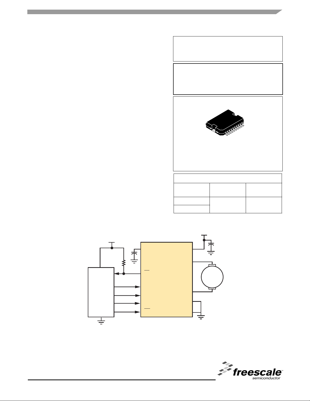
OUT
MCU
OUT
OUT
OUT
Figure 1. 33886 Simplified Application Diagram
© Freescale Semiconductor, Inc., 2005. All rights reserved.
C
FS
IN1
IN2
D1
D2
CP
V+
33886
V+
OUT1
MOTOR
OUT2
PGND
AGND
INTERNAL BLOCK DIAGRAM
INTERNAL BLOCK DIAGRAM
C
C
CP
CP
Charge
Charge
Pump
Pump
V
V+
PWR
IN1
IN2
D1
D2
FS
80 µA
80 uA
(each)
25 uA
25 µA
5.0 V
5.0 V
Regulator
Regulator
Gate Drive
Gate Drive
Over-
Control
Over-
temperature
temperature
Logic
Undervoltage
Undervoltage
Figure 2. 33886 Simplified Internal Block Diagram
Curre n t Li m it,
Current Limit,
Overcurrent
Short Circuit
Sense
Sense Circuit
Ci rcuit
PGNDAGND
OUT 1
OUT 2
33886
Analog Integrated Circuit Device Data
2 Freescale Semiconductor
TERMINAL CONNECTIONS
TERMINAL CONNECTIONS
DNCAGND
IN2
D1
CCP
V+
OUT2
OUT2
D2
PGND
PGND
FS
IN1
V+
V+
OUT1
OUT1
DNC
PGND
PGND
1
2
3
4
5
6
7
8
9
10
20
19
18
17
16
15
14
13
12
11
Figure 3. 33886 Terminal Connections
Table 1. 33886 Terminal Definitions
A functional description of each terminal can be found in the Functional Terminal Description section beginning on page
Terminal
Number
1 AGND Analog Ground
2 FS Fault Status for H-
Terminal
Name
Formal Name Definition
Low-current analog signal ground.
Open drain active Low Fault Status output requiring a pull-up resistor to 5.0 V.
Bridge
15.
3 IN1 Logic Input Control 1
4, 5, 16 V+ Positive Power Supply
6, 7 OUT1 H-Bridge Output 1
8, 20 DNC Do Not Connect
9 –12 PGND Power Ground
13 D2 Disable 2
14, 15 OUT2 H-Bridge Output 2
17 CCP Charge Pump Capacitor
18 D1 Disable 1
19 IN2 Logic Input Control 2
True logic input control of OUT1 (i.e., IN1 logic High = OUT1 logic High).
Positive supply connections.
Output 1 of H-Bridge.
Either do not connect (leave floating) or connect these terminals to ground in the
application. They are test mode terminals used in manufacturing only.
Device high-current power ground.
Active Low input used to simultaneously tri-state disable both H-Bridge outputs. When
D2
is logic Low, both outputs are tri-stated.
Output 2 of H-Bridge.
External reservoir capacitor connection for internal charge pump capacitor.
Active High input used to simultaneously tri-state disable both H-Bridge outputs. When
D1 is logic High, both outputs are tri-stated.
True logic input control of OUT2 (i.e., IN2 logic High = OUT2 logic High).
33886
Analog Integrated Circuit Device Data
Freescale Semiconductor 3
MAXIMUM RATINGS
MAXIMUM RATINGS
Table 2. Maximum Ratings
All voltages are with respect to ground unless otherwise noted. Exceeding these ratings may cause a malfunction or
permanent damage to the device.
Rating Symbol Value Unit
Supply Voltage
Input Voltage
Status Output
FS
Continuous Current
(1)
(2)
(3)
ESD Voltage for DH Package
Human Body Model
Machine Model
(4)
(5)
ESD Voltage for VW Package
Human Body Model
Machine Model
(4)
(5)
Storage Temperature
Ambient Operating Temperature
(7)
Operating Junction Temperature
Terminal Soldering Temperature
(8)
DH Suffix
VW (Pb-Free Suffix)
Approximate Junction-to-Board Thermal Resistance (and Package
Dissipation = 6.0 W)
(9)
V+ 40 V
V
V
I
OUT
V
ESD1
V
ESD2
V
ESD1
V
ESD2
T
STG
T
T
T
SOLDER
IN
FS
A
J
-0.1 to 7.0 V
7.0 V
5.0 A
(6)
±2000
±200
±2000
±200
-65 to 150 °C
-40 to 125 °C
-40 to 150 °C
220
260
R
JB
θ
~5.0
V
V
°C
°C/W
Notes
1. Exceeding the input voltage on IN1, IN2, D1, or D2
2. Exceeding the pull-up resistor voltage on the open drain FS
3. Continuous current capability so long as junction temperature is ≤ 150
4. ESD1 testing is performed in accordance with the Human Body Model (C
5. ESD2 testing is performed in accordance with the Machine Model (C
may cause a malfunction or permanent damage to the device.
terminal may cause permanent damage to the device.
°C.
ZAP
= 200 pF, R
ZAP
= 100 pF, R
ZAP
= 1500 Ω).
ZAP
= 0 Ω).
6. All terminals are capable of Human Body Model ESD voltages of ±2000 V with two exceptions pertaining only to the DH suffix package:
to PGND is capable of ±1500 V and (2) OUT1 to AGND is capable of ±1000 V.
(1) D2
7. The limiting factor is junction temperature, taking into account the power dissipation, thermal resistance, and heatsinking.
8. Terminal soldering temperature limit is for 10 seconds maximum duration. Not designed for immersion soldering. Exceeding these limits
may cause malfunction or permanent damage to the device.
9. Exposed heatsink pad plus the power and ground terminals comprise the main heat conduction paths. The actual R
(junction-to-PC
θ
JB
board) values will vary depending on solder thickness and composition and copper trace.
33886
Analog Integrated Circuit Device Data
4 Freescale Semiconductor
STATIC ELECTRICAL CHARACTERISTICS
STATIC ELECTRICAL CHARACTERISTICS
Table 3. Static Electrical Characteristics
Characteristics noted under conditions 5.0 V ≤ V+ ≤ 28 V and -40°C ≤ TA ≤ 125°C unless otherwise noted. Typical values noted
reflect the approximate parameter mean at T
Characteristic Symbol Min Typ Max Unit
Power Supply
Operating Voltage Range
Standby Supply Current
V
= 5.0 V, I
EN
OUT
Threshold Supply Voltage
Switch-OFF
Switch-ON
Hysteresis
CHARGE PUMP
(10)
= 0 A
= 25°C under nominal conditions unless otherwise noted.
A
V+ 5.0 – 40 V
I
Q (standby)
––20
V+
(thres-OFF)
V+
(thres-ON)
V+
(hys)
4.15
4.5
150
4.4
4.75
–
4.65
5.0
–
mA
V
V
mV
Charge Pump Voltage
V+ = 5.0 V
8.0 V ≤ V+ ≤ 40 V
V
- V +
CP
3.35
–
–
–
–
20
CONTROL INPUTS
Input Voltage (IN1, IN2, D1, D2)
Threshold High
Threshold Low
Hysteresis
Input Current (IN1, IN2, D1)
VIN = 0 V
D2
Input Current
(12)
V D2 = 5.0 V
(11)
V
V
V
HYS
I
IN
I
D2
IH
IL
3.5
–
0.7
1.0
–
–
–
1.4
–
-200 -80 –
–25100
Notes
10. Specifications are characterized over the range of 5.0 V ≤ V+ ≤ 28 V. Operation > 28 V will cause some parameters to exceed listed
min/max values. Refer to typical operating curves to extrapolate values for operation > 28 V but ≤ 40 V.
11. Inputs IN1, IN2, and D1 have independent internal pull-up current sources.
12. The D2
input incorporates an active internal pull-down current sink.
V
V
µA
µA
33886
Analog Integrated Circuit Device Data
Freescale Semiconductor 5
STATIC ELECTRICAL CHARACTERISTICS
Table 3. Static Electrical Characteristics
Characteristics noted under conditions 5.0 V
reflect the approximate parameter mean at T
Characteristic Symbol Min Typ Max Unit
POWER OUTPUTS (OUT1, OUT2)
Output-ON Resistance
5.0 V ≤ V+ ≤ 28 V, TJ = 25°C
8.0 V ≤ V+
5.0 V ≤ V+
≤ 28 V, TJ = 150°C
≤ 8.0 V, TJ = 150°C
(13)
≤ V+ ≤ 28 V and -40°C ≤ T
= 25°C under nominal conditions unless otherwise noted.
A
≤ 125°C unless otherwise noted. Typical values noted
A
R
DS(ON)
–
–
–
120
–
–
mΩ
–
225
300
Active Current Limiting Threshold (via Internal Constant OFF-Time
(14)
PWM)
High-Side Short Circuit Detection Threshold
Low-Side Short Circuit Detection Threshold
Leakage Current
V
= V+
OUT
= GND
V
OUT
Output FET Body Diode Forward Voltage Drop
I
= 3.0 A
OUT
(15)
(16)
Switch-OFF
Thermal Shutdown
Hysteresis
FAULT STATUS
Fault Status Leakage Current
(17)
(18)
V FS = 5.0 V
Fault Status Set Voltage
(19)
I FS = 300 µA
I
LIM
I
SCH
I
SCL
I
OUT(leak)
V
F
T
LIM
T
HYS
I
FS(leak)
V
FS(LOW)
5.2 6.5 7.8
11 – –
8.0 – –
–
–
100
30
200
60
––2.0
175
–
15
–
–
–
––10
––1.0
µA
°C
µA
Notes
13. Output-ON resistance as measured from output to V+ and ground.
14. Product with date codes of December 2002, week 51, will exhibit the values indicated in this table. Product with earlier date codes may
exhibit a minimum of 6.0 A and a maximum of 8.5 A.
15. Outputs switched OFF with D1 or D2
.
16. Parameter is guaranteed by design but not production tested.
17. Fault Status output is an open drain output requiring a pull-up resistor to 5.0 V.
18. Fault Status Leakage Current is measured with Fault Status High and not set.
19. Fault Status Set Voltage is measured with Fault Status Low and set with I
= 300 µA.
FS
A
A
A
V
V
33886
Analog Integrated Circuit Device Data
6 Freescale Semiconductor

DYNAMIC ELECTRICAL CHARACTERISTICS
DYNAMIC ELECTRICAL CHARACTERISTICS
Table 4. Dynamic Electrical Characteristics
Characteristics noted under conditions 5.0 V ≤ V+ ≤ 28 V and -40°C ≤ TA ≤ 125°C unless otherwise noted. Typical values noted
reflect the approximate parameter mean at T
Characteristic Symbol Min Typ Max Unit
TIMING CHARACTERISTICS
OUT
(20)
(22)
(22)
= 3.0 A
(23)
PWM Frequency
Maximum Switching Frequency During Active Current Limiting
Output ON Delay
V+ = 14 V
Output OFF Delay
V+ = 14 V
Output Rise and Fall Time
V+ = 14 V, I
= 25°C under nominal conditions unless otherwise noted.
A
(21)
f
f
t
d
PWM
MAX
(ON)
––10kHz
––20kHz
––18
t
d (OFF)
––18
, t
t
f
r
2.0 5.0 8.0
µs
µs
µs
Output Latch-OFF Time
Output Blanking Time
Output FET Body Diode Reverse Recovery Time
Disable Delay Time
Short Circuit / Overtemperature Turn-
(25)
OFF Time
(26)
Power-OFF Delay Time
(24)
t
a
t
b
t
r r
t
d (disable)
t
FAULT
t
pod
15 20.5 26
12 16.5 21
100 – –
––8.0µs
–4.0–µs
–1.05.0ms
Notes
20. The outputs can be PWM controlled from an external source. This is typically done by holding one input high while applying a PWM
pulse train to the other input. The maximum PWM frequency obtainable is a compromise between switching losses and switching
frequency. Refer to Typical Switching Waveforms, Figures 10
through 17, pp. 10–11.
21. The Maximum Switching Frequency during active current limiting is internally implemented. The internal control produces a constant
OFF-time PWM of the output. The output load current effects the Maximum Switching Frequency.
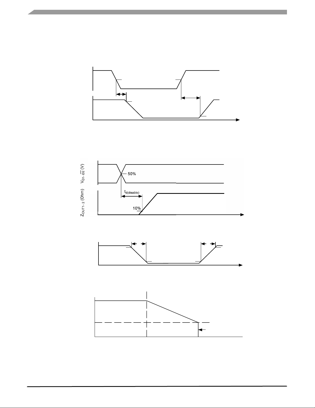
22. Output Delay is the time duration from the midpoint of the IN1 or IN2 input signal to the 10% or 90% point (dependent on the transition
direction) of the OUT1 or OUT2 signal. If the output is transitioning High-to-Low, the delay is from the midpoint of the input signal to the
90% point of the output response signal. If the output is transitioning Low-to-High, the delay is from the midpoint of the input signal to
the 10% point of the output response signal. See Figure 4
23. Rise Time is from the 10% to the 90% level and Fall Time is from the 90% to the 10% level of the output signal. See Figure 6
, page 8.
, page 8.
24. Parameter is guaranteed by design but not production tested.
25. Disable Delay Time is the time duration from the midpoint of the D (disable) input signal to 10% of the output tri-state response. See
Figure 5
, page 8.
26. Increasing currents will become limited at I
state latch-OFF. See Figures 8
above 160
°C will cause the active current limiting to progressively “fold-back” (or decrease) to 2.5 A typical at 175°C where thermal
latch-OFF will occur. See Figure 7
and 9, page 9. Active current limiting will cause junction temperatures to rise. A junction temperature
, page 8.
. Hard shorts will breach the I
LIM
SCH
or I
limit, forcing the output into an immediate tri-
SCL
µs
µs
ns
33886
Analog Integrated Circuit Device Data
Freescale Semiconductor 7
TIMING DIAGRAMS
TIMING DIAGRAMS
5.0
)
V
(
2
N
I
,
1
N
I
V
0
V
)
PWR
V
(
2
,
1
T
U
O
V
0
5.0 V
50%
t
d(ON)
50%
90%
TIME
Figure 4. Output Delay Time
t
d(OFF)
10%
0 V
∞Ω
0 Ω
Figure 5. Disable Delay Time
V
)
PWR
V
(
2
,
1
T
U
O
V
0
90%
t
f
10%
10%
t
r
90%
Figure 6. Output Switching Time
)
A
(
T
6.5
6.6
N
E
R
R
U
C
T
2.5
U
CURRENT (A)
P
,
T
U
O
I
,
,
X
A
M
I
I
LIM
LIM
160 175
TJ, JUNCTION TEMPERATURE (oC)
Thermal Shutdown
Figure 7. Active Current Limiting Versus Temperature (Typical)
33886
Analog Integrated Circuit Device Data
8 Freescale Semiconductor
)
TIM
E
A
(
T
N
E
R
R
U
C
T
U
P
T
, CURRENT (A)
U
O
,
,
OUT
D
I
A
O
OUT
L
I
8.0
6.5
Diode Reverse
Re c o ve r y Sp i ke s
Load Capacitance and/or
Diode Reverse Recovery Spikes
I
Short Circuit Detect Threshold
SCL
Typ. Short Ckt. Detect Threshold
for Low-Side FETs
Typical Current Limiting Threshold
Typ. Curr ent Limit Threshold
PWM
Active
Current
Current
Limiting
Limiting
(See Figure 7)
(See Figure 6)
(See Figure 7)
Hard Short Detect an d Lat ch-OFF
Hard Short Detect and Latch-Off
0
N
I
C
I
G
O
L
,
n
N
I
N
I
C
I
G
O
L
,
1
D
N
I
C
I
G
O
L
,
2
D
T
U
O
C
I
G
O
L
,
S
SF I
F
[1]
[0]
[1]
[0]
[1]
[0]
[1]
[0]
IN2 or IN1
IN1 OR IN 2
IN1 or IN2
IN2
Ou tp u ts
Outputs
Tristated
Tri-stated
IN1 IN2
IN1
IN2
Outputs
Outputs
Tristated
Tri-stated
IN1 or IN2
IN2IN1
OR
IN2 or IN1
IN2 IN1OR
Outputs Operat ional
Outputs Operational
(per Input Contr ol Condition)
(per Input Control Condition)
Figure 8. Active Current Limiting Versus Time
OR IN1
)
A
(
T
N
E
R
R
U
C
T
U
P
T
, CURRENT (A)
U
O
,
OUT
D
I
A
O
L
I
8.0
6.5
t
a
I
Short Circuit Detect Threshold
Short Circuit Detect Threshold
Overcurrent Minimum Threshold
SCL
ta = Output Latch-OFF Time
ta= Tristate Output OFF Time
t
b
= Output Blanking Time
t
t
= Current Limit Blank Time
b
b
Typical Current
Typical PWM Load
Limiting Waveform
Current Limiting
Waveform
Hard Output
Hard Short Detect
Short Latch-OFF
Latch-Off Prevented During t
b
TIME
Figure 9. Active Current Limiting Detail
33886
Analog Integrated Circuit Device Data
Freescale Semiconductor 9

TYPICAL SWITCHING WAVEFORMS
TYPICAL SWITCHING WAVEFORMS
Important For all plots, the following applies:
• Ch2 = 2.0 A per division
•L
•L
•R
= 533 µH @ 1.0 kHz
LOAD
= 530 µH @ 10.0 kHz
LOAD
= 4.0 Ω
LOAD
Output Voltage
(OUT1)
I
OUT
Input Voltage
(IN1)
V+= 24 V f
=1.0 kHz Duty Cycle= 10%
PWM
Output Voltage
(OUT1)
I
OUT
Input Voltage
(IN1)
V+= 34 V f
=1.0 kHz Duty Cycle=90%
PWM
Figure 12. Output Voltage and Current vs. Input Voltage
at V+ = 34 V, PMW Frequency of 1.0 kHz,
and Duty Cycle of 90%, Showing Device in
Current Limiting Mode
Figure 10. Output Voltage and Current vs. Input Voltage
at V+ = 24 V, PMW Frequency of 1.0 kHz,
and Duty Cycle of 10%
Output Voltage
(OUT1)
I
OUT
Input Voltage
(IN1)
V+=24 V f
=1.0 kHz Duty Cycle= 50%
PWM
Output Voltage
(OUT1)
I
OUT
Input Voltage
(IN1)
V+=22 V f
=1.0 kHz Duty Cycle= 90%
PWM
Figure 13. Output Voltage and Current vs. Input Voltage
at V+
= 22 V, PMW Frequency of 1.0 kHz,
and Duty Cycle of 90%
Figure 11. Output Voltage and Current vs. Input Voltage
at V+
= 24 V, PMW Frequency of 1.0 kHz,
and Duty Cycle of 50%
33886
Analog Integrated Circuit Device Data
10 Freescale Semiconductor

TYPICAL SWITCHING WAVEFORMS
%
%
%
%
Output Voltage
(OUT1)
I
OUT
Input Voltage
(IN1)
V+=24 V f
=10 kHz Duty Cycle=50
PWM
Figure 14. Output Voltage and Current vs. Input Voltage
at V+
= 24 V, PMW Frequency of 10 kHz,
and Duty Cycle of 50%
Output Voltage
(OUT1)
I
OUT
Input Voltage
(IN1)
V+=12 V f
=20 kHz Duty Cycle= 50
PWM
Figure 16. Output Voltage and Current vs. Input Voltage
at V+
= 12 V, PMW Frequency of 20 kHz,
and Duty Cycle of 50% for a Purely Resistive Load
Output Voltage
(OUT1)
I
OUT
Input Voltage
(IN1)
V+=24 V f
=10 kHz Duty Cycle= 90
PWM
Figure 15. Output Voltage and Current vs. Input Voltage
at V+
= 24 V, PMW Frequency of 10 kHz,
and Duty Cycle of 90%
Output Voltage
(OUT1)
I
OUT
Input Voltage
(IN1)
V+= 12 V f
=20 kHz Duty Cycle=90
PWM
Figure 17. Output Voltage and Current vs. Input Voltage
at V+
= 12 V, PMW Frequency of 20 kHz,
and Duty Cycle of 90% for a Purely Resistive Load
33886
Analog Integrated Circuit Device Data
Freescale Semiconductor 11

TYPICAL SWITCHING WAVEFORMS
Table 5. Truth Table
The tri-state conditions and the fault status are reset using D1 or
D2. The truth table uses the following notations: L = Low,
H = High, X = High or Low, and Z = High impedance (all output power transistors are switched off).
Device State
D1 D2 IN1 IN2 FS OUT1 OUT2
Forward
Reverse
Freewheeling Low
Freewheeling High
Disable 1 (D1)
Disable 2 (D2
IN1 Disconnected
IN2 Disconnected
D1 Disconnected
D2 Disconnected
Undervoltage
Overtemperature
Short Circuit
Notes
27. In the case of an undervoltage condition, the outputs tri-state and the fault status is set logic Low. Upon undervoltage recovery, fault
28. When a short circuit or overtemperature condition is detected, the power outputs are tri-state latched-OFF independent of the input
)
(27)
(28)
(28)
status is reset automatically or automatically cleared and the outputs are restored to their original operating condition.
signals and the fault status flag is set logic Low.
LHHL H H L
LHLH H L H
LHLL H L L
LHHH H H H
HXXX L Z Z
XLXX L Z Z
LHZX H H X
LHXZ H X H
ZXXX L Z Z
XZXX L Z Z
XXXX L Z Z
XXXX L Z Z
XXXX L Z Z
Input Conditions
Fault Status
Flag
Output States
33886
Analog Integrated Circuit Device Data
12 Freescale Semiconductor

0.40
0.35
0.30
0.25
0.20
Ohms
0.15
0.10
ELECTRICAL PERFORMANCE CURVES
ELECTRICAL PERFORMANCE CURVES
0.05
0.0
59117131519 3733 35 3927 412917 21 23 25 31
Volts
Figure 18. Typical High-Side R
DS(ON)
Versus V+
0.13
0.128
0.126
Ohms
0.124
OHMS
0.122
0.12
59117131519 3733 35 3927 412917 21 23 25 31
Volts
V
PWR
Figure 19. Typical Low-Side R
Analog Integrated Circuit Device Data
Freescale Semiconductor 13
DS(ON)
Versus V+
33886

ELECTRICAL PERFORMANCE CURVES
9.0
8.0
7.0
6.0
5.0
OHMS
4.0
milli amperes
3.0
2.0
1.0
0.0
59117131519 3733 35 3927 412917 21 23 25 31
Volts
V
PWR
Figure 20. Typical Quiescent Supply Current Versus V+
33886
Analog Integrated Circuit Device Data
14 Freescale Semiconductor

FUNCTIONAL DESCRIPTION
INTRODUCTION
FUNCTIONAL DESCRIPTION
INTRODUCTION
Numerous protection and operational features (speed,
torque, direction, dynamic braking, and PWM control), in
addition to the 5.0 A current capability, make the 33886 a
very attractive, cost-effective solution for controlling a broad
range of fractional horsepower DC motors. A pair of 33886
devices can be used to control bipolar stepper motors in both
directions. In addition, the 33886 can be used to control
permanent magnet solenoids in a push-pull variable force
fashion using PWM control. The 33886 can also be used to
excite transformer primary windings with a switched square
wave to produce secondary winding AC currents.
As shown in Figure 2
, the 33886 is a fully protected monolithic H-Bridge
page 2
with Fault Status reporting. For a DC motor to run the input
conditions need be as follows: D1 input logic Low, D2 input
logic High, FS
and the other IN logic High to define output polarity. The
33886 can execute dynamic braking by simultaneously
turning on either both high-side
MOSFETs in the output H-Bridge; e.g., IN1 and IN2 logic
High or IN1 and IN2 logic Low.
The 33886 outputs are capable of providing a continuous
DC load current of 5.0 A from a 40 V V+ source. An internal
charge pump supports PWM frequencies up to 10 kHz. An
flag cleared (logic High), with one IN logic Low
, Simplified Internal Block Diagram,
MOSFETs or both low-side
external pull-up resistor is required for the open drain FS
terminal for fault status reporting.
Two independent inputs (IN1 and IN2) provide control of
the two totem-pole half-bridge outputs. Two disable inputs
(D1 and D2
impedance state (all H-Bridge switches OFF).
The 33886 has undervoltage shutdown with automatic
recovery, active current limiting, output short-circuit latchOFF, and overtemperature latch-OFF. An undervoltage
shutdown, output short circuit latch-OFF, or overtemperature
latch-OFF fault condition will cause the outputs to turn OFF
(i.e., become high impedance or tri-stated) and the fault
output flag to be set Low. Either of the Disable inputs or V+
must be “toggled” to clear the fault flag.
The short circuit / overtemperature shutdown scheme is
unique and best described as using a junction temperaturedependent active current “fold back” protection scheme.
When a short circuit condition is experienced, the current
limited output is “ramped down” as the junction temperature
increases above 160°C, until at 175°C the current has
decreased to about 2.5 A. Above 175°C, overtemperature
shutdown (latch-OFF) occurs. This feature allows the device
to remain in operation for a longer time with unexpected
loads, while still retaining adequate protection for both the
device and the load.
) are for forcing the H-Bridge outputs to a high
FUNCTIONAL TERMINAL DESCRIPTION
POWER/ANALOG GROUNDS (PGND AND AGND)
Power and analog ground terminals. The power and
analog ground terminals should be connected together with a
very low impedance connection.
POSITIVE POWER SUPPLY (V+)
V+ terminals are the power supply inputs to the device. All
V+ terminals must be connected together on the printed
circuit board with as short as possible traces offering as low
impedance as possible between terminals.
V+ terminals have an undervoltage threshold. If the supply
voltage drops below a V+ undervoltage threshold, the output
power stage switches to a tri-state condition and the fault
status flag is set and the Fault Status terminal voltage
switched to a logic Low. When the supply voltage returns to a
level that is above the threshold, the power stage
automatically resumes normal operation according to the
established condition of the input terminals and the fault
status flag is automatically reset logic High.
FAULT STATUS (FS)
This terminal is the device fault status output. This output
is an active Low open drain structure requiring a pull-up
resistor to 5.0 V. Refer to Table 5,
Truth Table, page 12.
LOGIC INPUT 1, 2 AND DISABLE1, 2 (IN1, IN2, D1,
AND
D2)
These terminals are input control terminals used to control
the outputs. These terminals are 5.0 V CMOS-compatible
inputs with hysteresis. The IN1 and IN2 independently control
OUT1 and OUT2, respectively. D1 and D2
inputs used to tri-state disable the H-Bridge outputs.
When either D1 or D2
Low) in the disable state, outputs OUT1 and OUT2 are both
tri-state disabled; however, the rest of the device circuitry is
fully operational and the supply I
to a few milliamperes. Refer to Table 5,
Static Electrical Characteristics
is set (D1 = logic High or D2 = logic
Q (standby)
table, page 5.
are complimentary
current is reduced
Truth Table, and
33886
Analog Integrated Circuit Device Data
Freescale Semiconductor 15

FUNCTIONAL DESCRIPTION
FUNCTIONAL TERMINAL DESCRIPTION
H-BRIDGE OUTPUT 1, 2 (OUT1 AND OUT2)
These terminals are the outputs of the H-Bridge with
integrated output FET body diodes. The bridge output is
controlled using the IN1, IN2, D1, and D2
have active current limiting above 6.5 A. The outputs also
have thermal shutdown (tri-state latch-OFF) with hysteresis
as well as short circuit latch-OFF protection.
A disable timer (time t
) incorporated to detect currents
b
that are higher than active current limit is activated at each
inputs. The outputs
output activation to facilitate detecting hard output short
conditions (see Figure 9, page 9).
CHARGE PUMP CAPACITOR (CCP)
Charge pump output terminal. A filter capacitor (up to
33 nF) can be connected from the CCP terminal and PGND.
The device can operate without the external capacitor,
C
although the
the device to perform at maximum speed, timing, and PWM
frequency.
capacitor helps to reduce noise and allows
CP
33886
Analog Integrated Circuit Device Data
16 Freescale Semiconductor

FUNCTIONAL DEVICE OPERATION
FUNCTIONAL DEVICE OPERATION
FUNCTIONAL TERMINAL DESCRIPTION
SHORT CIRCUIT PROTECTION
If an output short circuit condition is detected, the power
outputs tri-state (latch-OFF) independent of the input (IN1
and IN2) states, and the fault status output flag is set logic
Low. If the D1 input changes from logic High to logic Low, or
D2 input changes from logic Low to logic High, the
if the
output bridge will become operational again and the fault
status flag will be reset (cleared) to a logic High state.
The output stage will always switch into the mode defined
by the input terminals (IN1, IN2, D1, and D2
), provided the
device junction temperature is within the specified operating
temperature.
ACTIVE CURRENT LIMITING
The maximum current flow under normal operating
conditions is internally limited to I
the maximum current value is reached, the output stages are
tri-stated for a fixed time (t
) of 20 µs typical. Depending on
a
the time constant associated with the load characteristics, the
current decreases during the tri-state duration until the next
output ON cycle occurs (see Figures 9
page 10, respectively).
The current limiting threshold value is dependent upon the
device junction temperature. When -40°C < TJ < 160°C, I
is between 5.2 A and 7.8 A. When T
current decreases linearly down to 2.5 A typical at 175°C.
Above 175°C the device overtemperature circuit detects T
and overtemperature shutdown occurs (see Figure 7
page 8). This feature allows the device to remain operational
for a longer time but at a regressing output performance level
at junction temperatures above 160°C.
(5.2 A to 7.8 A). When
LIM
and 12, page 9 and
exceeds 160°C, the I
J
LIM
LIM
LIM
,
OVERTEMPERATURE SHUTDOWN AND
HYSTERESIS
If an overtemperature condition occurs, the power outputs
are tri-state (latched-OFF) independent of the input signals
and the fault status flag is set logic Low.
To reset from this condition, D1 must change from logic
High to logic Low, or D2
must change from logic Low to logic
High. When reset, the output stage switches ON again,
provided that the junction temperature is now below the
overtemperature threshold limit minus the hysteresis.
Note Resetting from the fault condition will clear the fault
status flag.
MAIN DIFFERENCES COMPARED TO
MC33186DH1
• COD terminal has been removed. Terminal 8 is now a Do
Not Connect (DNC) terminal.
• Terminal 20 is no longer connected in the 20 HSOP
package. It is now a DNC terminal.
•R
transistor.
• Maximum temperature operation is now 160°C, as
minimum thermal shutdown temperature has increased.
• Current regulation limiting foldback is implemented above
160°C T
• Thermal resistance junction to case has been increased
from ~2.0°C/W to ~5.0°C/W.
max at TJ = 150°C is now 225 mΩ per each output
DS(ON)
.
J
33886
Analog Integrated Circuit Device Data
Freescale Semiconductor 17

FUNCTIONAL DEVICE OPERATION
PERFORMANCE
PERFORMANCE
The 33886 is designed for enhanced thermal
performance. The significant feature of this device is the
exposed copper pad on which the power die is soldered. This
pad is soldered on a PCB to provide heat flow to ambient and
also to provide thermal capacitance. The more copper area
on the PCB, the better the power dissipation and transient
behavior will be.
Example Characterization on a double-sided PCB:
bottom side area of copper is 7.8 cm
(see Figure 21
); grid array of 24 vias 0.3 mm in diameter.
Top Side
2
; top surface is 2.7 cm2
Bottom Side
Figure 21. PCB Test Layout
Figure 22 shows the thermal response with the device
soldered on to the test PCB described in Figure 21.
100
10
Rth (°C/W)
1
0,1
0,001 0,01 0,1 1 10 100 1000 10000
t, Time (s)
Figure 22. 33886 Thermal Response
33886
Analog Integrated Circuit Device Data
18 Freescale Semiconductor

TYPICAL APPLICATIONS
TYPICAL APPLICATIONS
A typical application schematic is shown in Figure 23. For
precision high-current applications in harsh, noisy
AGND
OUT1
PGND
environments, the V+ by-pass capacitor may need to be
substantially larger.
DC
MOTOR
V+
33886
V+
C
CP
33 nF
+
47 µF
OUT2
D2
D1
FS
IN1
IN2
IN2
IN1
FS
D1
D2
Figure 23. 33886 Typical Application Schematic
33886
Analog Integrated Circuit Device Data
Freescale Semiconductor 19

PACKAGING
PACKAGE DIMENSIONS
PACKAGING
PACKAGE DIMENSIONS
Important For the most current revision of the package, visit www.freescale.com and perform a keyword search on 98ASH70702A listed
below.
DH SUFFIX
VW (Pb-FREE) SUFFIX
20-TERMINAL HSOP
PLASTIC PACKAGE
98ASH70702A
ISSUE A
PIN ONE ID
GAUGE
PLANE
D2
A
bbb C
B
A2
18X
X 45
h
_
E2
1
e
20
D
e/2
10
11
EXPOSED
HEATSINK AREA
E1
Y
10X
E
M
bbb C
A
B
DATUM
H
PLANE
E3
D1
E4
BOTTOM VIEW
b1
c1
b
M
A
C
SEATING
PLANE
c
aaa C
SECTION W–W
L1
q
W
W
L
A1
A3
NOTES:
1. CONTROLLING DIMENSION: MILLIMETER.
2. DIMENSIONS AND TOLERANCES PER ASME
Y14.5M, 1994.
3. DATUM PLANE –H– IS LOCATED AT BOTTOM OF
LEAD AND IS COINCIDENT WITH THE LEAD
WHERE THE LEAD EXITS THE PLASTIC BODY AT
THE BOTTOM OF THE PARTING LINE.
4. DIMENSIONS D AND E1 DO NOT INCLUDE MOLD
PROTRUSION. ALLOWABLE PROTRUSION IS
0.150 PER SIDE. DIMENSIONS D AND E1 DO
INCLUDE MOLD MISMATCH AND ARE
DETERMINED AT DATUM PLANE –H–.
5. DIMENSION b DOES NOT INCLUDE DAMBAR
PROTRUSION. ALLOWABLE DAMBAR
PROTRUSION SHALL BE 0.127 TOTAL IN EXCESS
OF THE b DIMENSION AT MAXIMUM MATERIAL
CONDITION.
6. DATUMS –A– AND –B– TO BE DETERMINED AT
DATUM PLANE –H–.
7. DIMENSION D DOES NOT INCLUDE TIEBAR
PROTRUSIONS. ALLOWABLE TIEBAR
PROTRUSIONS ARE 0.150 PER SIDE.
MILLIMETERS
DIM MIN MAX
A 3.000 3.400
A1 0.100 0.300
A2 2.900 3.100
A3 0.00 0.100
D 15.800 16.000
D1 11.700 12.600
D2 0.900 1.100
E 13.950 14.450
E1 10.900 11.100
E2 2.500 2.700
E3 6.400 7.200
E4 2.700 2.900
L 0.840 1.100
L1 0.350 BSC
b 0.400 0.520
b1 0.400 0.482
c 0.230 0.320
c1 0.230 0.280
e 1.270 BSC
h ––– 1.100
q
0 8
__
aaa 0.200
bbb 0.100
(1.600)
DETAIL Y
33886
Analog Integrated Circuit Device Data
20 Freescale Semiconductor

ADDITIONAL DOCUMENTATION
ADDITIONAL DOCUMENTATION
THERMAL ADDENDUM - REVISION 2.0
THERMAL ADDENDUM - REVISION 2.0
5.0 A H-Bridge
Introduction
This thermal addendum is provided as a supplement to the MC33186
technical data sheet. The addendum provides thermal performance
information that may be critical in the design and development of system
applications. All electrical, application, and packaging information is provided
in the data sheet.
Packaging and Thermal Considerations
The MC33186 is offered in a 20 terminal HSOP exposed pad, single die
package. There is a single heat source (P), a single junction temperature
(T
), and thermal resistance (R
J
T
J
The stated values are solely for a thermal performance comparison of one
package to another in a standardized environment. This methodology is not
meant to and will not predict the performance of a package in an applicationspecific environment. Stated values were obtained by measurement and
simulation according to the standards listed below.
).
θJA
θJA
.
P
=
R
33886
20-TERMINAL
HSOP-EP
VW SUFFIX (Pb-free)
DH SUFFIX
98ASH70702A
20-TERMINAL HSOP
Note For package dimensions, refer to
the 33886 device data sheet.
Standards
Table 6. Thermal Performance Comparison
Thermal Resistance [°C/W]
(1)(2)
R
θJA
(2)(3)
R
θJB
(1)(4)
R
θJA
(5)
R
θJC
NOTES:
1.Per JEDEC JESD51-2 at natural convection, still air condition.
2.2s2p thermal test board per JEDEC JESD51-5 and JESD51-7.
3.Per JEDEC JESD51-8, with the board temperature on the center
trace near the center lead.
4.Single layer thermal test board per JEDEC JESD51-3 and
JESD51-5.
5.Thermal resistance between the die junction and the exposed
pad surface; cold plate attached to the package bottom side,
remaining surfaces insulated.
20
6.0
52
1.0
1.0
1.0
0.2
0.2
* All measurements
are in millimeters
Soldermast
openings
20 Terminal HSOP-EP
1.27 mm Pitch
16.0 mm x 11.0 mm Body
12.2 mm x 6.9 mm Exposed Pad
Thermal vias
connected to top
buried plane
Figure 24. Thermal Land Pattern for Direct Thermal
Attachment According to JESD51-5
33886
Analog Integrated Circuit Device Data
Freescale Semiconductor 21

ADDITIONAL DOCUMENTATION
THERMAL ADDENDUM - REVISION 2.0
A
DNCAGND
IN2
D1
C
CP
V+
OUT2
OUT2
D2
PGND
11
PGND
FS
IN1
V+
V+
OUT1
OUT1
DNC
PGND
PGND
1
2
3
4
5
6
7
8
9
10
20
19
18
17
16
15
14
13
12
33886 Terminal Connections
20-Terminal HSOP
1.27 mm Pitch
16.0 mm x 11.0 mm Body
12.2 mm x 6.9 mm Exposed Pad
Figure 25. Thermal Test Board
Device on Thermal Test Board
Material: Single layer printed circuit board
FR4, 1.6 mm thickness
Cu traces, 0.07 mm thickness
Outline: 80 mm x 100 mm board area,
including edge connector for thermal
testing
Area A: Cu heat-spreading areas on board
surface
Ambient Conditions: Natural convection, still air
Table 7. Thermal Resistance Performance
Thermal
Resistance
R
JA
θ
R
JS
θ
Area A (mm
2
) °C/W
0.0 52
300 36
600 32
0.0 10
300 7.0
600 6.0
R
is the thermal resistance between die junction and
JA
θ
ambient air.
R
is the thermal resistance between die junction and the
JS
θ
reference location on the board surface near a center lead of the
package (see
33886
Figure 25).
Analog Integrated Circuit Device Data
22 Freescale Semiconductor

60
]
50
40
ADDITIONAL DOCUMENTATION
THERMAL ADDENDUM - REVISION 2.0
100
10
1
Thermal Resistance [ºC/W
30
R
x
θ
JA
20
10
0
0 300 600
Heat spreading area A [mm²]
Figure 26. Device on Thermal Test Board R
R
x
θ
JA
θJA
Thermal Resistance [ºC/W]
0.1
1.00E-03 1.00E-02 1.00E-01 1.00E+00 1.00E+01 1.00E+02 1.00E+03 1.00E+04
Time(s)
Figure 27. Transient Thermal Resistance R
JA
θ
time[s]
Device on Thermal Test Board Area A = 600 (mm2)
33886
Analog Integrated Circuit Device Data
Freescale Semiconductor 23

REVISION HISTORY
REVISION HISTORY
Revision Date Description of Changes
7.0
7/2005
• Implemented Revision History page
• Added Thermal Addendum
• Converted to Freescale format
33886
Analog Integrated Circuit Device Data
24 Freescale Semiconductor

NOTES
NOTES
33886
Analog Integrated Circuit Device Data
Freescale Semiconductor 25

NOTES
NOTES
33886
Analog Integrated Circuit Device Data
26 Freescale Semiconductor

NOTES
NOTES
33886
Analog Integrated Circuit Device Data
Freescale Semiconductor 27

How to Reach Us:
Home Page:
www.freescale.com
E-mail:
support@freescale.com
USA/Europe or Locations Not Listed:
Freescale Semiconductor
Technical Information Center, CH370
1300 N. Alma School Road
Chandler, Arizona 85224
+1-800-521-6274 or +1-480-768-2130
support@freescale.com
Europe, Middle East, and Africa:
Freescale Halbleiter Deutschland GmbH
Technical Information Center
Schatzbogen 7
81829 Muenchen, Germany
+44 1296 380 456 (English)
+46 8 52200080 (English)
+49 89 92103 559 (German)
+33 1 69 35 48 48 (French)
support@freescale.com
Japan:
Freescale Semiconductor Japan Ltd.
Headquarters
ARCO Tower 15F
1-8-1, Shimo-Meguro, Meguro-ku,
Tokyo 153-0064
Japan
0120 191014 or +81 3 5437 9125
support.japan@freescale.com
Asia/Pacific:
Freescale Semiconductor Hong Kong Ltd.
Technical Information Center
2 Dai King Street
Tai Po Industrial Estate
Tai Po, N.T., Hong Kong
+800 2666 8080
support.asia@freescale.com
For Literature Requests Only:
Freescale Semiconductor Literature Distribution Center
P.O. Box 5405
Denver, Colorado 80217
1-800-441-2447 or 303-675-2140
Fax: 303-675-2150
LDCForFreescaleSemiconductor@hibbertgroup.com
Information in this document is provided solely to enable system and software
implementers to use Freescale Semiconductor products. There are no express or
implied copyright licenses granted hereunder to design or fabricate any integrated
circuits or integrated circuits based on the information in this document.
Freescale Semiconductor reserves the right to make changes without further notice to
any products herein. Freescale Semiconductor makes no warranty, representation or
guarantee regarding the suitability of its products for any particular purpose, nor does
Freescale Semiconductor assume any liability arising out of the application or use of any
product or circuit, and specifically disclaims any and all liability, including without
limitation consequential or incidental damages. “Typical” parameters that may be
provided in Freescale Semiconductor data sheets and/or specifications can and do vary
in different applications and actual performance may vary over time. All operating
parameters, including “Typicals”, must be validated for each customer application by
customer’s technical experts. Freescale Semiconductor does not convey any license
under its patent rights nor the rights of others. Freescale Semiconductor products are
not designed, intended, or authorized for use as components in systems intended for
surgical implant into the body, or other applications intended to support or sustain life,
or for any other application in which the failure of the Freescale Semiconductor product
could create a situation where personal injury or death may occur. Should Buyer
purchase or use Freescale Semiconductor products for any such unintended or
unauthorized application, Buyer shall indemnify and hold Freescale Semiconductor and
its officers, employees, subsidiaries, affiliates, and distributors harmless against all
claims, costs, damages, and expenses, and reasonable attorney fees arising out of,
directly or indirectly, any claim of personal injury or death associated with such
unintended or unauthorized use, even if such claim alleges that Freescale
Semiconductor was negligent regarding the design or manufacture of the part.
Freescale™ and the Freescale logo are trademarks of Freescale Semiconductor, Inc.
All other product or service names are the property of their respective owners.
© Freescale Semiconductor, Inc., 2005. All rights reserved.
MC33886
Rev 7.0
07/2005
 Loading...