

Page 1
Freescale Semiconductor
Advance Information
Dual DBUS Master with
Document Number: MC33780
Rev 4.0, 11/2006
Differential Drive and
Frequency Spreading
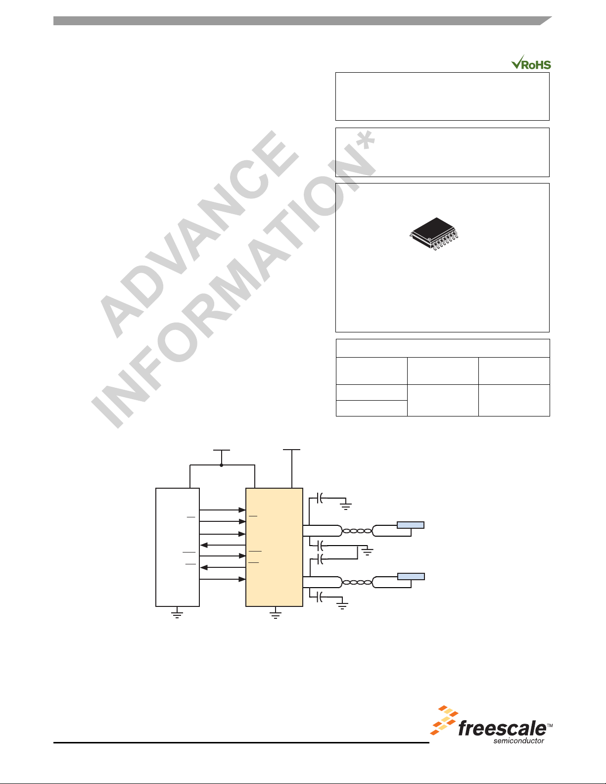
The 33780 is a master device for two differential DBUS buses. It
contains the logic to interface the buses to a standard serial
peripheral interface (SPI) port and the analog circuitry to drive data
and power over the bus as well as receive data from the remote slave
devices.
The differential mode of the 33780 generates lower electromagnetic interference (EMI) in situations where data rates and wiring
make this a problem. Frequency spreading further reduces interference by spreading the energy across many channels, reducing
the energy in any single channel.
Features
• Two Independent DBUS I /Os
• Common SPI Interface for All Operations
• Open-Drain Interrupt Output with Pull-up
• Maskable Interrupts for Send and Receive Data Status
• Automatic Message Cyclical Redundancy Checking (CRC)
Generation and Checking
• Four-Stage Transmit and Receive Buffers
• 8- to 16-Bit Messages with 0- to 8-Bit CRC
• Independent Frequency Spreading for Each Channel
• Pb-Free Packaging Designated by Suffix Code EG
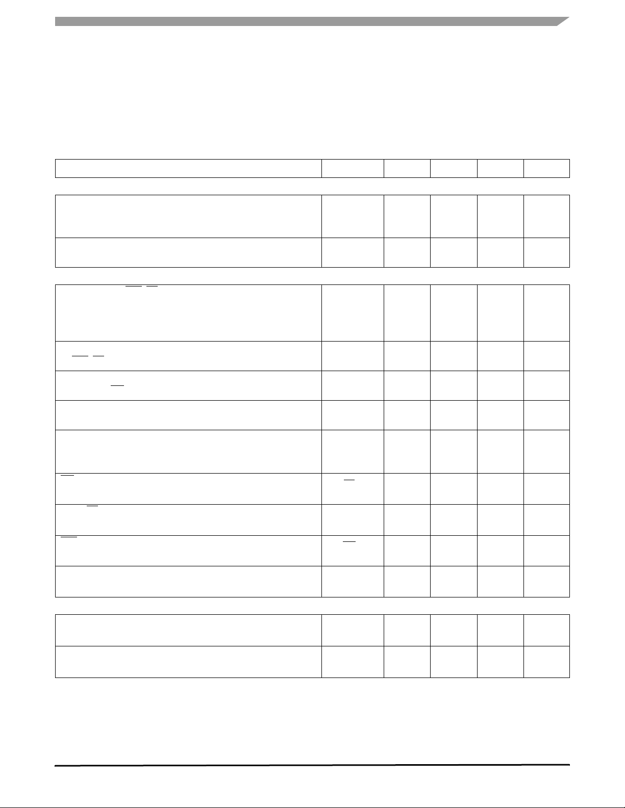
DIFFERENTIAL DBUS MASTER
ORDERING INFORMATION
Device
MC33780EG/R2
MCZ33780EG/R2
33780
EG (PB-FREE SUFFIX)
98ASB42567B
16-PIN SOICW
Temperature
Range (T
-40°C to 85°C 16 SOICW
)
A
Package
+5.0 V +25 V
MCU
VCC
SCLK
CS
MOSI
MISO
RST
INT
CLK
GND
VCC
SCLK
CS
MOSI
MISO
RST
INT
CLK
33780
VSUP
D0H
D0L
D1H
D1L
GND
Figure 1. 33780 Simplified Application Diagram
* This document contains certain information on a new product.
Specifications and information herein are subject to change without notice.
© Freescale Semiconductor, Inc., 2006. All rights reserved.
DSI/DBUS SLAVE
Twisted Pair
4.7 nF capacitors from D0H, D0L, D1H
and D1L to circuit ground are required
for proper operation.
33793
DSI/DBUS SLAVE
33793
Page 2
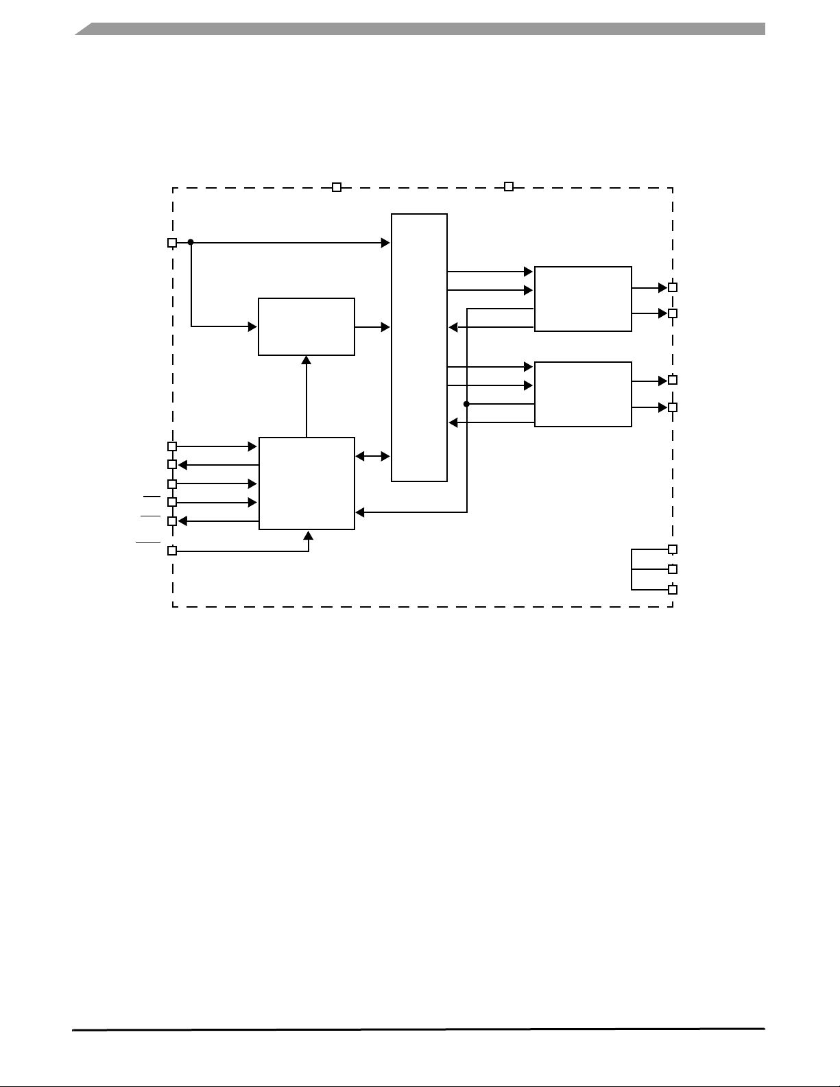
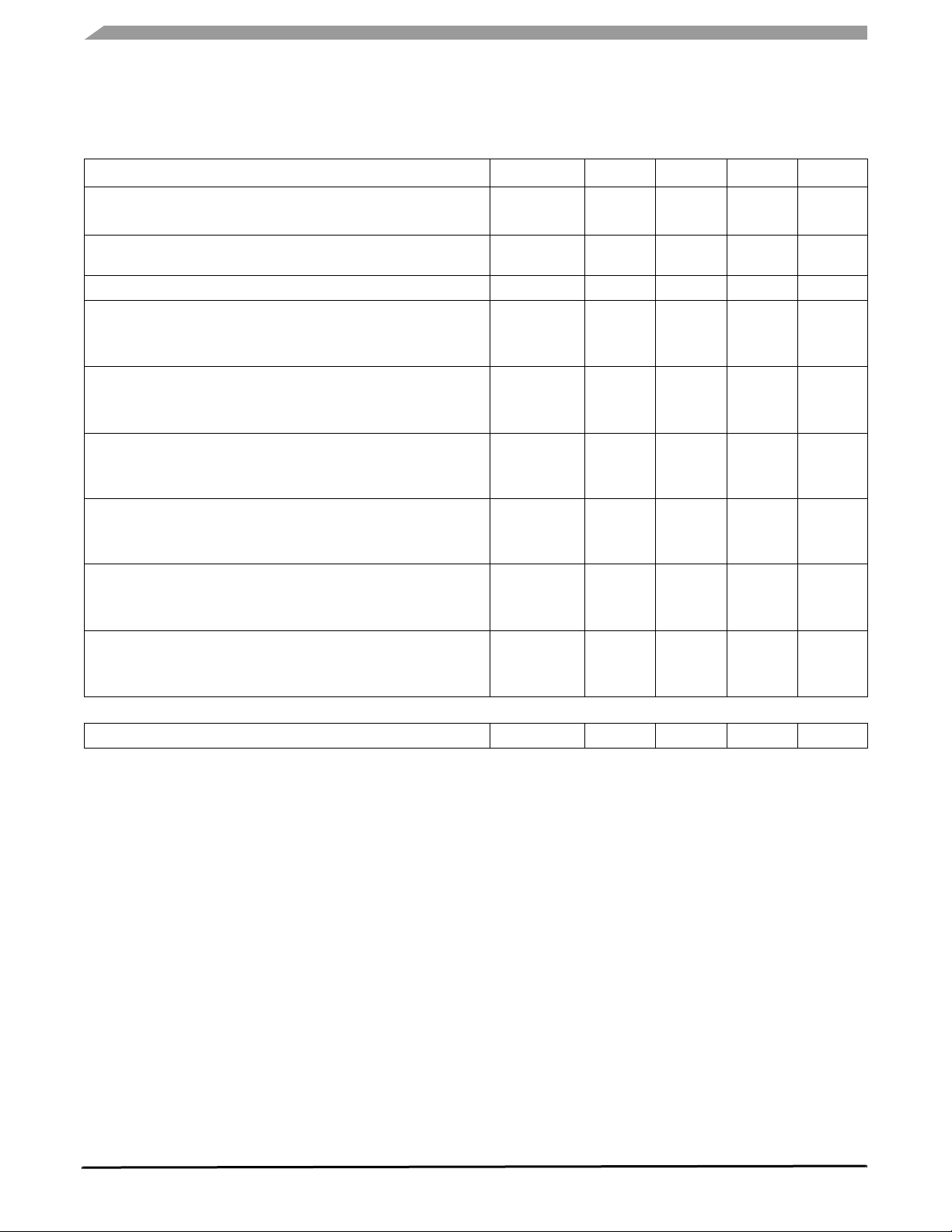
INTERNAL BLOCK DIAGRAM
CLK
INTERNAL BLOCK DIAGRAM
VCC VSUP
Spreader
Protocol Engine
DSIF
DSIS
DSIR
DSIF
DSIS
DSIR
DBUS
Driver/Receiver
DBUS
Driver/Receiver
D0H
D0L
D1H
D1L
SCLK
MISO
MOSI
CS
INT
RST
SPI,
Registers and
Interrupt
Generator
Figure 2. 33780 Internal Block Diagram
T
LIM
GND
GND
GND
33780
Analog Integrated Circuit Device Data
2 Freescale Semiconductor
Page 3
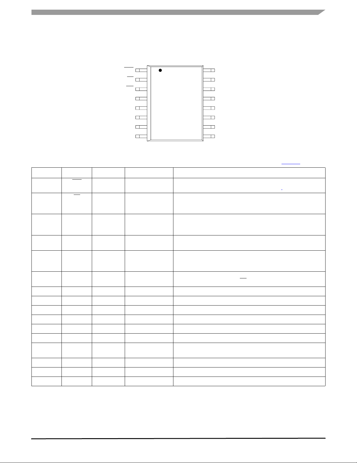
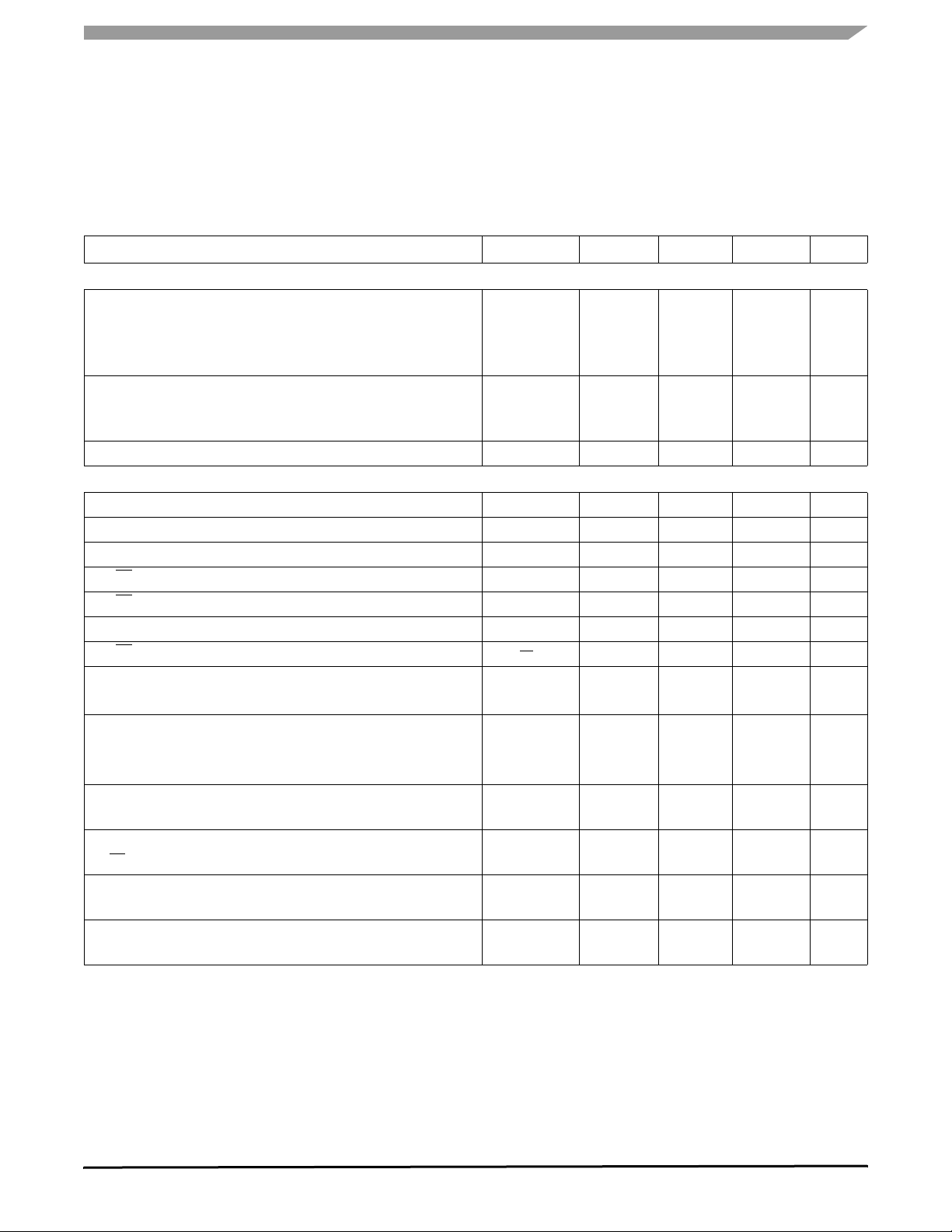
PIN CONNECTIONS
PIN CONNECTIONS
RST
CS
INT
MOSI
SCLK
MISO
CLK
GND
1
2
3
4
5
6
7
8
16
15
14
13
12
11
10
9
GND
D0L
D0H
VSUP
D1H
D1L
GND
VCC
Figure 3. 33780 Pin Connections
Table 1. 33780 Pin Definitions
A functional description of each pin can be found in the Functional Pin Descriptions section beginning on page 13.
Pin Pin Name Pin Function Formal Name Definition
1 RST Reset IC Reset
2 CS Input SPI Chip Select Input
3 INT Output Interrupt Output
4 MOSI Input Master Out Slave In
5 SCLK Input Serial Data Clock
6 MISO Output Master In Slave Out
7 CLK Input Clock Input
8 GND Ground Ground
9 VCC Input Logic Supply
10 GND Ground Power Ground
11 D1L Output Driver Low-Side Bus 1
12 D1H Output Driver High-Side Bus 1
13 VSUP Output Positive Supply for
Bus Output
14 D0H Output Driver High-Side Bus 0
15 D0L Output Driver Low-Side Bus 0
16 GND Ground Power Ground
A low level on this pin returns all registers to a known state as indicated
in the section entitled
Register and Bit Descriptions.
When this signal is high, SPI signals are ignored. Asserting this pin low
starts an SPI transaction. The SPI transaction is signaled as completed
when this signal returns high.
This output will be asserted low when an enabled interrupt condition
occurs. It contains a pullup current source that will perform a pullup when
unasserted.
SPI data into this IC. This data input is sampled on the positive edge of
SCLK.
Clocks in /out the data to/from the SPI. MISO data changes on the
negative transition of the SCLK. MOSI is sampled on the positive edge of
the SCLK.
SPI data sent to the MCU by this device. This data output changes on the
negative edge of SCLK. When
CS is high, this pin is high impedance.
4.0 MHz clock input.
Ground reference for analog and digital circuits.
Logic power source input.
Bus 1 power return.
Bus 1 low side.
Bus 1 high side.
This supply input is used to provide the positive level output of the bus.
Bus 0 high side.
Bus 0 low side.
Bus 0 power return.
33780
Analog Integrated Circuit Device Data
Freescale Semiconductor 3
Page 4
ELECTRICAL CHARACTERISTICS
MAXIMUM RATINGS
ELECTRICAL CHARACTERISTICS
MAXIMUM RATINGS
Table 2. Maximum Ratings
All voltages are with respect to ground unless otherwise noted. Exceeding these ratings may cause a malfunction or
permanent damage to the device.
Ratings Symbol Value Unit
ELECTRICAL RATINGS
Supply Voltages
V
SUP
Load Dump V
V
CC
(300 ms maximum)
SUP
Maximum Voltage on Logic Input /Output Pins
Maximum Voltage on DBUS Pins
Maximum DBUS Pin Current
Maximum Logic Pin Current
ESD Voltage 1
Human Body Model (HBM)
Machine Model (MM)
Charge Device Model (CDM)
THERMAL RATINGS
Storage Temperature
Operating Ambient Temperature
Operating Junction Temperature
Thermal Shutdown
Resistance, Junction-to-Ambient
Resistance, Junction-to-Board
Peak Package Reflow Temperature During Reflow
(2), (3)
Notes
1. ESD1 testing is performed in accordance with the Human Body Model (HBM) (C
performed in accordance with the Machine Model (MM) (C
= 200 pF, R
ZAP
2. Pin soldering temperature limit is for 10 seconds maximum duration. Not designed for immersion soldering. Exceeding these limits may
cause malfunction or permanent damage to the device.
3. Freescale’s Package Reflow capability meets Pb-free requirements for JEDEC standard J-STD-020C. For Peak Package Reflow
Temperature and Moisture Sensitivity Levels (MSL),
Go to www.freescale.com, search by part number [e.g. remove prefixes/suffixes and enter the core ID to view all orderable parts. (i.e.
MC33xxxD enter 33xxx), and review parametrics.
V
SUP
V
SUPLD
V
CC
– -0.3 to V
V
DBUS
I
DBUS
I
LOGIC
V
ESD
-0.3 to 26.5
40
-0.3 to 7.0
+ 0.3 V
CC
-0.3 to V
+ 0.3 V
SUP
400 mA
20 mA
±2000
±200
±750 for corner pins
±500 for others
T
STG
T
A
T
J
T
SD
R
JA
Θ
R
JB
Θ
T
PPRT
= 100 pF, R
ZAP
= 0 Ω); and Charge Body Model (CBM).
ZAP
-55 to 150 °C
-40 to 85 °C
-40 to 150 °C
155 to 190 °C
109 °C/W
50 °C/W
Note 3 °C
= 1500 Ω); ESD2 testing is
ZAP
V
V
33780
Analog Integrated Circuit Device Data
4 Freescale Semiconductor
Page 5
STATIC ELECTRICAL CHARACTERISTICS
ELECTRICAL CHARACTERISTICS
STATIC ELECTRICAL CHARACTERISTICS
Table 3. Static Electrical Characteristics
Characteristics noted under conditions 4.75 V ≤ VCC ≤ 5.25 V, 9.0 V ≤ V
noted. Voltages relative to GND unless otherwise noted. Typical values noted reflect the approximate parameter means at
TA = 25°C under nominal conditions unless otherwise noted.
Characteristic Symbol Min Typ Max Unit
≤ 25 V,- 40°C ≤ T
SUP
≤ 85°C unless otherwise
A
POWER INPUT REQUIREMENTS (V
I
Supply Current (| I
VSUP
| ≤ 10 µA) (Test Mode, CLK = 4.0 MHz)
BUS
SUP
, VCC)
Idle, HiZ
Signal High, Signal Low
I
Supply Current (Test Mode, CLK = 4.0 MHz)
VCC
Signal High, Signal Low
MICROCONTROLLER INTERFACE (RST, CS, MOSI, SCLK, AND CLK)
I / O Logic Levels (RST, CS, MOSI, SCLK, and CLK)
Input High
Input Low
Input Hysteresis
Input Capacitance
(4)
(4)
RST, CS, MOSI, SCLK, and CLK
Output Low Voltage
MISO and INT Pins = 0.3 mA
Output High Voltage
MISO Pin = - 0.3 mA
Output Leakage Current
MISO Pin = 0 V
MISO Pin = V
CC
INT Pullup Current
V
= V
CC
- 1.0 V
OUT
SCLK, CS Pullup Current
V
= V
CC
- 1.0 V
OUT
RST Pulldown Current
V
= 1.0 V
OUT
CLK, MOSI Pulldown Current
V
= 1.0 V
OUT
BUS TRANSMITTER (D0H, D0L, D1H, D1L)
Output Bus Idle Voltage (Differential)
InH = -200 mA, InL = 200 mA
(5)
Output Signal High Voltage (Differential)
-12.5 mA ≤ InH ≤ 1.0 mA, -1.0 mA ≤ InL ≤ 12.5 mA
(5)
Notes
4 Not measured in production.
5 InH = bus current at DnH, InL = bus current at DnL.
6V
DnD
= V
DnH
- V
DnL
.
I
VSUP
I
VCC
V
V
V
HYST
C
V
OL
V
OH
I
MISO
I
INTPU
I
PU
I
RSTPD
I
PD
V
DnD(
IDLE)
V
DnD (HIGH)
mA
–
–
6.5
15
10
23
mA
– 4.5 6.0
IH
IL
I
0.7
–
–
–
–
500
0.3
–
–
V
V
mV
CC
CC
pF
– 10 20
V
0 – 0.8
V
V
- 0.8 – V
CC
CC
µA
-10
-10
–
–
10
10
µA
-100 -75 -50
µA
-20 -10 -5.0
µA
4.0 7.0 10
µA
5.0 10 20
(6)
V
- 2.5 – –
SUP
(6)
V
V
4.175 4.5 4.825
33780
Analog Integrated Circuit Device Data
Freescale Semiconductor 5
Page 6
ELECTRICAL CHARACTERISTICS
STATIC ELECTRICAL CHARACTERISTICS
Table 3. Static Electrical Characteristics (continued)
Characteristics noted under conditions 4.75 V ≤ VCC ≤ 5.25 V, 9.0 V ≤ V
≤ 25 V,- 40°C ≤ T
SUP
≤ 85°C unless otherwise
A
noted. Voltages relative to GND unless otherwise noted. Typical values noted reflect the approximate parameter means at
TA = 25°C under nominal conditions unless otherwise noted.
Characteristic Symbol Min Typ Max Unit
Output Signal Low Voltage (Differential)
-12.5 mA ≤ InH ≤ 1.0 mA, -1.0 mA ≤ InL ≤ 12.5 mA
(5)
Vmid, (DnH + DnL) / 2 (Voltage Halfway Between Bus High Side and
Bus Low Side)
VCM Peak-to-Peak, Vmid (Signal High) - Vmid (Signal Low)
(7)
Output High-Side (DnH) Idle Driver Current Limit (DnL open)
Source: DnH = 0 V
Sink: DnH = V
SUP
Output Low-Side (DnL) Idle Driver Current Limit (DnH open)
Source: DnL = 0 V
Sink: DnL = V
SUP
Output High-Side (DnH) Signal Driver Overcurrent Shutdown
Source: Signal High, Signal Low
Sink: Signal High, Signal Low
Output Low-Side (DnL) Signal Driver Overcurrent Shutdown
Source: Signal High, Signal Low
Sink: Signal High, Signal Low
Disabled High-Side (DnH) Bus Leakage (DnL open)
DnH = 0 V
DnH = V
SUP
Disabled Low-Side (DnL) Bus Leakage (DnH open)
DnL = 0 V
DnL = V
SUP
BUS RECEIVER (D0H, D0L, D1H, D1L)
Comparator Trip Point
Notes
7 Not measured in production.
V
DnD (LOW)
I
ICL (HIGH)
I
ICL (LOW)
I
SCL (HIGH)
I
SCL (LOW)
I
LK(HIGH)
I
LK(LOW)
COMP(TRIP) 5.0 6.0 7.0 mA
(6)
V
1.175 1.5 1.825
V
mid
V
CM
pp
V
/ 2 -
V
SUP
1.0
/ 2 V
SUP
SUP
2 + 1.0
/
– 0.3 – V
V
mA
-400
100
–
–
-200
–
mA
–
200
–
–
-100
400
mA
-100
30
–
–
-30
100
mA
-100
30
–
–
-30
100
mA
-1.0
-1.0
-0.18
0.25
1.0
1.0
mA
-1.0
-1.0
-0.4
0.08
1.0
1.0
33780
Analog Integrated Circuit Device Data
6 Freescale Semiconductor
Page 7
DYNAMIC ELECTRICAL CHARACTERISTICS
ELECTRICAL CHARACTERISTICS
DYNAMIC ELECTRICAL CHARACTERISTICS
Table 4. Dynamic Electrical Characteristics
Characteristics noted under conditions 4.75 V ≤ VCC ≤ 5.25 V, 9.0 V ≤ V
noted. Voltages relative to GND unless otherwise noted. Typical values noted reflect the approximate parameter means at
TA = 25°C under nominal conditions unless otherwise noted.
Characteristic Symbol Min Typ Max Unit
CLOCK
CLK Periods
Time High
Time Low
Period (System requirement)
CLK Transition (System requirement)
(8)
(8)
Time for Low-to-High Transition of the CLK Input Signal
Time for High-to-Low Transition of the CLK Input Signal
Reset Low Time
SPI INTERFACE TIMING
SPI Clock Cycle Time
SPI Clock High Time
SPI Clock Low Time
SPI CS Lead Time
SPI CS Lag Time
SPI SCLK Time Between Bytes
SPI CS Time Between Bursts
(9)
(9)
(8)
(8)
Data Setup Time
MOSI Valid Before SCLK Rising Edge
(9)
Data Hold Time
MOSI Valid After SCLK Rising Edge
MISO Valid After SCLK Falling Edge
(9)
(8)
Data Valid Time
SCLK Falling Edge to MISO Valid, C = 100 pF
Output Disable Time
CS Rise to MISO Hi-Z
Rise Time (30% VCC to 70% VCC)
(8)
SCLK, MISO
Fall Time (70% VCC to 30% VCC)
(8)
SCLK, MISO
Notes
8 Not measured in production.
9 SPI signal timing from the production test equipment is programmed to ensure compliance.
tCLKHI
tCLKLO
tCLKPER
tCLKLH
tCLKHL
tRSTLO 100 – – ns
tCYC 200 – – ns
tLEAD 100 – – ns
tLAG 100 – – ns
tCSHI 80 – – ns
≤ 25 V, - 40°C ≤ TA ≤ 85°C unless otherwise
SUP
75
75
245
–
–
–
–
250
–
–
–
–
255
50
50
tHI 80 – – ns
tLO 80 – – ns
tHI 80 – – ns
tSU
25 – –
tH
tHO
t
V
25
–
0
–
–
–
– – 50
t
DIS
– – 100
t
R
– – 25
t
F
– – 25
ns
ns
ns
ns
ns
ns
ns
ns
33780
Analog Integrated Circuit Device Data
Freescale Semiconductor 7
Page 8
ELECTRICAL CHARACTERISTICS
DYNAMIC ELECTRICAL CHARACTERISTICS
Table 4. Dynamic Electrical Characteristics (continued)
Characteristics noted under conditions 4.75 V ≤ VCC ≤ 5.25 V, 9.0 V ≤ V
≤ 25 V, - 40°C ≤ TA ≤ 85°C unless otherwise
SUP
noted. Voltages relative to GND unless otherwise noted. Typical values noted reflect the approximate parameter means at
TA = 25°C under nominal conditions unless otherwise noted.
Characteristic Symbol Min Typ Max Unit
BUS TRANSMITTER
(10), (13)
(14)
(14)
(10)
t
SLEW (IDLE)
t
SLEW (SIGNAL)
D
RATE
t
BIT
t
INTON
t
INTON
t
INTOFF
t
DBUSSTART1
t
DBUSSTART2
t
DVLD1
t
DVLD2
t
DVLD3
t
DVLD4
2.0 4.5 8.0 V/µs
3.0 4.5 8.0 V/µs
– – 150 kbps
6.67 – – µs
– – 1/3 * tBIT
+0.2
– – 0.2
– – 0.2 µs
1/3 * t
1/3 * t
0.25
0.25
BIT
BIT
–
–
–
–
6.0
0.8
0.8
0.8
2/3 * t
4/3 * t
6.56
1.3
1.3
1.3
BIT
BIT
Idle-to-Signal and Signal-to-Idle Slew Rate (12 ≤ V
SUP
≤ 25 V)
Signal High-to-Low and Signal Low-to-High Slew Rate
(See Data Valid DSIS to DnD Timing)
Communication Data Rate Capability
(13)
(Ensured by Transmitter Data
Valid and Receiver Delay Measurements)
Signal Bit Time (1 / D
INT Turn ON Delay, DBUS Transaction End to Receive FIFO
INT Low
INT Turn ON Delay (C = 100 pF)
INT Turn OFF Delay, CS/SCLK Rising Edge to INT High
(11), (15)
CS to INT Low
DBUS Start Delay, CS/SCLK Rising Edge to DBUS
RATE
(13)
)
(12)
(11), (13), (15)
Spread Spectrum Mode Disabled
Spread Spectrum Mode Enabled
Data Valid
(10), (12)
DSIF (CS) = 0.5 * VCC to DnD Fall = 5.5 V
DSIS (MOSI) = 0.5 * VCC to DnD Fall = 0.2 * ∆V
DSIS (MOSI) = 0.5 * VCC to DnD Rise = 0.8 * ∆V
DnD
DnD
DSIF (CS) = 0.5 * VCC to DnD Rise = 6.5 V
µs
µs
µs
µs
Signal Driver Overcurrent Shutdown Delay
Signal Low Time for Logic Zero
33.3% Duty Cycle
(16)
Signal Low Time for Logic One
66.7% Duty Cycle
(16)
t
OC
t0
L
O
t1
L
O
2.0 – 20 µs
2/3 * t
1/3 * t
-0.8 2/3 * t
BIT
-0.8 1/3 * t
BIT
-0.6 2/3 * t
BIT
-0.6 1/3 * t
BIT
BIT
BIT
µs
-0.4
µs
-0.4
Notes
10 C = 7.5 nF from DnH to DnL and 4.7 nF from DnH and DnL to GND, capacitor tolerance = ±10%.
11 In the case where the SPI write to DnL (initiating a DBUS transaction start or causing an interrupt) is the last byte in the burst sequence,
timing is from rising edge of
CS. Otherwise, timing is from the first SCLK rising edge of the next SPI burst byte.
12 Delays are measured in test mode to determine the delay for analog signal paths.
13 Not measured in production.
14 ∆V
DnD
= V
DnD(HIGH)
- V
DnD(LOW).
15 Internal digital delay only.
16 Guaranteed by design.
33780
Analog Integrated Circuit Device Data
8 Freescale Semiconductor
Page 9
DYNAMIC ELECTRICAL CHARACTERISTICS
ELECTRICAL CHARACTERISTICS
Table 4. Dynamic Electrical Characteristics (continued)
Characteristics noted under conditions 4.75 V ≤ VCC ≤ 5.25 V, 9.0 V ≤ V
≤ 25 V, - 40°C ≤ TA ≤ 85°C unless otherwise
SUP
noted. Voltages relative to GND unless otherwise noted. Typical values noted reflect the approximate parameter means at
TA = 25°C under nominal conditions unless otherwise noted.
Characteristic Symbol Min Typ Max Unit
BUS RECEIVER
Receiver Delay Time (I
I
= -6.0 mA to DSIR (INT) = 0.5 * V
RSP
I
= -6.0 mA to DSIR (INT) = 0.5 * V
RSP
Receiver Delay Time (I
2.0
mA step)
I
RSP
I
RSP
(17)
= COMP(TRIP) to DSIR (INT) = 0.5 * V
= COMP(TRIP) to DSIR (INT) = 0.5 * V
= 0 mA / 11 mA step)
RSP
= COMP(TRIP) - 2.0 mA/COMP(TRIP) +
RSP
SPREAD SPECTRUM
Central Frequency Range
Bit Period Deviation (+/-) (f
CEN
Min ≤ f
CEN
DEV[1:0] = 10
DEV[1:0] = 01 @ f
Frame Jitter (Max) (f
=138.5KHz (Typ)
CEN
Min ≤ f
CEN
CEN
≤ f
CEN
DEV On
DEV Off
Notes
17 Delays are measured in test mode to determine the delay for analog signal path.
(17)
CC
CC
CC
CC
≤ f
Max)
CEN
Max) (PLL On)
t
DRH
t
DRL
t
DRH
t
DRL
f
CEN
t
DEV10
t
DEV01
J
FRDEVON
J
FRDEVOFF
250
250
500
500
–
–
–
–
750
750
1500
1500
132 – 148 kHz
400
800
–
–
–
–
–
–
600
1100
±1.0
±1.0
ns
ns
ns
µs
33780
Analog Integrated Circuit Device Data
Freescale Semiconductor 9
Page 10
ELECTRICAL CHARACTERISTICS
TIMING DIAGRAMS
TIMING DIAGRAMS
DSIS
DSIF
DnD
DSIR
5.0 V
0 V
5.0 V
0 V
V
SUP
6.5 V
5.5 V
4.5 V
3.9 V
2.1 V
1.5 V
I
OUT
6.0 mA
0 mA
5.0 V
0 V
t
CYC
t
DVLD1
t
CYC
t
CYC
t
CYC
Logic 1 Logic 0
t
t
SLEW(FRAME)
t
DVLD3
t
DVLD2
t1
LO
t
DRH
t
DRL
t
SLEW(SIGNAL)
t0
LO
DVLD4
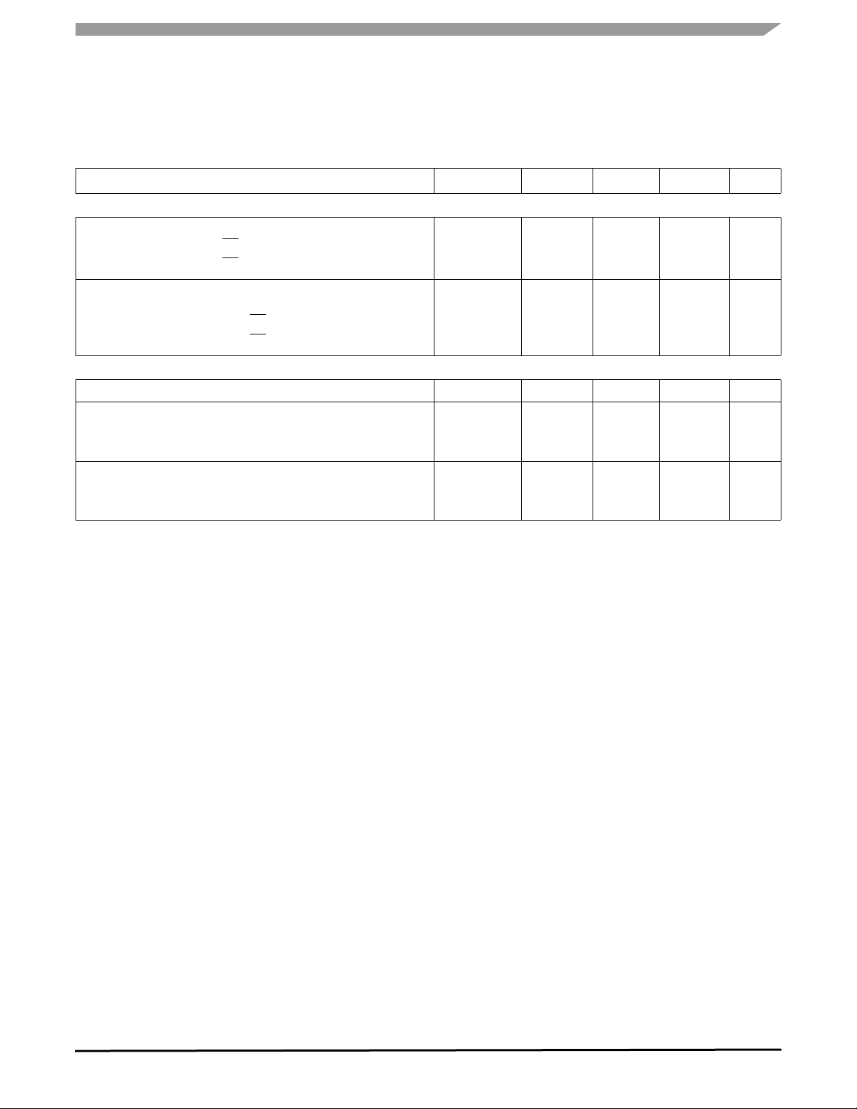
Figure 4. DBUS Timing Characteristics
33780
Analog Integrated Circuit Device Data
10 Freescale Semiconductor
Page 11
ELECTRICAL CHARACTERISTICS
TIMING DIAGRAMS
DnH
V
V
V
V
DnL
DnH
+ 2.25 V
mid
+ 0.75 V
mid
- 0.75 V
mid
- 2.25 V
mid
V
V
SUP
V
SUP
mid
0 V
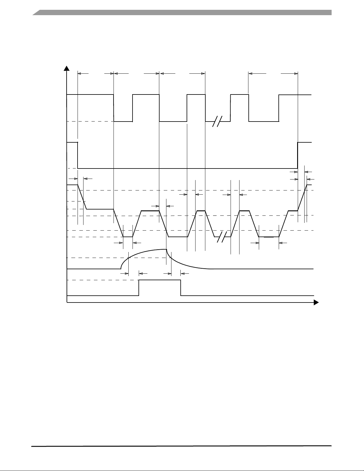
Figure 5. DBUS Normal Bus Waveforms
Overvoltage
Threshold
V
mid
V
mid
V
(Clamped)
mid
V
mid
V
mid
DnL
+ 2.25 V
+ 0.75 V
- 0.75 V
- 2.25 V
0 V
Figure 6. DBUS Overvoltage Bus Waveforms
33780
Analog Integrated Circuit Device Data
Freescale Semiconductor 11
Page 12
ELECTRICAL CHARACTERISTICS
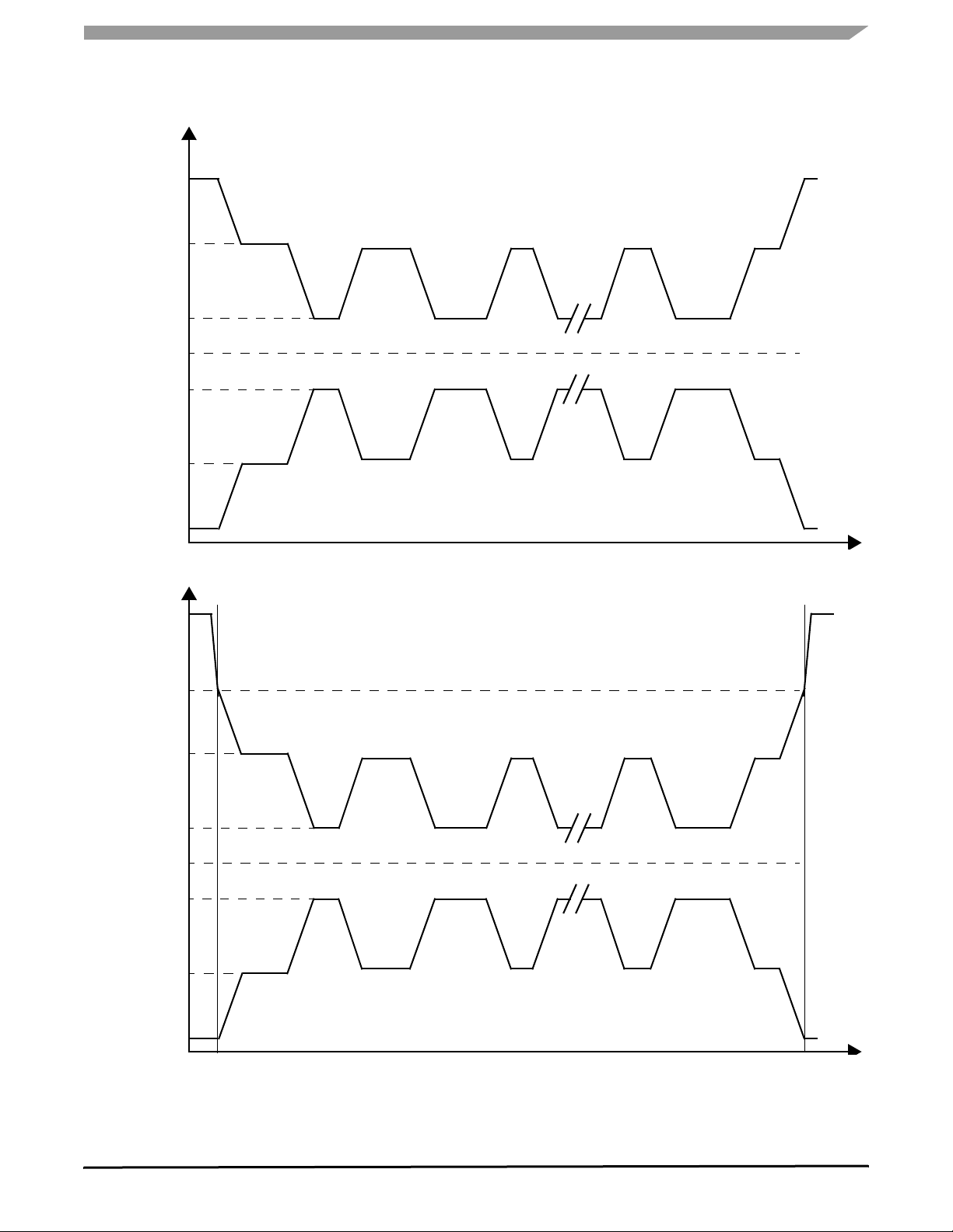
TIMING DIAGRAMS
CS
SCLK
MOSI
MISO
X = Don’t care
V
V
V
IL
t
LEAD
V
IH
V
IL
t
V
IH
V
IL
t
OH
OL
A
X
V
V
= 70% VCC, VOH = 70% V
IH
= 30% VCC, VOL = 30% V
IL
SU
MSB
t
H
MSB
CC
CC
V
IH
V
t
CYC
t
HI
t
LO
t
V
t
F
V
IH
t
HO
t
R
V
IH
LSB
V
IL
LSB
LSB
t
LAG
t
DIS
IL
V
IH
V
OH
V
OL
Figure 7. SPI Interface Timing
DBUS
(DnH-DnL)
INT
CS
SCLK
MOSI
t
INTON
Figure 8. INT and Bus Start Timing
t
DBUSSTART
t
INTOFF
33780
Analog Integrated Circuit Device Data
12 Freescale Semiconductor
Page 13

FUNCTIONAL DESCRIPTIONS
INTRODUCTION
FUNCTIONAL DESCRIPTIONS
INTRODUCTION
The 33780 is intended to be used as a master device in a
distributed system. It contains both protocol generators and
physical interfaces to allow an MCU to communicate with
devices on the bus using only a simple SPI in te rfa c e . Tw o
differential busses are provided.
Using a loop-back wire allows operation of the bus in the
presence of an open circuit. This is immediate and no
interruption is caused by the open circuit. The differential
outputs have reduced electromagnetic radiation and
susceptibility.
The equivalent bus capacitance consists of capacitors
connected between the two bus wires and capacitors
between the bus wires and ground. Because the voltage
change on either of the bus wires to ground is only 1/2 the
amount of change between the two bus wires, the
capacitance to ground only conducts half as much current as
it would if connected directly across the bus. The equivalent
bus capacitance of a capacitor to ground from the bus wires
is one half of the actual amount of the capacitor. The amount
of capacitance from either bus wire to ground should be kept
the same in order to achieve the lowest radiated EMI energy.
The 4.7
nF capacitors required between the bus wires and
ground result in an equivalent of 2.35
across the bus as seen by either bus wire.
Table 5 shows the voltages used for operation. Low side
(LS) is the bus wire that is the most negative and high side
(HS) is the bus wire that is the most positive.
the bus waveforms in normal operation.
Table 5. High-Side and Low-Side Typical Voltages (Voltage Relative to Ground)
Low Side High Side
IDLE HIGH LOW IDLE HIGH LOW
0 Vmid - 2.25
Notes
18 Vmid = V
SUP
/ 2.
(18)
Vmid - 0.75
(18)
V
SUP
Vmid + 2.25
(18)
FUNCTIONAL PIN DESCRIPTIONS
nF of capacitance
Figure 5 shows
Vmid + 0.75
(18)
RESET (RST)
When pulled low, this will reset all internal registers to a
known state as indicated in the section entitled
Descriptions.
Register and Bit
CHIP SELECT (CS)
This input is used to select the SPI port when pulled to
ground. When high, the SPI signals are ignored. The SPI
transaction is signaled as completed when this signal returns
high.
INTERRUPT (INT)
This output will be asserted ow when an enabled interrupt
condition occurs. It contains an internal current pull-up
source so that it will remain high when not active. The output
is open-drain so that it can be ORed together with other opendrain outputs so that this IC or any of the others can assert an
interrupt.
MASTER OUT/SLAVE IN (MOSI)
This is the SPI data input to the device. This data is
sampled on the positive (rising) edge of SCLK.
SERIAL CLOCK (SCLK)
This is the clock signal from the SPI master device. It
controls the clocking of data to the device and data read from
the device.
MASTER IN/SLAVE OUT (MISO)
This is the SPI data from the device to the SPI master (the
MCU). Data changes on the negative (falling) transition of the
SCLK.
CLOCK (CLK)
This is the main clock source for the internal logic. It must
be 4.0 MHz.
GROUND (GND)
Ground source for both logic and DBUS return.
POWER SOURCE (VCC)
Logic power source. Nominal value is +5.0 V. This should
be bypassed with a small capacitor to ground (0.01-0.1
µF)
LOW-SIDE BUS (DnL)
There are two independent LOW-SIDE outputs, D0L and
D1L They comprise the low-side differential output signal of
33780
Analog Integrated Circuit Device Data
Freescale Semiconductor 13
Page 14

FUNCTIONAL DESCRIPTIONS
FUNCTIONAL INTERNAL BLOCK DESCRIPTION
the DBUS physical layer as shown in Figure 5. They also
provide power to the slave modules during the DBUS idle
time. The output of DnL should have a bypass capacitor of
4.7 nF to ground.
HIGH-SIDE BUS (DnH)
There are two independent HIGH-SIDE outputs, D0H and
D1H They comprise the high-side differential output signal of
the DBUS physical layer. They also provide power to the
slave modules during the DBUS idle time. See
Figure 5. The
FUNCTIONAL INTERNAL BLOCK DESCRIPTION
SPI and
Registers
Interrupt
Generator
output of DnL should have a bypass capacitor of 4.7 nF to
ground.
POSITIVE SUPPLY FOR BUS OUTPUT (VSUP)
This 9.0 V to 25 V power supply is used to provide power
to the slave devices attached to the DBUS. During the bus
idle time, the storage capacitors in the slave modules are
charged up to maintain a regulated supply to the slave
device.
DBUS
Driver/Receiver
Protocol
Engine
Figure 9. Block Illustration
The 33780 is controlled by an MCU through an SPI
interface. It handles the digital and physical layer portions of
a DBUS master node. Two separate DBUS channels are
included, each capable of interfacing to up to 15 DBUS slave
devices (nodes). The physical layer uses a two-wire bus with
analog wave-shaped voltage and current signals. Refer to
Figure 1.
Major subsystems include the following:
•SPI interface to an MCU
•A register pointer block
•Two channels of DBUS protocol state logic
•CRC block for each channel
•Control and status registers
•4-level FIFOs on each transmit and receive buffer
SPI AND REGISTERS
This block contains the SPI interface logic and the control
and response registers that are written to and read from the
SPI interface.
The IC is an SPI slave-type device, so MOSI (Master-OutSlave-In) is an input and MISO (Master-In-Slave-Out) is an
output.
CS and SCLK are also inputs.
The SPI port will handle byte and multi-byte transfers. It
addresses 22 registers. The 33780 combines the functions of
both the 68HC55 (DSID) and the 33790 (DSIP). The 33780
uses the eight control registers defined in the DSID, and the
remaining registers are needed for the additional modes of
operation in the 33780. The organization of the registers is
described in the section entitled
Descriptions.
Register and Bit
INTERRUPT GENERATOR
This circuit accepts unmasked interrupt inputs for data
flow. It drives an open-drain output that allows the output to
be OR connected with other open-drain outputs so that this
IC or any of the others can assert an interrupt. An unmasked
interrupt will cause the
can be generated by two circumstances: (1)
register becoming empty, or (2)
not empty. Both of these events occur at the end of a DBUS
transaction. Either of these two events will generate an
interrupt when enabled by setting bits in the DnCTRL
registers.
Similarly, the interrupt signal can be cleared in two ways:
the Transmit FIFO becomes not empty, or (2) the Receive
(1)
FIFO becomes empty. Both of these events are checked at
the end of an SPI word (either with CS rising or with the rising
edge of SCLK of a new data byte in an SPI burst).
INT to pull down the output. Interrupts
a Transmit FIFO
the Receive FIFO becoming
33780
Analog Integrated Circuit Device Data
14 Freescale Semiconductor
Page 15

FUNCTIONAL INTERNAL BLOCK DESCRIPTION
FUNCTIONAL DESCRIPTIONS
PROTOCOL ENGINE
This block converts the data to be transmitted from the
registers into the DBUS sequences, and converts DBUS
response sequences to data in the registers. It generates the
proper DBUS timing.
DSIR
DSIS
DSIF
Differential
Signal
Generation
Control
Comp.
Signal
Signal
The DBUS transmit protocol uses a return to 1 type data
with a duty cycle determined by the logic state. The protocol
requires Cyclical Redundancy Check (CRC) generation and
validation.
Idle
DnH
Common
Mode
Correction
DnL
Idle
Overvoltage
T
LIM
Figure 10. Driver/Receiver Block Diagram
DBUS DRIVER / RECEIVER (PHYSICAL LAYER)
This block translates the transmit data to the voltage and
current needed to drive the DBUS. It also detects the
response current from the slave devices and translates that
current into digital levels. These circuits can drive their
T
LIM
Table 5.
Table 6.
DSIR DnD
outputs to the levels listed in
The internal signal DSIF controls the Idle to Signalling
state change, and internal signal DSIS controls the signal
level, high or low. DSIR is the slave device response signal to
the logic. This is shown in
Table 6. Internal Signal Truth Table
DSIF DSIS
0 0 0 Return Data Signal Low
0 1 0 Return Data Signal High
1 0 0 0 High Impedance
1 1 0 0 Idle
X X 1 0 High Impedance
The DBUS driver block diagram is shown in Figure 10. The
circuit uses independent drivers for the Idle and Signal states.
This allows each driver to be optimized for its function. The
Idle driver is active in Idle and during the transitions from Idle
to Signal high and Signal high to Idle. The Signal driver is only
active during actual signaling. Both drivers are disabled in
HiZ.
The Idle driver is required to supply a high current to
recharge the Slave device storage capacitors. It is also
required to drive the DBUS load capacitances and control the
slew rate over a wide supply voltage range. The DnH and
DnL Idle drivers are each optimized for their specific drive
requirements.
The Signal driver is optimized for driving the DBUS load,
and has the requirement of good slew rate control and
stability over a wide range of load conditions. The DnH and
DnL outputs use identical Signal driver circuits.
To ensure stability of the Signal driver, capacitors must be
connected between each output and ground. These are the
DBUS common mode capacitors. In addition, a bypass
capacitor is required at V
. These capacitors must be
SUP
located close to the IC pins and provide a low impedance
path to ground.
33780
Analog Integrated Circuit Device Data
Freescale Semiconductor 15
Page 16

FUNCTIONAL DESCRIPTIONS
FUNCTIONAL INTERNAL BLOCK DESCRIPTION
The DSIF signal controls the state of the drivers, enabling
the Idle drivers or Signal drivers as is appropriate. A
comparator in the Control block compares the DnL output
voltage with the internal Signal high voltage to determine the
transition from Idle driver to Signal driver. The overvoltage
signal modifies the driver characteristics. This is described in
more detail in the
Load Dump Operation section.
The overtemperature signal is also applied to this block.
The Differential Signal Generation block converts the
DSIS signal to the DBUS differential signal voltage levels.
This differential signal is buffered and slew rate controlled by
the Signal drivers. This block is active in all driver modes.
A special requirement of the differential bus is to maintain
a low common mode voltage. This is especially important
during the Idle to Signal transition in order to produce a
smooth changeover to the Signal driver. This is accomplished
by monitoring the common mode voltage and modifying the
Idle driver slew rates. This is the function of the Common
Mode Correction block. An additional feature to make a
smooth changeover and minimize undershoot is to reduce
the slew rate as the changeover point is approached. This
block is not illustrated in
Figure 10.
A sense resistor between the Signal driver and the DnH
output detects the Slave device response current. A
comparator (Comp.) generates the signal DSIR that is
supplied to the logic.
The comparator consists of a sense amplifier with offset
(VOS), a filter capacitor and logic gate with buffers to produce
the logic signal (DSIR). The sense amplifier is a ‘gm’ stage
that amplifies the voltage across the sense resistor (R
S
) to
produce an output current that charges and discharges a filter
capacitor. The voltage across the filter capacitor is compared
with the threshold voltage of the logic gate to produce the
output signal. The voltage across the filter capacitor is
I
BUS
Figure 11.
clamped between VCC and ground. See
R
S
DnH
V
OS
gm
I
O
V
TH
C
DSIR
Figure 11. Receive Filter
Definitions
•C = value of filter capacitor = 2.0 pF
•VTH = threshold of logic gate = VCC/2 = 2.5 V
•A = current gain from sense resistor to filter capacitor =
IO / I
= 3.0 µA/mA (the amplifier saturates with an
BUS
output current of ± 40 µA)
•I
[mA] = bus response current.
BUS
•ITH[mA] = response current threshold = VOS/RS = 6
The filter delay time is given by:
t [µs] = (C * VTH) / A (I
- ITH) = 1.7 / (I
BUS
BUS
- ITH)
The filter characteristic can also be expressed as the
product of the overdrive current (I
- ITH) and the duration of
BUS
the interference pulse, which must be less than 1.7 µs * mA
for the interference to be filtered.
33780
Analog Integrated Circuit Device Data
16 Freescale Semiconductor
Page 17

SPREAD SPECTRUM
FUNCTIONAL INTERNAL BLOCK DESCRIPTION
FUNCTIONAL DESCRIPTIONS
OFFSET[8:0]
PLLOFF
PLL Logic
SSUD
Center
Frequency
DAC
SSEN
DEV[1:0]
Modulation
DAC
Spreader Logic
PRBS[1:0]
Figure 12. Spread Spectrum Block Diagram
The dominant source of radiated electromagnetic
interference (EMI) from the DBUS bus is due to the regular
periodic frequency of the data bits. At a steady bit rate, the
time period for each bit is the same, which results in a steady
fundamental frequency plus harmonics. This results in
undesired signals appearing at multiples of the frequency
that can be strong enough to interfere with a desired signal.
A significant decrease of radiated EMI can be achieved by
randomly changing the duration of each bit. This can
significantly reduce the amplitude by having the signal spend
a much smaller percentage of time at any specific frequency.
The signal strength of the fundamental and harmonics are
reduced directly by the percentage of time it spends on a
specific frequency. For instance, if the bit rate is 136
there will be a harmonic at 680
kHz. If it is changed in
frequency so that only 1/10 of the bits are at the 136
rate, the signal energy at 680
kHz will be reduced by 90%.
kbps,
kbps
A circuit to do this is included in this IC and can perform the
spreading of the signal independently for each channel. This
is done in the Spread Spectrum (SS) Block Diagram shown
Figure 12.
in
Spreading can be enabled by setting the SSENn bits in the
DnSSCTRL registers. There are 64 possible bit durations that
are equally spaced between the shortest and longest bit
times. Because they are evenly spaced by a time difference
and not by a frequency difference (the reciprocal of time), all
frequency domain parameters of the SS block are expressed
in units of time.
CLK (4.0 MHz typ)
VCO
CLK_VCOn (408 kHz typ)
VCO
The output of the voltage-controlled oscillator (VCO) is
used as the bit rate clock. Three cycles of this clock are used
to create each bit of data on the DBUS.
There are two voltages that control the period (1/
frequency) of the signal coming from the VCO. The voltage
coming from the Center Frequency DAC (Digital-to-Analog
Converter) in
Figure 12 is used to keep the average period
constant. The voltage coming from the Spreader DAC
changes the period in random steps to spread the signal. The
Phase Locked Loop (PLL)-derived changes are much slower
to update the period than the ones derived from the Spreader
Logic. This prevents the two “loops” from interacting with
each other.
PLL
The PLL loop compensates for temperature drift and the
variations in processing of the IC that would otherwise
change the average data rate (center frequency). It does this
by comparing a time reference derived from the clock signal
MHz) to the period of the VCO output. If the ratio is not
(4.0
correct, it will change the frequency of the VCO by changing
the digital value it sends to the Center Frequency DAC.
The PLL has fast and slow update rates for making these
changes. It enters a fast update mode automatically anytime
the OFFSET register is written to using the SPI, or following
a reset. This fast acquisition mode consists of 64 VCO update
cycles (1.4
is done to quickly adjust the center frequency after changes
have been made. After the fast acquisition, the PLL switches
ms per update cycle) that last about 90 ms. This
33780
Analog Integrated Circuit Device Data
Freescale Semiconductor 17
Page 18

FUNCTIONAL DESCRIPTIONS
FUNCTIONAL INTERNAL BLOCK DESCRIPTION
automatically to a slow acquisition mode (180.224 ms per
update cycle, based on 4.0 MHz clock).
SPREADER LOGIC
The Spreader Logic contains a pseudo-random binary
sequence (PRBS) generator and time compensation
circuitry. The PRBS can generate maximal length sequences
of 6, 7, 11, and 15 bits. Maximal length means there is no
repeat of the sequence until 2
where n is the selected length.
n
counts have been reached,
A special feature of the Spreader Logic is that the bit
periods are chosen in a way to keep the length of the frame
constant, provided that the total number of bits is even. This
is useful if the time between samples made by the slaves
must be kept relatively constant. Without this feature, the time
from sample-to-sample would vary randomly.
The DEV1 and DEV0 bits in the DnSSCTRL register
control whether the deviation is enabled or disabled.
The Spreader Logic is synchronized to only change the
value of the digital word to the Spreader DAC at the
beginning of a DBUS bit. When spreading is enabled, these
changes will occur once per DBUS bit-time.
33780
Analog Integrated Circuit Device Data
18 Freescale Semiconductor
Page 19

FUNCTIONAL DEVICE OPERATION
LOGIC COMMANDS AND REGISTERS
FUNCTIONAL DEVICE OPERATION
LOGIC COMMANDS AND REGISTERS
SPI COMMUNICATIONS
All SPI transactions start with a command byte and can be
followed by 1 or more bytes of data. The start of an SPI
transaction is signaled by
sent (bit 7) of the first byte signals a read or write (write = 1)
of data. The last five bits (bits 4
CS being asserted low. The first bit
– 0) of the comman d set a
pointer to the desired register. Bits 5 and 6 are unused. See
Figure 13. As long as CS is asserted low, each additional byte
sent over the SPI will be a read / write of data to the sequential
next register. After address 10101 is written to, the next write
will wrap around to address 00000.
Bit 7 6 5 4 3 2 1 0
R/W X X ADDR4 ADDR3 ADDR2 ADDR1 ADDR0
Figure 13. SPI Communications, First Byte of Burst Transfer
The receive FIFO is popped only when the SPI reads or
writes the low data register (DnL). The Control and Status
registers can be read without affecting the receive FIFO. The
transmit FIFO is popped at the end of the DBUS transaction.
Figure 14 shows an example of a write operation. This
example assumes the last SPI transaction read or wrote the
data from register 00011 and is now pointing at 00100
(D01STAT). During the first byte of the SPI transaction, the
first MOSI bit is 1 (write) and the last five are 00000. During
this command byte, MISO returns the data from register
updates the data in register 00000 with new data while
reading back the old data via MISO.
Although it looks like the read and write for an address are
occurring at the same time, the changes caused earlier
during the same burst would not be reflected by the data
returned, because the D01STAT is latched at
When a short word is selected for Bus 0 (MS0 in D0CTRL
is set), the D0H register is skipped in the sequence. The
same is true for the D1H register when MS1 is set and
SWLEN1 = 1000.
00100 (D01STAT). During the next SPI transactions, MOSI
CLK
SCLK
MOS I
MI SO
CSB
CS
WRITE COMMAND
WRITE COMMAND
POINT TO 00000
POINT TO 00000
DATA FROM
DATA FROM
D01STAT (00100)
DSI01 STAT( 00 100)
DATA TO DS I0 H
DATA TO D0H
(00000)
(00000)
DATA FROM
DATA FROM D0H
(00000)
DSI0H ( 00 000)
DATA TO DSI0L
DATA TO D0L
(00001)
(00001)
DATA FROM D0L
DATA FROM
(00001)
DSI0L (00001)
DATA TO DSI1H
DATA TO D1H
DATA FROM
DATA FROM D1H
DS I1 H (0 0010 )
(00010)
(0 00 10 )
(00010)
DATA TO DSI1 L
DATA TO D1L
(00011)
(000 11)
DATA FROM
DATA FROM D1L
(00011)
D S I 1L (0001 1)
CS going low.
Figure 14. SPI Burst Transfer Example
DBUS COMMUNICATIONS
The DBUS messages contain data from the DnH and DnL
registers. A CRC pattern is automatically appended to each
Bit n . . . . . . . . . . . . . . . . Bit 0 CRC n . . . . . CRC 0
message. The data and CRC lengths are programmed by the
DnLENGTH register.
Figure 15 shows the structure of the
DBUS message.
Figure 15. DBUS Communications Message
DBUS Driver/Receiver communications involve a frame
(DSIF), a data signal (DSIS), and a data return (DSIR) signal.
These are signals internal to the IC associated with the
protocol engine.
A message starts with a falling edge on the DSIF signal,
which marks the start of a frame. There is a one bit-time delay
before the MSB of data appears on the DSIS pin. Data bits
start with a falling edge on DSIS. The low time is 1/3 of the bit
time for a 1, and 2/3 of a bit time for a 0. Data is transmitted
on DSIS and received on DSIR pins simultaneously. Receive
data is the captured level on the DSIR pin at the end of each
bit time. At the end of the bit time for the last CRC bit, the
DSIF pin returns to a logic high (Idle level). A minimum delay
is imposed between successive frames as determined by the
DnCTRL register.
Users initiate a message by writing (via the SPI interface
from the MCU) to the low byte of the data register (DnL).
When 9- to 16-bit messages are to be sent, the user writes to
the DnH register first and then the DnL register before the
combined 9 to 16-bit data value DnH:DnL is sent on the
DBUS. The user should first check the TFNFn status flag to
be sure the transmit FIFO is not full before writing a new data
33780
Analog Integrated Circuit Device Data
Freescale Semiconductor 19
Page 20

FUNCTIONAL DEVICE OPERATION
LOGIC COMMANDS AND REGISTERS
value to DnH and/or DnL. When the minimum inter-frame
delay has been satisfied, the DSIF pin will go low, indicating
the start of a new transfer frame.
DBUS Driver/Receiver communications involve a frame
(DSIF), a data signal (DSIS), and a data return (DSIR) signal.
These are signals internal to the IC asso ci at ed with the
prData is shifted out of DSIS (MSB first) and shifted into DSIR
at the same time. As a message is received, it is stored bitby-bit into the next available recei ve FIFO location . For each
data value in the receive FIFO, there is a one-bit status flag
to indicate whether or not there was a CRC error while
receiving the data. At the end of a DBUS transfer (and after
the CRC error status is stable), the RFNEn flag is set (if it was
not already) to indicate there is data in the receive FIFO to be
read.
DATA RATE
In non-spread spectrum mode, the data rate is determined
by the system clock (CLK) and the programmable clock
divider. (The Clock Divider ratio n is defined in
Data Rate = f
/ (27 * n)
CLK
In spread spectrum mode, the data rate is determined by
the system clock (CLK) and the DnOFFSETL/H register
programming. Note the programmable clock divider does not
control the data rate in Spread Spectrum mode. Refer to
Register and Bit Descriptions section for details.
The following table gives the correspondence between the
offset and the data rate for f
= 4.0 MHz.
CLK
Table 7. Data Rate versus OFFSET (Spread Spectrum)
OFFSET Data Rate
HEX DEC kHz
00 0 121.2
3F 63 136.1
7A 122 150.1
9F 159 158.9
For other clock frequencies, the data rate can be
computed using the following formula:
Data Rate = (f
/ 33) * (1 + OFFSET / 512)
CLK
Table 10.)
CRC GENERATION / CHECKING
Whenever a message is sent on the DBUS, a 0- to 8-bit
CRC value is computed and serially sent as the next n bits
after the LSB of the data. The CRC length, polynomial, and
initial seed are determined by the CRCLEN[3:0],
CRCPOLY[7:0], and CRCSEED[7:0] control register fields.
The message, including the CRC bits, is passed along to a
remote peripheral, which computes a separate CRC value as
the message data is received. If this computed CRC does not
agree with the CRC value received in the message, the
peripheral device considers the message invalid.
Messages received include a 0- to 8-bit CRC value, which
was computed in the peripheral device that is responding. As
the message is received, a separate 0- to 8-bit CRC value is
computed and is compared with the CRC value in the
received message. If these values do not agree, the message
is considered invalid and the ERn status bits in the D01STAT
register are set as the receive data is transferred into the
receive data buffer.
When no remote peripheral responds to a message, the
data pattern received will be all zeros with a CRC value of 0,
which may be detected as a CRC error depending on the
values of CRCLEN[3:0], CRCPOLY[7:0], and
CRCSEED[7:0]. On the other hand, if a remote peripheral is
attached and responds with all zeros with a CRC value of
1010, this may be detected as a non-error condition.
CRC COMPUTATION
The CRC algorithm uses a programmable initialization
value, or seed, of CRCSEED[7:0] and a programmable
polynomial of CRCPOLY[7:0].
description of the CRC algorithm for the DBUS standard 4-bit
CRC with its initial value of 1010. A seed value is chosen so
that a zero data value will generate a CRC value of 1010. A
block diagram of the default CRC calculation is shown in
Figure 17.
Figure 16 is a VHDL
--------------------------------------------------------------------------
-- Calculates the 4-bit CRC (x^4 + 1) serially for 8 to 16 bits of data.
33780
Analog Integrated Circuit Device Data
20 Freescale Semiconductor
Page 21

FUNCTIONAL DEVICE OPERATION
LOGIC COMMANDS AND REGISTERS
-------------------------------------------------------------------------constant CRCPoly: std_logic_vector: = “0001”; -- x^4 +1
constant InitCrc: std_logic_vector: = “1010”;
procedure SerialCalculateCRC4(CRC: input std_logic_vector;Data: in std_logic) is variable
Xor1: std_logic;
begin
Xor1: = CRC(3) xor Data;
CRC: = CRC(2 downto 0) & ‘0’; -- Shift left 1 bit
if Xor1 = ‘1’ then
CRC: = CRC xor CRCPoly
end if;
end SerialCalculateCRC4;
Figure 16. CRC Algorithm
C3
T
1X4 0X3 0X2 0X1 +X0 = X4+1++ ++
C2
C1
T
T
Figure 17. Default CRC Block Diagram
MESSAGE SIZE SPECIAL CASES
The response to any 8- to 15-bit message is expected to
be another 8- to 15-bit message and the response to any
16-bit message is expected to be another 16-bit message.
This gives rise to some special cases when there is a
transition from one message size to a different message size.
Some messages must be long words (16 bits of data), others
can be short words (8 to 15 bits of data).
The following are examples where the word is a standard
DSI formatted short word (8 bits of data and 4 bits of CRC).
Example 1: If the previous message was a short word and
the current message is a long word, the response message
(which is also a short word) finishes before the current
message frame and the CRC bits look like data bits in the
long word format. Since the CRC validation of this short word
message response is not reliable, this short word response
should not be used.
Example 2: If the previous message was a long word and
the current message is a short word, the response message
(which is also a long word) cannot finish before the current
message frame. Bits three to zero of the data and the CRC
bits are lost. Data bits seven to four of the 16-bit response
message look like the CRC bits of an 8-bit response and
almost certainly would not be correct. Because the response
C0
T
Input Data
is incomplete and the CRC check is probably not valid, this
response is not useful.
The long word to short word message size transition
normally only occurs after setting up the DBUS peripherals.
During address setup, a message with address 0000 is sent
to attempt to set the address of the next peripheral on the
daisy-chained bus. Before any peripherals have been
assigned an address, their bus switches are opened so the
addressing message only goes to the first peripheral in line.
As each peripheral gets an address, it closes its bus switch
so the next address assignment command can reach the next
peripheral in line on the bus. Each peripheral responds to an
address assignment only once (during the next message
after the command that set its address). After the last
peripheral has been assigned an address, any subsequent
address assignments will receive no response. When the
master MCU fails to receive a response, it knows it has
passed the last peripheral. At this point, short word messages
may be sent. The first such message will have no meaningful
response associated with it.
The first message after reset is also a special case
because there was no previous message, therefore there will
be no meaningful response during the first message transfer.
33780
Analog Integrated Circuit Device Data
Freescale Semiconductor 21
Page 22

FUNCTIONAL DEVICE OPERATION
LOGIC COMMANDS AND REGISTERS
CLK_VCO0
MISO
SCLK
CS
MOSI
CLK
INT
RST
Channel 0
Clock Select and Divider
SPI & Registers
Interrupt
status regs
control regs
enable regs
poly regs
seed regs
length regs
SS ct rl regs
SS o ffsetregs
SS Up/Dwn regs
register pointer
bit pointer
SPI XFER
BitClock 0
RX0 Data
RX0 Status
TX0 Data
TX0 Status
RX1 Data
RX1 Status
TX1Data
TX1 Status
RX FIFO
RX Buffer
RX Buffer
RX Buffer
RX Buffer
TX FIFO
TX Buffer
TX Buffer
TX Buffer
TX Buffer
RX FIFO
RX Buffer
RX Buffer
RX Buffer
RX Buffer
TX FIFO
TX Buffer
TX Buffer
TX Buffer
TX Buffer
k
c
e
h
C
C
R
C
CH0
e
t
a
r
e
n
e
G
C
R
C
CH0Enable
CH1Enable
k
c
e
h
C
C
R
C
CH1
e
t
a
r
e
n
e
G
C
R
C
r
e
y
a
L
l
a
c
i
s
y
h
P
0
H
C
S
U
B
D
o
T
r
e
y
a
L
l
a
c
i
s
y
h
P
1
H
C
S
U
B
D
o
T
CLK_VCO1
CLK
Channel 1
Clock Select and Divider
Bit Clock 1
Figure 18. Logic Block Diagram
LOGIC BLOCK DIAGRAM DESCRIPTION
Figure 18, Logic Block Diagram, shows a block diagram of
the major logic blocks in the IC.
REGISTERS
The register set consists of control, status, transmit, and
receive types. They are written and read using the SPI
interface and are affected by events in the IC. Detailed
SPI
The SPI is a standard serial peripheral interface. This
descriptions of their operation and use can be found
throughout later sections of this data sheet.
interface provides two-way communications between the IC
and an MCU. The MCU can write to registers that control the
operation of the IC and read back the conditions in the IC
using the SPI. It can also write data to be sent out on the
DBUS and read data that was returned on the DBUS. The
register pointer and bit pointer are used to control which
registers and bits are being written to and read from using the
SPI. Its operation is described in detail in the section entitled
SPI Communications on page 19.
33780
INTERRUPT
The Interrupt block controls the INT output pin. The main
purpose of the Interrupt is to quickly inform the MCU when
data has been received via the DBUS or when the DBUS
transmit buffer is empty. The
level on the pin low. The internal pull-up current or an external
resistor to V
is used to pull this pin high. This is done so
CC
that other ICs can be connected to the interrupt pin on the
INT output can only drive the
Analog Integrated Circuit Device Data
22 Freescale Semiconductor
Page 23

FUNCTIONAL DEVICE OPERATION
LOGIC COMMANDS AND REGISTERS
MCU. If the DBUS IC or any of the other ICs want to assert
an interrupt to the MCU, they can do so by pulling the pin low.
This is similar to a logical OR of the outputs because this IC
or any of the others can assert the interrupt to the MCU. The
operation of the Interrupt is described in detail in the section
Interrupt Generator on page 14.
titled
RST
Asserting this pin low will cause the part to reset, forcing
registers to a known state. The description for these registers
shows the bit values that will occur due to a reset. All bus
activity will be halted and not allowed to restart, and no SPI
activity will be recognized until the
level.
RST goes to a logic high
CLOCK SELECT AND DIVIDER
There is an independent Clock Select and Divider for each
channel. These circuits are controlled by register writes to the
SPI and can select whether the Spread Spectrum Clock
(CLK_VCOn) is used for the bit clock or the unspread clock is
used. They also contain dividers that can be selected to
reduce the bit rate by integer ratios in the unspread mode
only.
RXFIFO
The RXFIFO is an automatic register set that allows up to
responses to be stored without being transferred to the
four
MCU via the SPI. This is done so that data will not be lost
even if the MCU takes time to read the response data. When
the MCU reads a response from one of the DBUS registers,
the earliest response to be received is the one read. In other
words, the first in response will be the first out (FIFO). When
the RXFIFO becomes not empty and interrupts are enabled,
the MCU receives an interrupt via
INT.
TXFIFO
The TXFIFO is an automatic register set that allows up to
four transmit data packets to be stored for future
transmission on the DBUS. This is done to prevent the
overwrite of transmit data if the transmission of the previous
data has not been completed. The oldest data in the registers
is the first to be sent when the DBUS is ready to send. In other
words, the first data put into the regist ers to be sent will be the
first out when the DBUS is available (FIFO). When the
TXFIFO becomes empty and interrupts are enabled, the
MCU receives an interrupt via
INT.
CH0/CH1 ENABLE
The output of these signals control whether the DBUS can
drive power and signalling onto the bus. These are directly
controlled by bits written to the control registers.
CH0/CH1 OUTPUTS
These signals control the physical layer drivers and
receive data from the physical layer receivers. The physical
layer will convert the 0 V to 5.0 V low power logic signals to
the higher voltage (up to 26.5 V) and drive (150 mA nominal)
levels necessary for the DBUS to be used. It also converts
the low current (0
response signal from the slave to logic voltage levels to allow
the response from the slaves to be received. These internal
signals are named DSIF, DSIS, and DSIR.
mA to 11 mA typical) loading of the
CRC GENERATORS
Each channel contains a CRC generator that adds a series
of bits to each of the transmitted data words sent out on the
DBUS. The CRC bits are created from the data pattern and
are used by the slave devices to determine if one or more of
the data bits sent was in error. The detailed operation and
control of this function is covered in the section entitled
Generation / Checking on page 20.
CRC
CRC CHECK
This circuit checks the CRC bits that have been added to
the end of the response by the slave device. For a given
pattern of received data a new CRC is generated and
compared to the CRC bits received. If they do not match, a
bit is set in the status register indicating a CRC error for the
response. This bit is read back using the SPI during the same
SPI transaction that reads the response in order to keep them
associated with each other. The CRC bits are removed by the
IC and not seen by the MCU when reading the data registers.
Operation of the CRC Check is covered in the section entitled
CRC Generation / Checking on page 20.
SPI AND PROTOCOL ENGINE STATE MACHINES
Although the SPI clock and the DBUS input clock both
typically come from the same MCU system clock in an MCU
plus 33780 system, there is no guaranteed relationship
between these clocks, so the system was designed as if
these clocks were asynchronous. The FIFO architecture
eliminated most of the cases where these clocks need to
interact, and the remaining cases were designed with extra
care to prevent asynchronous problems.
Figure 19 explains the notation used in the subsequent
state diagrams. Entry to the IDLE state is asynchronous and
all other state transitions are synchronous. The note in the
upper right corner of the figure identifies which edge of which
clock or signal is used to synchronize state transitions. Each
arrow or arc has a condition that must be true before the
transition can take place. This condition can be the value of a
single signal or a more complex logic function. A slash (/)
indicates the end of the condition or equation, which must be
true for a transition to occur. The statement or statements
after the slash are executed during the transition to the next
state. These state diagrams are not a complete description of
the entire MC33780, they are intended to include just enough
relevant data to understand the operation of the state
machines and basic functions.
33780
Analog Integrated Circuit Device Data
Freescale Semiconductor 23
Page 24

FUNCTIONAL DEVICE OPERATION
LOGIC COMMANDS AND REGISTERS
ASYNCHRONOUS RESET/
ACTION(S);
IDLE
STATE_1
Figure 19. State Diagram Notation
Figure 20, describes how SPI transfers lead to transmit
FIFO push operations or transfer abort actions. State
transitions in this state machine are synchronous with rising
edges of the SPI clock (SCLK). The initial state, SPI_IDLE, is
entered asynchronously whenever internal reset becomes
active or the SPI chip select (
entry to the idle state, the SPI_WRITE signal is deactivated
and the SPI bit counter is set to 7 (it will count down as bits
are received).
When the CS goes low (active), the first SPI transfer will be
a command byte and the first bit indicates a write or read
command. The SPI_WRITE signal takes on the value of this
first bit, and the state machine enters the SPI_CMD_XFER
state, where the remaining bits of the command byte are
received. The last five bits of the command set the initial
value of the register pointer. After the command byte is
complete, the state machine advances to the SPI_BURST
CS) input is de-asserted. Upon
STATE TRANSITIONS OCCUR
ON POS EDGE OF XXX CLK
SYNCHRONOUS CONDITIONS/
ACTION(S);
state, which remains active until
CS goes high (or the
MC33780 is reset).
In the SPI_BURST state, new SPI characters are readfrom, or written-to-and-read-from, MC33780 registers. If the
control register (or CRC polynomial, CRC seed, CRC length,
or spread spectrum control) is written, an ABORT request is
generated that will immediately stop any DBUS transfer that
was in progress (refer to the DBUS transfer state diagram). If
the DATA register low byte is written, a transmit FIFO push
operation is generated (see transmit FIFO state diagram). If
the DATA register low byte is accessed (read or written) and
there is at least one entry in the receive FIFO, a receive FIFO
pop operation is generated.
When a DBUS transfer results in both an R_FIFO_PUSH
and an X_FIFO_POP, the R_FIFO_PUSH is performed first
to avoid the possibility of the transmit FIFO from getting
ahead of the receive FIFO.
RSTB ACTIVE or CSB INACTIVE/
SPI_WRITE = 0;
SPI_BIT_PTR = 7;
SPI_IDLE
SPI_CMD_XFER
LAST_SPI_BIT/
SPI_BIT_PTR = 7;
REG_PTR = REG_PTR +1 (rolls over to 0 after 21);
if SPI_WRITE & REG_PTR = CTRL or POLY or SEED or LENGTH or SSCTRL then ABORT;
if SPI_WRITE & REG_PTR = DATA_L then X_FIFO_PUSH;
if R_FIFO_NOT_EMPTY & REG_PTR = DATA_L then R_FIFO_POP;
SPI_BURST
Figure 20. State Diagram of SPI Transfer
Figure 21 describes what happens during DBUS serial
transfers. State transfers in this state machine are
synchronous with positive edges on the scaled DBUS 1/3rd
bit clock and the initial state is WAIT_FRAME_DLY. Initial
STATE TRANSITIONS OCCUR
ON POS EDGE OF SCLK
CSB ACTIVE/
SPI_WRITE= MOSI;
~LAST_SPI_BIT/
SPI_BIT_PTR = SPI_BIT_PTR-1;
LAST_SPI_BIT/
SPI_BIT_PTR = 7;
INIT_REG_PTR FROM CMD BITS[4:0]
~LAST_SPI_BIT/
SPI_BIT_PTR = SPI_BIT_PTR-1;
entry into this state is caused by a reset, abort, or by enable
becoming inactive. These conditions cause an asynchronous
entry into this state. The exit to the next state,
WAIT_SIG_DLY_0, needs to be synchronous.
33780
Analog Integrated Circuit Device Data
24 Freescale Semiconductor
Page 25

FUNCTIONAL DEVICE OPERATION
LOGIC COMMANDS AND REGISTERS
When enable is true and there is at least one valid entry in
the transmit FIFO, the DBUS frame signal is driven low to
start a frame. States WAIT_SIG_DLY_0 through
WAIT_SIG_DLY_2 create a one DBUS bit-time delay before
the start of the first data bit. After WAIT_SIG_DLY_2, the
DBUS_BIT_PTR gets initialized to the total word length, as
determined by the MSx, SWLENx, and CRCLENx bits. The
XFER_DBUS_BIT_0 state is then entered.
XFER_DBUS_BIT_0 through XFER_DBUS_BIT_2 form a
loop where each pass corresponds to one DBUS bit time.
During the first third of the bit the DSIxS signal is low, during
the second third DSIxS is low for a zero or high for a one,
during the last third of the bit time DSIxS is high. Provided this
is not the end of the last CRC bit, the bit pointer is
decremented and the loop is repeated.
After the last CRC bit, the DBUS_R_PUSH state is
entered. This state ensures that the CRC flag is stable prior
to adjusting the receive (and transmit) FIFO pointers. The
DBUS_X_POP state prevents an X_FIFO_POP from
occurring at the same time as an R_FIFO_PUSH.
After DBUS_X_POP, the state transitions back to the
WAIT_FRAME_DLY state. This state ensures proper frame
spacing is allowed to charge up the storage capacitors in
remote nodes. Notice that the delay counter was reset at the
end of the last CRC bit so the delay period can start to time
out even while the DBUS_R_PUSH and DBUS_X_POP
states are being processed.
Figure 22 describes the operation of the transmit FIFO.
This FIFO is four levels deep, including the stage which is
written into by the SPI and the stage which provides the data
for the current DBUS serial transfer. State transitions in this
state machine occur at the trailing edges of X_FIFO_PUSH
and X_FIFO_POP.
When this FIFO is completely empty, the SPI can write
four new values to fill the FIFO without waiting for any action
on the DBUS side of the FIFO. Values are pushed into the
FIFO from the SPI interface and values are popped after they
have been serially sent out of the DBUS interface. When the
FIFO is full, additional attempts to write new data from the
SPI side are ignored (the host MCU should be sure the
TFNFx status bit is set before writing more data to the FIFO).
Reset, abort, or enable going to zero causes
asynchronous entry to the TX_IDLE state, which
corresponds to the FIFO empty condition. The push and pop
pointers are cleared and X_FIFO_EMPTY is set to true.
X_FIFO_PUSH causes the push pointer to be incremental,
X_FIFO_EMPTY to be set to false, and the state to transition
to TX_NOT_EMPTY. The push request comes from the SPI
transfer state machine after a new value has been written into
the FIFO.
RSTB ACTIVE or ABORT or ~EN/
RESET_DELAY_CNTR;
DSIF = 1, DSIS = 1;
WAIT_FRAME_DLY
DELAY_OVER &
X_FIFO_NOT_EMPTY/
DSIF = 0;
WAIT_SIG_DLY_0
DBUS_BIT_PTR = 8 to 15, OR 23;
DSIS = 0;
XFER_DBUS_BIT_0 XFER_DBUS_BIT_1 XFER_DEBUS_BIT_2
X_FIFO_POP = 0;
DBUS_X_POP
STATE TRANSISITONS OCCUR
ON POS EDGE OF SCALED
DBUS 1/3
WAIT_SIG_DLY[0..2] CAUSES 1 BIT-TIME DLY TO 1
WAIT_SIG_DLY_1 WAIT_SIG_DLY_2
DSIS = DATA; DSIS = 1;
R_FIFO_PUSH = 0;
DBUS_R_PUSH
Figure 21. State Diagram of DBUS Transfer
RD
BIT CLOCK
ST
~LAST_CRC_BIT/
LAST_CRC-BIT/
BIT FALLING EDGE
DBUS_BIT_PTR = DBUS_BIT_PTR-1;
DSIS = 0;
DSIF = 1, DSIS = 1;
RESET DELAY_CNR;
R_FIFO_PUSH = 1
X_FIFO_POP = 1;
33780
Analog Integrated Circuit Device Data
Freescale Semiconductor 25
Page 26

FUNCTIONAL DEVICE OPERATION
LOGIC COMMANDS AND REGISTERS
~EN or ABORT or RSTB ACTIVE/
X_PUSH_PTR = 0;
X_POP_PTR = 0;
X_FIFO_EMPTY = TRUE;
X_FIFO_POP & X_POP_PTR = X_PUSH_PTR-1/
X_POP_PTR = X_POP_PTR+1;
X_FIFO_EMPTY = TRUE;
STATE TRANSISTIONS OCCUR
ON NEG EDGES OF X_FIFO_PUSH
AND X_FIFO_POP
TX_IDLE
X_FIFO_PUSH/
X_PUSH_PTR = X_PUSH_PTR+1;
X_FIFO_EMPTY = FALSE;
X_FIFO_POP & X_POP_PTR != X_PUSH_PTR-1/
X_POP_PTR = X_POP_PTR+1;
X_FIFO_POP/
X_FIFO_POP = X_FIFO_POP+1;
TX_NOT_EMPTY
Figure 22. State Diagram of Transmit FIFO
From TX_NOT_EMPTY, several things can happen.
Additional values can be pushed into the FIFO if the push
pointer is the same as the pop pointer minus one. This push
fills the FIFO so the state advances to TX_FULL. Each time
a new data value is pushed into the FIFO, the push pointer is
incriminated. From TX_NOT_EMPTY, values may also be
popped from the FIFO, freeing a stage for additional data. If
the pop pointer is the same as the push pointer minus one,
the pop removes the last value in the FIFO, so
X_FIFO_EMPTY is set to true and the state changes back to
TX_IDLE. Each time a value is popped, the pop pointer is
incremental.
When the transmit FIFO is full, no additional data can be
written into the FIFO, so no new push requests will be
generated. From TX_FULL, the only valid change is caused
by a pop, which causes the pop pointer to increment and the
state goes back to TX_NOT_EMPTY. (Of course reset, abort,
or disable could cause the state to asynchronously change to
the TX_IDLE state.)
Figure 23 describes the operation of the receive FIFO.
State transitions in this state machine occur at the trailing
edges of R_FIFO_PUSH and R_FIFO_POP. The receive
FIFO is four levels deep, including the stage which receives
X_FIFO_PUSH & X_PUSHPTR != X_POP_PTR-1
X_PUSH_PTR = X_PUSH_PTR+1;
X_FIFO_PUSH & X_PUSH_PTR = X_POP_PTR-1/
X_PUSH_PTR = X_PUSH_PTR+1;
TX_FULL
serial data from the current DBUS transfer and the stage
that is accessible for SPI reads. In order to assure coherence
of data and status, each FIFO stage includes an extra bit for
the CRC error status for each received data word. Also for
coherency, the DBUS transfer state machine imposes a
delay at the end of a DBUS transfer to assure that the CRC
status is stable before issuing the R_FIFO_PUSH request.
The RX_IDLE state is asynchronously entered at system
reset, when the enable bit goes low, or when there is an
abort.
During normal operation of the receive FIFO, values are
pushed into the FIFO from the DBUS serial interface, causing
the push pointer to increment. After the SPI has read a data
word, the receive FIFO is popped, which makes the location
available for additional data from the DBUS interface (it is the
user's responsibility to read status and data within the same
burst to assure coherence). The RX_NOT_EMPTY state is
active as long as there is some data in the FIFO.
The RX_FULL state is entered when enough data has
been pushed into the FIFO from the DBUS interface to cause
the push pointer to catch up to the pop pointer. Since it is not
possible to introduce another DBUS serial character without
reading (pop) the receive FIFO, it is not possible to overflow
the receive FIFO.
33780
Analog Integrated Circuit Device Data
26 Freescale Semiconductor
Page 27

FUNCTIONAL DEVICE OPERATION
LOGIC COMMANDS AND REGISTERS
~EN or ABORT or RSTB ACTIVE/
R_PUSH_PTR = 0;
R_POP_PTR = 0;
R_FIFO_EMPTY = TRUE;
R_FIFO_POP & R_POP_PTR = R_PUSH_PTR-1/
R_POP_PTR = R_POP_PTR+1;
R_FIFO_EMPTY = TRUE;
R_FIFO_POP & R_POP_PTR != R_PUSH_PTR-1/
R_POP_PTR = R_POP_PTR+1;
R_FIFO_POP/
R_FIFO_POP = R_FIFO_POP+1;
OVERFLOW = FALSE;
RX_IDLE
RX_NOT_EMPTY
RX_FULL
Figure 23. State Diagram of Receive FIFO
REGISTER AND BIT DESCRIPTIONS
The 33780 has 22 registers, shown in Table 8. The lower
8 (00000 through 00111) are compatible with the 8 registers
STATE TRANSISTIONS OCCUR
ON NEGATIVE EDGES OF R_FIFO_PUSH
AND R_FIFO_POP
R_FIFO_PUSH/
R_PUSH_PTR = R_PUSH_PTR+1;
R_FIFO_EMPTY = FALSE;
R_FIFO_PUSH & R_PUSHPTR != R_POP_PTR-1/
R_PUSH_PTR = R_PUSH_PTR+1;
R_FIFO_PUSH & R_PUSH_PTR = R_POP_PTR-1/
R_PUSH_PTR = R_PUSH_PTR+1;
in the 68HC55. The remaining registers (01000 through
10101) are needed for the additional modes of operation.
Table 8. Register List
Register
Address
00000 D0H
00001 D0L
00010 D1H
00011 D1L
00100 D01STAT
00101 D0CTRL
00110 D1CTRL
00111 DEN
01000 D0POLY
01001 D1POLY
01010 D0SEED
01011 D1SEED
01100 D0LENGTH
01101 D1LENGTH
01110 D0SSCTRL
01111 D1SSCTRL
10000 D0OFFSETH
10001 D0OFFSETL
10010 D1OFFSETH
10011 D1OFFSETL
10100 D0SSUD
10101 D1SSUD
Register Name Register Definition
DBUS 0 upper byte
DBUS 0 lower byte
DBUS 1 upper byte
DBUS 1 lower byte
DBUS 0 and 1 status
DBUS 0 control
DBUS 1 control
DBUS enable bits
DBUS 0 CRC polynomial
DBUS 1CRC polynomial
DBUS 0 CRC seed
DBUS 1 CRC seed
DBUS 0 short word and CRC lengths
DBUS 1 short word and CRC lengths
DBUS 0 spread spectrum control
DBUS 1spread spectrum control
DBUS 0 spread spectrum offset high
DBUS 0 spread spectrum offset low
DBUS 1 spread spectrum offset high
DBUS 1 spread spectrum offset low
DBUS 0 spread spectrum up/down counter
DBUS 1 spread spectrum up/down counter
33780
Analog Integrated Circuit Device Data
Freescale Semiconductor 27
Page 28

FUNCTIONAL DEVICE OPERATION
LOGIC COMMANDS AND REGISTERS
DLYn[B:A]
MSn
DBUS Encode/Decode Logic
Rx FIFOn Tx FIFOn
DnH Rx DnL Rx ERn DnH Tx DnL Tx
(Read-Only)
ERn
DnSTAT Register
TIEn
ENn
DEN Register
TSn
RIEn
DLYn[B:A]
DnCTRL Register
MSn
Figure 24. DBUS Master Registers and Interrupt Block Diagram
DnH REGISTERS
These are read / write registers. There are two of these
registers, one for each of the buses, as shown in
When written to, the data is the high byte of a 9- to16-bit
command. When read, it is the high byte of a 9- to 16-bit
return on the DBUS. Writing to this register does not begin a
DBUS transaction. The low byte must be written to initiate the
DBUS transaction.
Figure 24.
(Write-Only)
TFNFn
TFEn
(Read-Only)
RFNEn
RFNEn
RIEn
TFEn
TIEn
4 Interrupt Sources
(2 shown)
The bit assignments are shown in Figure 25. When a short
word of 8 bits is selected for the DBUS (MSn = 1), this register
is skipped in the SPI burst sequence. When the short word
length is set at other than 8 bits, this register will contain the
bits above eight, starting with the ninth bit in the least
significant bit position of the register. Unused bit positions are
don’t care values.
Interrupt Request
SPI Data Bit
Read / Write
Reset
Bit 7 6 5 4 3 2 1 0
Bit 15 Bit 14 Bit 13 Bit 12 Bit 1 1 Bit 10 Bit 9 Bit 8
0 0 0 0 0 0 0 0
Figure 25. DnH Data Register Bit Assignments
33780
Analog Integrated Circuit Device Data
28 Freescale Semiconductor
Page 29

FUNCTIONAL DEVICE OPERATION
LOGIC COMMANDS AND REGISTERS
DnL REGISTERS
These are read / write registers. There are two of these
registers, one for each of the buses. When written to, the data
is the low byte of a 16-bit command. When read, it is the
SPI Data Bit
Read / Write
Reset
Bit 7 6 5 4 3 2 1 0
Bit 7 Bit 6 Bit 5 Bit 4 Bit 3 Bit 2 Bit 1 Bit 0
0 0 0 0 0 0 0 0
Figure 26. DnL Data Register Bit Assignments
D01STAT REGISTER
This is a read-only register. This register covers the status
of DBUS 0 and 1. The values are latched when
asserted low. Any changes of the status that these bits detect
SPI Data Bit
Read
Reset
Bit 7 6 5 4 3 2 1 0
ER1 TFE1 TFNF1 RFNE1 ER0 TFE0 TFNF0 RFNE0
0 1 1 0 0 1 1 0
Figure 27. Channel 1 and 2 Status Register Bit Assignments
ERn–CRC Error Bit for Channel n
• 0 = CRC value for the data in the read buffer was correct
and no overcurrent condition exists.
• 1 = CRC value for the data in the read buffer was not
correct (data not valid) or that an overcurrent event has
occurred.
CRC errors are associated with each data value in the
receive FIFO, so each FIFO entry has a bit to indicate
whether the data in that stage of the FIFO was received
correctly.
Whenever a received data value is available in the DnH
and DnL registers, the associated CRC error status is
available at ERn in the D01STAT register. When a new data
value becomes available owing to a pop (read) of a previous
value, the ERn status flag reflects the CRC status of the new
data value. There is no separate interrupt associated with
ERn because it is always associated with the RFNEn status
flag.
TFEn–Transmit FIFO Empty Bit for Channel n
• 0 = Transmit FIFO not empty.
• 1 = Transmit FIFO empty.
When the transmit FIFO is empty, four consecutive write
bursts may be used to fill the FIFO without checking the flags
between writes.
INT will be asserted on the transmit FIFO
CS is
low byte of a 16-bit return on the DBUS. Writing to this
register initiates a DBUS transaction. The bit assignments
are shown in Figure 26
.
will not be transferred to the register until CS is deasserted. This is done to ensure that partial updates will not
occur. The bit assignments are shown in
Figure 27
.
empty condition if TIEn is set.
INT will be de-asserted when
TIEn is cleared or a byte is written to DnL.
TFNFn–Transmit FIFO Not Full Bit for Channe l n
• 0 = Transmit FIFO full; no more room for additional
data.
• 1 = Transmit FIFO not full; there is room for more data
in the transmit FIFO.
There is no interrupt associated with the transmit FIFO not
full condition. When the conclusion of a transfer frame would
cause both TFNF and RFNE to become set, RFNE becomes
set but TFNF is not set until one clock cycle later. When the
transmit FIFO is full, attempts to write more data into the
FIFO are ignored.
RFNEn–Receive FIFO Not Empty Bit for Channel n
• 0 = No new data ready.
• 1 = One or more data entries in the receive FIFO; data
is available to be read.
It is not possible to overflow the receive FIFO because it is
not possible to get more than four transmit messages into the
system at a time. When there is any data in the receive FIFO,
a write to the transmit buffer also pops data from the receive
FIFO. If RIEn is set,
INT will be asserted if this bit is set and
data becomes available in the receive buffers.
33780
Analog Integrated Circuit Device Data
Freescale Semiconductor 29
Page 30

FUNCTIONAL DEVICE OPERATION
LOGIC COMMANDS AND REGISTERS
DnCTRL REGISTER
The read / write DnCTRL register sets up conditions to be
used on the DBUS. There are two of these registers, one for
SPI Data Bit
Read/Write
Reset
Each output n has an associated DnCTRL register. This
register should be written to before data is sent over its bus.
A write to the register will abort any current activity on the bus.
Any bit changes will take place on the next DBUS transaction
following the conclusion of the SPI wri te to the register. Refer
Protocol Engine section for more detail.
to the
DLY[B:A]–Interframe Delay for Channel n
These bits specify the minimum delay between transfer
frames on the bus as illustrated in Table 9. For example,
when DLY[B:A] is set to 00, there is a minimum of four bit
times of IDLE voltage level. The time is measured from the
end of a DBUS transaction (signaled by the start of the signal
high to IDLE voltage transition) to the start of a new DBUS
transaction (signaled by the start of the IDLE voltage to signal
high transition).
Table 9. DLY[B:A] Frame Spacing
DLY[B:A]
00 4
01 5
10 6
11 8
RIE–Receive Interrupt Enable Channel n
• 0 = Receive interrupt disabled. RFNE status does not
affect INT pin.
• 1 = Receive interrupt enabled. Whenever the RFNE
status flag is 1, the
interrupt.
TIE–Transmit Interrupt Enable Channel n
• 0 = Transmit interrupt disabled. TFE status does not
affect
INT pin.
Bit 7 6 5 4 3 2 1 0
DIV1 DIV0 DLYB DLYA RIE TIE 0 MS
0 0 0 0 0 0 0 0
Figure 28. Dn Control Register Bit Assignment
Minimum Delay Between Frames
INT pin will be low to request an
(Bit
Times)
each of the buses. The bit assignments are shown in
Figure 28.
• 1 = Transmit interrupt enabled. Whenever the TFE
status flag is 1, the
INT pin will be low to request an
interrupt.
MS–Message Size for Channel n
•0 = Long Word.
•1 = Short Word
The Long Word will contain 16 bits of data and 0 to 8 bits
of CRC. The Short Word can be made to have between 8 and
15 bits of data and 0 to 8 bits of CRC. Long words are
generally used for configuration and setup messages. Short
words are generally used for DBUS data transactions.
DIV[1:0]–Clock Divider
The DIV bits set a pre-scaler for the bit clock to allow the
bit rate to be reduced by selectable integer values. The
divider values are shown in Table 10. The clock divider is
used during fixed frequency operation and is ignored when in
the spread-spectrum mode.
Table 10. Clock Divider
DIV[1:0] N
00 1
01 2
10 4
11 8
DEN Register
This read / write register is used to enable or disable each
of the busses. It also allows the state of the thermal
shutdowns to be read. The bit assignments are shown in
Figure 29. If a thermal shutdown occurs, the output of the bus
driver will be tri-stated and the receive current detector
disabled. This will result in an all 0 response, which will cause
a CRC error.
SPI Data Bit
Read/Write
Reset
Bit 7 6 5 4 3 2 1 0
TS1
(Read-Only)
0 0 0 0 0 0 0 0
TS0
(Read-Only)
0 0 0 0 EN1 EN0
Figure 29. DEN Register Bits
33780
Analog Integrated Circuit Device Data
30 Freescale Semiconductor
Page 31

FUNCTIONAL DEVICE OPERATION
LOGIC COMMANDS AND REGISTERS
TSn – Indicates a Thermal Shutdown on Channel n
• 0 = No thermal shutdown occurring on Channel n.
• 1 = Thermal shutdown has occurred on Channel n.
The TSn bits are latched when a thermal shutdown occurs
for a minimum of 16 clock cycles. The TSn bits are cleared
after a read of the DEN register if no longer in thermal
shutdown.
ENn – Controls Enabling and Disabling of Channel n
• 0 = Channel n is disabled.
• 1 = Channel n is enabled.
SPI Data Bit
Read/Write
Reset
Bit 7 6 5 4 3 2 1 0
CRCPOLY7 CRCPOLY6 CRCPOLY5 CRCPOLY4 CRCPOLY3 CRCPOLY2 CRCPOLY1 CRCPOLY0
0 0 0 1 0 0 0 1
Figure 30. Dn Polynomial Register Bit Assignments
Each bit represents a polynomial term in the CRC
equation. Bit 7 represents x7, bit 6 represents x6, and so on.
Both the short and long word command use the same
polynomial. The polynomial bits beyond what is specified in
the CRCLEN[3:0] registers are ignored, and the most
significant term of each polynomial is assumed to be on. So,
for example, to represent a 6-bit CRC with a polynomial of
6
+ x3 + 1, the value in DnPOLY is xx001001. Bits 7 and 6 are
x
ignored in this case. These registers reset to 00010001 (x4 +
1), which is the default DSI value (bit 4 does not need to be
on for this case but is included for readability).
The ENn bits are cleared and the channel disabled if a
thermal shutdown occurs. It is necessary to write a 1 to the
ENn bit to turn it back on.
DnPOLY REGISTERS
These read/write registers control the polynomial used for
calculating the CRC that is transmitted/received on the DBUS
channels. There are two of these registers, one for each
DBUS channel. The bit assignments are shown in
A write to the register will abort any current activity on the
bus. Any bit changes will take place on the next DBUS
transaction following the conclusion of the SPI write to the
register.
DnSEED REGISTERS
These read/write registers control the initial value, or seed,
used for calculating the CRC that is transmitted/received on
the DBUS channels. There are two of these registers, one for
each DBUS channel. The bit assignments are shown in
Figure 31.
Figure 30.
SPI Data Bit
Read/Write
Reset
Bit 7 6 5 4 3 2 1 0
CRCSEED7 CRCEED6 CRCEED5 CRCEED4 CRCEED3 CRCEED2 CRCEED1 CRCEED0
0 0 0 0 1 0 1 0
Figure 31. Dn CRC Seed Register Bit Assignments
The bits in these registers form a word that is used as the
seed for the CRC calculations. Both the short and long word
commands use the same seed. The seed bits beyond what is
specified in the CRCLEN[3:0] registers are ignored. So, for
example, to represent a 6-bit CRC with a seed 010101, the
value in DnSEED is xx010101. Bits
7 and 6 are ignored in this
case. These registers reset to 00001010, which is the default
DBUS value.
A write to the register will abort any current activity on the
bus. Any bit changes will take place on the next DBUS
SPI Data Bit
Read/Write
Reset
Bit 7 6 5 4 3 2 1 0
SWLEN3 SWLEN2 SWLEN1 SWLEN0 CRCLEN3 CRCLEN2 CRCLEN1 CRCLEN0
1 0 0 0 0 1 0 0
Figure 32. Dn Short Word and CRC Length Register Bit Assignments
A write to the register will abort any current activity on the
bus. Any bit changes will take place on the next DBUS
transaction following the conclusion of the SPI write to the
register.
DnLENGTH REGISTERS
These read/write registers control the short word lengths
and CRC lengths for data that is transmitted/received on the
DBUS channels. There are two of these registers, one for
each DBUS channel. The bit assignments are shown in
Figure 32.
transaction following the conclusion of the SPI write to the
register.
33780
Analog Integrated Circuit Device Data
Freescale Semiconductor 31
Page 32

FUNCTIONAL DEVICE OPERATION
LOGIC COMMANDS AND REGISTERS
SWLEN [3:0]–Short Word Length in Bits
These bits specify the bit length of the short word
command that will be sent onto the specified DBUS channel.
The reset value for these bits is 1000 (8 bits), which is the
default DSI value. Allowed SWLEN[3:0] values range from
bits to 15 bits. If an attempt is made to write a value that is
8
less than 8 bits, a 1 is automatically written to SWLEN3,
thereby making the register value greater than or equal to 8
bits.
Note If a SWLEN[3:0] value greater than 8 bits is chosen,
it is necessary to write a full 8
bits into both the DnL and DnH
registers with an SPI command, even though there will be
some MSBs of DnH that are not sent out on the DBUS.
Similarly, to read the data back onto the SPI, it is necessary
to read the full DnL and DnH registers, ignoring unused DnH
bits.
The SWLEN3 bit is not used, since words less than 8 bits
are not allowed. When reading the SWLEN3, bit 0 is always
return; however, the logic interprets the bit as if it were a 1.
SPI Data Bit
Read/Write
Reset
Bit 7 6 5 4 3 2 1 0
0 0 SSEN PLLOFF PRBS1 PRBS0 DEV1 DEV0
0 0 0 0 0 0 0 0
Figure 33. Dn Spread Spectrum Control Register Bit Assignments
CRCLEN [3:0]–CRC Length in Bits
These bits specify the bit length of CRCs that are sent out
with commands and read back in. The length is valid for both
short and long word commands. The reset value for these
bits is 0100 (4
bits), which is the default DSI value. Allowed
CRCLEN[3:0] values range from 0 bits (no CRC) to 8 bits. If
an attempt is made to write a value that is greater than 8 bits,
the value 8 (1000) is automatically written into this register.
The CRCLEN[3:0] value overrides the CRCPOLY and
CRCSEED bit values that are beyond what the CRCLEN[3:0]
specifies.
DnSSCTRL REGISTERS
These registers control the operation of the spread
spectrum circuits.
A write to the register will abort any current activity on the
bus. Any bit changes will take place on the next DBUS
transaction following the conclusion of the SPI write to this
register. The bit assignments are shown in Figure 33.
SSEN–Spread Spectrum Enable for Channel n
This bit enables spread spectrum on the particular channel
that is specified. With deviation enabled, the DBUS bit
periods will be pseudo-randomly varied from one bit to the
next, while keeping the time between successive Frame
edges constant. The DBUS data rate will be controlled by a
programmable PLL loop, rather than the 4.0
MHz external
clock.
PLLOFF–Spread Spectrum PLL Disable for Channel n
This bit disables the PLL loop updating of the DBUS
frequency. The PLL adjusts the spread spectrum frequency
up and down by comparing it to a divided down version of the
external 4.0
MHz clock. If the internal spread spectrum clock
is stable, then it is useful to be able to turn off the PLL
updates, thus avoiding clock jitter. In order to change the
frequency of the PLL, PLLOFF must be reset. A write
operation to the frequency offset registers is not allowed
while PLLOFF is set.
PRBS[1:0]–Pseudo-Random Binary Sequence
Register Length for Channel n
These bits control the length of the Pseudo-Random
Binary Sequence register (PRBS). The PRBS is used to
randomize the DBUS spread spectrum frequencies, and
choosing different lengths will change the XOR tap position
on the PRBS. The following
encoding of this field.
Table 11. PRBS Bit Encoding
PRBS[1:0]
00 6 5 4
01 7 6 5
10 11 10 8
11 15 14 13
PRBS Reg
Length
Table 11 describes the bit
XOR Input A XOR Input B
33780
Analog Integrated Circuit Device Data
32 Freescale Semiconductor
Page 33

FUNCTIONAL DEVICE OPERATION
LOGIC COMMANDS AND REGISTERS
DEV[1:0]–Spread Spectrum Frequency Deviation for
Channel n
These bits control the frequency deviation of the spread
spectrum signalling. DEV [1:0] is recommended to be
programmed to either 10 or 11 whenever the spread
spectrum is enabled. DEV = “00” (the default) and DEV = “01”
(typical 1000
nsec) are optionally available under application
usage.
DEV[1 : 0] = 10 = Deviation enabled.
DEV[1 : 0] = 11 = Deviation disabled.
SPI Data Bit
Read/Write
Reset
Bit 7 6 5 4 3 2 1 0
– – – – – – – OFFSETH8
0 0 0 0 0 0 0 0
Figure 34. Dn Spread Spectrum Offset High Register Bit Assignments
SPI Data Bit
Read/Write
Reset
Bit 7 6 5 4 3 2 1 0
OFFSETL7 OFFSETL6 OFFSETL5 OFFSETL4 OFFSETL3 OFFSETL2 OFFSETL1 OFFSETL0
0 0 0 0 0 0 0 0
Figure 35. Dn Spread Spectrum Offset Low Register Bit Assignments
The OFFSETH[0] and OFFSETL[7:0] register bits control
the updating of the PLL loop center frequency. After reset or
when either of these registers is written to, the spread
spectrum PLL loop goes into fast acquisition mode for 64
cycles. After this, the PLL switches to slow acquisition mode.
The default value of 0 0000 0000 sets the PLL to the
minimum data rate available.
The mode with deviation disabled may be used to achieve
fine control of the bit rate without frequency spreading.
DnOFFSETH and DnOFFSETL REGISTERS
These read/write registers control the spread spectrum
PLL offset value. There are four of these registers, two for
each DBUS channel. The bit assignments are shown in
Figure 34 and Figure 35.
DnSSUD Registers
These read-only registers reflect the spread spectrum PLL
loop 6-bit update count. There are two of these registers, one
for each DBUS channel. The bit assignments are shown in
Figure 36 and Figure 37.
D0SSUD also contains an ID bit in D0SSUD[2] which is
hardwired to logic 1. This bit is a 1 regardless of the state of
the spread-spectrum control bits in DOSSCTRL.
SPI Data Bit
Read
Reset
Bit 7 6 5 4 3 2 1 0
0 0 SSUD5 SSUD4 SSUD3 ID SSUD1 SSUD0
0 0 1 0 0 1 0 0
Figure 36. D0 Spread Spectrum Up / Down Register Bit Assignments
SPI Data Bit
Read
Reset
Bit 7 6 5 4 3 2 1 0
0 0 SSUD5 SSUD4 SSUD3 SSUD2 SSUD1 SSUD0
0 0 1 0 0 0 0 0
Figure 37. Dn Spread Spectrum Up / Down Register Bit Assignments
The SSUD[5:0] value reflects the current state of the PLL
loop up/down counter. This 6-bit value is the control input to
the Center Frequency DAC of
Figure 12. This 6-bit value is
normalized to the center frequency of the PLL.A write to the
whenever
CS transitions low so that the value of SSUD will
not change during an SPI command.
The default value of 10 0000 puts the VCO at the center of
its range to minimize the PLL acquisition time.
register will be ignored. The 6-bit SSUD value will be latched
33780
Analog Integrated Circuit Device Data
Freescale Semiconductor 33
Page 34

FUNCTIONAL DEVICE OPERATION
PROTECTION AND DIAGNOSIS FEATURES
PROTECTION AND DIAGNOSIS FEATURES
For handling fault conditions on the DBUS, the driver
includes overcurrent and thermal protection and an
overvoltage operating mode.
OVERCURRENT PROTECTION
Current limiters on the outputs prevent damage in the case
of shorts. Running in-current limit results in high power
dissipation of the IC. If the power dissipation becomes high
enough, the die temperature will rise above its maximum
rating and an overtemperature circuit on the IC will shut down
the DBUS Driver/Receiver block.
The Idle driver has current limits for protection of both this
device and slave devices connected on the DBUS. The DnH
driver has a high value current limit when it is sourcing current
to allow the driver to charge the slave power storage
capacitors, and a lower value current limit when sinking
current and slewing the load capacitance. Conversely, the
DnL driver has a high value current limit when it is sinking
current, and a lower value current limit when it is sourcing
current.
The overcurrent protection for the Signal driver
incorporates a gross current limit and an over current
shutdown. The current shutdown is set at a low value, such
that the Signal driver will shut down if the sourcing or sinking
current remains at a value larger than the response current.
The overcurrent shutdown is delayed by a filter to allow the
load capacitors to be slewed without causing a shutdown.
The purpose of the gross current limit is to protect the drivers
during the filter delay time. This current limit is set higher than
the peak current required to slew the load capacitance.
The signals from the sourcing and sinking current
detection circuits are connected to a logical OR. The
combined signal passes through a common filter before
setting the overcurrent latch. In overcurrent shutdown the
entire Signal driver will be shut down and the DBUS will be
high impedance until the end of Frame, when the DBUS
returns to the Idle state. In addition, the output of the OR gate
is logically OR’ed with the CRC error hit ERx which can be
read in register DO1STAT (see
The end of Frame will clear the overcurrent shutdown
state, allowing the Signal driver to retry in the next Frame.
Figure 28).
THERMAL PROTECTION
Independent thermal protection is provided for each
DBUS. The thermal limit cell is located adjacent to the Idle
and Signal drivers for each channel, such that both drivers
are protected. When a thermal fault is detected, the driver is
disabled (Hi-Z) until it is re-enabled via the SPI. The thermal
protection incorporates hysteresis preventing the DBUS from
being re-enabled until the temperature has decreased.
Thermal fault information is reported via the DEN register.
DEN Register section for a description of the fault
See
reporting and clearing of the EN bits.
LOAD DUMP OPERATION
During an overvoltage condition (e.g., when load dump is
applied at the VSUP pin), the DBUS voltage waveform is
modified to ensure that power dissipation is minimized,
DBUS timing is not violated, and internal components are
protected.
The midpoint of the signalling voltage is clamped at about
13
V such that, for V
voltage levels do not increase. An overvoltage detection
circuit connected to DnH, having a threshold at about 26
causes the slew rates and driver conditions to be modified.
For a Signal-to-Idle transition, this causes the DnH voltage to
rise rapidly to the Idle state and the DnL voltage is maintained
close to zero. For an Idle-to-Signal transition, the DnH
voltage will decrease rapidly until the overvoltage threshold is
reached, when normal operation resumes. During this rapid
fall of DnH, the DnL voltage is maintained close to zero by
forcing that driver on. See
greater than 26 V, the signalling
SUP
Figure 6.
V,
RESET FUNCTION
A low level on RST forces the internal registers to a known
state. The receive and transmit FIFO pointers are reset and
the FIFOs are cleared. Because the DBUS channels are now
disabled (ENn
= 0), the DBUS lines are tri-stated.
ABORT FUNCTION
An abort is generated whenever a control register
(DnCTRL, DnPOLY, DnSEED, DnLENGTH, or DnSSCTRL)
is addressed while writing, even if the data is unchanged. No
other register writes cause an abort. Reads of any register do
not cause an abort. The DEN register is not affected by an
abort. The abort occurs as soon as the address of the control
register is received on the SPI. Any DBUS transfer that was
in progress is stopped
states. The abort condition remains true throughout the SPI
write to the DBUS control registers. After the last bit of the
DBUS control register is written, the transmit and receive
FIFO pointers are reset and FIFO data is cleared. The
programmed inter-frame delay is then enforced (using the
new values of the delay control bits) to allow reservoir
capacitors in remote nodes to charge. In the case of DLY
changing, any partial inter-frame delay based on old control
settings is lost.
, and DBUS lines return to their Idle
ENABLE (DISABLE) FUNCTION
When a DBUS channel is disabled, the 33780 device
forces its bus output to tri-state. The transmit and receive
FIFO pointers are reset and the FIFO locations are forced to
zero. Any DBUS transfer that was in progress is stopped.
33780
Analog Integrated Circuit Device Data
34 Freescale Semiconductor
Page 35

PACKAGE DIMENSIONS
PACKAGING
PACKAGING
PACKAGE DIMENSIONS
For the most current package revision, visit www.freescale.com and perform a keyword search using the “98A” listed below.
33780
Analog Integrated Circuit Device Data
Freescale Semiconductor 35
Page 36

REVISION HISTORY
REVISION HISTORY
Revision Date Description of Changes
1.0
2.0
3.0
4.0
3/2006 • Initial Release
4/2006
5/2006 • Changed DnSSUD Registers on page 33.
11/2006
• Changed TA temperature from -40°C to 125°C to -40°C to 85°C
• Changed Soldering Reflow Temperature from 250 to 260 Maximum
• Added MCZ33780EG/R2
• Updated with the current Freescale format and style
• Removed Peak Package Reflow Temperature During Reflow (solder reflow) parameter from
Maximum Ratings on page 4. Added note with instructions from www.freescale.com
33780
Analog Integrated Circuit Device Data
36 Freescale Semiconductor
Page 37

How to Reach Us:
Home Page:
www.freescale.com
Web Support:
http://www.freescale.com/support
USA/Europe or Locations Not Listed:
Freescale Semiconductor, Inc.
Technical Information Center, EL516
2100 East Elliot Road
Tempe, Arizona 85284
+1-800-521-6274 or +1-480-768-2130
www.freescale.com/support
Europe, Middle East, and Africa:
Freescale Halbleiter Deutschland GmbH
Technical Information Center
Schatzbogen 7
81829 Muenchen, Germany
+44 1296 380 456 (English)
+46 8 52200080 (English)
+49 89 92103 559 (German)
+33 1 69 35 48 48 (French)
www.freescale.com/support
Japan:
Freescale Semiconductor Japan Ltd.
Headquarters
ARCO Tower 15F
1-8-1, Shimo-Meguro, Meguro-ku,
Tokyo 153-0064
Japan
0120 191014 or +81 3 5437 9125
support.japan@freescale.com
Asia/Pacific:
Freescale Semiconductor Hong Kong Ltd.
Technical Information Center
2 Dai King Street
Tai Po Industrial Estate
Tai Po, N.T., Hong Kong
+800 2666 8080
support.asia@freescale.com
For Literature Requests Only:
Freescale Semiconductor Literature Distribution Center
P.O. Box 5405
Denver, Colorado 80217
1-800-441-2447 or 303-675-2140
Fax: 303-675-2150
LDCForFreescaleSemiconductor@hibbertgroup.com
Information in this document is provided solely to enable system and software
implementers to use Freescale Semiconductor products. There are no express or
implied copyright licenses granted hereunder to design or fabricate any integrated
circuits or integrated circuits base d on the information in this document.
Freescale Semiconductor reserves the right to make changes without further notice to
any products herein. Freescale Semiconductor makes no warranty, representation or
guarantee regarding the suitability of its products for any particular purpose, nor does
Freescale Semiconductor assume any liability arising out of the application o r use of any
product or circuit, and specifically disclaims any and all liability, including without
limitation consequential or incidental damages. “Typical” parameters that may be
provided in Freescale Semiconductor data sheet s and/or specifications can and do vary
in different applications and actual performance may vary over time. All operating
parameters, including “Typicals”, must be validated for each customer application by
customer’s technical experts. Freescale Semiconductor does not convey any license
under its patent rights nor the rights of others. Freescale Semiconductor products are
not designed, intended, or authorized for use as components in systems intended for
surgical implant into the body, or other applications intended to support or sustain life,
or for any other application in which the failure of the Freescale Semiconduct or product
could create a situation where personal injury or death may occur. Should Buyer
purchase or use Freescale Semiconductor products for any such unintended or
unauthorized application, Buyer shall indemnify and hold Freescale Semiconductor and
its officers, employees, subsidiaries, affiliates, and distributors harmless against all
claims, costs, damages, and expenses, and reasonable attorney fee s arising out of,
directly or indirectly, any claim of personal injury or death associated with such
unintended or unauthorized use, even if such claim alleges that Freescale
Semiconductor was negligent regarding the design or manufacture of the part.
Freescale™ and the Freescale logo are trademarks of Freescale Semiconductor, Inc.
All other product or service names are the property of their respective owners.
© Freescale Semiconductor, Inc., 2006. All rights reserved.
MC33780
Rev 4.0
11/2006
 Loading...