

Page 1
查询18730供应商
Freescale Semiconductor
Technical Data
Power Management IC with Five
Regulated Outputs
Programmed Through 3-Wire
Document order number: MPC18730
Rev 1.0, 10/2005
18730
Serial Interface
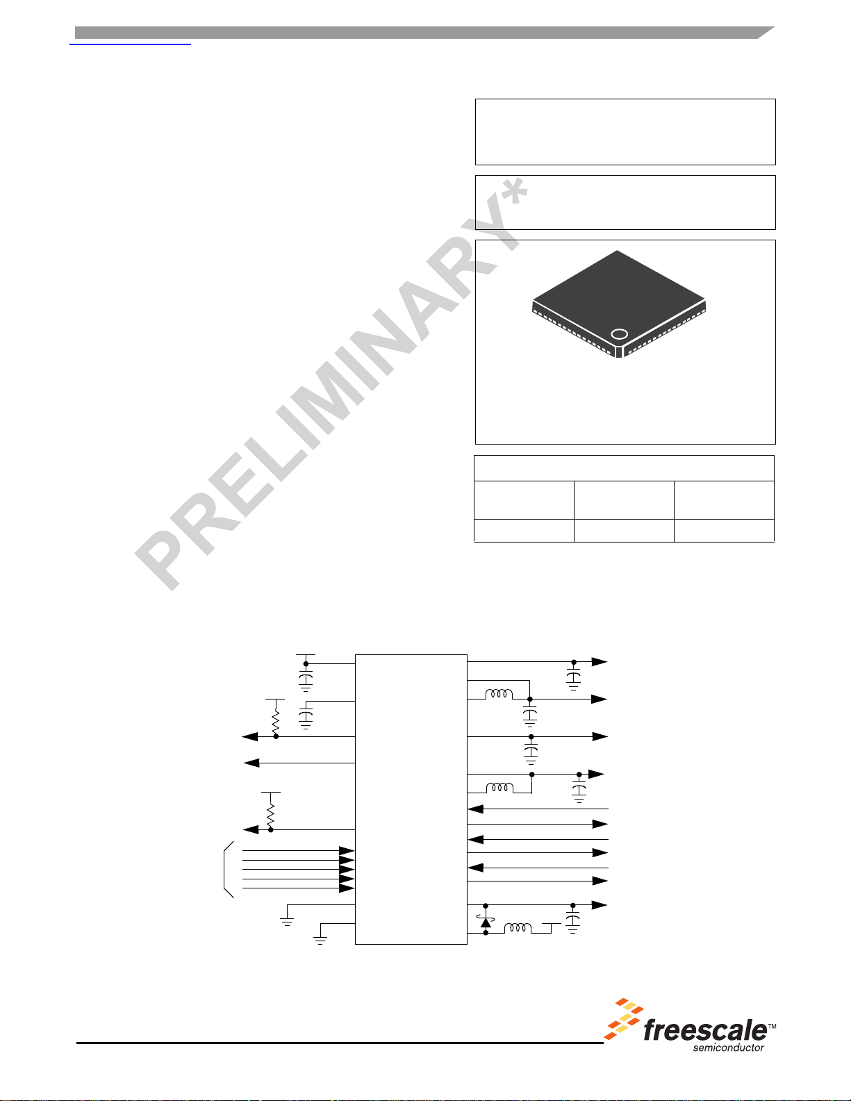
The MPC18730 Power Management IC (PMIC) regulates five
independent output voltages from either a single cell Li-Ion (2.7
4.2 V input range) or from a single cell Ni-MH or dry cell (0.9 V to
V input range).
2.2
The PMIC includes 2 DC-DC converters and 3 low drop out (LDO)
linear regulators. The output voltage for each of the 5 output voltages
is set independently through a 3-wire serial interface. The serial
interface also configures the PMIC's versatile start-up control system,
which includes multiple wakeup, sleep, standby, and reset modes to
minimize power consumption for portable equipment.
In single cell Li-Ion applications two DC-DC converters are
configured as buck (step-down) regulators. In single cell Ni-MH or dry
cell applications, one DC-DC converter is configured as a boost
(step-up) regulator, and the other as buck-boost regulator. The DCDC converters' output voltages have set ranges 1.613
V to 3.2 V at
up to 120 mA, and 0.805 V to 1.5 V up to 100 mA through the serial
interface.
Features
• Operates from single cell Li-Ion, Ni-MH, or Alkaline
• 2 DC-DC Converters
• 3 Low Drop Regulators
• Serial Interface Sets Output Voltages
• 4 Wake Inputs
• Low Current Standby Mode
• Pb-Free Packaging Designated by Suffix Code EP
2.7 V to 4.2 V Input
VO
VB
MPC18730
VB
VREF
V to
VCC1
SW1
POWER MANAGEMENT IC
EP SUFFIX
98ARL10571D
64-TERMINAL 0.5 mm PITCH
QFN
ORDERING INFORMATION
Device
MPC18730EP/R2 -10°C to 65°C 64 QFN
VO1
Temperature
Range (T
)
A
Programmable
1.613 V to 3.2 V
Programmable
0.805 V to 1.5 V
Package
RSTO1B
EXT_G_ON
VO
RSTO2B
MCU
CONTROL
LOGIC
INPUTS
GND
PGND
Figure 1. MPC18730 Simplified Application Diagram
* This document contains information on a product under development.
Freescale reserves the right to change or discontinue this product without notice.
© Freescale Semiconductor, Inc., 2005. All rights reserved.
VCC2
VO2
SW2
SREGI1
SREGO1
SREGI2
SREGO2
SREGI3
SREGO3
VG
SWG
VB
Programmable
0.865 V to 2.8 V
Programmable
0.011 V to 2.8 V
Programmable
2.08 V to 2.8 V
Page 2
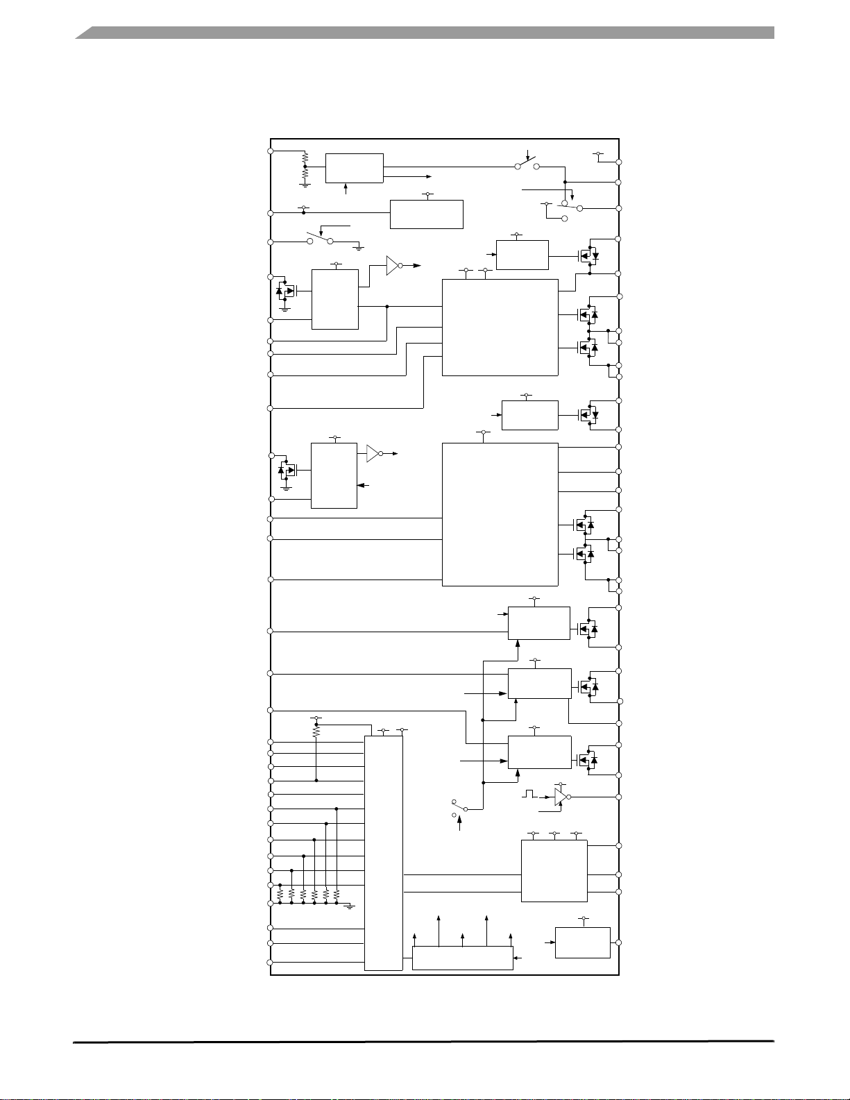
INTERNAL BLOCK DIAGRAM
INTERNAL BLOCK DIAGRAM
HVB
VREF
LSWO
RSTO1B
CRST1
RST1ADJ
INM1
RF1
DTC1
RSTO2B
CRST2
INM2
RF2
VREF
LVB
Driver
RSTO1B(Int)
CLR
VO1
RESET
Block 1
VO1
RESET
Block 2
BANDGAP
REFERENCE
RSTO1B(Int)
RSTO2B(Int)
REF2
VMODE
VO1
RSTO1B(Int)
RSTO2B(Int)
VO1
RSTO2B(Int)
VMODE
VG
POWER
SWITCH1
VG
Step-UpDown
DC/DC
Converter
CH1
VG
POWER
SWITCH2
VG
Step-UpDown
DC/DC
Converter
CH2
VB
VB
LVB
VO1
V_STBY
VCC1
VO1
VI1
SW1
PGND1
VCC2
VO2IN
VO2
DW_2T
DW_2B
VI2
SW2
DTC2
SREGC1
SREGC1
SREGC2
SREGC3
WAKE1B
WAKE2B
WAKE3B
WAKE4B
SEQSEL
DATA
STRB
SCKIN
CLR
SLEEP
CLKIN
GND
VGSEL1
VGSEL2
WDT
V_STBY
VO1 VB
CONTROL
Control
Logic
REF4
REF5
RSTO1B(Int)
RSTO2B
(Int)
SEQSEL
REF2
REF1
REF3
REF DAC
REF3
VG_select
VG_duty
REF4
REF5
VG
Series Pass
Regulator1
VG
Series Pass
Regulator2
VG
Series Pass
Regulator3
VB
CLKIN
CPoff
VO1VB
Step- Up
DC/DC
Convertor
On
VREF
VG
VG
EXT gate
On
Buffer
PGND2
SREGI1
SREGO1
SREGI2
SREGO2
SREG2G
SREGI3
SREGO3
C1L
VG
SWG
PGND3
EXT_G_ON
Figure 2. MPC18730 Simplified Internal Block Diagram
18730
Analog Integrated Circuit Device Data
2 Freescale Semiconductor
Page 3
CLR
WAKE4B
WAKE3B
WAKE2B
WAKE1B
LSWO
LVB
HVB
V_STBY
VO1
VCC1
VI1
SW1
SW1
PGND1
PGND1
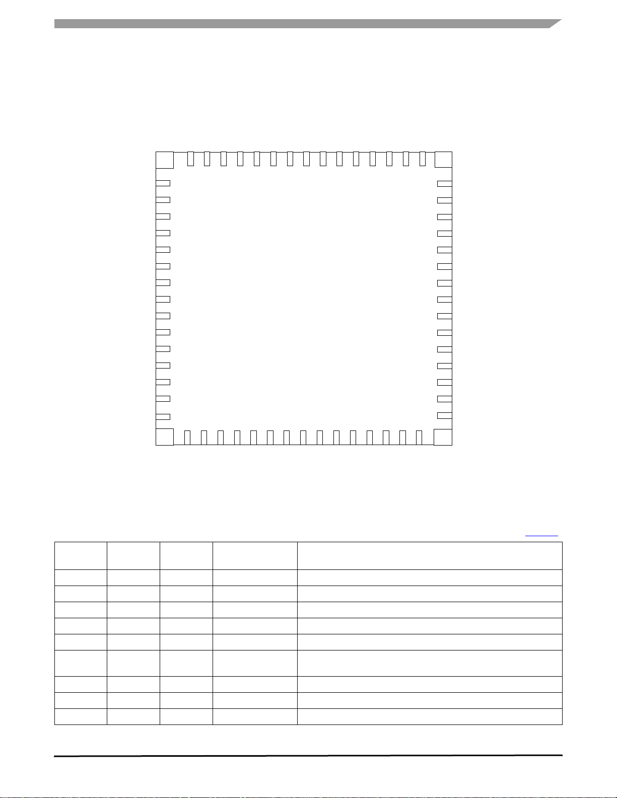
TERMINAL CONNECTIONS
GND
VREF
DATA
STRB
SCKIN
CLKIN
SLEEP
1
64 63 62 61 60 59 58 57 56 55 54 53 52 51
2
3
4
5
6
7
8
9
10
11
12
13
14
15
16
19 20 21 22 23 24 25 26 27 28 29 30 31 32
18
17
WDT
SEQSEL
SREGI1
TOP VIEW
SREGO1
SREGC1
SREGO2
SREGI2
SREG2G
50
48
47
46
45
44
43
42
41
40
39
38
37
36
35
34
TERMINAL CONNECTIONS
SREGC2
49
SREGI3
SREGO3
SREGC3
EXT_G_ON
DW_2B
DW_2T
VO2
VO2IN
VCC2
VI2
SW2
SW2
PGND2
PGND2
RSTO2B
CRST2
33
VB
PGND3
VGSEL2
VGSEL1
INM2
RF2
DTC2
CRST1
RSTO1B
DTC1
RST1ADJ
INM1
C1L
SWG
RF1
VG
Figure 3. MPC18730 Terminal Connections
Table 1. MPC18730 Terminal Definitions
A functional description of each terminal can be found in the Functional Terminal Description section beginning on page 14.
Terminal
Number
1 CLR Input Clear Start-up Signal Input Latch/Clear
2 WAKE4B Input Wake Signal 4 Start-up Signal Input 4
3 WAKE3B Input Wake Signal 3 Start-up Signal Input 3
4 WAKE2B Input Wake Signal 2 Start-up Signal Input 2
5 WAKE1B Input Wake Signal 1 Start-up Signal Input 1
6 LSWO Output Low-Side Switch
7 LVB Input Low Voltage Battery VB Power Supply Connection for Ni_mh
8 HVB Input High Voltage Battery VB Power Supply Connection for Li_ion
9 V_STBY Output Standby Voltage V_STBY Voltage Output
Terminal
Name
Terminal
Function
Formal Name Definition
Low-Side Switch Output Terminal
Output
18730
Analog Integrated Circuit Device Data
Freescale Semiconductor 3
Page 4
TERMINAL CONNECTIONS
Table 1. MPC18730 Terminal Definitions (continued)
A functional description of each terminal can be found in the Functional Terminal Description section beginning on page 14.
Terminal
Number
10 VO1 Input Voltage Input 1
11 VCC1 Output Voltage Output 1
12 VI1 Output Voltage Output 1
13 SW1 Power Switching 1
14 SW1 Power Switching 1
15 PGND1 Ground Power Ground 1
16 PGND1 Ground Power Ground 1
17 RSTO1B Output Inverted Reset
18 CRST1 Input Reset Delay
19 RST1ADJ Output Reset1 Adjustment
20 DTC1 Power Duty Control
21 RF1 Output Reference Feedback 1
22 INM1 Input Input Minus 1
23 C1L Power Charge Pump
24 VG Output Gate Voltage
25 SWG Power Switching
26 PGND3 Ground Power Ground 3
27 VB Power Battery Voltage
28 VGSEL2 Output VG Select 2
29 VGSEL1 Output VG Select 1
30 INM2 Input Input Minus
31 RF2 Output Reference Feedback 2
32 DTC2 Power Duty Control
33 CRST2 Input Reset Delay
34 RSTO2B Output Inverted Reset
35 PGND2 Ground Power Ground 2
36 PGND2 Ground Power Ground 2
37 SW2 Power Switching
38 SW2 Power Switching
39 VI2 Output Voltage Output
40 VCC2 Output Voltage Output
41 VO2IN Input Voltage Input
42 VO2 Input Voltage Input
Terminal
Name
Terminal
Function
Formal Name Definition
Output 1
Capacitor 1
Capacitor
Capacitor 1
Output 2
Switching Power Supply Circuit 1, VO1 Voltage Input, VO1 Power Supply
Power Switch 1 Output
Switching Power Supply Circuit 1 Output
Switching Power Supply Circuit 1 Coil Connection
Switching Power Supply Circuit 1 Coil Connection
Switching Power Supply Circuit 1 Power GND
Switching Power Supply Circuit 1 Power GND
Reset Circuit 1 Reset Signal Output
Reset Circuit 1 Reset Signal Delaying Capacitor Connection
Switching Power Supply Circuit 1 Reset Voltage Reference Output
Switching Power Supply Circuit 1 Maximum Duty Setting
Switching Power Supply Circuit 1 Error Amp Output
Switching Power Supply Circuit 1 Error Amp Inverse Input
VG Power Supply Circuit Charge Pump Capacitor Connection
VG Power Supply Circuit Voltage Output, Pre-Diver Circuit Power Supply
VG Power Supply Circuit Coil Connection
VG Power Supply Circuit Power GND
VB Power Supply Connection
VG Power Supply Circuit Output Voltage Setting 2
VG Power Supply Circuit Output Voltage Setting 1
Switching Power Supply Circuit 2 Error Amp Inverting Input
Switching Power Supply Circuit 2 Error Amp Output
Switching Power Supply Circuit 2 Maximum Duty Setting
Reset Circuit 2 Reset Signal Delay Capacitor Connection
Reset Circuit 2 Reset Signal Output
Switching Power Supply Circuit 2 Power GND
Switching Power Supply Circuit 2 Power GND
Switching Power Supply Circuit 2 Coil Connection
Switching Power Supply Circuit 2 Coil Connection
Switching Power Supply Circuit 2 Output
Power Switch 2 Output
Power Switch 2 Voltage Input
Switching Power Supply Circuit 2 VO2 Voltage Input
18730
Analog Integrated Circuit Device Data
4 Freescale Semiconductor
Page 5
TERMINAL CONNECTIONS
Table 1. MPC18730 Terminal Definitions (continued)
A functional description of each terminal can be found in the Functional Terminal Description section beginning on page 14.
Terminal
Number
43 DW_2T Output Step Down Top FET 2
44 DW_2B Output Step Down Bottom
45 EXT_G_ON Output Gate Switch
46 SREGC3 Power Regulator Capacitor 3
47 SREGO3 Output Regulator Output 3
48 SREGI3 Power Regulator Input 3
49 SREGC2 Power Regulator Capacitor 2
50 SREG2G Output Regulator Gate Output
51 SREGO2 Output Regulator Output 2
52 SREGI2 Power Regulator Input 2
53 SREGC1 Power Regulator Capacitor 1
54 SREGO1 Output Regulator Output 1
55 SREGI1 Power Regulator Input 1
56 GND Ground Ground
57 VREF Output Reference Voltage
58 DATA Input Data Signal
59 STRB Input Strobe
60 SCKIN Input Serial Clock
61 WDT Input Watch Dog Timer
62 SEQSEL Input Sequence Input
63 CLKIN Input Clock Input
64 SLEEP Input Sleep Signal
Terminal
Name
Terminal
Function
Formal Name Definition
FET 2
2
Switching Power Supply Circuit 2 Step down Top side FET Gate Output
for Ni_mh
Switching Power Supply Circuit 2 Step down Bottom side FRT Gate
Output for Ni_mh
External Transistor Gate Signal Output
Series Pass Power Supply Circuit 3 External Feedback Connection
Series Pass Power Supply Circuit 3 Output
Series Pass Power Supply Circuit 3 Power Supply
Series Pass Power Supply Circuit 2 External Feedback Connection
Series Pass Power Supply Circuit 2 External Transistor Gate Signal
Output
Series Pass Power Supply Circuit 2 Output
Series Pass Power Supply Circuit 2 Power Supply
Series Pass Power Supply Circuit 1 External Feedback Connection
Series Pass Power Supply Circuit 1 Output
Series Pass Power Supply Circuit 1 Power Supply
GND
Reference Voltage Output
Serial Interface Data Signal Input
Serial Interface Strobe Signal Input
Serial Interface Clock Signal Input
Watchdog Timer Capacitor Connection
Start-Up Sequence Setting Input
External Synchronous Clock Signal Input
Sleep Signal Input
18730
Analog Integrated Circuit Device Data
Freescale Semiconductor 5
Page 6
MAXIMUM RATINGS
MAXIMUM RATINGS
Table 2. Maximum Ratings
All voltages are with respect to ground unless otherwise noted. Exceeding these ratings may cause a malfunction or
permanent damage to the device.
Ratings Symbol Value Unit
ELECTRICAL RATINGS
Power Supply Voltage
Analog Signal Input
(1)
Logic Signal Input
WAKE1~4B
CLR, SLEEP, CLKIN, SCKIN, DATA, STRB
VGSEL1,2
Output Power Current
V
Power Supply Circuit
CC1
V
Power Supply Circuit
CC2
(2)
SREG1 Power Supply Circuit
SREG2 Power Supply Circuit
SREG3 Power Supply Circuit
VG Power Supply Circuit
RSTO1B Power Supply Circuit
Open-Drain Output Apply Voltage
RSTO1B
LSWO
ESD Voltage
Human Body Model (HBM)
Machine Model (MM)
(3)
(4)
Charge Device Model (CDM)
THERMAL RATINGS
Operating Temperature
Ambient
Junction
Storage Temperature
Thermal Resistance
(5)
Junction to Ambient
Lead Soldering Temperature
(6)
Notes
1. VREF, DTC1, DTC2, SREGC1, SREGC2, SREGC3 and RST1ADJ.
2. Includes the series pass power supply circuit output current.
3. ESD1 testing is performed in accordance with the Human Body Model (C
4. ESD2 testing is performed in accordance with the Machine Model (C
module specification with a capacitor 0.01
µF connected from OUT to GND.
ZAP
= 200 pF, R
ZAP
5. Device mounted on a 2s2p test board, in accordance with JEDEC JESD51-6 and JESD51-7.
6. Terminal soldering temperature limit is for 10 seconds maximum duration. Not designed for immersion soldering. Exceeding these limits
may cause malfunction or permanent damage to the device.
V
B
V
INAN
V
ILRSTB
V
ILGC
V
ILGSEL
I
OVO1
I
OVO2
I
OREG1
I
OREG2
I
OREG3
I
OVG
I
ORSTB
V
IODR
V
IODV
V
ESD1
V
ESD2
V
CDM
T
A
T
J
T
STG
R
JA
θ
T
SOLDER
= 100 pF, R
ZAP
-0.5 to 5.0 V
-0.5 to VO1+0.5 V
-0.5 to V_STBY+0.5
-0.5 to VO1+0.5
-0.5 to VB+0.5
mA
120
100
80
100
80
8
-20
-0.5 to 3.3
-0.5 to 3.3
± 1500
± 200
± 750
°C
-10 to 65
150
-50 to 150 °C
69 °C/W
260 °C
= 1500 Ω).
ZAP
= 0 Ω) and in accordance with the system
V
V
V
18730
Analog Integrated Circuit Device Data
6 Freescale Semiconductor
Page 7
STATIC ELECTRICAL CHARACTERISTICS
Table 3. Static Electrical Characteristics
Characteristics noted under conditions VB = 1.2 V, VO1 = 2.4 V, VG = 6.0 V, f
values noted reflect the approximate parameter means at T
Characteristic Symbol Min Typ Max Unit
GENERAL
VB Power Supply Voltage
Power Supply Voltage 1
Power Supply Voltage 2
Series Regulator Input Voltage
Start-Up Voltage
Analog Signal Input
(10)
Logic Signal Input
RSTO1 ~ 4B
CLR, SLEEP, CLKIN, DATA, STRB and SCKIN
VGSEL1, 2
Output Power Current
V
Power Supply Circuit
CC1
V
Power Supply Circuit
CC2
SREG1 Power Supply Circuit
SREG2 Power Supply Circuit
SREG3 Power Supply Circuit
VG Power Supply Circuit
RSTO
Supply Current in Stand-by mode
VB Supply Current (VB = 1.2 V for Ni_MH)
(HVB = 3.5 V for Li-Ion)
Supply Current in Operating mode
VB Supply Current (VB = 1.2 V for Ni_MH)
(HVB = 3.5 V for Li-Ion)
Reference Power Supply Circuit
Output Voltage
Output Current
Switching Power Supply 1
V
Output Voltage (Io = 0~100 mA)
CC1
Notes
7. When applying voltage from an external source.
8. 0.3 V when VG is 4.5 V.
9. Provide 2 V or higher for the voltage difference (VG - VO1).
10. VREF, DTC1, DTC2, SREGC1, SREGC2, SREGC3 and RST1ADJ.
11. Includes the series pass power supply circuit output current.
(7), (8)
(11)
(11)
= 27°C under nominal conditions unless otherwise noted.
A
V
LVB
V
HVB
V
SREGI
V
BST
V
IANA
V
ILRSTB
V
ILGC
V
ILGSEL
I
OVCC1
I
OVCC2
I
OSREG1
I
OSREG2
I
OSREG3
I
OVG
I
ORSTB
I
BSNi
I
BSLi
I
BNi
I
BLi
V
REF
I
OREF
V
CC1
STATIC ELECTRICAL CHARACTERISTICS
= 176.4 kHz unless otherwise noted. Typical
CLK
V
SREG
0.9
2.7
+0.2
(9)
V
1.2
3.5
SREG
+0.3 V
2.2
4.2
+0.4 V
SREG
0.9 - - V
0 - V
0
0
0
0
0
5
6
5
0
-5
-
-
-
-
1.255
-0.3
-
-
-
-
-
-
-
-
-
-
5
8
9
7
1.275
-
O1
V_STBY
VO1
VB
100
80
60
80
60
6
0
10
12
18
14
1.295
0.3
2.3 2.4 2.5 V
V
V
V
mA
mA
mA
V
mA
18730
Analog Integrated Circuit Device Data
Freescale Semiconductor 7
Page 8
STATIC ELECTRICAL CHARACTERISTICS
This paragraph is boilerplate - you may add to it but, can not change wording. You may change numeric values
Table 3. Static Electrical Characteristics (continued)
Characteristics noted under conditions VB = 1.2 V, VO1 = 2.4 V, VG = 6.0 V, f
= 176.4 kHz unless otherwise noted. Typical
CLK
values noted reflect the approximate parameter means at TA = 27°C under nominal conditions unless otherwise noted.
Characteristic Symbol Min Typ Max Unit
Switching Power Supply 2
V
Output Voltage (Io = 0~80 mA)
CC2
DW_2T Output Voltage
(I
= 400 µA)
sink
DW_2B Output Voltage
(I
= 400 µA)
sink
(12)
(12)
(I
(I
source
source
= 400 µA)
= 400 µA)
Series Pass Power Supply Circuit
SREG1 Control Voltage (Io = 5~60 mA)
SREG1-Error AMP Input offset voltage
SREG2 Control Voltage (Io = 6~80 mA)
SREG2-Error AMP Input offset voltage
SREG3 Control Voltage (Io = 5~60 mA)
SREG3-Error AMP Input offset voltage
SREG2G Output Voltage
(I
= 2.5 µA)
sink
(17)
(I
source
(13)
(14)
(13)
(15)
(13)
(16)
= 2.5 µA)
Power Switch On Resistance
V
Circuit
CC1
V
Circuit
CC2
VG Power Supply Circuit
(Io = 0~6 mA)
(Io = 0~6 mA)
C1L Output Voltage (I
(I
= 2.5 mA)
sink
(18)
(19)
source
= 2.5 mA)
VGH Voltage (Certified value)
V_STBY Output Voltage for Li_ion (Io = 300 µA)
(20)
Notes
12. Connect a transistor with gate capacity of 200 pF or smaller to DW_2T and DW_2B
13. If a capacitor with capacitance of 22µF is connected to SREGO, use a phase compensation capacitor between SREGO and SREGC
when the load is 5 mA (6 mA for SREG2) or lower. The output voltage values shown in the table assume that external resistance is
connected as follows:
SREGI1 = 3.0V to 3.3V, 65.14KΩ between SREGO1 and SREGC1, 34.86KΩ between SREGC1 and GND.
SREGI2 = 3.0V to 3.3V, 54.46KΩ between SREGO2 and SREGC2, 45.54KΩ between SREGC2 and GND.
SREGI3 = 3.0V to 3.3V, 73.84KΩ between SREGO3 and SREGC3, 26.16KΩ between SREGC3 and GND.
14. Calculated by the right formula for input offset: SR1OFST=(Vref x 0.77) - (SREGO1 ÷ (100k ÷ 34.86k))
15. Calculated by the right formula for input offset: SR2OFST=(Vref x 1) - (SREGO1 ÷ (100k ÷ 45.54k))
16. Calculated by the right formula for input offset: SR3OFST=(Vref x 0.58) - (SREGO1 ÷ (100k ÷ 26.16k))
17. Connect a transistor with gate capacity of 300 pF or smaller to REG2G.
18. When VGSEL1 is Low and VGSEL2 is Low, I/O=3mA or higher is certified by specification.
19. When VGSEL1 is High and VGSEL2 is Low, I/O=3mA or higher is certified by specification.
20. When HVB is 4.2V and the load from V_STBY is 0.5µA or higher.
V
CC2
V
DW2TH
V
DW2TL
V
DW2BH
V
DW2BL
V
SREG1
SR1OFST
V
SREG2
SR2OFST
V
SREG3
SR3OFST
SREG2GH
SREG2GL
R
VCC1
R
VCC2
VG_00
VG_10
VO11LH
VO11LL
VGH
V
LVB
1.05
5.2
0
5.2
0
2.7
-13.5
2.7
-17
2.7
-11
5
0
-
-
5.5
4.6
VB x 0.85
0
-
1.15
-
-
-
-
2.8
-
2.8
-
2.8
-
-
-
0.4
0.4
6.0
5.0
-
-
-
1.25
VG
0.3
VG
0.3
2.9
24.5
2.9
17
2.9
23
VG
0.5
0.6
0.6
6.5
5.4
VB
0.4
10.5
1.75 - 2.45 V
mV
mV
mV
V
V
V
V
V
V
Ω
V
18730
Analog Integrated Circuit Device Data
8 Freescale Semiconductor
Page 9
STATIC ELECTRICAL CHARACTERISTICS
Table 3. Static Electrical Characteristics (continued)
Characteristics noted under conditions VB = 1.2 V, VO1 = 2.4 V, VG = 6.0 V, f
= 176.4 kHz unless otherwise noted. Typical
CLK
values noted reflect the approximate parameter means at TA = 27°C under nominal conditions unless otherwise noted.
Characteristic Symbol Min Typ Max Unit
Reset Circuit
Reset Voltage 1
Reset Voltage 2
Hysteresis Voltage 1 (@RST1)
Hysteresis Voltage 2 (@RST2)
RSTB (V
(I
= 2 mA)
sink
CRST (I
RSTB
= 100 µA)
sink
= 2.4 V)
High Level Threshold Voltage
Low Level Threshold Voltage
CRST Pull-Up Resistance
V_STBY Output Resistance
Output Resistance (VO1)
Output Resistance (VB)
LSWO Output Resistance
Output Resistance
Ext_G_ON
Ext_G_ON Output Voltage (I
(I
= 100 µA)
sink
source
= 100 µA)
Logic Input
"H" Level Input Voltage
"L" Level Input Voltage
"H" Level Input Voltage
"L" Level Input Voltage
"H" Level Input Voltage
"L" Level Input Voltage
"H" Level Input Current
"L" Level Input Current
Pull Up Resistance
Pull Down Resistance
(21)
(21)
(22)
(22)
(23)
(23)
(21), (23)
(23), (24)
(25)
(26)
Notes
21. Applied to WAKEB1 ~ 4 and SEQSEL.
22. Applied to CLR, SLEEP, CLKIN, DATA, STRB and SCKIN.
23. Applied to VGSEL1 and 2.
24. Applied to WAKEB1 ~ 3, CLR, SLEEP, CLKIN, DATA, STRB, SCKIN and SEQSEL.
25. Applied to WAKEB4.
26. Applied to CLR, SLEEP, CLKIN, DATA, STRB and SCKIN.
V
RST1
V
RST2
V
HYRS1
V
HYRS2
I
ORSTB1,2
V
OLRSTB1,2
V
OLCR1,2
V
IHCR1,2
V
ILCR1,2
R
PUPRC1,2
R
VO1
R
VB
R
LSWO
V
OHEXTG
V
OLEXTG
V
IHVS
V
ILVS
V
IH
V
IL
V
IHVB
V
ILVB
I
IH
I
IL
R
PUP
R
PDW
0.85 x VO1
0.80 x VO2
40
50
0
0
0
1.25
0.75
50
-
-
0.88 x VO1
0.85 x VO2
78
75
-
-
-
1.42
1.00
100
30
200
0.91 x VO1
0.90 x VO2
115
100
10
0.5
0.7
1.65
1.15
150
45
400
- 42 50 Ω
VG x 0.9
0
V_STBY - 0.2
-
1.5
-
VB - 0.2
-
-1
-1
410
330
-
-
-
-
-
-
-
-
-
-
590
480
VG
VG x 0.1
0.2
0.4
0.2
770
625
-
-
-
1
1
V
V
mV
mV
µA
V
V
V
V
KΩ
Ω
V
V
V
V
V
V
V
µA
µA
KΩ
KΩ
18730
Analog Integrated Circuit Device Data
Freescale Semiconductor 9
Page 10
DYNAMIC ELECTRICAL CHARACTERISTICS
DYNAMIC ELECTRICAL CHARACTERISTICS
Table 4. Dynamic Electrical Characteristics
Characteristics noted under conditions VB = 1.2 V, VO1 = 2.4 V, VG = 6.0 V, f
values noted reflect the approximate parameter means at T
Characteristic Symbol Min Typ Max Unit
OSCILLATOR
Internal Oscillation Frequency
MICRO CONTROLLER INTERFACE
Clock Signal Input
Serial Interface (Refer to Timing Chart below)
DATA Set Up Time
DATA Hold Time
SCKIN Clock Frequency
SCKIN 'H' Pulse Width
SCKIN 'L' Pulse Width
SCKIN Hold Time
STRB Set Up Time
STRB Pulse Width
Notes
27. Duty 50%.
(27)
= 27°C under nominal conditions unless otherwise noted.
A
= 176.4 kHz unless otherwise noted. Typical
CLK
f
f
f
t
wckh
t
t
t
t
ICK
CLK
t
t
sck
wckl
hck
ssb
wsb
s
h
150 200 250 kHz
- 176.4 - kHz
20
20
-
50
50
50
50
50
6.0
-
-
-
-
-
-
-
-
-
-
-
-
-
-
-
nsec
nsec
MHz
nsec
nsec
nsec
nsec
nsec
18730
Analog Integrated Circuit Device Data
10 Freescale Semiconductor
Page 11
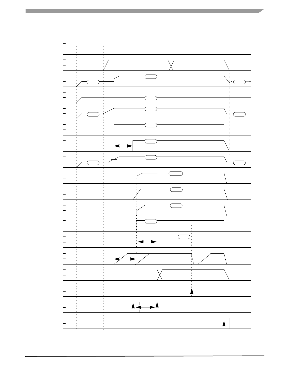
WAKE1~4(int)
FUNCTIONAL DIAGRAMS
FUNCTIONAL DIAGRAMS
CLKIN
V_STBY
VB
VG
RSTO1B(Int)
RSTO1B
VO1
VCC1
VO2
VB
VB
VB*1
CRST set value
INT
VO1
VB
VG
VO1
VO1
VO1
VO1
VO2
EXT
(Serial setting)
VB
VB
VB*1
VCC2
RSTO2B(Int)
RSTO2B
VSREG1~3
DATA
STRB
CLR
SLEEP
Standby Mode
*1: When using Ni_mh. High-Z when using Li_ion.
Figure 4. Power Supply Start-Up Timing Diagram
SEQSEL setting
Start-Up
VO2
VO1
CRST set value
VO1
DATA
SEQSEL setting
Operation Mode Standby Mode
18730
Analog Integrated Circuit Device Data
Freescale Semiconductor 11
Page 12
FUNCTIONAL DIAGRAMS
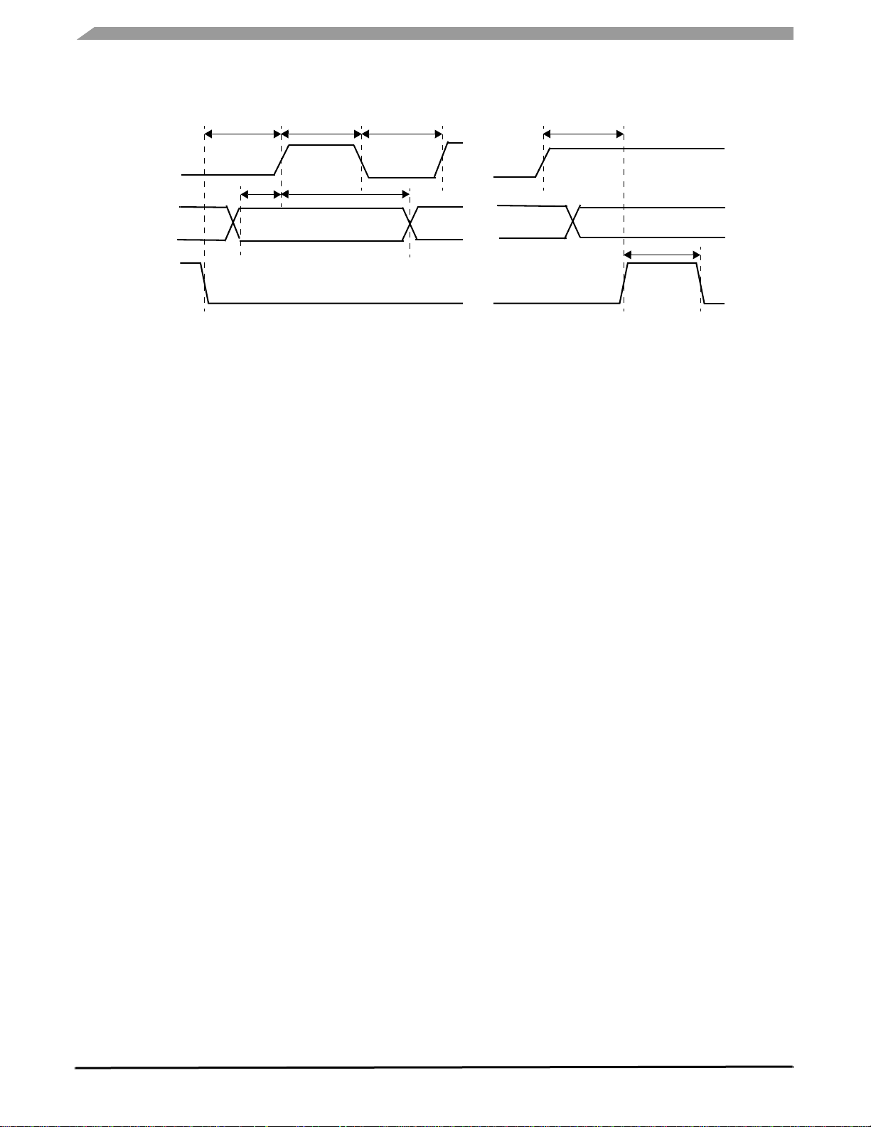
SCKIN
DATA
STRB
t
ssb
t
s
t
wckh
A3
t
wckl
t
h
A2
D0
t
hck
t
wsb
Figure 5. Serial Interface Timing Diagrams
18730
Analog Integrated Circuit Device Data
12 Freescale Semiconductor
Page 13

FUNCTIONAL DIAGRAMS
Table 5. Serial Interface Functions
Register Name Address DATA1 DATA2
0 CLR, SLEEP 1000 CLR SLEEP Reserved Reserved Reserved Reserved Reserved Reserved
1 Power Mode 0001 PSW1 PSW2 RSTO1B VCC2 SREG1 SREG2 SREG3 RSTO2B
2 Clock Select 0010 Ext / Int Half Freq RSTB sleep S_Off_VG VG_Duty[3] VG_Duty[2] VG_Duty[1] VG_Duty[0]
3 VO1 0011 MSB VO1 Output Voltage LSB S_Off_VO1
4 VO2 0100 MSB VO2 Output Voltage LSB S_Off_VO2
5 SREG1 0101 MSB SREG1 Output Voltage LSB Reserved
6 SREG2 0110 MSB SREG2 Output Voltage LSB
7 SREG3 0111 MSB SREG3 Output Voltage LSB CP Off EXTG On
Twelve bits immediately before start-up of STRB are
always effective. Upon power on, the internal power on reset
order of Add_[3], Add_[2], ..., Add_[0], DATA1_[3],
DATA1_[2], ...., DATA2_[0].
works to initialize the registers. Serial data is fetched in the
Table 6. Block Operation
INPUT OUTPUT
WAKE(Int) RSTO1B(Int) RSTO1B RSTO2B(Int) SEQSEL VG VO1 VO2 VCC1,2 REG1,2,3
L X X X X - - - - -
H L L L L O O - - -
H H L L L O O - - O
H H L L H O O - - -
H H H H L O O O O O
H H H H H O O O O O
O : Operation, - : Stop, X : Don’t care
Table 7. Start-Up Sequence Settings
SEQSEL CLR/SLEEP Series Regulators
V_STBY RSTO2B(Ext) RSTO2B(Int)
GND RSTO1B(Ext) RSTO1B(Int)
18730
Analog Integrated Circuit Device Data
Freescale Semiconductor 13
Page 14

FUNCTIONAL DESCRIPTION
INTRODUCTION
FUNCTIONAL DESCRIPTION
INTRODUCTION
The 18730 power management integrated circuit provides
five independent output voltages for the micro controller from
either a single cell Li-Ion or from a single cell Ni-MH or dry
cell. The PMIC includes two DC to DC converters and three
low drop out linear regulators. The output voltage for each of
the five output voltages is set independently through a 3-wire
serial interface. The PMIC has multiple wakeup, sleep, and
FUNCTIONAL TERMINAL DESCRIPTION
CLEAR TERMINAL (CLR)
This Clear input signal makes clear internal latches for
WAKE signal holding. The WAKE control circuit can not
receive another WAKE input until the latch is cleared by this
Clear input.
WAKE SIGNAL TERMINALS (WAKE1B, WAKE2B,
WAKE3B, WAKE4B) ... ACTIVE LOW
Any one WAKE input signal of these four WAKE inputs
awakes this device from sleep mode. The WAKE signals can
be made with external low side mechanical switch and
resistance that is pulled up to VSTB rail.
LOW-SIDE SWITCH OUTPUT TERMINAL (LSWO)
Low-Side switch output that is turned on with ‘CLR’ signal.
It can be used for external key input latches clear.
LOW VOLTAGE BATTERY TERMINAL (LVB)
This input terminal is used for temporarily power supply
while wake up for 1cell Ni-MH battery or 1cell dry cell battery
(= Low Voltage Battery) use. It has to be connected to VB rail.
When Li-Ion battery is used, the terminal has to be open.
HIGH VOLTAGE BATTERY TERMINAL (HVB)
This input terminal is used for temporarily power supply
while wake up for Li-Ion battery (= High Voltage Battery) use.
It has to be connected to the VB rail. When a Ni-MH battery
is used, the terminal has to be connected to ground level.
STANDBY VOLTAGE TERMINAL (V_STBY)
Standby Voltage is made from LVB or HVB that depends
on which battery is used. This voltage is used for internal
logic and analog circuit at standby (sleep) mode temporarily
before ‘VO1’ voltage is established.
VOLTAGE INPUT TERMINALS (VO1, VO2)
This power supply input terminal named ‘VO1 or VO2’ is
for internal logic and analog circuits and for input of ‘VCC1’
output via power switch. Input for ‘VCC2’ is ‘VO2IN’ terminal.
It is supplied from the output of Channel-1 or Channel-2 DC/
DC converter as ‘VO1 or VO2.
reset modes to minimize power consumption for portable
equipment. In single cell Li-Ion applications two DC-DC
converters are configured as buck regulators. In single cell
Ni-MH or dry cell applications, one DC-DC converter is
configured as a boost regulator, and the other as buck-boost
regulator.
VOLTAGE OUTPUT TERMINALS (VCC1, VCC2)
Output ‘VO1’ or ‘VO2’ voltage controlled internal power
switch.
POWER INPUT TERMINALS (VI1, VI2)
The power input terminals (VI1, VI2) are drain terminals on
the top side FET of the DC/DC converter switcher. They are
the power input for the buck converter and output for the
boost converter.
SWITCHING TERMINALS (SW1, SW2)
Switching Terminals (SW1, SW2) are the output of the half
bridge and connect to the external inductance.
POWER GROUND TERMINALS (PGND1, PGND2,
PGND3)
Ground level node for DC/DC converter and Charge Pump
portion.
INVERTED RESET OUTPUT TERMINALS (RSTO1B,
RSTO2B)
Reset signal output for external MPU or the something
controller. RSTO1B keeps ‘Low’ level while the VO1 voltage
is less than internal reference voltage. RSTO2B follows to
VO2 voltage.
RESET DELAY CAPACITOR TERMINALS (CRST1,
CSRT2)
The capacitor which is connected to this terminal decide
delay time to negate Reset signal from exceeding the
reference voltage level.
RESET 1 ADJUSTMENT TERMINAL (RST1ADJ)
Used to adjust the reset level with external resistance
which is connected to VO1 for RSTO1B.
DUTY CONTROL TERMINALS (DTC1, DTC2)
Connected external voltage to this terminal via
capacitance can control the duty of DC/DC converter
switching. Use of the terminal for this is not recommended.
18730
Analog Integrated Circuit Device Data
14 Freescale Semiconductor
Page 15

FUNCTIONAL TERMINAL DESCRIPTION
FUNCTIONAL DESCRIPTION
REFERENCE FEEDBACK TERMINALS (RF1, RF2)
Output node of internal error amp. for DC/DC converter 1
and 2. For phase compensation use.
INPUT MINUS TERMINALS (INM1, INM2)
Minus input of internal error amp. for DC/DC converter 1
and 2. For phase compensation use.
CHARGE PUMP CAPACITOR TERMINAL (C1L)
In case of use higher voltage than VG externally, connect
capacitance and diodes between VG. The charge pump
structure can output VG + VB - 2 x VF voltage. There is no
meaning for Ni-MH or dry cell battery, because the VB
voltage is almost same as 2 x VF voltage. Recommend to use
for Li-Ion battery use.
GATE VOLTAGE TERMINAL (VG)
Output terminal of boost converter for gate drive voltage.
The output voltage is decided by VGSEL input.
SWITCHING FOR GATE VOLTAGE TERMINAL
(SWG)
Switching terminal for VG boost converter. Connect to
external inductance.
BATTERY VOLTAGE TERMINAL (VB)
Power supply input that connects to Ni-MH or Dry cell or
Li-Ion battery.
VG SELECT TERMINALS (VGSEL1, VGSEL2)
VG output voltage is decided with these two bits input.
VOLTAGE INPUT FOR POWER SWITCH 2
TERMINAL (VO2IN)
Input of VCC2 output via power switch. Connect to VO2
terminal externally.
STEP DOWN FET GATE DRIVE TERMINALS
(DW_2T, DW_2B)
Gate drive output terminals for external FETs to use DC/
DC converter 2 as Buck / Boost converter.
GATE SWITCH TERMINAL (EXT_G_ON)
Gate drive output terminal for external low side switch. It
can be used for power switch turning On/OFF for remote
controller part.
Input the feed back voltage that divided SREGO voltage by
resistances.
REGULATOR OUTPUT TERMINALS (SREGO1,
SREGO2, SREGO3)
Series regulator output terminals. All output voltages can
be variable with internal DAC via serial I/F.
REGULATOR INPUT TERMINALS (SREGI1,
SREGI2, SREGI3)
Series regulator power input terminals. To be connected to
battery voltage in general.
GROUND TERMINAL (GND)
Ground terminal for logic and analog circuit portion (not
power portion). Recommend to connect to clean ground
which separated with power ground line.
REFERENCE VOLTAGE TERMINAL (VREF)
Output of internal reference voltage. It can be used
externally. Output current capacity is less than 300uA.
DATA INPUT TERMINAL (DATA)
Serial data input terminal. The latest 12 bits before strobe
signal are valid.
STROBE TERMINAL (STRB)
Strobe signal input terminal for serial I/F. It establishes the
input 12bits data to internal control registers.
SERIAL CLOCK TERMINAL (SCKIN)
Clock input terminal for serial I/F. Input data are taken in to
I/F with this clock.
WATCH DOG TIMER TERMINAL (WDT)
Watch dog timer prevent unstable wake up (flips between
wake-up and failure). If there is no ‘CLR’ input after any
WAKEnB input before this WDT is expired, this device move
to ‘SLEEP’ mode to prevent wake failure hanging-up
situation.
SEQUENCE SELECT TERMINAL (SEQSEL)
Select judgement Reset channel for wake-up complete
with this input. If this input level is VSTB voltage, this device
judges the wake-up completion with Reset2 (DC/DC2). If it is
Ground, judge with Reset1 (DC/DC1). See
13.
Table 7, on page
REGULATOR CONTROL TERMINALS (SREGC1,
SREGC2, SREGC3)
Feed back terminal for each series regulators. This
terminal voltage is compared with internal reference voltage.
Analog Integrated Circuit Device Data
Freescale Semiconductor 15
CLOCK INPUT TERMINAL (CLKIN)
Clock input terminal for internal switching part. This device
has a oscillator internally, but can be used this input clock for
internal switching frequency. It is selected by Clock select bit.
Table 19, on page 26.
See
18730
Page 16

FUNCTIONAL DESCRIPTION
FUNCTIONAL TERMINAL DESCRIPTION
SLEEP MODE TERMINAL (SLEEP)
The sleep input signal puts the device in sleep mode. All
output voltages are down, and internal current consumption
will be minimum.
18730
Analog Integrated Circuit Device Data
16 Freescale Semiconductor
Page 17

FUNCTIONAL DEVICE OPERATION
OPERATIONAL MODES
FUNCTIONAL DEVICE OPERATION
OPERATIONAL MODES
START-UP CONTROL INPUT (SYSTEM CONTROL)
The latch is set at the rising edge of any WAKE1B-4B input
pin, and WAKE(int) goes High. WAKE1~4B inputs consist of
OR logic. At this time, the input pin which went Low keeps
latched until CLR goes High. After the latch is reset by CLR,
WAKE(int) goes Low when SLEEP goes High. The latch is
also cleared and WAKE(int) goes Low when SLEEP goes
High before the latch is cleared by CLR. In this case, CLR
keeps negated while RSTO1B, 2B(Ext) is Low. SLEEP keeps
negated while RSTO1B, 2B(Ext) is Low or CLR is High. The
period of time for which CLR and SLEEP are negated can be
set by the SEQSEL pin. Refer to Truth
for the correspondence between the SEQSEL pin settings
and negation period.
WAKEB
CLR
WDT
WAKE(Int)
Table 5, on page 13
Time specified by WDT
If SLEEP goes High to place the chip into the standby
mode while any of the WAKEB pins is Low, the chip can be
awakened again. This may happen if, when an WAKEB pin
and LSWO are connected, SLEEP goes High earlier than the
period of time (*1) specified by the external component of the
WAKEB pin.
Also, if the period of time after WAKE(int) goes High until
CLR goes High from Low is longer than the time specified by
WDT, internal sleep will start up to place the chip into the
standby mode.
(*1: It is 30 µsec when a capacitor is not connected as the
external component.)
STANDBY POWER SUPPLY CIRCUIT
CLR
HVB
RST1B
RST1B(Int)
Standby
Power
Supply
Control
Figure 7. Standby Power Supply Circuit Diagram
Figure 6. Start-Up Timing Diagram
LSWO
Short-circuit VB and LVB, and connect a Schottky
diode between VB and V_STBY only when using
Ni_mh.
When using Li_ion, leave LVB open, and shortcircuit HVB and VB.
VO1
VB
V_STBY
VB
LVB
V_STBY
18730
Analog Integrated Circuit Device Data
Freescale Semiconductor 17
Page 18

FUNCTIONAL DEVICE OPERATION
OPERATIONAL MODES
When RSTO1B(int) is Low, output LVB voltage to V_STBY
terminal. When RSTO1B(int) is High, output VO1 voltage to
V_STBY terminal. When CLR is Low, LSWO is open. When
RSTO1B(int) is High and CLR is High, LSWO output voltage
turns GND. When RSTO1B(int) is Low and RSTO1B is High,
discharge the external capacitor which is connected to
Table 8. HVB and LVB Connection
MODE HVB LVB
Li_ion VB
Ni_mh GND VB
Notes
28. Externally connect to VB.
Table 9. V_STBY and LSWO Operation
INPUT OUTPUT
WAKE(Int) RSTO1B(Int) CLR V_STBY LSWO
L X X VB Z
H L X VB Z
H H L VO1 Z
H H H VO1 L
Z : High Impedance, X : Don’t care
V_STBY. When using Ni_mh, short-circuit VB and LVB to
external components and HVB to GND. When using Li_ion,
short-circuit HVB to VB, and leave LVB open. When using
Ni_MH, the VB voltage is output from V_STBY in Standby
mode. When using Li-Ion, 50% of the VB voltage is output to
V_STBY terminal in Standby Mode.
(28)
open
(28)
RESET CIRCUIT
CRST1, 2
VO1, 2 VG
RST1ADJ
(RSTO1B side only)
When the VO1 or VO2 voltage is higher than the reference
value, RSTO1B or 2B goes High. When RSTO1B(int) is Low
and RSTO1B is High, SLEEP(int) is forced to place the chip
into the standby mode.
Connect a capacitor between RST1ADJ and CRST. The
capacitor is not necessary if a resistor of 330KΩ or less is
inserted between RST1ADJ and VC1 for reset adjustment
VO1
BANDGAP
REFERENCE
Figure 8. Reset Circuit Block Diagram
VO1
RST1B, 2B
Reset
Control
RSTO1B, 2B(Int)
CRST1, 2
Connect the capacitor between RST1ADJ and RSTB as
directed below.
When SEQSEL is Low: Between RST1ADJ and CRST1
When SEQSEL is High: Between RST1ADJ and CRST2
Use a capacitor with approximately half of the
capacitance between CRST and GND
18730
Analog Integrated Circuit Device Data
18 Freescale Semiconductor
Page 19

RST1B(Int)
RST1B
SLEEP(Int)
Figure 9. Reset Timing Diagram
FUNCTIONAL DEVICE OPERATION
OPERATIONAL MODES
POWER SUPPLY VO1, VO2: NI_MH
The VB voltage rises and is output to VI1. When
RSTO2B(int) is High, the power switch turns ON to output the
VO1 voltage to VCC1. Capacitance value which is connected
to VO1 should be higher than the capacitor connected to
VCC1.
Table 10. Output Voltage of VO1
Address : 0011(30)
B7 B6 B5 B4 B3 B2 B1 S_Off_VO1 VO1 [V]
L L L L L L L X 1.613
L L L L L L H X 1.625
L L L L L H L X 1.638
L L L L H L L X 1.663
L L L H L L L X 1.713
L L H L L L L X 1.813
L H L L L L L X 2.013
H L L L L L L X 2.413
H L L L L L H X 2.425
H L L L L H L X 2.438
H L L L H L L X 2.463
H L L H L L L X 2.513
H L H L L L L X 2.613
H H L L L L L X 2.813
H H H H H H H X 3.200
Notes
29. Operation is not guaranteed when VO1 input voltage is 1.8 V or lower. By connecting a diode between
VI1 and VO1, VI1 can output voltage higher (with the voltage difference Vf) than VO1.
30. All combinations of input are not included.
The VB voltage rises or falls and is output to VI2. When
RSTO2B(int) is High, the power switch turns ON to output the
VO2IN voltage to VCC2. If you turn DDC2 OFF using the
register, the power switch 2 also turns OFF. Capacitance
value which is connected to VO2IN should be higher than the
capacitor connected to VCC2.
(29)
18730
Analog Integrated Circuit Device Data
Freescale Semiconductor 19
Page 20

FUNCTIONAL DEVICE OPERATION
OPERATIONAL MODES
Table 11. Output Voltage of VO2
Address : 0100(31)
B7 B6 B5 B4 B3 B2 B1 S_Off_VO2 VO2 [V]
L L LLLL L X 0.805
L L LLLL H X 0.811
L L L L L H L X 0.816
L L L L H L L X 0.827
L L L H L L L X 0.849
L L H L L L L X 0.893
L H LLLL L X 0.980
H L LLLL L X 1.155
H L LLLL H X 1.161
H L L L L H L X 1.166
H L L L H L L X 1.177
H L L H L L L X 1.199
H L H L L L L X 1.243
H H LLLL L X 1.330
H H HHHH H X 1.500
Notes
31. All combinations of input are not included.
POWER SUPPLY VO1, VO2: LI-ION
The VB voltage falls and is output to VO1. When using
Li_ion, duty limit due to DTC1 is not applied to the switch.
When RSTO2B(int) is High, the power switch turns ON to
output the VO1 voltage to VCC1. Capacitance value which is
connected to VO1 should be higher than the capacitor
connected to VCC1.
The VB voltage falls using only the internal transistor and
is output to VO2. When using Li_ion, duty limit due to DTC2
is not applied to the switch, and DW_2T and DW_2B are Low.
When RSTO2B(int) is High, the power switch turns ON to
output the VO2IN voltage to VCC2. If you turn DDC2 OFF
using the register, the power switch 2 also turns OFF.
Capacitance value which is connected to VO2IN should be
higher than the capacitor connected to VCC2.
18730
Analog Integrated Circuit Device Data
20 Freescale Semiconductor
Page 21

FUNCTIONAL DEVICE OPERATION
OPERATIONAL MODES
SERIES PASS POWER SUPPLY
The series pass outputs the SREGI1 voltage to SREGO1,
the SREGI2 voltage to SREGO2, and the SREGI3 voltage to
Table 12. Output Voltage of SREG1
Address : 0101(31)
B7 B6 B5 B4 B3 B2 B1 Reserved SREG1 [V]
L L L L L L L H 0.865
L L L L L L H H 0.880
L L L L L H L H 0.895
L L L L H L L H 0.926
L L L H L L L H 0.986
L L H L L L L H 1.107
L H L L L L L H 1.349
H L L L L L L H 1.833
H L L L L L H H 1.848
H L L L L H L H 1.863
H L L L H L L H 1.893
H L L H L L L H 1.954
H L H L L L L H 2.075
H H L L L L L H 2.317
H H H H H H H H 2.800
Notes
32. The SREG1 and 3 output voltages are determined by the combination of external resistances connected to
REGC1 and 3 (65.14KΩ between SREGO1 and REGC1, 34.86KΩ between REGC1 and GND, 73.84KΩ
between SREGO3 and REGC3, and 26.16KΩ between REGC3 and GND).
33. All combinations of input are not included.
SREGO3. If you use MOSFET as the external component in
this case, connect the gate to SREG2G.
(32)
18730
Analog Integrated Circuit Device Data
Freescale Semiconductor 21
Page 22

FUNCTIONAL DEVICE OPERATION
OPERATIONAL MODES
Table 13. Output Voltage of SREG2
Address : 0110(31)
B7 B6 B5 B4 B3 B2 B1 B0
LLLLLLLL0.011
LLLLLLLH0.022
LLLLLLHL0.033
LLLLLHLL0.055
LLLLHLLL0.098
LLLHLLLL0.186
LLHLLLLL0.361
LHLLLLLL0.711
HLLLLLLL1.411
HLLLLLLH1.422
HLLLLLHL1.433
HLLLLHLL1.455
HLLLHLLL1.498
HLLHLLLL1.586
HLHLLLLL1.761
HHLLLLLL2.111
HHHHHHHH2.800
Notes
34. All combinations of input are not included.
SREG2
[V]
Table 14. Output Voltage of SREG3
Address : 0111(31)
B7 B6 B5 B4 B3 B2 CP Off
L L L L L L X X 2.080
L L L L L H X X 2.091
L L L L H L X X 2.102
L L L H L L X X 2.125
L L H L L L X X 2.170
L H L L L L X X 2.260
H L L L L L X X 2.440
H L L L L H X X 2.451
H L L L H L X X 2.462
H L L H L L X X 2.485
H L H L L L X X 2.530
H H L L L L X X 2.620
H H H H H H X X 2.800
Notes
35. The SREG1 and 3 output voltages are determined by the combination of external resistances
connected to REGC1 and 3 (65.14KΩ between SREGO1 and REGC1, 34.86KΩ between REGC1
and GND, 73.84KΩ between SREGO3 and REGC3, and 26.16KΩ between REGC3 and GND).
36. All combinations of input are not included.
EXTG OnSREG3
[V]
(35)
18730
Analog Integrated Circuit Device Data
22 Freescale Semiconductor
Page 23

VG GENERATOR
VG
VB
Start Up
VG
VG
Step-Up
Pre Driver
VG_select
VG_duty
VG
LG
PGND3
Figure 10. Circuit when using a Step-Up Converter
FUNCTIONAL DEVICE OPERATION
OPERATIONAL MODES
VB
When WAKE (int) goes High from Low, the start-up circuit
raises the VB voltage and outputs it to VG, then outputs the
VG voltage when RSTO1B (int) goes High. The charge pump
circuit can be used for both Ni_mh and Li_ion by setting the
necessary registers. The charge pump circuit is disabled by
default.
VB
Start Up
VG
VG
VG_select
VG_duty
Step-Up
Pre Driver
Figure 11. Circuit When Using a Charge Pump
The VG voltage can be set to 6 V to 4.5 V according to the
combination of VGSEL1 and 2 pin connections. Refer to
Table 16, VG Voltage Settings and VGSEL1 and 2 Pin
Connection on page 24 for the VG voltage settings.
When using a charge pump, please refer to Figure 11.
VG
VB
CPoff
C1L
VG
LG
PGND3
VGH
VG
VB
18730
Analog Integrated Circuit Device Data
Freescale Semiconductor 23
Page 24

FUNCTIONAL DEVICE OPERATION
OPERATIONAL MODES
Table 15. VG Duty Settings
Address : 0010
Ext/Int Half Freq RSTB sleep S_Off_VG VG_Duty[3] VG_Duty[2] VG_Duty[1] VG_Duty[0] Duty
XXXXLLLL90 %
XXXXLLLH86 %
XX X X L L H L82 %
XX X X L H L L74 %
XXXXHLLL58 %
XX X X H L L H54 %
XXXXHLHL50 %
XX X X H H L L42 %
XXXXHHHH30 %
Table 16. VG Voltage Settings and VGSEL1 and 2 Pin Connection
VGSEL1 VGSEL2 VG [V]
GND GND 6.0
GND VB 5.5
VB GND 5.0
VB VB 4.5
18730
Analog Integrated Circuit Device Data
24 Freescale Semiconductor
Page 25

REGISTER MAPPINGS
Table 17. CLR and SLEEP Control Register
1000 Data1 Data2
LOGIC COMMANDS AND REGISTERS
FUNCTIONAL DEVICE OPERATION
LOGIC COMMANDS AND REGISTERS
Bit
Name
Default
3 2 1 0 3 2 1 0
CLR SLEEP Reserved Reserved Reserved Reserved Reserved Reserved
0 0 0 0 0 0 0 0
CLR : CLR Control
1 = CLR is high
0 = CLR is low
SLEEP : SLEEP Control
1 = SLEEP is high
0 = SLEEP is low
Reserved : Freescale defined register *1
1 = Forbidden
0 = Required
Reserved : Freescale defined register *1
1 = Forbidden
0 = Required
Reserved : Freescale defined register *1
1 = Forbidden
0 = Required
Table 18. Power Mode Register
0001 Data1 Data2
Bit
3 2 1 0 3 2 1 0
Reserved : Freescale defined register *1
1 = Forbidden
0 = Required
Reserved : Freescale defined register *1
1 = Forbidden
0 = Required
Reserved : Freescale defined register *1
1 = Forbidden
0 = Required
Note : Do NOT change Reserved Register from default
value.
*1: Data write to this address (1000) is allowed for the
most significant two bits only. The least significant 6 bits are
only used for the factory test. When writing data, always write
0 to these six bits.
Name
Default
PSW1 : VCC1 Power Switch control
1 = Power Switch on
0 = Power Switch off
PSW2 : VCC2 Power Switch control
1 = Power Switch on
0 = Power Switch off
RSTO1B : RSTO1B Mask *1
1 = RSTO1B mask on
0 = RSTO1B mask off
VO2 : DC/DC Converter Channel 2 output Control *2
1 = DDC2 on
0 = DDC2 off
SREG1 : Series Pass Regulator Channel1 output Control
1 = Regulator on
0 = Regulator off
PSW1 PSW2 RSTO1B VCC2 SREG1 SREG2 SREG3 RSTO2B
1 1 0 1 1 1 1 0
SREG2 : Series Pass Regulator Channel2 output
Control *3
1 = Regulator off
0 = Regulator on
SREG3 : Series Pass Regulator Channel3 output Control
1 = Regulator on
0 = Regulator off
RSTO2B : RSTO2B Mask *1
1 = RSTO2B mask on
0 = RSTO2B mask off
*1: When switching the output voltage of VO1 (2), write 1
to the RSTO1B (2) Mask bit in advance to fix the rest output
to High for preventing erroneous operation.
*2: When turning DDC2 OFF, set the RSTO2B bit to High
Mask RSTO2B. If you turn DDC2 OFF, the power switch 2
to
also turns OFF.
18730
Analog Integrated Circuit Device Data
Freescale Semiconductor 25
Page 26

FUNCTIONAL DEVICE OPERATION
LOGIC COMMANDS AND REGISTERS
Table 19. Clock Select Register
0010 Data1 Data2
Bit
Name
Default
3 2 1 0 3 2 1 0
Ext/Int Half Freq RSTB sleep S_Off_VG VG_Duty [3] VG_Duty[2] VG_Duty[1] VG_Duty[0]
0 0 1 0 0 0 0 0
Ext / Int : Clock Select control 1
1 = External Clock
0 = Internal Clock
2FS : Clock Select control 2
1 = 2FS on
0 = 2FS off
RSTB Sleep : RSTB Sleep Monitor *1
1 = RSTB SLEEP Monitor off
0 = RSTB SLEEP Monitor on
S_Off_VG : VG Top side transistor off
1 = Synchronous Rectification Off
0 = Synchronous Rectification On
VG_Duty[3] : VG Duty Control MSB
1 = VG Duty[3] is high
0 = VG Duty[3] is low
Table 20. VO1 Output Voltage Register
0011 Data1 Data2
Bit
3 2 1 0 3 2 1 0
VG_Duty[2] : VG Duty Control Bit 2
1 = VG Duty[2] is high
0 = VG Duty[2] is low
VG_Duty[1] : VG Duty Control Bit1
1 = VG Duty[1] is high
0 = VG Duty[1] is low
VG_Duty[0] : VG Duty Control LSB
1 = VG Duty[0] is high
0 = VG Duty[0] is low
VG is controlled by PFM method. This register can change
the duty by 16 steps.
Refer to Table 15, VG Duty Settings on page 24 for the
correspondence between the VG Duty maximum values and
register settings.
Name
Default
VO1_V[6] VO1_V[5] VO1_V[4] VO1_V[3] VO1_V[2] VO1_V[1] VO1_V[0] S_Off_VO1
1 0 0 0 0 0 0 0
VO1_V[6] : Reference DAC MSB
1 = VO1_V[6] on
0 = VO1_V[6] off
VO1_V[5] : Reference DAC Bit5
1 = VO1_V[5] on
0 = VO1_V[5] off
VO1_V[4] : Reference DAC Bit4
1 = VO1_V[4] on
0 = VO1_V[4] off
VO1_V[3] : Reference DAC Bit3
1 = VO1_V[3] on
0 = VO1_V[3] off
VO1_V[2] : Reference DAC Bit2
1 = VO1_V[2] on
0 = VO1_V[2] off
VO1_V[1] : Reference DAC Bit1
1 = VO1_V[1] on
0 = VO1_V[1] off
VO1_V[0]: Reference DAC LSB
1 = VO1_V[0] on
0 = VO1_V[0] off
S_Off_VO1 : DDC1 Top side (Ni_mh) / Bottom side
(Li_ion) transistor off
1 = Synchronous Rectification Off
0 = Synchronous Rectification On
Refer to Table 10, Output Voltage of VO1 on page 19 for
the correspondence between the output voltage and register
settings.
18730
Analog Integrated Circuit Device Data
26 Freescale Semiconductor
Page 27

LOGIC COMMANDS AND REGISTERS
Table 21. VO2 Output Voltage Register
0100 Data1 Data2
FUNCTIONAL DEVICE OPERATION
Bit
Name
Default
VO2_V[6] : Reference DAC MSB
1 = VO2_V[6] on
0 = VO2_V[6] off
VO2_V[5] : Reference DAC Bit5
1 = VO2_V[5] on
0 = VO2_V[5] off
VO2_V[4] : Reference DAC Bit4
1 = VO2_V[4] on
0 = VO2_V[4] off
VO2_V[3] : Reference DAC Bit3
1 = VO2_V[3] on
0 = VO2_V[3] off
VO2_V[2] : Reference DAC Bit2
3210 3 2 1 0
VO2_V[6] VO2_V[5] VO2_V[4] VO2_V[3] VO2_V[2] VO2_V[1] VO2_V[0] S_Off_VO2
1000 0 0 0 0
VO2_V[1] : Reference DAC Bit1
1 = VO2_V[1] on
0 = VO2_V[1] off
VO2_V[0]: Reference DAC LSB
1 = VO2_V[0] on
0 = VO2_V[0] off
S_Off_VO2 : DDC2 Top side & DW2B (Ni_mh) / Bottom
side (Li_ion) transistor off
1 = Synchronous Rectification Off
0 = Synchronous Rectification On
Refer to Table 11, Output Voltage of VO2 on page 20 for
the correspondence between the output voltage and register
settings.
1 = VO2_V[2] on
0 = VO2_V[2] off
Table 22. Regulator1 Output Voltage Register
0101 Data1 Data2
Bit
3 2 1 0 3 2 1 0
Name
Default
SREG1_V[6] SREG1_V[5] SREG1_V[4] SREG1_V[3] SREG1_V[2] SREG1_V[1] SREG1_V[0] Reserved
1 1 1 1 1 1 1 1
SREG1_V[6] : Reference DAC MSB
1 = SREG1_V[6] on
0 = SREG1_V[6] off
SREG1_V[5] : Reference DAC Bit5
1 = SREG1_V[5] on
0 = SREG1_V[5] off
SREG1_V[4] : Reference DAC Bit4
1 = SREG1_V[4] on
0 = SREG1_V[4] off
SREG1_V[3] : Reference DAC Bit3
1 = SREG1_V[3] on
0 = SREG1_V[3] off
SREG1_V[2] : Reference DAC Bit2
1 = SREG1_V[2] on
0 = SREG1_V[2] off
SREG1_V[1] : Reference DAC Bit1
1 = SREG1_V[1] on
0 = SREG1_V[1] off
SREG1_V[0]: Reference DAC LSB
1 = SREG1_V[0] on
0 = SREG1_V[0] off
Reserved : Blank register bit (Freescale Pre-Defined
Register)
1 = Preferred
0 = Forbidden
Note : Do NOT change Reserved Register from default
value.
Refer to Table 12, Output Voltage of SREG1 on page 21
for the correspondence between the output voltage and
register settings.
18730
Analog Integrated Circuit Device Data
Freescale Semiconductor 27
Page 28

FUNCTIONAL DEVICE OPERATION
LOGIC COMMANDS AND REGISTERS
Table 23. Regulator2 Output Voltage Register
0110 Data1 Data2
Bit
Name
Default
SREG2_V[7]: Reference DAC MSB
1 = SREG2_V[7] on
0 = SREG2_V[7] off
SREG2_V[6] : Reference DAC Bit6
1 = SREG2_V[6] on
0 = SREG2_V[6] off
SREG2_V[5] : Reference DAC Bit5
1 = SREG2_V[5] on
0 = SREG2_V[5] off
SREG2_V[4] : Reference DAC Bit4
1 = SREG2_V[4] on
0 = SREG2_V[4] off
32103210
SREG2_V[7] SREG2_V[6] SREG2_V[5] SREG2_V[4] SREG2_V[3] SREG2_V[2] SREG2_V[1] SREG2_V[0]
11111111
SREG2_V[2] : Reference DAC Bit2
1 = SREG2_V[2] on
0 = SREG2_V[2] off
SREG2_V[1] : Reference DAC Bit1
1 = SREG2_V[1] on
0 = SREG2_V[1] off
SREG2_V[0]: Reference DAC LSB
1 = SREG2_V[0] on
0 = SREG2_V[0] off
Refer to Table 13, Output Voltage of SREG2 on page 22
for the correspondence between the output voltage and
register settings.
SREG2_V[3] : Reference DAC Bit3
1 = SREG2_V[3] on
0 = SREG2_V[3] off
Table 24. Regulator3 Output Voltage Register
0111 Data1 Data2
Bit
Name
Default
3 2 1 0 3 2 1 0
SREG3_V[5] SREG3_V[4] SREG3_V[3] SREG3_V[2] SREG3_V[1] SREG3_V[0] CP Off EXTG On
1 1 1 1 1 1 1 1
SREG3_V[5] : Reference DAC MSB
1 = SREG3_V[5] on
0 = SREG3_V[5] off
SREG3_V[4] : Reference DAC Bit4
1 = SREG3_V[4] on
0 = SREG3_V[4] off
SREG3_V[3] : Reference DAC Bit3
1 = SREG3_V[3] on
0 = SREG3_V[3] off
SREG3_V[2] : Reference DAC Bit2
1 = SREG3_V[2] on
0 = SREG3_V[2] off
SREG3_V[1] : Reference DAC Bit1
1 = SREG3_V[1] on
0 = SREG3_V[1] off
SREG3_V[0]: Reference DAC LSB
1 = SREG3_V[0] on
0 = SREG3_V[0] off
CP Off : Charge Pump Control
1 = Charge Pump off
0 = Charge Pump on
EXTG On : EXT_G_ON Control *
1 = EXT_G_ON is low (GND level)
0 = EXT_G_ON is high (VG level)
EXTG On Register is assumed to use Pch FET as external
MOSFET.
If Nch FET will be used, Control logic should be inverted.
Refer to Table 14, Output Voltage of SREG3 on page 22
for the correspondence between the output voltage and
register settings.
18730
Analog Integrated Circuit Device Data
28 Freescale Semiconductor
Page 29

CRST1
or
CRST2
SREGO2
VO1
VREF
VREF
SREGO1
SREGO3
WAKE1B
WAKE2B
WAKE3B
WAKE4B
SEQSEL
VREF
LSWO
VO1
RSTO1B
CRST1
RST1ADJ
DTC1
VO1
RSTO2B
CRST2
DTC2
SREGC1
SREGC2
SREGC3
DATA
STRB
SCKIN
CLR
SLEEP
CLKIN
GND
VGSEL1
VGSEL2
HVB
INM1
RF1
INM2
RF2
WDT
VREF
V_STBY
TYPICAL APPLICATIONS
LVB
Driver
RSTO1B(Int)
CLR
VO1
RESET
Block 1
VO1
RESET
Block 2
RSTO2B(Int)
REF2
VO1 VB
CONTROL
Control
Logic
VMODE
VO1
BANDGAP
REFERENCE
RSTO2B(Int)
RSTO1B(Int)
RSTO2B(Int)
REF5
RSTO1B(Int)
RSTO2B
(Int)
SEQSEL
REF2
REF1
REF3
REF DAC
RSTO1B(Int)
VO1
Step-UpDown
Step-UpDown
REF3
REF4
VG_select
REF4
VMODE
VG
POWER
SWITCH1
VG
DC/DC
Converter
CH1
POWER
SWITCH2
VG
DC/DC
Converter
CH2
VG_duty
REF5
VO1
VG
VG
Series Pass
Regulator1
VG
Series Pass
Regulator2
VG
Series Pass
Regulator3
VB
CLKIN
CPoff
VO1VB
Step-Up
DC/DC
Convertor
On
VREF
LOGIC COMMANDS AND REGISTERS
VB
TYPICAL APPLICATIONS
VB
VB
LVB
V_STBY
VCC1
VO1
VI1
VB
SW1
PGND1
VCC2
VO2IN
VO2
DW_2T
VB
DW_2B
VI2
SW2
PGND2
SREGI1
SREGO1
SREGI2
SREGO2
SREG2G
SREGI3
SREGO3
C1L
VG
VG
VB
SWG
PGND3
VG
EXT gate
On
Buffer
EXT_G_ON
Figure 12. MPC18730 Typical Application Diagram (Ni-MH Battery)
18730
Analog Integrated Circuit Device Data
Freescale Semiconductor 29
Page 30

TYPICAL APPLICATIONS
LOGIC COMMANDS AND REGISTERS
VB
HVB
VREF
LSWO
VO1
RSTO1B
VO1
CRST1
RST1ADJ
INM1
RF1
CRST1
or
CRST2
DTC1
VO1
RSTO2B
CRST2
INM2
RF2
VREF
LVB
Driver
RSTO1B(Int)
CLR
VO1
RESET
Block 1
VO1
RESET
Block 2
VO1
BANDGAP
REFERENCE
RSTO1B(Int)
RSTO2B(Int)
REF2
VMODE
RSTO1B(Int)
RSTO2B(Int)
VG
VO1
Step-UpDown
Converter
RSTO2B(Int)
VG
Step-UpDown
Converter
VMODE
VG
POWER
SWITCH1
DC/DC
CH1
POWER
SWITCH2
DC/DC
CH2
VG
VO1
VB
VB
LVB
V_STBY
VCC1
VO1
VB
VI1
SW1
PGND1
VCC2
VO2IN
VO2
DW_2T
DW_2B
VI2
SW2
VB
VB
SREGO2
SREGO1
SREGO3
DTC2
SREGC1
SREGC2
SREGC3
WAKE1B
WAKE2B
WAKE3B
WAKE4B
SEQSEL
DATA
STRB
SCKIN
CLR
SLEEP
CLKIN
GND
VGSEL1
VGSEL2
WDT
V_STBY
VO1 VB
CONTROL
Control
Logic
REF4
REF5
RSTO1B(Int)
RSTO2B
(Int)
SEQSEL
REF2
REF1
REF3
REF DAC
REF3
VG_select
VG_duty
REF4
VG
Series Pass
Regulator1
VG
Series
Pass
Regulator2
VG
Series Pass
Regulator3
CLKIN
CPoff
VB
Step-Up
DC/DC
Convertor
REF5
On
VREF
VB
VGVO1
VG
EXT gate
On
Buffer
PGND2
SREGI1
SREGO1
SREGI2
SREGO2
SREG2G
SREGI3
SREGO3
C1L
VG
SWG
PGND3
EXT_G_ON
VGH
VB
Figure 13. MPC18730 Typical Application Diagram (Li-Ion Battery)
18730
Analog Integrated Circuit Device Data
30 Freescale Semiconductor
Page 31

PACKAGE DIMENSIONS
PACKAGING
PACKAGE DIMENSIONS
For the most current package revision, visit www.freescale.com and perform a keyword search using the “98A” listed below.
PACKAGING
EP (Pb-FREE) SUFFIX
64-TERMINAL 0.5mm pitch
PLASTIC PACKAGE
98ARL10571D
ISSUE B
18730
Analog Integrated Circuit Device Data
Freescale Semiconductor 31
Page 32

PACKAGING
PACKAGE DIMENSIONS
EP (Pb-FREE) SUFFIX
64-TERMINAL 0.5mm pitch
PLASTIC PACKAGE
98ARL10571D
ISSUE B
18730
Analog Integrated Circuit Device Data
32 Freescale Semiconductor
Page 33

PACKAGE DIMENSIONS
PACKAGING
EP (Pb-FREE) SUFFIX
64-TERMINAL 0.5mm pitch
PLASTIC PACKAGE
98ARL10571D
ISSUE B
18730
Analog Integrated Circuit Device Data
Freescale Semiconductor 33
Page 34

PACKAGING
PACKAGE DIMENSIONS
EP (Pb-FREE) SUFFIX
64-TERMINAL 0.5mm pitch
PLASTIC PACKAGE
98ARL10571D
ISSUE B
18730
Analog Integrated Circuit Device Data
34 Freescale Semiconductor
Page 35

PACKAGE DIMENSIONS
PACKAGING
EP (Pb-FREE) SUFFIX
64-TERMINAL 0.5mm pitch
PLASTIC PACKAGE
98ARL10571D
ISSUE B
18730
Analog Integrated Circuit Device Data
Freescale Semiconductor 35
Page 36

REVISION HISTORY
REVISION HISTORY
Revision Date Description of Changes
1.0
10/2005 • Initial Release
18730
Analog Integrated Circuit Device Data
36 Freescale Semiconductor
Page 37

NOTES
REVISION HISTORY
18730
Analog Integrated Circuit Device Data
Freescale Semiconductor 37
Page 38

How to Reach Us:
Home Page:
www.freescale.com
E-mail:
support@freescale.com
USA/Europe or Locations Not Listed:
Freescale Semiconductor
Technical Information Center, CH370
1300 N. Alma School Road
Chandler, Arizona 85224
+1-800-521-6274 or +1-480-768-2130
support@freescale.com
Europe, Middle East, and Africa:
Freescale Halbleiter Deutschland GmbH
Technical Information Center
Schatzbogen 7
81829 Muenchen, Germany
+44 1296 380 456 (English)
+46 8 52200080 (English)
+49 89 92103 559 (German)
+33 1 69 35 48 48 (French)
support@freescale.com
Japan:
Freescale Semiconductor Japan Ltd.
Headquarters
ARCO Tower 15F
1-8-1, Shimo-Meguro, Meguro-ku,
Tokyo 153-0064
Japan
0120 191014 or +81 3 5437 9125
support.japan@freescale.com
Asia/Pacific:
Freescale Semiconductor Hong Kong Ltd.
Technical Information Center
2 Dai King Street
Tai Po Industrial Estate
Tai Po, N.T., Hong Kong
+800 2666 8080
support.asia@freescale.com
For Literature Requests Only:
Freescale Semiconductor Literature Distribution Center
P.O. Box 5405
Denver, Colorado 80217
1-800-441-2447 or 303-675-2140
Fax: 303-675-2150
LDCForFreescaleSemiconductor@hibbertgroup.com
Information in this document is provided solely to enable system and software
implementers to use Freescale Semiconductor products. There are no express or
implied copyright licenses granted hereunder to design or fabricate any integrated
circuits or integrated circuits based on the information in this document.
Freescale Semiconductor reserves the right to make changes without further notice to
any products herein. Freescale Semiconductor makes no warranty, representation or
guarantee regarding the suitability of its products for any particular purpose, nor does
Freescale Semiconductor assume any liability arising out of the application or use of any
product or circuit, and specifically disclaims any and all liability, including without
limitation consequential or incidental damages. “Typical” parameters that may be
provided in Freescale Semiconductor data sheets and/or specifications can and do vary
in different applications and actual performance may vary over time. All operating
parameters, including “Typicals”, must be validated for each customer application by
customer’s technical experts. Freescale Semiconductor does not convey any license
under its patent rights nor the rights of others. Freescale Semiconductor products are
not designed, intended, or authorized for use as components in systems intended for
surgical implant into the body, or other applications intended to support or sustain life,
or for any other application in which the failure of the Freescale Semiconductor product
could create a situation where personal injury or death may occur. Should Buyer
purchase or use Freescale Semiconductor products for any such unintended or
unauthorized application, Buyer shall indemnify and hold Freescale Semiconductor and
its officers, employees, subsidiaries, affiliates, and distributors harmless against all
claims, costs, damages, and expenses, and reasonable attorney fees arising out of,
directly or indirectly, any claim of personal injury or death associated with such
unintended or unauthorized use, even if such claim alleges that Freescale
Semiconductor was negligent regarding the design or manufacture of the part.
Freescale™ and the Freescale logo are trademarks of Freescale Semiconductor, Inc.
All other product or service names are the property of their respective owners.
© Freescale Semiconductor, Inc., 2005. All rights reserved.
MPC18730
Rev 1.0
10/2005
 Loading...