

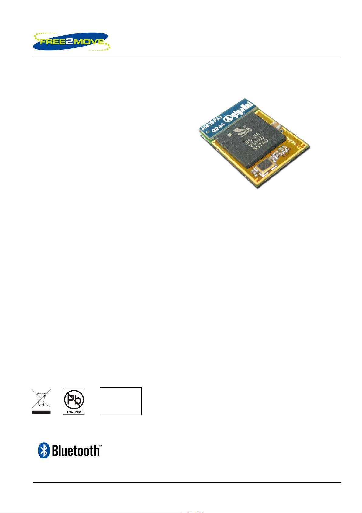
Low power Multimedia Bluetooth™ Module with antenna F2M03MLA
Datasheet
Features
Fully qualified end product with
•
Bluetooth™ v2.0, CE and FCC
Low power consumption
•
Integrated high output antenna
•
Transmit power up to +7dBm
•
Range up to 150m (line of sight)
•
Piconet and Scatternet capability,
•
support for up to 7 slaves
Require only few external components
•
Industrial temperature range -40°C to +85°C
•
Serial interface up to 1.5Mbps
•
Extensive digital and analog I/O interface
•
16-bit Stereo codec
•
32-bit Kalimba DSP for enhanced audio applications and other general purpose applications
•
Many digital audio options: PCM, I
•
Large internal memory for custom applications
•
Lead Free and RoHS compliant
•
2
S and SPDIF
Rev: b
Applications
Stereo headphones
•
Automotive hands-free kits
•
Echo cancellation
•
High performance telephony headsets
•
Industrial and domestic appliances
•
Medical systems
•
Automotive applications
•
Stand-alone sensors
•
Embedded systems
•
Cordless headsets
•
Handheld, laptop and desktop computers
•
• Mobile phones
RoHS
COMPLIANT
2002/96/EC
General Description
F2M03MLA is a low power embedded
Bluetooth™ v2.0 multimedia module with an on
board antenna, integrated stereo amplifier and a
32 bit digital signal processor (DSP) allowing
enhanced audio algorithms such as MP3
decoding and advanced echo cancellation as
well as other general purpose applications. The
module is a fully Bluetooth™ compliant device
for audio and data communication. With a
transmit power of up to +7dBm and receiver
sensibility of down to –81dBm combined with
stereo sound and low power consumption the
F2M03MLA is suitable for the most demanding
audio applications. The module is fully
Bluetooth™ v2.0 qualified and it is certified
according to CE and FCC, which give fast and
easy Plug-and-Go implementation and short time
to market.
F2M03MLA has by default the Wireless Audio
firmware consisting of four Bluetooth profiles:
Stereo Headset, HandsFree, A2DP and the
AVRCP profile. The module can optionally be
delivered with customized firmwares.
BLUETOOTH is a trademark owned by
Bluetooth SIG, Inc., U.S.A. and licensed to Free2move
www.free2move.net

Table of contents
Rev: b
Low power Multimedia Bluetooth™ Module with antenna F2M03MLA
Datasheet
1 Device pinout .........................................................................................................................3
2 Device terminal functions .....................................................................................................4
3 Electrical Characteristics ......................................................................................................5
4 Radio Characteristics ............................................................................................................9
5 Firmware versions ...............................................................................................................10
5.1
Wireless Audio .............................................................................................................................. 11
5.2
Customised firmwares ..................................................................................................................12
6 Device terminal description ................................................................................................13
6.1
Stereo Audio Interface ..................................................................................................................13
6.2
PCM CODEC Interface................................................................................................................. 16
6.3
UART Interface .............................................................................................................................31
6.4
Serial Peripheral Interface ............................................................................................................33
6.5
I2C Interface .................................................................................................................................. 33
6.6
PIOs .............................................................................................................................................. 34
6.7
Power supply ................................................................................................................................35
7 Application information....................................................................................................... 36
7.1
Recommended land pattern..........................................................................................................36
7.2
Layout guidelines .......................................................................................................................... 37
7.3
Typical application schematic .......................................................................................................38
8 Package information............................................................................................................39
9 Certifications ........................................................................................................................40
9.1
Bluetooth....................................................................................................................................... 40
9.2
CE ................................................................................................................................................. 40
9.3
FCC...............................................................................................................................................41
10 RoHS and WEEE Statement................................................................................................42
11 Tape and Reel information..................................................................................................43
11.1 Package Tape dimensions............................................................................................................43
11.2 Reel dimensions ...........................................................................................................................43
12 Ordering information ...........................................................................................................44
13 Document history ................................................................................................................45
14 Acronyms and definitions...................................................................................................46
© 2007 Free2move AB
Page 2(2)
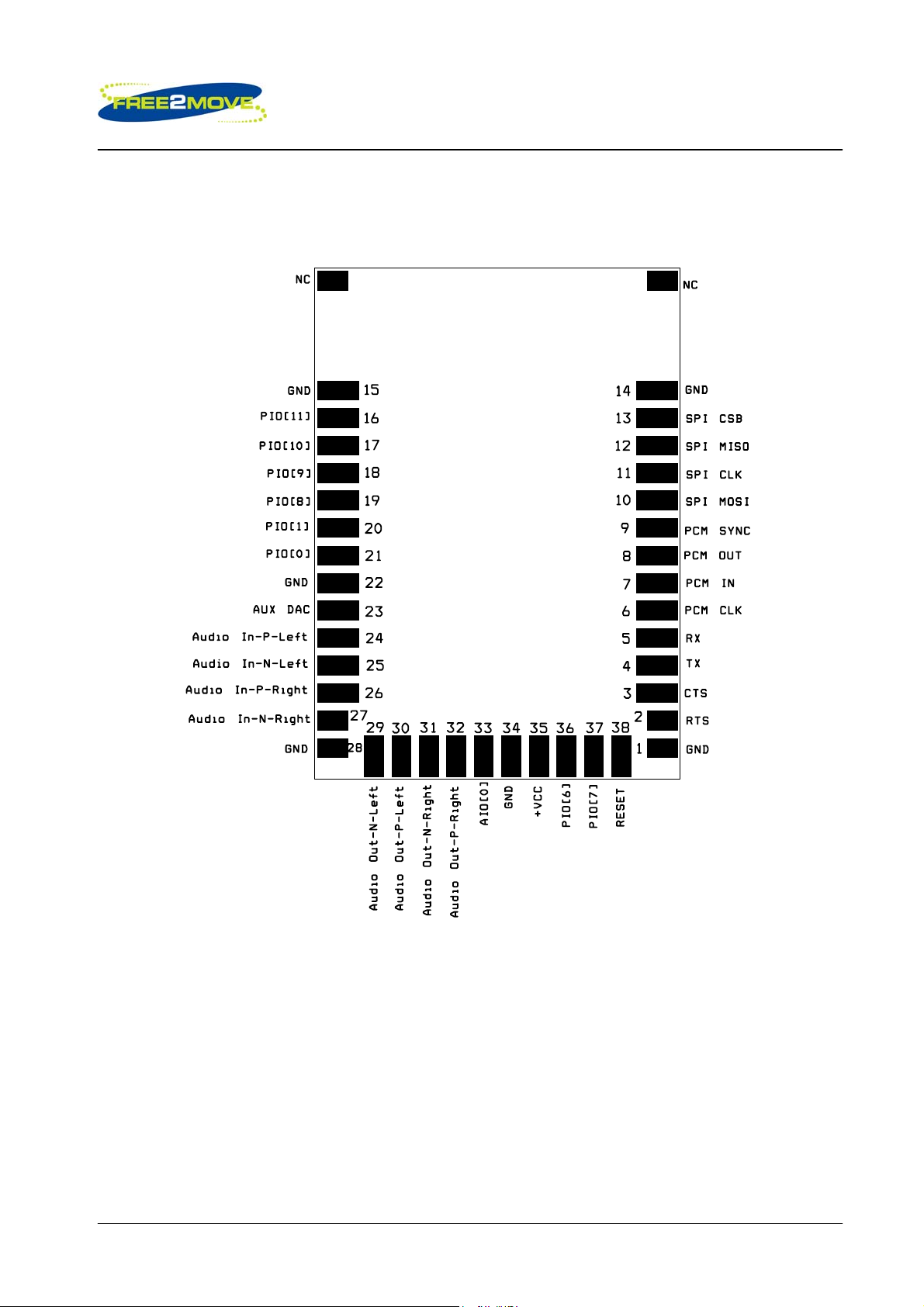
1 Device pinout
Rev: b
Low power Multimedia Bluetooth™ Module with antenna F2M03MLA
Datasheet
Pinout for F2M03MLA [TOP VIEW]
© 2007 Free2move AB
Page 3(3)
Rev: b
Low power Multimedia Bluetooth™ Module with antenna F2M03MLA
Datasheet
2 Device terminal functions
Ground Pin Pin type Description
GND 1,14,15,22,
28,34
Power supplies Pin Pin type Description
+VCC 35 VDD Positive voltage supply (3.0-3.6)
Analog I/O Pin Pin type Description
AIO[0] 33 Bi-directional Programmable input/output line also
AUX DAC 23 Analogue output Voltage DAC output
Reset Pin Pin type Description
RESET 38 CMOS input with internal pull-up (10k) Reset if low. Input debounced so must be
Test and debug Pin Pin type Description
SPI MISO 12 CMOS output, tristatable with weak internal
SPI CSB 13 CMOS input with weak internal pull-up Chip select for Synchronous Serial
SPI CLK 11 CMOS input with weak internal pull-down Serial Peripheral Interface clock
SPI MOSI 10 CMOS input with weak internal pull-down Serial Peripheral Interface data input
UART Pin Pin type Description
CTS 3 CMOS input with weak internal pull-down UART clear to send active low
TX 4 CMOS output UART data output active high
RTS 2 CMOS output, tristatable with internal pull-up UART request to send active low
RX 5 CMOS input with weak internal pull-down UART data input active high
PCM Pin Pin type Description
PCM_OUT / SPDIF_OUT /
SD_OUT
PCM_SYNC / WS 9 Bi-directional with weak internal pull-down Synchronous data SYNC
PCM_OUT / SPDIF_OUT /
SD_OUT
PCM_CLK / SCK 6 Bi-directional with weak internal pull-down Synchronous data clock
8 CMOS output, tristatable with internal weak
7 CMOS input, with weak internal pull-down Synchronous data input
AUDIO Pin Pin type Description
In-P-Left 24 Analogue input Microphone input positive (left side)
In-N-Left 25 Analogue input Microphone input negative (left side)
In-P-Right 26 Analogue input Microphone input positive (right side)
In-N-Right 27 Analogue input Microphone input negative (right side)
Out-N-Left 29 Analogue output Speaker output negative (left side)
Out-P-Left 30 Analogue output Speaker output positive (left side)
Out-N-Right 31 Analogue output Speaker output negative (right side)
Out-P-Right 32 Analogue output Speaker output positive (right side)
PIO Pin Pin type Description
PIO[11] 16 Bi-directional with programmable strength
PIO[10] 17 Bi-directional with programmable strength
PIO[9] 18 Bi-directional with programmable strength
PIO[8] 19 Bi-directional with programmable strength
PIO[7] 37 Bi-directional with programmable strength
PIO[6] 36 Bi-directional with programmable strength
PIO[1] 20 Bi-directional with programmable strength
PIO[0]
21 Bi-directional with programmable strength
Not connected Pin Pin type Description
NC Not connected Soldering pads for stability
VSS Ground connections
possible to use as digital I/O
low for >5ms to cause a reset
pull-down
pull down
internal pull-up/down
internal pull-up/down
internal pull-up/down
internal pull-up/down
internal pull-up/down
internal pull-up/down
internal pull-up/down
internal pull-up/down
Serial Peripheral Interface data output
Interface, active low
Synchronous data output
Programmable input/output line
Programmable input/output line
Programmable input/output line
Programmable input/output line
Programmable input/output line
Programmable input/output line
Programmable input/output line
Programmable input/output line or
Optionally WLAN_Active/Ch_Data input for
co-existence signalling
© 2007 Free2move AB
Page 4(4)
Low power Multimedia Bluetooth™ Module with antenna F2M03MLA
Datasheet
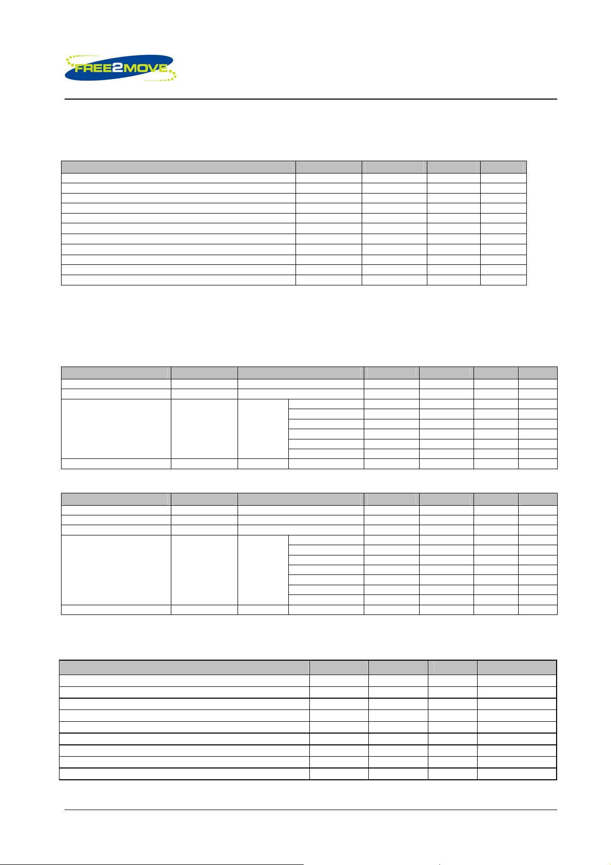
3 Electrical Characteristics
Absolute Maximum Ratings
Rating Min Max
Storage Temperature
Breakdown supply voltage -0.4V 5.60V
Recommended Operating Conditions
-40°C +150°C
Rev: b
Rating
Operating temperature range
Supply voltage 3.1V 3.6V
Min
-40°C +85°C
Max
Digital Terminals
Digital Terminals Min Typ Max Unit
Input Voltage
VIL input logic level low, 2.7V ≤ VDD ≤ 3.0V
VIH input logic level high 0.7VDD - VDD+0.4 V
Output Voltage
VOL output logic level low, (lO = 4.0mA), 2.7V ≤ VDD ≤ 3.0V
VOH output logic level high, (lO = 4.0mA), 2.7V ≤ VDD ≤ 3.0V
Input and tristate current
Strong pull-up -100 -40 -10
Strong pull-down +10 +40 +100
Weak pull-up -5.0 -1.0 -0.2
Weak pull-down +0.2 +1.0 +5.0
I/O pad leakage current -1 0 +1
CI Input Capacitance 1.0 - 5.0 pF
-0.4 - +0.8 V
- - 0.2 V
VDD-0.2 - - V
µA
µA
µA
µA
µA
Auxiliary ADC
Auxiliary ADC, 8-bit resolution Min Typ Max Unit
Resolution
Input voltage range
(LSB size = 1.8/255= 7.1mV)
(Guaranteed monotonic)
Offset -1 - 1 LSB
Gain Error -0.8 - 0.8 %
Input Bandwidth - 100 - KHz
Conversion time - 2.5 - µS
Sample rate*
INL -1 - 1 LSB Accuracy
DNL 0 - 1 LSB
- - 8 Bits
0 - 1.8 V
- - 700 Sample/s
*The ADC is accessed through the VM function. The sample rate given is achieved as a part of this function
© 2007 Free2move AB
Page 5(5)
Rev: b
Low power Multimedia Bluetooth™ Module with antenna F2M03MLA
Datasheet
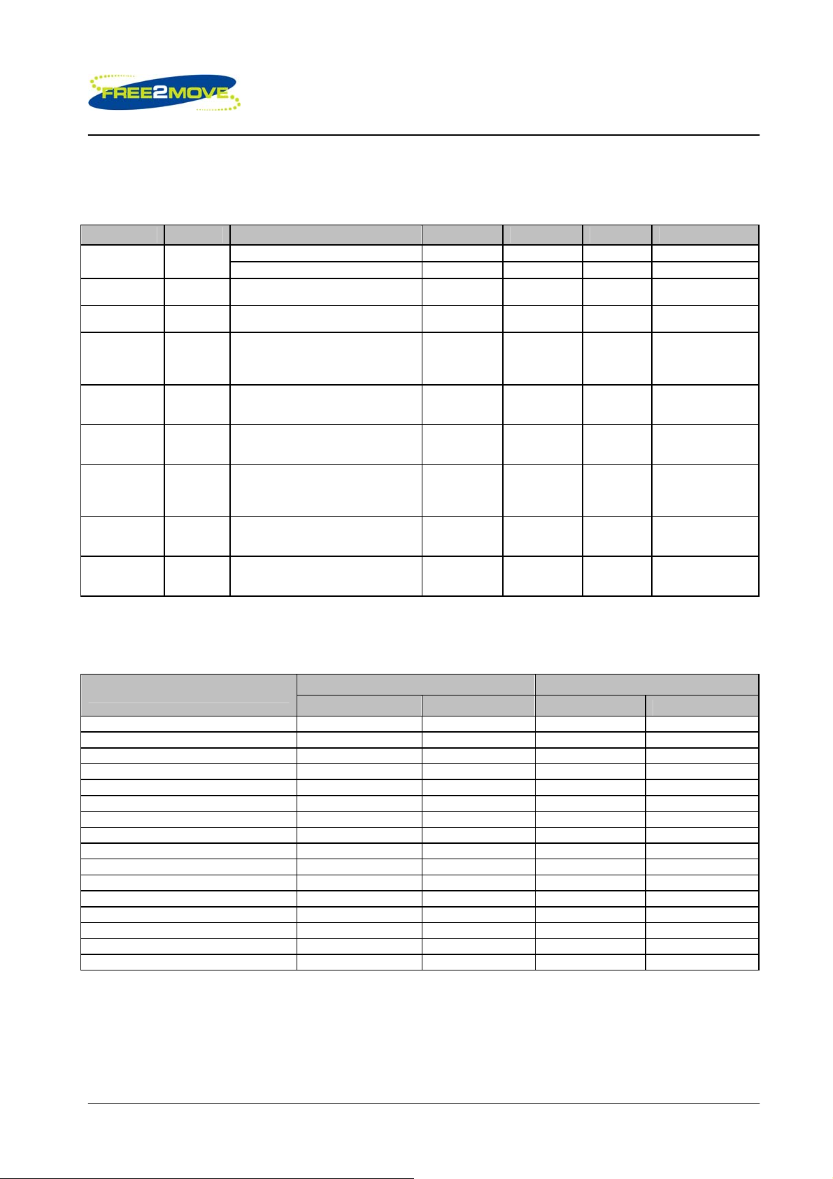
Auxiliary DAC
Auxiliary DAC, 8-bit resolution Min Typ Max Unit
Resolution - - 8 Bits
Average output step size 12.1 12.9 14.1 mV
Output Voltage Monotonic
Voltage range (IO=0mA) 0 - VDD V
Current range -10.0 - +0.1 mA
Minimum output voltage (IO=100µΑ)
Maximum output voltage (IO=10mA)
High impedance leakage current -1 - +1
Offset -220 - +120 MV
Integral non-linearity -2 - +2 LSB
Settling time (50pF load) - - 10
Notes:
Current drawn into a pin is defined as positive; current supplied out of a pin is defined as negative.
0 - 0.2 V
VDD-0.3 - VDD V
µA
µS
Stereo Audio CODEC Characteristics
ADC
Parameter Symbol Conditions Min Typ Max Unit
Resolution NOB - - 16 Bits
Input sample rate F
Signal to noise ratio +
distortion
1
sample
SINAD 0ƽF
=1kHz
f
in
sample
Digital gain -24 - 21.5 dB
DAC
Parameter Symbol Conditions Min Typ Max Unit
Resolution NOB - - 16 Bits
Output sample rate F
sample
Gain resolution - 3 - dB
Signal to noise ratio +
distortion
1
SINAD 0Æ20kHz,
=1kHz
f
in
Digital gain -24 - 21.5 dB
1
Measurements refer to digital part only
Audio Input, Microphone Amplifier
Input full scale at maximum gain - 4 - mV rms
Input full scale at minimum gain - 400 - mV rms
Gain resolution - 3 - dB
Distortion at 1kHz - - -74 dB
Input referenced rms noise - 8 3dB Bandwidth - 17 - kHz
Input impedance - 20 - k
THD+N (microphone input) @ 30mV rms input - -66 - dB
THD+N (line input) @ 300mV input
2
8 - 44.1 kHz
F
,
=8kHz - 84 - dB
sample
F
=11.025kHz - 83 - dB
sample
F
=16kHz - 84 - dB
sample
F
=22.050kHz - 83 - dB
sample
F
=32kHz - 80 - dB
sample
F
=44.1kHz - 74 - dB
sample
8 - 48 kHz
F
=8kHz - 79 - dB
sample
F
=11.025kHz - 78 - dB
sample
F
=16kHz - 79 - dB
sample
F
=22.050kHz - 88 - dB
sample
F
=32kHz - 90 - dB
sample
F
=44.1kHz - 90 - dB
sample
=48kHz - 89 - dB
F
sample
Min Typ Max Unit
µV rms
- -74 - dB
© 2007 Free2move AB
Page 6(6)
Low power Multimedia Bluetooth™ Module with antenna F2M03MLA
Datasheet
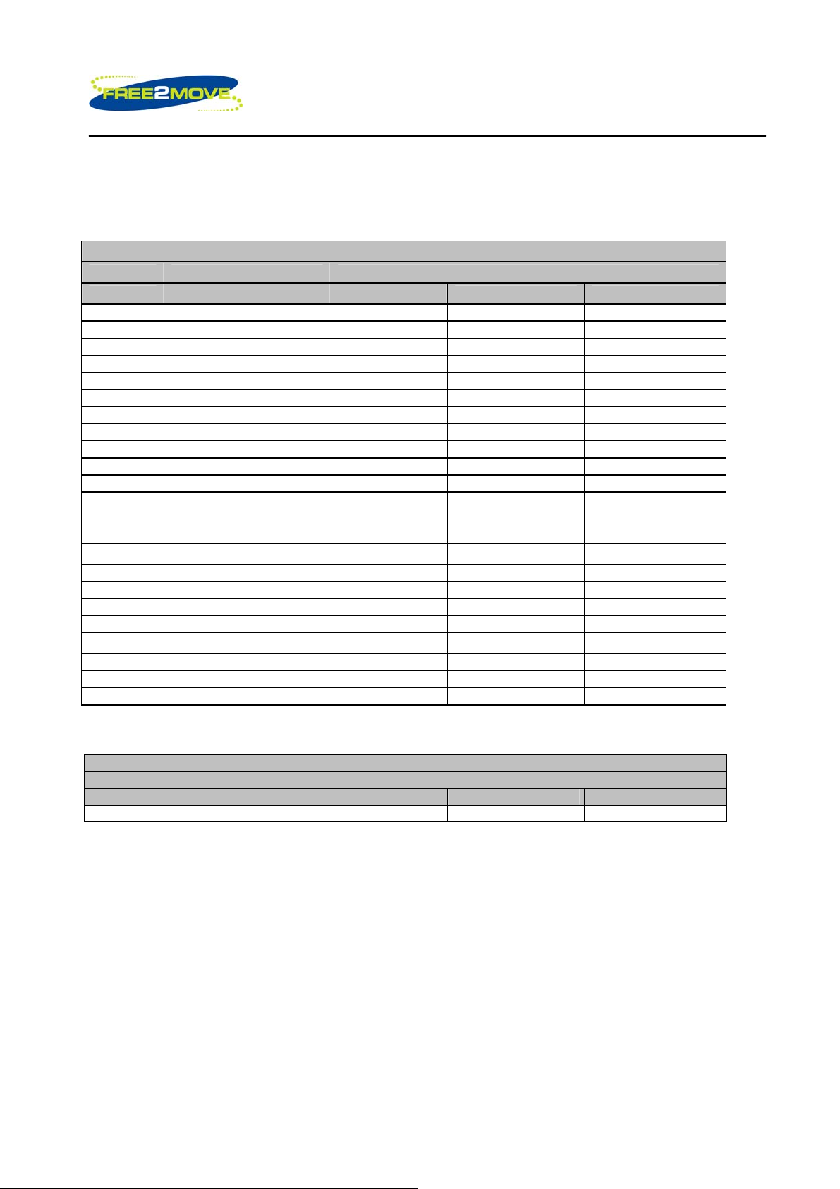
Audio Output, Speaker Output
Parameter Symbol Conditions Min Typ Max Unit
Allowed Load
Max output
voltage
Max output
current
Total
Harmonic
Distortion
plus Noise
Output noise
relative to full
scale
Channel
Separation
(Crosstalk)
Power
Supply
Rejection
Ratio
Second
Harmonic
Level
Third
Harmonic
Level
2
Input signal amplitudes are expressed as the differential voltages between the MIC_P and MIC_N terminals
R
R
THD+N
SNR
CS
PSRR
Resistive 16 -
Capacitive - -
=600 - 2.0 - V pk-pk
L
=22 - 75 - mA
L
=1kHz, BW=22Hz to 22kHz
f
IN
=600
R
L
A Weighted, Po=digital silence,
=600, BW=22Hz to 22kHz
R
L
=10kHz, analogue output set to
f
IN
maximum gain
=200mV
V
ripple
at VDD 3.1V VDD 3.6V,
analogue output set to maximum
gain
1kHz sinewave, 1dB below full
scale 600
1kHz sinewave, 1dB below full
scale 600
sinewave, 10kHz
pk-pk
- 0.015 - %
- -91 - dB
- - -60 dB
- TBD - dB
- <-95 - dB
- -95 - dB
Typical THD + N Relative to Full Scale
Full Scale Output, mV rms
600Ω 22Ω
% dB % dB
10 0.180 -54.7 0.180
14 0.120 -58.2 0.120
20 0.090 -60.7 0.090
28 0.060 -64.2 0.062
40 0.046 -66.5 0.048
57 0.032 -69.7 0.036
80 0.025 -71.8 0.030
113 0.018 -74.6 0.024
160 0.015 -76.2 0.022
226 0.015 -76.2 0.020
320 0.015 -76.2 0.019
453 0.015 -76.2 0.019
640 0.014 -76.8 0.019
905 0.014 -76.8 0.019
1280 0.014 -76.8 0.022 -72.9
1810 0.014 -76.8
O.C
500
pF
-54.7
-58.2
-60.7
-63.9
-66.1
-68.6
-70.2
-72.1
-72.9
-73.7
-74.2
-74.2
-74.2
-74.2
Rev: b
© 2007 Free2move AB
Page 7(7)
Low power Multimedia Bluetooth™ Module with antenna F2M03MLA
Datasheet
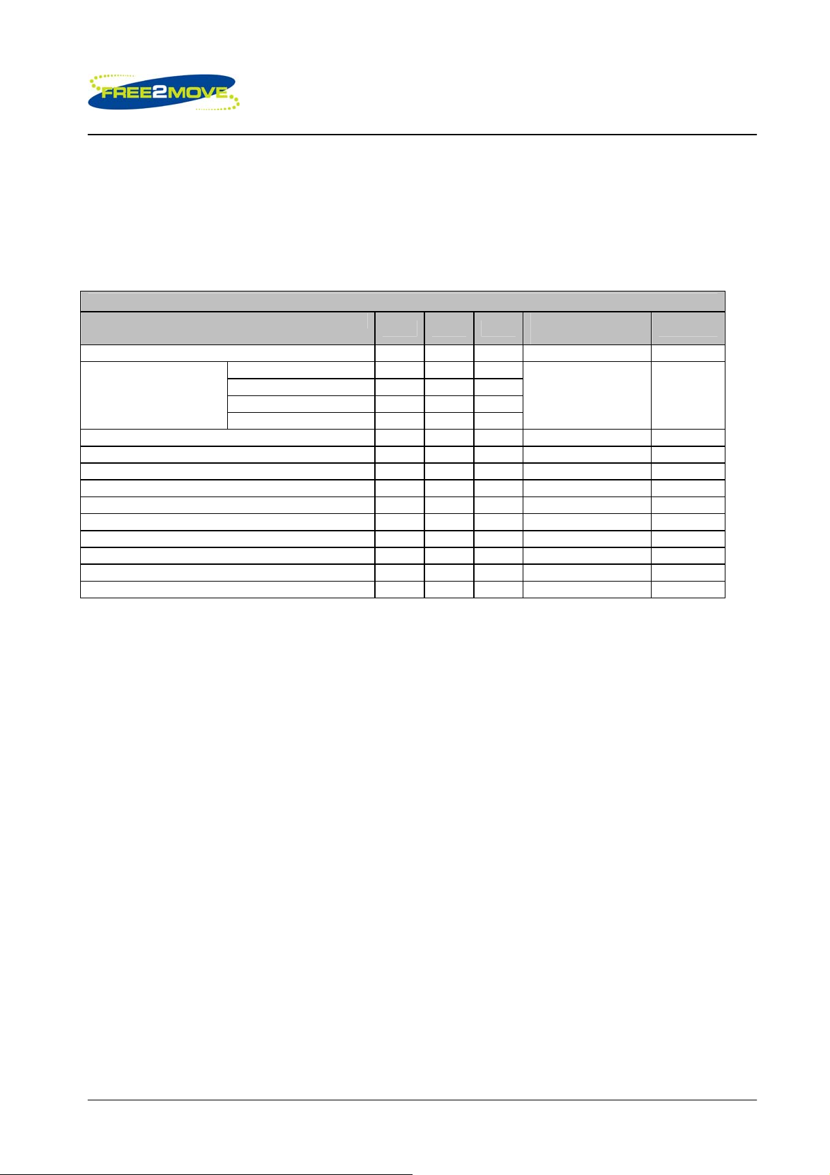
Power Consumption
Typical Average Current Consumption
VDD=3.3V Temperature = +20°C Output Power = 0dBm
Mode
SCO connection HV3 (30ms interval Sniff Mode) (Slave) 21 mA
SCO connection HV3 (30ms interval Sniff Mode) (Master) 21 mA
SCO connection HV3 (No Sniff Mode) (Slave) 28 mA
SCO connection HV1 (Slave) 42 mA
SCO connection HV1 (Master) 42 mA
ACL data transfer 115.2kbps UART no traffic (Master) 5 mA
ACL data transfer 115.2kbps UART no traffic (Slave) 22 mA
ACL data transfer 720kbps UART (Master or Slave) 45 mA
ACL data transfer 720kbps USB (Master or Slave) 45 mA
ACL connection, Sniff Mode 40ms interval, 38.4kbps UART 3.2 mA
ACL connection, Sniff Mode 1.28s interval, 38.4kbps UART 0.45 mA
Parked Slave, 1.28s beacon interval, 38.4kbps UART 0.55 mA
Standby Mode (Connected to host, no RF activity) 47
Reset (RESET high or RESETB low) 15
DSP
DSP core (including PM memory access)
Minimum (NOP) 0.25 mA/MIPS
Maximum (MAC) 0.65 mA/MIPS
DSP memory access (DM1 or DM2) 0.15 mA/MIPS
CODEC
Microphone inputs and ADC / channel 0.85 mA
DAC and loudspeaker driver, no signal / channel 1.4 mA
Digital audio processing subsystem 8 mA
VDD=3.3V Temperature = +20°C Output Power (max)= 7dBm
Peak consumption during RF peaks 75 mA
Average Unit
µA
µA
Peak current consumption
Mode Typ Unit
Rev: b
© 2007 Free2move AB
Page 8(8)
Low power Multimedia Bluetooth™ Module with antenna F2M03MLA
Datasheet
4 Radio Characteristics
VDD = 3.3V Temperature = 20 oC Frequency = 2.441GHz
All measurements are based on the Bluetooth test specification.
Radio Characteristics VDD = 3.3V Temperature = +25°C
Maximum RF transmit power
Frequency (GHz)
Sensitivity at 0.1% BER
RF power control range
RF power range control resolution 2.2 4 4.4
20dB bandwidth for modulated carrier - 800 -
f1avg .Maximum Modulation. - 165
f2max .Minimum Modulation. - 150 -
f1avg/f2avg - 0.98 -
Initial carrier frequency tolerance - 10 -
Drift Rate - 8 -
Drift (single slot packet) - 7 -
Drift (five slot packet) - 8 -
1
Class 1 RF transmit power range, Bluetooth specification v1.2
2.402 - -85 -
2.441 - -86 -
2.480 - -85 -
Min Typ Max
7.8 8.6 9.9
- 24 -
- 40<f1avg<175
Bluetooth
Specification
1
0 to 20
-70 dBm
16
-
1000
115
0.80
±75
20
25
40
Unit
dBm
dB
dB
kHz
kHz
KHz/50µs
kHz
kHz
Rev: b
-
© 2007 Free2move AB
Page 9(9)

Rev: b
Low power Multimedia Bluetooth™ Module with antenna F2M03MLA
Datasheet
5 Firmware versions
F2M03MLA is supplied with Bluetooth stack firmware, which runs on the internal RISC micro controller of
the Bluetooth module. This chapter includes an overview of the different options for more in depth
information please use separate firmware datasheets provided by Free2move.
All firmware versions are compliant with the Bluetooth specification v2.0. The F2M03MLA software
architecture allows Bluetooth processing to be shared between the internal micro controller and a host
processor. Depending on application the upper layers of the Bluetooth stack (above HCI) can execute onchip or on the host processor.
Running the upper stack on the F2M03MLA module reduces (or eliminates, in the case of a on module
application) the need for host-side software and processing time.
The integration approach depends on the type of product being developed. For example, performance will
depend on the integration approach adopted. In general Free2move offers two categories of Bluetooth
stack firmware for the F2M03MLA:
• Wireless Audio (WA) is Free2move’s standard firmware for audio applications. It is intended for
Headset and audio streaming applications. It currently supports the Headset, HandsFree, A2DP
and AVRCP profile. There is no need for additional drivers or Bluetooth software on a host.
• Customised firmwares. Free2move have the possibility to customise firmwares for a special
customer applications.
© 2007 Free2move AB
Page 10(10)

Rev: b
Low power Multimedia Bluetooth™ Module with antenna F2M03MLA
Datasheet
5.1 Wireless Audio
Wireless Audio is Free2move’s standard firmware for audio applications. It is intended for Headset and
audio streaming applications.
The current version of the Wireless Audio includes the Headset, HandsFree, A2DP and AVRCP Bluetooth
profiles. Additional profiles or functionalities may be included in future versions of Wireless Audio.
Please contact Free2move for a complete datasheet of the Wireless Audio firmware.
5.1.1 Supported Bluetooth profiles
Stereo Headset (HSP) and Handsfree Profile (HFP)
The Stereo Headset and HandsFree profile is used for full duplex audio connections to phones and similar
for telephone call purpose.
Wireless Audio supports both the Headset and the HandsFree profile. The profile of choice depends on
what the connecting device support. If the Wireless Audio firmware initiates the connection it will first try to
use the Handsfree profile. If the connecting device not support the HandsFree profile, it will choose the
Headset profile.
Advanced Audio Distribution Profile (A2DP)
The A2DP profile is used for high quality stereo audio streaming.
Wireless Audio supports the A2DP sink which makes it possible to receive audio streams from a A2DP
source.
Audio/Video Remote Control Profile(AVRCP)
The AVRCP profile is used for controlling the Audio stream.
© 2007 Free2move AB
Page 11(11)

Rev: b
Low power Multimedia Bluetooth™ Module with antenna F2M03MLA
Datasheet
5.2 Customised firmwares
Customised firmwares can be made upon request. Free2move have the possibility to produce modules with
customer specific settings of the Wireless Audio firmware (most applicable in large production volumes).
Free2move can also provide special firmwares for customer applications.
Please consult your reseller for more information about customised firmwares and special requirements.
© 2007 Free2move AB
Page 12(12)
Low power Multimedia Bluetooth™ Module with antenna F2M03MLA
Datasheet
6 Device terminal description
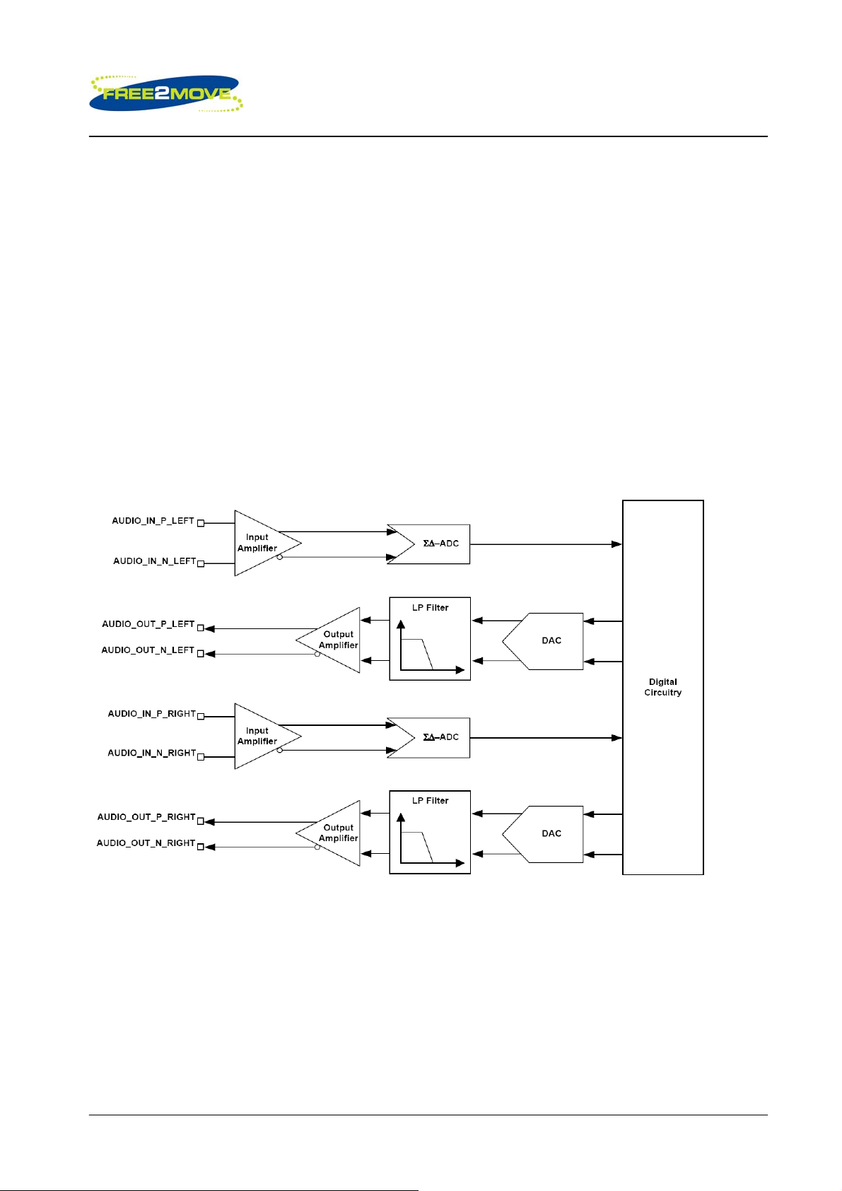
6.1 Stereo Audio Interface
The main features of the interface are:
• Stereo and mono analogue input for voice band and audio band
• Stereo and mono analogue output for voice band and audio band
• Support for stereo digital audio bus standards such as I
• Support for IEC-60958 standard stereo digital audio bus standards i.e. S/PDIF and AES3/EBU
• Support for PCM interfaces including PCM master CODECs that require an external system clock
2
S
Rev: b
Stereo CODEC Audio input and output stages
The stereo audio CODEC uses a fully differential architecture in the analogue signal path, which results in
low noise sensitivity and good power supply rejection while effectively doubling the signal amplitude.
Important Note:
To avoid any confusion with respect to stereo operation this datasheet with respect to hardware explicitly
states which is the left and right channel for audio input and output.
For mono operation F2M03MLA uses the left channel for standard mono operation for audio input and
output.
© 2007 Free2move AB
Page 13(13)
Rev: b
Low power Multimedia Bluetooth™ Module with antenna F2M03MLA
Datasheet
6.1.1 ADC
The ADC consists of two second order Sigma Delta converters allowing two separate channels that are
identical in functionality.
ADC Sample Rates
Each ADC supports the following sample rates:
• 8kHz
• 11.025kHz
• 16kHz
• 22.05kHz
• 24kHz
• 32kHz
• 44.1kHz
ADC Gain
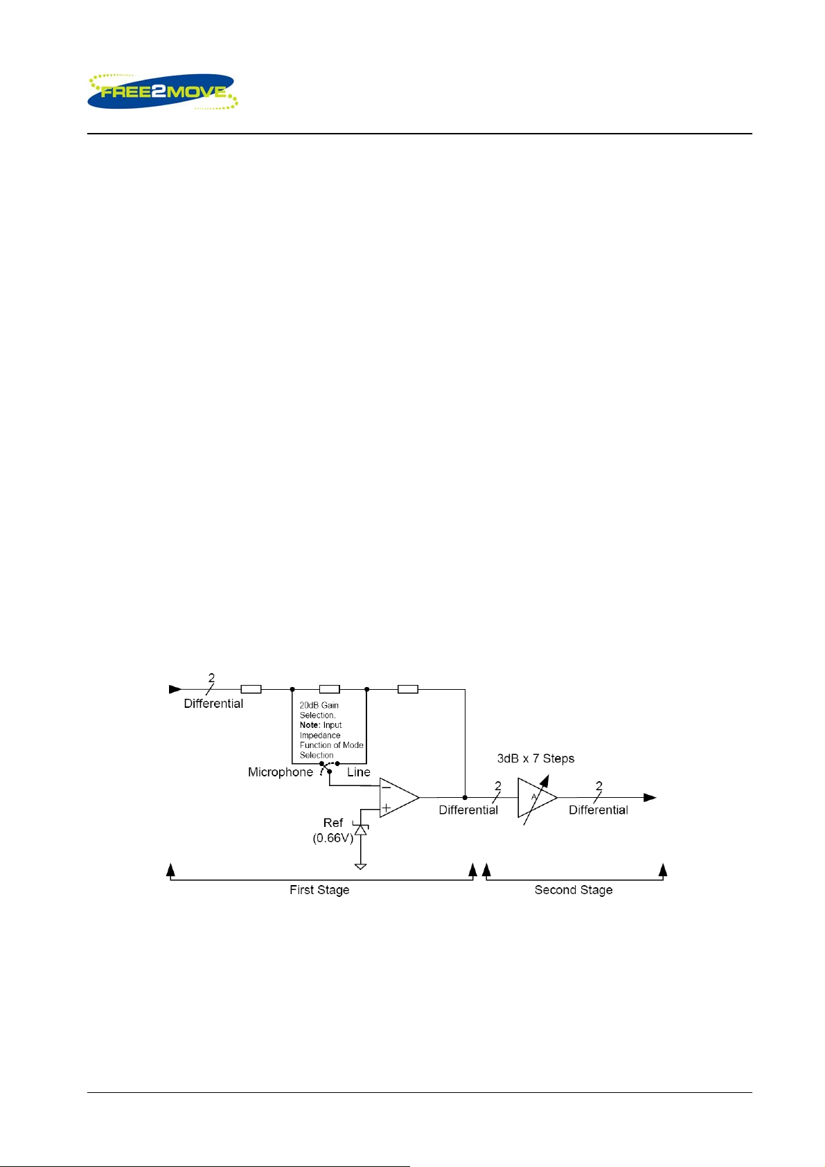
The ADC contains two gain stages for each channel, an analogue and a digital gain stage.
The digital gain stage has a range of –24dB to +21.5dB.
The ADC analogue amplifier is a two stage amplifier. The first stage of the analogue amplifier is responsible
for selecting the correct gain for either microphone input or line input and therefore has two gain settings,
one for the microphone and one for the line input. In simple terms the first stage amplifier has a selectable
20dB gain stage for the microphone and this creates the dual programmable gain required for the
microphone or the line input. The equivalent block diagram for the two stage is shown in the figure below.
First and second stage of ADC analogue amplifier block diagram
The second stage of the analogue amplifier has a programmable gain with seven individual 3dB steps. In
simple terms, by combining the 20dB gain selection of the microphone input with the seven individual 3dB
gain steps, the overall range of the analogue amplifier is approximately -4dB to 40dB. The overall gain
setting of the ADC is a combined function of the digital and analogue amplifier settings, so that the fullscale
range of the input to the ADC is kept to approximately 400mV rms.
© 2007 Free2move AB
Page 14(14)

Rev: b
Low power Multimedia Bluetooth™ Module with antenna F2M03MLA
Datasheet
6.1.2 DAC
The DAC consists of two second order Sigma Delta converters allowing two separate channels that are
identical in functionality.
DAC Sample rates
Each DAC supports the following samples rates:
• 48kHz
• 44.1kHz
• 32kHz
• 24kHz
• 22.050kHz
• 16kHz
• 11.025kHz
• 8kHz
DAC Gain
The DAC contains two gain stages for each channel, a digital and an analogue gain stage.
The digital gain stage has a programmable selection value in the range of –24dB to 21.5dB.
The DAC analogue amplifier unlike the ADC is a single stage amplifier with the same structure as the
second stage of the ADC analogue amplifier. The structure of the DAC analogue amplifier is similar to the
second stage of the ADC analogue amplifier.
The overall gain setting of the DAC is a combined function of the digital and analogue amplifier settings,
therefore for a 1V rms nominal digital output signal from the digital gain stage of the DAC, the approximate
output values of the analogue amplifier of the DAC is in the range of 0dB to –21dB.
6.1.3 Mono Operation
Mono operation is single channel operation of the stereo CODEC. The left channel represents the single
mono channel for audio in and audio out. In mono operation the right channel is auxiliary mono channel that
may be used in dual mono channel operation.
© 2007 Free2move AB
Page 15(15)

Rev: b
Low power Multimedia Bluetooth™ Module with antenna F2M03MLA
Datasheet
6.2 PCM CODEC Interface
Pulse Code Modulation (PCM) is the standard method used to digitise audio (particulary voice) for
transmission over digital communication channels. Through its PCM interface, F2M03MLA has hardware
support for continual transmission and reception of PCM data, thus reducing processor overhead for
wireless headset and other audio applications. F2M03MLA offers a bi-directional digital audio interface that
routes directly into the baseband layer of the on-chip firmware. It does not pass through the HCI protocol
layer.
Hardware on F2M03MLA allows the data to be sent to and received from a SCO connection. Up to three
SCO connections can be supported by the PCM interface at any one time
F2M03MLA can operate as the PCM interface Master generating an output clock of 128, 256 or 512kHz.
When configured as PCM interface slave it can operate with an input clock up to 2048kHz. F2M03MLA is
compatible with a variety of clock formats, including Long Frame Sync, Short Frame Sync and GCI timing
environments.
It supports 13 or 16-bit linear, 8-bit µ-law or A-law companded sample formats at 8ksamples/s and can
receive and transmit on any selection of three of the first four slots following PCM_SYNC. The PCM
configuration options are enabled by firmware settings (contact Free2move).
F2M03MLA interfaces directly to PCM audio devices includes the following:
• WM8731 Audio CODEC from Wolfson Micro
• Qualcomm MSM 3000 series and MSM 5000 series CDMA baseband devices
• OKI MSM7705 four channel A-law and µ-law CODEC
• Motorola MC145481 8-bit A-law and µ-law CODEC
• Motorola MC145483 13-bit linear CODEC
• Winbond W681360R 13-bit linear CODEC
• STW 5093 and 5094 14-bit linear CODECs
• F2M03MLA is also compatible with the Motorola SSI
TM
interface
Note:
(1)
Subject to firmware support, contact Free2move for current status.
(1)
© 2007 Free2move AB
Page 16(16)
Rev: b
Low power Multimedia Bluetooth™ Module with antenna F2M03MLA
Datasheet
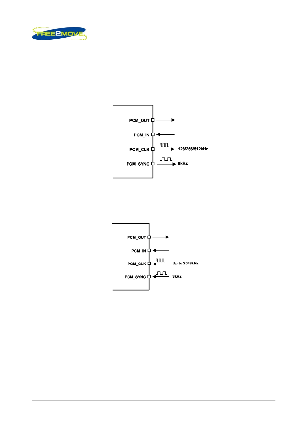
6.2.1 PCM Interface Master/Slave
When configured as the Master of the PCM interface, F2M03MLA generates PCM_CLK and PCM_SYNC.
F2M03MLA as PCM Interface Master
When configured as the Slave of the PCM interface, F2M03MLA accepts PCM_CLK rates up to 2048kHz
F2M03MLA as PCM Interface Master
© 2007 Free2move AB
Page 17(17)
Rev: b
Low power Multimedia Bluetooth™ Module with antenna F2M03MLA
Datasheet
6.2.2 Long Frame Sync
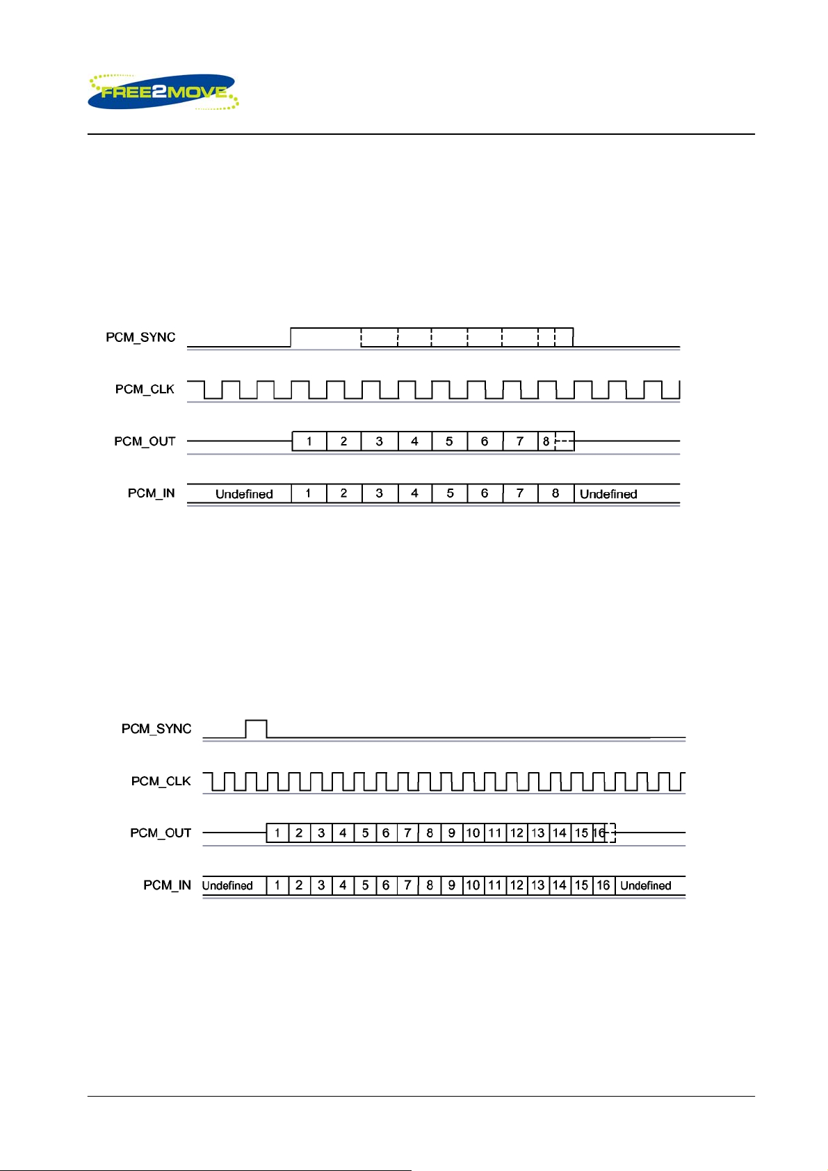
Long Frame Sync is the name given to a clocking format that controls the transfer of PCM data words or
samples. In Long Frame Sync, the rising edge of PCM_SYNC indicates the start of the PCM word. When
F2M03MLA is configured as PCM Master, generating PCM_SYNC and PCM_CLK, then PCM_SYNC is 8bits long. When F2M03MLA is configured as PCM Slave, PCM_SYNC may be from two consecutive falling
edges of PCM_CLK to half the PCM_SYNC rate (i.e., 62.5µs) long.
Long Frame Sync (Shown with 8-bit Companded Sample)
F2M03MLA samples PCM_IN on the falling edge of PCM_CLK and transmits PCM_OUT on the rising
edge. PCM_OUT may be configured to be high impedance on the falling edge of PCM_CLK in the LSB
position or on the rising edge.
6.2.3 Short Frame Sync
In Short Frame Sync the falling edge of PCM_SYNC indicates the start of the PCM word. PCM_SYNC is
always one clock cycle long.
Short Frame Sync (Shown with 16-bit Sample)
As with Long Frame Sync, F2M03MLA samples PCM_IN on the falling edge of PCM_CLK and transmits
PCM_OUT on the rising edge. PCM_OUT may be configured to be high impedance on the falling edge of
PCM_CLK in the LSB position or on the rising edge
© 2007 Free2move AB
Page 18(18)

Rev: b
Low power Multimedia Bluetooth™ Module with antenna F2M03MLA
Datasheet
6.2.4 Multi-Slot Operation
More than one SCO connection over the PCM interface is supported using multiple slots. Up to three SCO
connections can be carried over any of the first four slots.
Multi-slot Operation with Two Slots and 8-bit Companded Samples
6.2.5 GCI Interface
F2M03MLA is compatible with the General Circuit Interface, a standard synchronous 2B+D ISDN timing
interface. The two 64Kbps B channels can be accessed when this mode is configured. In the GCI interface
two clock cycles are required for each bit of the voice sample. The voice sample format is 8-bit companded.
As for the standard PCM interface up to 3 SCO connections can be carried over the first four slots.
GCI Interface
The start of frame is indicated by PCM SYNC and runs at 8kHz. With F2M03MLA in Slave mode, the
frequency of PCMCLK can be up to PCM_SYNC In order to configure the PCM interface to work in GCI
mode it is necessary to have the correct firmware support (contact Free2move)
© 2007 Free2move AB
Page 19(19)
Rev: b
Low power Multimedia Bluetooth™ Module with antenna F2M03MLA
Datasheet
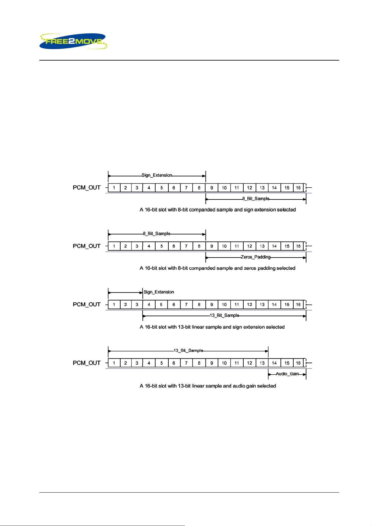
6.2.6 Slots and Sample Formats
F2M03MLA can receive and transmit on any selection of the first four slots following each sync pulse. Slot
durations can be either 8 or 16 clock cycles. Durations of 8 clock cycles may only be used with 8-bit sample
formats. Durations of 16 clocks may be used with 8, 13 or 16-bit sample formats.
F2M03MLA supports 13-bit linear, 16-bit linear and 8-bit µ-law or A-law sample formats. The sample rate is
8ksamples/s. The bit order may be little or big endian. When 16-bit slots are used, the 3 or 8 unused bits in
each slot may be filled with sign extension, padded with zeros or a programmable 3-bit audio attenuation
compatible with some Motorola CODECs.
6.2.7 Additional Features
F2M03MLA has a mute facility that forces PCM_OUT to be 0. In Master mode, PCM_SYNC may also be
forced to 0 while keeping PCM_CLK running (which some CODECS use to control power-down)
© 2007 Free2move AB
Page 20(20)
Low power Multimedia Bluetooth™ Module with antenna F2M03MLA
6.2.8 PCM Timing Information
PCM Master Timing
Datasheet
Rev: b
(1)
Symbol Parameter
4MHz DDS
generation
f
mclk
- PCM_SYNC frequency - 8 kHz
(1)
t
mclkh
(1)
t
l
mclk
PCM_CLK
frequency
48MHz DDS
generation
PCM_CLK high 4MHz DDS generation 980 - - ns
PCM_CLK low 4MHz DDS generation 730 - ns
Min
Typ
128
-
256
512
2.9 - kHz
(2)
Max
- kHz
Unit
- PCM_CLK jitter 48M Hz DD S generation 21 Ns pk-pk
t
dmclksynch
t
dmclkpout
Delay time from PCM_CLK high to
PCM_SYNC high
Delay time from PCM_CLK high to valid
PCM_OUT
-
-
-
-
20 ns
20 ns
Delay time from PCM_CLK low to
t
dmclklsyncl
PCM_SYNC low (Long Frame Sync
- - 20 ns
only)
t
dmclkhsyncl
t
dmclklpoutz
t
dmclkhpoutz
t
supinclkl
t
hpinclkl
Delay time from PCM_CLK high to
PCM_SYNC low
Delay time from PCM_CLK low to
PCMOUT high impedance
Delay time from PCM_CLK high to
PCMOUT high impedance
Set-up time for PCM_IN valid to
PCM_CLK low
Hold time for PCM_CLK low to PCM_IN
invalid
-
20 ns
- - 20 ns
- - 20 ns
30 - - ns
10 - - ns
Note:
(1)
Assumes normal system clock operation. Figures will vary during low power modes, when system clock speeds are reduced.
© 2007 Free2move AB
Page 21(21)

Rev: b
Low power Multimedia Bluetooth™ Module with antenna F2M03MLA
Datasheet
PCM Master Timing
PCM Slave Timing
Symbol Parameter Min Typ Max Unit
f
sclk
f
sclk
t
sclkl
t
sclkh
t
hsclksynch
t
susclksynch
t
dpout
t
dsclkhpout
t
dpoutz
t
supinsclkl
t
hpinsclkl
t
r
T
f
PCM clock frequency (Slave mode: input) 64 - 2048 kHz
PCM clock frequency (GCI mode) 128 - 4096 kHz
PCM_CLK low time 200 - - ns
PCM_CLK high time 200 - - ns
Hold time from PCM_CLK low to
PCM_SYNC high
Set-up time for PCM_SYNC high to
PCM_CLK low
30 - - ns
30 - - ns
Delay time from PCM_SYNC or
PCM_CLK whichever is later, to valid
- - 20 ns
PCM_OUT data (Long Frame Sync only)
Delay time from CLK high to PCM_OUT
valid data
-
-
20 ns
Delay time from PCM_SYNC or
PCM_CLK low, whichever is later, to
- - 20 ns
PCM_OUT data line high impedance
Set-up time for PCM_IN valid to CLK low 30 - - ns
Hold time for PCM_CLK low to PCM_IN
invalid
30 -
Edge rise time (Cl = 50 pF, 10-90 %) - - 15 ns
Edge fall time (Cl = 50 pF, 10-90 %)
- - 15 ns
ns
© 2007 Free2move AB
Page 22(22)

Rev: b
Low power Multimedia Bluetooth™ Module with antenna F2M03MLA
Datasheet
PCM slave timing
© 2007 Free2move AB
Page 23(23)

Low power Multimedia Bluetooth™ Module with antenna F2M03MLA
Datasheet
6.2.9 Digital Audio Bus
The digital audio interface supports the industry standard formats for I2S, left-justified (LJ) or right-justified(RJ)1.
The interface shares the same pins as the PCM interface and the timing diagram is shown in the figure below.
Rev: b
Digital Audio Interface Modes
The internal representation of audio samples within F2M03MLA is 16-bit and data on SD_OUT is
limited to 16-bit per channel. On SD_IN, if more than 16-bit per channel is present will round considering the 17
SCK typically operates 64 x WS frequency and cannot be less than 36 x WS.
Note:
1
Subject to firmware support, contact Free2move for more information.
th
bit.
© 2007 Free2move AB
Page 24(24)

Low power Multimedia Bluetooth™ Module with antenna F2M03MLA
Datasheet
Digital Audio Interface Slave timing
Symbol Parameter Min Typ Max Unit
- SCK Frequency - - 6.2 MHz
- WS Frequency - - 96 kHz
t
t
t
opd
t
t
ch
t
ssu
sh
isu
t
cl
ih
SCK high time - - - ns
SCK low time - - - ns
SCK to SD_OUT delay - - - ns
WS to SCK high set-up time - - - ns
WS to SCK high hold time - - - ns
SD_IN to SCK high set-up time - - - ns
SD_IN to SCK high hold time - - - ns
Rev: b
Digital Audio Interface Slave Timing
© 2007 Free2move AB
Page 25(25)

Low power Multimedia Bluetooth™ Module with antenna F2M03MLA
Datasheet
Digital Audio Interface Master timing
Symbol Parameter Min Typ Max Unit
- SCK Frequency - - 6.2 MHz
- WS Frequency - - 96 kHz
t
opd
T
spd
t
isu
t
ih
SCK to SD_OUT delay - - - ns
SCK to WS delay - - - ns
SD_IN to SCK high set-up time - - - ns
SD_IN to SCK high hold time - - - ns
Rev: b
Digital Audio Interface Master Timing
© 2007 Free2move AB
Page 26(26)
Rev: b
Low power Multimedia Bluetooth™ Module with antenna F2M03MLA
Datasheet
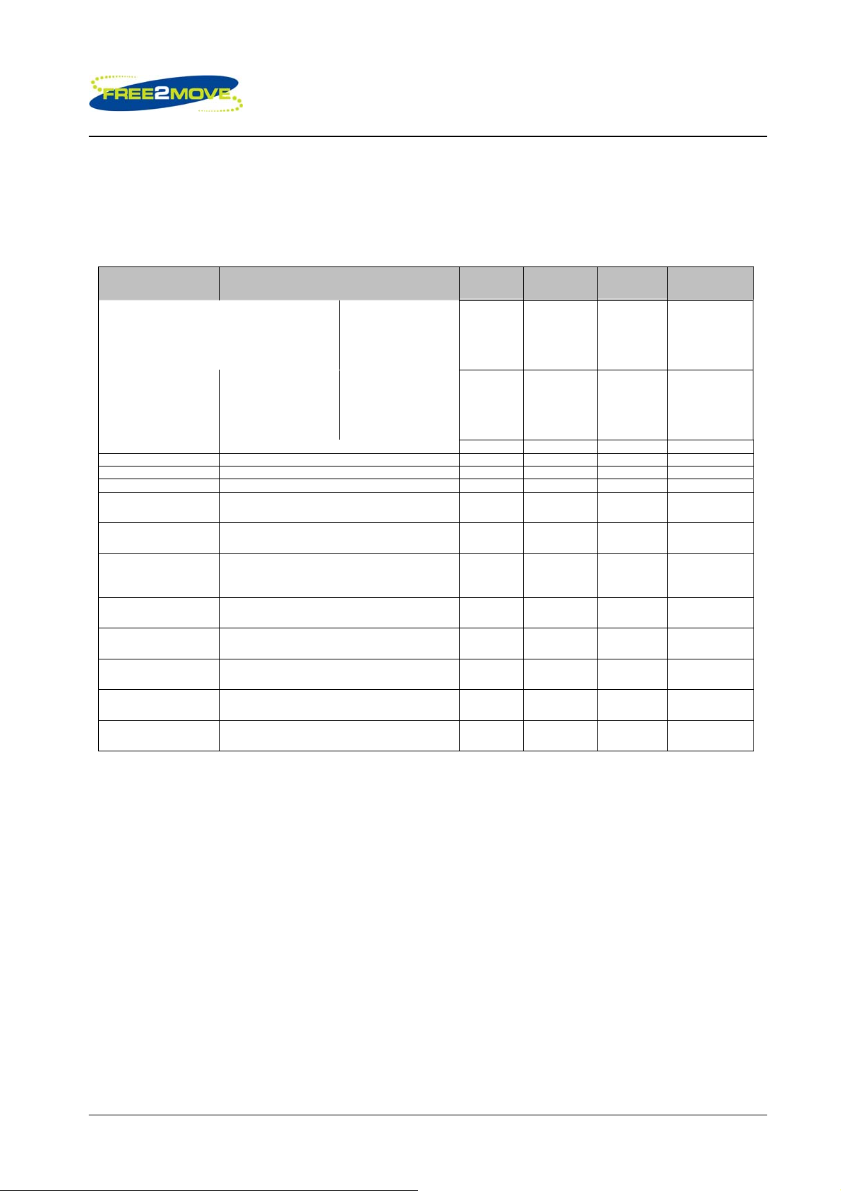
6.2.10 IEC 60958 Interface
The IEC 60958 interface is a digital audio interface that uses bi-phase coding to minimise the DC content of
the transmitted signal and allows the receiver to decode the clock information from the transmitted signal.
The IEC 60958 specification is based on the two industry standards AES/EBU and the Sony and Philips
interface specification SPDIF. The interface is compatible with IEC 60958-1, IEC 60958-3 and IEC 60958-4
Note:
1
Subject to firmware support, contact Free2move for information.
The SPDIF interface signals are SPDIF_IN and SPDIF_OUT and are shared on the PCM interface pins.
The input and output stages of the SPDIF pins can interface either 75 coaxial cable with an RCA
connector or there is an option to use an optical link that uses Toslink optical components. Typical output
and input stage interfaces for the coaxial and alternative optical solution interface is shown in the figures
below.
1
.
F2M03MLA
Example circuit for SPDIF Interface with coaxial output
Note: The 100 and 75 resistors are dependent on the supply voltage and therefore subject to change.
F2M03MLA
Example circuit for SPDIF Interface with coaxial input
© 2007 Free2move AB
Page 27(27)

Rev: b
Low power Multimedia Bluetooth™ Module with antenna F2M03MLA
Datasheet
Example circuit for SPDIF interface with optical output
Example circuit for SPDIF interface with optical input
6.2.11 Audio Input Stage
The input stage of F2M03MLA consists of a low noise input amplifier, which receives its analogue input
signal from pins AUDIO_IN_P_LEFT and AUDIO_IN_N_LEFT to a second-order - ADC that outputs a
4MBit/sec single-bit stream into the digital circuitry. The input can be configured to be either single ended or
fully differential. It can be programmed for either microphone or line input and has a 3-bit digital gain setting
of the input-amplifier in 3dB steps to optimize it for the use of different microphones.
© 2007 Free2move AB
Page 28(28)

Rev: b
Low power Multimedia Bluetooth™ Module with antenna F2M03MLA
Datasheet
6.2.12 Microphone Input
The audio-input is intended for use from 1µV@94dB SPL to about 10µV@94dB SPL. With biasing-resistors
R1 and R2 equal to 1k, this requires microphones with sensitivity between about –40dBV/Pa and
-60dBV/Pa. The microphone for each channel should be biased as shown in the figure below.
Microphone bias F2M03MLA
Microphone Biasing (Left Channel Shown)
The input impedance at AUDIO_IN_N_LEFT, AUDIO_IN_P_LEFT, AUDIO_IN_N_RIGHT and
AUDIO_IN_P_RIGHT is typically 20k. C1 and C2 should be 47nF. R1 sets the microphone load
impedance and is normally in a range of 1 to 2 k. R2, C3 and C4 improve the supply rejection by
decoupling supply noise from the microphone. Values should be selected as required in the specification.
R2 may be connected to a convenient supply (typically VDD).
6.2.13 Line Input
If the input gain is set to less than 21dB F2M03MLA automatically selects line input mode. In this
mode the input impedance at AUDIO_IN_N_LEFT, AUDIO_IN_P_LEFT, AUDIO_IN_N_RIGHT and
AUDIO_IN_P_RIGHT are increased to 130k typically. In line-input mode, the full-scale input signal is
about 400mV rms. The figures below show two circuits for line input operation and show connections for
either differential or single ended inputs.
Differential Input (Left channel shown)
Single ended input (Left channel shown)
© 2007 Free2move AB
Page 29(29)

Rev: b
Low power Multimedia Bluetooth™ Module with antenna F2M03MLA
Datasheet
6.2.14 Output Stage
The output digital circuitry converts the signal from 16-bit per sample, linear PCM of variable sampling
frequency to an 8 MBits/sec bit stream, which is fed into the analogue output circuitry.
The output circuit comprises a digital to analogue converter with gain setting and output amplifier.
Its class-AB output-stage is capable of driving a signal on both channels of up to 2V pk-pk- differential into a
load of 32 and 500pF with a typical THD+N of -74dBc. The output is available as a differential signal
between AUDIO_OUT_N_LEFT and AUDIO_OUT_P_LEFT for the left channel as shown in Figure 8.45;
and between AUDIO_OUT_N_RIGHT and AUDIO_OUT_P_RIGHT for the right channel. The output is
capable of driving a speaker directly if its impedance is at least 16 if only one channel is connected or an
external regulator is used.
Speaker output (Left channel shown)
The gain of the output stage is controlled by a 3-bit programmable resistive divider, which sets the gain in
steps of approximately 3dB.
The single bit stream from the digital circuitry is low pass filtered by a second order bi-quad filter with a pole
at 20kHz. The signal is then amplified in the fully differential output stage, which has a gain bandwidth of
typically 1MHz. It uses its high open loop gain in the closed loop application circuit to achieve low distortion
while operating with low standing current.
© 2007 Free2move AB
Page 30(30)

6.3 UART Interface
Rev: b
Low power Multimedia Bluetooth™ Module with antenna F2M03MLA
Datasheet
The F2M03MLA Bluetooth module’s Universal Asynchronous Receiver Transmitter (UART) interface
provides a simple mechanism for communicating with other serial devices using the RS232 standard
(1)
.
Universal Asynchronous Receiver
Four signals are used to implement the UART function, as shown in the figure above. When F2M03MLA is
connected to another digital device, UART_RX and UART_TX transfer data between the two devices. The
remaining two signals, UART_CTS and UART_RTS, can be used to implement RS232 hardware flow
control where both are active low indicators. All UART connections are implemented using CMOS
technology and have signalling levels of 0V and VDD. UART configuration parameters, such as Baud rate
and packet format, are set by Free2move firmware.
Note:
In order to communicate with the UART at its maximum data rate using a standard PC, an accelerated
serial port adapter card is required for the PC.
(1)
Uses RS232 protocol but voltage levels are 0V to VDD, (requires external RS232 transceiver IC)
Parameter Possible Values
1200 Baud (2%Error)
Baud Rate
Maximum 1.5MBaud (1%Error)
Flow Control RTS/CTS or None
Parity None, Odd or Even
Number of Stop Bits 1 or 2
Bits per channel 8
Minimum
9600 Baud (1%Error)
Possible UART Settings
© 2007 Free2move AB
Page 31(31)
Rev: b
Low power Multimedia Bluetooth™ Module with antenna F2M03MLA
Datasheet
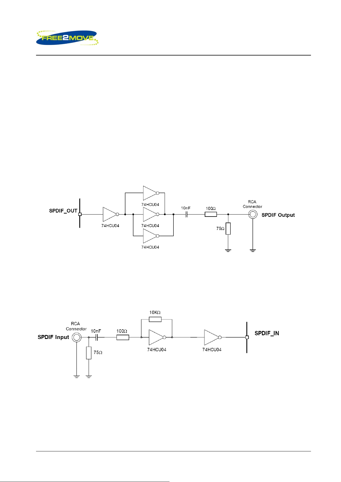
The UART interface is capable of resetting the Free2move module upon reception of a break signal. A
Break is identified by a continuous logic low on the UART_RX terminal, as shown in figure below. If tBRK is
longer than a special value, defined by the Free2move firmware a reset will occur. This feature allows a
host to initialise the system to a known state. Also, the F2M03MLA can emit a Break character that may be
used to wake the Host. The above capabilities are not supported in the standard firmware, please contact
Free2move for more information.
Break signal
© 2007 Free2move AB
Page 32(32)

Rev: b
Low power Multimedia Bluetooth™ Module with antenna F2M03MLA
Datasheet
6.4 Serial Peripheral Interface
F2M03MLA is a slave device that uses terminals SPI_MOSI, SPI_MISO, SPI_CLK and SPI_CSB. This
interface is used for program emulation/debug and IC test. It is also the means by which the F2M03MLA
flash may be programmed, before any 'boot' program is loaded.
The SPI signals should be routed out from the module if you need to upgrade the firmware on the module in
the future when the module is already soldered.
Note:
The designer should be aware that no security protection is built into the hardware or firmware associated with this port, so the
terminals should not be permanently connected in a PC application. This interface is not a user interface and only used for initial
download and configuration of the firmware for the module.
6.5 I2C Interface
PIO[8:6] can be used to form a master I2C interface. The interface is formed using software to drive these
lines. Therefore, it is suited only to relatively slow functions such as driving a dot matrix liquid crystal display
(LCD), keyboard scanner or EEPROM.
Notes:
2
C interface is controlled by firmware specific settings. Please see specific firmware datasheet for information
The I
PIO lines need to be pulled-up through 2.2k: resistors.
PIO[7:6] dual functions, UART bypass and EEPROM support, therefore, devices using an EEPROM cannot
support UART bypass mode.
For connection to EEPROMs, contact Free2move for information about devices that are currently supported.
Example EEPROM Connection
© 2007 Free2move AB
Page 33(33)

Rev: b
Low power Multimedia Bluetooth™ Module with antenna F2M03MLA
Datasheet
6.6 PIOs
The F2M03MLA have 8 programmable general-purpose I/O ports PIO[11:6, 1:0] and one analog I/O port
AIO[0]. The F2M03MLA also has one digital to analog port AUX_DAC. PIO lines can be configured through
software to have either weak or strong pull-ups or pull-downs.
All PIO lines are configured as inputs with weak pull-downs at reset.
AIO[0] functions available via this pin include an 8-bit ADC but can also be used as general-purpose I/O
line. Typically the AIO[0] is used for battery voltage measurement. The voltage range for AIO[0] is
constrained by the internal analogue supply voltage which is 1.8V.
The AUX_DAC is a 8-bit Digital to Analog Conveter used for customer specific applications. The voltage
range is from 0V to VDD.
Note:
The PIO, AIO and AUX_DAC lines are controlled by firmware specific settings. Please see specific firmware
datasheet for information about the PIOs used!
6.6.1 General-purpose I/O lines
PIO[0]
I/O terminal with programmable strength internal pull-up/down.
PIO[1]
I/O terminal with programmable strength internal pull-up/down.
PIO[6]
I/O terminal with programmable strength internal pull-up/down.
PIO[7]
I/O terminal with programmable strength internal pull-up/down.
PIO[8]
I/O terminal with programmable strength internal pull-up/down.
PIO[9]
I/O terminal with programmable strength internal pull-up/down.
PIO[10]
I/O terminal with programmable strength internal pull-up/down.
PIO[11]
I/O terminal with programmable strength internal pull-up/down.
6.6.2 Analog I/O lines
AIO[0]
Programmable input/output line also possible to use as digital I/O
AUX_DAC
Digital to Analog output line.
© 2007 Free2move AB
Page 34(34)

Rev: b
Low power Multimedia Bluetooth™ Module with antenna F2M03MLA
Datasheet
6.7 Power supply
The power supply for the F2M03MLA should be chosen carefully. Bad power supply can reduce the
performance and may damage the module. Please use the recommended voltage regulator or consult
Free2move if using another regulator. It is also essential to use a proper reset circuit to the module for
correct operation.
6.7.1 Voltage regulator
The F2M03MLA has one power supply, +VCC.
The voltage supplied should have low noise, less than 10mV rms between 0 and 10MHz. The transient
response of the regulator is also important. At the start of a Bluetooth packet, power consumption will jump
to high levels. The regulator should have a response time of 20µs or less; it is essential that the power rail
recovers quickly.
The recommended voltage regulator is:
XC6209B332MR from Torex.
6.7.2 Reset
The F2M03MLA has an active low reset (pin nr: 38).The reset pin MUST be connected to either a resetcircuit such as the TC1270SERCTR, TCM811SERCTR, DS1818 or using an I/O from a microcontroller.
Reset cannot be done with a R-C network. It is recommended to used one of the reset circuits mentioned
above. Special considerations must be taken when using an I/O from a microcontroller; a pull-down resistor
(typically 1.8kΩ) must be placed on the I/O-line.
It is recommended that RESET is applied for a period greater than 5ms.
At reset the digital I/O pins are set to inputs for bi-directional pins and outputs are tristated. The PIOs have
weak pull-downs.
© 2007 Free2move AB
Page 35(35)

Low power Multimedia Bluetooth™ Module with antenna F2M03MLA
7 Application information
7.1 Recommended land pattern
Solder pad
0.6
[TOP VIEW]
1.0
2.1
F2M03MLA
ANTENNA
13.2
Rev: b
Datasheet
All dimensions are in [mm]
4.0
18.6
13.0
1.1
Recommended extended pad for manual soldering (apply for all solder pads)
Restricted area for ground planes or other components
• Pad size: 0.6x1.4 and 0.6x0.8mm,
• Solder mask opening: Pad size + 0.1mm
• Pitch: 1.0mm
© 2007 Free2move AB
Page 36(36)

Rev: b
A
Low power Multimedia Bluetooth™ Module with antenna F2M03MLA
Datasheet
7.2 Layout guidelines
The module uses bottom pads for soldering optimized for an automatic solder line. It is also possible to
solder the module manually by using hot air soldering. For manual soldering solder pads may in some
situation be made slightly larger to allow easier heating process.
To achieve good RF performance it is recommended to place ground plane(s) beneath the module but not
under the antenna. The ground planes should be connected with vias surrounding the module. Except from
the ground plane it is preferable that there are as few components and other material as possible nearby
the antenna. Free air is the best surrounding for the antenna.
All GND pads must be connected directly to a flooded ground-plane. If more then one ground layer is used
then make a good connection between them using many via holes. +VCC should be connected to the
voltage regulator using a wide trace.
Vias
Ground layers
F2M03MLA
ntenna
© 2007 Free2move AB
Page 37(37)

Low power Multimedia Bluetooth™ Module with antenna F2M03MLA
7.3 Typical application schematic
Datasheet
Rev: b
Typical application schematic for F2M03MLA when using the Wireless Audio firmware
© 2007 Free2move AB
Page 38(38)

Low power Multimedia Bluetooth™ Module with antenna F2M03MLA
8 Package information
F2M03MLA
Physical size [mm]:
Length: 18.6
Width: 13.2
Height: 2.1
Weight: 1.2g
Datasheet
Rev: b
© 2007 Free2move AB
Page 39(39)

Rev: b
Low power Multimedia Bluetooth™ Module with antenna F2M03MLA
Datasheet
9 Certifications
9.1 Bluetooth
F2M03MLA has passed the Bluetooth Qualification/Certification process as specified within the Bluetooth
Specifications and as required within the PRD 2.0.
QDID: B012539
9.2 CE
F2M03MLA complies with the requirements of R&TTE Directive 1999/5/CE, the European Community
Directive 73/23/EEC and 93/68/EEC.
• EN 300 328
• EN 301 489-1/-17
• EN 60950
© 2007 Free2move AB
Page 40(40)

Rev: b
Low power Multimedia Bluetooth™ Module with antenna F2M03MLA
Datasheet
9.3 FCC
FCC-B Radio Frequency Interference Statement
This deceive has been tested and found to comply with the limits for a Class-B digital device, pursuant to
part 15 of the FCC rules. These limits are designed to provide reasonable protection against harmful
interference when the equipment is operated in commercial environment. This equipment generates, uses
and can radiate radio frequency energy and, if not installed and used according with the instruction manual,
may cause harmful interference to radio communication. Operation of this equipment in a residential area is
likely to cause harmful interference, in which case the user will be required to correct the interference at his
own expense.
Notice1
The changes or modifications not expressly approved by the party responsible for the compliance could
void the user’s authority to operate the equipment.
Notice 2
Shielded interface cables an A.C. power cord, if any, must be used in order to comply with the emission
limits.
Notice 3
This modular transmitter uses an electronic display of the FCC identification number, the information must
be readily accessible on the device in which it is installed.
The FCC ID can be read from the UART of the device.
UART Settings:
Baud rate: 38400bps
Data bits: 8
Parity: None
Stop bits: 1
Send command: “VERSION” (ASCII characters) over the UART and the module will respond with software,
hardware information and the FCC ID.
If the module is installed inside another device, then the outside of the device into which
the module is installed must display a label referring to the enclosed module. This exterior
label can use wording such as the following: “Contains FCC certified transmitter module(s).”
Any similar wording that expresses the same meaning may be used.
FCC ID R47F2M03MLA
This device complies with part 15 of the FCC
Rules. Operation is subject to the following two
conditions: (1) This device may not cause harmful
interference, and (2) This device must accept any
interference received, including interference that
may cause undesired operation.
© 2007 Free2move AB
Page 41(41)

Rev: b
Low power Multimedia Bluetooth™ Module with antenna F2M03MLA
Datasheet
10 RoHS and WEEE Statement
F2M03MLA meets the requirements of Directive 2002/95/EC of the European Parliament and of the Council
on the Restriction of Hazardous Substance (RoHS).
F2M03MLA also meet the requirements of Directive 2002/96/EG -Waste Electrical and Electronic
Equipment (WEEE).
© 2007 Free2move AB
Page 42(42)

Low power Multimedia Bluetooth™ Module with antenna F2M03MLA
A
11 Tape and Reel information
11.1 Package Tape dimensions
Datasheet
Rev: b
11.2 Reel dimensions
A 330.0 max
B 1.5 min
C 13.0±0.2
D 20.2 min
N 100.0
W1 44.4 +2.0 –0.0
W2 50.4 max
Pulling direction
W2
W1
D
C
B
N
© 2007 Free2move AB
Page 43(43)

Low power Multimedia Bluetooth™ Module with antenna F2M03MLA
Datasheet
12 Ordering information
The F2M03MLA is available for delivery in volumes.
Part nr: Description
F2M03MLA-S03 Low power Bluetooth Multimedia module with antenna and Wireless Audio firmware
Please use our website:
(HS, HF and A2DP)
www.free2move.net for more information about local distributors and dealers.
Rev: b
© 2007 Free2move AB
Page 44(44)

Low power Multimedia Bluetooth™ Module with antenna F2M03MLA
13 Document history
Date Revision Reason for Change
JAN 2007 a Original Publication of this document.
JUNE 2007 b Added Certification information
Datasheet
Rev: b
F2M03MLA
Datasheet
Datasheet_F2M03MLA_rev_b.pdf
Last revision change
June 2007
© 2007 Free2move AB
Page 45(45)

Low power Multimedia Bluetooth™ Module with antenna F2M03MLA
A
14 Acronyms and definitions
Datasheet
Rev: b
Bluetooth
ACL Asynchronous Connection-Less. A Bluetooth data packet.
AC Alternating Current
A-law Audio encoding standard
API Application Programming Interface
BCSP BlueCore™ Serial Protocol
BER Bit Error Rate. Used to measure the quality of a link
C/I Carrier Over Interferer
CMOS Complementary Metal Oxide Semiconductor
CODEC Coder Decoder
CPU Central Processing Unit
CQDDR Channel Quality Driven Data Rate
CTS Clear to Send
CVSD Continuous Variable Slope Delta Modulation
DAC Digital to Analogue Converter
dBm Decibels relative to 1mW
DC Direct Current
DFU Device Firmware Upgrade
GCI General Circuit Interface. Standard synchronous 2B+D ISDN timing interface
HCI Host Controller Interface
Host Application’s microcontroller
Host Controller Bluetooth integrated chip
HV Header Value
ISDN Integrated Services Digital Network
ISM Industrial, Scientific and Medical
ksamples/s kilosamples per second
L2CAP Logical Link Control and Adaptation Protocol (protocol layer)
LC Link Controller
LSB Least-Significant Bit
p-law Encoding standard
MISO Master In Serial Out
OHCI Open Host Controller Interface
PA Power Amplifier
PCB Printed Circuit Board
PCM Pulse Code Modulation. Refers to digital voice data
PIO Parallel Input Output
RAM Random Access Memory
RF Radio Frequency
RFCOMM Protocol layer providing serial port emulation over L2CAP
RISC Reduced Instruction Set Computer
RSSI Receive Signal Strength Indication
RTS Ready To Send
RX Receive or Receiver
SCO Synchronous Connection-Oriented. Voice oriented Bluetooth packet
SDP Service Discovery Protocol
SIG Special Interest Group
SPI Serial Peripheral Interface
SPP Serial Port Profile
TBD To Be Defined
TX Transmit or Transmitter
UART Universal Asynchronous Receiver Transmitter
USB Universal Serial Bus or Upper Side Band (depending on context)
VM Virtual Machine
www world wide web
set of technologies providing audio and data transfer over short-range radio
Term: Definition:
© 2007 Free2move AB
Page 46(46)

Rev: b
Low power Multimedia Bluetooth™ Module with antenna F2M03MLA
Datasheet
Contact information
For support questions please contact your local dealer
For other purposes use: info@free2move.net
Website: www.free2move.net
Local dealer/distributor
The information given herein includes text, drawings, illustrations and schematics that are believed to be reliable. However,
Free2move makes no warranties as to its accuracy or completeness and disclaims any liability in connection with its use. Free2move
will in no case be liable for any incidental, indirect or consequential damages arising out of sale, resale, use or misuse of the product.
Users of Free2move products should make their own evaluation to determine the suitability of each such product for the specific
application.
© 2007 Free2move AB
Page 47(47)
 Loading...