

Page 1
FreakLabs
Rapid Prototyping Platform
900 MHz 802.15.4 Radio Board
FL-AT86RF212-DEV v1.1
User Guide v1.1A
Page 2

Document Revision History
Date Description
2010-04-01 Document creation
FL-AT86RF212-DEV v1.1
Page 1
Page 3

Specications
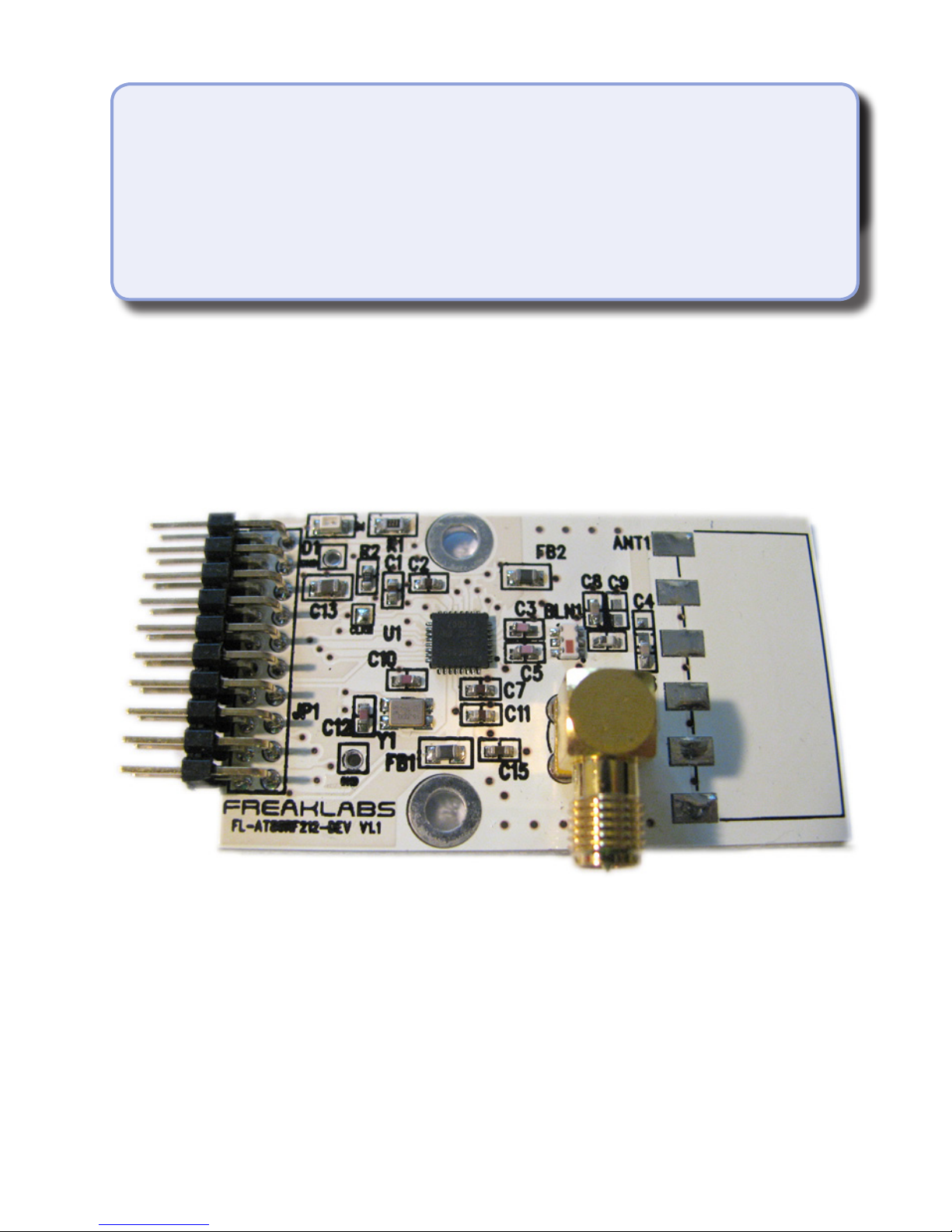
e FreakLabs FL-AT86RF212-DEV 900MHz modular radio board is
designed to be an easy way to rapidly prototype wireless sensor/actuator
applications using the 900 MHz IEEE 802.15.4 protocol. It includes
a complete radio circuit based on the Atmel AT86RF212 as well as a
standard FreakLabs universal serial peripheral connector and either an
external RP-SMA antenna connector or an on-board SMD antenna.
Quick SpecS
Radio: AT86RF212,
900 MHz, 802.15.4
radio
It’s designed to work with MCU boards that support the standardized
FreakLabs Universal Serial Connector and has a peripheral-side, right
angle, male connector that ts into any of the FreakLabs MCU boards.
It is also supported by the Chibi open source wireless protocol stack for
quick and easy wireless communication and testing.
Connectors: 1 USC
Peripheral
Antenna: RP-SMA
external antenna,
SMD antenna
Peripherals
e transceiver is the only peripheral on this board and it consists of the Atmel AT86RF212 900
MHz 802.15.4 radio. e AT86RF212 has a lot of built-in hardware to handle many of the time
sensitive or repetitive tasks in the 802.15.4 specication such as automatic ACK generation, frame
ltering based on address, auto-CRC generation and checking, automatic retries, and auto transmit after checking for a clear channel.
Some other nice features of the radio are that it supports the Chinese 780 MHz, European 868
MHz, and North American 916 MHz bands. ere are also dierent modulation schemes that
can be chosen based on requirements. e highest bitrates use O-QPSK modulation which can
handle up to 1 Mbps data rates in proprietary mode or 250 kbps in IEEE 802.15.4 compliant
mode. e modulation can also be changed to BPSK which yields approximately 5-10x improvement in receiver sensitivity and thus greater range. However using BPSK, the data rate goes down
to 20-40 kbps.
e RF front end consists of a matching circuit to match the radio data signals to the 50 ohm
antenna connector and optional discrete components to choose between the on-board SMD antenna and the external RP-SMA antenna connector. e components in the matching circuit are
chosen and tested to be as close as possible to 50 ohms so that there will be very little power loss
on the incoming and outgoing data signals.
Connectors
e universal serial connector (USC) interface is standard for all of the FreakLabs development
boards. e FL-AT86RF212-DEV board contains a peripheral-side universal serial connector.
Universal Serial Connector Pinouts
e FL-AT86RF212-DEV radio board supports the Universal Serial Connector (USC) v1.1. e
FL-AT86RF212-DEV v1.1
FL-AT86RF212-DEV v1.1
Page 2
Page 2
Page 4
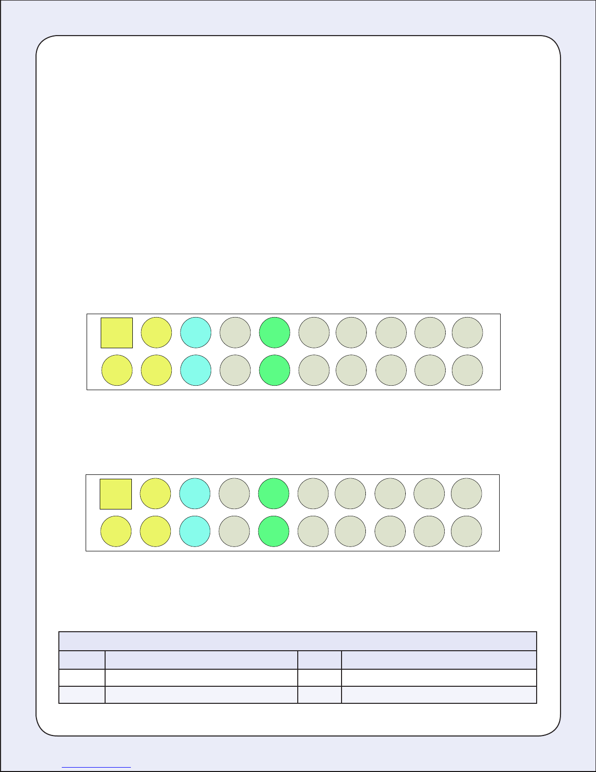
connector supports an SPI bus, I2C bus, 2 interrupts, 2 analog inputs, 1 PWM output, 1 timer/
capture input, 6 GPIOs, 3.3V supply, and optional 5V supply. All pins except power pins can also
be used as GPIO if there is no need for the principal function. In the case of the radio board, only
the SPI bus, 1 interrupt, and a few GPIO pins are used.
e connector consists of a host side which is a 20-pin, female, right-angle header and a peripheral side which is a 20-pin, male, right-angle header. e host side connector will always be on
MCU boards and the peripheral connector will be found on peripheral boards that interface to
the MCU boards.
e reason right angle connectors were chosen was so that the complete system can be level. is
makes it easier to access individual signals and pins, as well as make modications to the circuit.
e following diagram shows the pinouts of the connectors:
Universal Serial Connector v1.1 – Host (MCU) side
1
SSEL
SCLK
2
SSEL
SCLK
3 5 7 9 11 13 15 17 19
MOSI
MISO
4 6 8 10 12 14 16 18 20
SCL
SDA
IRQ0
IRQ1
GND
GND
ADC0
ADC1
PWM
0
GPIO/
PWM
1
CAPT
0
GPIO/
CAPT
1
GPIO
GPIO
Universal Serial Connector v1.1 – Peripheral side
MOSI
MISO
SCL
SDA
IRQ0
IRQ1
GND
GND
ADC0
ADC1
PWM
0
GPIO/
PWM
1
CAPT
0
GPIO/
CAPT
1
GPIO
GPIO
468101214161820
VCC3
NC/
VCC5
135791113151719
VCC3
NC/
VCC5
2
e specic pinout of the universal serial peripheral connector of the FL-AT86RF212-DEV board
can be found below:
USC Peripheral Connector (JP1)
Pin Description Pin Description
1 VCC3 2 NC
3 NC 4 NC
FL-AT86RF212-DEV v1.1
FL-AT86RF212-DEV v1.1
Page 3
Page 3
Page 5

USC Peripheral Connector (JP1)
Pin Description Pin Description
5 NC 6 NC
7 RST_n 8 SLP/TR
9 NC 10 NC
11 GND 12 GND
13 INT 14 NC
15 NC 16 NC
17 MOSI 18 MISO
19 SS_n (SPI Select) 20 SCLK
Disclaimer
e FL-AT86RF212-DEV board is NOT FCC approved. It is designed to comply with FCC Part
15 rules. However this board is not in a nished product form and is only intended for experimental and research/development purposes. If you wish to use this board in an actual product,
you will need to attain certication with the appropriate local regulatory body for the complete
system. Additionally, please use the wireless equipment in a responsible manner with regard for
others and your surroundings.
Schematics
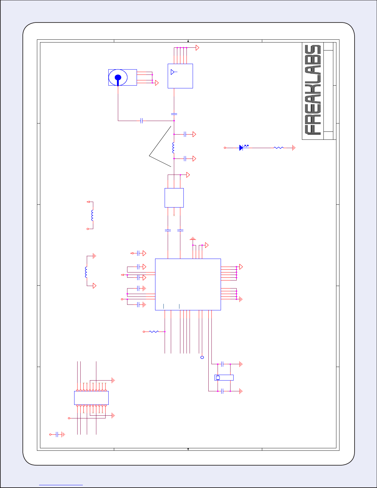
Schematics can be found on the following page:
FL-AT86RF212-DEV v1.1
Page 4
Page 6
5
5
4
4
3
3
2
2
1
1
D D
C C
B B
A A
SS_n
MOSI
RST_n
IRQ
SCLK
MISO
SLP_TR
XTAL1
XTAL2
PWR_LED
RST_n
SLP_TR
SS_n
SCLK
MISO
MOSI
IRQ
TP_CLKM
RFP
RFN
RF+
RF-
UNBAL SMD_ANTANT
SMA_ANT
VCC3
VCC3 AVCC3
VCC3 AVCC3
VCC3
VCC3
VCC3
AVCC3
Project Title:Size Rev
Date: Sheet
of
Page Title: v1.1
FL-AT86RF212-DEV
B
1 1Friday, April 02, 2010
RADIO
Project Title:Size Rev
Date: Sheet
of
Page Title: v1.1
FL-AT86RF212-DEV
B
1 1Friday, April 02, 2010
RADIO
Project Title:Size Rev
Date: Sheet
of
Page Title: v1.1
FL-AT86RF212-DEV
B
1 1Friday, April 02, 2010
RADIO
CONNECT AGND TO GND VIA FERRITE.
CONNECT AVCC TO VCC VIA FERRITE.
CAN ALSO BE REPLACED WITH 0 OHM
RESISTOR IF NOT NEEDED
ANALOG AND DIGITAL GROUND WILL BE SEPARATED
GND VIAS IN
BETWEEN PINS
2-6
2 separate transmission lines
-70 mil width, 150 mil length,
63 ohms @900 MHz, FR-4, 59 mil
thickness, 1 oz copper
ANT2
SMA
ANT2
SMA
1
1
GND
2
GND
3
GND
4
GND
5
D1
GREEND1GREEN
C9
Do Not Install
C9
Do Not Install
R2
10kR210k
R1
220R1220
JP1
H10X2 - RT
JP1
H10X2 - RT
1 2
3 4
5 6
7 8
9 10
1113151719
1214161820
C8
3.0 pFC83.0 pF
C12
12 pF
C12
12 pF
C10
12 pF
C10
12 pF
U1
AT86RF212
U1
AT86RF212
DIG31DIG4
2
AVSS
3
RFP
4
RFN
5
AVSS
6
DVSS
7
RST
8
DIG19DIG2
10
SLP_TR
11
DVSS
12
DVDD
13
DVDD
14
DEVDD
15
DVSS
16
CLKM
17
DVSS
18
SCLK19MISO
20
DVSS
21
MOSI
22
SEL
23
IRQ24XTAL225XTAL1
26
AVSS
27
EVDD
28
AVDD
29
AVSS
30
AVSS
31
AVSS
32
TP6TP6
1
FB2
FB/0805
FB2
FB/0805
1 2
C13
22uF/6.3V
C13
22uF/6.3V
C2
0.1 uFC20.1 uF
GND
Y1
NX3225SA, 15PPM
GND
Y1
NX3225SA, 15PPM
1
2 4
3
BLN1
RF BALUN-0900BL18B100
BLN1
RF BALUN-0900BL18B100
GND
1
UNBAL
2
GND
3
BAL1
4NC5
BAL2
6
L1 12.0 nHL1 12.0 nH
1 2
C5 68 pFC5 68 pF
C6
3.0 pFC63.0 pF
C1
0.1 uFC10.1 uF
C4
DNIC4DNI
C7
0.1 uFC70.1 uF
C11
0.1 uF
C11
0.1 uF
FB1
FB/0805
FB1
FB/0805
1 2
C3 68 pFC3 68 pF
C15
1uF
C15
1uF
ANT1
SMD_ANT_900MHZ
ANT1
SMD_ANT_900MHZ
FEED_IN
1
GND2GND3GND4GND5GND
6
FL-AT86RF212-DEV v1.1
Page 5
Page 7
5
5
4
4
3
3
2
2
1
1
D D
C C
B B
A A
Project Title:Size Rev
Date: Sheet
of
Page Title: v1.1
FL-AT86RF212-DEV
A
1 1Friday, January 15, 2010
MISC
Project Title:Size Rev
Date: Sheet
of
Page Title: v1.1
FL-AT86RF212-DEV
A
1 1Friday, January 15, 2010
MISC
Project Title:Size Rev
Date: Sheet
of
Page Title: v1.1
FL-AT86RF212-DEV
A
1 1Friday, January 15, 2010
MISC
TP1TP1
1
H2
MOUNT_HOLE/MOUNT_HOLE
H2
MOUNT_HOLE/MOUNT_HOLE
1
TP14TP14
1
H1
MOUNT_HOLE/MOUNT_HOLE
H1
MOUNT_HOLE/MOUNT_HOLE
1
FL-AT86RF212-DEV v1.1
Page 6
Page 8
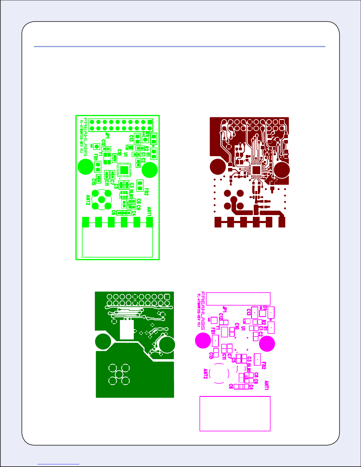
PCB Layout
PCB layout le order:
1. Assembly drawing
2. Top Layer
3. Bottom Layer
4. Silkscreen
FL-AT86RF212-DEV v1.1
Page 7
Page 9

Bill of Materials
Quantity
1 ANT1 Antenna Factor ANT-XXX-SP 900 MHz SMD Antenna
1 ANT2
Reference Manufacturer Part Number Description
(XXX=868 or 916)
ChangHong SMA-02-113-
RP-SMA Connector
TGG
1 BLN1 Johanson Tech-
nology
4 C1, C2, C7,
C11
2 C3,C5
Various 0.1uF/50V, 0603
Murata ERB1885C2E-
0900BL18B100 900 MHz balun
68 pF/250V, 0603, high freq
680JDX5D
2 C4, C9
2 C6,C8
2 C10,C12
1 C13
1 C15
1 D1
2 FB1,FB2
1 JP1
N/A Not Installed
Johanson Tech-
nology
251R14S3R0BV4T
3.0 pF/250V, 0603, high freq
Various 12 pF/50V, 0603
Various 22uF/6.3V, 0805, MLCC
Various 1uF/50V, 0603
Various Green LED, 0805
Various Ferrite Bead, 0805
Various 10x2 Right angle header, male,
0.100”
1 L1
Taiyo Yuden HK1608-12NJ-T12 nH, 0603, high freq
1 R1
1 R2
1 U1
1 Y1
Various 220 ohms, 0805
Various 10 kohms, 0603
Atmel AT86RF212 900 MHz, 802.15.4 radio
NDK NX3225SA 16 MHz crystal, 15 ppm
FL-AT86RF212-DEV v1.1
Page 8
 Loading...