

Force-Mos MESS138W, MESS138W-G Schematics
J
N - Channel 50-V (D-S) MOSFET
MESS138W/MESS138W-G
GENERAL DESCRIPTION
The MESS138W is the N-Channel logic enhancement mode power
field effect transistors are produced using high cell density, DMOS
trench technology. This high density process is especially tailored to
minimize on-state resistance.
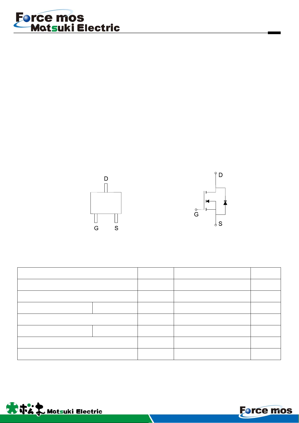
PIN CONFIGURATION
(SOT-323)
Top View
FEATURES
● RDS(ON)≦3Ω@VGS=10V
● R
DS(ON)≦3.5Ω@VGS=5V
● RDS(ON)≦7Ω@VGS=2.75V
● Super high density cell design for extremely low R
● Exceptional on-resistance and maximum DC current
capability
DS(ON)
APPLICATIONS
● Power Management in Note book
● DC/DC Converter
● Load Switch
● LCD Display inverter
Ordering Information: MESS138W (Pb-free)
MESS138W-G (Green product-Halogen free)
Absolute Maximum Ratings (TA=25℃ Unless Otherwise Noted)
Parameter Symbol
Drain-Source Voltage VDS 50 V
Gate-Source Voltage VGS ±20 V
Continuous Drain
TA=25℃
Pulsed Drain Current IDM 1.8 A
A=25℃
Maximum Power Dissipation
T
Maximum Ratings
I
D 0.5 A
P
D 1 W
Unit
Operating Junction Temperature TJ -55 to 150
Thermal Resistance-Junction to Ambient*
* The device mounted on 1in
an, 2007-Ve r1.1
Oct, 2011-Ver1.0
2
FR4 board with 2 oz copper
θJA 130
R
℃
℃/W
01
N - Channel 50-V (D-S) MOSFET
MESS138W/MESS138W-G
Electrical Characteristics (T
Symbol Parameter Limit Min Typ Max Unit
STATIC
BVDSS Drain-Source Breakdown Voltage
VGS(th) Gate Threshold Voltage VDS=VGS, ID=1mA 0.5 1.5 V
IGSS Gate-Body Leakage VDS=0V, VGS=±20V ±100 nA
A =25℃ Unless Otherwise Specified)
GS=0V, ID=250μA
V
50 V
IDSS Zero Gate Voltage Drain Current VDS=50V, VGS=0V
VGS=10V, ID=200mA 1.3 3
RDS(ON) Drain-Source On-Resistance*
VSD Diode Forward Voltage * IS=0.44A, VGS=0V 0.8 1.4 V
DYNAMIC
Qg Total Gate Charge
Qgs Gate-Source Charge
Qgd Gate-Drain Charge
Rg Gate Resistance VDS=0V, V
Ciss Input Capacitance
Coss Output Capacitance
Crss Reverse Transfer Capacitance
td(on)
tr
td(off)
tf
Turn-On Delay Time
Turn-On Rise Time
Turn-Off Delay Time
Turn-Off Fall Time
VGS=5V, ID=200mA 1.4 3.5
V
GS=2.75V, ID=200mA 1.6 7
7.0
1.8
0.7
8.7
42
15
3
4.63
18.9
6.8
11.4
V
DS=25V, VGS=10V, ID=0.22A
=0V, f=1MHz
GS
V
DS=25V, VGS=0V, f=1MHz
V
DD=30V, RL =103Ω
I
D=0.29A, VGS=10V,
R
GEN=6Ω
0.5 μA
Ω
nC
Ω
pF
ns
Notes: a. Pulse test; pulse width ≦ 300us, duty cycle≦ 2%
b.
Matsuki Electric/ Force mos reserves the right to improve product design, functions and reliability without notice.
Oct, 2011-Ver1.0
02
 Loading...