

FOCUS Enhancements FS454, FS453, FS455, FS456 User Manual

FS453/4 AND FS455/6 DATA SHEET: HARDWARE REFERENCE
FS453/4 and FS455/6
PC-to-TV Video Scan
Converter
FS453/4 and FS455/6
Data Sheet Guides
To make specialized information easier to find, the FS453/4 and FS455/6 Data Sheet is
organized into separate reference guides. Each guide addresses a different purpose or
user.
The FS453/4 and FS455/6 Product Brief provides general information for all
users.
; The FS453/4 and FS455/6 Hardware Reference is for
system designers. It provides information on developing
FS453/4 and FS455/6 applications. (This section now includes
PCB Layout Guide)
The FS453/4 and FS455/6 Software/Firmware Reference is for programmers.
It provides information on programming the FS453/4 and FS455/6.
If you need additional reference guides, contact your Focus Enhancements
representative.
Throughout this document "FS453" is used as a general term to reference the FS453,
FS454, FS455, and FS456. The FS453 and FS454 are the PQFP versions of the chip,
and the FS455 and FS456 are the BGA versions of the chip. The FS454 and FS456
support Macrovision anti-copy protection, while the FS453 and FS455 do not.
JANUARY, 2005, VERSION 3.0 1 COPYRIGHT ©2003-4 FOCUS ENHANCEMENTS, INC.
FOCUS Enhancements Semiconductor

FS453/4 AND FS455/6 DATA SHEET: HARDWARE REFERENCE
Table of Contents, Figures & Tables
Document Overview 3
1. Introduction 4
1.1 General Description..............................4
1.2 How does it work?.................................4
1.2.1 SDTV Output...............................4
1.2.2 HDTV Output...............................4
1.2.3 VGA (RGB) Output......................4
1.3 General Physical Requirements ...........4
2. Architectural Overview 5
2.1 Inputs ....................................................5
2.1.1 Input to Output Conversion Matrix6
2.2 Color Space Converter .........................6
2.3 Patented 2D Scaler...............................6
2.4 Patented 2D Flicker Filter .....................7
2.5 FIFO 7
2.6 Post (Horizontal Up) Scaler ..................7
2.7 Encoder and Inverse Color Space........7
2.8 Bi and Tri-Level Sync Insertion (HDTV)7
2.9 Configurable 10 bit DACs .....................7
2.10 Clock Management...............................7
2.11 Oscillators and PLL...............................7
2.12 Serial Control Interface .........................8
2.13 Sync Timing Generator.........................8
2.14 Input Synchronization ...........................8
3. Technical Highlights 9
3.1 Scaling ..................................................9
3.1.1 Video Scaler Challenges.............9
3.1.2 FS453 Solution............................9
3.2 Flicker Reduction ................................10
3.2.1 Flicker Filter Challenges............10
3.2.2 FS453 Solution..........................10
3.3 Video Encoding...................................11
3.3.1 Encoding Challenges................11
3.3.2 FS453 Solution..........................11
4. Scaling and Positioning Notes 12
4.1 Vertical Scaling ...................................12
4.2 Horizontal Scaling...............................13
4.3 Vertical and Horizontal Position..........13
5. Pin Assignments 14
5.1 FS453 ⇔ GCC Pin Mapping...............16
5.2 Pin Descriptions..................................17
6. Control Register Function Map 21
6.1 Register Reference Table...................21
7. Specifications 24
7.1 Absolute Maximum and Recommended
Ratings................................................24
7.2 Electrical Characteristics.....................25
7.3 Switching Characteristics....................27
8. Mechanical Dimensions 28
8.1 80-Lead PQFP Package.....................28
8.2 88-Lead FBGA Package.....................29
9. Component Placement 30
9.1 Power/Ground.....................................30
9.1.1 Power........................................ 30
9.1.2 Ground......................................31
9.2 DIGITAL SIGNALS.............................31
9.2.1 Digital Signal Routing................31
9.2.2 Video Inputs..............................32
9.3 ANALOG SIGNALS............................32
9.3.1 Video Output Filters..................32
9.4 CLOCK/OSCILLATOR........................34
9.4.1 Reference Crystal Oscillator..... 34
9.4.2 FS453 Pixel Clock.....................34
9.4.3 Pixel Clock Mode ......................35
9.5 EMI Case Study..................................37
9.6 Solder Re-flow Profiles.......................38
10. Revision History 40
11. Order Information 41
Figure 1: FS453 Functional Block Diagram..............5
Figure 2: FS453 Scaler Luma Frequency
Response.........................................................9
Figure 3: FS453 Flicker Filter Diagonal
Response.......................................................10
Figure 4: Equations for VTOTAL and VSC.............12
Figure 5: VTOTAL and VACTIVE ratios must
match..............................................................12
Figure 6: HSC Equations........................................13
Figure 7: PQFP Pin Diagram..................................14
Figure 8 FBGA Pin Diagram...................................15
Figure 9: PQFP Package Outline & Dimensions....28
Figure 10 FBGA Package Outline & Dimensions...29
Figure 11: Recommended Power Filter
Networks ........................................................31
Figure 12: Recommended Output Filter.................33
Figure 13: Pixel Clock Pseudo-master Mode.........36
Figure 14: Pixel Clock Slave Mode.........................36
Figure 15 PQFP Package (Lead Solder)................38
Figure 16 FBGA Package (Lead Solder)................39
Figure 17 PQFP or FBGA Package (Lead-Free
Solder)............................................................39
Table 1: Input to Output Conversion Matrix..............6
Table 2: FS453 PQFP Pin Assignments ................14
Table 3: FS453 to GCC Pin Mapping.....................16
Table 4: FS453 Pin Descriptions............................20
Table 5: Register Reference Table.........................23
Table 6: Absolute Maximum and Recommended
Ratings...........................................................24
Table 7: Electrical Characteristics ..........................26
Table 8: Switching Characteristics .........................27
Table 9: Package Dimensions................................28
Table 10: Output Filter Component Values............34
JANUARY, 2005, VERSION 3.0 2 COPYRIGHT ©2003-4 FOCUS ENHANCEMENTS, INC.
FOCUS Enhancements Semiconductor

FS453/4 AND FS455/6 DATA SHEET: HARDWARE REFERENCE
Document Overview
The Hardware Reference provides information needed to integrate the FS453 Video Processor into
system hardware. The reference is divided into eight sections:
1. Introduction – explains the purpose and general flow of the FS453. Begins on page 4.
2. Architectural Overview – defines the major sections of the FS453 and describes how they work
together. Begins on page 5.
3. Technical Highlights – explains technical challenges faced by scan converters, and explains
how the FS453 accomplishes Scaling, Flicker Filtering, and Video Encoding. Begins on page 9.
4. Scaling and Positioning Notes– provides more detailed information on how the FS453
performs Scaling and Positioning. Begins on page 12.
5. Pin Assignments – lists the pin names and maps their correspondence to sample host graphics
controller chips. Describes pin functions. Begins on page 14.
6. Control Register Function Map – lists the Control Register functions and register numbers. If
you need more information about the Control Registers, please request a copy of the FS453/4
and FS455/6 Software / Firmware Reference from your Focus Enhancements representative.
The Control Register Function Map begins on page 21.
7. Specifications – provides information on the Absolute Maximum and Recommended Ratings,
the Electrical Characteristics, and the Switching Characteristics. Begins on page 24.
8. Mechanical Dimensions – describes the FS453's 80-lead PQFP and 88-lead FBGA packages.
Begins on page 28.
9. Component Placement – gives guidelines for the placement and layout of components
associated with the FS453. Begins on page 30.
JANUARY, 2005, VERSION 3.0 3 COPYRIGHT ©2003-4 FOCUS ENHANCEMENTS, INC.
FOCUS Enhancements Semiconductor

FS453/4 AND FS455/6 DATA SHEET: HARDWARE REFERENCE
1. Introduction
1.1 General Description
The FS453 PC to TV Video Scan Converter provides broadcast-quality scan conversion for graphics
cards, motherboard chip sets, video game consoles, consumer electronics and other PC-to-TV
applications. Compatible with most graphics controller chips (GCC), the FS453 takes in high-resolution
computer graphics input (VGA through SXGA) and produces SDTV (Standard Definition Television) or
HDTV (High Definition Television) analog output. In SDTV mode the FS453 converts, scales, removes
flicker, interlaces and encodes the data into NTSC or PAL formats. In HDTV mode, it performs color
space conversions and then inserts the required syncs for output. The FS453's patented technology
enables it to scale the converted image to fill the TV screen and display flicker-free graphics with sharply
defined text.
1.2 How does it work?
The FS453 provides a glueless digital interface to most GCCs. It accepts computer-generated digital
graphics input in RGB or YCrCb format. The FS453 receives initialization and basic configuration
information through its I2C*-compatible SIO port with simple register Read/Write commands. How the
FS453 actually processes and converts the graphics information depends on the kind of video output
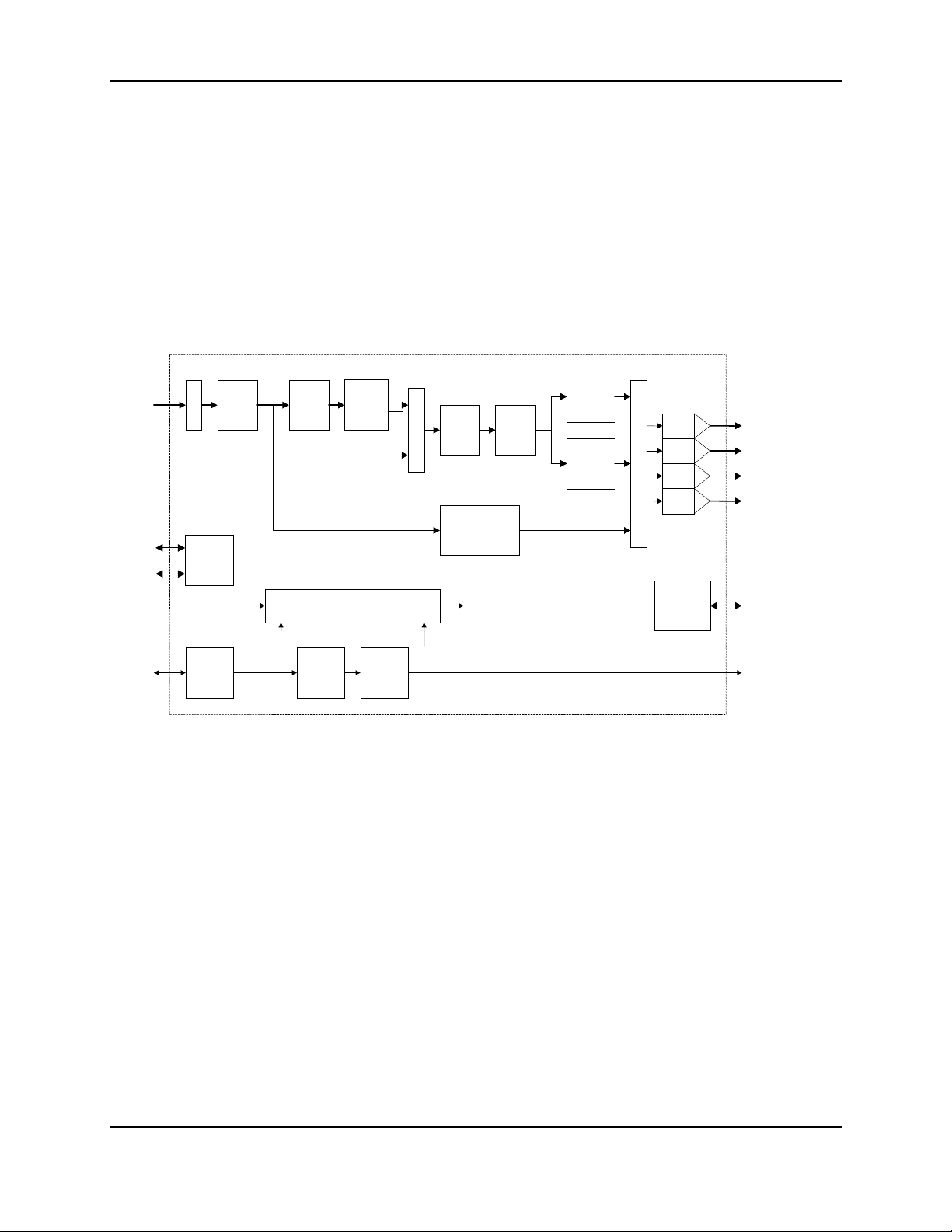
selected. (Refer to Figure 1: FS453 Functional Block Diagram on page 5.)
1.2.1 SDTV Output
For example, to create SDTV output the FS453 first changes RGB video to YCrCb. It uses patented
technology to scale (in other words, to proportionately increase or decrease) the number of video lines
and pixels per line to correspond to the specific SDTV standard. This allows the FS453 to precisely fill
the user's television screen without adding artifacts such as blank areas, or distorting the graphics image.
The FS453 uses more patented technology to adaptively remove the flicker effects common to SDTV
while keeping fine detail (such as text) clear and sharp. The FS453 then encodes the processed image
into broadcast quality, interlaced SDTV video and sends it out through the DACs. For European SCART
output, the FS453 converts the image into RGB video and sends the R, G and B signals through separate
DACs.
1.2.2 HDTV Output
To convert high-resolution computer graphics to high resolution HDTV output the FS453 converts the
digital video (whether RGB or YCrCb format) to YPrPb (analog component video). It adds Bi- and TriLevel Syncs as required by the selected standard and routes the analog HDTV video through the DACs.
1.2.3 VGA (RGB) Output
The FS453 can also provide VGA output. In this mode, it allows the GCC's RGB images to pass
unchanged directly through to the DACs. The HSync and VSync signals must be driven by the GCC.
1.3 General Physical Requirements
Implementing the FS453 in your system will require very few components – just a 27 MHz clock and
passive parts. The FS453 uses an 80-lead Quad Flat Pack (PQFP) or an 88-lead Fine-pitch Ball Grid
Array (FBGA) package and requires power from +1.8V digital and +3.3V analog supplies.
*
Note: I2C is a registered trademark of Philips Corporation. The FS453 Serial I/O bus is similar but not identical to the Philips I2C
bus.
JANUARY, 2005, VERSION 3.0 4 COPYRIGHT ©2003-4 FOCUS ENHANCEMENTS, INC.
FOCUS Enhancements Semiconductor
FS453/4 AND FS455/6 DATA SHEET: HARDWARE REFERENCE
x
r
A
r
r
2. Architectural Overview
The FS453 has the following major sections:
• Inputs P[23:0]
• Programmable Color Space Converter
• Patented 2D (Horizontal and Vertical)
Scaling
• Patented 2D Flicker Filter
• FIFO
• Post (Horizontal Up) Scaler
• Inverse Color Space
2D
Flicker
Filter
P[23:0]
SDATA
SCLK
ClkIn
Demu
Serial
Control
Interface
Color
Space
Conv.
2D
Scaler
Clock Management
Multiplexe
FIFO
Bi & Tri-Level
Post
Scaler
Sync
Insertion
to internal clocks
• Broadcast Quality Encoder
• HDTV Bi- & Tri-Level Sync Insertion
• Configurable 10 bit DACs
• Clock Management
• Oscillators and PLL
• Serial Control Interface
• Sync Timing Generator
Inverse
Color
Space
Encode
Multiplexe
Timing
Generator
10-bit
10-bit
10-bit
10-bit
Sync
DAC
DAC B
DAC C
DAC D
VSync
HSync
Blank
Field
XTAL
OSC
NCO
PLLCrystal
ClkOut
Figure 1: FS453 Functional Block Diagram
2.1 Inputs
The FS453 accepts computer graphics images in many different resolutions and pixel frequencies on
P[23:0]. The FS453 adaptively process this information for optimal display on SDTV and HDTV television
sets.
JANUARY, 2005, VERSION 3.0 5 COPYRIGHT ©2003-4 FOCUS ENHANCEMENTS, INC.
FOCUS Enhancements Semiconductor
FS453/4 AND FS455/6 DATA SHEET: HARDWARE REFERENCE
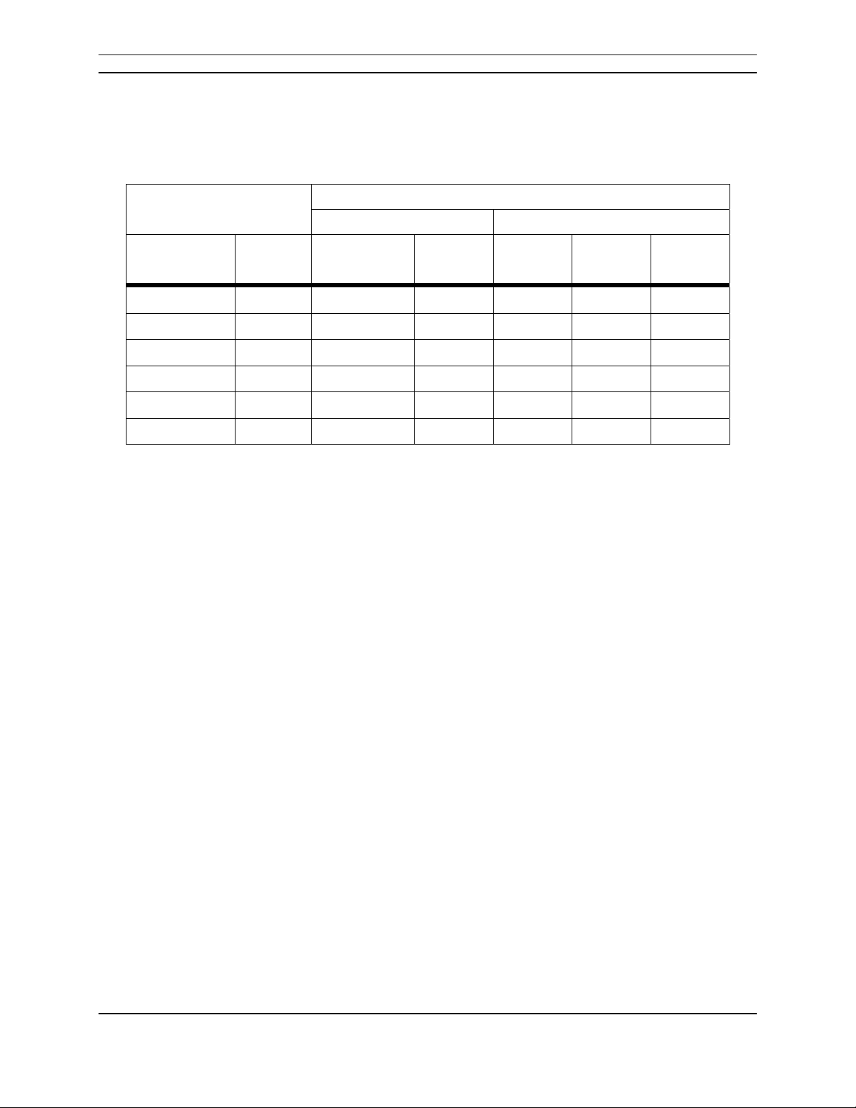
2.1.1 Input to Output Conversion Matrix
Table 1 below lists some commonly used input modes and the correspondingly supported output modes.
SDTV input dimensions are completely configurable, subject only to pixel clock range limitations.
Input Configuration
SDTV HDTV
Pixels Lines NTSC
640 - 720 480
640 - 720 576
800 600
1024 768
1280 720
@59.94Hz
∗ ∗ ∗
∗ ∗
∗ ∗
∗ ∗
(b)
∗
@50Hz
1920 1080
Table 1: Input to Output Conversion Matrix
Notes:
(a) No scaling supported
(b) Subject to the maximum 150 MHz pixel rate
(c) No scaling or interlacing supported, input data must be interlaced
Output Configuration
PAL
480p
@60Hz
(a)
(b)
∗
720p
@60Hz
1080i
@60Hz
(a)
∗
(c)
∗
2.2 Color Space Converter
The programmable Color Space Converter receives either RGB or YCrCb data from the input port. If the
data is RGB, it is converted to YCrCb using programmable coefficients. Each of the Y, Cr, and Cb
components can then be independently scaled in amplitude with programmable multipliers. This
programmability supports both SDTV and HDTV color space matrices.
2.3 Patented 2D Scaler
The Patented 2D Scaler receives data from the Color Space Converter. It performs vertical (up or down)
scaling based on the value programmed in the VSC (Vertical Scaling Coefficient) register, offset 06h. It
performs horizontal (down) scaling based on the downscale value programmed in the HSC (Horizontal
Scaling Coefficient) register, offset 08h.
Because different video standards call for different numbers of lines and different numbers of pixels per
line, scan converters add or subtract lines and areas to fit graphics images onto different sizes of TV
screens. Most scan converters use simple line-dropping algorithms and fixed aspect ratios.
Unfortunately, these techniques can introduce shape-distorting artifacts and surround the actual image
with blank areas.
The FS453, however, uses patented technology that can scale the graphics image without creating
artifacts. The patented 2D Scaler can independently upscale or downscale an image in both the
horizontal (pixels) and vertical (lines) directions. Its scaling functions provide equal weight to all pixels
and lines in the source material for all scaling factors. This allows users to perfectly fit the graphics image
to their TV screens without adding scaling artifacts or large blank borders.
JANUARY, 2005, VERSION 3.0 6 COPYRIGHT ©2003-4 FOCUS ENHANCEMENTS, INC.
FOCUS Enhancements Semiconductor

FS453/4 AND FS455/6 DATA SHEET: HARDWARE REFERENCE
2.4 Patented 2D Flicker Filter
The Patented 2D Flicker Filter receives video lines from the 2D Scaler and performs vertical filtering to
reduce or eliminate perceived flicker that is an artifact of the interlaced television format.
The FS453's flicker filter is significantly more effective than a typical three-line-average flicker filter. The
FS453’s flicker filter consists of joint horizontal (Sharpness) and vertical (Flicker) controls. Three-lineaverage flicker filters do reduce the visual effect of interlaced image flicker, but they also introduce
blurring. The flicker dimension of the FS453's filter reduces image flicker, while the sharpness dimension
of the FS453's filter reduces image blurring. Both the sharpness and flicker registers can be programmed
over a wide range of values to allow the user to customer tailor the filter settings to different display
devices.
2.5 FIFO
The Flicker Filter stores video data in a FIFO memory. This memory allows the video data to be
transferred from the graphics clock domain to the TV clock domain.
2.6 Post (Horizontal Up) Scaler
The Post Scaler draws information from the FIFO as necessary and scales it horizontally based on the
up-scale value programmed in the Horizontal Scaling Coefficient (HSC) register. The scaled data is
provided at the television clock rate to the SDTV video encoder and the Inverse Color Space.
2.7 Encoder and Inverse Color Space
The FS453 contains a broadcast quality, 2X oversampled video encoder with an Inverse Color Space
matrix. The encoder combines the chrominance, luminance, and timing information into broadcast quality
NTSC or PAL composite and YC (S-Video) signals and sends them to the DACs.
The Inverse Color Space transforms YCrCb video data to the RGB color space required for SCART
output. If the Inverse Color Space is not used, then the Encoder converts YCrCb to YPrPb as required
for SDTV YPrPb output. The RGB or YPrPb signals are sent to the DACs synchronized with the
Encoder's composite signal.
The FS454 and FS456, which are otherwise identical to the FS453 and FS455, respectively, incorporate
Macrovision 7 anti-copy protection in the encoder. The FS454 and FS456 also include 480p protection.
2.8 Bi and Tri-Level Sync Insertion (HDTV)
The FS453 also offers HDTV Syncs output modes. The color matrix, output level, and sync type are fully
programmable allowing for compatibility with the multiple HDTV standards. The FS453 inserts bi-level or
tri-level sync signals as defined by the standards.
2.9 Configurable 10 bit DACs
The four output DACs (Digital/Analog Converters) can be configured for several output formats: RGB
component output (VGA); RGB with CVBS (SCART); CVBS (2 optional) and Y/C (S-Video); and YPrPb
component output (HDTV or SDTV). To conserve power the DACs can be run in low power mode or can
be completely powered down when not in use.
2.10 Clock Management
The FS453 synthesizes a 0.78125-150 MHz clock from the 27 MHz XTAL_IN and supplies this clock
(CLKOUT) to the GCC. The clock is buffered and returned to the FS453 (CLKIN_P) synchronous to the
pixel data and sync information. This clock has a 1.5 Hz resolution and can be adjusted so that the GCC
scaled input data rate exactly matches the ITU-R BT.656 output data rate.
2.11 Oscillators and PLL
The FS453 clock generation circuit operates in one of two modes, NCO (Numerically Controlled
Oscillator) mode or PLL (Phase Locked Loop) mode. In NCO mode, the numerically controlled oscillator
JANUARY, 2005, VERSION 3.0 7 COPYRIGHT ©2003-4 FOCUS ENHANCEMENTS, INC.
FOCUS Enhancements Semiconductor

FS453/4 AND FS455/6 DATA SHEET: HARDWARE REFERENCE
is used to achieve the finest clock resolution, using a dithered clock. In PLL mode, the NCO is bypassed
and the clock is not dithered. The NCO can be used when HTOTAL and VTOTAL values have additional
constraints that prevent selection of values that are factors of the TV pixel rate.
2.12 Serial Control Interface
The FS453 registers are accessed through a serial input/output bus (SIO) which is I2C*-compatible and
SMBus-compatible. These registers can be read or written at any time the part is receiving a reference
clock at XTAL_IN and not being held in reset via the RESET_L pin.
2.13 Sync Timing Generator
The Sync Timing Generator provides/accepts HSync, VSync, Field and Blank signals to/from the graphics
controller.
2.14 Input Synchronization
The FS453 can operate in pseudo-master mode or slave mode. In pseudo-master mode, the GCC
derives the VGA pixel clock, horizontal sync, and vertical sync from CLKOUT supplied by the FS453. In
slave mode, the GCC generates the pixel clock, syncs and data, and the FS453 must be programmed to
generate the same pixel clock, using a common reference. Use the slave mode when the GCC does not
have a pixel clock input.
*
Note: I2C is a registered trademark of Philips Corporation. The FS453 Serial I/O bus is similar but not identical to the Philips I2C
bus.
JANUARY, 2005, VERSION 3.0 8 COPYRIGHT ©2003-4 FOCUS ENHANCEMENTS, INC.
FOCUS Enhancements Semiconductor
FS453/4 AND FS455/6 DATA SHEET: HARDWARE REFERENCE
3. Technical Highlights
Creating clear, broadcast quality television video from high resolution computer graphics is a complex
process. PC-to-TV Video Scan Converters have to surmount many technical obstacles. The most
challenging of these are scaling, flicker reduction, and encoding.
3.1 Scaling
Converting high-resolution computer images into relatively low-resolution TV images (such as converting
VGA or XGA images into NTSC standard definition television) is an inherently lossy process that requires
a video scaler. For example, converting an image with 1000 pixels in a line into an image with only 500
pixels in a line, means that there must be 50% less data in each line of output. The video scaler has to
perform its tasks effectively without further degrading the image.
3.1.1 Video Scaler Challenges
Therefore, in addition to reducing pixel count and interpolating pixel values, the scaler must not alter the
digital video data by adding artifacts. Examples of artifacts are the introduction of repeated pixels; the
complete loss of pixel data; and the creation of new pixel colors that are not interpolations of original pixel
colors.
In effect, the video scaler should behave like a high quality filter. It should have a gradual frequency roll
off with a good step response and little overshoot or ringing (less than 5%). This is ideal for maintaining
video quality with detailed images (such as text). Detailed images produce rapid output step transitions
that need to be executed cleanly.
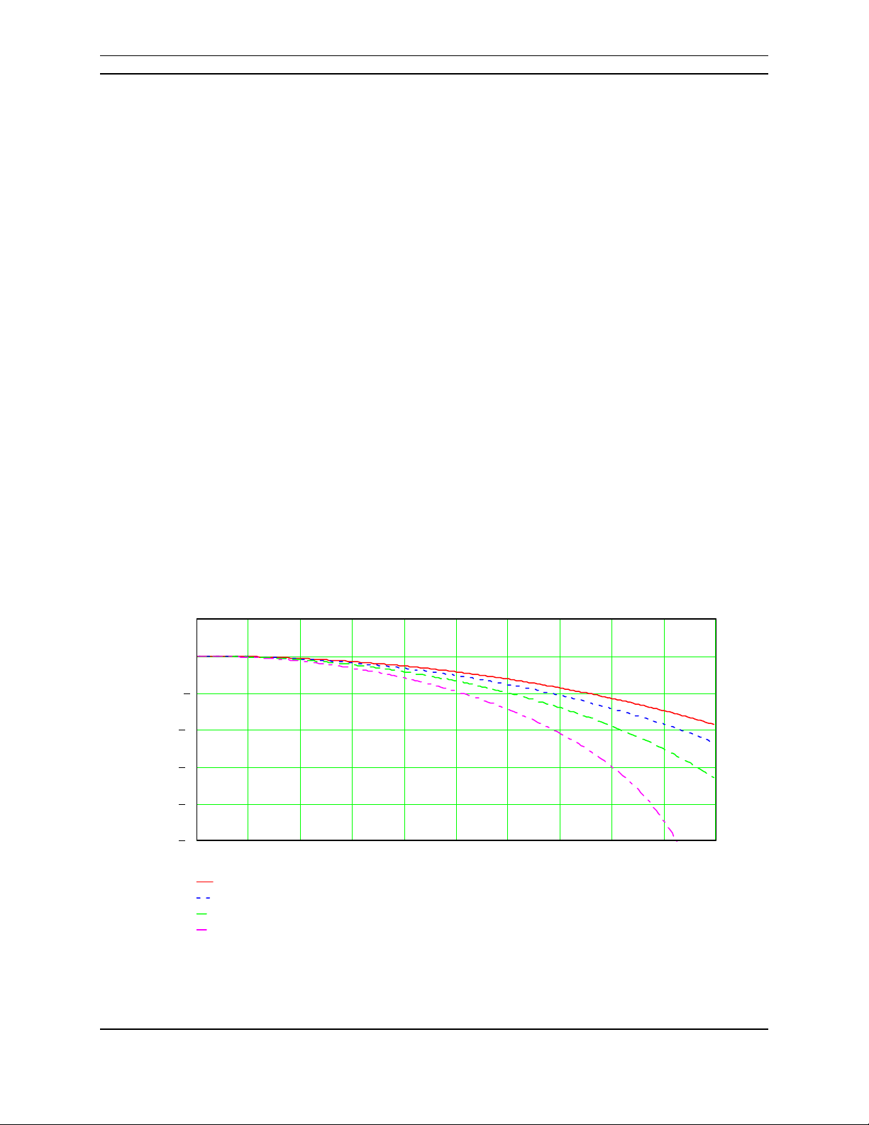
3.1.2 FS453 Solution
The following diagram (Figure 2) illustrates the response of the FS453's video scaler. It is a normalized
plot of the Luma frequency response of the FS453's video scaler. As we can see, the FS453's patented
video scaler behaves like a high quality filter with only a gradual frequency roll off.
5
0
5
10
Gain in Decibels
15
20
25
0 0.1 0.2 0.3 0.4 0.5 0.6 0.7 0.8 0.9 1
Normalized Frequency
Scale 7/8
Scale 3/4
Scale 5/8
Scale 1/2
Figure 2: FS453 Scaler Luma Frequency Response
JANUARY, 2005, VERSION 3.0 9 COPYRIGHT ©2003-4 FOCUS ENHANCEMENTS, INC.
FOCUS Enhancements Semiconductor
FS453/4 AND FS455/6 DATA SHEET: HARDWARE REFERENCE
3.2 Flicker Reduction
Computer images are displayed progressively. That is, for a given frame of video, each line of video is
scanned onto the monitor sequentially. SDTV images, however, are interlaced. Each SDTV frame of
video is broken into two fields (one composed of odd lines and the other of even lines). First the odd
lines are scanned onto the TV, and then the even lines are scanned onto the TV.
The energy decay rate of the phosphors on a TV screen is fast enough that the older field of video will
appear somewhat dimmer than the newer field of video. As the fields are constantly changing, this can
result in a visible flicker between the two fields of data on the TV screen. This flicker is especially visible
when one field contains a long dark line, while an adjacent line (in the other field) contains a long white
line. The higher energy line will decay in brightness much faster than the low energy line, and in turn will
appear to flicker heavily.
Most scan converters simply average the pixel data between lines. This removes the Black-or-White
relationships between lines that viewers recognize as video flicker. The problem with this solution is that
data becomes blurred. Single black or white lines are reduced to grays. Detailed areas of video (such as
the gap in the letter ‘e’) lose their distinction.
3.2.1 Flicker Filter Challenges
The goal is to completely remove flicker from the image without blurring detailed video. To preserve the
video details, the flicker filter should have a flat frequency response (+/- 1dB) between pixels in the
horizontal, and diagonal directions. It must also avoid introducing new artifacts into the digital video
stream. Artifacts include repeating pixels, losing pixels; and creating colors that are not interpolations of
original pixel colors.
3.2.2 FS453 Solution
The FS453 uses a patented flicker filter that calculates output pixel values as a function of both vertical
(line averaging) and horizontal (pixel averaging) pixel relationships. In effect the FS453 can decide
where and how to reduce flicker within the image.
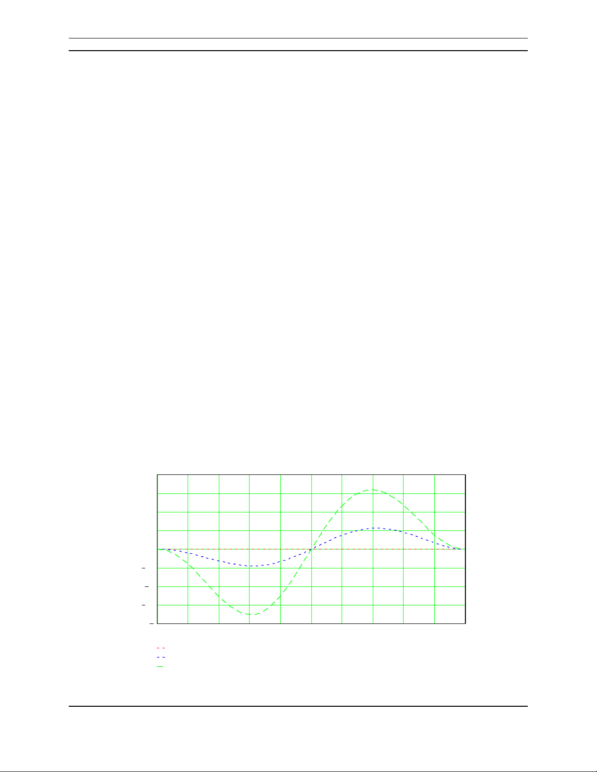
Figure 3 (below) shows a normalized plot of the frequency response of pixels along diagonal after being
processed by the FS453's flicker filter. The response is flat for the majority of the frequency space. This
maintains pixel sharpness while providing excellent flicker suppression.
1
0.75
0.5
0.25
0
Gain in Decibels
0.25
0.5
0.75
1
0 0.1 0.2 0.3 0.4 0.5 0.6 0.7 0.8 0.9 1
Normalized Frequency
Horizontal Direction
Diagonal at 27 degrees
Diagonal at 45 degrees
Figure 3: FS453 Flicker Filter Diagonal Response
JANUARY, 2005, VERSION 3.0 10 COPYRIGHT ©2003-4 FOCUS ENHANCEMENTS, INC.
FOCUS Enhancements Semiconductor

FS453/4 AND FS455/6 DATA SHEET: HARDWARE REFERENCE
3.3 Video Encoding
Unlike component video formats (PC and HDTV) that process the color information separately to avoid
interference, broadcast SDTV combines all picture information into a single, composite signal. SDTV
standards have been strictly defined to protect video quality and to allow television manufacturers to
design and build large volumes of systems with confidence that their signal decoders will work—
regardless of variances in final product tolerances.
3.3.1 Encoding Challenges
If a video encoder does not adhere closely to these standards, it may produce video artifacts on many
consumer televisions. Unfortunately, most scan converters use signal encoders that don't strictly follow
NTSC and PAL guidelines. Their encoders can increase artifacts such as chroma crawl and color
bleeding/smearing.
To meet broadcast quality a video encoder must comply with the NTSC (EIA-170A, SMPTE-170M) and
PAL (ITU-R624-3) standards in all modes. Of key importance are the specifications related to accurate
timing and signal amplitudes, video subcarrier frequency good to +/- 5Hz, and horizontal lock with zero
SC-H phase. The encoder must use a low jitter crystal (50 ppm) to drive DAC output directly. The DACs
should have 10 bits of resolution, and exhibit good differential gain and differential phase characteristics.
The video encoder must be able to pre-filter composite video (CVBS) to prevent luma(Y)/chroma(C) cross
talk.
3.3.2 FS453 Solution
The FS453 features a broadcast quality encoder. It uses tunable Y-notch and C-bandpass filters to
prevent the creation of video artifacts and to meet all specifications. The FS453's encoder subcarrier is
programmable in frequency and phase. Because of the encoder's independence of color format, vertical
sync, and number of lines, the FS453 is able to support many SDTV video standards, including all of the
South American variations. The FS453 can output NTSC M, J and PAL B, D, G, H, I, M, N, Combination
N, and PAL-60 formats with 10 bits of resolution. Both Composite and S-Video outputs are available
simultaneously. In addition to encoded PAL or NTSC, the user may select analog SCART RGB outputs.
Each channel of RGB has 10 bits of resolution. Note that the 10-bit DACs exceed the bit depth supported
by the 8-bits available at the FS453 input.
JANUARY, 2005, VERSION 3.0 11 COPYRIGHT ©2003-4 FOCUS ENHANCEMENTS, INC.
FOCUS Enhancements Semiconductor
FS453/4 AND FS455/6 DATA SHEET: HARDWARE REFERENCE
4. Scaling and Positioning Notes
The FS453 graphics converter does not use a frame memory. Therefore, the FS453 input video frame
rate must be synchronous to and match the output video field or frame rate. In SDTV modes, the FS453
uses internal line memories in order to perform horizontal and vertical scaling. This imposes certain
requirements on the scale and position settings.
4.1 Vertical Scaling
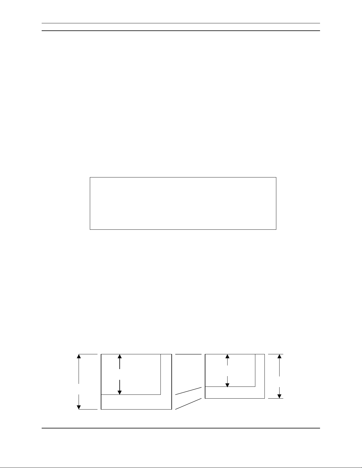
Because the frame/field rates are synchronous, and no frame memory is available, the ratios of input to
output VTOTAL and input to output VACTIVE must match. (See Figure 4 below.) In this sense, the
output VACTIVE is not necessarily the total active lines of the selected TV standard, but is the number of
TV lines that will contain active video information from the input source material. If the output VACTIVE
value is smaller than the value specified by the TV standard, then the FS453 will place borders and below
the image. TV_VTOTAL and GCC_VACTIVE in the VTOTAL equation are determined by the selected
TV standard and graphics mode. TV_VACTIVE is selected to set the desired number of TV lines
containing video information. The Vertical Scaling Coefficient is programmed in register 06h. The ratio of
input to output VTOTAL also determines the vertical scaling factor used. Note that calculations are done
using the output frame size, even though the output is interlaced, because interlacing is done after
vertical scaling.
GCC_VACTIVE / GCC_VTOTAL = TV_VACTIVE/TV_VTOTAL
For downscaling, VSC = (TV_VTOTAL / GCC_VTOTAL) * 65,536
For upscaling, VSC = (TV_VTOTAL / GCC_VTOTAL – 1) * 65,536
Figure 4: Equations for VTOTAL and VSC
Notes:
GCC_VACTIVE: The number of active lines of computer graphics in a frame.
GCC_VTOTAL: The total number of lines in a computer graphics frame, including active and blanking.
TV_VACTIVE: The number of lines in a TV video frame that will contain scaled graphics data.
TV_VTOTAL: The total number of lines in a TV video frame. PAL has 625 lines. NTSC has 525 lines.
For example, consider a case where the input graphics active area contains 600 lines and the selected
TV standard is NTSC. In NTSC, TV_VTOTAL is 525 lines per frame and the full-size active area is 487
lines per frame. To program the FS453 to scale the GRAPHICS image to fit on 400 lines of TV video (for
example, to fit the image within the TV bezel), set TV_VACTIVE to 400. This sets three of the four
parameters in the equation, and solving for VGA_VTOTAL results in a value of 787.5. Because values
must be integers, set VGA_VTOTAL to 788. The scaled image will still occupy approximately 400 lines.
Given these VTOTAL values, the vertical scaling factor is 0.6662, and the VSC register will be set to
43,663 (0xAA8F).
VGA_VACTIVE
VGA_VTOTAL
TV_VACTIVE
TV_VTOTAL
Figure 5: VTOTAL and VACTIVE ratios must match
JANUARY, 2005, VERSION 3.0 12 COPYRIGHT ©2003-4 FOCUS ENHANCEMENTS, INC.
FOCUS Enhancements Semiconductor

FS453/4 AND FS455/6 DATA SHEET: HARDWARE REFERENCE
4.2 Horizontal Scaling
While vertical scaling is linked to the VTOTAL ratio, horizontal scaling is arbitrary and not linked to
HTOTAL at all. The horizontal scaler is simply programmed with the ratio desired between TV_HACTIVE
and GCC_HACTIVE. (See Figure 6 below.) Like vertical scaling, TV_HACTIVE is the desired number of
pixels the image should occupy, not necessarily the number of active pixels for the selected TV standard.
A significant benefit of this architecture is that HTOTAL can be any arbitrary number that satisfies
graphics controller timing requirements and PLL programming requirements.
For downscaling, HDSC = (TV_HACTIVE / GCC_HACTIVE) * 256 and HUSC = 0
For upscaling, HUSC = ((TV_HACTIVE / GCC_HACTIVE - 1) * 256) and HDSC = 0
Figure 6: HSC Equations
Notes:
GCC_HACTIVE: The number of active pixels in a line of computer graphics.
GCC_HTOTAL: The total number of pixels in a computer graphics line, including active and blanking.
TV_HACTIVE: The number of pixels in a line of TV video that will contain scaled graphics data.
TV_HTOTAL: The total number of pixels in a TV line. PAL uses 864 pixels. NTSC uses 858 pixels.
HUSC and HDSC are programmed in register 08h (HSC).
For example, consider a case where the input graphics width is 800 pixels and the desired number of
pixels to show is 650. The image must be scaled down horizontally, so HDSC is 208 (D0h) and HSC =
00D0h. For a case where input VGA width is 640 and the desired TV pixel count is 720, the image must
be scaled up. HUSC is 32 (20h) and HSC = 2000h.
4.3 Vertical and Horizontal Position
The position of the graphics image on the television screen is controlled in two ways. The FS453
determines where input video data appears in time using the vertical and horizontal sync signals from the
GCC. This means that adjusting the sync timing in the GCC will change the position of the active video
area on the television. The FS453 also contains registers that control the offset from the sync transition.
These registers allow the active video position on the television to be adjusted independent of the GCC
sync timing.
The IHO (00h) register specifies the number of graphics pixels to skip before starting active video on the
television. To position the actual video area at the left edge of the theoretical active area in TV space,
program the IHO to the distance from the rising edge of HSYNC to the end of the line (HTOTAL). A
larger number will shift video to the left, and a smaller number will shift video to the right.
The IVO (02h) register specifies the number of graphics lines to skip before starting active video on the
television, counting from the rising edge of VSYNC. Programming the register is similar to programming
IHO, but in the vertical direction.
JANUARY, 2005, VERSION 3.0 13 COPYRIGHT ©2003-4 FOCUS ENHANCEMENTS, INC.
FOCUS Enhancements Semiconductor
 Loading...