

Page 1

Fn-Link
3131A-S
User's Manual
WIFI Module
Page 2
3131A-S
FN-LINK TECHNOLOGY LIMITED 1 Proprietary & Confidential Information
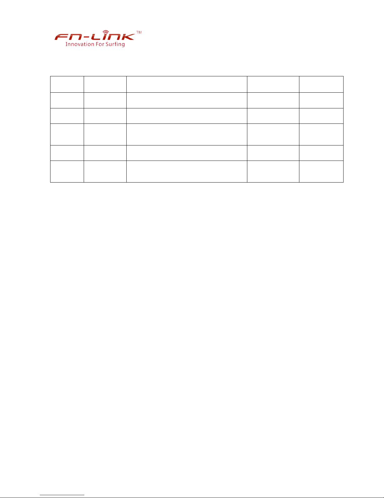
Revision History
Version Date Description Draft Approved
1.0 2017-06-01 First release Colin Ming William Tan
1.1 2017-06-22 Modified input voltage range Colin Ming William Tan
1.1 2017-06-22
Added 32.768K clock input
requesting
Colin Ming William Tan
1.2 2017-07-14 Modified Pin13、39、40 function Colin Ming William Tan
1.3 2017-08-04
Modified SDIO specification
description
Colin Ming William Tan
Page 3

3131A-S
FN-LINK TECHNOLOGY LIMITED 1 Proprietary & Confidential Information
CONTENTS
1. Introduction ..................................................................................................................... 1
2. Features ........................................................................................................................... 2
3. General Specification ..................................................................................................... 2
3.1 General Specification ................................................................................................. 2
4. WiFi RF Specification ..................................................................................................... 3
4.1 2.4GHz RF Specification............................................................................................ 3
5. Power Consumption ....................................................................................................... 5
6. Pin Assignments ............................................................................................................. 6
6.1 Pin Outline ................................................................................................................. 6
6.2 Pin Definition ............................................................................................................. 6
7. Dimensions ...................................................................................................................... 8
7.1 Physical Dimensions ................................................................................................. 8
7.2 Module Physical Dimensions ..................................................................................... 9
7.3 Layout Recommendation ......................................................................................... 10
8. Host Interface Timing Diagram .................................................................................... 11
8.1 SDIO Pin Description ............................................................................................... 11
8.2 SDIO Default Mode Timing Diagram ....................................................................... 11
8.3 SDIO High Speed Mode Timing Diagram ................................................................ 12
8.4 SDIO Bus Timing Specifications in SDR Modes ...................................................... 13
9.Reference Design ........................................................................................................... 14
10.Recommended Reflow Profile .................................................................................... 15
11. Packing Information .................................................................................................... 16
Page 4

3131A-S
FN-LINK TECHNOLOGY LIMITED 1 Proprietary & Confidential Information
1. Introduction
3131A-S is a small size and low profile of WiFi module, board size is 12mm*12mm
with module thickness of 1.7mm. It can be easily manufactured on SMT process and
highly suitable for tablet PC, ultra book, mobile device and consumer products. It
providesSDIO interface for WiFi. The WiFi throughput can go up to 150Mbps in theory
by using 1x1 802.11b/g/n SISO technology.
3131A-S uses highly integrated WiFi single chip based on advanced COMS process.
3131A-S integrates whole WiFi function blocks into a chip, such as SDIO/MPU, MAC,
BB, AFE, RFE, PA, EEPROM and LDO/SWR, except fewer passive components
remained on PCB.
Page 5
3131A-S
FN-LINK TECHNOLOGY LIMITED 2 Proprietary & Confidential Information
2. Features
Operate at ISM frequency bands (2.4GHz)
SDIO interface for WiFi
Low power dissipation
High transmitting power
High receiving sensitivity
IEEE standards support: IEEE 802.11b, IEEE 802.11g, IEEE 802.11n.
Enterprise level security which can apply WPA/WPA2 certification for WiFi.
WiFi 1 transmitter and 1 receiver allow data rates supporting up to 150 Mbps
downstream and 150 Mbps upstream PHY rates
3. General Specification
3.1 General Specification
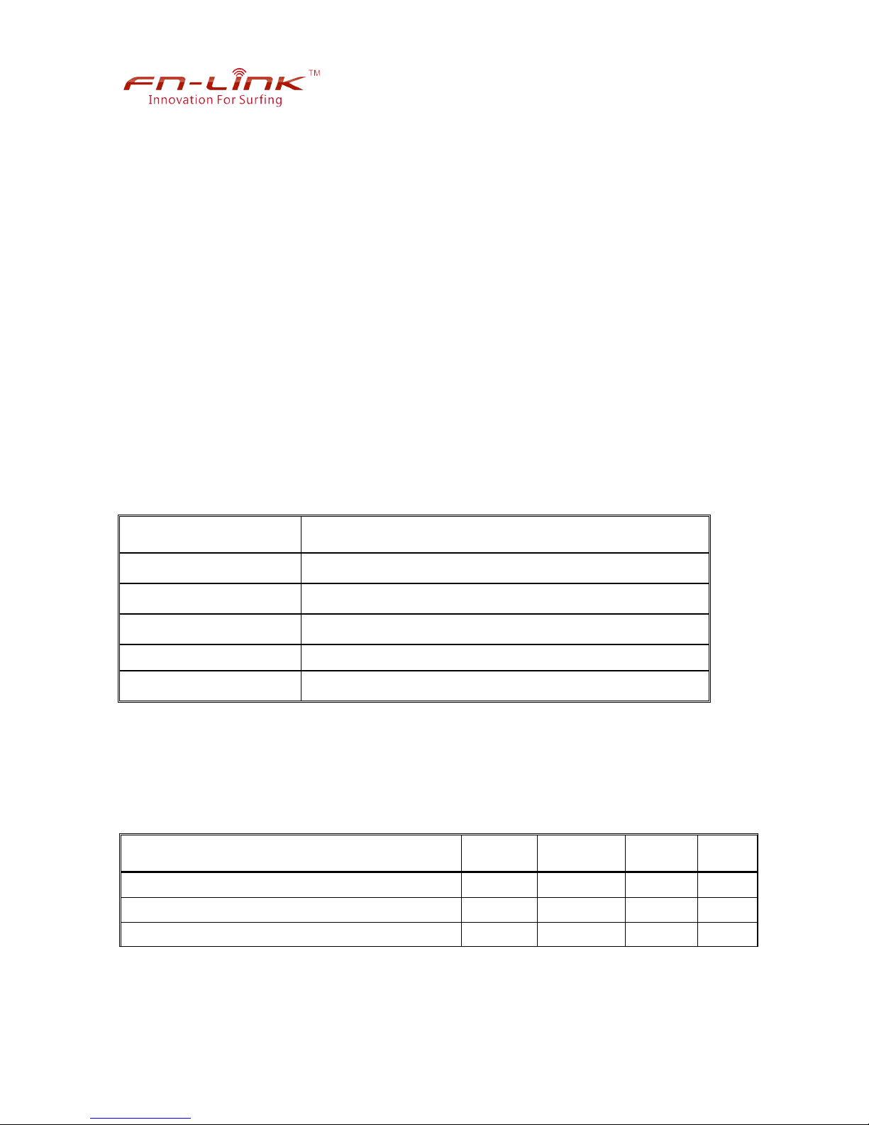
3.1.2 Recommended Operating Rating
Min. Typ. Max. Unit
Operating Temperature -30 25 70
deg.C
VCC33 3.3 3.6 4.8 V
VDDIO - 1.8V - V
Note: Suggested power input range in 3.6V-4.5V.
Model Name 3131A-S
Product Description Support WiFi functionality
Dimension
L x W x H: 12 x 12 x1.8 (typical) mm
WiFi Interface
Support SDIO
Operating temperature -30°C to 70°C
Storage temperature -40°C to 125°C
Page 6
3131A-S
FN-LINK TECHNOLOGY LIMITED 3 Proprietary & Confidential Information
4. WiFi RF Specification
4.1 2.4GHz RF Specification
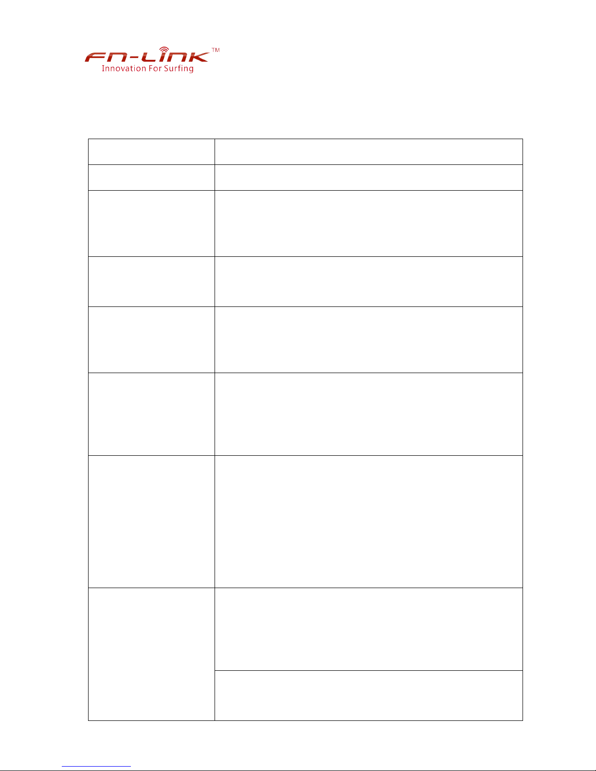
Feature Description
Operating Frequency 2.412~2.462GHz
Standards
WiFi:
IEEE 802.11b, IEEE 802.11g, IEEE 802.11n,
IEEE 802.11d, IEEE 802.11e, IEEE 802.11h,
IEEE 802.11i
Modulation
WiFi:
802.11b: DSSS(1M,2Mbps), CCK(11, 5.5Mbps),
802.11 g/n: OFDM
PHY Data rates
WiFi:
802.11b: 11,5.5,2,1 Mbps
802.11g: 54,48,36,24,18,12,9,6 Mbps
802.11n: up to 150Mbps
Transmit Output Power
WiFi:
802.11b 18.5
dBm
802.11g 16.5 dBm
802.11n
15.5 dBm (MCS 7_HT20)
14.5 dBm (MCS 7_HT40)
EVM
802.11b /1Mbps : EVM≦-10dB
802.11b /11Mbps : EVM≦-10dB
802.11g /6Mbps : EVM≦-5dB
802.11g /54Mbps : EVM≦-25dB
802.11n /6.5Mbps : EVM≦-5dB
802.11n /65Mbps : EVM≦-28dB
802.11n /13.5Mbps : EVM≦-5dB
802.11n /135Mbps : EVM≦-28dB
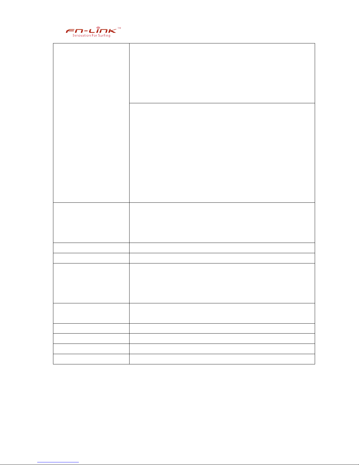
Receiver Sensitivity
(WiFi)
802.11b@10% PER
1Mbps ≦-98dBm
2Mbps≦ -94dBm
5.5Mbps≦ -93dBm
11Mbps ≦-90dBm Max input level≥-8
802.11g@10% PER
6Mbps ≦-94dBm
9Mbps ≦ -92dBm
≦
≦
≦
≦
Page 7
3131A-S
FN-LINK TECHNOLOGY LIMITED 4 Proprietary & Confidential Information
12Mbps≦ -91dBm
18Mbps≦ -89dBm
24Mbps≦ -86dBm
36Mbps≦ -82dBm
48Mbps ≦-78dBm
54Mbps ≦-77dBm Max input level≥-20
802.11n@10% PER
HT20_MCS 0 ≦-93dBm HT40_MCS 0≦-90
HT20_MCS 1≦ -90dBm HT40_MCS 1≦-87
HT20_MCS 2 ≦-88dBm HT40_MCS 2≦-85
HT20_MCS 3 ≦-85dBm HT40_MCS 3≦-82
HT20_MCS 4 ≦-82dBm HT40_MCS 4≦-79
HT20_MCS 5 ≦-78dBm HT40_MCS 5≦-75
HT20_MCS 6 ≦-76dBm HT40_MCS 6≦-73
HT20_MCS 7 ≦-75dBm HT40_MCS 7≦-71
Max input level≥-20
Operating Channel
WiFi 2.4GHz:
11: (Ch. 1-11) – United States
13: (Ch. 1-13) – Europe
Media Access Control WiFi: CSMA/CA with ACK
Antenna
Network Architecture
Ad-hoc mode (Peer-to-Peer )
Infrastructure mode
Software AP
WiFi Direct
Security
WPA, WPA-PSK, WPA2, WPA2-PSK, WEP 64bit & 128bit,
IEEE 802.11x, IEEE 802.11i
OS Supported Android /Linux
Host Interface SDIO2.0
Operating Voltage 3.3-4.8V Vdc, 1.8V I/O supply voltage
Dimension Typical 12*12*1.8 mm
See page 18
Page 8
3131A-S
FN-LINK TECHNOLOGY LIMITED 5 Proprietary & Confidential Information
5. Power Consumption
Power Consumption
(Typical by using SWR)
TX Mode: (Throughput mode) 230mA (MCS7/BW40/16dBm)
RX Mode: (Throughput mode) 66mA (MCS7/BW40/-60dBm)
Associated Idle power saving with DTIM=3 0.38mA
Deep Sleep: 0.04mA
Page 9
3131A-S
FN-LINK TECHNOLOGY LIMITED 6 Proprietary & Confidential Information
6. Pin Assignments
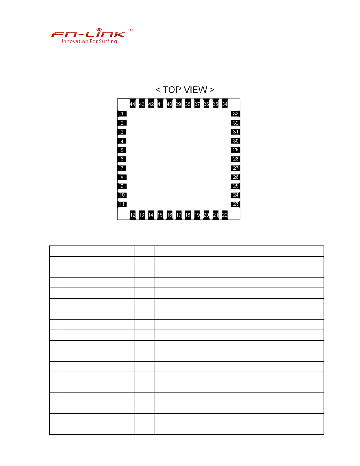
6.1 Pin Outline
6.2 Pin Definition
NO Name Type Description
1
GND - Ground connections
2
WL_ANT I/O RF I/O port
3
GND - Ground connections
4
NC - Floating (Don’t connected to ground)
5
NC - Floating (Don’t connected to ground)
6
Host wake device I Host Wake up WiFi, rising edge trigger
7
GPIO3 I/O Floating (Don’t connected to ground)
8
NC - Floating (Don’t connected to ground)
9
VCC P Main power voltage source input 3.3V-4.8V
10
NC - Floating (Don’t connected to ground)
11
NC - Floating (Don’t connected to ground)
12
PMU_POWRON I
Enable pin for WLAN device
ON: pull high ; OFF: pull low
13
GPIO1 I/O SDIO data interrupt
14
SDIO_DATA_2 I/O SDIO data line 2
15
SDIO_DATA_3 I/O SDIO data line 3
16
SDIO_DATA_CMD I/O SDIO command line
Page 10
3131A-S
FN-LINK TECHNOLOGY LIMITED 7 Proprietary & Confidential Information
17
SDIO_DATA_CLK I SDIO clock line
18
SDIO_DATA_0 I/O SDIO data line 0
19
SDIO_DATA_1 I/O SDIO data line 1
20
GND - Ground connections
21
NC - Floating (Don’t connected to ground)
22
VDDIO P I/O Voltage supply input 1.8V
23
NC - Floating (Don’t connected to ground)
24
RTC_CLK I Exteral 32.768Khz clock input for Power saving
25
NC - Floating (Don’t connected to ground)
26
NC - Floating (Don’t connected to ground)
27
NC - Floating (Don’t connected to ground)
28
NC - Floating (Don’t connected to ground)
29
NC - Floating (Don’t connected to ground)
30
NC - Floating (Don’t connected to ground)
31
GND - Ground connections
32
NC - Floating (Don’t connected to ground)
33
GND - Ground connections
34
GPIO2 I/O Floating (Don’t connected to ground)
35
NC - Floating (Don’t connected to ground)
36
GND - Ground connections
37
NC - Floating (Don’t connected to ground)
38
NC - Floating (Don’t connected to ground)
39
WL_RST
I
WiFi reset pin, internal pull high. Low: reset enable, High:
reset disable
40
Dev_Wake_Host
O
WiFi wake up host, rising edge trigger for host, high level
trigger for MCU.
41
NC - Floating (Don’t connected to ground)
42
NC - Floating (Don’t connected to ground)
43
NC - Floating (Don’t connected to ground)
44
NC - Floating (Don’t connected to ground)
Page 11
3131A-S
FN-LINK TECHNOLOGY LIMITED 8 Proprietary & Confidential Information
7. Dimensions
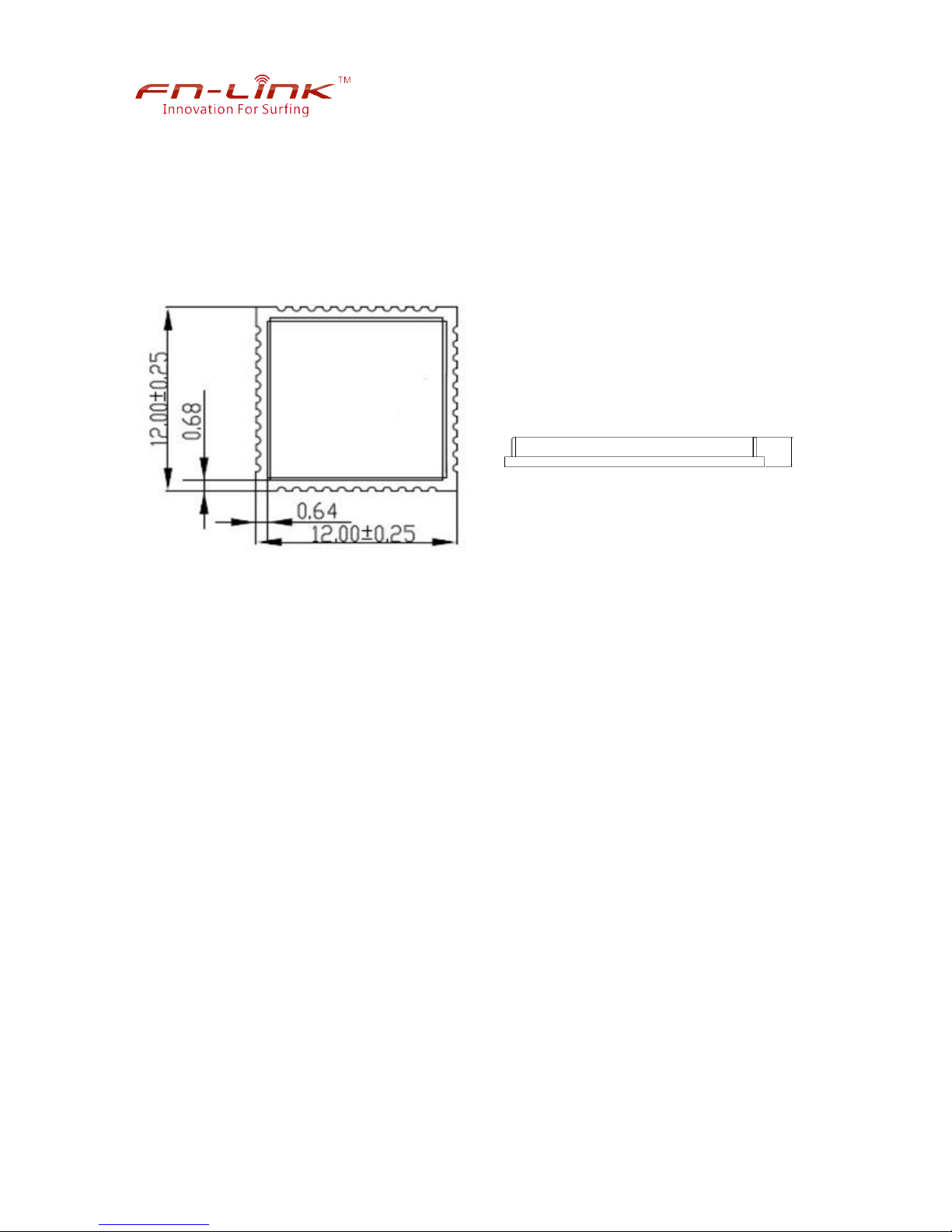
7.1 Physical Dimensions
(Unit: mm)
< TOP VIEW > < Side View >
1.7±0.1
Page 12
3131A-S
FN-LINK TECHNOLOGY LIMITED 9 Proprietary & Confidential Information
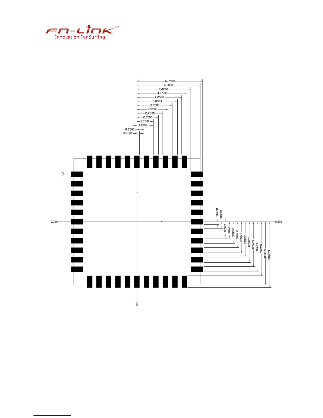
7.2 Module Physical Dimensions
(Unit: mm)
< TOP VIEW >
Page 13
3131A-S
FN-LINK TECHNOLOGY LIMITED 10 Proprietary & Confidential
Information
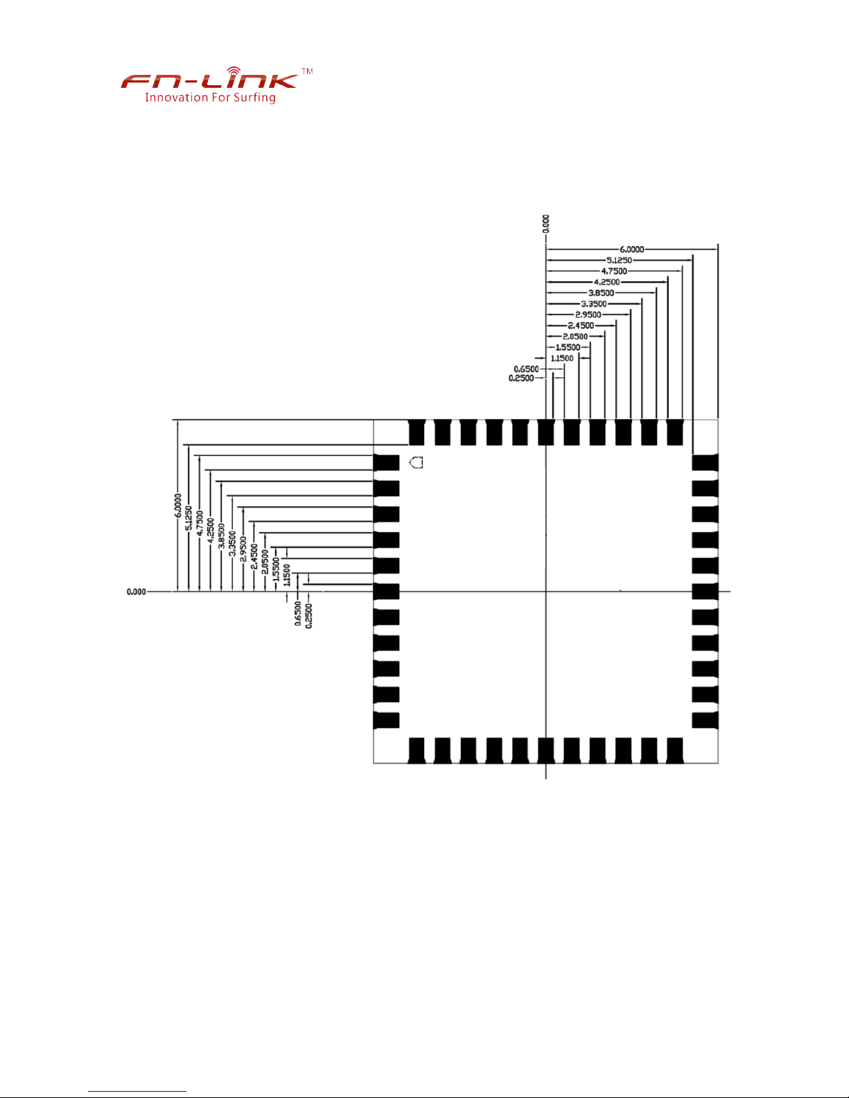
7.3 Layout Recommendation
(Unit: mm)
< TOP VIEW >
Page 14
3131A-S
FN-LINK TECHNOLOGY LIMITED 11 Proprietary & Confidential
Information
8. Host Interface Timing Diagram
8.1 SDIO Pin Description
The module supports SDR12(25MHz) and SDR25(50MHz, dual rates) in addition to the
1.8V default speed(25MHz) and high speed (50 MHz). It has the ability to stop the SDIO
clock and map the interrupt signal into a GPIO pin. This ‘out-of-band’ interrupt signal notifies
the host when the WLAN device wants to turn on the SDIO interface. The ability to force the
control of the gated clocks from within the WLAN chip is also provided.
SDIO Pin Description
SD 4-Bit Mode
DATA0 Data Line 0
DATA1 Data Line 1 or Interrupt
DATA2 Data Line 2 or Read Wait
DATA3 Data Line 3
CLK Clock
CMD Command Line
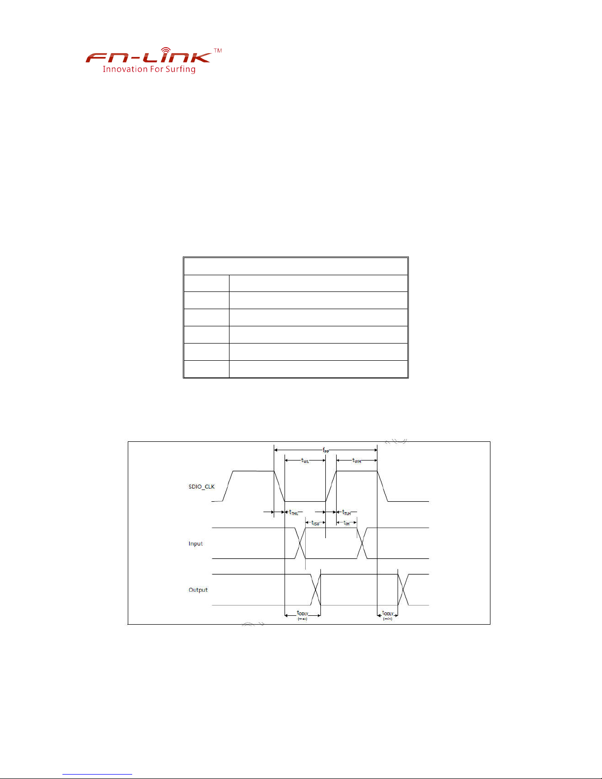
8.2 SDIO Default Mode Timing Diagram
Page 15
3131A-S
FN-LINK TECHNOLOGY LIMITED 12 Proprietary & Confidential Information
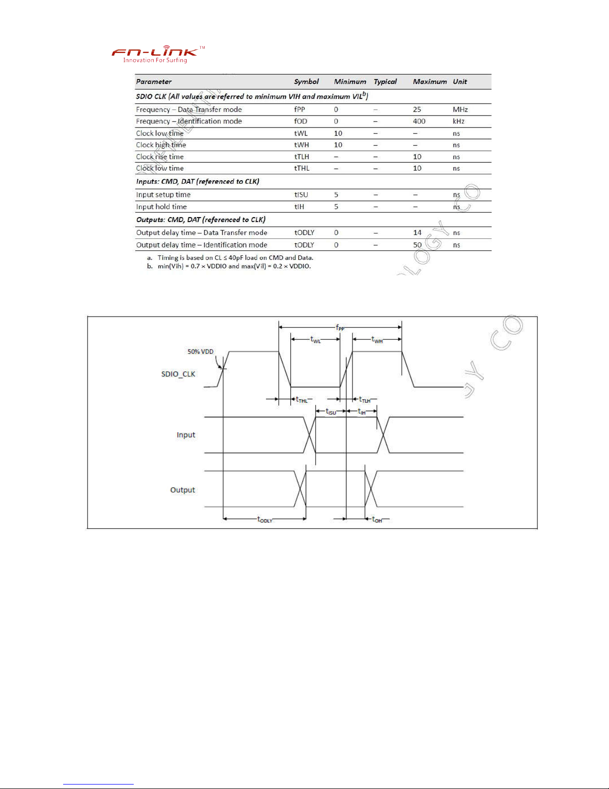
8.3 SDIO High Speed Mode Timing Diagram
Page 16
3131A-S
FN-LINK TECHNOLOGY LIMITED 13 Proprietary & Confidential Information
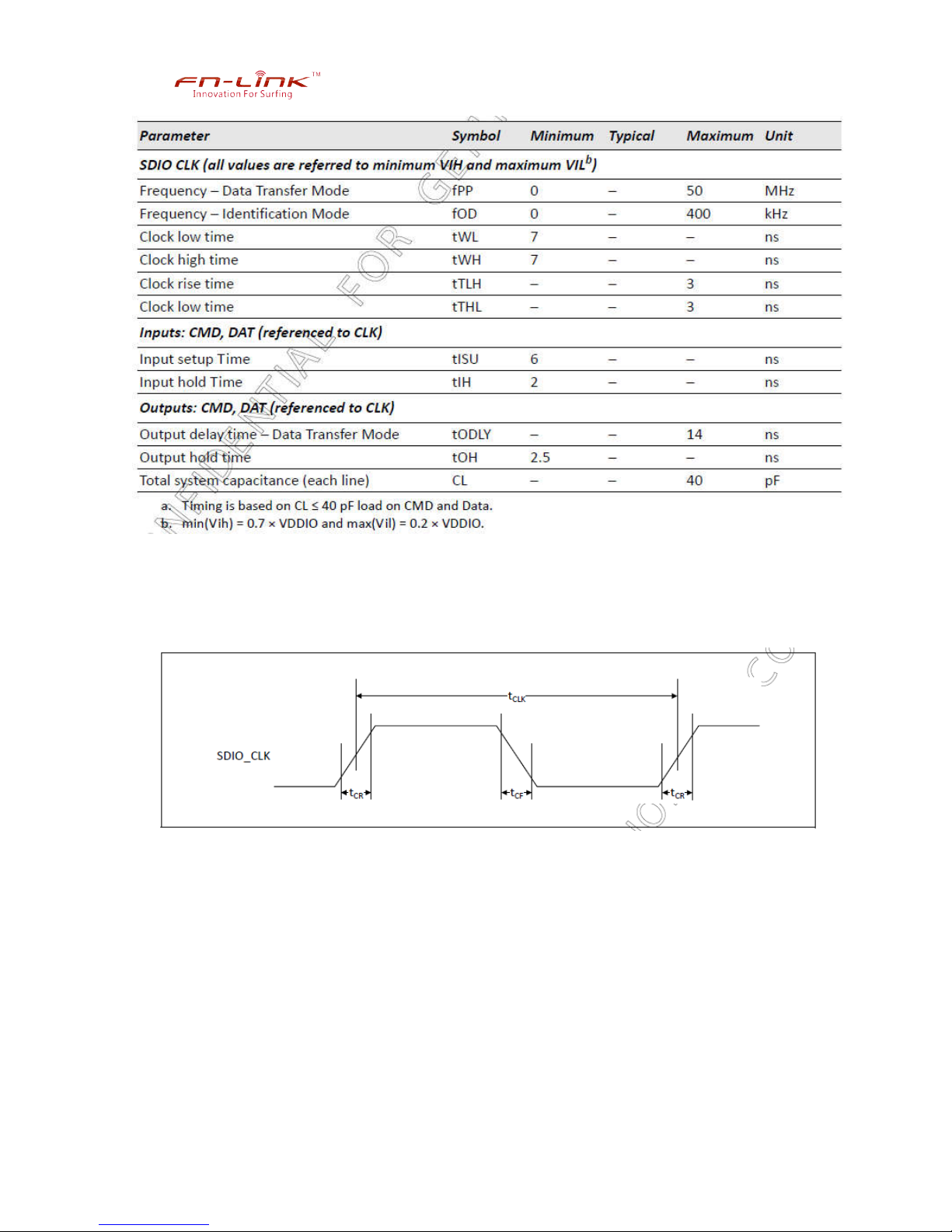
8.4 SDIO Bus Timing Specifications in SDR Modes
Clock timing(SDR Modes)
Page 17
3131A-S
FN-LINK TECHNOLOGY LIMITED 14 Proprietary & Confidential
Information
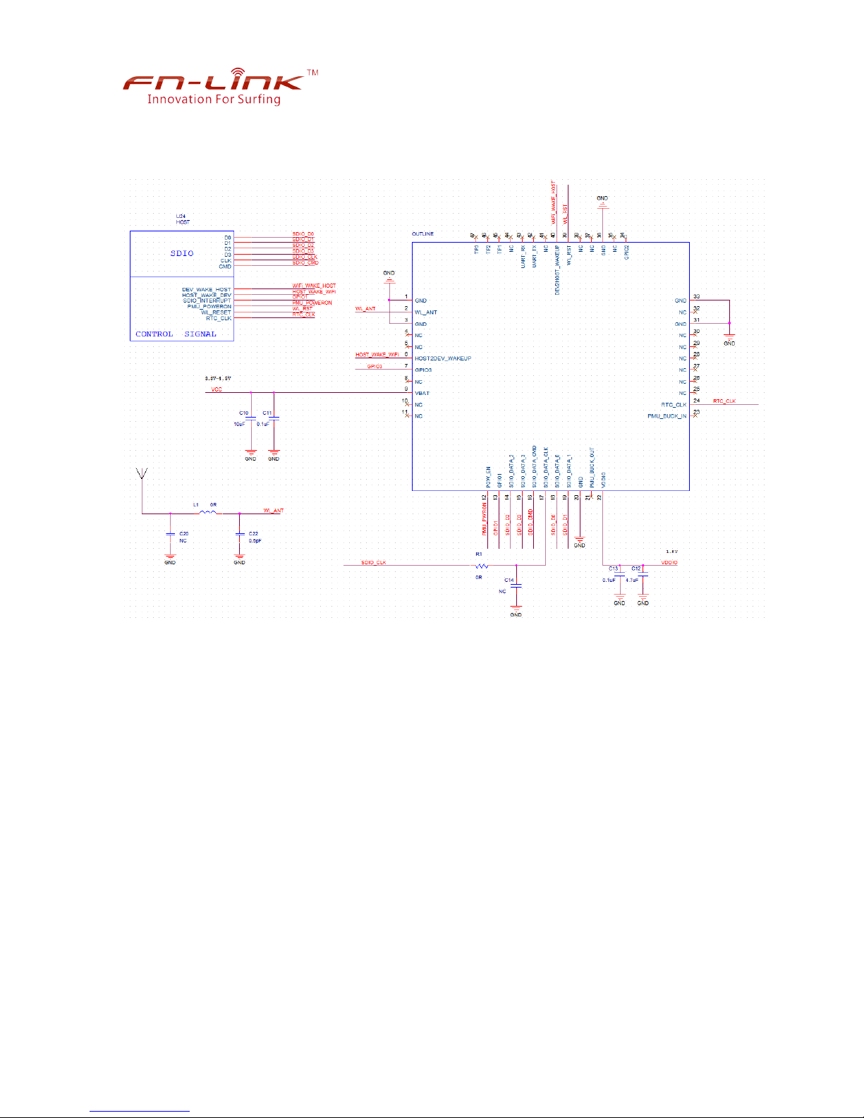
9.Reference Design
Page 18
3131A-S
FN-LINK TECHNOLOGY LIMITED 15 Proprietary & Confidential Information
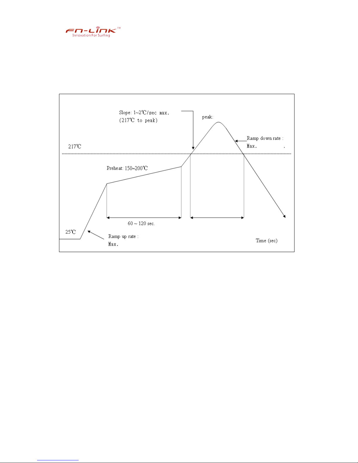
10. Recommended Reflow Profile
Referred to IPC/JEDEC standard.
Peak Temperature : <250°C
Number of Times : 2 times
-
Page 19
3131A-S
FN-LINK TECHNOLOGY LIMITED 16 Proprietary & Confidential Information
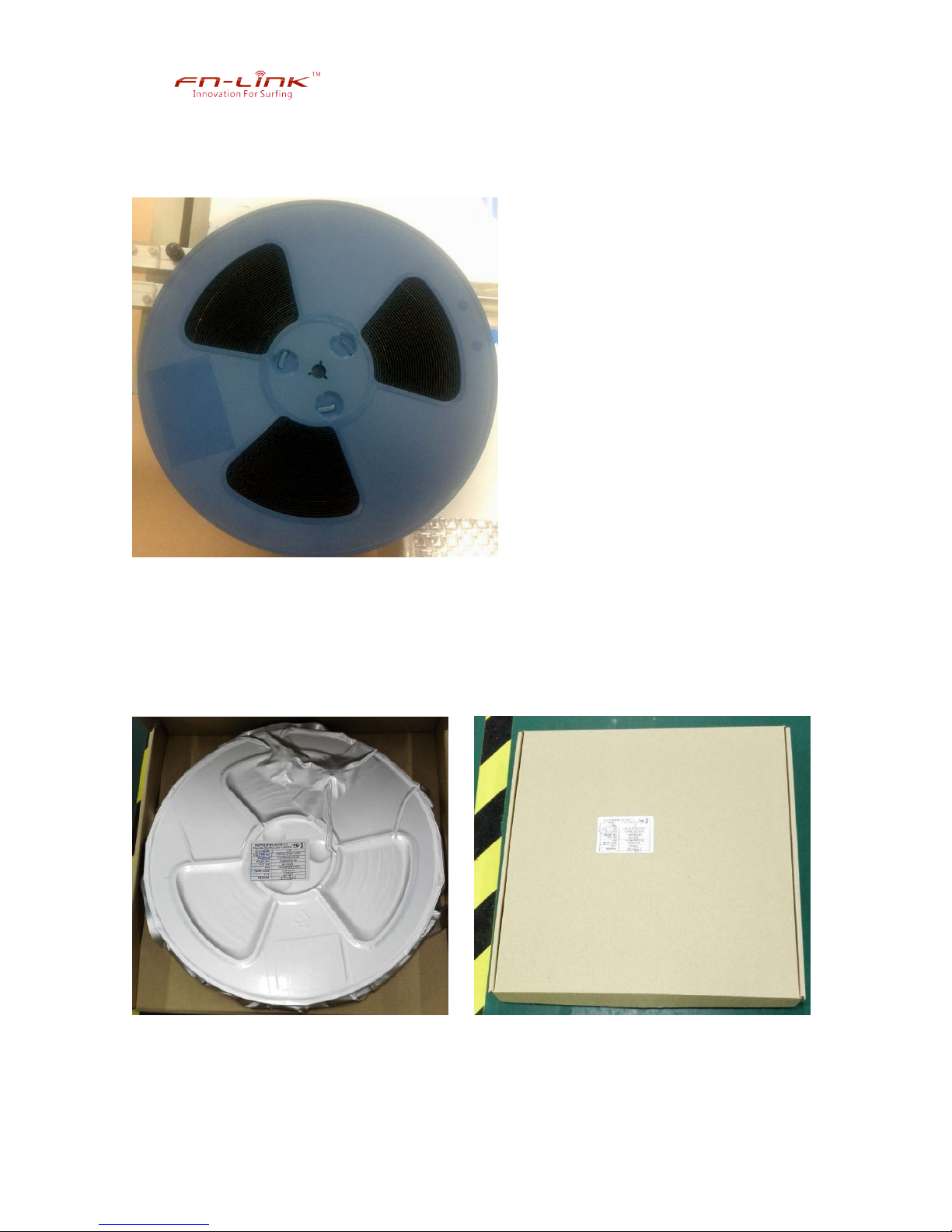
11. Packing Information
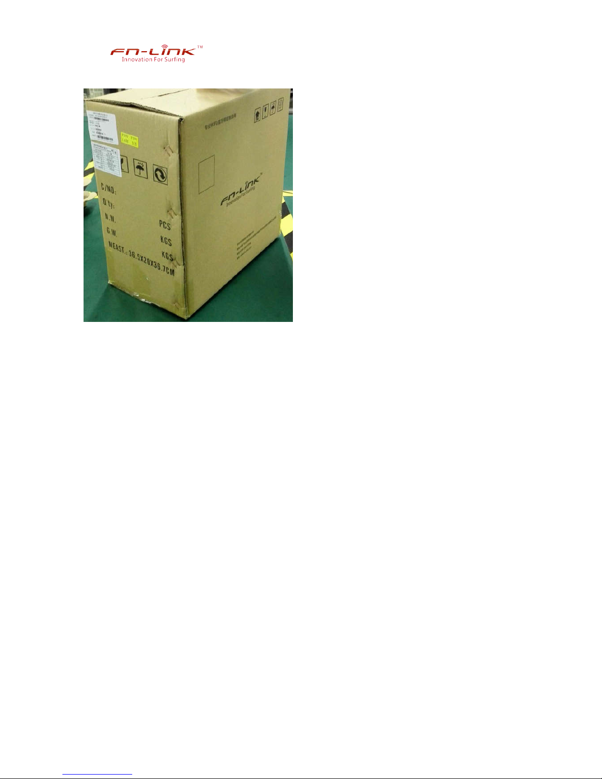
Tape and Reel Package
Using self-adhesive tape
Size of black tape: 24mm*32.6m the cover tape: 21.3mmm*32.6m
Color of plastic disc: blue
A roll of 2000pcs
NY bag size:460mm*385mm size :350*350*35mm
Page 20
3131A-S
FN-LINK TECHNOLOGY LIMITED 17 Proprietary & Confidential Information
The packing case size:350*210*370mm
Page 21
This module has been designed to operate with a PIFA antenna having a
maximum gain of 2dBi. Only this type of antenna may be used, the
manufacturer recommended antenna as
below:
Ant.
(Chain)
Brand Model name
Antenna
Type
Connector
Gain
(dBi)
1 XK
XKFPC-2D4-5D8-1
50
PIFA I-PEX 0.0
2 XK
XK-QX2400-PCB-1
40
PIFA I-PEX 2.0
3131A-S
FN-LINK TECHNOLOGY LIMITED 18 Proprietary & Confidential Information
Note: 1. This module has only one antenna port
2. Antenna 1 and antenna 2 are used for different customers.
FCC Statement:
This device complies with part 15 of the FCC Rules.
Operation is subject to the following two conditions:
(1) This device may not cause harmful interference, and (2) this device must accept any
interference received, including interference that may cause undesired operation.
Note: This equipment has been tested and found to comply with the limits for a Class B digital
device, pursuant to Part 15 of the FCC Rules. These limits are designed to provide reasonable
protection against harmful interference in a residential installation. This equipment generates,
uses and can radiate radio frequency energy and, if not installed and used in accordance with
the instructions, may cause harmful interference to radio communications.
However, there is no guarantee that interference will not occur in a particular installation. If this
equipment does cause harmful interference to radio or television reception, which can be
determined by turning the equipment off and on, the user is encouraged to try to correct the
interference by one or more of the following measures:
---Reorient or relocate the receiving antenna.
---Increase the separation between the equipment and receiver.
---Connect the equipment into an outlet on a circuit different from that to which the receiver is
connected.
---Consult the dealer or an experienced radio/TV technician for help.
FCC Radiation Exposure Statement
This equipment complied with FCC radiation exposure limits set forth for an uncontrolled
environment. This equipment should be installed and operated with minimum distance 20cm
between the radiator & your body.
Page 22

3131A-S
FN-LINK TECHNOLOGY LIMITED 19 Proprietary & Confidential Information
Warning: Changes or modifications to this unit not expressly approved by the part responsible
for compliance could void the user’s authority to operate the equipment.
LABEL OF THE END PRODUCT:
The final end product must be labeled in a visible area with the following "Contains TX FCC
ID:" 2AATL-3131A-S", and the FCC part 15.19 statem
ent has to be available on the label: This
device complies with Part 15 of the FCC Rules. Operation is subject to the following two
conditions: (1) this device may not cause harmful interference, and (2) this device must accept
any interference received, including interference that may cause undesired operation.
If the end product is so small or for such use that it is not practicable to place the statement
specified, the statement shall be placed in a prominent location in the instruction manual or
pamphlet supplied to the user or, alternatively, shall be placed on the container in which the
device is marketed.
The module must in the end-product be installed in such manner that the authorized antennas
can be used, any change of the antenna will void the certification.
Note:The module is limited to OEM installation ONLY;The OEM integrator is responsible
for ensuring that the end-user has no manual instructions to remove or install module.
This product is mounted inside of the end product only by professional installers OEM.
They use this module with changing the power and control signal setting by software
of end product within the scope of this application. End user can not change this
setting.
The equipment complies with RF exposure limits. This module is limited to installation
in mobile or fixed applications. The antenna used for this transmitter must not be
co-located or operating in conjunction with any other antenna or transmitter.
 Loading...