

Page 1

USER'S MANUAL
Part no. 48200490
March 2002 V1.1
1000 Series
Page 2
1000 User’s Manual
This Manual was written for installation purposes. It is to provide
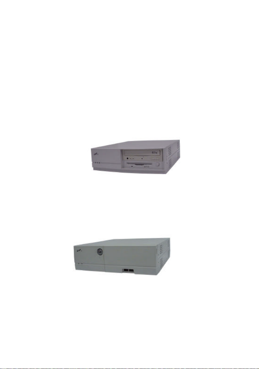
the information about the 1000 series for Book PC and POS PC
with B59/B63 all-in-one motherboard. .
Outlooking of Book PC 1000 Series
Outlooking of POS PC 1000 Series
Part no. 48200490
March 2002 V1.1
i
Page 3

COPYRIGHT
All rights reserved. The information contained in this guide has
been validated and reviewed for accuracy. No patent liability is
assumed with respect to the use of the information contained
herein. While every precaution has been taken in the preparation
of this guide, the Manufacturer assumes no responsibility for
errors or omissions.
No part of this publication may be reproduced, stored in a
retrieval system, or transmitted in any form or by any means,
electronic, mechanical, photocopying, recording, or otherwise,
without the prior written permission of the manufacturer.
TRADEMARK
Intel®, Pentium® and MMX are registered trademarks of Intel®
Corporation. Microsoft® and Windows® are registered trademarks
of Microsoft Corporation. AWARD is a trademark of AWARD
software INC.
General Notice: Other products and company names used
herein are for identification purposes only and may be trademarks
of their respective companies.
NOTICE
The contents of this manual are subject to change without
notice.
ii
Page 4

FEDERAL COMMUNICATIONS COMMISSION
NOTICE
This equipment has been tested and found to comply with the
limits for a Class A computing device, pursuant to Subpart B of
Part 15 of FCC Rules. Only peripherals (computer input/output
devices, monitors, printers, etc.) certified to comply with the Class
A limits may be attached to this computer. Operation with
non-certified peripherals is likely to result in interference to radio
and TV reception.
NOTICE: This equipment generates and uses radio frequency
energy and if not installed and used properly, that is, in strict
accordance with this user's manual, may cause interference to
radio and television reception. It has been type tested and found to
comply with the limits for a Class A computing device, pursuant to
Part 15 of FCC Rules, which are designed to provide reasonable
protection against such interference in a residential installation.
However there is no guarantee that interference will not occur in a
particular installation. If this equipment does cause interference to
radio or television reception, which can be determined by turning
the equipment on and off, the user is encouraged to try to correct
the interference by one or more of the following measures:
• Reorient the receiving antenna
• Relocate the computer with respect to the receiver
• Plug the computer into a different outlet so that computer
and receiver are on different branch circuits.
If necessary, the user should consult the supplier or an
experienced radio/television technician for additional suggestions.
The user may find the following booklet prepared by the Federal
Communications Commission helpful :
"How to identify and Resolve Radio-TV Interference Problems".
This book is available from the US Government Printing Office,
Washington, D.C. 20402
CE
F WARNING:
This is a Class A product. In a domestic environment this product
iii
Page 5

may cause radio interference in which case the user may be
required to take adequate measures.
iv
Page 6

BATTERY REPLACEMENT
F WARNING:
Your computer is provided with a battery -powered Real-Time
Clock circuit. There is a danger of explosion and risk of personal
injury if the battery is incorrectly replaced or mistreated. Do not
attempt to disassemble the battery, immerse it in water or dispose
of it in fire.
Model No. Decode
The following are the standard model number, CPU Type and
main board version : -
1 59 /63 X XXX
1000 Series B59 all-in-one
mainboard
B63 all-in one
mainboard
0:Front Panel without
FDD /CD-ROM
opening
1:Front Panel with
FDD / CD-ROM
opening
CPU Speed
v
Page 7

CHAPTER 1. PRECAUTIONS...................................................... 1
1-1. Check the Line Voltage ................................................... 1
1.2 Environmental Conditions ................................................. 1
1.3 Handle the System Carefully ............................................. 2
1.4 When Not In Use............................................................ 2
1.5 When Operation is Faulty................................................ 2
CHAPTER 2 GETTING START ED............................................... 3
2.1 Unpacking the package.................................................... 3
2.2 Introduction .................................................................... 4
2.3 1000 series PC Outlooking ............................................... 5
a Front View ................................................................... 5
2.4 Expansion Slot ............................................................... 9
2.4.1.Expansion Slot Card Type (Without LAN)................. 9
2.5 Installing a Floppy Disk Drive ..........................................11
2.6 Installing a CD-ROM drive ................................................11
CHAPTER 3 1591 TECHNICAL SPECIFICATION .........................13
3.1.Technical Specification for "B59" main board.....................13
3.2. Jumpers Location Diagram for "B59 V1.X " main board.....14
3.3.Memory configuration for “B59 V1.X” main board................15
3.5 Connector’s description...................................................22
CHAPTER 4 1631 TECHNICAL SPECIFICATION ..........................30
4.1.Technical Specification for "B63" main board.....................30
4.2.Jumpers Location Diagram for "B63 V2.X " main board......32
4.3.Memory configuration for “B63 V2.X” main board................33
4.4. Jumper Setting ..............................................................34
4.5.Connector ......................................................................40
APPENDIX A1- AWARD BIOS SETUP 1591 ...............................47
APPENDIX A2- AWARD BIOS SETUP 1631 ...............................81
APPENDIX B. FAST ETH ERNET CONTROLLER........................114
1
Page 8

Chapter 1. Precautions
This section is written to protect both you and the system itself. In order to
lengthen the service life of the system, Please read this section carefully.
1-1. Check the Line Voltage
The operating voltage for the internal switching power should be within the
range of 90V AC ~ 260V AC, otherwise the system may be damaged.
Rating Line Voltage Frequency
90 ~ 260V AC 100 ~ 240V AC 50/60 Hz
IMPORTANT !
Use the internal switching power adapter that supports your 1000 series PC
system unit only. Using a different switching power adapter may cause system
damage.
1.2 Environmental Conditions
Place your 1000 series PC on a solid level surface.
Avoid installing this system in an extremely hot or cold place.
Avoid putting this system in a place exposed to direct sunlight, in a closed car
in the summer time, or near a heating device such as a stove.
Operating Temperature: 5 °C ~ 40 °C. Storage Temperature: -20 °C ~ 60 °C.
Do not use a system that has been left outdoors on a cold winter day. The
lowest operating
ambient temperature is 5 °C.
Avoid moving the system rapidly from a hot place to a cold place or vice versa.
Otherwise, condensation may form inside the system.
Keep the system away from damp air, water and dust. The operating ambient
humidity is 20 ~ 80% (non - condensing). The Non - operating Relative
1
Page 9

Humidity is 5% ~ 80% (non-condensing). Avoid putting a water-filled container
such as a vase on or near the system.
Do not put the system in a place of strong vibration which may cause serious
damage to the hard disk inside the system( if a hard disk is installed inside).
Do not place the system too close to a radio, television, or other
communication systems to avoid interference.
1.3 Handle the System Carefully
Do not put heavy objects on the system except a small light monitor.
Do not turn the system upside down. Otherwise, the disk drive may not work
properly.
When you transport the system outdoors, it is always advisable to protect
it by inserting a protective diskette into the disk drive.
1.4 When Not In Use
When the system is not in use, remember to cover the system and store it with
care.
1.5 When Operation is Faulty
Double check the operating procedure and if problem persists, contact your
supplier.
2
Page 10

Chapter 2 Getting Started
This chapter explains how to set up your new 1000 series. It helps you to
unpack the computer, identify all the parts, and put it all together.
2.1 Unpacking the package
Upon unpacking the 1000 series package, make sure that you have the
following items in good condition:
• The main system unit
• Power cord
• Accessory Bag including ( jumper setting, warranty card)
• CD driver Bank
If any of the above items are damaged or missing , please contact your supplier
immediately.
After you have removed all items, put the packing material and plastic wraps
into the packing box and move it to a storage area. Save them for use when
moving or shipping the computer.
3
Page 11

2.2 Introduction
The 1000 series PC are high performance 16/32/64-bit personal computers.
They are IBM PC compatible PC with 3 expansion slots.
The main board used in the 1000 series PC is an all-in-one motherboard which
contains CPU, RAM, ROM BIOS, floppy disk drive controller, IDE hard disk
controller, VGA chip, etc.
The Dimension for 1000 series PC is as following: -
Model Dimension
1000 Series
The system unit is the main body of a PC system. Its equipment and
structures define almost all of the features & functions of the PC system. It
is a box -like structure with a metal casing enclosing all its electronic
components.
The outside of the system unit has LED indicating lights and input /output
connectors on it. The casing is made of metal so as to help with heat
dissipation to assure the proper function of the inside components.
300 (W) x 320 (L) x 90 (H) mm
4
Page 12
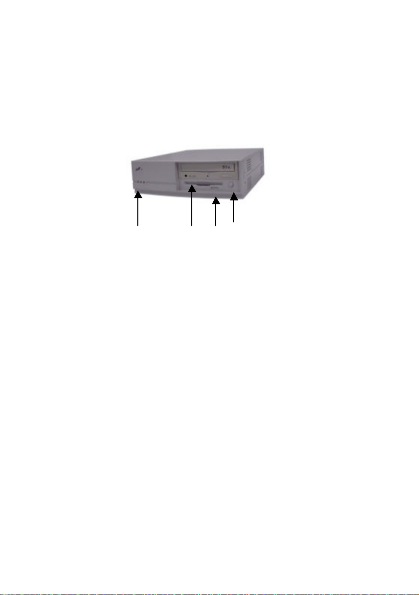
5.25” CD-ROM / 3.5” FDD / Power button
Power / HDD FDD
2.3 1000 series PC Outlooking
a Front View
Carry-I front panel
5
Page 13
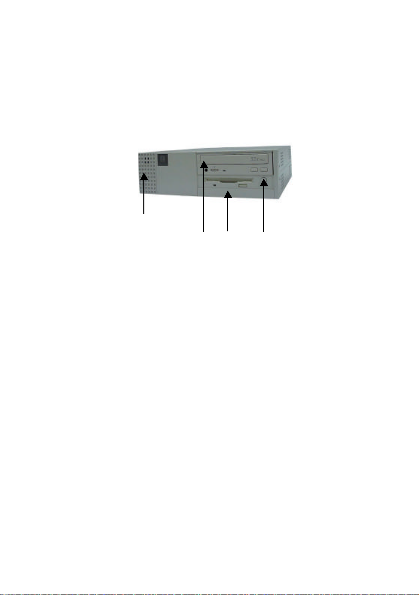
Power / HDD FDD
5.25” CD-ROM / 3.5” FDD / Power
OEM-1 front panel (QP front panel )
6
Page 14
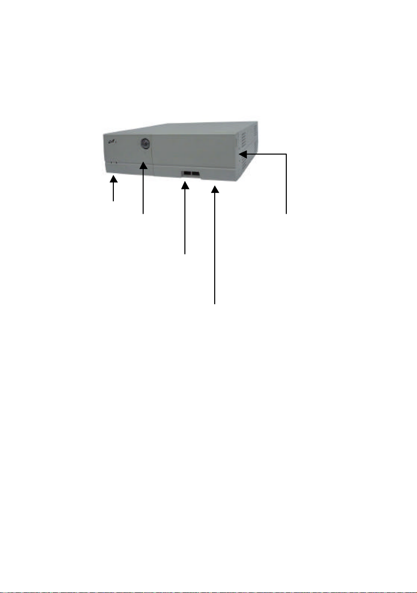
Power button
Power / HDD FDD
LED
Key
POS PC 1000 front panel
USB2/
USB1
Compact flash socket
5.25”
CD-ROM /
3.5” FDD /
7
Page 15
, standard
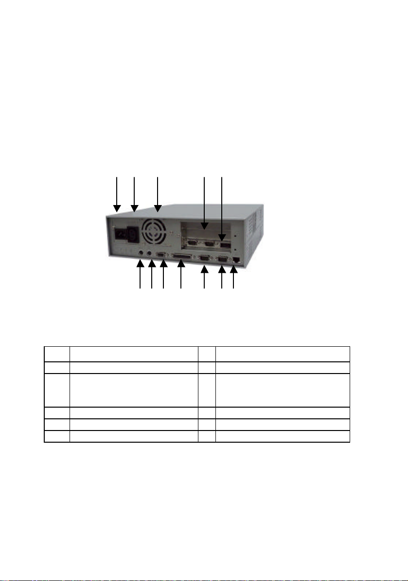
b)Rear Panel
1 2 3 4 5
6 7 8 9 10 11 12
AC Power Inlet 2 AC Power Outlet
1
3 System Fan 4 Expansion slot x3
5 COM3/COM4/DIO Port
(Option for Book 1000
kits for POS1000 )
7 PS2 mouse port 8 Display Port
9 Parallel Port 10 Serial 2 port
11 Serial 1 port 12 RJ-45 LAN Port
6 PS2 keyboard Port
8
Page 16
CAUTION :
Whenever you connect or disconnect any component, be sure that
your compute r is turned off and that your computer is disconnected
from its power source. Plugging or unplugging any item when the
computer is receiving power can cause power surges and damage
your computer.
2.4 Expansion Slot
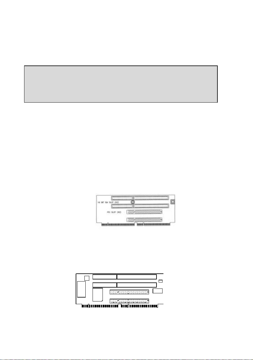
The 1000 series offer 3 (Three) expansion slots, 1xPCI, 1xPCI/ISA, 1xISA slot.
The maximum dimension of the expansion card of the system is 104 (H) x 278
(L) mm
2.4.1.Expansion Slot Card Type (Without LAN)
1.Riser Card (FT –7363 : standard )
2.Riser Card with UM9008 10Base-T LAN (FT –7324 : option)
U2
U1
DM9008F
9836-BB
E6246
U3
FB2022
JP1
U4
9831
9
Page 17
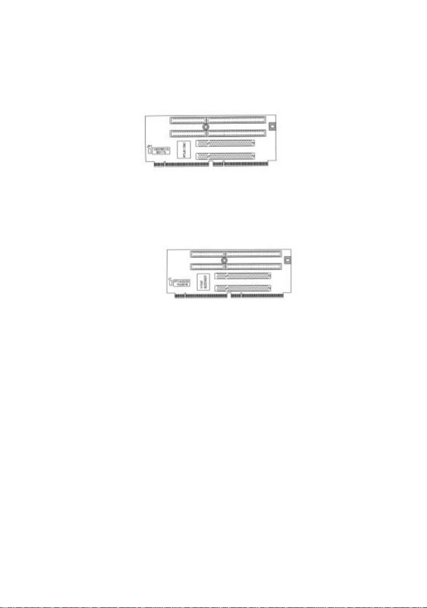
3. Riser Card with RTL8139 10/100Base-T LAN :(FT-7329 : option)
4.Riser Card with Intel 82559 10/100 Base-T LAN: (FT –7365 : option)
10
Page 18
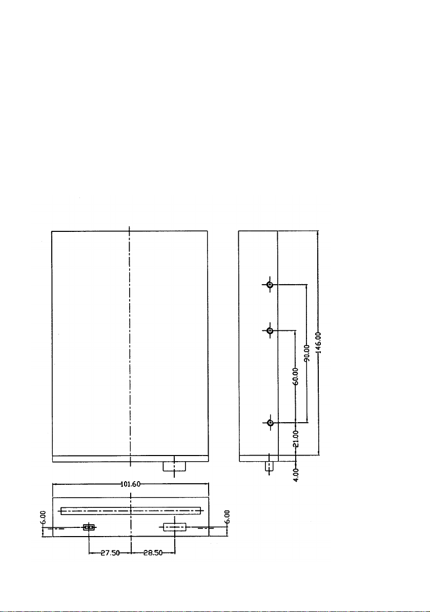
2.5 Installing a Floppy Disk Drive
To install a 3.5-inch Floppy Disk Drive to 1000 series, the
maximum dimension of the Floppy Disk Drive is 101.60mm width by 6.00mm
height, and make sure the location of the LED indicator and FDD eject button
order can fit 1000 series cabinet The use of NEC (part no. 134-506791-301-3)
and MITSUMI (part no. 0359M3R69-2010 ) are recommended.
Or contact your distributor for more information.
2.6 Installing a CD-ROM drive
11
Page 19
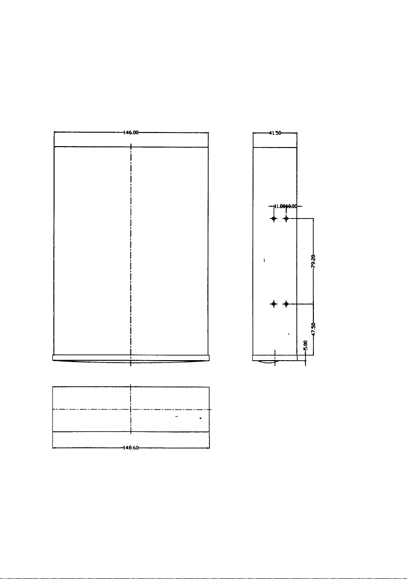
To install a 5.25-inch Floppy Disk Drive to 1000 series, the maximum
dimension is 148.60mm width by 42.30mm height. Please contact your
distributor in case you have problem to find it. (see below figure )
12
Page 20

Keyboard & Mouse
Chapter 4 1631 Technical Specification
The above model was installed with a “B63” Pentium all-in-one as system main
board. The following are the technical details of the "B63" main board.
4.1.Technical Specification for "B63" main board
MODEL 1631 -XXX
Main Board "B63" all-in-one M/B
CPU Intel socket 370 CPUs Celeron /PIII PPGA/FC-PGA
Co-processor Built-in CPU
Internal Cache Built-in CPU
External Cache Built-in CPU
System RAM 2x 168pin DIMM sockets, support 16 / 32 / 64 / 128 /256 MB
BIOS AWARD PnP BIOS
Core Logic Intel FW82443ZX/BX
Video Display S3 Trio 3D AGP
Video RAM 4MB SGRAM
Video Display port One 15-pin D-SUB female VGA monitor connector
HDD Controller support two 40-pin 2.54 pitch IDE pin-header
FDD Controller SMSC37C602 support one 34-pin 2.54mm pitch
I/O Port 2x 9-pin D-SUB RS232 FIFO Serial Ports connector
LAN port Optional LAN Rising Card
USB port 2 x USB ports
ROM disk Disk On Chip Socket supported
Compact Flash Compact Flash Socket Supported
Expansion Slot on
board
Power Supply Internal AT
The content of this specification is subject to change without notice.
30
pin-header .
2x 10-pin header support COM3/COM4 port
1x 25-pin D-SUB Parallel Port (SPP/EPP/ECP) connector
1x PS2 Keyboard connector , 1x PS2 mouse connector
1 FLYTECH EISA Bus Slot for system expansion slot used
-FT-8075 75W (5V/8.5A, 12V/2.4A, -12V/0.3A, )
-Optional FT-8075E 1202 ((5V/6A, 12V/2A, -12V/0.3A,
24V/2A, )
Page 21

31
Page 22
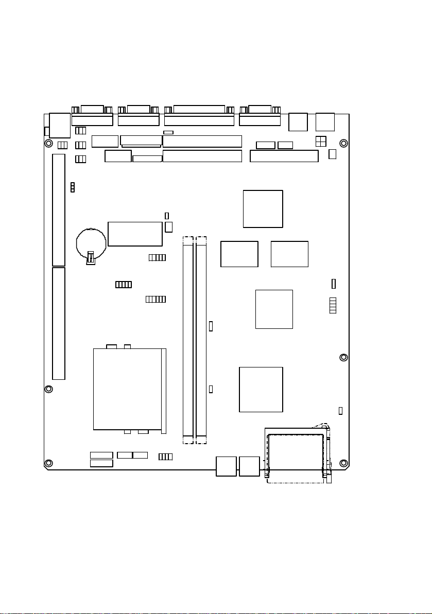
4.2.Jumpers Location Diagram for "B63 V2.X " main board
U1
6 2
JP3
J1 J2 J4 J5 J6 J7
5 1
6 2
JP4
JP6
1
1
5
1 1
26
JP5
5
612
JP9
2 10
1
102
9
JP7
1
9
JP8
3 1
JP11
8
2 40
2
81
1 39
JP10
J8
JP11 J9
JP14
39
4 1
40
33
34
JP13
3 1
JP32
1
1
2
2
JP12
JP2
5
JP31
FW82371EB
JP18
J19
1
2
1
2
JP29
1
341
5
J20
2
6 2
1
11
J30
2
12
2
1
1
J12
3
PCI SLOT
DOC
J11
U16
1
1092
BT1
PCI SLOT
U13
U24 U25
J10
U31
S3
TRIO 3D/2X
JP21
1
3
21
109
PGA370
JP24
JP27
U32
CPU
1
3
16
J13 J14
16
1
3
2
781
JP28
1
168-PIN DIMM RAM SOCKET-DIMM
168-PIN DIMM RAM SOCKET-DIMM
J22
2
JP25 JP26
32
U33
FW82443ZX
1
J23
2
CN2
Page 23

4.3.Memory configuration for “B63 V2.X” main board
33
Page 24
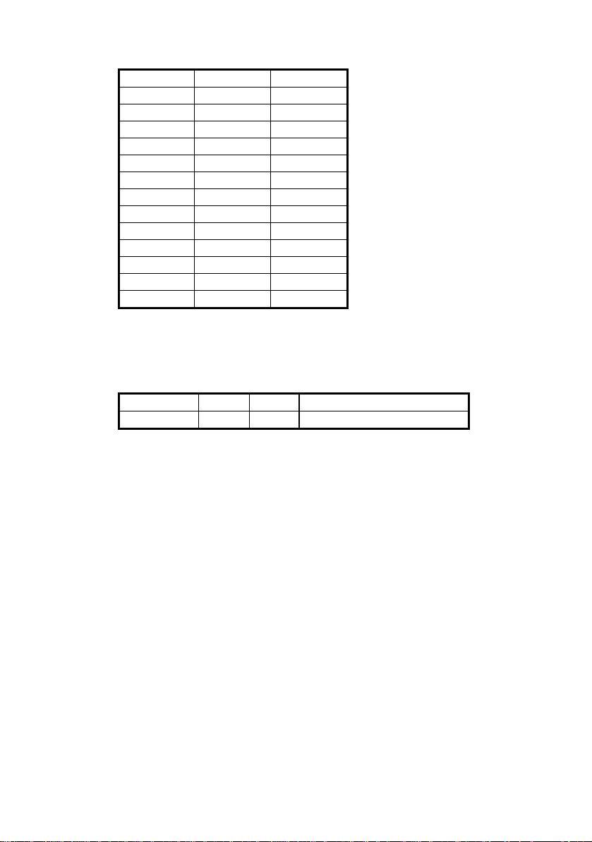
Capacity DIMM 1 DIMM 2
16MB 16MB none
16MB none 16MB
32MB 16MB 16MB
32MB 32MB none
32MB none 32MB
80MB 16MB 64MB
80MB 64MB 16MB
64MB 64MB none
64MB none 64MB
128MB 64MB 64MB
128MB 128MB None
128MB None 128MB
256MB 128MB 128MB
VGA Memory Configuration.
Capacity U24 U25 Video DRAM Type
4MB close close 512KB X 32 SOP package
4.4. Jumper Setting
CPU Frequency Selection: JP30
34
Page 25
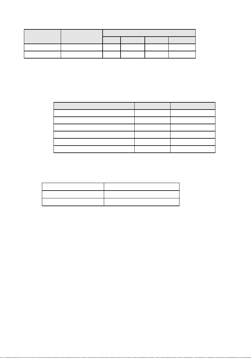
JP30 CPU Clock PCI Clock
FS0 FS1 FS2 FS3
100.3MHz 33.43MHz 1-3 7-9 2-4 10-12
66.8MHz 33.40MHz 1-3 7-9 4-6 10-12
=M-System Disk On Chip: JP20, JP19
Address JP19 JP20
0C800-0C9FF (Default) 1-2 1-2
0CC00 - 0CDFF 3-4 1-2
0D000 - 0D1FF 1-2 3-4
0D400 - 0D5FF 3-4 3-4
0D800 - 0D9FF 1-2 5-6
0DC00 - 0DDFF 3-4 5-6
=CMOS Operation mode: J12
Function J12
CMOS Normal 2-3 (Default)
CMOS Reset 1-2
35
Page 26

=ATX / AT power mode: JP18, J3
Function JP18 J3
Default AT power supply
4000 series : FT-8050 AT Internal power
supply
1000 series: FT-8075 AT Internal Power
Supply
ATX power supply Open 2-3
Close 1-2
36
Page 27
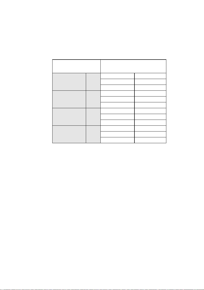
=COM Port Jumper Setting
COM Port Pin 1
COM1
COM2
COM3
COM4
JP4
JP3
JP9
JP5
1-2 (Default) Data Line
3-4 +5V
5-6 +12V
1-2(Default) Data Line
3-4 +5V
5-6 +12V
1-2(Default) Data Line
3-4 +5V
5-6 +12V
1-2(Default) Data Line
3-4 +5V
5-6 +12V
37
Page 28
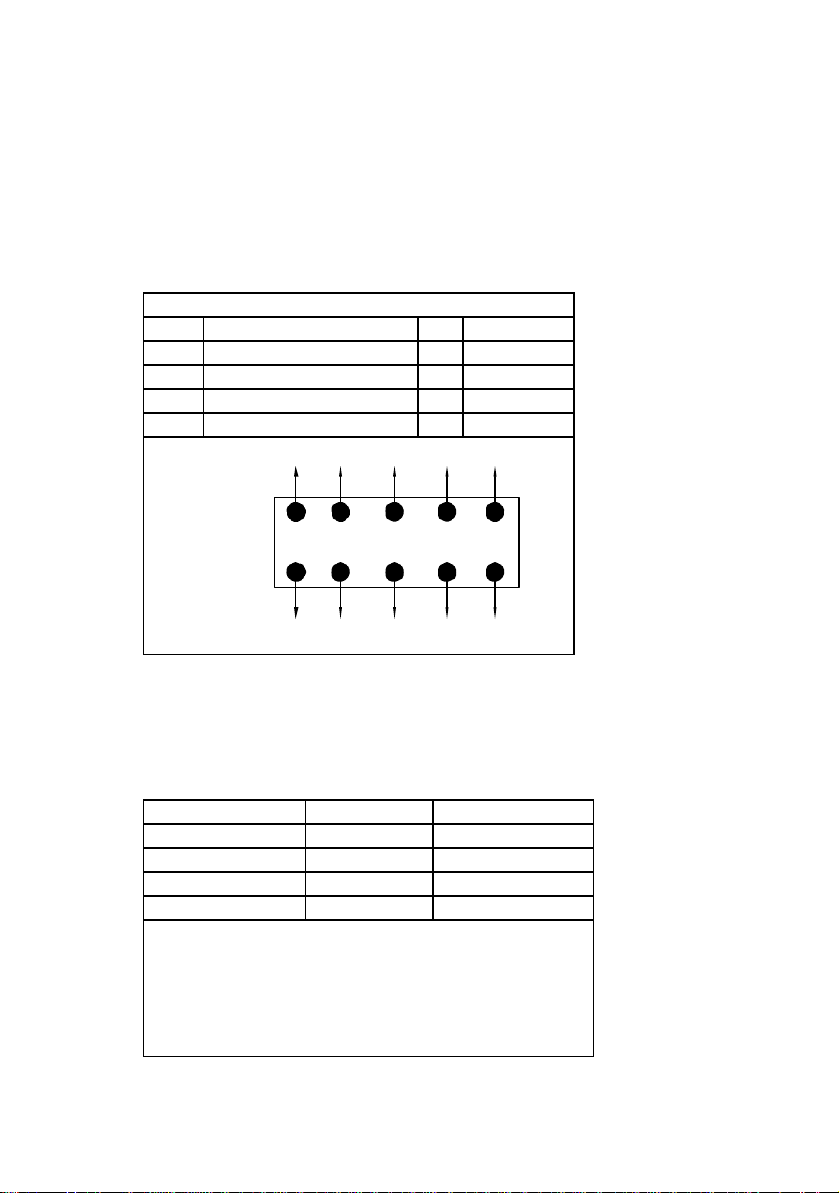
OUT3
OUT1
OUT2
OUT0
VDC+12V
=Digital I/O (4 Output & 4 Input) : J11
This main board provides the basic digital I/O signal
Controller. User can develop the program and extra
controller to open and sense the cash drawer that based on the
digital I/O function on this main board.
PIN ASSIGNMENT
1 GND 6 Out 1
2 VDC +12V 7 IN 2
3 IN 0 8 Out 2
4 Out 0 9 IN 3
5 IN 1 10 Out 3
IN3 IN2 IN1 IN0
7
9
5
GND
1
3
8
10
6
2
4
ν Digital output programming
The output is TTL Level. The output signal has to
be TTL compatible.
Output Address Bit
Out 0 206 0
Out 1 206 1
Out 2 206 2
Out 3 206 3
Example : ( “0” = off “1” =on )
Data 00 = Out 0 and Out 1 = “0”
Data 01 = Out 0 = “1”
Data 02 = Out 1 = “1”
Data 03 = Out 0 and Out 1 = “1”
38
Page 29

Example : If input 206 is [ 0111], then input 3 is “0”, If
Digital input programming
The input signal has to be TTL compatible.
Input Address Bit
IN 0 206 0
IN 1 206 1
IN 2 206 2
IN 3 206 3
input 206 is [0011], then input 3 & 4 are “0”
39
Page 30
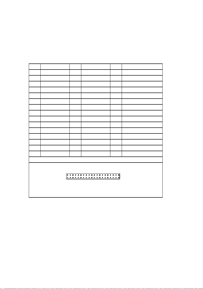
2
1
39
40
4.5.Connector
IDE connector :
Primary :J8 40pin 2.54mm , Primary :JP11 40pin 2.0mm
Pin# Assignment Pin# Assignment Pin# Assignment
1 Reset 16 Data bit 14 31 IRQ 14
2 Ground 17 Data bit 0 32 NC
3 Data bit 7 18 Data bit 15 33 Disk address 1
4 Data bit 8 19 Ground 34 NC
5 Data bit 6 20 NC 35 Disk address 0
6 Data bit 9 21 IDE DRQ 36 Disk address 2
7 Data bit 5 22 Ground 37 Disk chip select 0
8 Data bit 10 23 Disk Write 38 Disk chip select 1
9 Data bit 4 24 Ground 39 Disk LED
10 Data bit 11 25 Disk read 40 Ground
11 Data bit 3 26 Ground
12 Data bit 12 27 Disk ready
13 Data bit 2 28 NC
14 Data bit 13 29 IDE DACK
15 Data bit 1 30 Ground
Figure
40
Page 31
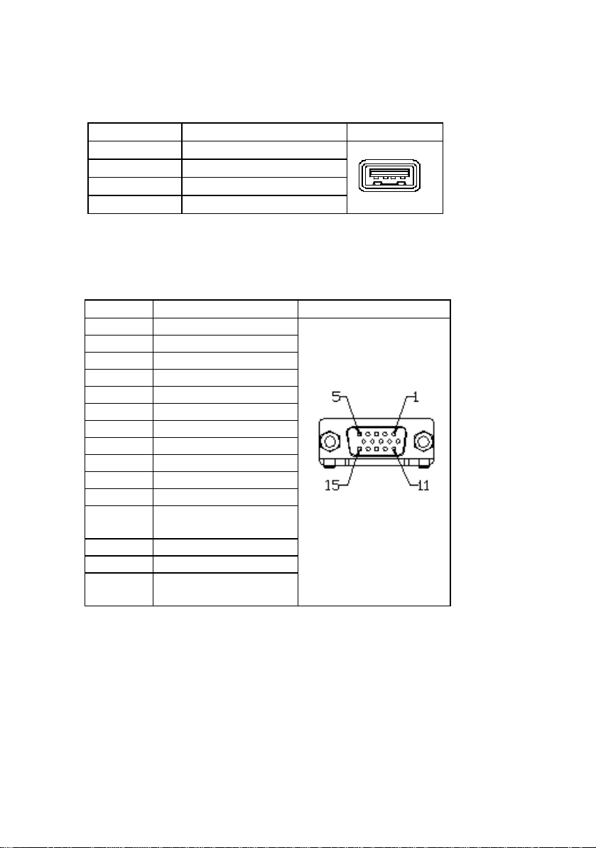
= USB port connector (Pin-Header 4 pin ) : JP25, JP26
Pin # Assignment Figure
1 +5V
2 USB Port Data 3 USB Port Data +
4 Ground
VGA connector (D-SUB 15-pin female connector ): J5
Pin # Assignment
1 Red signal
2 Green signal
3 Blue signal
4 NC
5 Ground
6 Red Ground
7 Green Ground
8 Blue Ground
9 +5V (via polyfuse)
10 Ground
11 NC
12 Data of monitor ID
(with 10KΩ pull high)
13 H Sync.
14 V Sync.
15 Clock of monitor ID
(with 10KΩ pull high)
Figure
41
Page 32
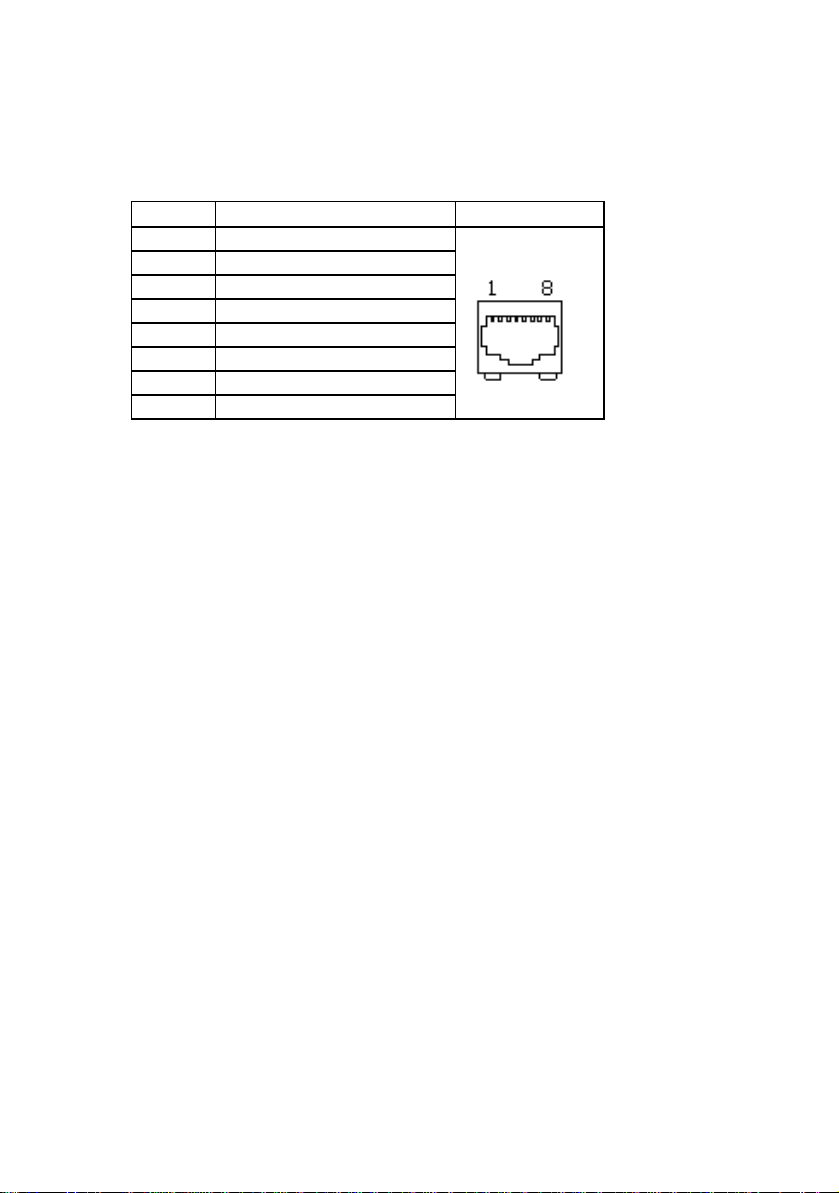
= LAN (10 /100Base- T RJ- 45 connector ) : U1
Pin # Assignment
1 Transmit output (+)
2 Transmit output (-)
3 Receive input (+)
4 NC
5 NC
6 Receive input (-)
7 NC
8 NC
Figure
42
Page 33
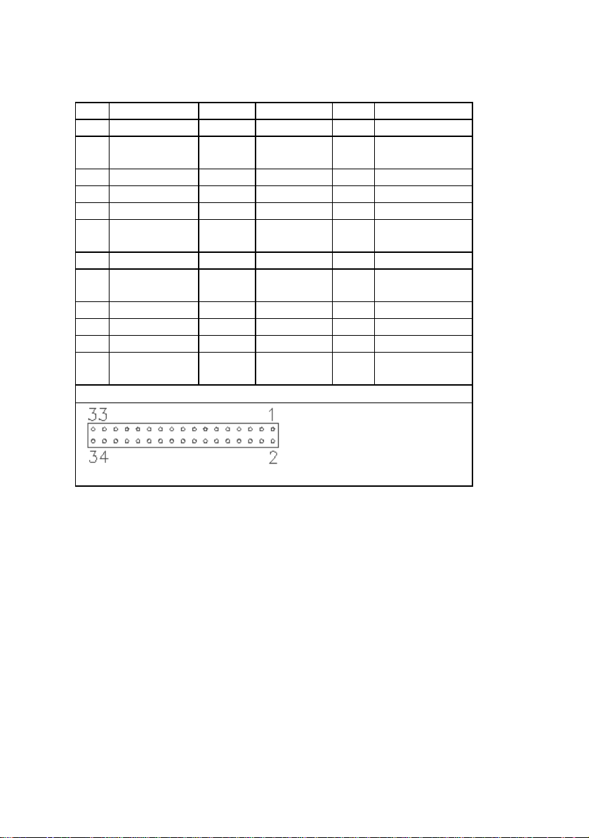
Driver select
Floppy disk connector (34pin 2.54mm pitch Pin-header with housing) : JP9
Pin# Assignment Pin# Assignment Pin# Assignment
1 Ground 13 Ground 25 Ground
2 Density select 14
2
3 Ground 15 Ground 26 Ground
4 Vcc 16 Motor on 1 28 Write protected
5 Ground 17 Ground 29 Ground
6 Vcc 18 Data
direction
7 Ground 19 Ground 31 Ground
8 Index 20 Step motor
active
9 Ground 21 Ground 33 Ground
10 Motor on 0 22 Write data 34 Disk change
11 Ground 23 Ground
12 Driver select 1 24 Write gate
26 Track 00
30 Read data
32 Head select
Figure
43
Page 34
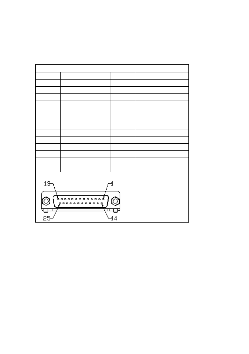
Parallel port : J3 ( D-SUB 25pin female )
Parallel port
Pin # Assignment Pin # Assignment
1 Strobe (-) 14 Auto feed (-)
2 Data bit 0 15 Error (-)
3 Data bit 1 16 INIT (-)
4 Data bit 2 17 SLCT IN (-)
5 Data bit 3 18 Signal Ground
6 Data bit 4 19 Signal Ground
7 Data bit 5 20 Signal Ground
8 Data bit 6 21 Signal Ground
9 Data bit 7 22 Signal Ground
10 ACK (-) 23 Signal Ground
11 Busy 24 Signal Ground
12 Paper empty 25 Signal Ground
13 SLCT
Figure
44
Page 35
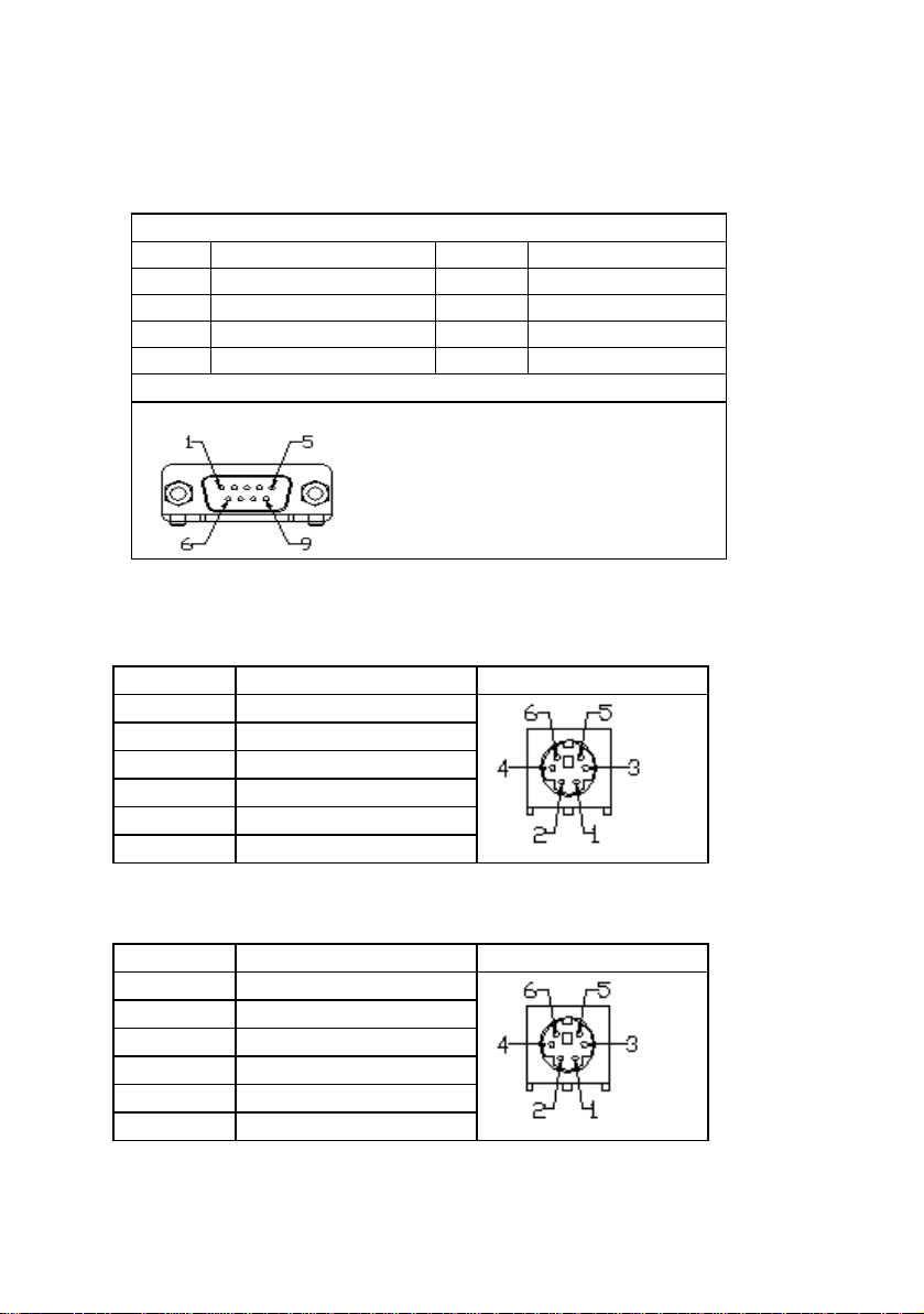
Serial port 1: J1 / Serial port 2 : J2
Serial port 3: JP7 /Serial port 4 : JP6
Serial port
1 Data carrier detect 6 Data set ready
2 Receive data 7 Request to send
3 Transmit data 8 Clear to send
4 Data Terminal ready 9 Ring indicator
5 Signal Ground
Figure
PS2 mouse (Mini Din 6 pin) : J6
Pin # Assignment Figure
1 Mouse data
2 NC
3 Ground
4 +5V via Poly-fuse
5 Mouse clock
6 NC
Keyboard (Standard PS2 type ) : J7
Pin # Assignment Figure
1 Keyboard data
2 NC
3 Ground
4 +5V
5 Keyboard clock
6 NC
45
Page 36
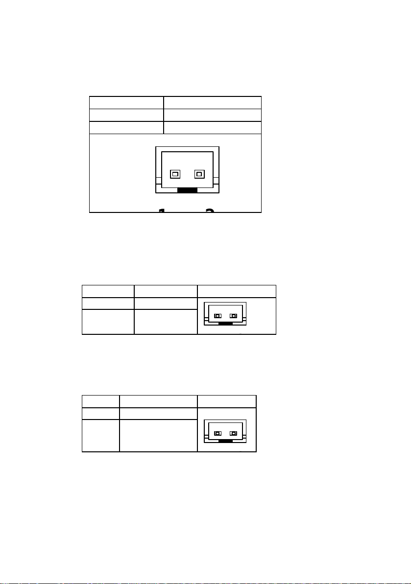
=Fan Connector : J13, J14 (default to use +12V Power )
Pin # Assignment
1 +12V
2 Ground
Figure
=COMPACT FLASH POWER : JP29
(default to use +5V Power)
Pin # Assignment
1 +5V
2 Ground
Figure
=POWER PUSH BUTTON : JP12
Pin # Assignment
1 Ground
2 N/A
Figure
46
Page 37

pin 2.54mm
Keyboard & Mouse
Chapter 3 1591 Technical Specification
The above model was installed with a “B59” Pentium all-in-one as system main
board. The following are the technical detail of the "B59" main board.
3.1.Technical Specification for "B59" main board
MODEL 1591 Pentium PC
Main Board "B59" all-in-one main board
CPU Intel Pentium / Pentium MMX , AMD K6 /K6-2/ K6-3, IDT C6
Co-processor Built-in CPU
Internal Cache Built-in CPU
External Cache 256KB 512KB Pipeline SRAM on board
System RAM 2 x 168pin DIMM sockets, support 16 / 32 / 64 / 128 /256MB
BIOS AWARD PnP BIOS
Core Logic VIA MVP4 VT8501 / VT82C686A
Video Disp lay 3D AGP SVGA
Video RAM Shared Memory (UMA) 4MB expandable to 8MB
Video Chip Built-in Core Logic
Video Display port One 15-pin D-SUB female VGA monitor connector
HDD Controller Build-in Core Logic VT82C686, supports one 40-pin 2.54
FDD Controller Built-in Core Logic VT82C686, supports one 34-
I/O Port -2x D-SUB 9-pin RS232 FIFO Serial Ports
LAN port Optional 100/ 10 Base -T RJ45 built-in LAN Rising Card
USB port Two USB ports
ROM disk Disk On Chip Socket supported
Compact Flash Compact Flash Socket supported
Expansion Slot on
board
Power Supply Internal AT
The content of this specification is subject to change without prior notice.
pitch pin header (primary)
pitch pin-header
-2x 10-pin header for COM3/COM4 port
-serial port pin 1 supports 5V/12V
-One 25-pin D-SUB Parallel Port (SPP/EPP/ECP) connector
1x PS2 Keyboard connector, 1 x PS2 mouse connector
1 FLYTECH Bus Slot for system expansion slot used
-FT-8075 75W (5V/8.5A, 12V/2.4A, -12V/0.3A, )
-Optional FT-8075E 120W ((5V/6A, 12V/2A, -12V/0.3A,
24V/2A, )
13
Page 38
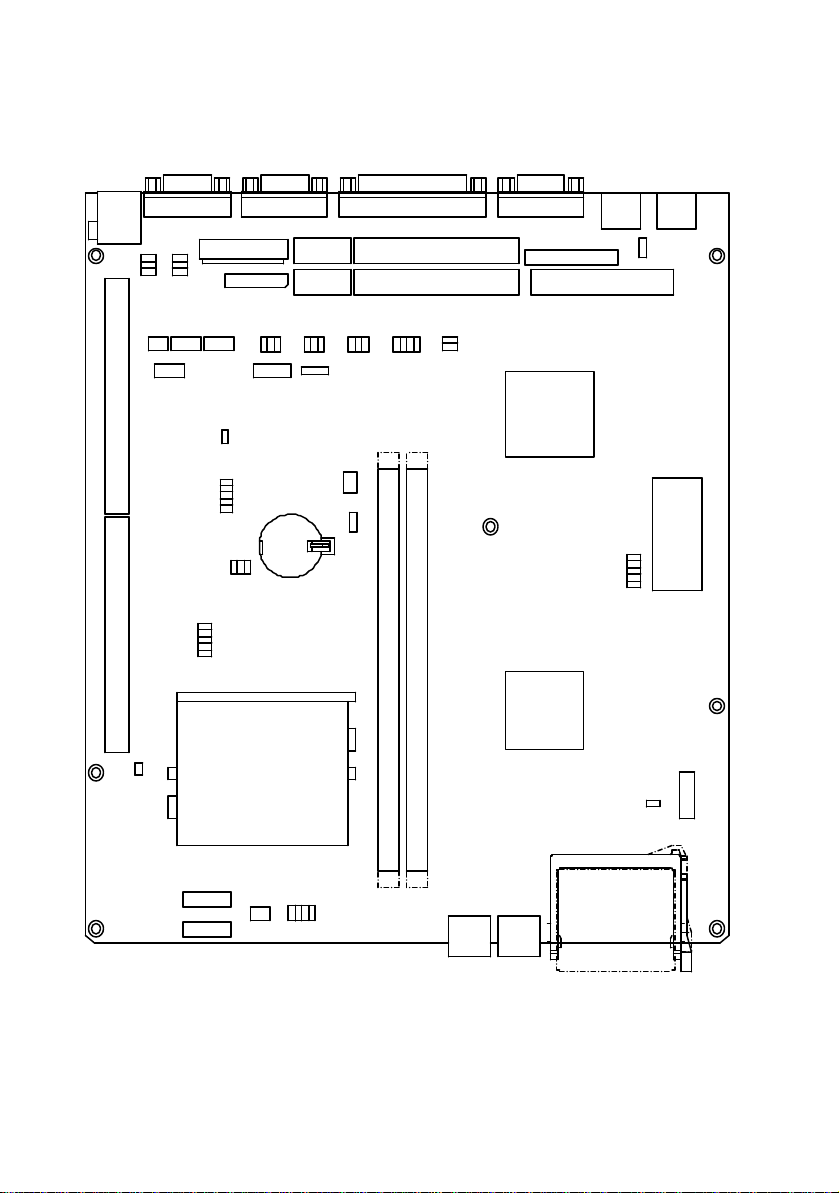
3.2. Jumpers Location Diagram for "B59 V1.X " main board
CN1
J1
J4 J6 J10 J18 J21 J23
1
655
6
JP15
JP16
1
1
2
2
CN3 CN5CN10
2 1
1 3 1 3
1 3 41
CN2 CN7 IR
PCI SLOT
PCI SLOT
JP3
J5
9
10
JP2
1
2
CN11
CN12
9
10
1
2
JP4
216
8
1 1
81
2 10
1
JP5 JP6
216
5 125
BAT1
5
102
2 40
J7
9
2
J8
9
1 39
JP7
6
JP10 J13
1 8
2
331
1
JP8
J11
J12 J20
7
J14
25
39
J19
26
40
33
34
VT82C686A
U19
CN13
3
JP9
1
2
1
1
1
JP11
2
3
1
2
DOC
U26
JP12
3
4
1
2
6
5
2
1
JP13
168-PIN DIMM RAM SOCKET-DIMM
JP1
CN4
CN14
U10
CPU
16
2 1
16
CN6
127
J16
8
168-PIN DIMM RAM SOCKET-DIMM
14
U20
VT8501
1
JP14
CN9
6
J22
J17J15
Page 39
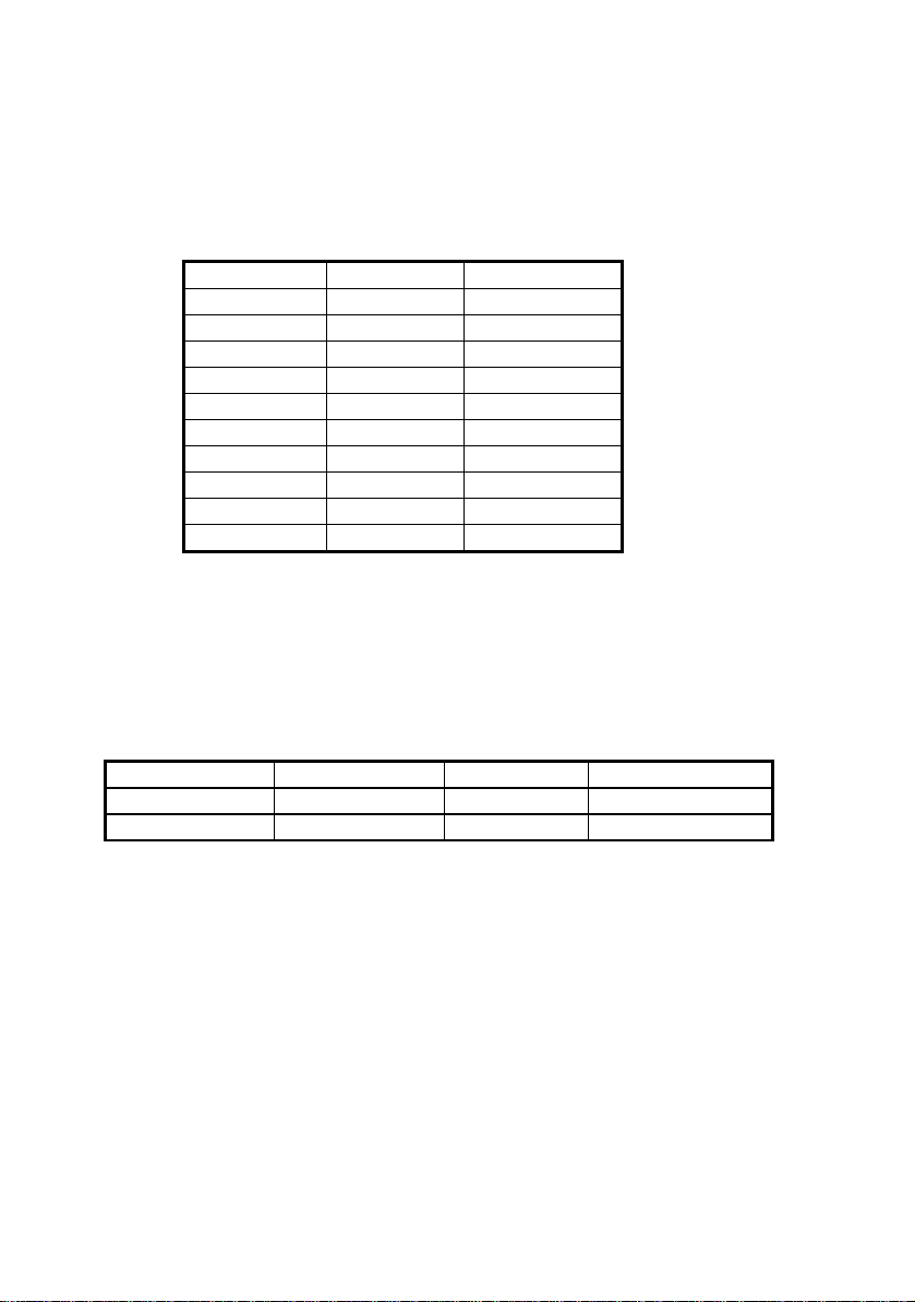
3.3.Memory configuration for “B59 V1.X” main board
System Memory Configuration
Capacity DIMM 1 DIMM 2
16MB 16MB None
32MB 16MB 16MB
32MB 32MB None
64MB 32MB 32MB
64MB 64MB None
80MB 16MB 64MB
80MB 64MB 16MB
128MB 64MB 64MB
128MB 128MB None
256MB 128MB 128MB
External Cache RAM Configuration.
Capacity SDRAM Type Quantity Location
256KB 32k x 64 1pcs U15
512KB 64k x 64 1pcs U15
15
Page 40

3.4. Jumper Setting
In order to set up the correct configuration, here is the description about how to
set the jumpers to enable/disable or change functions. All jumpers location
please refer to jumper location diagram.
CPU type selection :JP4, JP10
JP4
1-2 3-4 5-6 1-2 3-4 5-6 7-8
Pentium 100MHz Open Open Open Close Open Open Open
Pentium 120MHz Close Open Open Open Open Open Open
Pentium 133MHz Close Open Open Close Open Open Open
Pentium 150MHz Close Close Open Open Open Open Open
Pentium 166MHz Close Close Open Close Open Open Open
IDT C6 180MHz Open Close Open Open Open Open Open
IDT C6 200MHz Open Close Open Close Open Open Open
Pentium 200MHz
MMX
Pentium 233MHz
MMX
AMD
K6/233MHz(AFR)
AMD
K6/266MHz(AFR)
AMD
K6-2/266MHz
AMD
K6-2/300MHz
AMD
K6-2/350MHz
AMD
K6-2/400MHz
AMD
K6-3/400MHz
AMD
62-2/450MHZ
AMD
K6-3/450MHz
AMD
K6-2/500MHZ
AMD
K6-3/500MHZ
Open Close Open Close Open Open Open
Open Open Open Close Open Open Open
Open Open Open Close Open Open Open
Close Open Close Close Open Open Open
Open Close Open Close Close Close Open
Open Open Open Close Close Close Open
Close Open Close Close Close Close Open
Close Close Close Close Close Close Open
Open Close Close Close Close Close Open
JP10 CPU
16
Page 41
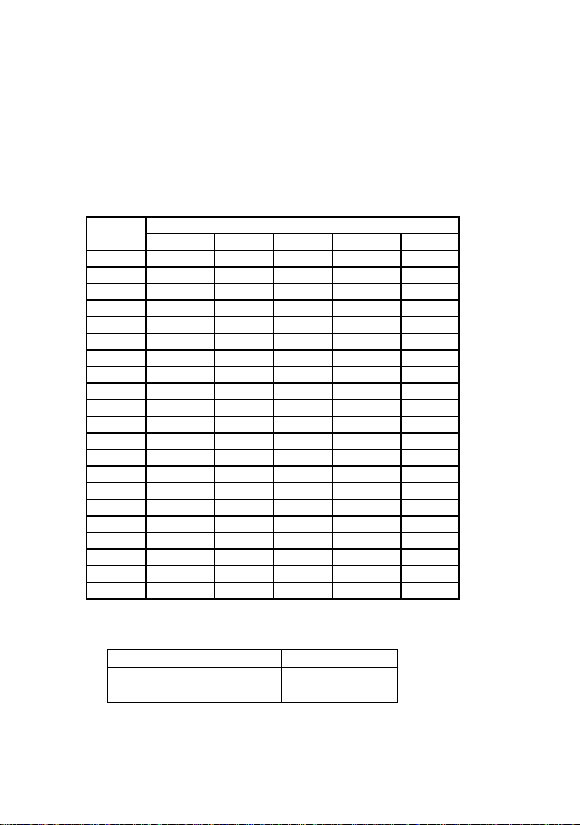
CPU Voltage selection :
JP2 Vcore
1-2 3-4 5-6 7-8 9-10
1.5 Open Open Close Open Close
1.6 Open Close Close Open Close
1.7 Open Open Open Close Close
1.8 Open Close Open Close Close
1.9 Open Open Close Close Close
2.0 Open Close Close Close Close
2.1 Close Open Open Open Open
2.2 Open Close Open Open Open
2.3 Close Close Open Open Open
2.4 Open Open Close Open Open
2.5 Close Open Close Open open
2.6 Open Close Close Open Open
2.7 Close Close Close Open Open
2.8 Open Open Open Close Open
2.9 Close Open Open Close Open
3.0 Open Close Open Close Open
3.1 Close Close Open Close Open
3.2 Open Open Close Close Open
3.3 Close Open Close Close Open
3.4 Open Close Close Close Open
3.5 Close Close Close Close Open
CMOS data clean function : JP9
CMOS data JP9
Clean 2-3
Normal (default) 1-2
17
Page 42
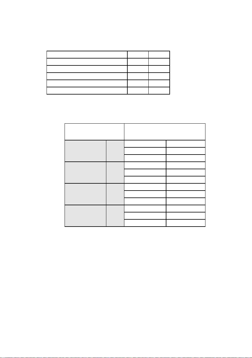
Disk On Chip address selection: JP12, JP13
Address JP12 JP13
0CC00H – 0CDFFH 1-2 1-2
0D000H – 0D1FFH 1-2 3-4
0D400H – 0D5FFH 3-4 3-4
0D800H – 0D9FFH 1-2 5-6
0DC00H – 0DDFFH 3-4 5-6
RS232 Select Jumper :JP5,JP6,JP15,JP16
COM Port Pin 1
COM1
COM2
COM3
COM4
JP15
JP16
JP6
JP5
1-2 (Default) Data Line
3-4 +5V
5-6 +12V
1-2(Default) Data Line
3-4 +5V
5-6 +12V
1-2(Default) Data Line
3-4 +5V
5-6 +12V
1-2(Default) Data Line
3-4 +5V
5-6 +12V
18
Page 43
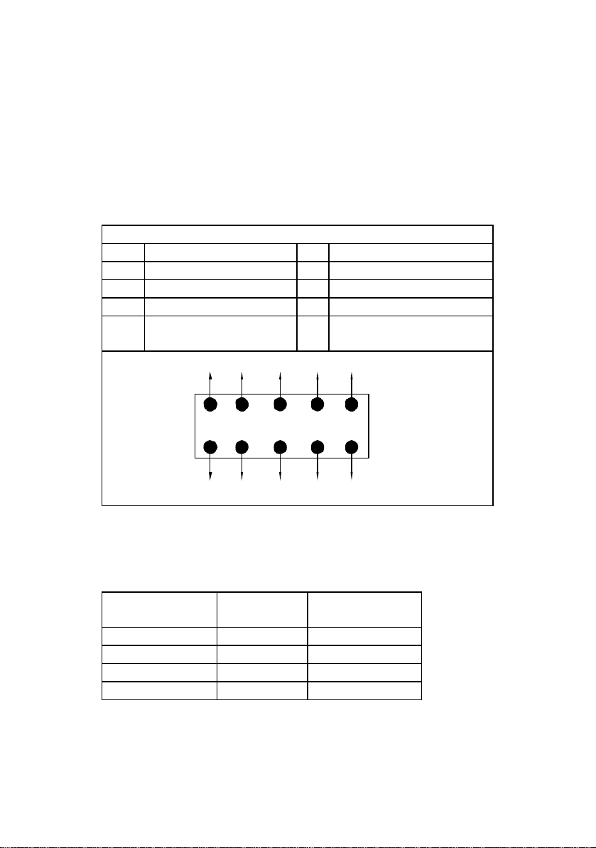
The output is TTL Level. The output signal must be TTL compatible.
OUT3
OUT1
OUT2
OUT0
VDC+12V
=Digital I/O (4 Output & 4 Input) : J5
This main board provides the basic digital I/O signal
Controller. User can develop the program and extra
controller to open and sense the cash drawer that based on the
digital I/O function on this main board.
PIN ASSIGNMENT
1 GND 6 Out 1
2 VDC +12V 7 IN 2
3 IN 0 8 Out 2
4 Out 0 9 IN 3
5 IN 1 10 Out 3
IN3 IN2 IN1 IN0
7
9
5
GND
1
3
8
10
6
2
4
Digital output programming
Output Addres
Bit
s
Out 0 206 0
Out 1 206 1
Out 2 206 2
Out 3 206 3
19
Page 44

Example : ( “0” = off “1” =on )
Data 00 = Out 0 and Out 1 = “0”
Data 01 = Out 0 = “1”
Data 02 = Out 1 = “1”
Data 03 = Out 0 and Out 1 = “1”
20
Page 45
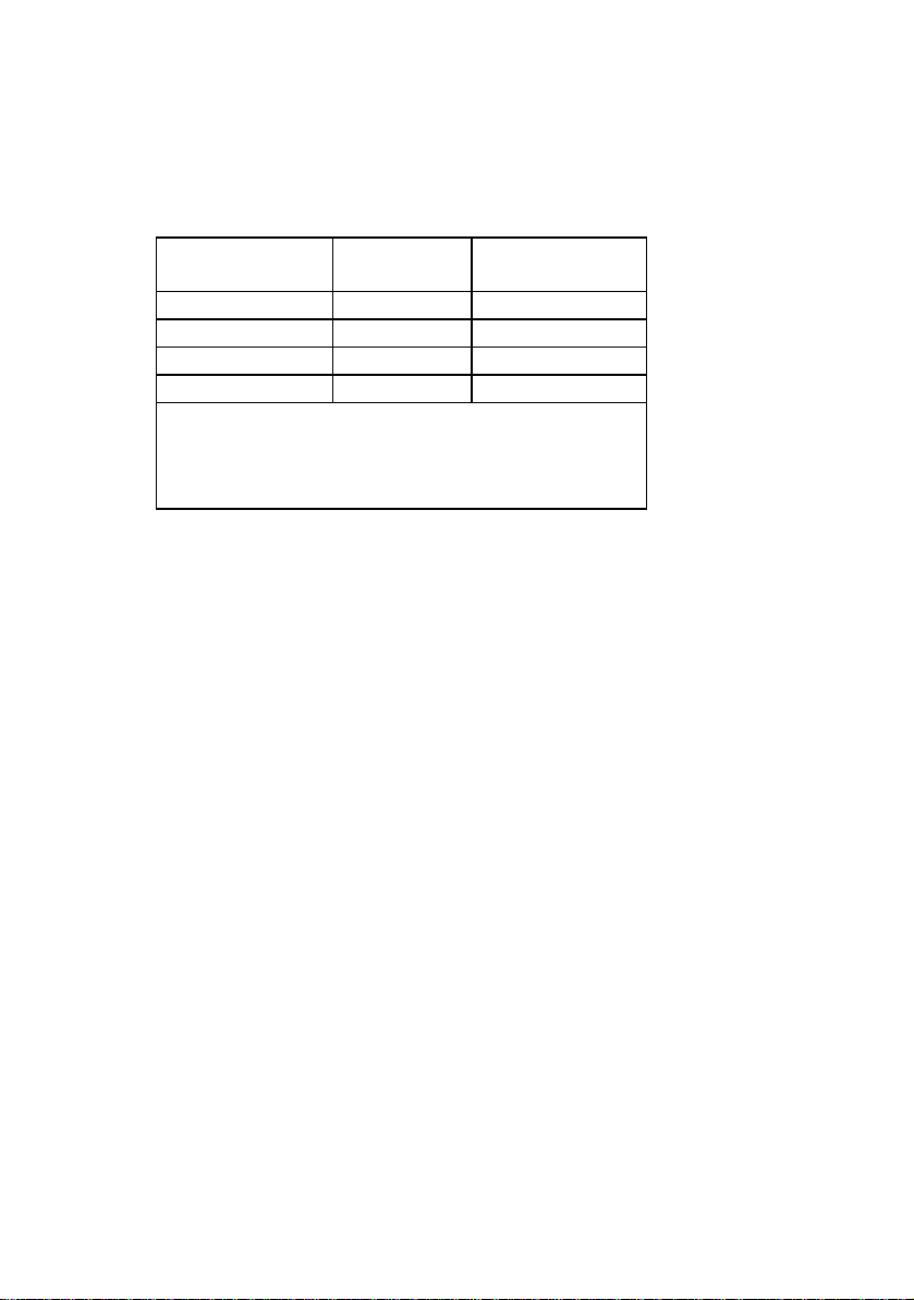
Digital input programming
The input signal must be TTL compatible.
Input Addres
s
IN 0 206 0
IN 1 206 1
IN 2 206 2
IN 3 206 3
Example : If input 206 is [ 0111], then input 3
is “0”, If input 206 is [0011], then input 3 & 4
are “0”
Bit
21
Page 46
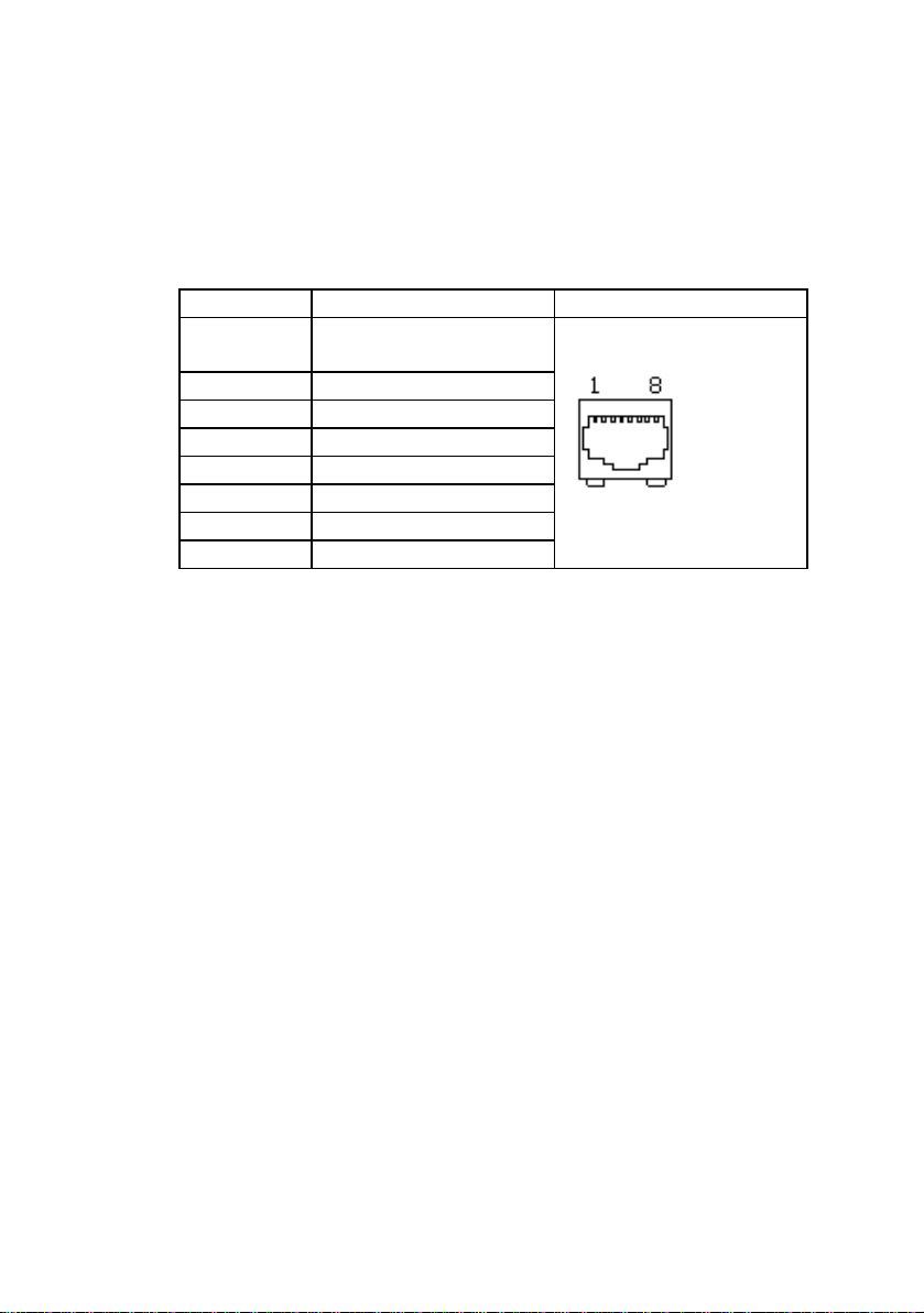
3.5 Connector’s description
LAN (100 / 10 Base-T RJ45 connector) : J1
Pin # Assignment Figure
1 Transmit output
(+)
2 Transmit output (-)
3 Receive input (+)
4 NC
5 NC
6 Receive input (-)
7 NC
8 NC
22
Page 47
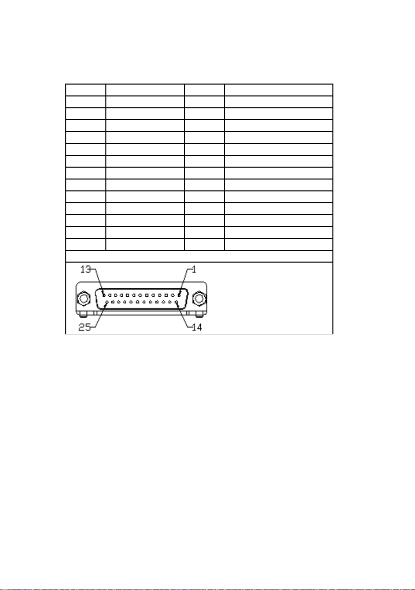
Parallel port 1 (D-SUB 25pin female connector) : J10
Pin # Assignment Pin # Assignment
1 Strobe (-) 14 Auto feed (-)
2 Data bit 0 15 Error (-)
3 Data bit 1 16 INIT (-)
4 Data bit 2 17 SLCT IN (-)
5 Data bit 3 18 Signal Ground
6 Data bit 4 19 Signal Ground
7 Data bit 5 20 Signal Ground
8 Data bit 6 21 Signal Ground
9 Data bit 7 22 Signal Ground
10 ACK (-) 23 Signal Ground
11 Busy 24 Signal Ground
12 Paper empty 25 Signal Ground
13 SLCT
Figure
23
Page 48
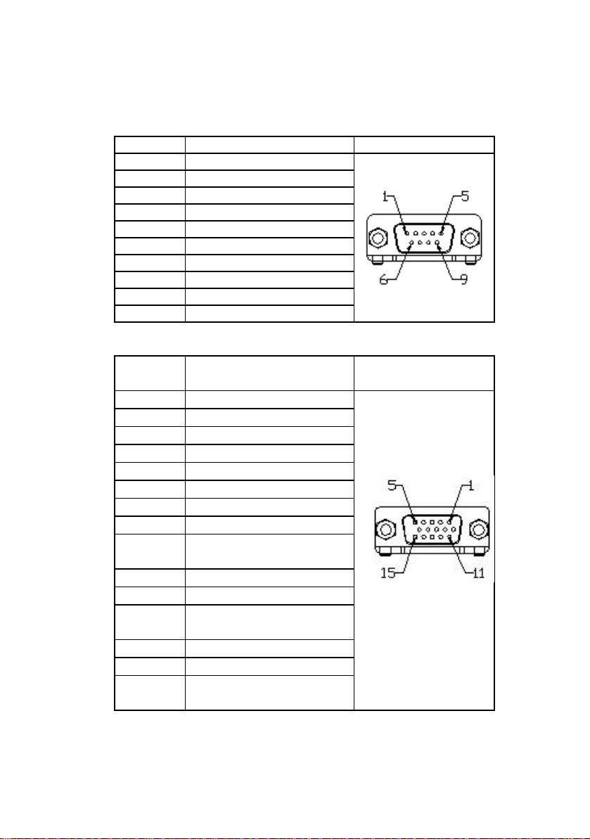
RS232 COM1 / COM2 (D-SUB 9pin male connector) : J4,J6
RS232 COM 3 / COM4 ( 2 x 10-pin pin header ) : J7, J8
Pin # Assignment Figure
1 Data carrier detect
2 Receive data
3 Transmit data
4 Data Terminal ready
5 Signal Ground
6 Data set ready
7 Request to send
8 Clear to send
9 Ring indicator
10 NC
VGA monitor (D-SUB 15pin female connector) : J18
Pin
Assignment Figure
#
1 Red signal
2 Green signal
3 Blue signal
4 NC
5 Ground
6 Red Ground
7 Green Ground
8 Blue Ground
9 VCC (with poly
switch)
10 Ground
11 NC
12 NC (with 10K Ω pull
high)
13 H Sync.
14 V Sync.
15 NC (with 10K Ω pull
high)
24
Page 49
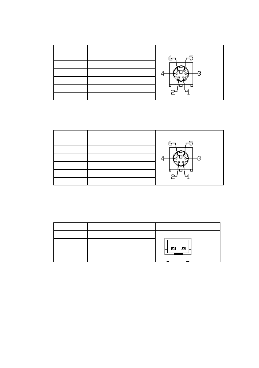
PS2 mouse (Mini Din 6 pin) : J 21
Pin # Assignment Figure
1 Mouse data
2 NC
3 Ground
4 +5V
5 Mouse clock
6 NC
Keyboard (Standard PS2 type ) : J23,
Pin # Assignment Figure
1 Keyboard data
2 NC
3 Ground
4 +5V
5 Keyboard clock
6 NC
+12V DC fan power (Pin-header 2pin) : CN6, CN10
Pin # Assignment Figure
1 +12V
2 Ground
25
Page 50
2
1
39
40
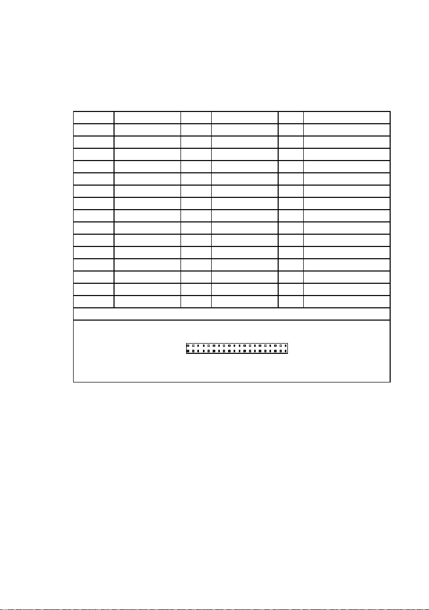
IDE harddisk connector (Pin-header 40pin) : J11,J12
Pin# Assignment Pin# Assignment Pin# Assignment
1 Reset 16 Data bit 14 31 IRQ 14
2 Ground 17 Data bit 0 32 NC
3 Data bit 7 18 Data bit 15 33 Disk address 1
4 Data bit 8 19 Ground 34 NC
5 Data bit 6 20 NC 35 Disk address 0
6 Data bit 9 21 IDE DRQ 36 Disk address 2
7 Data bit 5 22 Ground 37 Disk chip select 0
8 Data bit 10 23 Disk Write 38 Disk chip select 1
9 Data bit 4 24 Ground 39 Disk LED
10 Data bit 11 25 Disk read 40 Ground
11 Data bit 3 26 Ground
12 Data bit 12 27 Disk ready
13 Data bit 2 28 NC
14 Data bit 13 29 IDE DACK
15 Data bit 1 30 Ground
Figure
26
Page 51
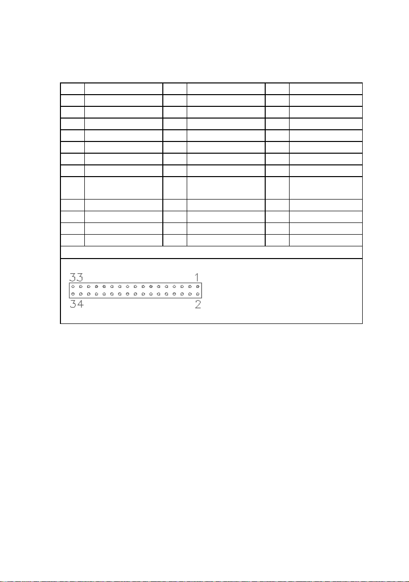
Floppy disk connector (Pin-header 34pin ): J20
Pin# Assignment Pin# Assignment Pin# Assignment
1 Ground 13 Ground 25 Ground
2 Density select 14 Driver select 2 26 Track 00
3 Ground 15 Ground 27 Ground
4 Not used 16 Motor on 1 28 Write protected
5 Ground 17 Ground 29 Ground
6 Vcc 18 Data direction 30 Read data
7 Ground 19 Ground 31 Ground
8 Index 20 Step
motor active
9 Ground 21 Ground 33 Ground
10 Motor on 0 22 Write data 34 Disk change
11 Ground 23 Ground
12 Driver select 1 24 Write gate
32 Head select
Figure
,
27
Page 52
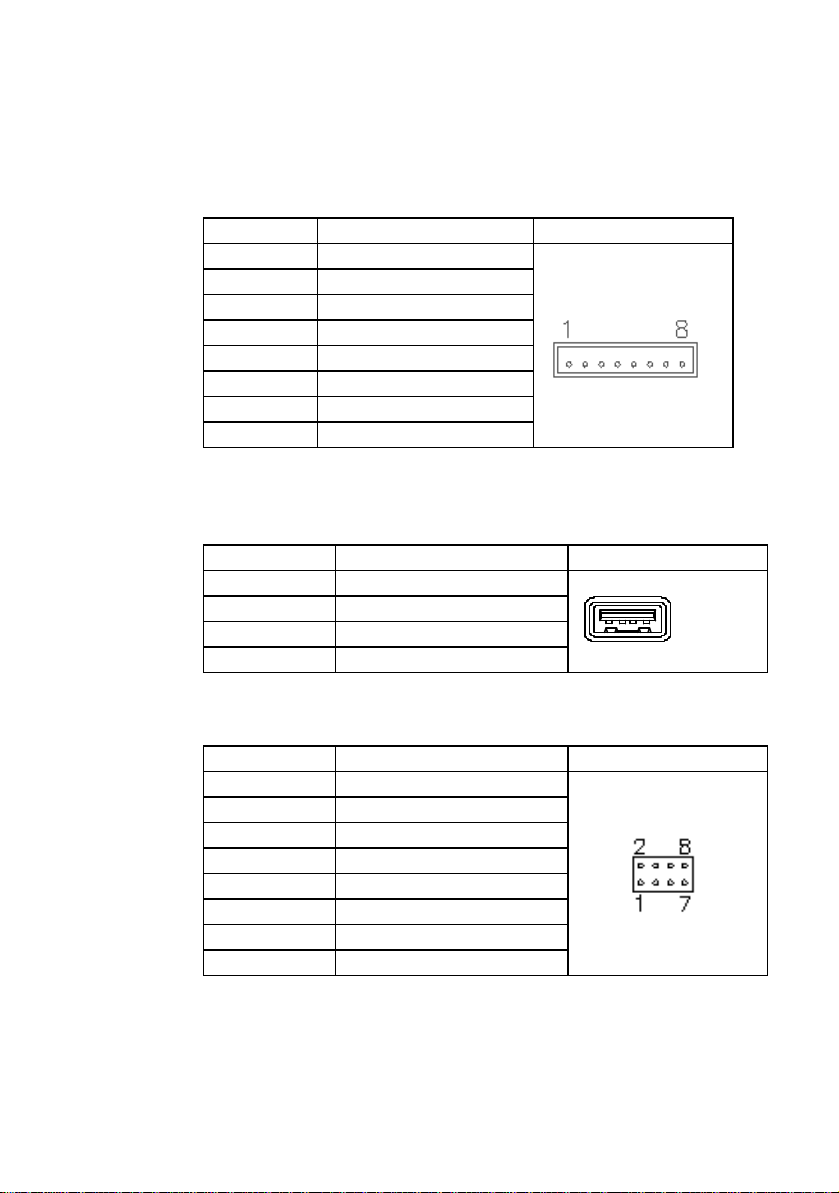
Power input for AT internal power adapter (Pin-header 8pin) : CN12
FT-8075 for 1000 series / FT-8050 for 4000 series
Pin # Assignment Figure
1 +5V
2 Ground
3 +5V
4 Ground
5 Ground
6 +12V
7 Ground
8 -12V
USB port connector (Pin-header 4pin) : J15,J17
Pin # Assignment Figure
1 +5V
1 4
USB port connector (Pin-header 4pin) : J16
2 USB Port Data 3 USB Port Data +
4 Ground
Pin # Assignment Figure
1 +5V
2 +5V
3 USB Port 1 Data 4 USB Port 2Data 5 USB Port 1 Data +
6 USB Port 2Data +
7 Ground
8 Ground
28
Page 53
6 1
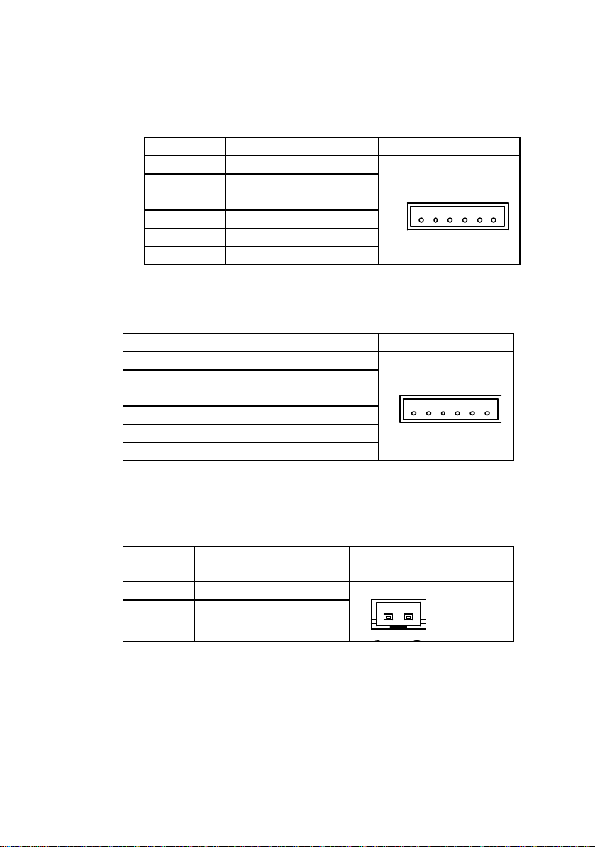
HDD, FDD, POWER LED connector:CN4
Pin # Assignment Figure
1 +5V
2 Ground
3 -MTR0
4 HD_LED
5 GPO0
6 Ground
HDD, FDD, POWER LED connector:CN14
Pin # Assignment Figure
1 -MTR0
2 +5V
3 HD_LED
4 +5V
5 GPO0
6 +5V
Compact Flash power connector: CN13
Pin
Assignment Figure
#
1 +5V
2 Ground
1
6
Compact Flash II connector: J25
29
Page 54
Appendix A2- AWARD BIOS setup 1631
Remark : We select the following model as a sample to analysis how to setup
System BIOS. For other models or updated BIOS information, please check
with your supplier.
MODEL 1631-XXX
CPU Intel Pentium II / III / Celeron
M / B B63
BIOS AWARD
The above models of the 1000 series computer's BIOS are supplied by AWARD
SOFTWARE, INC. AWARD'S BIOS Flash ROM has a built-in Setup program
that allows users to modify the basic system configuration. This type of
information is stored in battery-backed RAM of CMOS chipset so that it retains
the Setup information when the power is turned off.
Entering Setup
Power on the computer and press <Del> immediately will allow you to enter
Setup. The other way to enter Setup is to power on the computer, when the
below message appears briefly at the bottom of the screen during the POST
(Power On Self Test), press <Del> key or simultaneously press <Ctrl>, <Alt>,
and <Esc> keys.
TO ENTER SETUP BEFORE BOOT PRESS <CTRL-ALT-ESC> OR <DEL>
KEY
PRESS <F1> TO CONTINUE, <CTRL-ALT-ESC> OR <DEL> TO ENTER
SETUP
81
Page 55
Control Keys
Up arrow Move to previous item
Down arrow Move to next item
Left arrow Move to the item to the left side
Right arrow Move to the item to the right side
Esc key Main Menu -- Quit and not save changes into CMOS
Status Page Setup Menu and Option Page Setup Menu -- Exit
current page and return to Main Menu
PgUp / “+” key Increase the numeric value or make changes
PgDn / “−“ key Decrease the numeric value or make changes
F1 key General help, only for Status Page Setup Menu and Option
Page Setup Menu
(Shift)F2 key Change color from total 16 colors. F2 to select color forward,
(Shift) F2 to select color backward
F3 key Reserved
F4 key Reserved
F5 key Restore the previous CMOS value from CMOS, only for Option
Page Setup Menu
F6 key Load the default CMOS value from BIOS default table, only for
Option Page Setup Menu
F7 key Load the Setup default , only for Option Page Setup Menu
F8 key Reserved
F9 key Reserved
F10 key Save all the CMOS changes, only for Main Menu
Getting Help
Main Menu
The on-line description of the highlighted setup function is displayed at the
bottom of the screen.
Status Page Setup Menu/Option Page Setup Menu
Press F1 to pop up a small help window that describes the appropriate keys to
use and the possible selections for the highlighted item. To exit the Help
Window press <F1> or <Esc>.
82
Page 56

The Main Menu
Once you enter AWARD BIOS CMOS Setup Utility, the Main Menu will appear
on the screen. The Main Menu allows you to select from ten setup functions
and two exit choices. Use arrow keys to select among the items and press
<Enter> to accept or enter the sub-menu.
Standard CMOS setup
This setup page includes all the items in a standard compatible BIOS.
BIOS features setup
This setup page includes all the items of AWARD special enhanced features.
Chipset features setup
This setup page includes all the items of chipset special features.
Power Management setup
This category determines how much power consumption for system after
selecting below items. Default value is Disable.
PNP/PCI Configuration
This category specifies the value (in units of PCI bus clocks) of the latency timer
for this PCI bus master and the IRQ level for PCI device.
Load BIOS defaults
BIOS defaults indicates the most appropriate value of the system parameter
which the system would be in minimum performance.
Load set up defaults
Setup defaults indicates the values required by the system for the maximum
performance.
83
Page 57

CPU FEATURE Monitor
Setup defaults indicated the CPU temperature, CPU Fan Speed and the Vcore
information.
Integrated Peripherals
Change, set, or disable on board super I/O function.
Supervisor password & Password setting
Change, set, or disable password. It allows you to limit access to the system
and Setup, or just to Setup.
IDE HDD auto detection
Automatically configure hard disk parameters.
Save & exit setup
Save CMOS value changes to CMOS and exit setup.
Exit without save
Abandon all CMOS value changes and exit setup.
84
Page 58
Standard CMOS Setup Menu
The items in Standard CMOS Setup Menu are divided into 11 categories. Each
category includes no, one or more than one setup items. Use the arrow keys to
highlight the item and then use the <PgUp> or <PgDn> keys to select the value
you want in each item.
Date
The date format is <day>, <date> <month> <year>. Press <F3> to show the
calendar.
day The day of week, from Sun to Sat, determined by the BIOS, is read
only
date The date, from 1 to 31 (or the maximum allowed in the month),
can key in the numerical / function key
month The month, Jan. through Dec.
year The year, depend on the year of BIOS
Time
The time format is <hour> <minute> <second>. which accepts both function
key or numerical key The time is calculated based on the 24-hour military -time
clock. For example, 1 p.m. is 13:00:00.
Primary master / Primary slave / Secondary master / Secondary slave
The categories identify the types of hard disk drive C or drive D that have been
installed in the computer. There are 45 predefined types and 1 user definable
types and 1 automatic type for Normal BIOS. Type 1 to Type 45 are predefined.
Type User is user-definable. Type Auto is auto-definition by your computer.
85
Page 59

Press PgUp/<+> or PgDn/<−> to select a numbered hard disk type or type the
number and press <Enter>. Note that the specifications of your drive must
match with the drive table. The hard disk will not work properly if you enter
improper information for this category. If your hard disk drive type is not
matched or listed in 1 to 45, you can use Type User or Auto to define your own
drive type manually or automatically.
If you select Type User, related information is asked to be entered to the
following items. Enter the information directly from the keyboard and press
<Enter>. This information should be provided in the documentation from your
hard disk vendor or the system manufacturer.
If the controller of HDD interface is ESDI, the selection shall be “Type 1”.
If the controller of HDD interface is SCSI, the selection shall be “None”.
If the controller of HDD interface is CD-ROM, the selection shall be “None”.
CYLS. number of cylinders
HEADS number of heads
PRECOMP write precom
LANDZONE landing zone
SECTORS number of sectors
MODE HDD access mode
86
Page 60
If a hard disk has not been installed select NONE or Auto and press <Enter>.
Drive A / Drive B
The category identifies the types of floppy disk drive A or drive B that have been
installed in the computer.
None No floppy drive installed
360K, 5.25 in 5-1/4 inch PC-type standard drive; 360 kilobyte capacity
1.2M, 5.25 in 5-1/4 inch AT-type high-density drive; 1.2 megabyte
capacity
720K, 3.5 i 3-1/2 inch double-sided drive; 720 kilobyte capacity
1.44M, 3.5 in 3-1/2 inch double-sided drive; 1.44 megabyte capacity
2.88M, 3.5 in 3-1/2 inch double-sided drive; 2.88 megabyte capacity
Video
The category selects the type of adapter used for the primary system monitor
that must match your video display interface and monitor.
EGA/VGA Enhanced Graphics Adapter/video Graphics Array. For EGA,
VGA, SVGA, or PGA monitor adapters.
CGA 40 Color Graphics A dapter, power up in 40 column mode
CGA 80 Color Graphics Adapter, power up in 80 column mode
MONO Monochrome adapter, includes high resolution monochrome
adapters
87
Page 61
Error halt
The category determines whether the computer will stop if an error is detec ted
during power up.
No errors Whenever the BIOS detects a non-fatal error the
system will stop and you will be prompted.
All errors The system boot will stop for any error that may
be detected.
All, But Keyboard The system boot will not stop for a keyboard
error; it will stop for all other errors.
All, But Diskette The system boot will not stop for a disk error; it
will stop for all other errors.
All, But Disk/Key The system boot will not stop for a keyboard or
disk error; it will stop for all other errors.
Memory
The category is display-only which is determined by POS (Power On Self Test)
of the BIOS.
Base Memory
The POST of the BIOS will determine the amount of base (or conventional)
memory installed in the system. The value of the base memory is typically
512K for systems with 512K memory installed on the motherboard, or 640K for
systems with 640K or more memory installed on the motherboard.
Extended Memory
The BIOS determines how much extended memory is present during the POST.
This is the amount of memory located above 1MB in the CPU's memory
address map.
Other Memory
This refers to the memory located in the 640K to 1024K address space. This is
memory that can be used for different applications. DOS uses this area to load
device drivers to keep as much base memory free for application programs.
Most use for this area is Shadow RAM.
88
Page 62

Total Memory
89
Page 63
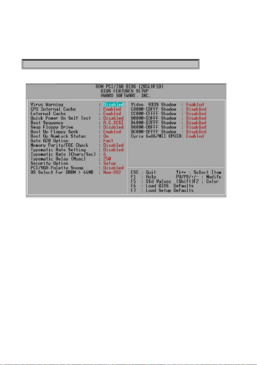
System total memory is the sum of basic memory, extended memory, and
other memory.
BIOS Features Setup Menu
Virus Warning
This category flashes on the screen. During and after the system boots up,
any attempt to write to the boot sector or partition table of the hard disk drive will
halt the system and the following error message will appear, in the mean time,
you can run an anti-virus program to locate the problem.
90
Page 64
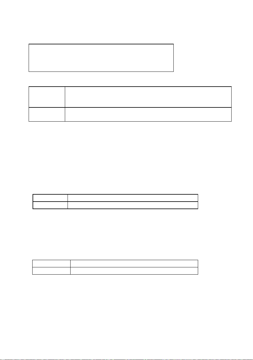
! WARNING !
Disk boot sector is to be modified
Type "Y" to accept write or "N" to abort write
AWARD Software, Inc.
Enabled Activates automatically when the system boots up causing a
warning messa ge to appear when anything attempts to access
the boot sector or hard disk partition table.
Disabled No warning message to appear when anything attempts to access
the boot sector or hard disk partition table.
Note: This function is available only for DOS and other OSes that do not trap
INT13.
CPU Internal Cache / External Cache
These two categories speed up memory access. However, it depends on
CPU/chipset design. The default value is Enable. If your CPU is without
Internal Cache then this item “CPU Internal Cache” will not appear.
Enabled Enable cache
Disabled Disable cache
Quick Power On Self Test
This category speeds up Power On Self Test (POST) after you power on the
computer. If it is set to Enable, BIOS will shorten or skip some check items
during POST.
Enabled Enable quick POST
Disabled Normal POST
Boot Sequence
This category determines which drive computer searches first for the disk
operating system (i.e., DOS). Default value is A,C.
91
Page 65

92
Page 66
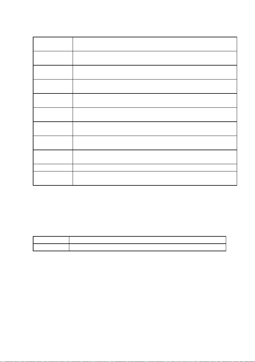
A, C,SCSI System will first search the floppy disk drive then hard disk drive
for booting purpose
C, A,SCSI System will first search the hard disk drive then floppy disk drive
for booting puropse
C,CDROM,A System will first search the harddisk drive then CDROM drive and
the next is floppy disk drive for booting purpose
CDROM,C,A System will first search the CDROM drive then harddisk drive and
the next is floppy disk drive for booting purpose
D, A,SCSI System will first search the hard disk D drive then floppy disk
drive for booting puropse
E, A,SCSI System will first search the hard disk E drive then floppy disk drive
for booting puropse
F, A,SCSI System will first search the hard disk F drive then floppy disk drive
for booting puropse
SCSI, A, C System will first search the SCSI hard disk drive then floppy disk
drive for booting puropse
SCSI, C, A System will first search the SCSI hard disk drive then hard disk
drive for booting puropse
C only System only search the harddisk drive for booting purpose
LS/ZIP, C System will first search the LS120 drive then hard disk drive for
booting purpose
Note: This function is only available for IDE type
Swap Floppy Drive
Enabled Enable Floppy Drives A and B Swap function
Disabled Disable Floppy Drives A and B Swap function
Boot Up Floppy Seek
During POST, BIOS will determine if the floppy disk drive installed is 40 or 80
tracks. 360K type is 40 tracks while 720K, 1.2M and 1.44M are all 80 tracks.
93
Page 67
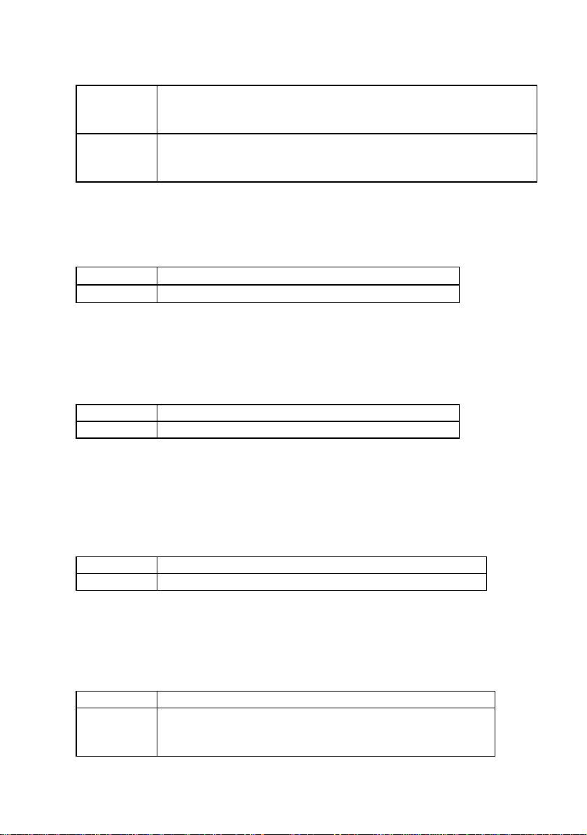
Enabled BIOS searches for floppy disk drive to determine if it is 40 or 80
tracks. Note that BIOS can not tell from 720K, 1.2M or 1.44M drive
type as they are all 80 tracks.
Disabled BIOS will not search for the type of floppy disk drive by track
number. Note that there will be no warning message if the drive
installed is 360K.
Boot Up NumLock Status
The default value is On.
On Keypad is number keys after boot -up
Off Keypad is arrow keys after boot -up
Boot Up System Speed
It selects the default system speed - the speed that the system will run
immediately after power on.
High Set the system speed to high
Low Set the system speed to low
Gate A20 Option
This entry allows you to select how the gate A20 is handled. The gate A20 is a
device used to address memory above 1 Mbytes. Initially, the gate A20 was
support, it is more common, and much faster, for the chipset to provide support
for A20.
Normal Handling gate A20 by keyboard
Fast Handling gate A20 by chipset
Typematic Rate Setting
This determines the typematic rate.
Enabled Enable typematic rate and typematic delay programming
Disabled Disable typematic rate and typematic delay programming.
The system BIOS will use default value of this 2 items and
the default is controlled by keyboard.
94
Page 68

95
Page 69

Typematic Rate (Chars/Sec)
When the typematic rate setting is enabled, this selection allows you select the
rate at which the key are accelerated.
6 6 characters per second
8 8 characters per second
10 10 characters per second
12 12 characters per second
15 15 characters per second
20 20 characters per second
24 24 characters per second
30 30 characters per second
Typematic Delay (Msec)
When the typematic rate setting is enabled, this selection allows you to select
the delay between when the key was first depressed and when the acceleration
begins.
250 250 msec
500 500 msec
750 750 msec
100
1000 msec
0
Security Option
This category allows you to limit access to the system and Setup, or just to
Setup.
System The system will not boot and access to Setup will be denied if the
correct password is not entered at the prompt.
Setup The system will boot, but access to Setup will be denied if the
correct password is not entered at the prompt.
96
Page 70
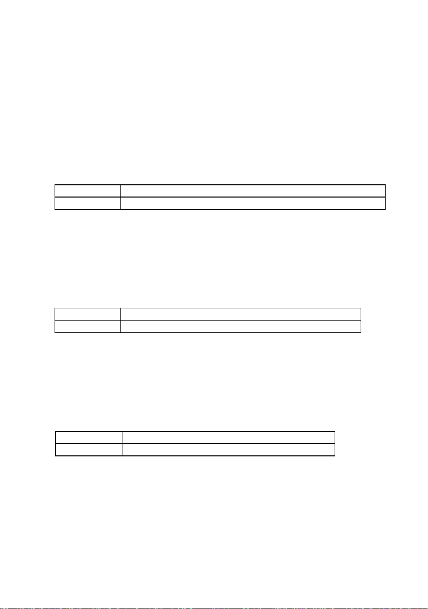
Note: To disable security, select PASSWORD SETTING at Main Menu and
then you will be asked to enter password Do not type anything and just press
<Enter>, it will disable security. Once the security is disabled, the system will
boot and you can enter Setup freely.
PCI/VGA Palette Snoop
It determines whether the MPEG ISA/VESA VGA cards can work with
PCI/VGA or not.
Enable When PCI/GA works with MPEG ISA/VESA VGA card
Disable When PCI/VGA doesn‘t work with MPEG ISA/VESA card
OS Select For DRAM > 64MB
This item allows you to access the memory that over 64MB in OS2
Non-OS2 OS2 cannot access the memory address over 64MB
OS2 OS2 can access the memory address over 64MB
Video BIOS Shadow
BIOS Shadow
It determines whether system BIOS will be copied to RAM or the system BIOS
is always shadow to support LBA HDD.
Enabled System shadow is enabled
Disabled System shadow is disabled
97
Page 71

Video ROM Shadow
It determines whether video ROM will be copied to RAM, however, it is optional
from chipset design. Video Shadow will increase the video speed.
Enabled Video shadow is enabled
Disabled Video shadow is disabled
C8000 - CBFFF Shadow / CC000 - CFFFF Shadow / D0000 - D3FFF Shadow /
D4000 - D7FF Shadow /D8000 - DBFFF Shadow / DC000 - DFFFF Shadow
These categories determine whether optional ROMs will be copied to RAM. An
example of such option ROM would be support of SCSI add-on card.
Enabled Optional shadow is enabled
Disabled Optional shadow is disabled
Cyrix 6x86/MII CPUID
The choice : enable, disable
98
Page 72
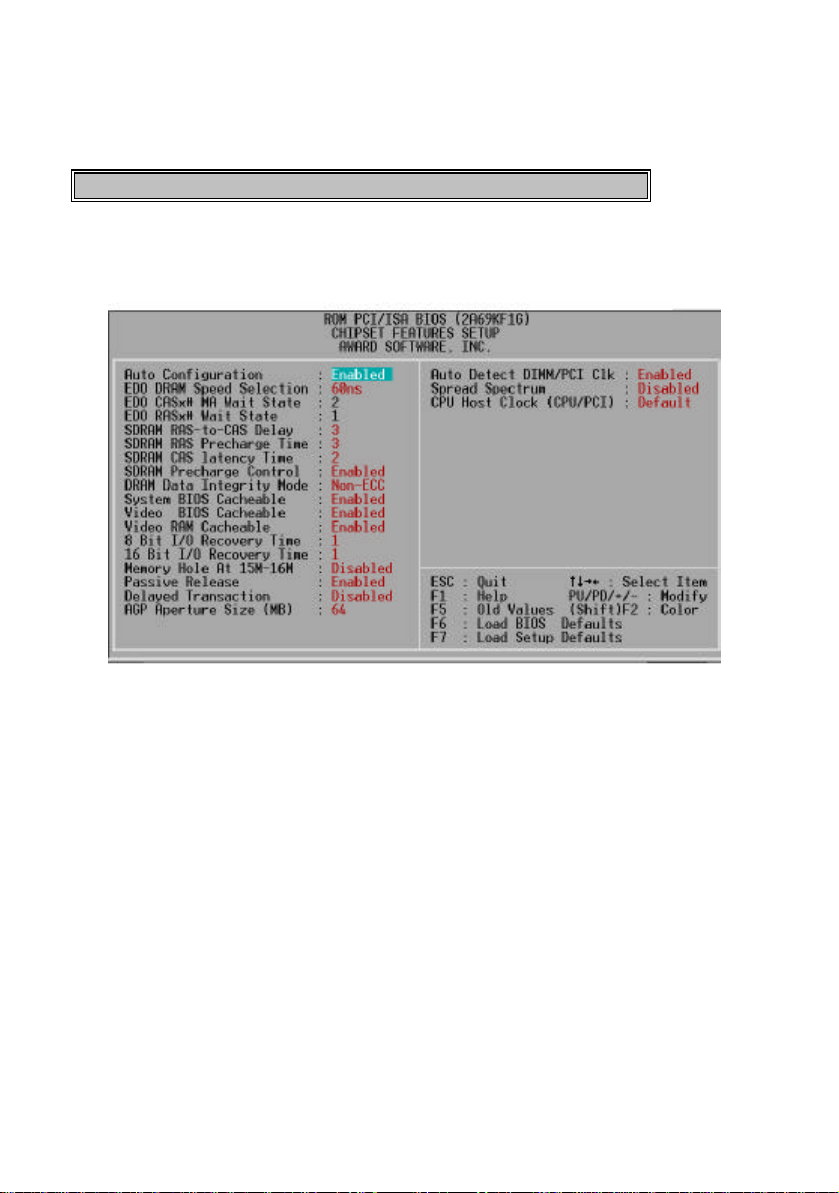
Chipset Features Setup Menu
Bank 0/1, 2/3 DRAM Timing
This value in this field is set by the system board manufacturer, depending on
whether the board has synchronous DRAMs
The Choice: SDRAM 10ns, SDRAM 8ns, Normal, Medium, Fast, Turbo.
SDRAM Cycle Length
This field sets the CAS latency timing.
The Choice: 2, 3.
99
Page 73

DRAM Read Pipeline
You may select Enabled for this field when PBSRAMs are installed. Pipelining
improves system performance.
The Choice: Enabled, Disabled.
Sustained 3T Write
This item allow you to enable or disable direct map write back / write through
secondary cache.
The Choice: Enabled, Disabled.
Cache Rd+CPU Wt Pipeline
This item allows you to enable/disable the cache timing.
The Choice: Enabled, Disabled.
Cache Timing
The Choice : Fast, Fastest
Video BIOS Cacheable
When enabled. The Video BIOS cache will cause access to video BIOS
addressed at C0000H to C7FFFH to be cached, if the cache controller is also
enabled
The Choice: Enabled, Disabled.
System BIOS Cacheable
As with caching the Video BIOS above, enabling this selection allows accesses
to the system BIOS ROM addressed at F0000H-FFFFFH to be cached,
provided that the cache controller is enabled.
The Choice: Enabled, Disabled.
100
Page 74

Memory Hole
In order to improve performance, certain space in memory is reserved for ISA
cards. This memory must be mapped into the memory space below 16MB.
The Choice: Disabled, 15M-16M, 14M-16M.
Aperture Size
Select the size of Accelerated Graphics Port (AGP) aperture. The aperture is a
portion of the PCI memory address range dedicated for graphics memory
address space. Host cycles that hit the aperture range are forwarded to the
AGP without any translation. See www.apgforum.org for AGP information.
The Choice: 4M, 8M, 16M, 32M, 64M, 128M, 256M.
OnChip USB
Select Enabled if your system contains a Universal Serial Bus (USB) controller
and you have a USB peripheral.
The Choice: Enabled, Disabled.
USB Keyboard Support
Select Enabled if your system contains a Universal Serial Bus (USB) controller
and you have a USB keyboard.
The Choice: Enabled, Disabled.
101
Page 75
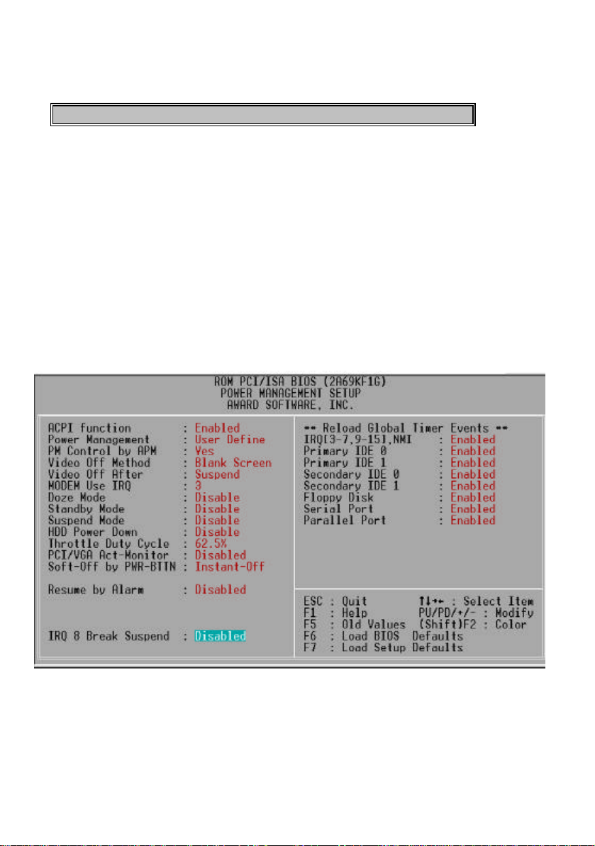
Power Management Setup
The Power management setup will appear on your screen like this:
Power Management
This category allows you to select the type (or degree) of power saving and is
directly related to the following modes:
1. Doze Mode
2. Suspend Mode
102
Page 76
3. HDD Power Down
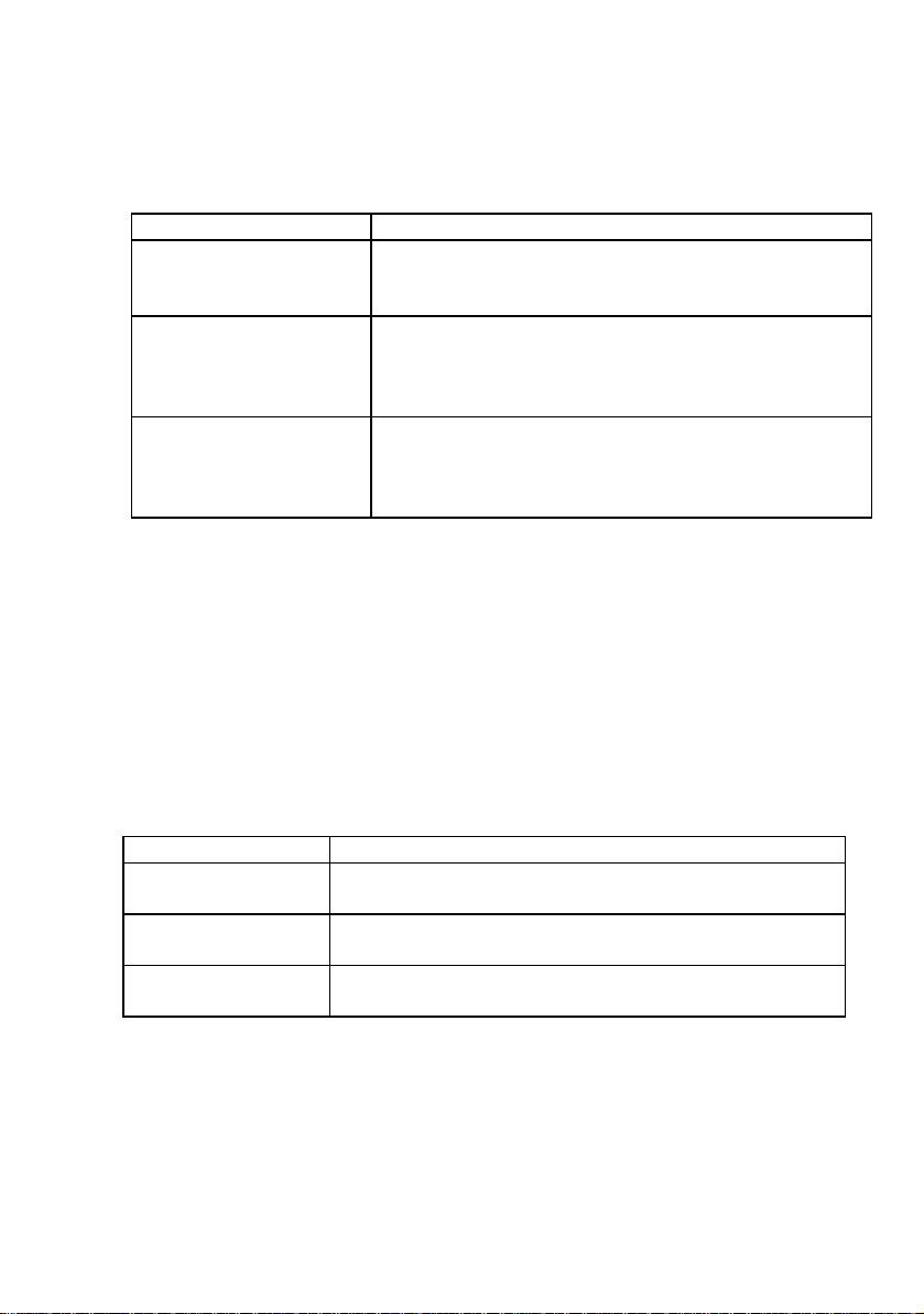
There are four selections for Power Management, three of which have fixed
mode settings.
Disable (default) No power management. Disables all four modes
Min. Power Saving Minimum power management. Doze Mode = 1 hr.
Standby Mode = 1 hr., Suspend Mode = 1 hr., and HDD
Power Down = 15 min.
Max. Power Saving Maximum power management -- ONLY AVAILABLE
FOR SL CPU’S . Doze Mode = 1 min., Standby Mode =
1 min., Suspend Mode = 1 min., and HDD Power
Down = 1 min.
Us er Defined Allows you to set each mode individually. When not
disabled, each of the ranges are from 1 min. to 1 hr.
except for HDD Power Down which ranges from 1 min.
to 15 min. and disable.
PM Control APM
When enabled, an Advanced Power Management device will be activated to
enhance the Max. Power Saving mode and stop the CPU internal clock. If
Advance Power Management (APM) is installed on your system, selecting Yes
gives better power savings.
If the Max. Power Saving is not enabled, this will be pres et to No.
Video Off After
When enabled, this feature allows the VGA adapter to operate in a power
saving
mode.
N/A Monitor will remain on during power saving modes.
Suspend Monitor blanked when the systems enters the Suspend
mode.
Standby Monitor blanked when the system enters Standby
mode.
Doze Monitor blanked when the system enters any power
saving mode.
103
Page 77

Video Off Method
This determines the manner in which the monitor is blanked.
V/H SYNC+Blank This selection will cause the system to turn off the
vertical and horizontal synchronization ports and
write blanks to the video buffer.
Blank Screen This option only writes blanks to the video buffer.
DPMS Select this option if your monitor supports the
Display Power Management Signaling (DPM S)
standard of the Video Electronics Standards to
select video power management values.
MODEM Use IRQ
This determines the IRQ in which the MODEM can use.
The choice: 1, 3, 4, 5, 7, 9, 10, 11, NA.
Soft-Off by PWRBTN
When Enabled, turning the system o ff with the on/off button places the system
in
a very low-power-usage state, with only enough circuitry receiving power to
detect power button activity or Resume by Ring activity.
The choice: Delay 4 Sec, Instant Off.
PM Timers
The following three modes are Green PC power saving functions which are only
user configurable when User Defined Power Management has been selected.
See above for available selections.
HDD Power Down
When enabled and after the set time of system inactivity, the hard disk drive will
be powered down while all other devices remain active.
Doze Mode
When enabled and after the set time of system inactivity, the CPU clock will run
at slower speed while all other devices still operate at full speed.
Suspend Mode
104
Page 78

When enabled and after the set time of system inactivity, all devices except the
CPU will be shut off.
PM Events
PM events are I/O events whose occurrence can prevent the system from
entering a power saving mode or can awaken the system from such a mode. In
effect, the system remains alert for anything which occurs to a device which is
configured as On, even when the system is in a power down mode.
VGA
When set to On (default), any event occurring at a VGA port will awaken a
system which has been powered down.
LPT & COM
When set to On (default), any event occurring at a COM(serial)/LPT (printer)
port will awaken a system which has been powered down.
HDD & FDD
When set to On (default), any event occurring at a hard or floppy drive port will
awaken a system which has been powered down.
DMA/master
When set to On (default), any event occurring to the DMA controller will awaken
a system which has been powered down.
Primary INTR
When set to On (default), any event occurring at will awaken a system which
has been powered down.
The following is a list of IRQ’s, Interrupt ReQuests, which can be exempted
much as the COM ports and LPT ports above can. When an I/O device wants to
gain the attention of the operating system, it signals this by causing an IRQ to
occur. When the operat ing system is ready to respond to the request, it
interrupts itself and performs the service.
105
Page 79

As above, the choices are On and Off. Off is the default.
When set On, activity will neither prevent the system from going into a power
management mode nor awaken it.
IRQ3 (COM 2 )
IRQ4 (COM 1)
IRQ5 (LPT 2)
IRQ6 (Floppy Disk)
IRQ7 (LPT 1)
IRQ8 (RTC Alarm)
IRQ9 (IRQ2 Redir)
IRQ10 (Reserved)
IRQ11 (Reserved)
IRQ12 ( PS / 2 Mouse )
IRQ13 (Coprocessor)
IRQ14 (Reserved)
IRQ15 (Reserved)
106
Page 80
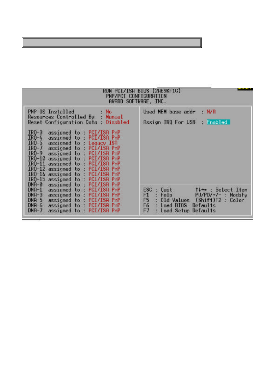
PNP/PCI Configuration Setup
You can manually configurate the PCI Device’s IRQ. The following pages tell
you the options of each item & describe the meanings of each options.
PNP OS Installed
Select Yes if the system operating environment is Plug-and-Play aware (e.g.,
Windows 95).
The Choice: Yes and No.
Resource controlled by
107
Page 81

The Award Plug and Play BIOS has the capacity to automatically configure all
of the boot and Plug and Play compatible devices. However, this capability
means absolutely nothing unless you are using a Plug and Play operating
system such as Windows 95.
The choice: Auto and Manual.
Reset Configuration Data
Normally, you leave this field Disabled. Select Enabled to reset Extended
System Configuration Data (ESCD) when you exit Setup if you have installed a
new add-on and the system reconfiguration has caused such a serious conflict
that the operating system can not boot.
The choice: Enabled and Disabled .
CPU to PCI Write Buffer
When enabled, up to four D words of data can be written to the PCI bus without
interrupting the CPU. When disabled, a write buffer is not used and the CPU
read cycle will not be completed until the PCI bus signals that it is ready to
receive the data..
The choice: Enabled, Disabled.
PCI Dynamic Bursting
When Enabled, data transfers on the PCI bus, where possible, make use of the
high-performance PCI bust protocol, in which greater amounts of data are
transferred at a single command..
The choice: Enabled, Disabled.
PCI Master 0 WS Write
When Enabled, writes to the PCI bus are command with zero wait states.
The choice: Enabled, Disabled.
PCI Delay Transaction
The chipset has an embedded 32-bit posted write buffer to support delay
transactions cycles. Select Enabled to support compliance with PCI
specification version 2.1.
The choice: Enabled, Disabled.
PCI Master Read Prefetch
108
Page 82

This item allows you enable/disable the PCI Master Read Prefetch.
The choice: Enabled, Disabled.
PCI #2 Access #1 Retry
This item allows you enable/disable the PCI #2 Access #1 Retry.
The choice: Enabled, Disabled.
AGP Master 1 WS Write
This implements a single delay when writing to the AGP Bus. By default,
two-wait states are used by the system, allowing for greater stability.
The choice: Enabled, Disabled.
AGP Master 1 WS Read
This implements a single delay when reading to the AGP Bus. By default,
two-wait states are used by the system, allowing for greater stability.
The choice: Enabled, Disabled.
Assign IRQ For USB/VGA
This item allows you enable/disable to assign a system interrupt for USB or
VGA.
The choice: Enabled and Disabled
109
Page 83
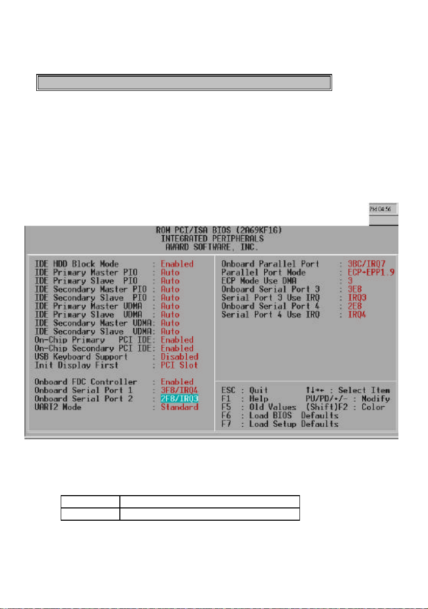
Integrated Peripherals
OnChip Channel 1
This chipset contains a PCI IDE interface with support for two IDE channels.
Select Enabled to activate the first and/or second IDE interface. Select
Disabled to deactivate this interface, if you install a first and/or second add-in
IDE interface IDE interface.
Enabled First HDD controller used – Default
Disabled First HDD controller not used.
110
Page 84
OnChip Channel 2
This chipset contains a PCI IDE interface with support for two IDE channels.
Select Enabled to activate the first and/or second IDE interface. Select
Disabled to deactivate this interface, if you install a first and/or second add-in
IDE interface IDE interface.
Enabled Second HDD controller used
Disabled Second HDD controller not used.
IDE Prefetch Mode
Enable prefetching for IDE drive interfaces that support its faster drive
accesses. If you are getting disk drive errors, change the setting to omit the
drive interface where the errors occur. Depending on the configuration of your
IDE subsystem, this field may not appear, and it does not appear when the
Internal PCI/IDE field, above, is Disabled.
The choice: Enabled, Disabled.
IDE HDD Block Mode
This item allows your hard disk controller to use the fast block mode to transfer
data to and from your hard disk drive (HDD). Select Enabled only if your hard
drives support block mode.
Enabled IDE controller uses block mode.
Disabled IDE controller uses standard
mode.
111
Page 85

IDE Primary/Secondary Master/Slave PIO
The four IDE PIO (Programmed Input/Output) fields let you set a PIO mode
(0-4) for each of the four IDE devices that the onboard IDE interface supports.
Modes 0 through 4 provide successively increased performance. In Auto mode,
the system automatically determines the best mode for each device.
Auto System will auto detect the best working type for your harddisk
Mode 0 Assign the harddisk‘s PIO working type to Mode 0 (Max.
access time = 600ns, Max. speed = 3.3MB/sec.)
Mode 1 Assign the harddisk‘s PIO working type to Mode 1 (Max.
access time = 383ns, Max. speed =5.2MB/sec.)
Mode 2 Assign the harddisk‘s PIO working type to Mode 2 (Max.
access time = 240ns, Max. speed = 8.3MB/sec.)
Mode 3 Assign the harddisk‘s PIO working type to Mode 3 (Max.
access time = 180ns, Max. speed = 11.1MB/sec.)
Mode 4 Assign the harddisk‘s PIO working type to Mode 4 (Max.
access time = 120ns, Max. speed = 16.6MB/sec.)
IDE Primary/Secondary Master/Slave UDMA
Ultra DMA/33 implementation is possible only if your IDE hard drive supports it
and the operating environment includes a DMA driver (Windows 95 OSR2 or a
third-party IDE bus master driver). If your hard drive and your system software
both support Ultra DMA/33, select Auto to enable BIOS support.
The Choice: Auto, Disabled
Onboard FDD Controller
This should be enabled if your system has a floppy disk drive (FDD) installed on
the system board and you wish to use it. Even when so equipped, if you add a
higher performance controller, you will need to disable this feature.
The choice: Enabled, Disabled.
Onboard Serial Port 1/Port 2
This item allows you to determine access onboard serial port 1/port 2 controller
with which I/O address.
112
Page 86

The choice: 3F8/IRQ4, 2E8/IRQ3, 3E8/IRQ4, 2F8/IRQ3, Disabled.
UART 2 Mode
This item allows you to determine which Infra Red (IR) function of onboard I/O
chip.
Standard RS232 will work in FIFO standard mode
HPSIR RS232 will work in Half Phase Serial Infra Red
mode
ASKIR RS232 will work in Amplitude Shift Keyed Infra
Red mode
Onboard Parallel Port
This item allows you to determine access onboard parallel port controller with
which I/O address.
The choice: 378/IRQ7, 278/IRQ5, 3BC/IRQ7, Disabled.
Onboard Parallel Mode
Select an operating mode for the onboard parallel (printer) port. Normal EPP
(Extended Parallel Port) ECP (Extended Capabilities Port) CEP+EPP PC AT
parallel port Bi-directional port Fast, buffered port Fast, buffered, bi-directional
port.
Select Normal unless you are certain your hardware and software both support
EPP or ECP mode.
The choice: SPP, ECP/EPP, ECP, EPP/SPP.
ECP Mode Use DMA
Select a DMA channel for the parallel port for use during ECP mode.
The choice: 3, 1.
Parallel Port EPP Type
This item allows you to determine the IR transfer mode of onboard I/O chip.
The choice: EPP1.9, EPP1.7.
113
Page 87

Appendix B. Fast Ethernet Controller
The Book PC 1000 series supports LAN Riser Card option
for bundled with Intel 82559ER /82559C LAN chip, RTL 8139C LAN chip.
or UM9008 LAN chip. Below is the basic feature about the LAN chip.
1.The Feature of Intel 82559ER Fast Ethernet PCI Controller
hIntegrated IEEE802.3 10BASE-T and 100BASET-TX compatible PHY
hACPI and PCI Power Management
hPower management event on “interesting” packets and link status change
support
h3 Kbyte transmit and 3 Kbyte receive FIFO’s
hFast back-to-back transmission support with minimum interface spacing
hEfficient dynamic standby mode
hDeep power down support
hClockrun protocol support
2.The Feature of Intel 82559C Fast Ethernet PCI Controller
hIntegrated IEEE802.3 10BASE-T and 100BASET-TX compatible PHY
hModem interface for combination solution in PCI, CardBus, and MiniPCI
design
hPXE Support in Combo Design
hIntegrated power management function
hACPI and PCI Power Management
hWake on “interesting” packets and link status charge support
hMagic Packet support
hRemote power up support
h3 Kbyte transmit and 3 Kbyte receive FIFO’s
hFast back-to-back transmission support with minimum interface spacing
hEfficient dynamic standby mode
hDeep power down support
hClockrun protocol support
114
Page 88

3. The Feature of Reltek8139C Fast Ethernet PCI Controller
hSupports 10Mb’s and 100MBb\s N-way Auto negotiation operation
hSupports Wake-On-LAN function and remote wake-up(Magic-Packet,
LinkChg and Microsoft wake-up frame)
hSupports 4 Wake-On-LAN (WOL) signals (active high, active low, active
pulse, and negative pulse)
hHalf/Full duplex capability
hSupports Full/Duplex Flow Control (IEEE 802.3x)
4.The Feature of UM9008 10Base-T Ethernet Card
h 100% compatibility with Novell NE2000
h 1Full compliance with IEEE 802.3 Ethernet standards
h 110Mbps network data transfer rate
h 116KBytes RAM data buffer
h 1On-board socket for boot ROM
h 1Support for 10Base-T (UTP) network cabling
115
 Loading...