

Fly Bird V109 Service Manual
Advance Information
MC13718/D
Rev. 0, 1/2003
MC13718 Li-Ion Charge
Control and Protection
IC
THIS DOCUMENT IS RELEASED UNDER NDA OR IS
A DELIVERABLE UNDER THE i.250 PLATFORM
MASTER AGREEMENT AND IS SUBJECT TO THE
TERMS AND CONDITIONS THEREOF.
Contents
1 Introduction . . . . . . . . . . 1
2 Contact Connections. . . 4
3 Operation . . . . . . . . . . . . 8
4 Marking and
Packaging. . . . . . . . . . . 20
1 Introduction
The MC13718 Charge Control and Protection IC is part of the chipset for Motorola’s 2.5G
Innovative Convergence™ (i.250) platform. This chipset also includes the MC13712
Dual-Band GPRS Front End Integrated Circuit, MMM6010/6011 Dual-Band GPRS Power
Amplifier Module, DSP56621 Baseband Processor, and MC13713 Integrated Power
Management and Audio Circuit. The MC13718 provides protection for and control of
single-cell battery charging using lithium-ion cell chemistry.
Device
MC13718
MC13718
Package Information
Plastic Package
(LLP-28)
Ordering Information
Operating
Temperature Range
T
= -20°C to 70°C
A
Package
LLP-28
The MC13718 is intended to be designed into a product with an embedded cell battery
system. In addition to multi-mode charging circuitry, the MC13718 provides the battery cell
protection circuitry normally included in stand-alone battery packs, as well as thermal and
power dissipation protection for the charging electronics. The MC13718 can be used with a
cost-effective wall transformer type supply.
The MC13718 is primarily targeted for the cellular phone handset market but can be used in
other products, such as PDAs, games, industrial products, and cameras, that use Li-Ion
batteries.
This document contains information on a new product. Specifications and information herein are subject to change
without notice. © Motorola, Inc., 2003. All rights reserved.
Motorola Confidential Proprietary, NDA Required or i.250 Platform Master Agreement Deliverable with 5 Year Confidentiality Term / Preliminary
General Specifications
Table 1. MC13718 Features
Multiple charge modes:
• Low-voltage charging
• Full-rate charging
• Pulse charging
• Trickle charging
• Disabled
Multiple features to protect the battery cell
against:
• Over voltage from external supply, or pass
transistor failure
• Excessive charge current
• Excessive load current
• Discharge of deeply discharged cell
1.1 General Specifications
Multiple electronic protection features:
• Internal junction temperature protection
• Power dissipation protection
• Short circuit protection
• Under voltage prevention
Other features:
• Wide external input voltage range
• Peak voltage detection on input and on cell
• Minimum external components
• Coke/graphite chemistry support
• Logic interfaces for power-on, charge
state, power detect, disable
• Seamless integration with MC13713
Power Management IC
Table 2 on page 2 lists general specifications, and Figure 1 on page 3 shows a block diagram that includes
off-chip components for the MC13718.
Table 2. General Specifications
Specification Conditions Min Typ Max Unit
Operating Voltage CELL+, normal range 2.575 3.6 4.2 V
Operating Voltage CELL+, low voltage 0 2.575 V
Quiescent Current CELL+, normal range, no charger 55 120 µA
Quiescent Current CELL+, sleep mode 9 25 µA
Operating Temperature –20 70 °C
Package Power Dissipation 0.95 W
Moisture Sensitivity Level: MSL1
Note: MSL1 means unlimited floor time with no dry pack required if exposure is limited to ≤ 30°C at no greater
than 85% relative humidity.
2 MC13718 Advance Information MOTOROLA
Motorola Confidential Proprietary, NDA Required or i.250 Platform Master Agreement Deliverable with 5 Year Confidentiality Term / Preliminary
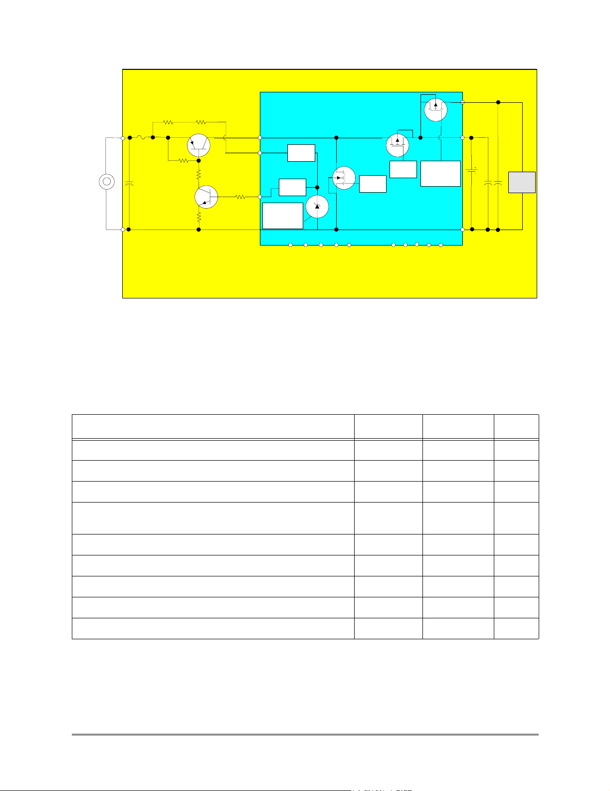
Maximum Ratings
Yellow shaded area = Host Device (modile phone)
External
Power
Supply
VPS
GND
R4A
Fuse
0.1 uf
Pass Transistor
Q1
R1
Drive
Transistor
Q2
R4B
R5
R2
R3
Cellular Phone
Figure 1. Block Diagram Including Off-Chip Components
1.2 Maximum Ratings
(mobile phone)
Blue shaded area = DH2 IC
VIN
Sense
Charge
Control
Charge Power
Shunt
Regulator
DISABLE
VPS
VDETECT
CNTRL
RADIO B+
MC13718 IC
M5
M3
NMOS
CHRG_STATE
CHRG_DETB
EXT_PWR_ON
BATT_DETB
Shunt
Safety
Current
Sense
CHEMISTRY
TEST
TMDATA
Undervoltage
& Short Circui t
Protection
TMCLK
TEST
HIB_DISB
Phone
RADIO_B+
M4
CELL +
Phone /
C3
0.1 uf
Device
Circuits
C2
1.0 uf
GND
HIB_EN
Table 3 lists the maximum ratings for the MC13718.
Table 3. Maximum Ratings
Rating Symbol Value Unit
Maximum Voltage on VIN contact 6.3 V
Maximum Voltage on any other contact 5.7 V
Maximum Reverse Voltage on any contact –0.3 V
Maximum Current on any contact (source or sink)
20 mA
(except VIN, CELL+, RADIO_B+, and GROUND)
Maximum Current VDETECT 130 mA
Maximum Ambient Temperature Ta –55 to 125 °C
Storage Temperature Tstg –65 to 150 °C
ESD (human model) 2kV
ESD (machine model) 200 V
NOTE:
Maximum ratings are those values beyond which damage to the device
may occur. Functional operation should be restricted to the limits in the
Electrical Characteristics tables or Section 2, “Contact Connections.”
MOTOROLA MC13718 Advance Information 3
Motorola Confidential Proprietary, NDA Required or i.250 Platform Master Agreement Deliverable with 5 Year Confidentiality Term / Preliminary
Contacts
2 Contact Connections
2.1 Contacts
Table 4 lists all the contacts and their definitions for the MC13718, and Figure 2 on page 5 shows contact
placement.
Table 4. Contact Definitions
Contact Name Description Contact In/Out Waveform Voltage
CELL+ + terminal of cell 1 in/out DC 0 to 4.2V
CELL+ + terminal of cell 2 in/out DC 0 to 4.2V
HIB_DISB Low disables hibernate mode 3 in digital 0 to 4.2V
HIB_EN High enables hibernate mode 4 in digital 0 to 4.2V
EXT_PWR_ON Active high to turn on MC13713 5 out digital 0 to 4.2V
VIN Charge current into IC 6 in DC 0 to 6.3V
VIN Charge current into IC 7 in DC 0 to 6.3V
CNTRL Drive to base of driver transistor
(Q2 in Figure 1)
GND Ground 9 - 0 V
GND Ground 10 - 0 V
GND Ground 11 - 0 V
GND Ground 12 - 0 V
VDETECT Charge supply detection 13 in DC current 0 to 4.2V
n/c 14 -
VIN Charge current into IC 15 in DC 0 to 6.3 V
VIN Charge current into IC 16 in DC 0 to 6.3 V
CHRG_DETB Active low upon supply detection 17 out digital 0 to 4.2 V
CHRG_STATE Low during full rate charge 18 out digital 0 to 4.2V
BATT_DETB Low for battery present 19 in digital 0V or open
CELL+ + terminal of cell 20 in/out DC 0 to 4.2V
8 out analog 0 to 4.2V
CELL+ + terminal of cell 21 in/out DC 0 to 4.2V
DISABLE High to disable charge 22 in digital 0 to 4.2V
(TEST) (Factory test use only) 23 n/a n/a N/C
RADIO_B+ B+ out to radio 24 out DC 0 to 4.2V
4 MC13718 Advance Information MOTOROLA
Motorola Confidential Proprietary, NDA Required or i.250 Platform Master Agreement Deliverable with 5 Year Confidentiality Term / Preliminary
Contacts
Table 4. Contact Definitions (Continued)
Contact Name Description Contact In/Out Waveform Voltage
RADIO_B+ B+ out to radio 25 out DC 0 to 4.2V
RADIO_B+ B+ out to radio 26 out DC 0 to 4.2V
(TEST) (Factory test use only) 27 n/a n/a N/C
CHEMISTRY Vterm select (high = 4.15V) 28 in digital 0 to 4.2V
GND Ground 29 - 0 V
Cell
CELL+
Cell
CELL+
HIB_DISB
HIB_EN
EXT_PWR_ON
VIN
VIN
CHEMISTRY
TEST
Chemistry
TMCLKB
28 27 26 25 24
1
2
3
4
5
6
7
8 9 10 11 12
29 GND
28-Pin LLP IC
GND
CNTRL
RADIO_B+
GND
RADIO_B+
GND
RADIO_B+
GND
TEST
TMDATAB
2223
13 14
VDETECT
DISABLE
No Connect
Cell
21
CELL+
CELL+
Cell
20
BATT_DETB
19
CHRG_STATE
18
CHRG_DETB
17
VIN
16
VIN
15
Figure 2. IC Contact Placement
NOTE:
Contacts 23 and 27 (test) are for factory test use only and should be left
unconnected (N/C).
There is a ground flag on the bottom of the package that serves as electrical
ground (contact 29) as well as thermal ground. This pad must be soldered
to ground on the board.
MOTOROLA MC13718 Advance Information 5
Motorola Confidential Proprietary, NDA Required or i.250 Platform Master Agreement Deliverable with 5 Year Confidentiality Term / Preliminary

Interfaces
2.2 Interfaces
The MC13718 IC interfaces to the battery cell, the radio load, the radio control lines, and the off-chip
charger components are described in detail in this section.
The MC13718 is optimized to interface directly to the MC13713 Integrated Power Management and Audio
Circuit. Since the MC13718 has no SPI port, the software commands to control or monitor the IC are
routed through the MC13713 via the interface contacts mentioned in the following sections.
2.2.1 Cell
The CELL+ and ground contacts are connected directly to the battery cell’s + and – terminals. In normal
operation, voltage on this contact (Vcell) powers the functions on the MC13718. In normal operation,
current flows into this contact to be routed to the load, and to power the IC itself. In charge operation,
current flows out of this contact and into the cell.
The IC monitors the voltage on this contact at all times and selects its mode of operation accordingly. A
1.0 µF capacitor should be connected between this pin and ground. This capacitor, which provides ESD
protection, should be mounted as close to the IC as possible with the traces kept as short as possible.
2.2.2 RADIO_B+
The load is connected to the MC13718’s RADIO_B+ contact. In normal operation, current flows into the
CELL+ contact, through the IC’s internal M4 FET switch, and out of the RADIO_B+ contact. Current in
this path is monitored as described in Section 3.1.1, “Normal Voltage Range,” and Section 3.4.3, “IC
Thermal Protection.” A 0.1 µF capacitor should be connected between this pin and ground. This capacitor,
which provides ESD protection, should be mounted as close to the IC as possible with the traces kept as
short as possible.
2.2.3 VIN
Charge current flows into this contact and is regulated and fed out of the CELL+ contact as described in
Section 3.2, “Charge Operation.”
2.2.4 VDETECT
This input is connected via a series resistor to the charger supply. Current flowing into this contact is
detected by the IC and indicates, after a debounce period of 32 ms, that a charger supply has been attached.
The level of the current is measured by the IC and is used as an indication of the charge supply voltage.
Additionally, current fed into this contact is routed to the CELL+ output to provide a trickle current when
charging a battery cell that has discharged to a voltage too low for the IC to otherwise function. Table 5
lists the specifications for the VDETECT input. The 32 ms debounce feature is active on both detect and
undetect.
Table 5. Specifications for the VDETECT Input
Specification Conditions Min Typ Max Unit
I
detect
I
detect_min
I
detect
6 MC13718 Advance Information MOTOROLA
Motorola Confidential Proprietary, NDA Required or i.250 Platform Master Agreement Deliverable with 5 Year Confidentiality Term / Preliminary
Charger detection 100 µA
Charger remains detected 25 µA
VDETECT regulated 15 mA
Interfaces
Table 5. Specifications for the VDETECT Input (Continued)
Specification Conditions Min Typ Max Unit
I
undetect
V
detect
V
detect2
Debounce delay Idetect connect or disconnect 22 32 64 ms
Charger disconnect detected 3 µA
Idetect within above range V
Idetect > 15 mA V
- 5 mV V
CELL
+ 50 mV V
CELL
+ 1 V V
CELL
2.2.5 Battery Detect
The BATT_DETB input can be used to detect the presence of a battery. The charge function of the
MC13718 will be completely disabled if this contact is high or floating. In a product incorporating a
non-removable (embedded) battery cell, this contact should be grounded at the IC.
2.2.6 Control Interface Inputs
The CHEMISTRY input contact of the MC13718 is driven low to set the termination voltage, Vterm, to
4.10 V and high to set Vterm to 4.15 V. See Section 3.2.2, “Full Rate Charge.”
The active-high DISABLE input disables all charging and resets the control logic.
The HIB_EN input turns off M4 to disconnect the load, and sets the MC13718 to sleep mode, so most of
the circuitry on the IC is turned off to reduce quiescent current drain. This is to allow a greatly extended
shelf life of products with an embedded battery cell. Pulling HIB_EN high forces hibernate mode and
pulling HIB_DISB low, or applying charge power, disables hibernate mode. There is an 8 ms debounce on
HIB_EN. If the hibernate function is not to be used, this contact should be tied to ground. Table 6 lists the
specifications for the control inputs and outputs.
2.2.7 Control Outputs
The CHRG_DETB output is low when a current between 100 µA and 15 mA is injected into the
VDETECT contact of the IC indicating that a charge supply of valid voltage is attached.
The CHRG_STATE output will be low when the battery voltage is above 2.575 V and the IC is in the
trickle or full-rate charge modes. It will be high when the IC completes full-rate charging and switches to
top-off mode (indicating charge is nearly complete). This output will be high at low battery voltage or
when charge is disabled.
EXT_PWR_ON will be high when CHRG_DETB is low AND the voltage of the cell is above
3.0 V ± 0.12 V. This signal is fed to the MC13713 to cause it to turn on when the battery has been charged
high enough to operate. Table 6 lists the specifications for the control inputs and outputs.
Table 6. Specifications for the Control Inputs and Outputs
Specification Conditions Min Typ Max Unit
V low CHEMISTRY, DISABLE, HIB_EN
inputs
V high CHEMISTRY, DISABLE, HIB_EN
inputs
00.6V
1.5 VIN V
MOTOROLA MC13718 Advance Information 7
Motorola Confidential Proprietary, NDA Required or i.250 Platform Master Agreement Deliverable with 5 Year Confidentiality Term / Preliminary
Discharge Operation
Table 6. Specifications for the Control Inputs and Outputs (Continued)
Specification Conditions Min Typ Max Unit
V low EXT_PWR_ON, CHRG_DETB,
CHRG_STATE outputs, 30 kΩ to
RADIO_B+
V low HIB_DISB, BATT_DETB 0.2*V
V high HIB_DISB, BATT_DETB 0.8*V
V high EXT_PWR_ON, CHRG_DETB,
CHRG_STATE outputs, 30 kΩ to
RADIO_B+
V low EXT_PWR_ON, 10 kΩ to RADIO_B+ 0.3 V
V high EXT_PWR_ON, 10 kΩ to ground 0.9*V
Resistance to
ground
DISABLE and CHEMISTRY inputs 50 100 200 kΩ
0.9*V
CELL
RADIO_B+
RADIO_B+
0.3 V
CELL
V
V
V
V
2.2.8 Charge Control
This current output drives the base of off-chip driver transistor, Q2, which in turn pulls current through the
base of the off-chip pass transistor Q1, turning it on.
This output can source adequate current to drive Q2. Only the topology shown in Figure 1 on page 3 or
Figure 4 on page 18 using the components outlined in Section 3.6, “Off-Chip Components,” should be
used in order to prevent voltage in excess of V
from being incident upon this pin.
CELL
2.2.9 Peak Detection
To prevent false voltage readings, the MC13718’s CELL+ and VIN inputs incorporate a peak detection
circuit. The peak voltage at these inputs is measured, rather than a lower average that might occur during
dips in voltage due to supply ripple, or the drop across the internal resistance of the cell during transmit
pulses.
3 Operation
3.1 Discharge Operation
In normal discharge operation, when no fault conditions exist and there is no charger supply connected, no
charging or fault mitigation is occurring. The only active connections will be the cell, the load at
RADIO_B+, and control inputs that may even be hardwired. The load is electrically connected to the cell
via a switch on the MC13718. The IC continuously monitors various parameters in the background to take
action as needed. Table 7 lists the specifications for discharge operation.
8 MC13718 Advance Information MOTOROLA
Motorola Confidential Proprietary, NDA Required or i.250 Platform Master Agreement Deliverable with 5 Year Confidentiality Term / Preliminary
 Loading...