

Fly Bird S288 Service Manual
English Service Manual S288
7300
7500
1580
32KHz Clock
7700
7660
7600
1660
X S288 Service Manual
Abstract: S288 is an eidolon, keeping close to your body—very slim、modern and streamline.
The thickness is only 12mm (with battery). Multi-Send has three manners: one by one、 all one
and Group. With long Standing by hours, you can call as much as you like and play games at
your pleasure. Large capacity of phonebook makes it easy adding phone numbers. Telecontroling
your mobile phone by SMS: Sending SMS to you mobile phone, you can know the new SMS
and new calls.
Key words: Slim, Multi-Send, Telecontrol
1. The theory and repair of baseband
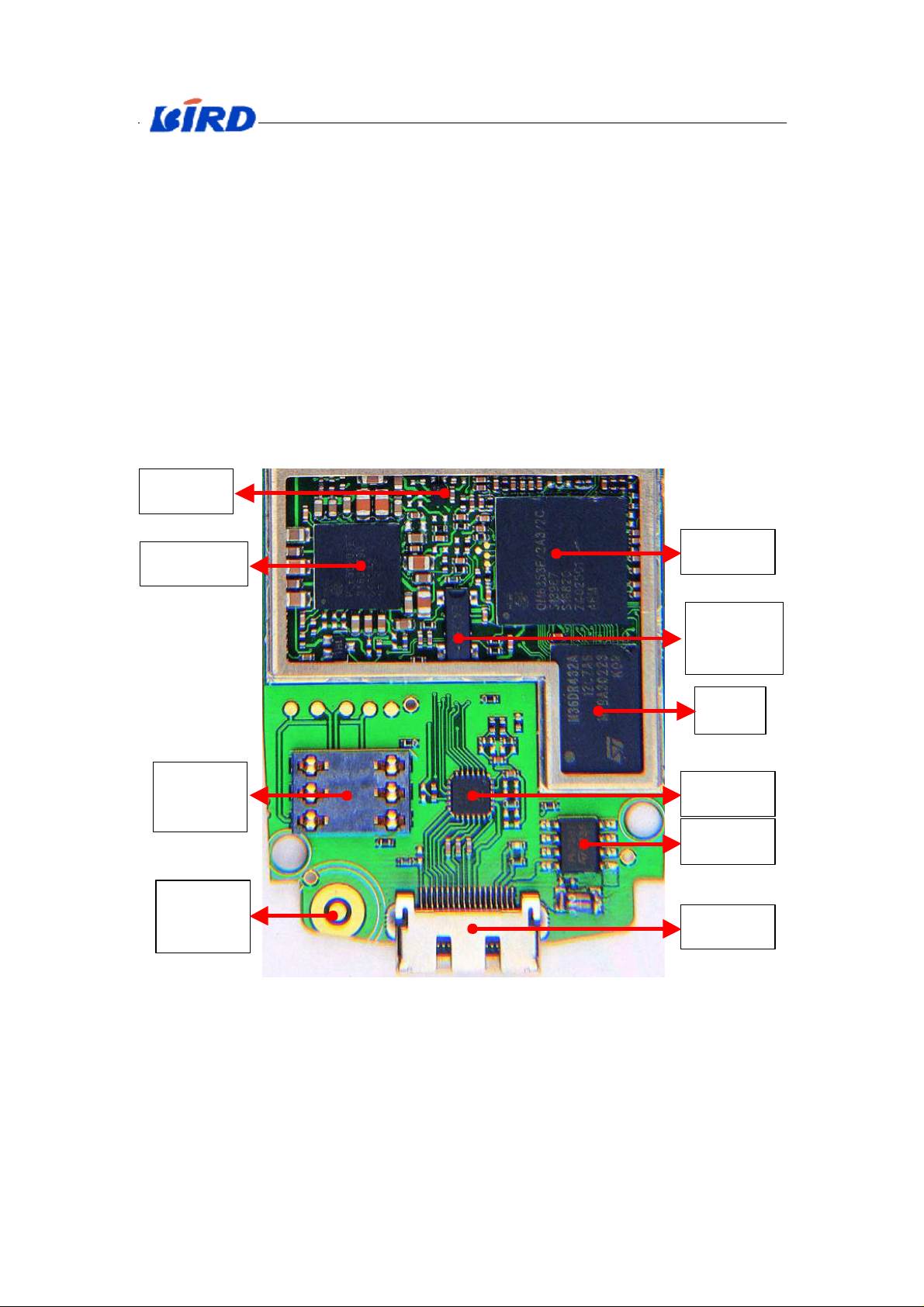
1.1 Baseband introduction
Audio-PA
PMU
SIM
Connector
Microphone
Connector
1740
CPU
Crystal
5505
Flash
7400
Connector IC
Charge IC
I/O Interface
Fig. X-1 Distribution of baseband hardware
1.1.1 CPU (7300)
1
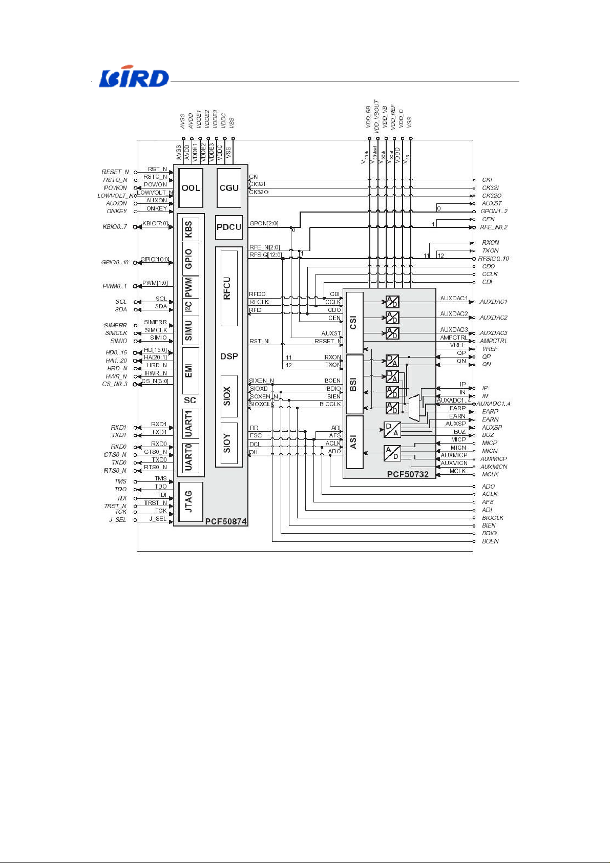
English Service Manual S288
Fig. X-2 Configuration of CPU
The next table shows the exterior pins of CPU. (Notice: The hatching signal is
unused.)
2
English Service Manual S288
A B C D E F G H J K L M N P
1 TRST_N HD6 VDDE2_e HD12 HD11 HD10 VSS_m HD5 VSS_b VSS_n HA12 HA9 HA10 VSS_o
2 TMS HD15 SCL TDI HD14 HD9 VDDE3_f HD2 HA14 HA19 HA11 HA13 HA8 HA7
3 TCK SDA VSS_k TDO HD13 HD8 CS_N3 HD1 HD3 HA16 VDDE3_g
HA6 HA4 HA2
4 TXD1 J_SEL RXD0 RXD1 HD7 PWM0 HA20 HD0 HA17 HA18 HA3 HA1 CS_N0 VDDE3_a
5 RTS0_N CTS0_N TXD0 RFSIG0 HD4 VDDC_a CS_N1 HRD_N HA15 HA5 HWR_N
6 RFSIG1 RFSIG3 RFSIG7 RFSIG2 PWM1 VDDC_d
GPIO1 VDDE3_b GPIO3 GPIO8
CS_N2 VSS_p GPIO0
7 RFSIG4 RFSIG6 RFSIG5 RFSIG10 RFSIG8 VSS_a GPIO5 VSS_c GPIO7 GPIO4
8 ADI ACLK VDDE1_c CDI VSS_j GPIO10 GPIO2 VDDC_c GPIO9 VDDE2_c
9 ADO AFS VDD_D CEN CDO RFSIG9 GPIO6 LOWVOLT_N
10 AUXSP EARP RESET_N MCLK CCLK BIEN AUXST AMPCTRL
11 EARN BUZ VSS_VBOUT
12 VSS_VB VDD_VB VDD_VBOUT
13 MICP MICN VSS_REF AUXDAC2
VSS_D BDIO BIOCLK BOEN VDDE1_d KBIO3 RFE_N2 KBIO4 SIMERR VSS_g CKI
AUXDAC3 AUXDAC1 VDD_BB TXON RXON RFE_N0 KBIO2 KBIO6 SIMIO VDDE1_b AVDD
VSS_BB AUXADC4 VSS_h QP IP AUXON KBIO5 SIMCLK VDDC_b CKI32I
KBIO1 KBIO0 GPON1 RSTO_N VSS_e AVSS
GPON2 VDDE1_a
14 AUXMICN
A B C D E F G H J K L M N P
AUXMICP
VREF VDD_REF AUXADC3 AUXADC1 AUXADC2
Tab. X-1 Exterior pins of CPU
QN IN PWON KBIO7 ONKEY VSS_f CKI32O
3

English Service Manual S288
Every signal and function of CPU:
Pin Signal Function
P11 CKI
D10 MCLK
13MHz system clock: reference clock
P12 CKI32I 32KHz logic clock
C10 RESET_N
Reset signal, input
M10 RSTO_N
HD0~HD15 16 bits parallel data signals(0~15)
HA1~HA20 20 bits parallel address signals(1~20)
L5 HWR_N Allow writing signal, output
H5 HRD_N Allow reading signal, output
M5 CS_N2 FLASH chip select signal(NCSFLASH), output
G5 CS_N1 SRAM chip select signal(NCSRAM), output
N4 CS_N0 21st address signal(HA21), output
P5 GPIO0
Data transfers speed switching signal for Connector IC
(SPEED_MD), output
L8 GPIO2 Enabling signal for audio-PA(CMD_AMPLI_AUDIO), output
N6 GPIO3 Power for periphery adjunct signal(CHARGE_REVERSE), output
P7 GPIO4
L7 GPIO5
N8 GPIO9
Switch signal for mobile’s charging mode
(CHARGE_MODE),output
Check the charger’s type (quick charger or slow charger)
(CHARGE_FLAG), input
Asynchronism exchange interface(UART0)controlling signal
CTS0
K8 GPIO10 Charge_pulse interrupt.(CHARGE_PULSE_IT) input
KBIO0~KBIO7 Triangle matrix keyboard, KBS(keyboard scanner).
B5 CTS0_N
A5 RTS0_N
Asynchronism exchange interface(UART0)controlling signal
CTS0
UART0 controlling signal RTS0(data equipment waiting)
In answer to output.
C5 TXD0 UART0 sending data(TXD0)
C4 RXD0 UART0 incepting data(RXD0)
D4 RXD1 Check peripheral adjuncts and input data from adjuncts.(RECO0)
A4 TXD1 UART1 sending data(TXD1)
D2 TDI JTAG testing data(TDI)input
A2 TMS JTAG testing mode switching(TMS)
A3 TCK JTAG testing clock (TCK)
D3 TDO JTAG testing data(TDO)output
A1 TRST_N Reset JTAG testing(TRST_N)
B4 J_SEL JTAG testing select(J_SEL)
F4 PWM0 Charge pulse wide modulation (CHARGE_PWM)
5
English Service Manual S288
Pin Signal name Function
M11 SIMERR Interrupt signal from PMU(IT_PMU)
M12 SIMIO I/O between SIM and CPU (SIMIO)
M13 SIMCLK SIM Card clock(SIMCLK)
B3 SDA Serial data transmitting(SDA)
C2 SCL Serial clock signal(SCL)
A14 AUXMICN Handset microphone positive input
B14 AUXMICP Handset microphone negative input
B13 MIC_AMP_N Microphone positive input
A13 MIC_AMP_P Microphone negative input
B11 BUZ Buzzer, audio signal to Audio_ PA
A10 AUXSP Earphone (AUX_speaker)
A11 EARP2 Earphone positive
B10 EARP1 Earphone negative
E14 AUXADC3 Mainboard’s temperature sensing(TEMP_PRODUCT)
F14 AUXADC1 A measure of the battery’s capacity(MES_BATT)
Differential positive output to RF for in_phase channel
J13/J14
H13/H14
D12 AUXDAC3 Control the multiple of PA(RAMP)
D13 AUXDAC2 Automatic frequency control(AFC)
K11 RFE_N2 BBI enable signal for RF(RF_EN_SYNT)
D8 CDI BBI data signal for RF(RF_BBI_DATA)
E10 CCLK BBI clock signal for RF(RF_BBI_CLK)
D7 RFSIG10 Power_ON_RX(PON_RX)
K9 RFSIG9 Power_ON_RX(PON_TX)
E7 RFSIG8 Power_on_synthesizer_TX(PON_SYNT)
C6 RFSIG7 EGSM working band switch
A7 RFSIG4 DCS working band switch
C7 RFSIG5 EGSM_ mode switch(EGSM_MODE_SW)
B7 RFSIG6 DCS_mode_switch (DCS_MODE_SW)
G10 AUXST
L10 GPON1 Switch the system clock’s mode(V_MODE)
N9 GPON2 Reset signal to LCD(RSTNC_LCD)
IP/IN
QP/QN
Differential negative output to RF for in_phase channel
(IRX_TX_P、IRX_TX_N)
Differential positive output to RF for quadrature channel
Differential negative output to RF for quadrature channel
(QRX_TX_P、QRX_TX_N)
Enable the IC working to supply power for 13KHz crystal
(REF_ON)
6
English Service Manual S288
P
Here is a picture of CPU (the I/O interface is subjacent).
The pins’ distributing:
14
1
A
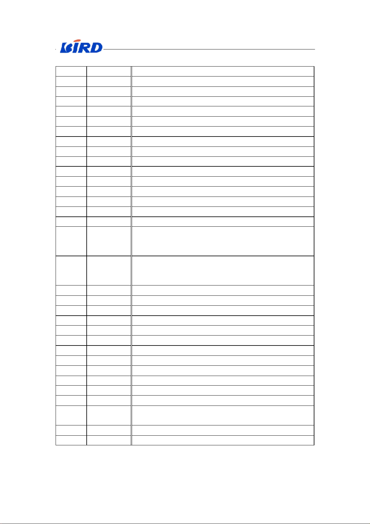
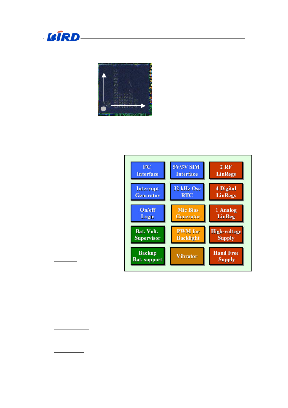
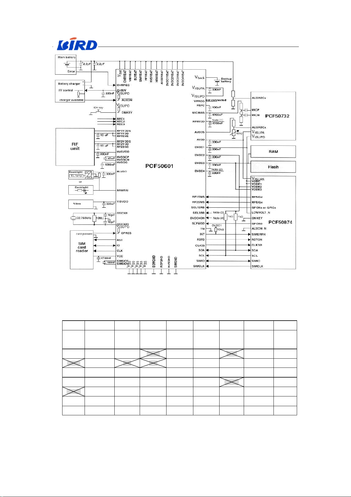
1.1.2 Power supply IC (7500):
Shown as Fig.X-3, there are
15 function modules in Power
Supply IC.
A. I2C Interface.
It follows I2C chief-line proto
-col. Through the interface,
CPU can control the voltage
of Power supply IC.
B. Interrupt Generator.
Its function is sending
interrupt to CPU.
C. On/off Logic. It can
control the working state
of the mobile. Such as:
A) No Power. Neither main
nor backup battery is
connected,
Fig.X-3 Power supply IC’s (PCF50601) function modules
or both the battery’s voltages
are too low for operation.
At this mode, PMU stays at very low current consumption.
B) Off mode. Main or backup battery is present, RTC and 32 kHz is running, but all
output voltages are off. PMU is using very low power (typ. 35 uA). Normal
mode, when the phone is switched off.
C) Sleeping mode. Main battery is present and with enough voltage. Outputs are
switched depending on the IIC settings to normal mode, ECO mode or off. PMU
with low power consumption (typ. about 150 uA) + output currents.
D) Active mode. Main battery present and with enough voltage. Output voltages
switched on (selectable by IIC). PMU power consumption typ. 1250 uA (=1.25
mA) + output currents. This mode is only during a call on the phone.
7
English Service Manual S288
D. SIM Interface. It is used to check SIM card, supply power to SIM card and
exchange data between SIM and mobile.
E. 32kHz Osc RTC. It can carry out clock and date of mobile; also it is the
working clock for the Power supply IC (7500).
F. Bat. Volt. Supervisor. Checking the battery’s voltage. If the voltage is too low,
it will bring an interrupt to turn mobile off.
G. Backup Bat. Support. It is used to control the backup battery’s charge.
H. Mic Bias Generator. It supplies the bias voltage to microphone.
I. PWM for Backlight. It is used to control the backlight of the keyboard and
LCD.
J. Vibrator. Controlling the vibrator’s working state.
K. 2 RF Linregs. 2 voltage Linearity regulating cells of RF.
L. 4 Digital Linregs. 4 voltage Linearity regulating cells of Digital module
M. 1 Analog Linregs. 1 voltage Linearity regulating cells of Analog module
N. High-voltage Supply.
O. Hand Free Supply.
The following table (Tab.X-2) shows the voltage, function and testing point of the
7500.
Signal
VDD1
VDD2 1.95
VDD3 1.95 Supply power to CPU and memory C2550
AVDD 2.65
AVDD_TEMP 2.65 Measure the PCB’s temperature R3620
HFAVDD 3.05 Supply power to hands-free audio C2560
VIBVDD 2.95 Supply power to vibrator C2563
BL_LCD_
VDD
MIS_BIAS 2.1 Bias voltage for microphone C2542
Voltage
(V)
1.35/
2.35
3.05
Function
Supply power to CPU C2552
Supply power to CPU, IIC bus and logic supply for
LCD driver
Supply power to CPU and analogic supply for LCD
driver
Supply power to keyboard backlight and LCD
backlight
Where
to test
C2551
C2562
C2559
VCC_SYN 2.7V Supply power to synthesizer C2512
VCC_RX_TX 2.7V Supply power to RX or TX C2513
VCC_RF_
VCO
VCC_TX_
BURST
VCC_CP 4V Supply power to CP C2529
1V Supply power to VCO C2514
1.5V Supply power to VCO for TX C2515
Tab. X-2 The voltage of power supply IC
8
English Service Manual S288
A J
Power supply
)
1
The practicality test points(Fig.X-4):
VCC_SYN
AVDD_TEM
VCC_RX_TX
VCC_RF_VCO
VCC_CP
BL_LCD_VDD
HFAVDD
VIBVDD
9
IC
PMU(7500
VCC_TX_BURST
AVDD
MIC_BIAS
VDD1
VDD3
Fig.X-4 The practicality test points
VDD2
The peripheral circuit of the power supply IC (Fig.X-5):
PCF50732 is the Audio manager mode. PCF50874 is ARM7 kernel of CPU and
DSP kernel of GSM BB.
9
English Service Manual S288
Fig.X-5 Peripheral circuit of power supply IC
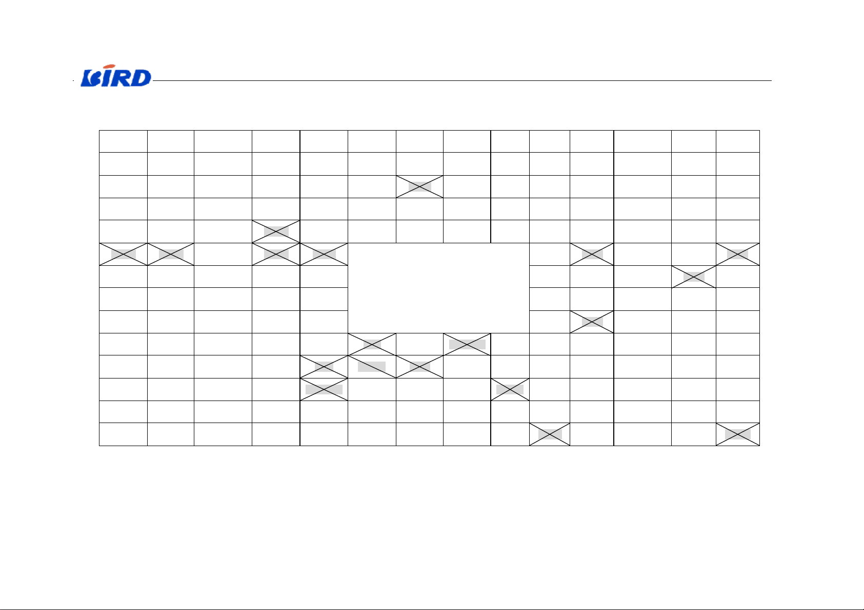
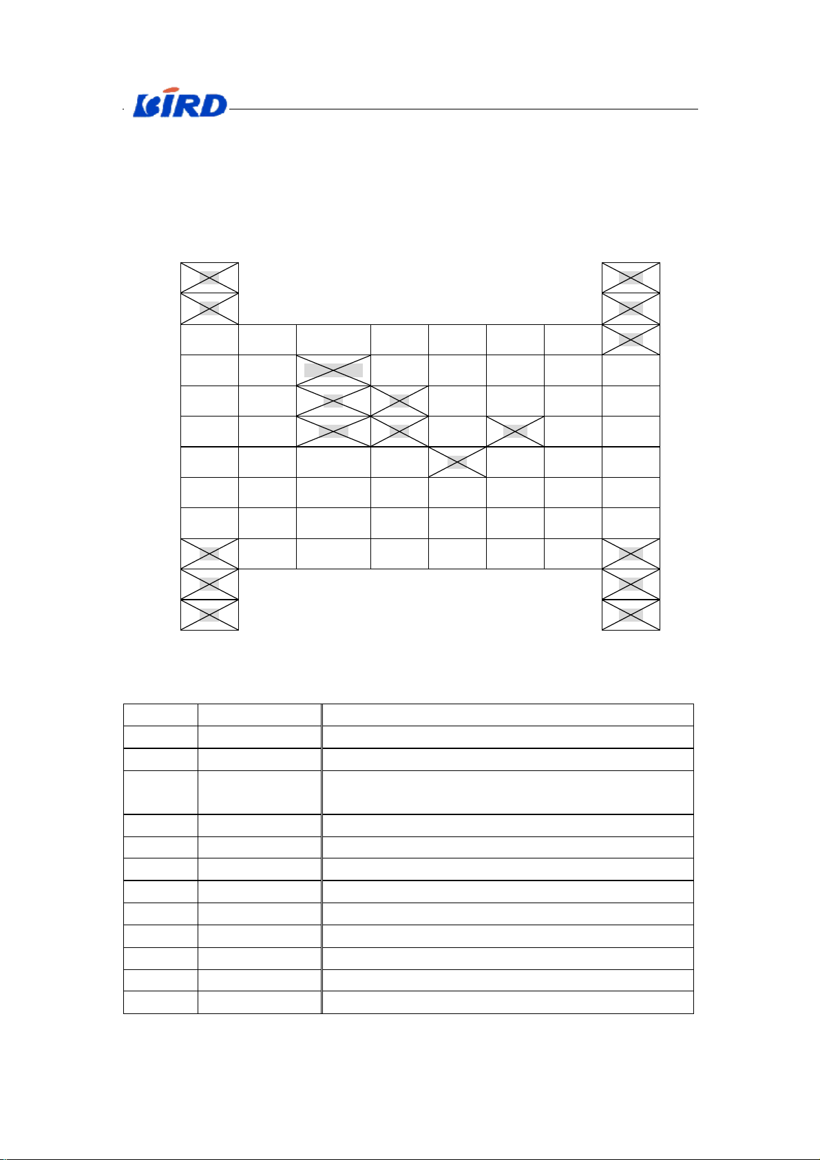
The exterior pins of Power Supply IC refer to Tab.X-3. (Notice: The hatching signal
is unused. )
A B C D E F G H J
SIMSCN
1
2
SIMGND
VIBVDD VIBVBAT
3
DVDD4 DVDD4VBAT
4
HFAVDD HFAVBAT
5
BLVDD
6
BBMSW BBMGND
7
VSS5
8
HVSGND
9
SIMSCP RST IO CHRVBAT DVDD1 DVDD2 DVDD3 VSS6
SIMVBAT VCC CLK CHRREG
VSS1 CPRES CHRIV SDA REC3 REC2 VBAT
NC2 NC1 SCL ONKEY_n
VSS4
BLVBAT SIMCLK RSTOn RF1SWS RF2SWS VPROG REFC
SIMIO INTn SEL12RB
CLK32
HVSSCN HVSSCP HVSVDD RF1VDDS
HVSVBAT
SLPMODn
HVSOC VSS3 RF1SNS RFVBAT RF2SNS OSCI
SEL3RB TM ISUPD ISUPA
DVDD1V
BAT
DVDD4ON
RF1VDD
DVDD2
VBAT
AUXON_n
AVDDS
RF2VDD
DVDD3VB
AT
VSS2 VSAVE
AVDD1VBAT
RF2VDDS
REC1
MICBIAS
REFGND
AVDD
OSCO
Tab. X-3 Exterior pins of Power Supply IC
The signal of PMU:
10
English Service Manual S288
H
12
Pin Signal Function
D5 SLPMODn Sleep_mode:“ 0”is sleep mode;“ 1”is work mode
G4 AUXON_n Enable to charge(CHARGER_OK), input
F4 ONKEY_n Power on or off(ONKEY_N), input
D6 RSTOn Reset (RSTON)output
B8 CLK32 32KHz logic clock
J2 REC1 Check accessory and data input(RECO1)
H3 REC2 Check accessory and data output(RECO2)
D7 INTn Interrupt signal from PMU to CPU(IT_PMU)
C2 VCC Supply to SIM(5V/3V/1.8V)
D2 CLK Clock sequence for SIM (1MHz~5MHz, GSM: 3.25MHz)
C1 RST Reset signal for SIM
D1 IO I/O between SIM and CPU
C7 SIMIO Data between CPU and controlling unit of SIM in PMU
C6 SIMCLK Clock from CPU to controlling unit of SIM in PMU
J8 OSCI 32KHz input
J9 OSCO 32KHz output
E2 CHRREG Check the battery plugging(VERROR)
E3 CHRIV Control the charger pulsatory working(CHARGE_PULSE)
D9 HVSVDD Supply power to CP(VCC_CP)
A3 VIBVDD (VIBVDD): Vibrator switch
A5 HFAVDD Supply power to earphone(HFAVDD)
G7 AVDD_TEMP PCB temperature testing(AVDD_TEMP)
J7 AVDD Supply power to analogic circuit(AVDD)
E7 SEL12RB Switch a band of system clock(V_MODE)
F6 RF2SWS Power on TX(PON_TX)
E6 RF1SWS Power on the circuit of RF synthesizer(PON_SYNT)
E4 SCL Serial clock, input
F3 SDA Serial data, input or output
1.1.3 Memory (7400):
FLASH
7400
1
A
Fig.X-6 Picture of the Memory
11
English Service Manual S288
2
3
4
5
6
7
8
9
10
11
12
There is a 32M bits flash and a 2M bits SRAM in the memory. There are 21bit
parallel address line, and 16bit parallel data line. The voltage for memory to work is
1.95V from PMU.
The exterior pins of the memory, please refer to Tab X-4. (Notice: The hatching
signal is unused. )
A B C D E F G H
NC1 NC11
1
1
NC2 NC12
F_A20 A16 F_WEn S_VSS F_WPn S_LBn F_A18 NC13
A11 A8 RDY_BUSYn F_RPn F_VPP S_UBn F_A17 A5
A15 A10 NC6 NC7 F_A19 S_OEn A7 A4
A14 A9 S_A17 NC8 I_O11 NC10 A6 A0
A13 I_O15 I_O13 I_O12 NC9 I_O9 A3 F_CEn
A12 S_WEn I_O6 S_CE2 I_O10 I_O8 A2 F_VSS2
F_VSS1 I_O14 I_O4 S_VCC I_O2 I_O0 A1 F_OEn
NC3 I_O7 I_O5 F_VCC I_O3 I_O1 S_CS1n NC14
NC4 NC15
NC5 NC16
A B C D E F G H
Tab.X-4 Exterior pins of memory
Every signal and function of Memory:
Pin Signal Function
A0~A16 Addressing signal(HA1~HA17)
G4 F_A17 18th addressing signal in FLASH(HA18)
F_A18/19/20
19th、20th and 21st addressing signals in FLASH
(HA19/20/21)
H7 F_CEn Chip select signal to FLASH(NCSFLASH)
H9 F_OEn Allow reading signal to FLASH(HRD_N)
F5 S_OEn Allow reading signal to SRAM(HRD_N)
C3 F_WEn Allow writing signal to FLASH(HWR_N)
B8 S_WEn Allow writing signal to SRAM(HWR_N)
G10 S_CS1n Chip select signal to SRAM(NCSRAM)
F3 S_LBn Low bit in SRAM
F4 S_UBn High bit in SRAM
I_O0~I_O15 Data bus(HD0~HD15)
2
3
4
5
6
7
8
9
10
11
12
12
English Service Manual S288
7 1 3
4 5
8
comes from PMU.
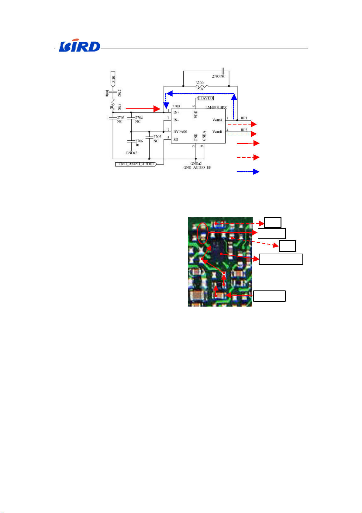
1.1.4 Audio-PA (7700)
Input
Output
Fig.X-7 Circuit diagram of Audio_ PA (7700)
Feedback
It is a circuit diagram of Audio_ PA (7700)
in Fig. X-7 above.
BUZ is a signal from CPU, to enable the
buzzer. CMD_AMPLI_AUDIO is an enable
signal from CPU to Audio_ PA. By dealing
with Audio_PA, the ring signal (HP1/HP2)
is send to speaker. HFAVDD is a voltage for
Audio_ PA’s working. It
Working flow:
When CMD_AMPLI_AUDIO is effectual,
Audio_ PA begins to work. The ring signal
from CPU comes in the 1st pin of Audio_
PA. After amplification, the signal comes
out from the 8th and 4th pins to speaker. At
the same time, a reactive signal comes from
6
2
Fig. X-8 Picture of Audio_ PA
HP1
R7300
HP2
Audio_PA 7700
BUZ input
the 8th pin to the 1st pin.
Note: 8th =8th pin.
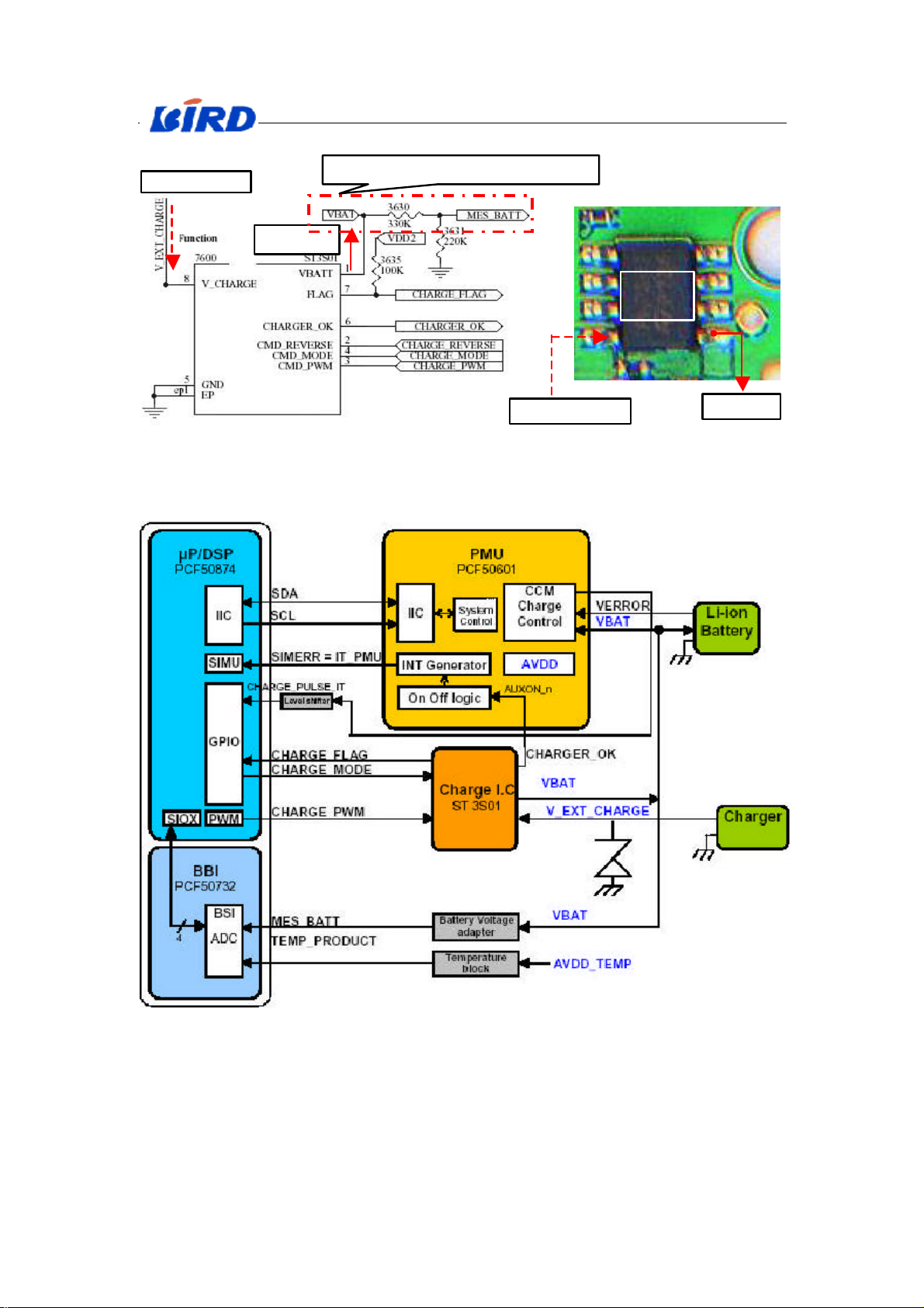
1.1.5 Charge IC (7600):
Signals relevant to The Charge IC (7600):
CHARGE_FLAG: Check the charger type (fast charger or slow charger).
CHARGE_OK: Charger plug-in and charger detection
CHARGE_MODE: Charge mode switch (Pre_Charge or Full_Charge)
CHARGE_PWM: charge pulse control signal
CHARGE_REVERSE: Reverse charge, enable to supply power for adjuncts.
13
English Service Manual S288
1 4 5
From charger
Check the voltage from charger to battery
To battery
Charge IC
7600
8
Fig. X-9、Circuit diagram of charge
From charger
Fig. X-10、A picture of charge IC
To battery
Charging - control block diagram (shown as Fig. X-11)
Fig. X-11 Charging-control
When a charger is plugged, the CHARGER_OK pin (PMU AUXON_N)
goes to logic low, the PMU charger control module is activated and the
PMU is waken up (32kHz output clock start-up, reset sequence generation… ).
Then, the PMU generates an interruption via the IT_PMU pin to inform
the µP/DSP that there is a wake-up condition detection.
14
English Service Manual S288
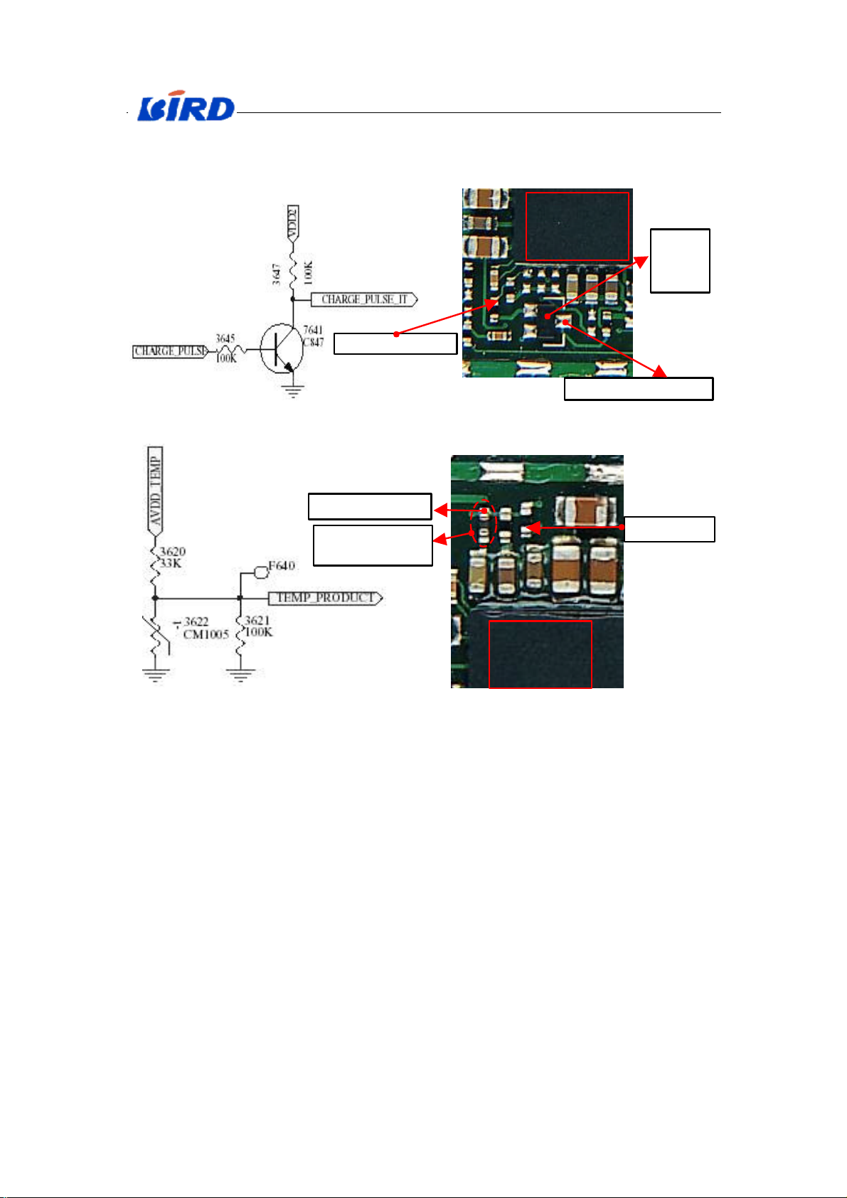
CHARGE_PULSE
7641
3622
about checking
about checking
By reading the PMU OOCS registers with IIC commands, the µP/DSP
knows that the wake-up condition is the plugged charger detection.
Power Supply
IC
PMU7500
NPN
Audion
CHARGE_PULSE_IT
Fig.X-12、Charge pulse circuit diagram
Fig.X-13、Charge pulse practical diagram
TEMP_PRODUCT
Thermal resistance
AVDD_TEMP
Power Supply
IC
PMU7500
Fig.X_14、Circuit diagram
the mainboard’s temperature
Fig.X_15、Practical diagram
the mainboard’s temperature
1.1.6 Connector IC (7600) and I/O Interface(1600):
Connector IC is used to buffer and prevent interference of static electricity.
I/O Interface is used for earphone、software downloading、charge and data
transmitting.
15

English Service Manual S288
Connector
1 6 13 18
18 1
IC
7660
I/O
Interface
1660
Fig.X-16 A picture of Connector IC and I/O Interface
Fig.X-17 Circuit diagram about Connector IC and I/O Interface
16
 Loading...