

Page 1
GSM Service Manual Page 1
Service Manual
Rev 1.2
(Hermes GPRS 900/1800)
20 Sep. 2004
NewGen Telecom Proprietary
Page 2
GSM Service Manual Page 2
Revision History
Version Release Date Author Comments
1.0 Nov. 12, 2003 Steve Bae 1st Draft version
1.1 Jan. 07, 2004 Min Kim Added repair chart
1.2 Jan. 12, 2004 Art Kim Update more in detail for level 1&2 AS
NewGen Telecom Proprietary
Page 3

GSM Service Manual Page 3
Contents
1. INTRODUCTION..................................................................................................................................5
2. PRODUCT DESCRIPTION..................................................................................................................5
2-1.
FEATURES
...........................................................................................................................................5
3. PRODUCT DESIGN..............................................................................................................................7
4. SYSTEM BLOCK DIAGRAM.............................................................................................................8
5. SCHEMATIC..........................................................................................................................................8
6. DRAWING OF PART PLACEMENT OF PCBA (PE D RO)...............................................................8
7. BOM........................................................................................................................................................8
8. GENERAL DESCRIPTION OF EACH FUNCTIONAL BLOCK ....................................................9
8-1.
ANT (7010004000)............................................................................................................................9
8-2.
ANT S
WITCH MODULE
8-3.
SAW BPF (F200, F201).....................................................................................................................9
(U204)..........................................................................................................9
8-4.
TRANSCEIVER IC
8-5.
POWER AMPLIFIER
8-6.
DIRECTIONAL COUPLER
8-7.
PAC(PA C
8-8.
SYNTHESIZER BLOCK
8-9.
LOOP FILTERS (FOR
8-10.
TX IF FILTER
8-11.
ANALOG BASE BAND IC
8-12.
POWER MANAGEMENT IC
8-13.
BASE BAND PROCESSOR
(U206) ...................................................................................................................9
(U203).................................................................................................................9
(U202).......................................................................................................10
ONTROL) CIRCUIT
............................................................................................................10
.......................................................................................................................10
UHF VCO
AND FOR TWO TX
VCOS) ................................................................10
.................................................................................................................................11
(U300).....................................................................................................11
(U500) ..................................................................................................11
(U401).....................................................................................................11
9. PERIPHERAL DEVICES ...................................................................................................................12
9-1.
CAMERA INTERFACE
9-2.
AUDIO INTERFACE
9-3.
MICROPHONE INTERFACE
9-4.
VIBRATOR INTERFACE
9-5.
SIM C
ARD INTERFACE
........................................................................................................................12
............................................................................................................................12
.................................................................................................................12
......................................................................................................................12
.....................................................................................................................12
9-6.
LCD
S AND BACKLIGHTING CIRCUIT
9-7.
BATTERY (LI-ION
.................................................................................................13
) ............................................................................................................................13
NewGen Telecom Proprietary
Page 4

GSM Service Manual Page 4
9-8.
LED
BACKLIGHT FOR KEYPAD AND LIGHT SENSOR
...........................................................................13
10. GENERAL TROUBLESHOOTING GUIDE...................................................................................14
10-1.
ENTERING TEST MODE
10-2.
LIST OF ITEMS IN
10-3.
SERVICE DIAGRAM
10-4.
REPAIR GUIDE
.................................................................................................................................20
....................................................................................................................14
CIT (C
USTOMER INTERFACE TEST) MENU
...........................................................14
.........................................................................................................................15
NewGen Telecom Proprietary
Page 5

GSM Service Manual Page 5
1. Introduction
This document titled “Service Manual” describes the product features of G1 model and, how
to find the defects and to repair within service level 1 and 2 when the phone is not operating
properly as expected. When a customer brings mobile phone for servicing, take a look at the
phone in detail, and carefully listen to the customer’s explanation of symptoms. Most of time,
water and humidity could be the reason for phone’s failure. After cleaning the board, blow some
hot air onto the circuit. This cleaning and blowing of hot air solves 30% of the mobile phone
problems. Many of time, proper cleaning of connectors and sockets also solve the problem. As
the components used on the mobile phone circuit are very small, one should use a luminarymagnifier to be able to properly view them.
2. Product Description
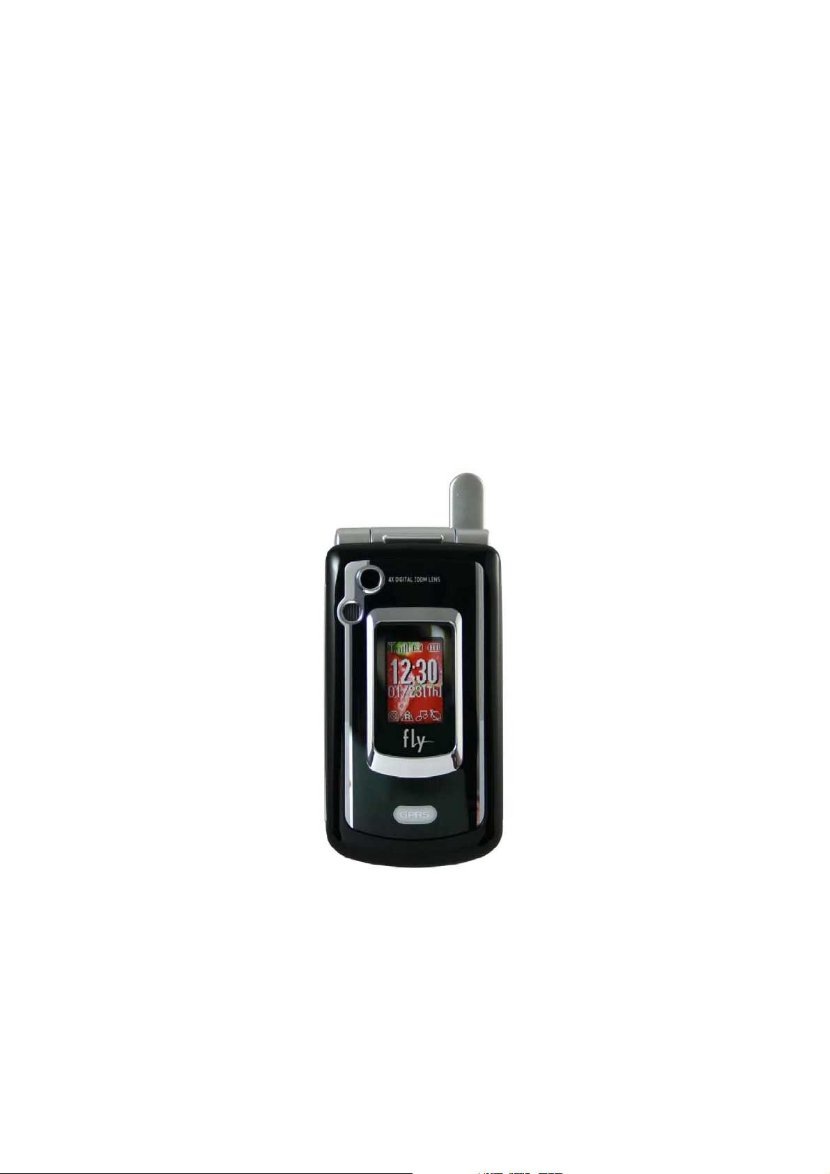
G1 is a dual band dual mode GSM phone, which supports both E-GSM and DCS1800 bands.
And this product has many other features, which will be explained briefly hereafter.
2-1. Features
2-1-1. General Features
. 260K TFT LCD for Main display (dots matrix: 128 x 160 dots)
. 4K CSTN for Sub display (dots matrix: 96 x 64)
. Dual back lighting for both LCDs
. 300K integrated CMOS camera with LED flash
. 7 color LED call coming indicator
. Support both Chinese and English character on display
. Quarter wavelength type Stubby ANT
. 64 level polyphonic sound for ring tone
. Built-in vibrator supporting the VibraCall feature
. WAP browser
. SIM Card (3V only)
. Li-ion battery (600 mAh for Slim / 780 mAh for Standard capacity)
. Mono Headset Jack
. RS232C data interface for PC sync
NewGen Telecom Proprietary
Page 6
GSM Service Manual Page 6
2-1-2. Performance Characteristics
Rx Sensitivity
Tx Power Out
Tx Frequency range
Rx Frequency range
Power Class
No. of RF channel
Duplex frequency offset
Duplex offset (time RX-TX)
Channel spacing
Modulation type
Modulator type
Frequency error
Operating System Parameters
GSM 900 DCS 1800
-107 dBm -106 dBm Typical
33dBm nominal 30 dBm nominal
890.2~914.8MHz 1710.2~1784.8MHz
935.2~959.8MHz 1805.2~1879.8MHz
4 1
124 374
45MHz 95MHz
3 timeslot 3 timeslot
200KHz 200KHz
0.3GMSK 0.3GMSK
I/Q I/Q
<±90Hz(0.1ppm) <±180Hz(0.1ppm)
Note
Phase error
Receiver BER at –102dBm
Co-channel rejection
IMR
Peak: <20 degrees
RMS: <5 degrees
FER<0.12%
Class 1b RBER<0.41%
Class 2b RBER<2.4 %
9dB below at –85dBM 9dB below at –85dBM
49dB 49dB
Peak: <20 degrees
RMS: <5 degrees
FER<0.12%
Class 1b RBER<0.41%
Class 2b RBER<2.439 %
NewGen Telecom Proprietary
Page 7
GSM Service Manual Page 7
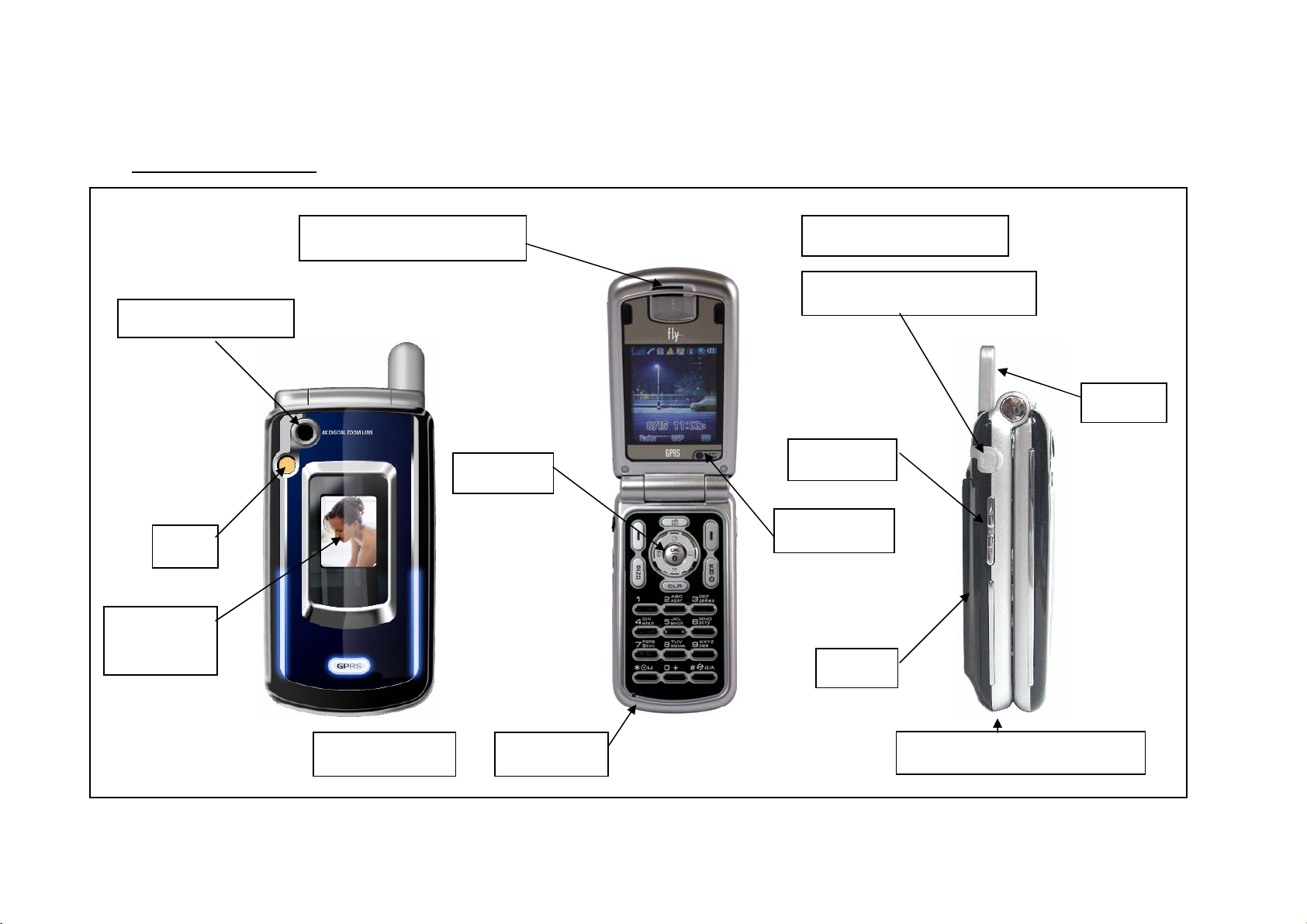
3. Product Design
300K CMOS Camera
One-way dynamic speaker
NAVI Key
MAIN LCD (260K TFT)
Mono Headset Jack & cover
Antenna
Side button
Flash
SUB LCD
(4K CSTN)
Status Indicator Microphone
NewGen Telecom Proprietary
Light sensor
Battery
Accessory connector & cover
Page 8

GSM Service Manual Page 8
4. System Block Diagram
Refer to Functional block diagram in Appendix 1.
5. Schematic
Refer to Functional block diagram in Appendix 2.
6. Drawing of part placement of PCBA (Pedro)
Refer to Functional block diagram in Appendix 3.
7. BOM
Refer to Functional block diagram in Appendix 4.
NewGen Telecom Proprietary
Page 9

GSM Service Manual Page 9
8. General Description of Each Functional Block
In this chapter, we will talk about functions of each blocks such as Amplifier, Filter, and
Synthesizer, to name a few from hardware point of view. In addition, the functions and
capabilities of main chipset will be introduced. When faced problems, understanding hardware
will be helpful for troubleshooting effectively.
8-1. ANT (7010004000)
Antenna (briefly, ANT) is a device, which receives signals from base station and also
radiates transmitted signal to communicate with base station. ANT type is classified by its
electrical length compared to the RF frequency and by its structure, and this model has
employed Quarter-wave length monopole Stubby antenna.
8-2. ANT Switch Module (U204)
Since this model supports dual band operation, E-GSM and DCS1800, this device acts like
a switch that controls the flow of the signal received by ANT into two different signal paths to
avoid interference between them. Its switching action is controlled by two control signals from
Analog base band IC (U300).
8-3. SAW BPF (F200, F201)
In order to select desired signals and also reject undesired signals from the ANT, this model
employed two SAW filters between ANT SW module (U204) and Transceiver IC (U206).
ANT switch module (U204) has some amount of rejection for the undesired signals but not
sufficient for the phone to meet the requirement specified in the standard, thus they were
employed for better selection and rejection performance. F200 and F201 are for GSM and DCS,
respectively.
8-4. Transceiver IC (U206)
This IC provides a lot of functions required for the signal processing in RF band such as low
noise amplification, down conversion, base band amplification etc… in receiver block, upconverter (or modulator), transmitter VCOs in transmitter block, and frequency synthesizer block
for carrier frequency generation. All internal blocks are controlled by software via multiple control
signals for optimum operation.
8-5. Power Amplifier (U203)
Power amplifier is, as its name implies, an amplifier that amplifies the transmitting signal
enough to be radiated by ANT so that it can communicate with base station.
NewGen Telecom Proprietary
Page 10

GSM Service Manual Page 10
PA module supports tri-band operation EGSM, DCS1800, and PCS1900, two set of different
input/output pins are assigned for each band (common pins are used for both DCS1800 and
PCS1900) and the selection is done by a control signal named “ BS”, which stands for “band
selection”. In addition, another control pin named “APC” and came from PAC circuit, is assigned
for gain control of the power amplifier, which is used for power control and abbreviation of
“power amplifier control”.
8-6. Directional Coupler (U202)
Directional coupler is employed for gain control of power amplifier. The role of directional
coupler is monitoring the transmitted power by capturing a part of the signal at the output of the
power amplifier, and the captured signal is fed into the PAC circuit through “COU_OUT” for the
conversion of RF signal to the proportional DC voltage. This device has two sets of input/output
port and one coupled port.
8-7. PAC(PA Control) Circuit
This circuit consists of two Schottky diode detectors (D201) and two OP amplifiers (U201) that
act as an integrator and DC amplifier, respectively. The coupled signal by directional coupler is
rectified by Schottky diode, and the proportional DC voltage, which is generated at port#1 in
U201, is fed into the APC pin of PA, which means the gain of PA is varied by the input DC
voltage level. In this procedure, two logic control signals are being used, one is “TX_EN0” for
turning ON/OFF the PA, and second is “PAC_OUT2” for adjustment of APC voltage.
8-8. Synthesizer Block
Synthesizer block in this model is integrated inside the transceiver IC (U206) and generates
local oscillator signals for receiver and transmitter, which are required for down conversion and
up conversion of IF signal. There are three oscillators for generation of local signals, one is UHF
oscillator, which is synthesized by fractional-N technique, and the others are two TX oscillators
(each one supports single operating band), which are synthesized by TX offset loop with UHF
oscillator as reference signal source.
8-9. Loop Filters (for UHF VCO and for two TX VCOs)
In a synthesizer block, loop filter is employed to convert error signal from phase detector into
the proportional DC voltage, and located between charge pump output and control port of an
oscillator, where the charge pump supplies/sinks charge to/from the loop filter if there’s
frequency deviation from reference signal, and loop filter converts the charge into proportional
DC voltage, which is used to control the resonance frequency of an oscillator by changing the
NewGen Telecom Proprietary
Page 11

GSM Service Manual Page 11
capacitance of varactor diode in the tank circuit of an oscillator. There are two loop filters, one
for UHF VCO and the other for TX VCOs, and connected externally to transceiver IC (U206) as
shown in the system block diagram.
8-10. TX IF Filter
This filter consists of discrete LC resonant circuit that was inserted in shunt configuration
between two balanced signal lines at the output of quadrature modulator. This filter rejects
roughly the undesired signal at the output of modulator.
8-11. Analog Base band IC (U300)
This IC interfaces transceiver IC (U206) with base band processor (U401) and provides some
important functionalities such as I/Q signal processing for both receiver and transmitter, power
amplifier control, timing generation for synthesizer, and audio interfaces. Analog base band IC
has 7 basic functional blocks required for transceiver operation, wh ich are as the following,
1. Receiver for digitizing Rx I/Q analog input signals to generate the digital data
2. Transmitter for generating Tx I/Q signal from digital data
3. Power control for PA control
4. Timing generation and control for synthesizer
5. Voice-band codec
6. LDO supplies to supply the stable power to each blocks in
8-12. Power Management IC (U500)
This IC is also called “PMIC” in general and its main role is providing regulated DC supplies to
each part of the system. Additionally, this IC includes charging circuitry for battery charging
(internal charger), and SIM card interface circuitry, and booster circuitry (Not used). As for the
DC supply, it provides 8 independent regulated DC outputs, 7 out of them are being used in this
model. The voltage is set to nominally 2.8V for “VCCD”, “VUHF”, “VRF”, “VTIC”, “VSIM”, “VRTC”
and, the voltage for “VIA” port is same as battery voltage.
8-13. Base band Processor (U401)
Base band processor is the brain of the system and manages execution of SW and signal
processing both in physical layer and logical layer. Two core processors (ARM7 and DSP) are
integrated and each processor takes part in different job function. ARM7 processor is taking
charge of mainly SW execution while DSP is doing signal processing, and both processors
communicate with each other through internal two-port RAM. This IC also includes various kinds
of interfaces such as MMI peripherals.
NewGen Telecom Proprietary
Page 12

GSM Service Manual Page 12
9. Peripheral Devices
9-1. Camera Interface
Embedded Camera module (8020001000) is utilizing CMOS sensor having 300K-pixel
resolution with dedicated image processor IC (U801) for Camera functionality and provides
features of still photos in JPEG format and moving picture capturing in MJPEG format. Also
supports “Zoom” function that displays magnified picture up to x4 zoom-in adjustability in 10
steps.
The image processor IC (U801) has 2 major functions depending on camera turn-on state or not.
The first function is that when normal operation mode, which means camera is turned off, this
chip is not fully working, but acting as LCD data buffer. Other function is when camera is turned
on, this chip is working for main processor to support unique functionality of camera as
mentioned above.
9-2. Audio interface
24 x 14 one-way dynamic speaker (737-0001-000) is employed to support both for ringer and
RX voice. In ringer mode, the digital sound source generated from base band processor (U401)
is fed into Audio synthesizer IC (U771) though data bus and then amplified sound source with
given audio gain comes out from “SPOUT1 / 2” ports, which are tie together with “SPK+/-“ pins
of the dynamic speaker. The audio gain can be adjustable by external components of equalizer
circuit and also S/W control. In voice mode, “EAR+/-“ pins, generated from analog base band IC
(U300), are directly tied to “SPK+/-“ pins, which means there’s no relationship with audio
synthesizer IC (U771) when a phone is in conversation mode.
9-3. Microphone interface
MIC is a device that converts the human voice into electrical signal, reverse action of the
speaker, and the converted signal is fed into the audio processing circuitry inside analog base
band IC (U300).
9-4. Vibrator interface
Vibrator is a micro-motor that provides some vibration when activated so that a phone user
can recognize the incoming call.
9-5. SIM Card interface
SIM card is a standard feature of all GSM phones. SIM card contains various kinds of user
information such as registration, phone number, network information etc… Working voltage for
NewGen Telecom Proprietary
Page 13

GSM Service Manual Page 13
SIM is VSIM voltage, which is 2.8V.
9-6. LCDs and backlighting circuit
This model has two kinds of LCD display, main LCD and sub LCD. Main LCD displays
all user functions in the form of menu tree and icons for easy selection. Sub LCD only displays
limited information than main LCD. The unique one is that both LCD is using same back light
circuit, which means when the back light is turned on, both main and sub LCD will be turned on
simultaneously.
9-7. Battery (Li-ion)
Battery is the main power source required for phone operation. It supplies DC voltage and
internally regulated and directly fed into the appropriate hardware block. Its nominal voltage is
3.7V and increased up to 4.2V when fully charged.
9-8. LED backlight for keypad and light sensor
12pcs blue color LEDs are employed for keypad back lighting. One of unique function is that
turn-on condition of this keypad back light can be controlled by light sensor, which is positioned
under main LCD, depending on the strength of light which fed into light sensor.
NewGen Telecom Proprietary
Page 14

GSM Service Manual Page 14
10. General Troubleshooting guide
If any reasons that the phone needs to be disassembled to fix the defected part, the functional
test listed below should be done first to verify the problems.
10-1. Entering test mode
1.
Command set for entering test mode:
2. Select “1. CIT” menu in the list for functional testing
*
364*
10-2. List of items in CIT (Customer Interface Test) menu
1. ALL (Testing include of Main LCD, Sub LCD, Vibrator, Camera & flash, 7 color indicator
LED, Speaker, Keypad LED test)
2. Main LCD
3. Sub LCD
4. Melody (Ringer testing)
5. Earpiece
6. Loopback (voice loop back testing)
7. Vibrator
8. LED (status indicator operation testing)
9. Backlight (LCD backlight testing, Normal/Dim lighting/Of f)
10. Key press (including side buttons)
11. Camera (including flash testing)
12. Sensor (light sensor detection test)
13. DAI (Factory testing only)
NewGen Telecom Proprietary
Page 15

GSM Service Manual Page 15
10-3. Service diagram
Metal Dome ass’y (6300900100)
Damaged or oxidized will result
in key not functioning.
MR sensor (U740)
Damaged will result in no flip
on/off detection.
Blue LED (D701 to D712)
Damaged will result in no lighting
on Keypad side.
NewGen Telecom Proprietary
Page 16

GSM Service Manual Page 16
RF switch (CN202)
Damaged result in no network.
ANT Switch Module (U204)
Damaged result in no network, no
smooth transmission & reception.
Transceiver IC (U206)
Damaged will result in no network
or no transmitting.
MCP Memory (U400)
Damaged will result in power-on
failure, no network or failure in
saving information.
Main FPCB connector (CN653)
Damaged or bad contact will
result in no display, white out on
the display, no backlight, no
camera functioning, no sound thru
the speaker or no vibrating.
Audio synthesizer IC (U771)
Damaged result in no Ringer or
key sound.
19.5MHz CCXO (OSC300)
Damaged result in power-on
failure, no network or call cut off.
Coin type Capacitor (C406)
Damaged or bad contact will
result in no clock update.
Battery(+)
Damaged or bad contact will
result in power-on failure.
Base band processor (U401)
Damaged will result in power-on
failure or no network.
Microphone Ass’y (7430002000)
Damaged or bad contact will
result in failure to send voice.
NewGen Telecom Proprietary
Page 17

GSM Service Manual Page 17
Antenna PAD (CN201)
Bad contact results in signal weak
or difficult to make a call.
Power Amplifier (U203)
Damaged will result in no
transmission.
External headset Jack (CN641)
Damaged or bad contact will result
in no voice through headset.
Analog base band IC (U300)
Damaged will result in no network or
no voice while making a call.
Power management IC(U500)
Damaged will result in power-on
failure, automatic power off, failure
to recognize battery or charging
failure.
SIM card connector (CN601)
Damaged or bad contact will
result in failure in recognizing SIM
card.
IO Connector (CN621)
Damaged or bad contact will
result in charging failure.
Image processor IC (U801)
Damaged will result in no camera
functioning or distorted.
32.768KHz OSC (OSC401)
Damaged will result in power-on
failure or no clock update.
Battery(-)
Damaged or bad contact will result
in power-on failure.
BATT ID
Damaged or bad contact will result
in power-on failure.
NewGen Telecom Proprietary
Page 18

GSM Service Manual Page 18
Vibrator (7130005000)
Damaged or bad contact will
result in no vibration.
Speaker (7370001000 )
Damaged or bad contact will
result in no sound thru the
speaker.
Vibrator (-)
Vibrator (+)
SPK (+)
SPK (-)
Camera Module (8020001000)
Damaged or bad contact will
result in no camera functioning
or making distortion.
Main FPCB (6302300100)
Damaged or bad contact will
result in no display, white out on
the display, no backlight, no
camera functioning, no sound
thru the speaker or no vibrating.
LCD module (7850001000)
Damaged will result in no
display, white out, line missing
on the display or no backlight.
White LED for flash
Damaged will result in no
camera flashing.
Camera lens
Damaged will result in no
camera functioning.
NewGen Telecom Proprietary
Page 19

GSM Service Manual Page 19
Magnet (6202200100)
If magnet is miss placed or damaged
no flip on/off functioning.
NewGen Telecom Proprietary
Page 20

GSM Service Manual Page 20
10-4. Repair guide
1. Phone does not power on.
Probable Cause 1: Housing assembly defective
Step 1: Check the tactile feeling of the “END” button which is use d for power on/off.
Probable Cause 2: Battery pack discharged or defective
Step 1 : Check the battery voltage. If the voltage is below 3.4Vdc, recharge the battery using an
appropriate travel charger.
Step 2: If the battery does not recharge after 2 hrs, replace the battery.
Probable Cause 3: Battery connectors open or misaligned
Step 1: Visually inspect the battery connectors on both the battery assembly and the phone.
Step 2: If necessary, adjust the pin of battery connectors on the PCBA.
Probable Cause 4: PCBA defective
Step 1: Visually inspect any damages on the PCBA.
Step 2: Replace a known good PCBA and verify that the fault has been cleared.
Step 3: Reassemble the phone with the new PCBA.
2. Call drop or weak and/or distorted audio during making a call
Probable Cause 1: Poor Antenna connection
Step 1: Check to make sure that the antenna connection is properly connected t o the PCBA.
Step 2: If necessary, substitute a known good antenna.
Probable Cause 2: PCBA defective
Step 1: Visually inspect any damages on the PCBA.
Step 2: Replace a known good PCBA and verify that the fault has been cleared.
Step 3: Reassemble the phone with the new PCBA.
3. Display is erratic or provides partial or no display
Probable Cause 1: Poor connection of Main FPCB
Step 1: Check general condition of the flex cable and connectors on both side of main PCBA
and LCD module.
Step 2: Check any disconnection of main FPCB. And then replace it to new one.
NewGen Telecom Proprietary
Page 21

GSM Service Manual Page 21
Probable Cause 2: LCD module is defective
Step 1: Substitute a known good LCD module and verify that the problem has been cleared.
Probable Cause 3: PCBA defective
Step 1: Visually inspect any damages around main FPCB connector on the PCBA.
Step 2: Replace a known good PCBA and verify that the fault has been cleared.
Step 3: Reassemble the phone with the new PCBA.
4. No Rings and/or no voice or too low sound
Probable Cause 1: Poor connection of Main FPCB
Step 1: Check general condition of the flex cable and connectors on both side of main PCBA
and LCD module.
Step 2: Check any disconnection of main FPCB. And then replace it to new one.
Probable Cause 2: Speaker defective or disconne ction of wire
Step 1: Visually inspect wire connection between LCD module an d the speaker.
Step 2: Check the input impedance of the speaker with DVM. It should be measured around
8ohm.
Step 3: If the impedance is measured over ~100ohms or more, replace with new speaker unit.
Probable Cause 3: PCBA defective
Step 1: Visually inspect any damages around audio synthesizer IC and main FPCB connector
on the PCBA.
Step 2: Replace a known good PCBA and verify that the fault has been cleared.
Step 3: Reassemble the phone with the new PCBA.
5. Outgoing voice is weak.
Probable Cause 1: Poor connection of microphone assembly
Step 1: Visually inspect the connection between microphone assembly and the PCBA.
Probable Cause 2: Microphone defective
Step 1: Replace with a known good microphone assembly. Place a call to verify improvement in
transmit voice as heard by called party.
Probable Cause 3: PCBA defective
NewGen Telecom Proprietary
Page 22

GSM Service Manual Page 22
Step 1: Visually inspect any damages around microphone assembly on the PCBA.
Step 2: Replace a known good PCBA and verify that the fault has been cleared.
Step 3: Reassemble the phone with the new PCBA.
6. No detection of SIM card
Probable Cause 1: SIM card defective
Step 1: Initially check that the contacts on the card are not dirty.
Step 2: Clean if necessary, and check if fault has been eliminated.
Step 3: If the contacts are clean, insert a known good SIM card into the phone. Power up the
radio and confirm whether or not the card has been accepted.
Probable Cause 2: Poor connection of SIM card connector
Step 1: Visually check the SIM card connector on the PCBA. If necessary, adjust the pin of
battery connectors on the PCBA.
Probable Cause 3: PCBA defective
Step 1: Visually inspect any damages around SIM card connector o n the PCBA.
Step 2: Replace a known good PCBA and verify that the fault has been cleared.
Step 3: Reassemble the phone with the new PCBA.
7. Phone does not sense when flip is opened or closed.
Probable Cause 1: Magnet in flip assembly defective or missing
Step 1: Check the general condition of magnet in flip assembly.
Step 2: If the magnet located right position, replace with a known good flip assembly and verify.
Probable Cause 2: PCBA defective
Step 1: Visually inspect any damages on MR sensor circuit on the PCBA.
Step 2: Replace a known good PCBA and verify that the fault has been cleared.
Step 3: Reassemble the phone with the new PCBA.
8. Vibrator feature not functioning
Probable Cause 1: Poor connection of Main FPCB
Step 1: Check general condition of the flex cable and connectors on both side of main PCBA
and LCD module.
Step 2: Check any disconnection of main FPCB. And then replace it to new one.
NewGen Telecom Proprietary
Page 23

GSM Service Manual Page 23
Probable Cause 2: Vibrator defective or disconnection of wire
Step 1: Visually inspect wire connection between LCD module and the vibrator.
Step 2: Replace with new speaker unit.
Probable Cause 3: PCBA defective
Step 1: Visually inspect any damages around Q701, Q702 and main FPCB connector on the
PCBA.
Step 2: Replace a known good PCBA and verify that the fault has been cleared.
Step 3: Reassemble the phone with the new PCBA.
9. Charger not working
Probable Cause 1: Travel charger defective
Step 1: Check with a known good travel charger.
Probable Cause 2: PCBA defective
Step 1: Visually inspect any damages around Q501 and U5 00 on the PCBA.
Step 2: Replace a known good PCBA and verify that the fault has been cleared.
Step 3: Reassemble the phone with the new PCBA.
10. Camera not working or distortion
Probable Cause 1: Poor connection of camera assembly
Step 1: Check the connection of camera module in flip assembly.
Step 1: Check general condition of the flex cable and connectors on both side of main PCBA
and LCD module.
Step 3: Check any disconnection of main FPCB. And then replace it to new one.
Probable Cause 2: Camera defective
Step 1: Replace a known good camera module and verify that the fault has been cleared.
Probable Cause 3: PCBA defective
Step 1: Visually inspect any damages around U801, U802, U803, Q801, Q802 and main FPCB
connector on the PCBA.
Step 2: Replace a known good PCBA and verify that the fault has been cleared.
Step 3: Reassemble the phone with the new PCBA.
NewGen Telecom Proprietary
 Loading...