

Page 1

Service Manual Page 1
Version 1.0
Oct 18, 2004
Service Manual
Model: X7
Copyright NEWGEN TELECOM. This material, including documentation and any related computer
programs, is protected by copyright controlled by NEWGENT TELECOM. All Rights reserved.
Written permission from NEWGEN TELECOM is required for copying, adapting, or any kinds of
reproducing any or all part of this document.
Copyright NEWGEN TELECOM Co. Ltd.
1
Page 2

Service Manual Page 2
Version 1.0
Oct 18, 2004
Table of Contents
Revision History.............................................................................................................................................3
1. Introduction..............................................................................................................................................................4
2. Product Description................................................................................................................................................4
2-1. Features Set........................................................................................................................................................4
2-2. Minimum Radio Performance........................................................................................................................5
2-3. System block diagram...................................................................................................................................7
2-4. General Description of Each Functional Block.............................................................................................7
2-4-1. Antenna (or briefly ANT).....................................................................................................................7
2-4-2. Antenna Switch Module (or simply ASM module; U105)...............................................................8
2-4-3. SAW Band pass Filter (or, SAW BPF; F101, F102).............................................................................8
2-4-4. Transceiver IC (CX74063; U101)..........................................................................................................9
2-4-4-1. LNA Block.................................................................................................................................10
2-4-4-2. Quadrature Demodulator.......................................................................................................10
2-4-4-3. Base band signal processing block (or, “base band block” in short).................................10
2-4-4-4. Control circuit...........................................................................................................................10
2-4-4-5. Synthesizer block;.....................................................................................................................10
2-4-4-6. Power Amplifier (simply, PA; U102) ;...................................................................................12
2-4-5. Analog Base-band IC + PMIC (SKY20524; U201);...........................................................................12
2-4-5-1. Earpiece/Melody Speaker/ Headset Interface;...................................................................12
2-4-5-2. Power Management IC (or, simply PMIC; U201) ;..............................................................13
2-4-5-3. Internal Charger;......................................................................................................................13
2-4-5-4. Real Time Clock (or, simply RTC);........................................................................................13
2-4-6. Base and Processor IC (CX805-32; U301);.........................................................................................14
Copyright NEWGEN TELECOM Co. Ltd.
2
Page 3
Service Manual Page 3
3
Version 1.0
Oct 18, 2004
Revision History
Version Date Author Status Remarks
1.0 Oct 18 Mounty Li Revised for Nostalgia Rev1.0
Copyright NEWGEN TELECOM Co. Ltd.
Page 4

Service Manual Page 4
Version 1.0
Oct 18, 2004
1. Introduction
This document titled “Service Manual” is intended to serve as a technical guideline for repairing the GSM
cellular phone (Model : X7) when in trouble. In order to troubleshoot a phone, service engineers or
technicians should know about basic knowledge on how the cellular phone is working and how it was
designed. According to symptoms of a problem, they should judge how to troubleshoot by taking proper
procedure. This service manual with other separate documents will provide such information. In this
document, the subject on system design, which is unique with X7, will be discussed, and some
instructions for troubleshooting will be covered by “HW troubleshooting guide”. Of course, it’s impossible
to cover all kinds of problems and its solution in a document, but tried to introduce basic and proper
procedure for troubleshooting that can serve as a reference. Experienced service engineers or technicians
maybe have their own tricks or know-how regarding some specific problems, which are not discussed in
this material or other documents, and maybe theirs are more efficient and practical. Unless violate
recommended warnings or cautions, they can use theirs at their own risks but it’s highly recommended to
follow the guidelines suggested in this material if possible.
2. Product Description
X7 is a “Dual-band GSM phone” that supports both E-GSM and DCS 1800 bands, and their channel
numbers (AFRCN) and operating frequencies are tabled at the end of this manual.
X7 has many other features except basic phone operation, and can use some accessories with which X7
is used more conveniently and efficiently, and they will be discussed briefly hereafter since they are also
part of candidates that service engineers or technicians need to troubleshoot.
2-1. Features Set
. 260K Color TFT display for Main LCD (2.2” Pixel Size: 176x220 )
. 64-poly melody play through stand-alone speaker
. Vibrator for etiquette mode
. Lithium-Ion Polymer Battery (Capacity: 570 mAh) with protection circuit
. Headset for hands free (Mono, 3-pole with SEND/END Key) *
. Blue LED Keypad backlight
. Travel Charger (TC)
. Internal Antenna
.Touch panel
. SIM Card Interface that support 3V SIM cards (5V SIM is not supported)
. CMOS Camera Module (300K pixel resolution)
** Note: Other SW features are not included in the list, and you can refer to “User Manual” for detailed
features of X7 regarding their usage.
Copyright NEWGEN TELECOM Co. Ltd.
4
Page 5
Service Manual Page 5
Version 1.0
Oct 18, 2004
2-2. Minimum Radio Performance
The following table shows summarized electrical performance of X7, which are required for phone
operation and also specified in GSM standards. Actual performance of X7 surpasses minimum required
performance.
Parameters
Static Sensitivity
@ RBER < 2.4 %
Tx Output Power
Tx Frequency Range 880 ~ 914.8 MHz 1710 ~ 1784.8 MHz
Rx Frequency Range 925 ~ 959.2 MHz 1805 ~ 1879.8 MHz
Power Class 4 1
No. of RF Channels 124 374
Duplex Frequency Offset 45 MHz 95 MHz
Duplex Time Offset 3 Time Slot 3 Time Slot
Channel Spacing 200 KHz 200 KHz
Modulation Type 0.3 GMSK 0.3 GMSK
Frequency Error
Phase Error
< - 104 dBm < - 102 dBm Min
+ 33 dBm ± 2 dB + 30 dBm ± 2dB
< ± 90 Hz < ± 180 Hz
Peak < 20 degrees
RMS < 5 degrees
Standard Requirement
Remarks
E-GSM DCS 1800
Peak < 20 degrees
RMS < 5 degrees
Copyright NEWGEN TELECOM Co. Ltd.
5
Page 6
Service Manual Page 7
Version 1.0
Oct 18, 2004
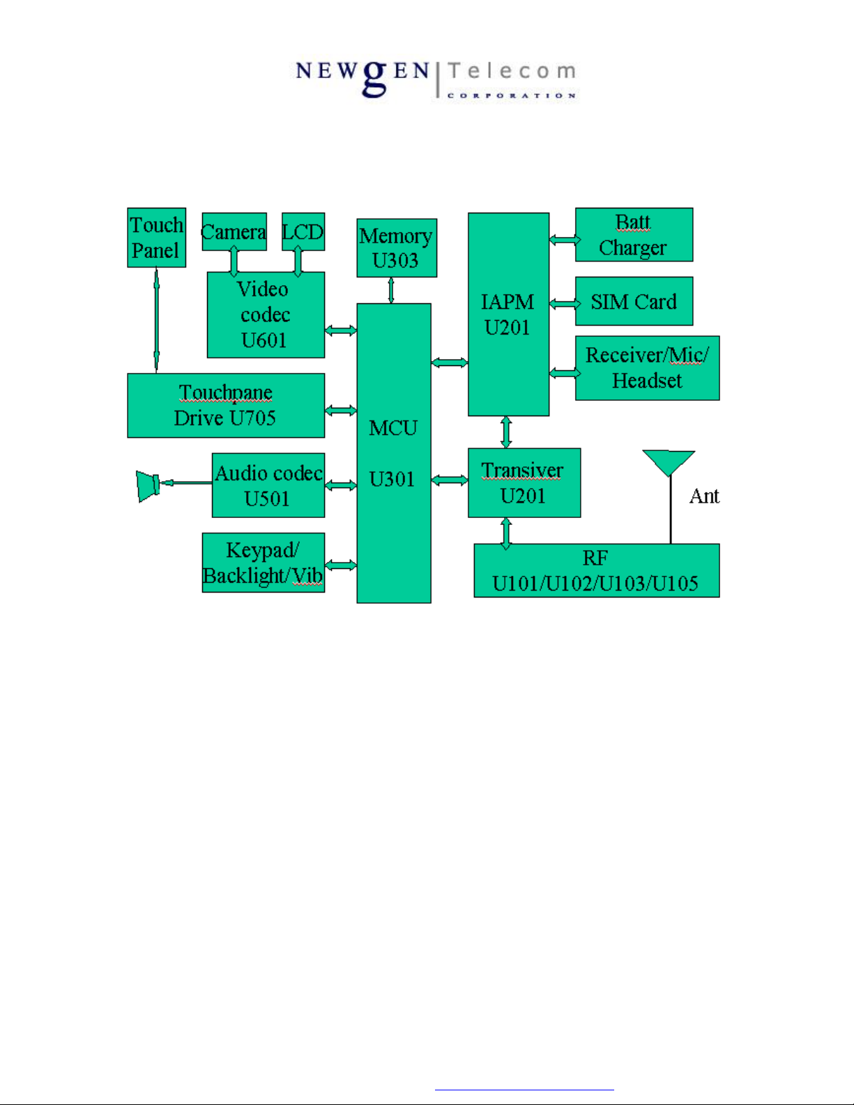
2-3. System block diagram
2-4. General Description of Each Functional Block
In this section, each functional block shown in the ”System block diagram” will be discussed one by one
briefly. When faced problems, understanding hardware design will be helpful for troubleshooting effectively.
2-4-1. Antenna (or briefly ANT)
ANT is a device that receives and transmits radio signals to communicate with base station nearby. Its type
is classified by its structure and implementation methods. X7 is employing PIFA internal antenna. A
phone user can’t change the ANT because the antenna is assembly inside the radio. Its electrical
performance is determined by careful adjustment and optimization with ANT matching circuit on PCB
board, thus just changing to other type ANT can make the phone function improperly.
Copyright NEWGEN TELECOM Co. Ltd.
7
Page 7

Service Manual Page 8
Version 1.0
Oct 18, 2004
2-4-2. Antenna Switch Module (or simply ASM module; U105)
Since X7 supports dual band operation (both E-GSM and DCS 1800) and each system is operating at
different frequency band, this device acts like a switch that controls the RF signal flow, that of in-band signal
received by ANT into two different LNAs and transmitting signals from dual band PA, so that it prevents
any out-of-band interference signals from interrupting proper operation at the selected band. Its switching
action is controlled by 2 control signals from “Analog Base band IC”, and named as “ CTL1 and CTL2”.
2-4-3. SAW Band pass Filter (or, SAW BPF; F101, F102)
In order to select desired signals (in-band signals) and reject undesired signals received by ANT, X7 is
employing two SAW BPFs, with which each operating frequency band is covered, between ASM and
Transceiver IC. ASM has some amount of rejection for undesired signals but not sufficient for the phone to
meet the requirement specified in the standard, thus they were employed for better selection and rejection
performance.
Copyright NEWGEN TELECOM Co. Ltd.
8
Page 8

Service Manual Page 9
9
LNA
÷
∆Σ
R
FilterIFTx
Σ
θ
PD
2
×
−
1D÷
2D÷
Quadrature
θ
2
×
2
×
θ
Version 1.0
Oct 18, 2004
2-4-4. Transceiver IC (CX74063; U101)
This IC provides a lot of functions required for the signal processing in RF band and base band related to
both modulation of received signal and demodulation for transmitting signal, such as “low noise
amplification by LNA block”, “ up/down conversion”, “ base band processing”, and “ frequency synthesis
for LO and Tx frequency generation” etc… All functional blocks are controlled by software with
sophisticated algorithms via multiple control signals grouped by and called “interfaces” (you can see many
interface group in the schematic). As both receiver and transmitter architecture, CX74063 is employing
“Direct Conversion” scheme, where IF stages are not required. The internal block diagram is shown in Fig.1
CX74063 IC has 7 basic functional blocks required for transceiver operation, which are as the following,
ICrTransceiveCX 74063
1. Three Low Noise Amplifiers (LNA)
2. Quadrature Demodulator
3. Base band signal processing block
LNA
dulatorDemo
)(EGSM
DOC
4. Control logic circuitry governing whole
)1800(DCS
BlockrSynthesize
−
DFC
)( NFractional
BlockBaseband
LogicControl
&
SupplyPower
(Fractional-N + Tx Translation Loop)
transceiver operation
5. Synthesizer block for local signal generation
6. Quadrature Modulator
7. Two Tx VCOs
VCOUHFforLPF
)30( KHzBW
=
mixerharmonicsub
DFC
)110( MHz
VCOsTxforLPF
)1( MHzBW
=
Quadrature
dulatorMo
APC
ControlPowergAnaloAPC=*
;
Copyright NEWGEN TELECOM Co. Ltd.
Page 9

Service Manual Page 10
Version 1.0
Oct 18, 2004
2-4-4-1. LNA Block
LNA block amplifies incoming signal from ANT so that the signal level should be sufficiently high for
demodulation process. Though CX74063 is supporting “Tri-band” and having 3 LNAs for each band, X7 is
only employing 2 of them, LNA for E-GSM and LNA for DCS1800, in its design.
2-4-4-2. Quadrature Demodulator
(or, simply “quad-modulator”)
Since GSM is adapting “digital modulation” scheme called “GMSK”, quadrature modulator is required for
demodulation of received signal, where both “In-phase signal” and “Quadrature phase signal” (or, shortly
called I/Q signals) is split for digital signal processing at base band processor (CX805-32) to extract
information. Local signal from synthesizer block is fed into the “quad-modulator” for down conversion of
received RF signal to analog I/Q signals. (Later, this analog I/Q signals is converted into digital signals at
Analog BB IC, CX20524-13)
2-4-4-3. Base band signal processing block (or, “base band block” in short)
The down converted I/Q signals are filtered and amplified according to the signal strength at the ANT for
optimum signal level to be fed into successive functional blocks, and the amplifier gain is adjusted to
optimize the receiver performance so that the receiver has sufficient immunity in terms of interference
rejection performance.
2-4-4-4. Control circuit
GSM system is using Time Division Duplex (or simply TDD) schemes to separate receiver and transmitter
operation, thus it requires that whole circuitry should operate precisely in terms of timing, and control block
is taking charge of this function by providing complex control signals both internally and externally.
This block is also involved in proper parameter setting of internal block such as receiver I/Q filters, gain stag
es, and synthesizer programming according to input signal level and operating channel for optimum perfor
mance in various environment, and plays a linkage role between Analog BB IC through control lines called “
interface”.
2-4-4-5. Synthesizer block;
To generate the required local signal(LO) to receiver block and to make Tx signal GMSK modulated, a little
complicated process is undertaken as shown below
shows how transmitter frequency is generated, where 2 synthesizer loops are involved in, one is
Fig 3
Copyright NEWGEN TELECOM Co. Ltd.
10
Page 10

Service Manual Page 11
Version 1.0
Oct 18, 2004
“fractional-N PLL” for receiver LO signal generation from UHF VCO and the other is “Translation Loop” for
direct modulation of Tx VCOs. Depending on operation band, appropriate divider (or multiplier) is selected
to make accurate frequency generation. Fractional-N PLL with UHF VCO provides low phase noise and fast
lock time, which is required for multi-slot operation in GSM/GPRS System. The Tx VCOs are directly
modulated by translation loop in which both UHF
PD
2D÷
1D÷
ITx
VCO and I/Q signals from base-band are involved
to generate GMSK modulated RF signal. The
demodulated base-band signal is fed into Analog
θ+
θ
2×
QTx
Base-band IC for further signal processing.
In Fig.3
, the “translation loop” is composed of a
couple of sub blocks as the following;
Tx VCO -> Harmonic Mixer -> LPF -> Quadrature
Modulator -> BPF -> Divider (D1 or D2) -> Phase
NFractional−
3÷
UHF VCO
2×
Fig 3 – Transmitter Frequency Generation
Detector -> Loop Filter -> Tx VCO,
And the signal directly from UHF VCO acts like a
reference signal in a normal PLL loop.
Tx I/Q signals from base-band is quadrature
modulated with mixing product between UHF VCO and Tx VCO, which is 100.267 MHz in GSM band and
102.812 MHz in DCS1800 band, and compared with reference signal to generate modulating signal for Tx
VCOs. For receiver LO signal generation, only UHF VCO is used as shown in Fig.4.
Harmonic
Mixer
divided by 3 in GSM900 band operation, and
, where UHF VCO is
multiplied by 2 after division by 3 for DCS 1800
band operation. The quadrature demodulator is
BBTo
realized by sub-harmonic mixer that requires 1/2
the received RF frequency from ANT, this helps
preventing LO leakage to ANT port that is well
known problem in a receiver employing direct
conversion architecture.
ANT
SW
DCS1800
LNA
GSM900
LNA
θ
Harmonic
Mixer
θ
2×
2×
NFractional−
3÷
UHF VCO
2×
Fig 4 – Receiver Frequency Generation
Copyright NEWGEN TELECOM Co. Ltd.
11
Page 11

Service Manual Page 12
Version 1.0
Oct 18, 2004
2-4-4-6. Power Amplifier (simply, PA; U102) ;
In Fig.5
, there are 2 power amplifiers were employed in X7 design to support both GSM and DCS band
operation. GMSK modulated Tx VCOs are input to each PA according to the operating band of interest, and
ANT
SwitchANT
Module
RF
.Con
RT/
SW
2CTL
1CTL
lDirectiona
Coupler
APC(Analog Power Control) circuit inside
CX74063 Transceiver IC controls PA operation in
terms of band selection and ramp control in burst
mode. In order to control the PA properly, part of
output signal from each PA is coupled by
directional coupler and is regulated to the
corresponding DC voltage through “power
detector” as shown in the Fig. 5
, and properly
controlled transmitting signals (both power level
and burst timing) are fed into ANT via ASM
BBgAnalofrom
Power
Detector
APC
DFC
)77321(CXPA
BS
APC
signalcontrol
module.
Fig.5 – Power Amplifier Block
2-4-5. Analog Base-band IC + PMIC (SKY20524; U201);
Analog Base band IC includes required signal processing blocks for both receiver and transmitter in base
band domain, such as digitizing received analog I/Q signal from receiver block in transceiver IC and
making analog I/Q signal from digital I/Q data from base band processor for transmitter, and except basic
signal processing blocks, power management function is integrated onto the same IC, which provides DC
voltage supplies for various functional blocks.
In addition, there’s a couple of interface circuitries for peripheral devices such as earpiece (or receiver
speaker), melody speaker, headset, MIC, SIM card interface, internal charging circuit, and coin battery for
“real time clock (simply, RTC) as shown in Fig.6
.
2-4-5-1. Earpiece/Melody Speaker/ Headset Interface;
Earpiece, or receiver speaker, is providing voice signal that a phone user wants to hear during a call, while m
elody speaker is used only for melody sound playing (64 poly phonic sound). The reason why employed sep
arate speaker is that a phone user usually listens voice signal in normal phone operating position, making th
e phone close to the listener’s ear after flip open, while melody playing is performed under flip closed condit
ion to show off to a friend or other people. Headset is recently used as a means of hands free device, or for pr
ivacy during a call, and X7 is providing required interface for dedicated headset device that has 3pole plug design (for detailed operation, refer to HW troubleshooting guide, where you also can see a photo
of headset)
Copyright NEWGEN TELECOM Co. Ltd.
12
Page 12

Service Manual Page 13
13
+
+
'
2
s
DAC
X
Sequencer
Frame
Sequencer
Ramp
er
Ch
Li
Audio
Version 1.0
Oct 18, 2004
2-4-5-2. Power Management IC (or, simply PMIC; U201) ;
Though this block is not clearly seen in the F
Headset
Melody
DC
ADC
Serial
nterfacei
ADC
GPO
Drivers
DAC
M
U
Internal
ADC
LDOsSystem
&
.&efRBandgap
eceiverR
rSpeake
ICYamaha
765YMU
MIC
Serial
Interface
MonitorStatus
Clock
SequencerBurst
Generator
dulatormoTo
arg
RTC
Audio
Codec
nterfaceiSIM
nterfaceiSerial
Tune
MHz5.19
CCXO
cardSIM
ig.6, PMIC takes charge of very important role
, which is generating various DC voltages for
each functional block. Some of them may need
to be turned ON/OFF according to the prede
termined timing sequence (please note that GS
M is TDD system in its operation).N500
is utilizing 6 different DC supplies from PMI
C block, and refer to “power distribution chart
” for detailed information. You will probably
understand later that the knowledge on these
supply lines will be very helpful for troublesh
Battery
.BattCoin
TRPass
Ion
ooting purposes because many cases of proble
rgerCha
ms are closely related to DC supply failure.
DAC
DAC
.
Comp
Modulator
s
.'2Comp
SequencerBurstFrom
Fig.6 – Analog Baseband + PMIC
2-4-5-3. Internal Charger;
Analog BB IC has a circuitry for charging a battery, which is called “internal charger”, with the help of travel
charger (or, simply TC). Actually, TC is not a charger but a constant DC voltage supplier and internal
charger circuitry is playing a role of charging a battery. This circuit is composed of “pass Transistor” (pchannel MOSFET), and current sensing resistor, and control block that is integrated onto the IC internally.
It controls the gate bias voltage of the pass TR with the help of SW, and adjusts charging voltage and current
according to different battery type. Detailed structure of the charging circuitry will be covered in “HW
troubleshooting guide” later.
2-4-5-4. Real Time Clock (or, simply RTC);
RTC is a functional block that manages time and date information as is with a time watch or time clock to a
phone user, and it operates independently from other blocks with independent DC supply called “coin
battery”, and can operate even without battery for a given time. The 32.768 KHz crystal(X301) at base band
processor IC (U301) is mainly employed as reference signal source to count time. For detailed information,
refer to “HW troubleshooting guide”.
Copyright NEWGEN TELECOM Co. Ltd.
PDF created with FinePrint pdfFactory Pro trial version http://www.fineprint.com
Page 13

Service Manual Page 14
14
KHz
32
Version 1.0
Oct 18, 2004
2-4-6. Base and Processor IC (CX805-32; U301);
Base band processor IC acts as brain for a human, it commands, controls, monitors, and performs signal
processing whole radio and it’s beyond the scope of this manual to cover detailed operation of the processor
but brief structure is as shown in Fig. 7, where the main body is divided by two cores called “ARM core”
and “DSP core”. ARM core takes charge of controls and commands while DSP core does mainly signal
processing required for sophisticated phone operation specified in GSM standards. In addition, there’s a
couple of interfaces such as “keypad interface”, where Key pressing or operation is scanned and monitored,
“back light interface”, which is related to keypad back lighting, “ringer and alert interface”, which is for
providing audio signals to a phone user during a call, “ memory interface”, which is for communication
with flash memory where SW and other useful data are stored, and “system connector interface”, which is
for communication with external devices such as data cable to a computer, and other functions.
32.769 KHz crystal is connected to this IC to provide reference signal source for RTC block.
System
Clock
Keypad
BackLight
Ringer
Alert
RTC
CoreARM7
Flash
Memory
System
Connector
CoreDSP
Fig.7 – Base band Processor (CX805-31)
The end.
Copyright NEWGEN TELECOM Co. Ltd.
PDF created with FinePrint pdfFactory Pro trial version http://www.fineprint.com
 Loading...