


MC13713 Integrated Power
Management and Audio Circuit
Reference Manu al
MC13713RM/D
Rev. 0.3, 6/2002
THIS DOCUMENT IS RELEASED UNDER NDA OR IS A
DELIVERABLE UNDER THE i.250 PLATFORM MASTER
AGREEMENT AND IS SUBJECT TO THE TERMS AND
CONDITIONS THEREOF.
Motorola Confidential Proprietary, NDA Required or i.250 Platform Master Agreement Deliverable /
Preliminary

HOW TO REACH US:
USA/EUROPE/LOCATIONS NOT LISTED:
Motorola Literature Distribution;
P.O. Box 5405, Denver, Colorado 80217
1-303-675-2140 or 1-800-441-2447
JAPAN:
Motorola Japan Ltd.; SPS, Technical Information Center,
3-20-1, Minami-Azabu Minato-ku, Tokyo 106-8573 Japan
81-3-3440-3569
ASIA/PACIFIC:
Motorola Semiconductors H.K. Ltd.; Silicon Harbour
Centre, 2 Dai King Street, Tai Po Industrial Estate,
Tai Po, N.T., Hong Kong
852-26668334
TECHNICAL INFORMATION CENTER:
1-800-521-6274
HOME PAGE:
http://www.motorola.com/semiconductors
Information in this document is provided solely to enable system and software implementers to
use Motorola products. There are no express or implied copyright licenses granted hereunder to
design or fabricate any integrated circuits or integrated circuits based on the information in this
document.
Motorola reserves the right to make changes without further notice to any products herein.
Motorola makes no warranty, representation or guarantee regarding the suitability of its products
for any particular purpose, nor does Motorola assume any liability arising out of the application or
use of any product or circuit, and specifically disclaims any and all liability, including without
limitation consequential or incidental damages. “Typical” parameters which may be provided in
Motorola data sheets and/or specifications can and do vary in different applications and actual
performance may vary over time. All operating parameters, including “Typicals” must be validated
for each customer application by customer’s technical experts. Motorola does not convey any
license under its patent rights nor the rights of others. Motorola products are not designed,
intended, or authorized for use as components in systems intended for surgical implant into the
body, or other applications intended to support or sustain life, or for any other application in which
the failure of the Motorola product could create a situation where personal injury or death may
occur. Should Buyer purchase or use Motorola products for any such unintended or unauthorized
application, Buyer shall indemnify and hold Motorola and its officers, employees, subsidiaries,
affiliates, and distributors harmless against all claims, costs, damages, and expenses, and
reasonable attorney fees arising out of, directly or indirectly, any claim of personal injury or death
associated with such unintended or unauthorized use, even if such claim alleges that Motorola
was negligent regarding the design or manufacture of the part.
Motorola and the Stylized M Logo are registered in the U.S. Patent and Trademark Office. All other
product or service names are the property of their respective owners. Motorola, Inc. is an Equal
Opportunity/Affirmative Action Employer.
© Motorola, Inc. 2002
Motorola Confidential Proprietary, NDA Required or i.250 Platform Master Agreement Deliverable /
Preliminary

Contents
Contents
1 Introduction . . . . . . . . . . . . . . . . . . . . . . . . . . . . . . . . . . . . . . . . . . . . . . . . . . . . . . . . . . 1
2 Pin Descriptions . . . . . . . . . . . . . . . . . . . . . . . . . . . . . . . . . . . . . . . . . . . . . . . . . . . . . . 2
3 Voltage Reference and Regulators . . . . . . . . . . . . . . . . . . . . . . . . . . . . . . . . . . . . . 5
3.1 Voltage Reference (REF_REG) . . . . . . . . . . . . . . . . . . . . . . . . . . . . . . . . . . . . . . . . . . . . . 7
3.2 Voltage Regulators . . . . . . . . . . . . . . . . . . . . . . . . . . . . . . . . . . . . . . . . . . . . . . . . . . . . . . . 9
3.3 Analog Ground Generator, VAG . . . . . . . . . . . . . . . . . . . . . . . . . . . . . . . . . . . . . . . . . . . 11
3.4 Backlight Current Source (BL_CURR) . . . . . . . . . . . . . . . . . . . . . . . . . . . . . . . . . . . . . . 12
3.5 Capacitive Voltage Multiplier (VMULT). . . . . . . . . . . . . . . . . . . . . . . . . . . . . . . . . . . . . 13
3.6 Regulator Sequencing and SPI Control Bits. . . . . . . . . . . . . . . . . . . . . . . . . . . . . . . . . . . 15
4 Audio . . . . . . . . . . . . . . . . . . . . . . . . . . . . . . . . . . . . . . . . . . . . . . . . . . . . . . . . . . . . . . . 18
4.1 TX Audio Path (TX_AUDIO) . . . . . . . . . . . . . . . . . . . . . . . . . . . . . . . . . . . . . . . . . . . . . 18
4.1.1 Microphone Bias Generators . . . . . . . . . . . . . . . . . . . . . . . . . . . . . . . . . . . . . . . . . . . 20
4.1.1.1 MIC_BIAS1 . . . . . . . . . . . . . . . . . . . . . . . . . . . . . . . . . . . . . . . . . . . . . . . . . . . . . 20
4.1.1.2 MIC_BIAS2 . . . . . . . . . . . . . . . . . . . . . . . . . . . . . . . . . . . . . . . . . . . . . . . . . . . . . 21
4.2 RX Audio Path (RX_AUDIO) . . . . . . . . . . . . . . . . . . . . . . . . . . . . . . . . . . . . . . . . . . . . . 23
4.2.1 Speaker Amplifier. . . . . . . . . . . . . . . . . . . . . . . . . . . . . . . . . . . . . . . . . . . . . . . . . . . . 26
4.2.2 Alert Amplifier . . . . . . . . . . . . . . . . . . . . . . . . . . . . . . . . . . . . . . . . . . . . . . . . . . . . . . 28
4.2.3 A1 Interrupt. . . . . . . . . . . . . . . . . . . . . . . . . . . . . . . . . . . . . . . . . . . . . . . . . . . . . . . . . 29
5 RTC Oscillator . . . . . . . . . . . . . . . . . . . . . . . . . . . . . . . . . . . . . . . . . . . . . . . . . . . . . . . 30
6 ON/OFF Control Logic . . . . . . . . . . . . . . . . . . . . . . . . . . . . . . . . . . . . . . . . . . . . . . . . 32
6.1 Power On Methods . . . . . . . . . . . . . . . . . . . . . . . . . . . . . . . . . . . . . . . . . . . . . . . . . . . . . . 32
6.1.1 Application of Power . . . . . . . . . . . . . . . . . . . . . . . . . . . . . . . . . . . . . . . . . . . . . . . . . 34
6.1.2 High to Low Transition on \ON . . . . . . . . . . . . . . . . . . . . . . . . . . . . . . . . . . . . . . . . . 34
6.1.3 Low to High Transition on EXT_PWR_ON . . . . . . . . . . . . . . . . . . . . . . . . . . . . . . . 34
6.1.4 Low to High Transition on STANDBY/TODA_INT. . . . . . . . . . . . . . . . . . . . . . . . . 34
6.2 Power Off Methods. . . . . . . . . . . . . . . . . . . . . . . . . . . . . . . . . . . . . . . . . . . . . . . . . . . . . . 34
6.2.1 High to Low Transition on WDI. . . . . . . . . . . . . . . . . . . . . . . . . . . . . . . . . . . . . . . . . 35
6.2.2 Under Voltage Condition . . . . . . . . . . . . . . . . . . . . . . . . . . . . . . . . . . . . . . . . . . . . . . 35
6.2.3 Removal of Power . . . . . . . . . . . . . . . . . . . . . . . . . . . . . . . . . . . . . . . . . . . . . . . . . . . 35
6.2.4 High to Low Transition on PPreset. . . . . . . . . . . . . . . . . . . . . . . . . . . . . . . . . . . . . . . 36
6.3 RESETB . . . . . . . . . . . . . . . . . . . . . . . . . . . . . . . . . . . . . . . . . . . . . . . . . . . . . . . . . . . . . . 36
6.4 Standby Mode. . . . . . . . . . . . . . . . . . . . . . . . . . . . . . . . . . . . . . . . . . . . . . . . . . . . . . . . . . 36
6.5 Comparator Operation . . . . . . . . . . . . . . . . . . . . . . . . . . . . . . . . . . . . . . . . . . . . . . . . . . . 36
MOTOROLA Contents iii
Motorola Confidential Proprietary, NDA Required or i.250 Platform Master Agreement Deliverable / Preliminary

6.5.1 Under Voltage Comparator. . . . . . . . . . . . . . . . . . . . . . . . . . . . . . . . . . . . . . . . . . . . . 36
6.5.2 Low Batt Comparator . . . . . . . . . . . . . . . . . . . . . . . . . . . . . . . . . . . . . . . . . . . . . . . . . 38
6.6 Interrupt Operation . . . . . . . . . . . . . . . . . . . . . . . . . . . . . . . . . . . . . . . . . . . . . . . . . . . . . . 39
7 Charger IC Interface . . . . . . . . . . . . . . . . . . . . . . . . . . . . . . . . . . . . . . . . . . . . . . . . . . 39
7.1 Contact Descriptions. . . . . . . . . . . . . . . . . . . . . . . . . . . . . . . . . . . . . . . . . . . . . . . . . . . . . 40
7.1.1 Disable . . . . . . . . . . . . . . . . . . . . . . . . . . . . . . . . . . . . . . . . . . . . . . . . . . . . . . . . . . . . 40
7.1.2 EXT_PWR_ON . . . . . . . . . . . . . . . . . . . . . . . . . . . . . . . . . . . . . . . . . . . . . . . . . . . . . 40
7.1.3 CHRG_DETB. . . . . . . . . . . . . . . . . . . . . . . . . . . . . . . . . . . . . . . . . . . . . . . . . . . . . . . 40
7.1.4 CHRG_STATE. . . . . . . . . . . . . . . . . . . . . . . . . . . . . . . . . . . . . . . . . . . . . . . . . . . . . . 41
7.1.5 AD1. . . . . . . . . . . . . . . . . . . . . . . . . . . . . . . . . . . . . . . . . . . . . . . . . . . . . . . . . . . . . . . 41
7.1.6 CHRG_SW . . . . . . . . . . . . . . . . . . . . . . . . . . . . . . . . . . . . . . . . . . . . . . . . . . . . . . . . . 41
7.2 Charger SPI Definitions . . . . . . . . . . . . . . . . . . . . . . . . . . . . . . . . . . . . . . . . . . . . . . . . . . 41
8 Analog-to-Digital Converter Multiplexer and Level Translator . . . . . . . . . . . . 42
8.1 B+SENSE . . . . . . . . . . . . . . . . . . . . . . . . . . . . . . . . . . . . . . . . . . . . . . . . . . . . . . . . . . . . . 42
8.2 TEMP . . . . . . . . . . . . . . . . . . . . . . . . . . . . . . . . . . . . . . . . . . . . . . . . . . . . . . . . . . . . . . . . 42
8.3 AD1. . . . . . . . . . . . . . . . . . . . . . . . . . . . . . . . . . . . . . . . . . . . . . . . . . . . . . . . . . . . . . . . . . 43
8.4 REF_REG A/D Input . . . . . . . . . . . . . . . . . . . . . . . . . . . . . . . . . . . . . . . . . . . . . . . . . . . . 43
8.5 Multiplexer Operation. . . . . . . . . . . . . . . . . . . . . . . . . . . . . . . . . . . . . . . . . . . . . . . . . . . . 43
8.5.1 Cycling Mode . . . . . . . . . . . . . . . . . . . . . . . . . . . . . . . . . . . . . . . . . . . . . . . . . . . . . . . 44
8.5.2 Single Channel Mode . . . . . . . . . . . . . . . . . . . . . . . . . . . . . . . . . . . . . . . . . . . . . . . . . 45
8.5.3 Standby Mode. . . . . . . . . . . . . . . . . . . . . . . . . . . . . . . . . . . . . . . . . . . . . . . . . . . . . . . 46
8.6 Multiplexer Specification . . . . . . . . . . . . . . . . . . . . . . . . . . . . . . . . . . . . . . . . . . . . . . . . . 46
8.7 A/D Multiplexer SPI Bit Definitions . . . . . . . . . . . . . . . . . . . . . . . . . . . . . . . . . . . . . . . . 47
9 SPI Programming Interface . . . . . . . . . . . . . . . . . . . . . . . . . . . . . . . . . . . . . . . . . . . 47
9.1 Operation Requirements . . . . . . . . . . . . . . . . . . . . . . . . . . . . . . . . . . . . . . . . . . . . . . . . . . 48
9.2 Interface Protocol Description . . . . . . . . . . . . . . . . . . . . . . . . . . . . . . . . . . . . . . . . . . . . . 49
9.3 Data Structure . . . . . . . . . . . . . . . . . . . . . . . . . . . . . . . . . . . . . . . . . . . . . . . . . . . . . . . . . . 50
10 Mechanical Dimension and Package . . . . . . . . . . . . . . . . . . . . . . . . . . . . . . . . . . . 57
10.1 Tape and Reel Information . . . . . . . . . . . . . . . . . . . . . . . . . . . . . . . . . . . . . . . . . . . . . . . . 58
iv MC13713 IC Reference Manual MOTOROLA
Motorola Confidential Proprietary, NDA Required or i.250 Platform Master Agreement Deliverable / Preliminary

List of Tables
List of Tables
Table 1 General MC13713 IC Specifications . . . . . . . . . . . . . . . . . . . . . . . . . . . . . . . . . . . 1
Table 2 Maximum Ratings . . . . . . . . . . . . . . . . . . . . . . . . . . . . . . . . . . . . . . . . . . . . . . . . . 1
Table 3 Contact Description . . . . . . . . . . . . . . . . . . . . . . . . . . . . . . . . . . . . . . . . . . . . . . . . 3
Table 4 Regulator Overview . . . . . . . . . . . . . . . . . . . . . . . . . . . . . . . . . . . . . . . . . . . . . . . . 7
Table 5 Reference Regulator (REF_REG) Specifications . . . . . . . . . . . . . . . . . . . . . . . . . 8
Table 6 Regulator Specifications. . . . . . . . . . . . . . . . . . . . . . . . . . . . . . . . . . . . . . . . . . . . . 9
Table 7 Backlight Control Bits . . . . . . . . . . . . . . . . . . . . . . . . . . . . . . . . . . . . . . . . . . . . . 12
Table 8 Back Light Control (BL_CURR) Specifications. . . . . . . . . . . . . . . . . . . . . . . . . 13
Table 9 Voltage Multiplier Switching Frequencies. . . . . . . . . . . . . . . . . . . . . . . . . . . . . . 14
Table 10 Capacitive Voltage Multiplier (VMULT) Specifications. . . . . . . . . . . . . . . . . . . 15
Table 11 Regulator SPI Bit Control. . . . . . . . . . . . . . . . . . . . . . . . . . . . . . . . . . . . . . . . . . . 16
Table 12 TX Audio Path (TX_AUDIO) Specifications . . . . . . . . . . . . . . . . . . . . . . . . . . . 19
Table 13 TX Audio Path (TX_AUDIO) SPI Bits . . . . . . . . . . . . . . . . . . . . . . . . . . . . . . . . 20
Table 14 Truth Table for MIC_BIAS2 Current Detection . . . . . . . . . . . . . . . . . . . . . . . . . 22
Table 15 Specifications for MIC_BIAS1 and MIC_BIAS2 . . . . . . . . . . . . . . . . . . . . . . . . 22
Table 16 Mic Bias SPI Control . . . . . . . . . . . . . . . . . . . . . . . . . . . . . . . . . . . . . . . . . . . . . . 23
Table 17 MIC_BIAS2 Detect Bits Definition . . . . . . . . . . . . . . . . . . . . . . . . . . . . . . . . . . . 23
Table 18 RX Audio Path (RX_AUDIO) Specifications . . . . . . . . . . . . . . . . . . . . . . . . . . . 25
Table 19 RX Audio Path (RX_AUDIO) SPI Bits . . . . . . . . . . . . . . . . . . . . . . . . . . . . . . . 26
Table 20 Speaker Amplifier Specifications . . . . . . . . . . . . . . . . . . . . . . . . . . . . . . . . . . . . . 27
Table 21 Alert Amplifier Specifications . . . . . . . . . . . . . . . . . . . . . . . . . . . . . . . . . . . . . . . 28
Table 22 Audio Interrupt SPI Bits . . . . . . . . . . . . . . . . . . . . . . . . . . . . . . . . . . . . . . . . . . . . 30
Table 23 RTC Specifications. . . . . . . . . . . . . . . . . . . . . . . . . . . . . . . . . . . . . . . . . . . . . . . . 32
Table 24 SPI Readable Power On Bits . . . . . . . . . . . . . . . . . . . . . . . . . . . . . . . . . . . . . . . . 34
Table 25 Under Voltage Comparator Specification. . . . . . . . . . . . . . . . . . . . . . . . . . . . . . . 38
Table 26 Low Batt Comparator Specification . . . . . . . . . . . . . . . . . . . . . . . . . . . . . . . . . . . 38
Table 27 Interrupt Bits. . . . . . . . . . . . . . . . . . . . . . . . . . . . . . . . . . . . . . . . . . . . . . . . . . . . . 39
Table 28 Charging Section Contact Description . . . . . . . . . . . . . . . . . . . . . . . . . . . . . . . . . 40
Table 29 Charger SPI Definitions . . . . . . . . . . . . . . . . . . . . . . . . . . . . . . . . . . . . . . . . . . . . 41
Table 30 Charger Sense and Mask Bits Definition . . . . . . . . . . . . . . . . . . . . . . . . . . . . . . . 41
Table 31 Temperature Sensor Requirements. . . . . . . . . . . . . . . . . . . . . . . . . . . . . . . . . . . . 43
Table 32 Multiplexer Operation Modes. . . . . . . . . . . . . . . . . . . . . . . . . . . . . . . . . . . . . . . . 44
Table 33 A/D Channel Multiplexer Specifications . . . . . . . . . . . . . . . . . . . . . . . . . . . . . . . 46
Table 34 A/D Multiplexer SPI Bit Definitions . . . . . . . . . . . . . . . . . . . . . . . . . . . . . . . . . . 47
MOTOROLA List of Tables v
Motorola Confidential Proprietary, NDA Required or i.250 Platform Master Agreement Deliverable / Preliminary

Table 35 SPI Interface Contact Description . . . . . . . . . . . . . . . . . . . . . . . . . . . . . . . . . . . . 47
Table 36 SPI Timing . . . . . . . . . . . . . . . . . . . . . . . . . . . . . . . . . . . . . . . . . . . . . . . . . . . . . . 48
Table 37 MC13713 SPI Register Summary. . . . . . . . . . . . . . . . . . . . . . . . . . . . . . . . . . . . . 50
Table 38 Processor Register 00: Interrupt Status Register (ISR) . . . . . . . . . . . . . . . . . . . . 51
Table 39 Processor Register 01: Interrupt Mask Register (IMR) . . . . . . . . . . . . . . . . . . . . 53
Table 40 Processor Register 02: Processor Status (PSTAT) . . . . . . . . . . . . . . . . . . . . . . . . 53
Table 41 Regulator Control Register (Location 05, VREG) . . . . . . . . . . . . . . . . . . . . . . . . 54
Table 42 Battery and Charger Control Register (Location 08, CHGCTRL). . . . . . . . . . . . 54
Table 43 A/D MUX Control Register (Location 09, ADC1) . . . . . . . . . . . . . . . . . . . . . . . 55
Table 44 RX Audio Path Control Register (Location 12, RX_AUDIO). . . . . . . . . . . . . . . 55
Table 45 TX Audio Path Control Register (Location 13, TX_AUDIO) . . . . . . . . . . . . . . . 56
Table 46 Peripheral Control Register (Location 21, PERIPH) . . . . . . . . . . . . . . . . . . . . . . 56
Table 47 Tape and Reel Information . . . . . . . . . . . . . . . . . . . . . . . . . . . . . . . . . . . . . . . . . . 58
vi MC13713 IC Reference Manual MOTOROLA
Motorola Confidential Proprietary, NDA Required or i.250 Platform Master Agreement Deliverable / Preliminary

List of Figures
List of Figures
Figure 1 MC13713 Block Diagram. . . . . . . . . . . . . . . . . . . . . . . . . . . . . . . . . . . . . . . . . . . . 2
Figure 2 i.250 Platform Chipset Power Distribution. . . . . . . . . . . . . . . . . . . . . . . . . . . . . . . 6
Figure 3 Simplified Block Diagram of Reference Regulator . . . . . . . . . . . . . . . . . . . . . . . . 8
Figure 4 Typical Regulator Simplified Block Diagram . . . . . . . . . . . . . . . . . . . . . . . . . . . . 9
Figure 5 Simplified Block Diagram of Analog Ground Generator VAG. . . . . . . . . . . . . . 11
Figure 6 Back Light Control Configurations (BL_CURR). . . . . . . . . . . . . . . . . . . . . . . . . 13
Figure 7 Capacitive Voltage Multiplier (VMULT). . . . . . . . . . . . . . . . . . . . . . . . . . . . . . . 14
Figure 8 Power Up Sequence After Battery Insertion – POR Condition . . . . . . . . . . . . . . 17
Figure 9 TX Audio Path (TX_AUDIO) . . . . . . . . . . . . . . . . . . . . . . . . . . . . . . . . . . . . . . . 18
Figure 10 Microphone Bias #1 Block Diagram . . . . . . . . . . . . . . . . . . . . . . . . . . . . . . . . . . 21
Figure 11 Simplified Block Diagram of MIC_BIAS2 . . . . . . . . . . . . . . . . . . . . . . . . . . . . . 21
Figure 12 Typical Connection of Microphone to Amp and Bias . . . . . . . . . . . . . . . . . . . . . 23
Figure 13 RX Audio Path (RX_AUDIO) . . . . . . . . . . . . . . . . . . . . . . . . . . . . . . . . . . . . . . . 24
Figure 14 Speaker Amplifier Block Diagram . . . . . . . . . . . . . . . . . . . . . . . . . . . . . . . . . . . . 26
Figure 15 Block Diagram of Alert Amplifier with Amplitude Control . . . . . . . . . . . . . . . . 28
Figure 16 RTC Oscillator Block Diagram . . . . . . . . . . . . . . . . . . . . . . . . . . . . . . . . . . . . . . 31
Figure 17 A/D Channel Multiplexer . . . . . . . . . . . . . . . . . . . . . . . . . . . . . . . . . . . . . . . . . . . 42
Figure 18 Cycling Mode . . . . . . . . . . . . . . . . . . . . . . . . . . . . . . . . . . . . . . . . . . . . . . . . . . . . 45
Figure 19 Single Channel Mode . . . . . . . . . . . . . . . . . . . . . . . . . . . . . . . . . . . . . . . . . . . . . . 45
Figure 20 Standby Mode. . . . . . . . . . . . . . . . . . . . . . . . . . . . . . . . . . . . . . . . . . . . . . . . . . . . 46
Figure 21 SPI Timing Diagram. . . . . . . . . . . . . . . . . . . . . . . . . . . . . . . . . . . . . . . . . . . . . . . 48
Figure 22 SPI Transfer Details . . . . . . . . . . . . . . . . . . . . . . . . . . . . . . . . . . . . . . . . . . . . . . . 50
Figure 23 SPI Multiple Read and Write . . . . . . . . . . . . . . . . . . . . . . . . . . . . . . . . . . . . . . . . 50
Figure 24 Package Diagram of 10 mm × 10 mm × 1.3, 81-Contact MAPBGA. . . . . . . . . . 57
Figure 25 Tape and Reel Component Orientation . . . . . . . . . . . . . . . . . . . . . . . . . . . . . . . . 58
MOTOROLA List of Figures vii
Motorola Confidential Proprietary, NDA Required or i.250 Platform Master Agreement Deliverable / Preliminary

viii MC13713 IC Reference Manual MOTOROLA
Motorola Confidential Proprietary, NDA Required or i.250 Platform Master Agreement Deliverable / Preliminary

1 Introduction
The MC13713 Integrat ed Power Manage ment and Audi o Circuit is part of the chip set for Motoro la ’s 2.5G
Innovative Convergence™ (i.250) platform. This chipset also includes the MC13712 Dual-Band GPRS
Front End Integrated Circuit (IC), MMM6010/6011 Dual-Band GPRS Power Amplifier Module,
DSP56621 Baseband Processor, and the MC13715 Charge Control and Protection Circuit. This IC is
primarily targeted for the GSM/GPRS market but can be used in other systems with additional supporting
circuitry. In general, the architecture has been optimized to reduce cost for GSM/GPRS and additional
functionality to support other pr otocol s has not been in cluded . The MC13 713 is opti mized fo r use with the
other ICs in the platform, but can be used in other IC architectures.
The IC contains the necessary glue components of a modern GSM/GPRS cellular phone. The MC13713
integrates control logic, voltage regulators and converters, reference oscillator, charger interface, trimmed
bandgap reference, alert amplifier, speaker amplifier, microphone amplifier and bias generator, voltage
multiplier, and analog- to-digital converter multip lexer (MUX) on a single IC.
Table 1 shows the general requirements for the MC13713 IC.
Table 1. General MC13713 IC Specifications
Parameter Min Typ Max Unit
Recommended B+ Supply 2.475 3.6 4.2 V
B+ OFF Current Drain
(1.9V<B+<3.6V, WDI low, RTC_CLK load capacitance
20pF, REF_REG load current= 0 µA)
Standby Current
(2.95V<B+,4.5V, RTC_CLK load capacitance 20pF,
REF_REG load current= 0 µA)
Radio Operating Ambient Temperature Range
ESD (Human Body Model) 2 kV
ESD (Machine Model) 200 V
MSL Level: MSL2A
–10
30 µA
30 µA
55
Table 2 provides the data on DC absolute maximum ratings.
Table 2. Maximum Ratings
Characteristics Symbol Value Units
B+ Supply Voltage 0 to 4.5 V
Input Voltage to VM_VCC V
Operating Temperature Range T
VM_VCC
1
0 to 3.0 V
A
–20 to 70
°C
o
C
Storage Temperature Range T
Power Dissipation 0.5 W
1. Maximum Ratings are those value s beyo nd whic h dama ge to the devic e may occur. Functi onal op eration
should be restricted to the limits in the Electrical Characteristics tables or Contact Descriptions section.
stg
–65 to 150
o
C
MOTOROLA Introduction 1
Motorola Confidential Proprietary, NDA Required or i.250 Platform Master Agreement Deliverable / Preliminary
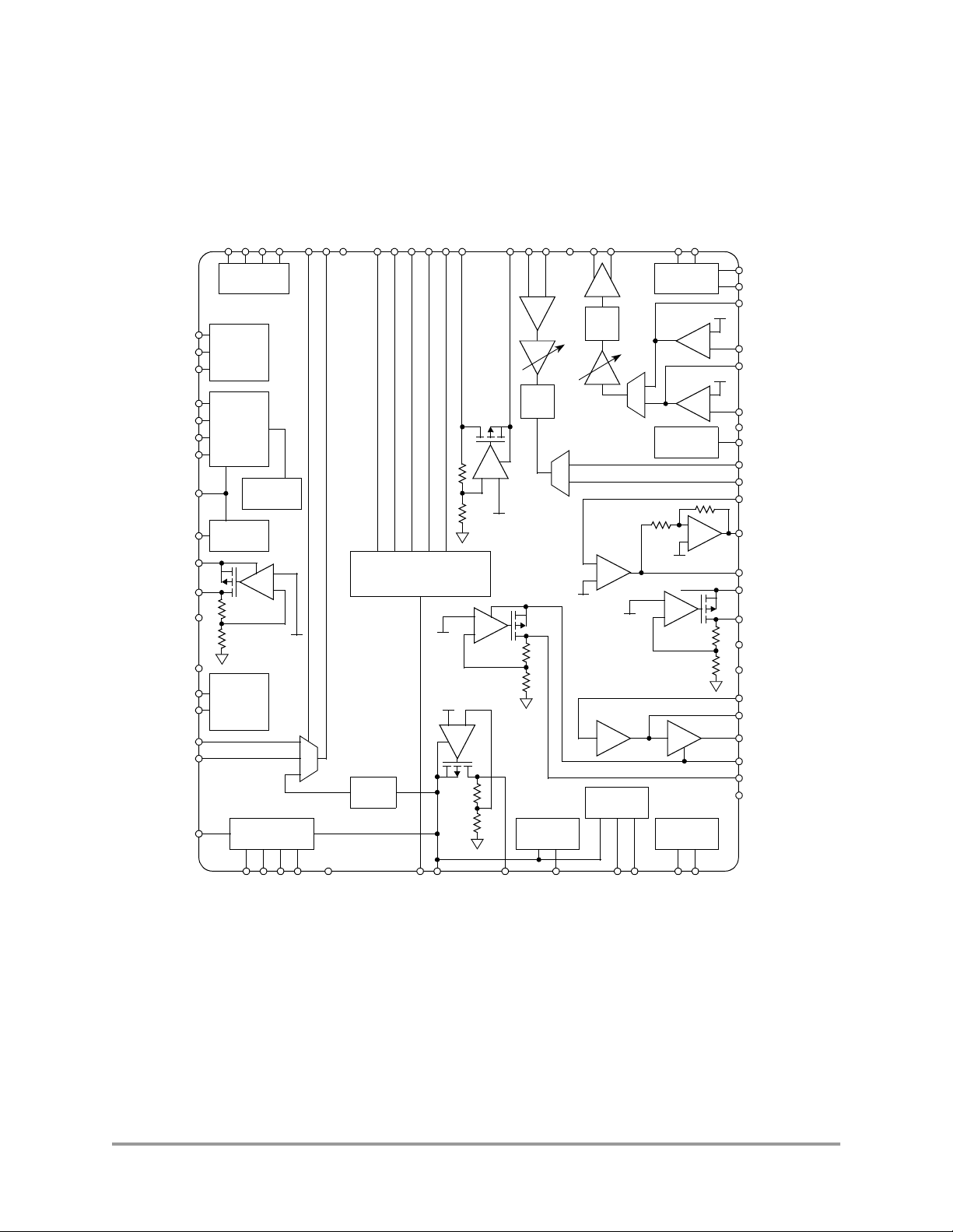
Figure 1 is a block diagram of the MC13713.
SPI_CS
SPI_CK
MISO
MOSI
A2D_SYNC
A2D_DATA
LOW_BATTB
WDI
PPRESET
IRQ
RESETB
ST ANDBY/TODA_INT
DIG_REG_OUT
DIG_REG_IN
D2A–
D2A+
A2D–
A2D+
GND
MIC_BYP1
MIC_BYP2
RTC_XTAL1
RTC_XTAL2
RTC_CLK
VM_VCC
VM_CAP1
VM_CAP2
VM_GND
VM_OUT
VM_REG
RF_REG_IN
RF_REG_OUT
GND
IC_TEST
BL_SNS
BL_SINK
TEMP
AD1
CHRG_SW
SPI
RTC
Oscillator
Voltage
Doubler
Oscillator
VM_REG
(4.7V)
Back
Light
Sink
Charger
Interface
2 MHz
–
+
Vref
MC13713
B+
SENSE
Regulator
Control
V
V
REF
REF
MIC Bias
+
–
LPF
LPF
Headset
Detect
+
–
V
REF
–
+
–
+
+
(SPK_
–
AL T_
GND)
Reference
Regulator
VAG
Regulator
V
SIM
REF
–
+
VAG
–
+
VAG
Regulator
MIC_BIAS1
MIC_BIAS2
MIC1_OUT
VAG
+
–
MIC1–
MIC2_OUT
VAG
+
–
MIC2–
GND
A1_INT
SPK_OUT
SPK2_OUT
SPK_IN
SPK+
SPK–
AUD_REG_IN
AUD_REG_OUT
SPK_GND
AL T_GND
SPK2_IN
AL T+
AL T–
VIB/ALT_IN
VIB_OUT
AL T_REF
B+
GND
DISABLE
CHRG_DETB
CHRG_STATE
EXT_PWR_ON
ON1
REF_REG
IO_REG_OU T
SIM_REG_OUT
SIM_EN
VAG
VAG_REF
Figure 1. MC13713 Block Diagram
2 Pin Descriptions
Table 3 lists all the pins in the MC13713 IC.
2 MC13713 IC Reference Manual MOTOROLA
Motorola Confidential Proprietary, NDA Required or i.250 Platform Master Agreement Deliverable / Preliminary

Table 3. Contact Description
Contact Name Description Contact In/Out
A1_INT Headset Insertion/Removal Sense C4 Input Logic 2.775
– TX Audio Output to CODEC, negative G3 Output Audio
A2D
A2D_DATA A2D MUX Output E5 Output DC 2.775
AD1 A2D Input E6 Input
A2D_SYNC A2D and MUX sync signal F6 Input Logic 2.775
A2D+ TX Audio Output to CODEC, positive H4 Output Audio
– Alert Amp Output, negative F9 Output Audio
ALT
ALT+ Alert Amp Output, positive E9 Output Audio
ALT_GND Alert Amp Ground G4 Output
ALT_REF Alert Amp Reference Bypass G9 DC 0.5*B+
AUD_REG_IN 2.775 V Audio Linear Regulator Input E7 Input DC B+
AUD_REG_OUT 2.775 V Audio Linear Regulator Output J7 Output DC 2.775
B+ Power Supply Input
(also SIM and I/O Regulator Inputs)
E8, F7 Input DC
Wave-
form
Voltage
–4.5
2.8
BL_SINK Back Light Current Sink C5 Input DC B+
BL_FB Back Light Sense Input B5 Input DC
CHRG_DETB Senses the Insertion/Removal of a Charger
(from Charge Circuitry)
CHRG_STATE Indicates the Charging Rate of the Charge
Circuitry
CHRG_SW Controls Output Current of Charger
Accessories
D2A
– RX Audio Input from CODEC, negative F4 Input Audio
D2A+ RX Audio Input from CODEC, positive F5 Input Audio
DIG_REG_IN 1.875V Digital Linear Regulator Input D7 Input DC B+
DIG_REG_OUT 1.875V Digital Linear Regulator Output A9 Output DC 1.875
DISABLE Disable Charging Signal E2 Output Logic 2.775
EXT_PWR_ON Power On Control from Charge Circuitry F1 Input Logic B+
GND Must be near the 32 kHz Oscillator
Components
GND B8
D1 Input Logic B+
E1 Input Logic B+
G1 Output Logic 2.775
B3
GND G5
GND F3, H3
IC_TEST Test Contact E4 Input Logic B+
MOTOROLA Pin Descriptions 3
Motorola Confidential Proprietary, NDA Required or i.250 Platform Master Agreement Deliverable / Preliminary

Table 3. Contact Description (Continued)
Contact Name Description Contact In/Out
IO_REG_OUT 2.775 V I/O Linear Regulator Output A8 Output DC 2.775
IRQ Interrupt Output to Processor C2 Output Logic 2.775
LOW_BATTB Low Battery Voltage Indicator A2 Output Logic 1.575
MIC_BIAS1 MIC1 Bias Output J1 Output DC 2.1
MIC_BIAS2 MIC2 Bias Output J2 Output DC 2.1
MIC_BYP1 MIC1 Bias Bypass H1 DC
MIC_BYP2 MIC2 Bias Bypass H2 DC
MIC2_OUT Output of MIC2 amp (A5) H5 Input Audio
– Inverting Input to MIC1 Amp (A3) J4 Input Audio
MIC1
MIC1_OUT Output of MIC1 Amp (A3) J3 Input Audio
– Inverting Input to MIC2 Amp (A5) J5 Input Audio
MIC2
MISO SPI Data Output D3 Output Logic Data 2.775
MOSI SPI Data Input D4 Input Logic Data 2.775
\ON1 ON/OFF Control Input F2 Input Logic B+
Wave-
form
Voltage
PPRESET Pen Point Reset G2 Input Logic B+
REF_REG 1.575 V Digital Linear Regulator Output C9 Output DC 1.575
RESETB System Reset Output C1 Output Logic 2.775
RF_REG_IN 2.775 V RF Linear Regulator Input D8 Input DC B+
RF_REG_OUT 2.775 V RF Linear Regulator Output D9 Output DC 2.775
RTC_CLK Buffered RTC 32 kHz Oscillator Output C3 Output CLK
Square
Wave
RTC_XTAL1 32.768 kHz XTAL Connection B1 Input
RTC_XTAL2 32.768 kHz XTAL Connection A1 Output
SIM_EN SIM Card Linear Regulator Enable C8 Input Logic 2.775
SIM_REG_OUT SIM Card Linear Regulator Output B9 Output DC 1.875/
SPI_CLK SPI Clock E3 Input Logic CLK 2.775
SPI_CS SPI Chip Select D2 Input Logic 2.775
– A1 Speaker Amp Output, negative J9 Output Audio
SPK
SPK_GND Speaker Amp Ground H6
1.575 V
2.85
SPK_IN1 A1 Speaker Amp Inverting Input H8 Input Audio
SPK_IN2 A2 Alert Amp Inverting Input H7 Input Audio
4 MC13713 IC Reference Manual MOTOROLA
Motorola Confidential Proprietary, NDA Required or i.250 Platform Master Agreement Deliverable / Preliminary

Table 3. Contact Description (Continued)
Contact Name Description Contact In/Out
SPK_OUT1 Audio RX PGA Output to A1 Path H9 Output Audio
SPK_OUT2 Audio RX PGA Output to A2 Path G7 Output Audio
SPK+ A1 Speaker Amp Output, positive J8 Output Audio
STANDBY/TODA_INT Standby Input/RTC Wakeup Signal D5 Input Logic 1.575
TEMP Temperature Sensing A2D Input D6 Input DC
TEST1 Test Mode (factory use only) B7 Test
TEST2 Test Mode (factory use only) B6 Test
TEST3 Test Mode (factory use only) C6 Test
TEST4 Test Mode (factory use only) C7 Test
VAG VAG Reference Output G6 Output DC 1.325
VAG_REF VAG Bypass Capacitor connection J6
VIB/ALT_IN Vibrator Linear Regula tor I npu t (s hare d wi th
alert in)
VIB_OUT Vibrator Linear Regulator Output G8 Output DC 1.3
VM_CAP1 Voltage Multiplier Pump Capacitor Negative
terminal
F8 Input DC B+
A6 Square
Wave-
form
Wave
Voltage
–2.775
0
VM_CAP2 Voltage Multiplier Pump Capacitor Positive
terminal
VM_GND Voltage Multiplier Ground B4
VM_OUT Voltage Multiplier O utput A4 Output DC 5.3
VM_REG 4.7 V Linear Regulator Output A3 Output DC 4.7
VM_VCC Voltage Multiplier Supply A7 Input DC 2.775
WDI Watch Dog Logic Input B2 Input Logic 2.775
A5 Square
Wave
3 Voltage Reference and Regulators
The MC13713 provides numerous power sources to the platform. A reference generator, eight separate
voltage regulator s, a vol ta ge mul ti pli er , and a constant current regulat or ar e pr ovi ded fo r del ivering power
to various parts of the radio. Figure 2 shows a block diagram of the power distribution used for the i.250
platform chipset. A brief description of the regulators and their primary functions is shown in Table 4.
MOTOROLA Voltage Reference and Regulators 5
Motorola Confidential Proprietary, NDA Required or i.250 Platform Master Agreement Deliverable / Preliminary

MC13715
Battery
Charger
IC
Battery
Charger
Interface
MC13713
+
B
SIM
Linear
Regulator
RF
Linear
Regulator
2.850 V/1.875 V
(10 mA)
2.775 V (200 mA)
SIM Card
MC13712
Low Noise
Regulator
RF
TX PA
VCOs
Analog
Baseband
100 mA
200 mA
200 mA
160mA
•
•
•
Speaker
Driver
Vibrator
Driver
Alert
Driver
Backlight
Sink
AUDIO
2.775 V (100 mA)
Regulator
DSP56621
VMULT
Regulator
Reference
Regulator
Digital
Linear
4.700 V (5 mA)
1.575 V (200 µA)
1.875 V (200 mA)
Synthesizer
RTC
1.575 V
Regulator
Regulator
I/O Linear
Regulator
2.775 V (200 mA)
Cores,Logic
& Memory
Figure 2. i.250 Platform Chipset Power Distribution
CODEC
RX/TX
Analog
I/O
Display
SRAM
FLASH
6 MC13713 IC Reference Manual MOTOROLA
Motorola Confidential Proprietary, NDA Required or i.250 Platform Master Agreement Deliverable / Preliminary

Table 4. Regulator Overview
Voltage Reference (REF_REG)
Output
Regulator Input
Reference Regulator B+ 1.575 200 µA RTC
SIM Regulator B+ 1.875/2.85 10 mA GSM SIM Card
RF Regulator B+ 2.775 200 mA Synthesizer, super filter regulator, RF, and
Audio Regulator B+ 2.775 100 mA Audio analog functions of DSP56621 and
Voltage Multiplier Synthesizer charge pumps
Multiplier IO_REG_OUT 5.55 5.0 mA
VM Regulator VM_OUT 4.7 5.0 mA
Digital Regulator B+ 1.875 200 mA DSP56621 cores, logic, and memory
I/O Regulator B+ 2.775 200 mA Voltage multiplier, DSP56621 I/O, serial
Vibrator Regulator B+ 1.3 200 mA Vibrator
Back Light Current IO_REG_OUT 160 mA Display back light
Voltage
(V)
Load
Current
Delivers Power To:
analog functions of MC13712
MC13713
flash, display
3.1 Voltage Reference (REF_REG)
The reference re gulator ( REF_REG) pro vides the 1.575 V refe rence vol tage f or all o ther volt age regul ators
on the MC13713 and can also source up to 200 µA to an external load. It is always turned on, even when
the MC13713 is off or in standby. These features are provided to maintain the Real Time Clock (RTC)
Oscillator on the MC13713 and the RTC registers on DSP56621.
REF_REG operates directly from B+. Regulation is guaranteed for a B+ voltage of 1.9 to 4.5 V, although
current sourcing capa bili ty falls off for B+ lower than 2.8 V. Bel ow 1.9 V, regulati on is not guara nteed bu t
current is available to a B+ as low as 1.3 V.
A low ESR bypass capacitor is required for noise reduction. Since this line is the reference for the rest of
the IC, external circuitry connected to this line should not be permitted to pull the voltage above or below
the limits in the specification, or to degrade the rise time on that contact. In the event B+ is removed, or
falls below the voltage at the REF_REG output, RTC clock circuitry internal to MC13713 and connected
to this contact will draw 25 µA. Additionally a discharge path exists through the regulator to B+, this will
typically be a non-guaranteed 2 k
A simplified block diagram of the circuit is shown in Figure 3.
Ω.
MOTOROLA Voltage Reference and Regulators 7
Motorola Confidential Proprietary, NDA Required or i.250 Platform Master Agreement Deliverable / Preliminary

B+
Bandgap
Cext
ESD
Figure 3. Simplified Block Diagram of Reference Regulator
Table 5 shows the specifications for the reference regulator circuit.
Table 5. Reference Regulator (REF_REG) Specifications
Specification Min Typ Max Unit
Input Voltage B+ 1.9 3.6 4.5 Volts
Output Voltage over all conditions
1.9 V<Vin<4.5 V 1.543
Output Current Capability
2.8 V<Vin<4.5 V
2.55 V<Vin<2.8 V
1.3 V<Vin<2.55 V
Current Limit (Vout = 0V) 2 mA
Load Regulation
(5 µA < Iload < Imax, Vin = 2.8 V and 2.55 V)
Line Regulation (2.65 V < Vin < 4.5 V, Iload = 5 µA) 8 mV
PSRR (20 Hz to 24 kHz, Cext = 4.7 µF, Iload = 100% of Imax,
Vin = 3.6 V)
Output Noise (0 to –200 kHz) 0.01 0.1 mVrms
Transient response (0 to 100% of Imax, Cext= 4.7 µF) 1 5 %
Cext range for stable operation
(5 µA < Iload < Imax, including capacitance tolerance)
REF_REG Output Reverse Leakage Current
Conditions: B+ = 2.0 V, –20 to +70 degC , Cload on RTC_CLK =
10pF, REF_REG Voltage Held Up by External Capacitor Cext
1
200
40
10
55 dB
4.0 10 µF
10 11 µA
1.575
1.607
20 mV
Volts
µA
µA
µA
Bypass Capacitor ESR 0.5
1. Assumes an X5R rating or better (±10 % at room temp, ±15 % over temp). Thus, the absolute mini-
mum capacitance is 4.7
µF to 15 % = 3.995 µF and the absolu te maximu m is 10 µF + 15 % = 11.5 µF.
Ω
8 MC13713 IC Reference Manual MOTOROLA
Motorola Confidential Proprietary, NDA Required or i.250 Platform Master Agreement Deliverable / Preliminary

Voltage Regulators
3.2 Voltage Regulators
All voltage regulators are linear to reduce external part count and cost. A simplified block diagram of a
representative regulator circuit is shown in Figure 4.
input voltage
Vref
Cext
ESD
_en
Figure 4. Typical Regulator Simplified Block Diagram
All regulators are current limited. When the output load current approaches the regulator current limit the
output voltage will drop as necess ary to pr event the outpu t current from excee din g the maximum spe cified
current limit. All regulators require a low ESR tantalum or ceramic bypass capacitor on the output. If
capacitor values outside the range listed in the specified conditions are used, the IC may not meet the
specified requirement. This could be especially true for shutdown time, turn on time, overshoot, transient
response, and PSRR.
All regulators (with the exception of the voltage multiplier) are powered from B+. Table 6 lists the
electrical speci fications for the RF, I O, AUD, DIG, SIM, an d VIB regula tors. Unless oth erwise noted, each
specification refers to all regulators. While the regulators are quite similar, each regulator is intended for a
specific purpose.
Table 6. Regulator Specifications
1
Specification Min Typ Max Unit
Input Voltage (B+) Vout + 0.3V 3.6 4.5 Volts
Input Voltage (B+) (DIG only) 2.55 3.6 4.5 Volts
Output Voltage (RF, AUD, IO) 2.675 2.775 2.875 Volts
Output Voltage (DIG) 1.819 1.875 1.931 Volts
Output Voltage (SIM, VSIM=0) 1.7 1.875 2.0 Volts
Output Voltage (SIM, VSIM=1) 2.75 2.85 2.95 Volts
Output Voltage (VM)
(input is VMULT driven by IO_Reg)
Output Voltage (VM) (disabled) VM_VCC
Output Voltage (disabled) 0.1 Volts
Output Voltage (VIB) 1.235 1.300 1.365 Volts
4.50 4.70 4.90 Volts
MOTOROLA Voltage Reference and Regulators 9
Motorola Confidential Proprietary, NDA Required or i.250 Platform Master Agreement Deliverable / Preliminary

Table 6. Regulator Specifications1 (Continued)
Specification Min Typ Max Unit
Current Drain (no load, all except VIB) 30 µA
Output Current Capability (DIG, VIB) 200 mA
Output Current Capability (IO, RF) 200 mA
Output Current Capability (AUD) 100 mA
Output Current Capability (SIM) 10 mA
Output Current Capability (VM) 5 mA
Current Limit (DIG, AUD, VIB) 750 mA
Current Limit (IO, RF) 900 mA
Current Limit (SIM) 100 mA
Current Limit (VM) 200 mA
Load Regulation (DIG, RF, IO, AUD) 0.35 mV/mA
Load Regulation (VIB) 0.5 mV/mA
Load Regulation (VM) 0.7 mV/mA
Load Regulation (SIM VSIM=0) 1.5 mV/mA
Load Regulation (SIM VSIM=1) 2.44 mV/mA
Line Regulation (Vin min to max, Iload=1 mA) 5 16 mV
Line Regulation (VIB, Vin min to max, Iload=1 mA) 20 mV
PSRR (DIG, RF, IO, VM, SIM, 20Hz–24 KHz) 40 45 dB
PSRR (VIB, 20Hz–24 KHz) 20 dB
PSRR (AUD, 20Hz–24 KHz) 45 dB
Start Up Overshoot 1 5 %
Transient Response (0 to 100% of I load) 1 5 %
Turn On Time (RF, AUD, SIM, VM, enable to 90%, Iload = 50% I max) 1 ms
Turn On Time (VIB, enable to 90%, Iload = 50% I max) 0.5 ms
Cext Range for Stable Operation (DIG, RF, AUD, VM) 3.995 25.3 µF
Cext Range for Stable Operation (VIB) 0.85 0.1 0.15 µF
Cext Range for Stable Operation (SIM) 0.85 11.5 µF
Cext Range for Stable Operation (IO) 3.995 4.7 5.405 µF
ESR of Bypass Capacitor 0.5 Ω
10 MC13713 IC Reference Manual MOTOROLA
Motorola Confidential Proprietary, NDA Required or i.250 Platform Master Agreement Deliverable / Preliminary

Analog Ground Generator, VAG
Table 6. Regulator Specifications1 (Continued)
Specification Min Typ Max Unit
Shutdown Time (to 10% Vout, Iload =0 mA) 20 ms
1. Unless noted, specification refers to all regulators.
The SIM regulator ( SIM_REG) i s the only regul ator that is progra mmable f or vo ltage . I ts ba sic topolo gy is
as shown in Figure 4 on page 9, but the divider resistors are implemented with switc habl e val ue s, sel ect ed
via an SPI command. In addition to an SPI enable bit, SIM_REG has a separate enable contact, SIM_EN.
This input can be used with the SIM car d soc ket to sh ut down voltage to the SIM card during removal and
insertion. This regulator can tolerate a short circuit on its output. When set to 2.85 V, the SIM regulator
will supply the 2.7 V needed for 3 V SIM card function even with an input voltage of 3.0 V, although
regulation and PSRR may be out of specification. 5 V SIM cards are not supported.
VM_REG regulates the output of the voltage multiplier (VMULT) described in Section 3.5. Its input is
internally wired to the output of VMULT, and their enable bits are common. The regulated 4.7 V voltage
can be used to power the synthesizer charge pumps, RF switches, or other high voltage requirements. The
voltage multiplier a nd r egulator are not inte nde d t o ha ve a high current output; 5 mA is the maximum they
can source.
The RF and audio regulators (RF_REG, AUD_REG) are separate from the other 2.775 V regulator,
(IO_REG), for noise isolation. Switching digital circuits should not be connected to those outputs. They
are separately enabled to allow for the independent timing needs of RF versus audio circuitry on a phone.
The vibrator regulator (VIB_REG) is intended only to be used to power the vibrator motor alert and is not
guaranteed to be stable with no load.
3.3 Analog Ground Generator, VAG
Another on-chip regulator that is not listed in the specifications is the Analog Ground Generator (VAG).
Shown in simplified block diagram form in Figure 5, this regulator is only used to generate the on-chip
virtual ground, at 1.325 V ± 100 mV, for the TX and RX audio paths and amplifiers. Two pins, VAG and
VAG_REF, are brought out for noise-reduction capacitors (0.01 to 0.1 µF, 15% tolerance, is required for
stable operation), because this ground must have very low noise and high supply rejection. VAG is not
intended to source curren t to external loads.
Vref
4R
22R
C
C
VAG_REF
VAG
VAG
ES D
VAG_REF
ES D
Figure 5. Simplified Block Diagram of Analog Ground Generator VAG
MOTOROLA Voltage Reference and Regulators 11
Motorola Confidential Proprietary, NDA Required or i.250 Platform Master Agreement Deliverable / Preliminary

The divider resistors on Vref are disconnected to reduce current drain when the audio paths are not
enabled.
3.4 Backlight Current Source (BL_CURR)
The Backlight Current Source, BL_CURR, is intended to supply a constant current sink for use by back
light LEDs. The constant current is achieved by forcing a constant voltage across a resistor RBL.
Tolerance of this resistor must be considered when designing for specific re qui re me nt s. Tab le 7 shows the
BL_FB voltages and nomi nal o utp ut current of the block (IRBL) assuming RBL = 2.2
Table 7. Backlight Control Bits
Ω, 3.3 Ω, and 4.7 Ω.
BL_CNTL<2:0>
Decimal Binary
0 000 High Z OFF OFF OFF
1 001 220 47 67 100
2 010 242 51 73 110
3 011 264 56 80 120
4 100 286 61 87 130
5 101 308 66 93 140
6 110 330 70 100 150
7 111 352 75 107 160
BL_FB
Voltage (mV)
IRBL (mA)
RBL = 4.7 Ω
IRBL (mA)
RBL = 3.3 Ω
IRBL (mA)
RBL = 2.2 Ω
Figure 6 shows block diagrams of the backlight control in two poss ibl e co nfi gurations. Configuration A is
the preferred s oluti on becau se of the lower n umber of ext ernal parts . Howev er, th e pass d evi ce on t he IC i s
required to dissipate a significant amount of energy. If a maximum battery supply voltage of 4.5 V and a
2 V drop across the backlight LEDs is assumed, the power dissipated would be:
Pd = ([B+] – V
LED – I
RBL
× R
BL
) × I
= (4.5 – 2 – 0.150 × 2.2) × 0.15 = 325 mW
RBL
Configuration B requires an external pass device, but would not require the MC13713 to dissipate a
significant amount of power. In this case, the current through R
would feed to ground via RBL, offsetting IBL
12 MC13713 IC Reference Manual MOTOROLA
Motorola Confidential Proprietary, NDA Required or i.250 Platform Master Agreement Deliverable / Preliminary
slightly.
and the base of the external transistor
BIAS
 Loading...