

Page 1
Model ESL808 Version V_0.01
Prepared by H/W Date 20/09/2005
Subject Technical Manual Page 1/47
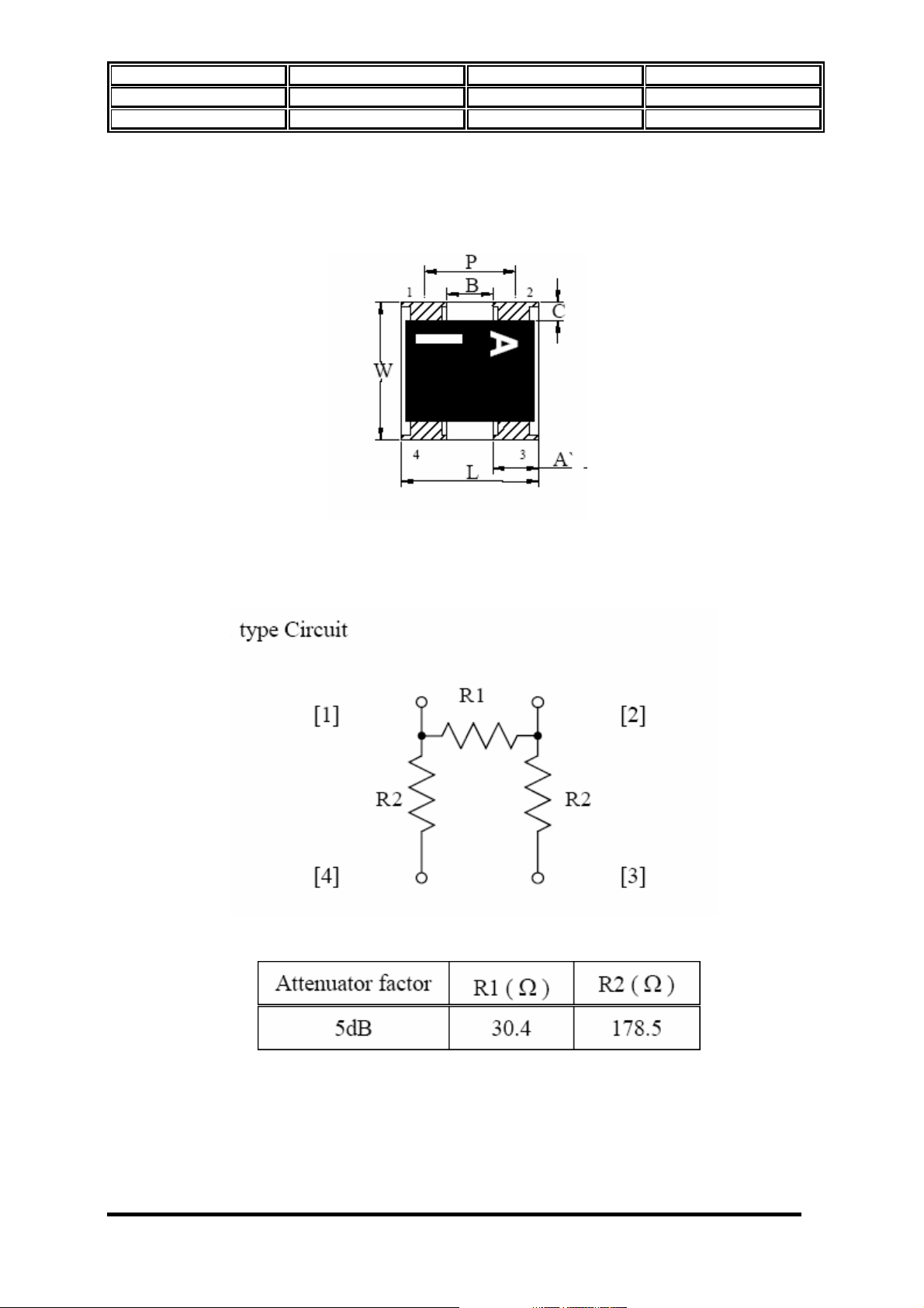
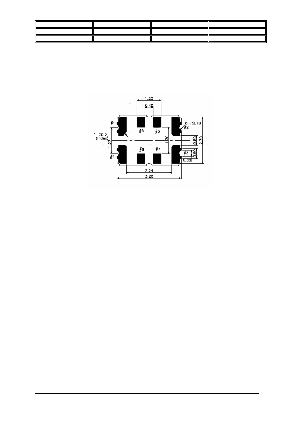
Pin out for R840, 850 (PAT1010 - X - 05dB - C - CN)
ESL808 Technical Manual Page 1
Page 2
Model ESL808 Version V_0.01
Prepared by H/W Date 20/09/2005
Subject Technical Manual Page 2/47
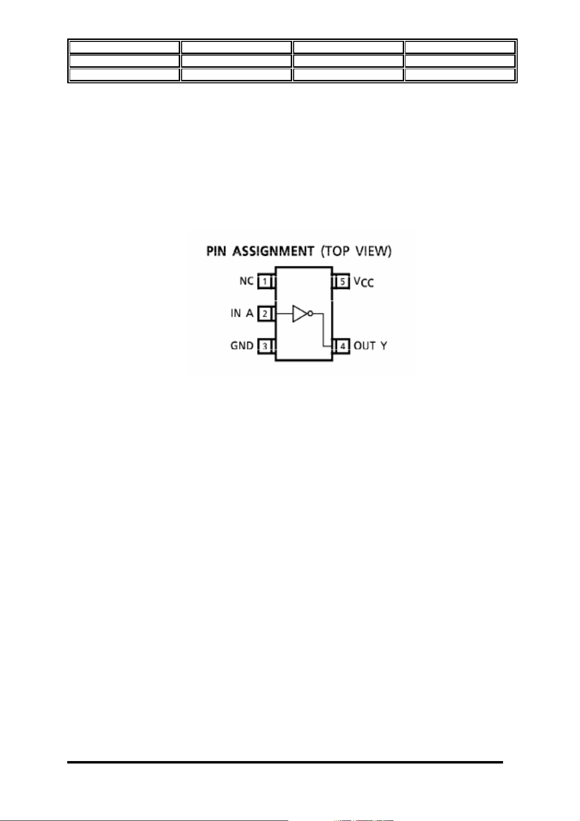
Pin out for U112 (TC7S04FU)
PIN NO FUNCTION NAME
1
2
3
4
5
No Connect
Input
Ground
Output
Power
NC
IN A
GND
OUT Y
VCC
ESL808 Technical Manual Page 2
Page 3
Model ESL808 Version V_0.01
Prepared by H/W Date 20/09/2005
Subject Technical Manual Page 3/47
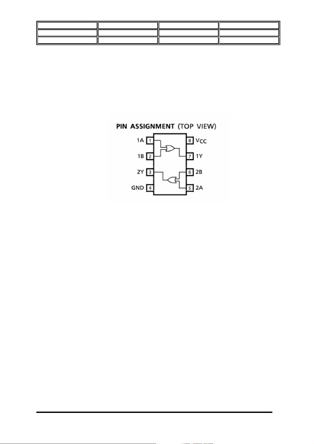
Pin out for U111 (TC7W32FK)
PIN NO FUNCTION NAME
1
2
3
4
5
6
7
8
Input
Input
Output
Ground
Input
Input
Output
Power
1A
1B
2Y
GND
2A
2B
1Y
VCC
ESL808 Technical Manual Page 3
Page 4
Model ESL808 Version V_0.01
Prepared by H/W Date 20/09/2005
Subject Technical Manual Page 4/47
Pin out for U803 (ESHS-M090SF)
PIN NO FUNCTION NAME
1
2
3
4
5
6
7
8
9
10
11
12
13
14
GSM900 RX1
GSM900 RX2
DCS1800 RX1
DCS1800 RX2
PCS1900 RX1
PCS1900 RX2
GND
DCS/PCS TX
VC2
GSM TX
VC1
GND
AND
GND
GSM900 RX1
GSM900 RX2
DCS1800 RX1
DCS1800 RX2
PCS1900 RX1
PCS1900 RX2
GND
DCS/PCS TX
VC2
GSM TX
VC1
GND
AND
GND
ESL808 Technical Manual Page 4
Page 5
Model ESL808 Version V_0.01
Prepared by H/W Date 20/09/2005
Subject Technical Manual Page 5/47
Pin out for U810 (DSA321SA 1XTV26000RCA)
PIN NO FUNCTION NAME
1
2
3
4
5, 6, 7, 8
V control
Ground
OSC Output
Power
No connect
Vcont
GND
OUTPUT
Vcc
N.C
ESL808 Technical Manual Page 5
Page 6
Model ESL808 Version V_0.01
Prepared by H/W Date 20/09/2005
Subject Technical Manual Page 6/47
Pin out for BAT100 (TS414H I106E)
PIN NO FUNCTION NAME
1
2
VCC
Ground
VCC
GND
ESL808 Technical Manual Page 6
Page 7
Model ESL808 Version V_0.01
Prepared by H/W Date 20/09/2005
Subject Technical Manual Page 7/47
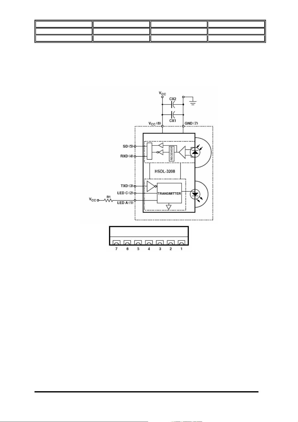
Pin out for U109 (HSDL-3208)
PIN NO FUNCTION NAME
1
2
3
4
5
6
7
LED ANODE
LED CATHODE
TRANSMIT DATA
RECEIVE DATA
SHUTDOWN
SUPPLY VOLTAGE
GROUND
LED A
LED C
TXD
RXD
SD/MODE
VCC
GND
ESL808 Technical Manual Page 7
Page 8
Model ESL808 Version V_0.01
Prepared by H/W Date 20/09/2005
Subject Technical Manual Page 8/47
Pin out for CON102 (2004-03-202)
PIN NO FUNCTION NAME
1
2
3
VBAT
BATTERY ID
GROUND
VBAT
BAT ID
GND
ESL808 Technical Manual Page 8
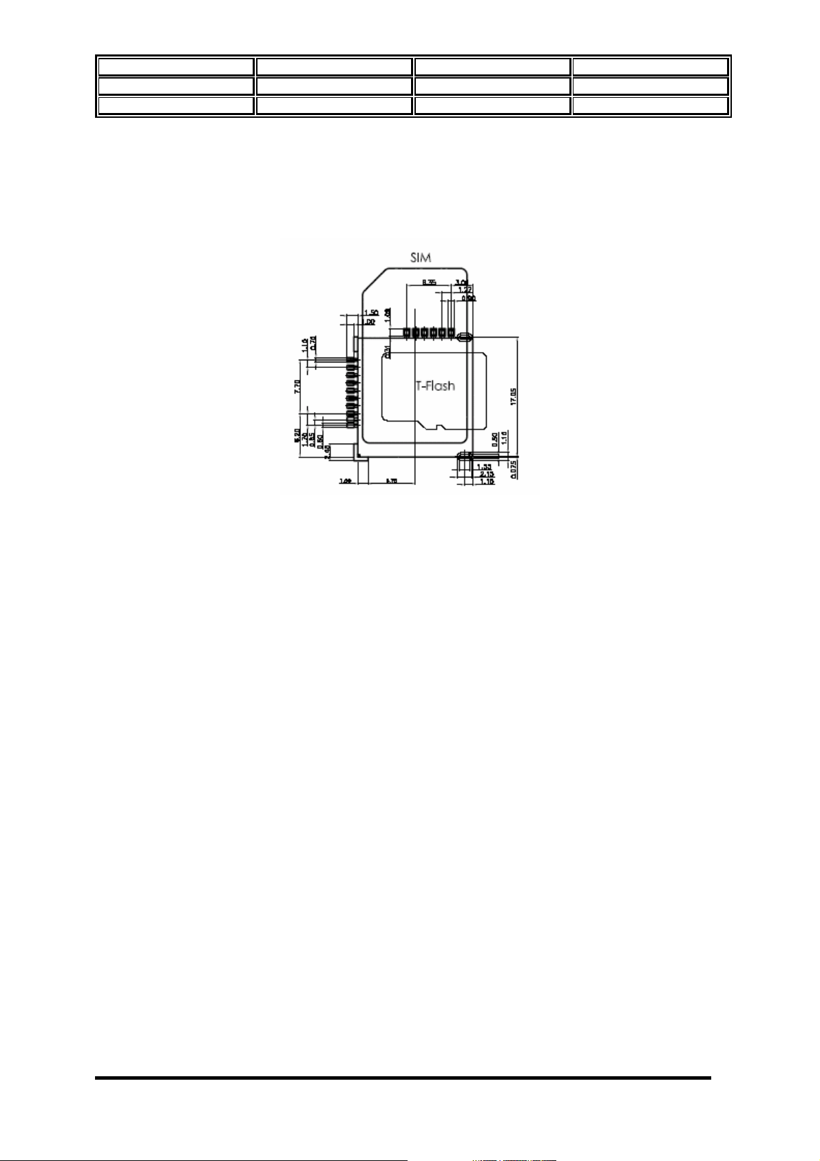
Page 9
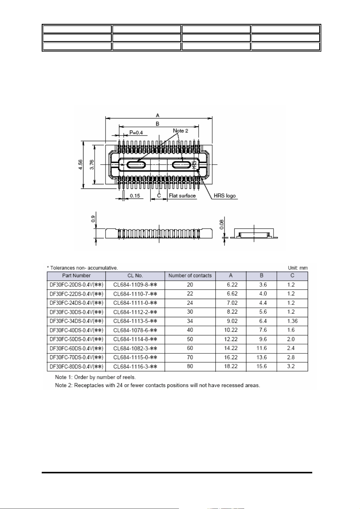
Model ESL808 Version V_0.01
Prepared by H/W Date 20/09/2005
Subject Technical Manual Page 9/47
Pin out for CON100 (DF18C-60DS-0.4V)
ESL808 Technical Manual Page 9
Page 10
Model ESL808 Version V_0.01
Prepared by H/W Date 20/09/2005
Subject Technical Manual Page 10/47
Pin out for CN103 (9000-8903-001)
PIN NO FUNCTION NAME
1
2
3
4
5
6
7
8
9
10
11
12
13
15
16
17
MCDA2
MCDA3
MCCMO
VCC
MCCK
GROUND
MCDA0
MCDA1
SWITCH1
MCINS
SIM_VCC
SIM_RESET
SIM_CLK
GROUND
SIM_VPP
SIM_IO
DAT2
CD/DAT3
CMD
VDD
CLK
VSS
DAT0
DAT1
SW1
SW2
VSIM
RST
CLK
GND
VPP
I/O
ESL808 Technical Manual Page 10
Page 11
Model ESL808 Version V_0.01
Prepared by H/W Date 20/09/2005
Subject Technical Manual Page 11/47
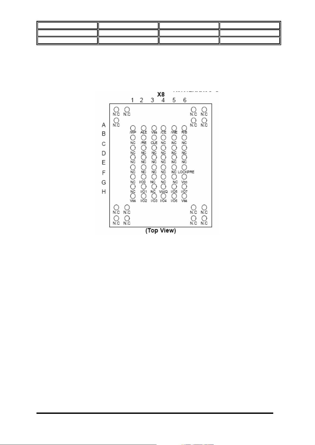
Pin out for U106 (K9K1208U0C)
PIN NO FUNCTION NAME
A1
A2
A3
A4
A5
A6
B2
B3
F2
F6
G2
G4
G5
G6
H1
H2
WRITE PROTECT
ADDRESS LATCH ENABLE
GROUND
CHIP ENABLE
WRITE ENABLE
READY/BUSY OUTPUT
READ ENABLE
COMMAND LATCH ENABLE
DATA0 INPUT/OUTPUT
POWER
DATA1 INPUT/OUTPUT
OUTPUT BUFFER POWER
DATA5 INPUT/OUTPUT
DATA7 INPUT/OUTPUT
GROUND
DATA2 INPUT/OUTPUT
/WP
ALE
VSS
/CE
/WE
R/B
/RE
CLE
I/O0
VCC
I/O1
VCCQ
I/O5
I/O7
VSS
I/O2
ESL808 Technical Manual Page 11
Page 12
Model ESL808 Version V_0.01
Prepared by H/W Date 20/09/2005
Subject Technical Manual Page 12/47
H3
H4
H5
H6
DATA3 INPUT/OUTPUT
DATA4 INPUT/OUTPUT
DATA6 INPUT/OUTPUT
GROUND
I/O3
I/O4
I/O6
VSS
ESL808 Technical Manual Page 12
Page 13
Model ESL808 Version V_0.01
Prepared by H/W Date 20/09/2005
Subject Technical Manual Page 13/47
Pin out for U601 (A3212EEHLT)
PIN NO FUNCTION NAME
1
2
3
4
5
6
Output
No connection
GND
GND
No connection
Power supply
OUTPUT
NO CONNECTION
GROUND
GROUND
NO CONNECTION
SUPPLY
ESL808 Technical Manual Page 13
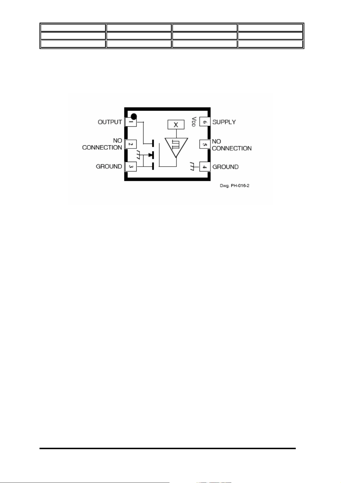
Page 14
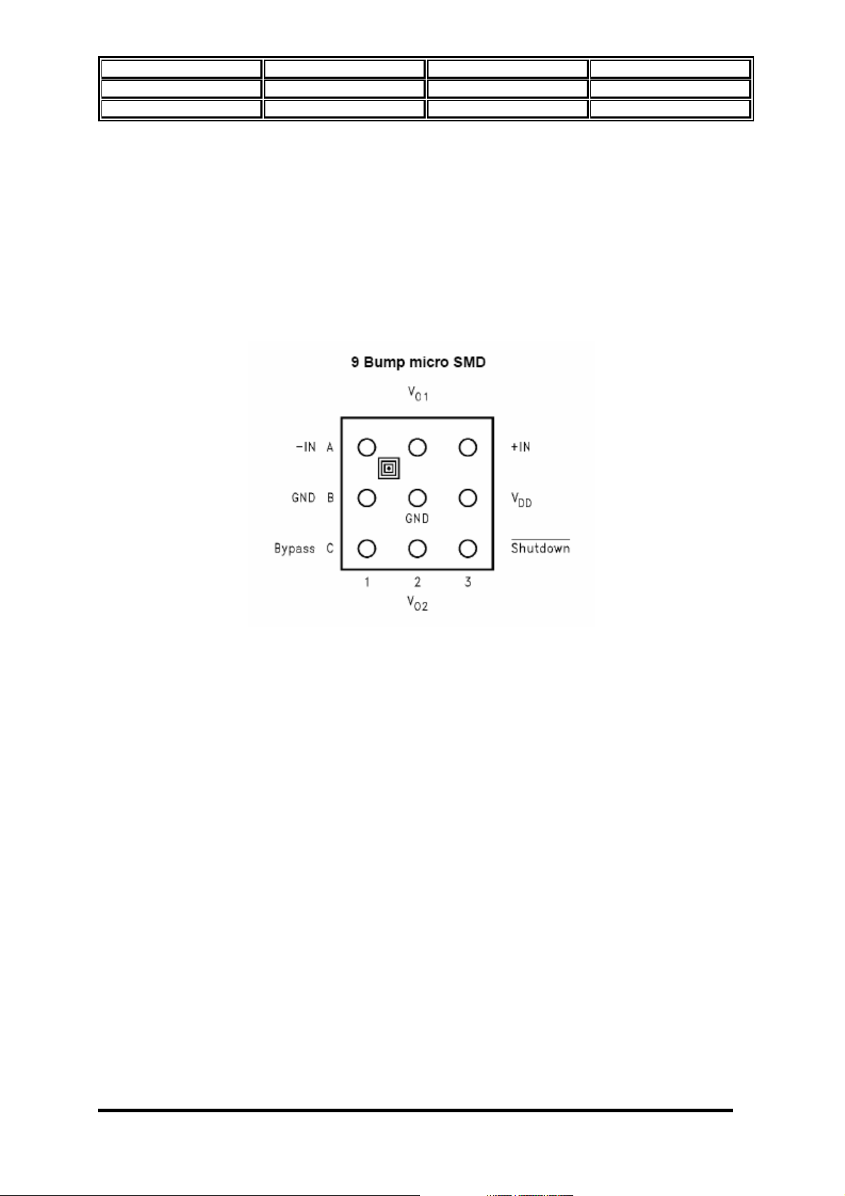
Model ESL808 Version V_0.01
Prepared by H/W Date 20/09/2005
Subject Technical Manual Page 14/47
Pin out for U600 (LM4990ITL)
PIN NO FUNCTION NAME
1
2
3
4
5
6
7
8
9
-IN
GROUND
BYPASS
V02
SHUTDOWN
VDD
+IN
V01
GROUND
A1
B1
C1
C2
C3
B3
A3
A2
B2
ESL808 Technical Manual Page 14
Page 15
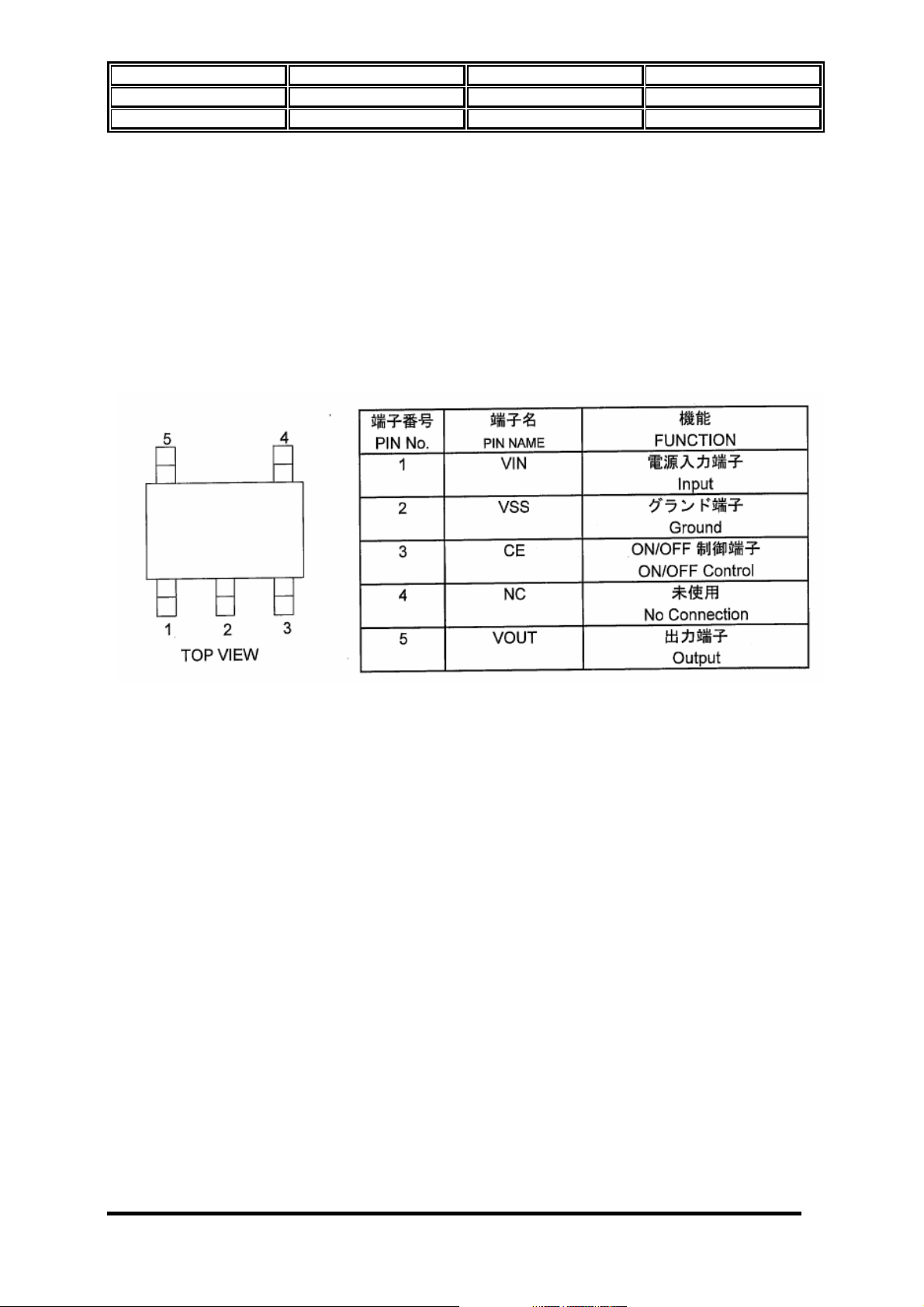
Model ESL808 Version V_0.01
Prepared by H/W Date 20/09/2005
Subject Technical Manual Page 15/47
Pin out for U133 (XC6219B332MR)
PIN NO FUNCTION NAME
1
2
3
4
5
Power Supply Input Voltage
Ground
ON/OFF Control
No Connection
Output Voltage
VOUT
VIN
VSS
CE
NC
ESL808 Technical Manual Page 15
Page 16

Model ESL808 Version V_0.01
Prepared by H/W Date 20/09/2005
Subject Technical Manual Page 16/47
Pin out for U840 (RF3146)
ESL808 Technical Manual Page 16
Page 17

Model ESL808 Version V_0.01
Prepared by H/W Date 20/09/2005
Subject Technical Manual Page 17/47
PIN NO FUNCTION NAME
1
2
3
4
5
6
7
8
9
10
11
12
13
14
15
16
17
18
19
20
21
22
23
24
25
26
27
28
29
30
31
32
33
34
35
36
37
38
39
40
41
42
43
44
45
46
47
48
Pkg Base
Internal circuit node. Do not externally connect.
Controlled voltage input to the GSM driver stage.
Internal circuit node. Do not externally connect.
Ground (Internal)
Ground (Internal)
GSM RF Output
Ground (Internal)
Internal circuit node. Do not externally connect.
Internal circuit node. Do not externally connect.
Internal circuit node. Do not externally connect.
Internal circuit node. Do not externally connect.
Internal circuit node. Do not externally connect.
No Internal or external connection.
Internal circuit node. Do not externally connect.
Internal circuit node. Do not externally connect.
Internal circuit node. Do not externally connect.
Internal circuit node. Do not externally connect.
Controlled voltage input to the GSM output stage.
Controlled voltage output to feed VCC2 and VCC3.
Controlled voltage output to feed VCC2 and VCC3.
Controlled voltage input to the DCS/PCS output stage.
Internal circuit node. Do not externally connect.
Internal circuit node. Do not externally connect.
No Internal or external connection.
Internal circuit node. Do not externally connect.
Internal circuit node. Do not externally connect.
Internal circuit node. Do not externally connect.
Internal circuit node. Do not externally connect.
Internal circuit node. Do not externally connect.
Ground (Internal)
DCS / PCS RF Output
Ground (Internal)
Internal circuit node. Do not externally connect.
Ground (Internal)
Controlled voltage input to the DCS/PCS driver stage.
No internal connection. Connect to ground.
DCS/PCS RF Input
No internal connection. Connect to ground.
Controlled voltage on the GSM and DCS/PCS preamplifier
Control to select the GSM or DCS/PCS bands.
Enable PA module
Power
Power
Internal circuit node. Do not externally connect.
Ramping signal from DAC.
Controlled voltage on the GSM preamplifier stage.
Ground for the GSM preamplifier stage.
GSM RF input
Ground
GSM 850 / 900 OUT
VCC3 DCS / PCS
DCS / PCS OUT
VCC2 DCS / PCS
VCC1 DCS / PCS
GSM 850 / 900 IN
NC
VCC2 GSM
NC
GND
GND
GND
NC
NC
NC
NC
NC
NC
NC
NC
NC
NC
VCC3 GSM
VCC OUT
VCC OUT
NC
NC
NC
NC
NC
NC
NC
NC
GND
GND
NC
GND
NC
DCS / PCS IN
NC
BAND SEL
TX ENABLE
VBATT
VBATT
NC
VRAMP
VCC1 GSM
GND1 GSM
GND
ESL808 Technical Manual Page 17
Page 18

Model ESL808 Version V_0.01
Prepared by H/W Date 20/09/2005
Subject Technical Manual Page 18/47
Pin out for F100 (0467 001.NR)
ESL808 Technical Manual Page 18
Page 19

Model ESL808 Version V_0.01
Prepared by H/W Date 20/09/2005
Subject Technical Manual Page 19/47
Pin out for OSC100 (DST410S)
ESL808 Technical Manual Page 19
Page 20

Model ESL808 Version V_0.01
Prepared by H/W Date 20/09/2005
Subject Technical Manual Page 20/47
Pin out for U101 (MT6305)
PIN NO FUNCTION NAME
1
2
3,29
4
5
6
7
8
9
10
Microprocessor Control Input Signal for Gate
Drive, Internal Pull Low to DGND.
Non-Level-Shifted Bidirectional Data I/O
Non-Level-Shifted SIM Reset Input, Internal
Charger Input Voltage
Gate Drive Output
No Connect
Charger Current Sense Input.
Charger Detect Output
Battery Input Voltage Sense
SIM Supply
Pull High to VIO.
CHRIN
GATEDRV
ISENSE
CHRCNTL
CHRDET
BATSNS
VSIM
SIMIO
SIMRST
NC
ESL808 Technical Manual Page 20
Page 21

Prepared by H/W Date 20/09/2005
17, 21, 46
37, 40
Model ESL808 Version V_0.01
Subject Technical Manual Page 21/47
11
12
13
14
15
16
18
19
20
22
23
24
25
26
27
28
30
31
32
33
34
35
36
38
39
41
42
43
44
45
47
48
Non-Level-Shifted SIM Clock Input.
SIM Enable
High for Vsim=3.0V, Low for Vsim=1.8V
Level-Shifted SIM Bidirectional Data I/O
Level-Shifted SIM Reset Output
Level-Shifted SIM Clock Output
Digital Ground
Memory Supply
Battery Input Voltage
Digital I/O Supply
Real Time Clock Supply
Reset Delay Time Capacitance
System Reset, Low Active
TCXO Supply
Battery Input Voltage for Analog Block
Circuits
Analog Supply
Analog Ground
Referenced Voltage Output
VTCXO and VA Enable
Power on/off Key, Internal Pull High to VBAT
Power on/off Signal from Microprocessor
Vibrator Driver Enable, Internal Pull Low to
DGND
Alerter Driver Enable, Internal Pull Low to
DGND
LED Driver Enable, Internal Pull Low to
DGND
Power Ground
Vibrator Driver Input
Alerter Driver Input
LED Driver Input
Battery Type Selection, High for NiMH, Low
for Li-ion, Internal Pull Low to DGND
Battery Detect Input, Low for Battery
Connected, Internal Pull High for Battery
Disconnected
High for VA enabled with VTCXO, Low for VA
SIMCLK
SIMVCC
SIMSEL
SIO
SRST
SCLK
DGND
VM
VBAT
VIO
VRTC
RSTCAP
/RESET
VTCXO
AVBAT
VA
AGND
VREF
SRCLKEN
PWRKEY
PWRBB
VIBRATOREN
ALERTEREN
LEDEN
PGND
VIBRATOR
ALETER
LED
BATUSE
BATDET
VASEL
VMSEL
VBAT
VCORE
enabled with VD, Internal Pull Low to DGND
High for Vm=2.8V, Low for Vm=1.8V,
ESL808 Technical Manual Page 21
Page 22

Model ESL808 Version V_0.01
Prepared by H/W Date 20/09/2005
Subject Technical Manual Page 22/47
Internal Pull High to VIO
Battery Input Voltage
Digital Core Supply
ESL808 Technical Manual Page 22
Page 23

Model ESL808 Version V_0.01
Prepared by H/W Date 20/09/2005
Subject Technical Manual Page 23/47
Pin out for U103 (AO8701)
PIN NO FUNCTION NAME
1
2
3
4
5
6
7
8
Drain
Source
Source
Gate
Cathode
Anode
Anode
Anode
D
S
S
G
K
A
A
A
ESL808 Technical Manual Page 23
Page 24

Model ESL808 Version V_0.01
Prepared by H/W Date 20/09/2005
Subject Technical Manual Page 24/47
Pin out for U105 (TH50VPF5783AASB)
PIN NO FUNCTION NAME
A1
A10
B1
B10
C1
C3
C4
C5
C6
C7
C8
D2
ESL808 Technical Manual Page 24
Write Protect/program acceleration input
Not Connected
Not Connected
Not Connected
Not Connected
Not Connected
Address input
Data byte control input
Write enable input
Address input
Address input
Address input
NC
NC
NC
NC
NC
A7
₩LB
₩WP/ACC
₩WE
A8
A11
A3
Page 25

Model ESL808 Version V_0.01
Prepared by H/W Date 20/09/2005
Subject Technical Manual Page 25/47
D3
D4
D5
D6
D7
D8
D9
E2
E3
E4
E5
E6
E7
E8
E9
F1
F2
F3
F4
F5
F6
F7
F8
F9
F10
G1
G2
G3
G4
G5
G6
G7
G8
G9
G10
H2
H3
H4
H5
H6
Chip enable inputs for Pseudo SRAM
Chip enable input for Flash Memory
Power supply for Flash Memory
Chip enable input for Flash Memory
Address input
Data byte control input
Hardware reset input
Address input
Address input
Address input
Address input
Address input
Address input
Ready/Busy output
Address input
Address input
Address input
Address input
Not Connected
Address input
Address input
Address input
Not Connected
Address input
Address input
Not Connected
Not Connected
Not Connected
Address input
Ground
Data inputs / outputs
Not Connected
Data inputs / outputs
Don’ t Use
Address input
Not Connected
Output enable input
Data inputs / outputs
Data inputs / outputs
Data inputs / outputs
A6
₩UB
₩RESET
CE2ps
A19
A12
A15
A2
A5
A18
RY/BY
A20
A9
A13
A21
NC
A1
A4
A17
₩CEf2
NC
A10
A14
NC
NC
NC
A0
VSS
DQ1
VCCf
NC
DQ6
DU
A16
NC
₩CEf1
₩OE
DQ9
DQ3
DQ4
ESL808 Technical Manual Page 25
Page 26

Model ESL808 Version V_0.01
Prepared by H/W Date 20/09/2005
Subject Technical Manual Page 26/47
H7
H8
H9
J2
Chip enable inputs for Pseudo SRAM
J3
J4
J5
J6
J7
J8
J9
K3
K4
K5
K6
K7
K8
L1
L10
M1
M10
Data inputs / outputs
Data inputs / outputs
Flash word enable input
Data inputs / outputs
Data inputs / outputs
Power supply for Flash Memory
Power supply for Pseudo SRAM
Data inputs / outputs
Data inputs / outputs
Ground
Data inputs / outputs
Data inputs / outputs
Data inputs / outputs
Don’ t Use
Data inputs / outputs
Data inputs / outputs
Not Connected
Not Connected
Not Connected
Not Connected
DQ13
DQ15
₩BYTE
₩CE1ps
DQ0
DQ10
VCCf
VCCps
DQ12
DQ7
VSS
DQ8
DQ2
DQ11
DU
DQ5
DQ14
NC
NC
NC
NC
ESL808 Technical Manual Page 26
Page 27

Model ESL808 Version V_0.01
Prepared by H/W Date 20/09/2005
Subject Technical Manual Page 27/47
Pin out for D103, D104, D120(RB520S-30)
PIN NO FUNCTION NAME
1
2
Anode
Cathode
A
C
ESL808 Technical Manual Page 27
Page 28

Model ESL808 Version V_0.01
Prepared by H/W Date 20/09/2005
Subject Technical Manual Page 28/47
Pin out for D111 – D121 (SSC – HB103 - 69)
PIN NO FUNCTION NAME
1
2
Anode
Cathode
A
C
ESL808 Technical Manual Page 28
Page 29

Model ESL808 Version V_0.01
Prepared by H/W Date 20/09/2005
Subject Technical Manual Page 29/47
Pin out for ZD101∼106, (AVRC5S05Q050-100R)
PIN NO FUNCTION
1,3,5,7
2,4,6,8
9
Input
Output
Ground
ESL808 Technical Manual Page 29
Page 30

Model ESL808 Version V_0.01
Prepared by H/W Date 20/09/2005
Subject Technical Manual Page 30/47
Pin out for ZD108 (GMF05LC-HS3)
PIN NO FUNCTION NAME
1,3,4,5,6
2
Cathode
Anode
C
A
ESL808 Technical Manual Page 30
Page 31

Model ESL808 Version V_0.01
Prepared by H/W Date 20/09/2005
Subject Technical Manual Page 31/47
Pin out for D102 (PG12HSUSC
)
PIN NO FUNCTION NAME
1
2
Anode
Cathode
A
C
ESL808 Technical Manual Page 31
Page 32

Model ESL808 Version V_0.01
Prepared by H/W Date 20/09/2005
Subject Technical Manual Page 32/47
Pin out for U800 (MT6129)
PIN NO
1
2
3
ESL808 Technical Manual Page 32
TX VCO supply voltage and Regulator 1 (TX
VCO) voltage output
Regulator 1 external noise bypass capacitor
Battery supply for Regulator1
FUNCTION
VCCTXVCO
NAME
CREG1
VBAT1
Page 33

Model ESL808 Version V_0.01
Prepared by H/W Date 20/09/2005
Subject Technical Manual Page 33/47
4
5
6
7
8
9
10
11
12
13
14
15
16
17
18
19
20
21
22
23
24
25
26
27
28
29
30
31
32
33
34
35
36
37
TRX RF and TX BUF block supply voltage and
Regulator 1 (TRX) voltage output
Receiver PCS 1900 RF differential positive input
Receiver PCS 1900 RF differential negative
input
Receiver DCS 1800 RF differential negative
input
Receiver DCS 1800 RF differential positive input
Receiver E-GSM 900 RF differential negative
input
Receiver E-GSM 900 RF differential positive
input
Receiver GSM 850 RF differential negative input
Receiver GSM 850 RF differential negative input
Regulator 2 external noise bypass capacitor
Regulator 1&2 enable input for TRX/ RFVCO
buffer/ Synthesizer/ VCXO
Battery supply for Regulator 2
RF VCO buffer supply voltage and Regulator 2
(SX) voltage output
RFVCO buffer ground
RF VCO differential positive test output
RF VCO ground
Loop filter main capacitor input
RF VCO supply voltage and Regulator (RF VCO)
voltage output
Synthesizer charge pump and PFD ground
NC
Synthesizer charge pump and PFD supply
voltage
Synthesizer supply voltage
Synthesizer ground
VCXO internal/ external output buffer control
VCXO coarse tuning capacitor and fine tuning
varactor
26MHz crystal reference input
VCXO supply voltage
13MHz / 26 MHz reference buffer output
VCXO ground
Reference output buffer 13MHz / 26MHz
VCCRF
PCSRF
PCSRFB
DCSRFB
DCSRF
GSMRFB
GSMRF
AMPSRF
AMPSRFB
CREG2
ENREG
VBAT2
VCCRFBUF
GNDRFBUF
RFVCOP
GNDRFVCO
LFCAP
VCCRFVCO
GNDRFCP
No
connection
VCCRFCP
VCCSYN
GNDSYN
VCXOCXR
VCXOCAP
XTAL
VCCVCXO
REFOUT
GNDVCXO
VCXOFRQ
GNDMOD
VCCMOD
GNDD
VCCD
ESL808 Technical Manual Page 33
Page 34

Model ESL808 Version V_0.01
Prepared by H/W Date 20/09/2005
Subject Technical Manual Page 34/47
38
39
40
41
42
43
44
45
46
47
48
49
50
51
52
53
54
55
56
selection
Synthesizer Sigma-Delta modulator ground
Synthesizer Sigma-Delta modulator supply
voltage and Regulator 3 output
3-wire digital circuit ground
Supply voltage for 3-wire digital circuit and
supply voltage for Regulator 3
Regulator 2 enable input for RFVCO
3-wire serial bus enable input
3-wire serial bus clock input
3-wire serial bus data input
Auxiliary test output
Q path negative baseband input / output
Q path positive baseband input / output
I path negative baseband input / output
I path positive baseband input / output
IF circuit supply voltage
Transmitter PFD and Receiver IF circuit supply
voltage
Transmitter charge pump supply voltage
No connection
Transmitter charge pump ground
TX VCO buffer transmit output for GSM
TX VCO ground
No connection
TX VCO ground
TX VCO buffer transmit output for DCS / PCS
ENRFVCO
EN
CLK
SDATA
AUXOUT
QB
Q
IB
I
VCCIQ
VCCIF
VCCTXCP
NC
GNDTXCP
TXOGSM
GNDTXVCO
NC
GNDTXVCO
TXODPCS
ESL808 Technical Manual Page 34
Page 35

Model ESL808 Version V_0.01
Prepared by H/W Date 20/09/2005
Subject Technical Manual Page 35/47
Pin out for U100 (MT6219)
PIN NO
JTAG PORT
E4 JTAG test port reset input JTRST#
E3 JTAG test port clock input JTCK
E2 JTAG test port data input JTDI
ESL808 Technical Manual Page 35
FUNCTION
NAME
Page 36

Model ESL808 Version V_0.01
g
play
Prepared by H/W Date 20/09/2005
Subject Technical Manual Page 36/47
E1 JTAG test port mode switch JTMS
F5 JTAG test port data output JTDO
F4 JTAG test port returned clock output JRTCK
RF Parallel Control Unit
F3
F2
G5
G4
G3
G2
G1
H5
H4
H3
RF hard-wire control bus 0 BPI_BUS0
RF hard-wire control bus 1 BPI_BUS1
RF hard-wire control bus 2 BPI_BUS2
RF hard-wire control bus 3 BPI_BUS3
RF hard-wire control bus 4 BPI_BUS4
RF hard-wire control bus 5 BPI_BUS5
RF hard-wire control bus 6 (GPIO10) BPI_BUS6
RF hard-wire control bus 7 (GPIO 11) BPI_BUS7
RF hard-wire control bus 8 (GPIO 12) BPI_BUS8
RF hard-wire control bus 9 (GPIO 13) BPI_BUS9
RF Serial Control Unit
H1 RF 3-wire interface chip select 0 BSI_CS0
J5 RF 3-wire interface data output BSI_DATA
J4 RF 3-wire interface clock output BSI_CLK
PWM Interface
R3 Pulse width modulated signal1 (GPIO 21) PWM1
R2 Pulse width modulated signal 2 (GPIO 22) GPIO22
T4
Pulse width modulated si
(GPIO 23)
Serial LCD / PM IC Interface
J3
J2
J1
K4
K3
Serial display interface data output (GPIO
16)
Serial display interface address output
(GPIO 17)
Serial display interface clock output (GPIO
18)
Serial dis
(GPIO 19)
Serial display interface chip select 1 output
nal for buzzer
interface chip select 0 output
ALERTER
LSCK
LSA0
LSDA
LSCE0#
LSCE1#
ESL808 Technical Manual Page 36
Page 37

Model ESL808 Version V_0.01
Prepared by H/W Date 20/09/2005
Subject Technical Manual Page 37/47
(GPIO 20)
Parallel LCD / Nand-Flash Interface
K2
L5
Parallel display interface chip select 1
output (GPIO 24)
Parallel display interface chip select 0
output
LPCE1#
LPCE0#
L4 Parallel display interface Reset Signal LRST#
L3 Parallel display interface Read Strobe LRD#
L2 Parallel display interface address output LPA0
L1 Parallel display interface Write Strobe LWR#
M5 Parallel LCD/NAND-Flash Data 7 NLD7
M4 Parallel LCD/NAND-Flash Data 6 NLD6
M3 Parallel LCD/NAND-Flash Data 5 NLD5
N5 Parallel LCD/NAND-Flash Data 4 NLD4
N4 Parallel LCD/NAND-Flash Data 3 NLD3
N3 Parallel LCD/NAND-Flash Data 2 NLD2
N2 Parallel LCD/NAND-Flash Data 1 NLD1
N1 Parallel LCD/NAND-Flash Data 0 NLD0
P5 NAND-Flash Read/Busy Flag (GPIO 25) NRNB
P4
P3
NAND-Flash Command Latch Signal (GPIO
26)
NAND-Flash Address Latch Signal (GPIO
27)
P2 NAND-Flash Write Strobe (GPIO 28) NWE#
P1 NAND-Flash Read Strobe (GPIO 29) NRE#
R4 NAND-Flash Chip select output (GPIO 30) NCE#
SIM Card Interface
L18 SIM card reset output SIMRST
L17 SIM card clock output SIMCLK
K15 SIM card supply power control SIMVCC
K16 SIM card supply power select (GPIO 32) SIMSEL
K17 SIM card data input / output SIMDATA
Dedicated GPIO Interface
NCLE
NALE
ESL808 Technical Manual Page 37
Page 38

Model ESL808 Version V_0.01
Prepared by H/W Date 20/09/2005
Subject Technical Manual Page 38/47
U2 General purpose input / output 0 GPIO0
M19 General purpose input / output 1
L15 General purpose input / output 2 GPIO2
L16 General purpose input / output 3 GPIO3
C17 General purpose input / output 4 GPIO4
A19 General purpose input / output 5 GPIO5
B18 General purpose input / output 6 GPIO6
B17 General purpose input / output 7 GPIO7
A18 General purpose input / output 8 GPIO8
A17 General purpose input / output 9 GPIO9
Miscellaneous
U1 System reset input active low SYSRST#
R18 Watchdog reset output WATCHDOG#
T3
T1
External TCXO enable output active low
(GPO 1)
External TCXO enable output active high
(GPO0)
SRCLKENAN
SRCLKENA
GPIO1
T2 External TCXO enable input (GPIO31) SRCLKENAI
E5 Boot Device Configuration Input IBOOT
Keypad Interface
G17 Keypad column 6 KCOL6
G18 Keypad column 5 KCOL5
G19 Keypad column 4 KCOL4
F15 Keypad column 3 KCOL3
F16 Keypad column 2 KCOL2
F17 Keypad column 1 KCOL1
F18 Keypad column 0 KCOL0
F19 Keypad row 5 KROW5
E16 Keypad row 4 KROW4
E17 Keypad row 3 KROW3
E18 Keypad row 2 KROW2
D16 Keypad row 1 KROW1
ESL808 Technical Manual Page 38
Page 39

Model ESL808 Version V_0.01
Prepared by H/W Date 20/09/2005
Subject Technical Manual Page 39/47
D19 Keypad row 0 KROW0
External Interrupt Interface
V1 External interrupt 0 EINT0
U3 External interrupt 1 EINT1
W1 External interrupt 2 EINT2
V2 External interrupt 3 EINT3
R5 Interrupt to MCU (GPIO41) MIRQ
R17 Interrupt to MCU (GPIO42) MFIQ
External Memory Interface
R16 External memory data bus 0 ED0
R15 External memory data bus 1 ED1
T19 External memory data bus 2 ED2
T17 External memory data bus 3 ED3
U19 External memory data bus 4 ED4
U18 External memory data bus 5 ED5
V18 External memory data bus 6 ED6
W19 External memory data bus 7 ED7
U17 External memory data bus 8 ED8
V17 External memory data bus 9 ED9
W17 External memory data bus 10 ED10
T16 External memory data bus 11 ED11
W16 External memory data bus 12 ED12
T15 External memory data bus 13 ED13
U15 External memory data bus 14 ED14
V15 External memory data bus 15 ED15
U14 External memory read strobe ERD#
W14 External memory write strobe EWR#
R13 External memory chip select 0 ECS0#
T13 External memory chip select 1 ECS1#
U13 External memory chip select 2 ECS2#
V13 External memory chip select 3 ECS3#
R12 External memory chip select 4 ECS4#
ESL808 Technical Manual Page 39
Page 40

Model ESL808 Version V_0.01
Prepared by H/W Date 20/09/2005
Subject Technical Manual Page 40/47
T12 External memory chip select 5 ECS5#
U12 External memory chip select 6 ECS6#
W12 External memory chip select 7 ECS7#
R14 External memory lower byte strobe ELB
T14 External memory upper byte strobe EUB#
T11
Power Down Control Signal for PSRAM
(GPO2)
EPDN#
U11 Address valid for burst mode flash memory EADV#
V11 Clock for flash memory ECLK
R10 External memory address bus 0 EA0
T10 External memory address bus 1 EA1
U10 External memory address bus 2 EA2
W10 External memory address bus 3 EA3
T9 External memory address bus 4 EA4
U9 External memory address bus 5 EA5
V9 External memory address bus 6 EA6
R8 External memory address bus 7 EA7
T8 External memory address bus 8 EA8
W8 External memory address bus 9 EA9
R7 External memory address bus 10 EA10
T7 External memory address bus 11 EA11
U7 External memory address bus 12 EA12
V7 External memory address bus 13 EA13
R6 External memory address bus 14 EA14
T6 External memory address bus 15 EA15
U6 External memory address bus 16 EA16
W6 External memory address bus 17 EA17
T5 External memory address bus 18 EA18
U5 External memory address bus 19 EA19
V5 External memory address bus 20 EA20
W5 External memory address bus 21 EA21
V4 External memory address bus 22 EA22
ESL808 Technical Manual Page 40
Page 41

Model ESL808 Version V_0.01
Prepared by H/W Date 20/09/2005
Subject Technical Manual Page 41/47
U4 External memory address bus 23 EA23
W3 External memory address bus 24 EA24
W2 External memory address bus 25 EA25
USB Interface
P16 USB D+ Input/Output USB_DP
P17 USB D- Input/Output USB_DM
Memory Card Interface
P19 SD Command/MS Bus State Output MCCM0
N15 SD Serial Data IO 0/MS Serial Data IO MCDA0
N16 SD Serial Data IO 1 MCDA1
N17 SD Serial Data IO 2 MCDA2
N18 SD Serial Data IO 3 MCDA3
N19 SD Serial Clock/MS Serial Clock Output MCCK
M16 SD Power On Control Output MCPWRON
M17 SD Write Protect Input MCWP
M18 SD Card Detect Input MCINS
UART Interface
K18 UART 1 receive data URXD1
K19 UART 1 transmit data UTXD1
J16 UART 1 clear to send UCTS1
J17 UART 1 request to send URTS1
J18 UART 2 receive data (GPIO35) URXD2
J19 UART 2 transmit data (GPIO36) UTXD2
H15 UART 3 receive data (GPIO33) URXD3
H16 UART 3 transmit data (GPIO34) UTXD3
H17 IrDA receive data (GPIO37) IRDA_RXD
G15 IrDA transmit data (GPIO38) IRDA_TXD
G16 IrDA power Down Control (GPIO39) IRDA_PDN
Digital Audio Interface
D17 DAI clock output DAICLK
D18 DAI pcm data out DAIPCMOUT
C19 DAI pcm data input DAIPCMIN
ESL808 Technical Manual Page 41
Page 42

Model ESL808 Version V_0.01
Prepared by H/W Date 20/09/2005
Subject Technical Manual Page 42/47
C18 DAI reset signal input DAIRST
B19 DAI frame synchronization signal output DAISYNC
CMOS Sensor Interface
J12 CMOS sensor reset signal output (GPIO48)
CMRST
K12 CMOS sensor power down control (GPIO49)
CMPDN
H12 Sensor vertical reference signal input
CMVREF
H11 Sensor horizontal reference signal input
CMHREF
H9 CMOS sensor pixel clock input
CMPCLK
H10 CMOS sensor master clock output
CMMCLK
H8 CMOS sensor data input 9
CMDAT9
J8 CMOS sensor data input 8
CMDAT8
K8 CMOS sensor data input 7
CMDAT7
L8 CMOS sensor data input 6
CMDAT6
M8 CMOS sensor data input 5
CMDAT5
M9 CMOS sensor data input 4
CMDAT4
M10 CMOS sensor data input 3
CMDAT3
M11 CMOS sensor data input 2
CMDAT2
M12 CMOS sensor data input 1 (GPIO50)
CMDAT1
L12 CMOS sensor data input 0 (GPIO51)
CMDAT0
ESL808 Technical Manual Page 42
Page 43

Model ESL808 Version V_0.01
Prepared by H/W Date 20/09/2005
Subject Technical Manual Page 43/47
Analog Interface
B15 Audio analog output left channel AU_MOUL
A15 Audio analog output right channel AU_MOUR
C14 Audio DAC bypass pin AU_M_BYP
B14 FM radio analog input left channel AU_FMINL
A14 FM radio analog input right channel AU_FMINR
D13 Earphone 1 amplifier output (+) AU_OUT1_P
C13 Earphone 1 amplifier output (-) AU_OUT1_N
B12 Earphone 0 amplifier output (-) AU_OUT0_N
A12 Earphone 0 amplifier output (+) AU_OUT0_P
C12 Microphone bias supply (+)
D12 Microphone bias supply (-)
AU_MICBIAS_
P
AU_MICBIAS_
N
C11 Audio reference voltage (-) AU_VREF_N
B11 Audio reference voltage (+) AU_VREF_P
D10 Microphone 0 amplifier input (+) AU_VIN0_P
C10 Microphone 0 amplifier input (-) AU_VIN0_N
B10 Micro phone 1 amplifier input (-) AU_VIN1_N
A10 Micro phone 1 amplifier input (+) AU_VIN1_P
D9
C9
A9
Quadrature input (Q+) baseband codec
downlink
Quadrature input (Q-) baseband codec
downlink
In-phase input (I+) baseband codec
downlink
BDLAQP
BDLAQN
BDLAIN
B9
In-phase input (I-) baseband codec
downlink
BDLAIP
B8 In-phase input (I+) baseband codec uplink BUPAIP
A8 In-phase input (I-) baseband codec uplink BUPAIN
C8
D8
ESL808 Technical Manual Page 43
Quadrature output (Q+) baseband codec
uplink
Quadrature output (Q-) baseband codec
BUPAQN
BUPAQP
Page 44

Model ESL808 Version V_0.01
Prepared by H/W Date 20/09/2005
Subject Technical Manual Page 44/47
uplink
B7 Automatic power control DAC output APC
D6 Auxiliary ADC input 0 AUXADIN0
C6 Auxiliary ADC input 1 AUXADIN1
B6 Auxiliary ADC input 2 AUXADIN2
A6 Auxiliary ADC input 3 AUXADIN3
C5 Auxiliary ADC input 4 AUXADIN4
B5 Auxiliary ADC input 5 AUXADIN5
A5 Auxiliary ADC input 6 AUXADIN6
C4 Auxiliary ADC reference voltage input AUX_REF
B4 Automatic frequency control DAC output AFC
A4
Automatic frequency control DAC bypass
capacitance
VCXO Interface
A2 13MHz or 26MHz system clock input SYSCLK
RTC Interface
C2 32.768KHz crystal input XIN
B1 32.768KHz crystal output XOUT
C1 Baseband power on/off control BBWAKEUP
Supply Voltages
D1 Supply voltage of internal logic VDDK
M1 Supply voltage of internal logic VDDK
V8 Supply voltage of internal logic VDDK
V16 Supply voltage of internal logic VDDK
H19 Supply voltage of internal logic VDDK
C16 Supply voltage of internal logic VDDK
W4 Supply voltage of memory interface driver VDD33_EMI
AFC_BYP
W7 Supply voltage of memory interface driver VDD33_EMI
W9 Supply voltage of memory interface driver VDD33_EMI
W11 Supply voltage of memory interface driver VDD33_EMI
W13 Supply voltage of memory interface driver VDD33_EMI
W15 Supply voltage of memory interface driver VDD33_EMI
ESL808 Technical Manual Page 44
Page 45

Model ESL808 Version V_0.01
Prepared by H/W Date 20/09/2005
Subject Technical Manual Page 45/47
W18 Supply voltage of memory interface driver VDD33_EMI
T18 Supply voltage of memory interface driver VDD33_EMI
V3 Ground of memory interface driver VSS33_EMI
V6 Ground of memory interface driver VSS33_EMI
U8 Ground of memory interface driver VSS33_EMI
V10 Ground of memory interface driver VSS33_EMI
V12 Ground of memory interface driver VSS33_EMI
V14 Ground of memory interface driver VSS33_EMI
U16 Ground of memory interface driver VSS33_EMI
V19 Ground of memory interface driver VSS33_EMI
R19 Ground of memory interface driver VSS33_EMI
P19 Supply voltage of drivers for USB VDD33_USB
D4
F1
K1
R1
L19
E19
E15
E13
E11
Supply voltage of drivers except memory
interface and USB
Supply voltage of drivers except memory
interface and USB
Supply voltage of drivers except memory
interface and USB
Supply voltage of drivers except memory
interface and USB
Supply voltage of drivers except memory
interface and USB
Supply voltage of drivers except memory
interface and USB
Supply voltage of drivers except memory
interface and USB
Supply voltage of drivers except memory
interface and USB
Supply voltage of drivers except memory
interface and USB
VDD33
VDD33
VDD33
VDD33
VDD33
VDD33
VDD33
VDD33
VDD33
E6
Supply voltage of drivers except memory
interface and USB
VDD33
A3 Ground of drivers except memory interface VSS33
D2 Ground of drivers except memory interface VSS33
ESL808 Technical Manual Page 45
Page 46

Model ESL808 Version V_0.01
Prepared by H/W Date 20/09/2005
Subject Technical Manual Page 46/47
D5 Ground of drivers except memory interface VSS33
H2 Ground of drivers except memory interface VSS33
M2 Ground of drivers except memory interface VSS33
P18 Ground of drivers except memory interface VSS33
H18 Ground of drivers except memory interface VSS33
A16 Ground of drivers except memory interface VSS33
B16 Ground of drivers except memory interface VSS33
E14 Ground of drivers except memory interface VSS33
E12 Ground of drivers except memory interface VSS33
E7 Ground of drivers except memory interface VSS33
B3 Supply voltage for PLL AVDD_PLL
C3 Ground for PLL supply AVSS_PLL
B2 Supply voltage for Real Time Clock AVDD_RTC
Analog Supplies
C15 Supply Voltage for Audio band section AVDD_MBUF
D14 GND for Audio band section AVSS_MBUF
B13
Supply voltage for voice band transmit
section
AVDD_BUF
A13 GND for voice band transmit section AVSS_BUF
D11
A11
Supply voltage for voice band receive
section
GND reference voltage for voice band
section
AVDD_AFE
AGND_AFE
E10 GND for voice band receive section AVSS_AFE
E9
E8 GND for baseband transmit section
GND reference voltage for baseband
section, APC, AFC and AUXADC
AGND_RFE
AVSS_GSMRF
TX
D7
C7
A7
ESL808 Technical Manual Page 46
Supply voltage for baseband transmit
section
GND for baseband receive section, APC,
AFC and AUXADC
Supply voltage for baseband receive
ANDD_GSMR
FTX
AVSS_RFE
AVDD_RFE
Page 47

Model ESL808 Version V_0.01
Prepared by H/W Date 20/09/2005
Subject Technical Manual Page 47/47
section,APC, AFC and AUXADC
ESL808 Technical Manual Page 47
 Loading...