

Page 1

S1160 Service Manual
Summary: My windows, My world S1160—Lucid new window, good view of world. Lucid
new window shows incoming calls and messages with flap folded. To answer the call or not is
up to you; Advanced RF technology, power signal; Adopt military RF technology from
European jets. Unique powerful ability of communication without dead angle; Wonderful DIY
rings can bring you stage of personalities and the compile fair-sounding music through the
keyboard shows your initiative and talent; Unique hands free function, giving owner more
freedom, when engaging in work, Bird S1160 is the best choice to free your hands from holding
mobile phone. Just slight push on button; Fun game, more choices in leisure time, internal fun
game makes you more relax in your spare time.
Keywords: Streamlined, delicate and round, slim and lovely; transparent, advance, meticulous
1. Performance
1.1 H/W Features
Item Feature Comment
Dimensions 86*46*20.5mm
Weight 85g(including battery)
Battery Type 550mAh Li-Ion
Ring MINI rings 25 Embedded Tones
Type of LCD TN B&W(112*64)
Call time 1.5-2h
Recharge time 1.5-2h
Stand-by time 50—120h
SIM card type Plug-In SIM 3V
LCD Indicator Green
Keypad Indicator Green
Number key: 10 Shortcut key: 3
Keypad
Internal Phone Book 200
Internal SMS Memory 10
Redial List / Notebook 10
Answer Auto/any Key Answer
Games Embedded Yes 2
Free hands Yes
Navigation Key: 3 Side key:0
Confirm Key: 2 #/* Key
Depends on the
network conditions
Table 1-1 H/W Features of S288
Page 2
1.2 Technical Specification
Item Description Specification
GSM TX:(890~915Mhz)
RX:(935~960Mhz)
1
2
Frequency Band
Phase Error
3 Frequency Error < 0.1 ppm
4
Level Power Toler. Level Power Toler
10 23dBm
11 21dBm
Power Level
12 19dBm
Level Power Toler. Level Power Toler
Output RF Spectrum
(due to modulation)
Offset from Carrier (kHz). Max. dBc
EGSM TX:(880~890Mhz)
RX:(925~935Mhz)
DCS TX:(1710~1785Mhz)
RX:(1805~1880Mhz)
RMS < 5 degrees
Peak < 20 degrees
GSM, EGSM
5 33dBm
6 31dBm
7 29dBm
8 27dBm
9 25dBm
±2dBm
±3dBm
±2dBm
±2dBm
±2dBm
±2dBm
±2dBm
±2dBm
13 17dBm
14 15 dBm
15 13 dBm
16 11 dBm
17 9 dBm
18 7 dBm
19 5 dBm
DCS1800
0 30dBm
1 28dBm
2 26dBm
3 24dBm
4 22dBm
5 20dBm
6 18dBm
7 16dBm
±2dBm
±2dBm
±2dBm
±2dBm
±2dBm
±2dBm
±2dBm
±2dBm
8 14dBm
9 12dBm
10 10dBm
11 8dBm
12 6dBm
13 4dBm
14 2dBm
GSM, EGSM
100
200
250
400
+0.5
-30
-33
-60
600~1200 -60
1200~1800
-60
±2dBm
±3dBm
±3dBm
±5dBm
±5dBm
±5dBm
±5dBm
±2dBm
±3dBm
±3dBm
±5dBm
±5dBm
±5dBm
±5dBm
Page 3

Output RF Spectrum
5
(due to switching transient)
6 Bit Error Ratio
7 RX Level Report Accuracy
8 SLR
9 Sending Response
10 RLR
11 Receiving Response
1800~3000 -63
3000~6000 -65
>=6000 -71
DCS
Offset from Carrier (kHz). Max. dBc
100
200
250
400
+0.5
-30
-33
-60
600~1200 -60
1200~1800
-60
1800~3000 -65
3000~6000 -65
>=6000 -73
Offset from Carrier (kHz). Max. ( dBm )
400
600
1200
1800
-23
-26
-32
-36
GSM,EGSM,DCS
BER (Class II) < 2.439% @-102 dBm
±3dB
8±3dB
Frequency (Hz) Max.(dB) Min.(dB)
100
-12
/
200 0 /
300 0
1000 0
2000 4
3000 4
3400 4
-12
-6
-6
-6
-9
4000 0 /
2±3dB
Frequency (Hz) Max.(dB) Min.(dB)
100
-12
/
200 0 /
300 2
1000 *
2000 0
3000 2
-7
-5
-5
-5
Page 4

3400 2
4000 2
Mean that Adopt a straight line in between 300 Hz
and 1,000 Hz to be Max. level in the range.
2. BB Brief and Trouble Shooting
2.1 Power On Signal Flow Chart
ULYSEE
MN301
-10
OMEGA
MN201
MANAGE
MN401
32.768KHZ
FLASH
MN303
MIC
PC201
SIM READER
J102
CHARGE IC
Q401
JACK
J103
Figure 2-1 Distribution of Baseband Hardware
Page 5

2.2 Technical Brief
2.2.1 ULYSEE (MN301)
HERCROM 200G2C035 is a chip implementing
the digital base-band processes of a GSM/GPRS
mobile phone. This chip combines a DSP
sub-chip (LEAD2 CPU) with its program and
data memories, a Micro-Controller core with
emulation facilities (ARM7TDMIE), internal
8Kb of Boot ROM memory, 4M bit SRAM
memory, a clock squarer cell, several compiled
single-port or 2-ports RAM and CMOS gates.
The application of this circuit is the management
of the GSM/GPRS base-band processes through
the GSM layer 1, 2 and 3 protocols as described
in the ETSI standard with a specific attention to
the power consumption in both GSM dedicated
and idle modes, and GPRS (class 12) capability. HERCROM200G1 architecture is based on
two processor cores ARM7 and LEAD2 using the generic TI RHEA bus standard as interface
with their associated application peripherals. ULYSEE block diagram is shown in Fig 2-3.
Figure 2-3 ULYSEE Internal Architecture
A14
A1 P1
Figure 2-2
Page 6

ULYSEE device pin configuration is shown in Table 2-1.
1 2 3 4 5 6 7 8 9 10 11 12 13 14
A GND D14 VRMEM
B GND RWL D15 D11 D8 VRMEM D0
C FLASH1 D12 D7 D5
D VRMEM D13 D9 D3 D1
VDD
E
HERC
F GND A1 FDPL BHE ONOFFL VDDPLL
G VRMEM A4 A5 A3 A2
H A6 A8 A7 A9 A10 TSPDI DA ENIOTA EN
OEL BLE D10 D6 D2
VDD
HERC
D4 GND
RXIR
_IRDA
TX_
IRDA
RX_
IRDA
RTS_
MODEM
RX_
MODEM
TX_
MODEM
CTS_
MODEM
DSR_
MODEM
TMS NEMU1 VDDANG GND CLKTCXO GND
GND VRIO VCXOEN VSSO
TCLK EMU0*
TDO CLK32K
TDI BSCAN*
SIM
RST3
VDDHERC OSC32K
PWRON
VRIO
HORUS
NRES
CLK
IOTA
CS
OSC32K
VDDRTC VDDRTC
SIMCLK3 VSDIO3
SIMIO3 GND
_OUT
_IN
IT
WAKEUP
GND
J A11 A12 A13 A14 A18
K GND A16 A15 A17 C2 R1 DOMIW DAIRST BDX
L A19 A20 IRQ4 C3 DAIOUT BFSX PUPLO2 RXON VRIO
VDD
M
HERC
N IBOOT* RSLCD C1 VRIO R4 UDX GND CSLCD DAICLK VCK VDX
P FIQL GND
GND EXTIT
RESET
LCD
SIM
_RNW
GND C4 R3
C5 R2 UDR MCUEN0 DIUW DAIIN BDR TXON VFS VREG
VDD
HERC
CKMIW GND ARMCLK BFSR GND VDR
MCLK CLK
CLKX
_SPI
TX
VDD
HERC
Table 2-1 ULYSEE DEVICE Pin Configuration (TOP VIEW)
Page 7

ULYSEE device pin description is shown in Table 2-2.
Pin nb Pin name Description I/O
MICRO_WIRE INTERFACE: 5 pins.
M9 DIUM Data In IN
K8 DOMIW Data Out OUT
P9 CRMIW Serial Clock OUT
L9 SCS0 Not Connect
N9 CSLCD LCD Select OUT
UART 16C750 INTERFACE (UART_IRDA): 5 pins
D8 RX_IRDA Receive Data IN
C8 TX_IRDA Transmit Data OUT
A8 RXIR_IRDA Not Application
C7 TXIR_IRDA Not Connect
B8 SD_IRDA Not Connect
UART 16C750 INTERFACE (UART_MODEM): 5 pins
A9 RXDI Receive Data IN
B9 TXDI Transmit Data OUT
D9 DSR_MODEM Not Application
E8 RTS_MODEM Request To Send OUT
C9 CTS_MODEM Data Set Ready IN
ARM MEMORY INTERFACE: 4 9 pins.
A (20:1) FLASH Address Bus Out OUT
D (15:0) FLASH Data Bus IN/OUT
CS (4:1) Not Connect
C2 FLASH 1 FLASH Select OUT
B2 RW FLASH Memory Read (no write) signal. OUT
F5 BHE OUT
E4 BLE
Ext RAM1/RAM2 Chip Select.
OUT
E2 OEL Flash Output Enable For Standby Mode.. OUT
F4 FDP Flash Deep Low-power OUT
E3 FWE Not Connect
TPU PARALLEL PORT: 12 pins.
TSPACT (11:0)
Synchronous Activation Signal (GSM bit accuracy)
OUT
TPU SERIAL PORT: 7 pins.
G12 TSPEN (3:0) Configurable Enable Triggers
OUT
(Edge/level, pos/neg)
H11 TSPDO Output Serial Data. OUT
J14 CLK Transfer Serial Clock OUT
H10 TSPDI Not Application
Page 8

ARM SERIAL PORT: 5 pins.
N7 UDX Input Serial Data. IN
M7 UDR Output Serial Data. OUT
L8 MCUEN (2) Not Connect
P8 MCUEN (1) Not Connect
M8 MCUEN0 Configurable Enable Triggers
OUT
(edge/level, positive/negative)
JTAG PORT: 7 pins.
B10 TCLK Test Clock. IN
E9 TMS Test Mode Select. IN
C10 TDO Test Data Output. OUT
D10 TDI Test Data Input. IN
D11 NBSCAN Boundary-scan Selection IN
E10 NEMU1 Test Emulation pin 1. IN/OUT
B11 NEMU0 Test Emulation pin 0. IN/OUT
MISCELLANEOUS: 11 pins.
D12 NRESPWRON Chip Power-On Reset IN
N (2) NRESET_OUT Not Connect
M2 IDDQ Not Application
E13 CLKTCXO VCTXO Input Clock (=13MHz). IN
F12 CLKIOTA CLKM Output Clock (=13MHz). OUT
C13 OSC32K_IN Input Component Signal of 32KHz Quartz. IN
B13 OSC32K_OUT Output Component Signal of 32KHz Quartz. OUT
C12 CLK32K 32KHz Oscillator Square Waveform Output OUT
M3 EXT_IT External Interrupt For ARM IN
P1 FIQL Fast External Interrupt For ARM IN
P11 ARMCLK Not Application
POWER MANAGEMENT: 4 pins.
B14 ITWAKEUP Wake-up Interrupt of Real Time Clock. OUT
A12 VCXOEN External TCXO Enable OUT
A13 PFEN Not Connect
F10 ONOFF Regulators Activity IN
VOICE BAND INTERFACE: 4 pins.
M13 VFS Transmit/Receive Synchrony. IN
N13 VDX Receive Data. IN
P14 VDR Transmit Data. OUT
N12 VCK Transmit/Receive Clock. IN
MCSI INTERFACE: 4 pins.
L10 DAIOUT Not Application
M10 DAIIN Not Application
Page 9

N10 DAICLK Not Application
K9 DAIRST Not Application
BASE BAND INTERFACE: 6 pins.
L11 BFSX Receive Synchrony. IN
P11 BCLKR Not Application
K10 BDX Receive Data. IN
M11 BDR Transmit Data. OUT
N11 BCLKX Not Connect
P12 BFSR Transmit Synchrony. OUT
SIM INTERFACE: 5 pins.
G10 SIMRST3 SIM Reset. OUT
F13 SIMCLK3 Output Clock. OUT
G13 SIMIO3 Input Output Signal. IN/OUT
F14 VSDIO3 Power Control. OUT
G11 VRIO Card Presence Detection IN
Table 2-2 ULYSEE DEVICE Pin Description
2.2.2 OMEGA (MN201)
The TWL3014 device includes a complete set of
baseband functions that perform the interface and
A10
processing of the following voice signals, the
baseband in-phase (I) and quadrature (Q) signals,
which support both the single-slot and multi-slot
mode, associated auxiliary RF control features,
supply voltage regulation, battery charging control
and switch ON/OFF system analysis. The TWL3014
device interfaces with the DBB device through a
A1
K1
digital baseband serial port (BSP) and a voice band
serial port (VSP). The signal ports communicate
with a DSP core (LEAD). A microcontroller serial
Figure 2-4
port (USP) communicates with the microcontroller
core and a time serial port (TSP) communicates with the time processing unit (TPU) for
real-time control. OMEGA BLOCK DIAGRAM is shown as in Fig 2-5.
Page 10
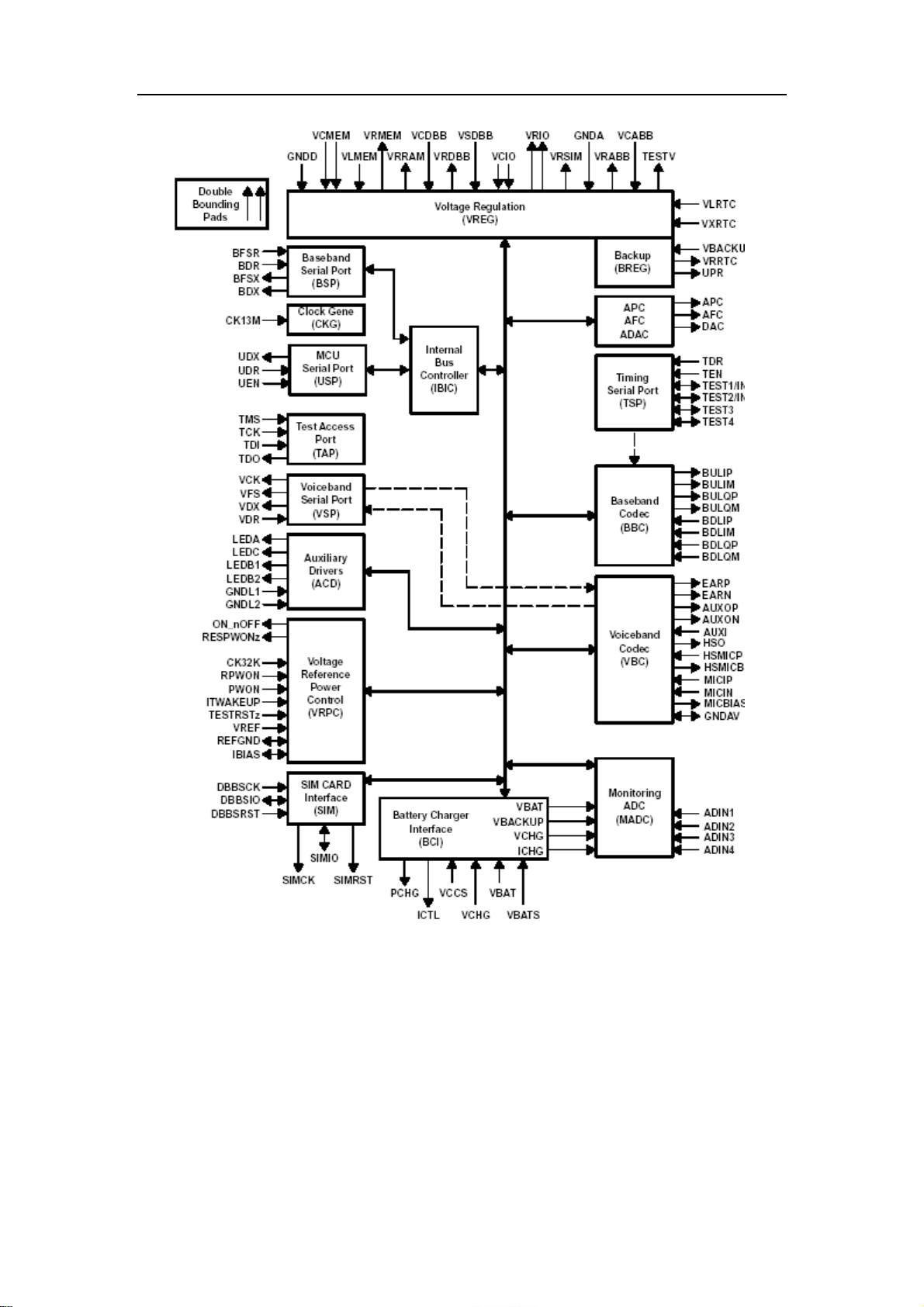
Figure 2–5 TWL3014 Functional Block Diagram
This section provides the terminal descriptions for the TWL3014 device. Fig 2–6 shows the
signal assigned to each terminal in the package. Table 2–3 shows the terminal functions for the
TWL3014 device.
Page 11

Figure 2-5. TWL3014 Device Pin Figuration (TOP VIEW)
Figure2-6 signal assigned of OMEGA
PIN nb PIN name Description I/O
B6 CTN Monitoring ADC Input 1 and Battery Temperature
I/O
Current Source
A6 NC Not Connect
C7 NC Not Connect
C6 VMES Monitoring ADC Input I
J4 AFC Automatic Frequency Control DAC Output O
K4 APC Automatic Power Control DAC Output O
G7 AUXIN Auxiliary Speech Signal Input I
K10 AUXON Auxiliary Speech Signal Output (–) O
Page 12

K9 AUXOP Auxiliary Speech Signal Output (+) O
F10 IRX In-phase Input (I–) Baseband Codec Downlink I
F9 IR In-phase Input (I+) Baseband Codec Downlink I
E9 QRX Quadrature Input (Q–) Baseband Codec Downlink I
E10 QR Quadrature Input (Q+) Baseband Codec Downlink I
J3 BDR Baseband Serial Port Receive Data I
J2 BDX Baseband Serial Port Transmit Data O
H3 BFSR Baseband Serial Port Receive Frame Synchronization I
K2 BFSX Baseband Serial Port Transmit Frame Synchronization O
D10 ITX In-phase Output (I–) Baseband Codec Uplink O
D9 IT In-phase Output (I+) Baseband Codec Uplink O
C9 QTX Quadrature Output (Q–) Baseband Codec Uplink O
C10 QT Quadrature Output (Q+) Baseband Codec Uplink O
E4 CLKIOTA 13-MHz Master Clock Input and BSP/TSP/USP Clock I
E2 CLK32K 32-kHz Clock Input I
H4 NC Not Connect
F4 SIMCLK3 SIM Card Shifters Clock Input I
E5 SIMIO3 SIM Card Shifters Data I/O
G4 SIMRST3 SIM Card Shifters Reset Input I
J10 EARN Earphone Amplifier Output (–) O
J9 EARP Earphone Amplifier Output (+) O
G10 GND Ground
G6 GND Ground
A3 GND Ground
B9 GND Ground
A9 GND Ground
K8 NC Not Connect
K7 NC Not Connect
H9 NC Not Connect
B7 IBIAS Bias Current Reference Resistor (100 kΩ) I/O
D6 NC Not Connect
H6 FIQL Fast Interrupt / Test Pad 1 (Default is INT1) I/O
E6 ITIOTA Microcontroller Interrupt / Test Pad 2 (Default is INT2) I/O
D2 ITWAKEUP Real-time Wake-up Input I
B8 NC Not Connect
B10 LEDB1 Connected to LEDB2
A10 LEDB2 Connected to LEDB1
C8 NC Not Connect
J8 NC Not Connect
H7 MICPIOTA Microphone Amplifier Input (–) I
Page 13

J7 MICNIO Microphone Amplifier Input (+) I
E3 ONOFFL Digital Baseband Reset (@ each switch on) O
B5 NC No Connect
F8 OUIL On Button Input I
A7 REFGND Reference Voltage Ground I/O
D3 NRESPWON Digital Baseband Power-on Reset (First Battery Plug) O
F7 RPWRC Remote Power-on (other than button) I
C4 SIMCLK SIM Card Shifters Clock Output (1.8 V/3 V) O
B3 SIMIO SIM Card Shifters Data I/O
D4 SIMRST SIM Card Shifters Reset Output O
D8 TCLK Scan Test Clock I
D7 TDIIOTA Scan Path Input I
E7 TDOIOTA Scan Path Output O
G3 DA Time Serial Port Input I
H1 ENIOTA Time Serial Port Enable I
J6 TEST3 Special Test I/O Terminals I/O
F6 TEST4 Special Test I/O Terminals I/O
H8 NC Not Connect
G8 NC Not Connect
E8 TMS JTAG Test Mode Select I
K5 UDR Microcontroller Serial Port Receive Data I
J5 UDX Microcontroller Serial Port Transmit Data O
K6 MCUENO Microcontroller Serial Port Enable I
C2 UPR Uninterrupted Power Rail Output O
E1 VBACKUP Backup Battery Input I/O
A4 VBAT Battery Voltage Sense Input I/O
C5 VBAT Battery Voltage Sense
G9 VBAT Input of Voltage Regulator VRABB I/O
D5 NC Not Connect I
K1 VBAT Input of Voltage Regulator VRDBB I/O
A5 GND Ground
A2 VBAT Input 1 of Voltage Regulators VRIO and VRSIM I/O
A1 VBAT Input 2 of Voltage Regulators VRIO and VRSIM I/O
K3 VCK Voiceband Serial Port Clock O
G2 VBAT Input of Voltage Regulator VRMEM I/O
F2 VBAT Input of Voltage Regulator VRRAM I/O
F5 VDR Voiceband Serial Port Receive Data I
H5 VDX Voiceband Serial Port Transmit Data O
G5 VFS Voiceband Serial Port Frame Synchronization O
F3 VLMEM Select Output Voltage of VRMEM I
Page 14
C3 VLRTC Select Output Voltage of VRRTC and VRDBB I
H10 VRABB Voltage Regulator VRABB Output O
J1 VRDBBIOTA Voltage Regulator VRDBB Output O
A8 NC Not Connect I/O
B2 VRIOIOTA Voltage Regulator VRIO Output O
B1 VRIOIOTA Voltage Regulator VRIO Output O
G1 VRMEM Voltage Regulator VRMEM Output O
F1 VRRAM Not Application O
D1 VDDRTC Voltage Regulator VRRTC Output O
B4 SIMVCC Voltage Regulator VRSIM Output O
H2 VRDBBIOTA Voltage Regulator VRDBB Input Feedback I
C1 NC Not Connect
Table 2-3 TWL3014 Pin Descriptions
The TWL3014 voltage regulation block consists of seven sub blocks. Several low-dropout (LDO)
regulators perform linear voltage regulation. These regulators supply power to internal analog and
digital circuits, to the DBB processor, and to external memory. TABLE 2-4 shown OMEGA volt
supply and descriptions. Fig 2-7 shown the test points of OMEGA supply.
Power supply Test point Supply to TEST POINT
VRDBBIOTA C208
VDDHERC C307
VDDPLLHERC C303
VDDRTC C217, C305
VDDRTC Q402, 2#
VDDRTC C305
VRMEM C215
VDDANGHERC C312
VRIOIOTA C220
VRIO
R315
R302
VRRAM
No Application
VRABB
Table 2-4 OMEGA voltage supply and descriptions
The first LDO (VRDBBIOTA) is a programmable regulator that generates the supply voltage
(1.5V) for the core of the DBB processor and inside PLL circuit
The second LDO (VDDRTC) is a programmable regulator that generates the supply voltage (1.6V)
for the 32-kHz oscillator located in the DBB device. Meanwhile supply to Q402, 2# logic high for
OMEGA transmit digital baseband power-on reset to Power IC. The main or backup battery
supplies VDDRTC.
The third LDO (VRMEM) is a programmable regulator that generates the supply voltages (2.8V)
for external memories (typically flash memories) and DBB memory interface I/Os.
Page 15

(
)
(
)
The fourth LDO (VRIOIOTA) generates the supply voltage (2.8V) for the digital core, analog
functions and I/Os of the TWL3014 device.
The fifth LDO (VRSIM) is programmable regulator that generates the supply voltages (2.9V) for
SIM card and SIM card drivers.
The sixth LDO (VRRAM) and the seventh LDO (VRABB) is not application in S1160.
VDDRTC
(Q402,2#)
VRIOIOTA
(C220)
VDDRTC
(C217)
VDDRTC
(C305)
VDDANGHERC
C312
VRDBBIOTA
(C208)
VRMEM
C215
VDDHERC
(C307)
VRIO
VDDPLLHERC
(C303)
Figure 2-7 Test point of OMEGA supply
2.2.3 Manager IC (MN401)
HORUS is a chip implementing the analog base-band processes
of a GSM/GPRS mobile phone peripheral circuit. HORUS
A1
A10
integrates power management (battery and charger) functions,
audio functions, power I/Os, radio interface I/Os and others
facilities tailored and adapted to SAGEM mobile phones
specific architecture. Fig 2–9 shows the signal assigned to
each terminal in the package. Table 2-5 shown the device
pins description.
K1
Figure 2-8
Page 16

Figure 2-7.
.
Figure 2-9 HORUS Terminal Assignments
PIN nb PIN name Description I/0
POWER MANAGEMENT
VBAT Power supply source I
GND
Power supply ground
A5 VMHV VBACKUP and ALIMLCD control O
B5 VBACKUP Backup area supply I/O
C4 ALIMLCD LCD interface supply O
D1 VCAPP Filter Output O
E1 VCAPN Filter Input I
E3 P5V6 Voltage doubler output O
J5 P5V6 Interior RADIO LDO supply O
F1 CHARGEUR Charger measurement bridge I
G8 VB Charge control device base current control O
G9 PCHAR Charge control shunt regulator supply I
H8 RESETHORUS Reset input/output I/O
Page 17

H10 VSAUV Power management and low power modes supply O
J5 P5V6 Interior RADIO LDO input I
K5 P4V5 MIC Bias voltage O
K7 VCRADIO RF supply O
K9 VPLL Radio VCO supply O
RADIO INTERFACE
B6 TX TX radio control input I
D6 BSW Band radio control input I
H6 SWANT3 Radio switch control O
J6 SWANT4 Radio switch control O
REFERENCES
J10 CREF Integrated reference output (external filtering) O
K2 VBIAS Reference current resistor pin Current
output
K10 Vfuse/Tes Fuse prog. I/O I/O
AUDIO
C9 GMICP Audio converter negative input I
D8 AAUX2 Auxiliary audio path negative input to power amplifier I
D9 AAUX1 Auxiliary audio path positive input to power amplifier I
E6 ARX2 Main power audio path negative input to power
I
amplifier
E7 ARX1 Main power audio path positive input to power
I
amplifier
E8 AUXIN Audio converter positive output O
E10 EARP Power Audio amp. high/mean power positive output O
F10 HPN Power Audio amp. high power negative output O
F7 Cbp Power audio amp. bypass capacitor O
G10 LPHPN Power Audio amp. mean power amp. Negative output O
POWER I/O
F3 BACKLCD LCD Backlight current source output Open-drain O
G1 BACKKEY KEY Backlight current source output Open-drain O
G3 Cmdvib Vibrator current source output Open-drain O
H2 VCRADIO RF supply Open-drain O
H4 CTN CTN current source detect O
SERIAL INTERFACE
A7 CKMIW Serial interface clock input I
B8 DIUM Serial interface data output (ULYSEE) O
C7 VCBB General purpose I/O I/O
C8 DOMIW Serial interface data input I
D7 CSHORUS Serial interface chip-select I
Page 18

NC N
d
F2 ITHORUS CPU interrupt O
ECO MODE (CLOCKS)
A6 OSCBF 32k digital square wave output O
A8 VCXOEN Radio VCO supply control digital input I
A9 CLK13MHOR
US
K8 CLKVCXO 13MHz analog clock input from VCO to low swing
MEASURMENT
A10 VMES Measurement bridges output O
2.2.4 FLASH (MN303)
The Am29DL161D is 16megabit, 2.8 volt flash memory
devices. The device is designed to be programmed in-system
with the 2.8 volt Vcc supply by OMEGA (MN201)
Table 2-5 Manager IC Terminal Functions
13MHz square wave output O
I
trigger
H1 A1
A6
Figure 2-10
A1–A20 20 Addresses
D0–D14 15 Data Inputs/Outputs
D15 Data Input/Output, word mode
FLASH1 Chip Enable
OE* Output Enable
RWL Write Enable
WP# Hardware Write Protect
FDPL Hardware Reset Pin, Active Low
VRMEN 3.0 volt-only single power supply
GND Device Ground
ot Connecte
Table 2-6 FLASH Device Pins Description
Page 19

Figure 2-11 FLASH Terminal Assignments
2.3 ULYSEE to OMEGA connections
ULYSEE OMEGA
Pin name Pin nb Pin name Pin nb
TSP Serial Interface
DA H11 DA G3
ENIOTA H13 ENIOTA H1
RIF/BSP Serial Interface
BFSX L11 BFSX K2
BDX K10 BDX J2
BFSR P12 BFSR H3
BDR M11 BDR J3
ARM SPI/USP Serial Interface
UDX N7 UDX J5
UDR M7 UDR K5
MCUENO M8 MCUENO K6
LEAD SPI/VSP
VCK N12 VCK K3
VDR P14 VDR F5
Page 20

VDX N13 VDX H5
VFS M13 VFS G5
SIM Interface
SIMCLK3 F13 SIMCLK3 F4
SIMIO3 G13 SIMIO3 E5
SIMRST3 G10 SIMRST3 G4
JTAG Interface
TDOCALYPSO C10 TDIIOTA D7
TMS E9 TMS E8
TCLK B10 TCLK D8
TDICALYPSO D10
TDOIOTA E7
CLOCKS
CLK32K C12 CLK32K E2
CLKIOTA F12 CLKIOTA E4
INTERRUPTS
EXTIT M3 ITIOTA E6
FIQL P1 FIQL H6
POWER MGMT
ITWAKEUP B14 ITWAKEUP D2
ONOFFL F10 ONOFFL E3
NRESPWRON D12 NRESPWRON D3
POWER SUPPLIES
VDDHERC
E1 J1
VRDBBIOTA
M1
P7
N14 H2
B12
A5
VDD-RTC D14 VRRTC D1
VDD-RTC D13 VRRTC D1
VRMEN
D1 G1
VRMEM
G1
B6
A4
N5 VRIO
VRIOIOTA
B1
L14
VDDS2 A11
B2
VDDPLL F11 VRDBBIOTA J1
VDDANG E11 VRIOIOTA B1
Page 21

2.3.1 TSP serial interface
The TSP serial interface allows the serial transmission of baseband control windows for the
POWER IC BBCODEC. It is managed through a TPU scenario hence it allows GSM quarter bit
resolution and a precise positioning of CODEC commands among the GSM TDMA frame.
2.3.2 RIF/BSP serial interface
This interface is dedicated to the UL and DL transmission of I/Q samples between the DSP and
the BBCODEC and to POWER IC registers access.
On the UL path the DSP sends to the CODEC the burst bits to be modulated while on the DL
path it receives non demodulated I/Q samples.
Write access to POWER IC register is done using the same data format as the UL. Main
functions executed are:
APC parameters programmation (levels, delays, ramp coefficients)
AFC
Voice CODEC control
Register accesses could be considered synchronized to the TDMA frame as the DSP receives
commands on TDMA frame start boundary.
2.3.3 ARM SPI/USP serial interface
This interface is dedicated to OMEGA read and writes register accesses from ULYSEE.
Through this link is possible to access all POWER IC registered; hence this port is used to
configure and to manage the status of each block of POWER IC device. Also ADC result of
conversion can be read through this interface.
2.3.4 LEAD SPI/VSP serial interface
This interface allows voice samples exchanges in DL and UL direction between the DSP and the
POWER IC Voice Band CODEC. POWER IC VSP is the master port in the transmission.
2.3.5 SIM interface
The SIM Card digital interface in ABB insures the translation of logic levels between DBB and
SIM Card, for the transmission of 3 different signals:
A clock derived from a clock elaborated in DBB, to the SIM -Card (SIMCLK3 →
SIMCLK )
A reset signal from DBB to the SIM Card (SIMRST3 → SIMRST),
A serial data from DBB to the SIM Card (SIMIO3 ←→SIMIO) .
2.3.6 JTAG interface
The test access port (TAP) meets JTAG testability standard (IEEE Std1131.1-1990). TAP
allows public instructions set of JTAG standard and also private instructions to configure the
device in special modes for test or debug purpose.
2.3.7 CLOCKS
POWER IC device receives two clocks from CPU:
A slow clock CLK32K_OUT used by the DBB as reference clock for low power modes
(back-up, deep-sleep). The ABB adopt this clock as the VRPC synchronous state machine
clock and as reference clock when fast clock is not present.
A fast clock CLK13M_OUT used by the DBB and ABB as reference clock for all modules.
Page 22

2.3.8 INTERRUPTS
POWER IC device is able to generate two kinds of interrupts:
An emergency interrupt connected to CPU FIQL signaling the detection of a low battery
voltage.
An event detection interrupt connected to CPU EXTIT signaling:
Falling or rising edge at RPWON pin.
Falling edge at PWON pin.
Termination of an analog to digital conversion.
Charger plug.
2.3.9 POWER MGMNT
Those three signals controls system status and system status transitions, they are supplied on the
VRRTC power domain.
The NRESPWRON signal is generated by the ABB, it is the reset of the power split part of the
DBB chip. It is active only one time (as long any kind of supply, Backup battery or Main battery
is present) at the first start of the mobile. Split power logic will provide to propagate this signal
as global reset as soon as power supply will be present on the rest of the chip.
The ONOFFL signal is generated by the ABB, it is the ASIC modules, ARM, LMM, reset.
It is at logical low level each time the system is switched off. Also this signal is managed by the
split power logic and propagated to the rest of the circuit.
High logical level is asserted on this signal when the POWER IC power management has
completed the enabling sequence of all LDO’s meaning that the system is correctly supplied and
that SW can be correctly executed.
At this time the MCU SW starts from its reset state.
The ITWAKEUP signal is generated by the DBB and it is used to wake up the system from low
power modes (backup, deep sleep). It is built as a combination of all the interrupt request that
are allowed to awake the CPU ULPD module and the RTC alarm.
2.4 SIM interface
The SIM_RST signal is SIM card async/sync reset.
The SIM_CLK signal is SIM card reference clock.
The SIM_IO signal is SIM card bidirectional data line.
The SIM_VCC signal is SIM card power activation.
S1160 only enables 3V SIM operation.
Figure 2-12 SIM Interface
SIMIO SIMVCC GND
SIMCLK SIMRST SIMVCC
Figure 2-13
Page 23

2.5 Display & FPC Interface
LCD module is connected to main board with 18 pins FPC.
Figure 2-14 FPC Interface Scheme
Pin nb Name Description
1 CSLCD LCD module select signal
2 RESETLCD LCD module reset signal
3 RSLCD Mobile in wait mode (wait or AT instruction)
4 CKMIW Serial interface clock output
5 DOMIW Serial interface data output (bidirectional)
6 ALIMLCD LCD module interface supply
7 GND Ground
8-13
Output filtering or no application
14-18 ALIMLCD
LCD control signal wave shown as below:
Table 2-7 FPC Interface Spec
Figure 2-15 RS Signal
Page 24

Figure 2-16 DOMIW Signal
Figure 2-17 CS signal
Figure 2-18 CKMIW signal
Page 25

2.6 Audio Signal Processing & Interface
Baseband CODEC is composed of baseband uplink path (BUL) and baseband downlink path
(BDL).
Uplink
The uplink path amplifies the audio signal from MIC and converts this analog signal to digital
signal and then transmit it to DBB Chip. This transmitted signal is reformed to fit in GSM Frame
format and delivered to RF Chip.
The microphone is soldered to the main PCB. The uplink signal is passed to MICNIOTA and
MICPIOTA pins of OMEGA. MICBIAS is 2.5V level. The MICBIAS voltage is supplied from
Manager IC (MN401).
Figure 2-19 Audio Signal From MIC to OMEGA Scheme
Figure 2-20 Audio Signal Baseband Codec Block Diagram
Figure 2-21 Audio Signal From BB to RF Block Diagram
Page 26

Downlink
Downlink process is opposite procedure of Uplink. Namely, it performs GMSK demodulation
with input analog I&Q signal from RF section, and then transmit it to DSP of DBB chip with
270KHz data rate through BSP.
S1160 has two receiving model, the normal model and the freehand model.
1. Normal Model:
2. Freehand Model:
Figure 2-22 Audio Signal From RF to BB Block Diagram
Figure 2-23 Audio Signal Processed Internal OMEGA
Figure 2-24 Audio Signal From OMEGA to Speaker Scheme
Figure 2-25 Audio Signal Amplifier Internal OMEGA
Page 27

2.7 Keyboards
DBB supports 18 Key and Switch-ON Key is directly connected to ABB:
- R (4:1) input pins for row lines
- C (5:1) output pins for column lines
If a key button of the keyboard matrix is pressed, the corresponding row and column lines are
shorted together. To allow a key press detection, all input pins (R) are pulled up to VCC and all
output pins (C) are driving a low level. Any action on a button will generate an interrupt to the
controller which will, as answer, scan the column lines with the sequence describe below. This
sequence is written to allow detection of simultaneous press actions on several key buttons.
C1 C2 C3 C4 C5
R1 [ 4 ] [ 7 ] [ 8 ] [ 9 ]
R2
R3
R4
[ ▲ ] [ … ]
[ · ]
[ ▼ ] [ ‥ ]
Table 2-8. Keypad Map
Figure 2-26 Keyboard Connection Scheme
2.8 Charge self-supply
Charger functions extract power from VCH pin to be self supplied from the charger
independently from VBAT. In case of shunt regulator architecture, external RC network
filters CHARGEUR to provide primary supply to the shunt regulator. A power-on-reset
function could be attached to the shunt regulator. Fig 2-26 shown charge scheme. Fig 2-27
shown charge architecture.
[ 5 ] [ OFF ] [ 6 ]
[ * ] [ 0 ] [ # ]
[ 1 ] [ 2 ] [ 3 ]
Page 28

Figure 2-27 Charge Scheme
Figure 2-28 Charge architecture
2.9 Keypad and LCD backlight Illumination
There are 6 deep green LEDs for keypad and 4 deep green LEDs for LCD back-light in Main
Board respectively, which are driven by “BACKKEY” and “BACKLCD” from Manger IC
(MN401).
Figure 2-29 Keypad Backlight Scheme
Figure 2-30 LCD Backlight Scheme
Page 29

N
N
NO N
2.10 Trouble Shooting
(a) CHARGE TROUBLE
Check the pins and battery
Is the TA voltage 5.2V?
R410 properly mounted?
START
connect terminals of
I/O connector (J103)
Connection OK?
Is it the level of
Q401.3 logic low?
Change MN401
O
Change or resoldering I/O connector
YES
O
Change or resoldering TA
YES
YES
Change or resoldering Q401
O
Change or resoldering R410
YES
Page 30

N
NO N
(b) VIB TROUBLE
START
([ · ]+ [ * ])(inside test card) and select Vibrator
Enter into engineering mode:
Is it the level of
J400.1 logic low?
YES
Does rectangular wave
appear at pin 1 of
J400?
L402 properly mounted?
YES
Change or resoldering MN401
O
Change or resoldering R404, L401
YES
Change or resoldering Vibrate
O
Change or resoldering L402
Page 31

3. RF TECHNICAL BRIEF
3.1 RF Components
J702
MA701
MA703
FL601
MA601
Y601
Figure 3-1 RF Components
Reference Name Description
J702 Antenna Connector Connect the Antenna with the PCB
MA701 Antenna Switch Switch E-GSM or DCS, Switch RX or TX
MA703 PAM Amplifier TX Power
FL601 SAW Filter Filter mottle frequency
Y601 26MHZ Oscillator Output steady 26MHZ frequency
MA601 Transceiver IC
Table 3-1 RF Components Description
RX signal amplifier, down frequency, demodulation
TX signal modulation, check phase, up frequency
Page 32

3.2 RF Configuration Block Diagram
Figure 3-2 RF Configuration Block Diagram
Page 33

3.3 Receiver
The Receive part consists of a dual band(E-GSM & DCS) antenna switch(MA701), a dual band
RF SAW filter(FL601) and a transceiver IC(MA601). All active circuits for a complete receiver
chain are contained in the transceiver IC (MA601). The RF received signals (GSM 925MHz ~
960MHz, DCS 1805MHz ~ 1880MHz) are input via the antenna (J702). An antenna matching
circuit is between the antenna and the dual band antenna switch. The Receiver Chart is shown in
Fig 3-3.
EGSM Signal Flow
DCS Signal Flow
10 8 6
3 1
5 7
9
11
Figure 3-3 Receive Signal Flow Chart
51 50 49 48
TO BB
Figure 3-4 RX Path Block Diagram
Page 34

3.3.1 Antenna Switch
VC1, VC2 that are connected to SWANT3, SWANT4 to switch either TX or RX path on. When
the RX path is turned on, the received RF signal passed through the dual band antenna switch, this
process is the same both E-GSM and DCS.
Table3-2 The logic and current is given below
SWITCH MODE SWANT3 (VC1) SWANT4 (VC2)
EGSM_TX 1 0
DCS_TX 0 1
EGSM_RX 0 0
DCS_RX 0 0
10 9 8 7 6
11
1 2 3 4 5
RXDCS GND ANT GND RXGSM
GND
TXDCS VCRADIO SWANT4 SWANT3 TXGSM
Pin number Pin name Description
1 TXDCS DCS_TX INPUT 1710-1785MHZ
2 VCRADIO Power Supply
3 SWANT4 Control Input
4 SWANT3 Control Input
5 TXGSM EGSM_TX INPUT 880-915MHZ
6 RXGSM EGSM_RX OUTPUT 935-960MHZ
7,9,11 GND Ground
8 ANT
Connect Antenna Switch Module with antenna
matching circuit
10 RXDCS DCS_RX OUTPUT 1805-1880MHZ
Table 3-3. Antenna Switch Device PIN Description
Figure 3-5 RF Front-end circuit Diagram
Page 35

3.3.2 SAW Filter
The received RF signal which has passed through the dual band antenna switch, is filtered by the
RF integrated SAW filter (FL601) for EGSM and DCS better stop band rejection.
r
3 2 1
4 8
5 6 7
DCSIN GND GSMIN
GND GND
DCSOUT GND GSMOUT
Figure 3-6 RF SAW Filter Circuit diagram
3.3.3 LNA and Quadrature Demodulator
The MA601 chip receive path implements a direct down-conversion architecture, so the received
RF signal is directly converted to base band I and Q signal by the transceiver IC (IF frequency is 0
Hz), which contains three Integrated Low Noise Amplifiers (LNAs), a quadrature demodulator,
tunable receiver baseband filters, Voltage gain amplifier (VGA) and DC-offset correction
sequencer.
Three separate LNAs(for PCS no used )are integrated to address different bands of operation.
These LNAs have separate single-ended inputs. The gain is switchable between high (15 dB
typical) and low(–5 dB GSM, –7 dB DCS typical) settings. The LNA outputs feed into a
quadrature demodulator that down converts the RF signals directly to baseband.
Figure 3-7 MA601 RX Internal Architecture
Page 36

56
1 43
57
15 29
44
16 28
Figure 3-8 RF Transceiver IC circuit Diagram
Figure 3-9 Transceiver IC Terminal Assignments
Page 37

Pin nb Pin name Description
1 RXON Receiver enable input
2 TXON Transmitter enable input
3 BSW Bi-directional band select
4 VPLL VCXO enable pin
5 PDETVCC No connect
6 VCRADIO LNA and TX charge pump supply
7 TXCPO Translational loop charge pump output
8 TXINP Translational loop feedback input
9 LNA900IN Low band LNA input for GSM850,EGSM900
10 GNDLNA900 Low band LNA emitter ground
11 LNA1800IN DCS LNA input
12 PDET ground
13 LNA1900IN PCS LNA input
14 NC No connect
15 NC No connect
16 PAVAPC No connect
17 BBVAPC Ground
18 IT TX I baseband input positive
19 ITX TX I baseband input negative
20 QT TX Q baseband input positive
21 QTX TX Q baseband input negative
22 TXFP TX IF filter output positive
23 TXFN TX IF filter output negative
24 VCRADIO RX mixer and TX loop supply
25 CAPIP Capacitor filter I positive
26 CAPIN Capacitor filter I negative
27 CAPQP Capacitor filter Q positive
28 CAPQN Capacitor filter Q negative
29 LPFADJ LPF frequency setting resistor
30 XTALBUF Crystal oscillator buffer output
31 GNDD Synthesizer digital ground
32 VPLL Synthesizer digital supply
33 VPLL
Synthesizer analog supply and crystal
oscillator supply
34 XTAL Crystal input
35 GNDFN Synthesizer analog ground
36 UHFCPO Synthesizer charge pump output
37 VCCFN_CP Synthesizer charge pump supply
38 SXENA Synthesizer enable input
Page 38

39 XTALTUNE Crystal oscillator varactor control
40 DA Serial bus data input
41 CLK Serial bus clock input
42 EN Serial bus latch enable input
43 VDDBB Digital CMOS supply
44 UHFBYP Bypass capacitor for UHF VCO
45 UHFTUNE UHF VCO control input
46 VCRADIO UHF VCO supply
47 VCRADIO LO chain supply
48 QRX Receiver output Q negative
49 QR Receiver output Q positive
50 IRX Receiver output I negative
51 IR Receiver output I positive
52 VCRADIO Baseband supply
53 VCRADIO Transmit VCO supply
54 INGSM Low band transmit VCO
55 INDCS DCS and PCS transmit VCO output
56 TXVCOTUNE Transmit VCO control input
57 CASE GND
Table 3-4 Transceiver IC Device PIN Descriptions
3.4 Transmit
The TX path is a frequency translation loop (TX OPLL) architecture consisting of an I/Q
modulator, integrated high power VCOs, offset mixer, programmable divider, PFD, and charge
pump. TX OPLL designed to perform frequency up-conversion with high output spectral purity.
The TXVCO output frequencies into PAM for amplifier signal power is suit BS (base station) and
into MA601 for TX local frequency. The PAM outputs pass the antenna connector via an
integrated dual band antenna switch module, and then transmit the signal to the BS.
Page 39

EGSM Signal Flow
8
1 5
DCS Signal Flow
9
13
5
3
55 54
18 19 20 21
Figure 3-10 Transmit Signal Flow Chart
From BB
Figure 3-11 TX Path Block Diagram
3.4.1 Modulator and TX OPLL
The TX I & Q signals that from BB analog chipset are put into the MA601 TX modulator,
where they are modulated. The TX I & Q signals from BB analog chipset are fed to the MA601
TX modulator, where they are modulated onto either a TX of 880-915 MHz (for EGSM-TX) or
1710-1785 MHz (for DCS-TX). The BB software is able to cancel out differential DC offsets in
the I/Q BB signals caused by imperfections in the D/A converters. The TX loop contains a
phase-frequency detector, charge pump, mixer, programmable dividers, and high power TX
Voltage Controlled Oscillators (TX VCO) with no external tank required. The TX VCO has a
frequency band from 880 MHz to 915 MHz (for EGSM) and from 1710MHZ to 1785MHZ (for
DCS). Two on-chip transmit VCOs are designed to meet EGSM900, DCS1800 requirements.
Page 40

Figure 3-12 MA601 TX Internal Architecture
3.4.2 Power Amplifier Module
The Power Amplifier Module (PAM) is consists of separate GSM850/900 PA and
DCS1800/PCS1900 PA blocks, impedance-matching circuitry for 50ohm, Input and output
impedances and a Power Amplifier Control (PAC) block with an internal current-sense resistor.
The custom CMOS Integrated Circuit provides the internal PAC function and interface circuitry.
One Heterojunction Bipolar Transistor (HBT) PA block supports the GSM850/900 bands and the
other supports the DCS1800 and PCS1900 bands. RF input and output ports of the PAM are
internally matched to 50ohm to reduce the number of external components for a quad-band design.
Extremely low leakage current (2.5 µA, typical) of the dual PA module maximizes handset
standby time. The PAM also contains band-select switching circuitry to select GSM (logic 0) or
DCS/PCS (logic 1) as determined from the Band Select signal. In the Functional Block Diagram
below, the BS (band select) pin selects the PA output (DCS/PCS OUT or GSM850/900 OUT) and
the Analog Power Control (VAPC) controls the level of output power.
VBATT and IREG OUT pins connect to an internal current-sense resistor and interface to an
integrated power amplifier control (PAC) function, which is insensitive to variations in
temperature, power supply, and process. The PAC ENABLE input allows initial turn-on of PAC
circuitry to minimize battery drain.
Figure 3-13 Functional Block Diagram
Page 41

8 7 6
9
10
11
12
13
14 15 16
17
5
4
3
2
GSM OUT GND GND VBAT INDCS
GND BSW
VCC2 GND INGSM
GND VREG
DCS OUT GND PAOUT IREG OUT VBAT
1
Figure 3-14 RF PAM Circuit Diagram
Pin nb Pin name Description
1 VBAT Battery input to high side of internal sense resistor
2 VREG Closed loop PAC mode CMOS enable
3 INGSM
RF input 880–915 MHz
4 BSW Band Select
5 INDCS
RF input 1710–1785 MHz
6 VBAT VCC (to GSM 1st stage, DCS 1st and 2nd stages, PAC)
7 GND RF and DC Ground
8 GND RF and DC Ground
9 GSM OUT
RF Output 880–915 MHz
10 GND RF and DC Ground
11 VCC2 VCC (to GSM and DCS Final stages)
12 GND RF and DC Ground
Page 42

13 DCS OUT
RF Output 1710–1785 MHz
14 GND RF and DC Ground
15 PAOUT Power Control Bias Voltage
16 IREG OUT Regulated output current (Externally connected to pin 11)
Table 3-5 PAM Device Pins Description
3.4.3 Dual Band Antenna Switch
When the TX path is turned on, the transmit RF signal passed through the dual band antenna
switch, the process is the same as both E-GSM and DCS.
3.5 Synthesizer
The SKY7493 (MA601) is a transceiver IC suitable for E-GSM and DCS. So, synthesizers use a
number of techniques to improve lock time, making them well suited to E-GSM and DCS. The
fine synthesizer resolution allows direct compensation or adjustment for reference frequency
errors. The SKY7493 includes two OPLL which operation offers low phase noise and fast
settling times. One is Franc N.PLL (RF PLL), which can phase-lock the local oscillator used in
both transmit and receive paths to a precision frequency reference input. Another is TX PLL,
which output frequency for E-GSM from 880MHZ to 915MHZ or for DCS from 1710MHZ to
1785MHZ.
The fractional-N synthesizer RF PLL consists of the following:
UHF VCO
High frequency prescaler
N-divider with a sigma-delta modulator
Reference divider
Fast phase frequency detector
Charge pump
A crystal oscillator output frequency reference to RF PLL. The UHF VCO with external tank
circuits is necessary for both transmitting and receiving operation. For receiving operation, the
RF synthesizers of the SKY7493 to extract from a modulated carrier wave to I and Q signals.
For transmitting operation, the UHF VCO output accurately frequency is for TX Feedback
Mixer and TX OPLL. Output frequency of the UHF VCO is set by the factional number,
prescaler and counter. A buffer amplifier follows the UHF VCO. The purpose of the buffer is to
give reverse isolation and prevent any frequency pulling of the VCO when the transceiver is
powered UP and DOWN..
Page 43

Figure 3-15 RF Synthesizer Architecture
The fractional-N synthesizer TX PLL consists of the following:
TX VCO
TX Feedback Mixer,
TX I/Q Modulator
D2 Divider with external LP filter
Phase Detector
Internal reference D1 Divider
Charger pump with external LP filter
The transmit loop takes baseband analog I/Q signals and modulates them with the mixed
product of transmitter output and LO signals. The TX VCO with external tank circuits is
necessary for transmitting operation only. The TX VCO has a frequency band from 880 MHz to
915 MHz (for E-GSM) and from 1710MHZ to 1785MHZ (for DCS). Output frequency of TX
VCO is settled by prescaler and counter also. The TX VCO is also followed by a buffer
amplifier, which is to give reverse isolation and prevent any frequency pulling of the VCO
when the transceiver is powered UP and DOWN.
Page 44

A fixed reference frequency is generated by a reference divider from the external applied
26MHZ crystal oscillator and the interior applied VCXO circuit.
Figure 3-16 TX Synthesizer Architecture
3.6 3-wire Serial Interface
3-wire serial interface controls the transceiver and synthesizer. The receiver gains control, as well
as the division ratios and charge pump currents in the synthesizer and transmitter, can be
programmed by using 24-bit words. These 24-bit words are programmed using the 3-wire input
signals CLK, DATA, and LE. To ensure that the data stays latched in power down mode, pin 43
(VDDBB) must be continuously supplied with voltage. This pin is provided for the digital sections
to allow power supply operation compatible with digital baseband devices.
Pin name Pin number Description
CLK 41 Serial clock input to the AM601
DATA 40 Serial data input to the AM601
LE 42 Input latches the serial data transferred to the AM601
Table 3-4 3-wire Interface Pin Description
Page 45

3.7 RF Trouble Shooting
When the mobile phone appears the following troubles, we will doubt about the RF part
problem first. Such as: No network retrieval, Good RSSI but no SVC, Signal weak, Network
unsteady, Freeze while call or search network, Can not dial out, Power off while call etc.
According to experience and the GSM network principle, we should judge whether the problem
is due to receiver or transmit part problems.
When the mobile phone appears to No network
retrieval, which is roots from receiver thoroughfare.
We can replace the receiver part flimsy parts, such
as dual band antenna switch, RF SAW filter,
transceiver IC, but the method will cause waste of
spare parts and time. Certainly, we can find the
receive thoroughfare problem by “false antenna
method” judge (Add a soldering or a lead in receiver
thoroughfare). In actual maintain, for the sake of
judging the trouble points, we can use “1/2 approach
method”. For example, a S1160 mobile phone is no
network retrieval, we can add the false antenna in
the MA601.6# (RXGSM)(shown as Fig 3-17).
If the signal recovers, we can make sure the trouble
is between the antenna and the dual band antenna
switch (includes the dual band antenna switch). If
no signal recovers, the trouble is between the dual band antennas switch and the transceiver
IC(includes transceiver IC).
When the mobile appears to be Good RSSI but no SVC, Network unsteady, Freeze while call or
search network, Power off while call. We can doubt about the mobile transmit part problem. We
can replace the transmit thoroughfare flimsy parts, such as PAM, transceiver IC, antenna switch.
Specially, we resoldering or replace the PAM.
When the mobile appears Freezing while call or search for network and Power off while call.
We can check the power on current of the mobile phone to judge whether the PAM is working
normal. When switching on the mobile phone, it starts execute its power on program, searches
the network and adjust the transmit power level. During the procedure, the mobile phone
working current will rise. If no rise or only with little rise, we can generally judge that the PAM
has some problem. In the same way, when the mobile phone makes a call, its working current
also will be rising, if it did not, the most possibility is the PAM.
Hereinabove, I tell about some experience about maintains. But, that way may be waste of time
and materials. We can used the equipment to
MA601
Figure 3-17
Page 46

Transmit part Standalone test.
3.7.1. Equipment List
Equipment for test Type/model Brand
SAGEM Test Kit Bird
S1160 Specific Test Clamp Bird
PC (for test Software Installation)
PC Series Date Link
Multimeter
Oscilloscope with probe HM1004, HM2005 etc
Spectrum Analyzer with High
CMU200, RS3131A etc
Frequency Probe
3.7.2. Spectrum Analyzer setting (make 62ch for example)
Item Preferences
Freq 902.4MHZ
SPAN 200KHZ
SWEEP 50ms
RBW 1MHZ BW
VBW 10KHZ
LEVEL 0dB
3.7.3. Test Software
(a) Software installation
Unzip the reglman.zip service software that supplied by BIRD. Execute SETUP.exe in reglman
folder. Default setup, only a process need attention, as Fig 3-18.
Select those options
Figure 3-18 Select Components
Page 47

Quit
d
p
m
(b) Common properties of Service Software
When you execute this program, you’ll see the below user interface window titled Reglman V
2.0.0.7 in Fig 3-19.
The Reglman Tool has three test context, but the main function is “Functions”. The “STMA”
option is used to test mobile function circuit, such as LCD, VIB, software version etc. The
“function” option is used to burn in emission or reception The “CTS55” option isn’t used in
maintain mobile phone.
(c) Software setup
Execute Reglman.exe. And then select the” options”
Menu. A table will be displayer as shown in Fig
3-19.
Then choose a correct serial port, serial port speed is
“56000”, Time-out is “1000”ms, Max numbers of
retries is “1”.
Test context select
Functions description
Communication setup
Spy messages
Mobile Switch on parameters
Automatic search communication spee
Serial port status indication
Hel
Displayinformation about this progra
Read/Write RAM
Read/Write EEPROM
Trace events
Maintenance code
Figure 3-19 User Interface Window
Figure 3-19 Communication Setup
Page 48

g
NO
N
N
t
N
(d) Test Procedure
(Used Spectrum Analyze check when no specialize)
Connect the mobile with PC, enable the
mobile in the transmit mode (GSM: 62
CH, Power Level: GSM12) by the tes
program
Check TPL110 (VCRADIO)
(TXGSM) signal peak value is
(INGSM) signal similar
check MA601.18/19/20/21
(IT/ITX/QT/QTX) signal similar
START
Use oscilloscope
= 2.8 V?
YES
Check MA1.5
full screen similar as
Fi
3-22?
O
Check MA601.54
as Fig 3-22?
O
Use oscilloscope
as Fig 3-23?
BB trouble
MA1: Dual Band Antenna Switch
(AM107-602)
MA601: T ransceiver IC
(TWL3014)
MN401: Manger IC
(HORUS)
O
Resoldering or
replace MN401
YES
YES
YES
1
2
3
Page 49

,
NONON
N
N
1
Dual band antenna
switch circuit trouble
Check MA1.8 (ANT)
signal peak value is full
screen similar as Fig.3-22?
Use oscilloscope
check MA1.3,4 signal
O
MA1.4 (SWANT3)
is logic low?
YES
MA1.3 (SWANT4)
is Similar as Fig 3-24?
YES
Resoldering or
replace MA1
Check J102 signal peak
YES
value is full screen similar
as Fig 3-22?
Check soldering of
O
Check soldering of
C705, R705, C707
O
Check soldering of
C704, R707, C708
L701
MA1: Dual Band Antenna Switch
J102: Antenna Contactor
YES
Download S/W
C701
GOOD
Resoldering or
replace MA401
GOOD
Resoldering or
replace MA401
Page 50

N
f
p
704, C719
NON
p
N
N
2
Power Amplifier
Device circuit trouble
MN201: Power IC
(TWL3014)
MN301: CPU
(HERCROM200G2C035)
MN401: Manger IC
(HORUS)
MA703: PAM
(CX77315)
Check soldering o
C607, R608
Resoldering or replace it
GOOD
Use oscilloscope check
TPL109 (PAOUT) signal
similar as Fig 2-25?
O
Resoldering or
re
lace MN201
Check soldering of
R
GOOD
O
Resoldering or replace it
Use oscilloscope check
C717 (VREG) signal
similar as Fig 3-26?
O
Resoldering or
replace MN301
YES
Use oscilloscope check
TPL101 (BSW) signal
similar as Fig 2-27
O
Resoldering or
lace MN401
re
YES
Resoldering or
replace MA703
Page 51

NONON
N
3
Transceiver IC
circuit trouble
Use oscilloscope check TPL106 (EN),
TPL107 (CLK), TPL108 (DA) signal
similar as Fig 3-28, 3-29, and 3-30?
YES
Use oscilloscope check
TPL605 (TXON) signal
similar as Fig 3-31?
YES
Use oscilloscope check
MA601.4 (VPLL) or C427= 2.8 V?
YES
Use oscilloscope check
TPL603 (SXENA) signal
similar as Fig 3-32?
YES
Check resoldering of
MA601peripheral circuit
YES
Resoldering or
replace MA601
MN301: CPU
(HERCROM200G2C035)
MA601: T ransceiver IC
(TWL3014)
MN401: Manger IC
(HORUS)
Resoldering or
replace MA301
O
Resoldering or
replace MA401
Resoldering or
replace MA301
O
Resoldering or
replace it
Page 52

L701
C701
C704
R707
C708
C705
R705
C707
TPL109
(PAOUT)
TP106
(EN)
J702
TP108
(DA)
R608
C607
TPL605
(TXON)
TPL603
(SXENA)
C717
C719
R704
Figure 3-20 Test points
TP107
(CLK)
TPL101
(BSW)
C427
TPL110
(VCRADIO)
Figure 3-21 Test Point
Page 53

dbm
Figure 3-22 TX Spectrum
Fre
Figure 3-23 TX I/Q Signal
Figure 3-24 Antenna S/W control voltage in EGSM-TX
Page 54

Figure 3-25 PAOUT Signal (EGSM TX Level=12)
Figure 3-26 VREG Signal
Figure 3-27 BSW Signal (EGSM)
Page 55

Figure 3-28 EN Signal
Figure 3-29 CLK Signal
Figure 3-30 DA Signal
Page 56

Figure 3-31 TXON Signal
Figure 3-32 SXENA Signal
Page 57

r
4. Download S/W
4.1 General Purpose
This document gives a guideline for upgrading software of S1160.
4.2 Download Equipment
1) Desktop or Notebook PC
2) PC Series Date Link
3) SAGEM Date Kit
4) S1160 Specific Clamp
5) Download Monitor program
6) S1160 mobile phone
SAGEM Date Kit PC Series Date Link
Caution
You must use the SAGEM Date Kit, S1160 Specific Clamp and UART Download Monito
program that are provided from BIRD. Otherwise downloading process won’t properly.
S1160 Specific Clamp
Page 58

4.3 Software Installation
A.Unzip S1160 UART Download monitor program (S1160.zip) in PC.
B. Execute MSU2.11 Bird.exe. And
then select the correct language
C. Press “next” button.
D. Choose “Modify”, and press “Next”
button.
E. Press “next” button
F. Press “Install” button.
G. Finally press “Finish”
Page 59

1.2 Download Procedure
A. Connect the PC and mobile with PC Series
Date Link, SAGEM Date Kit,S1160 Specific
Clamp
C. Choose a correct serial port, choose Automatic Download Mode, choose Manual Mobile
Software Update Selection, and then click “software to download” to choose the target S/W that the
latest one.
D. Click on “
following window
”, and then if the downloading procedure is succeeded, you can see the
B. Execute “My Sagem Update”, a table
will be displayed
Page 60

r
5. Disassembly Instruction
One cross screwdriver, one tweezers, one
plastic screwdriver, one sharp awl.
2. Use plastic screwdriver to slide and open the gap between front and rea
covers, and detach them carefully with both hands.
3.Remove the PCB and keypad
1.Removing screws.
Page 61

4.Take out right hinge deco with sharp awl.
7.Use a plastic screwdriver to slide and open the gap between the folders.
Then detach them carefully with both hands.
5.Push away the hinge to remove the
folder
6.Detach screw caps by a pin, and
Removing screw.
Page 62

8.Finally depart the speaker carefully
Page 63

6. Exploded View
Page 64

Level Description Level Description
1 Main Window 14 Speaker Deco
2 Main Window Tape 15 Screw M1.6*2.9
3 Keypad 16 Flip Lower
4 Main Front Cover 17 Magnet
5 Right Hinge Deco 18 Flip Upper
6 Left Hinge Deco 19 BIRD-Deco
7 Main Back Cover 20 Flip Window Tape
8 Antenna Connector 21 Flip Window
9 Antenna 22 SIM Lock
10 Battery 23 Hinge
11 Battery Lock Spring 24 Main LCD Poron
12 Battery Lock 25 SCR M1.6*4.8
13 Flip Screw Pad 26 SCR M2.0*4.1
 Loading...